US9595515B2 - Semiconductor chip including integrated circuit defined within dynamic array section - Google Patents
Semiconductor chip including integrated circuit defined within dynamic array sectionDownload PDFInfo
- Publication number
- US9595515B2 US9595515B2US14/276,528US201414276528AUS9595515B2US 9595515 B2US9595515 B2US 9595515B2US 201414276528 AUS201414276528 AUS 201414276528AUS 9595515 B2US9595515 B2US 9595515B2
- Authority
- US
- United States
- Prior art keywords
- transistor
- das
- gate electrode
- linear
- features
- Prior art date
- Legal status (The legal status is an assumption and is not a legal conclusion. Google has not performed a legal analysis and makes no representation as to the accuracy of the status listed.)
- Expired - Fee Related
Links
Images


Classifications
- H—ELECTRICITY
- H10—SEMICONDUCTOR DEVICES; ELECTRIC SOLID-STATE DEVICES NOT OTHERWISE PROVIDED FOR
- H10D—INORGANIC ELECTRIC SEMICONDUCTOR DEVICES
- H10D84/00—Integrated devices formed in or on semiconductor substrates that comprise only semiconducting layers, e.g. on Si wafers or on GaAs-on-Si wafers
- H10D84/90—Masterslice integrated circuits
- H10D84/903—Masterslice integrated circuits comprising field effect technology
- H10D84/907—CMOS gate arrays
- H01L27/0207—
- G06F17/5068—
- G—PHYSICS
- G06—COMPUTING OR CALCULATING; COUNTING
- G06F—ELECTRIC DIGITAL DATA PROCESSING
- G06F30/00—Computer-aided design [CAD]
- G06F30/30—Circuit design
- G06F30/39—Circuit design at the physical level
- H—ELECTRICITY
- H01—ELECTRIC ELEMENTS
- H01L—SEMICONDUCTOR DEVICES NOT COVERED BY CLASS H10
- H01L23/00—Details of semiconductor or other solid state devices
- H01L23/52—Arrangements for conducting electric current within the device in operation from one component to another, i.e. interconnections, e.g. wires, lead frames
- H01L23/522—Arrangements for conducting electric current within the device in operation from one component to another, i.e. interconnections, e.g. wires, lead frames including external interconnections consisting of a multilayer structure of conductive and insulating layers inseparably formed on the semiconductor body
- H01L23/5226—Via connections in a multilevel interconnection structure
- H—ELECTRICITY
- H01—ELECTRIC ELEMENTS
- H01L—SEMICONDUCTOR DEVICES NOT COVERED BY CLASS H10
- H01L23/00—Details of semiconductor or other solid state devices
- H01L23/52—Arrangements for conducting electric current within the device in operation from one component to another, i.e. interconnections, e.g. wires, lead frames
- H01L23/522—Arrangements for conducting electric current within the device in operation from one component to another, i.e. interconnections, e.g. wires, lead frames including external interconnections consisting of a multilayer structure of conductive and insulating layers inseparably formed on the semiconductor body
- H01L23/528—Layout of the interconnection structure
- H01L27/11803—
- H—ELECTRICITY
- H10—SEMICONDUCTOR DEVICES; ELECTRIC SOLID-STATE DEVICES NOT OTHERWISE PROVIDED FOR
- H10D—INORGANIC ELECTRIC SEMICONDUCTOR DEVICES
- H10D84/00—Integrated devices formed in or on semiconductor substrates that comprise only semiconducting layers, e.g. on Si wafers or on GaAs-on-Si wafers
- H10D84/90—Masterslice integrated circuits
- H10D84/903—Masterslice integrated circuits comprising field effect technology
- H—ELECTRICITY
- H10—SEMICONDUCTOR DEVICES; ELECTRIC SOLID-STATE DEVICES NOT OTHERWISE PROVIDED FOR
- H10D—INORGANIC ELECTRIC SEMICONDUCTOR DEVICES
- H10D89/00—Aspects of integrated devices not covered by groups H10D84/00 - H10D88/00
- H10D89/10—Integrated device layouts
- G—PHYSICS
- G06—COMPUTING OR CALCULATING; COUNTING
- G06F—ELECTRIC DIGITAL DATA PROCESSING
- G06F2119/00—Details relating to the type or aim of the analysis or the optimisation
- G06F2119/18—Manufacturability analysis or optimisation for manufacturability
- G06F2217/12—
- H01L27/11807—
- H—ELECTRICITY
- H10—SEMICONDUCTOR DEVICES; ELECTRIC SOLID-STATE DEVICES NOT OTHERWISE PROVIDED FOR
- H10D—INORGANIC ELECTRIC SEMICONDUCTOR DEVICES
- H10D84/00—Integrated devices formed in or on semiconductor substrates that comprise only semiconducting layers, e.g. on Si wafers or on GaAs-on-Si wafers
- H10D84/90—Masterslice integrated circuits
- H10D84/903—Masterslice integrated circuits comprising field effect technology
- H10D84/907—CMOS gate arrays
- H10D84/909—Microarchitecture
- H10D84/911—Basic cell P to N transistor counts
- H10D84/921—8-T CMOS basic cells
- H—ELECTRICITY
- H10—SEMICONDUCTOR DEVICES; ELECTRIC SOLID-STATE DEVICES NOT OTHERWISE PROVIDED FOR
- H10D—INORGANIC ELECTRIC SEMICONDUCTOR DEVICES
- H10D84/00—Integrated devices formed in or on semiconductor substrates that comprise only semiconducting layers, e.g. on Si wafers or on GaAs-on-Si wafers
- H10D84/90—Masterslice integrated circuits
- H10D84/903—Masterslice integrated circuits comprising field effect technology
- H10D84/907—CMOS gate arrays
- H10D84/909—Microarchitecture
- H10D84/959—Connectability characteristics, i.e. diffusion and polysilicon geometries
- H10D84/966—Gate electrode terminals or contacts
- H—ELECTRICITY
- H10—SEMICONDUCTOR DEVICES; ELECTRIC SOLID-STATE DEVICES NOT OTHERWISE PROVIDED FOR
- H10D—INORGANIC ELECTRIC SEMICONDUCTOR DEVICES
- H10D84/00—Integrated devices formed in or on semiconductor substrates that comprise only semiconducting layers, e.g. on Si wafers or on GaAs-on-Si wafers
- H10D84/90—Masterslice integrated circuits
- H10D84/903—Masterslice integrated circuits comprising field effect technology
- H10D84/907—CMOS gate arrays
- H10D84/968—Macro-architecture
- H10D84/974—Layout specifications, i.e. inner core regions
- H—ELECTRICITY
- H10—SEMICONDUCTOR DEVICES; ELECTRIC SOLID-STATE DEVICES NOT OTHERWISE PROVIDED FOR
- H10D—INORGANIC ELECTRIC SEMICONDUCTOR DEVICES
- H10D84/00—Integrated devices formed in or on semiconductor substrates that comprise only semiconducting layers, e.g. on Si wafers or on GaAs-on-Si wafers
- H10D84/90—Masterslice integrated circuits
- H10D84/903—Masterslice integrated circuits comprising field effect technology
- H10D84/907—CMOS gate arrays
- H10D84/983—Levels of metallisation
- H10D84/988—Four or more levels of metal
- Y—GENERAL TAGGING OF NEW TECHNOLOGICAL DEVELOPMENTS; GENERAL TAGGING OF CROSS-SECTIONAL TECHNOLOGIES SPANNING OVER SEVERAL SECTIONS OF THE IPC; TECHNICAL SUBJECTS COVERED BY FORMER USPC CROSS-REFERENCE ART COLLECTIONS [XRACs] AND DIGESTS
- Y02—TECHNOLOGIES OR APPLICATIONS FOR MITIGATION OR ADAPTATION AGAINST CLIMATE CHANGE
- Y02P—CLIMATE CHANGE MITIGATION TECHNOLOGIES IN THE PRODUCTION OR PROCESSING OF GOODS
- Y02P90/00—Enabling technologies with a potential contribution to greenhouse gas [GHG] emissions mitigation
- Y02P90/02—Total factory control, e.g. smart factories, flexible manufacturing systems [FMS] or integrated manufacturing systems [IMS]
- Y02P90/265—
Definitions
- a push for higher performance and smaller die sizedrives the semiconductor industry to reduce circuit chip area by approximately 50% every two years.
- the chip area reductionprovides an economic benefit for migrating to newer technologies.
- the 50% chip area reductionis achieved by reducing the feature sizes between 25% and 30%.
- the reduction in feature sizeis enabled by improvements in manufacturing equipment and materials. For example, improvement in the lithographic process has enabled smaller feature sizes to be achieved, while improvement in chemical mechanical polishing (CMP) has in-part enabled a higher number of interconnect layers.
- CMPchemical mechanical polishing
- the minimum feature sizeapproached the wavelength of the light source used to expose the feature shapes, unintended interactions occurred between neighboring features.
- Today minimum feature sizesare approaching 45 nm (nanometers), while the wavelength of the light source used in the photolithography process remains at 193 nm.
- the difference between the minimum feature size and the wavelength of light used in the photolithography processis defined as the lithographic gap.
- the lithographic gapgrows, the resolution capability of the lithographic process decreases.
- An interference patternoccurs as each shape on the mask interacts with the light.
- the interference patterns from neighboring shapescan create constructive or destructive interference.
- unwanted shapesmay be inadvertently created.
- desired shapesmay be inadvertently removed.
- a particular shapeis printed in a different manner than intended, possibly causing a device failure.
- Correction methodologiessuch as optical proximity correction (OPC), attempt to predict the impact from neighboring shapes and modify the mask such that the printed shape is fabricated as desired.
- OPCoptical proximity correction
- a methodfor designing a semiconductor chip having one or more functionally interfaced dynamic array sections.
- the methodincludes laying out a virtual grate for conductive features used to define a gate electrode level of a dynamic array section.
- the virtual grateis defined by a framework of parallel lines defined at a substantially constant pitch.
- the methodalso includes arranging one or more conductive features along a number of lines of the virtual grate. For each line of the virtual grate that has multiple conductive features arranged thereon, an operation is performed to define a gap between proximate ends of each pair of adjacent conductive features. Each gap is defined to maintain a substantially consistent separation between proximate ends of conductive features.
- Some of the conductive featuresare designed to define gate electrodes of transistor devices of the dynamic array section.
- the methodfurther includes defining each conductive feature to be devoid of a substantial change in direction, such that the conductive features remain substantially aligned to the framework of parallel lines of the virtual grate.
- a methodfor designing a semiconductor chip having one or more functionally interfaced dynamic array sections.
- the methodincludes defining a dynamic array section grid on a portion of the chip.
- the dynamic array section gridis defined by a virtual network of perpendicular gridlines projected upon the portion of the chip.
- the methodalso includes defining boundaries of a dynamic array section, such that each boundary of the dynamic array section aligns with a gridline of the dynamic array section grid.
- the dynamic array sectionrepresents a portion of the chip defined according to a dynamic array architecture.
- the methodfurther includes defining one or more diffusion regions to be formed within a substrate portion of the dynamic array section.
- the methodalso includes defining a plurality of levels of the chip above the substrate portion within the dynamic array section.
- a virtual grateis defined for each of the plurality of levels.
- the virtual grateis defined by a framework of parallel lines spaced at a substantially constant pitch.
- the framework of parallel lines that define the virtual grate for a particular levelis oriented to be substantially perpendicular to the framework of parallel lines that define the virtual grate for either a level above or a level below the particular level.
- Defining the plurality of levelsalso includes defining a number of linear conductive features along the framework of lines that define the virtual grate in each of the plurality of levels. Some of the lines that define the virtual grates in the plurality of levels have defined thereon multiple linear conductive features having proximate ends separated by a gap.
- Each gapis defined to maintain a substantially uniform distance between proximate ends of linear conductive features within a portion of a given level of the chip within the dynamic array section.
- Each of the number of linear conductive featuresis defined to be devoid of a substantial change in direction relative to the line of the virtual grate along which the linear conductive feature is defined.
- a methodfor designing a dynamic array section of a semiconductor chip.
- the methodincludes defining one or more diffusion regions to be formed within a substrate portion of the chip.
- the methodalso includes defining a plurality of levels of the dynamic array section above the substrate portion.
- Each levelis defined to include linear conductive features arranged along a virtual grate associated with the level.
- the virtual grate of each levelis defined by a framework of parallel lines spaced at a substantially constant pitch.
- the virtual grates in adjacent levelsare oriented to be perpendicular to each other.
- the methodfurther includes laying out a full-length linear conductive feature along a full length of a number of lines of each virtual grate of each level.
- the methodalso includes segmenting some of the full-length linear conductive features into a number of linear conductive segments.
- the segmenting of a given full-length linear conductive featureis performed by placing one or more gaps along the given full-length linear conductive feature, such that the gaps placed within a region of a given level are uniformly defined.
- a first portion of the linear conductive segmentsare defined to form conductive elements of an electronic circuit.
- a remaining portion of the linear conductive segmentsare defined to support manufacturing of the first portion and do not form conductive elements of the electronic circuit.
- a methodfor designing an integrated circuit device. The method includes placing a first transistor of a first transistor type within a gate electrode level. The method also includes placing a second transistor of the first transistor type within the gate electrode level. The method also includes placing a third transistor of the first transistor type within the gate electrode level. The method also includes placing a fourth transistor of the first transistor type within the gate electrode level.
- Each of the first, second, third, and fourth transistors of the first transistor typeincludes a respective linear-shaped gate electrode segment positioned to extend lengthwise in a first direction.
- the first, second, third, and fourth transistors of the first transistor typeare placed according to a substantially equal centerline-to-centerline spacing as measured perpendicular to the first direction between centerlines of adjacently placed linear-shaped gate electrode segments.
- the methodalso includes placing a first transistor of a second transistor type within a gate electrode level.
- the methodalso includes placing a second transistor of the second transistor type within the gate electrode level.
- the methodalso includes placing a third transistor of the second transistor type within the gate electrode level.
- the methodalso includes placing a fourth transistor of the second transistor type within the gate electrode level.
- Each of the first, second, third, and fourth transistors of the second transistor typeincludes a respective linear-shaped gate electrode segment positioned to extend lengthwise in the first direction.
- the first, second, third, and fourth transistors of the second transistor typeare placed according to the substantially equal centerline-to-centerline spacing as measured perpendicular to the first direction.
- the methodfurther includes placing a first linear conductive segment within the gate electrode level to electrically connect the gate electrode of the first transistor of the first transistor type to the gate electrode of the first transistor of the second transistor type.
- the methodalso includes placing a second linear conductive segment within the gate electrode level to electrically connect the gate electrode of the fourth transistor of the first transistor type to the gate electrode of the fourth transistor of the second transistor type.
- the methodalso includes placing a third linear conductive segment beside either the first linear conductive segment or the second linear conductive segment according to the substantially equal centerline-to-centerline spacing as measured perpendicular to the first direction.
- the first, second, and third linear conductive segmentsextend in the first direction parallel to each other.
- a methodfor designing an integrated circuit device. The method includes placing a first transistor of a first transistor type within a gate electrode level.
- the first transistor of the first transistor typeincludes a linear-shaped gate electrode segment positioned to extend lengthwise in a first direction.
- the methodalso includes placing a first transistor of a second transistor type within a gate electrode level.
- the first transistor of the second transistor typeincludes a linear-shaped gate electrode segment positioned to extend lengthwise in the first direction.
- the linear-shaped gate electrodes of the first transistor of the first transistor type and the first transistor of the second transistor typeare substantially co-aligned in the first direction.
- the methodalso includes placing a first linear conductive segment within the gate electrode level to electrically connect the linear-shaped gate electrode of the first transistor of the first transistor type to the linear-shaped gate electrode of the first transistor of the second transistor type.
- the methodfurther includes placing a second linear conductive segment next to, spaced apart from, and parallel to the first linear conductive segment. The second linear conductive segment does not form a gate electrode of a transistor device.
- a methodfor designing an integrated circuit device. The method includes placing a first transistor of a first transistor type within a gate electrode level.
- the first transistor of the first transistor typeincludes a first linear-shaped gate electrode defined to extend lengthwise in a first direction.
- the methodalso includes placing a second transistor of the first transistor type within the gate electrode level next to and spaced apart from the first transistor of the first transistor type.
- the second transistor of the first transistor typeincludes a second linear-shaped gate electrode defined to extend lengthwise in the first direction.
- the methodalso includes placing a third transistor of the first transistor type within the gate electrode level next to and spaced apart from the second transistor of the first transistor type.
- the third transistor of the first transistor typeincludes a third linear-shaped gate electrode defined to extend lengthwise in the first direction.
- Each of the first, second, and third transistors of the first transistor typeare placed according to a substantially equal centerline-to-centerline spacing as measured perpendicular to the first direction between centerlines of adjacently placed linear-shaped gate electrodes.
- the methodalso includes placing a first linear conductive segment to extend lengthwise in the first direction from the first linear-shaped gate electrode to an end location as delineated in the first direction.
- the methodalso includes placing a second linear conductive segment to extend lengthwise in the first direction from the second linear-shaped gate electrode to the end location as delineated in the first direction.
- the methodfurther includes placing a third linear conductive segment to extend lengthwise in the first direction from the third linear-shaped gate electrode to the end location as delineated in the first direction.
- FIG. 1is an illustration showing a number of neighboring layout features and a representation of light intensity used to render each of the layout features, in accordance with one embodiment of the present invention
- FIG. 2is an illustration showing a generalized stack of layers used to define a dynamic array architecture, in accordance with one embodiment of the present invention
- FIG. 3Ais an illustration showing an exemplary base grid to be projected onto the dynamic array to facilitate definition of the restricted topology, in accordance with one embodiment of the present invention
- FIG. 3Bis an illustration showing separate base grids projected across separate regions of the die, in accordance with an exemplary embodiment of the present invention
- FIG. 3Cis an illustration showing an exemplary linear-shaped feature defined to be compatible with the dynamic array, in accordance with one embodiment of the present invention.
- FIG. 3Dis an illustration showing another exemplary linear-shaped feature defined to be compatible with the dynamic array, in accordance with one embodiment of the present invention.
- FIG. 4is an illustration showing a diffusion layer layout of an exemplary dynamic array, in accordance with one embodiment of the present invention.
- FIG. 5is an illustration showing a gate electrode layer and a diffusion contact layer above and adjacent to the diffusion layer of FIG. 4 , in accordance with one embodiment of the present invention
- FIG. 6is an illustration showing a gate electrode contact layer defined above and adjacent to the gate electrode layer of FIG. 5 , in accordance with one embodiment of the present invention
- FIG. 7Ais an illustration showing a traditional approach for making contact to the gate electrode
- FIG. 7Bis an illustration showing a gate electrode contact defined in accordance with one embodiment of the present invention.
- FIG. 8Ais an illustration showing a metal 1 layer defined above and adjacent to the gate electrode contact layer of FIG. 6 , in accordance with one embodiment of the present invention.
- FIG. 8Bis an illustration showing the metal 1 layer of FIG. 8A with larger track widths for the metal 1 ground and power tracks, relative to the other metal 1 tracks;
- FIG. 9is an illustration showing a via 1 layer defined above and adjacent to the metal 1 layer of FIG. 8A , in accordance with one embodiment of the present invention.
- FIG. 10is an illustration showing a metal 2 layer defined above and adjacent to the via 1 layer of FIG. 9 , in accordance with one embodiment of the present invention.
- FIG. 11is an illustration showing conductor tracks traversing the dynamic array in a first diagonal direction relative to the first and second reference directions (x) and (y), in accordance with one embodiment of the present invention
- FIG. 12is an illustration showing conductor tracks traversing the dynamic array in a second diagonal direction relative to the first and second reference directions (x) and (y), in accordance with one embodiment of the present invention
- FIG. 13Ais an illustration showing an example of a sub-resolution contact layout used to lithographically reinforce diffusion contacts and gate electrode contacts, in accordance with one embodiment of the present invention
- FIG. 13Bis an illustration showing the sub-resolution contact layout of FIG. 13A with sub-resolution contacts defined to fill the grid to the extent possible, in accordance with one embodiment of the present invention
- FIG. 13Cis an illustration showing an example of a sub-resolution contact layout utilizing various shaped sub-resolution contacts, in accordance with one embodiment of the present invention.
- FIG. 13Dis an illustration showing an exemplary implementation of alternate phase shift masking (APSM) with sub-resolution contacts, in accordance with one embodiment of the present invention
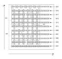
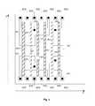
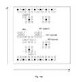
- FIG. 14is an illustration showing a semiconductor chip structure, in accordance with one embodiment of the present invention.
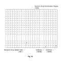
- FIG. 15is an illustration showing an exemplary chip implementing the dynamic array architecture, in accordance with one embodiment of the present invention.
- FIG. 16is an illustration showing a blank canvas of the dynamic array architecture region, in accordance with one embodiment of the present invention.
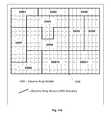
- FIG. 17Ais an illustration showing a number of exemplary dynamic array sections defined within the dynamic array architecture region, in accordance with one embodiment of the present invention.
- FIG. 17Bis an illustration showing a number of dynamic array sections defined at a higher vertical position within the dynamic array architecture region, in accordance with one embodiment of the present invention.
- FIG. 17Cis an illustration showing a side view of the DAS stack of FIG. 17B , in accordance with one embodiment of the present invention.
- FIG. 18is an illustration showing a substrate level of DAS10, in accordance with one embodiment of the present invention.
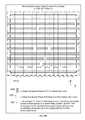
- FIG. 19Ais an illustration showing a gate electrode level virtual grate for the DAS10 example, in accordance with one embodiment of the present invention.
- FIG. 19 A 1is an illustration showing a virtual grate of the gate electrode level set at a pitch equal to one-half of the minimum center-to-center spacing between adjacent contacted gate electrode features, in accordance with one embodiment of the present invention
- FIG. 19Bis an illustration showing full-length linear conductive features defined along each line of the gate electrode level virtual grate of FIG. 19A , in accordance with one embodiment of the present invention.
- FIG. 19 B 1is an illustration showing linear conductive features defined along various lines of the gate electrode level virtual grate of FIG. 19 A 1 , in accordance with one embodiment of the present invention
- FIG. 19Cis an illustration showing a segmentation of the linear conductive features of FIG. 19B , in accordance with one embodiment of the present invention.
- FIG. 19Dis an illustration showing the gate electrode level segmented features of FIG. 19C with a region within which a non-functional linear conductive feature has been eliminated;
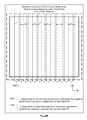
- FIG. 20Ais an illustration showing a first interconnect level virtual grate for the DAS10 example, in accordance with one embodiment of the present invention.
- FIG. 20 A 1is an illustration showing a virtual grate of the first interconnect level set at a pitch equal to one-half of the minimum center-to-center spacing between adjacent contacted linear conductive features of the first interconnect level, in accordance with one embodiment of the present invention
- FIG. 20Bis an illustration showing full-length linear conductive features defined along each line of the first interconnect level virtual grate of FIG. 20A , in accordance with one embodiment of the present invention
- FIG. 20B 1is an illustration showing linear conductive features defined along various lines of the first interconnect level virtual grate of FIG. 20 A 1 , in accordance with one embodiment of the present invention
- FIG. 20Cis an illustration showing a segmentation of the linear conductive features of FIG. 20B , in accordance with one embodiment of the present invention.
- FIG. 21Ais an illustration showing a second interconnect level virtual grate for the DAS10 example, in accordance with one embodiment of the present invention.
- FIG. 21Bis an illustration showing the spatial relationship between the second interconnect level and gate electrode level virtual grates for the DAS10 example, as defined based on a 3-to-2 pitch relationship between second interconnect level and gate electrode level conductive features, in accordance with one embodiment of the present invention
- FIG. 21Cis an illustration showing full-length linear conductive features defined along each line of the second interconnect level virtual grate, in accordance with one embodiment of the present invention.
- FIG. 21Dis an illustration showing a segmentation of the linear conductive features within the second interconnect level, in accordance with one embodiment of the present invention.
- FIG. 22Ais an illustration showing a second interconnect level virtual grate for the DAS10 example, as defined based on a 4-to-3 pitch relationship between second interconnect level and gate electrode level conductive features, in accordance with one embodiment of the present invention
- FIG. 22Bis an illustration showing the spatial relationship between the second interconnect level and gate electrode level virtual grates for the dynamic array section, as defined based on a 4-to-3 pitch relationship between second interconnect level and gate electrode level conductive features, in accordance with one embodiment of the present invention
- FIG. 22Cis an illustration showing full-length linear conductive features defined along each line of the second interconnect level virtual grate, in accordance with one embodiment of the present invention.
- FIG. 22Dis an illustration showing a segmentation of the linear conductive features of FIG. 22C within the second interconnect level, in accordance with one embodiment of the present invention.
- FIG. 23is an illustration showing the second interconnect level of FIG. 22D with a number of exemplary via locations identified thereon, in accordance with one embodiment of the present invention.
- FIG. 24Ais an illustration showing a third interconnect level virtual grate for the DAS10 example, in accordance with one embodiment of the present invention.
- FIG. 24Bis an illustration showing a spatial relationship between the third interconnect level and first interconnect level virtual grates for the DAS10 example, in accordance with one embodiment of the present invention.
- FIG. 24Cis an illustration showing full-length linear conductive features defined along each line of the third interconnect level virtual grate, in accordance with one embodiment of the present invention.
- FIG. 24Dis an illustration showing a segmentation of the linear conductive features within the third interconnect level, in accordance with one embodiment of the present invention.
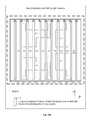
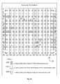
- FIG. 25Ais an illustration showing a number of exemplary DASs with their respective manufacturing assurance boundary compatibility designations, in accordance with one embodiment of the present invention.
- FIG. 25Bis an illustration showing an exemplary assembly of the DASs of FIG. 25A on a DAS grid according to their respective manufacturing assurance boundary compatibility designations, in accordance with one embodiment of the present invention
- FIG. 25Cis an illustration showing an exemplary assembly of the DASs of FIG. 25A on a DAS grid according to their respective manufacturing assurance boundary compatibility designations with intentionally defined empty areas, in accordance with one embodiment of the present invention
- FIG. 26A-1is an illustration showing a level of an exemplary DAS, in accordance with one embodiment of the present invention.
- FIG. 26A-2is an illustration showing the exemplary DAS of FIG. 26A-1 with its DAS halo region pre-defined to include a number of reinforcement features, in accordance with one embodiment of the present invention
- FIG. 26B-1is an illustration showing a level of another exemplary DAS, in accordance with one embodiment of the present invention.
- FIG. 26B-2is an illustration showing the exemplary DAS of FIG. 26B-1 with its DAS halo region pre-defined to include a number of reinforcement features, in accordance with one embodiment of the present invention
- FIG. 26C-1is an illustration showing an exemplary placement of the DAS of FIG. 26A-2 and the DAS of FIG. 26B-2 on a DAS grid, in accordance with one embodiment of the present invention
- FIG. 26C-2is an illustration showing an exemplary placement of the DAS of FIG. 26A-2 and the DAS of FIG. 26B-2 on a DAS grid without regard to their respective DAS halos, in accordance with one embodiment of the present invention
- FIG. 26C-3is an illustration showing the DAS cluster of FIG. 26C-2 having a DAS halo boundary defined around the periphery of the DAS cluster to form a DAS halo region, in accordance with one embodiment of the present invention
- FIG. 26C-4is an illustration showing the defined content of the DAS halo region of FIG. 26C-3 , in accordance with one embodiment of the present invention.
- FIG. 26C-5is an illustration showing the particular level of the DAS cluster of FIG. 26C-4 having a number of DAS interconnection segments defined therein, in accordance with one embodiment of the present invention
- FIG. 26D-1is an illustration showing a flowchart of a method for defining a dynamic array architecture region of a semiconductor chip, in accordance with one embodiment of the present invention, in accordance with one embodiment of the present invention;
- FIG. 26D-2is an illustration showing a flowchart of a method for defining a dynamic array architecture region of a semiconductor chip, in accordance with one embodiment of the present invention.
- FIG. 27Ais an illustration showing an exemplary DAS that defines a logic cell, in accordance with one embodiment of the present invention.
- FIG. 27Bshows a number of instances of the example DAS of FIG. 27A placed adjacent to each other so as to share DAS components that extend beyond the DAS boundary, in accordance with one embodiment of the present invention
- FIG. 28Ais an illustration showing a flowchart of a method for designing a semiconductor chip having one or more functionally interfaced dynamic array sections, in accordance with one embodiment of the present invention
- FIG. 28Bis an illustration showing a continuation of the flowchart of the method of FIG. 28A , in accordance with one embodiment of the present invention.
- FIG. 28Cis an illustration showing an expansion of the operation 2809 of FIG. 28B , in accordance with one embodiment of the present invention.
- FIG. 29Ais an illustration showing a flowchart of a method for designing a semiconductor chip having one or more functionally interfaced dynamic array sections, in accordance with one embodiment of the present invention.
- FIG. 29Bis an illustration showing an expansion of the operation 2907 of FIG. 29A , in accordance with one embodiment of the present invention.
- FIG. 30is an illustration showing a flowchart of a method for designing a DAS of a semiconductor chip, in accordance with one embodiment of the present invention.
- FIG. 31is an illustration showing a flowchart of a method for defining a dynamic array section to be manufactured on a semiconductor chip, in accordance with one embodiment of the present invention.
- FIG. 32is an illustration showing a flowchart of a method for designing a semiconductor chip having one or more functionally interfaced dynamic array sections, in accordance with one embodiment of the present invention.
- FIG. 33is an illustration showing an example of different phasings in a second interconnect level of adjacently disposed logic cells defined within a DAS, in accordance with one embodiment of the present invention.
- lithographic gapis defined as the difference between the minimum size of a feature to be defined and the wavelength of light used to render the feature in the lithographic process, wherein the feature size is less than the wavelength of the light.
- Current lithographic processesutilize a light wavelength of 193 nm.
- current feature sizesare as small as 65 nm and are expected to soon approach sizes as small as 45 nm. With a size of 65 nm, the shapes are three times smaller than the wavelength of the light used to define the shapes.
- the extent and complexity of light interference contributing to exposure of a given featureis significant. Additionally, the particular shapes associated with the features within the interaction radius of the light source weighs heavily on the type of light interactions that occur.
- designerswere allowed to define essentially any two-dimensional topology of feature shapes so long as a set of design rules were satisfied. For example, in a given layer of the chip, i.e., in a given mask, the designer may have defined two-dimensionally varying features having bends that wrap around each other. When such two-dimensionally varying features are located in neighboring proximity to each other, the light used to expose the features will interact in a complex and generally unpredictable manner. The light interaction becomes increasingly more complex and unpredictable as the feature sizes and relative spacing become smaller.
- the set of design rulesis expanded significantly to adequately address the possible combinations of two-dimensionally varying features.
- This expanded set of design rulesquickly becomes so complicated and unwieldy that application of the expanded set of design rules becomes prohibitively time consuming, expensive, and prone to error.
- the expanded set of design rulesrequires complex verification.
- the expanded set of design rulesmay not be universally applied. Furthermore, manufacturing yield is not guaranteed even if all design rules are satisfied.
- the set of design rulesmay also be modified to include increased margin to account for unpredictable light interaction between the neighboring two-dimensionally varying features. Because the design rules are established in an attempt to cover the random two-dimensional feature topology, the design rules may incorporate a significant amount of margin. While addition of margin in the set of design rules assists with the layout portions that include the neighboring two-dimensionally varying features, such global addition of margin causes other portions of the layout that do not include the neighboring two-dimensionally varying features to be overdesigned, thus leading to decreased optimization of chip area utilization and electrical performance.
- semiconductor product yieldis reduced as a result of parametric failures that stem from variability introduced by design-dependent unconstrained feature topologies, i.e., arbitrary two-dimensionally varying features disposed in proximity to each other.
- these parametric failuresmay result from failure to accurately print contacts and vias and from variability in fabrication processes.
- the variability in fabrication processesmay include CMP dishing, layout feature shape distortion due to photolithography, gate distortion, oxide thickness variability, implant variability, and other fabrication related phenomena.
- the dynamic array architecture of the present inventionis defined to address the above-mentioned semiconductor manufacturing process variability.
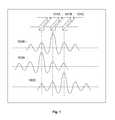
- FIG. 1is an illustration showing a number of neighboring layout features and a representation of light intensity used to render each of the layout features, in accordance with one embodiment of the present invention.
- three neighboring linear-shaped layout features( 101 A- 101 C) are depicted as being disposed in a substantially parallel relationship within a given mask layer.
- the distribution of light intensity from a layout feature shapeis represented by a sinc function.
- the sinc functions( 103 A- 103 C) represent the distribution of light intensity from each of the layout features ( 101 A- 101 C, respectively).
- the neighboring linear-shaped layout features ( 101 A- 101 C)are spaced apart at locations corresponding to peaks of the sinc functions ( 103 A- 103 C).
- a forbidden pitchi.e., forbidden layout feature spacing, occurs when the neighboring layout features ( 101 A- 101 C) are spaced such that peaks of the sinc function associated with one layout feature align with valleys of the sinc function associated with another layout feature, thus causing destructive interference of the light energy.
- the destructive interference of the light energycauses the light energy focused at a given location to be reduced. Therefore, to realize the beneficial constructive light interference associated with neighboring layout features, it is necessary to predict the layout feature spacing at which the constructive overlap of the sinc function peaks will occur.
- Predictable constructive overlap of the sinc function peaks and corresponding layout feature shape enhancementcan be realized if the layout feature shapes are rectangular, near the same size, and are oriented in the same direction, as illustrated by the layout features ( 101 A- 101 C) in FIG. 1 . In this manner, resonant light energy from neighboring layout feature shapes is used to enhance the exposure of a particular layout feature shape.
- FIG. 2is an illustration showing a generalized stack of layers used to define a dynamic array architecture, in accordance with one embodiment of the present invention. It should be appreciated that the generalized stack of layers used to define the dynamic array architecture, as described with respect to FIG. 2 , is not intended to represent an exhaustive description of the CMOS manufacturing process. However, the dynamic array is to be built in accordance with standard CMOS manufacturing processes. Generally speaking, the dynamic array architecture includes both the definition of the underlying structure of the dynamic array and the techniques for assembling the dynamic array for optimization of area utilization and manufacturability. Thus, the dynamic array is designed to optimize semiconductor manufacturing capabilities.
- the dynamic arrayis built-up in a layered manner upon a base substrate 201 , e.g., upon a silicon substrate, or silicon-on-insulator (SOI) substrate.
- Diffusion regions 203are defined in the base substrate 201 .
- the diffusion regions 203represent selected regions of the base substrate 201 within which impurities are introduced for the purpose of modifying the electrical properties of the base substrate 201 .
- diffusion contacts 205are defined to enable connection between the diffusion regions 203 and conductor lines.
- the diffusion contacts 205are defined to enable connection between source and drain diffusion regions 203 and their respective conductor nets.
- gate electrode features 207are defined above the diffusion regions 203 to form transistor gates.
- Gate electrode contacts 209are defined to enable connection between the gate electrode features 207 and conductor lines.
- the gate electrode contacts 209are defined to enable connection between transistor gates and their respective conductor nets.
- Interconnect layersare defined above the diffusion contact 205 layer and the gate electrode contact layer 209 .
- the interconnect layersinclude a first metal (metal 1) layer 211 , a first via (via 1) layer 213 , a second metal (metal 2) layer 215 , a second via (via 2) layer 217 , a third metal (metal 3) layer 219 , a third via (via 3) layer 221 , and a fourth metal (metal 4) layer 223 .
- the metal and via layersenable definition of the desired circuit connectivity.
- the metal and via layersenable electrical connection of the various diffusion contacts 205 and gate electrode contacts 209 such that the logic function of the circuitry is realized.
- the dynamic array architectureis not limited to a specific number of interconnect layers, i.e., metal and via layers.
- the dynamic arraymay include additional interconnect layers 225 , beyond the fourth metal (metal 4) layer 223 .
- the dynamic arraymay include less than four metal layers.
- the dynamic arrayis defined such that layers (other than the diffusion region layer 203 ) are restricted with regard to layout feature shapes that can be defined therein. Specifically, in each layer other than the diffusion region layer 203 , only linear-shaped layout features are allowed.
- a linear-shaped layout feature in a given layeris characterized as having a consistent vertical cross-section shape and extending in a single direction over the substrate.
- the linear-shaped layout featuresdefine structures that are one-dimensionally varying.
- the diffusion regions 203are not required to be one-dimensionally varying, although they are allowed to be if necessary.
- the diffusion regions 203 within the substratecan be defined to have any two-dimensionally varying shape with respect to a plane coincident with a top surface of the substrate.
- the number of diffusion bend topologiesis limited such that the interaction between the bend in diffusion and the conductive material, e.g., polysilicon, that forms the gate electrode of the transistor is predictable and can be accurately modeled.
- the linear-shaped layout features in a given layerare positioned to be parallel with respect to each other. Thus, the linear-shaped layout features in a given layer extend in a common direction over the substrate and parallel with the substrate. The specific configurations and associated requirements of the linear-shaped features in the various layers 207 - 223 are discussed further with regard to FIGS. 3-15C .
- the underlying layout methodology of the dynamic arrayuses constructive light interference of light waves in the lithographic process to reinforce exposure of neighboring shapes in a given layer. Therefore, the spacing of the parallel, linear-shaped layout features in a given layer is designed around the constructive light interference of the standing light waves such that lithographic correction (e.g., OPC/RET) is minimized or eliminated.
- lithographic correctione.g., OPC/RET
- the dynamic array defined hereinexploits the light interaction between neighboring features, rather than attempting to compensate for the light interaction between neighboring features.
- the standing light wave for a given linear-shaped layout featurecan be accurately modeled, it is possible to predict how the standing light waves associated with the neighboring linear-shaped layout features disposed in parallel in a given layer will interact. Therefore, it is possible to predict how the standing light wave used to expose one linear-shaped feature will contribute to the exposure of its neighboring linear-shaped features. Prediction of the light interaction between neighboring linear-shaped features enables the identification of an optimum feature-to-feature spacing such that light used to render a given shape will reinforce its neighboring shapes.
- the feature-to-feature spacing in a given layeris defined as the feature pitch, wherein the pitch is the center-to-center separation distance between adjacent linear-shaped features in a given layer.
- the linear-shaped layout features in a given layerare spaced such that constructive and destructive interference of the light from neighboring features will be optimized to produce the best rendering of all features in the neighborhood.
- the feature-to-feature spacing in a given layeris proportional to the wavelength of the light used to expose the features.
- the light used to expose each feature within about a five light wavelength distance from a given featurewill serve to enhance the exposure of the given feature to some extent.
- the exploitation of constructive interference of the standing light waves used to expose neighboring featuresenables the manufacturing equipment capability to be maximized and not be limited by concerns regarding light interactions during the lithography process.
- the dynamic arrayincorporates a restricted topology in which the features within each layer (other than diffusion) are required to be linear-shaped features that are oriented in a parallel manner to traverse over the substrate in a common direction.
- the restricted topology of the dynamic arraythe light interaction in the photolithography process can be optimized such that the printed image on the mask is essentially identical to the drawn shape in the layout, i.e., essentially a 100% accurate transfer of the layout onto the resist is achieved.
- FIG. 3Ais an illustration showing an exemplary base grid to be projected onto the dynamic array to facilitate definition of the restricted topology, in accordance with one embodiment of the present invention.
- the base gridcan be used to facilitate parallel placement of the linear-shaped features in each layer of the dynamic array at the appropriate optimized pitch.
- the base gridcan be considered as a projection on each layer of the dynamic array. Also, it should be understood that the base grid is projected in a substantially consistent manner with respect to position on each layer of the dynamic array, thus facilitating accurate feature stacking and alignment.
- the base gridis defined as a rectangular grid, i.e., Cartesian grid, in accordance with a first reference direction (x) and a second reference direction (y).
- the gridpoint-to-gridpoint spacing in the first and second reference directionscan be defined as necessary to enable definition of the linear-shaped features at the optimized feature-to-feature spacing.
- the gridpoint spacing in the first reference direction (x)can be different than the gridpoint spacing in the second reference direction (y).
- a single base gridis projected across the entire die to enable location of the various linear-shaped features in each layer across the entire die.
- FIG. 3Bis an illustration showing separate base grids projected across separate regions of the die, in accordance with an exemplary embodiment of the present invention.
- the base gridis defined with consideration for the light interaction function, i.e., the sinc function, and the manufacturing capability, wherein the manufacturing capability is defined by the manufacturing equipment and processes to be utilized in fabricating the dynamic array.
- the base gridis defined such that the spacing between gridpoints enables alignment of peaks in the sinc functions describing the light energy projected upon neighboring gridpoints. Therefore, linear-shaped features optimized for lithographic reinforcement can be specified by drawing a line from a first gridpoint to a second gridpoint, wherein the line represents a rectangular structure of a given width. It should be appreciated that the various linear-shaped features in each layer can be specified according to their endpoint locations on the base grid and their width.
- FIG. 3Cis an illustration showing an exemplary linear-shaped feature 301 defined to be compatible with the dynamic array, in accordance with one embodiment of the present invention.
- the linear-shaped feature 301has a substantially rectangular cross-section defined by a width 303 and a height 307 .
- the linear-shaped feature 301extends in a linear direction to a length 305 .
- a cross-section of the linear-shaped feature, as defined by its width 303 and height 307is substantially uniform along its length 305 . It should be understood, however, that lithographic effects may cause a rounding of the ends of the linear-shaped feature 301 .
- 3Aare shown to illustrate an exemplary orientation of the linear-shaped feature on the dynamic array.
- the linear-shaped featuremay be oriented to have its length 305 extend in either the first reference direction (x), the second reference direction (y), or in diagonal direction defined relative to the first and second reference directions (x) and (y).
- the linear-shaped featureis defined in a plane that is substantially parallel to a top surface of the substrate upon which the dynamic array is built.
- the linear-shaped featureis free of bends, i.e., change in direction, in the plane defined by the first and second reference directions.
- FIG. 3Dis an illustration showing another exemplary linear-shaped feature 317 defined to be compatible with the dynamic array, in accordance with one embodiment of the present invention.
- the linear-shaped feature 317has a trapezoidal cross-section defined by a lower width 313 , an upper width 315 , and a height 309 .
- the linear-shaped feature 317extends in a linear direction to a length 311 .
- the cross-section of the linear-shaped feature 317is substantially uniform along its length 311 . It should be understood, however, that lithographic effects may cause a rounding of the ends of the linear-shaped feature 317 .
- the linear-shaped feature 317may be oriented to have its length 311 extend in either the first reference direction (x), the second reference direction (y), or in diagonal direction defined relative to the first and second reference directions (x) and (y). Regardless of the particular orientation of the linear-shaped feature 317 with regard to the first and second reference directions (x) and (y), it should be understood that the linear-shaped feature 317 is defined in a plane that is substantially parallel to a top surface of the substrate upon which the dynamic array is built. Also, it should be understood that the linear-shaped feature 317 is free of bends, i.e., change in direction, in the plane defined by the first and second reference directions.
- FIGS. 3C and 3Dexplicitly discuss linear shaped features having rectangular and trapezoidal cross-sections, respectively, it should be understood that the linear shaped features having other types of cross-sections can be defined within the dynamic array. Therefore, essentially any suitable cross-sectional shape of the linear-shaped feature can be utilized so long as the linear-shaped feature is defined to have a length that extends in one direction, and is oriented to have its length extend in either the first reference direction (x), the second reference direction (y), or in diagonal direction defined relative to the first and second reference directions (x) and (y).
- the layout architecture of the dynamic arrayfollows the base grid pattern.
- grid pointsto represent where changes in direction occur in diffusion, wherein gate electrode and metal linear-shaped features are placed, where contacts are placed, where opens are in the linear-shaped gate electrode and metal features, etc.
- the pitch of the gridpointsi.e., the gridpoint-to-gridpoint spacing, should be set for a given feature line width, e.g., width 303 in FIG. 3C , such that exposure of neighboring linear-shaped features of the given feature line width will reinforce each other, wherein the linear-shaped features are centered on gridpoints.
- the gridpoint spacing in the first reference direction (x)is set by the required gate electrode gate pitch.
- the gridpoint pitch in the second reference direction (y)is set by the metal 1 and metal 3 pitch.
- the gridpoint pitch in the second reference direction (y)is about 0.24 micron.
- metal 1 and metal 2 layerswill have a common spacing and pitch. A different spacing and pitch may be used above the metal 2 layer.
- the various layers of the dynamic arrayare defined such that the linear-shaped features in adjacent layers extend in a crosswise manner with respect to each other.
- the linear-shaped features of adjacent layersmay extend orthogonally, i.e., perpendicularly with respect to each other.
- the linear-shaped features of one layermay extend across the linear-shaped features of an adjacent layer at an angle, e.g., at about 45 degrees.
- the linear-shaped feature of one layerextend in the first reference direction (x) and the linear-shaped features of the adjacent layer extend diagonally with respect to the first (x) and second (y) reference directions. It should be appreciated that to route a design in the dynamic array having the linear-shaped features positioned in the crosswise manner in adjacent layers, opens can be defined in the linear-shaped features, and contacts and vias can be defined as necessary.
- the dynamic arrayminimizes the use of bends in layout shapes to eliminate unpredictable lithographic interactions. Specifically, prior to OPC or other RET processing, the dynamic array allows bends in the diffusion layer to enable control of device sizes, but does not allow bends in layers above the diffusion layer.
- the layout features in each layer above the diffusion layerare linear in shape, e.g., FIG. 3C , and disposed in a parallel relationship with respect to each other.
- the linear shapes and parallel positioning of layout featuresare implemented in each stack layer of the dynamic array where predictability of constructive light interference is necessary to ensure manufacturability.
- the linear shapes and parallel positioning of layout featuresare implemented in the dynamic array in each layer above diffusion through metal 2. Above metal 2, the layout features may be of sufficient size and shape that constructive light interference is not required to ensure manufacturability. However, the presence of constructive light interference in patterning layout features above metal 2 may be beneficial.
- FIGS. 4 through 14An exemplary buildup of dynamic array layers from diffusion through metal 2 are described with respect to FIGS. 4 through 14 . It should be appreciated that the dynamic array described with respect to FIGS. 4 through 14 is provided by way of example only, and is not intended to convey limitations of the dynamic array architecture. The dynamic array can be used in accordance with the principles presented herein to define essentially any integrated circuit design.
- FIG. 4is an illustration showing a diffusion layer layout of an exemplary dynamic array, in accordance with one embodiment of the present invention.
- the diffusion layer of FIG. 4shows a p-diffusion region 401 and an n-diffusion region 403 . While the diffusion regions are defined according to the underlying base grid, the diffusion regions are not subject to the linear-shaped feature restrictions associated with the layers above the diffusion layer.
- the diffusion regions 401 and 403include diffusion squares 405 defined where diffusion contacts will be located.
- the diffusion regions 401 and 403do not include extraneous jogs or corners, thus improving the use of lithographic resolution and enabling more accurate device extraction.
- n+ mask regions ( 412 and 416 ) and p+ mask regions ( 410 and 414 )are defined as rectangles on the (x), (y) grid with no extraneous jogs or notches. This style permits use of larger diffusion regions, eliminates need for OPC/RET, and enables use of lower resolution and lower cost lithographic systems, e.g., i-line illumination at 365 nm. It should be appreciated that the n+ mask region 416 and the p+ mask region 410 , as depicted in FIG. 4 , are for an embodiment that does not employ well-biasing. In an alternative embodiment where well-biasing is to be used, the n+ mask region 416 shown in FIG. 4 will actually be defined as a p+ mask region. Also, in this alternative embodiment, the p+ mask region 410 shown in FIG. 4 will actually be defined as a n+ mask region.
- FIG. 5is an illustration showing a gate electrode layer and a diffusion contact layer above and adjacent to the diffusion layer of FIG. 4 , in accordance with one embodiment of the present invention.
- the gate electrode features 501define the transistor gates.
- the gate electrode features 501are defined as linear shaped features extending in a parallel relationship across the dynamic array in the second reference direction (y).
- the gate electrode features 501are defined to have a common width.
- one or more of the gate electrode featurescan be defined to have a different width.
- FIG. 5shows a gate electrode features 501 A that has a larger width relative to the other gate electrode features 501 .
- gate electrode features 501The pitch (center-to-center spacing) of the gate electrode features 501 is minimized while ensuring optimization of lithographic reinforcement, i.e., resonant imaging, provided by neighboring gate electrode features 501 .
- gate electrode features 501 extending across the dynamic array in a given lineare referred to as a gate electrode track.
- the gate electrode features 501form n-channel and p-channel transistors as they cross the diffusion regions 403 and 401 , respectively.
- Optimal gate electrode feature 501 printingis achieved by drawing gate electrode features 501 at every grid location, even though no diffusion region may be present at some grid locations.
- long continuous gate electrode features 501tend to improve line end shortening effects at the ends of gate electrode features within the interior of the dynamic array. Additionally, gate electrode printing is significantly improved when all bends are removed from the gate electrode features 501 .
- Each of the gate electrode tracksmay be interrupted, i.e., broken, any number of times in linearly traversing across the dynamic array in order to provide required electrical connectivity for a particular logic function to be implemented.
- interruptedi.e., broken
- the separation between ends of the gate electrode track segments at the point of interruptionis minimized to the extent possible taking into consideration the manufacturing capability and electrical effects.
- optimal manufacturabilityis achieved when a common end-to-end spacing is used between features within a particular layer.
- Minimizing the separation between ends of the gate electrode track segments at the points of interruptionserves to maximize the lithographic reinforcement, and uniformity thereof, provided from neighboring gate electrode tracks.
- the interruptions of the adjacent gate electrode tracksare made such that the respective points of interruption are offset from each other so as to avoid, to the extent possible, an occurrence of neighboring points of interruption. More specifically, points of interruption within adjacent gate electrode tracks are respectively positioned such that a line of sight does not exist through the points of interruption, wherein the line of sight is considered to extend perpendicularly to the direction in which the gate electrode tracks extend over the substrate.
- the gate electrodesmay extend through the boundaries at the top and bottom of the cells, i.e., the PMOS or NMOS cells. This embodiment would enable bridging of neighboring cells.
- diffusion contacts 503are defined at each diffusion square 405 to enhance the printing of diffusion contacts via resonant imaging.
- the diffusion squares 405are present around every diffusion contact 503 to enhance the printing of the power and ground connection polygons at the diffusion contacts 503 .
- the gate electrode features 501 and diffusion contacts 503share a common grid spacing. More specifically, the gate electrode feature 501 placement is offset by one-half the grid spacing relative to the diffusion contacts 503 . For example, if the gate electrode features 501 and diffusion contact 503 grid spacing is 0.36 ⁇ m, then the diffusion contacts are placed such that the x-coordinate of their center falls on an integer multiple of 0.36 ⁇ m, while the x-coordinate of the center of each gate electrode feature 501 minus 0.18 ⁇ m should be an integer multiple of 0.36 ⁇ m. In the present example, the x-coordinates are represented by the following:
- the grid based system of the dynamic arrayensures that all contacts (diffusion and gate electrode) will land on a horizontal grid that is equal to a multiple of one-half of the diffusion contact grid and a vertical grid that is set by the metal 1 pitch.
- the gate electrode feature and diffusion contact gridis 0.36 ⁇ m.
- the diffusion contacts and gate electrode contactswill land on a horizontal grid that is a multiple of 0.18 ⁇ m.
- the vertical grid for 90 nm process technologiesis about 0.24 ⁇ m.
- FIG. 6is an illustration showing a gate electrode contact layer defined above and adjacent to the gate electrode layer of FIG. 5 , in accordance with one embodiment of the present invention.
- gate electrode contacts 601are drawn to enable connection of the gate electrode features 501 to the overlying metal conduction lines.
- design ruleswill dictate the optimum placement of the gate electrode contacts 601 .
- the gate electrode contactsare drawn on top of the transistor endcap regions. This embodiment minimizes white space in the dynamic array when design rules specify long transistor endcaps. In some process technologies white space may be minimized by placing a number of gate electrode contacts for a cell in the center of the cell.
- the gate electrode contact 601is oversized in the direction perpendicular to the gate electrode feature 501 to ensure overlap between the gate electrode contact 601 and the gate electrode feature 501 .
- FIG. 7Ais an illustration showing a traditional approach for making contact to a gate electrode, e.g., polysilicon feature.
- a gate electrodee.g., polysilicon feature.
- an enlarged rectangular gate electrode region 707is defined where a gate electrode contact 709 is to be located.
- the enlarged rectangular gate electrode region 707introduces a bend of distance 705 in the gate electrode.
- the bend associated with the enlarged rectangular gate electrode region 707sets up undesirable light interactions and distorts the gate electrode line 711 . Distortion of the gate electrode line 711 is especially problematic when the gate electrode width is about the same as a transistor length.
- FIG. 7Bis an illustration showing a gate electrode contact 601 , e.g., polysilicon contact, defined in accordance with one embodiment of the present invention.
- the gate electrode contact 601is drawn to overlap the edges of the gate electrode feature 501 , and extend in a direction substantially perpendicular to the gate electrode feature 501 .
- the gate electrode contact 601is drawn such that the vertical dimension 703 is same as the vertical dimension used for the diffusion contacts 503 .
- the diffusion contact 503 openingis specified to be 0.12 ⁇ m square then the vertical dimension of the gate electrode contact 601 is drawn at 0.12 ⁇ m.
- the gate electrode contact 601can be drawn such that the vertical dimension 703 is different from the vertical dimension used for the diffusion contacts 503 .
- the gate electrode contact 601 extension 701 beyond the gate electrode feature 501is set such that maximum overlap is achieved between the gate electrode contact 601 and the gate electrode feature 501 .
- the extension 701is defined to accommodate line end shortening of the gate electrode contact 601 , and misalignment between the gate electrode contact layer and gate electrode feature layer.
- the length of the gate electrode contact 601is defined to ensure maximum surface area contact between the gate electrode contact 601 and the gate electrode feature 501 , wherein the maximum surface area contact is defined by the width of the gate electrode feature 501 .
- FIG. 8Ais an illustration showing a metal 1 layer defined above the gate electrode contact layer of FIG. 6 , in accordance with one embodiment of the present invention.
- the metal 1 layerincludes a number of metal 1 tracks 801 - 821 defined to include linear shaped features extending in a parallel relationship across the dynamic array.
- the metal 1 tracks 801 - 821extend in a direction substantially perpendicular to the gate electrode features 501 in the underlying gate electrode layer of FIG. 5 .
- the metal 1 tracks 801 - 821extend linearly across the dynamic array in the first reference direction (x).
- the pitch (center-to-center spacing) of the metal 1 tracks 801 - 821is minimized while ensuring optimization of lithographic reinforcement, i.e., resonant imaging, provided by neighboring metal 1 tracks 801 - 821 .
- the metal 1 tracks 801 - 821are centered on a vertical grid of about 0.24 ⁇ m for a 90 nm process technology.
- Each of the metal 1 tracks 801 - 821may be interrupted, i.e., broken, any number of times in linearly traversing across the dynamic array in order to provide required electrical connectivity for a particular logic function to be implemented.
- the separation between ends of the metal 1 track segments at the point of interruptionis minimized to the extent possible taking into consideration manufacturing capability and electrical effects. Minimizing the separation between ends of the metal 1 track segments at the points of interruption serves to maximize the lithographic reinforcement, and uniformity thereof, provided from neighboring metal 1 tracks.
- the interruptions of the adjacent metal 1 tracksare made such that the respective points of interruption are offset from each other so as to avoid, to the extent possible, an occurrence of neighboring points of interruption. More specifically, points of interruption within adjacent metal 1 tracks are respectively positioned such that a line of sight does not exist through the points of interruption, wherein the line of sight is considered to extend perpendicularly to the direction in which the metal 1 tracks extend over the substrate.
- the metal 1 track 801is connected to the ground supply, and the metal 1 track 821 is connected to the power supply voltage.
- the widths of the metal 1 tracks 801 and 821are the same as the other metal 1 tracks 803 - 819 .
- the widths of metal 1 tracks 801 and 821are larger than the widths of the other metal 1 tracks 803 - 819 .
- FIG. 8Bis an illustration showing the metal 1 layer of FIG. 8A with larger track widths for the metal 1 ground and power tracks ( 801 A and 821 A), relative to the other metal 1 tracks 803 - 819 .
- the metal 1 track patternis optimally configured to optimize the use of “white space” (space not occupied by transistors).
- the example of FIG. 8Aincludes the two shared metal 1 power tracks 801 and 821 , and nine metal 1 signal tracks 803 - 819 .
- Metal 1 tracks 803 , 809 , 811 , and 819are defined as gate electrode contact tracks in order to minimize white space.
- Metal 1 tracks 805 and 807are defined to connect to n-channel transistor source and drains.
- Metal 1 tracks 813 , 815 , and 817are defined to connect to p-channel source and drains.
- any of the nine metal 1 signal tracks 803 - 819can be used as a feed through if no connection is required.
- metal 1 tracks 813 and 815are configured as feed through connections.
- FIG. 9is an illustration showing a via 1 layer defined above and adjacent to the metal 1 layer of FIG. 8A , in accordance with one embodiment of the present invention.
- Vias 901are defined in the via 1 layer to enable connection of the metal 1 tracks 801 - 821 to higher level conduction lines.
- FIG. 10is an illustration showing a metal 2 layer defined above and adjacent to the via 1 layer of FIG. 9 , in accordance with one embodiment of the present invention.
- the metal 2 layerincludes a number of metal 2 tracks 1001 defined as linear shaped features extending in a parallel relationship across the dynamic array.
- the metal 2 tracks 1001extend in a direction substantially perpendicular to the metal 1 tracks 801 - 821 in the underlying metal 1 layer of FIG. 8A , and in a direction substantially parallel to the gate electrode tracks 501 in the underlying gate electrode layer of FIG. 5 .
- the metal 2 tracks 1001extend linearly across the dynamic array in the second reference direction (y).
- the pitch (center-to-center spacing) of the metal 2 tracks 1001is minimized while ensuring optimization of lithographic reinforcement, i.e., resonant imaging, provided by neighboring metal 2 tracks. It should be appreciated that regularity can be maintained on higher level interconnect layers in the same manner as implemented in the gate electrode and metal 1 layers.
- the gate electrode feature 501 pitch and the metal 2 track pitchis the same.
- the contacted gate electrode pitche.g., polysilicon-to-polysilicon space with a diffusion contact in between
- the metal 2 track pitchis optimally set to be 2 ⁇ 3 or 3 ⁇ 4 of the contacted gate electrode pitch.
- the gate electrode track and metal 2 trackalign at every two gate electrode track pitches and every three metal 2 track pitches.
- the optimum contacted gate electrode track pitchis 0.36 ⁇ m
- the optimum metal 2 track pitchis 0.24 ⁇ m.
- the gate electrode track and the metal 2 trackalign at every three gate electrode pitches and every four metal 2 pitches.
- the optimum contacted gate electrode track pitchis 0.36 ⁇ m
- the optimum metal 2 track pitchis 0.27 ⁇ m.
- Each of the metal 2 tracks 1001may be interrupted, i.e., broken, any number of times in linearly traversing across the dynamic array in order to provide required electrical connectivity for a particular logic function to be implemented.
- the separation between ends of the metal 2 track segments at the point of interruptionis minimized to the extent possible taking into consideration manufacturing and electrical effects. Minimizing the separation between ends of the metal 2 track segments at the points of interruption serves to maximize the lithographic reinforcement, and uniformity thereof, provided from neighboring metal 2 tracks.
- the interruptions of the adjacent metal 2 tracksare made such that the respective points of interruption are offset from each other so as to avoid, to the extent possible, an occurrence of neighboring points of interruption. More specifically, points of interruption within adjacent metal 2 tracks are respectively positioned such that a line of sight does not exist through the points of interruption, wherein the line of sight is considered to extend perpendicularly to the direction in which the metal 2 tracks extend over the substrate.
- the conduction lines in a given metal layer above the gate electrode layermay traverse the dynamic array in a direction coincident with either the first reference direction (x) or the second reference direction (y). It should be further appreciated that the conduction lines in a given metal layer above the gate electrode layer may traverse the dynamic array in a diagonal direction relative to the first and second reference directions (x) and (y).
- FIG. 11is an illustration showing conductor tracks 1101 traversing the dynamic array in a first diagonal direction relative to the first and second reference directions (x) and (y), in accordance with one embodiment of the present invention.
- FIG. 12is an illustration showing conductor tracks 1201 traversing the dynamic array in a second diagonal direction relative to the first and second reference directions (x) and (y), in accordance with one embodiment of the present invention.
- the diagonal traversing conductor tracks 1101 and 1201 of FIGS. 11 and 12may be interrupted, i.e., broken, any number of times in linearly traversing across the dynamic array in order to provide required electrical connectivity for a particular logic function to be implemented.
- the separation between ends of the diagonal conductor track at the point of interruptionis minimized to the extent possible taking into consideration manufacturing and electrical effects. Minimizing the separation between ends of the diagonal conductor track at the points of interruption serves to maximize the lithographic reinforcement, and uniformity thereof, provided from neighboring diagonal conductor tracks.
- FIG. 13Ais an illustration showing an example of a sub-resolution contact layout used to lithographically reinforce diffusion contacts and gate electrode contacts, in accordance with one embodiment of the present invention.
- Sub-resolution contacts 1301are drawn such that they are below the resolution of the lithographic system and will not be printed.
- the function of the sub-resolution contacts 1301is to increase the light energy at the desired contact locations, e.g., 503 , 601 , through resonant imaging.
- sub-resolution contacts 1301are placed on a grid such that both gate electrode contacts 601 and diffusion contacts 503 are lithographically reinforced.
- sub-resolution contacts 1301are placed on a grid that is equal to one-half the diffusion contact 503 grid spacing to positively impact both gate electrode contacts 601 and diffusion contacts 503 .
- a vertical spacing of the sub-resolution contacts 1301follows the vertical spacing of the gate electrode contacts 601 and diffusion contacts 503 .
- Grid location 1303 in FIG. 13Adenotes a location between adjacent gate electrode contacts 601 .
- a sub-resolution contact 1301 at this grid locationwould create an undesirable bridge between the two adjacent gate electrode contacts 601 . If bridging is likely to occur, a sub-resolution contact 1301 at location 1303 can be omitted.
- FIG. 13Ashows an embodiment where sub-resolution contacts are placed adjacent to actual features to be resolved and not elsewhere, it should be understood that another embodiment may place a sub-resolution contact at each available grid location so as to fill the grid.
- FIG. 13Bis an illustration showing the sub-resolution contact layout of FIG. 13A with sub-resolution contacts defined to fill the grid to the extent possible, in accordance with one embodiment of the present invention. It should be appreciated that while the embodiment of FIG. 13B fills the grid to the extent possible with sub-resolution contacts, placement of sub-resolution contacts is avoided at locations that would potentially cause undesirable bridging between adjacent fully resolved features.
- FIG. 13Cis an illustration showing an example of a sub-resolution contact layout utilizing various shaped sub-resolution contacts, in accordance with one embodiment of the present invention.
- Alternative sub-resolution contact shapescan be utilized so long as the sub-resolution contacts are below the resolution capability of the manufacturing process.
- FIG. 13Cshows the use of “X-shaped” sub-resolution contacts 1305 to focus light energy at the corners of the adjacent contacts.
- the ends of the X-shaped sub-resolution contact 1305are extended to further enhance the deposition of light energy at the corners of the adjacent contacts.
- FIG. 13Dis an illustration showing an exemplary implementation of alternate phase shift masking (APSM) with sub-resolution contacts, in accordance with one embodiment of the present invention.
- APSMalternate phase shift masking
- FIG. 13Asub-resolution contacts are utilized to lithographically reinforce diffusion contacts 503 and gate electrode contacts 601 .
- APSMis used to improve resolution when neighboring shapes create destructive interference patterns.
- the APSM techniquemodifies the mask so that the phase of light traveling through the mask on neighboring shapes is 180 degrees out of phase. This phase shift serves to remove destructive interference and allowing for greater contact density.
- interconnect layersAs feature sizes decrease, semiconductor dies are capable of including more gates. As more gates are included, however, the density of the interconnect layers begins to dictate the die size. This increasing demand on the interconnect layers drives higher levels of interconnect layers. However, the stacking of interconnect layers is limited in part by the topology of the underlying layers. For example, as interconnect layers are built up, islands, ridges, and troughs can occur. These islands, ridges, and troughs can cause breaks in the interconnect lines that cross them.
- the semiconductor manufacturing processutilizes a chemical mechanical polishing (CMP) procedure to mechanically and chemically polish the surface of the semiconductor wafer such that each subsequent interconnect layer is deposited on a substantially flat surface.
- CMPchemical mechanical polishing
- the quality of the CMP processis layout pattern dependent. Specifically, an uneven distribution of a layout features across a die or a wafer can cause too much material to be removed in some places and not enough material to be removed in other places, thus causing variations in the interconnect thickness and unacceptable variations in the capacitance and resistance of the interconnect layer.
- the capacitance and resistance variation within the interconnect layermay alter the timing of a critical net causing design failure.
- the CMP processrequires that dummy fill be added in the areas without interconnect shapes so that a substantially uniform wafer topology is provided to avoid dishing and improve center-to-edge uniformity.
- dummy fillis placed post-design.
- the designeris not aware of the dummy fill characteristics. Consequently, the dummy fill placed post-design may adversely influence the design performance in a manner that has not been evaluated by the designer.
- the conventional topology prior to the dummy fillis unconstrained, i.e., non-uniform, the post-design dummy fill will not be uniform and predictable. Therefore, in the conventional process, the capacitive coupling between the dummy fill regions and the neighboring active nets cannot be predicted by the designer.
- the dynamic array disclosed hereinprovides optimal regularity by maximally filling all interconnect tracks from gate electrode layer upward. If multiple nets are required in a single interconnect track, the interconnect track is split with a minimally spaced gap.
- track 809 representing the metal 1 conduction line in FIG. 8Arepresents three separate nets in the same track, where each net corresponds to a particular track segment. More specifically, there are two poly contact nets and a floating net to fill the track with minimal spacing between the track segments.
- the substantially complete filling of tracksmaintains the regular pattern that creates resonant images across the dynamic array.
- the regular architecture of the dynamic array with maximally filled interconnect tracksensures that the dummy fill is placed in a uniform manner across the die.
- the regular architecture of the dynamic arrayassists the CMP process to produce substantially uniform results across the die/wafer. Also, the regular gate pattern of the dynamic array assists with gate etching uniformity (microloading). Additionally, the regular architecture of the dynamic array combined with the maximally filled interconnect tracks allows the designer to analyze the capacitive coupling effects associated with the maximally filled tracks during the design phase and prior to fabrication.
- the design of the dynamic arraycan be optimized for the maximum capability of the manufacturing equipment and processes. That is to say, because the dynamic array is restricted to the regular architecture for each layer above diffusion, the manufacturer is capable of optimizing the manufacturing process for the specific characteristics of the regular architecture. It should be appreciated that with the dynamic array, the manufacturer does not have to be concerned with accommodating the manufacture of a widely varying set of arbitrarily-shaped layout features as is present in conventional unconstrained layouts.
- the regular architecture implemented within the dynamic arrayallows the light interaction unpredictability in the via lithography to be removed, thus allowing for a reduction in the metal 2 pitch margin.
- a reduction in the metal 2 pitch marginallows for a more dense design, i.e., allows for optimization of chip area utilization.
- the restricted, i.e., regular, topology afforded by the dynamic arraythe margin in the design rules can be reduced.
- the restricted topology afforded by the dynamic arrayalso allows the number of required design rules to be substantially reduced. For example, a typical design rule set for an unconstrained topology could have more than 600 design rules.
- a design rule set for use with the dynamic arraymay have about 45 design rules. Therefore, the effort required to analyze and verify the design against the design rules is decreased by more than a factor of ten with the restricted topology of the dynamic array.
- a correction modelcan be implemented as part of the layout generation for the dynamic array.
- a routercan be programmed to insert a line break having characteristics defined as a function of its surroundings, i.e., as a function of its particular line end gap light interactions.
- the regular architecture of the dynamic arrayallows the line ends to be adjusted by changing vertices rather than by adding vertices.
- the dynamic arraysignificantly reduces the cost and risk of mask production.
- the line end gap interactions in the dynamic arraycan be accurately predicted in the design phase, compensation for the predicted line end gap interactions during the design phase does not increase risk of design failure.
- the designis not required to be represented in terms of physical information. Rather, the design can be represented as a symbolic layout. Thus, the designer can represent the design from a pure logic perspective without having to represent physical characteristics, e.g., sizes, of the design.
- the grid-based netlistwhen translated to physical, matches the optimum design rules exactly for the dynamic array platform.
- a grid-based netlistcan be moved directly to the new technology because there is no physical data in the design representation.
- the grid-based dynamic array systemincludes a rules database, a grid-based (symbolic) netlist, and the dynamic array architecture.
- the grid-based dynamic arrayeliminates topology related failures associated with conventional unconstrained architectures. Also, because the manufacturability of the grid-based dynamic array is design independent, the yield of the design implemented on the dynamic array is independent of the design. Therefore, because the validity and yield of the dynamic array is preverified, the grid-based netlist can be implemented on the dynamic array with preverified yield performance.
- FIG. 14is an illustration showing a semiconductor chip structure 1400 , in accordance with one embodiment of the present invention.
- the semiconductor chip structure 1400represents an exemplary portion of a semiconductor chip, including a diffusion region 1401 having a number of conductive lines 1403 A- 1403 G defined thereover.
- the diffusion region 1401is defined in a substrate 1405 , to define an active region for at least one transistor device.
- the diffusion region 1401can be defined to cover an area of arbitrary shape relative to the substrate 1405 surface.
- the conductive lines 1403 A- 1403 Gare arranged to extend over the substrate 1405 in a common direction 1407 . It should also be appreciated that each of the number of conductive lines 1403 A- 1403 G are restricted to extending over the diffusion region 1401 in the common direction 1407 .
- the conductive lines 1403 A- 1403 G defined immediately over the substrate 1405are polysilicon lines.
- each of the conductive lines 1403 A- 1403 Gis defined to have essentially the same width 1409 in a direction perpendicular to the common direction 1407 of extension.
- some of the conductive lines 1403 A- 1403 Gare defined to have different widths relative to the other conductive lines. However, regardless of the width of the conductive lines 1403 A- 1403 G, each of the conductive lines 1403 A- 1403 G is spaced apart from adjacent conductive lines according to essentially the same center-to-center pitch 1411 .
- some of the conductive lines ( 1403 B- 1403 E)extend over the diffusion region 1401
- other conductive lines ( 1403 A, 1403 F, 1403 G)extend over non-diffusion portions the substrate 1405 .
- the conductive lines 1403 A- 1403 Gmaintain their width 1409 and pitch 1411 regardless of whether they are defined over diffusion region 1401 or not.
- the conductive lines 1403 A- 1403 Gmaintain essentially the same length 1413 regardless of whether they are defined over diffusion region 1401 or not, thereby maximizing lithographic reinforcement between the conductive lines 1403 A- 1403 G across the substrate.
- some of the conductive lines, e.g., 1403 D, defined over the diffusion region 1401include a necessary active portion 1415 , and one or more uniformity extending portions 1417 .
- the semiconductor chip structure 1400represents a portion of the dynamic array described above with respect to FIGS. 2-13D . Therefore, it should be understood that the uniformity extending portions 1417 of the conductive lines ( 1403 B- 1403 E) are present to provide lithographic reinforcement of neighboring conductive lines 1403 A- 1403 G. Also, although they may not be required for circuit operation, each of conductive lines 1403 A, 1403 F, and 1403 G are present to provide lithographic reinforcement of neighboring conductive lines 1403 A- 1403 G.
- each of the conductive lines within an interconnect layermay include a required portion (necessary active portion) to enable required routing/connectivity, and a non-required portion (uniformity extending portion) to provide lithographic reinforcement to neighboring conductive lines.
- the conductive lines within an interconnect layerextend in a common direction over the substrate, have essentially the same width, and are spaced apart from each other according to an essentially constant pitch.
- conductive lines within an interconnect layerfollow essentially the same ratio between line width and line spacing. For example, at 90 nm the metal 4 pitch is 280 nm with a line width and line spacing equal to 140 nm. Larger conductive lines can be printed on a larger line pitch if the line width is equal to the line spacing.
- the dynamic array architecture as described hereinrepresents a semiconductor device design paradigm in which linear conductive features are defined along a virtual grate in each of a plurality of levels.
- the plurality of levelsare defined above a portion of a semiconductor substrate that may have one or more diffusion regions defined therein.
- the virtual grate of a given levelis oriented to be substantially perpendicular to the virtual grate in an adjacent level.
- the linear conductive featuresare defined along each line of each virtual grate so as to be devoid of a substantial change in direction. It should be appreciated that each conductive feature within each of the plurality of levels is defined by one of the linear conductive features. Therefore, the dynamic array architecture specifically avoids the use of non-linear conductive features, wherein a non-linear conductive feature includes one or more bends within a plane of the associated level.
- the plurality of levels of the dynamic array architectureextends upward from the substrate through the entire chip to the outer packaging of the chip. In another embodiment, the plurality of levels of the dynamic array architecture extends upward from the substrate through a number of levels that is less than the total number of levels within the entire chip. In this embodiment, the number of levels defined according to the dynamic array architecture includes those levels which benefit from or require the high probability of accurate manufacturing prediction as afforded by the dynamic array architecture.
- the dynamic array architecturemay be used to define each level above the substrate through a third interconnect level. Then, due to the increased size and spacing of features and/or decreased number of features above the third interconnect level, an arbitrary layout technique may be used to define the features above the third interconnect level. It should be appreciated that any portion of a chip that employs the dynamic array architecture in any number of levels thereof is considered to represent a dynamic array architecture region.
- proximate ends of adjacent linear conductive featuresmay be separated from each other by a substantially uniform gap. More specifically, adjacent ends of linear conductive features defined along a common line of a virtual grate are separated by a gap, and such gaps within the level associated with the virtual grate may be defined to span a substantially uniform distance. Also, within the dynamic array architecture, vias and contacts are defined to interconnect a number of the linear conductive features in various levels so as to form a number of functional electronic devices, e.g., transistors, and electronic circuits. Thus, a number of the linear conductive features in the plurality of levels form functional components of an electronic circuit.
- linear conductive features within the plurality of levelsmay be non-functional with respect to an electronic circuit, but are manufactured nonetheless so as to reinforce manufacturing of neighboring linear conductive features. It should be understood that the dynamic array architecture is defined to enable accurate prediction of semiconductor device manufacturability with a high probability.
- FIG. 15is an illustration showing an exemplary chip 1501 implementing the dynamic array architecture, in accordance with one embodiment of the present invention.
- the exemplary chipincludes a dynamic array architecture region 1509 .
- the exemplary chip 1501also includes a memory region 1503 , an input/output (I/O) region 1505 , and a processor region 1507 . It should be understood that the memory region 1503 , the I/O region 1505 , and the processor region 1507 are shown by way of example and are not intended to represent required portions of a chip, required chip architecture, or required accompaniments to the dynamic array architecture.
- the dynamic array architecturecan be used to define one or more portions of a larger chip, i.e., die, wherein the circuitry defined within the one or more dynamic array architecture portions is defined to interface, as necessary, with circuitry in other portions of the chip.
- an entire chipcan be defined according to the dynamic array architecture.
- the chipcan be partitioned into a number of distinct regions, where each distinct region is defined according to the dynamic array architecture.
- a semiconductor chipcan be configured to include one or more dynamic array architecture regions defined over a portion of the substrate of the chip, wherein each dynamic array architecture region includes one or more distinct but functionally interfaced dynamic array sections.
- FIG. 16is an illustration showing a blank canvas of the dynamic array architecture region 1509 , in accordance with one embodiment of the present invention.
- a dynamic array section (DAS) grid 1601is defined across the blank canvas of the dynamic array architecture region 1509 to facilitate placement and alignment of dynamic array sections.
- the DAS grid 1601is defined by a virtual network of perpendicular lines 1603 A/ 1603 B, i.e., gridlines, for locating dynamic array sections (DASs) on the substrate.
- the DAS grid 1601may be defined on a portion of a die, or over an entire die.
- the virtual network of perpendicular lines 1603 A/ 1603 B that represent the DAS grid 1601are present in effect, although not present as physical entities.
- the DAS grid 1601is defined within a plane substantially coincident with an upper surface of the substrate upon which the DASs are built.
- the DAS grid 1601is defined within a plane that is parallel with a top surface of the substrate of the chip.
- the spacing between the lines 1603 A/ 1603 B of the DAS grid 1601 in each of the two perpendicular directions, respectively,can be the same or different. However, in one embodiment, the lines 1603 A/ 1603 B of the DAS grid 1601 having a common direction are uniformly spaced.
- the spacing between adjacent parallel lines ( 1603 A or 1603 B) of the DAS grid 1601is defined as a pitch of the adjacent parallel lines ( 1603 A or 1603 B).
- the pitch of the DAS grid 1601 lines ( 1603 A or 1603 B) that run parallel with gate electrode featuresis defined to be equal to one-half of the minimum center-to-center separation between adjacent contacted gate electrode features.
- one-half of the minimum center-to-center separation between adjacent contacted gate electrode featuresis referred to as the gate electrode half-pitch.
- a DAS boundary that is coincident with a DAS grid line defined based on the gate electrode half-pitchwill itself lie on the gate electrode half-pitch. Therefore, a cell defined within and at the edge of such a DAS will have a cell boundary that falls on the gate electrode half-pitch.
- the dynamic array sectionis defined as a subdivision of dynamic array architecture in which the features present in each vertically delineated level of the subdivision are defined with consideration of other features in the subdivision according to a set of rules, wherein the rules are established to govern relationships between features in a given level of the subdivision and between features in separate levels of the subdivision.
- a DAScan be defined to occupy a substrate area of arbitrary shape and size.
- a DAScan also be defined to occupy an area of arbitrary shape and size above the substrate.
- the perpendicular lines 1603 A/ 1603 B of the DAS grid 1601can be used to define DAS boundaries.
- FIG. 17Ais an illustration showing a number of exemplary dynamic array sections (DAS1-DAS11) defined within the dynamic array architecture region 1509 , in accordance with one embodiment of the present invention.
- Each boundary of each DAS (DAS1-DAS11)is defined along on a gridline 1603 A/ 1603 B of the DAS grid 1601 , as described with regard to FIG. 16 .
- the particular shapes of the exemplary DASs (DAS1-DAS11)are defined for descriptive purposes and should not be considered limiting with regard to the potential shape of a given DAS. More specifically, a given DAS can be defined to have essentially any shape and size as is necessary to define the devices and circuitry present within the DAS, so long as the DAS is compliant with the dynamic array architecture.
- a DASis not required to include the substrate portion of the chip, or be defined immediately above and in contact with the substrate portion of the chip. More specifically, a DAS can be vertically defined to occupy a number of layers of the chip over a particular substrate area, but not immediately above and in contact with the substrate of the chip. In this regard, one embodiment can include a number of stacked DASs, wherein each stacked DAS is defined independently from an adjacent DAS present either thereabove or therebelow. Also, vertically stacked DASs can be defined to have different sizes and shapes relative to each other. In this regard, a higher vertically positioned DAS may cover: 1) more than a single lower vertically positioned DAS, or 2) portions of multiple lower vertically positioned DASs, or 3) a portion of a single lower vertically positioned DAS.
- FIG. 17Bis an illustration showing a number of dynamic array sections (DAS12-DAS15) defined at a higher vertical position within the dynamic array architecture region 1509 , in accordance with one embodiment of the present invention.
- the collection of DAS12-DAS15is positioned above the collection of DAS1-DAS11 of FIG. 17A .
- FIG. 17Cis an illustration showing a side view of the DAS stack of FIG. 17B , in accordance with one embodiment of the present invention.
- DAS arrangement depicted in FIGS. 17A-17Cis provided for discussion purposes, and is not intended to represent an inclusive set of possible DAS arrangements.
- DASscan be horizontally and vertically arranged over a portion of a substrate in essentially any manner consistent with the dynamic array architecture.
- FIG. 18is an illustration showing a substrate level of DAS10, in accordance with one embodiment of the present invention.
- the substrate level of a DAScan include any number of diffusion regions.
- DAS10includes diffusion regions 1801 A- 1801 D defined within the substrate portion 1803 over which DAS10 is built.
- the shape of each diffusion region within the substrate portion of the DASis defined based on knowledge of the devices, i.e., transistors, that are to be formed within the DAS, and based on knowledge of the higher level linear conductive feature spacings and orientations that are to be utilized.
- each diffusion region within a given DAScan be defined to have an arbitrary two-dimensional shape.
- the diffusion regionsare defined to not include extraneous jogs or corners, so as to improve lithographic resolution and enable more accurate device extraction.
- Each DASis defined to have a surrounding DAS manufacturing assurance halo (DAS halo).
- DAS haloDAS manufacturing assurance halo
- DAS halois defined as a region surrounding a given DAS within a given level of the chip, wherein the manufacture of features within the DAS halo may impact the manufacturing predictability of features within the given DAS.
- the DAS halois sized and managed to ensure that the manufacturing predictability of features within the associated DAS is preserved or enhanced.
- a portion of the associated DAS halomay represent a buffer region devoid of features from a neighboring DAS.
- a portion of the associated DAS halomay include a portion of a neighboring DAS, wherein the manufacture of features within the portion of the neighboring DAS does not adversely affect the manufacture of features within the DAS about which the DAS halo exists, vice-versa.
- a DAS halo or portion thereofis allowed to overlap a neighboring DAS halo or encroach within a neighboring DAS, so long as the function of the DAS halo for each of the neighboring DASs is satisfied to ensure that the manufacturing predictability of features within each of the neighboring DAS s is preserved or enhanced.
- the DAS halois described in more detail with regard to FIGS. 25-27 .
- a gate electrode levelis defined above the substrate level of the DAS10 example.
- the gate electrode levelis defined to include a number linear conductive features defined according to a virtual grate associated with the gate electrode level.
- a virtual grate of any DAS level, including the gate electrode levelis defined as a virtual network of parallel lines for locating linear conductive features within a DAS level.
- the virtual network of parallel lines that represent a virtual grate for a given DAS levelare present in effect, although not present as physical entities.
- the virtual grate for any DAS levelis defined within a plane that is substantially parallel to an upper surface of an underlying substrate upon which the DAS is built.
- the parallel lines of the virtual grate for a given DAS levelare spaced according to a constant pitch.
- the constant pitch used to defined the virtual grate for a given DAS levelcan be set at essentially any value required to facilitate appropriate placement of linear conductive features within the given DAS level.
- linear conductive featuresare defined along the lines of the virtual grate associated with the DAS level.
- Each linear conductive featureis defined along a particular line of a virtual grate such that a centerline of the linear conductive feature is substantially centered upon the particular line of the virtual grate.
- a linear conductive featureis considered to be substantially centered upon a particular line of a virtual grate when a deviation in alignment between of the centerline of the linear conductive feature and the particular line of the virtual grate is sufficiently small so as to not reduce a manufacturing process window from what would be achievable with a true alignment between of the centerline of the linear conductive feature and the line of the virtual grate.
- the above-mentioned manufacturing process windowis defined by a lithographic domain of focus and exposure that yields an acceptable fidelity of the linear conductive feature.
- the fidelity of a linear conductive featureis defined by a characteristic dimension of the linear conductive feature.
- the centerline of a given linear conductive feature as referenced aboveis defined as a virtual line that passes through the cross-sectional centroid of the linear conductive feature at all points along its length, wherein the cross-sectional centroid of the linear conductive feature at any given point along its length is the centroid of its vertical cross-section area at the given point.
- each linear conductive feature defined within a given DAS levelwill have associated sidewall profiles corresponding to the shape contours of the sidewalls of the linear conductive feature.
- the sidewalls of the linear conductive featurein this regard are defined as the sides of the linear conductive feature when viewed as a vertical cross-section cut perpendicular to the centerline of the linear conductive feature.
- the DAS architectureaccommodates variation in the sidewall profiles of a given linear conductive feature along its length, so long as the sidewall profile variation is predictable from a manufacturing perspective and does not adversely impact the manufacture of the given linear conductive feature or its neighboring linear conductive features.
- sidewall variation along the length of a linear conductive featurewill correspond to width variation along the length of the linear conductive feature. Therefore, the DAS architecture also accommodates variation in the width of a given linear conductive feature along its length, so long as the width variation is predictable from a manufacturing perspective and does not adversely impact the manufacture of the given linear conductive feature or its neighboring linear conductive features.
- each linear conductive feature, or segment thereof, in each level of the dynamic array architectureis defined to be devoid of a substantial change in direction along its length.
- the lack of substantial change in direction of a linear conductive featureis considered relative to the line of the virtual grate along which the linear conductive feature is defined.
- a substantial change in direction of a linear conductive featureexists when the width of the linear conductive feature at any point thereon changes by more than 50% of the nominal width of the linear conductive feature along its entire length.
- a substantial change in direction of a linear conductive featureexists when the width of the linear conductive feature changes from any first location on the linear conductive feature to any second location on the linear conductive feature by more that 50% of the linear conductive feature width at the first location.
- each DAS levelcan be defined to have any number of the lines of its virtual grate occupied by any number of linear conductive features.
- a given DAS levelmay be defined such that all lines of its virtual grate are occupied by at least one linear conductive feature.
- a given DAS levelmay be defined such that some lines of its virtual grate are occupied by at least one linear conductive feature, and other lines of its virtual grate are vacant, i.e., not occupied by any number of linear conductive features.
- any number of successively adjacent virtual grate linescan be left vacant.
- any number of successively adjacent virtual grate linescan be respectively occupied by any number of linear conductive features.
- the occupancy versus vacancy of the virtual grate lines, with regard the presence of linear conductive features thereonmay follow a pattern or repeating pattern across the DAS level.
- different linear conductive features within a given level of the DAScan be designed to have the same width or different widths.
- the widths of a number of linear conductive features defined along adjacent lines of a given virtual gratecan be designed such that the number of linear conductive features contact each other so as to form a single linear conductive feature having a width equal to the sum of the widths of the number of linear conductive features.
- FIG. 19Ais an illustration showing a gate electrode level virtual grate for the DAS10 example, in accordance with one embodiment of the present invention.
- the gate electrode level virtual grateis defined by a framework of parallel lines 1901 spaced at a constant pitch P1.
- the gate electrode level virtual grateis oriented such that the lines thereof extend in a first direction, i.e., y direction, over the substrate portion 1803 upon which DAS10 is built.
- the position of the gate electrode level virtual grate (in a second direction, i.e., x direction) and the associated pitch P1are established to ensure that lines of the virtual grate along which linear conductive features are to be defined will be properly positioned relative to the underlying diffusion regions 1801 A- 1801 D such that a number of the linear conductive features defined within the gate electrode level can serve as gate electrode components of transistor devices.
- the pitch P1 of the virtual grateis equal to a minimum center-to-center spacing to be used between adjacent contacted gate electrode features.
- the pitch P1 of the gate electrode level virtual gratecan be set at essentially any value deemed appropriate for the particular DAS.
- FIG. 19 A 1shows a virtual grate of the gate electrode level set at a pitch P1A equal to one-half of the minimum center-to-center spacing between adjacent contacted gate electrode features.
- the gate electrode half-pitchone-half of the minimum center-to-center separation between adjacent contacted gate electrode features.
- the pitch that defines the virtual grate of the gate electrode levelis set to optimize lithographic reinforcement during manufacture of linear conductive features defined along the lines of the virtual grate.
- the pitch that defines the virtual grate of the gate electrode levelis set to optimize a density of the linear conductive features defined along the lines of the virtual grate. It should be appreciated that optimization of the density of the linear conductive features, as defined along the lines of the virtual grate, may not correspond to feature-to-feature lithographic reinforcement during manufacturing.
- the pitch that defines the virtual grate of the gate electrode levelcan be set based on optimization of circuit performance, manufacturability, or reliability.
- FIG. 19Bis an illustration showing full-length linear conductive features 1903 defined along each line 1901 of the gate electrode level virtual grate of FIG. 19A , in accordance with one embodiment of the present invention. It should be understood that while the example of FIG. 19B shows each line of the gate electrode level virtual grate occupied by a linear conductive feature, there is no requirement that every line of the gate electrode level virtual grate, or any virtual grate for that matter, be occupied by a linear conductive feature. It should be further appreciated that each line of a virtual grate, in any given DAS level, represents a potential linear conductive feature track along which one or more linear conductive features can be defined.
- Each full-length linear conductive feature 1903represents a maximum feature occupancy of a given line 1901 of the virtual grate. However, some of the full-length linear conductive features 1903 in the gate electrode level may need to be segmented to enable creation of transistor devices.
- FIG. 19Cis an illustration showing a segmentation of the linear conductive features 1903 of FIG. 19B , in accordance with one embodiment of the present invention.
- Each linear conductive feature, or segment thereof, in each level of the dynamic array architectureis defined to have a substantially uniform width along its length.
- each linear conductive feature 1903 , or segment thereofis defined to have a substantially uniform width W1 along its length.
- the width of each linear conductive feature within the dynamic array architectureis measured in a coplanar and perpendicular relationship relative to the framework of parallel lines that define the virtual grate along which the linear conductive feature is defined.
- the length of each linear conductive feature within the dynamic array architectureis measured in the direction of the line of the virtual grate along which the linear conductive feature is defined.
- each linear conductive feature within a given DAS levelis defined to have a substantially equal width.
- linear conductive features defined along various lines of the virtual grate within a given DAS levelcan be defined to have different widths.
- FIG. 19 B 1is an illustration showing linear conductive features 1904 A, 1904 B, 1904 C defined along various lines 1902 of the gate electrode level virtual grate of FIG. 19 A 1 , in accordance with one embodiment of the present invention.
- FIG. 19 B 1demonstrates several of the previously mentioned options with regard to defining linear conductive features along a virtual grate.
- areas 1906 in FIG. 19 B 1demonstrate leaving a number of virtual grate lines vacant.
- 19 B 1also demonstrates how linear conductive features within a given DAS level can be defined to have different widths, e.g., W1A, W1B, W1C. Areas 1908 in FIG. 19 B 1 also demonstrate how widths of a number of adjacent linear conductive features can be defined such that the number of adjacent linear conductive features combine to form a single linear conductive feature.
- the actual layout of the gate electrode levelis achieved by segmenting a number of the full-length linear conductive features 1903 of FIG. 19B .
- Segmentation of full-length linear conductive features in any given DAS levelis performed by placing a number of gaps along its length.
- a number of gaps of distance G1are placed along various full-length linear conductive features 1903 .
- the size of the gaps used to separate adjacent ends of co-aligned linear conductive feature segmentsmay be either uniform or non-uniform across a given DAS level.
- each gap used to segment the full-length linear conductive features in a given level of the dynamic array architectureis defined to be substantially uniform.
- a substantially uniform gapis maintained between proximate ends of adjacent linear conductive feature segments that occupy a common line in the virtual grate. Also in this embodiment, the substantially uniform gap between the proximate ends of adjacent linear conductive feature segments is maintained within each line in the virtual grate that is occupied by multiple linear conductive feature segments.
- the size of the gap maintained between proximate ends of adjacent linear conductive features in a given level of the dynamic array architectureis minimized within electrical performance constraints so as to maximize an overall linear conductive feature occupancy amount of the lines that define the virtual grate of the given level.
- size of the gap maintained between proximate ends of adjacent linear conductive features in a given level of the dynamic array architectureis defined to ensure that the manufacturability of the adjacent linear conductive features and neighboring linear conductive features can be accurately predicted.
- the gaps maintained between proximate ends of adjacent linear conductive features in a given level of the dynamic array architectureare placed to avoid adjacent gaps in adjacent lines that define the virtual grate of the given level.
- the gaps between proximate ends of adjacent linear conductive feature in a given DAS levelare defined for circuit performance, manufacturability, or reliability purposes.
- some of the linear conductive feature segmentsmay represent non-functional linear conductive features.
- a non-functional linear conductive featureis defined as a linear conductive feature that is not required for circuit functionality, but is manufactured nonetheless so as to assist with the manufacture of neighboring linear conductive features.
- some of the non-functional linear conductive featuresare defined to enhance prediction of semiconductor chip manufacturability.
- FIG. 19Cshows a number of non-functional linear conductive features 1903 B and a number of functional linear conductive features 1903 A, following segmentation of the full-length conductive features 1903 to form the gate electrode level layout of DAS10.
- the dynamic array architecturedoes not strictly require the retention of all non-functional linear conductive feature segments, when such retention is not necessary to enhance manufacturing of neighboring linear conductive feature segments.
- one or more non-functional linear conductive features that do not positively impact or support the manufacture of adjacent functional linear conductive featurescan be removed from the layout.
- FIG. 19Dis an illustration showing the gate electrode level segmented features of FIG. 19C with a region 1905 within which a non-functional linear conductive feature has been eliminated. The eliminated non-functional linear conductive feature in the example of FIG. 19D was deemed unnecessary with regard to supporting the manufacture of neighboring functional linear conductive features.
- the linear conductive features 1903 of the gate electrode levelare defined to end at a location inside the boundary of the DAS, as identified by location 1910 .
- a gapwill exist between colinearly aligned gate electrode level linear conductive features within two adjacent DAS's.
- one half of the gap between the colinearly aligned gate electrode level linear conductive features within the two adjacent DAS'swill reside in each of the two adjacent DAS's.
- segmentation and functional versus non-functional feature concepts of FIGS. 19C and 19Dare equally applicable to the exemplary embodiments of FIGS. 19 A 1 and 19 B 1 .
- the dynamic array architectureincludes a number of gate electrode contacts defined to electrically connect the linear conductive features defined to serve as gate electrodes of transistor devices to conductive features defined in one or more layers of the semiconductor chip.
- Each of the number of gate electrode contactsis defined to perpendicularly overlap a linear conductive feature defined to serve as a gate electrode of a transistor device.
- the gate electrode contact 601can be defined to have a rectangular shape. In another embodiment, the gate electrode contact can be defined to have a substantially square shape.
- FIG. 20Ais an illustration showing a first interconnect level virtual grate for the DAS10 example, in accordance with one embodiment of the present invention.
- the first interconnect level virtual grateis defined by a framework of parallel lines 2001 spaced at a constant pitch P2.
- the first interconnect level virtual grateis oriented such that the lines thereof extend in a direction (x direction) over the substrate portion 1803 upon which DAS10 is built, so as to extend in a direction perpendicular to the virtual grate of the gate electrode level.
- the position of the first interconnect level virtual grate in the y direction and the associated pitch P2are established to ensure that lines of the first interconnect level virtual grate along which linear conductive features are to be defined will be properly positioned relative to the underlying gate electrode features such that the associated transistor devices can be interconnected to form a functional electronic circuit.
- the pitch P2 of the virtual grateis equal to a minimum center-to-center spacing to be used between adjacent contacted linear conductive features of the first interconnect level.
- the pitch P2 of the first interconnect level virtual gratecan be set at essentially any value deemed appropriate for the particular DAS.
- FIG. 20 A 1shows a virtual grate of the first interconnect level set at a pitch P2A equal to one-half of the minimum center-to-center spacing between adjacent contacted linear conductive features of the first interconnect level.
- one-half of the minimum center-to-center spacing between adjacent contacted linear conductive features of the first interconnect levelis referred to as the metal one half-pitch.
- the power rail featuresare replaced by linear conductive features defined along the virtual grate of the first interconnect level, as opposed to being defined along power rail virtual lines defined separate from the first interconnect level virtual grate.
- the pitch that defines the virtual grate of the first interconnect levelis set to optimize lithographic reinforcement during manufacture of linear conductive features defined along the lines of the virtual grate.
- the pitch P2 that defines the virtual grate of the first interconnect levelis set to optimize a density of the linear conductive features defined along the lines of the virtual grate. It should be appreciated that optimization of the density of the linear conductive features, as defined along the lines of the virtual grate, may not correspond to feature-to-feature lithographic reinforcement during manufacturing.
- the pitch that defines the virtual grate of the first interconnect levelcan be set based on optimization of circuit performance, manufacturability, or reliability.
- FIG. 20Aalso shows virtual lines 2003 for power rail placement.
- the virtual lines 2003are defined in a manner similar to the lines 2001 of the first interconnect level virtual grate.
- Each of the power rail virtual lines 2003is spaced apart from its neighboring virtual grate line by a distance referred to as the power rail pitch PP1.
- the power rail virtual lines 2003are defined to have linear conductive features defined thereon. It should be understood that the power rail pitch PP1 is defined independently from the pitch P2 of the first interconnect level virtual grate.
- the power rail pitch PP1is the same as the pitch P2 of the first interconnect level virtual grate.
- the power rail pitch PP1may be equal to the first interconnect level virtual grate pitch P2.
- the power rail pitch PP1may different than the first interconnect level virtual grate pitch P2 to make up for a difference in virtual grate line count between the first and third interconnect levels, thereby allowing the first and third interconnect level virtual grates to be aligned at the boundary of the DAS.
- FIG. 20Bis an illustration showing full-length linear conductive features 2005 defined along each line 2001 of the first interconnect level virtual grate of FIG. 20A , in accordance with one embodiment of the present invention. It should be understood that while the example of FIG. 20B shows each line of the first interconnect level virtual grate occupied by a linear conductive feature, there is no requirement that every line of the first interconnect level virtual grate, or any virtual grate for that matter, be occupied by a linear conductive feature. Each linear conductive feature 2005 , or segment thereof, is defined to have a substantially uniform width W3 along its length.
- the first interconnect levelalso includes linear conductive power rail features 2007 defined along the power rail virtual lines 2003 .
- Each linear conductive power rail feature 2007is defined to have a substantially uniform width W2 along its length.
- each full-length linear conductive feature 2005represents a maximum feature occupancy of a given line 2001 of the virtual grate.
- some of the full-length linear conductive features 2005 in the first interconnect levelmay need to be segmented to enable interconnection of transistor devices and other electronic components (e.g., resistors, diodes, capacitors, etc.) to form a functional electronic circuit.
- FIGS. 18-24Dshows the linear conductive features of a given level extending into the DAS halo region
- the presence of linear conductive features within the DAS halo regionrepresents the content of the DAS halo region following placement of the DAS on the DAS grid.
- the specific content of the DAS halo regionmay be defined before or after placement of the DAS on the DAS grid. This is discussed further with regard to FIGS. 25A-26D-2 .
- each linear conductive feature within a given DAS levelis defined to have a substantially equal width.
- linear conductive features defined along various lines of the virtual grate within a given DAS levelcan be defined to have different widths.
- FIG. 20 B 1is an illustration showing linear conductive features 2004 A, 2004 B, 2004 C defined along various lines 2002 of the first interconnect level virtual grate of FIG. 20 A 1 , in accordance with one embodiment of the present invention.
- FIG. 20 B 1demonstrates several of the previously mentioned options with regard to defining linear conductive features along a virtual grate. In particular, areas 2006 in FIG. 20 B 1 demonstrate leaving a number of virtual grate lines vacant.
- 20 B 1also demonstrates how linear conductive features within a given DAS level can be defined to have different widths, e.g., W3A, W3B, W3C. Areas 2008 in FIG. 20 B 1 also demonstrate how widths of a number of adjacent linear conductive features can be defined such that the number of adjacent linear conductive features combine to form a single linear conductive feature.
- FIG. 20Cis an illustration showing a segmentation of the linear conductive features 2005 of FIG. 20B , in accordance with one embodiment of the present invention.
- the actual layout of the first interconnect levelis achieved by segmenting a number of the full-length linear conductive features defined therein. For example, a number of gaps of distance G2 are placed along various full-length linear conductive features 2005 .
- each gap of distance G2 used to segment the full-length linear conductive features in the first interconnect level of the dynamic array architectureis defined to be substantially uniform.
- the gaps used to segment the full-length linear conductive features in the first interconnect levelcan vary in size as necessary to ensure manufacturability.
- segmentation of the linear conductive features 2005can also include removal of a portion of a linear conductive feature 2005 at a location near the boundary of the DAS, as illustrated at locations 2012 .
- removal of a portion of a given linear conductive feature 2005 at the boundary of the DASis performed when continuity of the given linear conductive feature 2005 from the DAS to a neighboring DAS is not desired.
- removal of a portion of a given linear conductive feature 2005 at the boundary of the DASis performed to satisfy functional requirements of the circuitry to be defined within the DAS.
- removal of a portion of a given linear conductive feature 2005 at the boundary of the DASis performed to support manufacturability of one or more features within the DAS.
- a portion of a given linear conductive feature 2005is removed at the boundary of the DAS while leaving a portion of the linear conductive feature 2005 in the DAS halo region, as illustrated at locations 2012 .
- the length of the portion of the linear conductive features 2005 removed at the location near the boundary of the DAScan vary depending on the DAS requirements or DAS-to-DAS interface requirements.
- removal of the portion of the linear conductive feature 2005 at the boundary of the DASshould be done so as to avoid adversely impacting the manufacturability of neighboring linear conductive features 2005 within the DAS.
- FIG. 21Ais an illustration showing a second interconnect level virtual grate for the DAS10 example, in accordance with one embodiment of the present invention.
- the second interconnect level virtual grateis defined by a framework of parallel lines 2101 spaced at a constant pitch P3.
- the second interconnect level virtual grateis oriented such that the lines thereof extend in a direction (y direction) over the substrate portion 1803 upon which DAS10 is built, so as to extend in a direction perpendicular to the virtual grate of the first interconnect level.
- FIG. 21Bis an illustration showing the spatial relationship between the second interconnect level and gate electrode level virtual grates for the DAS10 example, as defined based on a 3-to-2 pitch relationship between second interconnect level and gate electrode level conductive features, in accordance with one embodiment of the present invention.
- the virtual grate of the second interconnect level of DAS10is defined such that the pitch ratio of second interconnect level virtual grate lines 2101 to gate electrode level virtual grate lines 1901 is 3-to-2.
- the pitch P3 of the second interconnect level virtual grateis defined such that three pitches of the virtual grate lines 2101 of the second interconnect level are provided for every two pitches of the virtual grate lines 1901 of the gate electrode level.
- the 3-to-2 virtual grate pitch ratio between the second interconnect level and gate electrode level of the dynamic array architectureis provided as an example for one particular embodiment.
- a different virtual grate pitch ratiocan be defined between the second interconnect level and gate electrode level of the dynamic array architecture.
- the virtual grate pitch ratio between the second interconnect level and the gate electrode levelcan be represented by an integer ratio (a/b), where the integer (a) represents a number of second interconnect level conductive feature pitches and the integer (b) represents a number of gate electrode level conductive feature pitches that occur between successive alignments of the second interconnect level and gate electrode level conductive features.
- an attemptis made to set the virtual grate pitch ratio (a/b) as close to one as possible.
- an alignment pattern between the second interconnect level and gate electrode level conductive featureswill repeat at a minimum interval across the DAS.
- the point to be understoodis that a specific spatial relationship in terms of pitch and alignment exists between the second interconnect level virtual grate and the gate electrode level virtual grate.
- FIG. 21Cis an illustration showing full-length linear conductive features 2103 defined along each line 2101 of the second interconnect level virtual grate, in accordance with one embodiment of the present invention. It should be understood that while the example of FIG. 21C shows each line of the second interconnect level virtual grate occupied by a linear conductive feature, there is no requirement that every line of the second interconnect level virtual grate, or any virtual grate for that matter, be occupied by a linear conductive feature. In the example of FIG. 21C , each linear conductive feature 2103 , or segment thereof, is defined to have a substantially uniform width W4 along its length.
- each full-length linear conductive feature 2103represents a maximum feature occupancy of a given line 2101 of the virtual grate.
- some of the full-length linear conductive features 2103 in the second interconnect levelmay need to be segmented to enable interconnection of transistor devices and other electronic components (e.g., resistors, diodes, capacitors, etc.) to form a functional electronic circuit.
- FIG. 21Dis an illustration showing a segmentation of the linear conductive features 2103 within the second interconnect level, in accordance with one embodiment of the present invention.
- the actual layout of the second interconnect levelis achieved by segmenting a number of the full-length linear conductive features 2103 .
- a number of gaps of distance G3are placed along various full-length linear conductive features 2103 .
- each gap of distance G3 used to segment the full-length linear conductive features in the second interconnect level of the dynamic array architectureis defined to be substantially uniform.
- the gaps used to segment the full-length linear conductive features in the second interconnect levelcan vary in size as necessary to ensure manufacturability.
- FIG. 22Ais an illustration showing a second interconnect level virtual grate for the DAS10 example, as defined based on a 4-to-3 pitch relationship between second interconnect level and gate electrode level conductive features, in accordance with one embodiment of the present invention.
- the second interconnect level virtual grate in the example of FIG. 22Ais defined by a framework of parallel lines 2201 spaced at a constant pitch P4.
- the second interconnect level virtual grate of FIG. 22Ais oriented such that the lines thereof extend in the direction perpendicular to the virtual grate of the first interconnect level.
- FIG. 22Bis an illustration showing the spatial relationship between the second interconnect level and gate electrode level virtual grates for the dynamic array section, as defined based on a 4-to-3 pitch relationship between second interconnect level and gate electrode level conductive features, in accordance with one embodiment of the present invention.
- the pitch P4 of the second interconnect level virtual grateis defined such that four virtual grate line pitches of the second interconnect level are provided for every three virtual grate line pitches of the gate electrode level.
- FIG. 22Cis an illustration showing full-length linear conductive features 2203 defined along each line 2201 of the second interconnect level virtual grate, in accordance with one embodiment of the present invention.
- Each linear conductive feature 2203or segment thereof, is defined to have a substantially uniform width W5 along its length.
- each full-length linear conductive feature 2203represents a maximum feature occupancy of a given line 2201 of the virtual grate.
- some of the full-length linear conductive features 2203 in the second interconnect levelmay need to be segmented to enable interconnection of transistor devices and other electronic components (e.g., resistors, diodes, capacitors, etc.) to form a functional electronic circuit.
- FIG. 22Dis an illustration showing a segmentation of the linear conductive features 2203 of FIG. 22C within the second interconnect level, in accordance with one embodiment of the present invention.
- the actual layout of the second interconnect levelis achieved by segmenting a number of the full-length linear conductive features 2203 .
- a number of gaps of distance G4are placed along various full-length linear conductive features 2203 .
- each gap of distance G4 used to segment the full-length linear conductive features in the second interconnect level of the dynamic array architectureis defined to be substantially uniform.
- the gaps used to segment the full-length linear conductive features in the second interconnect levelcan vary in size as necessary to ensure manufacturability.
- FIG. 23is an illustration showing the second interconnect level of FIG. 22D with a number of exemplary via locations 2301 identified thereon, in accordance with one embodiment of the present invention.
- each location at which virtual grate lines cross each otheris a potential via location. Therefore, a virtual via grid is defined by the various locations at which virtual grate lines of two different DAS levels cross each other, where each of the crossing locations represents a potential via location.
- the exemplary via locations 2301are defined at locations where virtual grate lines of the second interconnect level cross virtual grate lines of the first interconnect level. To ensure full seating of a via on the underlying conductive feature, it is may be necessary to extend the underlying conductive feature a distance beyond the actual via location.
- This extension distance, i.e., end overlap, of the underlying conductive featureensures that a line-end shortening effect associated with the underlying conductive feature will not preclude a full seating of the via on the underlying conductive feature.
- the gap G2 between the linear conductive features of the first interconnect level beneath the exemplary via locations 2301is positioned so as to allow extension, i.e., end overlap, of each of the linear conductive features upon which vias are seated at the exemplary via locations 2301 .
- FIG. 24Ais an illustration showing a third interconnect level virtual grate for the DAS10 example, in accordance with one embodiment of the present invention.
- the third interconnect level virtual grateis defined by a framework of parallel lines 2401 spaced at a constant pitch P5.
- the third interconnect level virtual grateis oriented such that the lines thereof extend in the x direction over the substrate portion 1803 upon which DAS10 is built, so as to extend in a direction perpendicular to the virtual grate of the second interconnect level.
- FIG. 24Bis an illustration showing a spatial relationship between the third interconnect level and first interconnect level virtual grates for the DAS10 example, in accordance with one embodiment of the present invention.
- the spatial relationship between the third interconnect level and first interconnect level virtual grates of a DASis defined as follows:
- P ⁇ ⁇ 5[ ( 2 ) ⁇ ( PP ⁇ ⁇ 1 ) ] + [ ( b - 1 ) ⁇ ( P ⁇ ⁇ 2 ) ] ( a - 1 ) . Equation ⁇ ⁇ 1 where P5 is the pitch of the third interconnect level virtual grate, P2 is the pitch of the first interconnect level virtual grate, PP1 is the power rail pitch used in the first interconnect level, (a) is the number of parallel lines defined within the virtual grate of the third interconnect level, and (b) is the number of parallel lines defined within the virtual grate of the first interconnect level not including the number of power rail virtual lines of the first interconnect level.
- Equation 1defines a relationship between the virtual grates of the third and first interconnect levels for one DAS embodiment, other DAS embodiments may utilize a different relationship between the virtual grates of the third and first interconnect levels. Regardless of the particular embodiment, the point to be understood is that a specific spatial relationship in terms of pitch and alignment exists between the third interconnect level virtual grate and the first interconnect level virtual grate.
- FIG. 24Cis an illustration showing full-length linear conductive features 2403 defined along each line 2401 of the third interconnect level virtual grate, in accordance with one embodiment of the present invention. It should be understood that while the example of FIG. 24C shows each line of the third interconnect level virtual grate occupied by a linear conductive feature, there is no requirement that every line of the third interconnect level virtual grate, or any virtual grate for that matter, be occupied by a linear conductive feature.
- Each linear conductive feature 2403 , or segment thereof,is defined to have a substantially uniform width W6 along its length.
- each full-length linear conductive feature 2403represents a maximum feature occupancy of a given line 2401 of the virtual grate.
- some of the full-length linear conductive features 2403 in the third interconnect levelmay need to be segmented to enable interconnection of transistor devices and other electronic components (e.g., resistors, diodes, capacitors, etc.) to form a functional electronic circuit.
- FIG. 24Dis an illustration showing a segmentation of the linear conductive features 2403 within the third interconnect level, in accordance with one embodiment of the present invention.
- the actual layout of the third interconnect levelis achieved by segmenting a number of the full-length linear conductive features 2403 .
- a number of gaps of distance G5are placed along various full-length linear conductive features 2403 .
- each gap of distance G5 used to segment the full-length linear conductive features in the third interconnect level of the dynamic array architectureis defined to be substantially uniform.
- the gaps used to segment the full-length linear conductive features in the third interconnect levelcan vary in size as necessary to ensure manufacturability.
- segmentation of a given linear conductive feature 2103 , 2203 , 2403can also include removal of a portion of the given linear conductive feature at a location near the boundary of the DAS.
- removal of a portion of a given linear conductive feature 2103 , 2203 , 2403 at the boundary of the DASis performed when continuity of the given linear conductive feature from the DAS to a neighboring DAS is not desired.
- the length of the portion of the given linear conductive feature 2103 , 2203 , 2403 removed at the location near the boundary of the DAScan vary depending on DAS-to-DAS interface requirements.
- each DAShas an associated manufacturing assurance halo (DAS halo).
- DAS halois defined to facilitate placement of its associated DAS on the DAS grid (see FIG. 17 ) such that functional features within the associated DAS will be protected from adverse manufacturing impact caused by neighboring DASs, and such that characteristics of the associated DAS can be appropriately considered with regard to their impact on the manufacture of each neighboring DAS.
- the DAS halodefines a mechanism by which the proximate placement of a DAS to another DAS can be controlled to ensure the manufacturability of each DAS, while enabling optimization of chip area utilization.
- the DAS halo for a given DAScan be segmented to include a number of compatibility designations. For example, given the linear characteristics of the dynamic array architecture in each level of the DAS, it can be expected that in one embodiment different compatibility designations may be applied to segments of the DAS halo about the boundaries of a given DAS, depending upon whether the particular boundary runs parallel to a first direction of the DAS grid or a second direction of the DAS grid (the second direction being perpendicular to the first direction). Additionally, in one embodiment, each DAS halo segment defined along a boundary of the DAS that runs in the first direction of the DAS grid may have a common compatibility designation. Similarly, each DAS halo segment defined along a boundary of the DAS that runs in the second direction of the DAS grid may have a common compatibility designation.
- FIG. 25Ais an illustration showing a number of exemplary DASs (DAS1-DAS11) with their respective boundary compatibility designations (c1-c5), in accordance with one embodiment of the present invention.
- the dashed lines around each DAS (DAS1-DAS11)represents the DAS halo for the DAS.
- the boundary compatibility designations for each DAS haloare identified by labels c1, c2, c3, c4, or c5.
- each boundary segment of a DASis given a boundary compatibility designation.
- the placement of each boundary of each DAScan be considered relative to each boundary of each DAS proximate thereto.
- a number of DASsmay be defined to form a DAS library.
- a given DAS librarymay be defined to include a number of DASs that form various electronic logic gates, devices, circuits, or components, wherein each DAS in the given DAS library is defined to have similar characteristics such that a common DAS boundary compatibility designation can be applied to each DAS in the given DAS library.
- a common DAS boundary compatibility designationcan be applied to each boundary of each DAS in the given DAS library that extends in a common direction.
- DAS boundary compatibility designationscan be commonly applied to the given DAS library such that each boundary of each DAS that extends in a first direction is assigned a first DAS boundary compatibility designation, and each boundary of each DAS that extends in a second direction is assigned a second DAS boundary compatibility designation.
- FIG. 25Bis an illustration showing an exemplary assembly of the DASs of FIG. 25A on a DAS grid according to their respective DAS boundary compatibility designations, in accordance with one embodiment of the present invention.
- a DAS clusteris defined as an assembly of DASs on the DAS grid, wherein each DAS in the assembly of DASs shares at least a portion of one DAS boundary with another DAS in the assembly of DASs.
- a first DAS clusteris defined by DAS1, DAS3, DAS4, DAS7, DAS8, DAS9, and DAS10.
- a second DAS clusteris defined by DAS3, DAS5, DAS6, and DAS11.
- like DAS boundary compatibility designations for particular boundaries of separate DASsindicates that the separate DASs can be placed on the DAS grid such that the particular boundaries thereof having like DAS boundary compatibility designations can be aligned in a colinear manner.
- DAS1 and DAS2each have an adjacent boundary with a DAS boundary compatibility designation of c2. Therefore, DAS1 and DAS2 can be placed on the DAS grid with respect to each other such that their adjacent boundaries having the DAS boundary compatibility designation of c2 are aligned in a colinear manner.
- DAS1 and DAS4DAS1 and DAS7, DAS4 and DAS8, DAS7 and DAS8, DAS7 and DAS9, DAS8 and DAS9, DAS9 and DAS10, DAS3 and DAS5, DAS5 and DAS6, and DAS6 and DAS11.
- different DAS boundary compatibility designations for particular boundaries of separate DASsindicates that the separate DASs should be placed on the DAS grid such that the particular boundaries thereof having different DAS boundary compatibility designations are separated from each other to ensure that the manufacture of the separate DASs does not adversely impact each other.
- adjacent boundaries of separate DASs having different DAS boundary compatibility designationsare spaced apart from each other such that the DAS halo portions associated with the adjacent boundaries of the separate DASs do not overlap.
- DAS2 and DAS3have adjacent boundaries with DAS boundary compatibility designations of c2 and c3, respectively.
- DAS2 and DAS3are placed on the DAS grid with respect to each other such that their DAS halo portions associated with their adjacent boundaries do not overlap.
- DAS boundaries having incompatible DAS boundary designationsare separated from each other, as exemplified by DAS41 and DAS5, DAS8 and DAS5, DAS10 and DAS11, DAS3 and DAS6, and DAS5 and DAS11.
- FIG. 25Cis an illustration showing an exemplary assembly of the DASs of FIG. 25A on a DAS grid according to their respective DAS boundary compatibility designations with intentionally defined empty areas 2501 , in accordance with one embodiment of the present invention. Specifically, in the example of FIG.
- DAS8is placed on the DAS grid so as to be separated from DAS4, thereby forming empty areas 2501 . Because chip area is usually at a premium, intentional formation of such empty areas 2501 may not be a common occurrence. However, it should be appreciated that the dynamic array architecture is flexible enough to enable the intentional formation of such empty areas 2501 , if necessary.
- FIG. 26A-1is an illustration showing a level of an exemplary DAS 2600 , in accordance with one embodiment of the present invention.
- the exemplary DAS 2600has an associated DAS boundary 2601 and an associated DAS halo boundary 2603 , thereby forming a DAS halo region 2605 outside the DAS boundary 2601 .
- a number of linear conductive features 2607are shown within the level of the DAS 2600 .
- an initial content of a DAS halo region, e.g., DAS halo region 2605for a given level of a DAS is pre-defined along with the given level of the DAS prior to placement of the DAS on the DAS grid.
- FIG. 1is an illustration showing a level of an exemplary DAS 2600 , in accordance with one embodiment of the present invention.
- the exemplary DAS 2600has an associated DAS boundary 2601 and an associated DAS halo boundary 2603 , thereby forming a DAS halo region 2605 outside the
- 26A-2is an illustration showing the exemplary DAS 2600 with its DAS halo region 2605 pre-defined to include a number of reinforcement features 2609 . It should be understood that the reinforcement features 2609 are shown by way of example, and are not intended to convey a particular requirement with regard to length, placement, number, or segmentation of reinforcement features to be defined within a DAS halo region.
- FIG. 26B-1is an illustration showing a level of another exemplary DAS 2602 , in accordance with one embodiment of the present invention.
- the exemplary DAS 2602has an associated DAS boundary 2611 and an associated DAS halo boundary 2617 , thereby forming a DAS halo region 2615 outside the DAS boundary 2611 .
- a number of linear conductive features 2613are shown within the level of the DAS 2602 .
- FIG. 26B-2is an illustration showing the exemplary DAS 2602 with its DAS halo region 2615 pre-defined to include a number of reinforcement features 2619 . It should be understood that the reinforcement features 2619 are shown by way of example, and are not intended to convey a particular requirement with regard to length, placement, number, or segmentation of reinforcement features to be defined within a DAS halo region.
- a number of DASsare placed on a DAS grid along with their respective DAS halo region contents to form a DAS cluster.
- the pre-defined content of the DAS halo region for a given level of each DASis subject to change upon placement of the DAS on the DAS grid. More specifically, upon placement of the given DAS on the DAS grid, a portion of the DAS halo region associated with the given DAS can be eliminated through occupancy of the location of the portion of the DAS halo region by a neighboring DAS. Additionally, in this embodiment, the pre-defined content of a portion of a DAS halo region is subject to change depending on the context in which the DAS halo region finds itself upon placement of the DAS on the DAS grid.
- FIG. 26C-1is an illustration showing an exemplary placement of DAS 2600 of FIG. 26A-2 and DAS 2602 of FIG. 26B-2 on a DAS grid, in accordance with one embodiment of the present invention.
- the pre-defined content of the DAS halo region 2605is placed on the DAS grid along with the DAS 2600 .
- the pre-defined content of the DAS halo region 2615is placed on the DAS grid along with the DAS 2602 .
- Each of DASs 2600 and 2602are placed on the DAS grid such that the bottom boundary of DAS 2600 and the top boundary of DAS 2602 are colinearly aligned, wherein the bottom boundary of DAS 2600 and the top boundary of DAS 2602 are referenced relative to the illustrated orientations of the DASs 2600 and 2602 .
- the bottom boundary of DAS 2600 and the top boundary of DAS 2602share a common DAS boundary compatibility designation.
- DAS halo region 2605 of DAS 2600is occupied by DAS 2602 .
- the central lower portion of the DAS halo region 2605 of DAS 2600is eliminated.
- the central upper portion of the DAS halo region 2615 of DAS 2602is occupied by DAS 2600 .
- the central upper portion of the DAS halo region 2615 of DAS 2602is eliminated.
- a DAS halo overlap region 2621results upon placement of DASs 2600 and 2602 on the DAS grid, as shown in FIG. 26C-1 . a DAS halo overlap region 2621 results. Specifically, in the overlap region 2621 , the outer lower portions of DAS halo region 2605 of DAS 2600 and the outer upper portions of DAS halo region 2615 of DAS 2602 overlap each other.
- placement of multiple DASs on the DAS gridis controlled such that the pre-defined content of DAS halo region portions within the DAS halo overlap region are compatible so as to not adversely impact the manufacturability of features in any of the multiple DASs.
- the content of the DAS halo region 2605 and the DAS halo region 2615 within the DAS halo overlap region 2621actually aligns so as to maintain the original pre-defined content of DAS halo regions 2605 and 2615 .
- the resulting content of a DAS halo overlap regionis not strictly required to maintain the original pre-defined content of the respective DAS halo regions involved in the overlap, so long as the resulting content of the DAS halo overlap region does not adversely impact the manufacturability of features within a neighboring DAS.
- FIG. 26C-2is an illustration showing an exemplary placement of DAS 2600 and DAS 2602 on a DAS grid without regard to their respective DAS halos, in accordance with one embodiment of the present invention.
- each of DASs 2600 and 2602are placed on the DAS grid such that the bottom boundary of DAS 2600 and the top boundary of DAS 2602 are colinearly aligned, in accordance with their common DAS boundary compatibility designation.
- the assembly of DAS 2600 and DAS 2602represents a DAS cluster.
- FIG. 26C-3is an illustration showing the DAS cluster of FIG. 26C-2 having a DAS halo boundary 2625 defined around the periphery of the DAS cluster to form a DAS halo region 2623 .
- the content of the DAS halo region 2623can then be defined as necessary to reinforce/support manufacturability of the various features in the DASs that make up the DAS cluster.
- FIG. 26C-4is an illustration showing the defined content of the DAS halo region 2623 .
- a number of reinforcement features 2627are shown within the DAS halo region 2623 . It should be understood that the reinforcement features 2627 are shown by way of example, and are not intended to convey a particular requirement with regard to length, placement, number, or segmentation of reinforcement features to be defined within a DAS halo region. In another embodiment, all or a portion of a DAS halo region defined around a periphery of the DAS cluster can be left empty, if appropriate for the successful manufacture of features within the DASs of the DAS cluster. For example, in this embodiment, all or a portion of the DAS halo region 2623 may be left empty, i.e., without reinforcement features 2627 .
- a number of DAS interconnection segmentsare defined during a place and route process, wherein each DAS interconnection segment is defined to connect a linear conductive feature in a given level of a first DAS to a coaligned linear conductive feature in the given level of a second DAS adjacent to the first DAS.
- FIG. 26C-5is an illustration showing the particular level of the DAS cluster of FIG. 26C-4 having a number of DAS interconnection segments 2629 defined therein. It should be understood that the DAS interconnection segments 2629 are shown by way of example, and are not intended to convey a particular requirement with regard to length, placement, or number of DAS interconnection segments to be defined between DASs.
- FIG. 26D-1is an illustration showing a flowchart of a method for defining a dynamic array architecture region of a semiconductor chip, in accordance with one embodiment of the present invention.
- the methodincludes an operation 2631 for placing a number of DASs with their corresponding DAS halos on a DAS grid to form a DAS cluster.
- each DAS halo portion that would overlie an interior region of another DASis excluded.
- each location on the DAS gridcan be occupied by either a DAS interior region or a DAS halo region, but not both. This concept is previously described with regard to FIG. 26C-1 .
- the remaining portions of the DAS halos and their respective contents in a given level of the chipare adopted to form the DAS halo for the DAS cluster in the given level of the chip.
- the methodalso includes an operation 2633 for defining necessary DAS-to-DAS functional interconnections within each level of the DAS cluster.
- the DAS-to-DAS functional interconnectionscorrespond to the DAS interconnections as previously described with regard to FIG. 26C-5 .
- operation 2633 for defining the necessary DAS interconnectionsis performed during a place and route process. However, in other embodiments, operation 2633 can be performed outside of a place and route process.
- FIG. 26D-2is an illustration showing a flowchart of a method for defining a dynamic array architecture region of a semiconductor chip, in accordance with one embodiment of the present invention.
- the methodincludes an operation 2641 for placing a number of DASs on a DAS grid to form a DAS cluster, without regard to the various DAS halos associated with the number of DASs.
- the methodalso includes an operation 2643 for defining a DAS halo boundary around a periphery of the DAS cluster, so as to form a DAS halo region outside the periphery of the DAS cluster.
- An operation 2645is then performed to define the contents of the DAS halo region to ensure manufacturability of features within the DASs than form the DAS cluster.
- the contents of the DAS halo regioncan include a number of reinforcement features defined with regard to orientation, size, and spacing, so as to reinforce the manufacture of features within the DASs of the DAS cluster. Also, in some embodiments, one or more portions of the DAS halo region can be left empty, i.e., without reinforcement features.
- the methodfurther includes an operation 2647 for defining necessary DAS-to-DAS functional interconnections within each level of each DAS that forms the DAS cluster.
- the DAS-to-DAS functional interconnectionscorrespond to the DAS interconnections as previously described with regard to FIG. 26C-5 .
- operation 2647 for defining the necessary DAS interconnectionsis performed during a place and route process. However, in other embodiments, operation 2647 can be performed outside of a place and route process.
- a DAScan be defined to form a portion of one or more logic cells, one or more complete logic cells, or a combination of complete and partial logic cells.
- logic cell boundariescontain an integer multiple of gate electrode features. More specifically, in this embodiment, logic cell boundaries that run parallel to the gate electrode features fall on the gate electrode half-pitch. Thus, in this embodiment, logic cell boundaries are defined based on the gate electrode level virtual grate, such that the logic cell boundaries fall on the gate electrode half-pitch.
- Each logic cellis defined to have a cell height and a cell width when viewed in a direction perpendicular to the plane of the substrate. In one embodiment, the relationship between the conductive feature spacings in the first and third interconnect levels allows for a selection of the logic cell height so that the conductive features of the first and third interconnect levels align at the height-defining logic cell borders.
- the conductive features in a given level of the logic celli.e., in a given level of the DAS containing the logic cell, are indexed relative to an origin of the logic cell.
- the origin of the logic cell in a given levelis considered to be located at a lower left corner of the logic cell when viewed in a direction perpendicular to the plane of the substrate. Because logic cell widths are variable, a logic cell boundary in the width direction may not always fall on a conductive feature pitch or half-pitch within a given DAS level (above the gate electrode level).
- phasingprovides for alignment of conductive features in a given level of a logic cell to the virtual grate of the DAS for the given level, depending on the location of the origin of the logic cell. For example, in the case where the gate electrode virtual grate extends across logic cell boundaries, phasing may be required to maintain alignment of second interconnect level conductive features in a given logic cell to the second interconnect level virtual grate.
- FIG. 33is an illustration showing an example of different phasings in a second interconnect level of adjacently disposed logic cells defined within a DAS, in accordance with one embodiment of the present invention.
- FIG. 33shows three exemplary cells (Cell 1, Phase A; Cell 1, Phase B; and Cell 1, Phase C) disposed adjacent to each other in a DAS. Therefore, each of the three cells share a virtual grate in each level of the DAS.
- the second interconnect level conductive features 3303 of each cellare shown superimposed over the gate electrode level conductive features 3301 of each cell. The cell boundaries in the width direction fall on the gate electrode half-pitch.
- the second interconnect level and gate electrode level conductive features spacingsare defined based on a 4:3 pitch ratio, such that four second interconnect level conductive feature pitches are provided for every three gate electrode level conductive feature pitches. The original of each cell is shown to reside at the cell's lower left corner.
- Each phasing of Cell 1 for the second interconnect levelis defined by an indexing of the second interconnect level conductive features to the origin of the cell. As shown in the example of FIG. 33 , the index, i.e., spacing, of the second interconnect level conductive features relative to the origin is consecutively reduced for each of Phases A, B, and C.
- adjacent cells within a DAScan be defined and placed so as to share conductive features in one or more levels of the DAS.
- the Phase B and C instances of Cell 1 in FIG. 33are depicted as sharing gate electrode level and second interconnect level conductive features.
- FIG. 27Ais an illustration showing an exemplary DAS 2700 that defines a logic cell, in accordance with one embodiment of the present invention.
- the DAS 2700defines a complete logic cell.
- the view of DAS 2700 in FIG. 27Ashows a number of diffusion regions 2703 defined within a portion of a substrate, a number of diffusion contacts 2705 , a number of gate electrode linear conductive features 2707 , and a number gate electrode contacts 2709 .
- a DAS boundary 2701is defined about the periphery of the DAS 2700 .
- each component of the DASis defined within the DAS boundary.
- DAS interior featuressuch as diffusion regions and diffusion contacts can be defined to extend beyond the DAS boundary and continue to be considered an integral component of the DAS.
- DAS interior featuressuch as diffusion regions and diffusion contacts can be defined to extend beyond the DAS boundary and continue to be considered an integral component of the DAS.
- the diffusion regions 2703 and a number of the diffusion contacts 2705are defined to extend beyond the DAS boundary 2701 .
- the portions of the diffusion regions 2703 and diffusion contacts 2705 that extend outside of the DAS boundary 2701remain integral components of the DAS 2700 .
- FIG. 27Bshows a number of instances of the example DAS 2700 placed adjacent to each other so as to share DAS components that extend beyond the DAS boundary. More specifically, DAS instances 2701 A and 2701 B are oriented in the same way as the example DAS 2700 , and are placed next to each other such that their neighboring boundary segments are colinear. The placement of DAS instances 2701 A and 2701 B enables a sharing of diffusion region portions and diffusion contact portions between the DAS instances 2701 A and 2701 B. Each of DAS instances 2701 C and 2701 D represents the example DAS 2700 having been flipped in the y-direction.
- Each of DAS instances 2701 C and 2701 Dare placed next to each other such that their neighboring boundary segments are colinear.
- the placement of DAS instances 2701 C and 2701 Denables a sharing of diffusion region portions and diffusion contact portions between the DAS instances 2701 C and 2701 D.
- placement of DAS instances 2701 C and 2701 Denables sharing of diffusion region portions and diffusion contact portions between the DAS instances 2701 C and 2701 A, between the DAS instances 2701 C and 2701 B, and between the DAS instances 2701 D and 2701 B.
- FIG. 28Ais an illustration showing a flowchart of a method for designing a semiconductor chip having one or more functionally interfaced dynamic array sections (DASs), in accordance with one embodiment of the present invention.
- the methodincludes an operation 2801 for laying out a virtual grate for conductive features used to define a gate electrode level of a DAS.
- the virtual grateis defined by a framework of parallel lines defined at a substantially constant pitch.
- An operation 2803is provided for arranging one or more conductive features along every line of the virtual grate.
- Each conductive featureis arranged on a given line of a given virtual grate such that a width of the conductive feature is substantially centered upon the given line of the given virtual grate.
- the width of the conductive featureis measured in a coplanar and perpendicular relationship relative to the framework of parallel lines that define the virtual grate along which the conductive feature is arranged.
- the arrangement of conductive features in operation 2803is performed to form transistor devices and enable interconnection of the transistor devices and other electronic components (e.g., resistors, diodes, capacitors, etc.) to form a functional electronic circuit.
- an operation 2805is performed to define a gap between proximate ends of each pair of adjacent conductive features which are arranged along a common line of the virtual grate. Each gap is defined to maintain a substantially consistent separation between proximate ends of conductive features.
- some of the conductive featuresare designed to define gate electrodes of transistor devices.
- a size of each gap defined between proximate ends of each pair of adjacent conductive features in a given level of the dynamic array sectionis minimized within electrical performance constraints so as to maximize an overall conductive feature occupancy of the lines that define the virtual grate of the given level.
- arrangement of the one or more conductive features along every line of the virtual grate of a given level of the DASis performed to avoid adjacent gaps in adjacent lines that define the virtual grate of the given level.
- the methodfurther includes an operation 2807 for defining each conductive feature to be devoid of a substantial change in direction, such that the conductive features remain substantially aligned to the framework of parallel lines of the virtual grate.
- a substantial change in direction of any given conductive featureexists when a width of the given conductive feature at any point thereon changes by more than 50% of a nominal width of the given conductive feature.
- a substantial change in direction of any given conductive featureexists when a width of the given conductive feature changes from any first location on the given conductive feature to any second location on the given conductive feature by more than 50% of the given conductive feature width at the first location.
- FIG. 28Bis an illustration showing a continuation of the flowchart of the method of FIG. 28A , in accordance with one embodiment of the present invention.
- An operation 2809is performed to lay out another virtual grate for conductive features used to define conductive lines of another level of the DAS.
- the other virtual grate of operation 2809is defined by a framework of parallel lines defined at a substantially constant pitch.
- the other virtual grate of operation 2809is defined such that each virtual grate of the DAS is perpendicular to an adjacent level virtual grate.
- An operation 2811is performed to arrange one or more conductive features along every line of the other virtual grate laid out in operation 2809 .
- the conductive featuresare arranged along every line of the virtual grate laid out in operation 2809 so as to enable interconnection of the transistor devices and other electronic components (e.g., resistors, diodes, capacitors, etc.) to form a functional electronic circuit.
- other electronic componentse.g., resistors, diodes, capacitors, etc.
- an operation 2813is performed to define a gap between proximate ends of each pair of adjacent conductive features which are arranged along a common line of the virtual grate, such that each gap is defined to maintain a substantially consistent separation between proximate ends of each pair of adjacent conductive features arranged along the virtual grate.
- each conductive feature arranged in operation 2811is defined to be devoid of a substantial change in direction, such that the conductive features remain substantially aligned to the framework of parallel lines of the virtual grate.
- the methodfurther includes an operation 2817 for designing additional levels of the DAS by repeating operations 2809 through 2815 .
- the methodincludes an operation 2819 for defining a number of gate electrode contacts to electrically connect the conductive features designed to define gate electrodes of transistor devices in the gate electrode level of the DAS to conductive features defined in one or more other levels of the DAS.
- Each gate electrode contactis defined to perpendicularly overlap a conductive feature designed to define a gate electrode of a transistor device in the gate electrode level of the DAS.
- An operation 2820is also provided for defining a number of diffusion contacts to electrically connect the source/drain regions of the transistor devices in the DAS to conductive features defined in one or more levels of the DAS.
- An operation 2821is also provided for defining a number of vias within the DAS so as to electrically connect conductive features within different levels of the DAS so as to form the functional electronic circuit.
- FIG. 28Cis an illustration showing an expansion of the operation 2809 of FIG. 28B , in accordance with one embodiment of the present invention.
- An operation 2823is provided to identify the substantially constant pitch used to define the virtual grate for a given one of the levels of the DAS that is oriented in the same direction as the other virtual grate to be laid out in operation 2809 .
- An operation 2825is then performed to determine a pitch relationship between the substantially constant pitch identified in operation 2823 and the substantially constant pitch to be used to define the other virtual grate to be laid out in operation 2809 .
- An operation 2827is then performed to use the substantially constant pitch identified in operation 2823 and the pitch relationship determined in operation 2825 to determine the substantially constant pitch to be used to define the other virtual grate to be laid out in 2809 .
- the pitch relationship determined in operation 2825defines a pitch multiplier by which the substantially constant pitch identified in operation 2823 is to be multiplied to determine the substantially constant pitch to be used to define the other virtual grate laid out in operation 2809 .
- the level of the DAS for which the substantially constant pitch is identified in operation 2823is the first interconnect level of the dynamic array section (above the gate electrode level of the DAS)
- the other level of the DAS defined by the other virtual grate to be laid out in 2809is a third interconnect level of the DAS
- (3rd_level_pitch)is the substantially constant pitch by which the virtual grate of the third interconnect level is defined
- (1st_level_power_pitch)is a center-to-center separation between a power rail in the first interconnect level and an adjacent conductive feature in the first interconnect level, wherein the power rail is a conductive feature used to supply either power or ground to the dynamic array section
- (1st_level_pitch)is the substantially constant pitch by which the virtual grate of the first interconnect level is defined
- (a)is the number of parallel lines defined within the virtual grate of the third interconnect level
- (b)is the number of parallel lines defined within the virtual grate of the first interconnect level not including the virtual lines for power rails.
- the substantially constant pitch that defines the framework of parallel lines of the virtual grate for a given levelis set to optimize lithographic reinforcement during manufacture of the conductive features arranged along the lines of the virtual grate for the given level.
- the substantially constant pitch that defines the framework of parallel lines of the virtual grate for a given levelis set to optimize a density of the conductive features arranged along the lines of the virtual grate for the given level.
- the substantially constant pitch that defines the framework of parallel lines of the virtual grate for a given levelis set to enable accurate prediction of the manufacturability of the conductive features arranged along the lines of the virtual grate for the given level.
- some of the conductive features in one or more levels of the dynamic array sectioncan be non-functional features with respect to electrical circuit functionality. Such non-functional features are defined to enhance manufacturability of other conductive features. In one embodiment, some of the non-functional features are omitted in locations where enhancement of manufacturability of other conductive features by the non-functional features is not required. Additionally, it should be understood that a given line of a virtual grate used to define any of the levels of the DAS can have arranged thereon one or more non-functional features such that the given line is completely occupied by the one or more non-functional features.
- a given line of a virtual grate used to define any of the levels of the DAScan have arranged thereon one or more conductive features that do not include any non-functional features. It should be further understood that a given line of a virtual grate used to define any of the levels of the DAS can have arranged thereon a number of conductive features that are functional features with respect to electrical circuit functionality, and a number of non-functional features.
- FIG. 29Ais an illustration showing a flowchart of a method for designing a semiconductor chip having one or more functionally interfaced dynamic array sections, in accordance with one embodiment of the present invention.
- the methodincludes an operation 2901 for defining a DAS grid on a portion of the chip.
- the DAS gridis defined by a virtual network of perpendicular gridlines projected upon the portion of the chip.
- An operation 2903is performed to define boundaries of a DAS, such that each of the defined boundaries of the DAS aligns with a gridline of the DAS grid.
- the DASrepresents a portion of the chip defined according to the dynamic array architecture. It should be understood that the DAS can be defined to have essentially any two-dimensional shape having each boundary thereof defined along a gridline of the DAS grid.
- the methodalso includes an operation 2905 for defining one or more diffusion regions to be formed within a substrate portion of the DAS.
- An operation 2907is further provided for defining a plurality of levels of the chip above the substrate portion within the
- FIG. 29Bis an illustration showing an expansion of the operation 2907 of FIG. 29A , in accordance with one embodiment of the present invention.
- An operation 2909is provided for defining a virtual grate for each of the plurality of levels of the DAS.
- the virtual grate of operation 2909is defined by a framework of parallel lines spaced at a substantially constant pitch, such that the framework of parallel lines that define the virtual grate for a particular level of the DAS are oriented to be substantially perpendicular to the framework of parallel lines that define the virtual grate for either a level above or a level below the particular level.
- the substantially constant pitch used to define the virtual grate for a particular level of the DASis determined by a relationship with the substantially constant pitch used to define the virtual grate for another level of the DAS having a same orientation as the virtual grate for the particular level.
- the substantially constant pitch that defines the framework of parallel lines of the virtual grate for a given level of the DASis set to enable accurate prediction of the manufacturability of the linear conductive features defined along the framework of lines that define the virtual grate for the given level.
- the methodfurther includes an operation 2911 for defining a number of linear conductive features along the framework of lines that define the virtual grate in each of the plurality of levels of the DAS.
- Each of the linear conductive featuresis defined to be devoid of a substantial change in direction relative to the line of the virtual grate along which the linear conductive feature is defined.
- Some of the lines that define the virtual grates in the plurality of levels of the DAShave defined thereon multiple linear conductive features having proximate ends separated by a gap. In one embodiment, each of these gaps is defined to maintain a substantially uniform distance between proximate ends of linear conductive features within a given level of the chip within the DAS.
- a number of linear gate electrode featuresare formed by some of the linear conductive features defined over one or more of the diffusion regions formed within the substrate portion.
- the methodfurther includes an operation 2913 for defining a number of gate electrode contacts to electrically connect the linear gate electrode features to linear conductive features defined in one or more levels above the gate electrode level. In one embodiment, each of the gate electrode contacts is defined to perpendicularly overlap a linear gate electrode feature.
- An operation 2914is also provided for defining a number of diffusion contacts to electrically connect the source/drain regions of the transistor devices in the DAS to conductive features defined in one or more levels of the DAS.
- the methodalso includes an operation 2915 for defining a number of vias within the DAS so as to electrically connect linear conductive features within different levels of the DAS.
- FIG. 30is an illustration showing a flowchart of a method for designing a DAS of a semiconductor chip, in accordance with one embodiment of the present invention.
- the methodincludes an operation 3001 for defining one or more diffusion regions to be formed within a substrate portion of the chip.
- the methodalso includes an operation 3003 for defining a plurality of levels of the DAS above the substrate portion of the chip.
- Each level of the DASis defined to include linear conductive features arranged along a virtual grate associated with the level.
- the virtual grate of each level of the DASis defined by a framework of parallel lines spaced at a substantially constant pitch.
- the virtual grates in adjacent levels of the DASare oriented to be perpendicular to each other.
- the methodalso includes an operation 3005 for laying out a full-length linear conductive feature along a full length of each line of each virtual grate of each level of the DAS.
- an operation 3007some of the full-length linear conductive features are segmented into a number of linear conductive segments. Segmenting of a given full-length linear conductive feature is performed by placing one or more gaps along the full-length linear conductive feature. In one embodiment, gaps placed along the full-length conductive features within a given level of the DAS are uniformly defined.
- a first portion of the linear conductive segmentsare defined to form conductive elements of an electronic circuit.
- a remaining portion of the linear conductive segmentsare defined to support manufacturing of the first portion and do not form conductive elements of the electronic circuit.
- each linear conductive segment throughout the DASis defined to be devoid of a substantial change in direction relative to the line of the virtual grate along which the linear conductive segment is laid out.
- the methodfurther includes an operation 3009 for defining a number of gate electrode contacts to electrically connect conductive features within a gate electrode level of the DAS, i.e., linear gate electrode features, to linear conductive features defined in one or more levels above the gate electrode level of the DAS.
- each of the gate electrode contactsis defined to perpendicularly overlap a linear gate electrode feature.
- An operation 3010is also provided for defining a number of diffusion contacts to electrically connect the source/drain regions of the transistor devices in the DAS to conductive features defined in one or more levels of the DAS.
- the methodfurther includes an operation 3011 for defining a number of vias within the dynamic array section so as to electrically connect linear conductive features or segments thereof within different levels of the DAS.
- FIG. 31is an illustration showing a flowchart of a method for defining a dynamic array section to be manufactured on a semiconductor chip, in accordance with one embodiment of the present invention.
- the methodincludes an operation 3101 for defining a peripheral boundary of the dynamic array section.
- the methodalso includes an operation 3103 for defining a manufacturing assurance halo outside the boundary of the dynamic array section.
- An extent of the manufacturing assurance halo in a perpendicular direction away from the peripheral boundary of the dynamic array sectionis defined to ensure that each chip layout feature defined outside of the manufacturing assurance halo is not capable of adversely affecting the manufacturing of conductive features inside the boundary of the dynamic array section.
- a number of the conductive features inside the boundary of the dynamic array sectionare defined to extend beyond the boundary of the dynamic array section through the manufacturing assurance halo.
- an outer periphery of the manufacturing assurance haloaligns with gridlines of a dynamic array section grid used to align the peripheral boundary of the dynamic array section.
- the dynamic array sectionis defined by a plurality of levels of the chip within the boundary of the dynamic array section, and a separate manufacturing assurance halo is independently and respectively defined for each of the plurality of levels of the dynamic array section.
- the methodfurther includes an operation 3105 for controlling chip layout features within the manufacturing assurance halo to ensure that manufacturing of conductive features inside the boundary of the dynamic array section is not adversely affected by chip layout features within the manufacturing assurance halo.
- controlling chip layout features within the manufacturing assurance halois performed by placing the dynamic array section on the chip such that chip layout features not associated with the dynamic array section are only allowed to encroach within the manufacturing assurance halo when such encroachment does not adversely affect manufacturing of conductive features inside the boundary of the dynamic array section.
- the boundary of the dynamic array sectionis defined by a circuitous arrangement of boundary segments.
- Each boundary segmenthas an associated manufacturing assurance halo segment.
- each manufacturing assurance halo segmentis assigned a manufacturing compatibility identifier.
- controlling chip layout features within the manufacturing assurance halois performed by placing the dynamic array section on the chip such that each manufacturing assurance halo segment is allowed to overlap a manufacturing assurance halo segment of a neighboring dynamic array section having a same manufacturing compatibility identifier.
- controlling chip layout features within the manufacturing assurance halois performed by placing the dynamic array section on the chip such that each manufacturing assurance halo segment is not allowed to overlap a manufacturing assurance halo segment of a neighboring dynamic array section having a different manufacturing compatibility identifier.
- FIG. 32is an illustration showing a flowchart of a method for designing a semiconductor chip having one or more functionally interfaced dynamic array sections, in accordance with one embodiment of the present invention.
- the methodincludes an operation 3201 for selecting a dynamic array section to be defined on a portion of the chip.
- the selected dynamic array sectionhas an associated manufacturing assurance halo defined outside a boundary of the selected dynamic array section.
- the methodalso includes an operation 3203 for placing the selected dynamic array section within a layout of the portion of the chip, such that layout features not associated with the selected dynamic array section and within the manufacturing assurance halo are compatible with the manufacturing assurance halo so as to avoid adversely impacting manufacturability of the selected dynamic array section.
- the selected dynamic array sectionis defined by a plurality of levels of the chip within the boundary of the selected dynamic array section.
- a separate manufacturing assurance halois independently and respectively associated with each of the plurality of levels of the selected dynamic array section.
- An extent of each manufacturing assurance halo in a perpendicular direction away from the boundary of the selected dynamic array sectionis defined to ensure that each chip layout feature defined outside of the manufacturing assurance halo is not capable of adversely affecting the manufacturing of conductive features inside the boundary of the selected dynamic array section.
- the boundary of the selected dynamic array sectionis defined by a circuitous arrangement of boundary segments, and each boundary segment has an associated manufacturing assurance halo segment.
- Each manufacturing assurance halo segmentis assigned a manufacturing compatibility identifier.
- operation 3203is performed by placing the selected dynamic array section within the layout of the portion of the chip such that each manufacturing assurance halo segment is allowed to overlap a manufacturing assurance halo segment of a neighboring dynamic array section having a same manufacturing compatibility identifier.
- operation 3203is performed by placing the selected dynamic array section within the layout of the portion of the chip such that each manufacturing assurance halo segment is not allowed to overlap a manufacturing assurance halo segment of a neighboring dynamic array section having a different manufacturing compatibility identifier.
- operation 3203is performed by placing the selected dynamic array section within the layout of the portion of the chip such that a number of manufacturing assurance halo segments are separated from a number of manufacturing assurance halo segments of one or more neighboring dynamic array sections having a same manufacturing compatibility identifier, thereby leaving a space between the selected dynamic array section and the one or more neighboring dynamic array sections.
- a chip layout feature not associated with a dynamic array sectionis defined within the space between the selected dynamic array section and the one or more neighboring dynamic array sections.
- the invention described hereincan be embodied as computer readable code on a computer readable medium.
- the computer readable mediumis any data storage device that can store data which can be thereafter be read by a computer system. Examples of the computer readable medium include hard drives, network attached storage (NAS), read-only memory, random-access memory, CD-ROMs, CD-Rs, CD-RWs, magnetic tapes, and other optical and non-optical data storage devices.
- the computer readable mediumcan also be distributed over a network coupled computer systems so that the computer readable code is stored and executed in a distributed fashion.
- GUIgraphical user interface
- implemented as computer readable code on a computer readable mediumcan be developed to provide a user interface for performing any embodiment of the present invention.
Landscapes
- Engineering & Computer Science (AREA)
- Physics & Mathematics (AREA)
- Computer Hardware Design (AREA)
- General Physics & Mathematics (AREA)
- Theoretical Computer Science (AREA)
- Geometry (AREA)
- General Engineering & Computer Science (AREA)
- Microelectronics & Electronic Packaging (AREA)
- Condensed Matter Physics & Semiconductors (AREA)
- Power Engineering (AREA)
- Evolutionary Computation (AREA)
- Design And Manufacture Of Integrated Circuits (AREA)
- Semiconductor Integrated Circuits (AREA)
- Metal-Oxide And Bipolar Metal-Oxide Semiconductor Integrated Circuits (AREA)
- Solid State Image Pick-Up Elements (AREA)
Abstract
Description
- Diffusion contact center x-coordinate=I*0.36 μm, where I is the grid number;
- Gate electrode feature center x-coordinate=0.18 μm+I*0.36 μm, where I is the grid number.
- at least two
metal 1 tracks be provided across the n-channel device area; - at least two
metal 1 tracks be provided across the p-channel device area; - at least two gate electrode tracks be provided for the n-channel device; and
- at least two gate electrode tracks be provided for the p-channel device.
- at least two
where P5 is the pitch of the third interconnect level virtual grate, P2 is the pitch of the first interconnect level virtual grate, PP1 is the power rail pitch used in the first interconnect level, (a) is the number of parallel lines defined within the virtual grate of the third interconnect level, and (b) is the number of parallel lines defined within the virtual grate of the first interconnect level not including the number of power rail virtual lines of the first interconnect level. In the DAS10 example, (a) is 10 and (b) is 9. Therefore, in the example of DAS10, P5 is defined as a function of PP1 and P2 by the following: P5=( 1/9)[(2*PP1)±(8*P2)].
wherein (3rd_level_pitch) is the substantially constant pitch by which the virtual grate of the third interconnect level is defined,
wherein (1st_level_power_pitch) is a center-to-center separation between a power rail in the first interconnect level and an adjacent conductive feature in the first interconnect level,
wherein the power rail is a conductive feature used to supply either power or ground to the dynamic array section,
wherein (1st_level_pitch) is the substantially constant pitch by which the virtual grate of the first interconnect level is defined,
wherein (a) is the number of parallel lines defined within the virtual grate of the third interconnect level, and
wherein (b) is the number of parallel lines defined within the virtual grate of the first interconnect level not including the virtual lines for power rails.
Claims (21)
Priority Applications (2)
| Application Number | Priority Date | Filing Date | Title |
|---|---|---|---|
| US14/276,528US9595515B2 (en) | 2007-03-07 | 2014-05-13 | Semiconductor chip including integrated circuit defined within dynamic array section |
| US15/457,997US20170186772A1 (en) | 2007-03-07 | 2017-03-13 | Semiconductor Chip Including Integrated Circuit Defined Within Dynamic Array Section |
Applications Claiming Priority (8)
| Application Number | Priority Date | Filing Date | Title |
|---|---|---|---|
| US11/683,402US7446352B2 (en) | 2006-03-09 | 2007-03-07 | Dynamic array architecture |
| US96336407P | 2007-08-02 | 2007-08-02 | |
| US97239407P | 2007-09-14 | 2007-09-14 | |
| US12/013,356US7908578B2 (en) | 2007-08-02 | 2008-01-11 | Methods for designing semiconductor device with dynamic array section |
| US12/013,342US7917879B2 (en) | 2007-08-02 | 2008-01-11 | Semiconductor device with dynamic array section |
| US12/013,366US7888705B2 (en) | 2007-08-02 | 2008-01-11 | Methods for defining dynamic array section with manufacturing assurance halo and apparatus implementing the same |
| US13/047,474US8756551B2 (en) | 2007-08-02 | 2011-03-14 | Methods for designing semiconductor device with dynamic array section |
| US14/276,528US9595515B2 (en) | 2007-03-07 | 2014-05-13 | Semiconductor chip including integrated circuit defined within dynamic array section |
Related Parent Applications (1)
| Application Number | Title | Priority Date | Filing Date |
|---|---|---|---|
| US13/047,474ContinuationUS8756551B2 (en) | 2006-03-09 | 2011-03-14 | Methods for designing semiconductor device with dynamic array section |
Related Child Applications (1)
| Application Number | Title | Priority Date | Filing Date |
|---|---|---|---|
| US15/457,997ContinuationUS20170186772A1 (en) | 2007-03-07 | 2017-03-13 | Semiconductor Chip Including Integrated Circuit Defined Within Dynamic Array Section |
Publications (2)
| Publication Number | Publication Date |
|---|---|
| US20140246733A1 US20140246733A1 (en) | 2014-09-04 |
| US9595515B2true US9595515B2 (en) | 2017-03-14 |
Family
ID=40337325
Family Applications (9)
| Application Number | Title | Priority Date | Filing Date |
|---|---|---|---|
| US12/013,366Expired - Fee RelatedUS7888705B2 (en) | 2007-03-05 | 2008-01-11 | Methods for defining dynamic array section with manufacturing assurance halo and apparatus implementing the same |
| US12/013,356Expired - Fee RelatedUS7908578B2 (en) | 2006-03-09 | 2008-01-11 | Methods for designing semiconductor device with dynamic array section |
| US12/013,342Expired - Fee RelatedUS7917879B2 (en) | 2006-03-09 | 2008-01-11 | Semiconductor device with dynamic array section |
| US13/007,582Expired - Fee RelatedUS8759882B2 (en) | 2007-08-02 | 2011-01-14 | Semiconductor device with dynamic array sections defined and placed according to manufacturing assurance halos |
| US13/007,584Expired - Fee RelatedUS8283701B2 (en) | 2007-08-02 | 2011-01-14 | Semiconductor device with dynamic array sections defined and placed according to manufacturing assurance halos |
| US13/047,474Expired - Fee RelatedUS8756551B2 (en) | 2006-03-09 | 2011-03-14 | Methods for designing semiconductor device with dynamic array section |
| US13/073,994Expired - Fee RelatedUS8356268B2 (en) | 2006-03-09 | 2011-03-28 | Integrated circuit device including dynamic array section with gate level having linear conductive features on at least three side-by-side lines and uniform line end spacings |
| US14/276,528Expired - Fee RelatedUS9595515B2 (en) | 2007-03-07 | 2014-05-13 | Semiconductor chip including integrated circuit defined within dynamic array section |
| US15/457,997AbandonedUS20170186772A1 (en) | 2007-03-07 | 2017-03-13 | Semiconductor Chip Including Integrated Circuit Defined Within Dynamic Array Section |
Family Applications Before (7)
| Application Number | Title | Priority Date | Filing Date |
|---|---|---|---|
| US12/013,366Expired - Fee RelatedUS7888705B2 (en) | 2007-03-05 | 2008-01-11 | Methods for defining dynamic array section with manufacturing assurance halo and apparatus implementing the same |
| US12/013,356Expired - Fee RelatedUS7908578B2 (en) | 2006-03-09 | 2008-01-11 | Methods for designing semiconductor device with dynamic array section |
| US12/013,342Expired - Fee RelatedUS7917879B2 (en) | 2006-03-09 | 2008-01-11 | Semiconductor device with dynamic array section |
| US13/007,582Expired - Fee RelatedUS8759882B2 (en) | 2007-08-02 | 2011-01-14 | Semiconductor device with dynamic array sections defined and placed according to manufacturing assurance halos |
| US13/007,584Expired - Fee RelatedUS8283701B2 (en) | 2007-08-02 | 2011-01-14 | Semiconductor device with dynamic array sections defined and placed according to manufacturing assurance halos |
| US13/047,474Expired - Fee RelatedUS8756551B2 (en) | 2006-03-09 | 2011-03-14 | Methods for designing semiconductor device with dynamic array section |
| US13/073,994Expired - Fee RelatedUS8356268B2 (en) | 2006-03-09 | 2011-03-28 | Integrated circuit device including dynamic array section with gate level having linear conductive features on at least three side-by-side lines and uniform line end spacings |
Family Applications After (1)
| Application Number | Title | Priority Date | Filing Date |
|---|---|---|---|
| US15/457,997AbandonedUS20170186772A1 (en) | 2007-03-07 | 2017-03-13 | Semiconductor Chip Including Integrated Circuit Defined Within Dynamic Array Section |
Country Status (5)
| Country | Link |
|---|---|
| US (9) | US7888705B2 (en) |
| EP (1) | EP2186136A4 (en) |
| JP (5) | JP4991938B2 (en) |
| TW (1) | TWI389298B (en) |
| WO (1) | WO2009017828A2 (en) |
Cited By (3)
| Publication number | Priority date | Publication date | Assignee | Title |
|---|---|---|---|---|
| CN107803230A (en)* | 2017-11-16 | 2018-03-16 | 北京工业大学 | Difference cross angle multi-layer micro-fluidic chips preparation method |
| US10216890B2 (en) | 2004-04-21 | 2019-02-26 | Iym Technologies Llc | Integrated circuits having in-situ constraints |
| US10748889B2 (en) | 2018-06-15 | 2020-08-18 | Samsung Electronics Co., Ltd. | Power grid and standard cell co-design structure and methods thereof |
Families Citing this family (86)
| Publication number | Priority date | Publication date | Assignee | Title |
|---|---|---|---|---|
| US9230910B2 (en) | 2006-03-09 | 2016-01-05 | Tela Innovations, Inc. | Oversized contacts and vias in layout defined by linearly constrained topology |
| US8245180B2 (en)* | 2006-03-09 | 2012-08-14 | Tela Innovations, Inc. | Methods for defining and using co-optimized nanopatterns for integrated circuit design and apparatus implementing same |
| US8225261B2 (en)* | 2006-03-09 | 2012-07-17 | Tela Innovations, Inc. | Methods for defining contact grid in dynamic array architecture |
| US8225239B2 (en)* | 2006-03-09 | 2012-07-17 | Tela Innovations, Inc. | Methods for defining and utilizing sub-resolution features in linear topology |
| US8839175B2 (en) | 2006-03-09 | 2014-09-16 | Tela Innovations, Inc. | Scalable meta-data objects |
| US9009641B2 (en) | 2006-03-09 | 2015-04-14 | Tela Innovations, Inc. | Circuits with linear finfet structures |
| US7446352B2 (en)* | 2006-03-09 | 2008-11-04 | Tela Innovations, Inc. | Dynamic array architecture |
| US8448102B2 (en) | 2006-03-09 | 2013-05-21 | Tela Innovations, Inc. | Optimizing layout of irregular structures in regular layout context |
| US9563733B2 (en) | 2009-05-06 | 2017-02-07 | Tela Innovations, Inc. | Cell circuit and layout with linear finfet structures |
| US7763534B2 (en) | 2007-10-26 | 2010-07-27 | Tela Innovations, Inc. | Methods, structures and designs for self-aligning local interconnects used in integrated circuits |
| US8247846B2 (en)* | 2006-03-09 | 2012-08-21 | Tela Innovations, Inc. | Oversized contacts and vias in semiconductor chip defined by linearly constrained topology |
| US8658542B2 (en) | 2006-03-09 | 2014-02-25 | Tela Innovations, Inc. | Coarse grid design methods and structures |
| US9035359B2 (en) | 2006-03-09 | 2015-05-19 | Tela Innovations, Inc. | Semiconductor chip including region including linear-shaped conductive structures forming gate electrodes and having electrical connection areas arranged relative to inner region between transistors of different types and associated methods |
| US8541879B2 (en) | 2007-12-13 | 2013-09-24 | Tela Innovations, Inc. | Super-self-aligned contacts and method for making the same |
| US8653857B2 (en) | 2006-03-09 | 2014-02-18 | Tela Innovations, Inc. | Circuitry and layouts for XOR and XNOR logic |
| US7956421B2 (en) | 2008-03-13 | 2011-06-07 | Tela Innovations, Inc. | Cross-coupled transistor layouts in restricted gate level layout architecture |
| US8286107B2 (en)* | 2007-02-20 | 2012-10-09 | Tela Innovations, Inc. | Methods and systems for process compensation technique acceleration |
| US8667443B2 (en) | 2007-03-05 | 2014-03-04 | Tela Innovations, Inc. | Integrated circuit cell library for multiple patterning |
| US7888705B2 (en)* | 2007-08-02 | 2011-02-15 | Tela Innovations, Inc. | Methods for defining dynamic array section with manufacturing assurance halo and apparatus implementing the same |
| US8453094B2 (en) | 2008-01-31 | 2013-05-28 | Tela Innovations, Inc. | Enforcement of semiconductor structure regularity for localized transistors and interconnect |
| US7939443B2 (en) | 2008-03-27 | 2011-05-10 | Tela Innovations, Inc. | Methods for multi-wire routing and apparatus implementing same |
| SG192532A1 (en) | 2008-07-16 | 2013-08-30 | Tela Innovations Inc | Methods for cell phasing and placement in dynamic array architecture and implementation of the same |
| US9122832B2 (en) | 2008-08-01 | 2015-09-01 | Tela Innovations, Inc. | Methods for controlling microloading variation in semiconductor wafer layout and fabrication |
| JP2010061547A (en)* | 2008-09-05 | 2010-03-18 | Nec Electronics Corp | Semiconductor device design support apparatus and substrate netlist generation method |
| JP2010278189A (en)* | 2009-05-28 | 2010-12-09 | Renesas Electronics Corp | Semiconductor integrated circuit design method and design system |
| US8495583B2 (en) | 2009-09-11 | 2013-07-23 | International Business Machines Corporation | System and method to determine defect risks in software solutions |
| US8661392B2 (en)* | 2009-10-13 | 2014-02-25 | Tela Innovations, Inc. | Methods for cell boundary encroachment and layouts implementing the Same |
| US7969199B1 (en)* | 2010-05-10 | 2011-06-28 | Pdf Solutions, Inc. | Pattern controlled IC layout |
| US9159627B2 (en) | 2010-11-12 | 2015-10-13 | Tela Innovations, Inc. | Methods for linewidth modification and apparatus implementing the same |
| US8513978B2 (en)* | 2011-03-30 | 2013-08-20 | Synopsys, Inc. | Power routing in standard cell designs |
| US9123562B2 (en)* | 2011-09-19 | 2015-09-01 | Texas Instruments Incorporated | Layout method to minimize context effects and die area |
| CN103094251B (en)* | 2011-10-28 | 2015-08-19 | 上海华虹宏力半导体制造有限公司 | For evaluating the test structure of OPC effect |
| US9355910B2 (en) | 2011-12-13 | 2016-05-31 | GlobalFoundries, Inc. | Semiconductor device with transistor local interconnects |
| US8581348B2 (en)* | 2011-12-13 | 2013-11-12 | GlobalFoundries, Inc. | Semiconductor device with transistor local interconnects |
| CN102663147B (en)* | 2012-02-28 | 2014-02-05 | 上海华力微电子有限公司 | Insertion algorithm for copper interconnecting dummy metal figures |
| US8533651B1 (en)* | 2012-07-18 | 2013-09-10 | Globalfoundries Inc. | Providing conversion of a planar design to a FinFET design |
| US20140040847A1 (en)* | 2012-08-01 | 2014-02-06 | Lsi Corporation | System and method for generating physical deterministic boundary interconnect features for dual patterning technologies |
| US8869090B2 (en)* | 2013-03-11 | 2014-10-21 | Taiwan Semiconductor Manufacturing Company, Ltd. | Stretch dummy cell insertion in FinFET process |
| US9147029B2 (en) | 2013-03-11 | 2015-09-29 | Taiwan Semiconductor Manufacturing Company, Ltd. | Stretch dummy cell insertion in FinFET process |
| KR20140128619A (en) | 2013-04-29 | 2014-11-06 | 에스케이하이닉스 주식회사 | Semiconductor Integration Circuit Apparatus Having Differential Amplifier |
| US9501600B2 (en)* | 2013-05-02 | 2016-11-22 | Taiwan Semiconductor Manufacturing Company, Ltd. | Standard cells for predetermined function having different types of layout |
| US9245076B2 (en)* | 2013-06-03 | 2016-01-26 | International Business Machines Corporation | Orthogonal circuit element routing |
| US9331016B2 (en)* | 2013-07-25 | 2016-05-03 | Qualcomm Incorporated | SOC design with critical technology pitch alignment |
| TWI588596B (en)* | 2013-08-15 | 2017-06-21 | 聯華電子股份有限公司 | Method for generating layout pattern |
| US9141744B2 (en)* | 2013-08-15 | 2015-09-22 | United Microelectronics Corp. | Method for generating layout pattern |
| US9793159B2 (en) | 2013-09-27 | 2017-10-17 | Intel Corporation | Previous layer self-aligned via and plug patterning for back end of line (BEOL) interconnects |
| CN105518837B (en) | 2013-09-27 | 2019-04-16 | 英特尔公司 | Self-aligned via and plug patterning for back-end-of-line (BEOL) interconnects |
| EP3050087B1 (en)* | 2013-09-27 | 2020-04-29 | Intel Corporation | Subtractive self-aligned via and plug patterning for back end of line (beol) interconnects |
| US9653413B2 (en)* | 2014-06-18 | 2017-05-16 | Arm Limited | Power grid conductor placement within an integrated circuit |
| US9690892B2 (en) | 2014-07-14 | 2017-06-27 | Taiwan Semiconductor Manufacturing Company, Ltd. | Masks based on gate pad layout patterns of standard cell having different gate pad pitches |
| CN105719688B (en)* | 2014-12-04 | 2019-03-29 | 中芯国际集成电路制造(上海)有限公司 | SRAM memory and the method for forming SRAM memory |
| US9690896B2 (en) | 2015-04-09 | 2017-06-27 | Samsung Electronics Co., Ltd. | Method for manufacturing a semiconductor device and semiconductor device manufactured by the same |
| US9698056B2 (en) | 2015-04-09 | 2017-07-04 | Samsung Electronics., Ltd. | Method for designing layout of semiconductor device and method for manufacturing semiconductor device using the same |
| KR102321605B1 (en) | 2015-04-09 | 2021-11-08 | 삼성전자주식회사 | Method for designing layout of semiconductor device and method for manufacturing semiconductor device using the same |
| US9773772B2 (en) | 2015-04-09 | 2017-09-26 | Samsung Electronics Co., Ltd. | Semiconductor device and method of fabricating the same |
| US10204920B2 (en) | 2015-04-09 | 2019-02-12 | Samsung Electronics Co., Ltd. | Semiconductor device including polygon-shaped standard cell |
| US9640480B2 (en) | 2015-05-27 | 2017-05-02 | Qualcomm Incorporated | Cross-couple in multi-height sequential cells for uni-directional M1 |
| KR102483254B1 (en) | 2016-03-21 | 2022-12-29 | 삼성전자주식회사 | Method for fabricating semiconductor device |
| US10275560B2 (en)* | 2016-05-26 | 2019-04-30 | Synopsys, Inc. | Placement of circuit elements in regions with customized placement grids |
| FR3053156B1 (en) | 2016-06-28 | 2018-11-16 | Stmicroelectronics (Rousset) Sas | LOW DISPERSION COMPONENT IN AN ELECTRONIC CHIP |
| US9977854B2 (en)* | 2016-07-12 | 2018-05-22 | Ati Technologies Ulc | Integrated circuit implementing standard cells with metal layer segments extending out of cell boundary |
| US10147714B2 (en)* | 2016-10-10 | 2018-12-04 | Globalfoundries Inc. | Method, apparatus, and system for two-dimensional power rail to enable scaling of a standard cell |
| US9837398B1 (en)* | 2016-11-23 | 2017-12-05 | Advanced Micro Devices, Inc. | Metal track cutting in standard cell layouts |
| KR102630392B1 (en)* | 2016-12-06 | 2024-01-29 | 삼성전자주식회사 | Semiconductor device, method of designing a layout of a semiconductor device, and method of manufacturing a semiconductor device |
| US10923425B2 (en)* | 2017-01-20 | 2021-02-16 | Arm Limited | Power distribution |
| KR102308779B1 (en) | 2017-04-10 | 2021-10-05 | 삼성전자주식회사 | Integrated circuit having heterogeneous contacts and semiconductor device including the same |
| US9978682B1 (en)* | 2017-04-13 | 2018-05-22 | Qualcomm Incorporated | Complementary metal oxide semiconductor (CMOS) standard cell circuits employing metal lines in a first metal layer used for routing, and related methods |
| US11211330B2 (en) | 2017-05-01 | 2021-12-28 | Advanced Micro Devices, Inc. | Standard cell layout architectures and drawing styles for 5nm and beyond |
| US11347925B2 (en) | 2017-05-01 | 2022-05-31 | Advanced Micro Devices, Inc. | Power grid architecture and optimization with EUV lithography |
| US10489548B2 (en)* | 2017-05-26 | 2019-11-26 | Taiwan Semiconductor Manufacturing Company, Ltd. | Integrated circuit and method for manufacturing the same |
| US11334703B2 (en)* | 2017-06-29 | 2022-05-17 | Taiwan Semiconductor Manufacturing Co., Ltd. | Integrated circuit layouts with fill feature shapes |
| US11271010B2 (en)* | 2017-09-20 | 2022-03-08 | Intel Corporation | Multi version library cell handling and integrated circuit structures fabricated therefrom |
| US10360337B2 (en)* | 2017-11-22 | 2019-07-23 | Taiwan Semiconductor Manufacturing Company Ltd. | Method of forming conductive grid of integrated circuit |
| US10916498B2 (en)* | 2018-03-28 | 2021-02-09 | Taiwan Semiconductor Manufacturing Co., Ltd. | Interconnect structure for logic circuit |
| KR102387946B1 (en)* | 2018-05-21 | 2022-04-18 | 삼성전자주식회사 | Integrated Circuit Including Clubfoot Structure Conductive Patterns |
| US10769342B2 (en)* | 2018-10-31 | 2020-09-08 | Taiwan Semiconductor Manufacturing Company Ltd. | Pin access hybrid cell height design |
| US10796061B1 (en) | 2019-08-29 | 2020-10-06 | Advanced Micro Devices, Inc. | Standard cell and power grid architectures with EUV lithography |
| US20210134783A1 (en)* | 2019-10-30 | 2021-05-06 | Taiwan Semiconductor Manufacturing Company Ltd. | Semiconductor structure |
| US11901286B2 (en) | 2021-01-28 | 2024-02-13 | Taiwan Semiconductor Manufacturing Company, Ltd. | Diagonal via pattern and method |
| US12413231B2 (en)* | 2021-09-23 | 2025-09-09 | Altera Corporation | Circuits and methods for routing crossbars with programmable vias |
| US12205897B2 (en) | 2021-09-23 | 2025-01-21 | Advanced Micro Devices, Inc. | Standard cell design architecture for reduced voltage droop utilizing reduced contacted gate poly pitch and dual height cells |
| US12001772B2 (en)* | 2021-09-24 | 2024-06-04 | International Business Machines Corporation | Ultra-short-height standard cell architecture |
| US20230369211A1 (en)* | 2022-05-13 | 2023-11-16 | Intel Corporation | Designs to enable inline circuit edit |
| US20240071830A1 (en)* | 2022-08-23 | 2024-02-29 | Taiwan Semiconductor Manufacturing Company, Ltd. | Semiconductor device and method for fabricating the same |
| US20240429161A1 (en)* | 2023-06-26 | 2024-12-26 | Intel Corporation | Staggered via architecture across unit cells |
| US20250275238A1 (en)* | 2024-02-22 | 2025-08-28 | Samsung Electronics Co., Ltd. | Semiconductor device and method of fabricating the same |
Citations (659)
| Publication number | Priority date | Publication date | Assignee | Title |
|---|---|---|---|---|
| US4069493A (en)* | 1970-10-02 | 1978-01-17 | Thomson-Csf | Novel integrated circuit and method of manufacturing same |
| US4197555A (en)* | 1975-12-29 | 1980-04-08 | Fujitsu Limited | Semiconductor device |
| US4417161A (en)* | 1980-09-04 | 1983-11-22 | Matsushita Electric Industrial Co., Ltd. | Complementary channel type MOS transistor exclusive OR/NOR logic gate circuit |
| JPS58182242U (en) | 1982-05-28 | 1983-12-05 | パイオニア株式会社 | Push button with slide lock |
| JPS58215827A (en) | 1982-06-09 | 1983-12-15 | Toshiba Corp | logic circuit |
| US4424460A (en)* | 1981-07-14 | 1984-01-03 | Rockwell International Corporation | Apparatus and method for providing a logical exclusive OR/exclusive NOR function |
| US4575648A (en) | 1983-12-23 | 1986-03-11 | At&T Bell Laboratories | Complementary field effect transistor EXCLUSIVE OR logic gates |
| US4602270A (en) | 1985-05-17 | 1986-07-22 | United Technologies Corporation | Gate array with reduced isolation |
| US4613940A (en)* | 1982-11-09 | 1986-09-23 | International Microelectronic Products | Method and structure for use in designing and building electronic systems in integrated circuits |
| JPS61182244U (en) | 1985-05-02 | 1986-11-13 | ||
| US4657628A (en)* | 1985-05-01 | 1987-04-14 | Texas Instruments Incorporated | Process for patterning local interconnects |
| US4682202A (en)* | 1983-07-29 | 1987-07-21 | Fujitsu Limited | Master slice IC device |
| US4745084A (en)* | 1986-11-12 | 1988-05-17 | Vlsi Technology, Inc. | Method of making a customized semiconductor integrated device |
| US4780753A (en)* | 1982-03-03 | 1988-10-25 | Mitsubishi Denki Kabushiki Kaisha | Semiconductor integrated circuit device |
| JPS63310136A (en) | 1987-06-12 | 1988-12-19 | Nippon Telegr & Teleph Corp <Ntt> | Complementary mis master slice logic integrated circuit |
| US4801986A (en) | 1987-04-03 | 1989-01-31 | General Electric Company | Vertical double diffused metal oxide semiconductor VDMOS device with increased safe operating area and method |
| US4804636A (en) | 1985-05-01 | 1989-02-14 | Texas Instruments Incorporated | Process for making integrated circuits having titanium nitride triple interconnect |
| US4812688A (en) | 1987-12-30 | 1989-03-14 | International Business Machines Corporation | Transistor delay circuits |
| EP0102644B1 (en) | 1982-09-06 | 1989-07-19 | Hitachi, Ltd. | Semiconductor integrated circuit device |
| JPH01284115A (en) | 1988-05-11 | 1989-11-15 | Sharp Corp | Logical circuit |
| US4884115A (en) | 1987-02-27 | 1989-11-28 | Siemens Aktiengesellschaft | Basic cell for a gate array arrangement in CMOS Technology |
| US4928160A (en) | 1989-01-17 | 1990-05-22 | Ncr Corporation | Gate isolated base cell structure with off-grid gate polysilicon pattern |
| US4975756A (en) | 1985-05-01 | 1990-12-04 | Texas Instruments Incorporated | SRAM with local interconnect |
| JPH03165061A (en) | 1989-11-22 | 1991-07-17 | Hitachi Ltd | Semiconductor integrated circuit device |
| US5047979A (en) | 1990-06-15 | 1991-09-10 | Integrated Device Technology, Inc. | High density SRAM circuit with ratio independent memory cells |
| US5068603A (en) | 1987-10-07 | 1991-11-26 | Xilinx, Inc. | Structure and method for producing mask-programmed integrated circuits which are pin compatible substitutes for memory-configured logic arrays |
| US5079614A (en) | 1990-09-26 | 1992-01-07 | S-Mos Systems, Inc. | Gate array architecture with basic cell interleaved gate electrodes |
| US5097422A (en) | 1986-10-10 | 1992-03-17 | Cascade Design Automation Corporation | Method and apparatus for designing integrated circuits |
| US5117277A (en) | 1989-01-27 | 1992-05-26 | Hitachi, Ltd. | Semiconductor integrated circuit device with improved connection pattern of signal wirings |
| US5121186A (en) | 1984-06-15 | 1992-06-09 | Hewlett-Packard Company | Integrated circuit device having improved junction connections |
| US5208765A (en) | 1990-07-20 | 1993-05-04 | Advanced Micro Devices, Inc. | Computer-based method and system for product development |
| JPH05152937A (en) | 1991-11-26 | 1993-06-18 | Hitachi Ltd | Logic gate circuit |
| US5224057A (en) | 1989-02-28 | 1993-06-29 | Kabushiki Kaisha Toshiba | Arrangement method for logic cells in semiconductor IC device |
| JPH05211437A (en) | 1992-01-20 | 1993-08-20 | Nec Corp | Logic circuit |
| JPH05218362A (en) | 1992-02-04 | 1993-08-27 | Sharp Corp | Basic cells of gate array |
| US5242770A (en) | 1992-01-16 | 1993-09-07 | Microunity Systems Engineering, Inc. | Mask for photolithography |
| US5268319A (en) | 1988-06-08 | 1993-12-07 | Eliyahou Harari | Highly compact EPROM and flash EEPROM devices |
| US5298774A (en) | 1990-01-11 | 1994-03-29 | Mitsubishi Denki Kabushiki Kaisha | Gate array system semiconductor integrated circuit device |
| US5313426A (en) | 1991-12-09 | 1994-05-17 | Oki Electric Industry Co., Ltd. | Semiconductor memory device |
| US5338963A (en) | 1993-04-05 | 1994-08-16 | International Business Machines Corporation | Soft error immune CMOS static RAM cell |
| US5351197A (en) | 1989-04-13 | 1994-09-27 | Cascade Design Automation Corporation | Method and apparatus for designing the layout of a subcircuit in an integrated circuit |
| US5359226A (en) | 1993-02-02 | 1994-10-25 | Paradigm Technology, Inc. | Static memory with self aligned contacts and split word lines |
| US5365454A (en) | 1990-10-18 | 1994-11-15 | Mitsubishi Denki Kabushiki Kaisha | Layout designing method for a semiconductor integrated circuit device |
| US5367187A (en) | 1992-12-22 | 1994-11-22 | Quality Semiconductor, Inc. | Master slice gate array integrated circuits with basic cells adaptable for both input/output and logic functions |
| US5378649A (en) | 1994-04-08 | 1995-01-03 | United Microelectronics Corporation | Process for producing non-volatile memory devices having closely spaced buried bit lines and non-overlapping code implant areas |
| US5396128A (en) | 1993-09-13 | 1995-03-07 | Motorola, Inc. | Output circuit for interfacing integrated circuits having different power supply potentials |
| US5420447A (en) | 1993-01-29 | 1995-05-30 | Sgs-Thomson Microelectronics, Inc. | Double buffer base gate array cell |
| JPH07153927A (en) | 1993-12-01 | 1995-06-16 | Nec Corp | Semiconductor integrated circuit |
| US5461577A (en) | 1987-08-04 | 1995-10-24 | Texas Instruments Incorporated | Comprehensive logic circuit layout system |
| JPH07302706A (en) | 1994-05-02 | 1995-11-14 | Tokin Corp | Magnetic garnet oxide powder and its manufacture |
| US5471403A (en) | 1991-03-08 | 1995-11-28 | Mitsubishi Denki Kabushiki Kaisha | Method for predicting the three-dimensional topography of surfaces of semiconductor devices after reflow processing |
| US5497334A (en) | 1993-02-19 | 1996-03-05 | International Business Machines Corporation | Application generator for use in verifying a hierarchical circuit design |
| US5497337A (en) | 1994-10-21 | 1996-03-05 | International Business Machines Corporation | Method for designing high-Q inductors in silicon technology without expensive metalization |
| US5526307A (en) | 1992-01-22 | 1996-06-11 | Macronix International Co., Ltd. | Flash EPROM integrated circuit architecture |
| US5536955A (en) | 1993-03-29 | 1996-07-16 | Toppan Electronics (Usa) Inc. | Electronic devices for use in generating integrated circuit structures and method therefor |
| US5545904A (en) | 1986-01-17 | 1996-08-13 | Quick Technologies Ltd. | Personalizable gate array devices |
| US5581098A (en) | 1995-05-05 | 1996-12-03 | Circuit Integration Technology, Inc. | Circuit routing structure using fewer variable masks |
| US5581202A (en) | 1993-11-08 | 1996-12-03 | Hitachi, Ltd. | Semiconductor integrated circuit device and production method thereof |
| US5612893A (en) | 1993-12-22 | 1997-03-18 | Vlsi Technology, Inc. | Method and apparatus for compacting integrataed circuits with transistor sizing |
| US5636002A (en) | 1994-04-29 | 1997-06-03 | Lucent Technologies Inc. | Auxiliary mask features for enhancing the resolution of photolithography |
| EP0788166A2 (en) | 1996-01-31 | 1997-08-06 | International Business Machines Corporation | Integrated circuit chip having gate array book personalisation using local interconnect |
| US5656861A (en) | 1990-01-12 | 1997-08-12 | Paradigm Technology, Inc. | Self-aligning contact and interconnect structure |
| US5682323A (en) | 1995-03-06 | 1997-10-28 | Lsi Logic Corporation | System and method for performing optical proximity correction on macrocell libraries |
| US5684733A (en) | 1996-09-30 | 1997-11-04 | Holtek Microelectronics, Inc. | Fixed resistance high density parallel ROM device |
| US5684311A (en) | 1994-05-10 | 1997-11-04 | Texas Instruments Incorporated | Base cell for BiCMOS and CMOS gate arrays |
| JP2684980B2 (en) | 1993-12-24 | 1997-12-03 | 日本電気株式会社 | Semiconductor memory device and manufacturing method thereof |
| US5698873A (en) | 1996-03-08 | 1997-12-16 | Lsi Logic Corporation | High density gate array base cell architecture |
| US5705301A (en) | 1996-02-27 | 1998-01-06 | Lsi Logic Corporation | Performing optical proximity correction with the aid of design rule checkers |
| US5723908A (en) | 1993-03-11 | 1998-03-03 | Kabushiki Kaisha Toshiba | Multilayer wiring structure |
| US5723883A (en) | 1995-11-14 | 1998-03-03 | In-Chip | Gate array cell architecture and routing scheme |
| US5740068A (en) | 1996-05-30 | 1998-04-14 | International Business Machines Corporation | Fidelity enhancement of lithographic and reactive-ion-etched images by optical proximity correction |
| US5745374A (en) | 1994-07-22 | 1998-04-28 | Kabushiki Kaisha Toshiba | Layout method for semiconductor integrated circuit and layout apparatus for semiconductor integrated circuit |
| JPH10116911A (en) | 1996-10-09 | 1998-05-06 | Toshiba Corp | Semiconductor integrated circuit re-layout method and medium recording re-layout program for semiconductor integrated circuit |
| US5764533A (en) | 1995-08-01 | 1998-06-09 | Sun Microsystems, Inc. | Apparatus and methods for generating cell layouts |
| US5774367A (en) | 1995-07-24 | 1998-06-30 | Motorola, Inc. | Method of selecting device threshold voltages for high speed and low power |
| US5780909A (en) | 1995-02-28 | 1998-07-14 | Nec Corporation | Semiconductor memory device with a two-layer top gate |
| US5789776A (en) | 1995-09-22 | 1998-08-04 | Nvx Corporation | Single poly memory cell and array |
| US5790417A (en) | 1996-09-25 | 1998-08-04 | Taiwan Semiconductor Manufacturing Company Ltd. | Method of automatic dummy layout generation |
| US5796128A (en) | 1996-07-25 | 1998-08-18 | Translogic Technology, Inc. | Gate array with fully wired multiplexer circuits |
| US5796624A (en) | 1994-09-16 | 1998-08-18 | Research Foundation Of State University Of New York | Method and apparatus for designing circuits for wave pipelining |
| US5798298A (en) | 1996-02-09 | 1998-08-25 | United Microelectronics Corporation | Method of automatically generating dummy metals for multilevel interconnection |
| US5814844A (en) | 1995-09-28 | 1998-09-29 | Nippondenso Co., Ltd. | Gate array having highly flexible interconnection structure |
| US5825203A (en) | 1995-11-28 | 1998-10-20 | Hitachi, Ltd. | Variable logic integrated circuit device having connections through switch matrix and top layers for inter-cell connections |
| US5834851A (en) | 1990-02-09 | 1998-11-10 | Hitachi, Ltd. | SRAM having load transistor formed above driver transistor |
| US5838594A (en) | 1995-02-24 | 1998-11-17 | Fujitsu Limited | Method and apparatus for generating finite element meshes, and analyzing method and apparatus |
| US5841663A (en) | 1995-09-14 | 1998-11-24 | Vlsi Technology, Inc. | Apparatus and method for synthesizing integrated circuits using parameterized HDL modules |
| KR19980084215A (en) | 1997-05-22 | 1998-12-05 | 김영환 | Method of manufacturing transistor of semiconductor device |
| US5847421A (en) | 1996-07-15 | 1998-12-08 | Kabushiki Kaisha Toshiba | Logic cell having efficient optical proximity effect correction |
| US5852562A (en) | 1994-12-13 | 1998-12-22 | Matsushita Electric Industrial Co., Ltd. | Method and apparatus for designing an LSI layout utilizing cells having a predetermined wiring height in order to reduce wiring zones |
| US5858580A (en) | 1997-09-17 | 1999-01-12 | Numerical Technologies, Inc. | Phase shifting circuit manufacture method and apparatus |
| JPH1145948A (en) | 1997-05-30 | 1999-02-16 | St Microelectron Inc | Layout for SRAM structure |
| US5900340A (en) | 1997-03-03 | 1999-05-04 | Motorola, Inc. | One dimensional lithographic proximity correction using DRC shape functions |
| US5905287A (en)* | 1996-04-25 | 1999-05-18 | Nec Corporation | Semiconductor device with high voltage protection |
| US5908827A (en) | 1992-12-22 | 1999-06-01 | Applied Research Systems Ars Holding N.V. | Protein from urine named component B |
| US5915199A (en) | 1998-06-04 | 1999-06-22 | Sharp Microelectronics Technology, Inc. | Method for manufacturing a CMOS self-aligned strapped interconnection |
| US5917207A (en) | 1993-07-01 | 1999-06-29 | Lsi Logic Corporation | Programmable polysilicon gate array base cell architecture |
| US5920486A (en) | 1996-08-16 | 1999-07-06 | International Business Machines Corporation | Parameterized cells for generating dense layouts of VLSI circuits |
| US5923060A (en) | 1996-09-27 | 1999-07-13 | In-Chip Systems, Inc. | Reduced area gate array cell design based on shifted placement of alternate rows of cells |
| KR19990057943A (en) | 1997-12-30 | 1999-07-15 | 김영환 | Contact hole formation method of semiconductor device |
| US5929469A (en) | 1996-12-25 | 1999-07-27 | Kabushiki Kaisha Toshiba | Contact holes of a different pitch in an application specific integrated circuit |
| US5930163A (en) | 1996-12-19 | 1999-07-27 | Kabushiki Kaisha Toshiba | Semiconductor memory device having two P-well layout structure |
| US5935763A (en) | 1996-06-11 | 1999-08-10 | International Business Machines Corporation | Self-aligned pattern over a reflective layer |
| US5949101A (en) | 1994-08-31 | 1999-09-07 | Kabushiki Kaisha Toshiba | Semiconductor memory device comprising multi-level logic value of the threshold voltage |
| US5973507A (en) | 1995-06-13 | 1999-10-26 | Fujitsu Limited | Exclusive-or gate for use in delay using transmission gate circuitry |
| US5977574A (en) | 1997-03-28 | 1999-11-02 | Lsi Logic Corporation | High density gate array cell architecture with sharing of well taps between cells |
| US5977305A (en) | 1990-04-20 | 1999-11-02 | Cold Spring Harbor Laboratories | Cloning by complementation and related processes |
| US5998879A (en) | 1997-02-03 | 1999-12-07 | Nec Corporation | Semiconductor memory device |
| US6009251A (en) | 1997-09-30 | 1999-12-28 | Synopsys, Inc. | Method and system for layout verification of an integrated circuit design with reusable subdesigns |
| US6026223A (en) | 1996-06-28 | 2000-02-15 | Scepanovic; Ranko | Advanced modular cell placement system with overlap remover with minimal noise |
| US6037613A (en) | 1997-02-24 | 2000-03-14 | Sharp Kabushiki Kaisha | Bidirectional thyristor device |
| US6037617A (en) | 1997-02-03 | 2000-03-14 | Nec Corporation | SOI IGFETs having raised integration level |
| US6044007A (en) | 1999-03-24 | 2000-03-28 | Advanced Micro Devices, Inc. | Modification of mask layout data to improve writeability of OPC |
| TW386288B (en) | 1997-04-14 | 2000-04-01 | Ibm | New structure for low cost mixed memory integration, new nvram structure, and process for forming the mixed memory and nvram structures |
| US6054872A (en) | 1996-12-27 | 2000-04-25 | Kabushiki Kaisha Toshiba | Semiconductor integrated circuit with mixed gate array and standard cell |
| US6063132A (en) | 1998-06-26 | 2000-05-16 | International Business Machines Corporation | Method for verifying design rule checking software |
| KR20000028830A (en) | 1998-10-05 | 2000-05-25 | 니시무로 타이죠 | A semiconductor device and a method of making thereof |
| US6077310A (en) | 1995-12-22 | 2000-06-20 | Kabushiki Kaisha Toshiba | Optical proximity correction system |
| US6080206A (en) | 1996-12-27 | 2000-06-27 | Oki Electric Industry Co., Ltd. | Method of laying out interconnections |
| US6084255A (en) | 1998-01-29 | 2000-07-04 | Mitsubishi Denki Kabushiki Kaisha | Gate array semiconductor device |
| US6084437A (en) | 1995-09-22 | 2000-07-04 | Kawasaki Steel Corporation | Logic circuit utilizing pass transistors and logic gate |
| US6091845A (en) | 1998-02-24 | 2000-07-18 | Micron Technology, Inc. | Inspection technique of photomask |
| US6099584A (en) | 1996-12-06 | 2000-08-08 | Vsli Technology, Inc. | System to fix post-layout timing and design rules violations |
| US6100025A (en) | 1990-04-20 | 2000-08-08 | Cold Spring Harbor Laboratory | Cloning by complementation and related processes |
| US6114071A (en) | 1997-11-24 | 2000-09-05 | Asml Masktools Netherlands B.V. | Method of fine feature edge tuning with optically-halftoned mask |
| US6144227A (en) | 1997-04-18 | 2000-11-07 | Sharp Kabushiki Kaisha | MOS logic circuit and semiconductor apparatus including the same |
| US6159839A (en) | 1999-02-11 | 2000-12-12 | Vanguard International Semiconductor Corporation | Method for fabricating borderless and self-aligned polysilicon and metal contact landing plugs for multilevel interconnections |
| US6166415A (en) | 1998-11-02 | 2000-12-26 | Mitsubishi Denki Kabushiki Kaisha | Semiconductor device with improved noise resistivity |
| US6166560A (en) | 1996-09-09 | 2000-12-26 | Sanyo Electric Co., Ltd. | Basic cell structure having a plurality of transistors for master slice type semiconductor integrated circuit device |
| US6174742B1 (en) | 1998-10-30 | 2001-01-16 | Lsi Logic Corporation | Off-grid metal layer utilization |
| US6182272B1 (en) | 1998-07-16 | 2001-01-30 | Lsi Logic Corporation | Metal layer assignment |
| JP2001056463A (en) | 1999-08-20 | 2001-02-27 | Casio Comput Co Ltd | Liquid crystal display |
| US6194912B1 (en) | 1999-03-11 | 2001-02-27 | Easic Corporation | Integrated circuit device |
| US6194104B1 (en) | 1999-10-12 | 2001-02-27 | Taiwan Semiconductor Manufacturing Company | Optical proximity correction (OPC) method for improving lithography process window |
| JP2001068558A (en) | 1999-08-30 | 2001-03-16 | Hitachi Ltd | Semiconductor integrated circuit device |
| US6209123B1 (en) | 1996-11-01 | 2001-03-27 | Motorola, Inc. | Methods of placing transistors in a circuit layout and semiconductor device with automatically placed transistors |
| US6230299B1 (en) | 1998-03-31 | 2001-05-08 | Mentor Graphics Corporation | Method and apparatus for extracting and storing connectivity and geometrical data for a deep sub-micron integrated circuit design |
| US6240542B1 (en) | 1998-07-14 | 2001-05-29 | Lsi Logic Corporation | Poly routing for chip interconnects with minimal impact on chip performance |
| US6249902B1 (en) | 1998-01-09 | 2001-06-19 | Silicon Perspective Corporation | Design hierarchy-based placement |
| JP2001168707A (en) | 1999-12-03 | 2001-06-22 | Sony Corp | Logic circuit and full adder using the same |
| US6255600B1 (en) | 1993-03-01 | 2001-07-03 | The Board Of Trustees Of The University Of Arkansas | Electronic interconnection medium having offset electrical mesh plane |
| US6255845B1 (en) | 1999-11-16 | 2001-07-03 | Advanced Micro Devices, Inc. | Efficient use of spare gates for post-silicon debug and enhancements |
| US6262487B1 (en) | 1998-06-23 | 2001-07-17 | Kabushiki Kaisha Toshiba | Semiconductor integrated circuit device, semiconductor integrated circuit wiring method, and cell arranging method |
| US6269472B1 (en) | 1996-02-27 | 2001-07-31 | Lsi Logic Corporation | Optical proximity correction method and apparatus |
| US6275973B1 (en) | 1998-10-30 | 2001-08-14 | Lsi Logic Corporation | Integrated circuit design with delayed cell selection |
| US6282696B1 (en) | 1997-08-15 | 2001-08-28 | Lsi Logic Corporation | Performing optical proximity correction with the aid of design rule checkers |
| US6291276B1 (en) | 1995-11-20 | 2001-09-18 | Micron Technology, Inc. | Cross coupled thin film transistors and static random access memory cell |
| US6297668B1 (en) | 1998-11-25 | 2001-10-02 | Manopower Technologies, Inc. | Serial device compaction for improving integrated circuit layouts |
| US6297674B1 (en) | 1998-11-10 | 2001-10-02 | Hitachi, Ltd. | Semiconductor integrated circuit for low power and high speed operation |
| JP2001272228A (en) | 2000-03-24 | 2001-10-05 | Railway Technical Res Inst | Relative displacement measurement system and relative displacement measurement method |
| US6303252B1 (en) | 1999-12-27 | 2001-10-16 | United Microelectronics Corp. | Reticle having assist feature between semi-dense lines |
| US20010049813A1 (en) | 1998-06-29 | 2001-12-06 | Chun Chan | Integrated circuit incorporating a power mesh |
| US6331791B1 (en) | 1999-10-06 | 2001-12-18 | Industrial Technology Research Institute | Charge-redistribution low-swing differential logic circuit |
| US6331733B1 (en) | 1999-08-10 | 2001-12-18 | Easic Corporation | Semiconductor device |
| US20020003270A1 (en) | 2000-07-10 | 2002-01-10 | Mitsubishi Denki Kabushiki Kaisha | Semiconductor device |
| JP2002026296A (en) | 2000-06-22 | 2002-01-25 | Internatl Business Mach Corp <Ibm> | Semiconductor integrated circuit device |
| US20020015899A1 (en) | 2000-05-01 | 2002-02-07 | Chen Jang Fung | Hybrid phase-shift mask |
| US6347062B2 (en) | 2000-05-16 | 2002-02-12 | Mitsubishi Denki Kabushiki Kaisha | Semiconductor memory device |
| US6356112B1 (en) | 2000-03-28 | 2002-03-12 | Translogic Technology, Inc. | Exclusive or/nor circuit |
| US6359804B2 (en) | 1998-04-16 | 2002-03-19 | Mitsubishi Denki Kabushiki Kaisha | Static semiconductor memory cell formed in an n-well and p-well |
| US6370679B1 (en) | 1997-09-17 | 2002-04-09 | Numerical Technologies, Inc. | Data hierarchy layout correction and verification method and apparatus |
| US6378110B1 (en) | 1998-03-31 | 2002-04-23 | Synopsys, Inc. | Layer-based rule checking for an integrated circuit layout |
| US6380592B2 (en) | 1997-11-28 | 2002-04-30 | Stmicroelectronics S.R.L. | Low power RAM memory cell using a precharge line pulse during write operation |
| KR20020034313A (en) | 2000-10-31 | 2002-05-09 | 박종섭 | Method of manufacturing sram cell |
| US6393601B1 (en) | 1997-04-14 | 2002-05-21 | Matsushita Electric Industrial Co., Ltd. | Layout designing apparatus for integrated circuit, transistor size determining apparatus, circuit characteristic evaluating method, and transistor size determining method |
| US20020063582A1 (en) | 1999-04-16 | 2002-05-30 | Kunihito Rikino | Semiconductor integrated circuit device |
| US6399972B1 (en) | 2000-03-13 | 2002-06-04 | Oki Electric Industry Co., Ltd. | Cell based integrated circuit and unit cell architecture therefor |
| US6400183B2 (en) | 1997-11-28 | 2002-06-04 | Hitachi, Ltd. | Logic circuit and its forming method |
| US20020068423A1 (en) | 2000-10-04 | 2002-06-06 | Park Young-Hoon | Contact forming method for semiconductor device |
| US6408427B1 (en) | 2000-02-22 | 2002-06-18 | The Regents Of The University Of California | Wire width planning and performance optimization for VLSI interconnects |
| US20020079927A1 (en) | 1997-12-26 | 2002-06-27 | Hitachi Ltd. | Semiconductor integrated circuit device, storage medium on which cell library is stored and designing method for semiconductor integrated circuit |
| JP2002184870A (en) | 2000-12-18 | 2002-06-28 | Mitsubishi Electric Corp | Static semiconductor memory device |
| US6415421B2 (en) | 2000-06-13 | 2002-07-02 | Mentor Graphics Corporation | Integrated verification and manufacturability tool |
| US6417549B1 (en) | 2000-01-12 | 2002-07-09 | Samsung Electronics Co., Ltd. | Static random access memory device and method for manufacturing the same |
| US6416907B1 (en) | 2000-04-27 | 2002-07-09 | Micron Technology, Inc. | Method for designing photolithographic reticle layout, reticle, and photolithographic process |
| US6421820B1 (en) | 1999-12-13 | 2002-07-16 | Infineon Technologies Ag | Semiconductor device fabrication using a photomask with assist features |
| US6425112B1 (en) | 1999-06-17 | 2002-07-23 | International Business Machines Corporation | Auto correction of error checked simulated printed images |
| US6426269B1 (en) | 1999-10-21 | 2002-07-30 | International Business Machines Corporation | Dummy feature reduction using optical proximity effect correction |
| US6436805B1 (en) | 1999-09-01 | 2002-08-20 | Micron Technology, Inc. | Local interconnect structures and methods for making the same |
| US6445065B1 (en) | 2000-06-06 | 2002-09-03 | In-Chip Systems, Inc. | Routing driven, metal programmable integrated circuit architecture with multiple types of core cells |
| US6445049B1 (en) | 1997-06-30 | 2002-09-03 | Artisan Components, Inc. | Cell based array comprising logic, transfer and drive cells |
| KR20020070777A (en) | 2001-03-01 | 2002-09-11 | 가부시키가이샤 히타치세이사쿠쇼 | A semiconductor device |
| JP2002258463A (en) | 2001-03-05 | 2002-09-11 | Dainippon Printing Co Ltd | Photomask pattern defect inspection method and fine figure pattern detection method |
| JP2002289703A (en) | 2001-01-22 | 2002-10-04 | Nec Corp | Semiconductor memory and its manufacturing method |
| US6467072B1 (en) | 1998-11-20 | 2002-10-15 | Via Technologies, Inc. | Method of placement and routing for an array device |
| US20020149392A1 (en) | 1999-11-18 | 2002-10-17 | Shizuo Cho | Level adjustment circuit and data output circuit thereof |
| US6470489B1 (en) | 1997-09-17 | 2002-10-22 | Numerical Technologies, Inc. | Design rule checking system and method |
| US6469328B2 (en) | 1998-10-27 | 2002-10-22 | Fujitsu Limited | Semiconductor memory device |
| US6477695B1 (en) | 1998-12-09 | 2002-11-05 | Artisan Components, Inc. | Methods for designing standard cell transistor structures |
| US20020166107A1 (en) | 2001-05-04 | 2002-11-07 | Luigi Capodieci | Method and apparatus for generating masks utilized in conjunction with dipole illumination techniques |
| US6480032B1 (en) | 1999-03-04 | 2002-11-12 | Intel Corporation | Gate array architecture |
| US6492066B1 (en) | 1999-05-28 | 2002-12-10 | Advanced Micro Devices, Inc. | Characterization and synthesis of OPC structures by fourier space analysis and/or wavelet transform expansion |
| US6496965B1 (en) | 1999-09-20 | 2002-12-17 | Magma Design Automation, Inc. | Automated design of parallel drive standard cells |
| US20020194575A1 (en) | 2001-04-12 | 2002-12-19 | Allen Robert J. | Hierarchical layout method for integrated circuits |
| US6504186B2 (en) | 1997-12-24 | 2003-01-07 | Mitsubishi Denki Kabushiki Kaisha | Semiconductor device having a library of standard cells and method of designing the same |
| US6505327B2 (en) | 2001-04-13 | 2003-01-07 | Numerical Technologies, Inc. | Generating an instance-based representation of a design hierarchy |
| US6505328B1 (en) | 1999-04-27 | 2003-01-07 | Magma Design Automation, Inc. | Method for storing multiple levels of design data in a common database |
| US6507941B1 (en) | 1999-04-28 | 2003-01-14 | Magma Design Automation, Inc. | Subgrid detailed routing |
| US6509952B1 (en) | 2000-05-23 | 2003-01-21 | Silicon Valley Group, Inc. | Method and system for selective linewidth optimization during a lithographic process |
| US6514849B1 (en) | 2001-04-02 | 2003-02-04 | Advanced Micro Devices, Inc. | Method of forming smaller contact size using a spacer hard mask |
| US6516459B1 (en) | 2000-07-10 | 2003-02-04 | Mentor Graphics Corporation | Integrated circuit design correction using fragment correspondence |
| US6523156B2 (en) | 2001-06-08 | 2003-02-18 | Library Technologies, Inc. | Apparatus and methods for wire load independent logic synthesis and timing closure with constant replacement delay cell libraries |
| US6525350B1 (en) | 1999-07-16 | 2003-02-25 | Kawasaki Steel Corporation | Semiconductor integrated circuit basic cell semiconductor integrated circuit using the same |
| US20030046653A1 (en) | 2001-08-31 | 2003-03-06 | Numerical Technologies, Inc. | Microloading effect correction |
| US20030042930A1 (en) | 2001-09-05 | 2003-03-06 | Larry Pileggi | Programmable gate array based on configurable metal interconnect vias |
| KR20030022006A (en) | 2001-09-07 | 2003-03-15 | 후지쯔 가부시끼가이샤 | Method for designing wiring connecting section and semiconductor device |
| US6536028B1 (en) | 2000-03-14 | 2003-03-18 | Ammocore Technologies, Inc. | Standard block architecture for integrated circuit design |
| US20030061592A1 (en) | 2000-08-02 | 2003-03-27 | Numerical Technologies, Inc. | General purpose shape-based layout processing scheme for IC layout modifications |
| US6543039B1 (en) | 1998-09-29 | 2003-04-01 | Kabushiki Kaisha Toshiba | Method of designing integrated circuit and apparatus for designing integrated circuit |
| JP2003100872A (en) | 2001-09-25 | 2003-04-04 | Sharp Corp | Pass transistor logic circuit |
| US6553559B2 (en) | 2001-01-05 | 2003-04-22 | International Business Machines Corporation | Method to determine optical proximity correction and assist feature rules which account for variations in mask dimensions |
| US6553544B2 (en) | 2000-04-04 | 2003-04-22 | Matsushita Electric Industrial Co., Ltd. | Method for design of partial circuit |
| US6566720B2 (en) | 2000-10-05 | 2003-05-20 | United Memories, Inc. | Base cell layout permitting rapid layout with minimum clock line capacitance on CMOS standard-cell and gate-array integrated circuits |
| US6571140B1 (en) | 1998-01-15 | 2003-05-27 | Eutech Cybernetics Pte Ltd. | Service-oriented community agent |
| US6570234B1 (en) | 1999-11-17 | 2003-05-27 | Aeroflex Utmc Microelectronic Systems, Inc. | Radiation resistant integrated circuit design |
| US6571379B2 (en) | 2000-06-26 | 2003-05-27 | Nec Electronics Corporation | Semiconductor integrated circuit and semiconductor integrated circuit wiring layout method |
| US6574786B1 (en) | 2000-07-21 | 2003-06-03 | Aeroflex UTMC Microelectronics Systems, Inc. | Gate array cell generator using cadence relative object design |
| US20030103176A1 (en) | 2001-11-30 | 2003-06-05 | Makoto Abe | Reflection type liquid crystal display device and process for producing the same |
| US20030106037A1 (en) | 2001-12-03 | 2003-06-05 | Hitachi, Ltd. | Method for fabricating a semiconductor device |
| US6578190B2 (en) | 2001-01-11 | 2003-06-10 | International Business Machines Corporation | Process window based optical proximity correction of lithographic images |
| US6583041B1 (en) | 2000-05-01 | 2003-06-24 | Advanced Micro Devices, Inc. | Microdevice fabrication method using regular arrays of lines and spaces |
| US20030117168A1 (en) | 2001-12-20 | 2003-06-26 | Mitsubishi Denki Kabushiki Kaisha | Semiconductor integrated circuit having a gate array structure |
| US6588005B1 (en) | 1998-12-11 | 2003-07-01 | Hitachi, Ltd. | Method of manufacturing semiconductor integrated circuit device |
| US20030124847A1 (en) | 2001-12-28 | 2003-07-03 | Houston Theodore W. | Double pattern and etch of poly with hard mask |
| US20030126569A1 (en) | 2002-01-02 | 2003-07-03 | International Business Machines Corporation | Delay correlation analysis and representation for vital compliant VHDL models |
| US20030125917A1 (en) | 2002-01-02 | 2003-07-03 | International Business Machines Corporation | Size reduction techniques for vital compliant VHDL simulation models |
| US6590289B2 (en) | 2001-05-17 | 2003-07-08 | Lsi Logic Corporation | Hexadecagonal routing |
| US6591207B2 (en) | 2001-02-23 | 2003-07-08 | Hitachi, Ltd. | Semiconductor production system |
| US20030145288A1 (en) | 2002-01-25 | 2003-07-31 | Xinning Wang | Method and apparatus for improving digital circuit design |
| US20030145299A1 (en) | 2002-01-28 | 2003-07-31 | Fried David M. | Finfet layout generation |
| US6609235B2 (en) | 2001-06-22 | 2003-08-19 | Bae Systems Information And Electronic Systems Integration, Inc. | Method for providing a fill pattern for an integrated circuit design |
| US6610607B1 (en) | 2000-05-25 | 2003-08-26 | International Business Machines Corporation | Method to define and tailor process limited lithographic features using a modified hard mask process |
| US6617621B1 (en) | 2000-06-06 | 2003-09-09 | Virage Logic Corporation | Gate array architecture using elevated metal levels for customization |
| US6621132B2 (en) | 2000-09-05 | 2003-09-16 | Fuji Electric Co., Ltds. | Semiconductor device |
| US20030177465A1 (en) | 2002-03-15 | 2003-09-18 | Numerical Technologies, Inc. | Using a suggested solution to speed up a process for simulating and correcting an integrated circuit layout |
| JP2003264231A (en) | 2002-03-11 | 2003-09-19 | Mitsubishi Electric Corp | Layout design method and semiconductor device |
| US20030185076A1 (en) | 2002-03-29 | 2003-10-02 | Worley James L. | Sense amplifying circuit and method |
| US6632741B1 (en) | 2000-07-19 | 2003-10-14 | International Business Machines Corporation | Self-trimming method on looped patterns |
| US20030203287A1 (en) | 2002-04-24 | 2003-10-30 | Nec Electronics Corporation | Preparation method of exposure original plate |
| US6643831B2 (en) | 1999-07-09 | 2003-11-04 | Sequence Design, Inc. | Method and system for extraction of parasitic interconnect impedance including inductance |
| US6642744B2 (en) | 2000-03-10 | 2003-11-04 | Easic Corporation | Customizable and programmable cell array |
| US6650014B2 (en) | 2001-06-19 | 2003-11-18 | Nec Electronics Corporation | Semiconductor device |
| US6661041B2 (en) | 1996-01-26 | 2003-12-09 | Micron Technology, Inc. | Digitline architecture for dynamic memory |
| US20030229875A1 (en) | 2002-06-07 | 2003-12-11 | Smith Taber H. | Use of models in integrated circuit fabrication |
| US20030229868A1 (en) | 2002-06-07 | 2003-12-11 | David White | Electronic design for integrated circuits based process related variations |
| US6664587B2 (en) | 1996-02-28 | 2003-12-16 | Sandisk Corporation | EEPROM cell array structure with specific floating gate shape |
| US6673638B1 (en) | 2001-11-14 | 2004-01-06 | Kla-Tencor Corporation | Method and apparatus for the production of process sensitive lithographic features |
| US6677649B2 (en) | 1999-05-12 | 2004-01-13 | Hitachi, Ltd. | SRAM cells with two P-well structure |
| JP2004013920A (en) | 2002-06-03 | 2004-01-15 | Mitsubishi Electric Corp | Semiconductor storage device |
| KR20040005609A (en) | 2002-07-08 | 2004-01-16 | 후지쯔 가부시끼가이샤 | Semiconductor storage device with signal wiring lines formed above memory cells |
| US6687895B2 (en) | 2002-07-03 | 2004-02-03 | Numerical Technologies Inc. | Method and apparatus for reducing optical proximity correction output file size |
| US6691297B1 (en) | 1999-03-04 | 2004-02-10 | Matsushita Electric Industrial Co., Ltd. | Method for planning layout for LSI pattern, method for forming LSI pattern and method for generating mask data for LSI |
| US20040029372A1 (en) | 2002-08-07 | 2004-02-12 | Se-Myeong Jang | Semiconductor memory devices having contact pads with silicide caps thereon and related methods |
| US6703170B1 (en) | 2000-12-13 | 2004-03-09 | Dupont Photomasks, Inc. | Method and apparatus for reducing loading effects on a semiconductor manufacturing component during an etch process |
| US20040049754A1 (en) | 2002-09-06 | 2004-03-11 | Sun Microsystems, Inc. | Method and apparatus for filling and connecting filler material in a layout |
| US6709880B2 (en) | 2001-09-18 | 2004-03-23 | Hitachi, Ltd. | Semiconductor device and a manufacturing method of the same |
| US6714903B1 (en) | 1998-07-10 | 2004-03-30 | Lsi Logic Corporation | Placement and routing of circuits using a combined processing/buffer cell |
| US20040063038A1 (en) | 2002-04-18 | 2004-04-01 | Taiwan Semiconductor Manufacturing Co. | New method to reduce CD non-uniformity in IC manufacturing |
| US6732334B2 (en) | 2001-04-02 | 2004-05-04 | Matsushita Electric Industrial Co., Ltd. | Analog MOS semiconductor device, manufacturing method therefor, manufacturing program therefor, and program device therefor |
| US6732344B2 (en) | 2001-10-29 | 2004-05-04 | Kabushiki Kaisha Toshiba | Semiconductor integrated circuit device and standard cell placement design method |
| US6732338B2 (en) | 2002-03-20 | 2004-05-04 | International Business Machines Corporation | Method for comprehensively verifying design rule checking runsets |
| KR100417093B1 (en) | 1995-11-21 | 2004-05-06 | 오끼 덴끼 고오교 가부시끼가이샤 | Semiconductor Device |
| US6734506B2 (en) | 2001-10-11 | 2004-05-11 | Kabushiki Kaisha Toshiba | Semiconductor device including a plurality of kinds of MOS transistors having different gate widths and method of manufacturing the same |
| US6737347B1 (en) | 1999-10-20 | 2004-05-18 | Texas Instruments Incorporated | Semiconductor device with fully self-aligned local interconnects, and method for fabricating the device |
| US6737199B1 (en) | 2000-01-31 | 2004-05-18 | Taiwan Semiconductor Manufacturing Company | Using new pattern fracturing rules for optical proximity correction mask-making to improve critical dimension uniformity |
| US6737318B2 (en) | 1987-09-19 | 2004-05-18 | Hitachi, Ltd. | Semiconductor integrated circuit device having switching misfet and capacitor element and method of producing the same, including wiring therefor and method of producing such wiring |
| US6745372B2 (en) | 2002-04-05 | 2004-06-01 | Numerical Technologies, Inc. | Method and apparatus for facilitating process-compliant layout optimization |
| US6745380B2 (en) | 2001-08-31 | 2004-06-01 | Infineon Technologies Ag | Method for optimizing and method for producing a layout for a mask, preferably for use in semiconductor production, and computer program therefor |
| US6750555B2 (en) | 2001-10-05 | 2004-06-15 | Matsushita Electric Industrial Co., Ltd. | Semiconductor SRAM having linear diffusion regions |
| US6749972B2 (en) | 2002-01-15 | 2004-06-15 | Taiwan Semiconductor Manufacturing Co., Ltd. | Optical proximity correction common process window maximization over varying feature pitch |
| US20040115539A1 (en) | 2002-09-11 | 2004-06-17 | Broeke Doug Van Den | Method of achieving CD linearity control for full-chip CPL manufacturing |
| US6760269B2 (en) | 2002-06-17 | 2004-07-06 | Renesas Technology Corp. | Semiconductor memory device capable of generating internal data read timing precisely |
| US20040139412A1 (en) | 2002-08-06 | 2004-07-15 | Mitsumi Ito | Semiconductor device, method of generating pattern for semiconductor device, method of manufacturing semiconductor device and device of generating pattern used for semiconductor device |
| JP2004200300A (en) | 2002-12-17 | 2004-07-15 | Toshiba Corp | SRAM cell and memory integrated circuit using the same |
| US6765245B2 (en) | 2002-03-25 | 2004-07-20 | Bae Systems Information And Electronic Systems Integration Inc. | Gate array core cell for VLSI ASIC devices |
| US20040145028A1 (en) | 2003-01-29 | 2004-07-29 | Nec Electronics Corporation | Semiconductor device and method of fabricating semiconductor device with high CMP uniformity and resistance to loss that occurs in dicing |
| US20040153979A1 (en) | 2003-01-30 | 2004-08-05 | Numerical Technologies, Inc. | System and method for generating a two-dimensional yield map for a full layout |
| US6777146B1 (en) | 2003-02-21 | 2004-08-17 | International Business Machines Corporation | Method of optical proximity correction with sub-resolution assists |
| US6777138B2 (en) | 2000-09-29 | 2004-08-17 | Numerical Technologies, Inc. | Mask product made by selection of evaluation point locations based on proximity effects model amplitudes for correcting proximity effects in a fabricat layout |
| US20040161878A1 (en) | 2002-12-18 | 2004-08-19 | Easic Corporation | Method for fabrication of semiconductor device |
| JP2004241529A (en) | 2003-02-05 | 2004-08-26 | Matsushita Electric Ind Co Ltd | Semiconductor circuit device and circuit simulation method thereof |
| US20040164360A1 (en) | 2003-02-21 | 2004-08-26 | Akio Nishida | Semiconductor integrated circuit device and a method of manufacturing the same |
| US20040169201A1 (en) | 2003-02-27 | 2004-09-02 | Nec Electronics Corporation | Layout structure of multiplexer cells |
| US6787823B2 (en) | 2002-07-19 | 2004-09-07 | Renesas Technology Corp. | Semiconductor device having cell-based basic element aggregate having protruding part in active region |
| US6789244B1 (en) | 2002-08-08 | 2004-09-07 | Xilinx, Inc. | Placement of clock objects under constraints |
| US6789246B1 (en) | 2002-04-07 | 2004-09-07 | Barcelona Design, Inc. | Method and apparatus for automatic layout of circuit structures |
| US6792593B2 (en) | 2001-04-26 | 2004-09-14 | Kabushiki Kaisha Toshiba | Pattern correction method, apparatus, and program |
| US6792591B2 (en) | 2001-02-28 | 2004-09-14 | Asml Masktools B.V. | Method of identifying an extreme interaction pitch region, methods of designing mask patterns and manufacturing masks, device manufacturing methods and computer programs |
| US6795358B2 (en) | 2002-06-24 | 2004-09-21 | Hitachi, Ltd. | Semiconductor integrated circuit device |
| US6795332B2 (en) | 2001-06-12 | 2004-09-21 | Hitachi, Ltd. | Semiconductor memory device with memory cells operated by boosted voltage |
| US6795953B2 (en) | 2002-06-11 | 2004-09-21 | Hpl Technologies, Inc. | Method for avoiding false failures attributable to dummy interconnects during defect analysis of an integrated circuit design |
| US6794914B2 (en) | 2002-05-24 | 2004-09-21 | Qualcomm Incorporated | Non-volatile multi-threshold CMOS latch with leakage control |
| US6795952B1 (en) | 1999-11-18 | 2004-09-21 | Pdf Solutions, Inc. | System and method for product yield prediction using device and process neighborhood characterization vehicle |
| US6794677B2 (en) | 2000-10-02 | 2004-09-21 | Matsushita Electric Industrial Co., Ltd. | Semiconductor integrated circuit device and method for fabricating the same |
| US20040194050A1 (en) | 2002-07-11 | 2004-09-30 | Jiunn-Ren Hwang | Optical proximity correction method |
| US6800883B2 (en) | 2000-09-21 | 2004-10-05 | Matsushita Electric Industrial Co., Ltd. | CMOS basic cell and method for fabricating semiconductor integrated circuit using the same |
| US20040196705A1 (en) | 2003-04-04 | 2004-10-07 | Matsushita Electric Industrial Co., Ltd. | Semiconductor memory device |
| US6807663B2 (en) | 2002-09-23 | 2004-10-19 | Numerical Technologies, Inc. | Accelerated layout processing using OPC pre-processing |
| US6806180B2 (en) | 2002-07-26 | 2004-10-19 | Samsung Electronics Co., Ltd. | Unitary interconnection structures integral with a dielectric layer |
| US6809399B2 (en) | 1994-05-27 | 2004-10-26 | Renesas Technology Corp. | Semiconductor integrated circuit device and process for manufacturing the same |
| US6812574B2 (en) | 2002-01-10 | 2004-11-02 | Renesas Technology Corp. | Semiconductor storage device and method of fabricating the same |
| US6819136B2 (en) | 2000-03-10 | 2004-11-16 | Easic Corporation | Customizable and programmable cell array |
| US6818929B2 (en) | 2002-06-18 | 2004-11-16 | Matsushita Electric Industrial Co., Ltd. | Standard cell for plural power supplies and related technologies |
| US6820248B1 (en) | 2002-02-14 | 2004-11-16 | Xilinx, Inc. | Method and apparatus for routing interconnects to devices with dissimilar pitches |
| US6818389B2 (en) | 2000-09-13 | 2004-11-16 | Massachusetts Institute Of Technology | Method of design and fabrication of integrated circuits using regular arrays and gratings |
| US20040229135A1 (en) | 2003-02-27 | 2004-11-18 | Jun Wang | Multiple exposure method for circuit performance improvement |
| US20040232444A1 (en) | 2003-05-21 | 2004-11-25 | Renesas Technology Corp. | Semiconductor device with dummy electrode |
| US6826738B2 (en) | 2002-05-10 | 2004-11-30 | Pdf Solutions, Inc. | Optimization of die placement on wafers |
| US20040243966A1 (en) | 2003-05-28 | 2004-12-02 | Eric Dellinger | Modular array defined by standard cell logic |
| JP2004342757A (en) | 2003-05-14 | 2004-12-02 | Toshiba Corp | Semiconductor integrated circuit and design method thereof |
| US6835991B2 (en) | 2001-04-24 | 2004-12-28 | Pell, Iii Edwin A. | Method and apparatus for improving resolution of objects in a semiconductor wafer |
| US20040262640A1 (en) | 2003-06-25 | 2004-12-30 | Fujitsu Limited | Semiconductor integrated circuit device having diagonal direction wiring and layout method therefor |
| US20050009344A1 (en) | 2002-07-11 | 2005-01-13 | Jiunn-Ren Hwang | Optical proximity correction method |
| US20050009312A1 (en) | 2003-06-26 | 2005-01-13 | International Business Machines Corporation | Gate length proximity corrected device |
| US20050012157A1 (en) | 2003-07-15 | 2005-01-20 | Man-Hyoung Ryoo | Semiconductor device having sufficient process margin and method of forming same |
| US6854096B2 (en) | 2002-08-15 | 2005-02-08 | Fulcrum Microsystems, Inc. | Optimization of cell subtypes in a hierarchical design flow |
| US6854100B1 (en) | 2002-08-27 | 2005-02-08 | Taiwan Semiconductor Manufacturing Company | Methodology to characterize metal sheet resistance of copper damascene process |
| US20050044522A1 (en) | 2003-08-21 | 2005-02-24 | Kawasaki Microelectronics, Inc. | Layout method of semiconductor integrated circuit, layout structure thereof, and photomask for forming the layout structure |
| US6867073B1 (en) | 2003-10-21 | 2005-03-15 | Ziptronix, Inc. | Single mask via method and device |
| US20050055828A1 (en) | 2003-09-17 | 2005-03-17 | Hsin-Shih Wang | Method for programming a routing layout design through one via layer |
| US6871338B2 (en) | 2001-11-05 | 2005-03-22 | Matsushita Electric Industrial Co., Ltd. | Semiconductor integrated circuit device and method for designing the same |
| US6872990B1 (en) | 1998-12-31 | 2005-03-29 | Samsung Electronics Co., Ltd. | Layout method of semiconductor device |
| KR20050030347A (en) | 2003-09-25 | 2005-03-30 | 동부아남반도체 주식회사 | Cell for test of sram cell and method for test sram cell |
| US6877144B1 (en) | 2002-02-28 | 2005-04-05 | Dupont Photomasks, Inc. | System and method for generating a mask layout file to reduce power supply voltage fluctuations in an integrated circuit |
| US20050076320A1 (en) | 2003-10-02 | 2005-04-07 | Kawasaki Microelectronics, Inc. | Layout structure of semiconductor integrated circuit and method for forming the same |
| FR2860920A1 (en) | 2003-10-14 | 2005-04-15 | St Microelectronics Sa | Multiple short local electrical connections for selective linkage of integrated circuit elements comprise masked selective humid attack of deposited metal |
| US6881523B2 (en) | 2001-03-14 | 2005-04-19 | Asml Masktools B.V. | Optical proximity correction method utilizing ruled ladder bars as sub-resolution assist features |
| KR20050037965A (en) | 2003-10-20 | 2005-04-25 | 가부시끼가이샤 도시바 | Semiconductor device and manufacturing method thereof |
| US6884712B2 (en) | 2003-02-07 | 2005-04-26 | Chartered Semiconductor Manufacturing, Ltd. | Method of manufacturing semiconductor local interconnect and contact |
| US20050087806A1 (en) | 2001-12-25 | 2005-04-28 | Akira Hokazono | Semiconductor device having active regions connected together by interconnect layer and method of manufacture thereof |
| JP2005114752A (en) | 2003-10-02 | 2005-04-28 | Yamaha Corp | Music player |
| US6889370B1 (en) | 2000-06-20 | 2005-05-03 | Unisys Corporation | Method and apparatus for selecting and aligning cells using a placement tool |
| US20050093147A1 (en) | 2003-10-29 | 2005-05-05 | Taiwan Semiconductor Manufacturing Co. | Structure for reducing leakage currents and high contact resistance for embedded memory and method for making same |
| US20050101112A1 (en) | 2001-07-25 | 2005-05-12 | Nantero, Inc. | Methods of nanotubes films and articles |
| US6898770B2 (en) | 2003-01-09 | 2005-05-24 | Lsi Logic Corporation | Split and merge design flow concept for fast turnaround time of circuit layout design |
| US6897536B2 (en) | 2002-06-11 | 2005-05-24 | Fujitsu Limited | ESD protection circuit |
| US6897517B2 (en) | 2002-06-24 | 2005-05-24 | Interuniversitair Microelektronica Centrum (Imec) | Multibit non-volatile memory and method |
| JP2005135971A (en) | 2003-10-28 | 2005-05-26 | Toshiba Microelectronics Corp | Wiring design method for semiconductor integrated circuit and semiconductor integrated circuit |
| JP2005149265A (en) | 2003-11-18 | 2005-06-09 | Olympus Corp | Arithmetic processing system and arithmetic processor |
| US20050135134A1 (en) | 2003-06-30 | 2005-06-23 | Ting-Pwu Yen | Ternary content addressable memory (tcam) cells with small footprint size and efficient layout aspect ratio |
| US20050136340A1 (en) | 2000-07-21 | 2005-06-23 | Asml Netherlands B.V. | Lithographic apparatus and methods, patterning structure and method for making a patterning structure, device manufacturing method, and device manufactured thereby |
| US20050138598A1 (en) | 2003-12-22 | 2005-06-23 | Nec Electronics Corporation | Method for providing layout design and photo mask |
| US6918104B2 (en) | 2000-09-29 | 2005-07-12 | Synopsys, Inc. | Dissection of printed edges from a fabrication layout for correcting proximity effects |
| US6920079B2 (en) | 2003-08-08 | 2005-07-19 | Matsushita Electric Industrial Co., Ltd. | Semiconductor device and semiconductor memory device |
| US20050156200A1 (en) | 2004-01-13 | 2005-07-21 | Kabushiki Kaisha Toshiba | Semiconductor integrated circuit, semiconductor integrated circuit design system, and a method for designing semiconductor integrated circuits |
| US6921982B2 (en) | 2003-07-21 | 2005-07-26 | International Business Machines Corporation | FET channel having a strained lattice structure along multiple surfaces |
| US6924560B2 (en) | 2003-08-08 | 2005-08-02 | Taiwan Semiconductor Manufacturing Co., Ltd. | Compact SRAM cell with FinFET |
| US6928635B2 (en) | 2002-09-25 | 2005-08-09 | Numerical Technologies, Inc. | Selectively applying resolution enhancement techniques to improve performance and manufacturing cost of integrated circuits |
| US6931617B2 (en) | 2003-04-21 | 2005-08-16 | Synopsys, Inc. | Mask cost driven logic optimization and synthesis |
| US20050185325A1 (en) | 2004-02-19 | 2005-08-25 | Samsung Electronics Co., Ltd. | Hard disk drive |
| US20050189614A1 (en) | 2004-02-26 | 2005-09-01 | David Ihme | Configurable integrated circuit capacitor array using via mask layers |
| US20050189604A1 (en) | 2004-02-26 | 2005-09-01 | Puneet Gupta | Integrated circuit logic with self compensating block delays |
| US20050196685A1 (en) | 2004-02-24 | 2005-09-08 | Jun Wang | Rectangular contact lithography for circuit performance improvement and manufacture cost reduction |
| US20050205894A1 (en) | 2004-03-19 | 2005-09-22 | Matsushita Electric Industrial Co., Ltd. | Method for variability constraints in design of integrated circuits especially digital circuits which includes timing closure upon placement and routing of digital circuit or network |
| US20050212018A1 (en) | 2003-07-30 | 2005-09-29 | Stmicroelectronics S.A. | Conductive lines buried in insulating areas |
| US6954918B2 (en) | 2002-08-30 | 2005-10-11 | Texas Instruments Incorporated | Integrated circuit cells |
| US20050224982A1 (en) | 2004-04-02 | 2005-10-13 | Kemerling James C | Via configurable architecture for customization of analog circuitry in a semiconductor device |
| US20050229130A1 (en) | 2004-04-07 | 2005-10-13 | Aprio Technologies, Inc. | Method and apparatus for selective, incremental, reconfigurable and reusable semiconductor manufacturing resolution-enhancements |
| US6957402B2 (en) | 2003-09-24 | 2005-10-18 | Artisan Components, Inc. | Yield maximization in the manufacture of integrated circuits |
| WO2005104356A1 (en) | 2004-04-20 | 2005-11-03 | Koninklijke Philips Electronics N.V. | High speed differential receiver with rail to rail common mode operation having a symmetrical differential output signal with low skew |
| US20050251771A1 (en) | 2004-05-07 | 2005-11-10 | Mentor Graphics Corporation | Integrated circuit layout design methodology with process variation bands |
| US6968527B2 (en) | 2000-09-29 | 2005-11-22 | Synopsys Inc. | High yield reticle with proximity effect halos |
| US20050266621A1 (en) | 2004-06-01 | 2005-12-01 | Kim Kee-Yong | Gate electrodes of semiconductor devices and methods of manufacturing the same |
| US20050264320A1 (en) | 2004-05-27 | 2005-12-01 | International Business Machines Corporation | Logic circuits having linear and cellular gate transistors |
| US20050268256A1 (en) | 2004-04-02 | 2005-12-01 | Chi-Ming Tsai | Modeling resolution enhancement processes in integrated circuit fabrication |
| US20050264324A1 (en) | 2004-05-25 | 2005-12-01 | Takaaki Nakazato | SOI sense amplifier with cross-coupled body terminal |
| US6974978B1 (en) | 1999-03-04 | 2005-12-13 | Intel Corporation | Gate array architecture |
| US20050278673A1 (en) | 2004-06-10 | 2005-12-15 | Genshiro Kawachi | Thin-film transistor circuit, design method for thin-film transistor, design program for thin-film transistor circuit, design program recording medium, design library database, and display device |
| US6978437B1 (en) | 2000-10-10 | 2005-12-20 | Toppan Photomasks, Inc. | Photomask for eliminating antenna effects in an integrated circuit and integrated circuit manufacture with same |
| US6978436B2 (en) | 2000-07-05 | 2005-12-20 | Synopsys, Inc. | Design data format and hierarchy management for phase processing |
| US20050280031A1 (en)* | 2004-06-16 | 2005-12-22 | Matsushita Electric Industrial Co., Ltd. | Standard cell, standard cell library, and semiconductor integrated circuit |
| US6980211B2 (en) | 2002-06-04 | 2005-12-27 | Springsoft, Inc. | Automatic schematic diagram generation using topology information |
| US6992394B2 (en) | 2000-12-28 | 2006-01-31 | Infineon Technologies Ag | Multi-level conductive lines with reduced pitch |
| US6993741B2 (en) | 2003-07-15 | 2006-01-31 | International Business Machines Corporation | Generating mask patterns for alternating phase-shift mask lithography |
| US6992925B2 (en) | 2002-04-26 | 2006-01-31 | Kilopass Technologies, Inc. | High density semiconductor memory cell and memory array using a single transistor and having counter-doped poly and buried diffusion wordline |
| US6994939B1 (en) | 2002-10-29 | 2006-02-07 | Advanced Micro Devices, Inc. | Semiconductor manufacturing resolution enhancement system and method for simultaneously patterning different feature types |
| US6998722B2 (en) | 2002-07-08 | 2006-02-14 | Viciciv Technology | Semiconductor latches and SRAM devices |
| US20060036976A1 (en) | 2004-08-13 | 2006-02-16 | International Business Machines Corporation | Method for designing an integrated circuit defect monitor |
| US7003068B2 (en) | 2004-06-21 | 2006-02-21 | Kenet, Inc. | Device for subtracting or adding a constant amount of charge in a charge-coupled device at high operating frequencies |
| US20060038234A1 (en) | 2004-08-23 | 2006-02-23 | Jhon-Jhy Liaw | Memory cell structure |
| US7009862B2 (en) | 2004-01-05 | 2006-03-07 | Hitachi, Ltd. | Semiconductor device |
| JP2006073696A (en) | 2004-09-01 | 2006-03-16 | Matsushita Electric Ind Co Ltd | Semiconductor integrated circuit using standard cell and its design method |
| US7016214B2 (en) | 2003-10-06 | 2006-03-21 | Hitachi, Ltd. | Semiconductor integrated circuit device |
| US20060063334A1 (en) | 2004-09-17 | 2006-03-23 | International Business Machines Corporation | Fin FET diode structures and methods for building |
| US20060070018A1 (en) | 2004-09-24 | 2006-03-30 | Armin Semmler | Method for producing a mask layout avoiding imaging errors for a mask |
| US7022559B2 (en) | 1998-09-30 | 2006-04-04 | Intel Corporation | MOSFET gate electrodes having performance tuned work functions and methods of making same |
| US7028285B2 (en) | 2000-07-05 | 2006-04-11 | Synopsys, Inc. | Standard cell design incorporating phase information |
| US20060084261A1 (en) | 2004-10-19 | 2006-04-20 | Nec Electronics Corporation | Interconnect layout method |
| US20060091550A1 (en) | 2004-09-30 | 2006-05-04 | Matsushita Electric Industrial Co., Ltd. | Method of analyzing operation of semiconductor integrated circuit device, analyzing apparatus used in the same, and optimization designing method using the same |
| US20060095872A1 (en) | 2002-07-29 | 2006-05-04 | Mcelvain Kenneth S | Integrated circuit devices and methods and apparatuses for designing integrated circuit devices |
| US7041568B2 (en) | 2001-08-02 | 2006-05-09 | Infineon Technologies Ag | Method for the production of a self-adjusted structure on a semiconductor wafer |
| US20060101370A1 (en) | 2004-11-05 | 2006-05-11 | International Business Machines Corporation | Method for improving optical proximity correction |
| US20060112355A1 (en) | 2004-11-04 | 2006-05-25 | Fabbrix, Inc. | Method and process for design of integrated circuits using regular geometry patterns to obtain geometrically consistent component features |
| US7052972B2 (en) | 2003-12-19 | 2006-05-30 | Micron Technology, Inc. | Method for forming sublithographic features during the manufacture of a semiconductor device and a resulting in-process apparatus |
| US7053424B2 (en) | 2002-10-31 | 2006-05-30 | Yamaha Corporation | Semiconductor integrated circuit device and its manufacture using automatic layout |
| US20060113533A1 (en) | 2004-11-30 | 2006-06-01 | Yasuhiro Tamaki | Semiconductor device and layout design method for the same |
| US20060113567A1 (en) | 2004-10-14 | 2006-06-01 | Sony Corporation | Semiconductor integrated circuit and method of producing same |
| US20060120143A1 (en) | 2003-06-13 | 2006-06-08 | Taiwan Semiconductor Manufacturing Co., Ltd. | SRAM cell design with high resistor CMOS gate structure for soft error rate improvement |
| US20060123376A1 (en) | 2004-12-03 | 2006-06-08 | Lsi Logic Corporation | Power mesh for multiple frequency operation of semiconductor products |
| US20060121715A1 (en) | 2004-12-03 | 2006-06-08 | International Business Machines Corporation | Integrated circuit having gates and active regions forming a regular grating |
| WO2006014849A3 (en) | 2004-07-27 | 2006-06-15 | Easic Corp | Structured integrated circuit device |
| US20060125024A1 (en) | 2004-12-09 | 2006-06-15 | Yoshiyuki Ishigaki | Semiconductor device and a method of manufacturing the same |
| US7065731B2 (en) | 2003-05-07 | 2006-06-20 | Cadence Design Systems, Inc. | Removal of acute angles in a design layout |
| US7063920B2 (en) | 2003-05-16 | 2006-06-20 | Asml Holding, N.V. | Method for the generation of variable pitch nested lines and/or contact holes using fixed size pixels for direct-write lithographic systems |
| US7064068B2 (en) | 2004-01-23 | 2006-06-20 | Taiwan Semiconductor Manufacturing Company, Ltd. | Method to improve planarity of electroplated copper |
| US20060131609A1 (en) | 2004-12-17 | 2006-06-22 | Koichi Kinoshita | Semiconductor integrated circuit device formed by automatic layout wiring by use of standard cells and design method of fixing its well potential |
| US20060136848A1 (en) | 2004-12-20 | 2006-06-22 | Matsushita Electric Industrial Co., Ltd. | Cell, standard cell, standard cell library, a placement method using standard cell, and a semiconductor integrated circuit |
| US20060146638A1 (en) | 2004-12-30 | 2006-07-06 | International Business Machines Corporation | Memory cell having improved read stability |
| US20060151810A1 (en) | 2005-01-12 | 2006-07-13 | Nec Electronics Corporation | Semiconductor device and computer program product for designing the same |
| US7079989B2 (en) | 2001-06-29 | 2006-07-18 | Shmuel Wimer | Arrangements for automatic re-legging of transistors |
| US7079413B2 (en) | 2003-03-31 | 2006-07-18 | Renesas Technology Corp. | Semiconductor memory device with back gate potential control circuit for transistor in memory cell |
| US20060158270A1 (en) | 2004-12-20 | 2006-07-20 | Atmel Nantes Sa | Electronic circuit including at least one first and one second differential pair with the transistors sharing one and the same well |
| US20060170108A1 (en) | 2005-01-28 | 2006-08-03 | Nec Electronics Corporation | Semiconductor device |
| US20060177744A1 (en) | 2005-01-14 | 2006-08-10 | Christof Bodendorf | Method for producing a mask layout avoiding imaging errors for a mask |
| US7093208B2 (en) | 2003-05-12 | 2006-08-15 | International Business Machines Corporation | Method for tuning a digital design for synthesized random logic circuit macros in a continuous design space with optional insertion of multiple threshold voltage devices |
| US7093228B2 (en) | 2002-12-20 | 2006-08-15 | Lsi Logic Corporation | Method and system for classifying an integrated circuit for optical proximity correction |
| US20060181310A1 (en) | 2005-02-17 | 2006-08-17 | Young-Chul Rhee | Exclusive-or and/or exclusive-nor circuits including output switches and related methods |
| WO2006090445A1 (en) | 2005-02-23 | 2006-08-31 | Fujitsu Limited | Semiconductor circuit device, and method for manufacturing the semiconductor circuit device |
| US20060195809A1 (en) | 2005-02-25 | 2006-08-31 | International Business Machines Corporation | Circuit layout methodology |
| US20060195810A1 (en) | 2005-02-24 | 2006-08-31 | Icera Inc. | Aligned logic cell grid and interconnect routing architecture |
| US20060197557A1 (en) | 2005-03-07 | 2006-09-07 | Yuan-Hung Chung | Self dc-bias high frequency logic gate, high frequency nand gate and high frequency nor gate |
| US7107551B1 (en) | 2003-05-30 | 2006-09-12 | Prolific, Inc. | Optimization of circuit designs using a continuous spectrum of library cells |
| US20060206854A1 (en) | 2005-02-24 | 2006-09-14 | Barnes Levi D | Assist feature placement using a process-sensitivity model |
| US7115343B2 (en) | 2004-03-10 | 2006-10-03 | International Business Machines Corporation | Pliant SRAF for improved performance and manufacturability |
| US7115920B2 (en) | 2004-04-12 | 2006-10-03 | International Business Machines Corporation | FinFET transistor and circuit |
| US20060223302A1 (en) | 2005-03-31 | 2006-10-05 | Chang Peter L | Self-aligned contacts for transistors |
| US7120882B2 (en) | 2002-03-12 | 2006-10-10 | Kabushiki Kaisha Toshiba | Method of setting process parameter and method of setting process parameter and/or design rule |
| US7124386B2 (en) | 2002-06-07 | 2006-10-17 | Praesagus, Inc. | Dummy fill for integrated circuits |
| KR20060108233A (en) | 2005-04-12 | 2006-10-17 | 가부시끼가이샤 도시바 | Pattern layout of integrated circuits, photomasks, semiconductor device manufacturing methods, and data creation methods |
| US7126837B1 (en) | 2004-03-26 | 2006-10-24 | Netlogic Microsystems, Inc. | Interlocking memory/logic cell layout and method of manufacture |
| JP2006303022A (en) | 2005-04-18 | 2006-11-02 | Toshiba Corp | Manufacturing method of semiconductor device |
| US20060248495A1 (en) | 2005-04-29 | 2006-11-02 | Invarium, Inc. | Method and apparatus of model-based photomask synthesis |
| US7132203B2 (en) | 2000-07-05 | 2006-11-07 | Synopsys, Inc. | Phase shift masking for complex patterns with proximity adjustments |
| US20060261417A1 (en)* | 2005-05-17 | 2006-11-23 | Nec Electronics Corporation | Semiconductor device with NMOS transistors arranged continuously |
| US7141853B2 (en) | 2001-06-12 | 2006-11-28 | International Business Machines Corporation | Method and structure for buried circuits and devices |
| US7143380B1 (en) | 2002-08-08 | 2006-11-28 | Xilinx, Inc. | Method for application of network flow techniques under constraints |
| US20060277521A1 (en) | 2005-04-12 | 2006-12-07 | Chen Jang F | Method, program product and apparatus for performing double exposure lithography |
| US7149999B2 (en) | 2003-02-25 | 2006-12-12 | The Regents Of The University Of California | Method for correcting a mask design layout |
| US7152215B2 (en) | 2002-06-07 | 2006-12-19 | Praesagus, Inc. | Dummy fill for integrated circuits |
| US7155685B2 (en) | 2002-12-27 | 2006-12-26 | Sipec Corporation | Optimizing designing apparatus of integrated circuit, optimizing designing method of integrated circuit, and storing medium in which program for carrying out optimizing designing method of integrated circuit is stored |
| US7155689B2 (en) | 2003-10-07 | 2006-12-26 | Magma Design Automation, Inc. | Design-manufacturing interface via a unified model |
| US7159197B2 (en) | 2001-12-31 | 2007-01-02 | Synopsys, Inc. | Shape-based geometry engine to perform smoothing and other layout beautification operations |
| US20070004147A1 (en) | 2005-06-30 | 2007-01-04 | Tetsurou Toubou | Semiconductor integrated circuit, standard cell, standard cell library, semiconductor integrated circuit designing method, and semiconductor integrated circuit designing equipment |
| US20070002617A1 (en) | 2005-06-30 | 2007-01-04 | Texas Instruments Incorporated | Area efficient implementation of small blocks in an SRAM array |
| US20070001304A1 (en) | 2005-06-29 | 2007-01-04 | Taiwan Semiconductor Manufacturing Co. | Interconnect structure for integrated circuits |
| US20070007574A1 (en) | 2005-07-06 | 2007-01-11 | Kabushiki Kaisha Toshiba | Semiconductor memory device and driving method of the same |
| JP2007013060A (en) | 2005-07-04 | 2007-01-18 | Matsushita Electric Ind Co Ltd | Semiconductor device |
| WO2007014053A2 (en) | 2005-07-22 | 2007-02-01 | Nanopower Technologies, Inc. | High sensitivity rfid tag integrated circuits |
| US7175940B2 (en) | 2001-10-09 | 2007-02-13 | Asml Masktools B.V. | Method of two dimensional feature model calibration and optimization |
| US7176508B2 (en) | 2004-07-27 | 2007-02-13 | International Business Machines Corporation | Temperature sensor for high power very large scale integration circuits |
| US20070038973A1 (en) | 2005-02-24 | 2007-02-15 | Jianliang Li | Method and apparatus for quickly determining the effect of placing an assist feature at a location in a layout |
| US7183611B2 (en) | 2003-06-03 | 2007-02-27 | Micron Technology, Inc. | SRAM constructions, and electronic systems comprising SRAM constructions |
| US7185294B2 (en) | 2004-09-23 | 2007-02-27 | Verisilicon Holdings, Co Ltd | Standard cell library having globally scalable transistor channel length |
| TW200709309A (en) | 2002-12-27 | 2007-03-01 | Semiconductor Energy Lab Co Ltd | Semiconductor device and manufacturing method thereof |
| TW200709565A (en) | 2006-06-16 | 2007-03-01 | Via Tech Inc | N-domino register with accelerated non-discharge path |
| US7194712B2 (en) | 2004-05-12 | 2007-03-20 | Synopsys, Inc. | Method and apparatus for identifying line-end features for lithography verification |
| US20070074145A1 (en) | 2005-09-28 | 2007-03-29 | Renesas Technology Corp. | Mask pattern design method and manufacturing method of semiconductor device |
| US7200835B2 (en) | 2005-02-24 | 2007-04-03 | Texas Instruments Incorporated | Method of locating sub-resolution assist feature(s) |
| US7202517B2 (en) | 2003-07-18 | 2007-04-10 | Interuniversitair Microelektronica Centrum (Imec Vzw) | Multiple gate semiconductor device and method for forming same |
| US7208794B2 (en) | 2002-09-05 | 2007-04-24 | Infineon Technologies Ag | High-density NROM-FINFET |
| US20070094634A1 (en) | 2005-08-19 | 2007-04-26 | Abdurrahman Seizginer | Method for checking printability of a lithography target |
| US7214579B2 (en) | 2002-10-24 | 2007-05-08 | Nxp Bv. | Self-aligned 2-bit “double poly CMP” flash memory cell |
| US20070106971A1 (en) | 2005-11-04 | 2007-05-10 | Lizotech, Inc. | Apparatus for a routing system |
| US20070105023A1 (en) | 2005-11-10 | 2007-05-10 | Wen-Zhan Zhou | Reticle and optical proximity correction method |
| US7219326B2 (en) | 2002-12-16 | 2007-05-15 | Intrinsity, Inc. | Physical realization of dynamic logic using parameterized tile partitioning |
| US20070113216A1 (en) | 2005-11-14 | 2007-05-17 | Youping Zhang | Photolithographic mask correction |
| US7225423B2 (en) | 2000-06-30 | 2007-05-29 | Zenasis Technologies, Inc. | Method for automated design of integrated circuits with targeted quality objectives using dynamically generated building blocks |
| US7227183B2 (en) | 2004-09-17 | 2007-06-05 | International Business Machines Corporation | Polysilicon conductor width measurement for 3-dimensional FETs |
| JP2007141971A (en) | 2005-11-15 | 2007-06-07 | Matsushita Electric Ind Co Ltd | Semiconductor integrated circuit design method |
| US7231628B2 (en) | 2002-07-12 | 2007-06-12 | Cadence Design Systems, Inc. | Method and system for context-specific mask inspection |
| US7235424B2 (en) | 2005-07-14 | 2007-06-26 | Taiwan Semiconductor Manufacturing Co., Ltd. | Method and apparatus for enhanced CMP planarization using surrounded dummy design |
| US20070172770A1 (en) | 2005-12-29 | 2007-07-26 | Liesbeth Witters | Methods for manufacturing dense integrated circuits |
| US20070186196A1 (en) | 2006-02-07 | 2007-08-09 | Masakazu Tanaka | Position-dependent variation amount computation method and circuit analysis method |
| US7257017B2 (en) | 2004-05-28 | 2007-08-14 | Taiwan Semiconductor Manufacturing Company, Ltd. | SRAM cell for soft-error rate reduction and cell stability improvement |
| US20070196958A1 (en) | 2006-02-22 | 2007-08-23 | International Business Machines Corporation | Method for using partitioned masks to build a chip |
| US7266787B2 (en) | 2005-02-24 | 2007-09-04 | Icera, Inc. | Method for optimising transistor performance in integrated circuits |
| US20070209029A1 (en) | 2005-08-08 | 2007-09-06 | Micronic Laser Systems Ab | SLM Lithography: Printing to below K1=.30 without previous OPC processing |
| US7269803B2 (en) | 2003-12-18 | 2007-09-11 | Lsi Corporation | System and method for mapping logical components to physical locations in an integrated circuit design environment |
| EP1833091A1 (en) | 2004-12-28 | 2007-09-12 | Spansion LLC | Semiconductor device and operation control method for same |
| WO2007103587A2 (en) | 2006-03-09 | 2007-09-13 | Tela Innovations, Inc. | Dynamic array architecture |
| EP1730777B1 (en) | 2004-04-01 | 2007-09-19 | Soisic | Improved layout of a sram memory cell |
| US20070234262A1 (en) | 2006-03-29 | 2007-10-04 | Fujitsu Limited | Method and apparatus for inspecting element layout in semiconductor device |
| US20070234252A1 (en) | 2006-02-21 | 2007-10-04 | Chandramouli Visweswariah | Method, system, and program product for computing a yield gradient from statistical timing |
| US7279727B2 (en) | 2004-07-22 | 2007-10-09 | Matsushita Electric Industrial Co., Ltd. | Semiconductor device |
| US20070241810A1 (en)* | 2006-04-18 | 2007-10-18 | Elpida Memory, Inc., | Semiconductor device |
| US20070256039A1 (en) | 2002-06-07 | 2007-11-01 | Cadence Design Systems, Inc. | Dummy fill for integrated circuits |
| US20070257277A1 (en) | 2004-06-04 | 2007-11-08 | Nec Corporation | Semiconductor Device and Method for Manufacturing the Same |
| US20070264758A1 (en) | 2005-06-27 | 2007-11-15 | International Business Machines Corporation | Systems and arrangements to interconnect components of a semiconductor device |
| US7302651B2 (en) | 2004-10-29 | 2007-11-27 | International Business Machines Corporation | Technology migration for integrated circuits with radical design restrictions |
| US20070274140A1 (en) | 2006-05-24 | 2007-11-29 | International Business Machines Corporation | A novel sram cell design to improve stability |
| US7308669B2 (en) | 2005-05-18 | 2007-12-11 | International Business Machines Corporation | Use of redundant routes to increase the yield and reliability of a VLSI layout |
| US20070288882A1 (en) | 2006-06-13 | 2007-12-13 | Kniffin Margaret L | Methods and apparatus for simulating distributed effects |
| US20070290361A1 (en) | 2006-06-19 | 2007-12-20 | Taiwan Semiconductor Manufacturing Co., Ltd. | Via layout with via groups placed in interlocked arrangement |
| US20070294652A1 (en) | 2006-06-20 | 2007-12-20 | Bowen C T | System and method for designing a common centroid layout for an integrated circuit |
| US7312003B2 (en) | 2000-07-05 | 2007-12-25 | Synopsys, Inc. | Design and layout of phase shifting photolithographic masks |
| US20070297249A1 (en) | 2003-09-24 | 2007-12-27 | Yen-Jen Chang | Low-power SRAM memory cell |
| US7315994B2 (en) | 2003-12-22 | 2008-01-01 | International Business Machines Corporation | Method and device for automated layer generation for double-gate FinFET designs |
| US20080001176A1 (en) | 2006-06-29 | 2008-01-03 | Kailash Gopalakrishnan | Multi-bit high-density memory device and architecture and method of fabricating multi-bit high-density memory devices |
| US20080005712A1 (en) | 2006-06-29 | 2008-01-03 | Charlebois Steven E | Method of optimizing customizable filler cells in an integrated circuit physical design process |
| US20080021689A1 (en) | 2006-07-18 | 2008-01-24 | Kyoji Yamashita | Method for designing semiconductor integrated circuit and method of circuit simulation |
| US20080022247A1 (en) | 2006-06-23 | 2008-01-24 | Tomokazu Kojima | Layout method and semiconductor device |
| US7327591B2 (en) | 2004-06-17 | 2008-02-05 | Texas Instruments Incorporated | Staggered memory cell array |
| US20080046846A1 (en) | 2006-08-15 | 2008-02-21 | Chew Marko P | System and method of maximizing integrated circuit manufacturing yield with fabrication process simulation driven layout optimization |
| US7337421B2 (en) | 2004-09-30 | 2008-02-26 | Cadence Design Systems, Inc. | Method and system for managing design corrections for optical and process effects based on feature tolerances |
| TW200811704A (en) | 2006-08-31 | 2008-03-01 | Univ Nat Yunlin Sci & Tech | Full adder of complementary type carry logic voltage compensator |
| US7338896B2 (en) | 2004-12-17 | 2008-03-04 | Interuniversitair Microelektronica Centrum (Imec) | Formation of deep via airgaps for three dimensional wafer to wafer interconnect |
| US7353492B2 (en) | 2004-02-26 | 2008-04-01 | International Business Machines Corporation | Method of IC fabrication, IC mask fabrication and program product therefor |
| US20080081472A1 (en) | 2006-09-28 | 2008-04-03 | Elpida Memory, Inc. | Manufacturing method of semiconductor device |
| US20080082952A1 (en) | 2006-09-29 | 2008-04-03 | Texas Instruments Incorporated | Method of inclusion of sub-resolution assist feature(s) |
| US20080086712A1 (en) | 2006-10-05 | 2008-04-10 | Nec Electronics Corporation | Method of designing a pattern |
| US7360198B2 (en) | 2002-06-17 | 2008-04-15 | Amar Pal Singh Rana | Technology dependent transformations for CMOS in digital design synthesis |
| US20080098341A1 (en) | 2006-10-20 | 2008-04-24 | Sachiko Kobayashi | Design layout generating method for semiconductor integrated circuits |
| US20080097641A1 (en) | 2006-10-20 | 2008-04-24 | Hirofumi Miyashita | Interconnect structure of semiconductor integrated circuit, and design method and device therefor |
| US7366997B1 (en) | 2005-01-11 | 2008-04-29 | Synplicity, Inc. | Methods and apparatuses for thermal analysis based circuit design |
| US20080127029A1 (en) | 2006-10-31 | 2008-05-29 | International Business Machines Corporation | Closed-loop design for manufacturability process |
| US20080127000A1 (en) | 2006-05-26 | 2008-05-29 | Open-Silicon, Inc. | Method of IC design optimization via creation of design-specific cells from post-layout patterns |
| US7383521B2 (en) | 2002-06-07 | 2008-06-03 | Cadence Design Systems, Inc. | Characterization and reduction of variation for integrated circuits |
| US20080134128A1 (en) | 2006-11-30 | 2008-06-05 | James Walter Blatchford | Maximum/variable shifter widths to allow alternating phase-shift implementation for dense or existing layouts |
| US20080144361A1 (en) | 2002-10-02 | 2008-06-19 | Cisco Technology, Inc. | Static random access memory architecture |
| US20080148216A1 (en) | 2006-12-18 | 2008-06-19 | Cadence Design Systems, Inc. | Method and system for mask optimization |
| US20080163141A1 (en) | 2006-12-29 | 2008-07-03 | Cadence Design Systems, Inc. | Supplant design rules in electronic designs |
| US7397260B2 (en) | 2005-11-04 | 2008-07-08 | International Business Machines Corporation | Structure and method for monitoring stress-induced degradation of conductive interconnects |
| US7400627B2 (en) | 2003-06-05 | 2008-07-15 | Brooktree Broadband Holding, Inc. | ATM header compression using hash tables |
| US7404154B1 (en) | 2005-07-25 | 2008-07-22 | Lsi Corporation | Basic cell architecture for structured application-specific integrated circuits |
| US7404173B2 (en) | 2004-04-07 | 2008-07-22 | Aprio Technologies, Inc. | Intermediate layout for resolution enhancement in semiconductor fabrication |
| US7411252B2 (en) | 2005-06-21 | 2008-08-12 | International Business Machines Corporation | Substrate backgate for trigate FET |
| US20080211028A1 (en) | 2007-02-20 | 2008-09-04 | Fujitsu Limited | Electro-static discharge protection device, semiconductor device, and method for manufacturing electro-static discharge protection device |
| US7424695B2 (en) | 2005-02-17 | 2008-09-09 | Kabushiki Kaisha Toshiba | Method of manufacturing a semiconductor integrated circuit, a program for a computer automated design system, and a semiconductor integrated circuit |
| US7424694B2 (en) | 2005-12-26 | 2008-09-09 | Fujitsu Limited | Integrated circuit layout device, method thereof and program thereof |
| US7423298B2 (en) | 2004-03-17 | 2008-09-09 | Sharp Kabushiki Kaisha | Bidirectional photothyristor chip, optical lighting coupler, and solid state relay |
| US20080216207A1 (en) | 2007-03-09 | 2008-09-11 | Shen-Hai Tsai | Finger pressing massage glove |
| US7426710B2 (en) | 2004-05-27 | 2008-09-16 | Verisilicon Holdings, Co. Ltd. | Standard cell library having cell drive strengths selected according to delay |
| US20080244494A1 (en) | 2007-03-28 | 2008-10-02 | Mccullen Kevin W | Migration of integrated circuit layout for alternating phase shift masks |
| US7434185B2 (en) | 2006-09-27 | 2008-10-07 | International Business Machines Corporation | Method and apparatus for parallel data preparation and processing of integrated circuit graphical design data |
| US20080251779A1 (en) | 2007-04-11 | 2008-10-16 | Infineon Technologies Ag | Apparatus of memory array using finfets |
| US7441211B1 (en) | 2005-05-06 | 2008-10-21 | Blaze Dfm, Inc. | Gate-length biasing for digital circuit optimization |
| US7442630B2 (en) | 2001-05-03 | 2008-10-28 | Ixys Corporation | Method for fabricating forward and reverse blocking devices |
| US20080265290A1 (en) | 2007-04-24 | 2008-10-30 | Infineon Technologies Ag | Double mesh finfet |
| US20080276105A1 (en) | 2003-05-07 | 2008-11-06 | Mosaid Technologies Corporation | Power managers for an integrated circuit |
| US20080283910A1 (en) | 2007-05-15 | 2008-11-20 | Qimonda Ag | Integrated circuit and method of forming an integrated circuit |
| US20080285331A1 (en) | 2007-05-17 | 2008-11-20 | Integrated Magnetoelectronics Corp. | Scalable nonvolatile memory |
| US7458045B2 (en) | 2004-10-29 | 2008-11-25 | Synopsys, Inc. | Silicon tolerance specification using shapes as design intent markers |
| US7466607B2 (en) | 2004-09-30 | 2008-12-16 | Analog Devices, Inc. | Memory access system and method using de-coupled read and write circuits |
| US20080308880A1 (en) | 2007-06-15 | 2008-12-18 | Kabushiki Kaisha Toshiba | Semiconductor device |
| US20080308848A1 (en) | 2007-05-15 | 2008-12-18 | Satoshi Inaba | Semiconductor device |
| US7469396B2 (en) | 2004-06-11 | 2008-12-23 | Panasonic Corporation | Semiconductor device and layout design method therefor |
| US20090024974A1 (en) | 2007-07-17 | 2009-01-22 | Nec Electronics Corporation | Method and program for designing semiconductor integrated circuit |
| US7484197B2 (en) | 2006-04-14 | 2009-01-27 | International Business Machines Corporation | Minimum layout perturbation-based artwork legalization with grid constraints for hierarchical designs |
| US7487475B1 (en) | 2004-10-15 | 2009-02-03 | Cadence Design Systems, Inc. | Systems, methods, and apparatus to perform statistical static timing analysis |
| US7485934B2 (en) | 2005-10-25 | 2009-02-03 | Taiwan Semiconductor Manufacturing Co., Ltd. | Integrated semiconductor structure for SRAM cells |
| US20090032967A1 (en) | 2007-08-02 | 2009-02-05 | Tela Innovations, Inc. | Semiconductor Device with Dynamic Array Section |
| US7500211B2 (en) | 2006-03-31 | 2009-03-03 | Fujitsu Microelectronics Limited | Unit cell of semiconductor integrated circuit and wiring method and wiring program using unit cell |
| US20090057780A1 (en) | 2007-08-27 | 2009-03-05 | International Business Machines Corporation | Finfet structure including multiple semiconductor fin channel heights |
| US7502275B2 (en) | 2005-05-23 | 2009-03-10 | Renesas Technology Corp. | Semiconductor memory device |
| US7506300B2 (en) | 2005-04-29 | 2009-03-17 | Cadence Design Systems, Inc. | Apparatus and method for breaking up and merging polygons |
| US7504184B2 (en) | 2005-04-20 | 2009-03-17 | Nanya Technology Corp. | Phase-shifting mask for equal line/space dense line patterns |
| US20090075485A1 (en) | 2007-09-18 | 2009-03-19 | Hynix Semiconductor Inc | Method for forming pattern of semiconductor device |
| US20090077524A1 (en) | 2007-09-14 | 2009-03-19 | Renesas Technology Corp. | Method of manufacturing photomask |
| US7509622B2 (en) | 2006-04-17 | 2009-03-24 | Synopsys, Inc. | Dummy filling technique for improved planarization of chip surface topography |
| US7509621B2 (en) | 2005-01-03 | 2009-03-24 | Synopsys, Inc. | Method and apparatus for placing assist features by identifying locations of constructive and destructive interference |
| US7508238B2 (en) | 2004-08-09 | 2009-03-24 | Elpida Memory, Inc. | Semiconductor integrated circuit device |
| US7512921B2 (en) | 2002-10-10 | 2009-03-31 | Fujitsu Limited | Method and apparatus for designing integrated circuit enabling the yield of integrated circuit to be improved by considering random errors |
| US7512017B2 (en) | 2005-12-21 | 2009-03-31 | Intel Corporation | Integration of planar and tri-gate devices on the same substrate |
| US20090087991A1 (en) | 2007-09-28 | 2009-04-02 | Tokyo Electron Limited | Manufacturing method, manufacturing apparatus, control program and program recording medium of semicontructor device |
| US7514355B2 (en) | 2004-06-24 | 2009-04-07 | Fujitsu Microelectronics Limited | Multilayer interconnection structure and method for forming the same |
| US7523429B2 (en) | 2004-02-20 | 2009-04-21 | Takumi Technology Corporation | System for designing integrated circuits with enhanced manufacturability |
| US20090101940A1 (en) | 2007-10-19 | 2009-04-23 | Barrows Corey K | Dual gate fet structures for flexible gate array design methodologies |
| US20090106714A1 (en) | 2007-10-23 | 2009-04-23 | International Business Machines Corporation | Methods and system for analysis and management of parametric yield |
| US7543262B2 (en) | 2005-12-06 | 2009-06-02 | Cadence Design Systems, Inc. | Analog layout module generator and method |
| US20090155990A1 (en) | 2007-12-12 | 2009-06-18 | Kabushiki Kaisha Toshiba | Manufacturing method of a semiconductor device and method for creating a layout thereof |
| US20090181314A1 (en) | 2008-01-14 | 2009-07-16 | Jiing-Shin Shyu | Reverse Dummy Insertion Algorithm |
| US7564134B2 (en) | 2004-11-05 | 2009-07-21 | Samsung Electronics Co., Ltd. | Circuit wiring layout in semiconductor memory device and layout method |
| US20090187871A1 (en) | 2008-01-17 | 2009-07-23 | Synopsys, Inc. | Hierarchical Compression For Metal One Logic Layer |
| US7569309B2 (en) | 2005-11-09 | 2009-08-04 | Texas Instruments Incorporated | Gate critical dimension variation by use of ghost features |
| US7569310B2 (en) | 2005-12-07 | 2009-08-04 | Intel Corporation | Sub-resolution assist features for photolithography with trim ends |
| US7575973B2 (en) | 2007-03-27 | 2009-08-18 | Sandisk 3D Llc | Method of making three dimensional NAND memory |
| US20090206443A1 (en) | 2008-02-19 | 2009-08-20 | Micron Technology, Inc. | Devices including fin transistors robust to gate shorts and methods of making the same |
| US20090228857A1 (en) | 2008-01-31 | 2009-09-10 | Tela Innovations, Inc. | Enforcement of Semiconductor Structure Regularity for Localized Transistors and Interconnect |
| US20090228853A1 (en) | 2006-03-09 | 2009-09-10 | Tela Innovations, Inc. | Methods for Defining Contact Grid in Dynamic Array Architecture |
| US20090224408A1 (en) | 2008-03-27 | 2009-09-10 | Tela Innovations, Inc. | Methods for Multi-Wire Routing and Apparatus Implementing Same |
| US20090235215A1 (en) | 2008-03-13 | 2009-09-17 | International Business Machines Corporation | Gridded glyph geometric objects (l3go) design method |
| US7598558B2 (en) | 1995-07-18 | 2009-10-06 | Renesas Technology Corp. | Method of manufacturing semiconductor integrated circuit device having capacitor element |
| US7598541B2 (en) | 2004-02-26 | 2009-10-06 | Fujitsu Microelectronics Limited | Semiconductor device comprising transistor pair isolated by trench isolation |
| US7614030B2 (en) | 2006-01-17 | 2009-11-03 | Taiwan Semiconductor Manufacturing Co., Ltd. | Scattering bar OPC application method for mask ESD prevention |
| US20090273100A1 (en) | 2008-05-02 | 2009-11-05 | Texas Instruments Inc. | Integrated circuit having interleaved gridded features, mask set and method for printing |
| US20090280582A1 (en) | 2008-05-09 | 2009-11-12 | Interuniversitair Microelektronica Centrum | Design Methodology for MuGFET ESD Protection Devices |
| US7625790B2 (en) | 2007-07-26 | 2009-12-01 | International Business Machines Corporation | FinFET with sublithographic fin width |
| US20090302372A1 (en) | 2007-06-20 | 2009-12-10 | International Business Machines Corporation | Fin Field Effect Transistor Devices with Self-Aligned Source and Drain Regions |
| US7632610B2 (en) | 2004-09-02 | 2009-12-15 | Intel Corporation | Sub-resolution assist features |
| US20090319977A1 (en) | 2008-06-24 | 2009-12-24 | Synopsys, Inc. | Interconnect-Driven Physical Synthesis Using Persistent Virtual Routing |
| US7640522B2 (en) | 2006-01-14 | 2009-12-29 | Tela Innovations, Inc. | Method and system for placing layout objects in a standard-cell layout |
| US7646651B2 (en) | 2007-03-13 | 2010-01-12 | Hynix Semiconductor Inc. | Latch structure and bit line sense amplifier structure including the same |
| US20100006951A1 (en) | 2006-03-09 | 2010-01-14 | Tela Innovations, Inc. | Semiconductor Device Portion Having Sub-193 Nanometers -Sized Gate Electrode Conductive Structures Formed from Rectangular Shaped Gate Electrode Layout Features and Having Equal Number of PMOS and NMOS Transistors |
| US20100006901A1 (en) | 2006-03-09 | 2010-01-14 | Tela Innovations, Inc. | Semiconductor Device Portion Having Gate Electrode Conductive Structures Formed from Rectangular Shaped Gate Electrode Layout Features Defined Along At Least Four Gate Electrode Tracks and Having Corresponding Non-Symmetric Diffusion Regions |
| US7653884B2 (en) | 2005-06-29 | 2010-01-26 | Geoffrey Mark Furnish | Methods and systems for placement |
| US20100019308A1 (en) | 2008-07-25 | 2010-01-28 | Semiconductor Manufacturing International (Shanghai) Corporation | Electrically programmable device with embedded eeprom and method for making thereof |
| US7665051B2 (en) | 2006-08-01 | 2010-02-16 | Qimonda Ag | Method and device for classifying cells in a layout into a same environment and their use for checking the layout of an electronic circuit |
| US7700466B2 (en) | 2007-07-26 | 2010-04-20 | International Business Machines Corporation | Tunneling effect transistor with self-aligned gate |
| US7712056B2 (en) | 2002-06-07 | 2010-05-04 | Cadence Design Systems, Inc. | Characterization and verification for integrated circuit designs |
| US20100115484A1 (en) | 2008-11-03 | 2010-05-06 | Arm Limited | Standard cell placement |
| US7739627B2 (en) | 2006-07-05 | 2010-06-15 | Chew Marko P | System and method of maximizing integrated circuit manufacturing yield with context-dependent yield cells |
| US7749662B2 (en) | 2005-10-07 | 2010-07-06 | Globalfoundries Inc. | Process margin using discrete assist features |
| US7755110B2 (en) | 2004-03-24 | 2010-07-13 | Infineon Technologies Ag | Architecture of function blocks and wirings in a structured ASIC and configurable driver cell of a logic cell zone |
| US7781847B2 (en) | 2006-04-21 | 2010-08-24 | International Business Machines Corporation | Device patterned with sub-lithographic features with variable widths |
| US7791109B2 (en) | 2007-03-29 | 2010-09-07 | International Business Machines Corporation | Metal silicide alloy local interconnect |
| US20100224943A1 (en) | 2009-03-06 | 2010-09-09 | Toshiba America Electronic Components, Inc. | Semiconductor device and manufacturing methods with using non-planar type of transistors |
| US20100229140A1 (en) | 2006-08-04 | 2010-09-09 | Sagantec Israel Ltd | Method and system for adapting a circuit layout to a predefined grid |
| US20100232212A1 (en) | 2009-03-13 | 2010-09-16 | International Business Machines Corporation | Split-gate dram with lateral control-gate mugfet |
| US7802219B2 (en) | 2006-11-30 | 2010-09-21 | Cadence Design Systems, Inc. | Flat placement of cells on non-integer multiple height rows in a digital integrated circuit layout |
| US20100252865A1 (en) | 2005-05-26 | 2010-10-07 | Nxp B.V. | Electronic device |
| US20100252896A1 (en) | 2007-10-26 | 2010-10-07 | Tela Innovations, Inc. | Methods, Structures, and Designs for Self-Aligning Local Interconnects used in Integrated Circuits |
| US7816740B2 (en) | 2008-01-04 | 2010-10-19 | Texas Instruments Incorporated | Memory cell layout structure with outer bitline |
| US20100264468A1 (en) | 2009-04-17 | 2010-10-21 | Taiwan Semiconductor Manufacturing Company, Ltd. | Method Of Fabrication Of A FinFET Element |
| US20100270681A1 (en) | 2007-04-04 | 2010-10-28 | Bird Steven C | Optimizing application specific integrated circuit pinouts for high density interconnect printed circuit boards |
| US7825437B2 (en) | 2007-12-28 | 2010-11-02 | Intel Corporation | Unity beta ratio tri-gate transistor static random access memory (SRAM) |
| US20100287518A1 (en) | 2009-05-06 | 2010-11-11 | Tela Innovations, Inc. | Cell Circuit and Layout with Linear Finfet Structures |
| EP2251901A1 (en) | 2007-12-14 | 2010-11-17 | Fujitsu Limited | Semiconductor device |
| US20100301482A1 (en) | 2009-06-01 | 2010-12-02 | Globalfoundries Inc. | Sram bit cell with self-aligned bidirectional local interconnects |
| US7873929B2 (en) | 2006-08-14 | 2011-01-18 | The Regents Of The University Of California | Method, apparatus and system for designing an integrated circuit including generating at least one auxiliary pattern for cell-based optical proximity correction |
| US20110016909A1 (en) | 2007-12-31 | 2011-01-27 | Alper Mirza | Cooling Device |
| US7882456B2 (en) | 2005-04-09 | 2011-02-01 | Cadence Design Systems, Inc. | Optical lithography correction process |
| US7898040B2 (en) | 2007-06-18 | 2011-03-01 | Infineon Technologies Ag | Dual gate FinFET |
| US7917877B2 (en) | 2008-05-09 | 2011-03-29 | Cadence Design Systems, Inc. | System and method for circuit schematic generation |
| US7926001B2 (en) | 2008-01-16 | 2011-04-12 | Cadence Design Systems, Inc. | Uniformity for semiconductor patterning operations |
| US7958465B2 (en) | 2008-05-08 | 2011-06-07 | Taiwan Semiconductor Manufacturing Company, Ltd. | Dummy pattern design for reducing device performance drift |
| US7956421B2 (en) | 2008-03-13 | 2011-06-07 | Tela Innovations, Inc. | Cross-coupled transistor layouts in restricted gate level layout architecture |
| US7962879B2 (en) | 2006-04-11 | 2011-06-14 | International Business Machines Corporation | VLSI artwork legalization for hierarchical designs with multiple grid constraints |
| US7964267B1 (en) | 2007-04-13 | 2011-06-21 | Bae Systems Tensylon H.P.M., Inc. | Ballistic-resistant panel including high modulus ultra high molecular weight polyethylene tape |
| US7971160B2 (en) | 2005-07-22 | 2011-06-28 | Fujitsu Semiconductor Limited | Creating method of photomask pattern data, photomask created by using the photomask pattern data, and manufacturing method of semiconductor apparatus using the photomask |
| US7992122B1 (en) | 2005-03-25 | 2011-08-02 | Gg Technology, Inc. | Method of placing and routing for power optimization and timing closure |
| US8004042B2 (en) | 2009-03-20 | 2011-08-23 | Taiwan Semiconductor Manufacturing Company, Ltd. | Static random access memory (SRAM) cell and method for forming same |
| US20110207298A1 (en) | 2005-06-24 | 2011-08-25 | International Business Machines Corporation | Dense pitch bulk finfet process by selective epi and etch |
| US8044437B1 (en) | 2005-05-16 | 2011-10-25 | Lsi Logic Corporation | Integrated circuit cell architecture configurable for memory or logic elements |
| US8072053B2 (en) | 2009-03-06 | 2011-12-06 | Kaixin Inc. | Leadless integrated circuit package having electrically routed contacts |
| US20110298025A1 (en) | 2010-06-03 | 2011-12-08 | International Business Machines Corporation | Finfet-compatible metal-insulator-metal capacitor |
| US20110317477A1 (en) | 2010-06-25 | 2011-12-29 | Taiwan Semiconductor Manufacturing Company, Ltd. | Cell structure for dual-port sram |
| US20120012932A1 (en) | 2010-07-15 | 2012-01-19 | Taiwan Semiconductor Manufacturing Company, Ltd. | Fin-like field effect transistor (finfet) device and method of manufacturing same |
| US8130529B2 (en) | 2007-11-27 | 2012-03-06 | Fujitsu Semiconductor Limited | Semiconductor device |
| US8161427B2 (en) | 2002-08-29 | 2012-04-17 | Technion Research & Development Foundation Ltd. | Logic circuit and method of logic circuit design |
| US8178905B2 (en) | 2007-01-12 | 2012-05-15 | Panasonic Corporation | Layout structure of semiconductor device |
| US20120118854A1 (en) | 2010-11-12 | 2012-05-17 | Tela Innovations, Inc. | Methods for linewidth modification and apparatus implementing the same |
| US8214778B2 (en) | 2007-08-02 | 2012-07-03 | Tela Innovations, Inc. | Methods for cell phasing and placement in dynamic array architecture and implementation of the same |
| US8225239B2 (en) | 2006-03-09 | 2012-07-17 | Tela Innovations, Inc. | Methods for defining and utilizing sub-resolution features in linear topology |
| US8245180B2 (en) | 2006-03-09 | 2012-08-14 | Tela Innovations, Inc. | Methods for defining and using co-optimized nanopatterns for integrated circuit design and apparatus implementing same |
| US8247846B2 (en) | 2006-03-09 | 2012-08-21 | Tela Innovations, Inc. | Oversized contacts and vias in semiconductor chip defined by linearly constrained topology |
| US8294212B2 (en) | 2009-09-18 | 2012-10-23 | Taiwan Semiconductor Manufacturing Company, Ltd. | Methods and apparatus for SRAM bit cell with low standby current, low supply voltage and high speed |
| US8316327B2 (en) | 2006-08-04 | 2012-11-20 | Infineon Technologies Ag | Methods of optical proximity correction |
| US8363455B2 (en) | 2008-12-04 | 2013-01-29 | David Rennie | Eight transistor soft error robust storage cell |
| US8378407B2 (en) | 2006-12-07 | 2013-02-19 | Tower Semiconductor, Ltd. | Floating gate inverter type memory cell and array |
| US8402397B2 (en) | 2011-07-26 | 2013-03-19 | Mentor Graphics Corporation | Hotspot detection based on machine learning |
| US20130097574A1 (en) | 2011-10-18 | 2013-04-18 | National Taiwan University | Method of analytical placement with weighted-average wirelength model |
| EP1394858B1 (en) | 2002-08-29 | 2013-04-24 | Fujitsu Semiconductor Limited | Semiconductor device for reading signal from photodiode via transistors |
| US20130207199A1 (en) | 2009-05-06 | 2013-08-15 | Scott T. Becker | Finfet Transistor Circuit |
| US8667443B2 (en) | 2007-03-05 | 2014-03-04 | Tela Innovations, Inc. | Integrated circuit cell library for multiple patterning |
| EP1670062B1 (en) | 2004-12-09 | 2014-07-23 | Omnivision Technologies, Inc. | Manufacturing method of local interconnect structure for a CMOS image sensor |
| US8839175B2 (en) | 2006-03-09 | 2014-09-16 | Tela Innovations, Inc. | Scalable meta-data objects |
| US8839162B2 (en) | 2010-07-14 | 2014-09-16 | International Business Machines Corporation | Specifying circuit level connectivity during circuit design synthesis |
| US9006841B2 (en) | 2011-12-30 | 2015-04-14 | Stmicroelectronics International N.V. | Dual port SRAM having reduced cell size and rectangular shape |
| US9269423B2 (en) | 2012-10-11 | 2016-02-23 | Dolphin Integration | Latch-based memory array |
| US9336344B2 (en) | 2006-03-09 | 2016-05-10 | Tela Innovations, Inc. | Coarse grid design methods and structures |
Family Cites Families (25)
| Publication number | Priority date | Publication date | Assignee | Title |
|---|---|---|---|---|
| JPS58182242A (en)* | 1982-04-19 | 1983-10-25 | Nec Corp | Semiconductor integrated circuit device |
| JPH0695570B2 (en)* | 1985-02-07 | 1994-11-24 | 三菱電機株式会社 | Semiconductor integrated circuit device |
| JP2617217B2 (en)* | 1988-11-24 | 1997-06-04 | シャープ株式会社 | Method for manufacturing semiconductor device |
| JPH04350954A (en)* | 1991-05-28 | 1992-12-04 | Hitachi Ltd | semiconductor equipment |
| JPH0669470A (en)* | 1992-08-18 | 1994-03-11 | Mitsubishi Electric Corp | Semiconductor device |
| JP2776180B2 (en)* | 1992-12-18 | 1998-07-16 | 株式会社日立製作所 | Superconducting magnet, superconducting magnet coil and method of manufacturing the same |
| JPH0951083A (en)* | 1995-08-10 | 1997-02-18 | Mitsubishi Electric Corp | Gate array type semiconductor integrated circuit device and manufacturing method thereof |
| JPH09282349A (en)* | 1996-04-17 | 1997-10-31 | Shinko Electric Ind Co Ltd | Data convesion processor |
| JP3964575B2 (en)* | 1998-06-23 | 2007-08-22 | 株式会社東芝 | Semiconductor integrated circuit device, semiconductor integrated circuit wiring method, and cell arrangement method |
| JP2001166452A (en)* | 1999-12-03 | 2001-06-22 | Toshiba Microelectronics Corp | Automatic pattern design method |
| JP2001351981A (en)* | 2000-06-06 | 2001-12-21 | Asahi Kasei Microsystems Kk | Cell layout method and device |
| US6781170B2 (en)* | 2001-05-01 | 2004-08-24 | Lattice Semiconductor Corporation | Integrated circuit base transistor structure and associated programmable cell library |
| JP4798881B2 (en)* | 2001-06-18 | 2011-10-19 | 富士通セミコンダクター株式会社 | Semiconductor integrated circuit device |
| JP2003258109A (en)* | 2002-03-07 | 2003-09-12 | Hitachi Ltd | Semiconductor integrated circuit device |
| JP4274814B2 (en)* | 2003-02-20 | 2009-06-10 | Necエレクトロニクス株式会社 | Semiconductor integrated circuit design method, design apparatus, cell library data structure, and automatic layout program |
| JP2005123537A (en)* | 2003-10-20 | 2005-05-12 | Sony Corp | Semiconductor device and its manufacturing method |
| JP2005229061A (en)* | 2004-02-16 | 2005-08-25 | Matsushita Electric Ind Co Ltd | Standard cells, cell columns and composite cell columns |
| JP4309360B2 (en)* | 2005-03-10 | 2009-08-05 | エルピーダメモリ株式会社 | Circuit cell and semiconductor device |
| CN102610606B (en)* | 2005-04-26 | 2016-01-27 | 瑞萨电子株式会社 | Semiconductor device and manufacture method, optical proximity processing method |
| JP2006332348A (en)* | 2005-05-26 | 2006-12-07 | Matsushita Electric Ind Co Ltd | Semiconductor integrated circuit design method and library design method |
| JP2007027643A (en)* | 2005-07-21 | 2007-02-01 | Matsushita Electric Ind Co Ltd | Semiconductor circuit device and its simulation method |
| JP2007073885A (en)* | 2005-09-09 | 2007-03-22 | Renesas Technology Corp | Semiconductor integrated circuit |
| JP4796817B2 (en)* | 2005-10-31 | 2011-10-19 | エルピーダメモリ株式会社 | Basic cell design method, layout design method, design apparatus, and program |
| JP4347304B2 (en)* | 2006-01-24 | 2009-10-21 | Sriスポーツ株式会社 | Golf ball |
| US8516819B2 (en)* | 2008-07-16 | 2013-08-27 | Siemens Energy, Inc. | Forward-section resonator for high frequency dynamic damping |
- 2008
- 2008-01-11USUS12/013,366patent/US7888705B2/ennot_activeExpired - Fee Related
- 2008-01-11USUS12/013,356patent/US7908578B2/ennot_activeExpired - Fee Related
- 2008-01-11USUS12/013,342patent/US7917879B2/ennot_activeExpired - Fee Related
- 2008-07-31WOPCT/US2008/009335patent/WO2009017828A2/enactiveApplication Filing
- 2008-07-31EPEP08794989Apatent/EP2186136A4/ennot_activeWithdrawn
- 2008-07-31JPJP2010526886Apatent/JP4991938B2/ennot_activeExpired - Fee Related
- 2008-08-01TWTW097129267Apatent/TWI389298B/ennot_activeIP Right Cessation
- 2011
- 2011-01-14USUS13/007,582patent/US8759882B2/ennot_activeExpired - Fee Related
- 2011-01-14USUS13/007,584patent/US8283701B2/ennot_activeExpired - Fee Related
- 2011-03-14USUS13/047,474patent/US8756551B2/ennot_activeExpired - Fee Related
- 2011-03-28USUS13/073,994patent/US8356268B2/ennot_activeExpired - Fee Related
- 2012
- 2012-01-27JPJP2012015484Apatent/JP5758815B2/ennot_activeExpired - Fee Related
- 2014
- 2014-05-13USUS14/276,528patent/US9595515B2/ennot_activeExpired - Fee Related
- 2015
- 2015-03-23JPJP2015059324Apatent/JP6093794B2/ennot_activeExpired - Fee Related
- 2016
- 2016-09-02JPJP2016171635Apatent/JP6289567B2/ennot_activeExpired - Fee Related
- 2017
- 2017-03-13USUS15/457,997patent/US20170186772A1/ennot_activeAbandoned
- 2017-11-27JPJP2017227099Apatent/JP2018050072A/enactivePending
Patent Citations (914)
| Publication number | Priority date | Publication date | Assignee | Title |
|---|---|---|---|---|
| US4069493A (en)* | 1970-10-02 | 1978-01-17 | Thomson-Csf | Novel integrated circuit and method of manufacturing same |
| US4197555A (en)* | 1975-12-29 | 1980-04-08 | Fujitsu Limited | Semiconductor device |
| US4417161A (en)* | 1980-09-04 | 1983-11-22 | Matsushita Electric Industrial Co., Ltd. | Complementary channel type MOS transistor exclusive OR/NOR logic gate circuit |
| US4424460A (en)* | 1981-07-14 | 1984-01-03 | Rockwell International Corporation | Apparatus and method for providing a logical exclusive OR/exclusive NOR function |
| US4780753A (en)* | 1982-03-03 | 1988-10-25 | Mitsubishi Denki Kabushiki Kaisha | Semiconductor integrated circuit device |
| JPS58182242U (en) | 1982-05-28 | 1983-12-05 | パイオニア株式会社 | Push button with slide lock |
| JPS58215827A (en) | 1982-06-09 | 1983-12-15 | Toshiba Corp | logic circuit |
| EP0102644B1 (en) | 1982-09-06 | 1989-07-19 | Hitachi, Ltd. | Semiconductor integrated circuit device |
| US4613940A (en)* | 1982-11-09 | 1986-09-23 | International Microelectronic Products | Method and structure for use in designing and building electronic systems in integrated circuits |
| US4682202A (en)* | 1983-07-29 | 1987-07-21 | Fujitsu Limited | Master slice IC device |
| US4575648A (en) | 1983-12-23 | 1986-03-11 | At&T Bell Laboratories | Complementary field effect transistor EXCLUSIVE OR logic gates |
| US5121186A (en) | 1984-06-15 | 1992-06-09 | Hewlett-Packard Company | Integrated circuit device having improved junction connections |
| US4975756A (en) | 1985-05-01 | 1990-12-04 | Texas Instruments Incorporated | SRAM with local interconnect |
| US4657628A (en)* | 1985-05-01 | 1987-04-14 | Texas Instruments Incorporated | Process for patterning local interconnects |
| US4804636A (en) | 1985-05-01 | 1989-02-14 | Texas Instruments Incorporated | Process for making integrated circuits having titanium nitride triple interconnect |
| JPS61182244U (en) | 1985-05-02 | 1986-11-13 | ||
| US4602270A (en) | 1985-05-17 | 1986-07-22 | United Technologies Corporation | Gate array with reduced isolation |
| US5545904A (en) | 1986-01-17 | 1996-08-13 | Quick Technologies Ltd. | Personalizable gate array devices |
| US5097422A (en) | 1986-10-10 | 1992-03-17 | Cascade Design Automation Corporation | Method and apparatus for designing integrated circuits |
| US4745084A (en)* | 1986-11-12 | 1988-05-17 | Vlsi Technology, Inc. | Method of making a customized semiconductor integrated device |
| US4884115A (en) | 1987-02-27 | 1989-11-28 | Siemens Aktiengesellschaft | Basic cell for a gate array arrangement in CMOS Technology |
| US4801986A (en) | 1987-04-03 | 1989-01-31 | General Electric Company | Vertical double diffused metal oxide semiconductor VDMOS device with increased safe operating area and method |
| JPS63310136A (en) | 1987-06-12 | 1988-12-19 | Nippon Telegr & Teleph Corp <Ntt> | Complementary mis master slice logic integrated circuit |
| US5461577A (en) | 1987-08-04 | 1995-10-24 | Texas Instruments Incorporated | Comprehensive logic circuit layout system |
| US6737318B2 (en) | 1987-09-19 | 2004-05-18 | Hitachi, Ltd. | Semiconductor integrated circuit device having switching misfet and capacitor element and method of producing the same, including wiring therefor and method of producing such wiring |
| US5068603A (en) | 1987-10-07 | 1991-11-26 | Xilinx, Inc. | Structure and method for producing mask-programmed integrated circuits which are pin compatible substitutes for memory-configured logic arrays |
| US4812688A (en) | 1987-12-30 | 1989-03-14 | International Business Machines Corporation | Transistor delay circuits |
| JPH01284115A (en) | 1988-05-11 | 1989-11-15 | Sharp Corp | Logical circuit |
| US5268319A (en) | 1988-06-08 | 1993-12-07 | Eliyahou Harari | Highly compact EPROM and flash EEPROM devices |
| US4928160A (en) | 1989-01-17 | 1990-05-22 | Ncr Corporation | Gate isolated base cell structure with off-grid gate polysilicon pattern |
| US5117277A (en) | 1989-01-27 | 1992-05-26 | Hitachi, Ltd. | Semiconductor integrated circuit device with improved connection pattern of signal wirings |
| US5224057A (en) | 1989-02-28 | 1993-06-29 | Kabushiki Kaisha Toshiba | Arrangement method for logic cells in semiconductor IC device |
| US5351197A (en) | 1989-04-13 | 1994-09-27 | Cascade Design Automation Corporation | Method and apparatus for designing the layout of a subcircuit in an integrated circuit |
| JPH03165061A (en) | 1989-11-22 | 1991-07-17 | Hitachi Ltd | Semiconductor integrated circuit device |
| US5298774A (en) | 1990-01-11 | 1994-03-29 | Mitsubishi Denki Kabushiki Kaisha | Gate array system semiconductor integrated circuit device |
| US5656861A (en) | 1990-01-12 | 1997-08-12 | Paradigm Technology, Inc. | Self-aligning contact and interconnect structure |
| US5834851A (en) | 1990-02-09 | 1998-11-10 | Hitachi, Ltd. | SRAM having load transistor formed above driver transistor |
| US5977305A (en) | 1990-04-20 | 1999-11-02 | Cold Spring Harbor Laboratories | Cloning by complementation and related processes |
| US6100025A (en) | 1990-04-20 | 2000-08-08 | Cold Spring Harbor Laboratory | Cloning by complementation and related processes |
| US5047979A (en) | 1990-06-15 | 1991-09-10 | Integrated Device Technology, Inc. | High density SRAM circuit with ratio independent memory cells |
| US5208765A (en) | 1990-07-20 | 1993-05-04 | Advanced Micro Devices, Inc. | Computer-based method and system for product development |
| US5079614A (en) | 1990-09-26 | 1992-01-07 | S-Mos Systems, Inc. | Gate array architecture with basic cell interleaved gate electrodes |
| US5365454A (en) | 1990-10-18 | 1994-11-15 | Mitsubishi Denki Kabushiki Kaisha | Layout designing method for a semiconductor integrated circuit device |
| US5471403A (en) | 1991-03-08 | 1995-11-28 | Mitsubishi Denki Kabushiki Kaisha | Method for predicting the three-dimensional topography of surfaces of semiconductor devices after reflow processing |
| JPH05152937A (en) | 1991-11-26 | 1993-06-18 | Hitachi Ltd | Logic gate circuit |
| US5313426A (en) | 1991-12-09 | 1994-05-17 | Oki Electric Industry Co., Ltd. | Semiconductor memory device |
| US5850362A (en) | 1991-12-09 | 1998-12-15 | Oki Electric Industry Co., Ltd. | Semiconductor memory device employing an improved layout of sense amplifiers |
| US5242770A (en) | 1992-01-16 | 1993-09-07 | Microunity Systems Engineering, Inc. | Mask for photolithography |
| JPH05211437A (en) | 1992-01-20 | 1993-08-20 | Nec Corp | Logic circuit |
| US5526307A (en) | 1992-01-22 | 1996-06-11 | Macronix International Co., Ltd. | Flash EPROM integrated circuit architecture |
| JPH05218362A (en) | 1992-02-04 | 1993-08-27 | Sharp Corp | Basic cells of gate array |
| US5908827A (en) | 1992-12-22 | 1999-06-01 | Applied Research Systems Ars Holding N.V. | Protein from urine named component B |
| US5367187A (en) | 1992-12-22 | 1994-11-22 | Quality Semiconductor, Inc. | Master slice gate array integrated circuits with basic cells adaptable for both input/output and logic functions |
| US5420447A (en) | 1993-01-29 | 1995-05-30 | Sgs-Thomson Microelectronics, Inc. | Double buffer base gate array cell |
| US5359226A (en) | 1993-02-02 | 1994-10-25 | Paradigm Technology, Inc. | Static memory with self aligned contacts and split word lines |
| US5497334A (en) | 1993-02-19 | 1996-03-05 | International Business Machines Corporation | Application generator for use in verifying a hierarchical circuit design |
| US6255600B1 (en) | 1993-03-01 | 2001-07-03 | The Board Of Trustees Of The University Of Arkansas | Electronic interconnection medium having offset electrical mesh plane |
| US5723908A (en) | 1993-03-11 | 1998-03-03 | Kabushiki Kaisha Toshiba | Multilayer wiring structure |
| US5536955A (en) | 1993-03-29 | 1996-07-16 | Toppan Electronics (Usa) Inc. | Electronic devices for use in generating integrated circuit structures and method therefor |
| US5338963A (en) | 1993-04-05 | 1994-08-16 | International Business Machines Corporation | Soft error immune CMOS static RAM cell |
| US5917207A (en) | 1993-07-01 | 1999-06-29 | Lsi Logic Corporation | Programmable polysilicon gate array base cell architecture |
| US5396128A (en) | 1993-09-13 | 1995-03-07 | Motorola, Inc. | Output circuit for interfacing integrated circuits having different power supply potentials |
| US5581202A (en) | 1993-11-08 | 1996-12-03 | Hitachi, Ltd. | Semiconductor integrated circuit device and production method thereof |
| JPH07153927A (en) | 1993-12-01 | 1995-06-16 | Nec Corp | Semiconductor integrated circuit |
| US5612893A (en) | 1993-12-22 | 1997-03-18 | Vlsi Technology, Inc. | Method and apparatus for compacting integrataed circuits with transistor sizing |
| JP2684980B2 (en) | 1993-12-24 | 1997-12-03 | 日本電気株式会社 | Semiconductor memory device and manufacturing method thereof |
| US5378649A (en) | 1994-04-08 | 1995-01-03 | United Microelectronics Corporation | Process for producing non-volatile memory devices having closely spaced buried bit lines and non-overlapping code implant areas |
| US5636002A (en) | 1994-04-29 | 1997-06-03 | Lucent Technologies Inc. | Auxiliary mask features for enhancing the resolution of photolithography |
| JPH07302706A (en) | 1994-05-02 | 1995-11-14 | Tokin Corp | Magnetic garnet oxide powder and its manufacture |
| US5684311A (en) | 1994-05-10 | 1997-11-04 | Texas Instruments Incorporated | Base cell for BiCMOS and CMOS gate arrays |
| US6809399B2 (en) | 1994-05-27 | 2004-10-26 | Renesas Technology Corp. | Semiconductor integrated circuit device and process for manufacturing the same |
| US5745374A (en) | 1994-07-22 | 1998-04-28 | Kabushiki Kaisha Toshiba | Layout method for semiconductor integrated circuit and layout apparatus for semiconductor integrated circuit |
| US5949101A (en) | 1994-08-31 | 1999-09-07 | Kabushiki Kaisha Toshiba | Semiconductor memory device comprising multi-level logic value of the threshold voltage |
| US5796624A (en) | 1994-09-16 | 1998-08-18 | Research Foundation Of State University Of New York | Method and apparatus for designing circuits for wave pipelining |
| US5497337A (en) | 1994-10-21 | 1996-03-05 | International Business Machines Corporation | Method for designing high-Q inductors in silicon technology without expensive metalization |
| US5852562A (en) | 1994-12-13 | 1998-12-22 | Matsushita Electric Industrial Co., Ltd. | Method and apparatus for designing an LSI layout utilizing cells having a predetermined wiring height in order to reduce wiring zones |
| US5838594A (en) | 1995-02-24 | 1998-11-17 | Fujitsu Limited | Method and apparatus for generating finite element meshes, and analyzing method and apparatus |
| US5780909A (en) | 1995-02-28 | 1998-07-14 | Nec Corporation | Semiconductor memory device with a two-layer top gate |
| US5682323A (en) | 1995-03-06 | 1997-10-28 | Lsi Logic Corporation | System and method for performing optical proximity correction on macrocell libraries |
| US6425117B1 (en) | 1995-03-06 | 2002-07-23 | Lsi Logic Corporation | System and method for performing optical proximity correction on the interface between optical proximity corrected cells |
| US5581098A (en) | 1995-05-05 | 1996-12-03 | Circuit Integration Technology, Inc. | Circuit routing structure using fewer variable masks |
| US5973507A (en) | 1995-06-13 | 1999-10-26 | Fujitsu Limited | Exclusive-or gate for use in delay using transmission gate circuitry |
| US7598558B2 (en) | 1995-07-18 | 2009-10-06 | Renesas Technology Corp. | Method of manufacturing semiconductor integrated circuit device having capacitor element |
| US5774367A (en) | 1995-07-24 | 1998-06-30 | Motorola, Inc. | Method of selecting device threshold voltages for high speed and low power |
| US5764533A (en) | 1995-08-01 | 1998-06-09 | Sun Microsystems, Inc. | Apparatus and methods for generating cell layouts |
| US5841663A (en) | 1995-09-14 | 1998-11-24 | Vlsi Technology, Inc. | Apparatus and method for synthesizing integrated circuits using parameterized HDL modules |
| US6084437A (en) | 1995-09-22 | 2000-07-04 | Kawasaki Steel Corporation | Logic circuit utilizing pass transistors and logic gate |
| US5789776A (en) | 1995-09-22 | 1998-08-04 | Nvx Corporation | Single poly memory cell and array |
| US5814844A (en) | 1995-09-28 | 1998-09-29 | Nippondenso Co., Ltd. | Gate array having highly flexible interconnection structure |
| US5723883A (en) | 1995-11-14 | 1998-03-03 | In-Chip | Gate array cell architecture and routing scheme |
| US5898194A (en) | 1995-11-14 | 1999-04-27 | Inchip Systems, Inc. | Integrated circuit cell architecture and routing scheme |
| US5923059A (en) | 1995-11-14 | 1999-07-13 | In-Chip Systems, Inc. | Integrated circuit cell architecture and routing scheme |
| US6291276B1 (en) | 1995-11-20 | 2001-09-18 | Micron Technology, Inc. | Cross coupled thin film transistors and static random access memory cell |
| KR100417093B1 (en) | 1995-11-21 | 2004-05-06 | 오끼 덴끼 고오교 가부시끼가이샤 | Semiconductor Device |
| US5825203A (en) | 1995-11-28 | 1998-10-20 | Hitachi, Ltd. | Variable logic integrated circuit device having connections through switch matrix and top layers for inter-cell connections |
| US6077310A (en) | 1995-12-22 | 2000-06-20 | Kabushiki Kaisha Toshiba | Optical proximity correction system |
| US6661041B2 (en) | 1996-01-26 | 2003-12-09 | Micron Technology, Inc. | Digitline architecture for dynamic memory |
| EP0788166A2 (en) | 1996-01-31 | 1997-08-06 | International Business Machines Corporation | Integrated circuit chip having gate array book personalisation using local interconnect |
| US5798298A (en) | 1996-02-09 | 1998-08-25 | United Microelectronics Corporation | Method of automatically generating dummy metals for multilevel interconnection |
| US6269472B1 (en) | 1996-02-27 | 2001-07-31 | Lsi Logic Corporation | Optical proximity correction method and apparatus |
| US5705301A (en) | 1996-02-27 | 1998-01-06 | Lsi Logic Corporation | Performing optical proximity correction with the aid of design rule checkers |
| US6664587B2 (en) | 1996-02-28 | 2003-12-16 | Sandisk Corporation | EEPROM cell array structure with specific floating gate shape |
| US5698873A (en) | 1996-03-08 | 1997-12-16 | Lsi Logic Corporation | High density gate array base cell architecture |
| US5905287A (en)* | 1996-04-25 | 1999-05-18 | Nec Corporation | Semiconductor device with high voltage protection |
| US5740068A (en) | 1996-05-30 | 1998-04-14 | International Business Machines Corporation | Fidelity enhancement of lithographic and reactive-ion-etched images by optical proximity correction |
| US5935763A (en) | 1996-06-11 | 1999-08-10 | International Business Machines Corporation | Self-aligned pattern over a reflective layer |
| US6026223A (en) | 1996-06-28 | 2000-02-15 | Scepanovic; Ranko | Advanced modular cell placement system with overlap remover with minimal noise |
| US5847421A (en) | 1996-07-15 | 1998-12-08 | Kabushiki Kaisha Toshiba | Logic cell having efficient optical proximity effect correction |
| US6194252B1 (en) | 1996-07-15 | 2001-02-27 | Kabushiki Kaisha Toshiba | Semiconductor device and manufacturing method for the same, basic cell library and manufacturing method for the same, and mask |
| US5796128A (en) | 1996-07-25 | 1998-08-18 | Translogic Technology, Inc. | Gate array with fully wired multiplexer circuits |
| US5920486A (en) | 1996-08-16 | 1999-07-06 | International Business Machines Corporation | Parameterized cells for generating dense layouts of VLSI circuits |
| US6166560A (en) | 1996-09-09 | 2000-12-26 | Sanyo Electric Co., Ltd. | Basic cell structure having a plurality of transistors for master slice type semiconductor integrated circuit device |
| US5790417A (en) | 1996-09-25 | 1998-08-04 | Taiwan Semiconductor Manufacturing Company Ltd. | Method of automatic dummy layout generation |
| US5923060A (en) | 1996-09-27 | 1999-07-13 | In-Chip Systems, Inc. | Reduced area gate array cell design based on shifted placement of alternate rows of cells |
| US5684733A (en) | 1996-09-30 | 1997-11-04 | Holtek Microelectronics, Inc. | Fixed resistance high density parallel ROM device |
| JPH10116911A (en) | 1996-10-09 | 1998-05-06 | Toshiba Corp | Semiconductor integrated circuit re-layout method and medium recording re-layout program for semiconductor integrated circuit |
| US6209123B1 (en) | 1996-11-01 | 2001-03-27 | Motorola, Inc. | Methods of placing transistors in a circuit layout and semiconductor device with automatically placed transistors |
| US6099584A (en) | 1996-12-06 | 2000-08-08 | Vsli Technology, Inc. | System to fix post-layout timing and design rules violations |
| US5930163A (en) | 1996-12-19 | 1999-07-27 | Kabushiki Kaisha Toshiba | Semiconductor memory device having two P-well layout structure |
| US5929469A (en) | 1996-12-25 | 1999-07-27 | Kabushiki Kaisha Toshiba | Contact holes of a different pitch in an application specific integrated circuit |
| US6054872A (en) | 1996-12-27 | 2000-04-25 | Kabushiki Kaisha Toshiba | Semiconductor integrated circuit with mixed gate array and standard cell |
| US6080206A (en) | 1996-12-27 | 2000-06-27 | Oki Electric Industry Co., Ltd. | Method of laying out interconnections |
| US6037617A (en) | 1997-02-03 | 2000-03-14 | Nec Corporation | SOI IGFETs having raised integration level |
| US5998879A (en) | 1997-02-03 | 1999-12-07 | Nec Corporation | Semiconductor memory device |
| US6037613A (en) | 1997-02-24 | 2000-03-14 | Sharp Kabushiki Kaisha | Bidirectional thyristor device |
| US5900340A (en) | 1997-03-03 | 1999-05-04 | Motorola, Inc. | One dimensional lithographic proximity correction using DRC shape functions |
| US5977574A (en) | 1997-03-28 | 1999-11-02 | Lsi Logic Corporation | High density gate array cell architecture with sharing of well taps between cells |
| TW386288B (en) | 1997-04-14 | 2000-04-01 | Ibm | New structure for low cost mixed memory integration, new nvram structure, and process for forming the mixed memory and nvram structures |
| US6393601B1 (en) | 1997-04-14 | 2002-05-21 | Matsushita Electric Industrial Co., Ltd. | Layout designing apparatus for integrated circuit, transistor size determining apparatus, circuit characteristic evaluating method, and transistor size determining method |
| US6232173B1 (en) | 1997-04-14 | 2001-05-15 | International Business Machines Corporation | Process for forming a memory structure that includes NVRAM, DRAM, and/or SRAM memory structures on one substrate and process for forming a new NVRAM cell structure |
| US6144227A (en) | 1997-04-18 | 2000-11-07 | Sharp Kabushiki Kaisha | MOS logic circuit and semiconductor apparatus including the same |
| KR19980084215A (en) | 1997-05-22 | 1998-12-05 | 김영환 | Method of manufacturing transistor of semiconductor device |
| JPH1145948A (en) | 1997-05-30 | 1999-02-16 | St Microelectron Inc | Layout for SRAM structure |
| US6445049B1 (en) | 1997-06-30 | 2002-09-03 | Artisan Components, Inc. | Cell based array comprising logic, transfer and drive cells |
| US6282696B1 (en) | 1997-08-15 | 2001-08-28 | Lsi Logic Corporation | Performing optical proximity correction with the aid of design rule checkers |
| US6470489B1 (en) | 1997-09-17 | 2002-10-22 | Numerical Technologies, Inc. | Design rule checking system and method |
| US6370679B1 (en) | 1997-09-17 | 2002-04-09 | Numerical Technologies, Inc. | Data hierarchy layout correction and verification method and apparatus |
| US5858580A (en) | 1997-09-17 | 1999-01-12 | Numerical Technologies, Inc. | Phase shifting circuit manufacture method and apparatus |
| US6009251A (en) | 1997-09-30 | 1999-12-28 | Synopsys, Inc. | Method and system for layout verification of an integrated circuit design with reusable subdesigns |
| US6114071A (en) | 1997-11-24 | 2000-09-05 | Asml Masktools Netherlands B.V. | Method of fine feature edge tuning with optically-halftoned mask |
| US6380592B2 (en) | 1997-11-28 | 2002-04-30 | Stmicroelectronics S.R.L. | Low power RAM memory cell using a precharge line pulse during write operation |
| US6400183B2 (en) | 1997-11-28 | 2002-06-04 | Hitachi, Ltd. | Logic circuit and its forming method |
| US6504186B2 (en) | 1997-12-24 | 2003-01-07 | Mitsubishi Denki Kabushiki Kaisha | Semiconductor device having a library of standard cells and method of designing the same |
| US20020079927A1 (en) | 1997-12-26 | 2002-06-27 | Hitachi Ltd. | Semiconductor integrated circuit device, storage medium on which cell library is stored and designing method for semiconductor integrated circuit |
| KR19990057943A (en) | 1997-12-30 | 1999-07-15 | 김영환 | Contact hole formation method of semiconductor device |
| US6249902B1 (en) | 1998-01-09 | 2001-06-19 | Silicon Perspective Corporation | Design hierarchy-based placement |
| US6571140B1 (en) | 1998-01-15 | 2003-05-27 | Eutech Cybernetics Pte Ltd. | Service-oriented community agent |
| US6084255A (en) | 1998-01-29 | 2000-07-04 | Mitsubishi Denki Kabushiki Kaisha | Gate array semiconductor device |
| US6091845A (en) | 1998-02-24 | 2000-07-18 | Micron Technology, Inc. | Inspection technique of photomask |
| US6230299B1 (en) | 1998-03-31 | 2001-05-08 | Mentor Graphics Corporation | Method and apparatus for extracting and storing connectivity and geometrical data for a deep sub-micron integrated circuit design |
| US6378110B1 (en) | 1998-03-31 | 2002-04-23 | Synopsys, Inc. | Layer-based rule checking for an integrated circuit layout |
| US6359804B2 (en) | 1998-04-16 | 2002-03-19 | Mitsubishi Denki Kabushiki Kaisha | Static semiconductor memory cell formed in an n-well and p-well |
| US6388296B1 (en) | 1998-06-04 | 2002-05-14 | Sharp Laboratories Of America, Inc. | CMOS self-aligned strapped interconnection |
| US5915199A (en) | 1998-06-04 | 1999-06-22 | Sharp Microelectronics Technology, Inc. | Method for manufacturing a CMOS self-aligned strapped interconnection |
| KR20000005660A (en) | 1998-06-04 | 2000-01-25 | 마찌다 가쯔히꼬 | Cmos self-aligned strapped interconnection and method for same |
| US6262487B1 (en) | 1998-06-23 | 2001-07-17 | Kabushiki Kaisha Toshiba | Semiconductor integrated circuit device, semiconductor integrated circuit wiring method, and cell arranging method |
| US6063132A (en) | 1998-06-26 | 2000-05-16 | International Business Machines Corporation | Method for verifying design rule checking software |
| US6480989B2 (en) | 1998-06-29 | 2002-11-12 | Lsi Logic Corporation | Integrated circuit design incorporating a power mesh |
| US20010049813A1 (en) | 1998-06-29 | 2001-12-06 | Chun Chan | Integrated circuit incorporating a power mesh |
| US6714903B1 (en) | 1998-07-10 | 2004-03-30 | Lsi Logic Corporation | Placement and routing of circuits using a combined processing/buffer cell |
| US6240542B1 (en) | 1998-07-14 | 2001-05-29 | Lsi Logic Corporation | Poly routing for chip interconnects with minimal impact on chip performance |
| US6182272B1 (en) | 1998-07-16 | 2001-01-30 | Lsi Logic Corporation | Metal layer assignment |
| US6543039B1 (en) | 1998-09-29 | 2003-04-01 | Kabushiki Kaisha Toshiba | Method of designing integrated circuit and apparatus for designing integrated circuit |
| US20030088839A1 (en) | 1998-09-29 | 2003-05-08 | Kabushiki Kaisha Toshiba | Method of designing integrated circuit and apparatus for designing integrated circuit |
| US7022559B2 (en) | 1998-09-30 | 2006-04-04 | Intel Corporation | MOSFET gate electrodes having performance tuned work functions and methods of making same |
| US6335250B1 (en) | 1998-10-05 | 2002-01-01 | Kabushiki Kaisha Toshiba | Semiconductor device and method for the manufacture thereof |
| KR20000028830A (en) | 1998-10-05 | 2000-05-25 | 니시무로 타이죠 | A semiconductor device and a method of making thereof |
| US6469328B2 (en) | 1998-10-27 | 2002-10-22 | Fujitsu Limited | Semiconductor memory device |
| US6338972B1 (en) | 1998-10-30 | 2002-01-15 | Lsi Logic Corporation | Off-grid metal layer utilization |
| US6174742B1 (en) | 1998-10-30 | 2001-01-16 | Lsi Logic Corporation | Off-grid metal layer utilization |
| US6275973B1 (en) | 1998-10-30 | 2001-08-14 | Lsi Logic Corporation | Integrated circuit design with delayed cell selection |
| US6166415A (en) | 1998-11-02 | 2000-12-26 | Mitsubishi Denki Kabushiki Kaisha | Semiconductor device with improved noise resistivity |
| US20020030510A1 (en) | 1998-11-10 | 2002-03-14 | Hitachi, Ltd. | Semiconductor integrated circuit for low power and high speed operation |
| US6297674B1 (en) | 1998-11-10 | 2001-10-02 | Hitachi, Ltd. | Semiconductor integrated circuit for low power and high speed operation |
| US6467072B1 (en) | 1998-11-20 | 2002-10-15 | Via Technologies, Inc. | Method of placement and routing for an array device |
| US6297668B1 (en) | 1998-11-25 | 2001-10-02 | Manopower Technologies, Inc. | Serial device compaction for improving integrated circuit layouts |
| US6477695B1 (en) | 1998-12-09 | 2002-11-05 | Artisan Components, Inc. | Methods for designing standard cell transistor structures |
| US6588005B1 (en) | 1998-12-11 | 2003-07-01 | Hitachi, Ltd. | Method of manufacturing semiconductor integrated circuit device |
| US6872990B1 (en) | 1998-12-31 | 2005-03-29 | Samsung Electronics Co., Ltd. | Layout method of semiconductor device |
| US6159839A (en) | 1999-02-11 | 2000-12-12 | Vanguard International Semiconductor Corporation | Method for fabricating borderless and self-aligned polysilicon and metal contact landing plugs for multilevel interconnections |
| US6691297B1 (en) | 1999-03-04 | 2004-02-10 | Matsushita Electric Industrial Co., Ltd. | Method for planning layout for LSI pattern, method for forming LSI pattern and method for generating mask data for LSI |
| US7103870B2 (en) | 1999-03-04 | 2006-09-05 | Matsushita Electric Industrial Co., Ltd. | Method for planning layout for LSI pattern, method for forming LSI pattern and method for generating mask data for LSI |
| US6974978B1 (en) | 1999-03-04 | 2005-12-13 | Intel Corporation | Gate array architecture |
| US6480032B1 (en) | 1999-03-04 | 2002-11-12 | Intel Corporation | Gate array architecture |
| US6194912B1 (en) | 1999-03-11 | 2001-02-27 | Easic Corporation | Integrated circuit device |
| US6044007A (en) | 1999-03-24 | 2000-03-28 | Advanced Micro Devices, Inc. | Modification of mask layout data to improve writeability of OPC |
| US6690206B2 (en) | 1999-04-16 | 2004-02-10 | Renesas Technology Corporation | Semiconductor integrated circuit device |
| US20020063582A1 (en) | 1999-04-16 | 2002-05-30 | Kunihito Rikino | Semiconductor integrated circuit device |
| US6505328B1 (en) | 1999-04-27 | 2003-01-07 | Magma Design Automation, Inc. | Method for storing multiple levels of design data in a common database |
| US6507941B1 (en) | 1999-04-28 | 2003-01-14 | Magma Design Automation, Inc. | Subgrid detailed routing |
| US6677649B2 (en) | 1999-05-12 | 2004-01-13 | Hitachi, Ltd. | SRAM cells with two P-well structure |
| US6492066B1 (en) | 1999-05-28 | 2002-12-10 | Advanced Micro Devices, Inc. | Characterization and synthesis of OPC structures by fourier space analysis and/or wavelet transform expansion |
| US6425112B1 (en) | 1999-06-17 | 2002-07-23 | International Business Machines Corporation | Auto correction of error checked simulated printed images |
| US6643831B2 (en) | 1999-07-09 | 2003-11-04 | Sequence Design, Inc. | Method and system for extraction of parasitic interconnect impedance including inductance |
| US6525350B1 (en) | 1999-07-16 | 2003-02-25 | Kawasaki Steel Corporation | Semiconductor integrated circuit basic cell semiconductor integrated circuit using the same |
| US6331733B1 (en) | 1999-08-10 | 2001-12-18 | Easic Corporation | Semiconductor device |
| US6476493B2 (en) | 1999-08-10 | 2002-11-05 | Easic Corp | Semiconductor device |
| JP2001056463A (en) | 1999-08-20 | 2001-02-27 | Casio Comput Co Ltd | Liquid crystal display |
| JP2001068558A (en) | 1999-08-30 | 2001-03-16 | Hitachi Ltd | Semiconductor integrated circuit device |
| US6436805B1 (en) | 1999-09-01 | 2002-08-20 | Micron Technology, Inc. | Local interconnect structures and methods for making the same |
| US6496965B1 (en) | 1999-09-20 | 2002-12-17 | Magma Design Automation, Inc. | Automated design of parallel drive standard cells |
| US6331791B1 (en) | 1999-10-06 | 2001-12-18 | Industrial Technology Research Institute | Charge-redistribution low-swing differential logic circuit |
| US6194104B1 (en) | 1999-10-12 | 2001-02-27 | Taiwan Semiconductor Manufacturing Company | Optical proximity correction (OPC) method for improving lithography process window |
| US6737347B1 (en) | 1999-10-20 | 2004-05-18 | Texas Instruments Incorporated | Semiconductor device with fully self-aligned local interconnects, and method for fabricating the device |
| US6426269B1 (en) | 1999-10-21 | 2002-07-30 | International Business Machines Corporation | Dummy feature reduction using optical proximity effect correction |
| US6255845B1 (en) | 1999-11-16 | 2001-07-03 | Advanced Micro Devices, Inc. | Efficient use of spare gates for post-silicon debug and enhancements |
| US6570234B1 (en) | 1999-11-17 | 2003-05-27 | Aeroflex Utmc Microelectronic Systems, Inc. | Radiation resistant integrated circuit design |
| US6795952B1 (en) | 1999-11-18 | 2004-09-21 | Pdf Solutions, Inc. | System and method for product yield prediction using device and process neighborhood characterization vehicle |
| US6834375B1 (en) | 1999-11-18 | 2004-12-21 | Pdf Solutions, Inc. | System and method for product yield prediction using a logic characterization vehicle |
| US20020149392A1 (en) | 1999-11-18 | 2002-10-17 | Shizuo Cho | Level adjustment circuit and data output circuit thereof |
| JP2001168707A (en) | 1999-12-03 | 2001-06-22 | Sony Corp | Logic circuit and full adder using the same |
| US6700405B1 (en) | 1999-12-03 | 2004-03-02 | Sony Corporation | Logic circuit and full adder using the same |
| US6421820B1 (en) | 1999-12-13 | 2002-07-16 | Infineon Technologies Ag | Semiconductor device fabrication using a photomask with assist features |
| US6303252B1 (en) | 1999-12-27 | 2001-10-16 | United Microelectronics Corp. | Reticle having assist feature between semi-dense lines |
| US6417549B1 (en) | 2000-01-12 | 2002-07-09 | Samsung Electronics Co., Ltd. | Static random access memory device and method for manufacturing the same |
| US6737199B1 (en) | 2000-01-31 | 2004-05-18 | Taiwan Semiconductor Manufacturing Company | Using new pattern fracturing rules for optical proximity correction mask-making to improve critical dimension uniformity |
| US6408427B1 (en) | 2000-02-22 | 2002-06-18 | The Regents Of The University Of California | Wire width planning and performance optimization for VLSI interconnects |
| US6642744B2 (en) | 2000-03-10 | 2003-11-04 | Easic Corporation | Customizable and programmable cell array |
| US6819136B2 (en) | 2000-03-10 | 2004-11-16 | Easic Corporation | Customizable and programmable cell array |
| US6399972B1 (en) | 2000-03-13 | 2002-06-04 | Oki Electric Industry Co., Ltd. | Cell based integrated circuit and unit cell architecture therefor |
| US20080315258A1 (en) | 2000-03-13 | 2008-12-25 | Oki Electric Industry Co., Ltd. | Cell based integrated circuit and unit cell architecture therefor |
| US6536028B1 (en) | 2000-03-14 | 2003-03-18 | Ammocore Technologies, Inc. | Standard block architecture for integrated circuit design |
| JP2001272228A (en) | 2000-03-24 | 2001-10-05 | Railway Technical Res Inst | Relative displacement measurement system and relative displacement measurement method |
| US6356112B1 (en) | 2000-03-28 | 2002-03-12 | Translogic Technology, Inc. | Exclusive or/nor circuit |
| US6553544B2 (en) | 2000-04-04 | 2003-04-22 | Matsushita Electric Industrial Co., Ltd. | Method for design of partial circuit |
| US6620561B2 (en) | 2000-04-27 | 2003-09-16 | Micron Technology Inc | Method for designing photolithographic reticle layout, reticle, and photolithographic process |
| US6416907B1 (en) | 2000-04-27 | 2002-07-09 | Micron Technology, Inc. | Method for designing photolithographic reticle layout, reticle, and photolithographic process |
| US20020015899A1 (en) | 2000-05-01 | 2002-02-07 | Chen Jang Fung | Hybrid phase-shift mask |
| US6583041B1 (en) | 2000-05-01 | 2003-06-24 | Advanced Micro Devices, Inc. | Microdevice fabrication method using regular arrays of lines and spaces |
| US6347062B2 (en) | 2000-05-16 | 2002-02-12 | Mitsubishi Denki Kabushiki Kaisha | Semiconductor memory device |
| US6509952B1 (en) | 2000-05-23 | 2003-01-21 | Silicon Valley Group, Inc. | Method and system for selective linewidth optimization during a lithographic process |
| US6610607B1 (en) | 2000-05-25 | 2003-08-26 | International Business Machines Corporation | Method to define and tailor process limited lithographic features using a modified hard mask process |
| US6445065B1 (en) | 2000-06-06 | 2002-09-03 | In-Chip Systems, Inc. | Routing driven, metal programmable integrated circuit architecture with multiple types of core cells |
| US6617621B1 (en) | 2000-06-06 | 2003-09-09 | Virage Logic Corporation | Gate array architecture using elevated metal levels for customization |
| US6415421B2 (en) | 2000-06-13 | 2002-07-02 | Mentor Graphics Corporation | Integrated verification and manufacturability tool |
| US6889370B1 (en) | 2000-06-20 | 2005-05-03 | Unisys Corporation | Method and apparatus for selecting and aligning cells using a placement tool |
| JP2002026296A (en) | 2000-06-22 | 2002-01-25 | Internatl Business Mach Corp <Ibm> | Semiconductor integrated circuit device |
| US6571379B2 (en) | 2000-06-26 | 2003-05-27 | Nec Electronics Corporation | Semiconductor integrated circuit and semiconductor integrated circuit wiring layout method |
| US7225423B2 (en) | 2000-06-30 | 2007-05-29 | Zenasis Technologies, Inc. | Method for automated design of integrated circuits with targeted quality objectives using dynamically generated building blocks |
| US7312003B2 (en) | 2000-07-05 | 2007-12-25 | Synopsys, Inc. | Design and layout of phase shifting photolithographic masks |
| US6978436B2 (en) | 2000-07-05 | 2005-12-20 | Synopsys, Inc. | Design data format and hierarchy management for phase processing |
| US7028285B2 (en) | 2000-07-05 | 2006-04-11 | Synopsys, Inc. | Standard cell design incorporating phase information |
| US7132203B2 (en) | 2000-07-05 | 2006-11-07 | Synopsys, Inc. | Phase shift masking for complex patterns with proximity adjustments |
| US20020003270A1 (en) | 2000-07-10 | 2002-01-10 | Mitsubishi Denki Kabushiki Kaisha | Semiconductor device |
| US6516459B1 (en) | 2000-07-10 | 2003-02-04 | Mentor Graphics Corporation | Integrated circuit design correction using fragment correspondence |
| JP2002026125A (en) | 2000-07-10 | 2002-01-25 | Mitsubishi Electric Corp | Semiconductor device |
| US6635935B2 (en) | 2000-07-10 | 2003-10-21 | Mitsubishi Denki Kabushiki Kaisha | Semiconductor device cell having regularly sized and arranged features |
| US6632741B1 (en) | 2000-07-19 | 2003-10-14 | International Business Machines Corporation | Self-trimming method on looped patterns |
| US20050136340A1 (en) | 2000-07-21 | 2005-06-23 | Asml Netherlands B.V. | Lithographic apparatus and methods, patterning structure and method for making a patterning structure, device manufacturing method, and device manufactured thereby |
| US6574786B1 (en) | 2000-07-21 | 2003-06-03 | Aeroflex UTMC Microelectronics Systems, Inc. | Gate array cell generator using cadence relative object design |
| US20030061592A1 (en) | 2000-08-02 | 2003-03-27 | Numerical Technologies, Inc. | General purpose shape-based layout processing scheme for IC layout modifications |
| US6621132B2 (en) | 2000-09-05 | 2003-09-16 | Fuji Electric Co., Ltds. | Semiconductor device |
| US6818389B2 (en) | 2000-09-13 | 2004-11-16 | Massachusetts Institute Of Technology | Method of design and fabrication of integrated circuits using regular arrays and gratings |
| US6800883B2 (en) | 2000-09-21 | 2004-10-05 | Matsushita Electric Industrial Co., Ltd. | CMOS basic cell and method for fabricating semiconductor integrated circuit using the same |
| US6918104B2 (en) | 2000-09-29 | 2005-07-12 | Synopsys, Inc. | Dissection of printed edges from a fabrication layout for correcting proximity effects |
| US6968527B2 (en) | 2000-09-29 | 2005-11-22 | Synopsys Inc. | High yield reticle with proximity effect halos |
| US6777138B2 (en) | 2000-09-29 | 2004-08-17 | Numerical Technologies, Inc. | Mask product made by selection of evaluation point locations based on proximity effects model amplitudes for correcting proximity effects in a fabricat layout |
| US6794677B2 (en) | 2000-10-02 | 2004-09-21 | Matsushita Electric Industrial Co., Ltd. | Semiconductor integrated circuit device and method for fabricating the same |
| US20020068423A1 (en) | 2000-10-04 | 2002-06-06 | Park Young-Hoon | Contact forming method for semiconductor device |
| US6566720B2 (en) | 2000-10-05 | 2003-05-20 | United Memories, Inc. | Base cell layout permitting rapid layout with minimum clock line capacitance on CMOS standard-cell and gate-array integrated circuits |
| US6978437B1 (en) | 2000-10-10 | 2005-12-20 | Toppan Photomasks, Inc. | Photomask for eliminating antenna effects in an integrated circuit and integrated circuit manufacture with same |
| KR20020034313A (en) | 2000-10-31 | 2002-05-09 | 박종섭 | Method of manufacturing sram cell |
| US6703170B1 (en) | 2000-12-13 | 2004-03-09 | Dupont Photomasks, Inc. | Method and apparatus for reducing loading effects on a semiconductor manufacturing component during an etch process |
| JP2002184870A (en) | 2000-12-18 | 2002-06-28 | Mitsubishi Electric Corp | Static semiconductor memory device |
| US6992394B2 (en) | 2000-12-28 | 2006-01-31 | Infineon Technologies Ag | Multi-level conductive lines with reduced pitch |
| US6553559B2 (en) | 2001-01-05 | 2003-04-22 | International Business Machines Corporation | Method to determine optical proximity correction and assist feature rules which account for variations in mask dimensions |
| US6578190B2 (en) | 2001-01-11 | 2003-06-10 | International Business Machines Corporation | Process window based optical proximity correction of lithographic images |
| JP2002289703A (en) | 2001-01-22 | 2002-10-04 | Nec Corp | Semiconductor memory and its manufacturing method |
| US6591207B2 (en) | 2001-02-23 | 2003-07-08 | Hitachi, Ltd. | Semiconductor production system |
| US6850854B2 (en) | 2001-02-23 | 2005-02-01 | Hitachi, Ltd. | Semiconductor production system |
| US6792591B2 (en) | 2001-02-28 | 2004-09-14 | Asml Masktools B.V. | Method of identifying an extreme interaction pitch region, methods of designing mask patterns and manufacturing masks, device manufacturing methods and computer programs |
| KR20020070777A (en) | 2001-03-01 | 2002-09-11 | 가부시키가이샤 히타치세이사쿠쇼 | A semiconductor device |
| JP2002258463A (en) | 2001-03-05 | 2002-09-11 | Dainippon Printing Co Ltd | Photomask pattern defect inspection method and fine figure pattern detection method |
| US6881523B2 (en) | 2001-03-14 | 2005-04-19 | Asml Masktools B.V. | Optical proximity correction method utilizing ruled ladder bars as sub-resolution assist features |
| US6732334B2 (en) | 2001-04-02 | 2004-05-04 | Matsushita Electric Industrial Co., Ltd. | Analog MOS semiconductor device, manufacturing method therefor, manufacturing program therefor, and program device therefor |
| US6514849B1 (en) | 2001-04-02 | 2003-02-04 | Advanced Micro Devices, Inc. | Method of forming smaller contact size using a spacer hard mask |
| US20020194575A1 (en) | 2001-04-12 | 2002-12-19 | Allen Robert J. | Hierarchical layout method for integrated circuits |
| US6505327B2 (en) | 2001-04-13 | 2003-01-07 | Numerical Technologies, Inc. | Generating an instance-based representation of a design hierarchy |
| US6835991B2 (en) | 2001-04-24 | 2004-12-28 | Pell, Iii Edwin A. | Method and apparatus for improving resolution of objects in a semiconductor wafer |
| US6792593B2 (en) | 2001-04-26 | 2004-09-14 | Kabushiki Kaisha Toshiba | Pattern correction method, apparatus, and program |
| US7442630B2 (en) | 2001-05-03 | 2008-10-28 | Ixys Corporation | Method for fabricating forward and reverse blocking devices |
| US6553562B2 (en) | 2001-05-04 | 2003-04-22 | Asml Masktools B.V. | Method and apparatus for generating masks utilized in conjunction with dipole illumination techniques |
| US20020166107A1 (en) | 2001-05-04 | 2002-11-07 | Luigi Capodieci | Method and apparatus for generating masks utilized in conjunction with dipole illumination techniques |
| US6590289B2 (en) | 2001-05-17 | 2003-07-08 | Lsi Logic Corporation | Hexadecagonal routing |
| US20030088842A1 (en) | 2001-06-08 | 2003-05-08 | Library Technologies, Inc. | Apparatus and methods for wire load independent logic synthesis and timing closure with constant replacement delay cell libraries |
| US6523156B2 (en) | 2001-06-08 | 2003-02-18 | Library Technologies, Inc. | Apparatus and methods for wire load independent logic synthesis and timing closure with constant replacement delay cell libraries |
| US7141853B2 (en) | 2001-06-12 | 2006-11-28 | International Business Machines Corporation | Method and structure for buried circuits and devices |
| US6795332B2 (en) | 2001-06-12 | 2004-09-21 | Hitachi, Ltd. | Semiconductor memory device with memory cells operated by boosted voltage |
| US6650014B2 (en) | 2001-06-19 | 2003-11-18 | Nec Electronics Corporation | Semiconductor device |
| US6609235B2 (en) | 2001-06-22 | 2003-08-19 | Bae Systems Information And Electronic Systems Integration, Inc. | Method for providing a fill pattern for an integrated circuit design |
| US7079989B2 (en) | 2001-06-29 | 2006-07-18 | Shmuel Wimer | Arrangements for automatic re-legging of transistors |
| US20050101112A1 (en) | 2001-07-25 | 2005-05-12 | Nantero, Inc. | Methods of nanotubes films and articles |
| US7264990B2 (en) | 2001-07-25 | 2007-09-04 | Nantero, Inc. | Methods of nanotubes films and articles |
| US7041568B2 (en) | 2001-08-02 | 2006-05-09 | Infineon Technologies Ag | Method for the production of a self-adjusted structure on a semiconductor wafer |
| US6745380B2 (en) | 2001-08-31 | 2004-06-01 | Infineon Technologies Ag | Method for optimizing and method for producing a layout for a mask, preferably for use in semiconductor production, and computer program therefor |
| US20030046653A1 (en) | 2001-08-31 | 2003-03-06 | Numerical Technologies, Inc. | Microloading effect correction |
| US6633182B2 (en) | 2001-09-05 | 2003-10-14 | Carnegie Mellon University | Programmable gate array based on configurable metal interconnect vias |
| US20030042930A1 (en) | 2001-09-05 | 2003-03-06 | Larry Pileggi | Programmable gate array based on configurable metal interconnect vias |
| KR20030022006A (en) | 2001-09-07 | 2003-03-15 | 후지쯔 가부시끼가이샤 | Method for designing wiring connecting section and semiconductor device |
| US6709880B2 (en) | 2001-09-18 | 2004-03-23 | Hitachi, Ltd. | Semiconductor device and a manufacturing method of the same |
| JP2003100872A (en) | 2001-09-25 | 2003-04-04 | Sharp Corp | Pass transistor logic circuit |
| US6750555B2 (en) | 2001-10-05 | 2004-06-15 | Matsushita Electric Industrial Co., Ltd. | Semiconductor SRAM having linear diffusion regions |
| US7175940B2 (en) | 2001-10-09 | 2007-02-13 | Asml Masktools B.V. | Method of two dimensional feature model calibration and optimization |
| US6734506B2 (en) | 2001-10-11 | 2004-05-11 | Kabushiki Kaisha Toshiba | Semiconductor device including a plurality of kinds of MOS transistors having different gate widths and method of manufacturing the same |
| US6732344B2 (en) | 2001-10-29 | 2004-05-04 | Kabushiki Kaisha Toshiba | Semiconductor integrated circuit device and standard cell placement design method |
| US6871338B2 (en) | 2001-11-05 | 2005-03-22 | Matsushita Electric Industrial Co., Ltd. | Semiconductor integrated circuit device and method for designing the same |
| US6673638B1 (en) | 2001-11-14 | 2004-01-06 | Kla-Tencor Corporation | Method and apparatus for the production of process sensitive lithographic features |
| US20030103176A1 (en) | 2001-11-30 | 2003-06-05 | Makoto Abe | Reflection type liquid crystal display device and process for producing the same |
| US20030106037A1 (en) | 2001-12-03 | 2003-06-05 | Hitachi, Ltd. | Method for fabricating a semiconductor device |
| US20030117168A1 (en) | 2001-12-20 | 2003-06-26 | Mitsubishi Denki Kabushiki Kaisha | Semiconductor integrated circuit having a gate array structure |
| US20050087806A1 (en) | 2001-12-25 | 2005-04-28 | Akira Hokazono | Semiconductor device having active regions connected together by interconnect layer and method of manufacture thereof |
| US20030124847A1 (en) | 2001-12-28 | 2003-07-03 | Houston Theodore W. | Double pattern and etch of poly with hard mask |
| US7159197B2 (en) | 2001-12-31 | 2007-01-02 | Synopsys, Inc. | Shape-based geometry engine to perform smoothing and other layout beautification operations |
| US20030126569A1 (en) | 2002-01-02 | 2003-07-03 | International Business Machines Corporation | Delay correlation analysis and representation for vital compliant VHDL models |
| US20030125917A1 (en) | 2002-01-02 | 2003-07-03 | International Business Machines Corporation | Size reduction techniques for vital compliant VHDL simulation models |
| US6812574B2 (en) | 2002-01-10 | 2004-11-02 | Renesas Technology Corp. | Semiconductor storage device and method of fabricating the same |
| US8422274B2 (en) | 2002-01-10 | 2013-04-16 | Renesas Electronics Corporation | Semiconductor storage device and method of fabricating the same |
| US6749972B2 (en) | 2002-01-15 | 2004-06-15 | Taiwan Semiconductor Manufacturing Co., Ltd. | Optical proximity correction common process window maximization over varying feature pitch |
| US20030145288A1 (en) | 2002-01-25 | 2003-07-31 | Xinning Wang | Method and apparatus for improving digital circuit design |
| US6662350B2 (en) | 2002-01-28 | 2003-12-09 | International Business Machines Corporation | FinFET layout generation |
| US20030145299A1 (en) | 2002-01-28 | 2003-07-31 | Fried David M. | Finfet layout generation |
| US6820248B1 (en) | 2002-02-14 | 2004-11-16 | Xilinx, Inc. | Method and apparatus for routing interconnects to devices with dissimilar pitches |
| US6904582B1 (en) | 2002-02-28 | 2005-06-07 | Dupont Photomasks, Inc. | Photomask for reducing power supply voltage fluctuations in an integrated circuit and integrated circuit manufactured with the same |
| US6877144B1 (en) | 2002-02-28 | 2005-04-05 | Dupont Photomasks, Inc. | System and method for generating a mask layout file to reduce power supply voltage fluctuations in an integrated circuit |
| JP2003264231A (en) | 2002-03-11 | 2003-09-19 | Mitsubishi Electric Corp | Layout design method and semiconductor device |
| US7120882B2 (en) | 2002-03-12 | 2006-10-10 | Kabushiki Kaisha Toshiba | Method of setting process parameter and method of setting process parameter and/or design rule |
| US20030177465A1 (en) | 2002-03-15 | 2003-09-18 | Numerical Technologies, Inc. | Using a suggested solution to speed up a process for simulating and correcting an integrated circuit layout |
| US6732338B2 (en) | 2002-03-20 | 2004-05-04 | International Business Machines Corporation | Method for comprehensively verifying design rule checking runsets |
| US6765245B2 (en) | 2002-03-25 | 2004-07-20 | Bae Systems Information And Electronic Systems Integration Inc. | Gate array core cell for VLSI ASIC devices |
| US20030185076A1 (en) | 2002-03-29 | 2003-10-02 | Worley James L. | Sense amplifying circuit and method |
| US6745372B2 (en) | 2002-04-05 | 2004-06-01 | Numerical Technologies, Inc. | Method and apparatus for facilitating process-compliant layout optimization |
| US6789246B1 (en) | 2002-04-07 | 2004-09-07 | Barcelona Design, Inc. | Method and apparatus for automatic layout of circuit structures |
| US20040063038A1 (en) | 2002-04-18 | 2004-04-01 | Taiwan Semiconductor Manufacturing Co. | New method to reduce CD non-uniformity in IC manufacturing |
| US7252909B2 (en) | 2002-04-18 | 2007-08-07 | Taiwan Semiconductor Manufacturing Co., Ltd. | Method to reduce CD non-uniformity in IC manufacturing |
| US20030203287A1 (en) | 2002-04-24 | 2003-10-30 | Nec Electronics Corporation | Preparation method of exposure original plate |
| US6992925B2 (en) | 2002-04-26 | 2006-01-31 | Kilopass Technologies, Inc. | High density semiconductor memory cell and memory array using a single transistor and having counter-doped poly and buried diffusion wordline |
| US6826738B2 (en) | 2002-05-10 | 2004-11-30 | Pdf Solutions, Inc. | Optimization of die placement on wafers |
| US6794914B2 (en) | 2002-05-24 | 2004-09-21 | Qualcomm Incorporated | Non-volatile multi-threshold CMOS latch with leakage control |
| JP2004013920A (en) | 2002-06-03 | 2004-01-15 | Mitsubishi Electric Corp | Semiconductor storage device |
| US6980211B2 (en) | 2002-06-04 | 2005-12-27 | Springsoft, Inc. | Automatic schematic diagram generation using topology information |
| US7124386B2 (en) | 2002-06-07 | 2006-10-17 | Praesagus, Inc. | Dummy fill for integrated circuits |
| US7383521B2 (en) | 2002-06-07 | 2008-06-03 | Cadence Design Systems, Inc. | Characterization and reduction of variation for integrated circuits |
| US20030229875A1 (en) | 2002-06-07 | 2003-12-11 | Smith Taber H. | Use of models in integrated circuit fabrication |
| US7152215B2 (en) | 2002-06-07 | 2006-12-19 | Praesagus, Inc. | Dummy fill for integrated circuits |
| US7360179B2 (en) | 2002-06-07 | 2008-04-15 | Cadence Design Systems, Inc. | Use of models in integrated circuit fabrication |
| US7243316B2 (en) | 2002-06-07 | 2007-07-10 | Praesagus, Inc. | Test masks for lithographic and etch processes |
| US7367008B2 (en) | 2002-06-07 | 2008-04-29 | Cadence Design Systems, Inc. | Adjustment of masks for integrated circuit fabrication |
| US20070256039A1 (en) | 2002-06-07 | 2007-11-01 | Cadence Design Systems, Inc. | Dummy fill for integrated circuits |
| US20090031261A1 (en) | 2002-06-07 | 2009-01-29 | Cadence Design Systems, Inc. | Characterization and reduction of variation for integrated circuits |
| US20070101305A1 (en) | 2002-06-07 | 2007-05-03 | Praesagus, Inc. | Methods and systems for implementing dummy fill for integrated circuits |
| US7174520B2 (en) | 2002-06-07 | 2007-02-06 | Praesagus, Inc. | Characterization and verification for integrated circuit designs |
| US7712056B2 (en) | 2002-06-07 | 2010-05-04 | Cadence Design Systems, Inc. | Characterization and verification for integrated circuit designs |
| US20030229868A1 (en) | 2002-06-07 | 2003-12-11 | David White | Electronic design for integrated circuits based process related variations |
| US7962867B2 (en) | 2002-06-07 | 2011-06-14 | Cadence Design Systems, Inc. | Electronic design for integrated circuits based on process related variations |
| US6897536B2 (en) | 2002-06-11 | 2005-05-24 | Fujitsu Limited | ESD protection circuit |
| US6795953B2 (en) | 2002-06-11 | 2004-09-21 | Hpl Technologies, Inc. | Method for avoiding false failures attributable to dummy interconnects during defect analysis of an integrated circuit design |
| US6760269B2 (en) | 2002-06-17 | 2004-07-06 | Renesas Technology Corp. | Semiconductor memory device capable of generating internal data read timing precisely |
| US7360198B2 (en) | 2002-06-17 | 2008-04-15 | Amar Pal Singh Rana | Technology dependent transformations for CMOS in digital design synthesis |
| US6818929B2 (en) | 2002-06-18 | 2004-11-16 | Matsushita Electric Industrial Co., Ltd. | Standard cell for plural power supplies and related technologies |
| US7177215B2 (en) | 2002-06-24 | 2007-02-13 | Hitachi, Ltd. | Semiconductor memory device operating at high speed and low power consumption |
| US6977856B2 (en) | 2002-06-24 | 2005-12-20 | Hitachi, Ltd. | Semiconductor integrated circuit device operating at high speed and low power consumption |
| US6897517B2 (en) | 2002-06-24 | 2005-05-24 | Interuniversitair Microelektronica Centrum (Imec) | Multibit non-volatile memory and method |
| US6795358B2 (en) | 2002-06-24 | 2004-09-21 | Hitachi, Ltd. | Semiconductor integrated circuit device |
| US6687895B2 (en) | 2002-07-03 | 2004-02-03 | Numerical Technologies Inc. | Method and apparatus for reducing optical proximity correction output file size |
| KR20040005609A (en) | 2002-07-08 | 2004-01-16 | 후지쯔 가부시끼가이샤 | Semiconductor storage device with signal wiring lines formed above memory cells |
| US6998722B2 (en) | 2002-07-08 | 2006-02-14 | Viciciv Technology | Semiconductor latches and SRAM devices |
| US20050009344A1 (en) | 2002-07-11 | 2005-01-13 | Jiunn-Ren Hwang | Optical proximity correction method |
| US20040194050A1 (en) | 2002-07-11 | 2004-09-30 | Jiunn-Ren Hwang | Optical proximity correction method |
| US7231628B2 (en) | 2002-07-12 | 2007-06-12 | Cadence Design Systems, Inc. | Method and system for context-specific mask inspection |
| US6787823B2 (en) | 2002-07-19 | 2004-09-07 | Renesas Technology Corp. | Semiconductor device having cell-based basic element aggregate having protruding part in active region |
| US6806180B2 (en) | 2002-07-26 | 2004-10-19 | Samsung Electronics Co., Ltd. | Unitary interconnection structures integral with a dielectric layer |
| US20060095872A1 (en) | 2002-07-29 | 2006-05-04 | Mcelvain Kenneth S | Integrated circuit devices and methods and apparatuses for designing integrated circuit devices |
| US20040139412A1 (en) | 2002-08-06 | 2004-07-15 | Mitsumi Ito | Semiconductor device, method of generating pattern for semiconductor device, method of manufacturing semiconductor device and device of generating pattern used for semiconductor device |
| US20040029372A1 (en) | 2002-08-07 | 2004-02-12 | Se-Myeong Jang | Semiconductor memory devices having contact pads with silicide caps thereon and related methods |
| US7143380B1 (en) | 2002-08-08 | 2006-11-28 | Xilinx, Inc. | Method for application of network flow techniques under constraints |
| US6789244B1 (en) | 2002-08-08 | 2004-09-07 | Xilinx, Inc. | Placement of clock objects under constraints |
| US6854096B2 (en) | 2002-08-15 | 2005-02-08 | Fulcrum Microsystems, Inc. | Optimization of cell subtypes in a hierarchical design flow |
| US6854100B1 (en) | 2002-08-27 | 2005-02-08 | Taiwan Semiconductor Manufacturing Company | Methodology to characterize metal sheet resistance of copper damascene process |
| US8161427B2 (en) | 2002-08-29 | 2012-04-17 | Technion Research & Development Foundation Ltd. | Logic circuit and method of logic circuit design |
| EP1394858B1 (en) | 2002-08-29 | 2013-04-24 | Fujitsu Semiconductor Limited | Semiconductor device for reading signal from photodiode via transistors |
| US6954918B2 (en) | 2002-08-30 | 2005-10-11 | Texas Instruments Incorporated | Integrated circuit cells |
| US7208794B2 (en) | 2002-09-05 | 2007-04-24 | Infineon Technologies Ag | High-density NROM-FINFET |
| US20040049754A1 (en) | 2002-09-06 | 2004-03-11 | Sun Microsystems, Inc. | Method and apparatus for filling and connecting filler material in a layout |
| US20040115539A1 (en) | 2002-09-11 | 2004-06-17 | Broeke Doug Van Den | Method of achieving CD linearity control for full-chip CPL manufacturing |
| US6807663B2 (en) | 2002-09-23 | 2004-10-19 | Numerical Technologies, Inc. | Accelerated layout processing using OPC pre-processing |
| US6928635B2 (en) | 2002-09-25 | 2005-08-09 | Numerical Technologies, Inc. | Selectively applying resolution enhancement techniques to improve performance and manufacturing cost of integrated circuits |
| US20080144361A1 (en) | 2002-10-02 | 2008-06-19 | Cisco Technology, Inc. | Static random access memory architecture |
| US7512921B2 (en) | 2002-10-10 | 2009-03-31 | Fujitsu Limited | Method and apparatus for designing integrated circuit enabling the yield of integrated circuit to be improved by considering random errors |
| US7214579B2 (en) | 2002-10-24 | 2007-05-08 | Nxp Bv. | Self-aligned 2-bit “double poly CMP” flash memory cell |
| US6994939B1 (en) | 2002-10-29 | 2006-02-07 | Advanced Micro Devices, Inc. | Semiconductor manufacturing resolution enhancement system and method for simultaneously patterning different feature types |
| US7053424B2 (en) | 2002-10-31 | 2006-05-30 | Yamaha Corporation | Semiconductor integrated circuit device and its manufacture using automatic layout |
| US7228510B2 (en) | 2002-10-31 | 2007-06-05 | Yamaha Corporation | Semiconductor integrated circuit device and its manufacture using automatic layout |
| US7219326B2 (en) | 2002-12-16 | 2007-05-15 | Intrinsity, Inc. | Physical realization of dynamic logic using parameterized tile partitioning |
| JP2004200300A (en) | 2002-12-17 | 2004-07-15 | Toshiba Corp | SRAM cell and memory integrated circuit using the same |
| US7105871B2 (en) | 2002-12-18 | 2006-09-12 | Easic Corporation | Semiconductor device |
| US6953956B2 (en) | 2002-12-18 | 2005-10-11 | Easic Corporation | Semiconductor device having borderless logic array and flexible I/O |
| US20040161878A1 (en) | 2002-12-18 | 2004-08-19 | Easic Corporation | Method for fabrication of semiconductor device |
| US7093228B2 (en) | 2002-12-20 | 2006-08-15 | Lsi Logic Corporation | Method and system for classifying an integrated circuit for optical proximity correction |
| TW200709309A (en) | 2002-12-27 | 2007-03-01 | Semiconductor Energy Lab Co Ltd | Semiconductor device and manufacturing method thereof |
| US7155685B2 (en) | 2002-12-27 | 2006-12-26 | Sipec Corporation | Optimizing designing apparatus of integrated circuit, optimizing designing method of integrated circuit, and storing medium in which program for carrying out optimizing designing method of integrated circuit is stored |
| US6898770B2 (en) | 2003-01-09 | 2005-05-24 | Lsi Logic Corporation | Split and merge design flow concept for fast turnaround time of circuit layout design |
| US20040145028A1 (en) | 2003-01-29 | 2004-07-29 | Nec Electronics Corporation | Semiconductor device and method of fabricating semiconductor device with high CMP uniformity and resistance to loss that occurs in dicing |
| US6841880B2 (en) | 2003-01-29 | 2005-01-11 | Nec Electronics Corporation | Semiconductor device and method of fabricating semiconductor device with high CMP uniformity and resistance to loss that occurs in dicing |
| US20040153979A1 (en) | 2003-01-30 | 2004-08-05 | Numerical Technologies, Inc. | System and method for generating a two-dimensional yield map for a full layout |
| JP2004241529A (en) | 2003-02-05 | 2004-08-26 | Matsushita Electric Ind Co Ltd | Semiconductor circuit device and circuit simulation method thereof |
| US6884712B2 (en) | 2003-02-07 | 2005-04-26 | Chartered Semiconductor Manufacturing, Ltd. | Method of manufacturing semiconductor local interconnect and contact |
| US20040164360A1 (en) | 2003-02-21 | 2004-08-26 | Akio Nishida | Semiconductor integrated circuit device and a method of manufacturing the same |
| US6777146B1 (en) | 2003-02-21 | 2004-08-17 | International Business Machines Corporation | Method of optical proximity correction with sub-resolution assists |
| US7149999B2 (en) | 2003-02-25 | 2006-12-12 | The Regents Of The University Of California | Method for correcting a mask design layout |
| US20040169201A1 (en) | 2003-02-27 | 2004-09-02 | Nec Electronics Corporation | Layout structure of multiplexer cells |
| US20040229135A1 (en) | 2003-02-27 | 2004-11-18 | Jun Wang | Multiple exposure method for circuit performance improvement |
| US6885045B2 (en) | 2003-02-27 | 2005-04-26 | Nec Electronics Corporation | Layout structure of multiplexer cells |
| US7079413B2 (en) | 2003-03-31 | 2006-07-18 | Renesas Technology Corp. | Semiconductor memory device with back gate potential control circuit for transistor in memory cell |
| US20040196705A1 (en) | 2003-04-04 | 2004-10-07 | Matsushita Electric Industrial Co., Ltd. | Semiconductor memory device |
| US6922354B2 (en) | 2003-04-04 | 2005-07-26 | Matsushita Electric Industrial Co., Ltd. | Semiconductor memory device |
| US6931617B2 (en) | 2003-04-21 | 2005-08-16 | Synopsys, Inc. | Mask cost driven logic optimization and synthesis |
| US20080276105A1 (en) | 2003-05-07 | 2008-11-06 | Mosaid Technologies Corporation | Power managers for an integrated circuit |
| US7065731B2 (en) | 2003-05-07 | 2006-06-20 | Cadence Design Systems, Inc. | Removal of acute angles in a design layout |
| US7093208B2 (en) | 2003-05-12 | 2006-08-15 | International Business Machines Corporation | Method for tuning a digital design for synthesized random logic circuit macros in a continuous design space with optional insertion of multiple threshold voltage devices |
| JP2004342757A (en) | 2003-05-14 | 2004-12-02 | Toshiba Corp | Semiconductor integrated circuit and design method thereof |
| US7205191B2 (en) | 2003-05-14 | 2007-04-17 | Kabushiki Kaisha Toshiba | Semiconductor integrated circuit and method of designing the same |
| US7063920B2 (en) | 2003-05-16 | 2006-06-20 | Asml Holding, N.V. | Method for the generation of variable pitch nested lines and/or contact holes using fixed size pixels for direct-write lithographic systems |
| US20040232444A1 (en) | 2003-05-21 | 2004-11-25 | Renesas Technology Corp. | Semiconductor device with dummy electrode |
| US7770144B2 (en) | 2003-05-28 | 2010-08-03 | Eric Dellinger | Modular array defined by standard cell logic |
| US20040243966A1 (en) | 2003-05-28 | 2004-12-02 | Eric Dellinger | Modular array defined by standard cell logic |
| US7107551B1 (en) | 2003-05-30 | 2006-09-12 | Prolific, Inc. | Optimization of circuit designs using a continuous spectrum of library cells |
| US7432562B2 (en) | 2003-06-03 | 2008-10-07 | Micron Technology, Inc. | SRAM devices, and electronic systems comprising SRAM devices |
| US7358131B2 (en) | 2003-06-03 | 2008-04-15 | Micron Technology, Inc. | Methods of forming SRAM constructions |
| US7183611B2 (en) | 2003-06-03 | 2007-02-27 | Micron Technology, Inc. | SRAM constructions, and electronic systems comprising SRAM constructions |
| US7400627B2 (en) | 2003-06-05 | 2008-07-15 | Brooktree Broadband Holding, Inc. | ATM header compression using hash tables |
| US20060120143A1 (en) | 2003-06-13 | 2006-06-08 | Taiwan Semiconductor Manufacturing Co., Ltd. | SRAM cell design with high resistor CMOS gate structure for soft error rate improvement |
| US20040262640A1 (en) | 2003-06-25 | 2004-12-30 | Fujitsu Limited | Semiconductor integrated circuit device having diagonal direction wiring and layout method therefor |
| JP2005020008A (en) | 2003-06-26 | 2005-01-20 | Internatl Business Mach Corp <Ibm> | Device with gate length proximity correction |
| US20050009312A1 (en) | 2003-06-26 | 2005-01-13 | International Business Machines Corporation | Gate length proximity corrected device |
| US20050135134A1 (en) | 2003-06-30 | 2005-06-23 | Ting-Pwu Yen | Ternary content addressable memory (tcam) cells with small footprint size and efficient layout aspect ratio |
| US6993741B2 (en) | 2003-07-15 | 2006-01-31 | International Business Machines Corporation | Generating mask patterns for alternating phase-shift mask lithography |
| US7221031B2 (en) | 2003-07-15 | 2007-05-22 | Samsung Electronics Co., Ltd. | Semiconductor device having sufficient process margin and method of forming same |
| US20050012157A1 (en) | 2003-07-15 | 2005-01-20 | Man-Hyoung Ryoo | Semiconductor device having sufficient process margin and method of forming same |
| US7202517B2 (en) | 2003-07-18 | 2007-04-10 | Interuniversitair Microelektronica Centrum (Imec Vzw) | Multiple gate semiconductor device and method for forming same |
| US6921982B2 (en) | 2003-07-21 | 2005-07-26 | International Business Machines Corporation | FET channel having a strained lattice structure along multiple surfaces |
| US20050212018A1 (en) | 2003-07-30 | 2005-09-29 | Stmicroelectronics S.A. | Conductive lines buried in insulating areas |
| US6920079B2 (en) | 2003-08-08 | 2005-07-19 | Matsushita Electric Industrial Co., Ltd. | Semiconductor device and semiconductor memory device |
| US6924560B2 (en) | 2003-08-08 | 2005-08-02 | Taiwan Semiconductor Manufacturing Co., Ltd. | Compact SRAM cell with FinFET |
| US20050044522A1 (en) | 2003-08-21 | 2005-02-24 | Kawasaki Microelectronics, Inc. | Layout method of semiconductor integrated circuit, layout structure thereof, and photomask for forming the layout structure |
| US7137092B2 (en) | 2003-08-21 | 2006-11-14 | Kawasaki Microelectronics, Inc. | Layout method of semiconductor integrated circuit, layout structure thereof, and photomask for forming the layout structure |
| US7287320B2 (en) | 2003-09-17 | 2007-10-30 | Faraday Technology Corp. | Method for programming a routing layout design through one via layer |
| US20050055828A1 (en) | 2003-09-17 | 2005-03-17 | Hsin-Shih Wang | Method for programming a routing layout design through one via layer |
| US7345909B2 (en) | 2003-09-24 | 2008-03-18 | Yen-Jen Chang | Low-power SRAM memory cell |
| US20070297249A1 (en) | 2003-09-24 | 2007-12-27 | Yen-Jen Chang | Low-power SRAM memory cell |
| US6957402B2 (en) | 2003-09-24 | 2005-10-18 | Artisan Components, Inc. | Yield maximization in the manufacture of integrated circuits |
| KR20050030347A (en) | 2003-09-25 | 2005-03-30 | 동부아남반도체 주식회사 | Cell for test of sram cell and method for test sram cell |
| JP2005114752A (en) | 2003-10-02 | 2005-04-28 | Yamaha Corp | Music player |
| US20050076320A1 (en) | 2003-10-02 | 2005-04-07 | Kawasaki Microelectronics, Inc. | Layout structure of semiconductor integrated circuit and method for forming the same |
| US7016214B2 (en) | 2003-10-06 | 2006-03-21 | Hitachi, Ltd. | Semiconductor integrated circuit device |
| US7155689B2 (en) | 2003-10-07 | 2006-12-26 | Magma Design Automation, Inc. | Design-manufacturing interface via a unified model |
| FR2860920A1 (en) | 2003-10-14 | 2005-04-15 | St Microelectronics Sa | Multiple short local electrical connections for selective linkage of integrated circuit elements comprise masked selective humid attack of deposited metal |
| KR20050037965A (en) | 2003-10-20 | 2005-04-25 | 가부시끼가이샤 도시바 | Semiconductor device and manufacturing method thereof |
| US6867073B1 (en) | 2003-10-21 | 2005-03-15 | Ziptronix, Inc. | Single mask via method and device |
| JP2005135971A (en) | 2003-10-28 | 2005-05-26 | Toshiba Microelectronics Corp | Wiring design method for semiconductor integrated circuit and semiconductor integrated circuit |
| US20050110130A1 (en) | 2003-10-28 | 2005-05-26 | Kabushiki Kaisha Toshiba | Semiconductor integrated circuit wiring design method and semiconductor integrated circuit |
| US7329953B2 (en) | 2003-10-29 | 2008-02-12 | Taiwan Semiconductor Manufacturing Co., Ltd. | Structure for reducing leakage currents and high contact resistance for embedded memory and method for making same |
| US20050093147A1 (en) | 2003-10-29 | 2005-05-05 | Taiwan Semiconductor Manufacturing Co. | Structure for reducing leakage currents and high contact resistance for embedded memory and method for making same |
| JP2005149265A (en) | 2003-11-18 | 2005-06-09 | Olympus Corp | Arithmetic processing system and arithmetic processor |
| US7269803B2 (en) | 2003-12-18 | 2007-09-11 | Lsi Corporation | System and method for mapping logical components to physical locations in an integrated circuit design environment |
| US7052972B2 (en) | 2003-12-19 | 2006-05-30 | Micron Technology, Inc. | Method for forming sublithographic features during the manufacture of a semiconductor device and a resulting in-process apparatus |
| US7315994B2 (en) | 2003-12-22 | 2008-01-01 | International Business Machines Corporation | Method and device for automated layer generation for double-gate FinFET designs |
| JP2005183793A (en) | 2003-12-22 | 2005-07-07 | Nec Electronics Corp | Layout design method and photomask |
| US20050138598A1 (en) | 2003-12-22 | 2005-06-23 | Nec Electronics Corporation | Method for providing layout design and photo mask |
| US7376931B2 (en) | 2003-12-22 | 2008-05-20 | Nec Electronics Corporation | Method for providing layout design and photo mask |
| US7009862B2 (en) | 2004-01-05 | 2006-03-07 | Hitachi, Ltd. | Semiconductor device |
| US20050156200A1 (en) | 2004-01-13 | 2005-07-21 | Kabushiki Kaisha Toshiba | Semiconductor integrated circuit, semiconductor integrated circuit design system, and a method for designing semiconductor integrated circuits |
| US7329938B2 (en) | 2004-01-13 | 2008-02-12 | Kabushiki Kaisha Toshiba | Semiconductor integrated circuit |
| JP2005203447A (en) | 2004-01-13 | 2005-07-28 | Toshiba Corp | Semiconductor integrated circuit, semiconductor integrated circuit design system, and semiconductor integrated circuit design method |
| US7064068B2 (en) | 2004-01-23 | 2006-06-20 | Taiwan Semiconductor Manufacturing Company, Ltd. | Method to improve planarity of electroplated copper |
| US20050185325A1 (en) | 2004-02-19 | 2005-08-25 | Samsung Electronics Co., Ltd. | Hard disk drive |
| US7523429B2 (en) | 2004-02-20 | 2009-04-21 | Takumi Technology Corporation | System for designing integrated circuits with enhanced manufacturability |
| US20050196685A1 (en) | 2004-02-24 | 2005-09-08 | Jun Wang | Rectangular contact lithography for circuit performance improvement and manufacture cost reduction |
| US7335966B2 (en) | 2004-02-26 | 2008-02-26 | Triad Semiconductor, Inc. | Configurable integrated circuit capacitor array using via mask layers |
| US20050189604A1 (en) | 2004-02-26 | 2005-09-01 | Puneet Gupta | Integrated circuit logic with self compensating block delays |
| US7598541B2 (en) | 2004-02-26 | 2009-10-06 | Fujitsu Microelectronics Limited | Semiconductor device comprising transistor pair isolated by trench isolation |
| US7353492B2 (en) | 2004-02-26 | 2008-04-01 | International Business Machines Corporation | Method of IC fabrication, IC mask fabrication and program product therefor |
| US20050189614A1 (en) | 2004-02-26 | 2005-09-01 | David Ihme | Configurable integrated circuit capacitor array using via mask layers |
| US7115343B2 (en) | 2004-03-10 | 2006-10-03 | International Business Machines Corporation | Pliant SRAF for improved performance and manufacturability |
| US7423298B2 (en) | 2004-03-17 | 2008-09-09 | Sharp Kabushiki Kaisha | Bidirectional photothyristor chip, optical lighting coupler, and solid state relay |
| US20050205894A1 (en) | 2004-03-19 | 2005-09-22 | Matsushita Electric Industrial Co., Ltd. | Method for variability constraints in design of integrated circuits especially digital circuits which includes timing closure upon placement and routing of digital circuit or network |
| JP2005268610A (en) | 2004-03-19 | 2005-09-29 | Matsushita Electric Ind Co Ltd | Standard cell design method and semiconductor integrated circuit |
| US7755110B2 (en) | 2004-03-24 | 2010-07-13 | Infineon Technologies Ag | Architecture of function blocks and wirings in a structured ASIC and configurable driver cell of a logic cell zone |
| US7126837B1 (en) | 2004-03-26 | 2006-10-24 | Netlogic Microsystems, Inc. | Interlocking memory/logic cell layout and method of manufacture |
| EP1730777B1 (en) | 2004-04-01 | 2007-09-19 | Soisic | Improved layout of a sram memory cell |
| US7449371B2 (en) | 2004-04-02 | 2008-11-11 | Triad Semiconductor | VIA configurable architecture for customization of analog circuitry in a semiconductor device |
| US20050224982A1 (en) | 2004-04-02 | 2005-10-13 | Kemerling James C | Via configurable architecture for customization of analog circuitry in a semiconductor device |
| US20050268256A1 (en) | 2004-04-02 | 2005-12-01 | Chi-Ming Tsai | Modeling resolution enhancement processes in integrated circuit fabrication |
| US7404173B2 (en) | 2004-04-07 | 2008-07-22 | Aprio Technologies, Inc. | Intermediate layout for resolution enhancement in semiconductor fabrication |
| US20050229130A1 (en) | 2004-04-07 | 2005-10-13 | Aprio Technologies, Inc. | Method and apparatus for selective, incremental, reconfigurable and reusable semiconductor manufacturing resolution-enhancements |
| US7115920B2 (en) | 2004-04-12 | 2006-10-03 | International Business Machines Corporation | FinFET transistor and circuit |
| US20080099795A1 (en) | 2004-04-12 | 2008-05-01 | Kerry Bernstein | FinFET TRANSISTOR AND CIRCUIT |
| US20100203689A1 (en) | 2004-04-12 | 2010-08-12 | International Business Machines Corporation | finFET TRANSISTOR AND CIRCUIT |
| WO2005104356A1 (en) | 2004-04-20 | 2005-11-03 | Koninklijke Philips Electronics N.V. | High speed differential receiver with rail to rail common mode operation having a symmetrical differential output signal with low skew |
| US20050251771A1 (en) | 2004-05-07 | 2005-11-10 | Mentor Graphics Corporation | Integrated circuit layout design methodology with process variation bands |
| US7194712B2 (en) | 2004-05-12 | 2007-03-20 | Synopsys, Inc. | Method and apparatus for identifying line-end features for lithography verification |
| US20050264324A1 (en) | 2004-05-25 | 2005-12-01 | Takaaki Nakazato | SOI sense amplifier with cross-coupled body terminal |
| US7426710B2 (en) | 2004-05-27 | 2008-09-16 | Verisilicon Holdings, Co. Ltd. | Standard cell library having cell drive strengths selected according to delay |
| US20050264320A1 (en) | 2004-05-27 | 2005-12-01 | International Business Machines Corporation | Logic circuits having linear and cellular gate transistors |
| US7257017B2 (en) | 2004-05-28 | 2007-08-14 | Taiwan Semiconductor Manufacturing Company, Ltd. | SRAM cell for soft-error rate reduction and cell stability improvement |
| US20050266621A1 (en) | 2004-06-01 | 2005-12-01 | Kim Kee-Yong | Gate electrodes of semiconductor devices and methods of manufacturing the same |
| US20070257277A1 (en) | 2004-06-04 | 2007-11-08 | Nec Corporation | Semiconductor Device and Method for Manufacturing the Same |
| US20050278673A1 (en) | 2004-06-10 | 2005-12-15 | Genshiro Kawachi | Thin-film transistor circuit, design method for thin-film transistor, design program for thin-film transistor circuit, design program recording medium, design library database, and display device |
| US20090085067A1 (en) | 2004-06-11 | 2009-04-02 | Panasonic Corporation | Semiconductor device and layout design method therefor |
| US7469396B2 (en) | 2004-06-11 | 2008-12-23 | Panasonic Corporation | Semiconductor device and layout design method therefor |
| US20050280031A1 (en)* | 2004-06-16 | 2005-12-22 | Matsushita Electric Industrial Co., Ltd. | Standard cell, standard cell library, and semiconductor integrated circuit |
| US7538368B2 (en) | 2004-06-16 | 2009-05-26 | Panasonic Corporation | Standard cell, standard cell library, and semiconductor integrated circuit with suppressed variation in characteristics |
| US7327591B2 (en) | 2004-06-17 | 2008-02-05 | Texas Instruments Incorporated | Staggered memory cell array |
| US7003068B2 (en) | 2004-06-21 | 2006-02-21 | Kenet, Inc. | Device for subtracting or adding a constant amount of charge in a charge-coupled device at high operating frequencies |
| US7514355B2 (en) | 2004-06-24 | 2009-04-07 | Fujitsu Microelectronics Limited | Multilayer interconnection structure and method for forming the same |
| US7279727B2 (en) | 2004-07-22 | 2007-10-09 | Matsushita Electric Industrial Co., Ltd. | Semiconductor device |
| US7514959B2 (en) | 2004-07-27 | 2009-04-07 | Easic Corporation | Structured integrated circuit device |
| US7176508B2 (en) | 2004-07-27 | 2007-02-13 | International Business Machines Corporation | Temperature sensor for high power very large scale integration circuits |
| WO2006014849A3 (en) | 2004-07-27 | 2006-06-15 | Easic Corp | Structured integrated circuit device |
| US7508238B2 (en) | 2004-08-09 | 2009-03-24 | Elpida Memory, Inc. | Semiconductor integrated circuit device |
| US20060036976A1 (en) | 2004-08-13 | 2006-02-16 | International Business Machines Corporation | Method for designing an integrated circuit defect monitor |
| US20060038234A1 (en) | 2004-08-23 | 2006-02-23 | Jhon-Jhy Liaw | Memory cell structure |
| JP2006073696A (en) | 2004-09-01 | 2006-03-16 | Matsushita Electric Ind Co Ltd | Semiconductor integrated circuit using standard cell and its design method |
| US7632610B2 (en) | 2004-09-02 | 2009-12-15 | Intel Corporation | Sub-resolution assist features |
| US20060063334A1 (en) | 2004-09-17 | 2006-03-23 | International Business Machines Corporation | Fin FET diode structures and methods for building |
| US7227183B2 (en) | 2004-09-17 | 2007-06-05 | International Business Machines Corporation | Polysilicon conductor width measurement for 3-dimensional FETs |
| US7185294B2 (en) | 2004-09-23 | 2007-02-27 | Verisilicon Holdings, Co Ltd | Standard cell library having globally scalable transistor channel length |
| US7346885B2 (en) | 2004-09-24 | 2008-03-18 | Qimonda Ag | Method for producing a mask layout avoiding imaging errors for a mask |
| US20060070018A1 (en) | 2004-09-24 | 2006-03-30 | Armin Semmler | Method for producing a mask layout avoiding imaging errors for a mask |
| US7337421B2 (en) | 2004-09-30 | 2008-02-26 | Cadence Design Systems, Inc. | Method and system for managing design corrections for optical and process effects based on feature tolerances |
| US20060091550A1 (en) | 2004-09-30 | 2006-05-04 | Matsushita Electric Industrial Co., Ltd. | Method of analyzing operation of semiconductor integrated circuit device, analyzing apparatus used in the same, and optimization designing method using the same |
| US7466607B2 (en) | 2004-09-30 | 2008-12-16 | Analog Devices, Inc. | Memory access system and method using de-coupled read and write circuits |
| US20060113567A1 (en) | 2004-10-14 | 2006-06-01 | Sony Corporation | Semiconductor integrated circuit and method of producing same |
| US7487475B1 (en) | 2004-10-15 | 2009-02-03 | Cadence Design Systems, Inc. | Systems, methods, and apparatus to perform statistical static timing analysis |
| US7294534B2 (en) | 2004-10-19 | 2007-11-13 | Nec Electronics Corporation | Interconnect layout method |
| US20060084261A1 (en) | 2004-10-19 | 2006-04-20 | Nec Electronics Corporation | Interconnect layout method |
| US7302651B2 (en) | 2004-10-29 | 2007-11-27 | International Business Machines Corporation | Technology migration for integrated circuits with radical design restrictions |
| US20070277129A1 (en) | 2004-10-29 | 2007-11-29 | Allen Robert J | Technology migration for integrated circuits with radical design restrictions |
| US7458045B2 (en) | 2004-10-29 | 2008-11-25 | Synopsys, Inc. | Silicon tolerance specification using shapes as design intent markers |
| US7278118B2 (en) | 2004-11-04 | 2007-10-02 | Pdf Solutions, Inc. | Method and process for design of integrated circuits using regular geometry patterns to obtain geometrically consistent component features |
| US20060112355A1 (en) | 2004-11-04 | 2006-05-25 | Fabbrix, Inc. | Method and process for design of integrated circuits using regular geometry patterns to obtain geometrically consistent component features |
| WO2006052738A3 (en) | 2004-11-04 | 2007-10-11 | Fabbrix Inc | A method and process for design of integrated circuits using regular geometry patterns to obtain geometrically consistent component features |
| US20080098334A1 (en) | 2004-11-04 | 2008-04-24 | Pileggi Lawrence T | Method and process for design of integrated circuits using regular geometry patterns to obtain geometrically consistent component features |
| US20060101370A1 (en) | 2004-11-05 | 2006-05-11 | International Business Machines Corporation | Method for improving optical proximity correction |
| US7564134B2 (en) | 2004-11-05 | 2009-07-21 | Samsung Electronics Co., Ltd. | Circuit wiring layout in semiconductor memory device and layout method |
| US7350183B2 (en) | 2004-11-05 | 2008-03-25 | International Business Machines Corporation | Method for improving optical proximity correction |
| US20060113533A1 (en) | 2004-11-30 | 2006-06-01 | Yasuhiro Tamaki | Semiconductor device and layout design method for the same |
| US7402848B2 (en) | 2004-12-03 | 2008-07-22 | International Business Machines Corporation | Integrated circuit having gates and active regions forming a regular grating |
| US7424696B2 (en) | 2004-12-03 | 2008-09-09 | Lsi Corporation | Power mesh for multiple frequency operation of semiconductor products |
| US20060123376A1 (en) | 2004-12-03 | 2006-06-08 | Lsi Logic Corporation | Power mesh for multiple frequency operation of semiconductor products |
| US20060121715A1 (en) | 2004-12-03 | 2006-06-08 | International Business Machines Corporation | Integrated circuit having gates and active regions forming a regular grating |
| US7465973B2 (en) | 2004-12-03 | 2008-12-16 | International Business Machines Corporation | Integrated circuit having gates and active regions forming a regular grating |
| US20060125024A1 (en) | 2004-12-09 | 2006-06-15 | Yoshiyuki Ishigaki | Semiconductor device and a method of manufacturing the same |
| EP1670062B1 (en) | 2004-12-09 | 2014-07-23 | Omnivision Technologies, Inc. | Manufacturing method of local interconnect structure for a CMOS image sensor |
| US20060131609A1 (en) | 2004-12-17 | 2006-06-22 | Koichi Kinoshita | Semiconductor integrated circuit device formed by automatic layout wiring by use of standard cells and design method of fixing its well potential |
| US7338896B2 (en) | 2004-12-17 | 2008-03-04 | Interuniversitair Microelektronica Centrum (Imec) | Formation of deep via airgaps for three dimensional wafer to wafer interconnect |
| US20060158270A1 (en) | 2004-12-20 | 2006-07-20 | Atmel Nantes Sa | Electronic circuit including at least one first and one second differential pair with the transistors sharing one and the same well |
| US7503026B2 (en) | 2004-12-20 | 2009-03-10 | Panasonic Corporation | Cell, standard cell, standard cell library, a placement method using standard cell, and a semiconductor integrated circuit |
| JP2007043049A (en) | 2004-12-20 | 2007-02-15 | Matsushita Electric Ind Co Ltd | Cell, standard cell, standard cell arrangement method, standard cell library, and semiconductor integrated circuit |
| US20060136848A1 (en) | 2004-12-20 | 2006-06-22 | Matsushita Electric Industrial Co., Ltd. | Cell, standard cell, standard cell library, a placement method using standard cell, and a semiconductor integrated circuit |
| EP1833091A1 (en) | 2004-12-28 | 2007-09-12 | Spansion LLC | Semiconductor device and operation control method for same |
| US20060146638A1 (en) | 2004-12-30 | 2006-07-06 | International Business Machines Corporation | Memory cell having improved read stability |
| US7509621B2 (en) | 2005-01-03 | 2009-03-24 | Synopsys, Inc. | Method and apparatus for placing assist features by identifying locations of constructive and destructive interference |
| US20080168406A1 (en) | 2005-01-11 | 2008-07-10 | Khalid Rahmat | Methods and apparatuses for thermal analysis based circuit design |
| US7366997B1 (en) | 2005-01-11 | 2008-04-29 | Synplicity, Inc. | Methods and apparatuses for thermal analysis based circuit design |
| US20060151810A1 (en) | 2005-01-12 | 2006-07-13 | Nec Electronics Corporation | Semiconductor device and computer program product for designing the same |
| US20060177744A1 (en) | 2005-01-14 | 2006-08-10 | Christof Bodendorf | Method for producing a mask layout avoiding imaging errors for a mask |
| US20060170108A1 (en) | 2005-01-28 | 2006-08-03 | Nec Electronics Corporation | Semiconductor device |
| US20060181310A1 (en) | 2005-02-17 | 2006-08-17 | Young-Chul Rhee | Exclusive-or and/or exclusive-nor circuits including output switches and related methods |
| US7424695B2 (en) | 2005-02-17 | 2008-09-09 | Kabushiki Kaisha Toshiba | Method of manufacturing a semiconductor integrated circuit, a program for a computer automated design system, and a semiconductor integrated circuit |
| WO2006090445A1 (en) | 2005-02-23 | 2006-08-31 | Fujitsu Limited | Semiconductor circuit device, and method for manufacturing the semiconductor circuit device |
| US7266787B2 (en) | 2005-02-24 | 2007-09-04 | Icera, Inc. | Method for optimising transistor performance in integrated circuits |
| US20060195810A1 (en) | 2005-02-24 | 2006-08-31 | Icera Inc. | Aligned logic cell grid and interconnect routing architecture |
| US20060206854A1 (en) | 2005-02-24 | 2006-09-14 | Barnes Levi D | Assist feature placement using a process-sensitivity model |
| US7421678B2 (en) | 2005-02-24 | 2008-09-02 | Synopsys, Inc. | Assist feature placement using a process-sensitivity model |
| US7200835B2 (en) | 2005-02-24 | 2007-04-03 | Texas Instruments Incorporated | Method of locating sub-resolution assist feature(s) |
| US20070038973A1 (en) | 2005-02-24 | 2007-02-15 | Jianliang Li | Method and apparatus for quickly determining the effect of placing an assist feature at a location in a layout |
| US20060195809A1 (en) | 2005-02-25 | 2006-08-31 | International Business Machines Corporation | Circuit layout methodology |
| US7188322B2 (en) | 2005-02-25 | 2007-03-06 | International Business Machines Corporation | Circuit layout methodology using a shape processing application |
| US20060197557A1 (en) | 2005-03-07 | 2006-09-07 | Yuan-Hung Chung | Self dc-bias high frequency logic gate, high frequency nand gate and high frequency nor gate |
| US7992122B1 (en) | 2005-03-25 | 2011-08-02 | Gg Technology, Inc. | Method of placing and routing for power optimization and timing closure |
| US20060223302A1 (en) | 2005-03-31 | 2006-10-05 | Chang Peter L | Self-aligned contacts for transistors |
| US7563701B2 (en) | 2005-03-31 | 2009-07-21 | Intel Corporation | Self-aligned contacts for transistors |
| US7882456B2 (en) | 2005-04-09 | 2011-02-01 | Cadence Design Systems, Inc. | Optical lithography correction process |
| US20110154281A1 (en) | 2005-04-09 | 2011-06-23 | Invarium, Inc. | Optical lithography correction process |
| KR20060108233A (en) | 2005-04-12 | 2006-10-17 | 가부시끼가이샤 도시바 | Pattern layout of integrated circuits, photomasks, semiconductor device manufacturing methods, and data creation methods |
| US20060277521A1 (en) | 2005-04-12 | 2006-12-07 | Chen Jang F | Method, program product and apparatus for performing double exposure lithography |
| JP2006303022A (en) | 2005-04-18 | 2006-11-02 | Toshiba Corp | Manufacturing method of semiconductor device |
| US7504184B2 (en) | 2005-04-20 | 2009-03-17 | Nanya Technology Corp. | Phase-shifting mask for equal line/space dense line patterns |
| US7506300B2 (en) | 2005-04-29 | 2009-03-17 | Cadence Design Systems, Inc. | Apparatus and method for breaking up and merging polygons |
| US7480891B2 (en) | 2005-04-29 | 2009-01-20 | Cadence Design Systems, Inc. | Method and apparatus of model-based photomask synthesis |
| US20060248495A1 (en) | 2005-04-29 | 2006-11-02 | Invarium, Inc. | Method and apparatus of model-based photomask synthesis |
| US7441211B1 (en) | 2005-05-06 | 2008-10-21 | Blaze Dfm, Inc. | Gate-length biasing for digital circuit optimization |
| US8044437B1 (en) | 2005-05-16 | 2011-10-25 | Lsi Logic Corporation | Integrated circuit cell architecture configurable for memory or logic elements |
| US8178909B2 (en) | 2005-05-16 | 2012-05-15 | Lsi Corporation | Integrated circuit cell architecture configurable for memory or logic elements |
| US7569894B2 (en) | 2005-05-17 | 2009-08-04 | Nec Electronics Corporation | Semiconductor device with NMOS transistors arranged continuously |
| US20060261417A1 (en)* | 2005-05-17 | 2006-11-23 | Nec Electronics Corporation | Semiconductor device with NMOS transistors arranged continuously |
| US7308669B2 (en) | 2005-05-18 | 2007-12-11 | International Business Machines Corporation | Use of redundant routes to increase the yield and reliability of a VLSI layout |
| US7502275B2 (en) | 2005-05-23 | 2009-03-10 | Renesas Technology Corp. | Semiconductor memory device |
| US20100252865A1 (en) | 2005-05-26 | 2010-10-07 | Nxp B.V. | Electronic device |
| US7411252B2 (en) | 2005-06-21 | 2008-08-12 | International Business Machines Corporation | Substrate backgate for trigate FET |
| US20110207298A1 (en) | 2005-06-24 | 2011-08-25 | International Business Machines Corporation | Dense pitch bulk finfet process by selective epi and etch |
| US20070264758A1 (en) | 2005-06-27 | 2007-11-15 | International Business Machines Corporation | Systems and arrangements to interconnect components of a semiconductor device |
| US7492013B2 (en) | 2005-06-27 | 2009-02-17 | International Business Machines Corporation | Systems and arrangements to interconnect components of a semiconductor device |
| US7653884B2 (en) | 2005-06-29 | 2010-01-26 | Geoffrey Mark Furnish | Methods and systems for placement |
| US20070001304A1 (en) | 2005-06-29 | 2007-01-04 | Taiwan Semiconductor Manufacturing Co. | Interconnect structure for integrated circuits |
| US20070002617A1 (en) | 2005-06-30 | 2007-01-04 | Texas Instruments Incorporated | Area efficient implementation of small blocks in an SRAM array |
| US20070004147A1 (en) | 2005-06-30 | 2007-01-04 | Tetsurou Toubou | Semiconductor integrated circuit, standard cell, standard cell library, semiconductor integrated circuit designing method, and semiconductor integrated circuit designing equipment |
| JP2007012855A (en) | 2005-06-30 | 2007-01-18 | Matsushita Electric Ind Co Ltd | Semiconductor integrated circuit, standard cell, standard cell library, semiconductor integrated circuit design method, and semiconductor integrated circuit design apparatus |
| JP2007013060A (en) | 2005-07-04 | 2007-01-18 | Matsushita Electric Ind Co Ltd | Semiconductor device |
| US20070007574A1 (en) | 2005-07-06 | 2007-01-11 | Kabushiki Kaisha Toshiba | Semiconductor memory device and driving method of the same |
| US7235424B2 (en) | 2005-07-14 | 2007-06-26 | Taiwan Semiconductor Manufacturing Co., Ltd. | Method and apparatus for enhanced CMP planarization using surrounded dummy design |
| US7971160B2 (en) | 2005-07-22 | 2011-06-28 | Fujitsu Semiconductor Limited | Creating method of photomask pattern data, photomask created by using the photomask pattern data, and manufacturing method of semiconductor apparatus using the photomask |
| WO2007014053A2 (en) | 2005-07-22 | 2007-02-01 | Nanopower Technologies, Inc. | High sensitivity rfid tag integrated circuits |
| US7404154B1 (en) | 2005-07-25 | 2008-07-22 | Lsi Corporation | Basic cell architecture for structured application-specific integrated circuits |
| US20070209029A1 (en) | 2005-08-08 | 2007-09-06 | Micronic Laser Systems Ab | SLM Lithography: Printing to below K1=.30 without previous OPC processing |
| US7568174B2 (en) | 2005-08-19 | 2009-07-28 | Cadence Design Systems, Inc. | Method for checking printability of a lithography target |
| US20070094634A1 (en) | 2005-08-19 | 2007-04-26 | Abdurrahman Seizginer | Method for checking printability of a lithography target |
| US20070074145A1 (en) | 2005-09-28 | 2007-03-29 | Renesas Technology Corp. | Mask pattern design method and manufacturing method of semiconductor device |
| US7749662B2 (en) | 2005-10-07 | 2010-07-06 | Globalfoundries Inc. | Process margin using discrete assist features |
| US7485934B2 (en) | 2005-10-25 | 2009-02-03 | Taiwan Semiconductor Manufacturing Co., Ltd. | Integrated semiconductor structure for SRAM cells |
| US20070106971A1 (en) | 2005-11-04 | 2007-05-10 | Lizotech, Inc. | Apparatus for a routing system |
| US7397260B2 (en) | 2005-11-04 | 2008-07-08 | International Business Machines Corporation | Structure and method for monitoring stress-induced degradation of conductive interconnects |
| US7569309B2 (en) | 2005-11-09 | 2009-08-04 | Texas Instruments Incorporated | Gate critical dimension variation by use of ghost features |
| US20070105023A1 (en) | 2005-11-10 | 2007-05-10 | Wen-Zhan Zhou | Reticle and optical proximity correction method |
| US7527900B2 (en) | 2005-11-10 | 2009-05-05 | United Microelectronics Corp. | Reticle and optical proximity correction method |
| US20070113216A1 (en) | 2005-11-14 | 2007-05-17 | Youping Zhang | Photolithographic mask correction |
| US7934184B2 (en) | 2005-11-14 | 2011-04-26 | Takumi Technology Corporation | Integrated circuit design using modified cells |
| JP2007141971A (en) | 2005-11-15 | 2007-06-07 | Matsushita Electric Ind Co Ltd | Semiconductor integrated circuit design method |
| US7543262B2 (en) | 2005-12-06 | 2009-06-02 | Cadence Design Systems, Inc. | Analog layout module generator and method |
| US7569310B2 (en) | 2005-12-07 | 2009-08-04 | Intel Corporation | Sub-resolution assist features for photolithography with trim ends |
| US7512017B2 (en) | 2005-12-21 | 2009-03-31 | Intel Corporation | Integration of planar and tri-gate devices on the same substrate |
| US8058690B2 (en) | 2005-12-21 | 2011-11-15 | Intel Corporation | Integration of planar and tri-gate devices on the same substrate |
| US7424694B2 (en) | 2005-12-26 | 2008-09-09 | Fujitsu Limited | Integrated circuit layout device, method thereof and program thereof |
| US20070172770A1 (en) | 2005-12-29 | 2007-07-26 | Liesbeth Witters | Methods for manufacturing dense integrated circuits |
| US7640522B2 (en) | 2006-01-14 | 2009-12-29 | Tela Innovations, Inc. | Method and system for placing layout objects in a standard-cell layout |
| US7614030B2 (en) | 2006-01-17 | 2009-11-03 | Taiwan Semiconductor Manufacturing Co., Ltd. | Scattering bar OPC application method for mask ESD prevention |
| US20070186196A1 (en) | 2006-02-07 | 2007-08-09 | Masakazu Tanaka | Position-dependent variation amount computation method and circuit analysis method |
| US7480880B2 (en) | 2006-02-21 | 2009-01-20 | International Business Machines Corporation | Method, system, and program product for computing a yield gradient from statistical timing |
| US20070234252A1 (en) | 2006-02-21 | 2007-10-04 | Chandramouli Visweswariah | Method, system, and program product for computing a yield gradient from statistical timing |
| US20070196958A1 (en) | 2006-02-22 | 2007-08-23 | International Business Machines Corporation | Method for using partitioned masks to build a chip |
| US8088679B2 (en) | 2006-03-09 | 2012-01-03 | Tela Innovations, Inc. | Method for fabricating integrated circuit with gate electrode level portion including at least two complementary transistor forming linear conductive segments and at least one non-gate linear conductive segment |
| US8129757B2 (en) | 2006-03-09 | 2012-03-06 | Tela Innovations, Inc. | Integrated circuit including at least six linear-shaped conductive structive structures at equal pitch including at least two linear-shaped conductive structures having non-gate portions of different length |
| US9336344B2 (en) | 2006-03-09 | 2016-05-10 | Tela Innovations, Inc. | Coarse grid design methods and structures |
| US20150270218A1 (en) | 2006-03-09 | 2015-09-24 | Tela Innovations, Inc. | Semiconductor Chip Including Integrated Circuit Including Four Transistors of First Transistor Type and Four Transistors of Second Transistor Type with Electrical Connections Between Various Transistors and Methods for Manufacturing the Same |
| US20150249041A1 (en) | 2006-03-09 | 2015-09-03 | Tela Innovations, Inc. | Semiconductor Chip Including Region Having Integrated Circuit Transistor Gate Electrodes Formed by Various Conductive Structures of Specified Shape and Position and Method for Manufacturing the Same |
| US8839175B2 (en) | 2006-03-09 | 2014-09-16 | Tela Innovations, Inc. | Scalable meta-data objects |
| US8436400B2 (en) | 2006-03-09 | 2013-05-07 | Tela Innovations, Inc. | Semiconductor device with gate level including gate electrode conductors for transistors of first type and transistors of second type with some gate electrode conductors of different length |
| US8264007B2 (en) | 2006-03-09 | 2012-09-11 | Tela Innovations, Inc. | Semiconductor device including at least six transistor forming linear shapes including at least two different gate contact connection distances |
| US8264008B2 (en) | 2006-03-09 | 2012-09-11 | Tela Innovations, Inc. | Semiconductor device including transistor forming linear shapes including gate portions and extending portions of different size |
| US8264009B2 (en) | 2006-03-09 | 2012-09-11 | Tela Innovations, Inc. | Semiconductor device with linearly restricted gate level region including four transistors of first type and four transistors of second type with gate defining shapes of different length |
| US8258552B2 (en) | 2006-03-09 | 2012-09-04 | Tela Innovations, Inc. | Semiconductor device including at least six transistor forming linear shapes with at least two transistor forming linear shapes having offset ends |
| US8258548B2 (en) | 2006-03-09 | 2012-09-04 | Tela Innovations, Inc. | Semiconductor device with gate level including four transistors of first type and four transistors of second type separated by non-diffusion region with restricted gate contact placement over separating non-diffusion region |
| US8258547B2 (en) | 2006-03-09 | 2012-09-04 | Tela Innovations, Inc. | Semiconductor device with linearly restricted gate level region including two transistors of first type and two transistors of second type with offset gate contacts |
| US20090014811A1 (en) | 2006-03-09 | 2009-01-15 | Tela Innovations, Inc. | Dynamic Array Architecture |
| US8258550B2 (en) | 2006-03-09 | 2012-09-04 | Tela Innovations, Inc. | Semiconductor device including at least six transistor forming linear shapes including at least two transistor forming linear shapes having different extension distances beyond gate contact |
| US8258549B2 (en) | 2006-03-09 | 2012-09-04 | Tela Innovations, Inc. | Semiconductor device including two transistors of first type having gates formed by conductors of different length respectively aligned with two transistors of second type having gates formed by conductors of different length |
| US8258551B2 (en) | 2006-03-09 | 2012-09-04 | Tela Innovations, Inc. | Semiconductor device with gate level including transistors of first type and transistors of second type with corresponding gate contact placement restriction |
| US8253173B2 (en) | 2006-03-09 | 2012-08-28 | Tela Innovations, Inc. | Semiconductor device with gate level including four transistors of first type and four transistors of second type separated by non-diffusion region and having at least two gate contacts positioned outside separating non-diffusion region |
| US8253172B2 (en) | 2006-03-09 | 2012-08-28 | Tela Innovations, Inc. | Semiconductor device with linearly restricted gate level region including four serially connected transistors of first type and four serially connected transistors of second type separated by non-diffusion region |
| US8247846B2 (en) | 2006-03-09 | 2012-08-21 | Tela Innovations, Inc. | Oversized contacts and vias in semiconductor chip defined by linearly constrained topology |
| US8245180B2 (en) | 2006-03-09 | 2012-08-14 | Tela Innovations, Inc. | Methods for defining and using co-optimized nanopatterns for integrated circuit design and apparatus implementing same |
| US8225261B2 (en) | 2006-03-09 | 2012-07-17 | Tela Innovations, Inc. | Methods for defining contact grid in dynamic array architecture |
| US8225239B2 (en) | 2006-03-09 | 2012-07-17 | Tela Innovations, Inc. | Methods for defining and utilizing sub-resolution features in linear topology |
| US7446352B2 (en) | 2006-03-09 | 2008-11-04 | Tela Innovations, Inc. | Dynamic array architecture |
| US8217428B2 (en) | 2006-03-09 | 2012-07-10 | Tela Innovations, Inc. | Integrated circuit including gate electrode level region including at least three linear-shaped conductive structures of equal length having aligned ends and positioned at equal pitch and forming multiple gate electrodes of transistors of different type |
| US8207053B2 (en) | 2006-03-09 | 2012-06-26 | Tela Innovations, Inc. | Electrodes of transistors with at least two linear-shaped conductive structures of different length |
| US8198656B2 (en) | 2006-03-09 | 2012-06-12 | Tela Innovations, Inc. | Integrated circuit including gate electrode level region including at least four linear-shaped conductive structures of equal length having aligned ends and positioned at equal pitch and forming multiple gate electrodes of transistors of different type |
| US8138525B2 (en) | 2006-03-09 | 2012-03-20 | Tela Innovations, Inc. | Integrated circuit including at least three linear-shaped conductive structures of different length each forming gate of different transistor |
| US8134186B2 (en) | 2006-03-09 | 2012-03-13 | Tela Innovations, Inc. | Integrated circuit including at least three linear-shaped conductive structures at equal pitch including linear-shaped conductive structure having non-gate portion length greater than gate portion length |
| US8134184B2 (en) | 2006-03-09 | 2012-03-13 | Tela Innovations, Inc. | Integrated circuit having gate electrode level region including at least four linear-shaped conductive structures with some outer-contacted linear-shaped conductive structures having larger outer extending portion than inner extending portion |
| US8134183B2 (en) | 2006-03-09 | 2012-03-13 | Tela Innovations, Inc. | Integrated circuit including linear-shaped conductive structures that have gate portions and extending portions of different size |
| US8134185B2 (en) | 2006-03-09 | 2012-03-13 | Tela Innovations, Inc. | Integrated circuit having gate electrode level region including at least seven linear-shaped conductive structures at equal pitch including linear-shaped conductive structure forming transistors of two different types and at least three linear-shaped conductive structures having aligned ends |
| US20090228853A1 (en) | 2006-03-09 | 2009-09-10 | Tela Innovations, Inc. | Methods for Defining Contact Grid in Dynamic Array Architecture |
| US8129819B2 (en) | 2006-03-09 | 2012-03-06 | Tela Innovations, Inc. | Method of fabricating integrated circuit including at least six linear-shaped conductive structures at equal pitch including at least two linear-shaped conductive structures having non-gate portions of different length |
| US8129756B2 (en) | 2006-03-09 | 2012-03-06 | Tela Innovations, Inc. | Integrated circuit including at least six linear-shaped conductive structures forming gate electrodes of transistors with at least two different extension distances beyond conductive contacting structures |
| WO2007103587A2 (en) | 2006-03-09 | 2007-09-13 | Tela Innovations, Inc. | Dynamic array architecture |
| US8129750B2 (en) | 2006-03-09 | 2012-03-06 | Tela Innovations, Inc. | Integrated circuit including at least six linear-shaped conductive structures forming gate electrodes of transistors with at least two linear-shaped conductive structures of different length |
| US20070210391A1 (en) | 2006-03-09 | 2007-09-13 | Tela Innovations, Inc. | Dynamic Array Architecture |
| US8129752B2 (en) | 2006-03-09 | 2012-03-06 | Tela Innovations, Inc. | Integrated circuit including a linear-shaped conductive structure forming one gate electrode and having length greater than or equal to one-half the length of linear-shaped conductive structure forming two gate electrodes |
| US8129754B2 (en) | 2006-03-09 | 2012-03-06 | Tela Innovations, Inc. | Integrated circuit with gate electrode level including at least six linear-shaped conductive structures forming gate electrodes of transisters with at least one pair of linear-shaped conductive structures having offset ends |
| US8129755B2 (en) | 2006-03-09 | 2012-03-06 | Tela Innovations, Inc. | Integrated circuit with gate electrode level including at least four linear-shaped conductive structures of equal length and equal pitch with linear-shaped conductive structure forming one transistor |
| US8129751B2 (en) | 2006-03-09 | 2012-03-06 | Tela Innovations, Inc. | Integrated circuit including at least six linear-shaped conductive structures forming gate electrodes and including four conductive contacting structures having at least two different connection distances |
| US8110854B2 (en) | 2006-03-09 | 2012-02-07 | Tela Innovations, Inc. | Integrated circuit device with linearly defined gate electrode level region and shared diffusion region of first type connected to shared diffusion region of second type through at least two interconnect levels |
| US8101975B2 (en) | 2006-03-09 | 2012-01-24 | Tela Innovations, Inc. | Integrated circuit device with gate level region including non-gate linear conductive segment positioned within 965 nanometers of four transistors of first type and four transistors of second type |
| US8089102B2 (en) | 2006-03-09 | 2012-01-03 | Tela Innovations, Inc. | Method for fabricating integrated circuit having three or more linear-shaped gate electrode level conductive segments of both equal length and equal pitch |
| US8088680B2 (en) | 2006-03-09 | 2012-01-03 | Tela Innovations, Inc. | Method for fabricating integrated circuit having at least three linear-shaped gate electrode level conductive features of equal length positioned side-by-side at equal pitch |
| US20100001321A1 (en) | 2006-03-09 | 2010-01-07 | Tela Innovations, Inc. | Semiconductor Device Layout Having Restricted Layout Region Including Rectangular Shaped Gate Electrode Layout Features Defined Along At Least Four Gate Electrode Tracks with Corresponding Non-Symmetric Diffusion Regions |
| US8089104B2 (en) | 2006-03-09 | 2012-01-03 | Tela Innovations, Inc. | Integrated circuit with gate electrode level region including multiple linear-shaped conductive structures forming gate electrodes of transistors and including uniformity extending portions of different size |
| US20100011328A1 (en) | 2006-03-09 | 2010-01-14 | Tela Innovations, Inc. | Semiconductor Device Layout Including Cell Layout Having Restricted Gate Electrode Level Layout with Linear Shaped Gate Electrode Layout Features Defined with Minimum End-to-End Spacing and Equal Number of PMOS and NMOS Transistors |
| US20100011329A1 (en) | 2006-03-09 | 2010-01-14 | Tela Innovations, Inc. | Semiconductor Device Layout Including Cell Layout Having Restricted Gate Electrode Level Layout with Rectangular Shaped Gate Electrode Layout Features and Equal Number of PMOS and NMOS Transistors |
| US20100011333A1 (en) | 2006-03-09 | 2010-01-14 | Tela Innovations, Inc. | Semiconductor Device Layout Having Restricted Layout Region Including Linear Shaped Gate Electrode Layout Features Defined with Minimum End-to-End Spacing and At Least Eight Transistors |
| US20100011331A1 (en) | 2006-03-09 | 2010-01-14 | Tela Innovations, Inc. | Semiconductor Device Layout Including Cell Layout Having Restricted Gate Electrode Level Layout with Linear Shaped Gate Electrode Layout Features Defined Along At Least Four Gate Electrode Tracks with Minimum End-to-End Spacing with Corresponding Non-Symmetric Diffusion Regions |
| US20100006902A1 (en) | 2006-03-09 | 2010-01-14 | Tela Innovations, Inc. | Semiconductor Device Portion Having Sub-Wavelength-Sized Gate Electrode Conductive Structures Formed from Rectangular Shaped Gate Electrode Layout Features Defined Along At Least Four Gate Electrode Tracks and Having Corresponding Non-Symmetric Diffusion Regions |
| US20100006898A1 (en) | 2006-03-09 | 2010-01-14 | Tela Innovations, Inc. | Semiconductor Device Layout Including Cell Layout Having Restricted Gate Electrode Level Layout with Rectangular Shaped Gate Electrode Layout Features and At Least Eight Transistors |
| US20100006947A1 (en) | 2006-03-09 | 2010-01-14 | Tela Innovations, Inc. | Semiconductor Device Portion Having Sub-Wavelength-Sized Gate Electrode Conductive Structures Formed from Rectangular Shaped Gate Electrode Layout Features and Having At Least Eight Transistors |
| US20100006951A1 (en) | 2006-03-09 | 2010-01-14 | Tela Innovations, Inc. | Semiconductor Device Portion Having Sub-193 Nanometers -Sized Gate Electrode Conductive Structures Formed from Rectangular Shaped Gate Electrode Layout Features and Having Equal Number of PMOS and NMOS Transistors |
| US20100006897A1 (en) | 2006-03-09 | 2010-01-14 | Tela Innovations. Inc. | Semiconductor Device Layout Having Restricted Layout Region Including Rectangular Shaped Gate Electrode Layout Features and Equal Number of PMOS and NMOS Transistors |
| US20100006901A1 (en) | 2006-03-09 | 2010-01-14 | Tela Innovations, Inc. | Semiconductor Device Portion Having Gate Electrode Conductive Structures Formed from Rectangular Shaped Gate Electrode Layout Features Defined Along At Least Four Gate Electrode Tracks and Having Corresponding Non-Symmetric Diffusion Regions |
| US20100006948A1 (en) | 2006-03-09 | 2010-01-14 | Tela Innovations, Inc. | Semiconductor Device Portion Having Sub-193 Nanometers -Sized Gate Electrode Conductive Structures Formed from Rectangular Shaped Gate Electrode Layout Features and Having At Least Eight Transistors |
| US20100011330A1 (en) | 2006-03-09 | 2010-01-14 | Tela Innovations, Inc. | Semiconductor Device Layout Having Restricted Layout Region Including Linear Shaped Gate Electrode Layout Features Defined Along At Least Four Gate Electrode Tracks with Minimum End-to-End Spacing with Corresponding Non-Symmetric Diffusion Regions |
| US20100006986A1 (en) | 2006-03-09 | 2010-01-14 | Tela Innovations, Inc. | Semiconductor Device Layout Including Cell Layout Having Restricted Gate Electrode Level Layout with Rectangular Shaped Gate Electrode Layout Features Defined Along At Least Four Gate Electrode Tracks with Corresponding Non-Symmetric Diffusion Regions |
| US20100011327A1 (en) | 2006-03-09 | 2010-01-14 | Tela Innovations, Inc. | Semiconductor Device Layout Having Restricted Layout Region Including Rectangular Shaped Gate Electrode Layout Features and At Least Eight Transistors |
| US20100006900A1 (en) | 2006-03-09 | 2010-01-14 | Tela Innovations, Inc. | Semiconductor Device Portion Having Sub-Wavelength-Sized Gate Electrode Conductive Structures Formed from Rectangular Shaped Gate Electrode Layout Features and Having Equal Number of PMOS and NMOS Transistors |
| US20100006950A1 (en) | 2006-03-09 | 2010-01-14 | Tela Innovations, Inc. | Semiconductor Device Portion Having Gate Electrode Conductive Structures Formed from Rectangular Shaped Gate Electrode Layout Features and Having At Least Eight Transistors |
| US20100006899A1 (en) | 2006-03-09 | 2010-01-14 | Tela Innovations, Inc. | Semiconductor Device Portion Having Gate Electrode Conductive Structures Formed from Rectangular Shaped Gate Electrode Layout Features and Having Equal Number of PMOS and NMOS Transistors |
| US20100011332A1 (en) | 2006-03-09 | 2010-01-14 | Tela Innovations, Inc. | Semiconductor Device Layout Having Restricted Layout Region Including Linear Shaped Gate Electrode Layout Features Defined with Minimum End-to-End Spacing and Equal Number of PMOS and NMOS Transistors |
| US20100006903A1 (en) | 2006-03-09 | 2010-01-14 | Tela Innovations, Inc. | Semiconductor Device Portion Having Sub-193 Nanometers-Sized Gate Electrode Conductive Structures Formed from Rectangular Shaped Gate Electrode Layout Features Defined Along At Least Four Gate Electrode Tracks and Having Corresponding Non-Symmetric Diffusion Regions |
| US20100017772A1 (en) | 2006-03-09 | 2010-01-21 | Tela Innovations, Inc. | Layout of Cell of Semiconductor Device Having Rectangular Shaped Gate Electrode Layout Features and At Least Eight Transistors with Corresponding p-type and n-type Diffusion Regions Separated by Central Inactive Region |
| US20100017767A1 (en) | 2006-03-09 | 2010-01-21 | Tela Innovations, Inc. | Layout of Cell of Semiconductor Device Having Rectangular Shaped Gate Electrode Layout Features Defined Along At Least Four Gate Electrode Tracks |
| US20100017768A1 (en) | 2006-03-09 | 2010-01-21 | Tela Innovations, Inc. | Layout of Cell of Semiconductor Device Having Rectangular Shaped Gate Electrode Layout Features Defined Along At Least Four Gate Electrode Tracks with Corresponding p-type and n-type Diffusion Regions Separated by Central Inactive Region |
| US20100012986A1 (en) | 2006-03-09 | 2010-01-21 | Tela Innovations, Inc. | Cell of Semiconductor Device Having Gate Electrode Conductive Structures Formed from Rectangular Shaped Gate Electrode Layout Features and Equal Number of PMOS and NMOS Transistors |
| US20100012984A1 (en) | 2006-03-09 | 2010-01-21 | Tela Innovations, Inc. | Semiconductor Device Portion Having Sub-Wavelength-Sized Gate Electrode Conductive Structures Formed from Linear Shaped Gate Electrode Layout Features Defined with Minimum End-to-End Spacing and Having Equal Number of PMOS and NMOS Transistors |
| US20100017769A1 (en) | 2006-03-09 | 2010-01-21 | Tela Innovations, Inc. | Layout of Cell of Semiconductor Device Having Rectangular Shaped Gate Electrode Layout Features and Equal Number of PMOS and NMOS Transistors |
| US20100012981A1 (en) | 2006-03-09 | 2010-01-21 | Tela Innovations, Inc. | Semiconductor Device Portion Having Gate Electrode Conductive Structures Formed from Linear Shaped Gate Electrode Layout Features Defined Along At Least Four Gate Electrode Tracks with Minimum End-to-End Spacing and Having Corresponding Non-Symmetric Diffusion Regions |
| US20100017766A1 (en) | 2006-03-09 | 2010-01-21 | Tela Innovations, Inc. | Semiconductor Device Layout Including Cell Layout Having Restricted Gate Electrode Level Layout with Linear Shaped Gate Electrode Layout Features Defined with Minimum End-to-End Spacing and At Least Eight Transistors |
| US20100012985A1 (en) | 2006-03-09 | 2010-01-21 | Tela Innovations, Inc. | Semiconductor Device Portion Having Sub-193 Nanometers -Sized Gate Electrode Conductive Structures Formed from Linear Shaped Gate Electrode Layout Features Defined with Minimum End-to-End Spacing and Having At Least Eight Transistors |
| US20100012983A1 (en) | 2006-03-09 | 2010-01-21 | Tela Innovations, Inc. | Semiconductor Device Portion Having Gate Electrode Conductive Structures Formed from Linear Shaped Gate Electrode Layout Features Defined with Minimum End-to-End Spacing and Having Equal Number of PMOS and NMOS Transistors |
| US20100017770A1 (en) | 2006-03-09 | 2010-01-21 | Tela Innovations, Inc. | Layout of Cell of Semiconductor Device Having Rectangular Shaped Gate Electrode Layout Features and Equal Number of PMOS and NMOS Transistors with Corresponding p-type and n-type Diffusion Regions Separated by Central Inactive Region |
| US20100012982A1 (en) | 2006-03-09 | 2010-01-21 | Tela Innovations, Inc. | Semiconductor Device Portion Having Sub-Wavelength-Sized Gate Electrode Conductive Structures Formed from Linear Shaped Gate Electrode Layout Features Defined Along At Least Four Gate Electrode Tracks with Minimum End-to-End Spacing and Having Corresponding Non-Symmetric Diffusion Regions |
| US20100017771A1 (en) | 2006-03-09 | 2010-01-21 | Tela Innovations, Inc. | Layout of Cell of Semiconductor Device Having Rectangular Shaped Gate Electrode Layout Features and At Least Eight Transistors |
| US8089101B2 (en) | 2006-03-09 | 2012-01-03 | Tela Innovations, Inc. | Integrated circuit device with gate electrode level region including two side-by-side ones of at least three linear-shaped conductive structures electrically connected to each other through non-gate level |
| US20100019281A1 (en) | 2006-03-09 | 2010-01-28 | Tela Innovations, Inc. | Cell of Semiconductor Device Having Sub-Wavelength-Sized Gate Electrode Conductive Structures Formed from Rectangular Shaped Gate Electrode Layout Features Defined Along At Least Four Gate Electrode Tracks |
| US20100023911A1 (en) | 2006-03-09 | 2010-01-28 | Tela Innovations, Inc. | Layout of Cell of Semiconductor Device Having Linear Shaped Gate Electrode Layout Features Defined with Minimum End-to-End Spacing and Having At Least Eight Transistors |
| US20100019286A1 (en) | 2006-03-09 | 2010-01-28 | Tela Innovations, Inc. | Cell of Semiconductor Device Having Gate Electrode Conductive Structures Formed from Linear Shaped Gate Electrode Layout Features Defined Along At Least Four Gate Electrode Tracks with Minimum End-to-End Spacing |
| US20100019282A1 (en) | 2006-03-09 | 2010-01-28 | Tela Innovations, Inc. | Cell of Semiconductor Device Having Sub-193 Nanometers-Sized Gate Electrode Conductive Structures Formed from Rectangular Shaped Gate Electrode Layout Features Defined Along At Least Four Gate Electrode Tracks |
| US20100019287A1 (en) | 2006-03-09 | 2010-01-28 | Tela Innovations, Inc. | Cell of Semiconductor Device Having Sub-193 Nanometers-Sized Gate Electrode Conductive Structures Formed from Linear Shaped Gate Electrode Layout Features Defined Along At Least Four Gate Electrode Tracks with Minimum End-to-End Spacing |
| US20100019285A1 (en) | 2006-03-09 | 2010-01-28 | Tela Innovations, Inc. | Cell of Semiconductor Device Having Sub-193 Nanometers-Sized Gate Electrode Conductive Structures Formed from Rectangular Shaped Gate Electrode Layout Features and At Least Eight Transistors |
| US20100019288A1 (en) | 2006-03-09 | 2010-01-28 | Tela Innovations, Inc. | Cell of Semiconductor Device Having Sub-Wavelength-Sized Gate Electrode Conductive Structures Formed from Linear Shaped Gate Electrode Layout Features Defined Along At Least Four Gate Electrode Tracks with Minimum End-to-End Spacing |
| US20100023908A1 (en) | 2006-03-09 | 2010-01-28 | Tela Innovations, Inc. | Layout of Cell of Semiconductor Device Having Linear Shaped Gate Electrode Layout Features Defined with Minimum End-to-End Spacing and Having At Least Eight Transistors and Having Corresponding p-type and n-type Diffusion Regions Separated by Central Inactive Region |
| US8089103B2 (en) | 2006-03-09 | 2012-01-03 | Tela Innovations, Inc. | Integrated circuit device with gate level region including at least three linear-shaped conductive segments having offset line ends and forming three transistors of first type and one transistor of second type |
| US20100019284A1 (en) | 2006-03-09 | 2010-01-28 | Tela Innovations, Inc. | Cell of Semiconductor Device Having Sub-Wavelength-Sized Gate Electrode Conductive Structures Formed from Rectangular Shaped Gate Electrode Layout Features and At Least Eight Transistors |
| US20100023907A1 (en) | 2006-03-09 | 2010-01-28 | Tela Innovations, Inc. | Layout of Cell of Semiconductor Device Having Linear Shaped Gate Electrode Layout Features Defined Along At Least Four Gate Electrode Tracks with Minimum End-to-End Spacing and Having Corresponding p-type and n-type Diffusion Regions Separated by Central Inactive Region |
| US20100023906A1 (en) | 2006-03-09 | 2010-01-28 | Tela Innovations, Inc. | Layout of Cell of Semiconductor Device Having Linear Shaped Gate Electrode Layout Features Defined Along At Least Four Gate Electrode Tracks with Minimum End-to-End Spacing |
| US20100019280A1 (en) | 2006-03-09 | 2010-01-28 | Tela Innovations, Inc. | Cell of Semiconductor Device Having Gate Electrode Conductive Structures Formed from Rectangular Shaped Gate Electrode Layout Features Defined Along At Least Four Gate Electrode Tracks |
| US20100019283A1 (en) | 2006-03-09 | 2010-01-28 | Tela Innovations, Inc. | Cell of Semiconductor Device Having Sub-Wavelength-Sized Gate Electrode Conductive Structures Formed from Rectangular Shaped Gate Electrode Layout Features and Equal Number of PMOS and NMOS Transistors |
| US20100025735A1 (en) | 2006-03-09 | 2010-02-04 | Tela Innovations, Inc. | Cell of Semiconductor Device Having Sub-193 Nanometers-Sized Gate Electrode Conductive Structures Formed from Linear Shaped Gate Electrode Layout Features Defined with Minimum End-to-End Spacing and Equal Number of PMOS and NMOS Transistors |
| US20100025733A1 (en) | 2006-03-09 | 2010-02-04 | Tela Innovations, Inc. | Cell of Semiconductor Device Having Sub-193 Nanometers-Sized Gate Electrode Conductive Structures Formed from Linear Shaped Gate Electrode Layout Features Defined with Minimum End-to-End Spacing and At Least Eight Transistors |
| US20100025731A1 (en) | 2006-03-09 | 2010-02-04 | Tela Innovations, Inc. | Cell of Semiconductor Device Having Gate Electrode Conductive Structures Formed from Linear Shaped Gate Electrode Layout Features Defined with Minimum End-to-End Spacing and Equal Number of PMOS and NMOS Transistors |
| US20100025732A1 (en) | 2006-03-09 | 2010-02-04 | Tela Innovations, Inc. | Cell of Semiconductor Device Having Sub-Wavelength-Sized Gate Electrode Conductive Structures Formed from Linear Shaped Gate Electrode Layout Features Defined with Minimum End-to-End Spacing and At Least Eight Transistors |
| US20100025736A1 (en) | 2006-03-09 | 2010-02-04 | Tela Innovations, Inc. | Cell of Semiconductor Device Having Gate Electrode Conductive Structures Formed from Linear Shaped Gate Electrode Layout Features Defined with Minimum End-to-End Spacing and At Least Eight Transistors |
| US20100025734A1 (en) | 2006-03-09 | 2010-02-04 | Tela Innovations, Inc. | Cell of Semiconductor Device Having Sub-Wavelength-Sized Gate Electrode Conductive Structures Formed from Linear Shaped Gate Electrode Layout Features Defined with Minimum End-to-End Spacing and Equal Number of PMOS and NMOS Transistors |
| US20100032723A1 (en) | 2006-03-09 | 2010-02-11 | Tela Innovations, Inc. | Semiconductor Device Portion Having Sub-Wavelength-Sized Gate Electrode Conductive Structures Formed from Linear Shaped Gate Electrode Layout Features Defined with Minimum End-to-End Spacing and Having At Least Eight Transistors |
| US20100032724A1 (en) | 2006-03-09 | 2010-02-11 | Tela Innovations, Inc. | Cell of Semiconductor Device Having Sub-193 Nanometers-Sized Gate Electrode Conductive Structures Formed from Rectangular Shaped Gate Electrode Layout Features and Equal Number of PMOS and NMOS Transistors |
| US20100032726A1 (en) | 2006-03-09 | 2010-02-11 | Tela Innovations, Inc. | Semiconductor Device Portion Having Sub-193 Nanometers -Sized Gate Electrode Conductive Structures Formed from Linear Shaped Gate Electrode Layout Features Defined Along At Least Four Gate Electrode Tracks with Minimum End-to-End Spacing and Having Corresponding Non-Symmetric Diffusion Regions |
| US20100037194A1 (en) | 2006-03-09 | 2010-02-11 | Tela Innovations, Inc. | Layout of Cell of Semiconductor Device Having Linear Shaped Gate Electrode Layout Features Defined with Minimum End-to-End Spacing and Having Equal Number of PMOS and NMOS Transistors |
| US20100032722A1 (en) | 2006-03-09 | 2010-02-11 | Tela Innovations, Inc. | Semiconductor Device Portion Having Gate Electrode Conductive Structures Formed from Linear Shaped Gate Electrode Layout Features Defined with Minimum End-to-End Spacing and Having At Least Eight Transistors |
| US20100037195A1 (en) | 2006-03-09 | 2010-02-11 | Tela Innovations, Inc. | Layout of Cell of Semiconductor Device Having Linear Shaped Gate Electrode Layout Features Defined with Minimum End-to-End Spacing and Having Equal Number of PMOS and NMOS Transistors and Having Corresponding p-type and n-type Diffusion Regions Separated by Central Inactive Region |
| US8089099B2 (en) | 2006-03-09 | 2012-01-03 | Tela Innovations, Inc, | Integrated circuit device and associated layout including gate electrode level region of 965 NM radius with linear-shaped conductive segments on fixed pitch |
| US8088681B2 (en) | 2006-03-09 | 2012-01-03 | Tela Innovations, Inc. | Method for fabricating integrated circuit including separated diffusion regions of different type each having four gate electrodes with each of two complementary gate electrode pairs formed from respective linear condcutive segment |
| US20100096671A1 (en) | 2006-03-09 | 2010-04-22 | Tela Innovations, Inc. | Cell of Semiconductor Device Having Gate Electrode Conductive Structures Formed from Rectangular Shaped Gate Electrode Layout Features and At Least Eight Transistors |
| US8088682B2 (en) | 2006-03-09 | 2012-01-03 | Tela Innovations, Inc. | Method for fabricating integrated circuit with gate electrode level region including two side-by-side ones of at least three linear-shaped conductive structures electrically connected to each other through non-gate level |
| US8089098B2 (en) | 2006-03-09 | 2012-01-03 | Tela Innovations, Inc. | Integrated circuit device and associated layout including linear gate electrodes of different transistor types next to linear-shaped non-gate conductive segment |
| US8089100B2 (en) | 2006-03-09 | 2012-01-03 | Tela Innovations, Inc. | Integrated circuit with gate electrode level region including at least four linear-shaped conductive structures forming gate electrodes of transistors and including extending portions of at least two different sizes |
| US8072003B2 (en) | 2006-03-09 | 2011-12-06 | Tela Innovations, Inc. | Integrated circuit device and associated layout including two pairs of co-aligned complementary gate electrodes with offset gate contact structures |
| US8058671B2 (en) | 2006-03-09 | 2011-11-15 | Tela Innovations, Inc. | Semiconductor device having at least three linear-shaped electrode level conductive features of equal length positioned side-by-side at equal pitch |
| US8035133B2 (en) | 2006-03-09 | 2011-10-11 | Tela Innovations, Inc. | Semiconductor device having two pairs of transistors of different types formed from shared linear-shaped conductive features with intervening transistors of common type on equal pitch |
| US8030689B2 (en) | 2006-03-09 | 2011-10-04 | Tela Innovations, Inc. | Integrated circuit device and associated layout including separated diffusion regions of different type each having four gate electrodes with each of two complementary gate electrode pairs formed from respective linear conductive segment |
| US8022441B2 (en) | 2006-03-09 | 2011-09-20 | Tela Innovations, Inc. | Semiconductor device and associated layouts having transistors formed from six linear conductive segments with gate electrode-to-gate electrode connection through single interconnect level and common node connection through different interconnect level |
| US7989848B2 (en) | 2006-03-09 | 2011-08-02 | Tela Innovations, Inc. | Semiconductor device having at least four side-by-side electrodes of equal length and equal pitch with at least two transistor connections to power or ground |
| US7989847B2 (en) | 2006-03-09 | 2011-08-02 | Tela Innovations, Inc. | Semiconductor device having linear-shaped gate electrodes of different transistor types with uniformity extending portions of different lengths |
| US7952119B2 (en) | 2006-03-09 | 2011-05-31 | Tela Innovations, Inc. | Semiconductor device and associated layout having three or more linear-shaped gate electrode level conductive segments of both equal length and equal pitch |
| US7948013B2 (en) | 2006-03-09 | 2011-05-24 | Tela Innovations, Inc. | Semiconductor device and associated layouts having linear shaped gate electrodes defined along at least five adjacent gate electrode tracks of equal pitch |
| US7948012B2 (en) | 2006-03-09 | 2011-05-24 | Tela Innovations, Inc. | Semiconductor device having 1965 nm gate electrode level region including at least four active linear conductive segments and at least one non-gate linear conductive segment |
| US7943967B2 (en) | 2006-03-09 | 2011-05-17 | Tela Innovations, Inc. | Semiconductor device and associated layouts including diffusion contact placement restriction based on relation to linear conductive segments |
| US7943966B2 (en) | 2006-03-09 | 2011-05-17 | Tela Innovations, Inc. | Integrated circuit and associated layout with gate electrode level portion including at least two complimentary transistor forming linear conductive segments and at least one non-gate linear conductive segment |
| US7932544B2 (en) | 2006-03-09 | 2011-04-26 | Tela Innovations, Inc. | Semiconductor device and associated layouts including linear conductive segments having non-gate extension portions |
| US7932545B2 (en) | 2006-03-09 | 2011-04-26 | Tela Innovations, Inc. | Semiconductor device and associated layouts including gate electrode level region having arrangement of six linear conductive segments with side-to-side spacing less than 360 nanometers |
| US7923757B2 (en) | 2006-03-09 | 2011-04-12 | Tela Innovations, Inc. | Semiconductor device and associated layouts having linear shaped gate electrodes defined along at least five adjacent gate electrode tracks of equal pitch with gate electrode connection through single interconnect level |
| US7910959B2 (en) | 2006-03-09 | 2011-03-22 | Tela Innovations, Inc. | Semiconductor device and associated layouts having transistors formed from six linear conductive segments with gate electrode connection through single interconnect level |
| US7910958B2 (en) | 2006-03-09 | 2011-03-22 | Tela Innovations, Inc. | Semiconductor device and associated layouts having transistors formed from linear conductive segment with non-active neighboring linear conductive segment |
| US7906801B2 (en) | 2006-03-09 | 2011-03-15 | Tela Innovations, Inc. | Semiconductor device and associated layouts having transistors formed from six linear conductive segments with intervening diffusion contact restrictions |
| US7842975B2 (en) | 2006-03-09 | 2010-11-30 | Tela Innovations, Inc. | Dynamic array architecture |
| US20070234262A1 (en) | 2006-03-29 | 2007-10-04 | Fujitsu Limited | Method and apparatus for inspecting element layout in semiconductor device |
| US7500211B2 (en) | 2006-03-31 | 2009-03-03 | Fujitsu Microelectronics Limited | Unit cell of semiconductor integrated circuit and wiring method and wiring program using unit cell |
| US7962879B2 (en) | 2006-04-11 | 2011-06-14 | International Business Machines Corporation | VLSI artwork legalization for hierarchical designs with multiple grid constraints |
| US7484197B2 (en) | 2006-04-14 | 2009-01-27 | International Business Machines Corporation | Minimum layout perturbation-based artwork legalization with grid constraints for hierarchical designs |
| US7509622B2 (en) | 2006-04-17 | 2009-03-24 | Synopsys, Inc. | Dummy filling technique for improved planarization of chip surface topography |
| US20070241810A1 (en)* | 2006-04-18 | 2007-10-18 | Elpida Memory, Inc., | Semiconductor device |
| US7781847B2 (en) | 2006-04-21 | 2010-08-24 | International Business Machines Corporation | Device patterned with sub-lithographic features with variable widths |
| US20070274140A1 (en) | 2006-05-24 | 2007-11-29 | International Business Machines Corporation | A novel sram cell design to improve stability |
| US20080127000A1 (en) | 2006-05-26 | 2008-05-29 | Open-Silicon, Inc. | Method of IC design optimization via creation of design-specific cells from post-layout patterns |
| US20070288882A1 (en) | 2006-06-13 | 2007-12-13 | Kniffin Margaret L | Methods and apparatus for simulating distributed effects |
| TW200709565A (en) | 2006-06-16 | 2007-03-01 | Via Tech Inc | N-domino register with accelerated non-discharge path |
| US7459792B2 (en) | 2006-06-19 | 2008-12-02 | Taiwan Semiconductor Manufacturing Co., Ltd. | Via layout with via groups placed in interlocked arrangement |
| US20070290361A1 (en) | 2006-06-19 | 2007-12-20 | Taiwan Semiconductor Manufacturing Co., Ltd. | Via layout with via groups placed in interlocked arrangement |
| US20070294652A1 (en) | 2006-06-20 | 2007-12-20 | Bowen C T | System and method for designing a common centroid layout for an integrated circuit |
| US20080022247A1 (en) | 2006-06-23 | 2008-01-24 | Tomokazu Kojima | Layout method and semiconductor device |
| US20080005712A1 (en) | 2006-06-29 | 2008-01-03 | Charlebois Steven E | Method of optimizing customizable filler cells in an integrated circuit physical design process |
| US7444609B2 (en) | 2006-06-29 | 2008-10-28 | International Business Machines Corporation | Method of optimizing customizable filler cells in an integrated circuit physical design process |
| US20080001176A1 (en) | 2006-06-29 | 2008-01-03 | Kailash Gopalakrishnan | Multi-bit high-density memory device and architecture and method of fabricating multi-bit high-density memory devices |
| US7739627B2 (en) | 2006-07-05 | 2010-06-15 | Chew Marko P | System and method of maximizing integrated circuit manufacturing yield with context-dependent yield cells |
| US20080021689A1 (en) | 2006-07-18 | 2008-01-24 | Kyoji Yamashita | Method for designing semiconductor integrated circuit and method of circuit simulation |
| US7665051B2 (en) | 2006-08-01 | 2010-02-16 | Qimonda Ag | Method and device for classifying cells in a layout into a same environment and their use for checking the layout of an electronic circuit |
| US8316327B2 (en) | 2006-08-04 | 2012-11-20 | Infineon Technologies Ag | Methods of optical proximity correction |
| US20100229140A1 (en) | 2006-08-04 | 2010-09-09 | Sagantec Israel Ltd | Method and system for adapting a circuit layout to a predefined grid |
| US7873929B2 (en) | 2006-08-14 | 2011-01-18 | The Regents Of The University Of California | Method, apparatus and system for designing an integrated circuit including generating at least one auxiliary pattern for cell-based optical proximity correction |
| US20080046846A1 (en) | 2006-08-15 | 2008-02-21 | Chew Marko P | System and method of maximizing integrated circuit manufacturing yield with fabrication process simulation driven layout optimization |
| TW200811704A (en) | 2006-08-31 | 2008-03-01 | Univ Nat Yunlin Sci & Tech | Full adder of complementary type carry logic voltage compensator |
| US7434185B2 (en) | 2006-09-27 | 2008-10-07 | International Business Machines Corporation | Method and apparatus for parallel data preparation and processing of integrated circuit graphical design data |
| US20080081472A1 (en) | 2006-09-28 | 2008-04-03 | Elpida Memory, Inc. | Manufacturing method of semiconductor device |
| US20080082952A1 (en) | 2006-09-29 | 2008-04-03 | Texas Instruments Incorporated | Method of inclusion of sub-resolution assist feature(s) |
| US20080086712A1 (en) | 2006-10-05 | 2008-04-10 | Nec Electronics Corporation | Method of designing a pattern |
| US20080097641A1 (en) | 2006-10-20 | 2008-04-24 | Hirofumi Miyashita | Interconnect structure of semiconductor integrated circuit, and design method and device therefor |
| US20080098341A1 (en) | 2006-10-20 | 2008-04-24 | Sachiko Kobayashi | Design layout generating method for semiconductor integrated circuits |
| US20080127029A1 (en) | 2006-10-31 | 2008-05-29 | International Business Machines Corporation | Closed-loop design for manufacturability process |
| US20080134128A1 (en) | 2006-11-30 | 2008-06-05 | James Walter Blatchford | Maximum/variable shifter widths to allow alternating phase-shift implementation for dense or existing layouts |
| US7802219B2 (en) | 2006-11-30 | 2010-09-21 | Cadence Design Systems, Inc. | Flat placement of cells on non-integer multiple height rows in a digital integrated circuit layout |
| US8378407B2 (en) | 2006-12-07 | 2013-02-19 | Tower Semiconductor, Ltd. | Floating gate inverter type memory cell and array |
| US20080148216A1 (en) | 2006-12-18 | 2008-06-19 | Cadence Design Systems, Inc. | Method and system for mask optimization |
| US20080163141A1 (en) | 2006-12-29 | 2008-07-03 | Cadence Design Systems, Inc. | Supplant design rules in electronic designs |
| US8178905B2 (en) | 2007-01-12 | 2012-05-15 | Panasonic Corporation | Layout structure of semiconductor device |
| US20080211028A1 (en) | 2007-02-20 | 2008-09-04 | Fujitsu Limited | Electro-static discharge protection device, semiconductor device, and method for manufacturing electro-static discharge protection device |
| US8667443B2 (en) | 2007-03-05 | 2014-03-04 | Tela Innovations, Inc. | Integrated circuit cell library for multiple patterning |
| US20080216207A1 (en) | 2007-03-09 | 2008-09-11 | Shen-Hai Tsai | Finger pressing massage glove |
| US7646651B2 (en) | 2007-03-13 | 2010-01-12 | Hynix Semiconductor Inc. | Latch structure and bit line sense amplifier structure including the same |
| US7575973B2 (en) | 2007-03-27 | 2009-08-18 | Sandisk 3D Llc | Method of making three dimensional NAND memory |
| US20080244494A1 (en) | 2007-03-28 | 2008-10-02 | Mccullen Kevin W | Migration of integrated circuit layout for alternating phase shift masks |
| US7791109B2 (en) | 2007-03-29 | 2010-09-07 | International Business Machines Corporation | Metal silicide alloy local interconnect |
| US20100270681A1 (en) | 2007-04-04 | 2010-10-28 | Bird Steven C | Optimizing application specific integrated circuit pinouts for high density interconnect printed circuit boards |
| US20080251779A1 (en) | 2007-04-11 | 2008-10-16 | Infineon Technologies Ag | Apparatus of memory array using finfets |
| US7964267B1 (en) | 2007-04-13 | 2011-06-21 | Bae Systems Tensylon H.P.M., Inc. | Ballistic-resistant panel including high modulus ultra high molecular weight polyethylene tape |
| US20080265290A1 (en) | 2007-04-24 | 2008-10-30 | Infineon Technologies Ag | Double mesh finfet |
| US20080308848A1 (en) | 2007-05-15 | 2008-12-18 | Satoshi Inaba | Semiconductor device |
| US20080283910A1 (en) | 2007-05-15 | 2008-11-20 | Qimonda Ag | Integrated circuit and method of forming an integrated circuit |
| US7994583B2 (en) | 2007-05-15 | 2011-08-09 | Kabushiki Kaisha Toshiba | Semiconductor device including n-type and p-type FinFET's constituting an inverter structure |
| US20110260253A1 (en) | 2007-05-15 | 2011-10-27 | Satoshi Inaba | Semiconductor device |
| US20080285331A1 (en) | 2007-05-17 | 2008-11-20 | Integrated Magnetoelectronics Corp. | Scalable nonvolatile memory |
| US20080308880A1 (en) | 2007-06-15 | 2008-12-18 | Kabushiki Kaisha Toshiba | Semiconductor device |
| US7898040B2 (en) | 2007-06-18 | 2011-03-01 | Infineon Technologies Ag | Dual gate FinFET |
| US7923337B2 (en) | 2007-06-20 | 2011-04-12 | International Business Machines Corporation | Fin field effect transistor devices with self-aligned source and drain regions |
| US20090302372A1 (en) | 2007-06-20 | 2009-12-10 | International Business Machines Corporation | Fin Field Effect Transistor Devices with Self-Aligned Source and Drain Regions |
| US20090024974A1 (en) | 2007-07-17 | 2009-01-22 | Nec Electronics Corporation | Method and program for designing semiconductor integrated circuit |
| US7625790B2 (en) | 2007-07-26 | 2009-12-01 | International Business Machines Corporation | FinFET with sublithographic fin width |
| US7700466B2 (en) | 2007-07-26 | 2010-04-20 | International Business Machines Corporation | Tunneling effect transistor with self-aligned gate |
| US20120273841A1 (en) | 2007-08-02 | 2012-11-01 | Tela Innovations, Inc. | Methods for Cell Phasing and Placement in Dynamic Array Architecture and Implementation of the Same |
| US7917879B2 (en) | 2007-08-02 | 2011-03-29 | Tela Innovations, Inc. | Semiconductor device with dynamic array section |
| US8214778B2 (en) | 2007-08-02 | 2012-07-03 | Tela Innovations, Inc. | Methods for cell phasing and placement in dynamic array architecture and implementation of the same |
| US20090037864A1 (en) | 2007-08-02 | 2009-02-05 | Tela Innovations, Inc. | Methods for Designing Semiconductor Device with Dynamic Array Section |
| US8283701B2 (en) | 2007-08-02 | 2012-10-09 | Tela Innovations, Inc. | Semiconductor device with dynamic array sections defined and placed according to manufacturing assurance halos |
| US20090032898A1 (en) | 2007-08-02 | 2009-02-05 | Tela Innovations, Inc. | Methods for Defining Dynamic Array Section with Manufacturing Assurance Halo and Apparatus Implementing the Same |
| US7908578B2 (en) | 2007-08-02 | 2011-03-15 | Tela Innovations, Inc. | Methods for designing semiconductor device with dynamic array section |
| US20110108891A1 (en) | 2007-08-02 | 2011-05-12 | Tela Innovations, Inc. | Semiconductor Device with Dynamic Array Sections Defined and Placed According to Manufacturing Assurance Halos |
| US8756551B2 (en) | 2007-08-02 | 2014-06-17 | Tela Innovations, Inc. | Methods for designing semiconductor device with dynamic array section |
| US7888705B2 (en) | 2007-08-02 | 2011-02-15 | Tela Innovations, Inc. | Methods for defining dynamic array section with manufacturing assurance halo and apparatus implementing the same |
| US20090032967A1 (en) | 2007-08-02 | 2009-02-05 | Tela Innovations, Inc. | Semiconductor Device with Dynamic Array Section |
| US8356268B2 (en) | 2007-08-02 | 2013-01-15 | Tela Innovations, Inc. | Integrated circuit device including dynamic array section with gate level having linear conductive features on at least three side-by-side lines and uniform line end spacings |
| US20110108890A1 (en) | 2007-08-02 | 2011-05-12 | Tela Innovations, Inc. | Semiconductor Device with Dynamic Array Sections Defined and Placed According to Manufacturing Assurance Halos |
| US20090057780A1 (en) | 2007-08-27 | 2009-03-05 | International Business Machines Corporation | Finfet structure including multiple semiconductor fin channel heights |
| US20090077524A1 (en) | 2007-09-14 | 2009-03-19 | Renesas Technology Corp. | Method of manufacturing photomask |
| US20090075485A1 (en) | 2007-09-18 | 2009-03-19 | Hynix Semiconductor Inc | Method for forming pattern of semiconductor device |
| US20090087991A1 (en) | 2007-09-28 | 2009-04-02 | Tokyo Electron Limited | Manufacturing method, manufacturing apparatus, control program and program recording medium of semicontructor device |
| US20090101940A1 (en) | 2007-10-19 | 2009-04-23 | Barrows Corey K | Dual gate fet structures for flexible gate array design methodologies |
| US20090106714A1 (en) | 2007-10-23 | 2009-04-23 | International Business Machines Corporation | Methods and system for analysis and management of parametric yield |
| US20100252896A1 (en) | 2007-10-26 | 2010-10-07 | Tela Innovations, Inc. | Methods, Structures, and Designs for Self-Aligning Local Interconnects used in Integrated Circuits |
| US8130529B2 (en) | 2007-11-27 | 2012-03-06 | Fujitsu Semiconductor Limited | Semiconductor device |
| US20090155990A1 (en) | 2007-12-12 | 2009-06-18 | Kabushiki Kaisha Toshiba | Manufacturing method of a semiconductor device and method for creating a layout thereof |
| EP2251901A1 (en) | 2007-12-14 | 2010-11-17 | Fujitsu Limited | Semiconductor device |
| US7825437B2 (en) | 2007-12-28 | 2010-11-02 | Intel Corporation | Unity beta ratio tri-gate transistor static random access memory (SRAM) |
| US20110016909A1 (en) | 2007-12-31 | 2011-01-27 | Alper Mirza | Cooling Device |
| US7816740B2 (en) | 2008-01-04 | 2010-10-19 | Texas Instruments Incorporated | Memory cell layout structure with outer bitline |
| US20090181314A1 (en) | 2008-01-14 | 2009-07-16 | Jiing-Shin Shyu | Reverse Dummy Insertion Algorithm |
| US7926001B2 (en) | 2008-01-16 | 2011-04-12 | Cadence Design Systems, Inc. | Uniformity for semiconductor patterning operations |
| US20090187871A1 (en) | 2008-01-17 | 2009-07-23 | Synopsys, Inc. | Hierarchical Compression For Metal One Logic Layer |
| US20140197543A1 (en) | 2008-01-31 | 2014-07-17 | Tela Innovations, Inc. | Enforcement of Semiconductor Structure Regularity for Localized Transistors and Interconnect |
| US20090228857A1 (en) | 2008-01-31 | 2009-09-10 | Tela Innovations, Inc. | Enforcement of Semiconductor Structure Regularity for Localized Transistors and Interconnect |
| US9202779B2 (en) | 2008-01-31 | 2015-12-01 | Tela Innovations, Inc. | Enforcement of semiconductor structure regularity for localized transistors and interconnect |
| US8701071B2 (en) | 2008-01-31 | 2014-04-15 | Tela Innovations, Inc. | Enforcement of semiconductor structure regularity for localized transistors and interconnect |
| US20160079159A1 (en) | 2008-01-31 | 2016-03-17 | Tela Innovations, Inc. | Enforcement of Semiconductor Structure Regularity for Localized Transistors and Interconnect |
| US20130254732A1 (en) | 2008-01-31 | 2013-09-26 | Tela Innovations, Inc. | Enforcement of Semiconductor Structure Regularity for Localized Transistors and Interconnect |
| US8453094B2 (en) | 2008-01-31 | 2013-05-28 | Tela Innovations, Inc. | Enforcement of semiconductor structure regularity for localized transistors and interconnect |
| US20090206443A1 (en) | 2008-02-19 | 2009-08-20 | Micron Technology, Inc. | Devices including fin transistors robust to gate shorts and methods of making the same |
| TW200947567A (en) | 2008-02-19 | 2009-11-16 | Micron Technology Inc | Devices including fin transistors robust to gate shorts and methods of making the same |
| US20130207198A1 (en) | 2008-03-13 | 2013-08-15 | Scott T. Becker | Cross-Coupled Transistor Circuit Having Diffusion Regions of Common Node on Opposing Sides of Same Gate Electrode Track |
| US20090235215A1 (en) | 2008-03-13 | 2009-09-17 | International Business Machines Corporation | Gridded glyph geometric objects (l3go) design method |
| US20130200469A1 (en) | 2008-03-13 | 2013-08-08 | Scott T. Becker | Cross-Coupled Transistor Circuit Defined on Three Gate Electrode Tracks With Diffusion Regions of Common Node on Opposing Sides of Same Gate Electrode Track |
| US8258581B2 (en) | 2008-03-13 | 2012-09-04 | Tela Innovations, Inc. | Integrated circuit including cross-coupled transistors with two transistors of different type formed by same gate level structure and two transistors of different type formed by separate gate level structures |
| US8847329B2 (en) | 2008-03-13 | 2014-09-30 | Tela Innovations, Inc. | Cross-coupled transistor circuit defined having diffusion regions of common node on opposing sides of same gate electrode track with at least two non-inner positioned gate contacts |
| US8836045B2 (en) | 2008-03-13 | 2014-09-16 | Tela Innovations, Inc. | Cross-coupled transistor circuit having diffusion regions of common node on opposing sides of same gate electrode track |
| US20130200465A1 (en) | 2008-03-13 | 2013-08-08 | Scott T. Becker | Cross-Coupled Transistor Circuit Defined Having Diffusion Regions of Common Node on Opposing Sides of Same Gate Electrode Track with At Least Two Non-Inner Positioned Gate Contacts |
| US7956421B2 (en) | 2008-03-13 | 2011-06-07 | Tela Innovations, Inc. | Cross-coupled transistor layouts in restricted gate level layout architecture |
| US8405163B2 (en) | 2008-03-13 | 2013-03-26 | Tela Innovations, Inc. | Integrated circuit including cross-coupled transistors having gate electrodes formed within gate level feature layout channels with shared diffusion regions on opposite sides of two-transistor-forming gate level feature |
| US8735995B2 (en) | 2008-03-13 | 2014-05-27 | Tela Innovations, Inc. | Cross-coupled transistor circuit defined on three gate electrode tracks with diffusion regions of common node on opposing sides of same gate electrode track |
| US8395224B2 (en) | 2008-03-13 | 2013-03-12 | Tela Innovations, Inc. | Linear gate level cross-coupled transistor device with non-overlapping PMOS transistors and non-overlapping NMOS transistors relative to directions of gate electrodes |
| US8575706B2 (en) | 2008-03-13 | 2013-11-05 | Tela Innovations, Inc. | Integrated circuit including cross-coupled transistors having gate electrodes formed within gate level feature layout channels with at least two different gate level features inner extensions beyond gate electrode |
| US20090224408A1 (en) | 2008-03-27 | 2009-09-10 | Tela Innovations, Inc. | Methods for Multi-Wire Routing and Apparatus Implementing Same |
| US7939443B2 (en) | 2008-03-27 | 2011-05-10 | Tela Innovations, Inc. | Methods for multi-wire routing and apparatus implementing same |
| US20090273100A1 (en) | 2008-05-02 | 2009-11-05 | Texas Instruments Inc. | Integrated circuit having interleaved gridded features, mask set and method for printing |
| US7958465B2 (en) | 2008-05-08 | 2011-06-07 | Taiwan Semiconductor Manufacturing Company, Ltd. | Dummy pattern design for reducing device performance drift |
| US7917877B2 (en) | 2008-05-09 | 2011-03-29 | Cadence Design Systems, Inc. | System and method for circuit schematic generation |
| US20090280582A1 (en) | 2008-05-09 | 2009-11-12 | Interuniversitair Microelektronica Centrum | Design Methodology for MuGFET ESD Protection Devices |
| US7923266B2 (en) | 2008-05-09 | 2011-04-12 | Imec | Design methodology for MuGFET ESD protection devices |
| US20090319977A1 (en) | 2008-06-24 | 2009-12-24 | Synopsys, Inc. | Interconnect-Driven Physical Synthesis Using Persistent Virtual Routing |
| US20100019308A1 (en) | 2008-07-25 | 2010-01-28 | Semiconductor Manufacturing International (Shanghai) Corporation | Electrically programmable device with embedded eeprom and method for making thereof |
| US20100115484A1 (en) | 2008-11-03 | 2010-05-06 | Arm Limited | Standard cell placement |
| US8363455B2 (en) | 2008-12-04 | 2013-01-29 | David Rennie | Eight transistor soft error robust storage cell |
| US20100224943A1 (en) | 2009-03-06 | 2010-09-09 | Toshiba America Electronic Components, Inc. | Semiconductor device and manufacturing methods with using non-planar type of transistors |
| US8072053B2 (en) | 2009-03-06 | 2011-12-06 | Kaixin Inc. | Leadless integrated circuit package having electrically routed contacts |
| US20100232212A1 (en) | 2009-03-13 | 2010-09-16 | International Business Machines Corporation | Split-gate dram with lateral control-gate mugfet |
| US8004042B2 (en) | 2009-03-20 | 2011-08-23 | Taiwan Semiconductor Manufacturing Company, Ltd. | Static random access memory (SRAM) cell and method for forming same |
| US20100264468A1 (en) | 2009-04-17 | 2010-10-21 | Taiwan Semiconductor Manufacturing Company, Ltd. | Method Of Fabrication Of A FinFET Element |
| US20100287518A1 (en) | 2009-05-06 | 2010-11-11 | Tela Innovations, Inc. | Cell Circuit and Layout with Linear Finfet Structures |
| US8863063B2 (en) | 2009-05-06 | 2014-10-14 | Tela Innovations, Inc. | Finfet transistor circuit |
| US20130207199A1 (en) | 2009-05-06 | 2013-08-15 | Scott T. Becker | Finfet Transistor Circuit |
| US20100301482A1 (en) | 2009-06-01 | 2010-12-02 | Globalfoundries Inc. | Sram bit cell with self-aligned bidirectional local interconnects |
| US8294212B2 (en) | 2009-09-18 | 2012-10-23 | Taiwan Semiconductor Manufacturing Company, Ltd. | Methods and apparatus for SRAM bit cell with low standby current, low supply voltage and high speed |
| US20110298025A1 (en) | 2010-06-03 | 2011-12-08 | International Business Machines Corporation | Finfet-compatible metal-insulator-metal capacitor |
| US20110317477A1 (en) | 2010-06-25 | 2011-12-29 | Taiwan Semiconductor Manufacturing Company, Ltd. | Cell structure for dual-port sram |
| US8839162B2 (en) | 2010-07-14 | 2014-09-16 | International Business Machines Corporation | Specifying circuit level connectivity during circuit design synthesis |
| US20120012932A1 (en) | 2010-07-15 | 2012-01-19 | Taiwan Semiconductor Manufacturing Company, Ltd. | Fin-like field effect transistor (finfet) device and method of manufacturing same |
| US20120118854A1 (en) | 2010-11-12 | 2012-05-17 | Tela Innovations, Inc. | Methods for linewidth modification and apparatus implementing the same |
| US8402397B2 (en) | 2011-07-26 | 2013-03-19 | Mentor Graphics Corporation | Hotspot detection based on machine learning |
| US20130097574A1 (en) | 2011-10-18 | 2013-04-18 | National Taiwan University | Method of analytical placement with weighted-average wirelength model |
| US9006841B2 (en) | 2011-12-30 | 2015-04-14 | Stmicroelectronics International N.V. | Dual port SRAM having reduced cell size and rectangular shape |
| US9269423B2 (en) | 2012-10-11 | 2016-02-23 | Dolphin Integration | Latch-based memory array |
Non-Patent Citations (205)
Cited By (6)
| Publication number | Priority date | Publication date | Assignee | Title |
|---|---|---|---|---|
| US10216890B2 (en) | 2004-04-21 | 2019-02-26 | Iym Technologies Llc | Integrated circuits having in-situ constraints |
| US10846454B2 (en) | 2004-04-21 | 2020-11-24 | Iym Technologies Llc | Integrated circuits having in-situ constraints |
| US10860773B2 (en) | 2004-04-21 | 2020-12-08 | Iym Technologies Llc | Integrated circuits having in-situ constraints |
| CN107803230A (en)* | 2017-11-16 | 2018-03-16 | 北京工业大学 | Difference cross angle multi-layer micro-fluidic chips preparation method |
| CN107803230B (en)* | 2017-11-16 | 2019-10-08 | 北京工业大学 | Difference cross angle multi-layer micro-fluidic chips production method |
| US10748889B2 (en) | 2018-06-15 | 2020-08-18 | Samsung Electronics Co., Ltd. | Power grid and standard cell co-design structure and methods thereof |
Also Published As
| Publication number | Publication date |
|---|---|
| US20110108890A1 (en) | 2011-05-12 |
| US7888705B2 (en) | 2011-02-15 |
| US7908578B2 (en) | 2011-03-15 |
| US8356268B2 (en) | 2013-01-15 |
| US8759882B2 (en) | 2014-06-24 |
| WO2009017828A3 (en) | 2009-04-30 |
| JP2016225648A (en) | 2016-12-28 |
| WO2009017828A2 (en) | 2009-02-05 |
| US20110161909A1 (en) | 2011-06-30 |
| US7917879B2 (en) | 2011-03-29 |
| US20090032898A1 (en) | 2009-02-05 |
| US20170186772A1 (en) | 2017-06-29 |
| US20090032967A1 (en) | 2009-02-05 |
| US20090037864A1 (en) | 2009-02-05 |
| JP2012124510A (en) | 2012-06-28 |
| JP4991938B2 (en) | 2012-08-08 |
| US8283701B2 (en) | 2012-10-09 |
| JP5758815B2 (en) | 2015-08-05 |
| JP6289567B2 (en) | 2018-03-07 |
| EP2186136A4 (en) | 2011-09-07 |
| JP2015149491A (en) | 2015-08-20 |
| US20140246733A1 (en) | 2014-09-04 |
| EP2186136A2 (en) | 2010-05-19 |
| US20110108891A1 (en) | 2011-05-12 |
| US8756551B2 (en) | 2014-06-17 |
| TWI389298B (en) | 2013-03-11 |
| US20110175144A1 (en) | 2011-07-21 |
| JP2018050072A (en) | 2018-03-29 |
| TW200924163A (en) | 2009-06-01 |
| JP6093794B2 (en) | 2017-03-08 |
| JP2011501876A (en) | 2011-01-13 |
Similar Documents
| Publication | Publication Date | Title |
|---|---|---|
| US9595515B2 (en) | Semiconductor chip including integrated circuit defined within dynamic array section | |
| US10186523B2 (en) | Semiconductor chip having region including gate electrode features formed in part from rectangular layout shapes on gate horizontal grid and first-metal structures formed in part from rectangular layout shapes on at least eight first-metal gridlines of first-metal vertical grid |
Legal Events
| Date | Code | Title | Description |
|---|---|---|---|
| STCF | Information on status: patent grant | Free format text:PATENTED CASE | |
| MAFP | Maintenance fee payment | Free format text:PAYMENT OF MAINTENANCE FEE, 4TH YEAR, LARGE ENTITY (ORIGINAL EVENT CODE: M1551); ENTITY STATUS OF PATENT OWNER: LARGE ENTITY Year of fee payment:4 | |
| AS | Assignment | Owner name:RPX CORPORATION, CALIFORNIA Free format text:ASSIGNMENT OF ASSIGNORS INTEREST;ASSIGNOR:TELA INNOVATIONS, INC.;REEL/FRAME:056602/0001 Effective date:20210604 | |
| AS | Assignment | Owner name:BARINGS FINANCE LLC, AS COLLATERAL AGENT, NORTH CAROLINA Free format text:PATENT SECURITY AGREEMENT;ASSIGNOR:RPX CORPORATION;REEL/FRAME:063424/0569 Effective date:20210706 | |
| AS | Assignment | Owner name:RPX CORPORATION, CALIFORNIA Free format text:RELEASE OF LIEN ON PATENTS;ASSIGNOR:BARINGS FINANCE LLC;REEL/FRAME:068328/0278 Effective date:20240802 | |
| AS | Assignment | Owner name:BARINGS FINANCE LLC, AS COLLATERAL AGENT, NORTH CAROLINA Free format text:PATENT SECURITY AGREEMENT;ASSIGNORS:RPX CORPORATION;RPX CLEARINGHOUSE LLC;REEL/FRAME:068328/0674 Effective date:20240802 | |
| FEPP | Fee payment procedure | Free format text:MAINTENANCE FEE REMINDER MAILED (ORIGINAL EVENT CODE: REM.); ENTITY STATUS OF PATENT OWNER: LARGE ENTITY | |
| LAPS | Lapse for failure to pay maintenance fees | Free format text:PATENT EXPIRED FOR FAILURE TO PAY MAINTENANCE FEES (ORIGINAL EVENT CODE: EXP.); ENTITY STATUS OF PATENT OWNER: LARGE ENTITY | |
| STCH | Information on status: patent discontinuation | Free format text:PATENT EXPIRED DUE TO NONPAYMENT OF MAINTENANCE FEES UNDER 37 CFR 1.362 | |
| FP | Lapsed due to failure to pay maintenance fee | Effective date:20250314 |