US9594114B2 - Structure for transmitting signals in an application space between a device under test and test electronics - Google Patents
Structure for transmitting signals in an application space between a device under test and test electronicsDownload PDFInfo
- Publication number
- US9594114B2 US9594114B2US14/316,164US201414316164AUS9594114B2US 9594114 B2US9594114 B2US 9594114B2US 201414316164 AUS201414316164 AUS 201414316164AUS 9594114 B2US9594114 B2US 9594114B2
- Authority
- US
- United States
- Prior art keywords
- coaxial structure
- conduits
- test
- electrical
- coaxial
- Prior art date
- Legal status (The legal status is an assumption and is not a legal conclusion. Google has not performed a legal analysis and makes no representation as to the accuracy of the status listed.)
- Active, expires
Links
- 238000012360testing methodMethods0.000titleclaimsabstractdescription121
- 230000037361pathwayEffects0.000claimsabstractdescription21
- 239000004020conductorSubstances0.000claimsdescription26
- 239000000463materialSubstances0.000claimsdescription21
- 239000011159matrix materialSubstances0.000claimsdescription20
- WYTGDNHDOZPMIW-RCBQFDQVSA-NalstonineNatural productsC1=CC2=C3C=CC=CC3=NC2=C2N1C[C@H]1[C@H](C)OC=C(C(=O)OC)[C@H]1C2WYTGDNHDOZPMIW-RCBQFDQVSA-N0.000claimsdescription12
- 238000001816coolingMethods0.000claimsdescription8
- 239000000110cooling liquidSubstances0.000claimsdescription2
- 238000010438heat treatmentMethods0.000claimsdescription2
- 230000000087stabilizing effectEffects0.000claimsdescription2
- 239000011295pitchSubstances0.000description41
- 238000000034methodMethods0.000description29
- 238000004519manufacturing processMethods0.000description27
- 230000008569processEffects0.000description21
- 239000000523sampleSubstances0.000description18
- 239000003989dielectric materialSubstances0.000description13
- 239000010410layerSubstances0.000description11
- 238000010276constructionMethods0.000description10
- 238000012545processingMethods0.000description10
- LAHWLEDBADHJGA-UHFFFAOYSA-N1,2,4-trichloro-5-(2,5-dichlorophenyl)benzeneChemical compoundClC1=CC=C(Cl)C(C=2C(=CC(Cl)=C(Cl)C=2)Cl)=C1LAHWLEDBADHJGA-UHFFFAOYSA-N0.000description9
- 230000005540biological transmissionEffects0.000description9
- 230000006870functionEffects0.000description9
- 238000003860storageMethods0.000description9
- 239000003990capacitorSubstances0.000description8
- 238000004590computer programMethods0.000description8
- 238000003754machiningMethods0.000description8
- 230000008054signal transmissionEffects0.000description8
- 229910052751metalInorganic materials0.000description7
- 239000002184metalSubstances0.000description7
- 229920000642polymerPolymers0.000description7
- 230000015572biosynthetic processEffects0.000description6
- 238000007639printingMethods0.000description6
- 239000004033plasticSubstances0.000description4
- 230000004044responseEffects0.000description4
- 2380000101463D printingMethods0.000description3
- 239000000919ceramicSubstances0.000description3
- 239000002826coolantSubstances0.000description3
- 230000003247decreasing effectEffects0.000description3
- 230000002950deficientEffects0.000description3
- 230000000694effectsEffects0.000description3
- 239000011521glassSubstances0.000description3
- RYGMFSIKBFXOCR-UHFFFAOYSA-NCopperChemical compound[Cu]RYGMFSIKBFXOCR-UHFFFAOYSA-N0.000description2
- 230000008901benefitEffects0.000description2
- 229910052802copperInorganic materials0.000description2
- 239000010949copperSubstances0.000description2
- -1dielectricSubstances0.000description2
- 238000009713electroplatingMethods0.000description2
- 239000011810insulating materialSubstances0.000description2
- 238000001459lithographyMethods0.000description2
- 230000007246mechanismEffects0.000description2
- 238000000845micromoulding in capillaryMethods0.000description2
- 238000004806packaging method and processMethods0.000description2
- 150000003071polychlorinated biphenylsChemical class0.000description2
- 238000000926separation methodMethods0.000description2
- 239000000758substrateSubstances0.000description2
- JBRZTFJDHDCESZ-UHFFFAOYSA-NAsGaChemical compound[As]#[Ga]JBRZTFJDHDCESZ-UHFFFAOYSA-N0.000description1
- 229910001218Gallium arsenideInorganic materials0.000description1
- XUIMIQQOPSSXEZ-UHFFFAOYSA-NSiliconChemical compound[Si]XUIMIQQOPSSXEZ-UHFFFAOYSA-N0.000description1
- 230000002411adverseEffects0.000description1
- 239000003570airSubstances0.000description1
- 230000003190augmentative effectEffects0.000description1
- 239000000969carrierSubstances0.000description1
- 230000008878couplingEffects0.000description1
- 238000010168coupling processMethods0.000description1
- 238000005859coupling reactionMethods0.000description1
- 238000013461designMethods0.000description1
- 238000005323electroformingMethods0.000description1
- 238000005530etchingMethods0.000description1
- 239000004744fabricSubstances0.000description1
- 230000001939inductive effectEffects0.000description1
- 239000012212insulatorSubstances0.000description1
- 239000007788liquidSubstances0.000description1
- 239000010445micaSubstances0.000description1
- 229910052618mica groupInorganic materials0.000description1
- 230000003287optical effectEffects0.000description1
- 239000005022packaging materialSubstances0.000description1
- 239000011347resinSubstances0.000description1
- 229920005989resinPolymers0.000description1
- 239000004065semiconductorSubstances0.000description1
- 229910052710siliconInorganic materials0.000description1
- 239000010703siliconSubstances0.000description1
- 239000002356single layerSubstances0.000description1
- 239000002904solventSubstances0.000description1
- 238000012421spikingMethods0.000description1
- 239000003351stiffenerSubstances0.000description1
- 230000000153supplemental effectEffects0.000description1
- 238000012546transferMethods0.000description1
- XLYOFNOQVPJJNP-UHFFFAOYSA-NwaterSubstancesOXLYOFNOQVPJJNP-UHFFFAOYSA-N0.000description1
Images


Classifications
- G—PHYSICS
- G01—MEASURING; TESTING
- G01R—MEASURING ELECTRIC VARIABLES; MEASURING MAGNETIC VARIABLES
- G01R31/00—Arrangements for testing electric properties; Arrangements for locating electric faults; Arrangements for electrical testing characterised by what is being tested not provided for elsewhere
- G01R31/28—Testing of electronic circuits, e.g. by signal tracer
- G01R31/2851—Testing of integrated circuits [IC]
- G01R31/2886—Features relating to contacting the IC under test, e.g. probe heads; chucks
- G01R31/2889—Interfaces, e.g. between probe and tester
- G—PHYSICS
- G01—MEASURING; TESTING
- G01R—MEASURING ELECTRIC VARIABLES; MEASURING MAGNETIC VARIABLES
- G01R31/00—Arrangements for testing electric properties; Arrangements for locating electric faults; Arrangements for electrical testing characterised by what is being tested not provided for elsewhere
- G01R31/01—Subjecting similar articles in turn to test, e.g. "go/no-go" tests in mass production; Testing objects at points as they pass through a testing station
- G—PHYSICS
- G01—MEASURING; TESTING
- G01R—MEASURING ELECTRIC VARIABLES; MEASURING MAGNETIC VARIABLES
- G01R31/00—Arrangements for testing electric properties; Arrangements for locating electric faults; Arrangements for electrical testing characterised by what is being tested not provided for elsewhere
- G01R31/26—Testing of individual semiconductor devices
- G01R31/2601—Apparatus or methods therefor
- G—PHYSICS
- G01—MEASURING; TESTING
- G01R—MEASURING ELECTRIC VARIABLES; MEASURING MAGNETIC VARIABLES
- G01R31/00—Arrangements for testing electric properties; Arrangements for locating electric faults; Arrangements for electrical testing characterised by what is being tested not provided for elsewhere
- G01R31/28—Testing of electronic circuits, e.g. by signal tracer
- G01R31/2851—Testing of integrated circuits [IC]
- G01R31/2855—Environmental, reliability or burn-in testing
- G01R31/2872—Environmental, reliability or burn-in testing related to electrical or environmental aspects, e.g. temperature, humidity, vibration, nuclear radiation
- G01R31/2874—Environmental, reliability or burn-in testing related to electrical or environmental aspects, e.g. temperature, humidity, vibration, nuclear radiation related to temperature
- G—PHYSICS
- G01—MEASURING; TESTING
- G01R—MEASURING ELECTRIC VARIABLES; MEASURING MAGNETIC VARIABLES
- G01R31/00—Arrangements for testing electric properties; Arrangements for locating electric faults; Arrangements for electrical testing characterised by what is being tested not provided for elsewhere
- G01R31/28—Testing of electronic circuits, e.g. by signal tracer
- G01R31/317—Testing of digital circuits
- G01R31/3181—Functional testing
- G01R31/319—Tester hardware, i.e. output processing circuits
- G01R31/31903—Tester hardware, i.e. output processing circuits tester configuration
- G01R31/31905—Interface with the device under test [DUT], e.g. arrangements between the test head and the DUT, mechanical aspects, fixture
- G—PHYSICS
- G01—MEASURING; TESTING
- G01R—MEASURING ELECTRIC VARIABLES; MEASURING MAGNETIC VARIABLES
- G01R31/00—Arrangements for testing electric properties; Arrangements for locating electric faults; Arrangements for electrical testing characterised by what is being tested not provided for elsewhere
- G01R31/28—Testing of electronic circuits, e.g. by signal tracer
- G01R31/317—Testing of digital circuits
- G01R31/3181—Functional testing
- G01R31/319—Tester hardware, i.e. output processing circuits
- G01R31/31917—Stimuli generation or application of test patterns to the device under test [DUT]
- G01R31/31926—Routing signals to or from the device under test [DUT], e.g. switch matrix, pin multiplexing
Definitions
- This specificationrelates generally to a structure for transmitting signals in an application space between a device under test (DUT) and test electronics.
- DUTdevice under test
- Wafer-level testingincludes testing dice on a wafer.
- “dice”is used as the plural of “die”.
- a probe cardmay be used in testing dice on a wafer.
- Today's probe cards and packaged device test boardsinclude a switching network to multiplex channels passing to and from devices being tested (e.g., radio transceivers for an RF probe card) down to a manageable number of channels that can be tested relatively quickly. These switching networks may be complex to design and may be finely-tuned to reduce their impact on the tests being performed.
- Such switching networksmay be constructed of stripline layers within the probe card or packaged device test PCB (printed circuit board), as well as components on the surface of those boards connected with coplanar waveguides.
- Test circuitrysuch as the switching matrix, should have a good electrical path (e.g., low loss, low inductance, and low crosstalk) to test a die accurately.
- a good electrical pathe.g., low loss, low inductance, and low crosstalk
- An example apparatuscomprises: a circuit board that is part of an application space between test electronics and a device under test (DUT); and a coaxial structure to pass signals along electrical pathways between the test electronics and the DUT, where the coaxial structure comprises a signal line at least partially surrounded by a return line.
- the example apparatusmay include one or more of the following features, either alone or in combination.
- the signal linemay be completely surrounded by the return line. In the coaxial structure, the signal line may be at least partially surrounded by the return line.
- the coaxial structuremay pass through the circuit board.
- the coaxial structuremay comprise an additively-manufactured structure.
- the additively-manufactured structuremay comprise a 3D-printed structure or a 21 ⁇ 2 D printed structure.
- the coaxial structuremay comprise a manufactured structure.
- the DUTmay comprise transceivers, each of which may comprise devices for transmitting and receiving signals.
- the coaxial structuremay comprise a switching matrix for selecting transceiver channels for test.
- the coaxial structuremay comprise at least one of active elements or passive elements.
- the active elements or passive elementsmay be an integral part of the coaxial structure.
- the active elements or passive elementsmay comprise discrete components attached to integral parts of the coaxial structure.
- the coaxial structuremay comprise at least one channel for holding or transferring thermal transferring material.
- the at least one channelmay be positioned to thermally impact an active or passive device associated with the application space.
- the thermal transmitting material passing through the channel or channelsmay be configured to stabilize a temperature of an active or passive device within the application space, where stabilizing comprises cooling or heating the device to maintain a target temperature.
- An example systemcomprises: devices under test (DUTs); test electronics to test the DUTs; and a coaxial structure to pass signals along electrical pathways between the test electronics and the DUT, where the coaxial structure comprises a signal line at least partially surrounded by a return line.
- the example systemmay include one or more of the following features, either alone or in combination.
- the coaxial structuremay be a first coaxial structure.
- the systemmay comprise: a second coaxial structure to pass signals between the test electronics and the first coaxial structure; and a third coaxial structure to pass signals between the first coaxial structure and the DUTs.
- the circuit boardmay comprise electrical elements arranged at a first pitch.
- the DUTsare on a wafer may comprise contacts arranged at a second pitch, where the second pitch is less than the first pitch.
- the third coaxial structuremay comprise an interconnect comprising additively-manufactured electrical conduits that are part of an electrical pathway between the electrical elements and the contacts.
- the additively-manufactured electrical conduitsmay comprise electrically-conductive material. At least some of the additively-manufactured electrical conduits may be configured to have substantially matching electrical path lengths, impedance, and signal attenuation.
- the additively-manufactured electrical conduitsmay comprise curved or serpentine portions configured to achieve substantially matching electrical path lengths and time-of-flight, impedance, and signal attenuation between different additively-manufactured electrical conduits.
- the signal linemay be completely surrounded by the return line. In the coaxial structure, the signal line may not be completely surrounded by the return line.
- the coaxial structuremay comprise an additively-manufactured structure.
- the additively-manufactured structuremay comprise a 3D-printed structure or a 21 ⁇ 2 D printed structure.
- the coaxial structuremay comprise a machined structure.
- the DUTmay comprise transceivers, each of which may comprise devices for transmitting and receiving signals.
- the coaxial structuremay comprise a switching matrix for selected ones of the transceivers for test.
- the coaxial structuremay comprise at least one of active elements or passive elements.
- the active elements or passive elementsmay be an integral part of the coaxial structure.
- the active elements or passive elementsmay comprise discrete components attached to integral parts of the coaxial structure.
- the coaxial structuremay comprise at least one channel for holding cooling liquid. The at least one channel may be positioned to thermally impact an active or passive element associated with testing of the DUT.
- test systems and techniques described herein, or portions thereofcan be implemented as/controlled by a computer program product that includes instructions that are stored on one or more non-transitory machine-readable storage media, and that are executable on one or more processing devices to control (e.g., coordinate) the operations described herein.
- the test systems and techniques described herein, or portions thereofcan be implemented as an apparatus, method, or electronic system that can include one or more processing devices and memory to store executable instructions to implement various operations.
- FIG. 1shows an example implementation of a test system.
- FIG. 2shows an example implementation of a switching matrix that may be used to transmit signals through a printed circuit board.
- FIG. 3is an example of a test system containing a test board and an interconnect, and a wafer containing DUTs to be tested.
- FIG. 4is an example of an additively-manufactured electrical conduit.
- FIG. 5is an example of an additively-manufactured interconnect.
- FIG. 6is another example of an additively-manufactured interconnect.
- FIG. 7is an example of an additive-manufacturing process.
- FIG. 8is an example of part an additive-manufacturing process that may be used to produce an additively-manufactured interconnect having a coaxial structure.
- FIG. 9is an alternative example implementation of an interconnect.
- FIG. 10is an alternative example implementation of an interconnect.
- FIG. 11is a close-up, cut away view of the example interconnect of FIG. 10 .
- FIGS. 12A, 12B and 12Cshow different manufacturing techniques for producing conductive conduits for the interconnect.
- Manufacturersmay test devices at various stages of manufacturing.
- integrated circuitsare fabricated in large quantities on a single silicon wafer.
- the waferis cut into individual integrated circuits called dice.
- Each diemay be encapsulated in plastic or another packaging material (e.g., a chip scale package) to produce a finished product.
- Manufacturershave an economic incentive to detect and discard faulty components as early as possible in the manufacturing process. Accordingly, many manufacturers test integrated circuits at the wafer level, before a wafer is cut. Defective circuits are identified and generally discarded prior to packaging, thus saving the cost of packaging defective dice. As a final check, many manufacturers test each finished product before it is shipped. Such a process tests parts in packages that have had additional expense added to them over bare dice. So, having accurate test results reduces the need to discard valuable parts.
- ATEe.g. Automatic Test Equipment (or “testers”).
- TPStest program set
- ATEIn response to instructions in a test program set (TPS), ATE automatically generates input signals to be applied to a device under test (DUT), such as a bare die or dice, and monitors resulting output signals.
- DUTdevice under test
- the ATEcompares the output signals with expected responses to determine whether each DUT is defective.
- ATEtypically includes a computer system and a test instruments or devices having corresponding functionalities.
- ATEis used to test electronic devices, or dice, at the wafer level.
- the electronic devices being tested on the waferare the DUTs, and are different from electronic devices on a printed circuit board (PCB) that are components that enable testing.
- PCBis used for radio frequency (RF) testing, and in other implementations the PCB may be used for other types of (e.g., non-RF) testing.
- RFradio frequency
- components on the PCB for RF testare there, among other things, to provide a switching matrix between the many RF channels coming from the DUT and the lesser number of test channels available in the tester.
- balunswhich may be used for impedance matching between the lines of the test system and the impedance lines of the DUT, and capacitors which support multiple power supplies of the DUTs by providing shorter, lower-inductance connections between stored energy in the capacitors and the DUT.
- This lattermay be relevant in some instances because the DUT can switch power states so quickly that the power supply cannot track the desired voltage at the DUT due to the inductance of the lines connecting the power supply to the DUT.
- This phenomenonis a function of cable length and construction, and may be compensated for by supplemental bypass capacitors mounted as electrically close as possible to the DUT.
- bypass capacitorsprovide a nearby (connected by a relatively low-inductance path) reserve supply of stored energy which can be called upon by the DUT when it turns on and limits over-voltage spiking when the DUT turns off.
- undervoltage (sag) and overvoltage (spike) conditionscan occur at the DUT, creating either soft or, potentially, hard failures.
- the PCBmay be used in testing DUTs (e.g., dice) on the wafer en masse, e.g., in parallel (or simultaneously).
- the PCBmay be part of (or form) a test probe card (e.g., an RF test or other test probe card), which itself may be part of a device interface board (DIB) of an ATE.
- the probe cardmay be used in performing tests on the DUTs on the wafer.
- the probe cardmay be brought into contact with multiple DUTs on the wafer, and tests may be performed in parallel on those DUTs.
- the probe cardmay be brought into contact with a 2 ⁇ 8 block of adjacent DUTs on the wafer or with any other appropriate block of DUTs.
- the probe cardmay be moved to a different (e.g., adjacent) block of DUTs on the wafer, and those DUTS may be tested. This process may be repeated until all DUTs on the wafer are tested. Contact between the probe card and DUTs on the wafer is described below.
- FIG. 1shows an example test system 100 that includes a PCB 101 , which constitutes a probe card, and which includes components such as those described herein.
- signalsare routed between PCB 101 and test electronics 102 , which may be part of a tester test head 103 .
- the test electronicsmay perform the actual testing on a DUT, e.g., by sending signals to the DUT, through cables 104 , PCB 101 , and interconnect 105 (examples of which are described below). Responses to those signals may retrace that path to reach the test electronics, where those responses are measured to determine whether a DUT is operating properly.
- the test electronicsmay have a different configuration than that shown, and may perform processing outside of the test head, e.g., at one or more processing devices, such as a computer.
- cables 104may be part of a coaxial structure.
- cables 104may be coaxial cables that are incorporated in the coaxial structure.
- cables 104may be an integral part of the coaxial structure, and may be formed inside the coaxial structure.
- a coaxial line in a coaxial structureincludes, but is not limited to, a signal (or force) line surrounded completely by a dielectric, such as air, that is, in turn, surrounded completely by return (or ground) line.
- the signal (or force) linemay be partially surrounded by a dielectric, such as air, that is, in turn, surrounded only partially by return (or ground) line.
- coaxialdoes not require that the same dielectric completely surround the force line, nor does it require that a return line completely surround the dielectric. This is the case for any coaxial line described herein.
- the application spaceis the area of the test system that includes the switching matrix described herein, among other things.
- the switching matrixis only an example of the type of circuitry that may be included in the application space. Accordingly, while the systems, apparatus and methods described herein are described in the context of the switching matrix, they are not limited to use with that type of circuitry, but rather may be used with any appropriate type of circuitry. Furthermore, the systems, apparatus and methods described herein are not limited to use with circuitry found in the application space of a test system, but rather may be used to implement any appropriate type of circuitry in any appropriate type of electronic or other type of system.
- switching matrix 201 in ASmay include, but is not limited to, active and/or passive elements.
- the switching matrixmay include microwave switches 202 , e.g., for routing signals and thereby selecting which functions are to be tested.
- other elementsthat may be part of the switching matrix, or otherwise included in the application space, include, but are not limited to, capacitors (not shown), baluns 204 , and microwave integrated circuits (MIMICs) (not shown), which may be gallium arsenide devices that are capable of generating and receiving high-speed signals.
- MIMICsmicrowave integrated circuits
- the switching networkmay be implemented using one or more coaxial structures 206 .
- the one or more coaxial structuresare referred to as the application space (AS) coaxial structure to distinguish it/them from the coaxial structure(s) between the AS 208 and the test electronics 102 and the interconnect 105 described below between the AS and the DUT.
- ASapplication space
- elements of the AS switching matrixwere incorporated into, or mounted on, PCB 101 .
- PCB electrical conduitsdid not have a coaxial structure and, therefore, could be subject to unacceptable levels of electrical signal loss and crosstalk.
- coaxial conduitssuch as the coaxial vias shown in FIG. 2 , electrical signal load and crosstalk may be decreased, thereby resulting in improved signal integrity during testing.
- Coaxial structures 206may be formed using any process described herein or using other appropriate process(es).
- Coaxial structures 206may have the form of any coaxial structure described herein or of any other appropriate coaxial structure.
- the AS coaxial structuremay be separate from the underlying PCB and directly connect to coaxial structures leading to the test head 103 and to the interconnect 105 , thereby providing an end-to-end coaxial structure for the test system.
- this end-to-end coaxial structureincludes coaxial signal transmission conduits from test electronics 102 , through coaxial structure 104 , to a point 210 at which the probe head contacts the DUTs.
- there may be one or more gaps in the coaxial transmission conduits(e.g., between different coaxial structures), with the gaps being breached by other types of transmission elements, such as stripline connections or other circuit elements.
- the AS coaxial structure 206may be used separately from, and in different circuitry than, the other coaxial structures described with respect to FIGS. 1 and 2 including, but not limited to, interconnect 105 .
- the AS coaxial structuremay include coaxial conduits for transmitting signals through PCB 101 to interconnect 105 .
- the AS coaxial structuremay also include one or more active and/or passive circuit elements, such as those described above.
- the AS coaxial structuremay be an integrated structure. For example, it may be formed using one or more additive-manufacturing processes and/or one or more (subtractive) machining processes.
- the AS coaxial structuremay be formed using three-dimensional (3D) printing or two-and-a-half dimensional (21 ⁇ 2 D) printing. Examples of 3D and 21 ⁇ 2 D printing processes that may be used to form the AS coaxial structure are described below. However, other types of additive-manufacturing processes may be used in addition to, or instead of, those processes described below.
- machining processesmay be used to form the coaxial structure(s) by removing material from an existing structure to produce the AS coaxial structure.
- electrical characteristics of different conduitsmay substantially match.
- the impedances of different conduitsmay be controlled to be substantially the same.
- impedance-controlincludes the ability to specify the impedance of individual conduits and to match the impedances of different conduits.
- the electrical path length (as opposed to the physical path length) as measured by ToF (Time of Flight) of the different conduitsmay be substantially the same.
- the signal attenuation produced by different electrical conduitsmay be substantially the same.
- all electrical conduits in the AF coaxial structurehave the same impedance, electrical path length, and attenuation. In other implementations, this is not the case, and those characteristics vary.
- the test electronicsmay account for, and/or correct for, variations in one or more of these parameters.
- the AS coaxial 206 structuremay be a fully integrated structure, in which active and/or passive circuit elements such as those described above (e.g., capacitors, baluns, microwave switches, MIMICs, etc.) are formed as part of the AS coaxial structure.
- active and/or passive circuit elementssuch as those described above (e.g., capacitors, baluns, microwave switches, MIMICs, etc.) are formed as part of the AS coaxial structure.
- these active and/or passive circuit elementsmay be constructed as part of the AS coaxial structure during formation of the structure using additive-manufacturing and/or machining processes.
- all of these active and/or passive circuit elementsmay be constructed as part of the AS coaxial structure during formation of the structure using additive-manufacturing and/or machining processes.
- these active and/or passive circuit elementsmay be constructed as part of the AS coaxial structure during formation of the structure using additive-manufacturing and/or machining processes. In some implementations, these active and/or passive circuit elements may not be constructed as part of the AS coaxial structure during formation of the structure using additive-manufacturing and/or machining processes. Instead, these active and/or passive circuit elements may be formed beforehand and connected to the AS coaxial structure and appropriately connected to the coaxial signal transmission conduits to affect signal transmission as intended.
- PCB 101may be constructed as part of the AS coaxial structure during formation of the structure using additive-manufacturing and/or machining processes. In some implementations, PCB 101 may not be constructed as part of the AS coaxial structure during formation of the structure using additive-manufacturing and/or machining processes. Instead, PCB 101 may be formed beforehand and the AS coaxial structure appropriately connected thereto or integrated therein.
- the AS coaxial structuremay include one or more cooling conduits formed into the structure.
- the cooling conduitsmay be connected to a coolant source, which may include liquid and/or gas.
- a coolant sourcewhich may include liquid and/or gas.
- the cooling conduitsmay be hermetically sealed so as to prevent leakage of the coolant.
- the cooling conduitsmay be located in the AS coaxial structure only or they may extend end-to-end in the test system via other coaxial structures (including the interconnect described below)
- the cooling conduitsmay be placed within the thermal environment of circuit elements in the application space or elsewhere in the test system.
- the test systemmay include sensors for detecting signals from the DUT. Cooling conduits may be positioned so as to thermally impact the sensors in order to maintain the sensors at an appropriate temperature level.
- the switching matrix described hereinmay be used to provide system end-to-end coaxial transmission between test electronics and DUTs on a wafer or elsewhere.
- electronic devices on the PCBmay be arranged at a specific pitch.
- a pitchincludes the distance between parts (e.g., centers) of adjacent electronic devices.
- pitchmay be defined differently.
- the pitch on the PCBis typically, although not necessarily, greater than the pitch of corresponding DUT contacts on the wafer. For instance, in some example implementations, the pitch on the PCB is 15 mm and the pitch on the wafer is 5 mm.
- the systems described hereinmay be used with any pitch values, and there may be cases where the pitches on the PCB and the wafer are the same.
- FIG. 3shows an example of a test system 300 of the type described with respect to FIGS. 1 and 2 .
- FIG. 3also shows a comparison between the pitch of electronic devices 302 on a PCB to corresponding contacts 306 for DUTs on a wafer 305 .
- the DUT pattern for electronic devices 302 on the probe cardhas a difference in pitch than the actual DUTs 321 , 322 on wafer 305 .
- the test systems described hereinprovide an interconnect to route signals between the AS coaxial structure 206 , such as that described above, and DUT contacts on the wafer. This may be done using an interconnect that translates the pitch of the PCB to the pitch of the wafer.
- the electronic devices and associated circuitryare arranged on a PCB at a first pitch, e.g., with possibly inches between devices.
- the interconnectis used to translate from the first pitch space on the PCB to a pitch on a wafer (a second pitch) that is smaller than the first pitch.
- an air-dielectric coaxial lineis used in the interconnect and in the AS coaxial structure.
- Using air as a dielectricmay reduce dielectric losses while the lower dielectric constant of air may permit larger conductors and lower conductive losses for a given impedance relative to most commonly used dielectrics; however, dielectrics other than air may be used.
- Using a coaxial configurationalso may reduce skin depth conductivity losses.
- the test systems described hereinmake use of an additive-manufacturing process to produce a coaxial line for wafer-level testing.
- an additive-manufacturing processexamples of which are 21 ⁇ 2-D and 3D printing, may be used to produce coaxial lines at a pitch that can interface between electronic devices on the test PCB and wafer-level DUT contacts.
- Using additively-manufactured electrical conduits that are part of an electrical pathway between electronic devices on a PCB and DUT contacts on a wafermay improve parallel testing of some electronic devices.
- the impedances of different conduitsshould be controlled to be substantially the same.
- impedance-controlledincludes the ability to specify the impedance of individual conduits and to match the impedances of different conduits.
- the electrical path length (as opposed to the physical path length) as measured by ToF (Time of Flight) of the different conduitsshould be substantially the same.
- the signal attenuation produced by different electrical conduitsshould be substantially the same.
- all electrical conduits in the interconnecthave the same impedance, electrical path length, and attenuation. In other implementations, this need not be the case.
- the test electronicsmay account for, and/or correct for, variations in one or more of these parameters.
- the electrical elements included on PCB 101include electronic devices that are part of a radio frequency (RF) probe function.
- RFradio frequency
- the test systems described hereinmay be used to provide interconnects for different types of touch-down, or other, test functions.
- example test system 300includes a PCB 301 of the type shown in FIG. 1 , which includes electrical elements.
- the electrical elementsinclude electronic devices 302 that are part of a probe card used to perform wafer-level tests on a DUT.
- the systems described hereinare not limited to use with PCBs containing electronic devices that are part of a probe card. Rather, the electrical elements may include, e.g., anything to or from which a signal can be routed.
- the electrical elementsmay include cables or other types of electrical conduits that terminate on the PCB.
- the PCBalso includes structural stiffener 304 . Also in this example, circuitry 325 is associated with each corresponding electronic device.
- Electronic devices 302are arranged at a first pitch, as shown in FIG. 3 .
- the first pitchmay be any distance between electronic devices.
- the pitch at which electronic devices 302 are arrangedis greater than the pitch of corresponding DUT contacts on wafer 305 .
- the pitch at which electronic devices 302 are arrangedmay be less than, or equal to, the pitch of corresponding DUT contacts on wafer 305 .
- Electronic devices 302 on PCB 301map to corresponding DUT contacts 306 on wafer 305 . That is, there is an electrical pathway between appropriate signal contacts on electronic devices 302 and corresponding DUT contacts on wafer 305 . Accordingly, testing of a DUT on wafer 305 may be enabled by electronic devices 302 on PCB 301 by routing signals to/from, DUTs on wafer 305 via the electrical pathway.
- interconnect 309includes additively-manufactured electrical conduits that are impedance-controlled (e.g., manufactured or otherwise configured to attain a specified impedance or impedance range), that have a coaxial structure, and that simulate coaxial cables in terms of electrical performance.
- the additively-manufactured electrical conduitsinclude electrically conductive material (e.g., metal, such as copper) immediately adjacent to (e.g., surrounded by or substantially surrounded by) a dielectric, such as air (e.g., an “air dielectric”). For example, from inner to outer, the sequence may proceed as: inner conductive material, air, outer material, and so forth, if applicable.
- FIG. 4shows an example of an additively-manufactured electrical conduit 400 , which was produced via an additive-manufacturing process such as that described below, and which may be used to implement any coaxial conduit described herein.
- Conduit 400includes an inner conductive material 401 , such as copper, surrounded, at least in part, by air 402 .
- an inner conductive material 401such as copper
- air 402Around the air, and forming the structure of additively-manufactured electrical conduit 400 , is another material 404 .
- the other materialmay be metal and may act as a return path for the inner conductive material.
- the additively-manufactured electrical conduitmay have a structure and/or components that are different than those shown in FIG. 4 .
- the additive-manufacturing process used to produce the interconnectincluding the electrical conduits 3D printing.
- the additive-manufacturing processincludes forming layers upon layers to produce the resulting 3D structure, examples of which include, but are not limited to, electroforming and damascene construction.
- techniques such as theseare referred to as 21 ⁇ 2-D printing.
- a printing processbecomes 21 ⁇ 2 D when multiple layers of the printed product are stacked and that create interconnections between the layers.
- a process that produces even a single printed layerconstitutes a 21 ⁇ 2 D printing process because that single layer necessarily has thickness.
- FIG. 5shows an example of an interconnect 500 comprised of additively-manufactured electrical conduits 501 , such as that shown in FIG. 4 , that are impedance-controlled and that are part of an electrical pathway between electronic devices on the PCB and DUT contacts on a wafer.
- an additively-manufactured electrical conduit 501comprises electrically-conductive material adjacent to an air dielectric 502 and surrounded by another material 503 .
- Example interconnect 500translates electrical connection at a first pitch 505 of the PCB to a tighter (e.g., smaller), second pitch 506 of the wafer.
- the first pitchcorresponds to the separation of, and thus the electrical connections of, electronic devices on the PCB
- the second pitchcorrespond to the separation of DUT contacts on the wafer.
- the relative thickness of the inner conductive materialremains about the same throughout the interconnect, as does the size of the air dielectric.
- the amount of additional materialvaries between the point closest to the PCB and the point closest to the wafer.
- the additive-manufacturing processenables creation of such tight pitches near to the wafer.
- the physical relationship between the outer walls of the conduit and the central conductorare designed and created to form a fixed tuned relationship between the two, which may be measured by impedance, as in, for example, a 50 ⁇ transmission conduit.
- FIG. 6shows another example of an interconnect 600 of the type described herein, which comprises additively-manufactured electrical conduits that are impedance-controlled and that are part of an electrical pathway between electronic devices on the PCB and DUT contacts on a wafer.
- interconnect 600translates a pitch between groups 601 of electronic devices, which are separated by space 602 , into a tighter pitch 604 , in which DUT contacts for corresponding groups on the wafer are separated by a smaller space 606 .
- the electrical pathway between electronic devices on the PCB and contacts on the waferincludes structures in addition to interconnect 309 .
- such structuresmay include an interposer material 310 that electrically and physically connects PCB 301 and interconnect 309 .
- the structuresmay also include a contactor assembly 312 .
- Contactor assembly 312may electrically and physically connect interconnect 309 and contacts 306 on wafer 305 .
- contactor assembly 312may include one or more pins (e.g., spring-based POGO® pins) that electrically and physically connect electrical conduits in the interconnect to corresponding contacts on the wafer.
- contactor assembly 312may include one or more MEMS (Micro Electro-Mechanical Systems) devices that make the appropriate electrical and physical connection between electrical conduits in the interconnect and corresponding contacts on the wafer. In some implementations, fewer or more structures than are shown in FIG. 3 may be included.
- MEMSMicro Electro-Mechanical Systems
- the electrical pathway between electronic devices on the PCB and contacts on the waferincludes an interconnect only.
- structures and/or functions of interposer material 310 , contactor assembly 312 , and any other appropriate intermediary structuresmay be constructed as part of the interconnect during the additive-manufacturing process that forms the interconnect.
- these structuresmay be formed inside of, or incorporated into, the interconnect via processes other than additive-manufacturing.
- additive-manufacturing processexamples include, but are not limited to, the MICA FreeformTM process developed by Microfabrica, Inc. of Van Nuys, Calif. and the PolystrataTM process developed by Nuvotronics, LLC of Durham, N.C.
- FIG. 7shows an example of an additive-manufacturing process 700 that includes operations that may be used in a process for creating coaxial structures of the type described herein (which includes additively-manufactured electrical conduits that comprise electrically-conductive material adjacent to a dielectric, such as air).
- the additive-manufacturing process of FIG. 7may also be used to implement any of the coaxial structures described herein.
- Example process 700begins ( 710 ) with a planar substrate 701 .
- a patterned polymer 702is added ( 711 ) to planar substrate 701 .
- a metallic layer 703is added ( 712 ) on top of patterned polymer 702 , which fills-in the pattern of the patterned polymer.
- the surfaceis then planarized ( 713 ) to remove the excess metal.
- Operations 710 to 713are repeated ( 714 ) any appropriate number of times to create a layer stack 704 comprised of polymer with embedded metal. Once the appropriate number of layers are in the stack, the polymer is removed ( 715 ) using a solvent, thereby leaving the exposed metal 706 .
- This basic process comprised of operations 710 to 715is typically augmented to support the center of a coaxial line (e.g., a conductive material surrounded by an air dielectric).
- FIG. 8shows an example of a process 800 that includes operations similar to those of process 700 , and which may be used to generate an electrical conduit comprised of a conductive material surrounded by a dielectric, such as air.
- the additive-manufacturing process of FIG. 8may also be used to implement any of the coaxial structures described herein.
- a stratais formed by addition of layers until it is completed.
- the stratamay be formed according to operations 710 to 714 above, e.g., through lithography, electroplating, and planarization to produce a structure comprised of patterned polymer with embedded metal layer(s).
- dielectric straps 807may be embedded ( 804 ) in the metal layers to support the inner conductive material 808 .
- Multiple strata 809may be built by performing successive operations including lithography, electroplating, and planarization. Thereafter, the polymer (or whatever resist is used) may be dissolved ( 805 ) to leave the resulting electrical conduit 810 .
- additive-manufacturing processes other than those described hereinmay be used to create the interconnect.
- true 3D printingmay be used to create the interconnect.
- the structure 320comprised of PCB 301 , interposer material 310 , interconnect 309 , and contactor assembly 312 may be brought into contact (e.g., electrical connection) with contacts for a block of DUTs 321 . These DUTs may be tested in parallel, e.g., simultaneously. Thereafter, the structure 320 may be brought into contact with another block 322 of DUTs on wafer 305 , and those DUTs may be tested in parallel. This process may be repeated until all DUTs on the wafer are tested.
- the testing processmay be computer controlled. For example, movement across a wafer may be computer-controlled, the application and analysis of test signals may be computer-controlled, and so forth.
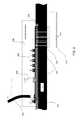
- FIG. 9shows another example implementation of an additively-manufactured electrical interconnect 1001 , and associated structures, to route signals between test circuitry electronic devices (not shown) on a PCB 1002 and DUT contacts on a wafer (not shown).
- the additively-manufactured electrical interconnectincludes individual additively-manufactured electrical conduits 1003 .
- the individual additively-manufactured electrical conduits 1003may be of the type described herein, e.g., they may be miniature coaxial structures, with each conduit comprising an electrically-conductive core (center), surrounded by a dielectric material, such as air, ceramic, glass, plastic, or the like.
- the electrically-conductive coreis, in turn, surrounded by an electrically-conductive outer material that functions as an electrical return for the core.
- the electrically-conductive outer materialmay, in turn, be surrounded by an insulator or isolated from other conductors by air, or may be electrically connected to the other outer material.
- At least some of (e.g., all of) the additively-manufactured electrical conduitsare configured to have substantially matching electrical characteristics, such as electrical path lengths/Time of Flight (ToF), impedance, and signal attenuation.
- substantially matching electrical characteristicssuch as electrical path lengths/Time of Flight (ToF), impedance, and signal attenuation.
- ToFTime of Flight
- a substantial matchmay include a match that is identical or to within one or more predefined tolerances. In some implementations, it may only be appropriate to substantially match only one or two of electrical path length, impedance, and signal attenuation.
- conduits 1003 aroutes signals to points further from their origin than conduits 1003 b . Without the curved or serpentine portions 1004 , this difference could result in conduits 1003 a having different electrical characteristics than conduits 1003 b .
- signals passing through conduits 1003 a signals passing through different conduitswould have different electrical characteristics (e.g., timing, attenuation, etc.) than signals passing through conduits 1003 b .
- the addition of curved or serpentine portions 1004effectively elongates the signal transmission path of conduits 1003 b , thereby causing electrical characteristics of different conduits, such as electrical path lengths, impedances, and signal attenuation, to match, and thereby decreasing the possibility of different effects on different signals transmitted through different conduits of the interconnect.
- Serpentine or curved portionsmay be added to any appropriate part or parts of a conduit to achieve desired electrical characteristics.
- the pitch of the contacts on the waferis maintained in one dimension (e.g., X-dimension 1007 ), but not in the other dimension (e.g., Y-dimension 1008 ).
- the spacing between conduitsis spread out in Y-dimension 1008 relative to the contacts on the wafer.
- the spacing between conduitsis about the same as the spacing between contacts on the wafer.
- This type of spacingcan be advantageous. For example, it may be possible to add additional groups of conduits at the front or the back of the interconnect to accommodate larger numbers of wafer contacts.
- Interconnect 1001may also include a structure 1010 , such as a circuit board, containing pins (e.g., spring contact pins, such as POGO® pins), which provide electrical connection to corresponding contacts on a DUT (the wafer). Electrical pathways pass through structure 1010 to reach circuit board 1011 (e.g., an interposer board). Circuit board 1011 includes active and/or passive electronic components that are used to compensate for inductance in the electrical transmission paths between the wafer and the circuit board 1002 . In some implementations, the passive electronic components may be capacitors, baluns, or switches; however, other active and/or passive electronic components may be used.
- the passive electronic componentsmay be capacitors, baluns, or switches; however, other active and/or passive electronic components may be used.
- the electrical pathwaysextend through circuit board 1011 to the additively-manufactured electrical conduits 1003 . From there, the electrical pathways extend to electrical elements on circuit board 1002 , as described above.
- three screws 1012are used as a mechanism to adjust the angle of structure 1010 so that plane (at which the pins contact the DUT) is substantially parallel to circuit board 1002 .
- one or more of screws 1012may be tightened or loosened in order to adjust the plane.
- different mechanismsmay be used to make mechanical adjustments to keep the pins and the circuit board parallel.
- Serpentine pathways and the various other constructs shown in FIG. 9may be used to implement AS coaxial structure 206 or, more generally, switching matrix 201 .
- switching matrix 201may also include curved or serpentine portions that effectively elongates the signal transmission path of its conduits, thereby causing electrical characteristics of different conduits, such as electrical path lengths, impedances, and signal attenuation, to match, and thereby decreasing the possibility of different effects on different signals transmitted through different conduits of the interconnect.
- Serpentine or curved portionsmay be added to any appropriate part or parts of a conduit to achieve desired electrical characteristics.
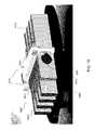
- FIG. 10shows an example of an alternative implementation that uses microstrip construction, stripline construction or a co-planar waveguide construction to produce electrical conduits 1015 for transmitting signals through the interconnect.
- Each of these constructionsis produced using etching and, therefore, is subtractively-manufactured (e.g., machined) in the sense that material is removed from the device to produce appropriate electrical and mechanical connections.
- a microstrip construction, stripline construction or a co-planar waveguide constructionmay also be used to produce coaxial structures 206 for transmitting signals through the switching matrix (and thus the PCB) to and from the interconnect.
- a forceoften called the “signal” line and a return (often called “ground”) line.
- a complete circuitis required to create a channel.
- the combination of the force and return(signal and ground) describes the complete circuit.
- the geometric relationship between the force and returncreates the impedance.
- the impedance controlled signal line 1301(the line that carries the signal forward, towards the DUT) is layered between two return (ground) planes 1302 (these are actually the “returns”, in that the signal must have both a force and a return to create a complete circuit).
- the geometric relationship between those force and return linesis a factor in determining the impedance of the circuit.
- Resin and fabric 1303may be between the conductive paths.
- a microstrip configurationremoves one of the ground planes, leaving the signal line 1304 and ground plane 1305 .
- a coplanar waveguideis a form of microstrip where the ground plane 1307 is coplanar with the signal line 1308 .
- the impedanceis largely derived from the relationship of the traces on the surface of the structure.
- Coplanar waveguidesare a good choice when signals are adjacent to each other that might be subject to crosstalk or inductive coupling between the traces. Any of the coaxial structures described herein may be implemented using the structures shown in FIG. 12A , FIG. 12B , and/or FIG. 12C .
- each conduit in the interconnect or the switching matrixmay have a stripline configuration, a microstrip configuration or a coplanar waveguide configuration. Otherwise, the functions and features of the conduits are substantially the same as the additively-manufactured conduits described above.
- different groups of conduits 1013are covered with insulating material. A portion 1014 of the insulating material is removed to reveal the serpentine portions 1004 of conduits creating the electrical pathway between the wafer and the probe card. This is shown in close-up in FIG. 11 .
- the structures described hereinmay include a circuit board comprising electrical elements arranged at a first pitch; a wafer comprising contacts arranged at a second pitch, the second pitch being less than the first pitch; and an interconnect comprising additively-manufactured electrical conduits that are part of an electrical pathway between the electrical elements and the contacts, where the additively-manufactured electrical conduits comprise electrically-conductive material.
- Testingmay be performed using a combination of system processing devices, embedded processing devices, and/or programmable logic. For example, each of these different elements may run on or more test programs to test multiple devices in parallel or in sequence.
- the testing described hereinis not limited to RF testing, but rather may be used to test any electronic devices, including microprocessors, programmable logic, and the like
- testingand a “test system”
- devices and method described hereinmay be used in any appropriate system, and are not limited to test systems or to the example test systems described herein.
- Testing performed as described hereinmay be implemented and/or controlled using hardware or a combination of hardware and software.
- a test systemlike the ones described herein may include various controllers and/or processing devices located at various points.
- a central computermay coordinate operation among the various controllers or processing devices.
- the central computer, controllers, and processing devicesmay execute various software routines to effect control and coordination of testing and calibration.
- Testingcan be controlled, at least in part, using one or more computer program products, e.g., one or more computer program tangibly embodied in one or more information carriers, such as one or more non-transitory machine-readable media, for execution by, or to control the operation of, one or more data processing apparatus, e.g., a programmable processor, a computer, multiple computers, and/or programmable logic components.
- one or more computer program productse.g., one or more computer program tangibly embodied in one or more information carriers, such as one or more non-transitory machine-readable media, for execution by, or to control the operation of, one or more data processing apparatus, e.g., a programmable processor, a computer, multiple computers, and/or programmable logic components.
- a computer programcan be written in any form of programming language, including compiled or interpreted languages, and it can be deployed in any form, including as a stand-alone program or as a module, component, subroutine, or other unit suitable for use in a computing environment.
- a computer programcan be deployed to be executed on one computer or on multiple computers at one site or distributed across multiple sites and interconnected by a network.
- Actions associated with implementing all or part of the testing and calibrationcan be performed by one or more programmable processors executing one or more computer programs to perform the functions described herein. All or part of the testing and calibration can be implemented using special purpose logic circuitry, e.g., an FPGA (field programmable gate array) and/or an ASIC (application-specific integrated circuit).
- FPGAfield programmable gate array
- ASICapplication-specific integrated circuit
- processors suitable for the execution of a computer programinclude, by way of example, both general and special purpose microprocessors, and any one or more processors of any kind of digital computer.
- a processorwill receive instructions and data from a read-only storage area or a random access storage area or both.
- Elements of a computerinclude one or more processors for executing instructions and one or more storage area devices for storing instructions and data.
- a computerwill also include, or be operatively coupled to receive data from, or transfer data to, or both, one or more machine-readable storage media, such as mass PCBs for storing data, e.g., magnetic, magneto-optical disks, or optical disks.
- Machine-readable storage media suitable for embodying computer program instructions and datainclude all forms of non-volatile storage area, including by way of example, semiconductor storage area devices, e.g., EPROM, EEPROM, and flash storage area devices; magnetic disks, e.g., internal hard disks or removable disks; magneto-optical disks; and CD-ROM and DVD-ROM disks.
- semiconductor storage area devicese.g., EPROM, EEPROM, and flash storage area devices
- magnetic diskse.g., internal hard disks or removable disks
- magneto-optical diskse.g., CD-ROM and DVD-ROM disks.
- connectionmay imply a direct physical connection or a connection that includes intervening components but that nevertheless allows electrical signals to flow between connected components.
- connectioninvolving electrical circuitry mentioned herein, unless stated otherwise, is an electrical connection and not necessarily a direct physical connection regardless of whether the word “electrical” is used to modify “connection”.
Landscapes
- Engineering & Computer Science (AREA)
- Physics & Mathematics (AREA)
- General Physics & Mathematics (AREA)
- General Engineering & Computer Science (AREA)
- Computer Hardware Design (AREA)
- Microelectronics & Electronic Packaging (AREA)
- Environmental & Geological Engineering (AREA)
- Health & Medical Sciences (AREA)
- Toxicology (AREA)
- Computer Networks & Wireless Communication (AREA)
- Testing Or Measuring Of Semiconductors Or The Like (AREA)
Abstract
Description
Claims (27)
Priority Applications (5)
| Application Number | Priority Date | Filing Date | Title |
|---|---|---|---|
| US14/316,164US9594114B2 (en) | 2014-06-26 | 2014-06-26 | Structure for transmitting signals in an application space between a device under test and test electronics |
| TW104115546ATWI651540B (en) | 2014-06-26 | 2015-05-15 | Structure for transmitting signals in an application space between a device under test and test electronics |
| KR1020167035649AKR102435680B1 (en) | 2014-06-26 | 2015-06-17 | Structure for transmitting signals in an application space between a device under test and test electronics |
| PCT/US2015/036213WO2015200066A1 (en) | 2014-06-26 | 2015-06-17 | Structure for transmitting signals in an application space between a device under test and test electronics |
| CN201580032165.XACN106561086B (en) | 2014-06-26 | 2015-06-17 | Structure for transmitting signals in the application space between the device under test and the test electronics |
Applications Claiming Priority (1)
| Application Number | Priority Date | Filing Date | Title |
|---|---|---|---|
| US14/316,164US9594114B2 (en) | 2014-06-26 | 2014-06-26 | Structure for transmitting signals in an application space between a device under test and test electronics |
Publications (2)
| Publication Number | Publication Date |
|---|---|
| US20150377946A1 US20150377946A1 (en) | 2015-12-31 |
| US9594114B2true US9594114B2 (en) | 2017-03-14 |
Family
ID=54930229
Family Applications (1)
| Application Number | Title | Priority Date | Filing Date |
|---|---|---|---|
| US14/316,164Active2035-04-27US9594114B2 (en) | 2014-06-26 | 2014-06-26 | Structure for transmitting signals in an application space between a device under test and test electronics |
Country Status (5)
| Country | Link |
|---|---|
| US (1) | US9594114B2 (en) |
| KR (1) | KR102435680B1 (en) |
| CN (1) | CN106561086B (en) |
| TW (1) | TWI651540B (en) |
| WO (1) | WO2015200066A1 (en) |
Cited By (9)
| Publication number | Priority date | Publication date | Assignee | Title |
|---|---|---|---|---|
| US9977052B2 (en) | 2016-10-04 | 2018-05-22 | Teradyne, Inc. | Test fixture |
| US10451652B2 (en) | 2014-07-16 | 2019-10-22 | Teradyne, Inc. | Coaxial structure for transmission of signals in test equipment |
| US10677815B2 (en) | 2018-06-08 | 2020-06-09 | Teradyne, Inc. | Test system having distributed resources |
| US10972192B2 (en) | 2018-05-11 | 2021-04-06 | Teradyne, Inc. | Handler change kit for a test system |
| US11018082B2 (en)* | 2018-07-30 | 2021-05-25 | Dyi-chung Hu | Space transformer and manufacturing method thereof |
| US11604219B2 (en) | 2020-12-15 | 2023-03-14 | Teradyne, Inc. | Automatic test equipement having fiber optic connections to remote servers |
| US11855376B2 (en) | 2021-03-24 | 2023-12-26 | Teradyne, Inc. | Coaxial contact having an open-curve shape |
| US11862901B2 (en) | 2020-12-15 | 2024-01-02 | Teradyne, Inc. | Interposer |
| US12046787B2 (en) | 2021-05-14 | 2024-07-23 | Teradyne, Inc. | Waveguide connector for connecting first and second waveguides, where the connector includes a male part, a female part and a self-alignment feature and a test system formed therefrom |
Families Citing this family (19)
| Publication number | Priority date | Publication date | Assignee | Title |
|---|---|---|---|---|
| JP6525831B2 (en)* | 2015-09-15 | 2019-06-05 | 株式会社ヨコオ | Contact unit and inspection jig |
| TWI582432B (en)* | 2016-01-20 | 2017-05-11 | 中華精測科技股份有限公司 | Ic test socket with capacitor |
| US10241146B2 (en)* | 2017-05-01 | 2019-03-26 | Advantest Corporation | Test system and method |
| KR20190051240A (en)* | 2017-11-06 | 2019-05-15 | 삼성전자주식회사 | Test apparatus |
| TWI672506B (en)* | 2018-08-08 | 2019-09-21 | 中華精測科技股份有限公司 | Radio-frequency probe card device and space transformer thereof |
| KR102205616B1 (en) | 2019-04-24 | 2021-01-21 | 주식회사 엑시콘 | Dut test system combined with system application board and rectangular shaped probe card |
| WO2021067011A1 (en)* | 2019-09-30 | 2021-04-08 | Electro Scientific Industries, Inc. | Reduced impedance variation in a modular 2-terminal terminal contacting electrical measurement system |
| US11493551B2 (en) | 2020-06-22 | 2022-11-08 | Advantest Test Solutions, Inc. | Integrated test cell using active thermal interposer (ATI) with parallel socket actuation |
| US11549981B2 (en) | 2020-10-01 | 2023-01-10 | Advantest Test Solutions, Inc. | Thermal solution for massively parallel testing |
| US11808812B2 (en) | 2020-11-02 | 2023-11-07 | Advantest Test Solutions, Inc. | Passive carrier-based device delivery for slot-based high-volume semiconductor test system |
| US11821913B2 (en) | 2020-11-02 | 2023-11-21 | Advantest Test Solutions, Inc. | Shielded socket and carrier for high-volume test of semiconductor devices |
| US12320841B2 (en) | 2020-11-19 | 2025-06-03 | Advantest Test Solutions, Inc. | Wafer scale active thermal interposer for device testing |
| US11567119B2 (en)* | 2020-12-04 | 2023-01-31 | Advantest Test Solutions, Inc. | Testing system including active thermal interposer device |
| US11573262B2 (en) | 2020-12-31 | 2023-02-07 | Advantest Test Solutions, Inc. | Multi-input multi-zone thermal control for device testing |
| TWI752781B (en)* | 2020-12-31 | 2022-01-11 | 致茂電子股份有限公司 | System and method for testing a laser diode |
| US11587640B2 (en) | 2021-03-08 | 2023-02-21 | Advantest Test Solutions, Inc. | Carrier based high volume system level testing of devices with pop structures |
| US11656273B1 (en) | 2021-11-05 | 2023-05-23 | Advantest Test Solutions, Inc. | High current device testing apparatus and systems |
| EP4533106A1 (en)* | 2022-06-03 | 2025-04-09 | FormFactor, Inc. | Abbreviated loopback attenuation |
| US20250141078A1 (en)* | 2023-11-01 | 2025-05-01 | GM Global Technology Operations LLC | Embedded coplanar waveguides for thin-film material characterization and methods related to the same |
Citations (100)
| Publication number | Priority date | Publication date | Assignee | Title |
|---|---|---|---|---|
| US3516077A (en) | 1968-05-28 | 1970-06-02 | Bell Telephone Labor Inc | Magnetic propagation device wherein pole patterns move along the periphery of magnetic disks |
| US3577131A (en) | 1969-01-30 | 1971-05-04 | Bell Telephone Labor Inc | Domain propagation arrangement |
| US3673433A (en) | 1970-08-21 | 1972-06-27 | Siemens Ag Albis | Circuit arrangement for selectively connecting at least two inputs to a counting stage possessing at least one preparatory input and one triggering input and including contact bounce suppression circuitry |
| US3934236A (en) | 1974-01-11 | 1976-01-20 | Monsanto Company | Pulsed field accessed bubble propagation circuits |
| US4021790A (en) | 1974-01-11 | 1977-05-03 | Monsanto Company | Mutually exclusive magnetic bubble propagation circuits |
| US4117543A (en) | 1972-08-24 | 1978-09-26 | Monsanto Company | Magnetic bubble logic family |
| US4692839A (en) | 1985-06-24 | 1987-09-08 | Digital Equipment Corporation | Multiple chip interconnection system and package |
| US4729166A (en) | 1985-07-22 | 1988-03-08 | Digital Equipment Corporation | Method of fabricating electrical connector for surface mounting |
| US4754546A (en) | 1985-07-22 | 1988-07-05 | Digital Equipment Corporation | Electrical connector for surface mounting and method of making thereof |
| US4757256A (en) | 1985-05-10 | 1988-07-12 | Micro-Probe, Inc. | High density probe card |
| US4758785A (en) | 1986-09-03 | 1988-07-19 | Tektronix, Inc. | Pressure control apparatus for use in an integrated circuit testing station |
| WO1988005544A1 (en) | 1987-01-20 | 1988-07-28 | Hughes Aircraft Company | Test connector for electrical devices |
| US4778950A (en) | 1985-07-22 | 1988-10-18 | Digital Equipment Corporation | Anisotropic elastomeric interconnecting system |
| EP0298219A2 (en) | 1987-06-08 | 1989-01-11 | Tektronix Inc. | Method and apparatus for testing unpackaged integrated circuits in a hybrid circuit environment |
| US4804132A (en) | 1987-08-28 | 1989-02-14 | Difrancesco Louis | Method for cold bonding |
| US4912399A (en) | 1987-06-09 | 1990-03-27 | Tektronix, Inc. | Multiple lead probe for integrated circuits in wafer form |
| EP0361779A1 (en) | 1988-09-26 | 1990-04-04 | Hewlett-Packard Company | Micro-strip architecture for membrane test probe |
| US4918383A (en) | 1987-01-20 | 1990-04-17 | Huff Richard E | Membrane probe with automatic contact scrub action |
| US4920574A (en)* | 1985-10-04 | 1990-04-24 | Fujitsu Limited | Cooling system for an electronic circuit device |
| US4922192A (en) | 1988-09-06 | 1990-05-01 | Unisys Corporation | Elastic membrane probe |
| US4954873A (en) | 1985-07-22 | 1990-09-04 | Digital Equipment Corporation | Electrical connector for surface mounting |
| US4975638A (en) | 1989-12-18 | 1990-12-04 | Wentworth Laboratories | Test probe assembly for testing integrated circuit devices |
| US4980637A (en) | 1988-03-01 | 1990-12-25 | Hewlett-Packard Company | Force delivery system for improved precision membrane probe |
| US5020219A (en) | 1988-05-16 | 1991-06-04 | Leedy Glenn J | Method of making a flexible tester surface for testing integrated circuits |
| US5072176A (en) | 1990-07-10 | 1991-12-10 | The United States Of America As Represented By The Secretary Of The Army | Flexible membrane circuit tester |
| US5083697A (en) | 1990-02-14 | 1992-01-28 | Difrancesco Louis | Particle-enhanced joining of metal surfaces |
| US5103557A (en) | 1988-05-16 | 1992-04-14 | Leedy Glenn J | Making and testing an integrated circuit using high density probe points |
| US5132613A (en) | 1990-11-30 | 1992-07-21 | International Business Machines Corporation | Low inductance side mount decoupling test structure |
| US5180977A (en) | 1991-12-02 | 1993-01-19 | Hoya Corporation Usa | Membrane probe contact bump compliancy system |
| US5264787A (en) | 1991-08-30 | 1993-11-23 | Hughes Aircraft Company | Rigid-flex circuits with raised features as IC test probes |
| US5355079A (en) | 1993-01-07 | 1994-10-11 | Wentworth Laboratories, Inc. | Probe assembly for testing integrated circuit devices |
| US5378982A (en) | 1993-02-25 | 1995-01-03 | Hughes Aircraft Company | Test probe for panel having an overlying protective member adjacent panel contacts |
| US5416429A (en) | 1994-05-23 | 1995-05-16 | Wentworth Laboratories, Inc. | Probe assembly for testing integrated circuits |
| US5422574A (en) | 1993-01-14 | 1995-06-06 | Probe Technology Corporation | Large scale protrusion membrane for semiconductor devices under test with very high pin counts |
| US5456404A (en) | 1993-10-28 | 1995-10-10 | Digital Equipment Corporation | Method of testing semiconductor chips with reusable test package |
| US5468157A (en) | 1993-10-29 | 1995-11-21 | Texas Instruments Incorporated | Non-destructive interconnect system for semiconductor devices |
| US5469072A (en) | 1993-11-01 | 1995-11-21 | Motorola, Inc. | Integrated circuit test system |
| US5623213A (en) | 1994-09-09 | 1997-04-22 | Micromodule Systems | Membrane probing of circuits |
| US5914613A (en) | 1996-08-08 | 1999-06-22 | Cascade Microtech, Inc. | Membrane probing system with local contact scrub |
| US5968282A (en) | 1997-11-10 | 1999-10-19 | Tokyo Electron Limited | Mechanism and method for cleaning probe needles |
| US5973405A (en) | 1997-07-22 | 1999-10-26 | Dytak Corporation | Composite electrical contact structure and method for manufacturing the same |
| US6246245B1 (en) | 1998-02-23 | 2001-06-12 | Micron Technology, Inc. | Probe card, test method and test system for semiconductor wafers |
| US6256882B1 (en) | 1998-07-14 | 2001-07-10 | Cascade Microtech, Inc. | Membrane probing system |
| US20020195265A1 (en)* | 2001-06-20 | 2002-12-26 | Miller Charles A. | High density planar electrical interface |
| US6499216B1 (en) | 1994-07-07 | 2002-12-31 | Tessera, Inc. | Methods and structures for electronic probing arrays |
| US6566898B2 (en) | 2000-03-06 | 2003-05-20 | Wentworth Laboratories, Inc. | Temperature compensated vertical pin probing device |
| US6578264B1 (en) | 1999-06-04 | 2003-06-17 | Cascade Microtech, Inc. | Method for constructing a membrane probe using a depression |
| US6586955B2 (en) | 2000-03-13 | 2003-07-01 | Tessera, Inc. | Methods and structures for electronic probing arrays |
| US20030122538A1 (en) | 2000-09-28 | 2003-07-03 | Teradyne, Inc. | Coaxial cable for ATE with overvoltage protection |
| US6633175B1 (en) | 2000-03-06 | 2003-10-14 | Wenworth Laboratories, Inc. | Temperature compensated vertical pin probing device |
| US6661244B2 (en) | 2000-03-06 | 2003-12-09 | Wentworth Laboratories, Inc. | Nickel alloy probe card frame laminate |
| US6686732B2 (en) | 2001-12-20 | 2004-02-03 | Teradyne, Inc. | Low-cost tester interface module |
| US6690186B2 (en) | 1994-07-07 | 2004-02-10 | Tessera, Inc. | Methods and structures for electronic probing arrays |
| US6756797B2 (en) | 2001-01-31 | 2004-06-29 | Wentworth Laboratories Inc. | Planarizing interposer for thermal compensation of a probe card |
| US6838890B2 (en) | 2000-02-25 | 2005-01-04 | Cascade Microtech, Inc. | Membrane probing system |
| US6911835B2 (en) | 2002-05-08 | 2005-06-28 | Formfactor, Inc. | High performance probe system |
| US6927586B2 (en) | 2000-03-06 | 2005-08-09 | Wentworth Laboratories, Inc. | Temperature compensated vertical pin probing device |
| US6965244B2 (en) | 2002-05-08 | 2005-11-15 | Formfactor, Inc. | High performance probe system |
| US7084657B2 (en) | 1998-06-09 | 2006-08-01 | Advantest Corporation | Bump and method of forming bump |
| US20070004238A1 (en)* | 2005-07-02 | 2007-01-04 | Teradyne, Inc. | Compliant electro-mechanical device |
| US7161363B2 (en) | 2002-05-23 | 2007-01-09 | Cascade Microtech, Inc. | Probe for testing a device under test |
| US20070103199A1 (en)* | 2005-10-28 | 2007-05-10 | Nestor Tzartzanis | Systems and methods for transmitting signals across integrated circuit chips |
| US7233160B2 (en) | 2000-12-04 | 2007-06-19 | Cascade Microtech, Inc. | Wafer probe |
| US7271603B2 (en) | 2003-05-23 | 2007-09-18 | Cascade Microtech, Inc. | Shielded probe for testing a device under test |
| US7285969B2 (en) | 2002-11-13 | 2007-10-23 | Cascade Microtech, Inc. | Probe for combined signals |
| US20080061808A1 (en) | 2006-09-12 | 2008-03-13 | Sammy Mok | Compliance partitioning in testing of integrated circuits |
| US7355420B2 (en) | 2001-08-21 | 2008-04-08 | Cascade Microtech, Inc. | Membrane probing system |
| US7368927B2 (en) | 2004-07-07 | 2008-05-06 | Cascade Microtech, Inc. | Probe head having a membrane suspended probe |
| US7403028B2 (en) | 2006-06-12 | 2008-07-22 | Cascade Microtech, Inc. | Test structure and probe for differential signals |
| US7420381B2 (en) | 2004-09-13 | 2008-09-02 | Cascade Microtech, Inc. | Double sided probing structures |
| US7427868B2 (en) | 2003-12-24 | 2008-09-23 | Cascade Microtech, Inc. | Active wafer probe |
| US7443186B2 (en) | 2006-06-12 | 2008-10-28 | Cascade Microtech, Inc. | On-wafer test structures for differential signals |
| US7449899B2 (en) | 2005-06-08 | 2008-11-11 | Cascade Microtech, Inc. | Probe for high frequency signals |
| US7453275B2 (en) | 2006-05-19 | 2008-11-18 | Elpida Memory, Inc. | Probe card |
| US20090033347A1 (en) | 2006-06-01 | 2009-02-05 | Hiroyuki Mineo | Measuring board for electronic device test apparatus |
| US7504842B2 (en) | 1997-05-28 | 2009-03-17 | Cascade Microtech, Inc. | Probe holder for testing of a test device |
| US7535247B2 (en) | 2005-01-31 | 2009-05-19 | Cascade Microtech, Inc. | Interface for testing semiconductors |
| US7601039B2 (en) | 1993-11-16 | 2009-10-13 | Formfactor, Inc. | Microelectronic contact structure and method of making same |
| US7609077B2 (en) | 2006-06-09 | 2009-10-27 | Cascade Microtech, Inc. | Differential signal probe with integral balun |
| US7619419B2 (en) | 2005-06-13 | 2009-11-17 | Cascade Microtech, Inc. | Wideband active-passive differential signal probe |
| US7656172B2 (en) | 2005-01-31 | 2010-02-02 | Cascade Microtech, Inc. | System for testing semiconductors |
| US7723999B2 (en) | 2006-06-12 | 2010-05-25 | Cascade Microtech, Inc. | Calibration structures for differential signal probing |
| US7764072B2 (en) | 2006-06-12 | 2010-07-27 | Cascade Microtech, Inc. | Differential signal probing system |
| US7791361B2 (en) | 2007-12-10 | 2010-09-07 | Touchdown Technologies, Inc. | Planarizing probe card |
| US20100231250A1 (en)* | 2009-03-11 | 2010-09-16 | Keith Breinlinger | Pin Electronics Liquid Cooled Multi-module for High Performance, Low Cost Automated Test Equipment |
| US7800001B2 (en) | 2006-04-14 | 2010-09-21 | Kabushiki Kaisha Nihon Micronics | Probe sheet and electrical connecting apparatus |
| US7876114B2 (en) | 2007-08-08 | 2011-01-25 | Cascade Microtech, Inc. | Differential waveguide probe |
| US7888957B2 (en) | 2008-10-06 | 2011-02-15 | Cascade Microtech, Inc. | Probing apparatus with impedance optimized interface |
| US7934944B2 (en) | 2006-04-07 | 2011-05-03 | Kabushiki Kaisha Nihon Micronics | Electrical connecting apparatus |
| US7934945B2 (en) | 2006-09-28 | 2011-05-03 | Kabushiki Kaisha Nihon Micronics | Electrical connecting apparatus |
| US8033838B2 (en) | 1996-02-21 | 2011-10-11 | Formfactor, Inc. | Microelectronic contact structure |
| US20120017428A1 (en) | 2008-03-07 | 2012-01-26 | Taiwan Semiconductor Manufacturing Co., Ltd. | Method for fabricating a semiconductor test probe card space transformer |
| US20120094534A1 (en)* | 2009-06-30 | 2012-04-19 | Advantest Corporaiton | Connector, cable assembly, and semiconductor testing device |
| US8202684B2 (en) | 2006-04-14 | 2012-06-19 | Kabushiki Kaisha Nihon Micronics | Method for manufacturing probe sheet |
| US20120175612A1 (en) | 2009-09-25 | 2012-07-12 | International Business Machines Corporation | Test structure for determination of tsv depth |
| US8373428B2 (en) | 1993-11-16 | 2013-02-12 | Formfactor, Inc. | Probe card assembly and kit, and methods of making same |
| US8410806B2 (en) | 2008-11-21 | 2013-04-02 | Cascade Microtech, Inc. | Replaceable coupon for a probing apparatus |
| US20130135002A1 (en) | 2008-11-25 | 2013-05-30 | Advantest (Singapore) Pte Ltd | Test electronics to device under test interfaces, and methods and apparatus using same |
| WO2013134568A1 (en) | 2012-03-07 | 2013-09-12 | Advantest Corporation | Shielded probe array |
| US20150137848A1 (en)* | 2013-11-19 | 2015-05-21 | Teradyne, Inc. | Interconnect for transmitting signals between a device and a tester |
Family Cites Families (1)
| Publication number | Priority date | Publication date | Assignee | Title |
|---|---|---|---|---|
| CN102405564B (en)* | 2009-02-18 | 2014-09-03 | 莫列斯公司 | Vertical Connectors for Printed Circuit Boards |
- 2014
- 2014-06-26USUS14/316,164patent/US9594114B2/enactiveActive
- 2015
- 2015-05-15TWTW104115546Apatent/TWI651540B/enactive
- 2015-06-17CNCN201580032165.XApatent/CN106561086B/enactiveActive
- 2015-06-17KRKR1020167035649Apatent/KR102435680B1/enactiveActive
- 2015-06-17WOPCT/US2015/036213patent/WO2015200066A1/enactiveApplication Filing
Patent Citations (146)
| Publication number | Priority date | Publication date | Assignee | Title |
|---|---|---|---|---|
| US3516077A (en) | 1968-05-28 | 1970-06-02 | Bell Telephone Labor Inc | Magnetic propagation device wherein pole patterns move along the periphery of magnetic disks |
| US3577131A (en) | 1969-01-30 | 1971-05-04 | Bell Telephone Labor Inc | Domain propagation arrangement |
| US3673433A (en) | 1970-08-21 | 1972-06-27 | Siemens Ag Albis | Circuit arrangement for selectively connecting at least two inputs to a counting stage possessing at least one preparatory input and one triggering input and including contact bounce suppression circuitry |
| US4117543A (en) | 1972-08-24 | 1978-09-26 | Monsanto Company | Magnetic bubble logic family |
| US3934236A (en) | 1974-01-11 | 1976-01-20 | Monsanto Company | Pulsed field accessed bubble propagation circuits |
| US4021790A (en) | 1974-01-11 | 1977-05-03 | Monsanto Company | Mutually exclusive magnetic bubble propagation circuits |
| US4757256A (en) | 1985-05-10 | 1988-07-12 | Micro-Probe, Inc. | High density probe card |
| US4692839A (en) | 1985-06-24 | 1987-09-08 | Digital Equipment Corporation | Multiple chip interconnection system and package |
| US4729166A (en) | 1985-07-22 | 1988-03-08 | Digital Equipment Corporation | Method of fabricating electrical connector for surface mounting |
| US4754546A (en) | 1985-07-22 | 1988-07-05 | Digital Equipment Corporation | Electrical connector for surface mounting and method of making thereof |
| US4954873A (en) | 1985-07-22 | 1990-09-04 | Digital Equipment Corporation | Electrical connector for surface mounting |
| US4778950A (en) | 1985-07-22 | 1988-10-18 | Digital Equipment Corporation | Anisotropic elastomeric interconnecting system |
| US4920574A (en)* | 1985-10-04 | 1990-04-24 | Fujitsu Limited | Cooling system for an electronic circuit device |
| US4758785A (en) | 1986-09-03 | 1988-07-19 | Tektronix, Inc. | Pressure control apparatus for use in an integrated circuit testing station |
| US4918383A (en) | 1987-01-20 | 1990-04-17 | Huff Richard E | Membrane probe with automatic contact scrub action |
| WO1988005544A1 (en) | 1987-01-20 | 1988-07-28 | Hughes Aircraft Company | Test connector for electrical devices |
| EP0298219A2 (en) | 1987-06-08 | 1989-01-11 | Tektronix Inc. | Method and apparatus for testing unpackaged integrated circuits in a hybrid circuit environment |
| US4912399A (en) | 1987-06-09 | 1990-03-27 | Tektronix, Inc. | Multiple lead probe for integrated circuits in wafer form |
| US4804132A (en) | 1987-08-28 | 1989-02-14 | Difrancesco Louis | Method for cold bonding |
| US4980637A (en) | 1988-03-01 | 1990-12-25 | Hewlett-Packard Company | Force delivery system for improved precision membrane probe |
| US5020219A (en) | 1988-05-16 | 1991-06-04 | Leedy Glenn J | Method of making a flexible tester surface for testing integrated circuits |
| US5103557A (en) | 1988-05-16 | 1992-04-14 | Leedy Glenn J | Making and testing an integrated circuit using high density probe points |
| US4922192A (en) | 1988-09-06 | 1990-05-01 | Unisys Corporation | Elastic membrane probe |
| EP0361779A1 (en) | 1988-09-26 | 1990-04-04 | Hewlett-Packard Company | Micro-strip architecture for membrane test probe |
| US4975638A (en) | 1989-12-18 | 1990-12-04 | Wentworth Laboratories | Test probe assembly for testing integrated circuit devices |
| US5083697A (en) | 1990-02-14 | 1992-01-28 | Difrancesco Louis | Particle-enhanced joining of metal surfaces |
| US5072176A (en) | 1990-07-10 | 1991-12-10 | The United States Of America As Represented By The Secretary Of The Army | Flexible membrane circuit tester |
| US5132613A (en) | 1990-11-30 | 1992-07-21 | International Business Machines Corporation | Low inductance side mount decoupling test structure |
| US5264787A (en) | 1991-08-30 | 1993-11-23 | Hughes Aircraft Company | Rigid-flex circuits with raised features as IC test probes |
| US5180977A (en) | 1991-12-02 | 1993-01-19 | Hoya Corporation Usa | Membrane probe contact bump compliancy system |
| US5355079A (en) | 1993-01-07 | 1994-10-11 | Wentworth Laboratories, Inc. | Probe assembly for testing integrated circuit devices |
| US5422574A (en) | 1993-01-14 | 1995-06-06 | Probe Technology Corporation | Large scale protrusion membrane for semiconductor devices under test with very high pin counts |
| US5378982A (en) | 1993-02-25 | 1995-01-03 | Hughes Aircraft Company | Test probe for panel having an overlying protective member adjacent panel contacts |
| US5456404A (en) | 1993-10-28 | 1995-10-10 | Digital Equipment Corporation | Method of testing semiconductor chips with reusable test package |
| US5468157A (en) | 1993-10-29 | 1995-11-21 | Texas Instruments Incorporated | Non-destructive interconnect system for semiconductor devices |
| US5469072A (en) | 1993-11-01 | 1995-11-21 | Motorola, Inc. | Integrated circuit test system |
| US7601039B2 (en) | 1993-11-16 | 2009-10-13 | Formfactor, Inc. | Microelectronic contact structure and method of making same |
| US8373428B2 (en) | 1993-11-16 | 2013-02-12 | Formfactor, Inc. | Probe card assembly and kit, and methods of making same |
| US5416429A (en) | 1994-05-23 | 1995-05-16 | Wentworth Laboratories, Inc. | Probe assembly for testing integrated circuits |
| US6499216B1 (en) | 1994-07-07 | 2002-12-31 | Tessera, Inc. | Methods and structures for electronic probing arrays |
| US6690186B2 (en) | 1994-07-07 | 2004-02-10 | Tessera, Inc. | Methods and structures for electronic probing arrays |
| US5623213A (en) | 1994-09-09 | 1997-04-22 | Micromodule Systems | Membrane probing of circuits |
| US8033838B2 (en) | 1996-02-21 | 2011-10-11 | Formfactor, Inc. | Microelectronic contact structure |
| US5914613A (en) | 1996-08-08 | 1999-06-22 | Cascade Microtech, Inc. | Membrane probing system with local contact scrub |
| US6927585B2 (en) | 1996-08-08 | 2005-08-09 | Cascade Microtech, Inc. | Membrane probing system with local contact scrub |
| US6437584B1 (en) | 1996-08-08 | 2002-08-20 | Cascade Microtech, Inc. | Membrane probing system with local contact scrub |
| US6307387B1 (en) | 1996-08-08 | 2001-10-23 | Cascade Microtech, Inc. | Membrane probing system with local contact scrub |
| US7109731B2 (en) | 1996-08-08 | 2006-09-19 | Cascade Microtech, Inc. | Membrane probing system with local contact scrub |
| US7893704B2 (en) | 1996-08-08 | 2011-02-22 | Cascade Microtech, Inc. | Membrane probing structure with laterally scrubbing contacts |
| US7541821B2 (en) | 1996-08-08 | 2009-06-02 | Cascade Microtech, Inc. | Membrane probing system with local contact scrub |
| US7504842B2 (en) | 1997-05-28 | 2009-03-17 | Cascade Microtech, Inc. | Probe holder for testing of a test device |
| US6359337B1 (en) | 1997-07-22 | 2002-03-19 | Dytak Corporation | Composite electrical contact structure and method for manufacturing the same |
| US5973405A (en) | 1997-07-22 | 1999-10-26 | Dytak Corporation | Composite electrical contact structure and method for manufacturing the same |
| US5968282A (en) | 1997-11-10 | 1999-10-19 | Tokyo Electron Limited | Mechanism and method for cleaning probe needles |
| US6246245B1 (en) | 1998-02-23 | 2001-06-12 | Micron Technology, Inc. | Probe card, test method and test system for semiconductor wafers |
| US6356098B1 (en) | 1998-02-23 | 2002-03-12 | Micron Technology, Inc. | Probe card, test method and test system for semiconductor wafers |
| US7084657B2 (en) | 1998-06-09 | 2006-08-01 | Advantest Corporation | Bump and method of forming bump |
| US7681312B2 (en) | 1998-07-14 | 2010-03-23 | Cascade Microtech, Inc. | Membrane probing system |
| US7761986B2 (en) | 1998-07-14 | 2010-07-27 | Cascade Microtech, Inc. | Membrane probing method using improved contact |
| US6708386B2 (en) | 1998-07-14 | 2004-03-23 | Cascade Microtech, Inc. | Method for probing an electrical device having a layer of oxide thereon |
| US6825677B2 (en) | 1998-07-14 | 2004-11-30 | Cascade Microtech, Inc. | Membrane probing system |
| US8451017B2 (en) | 1998-07-14 | 2013-05-28 | Cascade Microtech, Inc. | Membrane probing method using improved contact |
| US6860009B2 (en) | 1998-07-14 | 2005-03-01 | Cascade Microtech, Inc. | Probe construction using a recess |
| US7400155B2 (en) | 1998-07-14 | 2008-07-15 | Cascade Microtech, Inc. | Membrane probing system |
| US7266889B2 (en) | 1998-07-14 | 2007-09-11 | Cascade Microtech, Inc. | Membrane probing system |
| US6256882B1 (en) | 1998-07-14 | 2001-07-10 | Cascade Microtech, Inc. | Membrane probing system |
| US7533462B2 (en) | 1999-06-04 | 2009-05-19 | Cascade Microtech, Inc. | Method of constructing a membrane probe |
| US6578264B1 (en) | 1999-06-04 | 2003-06-17 | Cascade Microtech, Inc. | Method for constructing a membrane probe using a depression |
| US7178236B2 (en) | 1999-06-04 | 2007-02-20 | Cascade Microtech, Inc. | Method for constructing a membrane probe using a depression |
| US6930498B2 (en) | 2000-02-25 | 2005-08-16 | Cascade Microtech, Inc. | Membrane probing system |
| US7148711B2 (en) | 2000-02-25 | 2006-12-12 | Cascade Microtech, Inc. | Membrane probing system |
| US6838890B2 (en) | 2000-02-25 | 2005-01-04 | Cascade Microtech, Inc. | Membrane probing system |
| US7403025B2 (en) | 2000-02-25 | 2008-07-22 | Cascade Microtech, Inc. | Membrane probing system |
| US6661244B2 (en) | 2000-03-06 | 2003-12-09 | Wentworth Laboratories, Inc. | Nickel alloy probe card frame laminate |
| US6633175B1 (en) | 2000-03-06 | 2003-10-14 | Wenworth Laboratories, Inc. | Temperature compensated vertical pin probing device |
| US6566898B2 (en) | 2000-03-06 | 2003-05-20 | Wentworth Laboratories, Inc. | Temperature compensated vertical pin probing device |
| US6927586B2 (en) | 2000-03-06 | 2005-08-09 | Wentworth Laboratories, Inc. | Temperature compensated vertical pin probing device |
| US6586955B2 (en) | 2000-03-13 | 2003-07-01 | Tessera, Inc. | Methods and structures for electronic probing arrays |
| US20030122538A1 (en) | 2000-09-28 | 2003-07-03 | Teradyne, Inc. | Coaxial cable for ATE with overvoltage protection |
| US7688097B2 (en) | 2000-12-04 | 2010-03-30 | Cascade Microtech, Inc. | Wafer probe |
| US7456646B2 (en) | 2000-12-04 | 2008-11-25 | Cascade Microtech, Inc. | Wafer probe |
| US7761983B2 (en) | 2000-12-04 | 2010-07-27 | Cascade Microtech, Inc. | Method of assembling a wafer probe |
| US7495461B2 (en) | 2000-12-04 | 2009-02-24 | Cascade Microtech, Inc. | Wafer probe |
| US7233160B2 (en) | 2000-12-04 | 2007-06-19 | Cascade Microtech, Inc. | Wafer probe |
| US6756797B2 (en) | 2001-01-31 | 2004-06-29 | Wentworth Laboratories Inc. | Planarizing interposer for thermal compensation of a probe card |
| US20070007980A1 (en) | 2001-06-20 | 2007-01-11 | Formfactor, Inc. | High Density Planar Electrical Interface |
| US20020195265A1 (en)* | 2001-06-20 | 2002-12-26 | Miller Charles A. | High density planar electrical interface |
| US7492175B2 (en) | 2001-08-21 | 2009-02-17 | Cascade Microtech, Inc. | Membrane probing system |
| US7355420B2 (en) | 2001-08-21 | 2008-04-08 | Cascade Microtech, Inc. | Membrane probing system |
| US6686732B2 (en) | 2001-12-20 | 2004-02-03 | Teradyne, Inc. | Low-cost tester interface module |
| US7443181B2 (en) | 2002-05-08 | 2008-10-28 | Formfactor, Inc. | High performance probe system |
| US7227371B2 (en) | 2002-05-08 | 2007-06-05 | Formfactor, Inc. | High performance probe system |
| US6911835B2 (en) | 2002-05-08 | 2005-06-28 | Formfactor, Inc. | High performance probe system |
| US7764075B2 (en) | 2002-05-08 | 2010-07-27 | Formfactor, Inc. | High performance probe system |
| US6965244B2 (en) | 2002-05-08 | 2005-11-15 | Formfactor, Inc. | High performance probe system |
| US7161363B2 (en) | 2002-05-23 | 2007-01-09 | Cascade Microtech, Inc. | Probe for testing a device under test |
| US7436194B2 (en) | 2002-05-23 | 2008-10-14 | Cascade Microtech, Inc. | Shielded probe with low contact resistance for testing a device under test |
| US7518387B2 (en) | 2002-05-23 | 2009-04-14 | Cascade Microtech, Inc. | Shielded probe for testing a device under test |
| US7304488B2 (en) | 2002-05-23 | 2007-12-04 | Cascade Microtech, Inc. | Shielded probe for high-frequency testing of a device under test |
| US7482823B2 (en) | 2002-05-23 | 2009-01-27 | Cascade Microtech, Inc. | Shielded probe for testing a device under test |
| US7489149B2 (en) | 2002-05-23 | 2009-02-10 | Cascade Microtech, Inc. | Shielded probe for testing a device under test |
| US7417446B2 (en) | 2002-11-13 | 2008-08-26 | Cascade Microtech, Inc. | Probe for combined signals |
| US7453276B2 (en) | 2002-11-13 | 2008-11-18 | Cascade Microtech, Inc. | Probe for combined signals |
| US7285969B2 (en) | 2002-11-13 | 2007-10-23 | Cascade Microtech, Inc. | Probe for combined signals |
| US7501842B2 (en) | 2003-05-23 | 2009-03-10 | Cascade Microtech, Inc. | Shielded probe for testing a device under test |
| US7271603B2 (en) | 2003-05-23 | 2007-09-18 | Cascade Microtech, Inc. | Shielded probe for testing a device under test |
| US7898273B2 (en) | 2003-05-23 | 2011-03-01 | Cascade Microtech, Inc. | Probe for testing a device under test |
| US7498829B2 (en) | 2003-05-23 | 2009-03-03 | Cascade Microtech, Inc. | Shielded probe for testing a device under test |
| US7427868B2 (en) | 2003-12-24 | 2008-09-23 | Cascade Microtech, Inc. | Active wafer probe |
| US7759953B2 (en) | 2003-12-24 | 2010-07-20 | Cascade Microtech, Inc. | Active wafer probe |
| US7514944B2 (en) | 2004-07-07 | 2009-04-07 | Cascade Microtech, Inc. | Probe head having a membrane suspended probe |
| US7368927B2 (en) | 2004-07-07 | 2008-05-06 | Cascade Microtech, Inc. | Probe head having a membrane suspended probe |
| US8013623B2 (en) | 2004-09-13 | 2011-09-06 | Cascade Microtech, Inc. | Double sided probing structures |
| US7420381B2 (en) | 2004-09-13 | 2008-09-02 | Cascade Microtech, Inc. | Double sided probing structures |
| US7656172B2 (en) | 2005-01-31 | 2010-02-02 | Cascade Microtech, Inc. | System for testing semiconductors |
| US7898281B2 (en) | 2005-01-31 | 2011-03-01 | Cascade Mircotech, Inc. | Interface for testing semiconductors |
| US7535247B2 (en) | 2005-01-31 | 2009-05-19 | Cascade Microtech, Inc. | Interface for testing semiconductors |
| US7940069B2 (en) | 2005-01-31 | 2011-05-10 | Cascade Microtech, Inc. | System for testing semiconductors |
| US7449899B2 (en) | 2005-06-08 | 2008-11-11 | Cascade Microtech, Inc. | Probe for high frequency signals |
| US7619419B2 (en) | 2005-06-13 | 2009-11-17 | Cascade Microtech, Inc. | Wideband active-passive differential signal probe |
| US20070004238A1 (en)* | 2005-07-02 | 2007-01-04 | Teradyne, Inc. | Compliant electro-mechanical device |
| US20070103199A1 (en)* | 2005-10-28 | 2007-05-10 | Nestor Tzartzanis | Systems and methods for transmitting signals across integrated circuit chips |
| US7934944B2 (en) | 2006-04-07 | 2011-05-03 | Kabushiki Kaisha Nihon Micronics | Electrical connecting apparatus |
| US8202684B2 (en) | 2006-04-14 | 2012-06-19 | Kabushiki Kaisha Nihon Micronics | Method for manufacturing probe sheet |
| US7800001B2 (en) | 2006-04-14 | 2010-09-21 | Kabushiki Kaisha Nihon Micronics | Probe sheet and electrical connecting apparatus |
| US7453275B2 (en) | 2006-05-19 | 2008-11-18 | Elpida Memory, Inc. | Probe card |
| US20090033347A1 (en) | 2006-06-01 | 2009-02-05 | Hiroyuki Mineo | Measuring board for electronic device test apparatus |
| US7609077B2 (en) | 2006-06-09 | 2009-10-27 | Cascade Microtech, Inc. | Differential signal probe with integral balun |
| US7764072B2 (en) | 2006-06-12 | 2010-07-27 | Cascade Microtech, Inc. | Differential signal probing system |
| US7443186B2 (en) | 2006-06-12 | 2008-10-28 | Cascade Microtech, Inc. | On-wafer test structures for differential signals |
| US7403028B2 (en) | 2006-06-12 | 2008-07-22 | Cascade Microtech, Inc. | Test structure and probe for differential signals |
| US7750652B2 (en) | 2006-06-12 | 2010-07-06 | Cascade Microtech, Inc. | Test structure and probe for differential signals |
| US7723999B2 (en) | 2006-06-12 | 2010-05-25 | Cascade Microtech, Inc. | Calibration structures for differential signal probing |
| US20080061808A1 (en) | 2006-09-12 | 2008-03-13 | Sammy Mok | Compliance partitioning in testing of integrated circuits |
| US7934945B2 (en) | 2006-09-28 | 2011-05-03 | Kabushiki Kaisha Nihon Micronics | Electrical connecting apparatus |
| US7876114B2 (en) | 2007-08-08 | 2011-01-25 | Cascade Microtech, Inc. | Differential waveguide probe |
| US7791361B2 (en) | 2007-12-10 | 2010-09-07 | Touchdown Technologies, Inc. | Planarizing probe card |
| US20120017428A1 (en) | 2008-03-07 | 2012-01-26 | Taiwan Semiconductor Manufacturing Co., Ltd. | Method for fabricating a semiconductor test probe card space transformer |
| US7888957B2 (en) | 2008-10-06 | 2011-02-15 | Cascade Microtech, Inc. | Probing apparatus with impedance optimized interface |
| US8410806B2 (en) | 2008-11-21 | 2013-04-02 | Cascade Microtech, Inc. | Replaceable coupon for a probing apparatus |
| US20130135002A1 (en) | 2008-11-25 | 2013-05-30 | Advantest (Singapore) Pte Ltd | Test electronics to device under test interfaces, and methods and apparatus using same |
| US20100231250A1 (en)* | 2009-03-11 | 2010-09-16 | Keith Breinlinger | Pin Electronics Liquid Cooled Multi-module for High Performance, Low Cost Automated Test Equipment |
| US20120094534A1 (en)* | 2009-06-30 | 2012-04-19 | Advantest Corporaiton | Connector, cable assembly, and semiconductor testing device |
| US20120175612A1 (en) | 2009-09-25 | 2012-07-12 | International Business Machines Corporation | Test structure for determination of tsv depth |
| WO2013134568A1 (en) | 2012-03-07 | 2013-09-12 | Advantest Corporation | Shielded probe array |
| US20150137848A1 (en)* | 2013-11-19 | 2015-05-21 | Teradyne, Inc. | Interconnect for transmitting signals between a device and a tester |
Non-Patent Citations (27)
| Title |
|---|
| "New Product Release: Reliant Switch for better RF testing," DowKey.com, copyright 2010, retrieved on Feb. 3, 2015, http://www.dowkey.com/news-details.php?id= 110. |
| "Reliant Switch High Repeatability", DowKey.com, Data Sheet; retrieved on Feb. 3, 2015; http://www.dowkey.com/-news-attach-files/0/-plk121-1-Reliant-Switch-Datasheet.pdf. |
| Brunner et al., "Electron-Beam MCM Testing and Probing", IEEE Transactions on Components, Packaging, Manufacturing Technology-Part B: Advanced Packaging (1994). |
| Chong et al., "The Evolution of MCM Test from High Performance Bipolar Mainframe Multichip Modules to Low Cost Work Station Mulitchip Modules", ICEMM Proceedings '93, pp. 404-410. |
| Davidson, E., "Design, Analysis, Applications", IEEE Transactions on Components, Packaging, Manufacturing Technology-Part B: Advanced Packaging, 17(1):2 (Feb. 1994). |
| Doane, D., "Foreword: Advancing MCM Technologies", IEEE Transactions on Components, Packaging, and Manufacturing Technology-Part B: Advanced Packaging, 17(1):1 (Feb. 1994). |
| Economikos et al., "Electrical Test of Multichip Substrates", IEEE Transactions on Components, Packaging, Manufacturing Technology-Part B: Advanced Packaging, 17(1):56-61 (Feb. 1994). |
| Fisher et al, "Reducing Test Costs for High-Speed and High Pin-Count Devices", Probe Technology, Feb. 1992, Santa Clara, CA. |
| Fresh Quest Corporation, "Fresh Quest Corporation Announces the Deliver of QC2(TM) Bare Die Carriers and QPC(TM) Probe Cards for the Production of Known Good Die", Chandler, AZ (at least before Apr. 22, 1997, the issue date of U.S. Pat. No. 5,623,213). |
| Fresh Quest Corporation, "Fresh Quest Corporation Announces the Deliver of QC2™ Bare Die Carriers and QPC™ Probe Cards for the Production of Known Good Die", Chandler, AZ (at least before Apr. 22, 1997, the issue date of U.S. Pat. No. 5,623,213). |
| Fresh Quest Corporation, "Quest Pricing Guidelines" (at least before Apr. 22, 1997, the issue date of U.S. Pat. No. 5,623,213). |
| Hewlett Packard, "High Speed Wafer Probing with the HP 83000 Model F660", 1993, Germany. |
| Hughes Aircraft Company, "Additional Technical Data for Hughes' Membrane Test Probe", 1993. |
| Hughes, "Membrane Wafer Probe-The Future of the IC Test Industry" (at least before Apr. 22, 1997, the issue date of U.S. Pat. No. 5,623,213). |
| International Search Report and Written Opinion; PCT/US2014/063646; Jan. 28, 2015; 15 pp. |
| Kister et al., "Test Cost Reduction Using the Membrane Probe", Probe Technology, Santa Clara, CA (at least before Apr. 22, 1997, the issue date of U.S. Pat. No. 5,623,213). |
| Kister et al., Test Cost Reduction Using the Membrane Probe, Probe Technology, Santa Clara, CA (at least before Apr. 22, 1997, the issue date of U.S. Pat. No. 5,623,213). |
| Marshall et al., "CAD-Based Net Capacitance Testing of Unpopulated MCM Substrates", IEEE Transactions on Components, Packaging, Manufacturing Technology-Part B: Advanced Packaging, 17(1):50-55 (Feb. 1994). |
| Packard Hughes Interconnect, "Our New IC Membrane Test Probe. It's priced the Same, but It Costs Less.", 1993, Irvine, CA. |
| Packard Hughes Interconnect, "Science Over Art, Our New IC Membrane Test Probe", 1993, Irvine, CA. |
| PCT International Search Report and Written Opinion for PCT/US2015/036213 mailed Sep. 25, 2015 (9 pp). |
| Probe Technology, "Membrane Probe Card-The Concept" (at least before Apr. 22, 1997, the issue date of U.S. Pat. No. 5,623,213). |
| Probe Technology, "Prober Interface Unit for HP83000 Model-INT768" (at least before Apr. 22, 1997, the issue date of U.S. Pat. No. 5,623,213). |
| Ralston et al., "Liquid-Metal Vertical Interconnects for Flip Chip Assembly of GaAs C-Band Power Amplifiers Onto Micro-Rectangular Coaxial Transmission Lines", IEEE Journal of Solid-State Circuits, vol. 47, No. 10 (Oct. 2012). |
| Reid et al., "Micromachined Rectangular-Coaxial Transmission Lines", IEEE Transactions on Microwave Theory and Techniques, vol. 54, No. 8 (Aug. 2006). |
| Russell, T., "Testing", IEEE Transactions on Components, Packaging, Manufacturing Technology-Part B: Advanced Packaging, 17(1):2 (Feb. 1994). |
| West, et al., Principles of CMOS VLSI Design: A Systems Perspective, 2nd Ed., Chapter 8 (1993). |
Cited By (9)
| Publication number | Priority date | Publication date | Assignee | Title |
|---|---|---|---|---|
| US10451652B2 (en) | 2014-07-16 | 2019-10-22 | Teradyne, Inc. | Coaxial structure for transmission of signals in test equipment |
| US9977052B2 (en) | 2016-10-04 | 2018-05-22 | Teradyne, Inc. | Test fixture |
| US10972192B2 (en) | 2018-05-11 | 2021-04-06 | Teradyne, Inc. | Handler change kit for a test system |
| US10677815B2 (en) | 2018-06-08 | 2020-06-09 | Teradyne, Inc. | Test system having distributed resources |
| US11018082B2 (en)* | 2018-07-30 | 2021-05-25 | Dyi-chung Hu | Space transformer and manufacturing method thereof |
| US11604219B2 (en) | 2020-12-15 | 2023-03-14 | Teradyne, Inc. | Automatic test equipement having fiber optic connections to remote servers |
| US11862901B2 (en) | 2020-12-15 | 2024-01-02 | Teradyne, Inc. | Interposer |
| US11855376B2 (en) | 2021-03-24 | 2023-12-26 | Teradyne, Inc. | Coaxial contact having an open-curve shape |
| US12046787B2 (en) | 2021-05-14 | 2024-07-23 | Teradyne, Inc. | Waveguide connector for connecting first and second waveguides, where the connector includes a male part, a female part and a self-alignment feature and a test system formed therefrom |
Also Published As
| Publication number | Publication date |
|---|---|
| WO2015200066A1 (en) | 2015-12-30 |
| KR20170022999A (en) | 2017-03-02 |
| US20150377946A1 (en) | 2015-12-31 |
| KR102435680B1 (en) | 2022-08-24 |
| TWI651540B (en) | 2019-02-21 |
| CN106561086A (en) | 2017-04-12 |
| TW201600869A (en) | 2016-01-01 |
| CN106561086B (en) | 2019-07-30 |
Similar Documents
| Publication | Publication Date | Title |
|---|---|---|
| US9594114B2 (en) | Structure for transmitting signals in an application space between a device under test and test electronics | |
| US9435855B2 (en) | Interconnect for transmitting signals between a device and a tester | |
| US10451652B2 (en) | Coaxial structure for transmission of signals in test equipment | |
| Jung et al. | Through silicon via (TSV) defect modeling, measurement, and analysis | |
| US10677815B2 (en) | Test system having distributed resources | |
| US10914757B2 (en) | Connection module | |
| Umar et al. | Bondwire model and compensation network for 60 GHz chip-to-PCB interconnects | |
| Renbi et al. | Contactless testing of circuit interconnects | |
| US11156638B2 (en) | Contactors with signal pins, ground pins, and short ground pins | |
| Wang et al. | Measurement and correlation of the PCB high speed links | |
| Li et al. | Systematic Design Considerations for Test Vehicle of TSV Ground Shielding Array |
Legal Events
| Date | Code | Title | Description |
|---|---|---|---|
| AS | Assignment | Owner name:TERADYNE, INC., MASSACHUSETTS Free format text:ASSIGNMENT OF ASSIGNORS INTEREST;ASSIGNOR:SINSHEIMER, ROGER ALLEN;REEL/FRAME:033319/0335 Effective date:20140626 | |
| AS | Assignment | Owner name:BARCLAYS BANK PLC, NEW YORK Free format text:PATENT SECURITY AGREEMENT;ASSIGNORS:TERADYNE, INC.;LITEPOINT CORPORATION;REEL/FRAME:035507/0116 Effective date:20150427 | |
| STCF | Information on status: patent grant | Free format text:PATENTED CASE | |
| CC | Certificate of correction | ||
| AS | Assignment | Owner name:NEXTEST SYSTEMS CORPORATION, CALIFORNIA Free format text:RELEASE OF SECURITY INTEREST IN INTELLECTUAL PROPERTY;ASSIGNOR:BARCLAYS BANK PLC, AS COLLATERAL AGENT;REEL/FRAME:049632/0940 Effective date:20190627 Owner name:GENRAD, LLC, MASSACHUSETTS Free format text:RELEASE OF SECURITY INTEREST IN INTELLECTUAL PROPERTY;ASSIGNOR:BARCLAYS BANK PLC, AS COLLATERAL AGENT;REEL/FRAME:049632/0940 Effective date:20190627 Owner name:EAGLE TEST SYSTEMS, INC., ILLINOIS Free format text:RELEASE OF SECURITY INTEREST IN INTELLECTUAL PROPERTY;ASSIGNOR:BARCLAYS BANK PLC, AS COLLATERAL AGENT;REEL/FRAME:049632/0940 Effective date:20190627 Owner name:ENERGID TECHNOLOGIES CORPORATION, MASSACHUSETTS Free format text:RELEASE OF SECURITY INTEREST IN INTELLECTUAL PROPERTY;ASSIGNOR:BARCLAYS BANK PLC, AS COLLATERAL AGENT;REEL/FRAME:049632/0940 Effective date:20190627 Owner name:LITEPOINT CORPORATION, CALIFORNIA Free format text:RELEASE OF SECURITY INTEREST IN INTELLECTUAL PROPERTY;ASSIGNOR:BARCLAYS BANK PLC, AS COLLATERAL AGENT;REEL/FRAME:049632/0940 Effective date:20190627 Owner name:TERADYNE, INC., MASSACHUSETTS Free format text:RELEASE OF SECURITY INTEREST IN INTELLECTUAL PROPERTY;ASSIGNOR:BARCLAYS BANK PLC, AS COLLATERAL AGENT;REEL/FRAME:049632/0940 Effective date:20190627 | |
| AS | Assignment | Owner name:TRUIST BANK, GEORGIA Free format text:SECURITY INTEREST;ASSIGNOR:TERADYNE, INC.;REEL/FRAME:052595/0632 Effective date:20200501 | |
| MAFP | Maintenance fee payment | Free format text:PAYMENT OF MAINTENANCE FEE, 4TH YEAR, LARGE ENTITY (ORIGINAL EVENT CODE: M1551); ENTITY STATUS OF PATENT OWNER: LARGE ENTITY Year of fee payment:4 | |
| MAFP | Maintenance fee payment | Free format text:PAYMENT OF MAINTENANCE FEE, 8TH YEAR, LARGE ENTITY (ORIGINAL EVENT CODE: M1552); ENTITY STATUS OF PATENT OWNER: LARGE ENTITY Year of fee payment:8 |