US9593408B2 - Thin film deposition apparatus including deposition blade - Google Patents
Thin film deposition apparatus including deposition bladeDownload PDFInfo
- Publication number
- US9593408B2 US9593408B2US12/815,673US81567310AUS9593408B2US 9593408 B2US9593408 B2US 9593408B2US 81567310 AUS81567310 AUS 81567310AUS 9593408 B2US9593408 B2US 9593408B2
- Authority
- US
- United States
- Prior art keywords
- deposition
- nozzle unit
- substrate
- disposed
- blade
- Prior art date
- Legal status (The legal status is an assumption and is not a legal conclusion. Google has not performed a legal analysis and makes no representation as to the accuracy of the status listed.)
- Active, expires
Links
- 238000000151depositionMethods0.000titleclaimsabstractdescription196
- 230000008021depositionEffects0.000titleclaimsabstractdescription187
- 238000000427thin-film depositionMethods0.000titleabstractdescription42
- 230000004888barrier functionEffects0.000claimsabstractdescription197
- 239000000758substrateSubstances0.000claimsabstractdescription89
- 239000000463materialSubstances0.000claimsabstractdescription71
- 238000005137deposition processMethods0.000claimsdescription15
- 238000005192partitionMethods0.000claimsdescription9
- 238000000429assemblyMethods0.000claimsdescription7
- 230000000712assemblyEffects0.000claimsdescription7
- 238000000034methodMethods0.000claimsdescription6
- 238000000638solvent extractionMethods0.000abstractdescription2
- 230000008901benefitEffects0.000description3
- 238000004519manufacturing processMethods0.000description3
- 239000010409thin filmSubstances0.000description3
- 230000000903blocking effectEffects0.000description2
- 238000002347injectionMethods0.000description2
- 239000007924injectionSubstances0.000description2
- 229910001111Fine metalInorganic materials0.000description1
- 238000011109contaminationMethods0.000description1
- 230000007547defectEffects0.000description1
- 238000004925denaturationMethods0.000description1
- 230000036425denaturationEffects0.000description1
- 239000011521glassSubstances0.000description1
- 230000005525hole transportEffects0.000description1
- 239000011368organic materialSubstances0.000description1
- 230000008016vaporizationEffects0.000description1
- 238000009834vaporizationMethods0.000description1
Images


Classifications
- C—CHEMISTRY; METALLURGY
- C23—COATING METALLIC MATERIAL; COATING MATERIAL WITH METALLIC MATERIAL; CHEMICAL SURFACE TREATMENT; DIFFUSION TREATMENT OF METALLIC MATERIAL; COATING BY VACUUM EVAPORATION, BY SPUTTERING, BY ION IMPLANTATION OR BY CHEMICAL VAPOUR DEPOSITION, IN GENERAL; INHIBITING CORROSION OF METALLIC MATERIAL OR INCRUSTATION IN GENERAL
- C23C—COATING METALLIC MATERIAL; COATING MATERIAL WITH METALLIC MATERIAL; SURFACE TREATMENT OF METALLIC MATERIAL BY DIFFUSION INTO THE SURFACE, BY CHEMICAL CONVERSION OR SUBSTITUTION; COATING BY VACUUM EVAPORATION, BY SPUTTERING, BY ION IMPLANTATION OR BY CHEMICAL VAPOUR DEPOSITION, IN GENERAL
- C23C14/00—Coating by vacuum evaporation, by sputtering or by ion implantation of the coating forming material
- C23C14/22—Coating by vacuum evaporation, by sputtering or by ion implantation of the coating forming material characterised by the process of coating
- C23C14/24—Vacuum evaporation
- C23C14/243—Crucibles for source material
- C—CHEMISTRY; METALLURGY
- C23—COATING METALLIC MATERIAL; COATING MATERIAL WITH METALLIC MATERIAL; CHEMICAL SURFACE TREATMENT; DIFFUSION TREATMENT OF METALLIC MATERIAL; COATING BY VACUUM EVAPORATION, BY SPUTTERING, BY ION IMPLANTATION OR BY CHEMICAL VAPOUR DEPOSITION, IN GENERAL; INHIBITING CORROSION OF METALLIC MATERIAL OR INCRUSTATION IN GENERAL
- C23C—COATING METALLIC MATERIAL; COATING MATERIAL WITH METALLIC MATERIAL; SURFACE TREATMENT OF METALLIC MATERIAL BY DIFFUSION INTO THE SURFACE, BY CHEMICAL CONVERSION OR SUBSTITUTION; COATING BY VACUUM EVAPORATION, BY SPUTTERING, BY ION IMPLANTATION OR BY CHEMICAL VAPOUR DEPOSITION, IN GENERAL
- C23C14/00—Coating by vacuum evaporation, by sputtering or by ion implantation of the coating forming material
- C23C14/04—Coating on selected surface areas, e.g. using masks
- C23C14/042—Coating on selected surface areas, e.g. using masks using masks
- C—CHEMISTRY; METALLURGY
- C23—COATING METALLIC MATERIAL; COATING MATERIAL WITH METALLIC MATERIAL; CHEMICAL SURFACE TREATMENT; DIFFUSION TREATMENT OF METALLIC MATERIAL; COATING BY VACUUM EVAPORATION, BY SPUTTERING, BY ION IMPLANTATION OR BY CHEMICAL VAPOUR DEPOSITION, IN GENERAL; INHIBITING CORROSION OF METALLIC MATERIAL OR INCRUSTATION IN GENERAL
- C23C—COATING METALLIC MATERIAL; COATING MATERIAL WITH METALLIC MATERIAL; SURFACE TREATMENT OF METALLIC MATERIAL BY DIFFUSION INTO THE SURFACE, BY CHEMICAL CONVERSION OR SUBSTITUTION; COATING BY VACUUM EVAPORATION, BY SPUTTERING, BY ION IMPLANTATION OR BY CHEMICAL VAPOUR DEPOSITION, IN GENERAL
- C23C14/00—Coating by vacuum evaporation, by sputtering or by ion implantation of the coating forming material
- C23C14/06—Coating by vacuum evaporation, by sputtering or by ion implantation of the coating forming material characterised by the coating material
- C23C14/12—Organic material
- H—ELECTRICITY
- H05—ELECTRIC TECHNIQUES NOT OTHERWISE PROVIDED FOR
- H05B—ELECTRIC HEATING; ELECTRIC LIGHT SOURCES NOT OTHERWISE PROVIDED FOR; CIRCUIT ARRANGEMENTS FOR ELECTRIC LIGHT SOURCES, IN GENERAL
- H05B33/00—Electroluminescent light sources
- H05B33/10—Apparatus or processes specially adapted to the manufacture of electroluminescent light sources
- H—ELECTRICITY
- H10—SEMICONDUCTOR DEVICES; ELECTRIC SOLID-STATE DEVICES NOT OTHERWISE PROVIDED FOR
- H10K—ORGANIC ELECTRIC SOLID-STATE DEVICES
- H10K71/00—Manufacture or treatment specially adapted for the organic devices covered by this subclass
Definitions
- aspects of the present inventionrelate to a thin film deposition apparatus, and more particularly, to a thin film deposition apparatus including a deposition blade so that a deposition material is not deposited on a nozzle unit during a deposition process.
- Organic light-emitting display devicesinclude an anode, a cathode, and an emission layer.
- Organic light-emitting display devicesmay optionally include intermediate layers to achieve high light-emission efficiency. Examples of such intermediate layers include an electron injection layer, a hole transport layer, and a hole injection layer.
- the anode, the cathode, the emission layer, and the intermediate layermay be formed via various methods, one of which is a deposition method.
- a fine metal maskFMM
- the FMMhas a pattern that corresponds to a thin film to be formed on a substrate.
- the FMMis disposed to closely contact the substrate.
- a thin film materialis deposited over the FMM in order to form the thin film having a desired pattern.
- the size of the FMMhas to be the same as that of the substrate.
- the size of the FMMhas to be increased as the substrate becomes larger.
- a deposition method using a FMMhas low deposition efficiency.
- Deposition efficiencyrefers to the ratio of a deposition material deposited on a substrate to the deposition material vaporized from a deposition source.
- the deposition method using a FMMhas a deposition efficiency of about 32%.
- about 68% of the deposition material that is not deposited on the substrateremains adhered to a thin film deposition apparatus. Thus, it is not straightforward to reuse the deposition material not deposited on the substrate.
- aspects of the present inventionprovide a thin film deposition apparatus including a deposition blade, by which a deposition material is easily deposited on a substrate with high deposition efficiency.
- aspects of the present inventionprovide a thin film deposition apparatus including a deposition blade by which a deposition material continuously discharged from a deposition source is not deposited on a nozzle unit during a deposition process.
- a thin film deposition apparatusfor depositing a deposition material on a substrate
- the thin film deposition apparatusincluding: a deposition source that is disposed opposite to a substrate and includes a deposition material that is vaporized; a first nozzle unit disposed in front of the deposition source and including a plurality of first slit units arranged in a first direction of the substrate; a second nozzle unit disposed between the first nozzle unit and the substrate and including a plurality of second slit units arranged in the first direction of the substrate; a first barrier wall assembly disposed between the first nozzle unit and the second nozzle unit and including a plurality of first barrier walls arranged to partition the space between the first nozzle unit and the second nozzle unit; and a second barrier wall assembly disposed between the first barrier wall assembly and the second nozzle unit and including a plurality of second barrier walls, wherein the first barrier wall assembly and the second barrier wall assembly are separated from each other by a first distance, and a first deposition
- the thickness of the first deposition blademay be less than the first distance between the first barrier wall assembly and the second barrier wall assembly.
- the length of the first deposition blademay be the same as or greater than the length of the substrate.
- the plurality of first barrier wallsmay be arranged to be spaced apart from each other in a first direction of the substrate, and each of the first barrier walls may be formed to flatly extend along a second direction perpendicular to the first direction, the plurality of second barrier walls may be arranged to be spaced apart from each other in the first direction of the substrate, and each of the second barrier walls may be formed to flatly extend along the second direction perpendicular to the first direction, and the first barrier walls and the second barrier walls may partition the space between the first nozzle unit and the second nozzle unit.
- a first barrier wall framemay be disposed to surround the plurality of the first barrier walls, and a second barrier wall frame may be disposed to surround the plurality of the second barrier walls.
- the second barrier wallsmay be respectively disposed to be parallel to and to be on the same plane as the first barrier walls in the second direction.
- the first slit unitsmay be formed in the first nozzle unit to be arranged in a first direction of the substrate at equal intervals
- the second slit unitsmay be formed in the second nozzle unit to be arranged in the first direction of the substrate at equal intervals
- the number of the second slit units disposed between two adjacent first and second barrier wallsmay be greater than the number of the first slit units disposed between the two adjacent first and second barrier walls.
- the second nozzle unit and the substratemay be disposed to be separated from each other.
- the thin film deposition apparatusmay be disposed in a vacuum chamber.
- a thin film deposition apparatusfor depositing a deposition material on a substrate
- the thin film deposition apparatusincluding: a deposition source that is disposed opposite to a substrate and includes a deposition material that is vaporized; a first nozzle unit disposed in front of the deposition source and including a plurality of first slit units arranged in a first direction of the substrate; a second nozzle unit disposed between the first nozzle unit and the substrate and including a plurality of second slit units arranged in the first direction of the substrate; and a barrier wall assembly disposed between the first nozzle unit and the second nozzle unit and including a plurality of barrier walls arranged to partition the space between the first nozzle unit and the second nozzle unit, wherein the barrier wall assembly and the second nozzle unit are separated from each other by a first distance, and a first deposition blade is optionally disposed in the space between the barrier wall assembly and the second nozzle unit during a stand-by mode of the thin film deposition apparatus
- the thickness of the first deposition blademay be less than the first distance between the barrier wall assembly and the second nozzle unit.
- the length of the first deposition blademay be the same as or greater than the length of the substrate.
- the plurality of barrier wallsmay be arranged to be spaced apart from each other in a first direction of the substrate, each of the barrier walls may be formed to flatly extend along a second direction perpendicular to the first direction, and the barrier walls may partition the space between the first nozzle unit and the second nozzle unit.
- a barrier wall framemay be disposed to surround the plurality of the barrier walls.
- the first slit unitsmay be formed in the first nozzle unit to be arranged in a first direction of the substrate at equal intervals
- the second slit unitsmay be formed in the second nozzle unit to be arranged in the first direction of the substrate at equal intervals
- the number of the second slit units disposed between two adjacent barrier wallsmay be greater than the number of the first slit units disposed between the two adjacent barrier walls.
- the second nozzle unit and the substratemay be disposed to be separated from each other.
- the thin film deposition apparatusmay be disposed in a vacuum chamber.
- a thin film deposition apparatusincluding a deposition blade for depositing a deposition material on a substrate
- the thin film deposition apparatusincluding: a substrate; a deposition source that is disposed opposite to the substrate and includes a deposition material that is vaporized; a first nozzle unit disposed between the substrate and the deposition source and including a plurality of first slit units arranged in a first direction of the substrate; a second nozzle unit disposed between the first nozzle unit and the substrate and including a plurality of second slit units arranged in the first direction of the substrate; and at least one barrier member assembly disposed between the first nozzle unit and the second nozzle unit and partitioning the space between the first nozzle unit and the second nozzle unit, wherein a deposition blade is optionally disposed in any space formed between the first nozzle unit and the barrier member assembly, between the barrier member assemblies, or between the barrier member assembly and the second nozzle unit when the thin film deposition apparatus is moved up and down during a stand
- the thickness of the deposition blademay be less than the distance of the space.
- the length of the deposition blademay be the same as or greater than the length of the substrate.
- the barrier member assemblymay include a plurality of barrier walls that partition the space between the first nozzle unit and the second nozzle unit.
- the plurality of barrier wallsmay be arranged to be spaced apart from each other in a first direction of the substrate, each of the barrier walls may be formed to flatly extend along a second direction perpendicular to the first direction.
- the barrier member assemblymay include a first barrier wall assembly disposed in front of the first nozzle unit and including a plurality of first barrier walls and a second barrier wall assembly disposed between the first barrier wall assembly and the second nozzle unit and including a plurality of second barrier walls.
- the plurality of first barrier wallsmay be arranged to be spaced apart from each other in a first direction of the substrate, and each of the first barrier walls may be formed to flatly extend along a second direction perpendicular to the first direction, the plurality of second barrier walls may be arranged to be spaced apart from each other in the first direction of the substrate, and each of the second barrier walls may be formed to flatly extend along the second direction perpendicular to the first direction, and the first barrier walls and the second barrier walls may partition the space between the first nozzle unit and the second nozzle unit.
- the second barrier wallsmay be respectively disposed to be parallel to and to be on the same plane as the first barrier walls in the second direction.
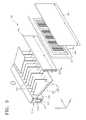
- FIG. 1is a schematic perspective view of a thin film deposition apparatus according to an embodiment of the present invention
- FIG. 2is a schematic side view of the thin film deposition apparatus of FIG. 1 before a deposition blade is disposed;
- FIG. 3is a schematic plan view of the thin film deposition apparatus of FIG. 1 ;
- FIG. 4is a schematic side view of the thin film deposition apparatus of FIG. 1 after a deposition blade is disposed;
- FIG. 5is a schematic perspective view of a thin film deposition apparatus according to another embodiment of the present invention.
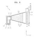
- FIG. 6is a schematic side view of the thin film deposition apparatus of FIG. 5 after a deposition blade is disposed.
- FIG. 1is a schematic perspective view of a thin film deposition apparatus 100 according to an embodiment of the present invention
- FIG. 2is a schematic side view of the thin film deposition apparatus 100 of FIG. 1 before a deposition blade 170 is disposed
- FIG. 3is a schematic plan view of the thin film deposition apparatus 100 of FIG. 1 .
- the thin film deposition apparatus 100includes a deposition source 110 , a first nozzle unit 120 , a first barrier wall assembly 130 , a second barrier wall assembly 140 , and a second nozzle unit 150 .
- the first nozzle unit 120is disposed in front of the deposition source 110 .
- the first barrier wall assembly 130is disposed in front of the first nozzle unit 120 .
- the second barrier wall assembly 140is disposed in front of the first barrier wall assembly 130 .
- the second nozzle unit 150is disposed in front of the second barrier wall assembly 140 .
- the substrate 160is disposed in front of the second nozzle unit 150 . While shown with first and second barrier wall assemblies 130 , 140 in the current example, it is understood that other numbers of barrier wall assemblies can be used, and that barrier wall assemblies are not required in all aspects of the invention.
- the deposition source 110 , the first nozzle unit 120 , the first barrier wall assembly 130 , the second barrier wall assembly 140 , the second nozzle unit 150 , and substrate 160are disposed in a vacuum chamber 180 in order to allow a deposition material to move straight.
- the temperature of the first barrier wall assembly 130 , the second barrier wall assembly 140 , and the second nozzle unit 150is lower than that of the deposition source 110 .
- the space between the first nozzle unit 120 and the second nozzle unit 150may be maintained at a high vacuum.
- the deposition material 112 that has collided against the first barrier wall assembly 130 and the second barrier wall assembly 140may not be vaporized again, and thereby maintaining the chamber at a high vacuum. Thus, since the deposition materials 112 do not collide with each other, the deposition materials 112 may move straight.
- the deposition source 110includes a heat resistant unit such as a crucible 111 .
- the crucible 111is filled with the deposition material 112 to be deposited on the substrate 160 .
- a heater 113is disposed on the inner surface of the crucible 111 and vaporizes the deposition material 112 in the crucible 111 .
- the first nozzle unit 120is disposed in front of the deposition source 110 .
- the first nozzle unit 120includes a plurality of first slit units 121 arranged at equal intervals.
- the first slit units 121are arranged in the Y-axis direction of the substrate 160 .
- the deposition material 112 that is vaporized in the deposition source 110proceeds toward the substrate 160 via the first slit units 121 .
- the first barrier wall assembly 130is disposed in front of the first nozzle 120 .
- the first barrier wall assembly 130includes a plurality of first barrier walls 131 .
- the first barrier walls 131are arranged parallel to each other at equal intervals in the Y-axis direction of the substrate 160 .
- Each of the first barrier walls 131are shown formed to extend along an XZ plane (i.e., perpendicular to the Y-axis direction). However, the invention is not limited to the shown orientation.
- the first barrier walls 131are respectively disposed between adjacent pairs of the first slit units 121 .
- one first slit unit 121is disposed between each two adjacent first barrier walls 131 .
- Each first slit unit 121is disposed at a midpoint between the two adjacent first barrier walls 131 .
- other numbers of first slit units 121can be disposed between adjacent pairs of the first barrier walls 131 , and that the first slit unit 121 does not have to be at the midpoint between the two adjacent first barrier walls 131 in all aspects of the invention.
- a first barrier wall frame 132is disposed to surround the plurality of first barrier walls 131 .
- the first barrier wall frame 132covers upper and lower sides of the first barrier walls 131 and retains the positions of the first barrier walls 131 .
- the second barrier wall assembly 140is disposed in front of the first barrier wall assembly 130 .
- the second barrier wall assembly 140includes a plurality of second barrier walls 141 .
- the second barrier walls 141are arranged parallel to each other at equal intervals in the Y-axis direction of the substrate 160 .
- Each of the second barrier walls 141are shown formed to extend along an XZ plane (i.e., perpendicular to the Y-axis direction), but the invention is not limited to the shown orientation.
- the second barrier walls 141should be accurately aligned with second slit units 151 of the second nozzle unit 150 , respectively.
- each of the second barrier walls 141may be formed to be relatively thinner than each of the first barrier walls 131 .
- the first barrier walls 131do not need to be precisely aligned with the second slit units 151 of the second nozzle unit 150 . Therefore, the first barrier walls 131 may be formed to be relatively thick. This makes it easier to manufacture the first barrier walls 131 .
- a second barrier wall frame 142is disposed to surround the plurality of second barrier walls 141 .
- the second barrier wall frame 142retains the positions of the second barrier walls 141 .
- the second barrier walls 141are aligned to correspond to the first barrier walls 131 , respectively.
- the second barrier walls 141may be respectively disposed to be parallel to and coplanar with the first barrier walls 131 in the X-axis direction of the substrate 160 to partition the space between the first nozzle unit 120 and the second nozzle unit 150 .
- the deposition material 112 discharged through one first slit unit 121is not mixed with the deposition material 112 discharged through another first slit unit 121 , and is deposited on the substrate 160 through the second slit units 151 of the second nozzle unit 150 .
- the inventionis not limited to the shown orientation in all aspects and that the second barrier walls 141 need not be precisely parallel to and coplanar with the first barrier walls 131 in the X-axis in all aspects of the invention.
- the first barrier wall assembly 130 and the second barrier wall assembly 140are disposed to be separated from each other by a predetermined distance.
- the first barrier wall assembly 130may be separated from the second barrier wall assembly 140 since it is unnecessary to precisely align the first barrier walls 131 and the second barrier walls 141 .
- the second barrier walls 141should be precisely aligned with the second nozzle unit 150 .
- high-precision controlmay be easily achieved by separating a part required to be precisely controlled from a part not required to be precisely controlled.
- the temperature of the first barrier wall assembly 130may increase to 100° C. or higher due to the high temperature of the deposition source 110 .
- the first barrier wall assembly 130 and the second barrier wall assembly 140are separated from each other.
- the deposition material 112 adhered to the first barrier wall assembly 130may be reused, whereas the deposition material 112 adhered to the second barrier wall assembly 140 and the second nozzle unit 150 may not be reused in all aspects of the invention.
- the first barrier wall assembly 130is separated from the second barrier wall assembly 140 and the second nozzle unit 150 , it may be straightforward to recover the deposition material 112 to be reused.
- the deposition material 112 adhered to the second barrier wall assembly 140can be reused in other aspects.
- the second nozzle unit 150is disposed between the second barrier wall assembly 140 and the substrate 160 .
- the second nozzle unit 150includes a plurality of second slit units 151 arranged at equal intervals.
- the second slit units 151are arranged in the Y axis direction of the substrate 160 .
- a second nozzle unit frame 152is formed to surround the second nozzle unit 150 .
- a total number of the second slit units 151is greater than a total number of the first slit units 121 .
- the number of the second slit units 151 disposed between two adjacent first and second barrier walls 131 and 141may be greater than the number of the first slit units 121 disposed between the two adjacent first and second barrier walls 131 and 141 .
- one first slit unit 121corresponds to three second slit units 151 in FIGS. 1 to 3
- the number of the second slit units 151 corresponding to one first slit unit 121may vary according to requirements for the resultant products.
- the second nozzle unit 150 and the substrate 160are disposed to be separated from each other by a predetermined distance. Accordingly, a defect caused by the contact between the second nozzle unit 150 and the substrate 160 may be prevented.
- depositionis performed while the thin film deposition apparatus 100 is moved relative to the substrate 160 in the Z-axis direction.
- the length of the second nozzle unit 150 in the Z-axis directionmay be less than the length of the substrate 160 in the Z-axis direction.
- the substrate 160may be a substrate for flat panel displays.
- a large substratesuch as a mother glass, for manufacturing a plurality of flat panel displays, may be used as the substrate 160 .
- the temperature of the thin film deposition apparatus 100should be constantly maintained without turning off the deposition source 110 until the deposition material 112 is exhausted in order to prevent denaturation of the deposition material 112 (e.g., an organic material). Accordingly, even during a stand-by mode, the deposition material 112 is continuously discharged to a vacuum chamber through the second nozzle unit 150 to be deposited on the second nozzle unit 150 . Therefore, this deposition through the second nozzle unit 150 during the stand-by mode should be prevented.
- the deposition material 112e.g., an organic material
- An example of the stand-by modeincludes a time period between one deposition process for the substrate 160 and a subsequent deposition process for another substrate 160 .
- the stand-by modecan be any interruption in the deposition process during which the deposition material 112 is being vaporized but the deposition material 112 should not pass through the second nozzle unit 150 , such as where the second nozzle unit 150 is being exchanged for another mask.
- a deposition blade 170is optionally disposed at the space (d 1 ) between the first barrier wall assembly 130 and the second barrier wall assembly 140 . If the deposition blade 170 is disposed between the first barrier wall assembly 130 and the second barrier wall assembly 140 , the deposition material 112 discharged from the deposition source 110 may not be adhered to undesirable regions, such as the second nozzle unit 150 . Instead, the deposition material 112 is deposited on the deposition blade 170 .
- the shown deposition blade 170is a flat panel.
- the length (l 1 ) of the deposition blade 170is the same as or greater than the length (l 2 ) of the substrate 160 to be patterned. Thus, contamination of the substrate 160 may be prevented.
- the height (h 1 ) of the deposition blade 170may be enough to cover the first barrier wall assembly 130 .
- the thickness (t 1 ) of the deposition blade 170may be less than the distance between the first barrier wall assembly 130 and the second barrier wall assembly 140 , and may vary according to requirements for products.
- the deposition blade 170can be formed of multiple elements, and need not be of the same material in all aspects of the invention. Further, while shown as having the length (l 1 ) that is the same as or greater than the length (l 2 ) of the substrate 160 to be patterned, the deposition blade 170 length (l 1 ) need only be long enough to prevent the deposition material 112 from passing to the second nozzle unit 150 , and therefore need only have a blocking surface having a length of the second nozzle unit 150 or the second barrier wall assembly 140 depending on the space in which the deposition blade 170 is inserted. While not required in all aspects, the deposition blade 170 can be of the same material as the first and second barrier wall assemblies 130 , 140 . Further, while one deposition blade 170 is shown, it is understood that multiple deposition blades can be used in disposed in different spaces between the first and second nozzle units 120 , 150 .
- the deposition blade 170is optionally disposed between the first barrier wall assembly 130 and the second barrier wall assembly 140 herein, the present invention is not limited thereto.
- the deposition blade 170may also be disposed in any space formed between units 120 , 150 in the thin film deposition apparatus 100 .
- a space (d 2 )may be formed between the deposition source 110 and the first barrier wall assembly 130 .
- the deposition blade 170may further be disposed in the space (d 2 ). However, if the deposition blade 170 is disposed in the space (d 2 ), the temperature conducted from the deposition source 110 should be considered. Meanwhile, the deposition blade 170 may also be formed between the second barrier wall assembly 140 and the second nozzle unit 150 .
- the deposition material 112 vaporized in the deposition source 110passes through the first slit units 121 of the first nozzle unit 120 , the space partitioned by the first barrier walls 131 and the second barrier walls 141 , and the second slit units 151 of the second nozzle unit 150 to be deposited on the substrate 160 .
- the deposition blade 170is not disposed in the space (d 1 ) between the first barrier wall assembly 130 and the second barrier wall assembly 140 .
- the deposition material 112 discharged through one first slit unit 121 of the first nozzle unit 120is not mixed with the deposition material 112 discharged through another adjacent first slit unit 121 due to the first barrier walls 131 and the second barrier walls 141 .
- the deposition material 112is deposited on the substrate 160 through the second nozzle unit 150 at an angle that is substantially perpendicular to the substrate 160 .
- the thin film deposition apparatus 100When deposition on one substrate 160 is completed, the thin film deposition apparatus 100 is moved up and down to enter a stand-by mode. However, the deposition material 112 is continuously vaporized by the deposition source 110 during the stand-by mode. Thus, unless the deposition blade 170 is used, the deposition material 112 is deposited on the second nozzle unit 150 . Since the width of the pattern of the second nozzle unit 150 is reduced due to the continuous vaporization of the deposition material 112 , the exchange cycle of the second nozzle unit 150 is reduced.
- the deposition blade 170is disposed in the space (d 1 ) between the first barrier wall assembly 130 and the second barrier wall assembly 140 .
- the deposition blade 170Since the deposition blade 170 is disposed in the space (d 1 ), the deposition material 112 is adhered to the surface of the deposition blade 170 even while the deposition material 112 is continuously discharged from the deposition source 110 that is heated. Thus, the deposition of the deposition material 112 on the second nozzle unit 150 may be prevented.
- FIG. 5is a schematic perspective view of a thin film deposition apparatus 500 according to another embodiment of the present invention.
- the thin film deposition apparatus 500includes a deposition source 510 , a first nozzle unit 520 , a barrier wall assembly 530 , and a second nozzle unit 550 .
- the first nozzle unit 550is disposed in front of the deposition source 510 .
- a barrier wall assembly 530is disposed in front of the first nozzle unit 520 .
- a second nozzle unit 550is disposed in front of the barrier wall assembly 530 .
- a substrate 560is disposed in front of the second nozzle unit 550 . According to the current embodiment, there is not second barrier wall assembly used.
- the deposition source 510includes a crucible 511 and a heater 513 .
- the crucible 511holds the deposition material 512 .
- the heater 513heats the crucible 511 to vaporize the deposition material 512 contained in the crucible 511 toward the first nozzle unit 520 .
- the first nozzle unit 520is disposed in front of the deposition source 510 .
- the first nozzle unit 520includes a plurality of first slit units 521 arranged at equal intervals in the Y-axis direction of the substrate 560 .
- the deposition material 512proceeds toward the substrate 560 via the first slit units 521 .
- the barrier wall assembly 530is disposed in front of the first nozzle unit 520 .
- the barrier wall assembly 530includes a plurality of barrier walls 531 , and a barrier wall frame 532 that surrounds sides of the barrier walls 531 .
- One first slit unit 521is disposed between each two adjacent barrier walls 531 .
- the first slit unit 521is disposed at the center between each two adjacent barrier walls 531 .
- other numbers of first slit units 521can be disposed between adjacent pairs of the first barrier walls 531 , and that the first slit unit 521 does not have to be at the midpoint between the two adjacent first barrier walls 531 in all aspects of the invention.
- the second nozzle unit 550is disposed between the barrier wall assembly 530 and the substrate 560 .
- the second nozzle unit 550includes a plurality of second slit units 551 arranged at equal intervals.
- a second nozzle unit frame 552is formed to surround the second nozzle unit 550 .
- a total number of the second slit units 551is greater than a total number of the first slit units 521 .
- the number of the second slit units 551 disposed between two adjacent barrier walls 531is greater than the number of the first slit unit 521 disposed between the same two adjacent barrier walls 531 .
- the second nozzle unit 550 and the substrate 560are disposed to be separated from each other by a predetermined distance.
- the barrier wall assembly 530 and the second nozzle 550are separated from each other by a predetermined distance (d 3 ).
- the deposition blade 570is removably disposed in the space (d 3 ). The deposition material 512 discharged from the deposition source 510 does adhere not to undesirable regions, such as the second nozzle unit 550 , due to the deposition blade 570 .
- the length (l 3 ) of the deposition blade 570is the same as or greater than the length (l 4 ) of the substrate 560 .
- the height (h 2 ) of the deposition blade 570may be enough to cover the barrier wall assembly 530 .
- the thickness (t 2 ) of the deposition blade 570may be less than the distance (d 3 ) between the barrier wall assembly 530 and the second nozzle unit 550 .
- the deposition blade 570is optionally disposed between the barrier wall assembly 530 and the second nozzle unit 550 herein, the present invention is not limited thereto.
- the deposition blade 570may also be disposed in any space formed between units 520 , 550 in the thin film deposition apparatus 500 .
- the deposition blade 570 length (l 3 )need only be long enough to prevent the deposition material 512 from passing to the second nozzle unit 550 , and therefore need only have a blocking surface having a length of the second nozzle unit 550 or the first barrier wall assembly 540 depending on the space in which the deposition blade 570 is inserted. While not required in all aspects, the deposition blade 570 can be of the same material as the first barrier wall assemblies 530 .
- the deposition material 512 vaporized in the deposition source 510passes through the first slit units 521 of the first nozzle unit 520 , the space partitioned by the barrier walls 530 , and the second slit units 551 of the second nozzle unit 550 to be deposited on the substrate 560 .
- the deposition blade 570is not disposed in the space (d 3 ) between the barrier wall assembly 530 and the second nozzle unit 550 during deposition.
- the thin film deposition apparatus 500When deposition on one substrate 560 is completed, the thin film deposition apparatus 500 is moved up and down to enter a stand-by mode. However, the deposition material 512 is continuously vaporized by the deposition source 510 during the stand-by mode. As such, as shown in FIG. 6 , when the thin film deposition apparatus 500 is moved up and down to enter the stand-by mode, the deposition blade 570 is optionally disposed in the space (d 3 ) between the barrier wall assembly 530 and the second nozzle unit 550 .
- the deposition blade 570Since the deposition blade 570 is disposed in the space (d 3 ), the deposition material 512 is adhered to the surface of the deposition blade 570 even while the deposition material 512 is continuously discharged from the deposition source 512 . Thus, the deposition of the deposition material 512 on the second nozzle unit 550 may be prevented.
- deposition of the deposition material continuously discharged from the deposition source on undesirable regions in the chamber such as the nozzle unitmay be prevented during the stand-by mode using the thin film deposition apparatus including the deposition blade since the deposition blade may be optionally disposed in any space formed between two units selected from the group consisting of the first barrier wall assembly, the second barrier wall assembly, and the nozzle unit.
Landscapes
- Chemical & Material Sciences (AREA)
- Engineering & Computer Science (AREA)
- Chemical Kinetics & Catalysis (AREA)
- Materials Engineering (AREA)
- Mechanical Engineering (AREA)
- Metallurgy (AREA)
- Organic Chemistry (AREA)
- Manufacturing & Machinery (AREA)
- Physical Vapour Deposition (AREA)
- Electroluminescent Light Sources (AREA)
Abstract
Description
Claims (4)
Applications Claiming Priority (2)
| Application Number | Priority Date | Filing Date | Title |
|---|---|---|---|
| KR10-2009-0073523 | 2009-08-10 | ||
| KR1020090073523AKR101127575B1 (en) | 2009-08-10 | 2009-08-10 | Apparatus for thin film deposition having a deposition blade |
Publications (2)
| Publication Number | Publication Date |
|---|---|
| US20110033619A1 US20110033619A1 (en) | 2011-02-10 |
| US9593408B2true US9593408B2 (en) | 2017-03-14 |
Family
ID=43535032
Family Applications (1)
| Application Number | Title | Priority Date | Filing Date |
|---|---|---|---|
| US12/815,673Active2033-09-28US9593408B2 (en) | 2009-08-10 | 2010-06-15 | Thin film deposition apparatus including deposition blade |
Country Status (2)
| Country | Link |
|---|---|
| US (1) | US9593408B2 (en) |
| KR (1) | KR101127575B1 (en) |
Families Citing this family (28)
| Publication number | Priority date | Publication date | Assignee | Title |
|---|---|---|---|---|
| TWI475124B (en) | 2009-05-22 | 2015-03-01 | Samsung Display Co Ltd | Thin film deposition apparatus |
| JP5620146B2 (en) | 2009-05-22 | 2014-11-05 | 三星ディスプレイ株式會社Samsung Display Co.,Ltd. | Thin film deposition equipment |
| US8882920B2 (en)* | 2009-06-05 | 2014-11-11 | Samsung Display Co., Ltd. | Thin film deposition apparatus |
| US8882921B2 (en)* | 2009-06-08 | 2014-11-11 | Samsung Display Co., Ltd. | Thin film deposition apparatus |
| KR101117719B1 (en)* | 2009-06-24 | 2012-03-08 | 삼성모바일디스플레이주식회사 | Apparatus for thin layer deposition |
| JP5328726B2 (en) | 2009-08-25 | 2013-10-30 | 三星ディスプレイ株式會社 | Thin film deposition apparatus and organic light emitting display device manufacturing method using the same |
| JP5677785B2 (en) | 2009-08-27 | 2015-02-25 | 三星ディスプレイ株式會社Samsung Display Co.,Ltd. | Thin film deposition apparatus and organic light emitting display device manufacturing method using the same |
| US8876975B2 (en) | 2009-10-19 | 2014-11-04 | Samsung Display Co., Ltd. | Thin film deposition apparatus |
| KR101146982B1 (en) | 2009-11-20 | 2012-05-22 | 삼성모바일디스플레이주식회사 | Aapparatus for thin layer deposition and method of manufacturing organic light emitting display apparatus |
| KR101084184B1 (en) | 2010-01-11 | 2011-11-17 | 삼성모바일디스플레이주식회사 | Thin film deposition apparatus |
| KR101174875B1 (en) | 2010-01-14 | 2012-08-17 | 삼성디스플레이 주식회사 | Apparatus for thin layer deposition, method for manufacturing of organic light emitting display apparatus using the same, and organic light emitting display apparatus manufactured by the method |
| KR101193186B1 (en)* | 2010-02-01 | 2012-10-19 | 삼성디스플레이 주식회사 | Apparatus for thin layer deposition, method for manufacturing of organic light emitting display apparatus using the same, and organic light emitting display apparatus manufactured by the method |
| KR101156441B1 (en) | 2010-03-11 | 2012-06-18 | 삼성모바일디스플레이주식회사 | Apparatus for thin layer deposition |
| KR101202348B1 (en) | 2010-04-06 | 2012-11-16 | 삼성디스플레이 주식회사 | Apparatus for thin layer deposition and method for manufacturing of organic light emitting display apparatus using the same |
| US8894458B2 (en) | 2010-04-28 | 2014-11-25 | Samsung Display Co., Ltd. | Thin film deposition apparatus, method of manufacturing organic light-emitting display device by using the apparatus, and organic light-emitting display device manufactured by using the method |
| KR101223723B1 (en) | 2010-07-07 | 2013-01-18 | 삼성디스플레이 주식회사 | Apparatus for thin layer deposition, method for manufacturing of organic light emitting display apparatus using the same, and organic light emitting display apparatus manufactured by the method |
| KR101673017B1 (en) | 2010-07-30 | 2016-11-07 | 삼성디스플레이 주식회사 | Apparatus for thin layer deposition and method for manufacturing of organic light emitting display apparatus using the same |
| KR101723506B1 (en) | 2010-10-22 | 2017-04-19 | 삼성디스플레이 주식회사 | Apparatus for organic layer deposition and method for manufacturing of organic light emitting display apparatus using the same |
| KR101738531B1 (en) | 2010-10-22 | 2017-05-23 | 삼성디스플레이 주식회사 | Method for manufacturing of organic light emitting display apparatus, and organic light emitting display apparatus manufactured by the method |
| KR20120045865A (en) | 2010-11-01 | 2012-05-09 | 삼성모바일디스플레이주식회사 | Apparatus for organic layer deposition |
| KR20120065789A (en) | 2010-12-13 | 2012-06-21 | 삼성모바일디스플레이주식회사 | Apparatus for organic layer deposition |
| KR101760897B1 (en) | 2011-01-12 | 2017-07-25 | 삼성디스플레이 주식회사 | Deposition source and apparatus for organic layer deposition having the same |
| KR101852517B1 (en) | 2011-05-25 | 2018-04-27 | 삼성디스플레이 주식회사 | Apparatus for organic layer deposition and method for manufacturing of organic light emitting display apparatus using the same |
| KR101840654B1 (en) | 2011-05-25 | 2018-03-22 | 삼성디스플레이 주식회사 | Apparatus for organic layer deposition and method for manufacturing of organic light emitting display apparatus using the same |
| KR101857249B1 (en) | 2011-05-27 | 2018-05-14 | 삼성디스플레이 주식회사 | Patterning slit sheet assembly, apparatus for organic layer deposition, method for manufacturing organic light emitting display apparatus and organic light emitting display apparatus |
| KR101826068B1 (en) | 2011-07-04 | 2018-02-07 | 삼성디스플레이 주식회사 | Apparatus for thin layer deposition |
| KR102075527B1 (en)* | 2013-05-16 | 2020-02-11 | 삼성디스플레이 주식회사 | Apparatus for organic layer deposition, and method for manufacturing of organic light emitting display apparatus using the same |
| US20240327983A1 (en)* | 2023-03-31 | 2024-10-03 | Applied Materials, Inc. | Processing systems for metal precursor synthesis and deposition |
Citations (182)
| Publication number | Priority date | Publication date | Assignee | Title |
|---|---|---|---|---|
| JPS57194252A (en) | 1981-05-25 | 1982-11-29 | Fuji Photo Film Co Ltd | Vapor depositing device by electron beam |
| US4687939A (en) | 1983-11-07 | 1987-08-18 | Hitachi, Ltd. | Method and apparatus for forming film by ion beam |
| JPH04272170A (en) | 1991-02-25 | 1992-09-28 | Tokai Carbon Co Ltd | Graphite crucible for vacuum deposition |
| JPH05230628A (en) | 1992-02-18 | 1993-09-07 | Fujitsu Ltd | Metal film forming apparatus, metal material recovery method in metal film forming apparatus |
| JPH0827568A (en) | 1994-07-19 | 1996-01-30 | Toshiba Corp | Steam generation method and apparatus |
| JPH0995776A (en) | 1995-09-29 | 1997-04-08 | Sony Corp | Vacuum deposition device |
| WO1999025894A1 (en) | 1997-11-17 | 1999-05-27 | The Trustees Of Princeton University | Low pressure vapor phase deposition of organic thin films |
| JP2000068054A (en) | 1998-08-26 | 2000-03-03 | Hokuriku Electric Ind Co Ltd | Manufacture of el element |
| KR20000019254A (en) | 1998-09-08 | 2000-04-06 | 석창길 | Device for improving thin film thickness uniformity of cvd |
| KR20000023929A (en) | 1999-10-29 | 2000-05-06 | 최중호 | Apparatus and method for emitting odor |
| KR100257219B1 (en) | 1997-10-23 | 2000-05-15 | 박용관 | Method and device for making a safety operation of a polyethylene gas pipe valve arrangement |
| US6091195A (en) | 1997-02-03 | 2000-07-18 | The Trustees Of Princeton University | Displays having mesa pixel configuration |
| JP2001052862A (en) | 1999-08-04 | 2001-02-23 | Hokuriku Electric Ind Co Ltd | Manufacture of organic el element and device therefor |
| JP2001093667A (en) | 1999-09-28 | 2001-04-06 | Sanyo Electric Co Ltd | Organic light-emitting element, device and method for manufacturing the same |
| US20010006827A1 (en) | 1999-12-27 | 2001-07-05 | Semiconductor Energy Laboratory Co., Ltd. | Film formation apparatus and method for forming a film |
| KR20010059939A (en) | 1999-12-30 | 2001-07-06 | 송문섭 | Mobile station for mobile communication system |
| US6274198B1 (en) | 1997-02-24 | 2001-08-14 | Agere Systems Optoelectronics Guardian Corp. | Shadow mask deposition |
| US6280821B1 (en) | 1998-09-10 | 2001-08-28 | Ppg Industries Ohio, Inc. | Reusable mask and method for coating substrate |
| US20010019807A1 (en) | 1999-12-24 | 2001-09-06 | Tsutomu Yamada | Deposition mask and manufacturing method thereof, and electroluminescence display device and manufacturing method thereof |
| US20010026638A1 (en) | 2000-03-28 | 2001-10-04 | Katsuya Sangu | Positioning apparatus used in a process for producing multi-layered printed circuit board and method of using the same |
| KR20010092914A (en) | 2000-03-27 | 2001-10-27 | 윤종용 | Electrical static chuck comprising a shadow ring |
| KR200257218Y1 (en) | 2001-09-07 | 2001-12-24 | 엘지.필립스 엘시디 주식회사 | Mask apparatus for organic electro-luminescence device |
| KR20020000201A (en) | 2000-06-23 | 2002-01-05 | 최승락 | Method cleaning Liquid Chrystal Display using Laser and Vapor Phase |
| KR20020001555A (en) | 2000-06-22 | 2002-01-09 | 키도 준지 | Apparatus for and method of vacuum vapor deposition and organic electroluminescent device |
| JP2002075638A (en) | 2000-08-29 | 2002-03-15 | Nec Corp | Vapor deposition method of mask and vapor deposition device |
| US6371451B1 (en) | 1999-10-29 | 2002-04-16 | Korea Institute Of Science And Technology | Scent diffusion apparatus and method |
| US20020076847A1 (en) | 2000-09-28 | 2002-06-20 | Tsutomu Yamada | Method of attaching layer material and forming layer in predetermined pattern on substrate using mask |
| KR20020050922A (en) | 2000-12-22 | 2002-06-28 | 박종섭 | Virtual channel sdram |
| US20020168577A1 (en) | 2001-05-11 | 2002-11-14 | Jin-Mo Yoon | Method of crystallizing amorphous silicon |
| KR20020090934A (en) | 2002-08-27 | 2002-12-05 | 에이엔 에스 주식회사 | Organic material point source feeding unit in organic semiconductor device and method thereof |
| KR20030001745A (en) | 2001-06-27 | 2003-01-08 | 주식회사 하이닉스반도체 | Method for monitoring focus |
| JP2003003250A (en) | 2001-06-22 | 2003-01-08 | Alps Electric Co Ltd | Vacuum deposition polymerization system and method for depositing organic film using the system |
| JP2003077662A (en) | 2001-06-22 | 2003-03-14 | Junji Kido | Method and device for manufacturing organic electroluminescent element |
| KR20030034730A (en) | 2001-10-26 | 2003-05-09 | 삼성 엔이씨 모바일 디스플레이 주식회사 | Frame for mask of organic EL display devices |
| JP2003157973A (en) | 2001-09-05 | 2003-05-30 | Sony Corp | Manufacturing method and manufacturing apparatus of organic electroluminescence device, and manufacturing system and manufacturing method of display device using the same |
| US20030101937A1 (en) | 2001-11-28 | 2003-06-05 | Eastman Kodak Company | Thermal physical vapor deposition source for making an organic light-emitting device |
| US20030101932A1 (en) | 2001-12-05 | 2003-06-05 | Samsung Nec Mobile Display Co., Ltd. | Tension mask assembly for use in vacuum deposition of thin film of organic electroluminescent device |
| US6579422B1 (en) | 1999-07-07 | 2003-06-17 | Sony Corporation | Method and apparatus for manufacturing flexible organic EL display |
| US20030118950A1 (en) | 2000-08-07 | 2003-06-26 | Ching-Ian Chao | Method of manufacturing full-color organic electro-luminescent device |
| KR20030069684A (en) | 2002-02-22 | 2003-08-27 | 엘지.필립스 엘시디 주식회사 | Device for fixing mask and Ultraviolet irradiating device using the same |
| US20030168013A1 (en) | 2002-03-08 | 2003-09-11 | Eastman Kodak Company | Elongated thermal physical vapor deposition source with plural apertures for making an organic light-emitting device |
| JP2003297562A (en) | 2002-03-29 | 2003-10-17 | Sanyo Electric Co Ltd | Vapor deposition method |
| JP2003321767A (en) | 2002-04-26 | 2003-11-14 | Seiko Epson Corp | Method for depositing thin film, organic electroluminescence device, method for manufacturing organic electroluminescence device, and electronic equipment |
| KR20030091947A (en) | 2000-12-21 | 2003-12-03 | 아르코 케미컬 테크날러쥐. 엘.피. | Process for Producing Hydrogen Peroxide |
| US20030221614A1 (en) | 2002-06-03 | 2003-12-04 | Samsung Nec Mobile Display Co., Ltd., Ulsan-City, Republic Of Korea | Mask and mask frame assembly for evaporation |
| US20030221620A1 (en) | 2002-06-03 | 2003-12-04 | Semiconductor Energy Laboratory Co., Ltd. | Vapor deposition device |
| US20030232563A1 (en) | 2002-05-09 | 2003-12-18 | Isao Kamiyama | Method and apparatus for manufacturing organic electroluminescence device, and system and method for manufacturing display unit using organic electroluminescence devices |
| US20040029028A1 (en) | 2002-08-05 | 2004-02-12 | Nec Plasma Display Coropration | Method for measuring gap between mask and substrate of display panel |
| JP2004043898A (en) | 2002-07-12 | 2004-02-12 | Canon Electronics Inc | Vapor deposition mask, and organic electroluminescence display device |
| US20040056244A1 (en) | 2002-09-23 | 2004-03-25 | Eastman Kodak Company | Device for depositing patterned layers in OLED displays |
| JP2004103341A (en) | 2002-09-09 | 2004-04-02 | Matsushita Electric Ind Co Ltd | Method for manufacturing organic electroluminescence device |
| JP2004103269A (en) | 2002-09-05 | 2004-04-02 | Sanyo Electric Co Ltd | Manufacture method for organic electroluminescence display device |
| EP1413644A2 (en) | 2002-10-24 | 2004-04-28 | Sony Corporation | Thin-film deposition device |
| KR20040034537A (en) | 2002-10-21 | 2004-04-28 | 도호꾸 파이오니어 가부시끼가이샤 | Vacuum evaporator |
| US20040086639A1 (en)* | 2002-09-24 | 2004-05-06 | Grantham Daniel Harrison | Patterned thin-film deposition using collimating heated mask asembly |
| KR20040050045A (en) | 2002-12-03 | 2004-06-14 | 세이코 엡슨 가부시키가이샤 | Mask vapor deposition method, mask vapor deposition system, mask, process for manufacturing mask, apparatus for manufacturing display panel, display pane, and electronic device |
| US6749906B2 (en) | 2002-04-25 | 2004-06-15 | Eastman Kodak Company | Thermal physical vapor deposition apparatus with detachable vapor source(s) and method |
| US20040115342A1 (en) | 2002-11-22 | 2004-06-17 | Samsung Nec Mobile Display Co., Ltd. | Deposition mask frame assembly, method of fabricating the same, and method of fabricating organic electroluminescent device using the deposition mask frame assembly |
| US20040115338A1 (en)* | 2002-09-05 | 2004-06-17 | Sanyo Electric Co., Ltd. | Manufacturing method of organic electroluminescent display device |
| US20040127066A1 (en) | 2002-12-31 | 2004-07-01 | Yun-Ho Jung | Mask for sequential lateral solidification and crystallization method using thereof |
| JP2004199919A (en) | 2002-12-17 | 2004-07-15 | Tohoku Pioneer Corp | Method for manufacturing organic el display panel |
| US20040144321A1 (en) | 2003-01-28 | 2004-07-29 | Eastman Kodak Company | Method of designing a thermal physical vapor deposition system |
| US20040183435A1 (en) | 2003-03-19 | 2004-09-23 | Tohoku Pioneer Corporation | Film formation mask, organic EL panel, and method of manufacturing the organic EL panel |
| KR20040084747A (en) | 2003-03-27 | 2004-10-06 | 세이코 엡슨 가부시키가이샤 | Method of forming pattern, pattern forming apparatus, method of manufacturing device, conductive film wiring, electro-optical apparatus, and electronic equipment |
| US20040194702A1 (en) | 2002-06-17 | 2004-10-07 | Koji Sasaki | Thin film-forming apparatus |
| US20040195530A1 (en) | 2003-04-04 | 2004-10-07 | Changsoo Kwak | Apparatus for measuring gap between mask and substrate using laser displacement sensor, and method thereof |
| US20040216673A1 (en)* | 2003-02-14 | 2004-11-04 | Semiconductor Energy Laboratory Co., Ltd. | Manufacturing apparatus |
| JP2004349101A (en) | 2003-05-22 | 2004-12-09 | Seiko Epson Corp | Film forming method, film forming apparatus, method of manufacturing organic electroluminescent device, organic electroluminescent device |
| US20050016461A1 (en) | 2003-07-22 | 2005-01-27 | Eastman Kodak Company | Thermal physical vapor deposition source using pellets of organic material for making oled displays |
| US20050037136A1 (en) | 2003-07-28 | 2005-02-17 | Katsuya Yamamoto | Mask for deposition, film formation method using the same and film formation equipment using the same |
| US20050072361A1 (en) | 2003-10-03 | 2005-04-07 | Yimou Yang | Multi-layered radiant thermal evaporator and method of use |
| US6878209B2 (en) | 1999-06-15 | 2005-04-12 | Toray Industries, Inc. | Organic electroluminescent device |
| JP2005122980A (en) | 2003-10-15 | 2005-05-12 | Chi Mei Electronics Corp | Image display device |
| US20050129489A1 (en) | 2003-11-12 | 2005-06-16 | Quan Yong C. | Load lock and load lock chamber using the same |
| JP2005165015A (en) | 2003-12-03 | 2005-06-23 | Seiko Epson Corp | Film forming mask, film forming apparatus, electro-optical device, and electronic apparatus |
| KR20050062853A (en) | 2003-12-19 | 2005-06-28 | 삼성전자주식회사 | Mask for forming the poly silicon layer and crystallization method of silicon using it |
| JP2005174843A (en) | 2003-12-15 | 2005-06-30 | Sony Corp | Deposition mask and its manufacturing method |
| US20050153472A1 (en) | 2003-12-26 | 2005-07-14 | Shinichi Yotsuya | Thin film formation method, thin film formation equipment, method of manufacturing organic electroluminescence device, organic electroluminescence device, and electronic apparatus |
| US20050166842A1 (en) | 2004-02-02 | 2005-08-04 | Fujitsu Limited | Vapor deposition mask and organic EL display device manufacturing method |
| JP2005235568A (en) | 2004-02-19 | 2005-09-02 | Seiko Epson Corp | Vapor deposition apparatus and organic EL device manufacturing method |
| JP2005293968A (en) | 2004-03-31 | 2005-10-20 | Sanyo Electric Co Ltd | Manufacturing method of organic electroluminescent element |
| US20050229848A1 (en) | 2004-04-15 | 2005-10-20 | Asm Japan K.K. | Thin-film deposition apparatus |
| JP2005296737A (en) | 2004-04-07 | 2005-10-27 | Mikuni Corp | Beat plate |
| US20060011136A1 (en) | 2004-07-15 | 2006-01-19 | Semiconductor Energy Laboratory Co., Ltd. | Manufacturing apparatus |
| KR20060008602A (en) | 2004-07-21 | 2006-01-27 | 엘지전자 주식회사 | Organic Electroluminescent Layer Deposition Method |
| US20060022590A1 (en) | 2004-08-02 | 2006-02-02 | Xerox Corporation | OLEDs having inorganic material containing anode capping layer |
| US7006202B2 (en) | 2002-02-21 | 2006-02-28 | Lg.Philips Lcd Co., Ltd. | Mask holder for irradiating UV-rays |
| KR20060018745A (en) | 2004-08-25 | 2006-03-02 | 삼성에스디아이 주식회사 | Vertically Moved Organic Material Deposition Equipment |
| KR20060020050A (en) | 2004-08-30 | 2006-03-06 | 삼성에스디아이 주식회사 | High efficiency organic electroluminescent device and manufacturing method thereof |
| US20060090705A1 (en)* | 2004-10-28 | 2006-05-04 | Kim Jae-Ho | Apparatus for fabricating display device |
| KR20060056706A (en) | 2004-11-22 | 2006-05-25 | 주식회사 하이닉스반도체 | Method of forming a semiconductor device |
| US20060110544A1 (en) | 2004-11-22 | 2006-05-25 | Kyekyoon Kim | Electrohydrodynamic spraying system |
| KR20060058459A (en) | 2004-11-25 | 2006-05-30 | 삼성에스디아이 주식회사 | Mask frame assembly, and method of manufacturing organic electroluminescent device using same |
| US20060113907A1 (en) | 2004-11-26 | 2006-06-01 | Ja-Hyun Im | Organic light emitting display and method for fabricating the same |
| KR20060065978A (en) | 2004-12-11 | 2006-06-15 | 비오이 하이디스 테크놀로지 주식회사 | Slit mask |
| KR20060073367A (en) | 2004-12-24 | 2006-06-28 | 엘지전자 주식회사 | Organics Treatment Unit in Cleaning Room |
| JP2006172930A (en) | 2004-12-16 | 2006-06-29 | Hitachi High-Tech Electronics Engineering Co Ltd | Vacuum deposition method and EL display panel |
| JP2006176809A (en) | 2004-12-21 | 2006-07-06 | Ulvac Japan Ltd | Substrate and mask alignment method, organic thin film deposition method, and alignment apparatus |
| US20060144325A1 (en) | 2005-01-05 | 2006-07-06 | Samsung Sdi Co., Ltd. | Driving shaft of effusion cell for deposition system and deposition system having the same |
| KR20060080481A (en) | 2005-01-05 | 2006-07-10 | 삼성에스디아이 주식회사 | Deposition source for material deposition and deposition system having same |
| KR20060080482A (en) | 2005-01-05 | 2006-07-10 | 삼성에스디아이 주식회사 | Deposition source for material deposition and deposition apparatus having same |
| KR20060083510A (en) | 2005-01-17 | 2006-07-21 | 삼성전자주식회사 | Photomask Equipment Eliminates Defective By-Products |
| JP2006210038A (en) | 2005-01-26 | 2006-08-10 | Seiko Epson Corp | Mask manufacturing method |
| US20060174829A1 (en) | 2005-02-07 | 2006-08-10 | Semes Co., Ltd. | Apparatus for processing substrate |
| KR20060092387A (en) | 2005-02-17 | 2006-08-23 | 비오이 하이디스 테크놀로지 주식회사 | Multi Slit Mask |
| US20060205101A1 (en) | 2004-12-03 | 2006-09-14 | Lee Jae-Ho | Laser irradiation device, patterning method and method of fabricating organic light emitting display (OLED) using the patterning method |
| KR20060098755A (en) | 2005-03-07 | 2006-09-19 | 에스케이씨 주식회사 | Vacuum deposition apparatus and method of organic light emitting diode |
| KR20060104288A (en) | 2005-03-30 | 2006-10-09 | 엘지전자 주식회사 | Clamping apparatus and method of mask for organic light emitting display device |
| KR20060104675A (en) | 2005-03-31 | 2006-10-09 | 세메스 주식회사 | Substrate processing equipment |
| JP2006275433A (en) | 2005-03-29 | 2006-10-12 | National Institute Of Advanced Industrial & Technology | Absorption type cooling and refrigeration equipment |
| KR100635903B1 (en) | 2004-01-29 | 2006-10-18 | 미쯔비시 히다찌 세이떼쯔 기까이 가부시끼가이샤 | Vacuum evaporator |
| KR20060109627A (en) | 2005-04-18 | 2006-10-23 | 엘지전자 주식회사 | Organic electroluminescent layer forming mask |
| JP2006292955A (en) | 2005-04-08 | 2006-10-26 | V Technology Co Ltd | Scan exposure method and scan exposure apparatus |
| KR20060114462A (en) | 2005-04-29 | 2006-11-07 | 엘지전자 주식회사 | Clamping apparatus and method of mask for organic light emitting display device |
| KR20060123944A (en) | 2005-05-30 | 2006-12-05 | 삼성에스디아이 주식회사 | Alignment device and alignment method of substrate and mask |
| JP2007047293A (en) | 2005-08-08 | 2007-02-22 | Casio Comput Co Ltd | Musical sound generator and program |
| KR100687007B1 (en) | 2005-03-22 | 2007-02-26 | 세메스 주식회사 | Organic thin film deposition apparatus used for manufacturing organic electroluminescent device |
| KR20070025164A (en) | 2005-08-31 | 2007-03-08 | 삼성에스디아이 주식회사 | Organic vapor deposition source and heating source control method thereof |
| US20070054044A1 (en) | 2003-07-10 | 2007-03-08 | Sumitomo Titanium | Method for forming metal oxide coating film and vapor deposition apparatus |
| KR100696550B1 (en) | 2005-12-09 | 2007-03-19 | 삼성에스디아이 주식회사 | Deposition equipment |
| KR100696547B1 (en) | 2005-12-09 | 2007-03-19 | 삼성에스디아이 주식회사 | Deposition method |
| KR100697663B1 (en) | 2005-10-27 | 2007-03-20 | 세메스 주식회사 | Organic material deposition apparatus |
| KR20070035796A (en) | 2005-09-28 | 2007-04-02 | 엘지전자 주식회사 | Device for manufacturing organic electroluminescent display device |
| KR20070050793A (en) | 2006-08-28 | 2007-05-16 | 주식회사 대우일렉트로닉스 | Micro heater and crucible manufacturing method, and organic vacuum deposition apparatus provided with them |
| KR100723627B1 (en) | 2006-08-01 | 2007-06-04 | 세메스 주식회사 | The evaporation source of the organic thin film deposition apparatus |
| US20070148337A1 (en) | 2005-12-22 | 2007-06-28 | Nichols Jonathan A | Flame-perforated aperture masks |
| US20070157879A1 (en) | 2006-01-11 | 2007-07-12 | Seiko Epson Corporation | Mask, film forming method, light-emitting device, and electronic apparatus |
| KR100739309B1 (en) | 2006-10-13 | 2007-07-12 | 삼성에스디아이 주식회사 | Thin film deposition mask and organic electroluminescent display device using the same |
| US20070163497A1 (en) | 2006-01-17 | 2007-07-19 | Eastman Kodak Company | Two-dimensional aperture array for vapor deposition |
| US20070178708A1 (en) | 2006-01-27 | 2007-08-02 | Canon Kabushiki Kaisha | Vapor deposition system and vapor deposition method for an organic compound |
| KR20070080635A (en) | 2006-02-08 | 2007-08-13 | 주식회사 아바코 | Organic Evaporation Boat |
| KR100770653B1 (en) | 2006-05-25 | 2007-10-29 | 에이엔 에스 주식회사 | Thin film deposition equipment |
| KR20070105595A (en) | 2006-04-27 | 2007-10-31 | 두산메카텍 주식회사 | Organic thin film deposition apparatus |
| KR20070112668A (en) | 2006-05-22 | 2007-11-27 | 세메스 주식회사 | Linear Evaporator for Fabrication of Organic Thin Film |
| KR100787457B1 (en) | 2006-08-31 | 2007-12-26 | 삼성에스디아이 주식회사 | Substrate alignment device and manufacturing apparatus for organic light emitting display device including the same |
| KR20080001184A (en) | 2006-06-29 | 2008-01-03 | 엘지.필립스 엘시디 주식회사 | Deposition Stem of Organic Electroluminescent Device and Manufacturing Method of Organic Electroluminescent Device Using Same |
| KR20080003720A (en) | 2006-07-03 | 2008-01-08 | 주식회사 야스 | Multi-nozzle evaporation source for deposition process |
| WO2008004792A1 (en) | 2006-07-03 | 2008-01-10 | Yas Co., Ltd. | Multiple nozzle evaporator for vacuum thermal evaporation |
| US20080018236A1 (en) | 2004-09-08 | 2008-01-24 | Toray Industries, Inc. | Organic Electroluminescent Device and Manufacturing Method Thereof |
| KR100800125B1 (en) | 2006-06-30 | 2008-01-31 | 세메스 주식회사 | Source Shutter and Substrate Control Method of Organic Light-Emitting Device Deposition Equipment |
| KR100823508B1 (en) | 2006-10-19 | 2008-04-21 | 삼성에스디아이 주식회사 | Evaporation source and deposition apparatus having same |
| KR20080036983A (en) | 2005-08-25 | 2008-04-29 | 히다치 조센 가부시키가이샤 | Alignment device for vacuum deposition |
| JP2008108628A (en) | 2006-10-26 | 2008-05-08 | Kyocera Corp | Organic EL display and manufacturing method thereof |
| KR20080044775A (en) | 2006-11-16 | 2008-05-21 | 자이단호징 야마가타켄산교기쥬츠신코기코 | Evaporation source and vacuum deposition apparatus using the same |
| KR20080048653A (en) | 2006-11-29 | 2008-06-03 | 엘지디스플레이 주식회사 | Mask device and manufacturing method of flat panel display device using same |
| US20080131587A1 (en) | 2006-11-30 | 2008-06-05 | Boroson Michael L | Depositing organic material onto an oled substrate |
| JP2008521165A (en) | 2004-11-16 | 2008-06-19 | インターナショナル・ビジネス・マシーンズ・コーポレーション | Organic light emitting device, method for manufacturing the same, and array comprising a plurality of organic light emitting devices |
| KR20080055124A (en) | 2006-12-14 | 2008-06-19 | 엘지디스플레이 주식회사 | Deposition equipment |
| US20080145521A1 (en) | 2006-12-13 | 2008-06-19 | Guo G X | System and process for fabricating photovoltaic cell |
| KR20080060400A (en) | 2006-12-27 | 2008-07-02 | 엘지디스플레이 주식회사 | Manufacturing method of array substrate and manufacturing method of organic light generating device using same |
| KR20080061132A (en) | 2006-12-28 | 2008-07-02 | 엘지디스플레이 주식회사 | Organic film deposition apparatus |
| KR20080061774A (en) | 2006-12-28 | 2008-07-03 | 엘지전자 주식회사 | Apparatus and method for aligning mask of liquid crystal display |
| KR20080061666A (en) | 2006-12-28 | 2008-07-03 | 세메스 주식회사 | Organic thin film deposition apparatus |
| KR20080062212A (en) | 2006-12-29 | 2008-07-03 | 세메스 주식회사 | Organic thin film deposition apparatus |
| US20080216741A1 (en) | 2001-10-26 | 2008-09-11 | Hermosa Thin Film Co., Ltd. | Dynamic film thickness control system/method and its utilization |
| US20080238294A1 (en) | 2007-03-30 | 2008-10-02 | The Penn State Research Foundation | Mist fabrication of quantum dot devices |
| KR20080109559A (en) | 2007-06-13 | 2008-12-17 | 주식회사 하이닉스반도체 | Masks and manufacturing methods for providing local modified illumination |
| US20090017192A1 (en) | 2007-07-12 | 2009-01-15 | Hiroyasu Matsuura | Vapor deposition method and apparatus |
| JP2009024208A (en) | 2007-07-18 | 2009-02-05 | Fujifilm Corp | Vapor deposition apparatus, vapor deposition method, and electronic device and organic electroluminescence device having layers patterned using the method |
| JP2009081165A (en) | 2007-09-25 | 2009-04-16 | Yamaha Motor Co Ltd | Substrate processing apparatus, surface mounting machine, printing machine, inspection machine, and coating machine |
| KR20090038733A (en) | 2007-10-16 | 2009-04-21 | 주식회사 실트론 | Heat treatment method for improving surface roughness of SOI wafer and heat treatment apparatus therefor |
| JP2009087910A (en) | 2007-09-10 | 2009-04-23 | Ulvac Japan Ltd | Vapor deposition apparatus and film formation method |
| KR20090040618A (en) | 2007-10-22 | 2009-04-27 | 네오뷰코오롱 주식회사 | Deposition mask unit |
| KR20090052155A (en) | 2007-11-20 | 2009-05-25 | 엘지디스플레이 주식회사 | OLED display device |
| KR20090053417A (en) | 2007-11-23 | 2009-05-27 | 삼성모바일디스플레이주식회사 | Mask assembly for thin film deposition of flat panel display |
| KR20090066996A (en) | 2007-12-20 | 2009-06-24 | 다이나믹솔라디자인 주식회사 | Continuous substrate processing system |
| KR100908232B1 (en) | 2002-06-03 | 2009-07-20 | 삼성모바일디스플레이주식회사 | Mask frame assembly for thin film deposition of organic electroluminescent device |
| KR20090093161A (en) | 2008-02-28 | 2009-09-02 | 삼성모바일디스플레이주식회사 | Evaporating apparatus and method for forming thin film |
| US20090232976A1 (en) | 2008-03-11 | 2009-09-17 | Samsung Sdi Co., Ltd. | Evaporating method for forming thin film |
| US20090277386A1 (en) | 2006-04-13 | 2009-11-12 | Ulvac, Inc. | Catalytic chemical vapor deposition apparatus |
| KR20100000129U (en) | 2008-06-26 | 2010-01-06 | (주) 씨앤앤 | Luminous watermark |
| KR20100000128A (en) | 2008-06-24 | 2010-01-06 | 엘지디스플레이 주식회사 | A deposition mask unit for fabrication of organic light emitting display device |
| US20100055810A1 (en) | 2008-09-01 | 2010-03-04 | Samsung Mobile Display Co.,Ltd. | Mask for thin film deposition and method of manufacturing oled using the same |
| US20100192856A1 (en) | 2009-02-05 | 2010-08-05 | Dong-Young Sung | Mask assembly and deposition and apparatus for a flat panel display using the same |
| KR20100099806A (en) | 2009-03-04 | 2010-09-15 | 삼성전자주식회사 | Holographic exposure apparatus |
| US20100271602A1 (en) | 2009-04-28 | 2010-10-28 | Noritsugu Hanazaki | Protective apparatus, mask, mask forming apparatus, mask forming method, exposure apparatus, device fabricating method, and foreign matter detecting apparatus |
| JP2010261081A (en) | 2009-05-08 | 2010-11-18 | V Technology Co Ltd | Vapor deposition method and vapor deposition apparatus |
| US20100297349A1 (en) | 2009-05-22 | 2010-11-25 | Samsung Mobile Display Co., Ltd. | Thin film deposition apparatus |
| KR20100126125A (en) | 2009-05-22 | 2010-12-01 | 삼성모바일디스플레이주식회사 | Thin film deposition apparatus |
| US20110220019A1 (en) | 2010-03-09 | 2011-09-15 | Lee Choong-Ho | Mask frame assembly for thin film deposition and method of assembling the same |
| US20120009328A1 (en) | 2010-07-12 | 2012-01-12 | Jae-Kwang Ryu | Thin film deposition apparatus and method of manufacturing organic light-emitting display device by using the same |
| US8193011B2 (en) | 2009-08-24 | 2012-06-05 | Samsung Mobile Display Co., Ltd. | Thin film deposition apparatus and method of manufacturing organic light-emitting display device by using the same |
- 2009
- 2009-08-10KRKR1020090073523Apatent/KR101127575B1/enactiveActive
- 2010
- 2010-06-15USUS12/815,673patent/US9593408B2/enactiveActive
Patent Citations (217)
| Publication number | Priority date | Publication date | Assignee | Title |
|---|---|---|---|---|
| JPS57194252A (en) | 1981-05-25 | 1982-11-29 | Fuji Photo Film Co Ltd | Vapor depositing device by electron beam |
| US4687939A (en) | 1983-11-07 | 1987-08-18 | Hitachi, Ltd. | Method and apparatus for forming film by ion beam |
| JPH04272170A (en) | 1991-02-25 | 1992-09-28 | Tokai Carbon Co Ltd | Graphite crucible for vacuum deposition |
| JPH05230628A (en) | 1992-02-18 | 1993-09-07 | Fujitsu Ltd | Metal film forming apparatus, metal material recovery method in metal film forming apparatus |
| JPH0827568A (en) | 1994-07-19 | 1996-01-30 | Toshiba Corp | Steam generation method and apparatus |
| JPH0995776A (en) | 1995-09-29 | 1997-04-08 | Sony Corp | Vacuum deposition device |
| US6091195A (en) | 1997-02-03 | 2000-07-18 | The Trustees Of Princeton University | Displays having mesa pixel configuration |
| US6274198B1 (en) | 1997-02-24 | 2001-08-14 | Agere Systems Optoelectronics Guardian Corp. | Shadow mask deposition |
| KR100257219B1 (en) | 1997-10-23 | 2000-05-15 | 박용관 | Method and device for making a safety operation of a polyethylene gas pipe valve arrangement |
| WO1999025894A1 (en) | 1997-11-17 | 1999-05-27 | The Trustees Of Princeton University | Low pressure vapor phase deposition of organic thin films |
| JP2000068054A (en) | 1998-08-26 | 2000-03-03 | Hokuriku Electric Ind Co Ltd | Manufacture of el element |
| KR20000019254A (en) | 1998-09-08 | 2000-04-06 | 석창길 | Device for improving thin film thickness uniformity of cvd |
| US6280821B1 (en) | 1998-09-10 | 2001-08-28 | Ppg Industries Ohio, Inc. | Reusable mask and method for coating substrate |
| US6878209B2 (en) | 1999-06-15 | 2005-04-12 | Toray Industries, Inc. | Organic electroluminescent device |
| US6579422B1 (en) | 1999-07-07 | 2003-06-17 | Sony Corporation | Method and apparatus for manufacturing flexible organic EL display |
| JP2001052862A (en) | 1999-08-04 | 2001-02-23 | Hokuriku Electric Ind Co Ltd | Manufacture of organic el element and device therefor |
| JP2001093667A (en) | 1999-09-28 | 2001-04-06 | Sanyo Electric Co Ltd | Organic light-emitting element, device and method for manufacturing the same |
| US6371451B1 (en) | 1999-10-29 | 2002-04-16 | Korea Institute Of Science And Technology | Scent diffusion apparatus and method |
| KR20000023929A (en) | 1999-10-29 | 2000-05-06 | 최중호 | Apparatus and method for emitting odor |
| US20010019807A1 (en) | 1999-12-24 | 2001-09-06 | Tsutomu Yamada | Deposition mask and manufacturing method thereof, and electroluminescence display device and manufacturing method thereof |
| US20010006827A1 (en) | 1999-12-27 | 2001-07-05 | Semiconductor Energy Laboratory Co., Ltd. | Film formation apparatus and method for forming a film |
| KR20010059939A (en) | 1999-12-30 | 2001-07-06 | 송문섭 | Mobile station for mobile communication system |
| KR20010092914A (en) | 2000-03-27 | 2001-10-27 | 윤종용 | Electrical static chuck comprising a shadow ring |
| US20010026638A1 (en) | 2000-03-28 | 2001-10-04 | Katsuya Sangu | Positioning apparatus used in a process for producing multi-layered printed circuit board and method of using the same |
| KR20010093666A (en) | 2000-03-28 | 2001-10-29 | 미즈따니군지 | Positioning apparatus used in a process for producing multi-layered printed circuit board and method of using the same |
| KR20020001555A (en) | 2000-06-22 | 2002-01-09 | 키도 준지 | Apparatus for and method of vacuum vapor deposition and organic electroluminescent device |
| US20020017245A1 (en) | 2000-06-22 | 2002-02-14 | Matsushita Electric Works, Ltd. | Apparatus for and method of vacuum vapor deposition and organic electroluminescent device |
| KR20020000201A (en) | 2000-06-23 | 2002-01-05 | 최승락 | Method cleaning Liquid Chrystal Display using Laser and Vapor Phase |
| US20030118950A1 (en) | 2000-08-07 | 2003-06-26 | Ching-Ian Chao | Method of manufacturing full-color organic electro-luminescent device |
| JP2002075638A (en) | 2000-08-29 | 2002-03-15 | Nec Corp | Vapor deposition method of mask and vapor deposition device |
| JP2002175878A (en) | 2000-09-28 | 2002-06-21 | Sanyo Electric Co Ltd | Layer forming method and color light emitting device manufacturing method |
| US20020076847A1 (en) | 2000-09-28 | 2002-06-20 | Tsutomu Yamada | Method of attaching layer material and forming layer in predetermined pattern on substrate using mask |
| KR20030091947A (en) | 2000-12-21 | 2003-12-03 | 아르코 케미컬 테크날러쥐. 엘.피. | Process for Producing Hydrogen Peroxide |
| KR20020050922A (en) | 2000-12-22 | 2002-06-28 | 박종섭 | Virtual channel sdram |
| US20020168577A1 (en) | 2001-05-11 | 2002-11-14 | Jin-Mo Yoon | Method of crystallizing amorphous silicon |
| JP2003003250A (en) | 2001-06-22 | 2003-01-08 | Alps Electric Co Ltd | Vacuum deposition polymerization system and method for depositing organic film using the system |
| JP2003077662A (en) | 2001-06-22 | 2003-03-14 | Junji Kido | Method and device for manufacturing organic electroluminescent element |
| KR20030001745A (en) | 2001-06-27 | 2003-01-08 | 주식회사 하이닉스반도체 | Method for monitoring focus |
| JP2003157973A (en) | 2001-09-05 | 2003-05-30 | Sony Corp | Manufacturing method and manufacturing apparatus of organic electroluminescence device, and manufacturing system and manufacturing method of display device using the same |
| KR200257218Y1 (en) | 2001-09-07 | 2001-12-24 | 엘지.필립스 엘시디 주식회사 | Mask apparatus for organic electro-luminescence device |
| KR20030034730A (en) | 2001-10-26 | 2003-05-09 | 삼성 엔이씨 모바일 디스플레이 주식회사 | Frame for mask of organic EL display devices |
| US20080216741A1 (en) | 2001-10-26 | 2008-09-11 | Hermosa Thin Film Co., Ltd. | Dynamic film thickness control system/method and its utilization |
| US20030101937A1 (en) | 2001-11-28 | 2003-06-05 | Eastman Kodak Company | Thermal physical vapor deposition source for making an organic light-emitting device |
| US20030101932A1 (en) | 2001-12-05 | 2003-06-05 | Samsung Nec Mobile Display Co., Ltd. | Tension mask assembly for use in vacuum deposition of thin film of organic electroluminescent device |
| KR20030046090A (en) | 2001-12-05 | 2003-06-12 | 삼성 엔이씨 모바일 디스플레이 주식회사 | Mask frame assembly for thin layer vacuum evaporation of Organic electro luminescence device |
| US7006202B2 (en) | 2002-02-21 | 2006-02-28 | Lg.Philips Lcd Co., Ltd. | Mask holder for irradiating UV-rays |
| KR20030069684A (en) | 2002-02-22 | 2003-08-27 | 엘지.필립스 엘시디 주식회사 | Device for fixing mask and Ultraviolet irradiating device using the same |
| US20030168013A1 (en) | 2002-03-08 | 2003-09-11 | Eastman Kodak Company | Elongated thermal physical vapor deposition source with plural apertures for making an organic light-emitting device |
| JP2003297562A (en) | 2002-03-29 | 2003-10-17 | Sanyo Electric Co Ltd | Vapor deposition method |
| US6749906B2 (en) | 2002-04-25 | 2004-06-15 | Eastman Kodak Company | Thermal physical vapor deposition apparatus with detachable vapor source(s) and method |
| JP2003321767A (en) | 2002-04-26 | 2003-11-14 | Seiko Epson Corp | Method for depositing thin film, organic electroluminescence device, method for manufacturing organic electroluminescence device, and electronic equipment |
| US20030232563A1 (en) | 2002-05-09 | 2003-12-18 | Isao Kamiyama | Method and apparatus for manufacturing organic electroluminescence device, and system and method for manufacturing display unit using organic electroluminescence devices |
| KR20030094033A (en) | 2002-06-03 | 2003-12-11 | 가부시키가이샤 한도오따이 에네루기 켄큐쇼 | Vapor deposition device |
| KR100908232B1 (en) | 2002-06-03 | 2009-07-20 | 삼성모바일디스플레이주식회사 | Mask frame assembly for thin film deposition of organic electroluminescent device |
| US20030221620A1 (en) | 2002-06-03 | 2003-12-04 | Semiconductor Energy Laboratory Co., Ltd. | Vapor deposition device |
| US20030221614A1 (en) | 2002-06-03 | 2003-12-04 | Samsung Nec Mobile Display Co., Ltd., Ulsan-City, Republic Of Korea | Mask and mask frame assembly for evaporation |
| EP1518940A1 (en) | 2002-06-17 | 2005-03-30 | Sony Corporation | Thin film-forming apparatus |
| US20040194702A1 (en) | 2002-06-17 | 2004-10-07 | Koji Sasaki | Thin film-forming apparatus |
| JP2004043898A (en) | 2002-07-12 | 2004-02-12 | Canon Electronics Inc | Vapor deposition mask, and organic electroluminescence display device |
| KR20040014258A (en) | 2002-08-05 | 2004-02-14 | 엔이시 플라즈마 디스플레이 가부시키가이샤 | Method for measuring gap between mask and substrate of display panel |
| US20040029028A1 (en) | 2002-08-05 | 2004-02-12 | Nec Plasma Display Coropration | Method for measuring gap between mask and substrate of display panel |
| KR20020090934A (en) | 2002-08-27 | 2002-12-05 | 에이엔 에스 주식회사 | Organic material point source feeding unit in organic semiconductor device and method thereof |
| JP2004103269A (en) | 2002-09-05 | 2004-04-02 | Sanyo Electric Co Ltd | Manufacture method for organic electroluminescence display device |
| US20040115338A1 (en)* | 2002-09-05 | 2004-06-17 | Sanyo Electric Co., Ltd. | Manufacturing method of organic electroluminescent display device |
| JP2004103341A (en) | 2002-09-09 | 2004-04-02 | Matsushita Electric Ind Co Ltd | Method for manufacturing organic electroluminescence device |
| US20040056244A1 (en) | 2002-09-23 | 2004-03-25 | Eastman Kodak Company | Device for depositing patterned layers in OLED displays |
| US20040086639A1 (en)* | 2002-09-24 | 2004-05-06 | Grantham Daniel Harrison | Patterned thin-film deposition using collimating heated mask asembly |
| EP1418250A2 (en) | 2002-10-21 | 2004-05-12 | Tohoku Pioneer Electronic Corporation | Vacuum evaporator |
| KR20040034537A (en) | 2002-10-21 | 2004-04-28 | 도호꾸 파이오니어 가부시끼가이샤 | Vacuum evaporator |
| US20040134428A1 (en) | 2002-10-24 | 2004-07-15 | Koji Sasaki | Thin-film deposition device |
| EP1413644A2 (en) | 2002-10-24 | 2004-04-28 | Sony Corporation | Thin-film deposition device |
| US20040115342A1 (en) | 2002-11-22 | 2004-06-17 | Samsung Nec Mobile Display Co., Ltd. | Deposition mask frame assembly, method of fabricating the same, and method of fabricating organic electroluminescent device using the deposition mask frame assembly |
| JP2004169169A (en) | 2002-11-22 | 2004-06-17 | Samsung Nec Mobile Display Co Ltd | Evaporation mask structure, method of manufacturing the same, and method of manufacturing organic EL element using the same |
| US20040142108A1 (en) | 2002-12-03 | 2004-07-22 | Mitsuro Atobe | Mask vapor deposition method, mask vapor deposition system, mask, process for manufacturing mask, apparatus for manufacturing display panel, display panel, and electronic device |
| KR20040050045A (en) | 2002-12-03 | 2004-06-14 | 세이코 엡슨 가부시키가이샤 | Mask vapor deposition method, mask vapor deposition system, mask, process for manufacturing mask, apparatus for manufacturing display panel, display pane, and electronic device |
| JP2004199919A (en) | 2002-12-17 | 2004-07-15 | Tohoku Pioneer Corp | Method for manufacturing organic el display panel |
| US20040127066A1 (en) | 2002-12-31 | 2004-07-01 | Yun-Ho Jung | Mask for sequential lateral solidification and crystallization method using thereof |
| KR20040069281A (en) | 2003-01-28 | 2004-08-05 | 이스트맨 코닥 캄파니 | Method of designing a thermal physical vapor deposition system |
| US20040144321A1 (en) | 2003-01-28 | 2004-07-29 | Eastman Kodak Company | Method of designing a thermal physical vapor deposition system |
| US20040216673A1 (en)* | 2003-02-14 | 2004-11-04 | Semiconductor Energy Laboratory Co., Ltd. | Manufacturing apparatus |
| US20040183435A1 (en) | 2003-03-19 | 2004-09-23 | Tohoku Pioneer Corporation | Film formation mask, organic EL panel, and method of manufacturing the organic EL panel |
| US20050031836A1 (en) | 2003-03-27 | 2005-02-10 | Toshimitsu Hirai | Pattern forming method, pattern forming apparatus, device manufacturing method, conductive film wiring, electro-optical device, and electronic apparatus |
| KR20040084747A (en) | 2003-03-27 | 2004-10-06 | 세이코 엡슨 가부시키가이샤 | Method of forming pattern, pattern forming apparatus, method of manufacturing device, conductive film wiring, electro-optical apparatus, and electronic equipment |
| KR20040087142A (en) | 2003-04-04 | 2004-10-13 | 한국전자통신연구원 | Gap measurement device for measuring a gap between a mask and a substrate using a laser displacement sensor, and measuring method thereof |
| US20040195530A1 (en) | 2003-04-04 | 2004-10-07 | Changsoo Kwak | Apparatus for measuring gap between mask and substrate using laser displacement sensor, and method thereof |
| JP2004349101A (en) | 2003-05-22 | 2004-12-09 | Seiko Epson Corp | Film forming method, film forming apparatus, method of manufacturing organic electroluminescent device, organic electroluminescent device |
| US20070054044A1 (en) | 2003-07-10 | 2007-03-08 | Sumitomo Titanium | Method for forming metal oxide coating film and vapor deposition apparatus |
| US20050016461A1 (en) | 2003-07-22 | 2005-01-27 | Eastman Kodak Company | Thermal physical vapor deposition source using pellets of organic material for making oled displays |
| JP2005044592A (en) | 2003-07-28 | 2005-02-17 | Toyota Industries Corp | Vapor deposition mask, film formation method using the vapor deposition mask, and film formation apparatus using the vapor deposition mask |
| US20050037136A1 (en) | 2003-07-28 | 2005-02-17 | Katsuya Yamamoto | Mask for deposition, film formation method using the same and film formation equipment using the same |
| US20050072361A1 (en) | 2003-10-03 | 2005-04-07 | Yimou Yang | Multi-layered radiant thermal evaporator and method of use |
| JP2005122980A (en) | 2003-10-15 | 2005-05-12 | Chi Mei Electronics Corp | Image display device |
| US20050110400A1 (en) | 2003-10-15 | 2005-05-26 | Chi Mei Optoelectronics Corp. | Image display device |
| US20050129489A1 (en) | 2003-11-12 | 2005-06-16 | Quan Yong C. | Load lock and load lock chamber using the same |
| JP2005165015A (en) | 2003-12-03 | 2005-06-23 | Seiko Epson Corp | Film forming mask, film forming apparatus, electro-optical device, and electronic apparatus |
| JP2005174843A (en) | 2003-12-15 | 2005-06-30 | Sony Corp | Deposition mask and its manufacturing method |
| KR20050062853A (en) | 2003-12-19 | 2005-06-28 | 삼성전자주식회사 | Mask for forming the poly silicon layer and crystallization method of silicon using it |
| JP2005206939A (en) | 2003-12-26 | 2005-08-04 | Seiko Epson Corp | THIN FILM FORMING METHOD, THIN FILM FORMING DEVICE, ORGANIC ELECTROLUMINESCENT DEVICE MANUFACTURING METHOD, ORGANIC ELECTROLUMINESCENT DEVICE, AND ELECTRONIC DEVICE |
| US20050153472A1 (en) | 2003-12-26 | 2005-07-14 | Shinichi Yotsuya | Thin film formation method, thin film formation equipment, method of manufacturing organic electroluminescence device, organic electroluminescence device, and electronic apparatus |
| KR100635903B1 (en) | 2004-01-29 | 2006-10-18 | 미쯔비시 히다찌 세이떼쯔 기까이 가부시끼가이샤 | Vacuum evaporator |
| US20050166842A1 (en) | 2004-02-02 | 2005-08-04 | Fujitsu Limited | Vapor deposition mask and organic EL display device manufacturing method |
| JP2005235568A (en) | 2004-02-19 | 2005-09-02 | Seiko Epson Corp | Vapor deposition apparatus and organic EL device manufacturing method |
| JP2005293968A (en) | 2004-03-31 | 2005-10-20 | Sanyo Electric Co Ltd | Manufacturing method of organic electroluminescent element |
| JP2005296737A (en) | 2004-04-07 | 2005-10-27 | Mikuni Corp | Beat plate |
| US20050229848A1 (en) | 2004-04-15 | 2005-10-20 | Asm Japan K.K. | Thin-film deposition apparatus |
| US20060011136A1 (en) | 2004-07-15 | 2006-01-19 | Semiconductor Energy Laboratory Co., Ltd. | Manufacturing apparatus |
| JP2006028583A (en) | 2004-07-15 | 2006-02-02 | Semiconductor Energy Lab Co Ltd | Production apparatus |
| KR20060008602A (en) | 2004-07-21 | 2006-01-27 | 엘지전자 주식회사 | Organic Electroluminescent Layer Deposition Method |
| US20060022590A1 (en) | 2004-08-02 | 2006-02-02 | Xerox Corporation | OLEDs having inorganic material containing anode capping layer |
| KR20060049050A (en) | 2004-08-02 | 2006-05-18 | 엘지.필립스 엘시디 주식회사 | Organic light emitting device having an inorganic material including an anode capping layer |
| KR20060018745A (en) | 2004-08-25 | 2006-03-02 | 삼성에스디아이 주식회사 | Vertically Moved Organic Material Deposition Equipment |
| KR20060020050A (en) | 2004-08-30 | 2006-03-06 | 삼성에스디아이 주식회사 | High efficiency organic electroluminescent device and manufacturing method thereof |
| US20080018236A1 (en) | 2004-09-08 | 2008-01-24 | Toray Industries, Inc. | Organic Electroluminescent Device and Manufacturing Method Thereof |
| US20060090705A1 (en)* | 2004-10-28 | 2006-05-04 | Kim Jae-Ho | Apparatus for fabricating display device |
| US20100001301A1 (en) | 2004-11-16 | 2010-01-07 | International Business Machines Corporation | Organic light emitting device, method for producing thereof and array of organic light emitting devices |
| JP2008521165A (en) | 2004-11-16 | 2008-06-19 | インターナショナル・ビジネス・マシーンズ・コーポレーション | Organic light emitting device, method for manufacturing the same, and array comprising a plurality of organic light emitting devices |
| US20060110544A1 (en) | 2004-11-22 | 2006-05-25 | Kyekyoon Kim | Electrohydrodynamic spraying system |
| KR20060056706A (en) | 2004-11-22 | 2006-05-25 | 주식회사 하이닉스반도체 | Method of forming a semiconductor device |
| KR20060058459A (en) | 2004-11-25 | 2006-05-30 | 삼성에스디아이 주식회사 | Mask frame assembly, and method of manufacturing organic electroluminescent device using same |
| US20060113907A1 (en) | 2004-11-26 | 2006-06-01 | Ja-Hyun Im | Organic light emitting display and method for fabricating the same |
| KR20060059068A (en) | 2004-11-26 | 2006-06-01 | 삼성에스디아이 주식회사 | Organic electroluminescent device and manufacturing method thereof |
| US20060205101A1 (en) | 2004-12-03 | 2006-09-14 | Lee Jae-Ho | Laser irradiation device, patterning method and method of fabricating organic light emitting display (OLED) using the patterning method |
| KR20060065978A (en) | 2004-12-11 | 2006-06-15 | 비오이 하이디스 테크놀로지 주식회사 | Slit mask |
| JP2006172930A (en) | 2004-12-16 | 2006-06-29 | Hitachi High-Tech Electronics Engineering Co Ltd | Vacuum deposition method and EL display panel |
| JP2006176809A (en) | 2004-12-21 | 2006-07-06 | Ulvac Japan Ltd | Substrate and mask alignment method, organic thin film deposition method, and alignment apparatus |
| KR20060073367A (en) | 2004-12-24 | 2006-06-28 | 엘지전자 주식회사 | Organics Treatment Unit in Cleaning Room |
| KR20060080481A (en) | 2005-01-05 | 2006-07-10 | 삼성에스디아이 주식회사 | Deposition source for material deposition and deposition system having same |
| KR20060080482A (en) | 2005-01-05 | 2006-07-10 | 삼성에스디아이 주식회사 | Deposition source for material deposition and deposition apparatus having same |
| KR100645719B1 (en) | 2005-01-05 | 2006-11-14 | 삼성에스디아이 주식회사 | Deposition source for material deposition and deposition apparatus having same |
| US20060144325A1 (en) | 2005-01-05 | 2006-07-06 | Samsung Sdi Co., Ltd. | Driving shaft of effusion cell for deposition system and deposition system having the same |
| KR20060083510A (en) | 2005-01-17 | 2006-07-21 | 삼성전자주식회사 | Photomask Equipment Eliminates Defective By-Products |
| JP2006210038A (en) | 2005-01-26 | 2006-08-10 | Seiko Epson Corp | Mask manufacturing method |
| US20060174829A1 (en) | 2005-02-07 | 2006-08-10 | Semes Co., Ltd. | Apparatus for processing substrate |
| KR20060092387A (en) | 2005-02-17 | 2006-08-23 | 비오이 하이디스 테크놀로지 주식회사 | Multi Slit Mask |
| KR20060098755A (en) | 2005-03-07 | 2006-09-19 | 에스케이씨 주식회사 | Vacuum deposition apparatus and method of organic light emitting diode |
| KR100687007B1 (en) | 2005-03-22 | 2007-02-26 | 세메스 주식회사 | Organic thin film deposition apparatus used for manufacturing organic electroluminescent device |
| JP2006275433A (en) | 2005-03-29 | 2006-10-12 | National Institute Of Advanced Industrial & Technology | Absorption type cooling and refrigeration equipment |
| KR20060104288A (en) | 2005-03-30 | 2006-10-09 | 엘지전자 주식회사 | Clamping apparatus and method of mask for organic light emitting display device |
| KR20060104675A (en) | 2005-03-31 | 2006-10-09 | 세메스 주식회사 | Substrate processing equipment |
| JP2006292955A (en) | 2005-04-08 | 2006-10-26 | V Technology Co Ltd | Scan exposure method and scan exposure apparatus |
| KR20060109627A (en) | 2005-04-18 | 2006-10-23 | 엘지전자 주식회사 | Organic electroluminescent layer forming mask |
| KR20060114462A (en) | 2005-04-29 | 2006-11-07 | 엘지전자 주식회사 | Clamping apparatus and method of mask for organic light emitting display device |
| KR20060123944A (en) | 2005-05-30 | 2006-12-05 | 삼성에스디아이 주식회사 | Alignment device and alignment method of substrate and mask |
| JP2007047293A (en) | 2005-08-08 | 2007-02-22 | Casio Comput Co Ltd | Musical sound generator and program |
| KR20080036983A (en) | 2005-08-25 | 2008-04-29 | 히다치 조센 가부시키가이샤 | Alignment device for vacuum deposition |
| US20070077358A1 (en) | 2005-08-31 | 2007-04-05 | Jeong Min J | Apparatus for depositing an organic layer and method for controlling a heating unit thereof |
| KR20070025164A (en) | 2005-08-31 | 2007-03-08 | 삼성에스디아이 주식회사 | Organic vapor deposition source and heating source control method thereof |
| KR20070035796A (en) | 2005-09-28 | 2007-04-02 | 엘지전자 주식회사 | Device for manufacturing organic electroluminescent display device |
| KR100697663B1 (en) | 2005-10-27 | 2007-03-20 | 세메스 주식회사 | Organic material deposition apparatus |
| KR100696547B1 (en) | 2005-12-09 | 2007-03-19 | 삼성에스디아이 주식회사 | Deposition method |
| KR100696550B1 (en) | 2005-12-09 | 2007-03-19 | 삼성에스디아이 주식회사 | Deposition equipment |
| US20070148337A1 (en) | 2005-12-22 | 2007-06-28 | Nichols Jonathan A | Flame-perforated aperture masks |
| JP2007186740A (en) | 2006-01-11 | 2007-07-26 | Seiko Epson Corp | Mask, film forming method, light emitting device, and electronic apparatus |
| US20070157879A1 (en) | 2006-01-11 | 2007-07-12 | Seiko Epson Corporation | Mask, film forming method, light-emitting device, and electronic apparatus |
| US20070163497A1 (en) | 2006-01-17 | 2007-07-19 | Eastman Kodak Company | Two-dimensional aperture array for vapor deposition |
| US20070178708A1 (en) | 2006-01-27 | 2007-08-02 | Canon Kabushiki Kaisha | Vapor deposition system and vapor deposition method for an organic compound |
| KR20070080635A (en) | 2006-02-08 | 2007-08-13 | 주식회사 아바코 | Organic Evaporation Boat |
| US20090277386A1 (en) | 2006-04-13 | 2009-11-12 | Ulvac, Inc. | Catalytic chemical vapor deposition apparatus |
| KR20070105595A (en) | 2006-04-27 | 2007-10-31 | 두산메카텍 주식회사 | Organic thin film deposition apparatus |
| KR20070112668A (en) | 2006-05-22 | 2007-11-27 | 세메스 주식회사 | Linear Evaporator for Fabrication of Organic Thin Film |
| KR100770653B1 (en) | 2006-05-25 | 2007-10-29 | 에이엔 에스 주식회사 | Thin film deposition equipment |
| KR20080001184A (en) | 2006-06-29 | 2008-01-03 | 엘지.필립스 엘시디 주식회사 | Deposition Stem of Organic Electroluminescent Device and Manufacturing Method of Organic Electroluminescent Device Using Same |
| KR100800125B1 (en) | 2006-06-30 | 2008-01-31 | 세메스 주식회사 | Source Shutter and Substrate Control Method of Organic Light-Emitting Device Deposition Equipment |
| KR20080003720A (en) | 2006-07-03 | 2008-01-08 | 주식회사 야스 | Multi-nozzle evaporation source for deposition process |
| WO2008004792A1 (en) | 2006-07-03 | 2008-01-10 | Yas Co., Ltd. | Multiple nozzle evaporator for vacuum thermal evaporation |
| US20090229524A1 (en) | 2006-07-03 | 2009-09-17 | Yas Co., Ltd. | Multiple Nozzle Evaporator for Vacuum Thermal Evaporation |
| KR100723627B1 (en) | 2006-08-01 | 2007-06-04 | 세메스 주식회사 | The evaporation source of the organic thin film deposition apparatus |
| KR20070050793A (en) | 2006-08-28 | 2007-05-16 | 주식회사 대우일렉트로닉스 | Micro heater and crucible manufacturing method, and organic vacuum deposition apparatus provided with them |
| KR100787457B1 (en) | 2006-08-31 | 2007-12-26 | 삼성에스디아이 주식회사 | Substrate alignment device and manufacturing apparatus for organic light emitting display device including the same |
| KR100739309B1 (en) | 2006-10-13 | 2007-07-12 | 삼성에스디아이 주식회사 | Thin film deposition mask and organic electroluminescent display device using the same |
| US20080174235A1 (en) | 2006-10-13 | 2008-07-24 | Samsung Sdi Co., Ltd. | Mask used to fabricate organic light-emitting diode (oled) display device, method of fabricating oled display device using the mask, oled display device fabricated using the mask, and method of fabricating the mask |
| KR100823508B1 (en) | 2006-10-19 | 2008-04-21 | 삼성에스디아이 주식회사 | Evaporation source and deposition apparatus having same |
| JP2008108628A (en) | 2006-10-26 | 2008-05-08 | Kyocera Corp | Organic EL display and manufacturing method thereof |
| US20080129194A1 (en) | 2006-10-26 | 2008-06-05 | Kyocera Corporation | Organic EL display and manufacturing method thereof |
| JP2008121098A (en) | 2006-11-16 | 2008-05-29 | Yamagata Promotional Organization For Industrial Technology | Evaporation source and vacuum vapor deposition system using the same |
| US20080115729A1 (en) | 2006-11-16 | 2008-05-22 | Yamagata Promotional Organization For Industrial Technology | Evaporation source and vacuum evaporator using the same |
| KR20080044775A (en) | 2006-11-16 | 2008-05-21 | 자이단호징 야마가타켄산교기쥬츠신코기코 | Evaporation source and vacuum deposition apparatus using the same |
| KR20080048653A (en) | 2006-11-29 | 2008-06-03 | 엘지디스플레이 주식회사 | Mask device and manufacturing method of flat panel display device using same |
| US20080131587A1 (en) | 2006-11-30 | 2008-06-05 | Boroson Michael L | Depositing organic material onto an oled substrate |
| US20080145521A1 (en) | 2006-12-13 | 2008-06-19 | Guo G X | System and process for fabricating photovoltaic cell |
| KR20080055124A (en) | 2006-12-14 | 2008-06-19 | 엘지디스플레이 주식회사 | Deposition equipment |
| KR20080060400A (en) | 2006-12-27 | 2008-07-02 | 엘지디스플레이 주식회사 | Manufacturing method of array substrate and manufacturing method of organic light generating device using same |
| KR20080061666A (en) | 2006-12-28 | 2008-07-03 | 세메스 주식회사 | Organic thin film deposition apparatus |
| KR20080061774A (en) | 2006-12-28 | 2008-07-03 | 엘지전자 주식회사 | Apparatus and method for aligning mask of liquid crystal display |
| KR20080061132A (en) | 2006-12-28 | 2008-07-02 | 엘지디스플레이 주식회사 | Organic film deposition apparatus |
| KR20080062212A (en) | 2006-12-29 | 2008-07-03 | 세메스 주식회사 | Organic thin film deposition apparatus |
| US20080238294A1 (en) | 2007-03-30 | 2008-10-02 | The Penn State Research Foundation | Mist fabrication of quantum dot devices |
| KR20080109559A (en) | 2007-06-13 | 2008-12-17 | 주식회사 하이닉스반도체 | Masks and manufacturing methods for providing local modified illumination |
| US20090017192A1 (en) | 2007-07-12 | 2009-01-15 | Hiroyasu Matsuura | Vapor deposition method and apparatus |
| JP2009019243A (en) | 2007-07-12 | 2009-01-29 | Hitachi Displays Ltd | Vapor deposition method and vapor deposition apparatus |
| JP2009024208A (en) | 2007-07-18 | 2009-02-05 | Fujifilm Corp | Vapor deposition apparatus, vapor deposition method, and electronic device and organic electroluminescence device having layers patterned using the method |
| JP2009087910A (en) | 2007-09-10 | 2009-04-23 | Ulvac Japan Ltd | Vapor deposition apparatus and film formation method |
| JP2009081165A (en) | 2007-09-25 | 2009-04-16 | Yamaha Motor Co Ltd | Substrate processing apparatus, surface mounting machine, printing machine, inspection machine, and coating machine |
| KR20090038733A (en) | 2007-10-16 | 2009-04-21 | 주식회사 실트론 | Heat treatment method for improving surface roughness of SOI wafer and heat treatment apparatus therefor |
| KR20090040618A (en) | 2007-10-22 | 2009-04-27 | 네오뷰코오롱 주식회사 | Deposition mask unit |
| KR20090052155A (en) | 2007-11-20 | 2009-05-25 | 엘지디스플레이 주식회사 | OLED display device |
| KR20090053417A (en) | 2007-11-23 | 2009-05-27 | 삼성모바일디스플레이주식회사 | Mask assembly for thin film deposition of flat panel display |
| KR20090066996A (en) | 2007-12-20 | 2009-06-24 | 다이나믹솔라디자인 주식회사 | Continuous substrate processing system |
| KR20090093161A (en) | 2008-02-28 | 2009-09-02 | 삼성모바일디스플레이주식회사 | Evaporating apparatus and method for forming thin film |
| US20090220691A1 (en) | 2008-02-28 | 2009-09-03 | Gong-Min Kim | Evaporation apparatus and thin film forming method using the same |
| US20090232976A1 (en) | 2008-03-11 | 2009-09-17 | Samsung Sdi Co., Ltd. | Evaporating method for forming thin film |
| KR20100000128A (en) | 2008-06-24 | 2010-01-06 | 엘지디스플레이 주식회사 | A deposition mask unit for fabrication of organic light emitting display device |
| KR20100000129U (en) | 2008-06-26 | 2010-01-06 | (주) 씨앤앤 | Luminous watermark |
| US20100055810A1 (en) | 2008-09-01 | 2010-03-04 | Samsung Mobile Display Co.,Ltd. | Mask for thin film deposition and method of manufacturing oled using the same |
| KR20100026655A (en) | 2008-09-01 | 2010-03-10 | 삼성모바일디스플레이주식회사 | Mask for thin film deposition and manufacturing method of oled using the same |
| US20100192856A1 (en) | 2009-02-05 | 2010-08-05 | Dong-Young Sung | Mask assembly and deposition and apparatus for a flat panel display using the same |
| KR20100090070A (en) | 2009-02-05 | 2010-08-13 | 삼성모바일디스플레이주식회사 | Mask assembly and deposition apparatus using the same for flat panel display |
| KR20100099806A (en) | 2009-03-04 | 2010-09-15 | 삼성전자주식회사 | Holographic exposure apparatus |
| US20100271602A1 (en) | 2009-04-28 | 2010-10-28 | Noritsugu Hanazaki | Protective apparatus, mask, mask forming apparatus, mask forming method, exposure apparatus, device fabricating method, and foreign matter detecting apparatus |
| JP2010261081A (en) | 2009-05-08 | 2010-11-18 | V Technology Co Ltd | Vapor deposition method and vapor deposition apparatus |
| US20100297349A1 (en) | 2009-05-22 | 2010-11-25 | Samsung Mobile Display Co., Ltd. | Thin film deposition apparatus |
| KR20100126125A (en) | 2009-05-22 | 2010-12-01 | 삼성모바일디스플레이주식회사 | Thin film deposition apparatus |
| US8193011B2 (en) | 2009-08-24 | 2012-06-05 | Samsung Mobile Display Co., Ltd. | Thin film deposition apparatus and method of manufacturing organic light-emitting display device by using the same |
| US20110220019A1 (en) | 2010-03-09 | 2011-09-15 | Lee Choong-Ho | Mask frame assembly for thin film deposition and method of assembling the same |
| KR20110101767A (en) | 2010-03-09 | 2011-09-16 | 삼성모바일디스플레이주식회사 | Mask frame assembly for thin film deposition and its assembly method |
| US20120009328A1 (en) | 2010-07-12 | 2012-01-12 | Jae-Kwang Ryu | Thin film deposition apparatus and method of manufacturing organic light-emitting display device by using the same |
| KR20120006324A (en) | 2010-07-12 | 2012-01-18 | 삼성모바일디스플레이주식회사 | Thin film deposition apparatus and manufacturing method of organic light emitting display device using the same |
Non-Patent Citations (68)
| Title |
|---|
| English machine translation of Japanese Publication 2004-349101, dated Dec. 9, 2004, (10 pages). |
| English-language abstract of Korean Publication No. KR 10-2002-0034272. |
| English-language abstract of Korean Publication No. KR 10-2002-0056238. |
| English-language abstract of Korean Publication No. KR 10-2002-0088662. |
| English-language abstract of Korean Publication No. KR 10-2005-0045619. |
| English-language abstract of Korean Publication No. KR 10-2006-0126267. |
| English-language abstract of Korean Publication No. KR 10-2008-0038650. |
| Japanese Office action dated Aug. 21, 2012 for Japanese Patent application 2010-145075, (5 pages). |
| Japanese Office action dated Sep. 4, 2012 for Japanese Patent application 2010-152846, (4 pages). |
| KIPO Notice of Allowance dated Apr. 30, 2012 for Korean Patent application 10-2010-0066992, (5 pages). |
| KIPO Notice of Allowance dated Aug. 24, 2012 for Korean Patent application 10-2010-0066993, (5 pages). |
| KIPO Notice of Allowance dated Jul. 20, 2012 for Korean Patent application 10-2010-0003545, (5 pages). |
| KIPO Notice of Allowance dated Nov. 25, 2011 for Korean Patent application 10-2010-0014277, (5 pages). |
| KIPO Notice of Allowance dated Sep. 1, 2012 for Korean Patent application 10-2010-0009160, (5 pages). |
| KIPO Notice of Allowance dated Sep. 1, 2012 for Korean Patent application 10-2010-0013848, (5 pages). |
| KIPO Notice of Allowance dated Sep. 1, 2012 for Korean Patent application 10-2010-0014276, (5 pages). |
| KIPO Notice of Allowance dated Sep. 28, 2011 for Korean Patent application 10-2009-0052357, (5 pages). |
| KIPO Office action dated Apr. 2, 2012 for Korean Patent application 10-2010-0066993, (4 pages). |
| KIPO Office action dated Aug. 1, 2011 for Korean Patent application 10-2009-0074001, (3 pages). |
| KIPO Office action dated Aug. 1, 2011, for Korean priority Patent application 10-2009-0073523, 3 pages. |
| KIPO Office action dated Aug. 28, 2012 for Korean Patent application 10-2010-0014274, (5 pages). |
| KIPO Office action dated Feb. 1, 2012 for Korean Patent application 10-2010-0011196, (4 pages). |
| KIPO Office action dated Feb. 1, 2012 for Korean Patent application 10-2010-0013848, (4 pages). |
| KIPO Office action dated Feb. 1, 2012 for Korean Patent application 10-2010-0014272, (4 pages). |
| KIPO Office action dated Feb. 6, 2012 for Korean Patent application 10-2010-0021835, (4 pages). |
| KIPO Office action dated Feb. 6, 2012, for Korean Patent application 10-2010-0014274, 9 pages. |
| KIPO Office action dated Jan. 13, 2012 for Korean Patent application 10-2009-0056529, (5 pages). |
| KIPO Office action dated Sep. 1, 2012 for Korean Patent application 10-2010-0010136, (5 pages). |
| KIPO Registration Determination Certificate dated Oct. 31, 2011, for Korean priority Patent application 10-2010-0014273, corresponding to cross reference U.S. Appl. No. 12/849,092, 5 pages. |
| Patent Abstracts of Japan, and English machine translation of Japanese Publication 2009-024208, (30 pages). |
| U.S. Appl. No. 12/784,774, filed May 21, 2010, Choong-Ho Lee et al., Samsung Mobile Display Co., Ltd. |
| U.S. Appl. No. 12/784,804, filed May 21, 2010, Choong-Ho Lee, et al., Samsung Mobile Display Co., Ltd. |
| U.S. Appl. No. 12/794,093, filed Jun. 4, 2010, Jung-Min Lee et al., Samsung Mobile Display Co., Ltd. |
| U.S. Appl. No. 12/795,001, filed Jun. 7, 2010, Choong-Ho Lee et al., Samsung Mobile Display Co., Ltd. |
| U.S. Appl. No. 12/795,896, filed Jun. 8, 2010, Jung-Min Lee, et al., Samsung Mobile Display Co., Ltd. |
| U.S. Appl. No. 12/797,858, filed Jun. 10, 2010, Choong-Ho Lee et al., Samsung Mobile Display Co., Ltd. |
| U.S. Appl. No. 12/813,786, filed Jun. 11, 2010, Choong-Ho Lee et al., Samsung Mobile Display Co., Ltd. |
| U.S. Appl. No. 12/814,816, filed Jun. 14, 2010, Jung-Min Lee et al., Samsung Mobile Display Co., Ltd. |
| U.S. Appl. No. 12/820,270, filed Jun. 22, 2010, Jung-Min Lee et al., Samsung Mobile Display Co., Ltd. |
| U.S. Appl. No. 12/820,355, filed Jun. 22, 2010, Yong-Sup Choi et al., Samsung Mobile Display Co., Ltd. |
| U.S. Appl. No. 12/836,760, filed Jul. 15, 2010, Jong-Heon Kim, et al., Samsung Mobile Display Co., Ltd. |
| U.S. Appl. No. 12/849,092, filed Aug. 3, 2010, Choong-Ho Lee et al., Samsung Mobile Display Co., Ltd. |
| U.S. Appl. No. 12/849,193, filed Aug. 3, 2010, Ji-Sook Oh et al., Samsung Mobile Display Co., Ltd. |
| U.S. Appl. No. 12/856,942, filed Aug. 16, 2010, Yun-Mi Lee et al., Samsung Mobile Display Co., Ltd. |
| U.S. Appl. No. 12/862,125, filed Aug. 24, 2010, Jae-Kwang Ryu et al., Samsung Mobile Display Co., Ltd. |
| U.S. Appl. No. 12/862,153, filed Aug. 24, 2010, Hee-Cheol Kang, et al., Samsung Mobile Display Co., Ltd. |
| U.S. Appl. No. 12/868,099, filed Aug. 25, 2010, Hoe-Cheol Kang, et al., Samsung Mobile Display Co., Ltd. |
| U.S. Appl. No. 12/869,830, filed Aug. 27, 2010, Chang-Mog Jo, et al., Samsung Mobile Display Co., Ltd. |
| U.S. Appl. No. 12/873,556, filed Sep. 1, 2010, Young-Mook Choi, et al., Samsung Mobile Display Co., Ltd. |
| U.S. Appl. No. 12/873,689, filed Sep. 1, 2010, Young-Mook Choi, et al., Samsung Mobile Display Co., Ltd. |
| U.S. Appl. No. 12/907,396, filed Oct. 19, 2010, Yong-Sup Choi, et al., Samsung Mobile Display Co., Ltd. |
| U.S. Appl. No. 12/950,361, filed Nov. 19, 2010, Choong-Ho Lee, et al., Samsung Mobile Display Co., Ltd. |
| U.S. Appl. No. 12/979,193, filed Dec. 28, 2010, Hyun Gook Park et al., Samsung Mobile Display Co., Ltd. |
| U.S. Appl. No. 12/984,289, filed Jan. 4, 2011, Jung-Yeong Kim et al., Samsung Mobile Display Co., Ltd. |
| U.S. Appl. No. 12/987,569, filed Jan. 10, 2011, Yun-Mi Lee et al., Samsung Mobile Display Co., Ltd. |
| U.S. Appl. No. 13/014,225, filed Jan. 26, 2011, Jong-Won Hong et al., Samsung Mobile Display Co., Ltd. |
| U.S. Appl. No. 13/031,756, filed Feb. 22, 2011, Yong Sup Choi et al., Samsung Mobile Display Co., Ltd. |
| U.S. Notice of Allowance dated Mar. 18, 2013, for cross reference U.S. Appl. No. 12/795,001, (29 pages). |
| U.S. Office action dated Apr. 1, 2013, for cross reference U.S. Appl. No. 12/784,774, (44 pages). |
| U.S. Office action dated Dec. 17, 2012, for cross reference U.S. Appl. No. 12/873,556, (37 pages). |
| U.S. Office action dated Dec. 20, 2012, for cross reference U.S. Appl. No. 12/984,289, (20 pages). |
| U.S. Office action dated Feb. 26, 2013, for cross reference U.S. Appl. No. 12/794,093, (31 pages). |
| U.S. Office action dated Jan. 25, 2013, for cross reference U.S. Appl. No. 13/015,357, (21 pages). |
| U.S. Office action dated Mar. 15, 2013, for cross reference U.S. Appl. No. 12/813,786, (33 pages). |
| U.S. Office action dated Mar. 18, 2013, for cross reference U.S. Appl. No. 12/984,231, (29 pages). |
| U.S. Office action dated Mar. 19, 2013, for cross reference U.S. Appl. No. 13/194,759, (36 pages). |
| U.S. Office action dated Mar. 22, 2013, for cross reference U.S. Appl. No. 12/987,569, (12 pages). |
| U.S. Office action dated May 7, 2013, for cross reference U.S. Appl. No. 12/820,270, (37 pages). |
Also Published As
| Publication number | Publication date |
|---|---|
| KR101127575B1 (en) | 2012-03-23 |
| KR20110016034A (en) | 2011-02-17 |
| US20110033619A1 (en) | 2011-02-10 |
Similar Documents
| Publication | Publication Date | Title |
|---|---|---|
| US9593408B2 (en) | Thin film deposition apparatus including deposition blade | |
| US20110033621A1 (en) | Thin film deposition apparatus including deposition blade | |
| KR102360558B1 (en) | Vacuum deposition apparatus and method for producing vapor deposited film and organic electronic device | |
| US8802200B2 (en) | Method and apparatus for cleaning organic deposition materials | |
| US8951610B2 (en) | Organic layer deposition apparatus | |
| KR100697663B1 (en) | Organic material deposition apparatus | |
| US9121095B2 (en) | Thin film deposition apparatus | |
| EP2354270B1 (en) | Thin film deposition apparatus | |
| US8137466B2 (en) | Thin film deposition apparatus and method of manufacturing organic light-emitting display device by using the same | |
| US20100316801A1 (en) | Thin film deposition apparatus | |
| US9174250B2 (en) | Method and apparatus for cleaning organic deposition materials | |
| US20120132137A1 (en) | Thin film deposition apparatus | |
| KR101092163B1 (en) | Organic EL device manufacturing apparatus and organic EL device manufacturing method and film forming apparatus and film forming method | |
| US9845530B2 (en) | Mask for vapor deposition apparatus, vapor deposition apparatus, vapor deposition method, and method for producing organic electroluminescence element | |
| JP5568729B2 (en) | Film forming apparatus and film forming method | |
| KR20140022804A (en) | Vapor-deposition device, vapor-deposition method, organic el display, and lighting device | |
| US8906731B2 (en) | Patterning slit sheet assembly, organic layer deposition apparatus, method of manufacturing organic light-emitting display apparatus, and the organic light-emitting display apparatus | |
| KR20200082919A (en) | Mask and method of manufacturing the same | |
| KR102154706B1 (en) | Deposition apparatus, method for manufacturing organic light emitting display apparatus using the same, and organic light emitting display apparatus manufactured by the same | |
| JP2010037649A (en) | Organic matter vapor deposition system | |
| KR102641720B1 (en) | Angle controlling plate for deposition and deposition apparatus including the same | |
| JP2013124373A (en) | Vapor deposition apparatus | |
| JP2008293675A (en) | Vapor deposition apparatus and organic EL element | |
| KR101591003B1 (en) | Apparatus of deposition | |
| KR20150081951A (en) | Apparatus of deposition and method of deposition using the same |
Legal Events
| Date | Code | Title | Description |
|---|---|---|---|
| AS | Assignment | Owner name:SAMSUNG MOBILE DISPLAY CO., LTD., KOREA, REPUBLIC Free format text:ASSIGNMENT OF ASSIGNORS INTEREST;ASSIGNORS:LEE, JUNG-MIN;LEE, CHOONG-HO;REEL/FRAME:024548/0556 Effective date:20100607 | |
| AS | Assignment | Owner name:SAMSUNG DISPLAY CO., LTD., KOREA, REPUBLIC OF Free format text:MERGER;ASSIGNOR:SAMSUNG MOBILE DISPLAY CO., LTD.;REEL/FRAME:028816/0306 Effective date:20120702 | |
| FEPP | Fee payment procedure | Free format text:PAYOR NUMBER ASSIGNED (ORIGINAL EVENT CODE: ASPN); ENTITY STATUS OF PATENT OWNER: LARGE ENTITY | |
| STCF | Information on status: patent grant | Free format text:PATENTED CASE | |
| MAFP | Maintenance fee payment | Free format text:PAYMENT OF MAINTENANCE FEE, 4TH YEAR, LARGE ENTITY (ORIGINAL EVENT CODE: M1551); ENTITY STATUS OF PATENT OWNER: LARGE ENTITY Year of fee payment:4 | |
| MAFP | Maintenance fee payment | Free format text:PAYMENT OF MAINTENANCE FEE, 8TH YEAR, LARGE ENTITY (ORIGINAL EVENT CODE: M1552); ENTITY STATUS OF PATENT OWNER: LARGE ENTITY Year of fee payment:8 |