US9590674B2 - Semiconductor devices with switchable ground-body connection - Google Patents
Semiconductor devices with switchable ground-body connectionDownload PDFInfo
- Publication number
- US9590674B2 US9590674B2US13/715,805US201213715805AUS9590674B2US 9590674 B2US9590674 B2US 9590674B2US 201213715805 AUS201213715805 AUS 201213715805AUS 9590674 B2US9590674 B2US 9590674B2
- Authority
- US
- United States
- Prior art keywords
- transistor
- terminal
- switch
- signal
- region
- Prior art date
- Legal status (The legal status is an assumption and is not a legal conclusion. Google has not performed a legal analysis and makes no representation as to the accuracy of the status listed.)
- Active, expires
Links
Images


Classifications
- H—ELECTRICITY
- H04—ELECTRIC COMMUNICATION TECHNIQUE
- H04B—TRANSMISSION
- H04B1/00—Details of transmission systems, not covered by a single one of groups H04B3/00 - H04B13/00; Details of transmission systems not characterised by the medium used for transmission
- H04B1/06—Receivers
- H04B1/16—Circuits
- H01L27/088—
- H01L27/092—
- H01L29/7841—
- H—ELECTRICITY
- H10—SEMICONDUCTOR DEVICES; ELECTRIC SOLID-STATE DEVICES NOT OTHERWISE PROVIDED FOR
- H10D—INORGANIC ELECTRIC SEMICONDUCTOR DEVICES
- H10D30/00—Field-effect transistors [FET]
- H10D30/60—Insulated-gate field-effect transistors [IGFET]
- H10D30/711—Insulated-gate field-effect transistors [IGFET] having floating bodies
- H—ELECTRICITY
- H10—SEMICONDUCTOR DEVICES; ELECTRIC SOLID-STATE DEVICES NOT OTHERWISE PROVIDED FOR
- H10D—INORGANIC ELECTRIC SEMICONDUCTOR DEVICES
- H10D84/00—Integrated devices formed in or on semiconductor substrates that comprise only semiconducting layers, e.g. on Si wafers or on GaAs-on-Si wafers
- H10D84/80—Integrated devices formed in or on semiconductor substrates that comprise only semiconducting layers, e.g. on Si wafers or on GaAs-on-Si wafers characterised by the integration of at least one component covered by groups H10D12/00 or H10D30/00, e.g. integration of IGFETs
- H10D84/82—Integrated devices formed in or on semiconductor substrates that comprise only semiconducting layers, e.g. on Si wafers or on GaAs-on-Si wafers characterised by the integration of at least one component covered by groups H10D12/00 or H10D30/00, e.g. integration of IGFETs of only field-effect components
- H10D84/83—Integrated devices formed in or on semiconductor substrates that comprise only semiconducting layers, e.g. on Si wafers or on GaAs-on-Si wafers characterised by the integration of at least one component covered by groups H10D12/00 or H10D30/00, e.g. integration of IGFETs of only field-effect components of only insulated-gate FETs [IGFET]
- H10D84/85—Complementary IGFETs, e.g. CMOS
Definitions
- the present disclosurerelates to semiconductor devices. More particularly, the present disclosure relates to semiconductor devices with switchable ground-body connection.
- Floating body N-channel metal oxide semiconductor (NMOS) deviceswhose device bodies float relative to ground, can exhibit higher power added efficiency (PAE) than body tied NMOS devices, whose device bodies are connected (or tied) to ground or a reference potential close to ground, by way of a body tie.
- PEEpower added efficiency
- floating body NMOS devicescan also exhibit leakage current that is orders of magnitude worse than body tied NMOS devices.
- a semiconductor devicecomprising: a transistor that is fabricated on a substrate, the transistor having a body; and a switch with a first switch terminal connected to the body and a second switch terminal connected to a reference potential node, the switch configured to be controlled by a control signal to provide a first operating characteristic in the transistor by connecting the body to the reference potential node and to provide a second operating characteristic in the transistor by disconnecting the body from the reference potential node.
- a semiconductor devicecomprising: a stacked arrangement of transistors that is fabricated on a substrate, each transistor of the stacked arrangement having a body and one or more switches in correspondence of one or more transistors from the stacked arrangement of transistors, each with a first switch terminal connected to the body of a corresponding transistor from the one or more transistors, and a second switch terminal connected to a corresponding reference potential node, the one or more switches configured to be controlled by a control signal to provide a first operating characteristic in the corresponding transistor by connecting the body of the corresponding transistor to the corresponding reference potential node and to provide a second operating characteristic in the corresponding transistor by disconnecting the body from the reference potential node.
- a method of operating a transistorcomprising: coupling a body of the transistor to a reference potential node when no input signal is provided to the transistor; and decoupling the body from the reference potential node when a radio frequency (RF) signal is provided to the transistor.
- RFradio frequency
- a method of operating a transistorcomprising: fabricating a transistor on a substrate, the transistor having a body; and fabricating a switch on the substrate with a first switch terminal of the switch connected to the body and a second switch terminal of the switch connected to a reference potential node.
- a method of operating a transistorcomprising: coupling a body of one or more transistors from the stacked arrangement of transistors to a corresponding reference potential node when no input signal is provided to an input transistor of the stacked arrangement; and decoupling the body of the one or more transistors from the corresponding reference node when a radio frequency (RF) signal is provided to the input transistor, wherein the one or more transistors comprises the input transistor.
- RFradio frequency
- a method of fabricating a semiconductor devicecomprising: fabricating a stacked arrangement of one or more transistors on a substrate, each of the one or more transistors having a body; and fabricating one or more switches on the substrate in correspondence of the one or more transistors with a first switch terminal of each of the one or more switches connected to the body of a corresponding transistor and a second switch terminal of each of the one or more switches connected to a corresponding reference potential node.
- FIG. 1Ashows an NMOS device in accordance with an embodiment of the present disclosure.
- the NMOS devicecan be constructed with a switch that allows a body terminal of the device to be selectively connected to a reference potential (e.g. ground) or disconnected from the reference potential (e.g. ground), depending on absence or presence of an RF signal, where the switch can be controlled by baseband/transceiver circuitry that is providing RF input.
- a reference potentiale.g. ground
- RF signale.g. ground
- FIG. 1Bshows an exemplary system that utilizes the NMOS device of FIG. 1A as a power amplifier.
- FIGS. 2A and 2Bshow NMOS devices in accordance with embodiments of the present disclosure.
- the NMOS devicescan be constructed with a switch that allows a body terminal of the devices to be selectively connected to a reference potential (e.g. ground) or disconnected from the reference potential, depending on absence or presence of an RF signal.
- An RF signalcan be detected using an RF coupler, as shown in FIG. 2A , or using an RF detector coupled to one or more of the device terminals, as shown in FIG. 2B .
- FIG. 3shows experimental leakage data for a device before and after a connection between device body and ground is cut.
- FIGS. 4A and 4Bshow experimental efficiency and linearity data for a device before and after a connection between device body and ground is cut, respectively.
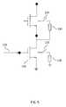
- FIG. 5shows an exemplary embodiment of the present disclosure wherein instead of the single NMOS device of FIG IA, a stacked arrangement of NMOS devices (e.g. two devices) is used.
- each of the NMOS devicesmay be constructed with a switch that allows the body terminal of the device to be selectively connected to a reference potential depending on the presence or absence of an RF signal at an input node of the stacked arrangement.
- the reference potential for the top deviceis the source node of the same device, and the reference potential for the bottom (input) device is ground.
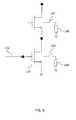
- FIG. 6shows an alternate embodiment of the one presented in FIG. 5 , wherein the bodies of all devices within the stacked arrangement are selectively connected the same reference potential (e.g. ground).
- the same reference potentiale.g. ground
- FIG. 7shows an alternate embodiment of the one presented in FIG. 5 , wherein only one of the devices from the stacked arrangement (input device) is provided with a switch to selectively connect the body of the device to a reference potential (e.g. ground).
- a reference potentiale.g. ground
- the term “body”can refer to a portion of a device between source and drain beneath a conducting channel.
- the preceding definitionapplies to both silicon on insulator devices as well as bulk CMOS devices because the portion referred to by the preceding definition describes a portion of a bulk CMOS device that can be considered as both the body and substrate of the bulk CMOS device (e.g. the body and substrate of a bulk CMOS device are generally the same).
- the term “substrate”can refer to an insulating wafer upon which a semiconductor device or devices can be fabricated for the case of silicon on insulator devices.
- the term “substrate”may refer to a silicon wafer upon which devices can be fabricated.
- floating body devicecan refer to a device whose body floats relative to ground.
- Examples of devices that can have a floating body configurationinclude, but are not limited to, “floating body NMOS devices” as well as “floating body PMOS devices”.
- body tied devicecan refer to a device whose body is connected (or tied) to a reference potential such as ground.
- Examples of devices that can have a body tied configurationinclude, but are not limited to, “body tied NMOS devices” as well as “body tied PMOS devices”.
- efficiencycan refer to a measure of how well a device converts one energy source to another.
- efficiency of the NMOS deviceis a metric that quantifies conversion of direct current (DC) power that is input to a drain of the NMOS device to RF power that is output from the drain of the NMOS device.
- DCdirect current
- RFradio frequencies
- Such efficiencymay also be referred to as drain efficiency of the NMOS device.
- Power added efficiency (PAE)provides a metric of efficiency that takes into consideration that gain of the power amplifier is not infinite.
- channelcan refer to a frequency range. More in particular, the term “channel” as used herein can refer to a frequency range defined by a wireless standard such as, but not limited to, wideband code division multiple access (WCDMA) and long term evolution (LTE).
- WCDMAwideband code division multiple access
- LTElong term evolution
- adjacent channel leakage ratioACLR
- a channel bandwidthis 5 MHz.
- Adjacent channelswould encompass the 5 MHz below the main channel (i.e. 1920 MHz to 1925 MHz) and the 5 MHz above the main channel (i.e.
- the ACLRwill be ratio of power leaked into these adjacent channels to power in the main channel. Consequently, the ACLR can be utilized as a measure of linearity of a device since higher ACLR is associated with more frequency smearing (lower linearity).
- operating characteristiccan refer to value of a metric utilized to measure performance of a device (e.g. a transistor). Metrics of the device include measures of efficiency, linearity, and leakage, and others identifiable by a person skilled in the art. Operating characteristics of the device would encompass values of these metrics.
- the “presence” or “absence” of a signalis relative to a threshold value that can be set based on application. Specifically, if a signal that is detected is above the threshold value (e.g. detected signal is of sufficient amplitude), then the signal is considered to be “present”. Similarly, if a signal that is detected is below the threshold value (e.g. detected signal is not of sufficient amplitude), then the signal is considered to be “absent” or “not present”.
- NMOS devicesare for convenience of discussion only and the embodiments of the present disclosure can also apply to other types of transistors such as PMOS devices.
- Choice of whether to employ NMOS and PMOS devicesis based on considerations that would be known by a person skilled in the art.
- NMOS devicesare generally used since mobility of electrons is higher than mobility of holes.
- the devicesmay be constructed using technologies such as, but not limited to, silicon on insulator (SOI) technology, silicon on sapphire (SOS) technology, or bulk complementary metal oxide semiconductor (CMOS) technology.
- SOIsilicon on insulator
- SOSsilicon on sapphire
- CMOSbulk complementary metal oxide semiconductor
- Example NMOSFETsinclude regular N (RN) FETs that have a nominal threshold voltage of 450 mV, high doping N (HN) FETs that have a nominal threshold voltage of 700 mV, and intrinsic N (IN) FETs that may have a threshold voltage of approximately 0V.
- RNregular N
- HNhigh doping N
- INPintrinsic N
- Corresponding PMOSFETsinclude regular P FETs (RP) that have a nominal threshold voltage of ⁇ 400 mV, high doping FETs (HP) that have a nominal threshold voltage of ⁇ 600 mV, and intrinsic P (IP) FETs that may have a threshold voltage of approximately 0 V.
- RPregular P FETs
- HPhigh doping FETs
- IPintrinsic P
- HN, RN, HP, and RP FETsmay have threshold voltages of 800 mV, 300 mV, ⁇ 800 mV, and ⁇ 300 mV, respectively. Details in a circuit are specific to a particular semiconductor process utilized, but the skilled person can adjust details to fit different semiconductor processes.
- a semiconductor devicesuch as an amplifier comprising stacked transistors, can be constructed that comprises one or more transistors and one or more switches.
- Each transistor within the stackis fabricated on a substrate and has a body whereas a corresponding switch can be configured to either connect the body of the transistor to a reference potential (e.g. ground) node or disconnect the body of the transistor from the reference potential (e.g. ground) node.
- a reference potentiale.g. ground
- teachings of the present disclosurecan be applied to operation of the semiconductor device at other frequencies.
- Configuration of the switch for each of the transistors, either connecting body to a reference potential or disconnecting body from the reference potentialis generally dependent on operating characteristics desired in the transistor.
- an application within which the semiconductor device is to be employedmay require that the transistor be capable of exhibiting a first operating characteristic (e.g. a particular value or a range of values for PAE of the transistor) when the switch connects the body of the transistor to a reference potential (e.g. ground) and of exhibiting a second operating characteristic (e.g. a particular value or a range of values for loss due to leakage for the transistor) when the switch disconnects the body of the transistor from the reference potential.
- the first and second operating characteristicsmay be of different metrics, as in the preceding example, or of the same metric but at different values.
- FIG. 1Ashows an NMOS device ( 110 ) in accordance with an embodiment of the present disclosure.
- the NMOS device ( 110 )can be constructed with a switch ( 120 ) that allows a body of the device ( 110 ) to be selectively connected to a reference potential, in this case ground, or disconnected from ground, depending on absence or presence of a primary RF signal ( 170 ), where the switch ( 120 ) can be controlled by baseband/transceiver circuitry (not shown) that is providing the primary RF signal ( 170 ). More specifically, a body tie switch control portion ( 125 ) of the transceiver circuitry can send a control signal ( 145 ) to the switch ( 120 ) to provide appropriate control.
- the control signal ( 145 )can be a switch de-activation signal configured to open the switch ( 120 ) and thereby disconnect the body of the NMOS device ( 110 ) from ground. As will be discussed, disconnecting the body of the NMOS device ( 110 ) from ground can improve PAE.
- the control signal ( 145 )can be a switch activation signal configured to close the switch ( 120 ) and thereby connect the body of the device ( 110 ) to ground. As will be discussed, connecting the body of the device ( 110 ) to ground or a reference potential close to ground, can reduce leakage current.
- the body tie switch control portion ( 125 ) of the transceiver circuitrycan be an enable/disable signal generated by the transceiver circuitry and applied to the switch ( 120 ) to effect appropriate control depending on whether or not the transceiver circuitry is transmitting.
- the switch ( 120 )can be implemented as any one of an NMOS switching transistor, PMOS switching transistor, a diode, or other active device that can be envisioned by a person skilled in the art. Additionally, this embodiment may comprise an impedance element ( 130 )
- FIG. 1Bshows an exemplary system ( 190 ) that utilizes the NMOS device ( 110 ) of FIG. 1A as a power amplifier.
- the system ( 190 )may be an RF lineup that comprises a baseband processor ( 180 ) that is configured to generate a baseband signal; a transceiver circuit ( 182 ) that is configured to receive the baseband signal and upconvert the baseband signal to an RF signal ( 170 ); a power amplifier ( 186 ) that is configured to receive the RF signal ( 170 ); and an antenna ( 188 ) that is configured to transmit an output of the power amplifier ( 186 ).
- the power amplifier ( 186 )may be implemented as the NMOS device ( 110 ) constructed with a switch ( 120 ), as shown in FIG. 1A , or implemented using a stacked arrangement of NMOS devices each with an associated switch as per FIGS. 5-7 .
- the transceiver circuit ( 182 )can be further configured to provide a control signal ( 184 ) to the NMOS device ( 110 ).
- control signal ( 184 )can be provided to the switch ( 120 ) as well as the switches associated to the other devices from the stack, to allow a body terminal of the NMOS device ( 110 ) and each of the NMOS devices of the stack associated with a switch, to be selectively connected to a reference potential (e.g. ground) or disconnected from the reference potential based on value of the control signal ( 184 ).
- a reference potentiale.g. ground
- the control signal ( 184 )can be configured to (e.g. set to a value that can) close the switch ( 120 ).
- the power amplifier ( 186 )is being turned on (e.g.
- control signal ( 184 )can open the switch ( 120 ).
- the power amplifier ( 186 )can be configured to receive a control signal ( 184 ) and logic used to open or close the switch ( 120 ) can be derived from the control signal ( 184 ). It is noted that, although in the example above the control signal ( 184 ) is being provided by the transceiver circuit ( 182 ), other components, such as the baseband processor ( 180 ), can instead provide the control signal ( 184 ).
- FIGS. 2A and 2Bshow NMOS devices ( 110 ) in accordance with embodiments of the present disclosure.
- the NMOS devices ( 110 )can be constructed with a switch ( 120 ) that allows a body of the device ( 110 ) to be selectively connected to a reference potential, in this case ground, or disconnected from ground, depending on absence or presence of an RF signal ( 261 , 262 ).
- a reference potentialin this case ground, or disconnected from ground, depending on absence or presence of an RF signal ( 261 , 262 ).
- an RF signal ( 261 )can be detected using an RF coupler ( 280 ).
- an RF signal ( 262 )can be detected using an RF detector ( 240 ) coupled to one or more terminals of the NMOS device ( 110 ). Any of the embodiments shown in FIGS.
- the 2A and 2Bcan detect an RF signal at any one of gate, drain, and source of the device ( 110 ).
- the device ( 110 ) in FIGS. 1 and 2A-2Bmay be constructed using technologies such as, but not limited to, SOI technology, SOS technology, or bulk CMOS technology.
- the RF coupler ( 280 )is a three port RF coupler ( 280 ).However, couplers with more ports may also be used.
- a primary RF signal ( 170 )such as from baseband/transceiver circuitry, is input to port 1 of the RF coupler ( 280 ), an output ( 270 ) from port 2 of the RF coupler ( 280 ) can drive the gate terminal of the NMOS device ( 110 ), and an output ( 261 ) from port 3 of the RF coupler ( 280 ) can be fed to a detector/control circuit ( 260 ).
- the detector/control circuit ( 260 )can generate a control signal based on the output ( 261 ) from port 3 of the RF coupler ( 280 ) to effect control of switch ( 120 ).
- the RF coupler ( 280 )can be configured to split the primary RF signal ( 170 ) such that a majority of signal power of the primary RF signal ( 170 ) is output ( 270 ) from port 2 of the RF coupler ( 280 ) to drive the gate of the NMOS device ( 110 ) while a smaller amount of signal power of the primary RF signal ( 170 ) is output ( 261 ) from port 3 of the RF coupler ( 280 ) to feed into the detector/control circuit ( 260 ).
- the RF coupler ( 280 )can be configured to split the primary RF signal ( 170 ) such that the output ( 270 ) from port 2 of the RF coupler ( 280 ) contains 90% of signal power of the primary RF signal ( 170 ) and RF signal ( 261 ) contains 10% of signal power of the primary RF signal ( 170 ).
- Other designs of RF couplers identifiable by a person skilled in the artmay also be utilized with the embodiments of the present disclosure.
- the NMOS devicemay be replaced with a stacked arrangement of NMOS devices, such as depicted in FIGS. 5-7 , found within an amplifier, in which case the RF signal at ( 270 ) drives the gate of the input transistor ( 110 ) from the stack.
- an RF signalcan be sampled capacitively or magnetically at one or more terminals (e.g. gate, source, drain) of the NMOS device ( 110 ).
- an RF signalcan be detected at any one of gate, drain, and source terminals of the NMOS device ( 110 ), or an input NMOS device ( 110 ) of an amplifier comprising stacked devices as depicted in FIGS. 5-7 , using an RF detector coupled to corresponding terminals
- the RF detectioncan be performed by electrically sensing voltage or current at one or more of the terminals of the NMOS device ( 110 ) and couple the sensed voltage or signal to a detector/control circuit ( 260 ).
- FIG. 2Bshows the RF detection performed through capacitive coupling ( 240 ) employed at each of the terminals, where the capacitive coupling ( 240 ) samples RF signals and couples the sampled RF signals to a detector/control circuit ( 260 ). Based on signals coupled or otherwise provided to the detector/control circuit ( 260 ), the detector/control circuit ( 260 ) can generate a control signal to effect control of switch ( 120 ).
- the signal ( 261 )represents an RF signal detected by the RF coupler ( 280 ).
- the signal ( 262 )represents an RF signal detected by capacitive coupling ( 240 ) employed at terminals of the NMOS device ( 110 ).
- the detector/control circuit ( 260 )detects an RF signal ( 261 , 262 ) and generates a control signal ( 245 ) based on absence or presence of the detected RF signal ( 261 , 262 ).
- the detector/control circuit ( 260 )can be fabricated on the same substrate as the NMOS device ( 110 ), although doing so does not necessarily confer benefits in regard to leakage or PAE. However, fabricating the detector/control circuit ( 260 ) on the same substrate as the NMOS device ( 110 ) may simplify fabrication.
- the control signal ( 245 )can be a switch de-activation signal that will open the switches and thereby disconnect the body of each one of the NMOS devices from the corresponding reference potential (e.g. ground). This can result in higher PAE.
- the detector/control circuit ( 260 )can generate the switch de-activation signal if an RF signal ( 261 , 262 ) of sufficient amplitude is detected in at least one terminal of the NMOS device ( 110 ) (e.g. gate, drain, or source).
- Each switch ( 120 )can be implemented as any one of an NMOS switching transistor, PMOS switching transistor, a diode, or other active device that can be envisioned by a person skilled in the art.
- an impedance element ( 130 )can be connected between the switch ( 120 ) and a reference potential such as ground or the source node of the corresponding device (body-tied-to-source (BTS device)).
- the impedance element ( 130 )can be an inductor or a primarily inductive element, where inclusion of the inductor would cause the body of the device ( 110 ) to float relative to AC (e.g. an RF signal) and connect the body to ground relative to DC.
- the impedance element ( 130 )can also simply be replaced with a short circuit without detrimentally compromising circuit operation.
- the detector/control circuit ( 260 )can apply a switch activation signal or otherwise remove application of the switch de-activation signal, closing the switch ( 120 ) and thereby connecting the body to ground. This can achieve lower leakage.
- the detector/control circuit ( 260 )can replace the switch de-activation signal with the switch activation signal when an RF signal ( 261 , 262 ) is not present at one of the NMOS device ( 110 ) terminals, closing the switch ( 120 ) and thereby connecting the body to the reference potential (e.g. ground).
- the reference potentiale.g. ground
- an RF coupler ( 280 )can be used to detect whether or not an RF signal ( 261 ) is present at the gate terminal of the NMOS device ( 110 ), although RF couplers can also be coupled to source and/or drain terminals of the NMOS device ( 110 ) for detection purposes.
- an RF signal ( 262 )can also be detected via capacitive coupling ( 240 ) coupled to at least one of the NMOS device ( 110 ) terminals.
- the switch ( 120 )can be closed when an RF signal ( 261 , 262 ) is below a certain threshold, corresponding to no RF signal being detected.
- closing the switch ( 120 ) when no RF signal is detectedhas been shown to achieve leakage in the range of 1 pA per ⁇ m to 1 nA per ⁇ m of gate width.
- the switch ( 120 )can be opened when an RF signal ( 261 , 262 ) is above a certain threshold, corresponding to an RF signal being detected.
- opening the switch ( 120 ) when an RF signal is detectedhas been shown to achieve PAE in the range of 40% to 60%.
- an example threshold for detectioncan be ⁇ 75 dBm.
- the example threshold value of ⁇ 75 dBm abovewould be the smallest amplitude of the primary RF signal ( 170 ) that can be generated by the transceiver circuit ( 182 ).
- An example gain of the power amplifier ( 186 )is 15 dB, which leads to an example transmitted signal of ⁇ 60 dBm at the antenna ( 188 ).
- the RF lineupcan include elements such as a transceiver, a filter, a power amplifier, a duplexer, and an antenna.
- the RF signal ( 261 , 262 )could be detected anywhere in the RF lineup that comprises the device ( 110 ) in addition to or instead of RF signals detected at the terminals (e.g. gate, drain, source) of the device ( 110 ).
- the RF signal ( 261 , 262 )can be detected at a transceiver, a filter, a power amplifier, a duplexer, an antenna, or some other element of the RF lineup that comprises the NMOS device ( 110 ).
- the RF signal( 261 , 262 ) can be in the UHF band, the VHF band, or a different high frequency band and can be a WCDMA or an LTE signal.
- a person skilled in the artwill also be able to identify numerous other frequency bands that the RF signal could occupy and numerous other wireless standards that the RF signal could follow.
- an NMOS device ( 110 )was constructed with its body connected to ground and performance characteristics measured. After the performance characteristics were obtained from the body tied NMOS device, the connection (body tie) between body and ground of the NMOS device ( 110 ) was cut (in particular, by a laser) and performance characteristics measured again.
- FIG. 3shows experimental leakage data for a device before and after a connection between device body and ground is cut.
- I leakrepresents leakage current
- V DDrepresents a DC voltage from a battery that is connected to the NMOS device.
- leakagerefers to a leakage of current from the battery along a current path from drain to source, thereby reducing battery life. Results shown in FIG. 3 indicate that leakage increases after cutting the connection between device body and ground.
- FIGS. 4A and 4Bshow experimental efficiency and linearity data for a device before and after connection between device body and ground is cut, respectively.
- FIGS. 4A and 4Bshow experimental power added efficiency (PAE) and adjacent channel leakage ratio (ACLR) data.
- the ACLR datais given with respect to an adjacent channel of frequencies lower than the main channel (denoted as “Lower ACLR”) and an adjacent channel of frequencies higher than the main channel (denoted as “Upper ACLR”).
- Results shown in FIGS. 4A and 4Bindicate that PAE improves after cutting the connection between device body and ground.
- An example ACLR specificationis ⁇ 40 dBc, which generally signifies that the worse of the two ACLR values needs to be ⁇ 40 dBc or lower.
- the body tied caseFIG. 4A
- the floating body caseFIG. 4B
- data shown in FIGS. 4A and 4Bmay indicate a larger difference in PAE before and after cutting the connection between device body and ground due to design of the device.
- body tied performance of the devicewas compromised by virtue of the device being designed to be cut with a laser.
- An alternative RF layoutcan improve body tied performance and decrease PAE differences between the body tied and floating body cases.
- floating body SOS NMOS devices of threshold between 0.4 V to 0.7 Vhave been shown to exhibit PAE of 2% to 5% higher than body tied NMOS devices.
- these floating body SOS NMOS devicesalso tend to exhibit 2 to 6 orders of magnitude worse leakage than body tied NMOS devices.
- a semiconductor devicecomprising a transistor configured to have its body tied to a reference potential (e.g. ground) node via a switch or its body disconnected from the reference potential node via the switch.
- the switchcan be configured to be controlled by a control signal.
- the control signalcan provided from other elements in a system comprising the semiconductor device, such as a transceiver circuit or a baseband processor.
- the control signalcan be derived from an RF signal detected by the semiconductor device. Logic used to open or close the switch can be derived from the control signal.
- a method of operating an amplifiercomprising of one or more transistors arranged in a stack, where each transistor has a body.
- the methodcan comprise coupling the body of one or more transistors of the stack to a corresponding reference potential (e.g. ground) node when no input signal is provided to the amplifier and decoupling the body from the reference potential (e.g. ground) node when an RF signal is provided to the amplifier.
- the coupling and decouplingcan be carried out using one or more switches, each associated to one transistor of the stack and all controlled via the same control signal.
- the presence or absence of a signalis relative to a threshold value that can be set based on application. If a detected signal is above the threshold value (e.g.
- the signalis considered to be “present”. Similarly, if a detected signal is below the threshold value (e.g. detected signal is not of sufficient amplitude), then the signal is considered to be “absent” or “not present”.
- a method for fabricating a semiconductor devicecomprising a plurality of transistors and a plurality of switches, where each transistor has a body.
- the methodcan comprise fabricating the transistors and the switches on a substrate, where each switch is adapted to connect the body of the corresponding transistor to a reference potential (e.g. ground) node or disconnect the body of the transistor to the reference potential (e.g. ground) node.
- the methodcan further comprise fabricating a control circuit on the substrate, where the control circuit is operable to provide a control signal to the switches.
Landscapes
- Engineering & Computer Science (AREA)
- Computer Networks & Wireless Communication (AREA)
- Signal Processing (AREA)
- Electronic Switches (AREA)
Abstract
Description
1. Field
The present disclosure relates to semiconductor devices. More particularly, the present disclosure relates to semiconductor devices with switchable ground-body connection.
2. Description of Related Art
Floating body N-channel metal oxide semiconductor (NMOS) devices, whose device bodies float relative to ground, can exhibit higher power added efficiency (PAE) than body tied NMOS devices, whose device bodies are connected (or tied) to ground or a reference potential close to ground, by way of a body tie. However, floating body NMOS devices can also exhibit leakage current that is orders of magnitude worse than body tied NMOS devices.
U.S. Pat. No. 7,910,993 B2, issued on Mar. 22, 2011 which is related to the present disclosure is incorporated by reference herein in its entirety.
According to a first aspect of the present disclosure, a semiconductor device is provided, the semiconductor device comprising: a transistor that is fabricated on a substrate, the transistor having a body; and a switch with a first switch terminal connected to the body and a second switch terminal connected to a reference potential node, the switch configured to be controlled by a control signal to provide a first operating characteristic in the transistor by connecting the body to the reference potential node and to provide a second operating characteristic in the transistor by disconnecting the body from the reference potential node.
According to a second aspect of the present disclosure, a semiconductor device is provided, the semiconductor device comprising: a stacked arrangement of transistors that is fabricated on a substrate, each transistor of the stacked arrangement having a body and one or more switches in correspondence of one or more transistors from the stacked arrangement of transistors, each with a first switch terminal connected to the body of a corresponding transistor from the one or more transistors, and a second switch terminal connected to a corresponding reference potential node, the one or more switches configured to be controlled by a control signal to provide a first operating characteristic in the corresponding transistor by connecting the body of the corresponding transistor to the corresponding reference potential node and to provide a second operating characteristic in the corresponding transistor by disconnecting the body from the reference potential node.
According to a third aspect of the present disclosure, a method of operating a transistor is provided, the method comprising: coupling a body of the transistor to a reference potential node when no input signal is provided to the transistor; and decoupling the body from the reference potential node when a radio frequency (RF) signal is provided to the transistor.
According to a fourth aspect of the present disclosure, a method of operating a transistor is provided, the method comprising: fabricating a transistor on a substrate, the transistor having a body; and fabricating a switch on the substrate with a first switch terminal of the switch connected to the body and a second switch terminal of the switch connected to a reference potential node.
According to a fifth aspect of the present disclosure, a method of operating a transistor is provided, the method comprising: coupling a body of one or more transistors from the stacked arrangement of transistors to a corresponding reference potential node when no input signal is provided to an input transistor of the stacked arrangement; and decoupling the body of the one or more transistors from the corresponding reference node when a radio frequency (RF) signal is provided to the input transistor, wherein the one or more transistors comprises the input transistor.
According to a sixth aspect of the present disclosure, a method of fabricating a semiconductor device is provided, the method comprising: fabricating a stacked arrangement of one or more transistors on a substrate, each of the one or more transistors having a body; and fabricating one or more switches on the substrate in correspondence of the one or more transistors with a first switch terminal of each of the one or more switches connected to the body of a corresponding transistor and a second switch terminal of each of the one or more switches connected to a corresponding reference potential node.
Further embodiments are provided in the specification, drawings, and claims of the present application.
The accompanying drawings, which are incorporated into and constitute a part of this specification, illustrate one or more embodiments of the present disclosure and, together with the description of example embodiments, serve to explain the principles and implementations of the disclosure. Like reference numerals indicate corresponding parts in the various figures.
As used in the present disclosure, the term “body” can refer to a portion of a device between source and drain beneath a conducting channel. The preceding definition applies to both silicon on insulator devices as well as bulk CMOS devices because the portion referred to by the preceding definition describes a portion of a bulk CMOS device that can be considered as both the body and substrate of the bulk CMOS device (e.g. the body and substrate of a bulk CMOS device are generally the same).
As used in the present disclosure, the term “substrate” can refer to an insulating wafer upon which a semiconductor device or devices can be fabricated for the case of silicon on insulator devices. Alternatively, for bulk devices, the term “substrate” may refer to a silicon wafer upon which devices can be fabricated.
As used in the present disclosure, the term “floating body device” can refer to a device whose body floats relative to ground. Examples of devices that can have a floating body configuration include, but are not limited to, “floating body NMOS devices” as well as “floating body PMOS devices”.
As used in the present disclosure, the term “body tied device” can refer to a device whose body is connected (or tied) to a reference potential such as ground. Examples of devices that can have a body tied configuration include, but are not limited to, “body tied NMOS devices” as well as “body tied PMOS devices”.
As used in the present disclosure, the term “efficiency” can refer to a measure of how well a device converts one energy source to another. In a case of an NMOS device configured as a power amplifier and operating at radio frequencies (RF), efficiency of the NMOS device is a metric that quantifies conversion of direct current (DC) power that is input to a drain of the NMOS device to RF power that is output from the drain of the NMOS device. Such efficiency may also be referred to as drain efficiency of the NMOS device. Power added efficiency (PAE) provides a metric of efficiency that takes into consideration that gain of the power amplifier is not infinite.
As used in the present disclosure, the term “channel” can refer to a frequency range. More in particular, the term “channel” as used herein can refer to a frequency range defined by a wireless standard such as, but not limited to, wideband code division multiple access (WCDMA) and long term evolution (LTE). Based on the preceding definition of “channel”, adjacent channel leakage ratio (ACLR) provides a ratio of adjacent channel power to main channel power. For instance, in WCDMA, a channel bandwidth is 5 MHz. Consider power is to be transmitted on/within a main channel of 1925 MHz to 1930 MHz. Adjacent channels would encompass the 5 MHz below the main channel (i.e. 1920 MHz to 1925 MHz) and the 5 MHz above the main channel (i.e. 1930 MHz to 1935 MHz), and the ACLR will be ratio of power leaked into these adjacent channels to power in the main channel. Consequently, the ACLR can be utilized as a measure of linearity of a device since higher ACLR is associated with more frequency smearing (lower linearity).
As used in the present disclosure, the term “operating characteristic” can refer to value of a metric utilized to measure performance of a device (e.g. a transistor). Metrics of the device include measures of efficiency, linearity, and leakage, and others identifiable by a person skilled in the art. Operating characteristics of the device would encompass values of these metrics.
As used in the present disclosure, the “presence” or “absence” of a signal is relative to a threshold value that can be set based on application. Specifically, if a signal that is detected is above the threshold value (e.g. detected signal is of sufficient amplitude), then the signal is considered to be “present”. Similarly, if a signal that is detected is below the threshold value (e.g. detected signal is not of sufficient amplitude), then the signal is considered to be “absent” or “not present”.
It is noted that several embodiments of the present disclosure are described with reference to utilization of NMOS devices. However, reference to NMOS devices is for convenience of discussion only and the embodiments of the present disclosure can also apply to other types of transistors such as PMOS devices. Choice of whether to employ NMOS and PMOS devices is based on considerations that would be known by a person skilled in the art. For example, in RF amplifiers, NMOS devices are generally used since mobility of electrons is higher than mobility of holes. The devices may be constructed using technologies such as, but not limited to, silicon on insulator (SOI) technology, silicon on sapphire (SOS) technology, or bulk complementary metal oxide semiconductor (CMOS) technology.
Various embodiments of the present disclosure can be implemented through NMOS and/or PMOS devices of all thresholds. An exemplary semiconductor process can include one or more of the following types of MOS field effect transistor (FET) types. Example NMOSFETs include regular N (RN) FETs that have a nominal threshold voltage of 450 mV, high doping N (HN) FETs that have a nominal threshold voltage of 700 mV, and intrinsic N (IN) FETs that may have a threshold voltage of approximately 0V. Corresponding PMOSFETs include regular P FETs (RP) that have a nominal threshold voltage of −400 mV, high doping FETs (HP) that have a nominal threshold voltage of −600 mV, and intrinsic P (IP) FETs that may have a threshold voltage of approximately 0 V. In another semiconductor process, HN, RN, HP, and RP FETs may have threshold voltages of 800 mV, 300 mV, −800 mV, and −300 mV, respectively. Details in a circuit are specific to a particular semiconductor process utilized, but the skilled person can adjust details to fit different semiconductor processes.
According to several embodiments of the present disclosure, a semiconductor device, such as an amplifier comprising stacked transistors, can be constructed that comprises one or more transistors and one or more switches. Each transistor within the stack is fabricated on a substrate and has a body whereas a corresponding switch can be configured to either connect the body of the transistor to a reference potential (e.g. ground) node or disconnect the body of the transistor from the reference potential (e.g. ground) node. Although the semiconductor device is discussed with reference to application primarily at RF, teachings of the present disclosure can be applied to operation of the semiconductor device at other frequencies.
Configuration of the switch for each of the transistors, either connecting body to a reference potential or disconnecting body from the reference potential, is generally dependent on operating characteristics desired in the transistor. For example, an application within which the semiconductor device is to be employed may require that the transistor be capable of exhibiting a first operating characteristic (e.g. a particular value or a range of values for PAE of the transistor) when the switch connects the body of the transistor to a reference potential (e.g. ground) and of exhibiting a second operating characteristic (e.g. a particular value or a range of values for loss due to leakage for the transistor) when the switch disconnects the body of the transistor from the reference potential. The first and second operating characteristics may be of different metrics, as in the preceding example, or of the same metric but at different values.
When the transceiver circuitry of a system that comprises the NMOS device (110) is transmitting, the control signal (145) can be a switch de-activation signal configured to open the switch (120) and thereby disconnect the body of the NMOS device (110) from ground. As will be discussed, disconnecting the body of the NMOS device (110) from ground can improve PAE. When the transceiver circuitry of the system is not transmitting, the control signal (145) can be a switch activation signal configured to close the switch (120) and thereby connect the body of the device (110) to ground. As will be discussed, connecting the body of the device (110) to ground or a reference potential close to ground, can reduce leakage current. It is noted that the body tie switch control portion (125) of the transceiver circuitry can be an enable/disable signal generated by the transceiver circuitry and applied to the switch (120) to effect appropriate control depending on whether or not the transceiver circuitry is transmitting.
The switch (120) can be implemented as any one of an NMOS switching transistor, PMOS switching transistor, a diode, or other active device that can be envisioned by a person skilled in the art. Additionally, this embodiment may comprise an impedance element (130)
InFIG. 1B , the power amplifier (186) may be implemented as the NMOS device (110) constructed with a switch (120), as shown inFIG. 1A , or implemented using a stacked arrangement of NMOS devices each with an associated switch as perFIGS. 5-7 . In such a case, the transceiver circuit (182) can be further configured to provide a control signal (184) to the NMOS device (110). In particular, the control signal (184) can be provided to the switch (120) as well as the switches associated to the other devices from the stack, to allow a body terminal of the NMOS device (110) and each of the NMOS devices of the stack associated with a switch, to be selectively connected to a reference potential (e.g. ground) or disconnected from the reference potential based on value of the control signal (184). For example, when the power amplifier (186) is being turned off (e.g. configured not to generate RF power), the control signal (184) can be configured to (e.g. set to a value that can) close the switch (120). When the power amplifier (186) is being turned on (e.g. configured to generate RF power), the control signal (184) can open the switch (120). In other words, the power amplifier (186) can be configured to receive a control signal (184) and logic used to open or close the switch (120) can be derived from the control signal (184). It is noted that, although in the example above the control signal (184) is being provided by the transceiver circuit (182), other components, such as the baseband processor (180), can instead provide the control signal (184).
In the embodiment shown inFIG. 2A , the RF coupler (280) is a three port RF coupler (280).However, couplers with more ports may also be used. With reference to the embodiment shown inFIG. 2A , a primary RF signal (170), such as from baseband/transceiver circuitry, is input toport 1 of the RF coupler (280), an output (270) fromport 2 of the RF coupler (280) can drive the gate terminal of the NMOS device (110), and an output (261) fromport 3 of the RF coupler (280) can be fed to a detector/control circuit (260). The detector/control circuit (260) can generate a control signal based on the output (261) fromport 3 of the RF coupler (280) to effect control of switch (120).
The RF coupler (280) can be configured to split the primary RF signal (170) such that a majority of signal power of the primary RF signal (170) is output (270) fromport 2 of the RF coupler (280) to drive the gate of the NMOS device (110) while a smaller amount of signal power of the primary RF signal (170) is output (261) fromport 3 of the RF coupler (280) to feed into the detector/control circuit (260). By way of example and not of limitation, the RF coupler (280) can be configured to split the primary RF signal (170) such that the output (270) fromport 2 of the RF coupler (280) contains 90% of signal power of the primary RF signal (170) and RF signal (261) contains 10% of signal power of the primary RF signal (170). Other designs of RF couplers identifiable by a person skilled in the art may also be utilized with the embodiments of the present disclosure. Furthermore and as previously mentioned, the NMOS device may be replaced with a stacked arrangement of NMOS devices, such as depicted inFIGS. 5-7 , found within an amplifier, in which case the RF signal at (270) drives the gate of the input transistor (110) from the stack.
According to several embodiments of the present disclosure, an RF signal can be sampled capacitively or magnetically at one or more terminals (e.g. gate, source, drain) of the NMOS device (110). In the embodiment shown inFIG. 2B , an RF signal can be detected at any one of gate, drain, and source terminals of the NMOS device (110), or an input NMOS device (110) of an amplifier comprising stacked devices as depicted inFIGS. 5-7 , using an RF detector coupled to corresponding terminals The RF detection can be performed by electrically sensing voltage or current at one or more of the terminals of the NMOS device (110) and couple the sensed voltage or signal to a detector/control circuit (260). For example,FIG. 2B shows the RF detection performed through capacitive coupling (240) employed at each of the terminals, where the capacitive coupling (240) samples RF signals and couples the sampled RF signals to a detector/control circuit (260). Based on signals coupled or otherwise provided to the detector/control circuit (260), the detector/control circuit (260) can generate a control signal to effect control of switch (120).
According to the embodiment shown inFIG. 2A , the signal (261) represents an RF signal detected by the RF coupler (280). According to the embodiment shown inFIG. 2B , the signal (262) represents an RF signal detected by capacitive coupling (240) employed at terminals of the NMOS device (110). In both embodiments, the detector/control circuit (260) detects an RF signal (261,262) and generates a control signal (245) based on absence or presence of the detected RF signal (261,262). The detector/control circuit (260) can be fabricated on the same substrate as the NMOS device (110), although doing so does not necessarily confer benefits in regard to leakage or PAE. However, fabricating the detector/control circuit (260) on the same substrate as the NMOS device (110) may simplify fabrication.
The switch (120), as well as each switch associated to a transistor within the stack as depicted inFIGS. 5-7 , can be controlled by the control signal (245). The control signal (245) can be a switch de-activation signal that will open the switches and thereby disconnect the body of each one of the NMOS devices from the corresponding reference potential (e.g. ground). This can result in higher PAE. By way of example, the detector/control circuit (260) can generate the switch de-activation signal if an RF signal (261,262) of sufficient amplitude is detected in at least one terminal of the NMOS device (110) (e.g. gate, drain, or source). Each switch (120) can be implemented as any one of an NMOS switching transistor, PMOS switching transistor, a diode, or other active device that can be envisioned by a person skilled in the art. Additionally, an impedance element (130) can be connected between the switch (120) and a reference potential such as ground or the source node of the corresponding device (body-tied-to-source (BTS device)). For example, the impedance element (130) can be an inductor or a primarily inductive element, where inclusion of the inductor would cause the body of the device (110) to float relative to AC (e.g. an RF signal) and connect the body to ground relative to DC. The impedance element (130) can also simply be replaced with a short circuit without detrimentally compromising circuit operation.
If an RF signal (261,262) is not present at one of the terminals of the NMOS device (110) terminals or an RF signal (261,262) detected is not of sufficient amplitude (e.g. below a threshold), the detector/control circuit (260) can apply a switch activation signal or otherwise remove application of the switch de-activation signal, closing the switch (120) and thereby connecting the body to ground. This can achieve lower leakage. By way of example, the detector/control circuit (260) can replace the switch de-activation signal with the switch activation signal when an RF signal (261,262) is not present at one of the NMOS device (110) terminals, closing the switch (120) and thereby connecting the body to the reference potential (e.g. ground).
With reference toFIG. 2A , an RF coupler (280) can be used to detect whether or not an RF signal (261) is present at the gate terminal of the NMOS device (110), although RF couplers can also be coupled to source and/or drain terminals of the NMOS device (110) for detection purposes. With reference toFIG. 2B , an RF signal (262) can also be detected via capacitive coupling (240) coupled to at least one of the NMOS device (110) terminals. The switch (120) can be closed when an RF signal (261,262) is below a certain threshold, corresponding to no RF signal being detected. In example implementations, closing the switch (120) when no RF signal is detected has been shown to achieve leakage in the range of 1 pA per μm to 1 nA per μm of gate width. The switch (120) can be opened when an RF signal (261,262) is above a certain threshold, corresponding to an RF signal being detected. In example implementations, opening the switch (120) when an RF signal is detected has been shown to achieve PAE in the range of 40% to 60%.
In some applications, an example threshold for detection can be −75 dBm. With reference back to the RF lineup (190) shown inFIG. 1B , the example threshold value of −75 dBm above would be the smallest amplitude of the primary RF signal (170) that can be generated by the transceiver circuit (182). An example gain of the power amplifier (186) is 15 dB, which leads to an example transmitted signal of −60 dBm at the antenna (188).
Note that embodiments of the present disclosure may be part of an RF lineup similar to that shown inFIG. 1B . The RF lineup can include elements such as a transceiver, a filter, a power amplifier, a duplexer, and an antenna. The RF signal (261,262) could be detected anywhere in the RF lineup that comprises the device (110) in addition to or instead of RF signals detected at the terminals (e.g. gate, drain, source) of the device (110). In other words, the RF signal (261,262) can be detected at a transceiver, a filter, a power amplifier, a duplexer, an antenna, or some other element of the RF lineup that comprises the NMOS device (110). By way of example, the RF signal (261,262) can be in the UHF band, the VHF band, or a different high frequency band and can be a WCDMA or an LTE signal. A person skilled in the art will also be able to identify numerous other frequency bands that the RF signal could occupy and numerous other wireless standards that the RF signal could follow.
Implementations of embodiments of the present disclosure were obtained and operating characteristics, such as leakage and efficiency data, were measured. In one implementation, an NMOS device (110) was constructed with its body connected to ground and performance characteristics measured. After the performance characteristics were obtained from the body tied NMOS device, the connection (body tie) between body and ground of the NMOS device (110) was cut (in particular, by a laser) and performance characteristics measured again.
It is noted that data shown inFIGS. 4A and 4B may indicate a larger difference in PAE before and after cutting the connection between device body and ground due to design of the device. In particular, body tied performance of the device was compromised by virtue of the device being designed to be cut with a laser. An alternative RF layout can improve body tied performance and decrease PAE differences between the body tied and floating body cases.
As another example, floating body SOS NMOS devices of threshold between 0.4 V to 0.7 V) have been shown to exhibit PAE of 2% to 5% higher than body tied NMOS devices. However, these floating body SOS NMOS devices also tend to exhibit 2 to 6 orders of magnitude worse leakage than body tied NMOS devices.
Embodiments of the present disclosure can combine benefits of both floating body and body tied devices. According to several embodiments of the present disclosure, a semiconductor device is provided that comprises a transistor configured to have its body tied to a reference potential (e.g. ground) node via a switch or its body disconnected from the reference potential node via the switch. The switch can be configured to be controlled by a control signal. In some embodiments, the control signal can provided from other elements in a system comprising the semiconductor device, such as a transceiver circuit or a baseband processor. In other embodiments, the control signal can be derived from an RF signal detected by the semiconductor device. Logic used to open or close the switch can be derived from the control signal.
Provided in the present disclosure are embodiments for a method of operating an amplifier comprising of one or more transistors arranged in a stack, where each transistor has a body. The method can comprise coupling the body of one or more transistors of the stack to a corresponding reference potential (e.g. ground) node when no input signal is provided to the amplifier and decoupling the body from the reference potential (e.g. ground) node when an RF signal is provided to the amplifier. The coupling and decoupling can be carried out using one or more switches, each associated to one transistor of the stack and all controlled via the same control signal. As indicated previously, the presence or absence of a signal is relative to a threshold value that can be set based on application. If a detected signal is above the threshold value (e.g. detected signal is of sufficient amplitude), then the signal is considered to be “present”. Similarly, if a detected signal is below the threshold value (e.g. detected signal is not of sufficient amplitude), then the signal is considered to be “absent” or “not present”.
Also provided in the present disclosure are embodiments for a method for fabricating a semiconductor device comprising a plurality of transistors and a plurality of switches, where each transistor has a body. The method can comprise fabricating the transistors and the switches on a substrate, where each switch is adapted to connect the body of the corresponding transistor to a reference potential (e.g. ground) node or disconnect the body of the transistor to the reference potential (e.g. ground) node. The method can further comprise fabricating a control circuit on the substrate, where the control circuit is operable to provide a control signal to the switches.
The examples set forth above are provided to give those of ordinary skill in the art a complete disclosure and description of how to make and use the embodiments of the semiconductor devices with switchable ground-body connection of the present disclosure, and are not intended to limit the scope of what the inventor regard as his disclosure. Modifications of the above-described modes for carrying out the disclosure may be used by persons of skill in the art, and are intended to be within the scope of the following claims. All patents and publications mentioned in the specification may be indicative of the levels of skill of those skilled in the art to which the disclosure pertains. All references cited in this disclosure are incorporated by reference to the same extent as if each reference had been incorporated by reference in its entirety individually.
It is to be understood that the disclosure is not limited to particular methods or systems, which can, of course, vary. It is also to be understood that the terminology used herein is for the purpose of describing particular embodiments only, and is not intended to be limiting. As used in this specification and the appended claims, the singular forms “a”, “an”, and “the” include plural referents unless the content clearly dictates otherwise. The term “plurality” includes two or more referents unless the content clearly dictates otherwise. Unless defined otherwise, all technical and scientific terms used herein have the same meaning as commonly understood by one of ordinary skill in the art to which the disclosure pertains.
A number of embodiments of the disclosure have been described. Nevertheless, it will be understood that various modifications may be made without departing from the spirit and scope of the present disclosure. Accordingly, other embodiments are within the scope of the following claims.
Claims (35)
1. A semiconductor device, comprising:
a four terminal transistor that is fabricated on a substrate, the transistor comprising:
i) a first terminal in contact with a first region of the transistor;
ii) a second terminal in contact with a second region of the transistor;
iii) a third terminal configured, during operation of the transistor, to receive a voltage to control a conduction channel in a portion of a body region of the transistor between the first region and the second region; and
iv) a body terminal in contact with the body region; and
a switch with a first switch terminal connected to the body terminal and a second switch terminal connected to a reference potential node, a closed condition and an open condition of the switch being controlled by a control signal to provide a first operating characteristic in the transistor by connecting the body terminal to the reference potential node when the switch is closed, and to provide a second operating characteristic in the transistor by disconnecting the body terminal from the reference potential node when the switch is open,
wherein:
the switch comprises an inductor operatively connected between the switch and the reference potential node, the inductor configured to cause the body region to float relative to AC and to connect the body region to the reference potential relative to DC,
the first operating characteristic comprises a reduction in a leakage current between the first terminal and the second terminal, and
the second operating characteristic comprises an increase of a power added efficiency (PAE) of the transistor.
2. The semiconductor device according toclaim 1 , wherein the transistor is a silicon on insulator NMOS transistor or a bulk NMOS transistor.
3. The semiconductor device according toclaim 1 , wherein in the transistor is configured as one of: a) an amplifier, and b) a power amplifier.
4. The semiconductor device according toclaim 1 , further comprising:
a control circuit that is configured to generate a switch de-activation signal for disconnecting the body terminal of the transistor from the reference potential node.
5. The semiconductor device according toclaim 4 , wherein the switch and the control circuit are fabricated on a common substrate.
6. The semiconductor device according toclaim 4 , further comprising:
a radio frequency (RF) signal detector configured to detect an RF signal in the semiconductor device, wherein the control circuit is configured to receive the detected RF signal and to generate the switch de-activation signal based on the detected RF signal.
7. The semiconductor device according toclaim 6 , wherein the RF signal is detected in at least one of a source node, a gate node, or a drain node respectively in correspondence of the second terminal, the third terminal and the first terminal of the transistor.
8. The semiconductor device according toclaim 7 , the control circuit being configured to remove the switch de-activation signal when the RF signal detector fails to detect an RF signal, wherein removal of the switch de-activation signal activates the switch and connects the body terminal of the transistor to the reference potential node.
9. The semiconductor device according toclaim 7 , the control circuit being configured to replace the switch de-activation signal with a switch activation signal when the RF signal detector fails to detect an RF signal, wherein the switch activation signal is configured to activate the switch and connect the body terminal to the reference potential node.
10. The semiconductor device according toclaim 6 , wherein:
the RF signal detector comprises an RF coupler configured to split the detected RF signal into at least a first component and a second component,
the transistor is configured to receive the first component and the control circuit is configured to receive the second component, and
the control circuit is configured to generate the switch de-activation signal based on the second component of the detected RF signal.
11. The semiconductor device according toclaim 1 , wherein the switch comprises an NMOS switching transistor.
12. A semiconductor device, comprising:
a stacked arrangement of transistors that is fabricated on a substrate, each transistor of the stacked arrangement comprising:
i) a first terminal in contact with a first region of the transistor;
ii) a second terminal in contact with a second region of the transistor;
iii) a third terminal, configured, during operation of the transistor, to receive a voltage to control a conduction channel in a portion of a body region of the transistor between the first region and the second region; and
iv) a body terminal in contact with the body region; and
one or more switches in correspondence of one or more transistors from the stacked arrangement of transistors, each with a first switch terminal connected to the body terminal of a corresponding transistor from the one or more transistors, and a second switch terminal connected to a corresponding reference potential node, a closed condition and an open condition of the one or more switches being controlled by a control signal to provide a first operating characteristic in the corresponding transistor by connecting the body terminal of the corresponding transistor to the corresponding reference potential node when a corresponding switch is closed, and to provide a second operating characteristic in the corresponding transistor by disconnecting the body terminal from the reference potential node when the corresponding switch is open,
wherein:
at least one switch of the one or more switches comprises an inductor operatively connected between the at least one switch and the corresponding reference potential node, the inductor configured to cause the body region of the corresponding transistor to float relative to AC and to connect the body region of the corresponding transistor to the reference potential relative to DC,
the first operating characteristic comprises a reduction in a leakage current between the first terminal and the second terminal, and
the second operating characteristic comprises an increase of a power added efficiency (PAE) of the transistor.
13. The semiconductor device according toclaim 12 , wherein in the stacked arrangement of transistors is configured as one of: a) an amplifier, and b) a power amplifier.
14. The semiconductor device according toclaim 12 , wherein at least one of the one or more switches comprises an NMOS switching transistor.
15. The semiconductor device according toclaim 12 , further comprising:
a control circuit that is configured to generate a switch de-activation signal for disconnecting the body terminal of each of the one or more transistors from the corresponding reference potential node.
16. The semiconductor device according toclaim 15 , further comprising:
a radio frequency (RF) signal detector configured to detect an RF signal in the semiconductor device, wherein the control circuit is configured to receive the detected RF signal and to generate the switch de-activation signal based on the detected RF signal.
17. A method of operating a transistor that is fabricated on a substrate, the transistor comprising a first terminal in contact with a first region of the transistor, a second terminal in contact with a second region of the transistor, a third terminal configured to receive a voltage to control a conduction channel in a portion of a body region of the transistor between the first region and the second region, and a body terminal in contact with the body region, the method comprising:
coupling a body terminal of the transistor to a reference potential node when no input signal is provided to the transistor, thereby reducing a leakage current between a first terminal and the second terminal; and
decoupling the body terminal from the reference potential node when a radio frequency (RF) signal is provided to the transistor, thereby increasing a power added efficiency (PAE) of the transistor.
18. The method according toclaim 17 , wherein the transistor is a silicon on insulator NMOS transistor or a bulk NMOS transistor.
19. The method according toclaim 18 , wherein the coupling and decoupling are carried out via a switch.
20. The method according toclaim 19 , wherein the switch is an NMOS switching transistor.
21. The method according toclaim 17 , wherein the RF signal encompasses at least one of a UHF or a VHF band of radio frequencies.
22. The method according toclaim 17 , wherein the RF signal comprises a WCDMA signal or an LTE signal.
23. A method of fabricating a semiconductor device, comprising:
fabricating a transistor on a substrate, the transistor comprising:
i) a first terminal in contact with a first region of the transistor;
ii) a second terminal in contact with a second region of the transistor;
iii) a third terminal configured, during operation of the transistor, to receive a voltage to control a conduction channel in a portion of a body region of the transistor between the first region and the second region; and
iv) a body terminal in contact with the body region; and
fabricating a switch on the substrate with a first switch terminal of the switch connected to the body terminal and a second switch terminal of the switch connected to a reference potential node, and
fabricating a control circuit on the substrate, the control circuit operable to provide a switch de-activation signal for operating the switch to selectively disconnect the body terminal from the reference potential node,
wherein the switch de-activation signal is provided to the switch upon detection of an RF signal in the semiconductor device.
24. The method according toclaim 23 , wherein the switch de-activation signal is provided to the switch upon detection of the RF signal in at least one of a drain node, a source node, a gate node respectively in correspondence of the first terminal, the second terminal and the third terminal of the transistor.
25. A method of operating a stacked arrangement of transistors, comprising:
coupling a body terminal of one or more transistors from the stacked arrangement of transistors to a corresponding reference potential node when no input signal is provided to an input transistor of the stacked arrangement, thereby providing a corresponding reference potential to the body terminal; and
decoupling the body terminal of the one or more transistors from the corresponding reference node when a radio frequency (RF) signal is provided to the input transistor, thereby floating the body terminal, wherein the one or more transistors comprises the input transistor,
wherein:
the one or more transistors are fabricated on a common substrate, and
each of the one or more transistors comprises:
i) a first terminal in contact with a first region of the transistor;
ii) a second terminal in contact with a second region of the transistor;
iii) a third terminal configured, during operation of the transistor, to receive a voltage to control a conduction channel in a portion of a body region of the transistor between the first region and the second region; and
iv) the body terminal in contact with the body region.
26. The method according toclaim 25 , wherein one or more transistors from the stacked arrangement of transistors is a silicon on insulator NMOS transistor or a bulk NMOS transistor.
27. The method according toclaim 26 , wherein the coupling and decoupling are carried out via one or more switches in correspondence of the one or more transistors.
28. The method according toclaim 27 , wherein a switch from the one or more switches is an NMOS switching transistor.
29. The method according toclaim 25 , wherein the RF signal encompasses at least one of a UHF or a VHF band of radio frequencies.
30. The method according toclaim 25 , wherein the RF signal comprises a WCDMA signal or an LTE signal.
31. A method of fabricating a semiconductor device, comprising:
fabricating a stacked arrangement of one or more transistors on a substrate, each of the one or more transistors having a body terminal in contact with a body region of the transistor; and
fabricating one or more switches on the substrate in correspondence of the one or more transistors with a first switch terminal of each of the one or more switches connected to the body terminal of a corresponding transistor and a second switch terminal of each of the one or more switches connected to a corresponding reference potential node;
fabricating a control circuit on the substrate, the control circuit operable to provide a switch de-activation signal for operating the one or more switches in correspondence of the one or more transistors to selectively disconnect the body terminal of each of the one or more transistors from the corresponding reference potential node, the switch de-activation signal being provided to the one or more switches upon detection of an RF signal in the semiconductor device,
wherein each of the one or more transistors comprises:
i) a first terminal in contact with a first region of the transistor;
ii) a second terminal in contact with a second region of the transistor;
iii) a third terminal configured, during operation of the transistor, to receive a voltage to control a conduction channel in a portion of a body region of the transistor between the first region and the second region; and
iv) the body terminal in contact with the body region.
32. The method according toclaim 31 , wherein the switch de-activation signal is provided to the one or more switches upon detection of the RF signal in at least one of a drain node, a source node, a gate node respectively in correspondence of the first terminal, the second terminal, and the third terminal of an input transistor of the stacked arrangement of one or more transistors.
33. A method of fabricating a semiconductor device, comprising:
fabricating a stacked arrangement of one or more transistors on a substrate, each of the one or more transistors having a body terminal in contact with a body region of the transistor; and
fabricating one or more switches on the substrate in correspondence of the one or more transistors with a first switch terminal of each of the one or more switches connected to the body terminal of a corresponding transistor and a second switch terminal of each of the one or more switches connected to a corresponding node,
wherein:
the corresponding node of the corresponding transistor different from an input transistor of the stacked arrangement is a source node of the corresponding transistor connected to a drain node of an adjacent transistor of the stacked arrangement,
the corresponding node of the input transistor is a reference potential node connected to a reference potential, and
each of the one or more transistors comprises:
i) a first terminal in contact with a first region of the transistor;
ii) a second terminal in contact with a second region of the transistor;
iii) a third terminal configured, during operation of the transistor, to receive a voltage to control a conduction channel in a portion of a body region of the transistor between the first region and the second region; and
iv) the body terminal in contact with the body region.
34. The method according toclaim 33 , wherein for the corresponding transistor different from the input transistor, the second switch terminal is connected to the corresponding node through a series connected inductor.
35. A semiconductor device, comprising:
a stacked arrangement of transistors that is fabricated on a substrate, each transistor of the stacked arrangement comprising:
i) a first terminal in contact with a first region of the transistor;
ii) a second terminal in contact with a second region of the transistor;
iii) a third terminal, configured, during operation of the transistor, to receive a voltage to control a conduction channel in a portion of a body region of the transistor between the first region and the second region; and
iv) a body terminal in contact with the body region; and
one or more switches in correspondence of one or more transistors from the stacked arrangement of transistors, each with a first switch terminal connected to the body terminal of a corresponding transistor from the one or more transistors, and a second switch terminal connected to a corresponding node, a closed condition and an open condition of the one or more switches being controlled by a control signal to provide a first operating characteristic in the corresponding transistor by connecting the body terminal of the corresponding transistor to the corresponding node when a corresponding switch is closed, and to provide a second operating characteristic in the corresponding transistor by disconnecting the body terminal from the corresponding node when the corresponding switch is open,
wherein:
the corresponding node of the corresponding transistor different from an input transistor of the stacked arrangement is a source node of the corresponding transistor connected to a drain node of an adjacent transistor of the stacked arrangement,
the corresponding node of the input transistor is a reference potential node connected to a reference potential, and
the first operating characteristic comprises a reduction in a leakage current between the first terminal and the second terminal, and
the second operating characteristic comprises an increase of a power added efficiency (PAE) of the transistor.
Priority Applications (1)
| Application Number | Priority Date | Filing Date | Title |
|---|---|---|---|
| US13/715,805US9590674B2 (en) | 2012-12-14 | 2012-12-14 | Semiconductor devices with switchable ground-body connection |
Applications Claiming Priority (1)
| Application Number | Priority Date | Filing Date | Title |
|---|---|---|---|
| US13/715,805US9590674B2 (en) | 2012-12-14 | 2012-12-14 | Semiconductor devices with switchable ground-body connection |
Publications (2)
| Publication Number | Publication Date |
|---|---|
| US20140171010A1 US20140171010A1 (en) | 2014-06-19 |
| US9590674B2true US9590674B2 (en) | 2017-03-07 |
Family
ID=50931468
Family Applications (1)
| Application Number | Title | Priority Date | Filing Date |
|---|---|---|---|
| US13/715,805Active2033-09-07US9590674B2 (en) | 2012-12-14 | 2012-12-14 | Semiconductor devices with switchable ground-body connection |
Country Status (1)
| Country | Link |
|---|---|
| US (1) | US9590674B2 (en) |
Cited By (2)
| Publication number | Priority date | Publication date | Assignee | Title |
|---|---|---|---|---|
| US9960737B1 (en) | 2017-03-06 | 2018-05-01 | Psemi Corporation | Stacked PA power control |
| US20230283237A1 (en)* | 2016-09-16 | 2023-09-07 | Psemi Corporation | Body Tie Optimization for Stacked Transistor Amplifier |
Families Citing this family (6)
| Publication number | Priority date | Publication date | Assignee | Title |
|---|---|---|---|---|
| US9143124B2 (en) | 2014-02-18 | 2015-09-22 | Acco | Switch controls |
| US9819317B2 (en)* | 2014-09-02 | 2017-11-14 | Quintech Electronics & Communications, Inc. | Modular RF matrix switch |
| US9837965B1 (en) | 2016-09-16 | 2017-12-05 | Peregrine Semiconductor Corporation | Standby voltage condition for fast RF amplifier bias recovery |
| US10250199B2 (en) | 2016-09-16 | 2019-04-02 | Psemi Corporation | Cascode amplifier bias circuits |
| US9843293B1 (en) | 2016-09-16 | 2017-12-12 | Peregrine Semiconductor Corporation | Gate drivers for stacked transistor amplifiers |
| US10461704B2 (en) | 2017-12-18 | 2019-10-29 | Psemi Corporation | Switchless multi input stacked transistor amplifier tree structure |
Citations (398)
| Publication number | Priority date | Publication date | Assignee | Title |
|---|---|---|---|---|
| US3646361A (en) | 1970-10-16 | 1972-02-29 | Hughes Aircraft Co | High-speed sample and hold signal level comparator |
| US3699359A (en) | 1971-04-20 | 1972-10-17 | Philco Ford Corp | Electronic latching device |
| US3975671A (en) | 1975-02-24 | 1976-08-17 | Intel Corporation | Capacitive voltage converter employing CMOS switches |
| US3983414A (en) | 1975-02-10 | 1976-09-28 | Fairchild Camera And Instrument Corporation | Charge cancelling structure and method for integrated circuits |
| US3988727A (en) | 1974-06-24 | 1976-10-26 | P. R. Mallory & Co., Inc. | Timed switching circuit |
| US4053916A (en) | 1975-09-04 | 1977-10-11 | Westinghouse Electric Corporation | Silicon on sapphire MOS transistor |
| US4145719A (en) | 1977-09-28 | 1979-03-20 | Gte Sylvania Incorporated | Multi-channel video switch using dual-gate MOS-FETS |
| JPS5575348U (en) | 1978-11-20 | 1980-05-24 | ||
| US4244000A (en) | 1978-11-28 | 1981-01-06 | Nippon Telegraph And Telephone Public Corporation | PNPN Semiconductor switches |
| US4256977A (en) | 1978-12-26 | 1981-03-17 | Honeywell Inc. | Alternating polarity power supply control apparatus |
| US4316101A (en) | 1978-11-30 | 1982-02-16 | Licentia-Patent-Verwaltungs-G.M.B.H. | Circuit for switching and transmitting alternating voltages |
| US4317055A (en) | 1978-05-24 | 1982-02-23 | Hitachi, Ltd. | High-voltage circuit for insulated gate field-effect transistor |
| US4367421A (en) | 1980-04-21 | 1983-01-04 | Reliance Electric Company | Biasing methods and circuits for series connected transistor switches |
| US4390798A (en) | 1979-11-22 | 1983-06-28 | Fujitsu Limited | Bias-voltage generator |
| USRE31749E (en) | 1975-09-03 | 1984-11-27 | Hitachi, Ltd. | Class B FET amplifier circuit |
| WO1986001037A1 (en) | 1984-08-01 | 1986-02-13 | American Telephone & Telegraph Company | Semiconductor-on-insulator (soi) devices and soi ic fabrication method |
| US4638184A (en) | 1983-09-22 | 1987-01-20 | Oki Electric Industry Co., Ltd. | CMOS bias voltage generating circuit |
| US4736169A (en) | 1986-09-29 | 1988-04-05 | Hughes Aircraft Company | Voltage controlled oscillator with frequency sensitivity control |
| US4739191A (en) | 1981-04-27 | 1988-04-19 | Signetics Corporation | Depletion-mode FET for the regulation of the on-chip generated substrate bias voltage |
| US4746960A (en) | 1987-07-27 | 1988-05-24 | General Motors Corporation | Vertical depletion-mode j-MOSFET |
| US4748485A (en) | 1985-03-21 | 1988-05-31 | Hughes Aircraft Company | Opposed dual-gate hybrid structure for three-dimensional integrated circuits |
| US4809056A (en) | 1985-10-31 | 1989-02-28 | Fujitsu Limited | Semiconductor device having a silicon on insulator structure |
| US4810911A (en) | 1986-11-14 | 1989-03-07 | Nec Corp | FET switch circuit having small insertion loss and exhibiting stable operation |
| US4825145A (en) | 1987-01-14 | 1989-04-25 | Hitachi, Ltd. | Constant current circuit |
| US4849651A (en) | 1988-02-24 | 1989-07-18 | Hughes Aircraft Company | Two-state, bilateral, single-pole, double-throw, half-bridge power-switching apparatus and power supply means for such electronic power switching apparatus |
| US4890077A (en) | 1989-03-28 | 1989-12-26 | Teledyne Mec | FET monolithic microwave integrated circuit variable attenuator |
| US4891609A (en) | 1987-12-22 | 1990-01-02 | U.S. Philips Corporation | Ring oscillator |
| US4906587A (en) | 1988-07-29 | 1990-03-06 | Texas Instruments Incorporated | Making a silicon-on-insulator transistor with selectable body node to source node connection |
| US4929855A (en) | 1988-12-09 | 1990-05-29 | Grumman Corporation | High frequency switching device |
| JPH02161769A (en) | 1988-12-15 | 1990-06-21 | Toshiba Corp | transmission gate |
| US4939485A (en) | 1988-12-09 | 1990-07-03 | Varian Associates, Inc. | Microwave field effect switch |
| US4984040A (en) | 1989-06-15 | 1991-01-08 | Xerox Corporation | High voltage thin film transistor with second gate |
| US4985647A (en) | 1988-06-21 | 1991-01-15 | Nec Corporation | CMOS transfer switch free from malfunction on noise signal |
| US4999585A (en) | 1989-11-06 | 1991-03-12 | Burr-Brown Corporation | Circuit technique for cancelling non-linear capacitor-induced harmonic distortion |
| US5001528A (en) | 1989-01-31 | 1991-03-19 | The United States Of America As Represented By The Secretary Of The Air Force | Radiation hardened CMOS on SOI or SOS devices |
| US5012123A (en) | 1989-03-29 | 1991-04-30 | Hittite Microwave, Inc. | High-power rf switching system |
| US5023494A (en) | 1989-10-20 | 1991-06-11 | Raytheon Company | High isolation passive switch |
| US5061907A (en) | 1991-01-17 | 1991-10-29 | National Semiconductor Corporation | High frequency CMOS VCO with gain constant and duty cycle compensation |
| US5061911A (en) | 1990-04-03 | 1991-10-29 | Motorola, Inc. | Single fault/tolerant MMIC switches |
| US5081706A (en) | 1987-07-30 | 1992-01-14 | Texas Instruments Incorporated | Broadband merged switch |
| US5095348A (en) | 1989-10-02 | 1992-03-10 | Texas Instruments Incorporated | Semiconductor on insulator transistor |
| US5107152A (en) | 1989-09-08 | 1992-04-21 | Mia-Com, Inc. | Control component for a three-electrode device |
| US5125007A (en) | 1988-11-25 | 1992-06-23 | Mitsubishi Denki Kabushiki Kaisha | Thin-film soi-mosfet with a body region |
| US5124762A (en) | 1990-12-31 | 1992-06-23 | Honeywell Inc. | Gaas heterostructure metal-insulator-semiconductor integrated circuit technology |
| JPH0434980Y2 (en) | 1986-06-30 | 1992-08-19 | ||
| US5146178A (en) | 1990-11-16 | 1992-09-08 | Nippon Telegraph And Telephone Company | Impedance-matched, class F high-frequency amplifier |
| US5148393A (en) | 1988-07-07 | 1992-09-15 | Kabushiki Kaisha Toshiba | Mos dynamic semiconductor memory cell |
| US5157279A (en) | 1991-05-28 | 1992-10-20 | Samsung Electronics Co., Ltd. | Data output driver with substrate biasing producing high output gain |
| US5182529A (en) | 1992-03-06 | 1993-01-26 | Micron Technology, Inc. | Zero crossing-current ring oscillator for substrate charge pump |
| US5208557A (en) | 1992-02-18 | 1993-05-04 | Texas Instruments Incorporated | Multiple frequency ring oscillator |
| US5272457A (en) | 1992-03-10 | 1993-12-21 | Harris Corporation | High isolation integrated switch circuit |
| US5274343A (en) | 1991-08-06 | 1993-12-28 | Raytheon Company | Plural switch circuits having RF propagation networks and RF terminations |
| US5283457A (en) | 1989-10-02 | 1994-02-01 | Texas Instruments Incorporated | Semiconductor on insulator transistor |
| US5285367A (en) | 1992-02-07 | 1994-02-08 | Power Integrations, Inc. | Linear load circuit to control switching power supplies under minimum load conditions |
| US5306954A (en) | 1992-06-04 | 1994-04-26 | Sipex Corporation | Charge pump with symmetrical +V and -V outputs |
| US5313083A (en) | 1988-12-16 | 1994-05-17 | Raytheon Company | R.F. switching circuits |
| US5317181A (en) | 1992-09-10 | 1994-05-31 | United Technologies Corporation | Alternative body contact for fully-depleted silicon-on-insulator transistors |
| US5319604A (en) | 1990-05-08 | 1994-06-07 | Texas Instruments Incorporated | Circuitry and method for selectively switching negative voltages in CMOS integrated circuits |
| US5345422A (en) | 1990-07-31 | 1994-09-06 | Texas Instruments Incorporated | Power up detection circuit |
| US5350957A (en) | 1989-10-20 | 1994-09-27 | Texas Instrument Incorporated | Electronic switch controlled by plural inputs |
| JPH06314985A (en) | 1993-04-28 | 1994-11-08 | Nec Corp | Portable radio device |
| US5375257A (en) | 1993-12-06 | 1994-12-20 | Raytheon Company | Microwave switch |
| EP0385641B1 (en) | 1989-02-28 | 1995-01-04 | AT&T Corp. | A high efficiency UHF linear power amplifier |
| US5405795A (en) | 1994-06-29 | 1995-04-11 | International Business Machines Corporation | Method of forming a SOI transistor having a self-aligned body contact |
| US5416043A (en) | 1993-07-12 | 1995-05-16 | Peregrine Semiconductor Corporation | Minimum charge FET fabricated on an ultrathin silicon on sapphire wafer |
| US5422590A (en) | 1993-01-05 | 1995-06-06 | Texas Instruments Incorporated | High voltage negative charge pump with low voltage CMOS transistors |
| JPH0770245B2 (en) | 1991-11-06 | 1995-07-31 | 株式会社大阪サイレン製作所 | Rotation warning light |
| US5442327A (en) | 1994-06-21 | 1995-08-15 | Motorola, Inc. | MMIC tunable biphase modulator |
| US5446418A (en) | 1992-11-06 | 1995-08-29 | Mitsubishi Denki Kabushiki Kaisha | Ring oscillator and constant voltage generation circuit |
| WO1995023460A1 (en) | 1994-02-28 | 1995-08-31 | Qualcomm Incorporated | Method and apparatus for correction and limitation of transmitter power on the reverse link of a mobile radio telephone system |
| US5448207A (en) | 1993-09-30 | 1995-09-05 | Sony Corporation | Attenuator circuit apparatus |
| JPH07106937B2 (en) | 1992-03-16 | 1995-11-15 | 日本碍子株式会社 | β-alumina solid electrolyte |
| US5477184A (en) | 1992-04-15 | 1995-12-19 | Sanyo Electric Co., Ltd. | Fet switching circuit for switching between a high power transmitting signal and a lower power receiving signal |
| US5488243A (en) | 1992-12-04 | 1996-01-30 | Nippondenso Co., Ltd. | SOI MOSFET with floating gate |
| US5493249A (en) | 1993-12-06 | 1996-02-20 | Micron Technology, Inc. | System powered with inter-coupled charge pumps |
| US5492857A (en) | 1993-07-12 | 1996-02-20 | Peregrine Semiconductor Corporation | High-frequency wireless communication system on a single ultrathin silicon on sapphire chip |
| US5548239A (en) | 1993-05-21 | 1996-08-20 | Sony Corporation | Radio receiver-transmitter apparatus and signal changeover switch |
| US5553295A (en) | 1994-03-23 | 1996-09-03 | Intel Corporation | Method and apparatus for regulating the output voltage of negative charge pumps |
| US5559368A (en) | 1994-08-30 | 1996-09-24 | The Regents Of The University Of California | Dynamic threshold voltage mosfet having gate to body connection for ultra-low voltage operation |
| US5576647A (en) | 1995-06-22 | 1996-11-19 | Marvell Technology Group, Ltd. | Charge pump for phase lock loop |
| US5578853A (en) | 1992-12-10 | 1996-11-26 | Sony Corporation | Semiconductor memory cell having information storage transistor and switching transistor |
| JPH098621A (en) | 1995-06-16 | 1997-01-10 | Nec Corp | Fet switch circuit |
| US5594371A (en) | 1994-06-28 | 1997-01-14 | Nippon Telegraph And Telephone Corporation | Low voltage SOI (Silicon On Insulator) logic circuit |
| US5597739A (en) | 1994-01-19 | 1997-01-28 | Sony Corporation | MOS transistor and method for making the same |
| US5600588A (en) | 1994-01-24 | 1997-02-04 | Fujitsu Limited | Data retention circuit and semiconductor memory device using the same |
| US5610533A (en) | 1993-11-29 | 1997-03-11 | Mitsubishi Denki Kabushiki Kaisha | Switched substrate bias for logic circuits |
| US5629655A (en) | 1992-10-27 | 1997-05-13 | Ericsson Inc. | Integrated distributed RC low-pass filters |
| JPH09163721A (en) | 1995-12-08 | 1997-06-20 | Mitsubishi Electric Corp | Negative voltage generating circuit |
| EP0782267A2 (en) | 1995-12-27 | 1997-07-02 | Nec Corporation | Semiconductor switch |
| JPH09200021A (en) | 1996-01-22 | 1997-07-31 | Mitsubishi Electric Corp | Integrated circuit |
| US5670907A (en) | 1995-03-14 | 1997-09-23 | Lattice Semiconductor Corporation | VBB reference for pumped substrates |
| US5681761A (en) | 1995-12-28 | 1997-10-28 | Philips Electronics North America Corporation | Microwave power SOI-MOSFET with high conductivity metal gate |
| JPH09284114A (en) | 1996-04-19 | 1997-10-31 | Toshiba Microelectron Corp | Analog input circuit |
| US5689144A (en) | 1996-05-15 | 1997-11-18 | Siliconix Incorporated | Four-terminal power MOSFET switch having reduced threshold voltage and on-resistance |
| US5694308A (en) | 1995-07-03 | 1997-12-02 | Motorola, Inc. | Method and apparatus for regulated low voltage charge pump |
| US5717356A (en) | 1995-01-23 | 1998-02-10 | Sony Corporation | Low insertion loss switch |
| WO1998006174A1 (en) | 1996-08-05 | 1998-02-12 | Mitsubishi Denki Kabushiki Kaisha | High-frequency integrated circuit for high-frequency radio transmitter-receiver suppressed in influence of high-frequency power leakage |
| US5731607A (en) | 1995-04-24 | 1998-03-24 | Sony Corporation | Semiconductor integrated circuit device |
| JPH1079467A (en) | 1996-09-04 | 1998-03-24 | Mitsubishi Electric Corp | Semiconductor device |
| US5734291A (en) | 1996-03-11 | 1998-03-31 | Telcom Semiconductor, Inc. | Power saving technique for battery powered devices |
| JPH1093471A (en) | 1996-09-11 | 1998-04-10 | Murata Mfg Co Ltd | Signal changeover switch |
| US5748016A (en) | 1995-03-22 | 1998-05-05 | Nec Corporation | Driver circuit |
| US5748053A (en) | 1995-09-28 | 1998-05-05 | Kabushiki Kaisha Toshiba | Switching circuit |
| US5753955A (en) | 1996-12-19 | 1998-05-19 | Honeywell Inc. | MOS device having a gate to body connection with a body injection current limiting feature for use on silicon on insulator substrates |
| US5760652A (en) | 1996-06-06 | 1998-06-02 | Mitsubishi Denki Kabushiki Kaisha | Integrated circuit device |
| US5767549A (en) | 1996-07-03 | 1998-06-16 | International Business Machines Corporation | SOI CMOS structure |
| US5774411A (en) | 1996-09-12 | 1998-06-30 | International Business Machines Corporation | Methods to enhance SOI SRAM cell stability |
| US5774792A (en) | 1994-08-29 | 1998-06-30 | Hitachi, Ltd. | Low distortion switch |
| US5777530A (en) | 1996-01-31 | 1998-07-07 | Matsushita Electric Industrial Co., Ltd. | Switch attenuator |
| US5784687A (en) | 1994-08-30 | 1998-07-21 | Matsushita Electric Industrial Co., Ltd. | Transmitting-receiving circuit for radiocommunication apparatus, semiconductor integrated circuit device including the circuit, and radiocommunication apparatus including the same |
| US5784311A (en) | 1997-06-13 | 1998-07-21 | International Business Machines Corporation | Two-device memory cell on SOI for merged logic and memory applications |
| US5793246A (en) | 1995-11-08 | 1998-08-11 | Altera Corporation | High voltage pump scheme incorporating an overlapping clock |
| US5801577A (en) | 1995-12-26 | 1998-09-01 | Sgs-Thomson Microelectronics S.A. | High voltage generator |
| US5804858A (en) | 1995-06-08 | 1998-09-08 | Taiwan Semiconductor Manufacturing, Ltd. | Body contacted SOI MOSFET |
| JPH10242826A (en) | 1997-02-26 | 1998-09-11 | Nec Corp | High frequency switch circuit |
| JPH10242477A (en) | 1996-12-26 | 1998-09-11 | Hitachi Ltd | Semiconductor device and manufacturing method thereof |
| US5807772A (en) | 1992-06-09 | 1998-09-15 | Semiconductor Energy Laboratory Co., Ltd. | Method for forming semiconductor device with bottom gate connected to source or drain |
| US5808505A (en) | 1993-05-25 | 1998-09-15 | Nec Corporation | Substrate biasing circuit having controllable ring oscillator |
| US5812939A (en) | 1995-08-10 | 1998-09-22 | Sony Corporation | Switch semiconductor integrated circuit and communication terminal device |
| US5814899A (en) | 1995-01-27 | 1998-09-29 | Nec Corporation | SOI-type semiconductor device with variable threshold voltages |
| US5818283A (en) | 1995-07-13 | 1998-10-06 | Japan Radio Co., Ltd. | High power FET switch |
| US5818289A (en) | 1996-07-18 | 1998-10-06 | Micron Technology, Inc. | Clocking scheme and charge transfer switch for increasing the efficiency of a charge pump or other circuit |
| US5818766A (en) | 1997-03-05 | 1998-10-06 | Integrated Silicon Solution Inc. | Drain voltage pump circuit for nonvolatile memory device |
| US5818099A (en) | 1996-10-03 | 1998-10-06 | International Business Machines Corporation | MOS high frequency switch circuit using a variable well bias |
| US5818278A (en) | 1996-09-06 | 1998-10-06 | Mitsubishi Denki Kabushiki Kaisha | Level shift circuit |
| US5821800A (en) | 1997-02-11 | 1998-10-13 | Advanced Micro Devices, Inc. | High-voltage CMOS level shifter |
| US5821769A (en) | 1995-04-21 | 1998-10-13 | Nippon Telegraph And Telephone Corporation | Low voltage CMOS logic circuit with threshold voltage control |
| US5825227A (en) | 1995-01-23 | 1998-10-20 | Sony Corporation | Switching circuit at high frequency with low insertion loss |
| JPH10335901A (en) | 1997-06-04 | 1998-12-18 | Nippon Telegr & Teleph Corp <Ntt> | Semiconductor switch |
| US5864328A (en) | 1995-09-01 | 1999-01-26 | Sharp Kabushiki Kaisha | Driving method for a liquid crystal display apparatus |
| US5863823A (en) | 1993-07-12 | 1999-01-26 | Peregrine Semiconductor Corporation | Self-aligned edge control in silicon on insulator |
| JPH1126776A (en) | 1997-07-02 | 1999-01-29 | Mitsubishi Electric Corp | Dual gate FET and high frequency circuit using dual gate FET |
| US5874849A (en) | 1996-07-19 | 1999-02-23 | Texas Instruments Incorporated | Low voltage, high current pump for flash memory |
| US5874836A (en) | 1996-09-06 | 1999-02-23 | International Business Machines Corporation | High reliability I/O stacked fets |
| US5877978A (en) | 1996-03-04 | 1999-03-02 | Mitsubishi Denki Kabushiki Kaisha | Semiconductor memory device |
| US5880620A (en) | 1997-04-22 | 1999-03-09 | Xilinx, Inc. | Pass gate circuit with body bias control |
| US5883541A (en) | 1997-03-05 | 1999-03-16 | Nec Corporation | High frequency switching circuit |
| US5892400A (en) | 1995-12-15 | 1999-04-06 | Anadigics, Inc. | Amplifier using a single polarity power supply and including depletion mode FET and negative voltage generator |
| US5892382A (en) | 1997-03-25 | 1999-04-06 | Mitsubishi Denki Kabushiki Kaisha | Current mode logic circuit, source follower circuit and flip flop circuit |
| JPH11112316A (en) | 1997-09-18 | 1999-04-23 | Samsung Electron Co Ltd | Switch circuit using MESFET |
| US5903178A (en) | 1994-12-16 | 1999-05-11 | Matsushita Electronics Corporation | Semiconductor integrated circuit |
| JPH11136111A (en) | 1997-10-30 | 1999-05-21 | Sony Corp | High frequency circuit |
| US5912560A (en) | 1997-02-25 | 1999-06-15 | Waferscale Integration Inc. | Charge pump circuit for voltage boosting in integrated semiconductor circuits |
| JPH11163704A (en) | 1997-11-25 | 1999-06-18 | Sharp Corp | High frequency switch circuit |
| JPH11163642A (en) | 1997-12-01 | 1999-06-18 | Nippon Telegr & Teleph Corp <Ntt> | Semiconductor device and high-frequency circuit using the same |
| US5917362A (en) | 1996-01-29 | 1999-06-29 | Sony Corporation | Switching circuit |
| US5920093A (en) | 1997-04-07 | 1999-07-06 | Motorola, Inc. | SOI FET having gate sub-regions conforming to t-shape |
| US5920233A (en) | 1996-11-18 | 1999-07-06 | Peregrine Semiconductor Corp. | Phase locked loop including a sampling circuit for reducing spurious side bands |
| WO1999035695A1 (en) | 1998-01-09 | 1999-07-15 | Infineon Technologies Ag | Silicon on insulator high-voltage switch |
| US5926466A (en) | 1995-05-16 | 1999-07-20 | Matsushita Electric Industrial Co., Ltd. | Time division multiple access FDD wireless unit and time division multiple access FDD/TDD dual mode wireless unit |
| US5930605A (en) | 1996-05-20 | 1999-07-27 | Digital Equipment Corporation | Compact self-aligned body contact silicon-on-insulator transistors |
| US5930638A (en) | 1993-07-12 | 1999-07-27 | Peregrine Semiconductor Corp. | Method of making a low parasitic resistor on ultrathin silicon on insulator |
| JPH11205188A (en) | 1998-01-16 | 1999-07-30 | Mitsubishi Electric Corp | Transmission / reception switching circuit |
| US5945867A (en) | 1997-02-24 | 1999-08-31 | Sanyo Electric Co., Ltd. | Switch circuit device |
| US5959335A (en) | 1998-09-23 | 1999-09-28 | International Business Machines Corporation | Device design for enhanced avalanche SOI CMOS |
| JPH11274804A (en) | 1998-03-19 | 1999-10-08 | Sharp Corp | High frequency switch |
| US5973363A (en) | 1993-07-12 | 1999-10-26 | Peregrine Semiconductor Corp. | CMOS circuitry with shortened P-channel length on ultrathin silicon on insulator |
| US5973636A (en) | 1996-03-12 | 1999-10-26 | Fujitsu Ltd. | Radar apparatus with a simplified construction |
| US5973382A (en) | 1993-07-12 | 1999-10-26 | Peregrine Semiconductor Corporation | Capacitor on ultrathin semiconductor on insulator |
| US5973364A (en) | 1997-09-19 | 1999-10-26 | Kabushiki Kaisha Toshiba | MIS semiconductor device having body-contact region |
| US5986518A (en) | 1998-06-30 | 1999-11-16 | Motorola, Inc. | Distributed MMIC active quadrature hybrid and method for providing in-phase and quadrature-phase signals |
| US5990580A (en) | 1998-03-05 | 1999-11-23 | The Whitaker Corporation | Single pole double throw switch |
| JP2000031167A (en) | 1998-05-01 | 2000-01-28 | Oki Electric Ind Co Ltd | Semiconductor device and method of manufacturing the same |
| US6020781A (en) | 1996-12-27 | 2000-02-01 | Fujitsu Limited | Step-up circuit using two frequencies |
| US6020778A (en) | 1997-04-24 | 2000-02-01 | Kabushiki Kaisha Toshiba | Transmission gate including body effect compensation circuit |
| US6049110A (en) | 1996-06-26 | 2000-04-11 | Nec Corporation | Body driven SOI-MOS field effect transistor |
| US6057723A (en) | 1997-01-13 | 2000-05-02 | Kabushiki Kaisha Toshiba | Phase shifter |
| US6061267A (en) | 1998-09-28 | 2000-05-09 | Texas Instruments Incorporated | Memory circuits, systems, and methods with cells using back bias to control the threshold voltage of one or more corresponding cell transistors |
| US6064872A (en) | 1991-03-12 | 2000-05-16 | Watkins-Johnson Company | Totem pole mixer having grounded serially connected stacked FET pair |
| US6064275A (en) | 1996-04-22 | 2000-05-16 | Mitsubishi Denki Kabushiki Kaisha | Internal voltage generation circuit having ring oscillator whose frequency changes inversely with power supply voltage |
| CN1256521A (en) | 1998-12-03 | 2000-06-14 | 夏普公司 | Semiconductor device of SOI structure |
| US6081165A (en) | 1997-07-25 | 2000-06-27 | Texas Instruments Incorporated | Ring oscillator |
| US6081694A (en) | 1997-10-21 | 2000-06-27 | Matsushita Electric Industrial Co., Ltd. | Mobile telephone transmitter with internal auxiliary matching circuit |
| JP2000183353A (en) | 1998-12-14 | 2000-06-30 | Mitsubishi Electric Corp | Semiconductor integrated circuit |
| JP2000188501A (en) | 1998-12-22 | 2000-07-04 | Mitsubishi Electric Corp | Semiconductor switch |
| US6084255A (en) | 1998-01-29 | 2000-07-04 | Mitsubishi Denki Kabushiki Kaisha | Gate array semiconductor device |
| US6087893A (en) | 1996-10-24 | 2000-07-11 | Toshiba Corporation | Semiconductor integrated circuit having suppressed leakage currents |
| US6100564A (en) | 1998-09-30 | 2000-08-08 | International Business Machines Corporation | SOI pass-gate disturb solution |
| JP2000223713A (en) | 1999-02-02 | 2000-08-11 | Oki Electric Ind Co Ltd | Semiconductor element and its manufacture |
| US6104061A (en) | 1997-07-08 | 2000-08-15 | Micron Technology, Inc. | Memory cell with vertical transistor and buried word and body lines |
| US6111778A (en) | 1999-05-10 | 2000-08-29 | International Business Machines Corporation | Body contacted dynamic memory |
| US6114923A (en) | 1997-09-01 | 2000-09-05 | Nec Corporation | Switching circuit and semiconductor device |
| US6118343A (en) | 1999-05-10 | 2000-09-12 | Tyco Electronics Logistics Ag | Power Amplifier incorporating single drain switch and single negative voltage generator |
| US6122185A (en) | 1997-07-22 | 2000-09-19 | Seiko Instruments R&D Center Inc. | Electronic apparatus |
| JP2000277703A (en) | 1999-03-25 | 2000-10-06 | Sanyo Electric Co Ltd | Switch circuit device |
| US6133752A (en) | 1997-09-25 | 2000-10-17 | Oki Electric Industry Co., Ltd. | Semiconductor integrated circuit having tri-state logic gate circuit |
| JP2000294786A (en) | 1999-04-05 | 2000-10-20 | Nippon Telegr & Teleph Corp <Ntt> | High frequency switch |
| JP2000311986A (en) | 1999-04-27 | 2000-11-07 | Mitsubishi Electric Corp | Digital / high frequency analog mixed IC chip, IC package and digital / high frequency analog mixed IC |
| US6160292A (en) | 1997-04-23 | 2000-12-12 | International Business Machines Corporation | Circuit and methods to improve the operation of SOI devices |
| US6169444B1 (en) | 1999-07-15 | 2001-01-02 | Maxim Integrated Products, Inc. | Pulse frequency operation of regulated charge pumps |
| US6172378B1 (en) | 1999-05-03 | 2001-01-09 | Silicon Wave, Inc. | Integrated circuit varactor having a wide capacitance range |
| US6173235B1 (en) | 1996-04-11 | 2001-01-09 | Mitsubishi Denki Kabushiki Kaisha | Method of estimating lifetime of floating SOI-MOSFET |
| JP2001007332A (en) | 1999-06-21 | 2001-01-12 | Seiko Epson Corp | SOI structure MOS field effect transistor and method of manufacturing the same |
| US6177826B1 (en) | 1997-12-01 | 2001-01-23 | Mitsubishi Denki Kabushiki Kaisha | Silicon-on-insulator circuit having series connected PMOS transistors each having connected body and gate |
| US6188247B1 (en) | 1999-01-29 | 2001-02-13 | International Business Machines Corporation | Method and apparatus for elimination of parasitic bipolar action in logic circuits for history removal under stack contention including complementary oxide semiconductor (CMOS) silicon on insulator (SOI) elements |
| US6188590B1 (en) | 1996-12-18 | 2001-02-13 | Macronix International Co., Ltd. | Regulator system for charge pump circuits |
| US6191449B1 (en) | 1996-09-19 | 2001-02-20 | Kabushiki Kaisha Toshiba | SOI based transistor having an independent substrate potential control |
| US6195307B1 (en) | 1997-02-26 | 2001-02-27 | Kabushiki Kaisha Toshiba | Booster circuit and semiconductor memory device having the same |
| US6201761B1 (en) | 2000-01-26 | 2001-03-13 | Advanced Micro Devices, Inc. | Field effect transistor with controlled body bias |
| JP2001089448A (en) | 1999-09-24 | 2001-04-03 | Yamanouchi Pharmaceut Co Ltd | Amide derivative |
| USRE37124E1 (en) | 1993-04-30 | 2001-04-03 | Stmicroelectronics Limited | Ring oscillator using current mirror inverter stages |
| US6215360B1 (en) | 1998-02-23 | 2001-04-10 | Motorola, Inc. | Semiconductor chip for RF transceiver and power output circuit therefor |
| US6218892B1 (en) | 1997-06-20 | 2001-04-17 | Intel Corporation | Differential circuits employing forward body bias |
| US6218248B1 (en) | 1998-04-02 | 2001-04-17 | Hyundai Electronics Industries Co., Ltd. | Semiconductor device and method for fabricating the same |
| US6218890B1 (en) | 1998-07-14 | 2001-04-17 | Sanyo Electric Co., Ltd. | Switching circuit device and semiconductor device |
| US6222394B1 (en) | 2000-02-03 | 2001-04-24 | International Business Machines Corporation | SOI CMOS sense amplifier with enhanced matching characteristics and sense point tolerance |
| JP2001119281A (en) | 1999-10-19 | 2001-04-27 | Nippon Telegr & Teleph Corp <Ntt> | Selection circuit and logic circuit using the same |
| US6239649B1 (en) | 1999-04-20 | 2001-05-29 | International Business Machines Corporation | Switched body SOI (silicon on insulator) circuits and fabrication method therefor |
| JP2001157487A (en) | 1999-11-26 | 2001-06-08 | Nissan Motor Co Ltd | Control device for rotating electric machine |
| JP2001156182A (en) | 1999-11-30 | 2001-06-08 | Nec Corp | Semiconductor device and method of manufacturing the same |
| US6249027B1 (en) | 1998-06-08 | 2001-06-19 | Sun Microsystems, Inc. | Partially depleted SOI device having a dedicated single body bias means |
| US6249446B1 (en) | 2000-08-23 | 2001-06-19 | Intersil Americas Inc. | Cascadable, high efficiency charge pump circuit and related methods |
| US20010015461A1 (en) | 1999-12-08 | 2001-08-23 | Akihiko Ebina | SOI-structure MIS field-effect transistor and method of manufacturing the same |
| US6281737B1 (en) | 1998-11-20 | 2001-08-28 | International Business Machines Corporation | Method and apparatus for reducing parasitic bipolar current in a silicon-on-insulator transistor |
| US6288458B1 (en) | 1999-09-30 | 2001-09-11 | Honeywell International Inc. | Power stealing solid state switch |
| US6297687B1 (en) | 1998-08-11 | 2001-10-02 | Oki Electric Industry Co., Ltd. | Drive control circuit of charged pump circuit |
| JP2001274265A (en) | 2000-03-28 | 2001-10-05 | Mitsubishi Electric Corp | Semiconductor device |
| US6300796B1 (en) | 1999-02-19 | 2001-10-09 | Zilog, Inc. | High voltage PMOS level shifter |
| US6304110B1 (en) | 1998-06-11 | 2001-10-16 | Mitsubishi Denki Kabushiki Kaisha | Buffer using dynamic threshold-voltage MOS transistor |
| US20010031518A1 (en) | 1999-10-25 | 2001-10-18 | Samsung Electronics,Co. Ltd | Soi semiconductor integrated circuit for eliminating floating body effects in soi mosfets and method of fabricating the same |
| US6310508B1 (en) | 2000-08-24 | 2001-10-30 | Agilent Technologies, Inc. | High frequency switch |
| US6316983B1 (en) | 2000-07-26 | 2001-11-13 | Yrp Advanced Mobile Communication Systems Research Laboratories Co., Ltd. | Predistortion circuit |
| US20010040479A1 (en) | 2000-03-03 | 2001-11-15 | Shuyun Zhang | Electronic switch |
| US6320225B1 (en) | 1999-07-13 | 2001-11-20 | International Business Machines Corporation | SOI CMOS body contact through gate, self-aligned to source- drain diffusions |
| US20010045602A1 (en) | 1998-08-07 | 2001-11-29 | Shigenobu Maeda | A partially depleted soi based tft |
| US6337594B1 (en) | 1998-06-17 | 2002-01-08 | Hynix Semiconductor, Inc. | Charge pump circuit |
| EP0851561B1 (en) | 1996-12-23 | 2002-02-27 | Texas Instruments Incorporated | Negative voltage charge pump, particularly for flash EEPROM memories. |
| US6356536B1 (en) | 1998-09-30 | 2002-03-12 | Ericsson Inc. | Protective and decoupling shunt switch at LNA input for TDMA/TDD transceivers |
| US6355957B1 (en) | 2000-01-05 | 2002-03-12 | Mitsubishi Denki Kabushiki Kaisha | Semiconductor device having body potential fixing portion and closed-loop gate structure |
| US20020029971A1 (en) | 1996-07-09 | 2002-03-14 | Nanogen, Inc. | Multiplexed active biologic array |
| US6365488B1 (en) | 1998-03-05 | 2002-04-02 | Industrial Technology Research Institute | Method of manufacturing SOI wafer with buried layer |
| WO2002027920A1 (en) | 2000-09-28 | 2002-04-04 | Koninklijke Philips Electronics N.V. | Cascode bootstrapped analog power amplifier circuit |
| US6380796B2 (en) | 1999-11-05 | 2002-04-30 | Hitachi, Ltd. | Semiconductor power converting apparatus |
| US6380793B1 (en) | 1999-10-28 | 2002-04-30 | Pixtech S.A. | Very high voltage switch |
| US6387739B1 (en) | 1998-08-07 | 2002-05-14 | International Business Machines Corporation | Method and improved SOI body contact structure for transistors |
| US6392440B2 (en) | 1998-06-04 | 2002-05-21 | Infineon Technologies Ag | 5V compliant transmission gate and the drive logic using 3.3V technology |
| US6396325B2 (en) | 1999-12-03 | 2002-05-28 | Fairchild Semiconductor Corporation | High frequency MOSFET switch |
| JP2002156602A (en) | 2000-08-10 | 2002-05-31 | Lg Electronics Inc | Total reflection prism system for digital micro mirror device and projector utilizing the same |
| US6400211B1 (en) | 2000-09-19 | 2002-06-04 | Rohm Co., Ltd. | DC/DC converter |
| US6407427B1 (en) | 1999-11-05 | 2002-06-18 | Hyundai Electronics Industries Co., Ltd. | SOI wafer device and a method of fabricating the same |
| US6407614B1 (en) | 2000-12-07 | 2002-06-18 | New Japan Radio Co., Ltd. | Semiconductor integrated switching circuit |
| US6411156B1 (en) | 1997-06-20 | 2002-06-25 | Intel Corporation | Employing transistor body bias in controlling chip parameters |
| US6414863B1 (en) | 2001-08-30 | 2002-07-02 | Texas Instruments Incorporated | Frequency control circuit for unregulated inductorless DC/DC converters |
| US6429632B1 (en) | 2000-02-11 | 2002-08-06 | Micron Technology, Inc. | Efficient CMOS DC-DC converters based on switched capacitor power supplies with inductive current limiters |
| US6429723B1 (en) | 1999-11-18 | 2002-08-06 | Texas Instruments Incorporated | Integrated circuit with charge pump and method |
| US6429487B1 (en) | 2000-07-18 | 2002-08-06 | Mitsubishi Denki Kabushiki Kaisha | Semiconductor device having gate to body connection |
| US6433589B1 (en) | 2001-04-12 | 2002-08-13 | International Business Machines Corporation | Sense amplifier and method for sensing signals in a silicon-on-insulator integrated circuit |
| US6433587B1 (en) | 2000-03-17 | 2002-08-13 | International Business Machines Corporation | SOI CMOS dynamic circuits having threshold voltage control |
| US20020115244A1 (en) | 2000-08-11 | 2002-08-22 | Sung-Bae Park | SOI MOSFET having body contact for preventing floating body effect and method of fabricating the same |
| US20020126767A1 (en) | 2001-01-25 | 2002-09-12 | Regents Of The University Of Minnesota | High linearity circuits and methods regarding same |
| US6461902B1 (en) | 2000-07-18 | 2002-10-08 | Institute Of Microelectronics | RF LDMOS on partial SOI substrate |
| US6466082B1 (en)* | 2000-05-17 | 2002-10-15 | Advanced Micro Devices, Inc. | Circuit technique to deal with floating body effects |
| US6469568B2 (en) | 1999-12-24 | 2002-10-22 | Sharp Kabushiki Kaisha | Metal oxide semiconductor transistor circuit and semiconductor integrated circuit using the same |
| US6486729B2 (en) | 2000-05-24 | 2002-11-26 | Kabushiki Kaisha Toshiba | Potential detector and semiconductor integrated circuit |
| US6486511B1 (en) | 2001-08-30 | 2002-11-26 | Northrop Grumman Corporation | Solid state RF switch with high cutoff frequency |
| US6498370B1 (en) | 1999-10-25 | 2002-12-24 | Samsung Electronics Co., Ltd. | SOI semiconductor integrated circuit for eliminating floating body effects in SOI MOSFETs and method of fabricating the same |
| US20020195623A1 (en) | 1998-07-06 | 2002-12-26 | Masatada Horiuchi | Semiconductor integrated circuit and method for manufacturing the same |
| US20030002452A1 (en) | 2001-06-26 | 2003-01-02 | Sahota Gurkanwal Singh | System and method for power control calibration and a wireless communication device |
| US6504212B1 (en) | 2000-02-03 | 2003-01-07 | International Business Machines Corporation | Method and apparatus for enhanced SOI passgate operations |
| US6504213B1 (en) | 1999-07-27 | 2003-01-07 | Seiko Epson Corporation | SOI-structure field-effect transistor and method of manufacturing the same |
| US6512269B1 (en) | 2000-09-07 | 2003-01-28 | International Business Machines Corporation | High-voltage high-speed SOI MOSFET |
| US6518645B2 (en) | 2001-03-30 | 2003-02-11 | Samsung Electronics Co., Ltd. | SOI-type semiconductor device and method of forming the same |
| JP2003060451A (en) | 2001-08-17 | 2003-02-28 | Mitsubishi Electric Corp | Complementary push-pull amplifier |
| US6537861B1 (en) | 1998-08-29 | 2003-03-25 | International Business Machines Corporation | SOI transistor with body contact and method of forming same |
| JP2003101407A (en) | 2001-09-21 | 2003-04-04 | Sharp Corp | Semiconductor integrated circuit |
| US6559689B1 (en) | 2000-10-02 | 2003-05-06 | Allegro Microsystems, Inc. | Circuit providing a control voltage to a switch and including a capacitor |
| JP2003143004A (en) | 2001-11-06 | 2003-05-16 | Matsushita Electric Ind Co Ltd | Level shifter circuit |
| US6573533B1 (en) | 1999-07-16 | 2003-06-03 | Seiko Epson Corporation | Semiconductor device, semiconductor gate array, electro-optical device, and electronic equipment |
| JP2003167615A (en) | 2001-11-30 | 2003-06-13 | Toyota Motor Corp | Production planning apparatus and method |
| JP2003189248A (en) | 2002-10-25 | 2003-07-04 | Toshiba Corp | Digital information management system including video information |
| US20030141543A1 (en) | 2002-01-31 | 2003-07-31 | International Business Machines Corporation | Body contact mosfet |
| WO2003032431A9 (en) | 2001-10-10 | 2003-08-14 | Peregrine Semiconductor Corp | Switch circuit and method of switching radio frequency signals |
| US6608789B2 (en) | 2001-12-21 | 2003-08-19 | Motorola, Inc. | Hysteresis reduced sense amplifier and method of operation |
| US6608785B2 (en) | 2002-01-07 | 2003-08-19 | International Business Machines Corporation | Method and apparatus to ensure functionality and timing robustness in SOI circuits |
| US20030160515A1 (en) | 2002-01-15 | 2003-08-28 | Luke Yu | Controllable broad-spectrum harmonic filter (cbf) for electrical power systems |
| US6617933B2 (en) | 2000-09-29 | 2003-09-09 | Mitsubishi Denki Kabushiki Kaisha | VCO circuit with wide output frequency range and PLL circuit with the VCO circuit |
| US20030181167A1 (en) | 2001-02-19 | 2003-09-25 | Sachio Iida | Switch device and portable communication terminal |
| US6631505B2 (en) | 2000-11-29 | 2003-10-07 | Nec Electronics Corporation | Simulation circuit for MOS transistor, simulation testing method, netlist of simulation circuit and storage medium storing same |
| US6632724B2 (en) | 1997-05-12 | 2003-10-14 | Silicon Genesis Corporation | Controlled cleaving process |
| US20030201494A1 (en) | 2002-04-25 | 2003-10-30 | Mitsubishi Denki Kabushiki Kaisha | Semiconductor device and method of manufacturing the same |
| US6642578B1 (en) | 2002-07-22 | 2003-11-04 | Anadigics, Inc. | Linearity radio frequency switch with low control voltage |
| US20030205760A1 (en) | 1997-02-28 | 2003-11-06 | Kabushiki Kaisha Toshiba | Method of manufacturing SOI element having body contact |
| US6646305B2 (en) | 2001-07-25 | 2003-11-11 | International Business Machines Corporation | Grounded body SOI SRAM cell |
| JP2003332583A (en) | 2002-05-15 | 2003-11-21 | Sony Corp | Semiconductor device and its manufacturing method |
| US6653697B2 (en) | 2001-03-27 | 2003-11-25 | Matsushita Electric Industrial Co., Ltd. | High frequency switch circuit and communications terminal using the same |
| US20030222313A1 (en) | 2002-05-30 | 2003-12-04 | Honeywell International Inc. | Self-aligned body tie for a partially depleted SOI device structure |
| JP2003347553A (en) | 2002-05-30 | 2003-12-05 | Nec Compound Semiconductor Devices Ltd | High frequency circuit element |
| US20030227056A1 (en) | 2002-06-05 | 2003-12-11 | Hongmei Wang | Fully-depleted (FD) (SOI) MOSFET access transistor and method of fabrication |
| US6670655B2 (en) | 2001-04-18 | 2003-12-30 | International Business Machines Corporation | SOI CMOS device with body to gate connection |
| US6677641B2 (en) | 2001-10-17 | 2004-01-13 | Fairchild Semiconductor Corporation | Semiconductor structure with improved smaller forward voltage loss and higher blocking capability |
| US6677803B1 (en) | 2002-08-21 | 2004-01-13 | Oki Electric Industry Co., Ltd. | Semiconductor integrated circuit device |
| US6684065B2 (en) | 1999-12-20 | 2004-01-27 | Broadcom Corporation | Variable gain amplifier for low voltage applications |
| US20040021137A1 (en) | 2001-06-18 | 2004-02-05 | Pierre Fazan | Semiconductor device |
| US20040021501A1 (en)* | 2002-06-11 | 2004-02-05 | The Regents Of The University Of Michigan | Low-leakage integrated circuits and dynamic logic circuits |
| US6693498B1 (en) | 2000-02-22 | 2004-02-17 | Murata Manufacturing Co. Ltd | SPDT switch and communication unit using the same |
| US6693326B2 (en) | 2000-04-04 | 2004-02-17 | Sharp Kabushiki Kaisha | Semiconductor device of SOI structure |
| US6698082B2 (en) | 2001-08-28 | 2004-03-02 | Texas Instruments Incorporated | Micro-electromechanical switch fabricated by simultaneous formation of a resistor and bottom electrode |
| US6704550B1 (en) | 1999-09-14 | 2004-03-09 | Sony Corporation | Antenna switching circuit and communication system using the same |
| US6703863B2 (en) | 2002-01-15 | 2004-03-09 | Matsushita Electric Industrial Co., Ltd. | Level shift circuit |
| US6711397B1 (en) | 2000-11-20 | 2004-03-23 | Ami Semiconductor, Inc. | Structures and methods for direct conversion from radio frequency modulated signals to baseband signals |
| US6714065B2 (en) | 2001-10-26 | 2004-03-30 | Renesas Technology Corp. | Semiconductor device including power supply circuit conducting charge pumping operation |
| US20040061130A1 (en) | 2000-03-30 | 2004-04-01 | Mayumi Morizuka | High electron mobility transistor and method of manufacturing the same |
| US6717458B1 (en) | 2001-12-03 | 2004-04-06 | National Semiconductor Corporation | Method and apparatus for a DC-DC charge pump voltage converter-regulator circuit |
| US20040080364A1 (en) | 2000-08-10 | 2004-04-29 | Sander Wendell B. | High-efficiency modulating RF amplifier |
| JP2004147175A (en) | 2002-10-25 | 2004-05-20 | Renesas Technology Corp | Semiconductor device |
| JP2004166470A (en) | 2002-11-13 | 2004-06-10 | Hitachi Lighting Ltd | Inverter system |
| US20040129975A1 (en) | 2002-12-06 | 2004-07-08 | Nec Corporation | Semiconductor device and method for manufacturing the same |
| US6762477B2 (en) | 2000-03-24 | 2004-07-13 | Renesas Technology Corp. | Semiconductor device |
| JP2004199950A (en) | 2002-12-17 | 2004-07-15 | Shin Kobe Electric Mach Co Ltd | Method for manufacturing positive electrode plate for lead-acid battery |
| US6774701B1 (en) | 2003-02-19 | 2004-08-10 | Raytheon Company | Method and apparatus for electronic switching with low insertion loss and high isolation |
| US6781805B1 (en) | 1999-09-22 | 2004-08-24 | Kabushiki Kaisha Toshiba | Stacked MOSFET protection circuit |
| US6788130B2 (en) | 2002-09-25 | 2004-09-07 | Texas Instruments Incorporated | Efficient charge pump capable of high voltage operation |
| US6790747B2 (en) | 1997-05-12 | 2004-09-14 | Silicon Genesis Corporation | Method and device for controlled cleaving process |
| US6801076B1 (en) | 2000-04-28 | 2004-10-05 | Micron Technology, Inc. | High output high efficiency low voltage charge pump |
| US6803680B2 (en) | 2002-09-13 | 2004-10-12 | Mia-Com, Inc. | Apparatus, methods, and articles of manufacture for a switch having sharpened control voltage |
| US20040204013A1 (en) | 2002-12-23 | 2004-10-14 | Qing Ma | Communication unit and switch unit |
| JP2004288978A (en) | 2003-03-24 | 2004-10-14 | Seiko Epson Corp | Semiconductor integrated device |
| US20040217372A1 (en)* | 2003-04-30 | 2004-11-04 | Chen Thomas W. | Individually adjustable back-bias technique |
| US20040227565A1 (en) | 2003-05-13 | 2004-11-18 | Feng Chen | Method and structure for improving the linearity of MOS switches |
| US20040242182A1 (en) | 2002-05-31 | 2004-12-02 | Kenichi Hidaka | High-frequency switch circuit and mobile telecommunications terminal device using the same |
| US6830963B1 (en) | 2003-10-09 | 2004-12-14 | Micron Technology, Inc. | Fully depleted silicon-on-insulator CMOS logic |
| US6871059B1 (en) | 1999-06-16 | 2005-03-22 | Skyworks Solutions, Inc. | Passive balun FET mixer |
| US6870241B2 (en) | 2000-11-27 | 2005-03-22 | Matsushita Electric Industrial Co., Ltd. | High frequency switch circuit device |
| US6879502B2 (en) | 2002-06-13 | 2005-04-12 | Seiko Instruments Inc. | Power source inverter circuit |
| US20050079829A1 (en) | 2003-10-08 | 2005-04-14 | Takashi Ogawa | Antenna switch |
| US6882210B2 (en) | 2001-04-19 | 2005-04-19 | Sanyo Electric Co. Ltd. | Semiconductor switching device |
| US6891234B1 (en) | 2004-01-07 | 2005-05-10 | Acorn Technologies, Inc. | Transistor with workfunction-induced charge layer |
| US6898778B2 (en) | 2000-07-13 | 2005-05-24 | Kabushiki Kaisha Toshiba | Semiconductor integrated circuit and method of manufacturing the same |
| US6903596B2 (en) | 2003-03-17 | 2005-06-07 | Mitsubishi Electric & Electronics U.S.A., Inc. | Method and system for impedance matched switching |
| US20050121699A1 (en) | 2003-12-08 | 2005-06-09 | Xiangdong Chen | Dynamic threshold voltage MOSFET on SOI |
| US20050127442A1 (en) | 2003-12-12 | 2005-06-16 | Surya Veeraraghavan | Method and apparatus for forming an SOI body-contacted transistor |
| US6908832B2 (en) | 1997-08-29 | 2005-06-21 | Silicon Genesis Corporation | In situ plasma wafer bonding method |
| US6917258B2 (en) | 2002-10-24 | 2005-07-12 | Matsushita Electric Industrial Co., Ltd. | High frequency switch |
| US20050167751A1 (en) | 2004-02-02 | 2005-08-04 | Kabushiki Kaisha Toshiba | Semiconductor memory device for storing data as state of majority carriers accumulated in channel body and method of manufacturing the same |
| JP2005251931A (en) | 2004-03-03 | 2005-09-15 | Seiko Epson Corp | Termination circuit |
| US6947720B2 (en) | 2000-10-17 | 2005-09-20 | Rf Micro Devices, Inc. | Low noise mixer circuit with improved gain |
| US20050212595A1 (en) | 2004-02-09 | 2005-09-29 | Sony Ericsson Mobile Communications Japan, Inc. | Distortion compensating device and power amplifying device with distortion compensating function |
| US6969668B1 (en) | 1999-04-21 | 2005-11-29 | Silicon Genesis Corporation | Treatment method of film quality for the manufacture of substrates |
| US20050264341A1 (en) | 2004-05-31 | 2005-12-01 | Matsushita Electric Industrial Co., Ltd. | Semiconductor switch |
| US6975271B2 (en) | 2003-02-26 | 2005-12-13 | Matsushita Electric Industrial Co., Ltd. | Antenna switch module, all-in-one communication module, communication apparatus and method for manufacturing antenna switch module |
| US6978437B1 (en) | 2000-10-10 | 2005-12-20 | Toppan Photomasks, Inc. | Photomask for eliminating antenna effects in an integrated circuit and integrated circuit manufacture with same |
| US6978122B2 (en) | 2001-05-25 | 2005-12-20 | Kabushiki Kaisha Toshiba | High-frequency switching device incorporating an inverter circuit |
| US20060009164A1 (en)* | 2004-07-07 | 2006-01-12 | Matsushita Electric Industrial Co., Ltd. | Radio frequency switching circuit |
| US20060022526A1 (en) | 2004-07-27 | 2006-02-02 | David Cartalade | Asymmetric radio-frequency switch |
| US7023260B2 (en) | 2003-06-30 | 2006-04-04 | Matrix Semiconductor, Inc. | Charge pump circuit incorporating corresponding parallel charge pump stages and method therefor |
| JP2000208614A5 (en) | 1999-01-14 | 2006-04-06 | ||
| US7056808B2 (en) | 1999-08-10 | 2006-06-06 | Silicon Genesis Corporation | Cleaving process to fabricate multilayered substrates using low implantation doses |
| US7057472B2 (en) | 2001-08-10 | 2006-06-06 | Hitachi Metals, Ltd. | Bypass filter, multi-band antenna switch circuit, and layered module composite part and communication device using them |
| US7082293B1 (en) | 1999-10-21 | 2006-07-25 | Broadcom Corporation | Adaptive radio transceiver with CMOS offset PLL |
| US7092677B1 (en) | 2002-09-05 | 2006-08-15 | Analog Devices, Inc. | 2V SPDT switch for high power RF wireless applications |
| US20060194558A1 (en) | 2005-02-03 | 2006-08-31 | Kelly Dylan J | Canceling harmonics in semiconductor RF switches |
| US20060194567A1 (en) | 2001-10-10 | 2006-08-31 | Kelly Dylan J | Symmetrically and asymmetrically stacked transistor grouping RF switch |
| US7109532B1 (en) | 2003-12-23 | 2006-09-19 | Lee Zachary K | High Ion/Ioff SOI MOSFET using body voltage control |
| US7129545B2 (en) | 2005-02-24 | 2006-10-31 | International Business Machines Corporation | Charge modulation network for multiple power domains for silicon-on-insulator technology |
| US7132873B2 (en) | 2003-01-08 | 2006-11-07 | Emosyn America, Inc. | Method and apparatus for avoiding gated diode breakdown in transistor circuits |
| US7138846B2 (en) | 2001-12-20 | 2006-11-21 | Matsushita Electric Industrial Co., Ltd. | Field effect transistor switch circuit |
| US20060267093A1 (en) | 2004-06-30 | 2006-11-30 | Tang Stephen H | Floating-body dynamic random access memory and method of fabrication in tri-gate technology |
| US7161197B2 (en) | 2004-05-31 | 2007-01-09 | Matsushita Electric Industrial Co., Ltd. | RF switching circuit for use in mobile communication systems |
| US20070018247A1 (en) | 2005-07-11 | 2007-01-25 | Brindle Christopher N | Method and apparatus for use in improving linearity of MOSFET's using an accumulated charge sink |
| US20070023833A1 (en) | 2005-07-28 | 2007-02-01 | Serguei Okhonin | Method for reading a memory cell having an electrically floating body transistor, and memory cell and array implementing same |
| US7173471B2 (en) | 2003-06-13 | 2007-02-06 | Matsushita Electric Industrial Co., Ltd. | High frequency switching circuit and semiconductor device |
| US20070045697A1 (en) | 2005-08-31 | 2007-03-01 | International Business Machines Corporation | Body-contacted semiconductor structures and methods of fabricating such body-contacted semiconductor structures |
| WO2007033045A2 (en) | 2005-09-12 | 2007-03-22 | Idaho Research Foundation, Inc. | Stacked mosfets |
| US20070069291A1 (en) | 2005-07-11 | 2007-03-29 | Stuber Michael A | Method and apparatus improving gate oxide reliability by controlling accumulated charge |
| US7199635B2 (en) | 2003-06-12 | 2007-04-03 | Matsushita Electric Industrial Co., Ltd. | High-frequency switching device and semiconductor |
| US7202734B1 (en) | 1999-07-06 | 2007-04-10 | Frederick Herbert Raab | Electronically tuned power amplifier |
| US7212788B2 (en) | 2002-08-13 | 2007-05-01 | Atheros Communications, Inc. | Method and apparatus for signal power loss reduction in RF communication systems |
| US20070176233A1 (en)* | 2006-01-27 | 2007-08-02 | Renesas Technology Corp. | Semiconductor integrated circuit |
| US7266014B2 (en) | 2005-08-01 | 2007-09-04 | Macronix International Co., Ltd | Method of operating non-volatile memory device |
| US7269392B2 (en) | 2003-08-27 | 2007-09-11 | Renesas Technology Corp. | Electric component for communication device and semiconductor device for switching transmission and reception |
| US20070279120A1 (en) | 2003-12-15 | 2007-12-06 | Infineon Technologies Ag | Noise-Reducing Transistor Arrangement, Integrated Circuit, and Method for Reducing the Noise of Field Effect Transistors |
| US7307490B2 (en) | 2003-10-09 | 2007-12-11 | Mitsubishi Denki Kabushiki Kaisha | High frequency switch device |
| US20070290744A1 (en) | 2006-05-31 | 2007-12-20 | Masakazu Adachi | Radio frequency switching circuit, radio frequency switching device, and transmitter module device |
| US7345521B2 (en) | 2002-05-17 | 2008-03-18 | Nec Corporation | High frequency switch circuit |
| US7345342B2 (en) | 2001-01-30 | 2008-03-18 | Fairchild Semiconductor Corporation | Power semiconductor devices and methods of manufacture |
| US20080076371A1 (en) | 2005-07-11 | 2008-03-27 | Alexander Dribinsky | Circuit and method for controlling charge injection in radio frequency switches |
| US20080079653A1 (en)* | 2006-10-03 | 2008-04-03 | Minsik Ahn | Systems, Methods, and Apparatuses for Complementary Metal Oxide Semiconductor (CMOS) Antenna Switches Using Body Switching in Multistacking Structure |
| US7391282B2 (en) | 2004-11-17 | 2008-06-24 | Matsushita Electric Industrial Co., Ltd. | Radio-frequency switch circuit and semiconductor device |
| US7404157B2 (en) | 2002-12-25 | 2008-07-22 | Nec Corporation | Evaluation device and circuit design method used for the same |
| US20080191788A1 (en) | 2007-02-08 | 2008-08-14 | International Business Machines Corporation | Soi mosfet device with adjustable threshold voltage |
| US7432552B2 (en) | 2005-06-11 | 2008-10-07 | Seoul National University Industry Foundation | Body biasing structure of SOI |
| JP4183008B2 (en) | 2007-02-28 | 2008-11-19 | 松下電工株式会社 | Micro relay |
| US20080303080A1 (en) | 2005-06-21 | 2008-12-11 | Micron Technology, Inc. | Back-sided trapped non-volatile memory device |
| US20090029511A1 (en) | 2004-02-18 | 2009-01-29 | Koucheng Wu | NOR-type channel-program channel-erase contactless flash memory on SOI |
| US7515882B2 (en) | 2002-12-17 | 2009-04-07 | Kelcourse Mark F | Apparatus, methods and articles of manufacture for a multi-band switch |
| US7561853B2 (en) | 2004-01-16 | 2009-07-14 | Eudyna Devices Inc. | Radio frequency switch |
| US7616482B2 (en) | 2004-02-24 | 2009-11-10 | Micron Technology, Inc. | Multi-state memory cell with asymmetric charge trapping |
| US7659152B2 (en) | 2002-08-29 | 2010-02-09 | Micron Technology, Inc. | Localized biasing for silicon on insulator structures |
| US7710189B2 (en) | 2005-05-27 | 2010-05-04 | Nec Electronics Corporation | Semiconductor device for RF switching |
| US7733156B2 (en) | 2003-09-04 | 2010-06-08 | Infineon Technologies Ag | Transistor arrangement, integrated circuit and method for operating field effect transistors |
| US7982265B2 (en) | 2003-05-20 | 2011-07-19 | Fairchild Semiconductor Corporation | Trenched shield gate power semiconductor devices and methods of manufacture |
| WO2012054642A1 (en) | 2010-10-20 | 2012-04-26 | Peregrine Semiconductor Corporation | Method and apparatus for use in improving linearity of mosfets using an accumulated charge sink - harmonic wrinkle reduction |
| US20120194276A1 (en)* | 2010-05-20 | 2012-08-02 | Jeremy Fisher | Low Noise Amplifiers Including Group III Nitride Based High Electron Mobility Transistors |
| US20120267719A1 (en) | 2005-07-11 | 2012-10-25 | Brindle Christopher N | Method and Apparatus for use in Improving Linearity of MOSFETS using an Accumulated Charge Sink-Harmonic Wrinkle Reduction |
| US8527949B1 (en) | 2001-11-19 | 2013-09-03 | Cypress Semiconductor Corporation | Graphical user interface for dynamically reconfiguring a programmable device |
| JP5299995B2 (en) | 2008-08-26 | 2013-09-25 | アルパイン株式会社 | Map display device |
| US8669804B2 (en) | 2008-02-28 | 2014-03-11 | Peregrine Semiconductor Corporation | Devices and methods for improving voltage handling and/or bi-directionality of stacks of elements when connected between terminals |
| US20160064561A1 (en) | 2005-07-11 | 2016-03-03 | Peregrine Semiconductor Corporation | Method and Apparatus for use in Improving Linearity of MOSFETs Using an Accumulated Charge Sink-Harmonic Wrinkle Reduction |
Family Cites Families (2)
| Publication number | Priority date | Publication date | Assignee | Title |
|---|---|---|---|---|
| JP4540146B2 (en) | 1998-12-24 | 2010-09-08 | ルネサスエレクトロニクス株式会社 | Manufacturing method of semiconductor device |
| JP2000208614A (en) | 1999-01-14 | 2000-07-28 | Mitsubishi Electric Corp | Semiconductor device manufacturing method and semiconductor device |
- 2012
- 2012-12-14USUS13/715,805patent/US9590674B2/enactiveActive
Patent Citations (489)
| Publication number | Priority date | Publication date | Assignee | Title |
|---|---|---|---|---|
| US3646361A (en) | 1970-10-16 | 1972-02-29 | Hughes Aircraft Co | High-speed sample and hold signal level comparator |
| US3699359A (en) | 1971-04-20 | 1972-10-17 | Philco Ford Corp | Electronic latching device |
| US3988727A (en) | 1974-06-24 | 1976-10-26 | P. R. Mallory & Co., Inc. | Timed switching circuit |
| US3983414A (en) | 1975-02-10 | 1976-09-28 | Fairchild Camera And Instrument Corporation | Charge cancelling structure and method for integrated circuits |
| US3975671A (en) | 1975-02-24 | 1976-08-17 | Intel Corporation | Capacitive voltage converter employing CMOS switches |
| USRE31749E (en) | 1975-09-03 | 1984-11-27 | Hitachi, Ltd. | Class B FET amplifier circuit |
| US4053916A (en) | 1975-09-04 | 1977-10-11 | Westinghouse Electric Corporation | Silicon on sapphire MOS transistor |
| US4053916B1 (en) | 1975-09-04 | 1983-03-08 | ||
| US4145719A (en) | 1977-09-28 | 1979-03-20 | Gte Sylvania Incorporated | Multi-channel video switch using dual-gate MOS-FETS |
| US4317055A (en) | 1978-05-24 | 1982-02-23 | Hitachi, Ltd. | High-voltage circuit for insulated gate field-effect transistor |
| JPS5575348U (en) | 1978-11-20 | 1980-05-24 | ||
| US4244000A (en) | 1978-11-28 | 1981-01-06 | Nippon Telegraph And Telephone Public Corporation | PNPN Semiconductor switches |
| US4316101A (en) | 1978-11-30 | 1982-02-16 | Licentia-Patent-Verwaltungs-G.M.B.H. | Circuit for switching and transmitting alternating voltages |
| US4256977A (en) | 1978-12-26 | 1981-03-17 | Honeywell Inc. | Alternating polarity power supply control apparatus |
| US4390798A (en) | 1979-11-22 | 1983-06-28 | Fujitsu Limited | Bias-voltage generator |
| US4367421A (en) | 1980-04-21 | 1983-01-04 | Reliance Electric Company | Biasing methods and circuits for series connected transistor switches |
| US4739191A (en) | 1981-04-27 | 1988-04-19 | Signetics Corporation | Depletion-mode FET for the regulation of the on-chip generated substrate bias voltage |
| US4638184A (en) | 1983-09-22 | 1987-01-20 | Oki Electric Industry Co., Ltd. | CMOS bias voltage generating circuit |
| WO1986001037A1 (en) | 1984-08-01 | 1986-02-13 | American Telephone & Telegraph Company | Semiconductor-on-insulator (soi) devices and soi ic fabrication method |
| US4748485A (en) | 1985-03-21 | 1988-05-31 | Hughes Aircraft Company | Opposed dual-gate hybrid structure for three-dimensional integrated circuits |
| US4809056A (en) | 1985-10-31 | 1989-02-28 | Fujitsu Limited | Semiconductor device having a silicon on insulator structure |
| JPH0434980Y2 (en) | 1986-06-30 | 1992-08-19 | ||
| US4736169A (en) | 1986-09-29 | 1988-04-05 | Hughes Aircraft Company | Voltage controlled oscillator with frequency sensitivity control |
| US4810911A (en) | 1986-11-14 | 1989-03-07 | Nec Corp | FET switch circuit having small insertion loss and exhibiting stable operation |
| US4825145A (en) | 1987-01-14 | 1989-04-25 | Hitachi, Ltd. | Constant current circuit |
| US4746960A (en) | 1987-07-27 | 1988-05-24 | General Motors Corporation | Vertical depletion-mode j-MOSFET |
| US5081706A (en) | 1987-07-30 | 1992-01-14 | Texas Instruments Incorporated | Broadband merged switch |
| US4891609A (en) | 1987-12-22 | 1990-01-02 | U.S. Philips Corporation | Ring oscillator |
| US4849651A (en) | 1988-02-24 | 1989-07-18 | Hughes Aircraft Company | Two-state, bilateral, single-pole, double-throw, half-bridge power-switching apparatus and power supply means for such electronic power switching apparatus |
| US4985647A (en) | 1988-06-21 | 1991-01-15 | Nec Corporation | CMOS transfer switch free from malfunction on noise signal |
| US5148393A (en) | 1988-07-07 | 1992-09-15 | Kabushiki Kaisha Toshiba | Mos dynamic semiconductor memory cell |
| US4906587A (en) | 1988-07-29 | 1990-03-06 | Texas Instruments Incorporated | Making a silicon-on-insulator transistor with selectable body node to source node connection |
| US5125007A (en) | 1988-11-25 | 1992-06-23 | Mitsubishi Denki Kabushiki Kaisha | Thin-film soi-mosfet with a body region |
| US4939485A (en) | 1988-12-09 | 1990-07-03 | Varian Associates, Inc. | Microwave field effect switch |
| US4929855A (en) | 1988-12-09 | 1990-05-29 | Grumman Corporation | High frequency switching device |
| JPH02161769A (en) | 1988-12-15 | 1990-06-21 | Toshiba Corp | transmission gate |
| US5313083A (en) | 1988-12-16 | 1994-05-17 | Raytheon Company | R.F. switching circuits |
| US5001528A (en) | 1989-01-31 | 1991-03-19 | The United States Of America As Represented By The Secretary Of The Air Force | Radiation hardened CMOS on SOI or SOS devices |
| EP0385641B1 (en) | 1989-02-28 | 1995-01-04 | AT&T Corp. | A high efficiency UHF linear power amplifier |
| US4890077A (en) | 1989-03-28 | 1989-12-26 | Teledyne Mec | FET monolithic microwave integrated circuit variable attenuator |
| US5012123A (en) | 1989-03-29 | 1991-04-30 | Hittite Microwave, Inc. | High-power rf switching system |
| US4984040A (en) | 1989-06-15 | 1991-01-08 | Xerox Corporation | High voltage thin film transistor with second gate |
| US5107152A (en) | 1989-09-08 | 1992-04-21 | Mia-Com, Inc. | Control component for a three-electrode device |
| US5095348A (en) | 1989-10-02 | 1992-03-10 | Texas Instruments Incorporated | Semiconductor on insulator transistor |
| US5283457A (en) | 1989-10-02 | 1994-02-01 | Texas Instruments Incorporated | Semiconductor on insulator transistor |
| US5350957A (en) | 1989-10-20 | 1994-09-27 | Texas Instrument Incorporated | Electronic switch controlled by plural inputs |
| US5023494B1 (en) | 1989-10-20 | 1992-10-27 | Raytheon Co | |
| US5023494A (en) | 1989-10-20 | 1991-06-11 | Raytheon Company | High isolation passive switch |
| US4999585A (en) | 1989-11-06 | 1991-03-12 | Burr-Brown Corporation | Circuit technique for cancelling non-linear capacitor-induced harmonic distortion |
| US5061911A (en) | 1990-04-03 | 1991-10-29 | Motorola, Inc. | Single fault/tolerant MMIC switches |
| US5319604A (en) | 1990-05-08 | 1994-06-07 | Texas Instruments Incorporated | Circuitry and method for selectively switching negative voltages in CMOS integrated circuits |
| US5345422A (en) | 1990-07-31 | 1994-09-06 | Texas Instruments Incorporated | Power up detection circuit |
| US5146178A (en) | 1990-11-16 | 1992-09-08 | Nippon Telegraph And Telephone Company | Impedance-matched, class F high-frequency amplifier |
| US5124762A (en) | 1990-12-31 | 1992-06-23 | Honeywell Inc. | Gaas heterostructure metal-insulator-semiconductor integrated circuit technology |
| US5061907A (en) | 1991-01-17 | 1991-10-29 | National Semiconductor Corporation | High frequency CMOS VCO with gain constant and duty cycle compensation |
| US6064872A (en) | 1991-03-12 | 2000-05-16 | Watkins-Johnson Company | Totem pole mixer having grounded serially connected stacked FET pair |
| US5157279A (en) | 1991-05-28 | 1992-10-20 | Samsung Electronics Co., Ltd. | Data output driver with substrate biasing producing high output gain |
| US5274343A (en) | 1991-08-06 | 1993-12-28 | Raytheon Company | Plural switch circuits having RF propagation networks and RF terminations |
| JPH0770245B2 (en) | 1991-11-06 | 1995-07-31 | 株式会社大阪サイレン製作所 | Rotation warning light |
| US5285367A (en) | 1992-02-07 | 1994-02-08 | Power Integrations, Inc. | Linear load circuit to control switching power supplies under minimum load conditions |
| US5208557A (en) | 1992-02-18 | 1993-05-04 | Texas Instruments Incorporated | Multiple frequency ring oscillator |
| US5182529A (en) | 1992-03-06 | 1993-01-26 | Micron Technology, Inc. | Zero crossing-current ring oscillator for substrate charge pump |
| US5272457A (en) | 1992-03-10 | 1993-12-21 | Harris Corporation | High isolation integrated switch circuit |
| JPH07106937B2 (en) | 1992-03-16 | 1995-11-15 | 日本碍子株式会社 | β-alumina solid electrolyte |
| US5477184A (en) | 1992-04-15 | 1995-12-19 | Sanyo Electric Co., Ltd. | Fet switching circuit for switching between a high power transmitting signal and a lower power receiving signal |
| US5306954A (en) | 1992-06-04 | 1994-04-26 | Sipex Corporation | Charge pump with symmetrical +V and -V outputs |
| US5807772A (en) | 1992-06-09 | 1998-09-15 | Semiconductor Energy Laboratory Co., Ltd. | Method for forming semiconductor device with bottom gate connected to source or drain |
| US5317181A (en) | 1992-09-10 | 1994-05-31 | United Technologies Corporation | Alternative body contact for fully-depleted silicon-on-insulator transistors |
| US5629655A (en) | 1992-10-27 | 1997-05-13 | Ericsson Inc. | Integrated distributed RC low-pass filters |
| US5446418A (en) | 1992-11-06 | 1995-08-29 | Mitsubishi Denki Kabushiki Kaisha | Ring oscillator and constant voltage generation circuit |
| US5488243A (en) | 1992-12-04 | 1996-01-30 | Nippondenso Co., Ltd. | SOI MOSFET with floating gate |
| US5581106A (en) | 1992-12-10 | 1996-12-03 | Sony Corporation | Semiconductor memory cell having information storage transistor and switching transistor |
| US5578853A (en) | 1992-12-10 | 1996-11-26 | Sony Corporation | Semiconductor memory cell having information storage transistor and switching transistor |
| US5422590A (en) | 1993-01-05 | 1995-06-06 | Texas Instruments Incorporated | High voltage negative charge pump with low voltage CMOS transistors |
| EP0622901B1 (en) | 1993-04-28 | 1999-02-03 | Nec Corporation | Signal processing circuit and control method with switch capable of reducing insertion loss |
| US5554892A (en) | 1993-04-28 | 1996-09-10 | Nec Corproation | Signal processing circuit for switch capable of reducing insertion loss |
| JPH06314985A (en) | 1993-04-28 | 1994-11-08 | Nec Corp | Portable radio device |
| USRE37124E1 (en) | 1993-04-30 | 2001-04-03 | Stmicroelectronics Limited | Ring oscillator using current mirror inverter stages |
| US5548239A (en) | 1993-05-21 | 1996-08-20 | Sony Corporation | Radio receiver-transmitter apparatus and signal changeover switch |
| EP0625831B1 (en) | 1993-05-21 | 2003-08-06 | Sony Corporation | Switch for radio transceiver |
| US5808505A (en) | 1993-05-25 | 1998-09-15 | Nec Corporation | Substrate biasing circuit having controllable ring oscillator |
| US5861336A (en) | 1993-07-12 | 1999-01-19 | Peregrine Semiconductor Corporation | High-frequency wireless communication system on a single ultrathin silicon on sapphire chip |
| US5596205A (en) | 1993-07-12 | 1997-01-21 | Peregrine Semiconductor Corporation | High-frequency wireless communication system on a single ultrathin silicon on sapphire chip |
| US5930638A (en) | 1993-07-12 | 1999-07-27 | Peregrine Semiconductor Corp. | Method of making a low parasitic resistor on ultrathin silicon on insulator |
| US5895957A (en) | 1993-07-12 | 1999-04-20 | Peregrine Semiconductor Corporation | Minimum charge FET fabricated on an ultrathin silicon on sapphire wafer |
| US5973363A (en) | 1993-07-12 | 1999-10-26 | Peregrine Semiconductor Corp. | CMOS circuitry with shortened P-channel length on ultrathin silicon on insulator |
| US5492857A (en) | 1993-07-12 | 1996-02-20 | Peregrine Semiconductor Corporation | High-frequency wireless communication system on a single ultrathin silicon on sapphire chip |
| US5973382A (en) | 1993-07-12 | 1999-10-26 | Peregrine Semiconductor Corporation | Capacitor on ultrathin semiconductor on insulator |
| US5572040A (en) | 1993-07-12 | 1996-11-05 | Peregrine Semiconductor Corporation | High-frequency wireless communication system on a single ultrathin silicon on sapphire chip |
| US6057555A (en) | 1993-07-12 | 2000-05-02 | Peregrine Semiconductor Corporation | High-frequency wireless communication system on a single ultrathin silicon on sapphire chip |
| US5416043A (en) | 1993-07-12 | 1995-05-16 | Peregrine Semiconductor Corporation | Minimum charge FET fabricated on an ultrathin silicon on sapphire wafer |
| US5600169A (en) | 1993-07-12 | 1997-02-04 | Peregrine Semiconductor Corporation | Minimum charge FET fabricated on an ultrathin silicon on sapphire wafer |
| US5883396A (en) | 1993-07-12 | 1999-03-16 | Peregrine Semiconductor Corporation | High-frequency wireless communication system on a single ultrathin silicon on sapphire chip |
| US5663570A (en) | 1993-07-12 | 1997-09-02 | Peregrine Semiconductor Corporation | High-frequency wireless communication system on a single ultrathin silicon on sapphire chip |
| US5863823A (en) | 1993-07-12 | 1999-01-26 | Peregrine Semiconductor Corporation | Self-aligned edge control in silicon on insulator |
| US5448207A (en) | 1993-09-30 | 1995-09-05 | Sony Corporation | Attenuator circuit apparatus |
| US5610533A (en) | 1993-11-29 | 1997-03-11 | Mitsubishi Denki Kabushiki Kaisha | Switched substrate bias for logic circuits |
| US5493249A (en) | 1993-12-06 | 1996-02-20 | Micron Technology, Inc. | System powered with inter-coupled charge pumps |
| US5375257A (en) | 1993-12-06 | 1994-12-20 | Raytheon Company | Microwave switch |
| US5597739A (en) | 1994-01-19 | 1997-01-28 | Sony Corporation | MOS transistor and method for making the same |
| US5600588A (en) | 1994-01-24 | 1997-02-04 | Fujitsu Limited | Data retention circuit and semiconductor memory device using the same |
| WO1995023460A1 (en) | 1994-02-28 | 1995-08-31 | Qualcomm Incorporated | Method and apparatus for correction and limitation of transmitter power on the reverse link of a mobile radio telephone system |
| US5553295A (en) | 1994-03-23 | 1996-09-03 | Intel Corporation | Method and apparatus for regulating the output voltage of negative charge pumps |
| US5442327A (en) | 1994-06-21 | 1995-08-15 | Motorola, Inc. | MMIC tunable biphase modulator |
| US5594371A (en) | 1994-06-28 | 1997-01-14 | Nippon Telegraph And Telephone Corporation | Low voltage SOI (Silicon On Insulator) logic circuit |
| US5405795A (en) | 1994-06-29 | 1995-04-11 | International Business Machines Corporation | Method of forming a SOI transistor having a self-aligned body contact |
| US5729039A (en) | 1994-06-29 | 1998-03-17 | International Business Machines Corporation | SOI transistor having a self-aligned body contact |
| US5774792A (en) | 1994-08-29 | 1998-06-30 | Hitachi, Ltd. | Low distortion switch |
| US5559368A (en) | 1994-08-30 | 1996-09-24 | The Regents Of The University Of California | Dynamic threshold voltage mosfet having gate to body connection for ultra-low voltage operation |
| US5784687A (en) | 1994-08-30 | 1998-07-21 | Matsushita Electric Industrial Co., Ltd. | Transmitting-receiving circuit for radiocommunication apparatus, semiconductor integrated circuit device including the circuit, and radiocommunication apparatus including the same |
| US5903178A (en) | 1994-12-16 | 1999-05-11 | Matsushita Electronics Corporation | Semiconductor integrated circuit |
| US5969560A (en) | 1995-01-23 | 1999-10-19 | Sony Corporation | Switching circuit at high frequency with low insertion loss |
| US5717356A (en) | 1995-01-23 | 1998-02-10 | Sony Corporation | Low insertion loss switch |
| US5825227A (en) | 1995-01-23 | 1998-10-20 | Sony Corporation | Switching circuit at high frequency with low insertion loss |
| US5892260A (en) | 1995-01-27 | 1999-04-06 | Nec Corporation | SOI-type semiconductor device with variable threshold voltages |
| US5814899A (en) | 1995-01-27 | 1998-09-29 | Nec Corporation | SOI-type semiconductor device with variable threshold voltages |
| US5670907A (en) | 1995-03-14 | 1997-09-23 | Lattice Semiconductor Corporation | VBB reference for pumped substrates |
| US5748016A (en) | 1995-03-22 | 1998-05-05 | Nec Corporation | Driver circuit |
| US5821769A (en) | 1995-04-21 | 1998-10-13 | Nippon Telegraph And Telephone Corporation | Low voltage CMOS logic circuit with threshold voltage control |
| US5731607A (en) | 1995-04-24 | 1998-03-24 | Sony Corporation | Semiconductor integrated circuit device |
| US5926466A (en) | 1995-05-16 | 1999-07-20 | Matsushita Electric Industrial Co., Ltd. | Time division multiple access FDD wireless unit and time division multiple access FDD/TDD dual mode wireless unit |
| US5804858A (en) | 1995-06-08 | 1998-09-08 | Taiwan Semiconductor Manufacturing, Ltd. | Body contacted SOI MOSFET |
| JPH098621A (en) | 1995-06-16 | 1997-01-10 | Nec Corp | Fet switch circuit |
| US5576647A (en) | 1995-06-22 | 1996-11-19 | Marvell Technology Group, Ltd. | Charge pump for phase lock loop |
| US5694308A (en) | 1995-07-03 | 1997-12-02 | Motorola, Inc. | Method and apparatus for regulated low voltage charge pump |
| US5818283A (en) | 1995-07-13 | 1998-10-06 | Japan Radio Co., Ltd. | High power FET switch |
| US5812939A (en) | 1995-08-10 | 1998-09-22 | Sony Corporation | Switch semiconductor integrated circuit and communication terminal device |
| US5864328A (en) | 1995-09-01 | 1999-01-26 | Sharp Kabushiki Kaisha | Driving method for a liquid crystal display apparatus |
| US5748053A (en) | 1995-09-28 | 1998-05-05 | Kabushiki Kaisha Toshiba | Switching circuit |
| US5793246A (en) | 1995-11-08 | 1998-08-11 | Altera Corporation | High voltage pump scheme incorporating an overlapping clock |
| JPH09163721A (en) | 1995-12-08 | 1997-06-20 | Mitsubishi Electric Corp | Negative voltage generating circuit |
| US5699018A (en) | 1995-12-08 | 1997-12-16 | Mitsubishi Denki Kabushiki Kaisha | Negative voltage generator |
| US5892400A (en) | 1995-12-15 | 1999-04-06 | Anadigics, Inc. | Amplifier using a single polarity power supply and including depletion mode FET and negative voltage generator |
| US5801577A (en) | 1995-12-26 | 1998-09-01 | Sgs-Thomson Microelectronics S.A. | High voltage generator |
| EP0782267A2 (en) | 1995-12-27 | 1997-07-02 | Nec Corporation | Semiconductor switch |
| US5681761A (en) | 1995-12-28 | 1997-10-28 | Philips Electronics North America Corporation | Microwave power SOI-MOSFET with high conductivity metal gate |
| US5878331A (en) | 1996-01-22 | 1999-03-02 | Mitsubishi Denki Kabushiki Kaisha | Integrated circuit |
| JPH09200021A (en) | 1996-01-22 | 1997-07-31 | Mitsubishi Electric Corp | Integrated circuit |
| US5917362A (en) | 1996-01-29 | 1999-06-29 | Sony Corporation | Switching circuit |
| US5777530A (en) | 1996-01-31 | 1998-07-07 | Matsushita Electric Industrial Co., Ltd. | Switch attenuator |
| EP0788185B1 (en) | 1996-01-31 | 2002-05-02 | Matsushita Electric Industrial Co., Ltd. | Switch attenuator |
| US6081443A (en) | 1996-03-04 | 2000-06-27 | Mitsubishi Denki Kabushiki Kaisha | Semiconductor memory device |
| US5877978A (en) | 1996-03-04 | 1999-03-02 | Mitsubishi Denki Kabushiki Kaisha | Semiconductor memory device |
| US5734291A (en) | 1996-03-11 | 1998-03-31 | Telcom Semiconductor, Inc. | Power saving technique for battery powered devices |
| US5973636A (en) | 1996-03-12 | 1999-10-26 | Fujitsu Ltd. | Radar apparatus with a simplified construction |
| US6173235B1 (en) | 1996-04-11 | 2001-01-09 | Mitsubishi Denki Kabushiki Kaisha | Method of estimating lifetime of floating SOI-MOSFET |
| JPH09284114A (en) | 1996-04-19 | 1997-10-31 | Toshiba Microelectron Corp | Analog input circuit |
| US6064275A (en) | 1996-04-22 | 2000-05-16 | Mitsubishi Denki Kabushiki Kaisha | Internal voltage generation circuit having ring oscillator whose frequency changes inversely with power supply voltage |
| US5689144A (en) | 1996-05-15 | 1997-11-18 | Siliconix Incorporated | Four-terminal power MOSFET switch having reduced threshold voltage and on-resistance |
| US5930605A (en) | 1996-05-20 | 1999-07-27 | Digital Equipment Corporation | Compact self-aligned body contact silicon-on-insulator transistors |
| US5760652A (en) | 1996-06-06 | 1998-06-02 | Mitsubishi Denki Kabushiki Kaisha | Integrated circuit device |
| US6049110A (en) | 1996-06-26 | 2000-04-11 | Nec Corporation | Body driven SOI-MOS field effect transistor |
| US5767549A (en) | 1996-07-03 | 1998-06-16 | International Business Machines Corporation | SOI CMOS structure |
| US20020029971A1 (en) | 1996-07-09 | 2002-03-14 | Nanogen, Inc. | Multiplexed active biologic array |
| US5818289A (en) | 1996-07-18 | 1998-10-06 | Micron Technology, Inc. | Clocking scheme and charge transfer switch for increasing the efficiency of a charge pump or other circuit |
| US5874849A (en) | 1996-07-19 | 1999-02-23 | Texas Instruments Incorporated | Low voltage, high current pump for flash memory |
| WO1998006174A1 (en) | 1996-08-05 | 1998-02-12 | Mitsubishi Denki Kabushiki Kaisha | High-frequency integrated circuit for high-frequency radio transmitter-receiver suppressed in influence of high-frequency power leakage |
| US6308047B1 (en) | 1996-08-05 | 2001-10-23 | Mitsubishi Denki Kabushiki Kaisha | Radio-frequency integrated circuit for a radio-frequency wireless transmitter-receiver with reduced influence by radio-frequency power leakage |
| JPH1079467A (en) | 1996-09-04 | 1998-03-24 | Mitsubishi Electric Corp | Semiconductor device |
| US5874836A (en) | 1996-09-06 | 1999-02-23 | International Business Machines Corporation | High reliability I/O stacked fets |
| US5818278A (en) | 1996-09-06 | 1998-10-06 | Mitsubishi Denki Kabushiki Kaisha | Level shift circuit |
| JPH1093471A (en) | 1996-09-11 | 1998-04-10 | Murata Mfg Co Ltd | Signal changeover switch |
| US5774411A (en) | 1996-09-12 | 1998-06-30 | International Business Machines Corporation | Methods to enhance SOI SRAM cell stability |
| US6191449B1 (en) | 1996-09-19 | 2001-02-20 | Kabushiki Kaisha Toshiba | SOI based transistor having an independent substrate potential control |
| US5818099A (en) | 1996-10-03 | 1998-10-06 | International Business Machines Corporation | MOS high frequency switch circuit using a variable well bias |
| US6392467B1 (en) | 1996-10-24 | 2002-05-21 | Toshiba Corporation | Semiconductor integrated circuit |
| US6087893A (en) | 1996-10-24 | 2000-07-11 | Toshiba Corporation | Semiconductor integrated circuit having suppressed leakage currents |
| US5920233A (en) | 1996-11-18 | 1999-07-06 | Peregrine Semiconductor Corp. | Phase locked loop including a sampling circuit for reducing spurious side bands |
| US6188590B1 (en) | 1996-12-18 | 2001-02-13 | Macronix International Co., Ltd. | Regulator system for charge pump circuits |
| US5753955A (en) | 1996-12-19 | 1998-05-19 | Honeywell Inc. | MOS device having a gate to body connection with a body injection current limiting feature for use on silicon on insulator substrates |
| EP0851561B1 (en) | 1996-12-23 | 2002-02-27 | Texas Instruments Incorporated | Negative voltage charge pump, particularly for flash EEPROM memories. |
| JPH10242477A (en) | 1996-12-26 | 1998-09-11 | Hitachi Ltd | Semiconductor device and manufacturing method thereof |
| US6020781A (en) | 1996-12-27 | 2000-02-01 | Fujitsu Limited | Step-up circuit using two frequencies |
| US6057723A (en) | 1997-01-13 | 2000-05-02 | Kabushiki Kaisha Toshiba | Phase shifter |
| US5821800A (en) | 1997-02-11 | 1998-10-13 | Advanced Micro Devices, Inc. | High-voltage CMOS level shifter |
| US5945867A (en) | 1997-02-24 | 1999-08-31 | Sanyo Electric Co., Ltd. | Switch circuit device |
| US5912560A (en) | 1997-02-25 | 1999-06-15 | Waferscale Integration Inc. | Charge pump circuit for voltage boosting in integrated semiconductor circuits |
| US6094088A (en) | 1997-02-26 | 2000-07-25 | Nec Corporation | Radio frequency switch circuit having resistors connected to back gates of transistors |
| US6195307B1 (en) | 1997-02-26 | 2001-02-27 | Kabushiki Kaisha Toshiba | Booster circuit and semiconductor memory device having the same |
| JPH10242826A (en) | 1997-02-26 | 1998-09-11 | Nec Corp | High frequency switch circuit |
| US20030205760A1 (en) | 1997-02-28 | 2003-11-06 | Kabushiki Kaisha Toshiba | Method of manufacturing SOI element having body contact |
| US5818766A (en) | 1997-03-05 | 1998-10-06 | Integrated Silicon Solution Inc. | Drain voltage pump circuit for nonvolatile memory device |
| US5883541A (en) | 1997-03-05 | 1999-03-16 | Nec Corporation | High frequency switching circuit |
| US5892382A (en) | 1997-03-25 | 1999-04-06 | Mitsubishi Denki Kabushiki Kaisha | Current mode logic circuit, source follower circuit and flip flop circuit |
| US5920093A (en) | 1997-04-07 | 1999-07-06 | Motorola, Inc. | SOI FET having gate sub-regions conforming to t-shape |
| US5880620A (en) | 1997-04-22 | 1999-03-09 | Xilinx, Inc. | Pass gate circuit with body bias control |
| US6160292A (en) | 1997-04-23 | 2000-12-12 | International Business Machines Corporation | Circuit and methods to improve the operation of SOI devices |
| US7405982B1 (en) | 1997-04-23 | 2008-07-29 | International Business Machines Corporation | Methods to improve the operation of SOI devices |
| US6020778A (en) | 1997-04-24 | 2000-02-01 | Kabushiki Kaisha Toshiba | Transmission gate including body effect compensation circuit |
| US6632724B2 (en) | 1997-05-12 | 2003-10-14 | Silicon Genesis Corporation | Controlled cleaving process |
| US6790747B2 (en) | 1997-05-12 | 2004-09-14 | Silicon Genesis Corporation | Method and device for controlled cleaving process |
| JPH10335901A (en) | 1997-06-04 | 1998-12-18 | Nippon Telegr & Teleph Corp <Ntt> | Semiconductor switch |
| US5784311A (en) | 1997-06-13 | 1998-07-21 | International Business Machines Corporation | Two-device memory cell on SOI for merged logic and memory applications |
| US6411156B1 (en) | 1997-06-20 | 2002-06-25 | Intel Corporation | Employing transistor body bias in controlling chip parameters |
| US6218892B1 (en) | 1997-06-20 | 2001-04-17 | Intel Corporation | Differential circuits employing forward body bias |
| JPH1126776A (en) | 1997-07-02 | 1999-01-29 | Mitsubishi Electric Corp | Dual gate FET and high frequency circuit using dual gate FET |
| US6104061A (en) | 1997-07-08 | 2000-08-15 | Micron Technology, Inc. | Memory cell with vertical transistor and buried word and body lines |
| US6122185A (en) | 1997-07-22 | 2000-09-19 | Seiko Instruments R&D Center Inc. | Electronic apparatus |
| US6081165A (en) | 1997-07-25 | 2000-06-27 | Texas Instruments Incorporated | Ring oscillator |
| US6908832B2 (en) | 1997-08-29 | 2005-06-21 | Silicon Genesis Corporation | In situ plasma wafer bonding method |
| US6114923A (en) | 1997-09-01 | 2000-09-05 | Nec Corporation | Switching circuit and semiconductor device |
| JPH11112316A (en) | 1997-09-18 | 1999-04-23 | Samsung Electron Co Ltd | Switch circuit using MESFET |
| US6130570A (en) | 1997-09-18 | 2000-10-10 | Samsung Electronics Co., Ltd. | MESFET circuit utilizing only positive power supplies |
| US5973364A (en) | 1997-09-19 | 1999-10-26 | Kabushiki Kaisha Toshiba | MIS semiconductor device having body-contact region |
| US6133752A (en) | 1997-09-25 | 2000-10-17 | Oki Electric Industry Co., Ltd. | Semiconductor integrated circuit having tri-state logic gate circuit |
| US6081694A (en) | 1997-10-21 | 2000-06-27 | Matsushita Electric Industrial Co., Ltd. | Mobile telephone transmitter with internal auxiliary matching circuit |
| JPH11136111A (en) | 1997-10-30 | 1999-05-21 | Sony Corp | High frequency circuit |
| EP0913939B1 (en) | 1997-10-30 | 2003-12-10 | Sony Corporation | High-frequency circuit |
| US6563366B1 (en) | 1997-10-30 | 2003-05-13 | Sony Corporation | High-frequency Circuit |
| JPH11163704A (en) | 1997-11-25 | 1999-06-18 | Sharp Corp | High frequency switch circuit |
| US6177826B1 (en) | 1997-12-01 | 2001-01-23 | Mitsubishi Denki Kabushiki Kaisha | Silicon-on-insulator circuit having series connected PMOS transistors each having connected body and gate |
| JPH11163642A (en) | 1997-12-01 | 1999-06-18 | Nippon Telegr & Teleph Corp <Ntt> | Semiconductor device and high-frequency circuit using the same |
| WO1999035695A1 (en) | 1998-01-09 | 1999-07-15 | Infineon Technologies Ag | Silicon on insulator high-voltage switch |
| DE19832565C2 (en) | 1998-01-16 | 2002-03-07 | Mitsubishi Electric Corp | Duplex circuit equipped with an amplifier and an impedance matching coil |
| JPH11205188A (en) | 1998-01-16 | 1999-07-30 | Mitsubishi Electric Corp | Transmission / reception switching circuit |
| US6066993A (en) | 1998-01-16 | 2000-05-23 | Mitsubishi Denki Kabushiki Kaisha | Duplexer circuit apparatus provided with amplifier and impedance matching inductor |
| US6084255A (en) | 1998-01-29 | 2000-07-04 | Mitsubishi Denki Kabushiki Kaisha | Gate array semiconductor device |
| US6215360B1 (en) | 1998-02-23 | 2001-04-10 | Motorola, Inc. | Semiconductor chip for RF transceiver and power output circuit therefor |
| US5990580A (en) | 1998-03-05 | 1999-11-23 | The Whitaker Corporation | Single pole double throw switch |
| US6365488B1 (en) | 1998-03-05 | 2002-04-02 | Industrial Technology Research Institute | Method of manufacturing SOI wafer with buried layer |
| JPH11274804A (en) | 1998-03-19 | 1999-10-08 | Sharp Corp | High frequency switch |
| US6218248B1 (en) | 1998-04-02 | 2001-04-17 | Hyundai Electronics Industries Co., Ltd. | Semiconductor device and method for fabricating the same |
| JP2000031167A (en) | 1998-05-01 | 2000-01-28 | Oki Electric Ind Co Ltd | Semiconductor device and method of manufacturing the same |
| US6392440B2 (en) | 1998-06-04 | 2002-05-21 | Infineon Technologies Ag | 5V compliant transmission gate and the drive logic using 3.3V technology |
| US6249027B1 (en) | 1998-06-08 | 2001-06-19 | Sun Microsystems, Inc. | Partially depleted SOI device having a dedicated single body bias means |
| US6304110B1 (en) | 1998-06-11 | 2001-10-16 | Mitsubishi Denki Kabushiki Kaisha | Buffer using dynamic threshold-voltage MOS transistor |
| US6337594B1 (en) | 1998-06-17 | 2002-01-08 | Hynix Semiconductor, Inc. | Charge pump circuit |
| US5986518A (en) | 1998-06-30 | 1999-11-16 | Motorola, Inc. | Distributed MMIC active quadrature hybrid and method for providing in-phase and quadrature-phase signals |
| US20020195623A1 (en) | 1998-07-06 | 2002-12-26 | Masatada Horiuchi | Semiconductor integrated circuit and method for manufacturing the same |
| US6218890B1 (en) | 1998-07-14 | 2001-04-17 | Sanyo Electric Co., Ltd. | Switching circuit device and semiconductor device |
| US6387739B1 (en) | 1998-08-07 | 2002-05-14 | International Business Machines Corporation | Method and improved SOI body contact structure for transistors |
| US6414353B1 (en) | 1998-08-07 | 2002-07-02 | Mitsubishi Denki Kabushiki Kaisha | TFT with partially depleted body |
| US20010045602A1 (en) | 1998-08-07 | 2001-11-29 | Shigenobu Maeda | A partially depleted soi based tft |
| US6297687B1 (en) | 1998-08-11 | 2001-10-02 | Oki Electric Industry Co., Ltd. | Drive control circuit of charged pump circuit |
| US6537861B1 (en) | 1998-08-29 | 2003-03-25 | International Business Machines Corporation | SOI transistor with body contact and method of forming same |
| US6249029B1 (en) | 1998-09-23 | 2001-06-19 | International Business Machines Corporation | Device method for enhanced avalanche SOI CMOS |
| US5959335A (en) | 1998-09-23 | 1999-09-28 | International Business Machines Corporation | Device design for enhanced avalanche SOI CMOS |
| US6061267A (en) | 1998-09-28 | 2000-05-09 | Texas Instruments Incorporated | Memory circuits, systems, and methods with cells using back bias to control the threshold voltage of one or more corresponding cell transistors |
| US6356536B1 (en) | 1998-09-30 | 2002-03-12 | Ericsson Inc. | Protective and decoupling shunt switch at LNA input for TDMA/TDD transceivers |
| US6100564A (en) | 1998-09-30 | 2000-08-08 | International Business Machines Corporation | SOI pass-gate disturb solution |
| US6498058B1 (en) | 1998-09-30 | 2002-12-24 | International Business Machines Corporation | SOI pass-gate disturb solution |
| US6281737B1 (en) | 1998-11-20 | 2001-08-28 | International Business Machines Corporation | Method and apparatus for reducing parasitic bipolar current in a silicon-on-insulator transistor |
| EP1006584A3 (en) | 1998-12-03 | 2002-09-18 | Sharp Kabushiki Kaisha | Semiconductor device having SOI structure and manufacturing method thereof |
| US6452232B1 (en) | 1998-12-03 | 2002-09-17 | Sharp Kabushiki Kaisha | Semiconductor device having SOI structure and manufacturing method thereof |
| CN1256521A (en) | 1998-12-03 | 2000-06-14 | 夏普公司 | Semiconductor device of SOI structure |
| JP2000183353A (en) | 1998-12-14 | 2000-06-30 | Mitsubishi Electric Corp | Semiconductor integrated circuit |
| JP2000188501A (en) | 1998-12-22 | 2000-07-04 | Mitsubishi Electric Corp | Semiconductor switch |
| JP2000208614A5 (en) | 1999-01-14 | 2006-04-06 | ||
| US6188247B1 (en) | 1999-01-29 | 2001-02-13 | International Business Machines Corporation | Method and apparatus for elimination of parasitic bipolar action in logic circuits for history removal under stack contention including complementary oxide semiconductor (CMOS) silicon on insulator (SOI) elements |
| JP2000223713A (en) | 1999-02-02 | 2000-08-11 | Oki Electric Ind Co Ltd | Semiconductor element and its manufacture |
| US6300796B1 (en) | 1999-02-19 | 2001-10-09 | Zilog, Inc. | High voltage PMOS level shifter |
| JP2000277703A (en) | 1999-03-25 | 2000-10-06 | Sanyo Electric Co Ltd | Switch circuit device |
| JP2000294786A (en) | 1999-04-05 | 2000-10-20 | Nippon Telegr & Teleph Corp <Ntt> | High frequency switch |
| US6239649B1 (en) | 1999-04-20 | 2001-05-29 | International Business Machines Corporation | Switched body SOI (silicon on insulator) circuits and fabrication method therefor |
| US6969668B1 (en) | 1999-04-21 | 2005-11-29 | Silicon Genesis Corporation | Treatment method of film quality for the manufacture of substrates |
| JP2000311986A (en) | 1999-04-27 | 2000-11-07 | Mitsubishi Electric Corp | Digital / high frequency analog mixed IC chip, IC package and digital / high frequency analog mixed IC |
| US6172378B1 (en) | 1999-05-03 | 2001-01-09 | Silicon Wave, Inc. | Integrated circuit varactor having a wide capacitance range |
| US6118343A (en) | 1999-05-10 | 2000-09-12 | Tyco Electronics Logistics Ag | Power Amplifier incorporating single drain switch and single negative voltage generator |
| US6111778A (en) | 1999-05-10 | 2000-08-29 | International Business Machines Corporation | Body contacted dynamic memory |
| US6871059B1 (en) | 1999-06-16 | 2005-03-22 | Skyworks Solutions, Inc. | Passive balun FET mixer |
| JP2001007332A (en) | 1999-06-21 | 2001-01-12 | Seiko Epson Corp | SOI structure MOS field effect transistor and method of manufacturing the same |
| JP2000243973A5 (en) | 1999-06-23 | 2006-08-10 | ||
| US7202734B1 (en) | 1999-07-06 | 2007-04-10 | Frederick Herbert Raab | Electronically tuned power amplifier |
| US6320225B1 (en) | 1999-07-13 | 2001-11-20 | International Business Machines Corporation | SOI CMOS body contact through gate, self-aligned to source- drain diffusions |
| US6169444B1 (en) | 1999-07-15 | 2001-01-02 | Maxim Integrated Products, Inc. | Pulse frequency operation of regulated charge pumps |
| US6573533B1 (en) | 1999-07-16 | 2003-06-03 | Seiko Epson Corporation | Semiconductor device, semiconductor gate array, electro-optical device, and electronic equipment |
| US6504213B1 (en) | 1999-07-27 | 2003-01-07 | Seiko Epson Corporation | SOI-structure field-effect transistor and method of manufacturing the same |
| US7056808B2 (en) | 1999-08-10 | 2006-06-06 | Silicon Genesis Corporation | Cleaving process to fabricate multilayered substrates using low implantation doses |
| US6704550B1 (en) | 1999-09-14 | 2004-03-09 | Sony Corporation | Antenna switching circuit and communication system using the same |
| US6781805B1 (en) | 1999-09-22 | 2004-08-24 | Kabushiki Kaisha Toshiba | Stacked MOSFET protection circuit |
| JP2001089448A (en) | 1999-09-24 | 2001-04-03 | Yamanouchi Pharmaceut Co Ltd | Amide derivative |
| US6288458B1 (en) | 1999-09-30 | 2001-09-11 | Honeywell International Inc. | Power stealing solid state switch |
| JP2001119281A (en) | 1999-10-19 | 2001-04-27 | Nippon Telegr & Teleph Corp <Ntt> | Selection circuit and logic circuit using the same |
| US7082293B1 (en) | 1999-10-21 | 2006-07-25 | Broadcom Corporation | Adaptive radio transceiver with CMOS offset PLL |
| US6521959B2 (en) | 1999-10-25 | 2003-02-18 | Samsung Electronics Co., Ltd. | SOI semiconductor integrated circuit for eliminating floating body effects in SOI MOSFETs and method of fabricating the same |
| US6498370B1 (en) | 1999-10-25 | 2002-12-24 | Samsung Electronics Co., Ltd. | SOI semiconductor integrated circuit for eliminating floating body effects in SOI MOSFETs and method of fabricating the same |
| US20010031518A1 (en) | 1999-10-25 | 2001-10-18 | Samsung Electronics,Co. Ltd | Soi semiconductor integrated circuit for eliminating floating body effects in soi mosfets and method of fabricating the same |
| US6380793B1 (en) | 1999-10-28 | 2002-04-30 | Pixtech S.A. | Very high voltage switch |
| US6380796B2 (en) | 1999-11-05 | 2002-04-30 | Hitachi, Ltd. | Semiconductor power converting apparatus |
| US6407427B1 (en) | 1999-11-05 | 2002-06-18 | Hyundai Electronics Industries Co., Ltd. | SOI wafer device and a method of fabricating the same |
| US6429723B1 (en) | 1999-11-18 | 2002-08-06 | Texas Instruments Incorporated | Integrated circuit with charge pump and method |
| JP2001157487A (en) | 1999-11-26 | 2001-06-08 | Nissan Motor Co Ltd | Control device for rotating electric machine |
| JP2001156182A (en) | 1999-11-30 | 2001-06-08 | Nec Corp | Semiconductor device and method of manufacturing the same |
| US6396325B2 (en) | 1999-12-03 | 2002-05-28 | Fairchild Semiconductor Corporation | High frequency MOSFET switch |
| US20010015461A1 (en) | 1999-12-08 | 2001-08-23 | Akihiko Ebina | SOI-structure MIS field-effect transistor and method of manufacturing the same |
| US6684065B2 (en) | 1999-12-20 | 2004-01-27 | Broadcom Corporation | Variable gain amplifier for low voltage applications |
| US6469568B2 (en) | 1999-12-24 | 2002-10-22 | Sharp Kabushiki Kaisha | Metal oxide semiconductor transistor circuit and semiconductor integrated circuit using the same |
| US6355957B1 (en) | 2000-01-05 | 2002-03-12 | Mitsubishi Denki Kabushiki Kaisha | Semiconductor device having body potential fixing portion and closed-loop gate structure |
| US6201761B1 (en) | 2000-01-26 | 2001-03-13 | Advanced Micro Devices, Inc. | Field effect transistor with controlled body bias |
| US6504212B1 (en) | 2000-02-03 | 2003-01-07 | International Business Machines Corporation | Method and apparatus for enhanced SOI passgate operations |
| US6222394B1 (en) | 2000-02-03 | 2001-04-24 | International Business Machines Corporation | SOI CMOS sense amplifier with enhanced matching characteristics and sense point tolerance |
| US6429632B1 (en) | 2000-02-11 | 2002-08-06 | Micron Technology, Inc. | Efficient CMOS DC-DC converters based on switched capacitor power supplies with inductive current limiters |
| US6693498B1 (en) | 2000-02-22 | 2004-02-17 | Murata Manufacturing Co. Ltd | SPDT switch and communication unit using the same |
| US20010040479A1 (en) | 2000-03-03 | 2001-11-15 | Shuyun Zhang | Electronic switch |
| US6433587B1 (en) | 2000-03-17 | 2002-08-13 | International Business Machines Corporation | SOI CMOS dynamic circuits having threshold voltage control |
| US6762477B2 (en) | 2000-03-24 | 2004-07-13 | Renesas Technology Corp. | Semiconductor device |
| JP2001274265A (en) | 2000-03-28 | 2001-10-05 | Mitsubishi Electric Corp | Semiconductor device |
| US6341087B1 (en) | 2000-03-28 | 2002-01-22 | Mitsubishi Denki Kabushiki Kaisha | Semiconductor device |
| US20040061130A1 (en) | 2000-03-30 | 2004-04-01 | Mayumi Morizuka | High electron mobility transistor and method of manufacturing the same |
| US6693326B2 (en) | 2000-04-04 | 2004-02-17 | Sharp Kabushiki Kaisha | Semiconductor device of SOI structure |
| US6801076B1 (en) | 2000-04-28 | 2004-10-05 | Micron Technology, Inc. | High output high efficiency low voltage charge pump |
| US6466082B1 (en)* | 2000-05-17 | 2002-10-15 | Advanced Micro Devices, Inc. | Circuit technique to deal with floating body effects |
| US6486729B2 (en) | 2000-05-24 | 2002-11-26 | Kabushiki Kaisha Toshiba | Potential detector and semiconductor integrated circuit |
| US6898778B2 (en) | 2000-07-13 | 2005-05-24 | Kabushiki Kaisha Toshiba | Semiconductor integrated circuit and method of manufacturing the same |
| US7058922B2 (en) | 2000-07-13 | 2006-06-06 | Kabushiki Kaisha Toshiba | Semiconductor integrated circuit and method of manufacturing the same |
| US6461902B1 (en) | 2000-07-18 | 2002-10-08 | Institute Of Microelectronics | RF LDMOS on partial SOI substrate |
| US6429487B1 (en) | 2000-07-18 | 2002-08-06 | Mitsubishi Denki Kabushiki Kaisha | Semiconductor device having gate to body connection |
| US6316983B1 (en) | 2000-07-26 | 2001-11-13 | Yrp Advanced Mobile Communication Systems Research Laboratories Co., Ltd. | Predistortion circuit |
| US6816016B2 (en) | 2000-08-10 | 2004-11-09 | Tropian, Inc. | High-efficiency modulating RF amplifier |
| US20040080364A1 (en) | 2000-08-10 | 2004-04-29 | Sander Wendell B. | High-efficiency modulating RF amplifier |
| JP2002156602A (en) | 2000-08-10 | 2002-05-31 | Lg Electronics Inc | Total reflection prism system for digital micro mirror device and projector utilizing the same |
| US20020115244A1 (en) | 2000-08-11 | 2002-08-22 | Sung-Bae Park | SOI MOSFET having body contact for preventing floating body effect and method of fabricating the same |
| US6249446B1 (en) | 2000-08-23 | 2001-06-19 | Intersil Americas Inc. | Cascadable, high efficiency charge pump circuit and related methods |
| US6310508B1 (en) | 2000-08-24 | 2001-10-30 | Agilent Technologies, Inc. | High frequency switch |
| US6512269B1 (en) | 2000-09-07 | 2003-01-28 | International Business Machines Corporation | High-voltage high-speed SOI MOSFET |
| US6400211B1 (en) | 2000-09-19 | 2002-06-04 | Rohm Co., Ltd. | DC/DC converter |
| WO2002027920A1 (en) | 2000-09-28 | 2002-04-04 | Koninklijke Philips Electronics N.V. | Cascode bootstrapped analog power amplifier circuit |
| JP2004515937A (en) | 2000-09-28 | 2004-05-27 | コーニンクレッカ フィリップス エレクトロニクス エヌ ヴィ | Cascode bootstrap analog power amplifier circuit |
| US6617933B2 (en) | 2000-09-29 | 2003-09-09 | Mitsubishi Denki Kabushiki Kaisha | VCO circuit with wide output frequency range and PLL circuit with the VCO circuit |
| US6559689B1 (en) | 2000-10-02 | 2003-05-06 | Allegro Microsystems, Inc. | Circuit providing a control voltage to a switch and including a capacitor |
| US6978437B1 (en) | 2000-10-10 | 2005-12-20 | Toppan Photomasks, Inc. | Photomask for eliminating antenna effects in an integrated circuit and integrated circuit manufacture with same |
| US6947720B2 (en) | 2000-10-17 | 2005-09-20 | Rf Micro Devices, Inc. | Low noise mixer circuit with improved gain |
| US6711397B1 (en) | 2000-11-20 | 2004-03-23 | Ami Semiconductor, Inc. | Structures and methods for direct conversion from radio frequency modulated signals to baseband signals |
| US6870241B2 (en) | 2000-11-27 | 2005-03-22 | Matsushita Electric Industrial Co., Ltd. | High frequency switch circuit device |
| US6631505B2 (en) | 2000-11-29 | 2003-10-07 | Nec Electronics Corporation | Simulation circuit for MOS transistor, simulation testing method, netlist of simulation circuit and storage medium storing same |
| US6407614B1 (en) | 2000-12-07 | 2002-06-18 | New Japan Radio Co., Ltd. | Semiconductor integrated switching circuit |
| US20020126767A1 (en) | 2001-01-25 | 2002-09-12 | Regents Of The University Of Minnesota | High linearity circuits and methods regarding same |
| US7345342B2 (en) | 2001-01-30 | 2008-03-18 | Fairchild Semiconductor Corporation | Power semiconductor devices and methods of manufacture |
| US20030181167A1 (en) | 2001-02-19 | 2003-09-25 | Sachio Iida | Switch device and portable communication terminal |
| US6653697B2 (en) | 2001-03-27 | 2003-11-25 | Matsushita Electric Industrial Co., Ltd. | High frequency switch circuit and communications terminal using the same |
| US6518645B2 (en) | 2001-03-30 | 2003-02-11 | Samsung Electronics Co., Ltd. | SOI-type semiconductor device and method of forming the same |
| US6433589B1 (en) | 2001-04-12 | 2002-08-13 | International Business Machines Corporation | Sense amplifier and method for sensing signals in a silicon-on-insulator integrated circuit |
| US6670655B2 (en) | 2001-04-18 | 2003-12-30 | International Business Machines Corporation | SOI CMOS device with body to gate connection |
| US6882210B2 (en) | 2001-04-19 | 2005-04-19 | Sanyo Electric Co. Ltd. | Semiconductor switching device |
| US6978122B2 (en) | 2001-05-25 | 2005-12-20 | Kabushiki Kaisha Toshiba | High-frequency switching device incorporating an inverter circuit |
| US20080073719A1 (en) | 2001-06-18 | 2008-03-27 | Pierre Fazan | Semiconductor device |
| US20040021137A1 (en) | 2001-06-18 | 2004-02-05 | Pierre Fazan | Semiconductor device |
| US20030002452A1 (en) | 2001-06-26 | 2003-01-02 | Sahota Gurkanwal Singh | System and method for power control calibration and a wireless communication device |
| US6819938B2 (en) | 2001-06-26 | 2004-11-16 | Qualcomm Incorporated | System and method for power control calibration and a wireless communication device |
| US6646305B2 (en) | 2001-07-25 | 2003-11-11 | International Business Machines Corporation | Grounded body SOI SRAM cell |
| US7057472B2 (en) | 2001-08-10 | 2006-06-06 | Hitachi Metals, Ltd. | Bypass filter, multi-band antenna switch circuit, and layered module composite part and communication device using them |
| JP2003060451A (en) | 2001-08-17 | 2003-02-28 | Mitsubishi Electric Corp | Complementary push-pull amplifier |
| US6698082B2 (en) | 2001-08-28 | 2004-03-02 | Texas Instruments Incorporated | Micro-electromechanical switch fabricated by simultaneous formation of a resistor and bottom electrode |
| US6486511B1 (en) | 2001-08-30 | 2002-11-26 | Northrop Grumman Corporation | Solid state RF switch with high cutoff frequency |
| US6414863B1 (en) | 2001-08-30 | 2002-07-02 | Texas Instruments Incorporated | Frequency control circuit for unregulated inductorless DC/DC converters |
| JP2003101407A (en) | 2001-09-21 | 2003-04-04 | Sharp Corp | Semiconductor integrated circuit |
| US20140179374A1 (en) | 2001-10-10 | 2014-06-26 | Peregrine Semiconductor Corporation | Switch Circuit and Method of Switching Radio Frequency Signals |
| US9225378B2 (en) | 2001-10-10 | 2015-12-29 | Peregrine Semiconductor Corpopration | Switch circuit and method of switching radio frequency signals |
| US7796969B2 (en) | 2001-10-10 | 2010-09-14 | Peregrine Semiconductor Corporation | Symmetrically and asymmetrically stacked transistor group RF switch |
| US20060194567A1 (en) | 2001-10-10 | 2006-08-31 | Kelly Dylan J | Symmetrically and asymmetrically stacked transistor grouping RF switch |
| US20050017789A1 (en) | 2001-10-10 | 2005-01-27 | Burgener Mark L. | Switch circuit and method of switching radio frequency signals |
| US7860499B2 (en) | 2001-10-10 | 2010-12-28 | Peregrine Semiconductor Corporation | Switch circuit and method of switching radio frequency signals |
| US6804502B2 (en) | 2001-10-10 | 2004-10-12 | Peregrine Semiconductor Corporation | Switch circuit and method of switching radio frequency signals |
| WO2003032431A9 (en) | 2001-10-10 | 2003-08-14 | Peregrine Semiconductor Corp | Switch circuit and method of switching radio frequency signals |
| US7460852B2 (en) | 2001-10-10 | 2008-12-02 | Peregrine Semiconductor Corporation | Switch circuit and method of switching radio frequency signals |
| US20070120103A1 (en) | 2001-10-10 | 2007-05-31 | Burgener Mark L | Switch circuit and method of switching radio frequency signals |
| EP2387094B1 (en) | 2001-10-10 | 2016-05-04 | Peregrine Semiconductor Corporation | Switch circuit and method of switching radio frequency signals |
| US20090117871A1 (en) | 2001-10-10 | 2009-05-07 | Burgener Mark L | Switch circuit and method of switching radio frequency signals |
| EP3113280A1 (en) | 2001-10-10 | 2017-01-04 | Peregrine Semiconductor Corporation | Switch circuit and method of switching radio frequency signals |
| US7123898B2 (en) | 2001-10-10 | 2006-10-17 | Peregrine Semiconductor Corporation | Switch circuit and method of switching radio frequency signals |
| US8583111B2 (en) | 2001-10-10 | 2013-11-12 | Peregrine Semiconductor Corporation | Switch circuit and method of switching radio frequency signals |
| US6677641B2 (en) | 2001-10-17 | 2004-01-13 | Fairchild Semiconductor Corporation | Semiconductor structure with improved smaller forward voltage loss and higher blocking capability |
| US6714065B2 (en) | 2001-10-26 | 2004-03-30 | Renesas Technology Corp. | Semiconductor device including power supply circuit conducting charge pumping operation |
| JP2003143004A (en) | 2001-11-06 | 2003-05-16 | Matsushita Electric Ind Co Ltd | Level shifter circuit |
| US8527949B1 (en) | 2001-11-19 | 2013-09-03 | Cypress Semiconductor Corporation | Graphical user interface for dynamically reconfiguring a programmable device |
| JP2003167615A (en) | 2001-11-30 | 2003-06-13 | Toyota Motor Corp | Production planning apparatus and method |
| US6717458B1 (en) | 2001-12-03 | 2004-04-06 | National Semiconductor Corporation | Method and apparatus for a DC-DC charge pump voltage converter-regulator circuit |
| US7138846B2 (en) | 2001-12-20 | 2006-11-21 | Matsushita Electric Industrial Co., Ltd. | Field effect transistor switch circuit |
| US6608789B2 (en) | 2001-12-21 | 2003-08-19 | Motorola, Inc. | Hysteresis reduced sense amplifier and method of operation |
| US6608785B2 (en) | 2002-01-07 | 2003-08-19 | International Business Machines Corporation | Method and apparatus to ensure functionality and timing robustness in SOI circuits |
| US20030160515A1 (en) | 2002-01-15 | 2003-08-28 | Luke Yu | Controllable broad-spectrum harmonic filter (cbf) for electrical power systems |
| US6703863B2 (en) | 2002-01-15 | 2004-03-09 | Matsushita Electric Industrial Co., Ltd. | Level shift circuit |
| US20030141543A1 (en) | 2002-01-31 | 2003-07-31 | International Business Machines Corporation | Body contact mosfet |
| US20030201494A1 (en) | 2002-04-25 | 2003-10-30 | Mitsubishi Denki Kabushiki Kaisha | Semiconductor device and method of manufacturing the same |
| JP2003332583A (en) | 2002-05-15 | 2003-11-21 | Sony Corp | Semiconductor device and its manufacturing method |
| US7345521B2 (en) | 2002-05-17 | 2008-03-18 | Nec Corporation | High frequency switch circuit |
| JP2003347553A (en) | 2002-05-30 | 2003-12-05 | Nec Compound Semiconductor Devices Ltd | High frequency circuit element |
| US20030222313A1 (en) | 2002-05-30 | 2003-12-04 | Honeywell International Inc. | Self-aligned body tie for a partially depleted SOI device structure |
| US6836172B2 (en) | 2002-05-30 | 2004-12-28 | Nec Compound Semiconductor Devices, Ltd. | Semiconductor switch apparatus including isolated MOS transistors |
| US20040242182A1 (en) | 2002-05-31 | 2004-12-02 | Kenichi Hidaka | High-frequency switch circuit and mobile telecommunications terminal device using the same |
| US20030227056A1 (en) | 2002-06-05 | 2003-12-11 | Hongmei Wang | Fully-depleted (FD) (SOI) MOSFET access transistor and method of fabrication |
| US6933744B2 (en) | 2002-06-11 | 2005-08-23 | The Regents Of The University Of Michigan | Low-leakage integrated circuits and dynamic logic circuits |
| US20040021501A1 (en)* | 2002-06-11 | 2004-02-05 | The Regents Of The University Of Michigan | Low-leakage integrated circuits and dynamic logic circuits |
| US6879502B2 (en) | 2002-06-13 | 2005-04-12 | Seiko Instruments Inc. | Power source inverter circuit |
| US6642578B1 (en) | 2002-07-22 | 2003-11-04 | Anadigics, Inc. | Linearity radio frequency switch with low control voltage |
| US7212788B2 (en) | 2002-08-13 | 2007-05-01 | Atheros Communications, Inc. | Method and apparatus for signal power loss reduction in RF communication systems |
| US6677803B1 (en) | 2002-08-21 | 2004-01-13 | Oki Electric Industry Co., Ltd. | Semiconductor integrated circuit device |
| US7659152B2 (en) | 2002-08-29 | 2010-02-09 | Micron Technology, Inc. | Localized biasing for silicon on insulator structures |
| US7092677B1 (en) | 2002-09-05 | 2006-08-15 | Analog Devices, Inc. | 2V SPDT switch for high power RF wireless applications |
| US6803680B2 (en) | 2002-09-13 | 2004-10-12 | Mia-Com, Inc. | Apparatus, methods, and articles of manufacture for a switch having sharpened control voltage |
| US6788130B2 (en) | 2002-09-25 | 2004-09-07 | Texas Instruments Incorporated | Efficient charge pump capable of high voltage operation |
| US6917258B2 (en) | 2002-10-24 | 2005-07-12 | Matsushita Electric Industrial Co., Ltd. | High frequency switch |
| US7741869B2 (en) | 2002-10-25 | 2010-06-22 | Renesas Technology Corp. | Low power consumption MIS semiconductor device |
| US7042245B2 (en) | 2002-10-25 | 2006-05-09 | Renesas Technology Corp. | Low power consumption MIS semiconductor device |
| JP2003189248A (en) | 2002-10-25 | 2003-07-04 | Toshiba Corp | Digital information management system including video information |
| US7355455B2 (en) | 2002-10-25 | 2008-04-08 | Renesas Technology Corp. | Low power consumption MIS semiconductor device |
| JP2004147175A (en) | 2002-10-25 | 2004-05-20 | Renesas Technology Corp | Semiconductor device |
| US7928759B2 (en) | 2002-10-25 | 2011-04-19 | Renesas Electronics Corporation | Low power consumption MIS semiconductor device |
| US20110163779A1 (en) | 2002-10-25 | 2011-07-07 | Renesas Electronics Corporation | Low power consumption mis semiconductor device |
| JP2004166470A (en) | 2002-11-13 | 2004-06-10 | Hitachi Lighting Ltd | Inverter system |
| US20040129975A1 (en) | 2002-12-06 | 2004-07-08 | Nec Corporation | Semiconductor device and method for manufacturing the same |
| US7515882B2 (en) | 2002-12-17 | 2009-04-07 | Kelcourse Mark F | Apparatus, methods and articles of manufacture for a multi-band switch |
| JP2004199950A (en) | 2002-12-17 | 2004-07-15 | Shin Kobe Electric Mach Co Ltd | Method for manufacturing positive electrode plate for lead-acid battery |
| US20040204013A1 (en) | 2002-12-23 | 2004-10-14 | Qing Ma | Communication unit and switch unit |
| US7404157B2 (en) | 2002-12-25 | 2008-07-22 | Nec Corporation | Evaluation device and circuit design method used for the same |
| US7132873B2 (en) | 2003-01-08 | 2006-11-07 | Emosyn America, Inc. | Method and apparatus for avoiding gated diode breakdown in transistor circuits |
| US6774701B1 (en) | 2003-02-19 | 2004-08-10 | Raytheon Company | Method and apparatus for electronic switching with low insertion loss and high isolation |
| US6975271B2 (en) | 2003-02-26 | 2005-12-13 | Matsushita Electric Industrial Co., Ltd. | Antenna switch module, all-in-one communication module, communication apparatus and method for manufacturing antenna switch module |
| US6903596B2 (en) | 2003-03-17 | 2005-06-07 | Mitsubishi Electric & Electronics U.S.A., Inc. | Method and system for impedance matched switching |
| JP2004288978A (en) | 2003-03-24 | 2004-10-14 | Seiko Epson Corp | Semiconductor integrated device |
| US20040217372A1 (en)* | 2003-04-30 | 2004-11-04 | Chen Thomas W. | Individually adjustable back-bias technique |
| US6897701B2 (en) | 2003-05-13 | 2005-05-24 | Texas Instruments Incorporated | Method and structure for improving the linearity of MOS switches |
| US20040227565A1 (en) | 2003-05-13 | 2004-11-18 | Feng Chen | Method and structure for improving the linearity of MOS switches |
| US7982265B2 (en) | 2003-05-20 | 2011-07-19 | Fairchild Semiconductor Corporation | Trenched shield gate power semiconductor devices and methods of manufacture |
| US7199635B2 (en) | 2003-06-12 | 2007-04-03 | Matsushita Electric Industrial Co., Ltd. | High-frequency switching device and semiconductor |
| US7173471B2 (en) | 2003-06-13 | 2007-02-06 | Matsushita Electric Industrial Co., Ltd. | High frequency switching circuit and semiconductor device |
| US7023260B2 (en) | 2003-06-30 | 2006-04-04 | Matrix Semiconductor, Inc. | Charge pump circuit incorporating corresponding parallel charge pump stages and method therefor |
| US7269392B2 (en) | 2003-08-27 | 2007-09-11 | Renesas Technology Corp. | Electric component for communication device and semiconductor device for switching transmission and reception |
| US7733156B2 (en) | 2003-09-04 | 2010-06-08 | Infineon Technologies Ag | Transistor arrangement, integrated circuit and method for operating field effect transistors |
| US20050079829A1 (en) | 2003-10-08 | 2005-04-14 | Takashi Ogawa | Antenna switch |
| US6830963B1 (en) | 2003-10-09 | 2004-12-14 | Micron Technology, Inc. | Fully depleted silicon-on-insulator CMOS logic |
| US20050077564A1 (en) | 2003-10-09 | 2005-04-14 | Micron Technology, Inc. | Fully depleted silicon-on-insulator CMOS logic |
| US7307490B2 (en) | 2003-10-09 | 2007-12-11 | Mitsubishi Denki Kabushiki Kaisha | High frequency switch device |
| US7045873B2 (en) | 2003-12-08 | 2006-05-16 | International Business Machines Corporation | Dynamic threshold voltage MOSFET on SOI |
| US20050121699A1 (en) | 2003-12-08 | 2005-06-09 | Xiangdong Chen | Dynamic threshold voltage MOSFET on SOI |
| US20050127442A1 (en) | 2003-12-12 | 2005-06-16 | Surya Veeraraghavan | Method and apparatus for forming an SOI body-contacted transistor |
| US20070279120A1 (en) | 2003-12-15 | 2007-12-06 | Infineon Technologies Ag | Noise-Reducing Transistor Arrangement, Integrated Circuit, and Method for Reducing the Noise of Field Effect Transistors |
| US7733157B2 (en) | 2003-12-15 | 2010-06-08 | Infineon Technologies Ag | Noise-reducing transistor arrangement |
| US7109532B1 (en) | 2003-12-23 | 2006-09-19 | Lee Zachary K | High Ion/Ioff SOI MOSFET using body voltage control |
| US6891234B1 (en) | 2004-01-07 | 2005-05-10 | Acorn Technologies, Inc. | Transistor with workfunction-induced charge layer |
| US7561853B2 (en) | 2004-01-16 | 2009-07-14 | Eudyna Devices Inc. | Radio frequency switch |
| US20050167751A1 (en) | 2004-02-02 | 2005-08-04 | Kabushiki Kaisha Toshiba | Semiconductor memory device for storing data as state of majority carriers accumulated in channel body and method of manufacturing the same |
| US20050212595A1 (en) | 2004-02-09 | 2005-09-29 | Sony Ericsson Mobile Communications Japan, Inc. | Distortion compensating device and power amplifying device with distortion compensating function |
| US20090029511A1 (en) | 2004-02-18 | 2009-01-29 | Koucheng Wu | NOR-type channel-program channel-erase contactless flash memory on SOI |
| US7616482B2 (en) | 2004-02-24 | 2009-11-10 | Micron Technology, Inc. | Multi-state memory cell with asymmetric charge trapping |
| JP2005251931A (en) | 2004-03-03 | 2005-09-15 | Seiko Epson Corp | Termination circuit |
| US7161197B2 (en) | 2004-05-31 | 2007-01-09 | Matsushita Electric Industrial Co., Ltd. | RF switching circuit for use in mobile communication systems |
| US20050264341A1 (en) | 2004-05-31 | 2005-12-01 | Matsushita Electric Industrial Co., Ltd. | Semiconductor switch |
| US20060267093A1 (en) | 2004-06-30 | 2006-11-30 | Tang Stephen H | Floating-body dynamic random access memory and method of fabrication in tri-gate technology |
| US20060009164A1 (en)* | 2004-07-07 | 2006-01-12 | Matsushita Electric Industrial Co., Ltd. | Radio frequency switching circuit |
| US20060022526A1 (en) | 2004-07-27 | 2006-02-02 | David Cartalade | Asymmetric radio-frequency switch |
| US7391282B2 (en) | 2004-11-17 | 2008-06-24 | Matsushita Electric Industrial Co., Ltd. | Radio-frequency switch circuit and semiconductor device |
| US20060194558A1 (en) | 2005-02-03 | 2006-08-31 | Kelly Dylan J | Canceling harmonics in semiconductor RF switches |
| US8081928B2 (en) | 2005-02-03 | 2011-12-20 | Peregrine Semiconductor Corporation | Canceling harmonics in semiconductor RF switches |
| US7129545B2 (en) | 2005-02-24 | 2006-10-31 | International Business Machines Corporation | Charge modulation network for multiple power domains for silicon-on-insulator technology |
| US7710189B2 (en) | 2005-05-27 | 2010-05-04 | Nec Electronics Corporation | Semiconductor device for RF switching |
| US7432552B2 (en) | 2005-06-11 | 2008-10-07 | Seoul National University Industry Foundation | Body biasing structure of SOI |
| US20080303080A1 (en) | 2005-06-21 | 2008-12-11 | Micron Technology, Inc. | Back-sided trapped non-volatile memory device |
| US8129787B2 (en) | 2005-07-11 | 2012-03-06 | Peregrine Semiconductor Corporation | Method and apparatus for use in improving linearity of MOSFETs using an accumulated charge sink |
| US20120267719A1 (en) | 2005-07-11 | 2012-10-25 | Brindle Christopher N | Method and Apparatus for use in Improving Linearity of MOSFETS using an Accumulated Charge Sink-Harmonic Wrinkle Reduction |
| US9397656B2 (en) | 2005-07-11 | 2016-07-19 | Peregrine Semiconductor Corporation | Circuit and method for controlling charge injection in radio frequency switches |
| US20070018247A1 (en) | 2005-07-11 | 2007-01-25 | Brindle Christopher N | Method and apparatus for use in improving linearity of MOSFET's using an accumulated charge sink |
| US7890891B2 (en) | 2005-07-11 | 2011-02-15 | Peregrine Semiconductor Corporation | Method and apparatus improving gate oxide reliability by controlling accumulated charge |
| US7910993B2 (en) | 2005-07-11 | 2011-03-22 | Peregrine Semiconductor Corporation | Method and apparatus for use in improving linearity of MOSFET's using an accumulated charge sink |
| US20160064561A1 (en) | 2005-07-11 | 2016-03-03 | Peregrine Semiconductor Corporation | Method and Apparatus for use in Improving Linearity of MOSFETs Using an Accumulated Charge Sink-Harmonic Wrinkle Reduction |
| US9130564B2 (en) | 2005-07-11 | 2015-09-08 | Peregrine Semiconductor Corporation | Method and apparatus for use in improving linearity of MOSFETs using an accumulated charge sink |
| US20110169550A1 (en) | 2005-07-11 | 2011-07-14 | Brindle Christopher N | Method and Apparatus for Use in Improving Linearity of MOSFETs Using an Accumulated Charge Sink |
| US9087899B2 (en) | 2005-07-11 | 2015-07-21 | Peregrine Semiconductor Corporation | Method and apparatus for use in improving linearity of MOSFETs using an accumulated charge sink-harmonic wrinkle reduction |
| EP2348535A2 (en) | 2005-07-11 | 2011-07-27 | Peregrine Semiconductor Corporation | Method and Apparatus for Use in Improving Linearity of MOSFETS Using an Accumulated Charge Sink |
| EP2348536A2 (en) | 2005-07-11 | 2011-07-27 | Peregrine Semiconductor Corporation | Method and apparatus for use in approving linearity of MOSFETs using an accumulated charge sink |
| EP2348533A2 (en) | 2005-07-11 | 2011-07-27 | Peregrine Semiconductor Corporation | Apparatus for use in improving linearity of MOSFETs using an accumulated charge sink |
| EP2348532A2 (en) | 2005-07-11 | 2011-07-27 | Peregrine Semiconductor Corporation | Apparatus for use in improving linearity of Mosfets using an accumulated charge sink |
| EP2348534A2 (en) | 2005-07-11 | 2011-07-27 | Peregrine Semiconductor Corporation | Apparatus for use in improving linearity of MOSFETs using an accumulated charge sink |
| US20110227637A1 (en) | 2005-07-11 | 2011-09-22 | Stuber Michael A | Method and Apparatus Improving Gate Oxide Reliability by Controlling Accumulated Charge |
| JP5678106B2 (en) | 2005-07-11 | 2015-02-25 | ペレグリン セミコンダクター コーポレイション | Method and apparatus used to improve the linearity of a MOSFET using a stored charge sink |
| US8954902B2 (en) | 2005-07-11 | 2015-02-10 | Peregrine Semiconductor Corporation | Method and apparatus improving gate oxide reliability by controlling accumulated charge |
| US20150015321A1 (en) | 2005-07-11 | 2015-01-15 | Peregrine Semiconductor Corporation | Circuit and Method for Controlling Charge Injection in Radio Frequency Switches |
| US20120169398A1 (en) | 2005-07-11 | 2012-07-05 | Brindle Christopher N | Method and Apparatus for Use in Improving Linearity of MOSFETs Using an Accumulated Charge Sink |
| US20140167834A1 (en) | 2005-07-11 | 2014-06-19 | Peregrine Semiconductor Corporation | Method and Apparatus Improving Gate Oxide Reliability by Controlling Accumulated Charge |
| US20080076371A1 (en) | 2005-07-11 | 2008-03-27 | Alexander Dribinsky | Circuit and method for controlling charge injection in radio frequency switches |
| US8405147B2 (en) | 2005-07-11 | 2013-03-26 | Peregrine Semiconductor Corporation | Method and apparatus for use in improving linearity of MOSFETs using an accumulated charge sink |
| US20070069291A1 (en) | 2005-07-11 | 2007-03-29 | Stuber Michael A | Method and apparatus improving gate oxide reliability by controlling accumulated charge |
| US8742502B2 (en) | 2005-07-11 | 2014-06-03 | Peregrine Semiconductor Corporation | Method and apparatus for use in improving linearity of MOSFETs using an accumulated charge sink-harmonic wrinkle reduction |
| US20130293280A1 (en) | 2005-07-11 | 2013-11-07 | Peregrine Semiconductor Corporation | Method and Apparatus for use in Improving Linearity of MOSFETs using an Accumulated Charge Sink |
| US20070023833A1 (en) | 2005-07-28 | 2007-02-01 | Serguei Okhonin | Method for reading a memory cell having an electrically floating body transistor, and memory cell and array implementing same |
| US7266014B2 (en) | 2005-08-01 | 2007-09-04 | Macronix International Co., Ltd | Method of operating non-volatile memory device |
| US20070045697A1 (en) | 2005-08-31 | 2007-03-01 | International Business Machines Corporation | Body-contacted semiconductor structures and methods of fabricating such body-contacted semiconductor structures |
| WO2007033045A2 (en) | 2005-09-12 | 2007-03-22 | Idaho Research Foundation, Inc. | Stacked mosfets |
| EP1925030A2 (en) | 2005-09-15 | 2008-05-28 | Peregrine Semiconductor Corporation | Method and apparatus improving gate oxide reliability by controlling accumulated charge |
| WO2007035610A2 (en) | 2005-09-15 | 2007-03-29 | Peregrine Semiconductor Corporation | Method and apparatus improving gate oxide reliability by controlling accumulated charge |
| US20070176233A1 (en)* | 2006-01-27 | 2007-08-02 | Renesas Technology Corp. | Semiconductor integrated circuit |
| US20070290744A1 (en) | 2006-05-31 | 2007-12-20 | Masakazu Adachi | Radio frequency switching circuit, radio frequency switching device, and transmitter module device |
| US20080079653A1 (en)* | 2006-10-03 | 2008-04-03 | Minsik Ahn | Systems, Methods, and Apparatuses for Complementary Metal Oxide Semiconductor (CMOS) Antenna Switches Using Body Switching in Multistacking Structure |
| US20080191788A1 (en) | 2007-02-08 | 2008-08-14 | International Business Machines Corporation | Soi mosfet device with adjustable threshold voltage |
| JP4183008B2 (en) | 2007-02-28 | 2008-11-19 | 松下電工株式会社 | Micro relay |
| US8669804B2 (en) | 2008-02-28 | 2014-03-11 | Peregrine Semiconductor Corporation | Devices and methods for improving voltage handling and/or bi-directionality of stacks of elements when connected between terminals |
| JP5299995B2 (en) | 2008-08-26 | 2013-09-25 | アルパイン株式会社 | Map display device |
| US20120194276A1 (en)* | 2010-05-20 | 2012-08-02 | Jeremy Fisher | Low Noise Amplifiers Including Group III Nitride Based High Electron Mobility Transistors |
| WO2012054642A1 (en) | 2010-10-20 | 2012-04-26 | Peregrine Semiconductor Corporation | Method and apparatus for use in improving linearity of mosfets using an accumulated charge sink - harmonic wrinkle reduction |
Non-Patent Citations (588)
| Title |
|---|
| "A Voltage Regulator for GaAs FETs", Microwave Journal, 1995. |
| "An Ultra-Thin Silicon Technology that Provides Integration Solutions on Standard CMOS", Peregrine Semiconductor, 1998. |
| "CMOS Analog Switches", Harris, 1999, pp. 1-9. |
| "CMOS SOI RF Switch Family", Honeywell, 2002, pp. 1-4. |
| "CMOS SOI Technology", Honeywell, 2001, pp. 1-7. |
| "Miniature Dual Control SP4T Switches for Low Cost Multiplexing", Hittite Microwave, 1995. |
| "Positive Bias GaAs Multi-Throw Switches with Integrated TTL Decoders", Hittite Microwave, 2000. |
| "Radiation Hardened CMOS Dual DPST Analog Switch", Intersil, 1999, pp. 1-2. |
| "RF & Microwave Device Overview 2003-Silicon and GaAs Semiconductors", NEC, 2003. |
| "RF Amplifier Design Using HFA3046, HFA3096, HFA3127, HFA3128 Transistor Arrays", Intersil Corporation, 1996, pp. 1-4. |
| "SA630 Single Pole Double Throw (SPDT) Switch", Philips Semiconductors, 1997. |
| "Silicon Wave SiW1502 Radio Modem IC", Silicon Wave, 2000, pp. 1-21. |
| "uPG13xG Series L-Band SPDT Switch GaAs MMIC", NEC, 1996, pp. 1-30. |
| Abidi, "Low Power Radio Frequency IC's for Portable Communications", IEEE, 1995, pp. 544-569. |
| Adan, et al., "Linearity and Low Noise Performance of SOIMOSFETs for RF Applications", IEEE International SOI Conference, 2000, pp. 30-31. |
| Adan, et al., "Linearity and Low-Noise Performance of SOI MOSFETs for RF Applications", IEEE Transactions on Electron Devices, vol. 49, No. 5, May 2002, pp. 881-888. |
| Adan, et al., "OFF-State Leakage Current Mechanisms in BulkSi and SOI MOSFETs and Their Impact on CMOS ULSIs Standby Current", IEEE Transactions on Electron Devices, vol. 48, No. 9, Sep. 2001, pp. 2050-2057. |
| Adriaensen, et al., "Analysis and Potential of the Bipolar- and Hybrid-Mode Thin-Film SOI MOSFETs for High-Temperature Applications", Laboratoire de Microelectronique, Universite catholique de Louvain, May 2001, 5 pgs. |
| Ajjkuttira, et al., "A Fully Integrated CMOS RFIC for Bluetooth Applications", IEEE International Solid-State Circuits Conference, 2001, pp. 1-3. |
| Akarvardar, et al., "Multi-Bias Dependence of Threshold Voltage, Subthreshold Swing, and Mobility in G4-FETs", Institute of Microelectronics, Electromagnetism, and Photonics, IEEE 2003, pp. 127-130. |
| Akarvardar, et al., "Threshold Voltage Model of the SOI 4-Gate Transistor", 2004 IEEE International SOI Conference, Oct. 2004, pp. 89-90. |
| Allen, Thomas P., "Characterization and Modeling of Silicon-on-Insulator Field Effect Transistors", Department of Electrical Engineering and Computer Science, MIT, May 20, 1999, 80 pgs. |
| Analog Devices, "CMOS, Low Voltage RF/Video, SPST Switch", Analog Devices, inc., 1999, pp. 1-10. |
| Analog Devices, "LC2MOS High Speed, Quad SPST Switch", Rev. B, 8 pgs. |
| Analog Devices, "LC2MOS Quad SPST Switches", Rev. B, 6 pgs. |
| Apel, et al., "A GaAs MMIC Transceiver for 2.45 GHz Wireless Commercial Products", Microwave and Millimeter-Wave Monolithic Circuits Symposium, 1994, pp. 15-18. |
| Aquilani, Communication and supplementary European Search Report dated Nov. 2009 relating to appln. No. 05763216. |
| Aquilani, Communications pursuant to Article 94(3) EPC received from the EPO dated Mar. 2010 relating to appln. No. 05763216.8. |
| Armijos, "High Speed DMOS FET Analog Switches and Switch Arrays", Temic Semiconductors 1994, pp. 1-10. |
| Assaderaghi, "DTMOS: Its Derivatives and Variations, and Their Potential Applications", The 12th Int'l Conference on Microelectronics, Nov. 2000, pp. 9-10. |
| Assaderaghi, et al, "Transient Pass-Transistor Leakage Current in SOI MOSFET's", IEEE Electron Device Letters, vol. 18, No. 6, Jun. 1997, pp. 241-243. |
| Assaderaghi, et al., "A Dynamic Threshold Voltage MOSFET (DTMOS) for Ultra-Low Voltage Operation", Int'l Electron Devices Meeting, Dec. 1994, pp. 809-812. |
| Assaderaghi, et al., "History Dependence of Non-Fully Depleted (NFD) Digital SOI Circuits", 1996 Symposium on VLSI Technology Digest of Technical Papers 13.1, 1996, pp. 122-123. |
| Ayasli, "Microwave Switching with GaAs FETs", Microwave Journal, 1982, pp. 719-723. |
| Ayasli, et al., "A Monolithic Single-Chip X-Band Four-Bit Phase Shifter", IEEE Transactions on Microwave Theory and Techniques, vol. MTT-30, No. 12, Dec. 1982, pp. 2201-2206. |
| Ayasli, et al., "An X-Band 10 W Monolithic Transmit-Receive GaAs FET Switch", Raytheon Research Division, 1982 IEEE, pp. 42-46. |
| Bahl, "Lumped Elements for RF and Microwave Circuits", Artech House, 2003, pp. 353-394. |
| Baker, et al., "Designing Nanosecond High Voltage Pulse Generators Using Power MOSFET's", Electronic Letters, 1994, pp. 1634-1635. |
| Baker, et al., "Series Operation of Power MOSFETs for High Speed Voltage Switching Applications", American Institute of Physics, 1993, pp. 1655-1656. |
| Baker, et al., "Stacking Power MOSFETs for Use in High Speed Instrumentation", American Institute of Physics, 1992, pp. 5799-5801. |
| Barker, Communications Electronics-Systems, Circuits, and Devices, 1987, Prentice-Hall. |
| Bawedin, et al., "Unusual Floating Body Effect in Fully Depleted MOSFETs", IMEP, Enserg, France and Microelectronics Laboratory, UCL, Belgium, Oct. 2004, 22 pgs. |
| Bernkopf, et al., "A High Power K/Ka-Band Monolithic T/R Switch", 1991 IEEE, IEEE 1991 Microwave and Millimeter-Wave Monolithic Circuits Symposium, pp. 15-18. |
| Bernstein, et al., "Design and CAD Challenges in sub-90nm CMOS Technologies", IBM Thomas J. Watson Research Center, NY, Nov. 11-13, 2003, pp. 129-136. |
| Bernstein, et al., "SOI Circuit Design Concepts", Springer Science + Business Media, 2000. |
| Bolam, et al., "Reliability Issues for Silicon-on-Insulator", 2000 IEEE, IBM Microelectronics Division, pp. 6.4.1-6.4.4, 4 pgs. |
| Bonkowski, et al., "Integraton of Triple Band GSM Antenna Switch Module Using SOI CMOS", IEEE Radio Frequency Integrated Circuits Symposium, 2004, pp. 511-514. |
| Botto, et al., "Series Connected Soft Switched IGBTs for High Power, High Voltage Drives Applications: Experimental Results", IEEE, 1997, pp. 3-7. |
| Brindle, Chris, et al., Translation of a Response filed in the Chinese Patent Office for appln No. 200680025128.7 dated Nov. 30, 2009, 3 pages. |
| Brindle, et al., "Method and Apparatus for use in Improving Linearity of MOSFETs Using an Accumulated Charge Sink", U.S. Appl. No. 14/845,154, filed Sep. 3, 2015. |
| Brindle, et al., "Method and Apparatus for use in Improving Linearity of MOSFETs using an Accumulated Charge Sink-Harmonic Wrinkle Reduction", U.S. Appl. No. 14/804,198, filed Jul. 20, 2015. |
| Brindle, et al., Amendment filed in the USPTO dated Dec. 19, 2012 or U.S. Appl. No. 13/412,529, 15 pgs. |
| Brindle, et al., Amendment filed in the USPTO dated Dec. 26, 2013 for U.S. Appl. No. 13/850,251, 22 pgs. |
| Brindle, et al., Amendment filed in the USPTO dated Jul. 6, 2010 for U.S. Appl. No. 11/484,370, 23 pgs. |
| Brindle, et al., Amendment filed in the USPTO dated Mar. 23, 2015 for U.S. Appl. No. 13/850,251, 14 pgs. |
| Brindle, et al., Amendment filed in the USPTO dated Oct. 11, 2012 for U.S. Appl. No. 13/412,529, 15 pgs. |
| Brindle, et al., Amendment filed in the USPTO dated Oct. 2, 2014 for U.S. Appl. No. 13/850,251, 13 pgs. |
| Brindle, et al., Comments on Examiner's Statement of Reasons for Allowance filed in the USPTO dated Feb. 8, 2013 for U.S. Appl. No. 13/412,529, 4 pgs. |
| Brindle, et al., Notice of Allowance received from the USPTO dated Feb. 3, 2015 for U.S. Appl. No. 14/198,315, 10 pgs. |
| Brindle, et al., Preliminary Amendment filed in the USPTO dated Jul. 19, 2013 for U.S. Appl. No. 13/850,251, 21 pgs. |
| Brindle, et al., Response and Terminal Disclaimer filed in the USPTO dated Dec. 26, 2012 for related U.S Appl. No. 13/277,108, 18 pgs. |
| Brindle, et al., Response filed in the EPO for application No. 06 814 836.0-1235 dated Oct. 12, 2010, 24 pages. |
| Brindle, et al., Response filed in the USPTO dated Aug. 24, 2009 for U.S. Appl. No. 11/484,370, 5 pgs. |
| Brindle, et al., Response filed in the USPTO dated Jan. 20, 2009 for U.S. Appl. No. 11/484,370, 5 pgs. |
| Brindle, et al., Response filed in the USPTO dated Jun. 2116 for U.S. Appl. No. 14/804,198, 9 pgs. |
| Brindle, et al., Response filed in the USPTO dated Oct. 28, 2016 for U.S. Appl. No. 14/845,154, 9 pgs. |
| Brinkman, et al., Respondents' Notice of Prior Art, Investigation No. 337-TA-848, dated Aug. 31, 2012, 59 pgs. |
| Bullock, "Transceiver and System Design for Digital Communication", Noble, 2000. |
| Burgener, CMOS SOS Switches Offer Useful Features, High Integration, CMOS SOS Switches, Microwaves & RF, Aug. 2001, p. 107-118. |
| Burgener, et al., Amendment filed in the USPTO dated Apr. 2010 relating to U.S. Appl. No. 11/501,125. |
| Burgener, et al., Amendment filed in the USPTO dated Dec. 5, 2005 for related U.S. Appl. No. 10/922,135, 7 pgs. |
| Burgener, et al., Amendment filed in the USPTO dated May 15, 2008 for related U.S. Appl. No. 11/582,206, 14 pgs. |
| Burgener, et al., Comments on Examiner's Statement of Reasons for Allowance dated Aug. 12, 2004 for related U.S. Appl. No. 10/267,531, 2 pgs. |
| Burgener, et al., Response filed in the USPTO dated Nov. 24, 2014 for U.S. Appl. No. 14/062,791, 8 pgs. |
| Burgener, Response filed in the UPSTO including Terminal Disclaimer dated May 16, 2006 for U.S. Appl. No. 10/922,135, 3 pgs. |
| Burghartz, "Integrated RF and Microwave Components in BiCMOS Technology", IEEE Transactions on Electron Devices, 1996, pp. 1559-1570. |
| C. F. Edwards, et al., The Effect of Body Contact Series Resistance on SOI CMOS Amplifier Stages, IEEE Transactions on Electron Devices, vol. 44, No. 12, Dec. 1997 pp. 2290-2294. |
| C. Tinella et al., "A High-Performance CMOS-SOI Antenna Switch for the 2.55-GHz Band,"IEEE Journal of Solid-State Circuits, vol. 38, No. 7, Jul. 2003. |
| Carr, "Secrets of RF Circuit Design", McGraw-Hill, 1997. |
| Casu, et al., "Comparative Analysis of PD-SOI Active Body-Biasing Circuits", IEEE Int'l SOI Conference, Oct. 2000, pp. 94-95. |
| Casu, et al., "Synthesis of Low-Leakage PD-SOI Circuits with Body Biasing", Int'l Symposium on Low Power Electronics and Design, Aug. 2001, pp. 287-290. |
| Casu, Mario Roberto, "High Performance Digital CMOS Circuits in PD-SOI Technology: Modeling and Design", Tesi di Dottorato di Recerca, Gennaio 2002, Politecnico di Torino, Corso di Dottorato di Ricerca in Ingegneria Elettronica e delle Communicazioni, 200 pgs. |
| Cathelin, et al., "Antenna Switch Devices in RF Modules for Mobile Applications", ST Microelectronics, Front-End Technology and Manufacturing, Crolles, France, Mar. 2005, 42 pgs. |
| Caverly, "A Project Oriented Undergraduate CMOS Analog Microelectronic System Design Course", IEEE, 1997, pp. 87-88. |
| Caverly, "Development of a CMOS Cell Library for RF Wireless and Telecommunications Applications", VLSI Symposium, 1998. |
| Caverly, "Distortion in GaAs MESFET Switch Circuits", 1994. |
| Caverly, "Distortion in RF and Microwave Control Devices", 1997. |
| Caverly, "Distortion Properties of Gallium Arsenide and Silicon RF and Microwave Switches", IEEE, 1997, pp. 153-156. |
| Caverly, "High Power Gallium Nitride Devices for Microwave and RF Control Applications", 1999, pp. 1-30. |
| Caverly, "High Power Gallium Nitride Devices for Microwave and RF Control Applications", 2000, pp. 1-33. |
| Caverly, "Linear and Nonlinear Characteristics of the Silicon CMOS Monolithic 50-Omega Microwave and RF Control Element", IEEE Journal of Solid-State Circuits, 1999, pp. 124-126. |
| Caverly, "Nonlinear Properties of Gallium Arsenide and Silicon FET-Based RF and Microwave Switches", IEEE, 1998, pp. 1-4. |
| Caverly, et al., "A Silicon CMOS Monolithic RF and Microwave Switching Element", 27th European Microwave Conference, 1997, pp. 1046-1051. |
| Caverly, et al., "CMOS RF Circuits for Integrated Wireless Systems", IEEE, 1998, pp. 1-4. |
| Caverly, et al., "Gallium Nitride-Based Microwave and RF Control Devices", 2001. |
| Caverly, et al., "On-State Distortion in High Electron Mobility Transistor Microwave and RF Switch Control Circuits", IEEE Transactions on Microwave Theory and Techniques, 2000, pp. 98-103. |
| Caverly, et al., "SPICE Modeling of Microwave and RF Control Diodes", IEEE, 2000, pp. 28-31. |
| Caverly, Robert H., "A Silicon CMOS Monolithic RF and Microwave Switching Element", 1997 European Microwave Conference, Jerusalem, Sep. 1987, 4 pgs. |
| Chan, et al., "A Novel SOI CBiCMOS Compatible Device Structure for Analog and Mixed-Mode Circuits", Dept. of EECS, University of California at Berkeley, IEEE 1995, pp. 40-43. |
| Chan, et al., "Comparative Study of Fully Depleted and Body-Grounded Non Fully Depleted SOI MOSFET's for High Performance Analog and Mixed Signal Circuits", IEEE Transactions on Electron Devices, vol. 42, No. 11, Nov. 1995, pp. 1975-1981. |
| Chang, et al., "Investigations of Bulk Dynamic Threshold-Voltage MOSFET with 65 GHz "Normal-Mode" Ft and 220GHz "Over-Drive Mode" Ft for RF Applications", Institute of Electronics, National Chiao-Tung Universtiy, Taiwan, 2001 Symposium on VLSI Technology Digest of Technical Papers, pp. 89-90. |
| Chen, et al., "Dual-Gate GaAs FET: A Versatile Circuit Component for MMICs", Microwave Journal, Jun. 1989, pp. 125-135. |
| Chen, et al., "Low Power, Multi-Gigabit DRAM Cell Design Issues Using SOI Technologies", http://bwrc.eecs.berkeley.edu/people/grad-students/chenff/reports, May 1999. |
| Chen, Suheng, "G4-FET Based Voltage Reference", Masters Theses, University of Tennessee, Knoxville, Trace: Tennessee Research and Creative Exchange, May 2004, 57 pgs. |
| Cheng, et al., "Gate-Channel Capacitance Characteristics in the Fully-Depleted SOI MOSFET", IEEE Transactions on Electron Devices, vol. 48, No. 2, Feb. 2001, pp. 388-391. |
| Cherne, et al., U.S. Statutory Invention Registration No. H1435, published May 2, 1995. |
| Chinese Patent Office, a translation of a Chinese Office Action dated Nov. 2, 2011 for related appln. No. 2006800251281, 12 pgs. |
| Cho, et al., "Comparative Assessment of Adaptive Body-Bias SOI Pass-Transistor Logic", Fourth Int'l Symposium on Quality Electronic Design, Mar. 2003, pp. 55-60. |
| Choumei, et al., "A High Efficiency, 2V Single Supply Voltage Operation RF Front End MMIC for 1.9GHz Personal Handy Phone Systems", IEEE, 1998, pp. 73-76. |
| Chow, Charles Chiang, Advisor Action received from the USPTO dated May 12, 2011 for related U.S. Appl. No. 11/347,671, 3 pgs. |
| Chow, Charles Chiang, Notice of Allowance dated Aug. 16, 2011 for related U.S. Appl. No. 11/347,671, 12 pgs. |
| Chow, Charles Chiang, Notice of Panel Decision from Pre-Appeal Brief Review dated Jul. 11, 2011 for related U.S. Appl. No. 11/347,671, 2 pgs. |
| Chow, Charles Chiang, Office Action received from the USPTO dated Apr. 16, 2009 for related U.S. Appl. No. 11/347,671, 16 pgs. |
| Chow, Charles Chiang, Office Action received from the USPTO dated Apr. 28, 2010 for related U.S. Appl. No. 11/347,671, 20 pgs. |
| Chow, Charles Chiang, Office Action received from the USPTO dated Aug. 19, 2008 for related U.S. Appl. No. 11/347,671, 14 pgs. |
| Chow, Charles Chiang, Office Action received from the USPTO dated Aug. 20, 2010 for related U.S. Appl. No. 11/347,671, 18 pgs. |
| Chow, Charles Chiang, Office Action received from the USPTO dated Jul. 20, 2009 for related U.S. Appl. No. 11/347,671, 17 pgs. |
| Chow, Charles Chiang, Office Action received from the USPTO dated Mar. 2, 2011 for related U.S. Appl. No. 11/347,671, 15 pgs. |
| Chuang, et al., "SOI for Digital CMOS VLSI Design: Design Consideration and Advances", Proceedings of the IEEE, vol. 86, No. 4, Apr. 1998, pp. 689-720. |
| Chung, et al., "A New SOI Inverter for Low Power Applications", IEEE SOI Conference, Oct. 1996, pp. 20-21. |
| Chung, et al., "A New SOI Inverter Using Dynamic Threshold for Low-Power Applications", IEEE Electron Device Letters, vol. 18, No. 6, Jun. 1997, pp. 248-250. |
| Chung, et al., "A New SOI MOSFET Structure with Junction Type Body Contact", Int'l Electron Device Meeting (IEDM) Technical Digest, 1999, pp. 59-62. |
| Chung, et al., "SOI MOSFET Structure with a Junction Type Body Contact for Suppression of Pass Gate Leakage", IEEE Transactions on Electron Devices, vol. 48, No. 7, Jul. 2001. |
| Chung, et al., "SOI MOSFET Structure with a Junction-Type Body Contact for Suppression of Pass Gate Leakage", IEEE Transactions on Electron Devices, vol. 48, No. 7, Jul. 2001. |
| Colinge, "Fully Depleted SOI CMOS for Analog Applications", IEEE Transactions on Electron Devices, 1998, pp. 1010-1016. |
| Colinge, et al., "A Low Voltage Low Power Microwave SOI MOSFET", IEEE International SOI Conference, 1996, pp. 128-129. |
| Colinge, Jean-Pierre, "An SOI Voltage-Controlled Bipolar-MOS Device", IEEE Transactions on Electron Devices, vol. ED-34, No. 4, Apr. 1987, pp. 845-849. |
| Couch, "Digital and Analog Communication Systems", 2001, Prentice-Hall. |
| Couch, "Modern Telecommunication System", Prentice-Hall, 1995. |
| Cristoloveanu, et al., "The Four-Gate Transistor", Institute of Microelectronics, Electromagnetism and Photonics, ESSDERC 2001, pp. 323-326. |
| Cristoloveanu, Sorin, "State-of-the-art and Future of Silicon on Insulator Technologies, Materials, and Devices", Microelectronics Reliability 40 (2000), pp. 771-777. |
| Crols, "CMOS Wireless Transceiver Design", Kluwer Academic, 1997. |
| Damiano, et al., "Integrated Dynamic Body Contact for H Gate PD SOI MOSFETs for High Performance/Low Power", IEEE SOI Conference, Oct. 2004, pp. 115-116. |
| Darabi, et al., "A 2.4GHz CMOS Transceiver for Bluetooth", IEEE, 2001, pp. 89-92. |
| Das, et al., "A Novel Sub-1 V High Speed Circuit Design Technique in Partially Depleted SOI-CMOS Technology with Ultra Low Leakage Power", Proceedings of the 28th European Solid-State Circuits Conference, Sep. 2002, pp. 24-26. |
| Das, et al., "A Novel Sub-1 V High Speed Circuit Design Technique in Partially Depleted SOI-CMOS Technology with Ultra Low Leakage Power", Proceedings of the 28th European Solid-State Circuits Conference, Sep. 2002, pp. 267-270. |
| Das, et al., "Ultra-Low-Leakage Power Strategies for Sub-1 V VLSI: Novel Circuit Styles and Design Methodologies for Partially Depleted Silicon-on-Insulator (PD-SOI) CMOS Technology", Proceedings of the 16th Int'l Conference on VLSI Design, 2003. |
| De Boer, et al., "Highly Integrated X-Band Multi-Function MMIC with Integrated LNA and Driver Amplifier", TNO Physics and Electronics Laboratory, 2002, pp. 1-4. |
| De La Houssaye, et al., "Microwave Performance of Optically Fabricated T-Gate Thin Film Silicon on Sapphire Based MOSFET's", IEEE Electron Device Letters, 1995, pp. 289-292. |
| Dehan, et al., "Alternative Architectures of SOI MOSFET for Improving DC and Microwave Characteristrics", Microwave Laboratory, Universite catholique de Louvain, Sep. 2001, 4 pgs. |
| Dehan, et al., "Dynamic Threshold Voltage MOS in Partially Depleted SOI Technology: A Wide Frequency Band Analysis", Solid-State Electronics 49 (2005), pp. 67-72. |
| Dehan, et al., "Partially Depleted SOI Dynamic Threshold MOSFET for low-voltage and microwave applications", 1 pg. |
| DeRossi, et al., "A Routing Switch Based on a Silicon-on-Insulator Mode Mixer", IEEE Photonics Technology Letters, 1999, pp. 194-196. |
| Devlin, "The Design of Integrated Switches and Phase Shifters", 1999. |
| Devlin, et al., "A 2.4 GHz Single Chip Transceiver", Microwave and Millimeter-Wave Monolithic Circuits Symposium, 1993, pp. 23-26. |
| Dinh, Le T., International Search Report received from the USRO dated Mar. 28, 2003 for related appln No. PCT/US02/32266, 2 pgs. |
| Douseki, et al., "A 0.5-V MTCMOS/SIMOX Logic Gate", IEEE Journal of Solid-State Circuits, vol. 32, No. 10, Oct. 1997. |
| Douseki, et al., "A 0.5v SIMOX-MTMCOS Circuit with 200ps Logic Gate", IEEE Int'l Solid-State Circuits Conference, 1996, pp. 84-85, 423. |
| Doyama, "Class E Power Amplifier for Wireless Transceivers", University of Toronto, 1999, pp. 1-9. |
| Drake, et al., "Analysis of the Impact of Gate-Body Signal Phase on DTMOS Inverters in 0.13um PD-SOI", Department of EECS, University of Michican, Ann Arbor, MI, Sep./Oct. 2003,16 pgs. |
| Drake, et al., "Analysis of the Impact of Gate-Body Signal Phase on DTMOS Inverters in 0.13um PD-SOI", Department of EECS, University of Michigan, Ann Arbor, MI, Sep./Oct. 2003, 4 pgs. |
| Drake, et al., "Dynamic-Threshold Logic for Low Power VLSI Design", www.research.ibm.com/acas, 2001. |
| Drake, et al., "Evaluation of Dynamic-Threshold Logic for Low-Power VLSI Design in 0.13um PD-SOI", IFIP VLSI-SoC 2003, IFIP WG 10.5 International Conference on Very Large Scale Integration of System-on-Chip, Darmstadt, Germany, Dec. 1-3, 2003. |
| Drake, et al., Evaluation of Dynamic-Threshold Logic for Low-Power VLSI Design in 0.13um PD-SOI, University of Michigan, Ann Arbor, MI, Dec. 2003, 29 pgs. |
| Dribinsky, et al, Response filed in USPTO dated Aug. 28, 2009 for U.S. Appl. No. 11/881,816, 5 pgs. |
| Dribinsky, et al., Notice of Appeal and Pre-Appeal Brief Request for Review filed in the USPTO dated Feb. 20, 2014 for related U.S. Appl. No. 11/881,816, 7 pgs. |
| Dribinsky, et al., Response filed in the USPTO dated Feb. 4, 2014 for related U.S. Appl. No. 11/881,816, 20 pgs. |
| Dribinsky, et al., Response filed in the USPTO dated Jan. 14, 2011 for related U.S. Appl. No. 11/881,816, 19 pgs. |
| Dribinsky, et al., Response filed in the USPTO dated Jan. 7, 2009 for related U.S. Appl. No. 11/881,816, 7 pgs. |
| Dribinsky, et al., Response filed in the USPTO for related U.S. Appl. No. 11/881,816, dated Jul. 19, 2010, 22 pgs. |
| Drozdovsky, et al., "Large Signal Modeling of Microwave Gallium Nitride Based HFETs", Asia Pacific Microwave Conference, 2001, pp. 248-251. |
| Dufrene, et al., "Investigation of the Four-Gate Action in G4-FETs", IEEE Transactions on Electron Devices, vol. 51, No. 11, Nov. 2004, pp. 1931-1935. |
| Dufrene, et al., "The G4-FET: Low Voltage to High Voltage Operation and Performance", Dept. of Electrical and Computer Engineering, The University of Tennessee, IEEE 2003, pp. 55-56. |
| Dunga, "Analysis of Floating Body Effects in Thin Film SOI MOSFET's Using the GIDL Current Technique", Proceedings of the 8th Int'l Symposium on Physical and Failure Analysis of Integrated Circuits, 2001, pp. 254-257. |
| Duyet, et al., "Effects of Body Reverse Pulse Bias on Geometric Component of Charge Pumping Current in FD SOI MOSFETs", Proceedings IEEE Int'l SOI Conference, Oct. 1998, pp. 79-80. |
| Duyet, et al., "Suppression of Geometric Component of Charge Pumping Current in Thin Film Silicon on Insulator Metal-Oxide-Semiconductor Field-Effect Transistors", Japanese Journal of Applied Physics, vol. 37, Jul. 1998, pp. L855-L858. |
| Eggert, et al., "CMOS/SIMOX-RF-Frontend for 1.7GHz", Solid State Circuits Conference, 1996. |
| Eggert, et al., A SOI-RF-CMOS Technology on High Resistivity SIMOX Substrates for Microwave Applications to 5 GHz, IEEE Transactions on Electron Devices, 1997, pp. 1981-1989. |
| Eisenberg, et al., "High Isolation 1-20GHz MMIC Switches with On-Chip Drivers", IEEE Microwave and Millimeter-Wave Monolithic Circuits Symposium, 1989, pp. 41-45. |
| Eliasson, et al., Decision of Technical Board of Appeal 3.4.03 of Sep. 29, 2016 received from the EPO dated Sep. 29, 2016 for application No. 06786943.8, 15 pgs. |
| Ernst, et al., "Detailed Analysis of Short-Channel SOI DT-MOSFET", Laboratoire de Physique des Composants a Semiconducteurs, Enserg, France, Sep. 1999, pp. 380-383. |
| Eron, "Small and Large Signal Analysis of MESETs as Switches" Microwave Journal, 1992. |
| European Patent Office, Brief Communication received from the EPO dated May 8, 2014 for related appln. No. 02800982.7, 2 pgs. |
| European Patent Office, Brief Communication received from the EPO dated Oct. 24, 2014 for appln. No. 02800982.7, 2 pgs. |
| European Patent Office, Communication received from the EPO dated Aug. 14, 2014 for related appln. No. 02800982.7, 2 pgs. |
| F. Assaderaghi, et al., "Dynamic Threshold-voltage MOSFET (DTMOS) for Ultra-low Voltage VLSI," IEEE Transactions on Electron Devices, vol. 44, No. 3, Mar. 1997, pp. 414-422. |
| F. Hameau and O. Rozeau, "Radio-Frequency Circuits Integration Using CMOS SOI 0.25μm Technology", 2002 RF IC Design Workshop Europe, Mar. 19-22, 2002, Grenoble, France. |
| Ferlet-Cavrois, et al., "High Frequency Characterization of SOI Dynamic Threshold Voltage MOS (DTMOS) Transistors", 1999 IEEE International SOI Conference, Oct. 1999, pp. 24-25. |
| Fiorenza, et al., "RF Power Performance of LDMOSFETs on SOI: An Experimental Comparison with Bulk Si MOSFETs", IEEE Radio Frequency Integrated Circuits Symposium, 2001, pp. 43-46. |
| Flandre, et al., "Design of EEPROM Memory Cells in Fully Depleted 'CMOS SOI Technology'", Catholic University of Louvain Faculty of Applied Science, Laboratory of Electronics and Microelectronics, Academic Year 2003-2004, 94 pgs. |
| Flandre, et al., "Fully Depleted SOI CMOS Technology for Low Voltage Low Power Mixed Digital/Analog/Microwave Circuits", Analog Integrated Circuits and Signal Processing, 1999, pp. 213-228. |
| Freeman, "Radio System Design for Telecommunications", Wiley, 1997. |
| Fukuda, et al., "SOI CMOS Device Technology", Special Edition on 21st Century Solutions, 2001, pp. 54-57. |
| Fung, et al., "Frequency Dispersion in Partially Depleted SOI MOSFET Output Resistance", Proceedings 1996 IEEE International SOI Conference, Oct. 1996, pp. 146-147. |
| Fung, et al., "Present Status and Future Direction of BSIM SOIL Model for High-Performance/Low-Power/RF Application", IBM Microelectronics, Semiconductor Research and Development Center, Apr. 2002, 4 pgs. |
| Fuse, et al., "0.5V SOI CMOS Pass-Gate Logic", 1996 IEEE Int'l Solid-State Circuits Conference, Feb. 1996, pp. 88-89,424. |
| Fuse, et al., "A 0.5V 200MHz 1-Stage 32b ALU Using a Body Bias Controlled SOI Pass-Gate Logic", IEEE Int'l Solid-State Circuits Conference, Feb. 1997. |
| G. O. Workman and J. G. Fossum, "A Comparative Analysis of the Dynamic Behavior of BTG/SOI MOSFETs and Circuits with Distributed Body Resistance," IEEE Transactions on Electron Devices, vol. 45, No. 10, Oct. 1998 pp. 2138-2145. |
| Gautier, et al., "Body Charge Related Transient Effects in Floating Body SOI NMOSFETs", IEDM Tech. Digest, 1995, pp. 623-626. |
| Geier, Adolf, International Preliminary Report on Patentability received from the EPo dated Jun. 21, 2007 for related appln. No. PCT/US2006/026965, 12 pgs. |
| Gentinne, et al., "Measurement and Two-Dimensional Simulation of Thin-Film SOI MOSETs: Intrinsic Gate Capacitances at Elevated Temperatures", Solid-State Electronics, vol. 39, No. 11, pp. 1613-1619, 1996. |
| Gibson, "The Communication Handbook", CRC Press, 1997. |
| Giffard, B., et al., "Dynamic Effects in SOI MOSFET's" IEEE 1991, pp. 160-161. |
| Gil, et al., "A High Speed and Low Power SOI Inverter Using Active Body-Bias", Proceedings Int'l Symposium on Low Power Electronics and Design, Aug. 1998, pp. 59-63. |
| Gil, et al., "A High Speed and Low Power SOI Inverter Using Active Body-Bias", Solid-State Electronics, vol. 43, 1999, pp. 791-799. |
| Giugni, "A Novel Multi-Port Microwave/Millimeter-Wave Switching Circuit", Microwave Conference, 2000. |
| Goldman, et al., "0.15um SOI DRAM Technology Incorporating Sub-Volt Dynamic Threshold Devices for Embedded Mixed-Signal & RF Circuits", 2001 IEEE SOI Conference, Oct. 2001, pp. 97-98. |
| Goo, et al., "History-Effect-Conscious SPICE Model Extraction for PD-SOI Technology", 2004 IEEE International SOI Conference, Oct. 2004, pp. 156-158. |
| Gopinath, et al., "GaAs FET RF Switches", IEEE Transactions on Electron Devices, 1985, pp. 1272-1278. |
| Gould, et al., "NMOS SPDT Switch MMIC with >48dB Isolation and 30dBm IIP3 for Applications within GSM and UMTS Bands", Bell Labs, 2001, pp. 1-4. |
| Gritsch, et al., "Influence of Generation/Recombination Effects in Simulations of Partially Depleted SOI MOSFETs", Solid-State Electronics 45 (2001), pp. 621-627. |
| Gu, et al., "A 2.3V PHEMT Power SP3T Antenna Switch IC for GSM Handsets", IEEE GaAs Digest, 2003, pp. 48-51. |
| Gu, et al., "A High Performance GaAs SP3T Switch for Digital Cellular Systems", IEEE MTT-s Digest, 2001, pp. 241-244. |
| Gu, et al., "A High Power DPDT MMIC Switch for Broadband Wireless Applications", IEEE MTT-s Digest, 2003, pp. 173-176. |
| Gu, et al., "Low Insertion Loss and High Linearity PHEMT SPDT and SP3T Switch Ics for WLAN 802.11a/b/g Application", 2004 IEEE Radio Frequency Integrated Circuits Symposium, 2004, pp. 505-508. |
| H. Lee et al., "Analysis of body bias effect with PD-SOI for analog and RF applications," Solid State Electron., vol. 46, pp. 1169-1176, 2002. |
| Hagen, "Radio Frequency Electronics", Cambridge University Press, 1996. |
| Han, et al., "A Simple and Accurate Method for Extracting Substrate Resistance of RF MOSFETs", IEEE Electron Device Letters, vol. 23, No. 7, Jul. 2002, pp. 434-436. |
| Hanzo, "Adaptive Wireless Transceivers", Wiley, 2002. |
| Harjani, et al., "A Prototype Framework for Knowledge Based Analog Circuit Synthesis", IEEE Design Automation Conference, 1987, pp. 42-49. |
| Heller, et al., "Cascode Voltage Switch Logic: A Different CMOS Logic Family", IEEE International Solid-State Circuits Conference, 1984, pp. 16-17. |
| Henshaw, "Design of an RF Transceiver", IEEE Colloquium on Analog Signal Processing, 1998. |
| Hess, et al., "Transformerless Capacitive Coupling of Gate Signals for Series Operation of Power MOS Devices", IEEE, 1999, pp. 673-675. |
| Hickman, "Practical RF Handbook", Newnes, 1997. |
| Hieda, et al., Floating-Body Effect Free Concave SOI-MOSFETs (COSMOS), ULSI Research Center, Toshiba Corporation, IEEE 1991, pp. 26.2.1-26.2.4. |
| Hiramoto, Toshiro, et al., "Low Power and Low Voltage MOSFETs with Variable Threshold Voltage Controlled by Back-Bias", IEICE Trans. Electron, vol. E83-C, No. 2, Feb. 2000, pp. 161-169. |
| Hirano, et al., "Impact of Actively Body-bias Controlled (ABC) SOI SRAM by using Direct Body Contact Technology for Low-Voltage Application" IEEE, 2003, pp. 2.41-2.4.4. |
| Hirota, et a., "0.5V 320MHz 8b Multiplexer/Demultiplexer Chips Based on a Gate Array with Regular-Structured DTMOS/SOI", ISSCC, Feb. 1998, pp. 12.2-1-12.2-11. |
| Hittite Microwave, "Wireless Symposium 2000 is Stage for New Product Introductions", Hittite Microwave, 2000, pp. 1-8. |
| Hittite Microwave, Floating Ground SPNT MMIC Switch Driver Techniques, 2001. |
| Hoffman, Niels, Extended Search Report received from the EPO dated May 4, 2012 for related appln. No. 11153227.1, 4 pgs. |
| Hoffman, Niels, Extended Search Report received from the EPO dated May 7, 2012 for related appln. No. 111153247.9, 4 pgs. |
| Hoffman, Niels, Extended Search Report received from the EPO dated May 7, 2012 for related appln. No. 11153241.2, 4 pgs. |
| Hoffman, Niels, Extended Search Report received from the EPO dated May 8, 2012 for related appln. No. 11153281.8, 4 pgs. |
| Hoffman, Niels, Extended Search Report received from the EPO dated May 8, 2012 for related appln. No. 11153313.9, 4 pgs. |
| Hoffmann, et al., Communication under Rule 71(3) EPC received from the EPO dated Dec. 1, 2016 for appln. No. 06786943.8, 4 pgs. |
| Hoffmann, N., Summons to Attend Oral Proceedings pursuant to Rule 115(1) EPC received from the EPO dated Jul. 22, 2011 for related No. 06786943.8, 8 pgs. |
| Hoffmann, Niels, Communication from the EPO dated Feb. 4, 2009 for appln No. 06786943.8, 7 pgs. |
| Hoffmann, Niels, Communication pursuant to Article 94(3) EPC received from the EPO dated May 13, 2016 for appln. No. 11153313.9, 4 pgs. |
| Hoffmann, Niels, International Search Report received from the EPO dated Feb. 27, 2012 for appln. No. PCT/US2011/056942, 12 pgs. |
| Honeywell, "Honeywell SPDT Absorptive RF Switch", Honeywell, 2002, pp. 1-6. |
| Honeywell, "Honeywell SPDT Reflective RF Switch", Honeywell Advance Information, 2001, pp. 1-3. |
| Horiuchi, Masatada, "A Dynamic-Threshold SOI Device with a J-FET Embedded Source Structure and a Merged Body-Bias-Control Transistor-Part I: A J-FET Embedded Source Structure Properties", IEEE Transactions on Electron Devices, vol. 47, No. 8, Aug. 2000, pp. 1587-1592. |
| Horiuchi, Masatada, "A Dynamic-Threshold SOI Device with a J-FET Embedded Source Structure and a Merged Body-Bias-Control Transistor-Part II: Circuit Simulation", IEEE Transactions on Electron Devices, vol. 47, No. 8, Aug. 2000, pp. 1593-1598. |
| Houng, et al., "60-70 dB Isolation 2-19 GHz Switches", Raytheon Electromagnetic Systems Division, 1989 IEEE, GaAs IC Symposium, pp. 173-176. |
| Hu, et al., "A Unified Gate Oxide Reliability Model", IEEE 99CH36296, 37th Annual International Reliability Physics Symposium, San Diego, CA 1999, pp. 47-51. |
| Huang, "A 0.5 um CMOS T/R Switch for 900-MHz Wireless Applications"; IEEE Journal of Solid-State Circuits, vol. 36, No. 3, Mar. 2001, pp. 486-492. |
| Huang, "Schottky Clamped MOS Transistors for Wireless CMOS Radio Frequency Switch Application", University of Florida, 2001, pp. 1-167. |
| Huang, et al., "A 2.4-GHz Single-Pole Double Throw T/R Switch with 0.8-dB Insertion Loss Implemented in a CMOS Process (slides)", Silicon Microwave Integrated Circuits and Systems Research, 2001, pp. 1-16. |
| Huang, et al., "A 2.4-GHz Single-Pole Double Throw T/R Switch with 0.8-dB Insertion Loss Implemented in a CMOS Process", Silicon Microwave Integrated Circuits and Systems Research, 2001, pp. 1-4. |
| Huang, et al., "A 900-MHz T/R Switch with a 0.8-dB Insertion Loss Implemented in a 0.5-um CMOS Process", IEEE Custom Integrated Circuits Conference, 2000, pp. 341-344. |
| Huang, et al., "Device Physics, Performance Simulations and Measured Results of SOI MOS and DTMOS Transistors and Integrated Circuits", Beijing Microelectronics Technology Institute, 1998 IEEE, pp. 712-715. |
| Huang, et al., "Hot Carrier Degradation Behavior in SOI Dynamic-Threshold-Voltage nMOSFET's (n-DTMOSFET) Measured by Gated-Diode Configuration", Microelectronics Reliability 43 (2003), pp. 707-711. |
| Huang, et al., "TFSOI Can It Meet the Challenge of Single Chip Portable Wireless Systems", IEEE International SOI Conference, 1997, pp. 1-3. |
| Huber & Schussler, Report on Decision in EPO Opposition Division for related appln. No. 02800982.7-2220 dated Feb. 25, 2014, 13 pgs. |
| Iijima, M, et al., "Boosted Voltage Scheme with Active Body-Biasing Control on PD-SOI for Ultra Low Voltage Operation", IEICE Transactions on Electronics, Institute of Electronics, vol. E90C, No. 4, Apr. 1, 2007, pp. 666-674. |
| Imai, et al., "Novel High Isolation FET Switches", IEEE Transactions on Microwave Theory and Techniques, 1996, pp. 685-691. |
| Imam, et al., "A Simple Method to Determine the Floating-Body Voltage of SOI CMOS Devices", IEEE Electron Device Letters, vol. 21, No. 1, Jan. 2000, pp. 21-23. |
| Ionescu, et al., "A Physical Analysis of Drain Current Transients at Low Drain Voltage in Thin Film SOI MOSFETs", Microelectronic Engineering 28 (1995), pp. 431-434. |
| Iperione, Analia, International Search Report and Written Opinion received from the EPO dated Nov. 7, 2006 for related appln. No. PCT/US2006/026965, 19 pgs. |
| Ippoushi, "SOI Structure Avoids Increases in Chip Area and Parasitic Capacitance Enables Operational Control of Transistor Threshold Voltage", Renesas Edge, vol. 2004.5, Jul. 2004, p. 15. |
| Ishida, et al., "A Low Power GaAs Front End IC with Current Reuse Configuration Using 0.15um Gate GaAs MODFETs", IEEE, 1997, pp. 669-672. |
| Itoh, "RF Technologies for Low Power Wireless Communications", Wiley, 2001. |
| Itoh, Tadashige, et al., English Translation of Office Action received from the JPO dated Dec. 1, 2015 for appln. No. 2013-535054, 3 pgs. |
| Iwata, et al., "Gate Over Driving CMOS Architecture for 0.5V Single Power Supply Operated Devices", IEEE, 1997, pp. 290-291, 473. |
| Iyama, et al., "L-Band SPDT Switch Using Si-MOSFET", IEICE Trans. Electron, vol. E79-C, No. 5, May 1996, pp. 636-643. |
| J.-H. Lee, et al., "Effect of Body Structure on Analog Performance of SOI NMOSFETs," Proceedings, 1998 IEEE International SOI Conference, Oct. 5-8, 1998, pp. 61-62. |
| Johnson, "Advanced High-Frequency Radio Communication", Artech House, 1997. |
| Johnson, "Silicon-on-Sapphire Technology for Microwave Circuit Applications", Dissertation, UCSD, 1997, pp. 1-184. |
| Johnson, et al., "A Model for Leakage Control by MOS Transistor Stacking", ECE Technical Papers, 1997, pp. 1-28. |
| Johnson, et al., "Advanced Thin-Film Silicon-on-Sapphire Technology: Microwave Circuit Applications", IEEE Transactions on Electron Devices, vol. 45, No. 5, May 1998, pp. 1047-1054. |
| Johnson, et al., "Silicon-On-Sapphire MOSFET Transmit/Receive Switch for L and S Band Transceiver Applications", Electronic Letters, 1997, pp. 1324-1326. |
| Juhl, Andreas, Decision to refuse a European patent application received from the EPO dated Nov. 18, 2011 for related appln. No. 06786943.8-1528, 4 pgs. |
| Kai, An English translation of an Office Action received from the Japanese Patent Office dated Jul. 2010 relating to appln. No. 2007-518298. |
| Kanda, et al., "A Si RF Switch MMIC for the Cellular Frequency Band Using SOI-CMOS Technology", Institute of Electronics, Information and Communication Engineers Technical Report, vol. 100, No. 152, Jun. 2000, pp. 79-83. |
| Kanda, et al., "High Performance 19GHz Band GaAs FET Switches Using LOXI (Layerd Oxide Isolation)-MESFETs", IEEE, 1997, pp. 62-65. |
| Karandikar, et al., "Technology Mapping for SOI Domino Logic Incorporating Solutions for the Parasitic Bipolar Effect", ACM, 2001, pp. 1-14. |
| Katzin, et al., "High Speed 100+ W RF Switches Using GaAs MMICs", IEEE Transactions on Microwave Theory and Techniques, 1992, pp. 1989-1996. |
| Kawakyu, et al., "A 2-V Operation Resonant Type T/R Switch with Low Distortion Characteristics for 1.9GHz PHS", IEICE Trans Electron, vol. E81-C, No. 6, Jun. 1998, pp. 862-867. |
| Kelly, "Integrated Ultra CMIS Designs in GSM Front End", Wireless Design Magazine, 2004, pp. 18-22. |
| Kelly, Dylan, Amendment filed in the USPTO dated Dec. 19, 2008 for related U.S. Appl. No. 11/347,671, 12 pgs. |
| Kelly, Dylan, Amendment filed in the USPTO dated Dec. 20, 2010 for related U.S. Appl. No. 11/347,671, 12 pgs. |
| Kelly, Dylan, Amendment filed in the USPTO dated Dec. 20, 2012 for related U.S. Appl. No. 11/347,671, 10 pgs. |
| Kelly, Dylan, Amendment filed in the USPTO dated Jan. 20, 2010 for related U.S. Appl. No. 11/347,671, 18 pgs. |
| Kelly, Dylan, Amendment filed in the USPTO dated Jul. 28, 2010 for related U.S. Appl. No. 11/347,671, 6 pgs. |
| Kelly, Dylan, Amendment filed in the USPTO dated May 2, 2011 for related U.S. Appl. No. 11/347,671, 6 pgs. |
| Kelly, Dylan, Comments on Examiner's Statement of Reasons for Allowance filed in the USPTO dated Nov. 16, 2011 for related U.S. Appl. No. 11/347,671, 4 pgs. |
| Kelly, Dylan, et al., Response and Terminal Disclaimers filed in the USPTO for related U.S. Appl. No. 11/347,014, dated Mar. 16, 2010, 10 pgs. |
| Kelly, Dylan, Notice of Appeal filed in the USPTO dated Jun. 2, 2011 for related U.S. Appl. No. 11/347,671, 6 pgs. |
| Kelly, Dylan, Response filed in the USPTO dated Jun. 16, 2009 for related U.S. Appl. No. 11/347,671, 14 pgs. |
| Kelly, Dylan, Supplemental Amendment filed in the USPTO dated Aug. 9, 2011 for related U.S. Appl. No. 11/347,671, 2 pgs. |
| Kelly, et al., Comments on Examiner's Statement of Reasons for Allowance filed in the USPTO dated Jul. 29, 2010 for related U.S. Appl. No. 11/347,014, 2 pgs. |
| Kelly, Proposed Amendment After Final from the USPTO dated Jun. 8, 2009 relating to U.S. Appl. No. 11/351,342. |
| Kelly, Response and Terminal Disclaimer filed in the USPTO dated Mar. 2010 relating to U.S. Appl. No. 11/347,014. |
| Kelly, Response to Office Action mailed to USPTO relating to U.S. Appl. No. 11/351,342 dated Jan. 30, 2009. |
| Keys, "Low Distortion Mixers or RF Communications", Ph.D. Thesis, University of California-Berkeley, 1995. |
| Koh, et al., "Body-Contacted SOI MOSFET Structure with Fully Bulk CMOS Compatible Layout and Process", IEEE Electron Device Letters, vol. 18, No. 3, Mar. 1997, pp. 102-104. |
| Koh, et al., "Body-Contracted SOI MOSFET Structure and its Application to DRAM", IEEE Transactions on Electron Devices, vol. 45, No. 5, May 1998, pp. 1063-1070. |
| Koh, et al., "Low-Voltage SOI CMOS VLSI Devices and Circuits", Wiley Interscience, XP001090589, New York, 2001, pp. 57-60, 349-354. |
| Kohama, et al., "High Power DPDT Antenna Switch MMIC for Digital Cellular Systems", GaAs IC Symposium, 1995, pp. 75-78. |
| Kohama, et al., "High Power DPDT Antenna Switch MMIC for Digital Cellular Systems", IEEE Journal of Solid-State Circuits, 1996, pp. 1406-1411. |
| Koo, Raymond, "RF Switches", Univ. Toronto, Elec. And Computer Engineering Dept. 2001, 12 pgs. |
| Koudymov, et al., "Low Loss High Power RF Switching Using Multifinger AlGaN/GaN MOSHFETs", University of South Carolina Scholar Commons, 2002, pp. 449-451. |
| Krishnan, "Efficacy of Body Ties Under Dynamic Switching Conditions in Partially Depleted SOI CMOS Technology", Proceedings IEEE Int'l SOI Conference, Oct. 1997, pp. 140-141. |
| Kuang, et al., "A Dynamic Body Discharge Technique for SOI Circuit Applications", IEEE Int'l SOI Conference, Oct. 1999, pp. 77-78. |
| Kuang, et al., "A High-Performance Body-Charge-Modulated SOI Sense Amplifier", IEEE Int'l SOI Conference, Oct. 2000, pp. 100-101. |
| Kuang, et al., "SRAM Bitline Circuits on PD SOI: Advantages and Concerns", IEEE Journal of Solid-State Circuits, vol. 32, No. 6, Jun. 1997. |
| Kuang, J.B., et al., "A Floating-Body Charge Monitoring Technique for Partially Depleted SOI Technology", Int. J. of Electronics, vol. 91, No. 11, Nov. 11, 2004, pp. 625-637. |
| Kuge, et al., "SOI-DRAM Circuit Technologies for Low Power High Speed Multigiga Scale Memories", IEEE Journal of Solid-State Circuits, vol. 31, No. 4, Apr. 1996, pp. 586-591. |
| Kumar, et al., "A Simple High Performance Complementary TFSOI BiCMOS Technology with Excellent Cross-Talk Isolation", 2000 IEEE International SOI Conference, 2000, pp. 142-143. |
| Kuo, et al., "Low-Voltage SOI CMOS VLSI Devices and Circuits", 2001, Wiley Interscience, New York, XP001090589, pp. 57-60 and 349-354. |
| Kuroda, et al., "A 0.9-V, 150-MHz, 10-mW, 4 mm2, 2-D Discrete Cosine Transform Core Processor with Variable Threshold-Voltage (VT) Scheme", IEEE Journal of Solid-State Circuits, vol. 31, No. 11, Nov. 1996, pp. 1770-1779. |
| Kuroda, et al., "A 0.9-V, 150-MHz, 10-mW, 4 mm2, 2-D Discrete Cosine Transform Core Processor with Variable-Threshold-Voltage Scheme", Technical Paper, 1996 IEEE International Solid-State Circuits Conference, 1996 Digest of Technical Papers, pp. 166-167. |
| Kusunoki, et al., "SPDT Switch MMIC Using E/D Mode GaAs JFETs for Personal Communications", IEEE GaAs IC Symposium, 1992, pp. 135-138. |
| Kwok, "An X-Band SOS Resistive Gate Insulator Semiconductor (RIS) Switch", IEEE Transactions on Electron Device, 1980, pp. 442-448. |
| La Casta Munoa, et al., Interlocutory Decision in Opposition Proceedings received from the EPO dated Oct. 31, 2014 or appln. No. 02800982.7, 77 pgs. |
| Larson, "Integrated Circuit Technology Options for RFIC's-Present Status and Future Directions", IEEE Journal of Solid-State Circuits, 1998, pp. 387-399. |
| Larson, "RF and Microwave Circuit Design for Wireless Communications", Artech House, 1996. |
| Lauterbach, et al. "Charge Sharing Concept and New Clocking Scheme for Power Efficiency and Electromagnetic Emission Improvement of Boosted Charge Pumps", IEEE Journal of Solid-State Circuits, vol. 35, No. 5, May 2000, pp. 719-723. |
| Le TMOS en technologie SOI, 3.7.2.2 Pompage de charges, pp. 110-111. |
| Le, International Search Report from the USPTO dated Mar. 2003 relating to U.S. Appl. No. 10/267,531. |
| Lederer, et al., "Frequency degradation of SOI MOS device output conductance", Microwave Laboratory of UCL, Belgium, IEEE 2003, pp. 76-77. |
| Lederer, et al., "Frequency degradation of SOI MOS device output conductance", Microwave Laboratory of Universite catholique de Louvain, Belgium, Sep./Oct. 2003, 1 pg. |
| Lee, "CMOS RF: (Still) No Longer an Oxymoron (Invited)", IEEE Radio Frequency Integrated Circuits Symposium, 1999, pp. 3-6. |
| Lee, et al., "Effects of Gate Structures on the RF Performance in PD SOI MOSFETs", IEEE Microwave and Wireless Components Letters, vol. 15, No. 4, Apr. 2005. |
| Lee, et al., "Harmonic Distortion Due to Narrow Width Effects in Deep sub-micron SOI-CMOS Device for analog-RF Applications", 2002 IEEE International SOI Conference, Oct. 2002. |
| Leenaerts, "Circuits Design for RF Transceivers" Kluwer Academic, 2001. |
| Lim, et al., "Partial SOI LDMOSFETs for High-Side Switching", Dept. of Engineering, University of Cambridge, 1999 IEEE, pp. 149-152. |
| Lindert, et al. "Dynamic Threshold Pass-Transistor Logic for Improved Delay at Lower Power Supply Voltages", IEEE Journal of Solid-State Circuits, vol. 34, No. 1, Jan. 1999, pp. 85-89. |
| Linear Systems, "High-Speed DMOS FET Analog Switches and Switch Arrays", 11 pgs. |
| Lossee, "RF Systems, Components, and Circuits Handbook", Artech House, 1997. |
| Lovelace, et al., "Silicon MOSFET Technology for RF ICs", IEEE, 1995, pp. 1238-1241. |
| Lu, et al., "Floating Body Effects in Partially Depleted SOI CMOS Circuits", ISPLED, Aug. 1996, pp. 1-6. |
| Luu, Final Office Action received from the USPTO dated Apr. 2009 relating to U.S. Appl. No. 11/351,342. |
| Luu, Notice of Allowance and Fee(s) Due from the USPTO dated Jul. 2, 2009 relating to U.S. Appl. No. 11/351,342. |
| Luu, Office Action from the USPTO dated Oct. 30, 2008 relating to U.S. Appl. No. 11/351,342. |
| Maas, "The RF and Microwave Circuit Design Cookbook", Artech House, 1998. |
| Madihian, et al., "A 2-V, 1-10GHz BiCMOS Transceiver Chip for Multimode Wireless Communications Networks", IEEE, 1997, pp. 521-525. |
| Madihian, et al., "A High Speed Resonance Type FET Transceiver Switch for Millimeter Wave Band Wireless Networks", 26th EuMC, 1996, pp. 941-944. |
| Madihian, et al., "CMOS RF ICs for 900MHz-2.4GHz Band Wireless Communication Networks", IEEE Radio Frequency Integrated Circuits Symposium, 1999, pp. 13-16. |
| Maeda, et al., "Substrate Bias Effect and Source Drain Breakdown Characteristics in Body Tied Short Channel SOI MOSFETs", IEEE Transactions on Electron Devices, vol. 46, No. 1, Jan. 1999, pp. 151-158. |
| Makioka, et al., "Super Self-Aligned GaAs RF Switch IC with 0.25 dB Extremely Low Insertion Loss for Mobile Communication Systems", IEEE Transactions on Electron Devices, vol. 48, No. 8, Aug. 2001, pp. 1510-1514. |
| Marenk, et al., "Layout Optimization of Cascode RF SOI Transistors", IEEE International SOI Conference, 2001, pp. 105-106. |
| Marks, Jeffery Earl, "SOI for Frequency Synthesis in RF Integrated Circuits", Thesis submitted to North Carolina State University, 2003, 155 pgs. |
| Marshall, et al., "SOI Design: Analog, Memory, and Digital Techniques", Kluwer Academic Publishers, 2002. |
| Mashiko, et al., "Ultra-Low Power Operation of Partially-Depleted SOI/CMOS Integrated Circuits", IEICE Transactions on Electronic Voltage, No. 11, Nov. 2000, pp. 1697-1704. |
| Masuda, et al., "High Power Heterojunction GaAs Switch IC with P-1dB of more than 38dBm for GSM Application", IEEE, 1998, pp. 229-232. |
| Masuda, et al., "RF Current Evaluation of ICs by MP-10L", NEC Research & Development, vol. 40-41, 1999, pp. 253-258. |
| Matloubian, "Smart Body Contact for SOI MOSFETs", 1989 IEEE SOS/SOI Technology Conference, Oct. 1999, pp. 128-12. |
| Matsumoto, et al., "A Novel High Frequency Quasi-SOI Power MOSFET for Multi-Gigahertz Application", IEEE, 1998, pp. 945-948. |
| Matsumoto, et al., "Fully Depleted 30-V-Class Thin Film SOI Power MOSFET", IEDM 95-979, 1995, pp. 38.6.1-38.6.4. |
| McGrath, et al., "A 1.9-GHz GaAs Chip Set for the Personal Handyphone System", IEEE Transaction on Microwave Theory and Techniques, 1995, pp. 1733-1744. |
| McGrath, et al., "Multi Gate FET Power Switches", Applied Microwave, 1991, pp. 77-88. |
| McGrath, et al., "Novel High Performance SPDT Power Switches Using Multi-Gate FET's", IEEE, 1991, pp. 839-842. |
| McRory, et al., "Transformer Coupled Stacked FET Power Amplifier", IEEE Journal of Solid State Circuits, vol. 34, No. 2, Feb. 1999, pp. 157-161. |
| Megahed, et al., "Low Cost UTSI Technology for RF Wireless Applications", Peregrine Semiconductor Corporation, 1998 IEEE MTT-S Digest p. 981-984. |
| Miller, "Modern Electronic Communications", Prentice-Hall, 1999. |
| Ming, et al., "A New Structure of Silicon-on-Insulator Metal-Oxide-Semiconductor Field Effect Transistor to Suppress the Floating Body Effect", Chin. Phys. Lett., vol. 20, No. 5 (2003), pp. 767-769. |
| Minoli, "Telecommunications Technology Handbook", Artech House, 2003. |
| Misra, "Radio Frequency and Microwave Communication Circuits", Wiley, 2001. |
| Miyajima, Ikumi, Notice of Reasons for Refusal received from the JPO dated Oct. 5, 2006 for related appln. No. 2003-535287, 4 pgs. |
| Miyajima, Notice of Reasons for Refusal received from the Japanese Patent Office for appln. No. 2003-535287 dated Feb. 13, 2006, 3 pgs. |
| Miyatsuji, et al., "A GaAs High Power RF Single Pole Double Throw Switch IC for Digital Mobile Communication System", IEEE International Solid-State Circuits Conference, 1994, pp. 34-35. |
| Miyatsuji, et al., "A GaAs High Power RF Single Pole Dual Throw Switch IC for Digital Mobile Communication System", IEEE Journal of Solid-State Circuits, 1995, pp. 979-983. |
| Mizutani, et al., "Compact DC-60-GHz HJFET MMIC Switches using Ohmic Electrode-Sharing Technology", IEEE Transactions on Microwave Theory and Techniques, vol. 46, No. 11, Nov. 1998, pp. 1597-1603. |
| Montoriol, et al., "3.6V and 4.8V GSM/DCS1800 Dual Band PA Application with DECT Capability Using Standard Motorola RFICs", 2000, pp. 1-20. |
| Morena, Enrico, Supplementary European Search Report for appln. No. 06814836.0, dated Feb. 17, 2010, 8 pages. |
| Morishita, et al., "Leakage Mechanism Due to Floating Body and Countermeasure on Dynamic Retention Mode of SOI-DRAM", 1995 Symposium on VLSI Technology Digest of Technical Papers, Apr. 1995, pp. 141-142. |
| Morreale, "The CRC Handbook of Modern Telecommunication", CRC Press, 2001. |
| Moye, et al., "A Compact Broadband, Six-Bit MMIC Phasor with Integrated Digital Driversi+", IEEE 1990 Microwave and Millimeter-Wave Monolithic Circuits Symposium, 1988 IEEE, pp. 123-126. |
| Nagayama, et al., "Low Insertion Los DP3T MMIC Switch for Dual Band Cellular Phones", IEEE Jounral of Solid State Circuits, 1999, pp. 1051-1055. |
| Nakatani, "A Wide Dynamic Range Switched-LNA in SiGe BICMOS", IEEE Radio Frequency Integrated Circuits Symposium, 2001, pp. 223-226. |
| Nakayama, et al., "A 1.9 GHz Single-Chip RF Front-End GaAs MMIC with Low-Distortion Cascade FET Mixer for Personal Handy-Phone System Terminals", IEEE, 1998, pp. 101-104. |
| Nakayama, et al., "A 1.9GHz Single-Chip RF Front End GaAs MMIC for Personal Communications", Microwave and Millimeter-Wave Monolithic Circuits Symposium, 1996, pp. 69-72. |
| Nakayama, et al., "A 1.9GHz Single-Chip RF Front End GaAs MMIC with Low-Distortion Cascode FET Mixer for Personal Handy-Phone System Terminals", Radio Frequency Integrated Circuits Symposium, 1998, pp. 205-208. |
| Narendra, et al., "Scaling of Stack Effects and its Application for Leakage Reduction", ISLPED 2001, 2001, pp. 195-200. |
| Newman, "Radiation Hardened Power Electronics", Intersil Corporation, 1999, pp. 1-4. |
| Nguyen, Niki Hoang, Final Office Action received from the USPTO dated Jan. 22, 2015 for U.S. Appl. No. 13/850,251, 245 pgs. |
| Nguyen, Niki Hoang, Notice of Allowance received from the USPTO dated Apr. 22, 2015 for U.S. Appl. No. 13/850,251, 22 pgs. |
| Nguyen, Niki Hoang, Notice of Allowance received from the USPTO dated Aug. 20, 2014 for related U.S. Appl. No. 14/198,315, 11 pgs. |
| Nguyen, Niki Hoang, Notice of Allowance received from the USPTO dated Sep. 23, 2016 for U.S. Appl. No. 14/804,198, 21 pgs. |
| Nguyen, Niki Hoang, Office Action received from the USPTO dated Apr. 2, 2014 for U.S. Appl. No. 13/850,251, 9 pgs. |
| Nguyen, Niki Hoang, Office Action received from the USPTO dated Jun. 1, 2016 for U.S. Appl. No. 14/845,154, 6 pgs. |
| Nguyen, Niki Hoang, Office Action received from the USPTO dated Mar. 2, 2016 for U.S. Appln. No. 14/804,198, 5 pgs. |
| Nguyen, Niki Hoang, Office Action received from the USPTO dated Oct. 2, 2013 for U.S. Appl. No. 13/850,251, 22 pgs. |
| Nguyen, Niki Hoang, Office Action received from the USPTO dated Sep. 26, 2012 for related U.S. Appl. No. 13/277,108, 47 pgs. |
| Nguyen, Tram Hoang, Examiner Amendment received from the USPTO dated Nov. 1, 2010 for related U.S. Appl. No. 11/484,370, 7 pgs. |
| Nguyen, Tram Hoang, Notice of Allowance received from the USPTO dated Feb. 8, 2013 for U.S. Appl. No. 13/412,529, 19 pgs. |
| Nguyen, Tram Hoang, Notice of Allowance received from the USPTO dated Jan. 17, 2013 for U.S. Appl. No. 13/412,529, 19 pgs. |
| Nguyen, Tram Hoang, Notice of Allowance received from the USPTO dated Nov. 12, 2010 for U.S. Appl. No. 11/484,370, 21 pgs. |
| Nguyen, Tram Hoang, Notice of Allowance received from the USPTO dated Nov. 17, 2011 for U.S. Appl. No. 13/053,211, 41 pgs. |
| Nguyen, Tram Hoang, Office Action received from the USPT dated Apr. 11, 2012 for U.S. Appl. No. 13/412,529, 6 pgs. |
| Nguyen, Tram Hoang, Office Action received from the USPTO dated Apr. 23, 2009 for U.S. Appl. No. 11/484,370, 11 pgs. |
| Nguyen, Tram Hoang, Office Action received from the USPTO dated Jan. 6, 2010 for U.S. Appl. No. 11/484,370, 46 pgs. |
| Nguyen, Tram Hoang, Office Action received from the USPTO dated Sep. 19, 2008 for U.S. Appl. No. 11/484,370, 7 pgs. |
| Nishide, Ryuji, Office Action and English translation received from the Japanese Patent Office dated Jul. 17, 2012 for related appln. No. 2008-521544, 4 pgs. |
| Nishijima, et al., "A High Performance Transceiver Hybrid IC for PHS Hand Set Operating with Single Positive Voltage Supply", Microwave Symposium Digest, 1997, pp. 1155-1158. |
| Numata, et al., "A +2.4/0 V Controlled High Power GaAs SPDT Antenna Switch IC for GSM Application", IEEE Radio Frequency Integrated Circuits Symposium, 2002, pp. 141-144. |
| Numata, et al., "A High Power Handling GSM Switch IC with New Adaptive Control Voltage Generator Circuit Scheme", IEEE Radio Frequency Integrated Circuits Symposium, 2003, pp. 233-236. |
| O. et al., "CMOS Components for 802.11b Wireless LAN Applications", IEEE Radio Frequency Integrated Circuits Symposium, 2002, pp. 103-106. |
| O. Rozeau et al., "SOI Technologies Overview for Low-Power Low-Voltage Radio-Frequency Applications," Analog Integrated Circuits and Signal Processing, 25, pp. 93-114, Boston, MA, Kluwer Academic Publishers, Nov. 2000. |
| Ohnakado, et al., "A 1.4dB Insertion Loss, 5GHz Transmit/Receive Switch Utilizing Novel Depletion-Layer Extended Transistors (DETs) in 0.18um CMOS Process", Symposium on VLSI Circuits Digest of Technical Papers, 2002, pp. 162-163. |
| Omura, Yasuhisa, et al., "Simplified Analysis of Body-Contact Effect for MOSFET/SOI", IEEE Transactions on Electron Devices, vol. 35, No. 8, Aug. 1988, pp. 1391-1393. |
| Orndorff, et al., "CMOS/SOS/LSI Switching Regulator Control Device", ISSCC 78, Feb. 17, 1978, IEEE International Solid-State Circuits Conference, pp. 234-235 and 282. |
| Ota, et al. "High Isolation and Low Insertion Loss Switch IC Using GaAs MESFETs", IEEE Transactions on Microwave Theory and Techniques, vol. 43, No. 9, Sep. 1995, pp. 2175-2177. |
| Park, "A Regulated, Charge Pump CMOS DC/DC Converter for Low Power Application", 1998, pp. 1-62. |
| Peczalski, "RF/Analog/Digital SOI Technology GPS Receivers and Other Systems on a Chip", IEEE Aerospace Conference Proceedings, 2002, pp. 2013-2017. |
| Pelella, et al., "Analysis and Control of Hysteresis in PD/SOI CMOS", University of Florida, Gainesville, FL., 1999 IEEE, pp. 34.5.1 through 34.5.4. |
| Pelella, et al., "Control of Off-State Current in Scaled PD/SOI CMOS Digital Circuits", Proceedings IEEE Int'l SOI Conference, Oct. 1998, pp. 147-148. |
| Pelella, et al., "Low-Voltage Transient Bipolar Effect Induced by Dynamic Floating-Body Charging in Scaled PD/SOI MOSFET's", IEEE Electron Device Letters, vol. 17, No. 5, May 1996. |
| Pelloie, et al., "WP 25.2: SOI Technology Performance and Modeling", 1999 IEEE Int'l Solid-State Circuits Conference, Feb. 1999. |
| Peregrine Semiconductor Corporation, Appeal to the Decision for Refusal filed in the EPO dated Mar. 20, 2012 for related appln No. 06786943.1, 27 pgs. |
| Peregrine Semiconductor Corporation, Demand filed in the EPO dated Aug. 17, 2012 for related appln. No. PCT/US2011/056942, 41 pgs. |
| Peregrine Semiconductor Corporation, English translation of Response filed in the JPO dated Jul. 3, 2014 for related appln. No. 2013-003388, 14 pgs. |
| Peregrine Semiconductor Corporation, Reply filed in the EPO dated May 8, 2014 for related appln. No. 02800982.7, 79 pgs. |
| Peregrine Semiconductor Corporation, Reply filed in the EPO dated Oct. 24, 2011 for related appln. No. 06786943.8, 1 pg. |
| Peregrine Semiconductor Corporation, Reply to Summons to Attend Oral Proceedings filed in the EPO dated Apr. 15, 2016 for appln. No. 06786943.8, 16 pgs. |
| Peregrine Semiconductor Corporation, Response filed in EPO dated May 15, 2012 for related appln. No. 10011669.8, 19 pgs. |
| Peregrine Semiconductor Corporation, Response filed in the EPO dated Jan. 17, 2012 for related appln. No. 06786943.8, 1 pg. |
| Peregrine Semiconductor Corporation, Response filed in the EPO dated Mar. 30, 2016 for appln. No. 11153241.2, 13 pgs. |
| Peregrine Semiconductor Corporation, Response filed in the EPO dated Mar. 30, 2016 for appln. No. 11153247.9, 13 pgs. |
| Peregrine Semiconductor Corporation, Response filed in the EPO dated Mar. 30, 2016 for appln. No. 11153281.1, 13 pgs. |
| Peregrine Semiconductor Corporation, Response filed in the EPO dated May 16, 2011 for related appln No. 11153227.1, 5 pgs. |
| Peregrine Semiconductor Corporation, Response filed in the EPO dated May 16, 2011 for related appln No. 11153241.2, 5 pgs. |
| Peregrine Semiconductor Corporation, Response filed in the EPO dated May 16, 2011 for related appln No. 11153247.9, 6 pgs. |
| Peregrine Semiconductor Corporation, Response filed in the EPO dated May 16, 2011 for related appln No. 11153281.8, 7 pgs. |
| Peregrine Semiconductor Corporation, Response filed in the EPO dated May 16, 2011 for related appln No. 11153313.9, 8 pgs. |
| Peregrine Semiconductor Corporation, Response filed in the EPO dated Oct. 14, 2014 for appln. No. 10011669.8, 30 pgs. |
| Peregrine Semiconductor Corporation, Response filed in the EPO dated Sep. 6, 2016 for appln. No. 16020116.6, 2 pgs. |
| Peregrine Semiconductor Corporation, Response to Communication filed in the EPO dated Aug. 12, 2009 for related application No. 06786943,8, 31 pgs. |
| Peregrine Semiconductor Corporation, Translation of Response filed in the Chinese Patent Office on Feb. 29, 2012 for related appln. No. 200680025128.7, 1 pg. |
| Peregrine Semiconductor Corporation, Translation of Response filed in the Chinese Patent Office on Jun. 20, 2012 for related appln. No. 200680025128.7, 12 pgs. |
| Photocopy of a translation of an Office Action dated Jul. 31, 2009 for Chinese appln. No. 200680025128.7, 3 pages. |
| Pozar, "Microwave and RF Design of Wireless Systems", Wiley, 2001. |
| Pucel, et al., "A Multi-Chip GaAs Monolithic Transmit/Receive Module for X-Band", Research Division, Raytheon Company, 1982 IEEE MTT-S Digest, pp. 489-492. |
| Puechberty, et al., "A GaAs Power Chip Set for 3V Cellular Communications", 1994. |
| Pylarinos, "Charge Pumps: An Overview", Proceedings of the IEEE International Symposium on Circuits and Systems, 2003, pp. 1-7. |
| Rauly, et al., Investigation of Single and Double Gate SOI MOSFETs in Accumulation Mode for Enhanced Performances and Reduced Technological Drawbacks, Proceedings 30th European Solid-State Device Research Conference, Sep. 2000, pp. 540-543. |
| Razavi, "Next Generation RF Circuits and Systems", IEEE, 1997, pp. 270-282. |
| Razavi, "RF Microelectronics", Prentice-Hall, 1998. |
| Reedy, et al., "Single Chip Wireless Systems Using SOI", IEEE International SOI Conference, 1999, pp. 8-11. |
| Reedy, et al., "UTSi CMOS: A Complete RF SOI Solution", Peregrine Semiconductor, 2001, pp. 1-6. |
| Rodgers, et al., "Silicon UTSi COMS RFIC for CDMA Wireless Communications Systems", Peregrine Semiconductor Corporation, 1999 IEEE MTT-S Digest, p. 485-488. |
| Rossek, Sacha, "Direct Optical Control of a Microwave Phase Shifter Using GaAs Field-Effect Transistors", Communications Research Group, School of Electronic Engineering, Faculty of Technology, Middlesex University, Sep. 1998, 224 pgs. |
| S. Maeda, et al., Substrate-bias Effect and Source-drain Breakdown Characteristics in Body-tied Short-channel SOI MOSFET's, IEEE Transactions on Electron Devices, vol. 46, No. 1, Jan. 1999 pp. 151-158. |
| Saccamango, et al., "An SOI Floating Body Charge Monitor Technique", IEEE Int'l SOI Conference, Oct. 2000, pp. 88-89. |
| Sanchez, Chiquero, Minutes of the oral proceedings received from the EPO dated Oct. 10, 2016 for application No. 36786943.8, 35 pgs. |
| Sanders, "Statistical Modeling of SOI Devices for the Low Power Electronics Program", AET, Inc., 1995, pp. 1-109. |
| Savla, "Design and Simulation of a Low Power Bluetooth Transceiver", The University of Wisconsin, 2001, pp. 1-90. |
| Sayre, "Complete Wireless Design", McGraw-Hill, 2001. |
| Schaper, "Communications, Computations, Control, and Signal Processing", Kluwer Academic, 1997. |
| Scheinberg, et al., "A Computer Simulation Model for Simulating Distortion in FET Resistors", IEEE Transactions on Computer-Aided Design of Integrated Circuits and Systems, vol. 19, No. 9, Sep. 2000, pp. 981-989. |
| Schindler, et al., "A 2-18 GHz Non-Blocking Active 2×2 Switch", Raytheon Company, 1989 IEEE, GaAs IC Symposium, pp. 181-183. |
| Schindler, et al., "A High Power 2-18 GHz T/R Switch", IEEE Microwave and Millimeter-Wave Monolithic Circuits Symposium, 1990, pp. 119-122. |
| Schindler, et al., "A Single Chip 2-20 GHz T/R Module" 1988 IEEE, IEEE 1990 Microwave and Millimeter-Wave Monolithic Circuits Symposium, pp. 99-102. |
| Schindler, et al., "DC-20 GHz N X M Passive Switches", IEEE Transactions on Microwave Theory and Techniques, vol. 36, No. 12, Dec. 1988, pp. 1604-1613. |
| Schindler, et al., "DC-20 Ghz N X M Passive Switches", Raytheon Co., 1998 IEEE MTT-S Digest, pp. 1001-1005. |
| Schindler, et al., "DC-40 GHz and 20-40 GHz MMIC SPDT Switches", IEEE Transactions of Electron Devices, vol. ED-34, No. 12, Dec. 1987, pp. 2595-2602. |
| Sedra, Adel A., et al., "Microelectronic Circuits", Fourth Edition, University of Toronto, Oxford University Press, 1982, 1987, 1991 and 1998, pp. 374-375. |
| Shafi, "Wireless Communications in the 21st Century", Wiley, 2002. |
| Shahidi, et al., "Partially Depleted SOI Technology for Digital Logic", IEEE Int'l Solid-State Circuits Conference, 1999, pp. 426-427. |
| Shifrin et al., "High Power Control Components Using a New Monolithic FET Structure", IEEE Microwave and Millimeter-Wave Monolithic Circuits Symposium, 1988, pp. 51-56. |
| Shifrin, et al., "A New Power Amplifier Topology with Series Biasing and Power Combining of Transistors", IEEE 1992 Microwave and Millimeter-Wave Monolithic Circuits Symposium, 1992, pp. 39-41. |
| Shifrin, Mitchell B., "Monolithic FET Structures for High-Power Control Component Applications", IEEE Transactions on Microwave Theory and Techniques, vol. 37, No. 12, Dec. 1989, pp. 2134-2141. |
| Shimomura, et al., "A 1-V 46-ns 16-mb SOI-DRAM with Body Control Technique", IEEE Journal of Solid-State Circuits, vol. 32, No. 11, Nov. 1997, pp. 1712-1720. |
| Shimomura, et al., "TP 4.3: A 1V 46ns 16Mb SOI-DRAM with Body Control Technique", 1997 IEEE Int'l Solid-State Circuits Conference, Feb. 1997. |
| Shimura, et al., "High Isolation V-Band SPDT Switch MMIC for High Power Use", IEEE MTT-S International Microwave Symposium Digest, 2001, pp. 245-248. |
| Shingleton, Michael B, Notice of Allowance received from the USPTO for related U.S. Appl. No. 11/881,816, dated Oct. 12, 2011, 5 pgs. |
| Shingleton, Michael B., Advisory Action received from the USPTO dated Mar. 18, 2011 for related U.S. Appl. No. 11/881,816, 3 pgs. |
| Shingleton, Michael B., Communication received from USPTO dated Apr. 28, 2009 for U.S. Appl. No. 11/881,816, 3 pgs. |
| Shingleton, Michael B., Interview Summary received from the USPTO dated Apr. 18, 2011 for related U.S. Appl. No. 11/881,816, 3 pgs. |
| Shingleton, Michael B., Notice of Allowance received from the USPTO dated Jun. 4, 2012 for related U.S. Appl. No. 11/881,816, 13 pgs. |
| Shingleton, Michael B., Office Action dated Oct. 7, 2008 received from the USPTO for U.S. Appl. No. 11/881,816, 4 pgs. |
| Shingleton, Michael B., Office Action received from the USPTO dated Jan. 19, 2010 for U.S. Appl. No. 11/881,816, 16 pgs. |
| Shingleton, Michael B., Office Action received from the USPTO dated Oct. 14, 2010 for related U.S. Appl. No. 11/881,816, 15 pgs. |
| Shingleton, Michael, Advisory Action received from the USPTO dated Feb. 19, 2014 or related U.S. Appl. No. 11/881,816, 3 pgs. |
| Shingleton, Michael, Office Action received from the USPTO dated Apr. 10, 2015 for U.S. Appl. No. 14/257,808, 8 pgs. |
| Shoucair, "Modeling, Decoupling and Supression of MOSFET Distortion Components", IEEE Proceeding Circuit Devices Systems, vol. 146, No. 1, Feb. 1999. |
| Sivaram, et al., "Silicon Film Thickness Considerations in SOI-DTMOS", IEEE Device Letters, vol. 23, No. 5, May 2002, pp. 276-278. |
| Sleight, et al., "Transient Measurements of SOI Body Contact Effectiveness", IEEE Electron Device Letters, vol. 19, No. 12, Dec. 1998. |
| Slobodnik, et al., "Millimeter Wave GaAs Switch FET Modeling", Microwave Journal, 1989. |
| Smith, "Modern Communication Systems", McGraw-Hill, 1998. |
| Smuk, et al., "Monolithic GaAs Multi-Throw Switches with Integrated Low Power Decoder/Driver Logic", 1997, IEEE Radio Frequency Integrated Circuits. |
| Smuk, et al., "Monolithic GaAs Multi-Throw Switches with Integrated Low-Power Decoder-Driver Logic", Hittite Microwave Corporation, Jun. 1997, 4 pgs. |
| Smuk, et al., "Multi-Throw Plastic MMIC Switches up to 6GHz with Integrated Positive Control Logic", IEEE, 1999, pp. 259-262. |
| Soyuer, et al., "RF and Microwave Building Blocks in a Standard BiCMOS Technology", IBM T.J. Watson Research Center, 1996 IEEE, pp. 89-92. |
| Street, A.M., "RF Switch Design", The Institution of Electrical Engineers, 2000, pp. 4/1-4/7. |
| Streetman, et al., "Solid State Electronic Devices", Microelectronics Research Center, Dept. of Electrical and Computer Engineering, The University of Texas at Austin, Chapter 6, 2004 by Pearson Education Inc., 4 pgs. |
| Stuber, et al., "SOI CMOS with High Performance Passive Components for Analog, RF and Mixed Signal Designs", IEEE International SOI Conference, 1998, pp. 99-100. |
| Stuber, et al., Amendment filed in the USPTO for U.S. Appl. No. 11/520,912, dated Jun. 10, 2010, 25 pages. |
| Stuber, et al., Comments on Examiner's Statement of Reasons for Allowance filed in the USPTO dated Dec. 15, 2010 for related U.S. Appl. No. 11/520,912, 5 pgs. |
| Stuber, et al., Comments on Examiners Statement of Reasons for Allowance filed in the USPTO dated Dec. 8, 2014 for U.S. Appl. No. 13/028,144, 4 pgs. |
| Stuber, et al., Proposed Amended Claims for Examiner's Consideration filed in the USPTO dated Aug. 27, 2010 for related U.S. Appl. No. 11/520,912, 11 pgs. |
| Stuber, et al., Response filed in the USPTO dated Aug. 3, 2012 for related U.S. Appl. No. 13/028,144, 6 pgs. |
| Stuber, et al., Response filed in the USPTO dated Feb. 21, 2012 for related U.S. Appl. No. 13/028,144, 3 pgs. |
| Stuber, et al., Response/Amendment filed in the USPTO dated Mar. 2, 2015 for U.S. Appl. No. 13/948,094, 11 pgs. |
| Stuber, et al., Response/Amendment filed in the USPTO dated Oct. 23, 2014 for U.S. Appl. No. 13/948,094, 28 pgs. |
| Stuber, et al., Supplemental Amendment filed in the USPTO dated Nov. 8, 2012 for related U.S. Appl. No. 13/028,144, 17 pgs. |
| Stuber, Michael, et al., Photocopy of a Response that was filed in the UPSTO for U.S. Appl. No. 11/520,912, dated Sep. 8, 2009, 3 pgs. |
| Stuber, Michael, et al., photocopy of an Amendment dated Mar. 16, 2009 filed in the USPTO for U.S. Appl. No. 11/520,912, 21 pages. |
| Su, et al., "On the Prediction of Geometry-Dependent Floating-Body Effect in SOI MOSFETs", IEEE Transactions on Electron Devices, vol. 52, No. 7, Jul. 2005, pp. 1662-1664. |
| Su, Pin, et al., "On the Body-Source Built-In Potential Lowering of SOI MOSFETs", IEEE Electron Device Letters, vol. 24, No. 2, Feb. 2003, pp. 90-92. |
| Sudhama, et al., "Compact Modeling and Circuit Impact of a Novel Frequency Dependence of Capacitance in RF MOSFETs", Nano Science and Technology Institute, Technical Proceedings of the 2001 Int'l Conference of Modeling and Simulation of Microsystems. 2001. |
| Suehle, et al., "Low Electric Field Breakdown of Thin Si02 Films Under Static and Dynamic Stress", IEEE Transactions on Electron Devices, vol. 44, No. 5, May 1997, pp. 801-808. |
| Suematsu, "On-Chip Matching SI-MMIC for Mobile Communication Terminal Application", IEEE, 1997, pp. 9-12. |
| Suematsu, et al., "L-Band Internally Matched Si-MMIC Front End", IEEE, 1996, pp. 2375-2378. |
| Suh, et al., "A Physical Charge-Based Model for Non-Fully Depleted SOI MOSFET's and Its Use in Assessing Floating-Body Effects in SOI CMOS Circuits", IEEE Transactions on Electron Devices, vol. 42, No. 4, Apr. 1995, pp. 728-737. |
| Szedon, et al., "Advanced Silicon Technology for Microwave Circuits", Naval Research Laboratory, 1994, pp. 1-110. |
| T.-S. Chao, et al., "High-voltage and High-temperature Applications of DTMOS with Reverse Schottky Barrier on Substrate Contacts," IEEE Electron Device Letters, vol. 25, No. 2, Feb. 2004, pp. 86-88. |
| Takamiya, et al., "High-Performance Accumulated Back-Interface Dynamic Threshold SOI MOSFET (AB-DTMOS) with Large Body Effect at Low Supply Voltage", Japanese Journal of Applied Physics, vol. 38 (1999), Part 1, No. 4B, Apr. 1999, pp. 2483-2486. |
| Tat, Binh C., International Search Report and Written Opinion received from USRO dated Jul. 3, 2008 for application No. PCT/US06/36240, 10 pgs. |
| Tat, Binh C., Notice of Allowance received from the USPTO dated Dec. 5, 2014 for U.S. Appl. No. 13/028,144, 13 pgs. |
| Tat, Binh C., Notice of Allowance received from the USPTO dated Jul. 18, 2014 for related U.S. Appl. No. 13/028,144, 29 pgs. |
| Tat, Binh C., Notice of Allowance received from the USPTO dated Oct. 1, 2014 for related U.S. Appl. No. 13/028,144, 15 pgs. |
| Tat, Binh C., Notice of Allowance received from the USPTO for U.S. Appl. No. 11/520,912, dated Sep. 16, 2010, 13 pages. |
| Tat, Binh C., Office Action received from the USPTO dated Apr. 12, 2012 for related U.S. Appl. No. 13/028,144, 19 pgs. |
| Tat, Binh C., Office Action received from the USPTO dated Dec. 10, 2009 for U.S. Appl. No. 11/520,912, 19 pages. |
| Tat, Binh C., Office Action received from the USPTO dated Jan. 18, 2012 for related U.S. Appl. No. 13/028,144, 33 pgs. |
| Tat, Binh C., Office Action received from the USPTO dated Jan. 2, 2015 for U.S. Appl. No. 13/948,094, 187 pgs. |
| Tat, Binh C., Office Action received from the USPTO dated Mar. 27, 2015 for U.S. Appl. No. 13/948,094, 23 pgs. |
| Tat, Binh C., Office Action received from the USPTO dated May 23, 2014 for related U.S. Appl. No. 13/948,094, 7 pgs. |
| Tat, Binh C., Office Action received from USPTO dated Jul. 8, 2009 for U.S. Appl. No. 11/520,912, 6 pgs. |
| Tat, Binh C., Office Action received from USPTO dated Sep. 15, 2008 for U.S. Appl. No. 11/520,912, 18 pgs. |
| Tat, Binh, Final Office Action received from the USPTO dated Nov. 19, 2015 for U.S. Appl. No. 13/948,094, 34 p gs. |
| Terauchi, et al., "A Novel 4T SRAM Cell Using "Self-Body-Biased" SOI MOSFET Structure Operating at 0.5 Volt", IEEE Int'l SOI Conference, Oct. 2000, pp. 108-109. |
| Terauchi, et al., "A 'Self-Body-Bias' SOI MOSFET: A Novel Body-Voltage-Controlled SOI MOSFET for Low Voltage Applications", The Japan Sociey of Applied Physics, vol. 42 (2003), pp. 2014-2019, Part 1, No. 4B, Apr. 2003. |
| Tieu, Binh Kien, Notice of Allowance received from the USPTO dated Aug. 11, 2010 for related U.S. Appl. No. 12/315,395, 26 pgs. |
| Tieu, Binh Kien, Notice of Allowance received from the USPTO dated Jan. 23, 2015 for U.S. Appl. No. 14/062,791, 8 pgs. |
| Tieu, Binh Kien, Notice of Allowance received from the USPTO dated May 14, 2015 for U.S. Appl. No. 14/062,791, 211 pgs. |
| Tieu, Binh Kien, Notice of Allowance received from the USPTO for related U.S. Appl. No. 11/347,014, dated Apr. 29, 2010, 12 pgs. |
| Tieu, Binh Kien, Notice of Allowance received in the USPTO dated Jul. 15, 2008 for related U.S. Appl. No. 11/582,206, 7 pgs. |
| Tieu, Binh Kien, Office Action received from the UPSTO dated Oct. 4, 2016 for U.S Appl. No. 14/883,499, 23 pgs. |
| Tieu, Binh Kien, Office Action received from the USPTO dated Jun. 24, 2014 for related U.S. Appl. No. 14/062,791, 7 pgs. |
| Tieu, Binh Kien, Office Action received from the USPTO dated Nov. 15, 2007 for related U.S. Appl. No. 11/582,206, 9 pgs. |
| Tieu, Binh Kien, Office Action received from the USPTO dated Sep. 16, 2009 for related U.S. Appl. No. 11/347,014, 26 pgs. |
| Tieu, Binh, Notice of Allowance received from the USPTO dated Jun. 2, 2006 for related U.S. Appl. No. 10/922,135, 5 pgs. |
| Tieu, Binh, Notice of Allowance received from the USPTO dated May 12, 2004 for related U.S. Appl. No. 10/267,531, 8 pgs. |
| Tieu, Binh, Office Action received from the USPTO dated Jun. 3, 2005 for related U.S. Appl. No. 10/922,135, 8 pgs. |
| Tieu, Binh, Office Action received from USPTO dated Jan. 17, 2006 for related U.S. Appl. No. 10/922,135, 8 pgs. |
| Tieu, Notice of Allowance and Fee(s) Due from the USPTO dated Dec. 19, 2008 relating to U.S. Appl. No. 11/127,520. |
| Tinella, Carlo, "Study of the potential of CMOS-SOI technologies partially abandoned for radiofrequency applications", Thesis for obtaining the standard of Doctor of INPG, National Polytechnic of Grenoble, Sep. 25, 2003, 187 pgs. |
| Tinella, et al., "A 0.7dB Insertion Loss CMOS-SOI Antenna Switch with More than 50dB Isolation over the 2.5 to 5GHz Band", Proceeding of the 28th European Solid-State Circuits Conference, 2002, pp. 483-486. |
| Titus, et al., "A Silicon BICMOS Transceiver Front-End MMIC Covering 900 and 1900 Mhz Applications", Hittite Microwave Corporation, IEEE 1996 Microwave and Millimeter-Wave Monolithic Circuits Symposium, pp. 73-75. |
| Tokumitsu, et al, "A Low-Voltage, High-Power T/R-Switch MMIC Using LC Resonators", IEEE Transactions on Microwave Theory and Techniques, vol. 43, No. 5, May 1995, pp. 997-1003. |
| Tokumitsu, et al., "A Low Voltage High Power T/R Switch MMIC Using LC Resonators", IEEE Transactions on Microwave Theory and Techniques, 1995, pp. 997-1003. |
| Tran, Notice of Allowance and Fee(s) Due from the USPTO dated Jun. 10, 2010 relating to U.S. Appl. No. 11/501,125. |
| Tseng, et al. "Comprehensive Study on AC Characteristics in SOI MOSFETs for Analog Applications", 1998 Symposium on VLSI Technology Digest of Technical Papers, Jun. 1998. |
| Tseng, et al., "AC Floating-Body Effects and the Resultant Analog Circuit Issues in Submicron Floating body and Body-Grounded SOI MOSFET's", IEEE Transactions on Electron Devices, vol. 46, No. 8, Aug. 1999, pp. All. |
| Tseng, et al., "AC Floating-Body Effects in Submicron Fully Depleted (FD) SOI nMOSFET's and the Impact on Analog Applications", IEEE Electron Devices, vol. 19, No. 9, Sep. 1998, pp. 351-353. |
| Tseng, et al., "Characterization of Floating Body and Body-Grounded Thin Film Silicon-on-Insulator MOSFETs for Analog Circuit Applications", PhD. Thesis, UCLA, 1999, pgs. All. |
| Tsutsumi, et al., "A Single Chip PHS Front End MMIC with a True Single + Voltage Supply", IEEE Radio Frequency Integrated Circuits Symposium, 1998, pp. 105-108. |
| Uda, "Miniturization and High Isolation of a GaAs SPDT Switch IC Mounted in Plastic Package", 1996. |
| Uda, et al., "A High Performance and Miniturized Dual Use (antenna/local) GaAs SPDT Switch IC Operating at +3V/0V", Microwave Symposium Digest, 1996, pp. 141-144. |
| Uda, et al., "High Performance GaAs Switch IC's Fabricated Using MESFETs with Two Kinds of Pinch Off Voltages and a Symmetrical Pattern Configuration", IEEE Journal of Solid-State Circuits, 1994, pp. 1262-1269. |
| Uda, et al., "High Performance GaAs Switch IC's Fabricated Using MESFETs with Two Kinds of Pinch Off Voltages", IEEE GaAs IC Symposium, 1993, pp. 247-250. |
| Uda, et al., "High-Performance GaAs Switch IC's Fabricated Using MESFET's with Two Kinds of Pinch-Off Voltages and a Symmetrical Pattern Configuration", IEEE Journal of Solid-State Circuits, vol. 29, No. 10, Oct. 1994, pp. 1262-1269. |
| Ueda, et al., "A CAD Compatible SOI/CMOS Gate Array Having Body Fixed Partially Depleted Transistors", IEEE Int'l Solid-State Circuits Conference, Feb. 8, 1997, pp. 288-289. |
| Ueda, et al., "Floating Body Effects on Propagation Delay in SOI/CMOS LSIs", IEEE SOI Conference, Oct. 1996, pp. 142-143. |
| Unterberger, M., Summons to attend oral proceedings pursuant to Rule 115(1) EPC received from EPO dated Oct. 17, 2013 for related appln. No. 02800982.7, 15 pgs. |
| Unterberger, Michael, Communication pursuant to Article 101(1) and Rule 81(2) to (3) received from the EPO dated Mar. 3, 2014 for related appln. No. 02800982.7, 3 pgs. |
| Unterberger, Michael, Communication pursuant to Article 94(3) EPC received from the EPO dated Apr. 9, 2014 for related appln. No. 10011669.8, 5 pgs. |
| Unterberger, Michael, extended European Search Report received from the EPO dated Sep. 30, 2011 for related appln. No. 10011669.8-2220, 9 pgs. |
| Valeri, et al., "A Composite High Voltage Device Using Low Voltage SOI MOSFEt's", IEEE, 1990, pp. 169-170. |
| Valeri, et al., "A Silicon-on-Insulator Circuit for High Temperature, High-Voltage Applications", IEEE, 1991, pp. 60-61. |
| Van Der Peet, H., Communication pursuant to Article 94(3) EPC for related application No. 02800982.7-2220 dated Aug. 6, 2009, 2 pgs. |
| Van der Peet, H., Communication Pursuant to Article 94(3) EPC received from the EPO in related appln. No. 02800982.7-2220, dated Jun. 19, 2008, 3 pgs. |
| Van Der Pujie, "Telecommunication Circuit Design", Wiley, 1992. |
| Van Der Pujie, "Telecommunication Circuit Design", Wiley, 2002. |
| Wada, et al., "Active Body-Bias SOI-CMOS Driver Circuits", Symposium on VLSI Circuits Digest of Technical Papers, 1997, pp. 29-30. |
| Wambacq, et al., "A Single Package Solution for Wireless Transceivers", IEEE, 1999, pp. 1-5. |
| Wang, et al., "A Robust Large Signal Non-Quasi-Static MOSFET Model for Circuit Simulation", IEEE 2004 Custom Integrated Circuits Conference, pp. 2-1-1 through 2-1-4. |
| Wang, et al., "Efficiency Improvement in Charge Pump Circuits", IEEE Journal of Solid-State Circuits, vol. 32, No. 6, Jun. 1997, pp. 852-860. |
| Wang, et al., "Threshold Voltage Instability at Low Temperatures in Partially Depleted Thin Film SOI MOSFET's", 1990 IEEE SOS/SOI Technology Conference, Oct. 1990, pp. 91-92. |
| Wang, et all., "A Novel Low-Voltage Silicon-On-Insulator (SOI) CMOS Complementary Pass-Transistor Logic (CPL) Circuit Using Asymmetrical Dynamic Threshold Pass-Transistor (ADTPT) Technique", Proceedings of the 43rd IEEE Midwest Symposium on Circuits and Systems, Aug. 2000, pp. 694-697. |
| Wei, "Measurement and Modeling of Transient Effects in Partially Depleted SOI MOSFETs", M.S. Thesis, MIT, Jul. 1996. |
| Wei, et al., "Effect of Floating-Body Charge on SOI MOSFET Design", IEEE Transaction on Electron Devices, vol. 45, No. 2, Feb. 1998. |
| Wei, et al., "Large-Signal Model of Triple-Gate MESFET/PHEMT for Switch Applications", Alpha Industries, Inc., 1999 IEEE, pp. 745-748. |
| Wei, et al., "Measurement of Transient Effects in SOI DRAM/SRAM Access Transistors", IEEE Electron Device Letters, vol. 17, No. 5, May 1996. |
| Weigand, Christopher, "An ASIC Driver for GaAs FET Control Components", Technical Feature, Applied Microwave & Wireless, 2000, pp. 42-48. |
| Weisman, "The Essential Guide to RF and Wireless", Prentice-Hall, 2000. |
| Weman, Eva, Communication of a Notice of Opposition received from the EPO dated Nov. 8, 2011 for related appln. No. 028000982.7, 33 pgs. |
| Weman, Eva, Communication under Rule 71(3) EPC and Annex Form 2004 received from the European Patent Office for related appln. No. 02800982.7 dated Nov. 27, 2009, 68 pgs. |
| Weman, Eva, Provision of a the minutes in accordance with Rule 124(4) EPC received from the EPO dated Apr. 10, 2014 for related appln. No. 02800982.7, 9 pgs. |
| Wetzel, "Silicon-on-Sapphire Technology for Microwave Power Application", University of California, San Diego, 2001. |
| Wiatr, et al., "Impact of Floating Silicon Film on Small-Signal Parameters of Fully Depleted SOI-MOSFETs Biased into Accumulation", Solid-State Electronics 49 (2005), Received 9/11/30, revised on Nov. 9, 2004, pp. 779-789. |
| Willert-Porata, M, Advanced in Microwave and Radio Frequency Processing, 8th International Conference on Microwave and High-Frequency Heating, Oct. 2009. |
| Workman, et al., "Dynamic Effects in BTG/SOI MOSFETs and Circuits Due to Distributed Body Resistance", Proceedings 1997 IEEE International SOI Conference, Oct. 1997, pp. 28-29. |
| Yamamoto, et al., "A 2.4GHz Band 1.8V Operation Single Chip Si-CMOS T/R MMIC Front End with a Low Insertion Loss Switch", IEEE Journal of Solid-State Circuits, vol. 36, No. 8, Aug. 2001, pp. 1186-1197. |
| Yamamoto, et al., "A GaAs RF Transceiver IC for 1.9GHz Digital Mobile Communication Systems", ISSCC96, 1996, pp. 340-341, 469. |
| Yamamoto, et al., "A Single-Chip GaAs RF Transceiver for 1.9GHz Digital Mobile Communication Systems", IEEE Journal of Solid-State Circuits, 1996. |
| Yamamoto, et al., "Design and Experimental Results of a 2V-Operation Single-Chip GaAs T/R MMIC Front-End for 1.9GHz Personal Communications", IEEE, 1998, pp. 7-12. |
| Yamamoto, Kazuya, et al., "A 2.2-V Operation, 2.4-GHz Single-Chip GaAs MMIC Transceiver for Wireless Applications", IEEE Journal of Solid-State Circuits, vol. 34, No. 4, Apr. 1999. |
| Yamao, "GaAs Broadband Monolithic Switches", 1986, pp. 63-71. |
| Yang, Min, "Sub-100nm Vertical MOSFET's with Si1-x-y GexCy Source/Drains", a dissertation presented to the faculty of Princeton University, Jun. 2000, 272 pgs. |
| Yeh, et al., "High Performance 0.1um Partially Depleted SOI CMOSFET", 2000 IEEE International SOI Conference, Oct. 2000, pp. 68-69. |
| Ytterdal, T., et al., "MOSFET Device Physics and Operation", Device Modeling for Analog and RF CMOS Circuit Design, 2003 John Wiley & Sons, Ltd., 46 pgs. |
| Yun, et al., "High Power-GaAs MMIC Switches wtih Planar Semi-Insulated Gate FETs (SIGFETs)", International Symposium on Power Semiconductor Devices & ICs, 1990, pp. 55-58. |
| Zhu, et al., "Simulation of Suppression of Floating-Body Effect in Partially Depleted SOI MOSFET Using a Sil-xGex Dual Source Structure", Materials Science and Engineering B 114-115 (2004), pp. 264-268. |
Cited By (3)
| Publication number | Priority date | Publication date | Assignee | Title |
|---|---|---|---|---|
| US20230283237A1 (en)* | 2016-09-16 | 2023-09-07 | Psemi Corporation | Body Tie Optimization for Stacked Transistor Amplifier |
| US12231087B2 (en)* | 2016-09-16 | 2025-02-18 | Psemi Corporation | Body tie optimization for stacked transistor amplifier |
| US9960737B1 (en) | 2017-03-06 | 2018-05-01 | Psemi Corporation | Stacked PA power control |
Also Published As
| Publication number | Publication date |
|---|---|
| US20140171010A1 (en) | 2014-06-19 |
Similar Documents
| Publication | Publication Date | Title |
|---|---|---|
| US9590674B2 (en) | Semiconductor devices with switchable ground-body connection | |
| Kelly et al. | The state-of-the-art of silicon-on-sapphire CMOS RF switches | |
| US9294073B2 (en) | CMOS RF switch device and method for biasing the same | |
| US8786002B2 (en) | Semiconductor device | |
| US8368469B2 (en) | Silicon-on-insulator high power amplifiers | |
| TWI595751B (en) | The body contact portion is depleted of the insulating layer overlying the germanium transistor | |
| US20110221519A1 (en) | Semiconductor integrated circuit and high frequency module using the same | |
| CN113114297B (en) | Transceiver front-end with receiver branch matching network including integrated electrostatic discharge protection | |
| US10361697B2 (en) | Switch linearization by compensation of a field-effect transistor | |
| US10326443B2 (en) | Forward isolation in power amplifier modules using internal regulator | |
| CN107924938A (en) | High Performance RF Switches | |
| TWI647910B (en) | Field effect transistor switching circuit | |
| CN101794793A (en) | Semiconductor device | |
| US11973115B2 (en) | Methods related to switch body connections to achieve soft breakdown | |
| US8633771B2 (en) | Power amplifier | |
| US20160254791A1 (en) | High frequency semiconductor integrated circuit | |
| US20180212296A1 (en) | Rf transceiver and rf transmitter of the same | |
| US10469124B2 (en) | Communications device with receiver chain of reduced size | |
| CN102394574B (en) | Wideband power amplifier based on RF-LDMOS (radio frequency-lateral diffusion metal oxide semiconductor) | |
| US11973470B2 (en) | Impedance control in merged stacked FET amplifiers | |
| Fu | SPDT switch using both nMOS and pMOS transistors for improving power handling | |
| Fu et al. | Design of Millimeter-Wave Asymmetric Single-Pole Double-Throw Switch in a 45nm SOI CMOS Technology | |
| Chen et al. | An asymmetrical bulk CMOS switch for 2.4 GHz application | |
| Cha | A CMOS radio-frequency front-end for multi-standard wireless communications |
Legal Events
| Date | Code | Title | Description |
|---|---|---|---|
| AS | Assignment | Owner name:PEREGRINE SEMICONDUCTOR CORPORATION, CALIFORNIA Free format text:ASSIGNMENT OF ASSIGNORS INTEREST;ASSIGNOR:OLSON, CHRIS;REEL/FRAME:030036/0160 Effective date:20130212 | |
| STCF | Information on status: patent grant | Free format text:PATENTED CASE | |
| AS | Assignment | Owner name:PSEMI CORPORATION, CALIFORNIA Free format text:CHANGE OF NAME;ASSIGNOR:PEREGRINE SEMICONDUCTOR CORPORATION;REEL/FRAME:045749/0391 Effective date:20171227 | |
| MAFP | Maintenance fee payment | Free format text:PAYMENT OF MAINTENANCE FEE, 4TH YEAR, LARGE ENTITY (ORIGINAL EVENT CODE: M1551); ENTITY STATUS OF PATENT OWNER: LARGE ENTITY Year of fee payment:4 | |
| MAFP | Maintenance fee payment | Free format text:PAYMENT OF MAINTENANCE FEE, 8TH YEAR, LARGE ENTITY (ORIGINAL EVENT CODE: M1552); ENTITY STATUS OF PATENT OWNER: LARGE ENTITY Year of fee payment:8 |