US9583333B2 - Low temperature silicon nitride films using remote plasma CVD technology - Google Patents
Low temperature silicon nitride films using remote plasma CVD technologyDownload PDFInfo
- Publication number
- US9583333B2 US9583333B2US14/520,721US201414520721AUS9583333B2US 9583333 B2US9583333 B2US 9583333B2US 201414520721 AUS201414520721 AUS 201414520721AUS 9583333 B2US9583333 B2US 9583333B2
- Authority
- US
- United States
- Prior art keywords
- silicon nitride
- electrode
- nitride layer
- degrees celsius
- plasma
- Prior art date
- Legal status (The legal status is an assumption and is not a legal conclusion. Google has not performed a legal analysis and makes no representation as to the accuracy of the status listed.)
- Active, expires
Links
- 229910052581Si3N4Inorganic materials0.000titleclaimsabstractdescription32
- HQVNEWCFYHHQES-UHFFFAOYSA-Nsilicon nitrideChemical compoundN12[Si]34N5[Si]62N3[Si]51N64HQVNEWCFYHHQES-UHFFFAOYSA-N0.000titleclaimsabstractdescription32
- 238000005268plasma chemical vapour depositionMethods0.000titleabstractdescription8
- 238000005516engineering processMethods0.000titledescription2
- 238000000034methodMethods0.000claimsabstractdescription62
- 239000000758substrateSubstances0.000claimsabstractdescription42
- 230000008569processEffects0.000claimsabstractdescription38
- 238000005229chemical vapour depositionMethods0.000claimsabstractdescription14
- WGGNJZRNHUJNEM-UHFFFAOYSA-N2,2,4,4,6,6-hexamethyl-1,3,5,2,4,6-triazatrisilinaneChemical compoundC[Si]1(C)N[Si](C)(C)N[Si](C)(C)N1WGGNJZRNHUJNEM-UHFFFAOYSA-N0.000claimsabstractdescription11
- GIRKRMUMWJFNRI-UHFFFAOYSA-Ntris(dimethylamino)siliconChemical compoundCN(C)[Si](N(C)C)N(C)CGIRKRMUMWJFNRI-UHFFFAOYSA-N0.000claimsabstractdescription11
- 239000007789gasSubstances0.000claimsdescription60
- 238000012545processingMethods0.000claimsdescription39
- 238000000151depositionMethods0.000claimsdescription23
- 230000008021depositionEffects0.000claimsdescription22
- 239000000203mixtureSubstances0.000claimsdescription21
- XKRFYHLGVUSROY-UHFFFAOYSA-NArgonChemical compound[Ar]XKRFYHLGVUSROY-UHFFFAOYSA-N0.000claimsdescription6
- YVQRICZYVAAUML-UHFFFAOYSA-NN-tert-butyl-2-methyl-N-silylpropan-2-amineChemical compoundCC(C)(C)N([SiH3])C(C)(C)CYVQRICZYVAAUML-UHFFFAOYSA-N0.000claimsdescription4
- 229910052786argonInorganic materials0.000claimsdescription3
- 239000012159carrier gasSubstances0.000claimsdescription3
- 238000001723curingMethods0.000claims5
- 238000003848UV Light-CuringMethods0.000claims2
- 238000001227electron beam curingMethods0.000claims1
- VOSJXMPCFODQAR-UHFFFAOYSA-Nac1l3fa4Chemical compound[SiH3]N([SiH3])[SiH3]VOSJXMPCFODQAR-UHFFFAOYSA-N0.000abstractdescription10
- MROCJMGDEKINLD-UHFFFAOYSA-NdichlorosilaneChemical compoundCl[SiH2]ClMROCJMGDEKINLD-UHFFFAOYSA-N0.000abstractdescription9
- 239000002243precursorSubstances0.000abstractdescription8
- PHUNDLUSWHZQPF-UHFFFAOYSA-Nbis(tert-butylamino)siliconChemical compoundCC(C)(C)N[Si]NC(C)(C)CPHUNDLUSWHZQPF-UHFFFAOYSA-N0.000abstractdescription7
- LXEXBJXDGVGRAR-UHFFFAOYSA-Ntrichloro(trichlorosilyl)silaneChemical compoundCl[Si](Cl)(Cl)[Si](Cl)(Cl)ClLXEXBJXDGVGRAR-UHFFFAOYSA-N0.000abstractdescription6
- 239000012530fluidSubstances0.000description19
- 238000009826distributionMethods0.000description17
- 238000010926purgeMethods0.000description12
- 238000012546transferMethods0.000description11
- LYCAIKOWRPUZTN-UHFFFAOYSA-NEthylene glycolChemical compoundOCCOLYCAIKOWRPUZTN-UHFFFAOYSA-N0.000description9
- 239000000463materialSubstances0.000description8
- IJGRMHOSHXDMSA-UHFFFAOYSA-NAtomic nitrogenChemical compoundN#NIJGRMHOSHXDMSA-UHFFFAOYSA-N0.000description7
- 238000004891communicationMethods0.000description7
- 238000010438heat treatmentMethods0.000description6
- 150000001875compoundsChemical class0.000description4
- 239000013529heat transfer fluidSubstances0.000description4
- 239000001257hydrogenSubstances0.000description4
- 229910052739hydrogenInorganic materials0.000description4
- 239000004065semiconductorSubstances0.000description4
- UFHFLCQGNIYNRP-UHFFFAOYSA-NHydrogenChemical compound[H][H]UFHFLCQGNIYNRP-UHFFFAOYSA-N0.000description3
- 230000015572biosynthetic processEffects0.000description3
- 238000004590computer programMethods0.000description3
- 238000001816coolingMethods0.000description3
- 230000007246mechanismEffects0.000description3
- 229910052757nitrogenInorganic materials0.000description3
- 238000005086pumpingMethods0.000description3
- XLYOFNOQVPJJNP-UHFFFAOYSA-NwaterSubstancesOXLYOFNOQVPJJNP-UHFFFAOYSA-N0.000description3
- 229910052782aluminiumInorganic materials0.000description2
- XAGFODPZIPBFFR-UHFFFAOYSA-NaluminiumChemical compound[Al]XAGFODPZIPBFFR-UHFFFAOYSA-N0.000description2
- 239000000919ceramicSubstances0.000description2
- 229910010293ceramic materialInorganic materials0.000description2
- 238000004140cleaningMethods0.000description2
- 238000011109contaminationMethods0.000description2
- 239000002826coolantSubstances0.000description2
- 239000003989dielectric materialSubstances0.000description2
- 230000010354integrationEffects0.000description2
- 238000004519manufacturing processMethods0.000description2
- 238000000623plasma-assisted chemical vapour depositionMethods0.000description2
- 230000005855radiationEffects0.000description2
- BLRPTPMANUNPDV-UHFFFAOYSA-NSilaneChemical compound[SiH4]BLRPTPMANUNPDV-UHFFFAOYSA-N0.000description1
- 229910020776SixNyInorganic materials0.000description1
- 230000004888barrier functionEffects0.000description1
- 239000011324beadSubstances0.000description1
- 239000006227byproductSubstances0.000description1
- 239000003054catalystSubstances0.000description1
- 230000000295complement effectEffects0.000description1
- 238000009833condensationMethods0.000description1
- 230000005494condensationEffects0.000description1
- 230000007423decreaseEffects0.000description1
- 230000001419dependent effectEffects0.000description1
- 238000005137deposition processMethods0.000description1
- 238000013461designMethods0.000description1
- 229910001873dinitrogenInorganic materials0.000description1
- 230000009977dual effectEffects0.000description1
- 230000000694effectsEffects0.000description1
- 230000005669field effectEffects0.000description1
- 230000004907fluxEffects0.000description1
- 230000006870functionEffects0.000description1
- 239000001307heliumSubstances0.000description1
- 229910052734heliumInorganic materials0.000description1
- SWQJXJOGLNCZEY-UHFFFAOYSA-Nhelium atomChemical compound[He]SWQJXJOGLNCZEY-UHFFFAOYSA-N0.000description1
- 150000002431hydrogenChemical class0.000description1
- 239000011261inert gasSubstances0.000description1
- 239000012212insulatorSubstances0.000description1
- 150000002500ionsChemical class0.000description1
- 229910052751metalInorganic materials0.000description1
- 239000002184metalSubstances0.000description1
- 238000012544monitoring processMethods0.000description1
- TWNQGVIAIRXVLR-UHFFFAOYSA-Noxo(oxoalumanyloxy)alumaneChemical compoundO=[Al]O[Al]=OTWNQGVIAIRXVLR-UHFFFAOYSA-N0.000description1
- 239000002245particleSubstances0.000description1
- 238000009832plasma treatmentMethods0.000description1
- 229920000642polymerPolymers0.000description1
- 238000004886process controlMethods0.000description1
- 239000000376reactantSubstances0.000description1
- 238000012163sequencing techniqueMethods0.000description1
- 229910000077silaneInorganic materials0.000description1
- 229910052710siliconInorganic materials0.000description1
- 239000010703siliconSubstances0.000description1
- 125000006850spacer groupChemical group0.000description1
- 230000003746surface roughnessEffects0.000description1
- 230000002459sustained effectEffects0.000description1
- 238000011144upstream manufacturingMethods0.000description1
Images

Classifications
- H—ELECTRICITY
- H01—ELECTRIC ELEMENTS
- H01L—SEMICONDUCTOR DEVICES NOT COVERED BY CLASS H10
- H01L21/00—Processes or apparatus adapted for the manufacture or treatment of semiconductor or solid state devices or of parts thereof
- H01L21/02—Manufacture or treatment of semiconductor devices or of parts thereof
- H01L21/02104—Forming layers
- H01L21/02107—Forming insulating materials on a substrate
- H01L21/02109—Forming insulating materials on a substrate characterised by the type of layer, e.g. type of material, porous/non-porous, pre-cursors, mixtures or laminates
- H01L21/02112—Forming insulating materials on a substrate characterised by the type of layer, e.g. type of material, porous/non-porous, pre-cursors, mixtures or laminates characterised by the material of the layer
- H01L21/02123—Forming insulating materials on a substrate characterised by the type of layer, e.g. type of material, porous/non-porous, pre-cursors, mixtures or laminates characterised by the material of the layer the material containing silicon
- H01L21/0217—Forming insulating materials on a substrate characterised by the type of layer, e.g. type of material, porous/non-porous, pre-cursors, mixtures or laminates characterised by the material of the layer the material containing silicon the material being a silicon nitride not containing oxygen, e.g. SixNy or SixByNz
- C—CHEMISTRY; METALLURGY
- C23—COATING METALLIC MATERIAL; COATING MATERIAL WITH METALLIC MATERIAL; CHEMICAL SURFACE TREATMENT; DIFFUSION TREATMENT OF METALLIC MATERIAL; COATING BY VACUUM EVAPORATION, BY SPUTTERING, BY ION IMPLANTATION OR BY CHEMICAL VAPOUR DEPOSITION, IN GENERAL; INHIBITING CORROSION OF METALLIC MATERIAL OR INCRUSTATION IN GENERAL
- C23C—COATING METALLIC MATERIAL; COATING MATERIAL WITH METALLIC MATERIAL; SURFACE TREATMENT OF METALLIC MATERIAL BY DIFFUSION INTO THE SURFACE, BY CHEMICAL CONVERSION OR SUBSTITUTION; COATING BY VACUUM EVAPORATION, BY SPUTTERING, BY ION IMPLANTATION OR BY CHEMICAL VAPOUR DEPOSITION, IN GENERAL
- C23C16/00—Chemical coating by decomposition of gaseous compounds, without leaving reaction products of surface material in the coating, i.e. chemical vapour deposition [CVD] processes
- C23C16/22—Chemical coating by decomposition of gaseous compounds, without leaving reaction products of surface material in the coating, i.e. chemical vapour deposition [CVD] processes characterised by the deposition of inorganic material, other than metallic material
- C23C16/30—Deposition of compounds, mixtures or solid solutions, e.g. borides, carbides, nitrides
- C23C16/34—Nitrides
- C23C16/345—Silicon nitride
- C—CHEMISTRY; METALLURGY
- C23—COATING METALLIC MATERIAL; COATING MATERIAL WITH METALLIC MATERIAL; CHEMICAL SURFACE TREATMENT; DIFFUSION TREATMENT OF METALLIC MATERIAL; COATING BY VACUUM EVAPORATION, BY SPUTTERING, BY ION IMPLANTATION OR BY CHEMICAL VAPOUR DEPOSITION, IN GENERAL; INHIBITING CORROSION OF METALLIC MATERIAL OR INCRUSTATION IN GENERAL
- C23C—COATING METALLIC MATERIAL; COATING MATERIAL WITH METALLIC MATERIAL; SURFACE TREATMENT OF METALLIC MATERIAL BY DIFFUSION INTO THE SURFACE, BY CHEMICAL CONVERSION OR SUBSTITUTION; COATING BY VACUUM EVAPORATION, BY SPUTTERING, BY ION IMPLANTATION OR BY CHEMICAL VAPOUR DEPOSITION, IN GENERAL
- C23C16/00—Chemical coating by decomposition of gaseous compounds, without leaving reaction products of surface material in the coating, i.e. chemical vapour deposition [CVD] processes
- C23C16/44—Chemical coating by decomposition of gaseous compounds, without leaving reaction products of surface material in the coating, i.e. chemical vapour deposition [CVD] processes characterised by the method of coating
- C23C16/4411—Cooling of the reaction chamber walls
- C—CHEMISTRY; METALLURGY
- C23—COATING METALLIC MATERIAL; COATING MATERIAL WITH METALLIC MATERIAL; CHEMICAL SURFACE TREATMENT; DIFFUSION TREATMENT OF METALLIC MATERIAL; COATING BY VACUUM EVAPORATION, BY SPUTTERING, BY ION IMPLANTATION OR BY CHEMICAL VAPOUR DEPOSITION, IN GENERAL; INHIBITING CORROSION OF METALLIC MATERIAL OR INCRUSTATION IN GENERAL
- C23C—COATING METALLIC MATERIAL; COATING MATERIAL WITH METALLIC MATERIAL; SURFACE TREATMENT OF METALLIC MATERIAL BY DIFFUSION INTO THE SURFACE, BY CHEMICAL CONVERSION OR SUBSTITUTION; COATING BY VACUUM EVAPORATION, BY SPUTTERING, BY ION IMPLANTATION OR BY CHEMICAL VAPOUR DEPOSITION, IN GENERAL
- C23C16/00—Chemical coating by decomposition of gaseous compounds, without leaving reaction products of surface material in the coating, i.e. chemical vapour deposition [CVD] processes
- C23C16/44—Chemical coating by decomposition of gaseous compounds, without leaving reaction products of surface material in the coating, i.e. chemical vapour deposition [CVD] processes characterised by the method of coating
- C23C16/448—Chemical coating by decomposition of gaseous compounds, without leaving reaction products of surface material in the coating, i.e. chemical vapour deposition [CVD] processes characterised by the method of coating characterised by the method used for generating reactive gas streams, e.g. by evaporation or sublimation of precursor materials
- C23C16/452—Chemical coating by decomposition of gaseous compounds, without leaving reaction products of surface material in the coating, i.e. chemical vapour deposition [CVD] processes characterised by the method of coating characterised by the method used for generating reactive gas streams, e.g. by evaporation or sublimation of precursor materials by activating reactive gas streams before their introduction into the reaction chamber, e.g. by ionisation or addition of reactive species
- C—CHEMISTRY; METALLURGY
- C23—COATING METALLIC MATERIAL; COATING MATERIAL WITH METALLIC MATERIAL; CHEMICAL SURFACE TREATMENT; DIFFUSION TREATMENT OF METALLIC MATERIAL; COATING BY VACUUM EVAPORATION, BY SPUTTERING, BY ION IMPLANTATION OR BY CHEMICAL VAPOUR DEPOSITION, IN GENERAL; INHIBITING CORROSION OF METALLIC MATERIAL OR INCRUSTATION IN GENERAL
- C23C—COATING METALLIC MATERIAL; COATING MATERIAL WITH METALLIC MATERIAL; SURFACE TREATMENT OF METALLIC MATERIAL BY DIFFUSION INTO THE SURFACE, BY CHEMICAL CONVERSION OR SUBSTITUTION; COATING BY VACUUM EVAPORATION, BY SPUTTERING, BY ION IMPLANTATION OR BY CHEMICAL VAPOUR DEPOSITION, IN GENERAL
- C23C16/00—Chemical coating by decomposition of gaseous compounds, without leaving reaction products of surface material in the coating, i.e. chemical vapour deposition [CVD] processes
- C23C16/44—Chemical coating by decomposition of gaseous compounds, without leaving reaction products of surface material in the coating, i.e. chemical vapour deposition [CVD] processes characterised by the method of coating
- C23C16/455—Chemical coating by decomposition of gaseous compounds, without leaving reaction products of surface material in the coating, i.e. chemical vapour deposition [CVD] processes characterised by the method of coating characterised by the method used for introducing gases into reaction chamber or for modifying gas flows in reaction chamber
- C23C16/45582—Expansion of gas before it reaches the substrate
- H—ELECTRICITY
- H01—ELECTRIC ELEMENTS
- H01L—SEMICONDUCTOR DEVICES NOT COVERED BY CLASS H10
- H01L21/00—Processes or apparatus adapted for the manufacture or treatment of semiconductor or solid state devices or of parts thereof
- H01L21/02—Manufacture or treatment of semiconductor devices or of parts thereof
- H01L21/02104—Forming layers
- H01L21/02107—Forming insulating materials on a substrate
- H01L21/02109—Forming insulating materials on a substrate characterised by the type of layer, e.g. type of material, porous/non-porous, pre-cursors, mixtures or laminates
- H01L21/02205—Forming insulating materials on a substrate characterised by the type of layer, e.g. type of material, porous/non-porous, pre-cursors, mixtures or laminates the layer being characterised by the precursor material for deposition
- H01L21/02208—Forming insulating materials on a substrate characterised by the type of layer, e.g. type of material, porous/non-porous, pre-cursors, mixtures or laminates the layer being characterised by the precursor material for deposition the precursor containing a compound comprising Si
- H01L21/02211—Forming insulating materials on a substrate characterised by the type of layer, e.g. type of material, porous/non-porous, pre-cursors, mixtures or laminates the layer being characterised by the precursor material for deposition the precursor containing a compound comprising Si the compound being a silane, e.g. disilane, methylsilane or chlorosilane
- H—ELECTRICITY
- H01—ELECTRIC ELEMENTS
- H01L—SEMICONDUCTOR DEVICES NOT COVERED BY CLASS H10
- H01L21/00—Processes or apparatus adapted for the manufacture or treatment of semiconductor or solid state devices or of parts thereof
- H01L21/02—Manufacture or treatment of semiconductor devices or of parts thereof
- H01L21/02104—Forming layers
- H01L21/02107—Forming insulating materials on a substrate
- H01L21/02109—Forming insulating materials on a substrate characterised by the type of layer, e.g. type of material, porous/non-porous, pre-cursors, mixtures or laminates
- H01L21/02205—Forming insulating materials on a substrate characterised by the type of layer, e.g. type of material, porous/non-porous, pre-cursors, mixtures or laminates the layer being characterised by the precursor material for deposition
- H01L21/02208—Forming insulating materials on a substrate characterised by the type of layer, e.g. type of material, porous/non-porous, pre-cursors, mixtures or laminates the layer being characterised by the precursor material for deposition the precursor containing a compound comprising Si
- H01L21/02219—Forming insulating materials on a substrate characterised by the type of layer, e.g. type of material, porous/non-porous, pre-cursors, mixtures or laminates the layer being characterised by the precursor material for deposition the precursor containing a compound comprising Si the compound comprising silicon and nitrogen
- H01L21/02222—Forming insulating materials on a substrate characterised by the type of layer, e.g. type of material, porous/non-porous, pre-cursors, mixtures or laminates the layer being characterised by the precursor material for deposition the precursor containing a compound comprising Si the compound comprising silicon and nitrogen the compound being a silazane
- H—ELECTRICITY
- H01—ELECTRIC ELEMENTS
- H01L—SEMICONDUCTOR DEVICES NOT COVERED BY CLASS H10
- H01L21/00—Processes or apparatus adapted for the manufacture or treatment of semiconductor or solid state devices or of parts thereof
- H01L21/02—Manufacture or treatment of semiconductor devices or of parts thereof
- H01L21/02104—Forming layers
- H01L21/02107—Forming insulating materials on a substrate
- H01L21/02225—Forming insulating materials on a substrate characterised by the process for the formation of the insulating layer
- H01L21/0226—Forming insulating materials on a substrate characterised by the process for the formation of the insulating layer formation by a deposition process
- H01L21/02263—Forming insulating materials on a substrate characterised by the process for the formation of the insulating layer formation by a deposition process deposition from the gas or vapour phase
- H01L21/02271—Forming insulating materials on a substrate characterised by the process for the formation of the insulating layer formation by a deposition process deposition from the gas or vapour phase deposition by decomposition or reaction of gaseous or vapour phase compounds, i.e. chemical vapour deposition
- H01L21/02274—Forming insulating materials on a substrate characterised by the process for the formation of the insulating layer formation by a deposition process deposition from the gas or vapour phase deposition by decomposition or reaction of gaseous or vapour phase compounds, i.e. chemical vapour deposition in the presence of a plasma [PECVD]
Definitions
- Embodiments of the present inventiongenerally relate to methods and processes for forming conformal silicon nitride films, including doped silicon nitride films, at low temperatures.
- ultra-large-scale integrated (ULSI) circuitstypically include more than one million transistors that are formed on a semiconductor substrate and which cooperate to perform various functions within an electronic device.
- Such transistorsmay include complementary metal-oxide-semiconductor (CMOS) field effect transistors.
- CMOS transistorincludes a gate structure that is disposed between a source region and a drain region defined in the semiconductor substrate.
- the gate structure (stack)generally comprises a gate electrode formed on a gate dielectric material.
- Transistorsmay also be formed as 3 dimensional or 3D circuits as compared to traditional planar circuits.
- 3D transistorsmay employ gates that form conducting channels on three sides of a vertical “fin” structure, allowing chips to operate at lower voltage with lower leakage.
- Examples of three dimensional transistors having such gate structuresinclude a FinFET (a nonplanar, double-gate transistor built on a silicon-on-insulator technology substrate, based on the earlier DELTA (single-gate) transistor design) or a Trigate transistor structure.
- Conformal coverage with low pattern loading effect of dielectric films on high aspect ratio structures and/or 3D structuresare of critical requirement as device node shrinks down to below 45 nm, such as to the 22 nm level, and as the manufacture of 3D transistors increases.
- Silicon nitride filmsincluding doped silicon nitride, may be used throughout integrated circuit formation, such as gate spacers, liner layers, sacrificial layers, barrier layers, etc. Silicon nitride films formed using thermal processes offers good conformality. The drawbacks, however, include a high temperature requirement (typically greater than 400° C.) and few capabilities to engineer film compositions and properties for different applications.
- silane-based plasma enhanced chemical vapor deposition (PECVD) silicon nitride filmshave poorer step coverage due to directionality of radicals' fluxes.
- tuning conformal layers to have desired film propertieshas also been difficult, particularly as the feature size decreases and the use of non-planar structures increases.
- Embodiments of the present inventiongenerally provide methods for forming a silicon nitride layer on a substrate.
- a method of forming a silicon nitride layer using remote plasma chemical vapor deposition (CVD) at a temperature that is less than 300 degrees Celsiusis disclosed.
- the precursors for the remote plasma CVD processinclude tris(dimethylamino)silane (TRIS), dichlorosilane (DCS), trisilylamine (TSA), bis-t-butylaminosilane (BTBAS), hexachlorodisilane (HCDS) or hexamethylcyclotrisilazane (HMCTZ).
- a methodin one embodiment, includes forming a silicon nitride layer on a substrate by a remote plasma chemical vapor deposition process at a deposition temperature less than 300 degrees Celsius, and the remote plasma chemical vapor deposition process utilizes a processing gas mixture, which includes tris(dimethylamino)silane, dichlorosilane, trisilylamine, di-t-butylaminosilane, hexachlorodisilane, or hexamethylcyclotrisilazane.
- a processing gas mixturewhich includes tris(dimethylamino)silane, dichlorosilane, trisilylamine, di-t-butylaminosilane, hexachlorodisilane, or hexamethylcyclotrisilazane.
- a methodin another embodiment, includes forming a silicon nitride layer on a substrate by a remote plasma chemical vapor deposition process.
- the deposition temperatureranges from about 20 degrees Celsius to about 250 degrees Celsius
- the remote plasma chemical vapor deposition processutilizes a processing gas mixture, which includes tris(dimethylamino)silane, dichlorosilane, trisilylamine, di-t-butylaminosilane, hexachlorodisilane, hexamethylcyclotrisilazane, argon or combination thereon, and the processing gas mixture is excited to form a plasma.
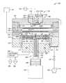
- FIG. 1is a schematic cross-sectional view of an exemplary substrate processing system.
- Embodiments of the present inventiongenerally provide methods for forming a silicon nitride layer on a substrate.
- a method of forming a silicon nitride layer using remote plasma chemical vapor deposition (CVD) at a temperature that is less than 300 degrees Celsiusis disclosed.
- the precursors for the remote plasma CVD processinclude tris(dimethylamino)silane (TRIS), dichlorosilane (DCS), trisilylamine (TSA), bis-t-butylaminosilane (BTBAS), hexachlorodisilane (HCDS) or hexamethylcyclotrisilazane (HMCTZ).
- Conformality of a layeris typically quantified by a ratio (which may be represented as a percentage) of the average thickness of a layer deposited on the sidewalls of a feature to the average thickness of the same deposited layer on the field, or upper surface, of the substrate. Layers deposited by the methods described herein are observed to have a conformality of greater than about 90%, such as 95% or greater, to about 100%.
- FIG. 1is a cross-sectional view of an illustrative processing chamber 100 suitable for conducting a deposition process as further described below.
- the chamber 100is configured to form a silicon nitride layer on a substrate surface.
- the chamber 100is particularly useful for performing the remote plasma CVD process.
- One processing chamber 100 suitable for practicing the inventionis a FrontierTM processing chamber which is available from Applied Materials, Santa Clara, Calif. It is noted that other vacuum processing chambers available from other manufactures may also be adapted to practice the present invention.
- the processing chamber 100provides both heating and cooling of a substrate surface without breaking vacuum.
- the processing chamber 100includes a chamber body 112 , a lid assembly 140 , and a support assembly 180 .
- the lid assembly 140is disposed at an upper end of the chamber body 112
- the support assembly 180is at least partially disposed within the chamber body 112 .
- the chamber body 112includes a slit valve opening 114 formed in a sidewall thereof to provide access to an interior of the processing chamber 100 .
- the slit valve opening 114is selectively opened and closed to allow access to the interior of the chamber body 112 by a wafer handling robot (not shown).
- the chamber body 112includes a channel 115 formed therein for flowing a heat transfer fluid therethrough.
- the heat transfer fluidcan be a heating fluid or a coolant and is used to control the temperature of the chamber body 112 during processing. Control of the temperature of the chamber body 112 is important to prevent unwanted condensation of the gas or byproducts on the interior of the chamber body 112 .
- Exemplary heat transfer fluidsinclude water, ethylene glycol, or a mixture thereof.
- An exemplary heat transfer fluidmay also include nitrogen gas.
- the chamber body 112can further include a liner 120 that surrounds the support assembly 180 .
- the liner 120is removable for servicing and cleaning.
- the liner 120can be made of a metal such as aluminum, a ceramic material, or any other process compatible material.
- the liner 120can be bead blasted to increase surface roughness and/or surface area which increases the adhesion of any material deposited thereon, thereby preventing flaking of material which results in contamination of the processing chamber 100 .
- the liner 120includes one or more apertures 125 and a pumping channel 129 formed therein that is in fluid communication with a vacuum port 131 .
- the apertures 125provide a flow path for gases into the pumping channel 129 , which provides an egress for the gases within the processing chamber 100 to the vacuum port 131 .
- a vacuum systemis coupled to the vacuum port 131 .
- the vacuum systemmay include a vacuum pump 130 and a throttle valve 132 to regulate flow of gases through the processing chamber 100 .
- the vacuum pump 130is coupled to a vacuum port 131 disposed in the chamber body 112 and therefore, in fluid communication with the pumping channel 129 formed within the liner 120 .
- gasand “gases” are used interchangeably, unless otherwise noted, and refer to one or more precursors, reactants, catalysts, carrier, purge, cleaning, combinations thereof, as well as any other fluid introduced into the chamber body 112 .
- the lid assembly 140includes at least two stacked components configured to form a plasma volume or cavity therebetween.
- the lid assembly 140includes a first electrode 143 (“upper electrode”) disposed vertically above a second electrode 145 (“lower electrode”) confining a plasma volume or cavity 150 therebetween.
- the first electrode 143is connected to a power source 152 , such as an RF power supply, and the second electrode 145 is connected to ground, forming a capacitance between the two electrodes 143 , 145 .
- the lid assembly 140includes one or more gas inlets 154 (only one is shown) that are at least partially formed within an upper section 156 of the first electrode 143 .
- the one or more process gasesenter the lid assembly 140 via the one or more gas inlets 154 .
- the one or more gas inlets 154are in fluid communication with the plasma cavity 150 at a first end thereof and coupled to one or more upstream gas sources and/or other gas delivery components, such as gas mixers, at a second end thereof.
- the first electrode 143has an expanding section 155 that bounds the plasma cavity 150 .
- the expanding section 155is an annular member that has an inner surface or diameter 157 that gradually increases from an upper portion 155 A thereof to a lower portion 155 B thereof.
- the distance between the first electrode 143 and the second electrode 145is variable across the expanding section 155 . The varying distance helps control the formation and stability of the plasma generated within the plasma cavity 150 .
- the expanding section 155resembles an inverted truncated cone or “funnel.”
- the inner surface 157 of the expanding section 155gradually slopes from the upper portion 155 A to the lower portion 1558 of the expanding section 155 .
- the slope or angle of the inner diameter 157can vary depending on process requirements and/or process limitations.
- the length or height of the expanding section 155can also vary depending on specific process requirements and/or limitations.
- the expanding section 155 of the first electrode 143varies the vertical distance between the first electrode 143 and the second electrode 145 because of the gradually increasing inner surface 157 of the first electrode 143 .
- the variable distanceis directly influences to the power level within the plasma cavity 150 .
- the variation in distance between the two electrodes 143 , 145allows the plasma to find the necessary power level to sustain itself within some portion of the plasma cavity 150 if not throughout the entire plasma cavity 150 .
- the plasma within the plasma cavity 150is therefore less dependent on pressure, allowing the plasma to be generated and sustained within a wider operating window. As such, a more repeatable and reliable plasma can be formed within the lid assembly 140 .
- the lid assembly 140As the plasma generated in the plasma cavity 150 is defined in the lid assembly 140 prior to entering into a processing region above the support assembly 180 wherein the substrate is proceed, the lid assembly 140 is considered as a remote plasma source because the plasma is generated remotely from the processing region.
- the usage of remote plasma CVDhas several benefits: plasma generation and film formation takes place in two different regions, deposition temperature is lowered, plasma is induced in a region free of source compound using a non-film forming gas, number of active species is substantially less, the chemistry of process can be predicted and controlled, and substrates and films are not damaged by bombarding charged particles.
- Additional process/carrier gasesmay be introduced into the process region 161 . These process/carrier gases are not excited to form a plasma and may be introduced into the process region 161 via a gas source 151 .
- the expanding section 155is in fluid communication with the gas inlet 154 as described above.
- the first end of the one or more gas inlets 154can open into the plasma cavity 150 at the upper most point of the inner diameter of the expanding section 155 .
- the first end of the one or more gas inlets 154can open into the plasma cavity 150 at any height interval along the inner diameter 157 of the expanding section 155 .
- two gas inlets 154can be disposed at opposite sides of the expanding section 155 to create a swirling flow pattern or “vortex” flow into the expanding section 155 which helps mix the gases within the plasma cavity 150 .
- the lid assembly 140can further include an isolator ring 160 that electrically isolates the first electrode 143 the second electrode 145 .
- the isolator ring 160can be made from aluminum oxide or any other insulative, process compatible material.
- the isolator ring 160surrounds or substantially surrounds at least the expanding section 155 .
- the lid assembly 140can further include a distribution plate 170 and blocker plate 175 adjacent the second electrode 145 .
- the second electrode 145 , distribution plate 170 and blocker plate 175can be stacked and disposed on a lid rim 178 which is connected to the chamber body 112 .
- a hinge assembly(not shown) can be used to couple the lid rim 178 to the chamber body 112 .
- the lid rim 178can include an embedded channel or passage 179 for circulating a heat transfer medium.
- the heat transfer mediumcan be used for heating, cooling, or both, depending on the process requirements.
- the second electrode or top plate 145can include a plurality of gas passages or apertures 165 formed beneath the plasma cavity 150 to allow gas from the plasma cavity 150 to flow therethrough.
- the distribution plate 170is substantially disc-shaped and also includes a plurality of apertures 172 or passageways to distribute the flow of gases therethrough.
- the apertures 172can be sized and positioned about the distribution plate 170 to provide a controlled and even flow distribution to the processing region of the chamber body 112 where the substrate to be processed is located. Furthermore, the apertures 172 prevent the gas(es) from impinging directly on the substrate surface by slowing and re-directing the velocity profile of the flowing gases, as well as evenly distributing the flow of gas to provide an even distribution of gas across the surface of the substrate.
- the distribution plate 170includes one or more embedded channels or passages 174 for housing a heater or heating fluid to provide temperature control of the lid assembly 140 .
- a resistive heating element(not shown) can be inserted within the passage 174 to heat the distribution plate 170 .
- a thermocouplecan be connected to the distribution plate 170 to regulate the temperature thereof. The thermocouple can be used in a feedback loop to control electric current applied to the heating element, as described above.
- a heat transfer mediumcan be passed through the passage 174 .
- the one or more passages 174can contain a cooling medium, if needed, to better control temperature of the distribution plate 170 depending on the process requirements within the chamber body 112 .
- Any heat suitable transfer mediummay be used, such as nitrogen, water, ethylene glycol, or mixtures thereof, for example.
- the lid assembly 140can be heated using one or more heat lamps (not shown).
- the heat lampsare arranged about an upper surface of the distribution plate 170 to heat the components of the lid assembly 140 including the distribution plate 170 by radiation.
- the blocker plate 175may optionally be disposed between the second electrode 145 and the distribution plate 170 .
- the blocker plate 175is removably mounted to a lower surface of the second electrode 145 .
- the blocker plate 175may be in good thermal and electrical contact with the second electrode 145 .
- the blocker plate 175can be coupled to the second electrode 145 using a bolt or similar fastener.
- the blocker plate 175can also be threaded or screwed onto an outer diameter of the second electrode 145 .
- the blocker plate 175includes a plurality of apertures 176 to provide a plurality of gas passages from the second electrode 145 to the distribution plate 170 .
- the apertures 176can be sized and positioned about the blocker plate 175 to provide a controlled and even flow distribution of gases to the distribution plate 170 .
- the support assembly 180can include a support member 185 to support a substrate (not shown in FIG. 1 ) for processing within the chamber body 112 .
- the support member 185can be coupled to a lift mechanism 183 through a shaft 187 which extends through a centrally-located opening 114 formed in a bottom surface of the chamber body 112 .
- the lift mechanism 183can be flexibly sealed to the chamber body 112 by a bellows 188 that prevents vacuum leakage from around the shaft 187 .
- the lift mechanism 183allows the support member 185 to be moved vertically within the chamber body 112 between a process position and a lower transfer position. The transfer position is slightly below the slit valve opening 114 formed in a sidewall of the chamber body 112 so that the substrate may be robotically removed from the substrate support member 185 .
- the support member 185has a flat, circular surface or a substantially flat, circular surface for supporting a substrate to be processed thereon.
- the support member 185may be constructed of aluminum.
- the support member 185can include a removable top plate 190 made of some other material, such as silicon or ceramic material, for example, to reduce backside contamination of the substrate.
- the substratemay be secured to the support member 185 using a vacuum chuck. In one or more embodiments, the substrate (not shown) may be secured to the support member 185 using an electrostatic chuck.
- An electrostatic chucktypically includes at least a dielectric material that surrounds an electrode 181 , which may be located on the support member 185 or formed as an integral part of the support member 185 . The dielectric portion of the chuck electrically insulates the chuck electrode 181 from the substrate and from the remainder of the support assembly 180 .
- the electrode 181is coupled to a plurality of RF power bias sources 184 , 186 .
- the RF bias power sources 184 , 186provide RF power to the electrode 181 which excites and sustains a plasma discharge formed from the gases disposed in the processing region of the chamber body.
- the dual RF bias power sources 184 , 186are coupled to the electrode 181 disposed in the support member 185 through a matching circuit 189 .
- the signal generated by the RF bias power sources 184 , 186is delivered through matching circuit 189 to the support member 185 through a single feed to ionize the gas mixture provided in the plasma processing chamber 100 , thereby providing ion energy necessary for performing a deposition, etch, or other plasma enhanced process.
- the RF bias power sources 184 , 186are generally capable of producing an RF signal having a frequency of from about 50 kHz to about 200 MHz and a power between about 0 Watts and about 5000 Watts. Additional bias power sources may be coupled to the electrode 181 to control the characteristics of the plasma as needed.
- the support member 185can include bores 192 formed therethrough to accommodate lift pins 193 , one of which is shown in FIG. 1 .
- Each lift pin 193is constructed of ceramic or ceramic-containing materials, and are used for substrate-handling and transport.
- the lift pin 193is moveable within its respective bore 192 when engaging an annular lift ring 195 disposed within the chamber body 112 .
- the lift ring 195is movable such that the upper surface of the lift pin 193 can be extended above the substrate support surface of the support member 185 when the lift ring 195 is in an upper position.
- the upper surface of the lift pins 193is located below the substrate support surface of the support member 185 when the lift ring 195 is in a lower position.
- each lift pin 193is moved in its respective bore 192 in the support member 185 when the lift ring 195 moves from either the lower position to the upper position.
- the support assembly 180can further include an edge ring 196 disposed about the support member 185 .
- the edge ring 196is an annular member that is adapted to cover an outer perimeter of the support member 185 and protect the support member 185 from deposition.
- the edge ring 196can be positioned on or adjacent the support member 185 to form an annular purge gas channel between the outer diameter of support member 185 and the inner diameter of the edge ring 196 .
- the annular purge gas channelcan be in fluid communication with a purge gas conduit 197 formed through the support member 185 and the shaft 187 .
- the purge gas conduit 197is in fluid communication with a purge gas supply (not shown) to provide a purge gas to the purge gas channel.
- any suitable purge gassuch as nitrogen, argon, or helium, may be used alone or in combination.
- the purge gasflows through the conduit 197 , into the purge gas channel, and about an edge of the substrate disposed on the support member 185 . Accordingly, the purge gas working in cooperation with the edge ring 196 prevents deposition at the edge and/or backside of the substrate.
- the temperature of the support assembly 180can be controlled by a fluid circulated through a fluid channel 198 embedded in the body of the support member 185 .
- the fluid channel 198is in fluid communication with a heat transfer conduit 199 disposed through the shaft 187 of the support assembly 180 .
- the fluid channel 198is positioned about the support member 185 to provide a uniform heat transfer to the substrate receiving surface of the support member 185 .
- the fluid channel 198 and heat transfer conduit 199can flow heat transfer fluids to either heat or cool the support member 185 and substrate disposed thereon. Any suitable heat transfer fluid may be used, such as water, nitrogen, ethylene glycol, or mixtures thereof.
- the support member 185can further include an embedded thermocouple (not shown) for monitoring the temperature of the support surface of the support member 185 , which is indicative of the temperature of the substrate disposed thereon.
- a signal from the thermocouplemay be used in a feedback loop to control the temperature or flow rate of the fluid circulated through the fluid channel 198 .
- the support member 185can be moved vertically within the chamber body 112 so that a distance between support member 185 and the lid assembly 140 can be controlled.
- a sensor(not shown) can provide information concerning the position of support member 185 within chamber 100 .
- the support member 185can be elevated to a close proximity of the lid assembly 140 to control the temperature of the substrate being processed.
- the substratecan be heated via radiation emitted from the distribution plate 170 .
- the substratecan be lifted off the support member 185 to close proximity of the heated lid assembly 140 using the lift pins 193 activated by the lift ring 195 .
- the substrateis heated to less than 300 degrees Celsius during the deposition of silicon nitride film by remote plasma CVD process.
- a system controller(not shown) can be used to regulate the operations of the processing chamber 100 .
- the system controllercan operate under the control of a computer program stored on a memory of a computer.
- the computer programmay include instructions that enable the process described below to be performed in the processing chamber 100 .
- the computer programcan dictate the process sequencing and timing, mixture of gases, chamber pressures, RF power levels, susceptor positioning, slit valve opening and closing, substrate cooling and other parameters of a particular process.
- Low temperature conformal depositionmay be achieved by processes utilizing a processing gas mixture and excite the process gas mixture to form a plasma at a location remote from where the deposition is performed.
- the plasmais formed in the plasma cavity 150 of the processing chamber 100 .
- the precursorsmay include one or more of the listed compounds, for example, TRIS, DCS, TSA, BTBAS, HCDS, or HMCTZ. Any of the precursor compounds may be used alone or in combination with other precursor compounds.
- the processing gas mixturemay include other process gases besides the precursor gases such as carrier or other types of gases.
- the other process gasesmay include inert gas such as Ar.
- the deposition of silicon nitrideinvolves Ar remote plasma and TSA.
- Arbreaks down to Ar radicals and breaks down Si—H bonds to form (—Si—NH—) x polymers.
- Deposition temperaturemay be between about 20 degrees Celsius (room temperature) and about 250 degrees Celsius. Deposition temperature is referred to the temperature of the substrate during the deposition.
- silicon nitride film having no residual hydrogenmay be deposited at a temperature below 300 degrees Celsius by remote plasma CVD.
Landscapes
- Chemical & Material Sciences (AREA)
- Engineering & Computer Science (AREA)
- Physics & Mathematics (AREA)
- Condensed Matter Physics & Semiconductors (AREA)
- General Physics & Mathematics (AREA)
- Manufacturing & Machinery (AREA)
- Computer Hardware Design (AREA)
- Microelectronics & Electronic Packaging (AREA)
- Power Engineering (AREA)
- Chemical Kinetics & Catalysis (AREA)
- Materials Engineering (AREA)
- General Chemical & Material Sciences (AREA)
- Mechanical Engineering (AREA)
- Metallurgy (AREA)
- Organic Chemistry (AREA)
- Plasma & Fusion (AREA)
- Inorganic Chemistry (AREA)
- Chemical Vapour Deposition (AREA)
- Formation Of Insulating Films (AREA)
Abstract
Description
This application claims priority to U.S. Provisional Patent Application Ser. No. 61/898,911, filed on Nov. 1, 2013, which herein is incorporated by reference.
Field
Embodiments of the present invention generally relate to methods and processes for forming conformal silicon nitride films, including doped silicon nitride films, at low temperatures.
Description of the Related Art
The electronic device industry and the semiconductor industry continue to strive for larger production yields while increasing the uniformity of layers deposited on substrates having increasingly larger surface areas. These same factors in combination with new materials also provide higher integration of circuits per unit area on the substrate. As circuit integration increases, the need for greater uniformity and process control regarding layer characteristics rises.
For example, ultra-large-scale integrated (ULSI) circuits typically include more than one million transistors that are formed on a semiconductor substrate and which cooperate to perform various functions within an electronic device. Such transistors may include complementary metal-oxide-semiconductor (CMOS) field effect transistors. A CMOS transistor includes a gate structure that is disposed between a source region and a drain region defined in the semiconductor substrate. The gate structure (stack) generally comprises a gate electrode formed on a gate dielectric material.
Transistors may also be formed as 3 dimensional or 3D circuits as compared to traditional planar circuits. 3D transistors may employ gates that form conducting channels on three sides of a vertical “fin” structure, allowing chips to operate at lower voltage with lower leakage. Examples of three dimensional transistors having such gate structures include a FinFET (a nonplanar, double-gate transistor built on a silicon-on-insulator technology substrate, based on the earlier DELTA (single-gate) transistor design) or a Trigate transistor structure.
Conformal coverage with low pattern loading effect of dielectric films on high aspect ratio structures and/or 3D structures are of critical requirement as device node shrinks down to below 45 nm, such as to the 22 nm level, and as the manufacture of 3D transistors increases. Silicon nitride films, including doped silicon nitride, may be used throughout integrated circuit formation, such as gate spacers, liner layers, sacrificial layers, barrier layers, etc. Silicon nitride films formed using thermal processes offers good conformality. The drawbacks, however, include a high temperature requirement (typically greater than 400° C.) and few capabilities to engineer film compositions and properties for different applications. Alternatively, conventional silane-based plasma enhanced chemical vapor deposition (PECVD) silicon nitride films have poorer step coverage due to directionality of radicals' fluxes. Additionally, tuning conformal layers to have desired film properties has also been difficult, particularly as the feature size decreases and the use of non-planar structures increases.
Therefore, there is a need for a low temperature process to form conformal silicon nitride films with micromodulated texture, composition and stable film properties.
Embodiments of the present invention generally provide methods for forming a silicon nitride layer on a substrate. In one embodiment, a method of forming a silicon nitride layer using remote plasma chemical vapor deposition (CVD) at a temperature that is less than 300 degrees Celsius is disclosed. The precursors for the remote plasma CVD process include tris(dimethylamino)silane (TRIS), dichlorosilane (DCS), trisilylamine (TSA), bis-t-butylaminosilane (BTBAS), hexachlorodisilane (HCDS) or hexamethylcyclotrisilazane (HMCTZ).
In one embodiment, a method is disclosed. The method includes forming a silicon nitride layer on a substrate by a remote plasma chemical vapor deposition process at a deposition temperature less than 300 degrees Celsius, and the remote plasma chemical vapor deposition process utilizes a processing gas mixture, which includes tris(dimethylamino)silane, dichlorosilane, trisilylamine, di-t-butylaminosilane, hexachlorodisilane, or hexamethylcyclotrisilazane.
In another embodiment, a method is disclosed. The method includes forming a silicon nitride layer on a substrate by a remote plasma chemical vapor deposition process. The deposition temperature ranges from about 20 degrees Celsius to about 250 degrees Celsius, the remote plasma chemical vapor deposition process utilizes a processing gas mixture, which includes tris(dimethylamino)silane, dichlorosilane, trisilylamine, di-t-butylaminosilane, hexachlorodisilane, hexamethylcyclotrisilazane, argon or combination thereon, and the processing gas mixture is excited to form a plasma.
So that the manner in which the above recited features of the present invention can be understood in detail, a more particular description of the invention, briefly summarized above, may be had by reference to embodiments, some of which are illustrated in the appended drawings. It is to be noted, however, that the appended drawings illustrate only typical embodiments of this invention and are therefore not to be considered limiting of its scope, for the invention may admit to other equally effective embodiments.
Embodiments of the present invention generally provide methods for forming a silicon nitride layer on a substrate. In one embodiment, a method of forming a silicon nitride layer using remote plasma chemical vapor deposition (CVD) at a temperature that is less than 300 degrees Celsius is disclosed. The precursors for the remote plasma CVD process include tris(dimethylamino)silane (TRIS), dichlorosilane (DCS), trisilylamine (TSA), bis-t-butylaminosilane (BTBAS), hexachlorodisilane (HCDS) or hexamethylcyclotrisilazane (HMCTZ).
Conformality of a layer is typically quantified by a ratio (which may be represented as a percentage) of the average thickness of a layer deposited on the sidewalls of a feature to the average thickness of the same deposited layer on the field, or upper surface, of the substrate. Layers deposited by the methods described herein are observed to have a conformality of greater than about 90%, such as 95% or greater, to about 100%.
Theprocessing chamber 100 provides both heating and cooling of a substrate surface without breaking vacuum. In one embodiment, theprocessing chamber 100 includes achamber body 112, alid assembly 140, and asupport assembly 180. Thelid assembly 140 is disposed at an upper end of thechamber body 112, and thesupport assembly 180 is at least partially disposed within thechamber body 112.
Thechamber body 112 includes aslit valve opening 114 formed in a sidewall thereof to provide access to an interior of theprocessing chamber 100. Theslit valve opening 114 is selectively opened and closed to allow access to the interior of thechamber body 112 by a wafer handling robot (not shown).
In one or more embodiments, thechamber body 112 includes achannel 115 formed therein for flowing a heat transfer fluid therethrough. The heat transfer fluid can be a heating fluid or a coolant and is used to control the temperature of thechamber body 112 during processing. Control of the temperature of thechamber body 112 is important to prevent unwanted condensation of the gas or byproducts on the interior of thechamber body 112. Exemplary heat transfer fluids include water, ethylene glycol, or a mixture thereof. An exemplary heat transfer fluid may also include nitrogen gas.
Thechamber body 112 can further include aliner 120 that surrounds thesupport assembly 180. Theliner 120 is removable for servicing and cleaning. Theliner 120 can be made of a metal such as aluminum, a ceramic material, or any other process compatible material. Theliner 120 can be bead blasted to increase surface roughness and/or surface area which increases the adhesion of any material deposited thereon, thereby preventing flaking of material which results in contamination of theprocessing chamber 100. In one or more embodiments, theliner 120 includes one ormore apertures 125 and apumping channel 129 formed therein that is in fluid communication with avacuum port 131. Theapertures 125 provide a flow path for gases into thepumping channel 129, which provides an egress for the gases within theprocessing chamber 100 to thevacuum port 131.
A vacuum system is coupled to thevacuum port 131. The vacuum system may include avacuum pump 130 and athrottle valve 132 to regulate flow of gases through theprocessing chamber 100. Thevacuum pump 130 is coupled to avacuum port 131 disposed in thechamber body 112 and therefore, in fluid communication with the pumpingchannel 129 formed within theliner 120. The terms “gas” and “gases” are used interchangeably, unless otherwise noted, and refer to one or more precursors, reactants, catalysts, carrier, purge, cleaning, combinations thereof, as well as any other fluid introduced into thechamber body 112.
Thelid assembly 140 includes at least two stacked components configured to form a plasma volume or cavity therebetween. In one or more embodiments, thelid assembly 140 includes a first electrode143 (“upper electrode”) disposed vertically above a second electrode145 (“lower electrode”) confining a plasma volume orcavity 150 therebetween. Thefirst electrode 143 is connected to apower source 152, such as an RF power supply, and thesecond electrode 145 is connected to ground, forming a capacitance between the twoelectrodes
In one or more embodiments, thelid assembly 140 includes one or more gas inlets154 (only one is shown) that are at least partially formed within anupper section 156 of thefirst electrode 143. The one or more process gases enter thelid assembly 140 via the one ormore gas inlets 154. The one ormore gas inlets 154 are in fluid communication with theplasma cavity 150 at a first end thereof and coupled to one or more upstream gas sources and/or other gas delivery components, such as gas mixers, at a second end thereof.
In one or more embodiments, thefirst electrode 143 has an expandingsection 155 that bounds theplasma cavity 150. In one or more embodiments, the expandingsection 155 is an annular member that has an inner surface ordiameter 157 that gradually increases from anupper portion 155A thereof to alower portion 155B thereof. As such, the distance between thefirst electrode 143 and thesecond electrode 145 is variable across the expandingsection 155. The varying distance helps control the formation and stability of the plasma generated within theplasma cavity 150.
In one or more embodiments, the expandingsection 155 resembles an inverted truncated cone or “funnel.” In one or more embodiments, theinner surface 157 of the expandingsection 155 gradually slopes from theupper portion 155A to the lower portion1558 of the expandingsection 155. The slope or angle of theinner diameter 157 can vary depending on process requirements and/or process limitations. The length or height of the expandingsection 155 can also vary depending on specific process requirements and/or limitations.
As mentioned above, the expandingsection 155 of thefirst electrode 143 varies the vertical distance between thefirst electrode 143 and thesecond electrode 145 because of the gradually increasinginner surface 157 of thefirst electrode 143. The variable distance is directly influences to the power level within theplasma cavity 150. Not wishing to be bound by theory, the variation in distance between the twoelectrodes plasma cavity 150 if not throughout theentire plasma cavity 150. The plasma within theplasma cavity 150 is therefore less dependent on pressure, allowing the plasma to be generated and sustained within a wider operating window. As such, a more repeatable and reliable plasma can be formed within thelid assembly 140. As the plasma generated in theplasma cavity 150 is defined in thelid assembly 140 prior to entering into a processing region above thesupport assembly 180 wherein the substrate is proceed, thelid assembly 140 is considered as a remote plasma source because the plasma is generated remotely from the processing region. The usage of remote plasma CVD has several benefits: plasma generation and film formation takes place in two different regions, deposition temperature is lowered, plasma is induced in a region free of source compound using a non-film forming gas, number of active species is substantially less, the chemistry of process can be predicted and controlled, and substrates and films are not damaged by bombarding charged particles.
Additional process/carrier gases may be introduced into theprocess region 161. These process/carrier gases are not excited to form a plasma and may be introduced into theprocess region 161 via agas source 151.
The expandingsection 155 is in fluid communication with thegas inlet 154 as described above. The first end of the one ormore gas inlets 154 can open into theplasma cavity 150 at the upper most point of the inner diameter of the expandingsection 155. Similarly, the first end of the one ormore gas inlets 154 can open into theplasma cavity 150 at any height interval along theinner diameter 157 of the expandingsection 155. Although not shown, twogas inlets 154 can be disposed at opposite sides of the expandingsection 155 to create a swirling flow pattern or “vortex” flow into the expandingsection 155 which helps mix the gases within theplasma cavity 150.
Thelid assembly 140 can further include anisolator ring 160 that electrically isolates thefirst electrode 143 thesecond electrode 145. Theisolator ring 160 can be made from aluminum oxide or any other insulative, process compatible material. Theisolator ring 160 surrounds or substantially surrounds at least the expandingsection 155.
Thelid assembly 140 can further include adistribution plate 170 andblocker plate 175 adjacent thesecond electrode 145. Thesecond electrode 145,distribution plate 170 andblocker plate 175 can be stacked and disposed on alid rim 178 which is connected to thechamber body 112. A hinge assembly (not shown) can be used to couple thelid rim 178 to thechamber body 112. Thelid rim 178 can include an embedded channel orpassage 179 for circulating a heat transfer medium. The heat transfer medium can be used for heating, cooling, or both, depending on the process requirements.
In one or more embodiments, the second electrode ortop plate 145 can include a plurality of gas passages orapertures 165 formed beneath theplasma cavity 150 to allow gas from theplasma cavity 150 to flow therethrough. Thedistribution plate 170 is substantially disc-shaped and also includes a plurality ofapertures 172 or passageways to distribute the flow of gases therethrough. Theapertures 172 can be sized and positioned about thedistribution plate 170 to provide a controlled and even flow distribution to the processing region of thechamber body 112 where the substrate to be processed is located. Furthermore, theapertures 172 prevent the gas(es) from impinging directly on the substrate surface by slowing and re-directing the velocity profile of the flowing gases, as well as evenly distributing the flow of gas to provide an even distribution of gas across the surface of the substrate.
In one or more embodiments, thedistribution plate 170 includes one or more embedded channels orpassages 174 for housing a heater or heating fluid to provide temperature control of thelid assembly 140. A resistive heating element (not shown) can be inserted within thepassage 174 to heat thedistribution plate 170. A thermocouple can be connected to thedistribution plate 170 to regulate the temperature thereof. The thermocouple can be used in a feedback loop to control electric current applied to the heating element, as described above.
Alternatively, a heat transfer medium can be passed through thepassage 174. The one ormore passages 174 can contain a cooling medium, if needed, to better control temperature of thedistribution plate 170 depending on the process requirements within thechamber body 112. Any heat suitable transfer medium may be used, such as nitrogen, water, ethylene glycol, or mixtures thereof, for example.
In one or more embodiments, thelid assembly 140 can be heated using one or more heat lamps (not shown). Typically, the heat lamps are arranged about an upper surface of thedistribution plate 170 to heat the components of thelid assembly 140 including thedistribution plate 170 by radiation.
Theblocker plate 175 may optionally be disposed between thesecond electrode 145 and thedistribution plate 170. Theblocker plate 175 is removably mounted to a lower surface of thesecond electrode 145. Theblocker plate 175 may be in good thermal and electrical contact with thesecond electrode 145. In one or more embodiments, theblocker plate 175 can be coupled to thesecond electrode 145 using a bolt or similar fastener. Theblocker plate 175 can also be threaded or screwed onto an outer diameter of thesecond electrode 145.
Theblocker plate 175 includes a plurality ofapertures 176 to provide a plurality of gas passages from thesecond electrode 145 to thedistribution plate 170. Theapertures 176 can be sized and positioned about theblocker plate 175 to provide a controlled and even flow distribution of gases to thedistribution plate 170.
Thesupport assembly 180 can include asupport member 185 to support a substrate (not shown inFIG. 1 ) for processing within thechamber body 112. Thesupport member 185 can be coupled to alift mechanism 183 through ashaft 187 which extends through a centrally-locatedopening 114 formed in a bottom surface of thechamber body 112. Thelift mechanism 183 can be flexibly sealed to thechamber body 112 by abellows 188 that prevents vacuum leakage from around theshaft 187. Thelift mechanism 183 allows thesupport member 185 to be moved vertically within thechamber body 112 between a process position and a lower transfer position. The transfer position is slightly below the slit valve opening114 formed in a sidewall of thechamber body 112 so that the substrate may be robotically removed from thesubstrate support member 185.
In one or more embodiments, thesupport member 185 has a flat, circular surface or a substantially flat, circular surface for supporting a substrate to be processed thereon. Thesupport member 185 may be constructed of aluminum. Thesupport member 185 can include a removabletop plate 190 made of some other material, such as silicon or ceramic material, for example, to reduce backside contamination of the substrate.
In one or more embodiments, the substrate (not shown) may be secured to thesupport member 185 using a vacuum chuck. In one or more embodiments, the substrate (not shown) may be secured to thesupport member 185 using an electrostatic chuck. An electrostatic chuck typically includes at least a dielectric material that surrounds anelectrode 181, which may be located on thesupport member 185 or formed as an integral part of thesupport member 185. The dielectric portion of the chuck electrically insulates thechuck electrode 181 from the substrate and from the remainder of thesupport assembly 180.
In one embodiment, theelectrode 181 is coupled to a plurality of RFpower bias sources power sources electrode 181 which excites and sustains a plasma discharge formed from the gases disposed in the processing region of the chamber body.
In the embodiment depicted inFIG. 1 , the dual RF biaspower sources electrode 181 disposed in thesupport member 185 through amatching circuit 189. The signal generated by the RF biaspower sources circuit 189 to thesupport member 185 through a single feed to ionize the gas mixture provided in theplasma processing chamber 100, thereby providing ion energy necessary for performing a deposition, etch, or other plasma enhanced process. The RF biaspower sources electrode 181 to control the characteristics of the plasma as needed.
Thesupport member 185 can includebores 192 formed therethrough to accommodatelift pins 193, one of which is shown inFIG. 1 . Eachlift pin 193 is constructed of ceramic or ceramic-containing materials, and are used for substrate-handling and transport. Thelift pin 193 is moveable within itsrespective bore 192 when engaging anannular lift ring 195 disposed within thechamber body 112. Thelift ring 195 is movable such that the upper surface of thelift pin 193 can be extended above the substrate support surface of thesupport member 185 when thelift ring 195 is in an upper position. Conversely, the upper surface of the lift pins193 is located below the substrate support surface of thesupport member 185 when thelift ring 195 is in a lower position. Thus, eachlift pin 193 is moved in itsrespective bore 192 in thesupport member 185 when thelift ring 195 moves from either the lower position to the upper position.
Thesupport assembly 180 can further include anedge ring 196 disposed about thesupport member 185. In one or more embodiments, theedge ring 196 is an annular member that is adapted to cover an outer perimeter of thesupport member 185 and protect thesupport member 185 from deposition. Theedge ring 196 can be positioned on or adjacent thesupport member 185 to form an annular purge gas channel between the outer diameter ofsupport member 185 and the inner diameter of theedge ring 196. The annular purge gas channel can be in fluid communication with apurge gas conduit 197 formed through thesupport member 185 and theshaft 187. Thepurge gas conduit 197 is in fluid communication with a purge gas supply (not shown) to provide a purge gas to the purge gas channel. Any suitable purge gas such as nitrogen, argon, or helium, may be used alone or in combination. In operation, the purge gas flows through theconduit 197, into the purge gas channel, and about an edge of the substrate disposed on thesupport member 185. Accordingly, the purge gas working in cooperation with theedge ring 196 prevents deposition at the edge and/or backside of the substrate.
The temperature of thesupport assembly 180 can be controlled by a fluid circulated through afluid channel 198 embedded in the body of thesupport member 185. In one or more embodiments, thefluid channel 198 is in fluid communication with aheat transfer conduit 199 disposed through theshaft 187 of thesupport assembly 180. Thefluid channel 198 is positioned about thesupport member 185 to provide a uniform heat transfer to the substrate receiving surface of thesupport member 185. Thefluid channel 198 andheat transfer conduit 199 can flow heat transfer fluids to either heat or cool thesupport member 185 and substrate disposed thereon. Any suitable heat transfer fluid may be used, such as water, nitrogen, ethylene glycol, or mixtures thereof. Thesupport member 185 can further include an embedded thermocouple (not shown) for monitoring the temperature of the support surface of thesupport member 185, which is indicative of the temperature of the substrate disposed thereon. For example, a signal from the thermocouple may be used in a feedback loop to control the temperature or flow rate of the fluid circulated through thefluid channel 198.
Thesupport member 185 can be moved vertically within thechamber body 112 so that a distance betweensupport member 185 and thelid assembly 140 can be controlled. A sensor (not shown) can provide information concerning the position ofsupport member 185 withinchamber 100.
In operation, thesupport member 185 can be elevated to a close proximity of thelid assembly 140 to control the temperature of the substrate being processed. As such, the substrate can be heated via radiation emitted from thedistribution plate 170. Alternatively, the substrate can be lifted off thesupport member 185 to close proximity of theheated lid assembly 140 using the lift pins193 activated by thelift ring 195. The substrate is heated to less than 300 degrees Celsius during the deposition of silicon nitride film by remote plasma CVD process.
A system controller (not shown) can be used to regulate the operations of theprocessing chamber 100. The system controller can operate under the control of a computer program stored on a memory of a computer. The computer program may include instructions that enable the process described below to be performed in theprocessing chamber 100. For example, the computer program can dictate the process sequencing and timing, mixture of gases, chamber pressures, RF power levels, susceptor positioning, slit valve opening and closing, substrate cooling and other parameters of a particular process.
Aspects of the invention provide for low temperature conformal deposition of a silicon nitride (SixNy) layer. Low temperature conformal deposition may be achieved by processes utilizing a processing gas mixture and excite the process gas mixture to form a plasma at a location remote from where the deposition is performed. For example, the plasma is formed in theplasma cavity 150 of theprocessing chamber 100.
The precursors may include one or more of the listed compounds, for example, TRIS, DCS, TSA, BTBAS, HCDS, or HMCTZ. Any of the precursor compounds may be used alone or in combination with other precursor compounds. The processing gas mixture may include other process gases besides the precursor gases such as carrier or other types of gases. For example, the other process gases may include inert gas such as Ar. In one embodiment, the deposition of silicon nitride involves Ar remote plasma and TSA. Ar breaks down to Ar radicals and breaks down Si—H bonds to form (—Si—NH—)xpolymers. Deposition temperature may be between about 20 degrees Celsius (room temperature) and about 250 degrees Celsius. Deposition temperature is referred to the temperature of the substrate during the deposition. At room temperature, there is more residual hydrogen in the film resulting in lower refractive index (1.8). At higher deposition temperature such as greater than room temperature there is less residual hydrogen in the film resulting in higher refractive index (2.2). After depositing the silicon nitride film, various processes may be performed on the deposited film to remove the residual hydrogen, such as high density plasma treatment, UV cure, or ebeam cure etc. Thus, silicon nitride film having no residual hydrogen may be deposited at a temperature below 300 degrees Celsius by remote plasma CVD.
While the foregoing is directed to embodiments of the present invention, other and further embodiments of the invention may be devised without departing from the basic scope thereof, and the scope thereof is determined by the claims that follow.
Claims (12)
1. A method, comprising:
forming a silicon nitride layer on a substrate in a processing region of a processing chamber by a remote plasma chemical vapor deposition process at a deposition temperature less than 300 degrees Celsius, wherein the remote plasma chemical vapor deposition process utilizes a processing gas mixture, wherein the processing gas mixture includes tris(dimethylamino)silane, di-t-butylaminosilane, or hexamethylcyclotrisilazane, and wherein the processing gas mixture is excited to form a plasma in a plasma cavity that is remote from the processing region, the plasma cavity is defined by a first electrode and a second electrode, and the first electrode and the second electrode are electrically isolated by an isolator ring.
2. The method ofclaim 1 , wherein the deposition temperature ranges from about 20 degrees Celsius to about 250 degrees Celsius.
3. The method ofclaim 2 , wherein the silicon nitride layer has a refractive index of 1.8 when the deposition temperature is about 20 degrees Celsius.
4. The method ofclaim 2 , wherein the silicon nitride layer has a refractive index of 2.2 when the deposition temperature is higher than 20 degrees Celsius.
5. The method ofclaim 1 , further comprising curing the silicon nitride layer.
6. The method ofclaim 5 , wherein the curing the silicon nitride layer includes UV curing or ebeam curing.
7. The method ofclaim 1 , wherein the processing gas mixture further includes a carrier gas.
8. A method, comprising:
forming a silicon nitride layer on a substrate in a processing region of a processing chamber by a remote plasma chemical vapor deposition process, wherein the deposition temperature ranges from about 20 degrees Celsius to about 250 degrees Celsius, wherein the remote plasma chemical vapor deposition process utilizes a processing gas mixture, wherein the processing gas mixture includes tris(dimethylamino)silane, di-t-butylaminosilane, hexamethylcyclotrisilazane, argon or combination thereof, and wherein the processing gas mixture is excited to form in a plasma cavity that is remote from the processing region, the plasma cavity is defined by a first electrode and a second electrode, and the first electrode and the second electrode are electrically isolated by an isolator ring.
9. The method ofclaim 8 , wherein the silicon nitride layer has a refractive index of 1.8 when the deposition temperature is about 20 degrees Celsius.
10. The method ofclaim 9 , wherein the silicon nitride layer has a refractive index of 2.2 when the deposition temperature is higher than 20 degrees Celsius.
11. The method ofclaim 8 , further comprising curing the silicon nitride layer.
12. The method ofclaim 11 , wherein the curing the silicon nitride layer includes UV curing or e-beam curing.
Priority Applications (1)
| Application Number | Priority Date | Filing Date | Title |
|---|---|---|---|
| US14/520,721US9583333B2 (en) | 2013-11-01 | 2014-10-22 | Low temperature silicon nitride films using remote plasma CVD technology |
Applications Claiming Priority (2)
| Application Number | Priority Date | Filing Date | Title |
|---|---|---|---|
| US201361898911P | 2013-11-01 | 2013-11-01 | |
| US14/520,721US9583333B2 (en) | 2013-11-01 | 2014-10-22 | Low temperature silicon nitride films using remote plasma CVD technology |
Publications (2)
| Publication Number | Publication Date |
|---|---|
| US20150126045A1 US20150126045A1 (en) | 2015-05-07 |
| US9583333B2true US9583333B2 (en) | 2017-02-28 |
Family
ID=53004967
Family Applications (1)
| Application Number | Title | Priority Date | Filing Date |
|---|---|---|---|
| US14/520,721Active2034-12-18US9583333B2 (en) | 2013-11-01 | 2014-10-22 | Low temperature silicon nitride films using remote plasma CVD technology |
Country Status (6)
| Country | Link |
|---|---|
| US (1) | US9583333B2 (en) |
| JP (1) | JP2016536792A (en) |
| KR (1) | KR20160078428A (en) |
| CN (1) | CN105659366B (en) |
| TW (1) | TW201522696A (en) |
| WO (1) | WO2015065790A1 (en) |
Cited By (275)
| Publication number | Priority date | Publication date | Assignee | Title |
|---|---|---|---|---|
| US20160138161A1 (en)* | 2014-11-19 | 2016-05-19 | Applied Materials, Inc. | Radical assisted cure of dielectric films |
| US11001925B2 (en) | 2016-12-19 | 2021-05-11 | Asm Ip Holding B.V. | Substrate processing apparatus |
| US11004977B2 (en) | 2017-07-19 | 2021-05-11 | Asm Ip Holding B.V. | Method for depositing a group IV semiconductor and related semiconductor device structures |
| US11015245B2 (en) | 2014-03-19 | 2021-05-25 | Asm Ip Holding B.V. | Gas-phase reactor and system having exhaust plenum and components thereof |
| US11018002B2 (en) | 2017-07-19 | 2021-05-25 | Asm Ip Holding B.V. | Method for selectively depositing a Group IV semiconductor and related semiconductor device structures |
| US11022879B2 (en) | 2017-11-24 | 2021-06-01 | Asm Ip Holding B.V. | Method of forming an enhanced unexposed photoresist layer |
| US11031242B2 (en) | 2018-11-07 | 2021-06-08 | Asm Ip Holding B.V. | Methods for depositing a boron doped silicon germanium film |
| USD922229S1 (en) | 2019-06-05 | 2021-06-15 | Asm Ip Holding B.V. | Device for controlling a temperature of a gas supply unit |
| US11049751B2 (en) | 2018-09-14 | 2021-06-29 | Asm Ip Holding B.V. | Cassette supply system to store and handle cassettes and processing apparatus equipped therewith |
| US11053591B2 (en) | 2018-08-06 | 2021-07-06 | Asm Ip Holding B.V. | Multi-port gas injection system and reactor system including same |
| US11056344B2 (en) | 2017-08-30 | 2021-07-06 | Asm Ip Holding B.V. | Layer forming method |
| US11069510B2 (en) | 2017-08-30 | 2021-07-20 | Asm Ip Holding B.V. | Substrate processing apparatus |
| US11081345B2 (en) | 2018-02-06 | 2021-08-03 | Asm Ip Holding B.V. | Method of post-deposition treatment for silicon oxide film |
| US11087997B2 (en) | 2018-10-31 | 2021-08-10 | Asm Ip Holding B.V. | Substrate processing apparatus for processing substrates |
| US11088002B2 (en) | 2018-03-29 | 2021-08-10 | Asm Ip Holding B.V. | Substrate rack and a substrate processing system and method |
| US11094582B2 (en) | 2016-07-08 | 2021-08-17 | Asm Ip Holding B.V. | Selective deposition method to form air gaps |
| US11094546B2 (en) | 2017-10-05 | 2021-08-17 | Asm Ip Holding B.V. | Method for selectively depositing a metallic film on a substrate |
| US11101370B2 (en) | 2016-05-02 | 2021-08-24 | Asm Ip Holding B.V. | Method of forming a germanium oxynitride film |
| US11107676B2 (en) | 2016-07-28 | 2021-08-31 | Asm Ip Holding B.V. | Method and apparatus for filling a gap |
| US11114294B2 (en) | 2019-03-08 | 2021-09-07 | Asm Ip Holding B.V. | Structure including SiOC layer and method of forming same |
| US11114283B2 (en) | 2018-03-16 | 2021-09-07 | Asm Ip Holding B.V. | Reactor, system including the reactor, and methods of manufacturing and using same |
| USD930782S1 (en) | 2019-08-22 | 2021-09-14 | Asm Ip Holding B.V. | Gas distributor |
| US11127617B2 (en) | 2017-11-27 | 2021-09-21 | Asm Ip Holding B.V. | Storage device for storing wafer cassettes for use with a batch furnace |
| US11127589B2 (en) | 2019-02-01 | 2021-09-21 | Asm Ip Holding B.V. | Method of topology-selective film formation of silicon oxide |
| USD931978S1 (en) | 2019-06-27 | 2021-09-28 | Asm Ip Holding B.V. | Showerhead vacuum transport |
| US11139308B2 (en) | 2015-12-29 | 2021-10-05 | Asm Ip Holding B.V. | Atomic layer deposition of III-V compounds to form V-NAND devices |
| US11139191B2 (en) | 2017-08-09 | 2021-10-05 | Asm Ip Holding B.V. | Storage apparatus for storing cassettes for substrates and processing apparatus equipped therewith |
| US11158513B2 (en) | 2018-12-13 | 2021-10-26 | Asm Ip Holding B.V. | Methods for forming a rhenium-containing film on a substrate by a cyclical deposition process and related semiconductor device structures |
| US11164955B2 (en) | 2017-07-18 | 2021-11-02 | Asm Ip Holding B.V. | Methods for forming a semiconductor device structure and related semiconductor device structures |
| US11168395B2 (en) | 2018-06-29 | 2021-11-09 | Asm Ip Holding B.V. | Temperature-controlled flange and reactor system including same |
| US11171025B2 (en) | 2019-01-22 | 2021-11-09 | Asm Ip Holding B.V. | Substrate processing device |
| USD935572S1 (en) | 2019-05-24 | 2021-11-09 | Asm Ip Holding B.V. | Gas channel plate |
| US11205585B2 (en) | 2016-07-28 | 2021-12-21 | Asm Ip Holding B.V. | Substrate processing apparatus and method of operating the same |
| US11217444B2 (en) | 2018-11-30 | 2022-01-04 | Asm Ip Holding B.V. | Method for forming an ultraviolet radiation responsive metal oxide-containing film |
| US11222772B2 (en) | 2016-12-14 | 2022-01-11 | Asm Ip Holding B.V. | Substrate processing apparatus |
| USD940837S1 (en) | 2019-08-22 | 2022-01-11 | Asm Ip Holding B.V. | Electrode |
| US11227782B2 (en) | 2019-07-31 | 2022-01-18 | Asm Ip Holding B.V. | Vertical batch furnace assembly |
| US11227789B2 (en) | 2019-02-20 | 2022-01-18 | Asm Ip Holding B.V. | Method and apparatus for filling a recess formed within a substrate surface |
| US11233133B2 (en) | 2015-10-21 | 2022-01-25 | Asm Ip Holding B.V. | NbMC layers |
| US11232963B2 (en) | 2018-10-03 | 2022-01-25 | Asm Ip Holding B.V. | Substrate processing apparatus and method |
| US11230766B2 (en) | 2018-03-29 | 2022-01-25 | Asm Ip Holding B.V. | Substrate processing apparatus and method |
| US11244825B2 (en) | 2018-11-16 | 2022-02-08 | Asm Ip Holding B.V. | Methods for depositing a transition metal chalcogenide film on a substrate by a cyclical deposition process |
| US11242598B2 (en) | 2015-06-26 | 2022-02-08 | Asm Ip Holding B.V. | Structures including metal carbide material, devices including the structures, and methods of forming same |
| US11251068B2 (en) | 2018-10-19 | 2022-02-15 | Asm Ip Holding B.V. | Substrate processing apparatus and substrate processing method |
| US11251035B2 (en) | 2016-12-22 | 2022-02-15 | Asm Ip Holding B.V. | Method of forming a structure on a substrate |
| US11251040B2 (en) | 2019-02-20 | 2022-02-15 | Asm Ip Holding B.V. | Cyclical deposition method including treatment step and apparatus for same |
| USD944946S1 (en) | 2019-06-14 | 2022-03-01 | Asm Ip Holding B.V. | Shower plate |
| US11270899B2 (en) | 2018-06-04 | 2022-03-08 | Asm Ip Holding B.V. | Wafer handling chamber with moisture reduction |
| US11274369B2 (en) | 2018-09-11 | 2022-03-15 | Asm Ip Holding B.V. | Thin film deposition method |
| US11282698B2 (en) | 2019-07-19 | 2022-03-22 | Asm Ip Holding B.V. | Method of forming topology-controlled amorphous carbon polymer film |
| US11286562B2 (en) | 2018-06-08 | 2022-03-29 | Asm Ip Holding B.V. | Gas-phase chemical reactor and method of using same |
| US11286558B2 (en) | 2019-08-23 | 2022-03-29 | Asm Ip Holding B.V. | Methods for depositing a molybdenum nitride film on a surface of a substrate by a cyclical deposition process and related semiconductor device structures including a molybdenum nitride film |
| US11289326B2 (en) | 2019-05-07 | 2022-03-29 | Asm Ip Holding B.V. | Method for reforming amorphous carbon polymer film |
| US11296189B2 (en) | 2018-06-21 | 2022-04-05 | Asm Ip Holding B.V. | Method for depositing a phosphorus doped silicon arsenide film and related semiconductor device structures |
| USD947913S1 (en) | 2019-05-17 | 2022-04-05 | Asm Ip Holding B.V. | Susceptor shaft |
| US11295980B2 (en) | 2017-08-30 | 2022-04-05 | Asm Ip Holding B.V. | Methods for depositing a molybdenum metal film over a dielectric surface of a substrate by a cyclical deposition process and related semiconductor device structures |
| USD948463S1 (en) | 2018-10-24 | 2022-04-12 | Asm Ip Holding B.V. | Susceptor for semiconductor substrate supporting apparatus |
| US11306395B2 (en) | 2017-06-28 | 2022-04-19 | Asm Ip Holding B.V. | Methods for depositing a transition metal nitride film on a substrate by atomic layer deposition and related deposition apparatus |
| USD949319S1 (en) | 2019-08-22 | 2022-04-19 | Asm Ip Holding B.V. | Exhaust duct |
| US11315794B2 (en) | 2019-10-21 | 2022-04-26 | Asm Ip Holding B.V. | Apparatus and methods for selectively etching films |
| US11339476B2 (en) | 2019-10-08 | 2022-05-24 | Asm Ip Holding B.V. | Substrate processing device having connection plates, substrate processing method |
| US11342216B2 (en) | 2019-02-20 | 2022-05-24 | Asm Ip Holding B.V. | Cyclical deposition method and apparatus for filling a recess formed within a substrate surface |
| US11345999B2 (en) | 2019-06-06 | 2022-05-31 | Asm Ip Holding B.V. | Method of using a gas-phase reactor system including analyzing exhausted gas |
| US11355338B2 (en) | 2019-05-10 | 2022-06-07 | Asm Ip Holding B.V. | Method of depositing material onto a surface and structure formed according to the method |
| US11361990B2 (en) | 2018-05-28 | 2022-06-14 | Asm Ip Holding B.V. | Substrate processing method and device manufactured by using the same |
| US11374112B2 (en) | 2017-07-19 | 2022-06-28 | Asm Ip Holding B.V. | Method for depositing a group IV semiconductor and related semiconductor device structures |
| US11378337B2 (en) | 2019-03-28 | 2022-07-05 | Asm Ip Holding B.V. | Door opener and substrate processing apparatus provided therewith |
| US11387120B2 (en) | 2017-09-28 | 2022-07-12 | Asm Ip Holding B.V. | Chemical dispensing apparatus and methods for dispensing a chemical to a reaction chamber |
| US11387106B2 (en) | 2018-02-14 | 2022-07-12 | Asm Ip Holding B.V. | Method for depositing a ruthenium-containing film on a substrate by a cyclical deposition process |
| US11390946B2 (en) | 2019-01-17 | 2022-07-19 | Asm Ip Holding B.V. | Methods of forming a transition metal containing film on a substrate by a cyclical deposition process |
| US11390945B2 (en) | 2019-07-03 | 2022-07-19 | Asm Ip Holding B.V. | Temperature control assembly for substrate processing apparatus and method of using same |
| US11393690B2 (en) | 2018-01-19 | 2022-07-19 | Asm Ip Holding B.V. | Deposition method |
| US11390950B2 (en) | 2017-01-10 | 2022-07-19 | Asm Ip Holding B.V. | Reactor system and method to reduce residue buildup during a film deposition process |
| US11398382B2 (en) | 2018-03-27 | 2022-07-26 | Asm Ip Holding B.V. | Method of forming an electrode on a substrate and a semiconductor device structure including an electrode |
| US11396702B2 (en) | 2016-11-15 | 2022-07-26 | Asm Ip Holding B.V. | Gas supply unit and substrate processing apparatus including the gas supply unit |
| US11401605B2 (en) | 2019-11-26 | 2022-08-02 | Asm Ip Holding B.V. | Substrate processing apparatus |
| US11411088B2 (en) | 2018-11-16 | 2022-08-09 | Asm Ip Holding B.V. | Methods for forming a metal silicate film on a substrate in a reaction chamber and related semiconductor device structures |
| US11410851B2 (en) | 2017-02-15 | 2022-08-09 | Asm Ip Holding B.V. | Methods for forming a metallic film on a substrate by cyclical deposition and related semiconductor device structures |
| US11414760B2 (en) | 2018-10-08 | 2022-08-16 | Asm Ip Holding B.V. | Substrate support unit, thin film deposition apparatus including the same, and substrate processing apparatus including the same |
| US11417545B2 (en) | 2017-08-08 | 2022-08-16 | Asm Ip Holding B.V. | Radiation shield |
| US11424119B2 (en) | 2019-03-08 | 2022-08-23 | Asm Ip Holding B.V. | Method for selective deposition of silicon nitride layer and structure including selectively-deposited silicon nitride layer |
| US11430674B2 (en) | 2018-08-22 | 2022-08-30 | Asm Ip Holding B.V. | Sensor array, apparatus for dispensing a vapor phase reactant to a reaction chamber and related methods |
| US11430640B2 (en) | 2019-07-30 | 2022-08-30 | Asm Ip Holding B.V. | Substrate processing apparatus |
| US11437241B2 (en) | 2020-04-08 | 2022-09-06 | Asm Ip Holding B.V. | Apparatus and methods for selectively etching silicon oxide films |
| US11443926B2 (en) | 2019-07-30 | 2022-09-13 | Asm Ip Holding B.V. | Substrate processing apparatus |
| US11447861B2 (en) | 2016-12-15 | 2022-09-20 | Asm Ip Holding B.V. | Sequential infiltration synthesis apparatus and a method of forming a patterned structure |
| US11447864B2 (en) | 2019-04-19 | 2022-09-20 | Asm Ip Holding B.V. | Layer forming method and apparatus |
| USD965044S1 (en) | 2019-08-19 | 2022-09-27 | Asm Ip Holding B.V. | Susceptor shaft |
| US11453943B2 (en) | 2016-05-25 | 2022-09-27 | Asm Ip Holding B.V. | Method for forming carbon-containing silicon/metal oxide or nitride film by ALD using silicon precursor and hydrocarbon precursor |
| USD965524S1 (en) | 2019-08-19 | 2022-10-04 | Asm Ip Holding B.V. | Susceptor support |
| US11469098B2 (en) | 2018-05-08 | 2022-10-11 | Asm Ip Holding B.V. | Methods for depositing an oxide film on a substrate by a cyclical deposition process and related device structures |
| US11473195B2 (en) | 2018-03-01 | 2022-10-18 | Asm Ip Holding B.V. | Semiconductor processing apparatus and a method for processing a substrate |
| US11476109B2 (en) | 2019-06-11 | 2022-10-18 | Asm Ip Holding B.V. | Method of forming an electronic structure using reforming gas, system for performing the method, and structure formed using the method |
| US11482533B2 (en) | 2019-02-20 | 2022-10-25 | Asm Ip Holding B.V. | Apparatus and methods for plug fill deposition in 3-D NAND applications |
| US11482412B2 (en) | 2018-01-19 | 2022-10-25 | Asm Ip Holding B.V. | Method for depositing a gap-fill layer by plasma-assisted deposition |
| US11482418B2 (en) | 2018-02-20 | 2022-10-25 | Asm Ip Holding B.V. | Substrate processing method and apparatus |
| US11488819B2 (en) | 2018-12-04 | 2022-11-01 | Asm Ip Holding B.V. | Method of cleaning substrate processing apparatus |
| US11488854B2 (en) | 2020-03-11 | 2022-11-01 | Asm Ip Holding B.V. | Substrate handling device with adjustable joints |
| US11495459B2 (en) | 2019-09-04 | 2022-11-08 | Asm Ip Holding B.V. | Methods for selective deposition using a sacrificial capping layer |
| US11492703B2 (en) | 2018-06-27 | 2022-11-08 | Asm Ip Holding B.V. | Cyclic deposition methods for forming metal-containing material and films and structures including the metal-containing material |
| US11501968B2 (en) | 2019-11-15 | 2022-11-15 | Asm Ip Holding B.V. | Method for providing a semiconductor device with silicon filled gaps |
| US11501956B2 (en) | 2012-10-12 | 2022-11-15 | Asm Ip Holding B.V. | Semiconductor reaction chamber showerhead |
| US11501973B2 (en) | 2018-01-16 | 2022-11-15 | Asm Ip Holding B.V. | Method for depositing a material film on a substrate within a reaction chamber by a cyclical deposition process and related device structures |
| US11499222B2 (en) | 2018-06-27 | 2022-11-15 | Asm Ip Holding B.V. | Cyclic deposition methods for forming metal-containing material and films and structures including the metal-containing material |
| US11499226B2 (en) | 2018-11-02 | 2022-11-15 | Asm Ip Holding B.V. | Substrate supporting unit and a substrate processing device including the same |
| US11515187B2 (en) | 2020-05-01 | 2022-11-29 | Asm Ip Holding B.V. | Fast FOUP swapping with a FOUP handler |
| US11515188B2 (en) | 2019-05-16 | 2022-11-29 | Asm Ip Holding B.V. | Wafer boat handling device, vertical batch furnace and method |
| US11521851B2 (en) | 2020-02-03 | 2022-12-06 | Asm Ip Holding B.V. | Method of forming structures including a vanadium or indium layer |
| US11521839B2 (en)* | 2019-11-27 | 2022-12-06 | Applied Materials, Inc. | Inline measurement of process gas dissociation using infrared absorption |
| US11527400B2 (en) | 2019-08-23 | 2022-12-13 | Asm Ip Holding B.V. | Method for depositing silicon oxide film having improved quality by peald using bis(diethylamino)silane |
| US11527403B2 (en) | 2019-12-19 | 2022-12-13 | Asm Ip Holding B.V. | Methods for filling a gap feature on a substrate surface and related semiconductor structures |
| US11532757B2 (en) | 2016-10-27 | 2022-12-20 | Asm Ip Holding B.V. | Deposition of charge trapping layers |
| US11530483B2 (en) | 2018-06-21 | 2022-12-20 | Asm Ip Holding B.V. | Substrate processing system |
| US11530876B2 (en) | 2020-04-24 | 2022-12-20 | Asm Ip Holding B.V. | Vertical batch furnace assembly comprising a cooling gas supply |
| US11551925B2 (en) | 2019-04-01 | 2023-01-10 | Asm Ip Holding B.V. | Method for manufacturing a semiconductor device |
| US11551912B2 (en) | 2020-01-20 | 2023-01-10 | Asm Ip Holding B.V. | Method of forming thin film and method of modifying surface of thin film |
| USD975665S1 (en) | 2019-05-17 | 2023-01-17 | Asm Ip Holding B.V. | Susceptor shaft |
| US11557474B2 (en) | 2019-07-29 | 2023-01-17 | Asm Ip Holding B.V. | Methods for selective deposition utilizing n-type dopants and/or alternative dopants to achieve high dopant incorporation |
| US11562901B2 (en) | 2019-09-25 | 2023-01-24 | Asm Ip Holding B.V. | Substrate processing method |
| US11572620B2 (en) | 2018-11-06 | 2023-02-07 | Asm Ip Holding B.V. | Methods for selectively depositing an amorphous silicon film on a substrate |
| US11581186B2 (en) | 2016-12-15 | 2023-02-14 | Asm Ip Holding B.V. | Sequential infiltration synthesis apparatus |
| US11587821B2 (en) | 2017-08-08 | 2023-02-21 | Asm Ip Holding B.V. | Substrate lift mechanism and reactor including same |
| US11587815B2 (en) | 2019-07-31 | 2023-02-21 | Asm Ip Holding B.V. | Vertical batch furnace assembly |
| US11587814B2 (en) | 2019-07-31 | 2023-02-21 | Asm Ip Holding B.V. | Vertical batch furnace assembly |
| US11594450B2 (en) | 2019-08-22 | 2023-02-28 | Asm Ip Holding B.V. | Method for forming a structure with a hole |
| USD979506S1 (en) | 2019-08-22 | 2023-02-28 | Asm Ip Holding B.V. | Insulator |
| US11594600B2 (en) | 2019-11-05 | 2023-02-28 | Asm Ip Holding B.V. | Structures with doped semiconductor layers and methods and systems for forming same |
| USD980813S1 (en) | 2021-05-11 | 2023-03-14 | Asm Ip Holding B.V. | Gas flow control plate for substrate processing apparatus |
| USD980814S1 (en) | 2021-05-11 | 2023-03-14 | Asm Ip Holding B.V. | Gas distributor for substrate processing apparatus |
| US11605528B2 (en) | 2019-07-09 | 2023-03-14 | Asm Ip Holding B.V. | Plasma device using coaxial waveguide, and substrate treatment method |
| US11610774B2 (en) | 2019-10-02 | 2023-03-21 | Asm Ip Holding B.V. | Methods for forming a topographically selective silicon oxide film by a cyclical plasma-enhanced deposition process |
| US11610775B2 (en) | 2016-07-28 | 2023-03-21 | Asm Ip Holding B.V. | Method and apparatus for filling a gap |
| US11615970B2 (en) | 2019-07-17 | 2023-03-28 | Asm Ip Holding B.V. | Radical assist ignition plasma system and method |
| USD981973S1 (en) | 2021-05-11 | 2023-03-28 | Asm Ip Holding B.V. | Reactor wall for substrate processing apparatus |
| US11626316B2 (en) | 2019-11-20 | 2023-04-11 | Asm Ip Holding B.V. | Method of depositing carbon-containing material on a surface of a substrate, structure formed using the method, and system for forming the structure |
| US11626308B2 (en) | 2020-05-13 | 2023-04-11 | Asm Ip Holding B.V. | Laser alignment fixture for a reactor system |
| US11629407B2 (en) | 2019-02-22 | 2023-04-18 | Asm Ip Holding B.V. | Substrate processing apparatus and method for processing substrates |
| US11629406B2 (en) | 2018-03-09 | 2023-04-18 | Asm Ip Holding B.V. | Semiconductor processing apparatus comprising one or more pyrometers for measuring a temperature of a substrate during transfer of the substrate |
| US11637011B2 (en) | 2019-10-16 | 2023-04-25 | Asm Ip Holding B.V. | Method of topology-selective film formation of silicon oxide |
| US11637014B2 (en) | 2019-10-17 | 2023-04-25 | Asm Ip Holding B.V. | Methods for selective deposition of doped semiconductor material |
| US11639548B2 (en) | 2019-08-21 | 2023-05-02 | Asm Ip Holding B.V. | Film-forming material mixed-gas forming device and film forming device |
| US11639811B2 (en) | 2017-11-27 | 2023-05-02 | Asm Ip Holding B.V. | Apparatus including a clean mini environment |
| US11643724B2 (en) | 2019-07-18 | 2023-05-09 | Asm Ip Holding B.V. | Method of forming structures using a neutral beam |
| US11646204B2 (en) | 2020-06-24 | 2023-05-09 | Asm Ip Holding B.V. | Method for forming a layer provided with silicon |
| US11644758B2 (en) | 2020-07-17 | 2023-05-09 | Asm Ip Holding B.V. | Structures and methods for use in photolithography |
| US11646205B2 (en) | 2019-10-29 | 2023-05-09 | Asm Ip Holding B.V. | Methods of selectively forming n-type doped material on a surface, systems for selectively forming n-type doped material, and structures formed using same |
| US11646184B2 (en) | 2019-11-29 | 2023-05-09 | Asm Ip Holding B.V. | Substrate processing apparatus |
| US11646197B2 (en) | 2018-07-03 | 2023-05-09 | Asm Ip Holding B.V. | Method for depositing silicon-free carbon-containing film as gap-fill layer by pulse plasma-assisted deposition |
| US11649546B2 (en) | 2016-07-08 | 2023-05-16 | Asm Ip Holding B.V. | Organic reactants for atomic layer deposition |
| US11658029B2 (en) | 2018-12-14 | 2023-05-23 | Asm Ip Holding B.V. | Method of forming a device structure using selective deposition of gallium nitride and system for same |
| US11658030B2 (en) | 2017-03-29 | 2023-05-23 | Asm Ip Holding B.V. | Method for forming doped metal oxide films on a substrate by cyclical deposition and related semiconductor device structures |
| US11658035B2 (en) | 2020-06-30 | 2023-05-23 | Asm Ip Holding B.V. | Substrate processing method |
| US11664245B2 (en) | 2019-07-16 | 2023-05-30 | Asm Ip Holding B.V. | Substrate processing device |
| US11664267B2 (en) | 2019-07-10 | 2023-05-30 | Asm Ip Holding B.V. | Substrate support assembly and substrate processing device including the same |
| US11664199B2 (en) | 2018-10-19 | 2023-05-30 | Asm Ip Holding B.V. | Substrate processing apparatus and substrate processing method |
| US11676812B2 (en) | 2016-02-19 | 2023-06-13 | Asm Ip Holding B.V. | Method for forming silicon nitride film selectively on top/bottom portions |
| US11674220B2 (en) | 2020-07-20 | 2023-06-13 | Asm Ip Holding B.V. | Method for depositing molybdenum layers using an underlayer |
| US11680839B2 (en) | 2019-08-05 | 2023-06-20 | Asm Ip Holding B.V. | Liquid level sensor for a chemical source vessel |
| US11685991B2 (en) | 2018-02-14 | 2023-06-27 | Asm Ip Holding B.V. | Method for depositing a ruthenium-containing film on a substrate by a cyclical deposition process |
| USD990441S1 (en) | 2021-09-07 | 2023-06-27 | Asm Ip Holding B.V. | Gas flow control plate |
| USD990534S1 (en) | 2020-09-11 | 2023-06-27 | Asm Ip Holding B.V. | Weighted lift pin |
| US11688603B2 (en) | 2019-07-17 | 2023-06-27 | Asm Ip Holding B.V. | Methods of forming silicon germanium structures |
| US11705333B2 (en) | 2020-05-21 | 2023-07-18 | Asm Ip Holding B.V. | Structures including multiple carbon layers and methods of forming and using same |
| US11718913B2 (en) | 2018-06-04 | 2023-08-08 | Asm Ip Holding B.V. | Gas distribution system and reactor system including same |
| US11725280B2 (en) | 2020-08-26 | 2023-08-15 | Asm Ip Holding B.V. | Method for forming metal silicon oxide and metal silicon oxynitride layers |
| US11725277B2 (en) | 2011-07-20 | 2023-08-15 | Asm Ip Holding B.V. | Pressure transmitter for a semiconductor processing environment |
| US11735422B2 (en) | 2019-10-10 | 2023-08-22 | Asm Ip Holding B.V. | Method of forming a photoresist underlayer and structure including same |
| US11742189B2 (en) | 2015-03-12 | 2023-08-29 | Asm Ip Holding B.V. | Multi-zone reactor, system including the reactor, and method of using the same |
| US11742198B2 (en) | 2019-03-08 | 2023-08-29 | Asm Ip Holding B.V. | Structure including SiOCN layer and method of forming same |
| US11767589B2 (en) | 2020-05-29 | 2023-09-26 | Asm Ip Holding B.V. | Substrate processing device |
| US11769682B2 (en) | 2017-08-09 | 2023-09-26 | Asm Ip Holding B.V. | Storage apparatus for storing cassettes for substrates and processing apparatus equipped therewith |
| US11776846B2 (en) | 2020-02-07 | 2023-10-03 | Asm Ip Holding B.V. | Methods for depositing gap filling fluids and related systems and devices |
| US11781243B2 (en) | 2020-02-17 | 2023-10-10 | Asm Ip Holding B.V. | Method for depositing low temperature phosphorous-doped silicon |
| US11781221B2 (en) | 2019-05-07 | 2023-10-10 | Asm Ip Holding B.V. | Chemical source vessel with dip tube |
| US11795545B2 (en) | 2014-10-07 | 2023-10-24 | Asm Ip Holding B.V. | Multiple temperature range susceptor, assembly, reactor and system including the susceptor, and methods of using the same |
| US11802338B2 (en) | 2017-07-26 | 2023-10-31 | Asm Ip Holding B.V. | Chemical treatment, deposition and/or infiltration apparatus and method for using the same |
| US11804364B2 (en) | 2020-05-19 | 2023-10-31 | Asm Ip Holding B.V. | Substrate processing apparatus |
| US11804388B2 (en) | 2018-09-11 | 2023-10-31 | Asm Ip Holding B.V. | Substrate processing apparatus and method |
| US11810788B2 (en) | 2016-11-01 | 2023-11-07 | Asm Ip Holding B.V. | Methods for forming a transition metal niobium nitride film on a substrate by atomic layer deposition and related semiconductor device structures |
| US11814747B2 (en) | 2019-04-24 | 2023-11-14 | Asm Ip Holding B.V. | Gas-phase reactor system-with a reaction chamber, a solid precursor source vessel, a gas distribution system, and a flange assembly |
| US11823876B2 (en) | 2019-09-05 | 2023-11-21 | Asm Ip Holding B.V. | Substrate processing apparatus |
| US11823866B2 (en) | 2020-04-02 | 2023-11-21 | Asm Ip Holding B.V. | Thin film forming method |
| US11821078B2 (en) | 2020-04-15 | 2023-11-21 | Asm Ip Holding B.V. | Method for forming precoat film and method for forming silicon-containing film |
| US11830738B2 (en) | 2020-04-03 | 2023-11-28 | Asm Ip Holding B.V. | Method for forming barrier layer and method for manufacturing semiconductor device |
| US11827981B2 (en) | 2020-10-14 | 2023-11-28 | Asm Ip Holding B.V. | Method of depositing material on stepped structure |
| US11830730B2 (en) | 2017-08-29 | 2023-11-28 | Asm Ip Holding B.V. | Layer forming method and apparatus |
| US11828707B2 (en) | 2020-02-04 | 2023-11-28 | Asm Ip Holding B.V. | Method and apparatus for transmittance measurements of large articles |
| US11840761B2 (en) | 2019-12-04 | 2023-12-12 | Asm Ip Holding B.V. | Substrate processing apparatus |
| US11848200B2 (en) | 2017-05-08 | 2023-12-19 | Asm Ip Holding B.V. | Methods for selectively forming a silicon nitride film on a substrate and related semiconductor device structures |
| US11876356B2 (en) | 2020-03-11 | 2024-01-16 | Asm Ip Holding B.V. | Lockout tagout assembly and system and method of using same |
| US11873557B2 (en) | 2020-10-22 | 2024-01-16 | Asm Ip Holding B.V. | Method of depositing vanadium metal |
| US11887857B2 (en) | 2020-04-24 | 2024-01-30 | Asm Ip Holding B.V. | Methods and systems for depositing a layer comprising vanadium, nitrogen, and a further element |
| USD1012873S1 (en) | 2020-09-24 | 2024-01-30 | Asm Ip Holding B.V. | Electrode for semiconductor processing apparatus |
| US11885020B2 (en) | 2020-12-22 | 2024-01-30 | Asm Ip Holding B.V. | Transition metal deposition method |
| US11885023B2 (en) | 2018-10-01 | 2024-01-30 | Asm Ip Holding B.V. | Substrate retaining apparatus, system including the apparatus, and method of using same |
| US11885013B2 (en) | 2019-12-17 | 2024-01-30 | Asm Ip Holding B.V. | Method of forming vanadium nitride layer and structure including the vanadium nitride layer |
| US11891696B2 (en) | 2020-11-30 | 2024-02-06 | Asm Ip Holding B.V. | Injector configured for arrangement within a reaction chamber of a substrate processing apparatus |
| US11898243B2 (en) | 2020-04-24 | 2024-02-13 | Asm Ip Holding B.V. | Method of forming vanadium nitride-containing layer |
| US11901179B2 (en) | 2020-10-28 | 2024-02-13 | Asm Ip Holding B.V. | Method and device for depositing silicon onto substrates |
| US11915929B2 (en) | 2019-11-26 | 2024-02-27 | Asm Ip Holding B.V. | Methods for selectively forming a target film on a substrate comprising a first dielectric surface and a second metallic surface |
| US11923181B2 (en) | 2019-11-29 | 2024-03-05 | Asm Ip Holding B.V. | Substrate processing apparatus for minimizing the effect of a filling gas during substrate processing |
| US11923190B2 (en) | 2018-07-03 | 2024-03-05 | Asm Ip Holding B.V. | Method for depositing silicon-free carbon-containing film as gap-fill layer by pulse plasma-assisted deposition |
| US11929251B2 (en) | 2019-12-02 | 2024-03-12 | Asm Ip Holding B.V. | Substrate processing apparatus having electrostatic chuck and substrate processing method |
| US11939673B2 (en) | 2018-02-23 | 2024-03-26 | Asm Ip Holding B.V. | Apparatus for detecting or monitoring for a chemical precursor in a high temperature environment |
| US11946137B2 (en) | 2020-12-16 | 2024-04-02 | Asm Ip Holding B.V. | Runout and wobble measurement fixtures |
| US11961741B2 (en) | 2020-03-12 | 2024-04-16 | Asm Ip Holding B.V. | Method for fabricating layer structure having target topological profile |
| US11959168B2 (en) | 2020-04-29 | 2024-04-16 | Asm Ip Holding B.V. | Solid source precursor vessel |
| USD1023959S1 (en) | 2021-05-11 | 2024-04-23 | Asm Ip Holding B.V. | Electrode for substrate processing apparatus |
| US11967488B2 (en) | 2013-02-01 | 2024-04-23 | Asm Ip Holding B.V. | Method for treatment of deposition reactor |
| US11976359B2 (en) | 2020-01-06 | 2024-05-07 | Asm Ip Holding B.V. | Gas supply assembly, components thereof, and reactor system including same |
| US11987881B2 (en) | 2020-05-22 | 2024-05-21 | Asm Ip Holding B.V. | Apparatus for depositing thin films using hydrogen peroxide |
| US11986868B2 (en) | 2020-02-28 | 2024-05-21 | Asm Ip Holding B.V. | System dedicated for parts cleaning |
| US11996309B2 (en) | 2019-05-16 | 2024-05-28 | Asm Ip Holding B.V. | Wafer boat handling device, vertical batch furnace and method |
| US11996292B2 (en) | 2019-10-25 | 2024-05-28 | Asm Ip Holding B.V. | Methods for filling a gap feature on a substrate surface and related semiconductor structures |
| US11996289B2 (en) | 2020-04-16 | 2024-05-28 | Asm Ip Holding B.V. | Methods of forming structures including silicon germanium and silicon layers, devices formed using the methods, and systems for performing the methods |
| US11993847B2 (en) | 2020-01-08 | 2024-05-28 | Asm Ip Holding B.V. | Injector |
| US12009224B2 (en) | 2020-09-29 | 2024-06-11 | Asm Ip Holding B.V. | Apparatus and method for etching metal nitrides |
| US12009241B2 (en) | 2019-10-14 | 2024-06-11 | Asm Ip Holding B.V. | Vertical batch furnace assembly with detector to detect cassette |
| US12006572B2 (en) | 2019-10-08 | 2024-06-11 | Asm Ip Holding B.V. | Reactor system including a gas distribution assembly for use with activated species and method of using same |
| US12020934B2 (en) | 2020-07-08 | 2024-06-25 | Asm Ip Holding B.V. | Substrate processing method |
| US12027365B2 (en) | 2020-11-24 | 2024-07-02 | Asm Ip Holding B.V. | Methods for filling a gap and related systems and devices |
| US12025484B2 (en) | 2018-05-08 | 2024-07-02 | Asm Ip Holding B.V. | Thin film forming method |
| US12033885B2 (en) | 2020-01-06 | 2024-07-09 | Asm Ip Holding B.V. | Channeled lift pin |
| US12040177B2 (en) | 2020-08-18 | 2024-07-16 | Asm Ip Holding B.V. | Methods for forming a laminate film by cyclical plasma-enhanced deposition processes |
| US12040199B2 (en) | 2018-11-28 | 2024-07-16 | Asm Ip Holding B.V. | Substrate processing apparatus for processing substrates |
| US12040200B2 (en) | 2017-06-20 | 2024-07-16 | Asm Ip Holding B.V. | Semiconductor processing apparatus and methods for calibrating a semiconductor processing apparatus |
| US12040184B2 (en) | 2017-10-30 | 2024-07-16 | Asm Ip Holding B.V. | Methods for forming a semiconductor structure and related semiconductor structures |
| US12051567B2 (en) | 2020-10-07 | 2024-07-30 | Asm Ip Holding B.V. | Gas supply unit and substrate processing apparatus including gas supply unit |
| US12051602B2 (en) | 2020-05-04 | 2024-07-30 | Asm Ip Holding B.V. | Substrate processing system for processing substrates with an electronics module located behind a door in a front wall of the substrate processing system |
| US12057314B2 (en) | 2020-05-15 | 2024-08-06 | Asm Ip Holding B.V. | Methods for silicon germanium uniformity control using multiple precursors |
| US12074022B2 (en) | 2020-08-27 | 2024-08-27 | Asm Ip Holding B.V. | Method and system for forming patterned structures using multiple patterning process |
| US12087586B2 (en) | 2020-04-15 | 2024-09-10 | Asm Ip Holding B.V. | Method of forming chromium nitride layer and structure including the chromium nitride layer |
| US12106944B2 (en) | 2020-06-02 | 2024-10-01 | Asm Ip Holding B.V. | Rotating substrate support |
| US12107005B2 (en) | 2020-10-06 | 2024-10-01 | Asm Ip Holding B.V. | Deposition method and an apparatus for depositing a silicon-containing material |
| US12112940B2 (en) | 2019-07-19 | 2024-10-08 | Asm Ip Holding B.V. | Method of forming topology-controlled amorphous carbon polymer film |
| US12125700B2 (en) | 2020-01-16 | 2024-10-22 | Asm Ip Holding B.V. | Method of forming high aspect ratio features |
| US12131885B2 (en) | 2020-12-22 | 2024-10-29 | Asm Ip Holding B.V. | Plasma treatment device having matching box |
| US12129545B2 (en) | 2020-12-22 | 2024-10-29 | Asm Ip Holding B.V. | Precursor capsule, a vessel and a method |
| US12148609B2 (en) | 2020-09-16 | 2024-11-19 | Asm Ip Holding B.V. | Silicon oxide deposition method |
| US12154824B2 (en) | 2020-08-14 | 2024-11-26 | Asm Ip Holding B.V. | Substrate processing method |
| US12159788B2 (en) | 2020-12-14 | 2024-12-03 | Asm Ip Holding B.V. | Method of forming structures for threshold voltage control |
| US12169361B2 (en) | 2019-07-30 | 2024-12-17 | Asm Ip Holding B.V. | Substrate processing apparatus and method |
| US12173402B2 (en) | 2018-02-15 | 2024-12-24 | Asm Ip Holding B.V. | Method of forming a transition metal containing film on a substrate by a cyclical deposition process, a method for supplying a transition metal halide compound to a reaction chamber, and related vapor deposition apparatus |
| US12173404B2 (en) | 2020-03-17 | 2024-12-24 | Asm Ip Holding B.V. | Method of depositing epitaxial material, structure formed using the method, and system for performing the method |
| US12195852B2 (en) | 2020-11-23 | 2025-01-14 | Asm Ip Holding B.V. | Substrate processing apparatus with an injector |
| US12211742B2 (en) | 2020-09-10 | 2025-01-28 | Asm Ip Holding B.V. | Methods for depositing gap filling fluid |
| US12209308B2 (en) | 2020-11-12 | 2025-01-28 | Asm Ip Holding B.V. | Reactor and related methods |
| USD1060598S1 (en) | 2021-12-03 | 2025-02-04 | Asm Ip Holding B.V. | Split showerhead cover |
| US12218000B2 (en) | 2020-09-25 | 2025-02-04 | Asm Ip Holding B.V. | Semiconductor processing method |
| US12217954B2 (en) | 2020-08-25 | 2025-02-04 | Asm Ip Holding B.V. | Method of cleaning a surface |
| US12217946B2 (en) | 2020-10-15 | 2025-02-04 | Asm Ip Holding B.V. | Method of manufacturing semiconductor device, and substrate treatment apparatus using ether-CAT |
| US12218269B2 (en) | 2020-02-13 | 2025-02-04 | Asm Ip Holding B.V. | Substrate processing apparatus including light receiving device and calibration method of light receiving device |
| US12221357B2 (en) | 2020-04-24 | 2025-02-11 | Asm Ip Holding B.V. | Methods and apparatus for stabilizing vanadium compounds |
| US12230531B2 (en) | 2018-04-09 | 2025-02-18 | Asm Ip Holding B.V. | Substrate supporting apparatus, substrate processing apparatus including the same, and substrate processing method |
| US12243747B2 (en) | 2020-04-24 | 2025-03-04 | Asm Ip Holding B.V. | Methods of forming structures including vanadium boride and vanadium phosphide layers |
| US12240760B2 (en) | 2016-03-18 | 2025-03-04 | Asm Ip Holding B.V. | Aligned carbon nanotubes |
| US12243742B2 (en) | 2020-04-21 | 2025-03-04 | Asm Ip Holding B.V. | Method for processing a substrate |
| US12243757B2 (en) | 2020-05-21 | 2025-03-04 | Asm Ip Holding B.V. | Flange and apparatus for processing substrates |
| US12241158B2 (en) | 2020-07-20 | 2025-03-04 | Asm Ip Holding B.V. | Method for forming structures including transition metal layers |
| US12247286B2 (en) | 2019-08-09 | 2025-03-11 | Asm Ip Holding B.V. | Heater assembly including cooling apparatus and method of using same |
| US12255053B2 (en) | 2020-12-10 | 2025-03-18 | Asm Ip Holding B.V. | Methods and systems for depositing a layer |
| US12252785B2 (en) | 2019-06-10 | 2025-03-18 | Asm Ip Holding B.V. | Method for cleaning quartz epitaxial chambers |
| US12266524B2 (en) | 2020-06-16 | 2025-04-01 | Asm Ip Holding B.V. | Method for depositing boron containing silicon germanium layers |
| US12272527B2 (en) | 2018-05-09 | 2025-04-08 | Asm Ip Holding B.V. | Apparatus for use with hydrogen radicals and method of using same |
| US12278129B2 (en) | 2020-03-04 | 2025-04-15 | Asm Ip Holding B.V. | Alignment fixture for a reactor system |
| US12276023B2 (en) | 2017-08-04 | 2025-04-15 | Asm Ip Holding B.V. | Showerhead assembly for distributing a gas within a reaction chamber |
| US12288710B2 (en) | 2020-12-18 | 2025-04-29 | Asm Ip Holding B.V. | Wafer processing apparatus with a rotatable table |
| US12322591B2 (en) | 2020-07-27 | 2025-06-03 | Asm Ip Holding B.V. | Thin film deposition process |
| US12378665B2 (en) | 2018-10-26 | 2025-08-05 | Asm Ip Holding B.V. | High temperature coatings for a preclean and etch apparatus and related methods |
| US12406846B2 (en) | 2020-05-26 | 2025-09-02 | Asm Ip Holding B.V. | Method for depositing boron and gallium containing silicon germanium layers |
| US12410515B2 (en) | 2020-01-29 | 2025-09-09 | Asm Ip Holding B.V. | Contaminant trap system for a reactor system |
| US12431354B2 (en) | 2020-07-01 | 2025-09-30 | Asm Ip Holding B.V. | Silicon nitride and silicon oxide deposition methods using fluorine inhibitor |
| US12428726B2 (en) | 2019-10-08 | 2025-09-30 | Asm Ip Holding B.V. | Gas injection system and reactor system including same |
| US12431334B2 (en) | 2020-02-13 | 2025-09-30 | Asm Ip Holding B.V. | Gas distribution assembly |
| US12444599B2 (en) | 2021-12-08 | 2025-10-14 | Asm Ip Holding B.V. | Method for forming an ultraviolet radiation responsive metal oxide-containing film |
Families Citing this family (19)
| Publication number | Priority date | Publication date | Assignee | Title |
|---|---|---|---|---|
| US9355922B2 (en) | 2014-10-14 | 2016-05-31 | Applied Materials, Inc. | Systems and methods for internal surface conditioning in plasma processing equipment |
| US9966240B2 (en) | 2014-10-14 | 2018-05-08 | Applied Materials, Inc. | Systems and methods for internal surface conditioning assessment in plasma processing equipment |
| US11066747B2 (en)* | 2016-04-25 | 2021-07-20 | Applied Materials, Inc. | Chemical delivery chamber for self-assembled monolayer processes |
| US20170338325A1 (en)* | 2016-05-20 | 2017-11-23 | Globalfoundries Inc. | Method, apparatus and system for providing nitride cap layer in replacement metal gate structure |
| JP2018021994A (en)* | 2016-08-02 | 2018-02-08 | 株式会社ジャパンディスプレイ | Display device and manufacturing method thereof |
| KR102698026B1 (en)* | 2016-09-28 | 2024-08-21 | 삼성전자주식회사 | Method for forming dielectric layer and Method for fabricating semiconductor device |
| CN110178201B (en)* | 2017-01-13 | 2023-06-16 | 应用材料公司 | Method and equipment for low temperature silicon nitride film |
| US20180230597A1 (en)* | 2017-02-14 | 2018-08-16 | Applied Materials, Inc. | Method and apparatus of remote plasmas flowable cvd chamber |
| US10790140B2 (en)* | 2017-02-14 | 2020-09-29 | Applied Materials, Inc. | High deposition rate and high quality nitride |
| US11177127B2 (en) | 2017-05-24 | 2021-11-16 | Versum Materials Us, Llc | Functionalized cyclosilazanes as precursors for high growth rate silicon-containing films |
| US12057310B2 (en) | 2018-05-22 | 2024-08-06 | Versum Materials Us, Llc | Functionalized cyclosilazanes as precursors for high growth rate silicon-containing films |
| CN110998790B (en)* | 2017-08-04 | 2024-07-09 | 朗姆研究公司 | Selective deposition of SiN on horizontal surfaces |
| CN107611144B (en)* | 2017-09-19 | 2019-10-11 | 武汉华星光电技术有限公司 | Preparation method of interlayer insulating layer, interlayer insulating layer and liquid crystal display panel |
| TWI830751B (en)* | 2018-07-19 | 2024-02-01 | 美商應用材料股份有限公司 | Low temperature high-quality dielectric films and method of forming the same |
| CN111320475A (en)* | 2018-12-17 | 2020-06-23 | 中国科学院上海硅酸盐研究所 | A high-throughput preparation method of Si-B-C three-component phase |
| TWI819257B (en)* | 2019-12-20 | 2023-10-21 | 美商應用材料股份有限公司 | Silicon carbonitride gapfill with tunable carbon content |
| KR102592414B1 (en)* | 2020-11-23 | 2023-10-20 | 세메스 주식회사 | An unit for controlling an electrode and an apparatus for treating a substrate with the unit |
| JP2024538526A (en)* | 2021-09-23 | 2024-10-23 | ラム リサーチ コーポレーション | Remote plasma deposition with electrostatic clamping |
| KR102595913B1 (en)* | 2022-08-01 | 2023-10-31 | 주식회사 미코세라믹스 | Ceramic susceptor |
Citations (8)
| Publication number | Priority date | Publication date | Assignee | Title |
|---|---|---|---|---|
| US5591494A (en) | 1993-09-24 | 1997-01-07 | Applied Materials, Inc. | Deposition of silicon nitrides by plasma-enhanced chemical vapor deposition |
| US20090095334A1 (en) | 2004-02-26 | 2009-04-16 | Huston Joel M | Showerhead assembly |
| US20110217851A1 (en)* | 2010-03-05 | 2011-09-08 | Applied Materials, Inc. | Conformal layers by radical-component cvd |
| US20120156894A1 (en) | 2003-10-10 | 2012-06-21 | Advanced Technology Materials, Inc. | Monosilane or disilane derivatives and method for low temperature deposition of silicon-containing films using the same |
| US20130183835A1 (en) | 2012-01-18 | 2013-07-18 | Applied Materials, Inc. | Low temperature plasma enhanced chemical vapor deposition of conformal silicon carbon nitride and silicon nitride films |
| US20130196516A1 (en) | 2011-04-11 | 2013-08-01 | Adrien Lavoie | Methods for uv-assisted conformal film deposition |
| US20130210241A1 (en) | 2012-02-14 | 2013-08-15 | Novellus Systems Inc. | Precursors for Plasma Activated Conformal Film Deposition |
| US8912353B2 (en)* | 2010-06-02 | 2014-12-16 | Air Products And Chemicals, Inc. | Organoaminosilane precursors and methods for depositing films comprising same |
Family Cites Families (2)
| Publication number | Priority date | Publication date | Assignee | Title |
|---|---|---|---|---|
| US7253123B2 (en)* | 2005-01-10 | 2007-08-07 | Applied Materials, Inc. | Method for producing gate stack sidewall spacers |
| US8766240B2 (en)* | 2010-09-21 | 2014-07-01 | Universal Display Corporation | Permeation barrier for encapsulation of devices and substrates |
- 2014
- 2014-10-14TWTW103135539Apatent/TW201522696A/enunknown
- 2014-10-22CNCN201480057976.0Apatent/CN105659366B/enactiveActive
- 2014-10-22WOPCT/US2014/061822patent/WO2015065790A1/enactiveApplication Filing
- 2014-10-22JPJP2016527439Apatent/JP2016536792A/enactivePending
- 2014-10-22KRKR1020167014041Apatent/KR20160078428A/ennot_activeWithdrawn
- 2014-10-22USUS14/520,721patent/US9583333B2/enactiveActive
Patent Citations (8)
| Publication number | Priority date | Publication date | Assignee | Title |
|---|---|---|---|---|
| US5591494A (en) | 1993-09-24 | 1997-01-07 | Applied Materials, Inc. | Deposition of silicon nitrides by plasma-enhanced chemical vapor deposition |
| US20120156894A1 (en) | 2003-10-10 | 2012-06-21 | Advanced Technology Materials, Inc. | Monosilane or disilane derivatives and method for low temperature deposition of silicon-containing films using the same |
| US20090095334A1 (en) | 2004-02-26 | 2009-04-16 | Huston Joel M | Showerhead assembly |
| US20110217851A1 (en)* | 2010-03-05 | 2011-09-08 | Applied Materials, Inc. | Conformal layers by radical-component cvd |
| US8912353B2 (en)* | 2010-06-02 | 2014-12-16 | Air Products And Chemicals, Inc. | Organoaminosilane precursors and methods for depositing films comprising same |
| US20130196516A1 (en) | 2011-04-11 | 2013-08-01 | Adrien Lavoie | Methods for uv-assisted conformal film deposition |
| US20130183835A1 (en) | 2012-01-18 | 2013-07-18 | Applied Materials, Inc. | Low temperature plasma enhanced chemical vapor deposition of conformal silicon carbon nitride and silicon nitride films |
| US20130210241A1 (en) | 2012-02-14 | 2013-08-15 | Novellus Systems Inc. | Precursors for Plasma Activated Conformal Film Deposition |
Non-Patent Citations (4)
| Title |
|---|
| Park et al., "Bulk and interface properties of low-temperature silicon nitride films deposited by remote plasma enhanced chemical vapor deposition," Journal of Materials Science: Materials in Electronics, Sep. 2001, vol. 12, Issue 9, pp. 515-522.* |
| Park, et al.; Journal of Materials Science: Materials in Electronics; Bulk and Interface Properties of Low-Temperature Silicon Nitride Films Deposited by Remote Plasma Enhanced Chemical Vapor Deposition; 2 pages; 2001. |
| PCT Notification of Transmittal of the International Search Report and the Written Opinion of the International Searching Authority for International Application No. PCT/US2014/061822 dated Jan. 27, 2015; 13 total pages. |
| Stein et al., "Properties of Plasma-Deposited Silicon Nitride," J. Electrochem Soc.: Solid-State Science and Technology, Oct. 1979, vol. 126, No. 10, pp. 1750-1754.* |
Cited By (327)
| Publication number | Priority date | Publication date | Assignee | Title |
|---|---|---|---|---|
| US11725277B2 (en) | 2011-07-20 | 2023-08-15 | Asm Ip Holding B.V. | Pressure transmitter for a semiconductor processing environment |
| US11501956B2 (en) | 2012-10-12 | 2022-11-15 | Asm Ip Holding B.V. | Semiconductor reaction chamber showerhead |
| US11967488B2 (en) | 2013-02-01 | 2024-04-23 | Asm Ip Holding B.V. | Method for treatment of deposition reactor |
| US11015245B2 (en) | 2014-03-19 | 2021-05-25 | Asm Ip Holding B.V. | Gas-phase reactor and system having exhaust plenum and components thereof |
| US11795545B2 (en) | 2014-10-07 | 2023-10-24 | Asm Ip Holding B.V. | Multiple temperature range susceptor, assembly, reactor and system including the susceptor, and methods of using the same |
| US20160138161A1 (en)* | 2014-11-19 | 2016-05-19 | Applied Materials, Inc. | Radical assisted cure of dielectric films |
| US11742189B2 (en) | 2015-03-12 | 2023-08-29 | Asm Ip Holding B.V. | Multi-zone reactor, system including the reactor, and method of using the same |
| US11242598B2 (en) | 2015-06-26 | 2022-02-08 | Asm Ip Holding B.V. | Structures including metal carbide material, devices including the structures, and methods of forming same |
| US11233133B2 (en) | 2015-10-21 | 2022-01-25 | Asm Ip Holding B.V. | NbMC layers |
| US11139308B2 (en) | 2015-12-29 | 2021-10-05 | Asm Ip Holding B.V. | Atomic layer deposition of III-V compounds to form V-NAND devices |
| US11956977B2 (en) | 2015-12-29 | 2024-04-09 | Asm Ip Holding B.V. | Atomic layer deposition of III-V compounds to form V-NAND devices |
| US11676812B2 (en) | 2016-02-19 | 2023-06-13 | Asm Ip Holding B.V. | Method for forming silicon nitride film selectively on top/bottom portions |
| US12240760B2 (en) | 2016-03-18 | 2025-03-04 | Asm Ip Holding B.V. | Aligned carbon nanotubes |
| US11101370B2 (en) | 2016-05-02 | 2021-08-24 | Asm Ip Holding B.V. | Method of forming a germanium oxynitride film |
| US11453943B2 (en) | 2016-05-25 | 2022-09-27 | Asm Ip Holding B.V. | Method for forming carbon-containing silicon/metal oxide or nitride film by ALD using silicon precursor and hydrocarbon precursor |
| US11749562B2 (en) | 2016-07-08 | 2023-09-05 | Asm Ip Holding B.V. | Selective deposition method to form air gaps |
| US11649546B2 (en) | 2016-07-08 | 2023-05-16 | Asm Ip Holding B.V. | Organic reactants for atomic layer deposition |
| US11094582B2 (en) | 2016-07-08 | 2021-08-17 | Asm Ip Holding B.V. | Selective deposition method to form air gaps |
| US11107676B2 (en) | 2016-07-28 | 2021-08-31 | Asm Ip Holding B.V. | Method and apparatus for filling a gap |
| US11694892B2 (en) | 2016-07-28 | 2023-07-04 | Asm Ip Holding B.V. | Method and apparatus for filling a gap |
| US11610775B2 (en) | 2016-07-28 | 2023-03-21 | Asm Ip Holding B.V. | Method and apparatus for filling a gap |
| US11205585B2 (en) | 2016-07-28 | 2021-12-21 | Asm Ip Holding B.V. | Substrate processing apparatus and method of operating the same |
| US11532757B2 (en) | 2016-10-27 | 2022-12-20 | Asm Ip Holding B.V. | Deposition of charge trapping layers |
| US11810788B2 (en) | 2016-11-01 | 2023-11-07 | Asm Ip Holding B.V. | Methods for forming a transition metal niobium nitride film on a substrate by atomic layer deposition and related semiconductor device structures |
| US11396702B2 (en) | 2016-11-15 | 2022-07-26 | Asm Ip Holding B.V. | Gas supply unit and substrate processing apparatus including the gas supply unit |
| US11222772B2 (en) | 2016-12-14 | 2022-01-11 | Asm Ip Holding B.V. | Substrate processing apparatus |
| US11447861B2 (en) | 2016-12-15 | 2022-09-20 | Asm Ip Holding B.V. | Sequential infiltration synthesis apparatus and a method of forming a patterned structure |
| US12000042B2 (en) | 2016-12-15 | 2024-06-04 | Asm Ip Holding B.V. | Sequential infiltration synthesis apparatus and a method of forming a patterned structure |
| US11851755B2 (en) | 2016-12-15 | 2023-12-26 | Asm Ip Holding B.V. | Sequential infiltration synthesis apparatus and a method of forming a patterned structure |
| US11581186B2 (en) | 2016-12-15 | 2023-02-14 | Asm Ip Holding B.V. | Sequential infiltration synthesis apparatus |
| US11970766B2 (en) | 2016-12-15 | 2024-04-30 | Asm Ip Holding B.V. | Sequential infiltration synthesis apparatus |
| US11001925B2 (en) | 2016-12-19 | 2021-05-11 | Asm Ip Holding B.V. | Substrate processing apparatus |
| US11251035B2 (en) | 2016-12-22 | 2022-02-15 | Asm Ip Holding B.V. | Method of forming a structure on a substrate |
| US11390950B2 (en) | 2017-01-10 | 2022-07-19 | Asm Ip Holding B.V. | Reactor system and method to reduce residue buildup during a film deposition process |
| US12043899B2 (en) | 2017-01-10 | 2024-07-23 | Asm Ip Holding B.V. | Reactor system and method to reduce residue buildup during a film deposition process |
| US11410851B2 (en) | 2017-02-15 | 2022-08-09 | Asm Ip Holding B.V. | Methods for forming a metallic film on a substrate by cyclical deposition and related semiconductor device structures |
| US12106965B2 (en) | 2017-02-15 | 2024-10-01 | Asm Ip Holding B.V. | Methods for forming a metallic film on a substrate by cyclical deposition and related semiconductor device structures |
| US11658030B2 (en) | 2017-03-29 | 2023-05-23 | Asm Ip Holding B.V. | Method for forming doped metal oxide films on a substrate by cyclical deposition and related semiconductor device structures |
| US11848200B2 (en) | 2017-05-08 | 2023-12-19 | Asm Ip Holding B.V. | Methods for selectively forming a silicon nitride film on a substrate and related semiconductor device structures |
| US12040200B2 (en) | 2017-06-20 | 2024-07-16 | Asm Ip Holding B.V. | Semiconductor processing apparatus and methods for calibrating a semiconductor processing apparatus |
| US11306395B2 (en) | 2017-06-28 | 2022-04-19 | Asm Ip Holding B.V. | Methods for depositing a transition metal nitride film on a substrate by atomic layer deposition and related deposition apparatus |
| US11976361B2 (en) | 2017-06-28 | 2024-05-07 | Asm Ip Holding B.V. | Methods for depositing a transition metal nitride film on a substrate by atomic layer deposition and related deposition apparatus |
| US11695054B2 (en) | 2017-07-18 | 2023-07-04 | Asm Ip Holding B.V. | Methods for forming a semiconductor device structure and related semiconductor device structures |
| US11164955B2 (en) | 2017-07-18 | 2021-11-02 | Asm Ip Holding B.V. | Methods for forming a semiconductor device structure and related semiconductor device structures |
| US12363960B2 (en) | 2017-07-19 | 2025-07-15 | Asm Ip Holding B.V. | Method for depositing a Group IV semiconductor and related semiconductor device structures |
| US11374112B2 (en) | 2017-07-19 | 2022-06-28 | Asm Ip Holding B.V. | Method for depositing a group IV semiconductor and related semiconductor device structures |
| US11004977B2 (en) | 2017-07-19 | 2021-05-11 | Asm Ip Holding B.V. | Method for depositing a group IV semiconductor and related semiconductor device structures |
| US11018002B2 (en) | 2017-07-19 | 2021-05-25 | Asm Ip Holding B.V. | Method for selectively depositing a Group IV semiconductor and related semiconductor device structures |
| US11802338B2 (en) | 2017-07-26 | 2023-10-31 | Asm Ip Holding B.V. | Chemical treatment, deposition and/or infiltration apparatus and method for using the same |
| US12276023B2 (en) | 2017-08-04 | 2025-04-15 | Asm Ip Holding B.V. | Showerhead assembly for distributing a gas within a reaction chamber |
| US11587821B2 (en) | 2017-08-08 | 2023-02-21 | Asm Ip Holding B.V. | Substrate lift mechanism and reactor including same |
| US11417545B2 (en) | 2017-08-08 | 2022-08-16 | Asm Ip Holding B.V. | Radiation shield |
| US11769682B2 (en) | 2017-08-09 | 2023-09-26 | Asm Ip Holding B.V. | Storage apparatus for storing cassettes for substrates and processing apparatus equipped therewith |
| US11139191B2 (en) | 2017-08-09 | 2021-10-05 | Asm Ip Holding B.V. | Storage apparatus for storing cassettes for substrates and processing apparatus equipped therewith |
| US11830730B2 (en) | 2017-08-29 | 2023-11-28 | Asm Ip Holding B.V. | Layer forming method and apparatus |
| US11056344B2 (en) | 2017-08-30 | 2021-07-06 | Asm Ip Holding B.V. | Layer forming method |
| US11295980B2 (en) | 2017-08-30 | 2022-04-05 | Asm Ip Holding B.V. | Methods for depositing a molybdenum metal film over a dielectric surface of a substrate by a cyclical deposition process and related semiconductor device structures |
| US11069510B2 (en) | 2017-08-30 | 2021-07-20 | Asm Ip Holding B.V. | Substrate processing apparatus |
| US11581220B2 (en) | 2017-08-30 | 2023-02-14 | Asm Ip Holding B.V. | Methods for depositing a molybdenum metal film over a dielectric surface of a substrate by a cyclical deposition process and related semiconductor device structures |
| US11387120B2 (en) | 2017-09-28 | 2022-07-12 | Asm Ip Holding B.V. | Chemical dispensing apparatus and methods for dispensing a chemical to a reaction chamber |
| US11094546B2 (en) | 2017-10-05 | 2021-08-17 | Asm Ip Holding B.V. | Method for selectively depositing a metallic film on a substrate |
| US12033861B2 (en) | 2017-10-05 | 2024-07-09 | Asm Ip Holding B.V. | Method for selectively depositing a metallic film on a substrate |
| US12040184B2 (en) | 2017-10-30 | 2024-07-16 | Asm Ip Holding B.V. | Methods for forming a semiconductor structure and related semiconductor structures |
| US11022879B2 (en) | 2017-11-24 | 2021-06-01 | Asm Ip Holding B.V. | Method of forming an enhanced unexposed photoresist layer |
| US11639811B2 (en) | 2017-11-27 | 2023-05-02 | Asm Ip Holding B.V. | Apparatus including a clean mini environment |
| US11682572B2 (en) | 2017-11-27 | 2023-06-20 | Asm Ip Holdings B.V. | Storage device for storing wafer cassettes for use with a batch furnace |
| US11127617B2 (en) | 2017-11-27 | 2021-09-21 | Asm Ip Holding B.V. | Storage device for storing wafer cassettes for use with a batch furnace |
| US11501973B2 (en) | 2018-01-16 | 2022-11-15 | Asm Ip Holding B.V. | Method for depositing a material film on a substrate within a reaction chamber by a cyclical deposition process and related device structures |
| US11393690B2 (en) | 2018-01-19 | 2022-07-19 | Asm Ip Holding B.V. | Deposition method |
| US12119228B2 (en) | 2018-01-19 | 2024-10-15 | Asm Ip Holding B.V. | Deposition method |
| US11972944B2 (en) | 2018-01-19 | 2024-04-30 | Asm Ip Holding B.V. | Method for depositing a gap-fill layer by plasma-assisted deposition |
| US11482412B2 (en) | 2018-01-19 | 2022-10-25 | Asm Ip Holding B.V. | Method for depositing a gap-fill layer by plasma-assisted deposition |
| US11081345B2 (en) | 2018-02-06 | 2021-08-03 | Asm Ip Holding B.V. | Method of post-deposition treatment for silicon oxide film |
| US11735414B2 (en) | 2018-02-06 | 2023-08-22 | Asm Ip Holding B.V. | Method of post-deposition treatment for silicon oxide film |
| US11387106B2 (en) | 2018-02-14 | 2022-07-12 | Asm Ip Holding B.V. | Method for depositing a ruthenium-containing film on a substrate by a cyclical deposition process |
| US11685991B2 (en) | 2018-02-14 | 2023-06-27 | Asm Ip Holding B.V. | Method for depositing a ruthenium-containing film on a substrate by a cyclical deposition process |
| US12173402B2 (en) | 2018-02-15 | 2024-12-24 | Asm Ip Holding B.V. | Method of forming a transition metal containing film on a substrate by a cyclical deposition process, a method for supplying a transition metal halide compound to a reaction chamber, and related vapor deposition apparatus |
| US11482418B2 (en) | 2018-02-20 | 2022-10-25 | Asm Ip Holding B.V. | Substrate processing method and apparatus |
| US11939673B2 (en) | 2018-02-23 | 2024-03-26 | Asm Ip Holding B.V. | Apparatus for detecting or monitoring for a chemical precursor in a high temperature environment |
| US11473195B2 (en) | 2018-03-01 | 2022-10-18 | Asm Ip Holding B.V. | Semiconductor processing apparatus and a method for processing a substrate |
| US11629406B2 (en) | 2018-03-09 | 2023-04-18 | Asm Ip Holding B.V. | Semiconductor processing apparatus comprising one or more pyrometers for measuring a temperature of a substrate during transfer of the substrate |
| US11114283B2 (en) | 2018-03-16 | 2021-09-07 | Asm Ip Holding B.V. | Reactor, system including the reactor, and methods of manufacturing and using same |
| US11398382B2 (en) | 2018-03-27 | 2022-07-26 | Asm Ip Holding B.V. | Method of forming an electrode on a substrate and a semiconductor device structure including an electrode |
| US12020938B2 (en) | 2018-03-27 | 2024-06-25 | Asm Ip Holding B.V. | Method of forming an electrode on a substrate and a semiconductor device structure including an electrode |
| US11088002B2 (en) | 2018-03-29 | 2021-08-10 | Asm Ip Holding B.V. | Substrate rack and a substrate processing system and method |
| US11230766B2 (en) | 2018-03-29 | 2022-01-25 | Asm Ip Holding B.V. | Substrate processing apparatus and method |
| US12230531B2 (en) | 2018-04-09 | 2025-02-18 | Asm Ip Holding B.V. | Substrate supporting apparatus, substrate processing apparatus including the same, and substrate processing method |
| US11469098B2 (en) | 2018-05-08 | 2022-10-11 | Asm Ip Holding B.V. | Methods for depositing an oxide film on a substrate by a cyclical deposition process and related device structures |
| US12025484B2 (en) | 2018-05-08 | 2024-07-02 | Asm Ip Holding B.V. | Thin film forming method |
| US12272527B2 (en) | 2018-05-09 | 2025-04-08 | Asm Ip Holding B.V. | Apparatus for use with hydrogen radicals and method of using same |
| US11908733B2 (en) | 2018-05-28 | 2024-02-20 | Asm Ip Holding B.V. | Substrate processing method and device manufactured by using the same |
| US11361990B2 (en) | 2018-05-28 | 2022-06-14 | Asm Ip Holding B.V. | Substrate processing method and device manufactured by using the same |
| US11718913B2 (en) | 2018-06-04 | 2023-08-08 | Asm Ip Holding B.V. | Gas distribution system and reactor system including same |
| US11270899B2 (en) | 2018-06-04 | 2022-03-08 | Asm Ip Holding B.V. | Wafer handling chamber with moisture reduction |
| US11837483B2 (en) | 2018-06-04 | 2023-12-05 | Asm Ip Holding B.V. | Wafer handling chamber with moisture reduction |
| US11286562B2 (en) | 2018-06-08 | 2022-03-29 | Asm Ip Holding B.V. | Gas-phase chemical reactor and method of using same |
| US11296189B2 (en) | 2018-06-21 | 2022-04-05 | Asm Ip Holding B.V. | Method for depositing a phosphorus doped silicon arsenide film and related semiconductor device structures |
| US11530483B2 (en) | 2018-06-21 | 2022-12-20 | Asm Ip Holding B.V. | Substrate processing system |
| US11952658B2 (en) | 2018-06-27 | 2024-04-09 | Asm Ip Holding B.V. | Cyclic deposition methods for forming metal-containing material and films and structures including the metal-containing material |
| US11492703B2 (en) | 2018-06-27 | 2022-11-08 | Asm Ip Holding B.V. | Cyclic deposition methods for forming metal-containing material and films and structures including the metal-containing material |
| US11814715B2 (en) | 2018-06-27 | 2023-11-14 | Asm Ip Holding B.V. | Cyclic deposition methods for forming metal-containing material and films and structures including the metal-containing material |
| US11499222B2 (en) | 2018-06-27 | 2022-11-15 | Asm Ip Holding B.V. | Cyclic deposition methods for forming metal-containing material and films and structures including the metal-containing material |
| US11168395B2 (en) | 2018-06-29 | 2021-11-09 | Asm Ip Holding B.V. | Temperature-controlled flange and reactor system including same |
| US11923190B2 (en) | 2018-07-03 | 2024-03-05 | Asm Ip Holding B.V. | Method for depositing silicon-free carbon-containing film as gap-fill layer by pulse plasma-assisted deposition |
| US11646197B2 (en) | 2018-07-03 | 2023-05-09 | Asm Ip Holding B.V. | Method for depositing silicon-free carbon-containing film as gap-fill layer by pulse plasma-assisted deposition |
| US11053591B2 (en) | 2018-08-06 | 2021-07-06 | Asm Ip Holding B.V. | Multi-port gas injection system and reactor system including same |
| US11430674B2 (en) | 2018-08-22 | 2022-08-30 | Asm Ip Holding B.V. | Sensor array, apparatus for dispensing a vapor phase reactant to a reaction chamber and related methods |
| US11804388B2 (en) | 2018-09-11 | 2023-10-31 | Asm Ip Holding B.V. | Substrate processing apparatus and method |
| US11274369B2 (en) | 2018-09-11 | 2022-03-15 | Asm Ip Holding B.V. | Thin film deposition method |
| US11049751B2 (en) | 2018-09-14 | 2021-06-29 | Asm Ip Holding B.V. | Cassette supply system to store and handle cassettes and processing apparatus equipped therewith |
| US11885023B2 (en) | 2018-10-01 | 2024-01-30 | Asm Ip Holding B.V. | Substrate retaining apparatus, system including the apparatus, and method of using same |
| US11232963B2 (en) | 2018-10-03 | 2022-01-25 | Asm Ip Holding B.V. | Substrate processing apparatus and method |
| US11414760B2 (en) | 2018-10-08 | 2022-08-16 | Asm Ip Holding B.V. | Substrate support unit, thin film deposition apparatus including the same, and substrate processing apparatus including the same |
| US11251068B2 (en) | 2018-10-19 | 2022-02-15 | Asm Ip Holding B.V. | Substrate processing apparatus and substrate processing method |
| US11664199B2 (en) | 2018-10-19 | 2023-05-30 | Asm Ip Holding B.V. | Substrate processing apparatus and substrate processing method |
| USD948463S1 (en) | 2018-10-24 | 2022-04-12 | Asm Ip Holding B.V. | Susceptor for semiconductor substrate supporting apparatus |
| US12378665B2 (en) | 2018-10-26 | 2025-08-05 | Asm Ip Holding B.V. | High temperature coatings for a preclean and etch apparatus and related methods |
| US11735445B2 (en) | 2018-10-31 | 2023-08-22 | Asm Ip Holding B.V. | Substrate processing apparatus for processing substrates |
| US11087997B2 (en) | 2018-10-31 | 2021-08-10 | Asm Ip Holding B.V. | Substrate processing apparatus for processing substrates |
| US11866823B2 (en) | 2018-11-02 | 2024-01-09 | Asm Ip Holding B.V. | Substrate supporting unit and a substrate processing device including the same |
| US11499226B2 (en) | 2018-11-02 | 2022-11-15 | Asm Ip Holding B.V. | Substrate supporting unit and a substrate processing device including the same |
| US11572620B2 (en) | 2018-11-06 | 2023-02-07 | Asm Ip Holding B.V. | Methods for selectively depositing an amorphous silicon film on a substrate |
| US11031242B2 (en) | 2018-11-07 | 2021-06-08 | Asm Ip Holding B.V. | Methods for depositing a boron doped silicon germanium film |
| US11244825B2 (en) | 2018-11-16 | 2022-02-08 | Asm Ip Holding B.V. | Methods for depositing a transition metal chalcogenide film on a substrate by a cyclical deposition process |
| US11798999B2 (en) | 2018-11-16 | 2023-10-24 | Asm Ip Holding B.V. | Methods for forming a metal silicate film on a substrate in a reaction chamber and related semiconductor device structures |
| US11411088B2 (en) | 2018-11-16 | 2022-08-09 | Asm Ip Holding B.V. | Methods for forming a metal silicate film on a substrate in a reaction chamber and related semiconductor device structures |
| US12040199B2 (en) | 2018-11-28 | 2024-07-16 | Asm Ip Holding B.V. | Substrate processing apparatus for processing substrates |
| US11217444B2 (en) | 2018-11-30 | 2022-01-04 | Asm Ip Holding B.V. | Method for forming an ultraviolet radiation responsive metal oxide-containing film |
| US11488819B2 (en) | 2018-12-04 | 2022-11-01 | Asm Ip Holding B.V. | Method of cleaning substrate processing apparatus |
| US11769670B2 (en) | 2018-12-13 | 2023-09-26 | Asm Ip Holding B.V. | Methods for forming a rhenium-containing film on a substrate by a cyclical deposition process and related semiconductor device structures |
| US11158513B2 (en) | 2018-12-13 | 2021-10-26 | Asm Ip Holding B.V. | Methods for forming a rhenium-containing film on a substrate by a cyclical deposition process and related semiconductor device structures |
| US11658029B2 (en) | 2018-12-14 | 2023-05-23 | Asm Ip Holding B.V. | Method of forming a device structure using selective deposition of gallium nitride and system for same |
| US11959171B2 (en) | 2019-01-17 | 2024-04-16 | Asm Ip Holding B.V. | Methods of forming a transition metal containing film on a substrate by a cyclical deposition process |
| US11390946B2 (en) | 2019-01-17 | 2022-07-19 | Asm Ip Holding B.V. | Methods of forming a transition metal containing film on a substrate by a cyclical deposition process |
| US11171025B2 (en) | 2019-01-22 | 2021-11-09 | Asm Ip Holding B.V. | Substrate processing device |
| US11127589B2 (en) | 2019-02-01 | 2021-09-21 | Asm Ip Holding B.V. | Method of topology-selective film formation of silicon oxide |
| US12176243B2 (en) | 2019-02-20 | 2024-12-24 | Asm Ip Holding B.V. | Method and apparatus for filling a recess formed within a substrate surface |
| US11615980B2 (en) | 2019-02-20 | 2023-03-28 | Asm Ip Holding B.V. | Method and apparatus for filling a recess formed within a substrate surface |
| US11227789B2 (en) | 2019-02-20 | 2022-01-18 | Asm Ip Holding B.V. | Method and apparatus for filling a recess formed within a substrate surface |
| US11342216B2 (en) | 2019-02-20 | 2022-05-24 | Asm Ip Holding B.V. | Cyclical deposition method and apparatus for filling a recess formed within a substrate surface |
| US11798834B2 (en) | 2019-02-20 | 2023-10-24 | Asm Ip Holding B.V. | Cyclical deposition method and apparatus for filling a recess formed within a substrate surface |
| US11482533B2 (en) | 2019-02-20 | 2022-10-25 | Asm Ip Holding B.V. | Apparatus and methods for plug fill deposition in 3-D NAND applications |
| US11251040B2 (en) | 2019-02-20 | 2022-02-15 | Asm Ip Holding B.V. | Cyclical deposition method including treatment step and apparatus for same |
| US11629407B2 (en) | 2019-02-22 | 2023-04-18 | Asm Ip Holding B.V. | Substrate processing apparatus and method for processing substrates |
| US12410522B2 (en) | 2019-02-22 | 2025-09-09 | Asm Ip Holding B.V. | Substrate processing apparatus and method for processing substrates |
| US11424119B2 (en) | 2019-03-08 | 2022-08-23 | Asm Ip Holding B.V. | Method for selective deposition of silicon nitride layer and structure including selectively-deposited silicon nitride layer |
| US11901175B2 (en) | 2019-03-08 | 2024-02-13 | Asm Ip Holding B.V. | Method for selective deposition of silicon nitride layer and structure including selectively-deposited silicon nitride layer |
| US11114294B2 (en) | 2019-03-08 | 2021-09-07 | Asm Ip Holding B.V. | Structure including SiOC layer and method of forming same |
| US11742198B2 (en) | 2019-03-08 | 2023-08-29 | Asm Ip Holding B.V. | Structure including SiOCN layer and method of forming same |
| US11378337B2 (en) | 2019-03-28 | 2022-07-05 | Asm Ip Holding B.V. | Door opener and substrate processing apparatus provided therewith |
| US11551925B2 (en) | 2019-04-01 | 2023-01-10 | Asm Ip Holding B.V. | Method for manufacturing a semiconductor device |
| US11447864B2 (en) | 2019-04-19 | 2022-09-20 | Asm Ip Holding B.V. | Layer forming method and apparatus |
| US11814747B2 (en) | 2019-04-24 | 2023-11-14 | Asm Ip Holding B.V. | Gas-phase reactor system-with a reaction chamber, a solid precursor source vessel, a gas distribution system, and a flange assembly |
| US11289326B2 (en) | 2019-05-07 | 2022-03-29 | Asm Ip Holding B.V. | Method for reforming amorphous carbon polymer film |
| US11781221B2 (en) | 2019-05-07 | 2023-10-10 | Asm Ip Holding B.V. | Chemical source vessel with dip tube |
| US11355338B2 (en) | 2019-05-10 | 2022-06-07 | Asm Ip Holding B.V. | Method of depositing material onto a surface and structure formed according to the method |
| US11515188B2 (en) | 2019-05-16 | 2022-11-29 | Asm Ip Holding B.V. | Wafer boat handling device, vertical batch furnace and method |
| US11996309B2 (en) | 2019-05-16 | 2024-05-28 | Asm Ip Holding B.V. | Wafer boat handling device, vertical batch furnace and method |
| USD947913S1 (en) | 2019-05-17 | 2022-04-05 | Asm Ip Holding B.V. | Susceptor shaft |
| USD975665S1 (en) | 2019-05-17 | 2023-01-17 | Asm Ip Holding B.V. | Susceptor shaft |
| USD935572S1 (en) | 2019-05-24 | 2021-11-09 | Asm Ip Holding B.V. | Gas channel plate |
| USD922229S1 (en) | 2019-06-05 | 2021-06-15 | Asm Ip Holding B.V. | Device for controlling a temperature of a gas supply unit |
| US12195855B2 (en) | 2019-06-06 | 2025-01-14 | Asm Ip Holding B.V. | Gas-phase reactor system including a gas detector |
| US11453946B2 (en) | 2019-06-06 | 2022-09-27 | Asm Ip Holding B.V. | Gas-phase reactor system including a gas detector |
| US11345999B2 (en) | 2019-06-06 | 2022-05-31 | Asm Ip Holding B.V. | Method of using a gas-phase reactor system including analyzing exhausted gas |
| US12252785B2 (en) | 2019-06-10 | 2025-03-18 | Asm Ip Holding B.V. | Method for cleaning quartz epitaxial chambers |
| US11908684B2 (en) | 2019-06-11 | 2024-02-20 | Asm Ip Holding B.V. | Method of forming an electronic structure using reforming gas, system for performing the method, and structure formed using the method |
| US11476109B2 (en) | 2019-06-11 | 2022-10-18 | Asm Ip Holding B.V. | Method of forming an electronic structure using reforming gas, system for performing the method, and structure formed using the method |
| USD944946S1 (en) | 2019-06-14 | 2022-03-01 | Asm Ip Holding B.V. | Shower plate |
| USD931978S1 (en) | 2019-06-27 | 2021-09-28 | Asm Ip Holding B.V. | Showerhead vacuum transport |
| US11390945B2 (en) | 2019-07-03 | 2022-07-19 | Asm Ip Holding B.V. | Temperature control assembly for substrate processing apparatus and method of using same |
| US11746414B2 (en) | 2019-07-03 | 2023-09-05 | Asm Ip Holding B.V. | Temperature control assembly for substrate processing apparatus and method of using same |
| US11605528B2 (en) | 2019-07-09 | 2023-03-14 | Asm Ip Holding B.V. | Plasma device using coaxial waveguide, and substrate treatment method |
| US11664267B2 (en) | 2019-07-10 | 2023-05-30 | Asm Ip Holding B.V. | Substrate support assembly and substrate processing device including the same |
| US12107000B2 (en) | 2019-07-10 | 2024-10-01 | Asm Ip Holding B.V. | Substrate support assembly and substrate processing device including the same |
| US11664245B2 (en) | 2019-07-16 | 2023-05-30 | Asm Ip Holding B.V. | Substrate processing device |
| US11996304B2 (en) | 2019-07-16 | 2024-05-28 | Asm Ip Holding B.V. | Substrate processing device |
| US11615970B2 (en) | 2019-07-17 | 2023-03-28 | Asm Ip Holding B.V. | Radical assist ignition plasma system and method |
| US11688603B2 (en) | 2019-07-17 | 2023-06-27 | Asm Ip Holding B.V. | Methods of forming silicon germanium structures |
| US12129548B2 (en) | 2019-07-18 | 2024-10-29 | Asm Ip Holding B.V. | Method of forming structures using a neutral beam |
| US11643724B2 (en) | 2019-07-18 | 2023-05-09 | Asm Ip Holding B.V. | Method of forming structures using a neutral beam |
| US11282698B2 (en) | 2019-07-19 | 2022-03-22 | Asm Ip Holding B.V. | Method of forming topology-controlled amorphous carbon polymer film |
| US12112940B2 (en) | 2019-07-19 | 2024-10-08 | Asm Ip Holding B.V. | Method of forming topology-controlled amorphous carbon polymer film |
| US11557474B2 (en) | 2019-07-29 | 2023-01-17 | Asm Ip Holding B.V. | Methods for selective deposition utilizing n-type dopants and/or alternative dopants to achieve high dopant incorporation |
| US12169361B2 (en) | 2019-07-30 | 2024-12-17 | Asm Ip Holding B.V. | Substrate processing apparatus and method |
| US11430640B2 (en) | 2019-07-30 | 2022-08-30 | Asm Ip Holding B.V. | Substrate processing apparatus |
| US11443926B2 (en) | 2019-07-30 | 2022-09-13 | Asm Ip Holding B.V. | Substrate processing apparatus |
| US11876008B2 (en) | 2019-07-31 | 2024-01-16 | Asm Ip Holding B.V. | Vertical batch furnace assembly |
| US11587814B2 (en) | 2019-07-31 | 2023-02-21 | Asm Ip Holding B.V. | Vertical batch furnace assembly |
| US11587815B2 (en) | 2019-07-31 | 2023-02-21 | Asm Ip Holding B.V. | Vertical batch furnace assembly |
| US11227782B2 (en) | 2019-07-31 | 2022-01-18 | Asm Ip Holding B.V. | Vertical batch furnace assembly |
| US11680839B2 (en) | 2019-08-05 | 2023-06-20 | Asm Ip Holding B.V. | Liquid level sensor for a chemical source vessel |
| US12247286B2 (en) | 2019-08-09 | 2025-03-11 | Asm Ip Holding B.V. | Heater assembly including cooling apparatus and method of using same |
| USD965044S1 (en) | 2019-08-19 | 2022-09-27 | Asm Ip Holding B.V. | Susceptor shaft |
| USD965524S1 (en) | 2019-08-19 | 2022-10-04 | Asm Ip Holding B.V. | Susceptor support |
| US11639548B2 (en) | 2019-08-21 | 2023-05-02 | Asm Ip Holding B.V. | Film-forming material mixed-gas forming device and film forming device |
| US12040229B2 (en) | 2019-08-22 | 2024-07-16 | Asm Ip Holding B.V. | Method for forming a structure with a hole |
| USD940837S1 (en) | 2019-08-22 | 2022-01-11 | Asm Ip Holding B.V. | Electrode |
| US11594450B2 (en) | 2019-08-22 | 2023-02-28 | Asm Ip Holding B.V. | Method for forming a structure with a hole |
| USD930782S1 (en) | 2019-08-22 | 2021-09-14 | Asm Ip Holding B.V. | Gas distributor |
| USD949319S1 (en) | 2019-08-22 | 2022-04-19 | Asm Ip Holding B.V. | Exhaust duct |
| USD979506S1 (en) | 2019-08-22 | 2023-02-28 | Asm Ip Holding B.V. | Insulator |
| US12033849B2 (en) | 2019-08-23 | 2024-07-09 | Asm Ip Holding B.V. | Method for depositing silicon oxide film having improved quality by PEALD using bis(diethylamino)silane |
| US11286558B2 (en) | 2019-08-23 | 2022-03-29 | Asm Ip Holding B.V. | Methods for depositing a molybdenum nitride film on a surface of a substrate by a cyclical deposition process and related semiconductor device structures including a molybdenum nitride film |
| US11898242B2 (en) | 2019-08-23 | 2024-02-13 | Asm Ip Holding B.V. | Methods for forming a polycrystalline molybdenum film over a surface of a substrate and related structures including a polycrystalline molybdenum film |
| US11827978B2 (en) | 2019-08-23 | 2023-11-28 | Asm Ip Holding B.V. | Methods for depositing a molybdenum nitride film on a surface of a substrate by a cyclical deposition process and related semiconductor device structures including a molybdenum nitride film |
| US11527400B2 (en) | 2019-08-23 | 2022-12-13 | Asm Ip Holding B.V. | Method for depositing silicon oxide film having improved quality by peald using bis(diethylamino)silane |
| US11495459B2 (en) | 2019-09-04 | 2022-11-08 | Asm Ip Holding B.V. | Methods for selective deposition using a sacrificial capping layer |
| US11823876B2 (en) | 2019-09-05 | 2023-11-21 | Asm Ip Holding B.V. | Substrate processing apparatus |
| US11562901B2 (en) | 2019-09-25 | 2023-01-24 | Asm Ip Holding B.V. | Substrate processing method |
| US11610774B2 (en) | 2019-10-02 | 2023-03-21 | Asm Ip Holding B.V. | Methods for forming a topographically selective silicon oxide film by a cyclical plasma-enhanced deposition process |
| US12230497B2 (en) | 2019-10-02 | 2025-02-18 | Asm Ip Holding B.V. | Methods for forming a topographically selective silicon oxide film by a cyclical plasma-enhanced deposition process |
| US12428726B2 (en) | 2019-10-08 | 2025-09-30 | Asm Ip Holding B.V. | Gas injection system and reactor system including same |
| US12006572B2 (en) | 2019-10-08 | 2024-06-11 | Asm Ip Holding B.V. | Reactor system including a gas distribution assembly for use with activated species and method of using same |
| US11339476B2 (en) | 2019-10-08 | 2022-05-24 | Asm Ip Holding B.V. | Substrate processing device having connection plates, substrate processing method |
| US11735422B2 (en) | 2019-10-10 | 2023-08-22 | Asm Ip Holding B.V. | Method of forming a photoresist underlayer and structure including same |
| US12009241B2 (en) | 2019-10-14 | 2024-06-11 | Asm Ip Holding B.V. | Vertical batch furnace assembly with detector to detect cassette |
| US11637011B2 (en) | 2019-10-16 | 2023-04-25 | Asm Ip Holding B.V. | Method of topology-selective film formation of silicon oxide |
| US11637014B2 (en) | 2019-10-17 | 2023-04-25 | Asm Ip Holding B.V. | Methods for selective deposition of doped semiconductor material |
| US11315794B2 (en) | 2019-10-21 | 2022-04-26 | Asm Ip Holding B.V. | Apparatus and methods for selectively etching films |
| US11996292B2 (en) | 2019-10-25 | 2024-05-28 | Asm Ip Holding B.V. | Methods for filling a gap feature on a substrate surface and related semiconductor structures |
| US11646205B2 (en) | 2019-10-29 | 2023-05-09 | Asm Ip Holding B.V. | Methods of selectively forming n-type doped material on a surface, systems for selectively forming n-type doped material, and structures formed using same |
| US12266695B2 (en) | 2019-11-05 | 2025-04-01 | Asm Ip Holding B.V. | Structures with doped semiconductor layers and methods and systems for forming same |
| US11594600B2 (en) | 2019-11-05 | 2023-02-28 | Asm Ip Holding B.V. | Structures with doped semiconductor layers and methods and systems for forming same |
| US11501968B2 (en) | 2019-11-15 | 2022-11-15 | Asm Ip Holding B.V. | Method for providing a semiconductor device with silicon filled gaps |
| US11626316B2 (en) | 2019-11-20 | 2023-04-11 | Asm Ip Holding B.V. | Method of depositing carbon-containing material on a surface of a substrate, structure formed using the method, and system for forming the structure |
| US11915929B2 (en) | 2019-11-26 | 2024-02-27 | Asm Ip Holding B.V. | Methods for selectively forming a target film on a substrate comprising a first dielectric surface and a second metallic surface |
| US11401605B2 (en) | 2019-11-26 | 2022-08-02 | Asm Ip Holding B.V. | Substrate processing apparatus |
| US11521839B2 (en)* | 2019-11-27 | 2022-12-06 | Applied Materials, Inc. | Inline measurement of process gas dissociation using infrared absorption |
| US11923181B2 (en) | 2019-11-29 | 2024-03-05 | Asm Ip Holding B.V. | Substrate processing apparatus for minimizing the effect of a filling gas during substrate processing |
| US11646184B2 (en) | 2019-11-29 | 2023-05-09 | Asm Ip Holding B.V. | Substrate processing apparatus |
| US11929251B2 (en) | 2019-12-02 | 2024-03-12 | Asm Ip Holding B.V. | Substrate processing apparatus having electrostatic chuck and substrate processing method |
| US11840761B2 (en) | 2019-12-04 | 2023-12-12 | Asm Ip Holding B.V. | Substrate processing apparatus |
| US11885013B2 (en) | 2019-12-17 | 2024-01-30 | Asm Ip Holding B.V. | Method of forming vanadium nitride layer and structure including the vanadium nitride layer |
| US12119220B2 (en) | 2019-12-19 | 2024-10-15 | Asm Ip Holding B.V. | Methods for filling a gap feature on a substrate surface and related semiconductor structures |
| US11527403B2 (en) | 2019-12-19 | 2022-12-13 | Asm Ip Holding B.V. | Methods for filling a gap feature on a substrate surface and related semiconductor structures |
| US11976359B2 (en) | 2020-01-06 | 2024-05-07 | Asm Ip Holding B.V. | Gas supply assembly, components thereof, and reactor system including same |
| US12033885B2 (en) | 2020-01-06 | 2024-07-09 | Asm Ip Holding B.V. | Channeled lift pin |
| US11993847B2 (en) | 2020-01-08 | 2024-05-28 | Asm Ip Holding B.V. | Injector |
| US12125700B2 (en) | 2020-01-16 | 2024-10-22 | Asm Ip Holding B.V. | Method of forming high aspect ratio features |
| US11551912B2 (en) | 2020-01-20 | 2023-01-10 | Asm Ip Holding B.V. | Method of forming thin film and method of modifying surface of thin film |
| US12410515B2 (en) | 2020-01-29 | 2025-09-09 | Asm Ip Holding B.V. | Contaminant trap system for a reactor system |
| US11521851B2 (en) | 2020-02-03 | 2022-12-06 | Asm Ip Holding B.V. | Method of forming structures including a vanadium or indium layer |
| US11828707B2 (en) | 2020-02-04 | 2023-11-28 | Asm Ip Holding B.V. | Method and apparatus for transmittance measurements of large articles |
| US11776846B2 (en) | 2020-02-07 | 2023-10-03 | Asm Ip Holding B.V. | Methods for depositing gap filling fluids and related systems and devices |
| US12218269B2 (en) | 2020-02-13 | 2025-02-04 | Asm Ip Holding B.V. | Substrate processing apparatus including light receiving device and calibration method of light receiving device |
| US12431334B2 (en) | 2020-02-13 | 2025-09-30 | Asm Ip Holding B.V. | Gas distribution assembly |
| US11781243B2 (en) | 2020-02-17 | 2023-10-10 | Asm Ip Holding B.V. | Method for depositing low temperature phosphorous-doped silicon |
| US11986868B2 (en) | 2020-02-28 | 2024-05-21 | Asm Ip Holding B.V. | System dedicated for parts cleaning |
| US12278129B2 (en) | 2020-03-04 | 2025-04-15 | Asm Ip Holding B.V. | Alignment fixture for a reactor system |
| US11876356B2 (en) | 2020-03-11 | 2024-01-16 | Asm Ip Holding B.V. | Lockout tagout assembly and system and method of using same |
| US11837494B2 (en) | 2020-03-11 | 2023-12-05 | Asm Ip Holding B.V. | Substrate handling device with adjustable joints |
| US11488854B2 (en) | 2020-03-11 | 2022-11-01 | Asm Ip Holding B.V. | Substrate handling device with adjustable joints |
| US11961741B2 (en) | 2020-03-12 | 2024-04-16 | Asm Ip Holding B.V. | Method for fabricating layer structure having target topological profile |
| US12173404B2 (en) | 2020-03-17 | 2024-12-24 | Asm Ip Holding B.V. | Method of depositing epitaxial material, structure formed using the method, and system for performing the method |
| US11823866B2 (en) | 2020-04-02 | 2023-11-21 | Asm Ip Holding B.V. | Thin film forming method |
| US11830738B2 (en) | 2020-04-03 | 2023-11-28 | Asm Ip Holding B.V. | Method for forming barrier layer and method for manufacturing semiconductor device |
| US11437241B2 (en) | 2020-04-08 | 2022-09-06 | Asm Ip Holding B.V. | Apparatus and methods for selectively etching silicon oxide films |
| US11821078B2 (en) | 2020-04-15 | 2023-11-21 | Asm Ip Holding B.V. | Method for forming precoat film and method for forming silicon-containing film |
| US12087586B2 (en) | 2020-04-15 | 2024-09-10 | Asm Ip Holding B.V. | Method of forming chromium nitride layer and structure including the chromium nitride layer |
| US11996289B2 (en) | 2020-04-16 | 2024-05-28 | Asm Ip Holding B.V. | Methods of forming structures including silicon germanium and silicon layers, devices formed using the methods, and systems for performing the methods |
| US12243742B2 (en) | 2020-04-21 | 2025-03-04 | Asm Ip Holding B.V. | Method for processing a substrate |
| US11530876B2 (en) | 2020-04-24 | 2022-12-20 | Asm Ip Holding B.V. | Vertical batch furnace assembly comprising a cooling gas supply |
| US12221357B2 (en) | 2020-04-24 | 2025-02-11 | Asm Ip Holding B.V. | Methods and apparatus for stabilizing vanadium compounds |
| US12243747B2 (en) | 2020-04-24 | 2025-03-04 | Asm Ip Holding B.V. | Methods of forming structures including vanadium boride and vanadium phosphide layers |
| US12130084B2 (en) | 2020-04-24 | 2024-10-29 | Asm Ip Holding B.V. | Vertical batch furnace assembly comprising a cooling gas supply |
| US11887857B2 (en) | 2020-04-24 | 2024-01-30 | Asm Ip Holding B.V. | Methods and systems for depositing a layer comprising vanadium, nitrogen, and a further element |
| US11898243B2 (en) | 2020-04-24 | 2024-02-13 | Asm Ip Holding B.V. | Method of forming vanadium nitride-containing layer |
| US11959168B2 (en) | 2020-04-29 | 2024-04-16 | Asm Ip Holding B.V. | Solid source precursor vessel |
| US11515187B2 (en) | 2020-05-01 | 2022-11-29 | Asm Ip Holding B.V. | Fast FOUP swapping with a FOUP handler |
| US11798830B2 (en) | 2020-05-01 | 2023-10-24 | Asm Ip Holding B.V. | Fast FOUP swapping with a FOUP handler |
| US12051602B2 (en) | 2020-05-04 | 2024-07-30 | Asm Ip Holding B.V. | Substrate processing system for processing substrates with an electronics module located behind a door in a front wall of the substrate processing system |
| US11626308B2 (en) | 2020-05-13 | 2023-04-11 | Asm Ip Holding B.V. | Laser alignment fixture for a reactor system |
| US12057314B2 (en) | 2020-05-15 | 2024-08-06 | Asm Ip Holding B.V. | Methods for silicon germanium uniformity control using multiple precursors |
| US11804364B2 (en) | 2020-05-19 | 2023-10-31 | Asm Ip Holding B.V. | Substrate processing apparatus |
| US12243757B2 (en) | 2020-05-21 | 2025-03-04 | Asm Ip Holding B.V. | Flange and apparatus for processing substrates |
| US11705333B2 (en) | 2020-05-21 | 2023-07-18 | Asm Ip Holding B.V. | Structures including multiple carbon layers and methods of forming and using same |
| US11987881B2 (en) | 2020-05-22 | 2024-05-21 | Asm Ip Holding B.V. | Apparatus for depositing thin films using hydrogen peroxide |
| US12406846B2 (en) | 2020-05-26 | 2025-09-02 | Asm Ip Holding B.V. | Method for depositing boron and gallium containing silicon germanium layers |
| US11767589B2 (en) | 2020-05-29 | 2023-09-26 | Asm Ip Holding B.V. | Substrate processing device |
| US12106944B2 (en) | 2020-06-02 | 2024-10-01 | Asm Ip Holding B.V. | Rotating substrate support |
| US12266524B2 (en) | 2020-06-16 | 2025-04-01 | Asm Ip Holding B.V. | Method for depositing boron containing silicon germanium layers |
| US11646204B2 (en) | 2020-06-24 | 2023-05-09 | Asm Ip Holding B.V. | Method for forming a layer provided with silicon |
| US11658035B2 (en) | 2020-06-30 | 2023-05-23 | Asm Ip Holding B.V. | Substrate processing method |
| US12431354B2 (en) | 2020-07-01 | 2025-09-30 | Asm Ip Holding B.V. | Silicon nitride and silicon oxide deposition methods using fluorine inhibitor |
| US12020934B2 (en) | 2020-07-08 | 2024-06-25 | Asm Ip Holding B.V. | Substrate processing method |
| US11644758B2 (en) | 2020-07-17 | 2023-05-09 | Asm Ip Holding B.V. | Structures and methods for use in photolithography |
| US12055863B2 (en) | 2020-07-17 | 2024-08-06 | Asm Ip Holding B.V. | Structures and methods for use in photolithography |
| US11674220B2 (en) | 2020-07-20 | 2023-06-13 | Asm Ip Holding B.V. | Method for depositing molybdenum layers using an underlayer |
| US12241158B2 (en) | 2020-07-20 | 2025-03-04 | Asm Ip Holding B.V. | Method for forming structures including transition metal layers |
| US12322591B2 (en) | 2020-07-27 | 2025-06-03 | Asm Ip Holding B.V. | Thin film deposition process |
| US12154824B2 (en) | 2020-08-14 | 2024-11-26 | Asm Ip Holding B.V. | Substrate processing method |
| US12040177B2 (en) | 2020-08-18 | 2024-07-16 | Asm Ip Holding B.V. | Methods for forming a laminate film by cyclical plasma-enhanced deposition processes |
| US12217954B2 (en) | 2020-08-25 | 2025-02-04 | Asm Ip Holding B.V. | Method of cleaning a surface |
| US11725280B2 (en) | 2020-08-26 | 2023-08-15 | Asm Ip Holding B.V. | Method for forming metal silicon oxide and metal silicon oxynitride layers |
| US12074022B2 (en) | 2020-08-27 | 2024-08-27 | Asm Ip Holding B.V. | Method and system for forming patterned structures using multiple patterning process |
| US12211742B2 (en) | 2020-09-10 | 2025-01-28 | Asm Ip Holding B.V. | Methods for depositing gap filling fluid |
| USD990534S1 (en) | 2020-09-11 | 2023-06-27 | Asm Ip Holding B.V. | Weighted lift pin |
| US12148609B2 (en) | 2020-09-16 | 2024-11-19 | Asm Ip Holding B.V. | Silicon oxide deposition method |
| USD1012873S1 (en) | 2020-09-24 | 2024-01-30 | Asm Ip Holding B.V. | Electrode for semiconductor processing apparatus |
| US12218000B2 (en) | 2020-09-25 | 2025-02-04 | Asm Ip Holding B.V. | Semiconductor processing method |
| US12009224B2 (en) | 2020-09-29 | 2024-06-11 | Asm Ip Holding B.V. | Apparatus and method for etching metal nitrides |
| US12107005B2 (en) | 2020-10-06 | 2024-10-01 | Asm Ip Holding B.V. | Deposition method and an apparatus for depositing a silicon-containing material |
| US12051567B2 (en) | 2020-10-07 | 2024-07-30 | Asm Ip Holding B.V. | Gas supply unit and substrate processing apparatus including gas supply unit |
| US11827981B2 (en) | 2020-10-14 | 2023-11-28 | Asm Ip Holding B.V. | Method of depositing material on stepped structure |
| US12217946B2 (en) | 2020-10-15 | 2025-02-04 | Asm Ip Holding B.V. | Method of manufacturing semiconductor device, and substrate treatment apparatus using ether-CAT |
| US11873557B2 (en) | 2020-10-22 | 2024-01-16 | Asm Ip Holding B.V. | Method of depositing vanadium metal |
| US11901179B2 (en) | 2020-10-28 | 2024-02-13 | Asm Ip Holding B.V. | Method and device for depositing silicon onto substrates |
| US12209308B2 (en) | 2020-11-12 | 2025-01-28 | Asm Ip Holding B.V. | Reactor and related methods |
| US12195852B2 (en) | 2020-11-23 | 2025-01-14 | Asm Ip Holding B.V. | Substrate processing apparatus with an injector |
| US12027365B2 (en) | 2020-11-24 | 2024-07-02 | Asm Ip Holding B.V. | Methods for filling a gap and related systems and devices |
| US11891696B2 (en) | 2020-11-30 | 2024-02-06 | Asm Ip Holding B.V. | Injector configured for arrangement within a reaction chamber of a substrate processing apparatus |
| US12255053B2 (en) | 2020-12-10 | 2025-03-18 | Asm Ip Holding B.V. | Methods and systems for depositing a layer |
| US12159788B2 (en) | 2020-12-14 | 2024-12-03 | Asm Ip Holding B.V. | Method of forming structures for threshold voltage control |
| US11946137B2 (en) | 2020-12-16 | 2024-04-02 | Asm Ip Holding B.V. | Runout and wobble measurement fixtures |
| US12288710B2 (en) | 2020-12-18 | 2025-04-29 | Asm Ip Holding B.V. | Wafer processing apparatus with a rotatable table |
| US11885020B2 (en) | 2020-12-22 | 2024-01-30 | Asm Ip Holding B.V. | Transition metal deposition method |
| US12131885B2 (en) | 2020-12-22 | 2024-10-29 | Asm Ip Holding B.V. | Plasma treatment device having matching box |
| US12129545B2 (en) | 2020-12-22 | 2024-10-29 | Asm Ip Holding B.V. | Precursor capsule, a vessel and a method |
| US12442082B2 (en) | 2021-05-04 | 2025-10-14 | Asm Ip Holding B.V. | Reactor system comprising a tuning circuit |
| USD981973S1 (en) | 2021-05-11 | 2023-03-28 | Asm Ip Holding B.V. | Reactor wall for substrate processing apparatus |
| USD1023959S1 (en) | 2021-05-11 | 2024-04-23 | Asm Ip Holding B.V. | Electrode for substrate processing apparatus |
| USD980814S1 (en) | 2021-05-11 | 2023-03-14 | Asm Ip Holding B.V. | Gas distributor for substrate processing apparatus |
| USD980813S1 (en) | 2021-05-11 | 2023-03-14 | Asm Ip Holding B.V. | Gas flow control plate for substrate processing apparatus |
| USD990441S1 (en) | 2021-09-07 | 2023-06-27 | Asm Ip Holding B.V. | Gas flow control plate |
| USD1060598S1 (en) | 2021-12-03 | 2025-02-04 | Asm Ip Holding B.V. | Split showerhead cover |
| US12444599B2 (en) | 2021-12-08 | 2025-10-14 | Asm Ip Holding B.V. | Method for forming an ultraviolet radiation responsive metal oxide-containing film |
Also Published As
| Publication number | Publication date |
|---|---|
| TW201522696A (en) | 2015-06-16 |
| US20150126045A1 (en) | 2015-05-07 |
| CN105659366A (en) | 2016-06-08 |
| KR20160078428A (en) | 2016-07-04 |
| WO2015065790A1 (en) | 2015-05-07 |
| JP2016536792A (en) | 2016-11-24 |
| CN105659366B (en) | 2020-08-18 |
Similar Documents
| Publication | Publication Date | Title |
|---|---|---|
| US9583333B2 (en) | Low temperature silicon nitride films using remote plasma CVD technology | |
| US10480074B2 (en) | Apparatus for radical-based deposition of dielectric films | |
| US9299577B2 (en) | Methods for etching a dielectric barrier layer in a dual damascene structure | |
| US9543163B2 (en) | Methods for forming features in a material layer utilizing a combination of a main etching and a cyclical etching process | |
| US9368370B2 (en) | Temperature ramping using gas distribution plate heat | |
| US11164724B2 (en) | Seasoning process for establishing a stable process and extending chamber uptime for semiconductor chip processing | |
| US9443753B2 (en) | Apparatus for controlling the flow of a gas in a process chamber | |
| KR102588544B1 (en) | Batch curing chamber with gas distribution and individual pumping | |
| JP6469705B2 (en) | How to stabilize the post-etch interface and minimize cue time issues before the next processing step | |
| TW201907047A (en) | Semiconductor processing chamber for improving the flow of precursors | |
| WO2015041747A1 (en) | Methods for etching an etching stop layer utilizing a cyclical etching process | |
| US20150064921A1 (en) | Low temperature plasma anneal process for sublimative etch processes | |
| TWI774308B (en) | Lid stack for high frequency processing | |
| KR102363241B1 (en) | Plasma-enhanced chemical vapor deposition (PE-CVD) apparatus and method of operating the same | |
| US10504746B2 (en) | HKMG integration |
Legal Events
| Date | Code | Title | Description |
|---|---|---|---|
| AS | Assignment | Owner name:APPLIED MATERIALS, INC., CALIFORNIA Free format text:ASSIGNMENT OF ASSIGNORS INTEREST;ASSIGNORS:CHATTERJEE, AMIT;MALLICK, ABHIJIT BASU;INGLE, NITIN K.;SIGNING DATES FROM 20141027 TO 20141106;REEL/FRAME:034216/0135 | |
| STCF | Information on status: patent grant | Free format text:PATENTED CASE | |
| MAFP | Maintenance fee payment | Free format text:PAYMENT OF MAINTENANCE FEE, 4TH YEAR, LARGE ENTITY (ORIGINAL EVENT CODE: M1551); ENTITY STATUS OF PATENT OWNER: LARGE ENTITY Year of fee payment:4 | |
| MAFP | Maintenance fee payment | Free format text:PAYMENT OF MAINTENANCE FEE, 8TH YEAR, LARGE ENTITY (ORIGINAL EVENT CODE: M1552); ENTITY STATUS OF PATENT OWNER: LARGE ENTITY Year of fee payment:8 |