US9579829B2 - Method for manufacturing an optical element - Google Patents
Method for manufacturing an optical elementDownload PDFInfo
- Publication number
- US9579829B2 US9579829B2US14/554,399US201414554399AUS9579829B2US 9579829 B2US9579829 B2US 9579829B2US 201414554399 AUS201414554399 AUS 201414554399AUS 9579829 B2US9579829 B2US 9579829B2
- Authority
- US
- United States
- Prior art keywords
- mold
- optical
- nanocomposite
- ink
- printing
- Prior art date
- Legal status (The legal status is an assumption and is not a legal conclusion. Google has not performed a legal analysis and makes no representation as to the accuracy of the status listed.)
- Active - Reinstated, expires
Links
Images


Classifications
- B—PERFORMING OPERATIONS; TRANSPORTING
- B29—WORKING OF PLASTICS; WORKING OF SUBSTANCES IN A PLASTIC STATE IN GENERAL
- B29C—SHAPING OR JOINING OF PLASTICS; SHAPING OF MATERIAL IN A PLASTIC STATE, NOT OTHERWISE PROVIDED FOR; AFTER-TREATMENT OF THE SHAPED PRODUCTS, e.g. REPAIRING
- B29C39/00—Shaping by casting, i.e. introducing the moulding material into a mould or between confining surfaces without significant moulding pressure; Apparatus therefor
- B29C39/02—Shaping by casting, i.e. introducing the moulding material into a mould or between confining surfaces without significant moulding pressure; Apparatus therefor for making articles of definite length, i.e. discrete articles
- B29C39/026—Shaping by casting, i.e. introducing the moulding material into a mould or between confining surfaces without significant moulding pressure; Apparatus therefor for making articles of definite length, i.e. discrete articles characterised by the shape of the surface
- B—PERFORMING OPERATIONS; TRANSPORTING
- B29—WORKING OF PLASTICS; WORKING OF SUBSTANCES IN A PLASTIC STATE IN GENERAL
- B29C—SHAPING OR JOINING OF PLASTICS; SHAPING OF MATERIAL IN A PLASTIC STATE, NOT OTHERWISE PROVIDED FOR; AFTER-TREATMENT OF THE SHAPED PRODUCTS, e.g. REPAIRING
- B29C64/00—Additive manufacturing, i.e. manufacturing of three-dimensional [3D] objects by additive deposition, additive agglomeration or additive layering, e.g. by 3D printing, stereolithography or selective laser sintering
- B29C64/10—Processes of additive manufacturing
- B29C64/106—Processes of additive manufacturing using only liquids or viscous materials, e.g. depositing a continuous bead of viscous material
- B29C64/112—Processes of additive manufacturing using only liquids or viscous materials, e.g. depositing a continuous bead of viscous material using individual droplets, e.g. from jetting heads
- B—PERFORMING OPERATIONS; TRANSPORTING
- B29—WORKING OF PLASTICS; WORKING OF SUBSTANCES IN A PLASTIC STATE IN GENERAL
- B29C—SHAPING OR JOINING OF PLASTICS; SHAPING OF MATERIAL IN A PLASTIC STATE, NOT OTHERWISE PROVIDED FOR; AFTER-TREATMENT OF THE SHAPED PRODUCTS, e.g. REPAIRING
- B29C33/00—Moulds or cores; Details thereof or accessories therefor
- B29C33/38—Moulds or cores; Details thereof or accessories therefor characterised by the material or the manufacturing process
- B29C33/3842—Manufacturing moulds, e.g. shaping the mould surface by machining
- B—PERFORMING OPERATIONS; TRANSPORTING
- B29—WORKING OF PLASTICS; WORKING OF SUBSTANCES IN A PLASTIC STATE IN GENERAL
- B29C—SHAPING OR JOINING OF PLASTICS; SHAPING OF MATERIAL IN A PLASTIC STATE, NOT OTHERWISE PROVIDED FOR; AFTER-TREATMENT OF THE SHAPED PRODUCTS, e.g. REPAIRING
- B29C39/00—Shaping by casting, i.e. introducing the moulding material into a mould or between confining surfaces without significant moulding pressure; Apparatus therefor
- B29C39/02—Shaping by casting, i.e. introducing the moulding material into a mould or between confining surfaces without significant moulding pressure; Apparatus therefor for making articles of definite length, i.e. discrete articles
- B29C39/021—Shaping by casting, i.e. introducing the moulding material into a mould or between confining surfaces without significant moulding pressure; Apparatus therefor for making articles of definite length, i.e. discrete articles by casting in several steps
- B—PERFORMING OPERATIONS; TRANSPORTING
- B29—WORKING OF PLASTICS; WORKING OF SUBSTANCES IN A PLASTIC STATE IN GENERAL
- B29C—SHAPING OR JOINING OF PLASTICS; SHAPING OF MATERIAL IN A PLASTIC STATE, NOT OTHERWISE PROVIDED FOR; AFTER-TREATMENT OF THE SHAPED PRODUCTS, e.g. REPAIRING
- B29C39/00—Shaping by casting, i.e. introducing the moulding material into a mould or between confining surfaces without significant moulding pressure; Apparatus therefor
- B29C39/02—Shaping by casting, i.e. introducing the moulding material into a mould or between confining surfaces without significant moulding pressure; Apparatus therefor for making articles of definite length, i.e. discrete articles
- B29C39/12—Making multilayered or multicoloured articles
- B29C67/0059—
- B—PERFORMING OPERATIONS; TRANSPORTING
- B29—WORKING OF PLASTICS; WORKING OF SUBSTANCES IN A PLASTIC STATE IN GENERAL
- B29D—PRODUCING PARTICULAR ARTICLES FROM PLASTICS OR FROM SUBSTANCES IN A PLASTIC STATE
- B29D11/00—Producing optical elements, e.g. lenses or prisms
- B29D11/00009—Production of simple or compound lenses
- B29D11/0048—Moulds for lenses
- B—PERFORMING OPERATIONS; TRANSPORTING
- B29—WORKING OF PLASTICS; WORKING OF SUBSTANCES IN A PLASTIC STATE IN GENERAL
- B29D—PRODUCING PARTICULAR ARTICLES FROM PLASTICS OR FROM SUBSTANCES IN A PLASTIC STATE
- B29D11/00—Producing optical elements, e.g. lenses or prisms
- B29D11/00663—Production of light guides
- B—PERFORMING OPERATIONS; TRANSPORTING
- B33—ADDITIVE MANUFACTURING TECHNOLOGY
- B33Y—ADDITIVE MANUFACTURING, i.e. MANUFACTURING OF THREE-DIMENSIONAL [3-D] OBJECTS BY ADDITIVE DEPOSITION, ADDITIVE AGGLOMERATION OR ADDITIVE LAYERING, e.g. BY 3-D PRINTING, STEREOLITHOGRAPHY OR SELECTIVE LASER SINTERING
- B33Y10/00—Processes of additive manufacturing
- B—PERFORMING OPERATIONS; TRANSPORTING
- B33—ADDITIVE MANUFACTURING TECHNOLOGY
- B33Y—ADDITIVE MANUFACTURING, i.e. MANUFACTURING OF THREE-DIMENSIONAL [3-D] OBJECTS BY ADDITIVE DEPOSITION, ADDITIVE AGGLOMERATION OR ADDITIVE LAYERING, e.g. BY 3-D PRINTING, STEREOLITHOGRAPHY OR SELECTIVE LASER SINTERING
- B33Y80/00—Products made by additive manufacturing
- B—PERFORMING OPERATIONS; TRANSPORTING
- B29—WORKING OF PLASTICS; WORKING OF SUBSTANCES IN A PLASTIC STATE IN GENERAL
- B29C—SHAPING OR JOINING OF PLASTICS; SHAPING OF MATERIAL IN A PLASTIC STATE, NOT OTHERWISE PROVIDED FOR; AFTER-TREATMENT OF THE SHAPED PRODUCTS, e.g. REPAIRING
- B29C41/00—Shaping by coating a mould, core or other substrate, i.e. by depositing material and stripping-off the shaped article; Apparatus therefor
- B29C41/34—Component parts, details or accessories; Auxiliary operations
- B29C41/36—Feeding the material on to the mould, core or other substrate
- B—PERFORMING OPERATIONS; TRANSPORTING
- B29—WORKING OF PLASTICS; WORKING OF SUBSTANCES IN A PLASTIC STATE IN GENERAL
- B29L—INDEXING SCHEME ASSOCIATED WITH SUBCLASS B29C, RELATING TO PARTICULAR ARTICLES
- B29L2011/00—Optical elements, e.g. lenses, prisms
- B—PERFORMING OPERATIONS; TRANSPORTING
- B29—WORKING OF PLASTICS; WORKING OF SUBSTANCES IN A PLASTIC STATE IN GENERAL
- B29L—INDEXING SCHEME ASSOCIATED WITH SUBCLASS B29C, RELATING TO PARTICULAR ARTICLES
- B29L2011/00—Optical elements, e.g. lenses, prisms
- B29L2011/0083—Reflectors
- B—PERFORMING OPERATIONS; TRANSPORTING
- B29—WORKING OF PLASTICS; WORKING OF SUBSTANCES IN A PLASTIC STATE IN GENERAL
- B29L—INDEXING SCHEME ASSOCIATED WITH SUBCLASS B29C, RELATING TO PARTICULAR ARTICLES
- B29L2031/00—Other particular articles
- B29L2031/756—Microarticles, nanoarticles
Definitions
- the present disclosurerelates in general to manufacturing optical elements and optical subsystems.
- the disclosurerelates in particular to ink-jet printing optics within 3D printed releasable molds.
- Traditional techniquesstill widely in use today, involve grinding and polishing of optics with abrasive particles.
- Glass blanksare created via grinding, molding, or machining glass to roughly obtain the same shape, slightly greater in size, of the desired final optic.
- the blank or multiple blanksare mounted to a top or bottom polishing block, the polishing blocks shaped matching the desired optic shape.
- the blocksare typically mechanized with the bottom block typically rotating and the top-block moving across the bottom-block with an actuated arm.
- Slurrycomprising of abrasive particles and water is continually added.
- the grit sizeis reduced, until the resultant shape and surface finish is obtained. Unless a single optic is blocked, this technique is generally limited to planar, convex, and concave surfaces on circularly symmetric optic.
- a method to manufacture an optical-element in accordance with the present disclosurecomprises the steps of: Printing at least a portion of a mold with an additive material printer. Optionally figuring the mold to the specifications of the desired optical-element. Depositing a nanocomposite-ink into the mold. Selectively, curing the nanocomposite-ink. Repeating at least the steps of depositing and selectively curing the nanocomposite-ink until the mold is sufficiently filled and cured. Last, optionally, removing at least a part of the mold from the optical-element.
- FIG. 1Ais a perspective view schematically illustrating a two printer-head optical printing apparatus for manufacture of optical-elements.
- FIG. 1Bis a perspective view schematically illustrating a four-head optical printing apparatus for manufacture of an optical-.
- FIG. 2Ais a cross-section view, schematically illustrating deposition of a first nanocomposite-ink at a voxel on a.
- FIG. 2Bis a cross-section view, schematically illustrating that shown in FIG. 2A , further including a second nanocomposite-ink deposit.
- FIG. 2Cis a cross-section view, schematically illustrating a resultant nanocomposite from the diffusion or convective mixing of nanofillers from the first and the second nanocomposite-ink as shown in FIG. 2B .
- FIG. 2Dis a cross-section view, schematically illustrating a resultant refractive-gradient between the first nanocomposite-ink and second nanocomposite-ink from diffusion of nanofillers of the first and second nanocomposite-inks, where the first nanocomposite was partially cured before deposition of the second nanocomposite.
- FIG. 2Eis a cross-section view, schematically illustrating deposition of the nanocomposite-ink side-by-side.
- FIG. 2Fis a cross-section view, schematically illustrating that shown in FIG. 2E , where the nanocomposite-ink mixing resulted in a slow transition in the refractive-gradient profile.
- FIG. 2Gis a cross-section view, schematically illustrating that shown in FIG. 2E , where the nanocomposite-ink mixing resulted in a fast transition in the refractive-gradient profile.
- FIG. 2His a cross-section view, schematically illustrating mixing of the nanocomposite-inks in air.
- FIG. 3Ais a cross-section view schematically illustrating the optical-element in the mold.
- FIG. 3Bis a plan view of that shown in FIG. 3A
- FIG. 3Cis a cross-section view schematically illustrating the optical element out of the mold.
- FIG. 4Ais a cross-section view schematically illustrating the optical element wherein the optical element comprises a flange and a rotational alignment feature.
- FIG. 4Bis a plan view of that shown in FIG. 4A
- FIG. 4Cis a cross-section view schematically illustrating the optical-element wherein the optical element has tabs with thru-holes for mounting.
- FIG. 4Dis a plan view of that shown in FIG. 4C .
- FIG. 5Ais a cross-section view schematically illustrating a macro waveguide optical element wherein the optical-element has two total internal reflection (TIR) surfaces.
- TIRtotal internal reflection
- FIG. 5Bis a plan view of that shown in FIG. 5A .
- FIG. 5Cis a cross-section view of the optical element shown in FIG. 5A wherein the mold incorporates a plurality of optical inserts.
- FIG. 5Dis a plan view of that shown in FIG. 5C
- Drawingsare characterized by Cartesian (mutually perpendicular) axes x, y, and, z with the z-axis, although anyone skilled in the art can transform the axis to other coordinates or topologies.
- the z-axisrefers generally to the direction of light propagation, and x and y being transverse axes. Methods of manufacture and optical-elements are described further herein below.
- a method for manufacturing optics and optical subsystemscomprise the following steps: Printing a mold with a 3-dimensional printer. Figuring the mold to the specifications of the desired optical-element. Depositing nanocomposite-ink into the mold. Selectively, curing the nanocomposite-ink. Repeating deposition of the nanocomposite-ink and selective curing until the mold is sufficiently filled and cured. Optionally, releasing the optical-element from the mold or removing at least a portion of the mold from the optical-element.
- the moldcan be designed in 3-dimensional software, the design based on the desired optical-element.
- the optical surfaces of the moldare critical areas which may require tolerance above what 3D-printing resolution provides. For instance, a reflective internal surface may require surface flatness or conformance less than a micron.
- optical inserts or post processing of the moldcan be implemented. Such post processing, referred herein generally as figuring, is described in further detail below.
- Optical insertsare pre-made components which have the same surface shape and specification as the surface of the optical-element. Such inserts can be incorporated within the mold with mounting features, or be printhead within mold thereby leaving the negative surface impression on the optical-element after deposition of the nanocomposite-ink.
- optical-insertsare removed after deposition and curing of the nanocomposite-ink, but optical-inserts can be incorporated within the optical-element.
- the optical-insertscan be made from a variety of materials such as metals, glasses, or polymers.
- the moldcan include mounting, alignment, break-lines, structural and functional features. Such features can be designed for incorporation within the mold material or the optical-element.
- Mounting featuresinclude flanges, slots, holes, and threading.
- alignment featuresinclude standoff, pins, and other such protrusions to aid alignment of the optical-element with other apparatus.
- Break-lineswhich are either thin or perforated paths, can be incorporated in the mold to ease removal of at least a portion of the mold from the optical-element.
- Structural featuressuch as casing or ribbing provide integrated packaging and stress reduction.
- ribbing of the backside of surfacecan provide extra stability and allow reduced material thickness, thereby reducing potential shrinkage of the mold.
- Featuressuch as gears, latches, living hinges, internal tubing and capillaries provide functionality of the mold for movement, assembly. Internal tubing allows integrated air or liquid transport.
- the moldcan be designed with sacrificial areas.
- the sacrificial areascan be removed either mechanically, removal eased by included break-lines, or the sacrificial areas can be printed in a dissolvable material, the solvent introduced via integrated tubing or other opening in the mold.
- the moldcan be made by using any commercially available additive manufacturing printer, also referred to in the art as 3D printing.
- 3D printingOne preferred material for the mold is plastic and thus a preferred printer is capable of printing plastic or plastic-like materials, although any printable material can be used.
- 3D-printer technologiesinclude extrusion such as fused deposition modeling (FDM).
- Granular 3D-printing technologyincludes selective heat sintering (SHS), selective laser sintering (SLS), wherein particles are fused in a powder bed.
- SHSselective heat sintering
- SLSselective laser sintering
- Photopolymerizationis a technique in which liquid polymer or resin is cured by photo exposure.
- additive manufacturing printersare available from a variety of manufacturers such as 3DSystems Inc. of Rock Hill, S.C., EnvisiontTEC, Inc.
- Hybrid approachesinclude plaster-based printing wherein a binder is inkjet deposited onto granular material in a powder bed and then cured.
- One such hybridized material printeris the HP Multi Jet FusionTM available from Hewlett Packard of Palo Alto, Calif.
- HP Multi Jet FusionTMavailable from Hewlett Packard of Palo Alto, Calif.
- 3D printing processeshave spatial resolution in the micron range. Such resolution is sufficient for surface qualities of that needed for general illumination and low-end imaging applications. For optical surfaces with tolerances beyond the printing capability, the aforementioned optical inserts or figuring, described below, must be implemented.
- Nonlimiting examples of figuring techniquesinclude laser ablation, chemical etching, electric discharge machining (EDM), computer numerical control (CNC), polishing, and stamping.
- Laser ablationremoves material from the mold with short pulses.
- Chemical etchingcan implement photolithography techniques to selectively remove material from the mold.
- Stampingcan be performed by pressing the positive optical surface shape onto the optical-element in the desired location by force, ultrasonic, heat or some combination thereof. Stamping can also include imprinting of patterns onto the mold surface. For instance, a diffractive pattern can be imprinted onto the surface of the optical-element.
- the moldcan optional be treated with a releasing agent, then filled by depositing the nanocomposite-ink.
- the releasing agentis preferably used when the nanocomposite-ink and the mold material will likely bond or stick due to structural or chemical properties.
- Releasing agentsinclude silicon-based agents, waxes, sodium dodecyl sulfide, fluorocarbons, and other such organic and inorganic real leasing agents.
- Such releasing agentscan be deposited via printing, aerosol, or dip coat. For areas in which a bond is desirable, for instance when parts of the mold will become integrated within the optical-element, the areas should be masked off or the releasing agent deposited deterministically.
- the nanocomposite-inkcan be deposited by any deterministic deposition process.
- a preferred deposition techniqueis material printing. Material printing allows controlled deposition of the nanocomposite-ink.
- the nanocomposite-inkcan be deposited after the mold is complete or simultaneous with the mold printing. For instance, the mold can be manufactured with an open cavity and then filled with the nanocomposite-ink. Alternatively, the mold can be manufactured in layers with the nanocomposite-ink deposited simultaneously in each or successive layers. Printing the nanocomposite-ink is describe in further detail below.
- FIG. 1Aschematically illustrates an ink-jet printing apparatus 10 for manufacture of optical-elements in accordance with the present disclosure.
- Printing apparatus 10is simplified for explanatory purposes.
- Those skilled in the artwill generally recognize the ink-jet printing approach, see Richard Chartoff et al., “Functionally Graded Polymer Matrix Nano-Composites by Solid Freeform Fabrication,” presented at the 2003 Solid Freeform (SFF) symposium and Richard Chartoff et al., “Polymer Matrix Nanocomposites by Inkjet Printing” presented at the SFF symposium in 2005, both incorporated by reference in their entireties for the purpose of explaining optic ink-jet printing.
- Printing apparatus 10 A of FIG. 1Ahas a reservoir 12 A and 12 B that hold a nanocomposite-ink 22 A and 22 B, respectively.
- Reservoirs 22 A and 22 Bprovide a print-head 16 A and 16 B with nanocomposite-ink 22 A and 22 B via a feed-line 14 A and 14 B, respectively.
- Printing-heads 16 A and 16 Bdeposit nanocomposite-ink 22 A and 22 B, on a substrate 18 at particular voxels, thereby forming an optical-element in-process 20 .
- Optical-element 20comprises of a mold 21 being filled with the nanocomposite-ink. Voxels refer to positions in three-dimensional space.
- a stage 17positions substrate 18 , with respect to the printing-heads, for deposition of the nanocomposite-inks at particular voxels.
- the printheadseach have at least one nozzle, but preferably have multiple nozzles, each independently actuated for nanocomposite-ink dispensing.
- the printheadsare preferably piezo actuated.
- printheadscan be thermally actuated, electrostatically actuated, or make use of interrupted continuous flow.
- Piezo actuated printheadeject ink by a piezo element within the printhead changing shape via applied voltage. The shape change generates a pressure pulse, or acoustic wave, in the fluid, forcing ink from the nozzle in volumes of about 1 picoliter (pl) to about 10 pl for nanocomposite-inks with viscosities that are under about 10 centipoise (cP).
- Thermally actuated printheadsquickly heat and evaporate volatile liquid, often, water, in the ink such that a bubble forms causing displacement of the ink through the nozzle.
- the nanocomposite-inkswith about 10 cP or less, produce droplets of 0.1 pl to 100 pl.
- Electrostatically actuated printheadsuse an electrostatically driven microeletromechanical (MEMs) mechanism to impart momentum to droplets of the same general size using the nanocomposite-inks of the same general viscosity.
- MEMsmicroeletromechanical
- Interrupted continuous flow headsbreak up a continuous ejection out a nozzle with resonant application of a force perpendicular to the flow resulting in a repeatable, predictable stream of droplets, which can range from about 1 pl to 100 pl making use of fluids with viscosities of 200 cP or less.
- Droplets that are not requiredare deflected, using air impingement or electrostatic charge selectively applied, into a recycling channel alongside trajectory of the droplets to be used.
- the nozzlesshould be located in proximity to the substrate on which the nanocomposite-ink is being printed, dependent on the deposition accuracy required. For precise deposition, the printhead should be within a centimeter or less of the substrate.
- Substrate 18can be made from a variety of materials which include glasses, metals, ceramics, and organic resins. Substrate 18 can become part of the optical-element or alternatively the optical-element and mold may be removed from the substrate. During deposition mold 21 is preferably attached to the substrate to allow for quick stage movement without losing spatial registration. For applications in which the substrate becomes part of the optical-element, the substrate may be optically transmissive, reflective, or absorptive. For example, in applications where the optical-element is optically transmissive and the substrate becomes a part of the optical-element, it is desirable for the substrate to be optically transparent.
- the ambient printing environmentis preferably controlled.
- Nonlimiting environmental factors which influence the printing processis pressure, humidity, and temperature of the printing environment.
- the ambient temperaturewill cause shrinkage or expansion of the mold based on the coefficient of thermal expansion (CTE) of the mold material.
- CTEcoefficient of thermal expansion
- the ambient temperaturewill determine in part the viscosity of the nanocomposite-ink in both deposition and flow within the mold.
- the ambient pressurecan be changed to allow passive release of any tramped air bubbles in the nanocomposite ink.
- a meniscusmay form in certain areas, especially in smaller mold cavities.
- the ambient pressure and ambient temperaturewill, along with the nanocomposite-ink and mold material properties determine the shape of the meniscus.
- mold 21can be positioned with respect to a radiation source 19 A for selective-curing of the nanocomposite-ink, at voxels, within mold 21 .
- Selective-curingrefers to localized radiation about voxels, activating the organic-host matrix. Activation of the organic-host matrix solidifies the nanocomposite-ink.
- Selective-curingmeans zero-curing, partial-curing, or fully-curing, which respectively means not solidifying, partially solidifying, or fully solidifying the nanocomposite-ink.
- Another radiation source 19 Bflood cures the nanocomposite-ink within the mold. Flood curing is desirable when the all the nanocomposite-ink needs to be partially or fully cured.
- FIG. 1Billustrate printing apparatus 10 B similar to that shown in FIG. 1A with an additional reservoir 12 C and 12 D, holding a nanocomposite-ink 22 C and 22 D, a feed-line 14 C and 14 D, and a printing head 16 C and 16 D.
- the additional printing headsprovide additional nanocomposite-ink different from the nanocomposite-ink in other printing heads.
- FIG. 2A through FIG. 2Hillustrate various deposition techniques and in particular exemplify formation of refractive-gradients within optical-element.
- Such techniquescan be utilized for mixing nanocomposite-ink within the mold. While such techniques are exemplified, mixing of the nanocomposite-ink can be performed such that the mold is filled with optically uniform material.
- FIG. 2Aschematically illustrate further detail of the optical-element in-process 22 B shown in FIG. 1A .
- Nanocomposite-ink 22 A, deposited within mold 21is bounded by a nanocomposite-air interface 26 A.
- the nanocomposite-inkconsists of an organic-matrix with a dispersed nanofillers 24 A throughout the organic-matrix.
- the organic matrixis inkjet printable, optically clear, photo-curable resin.
- suitable organic-matrix materialare polyacrylate, hexanediol diacrylate (HDODA), polymethyl methacrylate (PMMA), diethylene glycol diacrylate (DEGDA) and SU-8.
- the nanofillersare nanoparticles sufficiently small with respect to light wavelengths, for those wavelengths the optical element is intended for use, not to scatter the light.
- the nanocomposite-inkcan be different by the nanofiller type, the organic-host matrix type, or concentration of nanofillers and combinations thereof.
- Nanofillersinclude beryllium oxide (BeO), aluminum nitride (AlO), silicon carbide (SiC), zinc oxide (ZnO), zinc sulfide (ZnS), zirconium oxide (ZrO), yttrium orthovanadate (YVO4), titanium oxide (TiO 2 ), copper sulfide (CuS 2 ), cadmium selenide (CdSe), lead sulfide (PbS), molybdenum disulfide (MoS 2 ) and silicon dioxide (SiO 2 ), including those with core, core-shell, and core-shell-ligand architectures.
- Optical-dispersion of the nanocomposite-inkdepends on the organic-matrix and the nanofillers.
- FIG. 2Bschematically illustrate further detail of optical-element in-process 20 shown in FIG. 2A with additional deposit of a nanocomposite-ink 22 B at a voxel above the voxel of nanocomposite-ink 22 A.
- a nanocomposite-ink 22 Bis shown after deposition, characterized by a dispersed nanofillers 26 B, an ink-ink interface 28 A (where mixing between nanoparticle-inks has not yet occurred), and an air-ink interface 26 B.
- FIG. 2Cschematically illustrates the optical-element in-process 20 , as that shown in FIG. 2B , wherein the selective-curing of nanocomposite-ink 22 A before deposition of nanocomposite-ink 22 B was zero-curing.
- Nanocomposite-ink 30is the resultant mixture of uncured nanocomposite-ink 22 A and 22 B. Nanocomposite-ink 30 is characterized by an air-ink interface 32 and nanofillers 24 A and 24 B dispersed within.
- a refractive-gradient between the top and bottom of nanocomposite-ink 30depends on convective mixing resulting from relative size, velocities, and nanofiller concentrations between the nanocomposite-inks, any partial-curing of nanocomposite-ink 22 A drop before deposition of nanocomposite-ink 22 B, the temperature of the substrate, and time allowed for diffusion of nanofillers from nanocomposite-inks 22 A and 22 B, before additional partial-curing of the nanocomposite-inks.
- FIG. 2Dschematically illustrates the optical-element in-process 20 , as that shown in FIG. 2B , wherein nanocomposite 22 A was partially cured.
- partial-cure of nanocomposite 22 Aresults in gradient-area 22 B between nanocomposite 22 A and 22 B.
- the extent of gradient-area 22 Bdepends on the selective-cure of nanocomposite-ink 22 A.
- Zero-curingallows mixture of the nanocomposite-inks as exemplified in FIG. 2C .
- Partial-curingallows diffusion in a limited gradient area 28 A as exemplified in FIG. 3D .
- Fully-curingallows little diffusion and results in a substantially ink-ink interface 28 A as exemplified in FIG. 2B .
- partial-curing before subsequent depositionreduces stress and strain in the resultant optical-element.
- FIG. 2Eschematically illustrates optical-element in-process 20 shown in FIG. 1A where the nanocomposite-ink is deposited side-by-side.
- nanocomposite-ink 22 B with nanofillers 24 B and ink-air interface 26 Bis deposited along the side of a nanocomposite-ink 22 C.
- Nanocomposite-ink 22 Chas no nanofillers bound by air-interface 26 C.
- FIG. 2Fschematically illustrates optical-element in-process 20 as shown in FIG. 2E , where nanocomposite-ink 22 B has mixed with nanocomposite 22 C resulting in a gradient nanocomposite 22 D.
- nanocomposite 22 Dis bound by an ink-air interface 26 D, has a nanofiller 24 D, the same nanofillers as nanocomposite-ink 22 B distributed in a refractive-gradient profile 29 B.
- the gradientis a result of mixture of the nanocomposites where the partial-curing of nanocomposite 22 B was minimal and aforementioned convective mixing and time was allowed before further partial-curing.
- a refractive-gradient profile 29 Bis characterized by a high refractive-index nB, the high refractive-index due to higher concentration of nanoparticles 24 D, the refractive-gradient's refractive-index slowly and smoothly transitioning in the y-direction to a low refractive-index nc, the low refractive-index due to the low concentration of nanoparticles 24 D.
- FIG. 2Gschematically illustrates optical-element in-process 20 as shown in FIG. 2E , where nanocomposite-ink 22 B has been partially-cured before deposition of nanocomposite-ink 22 C.
- partial-cure of nanocomposite-ink 22 Bresults in limited mixing of nanocomposite-ink 22 C at interface 24 AB, resulting in a refractive-gradient 29 C.
- Refractive-gradient profile 29 Cis characterized by a high refractive-index nB, the high refractive-index due to higher concentration of nanoparticles 24 D, the refractive-gradient's refractive-index unchanging in the y-direction until quickly transitioning to a low refractive index nB at a former interface 24 AB.
- refractive-gradient profile 29 Ccould be obtained by without partial-curing of nanocomposite-ink 22 B before deposition of nanocomposite 22 C, by limiting the aforementioned mixing factors, such as controlling nanocomposite-ink deposition velocities, and limiting diffusion temperature control of the substrate, and curing the deposited nanocomposite-inks within a controlled time.
- FIG. 2Hschematically illustrates another nanocomposite-ink mixing method.
- Nanocomposite-ink 26 B and nanocomposite-ink 26 Care deposited such that the respective printing heads are aligned to cause the nanocomposite-ink to mix in air creating a nanocomposite-ink 22 E.
- Nanocomposite-ink 22 Ethen deposits, mixed, within mold 21 with a nanofiller 24 E bounded by an ink-air interface 26 B.
- the aforementioned deposition techniquesallow refractive-gradients to be formed with the optical-element. Such gradients allow reduced number of curved interfaces, reduction of chromatic aberration and geometric aberrations.
- Some nonlimiting geometric-aberrationsinclude spherical aberration, coma, astigmatism, curvature of field, and distortion, known as Seidel aberrations.
- Spherical aberrationis characterized by on-axis defocus.
- Comais characterized by defocus of off-axis field-points.
- Astigmatismis characterized by asymmetric power in transverse planes to the optical-axis.
- Curvature of fieldis characterized by focus on a curved surface rather than a preferred planar surface.
- Distortionis characterized by nonlinear power as function of distance from the optical-axis, resulting in pincushion or barrel distortion.
- the disclosed techniqueallows for complex refractive-gradient profiles that can correct for, in addition to chromatic aberration, those geometric-aberrations listed and combinations thereof.
- geometric-aberrations of the substrate of the optical-elementcan be measured, before deposition of nanocomposite-ink, and corrected in the final optical-element by altering the gradient-index of the optical-element to correct for the geometric-aberrations measured.
- geometric-aberrationcan be determined with knowledge of the optic surfaces and material.
- the material of the opticis generally known or can be determined.
- Inexpensive methodsinclude reflective and transmission spectrometry or refractometry, which are well known techniques in the art. Such techniques can be performed intermittently during the deposition process by external or in-situ.
- a transmissive lensa light source and camera can be positioned for reflective or transmissive measurements during nanocomposite-ink deposition.
- Detailed element material analysiscan be accomplished with scanning electron microscopy, x-ray spectrometry, and other advanced techniques. Surface properties can be measured using interferometry, profilometery, and other related techniques. Instruments capable of measuring those geometric aberrations aforementioned as well as others are commercially available from optical metrology companies such as ZYGO Corporation, of Middlefield, Conn.
- the additive printing or nanocomposite printingcan include opaque materials such as metal-based or carbon ink, which can be thermally and electrically conductive.
- opaque materialssuch as metal-based or carbon ink, which can be thermally and electrically conductive.
- inkscan be implemented in the optical-element for spatial filtering, or provide thermal or electrical paths within the optical-element.
- Metal-based inks and deposition processis described in U.S. application Ser. No. 14/307,071 filed on Jun. 17, 2014, assigned to the assignee of the present disclosure and hereby incorporated by reference in its entirety.
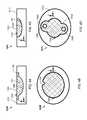
- FIG. 3A , and FIG. 3Billustrate an optical-element in mold 100 .
- FIG. 3Cillustrates an optical element 120 A with a mold 121 A removed.
- Optical-element in mold 100has optical-element 121 and mold 120 .
- the optical-elementis a simple plano-convex lens with a plano surface 102 A and a convex surface 102 B.
- Convex surface 102 Bcan be any surface shape including spherical and aspherical.
- Mold 121 Ahas curvature at a nanocomposite-mold interface 104 , causing nanocomposite-ink to conform to the mold curvature, resulting in optical-element 121 retaining the curvature of the mold interface upon removal.
- the plano surface in the moldmay be formed by 3D printing, optical inserts, or figuring.
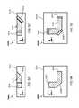
- FIG. 4A and FIG. 4Billustrate an optical-element in mold 100 B.
- Optical-element in mold 100 Bis the generally the same as that shown in FIG. 3A and FIG. 3B , except here, a flange 106 is included along the perimeter the optical element. Inclusion of the flange allows mounting of the optical-element in similar fashion to commercially available collimator and asphere optics. The flange thickness can be adjusted based on the standoff distance required in any apparatus in which it is installed.
- Flange 106also has an optional alignment feature 108 , here the alignment feature is an indent which allows the optic to be rotationally registered. Such alignment features are especially useful for optics which are not rotationally symmetric in optical power, shape, or other such properties.
- FIG. 4C and FIG. 4Dillustrate an optical-element in mold 100 C.
- Optical-element in mold 100 Cis the generally the same as that shown in FIG. 3A and FIG. 3B , except here further comprise a tab 109 A and 109 B, each have a thru-hole 108 A and 108 B respectively.
- the tabs and thru-holesallow mechanical fastening of the optical-element to another apparatus and act as alignment features.
- FIG. 5A and FIG. 5Billustrate an optical-element in mold 200 A.
- an optical element 220 Ais a macro-sized waveguide with a total-internal-reflection surface 202 A, 202 B, and 202 C formed by a mold 221 A.
- planar surfacesare shown, such surfaces could be shaped or otherwise have patterning as describe above.
- FIG. 5C and FIG. 5Dillustrate an optical-element in mold 200 B.
- Optical-element in mold 200 Bis similar to that shown in FIG. 5A and FIG.
- an optical insert 204 A, 204 B, and 204 Care integrated within a mold 221 B such that a surface 202 A, 202 B, and 202 C conform to the shape of the optical-inserts upon deposition and cure of the nanocomposite-ink.
- Another method of obtaining the desired surfacesis integration of optics. For instance, if all the optical surfaces are planar, then optical-windows can be inserted within the mold such that they form the optical surfaces with the nanocomposite-ink conforming to and bonding with the optical-windows.
- the methodcan be utilized to manufacture any optical-element, whether a single element or complex multi-element design.
- the methodis particularly useful for fast prototyping and volume manufacture of optical elements.
- optical-elementsin accordance with the present invention.
- one skilled in the artcould design an optical-element describing the nanocomposite-ink dispersion or GRIN material by using commercially available optical design software, such as ZEMAX available from the Zemax Corporation, of Belleview, Wash.
- optical design softwaresuch as ZEMAX available from the Zemax Corporation, of Belleview, Wash.
- the moldcan be designed in commercially available 3D computer aided design (CAD) software, such as Solidworks available from Dassault Systems Corporation, of Waltham, Mass.
- CADcomputer aided design
- the moldcan be printed on any commercially available 3D printer and the nanocomposite-ink can be deposited within and cured as described in detail above.
Landscapes
- Engineering & Computer Science (AREA)
- Manufacturing & Machinery (AREA)
- Mechanical Engineering (AREA)
- Chemical & Material Sciences (AREA)
- Materials Engineering (AREA)
- Health & Medical Sciences (AREA)
- Ophthalmology & Optometry (AREA)
- Physics & Mathematics (AREA)
- Optics & Photonics (AREA)
Abstract
Description
Claims (23)
Priority Applications (3)
| Application Number | Priority Date | Filing Date | Title |
|---|---|---|---|
| US14/554,399US9579829B2 (en) | 2014-06-02 | 2014-11-26 | Method for manufacturing an optical element |
| US14/618,965US9623609B2 (en) | 2014-06-02 | 2015-02-10 | Method of manufacturing multi-component functional article |
| PCT/US2015/062807WO2016086207A1 (en) | 2014-11-26 | 2015-11-25 | Method for manufacturing an optical element |
Applications Claiming Priority (2)
| Application Number | Priority Date | Filing Date | Title |
|---|---|---|---|
| US14/293,574US9442344B2 (en) | 2014-06-02 | 2014-06-02 | Nanocomposite high order nonlinear optical-element |
| US14/554,399US9579829B2 (en) | 2014-06-02 | 2014-11-26 | Method for manufacturing an optical element |
Related Parent Applications (1)
| Application Number | Title | Priority Date | Filing Date |
|---|---|---|---|
| US14/293,574Continuation-In-PartUS9442344B2 (en) | 2014-06-02 | 2014-06-02 | Nanocomposite high order nonlinear optical-element |
Related Child Applications (1)
| Application Number | Title | Priority Date | Filing Date |
|---|---|---|---|
| US14/480,515Continuation-In-PartUS9855737B2 (en) | 2014-06-02 | 2014-09-08 | Nanocomposite-ink factory |
Publications (2)
| Publication Number | Publication Date |
|---|---|
| US20150343673A1 US20150343673A1 (en) | 2015-12-03 |
| US9579829B2true US9579829B2 (en) | 2017-02-28 |
Family
ID=54700744
Family Applications (1)
| Application Number | Title | Priority Date | Filing Date |
|---|---|---|---|
| US14/554,399Active - Reinstated2034-08-14US9579829B2 (en) | 2014-06-02 | 2014-11-26 | Method for manufacturing an optical element |
Country Status (1)
| Country | Link |
|---|---|
| US (1) | US9579829B2 (en) |
Cited By (3)
| Publication number | Priority date | Publication date | Assignee | Title |
|---|---|---|---|---|
| US10375834B1 (en) | 2013-08-27 | 2019-08-06 | Flextronics Ap, Llc. | 3D printing with components embedded |
| US10449729B1 (en)* | 2015-12-03 | 2019-10-22 | Multek Technologies Ltd. | 3D printed fiber optics |
| US11167375B2 (en) | 2018-08-10 | 2021-11-09 | The Research Foundation For The State University Of New York | Additive manufacturing processes and additively manufactured products |
Families Citing this family (26)
| Publication number | Priority date | Publication date | Assignee | Title |
|---|---|---|---|---|
| US10364341B2 (en)* | 2015-04-08 | 2019-07-30 | Arevo, Inc. | Method and apparatus for 3d printing of nano-filler/polymer composites |
| JP2018529334A (en)* | 2015-09-04 | 2018-10-11 | ザ ジェネラル ホスピタル コーポレイション | 3D micro tissue bio printer |
| WO2017074397A1 (en)* | 2015-10-29 | 2017-05-04 | Hewlett-Packard Development Company, L.P. | Forming three-dimensional (3d) printed electronics |
| US20170217103A1 (en)* | 2016-01-29 | 2017-08-03 | Massachusetts Institute Of Technology | Techniques for color contoning in additive fabrication and related systems and methods |
| US11020905B2 (en) | 2016-03-24 | 2021-06-01 | Hewlett-Packard Development Company, L.P. | Accuracy improvement and surface finishing using fusing agent and detailing agent |
| CN108712957A (en) | 2016-04-28 | 2018-10-26 | 惠普发展公司,有限责任合伙企业 | three-dimensional printing component |
| US10288775B1 (en) | 2016-04-28 | 2019-05-14 | Rockwell Collins, Inc. | Multi-indexed printed optics designs |
| KR102142253B1 (en) | 2016-04-28 | 2020-08-07 | 휴렛-팩커드 디벨롭먼트 컴퍼니, 엘.피. | 3-dimensional printing |
| KR102179605B1 (en)* | 2016-04-28 | 2020-11-17 | 휴렛-팩커드 디벨롭먼트 컴퍼니, 엘.피. | Photoluminescent material set |
| US11241849B2 (en) | 2016-07-01 | 2022-02-08 | Signify Holding B.V. | 3D printed reflector and method for its manufacture |
| EP3266598B1 (en) | 2016-07-07 | 2024-03-06 | Essilor International | Process for marking an optical eyeglass |
| EP3273292A1 (en)* | 2016-07-19 | 2018-01-24 | Carl Zeiss Vision International GmbH | Spectacle glass and method for its production |
| EP3429829B1 (en)* | 2016-07-28 | 2022-02-09 | Hewlett-Packard Development Company, L.P. | Optically active material sets |
| US20180065307A1 (en) | 2016-09-06 | 2018-03-08 | Cc3D Llc | Systems and methods for controlling additive manufacturing |
| US20180065317A1 (en)* | 2016-09-06 | 2018-03-08 | Cc3D Llc | Additive manufacturing system having in-situ fiber splicing |
| EP3515708B1 (en) | 2016-09-22 | 2022-06-08 | Signify Holding B.V. | Method of using fdm to obtain specularly reflective surfaces. |
| RU2723684C2 (en)* | 2016-10-20 | 2020-06-17 | Общество с ограниченной ответственностью "Редиус 168" | Article forming method |
| CN108000864B (en)* | 2016-10-27 | 2020-09-29 | 三纬国际立体列印科技股份有限公司 | Color stereo printing mechanism |
| US10545806B2 (en) | 2017-06-05 | 2020-01-28 | International Business Machines Corporation | Proximity correction in three-dimensional manufacturing |
| EP3473418B1 (en)* | 2017-10-19 | 2023-12-06 | Essilor International | Method for manufacturing an ophthalmic lens |
| DE102018107585B3 (en)* | 2018-03-29 | 2019-03-28 | Universität Rostock | Device for producing 3D printed drug delivery systems with drug depots, and methods for manufacturing 3D printed drug delivery systems |
| WO2020068065A1 (en)* | 2018-09-26 | 2020-04-02 | Hewlett-Packard Development Company, L.P. | Three dimensional (3d) printed molds having breakaway features |
| WO2020131013A1 (en)* | 2018-12-17 | 2020-06-25 | Hewlett-Packard Development Company, L.P. | Breakable three dimensional (3d) printed molds |
| NL2022782B1 (en)* | 2019-03-21 | 2020-09-28 | Addoptics B V | Mould for casting an optical element and method for manufacturing |
| US20210251275A1 (en)* | 2019-10-06 | 2021-08-19 | Dorian Dena | Pulverized Leaf Cigarette Structure |
| US11926100B2 (en) | 2020-06-23 | 2024-03-12 | Continuous Composites Inc. | Systems and methods for controlling additive manufacturing |
Citations (20)
| Publication number | Priority date | Publication date | Assignee | Title |
|---|---|---|---|---|
| US5498444A (en) | 1994-02-28 | 1996-03-12 | Microfab Technologies, Inc. | Method for producing micro-optical components |
| US5800000A (en) | 1996-12-23 | 1998-09-01 | Shockley; James D. | Load adjusting device for a hoist |
| US5807906A (en) | 1995-02-27 | 1998-09-15 | Essilor International-Compagnie Generale D'optique | Process for obtaining a transparent article with a refractive index gradient |
| US6593415B2 (en) | 1994-04-18 | 2003-07-15 | Yasuhiro Koike | Graded-refractive-index optical plastic material and method for its production |
| US6656990B2 (en) | 2001-07-11 | 2003-12-02 | Corning Incorporated | Curable high refractive index compositions |
| US6805902B1 (en) | 2000-02-28 | 2004-10-19 | Microfab Technologies, Inc. | Precision micro-optical elements and the method of making precision micro-optical elements |
| US6836371B2 (en) | 2002-07-11 | 2004-12-28 | Ophthonix, Inc. | Optical elements and methods for making thereof |
| US7046439B2 (en) | 2003-05-22 | 2006-05-16 | Eastman Kodak Company | Optical element with nanoparticles |
| US7420743B2 (en) | 2002-07-11 | 2008-09-02 | Ophthonix, Inc. | Optical elements and methods for making thereof |
| US7473721B2 (en) | 2002-01-10 | 2009-01-06 | Tomoegawa Co., Ltd. | Nanocomposite material for the production of index of refraction gradient films |
| US7918555B2 (en) | 2006-09-25 | 2011-04-05 | Ophthonix, Inc. | Methods and lenses for correction of chromatic aberration |
| EP2412767A1 (en) | 2010-07-30 | 2012-02-01 | LUXeXcel Holding BV. | Printing ink, use of printing ink, article and method for manufacturing an article |
| EP2474404A1 (en) | 2011-01-06 | 2012-07-11 | LUXeXcel Holding BV. | Print head, upgrade kit for a conventional inkjet printer, printer and method for printing optical structures |
| EP2469309B1 (en) | 2009-02-14 | 2013-08-28 | LUXeXcel Holding BV. | Method for producing a lens-like light directing structure |
| EP2392473B1 (en) | 2010-06-07 | 2013-09-18 | LUXeXcel Holding BV. | Method for printing optical structures |
| US20150021528A1 (en) | 2013-07-17 | 2015-01-22 | State Of Oregon Acting By And Through The State Board Of Higher Education On Behalf Of University | Soluble functionalized nanoparticles for use in optical materials |
| US20150023643A1 (en) | 2013-07-17 | 2015-01-22 | State of Oregon acting by and through the State Board of Higher Education on behalf of the Univers | Gradient optical polymer nanocomposites |
| US20160023375A1 (en)* | 2013-05-17 | 2016-01-28 | Core Cast, Llc | Slip mixture for 3d printed molds and 3d printing ceramic material |
| US9308731B2 (en)* | 2014-09-08 | 2016-04-12 | Vadient Optics, Llc | Nanocomposite inkjet printer with integrated nanocomposite-ink factory |
| US20160231518A1 (en)* | 2013-10-14 | 2016-08-11 | Molex, Llc | Optical coupling and assembly |
- 2014
- 2014-11-26USUS14/554,399patent/US9579829B2/enactiveActive - Reinstated
Patent Citations (24)
| Publication number | Priority date | Publication date | Assignee | Title |
|---|---|---|---|---|
| US5498444A (en) | 1994-02-28 | 1996-03-12 | Microfab Technologies, Inc. | Method for producing micro-optical components |
| US5707684A (en) | 1994-02-28 | 1998-01-13 | Microfab Technologies, Inc. | Method for producing micro-optical components |
| US6593415B2 (en) | 1994-04-18 | 2003-07-15 | Yasuhiro Koike | Graded-refractive-index optical plastic material and method for its production |
| US5807906A (en) | 1995-02-27 | 1998-09-15 | Essilor International-Compagnie Generale D'optique | Process for obtaining a transparent article with a refractive index gradient |
| US5800000A (en) | 1996-12-23 | 1998-09-01 | Shockley; James D. | Load adjusting device for a hoist |
| US6805902B1 (en) | 2000-02-28 | 2004-10-19 | Microfab Technologies, Inc. | Precision micro-optical elements and the method of making precision micro-optical elements |
| US6656990B2 (en) | 2001-07-11 | 2003-12-02 | Corning Incorporated | Curable high refractive index compositions |
| US7473721B2 (en) | 2002-01-10 | 2009-01-06 | Tomoegawa Co., Ltd. | Nanocomposite material for the production of index of refraction gradient films |
| US6934088B2 (en) | 2002-07-11 | 2005-08-23 | Ophthonix, Inc. | Optical elements and methods for making thereof |
| US6976641B2 (en) | 2002-07-11 | 2005-12-20 | Ophthonix, Inc. | Optical elements and methods for making thereof |
| US7420743B2 (en) | 2002-07-11 | 2008-09-02 | Ophthonix, Inc. | Optical elements and methods for making thereof |
| US6836371B2 (en) | 2002-07-11 | 2004-12-28 | Ophthonix, Inc. | Optical elements and methods for making thereof |
| US7046439B2 (en) | 2003-05-22 | 2006-05-16 | Eastman Kodak Company | Optical element with nanoparticles |
| US7918555B2 (en) | 2006-09-25 | 2011-04-05 | Ophthonix, Inc. | Methods and lenses for correction of chromatic aberration |
| EP2469309B1 (en) | 2009-02-14 | 2013-08-28 | LUXeXcel Holding BV. | Method for producing a lens-like light directing structure |
| EP2392473B1 (en) | 2010-06-07 | 2013-09-18 | LUXeXcel Holding BV. | Method for printing optical structures |
| EP2412767A1 (en) | 2010-07-30 | 2012-02-01 | LUXeXcel Holding BV. | Printing ink, use of printing ink, article and method for manufacturing an article |
| EP2474404A1 (en) | 2011-01-06 | 2012-07-11 | LUXeXcel Holding BV. | Print head, upgrade kit for a conventional inkjet printer, printer and method for printing optical structures |
| US20130286073A1 (en)* | 2011-01-06 | 2013-10-31 | Luxexcel Holding Bv. | Print head, upgrade kit for a conventional inkjet printer, printer and method for printing optical structures |
| US20160023375A1 (en)* | 2013-05-17 | 2016-01-28 | Core Cast, Llc | Slip mixture for 3d printed molds and 3d printing ceramic material |
| US20150021528A1 (en) | 2013-07-17 | 2015-01-22 | State Of Oregon Acting By And Through The State Board Of Higher Education On Behalf Of University | Soluble functionalized nanoparticles for use in optical materials |
| US20150023643A1 (en) | 2013-07-17 | 2015-01-22 | State of Oregon acting by and through the State Board of Higher Education on behalf of the Univers | Gradient optical polymer nanocomposites |
| US20160231518A1 (en)* | 2013-10-14 | 2016-08-11 | Molex, Llc | Optical coupling and assembly |
| US9308731B2 (en)* | 2014-09-08 | 2016-04-12 | Vadient Optics, Llc | Nanocomposite inkjet printer with integrated nanocomposite-ink factory |
Non-Patent Citations (4)
| Title |
|---|
| Richard Chartoff, et al., Functionally Graded Polymer Matrix Nano-Composites by Solid Freeform Fabrciation: A Preliminary Report, Solid Freeform (SFF) symposium, [online], 2003, pp. 385-391, [retrieved on Apr. 23, 2015]. from the Internet: . |
| Richard Chartoff, et al., Functionally Graded Polymer Matrix Nano-Composites by Solid Freeform Fabrciation: A Preliminary Report, Solid Freeform (SFF) symposium, [online], 2003, pp. 385-391, [retrieved on Apr. 23, 2015]. from the Internet: <http://sffsymposium.engr.utexas.edu/Manuscripts/2003/2003-36-Chartoff.pdf>. |
| Richard Chartoff, et al., Polymer Matrix Nanocomposites by Inkjet Printing, Solid Freeform (SFF) symposium, [online], 2005, pp. 174-183, [retrieved on Apr. 23, 2015]. from the Internet: . |
| Richard Chartoff, et al., Polymer Matrix Nanocomposites by Inkjet Printing, Solid Freeform (SFF) symposium, [online], 2005, pp. 174-183, [retrieved on Apr. 23, 2015]. from the Internet: <http://sffsymposium.engr.utexas.edu/Manuscripts/2005/2005-16-Chartoff.pdf>. |
Cited By (5)
| Publication number | Priority date | Publication date | Assignee | Title |
|---|---|---|---|---|
| US10375834B1 (en) | 2013-08-27 | 2019-08-06 | Flextronics Ap, Llc. | 3D printing with components embedded |
| US10449729B1 (en)* | 2015-12-03 | 2019-10-22 | Multek Technologies Ltd. | 3D printed fiber optics |
| US11167375B2 (en) | 2018-08-10 | 2021-11-09 | The Research Foundation For The State University Of New York | Additive manufacturing processes and additively manufactured products |
| US11426818B2 (en) | 2018-08-10 | 2022-08-30 | The Research Foundation for the State University | Additive manufacturing processes and additively manufactured products |
| US12122120B2 (en) | 2018-08-10 | 2024-10-22 | The Research Foundation For The State University Of New York | Additive manufacturing processes and additively manufactured products |
Also Published As
| Publication number | Publication date |
|---|---|
| US20150343673A1 (en) | 2015-12-03 |
Similar Documents
| Publication | Publication Date | Title |
|---|---|---|
| US9579829B2 (en) | Method for manufacturing an optical element | |
| Gibson | Micro prototyping and fabrication in manufacturing | |
| Zolfaghari et al. | Additive manufacturing of precision optics at micro and nanoscale | |
| Walczak et al. | Inkjet 3D printing of microfluidic structures—on the selection of the printer towards printing your own microfluidic chips | |
| Tay et al. | Solid freeform fabrication of ceramics | |
| US10029422B2 (en) | Three-dimensional modelling and/or manufacturing apparatus, and related processes | |
| Dikshit et al. | Recent progress in 3D printing of fiber-reinforced composite and nanocomposites | |
| Bertsch et al. | Microstereolithography | |
| US11345879B2 (en) | Emulsion stereolithography and 3D printing of multimaterials and nanoscale material gradients | |
| US20170165931A1 (en) | Method for manufacturing a lens structure | |
| US20170348903A1 (en) | Fabrication of Three-Dimensional Materials Gradient Structures by In-Flight Curing of Aerosols | |
| Maruo | Stereolithography and two-photon polymerization | |
| Niesler et al. | Additive Manufacturing of Micro‐sized Parts: Trend of miniaturization is driver for 3D laser lithography | |
| Niesler et al. | 3D Printers for the Fabrication of Micro‐Optical Elements: Disruptive technology enables the way for unprecedented applications | |
| Fateri et al. | Introduction to additive manufacturing | |
| US10118338B2 (en) | Additive manufacturing with integrated microliter resin delivery | |
| Seok et al. | Micro/nanoscale 3-dimensional fabrication using multi-photons polymerization | |
| JP2016179584A (en) | Composition for manufacturing three-dimensional molded object and three-dimensional molded object | |
| WO2016086207A1 (en) | Method for manufacturing an optical element | |
| Mishra et al. | Additive manufacturing (3D printing): a review on the micro fabrication methods | |
| Jo et al. | Liquid bridge stereolithography: a proof of concept | |
| CN1325368C (en) | Method for rapid manufacturing three-dimensional complex micro structure | |
| Feng et al. | Development of a drop-on-demand micro dispensing system | |
| Hong | Additive manufacturing of freeform optics | |
| US11203170B2 (en) | Inkjet printed molded nanocomposite-ink optical-element |
Legal Events
| Date | Code | Title | Description |
|---|---|---|---|
| AS | Assignment | Owner name:VADIENT OPTICS, LLC., OREGON Free format text:ASSIGNMENT OF ASSIGNORS INTEREST;ASSIGNOR:WILLIAMS, GEORGE;REEL/FRAME:034875/0350 Effective date:20150129 | |
| STCF | Information on status: patent grant | Free format text:PATENTED CASE | |
| FEPP | Fee payment procedure | Free format text:MAINTENANCE FEE REMINDER MAILED (ORIGINAL EVENT CODE: REM.); ENTITY STATUS OF PATENT OWNER: SMALL ENTITY | |
| LAPS | Lapse for failure to pay maintenance fees | Free format text:PATENT EXPIRED FOR FAILURE TO PAY MAINTENANCE FEES (ORIGINAL EVENT CODE: EXP.); ENTITY STATUS OF PATENT OWNER: SMALL ENTITY | |
| STCH | Information on status: patent discontinuation | Free format text:PATENT EXPIRED DUE TO NONPAYMENT OF MAINTENANCE FEES UNDER 37 CFR 1.362 | |
| FP | Lapsed due to failure to pay maintenance fee | Effective date:20210228 | |
| FEPP | Fee payment procedure | Free format text:SURCHARGE, PETITION TO ACCEPT PYMT AFTER EXP, UNINTENTIONAL. (ORIGINAL EVENT CODE: M2558); ENTITY STATUS OF PATENT OWNER: SMALL ENTITY | |
| MAFP | Maintenance fee payment | Free format text:PAYMENT OF MAINTENANCE FEE, 4TH YR, SMALL ENTITY (ORIGINAL EVENT CODE: M2551); ENTITY STATUS OF PATENT OWNER: SMALL ENTITY Year of fee payment:4 | |
| REFU | Refund | Free format text:REFUND - SURCHARGE, PETITION TO ACCEPT PYMT AFTER EXP, UNINTENTIONAL (ORIGINAL EVENT CODE: R2558); ENTITY STATUS OF PATENT OWNER: SMALL ENTITY Free format text:REFUND - SURCHARGE, PETITION TO ACCEPT PYMT AFTER EXP, UNINTENTIONAL (ORIGINAL EVENT CODE: R2551); ENTITY STATUS OF PATENT OWNER: SMALL ENTITY | |
| PRDP | Patent reinstated due to the acceptance of a late maintenance fee | Effective date:20220201 | |
| FEPP | Fee payment procedure | Free format text:PETITION RELATED TO MAINTENANCE FEES FILED (ORIGINAL EVENT CODE: PMFP); ENTITY STATUS OF PATENT OWNER: SMALL ENTITY Free format text:PETITION RELATED TO MAINTENANCE FEES GRANTED (ORIGINAL EVENT CODE: PMFG); ENTITY STATUS OF PATENT OWNER: SMALL ENTITY Free format text:SURCHARGE, PETITION TO ACCEPT PYMT AFTER EXP, UNINTENTIONAL. (ORIGINAL EVENT CODE: M2558); ENTITY STATUS OF PATENT OWNER: SMALL ENTITY | |
| MAFP | Maintenance fee payment | Free format text:PAYMENT OF MAINTENANCE FEE, 4TH YR, SMALL ENTITY (ORIGINAL EVENT CODE: M2551); ENTITY STATUS OF PATENT OWNER: SMALL ENTITY Year of fee payment:4 | |
| STCF | Information on status: patent grant | Free format text:PATENTED CASE | |
| FEPP | Fee payment procedure | Free format text:PETITION RELATED TO MAINTENANCE FEES GRANTED (ORIGINAL EVENT CODE: PTGR); ENTITY STATUS OF PATENT OWNER: SMALL ENTITY | |
| MAFP | Maintenance fee payment | Free format text:PAYMENT OF MAINTENANCE FEE, 8TH YR, SMALL ENTITY (ORIGINAL EVENT CODE: M2552); ENTITY STATUS OF PATENT OWNER: SMALL ENTITY Year of fee payment:8 |