US9578237B2 - Array cameras incorporating optics with modulation transfer functions greater than sensor Nyquist frequency for capture of images used in super-resolution processing - Google Patents
Array cameras incorporating optics with modulation transfer functions greater than sensor Nyquist frequency for capture of images used in super-resolution processingDownload PDFInfo
- Publication number
- US9578237B2 US9578237B2US14/705,919US201514705919AUS9578237B2US 9578237 B2US9578237 B2US 9578237B2US 201514705919 AUS201514705919 AUS 201514705919AUS 9578237 B2US9578237 B2US 9578237B2
- Authority
- US
- United States
- Prior art keywords
- camera
- lens
- optics
- cameras
- array
- Prior art date
- Legal status (The legal status is an assumption and is not a legal conclusion. Google has not performed a legal analysis and makes no representation as to the accuracy of the status listed.)
- Expired - Fee Related
Links
Images


Classifications
- H—ELECTRICITY
- H04—ELECTRIC COMMUNICATION TECHNIQUE
- H04N—PICTORIAL COMMUNICATION, e.g. TELEVISION
- H04N23/00—Cameras or camera modules comprising electronic image sensors; Control thereof
- H04N23/95—Computational photography systems, e.g. light-field imaging systems
- H04N23/951—Computational photography systems, e.g. light-field imaging systems by using two or more images to influence resolution, frame rate or aspect ratio
- G—PHYSICS
- G02—OPTICS
- G02B—OPTICAL ELEMENTS, SYSTEMS OR APPARATUS
- G02B13/00—Optical objectives specially designed for the purposes specified below
- G02B13/001—Miniaturised objectives for electronic devices, e.g. portable telephones, webcams, PDAs, small digital cameras
- G02B13/0015—Miniaturised objectives for electronic devices, e.g. portable telephones, webcams, PDAs, small digital cameras characterised by the lens design
- G02B13/002—Miniaturised objectives for electronic devices, e.g. portable telephones, webcams, PDAs, small digital cameras characterised by the lens design having at least one aspherical surface
- G02B13/0035—Miniaturised objectives for electronic devices, e.g. portable telephones, webcams, PDAs, small digital cameras characterised by the lens design having at least one aspherical surface having three lenses
- H04N5/23232—
- G—PHYSICS
- G02—OPTICS
- G02B—OPTICAL ELEMENTS, SYSTEMS OR APPARATUS
- G02B13/00—Optical objectives specially designed for the purposes specified below
- G02B13/001—Miniaturised objectives for electronic devices, e.g. portable telephones, webcams, PDAs, small digital cameras
- G02B13/0015—Miniaturised objectives for electronic devices, e.g. portable telephones, webcams, PDAs, small digital cameras characterised by the lens design
- G02B13/002—Miniaturised objectives for electronic devices, e.g. portable telephones, webcams, PDAs, small digital cameras characterised by the lens design having at least one aspherical surface
- G02B13/004—Miniaturised objectives for electronic devices, e.g. portable telephones, webcams, PDAs, small digital cameras characterised by the lens design having at least one aspherical surface having four lenses
- G—PHYSICS
- G02—OPTICS
- G02B—OPTICAL ELEMENTS, SYSTEMS OR APPARATUS
- G02B13/00—Optical objectives specially designed for the purposes specified below
- G02B13/001—Miniaturised objectives for electronic devices, e.g. portable telephones, webcams, PDAs, small digital cameras
- G02B13/0015—Miniaturised objectives for electronic devices, e.g. portable telephones, webcams, PDAs, small digital cameras characterised by the lens design
- G02B13/002—Miniaturised objectives for electronic devices, e.g. portable telephones, webcams, PDAs, small digital cameras characterised by the lens design having at least one aspherical surface
- G02B13/0045—Miniaturised objectives for electronic devices, e.g. portable telephones, webcams, PDAs, small digital cameras characterised by the lens design having at least one aspherical surface having five or more lenses
- G—PHYSICS
- G02—OPTICS
- G02B—OPTICAL ELEMENTS, SYSTEMS OR APPARATUS
- G02B3/00—Simple or compound lenses
- G02B3/0006—Arrays
- G02B3/0037—Arrays characterized by the distribution or form of lenses
- G02B3/0062—Stacked lens arrays, i.e. refractive surfaces arranged in at least two planes, without structurally separate optical elements in-between
- G02B3/0068—Stacked lens arrays, i.e. refractive surfaces arranged in at least two planes, without structurally separate optical elements in-between arranged in a single integral body or plate, e.g. laminates or hybrid structures with other optical elements
- G06T7/0051—
- G—PHYSICS
- G06—COMPUTING OR CALCULATING; COUNTING
- G06T—IMAGE DATA PROCESSING OR GENERATION, IN GENERAL
- G06T7/00—Image analysis
- G06T7/50—Depth or shape recovery
- H04N13/0271—
- H—ELECTRICITY
- H04—ELECTRIC COMMUNICATION TECHNIQUE
- H04N—PICTORIAL COMMUNICATION, e.g. TELEVISION
- H04N13/00—Stereoscopic video systems; Multi-view video systems; Details thereof
- H04N13/20—Image signal generators
- H04N13/271—Image signal generators wherein the generated image signals comprise depth maps or disparity maps
- H—ELECTRICITY
- H04—ELECTRIC COMMUNICATION TECHNIQUE
- H04N—PICTORIAL COMMUNICATION, e.g. TELEVISION
- H04N23/00—Cameras or camera modules comprising electronic image sensors; Control thereof
- H04N23/45—Cameras or camera modules comprising electronic image sensors; Control thereof for generating image signals from two or more image sensors being of different type or operating in different modes, e.g. with a CMOS sensor for moving images in combination with a charge-coupled device [CCD] for still images
- H—ELECTRICITY
- H04—ELECTRIC COMMUNICATION TECHNIQUE
- H04N—PICTORIAL COMMUNICATION, e.g. TELEVISION
- H04N23/00—Cameras or camera modules comprising electronic image sensors; Control thereof
- H04N23/50—Constructional details
- H04N23/55—Optical parts specially adapted for electronic image sensors; Mounting thereof
- H—ELECTRICITY
- H04—ELECTRIC COMMUNICATION TECHNIQUE
- H04N—PICTORIAL COMMUNICATION, e.g. TELEVISION
- H04N23/00—Cameras or camera modules comprising electronic image sensors; Control thereof
- H04N23/60—Control of cameras or camera modules
- H—ELECTRICITY
- H04—ELECTRIC COMMUNICATION TECHNIQUE
- H04N—PICTORIAL COMMUNICATION, e.g. TELEVISION
- H04N23/00—Cameras or camera modules comprising electronic image sensors; Control thereof
- H04N23/60—Control of cameras or camera modules
- H04N23/698—Control of cameras or camera modules for achieving an enlarged field of view, e.g. panoramic image capture
- H04N5/2254—
- H04N5/2258—
- H04N5/23238—
- G—PHYSICS
- G02—OPTICS
- G02B—OPTICAL ELEMENTS, SYSTEMS OR APPARATUS
- G02B3/00—Simple or compound lenses
- G02B3/0006—Arrays
Definitions
- the present inventionis related to novel optical arrangements, designs and elements for use in an array camera, and more specifically to optical arrangements of varying configurations having modulation transfer function (MTF) characteristics capable of implementing super resolution for use with arrays of image sensors.
- MTFmodulation transfer function
- Image sensorsare used in cameras and other imaging devices to capture images.
- lightenters at one end of the imaging device and is directed to an image sensor by an optical element such as a lens.
- an optical elementsuch as a lens.
- one or more layers of optical elementsare placed before and after the aperture stop to focus light onto the image sensor.
- array camerashaving many imagers and lenses have been developed. In most cases, multiple copies of the optical elements must be formed laterally for use in array cameras.
- optical arrayscan be formed by molding or embossing from a master lens array, or fabricated by standard lithographic or other means.
- the standard polymer-on-glass WLO and monolithic lens WLO manufacturing techniqueshave so far not been adapted for the specific high performance requirements of array cameras.
- some technical limitations of conventional WLO-processesneed to be reduced, such as, for example, minimum substrate thickness requirements, inflexibility of where to place the aperture stop, accuracy, etc.
- the flexibility of such choices or processesneeds to be increased in order to meet the high demands by array cameras otherwise such WLO techniques cannot be used to manufacture array cameras. Accordingly, a need exists for fabrication processes capable of accurately forming these arrays and for optical arrangements that give an increased flexibility in manufacturing so that the image processing software of these new types of array-type cameras can take advantage to deliver superior image quality at the system level.
- optical transfer functionof an imaging system (camera, video system, microscope etc.) is considered the true measure of an imaging system's performance, i.e., the resolution (minimum feature size or maximum spatial frequency that can be imaged with sufficient contrast) or image sharpness (the contrast at a given spatial frequency) obtainable by an imaging system. While optical resolution, as commonly used with reference to camera systems, describes only the number of pixels in an image, and hence the potential to show fine detail, the transfer function describes the ability of adjacent pixels to change from black to white in response to patterns of varying spatial frequency, and hence the actual capability to show fine detail, whether with full or reduced contrast.
- the optical transfer Function (OTF)consists of two components: the modular transfer function (MTF), which is the magnitude of the OTF, and the phase transfer function (PTF), which is the phase component.
- MTFmodular transfer function
- PTFphase transfer function
- the MTFis the most relevant measurement of performance, and is generally taken as an objective measurement of the ability of an optical system to transfer various levels of detail from an object to an image.
- the MTFis measured in terms of contrast (degrees of gray), or of modulation, produced from a perfect source of that detail level (thus it is the ratio of contrast between the object and the image).
- the amount of detail in an imageis given by the resolution of the optical system, and is customarily specified in line pairs per millimeter (Ip/mm).
- a line pairis one cycle of a light bar and dark bar of equal width and has a contrast of unity.
- Contrastis defined as the ratio of the difference in maximum intensity (I max ) and minimum intensity (I min ) over the sum of I max and I min , where I max is the maximum intensity produced by an image (white) and I min is the minimum intensity (black).
- the MTFthen is the plot of contrast, measured in percent, against spatial frequency measured in Ip/rm. This graph is customarily normalized to a value of 1 at zero spatial frequency (all white or black).
- the current inventionis directed to optical arrangements for use with an array of cameras where the MTF of each of the optical arrangements or stacks for each camera of the array of cameras is at least as high as the desired MTF of the super resolution image synthesized from the combined images of the of cameras of the camera array.
- the camera arrayincludes a plurality of cameras, where each camera includes a separate optics, and a plurality of light sensing elements, and each camera is configured to independently capture an image of a scene;
- each camerahas a field of view that is shifted with respect to the field-of-views of the other cameras so that each shift includes a sub-pixel shifted view of the scene;
- the light sensing elementshave a pixel pitch defining a Nyquist frequency
- the optics of each camerahave a modular transfer function (MTF) such that the optics optically resolve, with sufficient contrast, spatial frequencies larger than the Nyquist frequency (Ny);
- the camera arrayis a monolithic integrated module comprising a single semiconductor substrate on which all of the sensor elements are formed, and optics including a plurality of lens elements, where each lens element forms part of the separate optics for one of the cameras;
- each of the camerasincludes one of a plurality of different types of filer
- the camera arrayincludes:
- each cameraincludes a separate optics, and a plurality of light sensing elements each having a pixel pitch defining a Nyquist frequency (Ny), and each camera is configured to independently capture a low resolution image of a scene;
- a processorconfigured to synthesize a higher resolution image from the plurality of lower resolution images, the high resolution image has a characteristic MTF;
- each camerahas a field of view that is shifted with respect to the field-of-views of the other cameras so that each shift includes a sub-pixel shifted view of the scene;
- each camerahas a modular transfer function (MTF) at least as large of the desired MTF of the high resolution image
- the camera arrayis a monolithic integrated module comprising a single semiconductor substrate on which all of the sensor elements are formed, and optics including a plurality of lens elements, where each lens element forms part of the separate optics for one of the cameras;
- each of the camerasincludes one of a plurality of different types of filer; and wherein cameras having the same type of filter are uniformly distributed about the geometric center of the camera array.
- the cut-off MTF of the opticsis at least 1.5 times the Ny, at least 2 times the Ny, or at least 3 times the Ny.
- the optics of each camerainclude a three-element monolithic lens optical arrangement including:
- the inventionis directed to a three-surface optical arrangement for an array camera.
- the optical arrangementincludes:
- the surfaces of the first elementare separated by a first substrate, and the surfaces of the second element are separated by a second substrate.
- the flat second proximal surfaceis formed by the second substrate.
- an aperture stopis disposed on the flat second proximal surface.
- at least one apertureis disposed on at least one of the first or second substrates.
- an aperture structureis disposed between said first and second lens elements, comprising at least one aperture substrate having at least one aperture disposed thereon.
- the first and second lens elements and the second lens element and the imagerare separated by spacers.
- a filteris disposed on at least one of the first or second substrates.
- at least two of the surfaces of the lens elementsare formed from materials having different Abbe-numbers.
- the convex surfacesare formed from crown-like materials, and the concave surfaces are formed from flint-like materials.
- an array of such arrangementsare described, where the array is designed to image a selected wavelength band, and where the profile of at least one of the lens surfaces within each optical arrangement is adapted to optimally image only a narrow-band portion of the selected wavelength band such that in combination the plurality of arrangements within the array image the entirety of the selected wavelength band.
- the inventionis directed to a five-surface optical arrangement for an array camera.
- the optical arrangementincludes:
- the surfaces of the first elementare separated by a first substrate, and the surfaces of the second element are separated by a second substrate.
- the third planar distal surfaceis in contact with one of either the image sensor or a cover glass disposed over the image sensor.
- an aperture stopis disposed on the first concave distal surface.
- an aperture stopis disposed on the first substrate adjacent to the first concave distal surface.
- at least one apertureis disposed within the first lens element.
- an aperture structureis disposed between at least two of said lens elements, the aperture structure comprising at least one aperture substrate having at least one aperture disposed thereon.
- the first and second lens elements, and the second and thirds lens elementsare separated by spacers.
- a filteris disposed within at least one of the first and second lens elements.
- at least two of the surfaces of the lens elementsare formed from materials having different Abbe-numbers.
- the convex surfacesare formed from crown-like materials, and the concave surfaces are formed from flint-like materials.
- an air-gapis positioned between the third lens element and the image sensor.
- at least one substrateis disposed between the surfaces of at least one of the lens elements.
- a substrateis disposed between the third lens element and the imager.
- at least one apertureis disposed on at least one substrate within the lens elements.
- at least one apertureis embedded within the first lens element.
- a plurality of the five-surface optical arrangementsis provided in an array.
- the arrayis designed to image a selected wavelength band, and wherein the profile of at least one of the lens surfaces within each optical arrangement is adapted to optimally image only a narrow-band portion of the selected wavelength such that in combination the plurality of arrangements within the array image the entirety of the selected wavelength band.
- the inventionis directed to a substrate embedded hybrid lens optical arrangement for an array camera.
- the optical arrangementincludes:
- the substrate embedded hybrid lens optical arrangementat least two axially aligned apertures are disposed on said substrate.
- the at least two axially aligned aperturesare one of either the same or different sizes.
- at least one coatingis disposed on said substrate in optical alignment with said at least one aperture.
- the at least one coatingis selected from the group consisting of a polarization filter, a color filter, an IRCF filter, and a NIR-pass filter.
- the substrateis formed from a material that acts as a filter selected from the group consisting of a polarization filter, a color filter, an IRCF filter, and a NIR-pass filter.
- the substratefurther comprises an adaptive optical element.
- at least two of the lens elementsare formed from materials having different Abbe-numbers.
- such an arrangementis part of a wafer stack comprising a plurality of the substrate embedded hybrid lens optical arrangements including:
- the arrangementis part of an array comprising a plurality of the substrate embedded hybrid lens optical arrangements, where the array is designed to image a selected wavelength band, and wherein the profile of at least one of the lens surfaces within each optical arrangement is adapted to optimally image only a narrow-band portion of the selected wavelength such that in combination the plurality of arrangements within the array image the entirety of the selected wavelength band.
- the inventionis directed to a monolithic lens optical arrangement for an array camera.
- the optical arrangementincludes:
- the monolithic optical arrangementincludes at least one filter disposed on said plano surface in optical alignment with said at least one aperture.
- the monolithic lensesare formed from materials having different Abbe-numbers.
- at least two lens elementsare formed.
- the monolithic lens optical arrangementis part of an array comprising a plurality of the monolithic optical arrangements, where the array is designed to image a selected wavelength band, and wherein the profile of at least one of the lens surfaces within each optical arrangement is adapted to optimally image only a narrow-band portion of the selected wavelength such that in combination the plurality of arrangements within the array image the entirety of the selected wavelength band.
- such an arrangementis part of a wafer stack comprising:
- the inventionis directed to a three-element monolithic lens optical arrangement for an array camera.
- the optical arrangementincludes:
- the three-element monolithic optical arrangementincludes first and second lens elements that are formed from low dispersion materials and the third lens element is formed from a high dispersion material.
- at least one filteris disposed on the first plano distal surface in optical alignment with the first lens element.
- the first lens elementfurther comprises a substrate disposed on the distal surface thereof.
- at least one apertureis disposed on the distal surface of said substrate.
- at least one filteris disposed on the distal surface of said substrate.
- the second lens elementfurther comprises a substrate disposed between the proximal and distal surfaces thereof.
- the three-element monolithic lens optical arrangementis part of an array comprising a plurality of the three-element monolithic optical arrangements, where the array is designed to image a selected wavelength band, and wherein the profile of at least one of the lens surfaces within each optical arrangement is adapted to optimally image only a narrow-band portion of the selected wavelength such that in combination the plurality of arrangements within the array image the entirety of the selected wavelength band.
- the inventionis directed to a plurality of optical arrangements for an array camera including:
- the inventionis directed to a plurality of optical arrangements for an array camera including:
- the structural featuresare selected from the group consisting of lateral and rotational alignment features, spacers and stand-offs.
- the inventionis directed to a method of compensation for systematic fabrication errors in an array having a plurality of optical channels comprising:
- the inventionis directed to an optical arrangement comprising a plurality of optical channels, each optical channel including at least one optical element, comprising at least two optical surfaces, wherein one of the optical surfaces of each of the plurality of optical channels is a channel specific surface having a wavefront deformation sufficient solely to adapt the optical channel to a selected waveband of light.
- the channel specific surfaceis selected from the group consisting of waveplates, kinoforms, and radial symmetric multilevel diffractive phase elements.
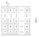
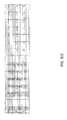
- FIG. 1is a plan view of a conventional camera array with a plurality of imagers.
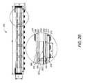
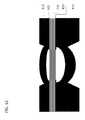
- FIG. 2Ais a perspective view of a camera module in accordance with embodiments of the invention.
- FIG. 2Bis a cross-sectional view of a conventional module in accordance with embodiments of the invention.
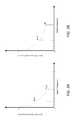
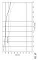
- FIG. 3Aillustrates a typical plot of the MTF of the optics for a legacy camera cutting-off below the corresponding image sensor's Ny spatial frequency.
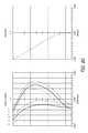
- FIG. 3Billustrates a plot of MTF of the optics for a camera array having bandlimited optical channels at the Nyquist frequency.
- FIG. 3Cillustrates a plot of MTF of the optics for a camera array in accordance with embodiments of the invention.
- FIG. 4Ais a schematic of a three surface two-lens optical arrangement according to one embodiment of the invention.
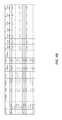
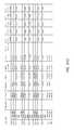
- FIG. 4Bis a table of exemplary lenses in accordance with one embodiment of the optical arrangement of FIG. 4A .
- FIG. 5 A 1is a schematic of a five surface three-lens optical arrangement according to one embodiment of the invention.
- FIG. 5 A 2is a table of exemplary lenses in accordance with one embodiment of the optical arrangement of FIG. 5 A 1 .
- FIGS. 5B to 5Hare data plots presenting characteristic performance indicators of the optical arrangement of FIG. 5 A 1 .
- FIG. 5 I 1is a schematic of a five surface three-lens optical arrangement according to one embodiment of the invention.
- FIG. 5 J 1is a schematic of a five surface three-lens optical arrangement according to one embodiment of the invention.
- FIG. 5 J 2is a table of exemplary lenses in accordance with one embodiment of the optical arrangement of FIG. 5 J 1 .
- FIG. 6Cis a schematic of a monolithic optical arrangement according to one embodiment of the invention.
- FIGS. 6 D 1 to 6 D 6are schematics of monolithic optical arrangements according to various embodiments of the invention.
- FIGS. 7B to 7Dare schematics of monolithic optical arrangements according to various embodiments of the invention.
- FIGS. 7E to 7Gare schematics of optical arrangements which incorporate monolithic lens elements according to the embodiments of the invention shown in FIGS. 7B to 7D .
- FIGS. 8A to 8Dare schematics of three element monolithic optical arrangements according to various embodiments of the invention.
- FIGS. 8E to 8Jare data graphs of characteristic performance indicators of the three-element monolithic optical arrangements according to one embodiment of the invention.
- FIGS. 9A and 9Bare schematics of conventional injection molded optical arrangement formed of two materials.
- FIG. 9Cis a schematic of an injection molded optical arrangement formed of two materials according to one embodiment of the invention.
- FIG. 9Dis a schematic of a conventional polymer on glass wafer level optical arrangement formed of two materials.
- FIG. 9Eis a schematic of a polymer on glass wafer level optical arrangement formed of two materials according to one embodiment of the invention.
- FIG. 10Ais a schematic of a conventional polymer on glass wafer level optical arrangement having an integrated aperture stop.
- FIG. 10Bis a schematic of a polymer on glass wafer level optical arrangement having an integrated aperture stop according to one embodiment of the invention.
- FIGS. 11A and 11Bare schematics of optical arrangements having preformed spacing and alignment elements according to one embodiment of the invention.
- FIG. 12is a flowchart of a process for manufacturing an optical arrangement according to one embodiment of the invention.
- each imager (camera) of such a camera arraymay be combined with separate optics (lens stacks) with different filters and operate with different operating parameters (e.g., exposure time).
- these distinct optical elementsmay be fabricated using any suitable technique, including, for example, injection molding, precision glass molding, polymer-on-glass wafer level optics (WLO), or monolithic-lens WLO technologies (polymer or glass).
- the various lens stacks of the individual cameras and camera arrayare implemented such that the MTF characteristics of the optics include contrast at a spatial frequency that is at least as large as the resolution of the high resolution images to be synthesized by the array camera from the low resolution images formed from the individual cameras, and significantly greater than the Nyquist frequency of the pixels in the focal plane.
- Array camerasincluding camera modules that can be utilized to capture image data from different viewpoints (i.e. light field images) are disclosed in U.S. patent application Ser. No. 12/935,504 entitled “Capturing and Processing of Images using Monolithic Camera Array with Heterogeneous Imagers” to Venkataraman et al.
- fusion and super-resolution processessuch as those described in U.S. patent application Ser. No. 12/967,807 entitled “Systems and Methods for Synthesizing High Resolution Images Using Super-Resolution Processes” to Lelescu et al., can be utilized to synthesize a higher resolution 2D image or a stereo pair of higher resolution 2D images from the lower resolution images in the light field captured by an array camera.
- Each two-dimensional (2D) image in a captured light fieldis from the viewpoint of one of the cameras in the array camera. Due to the different viewpoint of each of the cameras, parallax results in variations in the position of foreground objects within the images of the scene.
- Processessuch as those disclosed in U.S. Provisional Patent Application No. 61/691,666 entitled “Systems and Methods for Parallax Detection and Correction in Imaged Captured Using Array Cameras” to Venkataraman et al. can be utilized to provide an accurate account of the pixel disparity as a result of parallax between the different cameras in an array.
- the disclosure of U.S. Patent Application Ser. No. 61/691,666is hereby incorporated by reference in its entirety.
- Array camerascan use disparity between pixels in images within a light field to generate a depth map from a reference viewpoint.
- a depth mapindicates the distance of the surfaces of scene objects from the reference viewpoint and can be utilized to determine scene dependent geometric corrections to apply to the pixels from each of the images within a captured light field to eliminate disparity when performing fusion and/or super-resolution processing.
- the ultimate spatial resolution limit of a camerais inversely proportional to the pixel size or pitch of the imaging sensor of the camera and is defined as the Nyquist frequency limit.
- Rthe maximum resolution
- xthe pixel pitch
- Nyquist frequencythe pixel pitch determines the spatial sampling rate, and the corresponding Nyquist frequency (Ny), which is simply one half of the reciprocal of the center-to-center pixel spacing.
- the required MTF for the optics arrangementis usually specified at Ny/4, Ny/2, or Ny, as illustrated in the plot of FIG. 3A , i.e., to be at least optically limited by the pixel pitch.
- the challenge in implementing optics for array camerasresults from the requirements necessary to achieve the super-resolution processes described above.
- super resolutionshould be able to recover a higher resolution final output image than the intrinsic resolution in the input component images from the individual cameras.
- the spatial resolution of a lensmay be specified in terms of the modulation transfer function (MTF) curve over a range of spatial frequencies.
- MTFmodulation transfer function
- SFRspatial frequency response
- Performanceis measured in terms of contrast or modulation at a particular spatial frequency which is customarily specified in line pairs per millimeter.
- the imaging systemtypically passes the signal unattenuated, which implies a contrast of 100%.
- the signalis attenuated and the degree of attenuation in the output signal is expressed as a percentage with respect to that of the input signal, normalized to unity (or 100%) contrast at zero spatial frequency.
- the MTFis a measure of the ability of an optical system to transfer various levels of detail from object to image. Accordingly, embodiments of array cameras have more stringent MTF requirements than for legacy cameras, and in particular use optics having MTF characteristics that exceed the spatial resolution (Nyquist frequency) of the pixel pitch of the pixels on a focal plane.
- the lens MTFneeds to be as high as the desired high resolution output MTF from the super resolution processing. As illustrated in FIG. 3C , this requires that the cameras capture content above Ny such that the super-resolution process can then recover the higher resolution information.
- the MTF characteristics of the optics in camera arraysare implemented such that images formed include contrast at a spatial frequency that is at least as great as the resolution of the high resolution images synthesized by the array camera, and significantly greater than the Nyquist frequency of the pixel pitch of the pixels on the focal plane (e.g., in some embodiments from 1.5 to 3 times Ny).
- the specific MTF requirement of the optics of the camera arraymay be determined by the ratio of the resolution of the high resolution image and Nyquist resolution of the individual camera.
- optics lensare implemented having a contrast of at least 10%, in some embodiments at least 20%, and in other embodiments at least 30% at a spatial frequency given by the ratio of the number of line-pairs resolved in the final synthesized high resolution image, and the physical size of the low resolution camera image in the same dimension, where the physical size of the low resolution image is a function of the size and number of pixels in the individual camera along the relevant dimension.
- a sensor element or pixelrefers to an individual light-sensing element in a camera array.
- the sensor element or pixelincludes, among others, traditional CIS (CMOS Image Sensor), CCD (charge-coupled device), quantum dot films, high dynamic range pixel, multispectral pixel and various alternatives thereof.
- CMOS Image Sensorcomplementary metal-oxide-semiconductor
- CCDcharge-coupled device
- quantum dot filmshigh dynamic range pixel
- multispectral pixelmultispectral pixel and various alternatives thereof.
- the pixel pitch of these sensor elementsdefines the Nyquist frequency.
- An imagerrefers to a focal plane formed from a two dimensional array of pixels associate with a lens stack formed from a set of optical elements.
- the sensor elements or pixels of each imager or focal planehave similar physical properties and receive light through the same set of optical components or lens stack. Further, the sensor elements in the each imager/focal plane may be associated with the same color filter.
- An imager or camera arrayrefers to a collection of imagers/cameras designed to function as a unitary component.
- the imager or camera arraymay be fabricated on a single chip for mounting or installing in various devices.
- a lens stackrefers to an axial arrangement of several optical components/lens elements.
- An optical channelrefers to the combination of a lens stack and an imager or focal plane.
- a lens or optical arrayrefers to a lateral arrangement of individual lens elements stacks.
- An optics or lens stack arrayrefers to a lateral array of lens stacks, or an axial arrangement of multiple lens arrays.
- a camera array modulerefers to the combination of an optics array and an imager array, and can also be defined as an array of optical channels.
- Image characteristics of an imagerrefer to any characteristics or parameters of the imager associated with capturing of images.
- the imaging characteristicsmay include, among others, the size of the imager, the type of pixels included in the imager, the shape of the imager, filters associated with the imager, the exposure time of the imager, aperture size of the optics associated with the imager, the configuration of the optical element associated with the imager, gain of the imager, the resolution of the imager, and operational timing of the imager.
- the characteristics of the optics of a camerarefer to at least the field of view (FOV), F-number (F/#), resolution (MTF), effective focal length or magnification, color or waveband, distortion, and relative illumination.
- FIG. 1is a plan view of a generic array camera 100 , which includes a camera module ( 110 with an array of cameras orimagers 1 A through NM. As shown, a camera module of the type shown is fabricated to include a plurality or array of cameras 1 A through NM. In turn, each of the cameras 1 A through NM may include a plurality of focal planes and light sensing pixels (e.g., 0.32 Mega pixels).
- the imagers 1 A through NMare shown as arranged into a grid format, it should be understood that they may be arranged in any suitable configuration. For example, in other embodiments, the imagers may be arranged in a non-grid format, such as in a circular pattern, zigzagged pattern or scattered pattern.
- the array camerasmay be designed as a drop-in replacement for existing camera image sensors used in cell phones and other mobile devices.
- the camera arraymay be designed to be physically compatible with conventional camera modules of approximately the same resolution although the achieved resolution of the camera array may exceed conventional image sensors in many photographic situations.
- the array camera of the embodimentmay include an imager with fewer pixels to obtain equal or better quality images compared to conventional image sensors.
- the size of the pixels in the imagermay be reduced compared to pixels in conventional image sensors while achieving comparable results.
- the array camerareplaces a conventional image sensor of M megapixels.
- the array camerahas (N ⁇ N) individual imagers or cameras, each camera including pixels of M/N 2 .
- Each camera in the camera arraymay also have the same aspect ratio as the conventional image sensor being replaced.
- Camera modules in accordance with embodiments of the inventioncan be constructed from an imager array and an optic array. Camera modules in accordance with embodiments of the invention are illustrated in FIGS. 2A and 2B .
- the camera module 200includes an imager array 230 including an array of focal planes 240 along with a corresponding optic array 210 including an array of lens stacks 220 .
- each lens stack 220creates an optical channel that forms an image of the scene on an array of light sensitive pixels 242 within a corresponding focal plane 240 .
- the light sensitive pixels 242can be formed from quantum films.
- Each pairing of a lens stack 220 and focal plane 240forms a single camera 104 within the camera module.
- Each pixel within a focal plane 240 of a camera 104generates image data that can be sent from the camera 104 to the processor 108 .
- the lens stack within each optical channelis configured so that pixels of each focal plane 240 sample the same object space or region within the scene.
- the lens stacksare configured so that the pixels that sample the same object space do so with sub-pixel offsets to provide sampling diversity that can be utilized to recover increased resolution through the use of super-resolution processes.
- the camera modulemay be fabricated on a single chip for mounting or installing in various devices.
- an array cameragenerates image data from multiple focal planes and uses a processor to synthesize one or more images of a scene.
- the image data captured by a single focal plane in the sensor arraycan constitute a low resolution image (the term low resolution here is used only to contrast with higher resolution images), which the processor can use in combination with other low resolution image data captured by the camera module to construct a higher resolution image through Super Resolution processing, as previously described.
- super resolutionis performed then multiple copies of an aliased signal are present, such as in multiple images from the focal planes 240 , and the information inherently present in the aliasing may be used to reconstruct the higher resolution signal.
- the aliasing patterns from the different focal planes 240will have slight differences due to the sampling diversity of the focal planes. These slight differences result from the slightly different viewing directions of the cameras used to capture the low resolution images that are either intentionally introduced or result from positional manufacturing tolerances of the individual focal planes.
- the MTFs of the lens stacks 220need to be at least as high as the desired high resolution output MTF to provide sufficient contrast.
- optics in the lens stackare implemented that have an MTF at least as high as the desired MTF of the super resolution image, i.e., an MTF at which the individual optic channels of the camera array are capable of resolving spatial frequencies above the Nyquist frequency of the pixels on the focal plane.
- the opticshave an MTF at which they are capable of resolving spatial frequencies at least 1.5, 2 and/or 3 times the Nyquist frequency of the pixels to allow the super-resolution process to recover higher resolution information unavailable from the individual low resolution images captured at the individual cameras.
- Imager arrays in accordance with embodiments of the inventioncan be constructed from an array of focal planes formed of arrays of light sensitive pixels.
- the imager array 230is composed of multiple focal planes 240 , each of which have a corresponding lens stack 220 that directs light from the scene through optical channel and onto a plurality of light sensing elements (the pixel pitch of which define Ny) formed on the focal plane 240 .
- the light sensing elementsare formed on a CMOS device using photodiodes formed in the silicon where the depleted areas used for photon to electron conversion are disposed at specific depths within the bulk of the silicon.
- a focal plane of an array of light sensitive pixels formed from a quantum film sensormay be implemented.
- the formation, composition, performance and function of various quantum films, and their use in optical detection in association with semiconductor integrated circuitsare described in U.S. Patent Publication US/2009/0152664, entitled “Materials, Systems and Methods for Optoelectronic Devices”, published Jun. 18, 2009, the disclosure of which is incorporated by reference herein in its entirety.
- Imager arrays of this designmay include two or more types of heterogeneous imagers, each imager or camera including two or more sensor elements or pixels. Each one of the imagers may have different imaging characteristics. Alternatively, there may be two or more different types of imagers where the same type of imagers shares the same imaging characteristics. For example, each imager 1 A through NM in FIG. 1 may be associated with its own filter and/or optical element (e.g., lens). Specifically, each of the imagers 1 A through NM or a group of imagers may be associated with spectral color filters to receive certain wavelengths of light.
- each imager 1 A through NM in FIG. 1may be associated with its own filter and/or optical element (e.g., lens).
- each of the imagers 1 A through NM or a group of imagersmay be associated with spectral color filters to receive certain wavelengths of light.
- Example filtersinclude a traditional filter used in the Bayer pattern (R, G, B), an IR-cut filter, a near-IR filter, a polarizing filter, and a custom filter to suit the needs of hyper-spectral imaging.
- some imagersmay have no filter to allow reception of both the entire visible spectra and near-IR, which increases the imager's signal-to-noise ratio.
- the number of distinct filtersmay be as large as the number of cameras in the camera array.
- Embodiments where filter groups are formedis further discussed in U.S. Provisional Patent Application No. 61/641,165 entitled “Camera Modules Patterned with pi Filter Groups” filed May 1, 2012, the disclosure of which is incorporated by reference herein in its entirety.
- color filters in many embodiments of the inventionare included in the lens stack of the camera.
- a green color cameracan include a lens stack with a green light filter that allows green light to pass through the optical channel.
- the pixels in each focal planeare the same and the light information captured by the pixels is differentiated by the color filters in the corresponding lens stack for each filter.
- imager arraysmay include other related circuitry.
- the other circuitrymay include, among others, circuitry to control imaging parameters and sensors to sense physical parameters.
- the control circuitrymay control imaging parameters such as exposure times, gain, and black level offset.
- the sensormay include dark pixels to estimate dark current at the operating temperature. The dark current may be measured for on-the-fly compensation for any thermal creep that the substrate may suffer from.
- each lens stack 220may be specified in terms of its MTF curve over a range of spatial frequencies.
- MTFis a Spatial Frequency Response (SFR) of the output signal contrast with the input spatial frequency, it is possible to determine the frequencies that can be optically resolved with sufficient frequency by the individual optical elements and lens stacks.
- SFRSpatial Frequency Response
- any lens systemwill demonstrate a number of MTF curves depending on the operating conditions of the camera (such as aperture size) and the spatial frequency being resolved.
- the MTFmight also be impacted by the type of scene being imaged (for example, there is often a spread in the MTF curve between a lenses ability to resolve meridional and sagittal lines).
- a lens systemmay demonstrate various levels of spatial resolution as you proceed from the center of image outward.
- opticsare selected such that the individual cameras of the camera array are able to spatially resolve at frequencies above the Nyquist frequency of the pixels across all imaging conditions and locations on the lens to allow the super-resolution process to recover higher resolution information under all conditions and camera settings.
- lens stacks and optical elementsare contemplated that demonstrate an MTF sufficiently high to allow for the camera to spatially resolve at frequencies above the Nyquist frequency of the pixels across only some imaging conditions and camera settings.
- MTFsufficiently high to allow for the camera to spatially resolve at frequencies above the Nyquist frequency of the pixels across only some imaging conditions and camera settings.
- FIG. 2Aillustrates a perspective view of one array camera assembly 200 that incorporates an optics array 210 with an imager array 230 .
- the optics array 210generally includes a plurality of lens stacks 220 (which furthermore may consist of several axially aligned lens elements), each lens stack 220 covering (in the shown example) one of twenty-five imagers 240 in the imager array 230 .
- FIG. 2Billustrates a sectional view of a camera array assembly 250 .
- the camera assembly 250would comprise an optics array including a top lens wafer 262 and a bottom lens wafer 268 , and an imager array including a substrate 278 with multiple sensors and associated light sensing elements formed thereon. Spacers 258 , 264 and 270 are also included to provide proper positioning to the various elements.
- the camera array assembly 250is also packaged within an encapsulation 254 .
- an optional top spacer 258may be placed between the encapsulation 254 and the top lens wafer 262 of the imager array; however, it is not essential to the construction of the camera assembly 250 .
- lens elements 288are formed on the top lens wafer 262 . Although these lens elements 288 are shown as being identical in FIG. 2B , it should be understood that within the same camera array different types, sizes, and shapes of elements may be used. Another set of lens elements 286 is formed on the bottom lens wafer 268 . The combination of the lens elements on the top lens wafer and bottom lens wafer form the lens stacks 220 shown in FIG. 2A .
- through-silicon vias 274may also be provided to paths for transmitting signal from the imagers.
- the top lens wafer 262may be partially coated with light blocking materials 284 (e.g., chromium, oxidized (“black”) chromium, opaque photoresist) to block of light.
- light blocking materials 284e.g., chromium, oxidized (“black”) chromium, opaque photoresist
- the portions of the top lens wafer 262 of the optics array not coated with the blocking materials 284serve as apertures through which light passes to the bottom lens wafer 268 and the imager array. Although only a single aperture is shown in the embodiment provided in FIG.
- additional aperturesmay be formed from opaque layers disposed on any and all of the substrate faces in the camera assembly to improve stray light performance and reduced optical crosstalk.
- filters 282are formed on the bottom lens wafer 268 of the optics array.
- Light blocking materials 280may also be coated on the bottom lens wafer 268 of the optics array to function as an optical isolator.
- a light blocking material 280may also be coated on the substrate 278 of the imager array to protect the sensor electronics from incident radiation.
- Spacers 283can also be placed between the bottom lens wafer 268 of the optics array and the substrate 278 of the imager array, and between the lens wafers 262 and 268 of the optics array. In such array cameras, each layer of spacers may be implemented using a single plate.
- many such camera arraysalso include spacers between each optical channel located on top of the top lens wafer 262 of the optics array that are similar to, or implemented in single layer with, the spacer 258 shown at the edge of the lens stack array.
- the spacerscan be constructed from and/or coated in light blocking materials to isolate the optical channels formed by the wafer level optics.
- Suitable light blocking materialsmay include any opaque material, such as, for example, a metal material like Ti and Cr, or an oxide of these materials like black chromium (chrome and chrome oxide), or dark silicon, or a black particle filled photoresist like a black matrix polymer (PSK2000 from Brewer Science).
- many embodimentsare directed to optic arrangements capable of MTF characteristics such that images formed on a focal plane include contrast at a spatial frequency that is at least greater than the resolution of high resolution images synthesized by the array camera during super resolution, and significantly greater than the Nyquist frequency of the pixel pitch of the pixels on the focal plane, and in some cases as much as 1.5 to 3 times the Nyquist frequency.
- Embodiment 1Three-Surface WLO Design
- WLOwafer level optics
- Traditional wafer level opticsis a technology where polymer lenses are molded on glass wafers, potentially on both sides, stacked with further such lens wafers by spacer wafers, and diced into lens modules (this is called “polymer on glass WLO”) followed by packaging of the optics directly with the imager into a monolithic integrated module.
- the WLO proceduremay involve, among other procedures, using a wafer level mold to create the polymer lens elements on a glass substrate. Usually this involves incorporating apertures, and in particular the aperture stop by providing openings centered with the later lens channels in an otherwise opaque layer onto the substrate before lens molding.
- a three-surface optical arrangement suitable for the fabrication by wafer level optics technology, and, in particular, to be used for the optics (as one of the multiple channels) of an array camerais described in reference to FIG. 4A .
- a standard two-element lensas shown in FIGS. 2 and 3 , there are typically four lens surfaces (front and back for the top and the bottom lenses).
- the third surfacein this total-track-length-relaxed but MTF-performance optimized design, the third surface (first side of second element) has very low refractive power. As a result, it is possible to omit it from the design entirely.
- each lens elementmay optionally be associated with a corresponding supporting substrate 404 and 406 , made from example of glass, upon which the polymer lens surfaces are formed.
- spacer elements(not shown) that can serve to mechanically connect the lens elements to each other and/or to the image sensor may also be included in the construction.
- the lens surfacesare made from a (UV- or thermally curable) polymer.
- the first lens element 400there is a convex surface 408 of a first diameter on the first side of the first element and a concave surface 410 of a second diameter on the second side of the first element.
- the diameter of the first sideis larger than the diameter of the second side of the first lens element.
- the second element 402there is a shallow or flat surface 412 on the first side of the second element, and a convex surface 414 on the second side of the second element.
- the diameter of the first side of the second elementis smaller than the diameter of the second surface of the second element, and that the diameter of the second side of the second element is intermediate between the diameters of the first and second sides of the first element.
- the system aperture or stop(not shown) is preferably disposed on the first side of the second element.
- a (thin) first spacing structure(not shown) is placed in between the two lens elements, which can be either incorporated into the respective lens surfaces (“stand-offs”), or can be an additional element.
- a (thick) second spacing structureconnecting the second side of the second lens element with the cover glass or package 416 of the image sensor 417 may also be provided. Both spacing structures are preferably opaque, or have opaque surfaces, at least at the inner side-walls, and provide partial optical isolation between adjacent optical channels.
- FIG. 4Bprovides a lens table for an exemplary embodiment of the three-surface optical arrangement in accordance with the current invention.
- the optical arrangementis designed in such a way that very high contrast at the image sensor's Nyquist spatial frequency is achieved, which at the same time (for gradual fall-off of contrast with increasing spatial frequency) provides sufficient contrast at 1.5 ⁇ or 2 ⁇ the sensor's Nyquist frequency to allow the super-resolution image information recovery to work effectively.
- the optical arrangementis optimized for allowing a small lateral distance between adjacent optical channels in order to economically exploit the die real-estate area, consequently the lens diameters should be small, as should the wall-thickness of the (opaque) spacer structures.
- optical channels within one array dedicated to imaging different “colors”may differ with regard to the particular surface profile of at least one lens surface.
- the differences in the surface profiles of those lenses in one arraycan be minor, but are very effective in keeping the back focal length (“BFL”) color-independent, and consequently allowing (almost) equally sharp images for the different colors without the costly need for wide-spectral-band achromatization.
- BFLback focal length
- a high-resolution polychromatic imagecan be achieved.
- the last surface in the lens stackhere—second surface of second element
- the above design approachesresult in a (partial—as far it can be the case for the given non-symmetry between object- and image space) symmetry of the lens system around the aperture stop, which helps to reduce certain types of aberrations, including, distortion, coma and lateral color.
- a five-surface optical arrangement suitable for the fabrication by wafer level optics technology, and, in particular, to be used for the optics (as one of the multiple channels) of an array camerais described in reference to FIGS. 5A to 5J . More specifically, this embodiment is directed to a five-surface high-resolution wafer level lens/objective having a field-flattening element close to the image plane.
- this embodimentis directed to a five-surface high-resolution wafer level lens/objective having a field-flattening element close to the image plane.
- these optical arrangementsare non-ideal for use in high resolution array cameras.
- the large number of degrees of freedom in the five-surface designallows for achromatization for the full visible spectral band (or other band of interest), so that channel-specific lens profiles are not necessarily required.
- the back focal lengthmay be kept constant over the spectral band of interest, the effective focal length and with it the magnification may vary.
- the five-surface optical arrangementis identified by first 500 , second 502 , and third 504 lens elements arranged sequentially along a single optical path 505 .
- each lens elementmay optionally be associated with a corresponding supporting substrate 506 , 508 & 510 , made from example of glass, upon which the polymer lens surfaces are formed.
- spacer elements(not shown) that can serve to mechanically connects the lens elements to each other and/or to the image sensor may also be included in the construction.
- the lens surfacesi.e., the volume between the surface of the lens and the underlying substrate, are made from a (UV- or thermally curable) polymer.
- the first lens element 500has a convex surface 512 having a first diameter, and a concave surface 514 having a second diameter.
- the diameter of the convex surfaceis greater than the diameter of the concave surface on this lens element.
- the second lens element 502has a concave surface 516 on the first side of the second lens element, and a convex surface 518 on the second side of the second element.
- the convex surface thereofis of a larger diameter when compared to the concave surface thereof.
- the third lens element 504has a concave surface 520 on the first side of the third lens element, and a second planar side 522 that is adjoined to the substrate that serves as the image sensor cover 510 .
- the diameter of the concave surface of the third lens elementis larger than the diameters of any of the surfaces of the first and second lens elements.
- a first spacing structure(not shown) is disposed in between the first 500 and the second 502 lens elements.
- a second spacing structure(not shown) is disposed in between the second 502 and the third 504 lens elements.
- Either of these spacersmay be either incorporated (also split) into the respective lens surfaces (“stand-offs” in which the lenses then can be glued directly together), or can be an additional element.
- both of these spacing structuresare preferably opaque (or have opaque surfaces, at least at the (inner) side-walls), and provide (partial) optical isolation between adjacent optical channels.
- the third lens element 504is disposed comparatively close to the image surface 524 , and the second side of the third lens element is preferably connected with the image sensor or image sensor cover glass by a transparent areal bond or a local bond (e.g. UV- and/or thermally curing adhesive), or even a ( ⁇ n opaque) spacing structure with transparent openings as described above.
- a transparent areal bond or a local bonde.g. UV- and/or thermally curing adhesive
- FIG. 5 A 1demonstrates a five-surface optical arrangement disposed on a large-sag field flattener on a regular-thickness image sensor cover glass.
- the field flattener 504or its substrate, or the sensor cover glass, respectively
- the image sensor 524In front of the field flattener is the actual focusing objective comprised of first 500 and second 502 lens elements, ideally containing two concave surfaces close to the system aperture more or less symmetrically surrounded by two convex surfaces.
- An exemplary lens table associated with this designis provided in FIG. 5 A 2 .
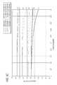
- FIGS. 5B-Hpresent some characteristic performance indicators of the five-surface optical arrangement shown in FIG. 5 A 1 .
- FIG. 5Bprovides a data graph of the Strehl ratio showing that the lens is diffraction limited over the full field height (@ F/2.4 and diagonal full FOV of 56°).
- FIG. 5Cprovides a data graph showing that in a comparison of MTF vs. field there is virtually no loss of performance with increasing field height.
- FIG. 5Dprovides a data graph of the polychromatic diffraction encircled energy, and demonstrates that most of the focused light energy is within the Airy disk.
- FIG. 5Eprovides a spot diagram demonstrating that the lens almost appears to be isoplanatic where there is little change of spot size and shape with field height.
- FIG. 5Bprovides a data graph of the Strehl ratio showing that the lens is diffraction limited over the full field height (@ F/2.4 and diagonal full FOV of 56°).
- FIG. 5Cprovides a data graph showing that in
- FIG. 5Fprovides a data graph of MTF vs. spatial frequency, and shows that for small and intermediate field heights there is still 15-20% contrast even at 500 LP/mm.
- FIG. 5Gprovides data graphs showing that the lens design demonstrates acceptable and monotonous distortion.
- FIG. 5Hprovides a relative illumination plot, demonstrating that the optical arrangement shows the usual vignetting behavior.
- FIGS. 5 I 1 and J 1provide diagrams of two such embodiments, which will be described below.
- the embodiment shown in FIG. 5 I 1is a five-surface optical arrangement that allows for an air gap 526 between the sensor cover glass 510 (on which the field flattener 528 is positioned) and the image sensor 524 . This is usually required when fill factor enhancing plenses are applied on top of the image sensor 524 . As a result of the presence of the air gap, the chief ray angle needs to be reduced over the embodiment shown in FIG. 5 A 1 . Although there are no constraints made on lens vertex heights and minimum glass thicknesses, lens TTL increases and image performance reduces due to the requirement of a reduced maximum CRA. However, ray calculations indicate that even in this embodiment the CRA of the inventive optical arrangement meets regular sensor specifications (in the order of magnitude of 27-28° in air). An exemplary lens table associated with this design is provided in FIG. 512 .
- FIG. 5 J 1provides a schematic of an embodiment of a five-surface optical arrangement optimized for best possible manufacturability.
- the lens sagsare decreased, and lens material planar base layers 532 , 534 , 536 , 538 and 542 having suitable thicknesses are provided.
- each lens elementmay optionally be associated with a corresponding supporting substrate 533 & 533 ′, 537 & 543 made from example of glass, upon which the polymer lens surfaces and base layers may be formed.
- spacer elements(not shown) that can serve to mechanically connect the lens elements to each other and/or to the image sensor may also be included in the construction.
- the system aperture 540is sandwiched (or “embedded”) between two glass substrates 533 and 533 ′ in order to decrease the necessary polymer thickness of the adjacent lens surfaces.
- a glass substrate 543is provided between the field flattener lens surface 544 and the imager package, including the image sensor glass cover 545 and the image sensor 546 (with air gap 548 ).
- the thickness between the glass substrate 543 and the image sensor cover glass 545may be shared by any reasonable ratio (which allows sufficient thickness for both).
- Cover glass as needed for the imagermay also be provided. All of these elements may then be immersed and bonded together by a suitable adhesive during manufacture.
- the CRAmeets regular sensor specifications (in the order of magnitude of 27-28° in air).
- An exemplary lens table associated with this designis provided in FIG. 5 J 2 .
- the optical arrangementis designed in such a way that very high contrast at the used image sensor's Nyquist spatial frequency is achieved, which at the same time (for gradual fall-off of contrast with increasing spatial frequency) provides sufficient contrast at 1.5 ⁇ or 2 ⁇ the sensor's Nyquist frequency to allow the super-resolution image information recovery to work effectively.
- the optical arrangementis optimized for allowing a small lateral distance between adjacent optical channels in order to economically exploit the die real-estate area, consequently the lens diameters and the wall-thickness of (opaque) spacer structures may be reduced.
- the field flattening structureitself this is sometimes difficult to achieve.
- optical channels within one array dedicated to imaging different “colors”may differ in the particular surface profile of at least one lens surface.
- the differences in the surface profiles of those lenses in one arraycan be minor, but are very effective in order to keep the back focal length (“BFL”) color-independent, and consequently allow (almost) equally sharp images for the different colors without the costly need for wide-spectral-band achromatization. Moreover, after computational color-fusion a high-resolution polychromatic image can still be achieved.
- the first surface of the first lens elementwould be specifically optimized for the narrow spectral band of the respective color channel.
- the separate color channelsonly need to be optimized for their respective spectral bands. This results in overall higher polychromatic resolution, while minimizing the need for achromatization correction within the individual channels. This in turn leads to the ability to implement simpler overall aberration balancing or correction process, and therefore have simpler lenses and lens manufacturing processes, and/or better MTF, and/or lower F/#.
- the MTF characteristics of the five-surface optical arrangementallow for contrast at spatial frequencies that are at east as great as the resolution of the high resolution images synthesized by the array camera, and significantly greater than the Nyquist frequency of the pixel pitch of the pixels on the focal plane, which in some embodiments may be 1.5, 2 or 3 times the Nyquist frequency.
- Embodiment 3Monolithic Lens Design with Embedded Substrate
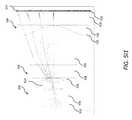
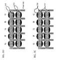
- FIG. 6Ashows the current state of the art of monolithic lens systems. More or less the same conceptual approach is taken as in creating injection-molded lenses and their packaging.
- many lensesare fabricated on a wafer scale. These replicated lenses 600 are stacked with other previously replicated lens wafers of different topology, the sandwich is diced, and the lens cubes are packaged into an opaque housing 602 with the image sensor 604 , which contains the aperture stop 606 at the front as shown in FIG. 6A .
- itmakes it difficult to accurately replicate and align the lenses with respect to each other, particularly as it is difficult to determine precisely the placement of the aperture stop.
- the aperture stop between the two lens elementsnot in front of the first lens element as shown in FIG. 6A .
- the only method for forming apertures of this type on monolithic lensesis to use a highly imprecise screen-printing method in which apertures 608 in opaque resins are printed onto the flat portions of the lens interfaces. The lateral accuracy of those apertures is unsuitable for their use as a system stop, which must be precisely aligned with the lenses.
- monolithic lens WLOis potentially an attractive means to manufacture cheap miniaturized optics for array cameras
- the current monolithic systemsare directly adapted from the methods used to form lenses by injection molding.
- many of the techniques used in conventional polymer-on-glass WLO to ensure proper alignmentare not applied, leading to alignment accuracy problems as well as to a limited lens design space.
- the current embodimentis directed to a novel method of forming monolithic lenses that combines the monolithic WLO lenses with substrates that hold apertures and additional structures in precise alignment, thereby reducing the limitations of conventional monolithic lens WLO.
- FIG. 6CAn exemplary embodiment of the method of monolithic lenses formed in accordance with the invention is shown in FIG. 6C .
- monolithic lenses 612 & 614fabricated by an independent replication process, are stacked with a substrate or sheet 616 that holds apertures 618 & 620 .
- the monolithic lensesmay be formed of glass or polymer.
- the aperturescan be formed on the substrate with lithographic precision, it is possible to align the elements with sufficient lateral precision to function as the aperture stop.
- FIG. 6CAn exemplary embodiment of the method of monolithic lenses formed in accordance with the invention is shown in FIG. 6C .
- monolithic lenses 612 & 614fabricated by an independent replication process, are stacked with a substrate or sheet 616 that holds apertures 618 & 620 .
- the aperturescan be formed on the substrate with lithographic precision, it is possible to align the elements with sufficient lateral precision to function as the aperture stop.
- the accuracy of the alignment in such a systemis increased by cooperative alignment marks, which are disposed in the opaque layer(s) where the transparent openings for the apertures are structured, to provide a guide for the precision alignment of the lenses and apertures.
- alignment markswould be formed in relation to each wafer surface.
- Each of the alignment markswould be cooperative with an alignment mark on an adjacent wafer surface such that when cooperatively aligned the alignment marks would aide in the lateral and rotational alignment of the lens surfaces with the corresponding apertures.
- Using these alignment marksresults in a very high lateral alignment accuracy (on the order of a few ⁇ m) compared to having the aperture stop in the external housing, which results in an accuracy of several 10-20 ⁇ m.
- the current method of providing a substrate embedded into monolithic lensesprovides a base onto which any number of different structures, coatings, kinds of substrates or sheets can be applied in order to achieve a desired optical functionality. A number of these possibilities are shown in FIG.
- 6Dthese include where there are two apertures on the front and back of the substrate that are the same size ( 6 D 1 ) or different sizes ( 6 D 2 ); where an additional IRCF coating, such as a homogenous IR cut-off filter made by a dielectric interference coating, is applied on either one or both sides of the substrate ( 6 D 3 ); where an additional color filter array material coating is applied to the substrate ( 6 D 4 ); where the sheet or substrate contains an adaptive refractive optical element allowing for the adjustment of the optical power of the element by changing an applied voltage, which can allow for the focusing of the whole lens stack, accounting for fabrication tolerances (such as BFL variations)( 6 D 5 ); or where the sheet or substrate is made from an opaque material ( 6 D 6 ).
- an additional IRCF coatingsuch as a homogenous IR cut-off filter made by a dielectric interference coating
- the substrate embedded monolithic lenses of the instant inventionscan incorporate, it should be understood that there are other features unique to the embedded substrates of the invention.
- the embedded substrates or sheets of the instant inventioncan be thin in comparison to wafer level optics standards since there is no need to replicate lenses on them.
- the mechanical stability and stress applied to the substrateis not an issue.
- the independently replicated monolithic lensescan themselves serve to stabilize the glass substrate. Moreover, this holds true even for a singlet lens construct (i.e., one monolithic lens and one thin substrate).
- these structuresmay allow for the implementation of optical arrangements that allow for contrast at spatial frequencies that are at least as great as the resolution of the high resolution images synthesized by the array camera, and significantly greater than the Nyquist frequency of the pixel pitch of the pixels on the focal plane, which in some embodiments may be 1.5, 2 or 3 times the Nyquist frequency.
- Embodiment 4Monolithic Lens Design with Embedded Aperture Stop
- This embodiment of the inventionprovides yet another alternative for aperture and filter placement within the lens stack of polymer or glass WLO monolithic lenses.
- the current state of the art for producing monolithic lens optical arraysis to stack the independently replicated monolithic lens wafers, dice the sandwich and package the lens cubes into an opaque housing which contains the aperture stop as an integral part at the front of the array. This methodology limits the degrees of freedom for the optical design of the objective, as well as making it extremely difficult to accurately align the lenses with respect to of the aperture stop.
- Embodiment 3 of the inventiondescribed a polymer or glass monolithic lens stacked with substrates for the placement of apertures and filters.
- a substratesuch as glass, having aperture and/or filters thereon is disposed between separately fabricated monolithic lenses.
- This novel optical arrangementprovides addition degrees of freedom for the optical design, and increases the lateral precision of the lens-aperture-alignment.
- the invention described in this embodimentembeds apertures and filters directly within a monolithic lens (See FIGS. 7A to 7G ), providing even more and different degrees of freedom for the optical design, while maintaining a high lithographic precision for the lateral aperture placement.
- lithographic procedures for producing apertures and/or filtersare well known for polymer on glass WLO, e.g., spin on photoresist, expose desired areas through a correspondingly structured photomask, develop unexposed or exposed—depending on whether a positive or negative photoresist is used—areas away; either the photoresist itself is the opaque layer the apertures are structured in, or the (CFA) filter; or the photoresist is a protective layer for a previously applied metal or dielectric coating, which prevents the etching away of that material at the desired areas when the wafer is placed into an etchant.
- the monolithic lenstypically the monolithic lenses are replicated as double-sided lenses. As a result of the unusual topography, these WLO techniques cannot be applied since a plano surface is needed for lithography.
- the current inventionis directed to an optical arrangement and process for producing such monolithic lenses formed of either polymer or glass with embedded apertures and filters.
- One embodiment of the inventionis shown schematically in FIG. 7A .
- the thick front-side of the lens 702is replicated as a plano-convex or plano—concave element.
- the front-side stampwhich also holds the lens profiles, additionally contains alignment marks (as described above in Embodiment 3) that are further used in the other manufacturing steps to aide in the precise alignment of the various elements to the overall optical arrangement.
- the backside 704 stamp in this initial stepmay be simply a highly flat and/or highly polished plate, no precise lateral alignment of the two stamps is required, only wedge error compensation as well as the correct thickness needs to be ensured. These modest requirements simplify this initial process step considerably.
- apertures 706 and filters 707are applied on the plano back-side 704 of this lens element.
- the front-side of the lens elementis provided with alignment features (not shown) that can be used during manufacture to assist in positioning the apertures with respect to the lens by aligning the alignment marks in the photomask of the apertures and/or filters to the complementary alignment marks within the first lens layer.
- Alignment markswhich may be of any suitable design, provide the benefit of allowing much higher lateral alignment accuracy (few ⁇ m) compared to having the aperture stop in the external housing, which has a typical lateral alignment precision of several 10-20 ⁇ m.
- the second lens surface 708is replicated on the plano back-side 704 , of the first lens surface 700 .
- This second lens surfacecan be aligned either based on the alignment features in the first lens front-side 702 , or based on alignment features within the aperture layer. However, it should be understood that aligning the second lens surface to the front-side of the first lens surface is preferred since the precision is expected to be better due to reduced error propagation when referring to this initial surface.
- FIG. 7Aprovides an embodiment of a desired lens element with an embedded aperture in accordance with the current invention
- a number of modifications or additional elementsmay be incorporated into the invention.
- multiple filters 712can be stacked on each other as shown in FIG. 7B .
- any desired filtermay be applied in this manner, including, for example, a CFA filter or a structured IRCF filter.
- the different replicationsmay be formed from any suitable material, and that the material may be the same for both replications (as shown in FIG. 7C ) or two different materials (as shown in FIG. 7D ). If the same lens materials are used for the first and second replication, the inside lens surface optically vanishes (in other words: it is not visible to the light and thus provides no refraction and consequently is free of any Fresnel reflection losses). However, making the two replications from two different materials provides yet another degree of freedom in manufacturing the optical arrangements, especially for achromatization correction if the Abbe numbers of the two materials are different (See Embodiment 6).
- FIGS. 7E , F and Gprovide schematic diagrams for monolithic lens arrangements suitable for array camera architectures.
- FIGS. 7E and 7Fshow two different monolithic doublet designs, while FIG. 7G shows a triplet design.
- the arrows in the diagramsindicate where an embedded system aperture or “stop” has been disposed between the monolithic lenses on one of the planar surfaces of the monolithic lenses.
- these structuresmay allow for the implementation of optical arrangements that allow for contrast at spatial frequencies that are at least as great as the resolution of the high resolution images synthesized by the array camera, and significantly greater than the Nyquist frequency of the pixel pitch of the pixels on the focal plane, which in some embodiments may be 1.5, 2 or 3 times the Nyquist frequency.
- Embodiment 5Three-Element Monolithic Lens Design
- This embodiment of the inventionprovides yet another alternative for aperture and filter placement within the lens stack of polymer or glass WLO monolithic lenses.
- the current state of the art for producing monolithic lens optical arraysis to stack the independently replicated monolithic lens wafers, dice the sandwich, and package the lens cubes into an opaque housing which contains the aperture stop as an integral part at the front of the array. This methodology limits the degrees of freedom for the optical design of the objective, as well as making it extremely difficult to accurately align the lenses with respect to the aperture stop.
- Embodiment 3a major problem of the monolithic lens process is that there is no suitable method to provide a precise system aperture (array) as well as (color- or IR cut-off-) filters within the lens stack of WLO monolithic lenses.
- the current embodimentprovides another alternative to bring a lithographically fabricated aperture (stop), as well as filters into a polymer or glass WLO monolithic lens stack.
- this embodimentbuilds on the design introduced in Embodiment 4, in which one element of the lens design is forced to have a plano surface where the aperture and filters can be lithographically structured.
- the plane side of the either plano-convex or plano-concave elementcan be used as substrate for the subsequent lithography step.
- the current embodimentprovides a three-element optical arrangement using this plano-element monolithic design.
- the basic three-element design of the instant embodimentis characterized by the following properties:
- This designhas two significant advantages, first, a plane, substrate-interface-like, surface (e.g., surface 804 in FIG. 8A ) is introduced in the lens stack.
- This plane, substrate-interface-like-surfacecan be used to apply a highly accurate (sub- or few-micron centering tolerance) aperture stop by photolithography. This is a major improvement in precision as the current state-of-the-art (screen printing)) has a centering tolerance of around 20 ⁇ m, which is insufficient for high image quality array cameras.
- color filters (CFA) and/or dielectric filters (IRCF) or other structureswhich need a planar substrate, can be applied to this planer surface.
- the designprovides a surface which is very close to the aperture stop (first surface of the second element) whose surface profile can be optimally adapted to the specific narrow spectral band of the different color channels of an array camera, as will be described in greater detail below with reference to the data-plots in FIGS. 8E to 8J , below.
- FIG. 8Ashows a modification of the basic optical arrangement in which the curvature at edges 818 of the second surface 820 of the second lens element 806 , and at the edges 820 of both surfaces of the third lens element 812 quickly change slope towards these edges.
- FIG. 8Cshows a modification of the basic optical arrangement in which the first element 800 is thinner and the third element 812 is in consequence made thicker.
- FIG. 8Dshows a modification of the basic optical arrangement in which the first element 800 is thinner and the third element 812 is thicker, and where the curvature of the surface at the edge 818 of the second surface 820 of the second element 806 quickly changes slope towards the edge formed thereof. Again, this design has the benefit of decreasing the steepness of the first surface of the third element 812 .
- the first lens elementcan be made as a polymer-on-glass wafer level lens instead of a (polymer or glass) monolithic lens.
- a polymer or glass monolithic lensThis would mean that there would be a (comparatively thick) glass substrate where the aperture stop and filters would be lithographically applied to the second side thereof, and the first lens surface would be replicated on the first side.
- This “hybrid lens”would then be stacked with the second and third lens elements, which would both be fabricated by a monolithic lens process.
- the second lens elementcould be a hybrid lens in which the polymer lens surfaces would be replicated on both sides of a thinner glass substrate.
- the third lens elementwould always be monolithic due to the menisc-nature of this lens.
- FIGS. 8E to 8Jprovide data plots showing the optical properties of these novel three-element monolithic optical arrangements.
- FIGS. 8E to 8Hprovide plots of MTF vs field ( 8 E), Strehl ratio vs. field ( 8 F), distortion and field curvature ( 8 G) as well as MTF vs. spatial frequency ( 8 H) of the lens design shown in FIG. 8A for a green channel.
- FIGS. 8I & 8Jprovide plots of MTF vs field ( 8 I) and Strehl ratio vs. field plots ( 8 J) of the corresponding blue channel of the design shown in FIG. 8A .
- the three-element monolithic optical arrangementprovides high image quality (See, e.g., FIGS. 8E to 8H ) comparable to that of a design using a field-flattening element (such as e.g. applied in Embodiment 2 above).
- a field-flattening elementsuch as e.g. applied in Embodiment 2 above.
- only three lens elementsneed to be stacked in the current design it is much more suitable for manufacture using a monolithic method compared to complex conventional multi-element optical arrangements.
- the lens material sequencei.e., in the above embodiment high Abbe number, high Abbe number, low Abbe number
- the lens material sequencefor the positive, positive, negative elements provides an efficient way of achromatization for each considered channel's spectral band (See Embodiment 6).
- the blue channel performance seen in the exemplary embodimentis much better than can be obtained for regular designs (See, e.g., FIGS. 8I and 8J ).
- this achromatizationstill increases the performance since both the central wavelength and the wavelengths at the sides of the used spectral band of the considered channels are imaged sharply.
- the MTF characteristics of the three element monolithic optical arrangementallow for contrast at spatial frequencies that are at least as great as the resolution of the high resolution images synthesized by the array camera, and significantly greater than the Nyquist frequency of the pixel pitch of the pixels on the focal plane, which in some embodiments may be 1.5, 2 or 3 times the Nyquist frequency.
- Embodiment 6Different Lens Material Sequences for Channels that Work with Different Spectral Bands
- the current inventionis also directed to novel methods and materials for modifying the optical properties of the various lens elements of these novel optical arrangements.
- the inventionis directed to the use of different lens materials (or combinations thereof) for different color channels.
- channel specific color-focusing in an array cameraso far is limited to adjusting at least one surface, (i.e., the surface profiles of front- and/or backside for lens 900 or lens 902 ) for channel-specific correction of the back-focal-length (BFL) for axial color.
- the material sequence for the different elements of the lens channelsis always the same, independently of the color the considered channel is supposed to work for. It should be noted that the only difference between the lens arrays in FIGS. 9A and 9B is that in FIG. 9B the supporting structure of the array is opaque and going through the full length of a channel.
- the current embodimenttakes advantage of the array nature of the camera to allow the use of a different material sequence in the blue channel (as shown in FIG. 9C ), which may be less optimal with regard to refractive index, but shows much less spectral dispersion. Using such a method makes it possible to adapt one or more lens profiles to optimize a channel to its respective spectral band, and to optimize the material sequence used, e.g., here changing the material sequence for the blue channel.
- the ability to modify the material sequence to optimize it for a specific color channelmay be used in injection molded lenses (as shown in FIG. 9C ) or with a specific type of polymer on glass “WLO” lenses (as shown in FIGS. 9D and 9E ) (where the lens material is dispensed in separated islands prior to the replication (e.g. by some device similar to an ink jet) other than with the wafer scale puddle dispense).
- a “crown-like” polymer materialwould, e.g., be PMMA, Zeonex (COP) and Topas (COC), and a “flint-like” material would be Polycarbonate (PC) and Polystyrene (PS).
- PCPolycarbonate
- PSPolystyrene
- Embodiment 7Polymer on Glass WLO Novel Aperture Stop
- the current inventionis also directed to novel methods and materials for modifying the optical properties of the various lens elements of these novel optical arrangements.
- the inventionis directed to a novel arrangement that could be used in any polymer on glass WLO, in which the aperture stop is disposed on a separate substrate in the air spacing between lenses.
- apertures 1000in the conventional polymer on glass WLO, apertures 1000 , and in particular the aperture stop, is structured on the supporting glass substrate 1002 , and then the lenses 1004 and 1006 are replicated above the aperture.
- an additional layer 1010is introduced between the lens substrates 1012 and 1014 , upon which the aperture stop 1016 is disposed.
- the aperturesmay be made using any suitable technique, such as, for example, transparent openings in an opaque layer (e.g. metal, metal oxide or opaque photoresist) on a thin (glass) substrate, be (metal) etch mask, etc.
- Embodiment 8Polymer Injection- or Precision Glass Molded Lens Arrays
- the current inventionis also directed to novel methods of manufacturing the various lens elements of these novel optical arrangements.
- the inventionis directed to a novel method of manufacturing optical arrangements for use in camera arrays in which stand-offs and mechanical self-alignment features for assembly are included in the manufacture of the lenses.
- a cavity for producing one lens arrayfront and back side
- the mold cavityis filled with a suitable material, such as, for example, PMMA or polycarbonate for polymer injection molding or preferably “low-Tg-glasses” such as e.g. P-BK7 or P-SF8 for precision glass molding.
- a suitable materialsuch as, for example, PMMA or polycarbonate for polymer injection molding or preferably “low-Tg-glasses” such as e.g. P-BK7 or P-SF8 for precision glass molding.
- FIGS. 11A and 11BTwo such embodiments are shown in FIGS. 11A and 11B .
- FIG. 11Ashows an example in which spacing structures/stand-offs 1100 are included in injection molding process of the lens array 1102 .
- the material combination choice and spacer thicknessprovide athermalization.
- the do/dT of the lens materialis compensated by the CTE of spacer.
- the same techniquemay be used in independently fabricated spacer or hole matrix structures.
- an (opaque) cavity array 1104is used as the supporting structure into which the lenses 1106 are replicated.
- Embodiment 9Waveplate or Multilevel Diffractive Phase Elements
- the inventionis directed to a waveplate or multilevel diffractive phase element (“kinoform”) for channelwise correction of chromatic aberrations in an array camera, and an iterative fabrication process tolerance compensation.
- kinoformmultilevel diffractive phase element
- the current embodimentis directed to an optical arrangement that accomplishes this channel-wise correction using a channel-specific surface that introduces only a minor wavefront deformation of exactly the size needed to distinguish the channels from each other so that they are perfectly adapted to their individual waveband.
- the wavefront deformation required for thisis typically on the order of only several wavelengths.
- this surfacecan either be a very shallow refractive surface (“waveplate”), a “low frequency” diffractive lens (“kinoform”) or radial symmetric multilevel diffractive phase element.
- waveplatevery shallow refractive surface
- kinoforma “low frequency” diffractive lens”
- radial symmetric multilevel diffractive phase elementradial symmetric multilevel diffractive phase element.
- FIG. 12A flow chart of this manufacturing method is provided in FIG. 12 .
- the optical channels of the array cameraare designed. This at this time includes the nominal shape of the waveplate or multilevel diffractive phase element which is used for channel-wise color aberration correction only.
- the array lens moduleis fabricated by a suitable means (as described above).
- step threethe systematic deviation of the lens prescriptions from design expectations are determined by lens surface metrology, centering- and distances-measurements are performed, as well as the systematic deviation of optical performance from design expectation are experimentally determined.
- the moduleis then redesigned (Step Four) by adapting the above aberration correcting surfaces in order to compensate for all determined systematic errors elsewhere in the stack (profile, xy-position, thickness, etc.).
- step sixthe array lens module is re-fabricated.
- the back focal lengthis used as a last compensator for all remaining systematic deviations (Step Seven).
- the advantage of this methodis that there are more degrees of freedom, rather then being able to change back focal length only, as is the case in conventional system. This leads to better overall performance, potentially without impacting optical magnification.
- optical performance parameters of the considered channele.g. RGB (and NIR), field of view (FOV), F/#, resolution, object distance, etc.
- coloridentifying the narrow spectral band the considered optical channel is supposed to image of the overall spectral band the whole system shall image
- RGBand NIR
- FOVfield of view
- F/#resolution, object distance, etc.
- FOVsfield of view
- the MTF characteristics of the optical arrangementsare configured to allow for contrast at spatial frequencies that are at least as great as the resolution of the high resolution images synthesized by the array camera, and significantly greater than the Nyquist frequency of the pixel pitch of the pixels on the focal plane, which in some embodiments may be 1.5, 2 or 3 times the Nyquist frequency.
Landscapes
- Physics & Mathematics (AREA)
- Engineering & Computer Science (AREA)
- General Physics & Mathematics (AREA)
- Optics & Photonics (AREA)
- Multimedia (AREA)
- Signal Processing (AREA)
- Theoretical Computer Science (AREA)
- Computer Vision & Pattern Recognition (AREA)
- Computing Systems (AREA)
- Human Computer Interaction (AREA)
- Lenses (AREA)
- Studio Devices (AREA)
Abstract
Description
- a first lens element having a first convex proximal surface and a first concave distal surface, wherein the diameter of the first convex surface is larger than the diameter of the first concave surface;
- a second lens element having a substantially flat second proximal surface and a second convex distal surface, wherein the diameter of the flat second proximal surface is smaller than the diameter of the second convex surface, and wherein the diameter of the second convex surface is intermediate between the diameters of the first convex surface and the first concave surface; and
- wherein the first and second lens elements are arranged sequentially in optical alignment with an imager positioned at the distal end thereof.
- a first lens element having a first convex proximal surface and a first concave distal surface, wherein the diameter of the first convex surface is larger than the diameter of the first concave surface;
- a second lens element having a second concave proximal surface and a second convex distal surface, wherein the diameter of the second concave proximal surface is smaller than the diameter of the second convex surface;
- a third lens element having a third concave proximal surface and a third planar distal surface, wherein the diameter of the third concave proximal surface is larger than the diameters of any of the surfaces of the first and second lens elements; and
- wherein the first, second and thirds lens elements are arranged sequentially in optical alignment with an imager positioned at the distal end thereof.
- a substrate having proximal and distal sides;
- a first monolithic lens element having first proximal and distal surfaces disposed on the proximal side of said substrate;
- a second monolithic lens element having second proximal and distal surfaces disposed on the distal side of said substrate;
- at least one aperture disposed on said substrate in optical alignment with said first and second lens elements; and
- wherein the first and second lens elements are arranged sequentially in optical alignment with an imager positioned at the distal end thereof.
- at least one lens element comprising:
- a first monolithic lens having first proximal and distal surfaces, wherein the first proximal surface of the first monolithic lens has one of either a concave or convex profile, and wherein the first distal surface of the first monolithic lens has a plano profile;
- at least one aperture disposed on the first distal surface of the first monolithic lens and in optical alignment therewith;
- a second monolithic lens having second proximal and distal surfaces, wherein the second proximal surface of the second monolithic lens has a plano profile, and wherein the second distal surface of the second monolithic lens has one of either a concave or convex profile, and wherein the second monolithic lens is arranged in optical alignment with said aperture; and
- wherein the first monolithic lens element is in direct contact with the aperture and the second monolithic lens.
- a first lens element having a first convex proximal surface and a first plano distal surface;
- a second lens element having a second concave proximal surface and a second convex distal surface;
- a third menisci lens element having a third concave proximal surface and a third convex distal surface;
- at least one aperture disposed on the first plano distal surface; and
- wherein the first, second and third lens elements are arranged sequentially in optical alignment with the aperture stop and an imager.
- a first lens element having a first convex proximal surface and a first concave distal surface, where the diameter of the first convex surface is larger than the diameter of the first concave surface,
- a second lens element having a substantially flat second proximal surface and a second convex distal surface, where the diameter of the flat second proximal surface is smaller than the diameter of the second convex surface, and where the diameter of the second convex surface is intermediate between the diameters of the first convex surface and the first concave surface; and
- wherein the first and second lens elements are arranged sequentially in optical alignment with an imager positioned at the distal end thereof.
- a first lens element having a first convex proximal surface and a first concave distal surface, where the diameter of the first convex surface is larger than the diameter of the first concave surface;
- a second lens element having a second concave proximal surface and a second convex distal surface, where the diameter of the second concave proximal surface is smaller than the diameter of the second convex surface;
- a third lens element having a third concave proximal surface and a third planar distal surface, where the diameter of the third concave proximal surface is larger than the diameters of any of the surfaces of the first and second lens elements; and
- where the first, second and thirds lens elements are arranged sequentially in optical alignment with an imager positioned at the distal end thereof.
- a substrate having proximal and distal sides;
- a first monolithic lens element having first proximal and distal surfaces disposed on the proximal side of the substrate;
- a second monolithic lens element having second proximal and distal surfaces disposed on the distal side of the substrate;
- at least one aperture disposed on said substrate in optical alignment with the first and second lens elements; and
- wherein the first and second lens elements are arranged sequentially in optical alignment with an imager positioned at the distal end thereof.
- a plurality of wafer surfaces formed from the elements of the arrangements; and
- at least two alignment marks formed in relation to each wafer surface, each of said alignment marks being cooperative with an alignment mark on an adjacent wafer surface such that said alignment marks when cooperatively aligned aide in the lateral and rotational alignment of the lens surfaces with the corresponding apertures.
- at least one lens element itself comprising:
- a first monolithic lens having first proximal and distal surfaces, where the first proximal surface of the first monolithic lens has one of either a concave or convex profile, and where the first distal surface of the first monolithic lens has a plano profile;
- at least one aperture disposed on the first distal surface of the first monolithic lens and in optical alignment therewith;
- a second monolithic lens having second proximal and distal surfaces, where the second proximal surface of the second monolithic lens has a plano profile, and where the second distal surface of the second monolithic lens has one of either a concave or convex profile, and where the second monolithic lens is arranged in optical alignment with said aperture; and
- where the first monolithic lens element is in direct contact with the aperture and the second monolithic lens.
- a plurality of wafer surfaces formed from the elements of the arrangements; and
- at least two alignment marks formed in relation to each wafer surface, each of the alignment marks being cooperative with an alignment mark on an adjacent wafer surface such that the alignment marks when cooperatively aligned aide in the lateral and rotational alignment of the lens surfaces with the corresponding apertures.
- a first lens element having a first convex proximal surface and a first plano distal surface;
- a second lens element having a second concave proximal surface and a second convex distal surface;
- a third menisci lens element having a third concave proximal surface and a third convex distal surface;
- at least one aperture disposed on the first plano distal surface; and
- wherein the first, second and third lens elements are arranged sequentially in optical alignment with the aperture stop and an imager.
- a lens element array stack formed from a plurality of lens element arrays, each of the lens element arrays being in optical alignment with each other and a corresponding imager; and
- where each of the individual lens elements of each of the lens element stacks is formed from one of either a high or low Abbe number material, and where the sequence in which one of either a high or low Abbe number material is used in any individual lens element stack depends upon the spectral band being detected by the imager related thereto.
- a lens element array stack formed from a plurality of lens element arrays, each of said lens element arrays being formed of a plurality of lens elements;
- a plurality of structural features integrated into each of the lens element arrays;
- where the structural features ensure alignment of the lens element arrays in relation to each other within the lens element array stack in at least one dimension.
- preparing a design incorporating a nominal shape of one of either a waveplate or a multilevel diffractive phase element used for only channel-wise color aberration correction of the optical channels of the array;
- fabricating an array lens module based on the design;
- experimentally determining the systematic deviation of the lens module from the design based on at least one parameter selected from the group consisting of lens metrologies, centering, distance and optical performance;
- redesigning only the channel-wise color aberration correcting surfaces of the lens module based on the results of the experiment;
- refabricating the lens module based on the redesign; and
- compensating for any of the systematic deviations remaining using a back focal length of the lens module.
- The inclusion of additional apertures within the lens stack (in particular on the glass substrates underneath the polymer lenses).
- Channel specific filters, such as, for example, organic color filter arrays “CFA” and/or structured dielectric filters, such as, for example, IR cut-off, NIR-pass, interference color filters. These filters may be arranged within the stack of the first and the second lens element, preferably in a surface close to the system aperture.
- Partial achromatization of the individual narrow-spectral-band-channels may be accomplished by combining different Abbe-number materials for the different lens surfaces, such as, for example, “crown-like” materials for the two convex surfaces on the outsides of the optical arrangement, and “flint-like” materials for the potentially two (concave) surfaces on the inner sides of the two lens elements (as is further described in
Embodiment 6, below). - Optimization of different color channels to their specific narrow spectral band may be accomplished by adapting (at least) one lens surface profile within the optical arrangement to that color to correct for chromatic aberrations. (For a full discussion see, e.g., U.S. patent application Ser. No. 13/050,429, the disclosure of which is incorporated herein by reference.)
- The ability to provide high resolution with as few as two elements, and with only three surfaces of refractive power within the two elements,
- Increased simplicity of the lens shapes,
- Reduced fabrication tolerance sensitivity due to reduced ray bending.
- Low CRA, due to relaxed total track length requirement.
- Low color cross-talk, due to color filters differentiating the different optical channels rather than having a Bayer pattern on the pixel level performing this task.
- Low pixel cross-talk, due to the smaller pixel stack height.
- Reduced color inhomogeneity, due to the color filters being farther from the image plane.
- Low inter-channel cross-talk, because of the long back focal length, which allows a thick opaque second spacer compared to thin transparent substrate.
- Fewer monochromatic aberrations, as a result of the smaller lenses, because many of these aberrations scale with lens size ^2-^4.
- Separate color channels that only need to be optimized for their respective spectral bands, resulting in higher overall polychromatic resolution while minimizing the achromatization requirements within the individual channels, again resulting in simpler overall aberration balancing or correction processes and simpler lenses, and/or better MTF, and/or lower F/#. In many embodiments the MTF characteristics of the three-surface optical arrangement allow for contrast at spatial frequencies that are at least as great as the resolution of the high resolution images synthesized by the array camera, and significantly greater than the Nyquist frequency of the pixel pitch of the pixels on the focal plane, which in some embodiments may be 1.5, 2 or 3 times the Nyquist frequency.
- Higher yield during manufacture, because the smaller lenses mean smaller sag (i.e., vertex height) of the lenses, which leads to less shrinkage and the ability to use less complex replication technology.
Embodiment 2: Five-Surface WLO Design
- The system aperture (Stop) may be disposed either on the second side of the
first element 500, or on the corresponding side of the respective glass substrate, or embedded within the first lens element500 (e.g. sandwiched between two thinner glass substrates that have been structured with an aperture array on the inner side, then glued together). In such an embodiment, the lenses of the element would be replicated on this aperture sandwich. - As discussed above, other implementations of this general design may have either no air gap or a thin air gap between the
third lens element 504 and the photosensitive surface (or interface thereto) of theimage sensor 524. Such a design allows this optical arrangement to operate with regular image sensors, specifically those with fill factor-enhancing microlenses, and image sensors with conventional CRA. However, this results in longer TTL and only moderate image quality compared to versions without the discussed air gap. In particular, the CRA needs to be moderate when there is an air gap at this location, because otherwise there can be (partly) total internal reflection at the interface between the higher refractive indexthird lens element 504 and the air gap, or such a strong refraction outwards that strong aberrations occur, i.e., rays may be fanned out rather than focused. - Several additional apertures may also be disposed within the stack, and, in particular, on the glass substrates underneath the polymer lenses where applicable.
- Channel specific filters may also be arranged within the stack of the first500 and the second502 lens element, preferably in a surface close to the system aperture. Such filters may include, for example, organic color filter array “CFA” and/or structured dielectric filters, such as, IR cut-off or NIR-pass interference color filters.
- Partial achromatization of the individual narrow-spectral-band-channels may be accomplished by combining different Abbe-number materials for the different lens surfaces. Preferably “crown-like” materials would be used for the two convex surfaces on the outsides of the two first lens elements and “flint-like” materials for the two concave surfaces on the inner sides of the two first lens elements (See Embodiment 6).
- Optimization of the different color channels to their specific narrow spectral band may also be accomplished by adapting at least one lens surface profile within the optical arrangement to that color to correct for chromatic aberrations. (For a full discussion see, e.g., U.S. patent application Ser. No. 13/050,429, the disclosure of which is incorporated herein by reference.)
- The system aperture (Stop) may be disposed either on the second side of the
- Extremely high image quality, both in terms of resolution and contrast, and image quality homogeneity over the field of view (close to diffraction limited performance and close to isoplanatically);
- A reduced TTL;
- A reduced fabrication tolerance sensitivity due to reduced ray bending;
- Low color cross-talk, due to color filters now being differentiating the different optical channels rather than having a Bayer pattern on the pixel level;
- Low pixel cross-talk, due to smaller pixel stack height); and
- Reduced color inhomogeneity, due to the color filters being far from the image plane.
- A substrate that is made of a material that is itself an absorptive IRCF (or combined with a dielectric coating);
- A structured dielectric IRCF complemented by a structured dielectric NIR-pass filter for extended color camera modules;
- A polarization filter disposed on the surface of the substrate or that is preformed into the sheet;
- A thin diffractive lens applied to the surface of the thin substrate by replication of an additional thin polymer layer, or also by etching the diffractive structure into the glass, front and/or backside of the substrate surface (See Embodiment 9); and/or
- Standoffs or spacing structures integrated into the monolithic lenses in addition to the actual lens surfaces in order to provide the correct positioning between the lens surfaces and the system aperture on the thin substrate (See Embodiment 8).
- A first plano-
convex lens element 800 that has a convexfirst surface 802 as well as a planesecond side 804 carrying the system aperture stop as well as required filter structures. Preferably, this first element is made from a first (low dispersion, low refractive index) lens material. - A second concave-
convex lens element 806 that has a concavefirst surface 808, bent towards the object side and a convexsecond surface 810, where the concavefirst surface 808 is very shallow and this concave surface is very close to the plane (second)surface 804 of thefirst element 800. Again, preferably this lens element is made from a first (low dispersion, low refractive index) lens material. In addition, in a preferred embodiment, the surface profile of this shallowconcave surface 808 close to thesystem aperture stop 804 is the one optimized/adapted to the specific narrow spectral band of the different color channels of an array camera. - A third menisc-
lens element 812 that has a concavefirst surface 813 and a convexsecond surface 814, both bent towards the object side. This lens is preferably a strongly bent concave-convex lens that is made from a second (high dispersion, high refractive index) lens material. This third lens element is disposed adjacent to the imagesensor cover glass 816, which itself is placed in above the image sensor817.
- A first plano-
- The first lens is a comparatively thick element with a plane backside and a shallow front lens surface, so little is lost functionally by inserting the glass substrate.
- The use of the substrate provides additional robustness/stability/planarity during the application of the aperture and filters due to the presence of the glass substrate. In addition, the first lens surface quality can be improved due to the stable glass substrate it is replicated on.
- There is less (especially lateral) thermal expansion than with a purely monolithic lens since the thick glass substrate with about 1/10thof the CTE of the polymer serves as a permanent carrier of the overall lens stack providing the majority of the mechanical integrity.
Claims (17)
Priority Applications (1)
| Application Number | Priority Date | Filing Date | Title |
|---|---|---|---|
| US14/705,919US9578237B2 (en) | 2011-06-28 | 2015-05-06 | Array cameras incorporating optics with modulation transfer functions greater than sensor Nyquist frequency for capture of images used in super-resolution processing |
Applications Claiming Priority (4)
| Application Number | Priority Date | Filing Date | Title |
|---|---|---|---|
| US201161502158P | 2011-06-28 | 2011-06-28 | |
| US13/536,520US8804255B2 (en) | 2011-06-28 | 2012-06-28 | Optical arrangements for use with an array camera |
| US13/832,120US20130265459A1 (en) | 2011-06-28 | 2013-03-15 | Optical arrangements for use with an array camera |
| US14/705,919US9578237B2 (en) | 2011-06-28 | 2015-05-06 | Array cameras incorporating optics with modulation transfer functions greater than sensor Nyquist frequency for capture of images used in super-resolution processing |
Related Parent Applications (1)
| Application Number | Title | Priority Date | Filing Date |
|---|---|---|---|
| US13/832,120ContinuationUS20130265459A1 (en) | 2011-06-28 | 2013-03-15 | Optical arrangements for use with an array camera |
Publications (2)
| Publication Number | Publication Date |
|---|---|
| US20150244934A1 US20150244934A1 (en) | 2015-08-27 |
| US9578237B2true US9578237B2 (en) | 2017-02-21 |
Family
ID=49292006
Family Applications (3)
| Application Number | Title | Priority Date | Filing Date |
|---|---|---|---|
| US13/832,120AbandonedUS20130265459A1 (en) | 2011-06-28 | 2013-03-15 | Optical arrangements for use with an array camera |
| US14/705,925Expired - Fee RelatedUS9516222B2 (en) | 2011-06-28 | 2015-05-06 | Array cameras incorporating monolithic array camera modules with high MTF lens stacks for capture of images used in super-resolution processing |
| US14/705,919Expired - Fee RelatedUS9578237B2 (en) | 2011-06-28 | 2015-05-06 | Array cameras incorporating optics with modulation transfer functions greater than sensor Nyquist frequency for capture of images used in super-resolution processing |
Family Applications Before (2)
| Application Number | Title | Priority Date | Filing Date |
|---|---|---|---|
| US13/832,120AbandonedUS20130265459A1 (en) | 2011-06-28 | 2013-03-15 | Optical arrangements for use with an array camera |
| US14/705,925Expired - Fee RelatedUS9516222B2 (en) | 2011-06-28 | 2015-05-06 | Array cameras incorporating monolithic array camera modules with high MTF lens stacks for capture of images used in super-resolution processing |
Country Status (1)
| Country | Link |
|---|---|
| US (3) | US20130265459A1 (en) |
Cited By (51)
| Publication number | Priority date | Publication date | Assignee | Title |
|---|---|---|---|---|
| US9749568B2 (en) | 2012-11-13 | 2017-08-29 | Fotonation Cayman Limited | Systems and methods for array camera focal plane control |
| US9754422B2 (en) | 2012-02-21 | 2017-09-05 | Fotonation Cayman Limited | Systems and method for performing depth based image editing |
| US9774831B2 (en) | 2013-02-24 | 2017-09-26 | Fotonation Cayman Limited | Thin form factor computational array cameras and modular array cameras |
| US9794476B2 (en) | 2011-09-19 | 2017-10-17 | Fotonation Cayman Limited | Systems and methods for controlling aliasing in images captured by an array camera for use in super resolution processing using pixel apertures |
| US9807382B2 (en) | 2012-06-28 | 2017-10-31 | Fotonation Cayman Limited | Systems and methods for detecting defective camera arrays and optic arrays |
| US9811753B2 (en) | 2011-09-28 | 2017-11-07 | Fotonation Cayman Limited | Systems and methods for encoding light field image files |
| US9813616B2 (en) | 2012-08-23 | 2017-11-07 | Fotonation Cayman Limited | Feature based high resolution motion estimation from low resolution images captured using an array source |
| US9888194B2 (en) | 2013-03-13 | 2018-02-06 | Fotonation Cayman Limited | Array camera architecture implementing quantum film image sensors |
| US9898856B2 (en) | 2013-09-27 | 2018-02-20 | Fotonation Cayman Limited | Systems and methods for depth-assisted perspective distortion correction |
| US9917998B2 (en) | 2013-03-08 | 2018-03-13 | Fotonation Cayman Limited | Systems and methods for measuring scene information while capturing images using array cameras |
| US9986224B2 (en) | 2013-03-10 | 2018-05-29 | Fotonation Cayman Limited | System and methods for calibration of an array camera |
| US10009538B2 (en) | 2013-02-21 | 2018-06-26 | Fotonation Cayman Limited | Systems and methods for generating compressed light field representation data using captured light fields, array geometry, and parallax information |
| US10027901B2 (en) | 2008-05-20 | 2018-07-17 | Fotonation Cayman Limited | Systems and methods for generating depth maps using a camera arrays incorporating monochrome and color cameras |
| US10089740B2 (en) | 2014-03-07 | 2018-10-02 | Fotonation Limited | System and methods for depth regularization and semiautomatic interactive matting using RGB-D images |
| US10091405B2 (en) | 2013-03-14 | 2018-10-02 | Fotonation Cayman Limited | Systems and methods for reducing motion blur in images or video in ultra low light with array cameras |
| US10122993B2 (en) | 2013-03-15 | 2018-11-06 | Fotonation Limited | Autofocus system for a conventional camera that uses depth information from an array camera |
| US10119808B2 (en) | 2013-11-18 | 2018-11-06 | Fotonation Limited | Systems and methods for estimating depth from projected texture using camera arrays |
| US10127682B2 (en) | 2013-03-13 | 2018-11-13 | Fotonation Limited | System and methods for calibration of an array camera |
| US10142560B2 (en) | 2008-05-20 | 2018-11-27 | Fotonation Limited | Capturing and processing of images including occlusions focused on an image sensor by a lens stack array |
| US10182216B2 (en) | 2013-03-15 | 2019-01-15 | Fotonation Limited | Extended color processing on pelican array cameras |
| US10218889B2 (en) | 2011-05-11 | 2019-02-26 | Fotonation Limited | Systems and methods for transmitting and receiving array camera image data |
| US10250871B2 (en) | 2014-09-29 | 2019-04-02 | Fotonation Limited | Systems and methods for dynamic calibration of array cameras |
| US10261219B2 (en) | 2012-06-30 | 2019-04-16 | Fotonation Limited | Systems and methods for manufacturing camera modules using active alignment of lens stack arrays and sensors |
| US10306120B2 (en) | 2009-11-20 | 2019-05-28 | Fotonation Limited | Capturing and processing of images captured by camera arrays incorporating cameras with telephoto and conventional lenses to generate depth maps |
| US10366472B2 (en) | 2010-12-14 | 2019-07-30 | Fotonation Limited | Systems and methods for synthesizing high resolution images using images captured by an array of independently controllable imagers |
| US10380752B2 (en) | 2012-08-21 | 2019-08-13 | Fotonation Limited | Systems and methods for estimating depth and visibility from a reference viewpoint for pixels in a set of images captured from different viewpoints |
| US10412314B2 (en) | 2013-03-14 | 2019-09-10 | Fotonation Limited | Systems and methods for photometric normalization in array cameras |
| US10455168B2 (en) | 2010-05-12 | 2019-10-22 | Fotonation Limited | Imager array interfaces |
| US10455218B2 (en) | 2013-03-15 | 2019-10-22 | Fotonation Limited | Systems and methods for estimating depth using stereo array cameras |
| US10482618B2 (en) | 2017-08-21 | 2019-11-19 | Fotonation Limited | Systems and methods for hybrid depth regularization |
| US10542208B2 (en) | 2013-03-15 | 2020-01-21 | Fotonation Limited | Systems and methods for synthesizing high resolution images using image deconvolution based on motion and depth information |
| US10708492B2 (en) | 2013-11-26 | 2020-07-07 | Fotonation Limited | Array camera configurations incorporating constituent array cameras and constituent cameras |
| US20210385376A1 (en)* | 2020-06-05 | 2021-12-09 | Korea Advanced Institute Of Science And Technology | Ultrathin camera device using microlens array, and multi-functional imaging method using the same |
| US11270110B2 (en) | 2019-09-17 | 2022-03-08 | Boston Polarimetrics, Inc. | Systems and methods for surface modeling using polarization cues |
| US11290658B1 (en) | 2021-04-15 | 2022-03-29 | Boston Polarimetrics, Inc. | Systems and methods for camera exposure control |
| US11302012B2 (en) | 2019-11-30 | 2022-04-12 | Boston Polarimetrics, Inc. | Systems and methods for transparent object segmentation using polarization cues |
| US11503192B2 (en) | 2019-12-24 | 2022-11-15 | Samsung Electronics Co., Ltd. | Imaging device and image sensing method |
| US11525906B2 (en) | 2019-10-07 | 2022-12-13 | Intrinsic Innovation Llc | Systems and methods for augmentation of sensor systems and imaging systems with polarization |
| US11580667B2 (en) | 2020-01-29 | 2023-02-14 | Intrinsic Innovation Llc | Systems and methods for characterizing object pose detection and measurement systems |
| US11689813B2 (en) | 2021-07-01 | 2023-06-27 | Intrinsic Innovation Llc | Systems and methods for high dynamic range imaging using crossed polarizers |
| US11792538B2 (en) | 2008-05-20 | 2023-10-17 | Adeia Imaging Llc | Capturing and processing of images including occlusions focused on an image sensor by a lens stack array |
| US11797863B2 (en) | 2020-01-30 | 2023-10-24 | Intrinsic Innovation Llc | Systems and methods for synthesizing data for training statistical models on different imaging modalities including polarized images |
| US11953700B2 (en) | 2020-05-27 | 2024-04-09 | Intrinsic Innovation Llc | Multi-aperture polarization optical systems using beam splitters |
| US11954886B2 (en) | 2021-04-15 | 2024-04-09 | Intrinsic Innovation Llc | Systems and methods for six-degree of freedom pose estimation of deformable objects |
| US12020455B2 (en) | 2021-03-10 | 2024-06-25 | Intrinsic Innovation Llc | Systems and methods for high dynamic range image reconstruction |
| US12067746B2 (en) | 2021-05-07 | 2024-08-20 | Intrinsic Innovation Llc | Systems and methods for using computer vision to pick up small objects |
| US12069227B2 (en) | 2021-03-10 | 2024-08-20 | Intrinsic Innovation Llc | Multi-modal and multi-spectral stereo camera arrays |
| US12172310B2 (en) | 2021-06-29 | 2024-12-24 | Intrinsic Innovation Llc | Systems and methods for picking objects using 3-D geometry and segmentation |
| US12175741B2 (en) | 2021-06-22 | 2024-12-24 | Intrinsic Innovation Llc | Systems and methods for a vision guided end effector |
| US12293535B2 (en) | 2021-08-03 | 2025-05-06 | Intrinsic Innovation Llc | Systems and methods for training pose estimators in computer vision |
| US12340538B2 (en) | 2021-06-25 | 2025-06-24 | Intrinsic Innovation Llc | Systems and methods for generating and using visual datasets for training computer vision models |
Families Citing this family (71)
| Publication number | Priority date | Publication date | Assignee | Title |
|---|---|---|---|---|
| US8178846B2 (en)* | 2008-07-24 | 2012-05-15 | Shimadzu Corporation | Light or radiation image pickup apparatus |
| US9485495B2 (en) | 2010-08-09 | 2016-11-01 | Qualcomm Incorporated | Autofocus for stereo images |
| US20130265459A1 (en) | 2011-06-28 | 2013-10-10 | Pelican Imaging Corporation | Optical arrangements for use with an array camera |
| KR20140045458A (en) | 2011-06-28 | 2014-04-16 | 펠리칸 이매징 코포레이션 | Optical arrangements for use with an array camera |
| US9438889B2 (en) | 2011-09-21 | 2016-09-06 | Qualcomm Incorporated | System and method for improving methods of manufacturing stereoscopic image sensors |
| US9210392B2 (en) | 2012-05-01 | 2015-12-08 | Pelican Imaging Coporation | Camera modules patterned with pi filter groups |
| US9214013B2 (en) | 2012-09-14 | 2015-12-15 | Pelican Imaging Corporation | Systems and methods for correcting user identified artifacts in light field images |
| EP4307659A1 (en) | 2012-09-28 | 2024-01-17 | Adeia Imaging LLC | Generating images from light fields utilizing virtual viewpoints |
| US9398264B2 (en) | 2012-10-19 | 2016-07-19 | Qualcomm Incorporated | Multi-camera system using folded optics |
| US10829816B2 (en) | 2012-11-19 | 2020-11-10 | Apton Biosystems, Inc. | Methods of analyte detection |
| CN105264532B (en) | 2012-11-19 | 2019-02-26 | 雅普顿生物系统公司 | Methods and kits for detection of multiple single-molecule target analytes |
| US9638883B1 (en) | 2013-03-04 | 2017-05-02 | Fotonation Cayman Limited | Passive alignment of array camera modules constructed from lens stack arrays and sensors based upon alignment information obtained during manufacture of array camera modules using an active alignment process |
| US9521416B1 (en) | 2013-03-11 | 2016-12-13 | Kip Peli P1 Lp | Systems and methods for image data compression |
| WO2014165244A1 (en) | 2013-03-13 | 2014-10-09 | Pelican Imaging Corporation | Systems and methods for synthesizing images from image data captured by an array camera using restricted depth of field depth maps in which depth estimation precision varies |
| US9106784B2 (en) | 2013-03-13 | 2015-08-11 | Pelican Imaging Corporation | Systems and methods for controlling aliasing in images captured by an array camera for use in super-resolution processing |
| WO2014150856A1 (en) | 2013-03-15 | 2014-09-25 | Pelican Imaging Corporation | Array camera implementing quantum dot color filters |
| US9633442B2 (en) | 2013-03-15 | 2017-04-25 | Fotonation Cayman Limited | Array cameras including an array camera module augmented with a separate camera |
| US9923008B2 (en)* | 2013-04-12 | 2018-03-20 | Omnivision Technologies, Inc. | Wafer-level array cameras and methods for fabricating the same |
| US10178373B2 (en) | 2013-08-16 | 2019-01-08 | Qualcomm Incorporated | Stereo yaw correction using autofocus feedback |
| EP4306650A3 (en) | 2013-08-22 | 2024-03-27 | Pacific Biosciences of California, Inc. | Digital analysis of molecular analytes using electrical methods |
| US20150090909A1 (en)* | 2013-09-30 | 2015-04-02 | Capella Microsystems (Taiwan), Inc. | Selectable view angle optical sensor |
| US9264592B2 (en) | 2013-11-07 | 2016-02-16 | Pelican Imaging Corporation | Array camera modules incorporating independently aligned lens stacks |
| US9417911B2 (en) | 2014-03-12 | 2016-08-16 | Live Planet Llc | Systems and methods for scalable asynchronous computing framework |
| EP3123226B1 (en)* | 2014-03-27 | 2019-02-20 | Intel Corporation | Apparatus and method for capturing multiple sub-images to generate an image |
| US9374516B2 (en) | 2014-04-04 | 2016-06-21 | Qualcomm Incorporated | Auto-focus in low-profile folded optics multi-camera system |
| US9383550B2 (en) | 2014-04-04 | 2016-07-05 | Qualcomm Incorporated | Auto-focus in low-profile folded optics multi-camera system |
| US9247117B2 (en) | 2014-04-07 | 2016-01-26 | Pelican Imaging Corporation | Systems and methods for correcting for warpage of a sensor array in an array camera module by introducing warpage into a focal plane of a lens stack array |
| GB201407267D0 (en)* | 2014-04-24 | 2014-06-11 | Cathx Res Ltd | Underwater surveys |
| US10371954B2 (en)* | 2014-06-10 | 2019-08-06 | Ams Sensors Singapore Pte. Ltd. | Optoelectronic modules including hybrid arrangements of beam shaping elements, and imaging devices incorporating the same |
| FR3022377B1 (en)* | 2014-06-13 | 2017-08-25 | Morpho | OPTICAL ACQUISITION DEVICE FOR BIOMETRIC SYSTEMS |
| US9521319B2 (en) | 2014-06-18 | 2016-12-13 | Pelican Imaging Corporation | Array cameras and array camera modules including spectral filters disposed outside of a constituent image sensor |
| US10013764B2 (en) | 2014-06-19 | 2018-07-03 | Qualcomm Incorporated | Local adaptive histogram equalization |
| US9294672B2 (en) | 2014-06-20 | 2016-03-22 | Qualcomm Incorporated | Multi-camera system using folded optics free from parallax and tilt artifacts |
| US9549107B2 (en) | 2014-06-20 | 2017-01-17 | Qualcomm Incorporated | Autofocus for folded optic array cameras |
| US9819863B2 (en) | 2014-06-20 | 2017-11-14 | Qualcomm Incorporated | Wide field of view array camera for hemispheric and spherical imaging |
| US9386222B2 (en) | 2014-06-20 | 2016-07-05 | Qualcomm Incorporated | Multi-camera system using folded optics free from parallax artifacts |
| US9541740B2 (en) | 2014-06-20 | 2017-01-10 | Qualcomm Incorporated | Folded optic array camera using refractive prisms |
| US9832381B2 (en) | 2014-10-31 | 2017-11-28 | Qualcomm Incorporated | Optical image stabilization for thin cameras |
| CN107431763B (en)* | 2015-04-16 | 2020-02-28 | 富士胶片株式会社 | Image pickup apparatus, image processing method, and recording medium |
| US9942474B2 (en) | 2015-04-17 | 2018-04-10 | Fotonation Cayman Limited | Systems and methods for performing high speed video capture and depth estimation using array cameras |
| US9753028B2 (en) | 2015-05-05 | 2017-09-05 | Maxim Integrated Products, Inc. | Electric-field imager for assays |
| US10107790B1 (en)* | 2015-05-05 | 2018-10-23 | Maxim Integrated Products, Inc. | Electric-field imager for assays |
| US10605816B1 (en) | 2015-08-11 | 2020-03-31 | Maxim Integrated Products, Inc. | H-field imager for assays |
| WO2016181512A1 (en)* | 2015-05-12 | 2016-11-17 | オリンパス株式会社 | Imaging device, endoscope system, and method for manufacturing imaging device |
| GB2570602B (en) | 2015-06-18 | 2020-02-12 | Qioptiq Ltd | Parallax correction device and method in blended optical system for use over a range of temperatures |
| US10178381B2 (en) | 2015-07-14 | 2019-01-08 | Microsoft Technology Licensing, Llc | Depth-spatial frequency-response assessment |
| US9653504B1 (en)* | 2015-11-03 | 2017-05-16 | Omnivision Technologies, Inc. | Chip-scale packaged image sensor packages with black masking and associated packaging methods |
| TWI781085B (en)* | 2015-11-24 | 2022-10-21 | 日商索尼半導體解決方案公司 | Fly-eye lens module and fly-eye camera module |
| US10600174B2 (en)* | 2015-12-29 | 2020-03-24 | Test Research, Inc. | Optical inspection apparatus |
| KR102391632B1 (en)* | 2016-06-07 | 2022-04-27 | 애어리3디 인크. | Light field imaging device and depth acquisition and three-dimensional imaging method |
| US20180017741A1 (en)* | 2016-07-15 | 2018-01-18 | Advanced Semiconductor Engineering, Inc. | Semiconductor package device and method of manufacturing the same |
| CN106408513B (en)* | 2016-08-25 | 2019-10-18 | 天津大学 | Depth Map Super-Resolution Reconstruction Method |
| US10611108B2 (en)* | 2016-09-30 | 2020-04-07 | Omnivision Technologies, Inc. | Yardless lens assemblies and manufacturing methods |
| US10666923B2 (en)* | 2017-02-24 | 2020-05-26 | Immervision, Inc. | Wide-angle stereoscopic vision with cameras having different parameters |
| CA3056765C (en) | 2017-03-17 | 2024-04-02 | Apton Biosystems, Inc. | Sequencing and high resolution imaging |
| US10587828B2 (en)* | 2017-06-27 | 2020-03-10 | Wipro Limited | System and method for generating distortion free images |
| CN107222734A (en)* | 2017-06-30 | 2017-09-29 | 联想(北京)有限公司 | A kind of image collecting device and electronic equipment |
| NL2020987B1 (en)* | 2018-05-25 | 2020-01-07 | Anteryon Int B V | Lens system |
| US11048067B2 (en) | 2018-05-25 | 2021-06-29 | Anteryon International B.V. | Lens system |
| KR20210047364A (en) | 2018-09-19 | 2021-04-29 | 앱톤 바이오시스템즈, 인코포레이티드 | Densely packed analyte layer and detection method |
| US11076098B2 (en)* | 2019-02-12 | 2021-07-27 | VIAVI Solutions he. | Panoramic image capture for multispectral sensor |
| TWI691762B (en)* | 2019-04-18 | 2020-04-21 | 友達光電股份有限公司 | Pixel structure |
| CN111683234B (en)* | 2020-06-04 | 2022-05-31 | 深圳开立生物医疗科技股份有限公司 | An endoscope imaging method, device and related equipment |
| US11877041B2 (en)* | 2020-07-23 | 2024-01-16 | Qualcomm Incorporated | Sensor with multiple focal zones |
| JP2023083031A (en)* | 2021-12-03 | 2023-06-15 | キヤノン株式会社 | Imaging apparatus and control method for controlling the same, program, and optical device |
| CN114905712B (en)* | 2022-07-19 | 2022-09-23 | 南通三信塑胶装备科技股份有限公司 | Injection molding machine control method based on computer vision |
| DE102022208949B4 (en)* | 2022-08-29 | 2025-08-21 | OptaSensor GmbH | Projection optics and method for producing an optical structure |
| WO2024110595A1 (en)* | 2022-11-23 | 2024-05-30 | ams Sensors Germany GmbH | Optical sensor element, multi-spectral optical sensor and electronic device |
| WO2024119169A2 (en)* | 2022-12-02 | 2024-06-06 | United Sensing Technology Inc | Lens assembly for a vehicle camera and method of designing the same |
| WO2024188873A1 (en)* | 2023-03-14 | 2024-09-19 | Ams-Osram Asia Pacific Pte. Ltd. | Wafer-level compound lens |
| CN119893326B (en)* | 2025-03-25 | 2025-07-04 | 杭州喵芯球科技有限公司 | Optical signal processing circuit and image sensor |
Citations (537)
| Publication number | Priority date | Publication date | Assignee | Title |
|---|---|---|---|---|
| US4124798A (en) | 1965-12-09 | 1978-11-07 | Thompson Kenneth B | Optical viewing apparatus |
| US4198646A (en) | 1978-10-13 | 1980-04-15 | Hughes Aircraft Company | Monolithic imager for near-IR |
| US4323925A (en) | 1980-07-07 | 1982-04-06 | Avco Everett Research Laboratory, Inc. | Method and apparatus for arraying image sensor modules |
| US4460449A (en) | 1983-01-03 | 1984-07-17 | Amerace Corporation | Apparatus for making a tool |
| US4467365A (en) | 1980-10-16 | 1984-08-21 | Fuji Xerox Co., Ltd. | Control system for reading device |
| US4899060A (en) | 1987-05-08 | 1990-02-06 | Siemens Aktiengesellschaft | Diaphragm system for generating a plurality of particle probes haivng variable cross section |
| US5005083A (en) | 1988-05-19 | 1991-04-02 | Siemens Aktiengesellschaft | FLIR system with two optical channels for observing a wide and a narrow field of view |
| US5070414A (en) | 1988-09-20 | 1991-12-03 | Kabushiki Kaisha Toshiba | Method and apparatus for reading image information formed on material |
| US5144448A (en) | 1990-07-31 | 1992-09-01 | Vidar Systems Corporation | Scanning apparatus using multiple CCD arrays and related method |
| US5325449A (en) | 1992-05-15 | 1994-06-28 | David Sarnoff Research Center, Inc. | Method for fusing images and apparatus therefor |
| US5327125A (en) | 1992-07-13 | 1994-07-05 | Sharp Kabushiki Kaisha | Apparatus for and method of converting a sampling frequency according to a data driven type processing |
| US5629524A (en) | 1995-02-21 | 1997-05-13 | Advanced Scientific Concepts, Inc. | High speed crystallography detector |
| EP0840502A2 (en) | 1996-11-04 | 1998-05-06 | Eastman Kodak Company | Compact digital camera with segmented fields of view |
| US5808350A (en) | 1997-01-03 | 1998-09-15 | Raytheon Company | Integrated IR, visible and NIR sensor and methods of fabricating same |
| US5832312A (en) | 1996-02-22 | 1998-11-03 | Eastman Kodak Company | Watertight body for accommodating a photographic camera |
| US5880691A (en) | 1995-11-07 | 1999-03-09 | California Institute Of Technology | Capacitively coupled successive approximation ultra low power analog-to-digital converter |
| JPH11142609A (en) | 1997-11-14 | 1999-05-28 | Nikon Corp | Diffusion plate manufacturing method and diffusion plate, and microlens array manufacturing method and microlens array |
| US5933190A (en) | 1995-04-18 | 1999-08-03 | Imec Vzw | Pixel structure, image sensor using such pixel structure and corresponding peripheral circuitry |
| JPH11223708A (en) | 1998-02-09 | 1999-08-17 | Nikon Corp | Method of manufacturing indenter and micro optical element array |
| US5973844A (en) | 1996-01-26 | 1999-10-26 | Proxemics | Lenslet array systems and methods |
| US6002743A (en) | 1996-07-17 | 1999-12-14 | Telymonde; Timothy D. | Method and apparatus for image acquisition from a plurality of cameras |
| US6005607A (en) | 1995-06-29 | 1999-12-21 | Matsushita Electric Industrial Co., Ltd. | Stereoscopic computer graphics image generating apparatus and stereoscopic TV apparatus |
| US6034690A (en) | 1996-08-02 | 2000-03-07 | U.S. Philips Corporation | Post-processing generation of focus/defocus effects for computer graphics images |
| US6069365A (en) | 1997-11-25 | 2000-05-30 | Alan Y. Chow | Optical processor based imaging system |
| US6069351A (en) | 1998-07-16 | 2000-05-30 | Intel Corporation | Focal plane processor for scaling information from image sensors |
| US6097394A (en) | 1997-04-28 | 2000-08-01 | Board Of Trustees, Leland Stanford, Jr. University | Method and system for light field rendering |
| US6124974A (en) | 1996-01-26 | 2000-09-26 | Proxemics | Lenslet array systems and methods |
| US6141048A (en) | 1996-08-19 | 2000-10-31 | Eastman Kodak Company | Compact image capture device |
| US6160909A (en) | 1998-04-01 | 2000-12-12 | Canon Kabushiki Kaisha | Depth control for stereoscopic images |
| US6163414A (en) | 1997-10-20 | 2000-12-19 | Fuji Xerox Co., Ltd. | Image reading apparatus |
| US6172352B1 (en) | 1998-03-20 | 2001-01-09 | Syscan, Inc. | Sensing module for accelerating signal readout from image sensors |
| US6205241B1 (en) | 1998-06-01 | 2001-03-20 | Canon Kabushiki Kaisha | Compression of stereoscopic images |
| US6239909B1 (en) | 1997-12-25 | 2001-05-29 | Olympus Optical Co. Ltd. | Image-forming method and image-forming apparatus |
| US20010005225A1 (en) | 1997-07-24 | 2001-06-28 | Vincent S. Clark | Focal plane exposure control system for cmos area image sensors |
| US20010019621A1 (en) | 1998-08-28 | 2001-09-06 | Hanna Keith James | Method and apparatus for processing images |
| US20010028038A1 (en) | 2000-04-04 | 2001-10-11 | Shinichi Hamaguchi | Multi-beam exposure apparatus using a multi-axis electron lens, fabrication method a semiconductor device |
| US20010038387A1 (en) | 1999-11-30 | 2001-11-08 | Takatoshi Tomooka | Image display method, image display system, host device, image display device and display interface |
| US20020012056A1 (en) | 1999-02-26 | 2002-01-31 | Roy T. Trevino | Light sensor with increased dynamic range |
| US20020015536A1 (en) | 2000-04-24 | 2002-02-07 | Warren Penny G. | Apparatus and method for color image fusion |
| US20020027608A1 (en) | 1998-09-23 | 2002-03-07 | Honeywell, Inc. | Method and apparatus for calibrating a tiled display |
| US6358862B1 (en) | 1999-09-02 | 2002-03-19 | Micron Technology, Inc | Passivation integrity improvements |
| US20020039438A1 (en) | 1996-02-21 | 2002-04-04 | Katsuhiko Mori | Matching point extracting method and apparatus therefor |
| EP1201407A2 (en) | 2000-10-31 | 2002-05-02 | Eastman Kodak Company | Method of manufacturing a microlens array mold and a microlens array |
| US20020063807A1 (en) | 1999-04-19 | 2002-05-30 | Neal Margulis | Method for Performing Image Transforms in a Digital Display System |
| US20020087403A1 (en) | 2001-01-03 | 2002-07-04 | Nokia Corporation | Statistical metering and filtering of content via pixel-based metadata |
| US20020089596A1 (en) | 2000-12-28 | 2002-07-11 | Yasuo Suda | Image sensing apparatus |
| US20020094027A1 (en) | 2001-01-15 | 2002-07-18 | Noriyuki Sato | Transmission header compressor not compressing transmission headers attached to intra-frame coded moving-picture data |
| US20020101528A1 (en) | 1998-01-22 | 2002-08-01 | Paul P. Lee | Integrated cmos active pixel digital camera |
| US20020113867A1 (en) | 1997-02-20 | 2002-08-22 | Tomoshi Takigawa | Stereoscopic image display apparatus for detecting viewpoint position and forming stereoscopic image while following up viewpoint position |
| US20020113888A1 (en) | 2000-12-18 | 2002-08-22 | Kazuhiro Sonoda | Image pickup apparatus |
| US6443579B1 (en) | 2001-05-02 | 2002-09-03 | Kenneth Myers | Field-of-view controlling arrangements |
| US6476805B1 (en) | 1999-12-23 | 2002-11-05 | Microsoft Corporation | Techniques for spatial displacement estimation and multi-resolution operations on light fields |
| US6477260B1 (en) | 1998-11-02 | 2002-11-05 | Nissan Motor Co., Ltd. | Position measuring apparatus using a pair of electronic cameras |
| US20020163054A1 (en) | 2001-03-21 | 2002-11-07 | Yasuo Suda | Semiconductor device and its manufacture method |
| US20020167537A1 (en) | 2001-05-11 | 2002-11-14 | Miroslav Trajkovic | Motion-based tracking with pan-tilt-zoom camera |
| US20020177054A1 (en) | 2001-04-24 | 2002-11-28 | Kenji Saitoh | Exposure method and apparatus |
| US6502097B1 (en) | 1999-12-23 | 2002-12-31 | Microsoft Corporation | Data structure for efficient access to variable-size data objects |
| US20030025227A1 (en) | 2001-08-02 | 2003-02-06 | Zograph, Llc | Reproduction of relief patterns |
| US6525302B2 (en) | 2001-06-06 | 2003-02-25 | The Regents Of The University Of Colorado | Wavefront coding phase contrast imaging systems |
| JP2003094445A (en) | 2001-09-20 | 2003-04-03 | Seiko Epson Corp | Method for manufacturing fine structure, method for manufacturing device provided with the fine structure, fine structure by the manufacturing method, device for manufacturing the fine structure, and device for manufacturing the device including the fine structure |
| US20030086079A1 (en) | 2001-10-31 | 2003-05-08 | Lfk-Lenkflugkoerpersysteme Gmbh | Process and apparatus for automatically determining the modulation transfer function of focal plane array cameras |
| US6563537B1 (en) | 1997-07-31 | 2003-05-13 | Fuji Photo Film Co., Ltd. | Image signal interpolation |
| US6571466B1 (en) | 2000-03-27 | 2003-06-03 | Amkor Technology, Inc. | Flip chip image sensor package fabrication method |
| US20030124763A1 (en) | 2001-05-30 | 2003-07-03 | Taiwan Semiconductor Manufacturing Company | Colors only process to reduce package yield loss |
| US20030140347A1 (en) | 1999-12-22 | 2003-07-24 | Viktor Varsa | Method for transmitting video images, a data transmission system, a transmitting video terminal, and a receiving video terminal |
| US6603513B1 (en) | 1999-02-16 | 2003-08-05 | Micron Technology, Inc. | Using a single control line to provide select and reset signals to image sensors in two rows of a digital imaging device |
| US6611289B1 (en) | 1999-01-15 | 2003-08-26 | Yanbin Yu | Digital cameras using multiple sensors with multiple lenses |
| US20030179418A1 (en) | 2002-03-19 | 2003-09-25 | Eastman Kodak Company | Producing a defective pixel map from defective cluster pixels in an area array image sensor |
| US6628330B1 (en) | 1999-09-01 | 2003-09-30 | Neomagic Corp. | Color interpolator and horizontal/vertical edge enhancer using two line buffer and alternating even/odd filters for digital camera |
| US6627896B1 (en) | 1999-07-27 | 2003-09-30 | Canon Kabushiki Kaisha | Image sensing apparatus |
| US6639596B1 (en) | 1999-09-20 | 2003-10-28 | Microsoft Corporation | Stereo reconstruction from multiperspective panoramas |
| US20030211405A1 (en) | 2002-05-13 | 2003-11-13 | Kartik Venkataraman | Color filter imaging array and method of formation |
| US6657218B2 (en) | 2000-11-01 | 2003-12-02 | Seiko Epson Corporation | Method and apparatus for measuring gap, method and apparatus for measuring shape and method for manufacturing liquid crystal device |
| US6671399B1 (en) | 1999-10-27 | 2003-12-30 | Canon Kabushiki Kaisha | Fast epipolar line adjustment of stereo pairs |
| US20040008271A1 (en) | 2002-07-04 | 2004-01-15 | Minolta Co., Ltd. | Imaging device and digital camera using the imaging device |
| US20040012689A1 (en) | 2002-07-16 | 2004-01-22 | Fairchild Imaging | Charge coupled devices in tiled arrays |
| US20040027358A1 (en) | 2002-08-09 | 2004-02-12 | Hayato Nakao | Image data generating apparatus |
| US20040047274A1 (en) | 2002-06-27 | 2004-03-11 | Olumpus Optical Co., Ltd. | Image pickup lens unit and image pickup device |
| US20040050104A1 (en) | 2002-09-18 | 2004-03-18 | Eastman Kodak Company | Forming information transfer lens array |
| US20040056966A1 (en) | 2000-07-21 | 2004-03-25 | Schechner Yoav Y. | Method and apparatus for image mosaicing |
| US20040061787A1 (en) | 2002-09-30 | 2004-04-01 | Zicheng Liu | Foveated wide-angle imaging system and method for capturing and viewing wide-angle images in real time |
| US20040066454A1 (en) | 2002-07-03 | 2004-04-08 | Topcon Corporation | Device and method of measuring data for calibration, program for measuring data for calibration, program recording medium readable with computer, and image data processing device |
| US20040071367A1 (en) | 2000-12-05 | 2004-04-15 | Michal Irani | Apparatus and method for alignmemt of spatial or temporal non-overlapping images sequences |
| US20040100570A1 (en) | 2002-11-19 | 2004-05-27 | Makoto Shizukuishi | Image sensor and digital camera |
| US6750904B1 (en) | 1998-10-31 | 2004-06-15 | International Business Machines Corporation | Camera system for three dimensional images and video |
| US20040114807A1 (en) | 2002-12-13 | 2004-06-17 | Dan Lelescu | Statistical representation and coding of light field data |
| US6765617B1 (en) | 1997-11-14 | 2004-07-20 | Tangen Reidar E | Optoelectronic camera and method for image formatting in the same |
| US6771833B1 (en) | 1999-08-20 | 2004-08-03 | Eastman Kodak Company | Method and system for enhancing digital images |
| US20040151401A1 (en) | 2000-12-01 | 2004-08-05 | Sawhney Harpreet S. | Techniques and systems for developing high-resolution imagery |
| US6774941B1 (en) | 1999-10-26 | 2004-08-10 | National Semiconductor Corporation | CCD output processing stage that amplifies signals from colored pixels based on the conversion efficiency of the colored pixels |
| US20040165090A1 (en) | 2003-02-13 | 2004-08-26 | Alex Ning | Auto-focus (AF) lens and process |
| US20040170340A1 (en) | 2003-02-27 | 2004-09-02 | Microsoft Corporation | Bayesian image super resolution |
| US20040169617A1 (en) | 2003-03-01 | 2004-09-02 | The Boeing Company | Systems and methods for providing enhanced vision imaging with decreased latency |
| US20040174439A1 (en) | 2003-03-07 | 2004-09-09 | Upton Wayne A. | High frame rate high definition imaging system and method |
| US20040179834A1 (en) | 2003-03-14 | 2004-09-16 | Eastman Kodak Company | Camera using beam splitter with micro-lens image amplification |
| US6795253B2 (en) | 2002-05-08 | 2004-09-21 | Fuji Photo Optical Co., Ltd. | Imaging lens |
| US20040207836A1 (en) | 2002-09-27 | 2004-10-21 | Rajeshwar Chhibber | High dynamic range optical inspection system and method |
| US20040213449A1 (en) | 2003-02-03 | 2004-10-28 | Photon Dynamics, Inc. | Method and apparatus for optical inspection of a display |
| US20040218809A1 (en) | 2003-05-02 | 2004-11-04 | Microsoft Corporation | Cyclopean virtual imaging via generalized probabilistic smoothing |
| US6819358B1 (en) | 1999-04-26 | 2004-11-16 | Microsoft Corporation | Error calibration for digital image sensors and apparatus using the same |
| US20040240052A1 (en) | 2003-06-02 | 2004-12-02 | Pentax Corporation | Multiple-focal imaging device, and a mobile device having the multiple-focal-length imaging device |
| US20040251509A1 (en) | 2003-06-11 | 2004-12-16 | Choi Kyoung-Sei | CMOS type image sensor module having transparent polymeric encapsulation material |
| US20040264806A1 (en) | 2003-06-24 | 2004-12-30 | Microsoft Corporation | System and method for de-noising multiple copies of a signal |
| US20050006477A1 (en) | 2003-07-07 | 2005-01-13 | Mehul Patel | Imaging arrangement and barcode imager for imaging an optical code or target at a plurality of focal planes |
| US20050009313A1 (en) | 2003-06-06 | 2005-01-13 | Sanyo Electric Co., Ltd. | Manufacturing method for semiconductor device |
| US20050010621A1 (en) | 2003-07-07 | 2005-01-13 | Victor Pinto | Dynamic identification and correction of defective pixels |
| US20050012035A1 (en) | 2003-01-21 | 2005-01-20 | Miller Steven D. | System and method for significant dust detection and enhancement of dust images over land and ocean |
| US20050036778A1 (en) | 2003-08-12 | 2005-02-17 | Demonte Frank J. | Fixed-focus camera module and associated method of assembly |
| US20050048690A1 (en) | 2003-06-24 | 2005-03-03 | Katsumi Yamamoto | Image sensor having micro-lens array separated with trench structures and method of making |
| US20050047678A1 (en) | 2003-09-03 | 2005-03-03 | Jones James L. | Image change detection systems, methods, and articles of manufacture |
| US20050068436A1 (en) | 2001-05-29 | 2005-03-31 | Miriam Fraenkel | CMOS imager for cellular applications and methods of using such |
| US6879735B1 (en) | 1998-09-14 | 2005-04-12 | University Of Utah Reasearch Foundation | Method of digital image enhancement and sharpening |
| JP2005116022A (en) | 2003-10-06 | 2005-04-28 | Toshiba Corp | Magnetic recording medium manufacturing method, manufacturing apparatus, imprint stamper and manufacturing method thereof |
| US6897454B2 (en) | 2002-05-24 | 2005-05-24 | Kabushiki Kaisha Toshiba | Energy beam exposure method and exposure apparatus |
| US6903770B1 (en) | 1998-07-27 | 2005-06-07 | Sanyo Electric Co., Ltd. | Digital camera which produces a single image based on two exposures |
| US20050128595A1 (en) | 2003-12-16 | 2005-06-16 | Nobuo Shimizu | Substrate with recess portion for microlens, microlens substrate, transmissive screen, rear type projector, and method of manufacturing substrate with recess portion for microlens |
| US20050132098A1 (en) | 2003-12-11 | 2005-06-16 | Canon Kabushiki Kaisha | Relay apparatus for relaying communication from CPU to peripheral device |
| US6909121B2 (en) | 1998-05-11 | 2005-06-21 | Seiko Epson Corporation | Microlens array substrate, method of manufacturing the same, and display device |
| US20050134712A1 (en) | 2003-12-18 | 2005-06-23 | Gruhlke Russell W. | Color image sensor having imaging element array forming images on respective regions of sensor elements |
| US20050147277A1 (en) | 2004-01-05 | 2005-07-07 | Honda Motor Co., Ltd | Apparatus, method and program for moving object detection |
| US20050151759A1 (en) | 2003-09-08 | 2005-07-14 | Gonzalez-Banos Hector H. | Systems and methods for directly generating a view using a layered approach |
| US6927922B2 (en) | 2001-12-18 | 2005-08-09 | The University Of Rochester | Imaging using a multifocal aspheric lens to obtain extended depth of field |
| US20050175257A1 (en) | 2002-05-21 | 2005-08-11 | Yoshihiko Kuroki | Information processing apparatus, information processing system, and dialogist displaying method |
| US20050185711A1 (en) | 2004-02-20 | 2005-08-25 | Hanspeter Pfister | 3D television system and method |
| US20050205785A1 (en) | 2001-05-11 | 2005-09-22 | Bert Hornback | Imaging device with multiple fields of view incorporating memory-based temperature compensation of an uncooled focal plane array |
| US20050219363A1 (en) | 2004-04-05 | 2005-10-06 | Kohler Timothy L | Imaging device analysis systems and imaging device analysis methods |
| US20050225654A1 (en) | 2004-04-08 | 2005-10-13 | Digital Optics Corporation | Thin color camera |
| US6958862B1 (en) | 2003-04-21 | 2005-10-25 | Foveon, Inc. | Use of a lenslet array with a vertically stacked pixel array |
| US20050265633A1 (en) | 2004-05-25 | 2005-12-01 | Sarnoff Corporation | Low latency pyramid processor for image processing systems |
| US20050275946A1 (en) | 2004-05-19 | 2005-12-15 | The Regents Of The University Of California | Optical system applicable to improving the dynamic range of Shack-Hartmann sensors |
| US20050286612A1 (en) | 2004-06-28 | 2005-12-29 | Nec Electronics Corporation | De-interleaver, mobile communication terminal, and de-interleaving method |
| US20060002635A1 (en) | 2004-06-30 | 2006-01-05 | Oscar Nestares | Computing a higher resolution image from multiple lower resolution images using model-based, robust bayesian estimation |
| JP2006033493A (en) | 2004-07-16 | 2006-02-02 | Matsushita Electric Ind Co Ltd | Imaging device |
| US20060023314A1 (en) | 2004-07-27 | 2006-02-02 | Boettiger Ulrich C | Controlling lens shape in a microlens array |
| US20060023197A1 (en) | 2004-07-27 | 2006-02-02 | Joel Andrew H | Method and system for automated production of autostereoscopic and animated prints and transparencies from digital and non-digital media |
| US20060034003A1 (en) | 2004-08-16 | 2006-02-16 | Xceed Imaging Ltd. | Optical method and system for extended depth of focus |
| US20060033005A1 (en) | 2004-08-11 | 2006-02-16 | Dmitri Jerdev | Correction of non-uniform sensitivity in an image array |
| JP2006047944A (en) | 2004-03-24 | 2006-02-16 | Fuji Photo Film Co Ltd | Photographing lens |
| US20060035415A1 (en) | 2004-08-16 | 2006-02-16 | Wood Alan G | Frame structure and semiconductor attach process for use therewith for fabrication of image sensor packages and the like, and resulting packages |
| US20060038891A1 (en) | 2003-01-31 | 2006-02-23 | Masatoshi Okutomi | Method for creating high resolution color image, system for creating high resolution color image and program creating high resolution color image |
| US20060046204A1 (en) | 2004-08-31 | 2006-03-02 | Sharp Laboratories Of America, Inc. | Directly patternable microlens |
| US20060049930A1 (en) | 2002-07-15 | 2006-03-09 | Levi Zruya | Method and apparatus for implementing multipurpose monitoring system |
| US20060055811A1 (en) | 2004-09-14 | 2006-03-16 | Frtiz Bernard S | Imaging system having modules with adaptive optical elements |
| US20060054780A1 (en) | 2004-09-15 | 2006-03-16 | Raytheon Company | Multispectral imaging chip using photonic crystals |
| US20060054782A1 (en) | 2004-08-25 | 2006-03-16 | Olsen Richard I | Apparatus for multiple camera devices and method of operating same |
| US7015954B1 (en) | 1999-08-09 | 2006-03-21 | Fuji Xerox Co., Ltd. | Automatic video system using multiple cameras |
| US20060069478A1 (en) | 2004-09-30 | 2006-03-30 | Clarion Co., Ltd. | Parking-assist system using image information from an imaging camera and distance information from an infrared laser camera |
| US20060072029A1 (en) | 2002-10-25 | 2006-04-06 | Konica Minolta Holdings, Inc. | Image input device |
| US20060087747A1 (en) | 2004-10-21 | 2006-04-27 | Konica Minolta Opto. Inc. | Optical system, image pickup device and digital apparatus |
| US20060098888A1 (en) | 2004-10-22 | 2006-05-11 | Nikon Corporation | Imaging device and image processing program for estimating fixed pattern noise from partial noise output of available pixel area |
| US20060125936A1 (en) | 2004-12-15 | 2006-06-15 | Gruhike Russell W | Multi-lens imaging systems and methods |
| US20060138322A1 (en) | 2003-01-31 | 2006-06-29 | Costello Kenneth A | Backside imaging through a doped layer |
| US20060152803A1 (en) | 2005-01-11 | 2006-07-13 | Provitola Anthony I | Enhancement of depth perception |
| US20060157640A1 (en) | 2005-01-18 | 2006-07-20 | Perlman Stephen G | Apparatus and method for capturing still images and video using coded aperture techniques |
| US20060159369A1 (en) | 2005-01-19 | 2006-07-20 | U.S. Army Research Laboratory | Method of super-resolving images |
| US7085409B2 (en) | 2000-10-18 | 2006-08-01 | Sarnoff Corporation | Method and apparatus for synthesizing new video and/or still imagery from a collection of real video and/or still imagery |
| US20060187338A1 (en) | 2005-02-18 | 2006-08-24 | May Michael J | Camera phone using multiple lenses and image sensors to provide an extended zoom range |
| US20060197937A1 (en) | 2005-02-08 | 2006-09-07 | Canesta, Inc. | Methods and system to quantify depth data accuracy in three-dimensional sensors using single frame capture |
| US20060203113A1 (en) | 2003-02-21 | 2006-09-14 | Takamasa Wada | Solid-state image pickup device and drive method thereof |
| US20060210186A1 (en) | 1999-12-10 | 2006-09-21 | Kathrin Berkner | Multiscale sharpening and smoothing with wavelets |
| JP2006258930A (en) | 2005-03-15 | 2006-09-28 | Nikon Corp | Microlens manufacturing method and microlens mold manufacturing method |
| US20060239549A1 (en) | 2005-04-26 | 2006-10-26 | Kelly Sean C | Method and apparatus for correcting a channel dependent color aberration in a digital image |
| US20060243889A1 (en) | 2004-07-19 | 2006-11-02 | Farnworth Warren M | Microelectronic imagers with optical devices and methods of manufacturing such microelectronic imagers |
| US20060251410A1 (en) | 2005-05-05 | 2006-11-09 | Trutna William R Jr | Imaging device employing optical motion sensor as gyroscope |
| US20060274174A1 (en) | 2005-06-02 | 2006-12-07 | Tewinkle Scott L | System for controlling integration times of photosensors in an imaging device |
| US20060278948A1 (en) | 2005-06-08 | 2006-12-14 | Matsushita Electric Industrial Co., Ltd. | Solid-state image sensor and manufacturing method thereof |
| US20060279648A1 (en) | 2005-06-09 | 2006-12-14 | Fuji Photo Film Co., Ltd. | Imaging device and digital camera |
| EP1734766A2 (en) | 2005-06-14 | 2006-12-20 | Samsung Electronics Co., Ltd. | Transport stream structure including image data and apparatus and method for transmitting and receiving image data |
| US20070002159A1 (en) | 2005-07-01 | 2007-01-04 | Olsen Richard I | Method and apparatus for use in camera and systems employing same |
| US7161614B1 (en) | 1999-11-26 | 2007-01-09 | Sanyo Electric Co., Ltd. | Device and method for converting two-dimensional video to three-dimensional video |
| US20070024614A1 (en) | 2005-07-26 | 2007-02-01 | Tam Wa J | Generating a depth map from a two-dimensional source image for stereoscopic and multiview imaging |
| US20070036427A1 (en) | 2005-08-15 | 2007-02-15 | Makibi Nakamura | Depth information for auto focus using two pictures and two-dimensional gaussian scale space theory |
| US20070040828A1 (en) | 2003-05-13 | 2007-02-22 | Eceed Imaging Ltd. | Optical method and system for enhancing image resolution |
| US20070040922A1 (en) | 2005-08-22 | 2007-02-22 | Micron Technology, Inc. | HDR/AB on multi-way shared pixels |
| US20070041391A1 (en) | 2005-08-18 | 2007-02-22 | Micron Technology, Inc. | Method and apparatus for controlling imager output data rate |
| US20070052825A1 (en) | 2000-08-07 | 2007-03-08 | Kwang-Bo Cho | Pixel optimization for color |
| US20070083114A1 (en) | 2005-08-26 | 2007-04-12 | The University Of Connecticut | Systems and methods for image resolution enhancement |
| US20070085917A1 (en) | 2005-10-14 | 2007-04-19 | Fujifilm Corporation | Image pickup apparatus for preventing linearity defect |
| US20070127831A1 (en) | 2003-04-10 | 2007-06-07 | Kartik Venkataraman | Compression system for integrated sensor devices |
| US20070126898A1 (en) | 2004-09-27 | 2007-06-07 | Digital Optics Corporation | Thin camera and associated methods |
| US20070139333A1 (en) | 2004-08-26 | 2007-06-21 | Susumu Sato | Optical element |
| US20070146511A1 (en) | 2005-11-17 | 2007-06-28 | Sony Corporation | Signal processing apparatus for solid-state imaging device, signal processing method, and imaging system |
| US20070153335A1 (en) | 2005-12-22 | 2007-07-05 | Hajime Hosaka | Image signal processing apparatus, imaging apparatus, image signal processing method and computer program |
| US20070158427A1 (en) | 2003-11-13 | 2007-07-12 | Xiaoxun Zhu | Method of automatically reading code symbols on objects present within the field of view (FOV) of a hand-supportable digital-imaging based code symbol reader, by simultaneously projecting an image cropping zone (ICZ) framing pattern and a field of illumination within the FOV during object illuminationand imaging operations |
| US20070160310A1 (en) | 2003-12-01 | 2007-07-12 | Japan Science And Technology Agency | Apparatus and method for image configuring |
| US20070159541A1 (en) | 2006-01-09 | 2007-07-12 | Sparks Andrew W | Single camera multi-spectral imager |
| JP2007520107A (en) | 2003-12-18 | 2007-07-19 | アバゴ・テクノロジーズ・ジェネラル・アイピー(シンガポール)プライベート・リミテッド | Color image sensor having an image sensor for forming an image on each area of the sensor element |
| US20070165931A1 (en) | 2005-12-07 | 2007-07-19 | Honda Motor Co., Ltd. | Human being detection apparatus, method of detecting human being, and human being detecting program |
| WO2007083579A1 (en) | 2006-01-20 | 2007-07-26 | Matsushita Electric Industrial Co., Ltd. | Compound eye camera module and method of producing the same |
| US20070171290A1 (en) | 2003-05-08 | 2007-07-26 | Ronald Kroger | Pixel patterns |
| CN101010619A (en) | 2004-08-26 | 2007-08-01 | 财团法人秋田企业活性化中心 | Optical element |
| US20070182843A1 (en) | 2006-02-03 | 2007-08-09 | Fujifilm Corporation | Solid-state imaging device and electronic endoscope using the same |
| US7262799B2 (en) | 2000-10-25 | 2007-08-28 | Canon Kabushiki Kaisha | Image sensing apparatus and its control method, control program, and storage medium |
| US20070206241A1 (en) | 2006-03-06 | 2007-09-06 | Micron Technology, Inc. | Fused multi-array color image sensor |
| US20070211164A1 (en) | 2004-08-25 | 2007-09-13 | Olsen Richard I | Imager module optical focus and assembly method |
| US20070216765A1 (en) | 2006-03-16 | 2007-09-20 | Wong Earl Q | Simple method for calculating camera defocus from an image scene |
| US20070228256A1 (en) | 2006-03-31 | 2007-10-04 | Mentzer Ray A | Analog vertical sub-sampling in an active pixel sensor (APS) image sensor |
| US20070247517A1 (en) | 2004-08-23 | 2007-10-25 | Sarnoff Corporation | Method and apparatus for producing a fused image |
| US7292735B2 (en) | 2004-04-16 | 2007-11-06 | Microsoft Corporation | Virtual image artifact detection |
| US20070258006A1 (en) | 2005-08-25 | 2007-11-08 | Olsen Richard I | Solid state camera optics frame and assembly |
| US20070258706A1 (en) | 2006-05-08 | 2007-11-08 | Ramesh Raskar | Method for deblurring images using optimized temporal coding patterns |
| US20070257184A1 (en) | 2005-08-25 | 2007-11-08 | Olsen Richard I | Large dynamic range cameras |
| US7295697B1 (en) | 1999-12-06 | 2007-11-13 | Canon Kabushiki Kaisha | Depth information measurement apparatus and mixed reality presentation system |
| US20070263114A1 (en) | 2006-05-01 | 2007-11-15 | Microalign Technologies, Inc. | Ultra-thin digital imaging device of high resolution for mobile electronic devices and method of imaging |
| US20070268374A1 (en) | 2006-05-12 | 2007-11-22 | Robinson M D | End-to-end design of superresolution electro-optic imaging systems |
| US20070296835A1 (en) | 2005-08-25 | 2007-12-27 | Olsen Richard I | Digital cameras with direct luminance and chrominance detection |
| US20070297696A1 (en) | 2006-06-27 | 2007-12-27 | Honeywell International Inc. | Fusion of sensor data and synthetic data to form an integrated image |
| US20070296847A1 (en) | 2006-06-21 | 2007-12-27 | Chao-Chi Chang | Method of making image capture unit |
| US20070296832A1 (en) | 2006-06-12 | 2007-12-27 | Masataka Ota | Imaging apparatus |
| US20080006859A1 (en) | 2006-06-19 | 2008-01-10 | Stmicroelectronics Rousset Sas | Method for manufacturing lenses, in particular for an imager comprising a diaphragm |
| US20080019611A1 (en) | 2004-03-31 | 2008-01-24 | Canon Kabushiki Kaisha | Imaging System Performance Measurement |
| US20080025649A1 (en) | 2002-02-07 | 2008-01-31 | Microsoft Coporation | Transformation of exif images |
| US20080043096A1 (en) | 2006-04-04 | 2008-02-21 | Anthony Vetro | Method and System for Decoding and Displaying 3D Light Fields |
| US20080043095A1 (en) | 2006-04-04 | 2008-02-21 | Anthony Vetro | Method and System for Acquiring, Encoding, Decoding and Displaying 3D Light Fields |
| US20080054518A1 (en) | 2006-08-31 | 2008-03-06 | Samsung Electro-Mechanics Co., Ltd. | Method of manufacturing a stamper |
| US20080062164A1 (en) | 2006-08-11 | 2008-03-13 | Bassi Zorawar | System and method for automated calibration and correction of display geometry and color |
| US20080080028A1 (en) | 2006-10-02 | 2008-04-03 | Micron Technology, Inc. | Imaging method, apparatus and system having extended depth of field |
| US20080079805A1 (en) | 2006-09-29 | 2008-04-03 | Ayako Takagi | Stereoscopic image display apparatus and stereoscopic image producing method |
| US20080084486A1 (en) | 2006-10-04 | 2008-04-10 | Enge Amy D | Providing multiple video signals from single sensor |
| US20080088793A1 (en) | 2006-09-25 | 2008-04-17 | Sverdrup Lawrence H | Methods and lenses for correction of chromatic aberration |
| US20080095523A1 (en) | 2006-10-18 | 2008-04-24 | Lynn Schilling-Benz | Lens array assisted focus detection |
| US20080099804A1 (en) | 2006-10-26 | 2008-05-01 | Omnivision Technologies, Inc. | Image sensor having curved micro-mirrors over the sensing photodiode and method for fabricating |
| US7369165B2 (en) | 2001-08-31 | 2008-05-06 | Stmicroelectronics S.R.L. | Noise filter for Bayer pattern image data |
| US20080112059A1 (en) | 2006-11-13 | 2008-05-15 | Samsung Electronics Co., Ltd. | Optical lens and method of manufacturing the same |
| US20080112635A1 (en) | 2006-11-15 | 2008-05-15 | Sony Corporation | Imaging apparatus and method, and method for designing imaging apparatus |
| US20080118241A1 (en) | 2006-11-16 | 2008-05-22 | Tekolste Robert | Control of stray light in camera systems employing an optics stack and associated methods |
| US20080131107A1 (en) | 2006-12-01 | 2008-06-05 | Fujifilm Corporation | Photographing apparatus |
| US20080131019A1 (en) | 2006-12-01 | 2008-06-05 | Yi-Ren Ng | Interactive Refocusing of Electronic Images |
| US7391572B2 (en) | 2006-03-01 | 2008-06-24 | International Business Machines Corporation | Hybrid optical/electronic structures fabricated by a common molding process |
| US20080151097A1 (en) | 2006-12-22 | 2008-06-26 | Industrial Technology Research Institute | Autofocus searching method |
| US20080152215A1 (en) | 2006-12-26 | 2008-06-26 | Kenichi Horie | Coding method, electronic camera, recording medium storing coded program, and decoding method |
| US20080152296A1 (en) | 2006-12-21 | 2008-06-26 | Byung Tae Oh | Methods and Systems for Processing Film Grain Noise |
| US20080158698A1 (en) | 2006-12-29 | 2008-07-03 | Chao-Chi Chang | Lens barrel array and lens array and the method of making the same |
| US20080158375A1 (en) | 2006-12-29 | 2008-07-03 | Nokia Corporation | Method and system for image pre-processing |
| US20080158259A1 (en) | 2006-12-28 | 2008-07-03 | Texas Instruments Incorporated | Image warping and lateral color correction |
| US7408725B2 (en) | 2005-09-29 | 2008-08-05 | Fujinon Corporation | Single focus lens |
| US20080187305A1 (en) | 2007-02-06 | 2008-08-07 | Ramesh Raskar | 4D light field cameras |
| US20080193026A1 (en) | 2007-02-09 | 2008-08-14 | Kenichi Horie | Decoding method, decoding apparatus, storage medium in which decoding program is stored, and electronic camera |
| US20080218610A1 (en) | 2005-09-30 | 2008-09-11 | Glenn Harrison Chapman | Methods and Apparatus for Detecting Defects in Imaging Arrays by Image Analysis |
| US20080219654A1 (en) | 2007-03-09 | 2008-09-11 | Border John N | Camera using multiple lenses and image sensors to provide improved focusing capability |
| WO2008108271A1 (en) | 2007-03-06 | 2008-09-12 | Sharp Kabushiki Kaisha | Imaging lens, imaging unit and portable information terminal provided with the imaging unit |
| US7425984B2 (en) | 2003-04-04 | 2008-09-16 | Stmicroelectronics, Inc. | Compound camera and methods for implementing auto-focus, depth-of-field and high-resolution functions |
| US20080240598A1 (en) | 2007-03-30 | 2008-10-02 | Brother Kogyo Kabushiki Kaisha | Image processor |
| US20080239116A1 (en) | 2007-03-27 | 2008-10-02 | Micron Technology, Inc. | Method and apparatus for automatic linear shift parallax correction for multi-array image systems |
| US20080247638A1 (en) | 2007-03-26 | 2008-10-09 | Funai Electric Co., Ltd. | Three-Dimensional Object Imaging Device |
| US20080247653A1 (en) | 2007-04-03 | 2008-10-09 | Micron Technology, Inc. | Method and apparatus for parallelization of image compression encoders |
| US20080273751A1 (en) | 2006-10-16 | 2008-11-06 | Chang Yuan | Detection and Tracking of Moving Objects from a Moving Platform in Presence of Strong Parallax |
| US20080272416A1 (en) | 2007-05-03 | 2008-11-06 | Young Je Yun | Image sensor and method of manufacturing the same |
| US20080278591A1 (en) | 2007-05-09 | 2008-11-13 | Barna Sandor L | Method and apparatus for improving low-light performance for small pixel image sensors |
| US20080284880A1 (en) | 2007-05-17 | 2008-11-20 | Sony Corporation | Video input processor, imaging signal-processing circuit, and method of reducing noises in imaging signals |
| US20080298674A1 (en) | 2007-05-29 | 2008-12-04 | Image Masters Inc. | Stereoscopic Panoramic imaging system |
| WO2008150817A1 (en) | 2007-05-31 | 2008-12-11 | Artificial Muscle, Inc. | Optical systems employing compliant electroactive materials |
| EP2026563A1 (en) | 2007-08-14 | 2009-02-18 | Deutsche Thomson OHG | System and method for detecting defective pixels |
| US7496293B2 (en) | 2004-01-14 | 2009-02-24 | Elbit Systems Ltd. | Versatile camera for various visibility conditions |
| US20090052743A1 (en) | 2004-10-12 | 2009-02-26 | Axel Techmer | Motion estimation in a plurality of temporally successive digital images |
| US20090050946A1 (en) | 2004-07-25 | 2009-02-26 | Jacques Duparre | Camera module, array based thereon, and method for the production thereof |
| US20090060281A1 (en) | 2007-03-26 | 2009-03-05 | Funai Electric Co., Ltd. | Object Distance Deriving Device |
| US20090086074A1 (en) | 2007-09-27 | 2009-04-02 | Omnivision Technologies, Inc. | Dual mode camera solution apparatus, system, and method |
| US20090091806A1 (en) | 2007-10-09 | 2009-04-09 | Masafumi Inuiya | Solid-state imaging device, imaging apparatus, and method for manufacturing solid-state imaging device |
| US20090096050A1 (en) | 2007-10-11 | 2009-04-16 | Park Seung Ryong | Image Sensor and Method for Manufacturing the Same |
| US20090102956A1 (en) | 2007-10-18 | 2009-04-23 | Georgiev Todor G | Fast Computational Camera Based On Two Arrays of Lenses |
| US20090109306A1 (en) | 2007-10-26 | 2009-04-30 | Jizhang Shan | High dynamic range sensor with reduced line memory for color interpolation |
| US20090128833A1 (en) | 2007-11-15 | 2009-05-21 | Giora Yahav | Dual mode depth imaging |
| US20090140131A1 (en) | 2005-06-23 | 2009-06-04 | Nikon Corporation | Image input apparatus, photodetection apparatus, and image synthesis method |
| JP2009132010A (en) | 2007-11-29 | 2009-06-18 | Panasonic Electric Works Co Ltd | Manufacturing method of mold for microlens array |
| US20090152664A1 (en) | 2007-04-18 | 2009-06-18 | Ethan Jacob Dukenfield Klem | Materials, Systems and Methods for Optoelectronic Devices |
| US20090167922A1 (en) | 2005-01-18 | 2009-07-02 | Perlman Stephen G | Apparatus and method for capturing still images and video using coded lens imaging techniques |
| US20090179142A1 (en) | 2006-01-23 | 2009-07-16 | Jacques Duparre | Image Detection System and Method For Production at Least One Image Detection System |
| US20090180021A1 (en) | 2008-01-15 | 2009-07-16 | Fujifilm Corporation | Method for adjusting position of image sensor, method and apparatus for manufacturing a camera module, and camera module |
| US20090201371A1 (en) | 2005-03-23 | 2009-08-13 | Panasonic Corporation | On-vehicle imaging device |
| US20090200622A1 (en) | 2008-02-11 | 2009-08-13 | Omnivision Technologies, Inc. | Self-aligned filter for an image sensor |
| US20090207235A1 (en) | 2005-11-30 | 2009-08-20 | Gianluca Francini | Method for Determining Scattered Disparity Fields in Stereo Vision |
| US20090219435A1 (en) | 2008-02-29 | 2009-09-03 | Hon Hai Precision Industry Co., Ltd. | Composite lens and lens module having same |
| US20090225203A1 (en) | 2008-02-28 | 2009-09-10 | Funai Electric Co., Ltd. | Compound-eye imaging device |
| TW200939739A (en) | 2007-10-23 | 2009-09-16 | Aptina Imaging Corp | Methods, systems and apparatuses using barrier self-calibration for high dynamic range imagers |
| EP2104334A1 (en) | 2006-12-04 | 2009-09-23 | Sony Corporation | Imaging device and imaging method |
| US20090237520A1 (en) | 2003-07-18 | 2009-09-24 | Katsumi Kaneko | Image pick-up appararus and synchronization-signal-generating apparatus |
| US20090245573A1 (en) | 2008-03-03 | 2009-10-01 | Videolq, Inc. | Object matching for tracking, indexing, and search |
| US7606484B1 (en) | 2006-03-23 | 2009-10-20 | Flir Systems, Inc. | Infrared and near-infrared camera hyperframing |
| US20090263017A1 (en) | 2002-10-10 | 2009-10-22 | Anthony Amir Tanbakuchi | Method for reconstruction of pixel color values |
| US20090268192A1 (en) | 2008-04-25 | 2009-10-29 | Rockwell Collins, Inc. | High dynamic range sensor system and method |
| US20090268983A1 (en) | 2005-07-25 | 2009-10-29 | The Regents Of The University Of California | Digital imaging system and method using multiple digital image sensors to produce large high-resolution gapless mosaic images |
| US20090268970A1 (en) | 2008-04-29 | 2009-10-29 | Sevket Derin Babacan | Method and Apparatus for Block-Based Compression of Light-field Images |
| US20090274387A1 (en) | 2008-05-05 | 2009-11-05 | Micron Technology, Inc. | Method of capturing high dynamic range images with objects in the scene |
| US7620265B1 (en) | 2004-04-12 | 2009-11-17 | Equinox Corporation | Color invariant image fusion of visible and thermal infrared video |
| US20090284651A1 (en) | 2008-05-19 | 2009-11-19 | Microsoft Corporation | Quantization and differential coding of alpha image data |
| US20090297056A1 (en) | 2008-05-28 | 2009-12-03 | Micron Technology, Inc. | Method and apparatus for extended depth-of-field image restoration |
| US20090302205A9 (en) | 2004-08-25 | 2009-12-10 | Olsen Richard I | Lens frame and optical focus assembly for imager module |
| US7633511B2 (en) | 2004-04-01 | 2009-12-15 | Microsoft Corporation | Pop-up light field |
| CN101606086A (en) | 2006-10-11 | 2009-12-16 | 珀莱特公司 | Be used to prepare the method for adjustable lens |
| WO2009151903A2 (en) | 2008-05-20 | 2009-12-17 | Pelican Imaging Corporation | Capturing and processing of images using monolithic camera array with hetergeneous imagers |
| US7639435B2 (en) | 2007-04-04 | 2009-12-29 | Hon Hai Precision Industry Co., Ltd. | Optical module with adhesively mounted filter |
| WO2009157273A1 (en) | 2008-06-25 | 2009-12-30 | コニカミノルタオプト株式会社 | Imaging optical system, and imaging lens manufacturing method |
| US20090324118A1 (en) | 2008-06-30 | 2009-12-31 | Oleg Maslov | Computing higher resolution images from multiple lower resolution images |
| US20090323206A1 (en) | 2008-06-25 | 2009-12-31 | Micron Technology, Inc. | Imaging module with symmetrical lens system and method of manufacture |
| US20090323195A1 (en) | 2008-06-27 | 2009-12-31 | Micron Technology, Inc. | Lens master devices, lens structures, imaging devices, and methods and apparatuses of making the same |
| US20100002314A1 (en) | 2008-07-01 | 2010-01-07 | Micron Technology, Inc. | Lens system with symmetrical optics |
| US20100002126A1 (en) | 2004-11-16 | 2010-01-07 | Aptina Imaging Corporation | System and method for focusing a digital camera |
| US20100002313A1 (en) | 2008-07-02 | 2010-01-07 | Jacques Duparre | Method and apparatus providing singlet wafer lens system with field flattener |
| US7646549B2 (en) | 2006-12-18 | 2010-01-12 | Xceed Imaging Ltd | Imaging system and method for providing extended depth of focus, range extraction and super resolved imaging |
| US20100013927A1 (en) | 2008-04-11 | 2010-01-21 | Nearmap Pty Ltd. | Systems and Methods of Capturing Large Area Images in Detail Including Cascaded Cameras and/or Calibration Features |
| US7657090B2 (en) | 2003-05-26 | 2010-02-02 | Noritsu Koki Co., Ltd. | Region detecting method and region detecting apparatus |
| US20100044815A1 (en) | 2008-08-20 | 2010-02-25 | Hon Hai Precision Industry Co., Ltd. | Cmos image sensor package and camera module using same |
| US20100053342A1 (en) | 2008-09-04 | 2010-03-04 | Samsung Electronics Co. Ltd. | Image edit method and apparatus for mobile terminal |
| US20100053600A1 (en) | 2008-09-01 | 2010-03-04 | Funai Electric Co., Ltd. | Optical Condition Design Method for a Compound-Eye Imaging Device |
| US7675681B2 (en) | 2007-02-02 | 2010-03-09 | Toshiba Matsushita Display Technology Co., Ltd. | Display device |
| US7675080B2 (en) | 2006-01-10 | 2010-03-09 | Aptina Imaging Corp. | Uniform color filter arrays in a moat |
| US20100060746A9 (en) | 2004-08-25 | 2010-03-11 | Richard Ian Olsen | Simultaneous multiple field of view digital cameras |
| US20100074532A1 (en) | 2006-11-21 | 2010-03-25 | Mantisvision Ltd. | 3d geometric modeling and 3d video content creation |
| US20100073463A1 (en) | 2008-09-25 | 2010-03-25 | Kabushiki Kaisha Toshiba | Stereoscopic image capturing apparatus and stereoscopic image capturing system |
| US20100085425A1 (en) | 2008-10-07 | 2010-04-08 | Kar-Han Tan | One-Touch Projector Alignment for 3D Stereo Display |
| US20100086227A1 (en) | 2008-10-04 | 2010-04-08 | Microsoft Corporation | Image super-resolution using gradient profile prior |
| US20100091389A1 (en) | 2006-10-11 | 2010-04-15 | Polight As | Design of compact adjustable lens |
| US20100097491A1 (en) | 2008-10-21 | 2010-04-22 | Stmicroelectronics S.R.L. | Compound camera sensor and related method of processing digital images |
| US7706634B2 (en) | 2003-01-20 | 2010-04-27 | Fraunhofer-Gesellschaft Zur Foerderung Der Angewandten Forschung E.V. | Method and camera (apparatus) for optically capturing a screen |
| US20100103259A1 (en) | 2008-10-20 | 2010-04-29 | Funai Electric Co., Ltd. | Object Distance Deriving Device |
| US20100103308A1 (en) | 2008-10-29 | 2010-04-29 | Jabil Circuit, Inc. | Positioning wafer lenses on electronic imagers |
| US20100111444A1 (en) | 2007-04-24 | 2010-05-06 | Coffman Thayne R | Method and system for fast dense stereoscopic ranging |
| US20100118127A1 (en) | 2008-11-13 | 2010-05-13 | Samsung Electronics Co., Ltd. | Wide depth of field 3D display apparatus and method |
| US7723662B2 (en) | 2005-10-07 | 2010-05-25 | The Board Of Trustees Of The Leland Stanford Junior University | Microscopy arrangements and approaches |
| US20100133418A1 (en) | 2005-01-07 | 2010-06-03 | Edward Sargent | Quantum dot optical devices with enhanced gain and sensitivity and methods of making same |
| US20100142839A1 (en) | 2008-11-19 | 2010-06-10 | Canon Kabushiki Kaisha | Dvc as generic file format for plenoptic camera |
| US20100141802A1 (en) | 2008-12-08 | 2010-06-10 | Timothy Knight | Light Field Data Acquisition Devices, and Methods of Using and Manufacturing Same |
| US7741620B2 (en) | 2004-11-03 | 2010-06-22 | Vistec Electron Beam Gmbh | Multi-beam modulator for a particle beam and use of the multi-beam modulator for the maskless structuring of a substrate |
| US20100157073A1 (en) | 2008-12-22 | 2010-06-24 | Yuhi Kondo | Image processing apparatus, image processing method, and program |
| US20100166410A1 (en) | 2008-12-27 | 2010-07-01 | Hon Hai Precision Industry Co., Ltd. | Camera module array for obtaining compound images |
| US20100165152A1 (en) | 2008-12-30 | 2010-07-01 | Massachusetts Institute Of Technology | Processing Images Having Different Focus |
| US20100177411A1 (en) | 2009-01-09 | 2010-07-15 | Shashikant Hegde | Wafer level lens replication on micro-electrical-mechanical systems |
| US20100194901A1 (en) | 2009-02-02 | 2010-08-05 | L-3 Communications Cincinnati Electronics Corporation | Multi-Channel Imaging Devices |
| US20100195716A1 (en) | 2007-06-26 | 2010-08-05 | Koninklijke Philips Electronics N.V. | Method and system for encoding a 3d video signal, enclosed 3d video signal, method and system for decoder for a 3d video signal |
| US20100202683A1 (en) | 2009-02-06 | 2010-08-12 | Robinson Ian S | Optimized imaging system for collection of high resolution imagery |
| US20100202054A1 (en) | 2007-08-11 | 2010-08-12 | David Niederer | Liquid Lens System |
| US20100201834A1 (en) | 2009-02-10 | 2010-08-12 | Sony Corporation | Solid-state imaging device, method of manufacturing the same, and electronic apparatus |
| US7782364B2 (en) | 2007-08-21 | 2010-08-24 | Aptina Imaging Corporation | Multi-array sensor with integrated sub-array for parallax detection and photometer functionality |
| US20100231285A1 (en) | 2009-03-12 | 2010-09-16 | Boomer James B | Mipi analog switch for automatic selection of multiple image sensors |
| US20100244165A1 (en) | 2009-03-26 | 2010-09-30 | Micron Technology, Inc. | Method and apparatus providing combined spacer and optical lens element |
| US20100265385A1 (en) | 2009-04-18 | 2010-10-21 | Knight Timothy J | Light Field Camera Image, File and Configuration Data, and Methods of Using, Storing and Communicating Same |
| US20100265381A1 (en) | 2009-04-16 | 2010-10-21 | Sony Corporation | Imaging device |
| US7826153B2 (en) | 2006-11-24 | 2010-11-02 | Lg Innotek Co., Ltd. | Lens assembly and method for manufacturing the same |
| US20100281070A1 (en) | 2009-05-01 | 2010-11-04 | Creative Technology Ltd | Data file having more than one mode of operation |
| US7840067B2 (en) | 2003-10-24 | 2010-11-23 | Arcsoft, Inc. | Color matching and color correction for images forming a panoramic image |
| US20100302423A1 (en) | 2009-05-27 | 2010-12-02 | Adams Jr James E | Four-channel color filter array pattern |
| US20100309368A1 (en) | 2009-06-03 | 2010-12-09 | Samsung Electronics Co., Ltd. | Wafer-level lens module and image pickup module including the same |
| US20100309292A1 (en) | 2007-11-29 | 2010-12-09 | Gwangju Institute Of Science And Technology | Method and apparatus for generating multi-viewpoint depth map, method for generating disparity of multi-viewpoint image |
| US20100321595A1 (en) | 2009-06-18 | 2010-12-23 | Hon Hai Precision Industry Co., Ltd. | Camera module with liquid crystal module |
| US20110001037A1 (en) | 2009-07-02 | 2011-01-06 | Xerox Corporation | Image sensor with integration time compensation |
| WO2011008443A2 (en) | 2009-06-29 | 2011-01-20 | Lensvector Inc. | Wafer level camera module with active optical element |
| US20110018973A1 (en) | 2008-03-26 | 2011-01-27 | Konica Minolta Holdings, Inc. | Three-dimensional imaging device and method for calibrating three-dimensional imaging device |
| JP2011017764A (en) | 2009-07-07 | 2011-01-27 | Konica Minolta Opto Inc | Imaging lens, imaging apparatus and portable terminal |
| US20110019243A1 (en) | 2009-07-21 | 2011-01-27 | Constant Jr Henry J | Stereoscopic form reader |
| US20110031381A1 (en) | 2007-12-28 | 2011-02-10 | Hiok-Nam Tay | Light guide array for an image sensor |
| US20110033129A1 (en) | 2009-08-05 | 2011-02-10 | Robinson Ian S | Resolution on demand |
| US20110032370A1 (en) | 2008-05-25 | 2011-02-10 | Avistar Communications Corporation | Synthetic image formation signal processing hardware for vignetted optoelectronic arrays, lensless cameras, and integrated camera-displays |
| US20110043665A1 (en) | 2009-08-19 | 2011-02-24 | Kabushiki Kaisha Toshiba | Image processing device, solid-state imaging device, and camera module |
| US20110043668A1 (en) | 2009-08-24 | 2011-02-24 | Mckinnon Patrick R | Detection of Defective Pixels in an Image Sensor |
| US20110043661A1 (en) | 2008-02-08 | 2011-02-24 | University Of Kent | Camera Adapter Based Optical Imaging Apparatus |
| US20110051255A1 (en) | 2009-08-31 | 2011-03-03 | Samsung Electronics Co., Ltd. | Fluidic lens and method of manufacturing the same |
| US7912673B2 (en) | 2005-03-11 | 2011-03-22 | Creaform Inc. | Auto-referenced system and apparatus for three-dimensional scanning |
| US20110080487A1 (en) | 2008-05-20 | 2011-04-07 | Pelican Imaging Corporation | Capturing and processing of images using monolithic camera array with heterogeneous imagers |
| WO2011055655A1 (en) | 2009-11-05 | 2011-05-12 | コニカミノルタオプト株式会社 | Image pickup device, optical unit, wafer lens laminated body, and method for manufacturing wafer lens laminated body |
| US20110122308A1 (en)* | 2009-11-20 | 2011-05-26 | Pelican Imaging Corporation | Capturing and processing of images using monolithic camera array with heterogeneous imagers |
| US20110121421A1 (en) | 2008-05-09 | 2011-05-26 | Ecole Polytechnique Federate de Lausanne EPFL | Image sensor having nonlinear response |
| US20110128393A1 (en) | 2009-12-01 | 2011-06-02 | Nokia Corporation | Digital imaging |
| US20110128412A1 (en) | 2009-11-25 | 2011-06-02 | Milnes Thomas B | Actively Addressable Aperture Light Field Camera |
| JP2011109484A (en) | 2009-11-18 | 2011-06-02 | Sharp Corp | Multi-lens camera apparatus and electronic information device |
| EP2336816A2 (en) | 2009-12-04 | 2011-06-22 | Ricoh Company, Ltd. | Imaging device |
| US20110149408A1 (en) | 2006-09-21 | 2011-06-23 | Sinvent As | Compact polymer lens |
| US20110153248A1 (en) | 2009-12-23 | 2011-06-23 | Yeming Gu | Ophthalmic quality metric system |
| US20110157321A1 (en) | 2009-12-25 | 2011-06-30 | Casio Computer Co., Ltd. | Imaging device, 3d modeling data creation method, and computer-readable recording medium storing programs |
| US7973834B2 (en) | 2007-09-24 | 2011-07-05 | Jianwen Yang | Electro-optical foveated imaging and tracking system |
| US20110176020A1 (en) | 2010-01-20 | 2011-07-21 | Hon Hai Precision Industry Co., Ltd. | Camera module with lens array |
| US7986018B2 (en) | 2006-10-23 | 2011-07-26 | Sony Corporation | Solid-state imaging device |
| US20110181797A1 (en) | 2008-09-01 | 2011-07-28 | Lensvector Inc. | Wafer-level fabrication of liquid crystal optoelectronic devices |
| US7990447B2 (en) | 2006-06-14 | 2011-08-02 | Kabushiki Kaisha Toshiba | Solid-state image sensor |
| US8000498B2 (en) | 2007-12-21 | 2011-08-16 | Industrial Research Institute | Moving object detection apparatus and method |
| KR20110097647A (en) | 2010-02-23 | 2011-08-31 | 삼성전자주식회사 | Apparatus and method for generating stereoscopic image data in a portable terminal |
| US20110211824A1 (en) | 2008-01-23 | 2011-09-01 | Georgiev Todor G | Methods and Apparatus for Full-Resolution Light-Field Capture and Rendering |
| US8013904B2 (en) | 2008-12-09 | 2011-09-06 | Seiko Epson Corporation | View projection matrix based high performance low latency display pipeline |
| US20110221658A1 (en) | 2010-02-28 | 2011-09-15 | Osterhout Group, Inc. | Augmented reality eyepiece with waveguide having a mirrored surface |
| US20110221599A1 (en) | 2010-03-09 | 2011-09-15 | Flir Systems, Inc. | Imager with multiple sensor arrays |
| US20110221950A1 (en) | 2010-03-12 | 2011-09-15 | Doeke Jolt Oostra | Camera device, wafer scale package |
| US20110221939A1 (en) | 2005-08-03 | 2011-09-15 | Dmitri Jerdev | Correction of cluster defects in imagers |
| US20110228144A1 (en) | 2010-03-19 | 2011-09-22 | Hui Tian | Dark current reduction in image sensors via dynamic electrical biasing |
| WO2011116203A1 (en) | 2010-03-17 | 2011-09-22 | Pelican Imaging Corporation | Fabrication process for mastering imaging lens arrays |
| US8027531B2 (en) | 2004-07-21 | 2011-09-27 | The Board Of Trustees Of The Leland Stanford Junior University | Apparatus and method for capturing a scene using staggered triggering of dense camera arrays |
| US20110234841A1 (en) | 2009-04-18 | 2011-09-29 | Lytro, Inc. | Storage and Transmission of Pictures Including Multiple Frames |
| US20110242356A1 (en) | 2010-04-05 | 2011-10-06 | Qualcomm Incorporated | Combining data from multiple image sensors |
| US20110255592A1 (en) | 2008-10-27 | 2011-10-20 | Lg Electronics Inc. | Virtual view image synthesis method and apparatus |
| US20110255745A1 (en) | 2008-11-14 | 2011-10-20 | The Scripps Research Institute | Image analysis platform for identifying artifacts in samples and laboratory consumables |
| US20110261993A1 (en) | 2010-04-26 | 2011-10-27 | City University Of Hong Kong | Well focused catadioptric image acquisition |
| US20110267348A1 (en) | 2010-04-29 | 2011-11-03 | Dennis Lin | Systems and methods for generating a virtual camera viewpoint for an image |
| US20110274366A1 (en) | 2010-05-07 | 2011-11-10 | Microsoft Corporation | Depth map confidence filtering |
| US20110273531A1 (en) | 2009-12-14 | 2011-11-10 | Atsushi Ito | Image processing apparatus, image processing method and program |
| US20110279721A1 (en) | 2010-05-12 | 2011-11-17 | Pelican Imaging Corporation | Imager array interfaces |
| US20110285866A1 (en) | 2010-05-18 | 2011-11-24 | Satish Kumar Bhrugumalla | Multi-Channel Imager |
| US20110292216A1 (en) | 2009-01-09 | 2011-12-01 | New York University | Method, computer-accessible, medium and systems for facilitating dark flash photography |
| US20110300929A1 (en) | 2010-06-03 | 2011-12-08 | Microsoft Corporation | Synthesis of information from multiple audiovisual sources |
| US20110298917A1 (en) | 2010-03-19 | 2011-12-08 | Satoshi Yanagita | Imaging apparatus, method, program, and recording medium used in the program |
| US8077245B2 (en) | 2004-03-17 | 2011-12-13 | Adamo Thomas J | Apparatus for imaging using an array of lenses |
| US20110310980A1 (en) | 2010-06-22 | 2011-12-22 | Qualcomm Mems Technologies, Inc. | Apparatus and methods for processing frames of video data across a display interface using a block-based encoding scheme and a tag id |
| US20110317766A1 (en) | 2010-06-25 | 2011-12-29 | Gwangju Institute Of Science And Technology | Apparatus and method of depth coding using prediction mode |
| US8098297B2 (en) | 2008-09-03 | 2012-01-17 | Sony Corporation | Pre- and post-shutter signal image capture and sort for digital camera |
| GB2482022A (en) | 2010-07-16 | 2012-01-18 | St Microelectronics Res & Dev | Method for measuring resolution and aberration of lens and sensor |
| US20120019700A1 (en) | 2010-07-26 | 2012-01-26 | American Technologies Network Corporation | Optical system with automatic mixing of daylight and thermal vision digital video signals |
| US8106949B2 (en) | 2009-03-26 | 2012-01-31 | Seiko Epson Corporation | Small memory footprint light transport matrix capture |
| US20120026451A1 (en) | 2010-07-29 | 2012-02-02 | Lensvector Inc. | Tunable liquid crystal lens with single sided contacts |
| US20120026297A1 (en) | 2009-03-30 | 2012-02-02 | Shunichi Sato | Imaging apparatus and imaging method |
| US20120026342A1 (en) | 2010-07-27 | 2012-02-02 | Xiaoguang Yu | Electronic system communicating with image sensor |
| US20120039525A1 (en) | 2010-08-12 | 2012-02-16 | At&T Intellectual Property I, L.P. | Apparatus and method for providing three dimensional media content |
| US20120044249A1 (en) | 2002-03-27 | 2012-02-23 | Sanyo Electric Co., Ltd. | Method and apparatus for processing three-dimensional images |
| US20120044372A1 (en) | 2010-08-18 | 2012-02-23 | Apple Inc. | Dual image sensor image processing system and method |
| US8126279B2 (en) | 2007-11-19 | 2012-02-28 | The University Of Arizona | Lifting-based view compensated compression and remote visualization of volume rendered images |
| US8130120B2 (en) | 2007-02-27 | 2012-03-06 | Toyota Jidosha Kabushiki Kaisha | Parking assistance device |
| US20120062697A1 (en) | 2010-06-09 | 2012-03-15 | Chemimage Corporation | Hyperspectral imaging sensor for tracking moving targets |
| US20120069235A1 (en) | 2010-09-20 | 2012-03-22 | Canon Kabushiki Kaisha | Image capture with focus adjustment |
| US8164629B1 (en) | 2003-02-12 | 2012-04-24 | The Research Foundation Of State University Of New York | Linear system based, qualitative independent motion detection from compressed mpeg surveillance video |
| US8169486B2 (en) | 2006-06-05 | 2012-05-01 | DigitalOptics Corporation Europe Limited | Image acquisition method and apparatus |
| WO2012057619A1 (en) | 2010-10-24 | 2012-05-03 | Ziv Attar | System and method for imaging using multi aperture camera |
| US20120105691A1 (en) | 2010-11-03 | 2012-05-03 | Sony Corporation | Lens and colour filter arrangement, super-resolution camera system and method |
| US20120113318A1 (en) | 2010-11-04 | 2012-05-10 | Lensvector Inc. | Methods of Adjustment Free Manufacture Of Focus Free Camera Modules |
| US20120113413A1 (en) | 2009-08-11 | 2012-05-10 | Ether Precision, Inc | Method and device for algining a lens with an optical system |
| US8180145B2 (en) | 2007-12-28 | 2012-05-15 | Industrial Technology Research Institute | Method for producing image with depth by using 2D images |
| US8189089B1 (en) | 2009-01-20 | 2012-05-29 | Adobe Systems Incorporated | Methods and apparatus for reducing plenoptic camera artifacts |
| US8189065B2 (en) | 2008-01-23 | 2012-05-29 | Adobe Systems Incorporated | Methods and apparatus for full-resolution light-field capture and rendering |
| US8194296B2 (en) | 2006-05-22 | 2012-06-05 | Omnivision Technologies, Inc. | Image sensor with improved light sensitivity |
| WO2012074361A1 (en) | 2010-12-03 | 2012-06-07 | Mimos Berhad | Method of image segmentation using intensity and depth information |
| US20120147205A1 (en) | 2010-12-14 | 2012-06-14 | Pelican Imaging Corporation | Systems and methods for synthesizing high resolution images using super-resolution processes |
| US20120147139A1 (en) | 2010-03-19 | 2012-06-14 | Bo Li | Stereoscopic image aligning apparatus, stereoscopic image aligning method, and program of the same |
| WO2012078126A1 (en) | 2010-12-08 | 2012-06-14 | Thomson Licensing | System and method for trinocular depth acquisition with triangular sensor |
| US20120154551A1 (en) | 2010-12-17 | 2012-06-21 | Canon Kabushiki Kaisha | Stereo image display system, stereo imaging apparatus and stereo display apparatus |
| US20120153153A1 (en) | 2007-07-25 | 2012-06-21 | Eminent Electronic Technology Corp. | Integrated Ambient Light Sensor and Distance Sensor |
| US8212914B2 (en) | 2009-07-24 | 2012-07-03 | Hon Hai Precision Industry Co., Ltd. | Computational imaging system |
| US8213711B2 (en) | 2007-04-03 | 2012-07-03 | Her Majesty The Queen In Right Of Canada As Represented By The Minister Of Industry, Through The Communications Research Centre Canada | Method and graphical user interface for modifying depth maps |
| US20120170134A1 (en) | 2009-09-15 | 2012-07-05 | Commissariat A L'energie Atomique Et Aux Ene Alt | Optical device with deformable piezoelectric actuation membrane |
| US20120176479A1 (en) | 2002-11-21 | 2012-07-12 | Vision Iii Imaging, Inc. | Critical Alignment of Parallax Images for Autostereoscopic Display |
| US20120188634A1 (en) | 2011-01-20 | 2012-07-26 | Kenneth Scott Kubala | Passively Athermalized Infrared Imaging System And Method Of Manufacturing Same |
| US20120188389A1 (en) | 2011-01-25 | 2012-07-26 | Peng Lin | Method and apparatus for parallax correction in fused array imaging systems |
| US20120188420A1 (en) | 2011-01-25 | 2012-07-26 | Black Robert A | Imaging systems with array cameras for depth sensing |
| US20120200734A1 (en) | 2011-02-09 | 2012-08-09 | Research In Motion Limited | Increased low light sensitivity for image sensors by combining quantum dot sensitivity to visible and infrared light |
| US8244027B2 (en) | 2008-01-25 | 2012-08-14 | Fuji Jukogyo Kabushiki Kaisha | Vehicle environment recognition system |
| US8244058B1 (en) | 2008-05-30 | 2012-08-14 | Adobe Systems Incorporated | Method and apparatus for managing artifacts in frequency domain processing of light-field images |
| US8242426B2 (en) | 2006-12-12 | 2012-08-14 | Dolby Laboratories Licensing Corporation | Electronic camera having multiple sensors for capturing high dynamic range images and related methods |
| US20120229628A1 (en) | 2009-11-13 | 2012-09-13 | Eiji Ishiyama | Distance measuring apparatus, distance measuring method, distance measuring program, distance measuring system, and image pickup apparatus |
| US8279325B2 (en) | 2008-11-25 | 2012-10-02 | Lytro, Inc. | System and method for acquiring, editing, generating and outputting video data |
| US8280194B2 (en) | 2008-04-29 | 2012-10-02 | Sony Corporation | Reduced hardware implementation for a two-picture depth map algorithm |
| US20120249836A1 (en) | 2011-03-28 | 2012-10-04 | Sony Corporation | Method and apparatus for performing user inspired visual effects rendering on an image |
| US20120249550A1 (en) | 2009-04-18 | 2012-10-04 | Lytro, Inc. | Selective Transmission of Image Data Based on Device Attributes |
| US8290358B1 (en) | 2007-06-25 | 2012-10-16 | Adobe Systems Incorporated | Methods and apparatus for light-field imaging |
| US20120262607A1 (en) | 2009-12-24 | 2012-10-18 | Tomoya Shimura | Multocular image pickup apparatus and multocular image pickup method |
| US8294099B2 (en) | 2009-04-10 | 2012-10-23 | Bae Systems Information And Electronic Systems Integration Inc. | On-wafer butted microbolometer imaging array |
| US20120268574A1 (en) | 2011-04-22 | 2012-10-25 | Commissariat A L'energie Atomique Et Aux Ene Alt | Imager integrated circuit and stereoscopic image capture device |
| US8305456B1 (en) | 2011-05-11 | 2012-11-06 | Pelican Imaging Corporation | Systems and methods for transmitting and receiving array camera image data |
| US8315476B1 (en) | 2009-01-20 | 2012-11-20 | Adobe Systems Incorporated | Super-resolution with the focused plenoptic camera |
| US20120293695A1 (en) | 2011-02-28 | 2012-11-22 | Seiji Tanaka | Color imaging apparatus |
| US20120307099A1 (en) | 2011-05-30 | 2012-12-06 | Canon Kabushiki Kaisha | Image processing apparatus, image processing method and program |
| US8345144B1 (en) | 2009-07-15 | 2013-01-01 | Adobe Systems Incorporated | Methods and apparatus for rich image capture with focused plenoptic cameras |
| WO2013003276A1 (en) | 2011-06-28 | 2013-01-03 | Pelican Imaging Corporation | Optical arrangements for use with an array camera |
| US20130002828A1 (en) | 2011-07-01 | 2013-01-03 | Yuanyuan Ding | Context and Epsilon Stereo Constrained Correspondence Matching |
| US20130010073A1 (en) | 2011-07-08 | 2013-01-10 | Do Minh N | System and method for generating a depth map and fusing images from a camera array |
| US20130016885A1 (en) | 2011-07-14 | 2013-01-17 | Canon Kabushiki Kaisha | Image processing apparatus, imaging system, and image processing system |
| US20130022111A1 (en) | 2011-07-22 | 2013-01-24 | Qualcomm Incorporated | Coding motion depth maps with depth range variation |
| US8360574B2 (en) | 2006-03-20 | 2013-01-29 | High Performance Optics, Inc. | High performance selective light wavelength filtering providing improved contrast sensitivity |
| US20130033579A1 (en) | 2010-02-19 | 2013-02-07 | Dual Aperture Inc. | Processing multi-aperture image data |
| US20130050504A1 (en) | 2011-08-29 | 2013-02-28 | Qualcomm Incorporated | Fast calibration of displays using spectral-based colorimetrically calibrated multicolor camera |
| US20130050526A1 (en) | 2011-08-24 | 2013-02-28 | Brian Keelan | Super-resolution imaging systems |
| US8400555B1 (en) | 2009-12-01 | 2013-03-19 | Adobe Systems Incorporated | Focused plenoptic camera employing microlenses with different focal lengths |
| US20130070060A1 (en) | 2011-09-19 | 2013-03-21 | Pelican Imaging Corporation | Systems and methods for determining depth from multiple views of a scene that include aliasing using hypothesized fusion |
| US20130077882A1 (en) | 2011-09-28 | 2013-03-28 | Pelican Imaging Corporation | Systems and methods for decoding light field image files |
| US20130076967A1 (en) | 2011-09-28 | 2013-03-28 | Apple Inc. | Dynamic Autofocus Opertions |
| US8411146B2 (en) | 2009-09-04 | 2013-04-02 | Lockheed Martin Corporation | Single camera color and infrared polarimetric imaging |
| US20130088637A1 (en) | 2011-10-11 | 2013-04-11 | Pelican Imaging Corporation | Lens Stack Arrays Including Adaptive Optical Elements |
| US20130088489A1 (en) | 2010-06-29 | 2013-04-11 | Koninklijke Philips Electronics N.V. | Method and system for producing a virtual output image from data obtained by an array of image capturing devices |
| US20130107061A1 (en) | 2011-10-31 | 2013-05-02 | Ankit Kumar | Multi-resolution ip camera |
| US20130113899A1 (en) | 2011-11-04 | 2013-05-09 | Kabushiki Kaisha Toshiba | Video processing device and video processing method |
| US20130113939A1 (en) | 2011-11-07 | 2013-05-09 | Flir Systems Ab | Gas visualization arrangements, devices, and methods |
| US20130120605A1 (en) | 2010-03-03 | 2013-05-16 | Todor G. Georgiev | Methods, Apparatus, and Computer-Readable Storage Media for Blended Rendering of Focused Plenoptic Camera Data |
| US8446492B2 (en) | 2009-12-10 | 2013-05-21 | Honda Motor Co., Ltd. | Image capturing device, method of searching for occlusion region, and program |
| US20130128121A1 (en) | 2010-09-14 | 2013-05-23 | Aseem O. Agarwala | Methods and Apparatus for Video Completion |
| US20130128087A1 (en) | 2010-08-27 | 2013-05-23 | Todor G. Georgiev | Methods and Apparatus for Super-Resolution in Integral Photography |
| US20130128068A1 (en) | 2010-08-27 | 2013-05-23 | Todor G. Georgiev | Methods and Apparatus for Rendering Focused Plenoptic Camera Data using Super-Resolved Demosaicing |
| US20130128069A1 (en) | 2010-08-27 | 2013-05-23 | Todor G. Georgiev | Methods and Apparatus for Rendering Output Images with Simulated Artistic Effects from Focused Plenoptic Camera Data |
| US20130147979A1 (en) | 2010-05-12 | 2013-06-13 | Pelican Imaging Corporation | Systems and methods for extending dynamic range of imager arrays by controlling pixel analog gain |
| WO2013119706A1 (en) | 2012-02-06 | 2013-08-15 | Pelican Imaging Corporation | Systems and methods for extending dynamic range of imager arrays by controlling pixel analog gain |
| US20130215231A1 (en) | 2011-09-20 | 2013-08-22 | Panasonic Corporation | Light field imaging device and image processing device |
| US20130215108A1 (en) | 2012-02-21 | 2013-08-22 | Pelican Imaging Corporation | Systems and Methods for the Manipulation of Captured Light Field Image Data |
| US20130222556A1 (en) | 2010-09-22 | 2013-08-29 | Fujitsu Limited | Stereo picture generating device, and stereo picture generating method |
| US20130223759A1 (en) | 2012-02-28 | 2013-08-29 | Canon Kabushiki Kaisha | Image processing method and device, and program |
| US20130250123A1 (en) | 2011-11-04 | 2013-09-26 | Qualcomm Incorporated | Multispectral imaging system |
| US20130259317A1 (en) | 2008-10-15 | 2013-10-03 | Spinella Ip Holdings, Inc. | Digital processing method and system for determination of optical flow |
| US8553093B2 (en) | 2008-09-30 | 2013-10-08 | Sony Corporation | Method and apparatus for super-resolution imaging using digital imaging devices |
| US20130265459A1 (en) | 2011-06-28 | 2013-10-10 | Pelican Imaging Corporation | Optical arrangements for use with an array camera |
| US8559756B2 (en) | 2007-08-06 | 2013-10-15 | Adobe Systems Incorporated | Radiance processing by demultiplexing in the frequency domain |
| US20130274923A1 (en) | 2012-04-13 | 2013-10-17 | Automation Engineering, Inc. | Active Alignment Using Continuous Motion Sweeps and Temporal Interpolation |
| US8565547B2 (en) | 2010-04-23 | 2013-10-22 | Flir Systems Ab | Infrared resolution and contrast enhancement with fusion |
| US20130293760A1 (en) | 2012-05-01 | 2013-11-07 | Pelican Imaging Corporation | Camera modules patterned with pi filter groups |
| US8619082B1 (en) | 2012-08-21 | 2013-12-31 | Pelican Imaging Corporation | Systems and methods for parallax detection and correction in images captured using array cameras that contain occlusions using subsets of images to perform depth estimation |
| US20140009586A1 (en) | 2009-07-31 | 2014-01-09 | 3D Media Corporation | Methods, systems, and computer-readable storage media for selecting image capture positions to generate three-dimensional images |
| US8648918B2 (en) | 2010-02-18 | 2014-02-11 | Sony Corporation | Method and system for obtaining a point spread function using motion information |
| US20140043507A1 (en) | 2012-08-09 | 2014-02-13 | Omnivision Technologies, Inc. | Lens array for partitioned image sensor having color filters |
| US8655052B2 (en) | 2007-01-26 | 2014-02-18 | Intellectual Discovery Co., Ltd. | Methodology for 3D scene reconstruction from 2D image sequences |
| US20140076336A1 (en) | 2009-09-17 | 2014-03-20 | Ascentia Health, Inc. | Ear insert for relief of tmj discomfort and headaches |
| US20140079336A1 (en) | 2012-09-14 | 2014-03-20 | Pelican Imaging Corporation | Systems and methods for correcting user identified artifacts in light field images |
| US8682107B2 (en) | 2010-12-22 | 2014-03-25 | Electronics And Telecommunications Research Institute | Apparatus and method for creating 3D content for oriental painting |
| WO2014052974A2 (en) | 2012-09-28 | 2014-04-03 | Pelican Imaging Corporation | Generating images from light fields utilizing virtual viewpoints |
| US20140104490A1 (en) | 2012-10-12 | 2014-04-17 | Wintek Corporation | Image capture device |
| US20140118493A1 (en) | 2009-04-16 | 2014-05-01 | Primesense Ltd. | Three-dimensional mapping and imaging |
| WO2014032020A3 (en) | 2012-08-23 | 2014-05-08 | Pelican Imaging Corporation | Feature based high resolution motion estimation from low resolution images captured using an array source |
| US20140132810A1 (en) | 2012-11-13 | 2014-05-15 | Pelican Imaging Corporation | Systems and methods for array camera focal plane control |
| US20140146201A1 (en) | 2012-05-09 | 2014-05-29 | Lytro, Inc. | Optimization of optical systems for improved light field capture and manipulation |
| US20140176592A1 (en) | 2011-02-15 | 2014-06-26 | Lytro, Inc. | Configuring two-dimensional image processing based on light-field parameters |
| US20140192253A1 (en) | 2013-01-05 | 2014-07-10 | Tinz Optics, Inc. | Methods and apparatus for capturing and/or processing images |
| US20140198188A1 (en) | 2011-09-21 | 2014-07-17 | Fujifilm Corporation | Image processing device, method and recording medium, stereoscopic image capture device, portable electronic apparatus, printer, and stereoscopic image player device |
| US20140204183A1 (en) | 2013-01-22 | 2014-07-24 | Samsung Electronics Co., Ltd. | Photographing device and photographing method for taking picture by using a plurality of microlenses |
| US20140232822A1 (en) | 2013-02-21 | 2014-08-21 | Pelican Imaging Corporation | Systems and methods for generating compressed light field representation data using captured light fields, array geometry, and parallax information |
| US20140240528A1 (en) | 2013-02-24 | 2014-08-28 | Pelican Imaging Corporation | Thin Form Factor Computational Array Cameras and Modular Array Cameras |
| US20140253738A1 (en) | 2013-03-10 | 2014-09-11 | Pelican Imaging Corporation | System and methods for calibration of an array camera using a single captured image |
| WO2014138695A1 (en) | 2013-03-08 | 2014-09-12 | Pelican Imaging Corporation | Systems and methods for measuring scene information while capturing images using array cameras |
| US20140267762A1 (en) | 2013-03-15 | 2014-09-18 | Pelican Imaging Corporation | Extended color processing on pelican array cameras |
| US20140267890A1 (en) | 2013-03-13 | 2014-09-18 | Pelican Imaging Corporation | Systems and methods for controlling aliasing in images captured by an array camera for use in super-resolution processing |
| US20140267633A1 (en) | 2013-03-15 | 2014-09-18 | Pelican Imaging Corporation | Systems and Methods for Stereo Imaging with Camera Arrays |
| WO2014144157A1 (en) | 2013-03-15 | 2014-09-18 | Pelican Imaging Corporation | Optical arrangements for use with an array camera |
| US20140267243A1 (en) | 2013-03-13 | 2014-09-18 | Pelican Imaging Corporation | Systems and Methods for Synthesizing Images from Image Data Captured by an Array Camera Using Restricted Depth of Field Depth Maps in which Depth Estimation Precision Varies |
| US20140267286A1 (en) | 2013-03-15 | 2014-09-18 | Pelican Imaging Corporation | Systems and Methods for Providing an Array Projector |
| US8842201B2 (en) | 2011-01-06 | 2014-09-23 | Sony Corporation | Image capturing device including lens array and processing |
| US20140285675A1 (en) | 2013-03-13 | 2014-09-25 | Pelican Imaging Corporation | System and Methods for Calibration of an Array Camera |
| WO2014150856A1 (en) | 2013-03-15 | 2014-09-25 | Pelican Imaging Corporation | Array camera implementing quantum dot color filters |
| WO2014159779A1 (en) | 2013-03-14 | 2014-10-02 | Pelican Imaging Corporation | Systems and methods for reducing motion blur in images or video in ultra low light with array cameras |
| WO2014160142A1 (en) | 2013-03-13 | 2014-10-02 | Pelican Imaging Corporation | Systems and methods for using alignment to increase sampling diversity of cameras in an array camera module |
| US8854462B2 (en) | 2006-08-24 | 2014-10-07 | Valeo Vision | Method of determining the passage of a vehicle through a gap |
| WO2014164909A1 (en) | 2013-03-13 | 2014-10-09 | Pelican Imaging Corporation | Array camera architecture implementing quantum film sensors |
| US20140313315A1 (en) | 2011-11-15 | 2014-10-23 | Technion Research & Development Foundation Limited | Method and system for transmitting light |
| US8896594B2 (en) | 2012-06-30 | 2014-11-25 | Microsoft Corporation | Depth sensing with depth-adaptive illumination |
| WO2015048694A2 (en) | 2013-09-27 | 2015-04-02 | Pelican Imaging Corporation | Systems and methods for depth-assisted perspective distortion correction |
| US9001226B1 (en) | 2012-12-04 | 2015-04-07 | Lytro, Inc. | Capturing and relighting images using multiple devices |
| US9019426B2 (en) | 2009-12-30 | 2015-04-28 | Samsung Electronics Co., Ltd. | Method of generating image data by an image device including a plurality of lenses and apparatus for generating image data |
| US20150122411A1 (en) | 2013-11-07 | 2015-05-07 | Pelican Imaging Corporation | Methods of Manufacturing Array Camera Modules Incorporating Independently Aligned Lens Stacks |
| US20150243480A1 (en) | 2014-02-26 | 2015-08-27 | Advantest Corporation | Charged particle beam exposure apparatus and method of manufacturing semiconductor device |
- 2013
- 2013-03-15USUS13/832,120patent/US20130265459A1/ennot_activeAbandoned
- 2015
- 2015-05-06USUS14/705,925patent/US9516222B2/ennot_activeExpired - Fee Related
- 2015-05-06USUS14/705,919patent/US9578237B2/ennot_activeExpired - Fee Related
Patent Citations (681)
| Publication number | Priority date | Publication date | Assignee | Title |
|---|---|---|---|---|
| US4124798A (en) | 1965-12-09 | 1978-11-07 | Thompson Kenneth B | Optical viewing apparatus |
| US4198646A (en) | 1978-10-13 | 1980-04-15 | Hughes Aircraft Company | Monolithic imager for near-IR |
| US4323925A (en) | 1980-07-07 | 1982-04-06 | Avco Everett Research Laboratory, Inc. | Method and apparatus for arraying image sensor modules |
| US4467365A (en) | 1980-10-16 | 1984-08-21 | Fuji Xerox Co., Ltd. | Control system for reading device |
| US4460449A (en) | 1983-01-03 | 1984-07-17 | Amerace Corporation | Apparatus for making a tool |
| US4899060A (en) | 1987-05-08 | 1990-02-06 | Siemens Aktiengesellschaft | Diaphragm system for generating a plurality of particle probes haivng variable cross section |
| US5005083A (en) | 1988-05-19 | 1991-04-02 | Siemens Aktiengesellschaft | FLIR system with two optical channels for observing a wide and a narrow field of view |
| US5070414A (en) | 1988-09-20 | 1991-12-03 | Kabushiki Kaisha Toshiba | Method and apparatus for reading image information formed on material |
| US5144448A (en) | 1990-07-31 | 1992-09-01 | Vidar Systems Corporation | Scanning apparatus using multiple CCD arrays and related method |
| US5325449A (en) | 1992-05-15 | 1994-06-28 | David Sarnoff Research Center, Inc. | Method for fusing images and apparatus therefor |
| US5488674A (en) | 1992-05-15 | 1996-01-30 | David Sarnoff Research Center, Inc. | Method for fusing images and apparatus therefor |
| US5327125A (en) | 1992-07-13 | 1994-07-05 | Sharp Kabushiki Kaisha | Apparatus for and method of converting a sampling frequency according to a data driven type processing |
| US5629524A (en) | 1995-02-21 | 1997-05-13 | Advanced Scientific Concepts, Inc. | High speed crystallography detector |
| US5933190A (en) | 1995-04-18 | 1999-08-03 | Imec Vzw | Pixel structure, image sensor using such pixel structure and corresponding peripheral circuitry |
| US6175379B1 (en) | 1995-06-29 | 2001-01-16 | Matsushita Electric Industrial Co., Ltd. | Stereoscopic CG image generating apparatus and stereoscopic TV apparatus |
| US6005607A (en) | 1995-06-29 | 1999-12-21 | Matsushita Electric Industrial Co., Ltd. | Stereoscopic computer graphics image generating apparatus and stereoscopic TV apparatus |
| US5880691A (en) | 1995-11-07 | 1999-03-09 | California Institute Of Technology | Capacitively coupled successive approximation ultra low power analog-to-digital converter |
| US6124974A (en) | 1996-01-26 | 2000-09-26 | Proxemics | Lenslet array systems and methods |
| US5973844A (en) | 1996-01-26 | 1999-10-26 | Proxemics | Lenslet array systems and methods |
| US20020039438A1 (en) | 1996-02-21 | 2002-04-04 | Katsuhiko Mori | Matching point extracting method and apparatus therefor |
| US5832312A (en) | 1996-02-22 | 1998-11-03 | Eastman Kodak Company | Watertight body for accommodating a photographic camera |
| US6002743A (en) | 1996-07-17 | 1999-12-14 | Telymonde; Timothy D. | Method and apparatus for image acquisition from a plurality of cameras |
| US6034690A (en) | 1996-08-02 | 2000-03-07 | U.S. Philips Corporation | Post-processing generation of focus/defocus effects for computer graphics images |
| US6141048A (en) | 1996-08-19 | 2000-10-31 | Eastman Kodak Company | Compact image capture device |
| US6137535A (en) | 1996-11-04 | 2000-10-24 | Eastman Kodak Company | Compact digital camera with segmented fields of view |
| EP0840502A2 (en) | 1996-11-04 | 1998-05-06 | Eastman Kodak Company | Compact digital camera with segmented fields of view |
| US5808350A (en) | 1997-01-03 | 1998-09-15 | Raytheon Company | Integrated IR, visible and NIR sensor and methods of fabricating same |
| US20020113867A1 (en) | 1997-02-20 | 2002-08-22 | Tomoshi Takigawa | Stereoscopic image display apparatus for detecting viewpoint position and forming stereoscopic image while following up viewpoint position |
| US6097394A (en) | 1997-04-28 | 2000-08-01 | Board Of Trustees, Leland Stanford, Jr. University | Method and system for light field rendering |
| US20010005225A1 (en) | 1997-07-24 | 2001-06-28 | Vincent S. Clark | Focal plane exposure control system for cmos area image sensors |
| US6563537B1 (en) | 1997-07-31 | 2003-05-13 | Fuji Photo Film Co., Ltd. | Image signal interpolation |
| US6163414A (en) | 1997-10-20 | 2000-12-19 | Fuji Xerox Co., Ltd. | Image reading apparatus |
| US6765617B1 (en) | 1997-11-14 | 2004-07-20 | Tangen Reidar E | Optoelectronic camera and method for image formatting in the same |
| JPH11142609A (en) | 1997-11-14 | 1999-05-28 | Nikon Corp | Diffusion plate manufacturing method and diffusion plate, and microlens array manufacturing method and microlens array |
| US6069365A (en) | 1997-11-25 | 2000-05-30 | Alan Y. Chow | Optical processor based imaging system |
| US6239909B1 (en) | 1997-12-25 | 2001-05-29 | Olympus Optical Co. Ltd. | Image-forming method and image-forming apparatus |
| US20020101528A1 (en) | 1998-01-22 | 2002-08-01 | Paul P. Lee | Integrated cmos active pixel digital camera |
| JPH11223708A (en) | 1998-02-09 | 1999-08-17 | Nikon Corp | Method of manufacturing indenter and micro optical element array |
| US6172352B1 (en) | 1998-03-20 | 2001-01-09 | Syscan, Inc. | Sensing module for accelerating signal readout from image sensors |
| US6160909A (en) | 1998-04-01 | 2000-12-12 | Canon Kabushiki Kaisha | Depth control for stereoscopic images |
| US6909121B2 (en) | 1998-05-11 | 2005-06-21 | Seiko Epson Corporation | Microlens array substrate, method of manufacturing the same, and display device |
| US6205241B1 (en) | 1998-06-01 | 2001-03-20 | Canon Kabushiki Kaisha | Compression of stereoscopic images |
| US6069351A (en) | 1998-07-16 | 2000-05-30 | Intel Corporation | Focal plane processor for scaling information from image sensors |
| US6903770B1 (en) | 1998-07-27 | 2005-06-07 | Sanyo Electric Co., Ltd. | Digital camera which produces a single image based on two exposures |
| US20010019621A1 (en) | 1998-08-28 | 2001-09-06 | Hanna Keith James | Method and apparatus for processing images |
| US20030190072A1 (en) | 1998-08-28 | 2003-10-09 | Sean Adkins | Method and apparatus for processing images |
| US6879735B1 (en) | 1998-09-14 | 2005-04-12 | University Of Utah Reasearch Foundation | Method of digital image enhancement and sharpening |
| US20020027608A1 (en) | 1998-09-23 | 2002-03-07 | Honeywell, Inc. | Method and apparatus for calibrating a tiled display |
| US6750904B1 (en) | 1998-10-31 | 2004-06-15 | International Business Machines Corporation | Camera system for three dimensional images and video |
| US6477260B1 (en) | 1998-11-02 | 2002-11-05 | Nissan Motor Co., Ltd. | Position measuring apparatus using a pair of electronic cameras |
| US6611289B1 (en) | 1999-01-15 | 2003-08-26 | Yanbin Yu | Digital cameras using multiple sensors with multiple lenses |
| US6603513B1 (en) | 1999-02-16 | 2003-08-05 | Micron Technology, Inc. | Using a single control line to provide select and reset signals to image sensors in two rows of a digital imaging device |
| US20020012056A1 (en) | 1999-02-26 | 2002-01-31 | Roy T. Trevino | Light sensor with increased dynamic range |
| US20020063807A1 (en) | 1999-04-19 | 2002-05-30 | Neal Margulis | Method for Performing Image Transforms in a Digital Display System |
| US6819358B1 (en) | 1999-04-26 | 2004-11-16 | Microsoft Corporation | Error calibration for digital image sensors and apparatus using the same |
| US6627896B1 (en) | 1999-07-27 | 2003-09-30 | Canon Kabushiki Kaisha | Image sensing apparatus |
| US7015954B1 (en) | 1999-08-09 | 2006-03-21 | Fuji Xerox Co., Ltd. | Automatic video system using multiple cameras |
| US6771833B1 (en) | 1999-08-20 | 2004-08-03 | Eastman Kodak Company | Method and system for enhancing digital images |
| US6628330B1 (en) | 1999-09-01 | 2003-09-30 | Neomagic Corp. | Color interpolator and horizontal/vertical edge enhancer using two line buffer and alternating even/odd filters for digital camera |
| US6358862B1 (en) | 1999-09-02 | 2002-03-19 | Micron Technology, Inc | Passivation integrity improvements |
| US6639596B1 (en) | 1999-09-20 | 2003-10-28 | Microsoft Corporation | Stereo reconstruction from multiperspective panoramas |
| US6774941B1 (en) | 1999-10-26 | 2004-08-10 | National Semiconductor Corporation | CCD output processing stage that amplifies signals from colored pixels based on the conversion efficiency of the colored pixels |
| US6671399B1 (en) | 1999-10-27 | 2003-12-30 | Canon Kabushiki Kaisha | Fast epipolar line adjustment of stereo pairs |
| US7161614B1 (en) | 1999-11-26 | 2007-01-09 | Sanyo Electric Co., Ltd. | Device and method for converting two-dimensional video to three-dimensional video |
| US20010038387A1 (en) | 1999-11-30 | 2001-11-08 | Takatoshi Tomooka | Image display method, image display system, host device, image display device and display interface |
| US7295697B1 (en) | 1999-12-06 | 2007-11-13 | Canon Kabushiki Kaisha | Depth information measurement apparatus and mixed reality presentation system |
| US20060210186A1 (en) | 1999-12-10 | 2006-09-21 | Kathrin Berkner | Multiscale sharpening and smoothing with wavelets |
| US20030140347A1 (en) | 1999-12-22 | 2003-07-24 | Viktor Varsa | Method for transmitting video images, a data transmission system, a transmitting video terminal, and a receiving video terminal |
| US6502097B1 (en) | 1999-12-23 | 2002-12-31 | Microsoft Corporation | Data structure for efficient access to variable-size data objects |
| US6476805B1 (en) | 1999-12-23 | 2002-11-05 | Microsoft Corporation | Techniques for spatial displacement estimation and multi-resolution operations on light fields |
| US6571466B1 (en) | 2000-03-27 | 2003-06-03 | Amkor Technology, Inc. | Flip chip image sensor package fabrication method |
| US20010028038A1 (en) | 2000-04-04 | 2001-10-11 | Shinichi Hamaguchi | Multi-beam exposure apparatus using a multi-axis electron lens, fabrication method a semiconductor device |
| US20020015536A1 (en) | 2000-04-24 | 2002-02-07 | Warren Penny G. | Apparatus and method for color image fusion |
| US20040056966A1 (en) | 2000-07-21 | 2004-03-25 | Schechner Yoav Y. | Method and apparatus for image mosaicing |
| US20070052825A1 (en) | 2000-08-07 | 2007-03-08 | Kwang-Bo Cho | Pixel optimization for color |
| US7085409B2 (en) | 2000-10-18 | 2006-08-01 | Sarnoff Corporation | Method and apparatus for synthesizing new video and/or still imagery from a collection of real video and/or still imagery |
| US7262799B2 (en) | 2000-10-25 | 2007-08-28 | Canon Kabushiki Kaisha | Image sensing apparatus and its control method, control program, and storage medium |
| EP1201407A2 (en) | 2000-10-31 | 2002-05-02 | Eastman Kodak Company | Method of manufacturing a microlens array mold and a microlens array |
| JP2002205310A (en) | 2000-10-31 | 2002-07-23 | Eastman Kodak Co | Method of manufacturing mold for micro-lens array |
| US6657218B2 (en) | 2000-11-01 | 2003-12-02 | Seiko Epson Corporation | Method and apparatus for measuring gap, method and apparatus for measuring shape and method for manufacturing liquid crystal device |
| US20040151401A1 (en) | 2000-12-01 | 2004-08-05 | Sawhney Harpreet S. | Techniques and systems for developing high-resolution imagery |
| US20040071367A1 (en) | 2000-12-05 | 2004-04-15 | Michal Irani | Apparatus and method for alignmemt of spatial or temporal non-overlapping images sequences |
| US20020113888A1 (en) | 2000-12-18 | 2002-08-22 | Kazuhiro Sonoda | Image pickup apparatus |
| US20020089596A1 (en) | 2000-12-28 | 2002-07-11 | Yasuo Suda | Image sensing apparatus |
| US20020087403A1 (en) | 2001-01-03 | 2002-07-04 | Nokia Corporation | Statistical metering and filtering of content via pixel-based metadata |
| US20020094027A1 (en) | 2001-01-15 | 2002-07-18 | Noriyuki Sato | Transmission header compressor not compressing transmission headers attached to intra-frame coded moving-picture data |
| US20020163054A1 (en) | 2001-03-21 | 2002-11-07 | Yasuo Suda | Semiconductor device and its manufacture method |
| US6635941B2 (en) | 2001-03-21 | 2003-10-21 | Canon Kabushiki Kaisha | Structure of semiconductor device with improved reliability |
| US20020177054A1 (en) | 2001-04-24 | 2002-11-28 | Kenji Saitoh | Exposure method and apparatus |
| US6443579B1 (en) | 2001-05-02 | 2002-09-03 | Kenneth Myers | Field-of-view controlling arrangements |
| US20020167537A1 (en) | 2001-05-11 | 2002-11-14 | Miroslav Trajkovic | Motion-based tracking with pan-tilt-zoom camera |
| US20050205785A1 (en) | 2001-05-11 | 2005-09-22 | Bert Hornback | Imaging device with multiple fields of view incorporating memory-based temperature compensation of an uncooled focal plane array |
| US20050068436A1 (en) | 2001-05-29 | 2005-03-31 | Miriam Fraenkel | CMOS imager for cellular applications and methods of using such |
| US20030124763A1 (en) | 2001-05-30 | 2003-07-03 | Taiwan Semiconductor Manufacturing Company | Colors only process to reduce package yield loss |
| US6525302B2 (en) | 2001-06-06 | 2003-02-25 | The Regents Of The University Of Colorado | Wavefront coding phase contrast imaging systems |
| US20030025227A1 (en) | 2001-08-02 | 2003-02-06 | Zograph, Llc | Reproduction of relief patterns |
| US7369165B2 (en) | 2001-08-31 | 2008-05-06 | Stmicroelectronics S.R.L. | Noise filter for Bayer pattern image data |
| JP2003094445A (en) | 2001-09-20 | 2003-04-03 | Seiko Epson Corp | Method for manufacturing fine structure, method for manufacturing device provided with the fine structure, fine structure by the manufacturing method, device for manufacturing the fine structure, and device for manufacturing the device including the fine structure |
| US20030086079A1 (en) | 2001-10-31 | 2003-05-08 | Lfk-Lenkflugkoerpersysteme Gmbh | Process and apparatus for automatically determining the modulation transfer function of focal plane array cameras |
| US6927922B2 (en) | 2001-12-18 | 2005-08-09 | The University Of Rochester | Imaging using a multifocal aspheric lens to obtain extended depth of field |
| US20080025649A1 (en) | 2002-02-07 | 2008-01-31 | Microsoft Coporation | Transformation of exif images |
| US20030179418A1 (en) | 2002-03-19 | 2003-09-25 | Eastman Kodak Company | Producing a defective pixel map from defective cluster pixels in an area array image sensor |
| US8254668B2 (en) | 2002-03-27 | 2012-08-28 | Sanyo Electric Co., Ltd. | Method and apparatus for processing three-dimensional images |
| US20120044249A1 (en) | 2002-03-27 | 2012-02-23 | Sanyo Electric Co., Ltd. | Method and apparatus for processing three-dimensional images |
| US6795253B2 (en) | 2002-05-08 | 2004-09-21 | Fuji Photo Optical Co., Ltd. | Imaging lens |
| US20030211405A1 (en) | 2002-05-13 | 2003-11-13 | Kartik Venkataraman | Color filter imaging array and method of formation |
| US20040234873A1 (en) | 2002-05-13 | 2004-11-25 | Kartik Venkataraman | Color filter imaging array and method of formation |
| US20050175257A1 (en) | 2002-05-21 | 2005-08-11 | Yoshihiko Kuroki | Information processing apparatus, information processing system, and dialogist displaying method |
| US6897454B2 (en) | 2002-05-24 | 2005-05-24 | Kabushiki Kaisha Toshiba | Energy beam exposure method and exposure apparatus |
| US20040047274A1 (en) | 2002-06-27 | 2004-03-11 | Olumpus Optical Co., Ltd. | Image pickup lens unit and image pickup device |
| US20040066454A1 (en) | 2002-07-03 | 2004-04-08 | Topcon Corporation | Device and method of measuring data for calibration, program for measuring data for calibration, program recording medium readable with computer, and image data processing device |
| US20040008271A1 (en) | 2002-07-04 | 2004-01-15 | Minolta Co., Ltd. | Imaging device and digital camera using the imaging device |
| US20060049930A1 (en) | 2002-07-15 | 2006-03-09 | Levi Zruya | Method and apparatus for implementing multipurpose monitoring system |
| US20040012689A1 (en) | 2002-07-16 | 2004-01-22 | Fairchild Imaging | Charge coupled devices in tiled arrays |
| US20040027358A1 (en) | 2002-08-09 | 2004-02-12 | Hayato Nakao | Image data generating apparatus |
| US20040050104A1 (en) | 2002-09-18 | 2004-03-18 | Eastman Kodak Company | Forming information transfer lens array |
| US20040207836A1 (en) | 2002-09-27 | 2004-10-21 | Rajeshwar Chhibber | High dynamic range optical inspection system and method |
| US20040061787A1 (en) | 2002-09-30 | 2004-04-01 | Zicheng Liu | Foveated wide-angle imaging system and method for capturing and viewing wide-angle images in real time |
| US20090263017A1 (en) | 2002-10-10 | 2009-10-22 | Anthony Amir Tanbakuchi | Method for reconstruction of pixel color values |
| US20060072029A1 (en) | 2002-10-25 | 2006-04-06 | Konica Minolta Holdings, Inc. | Image input device |
| US20040100570A1 (en) | 2002-11-19 | 2004-05-27 | Makoto Shizukuishi | Image sensor and digital camera |
| US20120176479A1 (en) | 2002-11-21 | 2012-07-12 | Vision Iii Imaging, Inc. | Critical Alignment of Parallax Images for Autostereoscopic Display |
| US20040114807A1 (en) | 2002-12-13 | 2004-06-17 | Dan Lelescu | Statistical representation and coding of light field data |
| US7706634B2 (en) | 2003-01-20 | 2010-04-27 | Fraunhofer-Gesellschaft Zur Foerderung Der Angewandten Forschung E.V. | Method and camera (apparatus) for optically capturing a screen |
| US20050012035A1 (en) | 2003-01-21 | 2005-01-20 | Miller Steven D. | System and method for significant dust detection and enhancement of dust images over land and ocean |
| US20060138322A1 (en) | 2003-01-31 | 2006-06-29 | Costello Kenneth A | Backside imaging through a doped layer |
| US20060038891A1 (en) | 2003-01-31 | 2006-02-23 | Masatoshi Okutomi | Method for creating high resolution color image, system for creating high resolution color image and program creating high resolution color image |
| US20040213449A1 (en) | 2003-02-03 | 2004-10-28 | Photon Dynamics, Inc. | Method and apparatus for optical inspection of a display |
| US8164629B1 (en) | 2003-02-12 | 2012-04-24 | The Research Foundation Of State University Of New York | Linear system based, qualitative independent motion detection from compressed mpeg surveillance video |
| US8773536B1 (en) | 2003-02-12 | 2014-07-08 | The Research Foundation For The State University Of New York | Linear system based, qualitative independent motion detection from compressed MPEG surveillance video |
| US20040165090A1 (en) | 2003-02-13 | 2004-08-26 | Alex Ning | Auto-focus (AF) lens and process |
| US20060203113A1 (en) | 2003-02-21 | 2006-09-14 | Takamasa Wada | Solid-state image pickup device and drive method thereof |
| US20040170340A1 (en) | 2003-02-27 | 2004-09-02 | Microsoft Corporation | Bayesian image super resolution |
| US20040169617A1 (en) | 2003-03-01 | 2004-09-02 | The Boeing Company | Systems and methods for providing enhanced vision imaging with decreased latency |
| US20040174439A1 (en) | 2003-03-07 | 2004-09-09 | Upton Wayne A. | High frame rate high definition imaging system and method |
| US20040179834A1 (en) | 2003-03-14 | 2004-09-16 | Eastman Kodak Company | Camera using beam splitter with micro-lens image amplification |
| US7425984B2 (en) | 2003-04-04 | 2008-09-16 | Stmicroelectronics, Inc. | Compound camera and methods for implementing auto-focus, depth-of-field and high-resolution functions |
| US20070127831A1 (en) | 2003-04-10 | 2007-06-07 | Kartik Venkataraman | Compression system for integrated sensor devices |
| US6958862B1 (en) | 2003-04-21 | 2005-10-25 | Foveon, Inc. | Use of a lenslet array with a vertically stacked pixel array |
| US20040218809A1 (en) | 2003-05-02 | 2004-11-04 | Microsoft Corporation | Cyclopean virtual imaging via generalized probabilistic smoothing |
| US20070171290A1 (en) | 2003-05-08 | 2007-07-26 | Ronald Kroger | Pixel patterns |
| US20070040828A1 (en) | 2003-05-13 | 2007-02-22 | Eceed Imaging Ltd. | Optical method and system for enhancing image resolution |
| US7657090B2 (en) | 2003-05-26 | 2010-02-02 | Noritsu Koki Co., Ltd. | Region detecting method and region detecting apparatus |
| US20040240052A1 (en) | 2003-06-02 | 2004-12-02 | Pentax Corporation | Multiple-focal imaging device, and a mobile device having the multiple-focal-length imaging device |
| US20050009313A1 (en) | 2003-06-06 | 2005-01-13 | Sanyo Electric Co., Ltd. | Manufacturing method for semiconductor device |
| US20040251509A1 (en) | 2003-06-11 | 2004-12-16 | Choi Kyoung-Sei | CMOS type image sensor module having transparent polymeric encapsulation material |
| US20040264806A1 (en) | 2003-06-24 | 2004-12-30 | Microsoft Corporation | System and method for de-noising multiple copies of a signal |
| US20050048690A1 (en) | 2003-06-24 | 2005-03-03 | Katsumi Yamamoto | Image sensor having micro-lens array separated with trench structures and method of making |
| US8098304B2 (en) | 2003-07-07 | 2012-01-17 | Zoran Corporation | Dynamic identification and correction of defective pixels |
| US20050010621A1 (en) | 2003-07-07 | 2005-01-13 | Victor Pinto | Dynamic identification and correction of defective pixels |
| US20050006477A1 (en) | 2003-07-07 | 2005-01-13 | Mehul Patel | Imaging arrangement and barcode imager for imaging an optical code or target at a plurality of focal planes |
| US20090237520A1 (en) | 2003-07-18 | 2009-09-24 | Katsumi Kaneko | Image pick-up appararus and synchronization-signal-generating apparatus |
| US20050036778A1 (en) | 2003-08-12 | 2005-02-17 | Demonte Frank J. | Fixed-focus camera module and associated method of assembly |
| US20050047678A1 (en) | 2003-09-03 | 2005-03-03 | Jones James L. | Image change detection systems, methods, and articles of manufacture |
| US20050151759A1 (en) | 2003-09-08 | 2005-07-14 | Gonzalez-Banos Hector H. | Systems and methods for directly generating a view using a layered approach |
| JP2005116022A (en) | 2003-10-06 | 2005-04-28 | Toshiba Corp | Magnetic recording medium manufacturing method, manufacturing apparatus, imprint stamper and manufacturing method thereof |
| US7840067B2 (en) | 2003-10-24 | 2010-11-23 | Arcsoft, Inc. | Color matching and color correction for images forming a panoramic image |
| US20070158427A1 (en) | 2003-11-13 | 2007-07-12 | Xiaoxun Zhu | Method of automatically reading code symbols on objects present within the field of view (FOV) of a hand-supportable digital-imaging based code symbol reader, by simultaneously projecting an image cropping zone (ICZ) framing pattern and a field of illumination within the FOV during object illuminationand imaging operations |
| US20070160310A1 (en) | 2003-12-01 | 2007-07-12 | Japan Science And Technology Agency | Apparatus and method for image configuring |
| US20050132098A1 (en) | 2003-12-11 | 2005-06-16 | Canon Kabushiki Kaisha | Relay apparatus for relaying communication from CPU to peripheral device |
| JP2005181460A (en) | 2003-12-16 | 2005-07-07 | Seiko Epson Corp | Microlens concave substrate, microlens substrate, transmissive screen, rear projector, and manufacturing method of microlens concave substrate |
| US20050128595A1 (en) | 2003-12-16 | 2005-06-16 | Nobuo Shimizu | Substrate with recess portion for microlens, microlens substrate, transmissive screen, rear type projector, and method of manufacturing substrate with recess portion for microlens |
| US20050134712A1 (en) | 2003-12-18 | 2005-06-23 | Gruhlke Russell W. | Color image sensor having imaging element array forming images on respective regions of sensor elements |
| JP2007520107A (en) | 2003-12-18 | 2007-07-19 | アバゴ・テクノロジーズ・ジェネラル・アイピー(シンガポール)プライベート・リミテッド | Color image sensor having an image sensor for forming an image on each area of the sensor element |
| US20050147277A1 (en) | 2004-01-05 | 2005-07-07 | Honda Motor Co., Ltd | Apparatus, method and program for moving object detection |
| US7496293B2 (en) | 2004-01-14 | 2009-02-24 | Elbit Systems Ltd. | Versatile camera for various visibility conditions |
| US20050185711A1 (en) | 2004-02-20 | 2005-08-25 | Hanspeter Pfister | 3D television system and method |
| US8077245B2 (en) | 2004-03-17 | 2011-12-13 | Adamo Thomas J | Apparatus for imaging using an array of lenses |
| JP2006047944A (en) | 2004-03-24 | 2006-02-16 | Fuji Photo Film Co Ltd | Photographing lens |
| US20080019611A1 (en) | 2004-03-31 | 2008-01-24 | Canon Kabushiki Kaisha | Imaging System Performance Measurement |
| US7633511B2 (en) | 2004-04-01 | 2009-12-15 | Microsoft Corporation | Pop-up light field |
| US20050219363A1 (en) | 2004-04-05 | 2005-10-06 | Kohler Timothy L | Imaging device analysis systems and imaging device analysis methods |
| US20050225654A1 (en) | 2004-04-08 | 2005-10-13 | Digital Optics Corporation | Thin color camera |
| US7620265B1 (en) | 2004-04-12 | 2009-11-17 | Equinox Corporation | Color invariant image fusion of visible and thermal infrared video |
| US7292735B2 (en) | 2004-04-16 | 2007-11-06 | Microsoft Corporation | Virtual image artifact detection |
| US20050275946A1 (en) | 2004-05-19 | 2005-12-15 | The Regents Of The University Of California | Optical system applicable to improving the dynamic range of Shack-Hartmann sensors |
| US20050265633A1 (en) | 2004-05-25 | 2005-12-01 | Sarnoff Corporation | Low latency pyramid processor for image processing systems |
| US20050286612A1 (en) | 2004-06-28 | 2005-12-29 | Nec Electronics Corporation | De-interleaver, mobile communication terminal, and de-interleaving method |
| US20060002635A1 (en) | 2004-06-30 | 2006-01-05 | Oscar Nestares | Computing a higher resolution image from multiple lower resolution images using model-based, robust bayesian estimation |
| JP2006033493A (en) | 2004-07-16 | 2006-02-02 | Matsushita Electric Ind Co Ltd | Imaging device |
| US20060243889A1 (en) | 2004-07-19 | 2006-11-02 | Farnworth Warren M | Microelectronic imagers with optical devices and methods of manufacturing such microelectronic imagers |
| US8027531B2 (en) | 2004-07-21 | 2011-09-27 | The Board Of Trustees Of The Leland Stanford Junior University | Apparatus and method for capturing a scene using staggered triggering of dense camera arrays |
| US20090050946A1 (en) | 2004-07-25 | 2009-02-26 | Jacques Duparre | Camera module, array based thereon, and method for the production thereof |
| US20060176566A1 (en) | 2004-07-27 | 2006-08-10 | Boettiger Ulrich C | Controlling lens shape in a microlens array |
| US20060023314A1 (en) | 2004-07-27 | 2006-02-02 | Boettiger Ulrich C | Controlling lens shape in a microlens array |
| US20060023197A1 (en) | 2004-07-27 | 2006-02-02 | Joel Andrew H | Method and system for automated production of autostereoscopic and animated prints and transparencies from digital and non-digital media |
| US20060033005A1 (en) | 2004-08-11 | 2006-02-16 | Dmitri Jerdev | Correction of non-uniform sensitivity in an image array |
| US20060035415A1 (en) | 2004-08-16 | 2006-02-16 | Wood Alan G | Frame structure and semiconductor attach process for use therewith for fabrication of image sensor packages and the like, and resulting packages |
| US20060034003A1 (en) | 2004-08-16 | 2006-02-16 | Xceed Imaging Ltd. | Optical method and system for extended depth of focus |
| US20070247517A1 (en) | 2004-08-23 | 2007-10-25 | Sarnoff Corporation | Method and apparatus for producing a fused image |
| US20100208100A9 (en) | 2004-08-25 | 2010-08-19 | Newport Imaging Corporation | Digital camera with multiple pipeline signal processors |
| US20110108708A1 (en) | 2004-08-25 | 2011-05-12 | Richard Ian Olsen | Digital camera with multiple pipeline signal processors |
| US20070211164A1 (en) | 2004-08-25 | 2007-09-13 | Olsen Richard I | Imager module optical focus and assembly method |
| US20090302205A9 (en) | 2004-08-25 | 2009-12-10 | Olsen Richard I | Lens frame and optical focus assembly for imager module |
| US7199348B2 (en) | 2004-08-25 | 2007-04-03 | Newport Imaging Corporation | Apparatus for multiple camera devices and method of operating same |
| US20080030597A1 (en) | 2004-08-25 | 2008-02-07 | Newport Imaging Corporation | Digital camera with multiple pipeline signal processors |
| US20060054782A1 (en) | 2004-08-25 | 2006-03-16 | Olsen Richard I | Apparatus for multiple camera devices and method of operating same |
| CN101427372A (en) | 2004-08-25 | 2009-05-06 | 美商新美景股份有限公司 | Apparatus for multiple camera devices and method of operating the same |
| US20100060746A9 (en) | 2004-08-25 | 2010-03-11 | Richard Ian Olsen | Simultaneous multiple field of view digital cameras |
| US20070139333A1 (en) | 2004-08-26 | 2007-06-21 | Susumu Sato | Optical element |
| CN101010619A (en) | 2004-08-26 | 2007-08-01 | 财团法人秋田企业活性化中心 | Optical element |
| US20060046204A1 (en) | 2004-08-31 | 2006-03-02 | Sharp Laboratories Of America, Inc. | Directly patternable microlens |
| US20060055811A1 (en) | 2004-09-14 | 2006-03-16 | Frtiz Bernard S | Imaging system having modules with adaptive optical elements |
| US20060054780A1 (en) | 2004-09-15 | 2006-03-16 | Raytheon Company | Multispectral imaging chip using photonic crystals |
| US20070126898A1 (en) | 2004-09-27 | 2007-06-07 | Digital Optics Corporation | Thin camera and associated methods |
| US20060069478A1 (en) | 2004-09-30 | 2006-03-30 | Clarion Co., Ltd. | Parking-assist system using image information from an imaging camera and distance information from an infrared laser camera |
| US20090052743A1 (en) | 2004-10-12 | 2009-02-26 | Axel Techmer | Motion estimation in a plurality of temporally successive digital images |
| US20060087747A1 (en) | 2004-10-21 | 2006-04-27 | Konica Minolta Opto. Inc. | Optical system, image pickup device and digital apparatus |
| US20060098888A1 (en) | 2004-10-22 | 2006-05-11 | Nikon Corporation | Imaging device and image processing program for estimating fixed pattern noise from partial noise output of available pixel area |
| US7741620B2 (en) | 2004-11-03 | 2010-06-22 | Vistec Electron Beam Gmbh | Multi-beam modulator for a particle beam and use of the multi-beam modulator for the maskless structuring of a substrate |
| US20100002126A1 (en) | 2004-11-16 | 2010-01-07 | Aptina Imaging Corporation | System and method for focusing a digital camera |
| US20060125936A1 (en) | 2004-12-15 | 2006-06-15 | Gruhike Russell W | Multi-lens imaging systems and methods |
| US20100133418A1 (en) | 2005-01-07 | 2010-06-03 | Edward Sargent | Quantum dot optical devices with enhanced gain and sensitivity and methods of making same |
| US20060152803A1 (en) | 2005-01-11 | 2006-07-13 | Provitola Anthony I | Enhancement of depth perception |
| US20100220212A1 (en) | 2005-01-18 | 2010-09-02 | Perlman Stephen G | Apparatus and method for capturing still images and video using coded lens imaging techniques |
| US20060157640A1 (en) | 2005-01-18 | 2006-07-20 | Perlman Stephen G | Apparatus and method for capturing still images and video using coded aperture techniques |
| US20090167922A1 (en) | 2005-01-18 | 2009-07-02 | Perlman Stephen G | Apparatus and method for capturing still images and video using coded lens imaging techniques |
| US20060159369A1 (en) | 2005-01-19 | 2006-07-20 | U.S. Army Research Laboratory | Method of super-resolving images |
| US20060197937A1 (en) | 2005-02-08 | 2006-09-07 | Canesta, Inc. | Methods and system to quantify depth data accuracy in three-dimensional sensors using single frame capture |
| US20060187338A1 (en) | 2005-02-18 | 2006-08-24 | May Michael J | Camera phone using multiple lenses and image sensors to provide an extended zoom range |
| US7912673B2 (en) | 2005-03-11 | 2011-03-22 | Creaform Inc. | Auto-referenced system and apparatus for three-dimensional scanning |
| JP2006258930A (en) | 2005-03-15 | 2006-09-28 | Nikon Corp | Microlens manufacturing method and microlens mold manufacturing method |
| US20090201371A1 (en) | 2005-03-23 | 2009-08-13 | Panasonic Corporation | On-vehicle imaging device |
| US20060239549A1 (en) | 2005-04-26 | 2006-10-26 | Kelly Sean C | Method and apparatus for correcting a channel dependent color aberration in a digital image |
| US20060251410A1 (en) | 2005-05-05 | 2006-11-09 | Trutna William R Jr | Imaging device employing optical motion sensor as gyroscope |
| US20060274174A1 (en) | 2005-06-02 | 2006-12-07 | Tewinkle Scott L | System for controlling integration times of photosensors in an imaging device |
| US20060278948A1 (en) | 2005-06-08 | 2006-12-14 | Matsushita Electric Industrial Co., Ltd. | Solid-state image sensor and manufacturing method thereof |
| US20060279648A1 (en) | 2005-06-09 | 2006-12-14 | Fuji Photo Film Co., Ltd. | Imaging device and digital camera |
| EP1734766A2 (en) | 2005-06-14 | 2006-12-20 | Samsung Electronics Co., Ltd. | Transport stream structure including image data and apparatus and method for transmitting and receiving image data |
| US20090140131A1 (en) | 2005-06-23 | 2009-06-04 | Nikon Corporation | Image input apparatus, photodetection apparatus, and image synthesis method |
| US20070002159A1 (en) | 2005-07-01 | 2007-01-04 | Olsen Richard I | Method and apparatus for use in camera and systems employing same |
| US20070102622A1 (en) | 2005-07-01 | 2007-05-10 | Olsen Richard I | Apparatus for multiple camera devices and method of operating same |
| US20090268983A1 (en) | 2005-07-25 | 2009-10-29 | The Regents Of The University Of California | Digital imaging system and method using multiple digital image sensors to produce large high-resolution gapless mosaic images |
| US20070024614A1 (en) | 2005-07-26 | 2007-02-01 | Tam Wa J | Generating a depth map from a two-dimensional source image for stereoscopic and multiview imaging |
| US20110221939A1 (en) | 2005-08-03 | 2011-09-15 | Dmitri Jerdev | Correction of cluster defects in imagers |
| US20070036427A1 (en) | 2005-08-15 | 2007-02-15 | Makibi Nakamura | Depth information for auto focus using two pictures and two-dimensional gaussian scale space theory |
| US20070041391A1 (en) | 2005-08-18 | 2007-02-22 | Micron Technology, Inc. | Method and apparatus for controlling imager output data rate |
| US20070040922A1 (en) | 2005-08-22 | 2007-02-22 | Micron Technology, Inc. | HDR/AB on multi-way shared pixels |
| US20070296835A1 (en) | 2005-08-25 | 2007-12-27 | Olsen Richard I | Digital cameras with direct luminance and chrominance detection |
| US20070258006A1 (en) | 2005-08-25 | 2007-11-08 | Olsen Richard I | Solid state camera optics frame and assembly |
| US20070257184A1 (en) | 2005-08-25 | 2007-11-08 | Olsen Richard I | Large dynamic range cameras |
| US20130027580A1 (en) | 2005-08-25 | 2013-01-31 | Protarius Filo Ag, L.L.C. | Digital cameras with direct luminance and chrominance detection |
| US7564019B2 (en) | 2005-08-25 | 2009-07-21 | Richard Ian Olsen | Large dynamic range cameras |
| US20070083114A1 (en) | 2005-08-26 | 2007-04-12 | The University Of Connecticut | Systems and methods for image resolution enhancement |
| US7408725B2 (en) | 2005-09-29 | 2008-08-05 | Fujinon Corporation | Single focus lens |
| US20080218610A1 (en) | 2005-09-30 | 2008-09-11 | Glenn Harrison Chapman | Methods and Apparatus for Detecting Defects in Imaging Arrays by Image Analysis |
| US7723662B2 (en) | 2005-10-07 | 2010-05-25 | The Board Of Trustees Of The Leland Stanford Junior University | Microscopy arrangements and approaches |
| US20070085917A1 (en) | 2005-10-14 | 2007-04-19 | Fujifilm Corporation | Image pickup apparatus for preventing linearity defect |
| US20070146511A1 (en) | 2005-11-17 | 2007-06-28 | Sony Corporation | Signal processing apparatus for solid-state imaging device, signal processing method, and imaging system |
| US20090207235A1 (en) | 2005-11-30 | 2009-08-20 | Gianluca Francini | Method for Determining Scattered Disparity Fields in Stereo Vision |
| US20070165931A1 (en) | 2005-12-07 | 2007-07-19 | Honda Motor Co., Ltd. | Human being detection apparatus, method of detecting human being, and human being detecting program |
| US20070153335A1 (en) | 2005-12-22 | 2007-07-05 | Hajime Hosaka | Image signal processing apparatus, imaging apparatus, image signal processing method and computer program |
| US20070159541A1 (en) | 2006-01-09 | 2007-07-12 | Sparks Andrew W | Single camera multi-spectral imager |
| US7675080B2 (en) | 2006-01-10 | 2010-03-09 | Aptina Imaging Corp. | Uniform color filter arrays in a moat |
| WO2007083579A1 (en) | 2006-01-20 | 2007-07-26 | Matsushita Electric Industrial Co., Ltd. | Compound eye camera module and method of producing the same |
| US20090179142A1 (en) | 2006-01-23 | 2009-07-16 | Jacques Duparre | Image Detection System and Method For Production at Least One Image Detection System |
| US20070182843A1 (en) | 2006-02-03 | 2007-08-09 | Fujifilm Corporation | Solid-state imaging device and electronic endoscope using the same |
| US7391572B2 (en) | 2006-03-01 | 2008-06-24 | International Business Machines Corporation | Hybrid optical/electronic structures fabricated by a common molding process |
| US20070206241A1 (en) | 2006-03-06 | 2007-09-06 | Micron Technology, Inc. | Fused multi-array color image sensor |
| US20070216765A1 (en) | 2006-03-16 | 2007-09-20 | Wong Earl Q | Simple method for calculating camera defocus from an image scene |
| US8360574B2 (en) | 2006-03-20 | 2013-01-29 | High Performance Optics, Inc. | High performance selective light wavelength filtering providing improved contrast sensitivity |
| US7606484B1 (en) | 2006-03-23 | 2009-10-20 | Flir Systems, Inc. | Infrared and near-infrared camera hyperframing |
| US20070228256A1 (en) | 2006-03-31 | 2007-10-04 | Mentzer Ray A | Analog vertical sub-sampling in an active pixel sensor (APS) image sensor |
| US8044994B2 (en) | 2006-04-04 | 2011-10-25 | Mitsubishi Electric Research Laboratories, Inc. | Method and system for decoding and displaying 3D light fields |
| US20080043095A1 (en) | 2006-04-04 | 2008-02-21 | Anthony Vetro | Method and System for Acquiring, Encoding, Decoding and Displaying 3D Light Fields |
| US20080043096A1 (en) | 2006-04-04 | 2008-02-21 | Anthony Vetro | Method and System for Decoding and Displaying 3D Light Fields |
| US20070263114A1 (en) | 2006-05-01 | 2007-11-15 | Microalign Technologies, Inc. | Ultra-thin digital imaging device of high resolution for mobile electronic devices and method of imaging |
| US20070258706A1 (en) | 2006-05-08 | 2007-11-08 | Ramesh Raskar | Method for deblurring images using optimized temporal coding patterns |
| US20070268374A1 (en) | 2006-05-12 | 2007-11-22 | Robinson M D | End-to-end design of superresolution electro-optic imaging systems |
| US8194296B2 (en) | 2006-05-22 | 2012-06-05 | Omnivision Technologies, Inc. | Image sensor with improved light sensitivity |
| US8169486B2 (en) | 2006-06-05 | 2012-05-01 | DigitalOptics Corporation Europe Limited | Image acquisition method and apparatus |
| US20070296832A1 (en) | 2006-06-12 | 2007-12-27 | Masataka Ota | Imaging apparatus |
| US7990447B2 (en) | 2006-06-14 | 2011-08-02 | Kabushiki Kaisha Toshiba | Solid-state image sensor |
| US20080006859A1 (en) | 2006-06-19 | 2008-01-10 | Stmicroelectronics Rousset Sas | Method for manufacturing lenses, in particular for an imager comprising a diaphragm |
| US20070296847A1 (en) | 2006-06-21 | 2007-12-27 | Chao-Chi Chang | Method of making image capture unit |
| US20070297696A1 (en) | 2006-06-27 | 2007-12-27 | Honeywell International Inc. | Fusion of sensor data and synthetic data to form an integrated image |
| US8406562B2 (en) | 2006-08-11 | 2013-03-26 | Geo Semiconductor Inc. | System and method for automated calibration and correction of display geometry and color |
| US20080062164A1 (en) | 2006-08-11 | 2008-03-13 | Bassi Zorawar | System and method for automated calibration and correction of display geometry and color |
| US8854462B2 (en) | 2006-08-24 | 2014-10-07 | Valeo Vision | Method of determining the passage of a vehicle through a gap |
| JP2008055908A (en) | 2006-08-31 | 2008-03-13 | Samsung Electro Mech Co Ltd | Manufacturing method of stamper |
| US20080054518A1 (en) | 2006-08-31 | 2008-03-06 | Samsung Electro-Mechanics Co., Ltd. | Method of manufacturing a stamper |
| US20110149408A1 (en) | 2006-09-21 | 2011-06-23 | Sinvent As | Compact polymer lens |
| US20110149409A1 (en) | 2006-09-21 | 2011-06-23 | Sinvent As | Polymer lens |
| US20080088793A1 (en) | 2006-09-25 | 2008-04-17 | Sverdrup Lawrence H | Methods and lenses for correction of chromatic aberration |
| US20080079805A1 (en) | 2006-09-29 | 2008-04-03 | Ayako Takagi | Stereoscopic image display apparatus and stereoscopic image producing method |
| US20080080028A1 (en) | 2006-10-02 | 2008-04-03 | Micron Technology, Inc. | Imaging method, apparatus and system having extended depth of field |
| US20080084486A1 (en) | 2006-10-04 | 2008-04-10 | Enge Amy D | Providing multiple video signals from single sensor |
| US20100133230A1 (en) | 2006-10-11 | 2010-06-03 | Polight As | Method for manufacturing adjustable lens |
| CN101606086A (en) | 2006-10-11 | 2009-12-16 | 珀莱特公司 | Be used to prepare the method for adjustable lens |
| US20100091389A1 (en) | 2006-10-11 | 2010-04-15 | Polight As | Design of compact adjustable lens |
| US20080273751A1 (en) | 2006-10-16 | 2008-11-06 | Chang Yuan | Detection and Tracking of Moving Objects from a Moving Platform in Presence of Strong Parallax |
| US20080095523A1 (en) | 2006-10-18 | 2008-04-24 | Lynn Schilling-Benz | Lens array assisted focus detection |
| US7986018B2 (en) | 2006-10-23 | 2011-07-26 | Sony Corporation | Solid-state imaging device |
| US20080099804A1 (en) | 2006-10-26 | 2008-05-01 | Omnivision Technologies, Inc. | Image sensor having curved micro-mirrors over the sensing photodiode and method for fabricating |
| US20080112059A1 (en) | 2006-11-13 | 2008-05-15 | Samsung Electronics Co., Ltd. | Optical lens and method of manufacturing the same |
| US20080112635A1 (en) | 2006-11-15 | 2008-05-15 | Sony Corporation | Imaging apparatus and method, and method for designing imaging apparatus |
| US20080118241A1 (en) | 2006-11-16 | 2008-05-22 | Tekolste Robert | Control of stray light in camera systems employing an optics stack and associated methods |
| US20100074532A1 (en) | 2006-11-21 | 2010-03-25 | Mantisvision Ltd. | 3d geometric modeling and 3d video content creation |
| US7826153B2 (en) | 2006-11-24 | 2010-11-02 | Lg Innotek Co., Ltd. | Lens assembly and method for manufacturing the same |
| US20080131107A1 (en) | 2006-12-01 | 2008-06-05 | Fujifilm Corporation | Photographing apparatus |
| US20080131019A1 (en) | 2006-12-01 | 2008-06-05 | Yi-Ren Ng | Interactive Refocusing of Electronic Images |
| EP2104334A1 (en) | 2006-12-04 | 2009-09-23 | Sony Corporation | Imaging device and imaging method |
| US8242426B2 (en) | 2006-12-12 | 2012-08-14 | Dolby Laboratories Licensing Corporation | Electronic camera having multiple sensors for capturing high dynamic range images and related methods |
| US7646549B2 (en) | 2006-12-18 | 2010-01-12 | Xceed Imaging Ltd | Imaging system and method for providing extended depth of focus, range extraction and super resolved imaging |
| US20080152296A1 (en) | 2006-12-21 | 2008-06-26 | Byung Tae Oh | Methods and Systems for Processing Film Grain Noise |
| US20080151097A1 (en) | 2006-12-22 | 2008-06-26 | Industrial Technology Research Institute | Autofocus searching method |
| US20080152215A1 (en) | 2006-12-26 | 2008-06-26 | Kenichi Horie | Coding method, electronic camera, recording medium storing coded program, and decoding method |
| US20080158259A1 (en) | 2006-12-28 | 2008-07-03 | Texas Instruments Incorporated | Image warping and lateral color correction |
| US20080158375A1 (en) | 2006-12-29 | 2008-07-03 | Nokia Corporation | Method and system for image pre-processing |
| US20080158698A1 (en) | 2006-12-29 | 2008-07-03 | Chao-Chi Chang | Lens barrel array and lens array and the method of making the same |
| US8655052B2 (en) | 2007-01-26 | 2014-02-18 | Intellectual Discovery Co., Ltd. | Methodology for 3D scene reconstruction from 2D image sequences |
| US7675681B2 (en) | 2007-02-02 | 2010-03-09 | Toshiba Matsushita Display Technology Co., Ltd. | Display device |
| US20080187305A1 (en) | 2007-02-06 | 2008-08-07 | Ramesh Raskar | 4D light field cameras |
| US20080193026A1 (en) | 2007-02-09 | 2008-08-14 | Kenichi Horie | Decoding method, decoding apparatus, storage medium in which decoding program is stored, and electronic camera |
| US8130120B2 (en) | 2007-02-27 | 2012-03-06 | Toyota Jidosha Kabushiki Kaisha | Parking assistance device |
| WO2008108271A1 (en) | 2007-03-06 | 2008-09-12 | Sharp Kabushiki Kaisha | Imaging lens, imaging unit and portable information terminal provided with the imaging unit |
| US20080219654A1 (en) | 2007-03-09 | 2008-09-11 | Border John N | Camera using multiple lenses and image sensors to provide improved focusing capability |
| US20090060281A1 (en) | 2007-03-26 | 2009-03-05 | Funai Electric Co., Ltd. | Object Distance Deriving Device |
| US20080247638A1 (en) | 2007-03-26 | 2008-10-09 | Funai Electric Co., Ltd. | Three-Dimensional Object Imaging Device |
| US20080239116A1 (en) | 2007-03-27 | 2008-10-02 | Micron Technology, Inc. | Method and apparatus for automatic linear shift parallax correction for multi-array image systems |
| US20080240598A1 (en) | 2007-03-30 | 2008-10-02 | Brother Kogyo Kabushiki Kaisha | Image processor |
| US20080247653A1 (en) | 2007-04-03 | 2008-10-09 | Micron Technology, Inc. | Method and apparatus for parallelization of image compression encoders |
| US8213711B2 (en) | 2007-04-03 | 2012-07-03 | Her Majesty The Queen In Right Of Canada As Represented By The Minister Of Industry, Through The Communications Research Centre Canada | Method and graphical user interface for modifying depth maps |
| US7639435B2 (en) | 2007-04-04 | 2009-12-29 | Hon Hai Precision Industry Co., Ltd. | Optical module with adhesively mounted filter |
| US20090152664A1 (en) | 2007-04-18 | 2009-06-18 | Ethan Jacob Dukenfield Klem | Materials, Systems and Methods for Optoelectronic Devices |
| US20100111444A1 (en) | 2007-04-24 | 2010-05-06 | Coffman Thayne R | Method and system for fast dense stereoscopic ranging |
| US20080272416A1 (en) | 2007-05-03 | 2008-11-06 | Young Je Yun | Image sensor and method of manufacturing the same |
| US20080278591A1 (en) | 2007-05-09 | 2008-11-13 | Barna Sandor L | Method and apparatus for improving low-light performance for small pixel image sensors |
| US20080284880A1 (en) | 2007-05-17 | 2008-11-20 | Sony Corporation | Video input processor, imaging signal-processing circuit, and method of reducing noises in imaging signals |
| US20080298674A1 (en) | 2007-05-29 | 2008-12-04 | Image Masters Inc. | Stereoscopic Panoramic imaging system |
| WO2008150817A1 (en) | 2007-05-31 | 2008-12-11 | Artificial Muscle, Inc. | Optical systems employing compliant electroactive materials |
| US8290358B1 (en) | 2007-06-25 | 2012-10-16 | Adobe Systems Incorporated | Methods and apparatus for light-field imaging |
| US20100195716A1 (en) | 2007-06-26 | 2010-08-05 | Koninklijke Philips Electronics N.V. | Method and system for encoding a 3d video signal, enclosed 3d video signal, method and system for decoder for a 3d video signal |
| US20120153153A1 (en) | 2007-07-25 | 2012-06-21 | Eminent Electronic Technology Corp. | Integrated Ambient Light Sensor and Distance Sensor |
| US8559756B2 (en) | 2007-08-06 | 2013-10-15 | Adobe Systems Incorporated | Radiance processing by demultiplexing in the frequency domain |
| US20100202054A1 (en) | 2007-08-11 | 2010-08-12 | David Niederer | Liquid Lens System |
| EP2026563A1 (en) | 2007-08-14 | 2009-02-18 | Deutsche Thomson OHG | System and method for detecting defective pixels |
| US7782364B2 (en) | 2007-08-21 | 2010-08-24 | Aptina Imaging Corporation | Multi-array sensor with integrated sub-array for parallax detection and photometer functionality |
| US7973834B2 (en) | 2007-09-24 | 2011-07-05 | Jianwen Yang | Electro-optical foveated imaging and tracking system |
| US20090086074A1 (en) | 2007-09-27 | 2009-04-02 | Omnivision Technologies, Inc. | Dual mode camera solution apparatus, system, and method |
| US8541730B2 (en) | 2007-10-09 | 2013-09-24 | Fujifilm Corporation | Solid-state imaging device, imaging apparatus, and method for manufacturing solid-state imaging device |
| US20090091806A1 (en) | 2007-10-09 | 2009-04-09 | Masafumi Inuiya | Solid-state imaging device, imaging apparatus, and method for manufacturing solid-state imaging device |
| US20090096050A1 (en) | 2007-10-11 | 2009-04-16 | Park Seung Ryong | Image Sensor and Method for Manufacturing the Same |
| US20090102956A1 (en) | 2007-10-18 | 2009-04-23 | Georgiev Todor G | Fast Computational Camera Based On Two Arrays of Lenses |
| TW200939739A (en) | 2007-10-23 | 2009-09-16 | Aptina Imaging Corp | Methods, systems and apparatuses using barrier self-calibration for high dynamic range imagers |
| US20090109306A1 (en) | 2007-10-26 | 2009-04-30 | Jizhang Shan | High dynamic range sensor with reduced line memory for color interpolation |
| US20090128833A1 (en) | 2007-11-15 | 2009-05-21 | Giora Yahav | Dual mode depth imaging |
| US8126279B2 (en) | 2007-11-19 | 2012-02-28 | The University Of Arizona | Lifting-based view compensated compression and remote visualization of volume rendered images |
| JP2009132010A (en) | 2007-11-29 | 2009-06-18 | Panasonic Electric Works Co Ltd | Manufacturing method of mold for microlens array |
| US20100309292A1 (en) | 2007-11-29 | 2010-12-09 | Gwangju Institute Of Science And Technology | Method and apparatus for generating multi-viewpoint depth map, method for generating disparity of multi-viewpoint image |
| US8000498B2 (en) | 2007-12-21 | 2011-08-16 | Industrial Research Institute | Moving object detection apparatus and method |
| US8180145B2 (en) | 2007-12-28 | 2012-05-15 | Industrial Technology Research Institute | Method for producing image with depth by using 2D images |
| US20110031381A1 (en) | 2007-12-28 | 2011-02-10 | Hiok-Nam Tay | Light guide array for an image sensor |
| US20090180021A1 (en) | 2008-01-15 | 2009-07-16 | Fujifilm Corporation | Method for adjusting position of image sensor, method and apparatus for manufacturing a camera module, and camera module |
| US8189065B2 (en) | 2008-01-23 | 2012-05-29 | Adobe Systems Incorporated | Methods and apparatus for full-resolution light-field capture and rendering |
| US20110211824A1 (en) | 2008-01-23 | 2011-09-01 | Georgiev Todor G | Methods and Apparatus for Full-Resolution Light-Field Capture and Rendering |
| US8244027B2 (en) | 2008-01-25 | 2012-08-14 | Fuji Jukogyo Kabushiki Kaisha | Vehicle environment recognition system |
| US20110043661A1 (en) | 2008-02-08 | 2011-02-24 | University Of Kent | Camera Adapter Based Optical Imaging Apparatus |
| US20090200622A1 (en) | 2008-02-11 | 2009-08-13 | Omnivision Technologies, Inc. | Self-aligned filter for an image sensor |
| US20090225203A1 (en) | 2008-02-28 | 2009-09-10 | Funai Electric Co., Ltd. | Compound-eye imaging device |
| US20090219435A1 (en) | 2008-02-29 | 2009-09-03 | Hon Hai Precision Industry Co., Ltd. | Composite lens and lens module having same |
| US20090245573A1 (en) | 2008-03-03 | 2009-10-01 | Videolq, Inc. | Object matching for tracking, indexing, and search |
| US20110018973A1 (en) | 2008-03-26 | 2011-01-27 | Konica Minolta Holdings, Inc. | Three-dimensional imaging device and method for calibrating three-dimensional imaging device |
| US20100013927A1 (en) | 2008-04-11 | 2010-01-21 | Nearmap Pty Ltd. | Systems and Methods of Capturing Large Area Images in Detail Including Cascaded Cameras and/or Calibration Features |
| US20090268192A1 (en) | 2008-04-25 | 2009-10-29 | Rockwell Collins, Inc. | High dynamic range sensor system and method |
| US8280194B2 (en) | 2008-04-29 | 2012-10-02 | Sony Corporation | Reduced hardware implementation for a two-picture depth map algorithm |
| US20090268970A1 (en) | 2008-04-29 | 2009-10-29 | Sevket Derin Babacan | Method and Apparatus for Block-Based Compression of Light-field Images |
| US20090274387A1 (en) | 2008-05-05 | 2009-11-05 | Micron Technology, Inc. | Method of capturing high dynamic range images with objects in the scene |
| US20110121421A1 (en) | 2008-05-09 | 2011-05-26 | Ecole Polytechnique Federate de Lausanne EPFL | Image sensor having nonlinear response |
| US20090284651A1 (en) | 2008-05-19 | 2009-11-19 | Microsoft Corporation | Quantization and differential coding of alpha image data |
| US20140354773A1 (en) | 2008-05-20 | 2014-12-04 | Pelican Imaging Corporation | Systems and Methods for Normalizing Image Data Captured by Camera Arrays |
| US20140354855A1 (en) | 2008-05-20 | 2014-12-04 | Pelican Imaging Corporation | Systems and Methods for Synthesizing Higher Resolution Images Using Images Captured by Camera Arrays |
| US20140333787A1 (en) | 2008-05-20 | 2014-11-13 | Pelican Imaging Corporation | Systems and Methods for Parallax Measurement Using Camera Arrays Incorporating 3 x 3 Camera Configurations |
| US20140354843A1 (en) | 2008-05-20 | 2014-12-04 | Pelican Imaging Corporation | Camera Arrays Incorporating 3 x 3 Imager Configurations |
| US20140333731A1 (en) | 2008-05-20 | 2014-11-13 | Pelican Imaging Corporation | Systems and Methods for Performing Post Capture Refocus Using Images Captured by Camera Arrays |
| US9041829B2 (en) | 2008-05-20 | 2015-05-26 | Pelican Imaging Corporation | Capturing and processing of high dynamic range images using camera arrays |
| US20110069189A1 (en) | 2008-05-20 | 2011-03-24 | Pelican Imaging Corporation | Capturing and processing of images using monolithic camera array with heterogeneous imagers |
| US20110080487A1 (en) | 2008-05-20 | 2011-04-07 | Pelican Imaging Corporation | Capturing and processing of images using monolithic camera array with heterogeneous imagers |
| US20140368684A1 (en) | 2008-05-20 | 2014-12-18 | Pelican Imaging Corporation | Capturing and Processing of Images Captured by Camera Arrays Including Heterogeneous Optics |
| US20140333764A1 (en) | 2008-05-20 | 2014-11-13 | Pelican Imaging Corporation | Systems and Methods for Generating Depth Maps Using Images Captured by Camera Arrays |
| US8885059B1 (en) | 2008-05-20 | 2014-11-11 | Pelican Imaging Corporation | Systems and methods for measuring depth using images captured by camera arrays |
| US8896719B1 (en) | 2008-05-20 | 2014-11-25 | Pelican Imaging Corporation | Systems and methods for parallax measurement using camera arrays incorporating 3 x 3 camera configurations |
| US8866920B2 (en) | 2008-05-20 | 2014-10-21 | Pelican Imaging Corporation | Capturing and processing of images using monolithic camera array with heterogeneous imagers |
| US20140347509A1 (en) | 2008-05-20 | 2014-11-27 | Pelican Imaging Corporation | Capturing and Processing of Images Including Occlusions Captured by Arrays of Luma and Chroma Cameras |
| US20140368662A1 (en) | 2008-05-20 | 2014-12-18 | Pelican Imaging Corporation | Capturing and Processing of Near-IR Images Including Occlusions Using Camera Arrays Incorporating Near-IR Light Sources |
| US9041823B2 (en) | 2008-05-20 | 2015-05-26 | Pelican Imaging Corporation | Systems and methods for performing post capture refocus using images captured by camera arrays |
| US20140340539A1 (en) | 2008-05-20 | 2014-11-20 | Pelican Imaging Corporation | Capturing and Processing of Images Captured by Arrays Including Polychromatic Cameras |
| US20140354844A1 (en) | 2008-05-20 | 2014-12-04 | Pelican Imaging Corporation | Systems and Methods for Measuring Depth Using Images Captured by Camera Arrays |
| US20140368683A1 (en) | 2008-05-20 | 2014-12-18 | Pelican Imaging Corporation | Capturing and Processing of Images Using Non-Monolithic Camera Arrays |
| US20140368685A1 (en) | 2008-05-20 | 2014-12-18 | Pelican Imaging Corporation | Capturing and Processing of High Dynamic Range Images Using Camera Arrays |
| US20150009354A1 (en) | 2008-05-20 | 2015-01-08 | Pelican Imaging Corporation | Capturing and Processing of Images Captured by Non-Grid Camera Arrays |
| US8902321B2 (en) | 2008-05-20 | 2014-12-02 | Pelican Imaging Corporation | Capturing and processing of images using monolithic camera array with heterogeneous imagers |
| US20150009353A1 (en) | 2008-05-20 | 2015-01-08 | Pelican Imaging Corporation | Systems and Methods for Measuring Depth Using Images Captured by Monolithic Camera Arrays Including at Least One Bayer Camera |
| US20140354854A1 (en) | 2008-05-20 | 2014-12-04 | Pelican Imaging Corporation | Capturing and Processing of Images Including Occlusions Captured by Camera Arrays |
| US20150009362A1 (en) | 2008-05-20 | 2015-01-08 | Pelican Imaging Corporation | Capturing and Processing of Images Captured by Camera Arrays Including Cameras Dedicated to Sampling Luma and Cameras Dedicated to Sampling Chroma |
| WO2009151903A2 (en) | 2008-05-20 | 2009-12-17 | Pelican Imaging Corporation | Capturing and processing of images using monolithic camera array with hetergeneous imagers |
| US20140354853A1 (en) | 2008-05-20 | 2014-12-04 | Pelican Imaging Corporation | Systems and methods for synthesizing higher resolution images using a set of images containing a baseline image |
| US20140355870A1 (en) | 2008-05-20 | 2014-12-04 | Pelican Imaging Corporation | Systems and Methods for Generating Depth Maps Using A Set of Images Containing A Baseline Image |
| US8830375B2 (en) | 2008-05-25 | 2014-09-09 | Lester F. Ludwig | Vignetted optoelectronic array for use in synthetic image formation via signal processing, lensless cameras, and integrated camera-displays |
| US20110032370A1 (en) | 2008-05-25 | 2011-02-10 | Avistar Communications Corporation | Synthetic image formation signal processing hardware for vignetted optoelectronic arrays, lensless cameras, and integrated camera-displays |
| US20090297056A1 (en) | 2008-05-28 | 2009-12-03 | Micron Technology, Inc. | Method and apparatus for extended depth-of-field image restoration |
| US8131097B2 (en) | 2008-05-28 | 2012-03-06 | Aptina Imaging Corporation | Method and apparatus for extended depth-of-field image restoration |
| US8244058B1 (en) | 2008-05-30 | 2012-08-14 | Adobe Systems Incorporated | Method and apparatus for managing artifacts in frequency domain processing of light-field images |
| WO2009157273A1 (en) | 2008-06-25 | 2009-12-30 | コニカミノルタオプト株式会社 | Imaging optical system, and imaging lens manufacturing method |
| US20090323206A1 (en) | 2008-06-25 | 2009-12-31 | Micron Technology, Inc. | Imaging module with symmetrical lens system and method of manufacture |
| US20090323195A1 (en) | 2008-06-27 | 2009-12-31 | Micron Technology, Inc. | Lens master devices, lens structures, imaging devices, and methods and apparatuses of making the same |
| US20090324118A1 (en) | 2008-06-30 | 2009-12-31 | Oleg Maslov | Computing higher resolution images from multiple lower resolution images |
| US20100002314A1 (en) | 2008-07-01 | 2010-01-07 | Micron Technology, Inc. | Lens system with symmetrical optics |
| US20100002313A1 (en) | 2008-07-02 | 2010-01-07 | Jacques Duparre | Method and apparatus providing singlet wafer lens system with field flattener |
| US20100044815A1 (en) | 2008-08-20 | 2010-02-25 | Hon Hai Precision Industry Co., Ltd. | Cmos image sensor package and camera module using same |
| US20100053600A1 (en) | 2008-09-01 | 2010-03-04 | Funai Electric Co., Ltd. | Optical Condition Design Method for a Compound-Eye Imaging Device |
| US20110181797A1 (en) | 2008-09-01 | 2011-07-28 | Lensvector Inc. | Wafer-level fabrication of liquid crystal optoelectronic devices |
| US8098297B2 (en) | 2008-09-03 | 2012-01-17 | Sony Corporation | Pre- and post-shutter signal image capture and sort for digital camera |
| US20100053342A1 (en) | 2008-09-04 | 2010-03-04 | Samsung Electronics Co. Ltd. | Image edit method and apparatus for mobile terminal |
| US20100073463A1 (en) | 2008-09-25 | 2010-03-25 | Kabushiki Kaisha Toshiba | Stereoscopic image capturing apparatus and stereoscopic image capturing system |
| US8553093B2 (en) | 2008-09-30 | 2013-10-08 | Sony Corporation | Method and apparatus for super-resolution imaging using digital imaging devices |
| US20100086227A1 (en) | 2008-10-04 | 2010-04-08 | Microsoft Corporation | Image super-resolution using gradient profile prior |
| US20100085425A1 (en) | 2008-10-07 | 2010-04-08 | Kar-Han Tan | One-Touch Projector Alignment for 3D Stereo Display |
| US20130259317A1 (en) | 2008-10-15 | 2013-10-03 | Spinella Ip Holdings, Inc. | Digital processing method and system for determination of optical flow |
| US20100103259A1 (en) | 2008-10-20 | 2010-04-29 | Funai Electric Co., Ltd. | Object Distance Deriving Device |
| US20130229540A1 (en) | 2008-10-21 | 2013-09-05 | Stmicroelectronics S.R.L | Compound camera sensor and related method of processing digital images |
| US20100097491A1 (en) | 2008-10-21 | 2010-04-22 | Stmicroelectronics S.R.L. | Compound camera sensor and related method of processing digital images |
| US20110255592A1 (en) | 2008-10-27 | 2011-10-20 | Lg Electronics Inc. | Virtual view image synthesis method and apparatus |
| US20100103308A1 (en) | 2008-10-29 | 2010-04-29 | Jabil Circuit, Inc. | Positioning wafer lenses on electronic imagers |
| US20100118127A1 (en) | 2008-11-13 | 2010-05-13 | Samsung Electronics Co., Ltd. | Wide depth of field 3D display apparatus and method |
| US20110255745A1 (en) | 2008-11-14 | 2011-10-20 | The Scripps Research Institute | Image analysis platform for identifying artifacts in samples and laboratory consumables |
| US20100142839A1 (en) | 2008-11-19 | 2010-06-10 | Canon Kabushiki Kaisha | Dvc as generic file format for plenoptic camera |
| US8279325B2 (en) | 2008-11-25 | 2012-10-02 | Lytro, Inc. | System and method for acquiring, editing, generating and outputting video data |
| US20100141802A1 (en) | 2008-12-08 | 2010-06-10 | Timothy Knight | Light Field Data Acquisition Devices, and Methods of Using and Manufacturing Same |
| US8289440B2 (en) | 2008-12-08 | 2012-10-16 | Lytro, Inc. | Light field data acquisition devices, and methods of using and manufacturing same |
| US20120327222A1 (en) | 2008-12-08 | 2012-12-27 | Lytro, Inc. | Light Field Data Acquisition |
| US8013904B2 (en) | 2008-12-09 | 2011-09-06 | Seiko Epson Corporation | View projection matrix based high performance low latency display pipeline |
| US20100157073A1 (en) | 2008-12-22 | 2010-06-24 | Yuhi Kondo | Image processing apparatus, image processing method, and program |
| US20100166410A1 (en) | 2008-12-27 | 2010-07-01 | Hon Hai Precision Industry Co., Ltd. | Camera module array for obtaining compound images |
| US20100165152A1 (en) | 2008-12-30 | 2010-07-01 | Massachusetts Institute Of Technology | Processing Images Having Different Focus |
| US20100177411A1 (en) | 2009-01-09 | 2010-07-15 | Shashikant Hegde | Wafer level lens replication on micro-electrical-mechanical systems |
| US20110292216A1 (en) | 2009-01-09 | 2011-12-01 | New York University | Method, computer-accessible, medium and systems for facilitating dark flash photography |
| US8189089B1 (en) | 2009-01-20 | 2012-05-29 | Adobe Systems Incorporated | Methods and apparatus for reducing plenoptic camera artifacts |
| US8315476B1 (en) | 2009-01-20 | 2012-11-20 | Adobe Systems Incorporated | Super-resolution with the focused plenoptic camera |
| US20100194901A1 (en) | 2009-02-02 | 2010-08-05 | L-3 Communications Cincinnati Electronics Corporation | Multi-Channel Imaging Devices |
| US20100202683A1 (en) | 2009-02-06 | 2010-08-12 | Robinson Ian S | Optimized imaging system for collection of high resolution imagery |
| US20100201834A1 (en) | 2009-02-10 | 2010-08-12 | Sony Corporation | Solid-state imaging device, method of manufacturing the same, and electronic apparatus |
| US20100231285A1 (en) | 2009-03-12 | 2010-09-16 | Boomer James B | Mipi analog switch for automatic selection of multiple image sensors |
| US20100244165A1 (en) | 2009-03-26 | 2010-09-30 | Micron Technology, Inc. | Method and apparatus providing combined spacer and optical lens element |
| US8106949B2 (en) | 2009-03-26 | 2012-01-31 | Seiko Epson Corporation | Small memory footprint light transport matrix capture |
| US20120026297A1 (en) | 2009-03-30 | 2012-02-02 | Shunichi Sato | Imaging apparatus and imaging method |
| US8294099B2 (en) | 2009-04-10 | 2012-10-23 | Bae Systems Information And Electronic Systems Integration Inc. | On-wafer butted microbolometer imaging array |
| US20140118493A1 (en) | 2009-04-16 | 2014-05-01 | Primesense Ltd. | Three-dimensional mapping and imaging |
| US20100265381A1 (en) | 2009-04-16 | 2010-10-21 | Sony Corporation | Imaging device |
| US20120249550A1 (en) | 2009-04-18 | 2012-10-04 | Lytro, Inc. | Selective Transmission of Image Data Based on Device Attributes |
| US20110234841A1 (en) | 2009-04-18 | 2011-09-29 | Lytro, Inc. | Storage and Transmission of Pictures Including Multiple Frames |
| US20100265385A1 (en) | 2009-04-18 | 2010-10-21 | Knight Timothy J | Light Field Camera Image, File and Configuration Data, and Methods of Using, Storing and Communicating Same |
| US20100281070A1 (en) | 2009-05-01 | 2010-11-04 | Creative Technology Ltd | Data file having more than one mode of operation |
| US20100302423A1 (en) | 2009-05-27 | 2010-12-02 | Adams Jr James E | Four-channel color filter array pattern |
| US20100309368A1 (en) | 2009-06-03 | 2010-12-09 | Samsung Electronics Co., Ltd. | Wafer-level lens module and image pickup module including the same |
| US20100321595A1 (en) | 2009-06-18 | 2010-12-23 | Hon Hai Precision Industry Co., Ltd. | Camera module with liquid crystal module |
| WO2011008443A2 (en) | 2009-06-29 | 2011-01-20 | Lensvector Inc. | Wafer level camera module with active optical element |
| US20110001037A1 (en) | 2009-07-02 | 2011-01-06 | Xerox Corporation | Image sensor with integration time compensation |
| JP2011017764A (en) | 2009-07-07 | 2011-01-27 | Konica Minolta Opto Inc | Imaging lens, imaging apparatus and portable terminal |
| US8345144B1 (en) | 2009-07-15 | 2013-01-01 | Adobe Systems Incorporated | Methods and apparatus for rich image capture with focused plenoptic cameras |
| US20110019243A1 (en) | 2009-07-21 | 2011-01-27 | Constant Jr Henry J | Stereoscopic form reader |
| US8212914B2 (en) | 2009-07-24 | 2012-07-03 | Hon Hai Precision Industry Co., Ltd. | Computational imaging system |
| US20140009586A1 (en) | 2009-07-31 | 2014-01-09 | 3D Media Corporation | Methods, systems, and computer-readable storage media for selecting image capture positions to generate three-dimensional images |
| US20110033129A1 (en) | 2009-08-05 | 2011-02-10 | Robinson Ian S | Resolution on demand |
| US8577183B2 (en) | 2009-08-05 | 2013-11-05 | Raytheon Company | Resolution on demand |
| US20120113413A1 (en) | 2009-08-11 | 2012-05-10 | Ether Precision, Inc | Method and device for algining a lens with an optical system |
| US20110043665A1 (en) | 2009-08-19 | 2011-02-24 | Kabushiki Kaisha Toshiba | Image processing device, solid-state imaging device, and camera module |
| US20110043668A1 (en) | 2009-08-24 | 2011-02-24 | Mckinnon Patrick R | Detection of Defective Pixels in an Image Sensor |
| US20110051255A1 (en) | 2009-08-31 | 2011-03-03 | Samsung Electronics Co., Ltd. | Fluidic lens and method of manufacturing the same |
| US8411146B2 (en) | 2009-09-04 | 2013-04-02 | Lockheed Martin Corporation | Single camera color and infrared polarimetric imaging |
| US20120170134A1 (en) | 2009-09-15 | 2012-07-05 | Commissariat A L'energie Atomique Et Aux Ene Alt | Optical device with deformable piezoelectric actuation membrane |
| US20140076336A1 (en) | 2009-09-17 | 2014-03-20 | Ascentia Health, Inc. | Ear insert for relief of tmj discomfort and headaches |
| WO2011055655A1 (en) | 2009-11-05 | 2011-05-12 | コニカミノルタオプト株式会社 | Image pickup device, optical unit, wafer lens laminated body, and method for manufacturing wafer lens laminated body |
| US20120229628A1 (en) | 2009-11-13 | 2012-09-13 | Eiji Ishiyama | Distance measuring apparatus, distance measuring method, distance measuring program, distance measuring system, and image pickup apparatus |
| JP2011109484A (en) | 2009-11-18 | 2011-06-02 | Sharp Corp | Multi-lens camera apparatus and electronic information device |
| US8861089B2 (en) | 2009-11-20 | 2014-10-14 | Pelican Imaging Corporation | Capturing and processing of images using monolithic camera array with heterogeneous imagers |
| US20110122308A1 (en)* | 2009-11-20 | 2011-05-26 | Pelican Imaging Corporation | Capturing and processing of images using monolithic camera array with heterogeneous imagers |
| US8514491B2 (en) | 2009-11-20 | 2013-08-20 | Pelican Imaging Corporation | Capturing and processing of images using monolithic camera array with heterogeneous imagers |
| WO2011063347A2 (en) | 2009-11-20 | 2011-05-26 | Pelican Imaging Corporation | Capturing and processing of images using monolithic camera array with heterogeneous imagers |
| WO2011063347A3 (en) | 2009-11-20 | 2011-10-06 | Pelican Imaging Corporation | Capturing and processing of images using monolithic camera array with heterogeneous imagers |
| US20140368686A1 (en) | 2009-11-20 | 2014-12-18 | Pelican Imaging Corporation | Capturing and Processing of Images Including Occlusions Captured by Heterogeneous Camera Arrays |
| US20110128412A1 (en) | 2009-11-25 | 2011-06-02 | Milnes Thomas B | Actively Addressable Aperture Light Field Camera |
| US8400555B1 (en) | 2009-12-01 | 2013-03-19 | Adobe Systems Incorporated | Focused plenoptic camera employing microlenses with different focal lengths |
| US20110128393A1 (en) | 2009-12-01 | 2011-06-02 | Nokia Corporation | Digital imaging |
| EP2336816A2 (en) | 2009-12-04 | 2011-06-22 | Ricoh Company, Ltd. | Imaging device |
| US8446492B2 (en) | 2009-12-10 | 2013-05-21 | Honda Motor Co., Ltd. | Image capturing device, method of searching for occlusion region, and program |
| US20110273531A1 (en) | 2009-12-14 | 2011-11-10 | Atsushi Ito | Image processing apparatus, image processing method and program |
| US20110153248A1 (en) | 2009-12-23 | 2011-06-23 | Yeming Gu | Ophthalmic quality metric system |
| US20120262607A1 (en) | 2009-12-24 | 2012-10-18 | Tomoya Shimura | Multocular image pickup apparatus and multocular image pickup method |
| US20110157321A1 (en) | 2009-12-25 | 2011-06-30 | Casio Computer Co., Ltd. | Imaging device, 3d modeling data creation method, and computer-readable recording medium storing programs |
| US9019426B2 (en) | 2009-12-30 | 2015-04-28 | Samsung Electronics Co., Ltd. | Method of generating image data by an image device including a plurality of lenses and apparatus for generating image data |
| US20110176020A1 (en) | 2010-01-20 | 2011-07-21 | Hon Hai Precision Industry Co., Ltd. | Camera module with lens array |
| US8289409B2 (en) | 2010-01-20 | 2012-10-16 | Hon Hai Precision Industry Co., Ltd. | Compact camera module with lens array |
| US8648918B2 (en) | 2010-02-18 | 2014-02-11 | Sony Corporation | Method and system for obtaining a point spread function using motion information |
| US20130033579A1 (en) | 2010-02-19 | 2013-02-07 | Dual Aperture Inc. | Processing multi-aperture image data |
| KR20110097647A (en) | 2010-02-23 | 2011-08-31 | 삼성전자주식회사 | Apparatus and method for generating stereoscopic image data in a portable terminal |
| US20120314033A1 (en) | 2010-02-23 | 2012-12-13 | Lee Gun-Ill | Apparatus and method for generating 3d image data in a portable terminal |
| US20110221658A1 (en) | 2010-02-28 | 2011-09-15 | Osterhout Group, Inc. | Augmented reality eyepiece with waveguide having a mirrored surface |
| US20130120605A1 (en) | 2010-03-03 | 2013-05-16 | Todor G. Georgiev | Methods, Apparatus, and Computer-Readable Storage Media for Blended Rendering of Focused Plenoptic Camera Data |
| US20110221599A1 (en) | 2010-03-09 | 2011-09-15 | Flir Systems, Inc. | Imager with multiple sensor arrays |
| US20110221950A1 (en) | 2010-03-12 | 2011-09-15 | Doeke Jolt Oostra | Camera device, wafer scale package |
| US20110241234A1 (en) | 2010-03-17 | 2011-10-06 | Pelican Imaging Corporation | Fabrication process for mastering imaging lens arrays |
| US8231814B2 (en) | 2010-03-17 | 2012-07-31 | Pelican Imaging Corporation | Fabrication process for mastering imaging lens arrays |
| WO2011116203A1 (en) | 2010-03-17 | 2011-09-22 | Pelican Imaging Corporation | Fabrication process for mastering imaging lens arrays |
| US20120198677A1 (en) | 2010-03-17 | 2012-08-09 | Pelican Imaging Corporation | Fabrication process for mastering imaging lens arrays |
| US20120147139A1 (en) | 2010-03-19 | 2012-06-14 | Bo Li | Stereoscopic image aligning apparatus, stereoscopic image aligning method, and program of the same |
| US20110298917A1 (en) | 2010-03-19 | 2011-12-08 | Satoshi Yanagita | Imaging apparatus, method, program, and recording medium used in the program |
| US20110228144A1 (en) | 2010-03-19 | 2011-09-22 | Hui Tian | Dark current reduction in image sensors via dynamic electrical biasing |
| US20110242356A1 (en) | 2010-04-05 | 2011-10-06 | Qualcomm Incorporated | Combining data from multiple image sensors |
| US20110242342A1 (en) | 2010-04-05 | 2011-10-06 | Qualcomm Incorporated | Combining data from multiple image sensors |
| US20110242355A1 (en) | 2010-04-05 | 2011-10-06 | Qualcomm Incorporated | Combining data from multiple image sensors |
| US8565547B2 (en) | 2010-04-23 | 2013-10-22 | Flir Systems Ab | Infrared resolution and contrast enhancement with fusion |
| US20110261993A1 (en) | 2010-04-26 | 2011-10-27 | City University Of Hong Kong | Well focused catadioptric image acquisition |
| US20110267348A1 (en) | 2010-04-29 | 2011-11-03 | Dennis Lin | Systems and methods for generating a virtual camera viewpoint for an image |
| US20110274366A1 (en) | 2010-05-07 | 2011-11-10 | Microsoft Corporation | Depth map confidence filtering |
| US20130147979A1 (en) | 2010-05-12 | 2013-06-13 | Pelican Imaging Corporation | Systems and methods for extending dynamic range of imager arrays by controlling pixel analog gain |
| JP2013526801A (en) | 2010-05-12 | 2013-06-24 | ペリカン イメージング コーポレイション | Architecture for imager arrays and array cameras |
| US20120012748A1 (en) | 2010-05-12 | 2012-01-19 | Pelican Imaging Corporation | Architectures for imager arrays and array cameras |
| US8928793B2 (en) | 2010-05-12 | 2015-01-06 | Pelican Imaging Corporation | Imager array interfaces |
| US20110279721A1 (en) | 2010-05-12 | 2011-11-17 | Pelican Imaging Corporation | Imager array interfaces |
| WO2011143501A1 (en) | 2010-05-12 | 2011-11-17 | Pelican Imaging Corporation | Architectures for imager arrays and array cameras |
| US20110285866A1 (en) | 2010-05-18 | 2011-11-24 | Satish Kumar Bhrugumalla | Multi-Channel Imager |
| US20110300929A1 (en) | 2010-06-03 | 2011-12-08 | Microsoft Corporation | Synthesis of information from multiple audiovisual sources |
| US20120062697A1 (en) | 2010-06-09 | 2012-03-15 | Chemimage Corporation | Hyperspectral imaging sensor for tracking moving targets |
| US20110310980A1 (en) | 2010-06-22 | 2011-12-22 | Qualcomm Mems Technologies, Inc. | Apparatus and methods for processing frames of video data across a display interface using a block-based encoding scheme and a tag id |
| US20110317766A1 (en) | 2010-06-25 | 2011-12-29 | Gwangju Institute Of Science And Technology | Apparatus and method of depth coding using prediction mode |
| US20130088489A1 (en) | 2010-06-29 | 2013-04-11 | Koninklijke Philips Electronics N.V. | Method and system for producing a virtual output image from data obtained by an array of image capturing devices |
| GB2482022A (en) | 2010-07-16 | 2012-01-18 | St Microelectronics Res & Dev | Method for measuring resolution and aberration of lens and sensor |
| US20120019700A1 (en) | 2010-07-26 | 2012-01-26 | American Technologies Network Corporation | Optical system with automatic mixing of daylight and thermal vision digital video signals |
| US20120026342A1 (en) | 2010-07-27 | 2012-02-02 | Xiaoguang Yu | Electronic system communicating with image sensor |
| US20120026451A1 (en) | 2010-07-29 | 2012-02-02 | Lensvector Inc. | Tunable liquid crystal lens with single sided contacts |
| US20120039525A1 (en) | 2010-08-12 | 2012-02-16 | At&T Intellectual Property I, L.P. | Apparatus and method for providing three dimensional media content |
| US20120044372A1 (en) | 2010-08-18 | 2012-02-23 | Apple Inc. | Dual image sensor image processing system and method |
| US20130128087A1 (en) | 2010-08-27 | 2013-05-23 | Todor G. Georgiev | Methods and Apparatus for Super-Resolution in Integral Photography |
| US20130128068A1 (en) | 2010-08-27 | 2013-05-23 | Todor G. Georgiev | Methods and Apparatus for Rendering Focused Plenoptic Camera Data using Super-Resolved Demosaicing |
| US20130128069A1 (en) | 2010-08-27 | 2013-05-23 | Todor G. Georgiev | Methods and Apparatus for Rendering Output Images with Simulated Artistic Effects from Focused Plenoptic Camera Data |
| US20130128121A1 (en) | 2010-09-14 | 2013-05-23 | Aseem O. Agarwala | Methods and Apparatus for Video Completion |
| US20120069235A1 (en) | 2010-09-20 | 2012-03-22 | Canon Kabushiki Kaisha | Image capture with focus adjustment |
| US20130222556A1 (en) | 2010-09-22 | 2013-08-29 | Fujitsu Limited | Stereo picture generating device, and stereo picture generating method |
| WO2012057623A1 (en) | 2010-10-24 | 2012-05-03 | Ziv Attar | System and method for imaging and image processing |
| WO2012057621A1 (en) | 2010-10-24 | 2012-05-03 | Ziv Attar | System and method for imaging using multi aperture camera |
| WO2012057619A1 (en) | 2010-10-24 | 2012-05-03 | Ziv Attar | System and method for imaging using multi aperture camera |
| WO2012057620A2 (en) | 2010-10-24 | 2012-05-03 | Ziv Attar | System and method for imaging using multi aperture camera |
| WO2012057622A1 (en) | 2010-10-24 | 2012-05-03 | Ziv Attar | System and method for imaging using multi aperture camera |
| US20120105691A1 (en) | 2010-11-03 | 2012-05-03 | Sony Corporation | Lens and colour filter arrangement, super-resolution camera system and method |
| US20120113318A1 (en) | 2010-11-04 | 2012-05-10 | Lensvector Inc. | Methods of Adjustment Free Manufacture Of Focus Free Camera Modules |
| WO2012074361A1 (en) | 2010-12-03 | 2012-06-07 | Mimos Berhad | Method of image segmentation using intensity and depth information |
| WO2012078126A1 (en) | 2010-12-08 | 2012-06-14 | Thomson Licensing | System and method for trinocular depth acquisition with triangular sensor |
| US20150036015A1 (en) | 2010-12-14 | 2015-02-05 | Pelican Imaging Corporation | Systems and Methods for Dynamic Refocusing of High Resolution Images Generated Using Images Captured by a Plurality of Imagers |
| US20150042833A1 (en) | 2010-12-14 | 2015-02-12 | Pelican Imaging Corporation | Systems and Methods for Synthesizing High Resolution Images Using a Set of Geometrically Registered Images |
| US20150036014A1 (en) | 2010-12-14 | 2015-02-05 | Pelican Imaging Corporation | Systems and Methods for Synthesizing High Resolution Images Using Images Captured by an Array of Independently Controllable Imagers |
| WO2012082904A1 (en) | 2010-12-14 | 2012-06-21 | Pelican Imaging Corporation | Systems and methods for synthesizing high resolution images using super-resolution processes |
| US20120147205A1 (en) | 2010-12-14 | 2012-06-14 | Pelican Imaging Corporation | Systems and methods for synthesizing high resolution images using super-resolution processes |
| US9041824B2 (en) | 2010-12-14 | 2015-05-26 | Pelican Imaging Corporation | Systems and methods for dynamic refocusing of high resolution images generated using images captured by a plurality of imagers |
| US8878950B2 (en) | 2010-12-14 | 2014-11-04 | Pelican Imaging Corporation | Systems and methods for synthesizing high resolution images using super-resolution processes |
| US20120154551A1 (en) | 2010-12-17 | 2012-06-21 | Canon Kabushiki Kaisha | Stereo image display system, stereo imaging apparatus and stereo display apparatus |
| US8682107B2 (en) | 2010-12-22 | 2014-03-25 | Electronics And Telecommunications Research Institute | Apparatus and method for creating 3D content for oriental painting |
| US8842201B2 (en) | 2011-01-06 | 2014-09-23 | Sony Corporation | Image capturing device including lens array and processing |
| US20120188634A1 (en) | 2011-01-20 | 2012-07-26 | Kenneth Scott Kubala | Passively Athermalized Infrared Imaging System And Method Of Manufacturing Same |
| US8581995B2 (en) | 2011-01-25 | 2013-11-12 | Aptina Imaging Corporation | Method and apparatus for parallax correction in fused array imaging systems |
| US20120188389A1 (en) | 2011-01-25 | 2012-07-26 | Peng Lin | Method and apparatus for parallax correction in fused array imaging systems |
| US20120188420A1 (en) | 2011-01-25 | 2012-07-26 | Black Robert A | Imaging systems with array cameras for depth sensing |
| US20120200734A1 (en) | 2011-02-09 | 2012-08-09 | Research In Motion Limited | Increased low light sensitivity for image sensors by combining quantum dot sensitivity to visible and infrared light |
| US20140176592A1 (en) | 2011-02-15 | 2014-06-26 | Lytro, Inc. | Configuring two-dimensional image processing based on light-field parameters |
| US20120293695A1 (en) | 2011-02-28 | 2012-11-22 | Seiji Tanaka | Color imaging apparatus |
| US20120249836A1 (en) | 2011-03-28 | 2012-10-04 | Sony Corporation | Method and apparatus for performing user inspired visual effects rendering on an image |
| US20120268574A1 (en) | 2011-04-22 | 2012-10-25 | Commissariat A L'energie Atomique Et Aux Ene Alt | Imager integrated circuit and stereoscopic image capture device |
| US20130057710A1 (en) | 2011-05-11 | 2013-03-07 | Pelican Imaging Corporation | Systems and methods for transmitting and receiving array camera image data |
| US20140218546A1 (en) | 2011-05-11 | 2014-08-07 | Pelican Imaging Corporation | Systems and Methods for Transmitting and Receiving Array Camera Image Data |
| US8692893B2 (en) | 2011-05-11 | 2014-04-08 | Pelican Imaging Corporation | Systems and methods for transmitting and receiving array camera image data |
| US8305456B1 (en) | 2011-05-11 | 2012-11-06 | Pelican Imaging Corporation | Systems and methods for transmitting and receiving array camera image data |
| US20120287291A1 (en) | 2011-05-11 | 2012-11-15 | Pelican Imaging Corporation | Systems and methods for transmitting and receiving array camera image data |
| WO2012155119A1 (en) | 2011-05-11 | 2012-11-15 | Pelican Imaging Corporation | Systems and methods for transmitting and receiving array camera image data |
| US20120307099A1 (en) | 2011-05-30 | 2012-12-06 | Canon Kabushiki Kaisha | Image processing apparatus, image processing method and program |
| US20130003184A1 (en) | 2011-06-28 | 2013-01-03 | Pelican Imaging Corporation | Optical arrangements for use with an array camera |
| WO2013003276A1 (en) | 2011-06-28 | 2013-01-03 | Pelican Imaging Corporation | Optical arrangements for use with an array camera |
| US20130265459A1 (en) | 2011-06-28 | 2013-10-10 | Pelican Imaging Corporation | Optical arrangements for use with an array camera |
| US8804255B2 (en) | 2011-06-28 | 2014-08-12 | Pelican Imaging Corporation | Optical arrangements for use with an array camera |
| US20140347748A1 (en) | 2011-06-28 | 2014-11-27 | Pelican Imaging Corporation | Optical Arrangements for Use with an Array Camera |
| JP2014521117A (en) | 2011-06-28 | 2014-08-25 | ペリカン イメージング コーポレイション | Optical array for use with array cameras |
| US20130002828A1 (en) | 2011-07-01 | 2013-01-03 | Yuanyuan Ding | Context and Epsilon Stereo Constrained Correspondence Matching |
| US20130010073A1 (en) | 2011-07-08 | 2013-01-10 | Do Minh N | System and method for generating a depth map and fusing images from a camera array |
| US20130016885A1 (en) | 2011-07-14 | 2013-01-17 | Canon Kabushiki Kaisha | Image processing apparatus, imaging system, and image processing system |
| US20130022111A1 (en) | 2011-07-22 | 2013-01-24 | Qualcomm Incorporated | Coding motion depth maps with depth range variation |
| US20130050526A1 (en) | 2011-08-24 | 2013-02-28 | Brian Keelan | Super-resolution imaging systems |
| US8866951B2 (en) | 2011-08-24 | 2014-10-21 | Aptina Imaging Corporation | Super-resolution imaging systems |
| US20130050504A1 (en) | 2011-08-29 | 2013-02-28 | Qualcomm Incorporated | Fast calibration of displays using spectral-based colorimetrically calibrated multicolor camera |
| WO2013043761A1 (en) | 2011-09-19 | 2013-03-28 | Pelican Imaging Corporation | Determining depth from multiple views of a scene that include aliasing using hypothesized fusion |
| WO2013043751A1 (en) | 2011-09-19 | 2013-03-28 | Pelican Imaging Corporation | Systems and methods for controlling aliasing in images captured by an array camera for use in super resolution processing using pixel apertures |
| US20130070060A1 (en) | 2011-09-19 | 2013-03-21 | Pelican Imaging Corporation | Systems and methods for determining depth from multiple views of a scene that include aliasing using hypothesized fusion |
| US20130215231A1 (en) | 2011-09-20 | 2013-08-22 | Panasonic Corporation | Light field imaging device and image processing device |
| US20140198188A1 (en) | 2011-09-21 | 2014-07-17 | Fujifilm Corporation | Image processing device, method and recording medium, stereoscopic image capture device, portable electronic apparatus, printer, and stereoscopic image player device |
| US9031343B2 (en) | 2011-09-28 | 2015-05-12 | Pelican Imaging Corporation | Systems and methods for encoding light field image files having a depth map |
| US9025894B2 (en) | 2011-09-28 | 2015-05-05 | Pelican Imaging Corporation | Systems and methods for decoding light field image files having depth and confidence maps |
| US20140376825A1 (en) | 2011-09-28 | 2014-12-25 | Pelican Imaging Corporation | Systems and methods for encoding light field image files having depth and confidence maps |
| US20140369612A1 (en) | 2011-09-28 | 2014-12-18 | Pelican Imaging Corporation | Systems and Methods for Encoding Structured Light Field Image Files |
| US20140369615A1 (en) | 2011-09-28 | 2014-12-18 | Pelican Imaging Corporation | Systems and methods for decoding structured light field image files |
| US9025895B2 (en) | 2011-09-28 | 2015-05-05 | Pelican Imaging Corporation | Systems and methods for decoding refocusable light field image files |
| US9031342B2 (en) | 2011-09-28 | 2015-05-12 | Pelican Imaging Corporation | Systems and methods for encoding refocusable light field image files |
| US20150015669A1 (en) | 2011-09-28 | 2015-01-15 | Pelican Imaging Corporation | Systems and methods for decoding light field image files using a depth map |
| US9031335B2 (en) | 2011-09-28 | 2015-05-12 | Pelican Imaging Corporation | Systems and methods for encoding light field image files having depth and confidence maps |
| US9036931B2 (en) | 2011-09-28 | 2015-05-19 | Pelican Imaging Corporation | Systems and methods for decoding structured light field image files |
| US20150003752A1 (en) | 2011-09-28 | 2015-01-01 | Pelican Imaging Corporation | Systems and methods for decoding refocusable light field image files |
| WO2013049699A1 (en) | 2011-09-28 | 2013-04-04 | Pelican Imaging Corporation | Systems and methods for encoding and decoding light field image files |
| US9036928B2 (en) | 2011-09-28 | 2015-05-19 | Pelican Imaging Corporation | Systems and methods for encoding structured light field image files |
| US20150003753A1 (en) | 2011-09-28 | 2015-01-01 | Pelican Imaging Corporation | Systems and methods for encoding refocusable light field image files |
| US20130077882A1 (en) | 2011-09-28 | 2013-03-28 | Pelican Imaging Corporation | Systems and methods for decoding light field image files |
| US20130077880A1 (en) | 2011-09-28 | 2013-03-28 | Pelican Imaging Corporation | Systems and methods for encoding light field image files |
| US20140376826A1 (en) | 2011-09-28 | 2014-12-25 | Pelican Imaging Corporation | Systems and methods for decoding light field image files having depth and confidence maps |
| US20130076967A1 (en) | 2011-09-28 | 2013-03-28 | Apple Inc. | Dynamic Autofocus Opertions |
| US9042667B2 (en) | 2011-09-28 | 2015-05-26 | Pelican Imaging Corporation | Systems and methods for decoding light field image files using a depth map |
| US8542933B2 (en) | 2011-09-28 | 2013-09-24 | Pelican Imaging Corporation | Systems and methods for decoding light field image files |
| US8831367B2 (en) | 2011-09-28 | 2014-09-09 | Pelican Imaging Corporation | Systems and methods for decoding light field image files |
| US20150055884A1 (en) | 2011-09-28 | 2015-02-26 | Pelican Imaging Corporation | Systems and methods for encoding light field image files having a depth map |
| WO2013055960A1 (en) | 2011-10-11 | 2013-04-18 | Pelican Imaging Corporation | Lens stack arrays including adaptive optical elements |
| US20130088637A1 (en) | 2011-10-11 | 2013-04-11 | Pelican Imaging Corporation | Lens Stack Arrays Including Adaptive Optical Elements |
| US20130107061A1 (en) | 2011-10-31 | 2013-05-02 | Ankit Kumar | Multi-resolution ip camera |
| US20130113899A1 (en) | 2011-11-04 | 2013-05-09 | Kabushiki Kaisha Toshiba | Video processing device and video processing method |
| US20130250123A1 (en) | 2011-11-04 | 2013-09-26 | Qualcomm Incorporated | Multispectral imaging system |
| US20130113939A1 (en) | 2011-11-07 | 2013-05-09 | Flir Systems Ab | Gas visualization arrangements, devices, and methods |
| US20140313315A1 (en) | 2011-11-15 | 2014-10-23 | Technion Research & Development Foundation Limited | Method and system for transmitting light |
| WO2013119706A1 (en) | 2012-02-06 | 2013-08-15 | Pelican Imaging Corporation | Systems and methods for extending dynamic range of imager arrays by controlling pixel analog gain |
| WO2013126578A1 (en) | 2012-02-21 | 2013-08-29 | Pelican Imaging Corporation | Systems and methods for the manipulation of captured light field image data |
| US20130215108A1 (en) | 2012-02-21 | 2013-08-22 | Pelican Imaging Corporation | Systems and Methods for the Manipulation of Captured Light Field Image Data |
| US20130223759A1 (en) | 2012-02-28 | 2013-08-29 | Canon Kabushiki Kaisha | Image processing method and device, and program |
| US20130274923A1 (en) | 2012-04-13 | 2013-10-17 | Automation Engineering, Inc. | Active Alignment Using Continuous Motion Sweeps and Temporal Interpolation |
| US20130293760A1 (en) | 2012-05-01 | 2013-11-07 | Pelican Imaging Corporation | Camera modules patterned with pi filter groups |
| US20140146201A1 (en) | 2012-05-09 | 2014-05-29 | Lytro, Inc. | Optimization of optical systems for improved light field capture and manipulation |
| US8896594B2 (en) | 2012-06-30 | 2014-11-25 | Microsoft Corporation | Depth sensing with depth-adaptive illumination |
| US20140043507A1 (en) | 2012-08-09 | 2014-02-13 | Omnivision Technologies, Inc. | Lens array for partitioned image sensor having color filters |
| US20150049915A1 (en) | 2012-08-21 | 2015-02-19 | Pelican Imaging Corporation | Systems and Methods for Generating Depth Maps and Corresponding Confidence Maps Indicating Depth Estimation Reliability |
| US20150049917A1 (en) | 2012-08-21 | 2015-02-19 | Pelican Imaging Corporation | Systems and Methods for Measuring Depth In the Presence of Occlusions Using a Subset of Images |
| US20140321712A1 (en) | 2012-08-21 | 2014-10-30 | Pelican Imaging Corporation | Systems and Methods for Performing Depth Estimation using Image Data from Multiple Spectral Channels |
| US8619082B1 (en) | 2012-08-21 | 2013-12-31 | Pelican Imaging Corporation | Systems and methods for parallax detection and correction in images captured using array cameras that contain occlusions using subsets of images to perform depth estimation |
| US20150042766A1 (en) | 2012-08-21 | 2015-02-12 | Pelican Imaging Corporation | System and Methods for Measuring Depth Using an Array Camera Employing a Bayer Filter |
| US20150042767A1 (en) | 2012-08-21 | 2015-02-12 | Pelican Imaging Corporation | Systems and Methods for Measuring Depth Based Upon Occlusion Patterns in Images |
| US8780113B1 (en) | 2012-08-21 | 2014-07-15 | Pelican Imaging Corporation | Systems and methods for performing depth estimation using image data from multiple spectral channels |
| US20150049916A1 (en) | 2012-08-21 | 2015-02-19 | Pelican Imaging Corporation | Systems and Methods for Estimating Depth and Visibility from a Reference Viewpoint for Pixels in a Set of Images Captured from Different Viewpoints |
| WO2014032020A3 (en) | 2012-08-23 | 2014-05-08 | Pelican Imaging Corporation | Feature based high resolution motion estimation from low resolution images captured using an array source |
| US20140079336A1 (en) | 2012-09-14 | 2014-03-20 | Pelican Imaging Corporation | Systems and methods for correcting user identified artifacts in light field images |
| US20140092281A1 (en) | 2012-09-28 | 2014-04-03 | Pelican Imaging Corporation | Generating Images from Light Fields Utilizing Virtual Viewpoints |
| WO2014052974A2 (en) | 2012-09-28 | 2014-04-03 | Pelican Imaging Corporation | Generating images from light fields utilizing virtual viewpoints |
| US20140104490A1 (en) | 2012-10-12 | 2014-04-17 | Wintek Corporation | Image capture device |
| WO2014078443A1 (en) | 2012-11-13 | 2014-05-22 | Pelican Imaging Corporation | Systems and methods for array camera focal plane control |
| US20140132810A1 (en) | 2012-11-13 | 2014-05-15 | Pelican Imaging Corporation | Systems and methods for array camera focal plane control |
| US9001226B1 (en) | 2012-12-04 | 2015-04-07 | Lytro, Inc. | Capturing and relighting images using multiple devices |
| US20140192253A1 (en) | 2013-01-05 | 2014-07-10 | Tinz Optics, Inc. | Methods and apparatus for capturing and/or processing images |
| US20140204183A1 (en) | 2013-01-22 | 2014-07-24 | Samsung Electronics Co., Ltd. | Photographing device and photographing method for taking picture by using a plurality of microlenses |
| WO2014130849A1 (en) | 2013-02-21 | 2014-08-28 | Pelican Imaging Corporation | Generating compressed light field representation data |
| US20140232822A1 (en) | 2013-02-21 | 2014-08-21 | Pelican Imaging Corporation | Systems and methods for generating compressed light field representation data using captured light fields, array geometry, and parallax information |
| US20140240529A1 (en) | 2013-02-24 | 2014-08-28 | Pelican Imaging Corporation | Thin form factor computational array cameras and modular array cameras |
| WO2014133974A9 (en) | 2013-02-24 | 2015-04-09 | Pelican Imaging Corporation | Thin form computational and modular array cameras |
| US20140240528A1 (en) | 2013-02-24 | 2014-08-28 | Pelican Imaging Corporation | Thin Form Factor Computational Array Cameras and Modular Array Cameras |
| WO2014133974A1 (en) | 2013-02-24 | 2014-09-04 | Pelican Imaging Corporation | Thin form computational and modular array cameras |
| WO2014138695A1 (en) | 2013-03-08 | 2014-09-12 | Pelican Imaging Corporation | Systems and methods for measuring scene information while capturing images using array cameras |
| WO2014138697A1 (en) | 2013-03-08 | 2014-09-12 | Pelican Imaging Corporation | Systems and methods for high dynamic range imaging using array cameras |
| US20140253738A1 (en) | 2013-03-10 | 2014-09-11 | Pelican Imaging Corporation | System and methods for calibration of an array camera using a single captured image |
| US8866912B2 (en) | 2013-03-10 | 2014-10-21 | Pelican Imaging Corporation | System and methods for calibration of an array camera using a single captured image |
| US20150035992A1 (en) | 2013-03-10 | 2015-02-05 | Pelican Imaging Corporation | System and Methods for Calibration of an Array Camera |
| WO2014164550A2 (en) | 2013-03-13 | 2014-10-09 | Pelican Imaging Corporation | System and methods for calibration of an array camera |
| WO2014165244A1 (en) | 2013-03-13 | 2014-10-09 | Pelican Imaging Corporation | Systems and methods for synthesizing images from image data captured by an array camera using restricted depth of field depth maps in which depth estimation precision varies |
| WO2014164909A1 (en) | 2013-03-13 | 2014-10-09 | Pelican Imaging Corporation | Array camera architecture implementing quantum film sensors |
| WO2014160142A1 (en) | 2013-03-13 | 2014-10-02 | Pelican Imaging Corporation | Systems and methods for using alignment to increase sampling diversity of cameras in an array camera module |
| US20140267243A1 (en) | 2013-03-13 | 2014-09-18 | Pelican Imaging Corporation | Systems and Methods for Synthesizing Images from Image Data Captured by an Array Camera Using Restricted Depth of Field Depth Maps in which Depth Estimation Precision Varies |
| US20140285675A1 (en) | 2013-03-13 | 2014-09-25 | Pelican Imaging Corporation | System and Methods for Calibration of an Array Camera |
| US20140267890A1 (en) | 2013-03-13 | 2014-09-18 | Pelican Imaging Corporation | Systems and methods for controlling aliasing in images captured by an array camera for use in super-resolution processing |
| WO2014159721A1 (en) | 2013-03-13 | 2014-10-02 | Pelican Imaging Corporation | Systems and methods for controlling aliasing in images captured by an array camera for use in super-resolution processing |
| WO2014159779A1 (en) | 2013-03-14 | 2014-10-02 | Pelican Imaging Corporation | Systems and methods for reducing motion blur in images or video in ultra low light with array cameras |
| US20140267286A1 (en) | 2013-03-15 | 2014-09-18 | Pelican Imaging Corporation | Systems and Methods for Providing an Array Projector |
| WO2014150856A1 (en) | 2013-03-15 | 2014-09-25 | Pelican Imaging Corporation | Array camera implementing quantum dot color filters |
| WO2014149403A1 (en) | 2013-03-15 | 2014-09-25 | Pelican Imaging Corporation | Extended color processing on pelican array cameras |
| WO2014145856A1 (en) | 2013-03-15 | 2014-09-18 | Pelican Imaging Corporation | Systems and methods for stereo imaging with camera arrays |
| WO2014144157A1 (en) | 2013-03-15 | 2014-09-18 | Pelican Imaging Corporation | Optical arrangements for use with an array camera |
| US20140267633A1 (en) | 2013-03-15 | 2014-09-18 | Pelican Imaging Corporation | Systems and Methods for Stereo Imaging with Camera Arrays |
| US20140267762A1 (en) | 2013-03-15 | 2014-09-18 | Pelican Imaging Corporation | Extended color processing on pelican array cameras |
| US20150091900A1 (en) | 2013-09-27 | 2015-04-02 | Pelican Imaging Corporation | Systems and Methods for Depth-Assisted Perspective Distortion Correction |
| WO2015048694A2 (en) | 2013-09-27 | 2015-04-02 | Pelican Imaging Corporation | Systems and methods for depth-assisted perspective distortion correction |
| US20150124151A1 (en) | 2013-11-07 | 2015-05-07 | Pelican Imaging Corporation | Array Camera Modules Incorporating Independently Aligned Lens Stacks |
| US20150124113A1 (en) | 2013-11-07 | 2015-05-07 | Pelican Imaging Corporation | Array Cameras Incorporating Independently Aligned Lens Stacks |
| US20150122411A1 (en) | 2013-11-07 | 2015-05-07 | Pelican Imaging Corporation | Methods of Manufacturing Array Camera Modules Incorporating Independently Aligned Lens Stacks |
| US20150243480A1 (en) | 2014-02-26 | 2015-08-27 | Advantest Corporation | Charged particle beam exposure apparatus and method of manufacturing semiconductor device |
Non-Patent Citations (162)
| Title |
|---|
| Baker et al., "Limits on Super-Resolution and How to Break Them", IEEE Transactions on Pattern Analysis and Machine Intelligence, Sep. 2002, vol. 24, No. 9, pp. 1167-1183. |
| Bertero et al., "Super-resolution in computational imaging", Micron, 2003, vol. 34, Issues 6-7, 17 pgs. |
| Bishop et al., "The Light Field Camera: Extended Depth of Field, Aliasing, and Superresolution", IEEE Transactions on Pattern Analysis and Machine Intelligence, May 2012, vol. 34, No. 5, pp. 972-986. |
| Borman et al, "Image Sequence Processing", Source unknown, Oct. 14, 2002, 81 pgs. |
| Borman et al., "Block-Matching Sub-Pixel Motion Estimation from Noisy, Under-Sampled Frames-An Empirical Performance Evaluation", Proc SPIE, Dec. 1998, 3653, 10 pgs. |
| Borman et al., "Image Resampling and Constraint Formulation for Multi-Frame Super-Resolution Restoration", Proc. SPIE, Jun. 2003, 5016, 12 pgs. |
| Borman et al., "Linear models for multi-frame super-resolution restoration under non-affine registration and spatially varying PSF", Proc. SPIE, May 2004, vol. 5299, 12 pgs. |
| Borman et al., "Nonlinear Prediction Methods for Estimation of Clique Weighting Parameters in NonGaussian Image Models", Proc. SPIE, 1998. 3459, 9 pgs. |
| Borman et al., "Simultaneous Multi-Frame MAP Super-Resolution Video Enhancement Using Spatio-Temporal Priors", Image Processing, 1999, ICIP 99 Proceedings, vol. 3, pp. 469-473. |
| Borman et al., "Super-Resolution from Image Sequences-A Review", Circuits & Systems, 1998, pp. 374-378. |
| Borman, "Topics in Multiframe Superresolution Restoration", Thesis of Sean Borman, Apr. 2004, 282 pgs. |
| Bose et al., "Superresolution and Noise Filtering Using Moving Least Squares", IEEE Transactions on Image Processing, date unknown, 21 pgs. |
| Bruckner et al., "Artificial compound eye applying hyperacuity", Optics Express, Dec. 11, 2006, vol. 14, No. 25, pp. 12076-12084. |
| Bruckner et al., "Driving microoptical imaging systems towards miniature camera applications", Proc. SPIE, Micro-Optics, 2010, 11 pgs. |
| Bruckner et al., "Thin wafer-level camera lenses inspired by insect compound eyes", Optics Express, Nov. 22, 2010, vol. 18, No. 24, pp. 24379-24394. |
| Capel, "Image Mosaicing and Super-resolution", [online], Retrieved on Nov. 10, 2012 (Nov. 11, 2012). Retrieved from the Internet at URL:<http://citeseerx.ist.psu.edu/viewdoc/download?doi=10.1.1.226.2643&rep=rep1 &type=pdf>, Title pg., abstract, table of contents, pp.1-263 (269 total pages). |
| Chan et al., "Extending the Depth of Field in a Compound-Eye Imaging System with Super-Resolution Reconstruction", Proceedings-International Conference on Pattern Recognition, 2006, vol. 3, pp. 623-626. |
| Chan et al., "Investigation of Computational Compound-Eye Imaging System with Super-Resolution Reconstruction", IEEE, ISASSP 2006, pp. 1177-1180. |
| Chan et al., "Super-resolution reconstruction in a computational compound-eye imaging system", Multidim Syst Sign Process, 2007, vol. 18, pp. 83-101. |
| Chen et al., "Interactive deformation of light fields", In Proceedings of SIGGRAPH I3D 2005, pp. 139-146. |
| Chen et al., "KNN Matting", IEEE Transactions on Pattern Analysis and Machine Intelligence, Sep. 2013, vol. 35, No. 9, pp. 2175-2188. |
| Deepu Rajan et al ; Simultaneous Estimation of Super Resolved Scene and Depth Map from Low Resolution Defocused Observations; IEEE Computer Society, vol. 25, No. 9; Sep. 2003; pp. 1-16.* |
| Drouin et al., "Fast Multiple-Baseline Stereo with Occlusion", Proceedings of the Fifth International Conference on 3-D Digital Imaging and Modeling, 2005, 8 pgs. |
| Drouin et al., "Geo-Consistency for Wide Multi-Camera Stereo", Proceedings of the 2005 IEEE Computer Society Conference on Computer Vision and Pattern Recognition, 2005, 8 pgs. |
| Drouin et al., "Improving Border Localization of Multi-Baseline Stereo Using Border-Cut", International Journal of Computer Vision, Jul. 2009, vol. 83, Issue 3, 8 pgs. |
| Duparre et al., "Artificial apposition compound eye fabricated by micro-optics technology", Applied Optics, Aug. 1, 2004, vol. 43, No. 22, pp. 4303-4310. |
| Duparre et al., "Artificial compound eye zoom camera", Bioinspiration & Biomimetics, 2008, vol. 3, pp. 1-6. |
| Duparre et al., "Artificial compound eyes-different concepts and their application to ultra flat image acquisition sensors", MOEMS and Miniaturized Systems IV, Proc. SPIE 5346, Jan. 2004, pp. 89-100. |
| Duparre et al., "Chirped arrays of refractive ellipsoidal microlenses for aberration correction under oblique incidence", Optics Express, Dec. 26, 2005, vol. 13, No. 26, pp. 10539-10551. |
| Duparre et al., "Micro-optical Artifical Compound Eyes-Two Different Concepts for Compact Imaging Systems", 11th Microoptics Conference, Oct. 30-Nov. 2, 2005, 2 pgs. |
| Duparre et al., "Micro-optical artificial compound eyes", Bioinspiration & Biomimetics, 2006, vol. 1, pp. R1-R16. |
| Duparre et al., "Microoptical telescope compound eye", Optics Express, Feb. 7, 2005, vol. 13, No. 3, pp. 889-903. |
| Duparre et al., "Micro-optically fabricated artificial apposition compound eye", Electronic Imaging-Science and Technology, Prod. SPIE 5301, Jan. 2004, pp. 25-33. |
| Duparre et al., "Novel Optics/Micro-Optics for Miniature Imaging Systems", Proc. of SPIE, 2006, vol. 6196, pp. 619607-1-619607-15. |
| Duparre et al., "Theoretical analysis of an artificial superposition compound eye for application in ultra flat digital image acquisition devices", Optical Systems Design, Proc. SPIE 5249, Sep. 2003, pp. 408-418. |
| Duparre et al., "Thin compound-eye camera", Applied Optics, May 20, 2005, vol. 44, No. 15, pp. 2949-2956. |
| Duparre et al., "Ultra-Thin Camera Based on Artificial Apposistion Compound Eyes", 10th Microoptics Conference, Sep. 1-3, 2004, 2 pgs. |
| Extended European Search Report for European Application EP12782935.6, report completed Aug. 28, 2014 Mailed Sep. 4, 2014, 6 Pgs. |
| Extended European Search Report for European Application EP12804266.0, Report Completed Jan. 27, 2015, Mailed Feb. 3, 2015, 6 Pgs. |
| Extended European Search Report for European Application EP12835041.0, Report Completed Jan. 28, 2015, Mailed Feb. 4, 2015, 6 Pgs. |
| Fanaswala, "Regularized Super-Resolution of Multi-View Images", Retrieved on Nov. 10, 2012 (Nov. 10, 2012). Retrieved from the Internet at URL:<http://www.site.uottawa.ca/-edubois/theses/Fanaswala-thesis.pdf>, 163 pgs. |
| Farrell et al., "Resolution and Light Sensitivity Tradeoff with Pixel Size", Proceedings of the SPIE Electronic Imaging 2006 Conference, 2006, vol. 6069, 8 pgs. |
| Farsiu et al., "Advances and Challenges in Super-Resolution", International Journal of Imaging Systems and Technology, 2004, vol. 14, pp. 47-57. |
| Farsiu et al., "Fast and Robust Multiframe Super Resolution", IEEE Transactions on Image Processing, Oct. 2004, vol. 13, No. 10, pp. 1327-1344. |
| Farsiu et al., "Multiframe Demosaicing and Super-Resolution of Color Images", IEEE Transactions on Image Processing, Jan. 2006, vol. 15, No. 1, pp. 141-159. |
| Feris et al., "Multi-Flash Stereopsis: Depth Edge Preserving Stereo with Small Baseline Illumination", IEEE Trans on PAMI, 2006, 31 pgs. |
| Fife et al., "A 3D Multi-Aperture Image Sensor Architecture", Custom Integrated Circuits Conference, 2006, CICC '06, IEEE, pp. 281-284. |
| Fife et al., "A 3MPixel Multi-Aperture Image Sensor with 0.7Mu Pixels in 0.11Mu CMOS", ISSCC 2008, Session 2, Image Sensors & Technology, 2008, pp. 48-50. |
| Goldman et al., "Video Object Annotation, Navigation, and Composition", In Proceedings of UIST 2008, pp. 3-12. |
| Gortler et al., "The Lumigraph", In Proceedings of SIGGRAPH 1996, pp. 43-54. |
| Hacohen et al., "Non-Rigid Dense Correspondence with Applications for Image Enhancement", ACM Transactions on Graphics, 30, 4, 2011, pp. 70:1-70:10. |
| Hamilton, "JPEG File Interchange Format, Version 1.02", Sep. 1, 1992, 9 pgs. |
| Hardie, "A Fast Image Super-Algorithm Using an Adaptive Wiener Filter", IEEE Transactions on Image Processing, Dec. 2007, vol. 16, No. 12, pp. 2953-2964. |
| Hasinoff et al., "Search-and-Replace Editing for Personal Photo Collections", Computational Photography (ICCP) 2010, pp. 1-8. |
| Horisaki et al., "Irregular Lens Arrangement Design to Improve Imaging Performance of Compound-Eye Imaging Systems", Applied Physics Express, 2010, vol. 3, pp. 022501-1-022501-3. |
| Horisaki et al., "Superposition Imaging for Three-Dimensionally Space-Invariant Point Spread Functions", Applied Physics Express, 2011, vol. 4, pp. 112501-1-112501-3. |
| Horn et al., "LightShop: Interactive Light Field Manipulation and Rendering", In Proceedings of I3D 2007, pp. 121-128. |
| International Preliminary Report on Patentability for International Application No. PCT/US2012/059813, Search Completed Apr. 15, 2014, 7 pgs. |
| International Preliminary Report on Patentability for International Application No. PCT/US2013/059991, Issued Mar. 17, 2015, Mailed Mar. 26, 2015, 8 pgs. |
| International Preliminary Report on Patentability for International Application PCT/US13/56065, Report Issued Feb. 24, 2015, Mailed Mar. 5, 2015, 4 Pgs. |
| International Preliminary Report on Patentability for International Application PCT/US13/62720, Report Issued Mar. 31, 2015, Mailed Apr. 9, 2015, 8 Pgs. |
| International Preliminary Report on Patentability for International Application PCT/US2013/024987, Mailed Aug. 21, 2014, 13 Pgs. |
| International Preliminary Report on Patentability for International Application PCT/US2013/027146, Completed Apr. 2, 2013, Issued Aug. 26, 2014, 10 pages. |
| International Preliminary Report on Patentability for International Application PCT/US2013/039155, completed Nov. 4, 2014, Mailed Nov. 13, 2014, 10 Pgs. |
| International Preliminary Report on Patentability for International Application PCT/US2013/046002, issued Dec. 31, 2014, Mailed Jan. 8, 2015, 6 Pgs. |
| International Preliminary Report on Patentability for International Application PCT/US2013/048772, issued Dec. 31, 2014, Mailed Jan. 8, 2015, 8 Pgs. |
| International Preliminary Report on Patentability for International Application PCT/US2013/056502, Issued Feb. 24, 2015, Mailed Mar. 5, 2015, 7 Pgs. |
| International Preliminary Report on Patentability for International Application PCT/US2013/069932, issued May 19, 2015, Mailed May 28, 2015, 12 Pgs. |
| International Preliminary Report on Patentability for International Application PCT/US2014/023762, issued Mar. 2, 2015, Mailed Mar. 9, 2015, 10 Pgs. |
| International Preliminary Report on Patentability for International Application PCT/US2014/028447, Issued Sep. 15, 2015, Mailed Sep. 24, 2015, 7 Pgs. |
| International Search Report and Written Opinion for International Application No. PCT/US13/46002, completed Nov. 13, 2013, Mailed Nov. 29, 2013, 7 pgs. |
| International Search Report and Written Opinion for International Application No. PCT/US13/56065, Completed Nov. 25, 2013, Mailed Nov. 26, 2013, 8 pgs. |
| International Search Report and Written Opinion for International Application No. PCT/US13/59991, Completed Feb. 6, 2014, Mailed Feb. 26, 2014, 8 pgs. |
| International Search Report and Written Opinion for International Application No. PCT/US2009/044687, completed Jan. 5, 2010, date mailed Jan. 13, 2010, 9 pgs. |
| International Search Report and Written Opinion for International Application No. PCT/US2011/64921, Completed Feb. 25, 2011, mailed Mar. 6, 2012, 17 pgs. |
| International Search Report and Written Opinion for International Application No. PCT/US2013/024987, Completed Mar. 27, 2013, Mailed Apr. 15, 2013, 14 pgs. |
| International Search Report and Written Opinion for International Application No. PCT/US2013/027146, completed Apr. 2, 2013, 12 pgs. |
| International Search Report and Written Opinion for International Application No. PCT/US2013/039155, completed Jul. 1, 2013, Mailed Jul. 11, 2013, 11 Pgs. |
| International Search Report and Written Opinion for International Application No. PCT/US2013/048772, Completed Oct. 21, 2013, Mailed Nov. 8, 2013, 6 pgs. |
| International Search Report and Written Opinion for International Application No. PCT/US2013/056502, Completed Feb. 18, 2014, Mailed Mar. 19, 2014, 7 pgs. |
| International Search Report and Written Opinion for International Application No. PCT/US2013/069932, Completed Mar. 14, 2014, Mailed Apr. 14, 2014, 12 pgs. |
| International Search Report and Written Opinion for International Application PCT/US11/36349, mailed Aug. 22, 2011, 11 pgs. |
| International Search Report and Written Opinion for International Application PCT/US13/62720, completed Mar. 25, 2014, Mailed Apr. 21, 2014, 9 Pgs. |
| International Search Report and Written Opinion for International Application PCT/US14/024903 completed Jun. 12, 2014, Mailed, Jun. 27, 2014, 13 pgs. |
| International Search Report and Written Opinion for International Application PCT/US14/17766, report completed May 28, 2014, Mailed Jun. 18, 2014, 9 Pgs. |
| International Search Report and Written Opinion for International Application PCT/US14/18084, report completed May 23, 2014, Mailed Jun. 10, 2014, 12 Pgs. |
| International Search Report and Written Opinion for International Application PCT/US14/18116, completed May 13, 2014, Mailed Jun. 2, 2014, 12 Pgs. |
| International Search Report and Written Opinion for International Application PCT/US14/22118, report completed Jun. 9, 2014, Mailed, Jun. 25, 2014, 5 pgs. |
| International Search Report and Written Opinion for International Application PCT/US14/22774 report completed Jun. 9, 2014, Mailed Jul. 14, 2014, 6 Pgs. |
| International Search Report and Written Opinion for International Application PCT/US14/24407, report completed Jun. 11, 2014, Mailed Jul. 8, 2014, 9 Pgs. |
| International Search Report and Written Opinion for International Application PCT/US14/25100, report completed Jul. 7, 2014, Mailed Aug. 7, 2014 5 Pgs. |
| International Search Report and Written Opinion for International Application PCT/US14/25904 report completed Jun. 10, 2014, Mailed Jul. 10, 2014, 6 Pgs. |
| International Search Report and Written Opinion for International Application PCT/US2010/057661, completed Mar. 9, 2011, 14 pgs. |
| International Search Report and Written Opinion for International Application PCT/US2012/044014, completed Oct. 12, 2012, 15 pgs. |
| International Search Report and Written Opinion for International Application PCT/US2012/056151, completed Nov. 14, 2012, 10 pgs. |
| International Search Report and Written Opinion for International Application PCT/US2012/059813, Report completed Dec. 17, 2012, 8 pgs. |
| International Search Report and Written Opinion for International Application PCT/US2012/37670, Jul. 18, 2012, Report Completed Jul. 5, 2012, 9 pgs. |
| International Search Report and Written Opinion for International Application PCT/US2012/58093, Report completed Nov. 15, 2012, 12 pgs. |
| International Search Report and Written Opinion for International Application PCT/US2014/022123, completed Jun. 9, 2014, Mailed Jun. 25, 2014, 5 pgs. |
| International Search Report and Written Opinion for International Application PCT/US2014/024947, Completed Jul. 8, 2014, Mailed Aug. 5, 2014, 8 Pgs. |
| International Search Report and Written Opinion for International Application PCT/US2014/028447, completed Jun. 30, 2014, Mailed Jul. 21, 2014, 8 Pgs. |
| International Search Report and Written Opinion for International Application PCT/US2014/030692, completed Jul. 28, 2014, Mailed Aug. 27, 2014, 7 Pages. |
| International Search Report and Written Opinion for International Application PCT/US2014/064693, Completed Mar. 7, 2015, Mailed Apr. 2, 2015, 15 pgs. |
| International Search Report and Written Opinion for International Application PCT/US2014/066229, Completed Mar. 6, 2015, Mailed Mar. 19, 2015, 9 Pgs. |
| International Search Report and Written Opinion for International Application PCT/US2014/067740, Completed Jan. 29, 2015, Mailed Mar. 3, 2015, 10 pgs. |
| International Search Report and Written Opinion for International Application PCT/US2014/23762, Completed May 30, 2014, Mailed Jul. 3, 2014, 6 Pgs. |
| Isaksen et al., "Dynamically Reparameterized Light Fields", In Proceedings of SIGGRAPH 2000, pp. 297-306. |
| Jarabo et al., "Efficient Propagation of Light Field Edits", In Proceedings of SIACG 2011, pp. 75-80. |
| Joshi et al. "Synthetic Aperture Tracking: Tracking Through Occlusions", ICCV IEEE 11th International Conference on Computer Vision; Publication [online]. Oct. 2007 [retrieved Jul. 28, 2014]. Retrieved from the Internet: http:I/ieeexplore.ieee.org/stamp/stamp.jsp?tp=&arnumber=4409032&isnumber=4408819>; pp. 1-8. |
| Kang et al., "Handling Occlusions inn Dense Multi-View Stereo", Computer Vision and Pattern Recognition, 2001, vol. 1, pp. I-103-I-110. |
| Kitamura et al., "Reconstruction of a high-resolution image on a compound-eye image-capturing system", Applied Optics, Mar. 10, 2004, vol. 43, No. 8, pp. 1719-1727. |
| Krishnamurthy et al., "Compression and Transmission of Depth Maps for Image-Based Rendering", Image Processing, 2001, pp. 828-831. |
| Lee et al., "Electroactive Polymer Actuator for Lens-Drive Unit in Auto-Focus Compact Camera Module", ETRI Journal, vol. 31, No. 6, Dec. 2009, pp. 695-702. |
| LensVector, "How LensVector Autofocus Works", printed Nov. 2, 2012 from http://www.lensvector.com/overview.html, 1 pg. |
| Levin et al., "A Closed Form Solution to Natural Image Matting", Pattern Analysis and Machine Intelligence, Feb. 2008, vol. 30, 8 pgs. |
| Levoy, "Light Fields and Computational Imaging", IEEE Computer Society, Aug. 2006, pp. 46-55. |
| Li et al., "A Hybrid Camera for Motion Deblurring and Depth Map Super-Resolution", Jun. 23-28, 2008, IEEE Conference on Computer Vision and Pattern Recognition, 8 pgs. Retrieved from www.eecis.udel.edu/~jye/lab-research/08/deblur-feng.pdf on Feb. 5, 2014. |
| Li et al., "A Hybrid Camera for Motion Deblurring and Depth Map Super-Resolution", Jun. 23-28, 2008, IEEE Conference on Computer Vision and Pattern Recognition, 8 pgs. Retrieved from www.eecis.udel.edu/˜jye/lab-research/08/deblur-feng.pdf on Feb. 5, 2014. |
| Liu et al., "Virtual View Reconstruction Using Temporal Information", 2012 IEEE International Conference on Multimedia and Expo, 2012, pp. 115-120. |
| Lo et al., "Stereoscopic 3D Copy & Paste", ACM Transactions on Graphics, vol. 29, No. 6, Article 147, Dec. 2010, pp. 147:1-147:10. |
| Mitra et al., "Light Field Denoising, Light Field Superresolution and Stereo Camera Based Refocussing using a GMM Light Field Patch Prior", Computer Vision and Pattern Recognition Workshops (CVPRW), 2012 IEEE Computer Society Conference on Jun. 16-21, 2012, pp. 22-28. |
| Moreno-Noguer et al. , "Active Refocusing of Images and Videos", ACM SIGGRAPH, 2007, vol. 26, pp. 1-10, [retrieved on Jul. 8, 2015], Retrieved from the Internet . |
| Moreno-Noguer et al. , "Active Refocusing of Images and Videos", ACM SIGGRAPH, 2007, vol. 26, pp. 1-10, [retrieved on Jul. 8, 2015], Retrieved from the Internet <U RL:http://doi.acm.org/1 0.1145/1276377.1276461 >. |
| Muehlebach, "Camera Auto Exposure Control for VSLAM Applications", Studies on Mechatronics, Swiss Federal Institute of Technology Zurich, Autumn Term 2010 course, 67 pgs. |
| Nayar, "Computational Cameras: Redefining the Image", IEEE Computer Society, Aug. 2006, pp. 30-38. |
| Ng et al., "Super-Resolution Image Restoration from Blurred Low-Resolution Images", Journal of Mathematical Imaging and Vision, 2005, vol. 23, pp. 367-378. |
| Ng, "Digital Light Field Photography", Thesis, Jul. 2006, 203 pgs. |
| Nitta et al., "Image reconstruction for thin observation module by bound optics by using the iterative backprojection method", Applied Optics, May 1, 2006, vol. 45, No. 13, pp. 2893-2900. |
| Nomura et al., "Scene Collages and Flexible Camera Arrays", Proceedings of Eurographics Symposium on Rendering, 2007, 12 pgs. |
| Office Action for U.S. Appl. No. 12/952,106, dated Aug. 16, 2012, 12 pgs. |
| Park et al., "Super-Resolution Image Reconstruction", IEEE Signal Processing Magazine, May 2003, pp. 21-36. |
| Pham et al., "Robust Super-Resolution without Regularization", Journal of Physics: Conference Series 124, 2008, pp. 1-19. |
| Pouydebasquea et al., "Varifocal liquid lenses with integrated actuator, high focusing power and low operating voltage fabricated on 200 mm wafers", Sensors and Actuators A: Physical, vol. 172, Issue 1, Dec. 2011, pp. 280-286. |
| Protter et al., "Generalizing the Nonlocal-Means to Super-Resolution Reconstruction", IEEE Transactions on Image Processing, Jan. 2009, vol. 18, No. 1, pp. 36-51. |
| Radtke et al., "Laser lithographic fabrication and characterization of a spherical artificial compound eye", Optics Express, Mar. 19, 2007, vol. 15, No. 6, pp. 3067-3077. |
| Robertson et al., "Dynamic Range Improvement Through Multiple Exposures", In Proc. of the Int. Conf. on Image Processing, 1999, 5 pgs. |
| Robertson et al., "Estimation-theoretic approach to dynamic range enhancement using multiple exposures", Journal of Electronic Imaging, Apr. 2003, vol. 12, No. 2, pp. 219-228. |
| Roy et al., "Non-Uniform Hierarchical Pyramid Stereo for Large Images", Computer and Robot Vision, 2007, pp. 208-215. |
| Sauer et al., "Parallel Computation of Sequential Pixel Updates in Statistical Tomographic Reconstruction", ICIP 1995, pp. 93-96. |
| Shum et al., "Pop-Up Light Field: An Interactive Image-Based Modeling and Rendering System", Apr. 2004, ACM Transactions on Graphics, vol. 23, No. 2, pp. 143-162. Retrieved from http://131.107.65.14/en-us/um/people/jiansun/papers/PopupLightField-TOG.pdf on Feb. 5. |
| Stollberg et al., "The Gabor superlens as an alternative wafer-level camera approach inspired by superposition compound eyes of nocturnal insects", Optics Express, Aug. 31, 2009, vol. 17, No. 18, pp. 15747-15759. |
| Takeda et al., "Super-resolution Without Explicit Subpixel Motion Estimation", IEEE Transaction on Image Processing, Sep. 2009, vol. 18, No. 9, pp. 1958-1975. |
| Tallon et al., "Upsampling and Denoising of Depth Maps Via Joint-Segmentation", 20th European Signal Processing Conference, Aug. 27-31, 2012, 5 pgs. |
| Tanida et al., "Color imaging with an integrated compound imaging system", Optics Express, Sep. 8, 2003, vol. 11, No. 18, pp. 2109-2117. |
| Tanida et al., "Thin observation module by bound optics (TOMBO): concept and experimental verification", Applied Optics, Apr. 10, 2001, vol. 40, No. 11, pp. 1806-1813. |
| US 8,957,977, 02/2015, Venkataraman et al. (withdrawn) |
| US 8,964,053, 02/2015, Venkataraman et al. (withdrawn) |
| US 8,965,058, 02/2015, Venkataraman et al. (withdrawn) |
| US 9,014,491, 04/2015, Venkataraman et al. (withdrawn) |
| Vaish et al., "Reconstructing Occluded Surfaces Using Synthetic Apertures: Stereo, Focus and Robust Measures", Proceeding, CVPR '06 Proceedings of the 2006 IEEE Computer Society Conference on Computer Vision and Pattern Recognition-vol. 2, pp. 2331-2338. |
| Vaish et al., "Synthetic Aperture Focusing Using a Shear-Warp Factorization of the Viewing Transform", IEEE Workshop on A3DISS, CVPR, 2005, 8 pgs. |
| Vaish et al., "Using Plane + Parallax for Calibrating Dense Camera Arrays", IEEE Conference on Computer Vision and Pattern Recognition (CVPR), 2004, 8 pgs. |
| Wheeler et al., "Super-Resolution Image Synthesis Using Projections Onto Convex Sets in the Frequency Domain", Proc. SPIE, 2005, 5674, 12 pgs. |
| Wilburn et al., "High Performance Imaging Using Large Camera Arrays", ACM Transactions on Graphics, Jul. 2005, vol. 24, No. 3, pp. 1-12. |
| Wilburn et al., "High-Speed Videography Using a Dense Camera Array", Proceeding, CVPR'04 Proceedings of the 2004 IEEE Computer Society Conference on Computer Vision and Pattern Recognition, pp. 294-301. |
| Wilburn et al., "The Light Field Video Camera", Proceedings of Media Processors 2002, SPIE Electronic Imaging, 2002, 8 pgs. |
| Wilburn, "High Performance Imaging Using Arrays of Inexpensive Cameras", Thesis of Bennett Wilburn, Dec. 2004, 128 pgs. |
| Wippermann et al., "Design and fabrication of a chirped array of refractive ellipsoidal micro-lenses for an apposition eye camera objective", Proceedings of SPIE, Optical Design and Engineering II, Oct. 15, 2005, 59622C-1-59622C-11. |
| Yang et al., "A Real-Time Distributed Light Field Camera", Eurographics Workshop on Rendering (2002), pp. 1-10. |
| Zhang et al. "Depth estimation, spatially variant image registration, and super-resolution using a multi-lenslet camera", Proceedings of SPIE, vol. 7705, Apr. 23, 2010, pp. 770505-770505-8, XP055113797 ISSN: 0277-786X, DOI: 10.1117/12.852171. |
| Zhang et al., "A Self-Reconfigurable Camera Array", Eurographics Symposium on Rendering, 2004, 12 pgs. |
| Zomet et al., "Robust Super-Resolution", IEEE, 2001, pp. 1-6. |
Cited By (98)
| Publication number | Priority date | Publication date | Assignee | Title |
|---|---|---|---|---|
| US11412158B2 (en) | 2008-05-20 | 2022-08-09 | Fotonation Limited | Capturing and processing of images including occlusions focused on an image sensor by a lens stack array |
| US10142560B2 (en) | 2008-05-20 | 2018-11-27 | Fotonation Limited | Capturing and processing of images including occlusions focused on an image sensor by a lens stack array |
| US12041360B2 (en) | 2008-05-20 | 2024-07-16 | Adeia Imaging Llc | Capturing and processing of images including occlusions focused on an image sensor by a lens stack array |
| US10027901B2 (en) | 2008-05-20 | 2018-07-17 | Fotonation Cayman Limited | Systems and methods for generating depth maps using a camera arrays incorporating monochrome and color cameras |
| US12022207B2 (en) | 2008-05-20 | 2024-06-25 | Adeia Imaging Llc | Capturing and processing of images including occlusions focused on an image sensor by a lens stack array |
| US11792538B2 (en) | 2008-05-20 | 2023-10-17 | Adeia Imaging Llc | Capturing and processing of images including occlusions focused on an image sensor by a lens stack array |
| US10306120B2 (en) | 2009-11-20 | 2019-05-28 | Fotonation Limited | Capturing and processing of images captured by camera arrays incorporating cameras with telephoto and conventional lenses to generate depth maps |
| US10735635B2 (en) | 2009-11-20 | 2020-08-04 | Fotonation Limited | Capturing and processing of images captured by camera arrays incorporating cameras with telephoto and conventional lenses to generate depth maps |
| US10455168B2 (en) | 2010-05-12 | 2019-10-22 | Fotonation Limited | Imager array interfaces |
| US10366472B2 (en) | 2010-12-14 | 2019-07-30 | Fotonation Limited | Systems and methods for synthesizing high resolution images using images captured by an array of independently controllable imagers |
| US12243190B2 (en) | 2010-12-14 | 2025-03-04 | Adeia Imaging Llc | Systems and methods for synthesizing high resolution images using images captured by an array of independently controllable imagers |
| US11423513B2 (en) | 2010-12-14 | 2022-08-23 | Fotonation Limited | Systems and methods for synthesizing high resolution images using images captured by an array of independently controllable imagers |
| US11875475B2 (en) | 2010-12-14 | 2024-01-16 | Adeia Imaging Llc | Systems and methods for synthesizing high resolution images using images captured by an array of independently controllable imagers |
| US10742861B2 (en) | 2011-05-11 | 2020-08-11 | Fotonation Limited | Systems and methods for transmitting and receiving array camera image data |
| US10218889B2 (en) | 2011-05-11 | 2019-02-26 | Fotonation Limited | Systems and methods for transmitting and receiving array camera image data |
| US10375302B2 (en) | 2011-09-19 | 2019-08-06 | Fotonation Limited | Systems and methods for controlling aliasing in images captured by an array camera for use in super resolution processing using pixel apertures |
| US9794476B2 (en) | 2011-09-19 | 2017-10-17 | Fotonation Cayman Limited | Systems and methods for controlling aliasing in images captured by an array camera for use in super resolution processing using pixel apertures |
| US11729365B2 (en) | 2011-09-28 | 2023-08-15 | Adela Imaging LLC | Systems and methods for encoding image files containing depth maps stored as metadata |
| US20180197035A1 (en) | 2011-09-28 | 2018-07-12 | Fotonation Cayman Limited | Systems and Methods for Encoding Image Files Containing Depth Maps Stored as Metadata |
| US9811753B2 (en) | 2011-09-28 | 2017-11-07 | Fotonation Cayman Limited | Systems and methods for encoding light field image files |
| US9864921B2 (en) | 2011-09-28 | 2018-01-09 | Fotonation Cayman Limited | Systems and methods for encoding image files containing depth maps stored as metadata |
| US10430682B2 (en) | 2011-09-28 | 2019-10-01 | Fotonation Limited | Systems and methods for decoding image files containing depth maps stored as metadata |
| US12052409B2 (en) | 2011-09-28 | 2024-07-30 | Adela Imaging LLC | Systems and methods for encoding image files containing depth maps stored as metadata |
| US10984276B2 (en) | 2011-09-28 | 2021-04-20 | Fotonation Limited | Systems and methods for encoding image files containing depth maps stored as metadata |
| US10019816B2 (en) | 2011-09-28 | 2018-07-10 | Fotonation Cayman Limited | Systems and methods for decoding image files containing depth maps stored as metadata |
| US10275676B2 (en) | 2011-09-28 | 2019-04-30 | Fotonation Limited | Systems and methods for encoding image files containing depth maps stored as metadata |
| US9754422B2 (en) | 2012-02-21 | 2017-09-05 | Fotonation Cayman Limited | Systems and method for performing depth based image editing |
| US10311649B2 (en) | 2012-02-21 | 2019-06-04 | Fotonation Limited | Systems and method for performing depth based image editing |
| US9807382B2 (en) | 2012-06-28 | 2017-10-31 | Fotonation Cayman Limited | Systems and methods for detecting defective camera arrays and optic arrays |
| US10334241B2 (en) | 2012-06-28 | 2019-06-25 | Fotonation Limited | Systems and methods for detecting defective camera arrays and optic arrays |
| US10261219B2 (en) | 2012-06-30 | 2019-04-16 | Fotonation Limited | Systems and methods for manufacturing camera modules using active alignment of lens stack arrays and sensors |
| US11022725B2 (en) | 2012-06-30 | 2021-06-01 | Fotonation Limited | Systems and methods for manufacturing camera modules using active alignment of lens stack arrays and sensors |
| US12437432B2 (en) | 2012-08-21 | 2025-10-07 | Adeia Imaging Llc | Systems and methods for estimating depth and visibility from a reference viewpoint for pixels in a set of images captured from different viewpoints |
| US10380752B2 (en) | 2012-08-21 | 2019-08-13 | Fotonation Limited | Systems and methods for estimating depth and visibility from a reference viewpoint for pixels in a set of images captured from different viewpoints |
| US12002233B2 (en) | 2012-08-21 | 2024-06-04 | Adeia Imaging Llc | Systems and methods for estimating depth and visibility from a reference viewpoint for pixels in a set of images captured from different viewpoints |
| US10462362B2 (en) | 2012-08-23 | 2019-10-29 | Fotonation Limited | Feature based high resolution motion estimation from low resolution images captured using an array source |
| US9813616B2 (en) | 2012-08-23 | 2017-11-07 | Fotonation Cayman Limited | Feature based high resolution motion estimation from low resolution images captured using an array source |
| US9749568B2 (en) | 2012-11-13 | 2017-08-29 | Fotonation Cayman Limited | Systems and methods for array camera focal plane control |
| US10009538B2 (en) | 2013-02-21 | 2018-06-26 | Fotonation Cayman Limited | Systems and methods for generating compressed light field representation data using captured light fields, array geometry, and parallax information |
| US9774831B2 (en) | 2013-02-24 | 2017-09-26 | Fotonation Cayman Limited | Thin form factor computational array cameras and modular array cameras |
| US9917998B2 (en) | 2013-03-08 | 2018-03-13 | Fotonation Cayman Limited | Systems and methods for measuring scene information while capturing images using array cameras |
| US11570423B2 (en) | 2013-03-10 | 2023-01-31 | Adeia Imaging Llc | System and methods for calibration of an array camera |
| US11985293B2 (en) | 2013-03-10 | 2024-05-14 | Adeia Imaging Llc | System and methods for calibration of an array camera |
| US9986224B2 (en) | 2013-03-10 | 2018-05-29 | Fotonation Cayman Limited | System and methods for calibration of an array camera |
| US11272161B2 (en) | 2013-03-10 | 2022-03-08 | Fotonation Limited | System and methods for calibration of an array camera |
| US10225543B2 (en) | 2013-03-10 | 2019-03-05 | Fotonation Limited | System and methods for calibration of an array camera |
| US10958892B2 (en) | 2013-03-10 | 2021-03-23 | Fotonation Limited | System and methods for calibration of an array camera |
| US9888194B2 (en) | 2013-03-13 | 2018-02-06 | Fotonation Cayman Limited | Array camera architecture implementing quantum film image sensors |
| US10127682B2 (en) | 2013-03-13 | 2018-11-13 | Fotonation Limited | System and methods for calibration of an array camera |
| US10412314B2 (en) | 2013-03-14 | 2019-09-10 | Fotonation Limited | Systems and methods for photometric normalization in array cameras |
| US10091405B2 (en) | 2013-03-14 | 2018-10-02 | Fotonation Cayman Limited | Systems and methods for reducing motion blur in images or video in ultra low light with array cameras |
| US10547772B2 (en) | 2013-03-14 | 2020-01-28 | Fotonation Limited | Systems and methods for reducing motion blur in images or video in ultra low light with array cameras |
| US10674138B2 (en) | 2013-03-15 | 2020-06-02 | Fotonation Limited | Autofocus system for a conventional camera that uses depth information from an array camera |
| US10638099B2 (en) | 2013-03-15 | 2020-04-28 | Fotonation Limited | Extended color processing on pelican array cameras |
| US10455218B2 (en) | 2013-03-15 | 2019-10-22 | Fotonation Limited | Systems and methods for estimating depth using stereo array cameras |
| US10122993B2 (en) | 2013-03-15 | 2018-11-06 | Fotonation Limited | Autofocus system for a conventional camera that uses depth information from an array camera |
| US10542208B2 (en) | 2013-03-15 | 2020-01-21 | Fotonation Limited | Systems and methods for synthesizing high resolution images using image deconvolution based on motion and depth information |
| US10182216B2 (en) | 2013-03-15 | 2019-01-15 | Fotonation Limited | Extended color processing on pelican array cameras |
| US10540806B2 (en) | 2013-09-27 | 2020-01-21 | Fotonation Limited | Systems and methods for depth-assisted perspective distortion correction |
| US9898856B2 (en) | 2013-09-27 | 2018-02-20 | Fotonation Cayman Limited | Systems and methods for depth-assisted perspective distortion correction |
| US10119808B2 (en) | 2013-11-18 | 2018-11-06 | Fotonation Limited | Systems and methods for estimating depth from projected texture using camera arrays |
| US11486698B2 (en) | 2013-11-18 | 2022-11-01 | Fotonation Limited | Systems and methods for estimating depth from projected texture using camera arrays |
| US10767981B2 (en) | 2013-11-18 | 2020-09-08 | Fotonation Limited | Systems and methods for estimating depth from projected texture using camera arrays |
| US10708492B2 (en) | 2013-11-26 | 2020-07-07 | Fotonation Limited | Array camera configurations incorporating constituent array cameras and constituent cameras |
| US10089740B2 (en) | 2014-03-07 | 2018-10-02 | Fotonation Limited | System and methods for depth regularization and semiautomatic interactive matting using RGB-D images |
| US10574905B2 (en) | 2014-03-07 | 2020-02-25 | Fotonation Limited | System and methods for depth regularization and semiautomatic interactive matting using RGB-D images |
| US11546576B2 (en) | 2014-09-29 | 2023-01-03 | Adeia Imaging Llc | Systems and methods for dynamic calibration of array cameras |
| US10250871B2 (en) | 2014-09-29 | 2019-04-02 | Fotonation Limited | Systems and methods for dynamic calibration of array cameras |
| US11562498B2 (en) | 2017-08-21 | 2023-01-24 | Adela Imaging LLC | Systems and methods for hybrid depth regularization |
| US10482618B2 (en) | 2017-08-21 | 2019-11-19 | Fotonation Limited | Systems and methods for hybrid depth regularization |
| US11983893B2 (en) | 2017-08-21 | 2024-05-14 | Adeia Imaging Llc | Systems and methods for hybrid depth regularization |
| US10818026B2 (en) | 2017-08-21 | 2020-10-27 | Fotonation Limited | Systems and methods for hybrid depth regularization |
| US11699273B2 (en) | 2019-09-17 | 2023-07-11 | Intrinsic Innovation Llc | Systems and methods for surface modeling using polarization cues |
| US11270110B2 (en) | 2019-09-17 | 2022-03-08 | Boston Polarimetrics, Inc. | Systems and methods for surface modeling using polarization cues |
| US11525906B2 (en) | 2019-10-07 | 2022-12-13 | Intrinsic Innovation Llc | Systems and methods for augmentation of sensor systems and imaging systems with polarization |
| US12099148B2 (en) | 2019-10-07 | 2024-09-24 | Intrinsic Innovation Llc | Systems and methods for surface normals sensing with polarization |
| US11982775B2 (en) | 2019-10-07 | 2024-05-14 | Intrinsic Innovation Llc | Systems and methods for augmentation of sensor systems and imaging systems with polarization |
| US11302012B2 (en) | 2019-11-30 | 2022-04-12 | Boston Polarimetrics, Inc. | Systems and methods for transparent object segmentation using polarization cues |
| US11842495B2 (en) | 2019-11-30 | 2023-12-12 | Intrinsic Innovation Llc | Systems and methods for transparent object segmentation using polarization cues |
| US12380568B2 (en) | 2019-11-30 | 2025-08-05 | Intrinsic Innovation Llc | Systems and methods for transparent object segmentation using polarization cues |
| US12052487B2 (en) | 2019-12-24 | 2024-07-30 | Samsung Electronics Co., Ltd. | Imaging device and image sensing method |
| US11503192B2 (en) | 2019-12-24 | 2022-11-15 | Samsung Electronics Co., Ltd. | Imaging device and image sensing method |
| US11580667B2 (en) | 2020-01-29 | 2023-02-14 | Intrinsic Innovation Llc | Systems and methods for characterizing object pose detection and measurement systems |
| US11797863B2 (en) | 2020-01-30 | 2023-10-24 | Intrinsic Innovation Llc | Systems and methods for synthesizing data for training statistical models on different imaging modalities including polarized images |
| US11953700B2 (en) | 2020-05-27 | 2024-04-09 | Intrinsic Innovation Llc | Multi-aperture polarization optical systems using beam splitters |
| US11818473B2 (en)* | 2020-06-05 | 2023-11-14 | Korea Advanced Institute Of Science And Technology | Ultrathin camera device using microlens array, and multi-functional imaging method using the same |
| US20210385376A1 (en)* | 2020-06-05 | 2021-12-09 | Korea Advanced Institute Of Science And Technology | Ultrathin camera device using microlens array, and multi-functional imaging method using the same |
| US12069227B2 (en) | 2021-03-10 | 2024-08-20 | Intrinsic Innovation Llc | Multi-modal and multi-spectral stereo camera arrays |
| US12020455B2 (en) | 2021-03-10 | 2024-06-25 | Intrinsic Innovation Llc | Systems and methods for high dynamic range image reconstruction |
| US11290658B1 (en) | 2021-04-15 | 2022-03-29 | Boston Polarimetrics, Inc. | Systems and methods for camera exposure control |
| US11954886B2 (en) | 2021-04-15 | 2024-04-09 | Intrinsic Innovation Llc | Systems and methods for six-degree of freedom pose estimation of deformable objects |
| US11683594B2 (en) | 2021-04-15 | 2023-06-20 | Intrinsic Innovation Llc | Systems and methods for camera exposure control |
| US12067746B2 (en) | 2021-05-07 | 2024-08-20 | Intrinsic Innovation Llc | Systems and methods for using computer vision to pick up small objects |
| US12175741B2 (en) | 2021-06-22 | 2024-12-24 | Intrinsic Innovation Llc | Systems and methods for a vision guided end effector |
| US12340538B2 (en) | 2021-06-25 | 2025-06-24 | Intrinsic Innovation Llc | Systems and methods for generating and using visual datasets for training computer vision models |
| US12172310B2 (en) | 2021-06-29 | 2024-12-24 | Intrinsic Innovation Llc | Systems and methods for picking objects using 3-D geometry and segmentation |
| US11689813B2 (en) | 2021-07-01 | 2023-06-27 | Intrinsic Innovation Llc | Systems and methods for high dynamic range imaging using crossed polarizers |
| US12293535B2 (en) | 2021-08-03 | 2025-05-06 | Intrinsic Innovation Llc | Systems and methods for training pose estimators in computer vision |
Also Published As
| Publication number | Publication date |
|---|---|
| US20150244934A1 (en) | 2015-08-27 |
| US9516222B2 (en) | 2016-12-06 |
| US20150296137A1 (en) | 2015-10-15 |
| US20130265459A1 (en) | 2013-10-10 |
Similar Documents
| Publication | Publication Date | Title |
|---|---|---|
| US9578237B2 (en) | Array cameras incorporating optics with modulation transfer functions greater than sensor Nyquist frequency for capture of images used in super-resolution processing | |
| US8804255B2 (en) | Optical arrangements for use with an array camera | |
| WO2014144157A1 (en) | Optical arrangements for use with an array camera | |
| US12389700B2 (en) | Aperture-metasurface and hybrid refractive-metasurface imaging systems | |
| US9025077B2 (en) | Geometrically distorted luminance in a multi-lens camera | |
| JP5379241B2 (en) | Optical image apparatus, optical image processing apparatus, and optical image forming method | |
| TWI443366B (en) | Imaging lens, and imaging module | |
| US11199678B2 (en) | Optical systems for cameras incorporating lens elements formed separately and subsequently bonded to low CTE substrates | |
| US8426789B2 (en) | Aspheric lens forming methods | |
| US20240120358A1 (en) | Solid-state imaging device, method for manufacturing solid-state imaging device, and electronic apparatus | |
| US20120099848A1 (en) | Folded optic, camera system including the same, and associated methods | |
| US20200021723A1 (en) | Micro-optical component for generating an image | |
| Brückner et al. | Ultra-compact close-up microoptical imaging system | |
| US20250244561A1 (en) | Projection optics and method for manufacturing an optical structure |
Legal Events
| Date | Code | Title | Description |
|---|---|---|---|
| AS | Assignment | Owner name:DBD CREDIT FUNDING LLC, NEW YORK Free format text:SECURITY INTEREST;ASSIGNOR:PELICAN IMAGING CORPORATION;REEL/FRAME:037565/0417 Effective date:20151221 Owner name:KIP PELI P1 LP, NEW YORK Free format text:ASSIGNMENT OF ASSIGNORS INTEREST;ASSIGNOR:PELICAN IMAGING CORPORATION;REEL/FRAME:037565/0385 Effective date:20151221 Owner name:KIP PELI P1 LP, NEW YORK Free format text:SECURITY INTEREST;ASSIGNOR:PELICAN IMAGING CORPORATION;REEL/FRAME:037565/0439 Effective date:20151221 | |
| AS | Assignment | Owner name:DBD CREDIT FUNDING LLC, NEW YORK Free format text:CORRECTIVE ASSIGNMENT TO CORRECT THE ASSIGNOR AND ASSIGNEE PREVIOUSLY RECORDED AT REEL: 037565 FRAME: 0439. ASSIGNOR(S) HEREBY CONFIRMS THE SECURITY INTEREST;ASSIGNOR:KIP PELI P1 LP;REEL/FRAME:037591/0377 Effective date:20151221 | |
| AS | Assignment | Owner name:DRAWBRIDGE OPPORTUNITIES FUND LP, NEW YORK Free format text:SECURITY INTEREST;ASSIGNOR:DBD CREDIT FUNDING LLC;REEL/FRAME:038982/0151 Effective date:20160608 Owner name:DRAWBRIDGE OPPORTUNITIES FUND LP, NEW YORK Free format text:SECURITY INTEREST;ASSIGNOR:DBD CREDIT FUNDING LLC;REEL/FRAME:039117/0345 Effective date:20160608 | |
| AS | Assignment | Owner name:PELICAN IMAGING CORPORATION, CALIFORNIA Free format text:ASSIGNMENT OF ASSIGNORS INTEREST;ASSIGNORS:DUPARRE, JACQUES;LELESCU, DAN;VENKATARAMAN, KARTIK;SIGNING DATES FROM 20140204 TO 20140410;REEL/FRAME:039373/0540 Owner name:PELICAN IMAGING CORPORATION, CALIFORNIA Free format text:ASSIGNMENT OF ASSIGNORS INTEREST;ASSIGNORS:DUPARRE, JACQUES;LELESCU, DAN;VENKATARAMAN, KARTIK;SIGNING DATES FROM 20130710 TO 20130712;REEL/FRAME:039373/0473 | |
| AS | Assignment | Owner name:DRAWBRIDGE SPECIAL OPPORTUNITIES FUND LP, NEW YORK Free format text:CHANGE OF NAME;ASSIGNOR:DBD CREDIT FUNDING LLC;REEL/FRAME:040494/0930 Effective date:20161019 Owner name:DRAWBRIDGE SPECIAL OPPORTUNITIES FUND LP, NEW YORK Free format text:CHANGE OF NAME;ASSIGNOR:DBD CREDIT FUNDING LLC;REEL/FRAME:040423/0725 Effective date:20161019 | |
| AS | Assignment | Owner name:PELICAN IMAGING CORPORATION, CALIFORNIA Free format text:ASSIGNMENT OF ASSIGNORS INTEREST;ASSIGNOR:KIP PELI P1 LP;REEL/FRAME:040674/0677 Effective date:20161031 Owner name:FOTONATION CAYMAN LIMITED, UNITED STATES Free format text:ASSIGNMENT OF ASSIGNORS INTEREST;ASSIGNOR:PELICAN IMAGING CORPORATION;REEL/FRAME:040675/0025 Effective date:20161031 | |
| STCF | Information on status: patent grant | Free format text:PATENTED CASE | |
| AS | Assignment | Owner name:FOTONATION LIMITED, IRELAND Free format text:ASSIGNMENT OF ASSIGNORS INTEREST;ASSIGNOR:FOTONATION CAYMAN LIMITED;REEL/FRAME:046539/0815 Effective date:20180516 | |
| FEPP | Fee payment procedure | Free format text:MAINTENANCE FEE REMINDER MAILED (ORIGINAL EVENT CODE: REM.); ENTITY STATUS OF PATENT OWNER: LARGE ENTITY | |
| LAPS | Lapse for failure to pay maintenance fees | Free format text:PATENT EXPIRED FOR FAILURE TO PAY MAINTENANCE FEES (ORIGINAL EVENT CODE: EXP.); ENTITY STATUS OF PATENT OWNER: LARGE ENTITY | |
| STCH | Information on status: patent discontinuation | Free format text:PATENT EXPIRED DUE TO NONPAYMENT OF MAINTENANCE FEES UNDER 37 CFR 1.362 | |
| FP | Lapsed due to failure to pay maintenance fee | Effective date:20210221 |