US9574268B1 - Pulsed valve manifold for atomic layer deposition - Google Patents
Pulsed valve manifold for atomic layer depositionDownload PDFInfo
- Publication number
- US9574268B1 US9574268B1US13/284,738US201113284738AUS9574268B1US 9574268 B1US9574268 B1US 9574268B1US 201113284738 AUS201113284738 AUS 201113284738AUS 9574268 B1US9574268 B1US 9574268B1
- Authority
- US
- United States
- Prior art keywords
- bore
- distribution channel
- disposed
- vapor deposition
- longitudinal axis
- Prior art date
- Legal status (The legal status is an assumption and is not a legal conclusion. Google has not performed a legal analysis and makes no representation as to the accuracy of the status listed.)
- Active, expires
Links
- 238000000231atomic layer depositionMethods0.000titledescription71
- 239000000376reactantSubstances0.000claimsabstractdescription310
- 238000009826distributionMethods0.000claimsabstractdescription192
- 238000006243chemical reactionMethods0.000claimsabstractdescription70
- 238000007740vapor depositionMethods0.000claimsabstractdescription44
- 238000004891communicationMethods0.000claimsabstractdescription16
- 230000001154acute effectEffects0.000claimsabstractdescription12
- 239000007789gasSubstances0.000claimsdescription179
- 239000011261inert gasSubstances0.000claimsdescription128
- 239000002243precursorSubstances0.000claimsdescription43
- 239000000758substrateSubstances0.000claimsdescription40
- 230000007246mechanismEffects0.000claimsdescription18
- 238000011144upstream manufacturingMethods0.000claimsdescription17
- 239000006200vaporizerSubstances0.000claimsdescription9
- 238000000151depositionMethods0.000abstractdescription16
- 238000000034methodMethods0.000description43
- 230000008569processEffects0.000description32
- 238000010926purgeMethods0.000description32
- 230000008021depositionEffects0.000description12
- 238000009792diffusion processMethods0.000description12
- 239000007788liquidSubstances0.000description11
- 239000006185dispersionSubstances0.000description9
- 239000000203mixtureSubstances0.000description9
- 239000007787solidSubstances0.000description9
- 239000012808vapor phaseSubstances0.000description9
- 238000005229chemical vapour depositionMethods0.000description8
- 239000010408filmSubstances0.000description8
- 239000012071phaseSubstances0.000description8
- 238000012545processingMethods0.000description8
- 239000006227byproductSubstances0.000description7
- 238000009833condensationMethods0.000description7
- 230000005494condensationEffects0.000description7
- 239000012530fluidSubstances0.000description7
- 238000002156mixingMethods0.000description7
- XKRFYHLGVUSROY-UHFFFAOYSA-NArgonChemical compound[Ar]XKRFYHLGVUSROY-UHFFFAOYSA-N0.000description6
- IJGRMHOSHXDMSA-UHFFFAOYSA-NAtomic nitrogenChemical compoundN#NIJGRMHOSHXDMSA-UHFFFAOYSA-N0.000description6
- 239000000463materialSubstances0.000description6
- 239000010409thin filmSubstances0.000description6
- 239000010410layerSubstances0.000description5
- 230000004888barrier functionEffects0.000description4
- 230000008901benefitEffects0.000description4
- 239000012159carrier gasSubstances0.000description4
- 238000002347injectionMethods0.000description4
- 239000007924injectionSubstances0.000description4
- 239000002356single layerSubstances0.000description4
- 238000006557surface reactionMethods0.000description4
- 238000005979thermal decomposition reactionMethods0.000description4
- 229910052786argonInorganic materials0.000description3
- 230000003993interactionEffects0.000description3
- 239000003446ligandSubstances0.000description3
- 229910052757nitrogenInorganic materials0.000description3
- 230000006399behaviorEffects0.000description2
- 238000005137deposition processMethods0.000description2
- MROCJMGDEKINLD-UHFFFAOYSA-NdichlorosilaneChemical compoundCl[SiH2]ClMROCJMGDEKINLD-UHFFFAOYSA-N0.000description2
- 230000004048modificationEffects0.000description2
- 238000012986modificationMethods0.000description2
- 239000002052molecular layerSubstances0.000description2
- 125000002524organometallic groupChemical group0.000description2
- 239000000047productSubstances0.000description2
- 239000004065semiconductorSubstances0.000description2
- 241000894007speciesSpecies0.000description2
- ZDHXKXAHOVTTAH-UHFFFAOYSA-NtrichlorosilaneChemical compoundCl[SiH](Cl)ClZDHXKXAHOVTTAH-UHFFFAOYSA-N0.000description2
- 239000005052trichlorosilaneSubstances0.000description2
- JLTRXTDYQLMHGR-UHFFFAOYSA-NtrimethylaluminiumChemical compoundC[Al](C)CJLTRXTDYQLMHGR-UHFFFAOYSA-N0.000description2
- 238000009827uniform distributionMethods0.000description2
- 241000579895ChlorostilbonSpecies0.000description1
- 229910003865HfCl4Inorganic materials0.000description1
- 229910003074TiCl4Inorganic materials0.000description1
- 229910007932ZrCl4Inorganic materials0.000description1
- 230000004913activationEffects0.000description1
- PNEYBMLMFCGWSK-UHFFFAOYSA-Naluminium oxideInorganic materials[O-2].[O-2].[O-2].[Al+3].[Al+3]PNEYBMLMFCGWSK-UHFFFAOYSA-N0.000description1
- 239000000969carrierSubstances0.000description1
- 238000005266castingMethods0.000description1
- 230000015556catabolic processEffects0.000description1
- 230000008859changeEffects0.000description1
- 239000002131composite materialSubstances0.000description1
- 150000001875compoundsChemical class0.000description1
- 238000010276constructionMethods0.000description1
- 238000000354decomposition reactionMethods0.000description1
- 238000002716delivery methodMethods0.000description1
- 238000013461designMethods0.000description1
- 229910052876emeraldInorganic materials0.000description1
- 239000010976emeraldSubstances0.000description1
- 230000004907fluxEffects0.000description1
- 230000006870functionEffects0.000description1
- 238000010574gas phase reactionMethods0.000description1
- PDPJQWYGJJBYLF-UHFFFAOYSA-Jhafnium tetrachlorideChemical compoundCl[Hf](Cl)(Cl)ClPDPJQWYGJJBYLF-UHFFFAOYSA-J0.000description1
- 238000010438heat treatmentMethods0.000description1
- 125000002887hydroxy groupChemical group[H]O*0.000description1
- 238000002955isolationMethods0.000description1
- 239000002184metalSubstances0.000description1
- 238000001451molecular beam epitaxyMethods0.000description1
- 238000000465mouldingMethods0.000description1
- 230000037361pathwayEffects0.000description1
- 238000000623plasma-assisted chemical vapour depositionMethods0.000description1
- 230000009257reactivityEffects0.000description1
- 230000004044responseEffects0.000description1
- 229920006395saturated elastomerPolymers0.000description1
- 150000004756silanesChemical class0.000description1
- 238000001179sorption measurementMethods0.000description1
- 229910001220stainless steelInorganic materials0.000description1
- 239000010935stainless steelSubstances0.000description1
- 238000003860storageMethods0.000description1
- 238000000859sublimationMethods0.000description1
- 230000008022sublimationEffects0.000description1
- 239000000126substanceSubstances0.000description1
- 238000004381surface treatmentMethods0.000description1
- 230000002123temporal effectEffects0.000description1
- XJDNKRIXUMDJCW-UHFFFAOYSA-Jtitanium tetrachlorideChemical compoundCl[Ti](Cl)(Cl)ClXJDNKRIXUMDJCW-UHFFFAOYSA-J0.000description1
- 238000012876topographyMethods0.000description1
- VEDJZFSRVVQBIL-UHFFFAOYSA-NtrisilaneChemical compound[SiH3][SiH2][SiH3]VEDJZFSRVVQBIL-UHFFFAOYSA-N0.000description1
- 238000007738vacuum evaporationMethods0.000description1
- 230000008016vaporizationEffects0.000description1
- XLYOFNOQVPJJNP-UHFFFAOYSA-NwaterSubstancesOXLYOFNOQVPJJNP-UHFFFAOYSA-N0.000description1
- DUNKXUFBGCUVQW-UHFFFAOYSA-Jzirconium tetrachlorideChemical compoundCl[Zr](Cl)(Cl)ClDUNKXUFBGCUVQW-UHFFFAOYSA-J0.000description1
Images


Classifications
- C—CHEMISTRY; METALLURGY
- C23—COATING METALLIC MATERIAL; COATING MATERIAL WITH METALLIC MATERIAL; CHEMICAL SURFACE TREATMENT; DIFFUSION TREATMENT OF METALLIC MATERIAL; COATING BY VACUUM EVAPORATION, BY SPUTTERING, BY ION IMPLANTATION OR BY CHEMICAL VAPOUR DEPOSITION, IN GENERAL; INHIBITING CORROSION OF METALLIC MATERIAL OR INCRUSTATION IN GENERAL
- C23C—COATING METALLIC MATERIAL; COATING MATERIAL WITH METALLIC MATERIAL; SURFACE TREATMENT OF METALLIC MATERIAL BY DIFFUSION INTO THE SURFACE, BY CHEMICAL CONVERSION OR SUBSTITUTION; COATING BY VACUUM EVAPORATION, BY SPUTTERING, BY ION IMPLANTATION OR BY CHEMICAL VAPOUR DEPOSITION, IN GENERAL
- C23C16/00—Chemical coating by decomposition of gaseous compounds, without leaving reaction products of surface material in the coating, i.e. chemical vapour deposition [CVD] processes
- C23C16/44—Chemical coating by decomposition of gaseous compounds, without leaving reaction products of surface material in the coating, i.e. chemical vapour deposition [CVD] processes characterised by the method of coating
- C23C16/455—Chemical coating by decomposition of gaseous compounds, without leaving reaction products of surface material in the coating, i.e. chemical vapour deposition [CVD] processes characterised by the method of coating characterised by the method used for introducing gases into reaction chamber or for modifying gas flows in reaction chamber
- C23C16/45523—Pulsed gas flow or change of composition over time
- C23C16/45525—Atomic layer deposition [ALD]
- C23C16/45544—Atomic layer deposition [ALD] characterized by the apparatus
- C—CHEMISTRY; METALLURGY
- C23—COATING METALLIC MATERIAL; COATING MATERIAL WITH METALLIC MATERIAL; CHEMICAL SURFACE TREATMENT; DIFFUSION TREATMENT OF METALLIC MATERIAL; COATING BY VACUUM EVAPORATION, BY SPUTTERING, BY ION IMPLANTATION OR BY CHEMICAL VAPOUR DEPOSITION, IN GENERAL; INHIBITING CORROSION OF METALLIC MATERIAL OR INCRUSTATION IN GENERAL
- C23C—COATING METALLIC MATERIAL; COATING MATERIAL WITH METALLIC MATERIAL; SURFACE TREATMENT OF METALLIC MATERIAL BY DIFFUSION INTO THE SURFACE, BY CHEMICAL CONVERSION OR SUBSTITUTION; COATING BY VACUUM EVAPORATION, BY SPUTTERING, BY ION IMPLANTATION OR BY CHEMICAL VAPOUR DEPOSITION, IN GENERAL
- C23C16/00—Chemical coating by decomposition of gaseous compounds, without leaving reaction products of surface material in the coating, i.e. chemical vapour deposition [CVD] processes
- C23C16/44—Chemical coating by decomposition of gaseous compounds, without leaving reaction products of surface material in the coating, i.e. chemical vapour deposition [CVD] processes characterised by the method of coating
- C23C16/455—Chemical coating by decomposition of gaseous compounds, without leaving reaction products of surface material in the coating, i.e. chemical vapour deposition [CVD] processes characterised by the method of coating characterised by the method used for introducing gases into reaction chamber or for modifying gas flows in reaction chamber
- C23C16/45512—Premixing before introduction in the reaction chamber
- C—CHEMISTRY; METALLURGY
- C23—COATING METALLIC MATERIAL; COATING MATERIAL WITH METALLIC MATERIAL; CHEMICAL SURFACE TREATMENT; DIFFUSION TREATMENT OF METALLIC MATERIAL; COATING BY VACUUM EVAPORATION, BY SPUTTERING, BY ION IMPLANTATION OR BY CHEMICAL VAPOUR DEPOSITION, IN GENERAL; INHIBITING CORROSION OF METALLIC MATERIAL OR INCRUSTATION IN GENERAL
- C23C—COATING METALLIC MATERIAL; COATING MATERIAL WITH METALLIC MATERIAL; SURFACE TREATMENT OF METALLIC MATERIAL BY DIFFUSION INTO THE SURFACE, BY CHEMICAL CONVERSION OR SUBSTITUTION; COATING BY VACUUM EVAPORATION, BY SPUTTERING, BY ION IMPLANTATION OR BY CHEMICAL VAPOUR DEPOSITION, IN GENERAL
- C23C16/00—Chemical coating by decomposition of gaseous compounds, without leaving reaction products of surface material in the coating, i.e. chemical vapour deposition [CVD] processes
- C23C16/44—Chemical coating by decomposition of gaseous compounds, without leaving reaction products of surface material in the coating, i.e. chemical vapour deposition [CVD] processes characterised by the method of coating
- C23C16/455—Chemical coating by decomposition of gaseous compounds, without leaving reaction products of surface material in the coating, i.e. chemical vapour deposition [CVD] processes characterised by the method of coating characterised by the method used for introducing gases into reaction chamber or for modifying gas flows in reaction chamber
- C23C16/45561—Gas plumbing upstream of the reaction chamber
- C—CHEMISTRY; METALLURGY
- C23—COATING METALLIC MATERIAL; COATING MATERIAL WITH METALLIC MATERIAL; CHEMICAL SURFACE TREATMENT; DIFFUSION TREATMENT OF METALLIC MATERIAL; COATING BY VACUUM EVAPORATION, BY SPUTTERING, BY ION IMPLANTATION OR BY CHEMICAL VAPOUR DEPOSITION, IN GENERAL; INHIBITING CORROSION OF METALLIC MATERIAL OR INCRUSTATION IN GENERAL
- C23C—COATING METALLIC MATERIAL; COATING MATERIAL WITH METALLIC MATERIAL; SURFACE TREATMENT OF METALLIC MATERIAL BY DIFFUSION INTO THE SURFACE, BY CHEMICAL CONVERSION OR SUBSTITUTION; COATING BY VACUUM EVAPORATION, BY SPUTTERING, BY ION IMPLANTATION OR BY CHEMICAL VAPOUR DEPOSITION, IN GENERAL
- C23C16/00—Chemical coating by decomposition of gaseous compounds, without leaving reaction products of surface material in the coating, i.e. chemical vapour deposition [CVD] processes
- C23C16/44—Chemical coating by decomposition of gaseous compounds, without leaving reaction products of surface material in the coating, i.e. chemical vapour deposition [CVD] processes characterised by the method of coating
- C23C16/455—Chemical coating by decomposition of gaseous compounds, without leaving reaction products of surface material in the coating, i.e. chemical vapour deposition [CVD] processes characterised by the method of coating characterised by the method used for introducing gases into reaction chamber or for modifying gas flows in reaction chamber
- C23C16/45563—Gas nozzles
- C23C16/45565—Shower nozzles
- C—CHEMISTRY; METALLURGY
- C23—COATING METALLIC MATERIAL; COATING MATERIAL WITH METALLIC MATERIAL; CHEMICAL SURFACE TREATMENT; DIFFUSION TREATMENT OF METALLIC MATERIAL; COATING BY VACUUM EVAPORATION, BY SPUTTERING, BY ION IMPLANTATION OR BY CHEMICAL VAPOUR DEPOSITION, IN GENERAL; INHIBITING CORROSION OF METALLIC MATERIAL OR INCRUSTATION IN GENERAL
- C23C—COATING METALLIC MATERIAL; COATING MATERIAL WITH METALLIC MATERIAL; SURFACE TREATMENT OF METALLIC MATERIAL BY DIFFUSION INTO THE SURFACE, BY CHEMICAL CONVERSION OR SUBSTITUTION; COATING BY VACUUM EVAPORATION, BY SPUTTERING, BY ION IMPLANTATION OR BY CHEMICAL VAPOUR DEPOSITION, IN GENERAL
- C23C16/00—Chemical coating by decomposition of gaseous compounds, without leaving reaction products of surface material in the coating, i.e. chemical vapour deposition [CVD] processes
- C23C16/44—Chemical coating by decomposition of gaseous compounds, without leaving reaction products of surface material in the coating, i.e. chemical vapour deposition [CVD] processes characterised by the method of coating
- C23C16/455—Chemical coating by decomposition of gaseous compounds, without leaving reaction products of surface material in the coating, i.e. chemical vapour deposition [CVD] processes characterised by the method of coating characterised by the method used for introducing gases into reaction chamber or for modifying gas flows in reaction chamber
- C23C16/45563—Gas nozzles
- C23C16/4557—Heated nozzles
- C—CHEMISTRY; METALLURGY
- C23—COATING METALLIC MATERIAL; COATING MATERIAL WITH METALLIC MATERIAL; CHEMICAL SURFACE TREATMENT; DIFFUSION TREATMENT OF METALLIC MATERIAL; COATING BY VACUUM EVAPORATION, BY SPUTTERING, BY ION IMPLANTATION OR BY CHEMICAL VAPOUR DEPOSITION, IN GENERAL; INHIBITING CORROSION OF METALLIC MATERIAL OR INCRUSTATION IN GENERAL
- C23C—COATING METALLIC MATERIAL; COATING MATERIAL WITH METALLIC MATERIAL; SURFACE TREATMENT OF METALLIC MATERIAL BY DIFFUSION INTO THE SURFACE, BY CHEMICAL CONVERSION OR SUBSTITUTION; COATING BY VACUUM EVAPORATION, BY SPUTTERING, BY ION IMPLANTATION OR BY CHEMICAL VAPOUR DEPOSITION, IN GENERAL
- C23C16/00—Chemical coating by decomposition of gaseous compounds, without leaving reaction products of surface material in the coating, i.e. chemical vapour deposition [CVD] processes
- C23C16/44—Chemical coating by decomposition of gaseous compounds, without leaving reaction products of surface material in the coating, i.e. chemical vapour deposition [CVD] processes characterised by the method of coating
- C23C16/455—Chemical coating by decomposition of gaseous compounds, without leaving reaction products of surface material in the coating, i.e. chemical vapour deposition [CVD] processes characterised by the method of coating characterised by the method used for introducing gases into reaction chamber or for modifying gas flows in reaction chamber
- C23C16/45563—Gas nozzles
- C23C16/45574—Nozzles for more than one gas
- C—CHEMISTRY; METALLURGY
- C23—COATING METALLIC MATERIAL; COATING MATERIAL WITH METALLIC MATERIAL; CHEMICAL SURFACE TREATMENT; DIFFUSION TREATMENT OF METALLIC MATERIAL; COATING BY VACUUM EVAPORATION, BY SPUTTERING, BY ION IMPLANTATION OR BY CHEMICAL VAPOUR DEPOSITION, IN GENERAL; INHIBITING CORROSION OF METALLIC MATERIAL OR INCRUSTATION IN GENERAL
- C23C—COATING METALLIC MATERIAL; COATING MATERIAL WITH METALLIC MATERIAL; SURFACE TREATMENT OF METALLIC MATERIAL BY DIFFUSION INTO THE SURFACE, BY CHEMICAL CONVERSION OR SUBSTITUTION; COATING BY VACUUM EVAPORATION, BY SPUTTERING, BY ION IMPLANTATION OR BY CHEMICAL VAPOUR DEPOSITION, IN GENERAL
- C23C16/00—Chemical coating by decomposition of gaseous compounds, without leaving reaction products of surface material in the coating, i.e. chemical vapour deposition [CVD] processes
- C23C16/44—Chemical coating by decomposition of gaseous compounds, without leaving reaction products of surface material in the coating, i.e. chemical vapour deposition [CVD] processes characterised by the method of coating
- C23C16/455—Chemical coating by decomposition of gaseous compounds, without leaving reaction products of surface material in the coating, i.e. chemical vapour deposition [CVD] processes characterised by the method of coating characterised by the method used for introducing gases into reaction chamber or for modifying gas flows in reaction chamber
- C23C16/45563—Gas nozzles
- C23C16/45576—Coaxial inlets for each gas
- C—CHEMISTRY; METALLURGY
- C23—COATING METALLIC MATERIAL; COATING MATERIAL WITH METALLIC MATERIAL; CHEMICAL SURFACE TREATMENT; DIFFUSION TREATMENT OF METALLIC MATERIAL; COATING BY VACUUM EVAPORATION, BY SPUTTERING, BY ION IMPLANTATION OR BY CHEMICAL VAPOUR DEPOSITION, IN GENERAL; INHIBITING CORROSION OF METALLIC MATERIAL OR INCRUSTATION IN GENERAL
- C23C—COATING METALLIC MATERIAL; COATING MATERIAL WITH METALLIC MATERIAL; SURFACE TREATMENT OF METALLIC MATERIAL BY DIFFUSION INTO THE SURFACE, BY CHEMICAL CONVERSION OR SUBSTITUTION; COATING BY VACUUM EVAPORATION, BY SPUTTERING, BY ION IMPLANTATION OR BY CHEMICAL VAPOUR DEPOSITION, IN GENERAL
- C23C16/00—Chemical coating by decomposition of gaseous compounds, without leaving reaction products of surface material in the coating, i.e. chemical vapour deposition [CVD] processes
- C23C16/44—Chemical coating by decomposition of gaseous compounds, without leaving reaction products of surface material in the coating, i.e. chemical vapour deposition [CVD] processes characterised by the method of coating
- C23C16/455—Chemical coating by decomposition of gaseous compounds, without leaving reaction products of surface material in the coating, i.e. chemical vapour deposition [CVD] processes characterised by the method of coating characterised by the method used for introducing gases into reaction chamber or for modifying gas flows in reaction chamber
- C23C16/45587—Mechanical means for changing the gas flow
- C23C16/45589—Movable means, e.g. fans
- H—ELECTRICITY
- H01—ELECTRIC ELEMENTS
- H01L—SEMICONDUCTOR DEVICES NOT COVERED BY CLASS H10
- H01L21/00—Processes or apparatus adapted for the manufacture or treatment of semiconductor or solid state devices or of parts thereof
- H01L21/02—Manufacture or treatment of semiconductor devices or of parts thereof
- H01L21/02104—Forming layers
- H01L21/02107—Forming insulating materials on a substrate
- H01L21/02225—Forming insulating materials on a substrate characterised by the process for the formation of the insulating layer
- H01L21/0226—Forming insulating materials on a substrate characterised by the process for the formation of the insulating layer formation by a deposition process
- H01L21/02263—Forming insulating materials on a substrate characterised by the process for the formation of the insulating layer formation by a deposition process deposition from the gas or vapour phase
- H01L21/02271—Forming insulating materials on a substrate characterised by the process for the formation of the insulating layer formation by a deposition process deposition from the gas or vapour phase deposition by decomposition or reaction of gaseous or vapour phase compounds, i.e. chemical vapour deposition
- H01L21/0228—Forming insulating materials on a substrate characterised by the process for the formation of the insulating layer formation by a deposition process deposition from the gas or vapour phase deposition by decomposition or reaction of gaseous or vapour phase compounds, i.e. chemical vapour deposition deposition by cyclic CVD, e.g. ALD, ALE, pulsed CVD
- H—ELECTRICITY
- H01—ELECTRIC ELEMENTS
- H01L—SEMICONDUCTOR DEVICES NOT COVERED BY CLASS H10
- H01L21/00—Processes or apparatus adapted for the manufacture or treatment of semiconductor or solid state devices or of parts thereof
- H01L21/02—Manufacture or treatment of semiconductor devices or of parts thereof
- H01L21/02104—Forming layers
- H01L21/02365—Forming inorganic semiconducting materials on a substrate
- H01L21/02612—Formation types
- H01L21/02617—Deposition types
- H01L21/0262—Reduction or decomposition of gaseous compounds, e.g. CVD
- H—ELECTRICITY
- H01—ELECTRIC ELEMENTS
- H01L—SEMICONDUCTOR DEVICES NOT COVERED BY CLASS H10
- H01L21/00—Processes or apparatus adapted for the manufacture or treatment of semiconductor or solid state devices or of parts thereof
- H01L21/02—Manufacture or treatment of semiconductor devices or of parts thereof
- H01L21/04—Manufacture or treatment of semiconductor devices or of parts thereof the devices having potential barriers, e.g. a PN junction, depletion layer or carrier concentration layer
- H01L21/18—Manufacture or treatment of semiconductor devices or of parts thereof the devices having potential barriers, e.g. a PN junction, depletion layer or carrier concentration layer the devices having semiconductor bodies comprising elements of Group IV of the Periodic Table or AIIIBV compounds with or without impurities, e.g. doping materials
- H01L21/28—Manufacture of electrodes on semiconductor bodies using processes or apparatus not provided for in groups H01L21/20 - H01L21/268
- H01L21/283—Deposition of conductive or insulating materials for electrodes conducting electric current
- H01L21/285—Deposition of conductive or insulating materials for electrodes conducting electric current from a gas or vapour, e.g. condensation
- H01L21/28506—Deposition of conductive or insulating materials for electrodes conducting electric current from a gas or vapour, e.g. condensation of conductive layers
- H01L21/28512—Deposition of conductive or insulating materials for electrodes conducting electric current from a gas or vapour, e.g. condensation of conductive layers on semiconductor bodies comprising elements of Group IV of the Periodic Table
- H01L21/28556—Deposition of conductive or insulating materials for electrodes conducting electric current from a gas or vapour, e.g. condensation of conductive layers on semiconductor bodies comprising elements of Group IV of the Periodic Table by chemical means, e.g. CVD, LPCVD, PECVD, laser CVD
Definitions
- FIG. 1Cis a schematic partial transverse cross-section of the flow path through a manifold at the same location as FIG. 1B , but according to another embodiment.
- FIG. 5Dis a cross-sectional view taken along lines 5 D- 5 D of FIG. 5A .
- Moving such components outside the ALD hot zonecan result in long pulse response times because of the distance between the source valve (outside the vacuum chamber) and the reactor, greater risk of diffusion of a reactant from a long line into the reactor between pulses of that reactant, long times required to purge lines and reactor of the previous reactant because of the lengths of gas lines between the source valve and the reactor, and/or increased potential for condensation of the precursor or reactant while it travels between the source valve and the reactor due to variations in temperature in longer gas lines.
- a first reactantis conducted into the chamber in the form of vapor phase pulse and contacted with the surface of a substrate. Conditions are preferably selected such that no more than about one monolayer of the precursor is adsorbed on the substrate surface in a self-limiting manner. Excess first reactant and reaction byproducts, if any, are purged from the reaction chamber, often with a pulse of inert gas such as nitrogen or argon.
- each pulse or phase of each cycleis preferably self-limiting.
- An excess of reactant precursorsis supplied in each phase to saturate the susceptible structure surfaces.
- Surface saturationensures reactant occupation of all available reactive sites (subject, for example, to physical size or steric hindrance restraints) and thus ensures excellent step coverage over any topography on the substrate.
- the degree of self-limiting behaviorcan be adjusted by, e.g., allowing some overlap of reactant pulses to trade off deposition speed (by allowing some CVD-type reactions) against conformality.
- Ideal ALD conditions with reactants well separated in time and spaceprovide near perfect self-limiting behavior and thus maximum conformality, but steric hindrance results in less than one molecular layer per cycle.
- FIG. 1Cis a schematic partial transverse cross-section of the flow path through a manifold according to another embodiment which includes a bore 80 and three reactant gas supply channels 82 a , 82 b , 82 c .
- horizontal components of the reactant gas supply channels 82 a , 82 b , 82 cconnect tangentially with the bore 82 (i.e., out of alignment with the center of the bore).
- Such a configurationcan serve to promote swirling and mixing of gases inside the bore.
- any or all of the gas supply channelscan connect with the bore in a tangential manner in the plane transverse to the bore axis.
- a removal step similar to the purge step described abovecan be performed, including purging of the distribution channel 136 and its depending supply channels 138 a , 138 b , 138 c .
- the above described cyclecan be repeated until a sufficiently thick layer is formed on the substrate 829 .
Landscapes
- Chemical & Material Sciences (AREA)
- General Chemical & Material Sciences (AREA)
- Chemical Kinetics & Catalysis (AREA)
- Engineering & Computer Science (AREA)
- Materials Engineering (AREA)
- Mechanical Engineering (AREA)
- Metallurgy (AREA)
- Organic Chemistry (AREA)
- Chemical Vapour Deposition (AREA)
Abstract
Description
Field of the Invention
This application relates generally to semiconductor processing equipment and specifically to an apparatus for delivering vapors in an atomic layer deposition (ALD) device.
Description of the Related Art
There are several vapor deposition methods for depositing thin films on the surface of substrates. These methods include vacuum evaporation deposition, Molecular Beam Epitaxy (MBE), different variants of Chemical Vapor Deposition (CVD) (including low-pressure and organometallic CVD and plasma-enhanced CVD), and Atomic Layer Deposition (ALD).
In an ALD process, one or more substrates with at least one surface to be coated are introduced into the reactor or deposition chamber. The substrate is heated to a desired temperature, typically above the condensation temperatures of the selected vapor phase reactants and below their thermal decomposition temperatures. One reactant is capable of reacting with the adsorbed species of a prior reactant to form a desired product on the substrate surface. The product can be in the form of a film, liner or layer on the substrate. Two, three or more reactants are provided to the substrate, typically in spatially and temporally separated pulses.
In an example, in a one pulse a first reactant representing a precursor material is adsorbed largely intact in a self-limiting process on a wafer. The process is self-limiting because the vapor phase precursor cannot react with or adsorb upon the adsorbed portion of the precursor. After any remaining first reactant is removed from the wafer or chamber, the adsorbed precursor material on the substrate may be decomposed or reacted with a subsequent reactant pulse to form no more than a single molecular layer of the desired material. The subsequent reactant may, e.g., strip ligands from the adsorbed precursor material to make the surface reactive again, replace ligands and leave additional material for a compound, etc. In an unadulterated ALD process, less than a monolayer is formed per cycle on average due to steric hindrance, whereby the size of the precursor molecules prevent access to adsorption sites on the substrate, which may become uncovered through subsequent cycles. Thicker films are produced through repeated growth cycles until the target thickness is achieved. Growth rate is often provided in terms of angstroms per cycle because in theory the growth depends solely on number of cycles, and has no dependence upon mass supplied or temperature, as long as each pulse is saturative and the temperature is within the ideal ALD temperature window for those reactants (no thermal decomposition and no condensation).
Reactants and temperatures are typically selected to avoid both condensation and thermal decomposition of the reactants during the process, such that chemical reaction is responsible for growth through multiple cycles. However, in certain variations on ALD processing, conditions can be selected to vary growth rates per cycle, possibly beyond one molecular monolayer per cycle, by hybridizing CVD and ALD reaction mechanisms. Other variations maybe allow some amount of spatial and/or temporal overlap between the reactants. In ALD and variations thereof, two, three, four or more reactants can be supplied in sequence in a single cycle, and the content of each cycle can be varied to tailor composition.
During a typical ALD process, the reactant pulses, all of which are in vapor form, are pulsed sequentially into a reaction space (e.g., reaction chamber) with removal steps between reactant pulses to avoid direct interaction between reactants in the vapor phase. For example, inert gas pulses or “purge” pulses can be provided between the pulses of reactants. The inert gas purges the chamber of one reactant pulse before the next reactant pulse to avoid gas phase mixing. A characteristic feature of ALD is that each reactant is delivered to the substrate until a saturated surface condition is reached. The cycles are repeated to form an atomic layer of the desired thickness. To obtain a self-limiting growth, a sufficient amount of each precursor is provided to saturate the substrate. As the growth rate in each cycle of a true ALD process is self-limiting, the rate of growth is proportional to the repetition rate of the reaction sequences rather than to the flux of reactant.
Designing and operating an ALD reactor to both minimize interaction among reactants and provide fast switching between reactant pulses is challenging.
The systems and methods of the present invention have several features, no single one of which is solely responsible for its desirable attributes. Without limiting the scope of this invention as expressed by the claims which follow, its more prominent features will now be discussed briefly. After considering this discussion, and particularly after reading the section entitled “Detailed Description of Preferred Embodiments,” one will understand how the features described herein provide several advantages over traditional ALD gas delivery methods and systems.
One aspect is a vapor deposition device including a reactor including a reaction chamber and an injector configured to inject vapor into the reaction chamber and a manifold configured to deliver vapor to the injector, the manifold being disposed upstream of the injector. The manifold includes a manifold body having a bore disposed within the body, the bore having a longitudinal axis; a first distribution channel disposed within the body and extending in a plane intersecting the longitudinal axis; and a plurality of first supply channels disposed within the body and in flow communication with the first distribution channel and with the bore, each of the first supply channels being disposed at an acute angle with respect to the longitudinal axis of the bore, each of the first supply channels connecting with the bore at a different angular position about the longitudinal axis.
In another aspect, a method of deposition includes providing a manifold configured to deliver vapor to an injector, the manifold comprising a manifold body having a bore disposed within the body, the bore having a longitudinal axis, and conducting an ALD process using the manifold. The ALD process includes supplying an inert gas to an inlet of the bore, supplying a first reactant vapor to the bore such that the first reactant vapor enters the bore at a plurality of angular positions about the longitudinal axis of the bore and at an acute angle with respect to the longitudinal axis of the bore, and providing the first reactant vapor from the bore to the injector.
These and other features, aspects and advantages of the present invention will now be described with reference to the drawings of several embodiments, which embodiments are intended to illustrate and not to limit the invention.
In order to maintain the precursors/reactants in vapor or gaseous form, the reactor, as well as the gas lines leading to the reactor, should be maintained at an appropriate temperature and often are heated. If the temperatures in the lines or reaction chamber are too low, condensation may occur and corrupt the ALD process. If the temperatures in the lines or reaction chamber are too high, the gases may degrade or decompose, which will also corrupt the ALD process. Maintaining certain components of the reactor at low pressures within a vacuum chamber can also aid delivery of saturative pulses without undue breakdown of the reactants.
In some ALD processes, depending on the types of precursors/reactants being used, the reactant storage containers and delivery lines can be continuously maintained at temperatures ranging from room temperature (or slightly below room temperature) to 300° C. Many ALD recipes employ substrate temperatures in the 75° C. to 300° C. range, with some recipes employing substrate temperatures between 500° C. and 600° C. Such high temperature requirements can limit the ability to use valves in the gas lines in the vacuum chamber, particularly in the lines close to the reactor. Moving such components outside the ALD hot zone can result in long pulse response times because of the distance between the source valve (outside the vacuum chamber) and the reactor, greater risk of diffusion of a reactant from a long line into the reactor between pulses of that reactant, long times required to purge lines and reactor of the previous reactant because of the lengths of gas lines between the source valve and the reactor, and/or increased potential for condensation of the precursor or reactant while it travels between the source valve and the reactor due to variations in temperature in longer gas lines.
As will be understood by the skilled artisan, the gases used in the ALD process (i.e., precursor/reactant gases and carrier/purge gases) are supplied to the manifold from outside of the reactor housing. The precursor/reactant gases may be liquid, gas or solid at room temperature. Some gases used for ALD are naturally gaseous (i.e., are in gas phase at room temperature and atmospheric pressure), while other reactants suitable for ALD processing are often liquid or solid at room temperature and atmospheric pressure and so are vaporized for processing. Conversion of each precursor/reactant into a gas can be performed outside of the reactor housing in a vaporizer apparatus (not shown). Maintaining thermal control is particularly important for vaporized precursors in ALD processing.
The precursor/reactant gases can be mixed with a carrier gas, which may be an inert gas such as nitrogen or argon, before entering the manifold. A single ALD apparatus may have multiple sources of reactants and/or carrier and purge gases, each of which may have its own lines to (and within) the manifold. In some cases, a single source of inert gas can serve as a supply of both carrier gas and purge gas from separate lines to different points in the gas distribution system, or a single line can act as carrier gas during some phases of the ALD process and act as purge gas at other phases. As used herein, the terms “gas” and “vapor” can be used interchangeably to refer to any reactant or inert gas that is in a gas phase, regardless of whether it is naturally gaseous or vaporized from a solid or liquid.
In embodiments described herein, an ALD device can include a manifold having an internal bore, at least one distribution channel extending generally in a plane intersecting the longitudinal axis of the bore, and a plurality of internal supply channels connecting the distribution channel and the bore. Inert gas can be constantly supplied to an upstream inlet of the bore, so as to provide a “sweep” flow from the top to the bottom of the bore. The distribution channel can be connected to a reactant vapor source, which can be a gas tank or a vaporizer. In some embodiments, the distribution channel can follow a circular curvature. In some embodiments, the distribution channel can extend through an arc of at least 180° but less than 300°, such as, for example, an arc of about 240°, and such an arcuate (rather than annular) channel can be referred to as a C-shaped channel. Relative to a completely closed loop, the C-shaped channels illustrated herein have a smaller volume, have no dead zones between outlets, and are quicker and easier to purge.
The supply channels connecting the distribution channel to the bore can be angled with respect to the longitudinal axis of the bore (as viewed in a longitudinal cross-section). The supply channels can be connected to or merge with the bore at multiple, spaced-apart locations about a longitudinal axis of the bore. In some embodiments, the supply channels can also connect with the bore in a tangential fashion (as viewed in a transverse cross-section) so as to promote swirling and further enhance mixing within the bore. By introducing each reactant gas to the bore at a plurality of locations about the bore in this manner, mixing is promoted at the point of injection into the bore. The constant flow of inert gas can serve to purge the mixing volume inside the bore, and can also serve as a diffusion barrier between pulses of reactant gas. The constant flow of inert gas can also serve as a diffusion barrier to protect against reactants migrating and stagnating in the bore upstream of the merge point for reactants. In embodiments, the bore can have length-to-diameter (L/D) ratio for each reactant of greater than 3, greater than 5, or greater than 10, where the L/D ratio is measured from point of merger with the bore for that reactant to the outlet of the bore, and the diameter is an average diameter along the reactant path length along the bore. The volume of the bore can thus be reduced as compared to conventional ALD systems, aiding in quick diffusion of the reactant across the bore prior to delivery into the reaction chamber. Indeed, it is of particular interest to quickly ensure diffusion of the reactant across the entire diameter of the bore where a dispersion mechanism (e.g., showerhead assembly) intervenes between the manifold and the reaction space. If concentration uniformity is not achieved within the bore before the gases enter the dispersion mechanism, the non-uniformity will be carried through the dispersion mechanism and into the reaction space, which can result in non-uniform deposition. The features of the distributed supply channels and the narrow and long bore, individually and collectively, facilitate a uniform distribution of reactant across the cross-section of the cylindrical “plug” of each reactant pulse.
The manifold can be disposed within the ALD hot zone, and can be configured to deliver gases to an injector (e.g., a showerhead) for distribution into a reaction chamber. Embodiments can also include one or more heaters configured to maintain thermal uniformity within the manifold, reducing the risk of decomposition or condensation within the manifold.
Atomic Layer Deposition (ALD)
Among vapor deposition techniques, ALD has many advantages, including high conformality at low temperatures and fine control of composition during the process. ALD type processes are based on controlled, self-limiting surface reactions of precursor chemicals. Gas phase reactions are avoided by feeding the precursors alternately and sequentially into the reaction chamber. Vapor phase reactants are separated from each other in the reaction chamber, for example, by removing excess reactants and/or reactant by-products from the reaction chamber between reactant pulses. Removal can be accomplished by a variety of techniques, including purging and/or lowering pressure between pulses. Pulses can be sequential in a continuous flow, or the reactor can be isolated and can backfilled for each pulse.
Briefly, a substrate is loaded into a reaction chamber and is heated to a suitable deposition temperature, generally at lowered pressure. Deposition temperatures are typically maintained below the precursor thermal decomposition temperature but at a high enough level to avoid condensation of reactants and to provide the activation energy for the desired surface reactions. Of course, the appropriate temperature window for any given ALD reaction will depend upon the surface termination and reactant species involved.
A first reactant is conducted into the chamber in the form of vapor phase pulse and contacted with the surface of a substrate. Conditions are preferably selected such that no more than about one monolayer of the precursor is adsorbed on the substrate surface in a self-limiting manner. Excess first reactant and reaction byproducts, if any, are purged from the reaction chamber, often with a pulse of inert gas such as nitrogen or argon.
Purging the reaction chamber means that vapor phase precursors and/or vapor phase byproducts are removed from the reaction chamber such as by evacuating the chamber with a vacuum pump and/or by replacing the gas inside the reactor with an inert gas such as argon or nitrogen. Typical purging times for a single wafer reactor are from about 0.05 to 20 seconds, more preferably between about 1 and 10, and still more preferably between about 1 and 2 seconds. However, other purge times can be utilized if necessary, such as when depositing layers over extremely high aspect ratio structures or other structures with complex surface morphology is needed, or when a high volume batch reactor is employed. The appropriate pulsing times can be readily determined by the skilled artisan based on the particular circumstances.
A second gaseous reactant is pulsed into the chamber where it reacts with the first reactant bound to the surface. Excess second reactant and gaseous by-products of the surface reaction are purged out of the reaction chamber, preferably with the aid of an inert gas. The steps of pulsing and purging are repeated until a thin film of the desired thickness has been formed on the substrate, with each cycle leaving no more than a molecular monolayer. Some ALD processes can have more complex sequences with three or more precursor pulses alternated, where each precursor contributes elements to the growing film. Reactants can also be supplied in their own pulses or with precursor pulses to strip or getter adhered ligands and/or free by-product, rather than contribute elements to the film. Additionally, not all cycles need to be identical. For example, a binary film can be doped with a third element by infrequent addition of a third reactant pulse, e.g., every fifth cycle, in order to control stoichiometry of the film, and the frequency can change during the deposition in order to grade film composition. Moreover, while described as starting with an adsorbing reactant, some recipes may start with the other reactant or with a separate surface treatment to ensure maximal reaction sites to initiate the ALD reactions (e.g., for certain recipes, a water pulse can provide hydroxyl groups on the substrate to enhance reactivity for certain ALD precursors).
As mentioned above, each pulse or phase of each cycle is preferably self-limiting. An excess of reactant precursors is supplied in each phase to saturate the susceptible structure surfaces. Surface saturation ensures reactant occupation of all available reactive sites (subject, for example, to physical size or steric hindrance restraints) and thus ensures excellent step coverage over any topography on the substrate. In some arrangements, the degree of self-limiting behavior can be adjusted by, e.g., allowing some overlap of reactant pulses to trade off deposition speed (by allowing some CVD-type reactions) against conformality. Ideal ALD conditions with reactants well separated in time and space provide near perfect self-limiting behavior and thus maximum conformality, but steric hindrance results in less than one molecular layer per cycle. Limited CVD reactions mixed with the self-limiting ALD reactions can raise the deposition speed. While embodiment described herein are particularly advantageous for sequentially pulsed deposition techniques, like ALD and mixed-mode ALD/CVD, the manifold can also be employed for pulsed or continuous CVD processing.
Examples of suitable reactors that may be used include commercially available ALD equipment such as any of the EmerALD® or Eagle® series reactors, available from ASM International of Almere, the Netherlands. Many other kinds of reactors capable of ALD growth of thin films, including CVD reactors equipped with appropriate equipment and means for pulsing the precursors, can be employed. In some embodiments a flow type ALD reactor is used, as compared to a backfilled reactor. In some embodiments, the manifold is upstream of an injector designed to distribute gas into the reaction space, particularly a dispersion mechanism such as a showerhead assembly above a single-wafer reaction space.
The ALD processes described below can optionally be carried out in a reactor or reaction space connected to a cluster tool. In a cluster tool, because each reaction space is dedicated to one type of process, the temperature of the reaction space in each module can be kept constant, which improves the throughput compared to a reactor in which is the substrate is heated to the process temperature before each run. A stand-alone reactor can be equipped with a load-lock. In that case, it is not necessary to cool down the reaction space between each run. These processes can also be carried out in a reactor designed to process multiple substrates simultaneously, e.g., a mini-batch type showerhead reactor.
The inertgas distribution channel 52 feeds inert gas to twoinert gas passageways 54a,54b, each of which can be connected to an inert gas valve (not shown inFIG. 1A ). Theinert gas passageways 54a,54bconnect with the inertgas distribution channel 52 at different angular locations distributed about the axis of the bore42 (as viewed in a transverse cross-section). In the illustrated embodiment, theinert gas passageways 54a,54bconnect with the inertgas distribution channel 52 about 90° apart from one another, and about 135° (in opposite directions) from where theinert gas inlet 50 connects with the inertgas distribution channel 52.
Theflow path 40 also includes areactant gas inlet 56 which is in fluid communication with a reactantgas distribution channel 58. The reactantgas distribution channel 58 extends generally in a plane intersecting the longitudinal axis ofbore 42. In the illustrated embodiment, the reactantgas distribution channel 58 extends in generally the same plane as the inert gas distribution channel52 (i.e., at generally the same longitudinal location along thebore 42 as the inert gas distribution channel52), and is generally concentric with the inertgas distribution channel 52. As described with respect to the inertgas distribution channel 52, the reactantgas distribution channel 58 need not be a closed shape, that is, can extend only partway about the longitudinal axis of the bore, such as the C-shaped channels described below with respect toFIGS. 2-7D . The reactantgas distribution channel 58 conveys inert gas to multiple, e.g., three reactantgas supply channels FIG. 1A ), each of which connects with the reactantgas distribution channel 58 at a different angular location about the axis of the bore42 (as viewed in a transverse cross-section). In other arrangements, there can be fewer or more than three supply channels leading from the reactantgas distribution channel 58. In the illustrated embodiment, each of the reactantgas supply channels gas distribution channel 58 at a location which is angularly offset from where thereactant gas inlet 56 connects with the reactantgas distribution channel 58.
The reactantgas supply channels bore 42 at different angular locations distributed about the axis of the bore (as viewed in a transverse cross-section), and at an angle with respect to the longitudinal axis of the bore42 (as viewed in a longitudinal cross-section). In the illustrated embodiment, the reactantgas supply channels gas distribution channel 58 and with thebore 42 at locations about 120° apart (about the bore axis) from one another, i.e., at evenly spaced locations around thebore 42.
Theflow path 40 also includes anotherreactant gas inlet 62 which is in fluid communication with a reactantgas distribution channel 64. The reactantgas distribution channel 64 extends generally in a plane intersecting the longitudinal axis ofbore 42. As described with respect to the inertgas distribution channel 52, the reactantgas distribution channel 64 need not be a closed shape, that is, can extend only partway about the longitudinal axis of the bore, such as the C-shaped channels described below with respect toFIGS. 2-7D . In the illustrated embodiment, the reactantgas distribution channel 64 extends in a plane at a different longitudinal location than the inertgas distribution channel 52 and the reactantgas distribution channel 58. The reactantgas distribution channel 64 conveys reactant gas to multiple, e.g., three reactant gas supply channels66a,66b,66c(only two of which are visible inFIG. 1A ), each of which connects with the reactantgas distribution channel 64 at a different angular location about the axis of the bore42 (as viewed in a transverse cross-section). In the illustrated embodiment, the reactant gas supply channels66a,66b,66cconnect with the reactantgas distribution channel 64 at locations about 120° apart (about the bore axis) from one another. In addition, each of the reactant gas supply channels66a,66b,66cconnect with the reactantgas distribution channel 64 at a location which is angularly offset from where thereactant gas inlet 62 connects with the reactantgas distribution channel 64.
The reactant gas supply channels66a,66b,66calso connect with thebore 42 at different angular locations about the axis of the bore (as viewed in a transverse cross-section), and at an angle with respect to the longitudinal axis of the bore (as viewed in a longitudinal cross-section). In the illustrated embodiment, the reactant gas supply channels66a,66b,66cconnect with the reactantgas distribution channel 64 and with thebore 42 at locations about 120° apart (about the bore axis) from one another, i.e., at evenly spaced locations around thebore 42.
Theflow path 40 also includes a furtherreactant gas inlet 68 which is in fluid communication with a reactantgas distribution channel 70. The reactantgas distribution channel 70 extends generally in a plane intersecting the longitudinal axis ofbore 42. As described with respect to the inertgas distribution channel 52, the reactantgas distribution channel 70 need not be a closed shape, that is, can extend only partway about the longitudinal axis of the bore, such as the C-shaped channels described below with respect toFIGS. 2-7D . In the illustrated embodiment, the reactantgas distribution channel 70 extends in generally the same plane as the reactant gas distribution channel64 (i.e., at generally the same longitudinal location along thebore 42 as the reactant gas distribution channel64), and is generally concentric with respect to the reactantgas distribution channel 64. The reactantgas distribution channel 70 conveys reactant gas to multiple, e.g., three reactantgas supply channels gas distribution channel 70 at a different angular location about the axis of the bore42 (as viewed in a transverse cross-section). In the illustrated embodiment, the reactantgas supply channels gas distribution channel 70 at locations about 120° apart (about the bore axis) from one another. In addition, each of the reactantgas supply channels gas distribution channel 70 at a location which is angularly offset from where thereactant gas inlet 68 connects with the reactantgas distribution channel 70.
The reactantgas supply channels bore 42 at different angular locations about the axis of the bore42 (as viewed in a transverse cross-section), and at an angle with respect to the longitudinal axis of the bore42 (as viewed in a longitudinal cross-section). In the illustrated embodiment, the reactantgas supply channels gas distribution channel 70 and with thebore 42 at locations about 120° apart (about the bore axis) from one another, i.e., at evenly spaced locations around thebore 42. Further, each of the reactantgas supply channels bore 42 at a location which is angularly offset from where the reactant gas supply channels66a,66b,66cconnect with the bore. The reactantgas supply channels bore 42 at a greater angle than the reactant gas supply channels66a,66b,66cdue to the reactantgas distribution channel 70 being a greater distance from thebore 42 than the reactantgas distribution channel 64. Additionally, thebore 42 widens at the taperedportion 48 where the reactantgas supply channels bore 42. This allows a smoother merger and mixing of the reactants entering at this point with flow of gas (e.g., inert gas) that enters at upstream portions of thebore 42.
In operation, an inert gas can be supplied to thebore 42 through theinlet 44. With this inert gas constantly flowing, a first reactant gas valve (not shown) can be opened for a period of time to supply a first reactant gas to thebore 42 through theinlet 56, via thedistribution channel 58 and thesupply channels bore 42, a well-mixed cylindrical slice or “plug” of the first reactant gas is created in thebore 42, fully diffused across thebore 42 at a point close downstream of the injection point (atlines 1B-1B), such that thebore 42 need not be excessively lengthy to accomplish a uniform distribution within the plug before it leaves thebore 42 atoutlet 46.
After the first reactant pulse is stopped, and optionally after a sufficiently long duration of purging to purge the bore and the downstream reaction space (and any intervening distribution mechanism like an expander or showerhead) by continued inert gas flow through thebore 42, a second reactant gas valve (not shown) can be opened for a period of time to supply a second reactant gas to thebore 42 through theinlet 62, via thedistribution channel 64 and the supply channels66a,66b,66c. Because the second reactant is injected at multiple angular locations about thebore 42, a plug of the second reactant gas is created in thebore 42, fully diffused across thebore 42 at a point very close downstream of the injection point (at tapered portion48).
After the second plug is created, an inert gas valve (not shown) can be opened for a period of time to supply an inert gas from theinert gas channel 52 to thebore 42, via the outlet54b, the second reactant gas valve and theinlet 62. In this way, the inert gas flows through the second reactant gas valve and flushes or purges thedistribution channel 64 and the supply channels66a,66b,66cof any remaining second reactant gas, thereby preventing reactant diffusion during subsequent steps. At the same time, inert gas can continue to flow from theinlet 44 through thebore 42, and together both sources of inert gas can purge the manifold, any intervening distribution mechanism and the downstream reaction space of the second reactant.
A two-reactant ALD recipe can then cycle through the above process as desired. Alternatively, in a more complicated ALD recipe, after the second reactant is removed (e.g., purged as described above) a third reactant gas valve (not shown) can be opened for a period of time to supply a third reactant gas to thebore 42 through theinlet 68, via thedistribution channel 70 and thesupply channels bore 42, a plug of the third reactant gas is created in thebore 42, fully diffused across thebore 42 at a point very close downstream of the injection point (at tapered portion48).
After the third plug is created, an inert gas valve (not shown) can be opened for a period of time to supply an inert gas frominert gas channel 52 to thebore 42, via theoutlet 54a, the second reactant gas valve and theinlet 68. In this way, the inert gas flows through the second reactant gas valve and flushes or purges thedistribution channel 70 and thesupply channels inlet 44 through thebore 42, and together both sources of inert gas can purge the manifold, any intervening distribution mechanism and the downstream reaction space of the third reactant.
During this process, the inert gas supplied throughinlet 44 can act as a carrier gas for each precursor or reactant gas during precursor/reactant pulses, as well as a purge gas between precursor/reactant pulses. The constant flow of inert gas throughinlet 44 prevents upward diffusion of the reactants, creates a gas phase barrier (also referred to as a diffusion barrier) between the plugs or pulses of reactant, and pushes the plugs down toward the toward theoutlet 46 for distribution into a reactor (e.g., by a showerhead). As will be understood by one of skill in the art, the illustratedflow path 40 and the manifold ofFIGS. 2-7D that can define it can also be employed with alternative processes for removing reactant from the manifold and downstream reaction space between reactant pulses. While the above process employs a continuous flow of inert and/or reactant gases, with reactant gases being injected into a continual inert gas flow, ALD can also be conducted by closing the reactor's exhaust and backfilling the reaction space for each reactant pulse, the reactor can be purged and/or pumped down between pulses. Residence time for each pulse can also be varied, e.g., by pulsing with one flow rate and/or pressure, and purging with another flow rate and/or pressure. For example, a pump isolation valve that exhausts the reaction space be left open and a throttle valve can be employed to control pressure and flow rates.
As will be understood by the skilled artisan, an ALD recipe may employ two, three, four or more reactants or precursors per cycle, pulses of which are generally (but not necessarily) separated by a reactant removal (e.g., purging) stage. The entire process can be repeated as desired in order to build up a layer of a desired thickness on the substrate in the reactor. The skilled artisan will also appreciate that not every cycle in a given ALD process is necessarily identical with all other cycles in the process, and changes may be made to tailor composition and profile of the thin film being deposited.
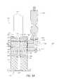
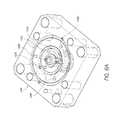
Thebody 102 can also include one ormore heaters 128. Each of the valve blocks112a,112bcan also include one ormore heaters heaters heaters
Thereactant gas inlet 124 connects with adistribution channel 136 in thebody 102 via apassageway 137. Thedistribution channel 136 is formed by lower and upper surfaces, respectively, of theupper block 104 and theintermediate block 106, and extends in a plane that intersects with the longitudinal axis of thebore 130, and is normal to the bore axis in the illustrated embodiment. Thedistribution channel 136 is in fluid communication with thebore 130 via three reactantgas supply channels FIG. 3A near their points of merger with the bore130), which connect with thebore 130 at a location downstream of thedistribution channel 136.
The inert gas inlet122 (seeFIG. 2 ) connects with an inertgas distribution channel 140 in thebody 102. The inertgas distribution channel 140 is formed by lower and upper surfaces, respectively, of theupper block 104 and theintermediate block 106, and extends in a plane that intersects the longitudinal axis of thebore 130, and is normal to the bore axis in the illustrated embodiment. In some embodiments, theinert gas channel 140 can be disposed at about the same longitudinal location as thedistribution channel 136. The inertgas distribution channel 140 supplies inert gas to theinert gas valve 114avia apassageway 142a. As shown inFIG. 3A , thepassageway 142aextends through theintermediate block 106 and the valve block112a. The inertgas distribution channel 140 also supplies inert gas to theinert gas valve 114bvia apassageway 142b(seeFIG. 3B ).
With continued reference toFIG. 3A , theinert gas valve 114acontrols a supply of inert gas from thepassageway 142a(and thus, from the inert gas distribution channel140) to thereactant gas valve 116a(seeFIG. 2 ). Thereactant gas valve 116acontrols a supply of a reactant gas from theinlet 118a(or a mixture of a reactant gas from theinlet 118aand an inert gas from theinert gas valve 114a) to apassageway 144a, which is connected to adistribution channel 146 in thebody 102. As shown inFIG. 3A , thepassageway 144aextends through the valve block112aand theintermediate block 106. Thedistribution channel 146 is formed by lower and upper surfaces, respectively, of theintermediate block 106 and thelower block 108, and extends in a plane that intersects the longitudinal axis of thebore 130, and is normal to the bore axis in the illustrated embodiment. Thedistribution channel 146 is in fluid communication with thebore 130 via threesupply channels bore 130 inFIG. 3A ), which connect with thebore 130 at a location downstream of thedistribution channel 146.
In some embodiments, each of thedistribution channels supply channels supply channels
Thesupply channels bore 130 at an angle with respect to the longitudinal axis of the bore (as viewed in a longitudinal cross-sections ofFIGS. 3A and 3B ). As can be seen inFIG. 3B , thesupply channels distribution channel 146 connect with thebore 130 at a greater angle than do thesupply channels distribution channel 150, as thedistribution channel 146 is laterally more remote frombore 130 than thedistribution channel 150. In addition, some or all of thesupply channels FIG. 1C and related description). As also shown inFIG. 3B , thesupply channels bore 130 at the taperedportion 134 of the bore. Such a configuration can serve to promote swirling and mixing of gases inside thebore 130.
While illustrated with three reactant inlets and two inert gas inlets to themanifold body 102, the number of precursor/reactant and inert gas inlets can vary in embodiments. Also, while illustrated with two each, the number of precursor/reactant valves inert gas valves distribution channel 136. Typically an ALD system includes at least two reactants and gas distribution therefor, and three- and four-reactant systems are not uncommon. In the embodiment illustrated inFIG. 2 , the supply of reactant gas to thereactant gas inlet 124 can be controlled by a valve (not shown) which is disposed outside of the ALD hot zone. Thevalves Valves valves valves valves
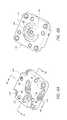
Themanifold body 102 is shown connected upstream of areaction chamber 810. In particular, theoutlet 132 of thebore 130 communicates with a reactant injector, particularly a dispersion mechanism in the form of ashowerhead 820 in the illustrated embodiment. Theshowerhead 820 includes ashowerhead plate 822 that defines ashowerhead plenum 824 above theplate 822. Theshowerhead 820 communicates vapors from the manifold100 to areaction space 826 below theshowerhead 820. Thereaction chamber 810 includes asubstrate support 828 configured to support asubstrate 829 in thereaction space 826. The reaction chamber also includes anexhaust opening 830 connected a vacuum source. While shown with a single-wafer, showerhead type of reaction chamber, the skilled artisan will appreciate that manifold can also be connected to other types of reaction chambers with other types of injectors, e.g. batch or furnace type, horizontal or cross-flow reactor, etc.
Themanifold block 102 is also connected via various valves and gas lines to inert gas and reactant sources. In the illustrated embodiment, three reactant sources are shown, although fewer or greater numbers can be provided in other arrangements. In the illustrated embodiment, the upperreactant distribution channel 136 connects, via thepassageway 137, external gas lines and control valves, to areactant source 840. The lowerreactant distribution channels passageways reactant valves reactant sources reactant sources reactant sources upper reactant source 840 can contain a naturally gaseous reactant, while thelower reactant sources upper reactant source 840 can be a vaporizer, while thelower reactant sources lower reactant sources
Thereactor 800 also includes at least oneinert gas source 855.FIG. 8 shows theinert gas source 855 as providing purge gas to thereactant valves reactant distribution channels 146,150 (via theinert gas inlet 122,distribution channel 140,passageways inert gas valve 114a). The sameinert gas source 855 is shown feeding the top of the central bore130 (via the inert gas inlet120). The same inert gas source also purges the upper reactant distribution channel136 (via thereactant inlet 124 and thepassageway 137. However, separate inert gas sources can be provided for each of these feeds.
Thereactor 800 also includes at least onecontroller 860, including processor(s) and memory with programming for controlling various components of thereactor 800. While shown schematically as connected to thereaction chamber 810, the skilled artisan will appreciate that thecontroller 860 communicates with various components of the reactor, such as vapor control valves, heating systems, gate valves, robot wafer carriers, etc., to carry out deposition processes.
In operation, thecontroller 860 arranges for asubstrate 829 to be loaded onto thesubstrate support 828, and for thereaction chamber 810 to be closed, purged and typically pumped down in readiness for deposition processes, particularly atomic layer deposition (ALD). A typical ALD sequence will now be described with reference to the reactor components ofFIG. 8 .
In one embodiment, prior to reactant supply and during the entire ALD process, purge gas flows through thetop inlet 120 into thebore 130. When the controller instructs a first ALD reactant pulse, for example from thereactant source 850a, thereactant valve 116ais open to permit flow from thereactant source 850ainto thepassageway 144aand around thedistribution channel 146. Backpressure within thedistribution channel 146 ensures even distribution among themultiple supply channels distribution channel 146 to thebore 130, where the first reactant merges with the inert gas flow. At the same time, inert gas can flow through all other reactant channels (e.g., thereactant distribution channel 136, thesupply channels reactant distribution channel 150 andsupply channels bore 130. From thebore 130, the mixture of inert gas and first reactant is fed to theshowerhead plenum 824 and distributed across the showerhead plate822 (or other dispersion mechanism) and into thereaction space 826. During this first reactant pulse, the narrower portion of thebore 130 upstream of the taperedportion 134 is filled with flowing inert gas and prevents upstream diffusion of the reactant.
After a sufficient duration to saturate thesubstrate 829 surface with the first reactant, thecontroller 860 switches off thereactant valve 116a, opens theinert gas valve 114a, and thus purges thereactant valve 116a, thepassageway 144a, thereactant distribution channel 146 and the dependingsupply channels bore 130 from thetop inlet 120 and the other reactant pathways for a sufficient duration to purge the manifold100, theshowerhead plenum 824, and thereaction space 826 of any remaining first reactant and/or byproduct. The skilled artisan will appreciate that other reactant removal procedures can be used in place of or in addition to purging.
After a suitably long removal period to avoid interaction of the first reactant with the subsequent reactant, thecontroller 860 can instruct control valves to supply a second ALD reactant from, e.g., thegaseous reactant source 840, into thereactant inlet 124, thepassageway 137 and the upperreactant distribution channel 136. Backpressure within thedistribution channel 136 ensures even distribution among themultiple supply channels distribution channel 136 to thebore 130, where the first reactant merges with the inert gas flow. At the same time, inert gas can flow through all other reactant channels (e.g., thereactant distribution channel 146, thesupply channels reactant distribution channel 150 andsupply channels bore 130. From thebore 130, the mixture of inert gas and first reactant is fed to theshowerhead plenum 824 and distributed across the showerhead plate822 (or other dispersion mechanism) and into thereaction space 826. During this second reactant pulse, the portion of thebore 130 upstream of its merger with thesupply channels
Following saturative surface reaction on the substrate, a removal step similar to the purge step described above can be performed, including purging of thedistribution channel 136 and its dependingsupply channels substrate 829.
Although the foregoing has been described in detail by way of illustrations and examples for purposes of clarity and understanding, it is apparent to those skilled in the art that certain changes and modifications may be practiced. Therefore, the description and examples should not be construed as limiting the scope of the invention to the specific embodiments and examples described herein, but rather to also cover all modification and alternatives coming with the true scope and spirit of the invention. Moreover, not all of the features, aspects and advantages described herein above are necessarily required to practice the present invention.
Claims (40)
1. A vapor deposition device comprising:
a reactor including a reaction chamber, a substrate support configured to support a substrate, and an injector configured to inject vapor into the reaction chamber, the injector comprising a showerhead mechanism disposed over the substrate support, the showerhead mechanism comprising a showerhead plate and defining a showerhead plenum, the showerhead plate including a plurality of non-annular openings to inject the vapor into the reaction chamber, each opening of the plurality of openings defining a channel disposed along a first direction; and
a manifold configured to deliver vapor to the injector, the manifold being disposed upstream of the injector, the manifold comprising:
a manifold body having a hollow bore disposed within the body, the bore having a longitudinal axis along which gas flows, the longitudinal axis generally parallel with the first direction, the manifold body comprising a first block and a second block disposed adjacent the first block,
a first distribution channel disposed within the body and extending in a plane intersecting the longitudinal axis, wherein the first distribution channel is defined by a groove formed in at least one of a lower surface of the first block and an upper surface of the second block, the groove disposed at least partially about the bore to direct gas circumferentially relative to the bore,
a plurality of first supply channels disposed within the body and in flow communication with the first distribution channel and with the bore, each of the first supply channels being disposed at an acute angle with respect to the longitudinal axis of the bore, each of the first supply channels connecting with the bore at a different angular position about the longitudinal axis, and
an inert gas inlet configured to fluidly connect to an inert gas source, wherein a portion of the bore extends upstream and downstream of the first distribution channel and the first supply channels along the longitudinal axis, the inert gas inlet disposed upstream of the first distribution channel and the first supply channels, the inert gas inlet directed along the longitudinal axis of the bore to supply inert gas through the bore along the longitudinal axis.
2. The vapor deposition device ofclaim 1 , further comprising the inert gas source, the inert gas source coupled to the inert gas inlet upstream of where the first supply channels connect with the bore.
3. The vapor deposition device ofclaim 1 , wherein the first distribution channel extends in a plane normal to the longitudinal axis.
4. The vapor deposition device ofclaim 1 , wherein each of the first supply channels connects with the first distribution channel at a different angular position about the longitudinal axis.
5. The vapor deposition device ofclaim 1 , wherein the first distribution channel has a curved shape.
6. The vapor deposition device ofclaim 5 , wherein the first distribution channel follows a circular curvature.
7. The vapor deposition device ofclaim 1 , wherein the first distribution channel extends through an arc of at least 180°.
8. The vapor deposition device ofclaim 1 , wherein the first distribution channel extends through an arc of about 240°.
9. The vapor deposition device ofclaim 1 , wherein the different angular positions are disposed symmetrically about the longitudinal axis.
10. The vapor deposition device ofclaim 1 , wherein the manifold comprises three first channels, and wherein the different angular positions are spaced apart by approximately 120°.
11. The vapor deposition device ofclaim 1 , wherein the different angular positions are disposed asymmetrically about the longitudinal axis.
12. The vapor deposition device ofclaim 1 , wherein each of the first channels extends radially from the bore, as viewed in a transverse cross-section.
13. The vapor deposition device ofclaim 1 , wherein each of the first supply channels extends tangentially or semitangentially from the bore, as viewed in a transverse cross-section.
14. The vapor deposition device ofclaim 1 , wherein an inlet to the first distribution channel has a diameter approximately equal to a diameter of the first distribution channel.
15. The vapor deposition device ofclaim 14 , wherein each of the first supply channels has a diameter between 25% and 100% of a diameter of the first distribution channel.
16. The vapor deposition device ofclaim 1 , wherein the first distribution channel is connected to a first reactant source.
17. The vapor deposition device ofclaim 1 , wherein the bore has a length-to-diameter (L/D) ratio of greater than 5, where the length is measured from where the first supply channels connect with the bore to an outlet of the bore, and the diameter is an average diameter along the length.
18. The vapor deposition device ofclaim 17 , wherein the manifold body further comprises:
a second distribution channel disposed within the body and extending in a plane intersecting the longitudinal axis; and
a plurality of second supply channels disposed within the body and in flow communication with the second distribution channel and with the bore, each of the second supply channels being disposed at an acute angle with respect to the longitudinal axis of the bore, each of the second supply channels connecting with the bore at a different angular position about the longitudinal axis.
19. The vapor deposition device ofclaim 18 , wherein the first reactant source is configured to hold a gas, wherein the second distribution channel is connected to a second reactant source, the second reactant source including a precursor vaporizer wherein the second supply channels connect with the bore downstream of where the first supply channels connect with the bore.
20. The vapor deposition device ofclaim 19 , wherein the manifold body further comprises:
a third distribution channel disposed within the body and extending in a plane intersecting the longitudinal axis; and
a plurality of third supply channels disposed within the body and in flow communication with the third distribution channel and with the bore, each of the third supply channels being disposed at an acute angle with respect to the longitudinal axis of the bore, each of the third supply channels connecting with the bore at a different angular position about the longitudinal axis.
21. The vapor deposition device ofclaim 20 , wherein the third distribution channel extends in substantially the same plane as the second distribution channel.
22. The vapor deposition device ofclaim 20 , the third supply channels connect with the bore at approximately the same longitudinal location as the second supply channels.
23. The vapor deposition device ofclaim 20 , wherein the third distribution channel is connected to a third reactant source, the third reactant source including another precursor vaporizer.
24. The vapor deposition device ofclaim 18 , further comprising a first reactant gas valve mounted on the manifold, the first reactant gas valve configured to control a supply of the second reactant to the second distribution channel.
25. The vapor deposition device ofclaim 24 , further comprising a first inert gas valve mounted on the manifold, the first inert gas valve configured to control a supply of an inert gas to the first reactant gas valve.
26. The vapor deposition device ofclaim 1 , wherein the groove comprises a floor having a curved surface, as viewed from a side cross-section.
27. The vapor deposition device ofclaim 1 , further comprising a second distribution channel disposed within the body, the first distribution channel comprising an annulus surrounding the second distribution channel.
28. The vapor deposition device ofclaim 27 , further comprising a plurality of second supply channels disposed within the body and in flow communication with the second distribution channel and with the bore, each of the second supply channels being disposed at an acute angle with respect to the longitudinal axis of the bore.
29. A vapor deposition device comprising:
a reactor including a reaction chamber, a substrate support configured to support a substrate, and an injector configured to inject vapor into the reaction chamber, the injector comprising a showerhead mechanism disposed over the substrate support, the showerhead mechanism comprising a showerhead plate and defining a showerhead plenum, the showerhead plate including a plurality of non-annular openings to inject the vapor into the reaction chamber, each opening of the plurality of openings defining a channel disposed along a first direction; and
a manifold configured to deliver vapor to the injector, the manifold being disposed upstream of the injector, the manifold comprising:
a manifold body having a hollow bore disposed within the body, the bore having a longitudinal axis along which gas flows, the longitudinal axis generally parallel with the first direction, the manifold body comprising a first block and a second block disposed adjacent the first block,
a first distribution channel disposed within the body and extending in a plane intersecting the longitudinal axis, wherein the first distribution channel is defined by a groove formed in at least one of a lower surface of the first block and an upper surface of the second block, the groove disposed at least partially about the bore to direct gas circumferentially relative to the bore, and
a plurality of first supply channels disposed within the body and in flow communication with the first distribution channel and with the bore, each of the first supply channels being disposed at an acute angle with respect to the longitudinal axis of the bore, each of the first supply channels connecting with the bore at a different angular position about the longitudinal axis.
30. The vapor deposition device ofclaim 29 , further comprising a third block disposed adjacent the second block and a second distribution channel disposed within the body and extending in a second plane intersecting the longitudinal axis, wherein the second distribution channel is defined by a lower surface of the second block and an upper surface of the third block.
31. The vapor deposition device ofclaim 29 , wherein the first distribution channel extends through an arc of at least 180°.
32. A vapor deposition device comprising:
a reactor including a reaction chamber, a substrate support configured to support a substrate, and an injector configured to inject vapor into the reaction chamber, the injector comprising a showerhead mechanism disposed over the substrate support, the showerhead mechanism comprising a showerhead plate and defining a showerhead plenum, the showerhead plate including a plurality of non-annular openings to inject the vapor into the reaction chamber, each opening of the plurality of openings defining a channel disposed along a first direction; and
a manifold configured to deliver vapor to the injector, the manifold being disposed upstream of the injector, the manifold comprising:
a manifold body having a hollow bore disposed within the body, the bore having a longitudinal axis along which gas flows, the longitudinal axis generally parallel with the first direction, the manifold body comprising a first block and a second block disposed adjacent the first block,
a first distribution channel disposed within the body and extending in a plane intersecting the longitudinal axis, wherein the first distribution channel is defined by a groove formed in at least one of a lower surface of the first block and an upper surface of the second block, the groove disposed at least partially about the bore to direct gas circumferentially relative to the bore,
a plurality of first supply channels disposed within the body and in flow communication with the first distribution channel and with the bore, each of the first supply channels being disposed at an acute angle with respect to the longitudinal axis of the bore,
a second distribution channel disposed within the body and extending in the same plane as the first distribution channel, the first distribution channel surrounding the second distribution channel,
a plurality of second supply channels disposed within the body and in flow communication with the second distribution channel and with the bore, each of the second supply channels being disposed at an acute angle with respect to the longitudinal axis of the bore.
33. The vapor deposition device ofclaim 32 , wherein the respective acute angle formed between the second supply channels and the longitudinal axis is larger than the respective acute angle formed between the first supply channels and the longitudinal axis.
34. The vapor deposition device ofclaim 32 , wherein the first distribution channel extends through an arc of at least 180°.
35. The vapor deposition device ofclaim 32 , further comprising an inert gas source coupled to an inlet of the bore upstream of where the first supply channels connect with the bore.
36. The vapor deposition device ofclaim 32 , wherein the first distribution channel extends in a plane normal to the longitudinal axis.
37. The vapor deposition device ofclaim 1 , wherein the showerhead plate is at least as large as the substrate support.
38. The vapor deposition device ofclaim 29 , wherein the showerhead plate is at least as large as the substrate support.
39. The vapor deposition device ofclaim 32 , wherein the showerhead plate is at least as large as the substrate support.
40. The vapor deposition device ofclaim 32 , wherein the first distribution channel comprises a first annular channel disposed at least partially about the bore, and wherein the second distribution channel comprises a second annular channel disposed at least partially about the bore.
Priority Applications (2)
| Application Number | Priority Date | Filing Date | Title |
|---|---|---|---|
| US13/284,738US9574268B1 (en) | 2011-10-28 | 2011-10-28 | Pulsed valve manifold for atomic layer deposition |
| US15/400,793US10370761B2 (en) | 2011-10-28 | 2017-01-06 | Pulsed valve manifold for atomic layer deposition |
Applications Claiming Priority (1)
| Application Number | Priority Date | Filing Date | Title |
|---|---|---|---|
| US13/284,738US9574268B1 (en) | 2011-10-28 | 2011-10-28 | Pulsed valve manifold for atomic layer deposition |
Related Child Applications (1)
| Application Number | Title | Priority Date | Filing Date |
|---|---|---|---|
| US15/400,793DivisionUS10370761B2 (en) | 2011-10-28 | 2017-01-06 | Pulsed valve manifold for atomic layer deposition |
Publications (1)
| Publication Number | Publication Date |
|---|---|
| US9574268B1true US9574268B1 (en) | 2017-02-21 |
Family
ID=58017645
Family Applications (2)
| Application Number | Title | Priority Date | Filing Date |
|---|---|---|---|
| US13/284,738Active2034-02-16US9574268B1 (en) | 2011-10-28 | 2011-10-28 | Pulsed valve manifold for atomic layer deposition |
| US15/400,793ActiveUS10370761B2 (en) | 2011-10-28 | 2017-01-06 | Pulsed valve manifold for atomic layer deposition |
Family Applications After (1)
| Application Number | Title | Priority Date | Filing Date |
|---|---|---|---|
| US15/400,793ActiveUS10370761B2 (en) | 2011-10-28 | 2017-01-06 | Pulsed valve manifold for atomic layer deposition |
Country Status (1)
| Country | Link |
|---|---|
| US (2) | US9574268B1 (en) |
Cited By (376)
| Publication number | Priority date | Publication date | Assignee | Title |
|---|---|---|---|---|
| US20150240359A1 (en)* | 2014-02-25 | 2015-08-27 | Asm Ip Holding B.V. | Gas Supply Manifold And Method Of Supplying Gases To Chamber Using Same |
| US20160168705A1 (en)* | 2014-12-10 | 2016-06-16 | Lam Research Corporation | Inlet for effective mixing and purging |
| US20160362785A1 (en)* | 2015-06-15 | 2016-12-15 | Samsung Electronics Co., Ltd. | Apparatus for manufacturing semiconductor device having a gas mixer |
| US20170350011A1 (en)* | 2016-06-01 | 2017-12-07 | Asm Ip Holding B.V. | Manifolds for uniform vapor deposition |
| US10023960B2 (en) | 2012-09-12 | 2018-07-17 | Asm Ip Holdings B.V. | Process gas management for an inductively-coupled plasma deposition reactor |
| US10083836B2 (en) | 2015-07-24 | 2018-09-25 | Asm Ip Holding B.V. | Formation of boron-doped titanium metal films with high work function |
| US10113232B2 (en) | 2014-07-31 | 2018-10-30 | Lam Research Corporation | Azimuthal mixer |
| US10134757B2 (en) | 2016-11-07 | 2018-11-20 | Asm Ip Holding B.V. | Method of processing a substrate and a device manufactured by using the method |
| US10229833B2 (en) | 2016-11-01 | 2019-03-12 | Asm Ip Holding B.V. | Methods for forming a transition metal nitride film on a substrate by atomic layer deposition and related semiconductor device structures |
| US10236177B1 (en) | 2017-08-22 | 2019-03-19 | ASM IP Holding B.V.. | Methods for depositing a doped germanium tin semiconductor and related semiconductor device structures |
| US10249524B2 (en) | 2017-08-09 | 2019-04-02 | Asm Ip Holding B.V. | Cassette holder assembly for a substrate cassette and holding member for use in such assembly |
| US10249577B2 (en) | 2016-05-17 | 2019-04-02 | Asm Ip Holding B.V. | Method of forming metal interconnection and method of fabricating semiconductor apparatus using the method |
| CN109609929A (en)* | 2018-11-20 | 2019-04-12 | 沈阳拓荆科技有限公司 | Mixing structure and reaction equipment |
| US10262859B2 (en) | 2016-03-24 | 2019-04-16 | Asm Ip Holding B.V. | Process for forming a film on a substrate using multi-port injection assemblies |
| US20190112707A1 (en)* | 2017-10-16 | 2019-04-18 | Asm Ip Holding B.V. | Systems and methods for atomic layer deposition |
| US10269558B2 (en) | 2016-12-22 | 2019-04-23 | Asm Ip Holding B.V. | Method of forming a structure on a substrate |
| US10276355B2 (en) | 2015-03-12 | 2019-04-30 | Asm Ip Holding B.V. | Multi-zone reactor, system including the reactor, and method of using the same |
| US10283353B2 (en) | 2017-03-29 | 2019-05-07 | Asm Ip Holding B.V. | Method of reforming insulating film deposited on substrate with recess pattern |
| US10290508B1 (en) | 2017-12-05 | 2019-05-14 | Asm Ip Holding B.V. | Method for forming vertical spacers for spacer-defined patterning |
| US10312129B2 (en) | 2015-09-29 | 2019-06-04 | Asm Ip Holding B.V. | Variable adjustment for precise matching of multiple chamber cavity housings |
| US10312055B2 (en) | 2017-07-26 | 2019-06-04 | Asm Ip Holding B.V. | Method of depositing film by PEALD using negative bias |
| US10319588B2 (en) | 2017-10-10 | 2019-06-11 | Asm Ip Holding B.V. | Method for depositing a metal chalcogenide on a substrate by cyclical deposition |
| US10322384B2 (en)* | 2015-11-09 | 2019-06-18 | Asm Ip Holding B.V. | Counter flow mixer for process chamber |
| US10340125B2 (en) | 2013-03-08 | 2019-07-02 | Asm Ip Holding B.V. | Pulsed remote plasma method and system |
| US10340135B2 (en) | 2016-11-28 | 2019-07-02 | Asm Ip Holding B.V. | Method of topologically restricted plasma-enhanced cyclic deposition of silicon or metal nitride |
| US10343920B2 (en) | 2016-03-18 | 2019-07-09 | Asm Ip Holding B.V. | Aligned carbon nanotubes |
| US10361201B2 (en) | 2013-09-27 | 2019-07-23 | Asm Ip Holding B.V. | Semiconductor structure and device formed using selective epitaxial process |
| US10367080B2 (en) | 2016-05-02 | 2019-07-30 | Asm Ip Holding B.V. | Method of forming a germanium oxynitride film |
| US10364496B2 (en) | 2011-06-27 | 2019-07-30 | Asm Ip Holding B.V. | Dual section module having shared and unshared mass flow controllers |
| US10366864B2 (en) | 2013-03-08 | 2019-07-30 | Asm Ip Holding B.V. | Method and system for in-situ formation of intermediate reactive species |
| US10370761B2 (en) | 2011-10-28 | 2019-08-06 | Asm America, Inc. | Pulsed valve manifold for atomic layer deposition |
| US10378106B2 (en) | 2008-11-14 | 2019-08-13 | Asm Ip Holding B.V. | Method of forming insulation film by modified PEALD |
| US10381219B1 (en) | 2018-10-25 | 2019-08-13 | Asm Ip Holding B.V. | Methods for forming a silicon nitride film |
| US10381226B2 (en) | 2016-07-27 | 2019-08-13 | Asm Ip Holding B.V. | Method of processing substrate |
| US10388509B2 (en) | 2016-06-28 | 2019-08-20 | Asm Ip Holding B.V. | Formation of epitaxial layers via dislocation filtering |
| US10388513B1 (en) | 2018-07-03 | 2019-08-20 | Asm Ip Holding B.V. | Method for depositing silicon-free carbon-containing film as gap-fill layer by pulse plasma-assisted deposition |
| US10395919B2 (en) | 2016-07-28 | 2019-08-27 | Asm Ip Holding B.V. | Method and apparatus for filling a gap |
| US10403504B2 (en) | 2017-10-05 | 2019-09-03 | Asm Ip Holding B.V. | Method for selectively depositing a metallic film on a substrate |
| US10410943B2 (en) | 2016-10-13 | 2019-09-10 | Asm Ip Holding B.V. | Method for passivating a surface of a semiconductor and related systems |
| US10438965B2 (en) | 2014-12-22 | 2019-10-08 | Asm Ip Holding B.V. | Semiconductor device and manufacturing method thereof |
| US10435790B2 (en) | 2016-11-01 | 2019-10-08 | Asm Ip Holding B.V. | Method of subatmospheric plasma-enhanced ALD using capacitively coupled electrodes with narrow gap |
| US20190311887A1 (en)* | 2018-04-06 | 2019-10-10 | Applied Materials, Inc. | Multizone gas distribution apparatus |
| US10446393B2 (en) | 2017-05-08 | 2019-10-15 | Asm Ip Holding B.V. | Methods for forming silicon-containing epitaxial layers and related semiconductor device structures |
| US10458018B2 (en) | 2015-06-26 | 2019-10-29 | Asm Ip Holding B.V. | Structures including metal carbide material, devices including the structures, and methods of forming same |
| US10468251B2 (en) | 2016-02-19 | 2019-11-05 | Asm Ip Holding B.V. | Method for forming spacers using silicon nitride film for spacer-defined multiple patterning |
| US10468261B2 (en) | 2017-02-15 | 2019-11-05 | Asm Ip Holding B.V. | Methods for forming a metallic film on a substrate by cyclical deposition and related semiconductor device structures |
| US10480072B2 (en) | 2009-04-06 | 2019-11-19 | Asm Ip Holding B.V. | Semiconductor processing reactor and components thereof |
| US10483099B1 (en) | 2018-07-26 | 2019-11-19 | Asm Ip Holding B.V. | Method for forming thermally stable organosilicon polymer film |
| US10501866B2 (en) | 2016-03-09 | 2019-12-10 | Asm Ip Holding B.V. | Gas distribution apparatus for improved film uniformity in an epitaxial system |
| US10504742B2 (en) | 2017-05-31 | 2019-12-10 | Asm Ip Holding B.V. | Method of atomic layer etching using hydrogen plasma |
| US10510536B2 (en) | 2018-03-29 | 2019-12-17 | Asm Ip Holding B.V. | Method of depositing a co-doped polysilicon film on a surface of a substrate within a reaction chamber |
| US10529563B2 (en) | 2017-03-29 | 2020-01-07 | Asm Ip Holdings B.V. | Method for forming doped metal oxide films on a substrate by cyclical deposition and related semiconductor device structures |
| US10529542B2 (en) | 2015-03-11 | 2020-01-07 | Asm Ip Holdings B.V. | Cross-flow reactor and method |
| US10529554B2 (en) | 2016-02-19 | 2020-01-07 | Asm Ip Holding B.V. | Method for forming silicon nitride film selectively on sidewalls or flat surfaces of trenches |
| US10535516B2 (en) | 2018-02-01 | 2020-01-14 | Asm Ip Holdings B.V. | Method for depositing a semiconductor structure on a surface of a substrate and related semiconductor structures |
| US10541333B2 (en) | 2017-07-19 | 2020-01-21 | Asm Ip Holding B.V. | Method for depositing a group IV semiconductor and related semiconductor device structures |
| US10541173B2 (en) | 2016-07-08 | 2020-01-21 | Asm Ip Holding B.V. | Selective deposition method to form air gaps |
| US10559458B1 (en) | 2018-11-26 | 2020-02-11 | Asm Ip Holding B.V. | Method of forming oxynitride film |
| US10566223B2 (en) | 2012-08-28 | 2020-02-18 | Asm Ip Holdings B.V. | Systems and methods for dynamic semiconductor process scheduling |
| US10561975B2 (en) | 2014-10-07 | 2020-02-18 | Asm Ip Holdings B.V. | Variable conductance gas distribution apparatus and method |
| US10590535B2 (en) | 2017-07-26 | 2020-03-17 | Asm Ip Holdings B.V. | Chemical treatment, deposition and/or infiltration apparatus and method for using the same |
| US10600673B2 (en) | 2015-07-07 | 2020-03-24 | Asm Ip Holding B.V. | Magnetic susceptor to baseplate seal |
| US10607895B2 (en) | 2017-09-18 | 2020-03-31 | Asm Ip Holdings B.V. | Method for forming a semiconductor device structure comprising a gate fill metal |
| US10605530B2 (en) | 2017-07-26 | 2020-03-31 | Asm Ip Holding B.V. | Assembly of a liner and a flange for a vertical furnace as well as the liner and the vertical furnace |
| US10604847B2 (en) | 2014-03-18 | 2020-03-31 | Asm Ip Holding B.V. | Gas distribution system, reactor including the system, and methods of using the same |
| USD880437S1 (en) | 2018-02-01 | 2020-04-07 | Asm Ip Holding B.V. | Gas supply plate for semiconductor manufacturing apparatus |
| US10612136B2 (en) | 2018-06-29 | 2020-04-07 | ASM IP Holding, B.V. | Temperature-controlled flange and reactor system including same |
| US10612137B2 (en) | 2016-07-08 | 2020-04-07 | Asm Ip Holdings B.V. | Organic reactants for atomic layer deposition |
| US10643904B2 (en) | 2016-11-01 | 2020-05-05 | Asm Ip Holdings B.V. | Methods for forming a semiconductor device and related semiconductor device structures |
| US10643826B2 (en) | 2016-10-26 | 2020-05-05 | Asm Ip Holdings B.V. | Methods for thermally calibrating reaction chambers |
| US10651016B2 (en)* | 2017-03-15 | 2020-05-12 | Hermes-Epitek Corporation | Detachable gas injector used for semiconductor equipment |
| US10658181B2 (en) | 2018-02-20 | 2020-05-19 | Asm Ip Holding B.V. | Method of spacer-defined direct patterning in semiconductor fabrication |
| US10658205B2 (en) | 2017-09-28 | 2020-05-19 | Asm Ip Holdings B.V. | Chemical dispensing apparatus and methods for dispensing a chemical to a reaction chamber |
| US10655221B2 (en) | 2017-02-09 | 2020-05-19 | Asm Ip Holding B.V. | Method for depositing oxide film by thermal ALD and PEALD |
| US10665452B2 (en) | 2016-05-02 | 2020-05-26 | Asm Ip Holdings B.V. | Source/drain performance through conformal solid state doping |
| US10685834B2 (en) | 2017-07-05 | 2020-06-16 | Asm Ip Holdings B.V. | Methods for forming a silicon germanium tin layer and related semiconductor device structures |
| US10692741B2 (en) | 2017-08-08 | 2020-06-23 | Asm Ip Holdings B.V. | Radiation shield |
| US10707106B2 (en) | 2011-06-06 | 2020-07-07 | Asm Ip Holding B.V. | High-throughput semiconductor-processing apparatus equipped with multiple dual-chamber modules |
| US10714315B2 (en) | 2012-10-12 | 2020-07-14 | Asm Ip Holdings B.V. | Semiconductor reaction chamber showerhead |
| US10714335B2 (en) | 2017-04-25 | 2020-07-14 | Asm Ip Holding B.V. | Method of depositing thin film and method of manufacturing semiconductor device |
| US10714350B2 (en) | 2016-11-01 | 2020-07-14 | ASM IP Holdings, B.V. | Methods for forming a transition metal niobium nitride film on a substrate by atomic layer deposition and related semiconductor device structures |
| US10714385B2 (en) | 2016-07-19 | 2020-07-14 | Asm Ip Holding B.V. | Selective deposition of tungsten |
| US10734497B2 (en) | 2017-07-18 | 2020-08-04 | Asm Ip Holding B.V. | Methods for forming a semiconductor device structure and related semiconductor device structures |
| US10731249B2 (en) | 2018-02-15 | 2020-08-04 | Asm Ip Holding B.V. | Method of forming a transition metal containing film on a substrate by a cyclical deposition process, a method for supplying a transition metal halide compound to a reaction chamber, and related vapor deposition apparatus |
| US10734244B2 (en) | 2017-11-16 | 2020-08-04 | Asm Ip Holding B.V. | Method of processing a substrate and a device manufactured by the same |
| US10741385B2 (en) | 2016-07-28 | 2020-08-11 | Asm Ip Holding B.V. | Method and apparatus for filling a gap |
| US10755922B2 (en) | 2018-07-03 | 2020-08-25 | Asm Ip Holding B.V. | Method for depositing silicon-free carbon-containing film as gap-fill layer by pulse plasma-assisted deposition |
| US10767789B2 (en) | 2018-07-16 | 2020-09-08 | Asm Ip Holding B.V. | Diaphragm valves, valve components, and methods for forming valve components |
| US10770286B2 (en) | 2017-05-08 | 2020-09-08 | Asm Ip Holdings B.V. | Methods for selectively forming a silicon nitride film on a substrate and related semiconductor device structures |
| US10770336B2 (en) | 2017-08-08 | 2020-09-08 | Asm Ip Holding B.V. | Substrate lift mechanism and reactor including same |
| CN111670265A (en)* | 2018-01-31 | 2020-09-15 | 朗姆研究公司 | Manifold valve for multiple precursors |
| CN111719138A (en)* | 2019-03-19 | 2020-09-29 | Asm Ip 控股有限公司 | Reactor Manifold |
| US10787741B2 (en) | 2014-08-21 | 2020-09-29 | Asm Ip Holding B.V. | Method and system for in situ formation of gas-phase compounds |
| US10797133B2 (en) | 2018-06-21 | 2020-10-06 | Asm Ip Holding B.V. | Method for depositing a phosphorus doped silicon arsenide film and related semiconductor device structures |
| US10804098B2 (en) | 2009-08-14 | 2020-10-13 | Asm Ip Holding B.V. | Systems and methods for thin-film deposition of metal oxides using excited nitrogen-oxygen species |
| US10811256B2 (en) | 2018-10-16 | 2020-10-20 | Asm Ip Holding B.V. | Method for etching a carbon-containing feature |
| USD900036S1 (en) | 2017-08-24 | 2020-10-27 | Asm Ip Holding B.V. | Heater electrical connector and adapter |
| US10818758B2 (en) | 2018-11-16 | 2020-10-27 | Asm Ip Holding B.V. | Methods for forming a metal silicate film on a substrate in a reaction chamber and related semiconductor device structures |
| US10829852B2 (en) | 2018-08-16 | 2020-11-10 | Asm Ip Holding B.V. | Gas distribution device for a wafer processing apparatus |
| US10832903B2 (en) | 2011-10-28 | 2020-11-10 | Asm Ip Holding B.V. | Process feed management for semiconductor substrate processing |
| US10847366B2 (en) | 2018-11-16 | 2020-11-24 | Asm Ip Holding B.V. | Methods for depositing a transition metal chalcogenide film on a substrate by a cyclical deposition process |
| US10847365B2 (en) | 2018-10-11 | 2020-11-24 | Asm Ip Holding B.V. | Method of forming conformal silicon carbide film by cyclic CVD |
| US10847371B2 (en) | 2018-03-27 | 2020-11-24 | Asm Ip Holding B.V. | Method of forming an electrode on a substrate and a semiconductor device structure including an electrode |
| US10844484B2 (en) | 2017-09-22 | 2020-11-24 | Asm Ip Holding B.V. | Apparatus for dispensing a vapor phase reactant to a reaction chamber and related methods |
| US10851456B2 (en) | 2016-04-21 | 2020-12-01 | Asm Ip Holding B.V. | Deposition of metal borides |
| USD903477S1 (en) | 2018-01-24 | 2020-12-01 | Asm Ip Holdings B.V. | Metal clamp |
| US10854498B2 (en) | 2011-07-15 | 2020-12-01 | Asm Ip Holding B.V. | Wafer-supporting device and method for producing same |
| US10858737B2 (en) | 2014-07-28 | 2020-12-08 | Asm Ip Holding B.V. | Showerhead assembly and components thereof |
| US10865475B2 (en) | 2016-04-21 | 2020-12-15 | Asm Ip Holding B.V. | Deposition of metal borides and silicides |
| US10867788B2 (en) | 2016-12-28 | 2020-12-15 | Asm Ip Holding B.V. | Method of forming a structure on a substrate |
| US10867786B2 (en) | 2018-03-30 | 2020-12-15 | Asm Ip Holding B.V. | Substrate processing method |
| US10872771B2 (en) | 2018-01-16 | 2020-12-22 | Asm Ip Holding B. V. | Method for depositing a material film on a substrate within a reaction chamber by a cyclical deposition process and related device structures |
| JP2020205422A (en)* | 2020-07-13 | 2020-12-24 | アプライド マテリアルズ インコーポレイテッドApplied Materials,Incorporated | Semiconductor processing chamber multi-stage mixing equipment |
| US10886123B2 (en) | 2017-06-02 | 2021-01-05 | Asm Ip Holding B.V. | Methods for forming low temperature semiconductor layers and related semiconductor device structures |
| US10883175B2 (en) | 2018-08-09 | 2021-01-05 | Asm Ip Holding B.V. | Vertical furnace for processing substrates and a liner for use therein |
| US10892156B2 (en) | 2017-05-08 | 2021-01-12 | Asm Ip Holding B.V. | Methods for forming a silicon nitride film on a substrate and related semiconductor device structures |
| US10896820B2 (en) | 2018-02-14 | 2021-01-19 | Asm Ip Holding B.V. | Method for depositing a ruthenium-containing film on a substrate by a cyclical deposition process |
| US10910262B2 (en) | 2017-11-16 | 2021-02-02 | Asm Ip Holding B.V. | Method of selectively depositing a capping layer structure on a semiconductor device structure |
| US10914004B2 (en) | 2018-06-29 | 2021-02-09 | Asm Ip Holding B.V. | Thin-film deposition method and manufacturing method of semiconductor device |
| US10923344B2 (en) | 2017-10-30 | 2021-02-16 | Asm Ip Holding B.V. | Methods for forming a semiconductor structure and related semiconductor structures |
| US10928731B2 (en) | 2017-09-21 | 2021-02-23 | Asm Ip Holding B.V. | Method of sequential infiltration synthesis treatment of infiltrateable material and structures and devices formed using same |
| US10934619B2 (en) | 2016-11-15 | 2021-03-02 | Asm Ip Holding B.V. | Gas supply unit and substrate processing apparatus including the gas supply unit |
| US10941490B2 (en) | 2014-10-07 | 2021-03-09 | Asm Ip Holding B.V. | Multiple temperature range susceptor, assembly, reactor and system including the susceptor, and methods of using the same |
| US10975470B2 (en) | 2018-02-23 | 2021-04-13 | Asm Ip Holding B.V. | Apparatus for detecting or monitoring for a chemical precursor in a high temperature environment |
| CN112695294A (en)* | 2019-10-22 | 2021-04-23 | Asm Ip 控股有限公司 | Semiconductor deposition reactor manifold |
| US11001925B2 (en) | 2016-12-19 | 2021-05-11 | Asm Ip Holding B.V. | Substrate processing apparatus |
| US11015245B2 (en) | 2014-03-19 | 2021-05-25 | Asm Ip Holding B.V. | Gas-phase reactor and system having exhaust plenum and components thereof |
| US11018002B2 (en) | 2017-07-19 | 2021-05-25 | Asm Ip Holding B.V. | Method for selectively depositing a Group IV semiconductor and related semiconductor device structures |
| US11018047B2 (en) | 2018-01-25 | 2021-05-25 | Asm Ip Holding B.V. | Hybrid lift pin |
| US11024523B2 (en) | 2018-09-11 | 2021-06-01 | Asm Ip Holding B.V. | Substrate processing apparatus and method |
| US11022879B2 (en) | 2017-11-24 | 2021-06-01 | Asm Ip Holding B.V. | Method of forming an enhanced unexposed photoresist layer |
| US11031242B2 (en) | 2018-11-07 | 2021-06-08 | Asm Ip Holding B.V. | Methods for depositing a boron doped silicon germanium film |
| USD922229S1 (en) | 2019-06-05 | 2021-06-15 | Asm Ip Holding B.V. | Device for controlling a temperature of a gas supply unit |
| US11049751B2 (en) | 2018-09-14 | 2021-06-29 | Asm Ip Holding B.V. | Cassette supply system to store and handle cassettes and processing apparatus equipped therewith |
| US11056567B2 (en) | 2018-05-11 | 2021-07-06 | Asm Ip Holding B.V. | Method of forming a doped metal carbide film on a substrate and related semiconductor device structures |
| US11056344B2 (en) | 2017-08-30 | 2021-07-06 | Asm Ip Holding B.V. | Layer forming method |
| US11053591B2 (en) | 2018-08-06 | 2021-07-06 | Asm Ip Holding B.V. | Multi-port gas injection system and reactor system including same |
| US11069510B2 (en) | 2017-08-30 | 2021-07-20 | Asm Ip Holding B.V. | Substrate processing apparatus |
| US11081345B2 (en) | 2018-02-06 | 2021-08-03 | Asm Ip Holding B.V. | Method of post-deposition treatment for silicon oxide film |
| US11087997B2 (en) | 2018-10-31 | 2021-08-10 | Asm Ip Holding B.V. | Substrate processing apparatus for processing substrates |
| US11088002B2 (en) | 2018-03-29 | 2021-08-10 | Asm Ip Holding B.V. | Substrate rack and a substrate processing system and method |
| US11114283B2 (en) | 2018-03-16 | 2021-09-07 | Asm Ip Holding B.V. | Reactor, system including the reactor, and methods of manufacturing and using same |
| US11114294B2 (en) | 2019-03-08 | 2021-09-07 | Asm Ip Holding B.V. | Structure including SiOC layer and method of forming same |
| USD930782S1 (en) | 2019-08-22 | 2021-09-14 | Asm Ip Holding B.V. | Gas distributor |
| US11127589B2 (en) | 2019-02-01 | 2021-09-21 | Asm Ip Holding B.V. | Method of topology-selective film formation of silicon oxide |
| US11127617B2 (en) | 2017-11-27 | 2021-09-21 | Asm Ip Holding B.V. | Storage device for storing wafer cassettes for use with a batch furnace |
| USD931978S1 (en) | 2019-06-27 | 2021-09-28 | Asm Ip Holding B.V. | Showerhead vacuum transport |
| US11139191B2 (en) | 2017-08-09 | 2021-10-05 | Asm Ip Holding B.V. | Storage apparatus for storing cassettes for substrates and processing apparatus equipped therewith |
| US11139308B2 (en) | 2015-12-29 | 2021-10-05 | Asm Ip Holding B.V. | Atomic layer deposition of III-V compounds to form V-NAND devices |
| US11158513B2 (en) | 2018-12-13 | 2021-10-26 | Asm Ip Holding B.V. | Methods for forming a rhenium-containing film on a substrate by a cyclical deposition process and related semiconductor device structures |
| USD935572S1 (en) | 2019-05-24 | 2021-11-09 | Asm Ip Holding B.V. | Gas channel plate |
| US11171025B2 (en) | 2019-01-22 | 2021-11-09 | Asm Ip Holding B.V. | Substrate processing device |
| US11205585B2 (en) | 2016-07-28 | 2021-12-21 | Asm Ip Holding B.V. | Substrate processing apparatus and method of operating the same |
| US11208722B2 (en) | 2011-12-27 | 2021-12-28 | Asm Ip Holding B.V. | Vapor flow control apparatus for atomic layer deposition |
| US11217444B2 (en) | 2018-11-30 | 2022-01-04 | Asm Ip Holding B.V. | Method for forming an ultraviolet radiation responsive metal oxide-containing film |
| US11222772B2 (en) | 2016-12-14 | 2022-01-11 | Asm Ip Holding B.V. | Substrate processing apparatus |
| USD940837S1 (en) | 2019-08-22 | 2022-01-11 | Asm Ip Holding B.V. | Electrode |
| CN113924385A (en)* | 2019-04-25 | 2022-01-11 | Beneq有限公司 | Gas distribution unit connected with ALD reactor |
| US11227789B2 (en) | 2019-02-20 | 2022-01-18 | Asm Ip Holding B.V. | Method and apparatus for filling a recess formed within a substrate surface |
| US11227782B2 (en) | 2019-07-31 | 2022-01-18 | Asm Ip Holding B.V. | Vertical batch furnace assembly |
| US11230766B2 (en) | 2018-03-29 | 2022-01-25 | Asm Ip Holding B.V. | Substrate processing apparatus and method |
| US11233133B2 (en) | 2015-10-21 | 2022-01-25 | Asm Ip Holding B.V. | NbMC layers |
| US11232963B2 (en) | 2018-10-03 | 2022-01-25 | Asm Ip Holding B.V. | Substrate processing apparatus and method |
| US11251068B2 (en) | 2018-10-19 | 2022-02-15 | Asm Ip Holding B.V. | Substrate processing apparatus and substrate processing method |
| US11251040B2 (en) | 2019-02-20 | 2022-02-15 | Asm Ip Holding B.V. | Cyclical deposition method including treatment step and apparatus for same |
| USD944946S1 (en) | 2019-06-14 | 2022-03-01 | Asm Ip Holding B.V. | Shower plate |
| US11270899B2 (en) | 2018-06-04 | 2022-03-08 | Asm Ip Holding B.V. | Wafer handling chamber with moisture reduction |
| US11274369B2 (en) | 2018-09-11 | 2022-03-15 | Asm Ip Holding B.V. | Thin film deposition method |
| US11282698B2 (en) | 2019-07-19 | 2022-03-22 | Asm Ip Holding B.V. | Method of forming topology-controlled amorphous carbon polymer film |
| US11289326B2 (en) | 2019-05-07 | 2022-03-29 | Asm Ip Holding B.V. | Method for reforming amorphous carbon polymer film |
| US11286562B2 (en) | 2018-06-08 | 2022-03-29 | Asm Ip Holding B.V. | Gas-phase chemical reactor and method of using same |
| US11286558B2 (en) | 2019-08-23 | 2022-03-29 | Asm Ip Holding B.V. | Methods for depositing a molybdenum nitride film on a surface of a substrate by a cyclical deposition process and related semiconductor device structures including a molybdenum nitride film |
| USD947913S1 (en) | 2019-05-17 | 2022-04-05 | Asm Ip Holding B.V. | Susceptor shaft |
| US11295980B2 (en) | 2017-08-30 | 2022-04-05 | Asm Ip Holding B.V. | Methods for depositing a molybdenum metal film over a dielectric surface of a substrate by a cyclical deposition process and related semiconductor device structures |
| USD948463S1 (en) | 2018-10-24 | 2022-04-12 | Asm Ip Holding B.V. | Susceptor for semiconductor substrate supporting apparatus |
| USD949319S1 (en) | 2019-08-22 | 2022-04-19 | Asm Ip Holding B.V. | Exhaust duct |
| US11306395B2 (en) | 2017-06-28 | 2022-04-19 | Asm Ip Holding B.V. | Methods for depositing a transition metal nitride film on a substrate by atomic layer deposition and related deposition apparatus |
| US11315794B2 (en) | 2019-10-21 | 2022-04-26 | Asm Ip Holding B.V. | Apparatus and methods for selectively etching films |
| US11342216B2 (en) | 2019-02-20 | 2022-05-24 | Asm Ip Holding B.V. | Cyclical deposition method and apparatus for filling a recess formed within a substrate surface |
| US11339476B2 (en) | 2019-10-08 | 2022-05-24 | Asm Ip Holding B.V. | Substrate processing device having connection plates, substrate processing method |
| US11345999B2 (en) | 2019-06-06 | 2022-05-31 | Asm Ip Holding B.V. | Method of using a gas-phase reactor system including analyzing exhausted gas |
| US11355338B2 (en) | 2019-05-10 | 2022-06-07 | Asm Ip Holding B.V. | Method of depositing material onto a surface and structure formed according to the method |
| US11361990B2 (en) | 2018-05-28 | 2022-06-14 | Asm Ip Holding B.V. | Substrate processing method and device manufactured by using the same |
| TWI768838B (en)* | 2019-04-09 | 2022-06-21 | 美商應用材料股份有限公司 | Semiconductor processing system component |
| US11374112B2 (en) | 2017-07-19 | 2022-06-28 | Asm Ip Holding B.V. | Method for depositing a group IV semiconductor and related semiconductor device structures |
| US11378337B2 (en) | 2019-03-28 | 2022-07-05 | Asm Ip Holding B.V. | Door opener and substrate processing apparatus provided therewith |
| US11390945B2 (en) | 2019-07-03 | 2022-07-19 | Asm Ip Holding B.V. | Temperature control assembly for substrate processing apparatus and method of using same |
| US11390946B2 (en) | 2019-01-17 | 2022-07-19 | Asm Ip Holding B.V. | Methods of forming a transition metal containing film on a substrate by a cyclical deposition process |
| US11393690B2 (en) | 2018-01-19 | 2022-07-19 | Asm Ip Holding B.V. | Deposition method |
| US11401605B2 (en) | 2019-11-26 | 2022-08-02 | Asm Ip Holding B.V. | Substrate processing apparatus |
| US11414760B2 (en) | 2018-10-08 | 2022-08-16 | Asm Ip Holding B.V. | Substrate support unit, thin film deposition apparatus including the same, and substrate processing apparatus including the same |
| US11424119B2 (en) | 2019-03-08 | 2022-08-23 | Asm Ip Holding B.V. | Method for selective deposition of silicon nitride layer and structure including selectively-deposited silicon nitride layer |
| US11430674B2 (en) | 2018-08-22 | 2022-08-30 | Asm Ip Holding B.V. | Sensor array, apparatus for dispensing a vapor phase reactant to a reaction chamber and related methods |
| US11430640B2 (en) | 2019-07-30 | 2022-08-30 | Asm Ip Holding B.V. | Substrate processing apparatus |
| US11437241B2 (en) | 2020-04-08 | 2022-09-06 | Asm Ip Holding B.V. | Apparatus and methods for selectively etching silicon oxide films |
| US11443926B2 (en) | 2019-07-30 | 2022-09-13 | Asm Ip Holding B.V. | Substrate processing apparatus |
| US11447864B2 (en) | 2019-04-19 | 2022-09-20 | Asm Ip Holding B.V. | Layer forming method and apparatus |
| US11447861B2 (en) | 2016-12-15 | 2022-09-20 | Asm Ip Holding B.V. | Sequential infiltration synthesis apparatus and a method of forming a patterned structure |
| USD965044S1 (en) | 2019-08-19 | 2022-09-27 | Asm Ip Holding B.V. | Susceptor shaft |
| US11453943B2 (en) | 2016-05-25 | 2022-09-27 | Asm Ip Holding B.V. | Method for forming carbon-containing silicon/metal oxide or nitride film by ALD using silicon precursor and hydrocarbon precursor |
| US20220307136A1 (en)* | 2019-08-07 | 2022-09-29 | Jusung Engineering Co., Ltd. | Apparatus for supplying gas and apparatus for processing substrate using the same |
| USD965524S1 (en) | 2019-08-19 | 2022-10-04 | Asm Ip Holding B.V. | Susceptor support |
| US11469098B2 (en) | 2018-05-08 | 2022-10-11 | Asm Ip Holding B.V. | Methods for depositing an oxide film on a substrate by a cyclical deposition process and related device structures |
| US11476109B2 (en) | 2019-06-11 | 2022-10-18 | Asm Ip Holding B.V. | Method of forming an electronic structure using reforming gas, system for performing the method, and structure formed using the method |
| US11473195B2 (en) | 2018-03-01 | 2022-10-18 | Asm Ip Holding B.V. | Semiconductor processing apparatus and a method for processing a substrate |
| US11482418B2 (en) | 2018-02-20 | 2022-10-25 | Asm Ip Holding B.V. | Substrate processing method and apparatus |
| US11482412B2 (en) | 2018-01-19 | 2022-10-25 | Asm Ip Holding B.V. | Method for depositing a gap-fill layer by plasma-assisted deposition |
| US11482533B2 (en) | 2019-02-20 | 2022-10-25 | Asm Ip Holding B.V. | Apparatus and methods for plug fill deposition in 3-D NAND applications |
| US11479857B2 (en)* | 2019-09-19 | 2022-10-25 | Applied Materials, Inc. | Clean isolation valve for reduced dead volume |
| US11488854B2 (en) | 2020-03-11 | 2022-11-01 | Asm Ip Holding B.V. | Substrate handling device with adjustable joints |
| US11488819B2 (en) | 2018-12-04 | 2022-11-01 | Asm Ip Holding B.V. | Method of cleaning substrate processing apparatus |
| US11492703B2 (en) | 2018-06-27 | 2022-11-08 | Asm Ip Holding B.V. | Cyclic deposition methods for forming metal-containing material and films and structures including the metal-containing material |
| US11495459B2 (en) | 2019-09-04 | 2022-11-08 | Asm Ip Holding B.V. | Methods for selective deposition using a sacrificial capping layer |
| US11501968B2 (en) | 2019-11-15 | 2022-11-15 | Asm Ip Holding B.V. | Method for providing a semiconductor device with silicon filled gaps |
| US11499226B2 (en) | 2018-11-02 | 2022-11-15 | Asm Ip Holding B.V. | Substrate supporting unit and a substrate processing device including the same |
| US11499222B2 (en) | 2018-06-27 | 2022-11-15 | Asm Ip Holding B.V. | Cyclic deposition methods for forming metal-containing material and films and structures including the metal-containing material |
| US11515187B2 (en) | 2020-05-01 | 2022-11-29 | Asm Ip Holding B.V. | Fast FOUP swapping with a FOUP handler |
| US11515179B2 (en) | 2018-02-15 | 2022-11-29 | Applied Materials, Inc. | Semiconductor processing chamber multistage mixing apparatus |
| US11515188B2 (en) | 2019-05-16 | 2022-11-29 | Asm Ip Holding B.V. | Wafer boat handling device, vertical batch furnace and method |
| US11521851B2 (en) | 2020-02-03 | 2022-12-06 | Asm Ip Holding B.V. | Method of forming structures including a vanadium or indium layer |
| US11527400B2 (en) | 2019-08-23 | 2022-12-13 | Asm Ip Holding B.V. | Method for depositing silicon oxide film having improved quality by peald using bis(diethylamino)silane |
| US11527403B2 (en) | 2019-12-19 | 2022-12-13 | Asm Ip Holding B.V. | Methods for filling a gap feature on a substrate surface and related semiconductor structures |
| US11532757B2 (en) | 2016-10-27 | 2022-12-20 | Asm Ip Holding B.V. | Deposition of charge trapping layers |
| US11530483B2 (en) | 2018-06-21 | 2022-12-20 | Asm Ip Holding B.V. | Substrate processing system |
| US11530876B2 (en) | 2020-04-24 | 2022-12-20 | Asm Ip Holding B.V. | Vertical batch furnace assembly comprising a cooling gas supply |
| US11551912B2 (en) | 2020-01-20 | 2023-01-10 | Asm Ip Holding B.V. | Method of forming thin film and method of modifying surface of thin film |
| US11551925B2 (en) | 2019-04-01 | 2023-01-10 | Asm Ip Holding B.V. | Method for manufacturing a semiconductor device |
| USD975665S1 (en) | 2019-05-17 | 2023-01-17 | Asm Ip Holding B.V. | Susceptor shaft |
| US11557474B2 (en) | 2019-07-29 | 2023-01-17 | Asm Ip Holding B.V. | Methods for selective deposition utilizing n-type dopants and/or alternative dopants to achieve high dopant incorporation |
| US11562901B2 (en) | 2019-09-25 | 2023-01-24 | Asm Ip Holding B.V. | Substrate processing method |
| US11572620B2 (en) | 2018-11-06 | 2023-02-07 | Asm Ip Holding B.V. | Methods for selectively depositing an amorphous silicon film on a substrate |
| US11581186B2 (en) | 2016-12-15 | 2023-02-14 | Asm Ip Holding B.V. | Sequential infiltration synthesis apparatus |
| US11587814B2 (en) | 2019-07-31 | 2023-02-21 | Asm Ip Holding B.V. | Vertical batch furnace assembly |
| US11587815B2 (en) | 2019-07-31 | 2023-02-21 | Asm Ip Holding B.V. | Vertical batch furnace assembly |
| USD979506S1 (en) | 2019-08-22 | 2023-02-28 | Asm Ip Holding B.V. | Insulator |
| US11594600B2 (en) | 2019-11-05 | 2023-02-28 | Asm Ip Holding B.V. | Structures with doped semiconductor layers and methods and systems for forming same |
| US11594450B2 (en) | 2019-08-22 | 2023-02-28 | Asm Ip Holding B.V. | Method for forming a structure with a hole |
| US11598004B2 (en)* | 2019-03-11 | 2023-03-07 | Applied Materials, Inc. | Lid assembly apparatus and methods for substrate processing chambers |
| USD980814S1 (en) | 2021-05-11 | 2023-03-14 | Asm Ip Holding B.V. | Gas distributor for substrate processing apparatus |
| USD980813S1 (en) | 2021-05-11 | 2023-03-14 | Asm Ip Holding B.V. | Gas flow control plate for substrate processing apparatus |
| US11605528B2 (en) | 2019-07-09 | 2023-03-14 | Asm Ip Holding B.V. | Plasma device using coaxial waveguide, and substrate treatment method |
| US11610774B2 (en) | 2019-10-02 | 2023-03-21 | Asm Ip Holding B.V. | Methods for forming a topographically selective silicon oxide film by a cyclical plasma-enhanced deposition process |
| US11610775B2 (en) | 2016-07-28 | 2023-03-21 | Asm Ip Holding B.V. | Method and apparatus for filling a gap |
| USD981973S1 (en) | 2021-05-11 | 2023-03-28 | Asm Ip Holding B.V. | Reactor wall for substrate processing apparatus |
| US11615970B2 (en) | 2019-07-17 | 2023-03-28 | Asm Ip Holding B.V. | Radical assist ignition plasma system and method |
| US11626316B2 (en) | 2019-11-20 | 2023-04-11 | Asm Ip Holding B.V. | Method of depositing carbon-containing material on a surface of a substrate, structure formed using the method, and system for forming the structure |
| US11626308B2 (en) | 2020-05-13 | 2023-04-11 | Asm Ip Holding B.V. | Laser alignment fixture for a reactor system |
| US11629407B2 (en) | 2019-02-22 | 2023-04-18 | Asm Ip Holding B.V. | Substrate processing apparatus and method for processing substrates |
| US11629406B2 (en) | 2018-03-09 | 2023-04-18 | Asm Ip Holding B.V. | Semiconductor processing apparatus comprising one or more pyrometers for measuring a temperature of a substrate during transfer of the substrate |
| US11637011B2 (en) | 2019-10-16 | 2023-04-25 | Asm Ip Holding B.V. | Method of topology-selective film formation of silicon oxide |
| US11637014B2 (en) | 2019-10-17 | 2023-04-25 | Asm Ip Holding B.V. | Methods for selective deposition of doped semiconductor material |
| US11639548B2 (en) | 2019-08-21 | 2023-05-02 | Asm Ip Holding B.V. | Film-forming material mixed-gas forming device and film forming device |
| US11639811B2 (en) | 2017-11-27 | 2023-05-02 | Asm Ip Holding B.V. | Apparatus including a clean mini environment |
| US11643724B2 (en) | 2019-07-18 | 2023-05-09 | Asm Ip Holding B.V. | Method of forming structures using a neutral beam |
| US11646205B2 (en) | 2019-10-29 | 2023-05-09 | Asm Ip Holding B.V. | Methods of selectively forming n-type doped material on a surface, systems for selectively forming n-type doped material, and structures formed using same |
| US11646204B2 (en) | 2020-06-24 | 2023-05-09 | Asm Ip Holding B.V. | Method for forming a layer provided with silicon |
| US11646184B2 (en) | 2019-11-29 | 2023-05-09 | Asm Ip Holding B.V. | Substrate processing apparatus |
| US11644758B2 (en) | 2020-07-17 | 2023-05-09 | Asm Ip Holding B.V. | Structures and methods for use in photolithography |
| US11658029B2 (en) | 2018-12-14 | 2023-05-23 | Asm Ip Holding B.V. | Method of forming a device structure using selective deposition of gallium nitride and system for same |
| US11658035B2 (en) | 2020-06-30 | 2023-05-23 | Asm Ip Holding B.V. | Substrate processing method |
| US11664245B2 (en) | 2019-07-16 | 2023-05-30 | Asm Ip Holding B.V. | Substrate processing device |
| US11664267B2 (en) | 2019-07-10 | 2023-05-30 | Asm Ip Holding B.V. | Substrate support assembly and substrate processing device including the same |
| US11664199B2 (en) | 2018-10-19 | 2023-05-30 | Asm Ip Holding B.V. | Substrate processing apparatus and substrate processing method |
| US11674220B2 (en) | 2020-07-20 | 2023-06-13 | Asm Ip Holding B.V. | Method for depositing molybdenum layers using an underlayer |
| US11680839B2 (en) | 2019-08-05 | 2023-06-20 | Asm Ip Holding B.V. | Liquid level sensor for a chemical source vessel |
| US11688603B2 (en) | 2019-07-17 | 2023-06-27 | Asm Ip Holding B.V. | Methods of forming silicon germanium structures |
| USD990441S1 (en) | 2021-09-07 | 2023-06-27 | Asm Ip Holding B.V. | Gas flow control plate |
| US11685991B2 (en) | 2018-02-14 | 2023-06-27 | Asm Ip Holding B.V. | Method for depositing a ruthenium-containing film on a substrate by a cyclical deposition process |
| USD990534S1 (en) | 2020-09-11 | 2023-06-27 | Asm Ip Holding B.V. | Weighted lift pin |
| US11705333B2 (en) | 2020-05-21 | 2023-07-18 | Asm Ip Holding B.V. | Structures including multiple carbon layers and methods of forming and using same |
| US11718913B2 (en) | 2018-06-04 | 2023-08-08 | Asm Ip Holding B.V. | Gas distribution system and reactor system including same |
| US11725280B2 (en) | 2020-08-26 | 2023-08-15 | Asm Ip Holding B.V. | Method for forming metal silicon oxide and metal silicon oxynitride layers |
| US11725277B2 (en) | 2011-07-20 | 2023-08-15 | Asm Ip Holding B.V. | Pressure transmitter for a semiconductor processing environment |
| US11735422B2 (en) | 2019-10-10 | 2023-08-22 | Asm Ip Holding B.V. | Method of forming a photoresist underlayer and structure including same |
| US11742198B2 (en) | 2019-03-08 | 2023-08-29 | Asm Ip Holding B.V. | Structure including SiOCN layer and method of forming same |
| US11767589B2 (en) | 2020-05-29 | 2023-09-26 | Asm Ip Holding B.V. | Substrate processing device |
| US11769682B2 (en) | 2017-08-09 | 2023-09-26 | Asm Ip Holding B.V. | Storage apparatus for storing cassettes for substrates and processing apparatus equipped therewith |
| US11776846B2 (en) | 2020-02-07 | 2023-10-03 | Asm Ip Holding B.V. | Methods for depositing gap filling fluids and related systems and devices |
| US11781243B2 (en) | 2020-02-17 | 2023-10-10 | Asm Ip Holding B.V. | Method for depositing low temperature phosphorous-doped silicon |
| US11781221B2 (en) | 2019-05-07 | 2023-10-10 | Asm Ip Holding B.V. | Chemical source vessel with dip tube |
| US20230340662A1 (en)* | 2022-04-26 | 2023-10-26 | Applied Materials, Inc. | Gas delivery for tungsten-containing layer |
| US11804364B2 (en) | 2020-05-19 | 2023-10-31 | Asm Ip Holding B.V. | Substrate processing apparatus |
| US11814747B2 (en) | 2019-04-24 | 2023-11-14 | Asm Ip Holding B.V. | Gas-phase reactor system-with a reaction chamber, a solid precursor source vessel, a gas distribution system, and a flange assembly |
| US11821078B2 (en) | 2020-04-15 | 2023-11-21 | Asm Ip Holding B.V. | Method for forming precoat film and method for forming silicon-containing film |
| US11823876B2 (en) | 2019-09-05 | 2023-11-21 | Asm Ip Holding B.V. | Substrate processing apparatus |
| US11823866B2 (en) | 2020-04-02 | 2023-11-21 | Asm Ip Holding B.V. | Thin film forming method |
| US11830738B2 (en) | 2020-04-03 | 2023-11-28 | Asm Ip Holding B.V. | Method for forming barrier layer and method for manufacturing semiconductor device |
| US11828707B2 (en) | 2020-02-04 | 2023-11-28 | Asm Ip Holding B.V. | Method and apparatus for transmittance measurements of large articles |
| US11830730B2 (en) | 2017-08-29 | 2023-11-28 | Asm Ip Holding B.V. | Layer forming method and apparatus |
| US11827981B2 (en) | 2020-10-14 | 2023-11-28 | Asm Ip Holding B.V. | Method of depositing material on stepped structure |
| US11840761B2 (en) | 2019-12-04 | 2023-12-12 | Asm Ip Holding B.V. | Substrate processing apparatus |
| WO2024010692A1 (en)* | 2022-07-08 | 2024-01-11 | Lam Research Corporation | Multi-plenum gas manifolds for substrate processing systems |
| US11876356B2 (en) | 2020-03-11 | 2024-01-16 | Asm Ip Holding B.V. | Lockout tagout assembly and system and method of using same |
| US11873557B2 (en) | 2020-10-22 | 2024-01-16 | Asm Ip Holding B.V. | Method of depositing vanadium metal |
| USD1012873S1 (en) | 2020-09-24 | 2024-01-30 | Asm Ip Holding B.V. | Electrode for semiconductor processing apparatus |
| US11887857B2 (en) | 2020-04-24 | 2024-01-30 | Asm Ip Holding B.V. | Methods and systems for depositing a layer comprising vanadium, nitrogen, and a further element |
| US11885020B2 (en) | 2020-12-22 | 2024-01-30 | Asm Ip Holding B.V. | Transition metal deposition method |
| US11885023B2 (en) | 2018-10-01 | 2024-01-30 | Asm Ip Holding B.V. | Substrate retaining apparatus, system including the apparatus, and method of using same |
| US11885013B2 (en) | 2019-12-17 | 2024-01-30 | Asm Ip Holding B.V. | Method of forming vanadium nitride layer and structure including the vanadium nitride layer |
| US11891696B2 (en) | 2020-11-30 | 2024-02-06 | Asm Ip Holding B.V. | Injector configured for arrangement within a reaction chamber of a substrate processing apparatus |
| US11898243B2 (en) | 2020-04-24 | 2024-02-13 | Asm Ip Holding B.V. | Method of forming vanadium nitride-containing layer |
| US11901179B2 (en) | 2020-10-28 | 2024-02-13 | Asm Ip Holding B.V. | Method and device for depositing silicon onto substrates |
| US11915929B2 (en) | 2019-11-26 | 2024-02-27 | Asm Ip Holding B.V. | Methods for selectively forming a target film on a substrate comprising a first dielectric surface and a second metallic surface |
| US11923181B2 (en) | 2019-11-29 | 2024-03-05 | Asm Ip Holding B.V. | Substrate processing apparatus for minimizing the effect of a filling gas during substrate processing |
| US11929251B2 (en) | 2019-12-02 | 2024-03-12 | Asm Ip Holding B.V. | Substrate processing apparatus having electrostatic chuck and substrate processing method |
| US11946137B2 (en) | 2020-12-16 | 2024-04-02 | Asm Ip Holding B.V. | Runout and wobble measurement fixtures |
| US11961741B2 (en) | 2020-03-12 | 2024-04-16 | Asm Ip Holding B.V. | Method for fabricating layer structure having target topological profile |
| US11959168B2 (en) | 2020-04-29 | 2024-04-16 | Asm Ip Holding B.V. | Solid source precursor vessel |
| USD1023959S1 (en) | 2021-05-11 | 2024-04-23 | Asm Ip Holding B.V. | Electrode for substrate processing apparatus |
| US11967488B2 (en) | 2013-02-01 | 2024-04-23 | Asm Ip Holding B.V. | Method for treatment of deposition reactor |
| US11976359B2 (en) | 2020-01-06 | 2024-05-07 | Asm Ip Holding B.V. | Gas supply assembly, components thereof, and reactor system including same |
| US11986868B2 (en) | 2020-02-28 | 2024-05-21 | Asm Ip Holding B.V. | System dedicated for parts cleaning |
| US11987881B2 (en) | 2020-05-22 | 2024-05-21 | Asm Ip Holding B.V. | Apparatus for depositing thin films using hydrogen peroxide |
| US11996292B2 (en) | 2019-10-25 | 2024-05-28 | Asm Ip Holding B.V. | Methods for filling a gap feature on a substrate surface and related semiconductor structures |
| US11993843B2 (en) | 2017-08-31 | 2024-05-28 | Asm Ip Holding B.V. | Substrate processing apparatus |
| US11996289B2 (en) | 2020-04-16 | 2024-05-28 | Asm Ip Holding B.V. | Methods of forming structures including silicon germanium and silicon layers, devices formed using the methods, and systems for performing the methods |
| US11996309B2 (en) | 2019-05-16 | 2024-05-28 | Asm Ip Holding B.V. | Wafer boat handling device, vertical batch furnace and method |
| US11993847B2 (en) | 2020-01-08 | 2024-05-28 | Asm Ip Holding B.V. | Injector |
| US12009224B2 (en) | 2020-09-29 | 2024-06-11 | Asm Ip Holding B.V. | Apparatus and method for etching metal nitrides |
| US12009241B2 (en) | 2019-10-14 | 2024-06-11 | Asm Ip Holding B.V. | Vertical batch furnace assembly with detector to detect cassette |
| US12006572B2 (en) | 2019-10-08 | 2024-06-11 | Asm Ip Holding B.V. | Reactor system including a gas distribution assembly for use with activated species and method of using same |
| US12020934B2 (en) | 2020-07-08 | 2024-06-25 | Asm Ip Holding B.V. | Substrate processing method |
| US12025484B2 (en) | 2018-05-08 | 2024-07-02 | Asm Ip Holding B.V. | Thin film forming method |
| US12027365B2 (en) | 2020-11-24 | 2024-07-02 | Asm Ip Holding B.V. | Methods for filling a gap and related systems and devices |
| US12033885B2 (en) | 2020-01-06 | 2024-07-09 | Asm Ip Holding B.V. | Channeled lift pin |
| US12040200B2 (en) | 2017-06-20 | 2024-07-16 | Asm Ip Holding B.V. | Semiconductor processing apparatus and methods for calibrating a semiconductor processing apparatus |
| US12040199B2 (en) | 2018-11-28 | 2024-07-16 | Asm Ip Holding B.V. | Substrate processing apparatus for processing substrates |
| US12040177B2 (en) | 2020-08-18 | 2024-07-16 | Asm Ip Holding B.V. | Methods for forming a laminate film by cyclical plasma-enhanced deposition processes |
| US12043899B2 (en) | 2017-01-10 | 2024-07-23 | Asm Ip Holding B.V. | Reactor system and method to reduce residue buildup during a film deposition process |
| US12051567B2 (en) | 2020-10-07 | 2024-07-30 | Asm Ip Holding B.V. | Gas supply unit and substrate processing apparatus including gas supply unit |
| US12051602B2 (en) | 2020-05-04 | 2024-07-30 | Asm Ip Holding B.V. | Substrate processing system for processing substrates with an electronics module located behind a door in a front wall of the substrate processing system |
| US12057314B2 (en) | 2020-05-15 | 2024-08-06 | Asm Ip Holding B.V. | Methods for silicon germanium uniformity control using multiple precursors |
| US12074022B2 (en) | 2020-08-27 | 2024-08-27 | Asm Ip Holding B.V. | Method and system for forming patterned structures using multiple patterning process |
| US12087586B2 (en) | 2020-04-15 | 2024-09-10 | Asm Ip Holding B.V. | Method of forming chromium nitride layer and structure including the chromium nitride layer |
| US12107005B2 (en) | 2020-10-06 | 2024-10-01 | Asm Ip Holding B.V. | Deposition method and an apparatus for depositing a silicon-containing material |
| US12106944B2 (en) | 2020-06-02 | 2024-10-01 | Asm Ip Holding B.V. | Rotating substrate support |
| US12112940B2 (en) | 2019-07-19 | 2024-10-08 | Asm Ip Holding B.V. | Method of forming topology-controlled amorphous carbon polymer film |
| US12125700B2 (en) | 2020-01-16 | 2024-10-22 | Asm Ip Holding B.V. | Method of forming high aspect ratio features |
| US12131885B2 (en) | 2020-12-22 | 2024-10-29 | Asm Ip Holding B.V. | Plasma treatment device having matching box |
| US12129545B2 (en) | 2020-12-22 | 2024-10-29 | Asm Ip Holding B.V. | Precursor capsule, a vessel and a method |
| US12148609B2 (en) | 2020-09-16 | 2024-11-19 | Asm Ip Holding B.V. | Silicon oxide deposition method |
| US12154824B2 (en) | 2020-08-14 | 2024-11-26 | Asm Ip Holding B.V. | Substrate processing method |
| US12159788B2 (en) | 2020-12-14 | 2024-12-03 | Asm Ip Holding B.V. | Method of forming structures for threshold voltage control |
| US12169361B2 (en) | 2019-07-30 | 2024-12-17 | Asm Ip Holding B.V. | Substrate processing apparatus and method |
| US12173404B2 (en) | 2020-03-17 | 2024-12-24 | Asm Ip Holding B.V. | Method of depositing epitaxial material, structure formed using the method, and system for performing the method |
| US12195852B2 (en) | 2020-11-23 | 2025-01-14 | Asm Ip Holding B.V. | Substrate processing apparatus with an injector |
| US12209308B2 (en) | 2020-11-12 | 2025-01-28 | Asm Ip Holding B.V. | Reactor and related methods |
| US12211742B2 (en) | 2020-09-10 | 2025-01-28 | Asm Ip Holding B.V. | Methods for depositing gap filling fluid |
| US12217954B2 (en) | 2020-08-25 | 2025-02-04 | Asm Ip Holding B.V. | Method of cleaning a surface |
| US12217946B2 (en) | 2020-10-15 | 2025-02-04 | Asm Ip Holding B.V. | Method of manufacturing semiconductor device, and substrate treatment apparatus using ether-CAT |
| US12218269B2 (en) | 2020-02-13 | 2025-02-04 | Asm Ip Holding B.V. | Substrate processing apparatus including light receiving device and calibration method of light receiving device |
| USD1060598S1 (en) | 2021-12-03 | 2025-02-04 | Asm Ip Holding B.V. | Split showerhead cover |
| US12218000B2 (en) | 2020-09-25 | 2025-02-04 | Asm Ip Holding B.V. | Semiconductor processing method |
| US12221357B2 (en) | 2020-04-24 | 2025-02-11 | Asm Ip Holding B.V. | Methods and apparatus for stabilizing vanadium compounds |
| US12230531B2 (en) | 2018-04-09 | 2025-02-18 | Asm Ip Holding B.V. | Substrate supporting apparatus, substrate processing apparatus including the same, and substrate processing method |
| US12243757B2 (en) | 2020-05-21 | 2025-03-04 | Asm Ip Holding B.V. | Flange and apparatus for processing substrates |
| US12241158B2 (en) | 2020-07-20 | 2025-03-04 | Asm Ip Holding B.V. | Method for forming structures including transition metal layers |
| US12243742B2 (en) | 2020-04-21 | 2025-03-04 | Asm Ip Holding B.V. | Method for processing a substrate |
| US12243747B2 (en) | 2020-04-24 | 2025-03-04 | Asm Ip Holding B.V. | Methods of forming structures including vanadium boride and vanadium phosphide layers |
| US12247286B2 (en) | 2019-08-09 | 2025-03-11 | Asm Ip Holding B.V. | Heater assembly including cooling apparatus and method of using same |
| US12255053B2 (en) | 2020-12-10 | 2025-03-18 | Asm Ip Holding B.V. | Methods and systems for depositing a layer |
| US12252785B2 (en) | 2019-06-10 | 2025-03-18 | Asm Ip Holding B.V. | Method for cleaning quartz epitaxial chambers |
| US12266524B2 (en) | 2020-06-16 | 2025-04-01 | Asm Ip Holding B.V. | Method for depositing boron containing silicon germanium layers |
| US12272527B2 (en) | 2018-05-09 | 2025-04-08 | Asm Ip Holding B.V. | Apparatus for use with hydrogen radicals and method of using same |
| US12276023B2 (en) | 2017-08-04 | 2025-04-15 | Asm Ip Holding B.V. | Showerhead assembly for distributing a gas within a reaction chamber |
| US12278129B2 (en) | 2020-03-04 | 2025-04-15 | Asm Ip Holding B.V. | Alignment fixture for a reactor system |
| US12288710B2 (en) | 2020-12-18 | 2025-04-29 | Asm Ip Holding B.V. | Wafer processing apparatus with a rotatable table |
| US12322591B2 (en) | 2020-07-27 | 2025-06-03 | Asm Ip Holding B.V. | Thin film deposition process |
| US12331398B2 (en) | 2019-07-31 | 2025-06-17 | Taiwan Semiconductor Manufacturing Company, Ltd. | Method of forming metal oxide layer using deposition apparatus |
| US12378665B2 (en) | 2018-10-26 | 2025-08-05 | Asm Ip Holding B.V. | High temperature coatings for a preclean and etch apparatus and related methods |
| US12406846B2 (en) | 2020-05-26 | 2025-09-02 | Asm Ip Holding B.V. | Method for depositing boron and gallium containing silicon germanium layers |
| US12410515B2 (en) | 2020-01-29 | 2025-09-09 | Asm Ip Holding B.V. | Contaminant trap system for a reactor system |
| US12431334B2 (en) | 2020-02-13 | 2025-09-30 | Asm Ip Holding B.V. | Gas distribution assembly |
| US12428726B2 (en) | 2019-10-08 | 2025-09-30 | Asm Ip Holding B.V. | Gas injection system and reactor system including same |
| US12431354B2 (en) | 2020-07-01 | 2025-09-30 | Asm Ip Holding B.V. | Silicon nitride and silicon oxide deposition methods using fluorine inhibitor |
| US12444599B2 (en) | 2021-12-08 | 2025-10-14 | Asm Ip Holding B.V. | Method for forming an ultraviolet radiation responsive metal oxide-containing film |
Families Citing this family (50)
| Publication number | Priority date | Publication date | Assignee | Title |
|---|---|---|---|---|
| US9132436B2 (en) | 2012-09-21 | 2015-09-15 | Applied Materials, Inc. | Chemical control features in wafer process equipment |
| US10256079B2 (en) | 2013-02-08 | 2019-04-09 | Applied Materials, Inc. | Semiconductor processing systems having multiple plasma configurations |
| US9966240B2 (en) | 2014-10-14 | 2018-05-08 | Applied Materials, Inc. | Systems and methods for internal surface conditioning assessment in plasma processing equipment |
| US9355922B2 (en) | 2014-10-14 | 2016-05-31 | Applied Materials, Inc. | Systems and methods for internal surface conditioning in plasma processing equipment |
| US11637002B2 (en) | 2014-11-26 | 2023-04-25 | Applied Materials, Inc. | Methods and systems to enhance process uniformity |
| US9691645B2 (en) | 2015-08-06 | 2017-06-27 | Applied Materials, Inc. | Bolted wafer chuck thermal management systems and methods for wafer processing systems |
| US9741593B2 (en) | 2015-08-06 | 2017-08-22 | Applied Materials, Inc. | Thermal management systems and methods for wafer processing systems |
| US10504700B2 (en) | 2015-08-27 | 2019-12-10 | Applied Materials, Inc. | Plasma etching systems and methods with secondary plasma injection |
| DE102016108845A1 (en)* | 2016-05-12 | 2017-11-16 | Stephan Wege | Gas injector for reactor areas |
| US10504754B2 (en) | 2016-05-19 | 2019-12-10 | Applied Materials, Inc. | Systems and methods for improved semiconductor etching and component protection |
| US9865484B1 (en) | 2016-06-29 | 2018-01-09 | Applied Materials, Inc. | Selective etch using material modification and RF pulsing |
| US10629473B2 (en) | 2016-09-09 | 2020-04-21 | Applied Materials, Inc. | Footing removal for nitride spacer |
| US10546729B2 (en) | 2016-10-04 | 2020-01-28 | Applied Materials, Inc. | Dual-channel showerhead with improved profile |
| US10163696B2 (en) | 2016-11-11 | 2018-12-25 | Applied Materials, Inc. | Selective cobalt removal for bottom up gapfill |
| US10026621B2 (en) | 2016-11-14 | 2018-07-17 | Applied Materials, Inc. | SiN spacer profile patterning |
| US10431429B2 (en) | 2017-02-03 | 2019-10-01 | Applied Materials, Inc. | Systems and methods for radial and azimuthal control of plasma uniformity |
| US10943834B2 (en) | 2017-03-13 | 2021-03-09 | Applied Materials, Inc. | Replacement contact process |
| JP7176860B6 (en) | 2017-05-17 | 2022-12-16 | アプライド マテリアルズ インコーポレイテッド | Semiconductor processing chamber to improve precursor flow |
| US11276559B2 (en) | 2017-05-17 | 2022-03-15 | Applied Materials, Inc. | Semiconductor processing chamber for multiple precursor flow |
| US11276590B2 (en) | 2017-05-17 | 2022-03-15 | Applied Materials, Inc. | Multi-zone semiconductor substrate supports |
| US10920320B2 (en) | 2017-06-16 | 2021-02-16 | Applied Materials, Inc. | Plasma health determination in semiconductor substrate processing reactors |
| US10727080B2 (en) | 2017-07-07 | 2020-07-28 | Applied Materials, Inc. | Tantalum-containing material removal |
| US10297458B2 (en) | 2017-08-07 | 2019-05-21 | Applied Materials, Inc. | Process window widening using coated parts in plasma etch processes |
| US10147597B1 (en) | 2017-09-14 | 2018-12-04 | Lam Research Corporation | Turbulent flow spiral multi-zone precursor vaporizer |
| US10903054B2 (en) | 2017-12-19 | 2021-01-26 | Applied Materials, Inc. | Multi-zone gas distribution systems and methods |
| US11328909B2 (en) | 2017-12-22 | 2022-05-10 | Applied Materials, Inc. | Chamber conditioning and removal processes |
| US10854426B2 (en) | 2018-01-08 | 2020-12-01 | Applied Materials, Inc. | Metal recess for semiconductor structures |
| US10964512B2 (en) | 2018-02-15 | 2021-03-30 | Applied Materials, Inc. | Semiconductor processing chamber multistage mixing apparatus and methods |
| TWI766433B (en) | 2018-02-28 | 2022-06-01 | 美商應用材料股份有限公司 | Systems and methods to form airgaps |
| US10593560B2 (en) | 2018-03-01 | 2020-03-17 | Applied Materials, Inc. | Magnetic induction plasma source for semiconductor processes and equipment |
| US10319600B1 (en) | 2018-03-12 | 2019-06-11 | Applied Materials, Inc. | Thermal silicon etch |
| US10699879B2 (en) | 2018-04-17 | 2020-06-30 | Applied Materials, Inc. | Two piece electrode assembly with gap for plasma control |
| US10886137B2 (en) | 2018-04-30 | 2021-01-05 | Applied Materials, Inc. | Selective nitride removal |
| US10755941B2 (en) | 2018-07-06 | 2020-08-25 | Applied Materials, Inc. | Self-limiting selective etching systems and methods |
| US10872778B2 (en) | 2018-07-06 | 2020-12-22 | Applied Materials, Inc. | Systems and methods utilizing solid-phase etchants |
| US10672642B2 (en) | 2018-07-24 | 2020-06-02 | Applied Materials, Inc. | Systems and methods for pedestal configuration |
| US11049755B2 (en) | 2018-09-14 | 2021-06-29 | Applied Materials, Inc. | Semiconductor substrate supports with embedded RF shield |
| US10892198B2 (en) | 2018-09-14 | 2021-01-12 | Applied Materials, Inc. | Systems and methods for improved performance in semiconductor processing |
| US11062887B2 (en) | 2018-09-17 | 2021-07-13 | Applied Materials, Inc. | High temperature RF heater pedestals |
| US11417534B2 (en) | 2018-09-21 | 2022-08-16 | Applied Materials, Inc. | Selective material removal |
| US11682560B2 (en) | 2018-10-11 | 2023-06-20 | Applied Materials, Inc. | Systems and methods for hafnium-containing film removal |
| US11121002B2 (en) | 2018-10-24 | 2021-09-14 | Applied Materials, Inc. | Systems and methods for etching metals and metal derivatives |
| US11437242B2 (en) | 2018-11-27 | 2022-09-06 | Applied Materials, Inc. | Selective removal of silicon-containing materials |
| KR102610827B1 (en)* | 2018-12-20 | 2023-12-07 | 어플라이드 머티어리얼스, 인코포레이티드 | Method and apparatus for providing improved gas flow to the processing volume of a processing chamber |
| US11721527B2 (en) | 2019-01-07 | 2023-08-08 | Applied Materials, Inc. | Processing chamber mixing systems |
| US10920319B2 (en) | 2019-01-11 | 2021-02-16 | Applied Materials, Inc. | Ceramic showerheads with conductive electrodes |
| CN111799143B (en)* | 2019-04-09 | 2023-09-22 | 应用材料公司 | Multistage mixing apparatus for semiconductor processing chamber |
| CN116250069A (en)* | 2020-09-28 | 2023-06-09 | 朗姆研究公司 | Compact modular gas distribution duct and heating system for multi-station deposition module |
| WO2024238276A1 (en)* | 2023-05-12 | 2024-11-21 | Lam Research Corporation | Showerhead inlet feed manifold |
| WO2024238572A2 (en)* | 2023-05-16 | 2024-11-21 | Eugenus, Inc. | Showerhead assembly for cyclic vapor deposition with enhanced gas mixing |
Citations (109)
| Publication number | Priority date | Publication date | Assignee | Title |
|---|---|---|---|---|
| US4401052A (en)* | 1979-05-29 | 1983-08-30 | The University Of Delaware | Apparatus for continuous deposition by vacuum evaporation |
| US4747367A (en) | 1986-06-12 | 1988-05-31 | Crystal Specialties, Inc. | Method and apparatus for producing a constant flow, constant pressure chemical vapor deposition |
| DE3715644A1 (en) | 1987-05-11 | 1988-12-01 | Fraunhofer Ges Forschung | MOLECULAR BEAM EPITAXY SYSTEM |
| US4828224A (en) | 1987-10-15 | 1989-05-09 | Epsilon Technology, Inc. | Chemical vapor deposition system |
| US4889609A (en) | 1988-09-06 | 1989-12-26 | Ovonic Imaging Systems, Inc. | Continuous dry etching system |
| US4895107A (en) | 1987-07-06 | 1990-01-23 | Kabushiki Kaisha Toshiba | Photo chemical reaction apparatus |
| US4907534A (en) | 1988-12-09 | 1990-03-13 | Siemens Aktiengesellschaft | Gas distributor for OMVPE Growth |
| US4949783A (en) | 1988-05-18 | 1990-08-21 | Veeco Instruments, Inc. | Substrate transport and cooling apparatus and method for same |
| US4951601A (en) | 1986-12-19 | 1990-08-28 | Applied Materials, Inc. | Multi-chamber integrated process system |
| WO1990010092A1 (en) | 1989-02-24 | 1990-09-07 | Massachusetts Institute Of Technology | A modified stagnation flow apparatus for chemical vapor deposition providing excellent control of the deposition |
| US4990047A (en) | 1988-05-24 | 1991-02-05 | Balzers Aktiengesellschaft | Vacuum apparatus |
| US5071460A (en) | 1988-03-04 | 1991-12-10 | Nippon Telegraph And Telephone Corporation | Process for the preparation of fluoride glass and process for the preparation of optical fiber preform using the fluoride glass |
| US5080549A (en) | 1987-05-11 | 1992-01-14 | Epsilon Technology, Inc. | Wafer handling system with Bernoulli pick-up |
| US5121705A (en) | 1991-04-05 | 1992-06-16 | Mbk Microtek Inc. | Loading lock for chemical vapor deposition apparatus |
| US5166092A (en) | 1988-01-28 | 1992-11-24 | Fujitsu Limited | Method of growing compound semiconductor epitaxial layer by atomic layer epitaxy |
| US5186718A (en) | 1989-05-19 | 1993-02-16 | Applied Materials, Inc. | Staged-vacuum wafer processing system and method |
| US5192371A (en) | 1991-05-21 | 1993-03-09 | Asm Japan K.K. | Substrate supporting apparatus for a CVD apparatus |
| US5199483A (en) | 1991-05-15 | 1993-04-06 | Applied Materials, Inc. | Method and apparatus for cooling wafers |
| US5217501A (en) | 1989-07-25 | 1993-06-08 | Tokyo Electron Limited | Vertical wafer heat treatment apparatus having dual load lock chambers |
| US5223001A (en) | 1991-11-21 | 1993-06-29 | Tokyo Electron Kabushiki Kaisha | Vacuum processing apparatus |
| US5229615A (en) | 1992-03-05 | 1993-07-20 | Eaton Corporation | End station for a parallel beam ion implanter |
| US5248253A (en) | 1992-01-28 | 1993-09-28 | Digital Equipment Corporation | Thermal processing furnace with improved plug flow |
| US5284519A (en)* | 1990-05-16 | 1994-02-08 | Simon Fraser University | Inverted diffuser stagnation point flow reactor for vapor deposition of thin films |
| US5286296A (en) | 1991-01-10 | 1994-02-15 | Sony Corporation | Multi-chamber wafer process equipment having plural, physically communicating transfer means |
| US5288327A (en) | 1992-03-12 | 1994-02-22 | Bell Communications Research, Inc. | Deflected flow in chemical vapor deposition cell |
| US5350453A (en) | 1990-03-02 | 1994-09-27 | Hoechst Aktiengesellschaft | Device for producing thin films of mixed metal oxides from organic metal compounds on a substrate |
| US5388944A (en) | 1992-02-07 | 1995-02-14 | Tokyo Electron Tohoku Kabushiki Kaisha | Vertical heat-treating apparatus and heat-treating process by using the vertical heat-treating apparatus |
| US5391035A (en) | 1992-11-06 | 1995-02-21 | Applied Materials, Inc. | Micro-enviroment load lock |
| US5433785A (en) | 1992-10-14 | 1995-07-18 | Sony Corporation | Thermal treatment apparatus, semiconductor device fabrication apparatus, load-lock chamber |
| US5462397A (en) | 1993-03-16 | 1995-10-31 | Tokyo Electron Limited | Processing apparatus |
| US5488925A (en) | 1993-10-28 | 1996-02-06 | Fujitsu Limited | Gas handling device assembly used for a CVD apparatus |
| US5516732A (en) | 1992-12-04 | 1996-05-14 | Sony Corporation | Wafer processing machine vacuum front end method and apparatus |
| US5520743A (en) | 1992-09-03 | 1996-05-28 | Tokyo Electron Kabushiki Kaisha | Processing apparatus with means for rotating an object mounting means and a disk body located in the mounting means differently relative to each other |
| US5520742A (en) | 1993-03-03 | 1996-05-28 | Tokyo Electron Kabushiki Kaisha | Thermal processing apparatus with heat shielding member |
| US5538390A (en) | 1993-10-29 | 1996-07-23 | Applied Materials, Inc. | Enclosure for load lock interface |
| US5571330A (en) | 1992-11-13 | 1996-11-05 | Asm Japan K.K. | Load lock chamber for vertical type heat treatment apparatus |
| US5586585A (en) | 1995-02-27 | 1996-12-24 | Asyst Technologies, Inc. | Direct loadlock interface |
| US5601651A (en) | 1992-09-17 | 1997-02-11 | Fujitsu Limited | Flow control valve for use in fabrication of semiconductor devices |
| US5609459A (en) | 1995-07-06 | 1997-03-11 | Brooks Automation, Inc. | Door drive mechanisms for substrate carrier and load lock |
| JPH09186111A (en) | 1995-12-27 | 1997-07-15 | Tokyo Electron Ltd | Film forming processor |
| US5728223A (en)* | 1995-06-09 | 1998-03-17 | Ebara Corporation | Reactant gas ejector head and thin-film vapor deposition apparatus |
| US5755878A (en) | 1994-10-25 | 1998-05-26 | Shin-Etsu Handotai Co., Ltd. | Method for vapor phase growth |
| US5789027A (en) | 1996-11-12 | 1998-08-04 | University Of Massachusetts | Method of chemically depositing material onto a substrate |
| US5951771A (en)* | 1996-09-30 | 1999-09-14 | Celestech, Inc. | Plasma jet system |
| US6036783A (en)* | 1996-04-05 | 2000-03-14 | Ebara Corporation | Liquid material vaporizer apparatus and gas ejection device |
| US6070550A (en) | 1996-09-12 | 2000-06-06 | Applied Materials, Inc. | Apparatus for the stabilization of halogen-doped films through the use of multiple sealing layers |
| US6079353A (en) | 1998-03-28 | 2000-06-27 | Quester Technology, Inc. | Chamber for reducing contamination during chemical vapor deposition |
| WO2001029282A2 (en) | 1999-10-20 | 2001-04-26 | Cvd Systems, Inc. | Fluid processing system |
| US6224676B1 (en) | 1998-12-02 | 2001-05-01 | Hitachi, Ltd. | Gas supply apparatus and film forming apparatus |
| US20010003015A1 (en) | 1997-12-02 | 2001-06-07 | Mei Chang | Method for in-situ, post deposition surface passivation of a chemical vapor deposited film |
| US20010006093A1 (en) | 1999-12-07 | 2001-07-05 | Toshihiro Tabuchi | Surface treatment apparatus |
| US6299692B1 (en)* | 2000-07-21 | 2001-10-09 | Applied Materials, Inc. | Head for vaporizing and flowing various precursor materials onto semiconductor wafers during chemical vapor deposition |
| US6303501B1 (en) | 2000-04-17 | 2001-10-16 | Applied Materials, Inc. | Gas mixing apparatus and method |
| US6302965B1 (en)* | 2000-08-15 | 2001-10-16 | Applied Materials, Inc. | Dispersion plate for flowing vaporizes compounds used in chemical vapor deposition of films onto semiconductor surfaces |
| US20020007790A1 (en) | 2000-07-22 | 2002-01-24 | Park Young-Hoon | Atomic layer deposition (ALD) thin film deposition equipment having cleaning apparatus and cleaning method |
| US20020072164A1 (en) | 2000-09-13 | 2002-06-13 | Applied Materials, Inc. | Processing chamber with multi-layer brazed lid |
| US20020081381A1 (en) | 2000-10-10 | 2002-06-27 | Rensselaer Polytechnic Institute | Atomic layer deposition of cobalt from cobalt metallorganic compounds |
| US20020195055A1 (en)* | 2000-10-16 | 2002-12-26 | Grant Robert W. | Vortex based CVD reactor |
| US20030010451A1 (en) | 2001-07-16 | 2003-01-16 | Applied Materials, Inc. | Lid assembly for a processing system to facilitate sequential deposition techniques |
| US20030019428A1 (en)* | 2001-04-28 | 2003-01-30 | Applied Materials, Inc. | Chemical vapor deposition chamber |
| US6534133B1 (en)* | 1996-06-14 | 2003-03-18 | Research Foundation Of State University Of New York | Methodology for in-situ doping of aluminum coatings |
| US20030056720A1 (en) | 2000-02-04 | 2003-03-27 | Martin Dauelsberg | Device and method for depositing one or more layers on a substrate |
| US20030070620A1 (en)* | 2001-10-15 | 2003-04-17 | Cooperberg David J. | Tunable multi-zone gas injection system |
| US20030079686A1 (en) | 2001-10-26 | 2003-05-01 | Ling Chen | Gas delivery apparatus and method for atomic layer deposition |
| US20030101938A1 (en) | 1998-10-27 | 2003-06-05 | Applied Materials, Inc. | Apparatus for the deposition of high dielectric constant films |
| US20030172872A1 (en) | 2002-01-25 | 2003-09-18 | Applied Materials, Inc. | Apparatus for cyclical deposition of thin films |
| US20030180460A1 (en)* | 2000-09-22 | 2003-09-25 | Gerd Strauch | Method for depositing in particular crystalline layers, gas-admission element and device for carrying out the method |
| US6660177B2 (en)* | 2001-11-07 | 2003-12-09 | Rapt Industries Inc. | Apparatus and method for reactive atom plasma processing for material deposition |
| US20040028810A1 (en)* | 2000-10-16 | 2004-02-12 | Primaxx, Inc. | Chemical vapor deposition reactor and method for utilizing vapor vortex |
| US20040035358A1 (en)* | 2002-08-23 | 2004-02-26 | Cem Basceri | Reactors having gas distributors and methods for depositing materials onto micro-device workpieces |
| US20040118342A1 (en) | 2002-12-18 | 2004-06-24 | Taiwan Semiconductor Manufacturing Co., Ltd. | Bypass gas feed system and method to improve reactant gas flow and film deposition |
| US20040144311A1 (en)* | 2002-11-14 | 2004-07-29 | Ling Chen | Apparatus and method for hybrid chemical processing |
| US6783590B2 (en) | 2000-04-14 | 2004-08-31 | Asm International N.V. | Method of growing a thin film onto a substrate |
| US20050000428A1 (en) | 2003-05-16 | 2005-01-06 | Shero Eric J. | Method and apparatus for vaporizing and delivering reactant |
| US20050000656A1 (en)* | 2001-01-30 | 2005-01-06 | Rapt Industries, Inc. | Apparatus for atmospheric pressure reactive atom plasma processing for surface modification |
| US20050009325A1 (en)* | 2003-06-18 | 2005-01-13 | Hua Chung | Atomic layer deposition of barrier materials |
| US6846516B2 (en) | 2002-04-08 | 2005-01-25 | Applied Materials, Inc. | Multiple precursor cyclical deposition system |
| US6881263B2 (en) | 2000-07-20 | 2005-04-19 | Asm Microchemistry Oy | Method of growing a thin film onto a substrate |
| US20050092247A1 (en) | 2003-08-29 | 2005-05-05 | Schmidt Ryan M. | Gas mixer and manifold assembly for ALD reactor |
| US6899507B2 (en) | 2002-02-08 | 2005-05-31 | Asm Japan K.K. | Semiconductor processing apparatus comprising chamber partitioned into reaction and transfer sections |
| US6905547B1 (en) | 2000-12-21 | 2005-06-14 | Genus, Inc. | Method and apparatus for flexible atomic layer deposition |
| US20050208217A1 (en) | 2003-10-09 | 2005-09-22 | Asm Japan K.K. | Apparatus and method for forming thin film using upstream and downstream exhaust mechanisms |
| US20050252449A1 (en)* | 2004-05-12 | 2005-11-17 | Nguyen Son T | Control of gas flow and delivery to suppress the formation of particles in an MOCVD/ALD system |
| US20050263197A1 (en) | 1998-03-05 | 2005-12-01 | Eidsmore Paul E | Modular surface mount manifold |
| US20060096540A1 (en)* | 2004-11-11 | 2006-05-11 | Choi Jin H | Apparatus to manufacture semiconductor |
| US20060266289A1 (en) | 2005-01-18 | 2006-11-30 | Mohith Verghese | Reaction system for growing a thin film |
| US7163587B2 (en)* | 2002-02-08 | 2007-01-16 | Axcelis Technologies, Inc. | Reactor assembly and processing method |
| US20070128864A1 (en) | 2005-11-04 | 2007-06-07 | Paul Ma | Apparatus and process for plasma-enhanced atomic layer deposition |
| US20070187634A1 (en) | 2003-10-17 | 2007-08-16 | Sundew Technologies, Llc | Fail-safe pneumatically actuated valve with fast time response and adjustable conductance |
| US20070194470A1 (en) | 2006-02-17 | 2007-08-23 | Aviza Technology, Inc. | Direct liquid injector device |
| US7297892B2 (en)* | 2003-08-14 | 2007-11-20 | Rapt Industries, Inc. | Systems and methods for laser-assisted plasma processing |
| US7304263B2 (en)* | 2003-08-14 | 2007-12-04 | Rapt Industries, Inc. | Systems and methods utilizing an aperture with a reactive atom plasma torch |
| US20080085226A1 (en) | 2006-10-10 | 2008-04-10 | Asm America, Inc. | Precursor delivery system |
| US20080102208A1 (en) | 2001-10-26 | 2008-05-01 | Dien-Yeh Wu | Vortex chamber lids for atomic layer deposition |
| US20080102203A1 (en)* | 2001-10-26 | 2008-05-01 | Dien-Yeh Wu | Vortex chamber lids for atomic layer deposition |
| US20080162580A1 (en) | 2006-12-28 | 2008-07-03 | Ben Harush Yossi | System and method for matching similar master data using associated behavioral data |
| US20080202416A1 (en) | 2006-01-19 | 2008-08-28 | Provencher Timothy J | High temperature ALD inlet manifold |
| US20100003406A1 (en) | 2008-07-03 | 2010-01-07 | Applied Materials, Inc. | Apparatuses and methods for atomic layer deposition |
| US20100024727A1 (en)* | 2008-08-04 | 2010-02-04 | Samsung Electro-Mechanics Co., Ltd | Showerhead and chemical vapor deposition apparatus including the same |
| US20100048032A1 (en)* | 2008-08-22 | 2010-02-25 | Applied Materials, Inc. | Process gas delivery for semiconductor process chamber |
| US7670399B2 (en)* | 2006-08-16 | 2010-03-02 | Samsung Electronics Co., Ltd. | Exhaust pipe having turbulence wings and an exhaust system |
| US7780789B2 (en) | 2001-10-26 | 2010-08-24 | Applied Materials, Inc. | Vortex chamber lids for atomic layer deposition |
| US7780785B2 (en)* | 2001-10-26 | 2010-08-24 | Applied Materials, Inc. | Gas delivery apparatus for atomic layer deposition |
| US20100266765A1 (en) | 2009-04-21 | 2010-10-21 | White Carl L | Method and apparatus for growing a thin film onto a substrate |
| US20100310772A1 (en)* | 2008-02-20 | 2010-12-09 | Tokyo Electron Limited | Gas supply device |
| US20110098841A1 (en)* | 2008-03-27 | 2011-04-28 | Tokyo Electron Limited | Gas supply device, processing apparatus, processing method, and storage medium |
| US8137463B2 (en)* | 2007-12-19 | 2012-03-20 | Applied Materials, Inc. | Dual zone gas injection nozzle |
| US8298336B2 (en)* | 2005-04-01 | 2012-10-30 | Lam Research Corporation | High strip rate downstream chamber |
| US20140261178A1 (en) | 2013-03-13 | 2014-09-18 | Applied Materials, Inc. | Peald apparatus to enable rapid cycling |
Family Cites Families (38)
| Publication number | Priority date | Publication date | Assignee | Title |
|---|---|---|---|---|
| DE7242602U (en) | 1972-11-20 | 1976-04-29 | Hoogovens Ijmuiden B.V., Ijmuiden (Niederlande) | |
| US4649859A (en) | 1985-02-19 | 1987-03-17 | The United States Of America As Represented By The United States Department Of Energy | Reactor design for uniform chemical vapor deposition-grown films without substrate rotation |
| GB8526566D0 (en) | 1985-10-29 | 1985-12-04 | Plessey Co Plc | Manifold assembly |
| US5106453A (en) | 1990-01-29 | 1992-04-21 | At&T Bell Laboratories | MOCVD method and apparatus |
| US5131627A (en) | 1990-10-17 | 1992-07-21 | Nupro Company | Diaphragm valve |
| JPH0811718B2 (en) | 1992-02-27 | 1996-02-07 | 大同ほくさん株式会社 | Gas source molecular beam epitaxy system |
| JP2875458B2 (en) | 1993-07-16 | 1999-03-31 | 大日本スクリーン製造株式会社 | Substrate heat treatment equipment |
| TW283250B (en) | 1995-07-10 | 1996-08-11 | Watkins Johnson Co | Plasma enhanced chemical processing reactor and method |
| TW356554B (en) | 1995-10-23 | 1999-04-21 | Watkins Johnson Co | Gas injection system for semiconductor processing |
| US5885358A (en) | 1996-07-09 | 1999-03-23 | Applied Materials, Inc. | Gas injection slit nozzle for a plasma process reactor |
| US5937323A (en) | 1997-06-03 | 1999-08-10 | Applied Materials, Inc. | Sequencing of the recipe steps for the optimal low-k HDP-CVD processing |
| US5846330A (en) | 1997-06-26 | 1998-12-08 | Celestech, Inc. | Gas injection disc assembly for CVD applications |
| US5893641A (en) | 1998-05-26 | 1999-04-13 | Garcia; Paul | Differential injector |
| US7246796B2 (en) | 2001-01-18 | 2007-07-24 | Masayuki Toda | Carburetor, various types of devices using the carburetor, and method of vaporization |
| KR100781820B1 (en) | 2001-02-21 | 2007-12-03 | 시부야 코교 가부시키가이샤 | Injection apparatus for mixed flow of gas and liquid |
| BR0101433B1 (en) | 2001-04-10 | 2011-02-22 | multi-functional input method and device for downflow tubular reactor. | |
| US6626997B2 (en) | 2001-05-17 | 2003-09-30 | Nathan P. Shapiro | Continuous processing chamber |
| US6684719B2 (en) | 2002-05-03 | 2004-02-03 | Caterpillar Inc | Method and apparatus for mixing gases |
| KR100500246B1 (en) | 2003-04-09 | 2005-07-11 | 삼성전자주식회사 | Gas supplying apparatus |
| US7846499B2 (en) | 2004-12-30 | 2010-12-07 | Asm International N.V. | Method of pulsing vapor precursors in an ALD reactor |
| US20090095222A1 (en) | 2007-10-16 | 2009-04-16 | Alexander Tam | Multi-gas spiral channel showerhead |
| EP2311552B1 (en) | 2008-08-07 | 2016-09-07 | Asahi Organic Chemicals Industry Co., Ltd. | Fluid mixer and use of the fluid mixer |
| JP4667540B2 (en) | 2008-10-20 | 2011-04-13 | 旭有機材工業株式会社 | Spiral fluid mixer and device using spiral fluid mixer |
| JP4667541B2 (en) | 2008-10-20 | 2011-04-13 | 旭有機材工業株式会社 | Swirl fluid mixer and device using a spiral fluid mixer |
| US8702017B2 (en) | 2008-12-16 | 2014-04-22 | Asm Assembly Automation Ltd | Nozzle device employing high frequency wave energy |
| SG183536A1 (en) | 2010-03-12 | 2012-09-27 | Applied Materials Inc | Atomic layer deposition chamber with multi inject |
| US8746284B2 (en) | 2011-05-11 | 2014-06-10 | Intermolecular, Inc. | Apparatus and method for multiple symmetrical divisional gas distribution |
| US8636958B2 (en) | 2011-09-07 | 2014-01-28 | Marathon Oil Canada Corporation | Nozzle reactor and method of use |
| US9574268B1 (en) | 2011-10-28 | 2017-02-21 | Asm America, Inc. | Pulsed valve manifold for atomic layer deposition |
| US9388492B2 (en) | 2011-12-27 | 2016-07-12 | Asm America, Inc. | Vapor flow control apparatus for atomic layer deposition |
| JP5848140B2 (en) | 2012-01-20 | 2016-01-27 | 東京エレクトロン株式会社 | Plasma processing equipment |
| US9279185B2 (en) | 2012-06-14 | 2016-03-08 | Asm Technology Singapore Pte Ltd | Feed-through apparatus for a chemical vapour deposition device |
| CN106304597B (en) | 2013-03-12 | 2019-05-10 | 应用材料公司 | Multi-zone gas injection assembly with azimuthal and radial distribution control |
| US20140284404A1 (en) | 2013-03-20 | 2014-09-25 | Asm Technology Singapore Pte Ltd. | Chemical vapour deposition injector |
| US9353440B2 (en) | 2013-12-20 | 2016-05-31 | Applied Materials, Inc. | Dual-direction chemical delivery system for ALD/CVD chambers |
| US10099948B2 (en) | 2014-02-20 | 2018-10-16 | King Abdullah University Of Science And Technology | Spiral-shaped disinfection reactors |
| US10683571B2 (en) | 2014-02-25 | 2020-06-16 | Asm Ip Holding B.V. | Gas supply manifold and method of supplying gases to chamber using same |
| US10662527B2 (en) | 2016-06-01 | 2020-05-26 | Asm Ip Holding B.V. | Manifolds for uniform vapor deposition |
- 2011
- 2011-10-28USUS13/284,738patent/US9574268B1/enactiveActive
- 2017
- 2017-01-06USUS15/400,793patent/US10370761B2/enactiveActive
Patent Citations (138)
| Publication number | Priority date | Publication date | Assignee | Title |
|---|---|---|---|---|
| US4401052A (en)* | 1979-05-29 | 1983-08-30 | The University Of Delaware | Apparatus for continuous deposition by vacuum evaporation |
| US4747367A (en) | 1986-06-12 | 1988-05-31 | Crystal Specialties, Inc. | Method and apparatus for producing a constant flow, constant pressure chemical vapor deposition |
| US4951601A (en) | 1986-12-19 | 1990-08-28 | Applied Materials, Inc. | Multi-chamber integrated process system |
| DE3715644A1 (en) | 1987-05-11 | 1988-12-01 | Fraunhofer Ges Forschung | MOLECULAR BEAM EPITAXY SYSTEM |
| US5080549A (en) | 1987-05-11 | 1992-01-14 | Epsilon Technology, Inc. | Wafer handling system with Bernoulli pick-up |
| US4895107A (en) | 1987-07-06 | 1990-01-23 | Kabushiki Kaisha Toshiba | Photo chemical reaction apparatus |
| US4828224A (en) | 1987-10-15 | 1989-05-09 | Epsilon Technology, Inc. | Chemical vapor deposition system |
| US5166092A (en) | 1988-01-28 | 1992-11-24 | Fujitsu Limited | Method of growing compound semiconductor epitaxial layer by atomic layer epitaxy |
| US5071460A (en) | 1988-03-04 | 1991-12-10 | Nippon Telegraph And Telephone Corporation | Process for the preparation of fluoride glass and process for the preparation of optical fiber preform using the fluoride glass |
| US4949783A (en) | 1988-05-18 | 1990-08-21 | Veeco Instruments, Inc. | Substrate transport and cooling apparatus and method for same |
| US4990047A (en) | 1988-05-24 | 1991-02-05 | Balzers Aktiengesellschaft | Vacuum apparatus |
| US4889609A (en) | 1988-09-06 | 1989-12-26 | Ovonic Imaging Systems, Inc. | Continuous dry etching system |
| US4907534A (en) | 1988-12-09 | 1990-03-13 | Siemens Aktiengesellschaft | Gas distributor for OMVPE Growth |
| WO1990010092A1 (en) | 1989-02-24 | 1990-09-07 | Massachusetts Institute Of Technology | A modified stagnation flow apparatus for chemical vapor deposition providing excellent control of the deposition |
| US5186718A (en) | 1989-05-19 | 1993-02-16 | Applied Materials, Inc. | Staged-vacuum wafer processing system and method |
| US5217501A (en) | 1989-07-25 | 1993-06-08 | Tokyo Electron Limited | Vertical wafer heat treatment apparatus having dual load lock chambers |
| US5350453A (en) | 1990-03-02 | 1994-09-27 | Hoechst Aktiengesellschaft | Device for producing thin films of mixed metal oxides from organic metal compounds on a substrate |
| US5284519A (en)* | 1990-05-16 | 1994-02-08 | Simon Fraser University | Inverted diffuser stagnation point flow reactor for vapor deposition of thin films |
| US5286296A (en) | 1991-01-10 | 1994-02-15 | Sony Corporation | Multi-chamber wafer process equipment having plural, physically communicating transfer means |
| US5121705A (en) | 1991-04-05 | 1992-06-16 | Mbk Microtek Inc. | Loading lock for chemical vapor deposition apparatus |
| US5199483A (en) | 1991-05-15 | 1993-04-06 | Applied Materials, Inc. | Method and apparatus for cooling wafers |
| US5192371A (en) | 1991-05-21 | 1993-03-09 | Asm Japan K.K. | Substrate supporting apparatus for a CVD apparatus |
| US5223001A (en) | 1991-11-21 | 1993-06-29 | Tokyo Electron Kabushiki Kaisha | Vacuum processing apparatus |
| US5248253A (en) | 1992-01-28 | 1993-09-28 | Digital Equipment Corporation | Thermal processing furnace with improved plug flow |
| US5388944A (en) | 1992-02-07 | 1995-02-14 | Tokyo Electron Tohoku Kabushiki Kaisha | Vertical heat-treating apparatus and heat-treating process by using the vertical heat-treating apparatus |
| US5229615A (en) | 1992-03-05 | 1993-07-20 | Eaton Corporation | End station for a parallel beam ion implanter |
| US5288327A (en) | 1992-03-12 | 1994-02-22 | Bell Communications Research, Inc. | Deflected flow in chemical vapor deposition cell |
| US5520743A (en) | 1992-09-03 | 1996-05-28 | Tokyo Electron Kabushiki Kaisha | Processing apparatus with means for rotating an object mounting means and a disk body located in the mounting means differently relative to each other |
| US5601651A (en) | 1992-09-17 | 1997-02-11 | Fujitsu Limited | Flow control valve for use in fabrication of semiconductor devices |
| US5433785A (en) | 1992-10-14 | 1995-07-18 | Sony Corporation | Thermal treatment apparatus, semiconductor device fabrication apparatus, load-lock chamber |
| US5391035A (en) | 1992-11-06 | 1995-02-21 | Applied Materials, Inc. | Micro-enviroment load lock |
| US5571330A (en) | 1992-11-13 | 1996-11-05 | Asm Japan K.K. | Load lock chamber for vertical type heat treatment apparatus |
| US5516732A (en) | 1992-12-04 | 1996-05-14 | Sony Corporation | Wafer processing machine vacuum front end method and apparatus |
| US5520742A (en) | 1993-03-03 | 1996-05-28 | Tokyo Electron Kabushiki Kaisha | Thermal processing apparatus with heat shielding member |
| US5462397A (en) | 1993-03-16 | 1995-10-31 | Tokyo Electron Limited | Processing apparatus |
| US5488925A (en) | 1993-10-28 | 1996-02-06 | Fujitsu Limited | Gas handling device assembly used for a CVD apparatus |
| US5538390A (en) | 1993-10-29 | 1996-07-23 | Applied Materials, Inc. | Enclosure for load lock interface |
| US5938840A (en) | 1994-10-24 | 1999-08-17 | Shin-Etsu Handotai, Co., Ltd | Method for vapor phase growth |
| US5755878A (en) | 1994-10-25 | 1998-05-26 | Shin-Etsu Handotai Co., Ltd. | Method for vapor phase growth |
| US5586585A (en) | 1995-02-27 | 1996-12-24 | Asyst Technologies, Inc. | Direct loadlock interface |
| US5728223A (en)* | 1995-06-09 | 1998-03-17 | Ebara Corporation | Reactant gas ejector head and thin-film vapor deposition apparatus |
| US5609459A (en) | 1995-07-06 | 1997-03-11 | Brooks Automation, Inc. | Door drive mechanisms for substrate carrier and load lock |
| JPH09186111A (en) | 1995-12-27 | 1997-07-15 | Tokyo Electron Ltd | Film forming processor |
| US6036783A (en)* | 1996-04-05 | 2000-03-14 | Ebara Corporation | Liquid material vaporizer apparatus and gas ejection device |
| US6534133B1 (en)* | 1996-06-14 | 2003-03-18 | Research Foundation Of State University Of New York | Methodology for in-situ doping of aluminum coatings |
| US6070550A (en) | 1996-09-12 | 2000-06-06 | Applied Materials, Inc. | Apparatus for the stabilization of halogen-doped films through the use of multiple sealing layers |
| US5951771A (en)* | 1996-09-30 | 1999-09-14 | Celestech, Inc. | Plasma jet system |
| US5789027A (en) | 1996-11-12 | 1998-08-04 | University Of Massachusetts | Method of chemically depositing material onto a substrate |
| US20010003015A1 (en) | 1997-12-02 | 2001-06-07 | Mei Chang | Method for in-situ, post deposition surface passivation of a chemical vapor deposited film |
| US7195037B2 (en) | 1998-03-05 | 2007-03-27 | Swagelok Company | Modular surface mount manifold |
| US20050263197A1 (en) | 1998-03-05 | 2005-12-01 | Eidsmore Paul E | Modular surface mount manifold |
| US6114227A (en) | 1998-03-28 | 2000-09-05 | Quester Technology, Inc. | Chamber for reducing contamination during chemical vapor deposition |
| US6079353A (en) | 1998-03-28 | 2000-06-27 | Quester Technology, Inc. | Chamber for reducing contamination during chemical vapor deposition |
| US20030101938A1 (en) | 1998-10-27 | 2003-06-05 | Applied Materials, Inc. | Apparatus for the deposition of high dielectric constant films |
| US6224676B1 (en) | 1998-12-02 | 2001-05-01 | Hitachi, Ltd. | Gas supply apparatus and film forming apparatus |
| WO2001029282A2 (en) | 1999-10-20 | 2001-04-26 | Cvd Systems, Inc. | Fluid processing system |
| US20010006093A1 (en) | 1999-12-07 | 2001-07-05 | Toshihiro Tabuchi | Surface treatment apparatus |
| US20030106643A1 (en) | 1999-12-07 | 2003-06-12 | Toshihiro Tabuchi | Surface treatment apparatus |
| US20030056720A1 (en) | 2000-02-04 | 2003-03-27 | Martin Dauelsberg | Device and method for depositing one or more layers on a substrate |
| US6783590B2 (en) | 2000-04-14 | 2004-08-31 | Asm International N.V. | Method of growing a thin film onto a substrate |
| US6303501B1 (en) | 2000-04-17 | 2001-10-16 | Applied Materials, Inc. | Gas mixing apparatus and method |
| US6881263B2 (en) | 2000-07-20 | 2005-04-19 | Asm Microchemistry Oy | Method of growing a thin film onto a substrate |
| US6299692B1 (en)* | 2000-07-21 | 2001-10-09 | Applied Materials, Inc. | Head for vaporizing and flowing various precursor materials onto semiconductor wafers during chemical vapor deposition |
| US20020007790A1 (en) | 2000-07-22 | 2002-01-24 | Park Young-Hoon | Atomic layer deposition (ALD) thin film deposition equipment having cleaning apparatus and cleaning method |
| US6302965B1 (en)* | 2000-08-15 | 2001-10-16 | Applied Materials, Inc. | Dispersion plate for flowing vaporizes compounds used in chemical vapor deposition of films onto semiconductor surfaces |
| US20020072164A1 (en) | 2000-09-13 | 2002-06-13 | Applied Materials, Inc. | Processing chamber with multi-layer brazed lid |
| US20030180460A1 (en)* | 2000-09-22 | 2003-09-25 | Gerd Strauch | Method for depositing in particular crystalline layers, gas-admission element and device for carrying out the method |
| US20020081381A1 (en) | 2000-10-10 | 2002-06-27 | Rensselaer Polytechnic Institute | Atomic layer deposition of cobalt from cobalt metallorganic compounds |
| US20020195055A1 (en)* | 2000-10-16 | 2002-12-26 | Grant Robert W. | Vortex based CVD reactor |
| US20040028810A1 (en)* | 2000-10-16 | 2004-02-12 | Primaxx, Inc. | Chemical vapor deposition reactor and method for utilizing vapor vortex |
| US6905547B1 (en) | 2000-12-21 | 2005-06-14 | Genus, Inc. | Method and apparatus for flexible atomic layer deposition |
| US20050000656A1 (en)* | 2001-01-30 | 2005-01-06 | Rapt Industries, Inc. | Apparatus for atmospheric pressure reactive atom plasma processing for surface modification |
| US7591957B2 (en)* | 2001-01-30 | 2009-09-22 | Rapt Industries, Inc. | Method for atmospheric pressure reactive atom plasma processing for surface modification |
| US20030019428A1 (en)* | 2001-04-28 | 2003-01-30 | Applied Materials, Inc. | Chemical vapor deposition chamber |
| US20030010451A1 (en) | 2001-07-16 | 2003-01-16 | Applied Materials, Inc. | Lid assembly for a processing system to facilitate sequential deposition techniques |
| US20030070620A1 (en)* | 2001-10-15 | 2003-04-17 | Cooperberg David J. | Tunable multi-zone gas injection system |
| US8668776B2 (en)* | 2001-10-26 | 2014-03-11 | Applied Materials, Inc. | Gas delivery apparatus and method for atomic layer deposition |
| US6916398B2 (en) | 2001-10-26 | 2005-07-12 | Applied Materials, Inc. | Gas delivery apparatus and method for atomic layer deposition |
| US20080102208A1 (en) | 2001-10-26 | 2008-05-01 | Dien-Yeh Wu | Vortex chamber lids for atomic layer deposition |
| US20070026147A1 (en)* | 2001-10-26 | 2007-02-01 | Ling Chen | Enhanced copper growth with ultrathin barrier layer for high performance interconnects |
| US7780789B2 (en) | 2001-10-26 | 2010-08-24 | Applied Materials, Inc. | Vortex chamber lids for atomic layer deposition |
| US20080102203A1 (en)* | 2001-10-26 | 2008-05-01 | Dien-Yeh Wu | Vortex chamber lids for atomic layer deposition |
| US20030079686A1 (en) | 2001-10-26 | 2003-05-01 | Ling Chen | Gas delivery apparatus and method for atomic layer deposition |
| US20050173068A1 (en)* | 2001-10-26 | 2005-08-11 | Ling Chen | Gas delivery apparatus and method for atomic layer deposition |
| US7780785B2 (en)* | 2001-10-26 | 2010-08-24 | Applied Materials, Inc. | Gas delivery apparatus for atomic layer deposition |
| US7311851B2 (en)* | 2001-11-07 | 2007-12-25 | Rapt Industries, Inc. | Apparatus and method for reactive atom plasma processing for material deposition |
| US6660177B2 (en)* | 2001-11-07 | 2003-12-09 | Rapt Industries Inc. | Apparatus and method for reactive atom plasma processing for material deposition |
| US20070095285A1 (en) | 2002-01-25 | 2007-05-03 | Thakur Randhir P | Apparatus for cyclical depositing of thin films |
| US20030172872A1 (en) | 2002-01-25 | 2003-09-18 | Applied Materials, Inc. | Apparatus for cyclical deposition of thin films |
| US7175713B2 (en) | 2002-01-25 | 2007-02-13 | Applied Materials, Inc. | Apparatus for cyclical deposition of thin films |
| US6899507B2 (en) | 2002-02-08 | 2005-05-31 | Asm Japan K.K. | Semiconductor processing apparatus comprising chamber partitioned into reaction and transfer sections |
| US7021881B2 (en) | 2002-02-08 | 2006-04-04 | Asm Japan K.K. | Semiconductor processing apparatus comprising chamber partitioned into reaction and transfer sections |
| US7163587B2 (en)* | 2002-02-08 | 2007-01-16 | Axcelis Technologies, Inc. | Reactor assembly and processing method |
| US6846516B2 (en) | 2002-04-08 | 2005-01-25 | Applied Materials, Inc. | Multiple precursor cyclical deposition system |
| US6884296B2 (en)* | 2002-08-23 | 2005-04-26 | Micron Technology, Inc. | Reactors having gas distributors and methods for depositing materials onto micro-device workpieces |
| US20040035358A1 (en)* | 2002-08-23 | 2004-02-26 | Cem Basceri | Reactors having gas distributors and methods for depositing materials onto micro-device workpieces |
| US7591907B2 (en) | 2002-11-14 | 2009-09-22 | Applied Materials, Inc. | Apparatus for hybrid chemical processing |
| US7204886B2 (en) | 2002-11-14 | 2007-04-17 | Applied Materials, Inc. | Apparatus and method for hybrid chemical processing |
| US20040144311A1 (en)* | 2002-11-14 | 2004-07-29 | Ling Chen | Apparatus and method for hybrid chemical processing |
| US7402210B2 (en) | 2002-11-14 | 2008-07-22 | Applied Materials, Inc. | Apparatus and method for hybrid chemical processing |
| US8070879B2 (en) | 2002-11-14 | 2011-12-06 | Applied Materials, Inc. | Apparatus and method for hybrid chemical processing |
| US20040118342A1 (en) | 2002-12-18 | 2004-06-24 | Taiwan Semiconductor Manufacturing Co., Ltd. | Bypass gas feed system and method to improve reactant gas flow and film deposition |
| US20050000428A1 (en) | 2003-05-16 | 2005-01-06 | Shero Eric J. | Method and apparatus for vaporizing and delivering reactant |
| US20050009325A1 (en)* | 2003-06-18 | 2005-01-13 | Hua Chung | Atomic layer deposition of barrier materials |
| US7304263B2 (en)* | 2003-08-14 | 2007-12-04 | Rapt Industries, Inc. | Systems and methods utilizing an aperture with a reactive atom plasma torch |
| US7297892B2 (en)* | 2003-08-14 | 2007-11-20 | Rapt Industries, Inc. | Systems and methods for laser-assisted plasma processing |
| US20090196992A1 (en) | 2003-08-29 | 2009-08-06 | Asm America, Inc. | Gas mixer and manifold assembly for ald reactor |
| US8784563B2 (en) | 2003-08-29 | 2014-07-22 | Asm America, Inc. | Gas mixer and manifold assembly for ALD reactor |
| US20120079984A1 (en) | 2003-08-29 | 2012-04-05 | Asm America, Inc. | Gas mixer and manifold assembly for ald reactor |
| US8152922B2 (en) | 2003-08-29 | 2012-04-10 | Asm America, Inc. | Gas mixer and manifold assembly for ALD reactor |
| US8465801B2 (en) | 2003-08-29 | 2013-06-18 | Asm America, Inc. | Gas mixer and manifold assembly for ALD reactor |
| US20050092247A1 (en) | 2003-08-29 | 2005-05-05 | Schmidt Ryan M. | Gas mixer and manifold assembly for ALD reactor |
| US7408225B2 (en) | 2003-10-09 | 2008-08-05 | Asm Japan K.K. | Apparatus and method for forming thin film using upstream and downstream exhaust mechanisms |
| US20050208217A1 (en) | 2003-10-09 | 2005-09-22 | Asm Japan K.K. | Apparatus and method for forming thin film using upstream and downstream exhaust mechanisms |
| US20070187634A1 (en) | 2003-10-17 | 2007-08-16 | Sundew Technologies, Llc | Fail-safe pneumatically actuated valve with fast time response and adjustable conductance |
| US20050252449A1 (en)* | 2004-05-12 | 2005-11-17 | Nguyen Son T | Control of gas flow and delivery to suppress the formation of particles in an MOCVD/ALD system |
| US20050271812A1 (en) | 2004-05-12 | 2005-12-08 | Myo Nyi O | Apparatuses and methods for atomic layer deposition of hafnium-containing high-k dielectric materials |
| US20060096540A1 (en)* | 2004-11-11 | 2006-05-11 | Choi Jin H | Apparatus to manufacture semiconductor |
| US8211230B2 (en) | 2005-01-18 | 2012-07-03 | Asm America, Inc. | Reaction system for growing a thin film |
| US20060266289A1 (en) | 2005-01-18 | 2006-11-30 | Mohith Verghese | Reaction system for growing a thin film |
| US8425682B2 (en)* | 2005-04-01 | 2013-04-23 | Lam Research Corporation | High strip rate downstream chamber |
| US8298336B2 (en)* | 2005-04-01 | 2012-10-30 | Lam Research Corporation | High strip rate downstream chamber |
| US20070128864A1 (en) | 2005-11-04 | 2007-06-07 | Paul Ma | Apparatus and process for plasma-enhanced atomic layer deposition |
| US7918938B2 (en) | 2006-01-19 | 2011-04-05 | Asm America, Inc. | High temperature ALD inlet manifold |
| US8372201B2 (en)* | 2006-01-19 | 2013-02-12 | Asm America, Inc. | High temperature ALD inlet manifold |
| US20080202416A1 (en) | 2006-01-19 | 2008-08-28 | Provencher Timothy J | High temperature ALD inlet manifold |
| US20070194470A1 (en) | 2006-02-17 | 2007-08-23 | Aviza Technology, Inc. | Direct liquid injector device |
| US7670399B2 (en)* | 2006-08-16 | 2010-03-02 | Samsung Electronics Co., Ltd. | Exhaust pipe having turbulence wings and an exhaust system |
| US20080085226A1 (en) | 2006-10-10 | 2008-04-10 | Asm America, Inc. | Precursor delivery system |
| US20080162580A1 (en) | 2006-12-28 | 2008-07-03 | Ben Harush Yossi | System and method for matching similar master data using associated behavioral data |
| US8137463B2 (en)* | 2007-12-19 | 2012-03-20 | Applied Materials, Inc. | Dual zone gas injection nozzle |
| US20100310772A1 (en)* | 2008-02-20 | 2010-12-09 | Tokyo Electron Limited | Gas supply device |
| US20110098841A1 (en)* | 2008-03-27 | 2011-04-28 | Tokyo Electron Limited | Gas supply device, processing apparatus, processing method, and storage medium |
| US20100003406A1 (en) | 2008-07-03 | 2010-01-07 | Applied Materials, Inc. | Apparatuses and methods for atomic layer deposition |
| US20100024727A1 (en)* | 2008-08-04 | 2010-02-04 | Samsung Electro-Mechanics Co., Ltd | Showerhead and chemical vapor deposition apparatus including the same |
| US20100048032A1 (en)* | 2008-08-22 | 2010-02-25 | Applied Materials, Inc. | Process gas delivery for semiconductor process chamber |
| US20100266765A1 (en) | 2009-04-21 | 2010-10-21 | White Carl L | Method and apparatus for growing a thin film onto a substrate |
| US20140261178A1 (en) | 2013-03-13 | 2014-09-18 | Applied Materials, Inc. | Peald apparatus to enable rapid cycling |
Non-Patent Citations (4)
| Title |
|---|
| Notice for Reasons for Rejection dated Feb. 28, 2012 for Japanese Patent Application No. 2008551324, filed Jul. 16, 2008, 5 pages. |
| Office Action for Chinese Patent Application No. 200780002793.9, issued Apr. 19, 2011. |
| Office Action for Chinese Patent Application No. 200780002793.9, issued Mar. 15, 2010. |
| Unpublished U.S. Appl. No. 13/337,604, filed Dec. 27, 2011. |
Cited By (495)
| Publication number | Priority date | Publication date | Assignee | Title |
|---|---|---|---|---|
| US10378106B2 (en) | 2008-11-14 | 2019-08-13 | Asm Ip Holding B.V. | Method of forming insulation film by modified PEALD |
| US10844486B2 (en) | 2009-04-06 | 2020-11-24 | Asm Ip Holding B.V. | Semiconductor processing reactor and components thereof |
| US10480072B2 (en) | 2009-04-06 | 2019-11-19 | Asm Ip Holding B.V. | Semiconductor processing reactor and components thereof |
| US10804098B2 (en) | 2009-08-14 | 2020-10-13 | Asm Ip Holding B.V. | Systems and methods for thin-film deposition of metal oxides using excited nitrogen-oxygen species |
| US10707106B2 (en) | 2011-06-06 | 2020-07-07 | Asm Ip Holding B.V. | High-throughput semiconductor-processing apparatus equipped with multiple dual-chamber modules |
| US10364496B2 (en) | 2011-06-27 | 2019-07-30 | Asm Ip Holding B.V. | Dual section module having shared and unshared mass flow controllers |
| US10854498B2 (en) | 2011-07-15 | 2020-12-01 | Asm Ip Holding B.V. | Wafer-supporting device and method for producing same |
| US11725277B2 (en) | 2011-07-20 | 2023-08-15 | Asm Ip Holding B.V. | Pressure transmitter for a semiconductor processing environment |
| US10370761B2 (en) | 2011-10-28 | 2019-08-06 | Asm America, Inc. | Pulsed valve manifold for atomic layer deposition |
| US10832903B2 (en) | 2011-10-28 | 2020-11-10 | Asm Ip Holding B.V. | Process feed management for semiconductor substrate processing |
| US11208722B2 (en) | 2011-12-27 | 2021-12-28 | Asm Ip Holding B.V. | Vapor flow control apparatus for atomic layer deposition |
| US10566223B2 (en) | 2012-08-28 | 2020-02-18 | Asm Ip Holdings B.V. | Systems and methods for dynamic semiconductor process scheduling |
| US10023960B2 (en) | 2012-09-12 | 2018-07-17 | Asm Ip Holdings B.V. | Process gas management for an inductively-coupled plasma deposition reactor |
| US11501956B2 (en) | 2012-10-12 | 2022-11-15 | Asm Ip Holding B.V. | Semiconductor reaction chamber showerhead |
| US10714315B2 (en) | 2012-10-12 | 2020-07-14 | Asm Ip Holdings B.V. | Semiconductor reaction chamber showerhead |
| US11967488B2 (en) | 2013-02-01 | 2024-04-23 | Asm Ip Holding B.V. | Method for treatment of deposition reactor |
| US10340125B2 (en) | 2013-03-08 | 2019-07-02 | Asm Ip Holding B.V. | Pulsed remote plasma method and system |
| US10366864B2 (en) | 2013-03-08 | 2019-07-30 | Asm Ip Holding B.V. | Method and system for in-situ formation of intermediate reactive species |
| US10361201B2 (en) | 2013-09-27 | 2019-07-23 | Asm Ip Holding B.V. | Semiconductor structure and device formed using selective epitaxial process |
| US10683571B2 (en)* | 2014-02-25 | 2020-06-16 | Asm Ip Holding B.V. | Gas supply manifold and method of supplying gases to chamber using same |
| US20150240359A1 (en)* | 2014-02-25 | 2015-08-27 | Asm Ip Holding B.V. | Gas Supply Manifold And Method Of Supplying Gases To Chamber Using Same |
| US10604847B2 (en) | 2014-03-18 | 2020-03-31 | Asm Ip Holding B.V. | Gas distribution system, reactor including the system, and methods of using the same |
| US11015245B2 (en) | 2014-03-19 | 2021-05-25 | Asm Ip Holding B.V. | Gas-phase reactor and system having exhaust plenum and components thereof |
| US10858737B2 (en) | 2014-07-28 | 2020-12-08 | Asm Ip Holding B.V. | Showerhead assembly and components thereof |
| US10113232B2 (en) | 2014-07-31 | 2018-10-30 | Lam Research Corporation | Azimuthal mixer |
| US10787741B2 (en) | 2014-08-21 | 2020-09-29 | Asm Ip Holding B.V. | Method and system for in situ formation of gas-phase compounds |
| US11795545B2 (en) | 2014-10-07 | 2023-10-24 | Asm Ip Holding B.V. | Multiple temperature range susceptor, assembly, reactor and system including the susceptor, and methods of using the same |
| US10941490B2 (en) | 2014-10-07 | 2021-03-09 | Asm Ip Holding B.V. | Multiple temperature range susceptor, assembly, reactor and system including the susceptor, and methods of using the same |
| US10561975B2 (en) | 2014-10-07 | 2020-02-18 | Asm Ip Holdings B.V. | Variable conductance gas distribution apparatus and method |
| US20160168705A1 (en)* | 2014-12-10 | 2016-06-16 | Lam Research Corporation | Inlet for effective mixing and purging |
| US9951421B2 (en)* | 2014-12-10 | 2018-04-24 | Lam Research Corporation | Inlet for effective mixing and purging |
| US10438965B2 (en) | 2014-12-22 | 2019-10-08 | Asm Ip Holding B.V. | Semiconductor device and manufacturing method thereof |
| US10529542B2 (en) | 2015-03-11 | 2020-01-07 | Asm Ip Holdings B.V. | Cross-flow reactor and method |
| US10276355B2 (en) | 2015-03-12 | 2019-04-30 | Asm Ip Holding B.V. | Multi-zone reactor, system including the reactor, and method of using the same |
| US11742189B2 (en) | 2015-03-12 | 2023-08-29 | Asm Ip Holding B.V. | Multi-zone reactor, system including the reactor, and method of using the same |
| US20160362785A1 (en)* | 2015-06-15 | 2016-12-15 | Samsung Electronics Co., Ltd. | Apparatus for manufacturing semiconductor device having a gas mixer |
| US11242598B2 (en) | 2015-06-26 | 2022-02-08 | Asm Ip Holding B.V. | Structures including metal carbide material, devices including the structures, and methods of forming same |
| US10458018B2 (en) | 2015-06-26 | 2019-10-29 | Asm Ip Holding B.V. | Structures including metal carbide material, devices including the structures, and methods of forming same |
| US10600673B2 (en) | 2015-07-07 | 2020-03-24 | Asm Ip Holding B.V. | Magnetic susceptor to baseplate seal |
| US10083836B2 (en) | 2015-07-24 | 2018-09-25 | Asm Ip Holding B.V. | Formation of boron-doped titanium metal films with high work function |
| US10312129B2 (en) | 2015-09-29 | 2019-06-04 | Asm Ip Holding B.V. | Variable adjustment for precise matching of multiple chamber cavity housings |
| US11233133B2 (en) | 2015-10-21 | 2022-01-25 | Asm Ip Holding B.V. | NbMC layers |
| US10322384B2 (en)* | 2015-11-09 | 2019-06-18 | Asm Ip Holding B.V. | Counter flow mixer for process chamber |
| US11956977B2 (en) | 2015-12-29 | 2024-04-09 | Asm Ip Holding B.V. | Atomic layer deposition of III-V compounds to form V-NAND devices |
| US11139308B2 (en) | 2015-12-29 | 2021-10-05 | Asm Ip Holding B.V. | Atomic layer deposition of III-V compounds to form V-NAND devices |
| US10529554B2 (en) | 2016-02-19 | 2020-01-07 | Asm Ip Holding B.V. | Method for forming silicon nitride film selectively on sidewalls or flat surfaces of trenches |
| US10720322B2 (en) | 2016-02-19 | 2020-07-21 | Asm Ip Holding B.V. | Method for forming silicon nitride film selectively on top surface |
| US11676812B2 (en) | 2016-02-19 | 2023-06-13 | Asm Ip Holding B.V. | Method for forming silicon nitride film selectively on top/bottom portions |
| US10468251B2 (en) | 2016-02-19 | 2019-11-05 | Asm Ip Holding B.V. | Method for forming spacers using silicon nitride film for spacer-defined multiple patterning |
| US10501866B2 (en) | 2016-03-09 | 2019-12-10 | Asm Ip Holding B.V. | Gas distribution apparatus for improved film uniformity in an epitaxial system |
| US10343920B2 (en) | 2016-03-18 | 2019-07-09 | Asm Ip Holding B.V. | Aligned carbon nanotubes |
| US12240760B2 (en) | 2016-03-18 | 2025-03-04 | Asm Ip Holding B.V. | Aligned carbon nanotubes |
| US10262859B2 (en) | 2016-03-24 | 2019-04-16 | Asm Ip Holding B.V. | Process for forming a film on a substrate using multi-port injection assemblies |
| US10865475B2 (en) | 2016-04-21 | 2020-12-15 | Asm Ip Holding B.V. | Deposition of metal borides and silicides |
| US10851456B2 (en) | 2016-04-21 | 2020-12-01 | Asm Ip Holding B.V. | Deposition of metal borides |
| US11101370B2 (en) | 2016-05-02 | 2021-08-24 | Asm Ip Holding B.V. | Method of forming a germanium oxynitride film |
| US10367080B2 (en) | 2016-05-02 | 2019-07-30 | Asm Ip Holding B.V. | Method of forming a germanium oxynitride film |
| US10665452B2 (en) | 2016-05-02 | 2020-05-26 | Asm Ip Holdings B.V. | Source/drain performance through conformal solid state doping |
| US10249577B2 (en) | 2016-05-17 | 2019-04-02 | Asm Ip Holding B.V. | Method of forming metal interconnection and method of fabricating semiconductor apparatus using the method |
| US11453943B2 (en) | 2016-05-25 | 2022-09-27 | Asm Ip Holding B.V. | Method for forming carbon-containing silicon/metal oxide or nitride film by ALD using silicon precursor and hydrocarbon precursor |
| KR20200117941A (en)* | 2016-06-01 | 2020-10-14 | 에이에스엠 아이피 홀딩 비.브이. | Manifolds for uniform vapor deposition |
| US12416081B2 (en) | 2016-06-01 | 2025-09-16 | Asm Ip Holding B.V. | Manifolds for uniform vapor deposition |
| US10662527B2 (en)* | 2016-06-01 | 2020-05-26 | Asm Ip Holding B.V. | Manifolds for uniform vapor deposition |
| US11377737B2 (en)* | 2016-06-01 | 2022-07-05 | Asm Ip Holding B.V. | Manifolds for uniform vapor deposition |
| KR20230031271A (en)* | 2016-06-01 | 2023-03-07 | 에이에스엠 아이피 홀딩 비.브이. | Manifolds for uniform vapor deposition |
| KR20170136432A (en)* | 2016-06-01 | 2017-12-11 | 에이에스엠 아이피 홀딩 비.브이. | Manifolds for uniform vapor deposition |
| US20170350011A1 (en)* | 2016-06-01 | 2017-12-07 | Asm Ip Holding B.V. | Manifolds for uniform vapor deposition |
| US10388509B2 (en) | 2016-06-28 | 2019-08-20 | Asm Ip Holding B.V. | Formation of epitaxial layers via dislocation filtering |
| US10541173B2 (en) | 2016-07-08 | 2020-01-21 | Asm Ip Holding B.V. | Selective deposition method to form air gaps |
| US11649546B2 (en) | 2016-07-08 | 2023-05-16 | Asm Ip Holding B.V. | Organic reactants for atomic layer deposition |
| US10612137B2 (en) | 2016-07-08 | 2020-04-07 | Asm Ip Holdings B.V. | Organic reactants for atomic layer deposition |
| US11749562B2 (en) | 2016-07-08 | 2023-09-05 | Asm Ip Holding B.V. | Selective deposition method to form air gaps |
| US11094582B2 (en) | 2016-07-08 | 2021-08-17 | Asm Ip Holding B.V. | Selective deposition method to form air gaps |
| US10714385B2 (en) | 2016-07-19 | 2020-07-14 | Asm Ip Holding B.V. | Selective deposition of tungsten |
| US10381226B2 (en) | 2016-07-27 | 2019-08-13 | Asm Ip Holding B.V. | Method of processing substrate |
| US10395919B2 (en) | 2016-07-28 | 2019-08-27 | Asm Ip Holding B.V. | Method and apparatus for filling a gap |
| US11610775B2 (en) | 2016-07-28 | 2023-03-21 | Asm Ip Holding B.V. | Method and apparatus for filling a gap |
| US10741385B2 (en) | 2016-07-28 | 2020-08-11 | Asm Ip Holding B.V. | Method and apparatus for filling a gap |
| US11107676B2 (en) | 2016-07-28 | 2021-08-31 | Asm Ip Holding B.V. | Method and apparatus for filling a gap |
| US11205585B2 (en) | 2016-07-28 | 2021-12-21 | Asm Ip Holding B.V. | Substrate processing apparatus and method of operating the same |
| US11694892B2 (en) | 2016-07-28 | 2023-07-04 | Asm Ip Holding B.V. | Method and apparatus for filling a gap |
| US10410943B2 (en) | 2016-10-13 | 2019-09-10 | Asm Ip Holding B.V. | Method for passivating a surface of a semiconductor and related systems |
| US10943771B2 (en) | 2016-10-26 | 2021-03-09 | Asm Ip Holding B.V. | Methods for thermally calibrating reaction chambers |
| US10643826B2 (en) | 2016-10-26 | 2020-05-05 | Asm Ip Holdings B.V. | Methods for thermally calibrating reaction chambers |
| US11532757B2 (en) | 2016-10-27 | 2022-12-20 | Asm Ip Holding B.V. | Deposition of charge trapping layers |
| US10714350B2 (en) | 2016-11-01 | 2020-07-14 | ASM IP Holdings, B.V. | Methods for forming a transition metal niobium nitride film on a substrate by atomic layer deposition and related semiconductor device structures |
| US10643904B2 (en) | 2016-11-01 | 2020-05-05 | Asm Ip Holdings B.V. | Methods for forming a semiconductor device and related semiconductor device structures |
| US10720331B2 (en) | 2016-11-01 | 2020-07-21 | ASM IP Holdings, B.V. | Methods for forming a transition metal nitride film on a substrate by atomic layer deposition and related semiconductor device structures |
| US11810788B2 (en) | 2016-11-01 | 2023-11-07 | Asm Ip Holding B.V. | Methods for forming a transition metal niobium nitride film on a substrate by atomic layer deposition and related semiconductor device structures |
| US10229833B2 (en) | 2016-11-01 | 2019-03-12 | Asm Ip Holding B.V. | Methods for forming a transition metal nitride film on a substrate by atomic layer deposition and related semiconductor device structures |
| US10435790B2 (en) | 2016-11-01 | 2019-10-08 | Asm Ip Holding B.V. | Method of subatmospheric plasma-enhanced ALD using capacitively coupled electrodes with narrow gap |
| US10134757B2 (en) | 2016-11-07 | 2018-11-20 | Asm Ip Holding B.V. | Method of processing a substrate and a device manufactured by using the method |
| US10622375B2 (en) | 2016-11-07 | 2020-04-14 | Asm Ip Holding B.V. | Method of processing a substrate and a device manufactured by using the method |
| US10644025B2 (en) | 2016-11-07 | 2020-05-05 | Asm Ip Holding B.V. | Method of processing a substrate and a device manufactured by using the method |
| US10934619B2 (en) | 2016-11-15 | 2021-03-02 | Asm Ip Holding B.V. | Gas supply unit and substrate processing apparatus including the gas supply unit |
| US11396702B2 (en) | 2016-11-15 | 2022-07-26 | Asm Ip Holding B.V. | Gas supply unit and substrate processing apparatus including the gas supply unit |
| US10340135B2 (en) | 2016-11-28 | 2019-07-02 | Asm Ip Holding B.V. | Method of topologically restricted plasma-enhanced cyclic deposition of silicon or metal nitride |
| US11222772B2 (en) | 2016-12-14 | 2022-01-11 | Asm Ip Holding B.V. | Substrate processing apparatus |
| US11581186B2 (en) | 2016-12-15 | 2023-02-14 | Asm Ip Holding B.V. | Sequential infiltration synthesis apparatus |
| US12000042B2 (en) | 2016-12-15 | 2024-06-04 | Asm Ip Holding B.V. | Sequential infiltration synthesis apparatus and a method of forming a patterned structure |
| US11970766B2 (en) | 2016-12-15 | 2024-04-30 | Asm Ip Holding B.V. | Sequential infiltration synthesis apparatus |
| US11851755B2 (en) | 2016-12-15 | 2023-12-26 | Asm Ip Holding B.V. | Sequential infiltration synthesis apparatus and a method of forming a patterned structure |
| US11447861B2 (en) | 2016-12-15 | 2022-09-20 | Asm Ip Holding B.V. | Sequential infiltration synthesis apparatus and a method of forming a patterned structure |
| US11001925B2 (en) | 2016-12-19 | 2021-05-11 | Asm Ip Holding B.V. | Substrate processing apparatus |
| US10784102B2 (en) | 2016-12-22 | 2020-09-22 | Asm Ip Holding B.V. | Method of forming a structure on a substrate |
| US11251035B2 (en) | 2016-12-22 | 2022-02-15 | Asm Ip Holding B.V. | Method of forming a structure on a substrate |
| US10269558B2 (en) | 2016-12-22 | 2019-04-23 | Asm Ip Holding B.V. | Method of forming a structure on a substrate |
| US10867788B2 (en) | 2016-12-28 | 2020-12-15 | Asm Ip Holding B.V. | Method of forming a structure on a substrate |
| US12043899B2 (en) | 2017-01-10 | 2024-07-23 | Asm Ip Holding B.V. | Reactor system and method to reduce residue buildup during a film deposition process |
| US10655221B2 (en) | 2017-02-09 | 2020-05-19 | Asm Ip Holding B.V. | Method for depositing oxide film by thermal ALD and PEALD |
| US11410851B2 (en) | 2017-02-15 | 2022-08-09 | Asm Ip Holding B.V. | Methods for forming a metallic film on a substrate by cyclical deposition and related semiconductor device structures |
| US10468261B2 (en) | 2017-02-15 | 2019-11-05 | Asm Ip Holding B.V. | Methods for forming a metallic film on a substrate by cyclical deposition and related semiconductor device structures |
| US10468262B2 (en) | 2017-02-15 | 2019-11-05 | Asm Ip Holding B.V. | Methods for forming a metallic film on a substrate by a cyclical deposition and related semiconductor device structures |
| US12106965B2 (en) | 2017-02-15 | 2024-10-01 | Asm Ip Holding B.V. | Methods for forming a metallic film on a substrate by cyclical deposition and related semiconductor device structures |
| US10651016B2 (en)* | 2017-03-15 | 2020-05-12 | Hermes-Epitek Corporation | Detachable gas injector used for semiconductor equipment |
| US10529563B2 (en) | 2017-03-29 | 2020-01-07 | Asm Ip Holdings B.V. | Method for forming doped metal oxide films on a substrate by cyclical deposition and related semiconductor device structures |
| US10283353B2 (en) | 2017-03-29 | 2019-05-07 | Asm Ip Holding B.V. | Method of reforming insulating film deposited on substrate with recess pattern |
| US11658030B2 (en) | 2017-03-29 | 2023-05-23 | Asm Ip Holding B.V. | Method for forming doped metal oxide films on a substrate by cyclical deposition and related semiconductor device structures |
| US10714335B2 (en) | 2017-04-25 | 2020-07-14 | Asm Ip Holding B.V. | Method of depositing thin film and method of manufacturing semiconductor device |
| US10950432B2 (en) | 2017-04-25 | 2021-03-16 | Asm Ip Holding B.V. | Method of depositing thin film and method of manufacturing semiconductor device |
| US10770286B2 (en) | 2017-05-08 | 2020-09-08 | Asm Ip Holdings B.V. | Methods for selectively forming a silicon nitride film on a substrate and related semiconductor device structures |
| US10892156B2 (en) | 2017-05-08 | 2021-01-12 | Asm Ip Holding B.V. | Methods for forming a silicon nitride film on a substrate and related semiconductor device structures |
| US10446393B2 (en) | 2017-05-08 | 2019-10-15 | Asm Ip Holding B.V. | Methods for forming silicon-containing epitaxial layers and related semiconductor device structures |
| US11848200B2 (en) | 2017-05-08 | 2023-12-19 | Asm Ip Holding B.V. | Methods for selectively forming a silicon nitride film on a substrate and related semiconductor device structures |
| US10504742B2 (en) | 2017-05-31 | 2019-12-10 | Asm Ip Holding B.V. | Method of atomic layer etching using hydrogen plasma |
| US10886123B2 (en) | 2017-06-02 | 2021-01-05 | Asm Ip Holding B.V. | Methods for forming low temperature semiconductor layers and related semiconductor device structures |
| US12040200B2 (en) | 2017-06-20 | 2024-07-16 | Asm Ip Holding B.V. | Semiconductor processing apparatus and methods for calibrating a semiconductor processing apparatus |
| US11306395B2 (en) | 2017-06-28 | 2022-04-19 | Asm Ip Holding B.V. | Methods for depositing a transition metal nitride film on a substrate by atomic layer deposition and related deposition apparatus |
| US11976361B2 (en) | 2017-06-28 | 2024-05-07 | Asm Ip Holding B.V. | Methods for depositing a transition metal nitride film on a substrate by atomic layer deposition and related deposition apparatus |
| US10685834B2 (en) | 2017-07-05 | 2020-06-16 | Asm Ip Holdings B.V. | Methods for forming a silicon germanium tin layer and related semiconductor device structures |
| US11164955B2 (en) | 2017-07-18 | 2021-11-02 | Asm Ip Holding B.V. | Methods for forming a semiconductor device structure and related semiconductor device structures |
| US11695054B2 (en) | 2017-07-18 | 2023-07-04 | Asm Ip Holding B.V. | Methods for forming a semiconductor device structure and related semiconductor device structures |
| US10734497B2 (en) | 2017-07-18 | 2020-08-04 | Asm Ip Holding B.V. | Methods for forming a semiconductor device structure and related semiconductor device structures |
| US10541333B2 (en) | 2017-07-19 | 2020-01-21 | Asm Ip Holding B.V. | Method for depositing a group IV semiconductor and related semiconductor device structures |
| US11018002B2 (en) | 2017-07-19 | 2021-05-25 | Asm Ip Holding B.V. | Method for selectively depositing a Group IV semiconductor and related semiconductor device structures |
| US12363960B2 (en) | 2017-07-19 | 2025-07-15 | Asm Ip Holding B.V. | Method for depositing a Group IV semiconductor and related semiconductor device structures |
| US11004977B2 (en) | 2017-07-19 | 2021-05-11 | Asm Ip Holding B.V. | Method for depositing a group IV semiconductor and related semiconductor device structures |
| US11374112B2 (en) | 2017-07-19 | 2022-06-28 | Asm Ip Holding B.V. | Method for depositing a group IV semiconductor and related semiconductor device structures |
| US10590535B2 (en) | 2017-07-26 | 2020-03-17 | Asm Ip Holdings B.V. | Chemical treatment, deposition and/or infiltration apparatus and method for using the same |
| US10312055B2 (en) | 2017-07-26 | 2019-06-04 | Asm Ip Holding B.V. | Method of depositing film by PEALD using negative bias |
| US10605530B2 (en) | 2017-07-26 | 2020-03-31 | Asm Ip Holding B.V. | Assembly of a liner and a flange for a vertical furnace as well as the liner and the vertical furnace |
| US11802338B2 (en) | 2017-07-26 | 2023-10-31 | Asm Ip Holding B.V. | Chemical treatment, deposition and/or infiltration apparatus and method for using the same |
| US12276023B2 (en) | 2017-08-04 | 2025-04-15 | Asm Ip Holding B.V. | Showerhead assembly for distributing a gas within a reaction chamber |
| US11587821B2 (en) | 2017-08-08 | 2023-02-21 | Asm Ip Holding B.V. | Substrate lift mechanism and reactor including same |
| US10770336B2 (en) | 2017-08-08 | 2020-09-08 | Asm Ip Holding B.V. | Substrate lift mechanism and reactor including same |
| US10692741B2 (en) | 2017-08-08 | 2020-06-23 | Asm Ip Holdings B.V. | Radiation shield |
| US11417545B2 (en) | 2017-08-08 | 2022-08-16 | Asm Ip Holding B.V. | Radiation shield |
| US10672636B2 (en) | 2017-08-09 | 2020-06-02 | Asm Ip Holding B.V. | Cassette holder assembly for a substrate cassette and holding member for use in such assembly |
| US11139191B2 (en) | 2017-08-09 | 2021-10-05 | Asm Ip Holding B.V. | Storage apparatus for storing cassettes for substrates and processing apparatus equipped therewith |
| US10249524B2 (en) | 2017-08-09 | 2019-04-02 | Asm Ip Holding B.V. | Cassette holder assembly for a substrate cassette and holding member for use in such assembly |
| US11769682B2 (en) | 2017-08-09 | 2023-09-26 | Asm Ip Holding B.V. | Storage apparatus for storing cassettes for substrates and processing apparatus equipped therewith |
| US10236177B1 (en) | 2017-08-22 | 2019-03-19 | ASM IP Holding B.V.. | Methods for depositing a doped germanium tin semiconductor and related semiconductor device structures |
| USD900036S1 (en) | 2017-08-24 | 2020-10-27 | Asm Ip Holding B.V. | Heater electrical connector and adapter |
| US11830730B2 (en) | 2017-08-29 | 2023-11-28 | Asm Ip Holding B.V. | Layer forming method and apparatus |
| US11581220B2 (en) | 2017-08-30 | 2023-02-14 | Asm Ip Holding B.V. | Methods for depositing a molybdenum metal film over a dielectric surface of a substrate by a cyclical deposition process and related semiconductor device structures |
| US11056344B2 (en) | 2017-08-30 | 2021-07-06 | Asm Ip Holding B.V. | Layer forming method |
| US11069510B2 (en) | 2017-08-30 | 2021-07-20 | Asm Ip Holding B.V. | Substrate processing apparatus |
| US11295980B2 (en) | 2017-08-30 | 2022-04-05 | Asm Ip Holding B.V. | Methods for depositing a molybdenum metal film over a dielectric surface of a substrate by a cyclical deposition process and related semiconductor device structures |
| US11993843B2 (en) | 2017-08-31 | 2024-05-28 | Asm Ip Holding B.V. | Substrate processing apparatus |
| US10607895B2 (en) | 2017-09-18 | 2020-03-31 | Asm Ip Holdings B.V. | Method for forming a semiconductor device structure comprising a gate fill metal |
| US10928731B2 (en) | 2017-09-21 | 2021-02-23 | Asm Ip Holding B.V. | Method of sequential infiltration synthesis treatment of infiltrateable material and structures and devices formed using same |
| US10844484B2 (en) | 2017-09-22 | 2020-11-24 | Asm Ip Holding B.V. | Apparatus for dispensing a vapor phase reactant to a reaction chamber and related methods |
| US11387120B2 (en) | 2017-09-28 | 2022-07-12 | Asm Ip Holding B.V. | Chemical dispensing apparatus and methods for dispensing a chemical to a reaction chamber |
| US10658205B2 (en) | 2017-09-28 | 2020-05-19 | Asm Ip Holdings B.V. | Chemical dispensing apparatus and methods for dispensing a chemical to a reaction chamber |
| US11094546B2 (en) | 2017-10-05 | 2021-08-17 | Asm Ip Holding B.V. | Method for selectively depositing a metallic film on a substrate |
| US12033861B2 (en) | 2017-10-05 | 2024-07-09 | Asm Ip Holding B.V. | Method for selectively depositing a metallic film on a substrate |
| US10403504B2 (en) | 2017-10-05 | 2019-09-03 | Asm Ip Holding B.V. | Method for selectively depositing a metallic film on a substrate |
| US10319588B2 (en) | 2017-10-10 | 2019-06-11 | Asm Ip Holding B.V. | Method for depositing a metal chalcogenide on a substrate by cyclical deposition |
| US10734223B2 (en) | 2017-10-10 | 2020-08-04 | Asm Ip Holding B.V. | Method for depositing a metal chalcogenide on a substrate by cyclical deposition |
| US11814727B2 (en) | 2017-10-16 | 2023-11-14 | Asm Ip Holding B.V. | Systems and methods for atomic layer deposition |
| US20190112707A1 (en)* | 2017-10-16 | 2019-04-18 | Asm Ip Holding B.V. | Systems and methods for atomic layer deposition |
| US10927459B2 (en)* | 2017-10-16 | 2021-02-23 | Asm Ip Holding B.V. | Systems and methods for atomic layer deposition |
| US12040184B2 (en) | 2017-10-30 | 2024-07-16 | Asm Ip Holding B.V. | Methods for forming a semiconductor structure and related semiconductor structures |
| US10923344B2 (en) | 2017-10-30 | 2021-02-16 | Asm Ip Holding B.V. | Methods for forming a semiconductor structure and related semiconductor structures |
| US10734244B2 (en) | 2017-11-16 | 2020-08-04 | Asm Ip Holding B.V. | Method of processing a substrate and a device manufactured by the same |
| US10910262B2 (en) | 2017-11-16 | 2021-02-02 | Asm Ip Holding B.V. | Method of selectively depositing a capping layer structure on a semiconductor device structure |
| US11022879B2 (en) | 2017-11-24 | 2021-06-01 | Asm Ip Holding B.V. | Method of forming an enhanced unexposed photoresist layer |
| US11682572B2 (en) | 2017-11-27 | 2023-06-20 | Asm Ip Holdings B.V. | Storage device for storing wafer cassettes for use with a batch furnace |
| US11639811B2 (en) | 2017-11-27 | 2023-05-02 | Asm Ip Holding B.V. | Apparatus including a clean mini environment |
| US11127617B2 (en) | 2017-11-27 | 2021-09-21 | Asm Ip Holding B.V. | Storage device for storing wafer cassettes for use with a batch furnace |
| US10290508B1 (en) | 2017-12-05 | 2019-05-14 | Asm Ip Holding B.V. | Method for forming vertical spacers for spacer-defined patterning |
| US11501973B2 (en) | 2018-01-16 | 2022-11-15 | Asm Ip Holding B.V. | Method for depositing a material film on a substrate within a reaction chamber by a cyclical deposition process and related device structures |
| US10872771B2 (en) | 2018-01-16 | 2020-12-22 | Asm Ip Holding B. V. | Method for depositing a material film on a substrate within a reaction chamber by a cyclical deposition process and related device structures |
| US11482412B2 (en) | 2018-01-19 | 2022-10-25 | Asm Ip Holding B.V. | Method for depositing a gap-fill layer by plasma-assisted deposition |
| US11393690B2 (en) | 2018-01-19 | 2022-07-19 | Asm Ip Holding B.V. | Deposition method |
| US12119228B2 (en) | 2018-01-19 | 2024-10-15 | Asm Ip Holding B.V. | Deposition method |
| US11972944B2 (en) | 2018-01-19 | 2024-04-30 | Asm Ip Holding B.V. | Method for depositing a gap-fill layer by plasma-assisted deposition |
| USD903477S1 (en) | 2018-01-24 | 2020-12-01 | Asm Ip Holdings B.V. | Metal clamp |
| US11018047B2 (en) | 2018-01-25 | 2021-05-25 | Asm Ip Holding B.V. | Hybrid lift pin |
| CN111670265A (en)* | 2018-01-31 | 2020-09-15 | 朗姆研究公司 | Manifold valve for multiple precursors |
| US11859282B2 (en) | 2018-01-31 | 2024-01-02 | Lam Research Corporation | Manifold valve for controlling multiple gases |
| US11427908B2 (en) | 2018-01-31 | 2022-08-30 | Lam Research Corporation | Manifold valve for multiple precursors |
| USD913980S1 (en) | 2018-02-01 | 2021-03-23 | Asm Ip Holding B.V. | Gas supply plate for semiconductor manufacturing apparatus |
| US10535516B2 (en) | 2018-02-01 | 2020-01-14 | Asm Ip Holdings B.V. | Method for depositing a semiconductor structure on a surface of a substrate and related semiconductor structures |
| USD880437S1 (en) | 2018-02-01 | 2020-04-07 | Asm Ip Holding B.V. | Gas supply plate for semiconductor manufacturing apparatus |
| US11735414B2 (en) | 2018-02-06 | 2023-08-22 | Asm Ip Holding B.V. | Method of post-deposition treatment for silicon oxide film |
| US11081345B2 (en) | 2018-02-06 | 2021-08-03 | Asm Ip Holding B.V. | Method of post-deposition treatment for silicon oxide film |
| US10896820B2 (en) | 2018-02-14 | 2021-01-19 | Asm Ip Holding B.V. | Method for depositing a ruthenium-containing film on a substrate by a cyclical deposition process |
| US11387106B2 (en) | 2018-02-14 | 2022-07-12 | Asm Ip Holding B.V. | Method for depositing a ruthenium-containing film on a substrate by a cyclical deposition process |
| US11685991B2 (en) | 2018-02-14 | 2023-06-27 | Asm Ip Holding B.V. | Method for depositing a ruthenium-containing film on a substrate by a cyclical deposition process |
| US11515179B2 (en) | 2018-02-15 | 2022-11-29 | Applied Materials, Inc. | Semiconductor processing chamber multistage mixing apparatus |
| US12173402B2 (en) | 2018-02-15 | 2024-12-24 | Asm Ip Holding B.V. | Method of forming a transition metal containing film on a substrate by a cyclical deposition process, a method for supplying a transition metal halide compound to a reaction chamber, and related vapor deposition apparatus |
| US10731249B2 (en) | 2018-02-15 | 2020-08-04 | Asm Ip Holding B.V. | Method of forming a transition metal containing film on a substrate by a cyclical deposition process, a method for supplying a transition metal halide compound to a reaction chamber, and related vapor deposition apparatus |
| US11482418B2 (en) | 2018-02-20 | 2022-10-25 | Asm Ip Holding B.V. | Substrate processing method and apparatus |
| US10658181B2 (en) | 2018-02-20 | 2020-05-19 | Asm Ip Holding B.V. | Method of spacer-defined direct patterning in semiconductor fabrication |
| US10975470B2 (en) | 2018-02-23 | 2021-04-13 | Asm Ip Holding B.V. | Apparatus for detecting or monitoring for a chemical precursor in a high temperature environment |
| US11939673B2 (en) | 2018-02-23 | 2024-03-26 | Asm Ip Holding B.V. | Apparatus for detecting or monitoring for a chemical precursor in a high temperature environment |
| US11473195B2 (en) | 2018-03-01 | 2022-10-18 | Asm Ip Holding B.V. | Semiconductor processing apparatus and a method for processing a substrate |
| US11629406B2 (en) | 2018-03-09 | 2023-04-18 | Asm Ip Holding B.V. | Semiconductor processing apparatus comprising one or more pyrometers for measuring a temperature of a substrate during transfer of the substrate |
| US11114283B2 (en) | 2018-03-16 | 2021-09-07 | Asm Ip Holding B.V. | Reactor, system including the reactor, and methods of manufacturing and using same |
| US10847371B2 (en) | 2018-03-27 | 2020-11-24 | Asm Ip Holding B.V. | Method of forming an electrode on a substrate and a semiconductor device structure including an electrode |
| US12020938B2 (en) | 2018-03-27 | 2024-06-25 | Asm Ip Holding B.V. | Method of forming an electrode on a substrate and a semiconductor device structure including an electrode |
| US11398382B2 (en) | 2018-03-27 | 2022-07-26 | Asm Ip Holding B.V. | Method of forming an electrode on a substrate and a semiconductor device structure including an electrode |
| US11230766B2 (en) | 2018-03-29 | 2022-01-25 | Asm Ip Holding B.V. | Substrate processing apparatus and method |
| US10510536B2 (en) | 2018-03-29 | 2019-12-17 | Asm Ip Holding B.V. | Method of depositing a co-doped polysilicon film on a surface of a substrate within a reaction chamber |
| US11088002B2 (en) | 2018-03-29 | 2021-08-10 | Asm Ip Holding B.V. | Substrate rack and a substrate processing system and method |
| US10867786B2 (en) | 2018-03-30 | 2020-12-15 | Asm Ip Holding B.V. | Substrate processing method |
| US20190311887A1 (en)* | 2018-04-06 | 2019-10-10 | Applied Materials, Inc. | Multizone gas distribution apparatus |
| US12230531B2 (en) | 2018-04-09 | 2025-02-18 | Asm Ip Holding B.V. | Substrate supporting apparatus, substrate processing apparatus including the same, and substrate processing method |
| US11469098B2 (en) | 2018-05-08 | 2022-10-11 | Asm Ip Holding B.V. | Methods for depositing an oxide film on a substrate by a cyclical deposition process and related device structures |
| US12025484B2 (en) | 2018-05-08 | 2024-07-02 | Asm Ip Holding B.V. | Thin film forming method |
| US12272527B2 (en) | 2018-05-09 | 2025-04-08 | Asm Ip Holding B.V. | Apparatus for use with hydrogen radicals and method of using same |
| US11056567B2 (en) | 2018-05-11 | 2021-07-06 | Asm Ip Holding B.V. | Method of forming a doped metal carbide film on a substrate and related semiconductor device structures |
| US11908733B2 (en) | 2018-05-28 | 2024-02-20 | Asm Ip Holding B.V. | Substrate processing method and device manufactured by using the same |
| US11361990B2 (en) | 2018-05-28 | 2022-06-14 | Asm Ip Holding B.V. | Substrate processing method and device manufactured by using the same |
| US11837483B2 (en) | 2018-06-04 | 2023-12-05 | Asm Ip Holding B.V. | Wafer handling chamber with moisture reduction |
| US11270899B2 (en) | 2018-06-04 | 2022-03-08 | Asm Ip Holding B.V. | Wafer handling chamber with moisture reduction |
| US11718913B2 (en) | 2018-06-04 | 2023-08-08 | Asm Ip Holding B.V. | Gas distribution system and reactor system including same |
| US11286562B2 (en) | 2018-06-08 | 2022-03-29 | Asm Ip Holding B.V. | Gas-phase chemical reactor and method of using same |
| US10797133B2 (en) | 2018-06-21 | 2020-10-06 | Asm Ip Holding B.V. | Method for depositing a phosphorus doped silicon arsenide film and related semiconductor device structures |
| US11530483B2 (en) | 2018-06-21 | 2022-12-20 | Asm Ip Holding B.V. | Substrate processing system |
| US11296189B2 (en) | 2018-06-21 | 2022-04-05 | Asm Ip Holding B.V. | Method for depositing a phosphorus doped silicon arsenide film and related semiconductor device structures |
| US11499222B2 (en) | 2018-06-27 | 2022-11-15 | Asm Ip Holding B.V. | Cyclic deposition methods for forming metal-containing material and films and structures including the metal-containing material |
| US11814715B2 (en) | 2018-06-27 | 2023-11-14 | Asm Ip Holding B.V. | Cyclic deposition methods for forming metal-containing material and films and structures including the metal-containing material |
| US11492703B2 (en) | 2018-06-27 | 2022-11-08 | Asm Ip Holding B.V. | Cyclic deposition methods for forming metal-containing material and films and structures including the metal-containing material |
| US11952658B2 (en) | 2018-06-27 | 2024-04-09 | Asm Ip Holding B.V. | Cyclic deposition methods for forming metal-containing material and films and structures including the metal-containing material |
| US10914004B2 (en) | 2018-06-29 | 2021-02-09 | Asm Ip Holding B.V. | Thin-film deposition method and manufacturing method of semiconductor device |
| US10612136B2 (en) | 2018-06-29 | 2020-04-07 | ASM IP Holding, B.V. | Temperature-controlled flange and reactor system including same |
| US11168395B2 (en) | 2018-06-29 | 2021-11-09 | Asm Ip Holding B.V. | Temperature-controlled flange and reactor system including same |
| US10755922B2 (en) | 2018-07-03 | 2020-08-25 | Asm Ip Holding B.V. | Method for depositing silicon-free carbon-containing film as gap-fill layer by pulse plasma-assisted deposition |
| US11646197B2 (en) | 2018-07-03 | 2023-05-09 | Asm Ip Holding B.V. | Method for depositing silicon-free carbon-containing film as gap-fill layer by pulse plasma-assisted deposition |
| US10388513B1 (en) | 2018-07-03 | 2019-08-20 | Asm Ip Holding B.V. | Method for depositing silicon-free carbon-containing film as gap-fill layer by pulse plasma-assisted deposition |
| US11923190B2 (en) | 2018-07-03 | 2024-03-05 | Asm Ip Holding B.V. | Method for depositing silicon-free carbon-containing film as gap-fill layer by pulse plasma-assisted deposition |
| US10755923B2 (en) | 2018-07-03 | 2020-08-25 | Asm Ip Holding B.V. | Method for depositing silicon-free carbon-containing film as gap-fill layer by pulse plasma-assisted deposition |
| US10767789B2 (en) | 2018-07-16 | 2020-09-08 | Asm Ip Holding B.V. | Diaphragm valves, valve components, and methods for forming valve components |
| US10483099B1 (en) | 2018-07-26 | 2019-11-19 | Asm Ip Holding B.V. | Method for forming thermally stable organosilicon polymer film |
| US11053591B2 (en) | 2018-08-06 | 2021-07-06 | Asm Ip Holding B.V. | Multi-port gas injection system and reactor system including same |
| US10883175B2 (en) | 2018-08-09 | 2021-01-05 | Asm Ip Holding B.V. | Vertical furnace for processing substrates and a liner for use therein |
| US10829852B2 (en) | 2018-08-16 | 2020-11-10 | Asm Ip Holding B.V. | Gas distribution device for a wafer processing apparatus |
| US11430674B2 (en) | 2018-08-22 | 2022-08-30 | Asm Ip Holding B.V. | Sensor array, apparatus for dispensing a vapor phase reactant to a reaction chamber and related methods |
| US11804388B2 (en) | 2018-09-11 | 2023-10-31 | Asm Ip Holding B.V. | Substrate processing apparatus and method |
| US11024523B2 (en) | 2018-09-11 | 2021-06-01 | Asm Ip Holding B.V. | Substrate processing apparatus and method |
| US11274369B2 (en) | 2018-09-11 | 2022-03-15 | Asm Ip Holding B.V. | Thin film deposition method |
| US11049751B2 (en) | 2018-09-14 | 2021-06-29 | Asm Ip Holding B.V. | Cassette supply system to store and handle cassettes and processing apparatus equipped therewith |
| US11885023B2 (en) | 2018-10-01 | 2024-01-30 | Asm Ip Holding B.V. | Substrate retaining apparatus, system including the apparatus, and method of using same |
| US11232963B2 (en) | 2018-10-03 | 2022-01-25 | Asm Ip Holding B.V. | Substrate processing apparatus and method |
| US11414760B2 (en) | 2018-10-08 | 2022-08-16 | Asm Ip Holding B.V. | Substrate support unit, thin film deposition apparatus including the same, and substrate processing apparatus including the same |
| US10847365B2 (en) | 2018-10-11 | 2020-11-24 | Asm Ip Holding B.V. | Method of forming conformal silicon carbide film by cyclic CVD |
| US10811256B2 (en) | 2018-10-16 | 2020-10-20 | Asm Ip Holding B.V. | Method for etching a carbon-containing feature |
| US11664199B2 (en) | 2018-10-19 | 2023-05-30 | Asm Ip Holding B.V. | Substrate processing apparatus and substrate processing method |
| US11251068B2 (en) | 2018-10-19 | 2022-02-15 | Asm Ip Holding B.V. | Substrate processing apparatus and substrate processing method |
| USD948463S1 (en) | 2018-10-24 | 2022-04-12 | Asm Ip Holding B.V. | Susceptor for semiconductor substrate supporting apparatus |
| US10381219B1 (en) | 2018-10-25 | 2019-08-13 | Asm Ip Holding B.V. | Methods for forming a silicon nitride film |
| US12378665B2 (en) | 2018-10-26 | 2025-08-05 | Asm Ip Holding B.V. | High temperature coatings for a preclean and etch apparatus and related methods |
| US11735445B2 (en) | 2018-10-31 | 2023-08-22 | Asm Ip Holding B.V. | Substrate processing apparatus for processing substrates |
| US11087997B2 (en) | 2018-10-31 | 2021-08-10 | Asm Ip Holding B.V. | Substrate processing apparatus for processing substrates |
| US11866823B2 (en) | 2018-11-02 | 2024-01-09 | Asm Ip Holding B.V. | Substrate supporting unit and a substrate processing device including the same |
| US11499226B2 (en) | 2018-11-02 | 2022-11-15 | Asm Ip Holding B.V. | Substrate supporting unit and a substrate processing device including the same |
| US11572620B2 (en) | 2018-11-06 | 2023-02-07 | Asm Ip Holding B.V. | Methods for selectively depositing an amorphous silicon film on a substrate |
| US11031242B2 (en) | 2018-11-07 | 2021-06-08 | Asm Ip Holding B.V. | Methods for depositing a boron doped silicon germanium film |
| US11244825B2 (en) | 2018-11-16 | 2022-02-08 | Asm Ip Holding B.V. | Methods for depositing a transition metal chalcogenide film on a substrate by a cyclical deposition process |
| US10847366B2 (en) | 2018-11-16 | 2020-11-24 | Asm Ip Holding B.V. | Methods for depositing a transition metal chalcogenide film on a substrate by a cyclical deposition process |
| US11798999B2 (en) | 2018-11-16 | 2023-10-24 | Asm Ip Holding B.V. | Methods for forming a metal silicate film on a substrate in a reaction chamber and related semiconductor device structures |
| US10818758B2 (en) | 2018-11-16 | 2020-10-27 | Asm Ip Holding B.V. | Methods for forming a metal silicate film on a substrate in a reaction chamber and related semiconductor device structures |
| US11411088B2 (en) | 2018-11-16 | 2022-08-09 | Asm Ip Holding B.V. | Methods for forming a metal silicate film on a substrate in a reaction chamber and related semiconductor device structures |
| CN109609929A (en)* | 2018-11-20 | 2019-04-12 | 沈阳拓荆科技有限公司 | Mixing structure and reaction equipment |
| US10559458B1 (en) | 2018-11-26 | 2020-02-11 | Asm Ip Holding B.V. | Method of forming oxynitride film |
| US12040199B2 (en) | 2018-11-28 | 2024-07-16 | Asm Ip Holding B.V. | Substrate processing apparatus for processing substrates |
| US11217444B2 (en) | 2018-11-30 | 2022-01-04 | Asm Ip Holding B.V. | Method for forming an ultraviolet radiation responsive metal oxide-containing film |
| US11488819B2 (en) | 2018-12-04 | 2022-11-01 | Asm Ip Holding B.V. | Method of cleaning substrate processing apparatus |
| US11158513B2 (en) | 2018-12-13 | 2021-10-26 | Asm Ip Holding B.V. | Methods for forming a rhenium-containing film on a substrate by a cyclical deposition process and related semiconductor device structures |
| US11769670B2 (en) | 2018-12-13 | 2023-09-26 | Asm Ip Holding B.V. | Methods for forming a rhenium-containing film on a substrate by a cyclical deposition process and related semiconductor device structures |
| US11658029B2 (en) | 2018-12-14 | 2023-05-23 | Asm Ip Holding B.V. | Method of forming a device structure using selective deposition of gallium nitride and system for same |
| US11390946B2 (en) | 2019-01-17 | 2022-07-19 | Asm Ip Holding B.V. | Methods of forming a transition metal containing film on a substrate by a cyclical deposition process |
| US11959171B2 (en) | 2019-01-17 | 2024-04-16 | Asm Ip Holding B.V. | Methods of forming a transition metal containing film on a substrate by a cyclical deposition process |
| US11171025B2 (en) | 2019-01-22 | 2021-11-09 | Asm Ip Holding B.V. | Substrate processing device |
| US11127589B2 (en) | 2019-02-01 | 2021-09-21 | Asm Ip Holding B.V. | Method of topology-selective film formation of silicon oxide |
| US11482533B2 (en) | 2019-02-20 | 2022-10-25 | Asm Ip Holding B.V. | Apparatus and methods for plug fill deposition in 3-D NAND applications |
| US11798834B2 (en) | 2019-02-20 | 2023-10-24 | Asm Ip Holding B.V. | Cyclical deposition method and apparatus for filling a recess formed within a substrate surface |
| US11251040B2 (en) | 2019-02-20 | 2022-02-15 | Asm Ip Holding B.V. | Cyclical deposition method including treatment step and apparatus for same |
| US11615980B2 (en) | 2019-02-20 | 2023-03-28 | Asm Ip Holding B.V. | Method and apparatus for filling a recess formed within a substrate surface |
| US11342216B2 (en) | 2019-02-20 | 2022-05-24 | Asm Ip Holding B.V. | Cyclical deposition method and apparatus for filling a recess formed within a substrate surface |
| US11227789B2 (en) | 2019-02-20 | 2022-01-18 | Asm Ip Holding B.V. | Method and apparatus for filling a recess formed within a substrate surface |
| US12176243B2 (en) | 2019-02-20 | 2024-12-24 | Asm Ip Holding B.V. | Method and apparatus for filling a recess formed within a substrate surface |
| US11629407B2 (en) | 2019-02-22 | 2023-04-18 | Asm Ip Holding B.V. | Substrate processing apparatus and method for processing substrates |
| US12410522B2 (en) | 2019-02-22 | 2025-09-09 | Asm Ip Holding B.V. | Substrate processing apparatus and method for processing substrates |
| US11424119B2 (en) | 2019-03-08 | 2022-08-23 | Asm Ip Holding B.V. | Method for selective deposition of silicon nitride layer and structure including selectively-deposited silicon nitride layer |
| US11742198B2 (en) | 2019-03-08 | 2023-08-29 | Asm Ip Holding B.V. | Structure including SiOCN layer and method of forming same |
| US11901175B2 (en) | 2019-03-08 | 2024-02-13 | Asm Ip Holding B.V. | Method for selective deposition of silicon nitride layer and structure including selectively-deposited silicon nitride layer |
| US11114294B2 (en) | 2019-03-08 | 2021-09-07 | Asm Ip Holding B.V. | Structure including SiOC layer and method of forming same |
| US11598004B2 (en)* | 2019-03-11 | 2023-03-07 | Applied Materials, Inc. | Lid assembly apparatus and methods for substrate processing chambers |
| US11492701B2 (en) | 2019-03-19 | 2022-11-08 | Asm Ip Holding B.V. | Reactor manifolds |
| CN111719138A (en)* | 2019-03-19 | 2020-09-29 | Asm Ip 控股有限公司 | Reactor Manifold |
| US11378337B2 (en) | 2019-03-28 | 2022-07-05 | Asm Ip Holding B.V. | Door opener and substrate processing apparatus provided therewith |
| US11551925B2 (en) | 2019-04-01 | 2023-01-10 | Asm Ip Holding B.V. | Method for manufacturing a semiconductor device |
| TWI768838B (en)* | 2019-04-09 | 2022-06-21 | 美商應用材料股份有限公司 | Semiconductor processing system component |
| US11447864B2 (en) | 2019-04-19 | 2022-09-20 | Asm Ip Holding B.V. | Layer forming method and apparatus |
| US11814747B2 (en) | 2019-04-24 | 2023-11-14 | Asm Ip Holding B.V. | Gas-phase reactor system-with a reaction chamber, a solid precursor source vessel, a gas distribution system, and a flange assembly |
| CN113924385B (en)* | 2019-04-25 | 2024-02-13 | 青岛四方思锐智能技术有限公司 | Gas distribution unit connected to ALD reactor |
| CN113924385A (en)* | 2019-04-25 | 2022-01-11 | Beneq有限公司 | Gas distribution unit connected with ALD reactor |
| US11289326B2 (en) | 2019-05-07 | 2022-03-29 | Asm Ip Holding B.V. | Method for reforming amorphous carbon polymer film |
| US11781221B2 (en) | 2019-05-07 | 2023-10-10 | Asm Ip Holding B.V. | Chemical source vessel with dip tube |
| US11355338B2 (en) | 2019-05-10 | 2022-06-07 | Asm Ip Holding B.V. | Method of depositing material onto a surface and structure formed according to the method |
| US11996309B2 (en) | 2019-05-16 | 2024-05-28 | Asm Ip Holding B.V. | Wafer boat handling device, vertical batch furnace and method |
| US11515188B2 (en) | 2019-05-16 | 2022-11-29 | Asm Ip Holding B.V. | Wafer boat handling device, vertical batch furnace and method |
| USD947913S1 (en) | 2019-05-17 | 2022-04-05 | Asm Ip Holding B.V. | Susceptor shaft |
| USD975665S1 (en) | 2019-05-17 | 2023-01-17 | Asm Ip Holding B.V. | Susceptor shaft |
| USD935572S1 (en) | 2019-05-24 | 2021-11-09 | Asm Ip Holding B.V. | Gas channel plate |
| USD922229S1 (en) | 2019-06-05 | 2021-06-15 | Asm Ip Holding B.V. | Device for controlling a temperature of a gas supply unit |
| US11453946B2 (en) | 2019-06-06 | 2022-09-27 | Asm Ip Holding B.V. | Gas-phase reactor system including a gas detector |
| US11345999B2 (en) | 2019-06-06 | 2022-05-31 | Asm Ip Holding B.V. | Method of using a gas-phase reactor system including analyzing exhausted gas |
| US12195855B2 (en) | 2019-06-06 | 2025-01-14 | Asm Ip Holding B.V. | Gas-phase reactor system including a gas detector |
| US12252785B2 (en) | 2019-06-10 | 2025-03-18 | Asm Ip Holding B.V. | Method for cleaning quartz epitaxial chambers |
| US11476109B2 (en) | 2019-06-11 | 2022-10-18 | Asm Ip Holding B.V. | Method of forming an electronic structure using reforming gas, system for performing the method, and structure formed using the method |
| US11908684B2 (en) | 2019-06-11 | 2024-02-20 | Asm Ip Holding B.V. | Method of forming an electronic structure using reforming gas, system for performing the method, and structure formed using the method |
| USD944946S1 (en) | 2019-06-14 | 2022-03-01 | Asm Ip Holding B.V. | Shower plate |
| USD931978S1 (en) | 2019-06-27 | 2021-09-28 | Asm Ip Holding B.V. | Showerhead vacuum transport |
| US11390945B2 (en) | 2019-07-03 | 2022-07-19 | Asm Ip Holding B.V. | Temperature control assembly for substrate processing apparatus and method of using same |
| US11746414B2 (en) | 2019-07-03 | 2023-09-05 | Asm Ip Holding B.V. | Temperature control assembly for substrate processing apparatus and method of using same |
| US11605528B2 (en) | 2019-07-09 | 2023-03-14 | Asm Ip Holding B.V. | Plasma device using coaxial waveguide, and substrate treatment method |
| US12107000B2 (en) | 2019-07-10 | 2024-10-01 | Asm Ip Holding B.V. | Substrate support assembly and substrate processing device including the same |
| US11664267B2 (en) | 2019-07-10 | 2023-05-30 | Asm Ip Holding B.V. | Substrate support assembly and substrate processing device including the same |
| US11664245B2 (en) | 2019-07-16 | 2023-05-30 | Asm Ip Holding B.V. | Substrate processing device |
| US11996304B2 (en) | 2019-07-16 | 2024-05-28 | Asm Ip Holding B.V. | Substrate processing device |
| US11615970B2 (en) | 2019-07-17 | 2023-03-28 | Asm Ip Holding B.V. | Radical assist ignition plasma system and method |
| US11688603B2 (en) | 2019-07-17 | 2023-06-27 | Asm Ip Holding B.V. | Methods of forming silicon germanium structures |
| US12129548B2 (en) | 2019-07-18 | 2024-10-29 | Asm Ip Holding B.V. | Method of forming structures using a neutral beam |
| US11643724B2 (en) | 2019-07-18 | 2023-05-09 | Asm Ip Holding B.V. | Method of forming structures using a neutral beam |
| US12112940B2 (en) | 2019-07-19 | 2024-10-08 | Asm Ip Holding B.V. | Method of forming topology-controlled amorphous carbon polymer film |
| US11282698B2 (en) | 2019-07-19 | 2022-03-22 | Asm Ip Holding B.V. | Method of forming topology-controlled amorphous carbon polymer film |
| US11557474B2 (en) | 2019-07-29 | 2023-01-17 | Asm Ip Holding B.V. | Methods for selective deposition utilizing n-type dopants and/or alternative dopants to achieve high dopant incorporation |
| US12169361B2 (en) | 2019-07-30 | 2024-12-17 | Asm Ip Holding B.V. | Substrate processing apparatus and method |
| US11443926B2 (en) | 2019-07-30 | 2022-09-13 | Asm Ip Holding B.V. | Substrate processing apparatus |
| US11430640B2 (en) | 2019-07-30 | 2022-08-30 | Asm Ip Holding B.V. | Substrate processing apparatus |
| US11587814B2 (en) | 2019-07-31 | 2023-02-21 | Asm Ip Holding B.V. | Vertical batch furnace assembly |
| US12359313B2 (en)* | 2019-07-31 | 2025-07-15 | Taiwan Semiconductor Manufacturing Company, Ltd. | Deposition apparatus and method of forming metal oxide layer using the same |
| US11876008B2 (en) | 2019-07-31 | 2024-01-16 | Asm Ip Holding B.V. | Vertical batch furnace assembly |
| US11587815B2 (en) | 2019-07-31 | 2023-02-21 | Asm Ip Holding B.V. | Vertical batch furnace assembly |
| US11227782B2 (en) | 2019-07-31 | 2022-01-18 | Asm Ip Holding B.V. | Vertical batch furnace assembly |
| US12331398B2 (en) | 2019-07-31 | 2025-06-17 | Taiwan Semiconductor Manufacturing Company, Ltd. | Method of forming metal oxide layer using deposition apparatus |
| US11680839B2 (en) | 2019-08-05 | 2023-06-20 | Asm Ip Holding B.V. | Liquid level sensor for a chemical source vessel |
| US12024774B2 (en)* | 2019-08-07 | 2024-07-02 | Jusung Engineering Co., Ltd. | Apparatus for supplying gas and apparatus for processing substrate using the same |
| US20220307136A1 (en)* | 2019-08-07 | 2022-09-29 | Jusung Engineering Co., Ltd. | Apparatus for supplying gas and apparatus for processing substrate using the same |
| US12247286B2 (en) | 2019-08-09 | 2025-03-11 | Asm Ip Holding B.V. | Heater assembly including cooling apparatus and method of using same |
| USD965044S1 (en) | 2019-08-19 | 2022-09-27 | Asm Ip Holding B.V. | Susceptor shaft |
| USD965524S1 (en) | 2019-08-19 | 2022-10-04 | Asm Ip Holding B.V. | Susceptor support |
| US11639548B2 (en) | 2019-08-21 | 2023-05-02 | Asm Ip Holding B.V. | Film-forming material mixed-gas forming device and film forming device |
| USD979506S1 (en) | 2019-08-22 | 2023-02-28 | Asm Ip Holding B.V. | Insulator |
| US12040229B2 (en) | 2019-08-22 | 2024-07-16 | Asm Ip Holding B.V. | Method for forming a structure with a hole |
| USD930782S1 (en) | 2019-08-22 | 2021-09-14 | Asm Ip Holding B.V. | Gas distributor |
| USD940837S1 (en) | 2019-08-22 | 2022-01-11 | Asm Ip Holding B.V. | Electrode |
| USD949319S1 (en) | 2019-08-22 | 2022-04-19 | Asm Ip Holding B.V. | Exhaust duct |
| US11594450B2 (en) | 2019-08-22 | 2023-02-28 | Asm Ip Holding B.V. | Method for forming a structure with a hole |
| US12033849B2 (en) | 2019-08-23 | 2024-07-09 | Asm Ip Holding B.V. | Method for depositing silicon oxide film having improved quality by PEALD using bis(diethylamino)silane |
| US11527400B2 (en) | 2019-08-23 | 2022-12-13 | Asm Ip Holding B.V. | Method for depositing silicon oxide film having improved quality by peald using bis(diethylamino)silane |
| US11898242B2 (en) | 2019-08-23 | 2024-02-13 | Asm Ip Holding B.V. | Methods for forming a polycrystalline molybdenum film over a surface of a substrate and related structures including a polycrystalline molybdenum film |
| US11827978B2 (en) | 2019-08-23 | 2023-11-28 | Asm Ip Holding B.V. | Methods for depositing a molybdenum nitride film on a surface of a substrate by a cyclical deposition process and related semiconductor device structures including a molybdenum nitride film |
| US11286558B2 (en) | 2019-08-23 | 2022-03-29 | Asm Ip Holding B.V. | Methods for depositing a molybdenum nitride film on a surface of a substrate by a cyclical deposition process and related semiconductor device structures including a molybdenum nitride film |
| US11495459B2 (en) | 2019-09-04 | 2022-11-08 | Asm Ip Holding B.V. | Methods for selective deposition using a sacrificial capping layer |
| US11823876B2 (en) | 2019-09-05 | 2023-11-21 | Asm Ip Holding B.V. | Substrate processing apparatus |
| US11479857B2 (en)* | 2019-09-19 | 2022-10-25 | Applied Materials, Inc. | Clean isolation valve for reduced dead volume |
| US11746417B2 (en) | 2019-09-19 | 2023-09-05 | Applied Materials, Inc. | Clean isolation valve for reduced dead volume |
| US11562901B2 (en) | 2019-09-25 | 2023-01-24 | Asm Ip Holding B.V. | Substrate processing method |
| US12230497B2 (en) | 2019-10-02 | 2025-02-18 | Asm Ip Holding B.V. | Methods for forming a topographically selective silicon oxide film by a cyclical plasma-enhanced deposition process |
| US11610774B2 (en) | 2019-10-02 | 2023-03-21 | Asm Ip Holding B.V. | Methods for forming a topographically selective silicon oxide film by a cyclical plasma-enhanced deposition process |
| US12006572B2 (en) | 2019-10-08 | 2024-06-11 | Asm Ip Holding B.V. | Reactor system including a gas distribution assembly for use with activated species and method of using same |
| US11339476B2 (en) | 2019-10-08 | 2022-05-24 | Asm Ip Holding B.V. | Substrate processing device having connection plates, substrate processing method |
| US12428726B2 (en) | 2019-10-08 | 2025-09-30 | Asm Ip Holding B.V. | Gas injection system and reactor system including same |
| US11735422B2 (en) | 2019-10-10 | 2023-08-22 | Asm Ip Holding B.V. | Method of forming a photoresist underlayer and structure including same |
| US12009241B2 (en) | 2019-10-14 | 2024-06-11 | Asm Ip Holding B.V. | Vertical batch furnace assembly with detector to detect cassette |
| US11637011B2 (en) | 2019-10-16 | 2023-04-25 | Asm Ip Holding B.V. | Method of topology-selective film formation of silicon oxide |
| US11637014B2 (en) | 2019-10-17 | 2023-04-25 | Asm Ip Holding B.V. | Methods for selective deposition of doped semiconductor material |
| US11315794B2 (en) | 2019-10-21 | 2022-04-26 | Asm Ip Holding B.V. | Apparatus and methods for selectively etching films |
| US11830731B2 (en) | 2019-10-22 | 2023-11-28 | Asm Ip Holding B.V. | Semiconductor deposition reactor manifolds |
| CN112695294A (en)* | 2019-10-22 | 2021-04-23 | Asm Ip 控股有限公司 | Semiconductor deposition reactor manifold |
| US11996292B2 (en) | 2019-10-25 | 2024-05-28 | Asm Ip Holding B.V. | Methods for filling a gap feature on a substrate surface and related semiconductor structures |
| US11646205B2 (en) | 2019-10-29 | 2023-05-09 | Asm Ip Holding B.V. | Methods of selectively forming n-type doped material on a surface, systems for selectively forming n-type doped material, and structures formed using same |
| US12266695B2 (en) | 2019-11-05 | 2025-04-01 | Asm Ip Holding B.V. | Structures with doped semiconductor layers and methods and systems for forming same |
| US11594600B2 (en) | 2019-11-05 | 2023-02-28 | Asm Ip Holding B.V. | Structures with doped semiconductor layers and methods and systems for forming same |
| US11501968B2 (en) | 2019-11-15 | 2022-11-15 | Asm Ip Holding B.V. | Method for providing a semiconductor device with silicon filled gaps |
| US11626316B2 (en) | 2019-11-20 | 2023-04-11 | Asm Ip Holding B.V. | Method of depositing carbon-containing material on a surface of a substrate, structure formed using the method, and system for forming the structure |
| US11915929B2 (en) | 2019-11-26 | 2024-02-27 | Asm Ip Holding B.V. | Methods for selectively forming a target film on a substrate comprising a first dielectric surface and a second metallic surface |
| US11401605B2 (en) | 2019-11-26 | 2022-08-02 | Asm Ip Holding B.V. | Substrate processing apparatus |
| US11646184B2 (en) | 2019-11-29 | 2023-05-09 | Asm Ip Holding B.V. | Substrate processing apparatus |
| US11923181B2 (en) | 2019-11-29 | 2024-03-05 | Asm Ip Holding B.V. | Substrate processing apparatus for minimizing the effect of a filling gas during substrate processing |
| US11929251B2 (en) | 2019-12-02 | 2024-03-12 | Asm Ip Holding B.V. | Substrate processing apparatus having electrostatic chuck and substrate processing method |
| US11840761B2 (en) | 2019-12-04 | 2023-12-12 | Asm Ip Holding B.V. | Substrate processing apparatus |
| US11885013B2 (en) | 2019-12-17 | 2024-01-30 | Asm Ip Holding B.V. | Method of forming vanadium nitride layer and structure including the vanadium nitride layer |
| US12119220B2 (en) | 2019-12-19 | 2024-10-15 | Asm Ip Holding B.V. | Methods for filling a gap feature on a substrate surface and related semiconductor structures |
| US11527403B2 (en) | 2019-12-19 | 2022-12-13 | Asm Ip Holding B.V. | Methods for filling a gap feature on a substrate surface and related semiconductor structures |
| US12033885B2 (en) | 2020-01-06 | 2024-07-09 | Asm Ip Holding B.V. | Channeled lift pin |
| US11976359B2 (en) | 2020-01-06 | 2024-05-07 | Asm Ip Holding B.V. | Gas supply assembly, components thereof, and reactor system including same |
| US11993847B2 (en) | 2020-01-08 | 2024-05-28 | Asm Ip Holding B.V. | Injector |
| US12125700B2 (en) | 2020-01-16 | 2024-10-22 | Asm Ip Holding B.V. | Method of forming high aspect ratio features |
| US11551912B2 (en) | 2020-01-20 | 2023-01-10 | Asm Ip Holding B.V. | Method of forming thin film and method of modifying surface of thin film |
| US12410515B2 (en) | 2020-01-29 | 2025-09-09 | Asm Ip Holding B.V. | Contaminant trap system for a reactor system |
| US11521851B2 (en) | 2020-02-03 | 2022-12-06 | Asm Ip Holding B.V. | Method of forming structures including a vanadium or indium layer |
| US11828707B2 (en) | 2020-02-04 | 2023-11-28 | Asm Ip Holding B.V. | Method and apparatus for transmittance measurements of large articles |
| US11776846B2 (en) | 2020-02-07 | 2023-10-03 | Asm Ip Holding B.V. | Methods for depositing gap filling fluids and related systems and devices |
| US12218269B2 (en) | 2020-02-13 | 2025-02-04 | Asm Ip Holding B.V. | Substrate processing apparatus including light receiving device and calibration method of light receiving device |
| US12431334B2 (en) | 2020-02-13 | 2025-09-30 | Asm Ip Holding B.V. | Gas distribution assembly |
| US11781243B2 (en) | 2020-02-17 | 2023-10-10 | Asm Ip Holding B.V. | Method for depositing low temperature phosphorous-doped silicon |
| US11986868B2 (en) | 2020-02-28 | 2024-05-21 | Asm Ip Holding B.V. | System dedicated for parts cleaning |
| US12278129B2 (en) | 2020-03-04 | 2025-04-15 | Asm Ip Holding B.V. | Alignment fixture for a reactor system |
| US11876356B2 (en) | 2020-03-11 | 2024-01-16 | Asm Ip Holding B.V. | Lockout tagout assembly and system and method of using same |
| US11488854B2 (en) | 2020-03-11 | 2022-11-01 | Asm Ip Holding B.V. | Substrate handling device with adjustable joints |
| US11837494B2 (en) | 2020-03-11 | 2023-12-05 | Asm Ip Holding B.V. | Substrate handling device with adjustable joints |
| US11961741B2 (en) | 2020-03-12 | 2024-04-16 | Asm Ip Holding B.V. | Method for fabricating layer structure having target topological profile |
| US12173404B2 (en) | 2020-03-17 | 2024-12-24 | Asm Ip Holding B.V. | Method of depositing epitaxial material, structure formed using the method, and system for performing the method |
| US11823866B2 (en) | 2020-04-02 | 2023-11-21 | Asm Ip Holding B.V. | Thin film forming method |
| US11830738B2 (en) | 2020-04-03 | 2023-11-28 | Asm Ip Holding B.V. | Method for forming barrier layer and method for manufacturing semiconductor device |
| US11437241B2 (en) | 2020-04-08 | 2022-09-06 | Asm Ip Holding B.V. | Apparatus and methods for selectively etching silicon oxide films |
| US11821078B2 (en) | 2020-04-15 | 2023-11-21 | Asm Ip Holding B.V. | Method for forming precoat film and method for forming silicon-containing film |
| US12087586B2 (en) | 2020-04-15 | 2024-09-10 | Asm Ip Holding B.V. | Method of forming chromium nitride layer and structure including the chromium nitride layer |
| US11996289B2 (en) | 2020-04-16 | 2024-05-28 | Asm Ip Holding B.V. | Methods of forming structures including silicon germanium and silicon layers, devices formed using the methods, and systems for performing the methods |
| US12243742B2 (en) | 2020-04-21 | 2025-03-04 | Asm Ip Holding B.V. | Method for processing a substrate |
| US11530876B2 (en) | 2020-04-24 | 2022-12-20 | Asm Ip Holding B.V. | Vertical batch furnace assembly comprising a cooling gas supply |
| US12130084B2 (en) | 2020-04-24 | 2024-10-29 | Asm Ip Holding B.V. | Vertical batch furnace assembly comprising a cooling gas supply |
| US11898243B2 (en) | 2020-04-24 | 2024-02-13 | Asm Ip Holding B.V. | Method of forming vanadium nitride-containing layer |
| US11887857B2 (en) | 2020-04-24 | 2024-01-30 | Asm Ip Holding B.V. | Methods and systems for depositing a layer comprising vanadium, nitrogen, and a further element |
| US12221357B2 (en) | 2020-04-24 | 2025-02-11 | Asm Ip Holding B.V. | Methods and apparatus for stabilizing vanadium compounds |
| US12243747B2 (en) | 2020-04-24 | 2025-03-04 | Asm Ip Holding B.V. | Methods of forming structures including vanadium boride and vanadium phosphide layers |
| US11959168B2 (en) | 2020-04-29 | 2024-04-16 | Asm Ip Holding B.V. | Solid source precursor vessel |
| US11798830B2 (en) | 2020-05-01 | 2023-10-24 | Asm Ip Holding B.V. | Fast FOUP swapping with a FOUP handler |
| US11515187B2 (en) | 2020-05-01 | 2022-11-29 | Asm Ip Holding B.V. | Fast FOUP swapping with a FOUP handler |
| US12051602B2 (en) | 2020-05-04 | 2024-07-30 | Asm Ip Holding B.V. | Substrate processing system for processing substrates with an electronics module located behind a door in a front wall of the substrate processing system |
| US11626308B2 (en) | 2020-05-13 | 2023-04-11 | Asm Ip Holding B.V. | Laser alignment fixture for a reactor system |
| US12057314B2 (en) | 2020-05-15 | 2024-08-06 | Asm Ip Holding B.V. | Methods for silicon germanium uniformity control using multiple precursors |
| US11804364B2 (en) | 2020-05-19 | 2023-10-31 | Asm Ip Holding B.V. | Substrate processing apparatus |
| US11705333B2 (en) | 2020-05-21 | 2023-07-18 | Asm Ip Holding B.V. | Structures including multiple carbon layers and methods of forming and using same |
| US12243757B2 (en) | 2020-05-21 | 2025-03-04 | Asm Ip Holding B.V. | Flange and apparatus for processing substrates |
| US11987881B2 (en) | 2020-05-22 | 2024-05-21 | Asm Ip Holding B.V. | Apparatus for depositing thin films using hydrogen peroxide |
| US12406846B2 (en) | 2020-05-26 | 2025-09-02 | Asm Ip Holding B.V. | Method for depositing boron and gallium containing silicon germanium layers |
| US11767589B2 (en) | 2020-05-29 | 2023-09-26 | Asm Ip Holding B.V. | Substrate processing device |
| US12106944B2 (en) | 2020-06-02 | 2024-10-01 | Asm Ip Holding B.V. | Rotating substrate support |
| US12266524B2 (en) | 2020-06-16 | 2025-04-01 | Asm Ip Holding B.V. | Method for depositing boron containing silicon germanium layers |
| US11646204B2 (en) | 2020-06-24 | 2023-05-09 | Asm Ip Holding B.V. | Method for forming a layer provided with silicon |
| US11658035B2 (en) | 2020-06-30 | 2023-05-23 | Asm Ip Holding B.V. | Substrate processing method |
| US12431354B2 (en) | 2020-07-01 | 2025-09-30 | Asm Ip Holding B.V. | Silicon nitride and silicon oxide deposition methods using fluorine inhibitor |
| US12020934B2 (en) | 2020-07-08 | 2024-06-25 | Asm Ip Holding B.V. | Substrate processing method |
| JP2020205422A (en)* | 2020-07-13 | 2020-12-24 | アプライド マテリアルズ インコーポレイテッドApplied Materials,Incorporated | Semiconductor processing chamber multi-stage mixing equipment |
| US11644758B2 (en) | 2020-07-17 | 2023-05-09 | Asm Ip Holding B.V. | Structures and methods for use in photolithography |
| US12055863B2 (en) | 2020-07-17 | 2024-08-06 | Asm Ip Holding B.V. | Structures and methods for use in photolithography |
| US11674220B2 (en) | 2020-07-20 | 2023-06-13 | Asm Ip Holding B.V. | Method for depositing molybdenum layers using an underlayer |
| US12241158B2 (en) | 2020-07-20 | 2025-03-04 | Asm Ip Holding B.V. | Method for forming structures including transition metal layers |
| US12322591B2 (en) | 2020-07-27 | 2025-06-03 | Asm Ip Holding B.V. | Thin film deposition process |
| US12154824B2 (en) | 2020-08-14 | 2024-11-26 | Asm Ip Holding B.V. | Substrate processing method |
| US12040177B2 (en) | 2020-08-18 | 2024-07-16 | Asm Ip Holding B.V. | Methods for forming a laminate film by cyclical plasma-enhanced deposition processes |
| US12217954B2 (en) | 2020-08-25 | 2025-02-04 | Asm Ip Holding B.V. | Method of cleaning a surface |
| US11725280B2 (en) | 2020-08-26 | 2023-08-15 | Asm Ip Holding B.V. | Method for forming metal silicon oxide and metal silicon oxynitride layers |
| US12074022B2 (en) | 2020-08-27 | 2024-08-27 | Asm Ip Holding B.V. | Method and system for forming patterned structures using multiple patterning process |
| US12211742B2 (en) | 2020-09-10 | 2025-01-28 | Asm Ip Holding B.V. | Methods for depositing gap filling fluid |
| USD990534S1 (en) | 2020-09-11 | 2023-06-27 | Asm Ip Holding B.V. | Weighted lift pin |
| US12148609B2 (en) | 2020-09-16 | 2024-11-19 | Asm Ip Holding B.V. | Silicon oxide deposition method |
| USD1012873S1 (en) | 2020-09-24 | 2024-01-30 | Asm Ip Holding B.V. | Electrode for semiconductor processing apparatus |
| US12218000B2 (en) | 2020-09-25 | 2025-02-04 | Asm Ip Holding B.V. | Semiconductor processing method |
| US12009224B2 (en) | 2020-09-29 | 2024-06-11 | Asm Ip Holding B.V. | Apparatus and method for etching metal nitrides |
| US12107005B2 (en) | 2020-10-06 | 2024-10-01 | Asm Ip Holding B.V. | Deposition method and an apparatus for depositing a silicon-containing material |
| US12051567B2 (en) | 2020-10-07 | 2024-07-30 | Asm Ip Holding B.V. | Gas supply unit and substrate processing apparatus including gas supply unit |
| US11827981B2 (en) | 2020-10-14 | 2023-11-28 | Asm Ip Holding B.V. | Method of depositing material on stepped structure |
| US12217946B2 (en) | 2020-10-15 | 2025-02-04 | Asm Ip Holding B.V. | Method of manufacturing semiconductor device, and substrate treatment apparatus using ether-CAT |
| US11873557B2 (en) | 2020-10-22 | 2024-01-16 | Asm Ip Holding B.V. | Method of depositing vanadium metal |
| US11901179B2 (en) | 2020-10-28 | 2024-02-13 | Asm Ip Holding B.V. | Method and device for depositing silicon onto substrates |
| US12209308B2 (en) | 2020-11-12 | 2025-01-28 | Asm Ip Holding B.V. | Reactor and related methods |
| US12195852B2 (en) | 2020-11-23 | 2025-01-14 | Asm Ip Holding B.V. | Substrate processing apparatus with an injector |
| US12027365B2 (en) | 2020-11-24 | 2024-07-02 | Asm Ip Holding B.V. | Methods for filling a gap and related systems and devices |
| US11891696B2 (en) | 2020-11-30 | 2024-02-06 | Asm Ip Holding B.V. | Injector configured for arrangement within a reaction chamber of a substrate processing apparatus |
| US12255053B2 (en) | 2020-12-10 | 2025-03-18 | Asm Ip Holding B.V. | Methods and systems for depositing a layer |
| US12159788B2 (en) | 2020-12-14 | 2024-12-03 | Asm Ip Holding B.V. | Method of forming structures for threshold voltage control |
| US11946137B2 (en) | 2020-12-16 | 2024-04-02 | Asm Ip Holding B.V. | Runout and wobble measurement fixtures |
| US12288710B2 (en) | 2020-12-18 | 2025-04-29 | Asm Ip Holding B.V. | Wafer processing apparatus with a rotatable table |
| US12129545B2 (en) | 2020-12-22 | 2024-10-29 | Asm Ip Holding B.V. | Precursor capsule, a vessel and a method |
| US12131885B2 (en) | 2020-12-22 | 2024-10-29 | Asm Ip Holding B.V. | Plasma treatment device having matching box |
| US11885020B2 (en) | 2020-12-22 | 2024-01-30 | Asm Ip Holding B.V. | Transition metal deposition method |
| US12442082B2 (en) | 2021-05-04 | 2025-10-14 | Asm Ip Holding B.V. | Reactor system comprising a tuning circuit |
| USD1023959S1 (en) | 2021-05-11 | 2024-04-23 | Asm Ip Holding B.V. | Electrode for substrate processing apparatus |
| USD981973S1 (en) | 2021-05-11 | 2023-03-28 | Asm Ip Holding B.V. | Reactor wall for substrate processing apparatus |
| USD980813S1 (en) | 2021-05-11 | 2023-03-14 | Asm Ip Holding B.V. | Gas flow control plate for substrate processing apparatus |
| USD980814S1 (en) | 2021-05-11 | 2023-03-14 | Asm Ip Holding B.V. | Gas distributor for substrate processing apparatus |
| USD990441S1 (en) | 2021-09-07 | 2023-06-27 | Asm Ip Holding B.V. | Gas flow control plate |
| USD1060598S1 (en) | 2021-12-03 | 2025-02-04 | Asm Ip Holding B.V. | Split showerhead cover |
| US12444599B2 (en) | 2021-12-08 | 2025-10-14 | Asm Ip Holding B.V. | Method for forming an ultraviolet radiation responsive metal oxide-containing film |
| US20230340662A1 (en)* | 2022-04-26 | 2023-10-26 | Applied Materials, Inc. | Gas delivery for tungsten-containing layer |
| US11939668B2 (en)* | 2022-04-26 | 2024-03-26 | Applied Materials, Inc. | Gas delivery for tungsten-containing layer |
| WO2024010692A1 (en)* | 2022-07-08 | 2024-01-11 | Lam Research Corporation | Multi-plenum gas manifolds for substrate processing systems |
Also Published As
| Publication number | Publication date |
|---|---|
| US20170121818A1 (en) | 2017-05-04 |
| US10370761B2 (en) | 2019-08-06 |
Similar Documents
| Publication | Publication Date | Title |
|---|---|---|
| US10370761B2 (en) | Pulsed valve manifold for atomic layer deposition | |
| US12416081B2 (en) | Manifolds for uniform vapor deposition | |
| US11814727B2 (en) | Systems and methods for atomic layer deposition | |
| US11208722B2 (en) | Vapor flow control apparatus for atomic layer deposition | |
| US11830731B2 (en) | Semiconductor deposition reactor manifolds | |
| US6773507B2 (en) | Apparatus and method for fast-cycle atomic layer deposition | |
| US11492701B2 (en) | Reactor manifolds | |
| CN112204167B (en) | Multi-zone gas injection for control of gas phase radicals | |
| US20230069359A1 (en) | Reactor manifolds | |
| CN221720921U (en) | Semiconductor processing equipment |
Legal Events
| Date | Code | Title | Description |
|---|---|---|---|
| AS | Assignment | Owner name:ASM AMERICA, INC., ARIZONA Free format text:ASSIGNMENT OF ASSIGNORS INTEREST;ASSIGNORS:DUNN, TODD;WHITE, CARL;HALPIN, MIKE;AND OTHERS;SIGNING DATES FROM 20111102 TO 20111223;REEL/FRAME:027557/0511 | |
| STCF | Information on status: patent grant | Free format text:PATENTED CASE | |
| MAFP | Maintenance fee payment | Free format text:PAYMENT OF MAINTENANCE FEE, 4TH YEAR, LARGE ENTITY (ORIGINAL EVENT CODE: M1551); ENTITY STATUS OF PATENT OWNER: LARGE ENTITY Year of fee payment:4 | |
| AS | Assignment | Owner name:ASM IP HOLDING B.V., NETHERLANDS Free format text:ASSIGNMENT OF ASSIGNORS INTEREST;ASSIGNOR:ASM AMERICA, INC.;REEL/FRAME:056465/0280 Effective date:20201215 | |
| MAFP | Maintenance fee payment | Free format text:PAYMENT OF MAINTENANCE FEE, 8TH YEAR, LARGE ENTITY (ORIGINAL EVENT CODE: M1552); ENTITY STATUS OF PATENT OWNER: LARGE ENTITY Year of fee payment:8 |