US9570369B1 - Semiconductor package with sidewall-protected RDL interposer and fabrication method thereof - Google Patents
Semiconductor package with sidewall-protected RDL interposer and fabrication method thereofDownload PDFInfo
- Publication number
- US9570369B1 US9570369B1US15/068,649US201615068649AUS9570369B1US 9570369 B1US9570369 B1US 9570369B1US 201615068649 AUS201615068649 AUS 201615068649AUS 9570369 B1US9570369 B1US 9570369B1
- Authority
- US
- United States
- Prior art keywords
- rdl
- interposer
- semiconductor package
- layer
- semiconductor
- Prior art date
- Legal status (The legal status is an assumption and is not a legal conclusion. Google has not performed a legal analysis and makes no representation as to the accuracy of the status listed.)
- Active
Links
Images


Classifications
- H—ELECTRICITY
- H01—ELECTRIC ELEMENTS
- H01L—SEMICONDUCTOR DEVICES NOT COVERED BY CLASS H10
- H01L23/00—Details of semiconductor or other solid state devices
- H01L23/28—Encapsulations, e.g. encapsulating layers, coatings, e.g. for protection
- H01L23/31—Encapsulations, e.g. encapsulating layers, coatings, e.g. for protection characterised by the arrangement or shape
- H01L23/3107—Encapsulations, e.g. encapsulating layers, coatings, e.g. for protection characterised by the arrangement or shape the device being completely enclosed
- H—ELECTRICITY
- H01—ELECTRIC ELEMENTS
- H01L—SEMICONDUCTOR DEVICES NOT COVERED BY CLASS H10
- H01L21/00—Processes or apparatus adapted for the manufacture or treatment of semiconductor or solid state devices or of parts thereof
- H01L21/02—Manufacture or treatment of semiconductor devices or of parts thereof
- H01L21/04—Manufacture or treatment of semiconductor devices or of parts thereof the devices having potential barriers, e.g. a PN junction, depletion layer or carrier concentration layer
- H01L21/48—Manufacture or treatment of parts, e.g. containers, prior to assembly of the devices, using processes not provided for in a single one of the groups H01L21/18 - H01L21/326 or H10D48/04 - H10D48/07
- H01L21/4803—Insulating or insulated parts, e.g. mountings, containers, diamond heatsinks
- H01L21/481—Insulating layers on insulating parts, with or without metallisation
- H—ELECTRICITY
- H01—ELECTRIC ELEMENTS
- H01L—SEMICONDUCTOR DEVICES NOT COVERED BY CLASS H10
- H01L23/00—Details of semiconductor or other solid state devices
- H01L23/28—Encapsulations, e.g. encapsulating layers, coatings, e.g. for protection
- H01L23/31—Encapsulations, e.g. encapsulating layers, coatings, e.g. for protection characterised by the arrangement or shape
- H01L23/3157—Partial encapsulation or coating
- H01L23/3185—Partial encapsulation or coating the coating covering also the sidewalls of the semiconductor body
- H—ELECTRICITY
- H01—ELECTRIC ELEMENTS
- H01L—SEMICONDUCTOR DEVICES NOT COVERED BY CLASS H10
- H01L21/00—Processes or apparatus adapted for the manufacture or treatment of semiconductor or solid state devices or of parts thereof
- H01L21/02—Manufacture or treatment of semiconductor devices or of parts thereof
- H01L21/04—Manufacture or treatment of semiconductor devices or of parts thereof the devices having potential barriers, e.g. a PN junction, depletion layer or carrier concentration layer
- H01L21/48—Manufacture or treatment of parts, e.g. containers, prior to assembly of the devices, using processes not provided for in a single one of the groups H01L21/18 - H01L21/326 or H10D48/04 - H10D48/07
- H01L21/4814—Conductive parts
- H01L21/4846—Leads on or in insulating or insulated substrates, e.g. metallisation
- H01L21/4857—Multilayer substrates
- H—ELECTRICITY
- H01—ELECTRIC ELEMENTS
- H01L—SEMICONDUCTOR DEVICES NOT COVERED BY CLASS H10
- H01L21/00—Processes or apparatus adapted for the manufacture or treatment of semiconductor or solid state devices or of parts thereof
- H01L21/02—Manufacture or treatment of semiconductor devices or of parts thereof
- H01L21/04—Manufacture or treatment of semiconductor devices or of parts thereof the devices having potential barriers, e.g. a PN junction, depletion layer or carrier concentration layer
- H01L21/50—Assembly of semiconductor devices using processes or apparatus not provided for in a single one of the groups H01L21/18 - H01L21/326 or H10D48/04 - H10D48/07 e.g. sealing of a cap to a base of a container
- H01L21/56—Encapsulations, e.g. encapsulation layers, coatings
- H01L21/561—Batch processing
- H—ELECTRICITY
- H01—ELECTRIC ELEMENTS
- H01L—SEMICONDUCTOR DEVICES NOT COVERED BY CLASS H10
- H01L21/00—Processes or apparatus adapted for the manufacture or treatment of semiconductor or solid state devices or of parts thereof
- H01L21/02—Manufacture or treatment of semiconductor devices or of parts thereof
- H01L21/04—Manufacture or treatment of semiconductor devices or of parts thereof the devices having potential barriers, e.g. a PN junction, depletion layer or carrier concentration layer
- H01L21/50—Assembly of semiconductor devices using processes or apparatus not provided for in a single one of the groups H01L21/18 - H01L21/326 or H10D48/04 - H10D48/07 e.g. sealing of a cap to a base of a container
- H01L21/56—Encapsulations, e.g. encapsulation layers, coatings
- H01L21/563—Encapsulation of active face of flip-chip device, e.g. underfilling or underencapsulation of flip-chip, encapsulation preform on chip or mounting substrate
- H—ELECTRICITY
- H01—ELECTRIC ELEMENTS
- H01L—SEMICONDUCTOR DEVICES NOT COVERED BY CLASS H10
- H01L21/00—Processes or apparatus adapted for the manufacture or treatment of semiconductor or solid state devices or of parts thereof
- H01L21/70—Manufacture or treatment of devices consisting of a plurality of solid state components formed in or on a common substrate or of parts thereof; Manufacture of integrated circuit devices or of parts thereof
- H01L21/77—Manufacture or treatment of devices consisting of a plurality of solid state components or integrated circuits formed in, or on, a common substrate
- H01L21/78—Manufacture or treatment of devices consisting of a plurality of solid state components or integrated circuits formed in, or on, a common substrate with subsequent division of the substrate into plural individual devices
- H—ELECTRICITY
- H01—ELECTRIC ELEMENTS
- H01L—SEMICONDUCTOR DEVICES NOT COVERED BY CLASS H10
- H01L23/00—Details of semiconductor or other solid state devices
- H01L23/28—Encapsulations, e.g. encapsulating layers, coatings, e.g. for protection
- H01L23/31—Encapsulations, e.g. encapsulating layers, coatings, e.g. for protection characterised by the arrangement or shape
- H01L23/3107—Encapsulations, e.g. encapsulating layers, coatings, e.g. for protection characterised by the arrangement or shape the device being completely enclosed
- H01L23/3121—Encapsulations, e.g. encapsulating layers, coatings, e.g. for protection characterised by the arrangement or shape the device being completely enclosed a substrate forming part of the encapsulation
- H01L23/3128—Encapsulations, e.g. encapsulating layers, coatings, e.g. for protection characterised by the arrangement or shape the device being completely enclosed a substrate forming part of the encapsulation the substrate having spherical bumps for external connection
- H—ELECTRICITY
- H01—ELECTRIC ELEMENTS
- H01L—SEMICONDUCTOR DEVICES NOT COVERED BY CLASS H10
- H01L23/00—Details of semiconductor or other solid state devices
- H01L23/48—Arrangements for conducting electric current to or from the solid state body in operation, e.g. leads, terminal arrangements ; Selection of materials therefor
- H01L23/488—Arrangements for conducting electric current to or from the solid state body in operation, e.g. leads, terminal arrangements ; Selection of materials therefor consisting of soldered or bonded constructions
- H01L23/498—Leads, i.e. metallisations or lead-frames on insulating substrates, e.g. chip carriers
- H01L23/49811—Additional leads joined to the metallisation on the insulating substrate, e.g. pins, bumps, wires, flat leads
- H01L23/49816—Spherical bumps on the substrate for external connection, e.g. ball grid arrays [BGA]
- H—ELECTRICITY
- H01—ELECTRIC ELEMENTS
- H01L—SEMICONDUCTOR DEVICES NOT COVERED BY CLASS H10
- H01L23/00—Details of semiconductor or other solid state devices
- H01L23/48—Arrangements for conducting electric current to or from the solid state body in operation, e.g. leads, terminal arrangements ; Selection of materials therefor
- H01L23/488—Arrangements for conducting electric current to or from the solid state body in operation, e.g. leads, terminal arrangements ; Selection of materials therefor consisting of soldered or bonded constructions
- H01L23/498—Leads, i.e. metallisations or lead-frames on insulating substrates, e.g. chip carriers
- H01L23/49827—Via connections through the substrates, e.g. pins going through the substrate, coaxial cables
- H—ELECTRICITY
- H01—ELECTRIC ELEMENTS
- H01L—SEMICONDUCTOR DEVICES NOT COVERED BY CLASS H10
- H01L23/00—Details of semiconductor or other solid state devices
- H01L23/52—Arrangements for conducting electric current within the device in operation from one component to another, i.e. interconnections, e.g. wires, lead frames
- H01L23/538—Arrangements for conducting electric current within the device in operation from one component to another, i.e. interconnections, e.g. wires, lead frames the interconnection structure between a plurality of semiconductor chips being formed on, or in, insulating substrates
- H01L23/5383—Multilayer substrates
- H—ELECTRICITY
- H01—ELECTRIC ELEMENTS
- H01L—SEMICONDUCTOR DEVICES NOT COVERED BY CLASS H10
- H01L24/00—Arrangements for connecting or disconnecting semiconductor or solid-state bodies; Methods or apparatus related thereto
- H01L24/80—Methods for connecting semiconductor or other solid state bodies using means for bonding being attached to, or being formed on, the surface to be connected
- H01L24/81—Methods for connecting semiconductor or other solid state bodies using means for bonding being attached to, or being formed on, the surface to be connected using a bump connector
- H—ELECTRICITY
- H01—ELECTRIC ELEMENTS
- H01L—SEMICONDUCTOR DEVICES NOT COVERED BY CLASS H10
- H01L24/00—Arrangements for connecting or disconnecting semiconductor or solid-state bodies; Methods or apparatus related thereto
- H01L24/93—Batch processes
- H01L24/95—Batch processes at chip-level, i.e. with connecting carried out on a plurality of singulated devices, i.e. on diced chips
- H01L24/97—Batch processes at chip-level, i.e. with connecting carried out on a plurality of singulated devices, i.e. on diced chips the devices being connected to a common substrate, e.g. interposer, said common substrate being separable into individual assemblies after connecting
- H—ELECTRICITY
- H01—ELECTRIC ELEMENTS
- H01L—SEMICONDUCTOR DEVICES NOT COVERED BY CLASS H10
- H01L25/00—Assemblies consisting of a plurality of semiconductor or other solid state devices
- H01L25/03—Assemblies consisting of a plurality of semiconductor or other solid state devices all the devices being of a type provided for in a single subclass of subclasses H10B, H10D, H10F, H10H, H10K or H10N, e.g. assemblies of rectifier diodes
- H01L25/04—Assemblies consisting of a plurality of semiconductor or other solid state devices all the devices being of a type provided for in a single subclass of subclasses H10B, H10D, H10F, H10H, H10K or H10N, e.g. assemblies of rectifier diodes the devices not having separate containers
- H01L25/065—Assemblies consisting of a plurality of semiconductor or other solid state devices all the devices being of a type provided for in a single subclass of subclasses H10B, H10D, H10F, H10H, H10K or H10N, e.g. assemblies of rectifier diodes the devices not having separate containers the devices being of a type provided for in group H10D89/00
- H01L25/0655—Assemblies consisting of a plurality of semiconductor or other solid state devices all the devices being of a type provided for in a single subclass of subclasses H10B, H10D, H10F, H10H, H10K or H10N, e.g. assemblies of rectifier diodes the devices not having separate containers the devices being of a type provided for in group H10D89/00 the devices being arranged next to each other
- H—ELECTRICITY
- H01—ELECTRIC ELEMENTS
- H01L—SEMICONDUCTOR DEVICES NOT COVERED BY CLASS H10
- H01L25/00—Assemblies consisting of a plurality of semiconductor or other solid state devices
- H01L25/50—Multistep manufacturing processes of assemblies consisting of devices, the devices being individual devices of subclass H10D or integrated devices of class H10
- H—ELECTRICITY
- H01—ELECTRIC ELEMENTS
- H01L—SEMICONDUCTOR DEVICES NOT COVERED BY CLASS H10
- H01L21/00—Processes or apparatus adapted for the manufacture or treatment of semiconductor or solid state devices or of parts thereof
- H01L21/02—Manufacture or treatment of semiconductor devices or of parts thereof
- H01L21/04—Manufacture or treatment of semiconductor devices or of parts thereof the devices having potential barriers, e.g. a PN junction, depletion layer or carrier concentration layer
- H01L21/50—Assembly of semiconductor devices using processes or apparatus not provided for in a single one of the groups H01L21/18 - H01L21/326 or H10D48/04 - H10D48/07 e.g. sealing of a cap to a base of a container
- H01L21/56—Encapsulations, e.g. encapsulation layers, coatings
- H01L21/568—Temporary substrate used as encapsulation process aid
- H—ELECTRICITY
- H01—ELECTRIC ELEMENTS
- H01L—SEMICONDUCTOR DEVICES NOT COVERED BY CLASS H10
- H01L2224/00—Indexing scheme for arrangements for connecting or disconnecting semiconductor or solid-state bodies and methods related thereto as covered by H01L24/00
- H01L2224/01—Means for bonding being attached to, or being formed on, the surface to be connected, e.g. chip-to-package, die-attach, "first-level" interconnects; Manufacturing methods related thereto
- H01L2224/10—Bump connectors; Manufacturing methods related thereto
- H01L2224/12—Structure, shape, material or disposition of the bump connectors prior to the connecting process
- H01L2224/13—Structure, shape, material or disposition of the bump connectors prior to the connecting process of an individual bump connector
- H01L2224/13001—Core members of the bump connector
- H01L2224/13099—Material
- H01L2224/131—Material with a principal constituent of the material being a metal or a metalloid, e.g. boron [B], silicon [Si], germanium [Ge], arsenic [As], antimony [Sb], tellurium [Te] and polonium [Po], and alloys thereof
- H01L2224/13101—Material with a principal constituent of the material being a metal or a metalloid, e.g. boron [B], silicon [Si], germanium [Ge], arsenic [As], antimony [Sb], tellurium [Te] and polonium [Po], and alloys thereof the principal constituent melting at a temperature of less than 400°C
- H—ELECTRICITY
- H01—ELECTRIC ELEMENTS
- H01L—SEMICONDUCTOR DEVICES NOT COVERED BY CLASS H10
- H01L2224/00—Indexing scheme for arrangements for connecting or disconnecting semiconductor or solid-state bodies and methods related thereto as covered by H01L24/00
- H01L2224/01—Means for bonding being attached to, or being formed on, the surface to be connected, e.g. chip-to-package, die-attach, "first-level" interconnects; Manufacturing methods related thereto
- H01L2224/10—Bump connectors; Manufacturing methods related thereto
- H01L2224/12—Structure, shape, material or disposition of the bump connectors prior to the connecting process
- H01L2224/13—Structure, shape, material or disposition of the bump connectors prior to the connecting process of an individual bump connector
- H01L2224/13001—Core members of the bump connector
- H01L2224/13099—Material
- H01L2224/131—Material with a principal constituent of the material being a metal or a metalloid, e.g. boron [B], silicon [Si], germanium [Ge], arsenic [As], antimony [Sb], tellurium [Te] and polonium [Po], and alloys thereof
- H01L2224/13138—Material with a principal constituent of the material being a metal or a metalloid, e.g. boron [B], silicon [Si], germanium [Ge], arsenic [As], antimony [Sb], tellurium [Te] and polonium [Po], and alloys thereof the principal constituent melting at a temperature of greater than or equal to 950°C and less than 1550°C
- H01L2224/13147—Copper [Cu] as principal constituent
- H—ELECTRICITY
- H01—ELECTRIC ELEMENTS
- H01L—SEMICONDUCTOR DEVICES NOT COVERED BY CLASS H10
- H01L2224/00—Indexing scheme for arrangements for connecting or disconnecting semiconductor or solid-state bodies and methods related thereto as covered by H01L24/00
- H01L2224/01—Means for bonding being attached to, or being formed on, the surface to be connected, e.g. chip-to-package, die-attach, "first-level" interconnects; Manufacturing methods related thereto
- H01L2224/10—Bump connectors; Manufacturing methods related thereto
- H01L2224/15—Structure, shape, material or disposition of the bump connectors after the connecting process
- H01L2224/16—Structure, shape, material or disposition of the bump connectors after the connecting process of an individual bump connector
- H01L2224/161—Disposition
- H01L2224/16151—Disposition the bump connector connecting between a semiconductor or solid-state body and an item not being a semiconductor or solid-state body, e.g. chip-to-substrate, chip-to-passive
- H01L2224/16221—Disposition the bump connector connecting between a semiconductor or solid-state body and an item not being a semiconductor or solid-state body, e.g. chip-to-substrate, chip-to-passive the body and the item being stacked
- H01L2224/16225—Disposition the bump connector connecting between a semiconductor or solid-state body and an item not being a semiconductor or solid-state body, e.g. chip-to-substrate, chip-to-passive the body and the item being stacked the item being non-metallic, e.g. insulating substrate with or without metallisation
- H—ELECTRICITY
- H01—ELECTRIC ELEMENTS
- H01L—SEMICONDUCTOR DEVICES NOT COVERED BY CLASS H10
- H01L2224/00—Indexing scheme for arrangements for connecting or disconnecting semiconductor or solid-state bodies and methods related thereto as covered by H01L24/00
- H01L2224/73—Means for bonding being of different types provided for in two or more of groups H01L2224/10, H01L2224/18, H01L2224/26, H01L2224/34, H01L2224/42, H01L2224/50, H01L2224/63, H01L2224/71
- H01L2224/732—Location after the connecting process
- H01L2224/73201—Location after the connecting process on the same surface
- H01L2224/73203—Bump and layer connectors
- H01L2224/73204—Bump and layer connectors the bump connector being embedded into the layer connector
- H—ELECTRICITY
- H01—ELECTRIC ELEMENTS
- H01L—SEMICONDUCTOR DEVICES NOT COVERED BY CLASS H10
- H01L2224/00—Indexing scheme for arrangements for connecting or disconnecting semiconductor or solid-state bodies and methods related thereto as covered by H01L24/00
- H01L2224/80—Methods for connecting semiconductor or other solid state bodies using means for bonding being attached to, or being formed on, the surface to be connected
- H01L2224/81—Methods for connecting semiconductor or other solid state bodies using means for bonding being attached to, or being formed on, the surface to be connected using a bump connector
- H01L2224/81001—Methods for connecting semiconductor or other solid state bodies using means for bonding being attached to, or being formed on, the surface to be connected using a bump connector involving a temporary auxiliary member not forming part of the bonding apparatus
- H01L2224/81005—Methods for connecting semiconductor or other solid state bodies using means for bonding being attached to, or being formed on, the surface to be connected using a bump connector involving a temporary auxiliary member not forming part of the bonding apparatus being a temporary or sacrificial substrate
- H—ELECTRICITY
- H01—ELECTRIC ELEMENTS
- H01L—SEMICONDUCTOR DEVICES NOT COVERED BY CLASS H10
- H01L2224/00—Indexing scheme for arrangements for connecting or disconnecting semiconductor or solid-state bodies and methods related thereto as covered by H01L24/00
- H01L2224/80—Methods for connecting semiconductor or other solid state bodies using means for bonding being attached to, or being formed on, the surface to be connected
- H01L2224/81—Methods for connecting semiconductor or other solid state bodies using means for bonding being attached to, or being formed on, the surface to be connected using a bump connector
- H01L2224/8119—Arrangement of the bump connectors prior to mounting
- H01L2224/81192—Arrangement of the bump connectors prior to mounting wherein the bump connectors are disposed only on another item or body to be connected to the semiconductor or solid-state body
- H—ELECTRICITY
- H01—ELECTRIC ELEMENTS
- H01L—SEMICONDUCTOR DEVICES NOT COVERED BY CLASS H10
- H01L2224/00—Indexing scheme for arrangements for connecting or disconnecting semiconductor or solid-state bodies and methods related thereto as covered by H01L24/00
- H01L2224/80—Methods for connecting semiconductor or other solid state bodies using means for bonding being attached to, or being formed on, the surface to be connected
- H01L2224/81—Methods for connecting semiconductor or other solid state bodies using means for bonding being attached to, or being formed on, the surface to be connected using a bump connector
- H01L2224/818—Bonding techniques
- H01L2224/81801—Soldering or alloying
- H01L2224/81815—Reflow soldering
- H—ELECTRICITY
- H01—ELECTRIC ELEMENTS
- H01L—SEMICONDUCTOR DEVICES NOT COVERED BY CLASS H10
- H01L2224/00—Indexing scheme for arrangements for connecting or disconnecting semiconductor or solid-state bodies and methods related thereto as covered by H01L24/00
- H01L2224/91—Methods for connecting semiconductor or solid state bodies including different methods provided for in two or more of groups H01L2224/80 - H01L2224/90
- H01L2224/92—Specific sequence of method steps
- H01L2224/921—Connecting a surface with connectors of different types
- H01L2224/9212—Sequential connecting processes
- H01L2224/92122—Sequential connecting processes the first connecting process involving a bump connector
- H01L2224/92125—Sequential connecting processes the first connecting process involving a bump connector the second connecting process involving a layer connector
- H—ELECTRICITY
- H01—ELECTRIC ELEMENTS
- H01L—SEMICONDUCTOR DEVICES NOT COVERED BY CLASS H10
- H01L2224/00—Indexing scheme for arrangements for connecting or disconnecting semiconductor or solid-state bodies and methods related thereto as covered by H01L24/00
- H01L2224/93—Batch processes
- H01L2224/95—Batch processes at chip-level, i.e. with connecting carried out on a plurality of singulated devices, i.e. on diced chips
- H01L2224/97—Batch processes at chip-level, i.e. with connecting carried out on a plurality of singulated devices, i.e. on diced chips the devices being connected to a common substrate, e.g. interposer, said common substrate being separable into individual assemblies after connecting
- H—ELECTRICITY
- H01—ELECTRIC ELEMENTS
- H01L—SEMICONDUCTOR DEVICES NOT COVERED BY CLASS H10
- H01L24/00—Arrangements for connecting or disconnecting semiconductor or solid-state bodies; Methods or apparatus related thereto
- H01L24/01—Means for bonding being attached to, or being formed on, the surface to be connected, e.g. chip-to-package, die-attach, "first-level" interconnects; Manufacturing methods related thereto
- H01L24/10—Bump connectors ; Manufacturing methods related thereto
- H01L24/12—Structure, shape, material or disposition of the bump connectors prior to the connecting process
- H01L24/13—Structure, shape, material or disposition of the bump connectors prior to the connecting process of an individual bump connector
- H—ELECTRICITY
- H01—ELECTRIC ELEMENTS
- H01L—SEMICONDUCTOR DEVICES NOT COVERED BY CLASS H10
- H01L24/00—Arrangements for connecting or disconnecting semiconductor or solid-state bodies; Methods or apparatus related thereto
- H01L24/01—Means for bonding being attached to, or being formed on, the surface to be connected, e.g. chip-to-package, die-attach, "first-level" interconnects; Manufacturing methods related thereto
- H01L24/10—Bump connectors ; Manufacturing methods related thereto
- H01L24/15—Structure, shape, material or disposition of the bump connectors after the connecting process
- H01L24/16—Structure, shape, material or disposition of the bump connectors after the connecting process of an individual bump connector
- H—ELECTRICITY
- H01—ELECTRIC ELEMENTS
- H01L—SEMICONDUCTOR DEVICES NOT COVERED BY CLASS H10
- H01L25/00—Assemblies consisting of a plurality of semiconductor or other solid state devices
- H01L25/18—Assemblies consisting of a plurality of semiconductor or other solid state devices the devices being of the types provided for in two or more different main groups of the same subclass of H10B, H10D, H10F, H10H, H10K or H10N
- H—ELECTRICITY
- H01—ELECTRIC ELEMENTS
- H01L—SEMICONDUCTOR DEVICES NOT COVERED BY CLASS H10
- H01L2924/00—Indexing scheme for arrangements or methods for connecting or disconnecting semiconductor or solid-state bodies as covered by H01L24/00
- H01L2924/10—Details of semiconductor or other solid state devices to be connected
- H01L2924/11—Device type
- H01L2924/14—Integrated circuits
- H01L2924/143—Digital devices
- H01L2924/1431—Logic devices
- H—ELECTRICITY
- H01—ELECTRIC ELEMENTS
- H01L—SEMICONDUCTOR DEVICES NOT COVERED BY CLASS H10
- H01L2924/00—Indexing scheme for arrangements or methods for connecting or disconnecting semiconductor or solid-state bodies as covered by H01L24/00
- H01L2924/10—Details of semiconductor or other solid state devices to be connected
- H01L2924/11—Device type
- H01L2924/14—Integrated circuits
- H01L2924/143—Digital devices
- H01L2924/1434—Memory
- H—ELECTRICITY
- H01—ELECTRIC ELEMENTS
- H01L—SEMICONDUCTOR DEVICES NOT COVERED BY CLASS H10
- H01L2924/00—Indexing scheme for arrangements or methods for connecting or disconnecting semiconductor or solid-state bodies as covered by H01L24/00
- H01L2924/15—Details of package parts other than the semiconductor or other solid state devices to be connected
- H01L2924/151—Die mounting substrate
- H01L2924/1511—Structure
- H—ELECTRICITY
- H01—ELECTRIC ELEMENTS
- H01L—SEMICONDUCTOR DEVICES NOT COVERED BY CLASS H10
- H01L2924/00—Indexing scheme for arrangements or methods for connecting or disconnecting semiconductor or solid-state bodies as covered by H01L24/00
- H01L2924/15—Details of package parts other than the semiconductor or other solid state devices to be connected
- H01L2924/151—Die mounting substrate
- H01L2924/1517—Multilayer substrate
- H01L2924/15192—Resurf arrangement of the internal vias
- H—ELECTRICITY
- H01—ELECTRIC ELEMENTS
- H01L—SEMICONDUCTOR DEVICES NOT COVERED BY CLASS H10
- H01L2924/00—Indexing scheme for arrangements or methods for connecting or disconnecting semiconductor or solid-state bodies as covered by H01L24/00
- H01L2924/15—Details of package parts other than the semiconductor or other solid state devices to be connected
- H01L2924/151—Die mounting substrate
- H01L2924/153—Connection portion
- H01L2924/1531—Connection portion the connection portion being formed only on the surface of the substrate opposite to the die mounting surface
- H01L2924/15311—Connection portion the connection portion being formed only on the surface of the substrate opposite to the die mounting surface being a ball array, e.g. BGA
- H—ELECTRICITY
- H01—ELECTRIC ELEMENTS
- H01L—SEMICONDUCTOR DEVICES NOT COVERED BY CLASS H10
- H01L2924/00—Indexing scheme for arrangements or methods for connecting or disconnecting semiconductor or solid-state bodies as covered by H01L24/00
- H01L2924/15—Details of package parts other than the semiconductor or other solid state devices to be connected
- H01L2924/181—Encapsulation
- H01L2924/1815—Shape
- H01L2924/1816—Exposing the passive side of the semiconductor or solid-state body
- H01L2924/18161—Exposing the passive side of the semiconductor or solid-state body of a flip chip
- H—ELECTRICITY
- H01—ELECTRIC ELEMENTS
- H01L—SEMICONDUCTOR DEVICES NOT COVERED BY CLASS H10
- H01L2924/00—Indexing scheme for arrangements or methods for connecting or disconnecting semiconductor or solid-state bodies as covered by H01L24/00
- H01L2924/15—Details of package parts other than the semiconductor or other solid state devices to be connected
- H01L2924/181—Encapsulation
- H01L2924/182—Disposition
- H—ELECTRICITY
- H01—ELECTRIC ELEMENTS
- H01L—SEMICONDUCTOR DEVICES NOT COVERED BY CLASS H10
- H01L2924/00—Indexing scheme for arrangements or methods for connecting or disconnecting semiconductor or solid-state bodies as covered by H01L24/00
- H01L2924/30—Technical effects
- H01L2924/35—Mechanical effects
- H01L2924/351—Thermal stress
- H01L2924/3511—Warping
Definitions
- the present inventionrelates generally to the field of semiconductor packaging. More particularly, the present invention relates to a wafer level package (WLP) with a sidewall-protected redistributed layer (RDL) interposer and a method for manufacturing the same.
- WLPwafer level package
- RDLredistributed layer
- the semiconductor technologiesare developing very fast, and especially semiconductor dies have a tendency toward miniaturization.
- the requirements for the functions of the semiconductor dieshave an opposite tendency to variety. Namely, the semiconductor dies must have more I/O pads into a smaller area, so the density of the pins is raised quickly. It causes the packaging for the semiconductor dies to become more difficult.
- the main purpose of the package structureis to protect the dies from outside damages. Furthermore, the heat generated by the dies must be diffused efficiently through the package structure to ensure the operation the dies.
- WLPwafer level package
- the WLP technologyhas some advantages, such as a shorter producing cycle time and lower cost.
- Fan-out wafer-level packagingis a packaging process in which contacts of a semiconductor die are redistributed over a larger area through a redistribution layer (RDL) that is typically formed on a substrate such as a TSV interposer.
- RDLredistribution layer
- the RDLis typically defined by the addition of metal and dielectric layers onto the surface of the wafer to re-route the I/O layout into a looser pitch footprint. Such redistribution requires thin film polymers such as BCB, PI or other organic polymers and metallization such as Al or Cu to reroute the peripheral pads to an area array configuration.
- the TSV interposeris costly because fabricating the interposer substrate with TSVs is a complex process. Thus, forming FOWLP products that includes an interposer having a TSV interposer may be undesirable for certain applications.
- the wafer and the dies mounted on the waferare typically covered with a relatively thick layer of the molding compound.
- the thick layer of the molding compoundresults in increased warping of the packaging due to coefficient of thermal expansion (CTE) mismatch, and the thickness of the packaging. It is known that wafer warpage continues to be a concern.
- Warpagecan prevent successful assembly of a die-to-wafer stack because of the inability to maintain the coupling of the die and wafer. Warpage issue is serious especially in a large sized wafer, and has raised an obstacle to a wafer level semiconductor packaging process that requires fine-pitch RDL process. Therefore, there remains a need in the art for an improved method of manufacturing wafer level packages.
- the present inventionis directed to provide an improved semiconductor package and a fabrication method that is capable of alleviating post-molding warpage and preventing cracking of the RDL interposer.
- a semiconductor packagein one aspect of the invention, includes a redistributed layer (RDL) interposer having a first side, a second side opposite to the first side, and a vertical sidewall extending between the first side and the second side; at least one semiconductor die mounted on the first side of the RDL interposer; a molding compound disposed on the first side and covering the at least one semiconductor die and the vertical sidewall of the RDL interposer; and a plurality of solder bumps or solder balls mounted on the second side.
- RDLredistributed layer
- a method for fabricating a semiconductor packageis disclosed.
- a redistributed layer (RDL) interposeris formed on a carrier.
- At least one semiconductor dieis mounted on a first side of the RDL interposer.
- At least one cut trenchis formed in the RDL interposer. The cut trench penetrates through the RDL interposer. The cut trench exposes a vertical sidewall of the RDL interposer.
- the semiconductor dieis encapsulated with a molding compound on the first side. The molding compound fills into the cut trench and covers the vertical sidewall of the RDL interposer.
- the carrieris then removed to expose a second side of the RDL interposer. A plurality of solder bumps or solder balls is formed on the second side.
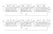
- FIG. 1 to FIG. 11are schematic diagrams showing an exemplary method for fabricating a semiconductor package with sidewall-protected RDL interposer according to one embodiment of the invention.
- wafer and substrate used hereininclude any structure having an exposed surface onto which a layer is deposited according to the present invention, for example, to form the circuit structure such as a redistribution layer (RDL).
- RDLredistribution layer
- substrateis understood to include semiconductor wafers, but not limited thereto.
- substrateis also used to refer to semiconductor structures during processing, and may include other layers that have been fabricated thereupon.
- FIG. 1 to FIG. 11are schematic diagrams showing an exemplary method for fabricating a semiconductor package with an encapsulated redistributed layer (RDL) interposer according to one embodiment of the invention.
- RDLredistributed layer
- a carrier 300is prepared.
- the carrier 300may be a releasable substrate material with an adhesive layer (not explicitly shown).
- the carrier 300may be a silicon wafer or a glass wafer, but is not limited thereto.
- At least a dielectric layer or a passivation layer 310is then formed on a top surface of the carrier 300 .
- the passivation layer 310may comprise organic materials such as polyimide (PI) or inorganic materials such as silicon nitride, silicon oxide or the like.
- a redistribution layer (RDL) layer 410is formed on the passivation layer 310 .
- the RDL layer 410may comprise at least one dielectric layer 412 and at least one metal layer 414 .
- the dielectric layer 412may comprise organic materials such as polyimide (PI) or inorganic materials such as silicon nitride, silicon oxide or the like, but not limited thereto.
- the metal layer 414may comprise aluminum, copper, tungsten, titanium, titanium nitride, or the like.
- the metal layer 414may comprise a plurality of bump pads 415 exposed from a top surface of the dielectric layer 412 .
- a passivation layer (or a dielectric layer) 510is formed on the RDL layer 410 . It is understood that the passivation layer 510 may comprise a solder mask, but is not limited thereto.
- a plurality of bumps 416such as micro-bumps may be formed on the RDL layer 410 for further connections.
- the bumps 416may be directly formed on respective bump pads 415 in the metal layer 414 .
- the formation of the bumps 416is known in the art. For example, openings may be formed in the passivation layer 510 to expose the respective bump pads 415 .
- an under-bump metallurgy (UBM) layermay be deposited. Thereafter, a photoresist layer defining the pattern of the bumps 416 is formed and a plating process may be carried out to form a metal bump on the UBM layer. After removing the photoresist layer, the UBM layer not covered by the metal bump is removed.
- UBMunder-bump metallurgy
- the bumps 416may comprise copper, but is not limited thereto. In some embodiments, the bumps 416 may be solder bumps and need to be ref lowed in a later stage.
- the passivation layer 310 , the RDL layer 410 and the passivation layer 510are collectively referred to as an RDL interposer 400 .
- These individual flip-chips or dies 420 a and 420 bare active integrated circuit chips with certain functions, for example, GPU (graphic processing unit), CPU (central processing unit), memory chips, etc.
- the die 420 a and the die 420 bmay be together disposed in one package and may be different chips with their specific functions.
- an underfill(not shown) may be applied under each die 420 a or 420 b .
- a thermal processmay be performed to reflow the bumps 416 .
- a sawing or cutting processis performed to form cut trenches 602 penetrating through the RDL interposer 400 , and extending slightly into the carrier 300 along the wafer dicing lines (or saw streets).
- the cut trench 602does not penetrate through the entire thickness of the carrier 300 .
- the cut trenches 602may be formed by using a dicing blade or a laser, but is not limited thereto.
- a molding compound 500is applied.
- the molding compound 500covers the attached dies 420 a and dies 420 b , and the top surface of the passivation layer 510 .
- the molding compound 500also covers the vertical sidewall 400 a of the RDL interposer 400 .
- the cut trenches 602may be completely filled up with the molding compound 500 .
- the molding compound 500may be subjected to a curing process.
- the mold compound 500may comprise a mixture of epoxy and silica fillers, but not limited thereto.
- an upper portion of the molding compound 500may be polished away to expose top surfaces of the dies 420 a and the dies 420 b.
- the carrier 300is removed or peeled off to expose a lower surface of the passivation layer 310 .
- the de-bonding of the carrier 300may be performed by using a laser process or UV irradiation process, but not limited thereto.
- protrudent features 512may be formed.
- a planarization processincluding, but not limited to, a chemical mechanical polishing (CMP) process, may be performed to remove the protrudent features 512 .
- CMPchemical mechanical polishing
- the protrudent features 512may be removed by other methods, for example, etching.
- the molding compound 500has a surface 500 a that is flush with a surface 310 a of the passivation layer 310 .
- a solder mask 312may be formed on the passivation layer 310 .
- a photographic processmay be performed to form openings 314 in the solder mask 312 and the passivation layer 310 to expose respective solder pads (or ball pads) 417 in the metal layer 414 of the RDL layer 410 .
- solder bumps or solder balls 520are formed on the respective solder pads 417 .
- the solder bumps or solder balls 520may be formed on a UBM layer.
- the formation of the solder bumps or solder balls 520are well-known in the art and therefore those details are omitted herein in the interest of brevity.
- the solder bumps or solder balls 520may be formed by plating, screen-printing, ball drop methods, or any suitable methods known in the art.
- each wafer level package 10may contain single die.
- the molding compound 500is in direct contact with the vertical sidewall 400 a of the RDL interposer 400 . It is advantageous to use the present invention as described above because the vertical sidewall 400 a of the RDL interposer 400 is protected by the molding compound 500 . Therefore, the cracking or delamination of the RDL interposer 400 may be effectively avoided.
- the molding compound 500is in direct contact with the solder mask 312 .
- the molding compound 500does not cover the sidewalls of the solder mask 312 .
Landscapes
- Engineering & Computer Science (AREA)
- Microelectronics & Electronic Packaging (AREA)
- Power Engineering (AREA)
- Computer Hardware Design (AREA)
- Physics & Mathematics (AREA)
- Condensed Matter Physics & Semiconductors (AREA)
- General Physics & Mathematics (AREA)
- Manufacturing & Machinery (AREA)
- Ceramic Engineering (AREA)
- Internal Circuitry In Semiconductor Integrated Circuit Devices (AREA)
- Structures Or Materials For Encapsulating Or Coating Semiconductor Devices Or Solid State Devices (AREA)
Abstract
Description
Claims (5)
Priority Applications (4)
| Application Number | Priority Date | Filing Date | Title |
|---|---|---|---|
| US15/068,649US9570369B1 (en) | 2016-03-14 | 2016-03-14 | Semiconductor package with sidewall-protected RDL interposer and fabrication method thereof |
| TW105113202ATWI587471B (en) | 2016-03-14 | 2016-04-28 | Semiconductor package with sidewall-protected rdl interposer and fabrication method thereof |
| CN201610649629.8ACN107195594B (en) | 2016-03-14 | 2016-08-10 | Semiconductor packages and its manufacturing method with side wall protection redistribution layer intermediary layer |
| US15/296,058US9786514B2 (en) | 2016-03-14 | 2016-10-18 | Semiconductor package with sidewall-protected RDL interposer |
Applications Claiming Priority (1)
| Application Number | Priority Date | Filing Date | Title |
|---|---|---|---|
| US15/068,649US9570369B1 (en) | 2016-03-14 | 2016-03-14 | Semiconductor package with sidewall-protected RDL interposer and fabrication method thereof |
Related Child Applications (1)
| Application Number | Title | Priority Date | Filing Date |
|---|---|---|---|
| US15/296,058DivisionUS9786514B2 (en) | 2016-03-14 | 2016-10-18 | Semiconductor package with sidewall-protected RDL interposer |
Publications (1)
| Publication Number | Publication Date |
|---|---|
| US9570369B1true US9570369B1 (en) | 2017-02-14 |
Family
ID=57965087
Family Applications (2)
| Application Number | Title | Priority Date | Filing Date |
|---|---|---|---|
| US15/068,649ActiveUS9570369B1 (en) | 2016-03-14 | 2016-03-14 | Semiconductor package with sidewall-protected RDL interposer and fabrication method thereof |
| US15/296,058ActiveUS9786514B2 (en) | 2016-03-14 | 2016-10-18 | Semiconductor package with sidewall-protected RDL interposer |
Family Applications After (1)
| Application Number | Title | Priority Date | Filing Date |
|---|---|---|---|
| US15/296,058ActiveUS9786514B2 (en) | 2016-03-14 | 2016-10-18 | Semiconductor package with sidewall-protected RDL interposer |
Country Status (3)
| Country | Link |
|---|---|
| US (2) | US9570369B1 (en) |
| CN (1) | CN107195594B (en) |
| TW (1) | TWI587471B (en) |
Cited By (12)
| Publication number | Priority date | Publication date | Assignee | Title |
|---|---|---|---|---|
| WO2019040384A1 (en)* | 2017-08-22 | 2019-02-28 | Micron Technology, Inc. | Semiconductor device |
| CN110676240A (en)* | 2019-10-16 | 2020-01-10 | 上海先方半导体有限公司 | 2.5D packaging structure and manufacturing method thereof |
| CN111384014A (en)* | 2018-12-28 | 2020-07-07 | 意法半导体有限公司 | Semiconductor package with sidewall connections |
| CN112397401A (en)* | 2019-08-14 | 2021-02-23 | 三星电子株式会社 | Method for manufacturing semiconductor package |
| CN112435996A (en)* | 2020-10-09 | 2021-03-02 | 日月光半导体制造股份有限公司 | Semiconductor package device and method of manufacturing the same |
| CN112687552A (en)* | 2019-10-17 | 2021-04-20 | 台湾积体电路制造股份有限公司 | Semiconductor package and manufacturing process thereof |
| CN112908948A (en)* | 2021-01-18 | 2021-06-04 | 上海先方半导体有限公司 | Packaging structure and manufacturing method thereof |
| CN112908947A (en)* | 2021-01-18 | 2021-06-04 | 上海先方半导体有限公司 | Plastic package structure and manufacturing method thereof |
| US11373954B2 (en) | 2019-08-21 | 2022-06-28 | Samsung Electronics Co., Ltd. | Semiconductor package |
| US20240021584A1 (en)* | 2020-05-28 | 2024-01-18 | Taiwan Semiconductor Manufacturing Company, Ltd. | Methods of fabricating the same die stack structure and semiconductor structure |
| US20240153861A1 (en)* | 2020-03-26 | 2024-05-09 | Taiwan Semiconductor Manufacturing Company, Ltd. | Manufacturing method of semiconductor package |
| US12033973B2 (en) | 2020-12-11 | 2024-07-09 | Samsung Electronics Co., Ltd. | Semiconductor package |
Families Citing this family (11)
| Publication number | Priority date | Publication date | Assignee | Title |
|---|---|---|---|---|
| US11322449B2 (en)* | 2017-10-31 | 2022-05-03 | Taiwan Semiconductor Manufacturing Co., Ltd. | Package with fan-out structures |
| TWI660473B (en)* | 2017-12-26 | 2019-05-21 | Industrial Technology Research Institute | Package structure and forming method thereof |
| CN109860125A (en)* | 2018-12-29 | 2019-06-07 | 华进半导体封装先导技术研发中心有限公司 | Chip packaging structure and packaging method |
| CN111627867A (en)* | 2019-02-28 | 2020-09-04 | 富泰华工业(深圳)有限公司 | Chip packaging structure and manufacturing method thereof |
| CN112018027B (en)* | 2019-05-31 | 2024-08-20 | 中芯国际集成电路制造(上海)有限公司 | Semiconductor structure, forming method thereof and wafer cutting method |
| KR102706158B1 (en)* | 2019-08-30 | 2024-09-11 | 삼성전자주식회사 | Method for manufacturing semiconductor package |
| CN111554641A (en) | 2020-05-11 | 2020-08-18 | 上海天马微电子有限公司 | Semiconductor package and method of making the same |
| CN111430313A (en)* | 2020-05-11 | 2020-07-17 | 上海天马微电子有限公司 | Semiconductor package and method of manufacturing the same |
| CN111952198B (en)* | 2020-08-25 | 2022-09-13 | 嘉兴启创科技咨询有限公司 | Semiconductor package and preparation method thereof |
| CN115332215B (en)* | 2022-10-14 | 2023-03-24 | 北京华封集芯电子有限公司 | Interposer for chip packaging and manufacturing method |
| WO2025182027A1 (en)* | 2024-02-29 | 2025-09-04 | 株式会社レゾナック | Method for manufacturing semiconductor device |
Citations (1)
| Publication number | Priority date | Publication date | Assignee | Title |
|---|---|---|---|---|
| US20160240466A1 (en)* | 2015-02-13 | 2016-08-18 | Siliconware Precision Industries Co., Ltd. | Electronic package and fabrication method thereof |
Family Cites Families (8)
| Publication number | Priority date | Publication date | Assignee | Title |
|---|---|---|---|---|
| US7268012B2 (en)* | 2004-08-31 | 2007-09-11 | Micron Technology, Inc. | Methods for fabrication of thin semiconductor assemblies including redistribution layers and packages and assemblies formed thereby |
| KR20100096879A (en)* | 2009-02-25 | 2010-09-02 | 삼성전자주식회사 | Devices including copper pads, stacked structures thereof and methods of manufacturing the same |
| TWI476888B (en)* | 2011-10-31 | 2015-03-11 | Unimicron Technology Corp | Package substrate having embedded via hole medium layer and fabrication method thereof |
| KR101419600B1 (en)* | 2012-11-20 | 2014-07-17 | 앰코 테크놀로지 코리아 주식회사 | Package of finger print sensor and fabricating method thereof |
| US9018045B2 (en)* | 2013-07-15 | 2015-04-28 | Freescale Semiconductor Inc. | Microelectronic packages and methods for the fabrication thereof |
| CN104425395A (en)* | 2013-08-20 | 2015-03-18 | 日月光半导体制造股份有限公司 | Semiconductor package and method of manufacturing the same |
| US20150187608A1 (en)* | 2013-12-26 | 2015-07-02 | Sanka Ganesan | Die package architecture with embedded die and simplified redistribution layer |
| TWI600133B (en)* | 2015-05-25 | 2017-09-21 | 美光科技公司 | Semiconductor device and fabrication method thereof |
- 2016
- 2016-03-14USUS15/068,649patent/US9570369B1/enactiveActive
- 2016-04-28TWTW105113202Apatent/TWI587471B/enactive
- 2016-08-10CNCN201610649629.8Apatent/CN107195594B/enactiveActive
- 2016-10-18USUS15/296,058patent/US9786514B2/enactiveActive
Patent Citations (1)
| Publication number | Priority date | Publication date | Assignee | Title |
|---|---|---|---|---|
| US20160240466A1 (en)* | 2015-02-13 | 2016-08-18 | Siliconware Precision Industries Co., Ltd. | Electronic package and fabrication method thereof |
Cited By (16)
| Publication number | Priority date | Publication date | Assignee | Title |
|---|---|---|---|---|
| WO2019040384A1 (en)* | 2017-08-22 | 2019-02-28 | Micron Technology, Inc. | Semiconductor device |
| US11688658B2 (en) | 2017-08-22 | 2023-06-27 | Micron Technology, Inc. | Semiconductor device |
| CN111384014A (en)* | 2018-12-28 | 2020-07-07 | 意法半导体有限公司 | Semiconductor package with sidewall connections |
| CN112397401A (en)* | 2019-08-14 | 2021-02-23 | 三星电子株式会社 | Method for manufacturing semiconductor package |
| US12062621B2 (en) | 2019-08-21 | 2024-08-13 | Samsung Electronics Co., Ltd. | Semiconductor package |
| US11373954B2 (en) | 2019-08-21 | 2022-06-28 | Samsung Electronics Co., Ltd. | Semiconductor package |
| CN110676240A (en)* | 2019-10-16 | 2020-01-10 | 上海先方半导体有限公司 | 2.5D packaging structure and manufacturing method thereof |
| CN112687552A (en)* | 2019-10-17 | 2021-04-20 | 台湾积体电路制造股份有限公司 | Semiconductor package and manufacturing process thereof |
| US12283541B2 (en)* | 2020-03-26 | 2025-04-22 | Taiwan Semiconductor Manufacturing Company, Ltd. | Manufacturing method of semiconductor package |
| US20240153861A1 (en)* | 2020-03-26 | 2024-05-09 | Taiwan Semiconductor Manufacturing Company, Ltd. | Manufacturing method of semiconductor package |
| US12119328B2 (en)* | 2020-05-28 | 2024-10-15 | Taiwan Semiconductor Manufacturing Company, Ltd. | Methods of fabricating the same die stack structure and semiconductor structure |
| US20240021584A1 (en)* | 2020-05-28 | 2024-01-18 | Taiwan Semiconductor Manufacturing Company, Ltd. | Methods of fabricating the same die stack structure and semiconductor structure |
| CN112435996A (en)* | 2020-10-09 | 2021-03-02 | 日月光半导体制造股份有限公司 | Semiconductor package device and method of manufacturing the same |
| US12033973B2 (en) | 2020-12-11 | 2024-07-09 | Samsung Electronics Co., Ltd. | Semiconductor package |
| CN112908947A (en)* | 2021-01-18 | 2021-06-04 | 上海先方半导体有限公司 | Plastic package structure and manufacturing method thereof |
| CN112908948A (en)* | 2021-01-18 | 2021-06-04 | 上海先方半导体有限公司 | Packaging structure and manufacturing method thereof |
Also Published As
| Publication number | Publication date |
|---|---|
| US20170263469A1 (en) | 2017-09-14 |
| TWI587471B (en) | 2017-06-11 |
| CN107195594A (en) | 2017-09-22 |
| CN107195594B (en) | 2018-12-04 |
| US9786514B2 (en) | 2017-10-10 |
| TW201733070A (en) | 2017-09-16 |
Similar Documents
| Publication | Publication Date | Title |
|---|---|---|
| US9570369B1 (en) | Semiconductor package with sidewall-protected RDL interposer and fabrication method thereof | |
| US12368115B2 (en) | Supporting InFO packages to reduce warpage | |
| US10446509B2 (en) | Methods of forming and operating microelectronic devices including dummy chips | |
| US11676939B2 (en) | Discrete polymer in fan-out packages | |
| US10699981B2 (en) | Non-vertical through-via in package | |
| US9520333B1 (en) | Wafer level package and fabrication method thereof | |
| US9761540B2 (en) | Wafer level package and fabrication method thereof | |
| US9704790B1 (en) | Method of fabricating a wafer level package | |
| US20120028411A1 (en) | Embedded Wafer-Level Bonding Approaches | |
| US11133282B2 (en) | COWOS structures and methods forming same | |
| US20170213801A1 (en) | Method for manufacturing a package-on-package assembly | |
| US20170062240A1 (en) | Method for manufacturing a wafer level package | |
| US9613895B1 (en) | Semiconductor package with double side molding | |
| US11728312B2 (en) | Semiconductor packaging and methods of forming same | |
| US9576931B1 (en) | Method for fabricating wafer level package | |
| US11756802B2 (en) | Thermally conductive material in the recess of an encapsulant and sidewall of an integrated circuit device |
Legal Events
| Date | Code | Title | Description |
|---|---|---|---|
| AS | Assignment | Owner name:INOTERA MEMORIES, INC., TAIWAN Free format text:ASSIGNMENT OF ASSIGNORS INTEREST;ASSIGNORS:SHIH, SHING-YIH;WU, TIEH-CHIANG;REEL/FRAME:037962/0279 Effective date:20160311 | |
| STCF | Information on status: patent grant | Free format text:PATENTED CASE | |
| AS | Assignment | Owner name:MORGAN STANLEY SENIOR FUNDING, INC., MARYLAND Free format text:SUPPLEMENT NO. 3 TO PATENT SECURITY AGREEMENT;ASSIGNOR:MICRON TECHNOLOGY, INC.;REEL/FRAME:041675/0105 Effective date:20170124 | |
| AS | Assignment | Owner name:MICRON TECHNOLOGY, INC., IDAHO Free format text:ASSIGNMENT OF ASSIGNORS INTEREST;ASSIGNOR:INOTERA MEMORIES, INC.;REEL/FRAME:041820/0815 Effective date:20170222 | |
| AS | Assignment | Owner name:JPMORGAN CHASE BANK, N.A., AS COLLATERAL AGENT, ILLINOIS Free format text:SECURITY INTEREST;ASSIGNORS:MICRON TECHNOLOGY, INC.;MICRON SEMICONDUCTOR PRODUCTS, INC.;REEL/FRAME:047540/0001 Effective date:20180703 Owner name:JPMORGAN CHASE BANK, N.A., AS COLLATERAL AGENT, IL Free format text:SECURITY INTEREST;ASSIGNORS:MICRON TECHNOLOGY, INC.;MICRON SEMICONDUCTOR PRODUCTS, INC.;REEL/FRAME:047540/0001 Effective date:20180703 | |
| AS | Assignment | Owner name:MICRON TECHNOLOGY, INC., IDAHO Free format text:RELEASE BY SECURED PARTY;ASSIGNOR:MORGAN STANLEY SENIOR FUNDING, INC., AS COLLATERAL AGENT;REEL/FRAME:050695/0825 Effective date:20190731 | |
| AS | Assignment | Owner name:MICRON TECHNOLOGY, INC., IDAHO Free format text:RELEASE BY SECURED PARTY;ASSIGNOR:JPMORGAN CHASE BANK, N.A., AS COLLATERAL AGENT;REEL/FRAME:051028/0001 Effective date:20190731 Owner name:MICRON SEMICONDUCTOR PRODUCTS, INC., IDAHO Free format text:RELEASE BY SECURED PARTY;ASSIGNOR:JPMORGAN CHASE BANK, N.A., AS COLLATERAL AGENT;REEL/FRAME:051028/0001 Effective date:20190731 | |
| MAFP | Maintenance fee payment | Free format text:PAYMENT OF MAINTENANCE FEE, 4TH YEAR, LARGE ENTITY (ORIGINAL EVENT CODE: M1551); ENTITY STATUS OF PATENT OWNER: LARGE ENTITY Year of fee payment:4 | |
| MAFP | Maintenance fee payment | Free format text:PAYMENT OF MAINTENANCE FEE, 8TH YEAR, LARGE ENTITY (ORIGINAL EVENT CODE: M1552); ENTITY STATUS OF PATENT OWNER: LARGE ENTITY Year of fee payment:8 |