US9564350B1 - Method and apparatus for storing and transporting semiconductor wafers in a vacuum pod - Google Patents
Method and apparatus for storing and transporting semiconductor wafers in a vacuum podDownload PDFInfo
- Publication number
- US9564350B1 US9564350B1US14/858,475US201514858475AUS9564350B1US 9564350 B1US9564350 B1US 9564350B1US 201514858475 AUS201514858475 AUS 201514858475AUS 9564350 B1US9564350 B1US 9564350B1
- Authority
- US
- United States
- Prior art keywords
- load port
- port module
- merged
- semiconductor wafers
- environment
- Prior art date
- Legal status (The legal status is an assumption and is not a legal conclusion. Google has not performed a legal analysis and makes no representation as to the accuracy of the status listed.)
- Expired - Fee Related
Links
- 235000012431wafersNutrition0.000titleclaimsabstractdescription149
- 239000004065semiconductorSubstances0.000titleclaimsabstractdescription64
- 238000000034methodMethods0.000titleclaimsabstractdescription36
- 238000012546transferMethods0.000claimsabstractdescription40
- 238000012545processingMethods0.000claimsabstractdescription28
- 239000012298atmosphereSubstances0.000claimsdescription12
- IJGRMHOSHXDMSA-UHFFFAOYSA-NAtomic nitrogenChemical compoundN#NIJGRMHOSHXDMSA-UHFFFAOYSA-N0.000claimsdescription11
- 239000012299nitrogen atmosphereSubstances0.000claimsdescription10
- 230000003247decreasing effectEffects0.000claimsdescription5
- 229910052757nitrogenInorganic materials0.000claimsdescription5
- 238000004519manufacturing processMethods0.000abstractdescription17
- 230000008569processEffects0.000abstractdescription13
- 238000011109contaminationMethods0.000abstractdescription9
- 238000003860storageMethods0.000description4
- 238000010586diagramMethods0.000description3
- 230000000694effectsEffects0.000description3
- 239000000463materialSubstances0.000description3
- 238000012986modificationMethods0.000description3
- 230000004048modificationEffects0.000description3
- 238000010926purgeMethods0.000description3
- 239000003795chemical substances by applicationSubstances0.000description2
- 238000005202decontaminationMethods0.000description2
- 230000007246mechanismEffects0.000description2
- 230000009227antibody-mediated cytotoxicityEffects0.000description1
- 238000013459approachMethods0.000description1
- 230000001413cellular effectEffects0.000description1
- 238000004140cleaningMethods0.000description1
- 239000000356contaminantSubstances0.000description1
- 239000011261inert gasSubstances0.000description1
- 239000004615ingredientSubstances0.000description1
- 239000004973liquid crystal related substanceSubstances0.000description1
- 230000006855networkingEffects0.000description1
- 230000008520organizationEffects0.000description1
- 230000002093peripheral effectEffects0.000description1
- 238000005498polishingMethods0.000description1
- 238000012805post-processingMethods0.000description1
- 239000000126substanceSubstances0.000description1
Images


Classifications
- H—ELECTRICITY
- H01—ELECTRIC ELEMENTS
- H01L—SEMICONDUCTOR DEVICES NOT COVERED BY CLASS H10
- H01L21/00—Processes or apparatus adapted for the manufacture or treatment of semiconductor or solid state devices or of parts thereof
- H01L21/67—Apparatus specially adapted for handling semiconductor or electric solid state devices during manufacture or treatment thereof; Apparatus specially adapted for handling wafers during manufacture or treatment of semiconductor or electric solid state devices or components ; Apparatus not specifically provided for elsewhere
- H01L21/677—Apparatus specially adapted for handling semiconductor or electric solid state devices during manufacture or treatment thereof; Apparatus specially adapted for handling wafers during manufacture or treatment of semiconductor or electric solid state devices or components ; Apparatus not specifically provided for elsewhere for conveying, e.g. between different workstations
- H01L21/67763—Apparatus specially adapted for handling semiconductor or electric solid state devices during manufacture or treatment thereof; Apparatus specially adapted for handling wafers during manufacture or treatment of semiconductor or electric solid state devices or components ; Apparatus not specifically provided for elsewhere for conveying, e.g. between different workstations the wafers being stored in a carrier, involving loading and unloading
- H01L21/67766—Mechanical parts of transfer devices
- B—PERFORMING OPERATIONS; TRANSPORTING
- B25—HAND TOOLS; PORTABLE POWER-DRIVEN TOOLS; MANIPULATORS
- B25J—MANIPULATORS; CHAMBERS PROVIDED WITH MANIPULATION DEVICES
- B25J11/00—Manipulators not otherwise provided for
- B25J11/0095—Manipulators transporting wafers
- H—ELECTRICITY
- H01—ELECTRIC ELEMENTS
- H01L—SEMICONDUCTOR DEVICES NOT COVERED BY CLASS H10
- H01L21/00—Processes or apparatus adapted for the manufacture or treatment of semiconductor or solid state devices or of parts thereof
- H01L21/67—Apparatus specially adapted for handling semiconductor or electric solid state devices during manufacture or treatment thereof; Apparatus specially adapted for handling wafers during manufacture or treatment of semiconductor or electric solid state devices or components ; Apparatus not specifically provided for elsewhere
- H01L21/673—Apparatus specially adapted for handling semiconductor or electric solid state devices during manufacture or treatment thereof; Apparatus specially adapted for handling wafers during manufacture or treatment of semiconductor or electric solid state devices or components ; Apparatus not specifically provided for elsewhere using specially adapted carriers or holders; Fixing the workpieces on such carriers or holders
- H01L21/6735—Closed carriers
- H01L21/67389—Closed carriers characterised by atmosphere control
- H—ELECTRICITY
- H01—ELECTRIC ELEMENTS
- H01L—SEMICONDUCTOR DEVICES NOT COVERED BY CLASS H10
- H01L21/00—Processes or apparatus adapted for the manufacture or treatment of semiconductor or solid state devices or of parts thereof
- H01L21/67—Apparatus specially adapted for handling semiconductor or electric solid state devices during manufacture or treatment thereof; Apparatus specially adapted for handling wafers during manufacture or treatment of semiconductor or electric solid state devices or components ; Apparatus not specifically provided for elsewhere
- H01L21/677—Apparatus specially adapted for handling semiconductor or electric solid state devices during manufacture or treatment thereof; Apparatus specially adapted for handling wafers during manufacture or treatment of semiconductor or electric solid state devices or components ; Apparatus not specifically provided for elsewhere for conveying, e.g. between different workstations
- H01L21/67763—Apparatus specially adapted for handling semiconductor or electric solid state devices during manufacture or treatment thereof; Apparatus specially adapted for handling wafers during manufacture or treatment of semiconductor or electric solid state devices or components ; Apparatus not specifically provided for elsewhere for conveying, e.g. between different workstations the wafers being stored in a carrier, involving loading and unloading
- H01L21/67775—Docking arrangements
- H—ELECTRICITY
- H01—ELECTRIC ELEMENTS
- H01L—SEMICONDUCTOR DEVICES NOT COVERED BY CLASS H10
- H01L21/00—Processes or apparatus adapted for the manufacture or treatment of semiconductor or solid state devices or of parts thereof
- H01L21/67—Apparatus specially adapted for handling semiconductor or electric solid state devices during manufacture or treatment thereof; Apparatus specially adapted for handling wafers during manufacture or treatment of semiconductor or electric solid state devices or components ; Apparatus not specifically provided for elsewhere
- H01L21/677—Apparatus specially adapted for handling semiconductor or electric solid state devices during manufacture or treatment thereof; Apparatus specially adapted for handling wafers during manufacture or treatment of semiconductor or electric solid state devices or components ; Apparatus not specifically provided for elsewhere for conveying, e.g. between different workstations
- H01L21/67763—Apparatus specially adapted for handling semiconductor or electric solid state devices during manufacture or treatment thereof; Apparatus specially adapted for handling wafers during manufacture or treatment of semiconductor or electric solid state devices or components ; Apparatus not specifically provided for elsewhere for conveying, e.g. between different workstations the wafers being stored in a carrier, involving loading and unloading
- H01L21/67778—Apparatus specially adapted for handling semiconductor or electric solid state devices during manufacture or treatment thereof; Apparatus specially adapted for handling wafers during manufacture or treatment of semiconductor or electric solid state devices or components ; Apparatus not specifically provided for elsewhere for conveying, e.g. between different workstations the wafers being stored in a carrier, involving loading and unloading involving loading and unloading of wafers
Definitions
- the present disclosurerelates generally to designing and fabricating integrated circuit (IC) devices.
- the present disclosureis particularly applicable to storing and transporting semiconductor wafers in a semiconductor fabrication facility.
- semiconductor manufacturersseek to reduce the number of processes and apparatus that are utilized in the fabrication facility, or maximize their efficiency. In some instances, the size of an apparatus may be reduced to allow for a more compact facility layout or for additional apparatus in the same layout.
- Semiconductor fabrication facilitiesutilize various processes and apparatus in fabricating IC devices on semiconductor wafers, which may be stored and transported, from one processing station/apparatus to a next one. While the wafers are stored or transported, they may be subjected to direct or wafer-to-wafer airborne molecular contamination (AMC) or moisture causing failures during subsequent fabrication processes. In some instances, additional processes and an inert gas (e.g., nitrogen (N 2 )) may be utilized to overcome some of the contamination/moisture issues.
- AMCwafer-to-wafer airborne molecular contamination
- N 2inert gas
- FIG. 1Aillustrates an example wafer processing system that includes a wafer processing apparatus 101 interfacing with an equipment front-end module (EFEM) 103 (e.g., a transfer chamber), which interfaces with load ports (LP) 105 .
- EFEMequipment front-end module
- LPload ports
- a front opening unified pod (FOUP) 107may be used to store wafers as well as to dock at a LP 105 for delivering wafers to the processing apparatus 101 .
- AMCequipment front-end module
- moisturee.g., directly or wafer-to-wafer
- the material (e.g., plastic) of a FOUP 107may absorb contaminants and later disperse them in the pod environment causing contamination of the wafers.
- FIG. 1Billustrates another example wafer processing system where LPs 109 may be purged by using a suitable purging agent (e.g., N 2 ), which may reduce AMCs and moisture in the FOUP 107 during storage and transportation of the wafers.
- a suitable purging agente.g., N 2
- this approachwould require new LPs 109 with a high consumption of purging agent, purging of the FOUP in storage to maintain the FOUP environment, and frequent cleaning of the FOUPs.
- the LPs 109 and FOUPs 107may have a purged atmosphere, the EFEM 103 does not and may still cause contamination of the wafers as they are transferred from and to the LPs 109 .
- FIG. 1Cillustrates another example wafer processing system where wafer pods 111 interface with LPs 113 , which directly interface with the processing apparatus 101 .
- This configurationrequires significant tool reconfiguration; for example, replacing load locks, modifying system software, and a faster automated material handling system (AMHS).
- AMHSautomated material handling system
- An aspect of the present disclosureis a method for using vacuum pods to store and transport semiconductor wafers to efficiently reduce contamination of the wafers while reducing cost, cycle time, and process steps and tools without the need for a complete reconfiguration of processes and tools in the fabrication facility.
- Another aspect of the present disclosureis a system using vacuum pods to store and transport semiconductor wafers to efficiently reduce contamination of the wafers while reducing cost, cycle time, and process steps and tools without the need for a complete reconfiguration of processes and tools in the fabrication facility.
- some technical effectsmay be achieved in part by a method including configuring a wafer pod with an isolated vacuum environment for storing and transporting semiconductor wafers; configuring a load port module with an isolated vacuum environment to interface with the wafer pod; transporting the wafer pod, including semiconductor wafers, to interlock with the load port module; creating a merged vacuum environment including the isolated vacuum environments of the wafer pod and the load port module; increasing a pressure level in the merged vacuum environment for creating a merged ambient atmospheric environment; and transferring the semiconductor wafers through a transfer chamber, with an isolated environment, from the load port module to a semiconductor wafer processing device.
- the wafer podinterfaces with the load port module at a lower surface of the wafer pod and an upper surface of the load port module.
- Another aspectincludes providing nitrogen for creating the merged ambient atmospheric environment.
- a further aspectincludes, subsequent to creating the merged vacuum environment in the merged environment, transferring the semiconductor wafers from the wafer pod to the load port module.
- Some aspectsinclude transferring processed semiconductor wafers, through the transfer chamber, from the semiconductor wafer processing device to the load port module; closing a valve between the load port module and the transfer chamber; and decreasing the pressure level in the merged ambient atmospheric environment to recreate a merged vacuum environment.
- An additional aspectincludes closing a door between the wafer pod and the load port module to recreate an isolated vacuum environment in the wafer pod.
- Another aspectincludes indexing the semiconductor wafers in the load port module.
- the isolated environment of the transfer chamberis a vacuum, an air atmosphere, or a nitrogen atmosphere.
- a transfer chamber with a vacuum or with a nitrogen atmosphereis smaller in size than a transfer chamber with an air atmosphere.
- Another aspect of the present disclosureincludes a system including: a wafer pod with an isolated vacuum environment for storing and transporting semiconductor wafers; a load port module with an isolated vacuum environment to interface with the wafer pod; an apparatus for transporting the wafer pod, including semiconductor wafers, to interlock with the load port module; an apparatus for creating a merged vacuum environment including the isolated vacuum environments of the wafer pod and the load port module; an apparatus for increasing a pressure level in the merged vacuum environment for creating a merged ambient atmospheric environment; and an apparatus for transferring the semiconductor wafers through a transfer chamber, with an isolated environment, from the load port module to a semiconductor wafer processing device.
- the wafer podinterfaces with the load port module at a lower surface of the wafer pod and an upper surface of the load port module.
- the systemincludes nitrogen in the apparatus for creating the merged atmospheric environment.
- One aspect of the systemincludes an apparatus for transferring the semiconductor wafers from the wafer pod to the load port module subsequent to creating the merged vacuum environment.
- a further aspect of the systemincludes an apparatus for transferring processed semiconductor wafers, through the transfer chamber, from the semiconductor wafer processing device to the load port module; a valve between the load port module and the transfer chamber for creating a merged vacuum environment; and an apparatus for decreasing the pressure level in the merged ambient atmospheric environment to recreate a merged vacuum environment.
- Another aspect of the systemincludes a door between the wafer pod and the load port module for recreating an isolated vacuum in the wafer pod.
- Another aspect of the systemincludes an apparatus for indexing the semiconductor wafers in the load port module.
- the isolated environment of the transfer chamberis a vacuum, an air atmosphere, or a nitrogen atmosphere.
- a transfer chamber with a vacuum or with a nitrogen atmosphereis smaller in size than a transfer chamber with an air atmosphere.
- FIGS. lA through 1 Cillustrate example wafer processing systems
- FIGS. 2A through 2Cillustrate wafer processing systems, in accordance with exemplary embodiments.
- the present disclosureaddresses and solves the problems of AMC, moisture levels, cycle times, high N 2 consumption, and fabrication facility layout attendant upon semiconductor wafer processing.
- the present disclosureaddresses and solves such problems without the need for a complete reconfiguration of processes and tools in the fabrication facility, for instance, by, inter alia, employing vacuum pods for storing and transporting the semiconductor wafers in the fabrication facility.
- the wafer pods and LPsare degassed at every process step eliminating the need for a dedicated pod regenerator tool, which makes available cleanroom space for more critical process tools.
- FIG. 2Aillustrates a wafer processing system in accordance with an exemplary embodiment including a processing apparatus 101 , an EFEM 115 , LPs 117 , and vacuum wafer pods 119 .
- a lower surface of the wafer pod 119may include an opening interfacing with an opening at an upper surface of an LP 117 .
- the LP 117may include another opening (e.g., on a side surface) interfacing with an opening at the EFEM 115 .
- the wafer pods 119may have an isolated vacuum environment for storing wafers or transferring them to an LP 117 .
- the interface between the LPs 117 and the EFEM 115may be a “box opener-loader tool standard” (BOLTS) interface developed by the Semiconductor Equipment and Materials International (SEMI) organization. BOLTS based LPs 117 may easily interface with already existing process tools.
- BOLTSbox opener-loader tool standard
- a wafer pod 119 at vacuum containing some wafersis transported (e.g., by AMHS) to and is docked at an LP 117 that is at vacuum (e.g., at some level of a vacuum environment).
- Vacuum environment of the LP 117may need to be pumped down to match that of the wafer pod 119 .
- openings/doors of the vacuum wafer pod 119 and LP 117are opened merging the two vacuum environments.
- the wafers in the wafer pod 119are lowered into the LP 117 and the merged vacuum environment is vented with N 2 or extra-clean dry air to atmospheric pressure.
- doors between the LP 117 and the EFEM 115are opened to allow a robot in the EFEM 115 to transfer the wafers to the processing apparatus 101 for processing (e.g., a chemical mechanical polishing).
- the LP 117is continuously purged with a low flow rate of N 2 (e.g., about 10 standard liters per minute (SLPM)) to maintain the N 2 concentration in the LP 117 .
- N 2standard liters per minute
- the wafersare transferred back to the LP 117 and the doors between the LP 117 and the EFEM 115 are closed so the merged N 2 atmosphere in the LP 117 and the wafer pod 119 can be pumped down to create a merged vacuum environment.
- the door on the wafer pod 119is closed to store the wafers in vacuum and transport them (e.g., by AMHS) to a next processing tool/station.
- FIG. 2BAdverting to FIG. 2B , another configuration in accordance with a second exemplary embodiment is illustrated where the EFEM 115 of FIG. 2A is replaced (e.g., reduced cost/space) by a transfer chamber 121 that may be at vacuum or at an ambient atmospheric pressure with air or N 2 environment.
- a transfer chamber 121 with a vacuum or with a N 2 atmospheremay be smaller in size than a transfer chamber with an air atmosphere.
- lower levels of AMC and moisturemay be maintained continuously while the layout of the processing system is reduced (e.g., smaller footprint) for a more compact fabrication facility layout or more space for additional equipment/stations.
- an LP 117may index the wafers included therein so that a more compact robot in a smaller transfer chamber 121 may easily access the already indexed wafers.
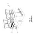
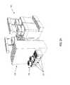
- FIG. 2Cis a diagram of an interface between an LP 117 and an EFEM 115 or 121 , in accordance with exemplary embodiments.
- the diagramis a view from inside an EFEM 115 / 121 illustrating a wafer pod 119 interfacing with an LP 117 for transporting semiconductor wafers 123 to the LP 117 .
- An interface between an LP 117 and an EFEM 115 / 121may include an opening 125 (e.g., on a side surface), through which, a robotic arm 127 in the EFEM may transfer the semiconductor wafers 123 from/to the LP 117 .
- the LP 117may include a mechanism for indexing the semiconductor wafers 123 as the robotic arm 127 transfers them into or out of the LP 117 .
- the robotic arm 127may include a mechanism to index the semiconductor wafers 123 as it transfers them into or out of the LP 117 .
- semiconductor wafers 123may be indexed in an LP 117 since there may be limited space for indexing movements of a robotic arm 127 .
- the embodiments of the present disclosurecan achieve several technical effects in semiconductor manufacturing including eliminating molecular contamination as a yield detractor, eliminating manufacturing queue time constraints that limit production capacity, reducing process equipment footprint, and lowering cost of manufacturing and N 2 consumption.
- the N 2 consumptionis reduced by drastically minimizing its use at LPs as well as eliminating the need for the N 2 during wafer storage in vacuum wafer pods.
- the vacuum wafer pods and wafersare degassed at every process step, which eliminates the need for a FOUP decontamination process and tool. Reducing the decontamination process eliminates a critical time link as well as a process step, making available cleanroom space for more critical process tools.
- Two common wafer environment control processesare replaced by simply storing wafers in a vacuum atmosphere.
- the embodimentsenjoy utility in various industrial applications as, for example, microprocessors, smart phones, mobile phones, cellular handsets, set-top boxes, DVD recorders and players, automotive navigation, printers and peripherals, networking and telecom equipment, gaming systems, digital cameras, or other devices utilizing logic or high-voltage technology nodes.
- the present disclosuretherefore enjoys industrial applicability in any of various types of highly integrated semiconductor devices, including devices that use static-random-access memory (SRAM) cells (e.g., liquid crystal display (LCD) drivers, digital processors, etc.)
- SRAMstatic-random-access memory
Landscapes
- Engineering & Computer Science (AREA)
- Physics & Mathematics (AREA)
- Condensed Matter Physics & Semiconductors (AREA)
- General Physics & Mathematics (AREA)
- Manufacturing & Machinery (AREA)
- Computer Hardware Design (AREA)
- Microelectronics & Electronic Packaging (AREA)
- Power Engineering (AREA)
- Robotics (AREA)
- Mechanical Engineering (AREA)
- Container, Conveyance, Adherence, Positioning, Of Wafer (AREA)
Abstract
Description
Claims (20)
Priority Applications (1)
| Application Number | Priority Date | Filing Date | Title |
|---|---|---|---|
| US14/858,475US9564350B1 (en) | 2015-09-18 | 2015-09-18 | Method and apparatus for storing and transporting semiconductor wafers in a vacuum pod |
Applications Claiming Priority (1)
| Application Number | Priority Date | Filing Date | Title |
|---|---|---|---|
| US14/858,475US9564350B1 (en) | 2015-09-18 | 2015-09-18 | Method and apparatus for storing and transporting semiconductor wafers in a vacuum pod |
Publications (1)
| Publication Number | Publication Date |
|---|---|
| US9564350B1true US9564350B1 (en) | 2017-02-07 |
Family
ID=57908779
Family Applications (1)
| Application Number | Title | Priority Date | Filing Date |
|---|---|---|---|
| US14/858,475Expired - Fee RelatedUS9564350B1 (en) | 2015-09-18 | 2015-09-18 | Method and apparatus for storing and transporting semiconductor wafers in a vacuum pod |
Country Status (1)
| Country | Link |
|---|---|
| US (1) | US9564350B1 (en) |
Cited By (1)
| Publication number | Priority date | Publication date | Assignee | Title |
|---|---|---|---|---|
| US20190326147A1 (en)* | 2014-11-11 | 2019-10-24 | Applied Materials, Inc. | Multi-cassette carrying case |
Citations (33)
| Publication number | Priority date | Publication date | Assignee | Title |
|---|---|---|---|---|
| US4724874A (en)* | 1986-05-01 | 1988-02-16 | Asyst Technologies | Sealable transportable container having a particle filtering system |
| US5139459A (en)* | 1990-10-22 | 1992-08-18 | Tdk Corporation | Clean transfer method and system therefor |
| US5364219A (en)* | 1991-06-24 | 1994-11-15 | Tdk Corporation | Apparatus for clean transfer of objects |
| US5462397A (en)* | 1993-03-16 | 1995-10-31 | Tokyo Electron Limited | Processing apparatus |
| US5586585A (en)* | 1995-02-27 | 1996-12-24 | Asyst Technologies, Inc. | Direct loadlock interface |
| US5628683A (en)* | 1992-03-09 | 1997-05-13 | Josef Gentischer | System for transferring substrates into clean rooms |
| US5695564A (en)* | 1994-08-19 | 1997-12-09 | Tokyo Electron Limited | Semiconductor processing system |
| US5697749A (en)* | 1992-07-17 | 1997-12-16 | Tokyo Electron Kabushiki Kaisha | Wafer processing apparatus |
| US5697748A (en)* | 1993-07-15 | 1997-12-16 | Applied Materials, Inc. | Wafer tray and ceramic blade for semiconductor processing apparatus |
| US5730573A (en)* | 1994-02-22 | 1998-03-24 | Tdk Corporation | Clean transfer method and apparatus therefor |
| US5984610A (en)* | 1995-03-07 | 1999-11-16 | Fortrend Engineering Corporation | Pod loader interface |
| US6048154A (en)* | 1996-10-02 | 2000-04-11 | Applied Materials, Inc. | High vacuum dual stage load lock and method for loading and unloading wafers using a high vacuum dual stage load lock |
| US6082948A (en)* | 1992-11-06 | 2000-07-04 | Applied Materials, Inc. | Controlled environment enclosure and mechanical interface |
| US6152669A (en)* | 1995-11-13 | 2000-11-28 | Shinko Electric Co., Ltd. | Mechanical interface apparatus |
| US6176667B1 (en)* | 1996-04-30 | 2001-01-23 | Applied Materials, Inc. | Multideck wafer processing system |
| US6338604B1 (en)* | 1999-08-11 | 2002-01-15 | Tdk Corporation | Lid latch mechanism for clean box |
| US6428262B1 (en)* | 1999-08-11 | 2002-08-06 | Proteros, Llc | Compact load lock system for ion beam processing of foups |
| US6537011B1 (en)* | 2000-03-10 | 2003-03-25 | Applied Materials, Inc. | Method and apparatus for transferring and supporting a substrate |
| US6540465B2 (en)* | 2000-03-30 | 2003-04-01 | Hitachi Kokusai Electric Inc. | Substrate processing apparatus |
| US6641349B1 (en)* | 1999-04-30 | 2003-11-04 | Tdk Corporation | Clean box, clean transfer method and system |
| US20040126206A1 (en)* | 2001-01-05 | 2004-07-01 | Tdk Corporation | Mini-environment system and operating method thereof |
| US20040234359A1 (en)* | 2003-05-22 | 2004-11-25 | Axcelis Technologies, Inc. | Work-piece treatment system having load lock and buffer |
| US20060285944A1 (en)* | 2005-06-21 | 2006-12-21 | Varian Semiconductor Equipment Associates, Inc. | FOUP loading load lock |
| US7198447B2 (en)* | 2002-09-12 | 2007-04-03 | Hitachi Kokusai Electric Inc. | Semiconductor device producing apparatus and producing method of semiconductor device |
| US20080080963A1 (en) | 2005-11-07 | 2008-04-03 | Bufano Michael L | Reduced capacity carrier, transport, load port, buffer system |
| US20100014945A1 (en)* | 2008-07-16 | 2010-01-21 | Asm Japan K.K. | Semiconductor processing apparatus having all-round type wafer handling chamber |
| US8303231B2 (en)* | 2007-09-28 | 2012-11-06 | Taiwan Semiconductor Manufacturing Company Ltd. | Apparatus and method for semiconductor wafer transfer |
| US8562271B2 (en)* | 2007-05-18 | 2013-10-22 | Brooks Automation, Inc. | Compact substrate transport system |
| US8950999B2 (en)* | 2007-01-31 | 2015-02-10 | Tokyo Electron Limited | Substrate processing apparatus and particle adhesion preventing method |
| US20150063955A1 (en)* | 2013-09-04 | 2015-03-05 | Tokyo Electron Limited | Load port device and substrate processing apparatus |
| US20150133044A1 (en)* | 2012-05-16 | 2015-05-14 | Tokyo Electron Limited | Cooling mechanism and processing system |
| US20150170945A1 (en)* | 2013-12-13 | 2015-06-18 | Sinfonia Technology Co., Ltd. | Efem |
| US20160079100A1 (en)* | 2014-09-17 | 2016-03-17 | Lam Research Corporation | Vacuum carrier interface having a switchable reduced capacity airlock chamber |
- 2015
- 2015-09-18USUS14/858,475patent/US9564350B1/ennot_activeExpired - Fee Related
Patent Citations (33)
| Publication number | Priority date | Publication date | Assignee | Title |
|---|---|---|---|---|
| US4724874A (en)* | 1986-05-01 | 1988-02-16 | Asyst Technologies | Sealable transportable container having a particle filtering system |
| US5139459A (en)* | 1990-10-22 | 1992-08-18 | Tdk Corporation | Clean transfer method and system therefor |
| US5364219A (en)* | 1991-06-24 | 1994-11-15 | Tdk Corporation | Apparatus for clean transfer of objects |
| US5628683A (en)* | 1992-03-09 | 1997-05-13 | Josef Gentischer | System for transferring substrates into clean rooms |
| US5697749A (en)* | 1992-07-17 | 1997-12-16 | Tokyo Electron Kabushiki Kaisha | Wafer processing apparatus |
| US6082948A (en)* | 1992-11-06 | 2000-07-04 | Applied Materials, Inc. | Controlled environment enclosure and mechanical interface |
| US5462397A (en)* | 1993-03-16 | 1995-10-31 | Tokyo Electron Limited | Processing apparatus |
| US5697748A (en)* | 1993-07-15 | 1997-12-16 | Applied Materials, Inc. | Wafer tray and ceramic blade for semiconductor processing apparatus |
| US5730573A (en)* | 1994-02-22 | 1998-03-24 | Tdk Corporation | Clean transfer method and apparatus therefor |
| US5695564A (en)* | 1994-08-19 | 1997-12-09 | Tokyo Electron Limited | Semiconductor processing system |
| US5586585A (en)* | 1995-02-27 | 1996-12-24 | Asyst Technologies, Inc. | Direct loadlock interface |
| US5984610A (en)* | 1995-03-07 | 1999-11-16 | Fortrend Engineering Corporation | Pod loader interface |
| US6152669A (en)* | 1995-11-13 | 2000-11-28 | Shinko Electric Co., Ltd. | Mechanical interface apparatus |
| US6176667B1 (en)* | 1996-04-30 | 2001-01-23 | Applied Materials, Inc. | Multideck wafer processing system |
| US6048154A (en)* | 1996-10-02 | 2000-04-11 | Applied Materials, Inc. | High vacuum dual stage load lock and method for loading and unloading wafers using a high vacuum dual stage load lock |
| US6641349B1 (en)* | 1999-04-30 | 2003-11-04 | Tdk Corporation | Clean box, clean transfer method and system |
| US6428262B1 (en)* | 1999-08-11 | 2002-08-06 | Proteros, Llc | Compact load lock system for ion beam processing of foups |
| US6338604B1 (en)* | 1999-08-11 | 2002-01-15 | Tdk Corporation | Lid latch mechanism for clean box |
| US6537011B1 (en)* | 2000-03-10 | 2003-03-25 | Applied Materials, Inc. | Method and apparatus for transferring and supporting a substrate |
| US6540465B2 (en)* | 2000-03-30 | 2003-04-01 | Hitachi Kokusai Electric Inc. | Substrate processing apparatus |
| US20040126206A1 (en)* | 2001-01-05 | 2004-07-01 | Tdk Corporation | Mini-environment system and operating method thereof |
| US7198447B2 (en)* | 2002-09-12 | 2007-04-03 | Hitachi Kokusai Electric Inc. | Semiconductor device producing apparatus and producing method of semiconductor device |
| US20040234359A1 (en)* | 2003-05-22 | 2004-11-25 | Axcelis Technologies, Inc. | Work-piece treatment system having load lock and buffer |
| US20060285944A1 (en)* | 2005-06-21 | 2006-12-21 | Varian Semiconductor Equipment Associates, Inc. | FOUP loading load lock |
| US20080080963A1 (en) | 2005-11-07 | 2008-04-03 | Bufano Michael L | Reduced capacity carrier, transport, load port, buffer system |
| US8950999B2 (en)* | 2007-01-31 | 2015-02-10 | Tokyo Electron Limited | Substrate processing apparatus and particle adhesion preventing method |
| US8562271B2 (en)* | 2007-05-18 | 2013-10-22 | Brooks Automation, Inc. | Compact substrate transport system |
| US8303231B2 (en)* | 2007-09-28 | 2012-11-06 | Taiwan Semiconductor Manufacturing Company Ltd. | Apparatus and method for semiconductor wafer transfer |
| US20100014945A1 (en)* | 2008-07-16 | 2010-01-21 | Asm Japan K.K. | Semiconductor processing apparatus having all-round type wafer handling chamber |
| US20150133044A1 (en)* | 2012-05-16 | 2015-05-14 | Tokyo Electron Limited | Cooling mechanism and processing system |
| US20150063955A1 (en)* | 2013-09-04 | 2015-03-05 | Tokyo Electron Limited | Load port device and substrate processing apparatus |
| US20150170945A1 (en)* | 2013-12-13 | 2015-06-18 | Sinfonia Technology Co., Ltd. | Efem |
| US20160079100A1 (en)* | 2014-09-17 | 2016-03-17 | Lam Research Corporation | Vacuum carrier interface having a switchable reduced capacity airlock chamber |
Cited By (1)
| Publication number | Priority date | Publication date | Assignee | Title |
|---|---|---|---|---|
| US20190326147A1 (en)* | 2014-11-11 | 2019-10-24 | Applied Materials, Inc. | Multi-cassette carrying case |
Similar Documents
| Publication | Publication Date | Title |
|---|---|---|
| US10679879B2 (en) | Substrate processing apparatus | |
| JP7263639B2 (en) | Substrate transfer section | |
| US20180114710A1 (en) | Equipment front end module and semiconductor manufacturing apparatus including the same | |
| KR20160028428A (en) | Pressure Controlled Wafer Carrier and Wafer Transportation System | |
| US9209055B2 (en) | Substrate processing apparatus | |
| US8544651B2 (en) | Wafer transfer pod for reducing wafer particulate contamination | |
| KR20030011536A (en) | Loadport, substrate processing apparatus and method of substituting atmosphere | |
| US10510572B2 (en) | Semiconductor processing station | |
| US9064807B2 (en) | Integrated platform for improved wafer manufacturing quality | |
| US8540473B2 (en) | Load port | |
| KR20190098056A (en) | Substrate transfer apparatus and substrate processing system | |
| US7398801B2 (en) | Apparatus and method for processing wafers | |
| US20250316509A1 (en) | Apparatus for manufacturing a bonded semiconductor structure and method for manufacturing the same | |
| JP4344370B2 (en) | Front opening shipping box and its operation method | |
| US20230178401A1 (en) | Modular pressurized workstation | |
| US9564350B1 (en) | Method and apparatus for storing and transporting semiconductor wafers in a vacuum pod | |
| US20040165973A1 (en) | Apparatus and method for processing wafers | |
| TWI750603B (en) | Substrate processing apparatus and substrate processing method | |
| US20120288355A1 (en) | Method for storing wafers | |
| CN109300828B (en) | Wafer transmission system and transmission method | |
| US12347702B2 (en) | Wet processing system and system and method for manufacturing semiconductor structure | |
| CN115101457A (en) | Wafer front-end transfer systems and semiconductor processing equipment | |
| US12308271B2 (en) | Semiconductor wafer processing system and method | |
| US20020153578A1 (en) | Wafer buffering system | |
| CN119108308A (en) | In-liquid posture conversion device and substrate processing device equipped with the same |
Legal Events
| Date | Code | Title | Description |
|---|---|---|---|
| AS | Assignment | Owner name:GLOBALFOUNDRIES INC., CAYMAN ISLANDS Free format text:ASSIGNMENT OF ASSIGNORS INTEREST;ASSIGNORS:FOSNIGHT, WILLIAM;WAITE, STEPHANIE;REEL/FRAME:036602/0448 Effective date:20150911 | |
| FEPP | Fee payment procedure | Free format text:PAYOR NUMBER ASSIGNED (ORIGINAL EVENT CODE: ASPN); ENTITY STATUS OF PATENT OWNER: LARGE ENTITY | |
| STCF | Information on status: patent grant | Free format text:PATENTED CASE | |
| AS | Assignment | Owner name:WILMINGTON TRUST, NATIONAL ASSOCIATION, DELAWARE Free format text:SECURITY AGREEMENT;ASSIGNOR:GLOBALFOUNDRIES INC.;REEL/FRAME:049490/0001 Effective date:20181127 | |
| FEPP | Fee payment procedure | Free format text:MAINTENANCE FEE REMINDER MAILED (ORIGINAL EVENT CODE: REM.); ENTITY STATUS OF PATENT OWNER: LARGE ENTITY | |
| AS | Assignment | Owner name:GLOBALFOUNDRIES INC., CAYMAN ISLANDS Free format text:RELEASE BY SECURED PARTY;ASSIGNOR:WILMINGTON TRUST, NATIONAL ASSOCIATION;REEL/FRAME:054636/0001 Effective date:20201117 | |
| LAPS | Lapse for failure to pay maintenance fees | Free format text:PATENT EXPIRED FOR FAILURE TO PAY MAINTENANCE FEES (ORIGINAL EVENT CODE: EXP.); ENTITY STATUS OF PATENT OWNER: LARGE ENTITY | |
| STCH | Information on status: patent discontinuation | Free format text:PATENT EXPIRED DUE TO NONPAYMENT OF MAINTENANCE FEES UNDER 37 CFR 1.362 | |
| FP | Lapsed due to failure to pay maintenance fee | Effective date:20210207 | |
| AS | Assignment | Owner name:GLOBALFOUNDRIES U.S. INC., NEW YORK Free format text:RELEASE BY SECURED PARTY;ASSIGNOR:WILMINGTON TRUST, NATIONAL ASSOCIATION;REEL/FRAME:056987/0001 Effective date:20201117 |