US9564227B2 - Memory device having a different source line coupled to each of a plurality of layers of memory cell arrays - Google Patents
Memory device having a different source line coupled to each of a plurality of layers of memory cell arraysDownload PDFInfo
- Publication number
- US9564227B2 US9564227B2US14/936,719US201514936719AUS9564227B2US 9564227 B2US9564227 B2US 9564227B2US 201514936719 AUS201514936719 AUS 201514936719AUS 9564227 B2US9564227 B2US 9564227B2
- Authority
- US
- United States
- Prior art keywords
- layers
- voltage
- memory cells
- memory
- layer
- Prior art date
- Legal status (The legal status is an assumption and is not a legal conclusion. Google has not performed a legal analysis and makes no representation as to the accuracy of the status listed.)
- Active
Links
Images


Classifications
- G—PHYSICS
- G11—INFORMATION STORAGE
- G11C—STATIC STORES
- G11C16/00—Erasable programmable read-only memories
- G11C16/02—Erasable programmable read-only memories electrically programmable
- G11C16/06—Auxiliary circuits, e.g. for writing into memory
- G11C16/10—Programming or data input circuits
- G—PHYSICS
- G11—INFORMATION STORAGE
- G11C—STATIC STORES
- G11C11/00—Digital stores characterised by the use of particular electric or magnetic storage elements; Storage elements therefor
- G11C11/56—Digital stores characterised by the use of particular electric or magnetic storage elements; Storage elements therefor using storage elements with more than two stable states represented by steps, e.g. of voltage, current, phase, frequency
- G11C11/5621—Digital stores characterised by the use of particular electric or magnetic storage elements; Storage elements therefor using storage elements with more than two stable states represented by steps, e.g. of voltage, current, phase, frequency using charge storage in a floating gate
- G11C11/5642—Sensing or reading circuits; Data output circuits
- G—PHYSICS
- G11—INFORMATION STORAGE
- G11C—STATIC STORES
- G11C16/00—Erasable programmable read-only memories
- G11C16/02—Erasable programmable read-only memories electrically programmable
- G11C16/04—Erasable programmable read-only memories electrically programmable using variable threshold transistors, e.g. FAMOS
- G11C16/0483—Erasable programmable read-only memories electrically programmable using variable threshold transistors, e.g. FAMOS comprising cells having several storage transistors connected in series
- G—PHYSICS
- G11—INFORMATION STORAGE
- G11C—STATIC STORES
- G11C16/00—Erasable programmable read-only memories
- G11C16/02—Erasable programmable read-only memories electrically programmable
- G11C16/06—Auxiliary circuits, e.g. for writing into memory
- G11C16/26—Sensing or reading circuits; Data output circuits
- G11C16/28—Sensing or reading circuits; Data output circuits using differential sensing or reference cells, e.g. dummy cells
- G—PHYSICS
- G11—INFORMATION STORAGE
- G11C—STATIC STORES
- G11C5/00—Details of stores covered by group G11C11/00
- G11C5/02—Disposition of storage elements, e.g. in the form of a matrix array
- G—PHYSICS
- G11—INFORMATION STORAGE
- G11C—STATIC STORES
- G11C5/00—Details of stores covered by group G11C11/00
- G11C5/02—Disposition of storage elements, e.g. in the form of a matrix array
- G11C5/025—Geometric lay-out considerations of storage- and peripheral-blocks in a semiconductor storage device
Definitions
- the present embodimentsrelate generally to memory and a particular embodiment relates to sense operations in a stacked memory array device.
- Flash memory deviceshave developed into a popular source of non-volatile memory for a wide range of electronic applications. Flash memory devices typically use a one-transistor memory cell that allows for high memory densities, high reliability, and low power consumption. Common uses for flash memory include personal computers, flash drives, digital cameras, and cellular telephones. Program code and system data such as a basic input/output system (BIOS) are typically stored in flash memory devices for use in personal computer systems.
- BIOSbasic input/output system
- a typical flash memory deviceis a type of memory in which the array of memory cells is typically organized into memory blocks that can be erased and reprogrammed on block-by-block basis instead of one byte at a time.
- Changes in a threshold voltage of each of the memory cellsthrough erasing or programming of a charge storage structure (e.g., floating gate or charge trap) or other physical phenomena (e.g., phase change or polarization), determine the data value of each cell.
- the data in a cell of this typeis determined by the presence or absence of the charge in the charge storage structure.
- FIG. 1illustrates one example of the architecture of a typical prior art stacked NAND flash memory array.
- FIG. 1shows a two layer 100 , 101 stacked architecture. Both layers 100 , 101 share the same source line 103 , access lines (e.g., word lines) 105 - 107 , and select gate source lines 110 . Each layer 100 , 101 is selected by the data line (e.g., bit line) 120 , 121 bias.
- the bottom layer array 101is coupled to bit line BL 0 120 and the top layer array 100 is coupled to bit line BL 1 121 .
- FIG. 2shows a diagram of voltages for typical prior art memory operations (e.g., programming, sense, and erase) that can be executed in a stacked memory array architecture. To better illustrate the operations, a four layer architecture is assumed.
- typical prior art memory operationse.g., programming, sense, and erase
- the programming operationincludes applying a programming voltage (e.g., 20V) to the selected word lines 201 being programmed. Since a word line is shared by all layers, bit line biasing (e.g., applying a bit line voltage) is used to inhibit layers that are not selected for programming.
- bit line biasinge.g., applying a bit line voltage
- the first and third layersare selected to be programmed so their respective bit lines are biased at an enable voltage (e.g., 0V) while the unselected bit lines are biased at an inhibit voltage (e.g., 2V).
- an enable voltagee.g., 0V
- an inhibit voltagee.g. 2V
- all of the layerscan be selected substantially simultaneously while, in the sense operation, only one row of each layer is selected.
- all of the bit linesare biased at a lower voltage (e.g., 0.5V) while the read voltage (V r ) is applied to the common word line 202 .
- the unselected word linesare biased at some pass voltage V pass (e.g., 6V), the select gate lines are turned on (e.g., 5V).
- all of the bit linesare biased at a relatively large erase voltage (e.g., 20V) while all of the word lines are biased at a reference voltage (e.g., 0V).
- the select gate drain lines and common select gate source linesare biased with a relatively large voltage (e.g., 20V).
- One problem with programming in a stacked memory array architectureis the programming disturb that can occur due to a programming rate offset between layers. For example, referring to FIG. 2 , if the first layer programs at a slower rate than the fourth layer, the relatively large voltages applied to the slower first layer in order to continue programming the first layer for a longer time than the faster fourth layer can cause programming stress to the fourth layer. Such disturb can cause errors during sense operations since the memory cell threshold voltages on the disturbed layer can be increased from the originally programmed voltage levels.
- FIG. 1shows a schematic diagram of a typical prior art two layer stacked NAND memory array.
- FIG. 2shows a diagram of typical prior art biasing for program, sense, and erase operations in a four layer stacked NAND memory array.
- FIG. 3shows a schematic diagram of one embodiment of a portion of a NAND architecture memory array.
- FIG. 4shows a diagram of one embodiment of biasing for providing a sense offset by layer.
- FIG. 5shows a diagram of one embodiment of threshold voltage distributions for both slow and fast programming layers in accordance with the embodiment of FIG. 4 .
- FIG. 6shows a flowchart of one embodiment of a method for performing a sense operation on a memory array in accordance with the embodiment of FIG. 4 .
- FIG. 7shows a schematic diagram of an alternate embodiment of a stacked memory array device architecture.
- FIG. 8shows a diagram of one embodiment for bit line and source line biasing in accordance with the embodiment of FIG. 7 .
- FIG. 9shows a schematic diagram of another embodiment of a stacked memory array architecture.
- FIG. 10shows a diagram of one embodiment of bit line and source line biasing in accordance with the embodiment of FIG. 9 .
- FIG. 11shows a diagram of yet another embodiment of a stacked memory array architecture.
- FIGS. 12A and 12Billustrate diagrams of layer selection and word line offset by layer in accordance with the embodiment of FIG. 11 , where FIG. 12A illustrates word line biasing for slower programming layers and where FIG. 12B illustrates word line biasing that includes an offset voltage for faster programming layers.
- FIG. 13shows a block diagram of one embodiment of a memory system that can incorporate a stacked memory array architecture using the described methods for sense operations.
- FIG. 3illustrates a schematic diagram of one embodiment of a portion of a single layer of a NAND architecture memory array 301 comprising series strings of non-volatile memory cells.
- the stacked array architecturecan include multiple layers of the embodiment of FIG. 3 .
- the schematic diagram of FIG. 3is for purposes of illustration only as the memory array architecture is not limited to the illustrated NAND architecture. Alternate embodiments can use NOR or other architectures as well.
- the memory array 301comprises an array of non-volatile memory cells (e.g., floating gate) arranged in columns such as series strings 304 , 305 . Each of the cells is coupled drain to source in each series string 304 , 305 .
- An access linee.g. word line
- WL 0 -WL 31that spans across multiple series strings 304 , 305 is coupled to the control gates of each memory cell in a row in order to bias the control gates of the memory cells in the row.
- Data linessuch as even/odd bit lines BL_E, BL_O, are coupled to the series strings and eventually each bit line is coupled to a page buffer with sense circuitry that detects the state of each cell by sensing current or voltage on a selected bit line.
- Each series string 304 , 305 of memory cellsis coupled to a source line 306 by a source select gate 316 , 317 (e.g., transistor) and to an individual bit line BL_E, BL_O by a drain select gate 312 , 313 (e.g., transistor).
- the source select gates 316 , 317are controlled by a source select gate control line SG(S) 318 coupled to their control gates.
- the drain select gates 312 , 313are controlled by a drain select gate control line SG(D) 314 .
- Each memory cellcan be programmed as a single level cell (SLC) or a multiple level cell (MLC).
- Each cell's threshold voltage (V t )is indicative of the data that is stored in the cell. For example, in an SLC, a V t of 2.5V might indicate a programmed cell while a V t of ⁇ 0.5V might indicate an erased cell.
- An MLCuses multiple V t ranges that each indicates a different state. Multilevel cells can take advantage of the analog nature of a traditional flash cell by assigning a bit pattern to a specific V t range. This technology permits the storage of data values representing two or more bits per cell, depending on the quantity of V t ranges assigned to the cell.
- a sense operation on a stacked memory array architecturesenses multiple layers simultaneously.
- a sense offsetcan be used on a per layer basis.
- the sense conditions for each layerare changed responsive (e.g., according) to the programming rate of that particular layer in relation to the other layers.
- the programming ratecan, for example, be determined at manufacture or predetermined.
- changing the sense conditions on a per layer basiscan include shifting the target V, range of slower programming layers to a lower V t range relative to a V t of a faster programming layer. This can be accomplished by sensing a higher sense current for the slower programming layers, precharging the bit lines of the slower programming layers to a higher pre-charge voltage, sensing the bit lines of slower programming layers with a higher bit line voltage than faster programming layers, and/or using a shorter bit line discharge time for the slower programming layers, relative to faster programming layers, during the sense operation. Alternate embodiments can use other ways to change the sense conditions on a per layer basis.
- FIG. 4illustrates one embodiment of biasing for providing a sense offset according to layer.
- the diagram of FIG. 4shows four layers that are respectively selected by their respective bit line BL 0 -BL 3 . Physical connections are denoted by a dot on intersections of signal lines. For example, the source line SRC is connected to each of the four layers while each bit line BL 0 -BL 3 is only connected to its respective layer.
- FIG. 4further shows a select gate source SG(S), a select gate drain SG(D), the source line SRC, and five word lines 400 - 402 that include the word line WLn 400 selected for reading. Even though the illustrated embodiment is shown with only five word lines for purposes of clarity, alternate embodiments are not limited to any certain number of word lines.
- the sense operationis also not limited to only those voltages shown in FIG. 4 .
- the illustrated sense operationturns on the SG(S) and SG(D) lines with 5V and applies 0V to the source line.
- the selected word line WLn 400is biased with a read voltage V r of approximately 0-5V and unselected word lines are biased at a pass voltage V PASS (e.g., approximately 6V or greater).
- V ris a ramped voltage (e.g., 0-5V).
- V ris a fixed voltage in that range.
- condition A-DThe condition (e.g., condition A-D) applied to each bit line BL 0 -BL 3 is responsive to (e.g., depends upon) the programming rate of that particular layer.
- BL 3is shown to be coupled to a slow programming layer as compared to the other layers while BL 0 is shown to be coupled to a faster programming layer when compared to the other layers.
- condition Awould include a sense offset as discussed previously.
- FIG. 5illustrates one embodiment of threshold voltage distributions 500 - 503 for both slow and fast programming layers of a stacked memory array architecture.
- One distribution 500represents an erased state.
- the other distributions 501 - 503represent programmed states.
- the different sense voltages V r1 -V r3 for the various programmed statesare also indicated.
- the slower programming cellsare located in the distributions 520 - 523 that have a lower V t than the distributions 510 - 513 of the faster programming cells.
- the slower programming cellswould then apply the substantially lower threshold voltages V r1′ -V r3′ to the common selected word line during a sense operation.
- FIG. 6illustrates a flowchart of one embodiment of a method for performing a sense operation on a stacked memory array architecture.
- the memory cells of different layers of the stacked memory array architectureare programmed 601 . This can be accomplished by applying a programming pulse (e.g., 15V) to the common word line of the different layers selected for programming. Applying the programming pulse to the common word line applies the programming pulse to all of the control gates of memory cells coupled that particular word line.
- a particular layercan be selected for programming by an enable voltage being applied to a bit line coupled to select the particular layer.
- a programming rateis determined for each of the just programmed layers of the stacked memory array architecture 603 . Determining the programming rate can be accomplished by sensing the just programmed memory cells to determine which have programmed faster than others. Determining the programming rate might also be accomplished by reading a known programming rate for particular layers that is stored in a register associated with that particular layer, or in the particular memory array layer itself, that indicates a programming rate for that particular layer.
- a sense operatione.g., program verify operation
- changed sense conditions 605e.g., shifting the V t distribution of the slower programming layer(s) to a lower voltage range
- these changed sense conditionscan include a higher sense current, a higher pre-charge bit line voltage, a higher sense bit line voltage, or shorter bit line discharge time at sensing.
- FIG. 7illustrates a schematic diagram of an alternate embodiment of a stacked memory array device architecture in accordance with a sense method.
- the illustrated embodimentshows a stacked memory array with four layers 700 - 703 .
- the bottom, first layer 700is coupled to bit line BL 0
- the second layer 701is coupled to bit line BL 1
- the third layer 702is coupled to bit line BL 2
- the top, fourth layer 703is coupled to bit line BL 3 .
- Each bit lineis used to select the respective layer 700 - 703 for programming.
- FIG. 7shows the first layer 700 coupled to source line SRC 0 .
- the second layer 701is coupled to source line SRC 1 .
- the third layer 702is coupled to source line SRC 2 .
- the fourth layer 703is coupled to source line SRC 3 .
- a particular word lineis common to all layers 700 - 703 .
- a signal applied to word line WLnis applied to the control gates of all of the memory cells on all layers 700 - 703 that are coupled to the word line WLn.
- the SG(S) linesare common to all of the layers 700 - 703 .
- the SG(D) linesare common to all of the layers 700 - 703 but only between a particular SG(D) transistor for each layer. For example, SG(D)n ⁇ 1 is only coupled to all SG(D)n ⁇ 1 transistors for all the layers 700 - 703 . SG(D)n is only coupled to all SG(D)n transistors for all of the layers 700 - 703 . SG(D)n+1 is only coupled to all SG(D)n+1 transistors for all of the layers 700 - 703 .
- FIG. 8illustrates one embodiment of sense operation biasing using the structure of FIG. 7 .
- the voltages shown in FIG. 8 and described subsequentlyare for purposes of illustration only since other voltages can be used.
- the top layer 803is the slowest programming layer while the bottom layer 800 is the fastest programming layer.
- the middle two layers 802 , 801have progressively faster programming rates from top to bottom.
- the selected word line WLn for all of the layersis biased at V r and the unselected word lines 810 , 811 are biased at a pass voltage V PASS (e.g., 6V).
- V PASSpass voltage
- the select gate lines SG(S) and SG(D)are biased at an enable voltage (e.g., 5.0V).
- a voltageis applied to each individual source line SRC 1 -SRC 3 depending on the programming rate of the selected layer 800 - 803 .
- the slower programming layershaving a higher source line voltage and the faster programming layers have a lower source line voltage.
- SRC 0is biased at 0V
- SRC 1is biased at 0.2V
- SRC 2is biased at 0.4V
- SRC 3is biased at 0.6V.
- the difference between the source line voltage and the read voltage (V r ) applied to the selected word line WLndetermines the actual voltage applied to the control gates of the memory cells of the selected layer. Since the selected word line WLn is common to all of the layers, this enables each individual layer to have a different voltage selectively applied to the control gates of the selected layer. This has the effect of shifting the V t sense voltage range to compensate for the programming disturb encountered by the sensed layer.
- the embodiment of FIG. 8also shows that the bit line voltage can be different for each layer, depending on the programming rate of that particular layer.
- the bit line voltagesare different in order to maintain the same voltage delta between the bit line and the source line for each layer.
- the bit line BL 3 for the top, slowest layer 703is biased at 1.1V.
- the bit line BL 2 for the next fastest layer 702is biased at 0.9V.
- the bit line BL 1 for the next fastest layer 701is biased at 0.7V.
- the bit line BL 0 for the fastest layer 700is biased at 0.5V.
- These different bit line voltagesmaintain the same voltage delta (e.g., 0.5V) for each of the layers.
- the slower the programming of the layer 700 - 703 to which the bit line is coupledthe higher the bit line voltage.
- FIG. 9illustrates another alternate embodiment of a stacked memory array architecture.
- the illustrated embodimentshows a stack memory array with four layers 900 - 903 .
- the bottom, first layer 900is coupled to bit line BL 0
- the second layer 901is coupled to bit line BL 1
- the third layer 902is coupled to bit line BL 2
- the top, fourth layer 903is coupled to bit line BL 3 .
- Each bit lineis used to select its respective layer 900 - 903 for programming.
- the embodiment of FIG. 9has a different source line for each group of X layers.
- the first layer 900 and the second layer 901are coupled to one source line SRC 0 .
- the third layer 902 and the fourth layer 903are coupled to another source line SRC 1 .
- the embodiment of FIG. 9shows each two layers coupled to a different source line, alternate embodiments can have X equal to some other number than two.
- each different source linemight be coupled to different quantities of layers than other source lines. For example, three of the faster programming layers might be coupled to one source line while four of the slower programming layers might be coupled to a different source line.
- a particular word lineis common to all layers 900 - 903 .
- a signal applied to word line WLnis applied to the control gates of all of the memory cells on all layers 900 - 903 that are coupled to the word line WLn.
- the SG(S) linesare common to all of the layers 900 - 903 .
- the SG(D) linesare common to all of the layers 900 - 903 but only between a particular SG(D) transistor for each layer. For example, SG(D)n ⁇ 1 is only coupled to all SG(D)n ⁇ 1 transistors for all the layers 900 - 903 . SG(D)n is only coupled to all SG(D)n transistors for all of the layers 900 - 903 . SG(D)n+1 is only coupled to all SG(D)n+1 transistors for all of the layers 900 - 903 .
- FIG. 10illustrates one embodiment of sense operation biasing using the structure of FIG. 9 .
- the voltages shown in FIG. 10 and described subsequentlyare for purposes of illustration only since other voltages can be used.
- the top layer 1003is the slowest programming layer while the bottom layer 1000 is the fastest programming layer.
- the middle two layers 1002 , 1001have progressively faster programming rates from top to bottom.
- the selected word line WLn for all of the layersis biased at V, and the unselected word lines 1010 , 1011 are biased at a pass voltage V PASS (e.g., 6V).
- V PASSpass voltage
- the select gate lines SG(S) and SG(D)are biased at an enable voltage (e.g., 5.0V).
- a source line voltageis applied to each source line SRC 0 , SRC 1 depending on the programming rate of the layers to which the source lines are coupled. Since it is assumed in this example that the top-most layers 1002 , 1003 are the slower programming layers, SRC 1 is biased at a higher voltage than SCR 0 that is coupled to the faster programming layers 1000 , 1001 . In the illustrated example, SRC 0 is biased at 0V and SRC 1 is biased at 0.4V.
- bit lines BL 0 -BL 3are organized in the same groups of X layers as the source lines and are biased to maintain the same voltage delta between the bit line and the source line for each group of X layers.
- bit lines BL 2 and BL 3are biased at 0.9V while bit lines BL 0 and BL 1 are biased at 0.5V. This maintains a 0.5V voltage delta between the bit lines and the source lines for their respective group.
- the slower programming layers 1002 , 1003have the higher bit line voltages as compared to the faster programming layers 1000 , 1001 .
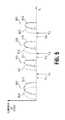
- FIG. 11illustrates yet another alternate embodiment of a stacked memory array architecture.
- This embodimentincludes two layers 1100 , 1101 .
- Each series string 1105 - 1107 , 1108 - 1110 in each layer 1100 , 1101is coupled to a common bit line BLn ⁇ 1, BLn, BLn+1.
- BLnbit line
- a first series string 1105 in the bottom layer 1100shares the same bit line BLn+1 with the first series string 1108 in the top layer 1101 .
- the second series string 1106 in the bottom layer 1100shares the same bit line BLn with the second series string 1109 in the top layer 1101 .
- the third series string 1107 in the bottom layer 1100shares the same bit line BLn ⁇ 1 with the third series string 1110 in the top layer 1101 . This pattern repeats for any number of series strings in any number of layers.
- the word lines WL 0 -WLnare common for each layer 1100 , 1101 .
- the select gate source SG(S) lineis also common between layers.
- the source line SRCis common to all layers.
- the select gate drain SG(D) lineis only common between select gate drain transistors of each layer 1100 , 1101 .
- the select gate drain transistors of the bottom layer 1100share SG(D) 0 .
- the select gate drain transistors of the top layer 1101share SG(D) 1 .
- the select gate drain lines SG(D) 0 -SG(D) 1are used to select and deselect each layer 1100 , 1101 .
- FIGS. 12A and 12Billustrate diagrams of layer selection and word line offset by layer in accordance with the embodiment of FIG. 11 .
- FIG. 12Aillustrates word line biasing for slower programming layers.
- FIG. 12Billustrates word line biasing that includes an offset voltage for faster programming layers.
- the embodiments of FIGS. 12A and 12Bassume that the top layer 1201 is the slower programming layer and the bottom layer 1200 is the faster programming layer.
- the word line biasing offset voltagechanges the sense condition during a sense operation to shift the V, voltage range.
- the top layer 1201is selected by an enable voltage (e.g., 5V) on the SG(D) 1 line.
- the bottom layer 1200is deselected by a disable voltage (e.g., 0V) on the SG(D) 0 line.
- the common source lineis biased at a reference voltage (e.g., 0V) and the common select gate source SG(S) line is biased at an enable voltage (e.g., 5V).
- the common selected word line WLnis biased at a sense voltage of V r without an offset voltage. This produces a sense Condition A on the bit line. Even though the same row of the lower layer(s) experience the same V r on their control gates, those layers are deselected by the disable voltage on the select gate drain lines.
- the top layer 1201is deselected by a disable voltage (e.g., 0V) on the SG(D) 1 line.
- the bottom layer 1200is selected by an enable voltage (e.g., 5V) on the SG(D) 0 line.
- the common source lineis biased at a reference voltage (e.g., 0V) and the common select gate source SG(S) line is biased at an enable voltage (e.g., 5V).
- the common selected word line WLnis biased at a sense voltage of V r +a where ‘a’ is the offset voltage that shifts the V t voltage range during the sense operation to take into account the memory cells with the increased threshold voltage.
- the offset voltageis added to the sense voltage when the faster programming layer is selected. This produces the changed Condition B on the bit line that can compensate for the program disturb condition.
- FIG. 13illustrates a functional block diagram of a memory device 1300 that can comprise a stacked memory array architecture.
- the memory device 1300is coupled to an external processor 1310 .
- the processor 1310may be a microprocessor or some other type of controller.
- the memory device 1300 and the processor 1310form part of a memory system 1320 .
- the memory device 1300includes an array 1330 of memory cells (e.g., non-volatile memory cells).
- the memory array 1330is arranged in banks of word line rows and bit line columns. In one embodiment, the columns of the memory array 1330 comprise series strings of memory cells.
- Address buffer circuitry 1340is provided to latch address signals provided through I/O circuitry 1360 . Address signals are received and decoded by a row decoder 1344 and a column decoder 1346 to access the memory array 1330 .
- the memory device 1300reads data in the memory array 1330 by sensing voltage or current changes in the memory array columns using sense amplifier circuitry 1350 .
- the page buffers 1350are coupled to read and latch a row of data from the memory array 1330 .
- the page buffers 1350include the sense circuitry as well as other circuits for performing a program verify operation.
- Dataare input and output through the I/O circuitry 1360 for bidirectional data communication as well as the address communication over a plurality of data connections 1362 with the controller 1310 .
- Write circuitry 1355is provided to write data to the memory array.
- Memory control circuitry 1370decodes signals provided on control connections 1372 from the processor 1310 . These signals are used to control the operations on the memory array 1330 , including data read, data write (program), and erase operations.
- the memory control circuitry 1370may be a state machine, a sequencer, or some other type of controller to generate the memory control signals. In one embodiment, the memory control circuitry 1370 is configured to control execution of the program verify embodiments of the present disclosure.
- FIG. 13has been simplified to facilitate a basic understanding of the features of the memory. A more detailed understanding of internal circuitry and functions of flash memories are known to those skilled in the art.
- one or more embodiments of a sense operationcan reduce the errors resulting from sensing memory cells that have experienced a program disturb condition. This can be accomplished by changing sense conditions in response to a programming rate of a memory cell layer.
Landscapes
- Engineering & Computer Science (AREA)
- Microelectronics & Electronic Packaging (AREA)
- Computer Hardware Design (AREA)
- Read Only Memory (AREA)
- Semiconductor Memories (AREA)
- Non-Volatile Memory (AREA)
Abstract
Description
Claims (18)
Priority Applications (1)
| Application Number | Priority Date | Filing Date | Title |
|---|---|---|---|
| US14/936,719US9564227B2 (en) | 2011-03-08 | 2015-11-10 | Memory device having a different source line coupled to each of a plurality of layers of memory cell arrays |
Applications Claiming Priority (3)
| Application Number | Priority Date | Filing Date | Title |
|---|---|---|---|
| US13/043,005US8559231B2 (en) | 2011-03-08 | 2011-03-08 | Sense operation in a stacked memory array device |
| US14/037,488US9202574B2 (en) | 2011-03-08 | 2013-09-26 | Memory device having a different source line coupled to each of a plurality of layers of memory cell arrays |
| US14/936,719US9564227B2 (en) | 2011-03-08 | 2015-11-10 | Memory device having a different source line coupled to each of a plurality of layers of memory cell arrays |
Related Parent Applications (1)
| Application Number | Title | Priority Date | Filing Date |
|---|---|---|---|
| US14/037,488ContinuationUS9202574B2 (en) | 2011-03-08 | 2013-09-26 | Memory device having a different source line coupled to each of a plurality of layers of memory cell arrays |
Publications (2)
| Publication Number | Publication Date |
|---|---|
| US20160064085A1 US20160064085A1 (en) | 2016-03-03 |
| US9564227B2true US9564227B2 (en) | 2017-02-07 |
Family
ID=46795472
Family Applications (3)
| Application Number | Title | Priority Date | Filing Date |
|---|---|---|---|
| US13/043,005Active2031-07-06US8559231B2 (en) | 2011-03-08 | 2011-03-08 | Sense operation in a stacked memory array device |
| US14/037,488Active2031-06-07US9202574B2 (en) | 2011-03-08 | 2013-09-26 | Memory device having a different source line coupled to each of a plurality of layers of memory cell arrays |
| US14/936,719ActiveUS9564227B2 (en) | 2011-03-08 | 2015-11-10 | Memory device having a different source line coupled to each of a plurality of layers of memory cell arrays |
Family Applications Before (2)
| Application Number | Title | Priority Date | Filing Date |
|---|---|---|---|
| US13/043,005Active2031-07-06US8559231B2 (en) | 2011-03-08 | 2011-03-08 | Sense operation in a stacked memory array device |
| US14/037,488Active2031-06-07US9202574B2 (en) | 2011-03-08 | 2013-09-26 | Memory device having a different source line coupled to each of a plurality of layers of memory cell arrays |
Country Status (3)
| Country | Link |
|---|---|
| US (3) | US8559231B2 (en) |
| TW (2) | TWI569274B (en) |
| WO (1) | WO2012121872A2 (en) |
Families Citing this family (11)
| Publication number | Priority date | Publication date | Assignee | Title |
|---|---|---|---|---|
| US9177671B2 (en) | 2012-02-23 | 2015-11-03 | Apple Inc. | Memory with bit line capacitive loading |
| US8953395B2 (en) | 2012-02-23 | 2015-02-10 | Apple Inc. | Memory with variable strength sense amplifier |
| US8780657B2 (en) | 2012-03-01 | 2014-07-15 | Apple Inc. | Memory with bit line current injection |
| US8780654B2 (en)* | 2012-04-10 | 2014-07-15 | Apple Inc. | Weak bit detection in a memory through variable development time |
| US9171636B2 (en)* | 2013-01-29 | 2015-10-27 | Macronix International Co. Ltd. | Hot carrier generation and programming in NAND flash |
| DE102013215520A1 (en)* | 2013-08-07 | 2015-02-12 | Robert Bosch Gmbh | Soft magnetic metal powder composite material and method for producing such |
| US9536612B1 (en)* | 2014-01-23 | 2017-01-03 | Avago Technologies General Ip (Singapore) Pte. Ltd | Digital signaling processing for three dimensional flash memory arrays |
| US9633719B2 (en)* | 2015-05-29 | 2017-04-25 | Micron Technology, Inc. | Programming memory cells to be programmed to different levels to an intermediate level from a lowest level |
| US10224103B2 (en) | 2016-02-09 | 2019-03-05 | Micron Technology, Inc. | Memory devices with a transistor that selectively connects a data line to another data line |
| US11017838B2 (en) | 2016-08-04 | 2021-05-25 | Samsung Electronics Co., Ltd. | Nonvolatile memory devices |
| KR102620562B1 (en)* | 2016-08-04 | 2024-01-03 | 삼성전자주식회사 | Nonvolatile memory device |
Citations (26)
| Publication number | Priority date | Publication date | Assignee | Title |
|---|---|---|---|---|
| US6646924B1 (en) | 2002-08-02 | 2003-11-11 | Macronix International Co, Ltd. | Non-volatile memory and operating method thereof |
| US6954394B2 (en) | 2002-11-27 | 2005-10-11 | Matrix Semiconductor, Inc. | Integrated circuit and method for selecting a set of memory-cell-layer-dependent or temperature-dependent operating conditions |
| US20080048237A1 (en) | 2006-07-26 | 2008-02-28 | Kabushiki Kaisha Toshiba | Nonvolatile semiconductor memory device |
| US20080099819A1 (en) | 2006-10-17 | 2008-05-01 | Kabushiki Kaisha Toshiba | Nonvolatile semiconductor storage apparatus and method for manufacturing the same |
| US20080181008A1 (en) | 2007-01-25 | 2008-07-31 | Byeong-Hoon Lee | Flash memory system capable of improving access performance and access method thereof |
| US20090141556A1 (en) | 2007-11-29 | 2009-06-04 | Hynix Semiconductor Inc. | Method of verifying programming of a nonvolatile memory device |
| US7554853B2 (en)* | 2006-12-30 | 2009-06-30 | Sandisk Corporation | Non-volatile storage with bias based on selective word line |
| US20090168533A1 (en) | 2007-12-28 | 2009-07-02 | Samsung Electronics Co., Ltd. | Three-dimensional memory device and programming method |
| US20090296476A1 (en) | 2008-05-28 | 2009-12-03 | Hynix Semiconductor Inc. | Flash Memory Device and Method for Manufacturing the Same |
| US7701761B2 (en) | 2007-12-20 | 2010-04-20 | Sandisk Corporation | Read, verify word line reference voltage to track source level |
| US20100128521A1 (en) | 2008-11-21 | 2010-05-27 | Spansion Llc | Applying negative gate voltage to wordlines adjacent to wordline associated with read or verify to reduce adjacent wordline disturb |
| US20100172182A1 (en) | 2009-01-06 | 2010-07-08 | Samsung Electronics Co., Ltd. | Nonvolatile memory device and method for operating the same |
| US20100177566A1 (en) | 2009-01-14 | 2010-07-15 | Kim Won-Joo | Non-volatile memory device having stacked structure, and memory card and electronic system including the same |
| US20100211852A1 (en) | 2009-02-17 | 2010-08-19 | Samsung Electronics Co., Ltd. | Method of reading data in non-volatile memory device |
| US20100259987A1 (en) | 2009-04-09 | 2010-10-14 | Dana Lee | Two Pass Erase For Non-Volatile Storage |
| US20100322000A1 (en) | 2009-06-19 | 2010-12-23 | Samsung Electronics Co., Ltd. | Programming methods for three-dimensional memory devices having multi-bit programming, and three-dimensional memory devices programmed thereby |
| US7889571B2 (en) | 2008-01-09 | 2011-02-15 | Unity Semiconductor Corporation | Buffering systems methods for accessing multiple layers of memory in integrated circuits |
| US20110051527A1 (en) | 2009-09-01 | 2011-03-03 | Kabushiki Kaisha Toshiba | Nonvolatile semiconductor memory device |
| US20110063914A1 (en) | 2009-09-16 | 2011-03-17 | Kabushiki Kaisha Toshiba | Nonvolatile semiconductor memory device |
| US7940578B2 (en) | 2008-01-21 | 2011-05-10 | Samsung Electronics Co., Ltd. | Flash memory device having row decoders sharing single high voltage level shifter, system including the same, and associated methods |
| US8004893B2 (en) | 2008-07-02 | 2011-08-23 | Samsung Electronics Co., Ltd. | Integrated circuit memory devices having vertically arranged strings of memory cells therein and methods of operating same |
| US20110205802A1 (en) | 2010-02-22 | 2011-08-25 | Samsung Electronics Co., Ltd. | Nonvolatile memory device and method of reading the same |
| US8064272B2 (en) | 2008-02-29 | 2011-11-22 | Kabushiki Kaisha Toshiba | Semiconductor memory device |
| US20120002477A1 (en) | 2010-07-02 | 2012-01-05 | Micron Technology, Inc. | Memories and their formation |
| US20120051137A1 (en) | 2010-09-01 | 2012-03-01 | Macronix International Co., Ltd. | Memory Architecture of 3D Array With Diode In Memory String |
| US20130107628A1 (en) | 2011-11-02 | 2013-05-02 | Yingda Dong | Selective Word Line Erase In 3D Non-Volatile Memory |
Family Cites Families (7)
| Publication number | Priority date | Publication date | Assignee | Title |
|---|---|---|---|---|
| US6504760B1 (en)* | 2001-06-22 | 2003-01-07 | Intel Corporation | Charging a capacitance of a memory cell and charger |
| US7177183B2 (en)* | 2003-09-30 | 2007-02-13 | Sandisk 3D Llc | Multiple twin cell non-volatile memory array and logic block structure and method therefor |
| US7433228B2 (en)* | 2005-09-20 | 2008-10-07 | Spansion Llc | Multi-bit flash memory device having improved program rate |
| US7349264B2 (en)* | 2005-12-28 | 2008-03-25 | Sandisk Corporation | Alternate sensing techniques for non-volatile memories |
| US7848145B2 (en)* | 2007-03-27 | 2010-12-07 | Sandisk 3D Llc | Three dimensional NAND memory |
| US7630246B2 (en)* | 2007-06-18 | 2009-12-08 | Micron Technology, Inc. | Programming rate identification and control in a solid state memory |
| CN101983423B (en)* | 2008-03-31 | 2014-03-26 | 富士通半导体股份有限公司 | Semiconductor device |
- 2011
- 2011-03-08USUS13/043,005patent/US8559231B2/enactiveActive
- 2012
- 2012-02-21WOPCT/US2012/025868patent/WO2012121872A2/enactiveApplication Filing
- 2012-03-07TWTW104121388Apatent/TWI569274B/enactive
- 2012-03-07TWTW101107751Apatent/TWI497502B/enactive
- 2013
- 2013-09-26USUS14/037,488patent/US9202574B2/enactiveActive
- 2015
- 2015-11-10USUS14/936,719patent/US9564227B2/enactiveActive
Patent Citations (26)
| Publication number | Priority date | Publication date | Assignee | Title |
|---|---|---|---|---|
| US6646924B1 (en) | 2002-08-02 | 2003-11-11 | Macronix International Co, Ltd. | Non-volatile memory and operating method thereof |
| US6954394B2 (en) | 2002-11-27 | 2005-10-11 | Matrix Semiconductor, Inc. | Integrated circuit and method for selecting a set of memory-cell-layer-dependent or temperature-dependent operating conditions |
| US20080048237A1 (en) | 2006-07-26 | 2008-02-28 | Kabushiki Kaisha Toshiba | Nonvolatile semiconductor memory device |
| US20080099819A1 (en) | 2006-10-17 | 2008-05-01 | Kabushiki Kaisha Toshiba | Nonvolatile semiconductor storage apparatus and method for manufacturing the same |
| US7554853B2 (en)* | 2006-12-30 | 2009-06-30 | Sandisk Corporation | Non-volatile storage with bias based on selective word line |
| US20080181008A1 (en) | 2007-01-25 | 2008-07-31 | Byeong-Hoon Lee | Flash memory system capable of improving access performance and access method thereof |
| US20090141556A1 (en) | 2007-11-29 | 2009-06-04 | Hynix Semiconductor Inc. | Method of verifying programming of a nonvolatile memory device |
| US7701761B2 (en) | 2007-12-20 | 2010-04-20 | Sandisk Corporation | Read, verify word line reference voltage to track source level |
| US20090168533A1 (en) | 2007-12-28 | 2009-07-02 | Samsung Electronics Co., Ltd. | Three-dimensional memory device and programming method |
| US7889571B2 (en) | 2008-01-09 | 2011-02-15 | Unity Semiconductor Corporation | Buffering systems methods for accessing multiple layers of memory in integrated circuits |
| US7940578B2 (en) | 2008-01-21 | 2011-05-10 | Samsung Electronics Co., Ltd. | Flash memory device having row decoders sharing single high voltage level shifter, system including the same, and associated methods |
| US8064272B2 (en) | 2008-02-29 | 2011-11-22 | Kabushiki Kaisha Toshiba | Semiconductor memory device |
| US20090296476A1 (en) | 2008-05-28 | 2009-12-03 | Hynix Semiconductor Inc. | Flash Memory Device and Method for Manufacturing the Same |
| US8004893B2 (en) | 2008-07-02 | 2011-08-23 | Samsung Electronics Co., Ltd. | Integrated circuit memory devices having vertically arranged strings of memory cells therein and methods of operating same |
| US20100128521A1 (en) | 2008-11-21 | 2010-05-27 | Spansion Llc | Applying negative gate voltage to wordlines adjacent to wordline associated with read or verify to reduce adjacent wordline disturb |
| US20100172182A1 (en) | 2009-01-06 | 2010-07-08 | Samsung Electronics Co., Ltd. | Nonvolatile memory device and method for operating the same |
| US20100177566A1 (en) | 2009-01-14 | 2010-07-15 | Kim Won-Joo | Non-volatile memory device having stacked structure, and memory card and electronic system including the same |
| US20100211852A1 (en) | 2009-02-17 | 2010-08-19 | Samsung Electronics Co., Ltd. | Method of reading data in non-volatile memory device |
| US20100259987A1 (en) | 2009-04-09 | 2010-10-14 | Dana Lee | Two Pass Erase For Non-Volatile Storage |
| US20100322000A1 (en) | 2009-06-19 | 2010-12-23 | Samsung Electronics Co., Ltd. | Programming methods for three-dimensional memory devices having multi-bit programming, and three-dimensional memory devices programmed thereby |
| US20110051527A1 (en) | 2009-09-01 | 2011-03-03 | Kabushiki Kaisha Toshiba | Nonvolatile semiconductor memory device |
| US20110063914A1 (en) | 2009-09-16 | 2011-03-17 | Kabushiki Kaisha Toshiba | Nonvolatile semiconductor memory device |
| US20110205802A1 (en) | 2010-02-22 | 2011-08-25 | Samsung Electronics Co., Ltd. | Nonvolatile memory device and method of reading the same |
| US20120002477A1 (en) | 2010-07-02 | 2012-01-05 | Micron Technology, Inc. | Memories and their formation |
| US20120051137A1 (en) | 2010-09-01 | 2012-03-01 | Macronix International Co., Ltd. | Memory Architecture of 3D Array With Diode In Memory String |
| US20130107628A1 (en) | 2011-11-02 | 2013-05-02 | Yingda Dong | Selective Word Line Erase In 3D Non-Volatile Memory |
Also Published As
| Publication number | Publication date |
|---|---|
| TWI497502B (en) | 2015-08-21 |
| WO2012121872A3 (en) | 2013-03-28 |
| US9202574B2 (en) | 2015-12-01 |
| TW201250692A (en) | 2012-12-16 |
| US20120230116A1 (en) | 2012-09-13 |
| TW201539456A (en) | 2015-10-16 |
| US8559231B2 (en) | 2013-10-15 |
| US20140036586A1 (en) | 2014-02-06 |
| US20160064085A1 (en) | 2016-03-03 |
| WO2012121872A2 (en) | 2012-09-13 |
| TWI569274B (en) | 2017-02-01 |
Similar Documents
| Publication | Publication Date | Title |
|---|---|---|
| US9564227B2 (en) | Memory device having a different source line coupled to each of a plurality of layers of memory cell arrays | |
| US7221592B2 (en) | Multiple level programming in a non-volatile memory device | |
| US7221589B2 (en) | Multiple level programming in a non-volatile memory device | |
| US8773910B2 (en) | Programming to mitigate memory cell performance differences | |
| US8670273B2 (en) | Methods for program verifying a memory cell and memory devices configured to perform the same | |
| US8050090B2 (en) | Memory page boosting method, device and system | |
| US8164950B2 (en) | Reduction of punch-through disturb during programming of a memory device | |
| US8619475B2 (en) | Methods to operate a memory cell | |
| US8416628B2 (en) | Local sensing in a memory device | |
| US8780626B2 (en) | Sense operation in a memory device | |
| KR20210074028A (en) | Memory device and operating method thereof | |
| JP2002133888A (en) | Nonvolatile semiconductor memory device |
Legal Events
| Date | Code | Title | Description |
|---|---|---|---|
| AS | Assignment | Owner name:U.S. BANK NATIONAL ASSOCIATION, AS COLLATERAL AGENT, CALIFORNIA Free format text:SECURITY INTEREST;ASSIGNOR:MICRON TECHNOLOGY, INC.;REEL/FRAME:038669/0001 Effective date:20160426 Owner name:U.S. BANK NATIONAL ASSOCIATION, AS COLLATERAL AGEN Free format text:SECURITY INTEREST;ASSIGNOR:MICRON TECHNOLOGY, INC.;REEL/FRAME:038669/0001 Effective date:20160426 | |
| AS | Assignment | Owner name:MORGAN STANLEY SENIOR FUNDING, INC., AS COLLATERAL AGENT, MARYLAND Free format text:PATENT SECURITY AGREEMENT;ASSIGNOR:MICRON TECHNOLOGY, INC.;REEL/FRAME:038954/0001 Effective date:20160426 Owner name:MORGAN STANLEY SENIOR FUNDING, INC., AS COLLATERAL Free format text:PATENT SECURITY AGREEMENT;ASSIGNOR:MICRON TECHNOLOGY, INC.;REEL/FRAME:038954/0001 Effective date:20160426 | |
| STCF | Information on status: patent grant | Free format text:PATENTED CASE | |
| AS | Assignment | Owner name:U.S. BANK NATIONAL ASSOCIATION, AS COLLATERAL AGENT, CALIFORNIA Free format text:CORRECTIVE ASSIGNMENT TO CORRECT THE REPLACE ERRONEOUSLY FILED PATENT #7358718 WITH THE CORRECT PATENT #7358178 PREVIOUSLY RECORDED ON REEL 038669 FRAME 0001. ASSIGNOR(S) HEREBY CONFIRMS THE SECURITY INTEREST;ASSIGNOR:MICRON TECHNOLOGY, INC.;REEL/FRAME:043079/0001 Effective date:20160426 Owner name:U.S. BANK NATIONAL ASSOCIATION, AS COLLATERAL AGEN Free format text:CORRECTIVE ASSIGNMENT TO CORRECT THE REPLACE ERRONEOUSLY FILED PATENT #7358718 WITH THE CORRECT PATENT #7358178 PREVIOUSLY RECORDED ON REEL 038669 FRAME 0001. ASSIGNOR(S) HEREBY CONFIRMS THE SECURITY INTEREST;ASSIGNOR:MICRON TECHNOLOGY, INC.;REEL/FRAME:043079/0001 Effective date:20160426 | |
| AS | Assignment | Owner name:JPMORGAN CHASE BANK, N.A., AS COLLATERAL AGENT, ILLINOIS Free format text:SECURITY INTEREST;ASSIGNORS:MICRON TECHNOLOGY, INC.;MICRON SEMICONDUCTOR PRODUCTS, INC.;REEL/FRAME:047540/0001 Effective date:20180703 Owner name:JPMORGAN CHASE BANK, N.A., AS COLLATERAL AGENT, IL Free format text:SECURITY INTEREST;ASSIGNORS:MICRON TECHNOLOGY, INC.;MICRON SEMICONDUCTOR PRODUCTS, INC.;REEL/FRAME:047540/0001 Effective date:20180703 | |
| AS | Assignment | Owner name:MICRON TECHNOLOGY, INC., IDAHO Free format text:RELEASE BY SECURED PARTY;ASSIGNOR:U.S. BANK NATIONAL ASSOCIATION, AS COLLATERAL AGENT;REEL/FRAME:047243/0001 Effective date:20180629 | |
| AS | Assignment | Owner name:MICRON TECHNOLOGY, INC., IDAHO Free format text:RELEASE BY SECURED PARTY;ASSIGNOR:MORGAN STANLEY SENIOR FUNDING, INC., AS COLLATERAL AGENT;REEL/FRAME:050937/0001 Effective date:20190731 | |
| AS | Assignment | Owner name:MICRON TECHNOLOGY, INC., IDAHO Free format text:RELEASE BY SECURED PARTY;ASSIGNOR:JPMORGAN CHASE BANK, N.A., AS COLLATERAL AGENT;REEL/FRAME:051028/0001 Effective date:20190731 Owner name:MICRON SEMICONDUCTOR PRODUCTS, INC., IDAHO Free format text:RELEASE BY SECURED PARTY;ASSIGNOR:JPMORGAN CHASE BANK, N.A., AS COLLATERAL AGENT;REEL/FRAME:051028/0001 Effective date:20190731 | |
| MAFP | Maintenance fee payment | Free format text:PAYMENT OF MAINTENANCE FEE, 4TH YEAR, LARGE ENTITY (ORIGINAL EVENT CODE: M1551); ENTITY STATUS OF PATENT OWNER: LARGE ENTITY Year of fee payment:4 | |
| MAFP | Maintenance fee payment | Free format text:PAYMENT OF MAINTENANCE FEE, 8TH YEAR, LARGE ENTITY (ORIGINAL EVENT CODE: M1552); ENTITY STATUS OF PATENT OWNER: LARGE ENTITY Year of fee payment:8 |