US9564212B2 - Solid-state memory corruption mitigation - Google Patents
Solid-state memory corruption mitigationDownload PDFInfo
- Publication number
- US9564212B2 US9564212B2US14/312,144US201414312144AUS9564212B2US 9564212 B2US9564212 B2US 9564212B2US 201414312144 AUS201414312144 AUS 201414312144AUS 9564212 B2US9564212 B2US 9564212B2
- Authority
- US
- United States
- Prior art keywords
- block
- data
- lpo
- programming
- write data
- Prior art date
- Legal status (The legal status is an assumption and is not a legal conclusion. Google has not performed a legal analysis and makes no representation as to the accuracy of the status listed.)
- Expired - Fee Related, expires
Links
Images


Classifications
- G—PHYSICS
- G11—INFORMATION STORAGE
- G11C—STATIC STORES
- G11C16/00—Erasable programmable read-only memories
- G11C16/02—Erasable programmable read-only memories electrically programmable
- G11C16/06—Auxiliary circuits, e.g. for writing into memory
- G11C16/34—Determination of programming status, e.g. threshold voltage, overprogramming or underprogramming, retention
- G11C16/3418—Disturbance prevention or evaluation; Refreshing of disturbed memory data
- G11C16/3427—Circuits or methods to prevent or reduce disturbance of the state of a memory cell when neighbouring cells are read or written
- G—PHYSICS
- G06—COMPUTING OR CALCULATING; COUNTING
- G06F—ELECTRIC DIGITAL DATA PROCESSING
- G06F11/00—Error detection; Error correction; Monitoring
- G06F11/07—Responding to the occurrence of a fault, e.g. fault tolerance
- G06F11/0703—Error or fault processing not based on redundancy, i.e. by taking additional measures to deal with the error or fault not making use of redundancy in operation, in hardware, or in data representation
- G06F11/0706—Error or fault processing not based on redundancy, i.e. by taking additional measures to deal with the error or fault not making use of redundancy in operation, in hardware, or in data representation the processing taking place on a specific hardware platform or in a specific software environment
- G06F11/073—Error or fault processing not based on redundancy, i.e. by taking additional measures to deal with the error or fault not making use of redundancy in operation, in hardware, or in data representation the processing taking place on a specific hardware platform or in a specific software environment in a memory management context, e.g. virtual memory or cache management
- G—PHYSICS
- G06—COMPUTING OR CALCULATING; COUNTING
- G06F—ELECTRIC DIGITAL DATA PROCESSING
- G06F11/00—Error detection; Error correction; Monitoring
- G06F11/07—Responding to the occurrence of a fault, e.g. fault tolerance
- G06F11/0703—Error or fault processing not based on redundancy, i.e. by taking additional measures to deal with the error or fault not making use of redundancy in operation, in hardware, or in data representation
- G06F11/0751—Error or fault detection not based on redundancy
- G—PHYSICS
- G06—COMPUTING OR CALCULATING; COUNTING
- G06F—ELECTRIC DIGITAL DATA PROCESSING
- G06F11/00—Error detection; Error correction; Monitoring
- G06F11/07—Responding to the occurrence of a fault, e.g. fault tolerance
- G06F11/0703—Error or fault processing not based on redundancy, i.e. by taking additional measures to deal with the error or fault not making use of redundancy in operation, in hardware, or in data representation
- G06F11/0793—Remedial or corrective actions
- G—PHYSICS
- G06—COMPUTING OR CALCULATING; COUNTING
- G06F—ELECTRIC DIGITAL DATA PROCESSING
- G06F11/00—Error detection; Error correction; Monitoring
- G06F11/07—Responding to the occurrence of a fault, e.g. fault tolerance
- G06F11/08—Error detection or correction by redundancy in data representation, e.g. by using checking codes
- G06F11/10—Adding special bits or symbols to the coded information, e.g. parity check, casting out 9's or 11's
- G06F11/1008—Adding special bits or symbols to the coded information, e.g. parity check, casting out 9's or 11's in individual solid state devices
- G06F11/1072—Adding special bits or symbols to the coded information, e.g. parity check, casting out 9's or 11's in individual solid state devices in multilevel memories
- G—PHYSICS
- G06—COMPUTING OR CALCULATING; COUNTING
- G06F—ELECTRIC DIGITAL DATA PROCESSING
- G06F12/00—Accessing, addressing or allocating within memory systems or architectures
- G06F12/02—Addressing or allocation; Relocation
- G—PHYSICS
- G06—COMPUTING OR CALCULATING; COUNTING
- G06F—ELECTRIC DIGITAL DATA PROCESSING
- G06F12/00—Accessing, addressing or allocating within memory systems or architectures
- G06F12/02—Addressing or allocation; Relocation
- G06F12/0223—User address space allocation, e.g. contiguous or non contiguous base addressing
- G06F12/023—Free address space management
- G06F12/0238—Memory management in non-volatile memory, e.g. resistive RAM or ferroelectric memory
- G06F12/0246—Memory management in non-volatile memory, e.g. resistive RAM or ferroelectric memory in block erasable memory, e.g. flash memory
- G—PHYSICS
- G06—COMPUTING OR CALCULATING; COUNTING
- G06F—ELECTRIC DIGITAL DATA PROCESSING
- G06F12/00—Accessing, addressing or allocating within memory systems or architectures
- G06F12/02—Addressing or allocation; Relocation
- G06F12/0223—User address space allocation, e.g. contiguous or non contiguous base addressing
- G06F12/023—Free address space management
- G06F12/0253—Garbage collection, i.e. reclamation of unreferenced memory
- G—PHYSICS
- G06—COMPUTING OR CALCULATING; COUNTING
- G06F—ELECTRIC DIGITAL DATA PROCESSING
- G06F3/00—Input arrangements for transferring data to be processed into a form capable of being handled by the computer; Output arrangements for transferring data from processing unit to output unit, e.g. interface arrangements
- G06F3/06—Digital input from, or digital output to, record carriers, e.g. RAID, emulated record carriers or networked record carriers
- G06F3/0601—Interfaces specially adapted for storage systems
- G06F3/0602—Interfaces specially adapted for storage systems specifically adapted to achieve a particular effect
- G06F3/0608—Saving storage space on storage systems
- G—PHYSICS
- G06—COMPUTING OR CALCULATING; COUNTING
- G06F—ELECTRIC DIGITAL DATA PROCESSING
- G06F3/00—Input arrangements for transferring data to be processed into a form capable of being handled by the computer; Output arrangements for transferring data from processing unit to output unit, e.g. interface arrangements
- G06F3/06—Digital input from, or digital output to, record carriers, e.g. RAID, emulated record carriers or networked record carriers
- G06F3/0601—Interfaces specially adapted for storage systems
- G06F3/0602—Interfaces specially adapted for storage systems specifically adapted to achieve a particular effect
- G06F3/0614—Improving the reliability of storage systems
- G06F3/0616—Improving the reliability of storage systems in relation to life time, e.g. increasing Mean Time Between Failures [MTBF]
- G—PHYSICS
- G06—COMPUTING OR CALCULATING; COUNTING
- G06F—ELECTRIC DIGITAL DATA PROCESSING
- G06F3/00—Input arrangements for transferring data to be processed into a form capable of being handled by the computer; Output arrangements for transferring data from processing unit to output unit, e.g. interface arrangements
- G06F3/06—Digital input from, or digital output to, record carriers, e.g. RAID, emulated record carriers or networked record carriers
- G06F3/0601—Interfaces specially adapted for storage systems
- G06F3/0628—Interfaces specially adapted for storage systems making use of a particular technique
- G06F3/0629—Configuration or reconfiguration of storage systems
- G06F3/0635—Configuration or reconfiguration of storage systems by changing the path, e.g. traffic rerouting, path reconfiguration
- G—PHYSICS
- G06—COMPUTING OR CALCULATING; COUNTING
- G06F—ELECTRIC DIGITAL DATA PROCESSING
- G06F3/00—Input arrangements for transferring data to be processed into a form capable of being handled by the computer; Output arrangements for transferring data from processing unit to output unit, e.g. interface arrangements
- G06F3/06—Digital input from, or digital output to, record carriers, e.g. RAID, emulated record carriers or networked record carriers
- G06F3/0601—Interfaces specially adapted for storage systems
- G06F3/0628—Interfaces specially adapted for storage systems making use of a particular technique
- G06F3/0646—Horizontal data movement in storage systems, i.e. moving data in between storage devices or systems
- G06F3/0652—Erasing, e.g. deleting, data cleaning, moving of data to a wastebasket
- G—PHYSICS
- G06—COMPUTING OR CALCULATING; COUNTING
- G06F—ELECTRIC DIGITAL DATA PROCESSING
- G06F3/00—Input arrangements for transferring data to be processed into a form capable of being handled by the computer; Output arrangements for transferring data from processing unit to output unit, e.g. interface arrangements
- G06F3/06—Digital input from, or digital output to, record carriers, e.g. RAID, emulated record carriers or networked record carriers
- G06F3/0601—Interfaces specially adapted for storage systems
- G06F3/0668—Interfaces specially adapted for storage systems adopting a particular infrastructure
- G06F3/0671—In-line storage system
- G06F3/0673—Single storage device
- G06F3/0679—Non-volatile semiconductor memory device, e.g. flash memory, one time programmable memory [OTP]
- G—PHYSICS
- G11—INFORMATION STORAGE
- G11C—STATIC STORES
- G11C11/00—Digital stores characterised by the use of particular electric or magnetic storage elements; Storage elements therefor
- G11C11/56—Digital stores characterised by the use of particular electric or magnetic storage elements; Storage elements therefor using storage elements with more than two stable states represented by steps, e.g. of voltage, current, phase, frequency
- G11C11/5621—Digital stores characterised by the use of particular electric or magnetic storage elements; Storage elements therefor using storage elements with more than two stable states represented by steps, e.g. of voltage, current, phase, frequency using charge storage in a floating gate
- G11C11/5628—Programming or writing circuits; Data input circuits
- G—PHYSICS
- G11—INFORMATION STORAGE
- G11C—STATIC STORES
- G11C16/00—Erasable programmable read-only memories
- G11C16/02—Erasable programmable read-only memories electrically programmable
- G11C16/06—Auxiliary circuits, e.g. for writing into memory
- G11C16/10—Programming or data input circuits
- G—PHYSICS
- G11—INFORMATION STORAGE
- G11C—STATIC STORES
- G11C29/00—Checking stores for correct operation ; Subsequent repair; Testing stores during standby or offline operation
- G11C29/52—Protection of memory contents; Detection of errors in memory contents
- G—PHYSICS
- G06—COMPUTING OR CALCULATING; COUNTING
- G06F—ELECTRIC DIGITAL DATA PROCESSING
- G06F2212/00—Indexing scheme relating to accessing, addressing or allocation within memory systems or architectures
- G06F2212/72—Details relating to flash memory management
- G06F2212/7201—Logical to physical mapping or translation of blocks or pages
Definitions
- This disclosurerelates to data storage systems. More particularly, the disclosure relates to systems and methods for programming solid-state memory.
- Certain solid-state memory devicessuch as flash drives, store information in an array of memory cells constructed with floating gate transistors. Programming failure in a solid-state memory cell may adversely affect device performance.
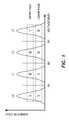
- FIG. 1is a graph showing a probability distribution of cells in a non-volatile memory array according to an embodiment.
- FIGS. 2A-2Cillustrate probability distributions of cells at various stages of a programming process according to an embodiment.
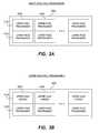
- FIG. 3Aillustrates a block of solid-state memory programmed in a Multi-Level Cell (MLC) modes according to an embodiment.
- MLCMulti-Level Cell
- FIG. 3Billustrates a block of solid-state memory programmed in a Lower Page Only (LPO) modes according to an embodiment.
- LPOLower Page Only
- FIG. 4is a block diagram of a data storage system including a non-volatile memory array according to an embodiment.
- FIG. 5is a data flow diagram illustrating a process for managing blocks of storage in a data storage environment.
- FIG. 6is a flow diagram illustrating a process for programming data in a non-volatile memory array according to an embodiment.
- non-volatile solid-state memorymay refer to solid-state memory such as NAND flash.
- Solid-state memorymay comprise a wide variety of technologies, such as flash integrated circuits, Phase Change Memory (PC-RAM or PRAM), Programmable Metallization Cell RAM (PMC-RAM or PMCm), Ovonic Unified Memory (OUM), Resistance RAM (RRAM), NAND memory, NOR memory, EEPROM, Ferroelectric Memory (FeRAM), MRAM, or other discrete NVM (non-volatile solid-state memory) chips.
- PC-RAM or PRAMPhase Change Memory
- PMC-RAM or PMCmProgrammable Metallization Cell RAM
- OFUMOvonic Unified Memory
- RRAMResistance RAM
- NAND memoryNOR memory
- EEPROMFerroelectric Memory
- FeRAMFerroelectric Memory
- MRAMor other discrete NVM (non-volatile solid-state memory) chips.
- non-volatile solid-state memory arrays or storage devicesmay be physically divided into planes, blocks, pages, and sectors, as is known in the art.
- Other forms of storagee.g., battery backed-up volatile DRAM or SRAM devices, magnetic disk drives, etc. may additionally or alternatively be used.
- pagemay refer to a block of a physical memory cells, or to the physical memory cells themselves.
- pagemay refer to either of upper or lower pages in a two-level scheme, or to data represented by most significant or least significant bits, or bits of intermediate significance in a three-level cell (TLC) scheme or schemes with greater granularity.
- blockmay be used herein to refer to groups of pages or to groups of blocks, such as super blocks.
- Multi-level cell (MLC) solid-state memoryis capable of storing more than one bit of information in a single memory element, or cell.
- a single cell of MLC memorymay store two or more bits of information.
- two bits per cellwill be assumed in the following teaching examples.
- the two bits of informationare not programmed together; programming of each of the two bits may occur at different times.
- the first bite.g., lower page
- the second bite.g., upper page
- MSBmost significant bit
- Such a programming schememay result in a cell having one of four possible voltage charge levels, wherein hardware is configured to detect the charge level, resulting in the ability to return four unique states, or two bits of data, from a single cell.
- two-stage MLC programmingcan result in corruption of LSB data.
- the upper page programming operationencounters an error or interruption during programming, the lower page may also become corrupted as a result.
- Programming interruptionmay be caused by, for example, system power failure.
- Certain data storage systemsinclude additional circuitry configured to provide backup power to allow for completion of memory access operations upon power failure.
- one or more capacitors or other charge-holding devicesmay be used to store power during normal operation and discharge such power for use during power failure.
- certain disk drive systemsare configured to generate back EMF power from a spindle motor after the power supply has been removed. However, cost and/or other considerations may make utilization of such backup power solutions impractical or undesirable.
- LSB corruptionLoss of the previously programmed lower page data is referred to herein as “LSB corruption,” or “paired-page corruption.” Further details of LSB corruption in solid-state memory devices are discussed below.
- Certain embodimentsare disclosed herein for preventing or reducing the effects of LSB corruption resulting from upper page programming interruption in MLC solid-state memory. Certain embodiments may provide a host data programming scheme in which only lower pages of memory are utilized initially for host data write operations, wherein a data consolidation mechanism (e.g., garbage collection) is used to pack the programmed lower page data into open blocks using both upper and lower pages.
- a data consolidation mechanisme.g., garbage collection
- FIG. 1is a graph showing a probability distribution of cells in a non-volatile memory array according to an embodiment.
- the distribution of FIG. 1is associated with an MLC programming scheme, in which two or more bits of information are stored in a single memory cell.
- MLCmulti-level cell
- FIG. 1shows four programming states (L 0 -L 3 ), wherein each state represents two bits of data.
- the programming stateseach comprise a most-significant bit, referred to herein as the “upper page,” and a least-significant bit (LSB), which may also be referred to herein as the “lower page.”
- “upper page”may refer to the least-significant bit
- “lower page”refers to the most-significant bit.
- particular coding valuesare assigned to the various states of the distribution (e.g., ‘11’ for L 0 , ‘01’ for L 1 , ‘00’ for L 2 , and ‘10’ for L 3 ), other coding schemes may be used.
- L 0corresponds to an erased state.
- one or more reference voltage levelsmay be used to read the cells to determine what charge state the cells belong to.
- FIG. 1illustrates three voltage read levels, R 1 , R 2 and R 3 .
- lower page valuesmay be determined based on a read at R 2
- upper page valuesmay be obtained by reading at R 1 and/or R 3 .
- FIGS. 2A-2Cillustrate probability distributions of cells at various stages of a programming process according to an embodiment.
- FIG. 2Aillustrates a voltage distribution in which cells of a page of solid-state memory are in a first state, such as an erased state.
- cellsare initially programmed from an erased state. Therefore, prior to programming, it may be necessary or desirable for a page of solid-state memory to be erased prior to programming to allow for proper programming, as described herein.
- MLC programmingcomprises two steps: in a first step, as illustrated in FIG. 2B , an LSB page may be programmed. For example, for a cell having an LSB value of ‘1,’ the cell may remain substantially in a low-voltage erased state, whereas a cell having an LSB value of ‘0’ may be programmed to a level above a higher program voltage (PV-Low).
- LSB page programmingmay be achieved by applying one or more programming pulses to the designated cells to push the programmed cells past PV-Low. Therefore, as illustrated, after LSB programming, the voltage distribution may comprise two separate states, which may be referred to as LSB “proto” states, or pages.
- the MSB pagemay be programmed, as illustrated in FIG. 2C .
- the LSB page programmingmay result in division of cells into two proto voltage states (e.g., a first state corresponding to a lower level/state, such as an erased state, and a second state corresponding to a higher level/state)
- MSB programmingmay further divide the distribution into four states.
- states L 0 and L 1both may correspond to an LSB value of ‘1,’ in certain embodiments, the lower LSB proto page may be split into the L 0 and L 1 states, wherein allocation to L 0 or L 1 is determined by the relevant MSB value.
- cellsmay be permitted to remain in a lowest voltage state (e.g., erased state). Furthermore, where the MSB page is ‘0,’ the cells may be programmed past a programming voltage level PV ⁇ 1. With respect to the cells corresponding to an LSB value of ‘0,’ the MSB programming of such cells may be performed by programming cells having an MSB value of ‘0’ past a programming voltage level PV ⁇ 2 to a third voltage state L 2 . Furthermore, cells having an MSB value of ‘1’ may be programmed from the higher LSB proto page past a programming voltage PV ⁇ 3 to a fourth voltage state L 3 .
- LSB, or “paired page,” corruption resulting from multi-stage MLC programmingcan be further illustrated by the logical view of an example MLC memory block 300 A shown in FIG. 3A .
- Block 300 Afor example, is programmed in MLC mode and both the block's lower pages ( 310 A) and upper pages ( 312 A) are programmed. Because the process of programming the upper page generally changes the cell's voltage, the data previously programmed in the lower page may be lost or corrupted if power is interrupted during the programming of the upper page. In particular, in order to program the upper page, the lower page may need to be temporarily transitioned to another programmed value, and then after the upper page is programmed, the lower page is transitioned back to the originally-programmed value.
- a data storage devicemay include a capacitor as a backup power source that allows the completion of upper page programming operations in MLC memory in the event of a power interruption.
- a backup power sourceis not always feasible or available.
- FIG. 3Billustrates a block 300 B programmed according to an alternative programming scheme, wherein only lower pages of the block of storage, or portion thereof, are programmed.
- a programming schememay be referred to herein as “lower page only,” or “LPO,” programming.
- the block 300 Bincludes a plurality of memory cells or units (e.g., 302 B), wherein a lower page 310 B is programmed, whereas a linked upper page 312 B is not programmed. Because only the lower pages of the block are used, the block 300 B may have a relatively reduced capacity compared to traditional MLC programming. However, as discussed in greater detail below, LPO programming may not suffer from complications associated with LSB corruption.
- FIG. 4illustrates a system 400 including a host system 410 and a data storage device 420 that implements LSB corruption mitigation according to one or more embodiments disclosed herein.
- the data storage device 420e.g., solid-state hybrid drive, solid-state drive, etc.
- the data storage device 420includes a controller 430 and a non-volatile memory array (e.g., solid-state storage) 440 .
- the non-volatile memory array 440may include a plurality of chips, or dies, each comprising one or more blocks of storage.
- the diagram of FIG. 4illustrates a plurality of blocks, identified as Block “A” ( 442 ) through Block “N,” which may be disposed on one or more discrete dies.
- Each blockcomprises a plurality of flash pages (F-pages).
- Block A ( 442 ) of FIG. 4includes a plurality of F-pages, identified as F-Pages A ( 443 ), B, through N.
- each “block”is a smallest grouping of memory pages or locations of the solid-state storage 440 that are erasable in a single operation or as a unit
- each “F-page” or “page”is a smallest grouping of memory cells that can be programmed in a single operation or as a unit.
- Other embodimentsmay use blocks and/or pages that are defined differently than as described herein.
- sets of blocksare grouped together into super blocks.
- a super block, or “S-Block,”may comprise one flash block per die.
- An S-Blocktherefore, may be thought of as a collection of F-Blocks, one F-Block per die, that are combined together to form a logical unit of the solid-state storage 440 .
- block allocation, erasure and/or garbage collectionmay be managed at the S-Block level.
- the data storage device 420may be a solid-state hybrid disk drive including a magnetic storage module 460 , which comprises magnetic media 464 (e.g., one or more magnetic disks).
- the solid-state storage 440may comprise any desirable type of solid-state memory.
- the controller 430can be configured to receive data and/or storage access commands from a storage interface module 412 (e.g., a device driver) of the host system 410 .
- Storage access commands communicated by the storage interface module 412can include write data and read data commands issued by the host system 410 .
- Read and write commandscan specify a logical address (e.g., logical block addresses, or “LBAs”) used to access the data storage device 420 .
- LBAslogical block addresses
- the programming module 432 of the controller 430may implement a desirable programming scheme suitable for the solid-state storage 440 .
- the programming module 432is configured to implement an MLC programming scheme in which cells of solid-state memory are programmed to store a charge level representative of two or more bits of data. Such a programming scheme is described above with reference to FIGS. 1 and 2 A- 2 C.
- the programming module 432may be configured to implement lower page only (LPO) programming of host data to the solid-state storage 440 , thereby providing paired page corruption mitigation, as described in greater detail below.
- LPOlower page only
- the data storage device 420can store data communicated by the host system 410 .
- the data storage device 420can act as memory storage for the host system 410 .
- the controller 430can implement a logical interface.
- the logical interfacecan present to the host system 410 data storage system memory as a set of logical addresses (e.g., contiguous address) where user data can be stored.
- the controller 430can map logical addresses to various physical locations or addresses in the solid-state storage 440 and/or other storage modules.
- the controller 430includes a garbage collection/wear leveling module 434 configured to perform garbage collection and wear leveling.
- Garbage collectionis a type of data consolidation or fragmentation operation. However, as used herein, “garbage collection” may refer to any type of data consolidation or fragmentation operation.
- a wear leveling operationcan be considered a sub-part of, or a special case of, an overall garbage collection operation.
- the garbage collection/wear leveling module 434performs solely wear leveling while, in other embodiments, performs garbage collection and/or wear leveling of at least a portion of the solid-state storage 440 .
- the garbage collection/wear leveling module 432may function to accommodate paired page corruption mitigation through LPO programming and subsequent data consolidation operations such as garbage collection and/or wear leveling.
- the garbage collection/wear leveling module 434can select blocks of the solid-state storage 440 on which garbage collection and/or wear leveling is performed. Such block-selection functionality may be performed based at least in part on information related to data age and/or wear leveling. The blocks may be selected in a way that increases the amount of free space through the life of the data storage device 420 and promotes or guarantees that blocks stay within a range of P/E counts, which may maximize the data storage life of the solid-state storage 440 .
- the data storage device 420may be configured to mitigate LSB corruption according to one or more embodiments disclosed herein.
- the data storage device 420uses only lower pages for host writes (e.g., writes host data into blocks in LPO mode), and uses garbage collection, wear leveling, and/or other background/system maintenance operations to pack data into new blocks (e.g., writes data into blocks in MLC mode).
- garbage collectionFor the sake of simplicity, the following examples will use garbage collection as an example illustration.
- garbage collectionin the event that an MLC programming operation is unsuccessful, any lost or corrupted lower page data may still be intact in the LPO block(s), such that the write operation may be retried at a later time, such as when power is restored to the system.
- a side benefit of writing host data in LPO modeis that write performance may be improved by, for example, a factor of two or greater, compared to write performance of typical MLC mode programming.
- Certain embodiments disclosed hereinprovide for paired page corruption mitigation through lower page only (LPO) programming of host data. Such functionality may be performed by the controller 430 and/or programming module 432 described above in connection with FIG. 4 .
- new incoming host write datamay be stored in user data MLC super blocks using only lower (LSB) pages; the upper pages of such blocks may not be programmed at such time.
- the host data stored in the lower pages (LPO data) of the designated super blocksmay be moved to other super blocks, utilizing both pages of such blocks.
- the forward map maintained by the controlleris not updated until the data is safely moved to the new super blocks and programmed in both upper and lower pages. Therefore, because the LPO data is not erased from the LPO blocks until after successful programming has occurred, power loss, or other paired page corruption may not result in lower page data loss.
- Parity datamay be calculated using an exclusive or (XOR) sum of the bits of pages of data, for example yielding ‘0’ for even parity and ‘1’ for odd parity.
- XORexclusive or
- each page is of datais compared with the previous page using XOR, and the result is accumulated and periodically saved (e.g., to a blank page, or “parity page”). Because parity is generally dependent upon all the relevant bits, corruption of any one bit may be revealed by examination of parity data in error detection.
- the parity stripe lengthrepresents the number of user data elements (e.g., pages) that are associated with a single parity element; a relatively high parity rate may negatively impact storage capacity because more storage is dedicated to parity rather than user data.
- Use of LPO programming, as described herein,may advantageously allow for a parity stripe length that is higher than certain other systems.
- the parity stripe lengthmay be limited by a desire to avoid paired pages being associated with the same parity element; the geometry of the memory module may dictate the parity stripe length. For example memory geometry may limit the parity stripe length to approximately 15:16, or lower.
- parity stripein the range of 127:128, 1023:1024, or greater may be used.
- the controller 430is configured to open super blocks in an LPO mode. New incoming host write data will be stored in user data MLC super blocks that have been opened in LPO mode. To such end, the controller 430 may maintain information indicating a reduced number of pages that are expected to be used in programming the LPO blocks. Specifically, approximately half the pages may be allocated for programming. In certain embodiments, super blocks opened in LPO mode are designated and tracked as LPO blocks, such that the controller 430 will know not to look for valid data in the upper pages of such blocks.
- LPO programmingmay result in at least temporary increase in write amplification (WA) for certain workloads, thereby effectively decreasing the amount of data that can be written over time.
- WAwrite amplification
- LPO programmingmay use only approximately half the potentially available pages of blocks for at least some program/erase cycles.
- the relevant reduction in capacitymay be relatively small.
- Garbage collectionis a memory management mechanism that allows for reclamation of pages of memory that are no longer valid. As a result of writing and updating data within the memory, some pages become invalidated. This causes fragmentation of the memory over time.
- garbage collectioninvolves selecting the appropriate block(s), moving all valid pages to new open block(s), and erasing the selected block. In this way, the garbage collected block can become available for use in connection with a write operation.
- the garbage collection module 434can select regions of memory for garbage collection. In one embodiment, regions with the least amount of valid data may be selected for garbage collection.
- the amount of valid data of a given blockmay be represented by metadata indicating an amount of valid or stale data in a block (e.g., a “stale count”).
- regions having an amount of valid data that is less than a threshold amountcan be selected for garbage collection.
- such regioncan be freed up by moving only valid data to another region (e.g., free region or region designated as free).
- Garbage collection functionalitymay advantageously be modified with respect to LPO blocks. For example, if garbage collection generally puts validly-mapped lower page data at risk, it may be modified to “skip” over the upper pages for those lower pages currently in use in the forward table. Furthermore, garbage collection metrics can be used to modify the rate of wear of LPO blocks in view of the reduced effective capacity of such blocks. For example, when an LPO block is closed, the stale count of the block may be augmented to reflect the limited capacity of the block. In an embodiment, the stale count is augmented to reflect a half-stale state.
- LPO blocksIt may be desirable to modify the stale count for LPO blocks because the rate of wear of a block can depend on how frequently it is erased. In the absence of modified stale count values for LPO blocks, such blocks may not be selected for garbage collection with desirable frequency because only half of their pages (i.e., the lower pages) may be potentially valid. Therefore, by augmenting the stale count of LPO blocks, such blocks may be selected more frequently for garbage collection. In certain applications, such an augmented stale count may result in effectively any LPO super block being considered a good candidate for garbage collection.
- the ready list threshold at which garbage collection operations beginmay be altered for LPO blocks.
- the garbage collection/wear leveling module 434may be configured to promote even distribution of data writes over the blocks of the solid-state storage 440 by implementing an algorithm by which the controller 430 re-maps logical block addresses to different physical block addresses in the solid-state memory array. Because LPO blocks may only be programmed to half capacity, and therefore subject to less wear than fully-programmed blocks, simply tracking the number of program/erase cycles of LPO blocks may lead to uneven wearing of the memory array. Furthermore, when data is read back from solid-state storage, the voltage threshold levels used may be based at least in part on assumptions about the level of wear of the blocks. Therefore, improper accounting of the wear level of blocks can be problematic.
- the controller and/or wear leveling module 434may be configured to track the number of times a given block is used as an LPO block. For example, a LPO count variable may be maintained in page header metadata or in a system table to indicate the number of times a particular super block has been used as an LPO block. The LPO count may be used in a manner similar to wear leveling in order to prevent a single block from being used in LPO mode significantly more often than other blocks. In an embodiment, the controller 430 is configured to ensure that a block has an LPO count within approximately 200 of the average LPO count, or other number.
- “Relaxation time,” as used herein,may be defined as the difference in time from when the last page of a block is programmed and the time when the block is erased. If a single block is recycled too quickly, it may incur undue wear.
- augmented stale countsmay be implemented for LPO blocks as a modified garbage collection mechanism. As a result, for certain workloads, it may be likely that LPO blocks will frequently be considered relatively stale, depending on the degree of augmentation. Therefore, it may be desirable to modify or control relaxation times of closed LPO super blocks to avoid undue wear.
- an LPO blockmay be selected for garbage collection substantially immediately after closing, and placed back onto the ready block queue (described in greater detail below in connection with the ready block pool 410 of FIG. 5 ), and then subsequently selected for use undesirably quickly; such process may repeat, thereby causing undue wearing of the block.
- a minimum relaxation timeis determined and implemented to prevent a super block from being recycled too quickly.
- the ready block list lengthmay be set to at least partially control the relaxation time of LPO super blocks.
- the blocks that go through garbage collectionmay be placed at the end of the ready list, wherein the open blocks in front in the queue are each programmed before the given block is programmed.
- the size of the ready listmay be selected such that the shortest period of time in which a block can possibly move from the back of the ready list to the front is greater than or equal to the desired relaxation time. In certain embodiments, a time period of approximately 60 seconds may be used for the relaxation time.
- FIG. 5is a data flow diagram illustrating a process 500 for managing blocks of storage in a data storage environment.
- the process 500involves a data storage system, such as a controller of the data storage device/system shown in FIG. 4 , receiving host data associated with a host-issued write command, wherein the write command directs the controller to write at least a portion of the data to a solid-state memory device.
- the process 500may involve selecting a block for programming and erasing the block to allow for the block to be programmed.
- the process 500involves programming host data initially to blocks designated for lower-page-only (LPO) programming.
- LPOlower-page-only
- the block 401may be designated as an LPO block and programmed only in lower pages, as described in greater detail above.
- the process 500involves maintaining metadata associated with the block 401 to indicate that the block has been selected for LPO mode and/or how many times the block has been selected for LPO mode.
- the block 402may be added to a pool of closed blocks that have programmed data.
- the processmay further include performing some data consolidation with regard to the programmed blocks. For example, over time, some or all of the data in a programmed block may become invalid. Data consolidation operations, such as garbage collection, may allow for data in partially invalid blocks to be consolidated into fewer blocks, thereby allowing for previously closed blocks to be erased and reused for programming.
- LPO blocksmay be selected for data consolidation, and may be placed into a queue 430 for awaiting rearrangement of data into other blocks.
- selection of blocks for data consolidationis based at least in part on metadata associated with blocks that indicates how stale a given block is.
- staleis used herein according to its broad and ordinary meaning and may indicate in the context of a block of storage how many, or what portion, of a blocks pages or cells contain invalid, or valid, data. Because an LPO block, at a maximum, has a data capacity that is 50% of the capacity of an MLC block, certain embodiments of the process 500 include augmenting staleness metadata associated with an LPO block to indicate that the block may contain a reduced amount of valid data. This is done so that when both types of blocks are considered for garbage collection, the reduced capacity of LPO blocks relative to MLC blocks are taken into consideration in a scheme that uses staleness as a selection factor for garbage collection block selection. For example, the stale count of an LPO block that has all valid data may nonetheless indicate that the block is approximately half-stale. Such staleness augmentation may result in the LPO block being selected for data consolidation sooner than it otherwise would.
- data in the LPO blockmay be reprogrammed to a block in an MLC programming mode (data programmed to both upper and lower pages).
- Block 405is an example of a block that has been programmed in MLC mode containing valid data saved from a garbage collection process.
- the blockis erased.
- the blockmay not be erased until it is selected again for programming. Therefore, the ready block pool 410 may include erased blocks, or may include primarily blocks comprising invalid data.
- LPO programmingas illustrated in FIG. 5 , may allow for data protection in the event of upper page programming failure, as described in greater detail above.
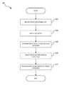
- FIG. 6is a flow diagram illustrating a process 600 for programming data in a non-volatile memory array according to an embodiment.
- the process 600may be performed at least in part by a controller of a data storage device/system, such as that shown in FIG. 4 .
- the process 600includes receiving write data from a host system (block 602 ).
- one or more blocks of storagemay be selected for lower page only (LPO) programming.
- the write datais programmed to one or more blocks in LPO mode.
- the LPO block(s)may be selected for data consolidation (e.g., garbage collection), wherein, as shown at block 610 , the data is reprogrammed to one or more other blocks not in an LPO mode.
- the datamay be programmed to the new block(s) using MLC programming.
- paired page corruption mitigation systemscan be implemented while remaining within the scope of the present disclosure.
- the actual steps taken in the processes discussed hereinmay differ from those described or shown in the figures. Depending on the embodiment, certain of the steps described above may be removed, others may be added.
Landscapes
- Engineering & Computer Science (AREA)
- Theoretical Computer Science (AREA)
- Physics & Mathematics (AREA)
- General Engineering & Computer Science (AREA)
- General Physics & Mathematics (AREA)
- Quality & Reliability (AREA)
- Human Computer Interaction (AREA)
- Computer Hardware Design (AREA)
- Computer Networks & Wireless Communication (AREA)
- Techniques For Improving Reliability Of Storages (AREA)
Abstract
Description
Adjusted ready list length=((number of superblocks)*0.5)+(2*ideal ready list length))
Modified Wear Leveling
Claims (21)
Priority Applications (4)
| Application Number | Priority Date | Filing Date | Title |
|---|---|---|---|
| US14/312,144US9564212B2 (en) | 2014-05-06 | 2014-06-23 | Solid-state memory corruption mitigation |
| CN201580023720.2ACN106462493B (en) | 2014-05-06 | 2015-04-28 | Mitigation of Solid State Memory Damage |
| PCT/US2015/028060WO2015171369A1 (en) | 2014-05-06 | 2015-04-28 | Solid-state memory corruption mitigation |
| US15/413,360US10020065B2 (en) | 2014-05-06 | 2017-01-23 | Corruption-preventative programming in solid-state data storage |
Applications Claiming Priority (2)
| Application Number | Priority Date | Filing Date | Title |
|---|---|---|---|
| US201461989420P | 2014-05-06 | 2014-05-06 | |
| US14/312,144US9564212B2 (en) | 2014-05-06 | 2014-06-23 | Solid-state memory corruption mitigation |
Related Child Applications (1)
| Application Number | Title | Priority Date | Filing Date |
|---|---|---|---|
| US15/413,360ContinuationUS10020065B2 (en) | 2014-05-06 | 2017-01-23 | Corruption-preventative programming in solid-state data storage |
Publications (2)
| Publication Number | Publication Date |
|---|---|
| US20150324282A1 US20150324282A1 (en) | 2015-11-12 |
| US9564212B2true US9564212B2 (en) | 2017-02-07 |
Family
ID=54367948
Family Applications (2)
| Application Number | Title | Priority Date | Filing Date |
|---|---|---|---|
| US14/312,144Expired - Fee RelatedUS9564212B2 (en) | 2014-05-06 | 2014-06-23 | Solid-state memory corruption mitigation |
| US15/413,360ActiveUS10020065B2 (en) | 2014-05-06 | 2017-01-23 | Corruption-preventative programming in solid-state data storage |
Family Applications After (1)
| Application Number | Title | Priority Date | Filing Date |
|---|---|---|---|
| US15/413,360ActiveUS10020065B2 (en) | 2014-05-06 | 2017-01-23 | Corruption-preventative programming in solid-state data storage |
Country Status (3)
| Country | Link |
|---|---|
| US (2) | US9564212B2 (en) |
| CN (1) | CN106462493B (en) |
| WO (1) | WO2015171369A1 (en) |
Cited By (1)
| Publication number | Priority date | Publication date | Assignee | Title |
|---|---|---|---|---|
| US20170133100A1 (en)* | 2014-05-06 | 2017-05-11 | Western Digital Technologies, Inc. | Corruption-preventative programming in solid-state data storage |
Families Citing this family (13)
| Publication number | Priority date | Publication date | Assignee | Title |
|---|---|---|---|---|
| US9798657B2 (en)* | 2014-10-15 | 2017-10-24 | Samsung Electronics Co., Ltd. | Data storage device including nonvolatile memory device and operating method thereof |
| TWI578320B (en)* | 2014-11-25 | 2017-04-11 | 旺宏電子股份有限公司 | Memory operating method and memory device using the same |
| US10540274B2 (en)* | 2016-03-29 | 2020-01-21 | Micron Technology, Inc. | Memory devices including dynamic superblocks, and related methods and electronic systems |
| JP6524039B2 (en)* | 2016-09-23 | 2019-06-05 | 東芝メモリ株式会社 | Memory system and control method |
| KR102299186B1 (en)* | 2017-03-21 | 2021-09-08 | 마이크론 테크놀로지, 인크. | Apparatus and Method for Automated Dynamic Word Line Start Voltage |
| US10319445B1 (en)* | 2017-11-30 | 2019-06-11 | Western Digital Technologies, Inc. | Programming unprogrammed upper page during lower page programming of multi-level storage cells |
| CN110147200A (en)* | 2018-02-13 | 2019-08-20 | 矽创电子股份有限公司 | Flash memory controller and control method |
| US10740181B2 (en)* | 2018-03-06 | 2020-08-11 | Western Digital Technologies, Inc. | Failed storage device rebuild method |
| US11204841B2 (en)* | 2018-04-06 | 2021-12-21 | Micron Technology, Inc. | Meta data protection against unexpected power loss in a memory system |
| CN112823331B (en)* | 2018-10-10 | 2024-03-29 | 阿里巴巴集团控股有限公司 | Systems and methods for data recovery in parallel multi-tenant SSDs with finer granularity |
| US10949123B2 (en)* | 2018-10-18 | 2021-03-16 | Western Digital Technologies, Inc. | Using interleaved writes to separate die planes |
| US11137944B1 (en)* | 2020-03-13 | 2021-10-05 | Western Digital Technologies, Inc. | Combined QLC programming method |
| KR20210157157A (en) | 2020-06-19 | 2021-12-28 | 삼성전자주식회사 | Operating method of memory controller, operating method of host and storage device |
Citations (94)
| Publication number | Priority date | Publication date | Assignee | Title |
|---|---|---|---|---|
| US6839801B2 (en) | 2003-01-06 | 2005-01-04 | International Business Machines Corporation | Deferred writing of data to be synchronized on magnetic tape employing a non-volatile store |
| US6856556B1 (en) | 2003-04-03 | 2005-02-15 | Siliconsystems, Inc. | Storage subsystem with embedded circuit for protecting against anomalies in power signal from host |
| US20070168564A1 (en)* | 2005-11-04 | 2007-07-19 | Conley Kevin M | Enhanced first level storage cache using nonvolatile memory |
| US20080228834A1 (en) | 2007-03-14 | 2008-09-18 | Microsoft Corporation | Delaying Database Writes For Database Consistency |
| US7430136B2 (en) | 2004-11-30 | 2008-09-30 | Siliconsystems, Inc. | Purge operations for solid-state storage devices |
| US20080250300A1 (en)* | 2007-03-29 | 2008-10-09 | Nima Mokhlesi | Method for decoding data in non-volatile storage using reliability metrics based on multiple reads |
| US7447807B1 (en) | 2006-06-30 | 2008-11-04 | Siliconsystems, Inc. | Systems and methods for storing data in segments of a storage subsystem |
| US7509441B1 (en) | 2006-06-30 | 2009-03-24 | Siliconsystems, Inc. | Systems and methods for segmenting and protecting a storage subsystem |
| US20090138654A1 (en) | 2006-12-11 | 2009-05-28 | Pantas Sutardja | Fatigue management system and method for hybrid nonvolatile solid state memory system |
| US7596643B2 (en) | 2007-02-07 | 2009-09-29 | Siliconsystems, Inc. | Storage subsystem with configurable buffer |
| US7653778B2 (en) | 2006-05-08 | 2010-01-26 | Siliconsystems, Inc. | Systems and methods for measuring the useful life of solid-state storage devices |
| US7685337B2 (en) | 2007-05-24 | 2010-03-23 | Siliconsystems, Inc. | Solid state storage subsystem for embedded applications |
| US7685374B2 (en) | 2007-07-26 | 2010-03-23 | Siliconsystems, Inc. | Multi-interface and multi-bus structured solid-state storage subsystem |
| US7685338B2 (en) | 2007-05-24 | 2010-03-23 | Siliconsystems, Inc. | Solid state storage subsystem for embedded applications |
| US7733712B1 (en) | 2008-05-20 | 2010-06-08 | Siliconsystems, Inc. | Storage subsystem with embedded circuit for protecting against anomalies in power signal from host |
| US20100174849A1 (en) | 2009-01-07 | 2010-07-08 | Siliconsystems, Inc. | Systems and methods for improving the performance of non-volatile memory operations |
| US7765373B1 (en) | 2006-06-27 | 2010-07-27 | Siliconsystems, Inc. | System for controlling use of a solid-state storage subsystem |
| US20100250793A1 (en) | 2009-03-24 | 2010-09-30 | Western Digital Technologies, Inc. | Adjusting access of non-volatile semiconductor memory based on access time |
| US20100325351A1 (en) | 2009-06-12 | 2010-12-23 | Bennett Jon C R | Memory system having persistent garbage collection |
| US20110029718A1 (en) | 2009-07-31 | 2011-02-03 | Frickey Iii Robert E | Method and system to improve the performance of a multi-level cell (mlc) nand flash memory |
| US7925796B1 (en) | 2007-05-03 | 2011-04-12 | Emc Corporation | Methods, systems, and computer program products for performing an input/output (I/O) operation that includes a virtual drain |
| US20110099323A1 (en) | 2009-10-27 | 2011-04-28 | Western Digital Technologies, Inc. | Non-volatile semiconductor memory segregating sequential, random, and system data to reduce garbage collection for page based mapping |
| US7962792B2 (en) | 2008-02-11 | 2011-06-14 | Siliconsystems, Inc. | Interface for enabling a host computer to retrieve device monitor data from a solid state storage subsystem |
| EP2336891A1 (en) | 2004-12-16 | 2011-06-22 | Sandisk Corporation | Non-volatile memory and method with multi-stream updating |
| US20110202710A1 (en) | 2010-02-17 | 2011-08-18 | Qun Zhao | Protection against data corruption for multi-level memory cell (mlc) flash memory |
| US20110283049A1 (en) | 2010-05-12 | 2011-11-17 | Western Digital Technologies, Inc. | System and method for managing garbage collection in solid-state memory |
| US20110302477A1 (en) | 2010-06-03 | 2011-12-08 | Seagate Technology Llc | Data Hardening to Compensate for Loss of Data Retention Characteristics in a Non-Volatile Memory |
| US8078918B2 (en) | 2008-02-07 | 2011-12-13 | Siliconsystems, Inc. | Solid state storage subsystem that maintains and provides access to data reflective of a failure risk |
| US8090899B1 (en) | 2009-03-04 | 2012-01-03 | Western Digital Technologies, Inc. | Solid state drive power safe wear-leveling |
| US8095851B2 (en) | 2007-09-06 | 2012-01-10 | Siliconsystems, Inc. | Storage subsystem capable of adjusting ECC settings based on monitored conditions |
| US8108692B1 (en) | 2006-06-27 | 2012-01-31 | Siliconsystems, Inc. | Solid-state storage subsystem security solution |
| US8135903B1 (en) | 2009-10-30 | 2012-03-13 | Western Digital Technologies, Inc. | Non-volatile semiconductor memory compressing data to improve performance |
| US20120089766A1 (en) | 2010-10-08 | 2012-04-12 | Phison Electronics Corp. | Non-volatile memory storage apparatus, memory controller and data storing method |
| US8161227B1 (en) | 2006-10-30 | 2012-04-17 | Siliconsystems, Inc. | Storage subsystem capable of programming field-programmable devices of a target computer system |
| US8225035B2 (en) | 2009-04-21 | 2012-07-17 | Apple Inc. | Systems and methods for operating a disk drive |
| US8243525B1 (en) | 2009-09-30 | 2012-08-14 | Western Digital Technologies, Inc. | Refreshing non-volatile semiconductor memory by reading without rewriting |
| US8254172B1 (en) | 2009-09-30 | 2012-08-28 | Western Digital Technologies, Inc. | Wear leveling non-volatile semiconductor memory based on erase times and program times |
| US8261012B2 (en) | 2009-10-30 | 2012-09-04 | Western Digital Technologies, Inc. | Non-volatile semiconductor memory comprising power fail circuitry for flushing write data in response to a power fail signal |
| US20120260020A1 (en) | 2011-04-06 | 2012-10-11 | Western Digital Technologies, Inc. | Non-volatile semiconductor memory module enabling out of order host command chunk media access |
| US20120278531A1 (en) | 2011-04-29 | 2012-11-01 | Western Digital Technologies, Inc. | System and method for improved parity determination within a data redundancy scheme in a solid state memory |
| US20120284460A1 (en) | 2011-05-02 | 2012-11-08 | Western Digital Technologies, Inc. | High performance path for command processing |
| US8316176B1 (en) | 2010-02-17 | 2012-11-20 | Western Digital Technologies, Inc. | Non-volatile semiconductor memory segregating sequential data during garbage collection to reduce write amplification |
| US20120324191A1 (en) | 2011-06-14 | 2012-12-20 | Western Digital Technologies, Inc. | System and method for performing data retention that incorporates environmental conditions |
| US8341339B1 (en) | 2010-06-14 | 2012-12-25 | Western Digital Technologies, Inc. | Hybrid drive garbage collecting a non-volatile semiconductor memory by migrating valid data to a disk |
| US8375151B1 (en) | 2009-02-12 | 2013-02-12 | Siliconsystems, Inc. | Command portal for securely communicating and executing non-standard storage subsystem commands |
| US8392635B2 (en) | 2010-12-22 | 2013-03-05 | Western Digital Technologies, Inc. | Selectively enabling a host transfer interrupt |
| US8397107B1 (en) | 2009-12-11 | 2013-03-12 | Western Digital Technologies, Inc. | Data storage device employing data path protection using both LBA and PBA |
| US8407449B1 (en) | 2010-02-26 | 2013-03-26 | Western Digital Technologies, Inc. | Non-volatile semiconductor memory storing an inverse map for rebuilding a translation table |
| US8423722B1 (en) | 2011-08-26 | 2013-04-16 | Western Digital Technologies, Inc. | System and method for high performance command processing in solid state drives |
| US20130103889A1 (en) | 2011-10-25 | 2013-04-25 | Ocz Technology Group Inc. | Page-buffer management of non-volatile memory-based mass storage devices |
| US8443167B1 (en) | 2009-12-16 | 2013-05-14 | Western Digital Technologies, Inc. | Data storage device employing a run-length mapping table and a single address mapping table |
| US8447920B1 (en) | 2010-06-29 | 2013-05-21 | Western Digital Technologies, Inc. | System and method for managing data access in non-volatile memory |
| US20130132638A1 (en) | 2011-11-21 | 2013-05-23 | Western Digital Technologies, Inc. | Disk drive data caching using a multi-tiered memory |
| US8458435B1 (en) | 2010-12-20 | 2013-06-04 | Western Digital Technologies, Inc. | Sequential write thread detection |
| US20130155760A1 (en) | 2011-12-15 | 2013-06-20 | Everspin Technologies, Inc. | Method of writing to a spin torque magnetic random access memory |
| US8503237B1 (en) | 2011-05-18 | 2013-08-06 | Western Digital Technologies, Inc. | System and method for data recovery in a solid state storage device |
| US8521972B1 (en) | 2010-06-30 | 2013-08-27 | Western Digital Technologies, Inc. | System and method for optimizing garbage collection in data storage |
| US8549236B2 (en) | 2006-12-15 | 2013-10-01 | Siliconsystems, Inc. | Storage subsystem with multiple non-volatile memory arrays to protect against data losses |
| US20130290793A1 (en) | 2012-04-25 | 2013-10-31 | Western Digital Technologies, Inc. | Managing unreliable memory in data storage systems |
| US8583835B1 (en) | 2008-08-06 | 2013-11-12 | Siliconsystems, Inc. | Command portal for executing non-standard storage subsystem commands |
| US8601313B1 (en) | 2010-12-13 | 2013-12-03 | Western Digital Technologies, Inc. | System and method for a data reliability scheme in a solid state memory |
| US8601311B2 (en) | 2010-12-14 | 2013-12-03 | Western Digital Technologies, Inc. | System and method for using over-provisioned data capacity to maintain a data redundancy scheme in a solid state memory |
| US8612669B1 (en) | 2010-06-28 | 2013-12-17 | Western Digital Technologies, Inc. | System and method for performing data retention in solid-state memory using copy commands and validity and usage data |
| US8612804B1 (en) | 2010-09-30 | 2013-12-17 | Western Digital Technologies, Inc. | System and method for improving wear-leveling performance in solid-state memory |
| US8615681B2 (en) | 2010-12-14 | 2013-12-24 | Western Digital Technologies, Inc. | System and method for maintaining a data redundancy scheme in a solid state memory in the event of a power loss |
| US8638602B1 (en) | 2010-09-10 | 2014-01-28 | Western Digital Technologies, Inc. | Background selection of voltage reference values for performing memory read operations |
| US8639872B1 (en) | 2010-08-13 | 2014-01-28 | Western Digital Technologies, Inc. | Hybrid drive comprising write cache spanning non-volatile semiconductor memory and disk |
| US20140059405A1 (en) | 2012-08-21 | 2014-02-27 | Western Digital Technologies, Inc. | Solid-state drive retention monitor using reference blocks |
| US8683113B2 (en) | 2011-02-04 | 2014-03-25 | Western Digital Technologies, Inc. | Concurrently searching multiple devices of a non-volatile semiconductor memory |
| US20140101369A1 (en) | 2012-10-05 | 2014-04-10 | Western Digital Technologies, Inc. | Methods, devices and systems for physical-to-logical mapping in solid state drives |
| US8700951B1 (en) | 2011-03-09 | 2014-04-15 | Western Digital Technologies, Inc. | System and method for improving a data redundancy scheme in a solid state subsystem with additional metadata |
| US8700834B2 (en) | 2011-09-06 | 2014-04-15 | Western Digital Technologies, Inc. | Systems and methods for an enhanced controller architecture in data storage systems |
| US8700950B1 (en) | 2011-02-11 | 2014-04-15 | Western Digital Technologies, Inc. | System and method for data error recovery in a solid state subsystem |
| US8707104B1 (en) | 2011-09-06 | 2014-04-22 | Western Digital Technologies, Inc. | Systems and methods for error injection in data storage systems |
| US20140115427A1 (en) | 2012-10-24 | 2014-04-24 | Western Digital Technologies, Inc. | Adaptive error correction codes for data storage systems |
| US20140115233A1 (en) | 2012-10-23 | 2014-04-24 | Seagate Technology Llc | Restoring Virtualized GCU State Information |
| US8713357B1 (en) | 2011-09-06 | 2014-04-29 | Western Digital Technologies, Inc. | Systems and methods for detailed error reporting in data storage systems |
| US8713066B1 (en) | 2010-03-29 | 2014-04-29 | Western Digital Technologies, Inc. | Managing wear leveling and garbage collection operations in a solid-state memory using linked lists |
| US8724422B1 (en) | 2012-02-29 | 2014-05-13 | Western Digital Technologies, Inc. | System and method for charging back-up charge storage element for data storage device using spindle phase switching elements |
| US8725931B1 (en) | 2010-03-26 | 2014-05-13 | Western Digital Technologies, Inc. | System and method for managing the execution of memory commands in a solid-state memory |
| US20140133220A1 (en) | 2012-11-13 | 2014-05-15 | Western Digital Technologies, Inc. | Methods and devices for avoiding lower page corruption in data storage devices |
| US20140136753A1 (en) | 2012-11-15 | 2014-05-15 | Western Digital Technologies, Inc. | Methods, data storage devices and systems for fragmented firmware table rebuild in a solid state drive |
| US20140149826A1 (en) | 2012-11-29 | 2014-05-29 | Western Digital Technologies, Inc. | Data reliability schemes for data storage systems |
| US20140157078A1 (en) | 2012-12-03 | 2014-06-05 | Western Digital Technologies, Inc. | Methods, solid state drive controllers and data storage devices having a runtime variable raid protection scheme |
| US8751728B1 (en) | 2011-04-29 | 2014-06-10 | Western Digital Technologies, Inc. | Storage system bus transfer optimization |
| US20140181432A1 (en) | 2012-12-26 | 2014-06-26 | Western Digital Technologies, Inc. | Priority-based garbage collection for data storage systems |
| US8769190B1 (en) | 2010-09-15 | 2014-07-01 | Western Digital Technologies, Inc. | System and method for reducing contentions in solid-state memory access |
| US8775720B1 (en) | 2010-08-31 | 2014-07-08 | Western Digital Technologies, Inc. | Hybrid drive balancing execution times for non-volatile semiconductor memory and disk |
| US8782327B1 (en) | 2010-05-11 | 2014-07-15 | Western Digital Technologies, Inc. | System and method for managing execution of internal commands and host commands in a solid-state memory |
| US8788778B1 (en) | 2012-06-04 | 2014-07-22 | Western Digital Technologies, Inc. | Garbage collection based on the inactivity level of stored data |
| US8788880B1 (en) | 2012-08-22 | 2014-07-22 | Western Digital Technologies, Inc. | Efficient retry mechanism for solid-state memory failures |
| US8788779B1 (en) | 2010-09-17 | 2014-07-22 | Western Digital Technologies, Inc. | Non-volatile storage subsystem with energy-based performance throttling |
| US8793429B1 (en) | 2011-06-03 | 2014-07-29 | Western Digital Technologies, Inc. | Solid-state drive with reduced power up time |
| US20140223255A1 (en) | 2012-12-18 | 2014-08-07 | Western Digital Technologies, Inc. | Decoder having early decoding termination detection |
Family Cites Families (5)
| Publication number | Priority date | Publication date | Assignee | Title |
|---|---|---|---|---|
| US9250687B1 (en)* | 2009-08-10 | 2016-02-02 | Ajoy Aswadhati | High performance flexible storage system architecture |
| US9645758B2 (en)* | 2011-07-22 | 2017-05-09 | Sandisk Technologies Llc | Apparatus, system, and method for indexing data of an append-only, log-based structure |
| US8862952B1 (en)* | 2012-03-16 | 2014-10-14 | Western Digital Technologies, Inc. | Prioritized memory scanning for data storage systems |
| US9448924B2 (en)* | 2014-01-08 | 2016-09-20 | Netapp, Inc. | Flash optimized, log-structured layer of a file system |
| US9564212B2 (en)* | 2014-05-06 | 2017-02-07 | Western Digital Technologies, Inc. | Solid-state memory corruption mitigation |
- 2014
- 2014-06-23USUS14/312,144patent/US9564212B2/ennot_activeExpired - Fee Related
- 2015
- 2015-04-28CNCN201580023720.2Apatent/CN106462493B/enactiveActive
- 2015-04-28WOPCT/US2015/028060patent/WO2015171369A1/enactiveApplication Filing
- 2017
- 2017-01-23USUS15/413,360patent/US10020065B2/enactiveActive
Patent Citations (113)
| Publication number | Priority date | Publication date | Assignee | Title |
|---|---|---|---|---|
| US6839801B2 (en) | 2003-01-06 | 2005-01-04 | International Business Machines Corporation | Deferred writing of data to be synchronized on magnetic tape employing a non-volatile store |
| US6856556B1 (en) | 2003-04-03 | 2005-02-15 | Siliconsystems, Inc. | Storage subsystem with embedded circuit for protecting against anomalies in power signal from host |
| US7126857B2 (en) | 2003-04-03 | 2006-10-24 | Siliconsystems, Inc. | Storage subsystem with embedded circuit for protecting against anomalies in power signal from host |
| US7430136B2 (en) | 2004-11-30 | 2008-09-30 | Siliconsystems, Inc. | Purge operations for solid-state storage devices |
| US7936603B2 (en) | 2004-11-30 | 2011-05-03 | Siliconsystems, Inc. | Purge operations for solid-state storage devices |
| US7898855B2 (en) | 2004-11-30 | 2011-03-01 | Siliconsystems, Inc. | Systems and methods for reducing unauthorized data recovery from solid-state storage devices |
| US7502256B2 (en) | 2004-11-30 | 2009-03-10 | Siliconsystems, Inc. | Systems and methods for reducing unauthorized data recovery from solid-state storage devices |
| EP2336891A1 (en) | 2004-12-16 | 2011-06-22 | Sandisk Corporation | Non-volatile memory and method with multi-stream updating |
| US20070168564A1 (en)* | 2005-11-04 | 2007-07-19 | Conley Kevin M | Enhanced first level storage cache using nonvolatile memory |
| US8312207B2 (en) | 2006-05-08 | 2012-11-13 | Siliconsystems, Inc. | Systems and methods for measuring the useful life of solid-state storage devices |
| US8122185B2 (en) | 2006-05-08 | 2012-02-21 | Siliconsystems, Inc. | Systems and methods for measuring the useful life of solid-state storage devices |
| US7653778B2 (en) | 2006-05-08 | 2010-01-26 | Siliconsystems, Inc. | Systems and methods for measuring the useful life of solid-state storage devices |
| US7765373B1 (en) | 2006-06-27 | 2010-07-27 | Siliconsystems, Inc. | System for controlling use of a solid-state storage subsystem |
| US8108692B1 (en) | 2006-06-27 | 2012-01-31 | Siliconsystems, Inc. | Solid-state storage subsystem security solution |
| US8127048B1 (en) | 2006-06-30 | 2012-02-28 | Siliconsystems, Inc. | Systems and methods for segmenting and protecting a storage subsystem |
| US7912991B1 (en) | 2006-06-30 | 2011-03-22 | Siliconsystems, Inc. | Systems and methods for segmenting and protecting a storage subsystem |
| US7509441B1 (en) | 2006-06-30 | 2009-03-24 | Siliconsystems, Inc. | Systems and methods for segmenting and protecting a storage subsystem |
| US7447807B1 (en) | 2006-06-30 | 2008-11-04 | Siliconsystems, Inc. | Systems and methods for storing data in segments of a storage subsystem |
| US8161227B1 (en) | 2006-10-30 | 2012-04-17 | Siliconsystems, Inc. | Storage subsystem capable of programming field-programmable devices of a target computer system |
| US20090138654A1 (en) | 2006-12-11 | 2009-05-28 | Pantas Sutardja | Fatigue management system and method for hybrid nonvolatile solid state memory system |
| US8549236B2 (en) | 2006-12-15 | 2013-10-01 | Siliconsystems, Inc. | Storage subsystem with multiple non-volatile memory arrays to protect against data losses |
| US7596643B2 (en) | 2007-02-07 | 2009-09-29 | Siliconsystems, Inc. | Storage subsystem with configurable buffer |
| US8151020B2 (en) | 2007-02-07 | 2012-04-03 | Siliconsystems, Inc. | Storage subsystem with configurable buffer |
| US20080228834A1 (en) | 2007-03-14 | 2008-09-18 | Microsoft Corporation | Delaying Database Writes For Database Consistency |
| US20080250300A1 (en)* | 2007-03-29 | 2008-10-09 | Nima Mokhlesi | Method for decoding data in non-volatile storage using reliability metrics based on multiple reads |
| US7925796B1 (en) | 2007-05-03 | 2011-04-12 | Emc Corporation | Methods, systems, and computer program products for performing an input/output (I/O) operation that includes a virtual drain |
| US7685338B2 (en) | 2007-05-24 | 2010-03-23 | Siliconsystems, Inc. | Solid state storage subsystem for embedded applications |
| US7685337B2 (en) | 2007-05-24 | 2010-03-23 | Siliconsystems, Inc. | Solid state storage subsystem for embedded applications |
| US8166245B2 (en) | 2007-07-26 | 2012-04-24 | Siliconsystems, Inc. | Multi-interface and multi-bus structured solid-state storage subsystem |
| US8433858B1 (en) | 2007-07-26 | 2013-04-30 | Siliconsystems, Inc. | Multi-interface and multi-bus structured solid-state storage subsystem |
| US7685374B2 (en) | 2007-07-26 | 2010-03-23 | Siliconsystems, Inc. | Multi-interface and multi-bus structured solid-state storage subsystem |
| US8296625B2 (en) | 2007-09-06 | 2012-10-23 | Siliconsystems, Inc. | Storage subsystem capable of adjusting ECC settings based on monitored conditions |
| US8095851B2 (en) | 2007-09-06 | 2012-01-10 | Siliconsystems, Inc. | Storage subsystem capable of adjusting ECC settings based on monitored conditions |
| US8078918B2 (en) | 2008-02-07 | 2011-12-13 | Siliconsystems, Inc. | Solid state storage subsystem that maintains and provides access to data reflective of a failure risk |
| US7962792B2 (en) | 2008-02-11 | 2011-06-14 | Siliconsystems, Inc. | Interface for enabling a host computer to retrieve device monitor data from a solid state storage subsystem |
| US7733712B1 (en) | 2008-05-20 | 2010-06-08 | Siliconsystems, Inc. | Storage subsystem with embedded circuit for protecting against anomalies in power signal from host |
| US20130145106A1 (en) | 2008-08-06 | 2013-06-06 | Western Digital Technologies, Inc. | Command portal for securely communicating and executing non-standard storage subsystem commands |
| US8583835B1 (en) | 2008-08-06 | 2013-11-12 | Siliconsystems, Inc. | Command portal for executing non-standard storage subsystem commands |
| US8745277B2 (en) | 2008-08-06 | 2014-06-03 | Siliconsystems, Inc. | Command portal for securely communicating and executing non-standard storage subsystem commands |
| US20100174849A1 (en) | 2009-01-07 | 2010-07-08 | Siliconsystems, Inc. | Systems and methods for improving the performance of non-volatile memory operations |
| US8375151B1 (en) | 2009-02-12 | 2013-02-12 | Siliconsystems, Inc. | Command portal for securely communicating and executing non-standard storage subsystem commands |
| US8478930B1 (en) | 2009-03-04 | 2013-07-02 | Western Digital Technologies, Inc. | Solid state drive power safe wear-leveling |
| US8090899B1 (en) | 2009-03-04 | 2012-01-03 | Western Digital Technologies, Inc. | Solid state drive power safe wear-leveling |
| US20100250793A1 (en) | 2009-03-24 | 2010-09-30 | Western Digital Technologies, Inc. | Adjusting access of non-volatile semiconductor memory based on access time |
| US8225035B2 (en) | 2009-04-21 | 2012-07-17 | Apple Inc. | Systems and methods for operating a disk drive |
| US20100325351A1 (en) | 2009-06-12 | 2010-12-23 | Bennett Jon C R | Memory system having persistent garbage collection |
| US20110029718A1 (en) | 2009-07-31 | 2011-02-03 | Frickey Iii Robert E | Method and system to improve the performance of a multi-level cell (mlc) nand flash memory |
| US8243525B1 (en) | 2009-09-30 | 2012-08-14 | Western Digital Technologies, Inc. | Refreshing non-volatile semiconductor memory by reading without rewriting |
| US8254172B1 (en) | 2009-09-30 | 2012-08-28 | Western Digital Technologies, Inc. | Wear leveling non-volatile semiconductor memory based on erase times and program times |
| US20110099323A1 (en) | 2009-10-27 | 2011-04-28 | Western Digital Technologies, Inc. | Non-volatile semiconductor memory segregating sequential, random, and system data to reduce garbage collection for page based mapping |
| US8261012B2 (en) | 2009-10-30 | 2012-09-04 | Western Digital Technologies, Inc. | Non-volatile semiconductor memory comprising power fail circuitry for flushing write data in response to a power fail signal |
| US8135903B1 (en) | 2009-10-30 | 2012-03-13 | Western Digital Technologies, Inc. | Non-volatile semiconductor memory compressing data to improve performance |
| US8397107B1 (en) | 2009-12-11 | 2013-03-12 | Western Digital Technologies, Inc. | Data storage device employing data path protection using both LBA and PBA |
| US8443167B1 (en) | 2009-12-16 | 2013-05-14 | Western Digital Technologies, Inc. | Data storage device employing a run-length mapping table and a single address mapping table |
| US20110202710A1 (en) | 2010-02-17 | 2011-08-18 | Qun Zhao | Protection against data corruption for multi-level memory cell (mlc) flash memory |
| US8316176B1 (en) | 2010-02-17 | 2012-11-20 | Western Digital Technologies, Inc. | Non-volatile semiconductor memory segregating sequential data during garbage collection to reduce write amplification |
| US8489854B1 (en) | 2010-02-26 | 2013-07-16 | Western Digital Technologies, Inc. | Non-volatile semiconductor memory storing an inverse map for rebuilding a translation table |
| US8407449B1 (en) | 2010-02-26 | 2013-03-26 | Western Digital Technologies, Inc. | Non-volatile semiconductor memory storing an inverse map for rebuilding a translation table |
| US8725931B1 (en) | 2010-03-26 | 2014-05-13 | Western Digital Technologies, Inc. | System and method for managing the execution of memory commands in a solid-state memory |
| US8713066B1 (en) | 2010-03-29 | 2014-04-29 | Western Digital Technologies, Inc. | Managing wear leveling and garbage collection operations in a solid-state memory using linked lists |
| US8782327B1 (en) | 2010-05-11 | 2014-07-15 | Western Digital Technologies, Inc. | System and method for managing execution of internal commands and host commands in a solid-state memory |
| US20110283049A1 (en) | 2010-05-12 | 2011-11-17 | Western Digital Technologies, Inc. | System and method for managing garbage collection in solid-state memory |
| US20110302477A1 (en) | 2010-06-03 | 2011-12-08 | Seagate Technology Llc | Data Hardening to Compensate for Loss of Data Retention Characteristics in a Non-Volatile Memory |
| US8341339B1 (en) | 2010-06-14 | 2012-12-25 | Western Digital Technologies, Inc. | Hybrid drive garbage collecting a non-volatile semiconductor memory by migrating valid data to a disk |
| US8612669B1 (en) | 2010-06-28 | 2013-12-17 | Western Digital Technologies, Inc. | System and method for performing data retention in solid-state memory using copy commands and validity and usage data |
| US8447920B1 (en) | 2010-06-29 | 2013-05-21 | Western Digital Technologies, Inc. | System and method for managing data access in non-volatile memory |
| US8706985B1 (en) | 2010-06-30 | 2014-04-22 | Western Digital Technologies, Inc. | System and method for optimizing garbage collection in data storage |
| US8521972B1 (en) | 2010-06-30 | 2013-08-27 | Western Digital Technologies, Inc. | System and method for optimizing garbage collection in data storage |
| US8639872B1 (en) | 2010-08-13 | 2014-01-28 | Western Digital Technologies, Inc. | Hybrid drive comprising write cache spanning non-volatile semiconductor memory and disk |
| US8775720B1 (en) | 2010-08-31 | 2014-07-08 | Western Digital Technologies, Inc. | Hybrid drive balancing execution times for non-volatile semiconductor memory and disk |
| US8638602B1 (en) | 2010-09-10 | 2014-01-28 | Western Digital Technologies, Inc. | Background selection of voltage reference values for performing memory read operations |
| US8769190B1 (en) | 2010-09-15 | 2014-07-01 | Western Digital Technologies, Inc. | System and method for reducing contentions in solid-state memory access |
| US8788779B1 (en) | 2010-09-17 | 2014-07-22 | Western Digital Technologies, Inc. | Non-volatile storage subsystem with energy-based performance throttling |
| US8612804B1 (en) | 2010-09-30 | 2013-12-17 | Western Digital Technologies, Inc. | System and method for improving wear-leveling performance in solid-state memory |
| US20120089766A1 (en) | 2010-10-08 | 2012-04-12 | Phison Electronics Corp. | Non-volatile memory storage apparatus, memory controller and data storing method |
| US8601313B1 (en) | 2010-12-13 | 2013-12-03 | Western Digital Technologies, Inc. | System and method for a data reliability scheme in a solid state memory |
| US8601311B2 (en) | 2010-12-14 | 2013-12-03 | Western Digital Technologies, Inc. | System and method for using over-provisioned data capacity to maintain a data redundancy scheme in a solid state memory |
| US8615681B2 (en) | 2010-12-14 | 2013-12-24 | Western Digital Technologies, Inc. | System and method for maintaining a data redundancy scheme in a solid state memory in the event of a power loss |
| US8458435B1 (en) | 2010-12-20 | 2013-06-04 | Western Digital Technologies, Inc. | Sequential write thread detection |
| US8392635B2 (en) | 2010-12-22 | 2013-03-05 | Western Digital Technologies, Inc. | Selectively enabling a host transfer interrupt |
| US8683113B2 (en) | 2011-02-04 | 2014-03-25 | Western Digital Technologies, Inc. | Concurrently searching multiple devices of a non-volatile semiconductor memory |
| US8700950B1 (en) | 2011-02-11 | 2014-04-15 | Western Digital Technologies, Inc. | System and method for data error recovery in a solid state subsystem |
| US8700951B1 (en) | 2011-03-09 | 2014-04-15 | Western Digital Technologies, Inc. | System and method for improving a data redundancy scheme in a solid state subsystem with additional metadata |
| US8769232B2 (en) | 2011-04-06 | 2014-07-01 | Western Digital Technologies, Inc. | Non-volatile semiconductor memory module enabling out of order host command chunk media access |
| US20120260020A1 (en) | 2011-04-06 | 2012-10-11 | Western Digital Technologies, Inc. | Non-volatile semiconductor memory module enabling out of order host command chunk media access |
| US20120278531A1 (en) | 2011-04-29 | 2012-11-01 | Western Digital Technologies, Inc. | System and method for improved parity determination within a data redundancy scheme in a solid state memory |
| US8751728B1 (en) | 2011-04-29 | 2014-06-10 | Western Digital Technologies, Inc. | Storage system bus transfer optimization |
| US20120284460A1 (en) | 2011-05-02 | 2012-11-08 | Western Digital Technologies, Inc. | High performance path for command processing |
| US8503237B1 (en) | 2011-05-18 | 2013-08-06 | Western Digital Technologies, Inc. | System and method for data recovery in a solid state storage device |
| US8793429B1 (en) | 2011-06-03 | 2014-07-29 | Western Digital Technologies, Inc. | Solid-state drive with reduced power up time |
| US8719531B2 (en) | 2011-06-14 | 2014-05-06 | Western Digital Technologies, Inc. | System and method for performing data retention that incorporates environmental conditions |
| US20120324191A1 (en) | 2011-06-14 | 2012-12-20 | Western Digital Technologies, Inc. | System and method for performing data retention that incorporates environmental conditions |
| US8423722B1 (en) | 2011-08-26 | 2013-04-16 | Western Digital Technologies, Inc. | System and method for high performance command processing in solid state drives |
| US8700834B2 (en) | 2011-09-06 | 2014-04-15 | Western Digital Technologies, Inc. | Systems and methods for an enhanced controller architecture in data storage systems |
| US8713357B1 (en) | 2011-09-06 | 2014-04-29 | Western Digital Technologies, Inc. | Systems and methods for detailed error reporting in data storage systems |
| US8707104B1 (en) | 2011-09-06 | 2014-04-22 | Western Digital Technologies, Inc. | Systems and methods for error injection in data storage systems |
| US20130103889A1 (en) | 2011-10-25 | 2013-04-25 | Ocz Technology Group Inc. | Page-buffer management of non-volatile memory-based mass storage devices |
| US20130132638A1 (en) | 2011-11-21 | 2013-05-23 | Western Digital Technologies, Inc. | Disk drive data caching using a multi-tiered memory |
| US20130155760A1 (en) | 2011-12-15 | 2013-06-20 | Everspin Technologies, Inc. | Method of writing to a spin torque magnetic random access memory |
| US8724422B1 (en) | 2012-02-29 | 2014-05-13 | Western Digital Technologies, Inc. | System and method for charging back-up charge storage element for data storage device using spindle phase switching elements |
| US20130290793A1 (en) | 2012-04-25 | 2013-10-31 | Western Digital Technologies, Inc. | Managing unreliable memory in data storage systems |
| US8788778B1 (en) | 2012-06-04 | 2014-07-22 | Western Digital Technologies, Inc. | Garbage collection based on the inactivity level of stored data |
| US20140059405A1 (en) | 2012-08-21 | 2014-02-27 | Western Digital Technologies, Inc. | Solid-state drive retention monitor using reference blocks |
| US8788880B1 (en) | 2012-08-22 | 2014-07-22 | Western Digital Technologies, Inc. | Efficient retry mechanism for solid-state memory failures |
| US20140101369A1 (en) | 2012-10-05 | 2014-04-10 | Western Digital Technologies, Inc. | Methods, devices and systems for physical-to-logical mapping in solid state drives |
| US20140115233A1 (en) | 2012-10-23 | 2014-04-24 | Seagate Technology Llc | Restoring Virtualized GCU State Information |
| US20140115427A1 (en) | 2012-10-24 | 2014-04-24 | Western Digital Technologies, Inc. | Adaptive error correction codes for data storage systems |
| US20140133220A1 (en) | 2012-11-13 | 2014-05-15 | Western Digital Technologies, Inc. | Methods and devices for avoiding lower page corruption in data storage devices |
| US20140136753A1 (en) | 2012-11-15 | 2014-05-15 | Western Digital Technologies, Inc. | Methods, data storage devices and systems for fragmented firmware table rebuild in a solid state drive |
| US20140149826A1 (en) | 2012-11-29 | 2014-05-29 | Western Digital Technologies, Inc. | Data reliability schemes for data storage systems |
| US20140157078A1 (en) | 2012-12-03 | 2014-06-05 | Western Digital Technologies, Inc. | Methods, solid state drive controllers and data storage devices having a runtime variable raid protection scheme |
| US20140223255A1 (en) | 2012-12-18 | 2014-08-07 | Western Digital Technologies, Inc. | Decoder having early decoding termination detection |
| US20140181432A1 (en) | 2012-12-26 | 2014-06-26 | Western Digital Technologies, Inc. | Priority-based garbage collection for data storage systems |
Non-Patent Citations (4)
| Title |
|---|
| International Search Report and Written Opinion dated Jul. 16, 2015 from related PCT Serial No. PCT/US2015/028060, 13 pages. |
| Robert L. Horn, et al., U.S. Appl. No. 13/330,250, filed Dec. 19, 2011, 13 pages. |
| Roberts, D., Kgil, T., Mudge, T., "Using non-volatile memory to save energy in servers", Design, Automation & Test in Europe Conference & Exhibition, Apr. 24, 2009, pp. 743-748. |
| Samsung, "4Gb Flex-OneNAND M-die", http://www.datasheetdir.com/KFH8GH6U4M+NAND-Flash, Aug. 22, 2007. |
Cited By (2)
| Publication number | Priority date | Publication date | Assignee | Title |
|---|---|---|---|---|
| US20170133100A1 (en)* | 2014-05-06 | 2017-05-11 | Western Digital Technologies, Inc. | Corruption-preventative programming in solid-state data storage |
| US10020065B2 (en)* | 2014-05-06 | 2018-07-10 | Western Digital Technologies, Inc. | Corruption-preventative programming in solid-state data storage |
Also Published As
| Publication number | Publication date |
|---|---|
| US20170133100A1 (en) | 2017-05-11 |
| US20150324282A1 (en) | 2015-11-12 |
| CN106462493B (en) | 2019-08-20 |
| WO2015171369A1 (en) | 2015-11-12 |
| US10020065B2 (en) | 2018-07-10 |
| CN106462493A (en) | 2017-02-22 |
Similar Documents
| Publication | Publication Date | Title |
|---|---|---|
| US10020065B2 (en) | Corruption-preventative programming in solid-state data storage | |
| TWI643066B (en) | Method for reusing destination block related to garbage collection in memory device, associated memory device and controller thereof, and associated electronic device | |
| CN107368429B (en) | Data storage device, memory controller, data management method thereof and data block management method | |
| AU2013345301B2 (en) | Methods and devices for avoiding lower page corruption in data storage devices | |
| US9778878B2 (en) | Method and system for limiting write command execution | |
| US8621266B2 (en) | Nonvolatile memory system and related method of performing erase refresh operation | |
| US8737148B2 (en) | Selective retirement of blocks | |
| US8909986B2 (en) | Data storing method for solid state drive to preserve data integrity after power failure | |
| US20160118132A1 (en) | Low Impact Read Disturb Handling | |
| US9880605B2 (en) | Method and system for throttling power consumption | |
| US20170090785A1 (en) | Weighted programming patterns in solid-state data storage systems | |
| US20160117253A1 (en) | Method for Improving Mixed Random Performance in Low Queue Depth Workloads | |
| US11507289B2 (en) | Storage device, controller and method for operating storage device | |
| WO2017039772A1 (en) | Adaptive multi-phase erase | |
| WO2017119995A2 (en) | Fast bulk secure erase at the device level | |
| US20170194062A1 (en) | Protection against state transition errors in solid-state data storage systems | |
| US9348741B1 (en) | Systems and methods for handling write data access requests in data storage devices | |
| US9373367B1 (en) | Data storage device and operating method thereof | |
| US12394490B2 (en) | PV distribution variation detection and data reclaim policy | |
| CN109411000A (en) | A kind of control method of solid-state memory, solid-state memory and storage medium | |
| KR101361725B1 (en) | Apparatus and method for recovering paired page data of multi level cell flash memory | |
| US20160210124A1 (en) | Methods of system optimization by over-sampling read |
Legal Events
| Date | Code | Title | Description |
|---|---|---|---|
| AS | Assignment | Owner name:WESTERN DIGITAL TECHNOLOGIES, INC., CALIFORNIA Free format text:ASSIGNMENT OF ASSIGNORS INTEREST;ASSIGNORS:SEEKINS, DAVID S.;ROLLAND, DENNIS M.;SIGNING DATES FROM 20150325 TO 20150403;REEL/FRAME:035332/0944 Owner name:WESTERN DIGITAL TECHNOLOGIES, INC., CALIFORNIA Free format text:ASSIGNMENT OF ASSIGNORS INTEREST;ASSIGNORS:SEEKINS, DAVID S.;ROLLAND, DENNIS M.;SIGNING DATES FROM 20150325 TO 20150403;REEL/FRAME:035329/0083 | |
| AS | Assignment | Owner name:JPMORGAN CHASE BANK, N.A., AS COLLATERAL AGENT, ILLINOIS Free format text:SECURITY AGREEMENT;ASSIGNOR:WESTERN DIGITAL TECHNOLOGIES, INC.;REEL/FRAME:038722/0229 Effective date:20160512 Owner name:U.S. BANK NATIONAL ASSOCIATION, AS COLLATERAL AGENT, CALIFORNIA Free format text:SECURITY AGREEMENT;ASSIGNOR:WESTERN DIGITAL TECHNOLOGIES, INC.;REEL/FRAME:038744/0281 Effective date:20160512 Owner name:JPMORGAN CHASE BANK, N.A., AS COLLATERAL AGENT, ILLINOIS Free format text:SECURITY AGREEMENT;ASSIGNOR:WESTERN DIGITAL TECHNOLOGIES, INC.;REEL/FRAME:038744/0481 Effective date:20160512 Owner name:JPMORGAN CHASE BANK, N.A., AS COLLATERAL AGENT, IL Free format text:SECURITY AGREEMENT;ASSIGNOR:WESTERN DIGITAL TECHNOLOGIES, INC.;REEL/FRAME:038722/0229 Effective date:20160512 Owner name:JPMORGAN CHASE BANK, N.A., AS COLLATERAL AGENT, IL Free format text:SECURITY AGREEMENT;ASSIGNOR:WESTERN DIGITAL TECHNOLOGIES, INC.;REEL/FRAME:038744/0481 Effective date:20160512 Owner name:U.S. BANK NATIONAL ASSOCIATION, AS COLLATERAL AGEN Free format text:SECURITY AGREEMENT;ASSIGNOR:WESTERN DIGITAL TECHNOLOGIES, INC.;REEL/FRAME:038744/0281 Effective date:20160512 | |
| FEPP | Fee payment procedure | Free format text:PAYOR NUMBER ASSIGNED (ORIGINAL EVENT CODE: ASPN); ENTITY STATUS OF PATENT OWNER: LARGE ENTITY | |
| STCF | Information on status: patent grant | Free format text:PATENTED CASE | |
| AS | Assignment | Owner name:WESTERN DIGITAL TECHNOLOGIES, INC., CALIFORNIA Free format text:RELEASE BY SECURED PARTY;ASSIGNOR:U.S. BANK NATIONAL ASSOCIATION, AS COLLATERAL AGENT;REEL/FRAME:045501/0714 Effective date:20180227 | |
| MAFP | Maintenance fee payment | Free format text:PAYMENT OF MAINTENANCE FEE, 4TH YEAR, LARGE ENTITY (ORIGINAL EVENT CODE: M1551); ENTITY STATUS OF PATENT OWNER: LARGE ENTITY Year of fee payment:4 | |
| AS | Assignment | Owner name:WESTERN DIGITAL TECHNOLOGIES, INC., CALIFORNIA Free format text:RELEASE OF SECURITY INTEREST AT REEL 038744 FRAME 0481;ASSIGNOR:JPMORGAN CHASE BANK, N.A.;REEL/FRAME:058982/0556 Effective date:20220203 | |
| AS | Assignment | Owner name:JPMORGAN CHASE BANK, N.A., ILLINOIS Free format text:PATENT COLLATERAL AGREEMENT - A&R LOAN AGREEMENT;ASSIGNOR:WESTERN DIGITAL TECHNOLOGIES, INC.;REEL/FRAME:064715/0001 Effective date:20230818 Owner name:JPMORGAN CHASE BANK, N.A., ILLINOIS Free format text:PATENT COLLATERAL AGREEMENT - DDTL LOAN AGREEMENT;ASSIGNOR:WESTERN DIGITAL TECHNOLOGIES, INC.;REEL/FRAME:067045/0156 Effective date:20230818 | |
| AS | Assignment | Owner name:SANDISK TECHNOLOGIES, INC., CALIFORNIA Free format text:ASSIGNMENT OF ASSIGNORS INTEREST;ASSIGNOR:WESTERN DIGITAL TECHNOLOGIES, INC.;REEL/FRAME:067567/0682 Effective date:20240503 | |
| AS | Assignment | Owner name:SANDISK TECHNOLOGIES, INC., CALIFORNIA Free format text:CHANGE OF NAME;ASSIGNOR:SANDISK TECHNOLOGIES, INC.;REEL/FRAME:067982/0032 Effective date:20240621 | |
| FEPP | Fee payment procedure | Free format text:MAINTENANCE FEE REMINDER MAILED (ORIGINAL EVENT CODE: REM.); ENTITY STATUS OF PATENT OWNER: LARGE ENTITY | |
| LAPS | Lapse for failure to pay maintenance fees | Free format text:PATENT EXPIRED FOR FAILURE TO PAY MAINTENANCE FEES (ORIGINAL EVENT CODE: EXP.); ENTITY STATUS OF PATENT OWNER: LARGE ENTITY | |
| STCH | Information on status: patent discontinuation | Free format text:PATENT EXPIRED DUE TO NONPAYMENT OF MAINTENANCE FEES UNDER 37 CFR 1.362 | |
| FP | Lapsed due to failure to pay maintenance fee | Effective date:20250207 |