US9559712B2 - Quantum tunneling devices and circuits with lattice-mismatched semiconductor structures - Google Patents
Quantum tunneling devices and circuits with lattice-mismatched semiconductor structuresDownload PDFInfo
- Publication number
- US9559712B2 US9559712B2US14/793,476US201514793476AUS9559712B2US 9559712 B2US9559712 B2US 9559712B2US 201514793476 AUS201514793476 AUS 201514793476AUS 9559712 B2US9559712 B2US 9559712B2
- Authority
- US
- United States
- Prior art keywords
- crystalline material
- layer
- node
- rtd
- substrate
- Prior art date
- Legal status (The legal status is an assumption and is not a legal conclusion. Google has not performed a legal analysis and makes no representation as to the accuracy of the status listed.)
- Active
Links
Images


Classifications
- H—ELECTRICITY
- H03—ELECTRONIC CIRCUITRY
- H03M—CODING; DECODING; CODE CONVERSION IN GENERAL
- H03M1/00—Analogue/digital conversion; Digital/analogue conversion
- H03M1/12—Analogue/digital converters
- B—PERFORMING OPERATIONS; TRANSPORTING
- B82—NANOTECHNOLOGY
- B82Y—SPECIFIC USES OR APPLICATIONS OF NANOSTRUCTURES; MEASUREMENT OR ANALYSIS OF NANOSTRUCTURES; MANUFACTURE OR TREATMENT OF NANOSTRUCTURES
- B82Y10/00—Nanotechnology for information processing, storage or transmission, e.g. quantum computing or single electron logic
- G—PHYSICS
- G06—COMPUTING OR CALCULATING; COUNTING
- G06F—ELECTRIC DIGITAL DATA PROCESSING
- G06F1/00—Details not covered by groups G06F3/00 - G06F13/00 and G06F21/00
- G06F1/04—Generating or distributing clock signals or signals derived directly therefrom
- G—PHYSICS
- G11—INFORMATION STORAGE
- G11C—STATIC STORES
- G11C11/00—Digital stores characterised by the use of particular electric or magnetic storage elements; Storage elements therefor
- G11C11/02—Digital stores characterised by the use of particular electric or magnetic storage elements; Storage elements therefor using magnetic elements
- G11C11/16—Digital stores characterised by the use of particular electric or magnetic storage elements; Storage elements therefor using magnetic elements using elements in which the storage effect is based on magnetic spin effect
- G11C11/161—Digital stores characterised by the use of particular electric or magnetic storage elements; Storage elements therefor using magnetic elements using elements in which the storage effect is based on magnetic spin effect details concerning the memory cell structure, e.g. the layers of the ferromagnetic memory cell
- H01L27/0629—
- H01L27/0641—
- H01L27/11—
- H01L27/24—
- H01L29/04—
- H01L29/0895—
- H01L29/122—
- H01L29/267—
- H01L29/36—
- H01L29/7376—
- H01L29/7378—
- H01L29/7786—
- H01L29/882—
- H—ELECTRICITY
- H03—ELECTRONIC CIRCUITRY
- H03K—PULSE TECHNIQUE
- H03K5/00—Manipulating of pulses not covered by one of the other main groups of this subclass
- H03K5/22—Circuits having more than one input and one output for comparing pulses or pulse trains with each other according to input signal characteristics, e.g. slope, integral
- H03K5/24—Circuits having more than one input and one output for comparing pulses or pulse trains with each other according to input signal characteristics, e.g. slope, integral the characteristic being amplitude
- H03K5/2409—Circuits having more than one input and one output for comparing pulses or pulse trains with each other according to input signal characteristics, e.g. slope, integral the characteristic being amplitude using bipolar transistors
- H03K5/2427—Circuits having more than one input and one output for comparing pulses or pulse trains with each other according to input signal characteristics, e.g. slope, integral the characteristic being amplitude using bipolar transistors using clock signals
- H—ELECTRICITY
- H10—SEMICONDUCTOR DEVICES; ELECTRIC SOLID-STATE DEVICES NOT OTHERWISE PROVIDED FOR
- H10B—ELECTRONIC MEMORY DEVICES
- H10B10/00—Static random access memory [SRAM] devices
- H—ELECTRICITY
- H10—SEMICONDUCTOR DEVICES; ELECTRIC SOLID-STATE DEVICES NOT OTHERWISE PROVIDED FOR
- H10B—ELECTRONIC MEMORY DEVICES
- H10B63/00—Resistance change memory devices, e.g. resistive RAM [ReRAM] devices
- H10B63/10—Phase change RAM [PCRAM, PRAM] devices
- H—ELECTRICITY
- H10—SEMICONDUCTOR DEVICES; ELECTRIC SOLID-STATE DEVICES NOT OTHERWISE PROVIDED FOR
- H10D—INORGANIC ELECTRIC SEMICONDUCTOR DEVICES
- H10D10/00—Bipolar junction transistors [BJT]
- H10D10/80—Heterojunction BJTs
- H10D10/821—Vertical heterojunction BJTs
- H10D10/881—Resonant tunnelling transistors
- H—ELECTRICITY
- H10—SEMICONDUCTOR DEVICES; ELECTRIC SOLID-STATE DEVICES NOT OTHERWISE PROVIDED FOR
- H10D—INORGANIC ELECTRIC SEMICONDUCTOR DEVICES
- H10D10/00—Bipolar junction transistors [BJT]
- H10D10/80—Heterojunction BJTs
- H10D10/821—Vertical heterojunction BJTs
- H10D10/891—Vertical heterojunction BJTs comprising lattice-mismatched active layers, e.g. SiGe strained-layer transistors
- H—ELECTRICITY
- H10—SEMICONDUCTOR DEVICES; ELECTRIC SOLID-STATE DEVICES NOT OTHERWISE PROVIDED FOR
- H10D—INORGANIC ELECTRIC SEMICONDUCTOR DEVICES
- H10D30/00—Field-effect transistors [FET]
- H10D30/40—FETs having zero-dimensional [0D], one-dimensional [1D] or two-dimensional [2D] charge carrier gas channels
- H10D30/47—FETs having zero-dimensional [0D], one-dimensional [1D] or two-dimensional [2D] charge carrier gas channels having 2D charge carrier gas channels, e.g. nanoribbon FETs or high electron mobility transistors [HEMT]
- H10D30/471—High electron mobility transistors [HEMT] or high hole mobility transistors [HHMT]
- H10D30/475—High electron mobility transistors [HEMT] or high hole mobility transistors [HHMT] having wider bandgap layer formed on top of lower bandgap active layer, e.g. undoped barrier HEMTs such as i-AlGaN/GaN HEMTs
- H—ELECTRICITY
- H10—SEMICONDUCTOR DEVICES; ELECTRIC SOLID-STATE DEVICES NOT OTHERWISE PROVIDED FOR
- H10D—INORGANIC ELECTRIC SEMICONDUCTOR DEVICES
- H10D62/00—Semiconductor bodies, or regions thereof, of devices having potential barriers
- H10D62/10—Shapes, relative sizes or dispositions of the regions of the semiconductor bodies; Shapes of the semiconductor bodies
- H10D62/13—Semiconductor regions connected to electrodes carrying current to be rectified, amplified or switched, e.g. source or drain regions
- H10D62/165—Tunnel injectors
- H—ELECTRICITY
- H10—SEMICONDUCTOR DEVICES; ELECTRIC SOLID-STATE DEVICES NOT OTHERWISE PROVIDED FOR
- H10D—INORGANIC ELECTRIC SEMICONDUCTOR DEVICES
- H10D62/00—Semiconductor bodies, or regions thereof, of devices having potential barriers
- H10D62/40—Crystalline structures
- H—ELECTRICITY
- H10—SEMICONDUCTOR DEVICES; ELECTRIC SOLID-STATE DEVICES NOT OTHERWISE PROVIDED FOR
- H10D—INORGANIC ELECTRIC SEMICONDUCTOR DEVICES
- H10D62/00—Semiconductor bodies, or regions thereof, of devices having potential barriers
- H10D62/60—Impurity distributions or concentrations
- H—ELECTRICITY
- H10—SEMICONDUCTOR DEVICES; ELECTRIC SOLID-STATE DEVICES NOT OTHERWISE PROVIDED FOR
- H10D—INORGANIC ELECTRIC SEMICONDUCTOR DEVICES
- H10D62/00—Semiconductor bodies, or regions thereof, of devices having potential barriers
- H10D62/80—Semiconductor bodies, or regions thereof, of devices having potential barriers characterised by the materials
- H10D62/81—Semiconductor bodies, or regions thereof, of devices having potential barriers characterised by the materials of structures exhibiting quantum-confinement effects, e.g. single quantum wells; of structures having periodic or quasi-periodic potential variation
- H10D62/812—Single quantum well structures
- H—ELECTRICITY
- H10—SEMICONDUCTOR DEVICES; ELECTRIC SOLID-STATE DEVICES NOT OTHERWISE PROVIDED FOR
- H10D—INORGANIC ELECTRIC SEMICONDUCTOR DEVICES
- H10D62/00—Semiconductor bodies, or regions thereof, of devices having potential barriers
- H10D62/80—Semiconductor bodies, or regions thereof, of devices having potential barriers characterised by the materials
- H10D62/82—Heterojunctions
- H—ELECTRICITY
- H10—SEMICONDUCTOR DEVICES; ELECTRIC SOLID-STATE DEVICES NOT OTHERWISE PROVIDED FOR
- H10D—INORGANIC ELECTRIC SEMICONDUCTOR DEVICES
- H10D8/00—Diodes
- H10D8/70—Tunnel-effect diodes
- H10D8/755—Resonant tunneling diodes [RTD]
- H—ELECTRICITY
- H10—SEMICONDUCTOR DEVICES; ELECTRIC SOLID-STATE DEVICES NOT OTHERWISE PROVIDED FOR
- H10D—INORGANIC ELECTRIC SEMICONDUCTOR DEVICES
- H10D84/00—Integrated devices formed in or on semiconductor substrates that comprise only semiconducting layers, e.g. on Si wafers or on GaAs-on-Si wafers
- H10D84/60—Integrated devices formed in or on semiconductor substrates that comprise only semiconducting layers, e.g. on Si wafers or on GaAs-on-Si wafers characterised by the integration of at least one component covered by groups H10D10/00 or H10D18/00, e.g. integration of BJTs
- H—ELECTRICITY
- H10—SEMICONDUCTOR DEVICES; ELECTRIC SOLID-STATE DEVICES NOT OTHERWISE PROVIDED FOR
- H10D—INORGANIC ELECTRIC SEMICONDUCTOR DEVICES
- H10D84/00—Integrated devices formed in or on semiconductor substrates that comprise only semiconducting layers, e.g. on Si wafers or on GaAs-on-Si wafers
- H10D84/80—Integrated devices formed in or on semiconductor substrates that comprise only semiconducting layers, e.g. on Si wafers or on GaAs-on-Si wafers characterised by the integration of at least one component covered by groups H10D12/00 or H10D30/00, e.g. integration of IGFETs
- H10D84/811—Combinations of field-effect devices and one or more diodes, capacitors or resistors
- H—ELECTRICITY
- H01—ELECTRIC ELEMENTS
- H01L—SEMICONDUCTOR DEVICES NOT COVERED BY CLASS H10
- H01L21/00—Processes or apparatus adapted for the manufacture or treatment of semiconductor or solid state devices or of parts thereof
- H01L21/02—Manufacture or treatment of semiconductor devices or of parts thereof
- H01L21/02104—Forming layers
- H01L21/02365—Forming inorganic semiconducting materials on a substrate
- H01L21/02367—Substrates
- H01L21/0237—Materials
- H—ELECTRICITY
- H01—ELECTRIC ELEMENTS
- H01L—SEMICONDUCTOR DEVICES NOT COVERED BY CLASS H10
- H01L21/00—Processes or apparatus adapted for the manufacture or treatment of semiconductor or solid state devices or of parts thereof
- H01L21/02—Manufacture or treatment of semiconductor devices or of parts thereof
- H01L21/02104—Forming layers
- H01L21/02365—Forming inorganic semiconducting materials on a substrate
- H01L21/02518—Deposited layers
- H01L21/02521—Materials
- H01L21/02551—Group 12/16 materials
- H01L21/02554—Oxides
- H—ELECTRICITY
- H01—ELECTRIC ELEMENTS
- H01L—SEMICONDUCTOR DEVICES NOT COVERED BY CLASS H10
- H01L21/00—Processes or apparatus adapted for the manufacture or treatment of semiconductor or solid state devices or of parts thereof
- H01L21/02—Manufacture or treatment of semiconductor devices or of parts thereof
- H01L21/02104—Forming layers
- H01L21/02365—Forming inorganic semiconducting materials on a substrate
- H01L21/02518—Deposited layers
- H01L21/02521—Materials
- H01L21/02551—Group 12/16 materials
- H01L21/0256—Selenides
- H—ELECTRICITY
- H01—ELECTRIC ELEMENTS
- H01L—SEMICONDUCTOR DEVICES NOT COVERED BY CLASS H10
- H01L21/00—Processes or apparatus adapted for the manufacture or treatment of semiconductor or solid state devices or of parts thereof
- H01L21/02—Manufacture or treatment of semiconductor devices or of parts thereof
- H01L21/02104—Forming layers
- H01L21/02365—Forming inorganic semiconducting materials on a substrate
- H01L21/02518—Deposited layers
- H01L21/02521—Materials
- H01L21/02565—Oxide semiconducting materials not being Group 12/16 materials, e.g. ternary compounds
- H—ELECTRICITY
- H01—ELECTRIC ELEMENTS
- H01L—SEMICONDUCTOR DEVICES NOT COVERED BY CLASS H10
- H01L21/00—Processes or apparatus adapted for the manufacture or treatment of semiconductor or solid state devices or of parts thereof
- H01L21/02—Manufacture or treatment of semiconductor devices or of parts thereof
- H01L21/02104—Forming layers
- H01L21/02365—Forming inorganic semiconducting materials on a substrate
- H01L21/02518—Deposited layers
- H01L21/02521—Materials
- H01L21/02568—Chalcogenide semiconducting materials not being oxides, e.g. ternary compounds
- H—ELECTRICITY
- H01—ELECTRIC ELEMENTS
- H01L—SEMICONDUCTOR DEVICES NOT COVERED BY CLASS H10
- H01L21/00—Processes or apparatus adapted for the manufacture or treatment of semiconductor or solid state devices or of parts thereof
- H01L21/02—Manufacture or treatment of semiconductor devices or of parts thereof
- H01L21/02104—Forming layers
- H01L21/02365—Forming inorganic semiconducting materials on a substrate
- H01L21/02612—Formation types
- H01L21/02617—Deposition types
- H01L21/02636—Selective deposition, e.g. simultaneous growth of mono- and non-monocrystalline semiconductor materials
- Y—GENERAL TAGGING OF NEW TECHNOLOGICAL DEVELOPMENTS; GENERAL TAGGING OF CROSS-SECTIONAL TECHNOLOGIES SPANNING OVER SEVERAL SECTIONS OF THE IPC; TECHNICAL SUBJECTS COVERED BY FORMER USPC CROSS-REFERENCE ART COLLECTIONS [XRACs] AND DIGESTS
- Y10—TECHNICAL SUBJECTS COVERED BY FORMER USPC
- Y10S—TECHNICAL SUBJECTS COVERED BY FORMER USPC CROSS-REFERENCE ART COLLECTIONS [XRACs] AND DIGESTS
- Y10S438/00—Semiconductor device manufacturing: process
- Y10S438/979—Tunnel diodes
Definitions
- This inventionrelates to methods and materials for formation of structures including tunneling devices built on alternative materials (i.e., non-silicon (Si)). More particularly, it relates to resonant tunneling devices and circuits using lattice-mismatched semiconductor hetero structures.
- Quantum tunneling devicesare potential candidates to replace conventional Si-based devices as a new type of logic device, or to enhance the performance of conventional Si-based devices and circuits when used together with the conventional Si devices.
- Quantum tunneling devicesinherently have very high speeds and also can enable more functionality.
- Their negative differential resistance (NDR) characteristicsresult in an inherent latching mechanism that enables very compact circuit configurations. They may be utilized to construct high speed and low power dissipation logic and memory circuits.
- a tunneling device-based circuitalso has a much smaller footprint since fewer devices are needed in constructing a functional circuit, in comparison to a conventional circuit.
- III-V materials for resonant tunneling diodesin conjunction with circuits built over Si-based substrates allows the implementation of a wide variety of applications with increased performance and higher circuit densities.
- Si-based applications that benefit from III-V based RTD integrationinclude static random access memory (SRAM), dynamic RAM (DRAM), digital signal processing (DSP) and field programmable gate array (FPGA). These represent a few examples of chips and applications using just one type of tunneling device.
- Examples of various quantum tunneling devicesinclude: Esaki diodes (also called tunnel diodes); single-barrier tunnel diodes; resonant tunneling diodes (RTD), which are typically use intraband tunneling with double-barriers; triple-barrier or multiple-barrier resonant tunneling diodes; resonant interband tunneling diodes (RITD); single-barrier interband-tunneling diodes; resonant tunneling transistors (RTT); resonant tunneling field-effect transistors (RTFET), double electron layer tunnel transistors (DELTT); quantum-well-based resonant tunneling transistors (QWBRTT); resonant tunneling bipolar transistors (RTBT or RBT); resonant tunneling hot-electron transistors (RHET), etc.
- Esaki diodesalso called tunnel diodes
- RTDresonant tunneling diodes
- RTDresonant tunneling diodes
- RVDresonant interband tunnel
- the RTDis one of the most basic device structures.
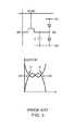
- the RTDis a conventional two-terminal diode 20 , as described in U.S. Pat. No. 5,825,049.
- the illustrated RTDincludes a cathode 22 , a bulk emitter 24 , an undoped layer 26 , a two-dimensional resonant electron layer 27 , thin barriers 28 , another undoped layer 29 , a bulk collector 30 , and an anode 32 , all disposed over a substrate 34 .
- the RTDis typically realized in III-V semiconductor material system, where heterojunctions create a quantum well, switched by two barrier layers that enable resonant tunneling.
- a variation of the RTDis an RITD.
- a three-terminal RTTmay be constructed by adding a control terminal to an RTD structure.
- a resonant tunneling structure and mechanismmay be integrated into a three-terminal transistor device in many other ways.
- a DELTT transistorincluding a thin tunnel barrier 40 , is positioned between two two-dimensional quantum wells (QW) 45 , 50 .
- QWquantum wells
- Electrical contactis made by a top layer contact 52 to the top QW 45 only by the source, and by a bottom layer contact 54 to the bottom QW 50 only by the drain, in both cases accomplished by using the top and back depletion gates 55 , 60 to remove electrons from the QW that one does not wish to contact. Tunneling between the two QWs occurs only when electrons in both wells have substantially identical momentum and energy; this may be controlled by the top control gate.
- a control gate 65is disposed over the structure.
- a total thickness of the semiconductor layersis kept less than 2 microns, allowing the back depletion gate to be brought close to the QWs and the entire device to be made small.
- the illustrated deviceincludes two gallium arsenide layers, each 150 angstroms thick, separated by a 125 angstrom aluminum gallium arsenide barrier. At left is shown the energy band diagram 65 of the structure, containing the two quantum wells separated by the thin tunnel barrier 40 .
- the resonant tunneling deviceis one of the potential emerging logic devices to continue functional scaling of electronics integrated circuits beyond the end of Si-based CMOS technology roadmap.
- This class of devicesmay include RTT and hybrid tunneling devices or circuit units that include both tunneling devices and conventional devices such as MOSFETs or HEMTs, etc.
- an RTD-FETincludes several RTDs and one or more conventional FETs.
- a hybrid systemcan potentially provide more computational power and/or functionality since it requires fewer devices in comparison to the conventional logic circuit and it is inherently faster due to the RTD's intrinsic high switching speed and negative differential resistance property, and yet it uses less power than conventional devices.
- SRAMstatic random access memory
- the illustrated tunnel diode SRAMhas two stable operating points 300 , 300 ′ that may be used to represent “0” and “1” in memory operation.
- This devicehas the potential to reduce the cell size in comparison to the conventional 6-transistor SRAM (6-T SRAM). It is refresh-free and offers a low power consumption advantage.
- the SRAM celloffers multi-value memory operation.
- a conventional latched comparatormay include 12 high electron mobility transistors (HEMTs) and 6 Schottky diodes.
- An RTD-based latched comparatorhas been fabricated with 2 RTDs and 2 HEMTs, with latching behavior being inherent to RTD devices. The unit area is reduced to one sixth in comparison to the conventional comparator.
- tunneling devicesare conventionally fabricated in III-V material systems, and thus typically are difficult to integrate into Si-based systems. Also the cost is typically high, which limits their widespread application.
- Si/SiGe RITD devicestypically require epitaxial growth in low temperature molecular beam epitaxy (MBE) systems, instead of metal-organic chemical vapor deposition (MOCVD) systems that may be unable to achieve the preferred high n-type phosphorus doping and also suffer from phosphorus poisoning issues.
- MOCVDmetal-organic chemical vapor deposition
- the Si/SiGe RITDalso typically has lower performance than an optimized III-V RITD device.
- Embodiments of the present inventioninclude methods and structures for fabricating tunneling devices on a first type of substrate, e.g., group IV, with improved material systems, e.g., III-V and II-VI materials.
- the manufacturing processmay be compatible with conventional CMOS processes utilizing Si substrates.
- the process flowmay include an aspect ratio trapping (ART) epitaxial technique.
- ARTaspect ratio trapping
- manufacturing methodsuse epitaxy techniques, including MBE and CVD systems, for ART.
- CVDhas a number of advantages, including low defect density, high quality regrowth capability, rapidly varying alloy compositions, and improved manufacturability due to CVD's higher throughput, relatively short downtimes, and scalability to very large reactors
- Embodiments of the inventionalso include new structures and methods for functional circuits incorporating both tunneling devices and conventional Si-based devices.
- Such circuit unitsmay function as, e.g., a logic circuit, an SRAM or a DRAM.
- the inventionincludes a structure.
- the structurehas a non-crystalline material defining an opening having a sidewall disposed above a surface of a substrate that comprises a first crystalline semiconductor material.
- the openinghas a non-crystalline sidewall.
- a second crystalline semiconductor material, lattice-mismatched to the first crystalline semiconductor material,is disposed in the opening.
- a tunneling deviceis disposed over at least a portion of the second crystalline semiconductor material.
- the tunneling devicemay be, e.g., an Esaki diode (tunnel diode), a single-barrier tunnel diode, an RTD, a triple-barrier or multiple-barrier resonant tunneling diode, an RITD, a single-barrier interband-tunneling diode, an RTT, an RTFET, a DELTT, a QWBRTT, an RTBT or RBT, or an RHET.
- the structuremay comprise a memory cell, with a phase change layer or a ferroelectric material disposed over the tunneling device.
- the structuremay include memory circuitry, such as SRAM circuitry, DRAM circuitry, or non-volatile memory circuitry, that includes the tunneling device.
- the first crystalline semiconductor materialmay include a group IV element or compound, a II-VI compound, and/or a III-V compound
- the second crystalline materialmay include a group IV element or compound, a II-VI compound, and/or a III-V compound.
- the first crystalline semiconductor material and the second crystalline semiconductor materialmay include materials selected from different groups.
- a majority of defects arising from the lattice-mismatch of the first and second crystalline semiconductor materialsmay terminate within the opening, e.g., below a height of the opening.
- the width of the openingmay be less than the height of the opening.
- the tunneling devicemay be in contact with at least a portion of the second crystalline material.
- a circuit componentsuch as a MOSFET, a MISFET, a HEMT, a capacitor, or a resistor, may be coupled to the tunneling device and disposed above a region of the substrate.
- the tunneling devicemay include a tunneling diode disposed above a transistor.
- the circuit componentmay include a gate array, a memory circuit, and/or a processor circuit.
- the tunneling diodemay be disposed above a source or drain of a transistor.
- a second tunneling diodemay be disposed over the source or drain of the transistor.
- the inventionfeatures a method for forming a structure.
- the methodincludes the formation of an opening above a region of a substrate comprising a first crystalline semiconductor material.
- the openingis defined by a dielectric sidewall and an exposed surface of the substrate.
- a second crystalline semiconductor material lattice-mismatched to the first crystalline semiconductor materialis formed in the opening.
- a tunneling deviceis defined over at least a portion of the second crystalline semiconductor material.
- the tunneling devicemay be, e.g., an Esaki diode (tunnel diode), a single-barrier tunnel diode, an RTD, a triple-barrier or multiple-barrier resonant tunneling diode, an RITD, a single-barrier interband-tunneling diode, an RTT, an RTFET, a DELTT, a QWBRTT, an RTBT or RBT, or an RHET.
- the second crystalline materialmay be formed in the window by selective epitaxy. The opening may be formed above a region of a transistor.
- the second crystalline semiconductor materialmay include a II-VI compound and/or a III-V compound.
- the inventionincludes a structure integrating a tunneling diode and a transistor using lattice-mismatched materials.
- the structureincludes the transistor formed proximate a substrate including a first crystalline semiconductor material.
- the tunneling diodeis coupled to one of a source or a drain of the transistor, and the tunneling diode is formed using a second crystalline semiconductor material lattice-mismatched to the first crystalline semiconductor material.
- At least a portion of the second semiconductor materialis disposed within an opening disposed above the substrate.
- the openinghas a non-crystalline sidewall and configured to trap a majority of defects arising from the lattice mismatch between the first and second semiconductor materials.
- the inventionincludes a method of reducing SRAM circuit surface area.
- the methodincludes the formation of an RTD-based static random access memory (SRAM) circuit.
- the RTD-based SRAM circuithas a perimeter defining an RTD-based SRAM cell area, the cell area including circuit components defining an SRAM memory cell.
- a transistor having a gate lengthis formed above a substrate including a first crystalline material.
- At least one RTDis formed proximate an opening disposed above the substrate, the opening comprising a non-crystalline sidewall.
- the RTDis coupled to a source or a drain of the transistor and includes crystalline material lattice-mismatched to the first crystalline material.
- the RTD-based SRAM cell areais at least 33% smaller than a surface area of an SRAM circuit constructed using six transistors having the same gate length as the transistor in the RTD-based SRAM cell area.
- the inventionfeatures a method of forming a transistor structure including a tunneling structure.
- the methodincludes the formation of an opening above a surface of a substrate comprising a first crystalline semiconductor material.
- the openinghas a non-crystalline sidewall.
- a second crystalline semiconductor materialis formed in the opening.
- the second crystalline semiconductor materialis lattice-mismatched to the first crystalline semiconductor material.
- a majority of defects arising from lattice-mismatch between the first and second semiconductor materialsterminate within the opening.
- a tunneling structureis formed over and in contact with at least a portion of the second crystalline semiconductor material. First, second, and third terminals of a transistor are formed proximate the tunneling structure.
- the tunneling devicemay be an RTD, a triple-barrier or multiple-barrier resonant tunneling diode, an RITD, an RTT, an RTFET, a DELTT, a quantum-well-base resonant tunneling transistor (QEBRTT), an RTBT or RBT, or an RHET.
- the first crystalline semiconductor materialcomprises or consists essentially of at least one of a group IV element, a II-VI compound, or a III-V compound.
- the second crystalline semiconductor materialcomprises a II-VI compound and/or a III-V compound.
- a phase change layeris disposed over the tunneling device, and the structure includes a memory cell.
- a ferroelectric materialis disposed over the tunneling device, and the structure includes a memory cell.
- Memory circuitrysuch as SRAM circuitry, DRAM circuitry, or non-volatile memory circuitry, may include the tunneling device.
- the inventionfeatures a method for forming a structure.
- the methodincludes the formation of a masking layer over a substrate comprising a first crystalline semiconductor material.
- a windowis defined in the masking layer.
- the windowis filled with a second crystalline semiconductor material that is lattice-mismatched to the first crystalline semiconductor material.
- a tunneling deviceis disposed over and in contact with at least a portion of the second crystalline semiconductor material.
- the tunneling devicemay be a DELTT, an RTD, or an RITD.
- the windowmay be filled by selective epitaxy.
- the inventionfeatures a structure.
- the structureincludes a substrate comprising a first crystalline semiconductor material, and an RTD comprising a second crystalline semiconductor material disposed over the substrate.
- the first crystalline semiconductor materialincludes a group IV element or compound and the second crystalline semiconductor material includes a III-V or a II-VI compound.
- the inventionfeatures a structure.
- the structureincludes a substrate including a first crystalline semiconductor material comprising a group IV element; An RITD is disposed over the substrate.
- the RITDincludes a second crystalline semiconductor material lattice-mismatched to the first crystalline semiconductor material, the second crystalline semiconductor material including at least one of a III-V compound or a II-VI compound.
- the inventionfeatures a structure.
- the structureincludes a substrate comprising a first crystalline semiconductor material comprising a group IV element and a DELTT device disposed over the substrate.
- the DELTT deviceincludes a second crystalline semiconductor material lattice-mismatched to the first crystalline semiconductor material, the second crystalline semiconductor material including at least one of a III-V compound or a II-VI compound.
- the DELTT deviceincludes an emitter contact, a collector contact, a two dimensional quantum well emitter layer electrically contacting the emitter contact, and a two dimensional quantum well resonant tunneling layer.
- the DELTT devicealso includes a collector layer disposed opposite the resonant tunneling layer from the emitter layer, the collector layer electrically contacting the collector contact, a first tunneling barrier layer disposed between the emitter layer and the resonant tunneling layer, a second tunneling barrier layer disposed between the resonant tunneling layer and the collector layer; and a voltage drop layer between the resonant tunneling layer and the collector.
- the inventionfeatures a structure.
- the structureincludes a substrate comprising a first crystalline semiconductor material, and a magnetic resonant tunneling diode comprising a second crystalline semiconductor material disposed over the substrate.
- the first crystalline semiconductor materialmay comprises or consist essentially of a group IV element or compound and the second crystalline semiconductor material may comprise or consist essentially of a III-V or a II-VI compound.
- the inventionfeatures a structure.
- the structureincludes a substrate comprising a first crystalline semiconductor material.
- a first windowis defined in a dielectric layer disposed over the first semiconductor substrate.
- a first deviceis disposed over the first window.
- a second windowis defined in a dielectric layer disposed over the first semiconductor substrate.
- a second crystalline semiconductoris disposed in the second window, the second crystalline semiconductor material being lattice-mismatched to the first crystalline semiconductor material.
- a tunneling deviceis disposed over and in contact with at least a portion of the second crystalline semiconductor material. The first device and the tunneling device are interconnected to form a circuit unit.
- the inventionfeatures a structure including a substrate that comprises a first crystalline semiconductor material.
- a dielectric layeris disposed over at least a portion of the substrate and has a window defined therein.
- a second crystalline semiconductor materialis disposed in the window and over the first crystalline semiconductor material, and is lattice-mismatched to the first crystalline semiconductor material.
- a tunneling deviceis disposed over and in contact with at least a portion of the second crystalline semiconductor material over a first region of the substrate.
- a circuit componentis formed over a second region of the substrate.
- the first crystalline semiconductor materialincludes a group IV element or compound, a II-VI compound, and/or a III-V compound
- the second crystalline materialincludes a group IV element or compound, a II-VI compound and/or a III-V compound
- the first crystalline semiconductor material and the second crystalline semiconductor materialinclude materials selected from different groups.
- a structuremay include a substrate comprising a first crystalline semiconductor material.
- a dielectric layeris disposed over at least a portion of the substrate and has a window defined therein.
- a second crystalline semiconductor materialis disposed in the window and over the first crystalline semiconductor material, the second crystalline semiconductor material being lattice-mismatched to the first crystalline semiconductor material.
- An amplifierincludes (i) a tunneling diode disposed over and in contact with at least a portion of the second crystalline semiconductor material, and (ii) a resistor.
- the first crystalline semiconductor materialincludes a group IV element or compound, a II-VI compound, and/or a III-V compound
- the second crystalline materialincludes a group IV element or compound, a II-VI compound and/or a III-V compound
- the first crystalline semiconductor material and the second crystalline semiconductor materialinclude materials selected from different groups.
- the inventionfeatures a structure including a substrate comprising a first crystalline semiconductor material.
- a dielectric layeris disposed over at least a portion of the substrate and has a window defined therein.
- a second crystalline semiconductor materialis disposed in the window and over the first crystalline semiconductor material, the second crystalline semiconductor material being lattice-mismatched to the first crystalline semiconductor material.
- a memory cellincludes a tunneling diode is disposed over and in contact with at least a portion of the second crystalline semiconductor material.
- the inventionfeatures a structure including a substrate comprising a first crystalline semiconductor material.
- a windowis defined in a dielectric layer disposed over the substrate.
- a second crystalline semiconductor materialis disposed in the window, the second crystalline semiconductor material being lattice-mismatched to the first crystalline semiconductor material.
- a logic inverterincludes (i) a tunneling device disposed over and in contact with at least a portion of the second crystalline semiconductor material, and (ii) a MOSFET.
- the first crystalline semiconductor materialincludes a group IV element or compound, a II-VI compound, and/or a III-V compound
- the second crystalline materialincludes a group IV element or compound, a II-VI compound and/or a III-V compound
- the first crystalline semiconductor material and the second crystalline semiconductor materialinclude materials selected from different groups.
- the inventionfeatures a structure including a substrate comprising a first crystalline semiconductor material.
- a dielectric layeris disposed over at least a portion of the substrate and has a first window and a second window defined therein.
- a second crystalline semiconductor materialis disposed in each of the first and second windows and over the first crystalline semiconductor material.
- the second crystalline semiconductor materialis lattice-mismatched to the first crystalline semiconductor material.
- An SRAMincludes (i) a first resonant tunneling diode disposed over and in contact with at least a portion of the second crystalline semiconductor material disposed in the first window, (ii) a second resonant tunneling diode disposed over and in contact with at least a portion of the second crystalline semiconductor material disposed in the second window, and (iii) a MOSFET.
- the first crystalline semiconductor materialincludes a group IV element or compound, a II-VI compound, and/or a III-V compound
- the second crystalline materialincludes a group IV element or compound, a II-VI compound and/or a III-V compound
- the first crystalline semiconductor material and the second crystalline semiconductor materialinclude materials selected from different groups.
- Each of the first and second resonant tunneling diodesmay be in electrical communication with a drain of the MOSFET.
- Each of the first and second resonant tunneling diodesmay be in electrical communication with a gate of the MOSFET.
- the inventionfeatures a structure including a substrate comprising a first crystalline semiconductor material.
- a dielectric layeris disposed over at least a portion of the substrate and has plurality of windows defined therein.
- a second crystalline semiconductor materialis disposed in each of the plurality of windows and over the first crystalline semiconductor material, the second crystalline semiconductor material being lattice-mismatched to the first crystalline semiconductor material.
- a field programmable arrayincludes a plurality of SRAMs, each SRAM comprising (i) a first resonant tunneling diode disposed over and in contact with at least a portion of the second crystalline semiconductor material disposed in one of the plurality of windows, (ii) a second resonant tunneling diode disposed over and in contact with at least a portion of the second crystalline semiconductor material disposed in another of the plurality of windows, and (iii) a MOSFET.
- the first crystalline semiconductor materialincludes a group IV element or compound, a II-VI compound, and/or a III-V compound
- the second crystalline materialincludes a group IV element or compound, a II-VI compound and/or a III-V compound
- the first crystalline semiconductor material and the second crystalline semiconductor materialinclude materials selected from different groups.
- the inventionfeatures a structure that includes a substrate comprising a first crystalline semiconductor material.
- a dielectric layeris disposed over at least a portion of the substrate and has a plurality of windows defined therein.
- a second crystalline semiconductor materialis disposed in each of the windows and over the first crystalline semiconductor material, the second crystalline semiconductor material being lattice-mismatched to the first crystalline semiconductor material.
- a microprocessorincludes (i) arithmetic logic units (ALU) adapted for executing arithmetic and logical functions; (ii) storage locations and memory units adapted to store data, addresses, instructions and control programs; and (iii) control systems and interconnection systems adapted to provide links among different components, accept and generate external control signals, and to provide timing signals.
- ALUarithmetic logic units
- At least one of the ALU, storage locations and memory units, and control and interconnection systemscomprises a tunneling device disposed over and in contact with the second crystalline semiconductor material.
- the first crystalline semiconductor materialincludes a group IV element or compound, a II-VI compound, and/or a III-V compound
- the second crystalline materialincludes a group IV element or compound, a II-VI compound and/or a III-V compound
- the first crystalline semiconductor material and the second crystalline semiconductor materialinclude materials selected from different groups.
- the inventionfeatures a method for forming a structure.
- the methodincludes providing a substrate comprising a first crystalline semiconductor material and a dielectric layer disposed thereover.
- a CMOS deviceis formed in a first region of the substrate.
- a windowis defined in the dielectric layer to expose at least a portion of a surface of the first semiconductor material.
- the windowis filled with a second crystalline semiconductor material lattice-mismatched to the first crystalline semiconductor material.
- a tunneling deviceis defined over and in contact with at least a portion of the second crystalline semiconductor material. An interconnection is formed between the tunneling device and the CMOS device.
- the inventionfeatures a method for forming a structure, the method including providing a substrate comprising a first crystalline semiconductor material. A masking layer is formed over the substrate. A window is defined in the masking layer. The window is filled with a second crystalline semiconductor material lattice-mismatched to the first crystalline semiconductor material, the second semiconductor material having a total thickness higher than a height of the masking layer. The second semiconductor material is planarized to define a planar surface of the second semiconductor material. A tunneling device is defined over and in contact with at least a portion of the second crystalline semiconductor material. Planarizing the second semiconductor material may include chemical-mechanical polishing utilizing the masking layer as a polishing stop.
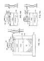
- FIG. 1is a cross-sectional view of an RTD or RITD device structure, prior art
- FIG. 2is a perspective view of a double electron layer tunnel transistor (DELTT), prior art
- FIG. 3illustrates a circuit of a tunnel diode SRAM and its associated IV curve, prior art
- FIG. 4is a cross-sectional view of a GaAs/AlGaAs RTD formed on a Si substrate with the use of ART in accordance with an embodiment of the invention
- FIG. 5is a cross-sectional view of an RTD formed with the use of ART and including III-V materials in accordance with an embodiment of the invention
- FIGS. 6 a -6 bis a cross-sectional view of an RTD formed with the use of ART and including contacts thereto in accordance with an embodiment of the invention
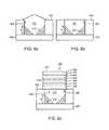
- FIGS. 7 a -7 b and 8 a -8 care cross-sectional views of device structures with non-flat top surfaces formed with the use ART in accordance with embodiments of the invention.
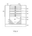
- FIG. 9is a cross-sectional view of a triple-barrier RTD formed with the use of ART in accordance with an embodiment of the invention.
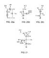
- FIGS. 10 a -10 eare cross-sectional views of five different RITD structures formed with the use of ART in accordance with embodiments of the invention.
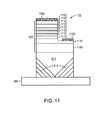
- FIG. 11is a cross-sectional view of a magnetic resonant tunneling diode as a spin selector for spintronic applications in accordance with an embodiment of the invention
- FIGS. 12 a -12 bare a pair of cross-sectional views illustrating a process for forming an RTFET in accordance with an embodiment of the invention
- FIGS. 13 a -13 bare cross-sectional views of a QWBRTT formed with the use of ART in accordance with an embodiment of the invention
- FIGS. 14 a -14 care cross-sectional views of tunneling quantum structures integrated within a bipolar transistor, formed with the use of ART in accordance with embodiments of the invention, as well as the corresponding energy-band diagrams;
- FIG. 15is a cross-sectional view of a three-terminal bipolar quantum resonant tunneling transistor formed over GaAs grown by ART on a Si substrate in accordance with an embodiment of the invention
- FIG. 16 ais a cross-sectional view of a multi-state RTBT formed by ART in accordance with an embodiment of the invention
- FIG. 16 bis an energy-band diagram of the device of FIG. 16 a;
- FIGS. 17 a -17 bare a cross-sectional view of an RHET formed by ART and its energy-band diagram in accordance with an embodiment of the invention
- FIG. 18is a cross-sectional view of a typical DELTT structure disposed over GaAs material formed by ART in accordance with an embodiment of the invention.
- FIG. 19is a cross-sectional view of a building block for various logic circuit units in accordance with an embodiment of the invention.
- FIGS. 20 a -20 c and 21are diagrams illustrating circuit units incorporating RTD formed by ART in accordance with embodiments of the invention.
- FIG. 22is a cross-sectional view of an SRAM structure including two RTDs and an n-FET in accordance with another embodiment of the invention.
- FIGS. 23 a -23 e , 24 a -24 e , and 25are diagrams illustrating SRAMs incorporating RTD devices formed in accordance with embodiments of the invention.
- FIG. 26is a cross-sectional view of a non-volatile memory cell including an RTD and one memory storage material (such as phase change material or ferroelectric material) in accordance with another embodiment of the invention
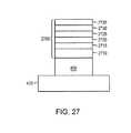
- FIG. 27is a cross-sectional view of a non-volatile magnetic random access memory including an RITD and a magnetic tunneling structure in accordance with another embodiment of the invention.
- FIG. 28is a diagram of a monostable-bistable transition logic element including an RTD formed by RTD in accordance with an embodiment of the invention.
- FIG. 29is a diagram of an analog-to-digital converter circuit employing multi-state RTBT devices formed by ART in accordance with an embodiment of the invention.
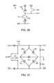
- FIG. 30is a diagram of a RTD/HEMT comparator incorporating an RTD into a HEMT formed by ART in accordance with an embodiment of the invention
- FIG. 31is a diagram of an RTD-based clock generator formed by ART in accordance with an embodiment of the invention.
- FIG. 32is a diagram of a field programmable gate array incorporating RTD-based SRAMS formed by ART in accordance with an embodiment of the invention
- FIGS. 33 and 34are block diagrams illustrating RTD-based or RTT-based microprocessors formed by ART in accordance with embodiments of the invention.
- FIG. 35is a block diagram of an RTD-based digital signal processor formed by ART in accordance with an embodiment of the invention.
- FIG. 36is a block diagram illustrating an RTD-based graphics processing unit formed by ART in accordance with an embodiment of the invention.
- FIG. 37is a cross-sectional view of a device including two RTDs connected to a drain of a MOSFET, formed by ART in accordance with an embodiment of the invention.
- embodiments of this inventionmay include other materials systems, such as SiGe, Ge, III-V and/or II-VI.
- the described structuresmay be fabricated on various semiconductor substrates, such as Si substrates, Ge substrates, semiconductor-on-insulator (SOI) substrates, strained-semiconductor-on-insulator (SSOI) substrates, and other substrate systems.
- Embodiments of the inventionalso include other similar tunneling device structures and circuit units.
- Structuresmay include various tunneling devices and various circuit units; methods are described herein for producing such structures or circuit units on a first type of substrate, e.g., from group IV such as a Si or Ge substrate, with improved material systems, e.g., III-V and II-VI epitaxial materials.
- the III-V or II-VI epitaxial layersmay be grown selectively on conventional substrates such as Si, SOI, or SSOI substrates in selected areas (such as the device active area).
- Such layersmay be formed by a heteroepitaxy technique, e.g., by ART heteroepitaxial techniques, as described in pending U.S. patent application Ser. Nos. 11/436,198 and 11/436,062.
- FIG. 4the use of an ART technique enables the integration of low-defect III-V or II-VI materials on a Si substrate for tunneling device 400 fabrication.
- An exemplary RTD device structureis illustrated in FIG. 5 .
- ARTis used to grow a low-defect high-quality semiconductor material 410 (e.g., GaAs) on a Si surface, such that defects 415 , e.g., dislocations and stacking faults, are trapped by the dielectric side walls 420 , resulting a low-defect upper region of GaAs material.
- a low-defect high-quality semiconductor material 410e.g., GaAs
- first contact 430may be the anode terminal and the second contact 435 may be the cathode terminal of tunneling device 400 , and in other embodiments, the first contact 430 may be the cathode terminal and the second contact 435 may be the anode terminal.
- the substrate 405may be, for example, a bulk silicon wafer, a bulk germanium wafer, a semiconductor-on-insulator (SOI) substrate, or a strained semiconductor-on-insulator (SSOI) substrate.
- the substrate 405may include or consist essentially of a first semiconductor material, such as a group IV element, e.g., germanium or silicon.
- the substrate 405includes or consists essentially of (100) silicon.
- a non-crystalline materiale.g., a dielectric layer 440
- the dielectric layer 440may include a dielectric material, such as silicon nitride or silicon dioxide.
- the dielectric layer 440may be formed by a method known to one of skill in the art, e.g., thermal oxidation or plasma-enhanced chemical vapor deposition.
- the dielectric layer 440may have a thickness t 1 corresponding to a desired height of crystalline material to be deposited in a window 445 formed through the dielectric layer 440 .
- the thickness t 1 of the dielectric layer 440may be selected from a range of, e.g., 20-50000 nm.
- a mask(not shown), such as a photoresist mask, is formed over the substrate 405 and the dielectric layer 440 .
- the maskis patterned to expose at least a portion of the dielectric layer 440 .
- the exposed portion of the dielectric layer 440is removed by, e.g., reactive ion etching (RIE) to define the window 445 .
- RIEreactive ion etching
- the window 445extends to a surface of the substrate 405 and may be defined by at least one sidewall 420 .
- the sidewall 420is formed from the dielectric layer 440 and is, therefore, non-crystalline.
- the sidewall 420may have a height h at least equal to a predetermined distance H from the surface of the substrate 405 .
- dislocations 415 in a mismatched cubic semiconductor grown on a Si (100) surface in the near-vicinity (e.g., within approximately 500 nm or less) of a vertical dielectric sidewall 420 surfacebend toward that surface at approximately 30 degrees through 60 degrees.
- the dislocations 415may bend toward that surface at approximately a 45 degree angle to that surface.
- the predetermined distance H necessary to trap defects 415may be approximately equal to a width between 1 ⁇ 2 w and 2 w, where w is the width of the window 445 .
- the window 445may be substantially rectangular in terms of cross-sectional profile, a top view, or both, and have a width w that is smaller than a length l (not shown) of the window.
- the width w of the windowmay be less than about 5000 nm, e.g., about 20-1000 nm. In some embodiments, the width of the window is about 150 nm.
- a length l of the windowmay exceed each of w and H.
- a ratio of the height h of the window to the width w of the windowmay be >1, preferably between about 1 and about 50.
- a second crystalline semiconductor material 410is formed in the window.
- the second crystalline semiconductor material 410may include or consist essentially of a group IV element or compound, a III-V compound, or a II-VI compound.
- suitable group IV elements or compoundsinclude germanium, silicon germanium, and silicon carbide.
- suitable III-V compoundsinclude gallium arsenide, gallium nitride, indium arsenide, indium antimonide, indium aluminum antimonide, indium aluminum arsenide, indium phosphide, and indium gallium arsenide.
- suitable II-VI compoundsinclude zinc selenide and zinc oxide.
- the second crystalline semiconductor material 410may be formed by selective epitaxial growth in any suitable epitaxial deposition system, including, but not limited to, metal-organic chemical vapor deposition (MOCVD), atmospheric-pressure CVD (APCVD), low- (or reduced-) pressure CVD (LPCVD), ultra-high-vacuum CVD (UHCVD), molecular beam epitaxy (MBE), or atomic layer deposition (ALD).
- MOCVDmetal-organic chemical vapor deposition
- APCVDatmospheric-pressure CVD
- LPCVDlow- (or reduced-) pressure CVD
- UHCVDultra-high-vacuum CVD
- MBEmolecular beam epitaxy
- ALDatomic layer deposition
- selective epitaxial growthtypically includes introducing a source gas into the chamber.
- the source gasmay include at least one precursor gas and a carrier gas, such as, for example, hydrogen.
- the reactor chambermay be heated by, for example, RF-heating.
- CVDhas a number of advantages, including the capability for depositing films with low defect densities and rapidly varying alloy compositions, as well as high quality regrowth capability. CVD may also provide improved manufacturability due to relatively higher throughput, relatively short downtimes, and scalability to very large reactors.
- the epitaxial growth systemmay be a single-wafer or multiple-wafer-batch reactor.
- Suitable CVD systems commonly used for volume epitaxy in manufacturing applicationsinclude, for example, an Aixtron 2600 multi-wafer system available from Aixtron, based in Aachen, Germany; an EPI CENTURA single-wafer multi-chamber systems available from Applied Materials of Santa Clara, Calif.; or EPSILON single-wafer epitaxial reactors available from ASM International based in Bilthoven, The Netherlands.
- Dislocation defects 415 in the second crystalline semiconductor material 410reach and terminate at the sidewalls 420 of the window in the dielectric material 440 at or below a vertical predetermined distance H from the surface of the substrate, such that dislocations 415 in the second crystalline semiconductor material 410 decrease in density with increasing distance from the bottom portion of the window. Accordingly, the upper portion of the crystalline material 410 is substantially exhausted of dislocation defects 415 .
- Various dislocation defects 415such as threading dislocations, stacking faults, twin boundaries, or anti-phase boundaries may thus be substantially eliminated from the upper portion of the epitaxial region.
- a density of such dislocation defects 415may be less than, for example, 10 6 /cm 2 , preferably less than 10 3 /cm 2 .
- the second crystalline semiconductor material 410may be either substantially relaxed or strained.
- a high-quality tunneling device 400may be fabricated on top of the low-defect second crystalline semiconductor material 410 .
- the tunneling devicemay be, for example, an RTD including GaAs and AlGaAs.
- the RTD device 400may include multiple thin semiconductor layers 425 such as, from bottom to top, a relatively thick n-type layer 446 (e.g., n-type gallium arsenide with a thickness of, e.g., 10-25000 nm); an undoped layer 447 (e.g., undoped gallium arsenide with a thickness of, e.g., 0-50 nm); a thin barrier layer with a large bandgap 448 (e.g., undoped aluminum gallium arsenide with a thickness of, e.g., 0-50 nm); a thin two-dimensional resonant electron layer 449 (e.g., undoped gallium arsenide with a thickness of, e.g
- All of these layers 425may be grown epitaxially in sequence in any suitable epitaxial deposition system, including, but not limited to, MOCVD, APCVD, LPCVD, UHCVD, MBE, or ALD.
- This exemplary RTD devicehas two external contacts: a first contact 430 contacts the n-type layer 446 , and a second contact 435 contacts the n-type layer 452 . Both contacts 430 and 435 typically include metal contacts.
- the first contact 430may be made by etching a small hole (not shown) on one side of the device to reach the layer 446 . Methods and variations for the fabrication of this RTD 400 device will be apparent to one of skill in the art.
- the layers 425 of the RTDinclude or consist essentially of AlGaAs and GaAs.
- the substratemay include a group IV element such as Si, and the RTD may include a III-V compound.
- the RTDmay include a II-VI compound.
- embodiments of the inventionalso include other varieties of resonant tunneling device structures with a variety of semiconductor material combinations, layer structures, layer thicknesses, doping levels in each layer, epitaxy growth conditions (e.g., precursors, growth temperature, etc), and contact configurations.
- epitaxy growth conditionse.g., precursors, growth temperature, etc
- the layers 425 of RTDmay include various combinations of pairs of III-V materials.
- the layersmay include a heavily doped materials 1 layer 546 , an undoped materials 1 (spacer) layer 547 , an undoped materials 2 barrier layer 548 , an undoped materials 1 (2D resonant electron layer) layer 549 , a second undoped materials 2 barrier layer 550 , an undoped material 1 spacer layer 551 , and a heavily doped materials 1 layer 552 , where materials 1/materials 2 combinations may be, e.g., GaAs/AlGaAs, GaAs/InGaAs, GaInAs/AlInAs, GaAs/AlAs, InP/InGaAs, InGaAs/AlAs, InAs/AlSb, or InSb/AlInSb.
- the two doped layers 546 and 552may include different materials.
- the 2D resonant electron layer 549may be undoped and may have a thickness of 5 nm
- the barrier layers 548 , 550may be undoped and may have a thickness of 1 to 5 nm.
- the doped layers 546 and 552may be, e.g., n-type with a doping level of 2 ⁇ 10 18 to 1 ⁇ 10 19 /cm 3 .
- a contact to a tunneling device 400may be formed by the following approach.
- the steps in this approachare also applicable to other tunneling devices and structures of other embodiments of the inventions described herein.
- III-V heteroepitaxial layers 410are grown selectively in a window 445 defined by a dielectric layer 440 disposed over a semiconductor substrate 405 .
- dielectric windowsmay be utilized in some heteroepitaxial growth technologies such as ART technology.
- the dielectric 440is etched back, e.g., approximately halfway back to form a recess structure.
- the etch-back of the dielectric 440partially exposes the layers 425 within the dielectric window, allowing, e.g., a first contact 430 to also be made to a bottom layer disposed in the dielectric window (e.g., to the doped layer 546 in FIG. 6 b ).
- FIG. 5Another approach is depicted in FIG. 7 b , where some layers 425 of the device structure are grown within the dielectric windows and are non-flat, while other layers are grown above the dielectric layer 440 .
- FIGS. 8 a -8 canother embodiment of an epitaxial layer and device structure is formed as follows.
- III-V material 410is grown within and above dielectric windows 445 by ART technique, this III-V material 410 having a non-flat surface due to faceting.
- the structureis planarized to achieve a flat surface, for example by CMP using the dielectric layer 440 as a polishing stop.
- epitaxial device layers 425are grown on the flat surface.
- both doped layers 546 and 552may be made, by, e.g., first and second contacts 430 and 435 , as shown in FIG. 8 c , as both doped layers 546 and 552 are disposed above the dielectric layer 440 and are at least partially exposed.
- FIGS. 7 and 8 a - 8 cAlthough only one exemplary device structure is illustrated in both FIGS. 7 and 8 a - 8 c , these approaches and methods are also applicable to other tunneling devices and structures of other embodiments of the inventions described herein.
- the structures described belowmay be fabricated on III-V or II-VI epitaxial layers that are grown selectively on conventional substrates such as Si, SOI, or SSOI substrates in selected areas (such as the device active area). Such layers may be formed by heteroepitaxy, such as with ART techniques.
- a triple-barrier tunneling diodeincludes three barriers 548 , 550 , 550 ′ and two 2D resonant electron layers 549 , 549 ′. This structure gives rise to multiple current peaks on I-V characteristics.
- a multiple-barrier tunneling diodemay be formed by incorporating more than three barrier layers separating multiple 2D resonant electron layers (not shown).
- Typical RTDsare often intra-band tunneling diodes.
- a variation of a tunneling diodeis the RITD device.
- FIGS. 10 a -10 eillustrate five different RITD structures 1000 .
- the III-V epitaxial layers 410e.g., n + -InAs, are grown on a semiconductor substrate 405 , e.g., an Si wafer, in the device area by heteroepitaxy.
- an RITD 1000may include an ohmic contact 1005 and an injecting junction 1010 that is a polytype heterostructure, i.e., including a barrier layer 1020 , 1020 ′ (e.g., i-AlSb layer having a thickness selected from a range of about 1.5 nm to 3 nm) inserted in a type-III (or so-called broken-gap) heterojunction, including e.g., a p-GaSb layer 1030 and an n-InAs layer 1040 .
- an RITD 1000may include a type-III (or broken-gap) heterojunction including, e.g. a p-GaSb layer 1030 and an n-InAs layer 1040 .
- an RITD 1000may include two delta-doped layers ⁇ n + , and ⁇ p + 1050 , 1060 .
- the delta-doped layer sheet chargesare typically on the order of 1 ⁇ 10 13 /cm 2 .
- delta-doped layers 1050 , 1060a single material may be used to make the diode, e.g., intrinsic 1061 and p + doped 1062 . Referring to FIG.
- an RITD 1000may include three delta-doped layers, e.g., ⁇ n + , ⁇ + , and ⁇ n + 1050 , 1060 , 1050 ′, between two intrinsic layers 1061 and an n + layer 1063 .
- an RITD 1000may include a double-quantum-well heterostructure with layers including, e.g., n + -InAlAs 1070 , i-InGaAs 1075 , i-InAlAs 1080 , i-InGaAs 1085 , and p + -InAlAs 1090 .
- RITDsare a high peak-to-valley current ratio (PVCR).
- PVCRpeak-to-valley current ratio
- FIG. 11an example of a magnetic resonant tunneling diode 1100 as a spin selector for spintronics applications is illustrated. It is fabricated in two phases.
- the first phaseincludes heteroepitaxy growth of a buffer layer 410 of either GaAs or ZnBeSe material using ART techniques to achieve high-quality low defect material.
- the second phaseincludes fabricating a typical magnetic resonant tunneling diode 1100 .
- the magnetic resonant tunneling diode 1100includes layer structure 425 that may include, for example, Zn 0.97 Be 0.03 Se layer (300 nm thick, n-type doping at 8 ⁇ 10 18 /cm 3 ) 1105 , a first ZnSe layer (100 nm thick, n-type doping at 1.5 ⁇ 10 19 /cm 3 ) 1110 , Zn 0.97 Be 0.03 Se layer (10 nm thick, n-type doping at 1 ⁇ 10 18 /cm 3 ) layer 1115 , a second ZnSe (10 nm, intrinsic) layer 1120 , Zn 0.7 Be 0.3 Se layer (5 nm thick, intrinsic) 1125 , Zn 0.96 Mn 0.04 Se layer (9 nm thick, intrinsic) 1130 , Zn 0.7 Be 0.3 Se layer (5 nm thick, intrinsic) 1135 , a third ZnSe layer (10 nm thick, intrinsic) 1140 , Zn 0.97 Be 0.03 Se layer (15 nm
- Metal contacts 1160are formed to the first ZnSe layer 1110 and the fifth ZnSe layer 1150 .
- magnetic Mnincorporated into the quantum well material in the magnetic resonant tunneling diode 1100 , a strong splitting of well resonance is obtained as a function of external magnetic field.
- the device 400can thus be used as a spin selector.
- 3-terminal transistor devicesincorporate quantum tunneling structures.
- the advantages of 3-terminal tunneling devices over the 2-terminal tunneling diodesmay include: (i) providing a high-speed tunable negative differential resistance/transconductance, and (ii) providing isolation between the input and output.
- an exemplary fabrication process for forming an RTFET on ART semiconductor materialis as follows. Multiple layers 425 are grown by heteroepitaxy, e.g., by an ART process, to form a quantum tunneling device structure 400 .
- the fabrication process and materials usedmay be similar to those discussed with respect to FIG. 5 , and include a source 1200 and a drain 1205 .
- the dielectric layer 440is at least partially etched back, e.g., halfway, and then a gate structure 1210 is formed to control the device.
- the gate 1210is typically either a metal contact (Schottky diode), or a p-n junction. The function of the gate is to control the depletion width to vary the net cross-section area of the diode.
- Devicesmay have one of two types of gate structures.
- the gate materialmay form on two opposite sides of the diode, resulting in a 1-D resonant-tunneling device, or quantum wire device.
- the gate materialmay form around all sides of the diode, resulting in a 0-D resonant-tunneling device, or quantum dot (or single-electron) transistor.
- a QWBRTTis an ultrafast device in which carrier conduction from an emitter 1300 to a collector 1305 takes place via a tunneling structure. It is essentially an RTD device with a third terminal (a base) 1310 that contacts the quantum well to control its potential.
- Two types of QWBRTTinclude a bipolar device with p-type base that has a doping type (e.g., p-type) opposite to that of the emitter 1300 and the collector 1305 (e.g., n-type) ( FIG.
- n-type basethat has a doping type (e.g., n-type) that is the same as the emitter 1300 and collector 1305 (e.g., n-type) ( FIG. 13 b ).
- Terminals for an emitter contact 1320 and a base contact 1325are provided.
- an RTBT or RBTintegrates a tunneling quantum structure within a bipolar transistor.
- Three exemplary structuresvary by the location of where the quantum tunneling structure is incorporated.
- an RTBT structuremay include a tunneling quantum structure in the base 1310 region. Its energy band diagram is shown. As illustrated, a GaAs material system may be used; another exemplary material system is GaInAs/AsInAs. Referring to FIG. 14 b , an RTBT structure may include a tunneling quantum structure at the base-emitter junction. Referring to FIG. 14 c , an RTBT structure may include a tunneling quantum structure in the emitter 1300 region.
- a three-terminal bipolar quantum RTTmay be disposed over lattice-mismatched material 410 , e.g., GaAs, formed by ART growth on a substrate 405 .
- This bipolar quantum resonant tunneling transistoroperates in a manner similar to a conventional bipolar transistor; the tunneling current may be controlled by modulating the potential inside a quantum well that functions as a base.
- the fabrication processhas two phases. In the first phase, a second semiconductor material 410 (e.g., GaAs) is grown in a window 445 on a Si substrate 405 using ART. In the second phase, multiple layers 425 of GaAs and AlGaAs quantum wells are grown epitaxially on this structure.
- QWsmay be formed by typical processes familiar to those of skill in the art, and may include, e.g., the following layers: GaAs buffer 410 formed on Si substrate 405 by ART, undoped GaAs 1510 (1 ⁇ m thick); contact layer 1515 of GaAs (2 ⁇ m thick, Si-doped to 2 ⁇ 10 18 /cm 3 ); supperlattice collector 1520 (50 periods of 8 nm GaAs and 2 nm of AlGaAs Si-doped to 2 ⁇ 10 8 /cm 3 ), 3 periods of the same superlattice 1525 (8 nm GaAs and 2 nm AlGaAs, undoped), tunnel barrier 1530 (5 nm undoped AlGaAs), quantum well 1535 (15 nm with center 5 nm Be-doped to 1 ⁇ 10 19 /cm 3 ), tunnel barrier 1540 (5 nm undoped AlGaAs), 3 periods of the same superlattice 1545 (8 nm
- a multi-state RTBT 1600may include a stack of two Al 0.48 In 0.52 As (5 nm)/Ga 0.47 In 0.53 As (5 nm)/Al 0.48 In 0.52 As (5 nm) resonant tunneling double barrier structures incorporated into the emitter 1300 region of a Ga 0.47 In 0.53 As n-p-n transistor. Its corresponding energy band diagram is shown in FIG. 16 b .
- This multi-state RTBTexhibits multiple negative differential resistance and transconductance characteristics.
- the RTBT 1600includes n + layer 1610 (GaInAs, 5000 angstroms), n-type layer 1615 (GaInAs, 3000 angstroms), p + layer 1620 (GaInAs, 3000 angstroms), n-type layer 1625 (GaInAs, 500 angstroms), undoped layer 1630 (AlInAs, 50 angstroms), undoped layer 1635 (GaInAs, 50 angstroms), undoped layer 1640 (AlInAs, 50 angstroms), n + layer 1645 (GaInAs, 1000 angstroms), undoped layer 1650 (AlInAs, 50 angstroms), undoped layer 1655 (GaInAs, 50 angstroms), undoped layer 1660 (AlInAs, 50 angstroms), and n + layer 1665 (GAInAs, 5000 angstroms). Undoped layers 1660 , 1655 and 1650 form
- an RHET 1700incorporates a tunneling diode structure between the emitter 1300 and the base 1310 regions.
- This figureshows an exemplary RHET on a heteroepitaxial layer 410 grown on Si, and its energy-band diagram.
- the RHEThas heavily doped emitter 1300 and base 1310 regions, except for the AlGaAs/GaAs/AlGaAs tunneling diode region layers in the lower portion of emitter 1300 . It combines resonant tunneling with hot-electron ballistic transport in the base, resulting in super high speed.
- the RHETincludes a GaAs buffer layer 410 formed by heteroepitaxy, a collector 1305 including n + -GaAs 1710 and i-AlGaAs 1720 , a base 1310 including n + -GaAs 1725 , and an emitter 1300 including i-AlGaAs 1730 , i-GaAs 1735 , i-AlGaAs 1740 , and n + -GaAs 1745 .
- a DELTT structure 1800may be disposed over lattice-mismatched material, e.g., GaAs region 410 .
- the GaAs region 410is formed by ART growth on a substrate 405 .
- An AlGaAs region 1850is formed above the GaAs region 410 .
- GaAsis used as narrow bandgap material and AlGaAs is used as wide bandgap material.
- Other narrow/wide bandgap material systemsmay be also used to fabricate DELTT devices in a similar manner.
- a dielectric layer over a semiconductor substrateis patterned to define a window for the DELTT region.
- Other devicessuch as CMOS devices, may be fabricated on another region of the substrate.
- undoped GaAsis epitaxially grown by ART techniques, such that a top portion of the GaAs is substantially defect-free.
- a DELTT deviceis fabricated on top of the GaAs by, for example, a typical fabrication process such as that described in U.S. Pat. No. 5,825,049, FIGS. 6A-8D.
- the DELTT devicemay include the following features: a metal emitter contact 1842 , a metal collector contact 1854 , a two dimensional quantum well emitter layer 1844 electrically contacting the emitter contact 1842 , a two dimensional quantum well resonant tunneling layer 1846 (e.g., about 7 nm of GaAs), a collector layer 1848 disposed opposite the resonant tunneling layer 1846 from the emitter layer 1844 (e.g., a 15 nm thick, 2-dimensional emitter layer for electrons), the collector layer 1848 electrically contacting the collector contact 1854 , a first barrier layer 1845 (e.g., including two layers including a 20-30 nm GaAs voltage drop layer over the collector layer 1848 and a 5 nm AlGaAs wide bandgap barrier layer under the resonant tunneling layer 1846 ) disposed between the collector layer 1848 and the resonant tunneling layer 1846 , a second thin tunneling barrier layer 1843 (e.g
- FIGS. 13 a - 18show three terminal devices (i.e., a transistor with terminals for the base, emitter, and collector) that include a tunneling structure and in which ART techniques are used to trap defects.
- Functional circuit unitsmay incorporate both quantum tunneling devices, such as those described above, and conventional Si-based devices such as a MOSFET, MESFET, or conventional III-V-based device such as a HEMT, etc., to form a hybrid system.
- Such circuit unitsmay function as, e.g., a logic circuit, an amplifier, an SRAM or a DRAM, a microprocessor, etc.
- FIG. 19A generic integrated circuit building block is disclosed in FIG. 19 , a structure where tunneling devices are a building component for a variety of logic circuitry units.
- the tunneling device and/or the conventional devicemay be formed over desirable III-V or II-VI semiconductor material structures grown on common semiconductor substrates by ART techniques.
- An exemplary generic logic circuit building blockincludes at least one tunneling device(s) 400 (e.g., RTD, RTT, RITD, RTFET, QEBRTT, RTBT, RHET, DELTT, etc.) and at least one conventional device(s) 1900 (e.g., MOSFET, MISFET, HEMT, etc.). Either or both of the tunneling device 400 and the conventional device 1900 may be formed over semiconductor material 410 grown on Si substrate 405 by ART techniques.
- the tunneling devices 400may be fabricated in accordance with the fabrication process described above, or other exemplary devices discussed above.
- the conventional devicemay be fabricated in accordance with typical processes.
- An exemplary fabrication processmay include fabricating a quantum tunneling device structure after the typical front-end process for a conventional Si-based CMOS process, but before the typical back-end process of the conventional Si-based CMOS process.
- Other similar processesmay be also used for device and circuit fabrication.
- Such monolithic integration of conventional devices with high-speed tunneling devicesenable the formation of high-speed logic circuits by increasing output drive current levels, logic fan-out, and output-to-input isolation, etc, while reducing both the power consumption and the number of devices used in the circuit.
- This hybrid circuit unitfabricated on Si or other common substrates using ART techniques, may be used as a building block for various functional logic circuitry for various applications, such as digital logic, mixed signal, analog, etc. Several examples are illustrated below. Embodiments of the invention are not limited to those exemplary circuits, and may include other types of circuit units or circuit systems.
- two RTDs 400 and one MOSFET 1900may be integrated to form an SRAM (TSRAM) 2100 with III-V heteroepitaxial layers on Si.
- This circuit unit SRAM 2100may be constructed with the structure illustrated in FIG. 22 , where two RTD (or RITD) devices are integrated on a semiconductor substrate 405 with a conventional n-MOSFET 1900 to construct an SRAM memory cell unit.
- the RTD or RITD devicesmay be fabricated in a process flow using ART techniques.
- the two RTD devicesmay be connected in series by an underlying doped region 2205 , e.g., a p+ Si region defined by implantation.
- Both RTD devicesmay be disposed over an n-well 2210 that is electrically isolated from an adjacent p-well 2215 underlying the n-FET. Interconnections (not shown) may be defined between the n-FET and the two RTD devices to form SRAM memory cell unit.
- the resulting structure illustrated in FIG. 22show two tunneling structures (in the two RTDs) formed via ART and coupled to a MOSFET 1900 , which as illustrated in FIGS. 23, 24 and 25 can be coupled to a terminal (gate, source, or drain) of the transistor.
- Such a SRAM memory cellhas two stable operation points that are substantially the same as those illustrated in FIG. 3 .
- this exemplary RTD-based SRAMhas the following features:
- a load 2110 of the memory cellis another RTD device.
- a resistor or a conventional MOSFETcan serve as a load as well.
- FIGS. 23 a - 23 eVarious exemplary alternative binary T-SRAM configurations 2300 are illustrated in FIGS. 23 a - 23 e.
- SRAM circuits according to FIGS. 21-24i.e., incorporating RTD(s) with transistors may be implemented in at least about a 33% smaller cell area and typically in a cell area at least 50% smaller than the area required for conventional SRAM circuits.
- the RTD-based SRAM cell areais at least 33% smaller than a surface area of an SRAM circuit constructed using six transistors having the same gate length as the transistor in the RTD-based SRAM cell area.
- various memory circuitrysuch as SRAM circuitry, DRAM circuitry, and non-volatile memory circuitry, may be fabricated incorporating RTDs.
- a monostable-bistable transition logic element (MOBILE) 2800has an edge-trigger and latching characteristics and can be used to build circuit units. For example, it can be used as an inverter.
- This circuit unituses either two three-terminal resonant tunneling transistors 400 , 400 ′ or one two-terminal RTD and one three-terminal resonant tunneling transistor 400 , 400 ′.
- a first RTD 400may have a controlled gate, such as a RTFET, an RTBT/RBT or a RHET.
- the second RTD 400 ′may or may not have a control gate.
- three-terminal resonant tunneling transistorrefer to, for example, structures in I (Individual Devices).
- an exemplary analog-to-digital converter circuit 2900 with an analog input 2910 and a binary output 2920employs multi-state RTBT devices 1600 , rather than standard RTBT devices, with an analog input 2910 .
- multi-state RTBT devices 1600rather than standard RTBT devices, with an analog input 2910 .
- FIG. 16For more details regarding the structure of three-terminal multi-state RTBT devices, refer to FIG. 16 .
- an exemplary RTD/HEMT comparator 3000incorporates an RTD 400 into a HEMT 1900 .
- This comparatorcan significantly reduce the number of devices used in a circuit, reduce power consumption, and increase speed, compared to a conventional HEMT-based comparator.
- an exemplary RTD-based clock generator 3100allows a great reduction in the number of devices used in the circuit by employing RTDs 400 .
- an exemplary field programmable gate array (FPGA) 3200incorporates a large number of RTD-based SRAMs fabricated on III-V epitaxial layer structures on Si, e.g., by using ART techniques.
- SRAM cells throughout the FPGAdetermine the functionality of the device. It typically includes:
- CLBconfigurable logic block 3210 .
- the fixed arrays of CLBsare connectable by a system of pass transistors, driven by SRAM cells.
- Each CLBtypically has two lookup tables (LUT) and two registers;
- SRAM cellsare primarily used for three purposes:
- LUTsmay alternatively be used as general purpose RAM.
- Each combination of four LUTscan become a 16 ⁇ 1-bit RAM array.
- an exemplary RTD-based or RTT-based microprocessor 3300is a VLSI device that carries out a range of instructions on data transferred from a register array.
- the use of RTD or RTT devicessignificantly reduces the number of devices needed in a circuit, reduces power consumption, and increases speed, in comparison to conventional FET-based microprocessors.
- the microprocessor 3300comprises (1) arithmetic logic units (ALUs) that execute a variety of arithmetic and logical function; (2) storage locations (called registers) and memory units which are used to store data, addresses, instructions and control programs, etc; and (3) control systems and interconnection systems that provide links among different components, accept and generate external control signals (such as read and write), and provide timing signals for the entire system, etc.
- ALUsarithmetic logic units
- registersstorage locations
- control systems and interconnection systemsthat provide links among different components, accept and generate external control signals (such as read and write), and provide timing signals for the entire system, etc.
- tunneling devicessuch as RTDs or RTTs for all of three of these components of the microprocessor can provide performance benefits including increased speed and reduced power consumption, thereby improving the basic functionalities of a microprocessor, which include:
- an RTD-based digital signal processor (DSP) 3500is a specialized microprocessor designed specifically for processing signal in digital form, generally in real-time.
- DSPshave at least four major subfields: audio signal processing, control engineering, digital image processing, and speech processing.
- the baseline DSPincludes one arithmetic logic unit (ALU), dual memory interfaces, and a control unit (instruction decoder, branch control, task control).
- An analog signal 3510enters the analog-to-digital converter (ADC) 3520 .
- the analog signalis converted to a digital signal 3530 and is processed by a signal processor 3540 .
- the digital signalis transmitted to a digital-analog converter 3550 , and an analog signal 3560 is transmitted to an audio amplifier 3570 .
- a DSPtypically has many advantages over its counterpart analog processing system. It is able to provide far better levels of signal processing than is possible with analog hardware alone. It is able to perform mathematical operations that enable many of the spurious effects of the analog components to be overcome. In addition to this, it is possible to easily update a digital signal processor by downloading new software.
- an RTD-based graphics processing unit (GPU) 3600(also called a visual processing unit (VPU)) is a dedicated graphics rendering device for a personal computer or game console that is very efficient at manipulating and displaying computer graphics. Modern GPUs also have support for 3D computer graphics, and typically also include digital video-related functions.
- GPU 3600 componentsinclude an EDRAM 3605 , unified memory 3610 , texture/vertex fetch 3615 , unified shader 3620 , primitive setup clipper rasterizer hierarchical Z/S 3625 , index stream generator tessellator 3630 , and an output buffer 3635 , with memory export from the output buffer 3635 to the unified memory 3610 .
- the vertex pipeline 3640 , pixel pipeline 3645 , and display pixels 3650are illustrated
- the tunneling devicesmay be integrated with conventional devices by several different structures and processes, using ART techniques in accordance to one aspect of this invention.
- two RTD (or RITD) devices 400may be integrated on a semiconductor substrate 405 with a conventional n-FET 1900 to construct an SRAM memory cell unit 2100 .
- the two RTD devices 400may be connected in series by an underlying doped region 2205 , e.g., a p+Si region defined by implantation.
- Both RTD devices 400may be disposed over an n-well 2210 that is electrically isolated from an adjacent p-well 2215 underlying the n-FET 1900 .
- Interconnections(not shown) may be defined between the n-FET 1900 and the two RTD devices 400 to form SRAM memory cell unit 2100 .
- a typical fabrication process for forming the SRAM memory cell unit 2100may be summarized as follows.
- Substrate 405including a first semiconductor material, is patterned to define an n-FET region and RTD (or RITD) regions.
- the n-FET device 1900is fabricated first using the conventional front-end Si CMOS processes.
- windows in a dielectric 440 layerare defined in RTD/RITD regions.
- the windowsare filled with a second crystalline semiconductor material 410 , e.g., a III-V or a II-VI compound, employing ART heteroepitaxy.
- RTD device layers 425are formed over the second crystalline semiconductor material 410 .
- CMOS processingis used to define interconnections between the RTD devices 400 and the n-FET 1900 . Issues regarding the thermal budget are mitigated by performing the CMOS front-end processing before the formation of the RTD devices. This sequence is preferable because front-end n-FET fabrication involves high process temperatures, while RTD material may only sustain a low thermal budget. This process is also highly compatible with current Si process.
- n-FETs 1900are fabricated during the first phase, which essentially is similar to a conventional front-end process of Si CMOS processing; RTDs or RITDs 400 are fabricated in the second phase; and interconnections are made during the third phase, which essentially is similar to the conventional back-end Si CMOS process.
- front-end processingand “back-end processing” have the meanings generally understood for these terms.
- Front-end processinggenerally refers to all the steps up to and including the formation of a gate and source/drain regions.
- Back-endgenerally refers to all the steps performed thereafter to fabricate a CMOS device, i.e., formation of inter-level dielectrics and conductive interconnects.
- the substrateis cleaned using a standard RCA clean.
- a pad oxide of 50 nmis grown on the surface, followed by deposition of a 150 nm layer of silicon nitride.
- windowsare etched through the silicon nitride and oxide layers to expose the Si surface in the area of n-well 2210 on which the RTD devices will be defined in third phase.
- These areasare implanted to form n-well 2210 by, for example, phosphorus implantation to a dose of 5.5E12/cm 2 at an implantation energy of 100 keV.
- a p-well 2215is similarly formed in the area where the n-FET 1900 will be fabricated.
- boron implantationmay be used, for example with a dose of 6E12/cm 2 at 55 keV.
- a well drive-in annealis carried out, for example at 1100 degrees C. in a nitrogen ambient. The remaining oxide is etched away.
- n-FET 1900is fabricated. Fabrication of the n-FET includes forming a silicon channel region with appropriate channel implantation, source/drain regions with appropriate source/drain implantation, a gate dielectric layer, and a gate electrode layer with appropriate gate implantation. At least one high temperature annual is conducted to activate the dopant, for example at 1000° C. for 30 minutes.
- the processestypically have a much lower thermal budget than the first phase.
- the RTD devices 400are grown after a FET 1900 is defined and after a pre-metal dielectric (PMD) layer is formed, but before a first metal layer is defined. Windows are etched through the dielectric layers on the areas in which RTD devices will be formed to expose the underlying silicon surface. In these windows, a second crystalline semiconductor (e.g., GaAs) 410 and then RTD devices 400 are grown epitaxially using essentially the methods described above. A relatively low temperature anneal may be carried out, for example 700 degrees C. for 1 minute.
- PMDpre-metal dielectric
- phase threea back-end process similar to conventional CMOS processing is performed.
- contact windowsare etched through the dielectric layer to reach the contact layers of the RTD devices.
- Another set of contact windowsare also made to reach the source/drain/gate contacts of the n-FET.
- a metal layersuch as Al or Cu, is deposited over the whole surface and into the contact windows. The metal layer is patterned and selectively removed by conventional lithographic and etch processes, leaving behind a pre-determined metal interconnection network that connects the n-FET 1900 and RTD devices 400 into a functional circuit system.
- two RTD (or RITD) 400 devicesmay be integrated on a semiconductor substrate 405 with a conventional n-FET 1900 to construct an SRAM memory cell unit 2100 .
- the two RTDs 400are directly connected with the drain region 3700 of the conventional MOSFET 1900 .
- one or both of the RTDs 400may be coupled to a source 3720 region of the MOSFET 1900 .
- the other process stepsmay be substantially similar to that in FIG. 22 , i.e., a MOSFET 1900 fabricated in the first phase; an RTD 400 fabricated in the second phase; and metal interconnection in the last phase.
- the resulting structure illustrated in FIG. 37includes two tunneling structures (in RTDs 400 ) formed via ART above the drain region 3700 of MOSFET 1900 , with the MOSFET bound by a shallow trench isolation region 3730 .
- the size of the RTD 400is similar to the size of traditional contact holes 3710 for the source and drain.
- a typical MOSFET layoutwhich may have multiple contact holes 3710 formed through a PMD layer 3705 over the source 3720 and/or drain 3700 areas, incorporating the RTDs does not require an additional significant increase in source/drain area.
- the tunneling devices 400 and other devicesmay be fabricated on top of each other, for example, as in the structures in FIGS. 26 and 27 .
- the RTDsare fabricated first, before the fabrication of other device structures on the top.
Landscapes
- Engineering & Computer Science (AREA)
- Theoretical Computer Science (AREA)
- Physics & Mathematics (AREA)
- Chemical & Material Sciences (AREA)
- Nanotechnology (AREA)
- Computer Hardware Design (AREA)
- Crystallography & Structural Chemistry (AREA)
- Mathematical Physics (AREA)
- Nonlinear Science (AREA)
- General Engineering & Computer Science (AREA)
- General Physics & Mathematics (AREA)
- Semiconductor Memories (AREA)
- Metal-Oxide And Bipolar Metal-Oxide Semiconductor Integrated Circuits (AREA)
- Physical Deposition Of Substances That Are Components Of Semiconductor Devices (AREA)
- Photovoltaic Devices (AREA)
Abstract
Description
This application is a continuation of U.S. patent application Ser. No. 14/485,443, filed on Sep. 12, 2014, entitled “Quantum Tunneling Devices and Circuits with Lattice-Mismatched Semiconductor Structures,” which is a continuation of U.S. patent application Ser. No. 14/109,478, filed on Dec. 17, 2013, entitled “Quantum Tunneling Devices and Circuits with Lattice-Mismatched Semiconductor Structures,” which is a continuation of U.S. patent application Ser. No. 13/544,661, filed on Jul. 9, 2012, entitled “Quantum Tunneling Devices and Circuits with Lattice-Mismatched Semiconductor Structures,” which is a divisional of U.S. patent application Ser. No. 12/973,616, filed on Dec. 20, 2010, entitled “Quantum Tunneling Devices and Circuits with Lattice-Mismatched Semiconductor Structures,” which is a divisional of U.S. patent application Ser. No. 11/862,850, filed on Sep. 27, 2007, entitled “Quantum Tunneling Devices and Circuits with Lattice-Mismatched Semiconductor Structures,” which claims the benefit of and priority to U.S. Provisional Application Ser. No. 60/848,037 filed Sep. 27, 2006, and U.S. Provisional Application Ser. No. 60/923,838 filed Apr. 17, 2007; the disclosures of these applications are hereby incorporated by reference in their entireties.
This invention relates to methods and materials for formation of structures including tunneling devices built on alternative materials (i.e., non-silicon (Si)). More particularly, it relates to resonant tunneling devices and circuits using lattice-mismatched semiconductor hetero structures.
Electronic devices utilizing quantum tunneling mechanism are potential candidates to replace conventional Si-based devices as a new type of logic device, or to enhance the performance of conventional Si-based devices and circuits when used together with the conventional Si devices. Quantum tunneling devices inherently have very high speeds and also can enable more functionality. Their negative differential resistance (NDR) characteristics result in an inherent latching mechanism that enables very compact circuit configurations. They may be utilized to construct high speed and low power dissipation logic and memory circuits. A tunneling device-based circuit also has a much smaller footprint since fewer devices are needed in constructing a functional circuit, in comparison to a conventional circuit.
The embodiments discussed in detail below allow integration of quantum tunneling devices into a variety of technologies and materials. For example, using III-V materials for resonant tunneling diodes (RTDs) in conjunction with circuits built over Si-based substrates allows the implementation of a wide variety of applications with increased performance and higher circuit densities. Si-based applications that benefit from III-V based RTD integration include static random access memory (SRAM), dynamic RAM (DRAM), digital signal processing (DSP) and field programmable gate array (FPGA). These represent a few examples of chips and applications using just one type of tunneling device.
Examples of various quantum tunneling devices include: Esaki diodes (also called tunnel diodes); single-barrier tunnel diodes; resonant tunneling diodes (RTD), which are typically use intraband tunneling with double-barriers; triple-barrier or multiple-barrier resonant tunneling diodes; resonant interband tunneling diodes (RITD); single-barrier interband-tunneling diodes; resonant tunneling transistors (RTT); resonant tunneling field-effect transistors (RTFET), double electron layer tunnel transistors (DELTT); quantum-well-based resonant tunneling transistors (QWBRTT); resonant tunneling bipolar transistors (RTBT or RBT); resonant tunneling hot-electron transistors (RHET), etc.
Of these devices, the RTD is one of the most basic device structures. Referring toFIG. 1 , the RTD is a conventional two-terminal diode 20, as described in U.S. Pat. No. 5,825,049. The illustrated RTD includes acathode 22, abulk emitter 24, anundoped layer 26, a two-dimensionalresonant electron layer 27,thin barriers 28, anotherundoped layer 29, abulk collector 30, and ananode 32, all disposed over asubstrate 34. The RTD is typically realized in III-V semiconductor material system, where heterojunctions create a quantum well, switched by two barrier layers that enable resonant tunneling. Their current-voltage relationship exhibits a characteristic “N” shape, and thus a characteristic NDR region. This characteristic originates from abrupt changes in the probability of quantum mechanical tunneling through a potential barrier with applied bias over the diode. A variation of the RTD is an RITD. A three-terminal RTT may be constructed by adding a control terminal to an RTD structure. A resonant tunneling structure and mechanism may be integrated into a three-terminal transistor device in many other ways.
Referring toFIG. 2 , a DELTT transistor, including athin tunnel barrier 40, is positioned between two two-dimensional quantum wells (QW)45,50. In operation, electrons quantum mechanically tunnel from one well to the other through the barrier. Electrical contact is made by atop layer contact 52 to thetop QW 45 only by the source, and by abottom layer contact 54 to thebottom QW 50 only by the drain, in both cases accomplished by using the top andback depletion gates control gate 65 is disposed over the structure. A total thickness of the semiconductor layers is kept less than 2 microns, allowing the back depletion gate to be brought close to the QWs and the entire device to be made small. The illustrated device includes two gallium arsenide layers, each 150 angstroms thick, separated by a 125 angstrom aluminum gallium arsenide barrier. At left is shown the energy band diagram65 of the structure, containing the two quantum wells separated by thethin tunnel barrier 40.
The resonant tunneling device is one of the potential emerging logic devices to continue functional scaling of electronics integrated circuits beyond the end of Si-based CMOS technology roadmap. This class of devices may include RTT and hybrid tunneling devices or circuit units that include both tunneling devices and conventional devices such as MOSFETs or HEMTs, etc. For example an RTD-FET includes several RTDs and one or more conventional FETs.
A hybrid system can potentially provide more computational power and/or functionality since it requires fewer devices in comparison to the conventional logic circuit and it is inherently faster due to the RTD's intrinsic high switching speed and negative differential resistance property, and yet it uses less power than conventional devices. Referring toFIG. 3 , for example, by connecting a conventional FET with two RTDs in series, one forms a static random access memory (SRAM) structure. The illustrated tunnel diode SRAM has twostable operating points
Another example is a comparator circuit. A conventional latched comparator may include 12 high electron mobility transistors (HEMTs) and 6 Schottky diodes. An RTD-based latched comparator has been fabricated with 2 RTDs and 2 HEMTs, with latching behavior being inherent to RTD devices. The unit area is reduced to one sixth in comparison to the conventional comparator.
One of the challenges of tunneling devices is that they are conventionally fabricated in III-V material systems, and thus typically are difficult to integrate into Si-based systems. Also the cost is typically high, which limits their widespread application.
Fabricating resonant tunneling devices on a Si-based substrate is highly desirable. Recently, several group IV-based, i.e., Si/SiGe-based, tunneling devices have been developed that enable the integration of the tunneling devices into Si systems, including a tri-state logic devices fabricated in SiGe, a Si-based field-induced band-to-band tunneling transistors, Si/SiGe RITDs. However, there are new technical challenges with those structures. For example, Si/SiGe RITD devices typically require epitaxial growth in low temperature molecular beam epitaxy (MBE) systems, instead of metal-organic chemical vapor deposition (MOCVD) systems that may be unable to achieve the preferred high n-type phosphorus doping and also suffer from phosphorus poisoning issues. Moreover, the Si/SiGe RITD also typically has lower performance than an optimized III-V RITD device.
There is thus a need to develop new methods and structures to fabricate tunneling devices on Si substrates with improved material systems, such as III-V and II-VI material. There is also a need to develop new methods to fabricate alternative semiconductor materials for tunneling devices on Si substrates using improved material growth techniques, such as, for example, CVD. There is also a need to develop new structures and methods to incorporate tunneling devices in circuits on Si substrates for various functions.
Embodiments of the present invention include methods and structures for fabricating tunneling devices on a first type of substrate, e.g., group IV, with improved material systems, e.g., III-V and II-VI materials. The manufacturing process may be compatible with conventional CMOS processes utilizing Si substrates. The process flow may include an aspect ratio trapping (ART) epitaxial technique.
In another embodiment, manufacturing methods use epitaxy techniques, including MBE and CVD systems, for ART. CVD has a number of advantages, including low defect density, high quality regrowth capability, rapidly varying alloy compositions, and improved manufacturability due to CVD's higher throughput, relatively short downtimes, and scalability to very large reactors
Embodiments of the invention also include new structures and methods for functional circuits incorporating both tunneling devices and conventional Si-based devices. Such circuit units may function as, e.g., a logic circuit, an SRAM or a DRAM.
In an aspect, the invention includes a structure. The structure has a non-crystalline material defining an opening having a sidewall disposed above a surface of a substrate that comprises a first crystalline semiconductor material. The opening has a non-crystalline sidewall. A second crystalline semiconductor material, lattice-mismatched to the first crystalline semiconductor material, is disposed in the opening. A tunneling device is disposed over at least a portion of the second crystalline semiconductor material.
One or more of the following features may be included. The tunneling device may be, e.g., an Esaki diode (tunnel diode), a single-barrier tunnel diode, an RTD, a triple-barrier or multiple-barrier resonant tunneling diode, an RITD, a single-barrier interband-tunneling diode, an RTT, an RTFET, a DELTT, a QWBRTT, an RTBT or RBT, or an RHET.
The structure may comprise a memory cell, with a phase change layer or a ferroelectric material disposed over the tunneling device. The structure may include memory circuitry, such as SRAM circuitry, DRAM circuitry, or non-volatile memory circuitry, that includes the tunneling device.
The first crystalline semiconductor material may include a group IV element or compound, a II-VI compound, and/or a III-V compound, and the second crystalline material may include a group IV element or compound, a II-VI compound, and/or a III-V compound. The first crystalline semiconductor material and the second crystalline semiconductor material may include materials selected from different groups.
A majority of defects arising from the lattice-mismatch of the first and second crystalline semiconductor materials may terminate within the opening, e.g., below a height of the opening. The width of the opening may be less than the height of the opening. The tunneling device may be in contact with at least a portion of the second crystalline material. A circuit component, such as a MOSFET, a MISFET, a HEMT, a capacitor, or a resistor, may be coupled to the tunneling device and disposed above a region of the substrate. The tunneling device may include a tunneling diode disposed above a transistor. The circuit component may include a gate array, a memory circuit, and/or a processor circuit.
The tunneling diode may be disposed above a source or drain of a transistor. A second tunneling diode may be disposed over the source or drain of the transistor.
In another aspect, the invention features a method for forming a structure. The method includes the formation of an opening above a region of a substrate comprising a first crystalline semiconductor material. The opening is defined by a dielectric sidewall and an exposed surface of the substrate. A second crystalline semiconductor material lattice-mismatched to the first crystalline semiconductor material is formed in the opening. A tunneling device is defined over at least a portion of the second crystalline semiconductor material.
One or more of the following features may be included. The tunneling device may be, e.g., an Esaki diode (tunnel diode), a single-barrier tunnel diode, an RTD, a triple-barrier or multiple-barrier resonant tunneling diode, an RITD, a single-barrier interband-tunneling diode, an RTT, an RTFET, a DELTT, a QWBRTT, an RTBT or RBT, or an RHET. The second crystalline material may be formed in the window by selective epitaxy. The opening may be formed above a region of a transistor. The second crystalline semiconductor material may include a II-VI compound and/or a III-V compound.
In still another aspect, the invention includes a structure integrating a tunneling diode and a transistor using lattice-mismatched materials. The structure includes the transistor formed proximate a substrate including a first crystalline semiconductor material. The tunneling diode is coupled to one of a source or a drain of the transistor, and the tunneling diode is formed using a second crystalline semiconductor material lattice-mismatched to the first crystalline semiconductor material. At least a portion of the second semiconductor material is disposed within an opening disposed above the substrate. The opening has a non-crystalline sidewall and configured to trap a majority of defects arising from the lattice mismatch between the first and second semiconductor materials.
In another aspect, the invention includes a method of reducing SRAM circuit surface area. The method includes the formation of an RTD-based static random access memory (SRAM) circuit. The RTD-based SRAM circuit has a perimeter defining an RTD-based SRAM cell area, the cell area including circuit components defining an SRAM memory cell. A transistor having a gate length is formed above a substrate including a first crystalline material. At least one RTD is formed proximate an opening disposed above the substrate, the opening comprising a non-crystalline sidewall. The RTD is coupled to a source or a drain of the transistor and includes crystalline material lattice-mismatched to the first crystalline material. The RTD-based SRAM cell area is at least 33% smaller than a surface area of an SRAM circuit constructed using six transistors having the same gate length as the transistor in the RTD-based SRAM cell area.
In still another aspect, the invention features a method of forming a transistor structure including a tunneling structure. The method includes the formation of an opening above a surface of a substrate comprising a first crystalline semiconductor material. The opening has a non-crystalline sidewall. A second crystalline semiconductor material is formed in the opening. The second crystalline semiconductor material is lattice-mismatched to the first crystalline semiconductor material. A majority of defects arising from lattice-mismatch between the first and second semiconductor materials terminate within the opening. A tunneling structure is formed over and in contact with at least a portion of the second crystalline semiconductor material. First, second, and third terminals of a transistor are formed proximate the tunneling structure.
In an aspect, the invention features a structure. The structure includes a substrate comprising a first crystalline semiconductor material, and a window defined in a dielectric layer disposed over the first semiconductor substrate. Disposed in the window is a second crystalline semiconductor that is lattice-mismatched to the first crystalline semiconductor material. A tunneling device is disposed over and in contact with at least a portion of the second crystalline semiconductor material.
In some embodiments, the tunneling device may be an RTD, a triple-barrier or multiple-barrier resonant tunneling diode, an RITD, an RTT, an RTFET, a DELTT, a quantum-well-base resonant tunneling transistor (QEBRTT), an RTBT or RBT, or an RHET. The first crystalline semiconductor material comprises or consists essentially of at least one of a group IV element, a II-VI compound, or a III-V compound. The second crystalline semiconductor material comprises a II-VI compound and/or a III-V compound. A phase change layer is disposed over the tunneling device, and the structure includes a memory cell. A ferroelectric material is disposed over the tunneling device, and the structure includes a memory cell. Memory circuitry, such as SRAM circuitry, DRAM circuitry, or non-volatile memory circuitry, may include the tunneling device.
In another aspect, the invention features a method for forming a structure. The method includes the formation of a masking layer over a substrate comprising a first crystalline semiconductor material. A window is defined in the masking layer. The window is filled with a second crystalline semiconductor material that is lattice-mismatched to the first crystalline semiconductor material. A tunneling device is disposed over and in contact with at least a portion of the second crystalline semiconductor material.
The tunneling device may be a DELTT, an RTD, or an RITD. The window may be filled by selective epitaxy.
In another aspect, the invention features a structure. The structure includes a substrate comprising a first crystalline semiconductor material, and an RTD comprising a second crystalline semiconductor material disposed over the substrate. The first crystalline semiconductor material includes a group IV element or compound and the second crystalline semiconductor material includes a III-V or a II-VI compound.
In another aspect, the invention features a structure. The structure includes a substrate including a first crystalline semiconductor material comprising a group IV element; An RITD is disposed over the substrate. The RITD includes a second crystalline semiconductor material lattice-mismatched to the first crystalline semiconductor material, the second crystalline semiconductor material including at least one of a III-V compound or a II-VI compound. The RITD includes a bottom injector layer, a bottom spacer, a top spacer, a top injector layer separated by an offset from the bottom injector, the bottom injector and top injector layers forming the ends of a p-i-n junction, and a material inserted between the bottom injector and top injector which serves as a tunnel barrier, and where i in the p-i-n junction represents at least one material provided between the bottom and top injectors.
In another aspect, the invention features a structure. The structure includes a substrate comprising a first crystalline semiconductor material comprising a group IV element and a DELTT device disposed over the substrate. The DELTT device includes a second crystalline semiconductor material lattice-mismatched to the first crystalline semiconductor material, the second crystalline semiconductor material including at least one of a III-V compound or a II-VI compound. The DELTT device includes an emitter contact, a collector contact, a two dimensional quantum well emitter layer electrically contacting the emitter contact, and a two dimensional quantum well resonant tunneling layer. The DELTT device also includes a collector layer disposed opposite the resonant tunneling layer from the emitter layer, the collector layer electrically contacting the collector contact, a first tunneling barrier layer disposed between the emitter layer and the resonant tunneling layer, a second tunneling barrier layer disposed between the resonant tunneling layer and the collector layer; and a voltage drop layer between the resonant tunneling layer and the collector.
In another aspect the invention features a structure. The structure includes a substrate comprising a first crystalline semiconductor material, and a magnetic resonant tunneling diode comprising a second crystalline semiconductor material disposed over the substrate. The first crystalline semiconductor material may comprises or consist essentially of a group IV element or compound and the second crystalline semiconductor material may comprise or consist essentially of a III-V or a II-VI compound.
In another aspect, the invention features a structure. The structure includes a substrate comprising a first crystalline semiconductor material. A first window is defined in a dielectric layer disposed over the first semiconductor substrate. A first device is disposed over the first window. A second window is defined in a dielectric layer disposed over the first semiconductor substrate. A second crystalline semiconductor is disposed in the second window, the second crystalline semiconductor material being lattice-mismatched to the first crystalline semiconductor material. A tunneling device is disposed over and in contact with at least a portion of the second crystalline semiconductor material. The first device and the tunneling device are interconnected to form a circuit unit.
In yet another aspect, the invention features a structure including a substrate that comprises a first crystalline semiconductor material. A dielectric layer is disposed over at least a portion of the substrate and has a window defined therein. A second crystalline semiconductor material is disposed in the window and over the first crystalline semiconductor material, and is lattice-mismatched to the first crystalline semiconductor material. A tunneling device is disposed over and in contact with at least a portion of the second crystalline semiconductor material over a first region of the substrate. A circuit component is formed over a second region of the substrate. The first crystalline semiconductor material includes a group IV element or compound, a II-VI compound, and/or a III-V compound, the second crystalline material includes a group IV element or compound, a II-VI compound and/or a III-V compound, and the first crystalline semiconductor material and the second crystalline semiconductor material include materials selected from different groups.
The following feature may be included. The circuit component may be a MOSFET, a MISFET, a HEMT, a capacitor, or a resistor.
In another aspect, a structure may include a substrate comprising a first crystalline semiconductor material. A dielectric layer is disposed over at least a portion of the substrate and has a window defined therein. A second crystalline semiconductor material is disposed in the window and over the first crystalline semiconductor material, the second crystalline semiconductor material being lattice-mismatched to the first crystalline semiconductor material. An amplifier includes (i) a tunneling diode disposed over and in contact with at least a portion of the second crystalline semiconductor material, and (ii) a resistor. The first crystalline semiconductor material includes a group IV element or compound, a II-VI compound, and/or a III-V compound, the second crystalline material includes a group IV element or compound, a II-VI compound and/or a III-V compound, and the first crystalline semiconductor material and the second crystalline semiconductor material include materials selected from different groups.
In another aspect, the invention features a structure including a substrate comprising a first crystalline semiconductor material. A dielectric layer is disposed over at least a portion of the substrate and has a window defined therein. A second crystalline semiconductor material is disposed in the window and over the first crystalline semiconductor material, the second crystalline semiconductor material being lattice-mismatched to the first crystalline semiconductor material. A memory cell includes a tunneling diode is disposed over and in contact with at least a portion of the second crystalline semiconductor material. The first crystalline semiconductor material includes a group IV element or compound, a II-VI compound, and/or a III-V compound, the second crystalline material includes a group IV element or compound, a II-VI compound and/or a III-V compound, and the first crystalline semiconductor material and the second crystalline semiconductor material include materials selected from different groups.
In another aspect, the invention features a structure including a substrate comprising a first crystalline semiconductor material. A window is defined in a dielectric layer disposed over the substrate. A second crystalline semiconductor material is disposed in the window, the second crystalline semiconductor material being lattice-mismatched to the first crystalline semiconductor material. A logic inverter includes (i) a tunneling device disposed over and in contact with at least a portion of the second crystalline semiconductor material, and (ii) a MOSFET. The first crystalline semiconductor material includes a group IV element or compound, a II-VI compound, and/or a III-V compound, the second crystalline material includes a group IV element or compound, a II-VI compound and/or a III-V compound, and the first crystalline semiconductor material and the second crystalline semiconductor material include materials selected from different groups.
In another aspect, the invention features a structure including a substrate comprising a first crystalline semiconductor material. A dielectric layer is disposed over at least a portion of the substrate and has a first window and a second window defined therein. A second crystalline semiconductor material is disposed in each of the first and second windows and over the first crystalline semiconductor material. The second crystalline semiconductor material is lattice-mismatched to the first crystalline semiconductor material. An SRAM includes (i) a first resonant tunneling diode disposed over and in contact with at least a portion of the second crystalline semiconductor material disposed in the first window, (ii) a second resonant tunneling diode disposed over and in contact with at least a portion of the second crystalline semiconductor material disposed in the second window, and (iii) a MOSFET. The first crystalline semiconductor material includes a group IV element or compound, a II-VI compound, and/or a III-V compound, the second crystalline material includes a group IV element or compound, a II-VI compound and/or a III-V compound, and the first crystalline semiconductor material and the second crystalline semiconductor material include materials selected from different groups.
One or more of the following features may be included. Each of the first and second resonant tunneling diodes may be in electrical communication with a drain of the MOSFET. Each of the first and second resonant tunneling diodes may be in electrical communication with a gate of the MOSFET.
In another aspect, the invention features a structure including a substrate comprising a first crystalline semiconductor material. A dielectric layer is disposed over at least a portion of the substrate and has plurality of windows defined therein. A second crystalline semiconductor material is disposed in each of the plurality of windows and over the first crystalline semiconductor material, the second crystalline semiconductor material being lattice-mismatched to the first crystalline semiconductor material. A field programmable array includes a plurality of SRAMs, each SRAM comprising (i) a first resonant tunneling diode disposed over and in contact with at least a portion of the second crystalline semiconductor material disposed in one of the plurality of windows, (ii) a second resonant tunneling diode disposed over and in contact with at least a portion of the second crystalline semiconductor material disposed in another of the plurality of windows, and (iii) a MOSFET. The first crystalline semiconductor material includes a group IV element or compound, a II-VI compound, and/or a III-V compound, the second crystalline material includes a group IV element or compound, a II-VI compound and/or a III-V compound, and the first crystalline semiconductor material and the second crystalline semiconductor material include materials selected from different groups.
In another aspect, the invention features a structure that includes a substrate comprising a first crystalline semiconductor material. A dielectric layer is disposed over at least a portion of the substrate and has a plurality of windows defined therein. A second crystalline semiconductor material is disposed in each of the windows and over the first crystalline semiconductor material, the second crystalline semiconductor material being lattice-mismatched to the first crystalline semiconductor material. A microprocessor includes (i) arithmetic logic units (ALU) adapted for executing arithmetic and logical functions; (ii) storage locations and memory units adapted to store data, addresses, instructions and control programs; and (iii) control systems and interconnection systems adapted to provide links among different components, accept and generate external control signals, and to provide timing signals. At least one of the ALU, storage locations and memory units, and control and interconnection systems comprises a tunneling device disposed over and in contact with the second crystalline semiconductor material. The first crystalline semiconductor material includes a group IV element or compound, a II-VI compound, and/or a III-V compound, the second crystalline material includes a group IV element or compound, a II-VI compound and/or a III-V compound, and the first crystalline semiconductor material and the second crystalline semiconductor material include materials selected from different groups.
In another aspect, the invention features a method for forming a structure. The method includes providing a substrate comprising a first crystalline semiconductor material and a dielectric layer disposed thereover. A CMOS device is formed in a first region of the substrate. A window is defined in the dielectric layer to expose at least a portion of a surface of the first semiconductor material. The window is filled with a second crystalline semiconductor material lattice-mismatched to the first crystalline semiconductor material. A tunneling device is defined over and in contact with at least a portion of the second crystalline semiconductor material. An interconnection is formed between the tunneling device and the CMOS device.
In yet another aspect, the invention features a method for forming a structure, the method including providing a substrate comprising a first crystalline semiconductor material. A masking layer is formed over the substrate. A window is defined in the masking layer. The window is filled with a second crystalline semiconductor material lattice-mismatched to the first crystalline semiconductor material, the second semiconductor material having a total thickness higher than a height of the masking layer. The second semiconductor material is planarized to define a planar surface of the second semiconductor material. A tunneling device is defined over and in contact with at least a portion of the second crystalline semiconductor material. Planarizing the second semiconductor material may include chemical-mechanical polishing utilizing the masking layer as a polishing stop.
Although the following examples are illustrated with particular III-V material systems for tunneling device on Si substrates, embodiments of this invention may include other materials systems, such as SiGe, Ge, III-V and/or II-VI. The described structures may be fabricated on various semiconductor substrates, such as Si substrates, Ge substrates, semiconductor-on-insulator (SOI) substrates, strained-semiconductor-on-insulator (SSOI) substrates, and other substrate systems. Embodiments of the invention also include other similar tunneling device structures and circuit units. Structures may include various tunneling devices and various circuit units; methods are described herein for producing such structures or circuit units on a first type of substrate, e.g., from group IV such as a Si or Ge substrate, with improved material systems, e.g., III-V and II-VI epitaxial materials. The III-V or II-VI epitaxial layers may be grown selectively on conventional substrates such as Si, SOI, or SSOI substrates in selected areas (such as the device active area). Such layers may be formed by a heteroepitaxy technique, e.g., by ART heteroepitaxial techniques, as described in pending U.S. patent application Ser. Nos. 11/436,198 and 11/436,062.
Cross-sectional TEM micrographs were taken of an experimental sample of lattice-mismatched semiconductor material grown within dielectric windows on a Si substrate by the ART heteroepitaxial technique. The micrographs demonstrated that defects, e.g., dislocations, are trapped by the dielectric sidewalls, resulting in high quality material suitable for device fabrication.
Referring toFIG. 4 , the use of an ART technique enables the integration of low-defect III-V or II-VI materials on a Si substrate fortunneling device 400 fabrication. An exemplary RTD device structure is illustrated inFIG. 5 . After a window is opened in a dielectric layer over asubstrate 405, ART is used to grow a low-defect high-quality semiconductor material410 (e.g., GaAs) on a Si surface, such thatdefects 415, e.g., dislocations and stacking faults, are trapped by thedielectric side walls 420, resulting a low-defect upper region of GaAs material. Next,multiple layers 425 of GaAs and AlGaAs are grown on the low-defect GaAs material by epitaxy. These layers may be used to fabricate an RTD device. This RTD device may be contacted viafirst contact 430 andsecond contact 435. In some embodiments, thefirst contact 430 may be the anode terminal and thesecond contact 435 may be the cathode terminal oftunneling device 400, and in other embodiments, thefirst contact 430 may be the cathode terminal and thesecond contact 435 may be the anode terminal.
A detailed preferred fabrication process is as follows. Thesubstrate 405 may be, for example, a bulk silicon wafer, a bulk germanium wafer, a semiconductor-on-insulator (SOI) substrate, or a strained semiconductor-on-insulator (SSOI) substrate. Thesubstrate 405 may include or consist essentially of a first semiconductor material, such as a group IV element, e.g., germanium or silicon. In an embodiment, thesubstrate 405 includes or consists essentially of (100) silicon.
A non-crystalline material, e.g., adielectric layer 440, is formed over thesemiconductor substrate 405. Thedielectric layer 440 may include a dielectric material, such as silicon nitride or silicon dioxide. Thedielectric layer 440 may be formed by a method known to one of skill in the art, e.g., thermal oxidation or plasma-enhanced chemical vapor deposition. As discussed below, thedielectric layer 440 may have a thickness t1corresponding to a desired height of crystalline material to be deposited in awindow 445 formed through thedielectric layer 440. In some embodiments, the thickness t1of thedielectric layer 440 may be selected from a range of, e.g., 20-50000 nm.
A mask (not shown), such as a photoresist mask, is formed over thesubstrate 405 and thedielectric layer 440. The mask is patterned to expose at least a portion of thedielectric layer 440. The exposed portion of thedielectric layer 440 is removed by, e.g., reactive ion etching (RIE) to define thewindow 445. Thewindow 445 extends to a surface of thesubstrate 405 and may be defined by at least onesidewall 420. Thesidewall 420 is formed from thedielectric layer 440 and is, therefore, non-crystalline. Thesidewall 420 may have a height h at least equal to a predetermined distance H from the surface of thesubstrate 405. It has been observed experimentally thatdislocations 415 in a mismatched cubic semiconductor grown on a Si (100) surface in the near-vicinity (e.g., within approximately 500 nm or less) of a verticaldielectric sidewall 420 surface bend toward that surface at approximately 30 degrees through 60 degrees. For example, thedislocations 415 may bend toward that surface at approximately a 45 degree angle to that surface. Based on this relationship, one may typically expect the predetermined distance H necessary to trapdefects 415 to be approximately equal to a width between ½ w and 2 w, where w is the width of thewindow 445.
Thewindow 445 may be substantially rectangular in terms of cross-sectional profile, a top view, or both, and have a width w that is smaller than a length l (not shown) of the window. For example, the width w of the window may be less than about 5000 nm, e.g., about 20-1000 nm. In some embodiments, the width of the window is about 150 nm. A length l of the window may exceed each of w and H. A ratio of the height h of the window to the width w of the window may be >1, preferably between about 1 and about 50.
A secondcrystalline semiconductor material 410 is formed in the window. The secondcrystalline semiconductor material 410 may include or consist essentially of a group IV element or compound, a III-V compound, or a II-VI compound. Examples of suitable group IV elements or compounds include germanium, silicon germanium, and silicon carbide. Examples of suitable III-V compounds include gallium arsenide, gallium nitride, indium arsenide, indium antimonide, indium aluminum antimonide, indium aluminum arsenide, indium phosphide, and indium gallium arsenide. Examples of suitable II-VI compounds include zinc selenide and zinc oxide.
The secondcrystalline semiconductor material 410 may be formed by selective epitaxial growth in any suitable epitaxial deposition system, including, but not limited to, metal-organic chemical vapor deposition (MOCVD), atmospheric-pressure CVD (APCVD), low- (or reduced-) pressure CVD (LPCVD), ultra-high-vacuum CVD (UHCVD), molecular beam epitaxy (MBE), or atomic layer deposition (ALD). In the CVD process, selective epitaxial growth typically includes introducing a source gas into the chamber. The source gas may include at least one precursor gas and a carrier gas, such as, for example, hydrogen. The reactor chamber may be heated by, for example, RF-heating. The growth temperature in the chamber may range from about 300° C. to about 900° C., depending on the composition of the epitaxial region. The growth system may also utilize low-energy plasma to enhance the layer growth kinetics. CVD has a number of advantages, including the capability for depositing films with low defect densities and rapidly varying alloy compositions, as well as high quality regrowth capability. CVD may also provide improved manufacturability due to relatively higher throughput, relatively short downtimes, and scalability to very large reactors.
The epitaxial growth system may be a single-wafer or multiple-wafer-batch reactor. Suitable CVD systems commonly used for volume epitaxy in manufacturing applications include, for example, anAixtron 2600 multi-wafer system available from Aixtron, based in Aachen, Germany; an EPI CENTURA single-wafer multi-chamber systems available from Applied Materials of Santa Clara, Calif.; or EPSILON single-wafer epitaxial reactors available from ASM International based in Bilthoven, The Netherlands.
A high-quality tunneling device 400 may be fabricated on top of the low-defect secondcrystalline semiconductor material 410. The tunneling device may be, for example, an RTD including GaAs and AlGaAs. TheRTD device 400 may include multiplethin semiconductor layers 425 such as, from bottom to top, a relatively thick n-type layer446 (e.g., n-type gallium arsenide with a thickness of, e.g., 10-25000 nm); an undoped layer447 (e.g., undoped gallium arsenide with a thickness of, e.g., 0-50 nm); a thin barrier layer with a large bandgap448 (e.g., undoped aluminum gallium arsenide with a thickness of, e.g., 0-50 nm); a thin two-dimensional resonant electron layer449 (e.g., undoped gallium arsenide with a thickness of, e.g., 0-50 nm); another thin barrier layer with large bandgap450 (e.g., undoped aluminum gallium arsenide with a thickness of, e.g., 0-50 nm); another undoped layer451 (e.g., undoped gallium arsenide with a thickness of, e.g., 0-50 nm); and another relatively thick n-type layer452 (e.g., n-type gallium arsenide, 10-25000 nm). All of theselayers 425 may be grown epitaxially in sequence in any suitable epitaxial deposition system, including, but not limited to, MOCVD, APCVD, LPCVD, UHCVD, MBE, or ALD. This exemplary RTD device has two external contacts: afirst contact 430 contacts the n-type layer 446, and asecond contact 435 contacts the n-type layer 452. Bothcontacts first contact 430 may be made by etching a small hole (not shown) on one side of the device to reach thelayer 446. Methods and variations for the fabrication of thisRTD 400 device will be apparent to one of skill in the art.
In the above examples, thelayers 425 of the RTD include or consist essentially of AlGaAs and GaAs. Thus, the substrate may include a group IV element such as Si, and the RTD may include a III-V compound. In some embodiments, the RTD may include a II-VI compound.
Although only one exemplary RTD is illustrated inFIG. 4 , embodiments of the invention also include other varieties of resonant tunneling device structures with a variety of semiconductor material combinations, layer structures, layer thicknesses, doping levels in each layer, epitaxy growth conditions (e.g., precursors, growth temperature, etc), and contact configurations.
For example, referring toFIG. 5 , thelayers 425 of RTD may include various combinations of pairs of III-V materials. The layers may include a heavily dopedmaterials 1layer 546, an undoped materials 1 (spacer)layer 547, anundoped materials 2barrier layer 548, an undoped materials 1 (2D resonant electron layer)layer 549, a secondundoped materials 2barrier layer 550, anundoped material 1spacer layer 551, and a heavily dopedmaterials 1layer 552, wherematerials 1/materials 2 combinations may be, e.g., GaAs/AlGaAs, GaAs/InGaAs, GaInAs/AlInAs, GaAs/AlAs, InP/InGaAs, InGaAs/AlAs, InAs/AlSb, or InSb/AlInSb. Other material systems may also be used. In addition, the twodoped layers resonant electron layer 549 may be undoped and may have a thickness of 5 nm, and the barrier layers548,550 may be undoped and may have a thickness of 1 to 5 nm. The doped layers546 and552 may be, e.g., n-type with a doping level of 2×10¹⁸to 1×10¹⁹/cm3.
Referring toFIGS. 6aand 6b , a contact to atunneling device 400 may be formed by the following approach. The steps in this approach are also applicable to other tunneling devices and structures of other embodiments of the inventions described herein. In a first step, III-V heteroepitaxial layers410 are grown selectively in awindow 445 defined by adielectric layer 440 disposed over asemiconductor substrate 405. Such dielectric windows may be utilized in some heteroepitaxial growth technologies such as ART technology. In a second step, the dielectric440 is etched back, e.g., approximately halfway back to form a recess structure. The etch-back of the dielectric440 partially exposes thelayers 425 within the dielectric window, allowing, e.g., afirst contact 430 to also be made to a bottom layer disposed in the dielectric window (e.g., to the dopedlayer 546 inFIG. 6b ).
In most of the drawings discussed herein, the semiconductor epitaxial layers of the tunneling device structures are depicted with flat layers, for the sake of simplicity. Nevertheless, those drawings should also be considered to encompass structures with non-flat layers. One experimental sample of Ge material grown in silicon oxide windows on a Si substrate by ART technique illustrates that the surface of a semiconductor epitaxial layer is typically non-flat, due to faceting during the epitaxial growth. Therefore, the simplified illustrations such asFIG. 5 should be interpreted as including variations having non-flat epitaxial layers, as depicted inFIG. 7a . Another approach is depicted inFIG. 7b , where somelayers 425 of the device structure are grown within the dielectric windows and are non-flat, while other layers are grown above thedielectric layer 440.
Referring toFIGS. 8a-8c , another embodiment of an epitaxial layer and device structure is formed as follows. In the first step,FIG. 8a , III-V material 410 is grown within and abovedielectric windows 445 by ART technique, this III-V material 410 having a non-flat surface due to faceting. In the second step,FIG. 8b , the structure is planarized to achieve a flat surface, for example by CMP using thedielectric layer 440 as a polishing stop. In the third step (FIG. 8c ), epitaxial device layers425 are grown on the flat surface. Contacts to both dopedlayers second contacts FIG. 8c , as both dopedlayers dielectric layer 440 and are at least partially exposed.
Although only one exemplary device structure is illustrated in bothFIGS. 7 and 8 a-8c, these approaches and methods are also applicable to other tunneling devices and structures of other embodiments of the inventions described herein.
In addition to the basic RTD structures discussed above, some other exemplary tunneling devices are further described below. In some embodiments, the structures described below may be fabricated on III-V or II-VI epitaxial layers that are grown selectively on conventional substrates such as Si, SOI, or SSOI substrates in selected areas (such as the device active area). Such layers may be formed by heteroepitaxy, such as with ART techniques.
Referring toFIG. 9 , a triple-barrier tunneling diode includes threebarriers
Typical RTDs are often intra-band tunneling diodes. A variation of a tunneling diode is the RITD device.FIGS. 10a-10e illustrate fivedifferent RITD structures 1000. In each example, the III-V epitaxial layers410, e.g., n+-InAs, are grown on asemiconductor substrate 405, e.g., an Si wafer, in the device area by heteroepitaxy. Referring toFIG. 10a , anRITD 1000 may include anohmic contact 1005 and an injectingjunction 1010 that is a polytype heterostructure, i.e., including abarrier layer GaSb layer 1030 and an n-InAs layer 1040. Referring toFIG. 10b , anRITD 1000 may include a type-III (or broken-gap) heterojunction including, e.g. a p-GaSb layer 1030 and an n-InAs layer 1040.
Referring toFIG. 10c , anRITD 1000 may include two delta-doped layers δn+, andδp layers FIG. 10(d) , anRITD 1000 may include three delta-doped layers, e.g., δn+, δ+, andδn intrinsic layers 1061 and an n+ layer1063. Referring toFIG. 10(e) , anRITD 1000 may include a double-quantum-well heterostructure with layers including, e.g., n+-InAlAs 1070, i-InGaAs 1075, i-InAlAs 1080, i-InGaAs 1085, and p+-InAlAs1090.
One advantage of RITDs is a high peak-to-valley current ratio (PVCR). Among the illustrated devices, theRITD 1000 with double-quantum-well heterostructure (FIG. 10(e) ) exhibits the highest PVCR.
Referring toFIG. 11 , an example of a magneticresonant tunneling diode 1100 as a spin selector for spintronics applications is illustrated. It is fabricated in two phases. The first phase includes heteroepitaxy growth of abuffer layer 410 of either GaAs or ZnBeSe material using ART techniques to achieve high-quality low defect material. The second phase includes fabricating a typical magneticresonant tunneling diode 1100. The magneticresonant tunneling diode 1100 includeslayer structure 425 that may include, for example, Zn0.97Be0.03Se layer (300 nm thick, n-type doping at 8×10¹⁸/cm3)1105, a first ZnSe layer (100 nm thick, n-type doping at 1.5×10¹⁹/cm3)1110, Zn0.97Be0.03Se layer (10 nm thick, n-type doping at 1×10¹⁸/cm3)layer 1115, a second ZnSe (10 nm, intrinsic)layer 1120, Zn0.7Be0.3Se layer (5 nm thick, intrinsic)1125, Zn0.96Mn0.04Se layer (9 nm thick, intrinsic)1130, Zn0.7Be0.3Se layer (5 nm thick, intrinsic)1135, a third ZnSe layer (10 nm thick, intrinsic)1140, Zn0.97Be0.03Se layer (15 nm thick, n-type doping at 1×10¹⁸/cm3)1145, and a fifth ZnSe layer (30 nm thick, n-type doping at 1.5×10¹⁹/cm3)1150.Metal contacts 1160 are formed to thefirst ZnSe layer 1110 and thefifth ZnSe layer 1150. With magnetic Mn incorporated into the quantum well material in the magneticresonant tunneling diode 1100, a strong splitting of well resonance is obtained as a function of external magnetic field. Thedevice 400 can thus be used as a spin selector.
Referring toFIGS. 12 to 17 , besides various 2-terminal tunneling diodes, a number of 3-terminal transistor devices incorporate quantum tunneling structures. The advantages of 3-terminal tunneling devices over the 2-terminal tunneling diodes may include: (i) providing a high-speed tunable negative differential resistance/transconductance, and (ii) providing isolation between the input and output.
Referring toFIGS. 12a-12b , an exemplary fabrication process for forming an RTFET on ART semiconductor material is as follows.Multiple layers 425 are grown by heteroepitaxy, e.g., by an ART process, to form a quantumtunneling device structure 400. The fabrication process and materials used may be similar to those discussed with respect toFIG. 5 , and include asource 1200 and adrain 1205. Thedielectric layer 440 is at least partially etched back, e.g., halfway, and then agate structure 1210 is formed to control the device. Thegate 1210 is typically either a metal contact (Schottky diode), or a p-n junction. The function of the gate is to control the depletion width to vary the net cross-section area of the diode.
Devices may have one of two types of gate structures. In a two-sided gate structure, the gate material may form on two opposite sides of the diode, resulting in a 1-D resonant-tunneling device, or quantum wire device. In a four-sided gate structure, the gate material may form around all sides of the diode, resulting in a 0-D resonant-tunneling device, or quantum dot (or single-electron) transistor.
Referring toFIGS. 13a-13b , a QWBRTT is an ultrafast device in which carrier conduction from anemitter 1300 to acollector 1305 takes place via a tunneling structure. It is essentially an RTD device with a third terminal (a base)1310 that contacts the quantum well to control its potential. Two types of QWBRTT include a bipolar device with p-type base that has a doping type (e.g., p-type) opposite to that of theemitter 1300 and the collector1305 (e.g., n-type) (FIG. 13a ), and a unipolar device with an n-type base that has a doping type (e.g., n-type) that is the same as theemitter 1300 and collector1305 (e.g., n-type) (FIG. 13b ). Terminals for anemitter contact 1320 and abase contact 1325 are provided.
Referring toFIGS. 14a-14c , an RTBT or RBT integrates a tunneling quantum structure within a bipolar transistor. Three exemplary structures vary by the location of where the quantum tunneling structure is incorporated.
Referring toFIG. 14a , an RTBT structure may include a tunneling quantum structure in thebase 1310 region. Its energy band diagram is shown. As illustrated, a GaAs material system may be used; another exemplary material system is GaInAs/AsInAs. Referring toFIG. 14b , an RTBT structure may include a tunneling quantum structure at the base-emitter junction. Referring toFIG. 14c , an RTBT structure may include a tunneling quantum structure in theemitter 1300 region.
Referring toFIG. 15 , a three-terminal bipolar quantum RTT may be disposed over lattice-mismatchedmaterial 410, e.g., GaAs, formed by ART growth on asubstrate 405. This bipolar quantum resonant tunneling transistor operates in a manner similar to a conventional bipolar transistor; the tunneling current may be controlled by modulating the potential inside a quantum well that functions as a base. The fabrication process has two phases. In the first phase, a second semiconductor material410 (e.g., GaAs) is grown in awindow 445 on aSi substrate 405 using ART. In the second phase,multiple layers 425 of GaAs and AlGaAs quantum wells are grown epitaxially on this structure. These QWs may be formed by typical processes familiar to those of skill in the art, and may include, e.g., the following layers:GaAs buffer 410 formed onSi substrate 405 by ART, undoped GaAs1510 (1 μm thick);contact layer 1515 of GaAs (2 μm thick, Si-doped to 2×10¹⁸/cm3); supperlattice collector1520 (50 periods of 8 nm GaAs and 2 nm of AlGaAs Si-doped to 2×10⁸/cm3), 3 periods of the same superlattice1525 (8 nm GaAs and 2 nm AlGaAs, undoped), tunnel barrier1530 (5 nm undoped AlGaAs), quantum well1535 (15 nm withcenter 5 nm Be-doped to 1×10¹⁹/cm3), tunnel barrier1540 (5 nm undoped AlGaAs), 3 periods of the same superlattice1545 (8 nm GaAs and 2 nm AlGaAs, undoped), supperlattice collector1550 (50 periods of 8 nm GaAs and 2 nm of AlGaAs Si-doped to 2×10¹¹/cm3), and contact layer1555 (2 μm GaAs, Si-doped to 2×10¹⁸/cm3).
Referring toFIG. 16a , amulti-state RTBT 1600 may include a stack of two Al0.48In0.52As (5 nm)/Ga0.47In0.53As (5 nm)/Al0.48In0.52As (5 nm) resonant tunneling double barrier structures incorporated into theemitter 1300 region of a Ga0.47In0.53As n-p-n transistor. Its corresponding energy band diagram is shown inFIG. 16b . This multi-state RTBT exhibits multiple negative differential resistance and transconductance characteristics.
TheRTBT 1600 includes n+ layer1610 (GaInAs, 5000 angstroms), n-type layer1615 (GaInAs, 3000 angstroms), p+ layer1620 (GaInAs, 3000 angstroms), n-type layer1625 (GaInAs, 500 angstroms), undoped layer1630 (AlInAs, 50 angstroms), undoped layer1635 (GaInAs, 50 angstroms), undoped layer1640 (AlInAs, 50 angstroms), n+ layer1645 (GaInAs, 1000 angstroms), undoped layer1650 (AlInAs, 50 angstroms), undoped layer1655 (GaInAs, 50 angstroms), undoped layer1660 (AlInAs, 50 angstroms), and n+ layer1665 (GAInAs, 5000 angstroms). Undoped layers1660,1655 and1650 form one tunneling structure, andundoped layers
Referring toFIG. 17 , anRHET 1700 incorporates a tunneling diode structure between theemitter 1300 and the base1310 regions. This figure shows an exemplary RHET on aheteroepitaxial layer 410 grown on Si, and its energy-band diagram. One distinct characteristic is that the RHET has heavily doped emitter1300 and base1310 regions, except for the AlGaAs/GaAs/AlGaAs tunneling diode region layers in the lower portion ofemitter 1300. It combines resonant tunneling with hot-electron ballistic transport in the base, resulting in super high speed. More specifically, the RHET includes aGaAs buffer layer 410 formed by heteroepitaxy, acollector 1305 including n+-GaAs 1710 and i-AlGaAs 1720, abase 1310 including n+-GaAs 1725, and anemitter 1300 including i-AlGaAs 1730, i-GaAs 1735, i-AlGaAs 1740, and n+-GaAs 1745.
Referring toFIG. 18 aDELTT structure 1800 may be disposed over lattice-mismatched material, e.g.,GaAs region 410. TheGaAs region 410 is formed by ART growth on asubstrate 405. AnAlGaAs region 1850 is formed above theGaAs region 410. In this example, GaAs is used as narrow bandgap material and AlGaAs is used as wide bandgap material. Other narrow/wide bandgap material systems may be also used to fabricate DELTT devices in a similar manner.
In an exemplary fabrication process, a dielectric layer over a semiconductor substrate is patterned to define a window for the DELTT region. Other devices, such as CMOS devices, may be fabricated on another region of the substrate. In the DELTT region, undoped GaAs is epitaxially grown by ART techniques, such that a top portion of the GaAs is substantially defect-free. Next a DELTT device is fabricated on top of the GaAs by, for example, a typical fabrication process such as that described in U.S. Pat. No. 5,825,049, FIGS. 6A-8D. The DELTT device may include the following features: ametal emitter contact 1842, ametal collector contact 1854, a two dimensional quantumwell emitter layer 1844 electrically contacting theemitter contact 1842, a two dimensional quantum well resonant tunneling layer1846 (e.g., about 7 nm of GaAs), acollector layer 1848 disposed opposite theresonant tunneling layer 1846 from the emitter layer1844 (e.g., a 15 nm thick, 2-dimensional emitter layer for electrons), thecollector layer 1848 electrically contacting thecollector contact 1854, a first barrier layer1845 (e.g., including two layers including a 20-30 nm GaAs voltage drop layer over thecollector layer 1848 and a 5 nm AlGaAs wide bandgap barrier layer under the resonant tunneling layer1846) disposed between thecollector layer 1848 and theresonant tunneling layer 1846, a second thin tunneling barrier layer1843 (e.g., a 7.5 nm AlGaAs layer) disposed between theresonant tunneling layer 1846 and theemitter layer 1844. The device may also include aback gate 1852 formed by implantation, an insulator1860 (60 nm), anopening 1856 for insulation, and ametal control gate 1858. At least some of these features may also include GaAs. Thus, the substrate may include a group IV element such as Si, and the DELTT device may include a III-V compound. In some embodiments, the DELTT device may include a II-VI compound.
The various transistor structures illustrated inFIGS. 13a -18 show three terminal devices (i.e., a transistor with terminals for the base, emitter, and collector) that include a tunneling structure and in which ART techniques are used to trap defects.
Functional circuit units may incorporate both quantum tunneling devices, such as those described above, and conventional Si-based devices such as a MOSFET, MESFET, or conventional III-V-based device such as a HEMT, etc., to form a hybrid system. Such circuit units may function as, e.g., a logic circuit, an amplifier, an SRAM or a DRAM, a microprocessor, etc.
A generic integrated circuit building block is disclosed inFIG. 19 , a structure where tunneling devices are a building component for a variety of logic circuitry units. The tunneling device and/or the conventional device may be formed over desirable III-V or II-VI semiconductor material structures grown on common semiconductor substrates by ART techniques.
Referring toFIG. 19 , a structure including tunneling devices may be used as a building block for a variety of logic circuitry units. An exemplary generic logic circuit building block includes at least one tunneling device(s)400 (e.g., RTD, RTT, RITD, RTFET, QEBRTT, RTBT, RHET, DELTT, etc.) and at least one conventional device(s)1900 (e.g., MOSFET, MISFET, HEMT, etc.). Either or both of thetunneling device 400 and theconventional device 1900 may be formed oversemiconductor material 410 grown onSi substrate 405 by ART techniques. Thetunneling devices 400 may be fabricated in accordance with the fabrication process described above, or other exemplary devices discussed above. The conventional device may be fabricated in accordance with typical processes. An exemplary fabrication process may include fabricating a quantum tunneling device structure after the typical front-end process for a conventional Si-based CMOS process, but before the typical back-end process of the conventional Si-based CMOS process. Other similar processes may be also used for device and circuit fabrication.
Such monolithic integration of conventional devices with high-speed tunneling devices enable the formation of high-speed logic circuits by increasing output drive current levels, logic fan-out, and output-to-input isolation, etc, while reducing both the power consumption and the number of devices used in the circuit. This hybrid circuit unit, fabricated on Si or other common substrates using ART techniques, may be used as a building block for various functional logic circuitry for various applications, such as digital logic, mixed signal, analog, etc. Several examples are illustrated below. Embodiments of the invention are not limited to those exemplary circuits, and may include other types of circuit units or circuit systems.
Referring toFIGS. 20a-20c , basic circuit units may incorporate an RTD fabricated on III-V epitaxy layers grown on Si. Alternatively, other types of tunneling diodes may also be used, such an RITD. Referring toFIG. 20a , anexemplary circuit unit 2000 includes an amplifier that provides an AC voltage gain. Referring toFIG. 20b , anotherexemplary circuit unit 2010 includes a simple memory cell comprising one RTD. The negative differential resistance of an RTD gives rise to two bi-stable operating states that enable a memory function. Referring toFIG. 20c , yet anotherexemplary circuit unit 2020 includes a logic inverter.
Referring toFIG. 21 , twoRTDs 400 and oneMOSFET 1900 may be integrated to form an SRAM (TSRAM)2100 with III-V heteroepitaxial layers on Si. Thiscircuit unit SRAM 2100 may be constructed with the structure illustrated inFIG. 22 , where two RTD (or RITD) devices are integrated on asemiconductor substrate 405 with a conventional n-MOSFET 1900 to construct an SRAM memory cell unit. The RTD or RITD devices may be fabricated in a process flow using ART techniques. The two RTD devices may be connected in series by an underlyingdoped region 2205, e.g., a p+ Si region defined by implantation. Both RTD devices may be disposed over an n-well2210 that is electrically isolated from an adjacent p-well2215 underlying the n-FET. Interconnections (not shown) may be defined between the n-FET and the two RTD devices to form SRAM memory cell unit. The resulting structure illustrated in FIG.22 show two tunneling structures (in the two RTDs) formed via ART and coupled to aMOSFET 1900, which as illustrated inFIGS. 23, 24 and 25 can be coupled to a terminal (gate, source, or drain) of the transistor.
Such a SRAM memory cell has two stable operation points that are substantially the same as those illustrated inFIG. 3 . One may arrange multiple SRAM memory cells together within one chip to form a large scale SRAM array.
Because fewer devices are used in the SRAM memory cell unit (seeFIG. 21 ) in comparison to conventional six-transistor SRAM units, and also due to the small footprint of RTD devices that can be made much smaller than a MOSFET, this novelhybrid SRAM unit 2100 may provide a 3 to 5 times area reduction compared to the conventional six-transistor SRAM. It is refresh-free and has fast read and write. Its low-voltage operation and low leakage current enable it to serve as a low power solution. It may also be used to replace the conventional DRAM function.
In summary, this exemplary RTD-based SRAM has the following features:
- about 3-5× area reduction in comparison to a conventional 6-transistor SRAM (the size of RTD can be much smaller than that of a conventional transistor);
- refresh free;
- fast read and write; and
- low voltage operation.
In the example ofFIG. 21 , aload 2110 of the memory cell is another RTD device. Alternatively, a resistor or a conventional MOSFET can serve as a load as well. Various exemplary alternative binary T-SRAM configurations 2300 are illustrated inFIGS. 23a -23e.
In the examples ofFIG. 21 andFIGS. 23a-23e , the SRAM logic is binary logic. RTDs can also be used to construct multi-valued SRAM unit as well. Referring toFIGS. 24a-24e , various exemplary alternative multi-valued T-SRAM cell configurations 2400 include two or more RTDs connected in series to realize multi-value logic.
In comparison to conventional SRAM circuits that typically use six transistors, when forming transistors of a given gate length, SRAM circuits according toFIGS. 21-24 , i.e., incorporating RTD(s) with transistors may be implemented in at least about a 33% smaller cell area and typically in a cell area at least 50% smaller than the area required for conventional SRAM circuits. In other words, the RTD-based SRAM cell area is at least 33% smaller than a surface area of an SRAM circuit constructed using six transistors having the same gate length as the transistor in the RTD-based SRAM cell area.
Referring toFIG. 25 , as a variation of the memory cell ofFIG. 21 , twoRTDs 400 are connected to thegate 2500 of theMOSFET 1900, instead of connected to the drain as in the case ofFIG. 21 . This circuit also functions as a memory cell.
Referring toFIG. 26 , a memory cell unit may include atunneling device 400 with amemory storage film 2600 disposed thereover. The memory storage film may be a phase change material film, i.e., a phase change layer. In an alternative embodiment, the memory storage film may include a ferroelectric material film.
Referring toFIG. 27 , a non-volatile RITD/magnetic random access memory (RITD/MRAM) may include (1) anRITD device 400 fabricated in a window in a dielectric layer (not shown), and (2) a tunneling structure or magnetic tunnel junction (MTJ)2700 disposed directly on top of the RITD.MTJ 2700 has, from bottom to top, an anti-ferromagneticexchange bias layer 2710, a magnetic pinnedlayer 2715, aRu spacer layer 2720, another magnetic pinnedlayer 2725, atunnel barrier layer 2730, and a magneticfree layer 2735. TheMTJ 2700 structure may include a conventional MRAM memory cell structure, and may have different variations By stacking more than one MTJ in series in this structure, the memory cell can have multi-value memory function.
Another memory example includes a non-volatile memory cell including an RITD and a phase change chalcogenide resistor memory storage unit. By connecting a chalcogenide resistor as the load for the RITD, this memory cell may be used to realize a smaller multi-valued RAM memory. A typical chalcogenide resistor material is GeSbTe.
In the manner described above, various memory circuitry, such as SRAM circuitry, DRAM circuitry, and non-volatile memory circuitry, may be fabricated incorporating RTDs.
Referring toFIG. 28 , another basic circuit unit, a monostable-bistable transition logic element (MOBILE)2800, has an edge-trigger and latching characteristics and can be used to build circuit units. For example, it can be used as an inverter. This circuit unit uses either two three-terminalresonant tunneling transistors resonant tunneling transistor first RTD 400 may have a controlled gate, such as a RTFET, an RTBT/RBT or a RHET. Thesecond RTD 400′ may or may not have a control gate. For detailed structure of three-terminal resonant tunneling transistor, refer to, for example, structures in I (Individual Devices).
Referring toFIG. 29 , an exemplary analog-to-digital converter circuit 2900 with ananalog input 2910 and abinary output 2920 employsmulti-state RTBT devices 1600, rather than standard RTBT devices, with ananalog input 2910. For more details regarding the structure of three-terminal multi-state RTBT devices, refer toFIG. 16 .
Referring toFIG. 30 , an exemplary RTD/HEMT comparator 3000 incorporates anRTD 400 into aHEMT 1900. This comparator can significantly reduce the number of devices used in a circuit, reduce power consumption, and increase speed, compared to a conventional HEMT-based comparator.
Referring toFIG. 31 , an exemplary RTD-basedclock generator 3100 allows a great reduction in the number of devices used in the circuit by employingRTDs 400.
Referring toFIG. 32 , an exemplary field programmable gate array (FPGA)3200 incorporates a large number of RTD-based SRAMs fabricated on III-V epitaxial layer structures on Si, e.g., by using ART techniques.
In a typical SRAM-based FPGA system, SRAM cells throughout the FPGA determine the functionality of the device. It typically includes:
(a) configurable logic block (CLB)3210. The fixed arrays of CLBs are connectable by a system of pass transistors, driven by SRAM cells. Each CLB typically has two lookup tables (LUT) and two registers;
(b)switch matrix 3220; and
(c) input/output block 3230.
SRAM cells are primarily used for three purposes:
- As look-up tables (LUTs) for implementing logic (i.e., as a truth-table).
- As embedded block RAM blocks (for buffer storage, etc.).
- As control to routing and configuration switches.
For the LUT, in addition to their use as general logic “gates,” LUTs may alternatively be used as general purpose RAM. Each combination of four LUTs can become a 16×1-bit RAM array.
Referring toFIGS. 33 and 34 , an exemplary RTD-based or RTT-basedmicroprocessor 3300 is a VLSI device that carries out a range of instructions on data transferred from a register array. Similarly to the previous examples of RTD-based circuitry, the use of RTD or RTT devices significantly reduces the number of devices needed in a circuit, reduces power consumption, and increases speed, in comparison to conventional FET-based microprocessors. Themicroprocessor 3300 comprises (1) arithmetic logic units (ALUs) that execute a variety of arithmetic and logical function; (2) storage locations (called registers) and memory units which are used to store data, addresses, instructions and control programs, etc; and (3) control systems and interconnection systems that provide links among different components, accept and generate external control signals (such as read and write), and provide timing signals for the entire system, etc.
Using tunneling devices such as RTDs or RTTs for all of three of these components of the microprocessor can provide performance benefits including increased speed and reduced power consumption, thereby improving the basic functionalities of a microprocessor, which include:
- retrieving data from memory;
- manipulating data; and
- storing data in memory.
FIG. 33 shows an exemplary block diagram of amodern microprocessor 3300, andFIG. 34 shows its micro-architecture.
Referring toFIG. 35 , an RTD-based digital signal processor (DSP)3500 is a specialized microprocessor designed specifically for processing signal in digital form, generally in real-time. DSPs have at least four major subfields: audio signal processing, control engineering, digital image processing, and speech processing. The baseline DSP includes one arithmetic logic unit (ALU), dual memory interfaces, and a control unit (instruction decoder, branch control, task control). Ananalog signal 3510 enters the analog-to-digital converter (ADC)3520. The analog signal is converted to adigital signal 3530 and is processed by asignal processor 3540. The digital signal is transmitted to a digital-analog converter 3550, and ananalog signal 3560 is transmitted to anaudio amplifier 3570.
A DSP typically has many advantages over its counterpart analog processing system. It is able to provide far better levels of signal processing than is possible with analog hardware alone. It is able to perform mathematical operations that enable many of the spurious effects of the analog components to be overcome. In addition to this, it is possible to easily update a digital signal processor by downloading new software.
Referring toFIG. 36 , an RTD-based graphics processing unit (GPU)3600 (also called a visual processing unit (VPU)) is a dedicated graphics rendering device for a personal computer or game console that is very efficient at manipulating and displaying computer graphics. Modern GPUs also have support for 3D computer graphics, and typically also include digital video-related functions.GPU 3600 components include anEDRAM 3605,unified memory 3610, texture/vertex fetch3615,unified shader 3620, primitive setup clipper rasterizer hierarchical Z/S 3625, index stream generator tessellator3630, and an output buffer3635, with memory export from the output buffer3635 to theunified memory 3610. Thevertex pipeline 3640,pixel pipeline 3645, anddisplay pixels 3650 are illustrated
In various integrated circuit units described in II (Integrated Circuit Units with Tunneling Devices and Conventional Devices), the tunneling devices may be integrated with conventional devices by several different structures and processes, using ART techniques in accordance to one aspect of this invention.
In one embodiment, for example referring toFIG. 22 , two RTD (or RITD)devices 400 may be integrated on asemiconductor substrate 405 with a conventional n-FET 1900 to construct an SRAMmemory cell unit 2100. The twoRTD devices 400 may be connected in series by an underlyingdoped region 2205, e.g., a p+Si region defined by implantation. BothRTD devices 400 may be disposed over an n-well2210 that is electrically isolated from an adjacent p-well2215 underlying the n-FET 1900. Interconnections (not shown) may be defined between the n-FET 1900 and the twoRTD devices 400 to form SRAMmemory cell unit 2100.
A typical fabrication process for forming the SRAMmemory cell unit 2100 may be summarized as follows.Substrate 405, including a first semiconductor material, is patterned to define an n-FET region and RTD (or RITD) regions. The n-FET device 1900 is fabricated first using the conventional front-end Si CMOS processes. Then, windows in a dielectric440 layer are defined in RTD/RITD regions. The windows are filled with a secondcrystalline semiconductor material 410, e.g., a III-V or a II-VI compound, employing ART heteroepitaxy. RTD device layers425 are formed over the secondcrystalline semiconductor material 410. Finally, back-end CMOS processing is used to define interconnections between theRTD devices 400 and the n-FET 1900. Issues regarding the thermal budget are mitigated by performing the CMOS front-end processing before the formation of the RTD devices. This sequence is preferable because front-end n-FET fabrication involves high process temperatures, while RTD material may only sustain a low thermal budget. This process is also highly compatible with current Si process.
Referring still toFIG. 22 , details of an exemplary fabrication process are now given. The fabrication process may be divided into three phases. n-FETs 1900 are fabricated during the first phase, which essentially is similar to a conventional front-end process of Si CMOS processing; RTDs orRITDs 400 are fabricated in the second phase; and interconnections are made during the third phase, which essentially is similar to the conventional back-end Si CMOS process. As used herein, the terms “front-end processing” and “back-end processing” have the meanings generally understood for these terms. Front-end processing generally refers to all the steps up to and including the formation of a gate and source/drain regions. Back-end generally refers to all the steps performed thereafter to fabricate a CMOS device, i.e., formation of inter-level dielectrics and conductive interconnects.
During the first phase, the substrate is cleaned using a standard RCA clean. A pad oxide of 50 nm is grown on the surface, followed by deposition of a 150 nm layer of silicon nitride. Then windows are etched through the silicon nitride and oxide layers to expose the Si surface in the area of n-well2210 on which the RTD devices will be defined in third phase. These areas are implanted to form n-well2210 by, for example, phosphorus implantation to a dose of 5.5E12/cm2at an implantation energy of 100 keV.
Next, a p-well 2215 is similarly formed in the area where the n-FET 1900 will be fabricated. To form a p-well, boron implantation may be used, for example with a dose of 6E12/cm2at 55 keV.
After both n- and p-wells are implanted, a well drive-in anneal is carried out, for example at 1100 degrees C. in a nitrogen ambient. The remaining oxide is etched away.
Next, another pad oxide of 50 nm and another silicon nitride layer 150 nm are deposited over the substrate. A window is etched through the pad oxide and silicon nitride layers to expose the underlying silicon surface only in the n-FET area. In this window, an n-FET 1900 is fabricated. Fabrication of the n-FET includes forming a silicon channel region with appropriate channel implantation, source/drain regions with appropriate source/drain implantation, a gate dielectric layer, and a gate electrode layer with appropriate gate implantation. At least one high temperature annual is conducted to activate the dopant, for example at 1000° C. for 30 minutes.
In the second phase in which theRTD devices 400 are fabricated, and in the third phase in which interconnections are defined, the processes typically have a much lower thermal budget than the first phase.
In the second phase, in an embodiment, theRTD devices 400 are grown after aFET 1900 is defined and after a pre-metal dielectric (PMD) layer is formed, but before a first metal layer is defined. Windows are etched through the dielectric layers on the areas in which RTD devices will be formed to expose the underlying silicon surface. In these windows, a second crystalline semiconductor (e.g., GaAs)410 and thenRTD devices 400 are grown epitaxially using essentially the methods described above. A relatively low temperature anneal may be carried out, for example 700 degrees C. for 1 minute.
In phase three, a back-end process similar to conventional CMOS processing is performed. First, contact windows are etched through the dielectric layer to reach the contact layers of the RTD devices. Another set of contact windows are also made to reach the source/drain/gate contacts of the n-FET. A metal layer, such as Al or Cu, is deposited over the whole surface and into the contact windows. The metal layer is patterned and selectively removed by conventional lithographic and etch processes, leaving behind a pre-determined metal interconnection network that connects the n-FET 1900 andRTD devices 400 into a functional circuit system.
In another embodiment, referring toFIG. 37 , two RTD (or RITD)400 devices may be integrated on asemiconductor substrate 405 with a conventional n-FET 1900 to construct an SRAMmemory cell unit 2100. In this structure, the twoRTDs 400 are directly connected with thedrain region 3700 of theconventional MOSFET 1900. Alternatively, one or both of theRTDs 400 may be coupled to asource 3720 region of theMOSFET 1900. The other process steps may be substantially similar to that inFIG. 22 , i.e., aMOSFET 1900 fabricated in the first phase; anRTD 400 fabricated in the second phase; and metal interconnection in the last phase. The resulting structure illustrated inFIG. 37 includes two tunneling structures (in RTDs400) formed via ART above thedrain region 3700 ofMOSFET 1900, with the MOSFET bound by a shallowtrench isolation region 3730.
In the configuration illustrated inFIG. 37 , the size of theRTD 400 is similar to the size oftraditional contact holes 3710 for the source and drain. In a typical MOSFET layout, which may havemultiple contact holes 3710 formed through aPMD layer 3705 over thesource 3720 and/or drain3700 areas, incorporating the RTDs does not require an additional significant increase in source/drain area.
In yet another embodiment, thetunneling devices 400 and other devices may be fabricated on top of each other, for example, as in the structures inFIGS. 26 and 27 . In those structures, the RTDs are fabricated first, before the fabrication of other device structures on the top.
The invention may be embodied in other specific forms without departing from the spirit or essential characteristics thereof. The foregoing embodiments are therefore to be considered in all respects illustrative rather than limiting on the invention described herein. Scope of the invention is thus indicated by the appended claims rather than by the foregoing description, and all changes which come within the meaning and range of equivalency of the claims are intended to be embraced therein.
Claims (17)
1. A device comprising:
an analog-to-digital converter comprising:
a first voltage divider, an input node of the first voltage divider being electrically coupled to a circuit analog input node,
a first multi-state resonant tunneling bipolar transistor having a first base, a first collector, and a first emitter, a voltage-divided node of the first voltage divider being electrically coupled to the first base, the first collector being a first output and being electrically coupled to a first node of a first impedance element, a second node of the first impedance element being electrically coupled to a first power node, the first emitter being electrically coupled to a second power node,
a second voltage divider, an input node of the second voltage divider being electrically coupled to the circuit analog input node, and
a second multi-state resonant tunneling bipolar transistor having a second base, a second collector, and a second emitter, a voltage-divided node of the second voltage divider being electrically coupled to the second base, the second collector being a second output and being electrically coupled to a first node of a second impedance element, a second node of the second impedance element being electrically coupled to the first power node, the second emitter being electrically coupled to the second power node; wherein:
the first multi-state resonant tunneling bipolar transistor is on a first crystalline material, the first crystalline material being on a substrate crystalline material of a substrate, the first crystalline material being lattice-mismatched to the substrate crystalline material, a majority of defects in the first crystalline material arising from the first crystalline material being lattice-mismatched to the substrate crystalline material terminating at sidewalls of the first crystalline material, and
the second multi-state resonant tunneling bipolar transistor is on a second crystalline material, the second crystalline material being on the substrate crystalline material, the second crystalline material being lattice-mismatched to the substrate crystalline material, a majority of defects in the second crystalline material arising from the second crystalline material being the lattice-mismatched to the substrate crystalline material terminating at sidewalls of the second crystalline material.
2. The device ofclaim 1 , wherein the first power node is a power supply node, and the second power node is a ground node.
3. The device ofclaim 1 , wherein:
the first voltage divider comprises a first resistor and a second resistor, a first node of the first resistor being the input node of the first voltage divider, a second node of the first resistor being the voltage-divided node of the first voltage divider and being electrically coupled to a first node of the second resistor, a second node of the second resistor being electrically coupled to the second power node, and
the second voltage divider comprises a third resistor and a fourth resistor, a first node of the third resistor being the input node of the second voltage divider, a second node of the third resistor being the voltage-divided node of the second voltage divider and being electrically coupled to a first node of the fourth resistor, a second node of the fourth resistor being electrically coupled to the second power node, the first resistor and the third resistor having a same resistance value, the second resistor and the fourth resistor having a different resistance value.
4. The device ofclaim 1 , wherein the sidewalls of the first crystalline material are defined by first sidewalls of a dielectric material, and the sidewalls of the second crystalline material are defined by second sidewalls of the dielectric material.
5. The device ofclaim 1 , wherein each of the first multi-state resonant tunneling bipolar transistor and the second multi-state resonant tunneling bipolar transistor comprises a stack of dual tunnel structures.
6. The device ofclaim 1 , wherein each of the first multi-state resonant tunneling bipolar transistor and the second multi-state resonant tunneling bipolar transistor comprises:
a first n+ doped layer over the first crystalline material or the second crystalline material, respectively, an contact being on the first n+ doped layer,
a first n doped layer over the first n+ doped layer,
a p+ doped layer over the first n doped layer, a base contact being on the p+ doped layer,
a second n doped layer over the p+ doped layer,
a first tunnel structure over the second n doped layer,
a second n+ doped layer over the first tunnel structure,
a second tunnel structure over the second n+ doped layer, and
a third n+ doped layer over the second tunnel structure, an emitter contact being on the third n+ doped layer.
7. The device ofclaim 6 , wherein:
the first tunnel structure comprises:
a first layer of a first undoped material over the second n doped layer,
a second layer of a second undoped material over the first layer, and
a third layer of the first undoped material over the second layer, and
the second tunnel structure comprises:
a fourth layer of a third undoped material over the second n+ doped layer,
a fifth layer of a fourth undoped material over the fourth layer, and
a sixth layer of the third undoped material over the fifth layer.
8. A device comprising:
a comparator comprising:
a first resonant tunneling diode (RTD) having a first anode and a first cathode, the first anode being electrically coupled to a first power node, the first cathode being electrically coupled to an output node,
a first high electron mobility transistor (HEMT) having a first gate, a first source/drain, and a second source/drain, the first gate being electrically coupled to an input node, the first source/drain being electrically coupled to the output node,
a second RTD having a second anode and a second cathode, the second anode being electrically coupled to the second source/drain, the second cathode being electrically coupled to a second power node, and
a second HEMT having a second gate, a third source/drain, and a fourth source/drain, the second gate being electrically coupled to a clock node, the third source/drain being electrically coupled to the first power node, the fourth source/drain being electrically coupled to the output node; wherein:
the first RTD is on a first crystalline material, the first crystalline material being on a substrate crystalline material of a substrate, the first crystalline material being lattice-mismatched to the substrate crystalline material, a majority of defects in the first crystalline material arising from the first crystalline material being lattice-mismatched to the substrate crystalline material terminating at sidewalls of the first crystalline material, and
the second RTD is on a second crystalline material, the second crystalline material being on the substrate crystalline material, the second crystalline material being lattice-mismatched to the substrate crystalline material, a majority of defects in the second crystalline material arising from the second crystalline material being lattice-mismatched to the substrate crystalline material terminating at sidewalls of the second crystalline material.
9. The device ofclaim 8 further comprising a dielectric layer over the substrate, the dielectric layer having a first opening and a second opening, the first crystalline material being in the first opening, sidewalls of the first opening defining the sidewalls of the first crystalline material, the second crystalline material being in the second opening, sidewalls of the second opening defining the sidewalls of the second crystalline material.
10. The device ofclaim 8 , wherein a distal portion of the first crystalline material distal from the substrate has a dislocation defect density of less than 106cm−2, and a distal portion of the second crystalline material distal from the substrate has a dislocation defect density of less than 106cm−2.
11. The device ofclaim 8 , wherein a distal portion of the first crystalline material distal from the substrate has a dislocation defect density of less than 106cm−2, and a distal portion of the second crystalline than 103cm−2.
12. The device ofclaim 8 , wherein each of the first RTD and the second RTD comprises:
a first doped layer of a first material over the first crystalline material or the second crystalline material, respectively,
a first undoped layer of the first material over the first doped layer,
a first barrier layer over the first undoped layer,
a second undoped layer of the first material over the first barrier layer,
a second barrier layer over the second undoped layer,
a third undoped layer of the first material, and
a second doped layer of the first material over the third undoped layer.
13. The device ofclaim 8 further comprising:
a first contact on a top portion of the first RTD;
a second contact on the first crystalline material;
a third contact on a top portion of the second RTD; and
a fourth contact on the second crystalline material.
14. A device comprising:
a clock-generator comprising:
a first resonant tunneling diode (RTD) having a first anode and a first cathode, the first anode being electrically coupled to an output node, the first cathode being electrically coupled to a first power node,
a second RTD having a second anode and a second cathode, the second anode being electrically coupled to the output node, the second cathode being electrically coupled to a second power node,
a third RTD having a third anode and a third cathode, the third anode being electrically coupled to the first power node, the third cathode being electrically coupled to a complementary output node, and
a fourth RTD having a fourth anode and a fourth cathode, the fourth anode being electrically coupled to the second power node, the fourth cathode being electrically coupled to the complementary output node;
wherein each of the first RTD, the second RTD, the third RTD, and the fourth RTD is on a respective first crystalline material, the first crystalline material being on a substrate crystalline material of a substrate, the first crystalline material being lattice-mismatched to the substrate crystalline material, a majority of defects in the first crystalline material arising from the lattice-mismatch to the substrate crystalline material terminating at sidewalls of the first crystalline material.
15. The device ofclaim 14 further comprising a dielectric layer over the substrate, the dielectric layer having respective openings, the first crystalline material being in the respective openings, sidewalls of the respective openings defining the sidewalls of the first crystalline material.
16. The device ofclaim 14 , wherein respective distal portions of the first crystalline material distal from the substrate has a dislocation defect density of less than 106 cm-2.
17. The device ofclaim 14 , wherein each of the first RTD, the second RTD, the third RTD, and the fourth RTD comprises: a first doped layer of a first material over the respective first crystalline material, a first undoped layer of the first material over the first doped layer, a first barrier layer over the first undoped layer, a second undoped layer of the first material over the first barrier layer, a second barrier layer over the second undoped layer, a third undoped layer of the first material, and a second doped layer of the first material over the third undoped layer.
Priority Applications (1)
| Application Number | Priority Date | Filing Date | Title |
|---|---|---|---|
| US14/793,476US9559712B2 (en) | 2006-09-27 | 2015-07-07 | Quantum tunneling devices and circuits with lattice-mismatched semiconductor structures |
Applications Claiming Priority (8)
| Application Number | Priority Date | Filing Date | Title |
|---|---|---|---|
| US84803706P | 2006-09-27 | 2006-09-27 | |
| US92383807P | 2007-04-17 | 2007-04-17 | |
| US11/862,850US7875958B2 (en) | 2006-09-27 | 2007-09-27 | Quantum tunneling devices and circuits with lattice-mismatched semiconductor structures |
| US12/973,616US8216951B2 (en) | 2006-09-27 | 2010-12-20 | Quantum tunneling devices and circuits with lattice-mismatched semiconductor structures |
| US13/544,661US8629047B2 (en) | 2006-09-27 | 2012-07-09 | Quantum tunneling devices and circuits with lattice-mismatched semiconductor structures |
| US14/109,478US8860160B2 (en) | 2006-09-27 | 2013-12-17 | Quantum tunneling devices and circuits with lattice-mismatched semiconductor structures |
| US14/485,443US9105522B2 (en) | 2006-09-27 | 2014-09-12 | Quantum tunneling devices and circuits with lattice-mismatched semiconductor structures |
| US14/793,476US9559712B2 (en) | 2006-09-27 | 2015-07-07 | Quantum tunneling devices and circuits with lattice-mismatched semiconductor structures |
Related Parent Applications (1)
| Application Number | Title | Priority Date | Filing Date |
|---|---|---|---|
| US14/485,443ContinuationUS9105522B2 (en) | 2006-09-27 | 2014-09-12 | Quantum tunneling devices and circuits with lattice-mismatched semiconductor structures |
Publications (2)
| Publication Number | Publication Date |
|---|---|
| US20150311911A1 US20150311911A1 (en) | 2015-10-29 |
| US9559712B2true US9559712B2 (en) | 2017-01-31 |
Family
ID=39230836
Family Applications (6)
| Application Number | Title | Priority Date | Filing Date |
|---|---|---|---|
| US11/862,850Active2028-02-09US7875958B2 (en) | 2006-09-27 | 2007-09-27 | Quantum tunneling devices and circuits with lattice-mismatched semiconductor structures |
| US12/973,616ActiveUS8216951B2 (en) | 2006-09-27 | 2010-12-20 | Quantum tunneling devices and circuits with lattice-mismatched semiconductor structures |
| US13/544,661ActiveUS8629047B2 (en) | 2006-09-27 | 2012-07-09 | Quantum tunneling devices and circuits with lattice-mismatched semiconductor structures |
| US14/109,478ActiveUS8860160B2 (en) | 2006-09-27 | 2013-12-17 | Quantum tunneling devices and circuits with lattice-mismatched semiconductor structures |
| US14/485,443ActiveUS9105522B2 (en) | 2006-09-27 | 2014-09-12 | Quantum tunneling devices and circuits with lattice-mismatched semiconductor structures |
| US14/793,476ActiveUS9559712B2 (en) | 2006-09-27 | 2015-07-07 | Quantum tunneling devices and circuits with lattice-mismatched semiconductor structures |
Family Applications Before (5)
| Application Number | Title | Priority Date | Filing Date |
|---|---|---|---|
| US11/862,850Active2028-02-09US7875958B2 (en) | 2006-09-27 | 2007-09-27 | Quantum tunneling devices and circuits with lattice-mismatched semiconductor structures |
| US12/973,616ActiveUS8216951B2 (en) | 2006-09-27 | 2010-12-20 | Quantum tunneling devices and circuits with lattice-mismatched semiconductor structures |
| US13/544,661ActiveUS8629047B2 (en) | 2006-09-27 | 2012-07-09 | Quantum tunneling devices and circuits with lattice-mismatched semiconductor structures |
| US14/109,478ActiveUS8860160B2 (en) | 2006-09-27 | 2013-12-17 | Quantum tunneling devices and circuits with lattice-mismatched semiconductor structures |
| US14/485,443ActiveUS9105522B2 (en) | 2006-09-27 | 2014-09-12 | Quantum tunneling devices and circuits with lattice-mismatched semiconductor structures |
Country Status (2)
| Country | Link |
|---|---|
| US (6) | US7875958B2 (en) |
| WO (1) | WO2008039534A2 (en) |
Cited By (1)
| Publication number | Priority date | Publication date | Assignee | Title |
|---|---|---|---|---|
| US20170103937A1 (en)* | 2015-10-09 | 2017-04-13 | Taiwan Semiconductor Manufacturing Company, Ltd. | Cooling Devices, Packaged Semiconductor Devices, and Methods of Packaging Semiconductor Devices |
Families Citing this family (109)
| Publication number | Priority date | Publication date | Assignee | Title |
|---|---|---|---|---|
| US9153645B2 (en) | 2005-05-17 | 2015-10-06 | Taiwan Semiconductor Manufacturing Company, Ltd. | Lattice-mismatched semiconductor structures with reduced dislocation defect densities and related methods for device fabrication |
| US8324660B2 (en) | 2005-05-17 | 2012-12-04 | Taiwan Semiconductor Manufacturing Company, Ltd. | Lattice-mismatched semiconductor structures with reduced dislocation defect densities and related methods for device fabrication |
| EP2595175B1 (en)* | 2005-05-17 | 2019-04-17 | Taiwan Semiconductor Manufacturing Company, Ltd. | Method of fabricating a lattice-mismatched semiconductor structure with reduced dislocation defect densities |
| KR101329388B1 (en)* | 2005-07-26 | 2013-11-14 | 앰버웨이브 시스템즈 코포레이션 | Solutions for integrated circuit integration of alternative active area materials |
| US7638842B2 (en)* | 2005-09-07 | 2009-12-29 | Amberwave Systems Corporation | Lattice-mismatched semiconductor structures on insulators |
| US20070054467A1 (en)* | 2005-09-07 | 2007-03-08 | Amberwave Systems Corporation | Methods for integrating lattice-mismatched semiconductor structure on insulators |
| US8338916B2 (en)* | 2010-12-22 | 2012-12-25 | Lawrence Livermore National Security, Llc | Thermal oxidation of single crystal aluminum antimonide and materials having the same |
| WO2007112066A2 (en) | 2006-03-24 | 2007-10-04 | Amberwave Systems Corporation | Lattice-mismatched semiconductor structures and related methods for device fabrication |
| US8173551B2 (en) | 2006-09-07 | 2012-05-08 | Taiwan Semiconductor Manufacturing Co., Ltd. | Defect reduction using aspect ratio trapping |
| US20080070355A1 (en)* | 2006-09-18 | 2008-03-20 | Amberwave Systems Corporation | Aspect ratio trapping for mixed signal applications |
| WO2008039495A1 (en) | 2006-09-27 | 2008-04-03 | Amberwave Systems Corporation | Tri-gate field-effect transistors formed by aspect ratio trapping |
| WO2008039534A2 (en) | 2006-09-27 | 2008-04-03 | Amberwave Systems Corporation | Quantum tunneling devices and circuits with lattice- mismatched semiconductor structures |
| US8502263B2 (en)* | 2006-10-19 | 2013-08-06 | Taiwan Semiconductor Manufacturing Company, Ltd. | Light-emitter-based devices with lattice-mismatched semiconductor structures |
| WO2008124154A2 (en)* | 2007-04-09 | 2008-10-16 | Amberwave Systems Corporation | Photovoltaics on silicon |
| US8237151B2 (en) | 2009-01-09 | 2012-08-07 | Taiwan Semiconductor Manufacturing Company, Ltd. | Diode-based devices and methods for making the same |
| US8304805B2 (en)* | 2009-01-09 | 2012-11-06 | Taiwan Semiconductor Manufacturing Company, Ltd. | Semiconductor diodes fabricated by aspect ratio trapping with coalesced films |
| US7825328B2 (en) | 2007-04-09 | 2010-11-02 | Taiwan Semiconductor Manufacturing Company, Ltd. | Nitride-based multi-junction solar cell modules and methods for making the same |
| US8329541B2 (en) | 2007-06-15 | 2012-12-11 | Taiwan Semiconductor Manufacturing Company, Ltd. | InP-based transistor fabrication |
| JP2010538495A (en) | 2007-09-07 | 2010-12-09 | アンバーウェーブ・システムズ・コーポレーション | Multi-junction solar cell |
| US20100140587A1 (en)* | 2007-10-31 | 2010-06-10 | Carothers Daniel N | High-Injection Heterojunction Bipolar Transistor |
| US7915577B2 (en)* | 2008-05-01 | 2011-03-29 | The United States Of America As Represented By The Secretary Of The Navy | Single-shot spatially-resolved imaging magnetometry using ultracold atoms |
| US8183667B2 (en)* | 2008-06-03 | 2012-05-22 | Taiwan Semiconductor Manufacturing Co., Ltd. | Epitaxial growth of crystalline material |
| US8274097B2 (en) | 2008-07-01 | 2012-09-25 | Taiwan Semiconductor Manufacturing Company, Ltd. | Reduction of edge effects from aspect ratio trapping |
| US8981427B2 (en) | 2008-07-15 | 2015-03-17 | Taiwan Semiconductor Manufacturing Company, Ltd. | Polishing of small composite semiconductor materials |
| EP2335273A4 (en) | 2008-09-19 | 2012-01-25 | Taiwan Semiconductor Mfg | FORMATION OF DEVICES BY GROWTH OF EPITAXIAL LAYERS |
| US20100072515A1 (en)* | 2008-09-19 | 2010-03-25 | Amberwave Systems Corporation | Fabrication and structures of crystalline material |
| US8253211B2 (en)* | 2008-09-24 | 2012-08-28 | Taiwan Semiconductor Manufacturing Company, Ltd. | Semiconductor sensor structures with reduced dislocation defect densities |
| US8189364B2 (en)* | 2008-12-17 | 2012-05-29 | Qs Semiconductor Australia Pty Ltd. | Charge retention structures and techniques for implementing charge controlled resistors in memory cells and arrays of memory |
| US8008649B2 (en)* | 2009-02-13 | 2011-08-30 | Board Of Regents, The University Of Texas System | Incorporating gate control over a resonant tunneling structure in CMOS to reduce off-state current leakage, supply voltage and power consumption |
| US8629446B2 (en) | 2009-04-02 | 2014-01-14 | Taiwan Semiconductor Manufacturing Company, Ltd. | Devices formed from a non-polar plane of a crystalline material and method of making the same |
| US9601328B2 (en) | 2009-10-08 | 2017-03-21 | Taiwan Semiconductor Manufacturing Company, Ltd. | Growing a III-V layer on silicon using aligned nano-scale patterns |
| US8969803B2 (en)* | 2009-12-22 | 2015-03-03 | Lawrence Livermore National Security, Llc | Room temperature aluminum antimonide radiation detector and methods thereof |
| US8242510B2 (en)* | 2010-01-28 | 2012-08-14 | Intersil Americas Inc. | Monolithic integration of gallium nitride and silicon devices and circuits, structure and method |
| US9219058B2 (en)* | 2010-03-01 | 2015-12-22 | Infineon Technologies Americas Corp. | Efficient high voltage switching circuits and monolithic integration of same |
| US8981380B2 (en)* | 2010-03-01 | 2015-03-17 | International Rectifier Corporation | Monolithic integration of silicon and group III-V devices |
| US8692343B2 (en)* | 2010-04-26 | 2014-04-08 | Headway Technologies, Inc. | MR enhancing layer (MREL) for spintronic devices |
| WO2011153451A2 (en) | 2010-06-04 | 2011-12-08 | The Penn State Research Foundation | Tfet based 4t memory devices |
| US8890118B2 (en)* | 2010-12-17 | 2014-11-18 | Intel Corporation | Tunnel field effect transistor |
| US8541773B2 (en) | 2011-05-02 | 2013-09-24 | Intel Corporation | Vertical tunneling negative differential resistance devices |
| CN102790006B (en)* | 2011-05-17 | 2014-09-17 | 中国科学院微电子研究所 | Semiconductor structure and manufacturing method thereof |
| KR101556840B1 (en) | 2011-05-20 | 2015-10-01 | 애플 인크. | Apparatus and methods for optimizing scheduled operations in hybrid network environments |
| TWI449067B (en)* | 2011-06-01 | 2014-08-11 | Voltafield Technology Corp | Spin-vavle magnetic sensor |
| CN102820253B (en)* | 2011-06-08 | 2014-04-16 | 中国科学院上海微系统与信息技术研究所 | Preparation method of high mobility ratio double channel material based on silicon-on-insulator (SOI) substrate |
| US9099388B2 (en)* | 2011-10-21 | 2015-08-04 | Taiwan Semiconductor Manufacturing Company, Ltd. | III-V multi-channel FinFETs |
| US9177815B2 (en)* | 2012-05-04 | 2015-11-03 | Applied Materials, Inc. | Methods for chemical mechanical planarization of patterned wafers |
| US9142400B1 (en) | 2012-07-17 | 2015-09-22 | Stc.Unm | Method of making a heteroepitaxial layer on a seed area |
| US20140054646A1 (en)* | 2012-08-24 | 2014-02-27 | Taiwan Semiconductor Manufacturing Company, Ltd. | Apparatus and Method for Multiple Gate Transistors |
| US8901687B2 (en) | 2012-11-27 | 2014-12-02 | Industrial Technology Research Institute | Magnetic device with a substrate, a sensing block and a repair layer |
| DE102013006624B3 (en)* | 2013-04-18 | 2014-05-28 | Forschungszentrum Jülich GmbH | High-frequency conductor with improved conductivity and method of its production |
| US9000530B2 (en) | 2013-04-23 | 2015-04-07 | International Business Machines Corporation | 6T SRAM architecture for gate-all-around nanowire devices |
| KR102124207B1 (en) | 2013-06-03 | 2020-06-18 | 삼성전자주식회사 | Semiconductor device and method for forming the same |
| US8975123B2 (en)* | 2013-07-09 | 2015-03-10 | International Business Machines Corporation | Tunnel field-effect transistors with a gate-swing broken-gap heterostructure |
| EP4044256A1 (en)* | 2013-08-23 | 2022-08-17 | INTEL Corporation | High resistance layer for iii-v channel deposited on group iv substrates for mos transistors |
| JP2015073073A (en)* | 2013-09-06 | 2015-04-16 | 三菱電機株式会社 | Semiconductor device and method of manufacturing the same |
| US9123879B2 (en)* | 2013-09-09 | 2015-09-01 | Masahiko Nakayama | Magnetoresistive element and method of manufacturing the same |
| WO2015038309A1 (en)* | 2013-09-16 | 2015-03-19 | Applied Materials, Inc. | Method of forming strain-relaxed buffer layers |
| CN104465657B (en)* | 2013-09-22 | 2017-10-20 | 中芯国际集成电路制造(上海)有限公司 | Complementary TFET and its manufacture method |
| TWI493617B (en)* | 2013-10-07 | 2015-07-21 | Nat Univ Tsing Hua | Group III nitride semiconductor device partially isolated germanium substrate |
| EP2869331A1 (en)* | 2013-10-29 | 2015-05-06 | IMEC vzw | Episubstrates for selective area growth of group iii-v material and a method for fabricating a group iii-v material on a silicon substrate |
| US9177967B2 (en)* | 2013-12-24 | 2015-11-03 | Intel Corporation | Heterogeneous semiconductor material integration techniques |
| KR102256763B1 (en)* | 2014-02-04 | 2021-05-26 | 보드 오브 리전츠, 더 유니버시티 오브 텍사스 시스템 | Energy-filtered cold electron devices and methods |
| US9947827B2 (en)* | 2014-02-21 | 2018-04-17 | Terahertz Device Corporation | Front-side emitting mid-infrared light emitting diode |
| US9711679B2 (en)* | 2014-03-11 | 2017-07-18 | Terahertz Device Corporation | Front-side emitting mid-infrared light emitting diode fabrication methods |
| WO2015138731A1 (en)* | 2014-03-12 | 2015-09-17 | QuTel, Inc. | Compact memory structure including tunneling diode |
| WO2015147851A1 (en)* | 2014-03-28 | 2015-10-01 | Intel Corporation | Strain compensation in transistors |
| US10096709B2 (en) | 2014-03-28 | 2018-10-09 | Intel Corporation | Aspect ratio trapping (ART) for fabricating vertical semiconductor devices |
| NL1040773B1 (en)* | 2014-04-18 | 2016-06-27 | Stichting Dutch Polymer Inst | Semiconductor device and process of producing a semiconductor device. |
| FR3021458B1 (en)* | 2014-05-23 | 2016-07-01 | Commissariat Energie Atomique | PHOTONIC CMOS INVERTER |
| US9252217B2 (en)* | 2014-05-29 | 2016-02-02 | Taiwan Semiconductor Manufacturing Company Limited | Semiconductor arrangement and formation thereof |
| US9349808B2 (en) | 2014-09-29 | 2016-05-24 | International Business Machines Corporation | Double aspect ratio trapping |
| US9349809B1 (en) | 2014-11-14 | 2016-05-24 | International Business Machines Corporation | Aspect ratio trapping and lattice engineering for III/V semiconductors |
| US9337255B1 (en) | 2014-11-21 | 2016-05-10 | International Business Machines Corporation | Reducing direct source-to-drain tunneling in field effect transistors with low effective mass channels |
| US9536886B2 (en)* | 2015-03-02 | 2017-01-03 | Samsung Electronics Co., Ltd. | CMOS compatible resonant interband tunneling cell |
| US9401583B1 (en)* | 2015-03-30 | 2016-07-26 | International Business Machines Corporation | Laser structure on silicon using aspect ratio trapping growth |
| US9401397B1 (en) | 2015-05-11 | 2016-07-26 | International Business Machines Corporation | Reduction of defect induced leakage in III-V semiconductor devices |
| US9526436B2 (en) | 2015-05-19 | 2016-12-27 | Samsung Electronics Co., Ltd | Amplifiers including tunable tunnel field effect transistor pseudo resistors and related devices |
| CN105047725A (en)* | 2015-06-08 | 2015-11-11 | 中国科学院半导体研究所 | Near infrared detector based on resonance tunneling effect |
| CN106611787A (en)* | 2015-10-26 | 2017-05-03 | 联华电子股份有限公司 | Semiconductor structure and manufacturing method thereof |
| US9978868B2 (en)* | 2015-11-16 | 2018-05-22 | Taiwan Semiconductor Manufacturing Co., Ltd. | Negative capacitance field effect transistor with charged dielectric material |
| US9530669B1 (en)* | 2015-11-30 | 2016-12-27 | International Business Machines Corporation | Method of making a semiconductor device having a semiconductor material on a relaxed semiconductor including replacing a strained, selective etchable material, with a low density dielectric in a cavity |
| US10347544B2 (en) | 2015-12-11 | 2019-07-09 | Intel Corporation | Co-planar p-channel and n-channel gallium nitride-based transistors on silicon and techniques for forming same |
| KR102430501B1 (en) | 2015-12-29 | 2022-08-09 | 삼성전자주식회사 | Semiconductor single crystal sturucture, semiconductor device and method of fabricating the same |
| US9947586B2 (en) | 2016-02-12 | 2018-04-17 | International Business Machines Corporation | Tunneling fin type field effect transistor with epitaxial source and drain regions |
| CN105845716B (en)* | 2016-05-12 | 2019-01-29 | 西安电子科技大学 | The RTD diode and technique of the sub- Quantum Well of gradual change In component InGaN |
| GB2548428B (en)* | 2016-08-08 | 2018-05-16 | Quantum Base Ltd | Nondeterministic response to a challenge |
| US10170603B2 (en)* | 2016-08-08 | 2019-01-01 | Atomera Incorporated | Semiconductor device including a resonant tunneling diode structure with electron mean free path control layers |
| US10461216B2 (en)* | 2016-09-23 | 2019-10-29 | Wright State University | Gallium nitride cross-gap light emitters based on unipolar-doped tunneling structures |
| US10861939B2 (en)* | 2016-09-30 | 2020-12-08 | Intel Corporation | Stiff quantum layers to slow and or stop defect propagation |
| DE102016125430A1 (en)* | 2016-12-22 | 2018-06-28 | Osram Opto Semiconductors Gmbh | Surface-mountable semiconductor laser, arrangement with such a semiconductor laser and operating method therefor |
| US10056477B1 (en)* | 2017-05-24 | 2018-08-21 | Palo Alto Research Center Incorporated | Nitride heterojunction bipolar transistor with polarization-assisted alloy hole-doped short-period superlattice emitter or collector layers |
| US10566447B2 (en)* | 2017-11-20 | 2020-02-18 | International Business Machines Corporation | Single column compound semiconductor bipolar junction transistor with all-around base |
| DE102018106967B3 (en)* | 2018-03-23 | 2019-05-23 | Infineon Technologies Ag | SILICON CARBIDE SEMICONDUCTOR ELEMENT and semiconductor diode |
| US10510871B1 (en) | 2018-08-16 | 2019-12-17 | Taiwan Semiconductor Manufacturing Company, Ltd. | Semiconductor device and method |
| FR3087047B1 (en) | 2018-10-08 | 2021-10-22 | St Microelectronics Sa | BIPOLAR TRANSISTOR |
| FR3087048B1 (en) | 2018-10-08 | 2021-11-12 | St Microelectronics Sa | BIPOLAR TRANSISTOR |
| CN109545861B (en)* | 2018-10-30 | 2022-04-01 | 杭州电子科技大学 | Multi-harmonic GaN/AlGaN resonant tunneling diode |
| US10366884B1 (en)* | 2018-11-08 | 2019-07-30 | Stratio | Methods for forming a germanium island using selective epitaxial growth and a sacrificial filling layer |
| EP3671856B1 (en)* | 2018-12-21 | 2023-01-25 | IMEC vzw | A method for forming a group iii-v heterojunction bipolar transistor on a group iv substrate and corresponding heterojunction bipolar transistor device |
| GB201907540D0 (en)* | 2019-05-29 | 2019-07-10 | Univ Of Lancaster | Improvements relating to electronic memory devices |
| US10797168B1 (en) | 2019-10-28 | 2020-10-06 | Semiconductor Components Industries, Llc | Electronic device including a high electron mobility transistor that includes a barrier layer having different portions |
| US10863062B1 (en)* | 2019-11-05 | 2020-12-08 | IR3 Ventures LLC | Apparatus to cover front and rear mobile device cameras |
| EP3828918B1 (en) | 2019-11-29 | 2025-06-11 | Imec VZW | Low parasitic ccb heterojunction bipolar transistor |
| FR3113539B1 (en) | 2020-08-24 | 2022-09-23 | St Microelectronics Crolles 2 Sas | bipolar transistor |
| CN111816711B (en)* | 2020-08-27 | 2024-02-09 | 中国科学院苏州纳米技术与纳米仿生研究所 | Resonant tunneling diode and manufacturing method thereof |
| US20220139709A1 (en)* | 2020-11-05 | 2022-05-05 | International Business Machines Corporation | Confined gallium nitride epitaxial layers |
| US11862668B2 (en)* | 2021-07-02 | 2024-01-02 | Micron Technology, Inc. | Single-crystal transistors for memory devices |
| US12051756B2 (en)* | 2021-07-16 | 2024-07-30 | Taiwan Semiconductor Manufacturing Company, Ltd. | Flash memory device and method thereof |
| US20230327008A1 (en)* | 2022-04-06 | 2023-10-12 | International Business Machines Corporation | Semiconductor device with high-electron mobility transistor |
| CN118510374A (en)* | 2023-02-14 | 2024-08-16 | 中国科学院物理研究所 | Magnonic junctions, magnon random access memory, microwave oscillations and detectors, electronic devices |
Citations (388)
| Publication number | Priority date | Publication date | Assignee | Title |
|---|---|---|---|---|
| US4307510A (en) | 1980-03-12 | 1981-12-29 | The United States Of America As Represented By The Administrator Of The National Aeronautics & Space Administration | Computer circuit card puller |
| US4322253A (en) | 1980-04-30 | 1982-03-30 | Rca Corporation | Method of making selective crystalline silicon regions containing entrapped hydrogen by laser treatment |
| US4370510A (en) | 1980-09-26 | 1983-01-25 | California Institute Of Technology | Gallium arsenide single crystal solar cell structure and method of making |
| US4545109A (en) | 1983-01-21 | 1985-10-08 | Rca Corporation | Method of making a gallium arsenide field effect transistor |
| US4551394A (en) | 1984-11-26 | 1985-11-05 | Honeywell Inc. | Integrated three-dimensional localized epitaxial growth of Si with localized overgrowth of GaAs |
| US4651179A (en) | 1983-01-21 | 1987-03-17 | Rca Corporation | Low resistance gallium arsenide field effect transistor |
| US4727047A (en) | 1980-04-10 | 1988-02-23 | Massachusetts Institute Of Technology | Method of producing sheets of crystalline material |
| US4774205A (en) | 1986-06-13 | 1988-09-27 | Massachusetts Institute Of Technology | Monolithic integration of silicon and gallium arsenide devices |
| US4789643A (en) | 1986-09-25 | 1988-12-06 | Mitsubishi Denki Kabushiki Kaisha | Method of manufacturing a heterojunction bipolar transistor involving etch and refill |
| US4826784A (en) | 1987-11-13 | 1989-05-02 | Kopin Corporation | Selective OMCVD growth of compound semiconductor materials on silicon substrates |
| US4860081A (en) | 1984-06-28 | 1989-08-22 | Gte Laboratories Incorporated | Semiconductor integrated circuit structure with insulative partitions |
| GB2215514A (en) | 1988-03-04 | 1989-09-20 | Plessey Co Plc | Terminating dislocations in semiconductor epitaxial layers |
| US4876210A (en) | 1987-04-30 | 1989-10-24 | The University Of Delaware | Solution growth of lattice mismatched and solubility mismatched heterostructures |
| US4948456A (en) | 1989-06-09 | 1990-08-14 | Delco Electronics Corporation | Confined lateral selective epitaxial growth |
| US4963508A (en) | 1985-09-03 | 1990-10-16 | Daido Tokushuko Kabushiki Kaisha | Method of making an epitaxial gallium arsenide semiconductor wafer using a strained layer superlattice |
| EP0352472A3 (en) | 1988-07-25 | 1991-02-06 | Texas Instruments Incorporated | Heteroepitaxy of lattice-mismatched semiconductor materials |
| US5032893A (en) | 1988-04-01 | 1991-07-16 | Cornell Research Foundation, Inc. | Method for reducing or eliminating interface defects in mismatched semiconductor eiplayers |
| US5034337A (en) | 1989-02-10 | 1991-07-23 | Texas Instruments Incorporated | Method of making an integrated circuit that combines multi-epitaxial power transistors with logic/analog devices |
| US5061644A (en) | 1988-12-22 | 1991-10-29 | Honeywell Inc. | Method for fabricating self-aligned semiconductor devices |
| US5079616A (en) | 1988-02-11 | 1992-01-07 | Gte Laboratories Incorporated | Semiconductor structure |
| US5091333A (en) | 1983-09-12 | 1992-02-25 | Massachusetts Institute Of Technology | Reducing dislocations in semiconductors utilizing repeated thermal cycling during multistage epitaxial growth |
| US5091767A (en) | 1991-03-18 | 1992-02-25 | At&T Bell Laboratories | Article comprising a lattice-mismatched semiconductor heterostructure |
| US5093699A (en) | 1990-03-12 | 1992-03-03 | Texas A & M University System | Gate adjusted resonant tunnel diode device and method of manufacture |
| US5098850A (en) | 1989-06-16 | 1992-03-24 | Canon Kabushiki Kaisha | Process for producing substrate for selective crystal growth, selective crystal growth process and process for producing solar battery by use of them |
| US5105247A (en) | 1990-08-03 | 1992-04-14 | Cavanaugh Marion E | Quantum field effect device with source extension region formed under a gate and between the source and drain regions |
| US5108947A (en) | 1989-01-31 | 1992-04-28 | Agfa-Gevaert N.V. | Integration of gaas on si substrates |
| US5156995A (en) | 1988-04-01 | 1992-10-20 | Cornell Research Foundation, Inc. | Method for reducing or eliminating interface defects in mismatched semiconductor epilayers |
| US5159413A (en) | 1990-04-20 | 1992-10-27 | Eaton Corporation | Monolithic integrated circuit having compound semiconductor layer epitaxially grown on ceramic substrate |
| US5166767A (en) | 1987-04-14 | 1992-11-24 | National Semiconductor Corporation | Sidewall contact bipolar transistor with controlled lateral spread of selectively grown epitaxial layer |
| US5223043A (en) | 1991-02-11 | 1993-06-29 | The United States Of America As Represented By The United States Department Of Energy | Current-matched high-efficiency, multijunction monolithic solar cells |
| US5236546A (en) | 1987-01-26 | 1993-08-17 | Canon Kabushiki Kaisha | Process for producing crystal article |
| US5238869A (en) | 1988-07-25 | 1993-08-24 | Texas Instruments Incorporated | Method of forming an epitaxial layer on a heterointerface |
| US5256594A (en) | 1989-06-16 | 1993-10-26 | Intel Corporation | Masking technique for depositing gallium arsenide on silicon |
| US5269876A (en) | 1987-01-26 | 1993-12-14 | Canon Kabushiki Kaisha | Process for producing crystal article |
| US5269852A (en) | 1991-05-27 | 1993-12-14 | Canon Kabushiki Kaisha | Crystalline solar cell and method for producing the same |
| US5272105A (en) | 1988-02-11 | 1993-12-21 | Gte Laboratories Incorporated | Method of manufacturing an heteroepitaxial semiconductor structure |
| US5281283A (en) | 1987-03-26 | 1994-01-25 | Canon Kabushiki Kaisha | Group III-V compound crystal article using selective epitaxial growth |
| US5285086A (en) | 1990-08-02 | 1994-02-08 | At&T Bell Laboratories | Semiconductor devices with low dislocation defects |
| US5295150A (en) | 1992-12-11 | 1994-03-15 | Eastman Kodak Company | Distributed feedback-channeled substrate planar semiconductor laser |
| US5403751A (en) | 1990-11-29 | 1995-04-04 | Canon Kabushiki Kaisha | Process for producing a thin silicon solar cell |
| US5405453A (en) | 1993-11-08 | 1995-04-11 | Applied Solar Energy Corporation | High efficiency multi-junction solar cell |
| US5407491A (en) | 1993-04-08 | 1995-04-18 | University Of Houston | Tandem solar cell with improved tunnel junction |
| US5410167A (en) | 1992-07-10 | 1995-04-25 | Fujitsu Limited | Semiconductor device with reduced side gate effect |
| US5417180A (en) | 1991-10-24 | 1995-05-23 | Rohm Co., Ltd. | Method for forming SOI structure |
| US5427976A (en) | 1991-03-27 | 1995-06-27 | Nec Corporation | Method of producing a semiconductor on insulating substrate, and a method of forming a transistor thereon |
| US5432120A (en) | 1992-12-04 | 1995-07-11 | Siemens Aktiengesellschaft | Method for producing a laterally limited single-crystal region with selective epitaxy and the employment thereof for manufacturing a bipolar transistor as well as a MOS transistor |
| US5438018A (en) | 1992-12-07 | 1995-08-01 | Fujitsu Limited | Method of making semiconductor device by selective epitaxial growth |
| US5461243A (en) | 1993-10-29 | 1995-10-24 | International Business Machines Corporation | Substrate for tensilely strained semiconductor |
| US5518953A (en) | 1991-09-24 | 1996-05-21 | Rohm Co., Ltd. | Method for manufacturing semiconductor device having grown layer on insulating layer |
| US5528209A (en) | 1995-04-27 | 1996-06-18 | Hughes Aircraft Company | Monolithic microwave integrated circuit and method |
| US5545586A (en) | 1990-11-27 | 1996-08-13 | Nec Corporation | Method of making a transistor having easily controllable impurity profile |
| US5548129A (en) | 1994-01-10 | 1996-08-20 | Hughes Aircraft Company | Quantum well structure with self-aligned gate and method of making the same |
| US5589696A (en) | 1991-10-15 | 1996-12-31 | Nec Corporation | Tunnel transistor comprising a semiconductor film between gate and source/drain |
| US5621227A (en) | 1995-07-18 | 1997-04-15 | Discovery Semiconductors, Inc. | Method and apparatus for monolithic optoelectronic integrated circuit using selective epitaxy |
| US5640022A (en) | 1993-08-27 | 1997-06-17 | Sanyo Electric Co., Inc. | Quantum effect device |
| US5710436A (en) | 1994-09-27 | 1998-01-20 | Kabushiki Kaisha Toshiba | Quantum effect device |
| US5717709A (en) | 1993-06-04 | 1998-02-10 | Sharp Kabushiki Kaisha | Semiconductor light-emitting device capable of having good stability in fundamental mode of oscillation, decreasing current leakage, and lowering oscillation threshold limit, and method of making the same |
| JPH10126010A (en) | 1996-10-23 | 1998-05-15 | Ricoh Co Ltd | Method of manufacturing semiconductor laser device |
| US5792679A (en) | 1993-08-30 | 1998-08-11 | Sharp Microelectronics Technology, Inc. | Method for forming silicon-germanium/Si/silicon dioxide heterostructure using germanium implant |
| US5825240A (en) | 1994-11-30 | 1998-10-20 | Massachusetts Institute Of Technology | Resonant-tunneling transmission line technology |
| US5825049A (en) | 1996-10-09 | 1998-10-20 | Sandia Corporation | Resonant tunneling device with two-dimensional quantum well emitter and base layers |
| JPH10284507A (en) | 1997-04-04 | 1998-10-23 | Matsushita Electric Ind Co Ltd | Semiconductor device |
| JPH10284436A (en) | 1997-04-11 | 1998-10-23 | Matsushita Electric Ind Co Ltd | Ohmic electrode formation method |
| US5849077A (en) | 1994-04-11 | 1998-12-15 | Texas Instruments Incorporated | Process for growing epitaxial silicon in the windows of an oxide-patterned wafer |
| US5853497A (en) | 1996-12-12 | 1998-12-29 | Hughes Electronics Corporation | High efficiency multi-junction solar cells |
| US5869845A (en) | 1997-06-26 | 1999-02-09 | Texas Instruments Incorporated | Resonant tunneling memory |
| US5883549A (en) | 1997-06-20 | 1999-03-16 | Hughes Electronics Corporation | Bipolar junction transistor (BJT)--resonant tunneling diode (RTD) oscillator circuit and method |
| US5886385A (en) | 1996-08-22 | 1999-03-23 | Kabushiki Kaisha Toshiba | Semiconductor device and manufacturing method thereof |
| US5903170A (en) | 1997-06-03 | 1999-05-11 | The Regents Of The University Of Michigan | Digital logic design using negative differential resistance diodes and field-effect transistors |
| US5953361A (en) | 1995-05-31 | 1999-09-14 | Siemens Aktiengesellschaft | DFB laser diode structure having complex optical grating coupling |
| JPH11251684A (en) | 1998-02-26 | 1999-09-17 | Nichia Chem Ind Ltd | Nitride semiconductor device |
| US5966620A (en) | 1996-11-15 | 1999-10-12 | Canon Kabshiki Kaisha | Process for producing semiconductor article |
| JPH11307866A (en) | 1998-04-24 | 1999-11-05 | Nec Corp | Nitride compound semiconductor laser element |
| US5998781A (en) | 1997-04-30 | 1999-12-07 | Sandia Corporation | Apparatus for millimeter-wave signal generation |
| US6011271A (en) | 1994-04-28 | 2000-01-04 | Fujitsu Limited | Semiconductor device and method of fabricating the same |
| US6015979A (en) | 1997-08-29 | 2000-01-18 | Kabushiki Kaisha Toshiba | Nitride-based semiconductor element and method for manufacturing the same |
| JP2000021789A (en) | 1997-08-29 | 2000-01-21 | Toshiba Corp | Nitride-based semiconductor device, light-emitting device and method of manufacturing the same |
| US6049098A (en) | 1995-04-27 | 2000-04-11 | Nec Corporation | Bipolar transistor having an emitter region formed of silicon carbide |
| US6083598A (en) | 1995-12-20 | 2000-07-04 | Kabushiki Kaisha Toshiba | Information recording medium, method for manufacturing the medium, and apparatus for manufacturing the medium |
| JP2000216432A (en) | 1999-01-20 | 2000-08-04 | Nichia Chem Ind Ltd | Gallium nitride based compound semiconductor device |
| US6100106A (en) | 1997-11-17 | 2000-08-08 | Nec Corporation | Fabrication of nitride semiconductor light-emitting device |
| US6111288A (en) | 1997-03-18 | 2000-08-29 | Kabushiki Kaisha Toshiba | Quantum tunneling effect device and semiconductor composite substrate |
| US6110813A (en) | 1997-04-04 | 2000-08-29 | Matsushita Electric Industrial Co., Ltd. | Method for forming an ohmic electrode |
| US6121542A (en) | 1996-05-17 | 2000-09-19 | Canon Kabushiki Kaisha | Photovoltaic device |
| JP2000286449A (en) | 1999-03-31 | 2000-10-13 | Toyoda Gosei Co Ltd | Iii nitride compound semiconductor device and its manufacture |
| JP2000299532A (en) | 1999-02-10 | 2000-10-24 | Nichia Chem Ind Ltd | Nitride semiconductor laser element |
| DE10017137A1 (en) | 1999-04-14 | 2000-10-26 | Siemens Ag | Novel silicon structure, used for solar cells or LCD TFTs, comprises a crystalline textured silicon thin film over a biaxially textured lattice-matched diffusion barrier buffer layer on a thermal expansion-matched inert substrate |
| US6150242A (en) | 1998-03-25 | 2000-11-21 | Texas Instruments Incorporated | Method of growing crystalline silicon overlayers on thin amorphous silicon oxide layers and forming by method a resonant tunneling diode |
| US6153010A (en) | 1997-04-11 | 2000-11-28 | Nichia Chemical Industries Ltd. | Method of growing nitride semiconductors, nitride semiconductor substrate and nitride semiconductor device |
| WO2000072383A1 (en) | 1999-05-25 | 2000-11-30 | The University Court Of The University Of Glasgow | Improved optoelectronic device |
| WO2001001465A1 (en) | 1999-06-25 | 2001-01-04 | Massachusetts Institute Of Technology | Cyclic thermal anneal for dislocation reduction |
| JP2001007447A (en) | 1999-06-18 | 2001-01-12 | Nichia Chem Ind Ltd | Nitride semiconductor laser element |
| US6191432B1 (en) | 1996-09-02 | 2001-02-20 | Kabushiki Kaisha Toshiba | Semiconductor device and memory device |
| US6208555B1 (en) | 1999-03-30 | 2001-03-27 | Micron Technology, Inc. | Negative resistance memory cell and method |
| JP2001102678A (en) | 1999-09-29 | 2001-04-13 | Toshiba Corp | Gallium nitride based compound semiconductor device |
| US6225650B1 (en) | 1997-03-25 | 2001-05-01 | Mitsubishi Cable Industries, Ltd. | GAN group crystal base member having low dislocation density, use thereof and manufacturing methods thereof |
| US6229153B1 (en) | 1996-06-21 | 2001-05-08 | Wisconsin Alumni Research Corporation | High peak current density resonant tunneling diode |
| US6228691B1 (en) | 1999-06-30 | 2001-05-08 | Intel Corp. | Silicon-on-insulator devices and method for producing the same |
| US6252261B1 (en) | 1998-09-30 | 2001-06-26 | Nec Corporation | GaN crystal film, a group III element nitride semiconductor wafer and a manufacturing process therefor |
| US6252287B1 (en) | 1999-05-19 | 2001-06-26 | Sandia Corporation | InGaAsN/GaAs heterojunction for multi-junction solar cells |
| US20010006249A1 (en) | 1997-09-16 | 2001-07-05 | Eugene A Fitzgerald | Co-planar si and ge composite substrate and method of producing same |
| US6271551B1 (en) | 1995-12-15 | 2001-08-07 | U.S. Philips Corporation | Si-Ge CMOS semiconductor device |
| JP2001257351A (en) | 2000-03-10 | 2001-09-21 | Toshiba Corp | Semiconductor device and manufacturing method thereof |
| US6300650B1 (en) | 1996-08-30 | 2001-10-09 | Ricoh Company, Ltd. | Optical semiconductor device having a multilayer reflection structure |
| US20010045604A1 (en) | 2000-05-25 | 2001-11-29 | Hitachi, Ltd. | Semiconductor device and manufacturing method |
| US6325850B1 (en) | 1997-10-20 | 2001-12-04 | CENTRE NATIONAL DE LA RECHERCHé SCIENTIFIQUE (CNRS) | Method for producing a gallium nitride epitaxial layer |
| US6339232B1 (en) | 1999-09-20 | 2002-01-15 | Kabushika Kaisha Toshiba | Semiconductor device |
| US6342404B1 (en) | 1999-03-31 | 2002-01-29 | Toyoda Gosei Co., Ltd. | Group III nitride compound semiconductor device and method for producing |
| US20020011612A1 (en) | 2000-07-31 | 2002-01-31 | Kabushiki Kaisha Toshiba | Semiconductor device and method for manufacturing the same |
| US20020017642A1 (en) | 2000-08-01 | 2002-02-14 | Mitsubishi Materials Corporation | Semiconductor substrate, field effect transistor, method of forming SiGe layer and method of forming strained Si layer using same, and method of manufacturing field effect transistor |
| US6348096B1 (en) | 1997-03-13 | 2002-02-19 | Nec Corporation | Method for manufacturing group III-V compound semiconductors |
| US20020022290A1 (en) | 1999-10-14 | 2002-02-21 | Hua-Shuang Kong | Single step pendeo-and lateral epitaxial overgrowth of group III-nitride epitaxial layers with group III-nitride buffer layer and resulting structures |
| US20020030246A1 (en) | 2000-06-28 | 2002-03-14 | Motorola, Inc. | Structure and method for fabricating semiconductor structures and devices not lattice matched to the substrate |
| US6362071B1 (en) | 2000-04-05 | 2002-03-26 | Motorola, Inc. | Method for forming a semiconductor device with an opening in a dielectric layer |
| US20020036290A1 (en) | 2000-09-28 | 2002-03-28 | Kabushiki Kaisha Toshiba | Semiconductor device having MIS field effect transistors or three-dimensional structure |
| JP2002118255A (en) | 2000-07-31 | 2002-04-19 | Toshiba Corp | Semiconductor device and manufacturing method thereof |
| US20020047155A1 (en) | 2000-09-21 | 2002-04-25 | Babcock Jeffrey A. | Programmable neuron MOSFET on SOI |
| US6380590B1 (en) | 2001-02-22 | 2002-04-30 | Advanced Micro Devices, Inc. | SOI chip having multiple threshold voltage MOSFETs by using multiple channel materials and method of fabricating same |
| US6380051B1 (en) | 1998-06-24 | 2002-04-30 | Sharp Kabushiki Kaisha | Layered structure including a nitride compound semiconductor film and method for making the same |
| WO2002009187A3 (en) | 2000-07-24 | 2002-05-10 | Motorola Inc | Heterojunction tunneling diodes and process for fabricating same |
| JP2002141553A (en) | 1995-02-23 | 2002-05-17 | Nichia Chem Ind Ltd | Nitride semiconductor light emitting device |
| US6403451B1 (en) | 2000-02-09 | 2002-06-11 | Noerh Carolina State University | Methods of fabricating gallium nitride semiconductor layers on substrates including non-gallium nitride posts |
| US20020084000A1 (en) | 1997-06-24 | 2002-07-04 | Eugene A. Fitzgerald | Controlling threading dislocation densities in Ge on Si using graded GeSi layers and planarization |
| JP2002241192A (en) | 2001-02-14 | 2002-08-28 | Toyoda Gosei Co Ltd | Semiconductor crystal manufacturing method and semiconductor light emitting device |
| US20020127427A1 (en) | 2001-01-02 | 2002-09-12 | Eastman Kodak Company | Organic light emitting diode devices with improved luminance efficiency |
| US6456214B1 (en) | 2000-09-27 | 2002-09-24 | Raytheon Company | High-speed comparator utilizing resonant tunneling diodes and associated method |
| US6458614B1 (en) | 1998-03-26 | 2002-10-01 | Murata Manufacturing Co., | Opto-electronic integrated circuit |
| JP2002293698A (en) | 2001-03-30 | 2002-10-09 | Toyoda Gosei Co Ltd | Semiconductor substrate manufacturing method and semiconductor element |
| WO2002086952A1 (en) | 2001-04-23 | 2002-10-31 | Motorola Inc. | Mixed-signal semiconductor structure |
| US6475869B1 (en) | 2001-02-26 | 2002-11-05 | Advanced Micro Devices, Inc. | Method of forming a double gate transistor having an epitaxial silicon/germanium channel region |
| US20020168844A1 (en) | 2001-03-07 | 2002-11-14 | Nec Corporation | Group III-V compound semiconductor crystal structure and method of epitaxial growth of the same as well as semiconductor device including the same |
| US20020168802A1 (en) | 2001-05-14 | 2002-11-14 | Hsu Sheng Teng | SiGe/SOI CMOS and method of making the same |
| US20020179005A1 (en) | 1999-05-10 | 2002-12-05 | Masayoshi Koike | Method for manufacturing group III nitride compound semiconductor and a light-emitting device using group III nitride compound semiconductor |
| US6492216B1 (en) | 2002-02-07 | 2002-12-10 | Taiwan Semiconductor Manufacturing Company | Method of forming a transistor with a strained channel |
| US6500257B1 (en) | 1998-04-17 | 2002-12-31 | Agilent Technologies, Inc. | Epitaxial material grown laterally within a trench and method for producing same |
| US6503610B2 (en) | 2000-03-24 | 2003-01-07 | Sumitomo Chemical Company, Limited | Group III-V compound semiconductor and method of producing the same |
| US6512252B1 (en) | 1999-11-15 | 2003-01-28 | Matsushita Electric Industrial Co., Ltd. | Semiconductor device |
| US20030030117A1 (en) | 2001-05-22 | 2003-02-13 | Hitachi, Ltd. | Semiconductor device |
| US6521514B1 (en) | 1999-11-17 | 2003-02-18 | North Carolina State University | Pendeoepitaxial methods of fabricating gallium nitride semiconductor layers on sapphire substrates |
| US20030045017A1 (en) | 2001-09-06 | 2003-03-06 | Kazumasa Hiramatsu | Method for fabricating III-V Group compound semiconductor |
| US20030057486A1 (en) | 2001-09-27 | 2003-03-27 | International Business Machines Corporation | Fin field effect transistor with self-aligned gate |
| US20030064535A1 (en) | 2001-09-28 | 2003-04-03 | Kub Francis J. | Method of manufacturing a semiconductor device having a thin GaN material directly bonded to an optimized substrate |
| WO2002088834A3 (en) | 2001-04-25 | 2003-04-17 | Univ Glasgow | Optoelectronic device |
| US20030070707A1 (en) | 2001-10-12 | 2003-04-17 | King Richard Roland | Wide-bandgap, lattice-mismatched window layer for a solar energy conversion device |
| US6552259B1 (en) | 1999-10-18 | 2003-04-22 | Sharp Kabushiki Kaisha | Solar cell with bypass function and multi-junction stacked type solar cell with bypass function, and method for manufacturing these devices |
| US20030087462A1 (en) | 2001-11-02 | 2003-05-08 | Norikatsu Koide | Semiconductor light emitting device and method for producing the same |
| CN2550906Y (en) | 2002-05-27 | 2003-05-14 | 李映华 | Stereo light double side junction light battery |
| US20030089899A1 (en) | 2000-08-22 | 2003-05-15 | Lieber Charles M. | Nanoscale wires and related devices |
| US6566284B2 (en) | 2001-08-07 | 2003-05-20 | Hrl Laboratories, Llc | Method of manufacture for 80 nanometer diameter resonant tunneling diode with improved peak-to-valley ratio and resonant tunneling diode therefrom |
| JP2003163370A (en) | 2001-09-11 | 2003-06-06 | Toyoda Gosei Co Ltd | Manufacturing method of semiconductor crystal |
| US6576532B1 (en) | 2001-11-30 | 2003-06-10 | Motorola Inc. | Semiconductor device and method therefor |
| US6579463B1 (en) | 2000-08-18 | 2003-06-17 | The Regents Of The University Of Colorado | Tunable nanomasks for pattern transfer and nanocluster array formation |
| TW544930B (en) | 2001-09-11 | 2003-08-01 | Toyoda Gosei Kk | Method for producing semiconductor crystal |
| US6603172B1 (en) | 1996-06-17 | 2003-08-05 | Matsushita Electric Industrial Co., Ltd. | Semiconductor device and method of manufacturing the same |
| KR20030065631A (en) | 2002-01-30 | 2003-08-09 | 한국과학기술원 | Double-Gate FinFET |
| US6606335B1 (en) | 1998-07-14 | 2003-08-12 | Fujitsu Limited | Semiconductor laser, semiconductor device, and their manufacture methods |
| US20030155586A1 (en) | 1999-05-21 | 2003-08-21 | Toyoda Gosei Co., Ltd. | Methods and devices using group III nitride compound semiconductor |
| WO2003073517A1 (en) | 2002-02-27 | 2003-09-04 | Midwest Research Institute | Monolithic photovoltaic energy conversion device |
| US6617643B1 (en) | 2002-06-28 | 2003-09-09 | Mcnc | Low power tunneling metal-oxide-semiconductor (MOS) device |
| US20030168002A1 (en) | 2001-11-16 | 2003-09-11 | Zaidi Saleem H. | Nanostructures for hetero-expitaxial growth on silicon substrates |
| US20030178681A1 (en) | 2002-03-19 | 2003-09-25 | Clark William F. | Strained fin FETs structure and method |
| US20030183827A1 (en) | 2001-06-13 | 2003-10-02 | Matsushita Electric Industrial Co., Ltd. | Nitride semiconductor, method for manufacturing the same and nitride semiconductor device |
| US20030203531A1 (en) | 2001-05-09 | 2003-10-30 | Vitaly Shchukin | Defect-free semiconductor templates for epitaxial growth and method of making same |
| US6645797B1 (en) | 2002-12-06 | 2003-11-11 | Advanced Micro Devices, Inc. | Method for forming fins in a FinFET device using sacrificial carbon layer |
| US20030227036A1 (en) | 2002-02-22 | 2003-12-11 | Naoharu Sugiyama | Semiconductor device |
| US20040005740A1 (en) | 2002-06-07 | 2004-01-08 | Amberwave Systems Corporation | Strained-semiconductor-on-insulator device structures |
| US20040012037A1 (en) | 2002-07-18 | 2004-01-22 | Motorola, Inc. | Hetero-integration of semiconductor materials on silicon |
| US6686245B1 (en) | 2002-12-20 | 2004-02-03 | Motorola, Inc. | Vertical MOSFET with asymmetric gate structure |
| US20040031979A1 (en) | 2002-06-07 | 2004-02-19 | Amberwave Systems Corporation | Strained-semiconductor-on-insulator device structures |
| US20040041932A1 (en) | 2002-08-27 | 2004-03-04 | Calvin Chao | Photoconductor-on-active-pixel (POAP) sensor utilizing a multi-layered radiation absorbing structure |
| WO2004004927A8 (en) | 2002-07-08 | 2004-03-04 | Btg Int Ltd | Nanostructures and methods for manufacturing the same |
| US20040043584A1 (en) | 2002-08-27 | 2004-03-04 | Thomas Shawn G. | Semiconductor device and method of making same |
| US6703253B2 (en) | 2001-11-15 | 2004-03-09 | Sharp Kabushiki Kaisha | Method for producing semiconductor light emitting device and semiconductor light emitting device produced by such method |
| WO2004023536A1 (en) | 2002-09-03 | 2004-03-18 | University Of Warwick | Formation of lattice-tuning semiconductor substrates |
| US6710368B2 (en) | 2001-10-01 | 2004-03-23 | Ken Scott Fisher | Quantum tunneling transistor |
| US6709982B1 (en) | 2002-11-26 | 2004-03-23 | Advanced Micro Devices, Inc. | Double spacer FinFET formation |
| JP3515974B2 (en) | 2001-06-13 | 2004-04-05 | 松下電器産業株式会社 | Nitride semiconductor, manufacturing method thereof and nitride semiconductor device |
| US6720196B2 (en) | 2001-05-11 | 2004-04-13 | Sanyo Electric Co., Ltd. | Nitride-based semiconductor element and method of forming nitride-based semiconductor |
| US20040072410A1 (en) | 1997-10-30 | 2004-04-15 | Kensaku Motoki | GaN single crystal substrate and method of making the same |
| US20040075105A1 (en) | 2002-08-23 | 2004-04-22 | Amberwave Systems Corporation | Semiconductor heterostructures having reduced dislocation pile-ups and related methods |
| US6727523B2 (en) | 1999-12-16 | 2004-04-27 | Sony Corporation | Method of manufacturing crystal of iii-v compounds of the nitride system, crystal substrate of iii-v compounds of the nitride system, crystal film of iii-v compounds of the nitride system, and method of manufacturing device |
| US20040087051A1 (en) | 2001-12-20 | 2004-05-06 | Matsushita Electric Industrial Co., Ltd. | Method of fabricating nitride based semiconductor substrate and method of fabricating nitride based semiconductor device |
| US20040121507A1 (en) | 2002-12-18 | 2004-06-24 | Bude Jeffrey Devin | Semiconductor devices with reduced active region deffects and unique contacting schemes |
| US20040118451A1 (en) | 2002-05-24 | 2004-06-24 | Wladyslaw Walukiewicz | Broad spectrum solar cell |
| US20040123796A1 (en) | 2001-02-14 | 2004-07-01 | Seiji Nagai | Production method for semiconductor crystal and semiconductor luminous element |
| US6762483B1 (en) | 2003-01-23 | 2004-07-13 | Advanced Micro Devices, Inc. | Narrow fin FinFET |
| JP2004200375A (en) | 2002-12-18 | 2004-07-15 | Matsushita Electric Ind Co Ltd | Semiconductor laser device and method of manufacturing the same |
| US20040142503A1 (en) | 2003-01-21 | 2004-07-22 | Samsung Electronics Co., Ltd. | Method of manufacturing highly efficient semiconductor device |
| US20040155249A1 (en) | 2003-01-28 | 2004-08-12 | Sony Corporation | Optical semiconductor apparatus |
| DE10320160A1 (en) | 2003-02-14 | 2004-08-26 | Osram Opto Semiconductors Gmbh | Production of semiconductor bodies for e.g. optoelectronic components comprises forming a mask layer on the substrate or on an initial layer having windows to the substrate, back-etching, and further processing |
| US6787864B2 (en) | 2002-09-30 | 2004-09-07 | Advanced Micro Devices, Inc. | Mosfets incorporating nickel germanosilicided gate and methods for their formation |
| US20040173812A1 (en) | 2003-03-07 | 2004-09-09 | Amberwave Systems Corporation | Shallow trench isolation process |
| US6794718B2 (en) | 2002-12-19 | 2004-09-21 | International Business Machines Corporation | High mobility crystalline planes in double-gate CMOS technology |
| US20040185665A1 (en) | 2003-03-07 | 2004-09-23 | Fuji Electric Holdings Co., Ltd. | Fabrication method of semiconductor wafer |
| US20040183078A1 (en) | 2003-03-21 | 2004-09-23 | Wang Tien Yang | Semiconductor light-emitting device and method for manufacturing the same |
| US20040188791A1 (en) | 2003-03-31 | 2004-09-30 | Ray-Hua Horng | Light emitting diode and method for producing the same |
| US6800910B2 (en) | 2002-09-30 | 2004-10-05 | Advanced Micro Devices, Inc. | FinFET device incorporating strained silicon in the channel region |
| US20040195624A1 (en) | 2003-04-04 | 2004-10-07 | National Taiwan University | Strained silicon fin field effect transistor |
| US6803598B1 (en) | 1999-05-07 | 2004-10-12 | University Of Delaware | Si-based resonant interband tunneling diodes and method of making interband tunneling diodes |
| US6812495B2 (en) | 2002-06-19 | 2004-11-02 | Massachusetts Institute Of Technology | Ge photodetectors |
| US6815738B2 (en) | 2003-02-28 | 2004-11-09 | International Business Machines Corporation | Multiple gate MOSFET structure with strained Si Fin body |
| US6815241B2 (en) | 2002-09-25 | 2004-11-09 | Cao Group, Inc. | GaN structures having low dislocation density and methods of manufacture |
| US20040227187A1 (en) | 2003-02-13 | 2004-11-18 | Zhiyuan Cheng | Integrated semiconductor device and method to make same |
| US6825534B2 (en) | 1999-06-04 | 2004-11-30 | International Business Machines Corporation | Semiconductor device on a combination bulk silicon and silicon-on-insulator (SOI) substrate |
| US6831350B1 (en) | 2003-10-02 | 2004-12-14 | Freescale Semiconductor, Inc. | Semiconductor structure with different lattice constant materials and method for forming the same |
| US20040256647A1 (en) | 2003-06-23 | 2004-12-23 | Sharp Laboratories Of America Inc. | Strained silicon finFET device |
| US20040256613A1 (en) | 2003-06-18 | 2004-12-23 | Katsuya Oda | Semiconductor device, semiconductor circuit module and manufacturing method of the same |
| US6835618B1 (en) | 2003-08-05 | 2004-12-28 | Advanced Micro Devices, Inc. | Epitaxially grown fin for FinFET |
| US20040262617A1 (en) | 2003-06-24 | 2004-12-30 | Hahm Hun Joo | White light emitting diode and method for manufacturing the same |
| US6838322B2 (en) | 2003-05-01 | 2005-01-04 | Freescale Semiconductor, Inc. | Method for forming a double-gated semiconductor device |
| US20050001216A1 (en) | 2000-10-18 | 2005-01-06 | Adkisson James W. | Method of fabricating semiconductor side wall fin |
| US20050003572A1 (en) | 2003-04-30 | 2005-01-06 | Osram Opto Semiconductors Gmbh | Method for fabricating a plurality of semiconductor chips |
| US6841410B2 (en) | 2001-09-03 | 2005-01-11 | Nec Corporation | Method for forming group-III nitride semiconductor layer and group-III nitride semiconductor device |
| US6841808B2 (en) | 2000-06-23 | 2005-01-11 | Toyoda Gosei Co., Ltd. | Group III nitride compound semiconductor device and method for producing the same |
| US20050009304A1 (en) | 1998-06-10 | 2005-01-13 | Tsvetanka Zheleva | Methods of fabricating gallium nitride semiconductor layers by lateral growth into trenches |
| US20050017351A1 (en) | 2003-06-30 | 2005-01-27 | Ravi Kramadhati V. | Silicon on diamond wafers and devices |
| US6849487B2 (en) | 2003-05-27 | 2005-02-01 | Motorola, Inc. | Method for forming an electronic structure using etch |
| US6849077B2 (en) | 2000-02-11 | 2005-02-01 | Evysio Medical Devices Ulc | Stent delivery system and method of use |
| WO2005013375A1 (en) | 2003-08-05 | 2005-02-10 | Fujitsu Limited | Semiconductor device and its manufacturing method |
| US6855583B1 (en) | 2003-08-05 | 2005-02-15 | Advanced Micro Devices, Inc. | Method for forming tri-gate FinFET with mesa isolation |
| US6855990B2 (en) | 2002-11-26 | 2005-02-15 | Taiwan Semiconductor Manufacturing Co., Ltd | Strained-channel multiple-gate transistor |
| US6855982B1 (en) | 2004-02-02 | 2005-02-15 | Advanced Micro Devices, Inc. | Self aligned double gate transistor having a strained channel region and process therefor |
| US20050035410A1 (en) | 2003-08-15 | 2005-02-17 | Yee-Chia Yeo | Semiconductor diode with reduced leakage |
| US20050040444A1 (en) | 2003-08-22 | 2005-02-24 | International Business Machines Corporation | Strained-channel fin field effect transistor (FET) with a uniform channel thickness and separate gates |
| US20050045983A1 (en) | 2003-07-28 | 2005-03-03 | Takafumi Noda | Semiconductor device and method for manufacturing the same |
| US20050054180A1 (en) | 2003-09-09 | 2005-03-10 | Sang Han | Threading-dislocation-free nanoheteroepitaxy of Ge on Si using self-directed touch-down of Ge through a thin SiO2 layer |
| US20050054164A1 (en) | 2003-09-09 | 2005-03-10 | Advanced Micro Devices, Inc. | Strained silicon MOSFETs having reduced diffusion of n-type dopants |
| US6867433B2 (en) | 2003-04-30 | 2005-03-15 | Taiwan Semiconductor Manufacturing Company, Ltd. | Semiconductor-on-insulator chip incorporating strained-channel partially-depleted, fully-depleted, and multiple-gate transistors |
| US20050056892A1 (en) | 2003-09-15 | 2005-03-17 | Seliskar John J. | Fully-depleted castellated gate MOSFET device and method of manufacture thereof |
| US20050056827A1 (en) | 2003-09-15 | 2005-03-17 | Agency For Science, Technology And Research | CMOS compatible low band offset double barrier resonant tunneling diode |
| US6873009B2 (en) | 1999-05-13 | 2005-03-29 | Hitachi, Ltd. | Vertical semiconductor device with tunnel insulator in current path controlled by gate electrode |
| US20050073028A1 (en) | 2003-10-02 | 2005-04-07 | Grant John M. | Semiconductor device incorporating a defect controlled strained channel structure and method of making the same |
| US20050072995A1 (en) | 2003-10-06 | 2005-04-07 | Anthony Thomas C. | Magnetic memory |
| US6882051B2 (en) | 2001-03-30 | 2005-04-19 | The Regents Of The University Of California | Nanowires, nanostructures and devices fabricated therefrom |
| US6888181B1 (en) | 2004-03-18 | 2005-05-03 | United Microelectronics Corp. | Triple gate device having strained-silicon channel |
| US6887773B2 (en) | 2002-06-19 | 2005-05-03 | Luxtera, Inc. | Methods of incorporating germanium within CMOS process |
| US20050093154A1 (en) | 2003-07-25 | 2005-05-05 | Interuniversitair Microelektronica Centrum (Imec Vzw) | Multiple gate semiconductor device and method for forming same |
| US20050093021A1 (en) | 2003-10-31 | 2005-05-05 | Ouyang Qiqing C. | High mobility heterojunction complementary field effect transistors and methods thereof |
| US20050104156A1 (en) | 2003-11-13 | 2005-05-19 | Texas Instruments Incorporated | Forming a semiconductor structure in manufacturing a semiconductor device using one or more epitaxial growth processes |
| US20050104152A1 (en) | 2003-09-19 | 2005-05-19 | Snyder John P. | Schottky barrier integrated circuit |
| WO2005048330A1 (en) | 2003-11-12 | 2005-05-26 | Advancesis Limited | Formation of lattice-tuning semiconductor substrates |
| US6900502B2 (en) | 2003-04-03 | 2005-05-31 | Taiwan Semiconductor Manufacturing Company, Ltd. | Strained channel on insulator device |
| US6900070B2 (en) | 2002-04-15 | 2005-05-31 | The Regents Of The University Of California | Dislocation reduction in non-polar gallium nitride thin films |
| US20050118825A1 (en) | 2002-02-28 | 2005-06-02 | Kazuki Nishijima | Process for producing group III nitride compound semiconductor |
| US20050118793A1 (en) | 2003-10-03 | 2005-06-02 | Snyder John P. | Schottky-barrier MOSFET manufacturing method using isotropic etch process |
| US6902991B2 (en) | 2002-10-24 | 2005-06-07 | Advanced Micro Devices, Inc. | Semiconductor device having a thick strained silicon layer and method of its formation |
| US6902965B2 (en) | 2003-10-31 | 2005-06-07 | Taiwan Semiconductor Manufacturing Company, Ltd. | Strained silicon structure |
| US20050121688A1 (en) | 2003-12-03 | 2005-06-09 | Sumitomo Electric Industries, Ltd. | Light emitting device |
| US20050127451A1 (en) | 2003-12-05 | 2005-06-16 | Yoshinori Tsuchiya | Semiconductor device |
| US6909186B2 (en) | 2003-05-01 | 2005-06-21 | International Business Machines Corporation | High performance FET devices and methods therefor |
| US20050136626A1 (en) | 2003-06-30 | 2005-06-23 | Mike Morse | Methods of forming a high germanium concentration silicon germanium alloy by epitaxial lateral overgrowth and structures formed thereby |
| US20050139860A1 (en) | 2003-10-22 | 2005-06-30 | Snyder John P. | Dynamic schottky barrier MOSFET device and method of manufacture |
| US20050148161A1 (en) | 2004-01-02 | 2005-07-07 | Huajie Chen | Method of preventing surface roughening during hydrogen prebake of SiGe substrates |
| US20050145941A1 (en) | 2004-01-07 | 2005-07-07 | International Business Machines Corporation | High performance strained silicon FinFETs device and method for forming same |
| US20050145954A1 (en) | 2004-01-05 | 2005-07-07 | International Business Machines Corporation | Structures and methods for making strained mosfets |
| US6917068B1 (en) | 2002-06-21 | 2005-07-12 | Advanced Micro Devices, Inc. | Semiconductor device having conductive structures formed near a gate electrode |
| US6920159B2 (en) | 2002-11-29 | 2005-07-19 | Optitune Plc | Tunable optical source |
| US20050156202A1 (en) | 2004-01-17 | 2005-07-21 | Hwa-Sung Rhee | At least penta-sided-channel type of FinFET transistor |
| US6921982B2 (en) | 2003-07-21 | 2005-07-26 | International Business Machines Corporation | FET channel having a strained lattice structure along multiple surfaces |
| US6921673B2 (en) | 2001-03-27 | 2005-07-26 | Sony Corporation | Nitride semiconductor device and method of manufacturing the same |
| US20050164475A1 (en) | 2004-01-23 | 2005-07-28 | Martin Peckerar | Technique for perfecting the active regions of wide bandgap semiconductor nitride devices |
| US20050181549A1 (en) | 2004-02-17 | 2005-08-18 | Barr Alexander L. | Semiconductor structure having strained semiconductor and method therefor |
| US20050184302A1 (en) | 2000-04-04 | 2005-08-25 | Toshimasa Kobayashi | Nitride semiconductor device and method of manufacturing the same |
| US6936875B2 (en) | 2002-10-02 | 2005-08-30 | Renesas Technology Corp. | Insulated-gate field-effect transistor, method of fabricating same, and semiconductor device employing same |
| US6943407B2 (en) | 2003-06-17 | 2005-09-13 | International Business Machines Corporation | Low leakage heterojunction vertical transistors and high performance devices thereof |
| US6946683B2 (en) | 2002-01-28 | 2005-09-20 | Nichia Corporation | Opposed terminal structure having a nitride semiconductor element |
| US6949769B2 (en) | 2002-09-17 | 2005-09-27 | Taiwan Semiconductor Manufacturing Company, Ltd. | Suppression of MOSFET gate leakage current |
| US20050212051A1 (en) | 2003-04-16 | 2005-09-29 | Sarnoff Corporation | Low voltage silicon controlled rectifier (SCR) for electrostatic discharge (ESD) protection of silicon-on-insulator technologies |
| US20050211291A1 (en) | 2004-03-23 | 2005-09-29 | The Boeing Company | Solar cell assembly |
| US6951819B2 (en) | 2002-12-05 | 2005-10-04 | Blue Photonics, Inc. | High efficiency, monolithic multijunction solar cells containing lattice-mismatched materials and methods of forming same |
| US20050217565A1 (en) | 2002-05-28 | 2005-10-06 | Hacene Lahreche | Method for epitaxial growth of a gallium nitride film separated from its substrate |
| US6955969B2 (en) | 2003-09-03 | 2005-10-18 | Advanced Micro Devices, Inc. | Method of growing as a channel region to reduce source/drain junction capacitance |
| WO2005098963A1 (en) | 2004-03-31 | 2005-10-20 | Intel Corporation | A bulk non-planar transistor having a strained channel with enhanced mobility and methods of fabrication |
| US6958254B2 (en) | 2001-05-08 | 2005-10-25 | Btg International Limited | Method to produce germanium layers |
| US20050245095A1 (en) | 2002-04-15 | 2005-11-03 | The Regents Of The University Of California | Growth of planar reduced dislocation density m-plane gallium nitride by hydride vapor phase epitaxy |
| US20050263751A1 (en) | 2004-02-27 | 2005-12-01 | Hall Kimberley C | Non-magnetic semiconductor spin transistor |
| US6974733B2 (en) | 2003-06-16 | 2005-12-13 | Intel Corporation | Double-gate transistor with enhanced carrier mobility |
| US20050274409A1 (en) | 2004-06-15 | 2005-12-15 | The Boeing Company | Multijunction solar cell having a lattice mismatched GrIII-GrV-X layer and a composition-graded buffer layer |
| US6977194B2 (en) | 2003-10-30 | 2005-12-20 | International Business Machines Corporation | Structure and method to improve channel mobility by gate electrode stress modification |
| US6982204B2 (en) | 2002-07-16 | 2006-01-03 | Cree, Inc. | Nitride-based transistors and methods of fabrication thereof using non-etched contact recesses |
| US6984571B1 (en) | 1999-10-01 | 2006-01-10 | Ziptronix, Inc. | Three dimensional device integration method and integrated device |
| US20060019462A1 (en) | 2004-07-23 | 2006-01-26 | International Business Machines Corporation | Patterned strained semiconductor substrate and device |
| US6991998B2 (en) | 2004-07-02 | 2006-01-31 | International Business Machines Corporation | Ultra-thin, high quality strained silicon-on-insulator formed by elastic strain transfer |
| US6994751B2 (en) | 2001-02-27 | 2006-02-07 | Sanyo Electric Co., Ltd. | Nitride-based semiconductor element and method of forming nitride-based semiconductor |
| US6995456B2 (en) | 2004-03-12 | 2006-02-07 | International Business Machines Corporation | High-performance CMOS SOI devices on hybrid crystal-oriented substrates |
| US6998684B2 (en) | 2004-03-31 | 2006-02-14 | International Business Machines Corporation | High mobility plane CMOS SOI |
| US7001804B2 (en) | 2004-01-30 | 2006-02-21 | Atmel Germany Gmbh | Method of producing active semiconductor layers of different thicknesses in an SOI wafer |
| US7002175B1 (en) | 2004-10-08 | 2006-02-21 | Agency For Science, Technology And Research | Method of making resonant tunneling diodes and CMOS backend-process-compatible three dimensional (3-D) integration |
| WO2006025407A1 (en) | 2004-08-31 | 2006-03-09 | Akihiko Kikuchi | Light emitting element and its manufacturing method |
| US20060049409A1 (en) | 2002-12-18 | 2006-03-09 | Rafferty Conor S | Method for forming integrated circuit utilizing dual semiconductors |
| US7015497B1 (en) | 2002-08-27 | 2006-03-21 | The Ohio State University | Self-aligned and self-limited quantum dot nanoswitches and methods for making same |
| US20060073681A1 (en) | 2004-09-08 | 2006-04-06 | Han Sang M | Nanoheteroepitaxy of Ge on Si as a foundation for group III-V and II-VI integration |
| US7033436B2 (en) | 2001-04-12 | 2006-04-25 | Sony Corporation | Crystal growth method for nitride semiconductor and formation method for semiconductor device |
| US7033936B1 (en) | 1999-08-17 | 2006-04-25 | Imperial Innovations Limited | Process for making island arrays |
| US7041178B2 (en) | 2000-02-16 | 2006-05-09 | Ziptronix, Inc. | Method for low temperature bonding and bonded structure |
| US20060105533A1 (en) | 2004-11-16 | 2006-05-18 | Chong Yung F | Method for engineering hybrid orientation/material semiconductor substrate |
| US20060112986A1 (en) | 2004-10-21 | 2006-06-01 | Aonex Technologies, Inc. | Multi-junction solar cells and methods of making same using layer transfer and bonding techniques |
| US20060113603A1 (en) | 2004-12-01 | 2006-06-01 | Amberwave Systems Corporation | Hybrid semiconductor-on-insulator structures and related methods |
| US20060128124A1 (en) | 2002-12-16 | 2006-06-15 | Haskell Benjamin A | Growth of reduced dislocation density non-polar gallium nitride by hydride vapor phase epitaxy |
| US20060131606A1 (en) | 2004-12-18 | 2006-06-22 | Amberwave Systems Corporation | Lattice-mismatched semiconductor structures employing seed layers and related fabrication methods |
| US20060145264A1 (en) | 2005-01-05 | 2006-07-06 | Internaional Business Machines Corporation | Stressed field effect transistors on hybrid orientation substrate |
| US20060144435A1 (en) | 2002-05-21 | 2006-07-06 | Wanlass Mark W | High-efficiency, monolithic, multi-bandgap, tandem photovoltaic energy converters |
| US7078731B2 (en) | 2002-12-27 | 2006-07-18 | General Electric Company | Gallium nitride crystals and wafers and method of making |
| US7078299B2 (en) | 2003-09-03 | 2006-07-18 | Advanced Micro Devices, Inc. | Formation of finFET using a sidewall epitaxial layer |
| US20060160291A1 (en) | 2005-01-19 | 2006-07-20 | Sharp Laboratories Of America, Inc. | Integration of biaxial tensile strained NMOS and uniaxial compressive strained PMOS on the same wafer |
| US20060166437A1 (en) | 2005-01-26 | 2006-07-27 | Micron Technology, Inc. | Isolation regions for semiconductor devices and their formation |
| US20060162768A1 (en) | 2002-05-21 | 2006-07-27 | Wanlass Mark W | Low bandgap, monolithic, multi-bandgap, optoelectronic devices |
| US7084051B2 (en) | 2002-06-07 | 2006-08-01 | Sharp Kabushiki Kaisha | Manufacturing method for semiconductor substrate and manufacturing method for semiconductor device |
| US7084441B2 (en) | 2004-05-20 | 2006-08-01 | Cree, Inc. | Semiconductor devices having a hybrid channel layer, current aperture transistors and methods of fabricating same |
| US20060169987A1 (en) | 2005-01-13 | 2006-08-03 | Makoto Miura | Semiconductor device and manufacturing method thereof |
| US7088143B2 (en) | 2003-05-22 | 2006-08-08 | The Regents Of The University Of Michigan | Dynamic circuits having improved noise tolerance and method for designing same |
| US7087965B2 (en) | 2004-04-22 | 2006-08-08 | International Business Machines Corporation | Strained silicon CMOS on hybrid crystal orientations |
| US20060175601A1 (en) | 2000-08-22 | 2006-08-10 | President And Fellows Of Harvard College | Nanoscale wires and related devices |
| US7091561B2 (en) | 2003-06-13 | 2006-08-15 | Kabushiki Kaisha Toshiba | Field effect transistor and method of manufacturing the same |
| US20060189056A1 (en) | 2003-08-12 | 2006-08-24 | Chih-Hsin Ko | Strained channel complementary field-effect transistors and methods of manufacture |
| US7098508B2 (en) | 2003-08-25 | 2006-08-29 | International Business Machines Corporation | Ultra-thin silicon-on-insulator and strained-silicon-direct-on-insulator with hybrid crystal orientations |
| US20060205197A1 (en) | 2005-03-09 | 2006-09-14 | Siltron Inc. | Compound semiconductor devices and methods of manufacturing the same |
| US20060202276A1 (en) | 2005-03-08 | 2006-09-14 | Seiko Epson Corporation | Semiconductor device and method of making semiconductor devices |
| US20060211210A1 (en) | 2004-08-27 | 2006-09-21 | Rensselaer Polytechnic Institute | Material for selective deposition and etching |
| US7119402B2 (en) | 2003-09-05 | 2006-10-10 | Kabushiki Kaisha Toshiba | Field effect transistor and manufacturing method thereof |
| US7118987B2 (en) | 2004-01-29 | 2006-10-10 | Taiwan Semiconductor Manufacturing Co., Ltd. | Method of achieving improved STI gap fill with reduced stress |
| US7122733B2 (en) | 2002-09-06 | 2006-10-17 | The Boeing Company | Multi-junction photovoltaic cell having buffer layers for the growth of single crystal boron compounds |
| US7125785B2 (en) | 2004-06-14 | 2006-10-24 | International Business Machines Corporation | Mixed orientation and mixed material semiconductor-on-insulator wafer |
| EP1551063A4 (en) | 2002-06-04 | 2006-11-02 | Nitride Semiconductors Co Ltd | GALLIUM NITRIDE SEMICONDUCTOR DEVICE AND METHOD FOR MANUFACTURING THE SAME |
| US7132691B1 (en) | 1998-09-10 | 2006-11-07 | Rohm Co., Ltd. | Semiconductor light-emitting device and method for manufacturing the same |
| US7138302B2 (en) | 2004-01-12 | 2006-11-21 | Advanced Micro Devices, Inc. | Method of fabricating an integrated circuit channel region |
| US7138292B2 (en) | 2003-09-10 | 2006-11-21 | Lsi Logic Corporation | Apparatus and method of manufacture for integrated circuit and CMOS device including epitaxially grown dielectric on silicon carbide |
| US20060266281A1 (en) | 2004-05-18 | 2006-11-30 | Bernard Beaumont | Manufacturing gallium nitride substrates by lateral overgrowth through masks and devices fabricated thereof |
| US20060267047A1 (en) | 2005-05-26 | 2006-11-30 | Matsushita Electric Industrial Co., Ltd. | Hetero-junction bipolar transistor and manufacturing method of the same |
| US7145167B1 (en) | 2000-03-11 | 2006-12-05 | International Business Machines Corporation | High speed Ge channel heterostructures for field effect devices |
| US20060292719A1 (en) | 2005-05-17 | 2006-12-28 | Amberwave Systems Corporation | Lattice-mismatched semiconductor structures with reduced dislocation defect densities and related methods for device fabrication |
| US7160753B2 (en) | 2004-03-16 | 2007-01-09 | Voxtel, Inc. | Silicon-on-insulator active pixel sensors |
| WO2005122267A8 (en) | 2004-06-03 | 2007-01-11 | Univ California | Growth of planar reduced dislocation density m-plane gallium nitride by hydride vapor phase epitaxy |
| US7164183B2 (en) | 2003-06-09 | 2007-01-16 | Canon Kabushiki Kaisha | Semiconductor substrate, semiconductor device, and method of manufacturing the same |
| US20070025670A1 (en) | 2005-08-01 | 2007-02-01 | Dong Pan | Method of fabricating Ge or SiGe/Si waveguide or photonic crystal structures by selective growth |
| US20070029643A1 (en) | 2003-03-21 | 2007-02-08 | Johnson Mark A L | Methods for nanoscale structures from optical lithography and subsequent lateral growth |
| US7176522B2 (en) | 2003-11-25 | 2007-02-13 | Taiwan Semiconductor Manufacturing Company, Ltd. | Semiconductor device having high drive current and method of manufacturing thereof |
| US7180134B2 (en) | 2004-01-30 | 2007-02-20 | Taiwan Semiconductor Manufacturing Company, Ltd. | Methods and structures for planar and multiple-gate transistors formed on SOI |
| US20070054467A1 (en) | 2005-09-07 | 2007-03-08 | Amberwave Systems Corporation | Methods for integrating lattice-mismatched semiconductor structure on insulators |
| US20070054465A1 (en) | 2005-09-07 | 2007-03-08 | Amberwave Systems Corporation | Lattice-mismatched semiconductor structures on insulators |
| US7198995B2 (en) | 2003-12-12 | 2007-04-03 | International Business Machines Corporation | Strained finFETs and method of manufacture |
| US7205604B2 (en) | 2001-03-13 | 2007-04-17 | International Business Machines Corporation | Ultra scalable high speed heterojunction vertical n-channel MISFETs and methods thereof |
| US20070099315A1 (en) | 2005-10-27 | 2007-05-03 | Sharp Laboratories Of America, Inc. | Germanium photo detector having planar surface through germanium epitaxial overgrowth |
| US20070102721A1 (en) | 2005-11-04 | 2007-05-10 | Denbaars Steven P | High light extraction efficiency light emitting diode (LED) |
| US20070105274A1 (en) | 2005-11-01 | 2007-05-10 | Massachusetts Institute Of Technology | Monolithically integrated semiconductor materials and devices |
| US7224033B2 (en) | 2005-02-15 | 2007-05-29 | International Business Machines Corporation | Structure and method for manufacturing strained FINFET |
| US7244958B2 (en) | 2004-06-24 | 2007-07-17 | International Business Machines Corporation | Integration of strained Ge into advanced CMOS technology |
| US7247534B2 (en) | 2003-11-19 | 2007-07-24 | International Business Machines Corporation | Silicon device on Si:C-OI and SGOI and method of manufacture |
| US20070181977A1 (en) | 2005-07-26 | 2007-08-09 | Amberwave Systems Corporation | Solutions for integrated circuit integration of alternative active area materials |
| US20070187796A1 (en) | 2006-02-10 | 2007-08-16 | Noble Device Technologies Corp. | Semiconductor photonic devices with enhanced responsivity and reduced stray light |
| US20070187668A1 (en) | 2006-02-16 | 2007-08-16 | Takashi Noguchi | Crystal substrates and methods of fabricating the same |
| US20070196987A1 (en) | 2006-02-21 | 2007-08-23 | Dureseti Chidambarrao | Pseudomorphic Si/SiGe/Si body device with embedded SiGe source/drain |
| US7262117B1 (en) | 2003-06-10 | 2007-08-28 | Luxtera, Inc. | Germanium integrated CMOS wafer and method for manufacturing the same |
| US7268058B2 (en) | 2004-01-16 | 2007-09-11 | Intel Corporation | Tri-gate transistors and methods to fabricate same |
| US20070267722A1 (en) | 2006-05-17 | 2007-11-22 | Amberwave Systems Corporation | Lattice-mismatched semiconductor structures with reduced dislocation defect densities and related methods for device fabrication |
| US20080001169A1 (en) | 2006-03-24 | 2008-01-03 | Amberwave Systems Corporation | Lattice-mismatched semiconductor structures and related methods for device fabrication |
| US20080070355A1 (en) | 2006-09-18 | 2008-03-20 | Amberwave Systems Corporation | Aspect ratio trapping for mixed signal applications |
| US20080073641A1 (en) | 2006-09-27 | 2008-03-27 | Amberwave Systems Corporation | Quantum tunneling devices and circuits with lattice-mismatched semiconductor structures |
| US20080073667A1 (en) | 2006-09-27 | 2008-03-27 | Amberwave Systems Corporation | Tri-gate field-effect transistors formed by aspect ratio trapping |
| US7361576B2 (en) | 2005-05-31 | 2008-04-22 | The Regents Of The University Of California | Defect reduction of non-polar and semi-polar III-Nitrides with sidewall lateral epitaxial overgrowth (SLEO) |
| US20080093622A1 (en) | 2006-10-19 | 2008-04-24 | Amberwave Systems Corporation | Light-Emitter-Based Devices with Lattice-Mismatched Semiconductor Structures |
| US20080099785A1 (en) | 2006-09-07 | 2008-05-01 | Amberwave Systems Coporation | Defect Reduction Using Aspect Ratio Trapping |
| US20080154197A1 (en) | 2006-12-20 | 2008-06-26 | Joel Brian Derrico | System and method for regulating the temperature of a fluid injected into a patient |
| US20080194078A1 (en) | 2007-02-08 | 2008-08-14 | Shin-Etsu Chemical Co., Ltd. | Method for manufacturing semiconductor substrate |
| US20080245400A1 (en) | 2007-04-09 | 2008-10-09 | Amberwave Systems Corporation | Nitride-based multi-junction solar cell modules and methods for making the same |
| WO2008124154A2 (en) | 2007-04-09 | 2008-10-16 | Amberwave Systems Corporation | Photovoltaics on silicon |
| US20080286957A1 (en) | 2007-05-18 | 2008-11-20 | Samsung Electronics Co., Ltd. | Method forming epitaxial silicon structure |
| US20090039361A1 (en) | 2005-05-17 | 2009-02-12 | Amberwave Systems Corporation | Lattice-mismatched semiconductor structures with reduced dislocation defect densities and related methods for device fabrication |
| US20090042344A1 (en) | 2007-06-15 | 2009-02-12 | Amberwave Systems Corporation | InP-Based Transistor Fabrication |
| US20090065047A1 (en) | 2007-09-07 | 2009-03-12 | Amberwave Systems Corporation | Multi-Junction Solar Cells |
| US20090072284A1 (en) | 2002-12-18 | 2009-03-19 | Noble Peak Vision Corp. | Image sensor comprising isolated germanium photodetectors integrated with a silicon substrate and silicon circuitry |
| US20090110898A1 (en) | 2007-10-31 | 2009-04-30 | International Business Machines Corporation | High resistivity soi base wafer using thermally annealed substrate |
| JP2009177167A (en) | 2007-12-28 | 2009-08-06 | Sumitomo Chemical Co Ltd | Semiconductor substrate, semiconductor substrate manufacturing method, and electronic device |
| US7582498B2 (en) | 2003-10-24 | 2009-09-01 | Momentive Performance Materials Inc. | Resonant cavity light emitting devices and associated method |
| KR20090010284U (en) | 2008-04-05 | 2009-10-08 | 이학진 | Earth Gravity Rotator |
| US20090321882A1 (en) | 2008-06-03 | 2009-12-31 | Amberwave Systems Corporation | Epitazial growth of crystalline material |
| US20100012976A1 (en) | 2008-07-15 | 2010-01-21 | Amberwave Systems Corporation | Polishing of small composite semiconductor materials |
| US7655960B2 (en) | 2001-09-19 | 2010-02-02 | Sumito Electric Industries, Ltd. | A1xInyGa1-x-yN mixture crystal substrate, method of growing same and method of producing same |
| US20100025683A1 (en) | 2008-07-01 | 2010-02-04 | Amberwave Systems Corporation | Reduction of edge effects from aspect ration trapping |
| US20100072515A1 (en) | 2008-09-19 | 2010-03-25 | Amberwave Systems Corporation | Fabrication and structures of crystalline material |
| US20100078680A1 (en) | 2008-09-24 | 2010-04-01 | Amberwave Systems Corporation | Semiconductor sensor structures with reduced dislocation defect densities and related methods for the same |
| EP0817096B1 (en) | 1996-04-02 | 2010-07-14 | Texas Instruments Incorporated | Integrated circuit |
| US20100176375A1 (en) | 2009-01-09 | 2010-07-15 | Taiwan Semiconductor Manufacturing Company, Ltd. | Diode-Based Devices and Methods for Making the Same |
| US20100176371A1 (en) | 2009-01-09 | 2010-07-15 | Taiwan Semiconductor Manufacturing Company, Ltd. | Semiconductor Diodes Fabricated by Aspect Ratio Trapping with Coalesced Films |
| US20100216277A1 (en) | 2008-09-19 | 2010-08-26 | Taiwan Semiconductor Manufacturing Company, Ltd. | Formation of Devices by Epitaxial Layer Overgrowth |
| US20100252861A1 (en) | 2009-04-02 | 2010-10-07 | Taiwan Semiconductor Manufacturing Company, Ltd. | Devices Formed from a Non-Polar Plane of a Crystalline Material and Method of Making the Same |
| US20110049568A1 (en) | 2005-05-17 | 2011-03-03 | Taiwan Semiconductor Manufacturing Company, Ltd. | Lattice-Mismatched Semiconductor Structures with Reduced Dislocation Defect Densities and Related Methods for Device Fabrication |
| JP3202223U (en) | 2015-11-09 | 2016-01-28 | 株式会社千葉武道具 | Kendo hand |
Family Cites Families (5)
| Publication number | Priority date | Publication date | Assignee | Title |
|---|---|---|---|---|
| US4855800A (en)* | 1986-03-27 | 1989-08-08 | Texas Instruments Incorporated | EPROM with increased floating gate/control gate coupling |
| RU2175324C2 (en)* | 1995-09-01 | 2001-10-27 | Фармация Энд Апджон Компани | Phenyloxazolidinones having c-c-bond with 4-8-membered heterocyclic rings |
| JPH11307868A (en) | 1998-04-22 | 1999-11-05 | Furukawa Electric Co Ltd:The | Surface emitting laser module |
| US6642129B2 (en)* | 2001-07-26 | 2003-11-04 | The Board Of Trustees Of The University Of Illinois | Parallel, individually addressable probes for nanolithography |
| KR20090010284A (en) | 2007-07-23 | 2009-01-30 | 엘지이노텍 주식회사 | Semiconductor light emitting device and manufacturing method thereof |
- 2007
- 2007-09-27WOPCT/US2007/021023patent/WO2008039534A2/enactiveApplication Filing
- 2007-09-27USUS11/862,850patent/US7875958B2/enactiveActive
- 2010
- 2010-12-20USUS12/973,616patent/US8216951B2/enactiveActive
- 2012
- 2012-07-09USUS13/544,661patent/US8629047B2/enactiveActive
- 2013
- 2013-12-17USUS14/109,478patent/US8860160B2/enactiveActive
- 2014
- 2014-09-12USUS14/485,443patent/US9105522B2/enactiveActive
- 2015
- 2015-07-07USUS14/793,476patent/US9559712B2/enactiveActive
Patent Citations (479)
| Publication number | Priority date | Publication date | Assignee | Title |
|---|---|---|---|---|
| US4307510A (en) | 1980-03-12 | 1981-12-29 | The United States Of America As Represented By The Administrator Of The National Aeronautics & Space Administration | Computer circuit card puller |
| US4727047A (en) | 1980-04-10 | 1988-02-23 | Massachusetts Institute Of Technology | Method of producing sheets of crystalline material |
| US4322253A (en) | 1980-04-30 | 1982-03-30 | Rca Corporation | Method of making selective crystalline silicon regions containing entrapped hydrogen by laser treatment |
| US4370510A (en) | 1980-09-26 | 1983-01-25 | California Institute Of Technology | Gallium arsenide single crystal solar cell structure and method of making |
| US4545109A (en) | 1983-01-21 | 1985-10-08 | Rca Corporation | Method of making a gallium arsenide field effect transistor |
| US4651179A (en) | 1983-01-21 | 1987-03-17 | Rca Corporation | Low resistance gallium arsenide field effect transistor |
| US5091333A (en) | 1983-09-12 | 1992-02-25 | Massachusetts Institute Of Technology | Reducing dislocations in semiconductors utilizing repeated thermal cycling during multistage epitaxial growth |
| US4860081A (en) | 1984-06-28 | 1989-08-22 | Gte Laboratories Incorporated | Semiconductor integrated circuit structure with insulative partitions |
| US4551394A (en) | 1984-11-26 | 1985-11-05 | Honeywell Inc. | Integrated three-dimensional localized epitaxial growth of Si with localized overgrowth of GaAs |
| US4963508A (en) | 1985-09-03 | 1990-10-16 | Daido Tokushuko Kabushiki Kaisha | Method of making an epitaxial gallium arsenide semiconductor wafer using a strained layer superlattice |
| US4774205A (en) | 1986-06-13 | 1988-09-27 | Massachusetts Institute Of Technology | Monolithic integration of silicon and gallium arsenide devices |
| US4789643A (en) | 1986-09-25 | 1988-12-06 | Mitsubishi Denki Kabushiki Kaisha | Method of manufacturing a heterojunction bipolar transistor involving etch and refill |
| US5269876A (en) | 1987-01-26 | 1993-12-14 | Canon Kabushiki Kaisha | Process for producing crystal article |
| US5236546A (en) | 1987-01-26 | 1993-08-17 | Canon Kabushiki Kaisha | Process for producing crystal article |
| US5281283A (en) | 1987-03-26 | 1994-01-25 | Canon Kabushiki Kaisha | Group III-V compound crystal article using selective epitaxial growth |
| US5166767A (en) | 1987-04-14 | 1992-11-24 | National Semiconductor Corporation | Sidewall contact bipolar transistor with controlled lateral spread of selectively grown epitaxial layer |
| US4876210A (en) | 1987-04-30 | 1989-10-24 | The University Of Delaware | Solution growth of lattice mismatched and solubility mismatched heterostructures |
| US4826784A (en) | 1987-11-13 | 1989-05-02 | Kopin Corporation | Selective OMCVD growth of compound semiconductor materials on silicon substrates |
| US5079616A (en) | 1988-02-11 | 1992-01-07 | Gte Laboratories Incorporated | Semiconductor structure |
| US5272105A (en) | 1988-02-11 | 1993-12-21 | Gte Laboratories Incorporated | Method of manufacturing an heteroepitaxial semiconductor structure |
| GB2215514A (en) | 1988-03-04 | 1989-09-20 | Plessey Co Plc | Terminating dislocations in semiconductor epitaxial layers |
| US5032893A (en) | 1988-04-01 | 1991-07-16 | Cornell Research Foundation, Inc. | Method for reducing or eliminating interface defects in mismatched semiconductor eiplayers |
| US5156995A (en) | 1988-04-01 | 1992-10-20 | Cornell Research Foundation, Inc. | Method for reducing or eliminating interface defects in mismatched semiconductor epilayers |
| EP0352472A3 (en) | 1988-07-25 | 1991-02-06 | Texas Instruments Incorporated | Heteroepitaxy of lattice-mismatched semiconductor materials |
| US5959308A (en) | 1988-07-25 | 1999-09-28 | Texas Instruments Incorporated | Epitaxial layer on a heterointerface |
| US5238869A (en) | 1988-07-25 | 1993-08-24 | Texas Instruments Incorporated | Method of forming an epitaxial layer on a heterointerface |
| US5061644A (en) | 1988-12-22 | 1991-10-29 | Honeywell Inc. | Method for fabricating self-aligned semiconductor devices |
| US5108947A (en) | 1989-01-31 | 1992-04-28 | Agfa-Gevaert N.V. | Integration of gaas on si substrates |
| US5034337A (en) | 1989-02-10 | 1991-07-23 | Texas Instruments Incorporated | Method of making an integrated circuit that combines multi-epitaxial power transistors with logic/analog devices |
| US4948456A (en) | 1989-06-09 | 1990-08-14 | Delco Electronics Corporation | Confined lateral selective epitaxial growth |
| US5256594A (en) | 1989-06-16 | 1993-10-26 | Intel Corporation | Masking technique for depositing gallium arsenide on silicon |
| US5098850A (en) | 1989-06-16 | 1992-03-24 | Canon Kabushiki Kaisha | Process for producing substrate for selective crystal growth, selective crystal growth process and process for producing solar battery by use of them |
| US5093699A (en) | 1990-03-12 | 1992-03-03 | Texas A & M University System | Gate adjusted resonant tunnel diode device and method of manufacture |
| US5356831A (en) | 1990-04-20 | 1994-10-18 | Eaton Corporation | Method of making a monolithic integrated circuit having compound semiconductor layer epitaxially grown on ceramic substrate |
| US5159413A (en) | 1990-04-20 | 1992-10-27 | Eaton Corporation | Monolithic integrated circuit having compound semiconductor layer epitaxially grown on ceramic substrate |
| US5164359A (en) | 1990-04-20 | 1992-11-17 | Eaton Corporation | Monolithic integrated circuit having compound semiconductor layer epitaxially grown on ceramic substrate |
| US5285086A (en) | 1990-08-02 | 1994-02-08 | At&T Bell Laboratories | Semiconductor devices with low dislocation defects |
| US5105247A (en) | 1990-08-03 | 1992-04-14 | Cavanaugh Marion E | Quantum field effect device with source extension region formed under a gate and between the source and drain regions |
| US5545586A (en) | 1990-11-27 | 1996-08-13 | Nec Corporation | Method of making a transistor having easily controllable impurity profile |
| US5403751A (en) | 1990-11-29 | 1995-04-04 | Canon Kabushiki Kaisha | Process for producing a thin silicon solar cell |
| US5223043A (en) | 1991-02-11 | 1993-06-29 | The United States Of America As Represented By The United States Department Of Energy | Current-matched high-efficiency, multijunction monolithic solar cells |
| US5091767A (en) | 1991-03-18 | 1992-02-25 | At&T Bell Laboratories | Article comprising a lattice-mismatched semiconductor heterostructure |
| US5427976A (en) | 1991-03-27 | 1995-06-27 | Nec Corporation | Method of producing a semiconductor on insulating substrate, and a method of forming a transistor thereon |
| US5269852A (en) | 1991-05-27 | 1993-12-14 | Canon Kabushiki Kaisha | Crystalline solar cell and method for producing the same |
| US5518953A (en) | 1991-09-24 | 1996-05-21 | Rohm Co., Ltd. | Method for manufacturing semiconductor device having grown layer on insulating layer |
| US5589696A (en) | 1991-10-15 | 1996-12-31 | Nec Corporation | Tunnel transistor comprising a semiconductor film between gate and source/drain |
| US5417180A (en) | 1991-10-24 | 1995-05-23 | Rohm Co., Ltd. | Method for forming SOI structure |
| US5410167A (en) | 1992-07-10 | 1995-04-25 | Fujitsu Limited | Semiconductor device with reduced side gate effect |
| US5622891A (en) | 1992-07-10 | 1997-04-22 | Fujitsu Limited | Method of manufacturing semiconductor device with reduced side gate effect |
| US5432120A (en) | 1992-12-04 | 1995-07-11 | Siemens Aktiengesellschaft | Method for producing a laterally limited single-crystal region with selective epitaxy and the employment thereof for manufacturing a bipolar transistor as well as a MOS transistor |
| EP0600276B1 (en) | 1992-12-04 | 1998-08-05 | Siemens Aktiengesellschaft | Process for production of a laterally limited monocrystal area by selective epitaxy and its application for production of a bipolar transistor as well as well as a MOS-transistor |
| US5438018A (en) | 1992-12-07 | 1995-08-01 | Fujitsu Limited | Method of making semiconductor device by selective epitaxial growth |
| US5295150A (en) | 1992-12-11 | 1994-03-15 | Eastman Kodak Company | Distributed feedback-channeled substrate planar semiconductor laser |
| US5407491A (en) | 1993-04-08 | 1995-04-18 | University Of Houston | Tandem solar cell with improved tunnel junction |
| US5717709A (en) | 1993-06-04 | 1998-02-10 | Sharp Kabushiki Kaisha | Semiconductor light-emitting device capable of having good stability in fundamental mode of oscillation, decreasing current leakage, and lowering oscillation threshold limit, and method of making the same |
| US5640022A (en) | 1993-08-27 | 1997-06-17 | Sanyo Electric Co., Inc. | Quantum effect device |
| US5792679A (en) | 1993-08-30 | 1998-08-11 | Sharp Microelectronics Technology, Inc. | Method for forming silicon-germanium/Si/silicon dioxide heterostructure using germanium implant |
| US5461243A (en) | 1993-10-29 | 1995-10-24 | International Business Machines Corporation | Substrate for tensilely strained semiconductor |
| US5405453A (en) | 1993-11-08 | 1995-04-11 | Applied Solar Energy Corporation | High efficiency multi-junction solar cell |
| US5548129A (en) | 1994-01-10 | 1996-08-20 | Hughes Aircraft Company | Quantum well structure with self-aligned gate and method of making the same |
| US5849077A (en) | 1994-04-11 | 1998-12-15 | Texas Instruments Incorporated | Process for growing epitaxial silicon in the windows of an oxide-patterned wafer |
| US6235547B1 (en) | 1994-04-28 | 2001-05-22 | Fujitsu Limited | Semiconductor device and method of fabricating the same |
| US6011271A (en) | 1994-04-28 | 2000-01-04 | Fujitsu Limited | Semiconductor device and method of fabricating the same |
| US5710436A (en) | 1994-09-27 | 1998-01-20 | Kabushiki Kaisha Toshiba | Quantum effect device |
| US5825240A (en) | 1994-11-30 | 1998-10-20 | Massachusetts Institute Of Technology | Resonant-tunneling transmission line technology |
| JP2002141553A (en) | 1995-02-23 | 2002-05-17 | Nichia Chem Ind Ltd | Nitride semiconductor light emitting device |
| US5528209A (en) | 1995-04-27 | 1996-06-18 | Hughes Aircraft Company | Monolithic microwave integrated circuit and method |
| US6049098A (en) | 1995-04-27 | 2000-04-11 | Nec Corporation | Bipolar transistor having an emitter region formed of silicon carbide |
| US5953361A (en) | 1995-05-31 | 1999-09-14 | Siemens Aktiengesellschaft | DFB laser diode structure having complex optical grating coupling |
| US5621227A (en) | 1995-07-18 | 1997-04-15 | Discovery Semiconductors, Inc. | Method and apparatus for monolithic optoelectronic integrated circuit using selective epitaxy |
| US6271551B1 (en) | 1995-12-15 | 2001-08-07 | U.S. Philips Corporation | Si-Ge CMOS semiconductor device |
| US6083598A (en) | 1995-12-20 | 2000-07-04 | Kabushiki Kaisha Toshiba | Information recording medium, method for manufacturing the medium, and apparatus for manufacturing the medium |
| EP0817096B1 (en) | 1996-04-02 | 2010-07-14 | Texas Instruments Incorporated | Integrated circuit |
| US6121542A (en) | 1996-05-17 | 2000-09-19 | Canon Kabushiki Kaisha | Photovoltaic device |
| US6603172B1 (en) | 1996-06-17 | 2003-08-05 | Matsushita Electric Industrial Co., Ltd. | Semiconductor device and method of manufacturing the same |
| US6229153B1 (en) | 1996-06-21 | 2001-05-08 | Wisconsin Alumni Research Corporation | High peak current density resonant tunneling diode |
| US20040016921A1 (en) | 1996-06-21 | 2004-01-29 | Wisconsin Alumni Research Foundation | High peak current density resonant tunneling diode |
| US5886385A (en) | 1996-08-22 | 1999-03-23 | Kabushiki Kaisha Toshiba | Semiconductor device and manufacturing method thereof |
| US6300650B1 (en) | 1996-08-30 | 2001-10-09 | Ricoh Company, Ltd. | Optical semiconductor device having a multilayer reflection structure |
| US6191432B1 (en) | 1996-09-02 | 2001-02-20 | Kabushiki Kaisha Toshiba | Semiconductor device and memory device |
| US5825049A (en) | 1996-10-09 | 1998-10-20 | Sandia Corporation | Resonant tunneling device with two-dimensional quantum well emitter and base layers |
| JPH10126010A (en) | 1996-10-23 | 1998-05-15 | Ricoh Co Ltd | Method of manufacturing semiconductor laser device |
| US5966620A (en) | 1996-11-15 | 1999-10-12 | Canon Kabshiki Kaisha | Process for producing semiconductor article |
| US5853497A (en) | 1996-12-12 | 1998-12-29 | Hughes Electronics Corporation | High efficiency multi-junction solar cells |
| US20020066403A1 (en) | 1997-03-13 | 2002-06-06 | Nec Corporation | Method for manufacturing group III-V compound semiconductors |
| US6348096B1 (en) | 1997-03-13 | 2002-02-19 | Nec Corporation | Method for manufacturing group III-V compound semiconductors |
| US6320220B1 (en) | 1997-03-18 | 2001-11-20 | Kabushiki Kaisha Toshiba | Quantum tunneling effect device and semiconductor composite substrate |
| US6111288A (en) | 1997-03-18 | 2000-08-29 | Kabushiki Kaisha Toshiba | Quantum tunneling effect device and semiconductor composite substrate |
| US6225650B1 (en) | 1997-03-25 | 2001-05-01 | Mitsubishi Cable Industries, Ltd. | GAN group crystal base member having low dislocation density, use thereof and manufacturing methods thereof |
| US6110813A (en) | 1997-04-04 | 2000-08-29 | Matsushita Electric Industrial Co., Ltd. | Method for forming an ohmic electrode |
| JPH10284507A (en) | 1997-04-04 | 1998-10-23 | Matsushita Electric Ind Co Ltd | Semiconductor device |
| US6274889B1 (en) | 1997-04-04 | 2001-08-14 | Matsushita Electric Industrial Co., Ltd. | Method for forming ohmic electrode, and semiconductor device |
| US20020046693A1 (en) | 1997-04-11 | 2002-04-25 | Nichia Chemical Industries, Ltd. | Nitride semiconductor growth method, nitride semiconductor substrate, and nitride semiconductor device |
| US6153010A (en) | 1997-04-11 | 2000-11-28 | Nichia Chemical Industries Ltd. | Method of growing nitride semiconductors, nitride semiconductor substrate and nitride semiconductor device |
| JPH10284436A (en) | 1997-04-11 | 1998-10-23 | Matsushita Electric Ind Co Ltd | Ohmic electrode formation method |
| US6756611B2 (en) | 1997-04-11 | 2004-06-29 | Nichia Chemical Industries, Ltd. | Nitride semiconductor growth method, nitride semiconductor substrate, and nitride semiconductor device |
| US5998781A (en) | 1997-04-30 | 1999-12-07 | Sandia Corporation | Apparatus for millimeter-wave signal generation |
| US5903170A (en) | 1997-06-03 | 1999-05-11 | The Regents Of The University Of Michigan | Digital logic design using negative differential resistance diodes and field-effect transistors |
| US5883549A (en) | 1997-06-20 | 1999-03-16 | Hughes Electronics Corporation | Bipolar junction transistor (BJT)--resonant tunneling diode (RTD) oscillator circuit and method |
| US7250359B2 (en) | 1997-06-24 | 2007-07-31 | Massachusetts Institute Of Technology | Controlling threading dislocation densities in Ge on Si using graded GeSi layers and planarization |
| US20020084000A1 (en) | 1997-06-24 | 2002-07-04 | Eugene A. Fitzgerald | Controlling threading dislocation densities in Ge on Si using graded GeSi layers and planarization |
| US5869845A (en) | 1997-06-26 | 1999-02-09 | Texas Instruments Incorporated | Resonant tunneling memory |
| JP2000021789A (en) | 1997-08-29 | 2000-01-21 | Toshiba Corp | Nitride-based semiconductor device, light-emitting device and method of manufacturing the same |
| US6015979A (en) | 1997-08-29 | 2000-01-18 | Kabushiki Kaisha Toshiba | Nitride-based semiconductor element and method for manufacturing the same |
| US20010006249A1 (en) | 1997-09-16 | 2001-07-05 | Eugene A Fitzgerald | Co-planar si and ge composite substrate and method of producing same |
| US6325850B1 (en) | 1997-10-20 | 2001-12-04 | CENTRE NATIONAL DE LA RECHERCHé SCIENTIFIQUE (CNRS) | Method for producing a gallium nitride epitaxial layer |
| US20040072410A1 (en) | 1997-10-30 | 2004-04-15 | Kensaku Motoki | GaN single crystal substrate and method of making the same |
| US6100106A (en) | 1997-11-17 | 2000-08-08 | Nec Corporation | Fabrication of nitride semiconductor light-emitting device |
| JPH11251684A (en) | 1998-02-26 | 1999-09-17 | Nichia Chem Ind Ltd | Nitride semiconductor device |
| US6150242A (en) | 1998-03-25 | 2000-11-21 | Texas Instruments Incorporated | Method of growing crystalline silicon overlayers on thin amorphous silicon oxide layers and forming by method a resonant tunneling diode |
| US6458614B1 (en) | 1998-03-26 | 2002-10-01 | Murata Manufacturing Co., | Opto-electronic integrated circuit |
| US6500257B1 (en) | 1998-04-17 | 2002-12-31 | Agilent Technologies, Inc. | Epitaxial material grown laterally within a trench and method for producing same |
| JPH11307866A (en) | 1998-04-24 | 1999-11-05 | Nec Corp | Nitride compound semiconductor laser element |
| US7195993B2 (en) | 1998-06-10 | 2007-03-27 | North Carolina State University | Methods of fabricating gallium nitride semiconductor layers by lateral growth into trenches |
| US20050009304A1 (en) | 1998-06-10 | 2005-01-13 | Tsvetanka Zheleva | Methods of fabricating gallium nitride semiconductor layers by lateral growth into trenches |
| US6380051B1 (en) | 1998-06-24 | 2002-04-30 | Sharp Kabushiki Kaisha | Layered structure including a nitride compound semiconductor film and method for making the same |
| US6606335B1 (en) | 1998-07-14 | 2003-08-12 | Fujitsu Limited | Semiconductor laser, semiconductor device, and their manufacture methods |
| US7132691B1 (en) | 1998-09-10 | 2006-11-07 | Rohm Co., Ltd. | Semiconductor light-emitting device and method for manufacturing the same |
| US6252261B1 (en) | 1998-09-30 | 2001-06-26 | Nec Corporation | GaN crystal film, a group III element nitride semiconductor wafer and a manufacturing process therefor |
| JP2000216432A (en) | 1999-01-20 | 2000-08-04 | Nichia Chem Ind Ltd | Gallium nitride based compound semiconductor device |
| JP2000299532A (en) | 1999-02-10 | 2000-10-24 | Nichia Chem Ind Ltd | Nitride semiconductor laser element |
| US6208555B1 (en) | 1999-03-30 | 2001-03-27 | Micron Technology, Inc. | Negative resistance memory cell and method |
| US20020070383A1 (en) | 1999-03-31 | 2002-06-13 | Naoki Shibata | Group III nitride compound semiconductor device and method for producing the same |
| JP2000286449A (en) | 1999-03-31 | 2000-10-13 | Toyoda Gosei Co Ltd | Iii nitride compound semiconductor device and its manufacture |
| US6342404B1 (en) | 1999-03-31 | 2002-01-29 | Toyoda Gosei Co., Ltd. | Group III nitride compound semiconductor device and method for producing |
| US6982435B2 (en) | 1999-03-31 | 2006-01-03 | Toyoda Gosei Co., Ltd. | Group III nitride compound semiconductor device and method for producing the same |
| DE10017137A1 (en) | 1999-04-14 | 2000-10-26 | Siemens Ag | Novel silicon structure, used for solar cells or LCD TFTs, comprises a crystalline textured silicon thin film over a biaxially textured lattice-matched diffusion barrier buffer layer on a thermal expansion-matched inert substrate |
| US6803598B1 (en) | 1999-05-07 | 2004-10-12 | University Of Delaware | Si-based resonant interband tunneling diodes and method of making interband tunneling diodes |
| US20020179005A1 (en) | 1999-05-10 | 2002-12-05 | Masayoshi Koike | Method for manufacturing group III nitride compound semiconductor and a light-emitting device using group III nitride compound semiconductor |
| US6645295B1 (en) | 1999-05-10 | 2003-11-11 | Toyoda Gosei Co., Ltd. | Method for manufacturing group III nitride compound semiconductor and a light-emitting device using group III nitride compound semiconductor |
| US6873009B2 (en) | 1999-05-13 | 2005-03-29 | Hitachi, Ltd. | Vertical semiconductor device with tunnel insulator in current path controlled by gate electrode |
| US6252287B1 (en) | 1999-05-19 | 2001-06-26 | Sandia Corporation | InGaAsN/GaAs heterojunction for multi-junction solar cells |
| US20030155586A1 (en) | 1999-05-21 | 2003-08-21 | Toyoda Gosei Co., Ltd. | Methods and devices using group III nitride compound semiconductor |
| WO2000072383A1 (en) | 1999-05-25 | 2000-11-30 | The University Court Of The University Of Glasgow | Improved optoelectronic device |
| US6825534B2 (en) | 1999-06-04 | 2004-11-30 | International Business Machines Corporation | Semiconductor device on a combination bulk silicon and silicon-on-insulator (SOI) substrate |
| JP2001007447A (en) | 1999-06-18 | 2001-01-12 | Nichia Chem Ind Ltd | Nitride semiconductor laser element |
| US6635110B1 (en) | 1999-06-25 | 2003-10-21 | Massachusetts Institute Of Technology | Cyclic thermal anneal for dislocation reduction |
| US6352942B1 (en) | 1999-06-25 | 2002-03-05 | Massachusetts Institute Of Technology | Oxidation of silicon on germanium |
| WO2001001465A1 (en) | 1999-06-25 | 2001-01-04 | Massachusetts Institute Of Technology | Cyclic thermal anneal for dislocation reduction |
| US6228691B1 (en) | 1999-06-30 | 2001-05-08 | Intel Corp. | Silicon-on-insulator devices and method for producing the same |
| US7033936B1 (en) | 1999-08-17 | 2006-04-25 | Imperial Innovations Limited | Process for making island arrays |
| US6339232B1 (en) | 1999-09-20 | 2002-01-15 | Kabushika Kaisha Toshiba | Semiconductor device |
| JP2001102678A (en) | 1999-09-29 | 2001-04-13 | Toshiba Corp | Gallium nitride based compound semiconductor device |
| US6984571B1 (en) | 1999-10-01 | 2006-01-10 | Ziptronix, Inc. | Three dimensional device integration method and integrated device |
| US20030207518A1 (en) | 1999-10-14 | 2003-11-06 | Hua-Shuang Kong | Single step pendeo- and lateral epitaxial overgrowth of Group III-nitride epitaxial layers with Group III-nitride buffer layer and resulting structures |
| US20020022290A1 (en) | 1999-10-14 | 2002-02-21 | Hua-Shuang Kong | Single step pendeo-and lateral epitaxial overgrowth of group III-nitride epitaxial layers with group III-nitride buffer layer and resulting structures |
| US6955977B2 (en) | 1999-10-14 | 2005-10-18 | Cree, Inc. | Single step pendeo-and lateral epitaxial overgrowth of group III-nitride epitaxial layers with group III-nitride buffer layer and resulting structures |
| US20040082150A1 (en) | 1999-10-14 | 2004-04-29 | Hua-Shuang Kong | Single step pendeo-and lateral epitaxial overgrowth of group III-nitride epitaxial layers with group III-nitride buffer layer and resulting structures |
| US6812053B1 (en) | 1999-10-14 | 2004-11-02 | Cree, Inc. | Single step pendeo- and lateral epitaxial overgrowth of Group III-nitride epitaxial layers with Group III-nitride buffer layer and resulting structures |
| US6552259B1 (en) | 1999-10-18 | 2003-04-22 | Sharp Kabushiki Kaisha | Solar cell with bypass function and multi-junction stacked type solar cell with bypass function, and method for manufacturing these devices |
| US7205586B2 (en) | 1999-11-15 | 2007-04-17 | Matsushita Electric Industrial Co., Ltd. | Semiconductor device having SiGe channel region |
| US6512252B1 (en) | 1999-11-15 | 2003-01-28 | Matsushita Electric Industrial Co., Ltd. | Semiconductor device |
| US6753555B2 (en) | 1999-11-15 | 2004-06-22 | Matsushita Electric Industrial Co., Ltd. | DTMOS device having low threshold voltage |
| US6521514B1 (en) | 1999-11-17 | 2003-02-18 | North Carolina State University | Pendeoepitaxial methods of fabricating gallium nitride semiconductor layers on sapphire substrates |
| US6727523B2 (en) | 1999-12-16 | 2004-04-27 | Sony Corporation | Method of manufacturing crystal of iii-v compounds of the nitride system, crystal substrate of iii-v compounds of the nitride system, crystal film of iii-v compounds of the nitride system, and method of manufacturing device |
| US6403451B1 (en) | 2000-02-09 | 2002-06-11 | Noerh Carolina State University | Methods of fabricating gallium nitride semiconductor layers on substrates including non-gallium nitride posts |
| US6849077B2 (en) | 2000-02-11 | 2005-02-01 | Evysio Medical Devices Ulc | Stent delivery system and method of use |
| US7041178B2 (en) | 2000-02-16 | 2006-05-09 | Ziptronix, Inc. | Method for low temperature bonding and bonded structure |
| JP2001257351A (en) | 2000-03-10 | 2001-09-21 | Toshiba Corp | Semiconductor device and manufacturing method thereof |
| US7145167B1 (en) | 2000-03-11 | 2006-12-05 | International Business Machines Corporation | High speed Ge channel heterostructures for field effect devices |
| US6503610B2 (en) | 2000-03-24 | 2003-01-07 | Sumitomo Chemical Company, Limited | Group III-V compound semiconductor and method of producing the same |
| US20050184302A1 (en) | 2000-04-04 | 2005-08-25 | Toshimasa Kobayashi | Nitride semiconductor device and method of manufacturing the same |
| US6362071B1 (en) | 2000-04-05 | 2002-03-26 | Motorola, Inc. | Method for forming a semiconductor device with an opening in a dielectric layer |
| US20010045604A1 (en) | 2000-05-25 | 2001-11-29 | Hitachi, Ltd. | Semiconductor device and manufacturing method |
| US6841808B2 (en) | 2000-06-23 | 2005-01-11 | Toyoda Gosei Co., Ltd. | Group III nitride compound semiconductor device and method for producing the same |
| US20020030246A1 (en) | 2000-06-28 | 2002-03-14 | Motorola, Inc. | Structure and method for fabricating semiconductor structures and devices not lattice matched to the substrate |
| WO2002009187A3 (en) | 2000-07-24 | 2002-05-10 | Motorola Inc | Heterojunction tunneling diodes and process for fabricating same |
| US20020011612A1 (en) | 2000-07-31 | 2002-01-31 | Kabushiki Kaisha Toshiba | Semiconductor device and method for manufacturing the same |
| JP2002118255A (en) | 2000-07-31 | 2002-04-19 | Toshiba Corp | Semiconductor device and manufacturing method thereof |
| US20020017642A1 (en) | 2000-08-01 | 2002-02-14 | Mitsubishi Materials Corporation | Semiconductor substrate, field effect transistor, method of forming SiGe layer and method of forming strained Si layer using same, and method of manufacturing field effect transistor |
| US6579463B1 (en) | 2000-08-18 | 2003-06-17 | The Regents Of The University Of Colorado | Tunable nanomasks for pattern transfer and nanocluster array formation |
| US20060175601A1 (en) | 2000-08-22 | 2006-08-10 | President And Fellows Of Harvard College | Nanoscale wires and related devices |
| US20030089899A1 (en) | 2000-08-22 | 2003-05-15 | Lieber Charles M. | Nanoscale wires and related devices |
| US20020047155A1 (en) | 2000-09-21 | 2002-04-25 | Babcock Jeffrey A. | Programmable neuron MOSFET on SOI |
| US6407425B1 (en) | 2000-09-21 | 2002-06-18 | Texas Instruments Incorporated | Programmable neuron MOSFET on SOI |
| US6456214B1 (en) | 2000-09-27 | 2002-09-24 | Raytheon Company | High-speed comparator utilizing resonant tunneling diodes and associated method |
| US20020036290A1 (en) | 2000-09-28 | 2002-03-28 | Kabushiki Kaisha Toshiba | Semiconductor device having MIS field effect transistors or three-dimensional structure |
| US20050001216A1 (en) | 2000-10-18 | 2005-01-06 | Adkisson James W. | Method of fabricating semiconductor side wall fin |
| US20020127427A1 (en) | 2001-01-02 | 2002-09-12 | Eastman Kodak Company | Organic light emitting diode devices with improved luminance efficiency |
| JP2002241192A (en) | 2001-02-14 | 2002-08-28 | Toyoda Gosei Co Ltd | Semiconductor crystal manufacturing method and semiconductor light emitting device |
| US20040123796A1 (en) | 2001-02-14 | 2004-07-01 | Seiji Nagai | Production method for semiconductor crystal and semiconductor luminous element |
| US6380590B1 (en) | 2001-02-22 | 2002-04-30 | Advanced Micro Devices, Inc. | SOI chip having multiple threshold voltage MOSFETs by using multiple channel materials and method of fabricating same |
| US6475869B1 (en) | 2001-02-26 | 2002-11-05 | Advanced Micro Devices, Inc. | Method of forming a double gate transistor having an epitaxial silicon/germanium channel region |
| US6994751B2 (en) | 2001-02-27 | 2006-02-07 | Sanyo Electric Co., Ltd. | Nitride-based semiconductor element and method of forming nitride-based semiconductor |
| US6809351B2 (en) | 2001-03-07 | 2004-10-26 | Nec Corporation | Group III-V compound semiconductor crystal structure and method of epitaxial growth of the same as well as semiconductor device including the same |
| US20020168844A1 (en) | 2001-03-07 | 2002-11-14 | Nec Corporation | Group III-V compound semiconductor crystal structure and method of epitaxial growth of the same as well as semiconductor device including the same |
| US7205604B2 (en) | 2001-03-13 | 2007-04-17 | International Business Machines Corporation | Ultra scalable high speed heterojunction vertical n-channel MISFETs and methods thereof |
| US6921673B2 (en) | 2001-03-27 | 2005-07-26 | Sony Corporation | Nitride semiconductor device and method of manufacturing the same |
| US6882051B2 (en) | 2001-03-30 | 2005-04-19 | The Regents Of The University Of California | Nanowires, nanostructures and devices fabricated therefrom |
| US6996147B2 (en) | 2001-03-30 | 2006-02-07 | The Regents Of The University Of California | Methods of fabricating nanostructures and nanowires and devices fabricated therefrom |
| JP2002293698A (en) | 2001-03-30 | 2002-10-09 | Toyoda Gosei Co Ltd | Semiconductor substrate manufacturing method and semiconductor element |
| US7033436B2 (en) | 2001-04-12 | 2006-04-25 | Sony Corporation | Crystal growth method for nitride semiconductor and formation method for semiconductor device |
| WO2002086952A1 (en) | 2001-04-23 | 2002-10-31 | Motorola Inc. | Mixed-signal semiconductor structure |
| US20040247218A1 (en) | 2001-04-25 | 2004-12-09 | Ironside Charles Norman | Optoelectronic device |
| WO2002088834A3 (en) | 2001-04-25 | 2003-04-17 | Univ Glasgow | Optoelectronic device |
| US6958254B2 (en) | 2001-05-08 | 2005-10-25 | Btg International Limited | Method to produce germanium layers |
| US20030203531A1 (en) | 2001-05-09 | 2003-10-30 | Vitaly Shchukin | Defect-free semiconductor templates for epitaxial growth and method of making same |
| US6784074B2 (en) | 2001-05-09 | 2004-08-31 | Nsc-Nanosemiconductor Gmbh | Defect-free semiconductor templates for epitaxial growth and method of making same |
| US20040150001A1 (en) | 2001-05-09 | 2004-08-05 | Vitaly Shchukin | Defect-free semiconductor templates for epitaxial growth |
| US7101444B2 (en) | 2001-05-09 | 2006-09-05 | Nl Nanosemiconductor Gmbh | Defect-free semiconductor templates for epitaxial growth |
| US6720196B2 (en) | 2001-05-11 | 2004-04-13 | Sanyo Electric Co., Ltd. | Nitride-based semiconductor element and method of forming nitride-based semiconductor |
| US20020168802A1 (en) | 2001-05-14 | 2002-11-14 | Hsu Sheng Teng | SiGe/SOI CMOS and method of making the same |
| US20030030117A1 (en) | 2001-05-22 | 2003-02-13 | Hitachi, Ltd. | Semiconductor device |
| JP3515974B2 (en) | 2001-06-13 | 2004-04-05 | 松下電器産業株式会社 | Nitride semiconductor, manufacturing method thereof and nitride semiconductor device |
| US20030183827A1 (en) | 2001-06-13 | 2003-10-02 | Matsushita Electric Industrial Co., Ltd. | Nitride semiconductor, method for manufacturing the same and nitride semiconductor device |
| US20030230759A1 (en) | 2001-08-07 | 2003-12-18 | Stephen Thomas | 80 nanometer diameter resonant tunneling diode with improved peak-to-valley ratio |
| US6566284B2 (en) | 2001-08-07 | 2003-05-20 | Hrl Laboratories, Llc | Method of manufacture for 80 nanometer diameter resonant tunneling diode with improved peak-to-valley ratio and resonant tunneling diode therefrom |
| US6841410B2 (en) | 2001-09-03 | 2005-01-11 | Nec Corporation | Method for forming group-III nitride semiconductor layer and group-III nitride semiconductor device |
| US20030045017A1 (en) | 2001-09-06 | 2003-03-06 | Kazumasa Hiramatsu | Method for fabricating III-V Group compound semiconductor |
| TW544930B (en) | 2001-09-11 | 2003-08-01 | Toyoda Gosei Kk | Method for producing semiconductor crystal |
| JP2003163370A (en) | 2001-09-11 | 2003-06-06 | Toyoda Gosei Co Ltd | Manufacturing method of semiconductor crystal |
| US7655960B2 (en) | 2001-09-19 | 2010-02-02 | Sumito Electric Industries, Ltd. | A1xInyGa1-x-yN mixture crystal substrate, method of growing same and method of producing same |
| US20040092060A1 (en) | 2001-09-27 | 2004-05-13 | Gambino Jeffrey P. | FIN field effect transistor with self-aligned gate |
| US20030057486A1 (en) | 2001-09-27 | 2003-03-27 | International Business Machines Corporation | Fin field effect transistor with self-aligned gate |
| US20030064535A1 (en) | 2001-09-28 | 2003-04-03 | Kub Francis J. | Method of manufacturing a semiconductor device having a thin GaN material directly bonded to an optimized substrate |
| US6710368B2 (en) | 2001-10-01 | 2004-03-23 | Ken Scott Fisher | Quantum tunneling transistor |
| US20030070707A1 (en) | 2001-10-12 | 2003-04-17 | King Richard Roland | Wide-bandgap, lattice-mismatched window layer for a solar energy conversion device |
| US20030087462A1 (en) | 2001-11-02 | 2003-05-08 | Norikatsu Koide | Semiconductor light emitting device and method for producing the same |
| US6703253B2 (en) | 2001-11-15 | 2004-03-09 | Sharp Kabushiki Kaisha | Method for producing semiconductor light emitting device and semiconductor light emitting device produced by such method |
| US20030168002A1 (en) | 2001-11-16 | 2003-09-11 | Zaidi Saleem H. | Nanostructures for hetero-expitaxial growth on silicon substrates |
| US6835246B2 (en) | 2001-11-16 | 2004-12-28 | Saleem H. Zaidi | Nanostructures for hetero-expitaxial growth on silicon substrates |
| US6576532B1 (en) | 2001-11-30 | 2003-06-10 | Motorola Inc. | Semiconductor device and method therefor |
| US20040087051A1 (en) | 2001-12-20 | 2004-05-06 | Matsushita Electric Industrial Co., Ltd. | Method of fabricating nitride based semiconductor substrate and method of fabricating nitride based semiconductor device |
| US6946683B2 (en) | 2002-01-28 | 2005-09-20 | Nichia Corporation | Opposed terminal structure having a nitride semiconductor element |
| KR20030065631A (en) | 2002-01-30 | 2003-08-09 | 한국과학기술원 | Double-Gate FinFET |
| US6492216B1 (en) | 2002-02-07 | 2002-12-10 | Taiwan Semiconductor Manufacturing Company | Method of forming a transistor with a strained channel |
| US20030227036A1 (en) | 2002-02-22 | 2003-12-11 | Naoharu Sugiyama | Semiconductor device |
| WO2003073517A1 (en) | 2002-02-27 | 2003-09-04 | Midwest Research Institute | Monolithic photovoltaic energy conversion device |
| US20050118825A1 (en) | 2002-02-28 | 2005-06-02 | Kazuki Nishijima | Process for producing group III nitride compound semiconductor |
| US7128846B2 (en) | 2002-02-28 | 2006-10-31 | Toyoda Gosei Co., Ltd. | Process for producing group III nitride compound semiconductor |
| US20030178681A1 (en) | 2002-03-19 | 2003-09-25 | Clark William F. | Strained fin FETs structure and method |
| US6767793B2 (en) | 2002-03-19 | 2004-07-27 | International Business Machines Corporation | Strained fin FETs structure and method |
| US20030178677A1 (en) | 2002-03-19 | 2003-09-25 | International Business Machines Corporation | Strained fin fets structure and method |
| US6849884B2 (en) | 2002-03-19 | 2005-02-01 | International Business Machines Corporation | Strained Fin FETs structure and method |
| US20050245095A1 (en) | 2002-04-15 | 2005-11-03 | The Regents Of The University Of California | Growth of planar reduced dislocation density m-plane gallium nitride by hydride vapor phase epitaxy |
| US6900070B2 (en) | 2002-04-15 | 2005-05-31 | The Regents Of The University Of California | Dislocation reduction in non-polar gallium nitride thin films |
| US20060144435A1 (en) | 2002-05-21 | 2006-07-06 | Wanlass Mark W | High-efficiency, monolithic, multi-bandgap, tandem photovoltaic energy converters |
| US20060162768A1 (en) | 2002-05-21 | 2006-07-27 | Wanlass Mark W | Low bandgap, monolithic, multi-bandgap, optoelectronic devices |
| US20040118451A1 (en) | 2002-05-24 | 2004-06-24 | Wladyslaw Walukiewicz | Broad spectrum solar cell |
| US7217882B2 (en) | 2002-05-24 | 2007-05-15 | Cornell Research Foundation, Inc. | Broad spectrum solar cell |
| CN2550906Y (en) | 2002-05-27 | 2003-05-14 | 李映华 | Stereo light double side junction light battery |
| US20050217565A1 (en) | 2002-05-28 | 2005-10-06 | Hacene Lahreche | Method for epitaxial growth of a gallium nitride film separated from its substrate |
| EP1551063A4 (en) | 2002-06-04 | 2006-11-02 | Nitride Semiconductors Co Ltd | GALLIUM NITRIDE SEMICONDUCTOR DEVICE AND METHOD FOR MANUFACTURING THE SAME |
| US7372066B2 (en) | 2002-06-04 | 2008-05-13 | Nitride Semiconductors Co., Ltd. | Gallium nitride compound semiconductor device and manufacturing method |
| US20040005740A1 (en) | 2002-06-07 | 2004-01-08 | Amberwave Systems Corporation | Strained-semiconductor-on-insulator device structures |
| US7074623B2 (en) | 2002-06-07 | 2006-07-11 | Amberwave Systems Corporation | Methods of forming strained-semiconductor-on-insulator finFET device structures |
| US20050280103A1 (en) | 2002-06-07 | 2005-12-22 | Amberwave Systems Corporation | Strained-semiconductor-on-insulator finFET device structures |
| US20060197126A1 (en) | 2002-06-07 | 2006-09-07 | Amberwave Systems Corporation | Methods for forming structures including strained-semiconductor-on-insulator devices |
| US7084051B2 (en) | 2002-06-07 | 2006-08-01 | Sharp Kabushiki Kaisha | Manufacturing method for semiconductor substrate and manufacturing method for semiconductor device |
| US20060197123A1 (en) | 2002-06-07 | 2006-09-07 | Amberwave Systems Corporation | Methods for forming strained-semiconductor-on-insulator bipolar device structures |
| US7420201B2 (en) | 2002-06-07 | 2008-09-02 | Amberwave Systems Corporation | Strained-semiconductor-on-insulator device structures with elevated source/drain regions |
| US6995430B2 (en) | 2002-06-07 | 2006-02-07 | Amberwave Systems Corporation | Strained-semiconductor-on-insulator device structures |
| US20060197124A1 (en) | 2002-06-07 | 2006-09-07 | Amberwave Systems Corporation | Double gate strained-semiconductor-on-insulator device structures |
| US7109516B2 (en) | 2002-06-07 | 2006-09-19 | Amberwave Systems Corporation | Strained-semiconductor-on-insulator finFET device structures |
| US20060186510A1 (en) | 2002-06-07 | 2006-08-24 | Amberwave Systems Corporation | Strained-semiconductor-on-insulator bipolar device structures |
| US20040031979A1 (en) | 2002-06-07 | 2004-02-19 | Amberwave Systems Corporation | Strained-semiconductor-on-insulator device structures |
| US6887773B2 (en) | 2002-06-19 | 2005-05-03 | Luxtera, Inc. | Methods of incorporating germanium within CMOS process |
| US6812495B2 (en) | 2002-06-19 | 2004-11-02 | Massachusetts Institute Of Technology | Ge photodetectors |
| US7012298B1 (en) | 2002-06-21 | 2006-03-14 | Advanced Micro Devices, Inc. | Non-volatile memory device |
| US6917068B1 (en) | 2002-06-21 | 2005-07-12 | Advanced Micro Devices, Inc. | Semiconductor device having conductive structures formed near a gate electrode |
| US6617643B1 (en) | 2002-06-28 | 2003-09-09 | Mcnc | Low power tunneling metal-oxide-semiconductor (MOS) device |
| WO2004004927A8 (en) | 2002-07-08 | 2004-03-04 | Btg Int Ltd | Nanostructures and methods for manufacturing the same |
| US20040075464A1 (en) | 2002-07-08 | 2004-04-22 | Btg International Limited | Nanostructures and methods for manufacturing the same |
| US6982204B2 (en) | 2002-07-16 | 2006-01-03 | Cree, Inc. | Nitride-based transistors and methods of fabrication thereof using non-etched contact recesses |
| US20040012037A1 (en) | 2002-07-18 | 2004-01-22 | Motorola, Inc. | Hetero-integration of semiconductor materials on silicon |
| US20060009012A1 (en) | 2002-08-23 | 2006-01-12 | Amberwave Systems Corporation | Methods of fabricating semiconductor heterostructures |
| US7049627B2 (en) | 2002-08-23 | 2006-05-23 | Amberwave Systems Corporation | Semiconductor heterostructures and related methods |
| US20040075105A1 (en) | 2002-08-23 | 2004-04-22 | Amberwave Systems Corporation | Semiconductor heterostructures having reduced dislocation pile-ups and related methods |
| US20040041932A1 (en) | 2002-08-27 | 2004-03-04 | Calvin Chao | Photoconductor-on-active-pixel (POAP) sensor utilizing a multi-layered radiation absorbing structure |
| US7015497B1 (en) | 2002-08-27 | 2006-03-21 | The Ohio State University | Self-aligned and self-limited quantum dot nanoswitches and methods for making same |
| US20040043584A1 (en) | 2002-08-27 | 2004-03-04 | Thomas Shawn G. | Semiconductor device and method of making same |
| WO2004023536A1 (en) | 2002-09-03 | 2004-03-18 | University Of Warwick | Formation of lattice-tuning semiconductor substrates |
| US7179727B2 (en) | 2002-09-03 | 2007-02-20 | Advancesis Limited | Formation of lattice-tuning semiconductor substrates |
| US7122733B2 (en) | 2002-09-06 | 2006-10-17 | The Boeing Company | Multi-junction photovoltaic cell having buffer layers for the growth of single crystal boron compounds |
| US6949769B2 (en) | 2002-09-17 | 2005-09-27 | Taiwan Semiconductor Manufacturing Company, Ltd. | Suppression of MOSFET gate leakage current |
| US6815241B2 (en) | 2002-09-25 | 2004-11-09 | Cao Group, Inc. | GaN structures having low dislocation density and methods of manufacture |
| US6787864B2 (en) | 2002-09-30 | 2004-09-07 | Advanced Micro Devices, Inc. | Mosfets incorporating nickel germanosilicided gate and methods for their formation |
| US6800910B2 (en) | 2002-09-30 | 2004-10-05 | Advanced Micro Devices, Inc. | FinFET device incorporating strained silicon in the channel region |
| US6936875B2 (en) | 2002-10-02 | 2005-08-30 | Renesas Technology Corp. | Insulated-gate field-effect transistor, method of fabricating same, and semiconductor device employing same |
| US6902991B2 (en) | 2002-10-24 | 2005-06-07 | Advanced Micro Devices, Inc. | Semiconductor device having a thick strained silicon layer and method of its formation |
| US6855990B2 (en) | 2002-11-26 | 2005-02-15 | Taiwan Semiconductor Manufacturing Co., Ltd | Strained-channel multiple-gate transistor |
| US6709982B1 (en) | 2002-11-26 | 2004-03-23 | Advanced Micro Devices, Inc. | Double spacer FinFET formation |
| US6920159B2 (en) | 2002-11-29 | 2005-07-19 | Optitune Plc | Tunable optical source |
| US6951819B2 (en) | 2002-12-05 | 2005-10-04 | Blue Photonics, Inc. | High efficiency, monolithic multijunction solar cells containing lattice-mismatched materials and methods of forming same |
| US6645797B1 (en) | 2002-12-06 | 2003-11-11 | Advanced Micro Devices, Inc. | Method for forming fins in a FinFET device using sacrificial carbon layer |
| US20060128124A1 (en) | 2002-12-16 | 2006-06-15 | Haskell Benjamin A | Growth of reduced dislocation density non-polar gallium nitride by hydride vapor phase epitaxy |
| JP2004200375A (en) | 2002-12-18 | 2004-07-15 | Matsushita Electric Ind Co Ltd | Semiconductor laser device and method of manufacturing the same |
| US7297569B2 (en) | 2002-12-18 | 2007-11-20 | Noble Device Technologies Corporation | Semiconductor devices with reduced active region defects and unique contacting schemes |
| US20040121507A1 (en) | 2002-12-18 | 2004-06-24 | Bude Jeffrey Devin | Semiconductor devices with reduced active region deffects and unique contacting schemes |
| US20090072284A1 (en) | 2002-12-18 | 2009-03-19 | Noble Peak Vision Corp. | Image sensor comprising isolated germanium photodetectors integrated with a silicon substrate and silicon circuitry |
| US20060049409A1 (en) | 2002-12-18 | 2006-03-09 | Rafferty Conor S | Method for forming integrated circuit utilizing dual semiconductors |
| US20060057825A1 (en) | 2002-12-18 | 2006-03-16 | Agere Systems Inc. | Semiconductor devices with reduced active region defects and unique contacting schemes |
| US7012314B2 (en) | 2002-12-18 | 2006-03-14 | Agere Systems Inc. | Semiconductor devices with reduced active region defects and unique contacting schemes |
| US6794718B2 (en) | 2002-12-19 | 2004-09-21 | International Business Machines Corporation | High mobility crystalline planes in double-gate CMOS technology |
| US6686245B1 (en) | 2002-12-20 | 2004-02-03 | Motorola, Inc. | Vertical MOSFET with asymmetric gate structure |
| US7078731B2 (en) | 2002-12-27 | 2006-07-18 | General Electric Company | Gallium nitride crystals and wafers and method of making |
| US20040142503A1 (en) | 2003-01-21 | 2004-07-22 | Samsung Electronics Co., Ltd. | Method of manufacturing highly efficient semiconductor device |
| US6921963B2 (en) | 2003-01-23 | 2005-07-26 | Advanced Micro Devices, Inc | Narrow fin FinFET |
| US6762483B1 (en) | 2003-01-23 | 2004-07-13 | Advanced Micro Devices, Inc. | Narrow fin FinFET |
| US20040155249A1 (en) | 2003-01-28 | 2004-08-12 | Sony Corporation | Optical semiconductor apparatus |
| US20040227187A1 (en) | 2003-02-13 | 2004-11-18 | Zhiyuan Cheng | Integrated semiconductor device and method to make same |
| DE10320160A1 (en) | 2003-02-14 | 2004-08-26 | Osram Opto Semiconductors Gmbh | Production of semiconductor bodies for e.g. optoelectronic components comprises forming a mask layer on the substrate or on an initial layer having windows to the substrate, back-etching, and further processing |
| US6815738B2 (en) | 2003-02-28 | 2004-11-09 | International Business Machines Corporation | Multiple gate MOSFET structure with strained Si Fin body |
| US20040173812A1 (en) | 2003-03-07 | 2004-09-09 | Amberwave Systems Corporation | Shallow trench isolation process |
| US6960781B2 (en) | 2003-03-07 | 2005-11-01 | Amberwave Systems Corporation | Shallow trench isolation process |
| US20040185665A1 (en) | 2003-03-07 | 2004-09-23 | Fuji Electric Holdings Co., Ltd. | Fabrication method of semiconductor wafer |
| US20050205859A1 (en) | 2003-03-07 | 2005-09-22 | Amberwave Systems Corporation | Shallow trench isolation process |
| US20040183078A1 (en) | 2003-03-21 | 2004-09-23 | Wang Tien Yang | Semiconductor light-emitting device and method for manufacturing the same |
| US20070029643A1 (en) | 2003-03-21 | 2007-02-08 | Johnson Mark A L | Methods for nanoscale structures from optical lithography and subsequent lateral growth |
| US7061065B2 (en) | 2003-03-31 | 2006-06-13 | National Chung-Hsing University | Light emitting diode and method for producing the same |
| US20040188791A1 (en) | 2003-03-31 | 2004-09-30 | Ray-Hua Horng | Light emitting diode and method for producing the same |
| US6900502B2 (en) | 2003-04-03 | 2005-05-31 | Taiwan Semiconductor Manufacturing Company, Ltd. | Strained channel on insulator device |
| US20040195624A1 (en) | 2003-04-04 | 2004-10-07 | National Taiwan University | Strained silicon fin field effect transistor |
| US20050212051A1 (en) | 2003-04-16 | 2005-09-29 | Sarnoff Corporation | Low voltage silicon controlled rectifier (SCR) for electrostatic discharge (ESD) protection of silicon-on-insulator technologies |
| US6867433B2 (en) | 2003-04-30 | 2005-03-15 | Taiwan Semiconductor Manufacturing Company, Ltd. | Semiconductor-on-insulator chip incorporating strained-channel partially-depleted, fully-depleted, and multiple-gate transistors |
| US20050003572A1 (en) | 2003-04-30 | 2005-01-06 | Osram Opto Semiconductors Gmbh | Method for fabricating a plurality of semiconductor chips |
| US20050161711A1 (en) | 2003-05-01 | 2005-07-28 | International Business Machines Corporation | High performance FET devices and methods thereof |
| US6838322B2 (en) | 2003-05-01 | 2005-01-04 | Freescale Semiconductor, Inc. | Method for forming a double-gated semiconductor device |
| US6909186B2 (en) | 2003-05-01 | 2005-06-21 | International Business Machines Corporation | High performance FET devices and methods therefor |
| US20050156169A1 (en) | 2003-05-01 | 2005-07-21 | International Business Machines Corporation | High performance FET devices and methods thereof |
| US7088143B2 (en) | 2003-05-22 | 2006-08-08 | The Regents Of The University Of Michigan | Dynamic circuits having improved noise tolerance and method for designing same |
| US6849487B2 (en) | 2003-05-27 | 2005-02-01 | Motorola, Inc. | Method for forming an electronic structure using etch |
| US7164183B2 (en) | 2003-06-09 | 2007-01-16 | Canon Kabushiki Kaisha | Semiconductor substrate, semiconductor device, and method of manufacturing the same |
| US7262117B1 (en) | 2003-06-10 | 2007-08-28 | Luxtera, Inc. | Germanium integrated CMOS wafer and method for manufacturing the same |
| US7091561B2 (en) | 2003-06-13 | 2006-08-15 | Kabushiki Kaisha Toshiba | Field effect transistor and method of manufacturing the same |
| US6974733B2 (en) | 2003-06-16 | 2005-12-13 | Intel Corporation | Double-gate transistor with enhanced carrier mobility |
| US6943407B2 (en) | 2003-06-17 | 2005-09-13 | International Business Machines Corporation | Low leakage heterojunction vertical transistors and high performance devices thereof |
| US7095043B2 (en) | 2003-06-18 | 2006-08-22 | Hitachi, Ltd. | Semiconductor device, semiconductor circuit module and manufacturing method of the same |
| US20040256613A1 (en) | 2003-06-18 | 2004-12-23 | Katsuya Oda | Semiconductor device, semiconductor circuit module and manufacturing method of the same |
| US7045401B2 (en) | 2003-06-23 | 2006-05-16 | Sharp Laboratories Of America, Inc. | Strained silicon finFET device |
| US20040256647A1 (en) | 2003-06-23 | 2004-12-23 | Sharp Laboratories Of America Inc. | Strained silicon finFET device |
| US20040262617A1 (en) | 2003-06-24 | 2004-12-30 | Hahm Hun Joo | White light emitting diode and method for manufacturing the same |
| US20050136626A1 (en) | 2003-06-30 | 2005-06-23 | Mike Morse | Methods of forming a high germanium concentration silicon germanium alloy by epitaxial lateral overgrowth and structures formed thereby |
| US20050017351A1 (en) | 2003-06-30 | 2005-01-27 | Ravi Kramadhati V. | Silicon on diamond wafers and devices |
| US6921982B2 (en) | 2003-07-21 | 2005-07-26 | International Business Machines Corporation | FET channel having a strained lattice structure along multiple surfaces |
| US20050093154A1 (en) | 2003-07-25 | 2005-05-05 | Interuniversitair Microelektronica Centrum (Imec Vzw) | Multiple gate semiconductor device and method for forming same |
| US20050045983A1 (en) | 2003-07-28 | 2005-03-03 | Takafumi Noda | Semiconductor device and method for manufacturing the same |
| US6835618B1 (en) | 2003-08-05 | 2004-12-28 | Advanced Micro Devices, Inc. | Epitaxially grown fin for FinFET |
| US7449379B2 (en) | 2003-08-05 | 2008-11-11 | Fujitsu Limited | Semiconductor device and method for fabricating the same |
| WO2005013375A1 (en) | 2003-08-05 | 2005-02-10 | Fujitsu Limited | Semiconductor device and its manufacturing method |
| US6855583B1 (en) | 2003-08-05 | 2005-02-15 | Advanced Micro Devices, Inc. | Method for forming tri-gate FinFET with mesa isolation |
| US20060189056A1 (en) | 2003-08-12 | 2006-08-24 | Chih-Hsin Ko | Strained channel complementary field-effect transistors and methods of manufacture |
| US20050035410A1 (en) | 2003-08-15 | 2005-02-17 | Yee-Chia Yeo | Semiconductor diode with reduced leakage |
| US20050040444A1 (en) | 2003-08-22 | 2005-02-24 | International Business Machines Corporation | Strained-channel fin field effect transistor (FET) with a uniform channel thickness and separate gates |
| US20050205932A1 (en) | 2003-08-22 | 2005-09-22 | International Business Machines Corporation | Strained-channel Fin field effect transistor (FET) with a uniform channel thickness and separate gates |
| US7098508B2 (en) | 2003-08-25 | 2006-08-29 | International Business Machines Corporation | Ultra-thin silicon-on-insulator and strained-silicon-direct-on-insulator with hybrid crystal orientations |
| US6955969B2 (en) | 2003-09-03 | 2005-10-18 | Advanced Micro Devices, Inc. | Method of growing as a channel region to reduce source/drain junction capacitance |
| US7078299B2 (en) | 2003-09-03 | 2006-07-18 | Advanced Micro Devices, Inc. | Formation of finFET using a sidewall epitaxial layer |
| US7119402B2 (en) | 2003-09-05 | 2006-10-10 | Kabushiki Kaisha Toshiba | Field effect transistor and manufacturing method thereof |
| US20050054180A1 (en) | 2003-09-09 | 2005-03-10 | Sang Han | Threading-dislocation-free nanoheteroepitaxy of Ge on Si using self-directed touch-down of Ge through a thin SiO2 layer |
| US20050054164A1 (en) | 2003-09-09 | 2005-03-10 | Advanced Micro Devices, Inc. | Strained silicon MOSFETs having reduced diffusion of n-type dopants |
| US7138292B2 (en) | 2003-09-10 | 2006-11-21 | Lsi Logic Corporation | Apparatus and method of manufacture for integrated circuit and CMOS device including epitaxially grown dielectric on silicon carbide |
| US20050056827A1 (en) | 2003-09-15 | 2005-03-17 | Agency For Science, Technology And Research | CMOS compatible low band offset double barrier resonant tunneling diode |
| US20050056892A1 (en) | 2003-09-15 | 2005-03-17 | Seliskar John J. | Fully-depleted castellated gate MOSFET device and method of manufacture thereof |
| US7211864B2 (en) | 2003-09-15 | 2007-05-01 | Seliskar John J | Fully-depleted castellated gate MOSFET device and method of manufacture thereof |
| US20050104152A1 (en) | 2003-09-19 | 2005-05-19 | Snyder John P. | Schottky barrier integrated circuit |
| US7015517B2 (en) | 2003-10-02 | 2006-03-21 | Freescale Semiconductor, Inc. | Semiconductor device incorporating a defect controlled strained channel structure and method of making the same |
| US20050073028A1 (en) | 2003-10-02 | 2005-04-07 | Grant John M. | Semiconductor device incorporating a defect controlled strained channel structure and method of making the same |
| US6831350B1 (en) | 2003-10-02 | 2004-12-14 | Freescale Semiconductor, Inc. | Semiconductor structure with different lattice constant materials and method for forming the same |
| US6919258B2 (en) | 2003-10-02 | 2005-07-19 | Freescale Semiconductor, Inc. | Semiconductor device incorporating a defect controlled strained channel structure and method of making the same |
| US20050118793A1 (en) | 2003-10-03 | 2005-06-02 | Snyder John P. | Schottky-barrier MOSFET manufacturing method using isotropic etch process |
| US20050072995A1 (en) | 2003-10-06 | 2005-04-07 | Anthony Thomas C. | Magnetic memory |
| US20050139860A1 (en) | 2003-10-22 | 2005-06-30 | Snyder John P. | Dynamic schottky barrier MOSFET device and method of manufacture |
| US7582498B2 (en) | 2003-10-24 | 2009-09-01 | Momentive Performance Materials Inc. | Resonant cavity light emitting devices and associated method |
| US6977194B2 (en) | 2003-10-30 | 2005-12-20 | International Business Machines Corporation | Structure and method to improve channel mobility by gate electrode stress modification |
| US20050093021A1 (en) | 2003-10-31 | 2005-05-05 | Ouyang Qiqing C. | High mobility heterojunction complementary field effect transistors and methods thereof |
| US6902965B2 (en) | 2003-10-31 | 2005-06-07 | Taiwan Semiconductor Manufacturing Company, Ltd. | Strained silicon structure |
| WO2005048330A1 (en) | 2003-11-12 | 2005-05-26 | Advancesis Limited | Formation of lattice-tuning semiconductor substrates |
| US20050104156A1 (en) | 2003-11-13 | 2005-05-19 | Texas Instruments Incorporated | Forming a semiconductor structure in manufacturing a semiconductor device using one or more epitaxial growth processes |
| US7247534B2 (en) | 2003-11-19 | 2007-07-24 | International Business Machines Corporation | Silicon device on Si:C-OI and SGOI and method of manufacture |
| US7176522B2 (en) | 2003-11-25 | 2007-02-13 | Taiwan Semiconductor Manufacturing Company, Ltd. | Semiconductor device having high drive current and method of manufacturing thereof |
| US20050121688A1 (en) | 2003-12-03 | 2005-06-09 | Sumitomo Electric Industries, Ltd. | Light emitting device |
| US20050127451A1 (en) | 2003-12-05 | 2005-06-16 | Yoshinori Tsuchiya | Semiconductor device |
| US7198995B2 (en) | 2003-12-12 | 2007-04-03 | International Business Machines Corporation | Strained finFETs and method of manufacture |
| US20050148161A1 (en) | 2004-01-02 | 2005-07-07 | Huajie Chen | Method of preventing surface roughening during hydrogen prebake of SiGe substrates |
| US20050145954A1 (en) | 2004-01-05 | 2005-07-07 | International Business Machines Corporation | Structures and methods for making strained mosfets |
| US7247912B2 (en) | 2004-01-05 | 2007-07-24 | International Business Machines Corporation | Structures and methods for making strained MOSFETs |
| US20050145941A1 (en) | 2004-01-07 | 2005-07-07 | International Business Machines Corporation | High performance strained silicon FinFETs device and method for forming same |
| US7138302B2 (en) | 2004-01-12 | 2006-11-21 | Advanced Micro Devices, Inc. | Method of fabricating an integrated circuit channel region |
| US7268058B2 (en) | 2004-01-16 | 2007-09-11 | Intel Corporation | Tri-gate transistors and methods to fabricate same |
| US20050156202A1 (en) | 2004-01-17 | 2005-07-21 | Hwa-Sung Rhee | At least penta-sided-channel type of FinFET transistor |
| US20050164475A1 (en) | 2004-01-23 | 2005-07-28 | Martin Peckerar | Technique for perfecting the active regions of wide bandgap semiconductor nitride devices |
| US7118987B2 (en) | 2004-01-29 | 2006-10-10 | Taiwan Semiconductor Manufacturing Co., Ltd. | Method of achieving improved STI gap fill with reduced stress |
| US7001804B2 (en) | 2004-01-30 | 2006-02-21 | Atmel Germany Gmbh | Method of producing active semiconductor layers of different thicknesses in an SOI wafer |
| US7180134B2 (en) | 2004-01-30 | 2007-02-20 | Taiwan Semiconductor Manufacturing Company, Ltd. | Methods and structures for planar and multiple-gate transistors formed on SOI |
| US6855982B1 (en) | 2004-02-02 | 2005-02-15 | Advanced Micro Devices, Inc. | Self aligned double gate transistor having a strained channel region and process therefor |
| US20050181549A1 (en) | 2004-02-17 | 2005-08-18 | Barr Alexander L. | Semiconductor structure having strained semiconductor and method therefor |
| US20050263751A1 (en) | 2004-02-27 | 2005-12-01 | Hall Kimberley C | Non-magnetic semiconductor spin transistor |
| US6995456B2 (en) | 2004-03-12 | 2006-02-07 | International Business Machines Corporation | High-performance CMOS SOI devices on hybrid crystal-oriented substrates |
| US7160753B2 (en) | 2004-03-16 | 2007-01-09 | Voxtel, Inc. | Silicon-on-insulator active pixel sensors |
| US6888181B1 (en) | 2004-03-18 | 2005-05-03 | United Microelectronics Corp. | Triple gate device having strained-silicon channel |
| US20050211291A1 (en) | 2004-03-23 | 2005-09-29 | The Boeing Company | Solar cell assembly |
| US7154118B2 (en) | 2004-03-31 | 2006-12-26 | Intel Corporation | Bulk non-planar transistor having strained enhanced mobility and methods of fabrication |
| US6998684B2 (en) | 2004-03-31 | 2006-02-14 | International Business Machines Corporation | High mobility plane CMOS SOI |
| WO2005098963A1 (en) | 2004-03-31 | 2005-10-20 | Intel Corporation | A bulk non-planar transistor having a strained channel with enhanced mobility and methods of fabrication |
| US7087965B2 (en) | 2004-04-22 | 2006-08-08 | International Business Machines Corporation | Strained silicon CMOS on hybrid crystal orientations |
| US20060266281A1 (en) | 2004-05-18 | 2006-11-30 | Bernard Beaumont | Manufacturing gallium nitride substrates by lateral overgrowth through masks and devices fabricated thereof |
| US7084441B2 (en) | 2004-05-20 | 2006-08-01 | Cree, Inc. | Semiconductor devices having a hybrid channel layer, current aperture transistors and methods of fabricating same |
| WO2005122267A8 (en) | 2004-06-03 | 2007-01-11 | Univ California | Growth of planar reduced dislocation density m-plane gallium nitride by hydride vapor phase epitaxy |
| US7125785B2 (en) | 2004-06-14 | 2006-10-24 | International Business Machines Corporation | Mixed orientation and mixed material semiconductor-on-insulator wafer |
| US20050274409A1 (en) | 2004-06-15 | 2005-12-15 | The Boeing Company | Multijunction solar cell having a lattice mismatched GrIII-GrV-X layer and a composition-graded buffer layer |
| US7244958B2 (en) | 2004-06-24 | 2007-07-17 | International Business Machines Corporation | Integration of strained Ge into advanced CMOS technology |
| US6991998B2 (en) | 2004-07-02 | 2006-01-31 | International Business Machines Corporation | Ultra-thin, high quality strained silicon-on-insulator formed by elastic strain transfer |
| US20060019462A1 (en) | 2004-07-23 | 2006-01-26 | International Business Machines Corporation | Patterned strained semiconductor substrate and device |
| US20060211210A1 (en) | 2004-08-27 | 2006-09-21 | Rensselaer Polytechnic Institute | Material for selective deposition and etching |
| EP1796180A1 (en) | 2004-08-31 | 2007-06-13 | Akihiko Kikuchi | Light emitting element and its manufacturing method |
| US20070248132A1 (en) | 2004-08-31 | 2007-10-25 | Akihiko Kikuchi | Light Emitting Element and Method of Manufacturing the Same |
| WO2006025407A1 (en) | 2004-08-31 | 2006-03-09 | Akihiko Kikuchi | Light emitting element and its manufacturing method |
| US20060073681A1 (en) | 2004-09-08 | 2006-04-06 | Han Sang M | Nanoheteroepitaxy of Ge on Si as a foundation for group III-V and II-VI integration |
| US7002175B1 (en) | 2004-10-08 | 2006-02-21 | Agency For Science, Technology And Research | Method of making resonant tunneling diodes and CMOS backend-process-compatible three dimensional (3-D) integration |
| US20060112986A1 (en) | 2004-10-21 | 2006-06-01 | Aonex Technologies, Inc. | Multi-junction solar cells and methods of making same using layer transfer and bonding techniques |
| US20060105533A1 (en) | 2004-11-16 | 2006-05-18 | Chong Yung F | Method for engineering hybrid orientation/material semiconductor substrate |
| US20060113603A1 (en) | 2004-12-01 | 2006-06-01 | Amberwave Systems Corporation | Hybrid semiconductor-on-insulator structures and related methods |
| US20060131606A1 (en) | 2004-12-18 | 2006-06-22 | Amberwave Systems Corporation | Lattice-mismatched semiconductor structures employing seed layers and related fabrication methods |
| US20060145264A1 (en) | 2005-01-05 | 2006-07-06 | Internaional Business Machines Corporation | Stressed field effect transistors on hybrid orientation substrate |
| US20060169987A1 (en) | 2005-01-13 | 2006-08-03 | Makoto Miura | Semiconductor device and manufacturing method thereof |
| US20060160291A1 (en) | 2005-01-19 | 2006-07-20 | Sharp Laboratories Of America, Inc. | Integration of biaxial tensile strained NMOS and uniaxial compressive strained PMOS on the same wafer |
| US20060166437A1 (en) | 2005-01-26 | 2006-07-27 | Micron Technology, Inc. | Isolation regions for semiconductor devices and their formation |
| US7344942B2 (en) | 2005-01-26 | 2008-03-18 | Micron Technology, Inc. | Isolation regions for semiconductor devices and their formation |
| US7224033B2 (en) | 2005-02-15 | 2007-05-29 | International Business Machines Corporation | Structure and method for manufacturing strained FINFET |
| US20060202276A1 (en) | 2005-03-08 | 2006-09-14 | Seiko Epson Corporation | Semiconductor device and method of making semiconductor devices |
| US20060205197A1 (en) | 2005-03-09 | 2006-09-14 | Siltron Inc. | Compound semiconductor devices and methods of manufacturing the same |
| US20090039361A1 (en) | 2005-05-17 | 2009-02-12 | Amberwave Systems Corporation | Lattice-mismatched semiconductor structures with reduced dislocation defect densities and related methods for device fabrication |
| US20060292719A1 (en) | 2005-05-17 | 2006-12-28 | Amberwave Systems Corporation | Lattice-mismatched semiconductor structures with reduced dislocation defect densities and related methods for device fabrication |
| WO2006125040A3 (en) | 2005-05-17 | 2007-02-22 | Amberwave Systems Corp | Lattice-mismatched semiconductor structures with reduced dislocation defect densities related methods for device fabrication |
| US20110049568A1 (en) | 2005-05-17 | 2011-03-03 | Taiwan Semiconductor Manufacturing Company, Ltd. | Lattice-Mismatched Semiconductor Structures with Reduced Dislocation Defect Densities and Related Methods for Device Fabrication |
| US20060267047A1 (en) | 2005-05-26 | 2006-11-30 | Matsushita Electric Industrial Co., Ltd. | Hetero-junction bipolar transistor and manufacturing method of the same |
| US7361576B2 (en) | 2005-05-31 | 2008-04-22 | The Regents Of The University Of California | Defect reduction of non-polar and semi-polar III-Nitrides with sidewall lateral epitaxial overgrowth (SLEO) |
| US20070181977A1 (en) | 2005-07-26 | 2007-08-09 | Amberwave Systems Corporation | Solutions for integrated circuit integration of alternative active area materials |
| US7626246B2 (en) | 2005-07-26 | 2009-12-01 | Amberwave Systems Corporation | Solutions for integrated circuit integration of alternative active area materials |
| US20070025670A1 (en) | 2005-08-01 | 2007-02-01 | Dong Pan | Method of fabricating Ge or SiGe/Si waveguide or photonic crystal structures by selective growth |
| US20070054467A1 (en) | 2005-09-07 | 2007-03-08 | Amberwave Systems Corporation | Methods for integrating lattice-mismatched semiconductor structure on insulators |
| US20070054465A1 (en) | 2005-09-07 | 2007-03-08 | Amberwave Systems Corporation | Lattice-mismatched semiconductor structures on insulators |
| US7638842B2 (en) | 2005-09-07 | 2009-12-29 | Amberwave Systems Corporation | Lattice-mismatched semiconductor structures on insulators |
| US20070099315A1 (en) | 2005-10-27 | 2007-05-03 | Sharp Laboratories Of America, Inc. | Germanium photo detector having planar surface through germanium epitaxial overgrowth |
| US20070099329A1 (en) | 2005-10-27 | 2007-05-03 | Sharp Laboratories Of America, Inc. | Method of fabricating a germanium photo detector on a high quality germanium epitaxial overgrowth layer |
| US20070105256A1 (en) | 2005-11-01 | 2007-05-10 | Massachusetts Institute Of Technology | Monolithically integrated light emitting devices |
| US20070105274A1 (en) | 2005-11-01 | 2007-05-10 | Massachusetts Institute Of Technology | Monolithically integrated semiconductor materials and devices |
| US20070105335A1 (en) | 2005-11-01 | 2007-05-10 | Massachusetts Institute Of Technology | Monolithically integrated silicon and III-V electronics |
| US20070102721A1 (en) | 2005-11-04 | 2007-05-10 | Denbaars Steven P | High light extraction efficiency light emitting diode (LED) |
| US20070187796A1 (en) | 2006-02-10 | 2007-08-16 | Noble Device Technologies Corp. | Semiconductor photonic devices with enhanced responsivity and reduced stray light |
| US20070187668A1 (en) | 2006-02-16 | 2007-08-16 | Takashi Noguchi | Crystal substrates and methods of fabricating the same |
| US20070196987A1 (en) | 2006-02-21 | 2007-08-23 | Dureseti Chidambarrao | Pseudomorphic Si/SiGe/Si body device with embedded SiGe source/drain |
| US20080001169A1 (en) | 2006-03-24 | 2008-01-03 | Amberwave Systems Corporation | Lattice-mismatched semiconductor structures and related methods for device fabrication |
| US20100213511A1 (en) | 2006-03-24 | 2010-08-26 | Taiwan Semiconductor Manufacturing Company, Ltd. | Lattice-Mismatched Semiconductor Structures and Related Methods for Device Fabrication |
| US20070267722A1 (en) | 2006-05-17 | 2007-11-22 | Amberwave Systems Corporation | Lattice-mismatched semiconductor structures with reduced dislocation defect densities and related methods for device fabrication |
| US20080099785A1 (en) | 2006-09-07 | 2008-05-01 | Amberwave Systems Coporation | Defect Reduction Using Aspect Ratio Trapping |
| US20080070355A1 (en) | 2006-09-18 | 2008-03-20 | Amberwave Systems Corporation | Aspect ratio trapping for mixed signal applications |
| US20080073667A1 (en) | 2006-09-27 | 2008-03-27 | Amberwave Systems Corporation | Tri-gate field-effect transistors formed by aspect ratio trapping |
| US7799592B2 (en) | 2006-09-27 | 2010-09-21 | Taiwan Semiconductor Manufacturing Company, Ltd. | Tri-gate field-effect transistors formed by aspect ratio trapping |
| US7875958B2 (en) | 2006-09-27 | 2011-01-25 | Taiwan Semiconductor Manufacturing Company, Ltd. | Quantum tunneling devices and circuits with lattice-mismatched semiconductor structures |
| US20080073641A1 (en) | 2006-09-27 | 2008-03-27 | Amberwave Systems Corporation | Quantum tunneling devices and circuits with lattice-mismatched semiconductor structures |
| US20080187018A1 (en) | 2006-10-19 | 2008-08-07 | Amberwave Systems Corporation | Distributed feedback lasers formed via aspect ratio trapping |
| US20080093622A1 (en) | 2006-10-19 | 2008-04-24 | Amberwave Systems Corporation | Light-Emitter-Based Devices with Lattice-Mismatched Semiconductor Structures |
| US20080154197A1 (en) | 2006-12-20 | 2008-06-26 | Joel Brian Derrico | System and method for regulating the temperature of a fluid injected into a patient |
| US20080194078A1 (en) | 2007-02-08 | 2008-08-14 | Shin-Etsu Chemical Co., Ltd. | Method for manufacturing semiconductor substrate |
| US20080257409A1 (en) | 2007-04-09 | 2008-10-23 | Amberwave Systems Corporation | Photovoltaics on silicon |
| US20080245400A1 (en) | 2007-04-09 | 2008-10-09 | Amberwave Systems Corporation | Nitride-based multi-junction solar cell modules and methods for making the same |
| WO2008124154A2 (en) | 2007-04-09 | 2008-10-16 | Amberwave Systems Corporation | Photovoltaics on silicon |
| US20110011438A1 (en) | 2007-04-09 | 2011-01-20 | Taiwan Semiconductor Manufacturing Company, Ltd. | Nitride-Based Multi-Junction Solar Cell Modules and Methods for Making the Same |
| US7825328B2 (en) | 2007-04-09 | 2010-11-02 | Taiwan Semiconductor Manufacturing Company, Ltd. | Nitride-based multi-junction solar cell modules and methods for making the same |
| US20080286957A1 (en) | 2007-05-18 | 2008-11-20 | Samsung Electronics Co., Ltd. | Method forming epitaxial silicon structure |
| US20090042344A1 (en) | 2007-06-15 | 2009-02-12 | Amberwave Systems Corporation | InP-Based Transistor Fabrication |
| US20090065047A1 (en) | 2007-09-07 | 2009-03-12 | Amberwave Systems Corporation | Multi-Junction Solar Cells |
| US20090110898A1 (en) | 2007-10-31 | 2009-04-30 | International Business Machines Corporation | High resistivity soi base wafer using thermally annealed substrate |
| JP2009177167A (en) | 2007-12-28 | 2009-08-06 | Sumitomo Chemical Co Ltd | Semiconductor substrate, semiconductor substrate manufacturing method, and electronic device |
| US20100308376A1 (en) | 2007-12-28 | 2010-12-09 | Sumitomo Chemical Company, Limited | Semiconductor wafer, semiconductor wafer manufacturing method, and electronic device |
| KR20090010284U (en) | 2008-04-05 | 2009-10-08 | 이학진 | Earth Gravity Rotator |
| US20090321882A1 (en) | 2008-06-03 | 2009-12-31 | Amberwave Systems Corporation | Epitazial growth of crystalline material |
| US20100025683A1 (en) | 2008-07-01 | 2010-02-04 | Amberwave Systems Corporation | Reduction of edge effects from aspect ration trapping |
| US20100012976A1 (en) | 2008-07-15 | 2010-01-21 | Amberwave Systems Corporation | Polishing of small composite semiconductor materials |
| US20100216277A1 (en) | 2008-09-19 | 2010-08-26 | Taiwan Semiconductor Manufacturing Company, Ltd. | Formation of Devices by Epitaxial Layer Overgrowth |
| US20100072515A1 (en) | 2008-09-19 | 2010-03-25 | Amberwave Systems Corporation | Fabrication and structures of crystalline material |
| US8034697B2 (en) | 2008-09-19 | 2011-10-11 | Taiwan Semiconductor Manufacturing Company, Ltd. | Formation of devices by epitaxial layer overgrowth |
| US20100078680A1 (en) | 2008-09-24 | 2010-04-01 | Amberwave Systems Corporation | Semiconductor sensor structures with reduced dislocation defect densities and related methods for the same |
| US20100176371A1 (en) | 2009-01-09 | 2010-07-15 | Taiwan Semiconductor Manufacturing Company, Ltd. | Semiconductor Diodes Fabricated by Aspect Ratio Trapping with Coalesced Films |
| US20100176375A1 (en) | 2009-01-09 | 2010-07-15 | Taiwan Semiconductor Manufacturing Company, Ltd. | Diode-Based Devices and Methods for Making the Same |
| US20100252861A1 (en) | 2009-04-02 | 2010-10-07 | Taiwan Semiconductor Manufacturing Company, Ltd. | Devices Formed from a Non-Polar Plane of a Crystalline Material and Method of Making the Same |
| JP3202223U (en) | 2015-11-09 | 2016-01-28 | 株式会社千葉武道具 | Kendo hand |
Non-Patent Citations (277)
| Title |
|---|
| "Communication pursuant to Article 94(3) EPC," Application No. 06 770 525.1-2203, Applicant: Taiwan Semiconductor Company, Ltd., Feb. 17, 2011, 4 pages. |
| 68 Applied Physics Letters 7, 1999, pp. 774-779. |
| Ames, "Intel Says More Efficient Chips are Coming," PC WORLD, available at: http://www.pcworld.com/printable/article/id,126044/printable.html (Jun. 12, 2006); 4 pages. |
| Asano et al., "AlGaInN laser diodes grown on an ELO-GaN substrate vs. on a sapphire substrate," Semiconductor Laser Conference (2000) Conference Digest, IEEE 17th International, 2000, pp. 109-110. |
| Asaoka, et al., "Observation of 1 f x/noise of GaInP/GaAs triple barrier resonant tunneling diodes," AIP Conf. Proc., vol. 780, Issue 1, 2005, pp. 492-495. |
| Ashby, et al., "Low-dislocation-density GaN from a single growth on a textured substrate," Applied Physics Letters, vol. 77, No. 20, Nov. 13, 2000, pp. 3233-3235. |
| Ashley, et al., "Heternogeneous InSb Quantum Well Transistors on Silicon for Ultra-High Speed, Low Power Logic Applications," 43 Electronics Letters 14, Jul. 2007, 2 pages. |
| Bai et al., "Study of the Defect Elimination Mechanisms in Aspect Ratio Trapping Ge Growth," Applied Physics Letters, vol. 90, 2007, 3 pages. |
| Bakkers et al., "Epitaxial Growth on InP Nanowires on Germanium," Nature Materials, vol. 3, Nov. 2004, pp. 769-773. |
| Baron et al., "Chemical Vapor Deposition of Ge Nanocrystals on SiO2," Applied Physics Letters, vol. 83, No. 7, Aug. 18, 2003, pp. 1444-1446. |
| Bean et al., "GexSi1-x/Si strained-latter Superlattice grown by molecular beam Epitaxy," Journal of Vaccum Science Technology A2 (2), Jun. 1984, pp. 436-440. |
| Beckett et al., "Towards a reconfigurable nanocomputer platform," ACM International Conference Proceeding Series, vol. 19, 2002, pp. 141-150. |
| Beltz et al., "A Theoretical Model for Threading Dislocation Reduction During Selective Area Growth," Materials Science and Engineering, A234-236, 1997, pp. 794-797. |
| Belyaev, et al., "Resonance and current instablilites in AlN/GaN resonant tunneling diodes," 21 Physica E 2-4, 2004, pp. 752-755. |
| Berg, J., "Electrical Characterization of Silicon Nanogaps," Doktorsavhandlingar vid Chalmers Tekniska Hagskola, 2005, No. 2355, 2 pages. |
| Bergman et al., "RTD/CMOS Nanoelectronics Circits: Thin-Film InP-based Resonant Tunneling Diodes Integrated with CMOS circuits," 20 Electron Device Letters 3, 1999, pp. 119-122. |
| Blakeslee, "The Use of Superlattices to Block the Propagation of Dislocations in Semiconductors," Mat. Res. Soc. Symposium Proceedings 148, 1989, pp. 217-227. |
| Bogumilowicz et al., "Chemical Vapour Etching of Si, SiGe and Ge with HCL: Applications to the Formation of Thin Relaxed SiGe Buffers and to the Revelation of Threading Disclocations," 20 Semicond. Sci. Tech. 2005, pp. 127-134. |
| Borland, "Novel Device structures by selective epitaxial growth (SEG)," Electron Devices Meeting, vol. 33, pp. 12-15. |
| Bryskiewicz, "Dislocation filtering in SiGe and InGaAs buffer layers grown by selective lateral overgrowth method," Applied Physics Letters, vol. 66, No. 10, Mar. 6, 1995, pp. 1237-1239. |
| Burenkov et al., "Corner Effect in Double and Triple Gate FinFETs" European solid-state device research, 33rd Conference on Essderc '03 Sep. 6-18, 2003, Piscataway, NJ, USA, IEEE, vol. 16, pp. 135-138, XPo10676716. |
| Bushroa et al., "Lateral epitaxial overgrowth and reduction in defect density of 3C-SiC on patterned Si substrates," Journal of Crystal Growth, vol. 271, No. 1-2, Oct. 15, 2004, pp. 200-206. |
| Calado, et al., "Modeling of a resonant tunneling diode optical modulator," University of Algarve, Department of Electronics and Electrical Engineering, 2005, pp. 96-99. |
| Campo et al., "Comparison of Etching Processes of Silicon and Germanium in SF6-O2 Radio-Frequency Plasma," 13 Journal of Vac. Sci. Tech., B-2, 1995, pp. 235-241. |
| Cannon et al., "Monolithic Si-based Technology for Optical Receiver Circuits," Proceedings of SPIE, vol. 4999, 2003, pp. 145-155. |
| Chan et al., "Influence of Metalorganic Sources on the Composition Uniformity of Selectively Grown GaxIn1-xP," Japan. Journal of Applied Physics, vol. 33, 1994, pp. 4812-4819. |
| Chang et al. "3-D simulation of strained Si/SiGe heterojunction FinFETs" Semiconductor Device Research Symposium, Dec. 10-12, 2003, pp. 176-177. |
| Chang et al., "Effect of growth temperature on epitaxial lateral overgrowth of GaAs on Si substrate," Journal of Crystal Growth, vol. 174, No. 1-4, Apr. 1997, pp. 630-634. |
| Chang et al., "Epitaxial Lateral Overgrowth of Wide Dislocation-Free GaAs on Si Substrates," Electrochemical Society Proceedings, vol. 97-21, May 13, 1998, pp. 196-200. |
| Chau et al., Opportunities and Challenges of III-V Nanoelectronics for Future High-Speed, Low Power Logic Applications, IEEE CSIC Digest, 2005, pp. 17-20. |
| Chen et al., "Dislocation reduction in GaN thin films via lateral overgrowth from trenches," Applied Physics Letters, vol. 75, No. 14, Oct. 4, 1999, pp. 2062-2063. |
| Chengrong, et al., "DBRTD with a high PVCR and a peak current density at room temperature," Chinese Journal of Semiconductors vol. 26, No. 10, Oct. 2005, pp. 1871-1874. |
| Choi et al., "Monolithic Integration GaAs/AlGaAs LED and Si Driver Circuit," 9 Electron Device Letters 10, Oct. 1998, 3 pages. |
| Choi et al., "Monolithic Integration of GaAs/AlGaAs Double-Heterostructure LEDs and Si MOSFETs," Electron Device Letters, vol. EDL-7, No. 9, Sep. 1986, 3 pages. |
| Choi et al., "Monolithic Integration of Si MOSFETs and GaAs MESFETs," Electron Device Letters, vol. EDL-7, No. 4, Apr. 1986, 3 pages. |
| Choi, et al., "Low-voltage low-power K-band balanced RTD-based MMIC VCO," 2006 IEEE, Department of EECS, Korea Advanced Institute of Science and Technology, 2006, pp. 743-746. |
| Cloutier et al., "Optical gain and stimulated emission in periodic nanapatterned crystalline sillicon," Nature Materials, Nov. 2005, 5 pages. |
| Currie et al., "Carrier Mobilities and Process Stability of Strained Si n- and p-MOSFETs on SiGe Virtual Substrates," J. Vacuum Science Technology, B, vol. 19, No. 6, 2001, pp. 2268-2279. |
| Dadgar et al., "MOVPE growth of GaN on Si (111) substrates," Journal of Crystal Growth, vol. 248, Feb. 1, 2003, pp. 556-562. |
| Datta et al., "Silicon and III-V Nanoelectronics," IEEE International Conference on Indium Phosphide & Related Materials, 2005, pp. 7-8. |
| Datta et al., "Ultrahigh-Speed 0.5 V Supply Voltage In0.7Ga0.3As Quantum-Well Transistors on Silicon Substrate," 28 Electron Device Letters 8, 2007, pp. 685-687. |
| Davis et al., "Lateral epitaxial overgrowth of and defect reduction in GaN thin films," Lasers and Electro-Optics Society Annual Meeting (1998) LEOS '98. IEEE, vol. 1, Dec. 1-4, 1998, pp. 360-361. |
| De Boeck et al., "The fabrication on a novel composite GaAs/SiO2 nucleation layer on silicon for heteroepitaxial overgrowth by molecular beam Epitaxy," Material Science and Engineering, B9, 1991, pp. 137-141. |
| Donaton et al., "Design and Fabrication of MOSFETs with a Reverse Embedded SiGe (Rev. e-SiGe) Structure," 2006 IEDM, pp. 465-468. |
| Dong et al., "Selective area growth of InP through narrow openings by MOCVD and its application to inP HBT," Indium Phosphide and Related Materials, International Conference, May 12-16, 2003, pp. 389-392. |
| Dong, Y., et al, "Selective area growth of InP through narrow openings by MOCVD and its application to InP HBT," 2003 International Conference on Indium Phosphide and Related Materials, May 12-16, 2003, pp. 389-392. |
| European Patent Office, Extended European Search Report and Search Opinion dated Jan. 26, 2011 in EP Patent Application No. 10003084.0-2203 (9 pages). |
| European Search Report issued by the European Patent Office on Dec. 15, 2010 in European Patent Application No. 10002884.4 (10 pages). |
| Examination Report in European Patent Application No. 06800414.2, mailed Mar. 5, 2009, 3 pages. |
| Fang et al., "Electrically pumped hybrid AlGaInAs-silicon evanescent laser," 14 Optics Express 20, 2006, pp. 9203-9210. |
| Feltin et al., "Epitaxial lateral overgrowth of GaN on Si (111)," Journal of Applied Physics, vol. 93, No. 1, Jan. 1, 2003, pp. 182-185. |
| Feng et al., "Integration of Germanium-on Insulator and Silicon Substrate," 27 Electron Device Letters 11, 2006, pp. 911-913. |
| Fiorenza et al., "Film Thickness Constraints for Manufacturable Strained Silicon CMOS," 19 Semiconductor Science Technology, 2004, p. L4. |
| Fischer et al., "Elastic stress relaxation in SiGe epilayers on patterned Si substrates," 75 Journal of Applied Physics 1, 1994, pp. 657-659. |
| Fischer et al., "State of stress and critical thickness of Strained small-area SiGe layers," Phys. Stat. Sol. (a) vol. 171, 1999, pp. 475-485. |
| Fitzgerald et al., "Elimination of Dislocations in Heteroepitaxial MBE and RTCVD GexSi1-x Grown on Patterned Si Substrates," Journal of Electronic Materials, vol. 19, No. 9, 1990, pp. 949-955. |
| Fitzgerald et al., "Epitaxial Necking in GaAs Growth on Pre-patterned Si Substrates," Journal of Electronic Materials, vol. 20, No. 10, 1991, pp. 839-853. |
| Fitzgerald et al., "Nucleation Mechanisms and the Elimination of Misfit Dislocations at Mismatched Interfaces by Reduction in Growth Areas," Journal of Applied Physics, vol. 65, No. 6, Mar. 15, 1989, pp. 2220-2237. |
| Fitzgerald et al., "Structure and recombination in InGaAs/GaAs heterostructures," 63 Journal of Applied Physics, vol. 3, 1988, pp. 693-703. |
| Fitzgerald et al., "Totally relaxed GexSi1-x layers with low threading dislocation densities grown on Si Substrates," vol. 59, Applied Physics Letters 7, 1991, pp. 811-813. |
| Fitzgerald, "The Effect of Substrate Growth Area on Misfit and Threading Dislocation Densities in Mismatched Heterostructures," Journal of Vacuum Science Technology, vol. 7, No. 4, Jul./Aug. 1989, pp. 782-788. |
| Gallagher et al., "Development of the magnetic tunnel junction MRAM at IBM: From first junctions to a 16-Mb MRAM demonstrator chip," 50 IBM J. Research & Dev. 1, Jan. 2006, pp. 5-23A. |
| Gallas et al., "Influence of Doping on Facet Formation at the SiO2/Si Interface," Surface Sci. 440, 1999, pp. 41-48. |
| Geppert, "Quantum transistors: toward nanoelectronics," IEEE Spectrum, Sep. 2000, pp. 46-51. |
| Gibbon et al., "Selective-area low-pressure MOCVD of GaInAsP and related materials on planar InP substrates," Semicond. Sci. Tech. vol. 8, 1993, pp. 998-1010. |
| Glew et al., "New DFB grating structure using dopant-induced refractive index step," J. Crystal Growth 261, 2004, pp. 349-354. |
| Golka, et al., "Negative differential resistance in dislocation-free GaN/AlGan double-barrier diodes grown on bulk GaN," 88 Applied Physics Letters 17, Apr. 2006, pp. 172106-1-172106-3. |
| Goodnick, S.M., "Radiation Physics and Reliability Issues in III-V Compound Semiconductor Nanoscale Heterostructure Devices," Final Technical Report, Arizona State Univ. Dept. Electrical & Computer Eng, 80 pages, 1996-1999. |
| Gould et al., "Magnetic resonant tunneling diodes as voltage-controlled spin selectors," 241 Phys. Stat. Sol. (B), vol. 3, 2004, pp. 700-703. |
| Groenert et al., "Monolithic integration of room-temperature cw GaAs/AlGaAs lasers on Si substrates via relaxed graded GeSi buffer layers," 93 Journal of Applied Physics, No. 362, Jan. 2003, pp. 362-367. |
| Gruber, et al., "Semimagnetic Resonant Tunneling Diodes for Electron Spin Manipulation," Nanostructures: Physics & Technology, 8th International Symposium, 2000, pp. 483-486. |
| Gustafsson et al., "Cathodoluminescence from relaxed GexSi1-x grown by heteroepitaxial lateral overgrowth," Journal of Crystal Growth 141, 1994, pp. 363-370. |
| Gustafsson et al., "Investigations of high quality GexSi1-x grown by heteroepitaxial lateral overgrowth using cathodoluminescence," Inst. Phys. Conf. Ser., No. 134, Section 11, Apr. 1993, pp. 675-678. |
| Hammerschmidt, "Intel to Use Trigate Transistors from 2009 on," EETIMES Online, available at: http://www.eetimes.com/showArticle.jhtml?articleID=189400035 (Jun. 12, 2006). 1 page. |
| Hasegawa, et al., "Sensing Terahertz Signals with III-V Quantum Nanostructures," Quantum Sensing: Evolution and Revolution from Past to Future, SPIE 2003, pp. 96-105. |
| Hayafuji et al., Japan, Journal of Applied Physics, vol. 29, 1990, pp. 2371. |
| Hersee et al., "The Controlled Growth of GaN Nanowires," Nano Letters, vol. 6, No. 8, 2006, pp. 1808-1811. |
| Hiramatsu et al., "Fabrication and characterization of low defect density GaN using facet-controlled epitaxial lateral overgrowth (FACELO)," Journal of Crystal Growth, vol. 221, Dec. 2000, pp. 316-326. |
| Hollander et al., "Strain and Misfit Dislocation Density in Finite Lateral Size Si1-xGex/Si Films Grown by Selective Epitaxy," Thin Solid Films, vol. 292, 1997, pp. 213-217. |
| Hu et al., "Growth of Well-Aligned Carbon Nanotube arrays on Silicon Substrates Using Porous Alumina Film as a Nanotemplate," 79 Applied Physics Letters 19, 2001, 3 pages. |
| Huang et al., "Electron and Hole Mobility Enhancement in Strained SOI by Wafer Bonding," 49 IEEE Transactions on Electron Devices 9, 2002, pp. 1566-1570. |
| Hydrick et al., "Chemical Mechanical Polishing of Epitaxial Germanium on Si02-patterned Si(001) Substrates," ECS Transactions, 16 (10), 2008, (pp. 237-248). |
| Intel Press Release, "Intel's Tri-Gate Transistor to Enable Next Era in Energy-Efficient Performance," Intel Corporation (Jun. 12, 2006). 2 pages. |
| Intel to Develop Tri-Gate Transistors Based Processors, available at: http://news.techwhack.com/3822/tri-gate-transistors/ (Jun. 13, 2006) 6 pages. |
| International Preliminary Report on Patentability for International Application No. PCT/US2006/019152 mailed Nov. 29, 2007, 2 pages. |
| International Preliminary Report on Patentability for International Application No. PCT/US2006/029247 mailed Feb. 7, 2008, 12 pages. |
| International Preliminary Report on Patentability for International Application No. PCT/US2006/033859 mailed Mar. 20, 2008, 14 pages. |
| International Preliminary Report on Patentability for International Application No. PCT/US2007/019568 mailed Mar. 19, 2009, 10 pages. |
| International Preliminary Report on Patentability for International Application No. PCT/US2007/020181 mailed Apr. 2, 2009, 9 pages. |
| International Preliminary Report on Patentability for International Application No. PCT/US2007/020777 mailed Apr. 9, 2009, 12 pages. |
| International Preliminary Report on Patentability for International Application No. PCT/US2007/021023 mailed Apr. 9, 2009, 8 pages. |
| International Preliminary Report on Patentability for International Application No. PCT/US2007/022392 mailed Apr. 30, 2009, 14 pages. |
| International Search Report and Written Opinion for International Application No. PCT/US2006/019152 mailed Oct. 19, 2006, 11 pages. |
| International Search Report and Written Opinion for International Application No. PCT/US2006/029247 mailed May 7, 2007, 19 pages. |
| International Search Report and Written Opinion for International Application No. PCT/US2006/033859 mailed Sep. 12, 2007, 22 pages. |
| International Search Report and Written Opinion for International Application No. PCT/US2007/007373, dated Oct. 5, 2007, 13 pages. |
| International Search Report and Written Opinion for International Application No. PCT/US2007/019568 mailed Feb. 6, 2008, 13 pages. |
| International Search Report and Written Opinion for International Application No. PCT/US2007/020181 mailed Jan. 25, 2008, 15 pages. |
| International Search Report and Written Opinion for International Application No. PCT/US2007/020777 mailed Feb. 8, 2008, 18 pages. |
| International Search Report and Written Opinion for International Application No. PCT/US2007/021023 mailed Jun. 6, 2008, 10 pages. |
| International Search Report and Written Opinion for International Application No. PCT/US2007/022392 mailed Apr. 11, 2008, 20 pages. |
| International Search Report and Written Opinion for International Application No. PCT/US2008/068377, mailed Jul. 6, 2009, 19 pages. |
| International Search Report for International Application No. PCT/US2006/019152, mailed May 17, 2005. 11 pages. |
| International Technology Roadmap for Semiconductors-Front End Processes, pp. 1-62 (2005). |
| Ipri et al., "MONO/POLY technology for fabricating low-capacitance CMOS integrated circuits," Electron Devices, IEEE Transactions, vol. 35, No. 8, Aug. 1988 pp. 1382-1383. |
| Ishibashi, et al., "3rd Topical Workshop on Heterostructure Microelectronics for Information Systems Applications," Aug.-Sep. 1998, 115 pages. |
| Ishitani et al., "Facet Formation in Selective Silicon Epitaxial Growth," 24 Japan, Journal of Applied Physics, vol. 10, 1985, pp. 1267-1269. |
| Ismail et al., "High-quality GaAs on Sawtooth-patterned Si Substrates," 59 Applied Physics Letters 19, 1991, pp. 2418-2420. |
| Jain et al., "Stresses in strained GeSi stripes and quantum structures: calculation using the finite element method and determination using micro-Raman and other measurements," Thin Solid Films 292, 1997, pp. 218-226. |
| Jeong, et al., "Performance improvement of InP-based differential HBT VCO using the resonant tunneling diode," 2006 International Conf. on Indium Phosphide and Related Mat. Conf. Proc., pp. 42-45. |
| Ju et al., "Epitaxial lateral overgrowth of gallium nitride on silicon substrate," Journal of Crystal Growth, vol. 263, No. 1-4, Mar. 1, 2004, pp. 30-34. |
| Kamins et al., "Kinetics of Selective Epitaxial Depostion of Si1-xGex," Hewlett-Packard Company, Palo Alto, CA, Appl. Phys. Lett. 61 (6), Aug. 10, 1992 (pp. 669-671). |
| Kamiyama, et al., "UV laser diode with 350.9-nm-lasing wavelength grown by hetero-epitaxial-lateral overgrowth technology," Selected Topics in Quantum Electronics, IEEE Journal of Selected Topics in Quantum Electronics, vol. 11, No. 5, Sep.-Oct. 2005, pp. 1069-1073. |
| Kamiyama, et al., "UV light-emitting diode fabricated on hetero-ELO-grown Al0.22Ga0.78N with low dislocation density," Physica Status Solidi A, vol. 192, No. 2, Aug. 2002, pp. 296-300. |
| Kawai, et al., "Epitaxial Growth of InN Films and InN Nano-Columns by RF-MBE," The Institute of Electronics, Information and Communication Engineers, Gijutsu Kenkyu, vol. 13, No. 343 (CPM2003 102-116), 2003, pp. 33-37. |
| Kazi et al., "Realization of GaAs/AlGaAs Lasers on Si Substrates Using Epitaxial Lateral Overgrowth by Metalorganic Chemical Vapor Deposition," Japan, Journal of Applied Physics, vol. 40, 2001, pp. 4903-4906. |
| Kidoguchi et al., "Air-bridged lateral epitaxial overgrowth of GaN thin Films," Applied Physics Letters, vol. 76, No. 25, Jun. 19, 2000, pp. 3768-3770. |
| Kim et al., "GaN nano epitaxial lateral overgrowth on holographically patterned substrates," School of Physics and Inter-University Semiconductor Research Center, Seoul National University, Aug. 25-27, 2003, pp. 27-28. |
| Kim et al., "Silicon-Based Field-Induced Band-to-Band Tunneling Effect Transistor," IEEE Electron Device Letters, No. 25, No. 6, 2004, pp. 439-441. |
| Kimura et al., "Vibronic Fine Structure Found in the Blue Luminescence from Silicon Nanocolloids," Japan, Journal of Applied Physics, vol. 38, 1999, pp. 609-612. |
| Klapper, "Generation and Propagation of Dislocations During Crystal Growth," Mat. Chem. and Phys. vol. 66, 2000, pp. 101-109. |
| Knall et al., "Threading Dislocations in GaAs Grown with Free Sidewalls on Si mesas," Journal of Vac. Sci. Technol. B, vol. 12, No. 6, Nov./Dec. 1994, pp. 3069-3074. |
| Kollonitsch, et al., "Improved Structure and Performance of the GaAsSb/InP Interface in a Resonant Tunneling Diode," Journal of Crystal Growth, vol. 287, 2006, pp. 536-540. |
| Krishnamurthy, et al., "I-V characteristics in resonant tunneling devices: Difference Equation Method," Journal of Applied Physics, vol. 84, Issue 9, Condensed Matter: Electrical and Magnetic Properties (PACS 71-76), 1998, 9 pages. |
| Krost et al., "GaN-based Optoelectronics on Silicon Substrates," Materials Science & Engineering, B93, 2002, pp. 77-84. |
| Kusakabe, K. et al., Characterization of Overgrown GaN layers on Nano-Columns Grown by RF-Molecular Beam Epitaxy, Japan, Journal of Applied Physics, Part 2, vol. 40, No. 3A, 2001, pp. L192-L194. |
| Kushida et al., "Epitaxial growth of PbTiO3 films on SrTiO3 by RF magnetron sputtering," Ultrasonics, Ferroelectrics and Frequency Control, IEEE Transactions on Ultrasonics Ferroelectrics and Frequency Control, vol. 38, No. 6, Nov. 1991, pp. 656-662. |
| Kwok K. Ng, "Resonant-Tunneling Diode," Complete Guide to Semiconductor Devices, Chapter 10. Nov. 3, 2010, pp. 75-83. |
| Kwok, "Barrier-Injection Transit Time Diode," Complete Guide to Semiconductor Devices, 2nd ed., Chapter 18, 2002, pp. 137-144. |
| Lammers, "Trigate and High-k stack up vs. planar," EETIMES Online, available at: http://www.eetimes.com/showArticle.jhtml?articleID=188703323&pgno=2&printable=true (Jun. 12, 2006). 2 pages. |
| Langdo et al., "High Quality Ge on Si by Epitaxial Necking," Applied Physics Letters, vol. 76, No. 25, Jun. 19, 2000, pp. 3700-3702. |
| Langdo, "Selective SiGe Nanostructures," PhD Thesis, Massachusetts Institute of Technology, Jun. 2001, 215 pages. |
| Lee et al., "Growth of GaN on a nanoscale periodic faceted Si substrate by metal organic vapor phase epitaxy," Compound Semiconductors: Post-Conference Proceedings, Aug. 25-27, 2003, pp. 15-21. |
| Lee et al., "Strain-relieved, Dislocation-free InxGa1-xAs/GaAs(001) Heterostructure by Nanoscale-patterned Growth," Applied Physics Letters, vol. 85, No. 18, Nov. 1, 2004, pp. 4181-4183. |
| Li et al., "Defect Reduction of GasAs Epitaxy on Si (001) Using Selective Aspect Ratio Trapping," 91 Applied Physics Letters, 2007, pp. 021114-1-021114-3. |
| Li et al., "Heteroepitaxy of High-quality Ge on Si by Nanoscale Ge seeds Grown through a Thin Layer of SiO2," Applied Physics Letters, vol. 85, No. 11, Sep. 13, 2004, pp. 1928-1930. |
| Li et al., "Monolithic Integration of GaAs/InGaAs Lasers on Virtual Ge Substrates via Aspect-Ratio Trapping," Journal of The Electrochemical Society, vol. 156, No. 7, 2009, pp. H574-H578. |
| Li et al., "Morphological Evolution and Strain Relaxation of Ge Islands Grown on Chemically Oxidized Si (100) by Molecular-Beam Epitaxy," Journal of Applied Physics, vol. 98, 2005, pp. 073504-1-073504-8. |
| Li et al., "Selective Growth of Ge on Si (100) through Vias of Si02Nanotemplate Using Solid Source Molecular Beam Epitaxy," Applied Physics Letters, vol. 83, No. 24, Dec. 15, 2003, pp. 5032-5034. |
| Liang et al., "Critical Thickness enhancement of Epitaxial SiGe films Grown on Small Structures," Journal of Applied Physics, vol. 97, 2005, pp. 043519-1-043519-7. |
| Lim et al., "Facet Evolution in Selective Epitaxial Growth of Si by cold-wall ultrahigh vacuum chemical vapor deposition," Journal of Vac. Sci. Tech., vol. B 22, No. 2, 2004, pp. 682. |
| Liu et al., "High Quality Single-crystal Ge on Insulator by Liquid-phase Epitaxy on Si Substrates," Applied Physics Letters, vol. 84, No. 14, Apr. 4, 2004, pp. 2563-2565. |
| Liu et al., "Rapid Melt Growth of Germanium Crystals with Self Aligned Microcrucibles on Si Substrates," Journal of the Electrochemical Society, vol. 152, No. 8, 2005, pp. G688-G693. |
| Loo et al., "Successful Selective Epitaxial Si1-xGex Deposition Process for HBT-BiCMOS and High Mobility Heterojunction pMOS Applications," 150 Journal of Electrochemical Society 10, 2003, pp. G638-G647. |
| Lourdudoss et al., "Semi-insulating epitaxial layers for optoelectronic devices," Semiconducting and Insulating Materials Conference, SIMC-XI, 2000, pp. 171-178. |
| Luan et al., "High-quality Ge Epilayers on Si with Low Threading-dislocation Densities," Applied Physics Letters, vol. 75, No. 19, Nov. 8, 1999, pp. 2909-2911. |
| Luan, "Ge Photodetectors for Si Microphotonics," PhD Thesis, Massachusetts Institute of Technology, Department of Materials Science & Engineering, Jan. 12, 2001, 155 pages. |
| Lubnow et al., "Effect of III/V-Compound Epitaxy on Si Metal-Oxide-Semiconductor Circuits," Japan, Journal of Applied Physics, vol. 33, 1994, pp. 3628-3634. |
| Luo et al., Enhancement of (IN,Ga)N Light-Emitting Diode Performance by Laser Liftoff and Transfer From Sapphire to Silicon, IEEE Photonics Technology Letters, vol. 14, No. 10, 2002, pp. 1400-1402. |
| Luryi et al., "New Approach to the High Quality Epitaxial Growth of Latticed-Mismatched Materials," Applied Physics Letters, vol. 49, No. 3, Jul. 21, 1986, pp. 140-142. |
| Ma, et al., "A small signal equivalent circuit model for resonant tunneling diode," Chinese Physics Letters, vol. 23, No. 8, Aug. 2006, pp. 2292-2295. |
| Ma, et al., "Fabrication of An AlAs/In0.53/Ga0.47/As/InAs resonant tunneling diode on InP substrate for high-speed circuit application," 27 Chinese J. Semiconductors 6, Jun. 2006, pp. 959-962. |
| Maekawa, et al., "High PVCR Si/Si1-x/Gex DW RTD formed with a new triple-layer buffer," Materials Science in Semiconductor Processing, vol. 8, 2005, pp. 417-421. |
| Maezawa, et al., "InP-based resonant tunneling diode/HEMT integrated circuits for ultrahigh-speed operation," IEEE Nagoya University, Institute for Advanced Research, 2006, pp. 252-257. |
| Maezawa, et al., "Metamorphic resonant tunneling diodes and its application to chaos generator ICs," 44 Jap. J. Applied Physics, Part 1, No. 7A, Jul. 2005, pp. 4790-4794. |
| Martinez et al., "Characterization of GaAs Conformal Layers Grown by Hydride Vapour Phase Epitaxy on Si Substrates by Microphotoluminescence Cathodoluminescence and MicroRaman," Journal of Crystal Growth, vol. 210, 2000, pp. 198-202. |
| Matsunaga et al., "A New Way to Achieve Dislocation-Free Heteroepitaxial Growth by Molecular Beam Epitaxy: Vertical Microchannel Epitaxy," Journal of Crystal Growth, vol. 237-239, 2002, pp. 1460-1465. |
| Matthews et al., "Defects in Epitaxial Multilayers-Misfit Dislocations," Journal of Crystal Growth, vol. 27, 1974, pp. 118-125. |
| Monroy, et al., "High UV/visible Contrast Photodiodes Based on Epitaxial Lateral Overgrown GaN layers," Electronics Letters, vol. 35, No. 17, Aug. 19, 1999, pp. 1488-1489. |
| Nakano et al., "Epitaxial Lateral Overgrowth of AIN Layers on Patterned Sapphire Substrates," Source: Physica Status Solidi A, vol. 203, No. 7, May 2006, pp. 1632-1635. |
| Nam et al., "Lateral Epitaxy of Low Defect Density GaN Layers via Organometallic Vapor Phase Epitaxy," Applied Physics Letters, vol. 71, No. 18, Nov. 3, 1997, pp. 2638-2640. |
| Naoi et al., "Epitaxial Lateral Overgrowth of GaN on Selected-area Si (111) Substrate with Nitrided Si Mask," Journal of Crystal Growth, vol. 248, 2003, pp. 573-577. |
| Naritsuka et al., "InP Layer Grown on (001) Silicon Substrate by Epitaxial Lateral Overgrowth," Japan, Journal of Applied Physics, vol. 34, 1995, pp. L1432-L1435. |
| Naritsuka et al., "Vertical Cavity Surface Emitting Laser Fabricated on GaAs Laterally Grown on Si Substrate," Electrochemical Society Proceedings, vol. 97, No. 21, pp. 86-90. |
| Neudeck, et al., "Novel silicon Epitaxy for advanced MOSFET devices," Electron Devices Meeting, IEDM Technical Digest International, 2000, pp. 169-172. |
| Neumann et al., "Growth of III-V Resonant Tunneling Diode on Si Substrate with LP-MOVPE," Journal of Crystal Growth, vol. 248, 2003, pp. 380-383. |
| Noborisaka, J., et al., "Catalyst-free growth of GaAs nanowires by selective-area metalorganic vapor-phase epitaxy," Applied Physics Letters, vol. 86, May 16, 2005, pp. 213102-1-213102-3. |
| Noborisaka, J., et al., "Fabrication and characterization of freestanding GaAs/AlGaAs core-shell nanowires and AlGaAs nanotubes by suing selective-area metalorganic vapor phase epitaxy," Applied Physics Letters, vol. 87, Aug. 24, 2005, pp. 093109-1-093109-3. |
| Noda, et al., "Current-voltage characteristics in double-barrier resonant tunneling diodes with embedded GaAs quantum rings," Physica E 32, 2006, pp. 550-553. |
| Norman, et al., "Characterization of MOCVD Lateral Epitaxial Overgrown III-V Semiconductor Layers on GaAs Substrates," Compound Semiconductors, Aug. 25-27, 2003, pp. 45-46. |
| Notification of Transmittal of the International Search Report and the Written Opinion of the International Searching Authority for PCT/US2010/029552, Applicant: Taiwan Semiconductor Manufacturing Company, Ltd., May 26, 2010, 14 pages. |
| Oehrlein et al., "Studies of the Reactive Ion Etching of SiGe Alloys," J. Vac. Sci. Tech, A9, No. 3, May/Jun. 1991, pp. 768-774. |
| Orihashi, et al., "Experimental and theoretical characteristics of sub-terahertz and terahertz oscillations of resonant tunneling diodes integrated with slot antennas," 44 Jap. J. Applied Physics, Part 1, No. 11, Nov. 2005, pp. 7809-7815. |
| Pae, et al., "Multiple Layers of Silicon-on-Insulator Islands Fabrication by Selective Epitaxial Growth," Electron Device Letters, IEEE, vol. 20, No. 5, May 1999, pp. 194-196. |
| Parillaud et al., "High Quality InP on Si by Conformal Growth," Applied Physics Letters, vol. 68, No. 19, May 6, 1996, pp. 2654-2656. |
| Park et al., "Defect Reduction and its Mechanism of Selective Ge Epitaxy in Trenches on Si(001) Substrates Using Aspect Ratio Trapping," Mat. Res. Society Symp. Proc., vol. 994, 2007, 6 pages. |
| Park et al., "Defect Reduction of Selective Ge Epitaxy in Trenches on Si (001) Substrates Using Aspect Ratio Trapping," Applied Physics Letters 90, 052113, Feb. 2, 2007, 3 pages. |
| Park et al., "Fabrication of Low-Defectivity, Compressively Strained Geon Si0.2Ge0.8 Structures Using Aspect Ratio Trapping," Journal of The Electrochemical Society, vol. 156, No. 4, 2009, pp. H249-H254. |
| Park et al., "Growth of Ge Thick Layers on Si (001) Substrates Using Reduced Pressure Chemical Vapor Deposition," 45 Japan, Journal of Applied Physics, vol. 11, 2006, pp. 8581-8585. |
| Partial International Search for International Application No. PCT/US2006/033859 mailed Jun. 22, 2007, 7 pages. |
| Partial International Search Report for International Application No. PCT/US2008/004564 completed Jul. 22, 2009, mailed Oct. 16, 2009, 5 pages. |
| Partial International Search Report for International Application No. PCT/US2008/068377, completed Mar. 19, 2008, mailed Apr. 22, 2008, 3 pages. |
| PCT International Search Report of PCT/US2009/057493, from PCT/ISA/210, mailed Mar. 22, 2010, Applicant: Amberwave System Corporation et al., 2 pages. |
| Pidin et al., "MOSFET Current Drive Optimization Using Silicon Nitride Capping Layer for 65-nm Technology Node," Symposium on VLSI Technology, Dig. Tech. Papers, 2004, pp. 54-55. |
| Piffault et al., "Assessment of the Strain of InP Films on Si Obtained by HVPE Conformal Growth," Indium Phosphide and Related Materials, Conference Proceedings, Sixth International Conference on Mar. 27-31, 1994, pp. 155-158. |
| Pribat et al., "High Quality GaAs on Si by Conformal Growth," Applied Physics Letters, vol. 60, No. 17, Apr. 27, 1992, pp. 2144-2146. |
| Prost, ed. "QUDOS Technical Report," 2002-2004, 77 pages. |
| Prost, et al., "High-speed InP-based resonant tunneling diode on silicon substrate," Proceedings of the 31st European Solid-State Device Research Conf., 2005, pp. 257-260. |
| Radulovic, et al., "Transient Quantum Drift-Diffusion Modelling of Resonant Tunneling Heterostructure Nanodevices," Physics of Semiconductors: 27th International Conference on the Physics of Semiconductors-ICPS-27, Jun. 2005 AIP Conf. Proc., pp. 1485-1486. |
| Reed et al., "Realization of a Three-Terminal Resonant Tunneling Device: The Bipolar Quantum Resonant Tunneling Transistor," 54 Applied Physics Letters 11, 1989, p. 1034. |
| Ren et al., "Low-dislocation-density, Nonplanar GaN Templates for Buried Heterostructure Lasers Grown by Lateral Expitaxial Overgrowth," Applied Physics Letters, vol. 86, No. 11, Mar. 14, 2005, pp. 111901-1-111901-3. |
| Rim et al., "Enhanced Hole Mobilities in Surface-Channel Strained-Si p-MOSFETs," 1995 IEDM, pp. 517-520. |
| Rim et al., "Fabrication and Mobility Characteristics of Ultra-thin Strained Si Directly on Insulator (SSDOI) MOSFETs," IEDM Tech. Dig., 2003, pp. 49-52. |
| Ringel et al., "Single-junction InGaP/GaAs Solar Cells Grown on Si Substrates with SiGe Buffer Layers," Prog. Photovolt., Res. & Applied, vol. 10, 2002, pp. 417-426. |
| Rosenblad et al., "A Plasma Process for Ultrafast Deposition of SiGe Graded Buffer Layers," 76 Applied Physics Letters 4, 2000, pp. 427-429. |
| Sakai, "Defect Structure in Selectively Grown GaN Films with Low Threading Dislocation Density," Applied Physics Letters 71, vol. 16, 1997, pp. 2259-2261. |
| Sakai, "Transmission Electron Microscopy of Defects in GaN Films Formed by Epitaxial Lateral Overgrowth," 73 Applied Physics Letters 4, 1998, pp. 481-483. |
| Sakawa et al., "Effect of Si Doping on Epitaxial Lateral Overgrowth of GaAs on GaAs-Coated Si Substrate," Japan, Journal of Applied Physics, vol. 31, 1992, pp. L359-L361. |
| Sass, et al., "Strain in GaP/GaAs and GaAs/GaP resonant tunneling heterostructures," Journal of Crystal Growth, vol. 248, Feb. 2003, pp. 375-379. |
| Schaub, et al., "Resonant-Cavity-Enhanced High-Speed Si photodiode Grown by Epitaxial Lateral Overgrowth," Photonics Technology Letters, IEEE, vol. 11, No. 12, Dec. 1999, pp. 1647-1649. |
| Seabaugh et al., Promise of Tunnel Diode Integrated Circuits, Tunnel Diode and CMOS/HBT Integration Workshop, Naval Research Laboratory, Dec. 9, 1999, 13 pages. |
| Shahidi, et al., "Fabrication of CMOS on Ultrathin SOI Obtained by Epitaxial Lateral Overgrowth and Chemical-Mechanical Polishing," Electron Devices Meeting, Technical Digest, International, Dec. 9-12, 1990, pp. 587-590. |
| Shichijo et al., "Co-Integration of GaAs MESFET & Si CMOS Circuits," 9 Elec. Device Letters 9, Sep. 1988, pp. 444-446. |
| Shubert, E.F., "Resonant tunneling diode (RTD) structures," Rensselear Polytechnic Institute, 2003, pp. 1-14. |
| Siekkinen, et al., "Selective Epitaxial Growth Silicon Bipolar Transistors for Material Characterization," Electron Devices, IEEE Transactions on Electron Devices, vol. 35, No. 10, Oct. 1988, pp. 1640-1644. |
| Su et al., "Catalytic Growth of Group III-nitride Nanowires and Nanostructures by Metalorganic Chemical Vapor Deposition," Applied Physics Letters, vol. 86, 2005, pp. 013105-1-013105-3. |
| Su et al., "New Planar Self-Aligned Double-Gate Fully-depleted P-MOSFETs Using Epitaxial Lateral Overgrowth (ELO) and selectively grown source/drain (S/D)," 2000 IEEE Int'l. SOI Conf., pp. 110-111. |
| Sudirgo et al., "Si-Based Resonant Interband Tunnel Diode/CMOS Integrated Memory Circuits," Rochester Institute of Technology, IEEE, 2006, pp. 109-112. |
| Suhara, et al, "Characterization of argon fast atom beam source and its application to the fabrication of resonant tunneling diodes," 2005 International Microprocesses and Nanotechnology Conf. Di. of Papers, 2005, pp. 132-133. |
| Sun et al., "InGaAsP Multi-Quantum Wells at 1.5 /splmu/m Wavelength Grown on Indium Phosphide Templates on Silicon," Indium Phosphide and Related Materials, May 12-16, 2003, pp. 277-280. |
| Sun et al., "Room-temperature observation of electron resonant tunneling through InAs/AlAs quantum dots," 9 Electrochemical and Solid-State Letters 5, May 2006, pp. G167-G170. |
| Sun et al., "Selective Area Growth of InP on InP Precoated Silicon Substrate by Hydride Vapor Phase epitaxy," Indium Phosphide and Related Materials Conference, IPRM. 14th, 2002, pp. 339-342. |
| Sun et al., "Sulfur Doped Indium Phosphide on Silicon Substrate Grown by Epitaxial Lateral Overgrowth," Indium Phosphide and Related Materials 16th IPRM, May 31-Jun. 4, 2004, pp. 334-337. |
| Sun et al., "Temporally Resolved Growth of InP in the Opening Off-Oriented from [110] Direction," Idium Phosphide and Related Materials, Conference Proceedings, 2000 International Conference, pp. 227-230. |
| Sun et al., "Thermal Strain in Indium Phosphide on Silicon Obtained by Epitaxial Lateral Overgrowth," 94 Journal of Applied Physics 4, 2003, pp. 2746-2748. |
| Sun et al., Electron resonant tunneling through InAs/GaAs quantum dots embedded in a Schottky diode with an AlAs insertion layer, 153 J. Electrochemical Society 153, 2006, pp. G703-G706. |
| Suryanarayanan et al., "Microstructure of Lateral Epitaxial Overgrown InAs on (100) GaAs Substrates," Applied Physics Letters, vol. 83, No. 10, Sep. 8, 2003, pp. 1977-1979. |
| Suzuki, et al., "Mutual injection locking between sub-THz oscillating resonant tunneling diodes," Japan Science and Technology Agency, IEEE, Joint 30th International Conference on Infrared and Millimeter Waves & 13th International Conference on Terahertz Electronics, 2005, pp. 150-151. |
| Takasuka et al., "AlGaAs/InGaAs DFB Laser by One-Time Selective MOCVD Growth on a Grating Substrate," 43 Japan, Journal of Applied Physics, 4B, 2004, pp. 2019-2022. |
| Takasuka et al., "InGaAs/AlGaAs Quantum Wire DFB Buried HeteroStructure Laser Diode by One-Time Selective MOCVD on Ridge Substrate," 44 Japan, Journal of Applied Physics, 4B, 2005, pp. 2546-2548. |
| Tamura et al., "Heteroepitaxy on High-Quality GaAs on Si for Optical Interconnections on Si Chip," Proceedings of the SPIE, vol. 2400, 1995, pp. 128-139. |
| Tamura et al., "Threading Dislocations in GaAs on Pre-patterned Si and in Post-patterned GaAs on Si," Journal of Crystal Growth, vol. 147, 1995, pp. 264-273. |
| Tanaka et al., "Structural Characterization of GaN Lateral Overgrown on a (111) Si Substrate," Applied Physics Letters, vol. 79, No. 7, Aug. 3, 2001, pp. 955-957. |
| Thean et al., "Uniaxial-Biaxial Hybridization for Super-Critical Strained-Si Directly on Insulator (SC-SSOI) PMOS with Different Channel Orientations," IEEE, 2005, pp. 1-4. |
| Thelander, et al., "Heterostructures incorporated in one-dimensional semiconductor materials and devices," Physics of Semiconductors, vol. 171, 2002, 1 page. Abstract Only. |
| Thompson et al., "A Logic Nanotechnology Featuring Strained-Silicon," 25 IEEE Electron Device Letters 4, 2004, pp. 191-193. |
| Ting, et al., "Modeling Spin-Dependent Transport in InAS/GaSb/AlSb Resonant Tunneling Structures," 1 J. Computational Electronics, 2002, pp. 147-151. |
| Tomiya et al., "Dislocation Related Issues in the Degradation of GaN-Based Laser Diodes," Selected Topics in Quantum Electronics, IEEE Journal of Selected Topics in Quantum Electronics, vol. 10, No. 6, Nov./Dec. 2004, pp. 1277-1286. |
| Tomiya, "Dependency of crystallographic tilt and defect distribution of mask material in epitaxial lateral overgrown GaN layers," Applied Physics Letters vol. 77, No. 5, pp. 636-638. |
| Tran et al., "Growth and Characterization of InP on Silicon by MOCVD," Journal of Crystal Growth, vol. 121, 1992, pp. 365-372. |
| Tsai, et al., "InP/InGaAs resonant tunneling diode with six-route negative differential resistances," 13th European Gallium Arsenide and other Compound Semiconductors Application Symp., 2006, pp. 421-423. |
| Tsang et al., "The heteroepitaxial Ridge-Overgrown Distributed Feedback Laser," Quantum Electronics, IEEE Journal of Quantum Electronics, vol. 21, No. 6, Jun. 1985, pp. 519-526. |
| Tsaur, et al., "Low-Dislocation-Density GaAs epilayers Grown on Ge-Coated Si substrates by Means of Lateral Epitaxial Overgrowth," Applied Physics Letters, vol. 41, No. 15, Aug. 1982, pp. 347-349. |
| Tseng et al., "Effects of Isolation Materials on Facet Formation for Silicon Selective Epitaxial Growth," 71 Applied Physics Letters 16, 1997, pp. 2328. |
| Tsuji et al., Selective Epitaxial Growth of GaAs on Si with Strained Sort-period Superlattices by Molecular Beam Epitaxy under Atomic Hydrogen Irradation, J. Vac. Sci. Technol. B, vol. 22, No. 3, May/Jun. 2004, pp. 1428-1431. |
| Ujiie, et al., Epitaxial Lateral Overgrowth of GaAs on a Si Substrate, 28, Japan, Journal of Applied Physics, vol. 3, Mar. 1989, pp. L337-L339. |
| Usuda et al., "Strain Relaxation of Strained-Si Layers on SiGe-on-Insulator (SGOI) Structures After Mesa Isolation," Applied Surface Science, vol. 224, 2004, pp. 113-116. |
| Usui et al., "Thick GaN Epitaxial Growth with Low Dislocation Density by Hydride Vapor Phase Epitaxy," vol. 36, Japan, Journal of Applied Physics, 1997, pp. L899-L902. |
| Vanamu et al., "Epitaxial Growth of High-Quality Ge Films on Nanostructured Silicon Substrates," Applied Physics Letters, vol. 88, 2006, pp. 204104.1-204-104.3. |
| Vanamu et al., "Growth of High Quality Ge/Si1-xGex on Nano-scale Patterned Si Structures," J. Vac. Sci. Technology. B, vol. 23, No. 4, Jul./Aug. 2005, pp. 1622-1629. |
| Vanamu et al., "Heteroepitaxial Growth on Microscale Patterned Silicon Structures," Journal of Crystal Growth, vol. 280, 2005, pp. 66-74. |
| Vanamu et al., "Improving Ge SisGe1-x Film Quality through Growth onto Patterned Silicon Substrates," Advances in Electronics Manufacturing Technology, Nov. 8, 2004, pp. 1-4. |
| Vescan et al., "Lateral Confinement by Low Pressure Chemical Vapor Deposition-Based Selective Epitaxial Growth of Si1-xGex/Si Nanostructures,"No. 81, Journal of Applied Physics 10, 1997, pp. 6709-6715. |
| Vetury et al., "First Demonstration of AlGaN/GaN Heterostructure Field Effect Transistor on GaN Grown by Lateral Epitaxial Overgrowth (ELO)," Inst. Phys. Conf. Ser. No. 162: Ch. 5, Oct. 1998, pp. 177-183. |
| Walker, et al., "Magnetotunneling spectroscopy of ring-shaped (InGa)As quantum dots: Evidence of excited states with 2pz character," 32 Physica E 1-2, May 2006, pp. 57-60. |
| Wang et al, "Fabrication of Patterned Sapphire Substrate by Wet Chemical Etching for Maskless Lateral Overgrowth of GaN," Journal of Electrochemical Society, vol. 153, No. 3, Mar. 2006, pp. C182-C185. |
| Watanabe, et al., "Fluoride resonant tunneling diodes on Si substrates," IEEE International Semiconductor Device Research Symp. Dec. 2005, pp. 177-178. |
| Wernersson et al., "InAs Epitaxial Lateral Growth of W Marks," Journal of Crystal Growth, vol. 280, 2005, pp. 81-86. |
| Williams et al., "Etch Rates for Micromachining Processing-Part II," Journal of Microelectromechanical Systems, vol. 4, 1996, pp. 761-778. |
| Williams et al., "Etch Rates for Micromachining Processing-Part II," Journal of Microelectromechnical Systems, vol. 5, No. 4, Dec. 1996, pp. 256-269. |
| Wu et al., "Enhancement-mode InP n-channel metal-oxide-semiconductor field-effect-transistors with atomic-layer-deposited Al2O3 dielectrics," Applied Physics Letters 91, 022108-022110 (2007). |
| Wu et al., "Inversion-type enhancement-mode InP MOSFETs with ALD Al2O3, HfAlO nanolaminates as high-k gate dielectrics," Proceedings of the 65th Device Research Conf., 2007, pp. 49-52. |
| Wu et al., Gross-Sectional Scanning/Tunneling Microscopy Investigations of Cleaned III-V Heterostructures, Technical report, Dec. 1996, 7 pages. |
| Wuu et al., "Defect Reduction and Efficiency Improvement of Near-Ultraviolet Emitters via Laterally Overgrown GaN on a GaN/Patterned Sapphire Template," Applied Physics Letters, vol. 89, No. 16, Oct. 16, 2006, pp. 161105-1-161105-3. |
| Xie et al., "From Porous Si to Patterned Si Substrate: Can Misfit Strain Energy in a Continuous Heteropitaxial Film Be Reduced?" Journal of Vacuum Science Technology, B, vol. 8, No. 2, Mar./Apr. 1990, pp. 227-231. |
| Xu et al., "Spin-Filter Devices Based on Resonant Tunneling Antisymmetrical Magnetic Semiconductor Hybrid Structures," vol. 84, Applied Physics Letters 11, 2004, pp. 1955-1957. |
| Yamaguchi et al., "Analysis for Dislocation Density Reduction in Selective Area Growth GaAs Films on Si Substrates," Applied Physics Letters, vol. 56, No. 1, Jan. 1, 1990, pp. 27-29. |
| Yamaguchi et al., "Defect Reduction Effects in GaAs on Si Substrates by Thermal Annealing," Applied Physics Letters vol. 53, No. 23, 1998, pp. 2293. |
| Yamaguchi et al., "Super-High-Efficiency Multi-junction Solar Cells," Prog. Photovolt.: Res. Appl., vol. 13, 2005, pp. 125-132. |
| Yamaguchi et al., GaAs Solar Cells Grown on Si Substrates for Space Use: Prog. Photovolt.: Res. Appl., vol. 9, 2001; pp. 191-201. |
| Yamamoto et al., "Optimization of InP/Si Heteroepitaxial Growth Conditions Using Organometallic Vapor Phase Epitaxy," Journal of Crystal Growth, vol. 96, 1989, pp. 369-377. |
| Yang et al., "High Performance CMOS Fabricated on Hybrid Substrate with Different Crystal Orientations," IEDM Tech. Dig., 2003, pp. 453-456. |
| Yang et al., "Selective Area Deposited Blue GaN-InGaN Multiple-quantum Well Light Emitting Diodes over Silicon Substrates," Applied Physics Letter, vol. 76, No. 3, Jan. 17, 2000, pp. 273-275. |
| Yanlong, et al., "Monolithically fabricated OEICs using RTD and MSM," Chinese Journal Semiconductors vol. 27, No. 4, Apr. 2006, pp. 641-645. |
| Yili, et al., "Physics-based hydrodynamic simulation of direct current characteristics in DBRTD," 29 Chinese J. Electron Devices 2, Jun. 2006, pp. 365-368. |
| Yin et al., "Ultrathin Strained-SOI by Stress Balance on Compliant Substrates and FET Performance," 52 IEEE Trans. on Electron Devices 10, 2005, pp. 2207-2214. |
| Ying-Long, et al., "Resonant tunneling diodes and high electron mobility transistors integrated on GaAs substrates," Chinese Physics Letters 23, vol. 3, Mar. 2006, pp. 697-700. |
| Yoon et al., "Selective Growth of Ge Islands on Nanometer-scale Patterned SiO2/Si Substrate by Molecular Beam Epitaxy," Applied Physics Letters, vol. 89, 2006, pp. 063107.1-063107.3. |
| Yoshizawa et al., "Growth of self-Organized GaN Nanostructures on Al 2O3 (0001) by RF-Radial Source Molecular Beam Epitaxy", Japan, Journal of Applied Physics, Part 2, vol. 36, No. 4B, 1997, pp. L459-L462. |
| Zamir et al., Thermal Microcrack Distribution Control in GaN Layers on Si Substrates by Lateral Confined Epitaxy, Applied Physics Letters, vol. 78, No. 3, Jan. 15, 2001, pp. 288-290. |
| Zang et al., "Nanoheteroepitaxial lateral overgrowth of GaN on nanoporous Si (111)," Applied Physics Letters, vol. 88, No. 14, Apr. 3, 2006, pp. 141925. |
| Zang et al., "Nanoscale lateral epitaxial overgrowth of GaN on Si (111)," Applied Physics Letters, vol. 87, No. 19 (Nov. 7, 2005) pp. 193106.1-193106.3. |
| Zela et al., "Single-crystalline Ge Grown Epitaxially on Oxidized and Reduced Ge/Si (100) Islands," Journal of Crystal Growth, vol. 263, 2004, pp. 90-93. |
| Zhang et al., "Removal of Threading Dislocations from Patterned Heteroepitaxial Semiconductors by Glide to Sidewalls," Journal of Electronic Materials, vol. 27, No. 11, 1998, pp. 1248-1253. |
| Zhang et al., "Strain Status of Self-Assembled InAs Quantum Dots," Applied Physics Letters, vol. 77, No. 9, Aug. 28, 2000, pp. 1295-1297. |
| Zheleva et al., "Lateral Epitaxy and Dislocation Density Reduction in Selectively Grown GaN Structures," Journal of Crystal Growth, vol. 222, No. 4, Feb. 4, 2001, pp. 706-718. |
| Zubia et al., "Initial Nanoheteroepitaxial Growth of GaAs on Si (100) by OMVPE," Journal of Electronic Materials, vol. 30, No. 7, 2001, pp. 812-816. |
Cited By (4)
| Publication number | Priority date | Publication date | Assignee | Title |
|---|---|---|---|---|
| US20170103937A1 (en)* | 2015-10-09 | 2017-04-13 | Taiwan Semiconductor Manufacturing Company, Ltd. | Cooling Devices, Packaged Semiconductor Devices, and Methods of Packaging Semiconductor Devices |
| US10269682B2 (en)* | 2015-10-09 | 2019-04-23 | Taiwan Semiconductor Manufacturing Company, Ltd. | Cooling devices, packaged semiconductor devices, and methods of packaging semiconductor devices |
| US20190252294A1 (en)* | 2015-10-09 | 2019-08-15 | Taiwan Semiconductor Manufacturing Company, Ltd. | Cooling Devices, Packaged Semiconductor Devices, and Methods of Packaging Semiconductor Devices |
| US11004771B2 (en)* | 2015-10-09 | 2021-05-11 | Taiwan Semiconductor Manufacturing Company, Ltd. | Cooling devices, packaged semiconductor devices, and methods of packaging semiconductor devices |
Also Published As
| Publication number | Publication date |
|---|---|
| US8216951B2 (en) | 2012-07-10 |
| US20080073641A1 (en) | 2008-03-27 |
| WO2008039534A3 (en) | 2008-07-24 |
| US9105522B2 (en) | 2015-08-11 |
| US8860160B2 (en) | 2014-10-14 |
| US8629047B2 (en) | 2014-01-14 |
| US7875958B2 (en) | 2011-01-25 |
| US20150001469A1 (en) | 2015-01-01 |
| US20150311911A1 (en) | 2015-10-29 |
| WO2008039534A2 (en) | 2008-04-03 |
| US20120309113A1 (en) | 2012-12-06 |
| US20110086498A1 (en) | 2011-04-14 |
| US20140167098A1 (en) | 2014-06-19 |
Similar Documents
| Publication | Publication Date | Title |
|---|---|---|
| US9559712B2 (en) | Quantum tunneling devices and circuits with lattice-mismatched semiconductor structures | |
| US10074536B2 (en) | Lattice-mismatched semiconductor structures and related methods for device fabrication | |
| US8946679B2 (en) | Vertical tunneling negative differential resistance devices | |
| US9564490B2 (en) | Apparatus and methods for forming a modulation doped non-planar transistor | |
| US9048266B2 (en) | Apparatus and methods for improving parallel conduction in a quantum well device | |
| US20070290193A1 (en) | Field effect transistor devices and methods | |
| CN103094338A (en) | Semiconductor device and method for manufacturing the same | |
| US20130105763A1 (en) | Semiconductor device and manufacturing method thereof | |
| US4959696A (en) | Three terminal tunneling device and method | |
| US5059545A (en) | Three terminal tunneling device and method | |
| US5322808A (en) | Method of fabricating inverted modulation-doped heterostructure | |
| US5514876A (en) | Multi-terminal resonant tunneling transistor | |
| JPH05335346A (en) | Semiconductor device and manufacturing method thereof | |
| JPH03159135A (en) | Semiconductor device and its manufacturing method | |
| US5225895A (en) | Velocity-modulation transistor with quantum well wire layer | |
| JPH07120792B2 (en) | Semiconductor device | |
| Lee et al. | Novel GaAs Metal–Semiconductor Field-Effect Transistors with InGaP/GaAs Multiple Quantum Barrier Capping and Buffer Layers |
Legal Events
| Date | Code | Title | Description |
|---|---|---|---|
| STCF | Information on status: patent grant | Free format text:PATENTED CASE | |
| MAFP | Maintenance fee payment | Free format text:PAYMENT OF MAINTENANCE FEE, 4TH YEAR, LARGE ENTITY (ORIGINAL EVENT CODE: M1551); ENTITY STATUS OF PATENT OWNER: LARGE ENTITY Year of fee payment:4 | |
| MAFP | Maintenance fee payment | Free format text:PAYMENT OF MAINTENANCE FEE, 8TH YEAR, LARGE ENTITY (ORIGINAL EVENT CODE: M1552); ENTITY STATUS OF PATENT OWNER: LARGE ENTITY Year of fee payment:8 |