US9559518B2 - System and method of solar module biasing - Google Patents
System and method of solar module biasingDownload PDFInfo
- Publication number
- US9559518B2 US9559518B2US13/873,816US201313873816AUS9559518B2US 9559518 B2US9559518 B2US 9559518B2US 201313873816 AUS201313873816 AUS 201313873816AUS 9559518 B2US9559518 B2US 9559518B2
- Authority
- US
- United States
- Prior art keywords
- arrays
- array
- subset
- photovoltaic modules
- current
- Prior art date
- Legal status (The legal status is an assumption and is not a legal conclusion. Google has not performed a legal analysis and makes no representation as to the accuracy of the status listed.)
- Active, expires
Links
- 238000000034methodMethods0.000titleclaimsabstractdescription36
- 238000003491arrayMethods0.000claimsabstractdescription75
- 230000001105regulatory effectEffects0.000claimsabstractdescription24
- 230000008878couplingEffects0.000claimsabstractdescription4
- 238000010168coupling processMethods0.000claimsabstractdescription4
- 238000005859coupling reactionMethods0.000claimsabstractdescription4
- 230000005611electricityEffects0.000description7
- 230000008569processEffects0.000description7
- 238000012423maintenanceMethods0.000description2
- MARUHZGHZWCEQU-UHFFFAOYSA-N5-phenyl-2h-tetrazoleChemical compoundC1=CC=CC=C1C1=NNN=N1MARUHZGHZWCEQU-UHFFFAOYSA-N0.000description1
- 239000006117anti-reflective coatingSubstances0.000description1
- 230000005540biological transmissionEffects0.000description1
- 230000008859changeEffects0.000description1
- 230000001276controlling effectEffects0.000description1
- 230000000694effectsEffects0.000description1
- 238000009434installationMethods0.000description1
- 238000011900installation processMethods0.000description1
- 238000004519manufacturing processMethods0.000description1
- 239000000463materialSubstances0.000description1
- 238000012986modificationMethods0.000description1
- 230000004048modificationEffects0.000description1
- 239000004065semiconductorSubstances0.000description1
- 230000003068static effectEffects0.000description1
- 238000006467substitution reactionMethods0.000description1
- 239000000758substrateSubstances0.000description1
- 239000010409thin filmSubstances0.000description1
Images


Classifications
- H—ELECTRICITY
- H02—GENERATION; CONVERSION OR DISTRIBUTION OF ELECTRIC POWER
- H02J—CIRCUIT ARRANGEMENTS OR SYSTEMS FOR SUPPLYING OR DISTRIBUTING ELECTRIC POWER; SYSTEMS FOR STORING ELECTRIC ENERGY
- H02J3/00—Circuit arrangements for AC mains or AC distribution networks
- H02J3/38—Arrangements for parallely feeding a single network by two or more generators, converters or transformers
- H02J3/381—Dispersed generators
- H—ELECTRICITY
- H02—GENERATION; CONVERSION OR DISTRIBUTION OF ELECTRIC POWER
- H02J—CIRCUIT ARRANGEMENTS OR SYSTEMS FOR SUPPLYING OR DISTRIBUTING ELECTRIC POWER; SYSTEMS FOR STORING ELECTRIC ENERGY
- H02J1/00—Circuit arrangements for DC mains or DC distribution networks
- H02J3/383—
- H—ELECTRICITY
- H02—GENERATION; CONVERSION OR DISTRIBUTION OF ELECTRIC POWER
- H02J—CIRCUIT ARRANGEMENTS OR SYSTEMS FOR SUPPLYING OR DISTRIBUTING ELECTRIC POWER; SYSTEMS FOR STORING ELECTRIC ENERGY
- H02J2300/00—Systems for supplying or distributing electric power characterised by decentralized, dispersed, or local generation
- H02J2300/20—The dispersed energy generation being of renewable origin
- H02J2300/22—The renewable source being solar energy
- H02J2300/24—The renewable source being solar energy of photovoltaic origin
- Y—GENERAL TAGGING OF NEW TECHNOLOGICAL DEVELOPMENTS; GENERAL TAGGING OF CROSS-SECTIONAL TECHNOLOGIES SPANNING OVER SEVERAL SECTIONS OF THE IPC; TECHNICAL SUBJECTS COVERED BY FORMER USPC CROSS-REFERENCE ART COLLECTIONS [XRACs] AND DIGESTS
- Y02—TECHNOLOGIES OR APPLICATIONS FOR MITIGATION OR ADAPTATION AGAINST CLIMATE CHANGE
- Y02E—REDUCTION OF GREENHOUSE GAS [GHG] EMISSIONS, RELATED TO ENERGY GENERATION, TRANSMISSION OR DISTRIBUTION
- Y02E10/00—Energy generation through renewable energy sources
- Y02E10/50—Photovoltaic [PV] energy
- Y02E10/56—Power conversion systems, e.g. maximum power point trackers
- Y02E10/563—
- Y10T307/305—
Definitions
- PVphotovoltaic
- PV devicesconvert sunlight into electricity via a physical process called “photovoltaic effect.” Specifically, sunlight is composed of photons, or “packets” of energy. The photons contain various amounts of energy corresponding to different wavelengths of light. Upon striking a PV device, a photon may be reflected, absorbed, or pass right through the device. When a photon is absorbed, the energy of the photon is converted into electrical energy by a semiconductor within the PV device. This electrical energy is transferred to two separate electrodes. The PV device can then be used to power an external electrical load using the two electrodes.
- Current-biasingmay be used to make a PV device more efficient.
- a method of improving PV device efficiency by biasing or re-biasing the devicemay be used in the field.
- FIG. 1illustrates a top perspective view of a photovoltaic module.
- FIG. 2illustrates a bottom perspective view of a photovoltaic module.
- FIG. 3illustrates an array of photovoltaic modules.
- FIG. 4illustrates a biasing system in accordance with the present disclosure.
- FIG. 5illustrates a biasing system in accordance with the present disclosure.
- FIG. 6illustrates a biasing system in accordance with the present disclosure.
- FIG. 7illustrates a method of using a biasing system in accordance with the present disclosure.
- a PV devicemay be either a PV module or an individual PV cell.
- a PV moduleincludes a plurality of PV cells connected in series and/or parallel configurations, depending on the desired current and voltage output from the module.
- the disclosed systems and methodsare applied to PV modules and not to individual PV cells within a module.
- the disclosed systems and methodsmay also be applied to individual or standalone PV cells that are not integrated into a module.
- a PV modulegenerally includes multiple material layers formed on a substrate.
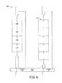
- FIG. 1shows a top perspective view of an exemplary photovoltaic module 100
- FIG. 2shows a bottom perspective view of the same module.
- the module 100is configured to receive sunlight on its top surface and may include an anti-reflective coating 105 to increase light transmission.
- the module 100may have any suitable geometry.
- the modulemay be a thin-film cadmium telluride solar module.
- the exemplary modulemay include a junction box 250 for electrically connecting the module to other modules or electrical devices using a pair of cables 120 , 125 .
- the cables 120 , 125provide an electrical connection to the electrodes of the PV cells within the module 100 .
- one of the cables 120 , 125is connected via junction box 250 to the PV cell at one end of the series while the other of the cables 120 , 125 is connected via junction box 250 to the PV cell at the other end of the series.
- the ends of the cables 120 , 125may be fitted with quick connects 130 , 135 in order to speed the PV module installation process.
- the junction box 250may be mounted on a back cover 240 of the module 100 .
- FIG. 3illustrates an array 300 of PV modules 100 .
- the PV modules 100 in the array 300are connected in series using the cables 120 , 125 and quick connects 130 , 135 .
- a solar farmfor example, includes many PV arrays, each configured to generate electrical power and then deliver the power to a load coupled to the solar farm (for example, a utility grid).
- the solar farmtypically includes inverters, converters, power substations and other power plant components, all configured to condition and deliver the generated power to the coupled loads.
- the PV modules in the solar farm arraysare easily connected and disconnected from the arrays, due to the quick connects 130 , 135 .
- the modules 100are not easily mobile.
- the modules 100may be large, bulky and anchored onto a support foundation for use in the solar farm. Therefore, maintenance of the PV modules is preferably performed on-site.
- One type of maintenance that is preferably performed on-siteis the biasing of the PV modules 100 .
- a method and system of biasingcan be applied at the solar farm.
- an array of biasing modules 410is provided, as illustrated in the biasing system 400 of FIG. 4 .
- a plurality of PV module arrays 300 A, 300 B, 300 Care arranged for generating electrical power at, for example, a solar power plant.
- the PV module arrays 300each include an integer number n of PV modules 100 .
- the PV module arrays 300can easily be reconfigured to include an integer number n of PV modules 100 by either connecting or disconnecting the modules 100 using the module quick connects.
- the biasing system 400includes at least one array of biasing modules 410 .
- the array of biasing modules 410includes at least n+1 modules. As explained below, the array of biasing modules 410 must include more modules than at least one of the array 300 of PV modules to be biased so as to provide sufficient overhead voltage to sustain the necessary current loading.
- the biasing modules 410may be the same as or similar to the modules 100 , meaning that each biasing module 410 is a PV module that generates electricity.
- the array of biasing modules 410can be connected to an array 300 of PV modules 100 , as described below, in order to bias the array 300 of PV modules 100 .
- Connectionsmay be adjusted so that the array of biasing modules 410 is first connected to a first array 300 A of PV modules 100 and then to other arrays 300 B, 300 C of PV modules 100 .
- the ability to change which PV module array is being biased by the biasing modules 410can be implemented through manual connections (using, for example, the ability to quickly disconnect and connect the quick connects 130 , 135 ) or through a switch network 420 .
- biasing modules 410can be used to generate electricity just as PV modules 100 are used.
- the array of biasing modules 410is coupled to a first array 300 A of PV modules via switch network 420 in order to bias the first array 300 A of PV modules. Accordingly, the array of biasing modules 410 and the first array 300 A of PV modules are disconnected from the local solar power plant grid, while other arrays 300 B, 300 C of PV modules remain connected to the local grid in order to continue to provide electricity for the solar power plant.
- the array of biasing modules 410is decoupled from the first array 300 A of PV modules and either coupled to a second array of PV modules (which would be decoupled from the local grid), coupled to the local solar power plant grid in order to generate electricity for the power plant, or, if the array 410 itself or portions thereof require biasing, the array 410 is coupled to other modules that will apply a bias operation to the array 410 or portions thereof.
- FIG. 4illustrates the switch network 420 that is used to couple arrays 410 and arrays 300 to each other or to the local power plant grid
- additional componentsare necessary in order to ensure proper current flow from the biasing array 410 to the PV module array 300 .
- these additional componentsare not shown in FIG. 4 .
- FIGS. 5 and 6are illustrated in FIGS. 5 and 6 , described below.
- the switch network 420 of FIG. 4is modified according to the systems illustrated in either FIG. 5 or FIG. 6 .
- FIG. 5illustrates a system 500 for using the biasing modules 410 to bias the PV modules 100 .
- System 500demonstrates an unregulated biasing strategy.
- an array of biasing modules 410is provided in series in order to produce a static output of known current and voltage.
- the array of biasing modules 410is configured to provide a forwarding bias current to the array of PV modules 100 in order to bias the modules.
- the array of biasing modules 410includes at least n+1 biasing modules, or at least one more biasing modules than the PV modules to be biased. The at least one extra module ensures that enough overhead voltage is provided to sustain the necessary current loading required by the array of PV modules 100 .
- a directional current device 510such as one or more diodes couples the array of biasing modules 410 to the PV modules 100 .
- the directional current device 510ensures that no back current flows and that the current provided moves from the biasing modules 410 to the PV modules 100 .
- System 500includes no additional components for controlling the current delivered to the PV modules 100 .
- system 500is referred to as an “unregulated” system. While a constant current output is preferred for the biasing operation, the unregulated system 500 cannot guarantee a constant current.
- the output of biasing modules 410may be affected by changes in the weather (e.g., a cloud momentarily obscures the sun) or other conditions.
- the unregulated system 500is in contrast to the regulated system 600 illustrated in FIG. 6 .
- FIG. 6illustrates the system 600 for using the biasing modules 410 to bias the PV modules 100 .
- System 600uses a regulated biasing strategy.
- the biasing modules 410are again provided in series in order to produce a current and voltage output.
- the output of the array of biasing modules 410is instead coupled to a current regulator 610 .
- the current regulator 610conditions the input current so that a known output current can be output.
- the known output currentcan be changed using the current regulator 610 , if desired.
- a forwarding bias currentis provided to the array of PV modules 100 .
- the bias currentis provided from the current regulator 610 . While the current regulator 610 controls the current output to the PV modules 100 , the current regulator 610 allows its output voltage to fluctuate according to the demands of the PV modules 100 . Thus, in the regulated system 600 , a desired constant current is provided while voltage varies based on, for example, the resistance of the PV modules 100 . Because the currents provided (and accompanying voltages) are relatively small, the current regulator 610 may be designed as a small and even portable device.
- the biasing modules 410may be a subset of PV modules 100 .
- a solar power plantfor example, that includes PV modules 100 can include a dedicated subset of PV modules 100 serving as biasing modules 410 as needed.
- the biasing modules 410When not needed, the biasing modules 410 generate electricity to contribute to the output of the solar farm.
- the biasing modules 410 and the PV modules 100 to be biasedare disconnected from the solar farm grid and the biasing modules 410 are coupled to the PV modules 100 using either system 500 or system 600 .
- the biasing modules 410need not be limited to a dedicated subset; any PV module 100 can serve as a biasing module 410 when needed.
- an array of at least n+1 PV modules 100can act as biasing modules 410 for an array of n PV modules 100 in need of a bias. Subsequently, at least some of the PV modules 100 that were biased may be used as biasing modules 410 for other PV modules 100 in need of a bias (including the PV modules originally used as biasing modules).
- the biasing modules 410are coupled to an array of PV modules 100 to be biased using either a directional current device 510 (in the unregulated system 500 ) or a current regulator 610 (in the regulated system 600 ).
- the subset of PV modules used during any given biasing operationmust include at least one more biasing module than the number of PV modules being biased during the biasing operation.
- FIG. 7illustrates a method 700 for using PV modules to bias other PV modules in the field.
- a determinationis made (at step 710 ) that one or more PV modules need to be biased.
- an integer number n of PV modulesis designated for biasing based on the determination made during step 710 .
- an integer number of at least n+1 PV modulesis designated as biasing modules to be used to bias the n PV modules designated in step 720 .
- the biasing modulesare serially coupled to each other and their output is directed to the n PV modules to be biased.
- the biasing module outputis directed to the PV modules to be biased via a current regulating device such as either a directional current device or a current regulator.
- the current regulating deviceassists in providing a biasing current to the PV modules.
- the biasing modulesare used to bias the n PV modules.
- the process of biasing the n PV modulesmay take several minutes or even hours, with the biasing time being generally related to the module temperature.
- the biasing processresults in a forward bias constant current being applied from the biasing modules to the PV modules.
- the biasing modulesare disconnected from the biased PV modules (step 750 ).
- the biasing modulesmay then be used to bias additional PV modules, to be biased themselves (if needed), or to generate electricity for the solar farm output.
- a solar farmmay include pre-assembled arrays of PV modules, with the pre-assembled arrays including arrays of length n and arrays of length at least n+1.
- Such pre-assembled arraysmay be assembled on cartridges.
- An example of an array assembled on a cartridgecan be found in U.S. Patent Application Publication No. 2011/0140528 (U.S. patent Ser. No. 12/969,049), the disclosure of which is incorporated herein by reference.
- a cartridge that includes more PV modules than another cartridgecan be used to bias the smaller cartridge with a minimal amount of disconnecting and reconnecting of PV modules into arrays.
- biasing modules 410have been described above as being serially connected, other configurations may be used. For example, the biasing modules 410 could be connected in parallel. Regardless of the configuration used, however, the output of the biasing modules 410 must provide a sufficient bias current, and preferably a constant current. Some configurations may require additional components to provide a biasing module output current that is a constant current.
Landscapes
- Engineering & Computer Science (AREA)
- Power Engineering (AREA)
- Photovoltaic Devices (AREA)
Abstract
Description
Claims (30)
Priority Applications (1)
| Application Number | Priority Date | Filing Date | Title |
|---|---|---|---|
| US13/873,816US9559518B2 (en) | 2012-05-01 | 2013-04-30 | System and method of solar module biasing |
Applications Claiming Priority (2)
| Application Number | Priority Date | Filing Date | Title |
|---|---|---|---|
| US201261641025P | 2012-05-01 | 2012-05-01 | |
| US13/873,816US9559518B2 (en) | 2012-05-01 | 2013-04-30 | System and method of solar module biasing |
Publications (2)
| Publication Number | Publication Date |
|---|---|
| US20130313900A1 US20130313900A1 (en) | 2013-11-28 |
| US9559518B2true US9559518B2 (en) | 2017-01-31 |
Family
ID=49621032
Family Applications (1)
| Application Number | Title | Priority Date | Filing Date |
|---|---|---|---|
| US13/873,816Active2035-09-17US9559518B2 (en) | 2012-05-01 | 2013-04-30 | System and method of solar module biasing |
Country Status (1)
| Country | Link |
|---|---|
| US (1) | US9559518B2 (en) |
Cited By (2)
| Publication number | Priority date | Publication date | Assignee | Title |
|---|---|---|---|---|
| US20150244313A1 (en)* | 2014-02-21 | 2015-08-27 | Solarlytics, Inc. | System and Method for Managing the Power Output of a Photovoltaic Cell |
| US20150244315A1 (en)* | 2014-02-21 | 2015-08-27 | Solarlytics, Inc. | Method and system for applying electric fields to multiple solar panels |
Families Citing this family (1)
| Publication number | Priority date | Publication date | Assignee | Title |
|---|---|---|---|---|
| GB2543308A (en)* | 2015-10-14 | 2017-04-19 | Solaris Photonics Ltd | System of power generation |
Citations (29)
| Publication number | Priority date | Publication date | Assignee | Title |
|---|---|---|---|---|
| US4166918A (en) | 1978-07-19 | 1979-09-04 | Rca Corporation | Method of removing the effects of electrical shorts and shunts created during the fabrication process of a solar cell |
| US4494302A (en)* | 1981-03-23 | 1985-01-22 | Hughes Aircraft Company | Accelerated annealing of gallium arsenide solar cells |
| US5215599A (en) | 1991-05-03 | 1993-06-01 | Electric Power Research Institute | Advanced solar cell |
| US6081017A (en) | 1998-05-28 | 2000-06-27 | Samsung Electronics Co., Ltd. | Self-biased solar cell and module adopting the same |
| US6246219B1 (en)* | 2000-03-24 | 2001-06-12 | The Boeing Company | String switching apparatus and associated method for controllably connecting the output of a solar array string to a respective power bus |
| US20010023703A1 (en)* | 2000-02-29 | 2001-09-27 | Hiroshi Kondo | Solar power generation apparatus and control method therefor |
| US6365825B1 (en)* | 1999-05-14 | 2002-04-02 | Kaneka Corporation | Reverse biasing apparatus for solar battery module |
| US20030015728A1 (en) | 2001-07-17 | 2003-01-23 | Motorola, Inc. | Photonic biasing and integrated solar charging networks for integrated circuits |
| US6979771B2 (en)* | 1998-03-13 | 2005-12-27 | Canon Kabushiki Kaisha | Photovoltaic module, photovoltaic module array, photovoltaic system, and method of detecting failure of photovoltaic module |
| US7276684B2 (en) | 2003-06-16 | 2007-10-02 | Avago Technologies General Ip Pte Ltd | High gain photo cell with improved pulsed light operation |
| KR20090128954A (en) | 2008-06-12 | 2009-12-16 | 주식회사 엔피홀딩스 | Solar cell module |
| US20100084011A1 (en) | 2008-09-26 | 2010-04-08 | The Regents Of The University Of Michigan | Organic tandem solar cells |
| US20100109759A1 (en) | 2003-09-10 | 2010-05-06 | Ixys Corporation | Solar cell device having a charge pump |
| US20110012430A1 (en)* | 2009-07-16 | 2011-01-20 | General Cybernation Group, Inc. | Smart and scalable power inverters |
| US20110121647A1 (en)* | 2009-09-21 | 2011-05-26 | Renewable Energy Solution Systems, Inc. | Solar power distribution system |
| US7969757B2 (en)* | 2008-12-12 | 2011-06-28 | Array Converter, Inc. | Apparatus providing bias to solar cells |
| GB2476508A (en) | 2009-12-23 | 2011-06-29 | Control Tech Ltd | Voltage compensation system for photovoltaic modules |
| US7979969B2 (en)* | 2008-11-17 | 2011-07-19 | Solopower, Inc. | Method of detecting and passivating a defect in a solar cell |
| US20110203635A1 (en)* | 2010-02-24 | 2011-08-25 | Bernhard Beck | Photovoltaic arrays, in part having switches for short-circuiting of modules |
| US20110276188A1 (en)* | 2010-05-04 | 2011-11-10 | Bernhard Beck | Photovoltaic system with selective mpp mismatch |
| US20120112557A1 (en)* | 2010-10-09 | 2012-05-10 | Sager Brian M | Solar Panel with Reconfigurable Interconnections |
| US20120313455A1 (en)* | 2011-06-08 | 2012-12-13 | Latham Andrew V | Instantaneous solar array recombining technology |
| US20130057198A1 (en)* | 2011-09-02 | 2013-03-07 | Boston-Power, Inc. | Method for balancing cells in batteries |
| US20130241294A1 (en)* | 2010-09-23 | 2013-09-19 | Hybridyne Power Electronics Inc. | Method and System for Optimizing Power Generated by a Photovoltaic System |
| US20130249297A1 (en)* | 2012-01-12 | 2013-09-26 | Paceo Corp. | Energy recovery from a photovoltaic array |
| US8633671B2 (en)* | 2011-03-31 | 2014-01-21 | GM Global Technology Operations LLC | Photo-voltaic charging of high voltage traction batteries |
| US8659858B2 (en)* | 2010-08-24 | 2014-02-25 | Sanyo Electric Co., Ltd. | Ground-fault detecting device, current collecting box using the ground-fault detecting device, and photovoltaic power generating device using the current collecting box |
| US20150308889A1 (en)* | 2012-04-19 | 2015-10-29 | Atonometrics | System for field measurement and calibration of photovoltatic reference devices |
| US9184594B2 (en)* | 2011-06-03 | 2015-11-10 | Schneider Electric Solar Inverters Usa, Inc. | Photovoltaic voltage regulation |
- 2013
- 2013-04-30USUS13/873,816patent/US9559518B2/enactiveActive
Patent Citations (30)
| Publication number | Priority date | Publication date | Assignee | Title |
|---|---|---|---|---|
| US4166918A (en) | 1978-07-19 | 1979-09-04 | Rca Corporation | Method of removing the effects of electrical shorts and shunts created during the fabrication process of a solar cell |
| US4494302A (en)* | 1981-03-23 | 1985-01-22 | Hughes Aircraft Company | Accelerated annealing of gallium arsenide solar cells |
| US5215599A (en) | 1991-05-03 | 1993-06-01 | Electric Power Research Institute | Advanced solar cell |
| US6979771B2 (en)* | 1998-03-13 | 2005-12-27 | Canon Kabushiki Kaisha | Photovoltaic module, photovoltaic module array, photovoltaic system, and method of detecting failure of photovoltaic module |
| US6081017A (en) | 1998-05-28 | 2000-06-27 | Samsung Electronics Co., Ltd. | Self-biased solar cell and module adopting the same |
| US6365825B1 (en)* | 1999-05-14 | 2002-04-02 | Kaneka Corporation | Reverse biasing apparatus for solar battery module |
| US20010023703A1 (en)* | 2000-02-29 | 2001-09-27 | Hiroshi Kondo | Solar power generation apparatus and control method therefor |
| US6246219B1 (en)* | 2000-03-24 | 2001-06-12 | The Boeing Company | String switching apparatus and associated method for controllably connecting the output of a solar array string to a respective power bus |
| US20030015728A1 (en) | 2001-07-17 | 2003-01-23 | Motorola, Inc. | Photonic biasing and integrated solar charging networks for integrated circuits |
| US7276684B2 (en) | 2003-06-16 | 2007-10-02 | Avago Technologies General Ip Pte Ltd | High gain photo cell with improved pulsed light operation |
| US20100109759A1 (en) | 2003-09-10 | 2010-05-06 | Ixys Corporation | Solar cell device having a charge pump |
| KR20090128954A (en) | 2008-06-12 | 2009-12-16 | 주식회사 엔피홀딩스 | Solar cell module |
| US20100084011A1 (en) | 2008-09-26 | 2010-04-08 | The Regents Of The University Of Michigan | Organic tandem solar cells |
| US7979969B2 (en)* | 2008-11-17 | 2011-07-19 | Solopower, Inc. | Method of detecting and passivating a defect in a solar cell |
| US7969757B2 (en)* | 2008-12-12 | 2011-06-28 | Array Converter, Inc. | Apparatus providing bias to solar cells |
| US20110012430A1 (en)* | 2009-07-16 | 2011-01-20 | General Cybernation Group, Inc. | Smart and scalable power inverters |
| US20110121647A1 (en)* | 2009-09-21 | 2011-05-26 | Renewable Energy Solution Systems, Inc. | Solar power distribution system |
| US20120280571A1 (en)* | 2009-12-23 | 2012-11-08 | Control Techniques Ltd | Voltage compensation |
| GB2476508A (en) | 2009-12-23 | 2011-06-29 | Control Tech Ltd | Voltage compensation system for photovoltaic modules |
| US20110203635A1 (en)* | 2010-02-24 | 2011-08-25 | Bernhard Beck | Photovoltaic arrays, in part having switches for short-circuiting of modules |
| US20110276188A1 (en)* | 2010-05-04 | 2011-11-10 | Bernhard Beck | Photovoltaic system with selective mpp mismatch |
| US8659858B2 (en)* | 2010-08-24 | 2014-02-25 | Sanyo Electric Co., Ltd. | Ground-fault detecting device, current collecting box using the ground-fault detecting device, and photovoltaic power generating device using the current collecting box |
| US20130241294A1 (en)* | 2010-09-23 | 2013-09-19 | Hybridyne Power Electronics Inc. | Method and System for Optimizing Power Generated by a Photovoltaic System |
| US20120112557A1 (en)* | 2010-10-09 | 2012-05-10 | Sager Brian M | Solar Panel with Reconfigurable Interconnections |
| US8633671B2 (en)* | 2011-03-31 | 2014-01-21 | GM Global Technology Operations LLC | Photo-voltaic charging of high voltage traction batteries |
| US9184594B2 (en)* | 2011-06-03 | 2015-11-10 | Schneider Electric Solar Inverters Usa, Inc. | Photovoltaic voltage regulation |
| US20120313455A1 (en)* | 2011-06-08 | 2012-12-13 | Latham Andrew V | Instantaneous solar array recombining technology |
| US20130057198A1 (en)* | 2011-09-02 | 2013-03-07 | Boston-Power, Inc. | Method for balancing cells in batteries |
| US20130249297A1 (en)* | 2012-01-12 | 2013-09-26 | Paceo Corp. | Energy recovery from a photovoltaic array |
| US20150308889A1 (en)* | 2012-04-19 | 2015-10-29 | Atonometrics | System for field measurement and calibration of photovoltatic reference devices |
Non-Patent Citations (5)
| Title |
|---|
| B. Van Zeghbroeck, "Principles of Semiconductor Device." http://ecee.colorado.edu/~bart/book/book/chapter4/ch4-6.htm. |
| B. Van Zeghbroeck, "Principles of Semiconductor Device." http://ecee.colorado.edu/˜bart/book/book/chapter4/ch4-6.htm. |
| C. Honsberg et al., "Bias of PN Junctions." http://pveducation.org./pvcdrom/pn-junction/bias-of-pn-junction. Oct. 27, 2011. |
| K. Emery et al., "Measurement of Photovoltaic Device Current as a Function of Voltage, Termperature, Intensity and Spectrum." Solar Cells, vol. 21, pp. 313-327, 1987. |
| Y. Yuan et al., "Efficiency Enhancement in Organic Solar Cells with Ferroelectric Polymers." Nature Materials, vol. 10, pp. 296-302, Apr. 2011. Supplementary Information, pp. 1-12. |
Cited By (14)
| Publication number | Priority date | Publication date | Assignee | Title |
|---|---|---|---|---|
| US20150244313A1 (en)* | 2014-02-21 | 2015-08-27 | Solarlytics, Inc. | System and Method for Managing the Power Output of a Photovoltaic Cell |
| US20150244315A1 (en)* | 2014-02-21 | 2015-08-27 | Solarlytics, Inc. | Method and system for applying electric fields to multiple solar panels |
| US10069306B2 (en)* | 2014-02-21 | 2018-09-04 | Solarlytics, Inc. | System and method for managing the power output of a photovoltaic cell |
| US10103547B2 (en)* | 2014-02-21 | 2018-10-16 | Solarlytics, Inc. | Method and system for applying electric fields to multiple solar panels |
| US10193345B2 (en) | 2014-02-21 | 2019-01-29 | Solarlytics, Inc. | System and method for managing the power output of a photovoltaic cell |
| US10236689B2 (en) | 2014-02-21 | 2019-03-19 | Solarlytics, Inc. | Method and system for applying electric fields to multiple solar panels |
| US10355489B2 (en) | 2014-02-21 | 2019-07-16 | Solarlytics, Inc. | System and method for managing the power output of a photovoltaic cell |
| US10804705B2 (en) | 2014-02-21 | 2020-10-13 | Solarlytics, Inc. | Method and system for applying electric fields to multiple solar panels |
| US10804706B2 (en) | 2014-02-21 | 2020-10-13 | Solarlytics, Inc. | Method and system for applying electric fields to multiple solar panels |
| US10826296B2 (en) | 2014-02-21 | 2020-11-03 | Solarlytics, Inc. | Method and system for applying electric fields to multiple solar panels |
| US10978878B2 (en) | 2014-02-21 | 2021-04-13 | Solarlytics, Inc. | System and method for managing the power output of a photovoltaic cell |
| US11063439B2 (en) | 2014-02-21 | 2021-07-13 | Solarlytics, Inc. | Method and system for applying electric fields to multiple solar panels |
| US11108240B2 (en) | 2014-02-21 | 2021-08-31 | Solarlytics, Inc. | System and method for managing the power output of a photovoltaic cell |
| US11152790B2 (en) | 2014-02-21 | 2021-10-19 | Solarlytics, Inc. | System and method for managing the power output of a photovoltaic cell |
Also Published As
| Publication number | Publication date |
|---|---|
| US20130313900A1 (en) | 2013-11-28 |
Similar Documents
| Publication | Publication Date | Title |
|---|---|---|
| Yaqoob et al. | A comprehensive review on small satellite microgrids | |
| US8106537B2 (en) | Photovoltaic DC/DC micro-converter | |
| US9531322B2 (en) | Dynamically reconfigurable photovoltaic system | |
| US9093586B2 (en) | Photovoltaic power generation system free of bypass diodes | |
| US20130200709A1 (en) | Techniques for Grid Coupling Photovoltaic Cells Using Ratiometric Voltage Conversion | |
| US11888442B2 (en) | Solar modules having solar sub cells with matrix connections between the solar sub cells | |
| US20080135084A1 (en) | Sub-module photovoltaic control system | |
| US20120217800A1 (en) | Solar power systems optimized for use in communications networks | |
| Das et al. | Modeling and simulation of PV array with boost converter: an open loop study | |
| KR101425935B1 (en) | Photovoltaic power generation apparatus | |
| Verma et al. | Implementation of perturb and observe method of maximum power point tracking in SIMSCAPE/MATLAB | |
| US9559518B2 (en) | System and method of solar module biasing | |
| Lentine et al. | Optimal cell connections for improved shading, reliability, and spectral performance of microsystem enabled photovoltaic (MEPV) modules | |
| JP2016149582A (en) | Solar power generation system without bypass diode | |
| Rakesh et al. | A new technique to enhance output power from solar PV array under different partial shaded conditions | |
| US20210288202A1 (en) | Photovoltaic device | |
| Alam et al. | An efficient power electronics solution for lateral multi-junction solar cell systems | |
| Zaman et al. | Distributed power-management architecture for a low-profile concentrating-pv system | |
| KR102175430B1 (en) | Apparatus for photovoltaic power generation | |
| GB2589099A (en) | Power system | |
| CA2728619A1 (en) | A renewable power control system | |
| JP2014170331A (en) | Power control system | |
| ACHARA | Grid Parity and Solar Electricity for Homes | |
| HK1237053A1 (en) | System of power generation |
Legal Events
| Date | Code | Title | Description |
|---|---|---|---|
| AS | Assignment | Owner name:JPMORGAN CHASE BANK, N.A., ILLINOIS Free format text:SECURITY AGREEMENT;ASSIGNOR:FIRST SOLAR, INC.;REEL/FRAME:030832/0088 Effective date:20130715 | |
| AS | Assignment | Owner name:JPMORGAN CHASE BANK, N.A., ILLINOIS Free format text:CORRECTIVE ASSIGNMENT TO CORRECT THE PATENT APPLICATION 13/895113 ERRONEOUSLY ASSIGNED BY FIRST SOLAR, INC. TO JPMORGAN CHASE BANK, N.A. ON JULY 19, 2013 PREVIOUSLY RECORDED ON REEL 030832 FRAME 0088. ASSIGNOR(S) HEREBY CONFIRMS THE CORRECT PATENT APPLICATION TO BE ASSIGNED IS 13/633664;ASSIGNOR:FIRST SOLAR, INC.;REEL/FRAME:033779/0081 Effective date:20130715 | |
| STCF | Information on status: patent grant | Free format text:PATENTED CASE | |
| AS | Assignment | Owner name:JPMORGAN CHASE BANK, N.A., AS ADMINISTRATIVE AGENT, ILLINOIS Free format text:PATENT SECURITY AGREEMENT;ASSIGNOR:FIRST SOLAR, INC.;REEL/FRAME:043177/0581 Effective date:20170710 Owner name:JPMORGAN CHASE BANK, N.A., AS ADMINISTRATIVE AGENT Free format text:PATENT SECURITY AGREEMENT;ASSIGNOR:FIRST SOLAR, INC.;REEL/FRAME:043177/0581 Effective date:20170710 | |
| MAFP | Maintenance fee payment | Free format text:PAYMENT OF MAINTENANCE FEE, 4TH YEAR, LARGE ENTITY (ORIGINAL EVENT CODE: M1551); ENTITY STATUS OF PATENT OWNER: LARGE ENTITY Year of fee payment:4 | |
| AS | Assignment | Owner name:FIRST SOLAR, INC., ARIZONA Free format text:TERMINATION AND RELEASE OF SECURITY INTEREST IN PATENT RIGHTS;ASSIGNOR:JPMORGAN CHASE BANK, N.A.;REEL/FRAME:058132/0566 Effective date:20210825 Owner name:FIRST SOLAR, INC., ARIZONA Free format text:TERMINATION AND RELEASE OF SECURITY INTEREST IN PATENT RIGHTS;ASSIGNOR:JPMORGAN CHASE BANK, N.A.;REEL/FRAME:058132/0261 Effective date:20210825 | |
| AS | Assignment | Owner name:JPMORGAN CHASE BANK, N.A., AS ADMINISTRATIVE AGENT, ILLINOIS Free format text:SECURITY INTEREST;ASSIGNOR:FIRST SOLAR, INC.;REEL/FRAME:064237/0462 Effective date:20230630 | |
| MAFP | Maintenance fee payment | Free format text:PAYMENT OF MAINTENANCE FEE, 8TH YEAR, LARGE ENTITY (ORIGINAL EVENT CODE: M1552); ENTITY STATUS OF PATENT OWNER: LARGE ENTITY Year of fee payment:8 |