US9559029B2 - Semiconductor device and method of forming interconnect structure for encapsulated die having pre-applied protective layer - Google Patents
Semiconductor device and method of forming interconnect structure for encapsulated die having pre-applied protective layerDownload PDFInfo
- Publication number
- US9559029B2 US9559029B2US14/523,556US201414523556AUS9559029B2US 9559029 B2US9559029 B2US 9559029B2US 201414523556 AUS201414523556 AUS 201414523556AUS 9559029 B2US9559029 B2US 9559029B2
- Authority
- US
- United States
- Prior art keywords
- insulating layer
- forming
- semiconductor die
- opening
- over
- Prior art date
- Legal status (The legal status is an assumption and is not a legal conclusion. Google has not performed a legal analysis and makes no representation as to the accuracy of the status listed.)
- Active
Links
Images


Classifications
- H—ELECTRICITY
- H01—ELECTRIC ELEMENTS
- H01L—SEMICONDUCTOR DEVICES NOT COVERED BY CLASS H10
- H01L23/00—Details of semiconductor or other solid state devices
- H01L23/28—Encapsulations, e.g. encapsulating layers, coatings, e.g. for protection
- H01L23/31—Encapsulations, e.g. encapsulating layers, coatings, e.g. for protection characterised by the arrangement or shape
- H01L23/3107—Encapsulations, e.g. encapsulating layers, coatings, e.g. for protection characterised by the arrangement or shape the device being completely enclosed
- H01L23/3121—Encapsulations, e.g. encapsulating layers, coatings, e.g. for protection characterised by the arrangement or shape the device being completely enclosed a substrate forming part of the encapsulation
- H01L23/3128—Encapsulations, e.g. encapsulating layers, coatings, e.g. for protection characterised by the arrangement or shape the device being completely enclosed a substrate forming part of the encapsulation the substrate having spherical bumps for external connection
- H—ELECTRICITY
- H01—ELECTRIC ELEMENTS
- H01L—SEMICONDUCTOR DEVICES NOT COVERED BY CLASS H10
- H01L23/00—Details of semiconductor or other solid state devices
- H01L23/48—Arrangements for conducting electric current to or from the solid state body in operation, e.g. leads, terminal arrangements ; Selection of materials therefor
- H—ELECTRICITY
- H01—ELECTRIC ELEMENTS
- H01L—SEMICONDUCTOR DEVICES NOT COVERED BY CLASS H10
- H01L21/00—Processes or apparatus adapted for the manufacture or treatment of semiconductor or solid state devices or of parts thereof
- H01L21/02—Manufacture or treatment of semiconductor devices or of parts thereof
- H01L21/04—Manufacture or treatment of semiconductor devices or of parts thereof the devices having potential barriers, e.g. a PN junction, depletion layer or carrier concentration layer
- H01L21/50—Assembly of semiconductor devices using processes or apparatus not provided for in a single one of the groups H01L21/18 - H01L21/326 or H10D48/04 - H10D48/07 e.g. sealing of a cap to a base of a container
- H01L21/56—Encapsulations, e.g. encapsulation layers, coatings
- H01L21/568—Temporary substrate used as encapsulation process aid
- H—ELECTRICITY
- H01—ELECTRIC ELEMENTS
- H01L—SEMICONDUCTOR DEVICES NOT COVERED BY CLASS H10
- H01L21/00—Processes or apparatus adapted for the manufacture or treatment of semiconductor or solid state devices or of parts thereof
- H01L21/67—Apparatus specially adapted for handling semiconductor or electric solid state devices during manufacture or treatment thereof; Apparatus specially adapted for handling wafers during manufacture or treatment of semiconductor or electric solid state devices or components ; Apparatus not specifically provided for elsewhere
- H01L21/683—Apparatus specially adapted for handling semiconductor or electric solid state devices during manufacture or treatment thereof; Apparatus specially adapted for handling wafers during manufacture or treatment of semiconductor or electric solid state devices or components ; Apparatus not specifically provided for elsewhere for supporting or gripping
- H01L21/6835—Apparatus specially adapted for handling semiconductor or electric solid state devices during manufacture or treatment thereof; Apparatus specially adapted for handling wafers during manufacture or treatment of semiconductor or electric solid state devices or components ; Apparatus not specifically provided for elsewhere for supporting or gripping using temporarily an auxiliary support
- H—ELECTRICITY
- H01—ELECTRIC ELEMENTS
- H01L—SEMICONDUCTOR DEVICES NOT COVERED BY CLASS H10
- H01L21/00—Processes or apparatus adapted for the manufacture or treatment of semiconductor or solid state devices or of parts thereof
- H01L21/70—Manufacture or treatment of devices consisting of a plurality of solid state components formed in or on a common substrate or of parts thereof; Manufacture of integrated circuit devices or of parts thereof
- H01L21/71—Manufacture of specific parts of devices defined in group H01L21/70
- H01L21/768—Applying interconnections to be used for carrying current between separate components within a device comprising conductors and dielectrics
- H01L21/76801—Applying interconnections to be used for carrying current between separate components within a device comprising conductors and dielectrics characterised by the formation and the after-treatment of the dielectrics, e.g. smoothing
- H01L21/76802—Applying interconnections to be used for carrying current between separate components within a device comprising conductors and dielectrics characterised by the formation and the after-treatment of the dielectrics, e.g. smoothing by forming openings in dielectrics
- H—ELECTRICITY
- H01—ELECTRIC ELEMENTS
- H01L—SEMICONDUCTOR DEVICES NOT COVERED BY CLASS H10
- H01L21/00—Processes or apparatus adapted for the manufacture or treatment of semiconductor or solid state devices or of parts thereof
- H01L21/70—Manufacture or treatment of devices consisting of a plurality of solid state components formed in or on a common substrate or of parts thereof; Manufacture of integrated circuit devices or of parts thereof
- H01L21/71—Manufacture of specific parts of devices defined in group H01L21/70
- H01L21/768—Applying interconnections to be used for carrying current between separate components within a device comprising conductors and dielectrics
- H01L21/76838—Applying interconnections to be used for carrying current between separate components within a device comprising conductors and dielectrics characterised by the formation and the after-treatment of the conductors
- H01L21/76877—Filling of holes, grooves or trenches, e.g. vias, with conductive material
- H—ELECTRICITY
- H01—ELECTRIC ELEMENTS
- H01L—SEMICONDUCTOR DEVICES NOT COVERED BY CLASS H10
- H01L23/00—Details of semiconductor or other solid state devices
- H01L23/28—Encapsulations, e.g. encapsulating layers, coatings, e.g. for protection
- H—ELECTRICITY
- H01—ELECTRIC ELEMENTS
- H01L—SEMICONDUCTOR DEVICES NOT COVERED BY CLASS H10
- H01L23/00—Details of semiconductor or other solid state devices
- H01L23/28—Encapsulations, e.g. encapsulating layers, coatings, e.g. for protection
- H01L23/31—Encapsulations, e.g. encapsulating layers, coatings, e.g. for protection characterised by the arrangement or shape
- H01L23/3107—Encapsulations, e.g. encapsulating layers, coatings, e.g. for protection characterised by the arrangement or shape the device being completely enclosed
- H01L23/3114—Encapsulations, e.g. encapsulating layers, coatings, e.g. for protection characterised by the arrangement or shape the device being completely enclosed the device being a chip scale package, e.g. CSP
- H—ELECTRICITY
- H01—ELECTRIC ELEMENTS
- H01L—SEMICONDUCTOR DEVICES NOT COVERED BY CLASS H10
- H01L23/00—Details of semiconductor or other solid state devices
- H01L23/48—Arrangements for conducting electric current to or from the solid state body in operation, e.g. leads, terminal arrangements ; Selection of materials therefor
- H01L23/481—Internal lead connections, e.g. via connections, feedthrough structures
- H—ELECTRICITY
- H01—ELECTRIC ELEMENTS
- H01L—SEMICONDUCTOR DEVICES NOT COVERED BY CLASS H10
- H01L23/00—Details of semiconductor or other solid state devices
- H01L23/52—Arrangements for conducting electric current within the device in operation from one component to another, i.e. interconnections, e.g. wires, lead frames
- H01L23/522—Arrangements for conducting electric current within the device in operation from one component to another, i.e. interconnections, e.g. wires, lead frames including external interconnections consisting of a multilayer structure of conductive and insulating layers inseparably formed on the semiconductor body
- H01L23/528—Layout of the interconnection structure
- H—ELECTRICITY
- H01—ELECTRIC ELEMENTS
- H01L—SEMICONDUCTOR DEVICES NOT COVERED BY CLASS H10
- H01L23/00—Details of semiconductor or other solid state devices
- H01L23/52—Arrangements for conducting electric current within the device in operation from one component to another, i.e. interconnections, e.g. wires, lead frames
- H01L23/538—Arrangements for conducting electric current within the device in operation from one component to another, i.e. interconnections, e.g. wires, lead frames the interconnection structure between a plurality of semiconductor chips being formed on, or in, insulating substrates
- H01L23/5389—Arrangements for conducting electric current within the device in operation from one component to another, i.e. interconnections, e.g. wires, lead frames the interconnection structure between a plurality of semiconductor chips being formed on, or in, insulating substrates the chips being integrally enclosed by the interconnect and support structures
- H—ELECTRICITY
- H01—ELECTRIC ELEMENTS
- H01L—SEMICONDUCTOR DEVICES NOT COVERED BY CLASS H10
- H01L24/00—Arrangements for connecting or disconnecting semiconductor or solid-state bodies; Methods or apparatus related thereto
- H01L24/01—Means for bonding being attached to, or being formed on, the surface to be connected, e.g. chip-to-package, die-attach, "first-level" interconnects; Manufacturing methods related thereto
- H01L24/10—Bump connectors ; Manufacturing methods related thereto
- H01L24/12—Structure, shape, material or disposition of the bump connectors prior to the connecting process
- H01L24/14—Structure, shape, material or disposition of the bump connectors prior to the connecting process of a plurality of bump connectors
- H—ELECTRICITY
- H01—ELECTRIC ELEMENTS
- H01L—SEMICONDUCTOR DEVICES NOT COVERED BY CLASS H10
- H01L24/00—Arrangements for connecting or disconnecting semiconductor or solid-state bodies; Methods or apparatus related thereto
- H01L24/01—Means for bonding being attached to, or being formed on, the surface to be connected, e.g. chip-to-package, die-attach, "first-level" interconnects; Manufacturing methods related thereto
- H01L24/18—High density interconnect [HDI] connectors; Manufacturing methods related thereto
- H01L24/19—Manufacturing methods of high density interconnect preforms
- H—ELECTRICITY
- H01—ELECTRIC ELEMENTS
- H01L—SEMICONDUCTOR DEVICES NOT COVERED BY CLASS H10
- H01L24/00—Arrangements for connecting or disconnecting semiconductor or solid-state bodies; Methods or apparatus related thereto
- H01L24/93—Batch processes
- H01L24/95—Batch processes at chip-level, i.e. with connecting carried out on a plurality of singulated devices, i.e. on diced chips
- H01L24/96—Batch processes at chip-level, i.e. with connecting carried out on a plurality of singulated devices, i.e. on diced chips the devices being encapsulated in a common layer, e.g. neo-wafer or pseudo-wafer, said common layer being separable into individual assemblies after connecting
- H—ELECTRICITY
- H01—ELECTRIC ELEMENTS
- H01L—SEMICONDUCTOR DEVICES NOT COVERED BY CLASS H10
- H01L25/00—Assemblies consisting of a plurality of semiconductor or other solid state devices
- H01L25/03—Assemblies consisting of a plurality of semiconductor or other solid state devices all the devices being of a type provided for in a single subclass of subclasses H10B, H10D, H10F, H10H, H10K or H10N, e.g. assemblies of rectifier diodes
- H01L25/10—Assemblies consisting of a plurality of semiconductor or other solid state devices all the devices being of a type provided for in a single subclass of subclasses H10B, H10D, H10F, H10H, H10K or H10N, e.g. assemblies of rectifier diodes the devices having separate containers
- H01L25/105—Assemblies consisting of a plurality of semiconductor or other solid state devices all the devices being of a type provided for in a single subclass of subclasses H10B, H10D, H10F, H10H, H10K or H10N, e.g. assemblies of rectifier diodes the devices having separate containers the devices being integrated devices of class H10
- H—ELECTRICITY
- H01—ELECTRIC ELEMENTS
- H01L—SEMICONDUCTOR DEVICES NOT COVERED BY CLASS H10
- H01L25/00—Assemblies consisting of a plurality of semiconductor or other solid state devices
- H01L25/16—Assemblies consisting of a plurality of semiconductor or other solid state devices the devices being of types provided for in two or more different subclasses of H10B, H10D, H10F, H10H, H10K or H10N, e.g. forming hybrid circuits
- H—ELECTRICITY
- H05—ELECTRIC TECHNIQUES NOT OTHERWISE PROVIDED FOR
- H05K—PRINTED CIRCUITS; CASINGS OR CONSTRUCTIONAL DETAILS OF ELECTRIC APPARATUS; MANUFACTURE OF ASSEMBLAGES OF ELECTRICAL COMPONENTS
- H05K1/00—Printed circuits
- H05K1/18—Printed circuits structurally associated with non-printed electric components
- H05K1/182—Printed circuits structurally associated with non-printed electric components associated with components mounted in the printed circuit board, e.g. insert mounted components [IMC]
- H05K1/185—Components encapsulated in the insulating substrate of the printed circuit or incorporated in internal layers of a multilayer circuit
- H05K1/186—Components encapsulated in the insulating substrate of the printed circuit or incorporated in internal layers of a multilayer circuit manufactured by mounting on or connecting to patterned circuits before or during embedding
- H—ELECTRICITY
- H01—ELECTRIC ELEMENTS
- H01L—SEMICONDUCTOR DEVICES NOT COVERED BY CLASS H10
- H01L2221/00—Processes or apparatus adapted for the manufacture or treatment of semiconductor or solid state devices or of parts thereof covered by H01L21/00
- H01L2221/67—Apparatus for handling semiconductor or electric solid state devices during manufacture or treatment thereof; Apparatus for handling wafers during manufacture or treatment of semiconductor or electric solid state devices or components; Apparatus not specifically provided for elsewhere
- H01L2221/683—Apparatus for handling semiconductor or electric solid state devices during manufacture or treatment thereof; Apparatus for handling wafers during manufacture or treatment of semiconductor or electric solid state devices or components; Apparatus not specifically provided for elsewhere for supporting or gripping
- H01L2221/68304—Apparatus for handling semiconductor or electric solid state devices during manufacture or treatment thereof; Apparatus for handling wafers during manufacture or treatment of semiconductor or electric solid state devices or components; Apparatus not specifically provided for elsewhere for supporting or gripping using temporarily an auxiliary support
- H01L2221/68345—Apparatus for handling semiconductor or electric solid state devices during manufacture or treatment thereof; Apparatus for handling wafers during manufacture or treatment of semiconductor or electric solid state devices or components; Apparatus not specifically provided for elsewhere for supporting or gripping using temporarily an auxiliary support used as a support during the manufacture of self supporting substrates
- H—ELECTRICITY
- H01—ELECTRIC ELEMENTS
- H01L—SEMICONDUCTOR DEVICES NOT COVERED BY CLASS H10
- H01L2224/00—Indexing scheme for arrangements for connecting or disconnecting semiconductor or solid-state bodies and methods related thereto as covered by H01L24/00
- H01L2224/01—Means for bonding being attached to, or being formed on, the surface to be connected, e.g. chip-to-package, die-attach, "first-level" interconnects; Manufacturing methods related thereto
- H01L2224/02—Bonding areas; Manufacturing methods related thereto
- H01L2224/04—Structure, shape, material or disposition of the bonding areas prior to the connecting process
- H01L2224/04105—Bonding areas formed on an encapsulation of the semiconductor or solid-state body, e.g. bonding areas on chip-scale packages
- H—ELECTRICITY
- H01—ELECTRIC ELEMENTS
- H01L—SEMICONDUCTOR DEVICES NOT COVERED BY CLASS H10
- H01L2224/00—Indexing scheme for arrangements for connecting or disconnecting semiconductor or solid-state bodies and methods related thereto as covered by H01L24/00
- H01L2224/01—Means for bonding being attached to, or being formed on, the surface to be connected, e.g. chip-to-package, die-attach, "first-level" interconnects; Manufacturing methods related thereto
- H01L2224/10—Bump connectors; Manufacturing methods related thereto
- H01L2224/12—Structure, shape, material or disposition of the bump connectors prior to the connecting process
- H01L2224/12105—Bump connectors formed on an encapsulation of the semiconductor or solid-state body, e.g. bumps on chip-scale packages
- H—ELECTRICITY
- H01—ELECTRIC ELEMENTS
- H01L—SEMICONDUCTOR DEVICES NOT COVERED BY CLASS H10
- H01L2224/00—Indexing scheme for arrangements for connecting or disconnecting semiconductor or solid-state bodies and methods related thereto as covered by H01L24/00
- H01L2224/01—Means for bonding being attached to, or being formed on, the surface to be connected, e.g. chip-to-package, die-attach, "first-level" interconnects; Manufacturing methods related thereto
- H01L2224/10—Bump connectors; Manufacturing methods related thereto
- H01L2224/12—Structure, shape, material or disposition of the bump connectors prior to the connecting process
- H01L2224/13—Structure, shape, material or disposition of the bump connectors prior to the connecting process of an individual bump connector
- H01L2224/13001—Core members of the bump connector
- H01L2224/1302—Disposition
- H01L2224/13025—Disposition the bump connector being disposed on a via connection of the semiconductor or solid-state body
- H—ELECTRICITY
- H01—ELECTRIC ELEMENTS
- H01L—SEMICONDUCTOR DEVICES NOT COVERED BY CLASS H10
- H01L2224/00—Indexing scheme for arrangements for connecting or disconnecting semiconductor or solid-state bodies and methods related thereto as covered by H01L24/00
- H01L2224/01—Means for bonding being attached to, or being formed on, the surface to be connected, e.g. chip-to-package, die-attach, "first-level" interconnects; Manufacturing methods related thereto
- H01L2224/10—Bump connectors; Manufacturing methods related thereto
- H01L2224/15—Structure, shape, material or disposition of the bump connectors after the connecting process
- H01L2224/16—Structure, shape, material or disposition of the bump connectors after the connecting process of an individual bump connector
- H—ELECTRICITY
- H01—ELECTRIC ELEMENTS
- H01L—SEMICONDUCTOR DEVICES NOT COVERED BY CLASS H10
- H01L2224/00—Indexing scheme for arrangements for connecting or disconnecting semiconductor or solid-state bodies and methods related thereto as covered by H01L24/00
- H01L2224/01—Means for bonding being attached to, or being formed on, the surface to be connected, e.g. chip-to-package, die-attach, "first-level" interconnects; Manufacturing methods related thereto
- H01L2224/18—High density interconnect [HDI] connectors; Manufacturing methods related thereto
- H01L2224/23—Structure, shape, material or disposition of the high density interconnect connectors after the connecting process
- H01L2224/24—Structure, shape, material or disposition of the high density interconnect connectors after the connecting process of an individual high density interconnect connector
- H01L2224/241—Disposition
- H01L2224/24151—Connecting between a semiconductor or solid-state body and an item not being a semiconductor or solid-state body, e.g. chip-to-substrate, chip-to-passive
- H01L2224/24153—Connecting between a semiconductor or solid-state body and an item not being a semiconductor or solid-state body, e.g. chip-to-substrate, chip-to-passive the body and the item being arranged next to each other, e.g. on a common substrate
- H01L2224/24195—Connecting between a semiconductor or solid-state body and an item not being a semiconductor or solid-state body, e.g. chip-to-substrate, chip-to-passive the body and the item being arranged next to each other, e.g. on a common substrate the item being a discrete passive component
- H—ELECTRICITY
- H01—ELECTRIC ELEMENTS
- H01L—SEMICONDUCTOR DEVICES NOT COVERED BY CLASS H10
- H01L2224/00—Indexing scheme for arrangements for connecting or disconnecting semiconductor or solid-state bodies and methods related thereto as covered by H01L24/00
- H01L2224/01—Means for bonding being attached to, or being formed on, the surface to be connected, e.g. chip-to-package, die-attach, "first-level" interconnects; Manufacturing methods related thereto
- H01L2224/26—Layer connectors, e.g. plate connectors, solder or adhesive layers; Manufacturing methods related thereto
- H01L2224/31—Structure, shape, material or disposition of the layer connectors after the connecting process
- H01L2224/32—Structure, shape, material or disposition of the layer connectors after the connecting process of an individual layer connector
- H01L2224/321—Disposition
- H01L2224/32151—Disposition the layer connector connecting between a semiconductor or solid-state body and an item not being a semiconductor or solid-state body, e.g. chip-to-substrate, chip-to-passive
- H01L2224/32221—Disposition the layer connector connecting between a semiconductor or solid-state body and an item not being a semiconductor or solid-state body, e.g. chip-to-substrate, chip-to-passive the body and the item being stacked
- H01L2224/32225—Disposition the layer connector connecting between a semiconductor or solid-state body and an item not being a semiconductor or solid-state body, e.g. chip-to-substrate, chip-to-passive the body and the item being stacked the item being non-metallic, e.g. insulating substrate with or without metallisation
- H—ELECTRICITY
- H01—ELECTRIC ELEMENTS
- H01L—SEMICONDUCTOR DEVICES NOT COVERED BY CLASS H10
- H01L2224/00—Indexing scheme for arrangements for connecting or disconnecting semiconductor or solid-state bodies and methods related thereto as covered by H01L24/00
- H01L2224/80—Methods for connecting semiconductor or other solid state bodies using means for bonding being attached to, or being formed on, the surface to be connected
- H01L2224/82—Methods for connecting semiconductor or other solid state bodies using means for bonding being attached to, or being formed on, the surface to be connected by forming build-up interconnects at chip-level, e.g. for high density interconnects [HDI]
- H01L2224/82009—Pre-treatment of the connector or the bonding area
- H01L2224/8203—Reshaping, e.g. forming vias
- H01L2224/82035—Reshaping, e.g. forming vias by heating means
- H01L2224/82039—Reshaping, e.g. forming vias by heating means using a laser
- H—ELECTRICITY
- H01—ELECTRIC ELEMENTS
- H01L—SEMICONDUCTOR DEVICES NOT COVERED BY CLASS H10
- H01L2224/00—Indexing scheme for arrangements for connecting or disconnecting semiconductor or solid-state bodies and methods related thereto as covered by H01L24/00
- H01L2224/80—Methods for connecting semiconductor or other solid state bodies using means for bonding being attached to, or being formed on, the surface to be connected
- H01L2224/83—Methods for connecting semiconductor or other solid state bodies using means for bonding being attached to, or being formed on, the surface to be connected using a layer connector
- H01L2224/8312—Aligning
- H01L2224/83121—Active alignment, i.e. by apparatus steering, e.g. optical alignment using marks or sensors
- H01L2224/83132—Active alignment, i.e. by apparatus steering, e.g. optical alignment using marks or sensors using marks formed outside the semiconductor or solid-state body, i.e. "off-chip"
- H—ELECTRICITY
- H01—ELECTRIC ELEMENTS
- H01L—SEMICONDUCTOR DEVICES NOT COVERED BY CLASS H10
- H01L2224/00—Indexing scheme for arrangements for connecting or disconnecting semiconductor or solid-state bodies and methods related thereto as covered by H01L24/00
- H01L2224/80—Methods for connecting semiconductor or other solid state bodies using means for bonding being attached to, or being formed on, the surface to be connected
- H01L2224/83—Methods for connecting semiconductor or other solid state bodies using means for bonding being attached to, or being formed on, the surface to be connected using a layer connector
- H01L2224/8312—Aligning
- H01L2224/83136—Aligning involving guiding structures, e.g. spacers or supporting members
- H01L2224/83138—Aligning involving guiding structures, e.g. spacers or supporting members the guiding structures being at least partially left in the finished device
- H01L2224/8314—Guiding structures outside the body
- H—ELECTRICITY
- H01—ELECTRIC ELEMENTS
- H01L—SEMICONDUCTOR DEVICES NOT COVERED BY CLASS H10
- H01L2224/00—Indexing scheme for arrangements for connecting or disconnecting semiconductor or solid-state bodies and methods related thereto as covered by H01L24/00
- H01L2224/80—Methods for connecting semiconductor or other solid state bodies using means for bonding being attached to, or being formed on, the surface to be connected
- H01L2224/83—Methods for connecting semiconductor or other solid state bodies using means for bonding being attached to, or being formed on, the surface to be connected using a layer connector
- H01L2224/8319—Arrangement of the layer connectors prior to mounting
- H01L2224/83192—Arrangement of the layer connectors prior to mounting wherein the layer connectors are disposed only on another item or body to be connected to the semiconductor or solid-state body
- H—ELECTRICITY
- H01—ELECTRIC ELEMENTS
- H01L—SEMICONDUCTOR DEVICES NOT COVERED BY CLASS H10
- H01L2224/00—Indexing scheme for arrangements for connecting or disconnecting semiconductor or solid-state bodies and methods related thereto as covered by H01L24/00
- H01L2224/91—Methods for connecting semiconductor or solid state bodies including different methods provided for in two or more of groups H01L2224/80 - H01L2224/90
- H01L2224/92—Specific sequence of method steps
- H01L2224/921—Connecting a surface with connectors of different types
- H01L2224/9212—Sequential connecting processes
- H01L2224/92142—Sequential connecting processes the first connecting process involving a layer connector
- H01L2224/92144—Sequential connecting processes the first connecting process involving a layer connector the second connecting process involving a build-up interconnect
- H—ELECTRICITY
- H01—ELECTRIC ELEMENTS
- H01L—SEMICONDUCTOR DEVICES NOT COVERED BY CLASS H10
- H01L2225/00—Details relating to assemblies covered by the group H01L25/00 but not provided for in its subgroups
- H01L2225/03—All the devices being of a type provided for in the same main group of the same subclass of class H10, e.g. assemblies of rectifier diodes
- H01L2225/10—All the devices being of a type provided for in the same main group of the same subclass of class H10, e.g. assemblies of rectifier diodes the devices having separate containers
- H01L2225/1005—All the devices being of a type provided for in the same main group of the same subclass of class H10, e.g. assemblies of rectifier diodes the devices having separate containers the devices being integrated devices of class H10
- H01L2225/1011—All the devices being of a type provided for in the same main group of the same subclass of class H10, e.g. assemblies of rectifier diodes the devices having separate containers the devices being integrated devices of class H10 the containers being in a stacked arrangement
- H01L2225/1017—All the devices being of a type provided for in the same main group of the same subclass of class H10, e.g. assemblies of rectifier diodes the devices having separate containers the devices being integrated devices of class H10 the containers being in a stacked arrangement the lowermost container comprising a device support
- H01L2225/1023—All the devices being of a type provided for in the same main group of the same subclass of class H10, e.g. assemblies of rectifier diodes the devices having separate containers the devices being integrated devices of class H10 the containers being in a stacked arrangement the lowermost container comprising a device support the support being an insulating substrate
- H—ELECTRICITY
- H01—ELECTRIC ELEMENTS
- H01L—SEMICONDUCTOR DEVICES NOT COVERED BY CLASS H10
- H01L2225/00—Details relating to assemblies covered by the group H01L25/00 but not provided for in its subgroups
- H01L2225/03—All the devices being of a type provided for in the same main group of the same subclass of class H10, e.g. assemblies of rectifier diodes
- H01L2225/10—All the devices being of a type provided for in the same main group of the same subclass of class H10, e.g. assemblies of rectifier diodes the devices having separate containers
- H01L2225/1005—All the devices being of a type provided for in the same main group of the same subclass of class H10, e.g. assemblies of rectifier diodes the devices having separate containers the devices being integrated devices of class H10
- H01L2225/1011—All the devices being of a type provided for in the same main group of the same subclass of class H10, e.g. assemblies of rectifier diodes the devices having separate containers the devices being integrated devices of class H10 the containers being in a stacked arrangement
- H01L2225/1047—Details of electrical connections between containers
- H01L2225/1058—Bump or bump-like electrical connections, e.g. balls, pillars, posts
- H—ELECTRICITY
- H01—ELECTRIC ELEMENTS
- H01L—SEMICONDUCTOR DEVICES NOT COVERED BY CLASS H10
- H01L23/00—Details of semiconductor or other solid state devices
- H01L23/48—Arrangements for conducting electric current to or from the solid state body in operation, e.g. leads, terminal arrangements ; Selection of materials therefor
- H01L23/50—Arrangements for conducting electric current to or from the solid state body in operation, e.g. leads, terminal arrangements ; Selection of materials therefor for integrated circuit devices, e.g. power bus, number of leads
- H—ELECTRICITY
- H01—ELECTRIC ELEMENTS
- H01L—SEMICONDUCTOR DEVICES NOT COVERED BY CLASS H10
- H01L2924/00—Indexing scheme for arrangements or methods for connecting or disconnecting semiconductor or solid-state bodies as covered by H01L24/00
- H—ELECTRICITY
- H01—ELECTRIC ELEMENTS
- H01L—SEMICONDUCTOR DEVICES NOT COVERED BY CLASS H10
- H01L2924/00—Indexing scheme for arrangements or methods for connecting or disconnecting semiconductor or solid-state bodies as covered by H01L24/00
- H01L2924/01—Chemical elements
- H01L2924/01005—Boron [B]
- H—ELECTRICITY
- H01—ELECTRIC ELEMENTS
- H01L—SEMICONDUCTOR DEVICES NOT COVERED BY CLASS H10
- H01L2924/00—Indexing scheme for arrangements or methods for connecting or disconnecting semiconductor or solid-state bodies as covered by H01L24/00
- H01L2924/01—Chemical elements
- H01L2924/01006—Carbon [C]
- H—ELECTRICITY
- H01—ELECTRIC ELEMENTS
- H01L—SEMICONDUCTOR DEVICES NOT COVERED BY CLASS H10
- H01L2924/00—Indexing scheme for arrangements or methods for connecting or disconnecting semiconductor or solid-state bodies as covered by H01L24/00
- H01L2924/01—Chemical elements
- H01L2924/01013—Aluminum [Al]
- H—ELECTRICITY
- H01—ELECTRIC ELEMENTS
- H01L—SEMICONDUCTOR DEVICES NOT COVERED BY CLASS H10
- H01L2924/00—Indexing scheme for arrangements or methods for connecting or disconnecting semiconductor or solid-state bodies as covered by H01L24/00
- H01L2924/01—Chemical elements
- H01L2924/01015—Phosphorus [P]
- H—ELECTRICITY
- H01—ELECTRIC ELEMENTS
- H01L—SEMICONDUCTOR DEVICES NOT COVERED BY CLASS H10
- H01L2924/00—Indexing scheme for arrangements or methods for connecting or disconnecting semiconductor or solid-state bodies as covered by H01L24/00
- H01L2924/01—Chemical elements
- H01L2924/01029—Copper [Cu]
- H—ELECTRICITY
- H01—ELECTRIC ELEMENTS
- H01L—SEMICONDUCTOR DEVICES NOT COVERED BY CLASS H10
- H01L2924/00—Indexing scheme for arrangements or methods for connecting or disconnecting semiconductor or solid-state bodies as covered by H01L24/00
- H01L2924/01—Chemical elements
- H01L2924/01033—Arsenic [As]
- H—ELECTRICITY
- H01—ELECTRIC ELEMENTS
- H01L—SEMICONDUCTOR DEVICES NOT COVERED BY CLASS H10
- H01L2924/00—Indexing scheme for arrangements or methods for connecting or disconnecting semiconductor or solid-state bodies as covered by H01L24/00
- H01L2924/01—Chemical elements
- H01L2924/01047—Silver [Ag]
- H—ELECTRICITY
- H01—ELECTRIC ELEMENTS
- H01L—SEMICONDUCTOR DEVICES NOT COVERED BY CLASS H10
- H01L2924/00—Indexing scheme for arrangements or methods for connecting or disconnecting semiconductor or solid-state bodies as covered by H01L24/00
- H01L2924/01—Chemical elements
- H01L2924/0105—Tin [Sn]
- H—ELECTRICITY
- H01—ELECTRIC ELEMENTS
- H01L—SEMICONDUCTOR DEVICES NOT COVERED BY CLASS H10
- H01L2924/00—Indexing scheme for arrangements or methods for connecting or disconnecting semiconductor or solid-state bodies as covered by H01L24/00
- H01L2924/01—Chemical elements
- H01L2924/01074—Tungsten [W]
- H—ELECTRICITY
- H01—ELECTRIC ELEMENTS
- H01L—SEMICONDUCTOR DEVICES NOT COVERED BY CLASS H10
- H01L2924/00—Indexing scheme for arrangements or methods for connecting or disconnecting semiconductor or solid-state bodies as covered by H01L24/00
- H01L2924/01—Chemical elements
- H01L2924/01078—Platinum [Pt]
- H—ELECTRICITY
- H01—ELECTRIC ELEMENTS
- H01L—SEMICONDUCTOR DEVICES NOT COVERED BY CLASS H10
- H01L2924/00—Indexing scheme for arrangements or methods for connecting or disconnecting semiconductor or solid-state bodies as covered by H01L24/00
- H01L2924/01—Chemical elements
- H01L2924/01079—Gold [Au]
- H—ELECTRICITY
- H01—ELECTRIC ELEMENTS
- H01L—SEMICONDUCTOR DEVICES NOT COVERED BY CLASS H10
- H01L2924/00—Indexing scheme for arrangements or methods for connecting or disconnecting semiconductor or solid-state bodies as covered by H01L24/00
- H01L2924/01—Chemical elements
- H01L2924/01082—Lead [Pb]
- H—ELECTRICITY
- H01—ELECTRIC ELEMENTS
- H01L—SEMICONDUCTOR DEVICES NOT COVERED BY CLASS H10
- H01L2924/00—Indexing scheme for arrangements or methods for connecting or disconnecting semiconductor or solid-state bodies as covered by H01L24/00
- H01L2924/013—Alloys
- H01L2924/014—Solder alloys
- H—ELECTRICITY
- H01—ELECTRIC ELEMENTS
- H01L—SEMICONDUCTOR DEVICES NOT COVERED BY CLASS H10
- H01L2924/00—Indexing scheme for arrangements or methods for connecting or disconnecting semiconductor or solid-state bodies as covered by H01L24/00
- H01L2924/10—Details of semiconductor or other solid state devices to be connected
- H01L2924/11—Device type
- H01L2924/12—Passive devices, e.g. 2 terminal devices
- H01L2924/1204—Optical Diode
- H01L2924/12042—LASER
- H—ELECTRICITY
- H01—ELECTRIC ELEMENTS
- H01L—SEMICONDUCTOR DEVICES NOT COVERED BY CLASS H10
- H01L2924/00—Indexing scheme for arrangements or methods for connecting or disconnecting semiconductor or solid-state bodies as covered by H01L24/00
- H01L2924/10—Details of semiconductor or other solid state devices to be connected
- H01L2924/11—Device type
- H01L2924/14—Integrated circuits
- H—ELECTRICITY
- H01—ELECTRIC ELEMENTS
- H01L—SEMICONDUCTOR DEVICES NOT COVERED BY CLASS H10
- H01L2924/00—Indexing scheme for arrangements or methods for connecting or disconnecting semiconductor or solid-state bodies as covered by H01L24/00
- H01L2924/15—Details of package parts other than the semiconductor or other solid state devices to be connected
- H01L2924/151—Die mounting substrate
- H01L2924/1517—Multilayer substrate
- H01L2924/15172—Fan-out arrangement of the internal vias
- H01L2924/15174—Fan-out arrangement of the internal vias in different layers of the multilayer substrate
- H—ELECTRICITY
- H01—ELECTRIC ELEMENTS
- H01L—SEMICONDUCTOR DEVICES NOT COVERED BY CLASS H10
- H01L2924/00—Indexing scheme for arrangements or methods for connecting or disconnecting semiconductor or solid-state bodies as covered by H01L24/00
- H01L2924/15—Details of package parts other than the semiconductor or other solid state devices to be connected
- H01L2924/151—Die mounting substrate
- H01L2924/153—Connection portion
- H01L2924/1531—Connection portion the connection portion being formed only on the surface of the substrate opposite to the die mounting surface
- H01L2924/15311—Connection portion the connection portion being formed only on the surface of the substrate opposite to the die mounting surface being a ball array, e.g. BGA
- H—ELECTRICITY
- H01—ELECTRIC ELEMENTS
- H01L—SEMICONDUCTOR DEVICES NOT COVERED BY CLASS H10
- H01L2924/00—Indexing scheme for arrangements or methods for connecting or disconnecting semiconductor or solid-state bodies as covered by H01L24/00
- H01L2924/15—Details of package parts other than the semiconductor or other solid state devices to be connected
- H01L2924/151—Die mounting substrate
- H01L2924/153—Connection portion
- H01L2924/1532—Connection portion the connection portion being formed on the die mounting surface of the substrate
- H01L2924/1533—Connection portion the connection portion being formed on the die mounting surface of the substrate the connection portion being formed both on the die mounting surface of the substrate and outside the die mounting surface of the substrate
- H01L2924/15331—Connection portion the connection portion being formed on the die mounting surface of the substrate the connection portion being formed both on the die mounting surface of the substrate and outside the die mounting surface of the substrate being a ball array, e.g. BGA
- H—ELECTRICITY
- H01—ELECTRIC ELEMENTS
- H01L—SEMICONDUCTOR DEVICES NOT COVERED BY CLASS H10
- H01L2924/00—Indexing scheme for arrangements or methods for connecting or disconnecting semiconductor or solid-state bodies as covered by H01L24/00
- H01L2924/15—Details of package parts other than the semiconductor or other solid state devices to be connected
- H01L2924/181—Encapsulation
- H—ELECTRICITY
- H01—ELECTRIC ELEMENTS
- H01L—SEMICONDUCTOR DEVICES NOT COVERED BY CLASS H10
- H01L2924/00—Indexing scheme for arrangements or methods for connecting or disconnecting semiconductor or solid-state bodies as covered by H01L24/00
- H01L2924/19—Details of hybrid assemblies other than the semiconductor or other solid state devices to be connected
- H01L2924/1901—Structure
- H01L2924/1904—Component type
- H01L2924/19041—Component type being a capacitor
- H—ELECTRICITY
- H01—ELECTRIC ELEMENTS
- H01L—SEMICONDUCTOR DEVICES NOT COVERED BY CLASS H10
- H01L2924/00—Indexing scheme for arrangements or methods for connecting or disconnecting semiconductor or solid-state bodies as covered by H01L24/00
- H01L2924/19—Details of hybrid assemblies other than the semiconductor or other solid state devices to be connected
- H01L2924/1901—Structure
- H01L2924/1904—Component type
- H01L2924/19042—Component type being an inductor
- H—ELECTRICITY
- H01—ELECTRIC ELEMENTS
- H01L—SEMICONDUCTOR DEVICES NOT COVERED BY CLASS H10
- H01L2924/00—Indexing scheme for arrangements or methods for connecting or disconnecting semiconductor or solid-state bodies as covered by H01L24/00
- H01L2924/19—Details of hybrid assemblies other than the semiconductor or other solid state devices to be connected
- H01L2924/1901—Structure
- H01L2924/1904—Component type
- H01L2924/19043—Component type being a resistor
- H—ELECTRICITY
- H01—ELECTRIC ELEMENTS
- H01L—SEMICONDUCTOR DEVICES NOT COVERED BY CLASS H10
- H01L2924/00—Indexing scheme for arrangements or methods for connecting or disconnecting semiconductor or solid-state bodies as covered by H01L24/00
- H01L2924/19—Details of hybrid assemblies other than the semiconductor or other solid state devices to be connected
- H01L2924/191—Disposition
- H01L2924/19101—Disposition of discrete passive components
- H01L2924/19105—Disposition of discrete passive components in a side-by-side arrangement on a common die mounting substrate
- H—ELECTRICITY
- H01—ELECTRIC ELEMENTS
- H01L—SEMICONDUCTOR DEVICES NOT COVERED BY CLASS H10
- H01L2924/00—Indexing scheme for arrangements or methods for connecting or disconnecting semiconductor or solid-state bodies as covered by H01L24/00
- H01L2924/30—Technical effects
- H01L2924/301—Electrical effects
- H01L2924/30105—Capacitance
- H—ELECTRICITY
- H05—ELECTRIC TECHNIQUES NOT OTHERWISE PROVIDED FOR
- H05K—PRINTED CIRCUITS; CASINGS OR CONSTRUCTIONAL DETAILS OF ELECTRIC APPARATUS; MANUFACTURE OF ASSEMBLAGES OF ELECTRICAL COMPONENTS
- H05K2201/00—Indexing scheme relating to printed circuits covered by H05K1/00
- H05K2201/09—Shape and layout
- H05K2201/09209—Shape and layout details of conductors
- H05K2201/095—Conductive through-holes or vias
- H05K2201/09509—Blind vias, i.e. vias having one side closed
- H—ELECTRICITY
- H05—ELECTRIC TECHNIQUES NOT OTHERWISE PROVIDED FOR
- H05K—PRINTED CIRCUITS; CASINGS OR CONSTRUCTIONAL DETAILS OF ELECTRIC APPARATUS; MANUFACTURE OF ASSEMBLAGES OF ELECTRICAL COMPONENTS
- H05K2201/00—Indexing scheme relating to printed circuits covered by H05K1/00
- H05K2201/10—Details of components or other objects attached to or integrated in a printed circuit board
- H05K2201/10613—Details of electrical connections of non-printed components, e.g. special leads
- H05K2201/10621—Components characterised by their electrical contacts
- H05K2201/10674—Flip chip
- H—ELECTRICITY
- H05—ELECTRIC TECHNIQUES NOT OTHERWISE PROVIDED FOR
- H05K—PRINTED CIRCUITS; CASINGS OR CONSTRUCTIONAL DETAILS OF ELECTRIC APPARATUS; MANUFACTURE OF ASSEMBLAGES OF ELECTRICAL COMPONENTS
- H05K3/00—Apparatus or processes for manufacturing printed circuits
- H05K3/46—Manufacturing multilayer circuits
- H05K3/4602—Manufacturing multilayer circuits characterized by a special circuit board as base or central core whereon additional circuit layers are built or additional circuit boards are laminated
Definitions
- the present inventionrelates in general to semiconductor devices and, more particularly, to a wafer level chip scale package (WLCSP) with interconnect structure, in which a semiconductor die is prepared from a semiconductor wafer having protective layer on the front or active side of the wafer.
- WLCSPwafer level chip scale package
- Semiconductor devicesare found in many products in the fields of entertainment, communications, networks, computers, and household markets. Semiconductor devices are also found in military, aviation, automotive, industrial controllers, and office equipment. The semiconductor devices perform a variety of electrical functions necessary for each of these applications.
- Front-end manufacturinggenerally refers to formation of the semiconductor devices on the wafer.
- the finished waferhas an active side containing the transistors and other active and passive components.
- Back-end manufacturingrefers to cutting or singulating the finished wafer into the individual die and then packaging the die for structural support and environmental isolation.
- Flip chip packages or wafer level packagesare ideally suited for ICs demanding high speed, high density, and greater pin count.
- Flip chip style packaginginvolves mounting the active side of the die facedown toward a chip carrier substrate or printed circuit board (PCB).
- PCBprinted circuit board
- the electrical and mechanical interconnect between the active devices on the die and conduction tracks on the carrier substrateis achieved through a solder bump structure comprising a large number of conductive solder bumps or balls.
- the solder bumpsare formed by a reflow process applied to solder material deposited on contact pads which are disposed on the semiconductor substrate.
- the solder bumpsare then soldered to the carrier substrate.
- the flip chip semiconductor packageprovides a short electrical conduction path from the active devices on the die to the carrier substrate in order to reduce signal propagation, lower capacitance, and achieve overall better circuit performance.
- a semiconductor dieis encapsulated by a molding material using a process which leaves the active surface of the semiconductor die exposed after encapsulation.
- An interconnect build-up layerincluding dielectric layers, metalized redistribution layers, and under bump metallurgy layer, is disposed over the active surface of the chip and the molding compound. Solder bumps or other electrical interconnections are then formed on the interconnect build-up layer, making the semiconductor die capable of electrically connecting to external devices.
- the encapsulation of the semiconductor dieincludes using a substrate on which the die is set facedown and allowing the molding compound to flow around and over the die without coating the active surface.
- the molding materialis thinner over the semiconductor die than the surrounding area.
- solder jointsare fragile elements of a semiconductor package due to their small size and use at high temperatures relative to their melting points. Solder joint failure can occur for a variety of reasons. One category of failure arises from the application of cyclical stresses, primarily from temperature swings and the different CTEs of the solder joints and application board. As solder joint failures can result from standard daily events, such as powering on and off electrical equipment, solder joint reliability is important in the manufacture of WLCSPs.
- the present inventionis a method of making a semiconductor device comprising the steps of providing a semiconductor die, providing a first insulating layer over the semiconductor die, forming a second insulating layer over the first insulating layer, and forming an interconnect structure over the semiconductor die by using a laser to form an opening through the first insulating layer and second insulating layer.
- the interconnect structureis electrically connected to the semiconductor die.
- the present inventionis a method of making a semiconductor device comprising the steps of providing a semiconductor die, providing a first insulating layer over the semiconductor die, and forming an interconnect structure over the semiconductor die by using a laser to form a first opening through the first insulating layer.
- the interconnect structureis electrically connected to the semiconductor die.
- the present inventionis a semiconductor device comprising a semiconductor die.
- a first insulating layeris disposed over the semiconductor die.
- the first insulating layerincludes a first laser-formed opening.
- An encapsulantis deposited around the semiconductor die.
- An interconnect structureis formed over the semiconductor die and encapsulant. The interconnect structure is electrically connected to the semiconductor die through the first laser-formed opening in the first insulating layer.
- the present inventionis a semiconductor device comprising a semiconductor die.
- An encapsulantis deposited around the semiconductor die.
- a first insulating layeris disposed over the semiconductor die and encapsulant.
- the first insulating layerincludes a first laser-formed opening.
- a first conductive layeris formed within the first laser-formed opening and over the first insulating layer.
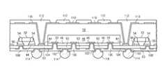
- FIG. 1is a flip chip semiconductor device with solder bumps providing electrical interconnect between an active area of the die and a chip carrier substrate;
- FIGS. 2 a -2 iillustrate the method of making a WLCSP with an interconnect build-up layer
- FIGS. 3 a and 3 billustrate an alternative embodiment of the WLCSP made in FIGS. 2 a - 2 i;
- FIG. 4illustrates an embodiment of a WLCSP where the redistribution layer is applied directly to the surface of the molding compound and protective layer of the semiconductor die;
- FIG. 5illustrates the embodiment of FIG. 4 where an additional metallized redistribution layer and insulating layer have been added.
- FIGS. 6 a -6 billustrate a redistribution layer formed in the molding compound of the semiconductor package.
- Front-end manufacturinggenerally refers to formation of the semiconductor devices on the wafer.
- the finished waferhas an active side containing the transistors and other active and passive components.
- Back-end manufacturingrefers to cutting or singulating the finished wafer into the individual die and then packaging the die for structural support and/or environmental isolation.
- a semiconductor wafergenerally includes an active surface having semiconductor devices disposed thereon, and a backside surface formed with bulk semiconductor material, e.g., silicon.
- the active side surfacecontains a plurality of semiconductor die.
- the active surfaceis formed by a variety of semiconductor processes, including layering, patterning, doping, and heat treatment.
- semiconductor materialsare grown or deposited on the substrate by techniques involving thermal oxidation, nitridation, chemical vapor deposition, evaporation, and sputtering.
- Photolithographyinvolves the masking of areas of the surface and etching away undesired material to form specific structures.
- the doping processinjects concentrations of dopant material by thermal diffusion or ion implantation.
- Flip chip semiconductor packages and wafer level packagesare commonly used with integrated circuits (ICs) demanding high speed, high density, and greater pin count.
- Flip chip style semiconductor device 10involves mounting an active area 12 of die 14 facedown toward a chip carrier substrate or printed circuit board (PCB) 16 , as shown in FIG. 1 .
- Active area 12contains active and passive devices, conductive layers, and dielectric layers according to the electrical design of the die.
- the electrical and mechanical interconnectis achieved through a solder bump structure 20 comprising a large number of individual conductive solder bumps or balls 22 .
- the solder bumpsare formed on bump pads or interconnect sites 24 , which are disposed on active area 12 .
- the bump pads 24connect to the active circuits by conduction tracks in active area 12 .
- the solder bumps 22are electrically and mechanically connected to contact pads or interconnect sites 26 on carrier substrate 16 by a solder reflow process.
- the flip chip semiconductor deviceprovides a short electrical conduction path from the active devices on die 14 to conduction tracks on carrier substrate 16 in order to reduce signal propagation, lower capacitance, and achieve overall better circuit performance.
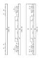
- FIGS. 2 a -2 iillustrate the method of making a wafer level chip scale package (WLCSP) with an interconnect structure, in which the semiconductor die is prepared from a semiconductor wafer having a pre-applied protective layer on the active side of the wafer.
- a metal carrier 40is shown having a photoresist layer 42 applied to a top surface of metal carrier 40 .
- the metal carrier 40is made of copper (Cu), aluminum (Al), or other electrically conducting metal.
- Carrier 40acts as a support member to hold a semiconductor die and plated metal pads in place during the manufacturing process. During a subsequent electroplating process, metal carrier 40 also serves as a plating current path to form plated metal pads on the carrier.
- a plurality of openings or viasare made in the photoresist layer 42 using a photo patterning process such as ultraviolet (UV) exposure and development.
- the openingsdefine areas for selective plating and can be strategically placed, allowing the areas, when plated, to act as fiducial marks, interconnection contact pads, and saw alignment marks.
- Metal contact pads 44are deposited in the openings and onto metal carrier 40 using an electroplating process. Contact pads 44 can be made with electroless nickel/immersion gold (Ni/Au) or other metal or alloy having low resistivity. Once contact pads 44 have been deposited, photoresist layer 42 is stripped off metal carrier 40 through either UV or thermal curing, as shown in FIG. 2 c.
- a protective layeris pre-applied to the active surface of a semiconductor wafer containing a plurality of semiconductor die.
- the protective layeris a lamination or coating adhesive applied by spin coating or screen printing.
- the protection layeris an insulator and can be made with polyimide (PI) film having a low coefficient of thermal expansion (CTE), such as 20 ppm/° C. or below, or a low modulus silicon base elastomer, under pressure of less than 200 MPa.
- PIpolyimide
- Vias or openingscan be formed in the active surface of the semiconductor wafer by laser drilling or deep reactive ion etching (DRIE). Photo vias can be formed if photosensitive adhesive layer is applied. The wafer is placed protective layer down to dicing tape and cut with a dicing blade. A pick and place tool removes the individual die with its pre-applied protective layer and places the die on metal carrier 40 .
- DRIEdeep reactive ion etching
- FIG. 2 dillustrates semiconductor die 48 with pre applied protective layer 46 mounted face down on metal carrier 40 .
- the protective layer 46can be used as the die attach material.
- the interconnect sites 50electrically connect to active and passive devices on semiconductor die 48 through conduction tracks or layers formed within the die.
- the conductive materialcan be Al, Cu, tin (Sn), nickel (Ni), gold (Au), or silver (Ag).
- metal carrier 40has one or more passive components 52 with electrodes 54 electrically connected to metal pads 44 with conductive adhesive 56 .
- Passive components 52can include resistors, capacitors, inductors, transformers, voltage sources, current sources, or similar devices.
- FIG. 2 ethe structure formed in FIG. 2 d is encapsulated with a polymer molding compound 58 down to metal carrier 40 .
- the molding compound 58is non-conductive and environmentally protects the semiconductor device from external elements and contaminants.
- Molding compound 58can be made with epoxy acrylate or other polymer material and applied by transfer molding, liquid encapsulant molding, or other molding process.
- Carrier 40is removed by an etching process, exposing protective layer 46 of semiconductor die 48 and metal pads 44 . With metal carrier 40 removed, molding compound 58 provides rigid support for the semiconductor device.
- the semiconductor packageis inverted such that interconnect sites 50 and active surface of semiconductor die 48 face upwards.
- An insulating layer 63is applied to contact pads 44 , protective layer 46 , and molding compound 58 .
- the insulating layer 63is made with dielectric or photosensitive polymer material having low cure temperature, e.g. less than 200° C.
- a process carrier 62is applied to a surface of molding compound 58 , opposite protective layer 46 , using an adhesive layer 60 . Carrier 62 facilitates the process handling in the subsequent interconnect build-up process.
- a portion of insulating layer 63 and protective layer 46is removed to form openings and expose contact pads 44 and interconnect sites 50 .
- the openingscan be formed using a photo patterning process if insulating layer 63 and protection layer 46 are photosensitive. Alternatively, if the protective layer 46 is not photosensitive, the openings are formed by laser drilling or DRIE process.
- a metallized redistribution layer (RDL) 64is formed by depositing thin layers of metals over the surface of insulating layer 63 and protection layer 46 . Multiple metal layers are typically required to meet the different functional requirements of the metallized RDL such as adhesion, barrier, conductor, and protection. Accordingly, RDLs 64 can be made with layers of Al, titanium (Ti), and titanium tungsten (TiW). RDLs 64 provide electrical contact between metal pads 44 and interconnect sites 50 and subsequent layers.
- an insulating layer 66is formed over insulating layer 63 and RDLs 64 .
- the insulating layer 66is made with dielectric or photosensitive polymer material having low cure temperature, e.g. less than 200° C.
- a portion of insulating layer 66is removed using a photo patterning process such as UV exposure and development to expose RDLs 64 .
- the insulating layers 63 and 66 and RDLs 64constitute at least a portion of the interconnect build-up layer. Additional photosensitive insulating layers, metalized RDLs, and other conductive layers can be added as needed to expand the interconnect build-up layers to meet the interconnect requirements for the functional design of semiconductor die 48 .
- Interconnection contact padsare deposited and patterned to electrically contact RDLs 64 .
- UBMs 68provide multiple benefits to the semiconductor package: (1) an interface between the interconnect sites 50 and subsequent electrical interconnections, (2) protection of interconnect sites 50 from the environment, (3) low resistive contact between interconnect sites 50 and the subsequent electrical interconnections, (4) a barrier to solder diffusion into the metal pad, and (5) a seed layer for solder wettability.
- UBMs 68are made by forming successive layers of metals by sputtering, each layer having a different function. These layers may include an adhesion layer, diffusion layer, solder wettable layer, and protective layer.
- solder bumps 70are formed on UBMs 68 .
- the solder bumps 70electrically connect interconnect sites 50 and metal pads 44 with other electrical devices.
- the solder bumps 70may be deposited through an evaporation, electrolytic plating, electroless plating, ball drop, or screen printing process and are formed from any metal or electrically conductive material, e.g., Sn, lead (Pb), Ni, Au, Ag, Cu, bismuthinite (Bi), and alloys thereof.
- the solder bumps 70represent one type of electrical interconnect structure.
- carrier 62is removed either after attaching solder bumps 70 or after wafer singulation.
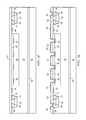
- FIGS. 3 a and 3 billustrate an alternative embodiment of the WLCSP made in FIGS. 2 a -2 i .
- a metal carrier having a photoresist layeris used as a support member. Openings are made in the photoresist layer to define the areas where metal pads 44 are deposited and, once deposited, the photoresist layer is stripped off.
- vias 72are pre-formed in protective layer 46 to expose interconnect sites 50 .
- the semiconductor die 48is mounted to the metal carrier in a face down position and encapsulated, along with passive components 52 , with molding compound 58 .
- the metal carrieris stripped from the semiconductor device and insulating layer 63 is formed on contact pads 44 and protective layer 46 .
- Vias 74shown in FIG. 3 b , are made in insulating layer 63 using a photo patterning process, such as UV exposure and development, directly coupling vias 74 with vias 72 in protective layer 46 .
- the vias 74 in insulating layer 63are typically the same size or larger than vias 72 in protective layer 46 .
- Vias 74are aligned with vias 72 to expose interconnect sites 50 .
- metallized RDLs and additional insulating layersare formed as needed for the interconnect build-up process and, finally, the electrical interconnections are formed, see FIGS. 2 g - 2 i.
- FIG. 4illustrates another embodiment of a semiconductor package.
- a metal carrier having a photoresist layeris used as a support member. Openings are made in the photoresist layer to define the areas where metal pads 44 are deposited and, once deposited, the photoresist layer is stripped off.
- a semiconductor die 48having a pre-applied protective layer 46 on its face, is applied facedown to the metal carrier.
- the semiconductor die 48may optionally have pre-formed vias similar to the embodiment illustrated in FIGS. 3 a -3 b .
- the semiconductor die 48is encapsulated, along with passive components 52 , with molding compound 58 . Next, the metal carrier is stripped from the semiconductor device.
- FIG. 4shows that RDL 76 is applied directly to the surface of protective layer 46 , molding compound 58 , and contact pads 46 using a chemical vapor disposition (CVD), physical vapor deposition (PVD), and/or plating process.
- the insulating layer 63is not used in this embodiment.
- RDLs 76can be made of Al, Ti, TiW, or other metal.
- An insulating layer 84is applied to RDLs 76 and vias are formed, exposing RDLs 76 .
- UBMs 78can be plated to form the final metal pad areas.
- Solder bumps 80are formed on UBMs 78 .p
- a second metalized RDL 86is formed on insulating layer 84 and is electrically connected to RDL 76 .
- An insulating layer 92is formed over RDL 86 and insulating layer 84 .
- the insulating layer 92is made with dielectric or photosensitive polymer material having low cure temperature, e.g. less than 200° C.
- Viasare formed in insulating layer 92 to expose portions of RDLs 86 .
- UBMs 88can be plated to form the final metal pad areas.
- Solder bumps 90are formed on UBMs 88 .
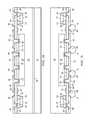
- openingsare made in photoresist layer that has been applied to the metal carrier.
- the openingsdefine the areas where metal pads 44 are deposited and, once deposited, the photoresist layer is stripped off.
- a semiconductor die 48with optional pre-formed vias in the protective layer 46 , is applied to the metal carrier in a facedown position.
- the semiconductor die 48is encapsulated, along with passive components 52 , with molding compound 58 .
- the metal carrieris stripped from the semiconductor device and insulating layer 63 is applied to contact pads 44 and protective layer 46 . Vias are formed in insulating layer 63 and protective layer 46 , if protective layer 46 did not have pre-formed vias.
- a metalized RDL 104is formed on insulating layer 63 and protective layer 46 .
- a second photosensitive insulating layer 100is applied on top of insulating layer 63 , covering RDLs 104 . Vias are formed in insulating layer 100 . Additional photosensitive insulating layers and metalized RDLs may be added as needed to form the interconnect build-up layers. Additionally, an optional UBMs 102 can be plated in insulating layer 100 .
- a temporary carrier 108is applied to the bottom side of molding compound 58 using an adhesive layer 106 .
- the temporary carrier 108can be made of a stiff material or flexible tape and facilitates the interconnect build-up process formed on the top surface of molding compound 58 .
- Vias or openingsare formed through molding compound 58 to expose metal pads 44 using a laser drill or DRIE process.
- Another metallized RDL 110is formed on the top surface of molding compound 58 and the vias made in molding compound 58 .
- An insulating layer 112is applied over RDLs 110 .
- the insulating layer 112is made with dielectric or photosensitive polymer material having low cure temperature, e.g. less than 200° C.
- vias or openingsare made in insulating layer 112 , exposing portions of RDL 110 .
- process carrier 108is released and solder bumps 114 are formed on UBMs 102 .
- UBMscan be plated to form the final metal pad areas in insulating layer 112 .
Landscapes
- Engineering & Computer Science (AREA)
- Microelectronics & Electronic Packaging (AREA)
- Power Engineering (AREA)
- Computer Hardware Design (AREA)
- Physics & Mathematics (AREA)
- Condensed Matter Physics & Semiconductors (AREA)
- General Physics & Mathematics (AREA)
- Manufacturing & Machinery (AREA)
- Geometry (AREA)
- Internal Circuitry In Semiconductor Integrated Circuit Devices (AREA)
- Wire Bonding (AREA)
Abstract
Description
Claims (15)
Priority Applications (1)
| Application Number | Priority Date | Filing Date | Title |
|---|---|---|---|
| US14/523,556US9559029B2 (en) | 2007-12-14 | 2014-10-24 | Semiconductor device and method of forming interconnect structure for encapsulated die having pre-applied protective layer |
Applications Claiming Priority (4)
| Application Number | Priority Date | Filing Date | Title |
|---|---|---|---|
| US11/957,101US7767496B2 (en) | 2007-12-14 | 2007-12-14 | Semiconductor device and method of forming interconnect structure for encapsulated die having pre-applied protective layer |
| US12/822,080US8004095B2 (en) | 2007-12-14 | 2010-06-23 | Semiconductor device and method of forming interconnect structure for encapsulated die having pre-applied protective layer |
| US13/207,633US9252066B2 (en) | 2007-12-14 | 2011-08-11 | Semiconductor device and method of forming interconnect structure for encapsulated die having pre-applied protective layer |
| US14/523,556US9559029B2 (en) | 2007-12-14 | 2014-10-24 | Semiconductor device and method of forming interconnect structure for encapsulated die having pre-applied protective layer |
Related Parent Applications (1)
| Application Number | Title | Priority Date | Filing Date |
|---|---|---|---|
| US13/207,633ContinuationUS9252066B2 (en) | 2007-12-14 | 2011-08-11 | Semiconductor device and method of forming interconnect structure for encapsulated die having pre-applied protective layer |
Publications (2)
| Publication Number | Publication Date |
|---|---|
| US20150061124A1 US20150061124A1 (en) | 2015-03-05 |
| US9559029B2true US9559029B2 (en) | 2017-01-31 |
Family
ID=40752123
Family Applications (5)
| Application Number | Title | Priority Date | Filing Date |
|---|---|---|---|
| US11/957,101Active2028-01-08US7767496B2 (en) | 2007-12-14 | 2007-12-14 | Semiconductor device and method of forming interconnect structure for encapsulated die having pre-applied protective layer |
| US12/822,080ActiveUS8004095B2 (en) | 2007-12-14 | 2010-06-23 | Semiconductor device and method of forming interconnect structure for encapsulated die having pre-applied protective layer |
| US13/207,633Active2029-06-17US9252066B2 (en) | 2007-12-14 | 2011-08-11 | Semiconductor device and method of forming interconnect structure for encapsulated die having pre-applied protective layer |
| US13/555,531ActiveUS8846454B2 (en) | 2007-12-14 | 2012-07-23 | Semiconductor device and method of forming interconnect structure for encapsulated die having pre-applied protective layer |
| US14/523,556ActiveUS9559029B2 (en) | 2007-12-14 | 2014-10-24 | Semiconductor device and method of forming interconnect structure for encapsulated die having pre-applied protective layer |
Family Applications Before (4)
| Application Number | Title | Priority Date | Filing Date |
|---|---|---|---|
| US11/957,101Active2028-01-08US7767496B2 (en) | 2007-12-14 | 2007-12-14 | Semiconductor device and method of forming interconnect structure for encapsulated die having pre-applied protective layer |
| US12/822,080ActiveUS8004095B2 (en) | 2007-12-14 | 2010-06-23 | Semiconductor device and method of forming interconnect structure for encapsulated die having pre-applied protective layer |
| US13/207,633Active2029-06-17US9252066B2 (en) | 2007-12-14 | 2011-08-11 | Semiconductor device and method of forming interconnect structure for encapsulated die having pre-applied protective layer |
| US13/555,531ActiveUS8846454B2 (en) | 2007-12-14 | 2012-07-23 | Semiconductor device and method of forming interconnect structure for encapsulated die having pre-applied protective layer |
Country Status (4)
| Country | Link |
|---|---|
| US (5) | US7767496B2 (en) |
| KR (1) | KR101523383B1 (en) |
| SG (1) | SG153721A1 (en) |
| TW (1) | TWI508198B (en) |
Cited By (1)
| Publication number | Priority date | Publication date | Assignee | Title |
|---|---|---|---|---|
| US11114359B2 (en) | 2018-09-13 | 2021-09-07 | Dialog Semiconductor (Uk) Limited | Wafer level chip scale package structure |
Families Citing this family (104)
| Publication number | Priority date | Publication date | Assignee | Title |
|---|---|---|---|---|
| US8193034B2 (en) | 2006-11-10 | 2012-06-05 | Stats Chippac, Ltd. | Semiconductor device and method of forming vertical interconnect structure using stud bumps |
| TWI360207B (en) | 2007-10-22 | 2012-03-11 | Advanced Semiconductor Eng | Chip package structure and method of manufacturing |
| US9318441B2 (en) | 2007-12-14 | 2016-04-19 | Stats Chippac, Ltd. | Semiconductor device and method of forming sacrificial adhesive over contact pads of semiconductor die |
| US8183095B2 (en) | 2010-03-12 | 2012-05-22 | Stats Chippac, Ltd. | Semiconductor device and method of forming sacrificial protective layer to protect semiconductor die edge during singulation |
| US8456002B2 (en) | 2007-12-14 | 2013-06-04 | Stats Chippac Ltd. | Semiconductor device and method of forming insulating layer disposed over the semiconductor die for stress relief |
| US7767496B2 (en) | 2007-12-14 | 2010-08-03 | Stats Chippac, Ltd. | Semiconductor device and method of forming interconnect structure for encapsulated die having pre-applied protective layer |
| US8343809B2 (en)* | 2010-03-15 | 2013-01-01 | Stats Chippac, Ltd. | Semiconductor device and method of forming repassivation layer with reduced opening to contact pad of semiconductor die |
| US7851246B2 (en)* | 2007-12-27 | 2010-12-14 | Stats Chippac, Ltd. | Semiconductor device with optical sensor and method of forming interconnect structure on front and backside of the device |
| KR101003678B1 (en)* | 2008-12-03 | 2010-12-23 | 삼성전기주식회사 | wafer level package and method of manufacturing the same and method for reusing chip |
| US7851894B1 (en)* | 2008-12-23 | 2010-12-14 | Amkor Technology, Inc. | System and method for shielding of package on package (PoP) assemblies |
| US8367470B2 (en)* | 2009-08-07 | 2013-02-05 | Stats Chippac, Ltd. | Semiconductor device and method of forming cavity in build-up interconnect structure for short signal path between die |
| JP5296636B2 (en)* | 2009-08-21 | 2013-09-25 | 新光電気工業株式会社 | Manufacturing method of semiconductor package |
| US7977783B1 (en)* | 2009-08-27 | 2011-07-12 | Amkor Technology, Inc. | Wafer level chip size package having redistribution layers |
| US9397050B2 (en)* | 2009-08-31 | 2016-07-19 | STATS ChipPAC Pte. Ltd. | Semiconductor device and method of forming pre-molded semiconductor die having bumps embedded in encapsulant |
| TWI425580B (en)* | 2009-09-09 | 2014-02-01 | Du Pont | Process for manufacturing semiconductor chip packaging module |
| US8883559B2 (en)* | 2009-09-25 | 2014-11-11 | Stats Chippac, Ltd. | Semiconductor device and method of forming adhesive material to secure semiconductor die to carrier in WLCSP |
| US8796561B1 (en)* | 2009-10-05 | 2014-08-05 | Amkor Technology, Inc. | Fan out build up substrate stackable package and method |
| TWI404149B (en)* | 2009-12-18 | 2013-08-01 | Univ Nat Pingtung Sci & Tech | Aligning bonding method for semiconductor package |
| US9754835B2 (en)* | 2010-02-16 | 2017-09-05 | Deca Technologies Inc. | Semiconductor device and method comprising redistribution layers |
| US9196509B2 (en) | 2010-02-16 | 2015-11-24 | Deca Technologies Inc | Semiconductor device and method of adaptive patterning for panelized packaging |
| US10373870B2 (en) | 2010-02-16 | 2019-08-06 | Deca Technologies Inc. | Semiconductor device and method of packaging |
| US8799845B2 (en) | 2010-02-16 | 2014-08-05 | Deca Technologies Inc. | Adaptive patterning for panelized packaging |
| US20110198762A1 (en)* | 2010-02-16 | 2011-08-18 | Deca Technologies Inc. | Panelized packaging with transferred dielectric |
| US20110215450A1 (en)* | 2010-03-05 | 2011-09-08 | Chi Heejo | Integrated circuit packaging system with encapsulation and method of manufacture thereof |
| US8409926B2 (en) | 2010-03-09 | 2013-04-02 | Stats Chippac, Ltd. | Semiconductor device and method of forming insulating layer around semiconductor die |
| US9548240B2 (en) | 2010-03-15 | 2017-01-17 | STATS ChipPAC Pte. Ltd. | Semiconductor device and method of forming repassivation layer for robust low cost fan-out semiconductor package |
| US8710680B2 (en)* | 2010-03-26 | 2014-04-29 | Shu-Ming Chang | Electronic device package and fabrication method thereof |
| US8258633B2 (en)* | 2010-03-31 | 2012-09-04 | Infineon Technologies Ag | Semiconductor package and multichip arrangement having a polymer layer and an encapsulant |
| JP5826532B2 (en)* | 2010-07-15 | 2015-12-02 | 新光電気工業株式会社 | Semiconductor device and manufacturing method thereof |
| US8076184B1 (en)* | 2010-08-16 | 2011-12-13 | Stats Chippac, Ltd. | Semiconductor device and method of forming wafer-level multi-row etched leadframe with base leads and embedded semiconductor die |
| KR101169688B1 (en)* | 2010-11-08 | 2012-08-06 | 에스케이하이닉스 주식회사 | Semiconductor device and stacked semiconductor package |
| US10204879B2 (en) | 2011-01-21 | 2019-02-12 | STATS ChipPAC Pte. Ltd. | Semiconductor device and method of forming wafer-level interconnect structures with advanced dielectric characteristics |
| US8492203B2 (en) | 2011-01-21 | 2013-07-23 | Stats Chippac, Ltd. | Semiconductor device and method for forming semiconductor package having build-up interconnect structure over semiconductor die with different CTE insulating layers |
| WO2012100720A1 (en)* | 2011-01-30 | 2012-08-02 | 南通富士通微电子股份有限公司 | Packaging method |
| US9595490B2 (en) | 2011-03-22 | 2017-03-14 | Nantong Fujitsu Microelectronics Co., Ltd. | 3D system-level packaging methods and structures |
| WO2012126377A1 (en) | 2011-03-22 | 2012-09-27 | Nantong Fujitsu Microelectronics Co., Ltd. | System-level packaging methods and structures |
| US20130049214A1 (en)* | 2011-08-29 | 2013-02-28 | Infineon Technologies Ag | Method of processing at least one die and die arrangement |
| US9385009B2 (en)* | 2011-09-23 | 2016-07-05 | STATS ChipPAC Pte. Ltd. | Semiconductor device and method of forming stacked vias within interconnect structure for Fo-WLCSP |
| WO2013057949A2 (en)* | 2011-10-19 | 2013-04-25 | Panasonic Corporation | Manufacturing method for semiconductor package, semiconductor package, and semiconductor device |
| KR101532816B1 (en)* | 2011-11-14 | 2015-06-30 | 유나이티드 테스트 엔드 어셈블리 센터 엘티디 | Semiconductor packages and methods of packaging semiconductor devices |
| US9576873B2 (en)* | 2011-12-14 | 2017-02-21 | STATS ChipPAC Pte. Ltd. | Integrated circuit packaging system with routable trace and method of manufacture thereof |
| KR101332916B1 (en) | 2011-12-29 | 2013-11-26 | 주식회사 네패스 | Semiconductor package and method of manufacturing the same |
| US8900929B2 (en)* | 2012-03-21 | 2014-12-02 | Stats Chippac, Ltd. | Semiconductor device and method for forming openings and trenches in insulating layer by first LDA and second LDA for RDL formation |
| US9111949B2 (en)* | 2012-04-09 | 2015-08-18 | Taiwan Semiconductor Manufacturing Company, Ltd. | Methods and apparatus of wafer level package for heterogeneous integration technology |
| KR101947722B1 (en)* | 2012-06-07 | 2019-04-25 | 삼성전자주식회사 | stack semiconductor package and method of manufacturing the same |
| KR101452587B1 (en)* | 2012-06-28 | 2014-10-22 | 타이완 세미콘덕터 매뉴팩쳐링 컴퍼니 리미티드 | Methods and apparatus of wafer level package for heterogeneous integration technology |
| US10622310B2 (en) | 2012-09-26 | 2020-04-14 | Ping-Jung Yang | Method for fabricating glass substrate package |
| US9721878B2 (en)* | 2012-09-28 | 2017-08-01 | Intel Corporation | High density second level interconnection for bumpless build up layer (BBUL) packaging technology |
| US9799592B2 (en) | 2013-11-19 | 2017-10-24 | Amkor Technology, Inc. | Semicondutor device with through-silicon via-less deep wells |
| KR101366461B1 (en) | 2012-11-20 | 2014-02-26 | 앰코 테크놀로지 코리아 주식회사 | Semiconductor device and manufacturing method thereof |
| US9953907B2 (en)* | 2013-01-29 | 2018-04-24 | Taiwan Semiconductor Manufacturing Company, Ltd. | PoP device |
| US10128175B2 (en)* | 2013-01-29 | 2018-11-13 | Taiwan Semiconductor Manufacturing Company | Packaging methods and packaged semiconductor devices |
| US20140264954A1 (en)* | 2013-03-14 | 2014-09-18 | Applied Materials, Inc. | Passivation and warpage correction by nitride film for molded wafers |
| KR20140119522A (en)* | 2013-04-01 | 2014-10-10 | 삼성전자주식회사 | Semiconductor package having package on package structure |
| US8952544B2 (en)* | 2013-07-03 | 2015-02-10 | Taiwan Semiconductor Manufacturing Company Ltd. | Semiconductor device and manufacturing method thereof |
| US8822268B1 (en)* | 2013-07-17 | 2014-09-02 | Freescale Semiconductor, Inc. | Redistributed chip packages containing multiple components and methods for the fabrication thereof |
| KR101488608B1 (en)* | 2013-07-19 | 2015-02-02 | 앰코 테크놀로지 코리아 주식회사 | Semiconductor device and manufacturing method thereof |
| US8928117B1 (en)* | 2013-08-01 | 2015-01-06 | Taiwan Semiconductor Manufacturing Company, Ltd. | Multi-chip package structure and method of forming same |
| US8927412B1 (en)* | 2013-08-01 | 2015-01-06 | Taiwan Semiconductor Manufacturing Company, Ltd. | Multi-chip package and method of formation |
| US9419156B2 (en) | 2013-08-30 | 2016-08-16 | Taiwan Semiconductor Manufacturing Co., Ltd. | Package and method for integration of heterogeneous integrated circuits |
| KR101522780B1 (en)* | 2013-10-07 | 2015-05-26 | 삼성전기주식회사 | A printed circuit board comprising embeded electronic component within and a method for manufacturing |
| JP2015095482A (en)* | 2013-11-08 | 2015-05-18 | アイメックImec | Method for producing microbumps on semiconductor component |
| KR20150091932A (en) | 2014-02-04 | 2015-08-12 | 앰코 테크놀로지 코리아 주식회사 | Manufacturing method of semiconductor device and semiconductor device thereof |
| TWI548030B (en)* | 2014-04-15 | 2016-09-01 | 矽品精密工業股份有限公司 | Conductive blind-hole structure and manufacturing method thereof |
| US9040316B1 (en) | 2014-06-12 | 2015-05-26 | Deca Technologies Inc. | Semiconductor device and method of adaptive patterning for panelized packaging with dynamic via clipping |
| US9978700B2 (en) | 2014-06-16 | 2018-05-22 | STATS ChipPAC Pte. Ltd. | Method for building up a fan-out RDL structure with fine pitch line-width and line-spacing |
| US10804153B2 (en)* | 2014-06-16 | 2020-10-13 | STATS ChipPAC Pte. Ltd. | Semiconductor device and method to minimize stress on stack via |
| US11239138B2 (en) | 2014-06-27 | 2022-02-01 | Taiwan Semiconductor Manufacturing Company | Methods of packaging semiconductor devices and packaged semiconductor devices |
| KR101647559B1 (en)* | 2014-11-07 | 2016-08-10 | 앰코 테크놀로지 코리아 주식회사 | Method of manufactuing semiconductor package and semiconductor package |
| US10325853B2 (en)* | 2014-12-03 | 2019-06-18 | Taiwan Semiconductor Manufacturing Company, Ltd. | Method of forming semiconductor packages having through package vias |
| TWI584431B (en)* | 2015-01-21 | 2017-05-21 | 尼克森微電子股份有限公司 | Method for manufacturing ultra-thin semiconductor device package structure |
| US9583462B2 (en)* | 2015-01-22 | 2017-02-28 | Qualcomm Incorporated | Damascene re-distribution layer (RDL) in fan out split die application |
| BR112017018820A2 (en)* | 2015-04-14 | 2018-04-24 | Huawei Technologies Co., Ltd. | A chip |
| KR102357937B1 (en)* | 2015-08-26 | 2022-02-04 | 삼성전자주식회사 | Semiconductor chip, method for fabricating the same, and semiconductor package comprising the same |
| KR102372349B1 (en)* | 2015-08-26 | 2022-03-11 | 삼성전자주식회사 | Semiconductor chip, method for fabricating the same, and semiconductor package comprising the same |
| US9735131B2 (en)* | 2015-11-10 | 2017-08-15 | Taiwan Semiconductor Manufacturing Company, Ltd. | Multi-stack package-on-package structures |
| US10090255B2 (en) | 2016-01-29 | 2018-10-02 | Globalfoundries Inc. | Dicing channels for glass interposers |
| US20170338204A1 (en)* | 2016-05-17 | 2017-11-23 | Taiwan Semiconductor Manufacturing Company, Ltd. | Device and Method for UBM/RDL Routing |
| US10475775B2 (en)* | 2016-08-31 | 2019-11-12 | Advanced Semiconductor Engineering, Inc. | Semiconductor package device and method of manufacturing the same |
| US9960328B2 (en) | 2016-09-06 | 2018-05-01 | Amkor Technology, Inc. | Semiconductor device and manufacturing method thereof |
| US10573601B2 (en) | 2016-09-19 | 2020-02-25 | Deca Technologies Inc. | Semiconductor device and method of unit specific progressive alignment |
| US10157803B2 (en) | 2016-09-19 | 2018-12-18 | Deca Technologies Inc. | Semiconductor device and method of unit specific progressive alignment |
| WO2018057490A1 (en)* | 2016-09-22 | 2018-03-29 | Macdermid Enthone Inc. | Copper plating method and composition for semiconductor substrates |
| US10128193B2 (en)* | 2016-11-29 | 2018-11-13 | Taiwan Semiconductor Manufacturing Co., Ltd. | Package structure and method for forming the same |
| US11114315B2 (en) | 2017-11-29 | 2021-09-07 | Pep Innovation Pte. Ltd. | Chip packaging method and package structure |
| US11232957B2 (en) | 2017-11-29 | 2022-01-25 | Pep Inovation Pte. Ltd. | Chip packaging method and package structure |
| US11233028B2 (en)* | 2017-11-29 | 2022-01-25 | Pep Inovation Pte. Ltd. | Chip packaging method and chip structure |
| US11610855B2 (en) | 2017-11-29 | 2023-03-21 | Pep Innovation Pte. Ltd. | Chip packaging method and package structure |
| US10546817B2 (en)* | 2017-12-28 | 2020-01-28 | Intel IP Corporation | Face-up fan-out electronic package with passive components using a support |
| JP2019145546A (en)* | 2018-02-16 | 2019-08-29 | 住友電工デバイス・イノベーション株式会社 | Manufacturing method of semiconductor device |
| US10700008B2 (en)* | 2018-05-30 | 2020-06-30 | Taiwan Semiconductor Manufacturing Co., Ltd. | Package structure having redistribution layer structures |
| US11004812B2 (en)* | 2018-09-18 | 2021-05-11 | Taiwan Semiconductor Manufacturing Company, Ltd. | Package structure and method of forming the same |
| US20220026705A1 (en)* | 2018-11-26 | 2022-01-27 | Corning Incorporated | Methods for forming patterned insulating layers on conductive layers and devices manufactured using such methods |
| TWI718011B (en) | 2019-02-26 | 2021-02-01 | 日商長瀨產業股份有限公司 | Embedded semiconductor packages and methods thereof |
| DE102019202720B4 (en)* | 2019-02-28 | 2021-04-01 | Fraunhofer-Gesellschaft zur Förderung der angewandten Forschung e.V. | Thin film chip package for semiconductor chips with indirect contact and process for producing the same |
| CN210200700U (en)* | 2019-03-11 | 2020-03-27 | Pep创新私人有限公司 | Chip structure |
| US11282756B2 (en)* | 2020-08-17 | 2022-03-22 | Taiwan Semiconductor Manufacturing Company Limited | Organic interposer including stress-resistant bonding structures and methods of forming the same |
| US11749629B2 (en)* | 2020-12-10 | 2023-09-05 | Advanced Micro Devices, Inc. | High-speed die connections using a conductive insert |
| CN113990759B (en)* | 2020-12-21 | 2025-07-22 | 矽磐微电子(重庆)有限公司 | Semiconductor packaging method and semiconductor packaging structure |
| US20240006191A1 (en)* | 2020-12-23 | 2024-01-04 | Heraeus Materials Singapore Pte. Ltd. | Process for the manufacture of encapsulated semiconductor dies and/or of encapsulated semiconductor packages |
| CN112928077A (en)* | 2021-01-20 | 2021-06-08 | 上海先方半导体有限公司 | Multi-chip heterogeneous integrated packaging unit and manufacturing method and stacking structure thereof |
| TWI762279B (en)* | 2021-04-21 | 2022-04-21 | 翔名科技股份有限公司 | Semiconductor part protective coating and method of fabricating the same |
| US12431422B2 (en) | 2023-01-05 | 2025-09-30 | STATS ChipPAC Pte. Ltd. | Semiconductor device and method of forming RDL with graphene-coated core |
| US12362322B2 (en) | 2023-06-22 | 2025-07-15 | Deca Technologies Usa, Inc. | Method of making a fan-out semiconductor assembly with an intermediate carrier |
Citations (90)
| Publication number | Priority date | Publication date | Assignee | Title |
|---|---|---|---|---|
| US4894115A (en) | 1989-02-14 | 1990-01-16 | General Electric Company | Laser beam scanning method for forming via holes in polymer materials |
| US5157001A (en) | 1989-09-18 | 1992-10-20 | Matsushita Electric Industrial Co., Ltd. | Method of dicing semiconductor wafer along protective film formed on scribe lines |
| US5161093A (en) | 1990-07-02 | 1992-11-03 | General Electric Company | Multiple lamination high density interconnect process and structure employing a variable crosslinking adhesive |
| US5250843A (en) | 1991-03-27 | 1993-10-05 | Integrated System Assemblies Corp. | Multichip integrated circuit modules |
| US5353498A (en) | 1993-02-08 | 1994-10-11 | General Electric Company | Method for fabricating an integrated circuit module |
| US5524339A (en)* | 1994-09-19 | 1996-06-11 | Martin Marietta Corporation | Method for protecting gallium arsenide mmic air bridge structures |
| US5527741A (en) | 1994-10-11 | 1996-06-18 | Martin Marietta Corporation | Fabrication and structures of circuit modules with flexible interconnect layers |
| US5703400A (en) | 1995-12-04 | 1997-12-30 | General Electric Company | Fabrication and structures of two-sided molded circuit modules with flexible interconnect layers |
| US5814193A (en) | 1995-08-17 | 1998-09-29 | Bp Chemicals Limited | Process for the purification of a C2 to C4 carboxylic acid and/or anhydride having halide impurities |
| US5834340A (en) | 1993-06-01 | 1998-11-10 | Mitsubishi Denki Kabushiki Kaisha | Plastic molded semiconductor package and method of manufacturing the same |
| US5841193A (en) | 1996-05-20 | 1998-11-24 | Epic Technologies, Inc. | Single chip modules, repairable multichip modules, and methods of fabrication thereof |
| US5866952A (en) | 1995-11-30 | 1999-02-02 | Lockheed Martin Corporation | High density interconnected circuit module with a compliant layer as part of a stress-reducing molded substrate |
| US6025995A (en) | 1997-11-05 | 2000-02-15 | Ericsson Inc. | Integrated circuit module and method |
| US6028364A (en) | 1994-09-20 | 2000-02-22 | Hitachi, Ltd. | Semiconductor device having a stress relieving mechanism |
| CN1246731A (en) | 1998-08-28 | 2000-03-08 | 三星电子株式会社 | Chip dimention packaging and method for preparing wafer-class chip dimention packing |
| US6052995A (en) | 1996-09-12 | 2000-04-25 | Robert Bosch Gmbh | Valve for an internal combustion engine, and an internal combustion engine including the valve |
| US6110773A (en) | 1994-12-31 | 2000-08-29 | Samsung Electronics Co., Ltd. | Static random access memory device manufacturing method |
| US6168966B1 (en) | 1999-02-18 | 2001-01-02 | Taiwan Semiconductor Manufacturing Company | Fabrication of uniform areal sensitivity image array |
| US6197613B1 (en) | 1999-03-23 | 2001-03-06 | Industrial Technology Research Institute | Wafer level packaging method and devices formed |
| US6271469B1 (en) | 1999-11-12 | 2001-08-07 | Intel Corporation | Direct build-up layer on an encapsulated die package |
| US6351031B1 (en)* | 1999-10-12 | 2002-02-26 | Fujitsu Limited | Semiconductor device and method for manufacturing substrate of the same |
| US6423571B2 (en) | 1994-09-20 | 2002-07-23 | Hitachi, Ltd. | Method of making a semiconductor device having a stress relieving mechanism |
| US6501164B1 (en)* | 2001-06-26 | 2002-12-31 | Siliconware Precision Industries Co., Ltd. | Multi-chip semiconductor package with heat dissipating structure |
| US20030013232A1 (en) | 2001-07-11 | 2003-01-16 | Intel Corporation | Method for fabricating a microelectronic device using wafer-level adhesion layer deposition |
| US20030141105A1 (en) | 1999-12-20 | 2003-07-31 | Matsushita Electric Industrial Co., Ltd. | Circuit component built-in module, radio device having the same, and method for producing the same |
| US20040056344A1 (en) | 2001-11-22 | 2004-03-25 | Tsuyoshi Ogawa | Multi-chip circuit module and method for producing the same |
| US20040110316A1 (en) | 2002-11-20 | 2004-06-10 | Mitsuhiko Ogihara | Semiconductor device and method of manufacturing the same |
| US20040219717A1 (en) | 2000-03-09 | 2004-11-04 | Yoshikazu Takahashi | Method of manufacturing chip size package semiconductor device without intermediate substrate |
| US20050121771A1 (en) | 2001-12-31 | 2005-06-09 | Mou-Shiung Lin | Integrated chip package structure using metal substrate and method of manufacturing the same |
| US20050186704A1 (en) | 2002-05-30 | 2005-08-25 | Micron Technology, Inc. | Intrinsic thermal enhancement for FBGA package |
| US20060046347A1 (en) | 2004-09-02 | 2006-03-02 | Wood Alan G | Die package, conductive element, semiconductor device including same, microlens, system including same, and methods of manufacture |
| US7008822B2 (en) | 2003-05-12 | 2006-03-07 | Micron Technology, Inc. | Method for fabricating semiconductor component having stacked, encapsulated dice |
| US20060063312A1 (en) | 2004-06-30 | 2006-03-23 | Nec Electronics Corporation | Semiconductor device and method for manufacturing the same |
| US20060084240A1 (en) | 2001-10-08 | 2006-04-20 | Micron Technology, Inc. | Apparatus and method for packaging circuits |
| US20060125072A1 (en)* | 2004-12-14 | 2006-06-15 | Casio Computer Co., Ltd. | Semiconductor device having laminated semiconductor constructions and a manufacturing method thereof |
| US7165316B2 (en) | 1996-04-18 | 2007-01-23 | Tessera, Inc. | Methods for manufacturing resistors using a sacrificial layer |
| US20070035015A1 (en)* | 2005-08-15 | 2007-02-15 | Shih-Ping Hsu | Stack structure with semiconductor chip embedded in carrier |
| US20070035033A1 (en)* | 2005-05-26 | 2007-02-15 | Volkan Ozguz | Stackable tier structure comprising high density feedthrough |
| US20070040258A1 (en) | 2005-08-18 | 2007-02-22 | Intelleflex Corporation | Method of packaging and interconnection of integrated circuits |
| US7189596B1 (en) | 2000-03-01 | 2007-03-13 | Intel Corporation | Process for forming a direct build-up layer on an encapsulated die packages utilizing intermediate structures |
| US7192807B1 (en) | 2002-11-08 | 2007-03-20 | Amkor Technology, Inc. | Wafer level package and fabrication method |
| US20070085188A1 (en)* | 2005-10-18 | 2007-04-19 | Phoenix Precision Technology Corporation | Stack Structure of Carrier Board Embedded with Semiconductor Components and Method for Fabricating the same |
| US20070141759A1 (en)* | 2005-12-19 | 2007-06-21 | Tdk Corporation | Method for manufacturing ic-embedded substrate |
| JP2007184636A (en) | 2003-12-25 | 2007-07-19 | Casio Comput Co Ltd | Semiconductor device |
| US20070178622A1 (en) | 2006-01-30 | 2007-08-02 | Marvell International Ltd. | Thermal enhanced package |
| US20070249153A1 (en) | 2006-04-20 | 2007-10-25 | Wen-Chang Dong | Chip structure with half-tunneling electrical contact to have one electrical contact formed on inactive side thereof and method for producing the same |
| US20080006900A1 (en) | 2004-10-21 | 2008-01-10 | Infineon Technologies Ag | Semiconductor Package and Method for Producing the Same |
| US20080012144A1 (en) | 2006-07-12 | 2008-01-17 | Infineon Technologies Ag | Method for producing chip packages, and chip package produced in this way |
| US20080054426A1 (en) | 2006-08-31 | 2008-03-06 | Oki Electric Industry Co., Ltd. | Semiconductor device and manufacturing method thereof |
| US20080090335A1 (en) | 2003-07-22 | 2008-04-17 | Matsushita Electric Industrial Co., Ltd. | Circuit module and manufacturing method thereof |
| US20080119004A1 (en)* | 2006-11-17 | 2008-05-22 | Burch Kenneth R | Method of packaging a device having a keypad switch point |
| CN101192550A (en) | 2006-12-01 | 2008-06-04 | 矽品精密工业股份有限公司 | Semiconductor package and fabrication method thereof |
| US20080136004A1 (en) | 2006-12-08 | 2008-06-12 | Advanced Chip Engineering Technology Inc. | Multi-chip package structure and method of forming the same |
| US20080188037A1 (en) | 2007-02-05 | 2008-08-07 | Bridge Semiconductor Corporation | Method of manufacturing semiconductor chip assembly with sacrificial metal-based core carrier |
| CN101261984A (en) | 2007-03-08 | 2008-09-10 | 育霈科技股份有限公司 | Semiconductor assembly packaging structure and method thereof |
| US20080246126A1 (en)* | 2007-04-04 | 2008-10-09 | Freescale Semiconductor, Inc. | Stacked and shielded die packages with interconnects |
| US20080265383A1 (en) | 2007-04-30 | 2008-10-30 | Infineon Technologies Ag | Workpiece with Semiconductor Chips, Semiconductor Device and Method for Producing a Workpiece with Semiconductor Chips |
| US20080313894A1 (en) | 2007-06-21 | 2008-12-25 | General Electric Company | Method for making an interconnect structure and low-temperature interconnect component recovery process |
| US20080315385A1 (en) | 2007-06-22 | 2008-12-25 | Texas Instruments Incorporated | Array molded package-on-package having redistribution lines |
| US20090008793A1 (en) | 2007-07-02 | 2009-01-08 | Infineon Technologies Ag | Semiconductor device |
| US7514767B2 (en)* | 2003-12-03 | 2009-04-07 | Advanced Chip Engineering Technology Inc. | Fan out type wafer level package structure and method of the same |
| US20090140442A1 (en) | 2007-12-03 | 2009-06-04 | Stats Chippac, Ltd. | Wafer Level Package Integration and Method |
| US20090146282A1 (en) | 2007-12-07 | 2009-06-11 | Stats Chippac, Ltd. | Semiconductor Package and Method of Forming Similar Structure for Top and Bottom Bonding Pads |
| US20090152715A1 (en) | 2007-12-14 | 2009-06-18 | Stats Chippac, Ltd. | Semiconductor Device and Method of Forming Interconnect Structure for Encapsulated Die Having Pre-applied Protective Layer |
| US7569427B2 (en) | 2005-11-09 | 2009-08-04 | Infineon Technologies Ag | Semiconductor component with connecting elements and method for producing the same |
| US7598117B2 (en) | 2005-10-18 | 2009-10-06 | Nec Electronics Corporation | Method for manufacturing semiconductor module using interconnection structure |
| US7619901B2 (en) | 2007-06-25 | 2009-11-17 | Epic Technologies, Inc. | Integrated structures and fabrication methods thereof implementing a cell phone or other electronic system |
| US20090309212A1 (en) | 2008-06-11 | 2009-12-17 | Stats Chippac, Ltd. | Semiconductor Device and Method of Forming Stress Relief Layer Between Die and Interconnect Structure |
| US7642128B1 (en) | 2008-12-12 | 2010-01-05 | Stats Chippac, Ltd. | Semiconductor device and method of forming a vertical interconnect structure for 3-D FO-WLCSP |
| US7657157B2 (en) | 2004-01-15 | 2010-02-02 | Panasonic Corporation | Still image producing apparatus |
| US7666709B1 (en) | 2008-12-10 | 2010-02-23 | Stats Chippac, Ltd. | Semiconductor device and method of placing semiconductor die on a temporary carrier using fiducial patterns |
| US7675131B2 (en) | 2007-04-05 | 2010-03-09 | Micron Technology, Inc. | Flip-chip image sensor packages and methods of fabricating the same |
| US7741194B2 (en) | 2008-01-04 | 2010-06-22 | Freescale Semiconductor, Inc. | Removable layer manufacturing method |
| CN101752273A (en) | 2008-12-10 | 2010-06-23 | 卡西欧计算机株式会社 | Method of manufacturing semiconductor device |
| US7830004B2 (en)* | 2006-10-27 | 2010-11-09 | Taiwan Semiconductor Manufacturing Company, Ltd. | Packaging with base layers comprising alloy 42 |
| US7888238B2 (en) | 2007-12-12 | 2011-02-15 | Casio Computer Co., Ltd. | Method of manufacturing semiconductor device having semiconductor formation regions of different planar sizes |
| US7915690B2 (en) | 2007-12-20 | 2011-03-29 | Chipmos Technologies Inc | Die rearrangement package structure using layout process to form a compliant configuration |
| US20110095404A1 (en) | 2009-10-23 | 2011-04-28 | Shinko Electric Industries Co., Ltd. | Semiconductor device and method of manufacturing the same |
| US20110114950A1 (en) | 2009-11-13 | 2011-05-19 | Yao-Sheng Huang | Integrated Circuit Wafer and Integrated Circuit Die |
| US20110198762A1 (en) | 2010-02-16 | 2011-08-18 | Deca Technologies Inc. | Panelized packaging with transferred dielectric |
| US20110221057A1 (en) | 2010-03-12 | 2011-09-15 | Stats Chippac, Ltd. | Semiconductor Device and Method of Forming Sacrificial Protective Layer to Protect Semiconductor Die Edge During Singulation |
| US20110221055A1 (en) | 2010-03-15 | 2011-09-15 | Stats Chippac, Ltd. | Semiconductor Device and Method of Forming Repassivation Layer with Reduced Opening to Contact Pad of Semiconductor Die |
| US20110244657A1 (en) | 2007-08-07 | 2011-10-06 | Grivna Gordon M | Semiconductor die singulation method |
| US8035231B2 (en) | 2005-04-06 | 2011-10-11 | Renesas Electronics Corporation | Semiconductor device and method of manufacturing the same |
| US20110254156A1 (en) | 2007-12-03 | 2011-10-20 | Stats Chippac, Ltd. | Semiconductor Device and Method of Wafer Level Package Integration |
| US20110256690A1 (en) | 2010-04-20 | 2011-10-20 | Yao-Sheng Huang | Integrated circuit wafer dicing method |
| US8097489B2 (en) | 2009-03-23 | 2012-01-17 | Stats Chippac, Ltd. | Semiconductor device and method of mounting pre-fabricated shielding frame over semiconductor die |
| US8188584B1 (en) | 2002-11-08 | 2012-05-29 | Amkor Technology, Inc. | Direct-write wafer level chip scale package |
| US8193647B2 (en) | 2009-07-21 | 2012-06-05 | Advanced Semiconductor Engineering, Inc. | Semiconductor device package with an alignment mark |
| US8258633B2 (en) | 2010-03-31 | 2012-09-04 | Infineon Technologies Ag | Semiconductor package and multichip arrangement having a polymer layer and an encapsulant |
Family Cites Families (7)
| Publication number | Priority date | Publication date | Assignee | Title |
|---|---|---|---|---|
| US5111278A (en)* | 1991-03-27 | 1992-05-05 | Eichelberger Charles W | Three-dimensional multichip module systems |
| US5353195A (en)* | 1993-07-09 | 1994-10-04 | General Electric Company | Integral power and ground structure for multi-chip modules |
| US6242282B1 (en)* | 1999-10-04 | 2001-06-05 | General Electric Company | Circuit chip package and fabrication method |
| US6800930B2 (en)* | 2002-07-31 | 2004-10-05 | Micron Technology, Inc. | Semiconductor dice having back side redistribution layer accessed using through-silicon vias, and assemblies |
| JP2005150248A (en)* | 2003-11-12 | 2005-06-09 | Matsushita Electric Ind Co Ltd | Semiconductor integrated circuit device |
| JP2005327984A (en)* | 2004-05-17 | 2005-11-24 | Shinko Electric Ind Co Ltd | Electronic component and method of manufacturing electronic-component mounting structure |
| US8138087B2 (en)* | 2006-09-18 | 2012-03-20 | Nxp B.V. | Method of manufacturing an integrated circuit |
- 2007
- 2007-12-14USUS11/957,101patent/US7767496B2/enactiveActive
- 2008
- 2008-10-16SGSG200807741-4Apatent/SG153721A1/enunknown
- 2008-10-16TWTW097139670Apatent/TWI508198B/enactive
- 2008-11-21KRKR1020080116209Apatent/KR101523383B1/enactiveActive
- 2010
- 2010-06-23USUS12/822,080patent/US8004095B2/enactiveActive
- 2011
- 2011-08-11USUS13/207,633patent/US9252066B2/enactiveActive
- 2012
- 2012-07-23USUS13/555,531patent/US8846454B2/enactiveActive
- 2014
- 2014-10-24USUS14/523,556patent/US9559029B2/enactiveActive
Patent Citations (97)
| Publication number | Priority date | Publication date | Assignee | Title |
|---|---|---|---|---|
| US4894115A (en) | 1989-02-14 | 1990-01-16 | General Electric Company | Laser beam scanning method for forming via holes in polymer materials |
| US5157001A (en) | 1989-09-18 | 1992-10-20 | Matsushita Electric Industrial Co., Ltd. | Method of dicing semiconductor wafer along protective film formed on scribe lines |
| US5161093A (en) | 1990-07-02 | 1992-11-03 | General Electric Company | Multiple lamination high density interconnect process and structure employing a variable crosslinking adhesive |
| US5250843A (en) | 1991-03-27 | 1993-10-05 | Integrated System Assemblies Corp. | Multichip integrated circuit modules |
| US5353498A (en) | 1993-02-08 | 1994-10-11 | General Electric Company | Method for fabricating an integrated circuit module |
| US5834340A (en) | 1993-06-01 | 1998-11-10 | Mitsubishi Denki Kabushiki Kaisha | Plastic molded semiconductor package and method of manufacturing the same |
| US5524339A (en)* | 1994-09-19 | 1996-06-11 | Martin Marietta Corporation | Method for protecting gallium arsenide mmic air bridge structures |
| US6028364A (en) | 1994-09-20 | 2000-02-22 | Hitachi, Ltd. | Semiconductor device having a stress relieving mechanism |
| US6423571B2 (en) | 1994-09-20 | 2002-07-23 | Hitachi, Ltd. | Method of making a semiconductor device having a stress relieving mechanism |
| US5527741A (en) | 1994-10-11 | 1996-06-18 | Martin Marietta Corporation | Fabrication and structures of circuit modules with flexible interconnect layers |
| US6110773A (en) | 1994-12-31 | 2000-08-29 | Samsung Electronics Co., Ltd. | Static random access memory device manufacturing method |
| US5814193A (en) | 1995-08-17 | 1998-09-29 | Bp Chemicals Limited | Process for the purification of a C2 to C4 carboxylic acid and/or anhydride having halide impurities |
| US5866952A (en) | 1995-11-30 | 1999-02-02 | Lockheed Martin Corporation | High density interconnected circuit module with a compliant layer as part of a stress-reducing molded substrate |
| US5703400A (en) | 1995-12-04 | 1997-12-30 | General Electric Company | Fabrication and structures of two-sided molded circuit modules with flexible interconnect layers |
| US7165316B2 (en) | 1996-04-18 | 2007-01-23 | Tessera, Inc. | Methods for manufacturing resistors using a sacrificial layer |
| US5841193A (en) | 1996-05-20 | 1998-11-24 | Epic Technologies, Inc. | Single chip modules, repairable multichip modules, and methods of fabrication thereof |
| US6052995A (en) | 1996-09-12 | 2000-04-25 | Robert Bosch Gmbh | Valve for an internal combustion engine, and an internal combustion engine including the valve |
| US6025995A (en) | 1997-11-05 | 2000-02-15 | Ericsson Inc. | Integrated circuit module and method |
| CN1246731A (en) | 1998-08-28 | 2000-03-08 | 三星电子株式会社 | Chip dimention packaging and method for preparing wafer-class chip dimention packing |
| US6187615B1 (en) | 1998-08-28 | 2001-02-13 | Samsung Electronics Co., Ltd. | Chip scale packages and methods for manufacturing the chip scale packages at wafer level |
| US6168966B1 (en) | 1999-02-18 | 2001-01-02 | Taiwan Semiconductor Manufacturing Company | Fabrication of uniform areal sensitivity image array |
| US6197613B1 (en) | 1999-03-23 | 2001-03-06 | Industrial Technology Research Institute | Wafer level packaging method and devices formed |
| US6351031B1 (en)* | 1999-10-12 | 2002-02-26 | Fujitsu Limited | Semiconductor device and method for manufacturing substrate of the same |
| US6271469B1 (en) | 1999-11-12 | 2001-08-07 | Intel Corporation | Direct build-up layer on an encapsulated die package |
| US20030141105A1 (en) | 1999-12-20 | 2003-07-31 | Matsushita Electric Industrial Co., Ltd. | Circuit component built-in module, radio device having the same, and method for producing the same |
| US7189596B1 (en) | 2000-03-01 | 2007-03-13 | Intel Corporation | Process for forming a direct build-up layer on an encapsulated die packages utilizing intermediate structures |
| US20040219717A1 (en) | 2000-03-09 | 2004-11-04 | Yoshikazu Takahashi | Method of manufacturing chip size package semiconductor device without intermediate substrate |
| US6501164B1 (en)* | 2001-06-26 | 2002-12-31 | Siliconware Precision Industries Co., Ltd. | Multi-chip semiconductor package with heat dissipating structure |
| US20030013232A1 (en) | 2001-07-11 | 2003-01-16 | Intel Corporation | Method for fabricating a microelectronic device using wafer-level adhesion layer deposition |
| US20060084240A1 (en) | 2001-10-08 | 2006-04-20 | Micron Technology, Inc. | Apparatus and method for packaging circuits |
| US20040056344A1 (en) | 2001-11-22 | 2004-03-25 | Tsuyoshi Ogawa | Multi-chip circuit module and method for producing the same |
| US20050121771A1 (en) | 2001-12-31 | 2005-06-09 | Mou-Shiung Lin | Integrated chip package structure using metal substrate and method of manufacturing the same |
| US20050186704A1 (en) | 2002-05-30 | 2005-08-25 | Micron Technology, Inc. | Intrinsic thermal enhancement for FBGA package |
| US7192807B1 (en) | 2002-11-08 | 2007-03-20 | Amkor Technology, Inc. | Wafer level package and fabrication method |
| US8188584B1 (en) | 2002-11-08 | 2012-05-29 | Amkor Technology, Inc. | Direct-write wafer level chip scale package |
| US20040110316A1 (en) | 2002-11-20 | 2004-06-10 | Mitsuhiko Ogihara | Semiconductor device and method of manufacturing the same |
| US7008822B2 (en) | 2003-05-12 | 2006-03-07 | Micron Technology, Inc. | Method for fabricating semiconductor component having stacked, encapsulated dice |
| US20080090335A1 (en) | 2003-07-22 | 2008-04-17 | Matsushita Electric Industrial Co., Ltd. | Circuit module and manufacturing method thereof |
| US7514767B2 (en)* | 2003-12-03 | 2009-04-07 | Advanced Chip Engineering Technology Inc. | Fan out type wafer level package structure and method of the same |
| JP2007184636A (en) | 2003-12-25 | 2007-07-19 | Casio Comput Co Ltd | Semiconductor device |
| US7657157B2 (en) | 2004-01-15 | 2010-02-02 | Panasonic Corporation | Still image producing apparatus |
| US20060063312A1 (en) | 2004-06-30 | 2006-03-23 | Nec Electronics Corporation | Semiconductor device and method for manufacturing the same |
| US20060046347A1 (en) | 2004-09-02 | 2006-03-02 | Wood Alan G | Die package, conductive element, semiconductor device including same, microlens, system including same, and methods of manufacture |
| US20080006900A1 (en) | 2004-10-21 | 2008-01-10 | Infineon Technologies Ag | Semiconductor Package and Method for Producing the Same |
| US20060125072A1 (en)* | 2004-12-14 | 2006-06-15 | Casio Computer Co., Ltd. | Semiconductor device having laminated semiconductor constructions and a manufacturing method thereof |
| US8035231B2 (en) | 2005-04-06 | 2011-10-11 | Renesas Electronics Corporation | Semiconductor device and method of manufacturing the same |
| US20070035033A1 (en)* | 2005-05-26 | 2007-02-15 | Volkan Ozguz | Stackable tier structure comprising high density feedthrough |
| US20070035015A1 (en)* | 2005-08-15 | 2007-02-15 | Shih-Ping Hsu | Stack structure with semiconductor chip embedded in carrier |
| US20070040258A1 (en) | 2005-08-18 | 2007-02-22 | Intelleflex Corporation | Method of packaging and interconnection of integrated circuits |
| US20070085188A1 (en)* | 2005-10-18 | 2007-04-19 | Phoenix Precision Technology Corporation | Stack Structure of Carrier Board Embedded with Semiconductor Components and Method for Fabricating the same |
| US7598117B2 (en) | 2005-10-18 | 2009-10-06 | Nec Electronics Corporation | Method for manufacturing semiconductor module using interconnection structure |
| US7569427B2 (en) | 2005-11-09 | 2009-08-04 | Infineon Technologies Ag | Semiconductor component with connecting elements and method for producing the same |
| US20070141759A1 (en)* | 2005-12-19 | 2007-06-21 | Tdk Corporation | Method for manufacturing ic-embedded substrate |
| US7675157B2 (en) | 2006-01-30 | 2010-03-09 | Marvell World Trade Ltd. | Thermal enhanced package |
| US20070178622A1 (en) | 2006-01-30 | 2007-08-02 | Marvell International Ltd. | Thermal enhanced package |
| US20070249153A1 (en) | 2006-04-20 | 2007-10-25 | Wen-Chang Dong | Chip structure with half-tunneling electrical contact to have one electrical contact formed on inactive side thereof and method for producing the same |
| US20080012144A1 (en) | 2006-07-12 | 2008-01-17 | Infineon Technologies Ag | Method for producing chip packages, and chip package produced in this way |
| US8012807B2 (en) | 2006-07-12 | 2011-09-06 | Infineon Technologies Ag | Method for producing chip packages, and chip package produced in this way |
| US20080054426A1 (en) | 2006-08-31 | 2008-03-06 | Oki Electric Industry Co., Ltd. | Semiconductor device and manufacturing method thereof |
| US7830004B2 (en)* | 2006-10-27 | 2010-11-09 | Taiwan Semiconductor Manufacturing Company, Ltd. | Packaging with base layers comprising alloy 42 |
| US20080119004A1 (en)* | 2006-11-17 | 2008-05-22 | Burch Kenneth R | Method of packaging a device having a keypad switch point |
| CN101192550A (en) | 2006-12-01 | 2008-06-04 | 矽品精密工业股份有限公司 | Semiconductor package and fabrication method thereof |
| US20080136004A1 (en) | 2006-12-08 | 2008-06-12 | Advanced Chip Engineering Technology Inc. | Multi-chip package structure and method of forming the same |
| US20080188037A1 (en) | 2007-02-05 | 2008-08-07 | Bridge Semiconductor Corporation | Method of manufacturing semiconductor chip assembly with sacrificial metal-based core carrier |
| US20080217761A1 (en) | 2007-03-08 | 2008-09-11 | Advanced Chip Engineering Technology Inc. | Structure of semiconductor device package and method of the same |
| CN101261984A (en) | 2007-03-08 | 2008-09-10 | 育霈科技股份有限公司 | Semiconductor assembly packaging structure and method thereof |
| US20080246126A1 (en)* | 2007-04-04 | 2008-10-09 | Freescale Semiconductor, Inc. | Stacked and shielded die packages with interconnects |
| US7675131B2 (en) | 2007-04-05 | 2010-03-09 | Micron Technology, Inc. | Flip-chip image sensor packages and methods of fabricating the same |
| US20080265383A1 (en) | 2007-04-30 | 2008-10-30 | Infineon Technologies Ag | Workpiece with Semiconductor Chips, Semiconductor Device and Method for Producing a Workpiece with Semiconductor Chips |
| US20080313894A1 (en) | 2007-06-21 | 2008-12-25 | General Electric Company | Method for making an interconnect structure and low-temperature interconnect component recovery process |
| US20080315385A1 (en) | 2007-06-22 | 2008-12-25 | Texas Instruments Incorporated | Array molded package-on-package having redistribution lines |
| US7619901B2 (en) | 2007-06-25 | 2009-11-17 | Epic Technologies, Inc. | Integrated structures and fabrication methods thereof implementing a cell phone or other electronic system |
| US20090008793A1 (en) | 2007-07-02 | 2009-01-08 | Infineon Technologies Ag | Semiconductor device |
| US20110244657A1 (en) | 2007-08-07 | 2011-10-06 | Grivna Gordon M | Semiconductor die singulation method |
| US20110254156A1 (en) | 2007-12-03 | 2011-10-20 | Stats Chippac, Ltd. | Semiconductor Device and Method of Wafer Level Package Integration |
| US20090140442A1 (en) | 2007-12-03 | 2009-06-04 | Stats Chippac, Ltd. | Wafer Level Package Integration and Method |
| US20090146282A1 (en) | 2007-12-07 | 2009-06-11 | Stats Chippac, Ltd. | Semiconductor Package and Method of Forming Similar Structure for Top and Bottom Bonding Pads |
| US7888238B2 (en) | 2007-12-12 | 2011-02-15 | Casio Computer Co., Ltd. | Method of manufacturing semiconductor device having semiconductor formation regions of different planar sizes |
| US20090152715A1 (en) | 2007-12-14 | 2009-06-18 | Stats Chippac, Ltd. | Semiconductor Device and Method of Forming Interconnect Structure for Encapsulated Die Having Pre-applied Protective Layer |
| US20100258937A1 (en) | 2007-12-14 | 2010-10-14 | Stats Chippac, Ltd. | Semiconductor Device and Method of Forming Interconnect Structure for Encapsulated Die Having Pre-Applied Protective Layer |
| US7767496B2 (en) | 2007-12-14 | 2010-08-03 | Stats Chippac, Ltd. | Semiconductor device and method of forming interconnect structure for encapsulated die having pre-applied protective layer |
| US7915690B2 (en) | 2007-12-20 | 2011-03-29 | Chipmos Technologies Inc | Die rearrangement package structure using layout process to form a compliant configuration |
| US7741194B2 (en) | 2008-01-04 | 2010-06-22 | Freescale Semiconductor, Inc. | Removable layer manufacturing method |
| US8039303B2 (en) | 2008-06-11 | 2011-10-18 | Stats Chippac, Ltd. | Method of forming stress relief layer between die and interconnect structure |
| US20090309212A1 (en) | 2008-06-11 | 2009-12-17 | Stats Chippac, Ltd. | Semiconductor Device and Method of Forming Stress Relief Layer Between Die and Interconnect Structure |
| CN101752273A (en) | 2008-12-10 | 2010-06-23 | 卡西欧计算机株式会社 | Method of manufacturing semiconductor device |
| US7666709B1 (en) | 2008-12-10 | 2010-02-23 | Stats Chippac, Ltd. | Semiconductor device and method of placing semiconductor die on a temporary carrier using fiducial patterns |
| US7642128B1 (en) | 2008-12-12 | 2010-01-05 | Stats Chippac, Ltd. | Semiconductor device and method of forming a vertical interconnect structure for 3-D FO-WLCSP |
| US8097489B2 (en) | 2009-03-23 | 2012-01-17 | Stats Chippac, Ltd. | Semiconductor device and method of mounting pre-fabricated shielding frame over semiconductor die |
| US8193647B2 (en) | 2009-07-21 | 2012-06-05 | Advanced Semiconductor Engineering, Inc. | Semiconductor device package with an alignment mark |
| US20110095404A1 (en) | 2009-10-23 | 2011-04-28 | Shinko Electric Industries Co., Ltd. | Semiconductor device and method of manufacturing the same |
| US20110114950A1 (en) | 2009-11-13 | 2011-05-19 | Yao-Sheng Huang | Integrated Circuit Wafer and Integrated Circuit Die |
| US20110198762A1 (en) | 2010-02-16 | 2011-08-18 | Deca Technologies Inc. | Panelized packaging with transferred dielectric |
| US20110221057A1 (en) | 2010-03-12 | 2011-09-15 | Stats Chippac, Ltd. | Semiconductor Device and Method of Forming Sacrificial Protective Layer to Protect Semiconductor Die Edge During Singulation |
| US20110221055A1 (en) | 2010-03-15 | 2011-09-15 | Stats Chippac, Ltd. | Semiconductor Device and Method of Forming Repassivation Layer with Reduced Opening to Contact Pad of Semiconductor Die |
| US8258633B2 (en) | 2010-03-31 | 2012-09-04 | Infineon Technologies Ag | Semiconductor package and multichip arrangement having a polymer layer and an encapsulant |
| US20110256690A1 (en) | 2010-04-20 | 2011-10-20 | Yao-Sheng Huang | Integrated circuit wafer dicing method |
Cited By (2)
| Publication number | Priority date | Publication date | Assignee | Title |
|---|---|---|---|---|
| US11114359B2 (en) | 2018-09-13 | 2021-09-07 | Dialog Semiconductor (Uk) Limited | Wafer level chip scale package structure |
| DE102019205869B4 (en) | 2018-09-13 | 2022-11-03 | Dialog Semiconductor (Uk) Limited | Wafer-level chip-scale package structure and method of making same |
Also Published As
| Publication number | Publication date |
|---|---|
| US9252066B2 (en) | 2016-02-02 |
| US20120217647A9 (en) | 2012-08-30 |
| SG153721A1 (en) | 2009-07-29 |
| US20110316171A1 (en) | 2011-12-29 |
| US20100258937A1 (en) | 2010-10-14 |
| US8846454B2 (en) | 2014-09-30 |
| KR101523383B1 (en) | 2015-05-27 |
| US8004095B2 (en) | 2011-08-23 |
| KR20090064300A (en) | 2009-06-18 |
| US7767496B2 (en) | 2010-08-03 |
| TWI508198B (en) | 2015-11-11 |
| US20150061124A1 (en) | 2015-03-05 |
| US20120286422A1 (en) | 2012-11-15 |
| TW200926323A (en) | 2009-06-16 |
| US20090152715A1 (en) | 2009-06-18 |
Similar Documents
| Publication | Publication Date | Title |
|---|---|---|
| US9559029B2 (en) | Semiconductor device and method of forming interconnect structure for encapsulated die having pre-applied protective layer | |
| US7923295B2 (en) | Semiconductor device and method of forming the device using sacrificial carrier | |
| US10074553B2 (en) | Wafer level package integration and method | |
| US9401331B2 (en) | Semiconductor device and method of forming a vertical interconnect structure for 3-D FO-WLCSP | |
| US6902950B2 (en) | Method to protect an encapsulated die package during back grinding with a solder metallization layer and devices formed thereby | |
| US9589876B2 (en) | Semiconductor device and method of forming a wafer level package with top and bottom solder bump interconnection | |
| US7838395B2 (en) | Semiconductor wafer level interconnect package utilizing conductive ring and pad for separate voltage supplies and method of making the same | |
| US8241954B2 (en) | Wafer level die integration and method | |
| US7842607B2 (en) | Semiconductor device and method of providing a thermal dissipation path through RDL and conductive via | |
| US8895358B2 (en) | Semiconductor device and method of forming cavity in PCB containing encapsulant or dummy die having CTE similar to CTE of large array WLCSP | |
| EP1354354A2 (en) | Microelectronic package having an integrated heat sink and build-up layers | |
| US7174631B2 (en) | Method of fabricating electrical connection terminal of embedded chip | |
| KR100762423B1 (en) | Semiconductor package and manufacturing method thereof | |
| US8048776B2 (en) | Semiconductor device and method of supporting a wafer during backgrinding and reflow of solder bumps |
Legal Events
| Date | Code | Title | Description |
|---|---|---|---|
| AS | Assignment | Owner name:CITICORP INTERNATIONAL LIMITED, AS COMMON SECURITY AGENT, HONG KONG Free format text:SECURITY INTEREST;ASSIGNORS:STATS CHIPPAC, INC.;STATS CHIPPAC LTD.;REEL/FRAME:036288/0748 Effective date:20150806 Owner name:CITICORP INTERNATIONAL LIMITED, AS COMMON SECURITY Free format text:SECURITY INTEREST;ASSIGNORS:STATS CHIPPAC, INC.;STATS CHIPPAC LTD.;REEL/FRAME:036288/0748 Effective date:20150806 | |
| AS | Assignment | Owner name:STATS CHIPPAC PTE. LTE., SINGAPORE Free format text:CHANGE OF NAME;ASSIGNOR:STATS CHIPPAC LTD.;REEL/FRAME:038378/0382 Effective date:20160329 | |
| STCF | Information on status: patent grant | Free format text:PATENTED CASE | |
| AS | Assignment | Owner name:STATS CHIPPAC PTE. LTD. FORMERLY KNOWN AS STATS CHIPPAC LTD., SINGAPORE Free format text:RELEASE BY SECURED PARTY;ASSIGNOR:CITICORP INTERNATIONAL LIMITED, AS COMMON SECURITY AGENT;REEL/FRAME:052963/0546 Effective date:20190503 Owner name:STATS CHIPPAC, INC., CALIFORNIA Free format text:RELEASE BY SECURED PARTY;ASSIGNOR:CITICORP INTERNATIONAL LIMITED, AS COMMON SECURITY AGENT;REEL/FRAME:052963/0546 Effective date:20190503 | |
| MAFP | Maintenance fee payment | Free format text:PAYMENT OF MAINTENANCE FEE, 4TH YEAR, LARGE ENTITY (ORIGINAL EVENT CODE: M1551); ENTITY STATUS OF PATENT OWNER: LARGE ENTITY Year of fee payment:4 | |
| AS | Assignment | Owner name:STATS CHIPPAC PTE. LTD., SINGAPORE Free format text:THIS SUBMISSION IS TO CORRECT A TYPOGRAPHICAL ERROR IN THE COVER SHEET PREVIOUSLY RECORDED ON REEL: 038378 FRAME: 0382 TO CORRECT THE SPELLING OF ASSIGNEE'S NAME FROM "STATS CHIPPAC PTE. LTE." TO "STATS CHIPPAC PTE. LTD.";ASSIGNOR:STATS CHIPPAC LTD.;REEL/FRAME:064869/0363 Effective date:20160329 | |
| MAFP | Maintenance fee payment | Free format text:PAYMENT OF MAINTENANCE FEE, 8TH YEAR, LARGE ENTITY (ORIGINAL EVENT CODE: M1552); ENTITY STATUS OF PATENT OWNER: LARGE ENTITY Year of fee payment:8 |