US9551763B1 - Diamond nitrogen vacancy sensor with common RF and magnetic fields generator - Google Patents
Diamond nitrogen vacancy sensor with common RF and magnetic fields generatorDownload PDFInfo
- Publication number
- US9551763B1 US9551763B1US15/003,298US201615003298AUS9551763B1US 9551763 B1US9551763 B1US 9551763B1US 201615003298 AUS201615003298 AUS 201615003298AUS 9551763 B1US9551763 B1US 9551763B1
- Authority
- US
- United States
- Prior art keywords
- diamond
- light
- magnetic field
- elements
- sensor assembly
- Prior art date
- Legal status (The legal status is an assumption and is not a legal conclusion. Google has not performed a legal analysis and makes no representation as to the accuracy of the status listed.)
- Expired - Fee Related
Links
Images


Classifications
- G—PHYSICS
- G01—MEASURING; TESTING
- G01R—MEASURING ELECTRIC VARIABLES; MEASURING MAGNETIC VARIABLES
- G01R33/00—Arrangements or instruments for measuring magnetic variables
- G01R33/12—Measuring magnetic properties of articles or specimens of solids or fluids
- G01R33/1284—Spin resolved measurements; Influencing spins during measurements, e.g. in spintronics devices
- G—PHYSICS
- G01—MEASURING; TESTING
- G01R—MEASURING ELECTRIC VARIABLES; MEASURING MAGNETIC VARIABLES
- G01R33/00—Arrangements or instruments for measuring magnetic variables
- G01R33/02—Measuring direction or magnitude of magnetic fields or magnetic flux
- G01R33/032—Measuring direction or magnitude of magnetic fields or magnetic flux using magneto-optic devices, e.g. Faraday or Cotton-Mouton effect
- G—PHYSICS
- G01—MEASURING; TESTING
- G01R—MEASURING ELECTRIC VARIABLES; MEASURING MAGNETIC VARIABLES
- G01R33/00—Arrangements or instruments for measuring magnetic variables
- G01R33/0017—Means for compensating offset magnetic fields or the magnetic flux to be measured; Means for generating calibration magnetic fields
Definitions
- the present inventionrelates generally to a sensor assembly of a magnetic sensor.
- Magnetic sensors based on a nitrogen vacancy (NV) center in diamondare known.
- Diamond NV (DNV) sensorsmay provide good sensitivity for magnetic field measurements.
- Such magnetic sensor systemsoften include components such an optical excitation source, an RF excitation source, and optical detectors. These components are all formed on different substrates or as separate components mechanically supported together.
- a magnetic field sensor assemblyincludes four side radio frequency (RF) elements. Each side RF element includes an RF connection.
- the magnetic field sensoralso includes four side RF feed cables connected to one of the four side RF elements such that each side RF element is connected to one RF feed cable that provides a feed signal to the side RF element.
- the magnetic field sensoralso includes a top RF element and a bottom element along with a top RF element feed cable and a bottom RF feed cable. The top and bottom feed cables provide a RF feed signal to the top and bottom RF elements respectively.
- the four side RF side elements, the top RF element, and the bottom RF elementare arranged in a cube formation.
- a nitrogen-vacancy (NV) center diamondis located within the cube formation.
- the side RF elements, top RF element, and bottom RF elementgenerate a microwave signal that is uniform over the NV center diamond, and also generate a magnetic bias field to the NV center diamond.
- a magnetic field sensor assemblyincludes four side radio frequency (RF) elements.
- Each side RF elementincludes an RF connection.
- the magnetic field sensoralso includes four side RF feed cables connected to one of the four side RF elements such that each side RF element is connected to one RF feed cable that provides a feed signal to the side RF element.
- the magnetic field sensoralso includes a top RF element and a bottom element along with a top RF element feed cable and a bottom RF feed cable. The top and bottom feed cables provide a RF feed signal to the top and bottom RF elements respectively.
- the four side RF side elements, the top RF element, and the bottom RF elementare arranged in a column formation.
- a nitrogen-vacancy (NV) center diamondis located within the column formation.
- the side RF elements, top RF element, and bottom RF elementgenerate a microwave signal that is uniform over the NV center diamond, and also generate a magnetic bias field to the NV center diamond.
- NVnitrogen-vacancy
- FIG. 1illustrates one orientation of an NV center in a diamond lattice.
- FIG. 2is an energy level diagram illustrates energy levels of spin states for the NV center.
- FIG. 3is a schematic illustrating an NV center magnetic sensor system.
- FIG. 4is a graph illustrating the fluorescence as a function of applied RF frequency of an NV center along a given direction for a zero magnetic field and a non-zero magnetic field.
- FIG. 5is a graph illustrating the fluorescence as a function of applied RF frequency for four different NV center orientations for a non-zero magnetic field.
- FIG. 6is a schematic illustrating an NV center magnetic sensor system in accordance with some illustrative implementations.
- FIG. 7is a schematic illustrating a portion of a DNV sensor with a coil assembly in accordance with some illustrative implementations.
- FIG. 8is a schematic illustrating a cross section of a portion of a DNV sensor with a coil assembly in accordance with some illustrative implementations.
- FIGS. 9A and 9Bare schematics illustrating a coil assembly in accordance with some illustrative implementations.
- FIG. 10is a cross section illustrating a coil assembly in accordance with some illustrative implementations.
- FIG. 11is a schematic illustrating a side element of a coil assembly in accordance with some illustrative implementations.
- FIG. 12is a schematic illustrating a top or bottom element of a coil assembly in accordance with some illustrative implementations.
- FIG. 13is a schematic illustrating a center mounting block of a coil assembly in accordance with some illustrative implementations.
- FIG. 14is a cross section illustrating of a portion of a DNV sensor with a coil assembly in accordance with some illustrative implementations.
- FIG. 15is a schematic illustrating a coil assembly in accordance with some illustrative implementations.
- FIG. 16is a schematic illustrating a cross section of a coil assembly in accordance with some illustrative implementations.
- FIG. 17is a schematic illustrating a side element of a coil assembly in accordance with some illustrative implementations.
- FIG. 18is a schematic illustrating a portion of a DNV sensor with a coil assembly in accordance with some illustrative implementations.
- FIG. 19is a schematic illustrating a cross section of a portion of a DNV sensor with a coil assembly in accordance with some illustrative implementations.
- FIG. 20is a schematic illustrating a cross section of a portion of a DNV sensor with a coil assembly in accordance with some illustrative implementations.
- FIG. 21is a schematic illustrating a coil assembly in accordance with some illustrative implementations.
- FIG. 22is a schematic illustrating a cross section of a coil assembly in accordance with some illustrative implementations.
- FIG. 23is a schematic illustrating a side element of a coil assembly in accordance with some illustrative implementations.
- FIGS. 24A and 24Bare schematics illustrating top and bottom elements of a coil assembly in accordance with some illustrative implementations.
- Nitrogen-vacancy (NV) centersare defects in a diamond's crystal structure. Synthetic diamonds can be created that have these NV centers. NV centers generate red light when excited by a light source, such as a green light source, and microwave radiation. When an excited NV center diamond is exposed to an external magnetic field the frequency of the microwave radiation at which the diamond generates red light and the intensity of the light change. By measuring this change and comparing the change to the microwave frequency that the diamond generates red light at when not in the presence of the external magnetic field, the external magnetic field strength can be determined. Accordingly, NV centers can be used as part of a magnetic field sensor.
- microwave RF excitationis needed in a DNV sensor.
- Various NV sensorsrespond to a microwave frequency that is not easily generated by RF antenna elements that are comparable to the small size of the NV sensor.
- RF elementsshould reduce the amount of light within the sensor that is blocked by the RF elements.
- the RF elementWhen a single RF element is used, the RF element is offset from the NV diamond when the RF element maximized the faces and edges of the diamond that light can enter or leave. Moving the RF element away from the NV diamond, however, impacts the uniformity of strength of the RF that is applied to the NV diamond.
- a configuration of RF elementscan provide both the magnetic bias and the RF field for a DNV magnetic system.
- the magnetic bias provided by various implementationscan be a uniform magnetic field along three polarizations of the axes of the coils used in various implementations.
- using the various configuration of RF elements in a DNV sensorcan allow greater access to the edges and faces of the diamond for light input and egress, while also providing a relatively uniform field in addition to a bias magnetic field.
- a NV diamondis contained within a housing.
- the housingcan have six sides, each side operating as an RF element to apply a uniform RF field to the NV diamond.
- the six RF elementscan also provide the magnetic bias for the NV sensor.
- the six sidescan be configured to allow various different configurations for light ingress and egress.
- the spacing and size of the RF elementsallow for all edges and faces of the diamond to be used for light ingress and egress.
- the more light captured by photo-sensing elements of a DNV sensorresults in an increased efficiency of the sensor.
- the multiple polarization RF field of various implementationscan increase the number of NV centers that are efficiently excited.
- the multiple polarization RF fieldcan be used to differentially control the polarizations to achieve higher order functionality from the DNV sensor.
- the nitrogen vacancy (NV) center in diamondcomprises a substitutional nitrogen atom in a lattice site adjacent a carbon vacancy as shown in FIG. 1 .
- the NV centermay have four orientations, each corresponding to a different crystallographic orientation of the diamond lattice.
- the NV centermay exist in a neutral charge state or a negative charge state.
- the neutral charge stateuses the nomenclature NV 0
- the negative charge stateuses the nomenclature NV, which is adopted in this description.
- the NV centerhas a number of electrons including three unpaired electrons, each one from the vacancy to a respective of the three carbon atoms adjacent to the vacancy, and a pair of electrons between the nitrogen and the vacancy.
- the NV centerwhich is in the negatively charged state, also includes an extra electron.
- the optical transitions between the ground state 3 A 2 and the excited triplet 3 Eare predominantly spin conserving, meaning that the optical transitions are between initial and final states which have the same spin.
- a photon of red lightis emitted with a photon energy corresponding to the energy difference between the energy levels of the transitions.
- the system 300includes an optical excitation source 310 , which directs optical excitation to an NV diamond material 320 with NV centers.
- the system 300further includes an RF excitation source 330 which provides RF radiation to the NV diamond material 320 .
- Light from the NV diamondmay be directed through an optical filter 350 to an optical detector 340 .
- the RF excitation source 330may be a microwave coil, for example.
- the optical excitation source 310may be a laser or a light emitting diode, for example, which emits light in the green, for example.
- the optical excitation source 310induces fluorescence in the red, which corresponds to an electronic transition from the excited state to the ground state.
- Light from the NV diamond material 320is directed through the optical filter 350 to filter out light in the excitation band (in the green for example), and to pass light in the red fluorescence band, which in turn is detected by the detector 340 .
- the component Bzmay be determined.
- Optical excitation schemes other than continuous wave excitationare contemplated, such as excitation schemes involving pulsed optical excitation, and pulsed RF excitation. Examples, of pulsed excitation schemes include Ramsey pulse sequence, and spin echo pulse sequence.
- the diamond material 320will have NV centers aligned along directions of four different orientation classes.
- FIG. 5illustrates fluorescence as a function of RF frequency for the case where the diamond material 320 has NV centers aligned along directions of four different orientation classes.
- the component Bz along each of the different orientationsmay be determined.
- FIG. 3illustrates an NV center magnetic sensor system 300 with NV diamond material 320 with a plurality of NV centers
- the magnetic sensor systemmay instead employ a different magneto-optical defect center material, with a plurality of magneto-optical defect centers.
- the electronic spin state energies of the magneto-optical defect centersshift with magnetic field, and the optical response, such as fluorescence, for the different spin states is not the same for all of the different spin states.
- the magnetic fieldmay be determined based on optical excitation, and possibly RF excitation, in a corresponding way to that described above with NV diamond material.
- FIG. 6is a schematic of an NV center magnetic sensor 600 , according to an embodiment of the invention.
- the sensor 600includes an optical excitation source 610 , which directs optical excitation to an NV diamond material 620 with NV centers, or another magneto-optical defect center material with magneto-optical defect centers.
- An RF excitation source 630provides RF radiation to the NV diamond material 620 .
- the NV center magnetic sensor 600may include a bias magnet 670 applying a bias magnetic field to the NV diamond material 620 .
- Light from the NV diamond material 620may be directed through an optical filter 650 and an electromagnetic interference (EMI) filter 660 , which suppresses conducted interference, to an optical detector 640 .
- the sensor 600further includes a controller 680 arranged to receive a light detection signal from the optical detector 640 and to control the optical excitation source 610 and the RF excitation source 630 .
- EMIelectromagnetic interference
- the RF excitation source 630may be a microwave coil, for example.
- the optical excitation source 610may be a laser or a light emitting diode, for example, which emits light in the green, for example.
- the optical excitation source 610induces fluorescence in the red, which corresponds to an electronic transition from the excited state to the ground state.
- Light from the NV diamond material 620is directed through the optical filter 650 to filter out light in the excitation band (in the green for example), and to pass light in the red fluorescence band, which in turn is detected by the optical detector 640 .
- the EMI filter 660is arranged between the optical filter 650 and the optical detector 640 and suppresses conducted interference.
- the controller 680is arranged to receive a light detection signal from the optical detector 640 and to control the optical excitation source 610 and the RF excitation source 630 .
- the controllermay include a processor 682 and a memory 684 , in order to control the operation of the optical excitation source 610 and the RF excitation source 630 .
- the memory 684which may include a nontransitory computer readable medium, may store instructions to allow the operation of the optical excitation source 610 and the RF excitation source 630 to be controlled.
- the controller 680controls the operation such that the optical excitation source 610 continuously pumps the NV centers of the NV diamond material 620 .
- the bias magnet 670provides a magnetic field, which is preferably uniform on the NV diamond material 620 , to separate the energies for the different orientation classes, so that they may be more easily identified.
- FIG. 7is a schematic illustrating a portion of a DNV sensor with a coil assembly in accordance with some illustrative implementations.
- the magnetic sensor shown in FIG. 6used a single RF excitation source 630 and a bias magnet 670 .
- the DNV sensor illustrated in FIG. 7uses six separate RF elements that also provide the bias field that is provided the bias magnet 670 in FIG. 6 . Accordingly, in various implementations, the DNV sensor shown in FIG. 7 does not require a separate bias magnetic.
- FIGS. 7-13illustrate various components of the DNV sensor.
- the portion of the illustrated DNV sensorincludes a heatsink 702 that can connect to the rest of the DNV sensor via a mounting clamp.
- a light elementsuch as a laser or LED that is located within or near the heatsink 702 .
- Light from the light elementtravels through a lens tube 706 through a focusing lens tube 718 and through a coil assembly 716 that includes the NV diamond.
- Lightpasses into the coil assembly 716 through the NV diamond and exits the coil assembly.
- Light that exits the coil assemblypasses through a red filter to a photo sensor assembly 714 .
- the coil assembly 716 , red filter, and photo sensorcan all be housed in a lens tube 710 that can be coupled to lens tube 718 via a lens tube coupler 708 .
- a lens tube rotation mount 712allows a rotation adjustment element to be attached that allows the coil assembly to be rotated in relation to the light element.
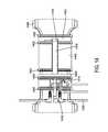
- FIG. 8is a schematic illustrating a cross section of a portion of a DNV sensor with a coil assembly in accordance with some illustrative implementations.
- the portion of the DNV sensor that is illustratedcontains the coil assembly 816 and the photo sensor 820 .
- the coil assembly 816includes six RF elements.
- Each RF elementhas an RF mount that can be used to connect an RF cable 830 .
- each RF elementcan have its own RF feed.
- the each RF elementis fed a unique RF signal.
- sub-combinations of the RF elementsreceive the same RF feed signal. For example, groups of two or three RF elements can receive the same RF feed signal.
- Various connectorscan be used to connect an RF cable 830 to the RF elements, such as a right angle connector 832 .
- the coil assembly 816 , red filter 826 , EMI glass 824 , and photo sensor mounting platecan be held in place using retaining rings 802 .
- a photo sensor 820can be secured to the photo sensor mounting plate 822 , which can be used to locate the photo sensor 820 in the path of light that exits the coil assembly 816 .
- FIG. 10is a cross section illustrating a coil assembly in accordance with some illustrative implementations.
- the light path 1030is shown.
- the light pathallows for light from the lighting element to pass through the coil assembly and through the NV diamond 1040 .
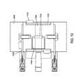
- the coil assemblyincludes four RF elements 1002 and two top and bottom elements 1020 .
- the NV diamond 1040is held in place via a diamond plug 1004 that holds the diamond in the mounting block 1006 .
- the RF elementscan be held together using various means such as element mounting screws 1032 .
- the six total RF elementscan be seen in FIGS. 9 A and 9 B that illustrate a coil assembly in accordance with some illustrative implementations.
- Four side RF elements 902are shown along with two top and bottom RF elements 920 .
- Each RF elementis attached to a center mounting block 904 . Attachment mechanisms such as screws 932 can be used to attach the RF elements to the mounting block.
- a light injection hole 930is the bottom RF element and the light exit hole 910 is in the top RF element. Accordingly, in this implementation light passes through the coil assembly and the diamond in a straight path. In one implementation, the light enters a face of the NV diamond and exits through another face of the NV diamond. As described below, in other implementation the light path through the coil assembly is not straight and may take on multiple paths of egress.
- FIG. 11is a schematic illustrating a side element 1100 of a coil assembly in accordance with some illustrative implementations.
- the side element 1100can include a middle mounting hole and one other mounting hole. In this implementation, there would be side elements that had different mounting hole configurations. As shown in FIG. 11 , the side element 1100 has three mounting holes, but not all mounting holes are required to be used. In one implementation, the middle mounting hole and one of the remaining two mounting holes are used, but all three mounting holes are not used.
- Each side element 1100includes an RF connector 1102 that is used to provide the RF feed signal to the side element.
- FIG. 12is a schematic illustrating a top or bottom element 1200 of a coil assembly in accordance with some illustrative implementations. Similar to the side element 1100 , the top or bottom element 1200 includes an RF connector 1202 for receiving an RF feed signal. The top or bottom element 1200 , however, has only two mounting holes 1204 . The three hole is a light path portion 1230 that allows for light to enter or exit the coil assembly.
- FIG. 13is a schematic illustrating a center mounting block 1300 of a coil assembly in accordance with some illustrative implementations.
- the NV diamondis located within the mounting block 1300 .
- a diamond plugcan be used to hold the NV diamond.
- the mounting block 1300can include a diamond mounting location that provides alignment of the NV diamond.
- the mounting block 1300can include a recess that fits the NV diamond. Once positioned, the diamond plug can be inserted into the mounting block 1300 to hold the diamond in place.
- FIGS. 14-17illustrate another implementation.
- FIG. 14is a cross section illustrating of a portion of a DNV sensor with a coil assembly in accordance with some illustrative implementations.
- a coil assembly 1416holds an NV diamond within an NV diamond sensor.
- the coil assembly 1416can include six RF elements, four side elements and two top and bottom elements (shown in FIGS. 15-17 ).
- RF cables 1430can connect to the RF elements via RF connections 1432 .
- the RF cables 1430are used to provide an RF signal to one or more of the RF elements.
- the RF signalcan be different for each RF element or subsets of the RF elements can receive different RF signals.
- RF feed signalsare used by the RF elements to provide a uniform microwave RF signal to the NV diamond.
- the arrangement of the RF elementsallows the RF elements to also provide the magnetic bias field to the NV diamond.
- lightenters and exits through the top and bottom elements.
- Light that exits the NV diamondcan pass through a red filter 1426 and through a light pipe 1450 that is located within an attenuator 1440 .
- at least a portion of the light pipe 1450is located within the attenuator 1440 .
- Such a configurationallows the photo-sensing array 1420 to be positioned closer to the NV diamond and remain unaffected by the EMI of the sensor.
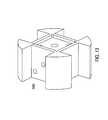
- FIG. 15is a schematic illustrating a coil assembly in accordance with some illustrative implementations.
- FIG. 16is a schematic illustrating a cross section of a coil assembly in accordance with some illustrative implementations.
- the coil assemblyincludes two bottom or top RF elements 1506 and 1606 .
- the top or bottom RF elementsare circular and are larger compared to the side elements 1502 and 1602 .
- In between the top or bottom elementsare the four side elements 1502 and 1602 .
- FIG. 17is a schematic illustrating a side element of a coil assembly in accordance with some illustrative implementations.
- the side elementhas an RF connector 1702 used to provide a feed RF signal to the RF element.
- each of the RF elementscan include multiple stacked spiral antenna coils. These stacked coils can occupy a small footprint and can provide the needed microwave RF field in such that the RF field is uniform over the NV diamond. Additional details regarding RF elements and RF circuit boards that contain RF elements are described in U.S. patent application Ser. No. 15/003,309, entitled “DIAMOND NITROGEN VACANCY SENSOR WITH DUAL RF SOURCES,” filed on the same day as this application, the contents of which are hereby incorporated by reference.
- each RF side element and top and bottom RF elementscan include an RF element or an RF circuit board.
- the NV diamond 1622is located within the six RF elements.
- the RF elementscan be held together by mounting screws 1510 and 1610 .
- a light injection portion 1504 of the top RF elementallows light to enter the coil assembly and enter the NV diamond.
- the bottom portionincludes a corresponding light egress portion 1620 .
- the NV diamondcan fit within a mounting block 1608 and be held in position via a diamond plug 1624 .
- FIGS. 18-24illustrate another implementation.
- lightenters the NV diamond through an edge of the NV diamond and exits through multiple faces of the NV diamond. How light enters and exits the NV diamond is based upon the orientation of the NV diamond relative to the light source.
- the NV diamondcan be repositioned to allow light to enter and exit from edges, faces, and/or both edges and faces.
- FIG. 18is a schematic illustrating a portion of a DNV sensor with a coil assembly in accordance with some illustrative implementations. Similar to other implementations, the DNV sensor includes a light source heatsink 1802 and 1902 , a mounting clamp 1804 for the heatsink 1802 , a lens tube 1806 , a focusing lens tube 1818 , a coil assembly 1816 located, and red filters and photo sensor assemblies 1814 , and a lens tube rotation mount 1812 and 1912 .
- FIG. 19is a schematic illustrating a cross section of a portion of a DNV sensor with a coil assembly in accordance with some illustrative implementations. In this implementation, the light source is an LED 1906 .
- a thermal electric cooler 1904can be used to provide cooling for the LED 1906 .
- Light from the LED 1906can be focused using lens 1918 . The focused light enters the NV diamond that is located within the coil assembly 1916 .
- FIG. 20is a schematic illustrating a cross section of a portion of a DNV sensor with a coil assembly in accordance with some illustrative implementations.
- the NV diamond 2040 within the coil assemblycan be seen.
- the light the exits the NV diamond 2040travels one of two light pipes 1914 .
- at least a portion of the light pipeis located within an attenuator.
- the NV diamond 2040can be held in place within the coil assembly via center mounting blocks 2050 .
- the mounting blocks and the coil assemblycan be held in place using retaining rings 2052 .
- RF cables 2030connect to the RF elements via RF connectors 2032 to provide an RF feed signal to the RF elements as described in greater detail below.
- FIG. 21is a schematic illustrating a coil assembly in accordance with some illustrative implementations.
- FIG. 22is a schematic illustrating a cross section of a coil assembly in accordance with some illustrative implementations.
- FIG. 21shows four side elements 2014 and 2242 located between the top and bottom RF elements 2112 and 2212 .
- the center mounting blocks 2108 and 2208 and retaining plate 2106 and 2206are also shown.
- lightenters the NV diamond 2240 at an edge. The light reaches the NV diamond via a light injection opening 2101 and 2202 . Light exits the NV diamond 2240 substantially orthogonal to the ingress path through two light exit holes 2110 .
- a second light exit holeis opposite of the illustrated light exit hole 2110 . In FIG. 22 , the second light exit hold is behind the NV diamond 2240 .
- FIG. 23is a schematic illustrating a side element of a coil assembly in accordance with some illustrative implementations.
- the individual side elementincludes an RF connector 2304 and a light egress portion 2302 .
- the side elementdoes not include any attachment holes. Rather, the side elements can be held in place within the coil assembly using the top and bottom elements as illustrated in FIGS. 24A and 24B .
- FIGS. 24A and 24Bare schematics illustrating top and bottom elements of a coil assembly in accordance with some illustrative implementations.
- the top elementincludes slots 2406 for aligning and holding into position the four RF side elements.
- the light injection hole 2404is also shown.
- RF connectors 2404 located on both the top RF element and the bottom RF elementallow for separate RF feeds to be separately applied to the top and bottom RF elements.
- phrases such as an aspect, the aspect, another aspect, some aspects, one or more aspects, an implementation, the implementation, another implementation, some implementations, one or more implementations, an embodiment, the embodiment, another embodiment, some embodiments, one or more embodiments, a configuration, the configuration, another configuration, some configurations, one or more configurations, the subject technology, the disclosure, the present disclosure, other variations thereof and alikeare for convenience and do not imply that a disclosure relating to such phrase(s) is essential to the subject technology or that such disclosure applies to all configurations of the subject technology.
- a disclosure relating to such phrase(s)may apply to all configurations, or one or more configurations.
- a disclosure relating to such phrase(s)may provide one or more examples.
- a phrase such as an aspect or some aspectsmay refer to one or more aspects and vice versa, and this applies similarly to other foregoing phrases
Landscapes
- Physics & Mathematics (AREA)
- Condensed Matter Physics & Semiconductors (AREA)
- General Physics & Mathematics (AREA)
- Engineering & Computer Science (AREA)
- Power Engineering (AREA)
- Measuring Magnetic Variables (AREA)
- Investigating, Analyzing Materials By Fluorescence Or Luminescence (AREA)
Abstract
Description
The present invention relates generally to a sensor assembly of a magnetic sensor.
Magnetic sensors based on a nitrogen vacancy (NV) center in diamond are known. Diamond NV (DNV) sensors may provide good sensitivity for magnetic field measurements. Such magnetic sensor systems often include components such an optical excitation source, an RF excitation source, and optical detectors. These components are all formed on different substrates or as separate components mechanically supported together.
Systems and apparatuses are described that use multiple radio frequency elements for providing a uniform magnetic field over an NV diamond and also providing a magnetic bias for the NV diamond. In one implementation, a magnetic field sensor assembly includes four side radio frequency (RF) elements. Each side RF element includes an RF connection. The magnetic field sensor also includes four side RF feed cables connected to one of the four side RF elements such that each side RF element is connected to one RF feed cable that provides a feed signal to the side RF element. The magnetic field sensor also includes a top RF element and a bottom element along with a top RF element feed cable and a bottom RF feed cable. The top and bottom feed cables provide a RF feed signal to the top and bottom RF elements respectively. The four side RF side elements, the top RF element, and the bottom RF element are arranged in a cube formation. A nitrogen-vacancy (NV) center diamond is located within the cube formation. The side RF elements, top RF element, and bottom RF element generate a microwave signal that is uniform over the NV center diamond, and also generate a magnetic bias field to the NV center diamond.
In other implementations, a magnetic field sensor assembly includes four side radio frequency (RF) elements. Each side RF element includes an RF connection. The magnetic field sensor also includes four side RF feed cables connected to one of the four side RF elements such that each side RF element is connected to one RF feed cable that provides a feed signal to the side RF element. The magnetic field sensor also includes a top RF element and a bottom element along with a top RF element feed cable and a bottom RF feed cable. The top and bottom feed cables provide a RF feed signal to the top and bottom RF elements respectively. The four side RF side elements, the top RF element, and the bottom RF element are arranged in a column formation. A nitrogen-vacancy (NV) center diamond is located within the column formation. The side RF elements, top RF element, and bottom RF element generate a microwave signal that is uniform over the NV center diamond, and also generate a magnetic bias field to the NV center diamond.
The foregoing and other features of the present disclosure will become more fully apparent from the following description and appended claims, taken in conjunction with the accompanying drawings. Understanding that these drawings depict only several implementations in accordance with the disclosure and are, therefore, not to be considered limiting of its scope, the disclosure will be described with additional specificity and detail through use of the accompanying drawings.
Nitrogen-vacancy (NV) centers are defects in a diamond's crystal structure. Synthetic diamonds can be created that have these NV centers. NV centers generate red light when excited by a light source, such as a green light source, and microwave radiation. When an excited NV center diamond is exposed to an external magnetic field the frequency of the microwave radiation at which the diamond generates red light and the intensity of the light change. By measuring this change and comparing the change to the microwave frequency that the diamond generates red light at when not in the presence of the external magnetic field, the external magnetic field strength can be determined. Accordingly, NV centers can be used as part of a magnetic field sensor.
In various implementations, microwave RF excitation is needed in a DNV sensor. The more uniform the microwave signal is across the NV centers in the diamond the better and more accurate an NV sensor will perform. Uniformity, however, can be difficult to achieve. Also, the larger the bandwidth of the element, the better the NV sensor will perform. Large bandwidth, such as octave bandwidth, however, can be difficult to achieve. Various NV sensors respond to a microwave frequency that is not easily generated by RF antenna elements that are comparable to the small size of the NV sensor. In addition, RF elements should reduce the amount of light within the sensor that is blocked by the RF elements. When a single RF element is used, the RF element is offset from the NV diamond when the RF element maximized the faces and edges of the diamond that light can enter or leave. Moving the RF element away from the NV diamond, however, impacts the uniformity of strength of the RF that is applied to the NV diamond.
The present inventors have realized that a configuration of RF elements can provide both the magnetic bias and the RF field for a DNV magnetic system. The magnetic bias provided by various implementations can be a uniform magnetic field along three polarizations of the axes of the coils used in various implementations. As described in greater detail below, using the various configuration of RF elements in a DNV sensor can allow greater access to the edges and faces of the diamond for light input and egress, while also providing a relatively uniform field in addition to a bias magnetic field. In various implementations, a NV diamond is contained within a housing. The housing can have six sides, each side operating as an RF element to apply a uniform RF field to the NV diamond. In addition, the six RF elements can also provide the magnetic bias for the NV sensor. Further, the six sides can be configured to allow various different configurations for light ingress and egress. The spacing and size of the RF elements allow for all edges and faces of the diamond to be used for light ingress and egress. The more light captured by photo-sensing elements of a DNV sensor results in an increased efficiency of the sensor. In addition, the multiple polarization RF field of various implementations can increase the number of NV centers that are efficiently excited. In addition, the multiple polarization RF field can be used to differentially control the polarizations to achieve higher order functionality from the DNV sensor.
NV Center, its Electronic Structure, and Optical and RF Interaction
The nitrogen vacancy (NV) center in diamond comprises a substitutional nitrogen atom in a lattice site adjacent a carbon vacancy as shown inFIG. 1 . The NV center may have four orientations, each corresponding to a different crystallographic orientation of the diamond lattice.
The NV center may exist in a neutral charge state or a negative charge state. Conventionally, the neutral charge state uses the nomenclature NV0, while the negative charge state uses the nomenclature NV, which is adopted in this description.
The NV center has a number of electrons including three unpaired electrons, each one from the vacancy to a respective of the three carbon atoms adjacent to the vacancy, and a pair of electrons between the nitrogen and the vacancy. The NV center, which is in the negatively charged state, also includes an extra electron.
The NV center has rotational symmetry, and as shown inFIG. 2 , has a ground state, which is a spin triplet with3A2symmetry with one spin state ms=0, and two further spin states ms=+1, and ms=−1. In the absence of an external magnetic field, the ms=±1 energy levels are offset from the ms=0 due to spin-spin interactions, and the ms=±1 energy levels are degenerate, i.e., they have the same energy. The ms=0 spin state energy level is split from the ms=±1 energy levels by an energy of 2.87 GHz for a zero external magnetic field.
Introducing an external magnetic field with a component along the NV axis lifts the degeneracy of the ms=±1 energy levels, splitting the energy levels ms=±1 by an amount 2 gμBBz, where g is the g-factor, μBis the Bohr magneton, and Bz is the component of the external magnetic field along the NV axis. This relationship is correct for a first order and inclusion of higher order corrections is a straight forward matter and will not affect the computational and logic steps in the systems and methods described below.
The NV center electronic structure further includes an excited triplet state3E with corresponding ms=0 and ms=±1 spin states. The optical transitions between the ground state3A2and the excited triplet3E are predominantly spin conserving, meaning that the optical transitions are between initial and final states which have the same spin. For a direct transition between the excited triplet3E and the ground state3A2, a photon of red light is emitted with a photon energy corresponding to the energy difference between the energy levels of the transitions.
There is, however, an alternate non-radiative decay route from the triplet3E to the ground state3A2via intermediate electron states, which are thought to be intermediate singlet states A, E with intermediate energy levels. Significantly, the transition rate from the ms=±1 spin states of the excited triplet3E to the intermediate energy levels is significantly greater than the transition rate from the ms=0 spin state of the excited triplet3E to the intermediate energy levels. The transition from the singlet states A, E to the ground state triplet3A2predominantly decays to the ms=0 spin state over the ms=±1 spin states. These features of the decay from the excited triplet3E state via the intermediate singlet states A, E to the ground state triplet3A2allows that if optical excitation is provided to the system, the optical excitation will eventually pump the NV center into the ms=0 spin state of the ground state3A2. In this way, the population of the ms=0 spin state of the ground state3A2may be “reset” to a maximum polarization determined by the decay rates from the triplet3E to the intermediate singlet states.
Another feature of the decay is that the fluorescence intensity due to optically stimulating the excited triplet3E state is less for the ms=±1 states than for the ms=0 spin state. This is so because the decay via the intermediate states does not result in a photon emitted in the fluorescence band, and because of the greater probability that the ms=±1 states of the excited triplet3E state will decay via the non-radiative decay path. The lower fluorescence intensity for the ms=±1 states than for the ms=0 spin state allows the fluorescence intensity to be used to determine the spin state. As the population of the ms=±1 states increases relative to the ms=0 spin, the overall fluorescence intensity will be reduced.
NV Center, or Magneto-Optical Defect Center, Magnetic Sensor System
TheRF excitation source 330 may be a microwave coil, for example. TheRF excitation source 330 when emitting RF radiation with a photon energy resonant with the transition energy between ground ms=0 spin state and the ms=+1 spin state excites a transition between those spin states. For such a resonance, the spin state cycles between ground ms=0 spin state and the ms=+1 spin state, reducing the population in the ms=0 spin state and reducing the overall fluorescence at resonance. Similarly resonance occurs between the ms=0 spin state and the ms=−1 spin state of the ground state when the photon energy of the RF radiation emitted by the RF excitation source is the difference in energies of the ms=0 spin state and the ms=−1 spin state. At resonance between the ms=0 spin state and the ms=−1 spin state, or between the ms=0 spin state and the ms=+1 spin state, there is a decrease in the fluorescence intensity.
Theoptical excitation source 310 may be a laser or a light emitting diode, for example, which emits light in the green, for example. Theoptical excitation source 310 induces fluorescence in the red, which corresponds to an electronic transition from the excited state to the ground state. Light from theNV diamond material 320 is directed through theoptical filter 350 to filter out light in the excitation band (in the green for example), and to pass light in the red fluorescence band, which in turn is detected by thedetector 340. The opticalexcitation light source 310, in addition to exciting fluorescence in thediamond material 320, also serves to reset the population of the ms=0 spin state of the ground state3A2to a maximum polarization, or other desired polarization.
For continuous wave excitation, theoptical excitation source 310 continuously pumps the NV centers, and theRF excitation source 330 sweeps across a frequency range which includes the zero splitting (when the ms=±1 spin states have the same energy) photon energy of 2.87 GHz. The fluorescence for an RF sweep corresponding to adiamond material 320 with NV centers aligned along a single direction is shown inFIG. 4 for different magnetic field components Bz along the NV axis, where the energy splitting between the ms=−1 spin state and the ms=+1 spin state increases with Bz. Thus, the component Bz may be determined. Optical excitation schemes other than continuous wave excitation are contemplated, such as excitation schemes involving pulsed optical excitation, and pulsed RF excitation. Examples, of pulsed excitation schemes include Ramsey pulse sequence, and spin echo pulse sequence.
In general, thediamond material 320 will have NV centers aligned along directions of four different orientation classes.FIG. 5 illustrates fluorescence as a function of RF frequency for the case where thediamond material 320 has NV centers aligned along directions of four different orientation classes. In this case, the component Bz along each of the different orientations may be determined. These results along with the known orientation of crystallographic planes of a diamond lattice allows not only the magnitude of the external magnetic field to be determined, but also the direction of the magnetic field.
WhileFIG. 3 illustrates an NV centermagnetic sensor system 300 withNV diamond material 320 with a plurality of NV centers, in general the magnetic sensor system may instead employ a different magneto-optical defect center material, with a plurality of magneto-optical defect centers. The electronic spin state energies of the magneto-optical defect centers shift with magnetic field, and the optical response, such as fluorescence, for the different spin states is not the same for all of the different spin states. In this way, the magnetic field may be determined based on optical excitation, and possibly RF excitation, in a corresponding way to that described above with NV diamond material.
TheRF excitation source 630 may be a microwave coil, for example. TheRF excitation source 630 is controlled to emit RF radiation with a photon energy resonant with the transition energy between the ground ms=0 spin state and the ms=±1 spin states as discussed above with respect toFIG. 3 .
Theoptical excitation source 610 may be a laser or a light emitting diode, for example, which emits light in the green, for example. Theoptical excitation source 610 induces fluorescence in the red, which corresponds to an electronic transition from the excited state to the ground state. Light from theNV diamond material 620 is directed through theoptical filter 650 to filter out light in the excitation band (in the green for example), and to pass light in the red fluorescence band, which in turn is detected by theoptical detector 640. The EMI filter660 is arranged between theoptical filter 650 and theoptical detector 640 and suppresses conducted interference. The opticalexcitation light source 610, in addition to exciting fluorescence in theNV diamond material 620, also serves to reset the population of the ms=0 spin state of the ground state3A2to a maximum polarization, or other desired polarization.
Thecontroller 680 is arranged to receive a light detection signal from theoptical detector 640 and to control theoptical excitation source 610 and theRF excitation source 630. The controller may include aprocessor 682 and amemory 684, in order to control the operation of theoptical excitation source 610 and theRF excitation source 630. Thememory 684, which may include a nontransitory computer readable medium, may store instructions to allow the operation of theoptical excitation source 610 and theRF excitation source 630 to be controlled.
According to one embodiment of operation, thecontroller 680 controls the operation such that theoptical excitation source 610 continuously pumps the NV centers of theNV diamond material 620. TheRF excitation source 630 is controlled to continuously sweep across a frequency range which includes the zero splitting (when the ms=±1 spin states have the same energy) photon energy of 2.87 GHz. When the photon energy of the RF radiation emitted by theRF excitation source 630 is the difference in energies of the ms=0 spin state and the ms=−1 or ms=+1 spin state, the overall fluorescence intensity is reduced at resonance, as discussed above with respect toFIG. 3 . In this case, there is a decrease in the fluorescence intensity when the RF energy resonates with an energy difference of the ms=0 spin state and the ms=−1 or ms=+1 spin states. In this way the component of the magnetic field Bz along the NV axis may be determined by the difference in energies between the ms=−1 and the ms=+1 spin states.
As noted above, thediamond material 620 will have NV centers aligned along directions of four different orientation classes, and the component Bz along each of the different orientations may be determined based on the difference in energy between the ms=−1 and the ms=+1 spin states for the respective orientation classes. In certain cases, however, it may be difficult to determine which energy splitting corresponds to which orientation class, due to overlap of the energies, etc. Thebias magnet 670 provides a magnetic field, which is preferably uniform on theNV diamond material 620, to separate the energies for the different orientation classes, so that they may be more easily identified.
InFIG. 7 , the portion of the illustrated DNV sensor includes aheatsink 702 that can connect to the rest of the DNV sensor via a mounting clamp. Not shown is a light element, such as a laser or LED that is located within or near theheatsink 702. Light from the light element travels through alens tube 706 through a focusinglens tube 718 and through acoil assembly 716 that includes the NV diamond. Light passes into thecoil assembly 716 through the NV diamond and exits the coil assembly. Light that exits the coil assembly passes through a red filter to aphoto sensor assembly 714. Thecoil assembly 716, red filter, and photo sensor can all be housed in alens tube 710 that can be coupled tolens tube 718 via alens tube coupler 708. A lenstube rotation mount 712 allows a rotation adjustment element to be attached that allows the coil assembly to be rotated in relation to the light element.
The coil assembly includes fourRF elements 1002 and two top andbottom elements 1020. TheNV diamond 1040 is held in place via adiamond plug 1004 that holds the diamond in themounting block 1006. The RF elements can be held together using various means such aselement mounting screws 1032. The six total RF elements can be seen in FIGS.9A and9B that illustrate a coil assembly in accordance with some illustrative implementations. Fourside RF elements 902 are shown along with two top andbottom RF elements 920. Each RF element is attached to a center mounting block904. Attachment mechanisms such asscrews 932 can be used to attach the RF elements to the mounting block. In the illustrated implementation, alight injection hole 930 is the bottom RF element and thelight exit hole 910 is in the top RF element. Accordingly, in this implementation light passes through the coil assembly and the diamond in a straight path. In one implementation, the light enters a face of the NV diamond and exits through another face of the NV diamond. As described below, in other implementation the light path through the coil assembly is not straight and may take on multiple paths of egress.
TheNV diamond 1622 is located within the six RF elements. The RF elements can be held together by mountingscrews light injection portion 1504 of the top RF element allows light to enter the coil assembly and enter the NV diamond. The bottom portion includes a correspondinglight egress portion 1620. The NV diamond can fit within amounting block 1608 and be held in position via adiamond plug 1624.
The foregoing description is provided to enable a person skilled in the art to practice the various configurations described herein. While the subject technology has been particularly described with reference to the various figures and configurations, it should be understood that these are for illustration purposes only and should not be taken as limiting the scope of the subject technology. In some aspects, the subject technology may be used in various markets, including for example and without limitation, advanced sensors and mobile space platforms.
There may be many other ways to implement the subject technology. Various functions and elements described herein may be partitioned differently from those shown without departing from the scope of the subject technology. Various modifications to these embodiments may be readily apparent to those skilled in the art, and generic principles defined herein may be applied to other embodiments. Thus, many changes and modifications may be made to the subject technology, by one having ordinary skill in the art, without departing from the scope of the subject technology.
Phrases such as an aspect, the aspect, another aspect, some aspects, one or more aspects, an implementation, the implementation, another implementation, some implementations, one or more implementations, an embodiment, the embodiment, another embodiment, some embodiments, one or more embodiments, a configuration, the configuration, another configuration, some configurations, one or more configurations, the subject technology, the disclosure, the present disclosure, other variations thereof and alike are for convenience and do not imply that a disclosure relating to such phrase(s) is essential to the subject technology or that such disclosure applies to all configurations of the subject technology. A disclosure relating to such phrase(s) may apply to all configurations, or one or more configurations. A disclosure relating to such phrase(s) may provide one or more examples. A phrase such as an aspect or some aspects may refer to one or more aspects and vice versa, and this applies similarly to other foregoing phrases
A reference to an element in the singular is not intended to mean “one and only one” unless specifically stated, but rather “one or more.” The term “some” refers to one or more. Underlined and/or italicized headings and subheadings are used for convenience only, do not limit the subject technology, and are not referred to in connection with the interpretation of the description of the subject technology. All structural and functional equivalents to the elements of the various embodiments described throughout this disclosure that are known or later come to be known to those of ordinary skill in the art are expressly incorporated herein by reference and intended to be encompassed by the subject technology. Moreover, nothing disclosed herein is intended to be dedicated to the public regardless of whether such disclosure is explicitly recited in the above description.
Claims (21)
1. A magnetic field sensor assembly comprising:
four side radio frequency (RF) elements, each side RF element comprising an RF connection;
four side RF feed cables operably connected to one of the four side RF elements such that each side RF element is connected to one RF feed cable that provides a feed signal to the side RF element;
a top RF element;
a top RF element feed cable that provides a top RF feed signal to the top RF element;
a bottom RF element;
a bottom RF element feed cable that provides a bottom RF feed signal to the bottom RF element, wherein the four side RF side elements, the top RF element, and the bottom RF element are arranged in a cube formation; and
a nitrogen-vacancy (NV) center diamond located within the cube formation, wherein the side RF elements, top RF element, and bottom RF element generate a microwave signal that is uniform over the NV center diamond, and wherein the side RF elements, top RF element, and bottom RF element generate a magnetic bias field to the NV center diamond.
2. The magnetic field sensor assembly ofclaim 1 , wherein the top RF element includes a light ingress portion, wherein the bottom RF element includes a light egress portion, and wherein the cube formation includes a light path through the cube formation and through the NV center diamond via the light ingress portion and the light egress portion.
3. The magnetic field sensor assembly ofclaim 2 , wherein light ingress into the NV diamond at a first face of the NV diamond.
4. The magnetic field sensor assembly ofclaim 3 , wherein light egresses out of the NV diamond at a second face of the NV diamond.
5. The magnetic field sensor assembly ofclaim 2 , further comprising a photo sensor that receives the light that egresses from the light egress portion.
6. The magnetic field sensor assembly ofclaim 1 , wherein each feed signal is a different RF feed signal.
7. The magnetic field sensor assembly ofclaim 1 , wherein the top RF element includes a light ingress portion, wherein a first RF side element includes a light egress portion, and wherein the cube formation includes a light path through the cube formation and through the NV center diamond via the light ingress portion and the light egress portion.
8. The magnetic field sensor assembly ofclaim 7 , wherein a second RF side element includes a second light egress portion that forms a second light egress path.
9. The magnetic field assembly ofclaim 1 , wherein the NV center diamond is held with the cube formation via a mounting block that contains a diamond recess and a diamond plug that holds with NV center diamond in the diamond recess.
10. A magnetic field sensor assembly comprising:
four side radio frequency (RF) elements, each side RF element comprising an RF connection;
four side RF feed cables operably connected to one of the four side RF elements such that each side RF element is connected to one RF feed cable that provides a feed signal to the side RF element;
a top RF element;
a top RF element feed cable that provides a top RF feed signal to the top RF element;
a bottom RF element;
a bottom RF element feed cable that provides a bottom RF feed signal to the bottom RF element, wherein the four side RF side elements, the top RF element, and the bottom RF element are arranged in a column formation; and
a nitrogen-vacancy (NV) center diamond located within the column formation, wherein the side RF elements, top RF element, and bottom RF element generate a microwave signal that is uniform over the NV center diamond, and wherein the side RF elements, top RF element, and bottom RF element generate a magnetic bias field to the NV center diamond.
11. The magnetic field sensor assembly ofclaim 10 , wherein the top RF element and the bottom RF element are larger than RF side elements.
12. The magnetic field sensor assembly ofclaim 10 , wherein the top RF element includes a light ingress portion, wherein the bottom RF element includes a light egress portion, and wherein the column formation includes a light path through the column formation and through the NV center diamond via the light ingress portion and the light egress portion.
13. The magnetic field sensor assembly ofclaim 12 , wherein light ingress into the NV diamond at a first face of the NV diamond.
14. The magnetic field sensor assembly ofclaim 13 , wherein light egresses out of the NV diamond at a second face of the NV diamond.
15. The magnetic field sensor assembly ofclaim 12 , further comprising a photo sensor that receives the light that egresses from the light egress portion.
16. The magnetic field sensor assembly ofclaim 10 , wherein each feed signal is a different RF feed signal.
17. The magnetic field sensor assembly ofclaim 10 , wherein the top RF element includes a light ingress portion, wherein a first RF side element includes a light egress portion, and wherein the column formation includes a light path through the column formation and through the NV center diamond via the light ingress portion and the light egress portion.
18. The magnetic field sensor assembly ofclaim 17 , wherein a second RF side element includes a second light egress portion that forms a second light egress path.
19. The magnetic field assembly ofclaim 10 , wherein the NV center diamond is held with the column formation via a mounting block that contains a diamond recess and a diamond plug that holds with NV center diamond in the diamond recess.
20. The magnetic field assembly ofclaim 10 , wherein the four RF side elements are held in place via the top RF element and the bottom RF element.
21. The magnetic field assembly ofclaim 10 , wherein the top RF element comprises four side element alignment portions that align the four side RF elements within the column formation.
Priority Applications (15)
| Application Number | Priority Date | Filing Date | Title |
|---|---|---|---|
| PCT/US2016/014392WO2017127095A1 (en) | 2016-01-21 | 2016-01-21 | Diamond nitrogen vacancy sensor with common rf and magnetic fields generator |
| KR1020177023300AKR20170140156A (en) | 2015-01-23 | 2016-01-21 | DNV magnetic field detector |
| AU2016209217AAU2016209217A1 (en) | 2015-01-23 | 2016-01-21 | DNV magnetic field detector |
| GB1813544.2AGB2562193B (en) | 2016-01-21 | 2016-01-21 | Diamond nitrogen vacancy sensor with common RF and magnetic fields generator |
| CA2974688ACA2974688A1 (en) | 2015-01-23 | 2016-01-21 | Dnv magnetic field detector |
| AU2016388316AAU2016388316A1 (en) | 2016-01-21 | 2016-01-21 | Diamond nitrogen vacancy sensor with common RF and magnetic fields generator |
| US15/003,298US9551763B1 (en) | 2016-01-21 | 2016-01-21 | Diamond nitrogen vacancy sensor with common RF and magnetic fields generator |
| EP16740794.9AEP3248021A4 (en) | 2015-01-23 | 2016-01-21 | Dnv magnetic field detector |
| BR112017015746ABR112017015746A2 (en) | 2015-01-23 | 2016-01-21 | dnv magnetic field detector |
| PCT/US2016/014403WO2016118791A1 (en) | 2015-01-23 | 2016-01-21 | Dnv magnetic field detector |
| US15/179,957US9910105B2 (en) | 2014-03-20 | 2016-06-10 | DNV magnetic field detector |
| US15/218,821US9823314B2 (en) | 2016-01-21 | 2016-07-25 | Magnetometer with a light emitting diode |
| US15/351,862US9720055B1 (en) | 2016-01-21 | 2016-11-15 | Magnetometer with light pipe |
| US15/372,201US20170212187A1 (en) | 2016-01-21 | 2016-12-07 | Magneto-optical defect sensor with common rf and magnetic fields generator |
| US15/912,461US10725124B2 (en) | 2014-03-20 | 2018-03-05 | DNV magnetic field detector |
Applications Claiming Priority (1)
| Application Number | Priority Date | Filing Date | Title |
|---|---|---|---|
| US15/003,298US9551763B1 (en) | 2016-01-21 | 2016-01-21 | Diamond nitrogen vacancy sensor with common RF and magnetic fields generator |
Related Parent Applications (3)
| Application Number | Title | Priority Date | Filing Date |
|---|---|---|---|
| PCT/US2016/014392ContinuationWO2017127095A1 (en) | 2016-01-21 | 2016-01-21 | Diamond nitrogen vacancy sensor with common rf and magnetic fields generator |
| US15/003,292Continuation-In-PartUS10006973B2 (en) | 2014-03-20 | 2016-01-21 | Magnetometer with a light emitting diode |
| US15/003,396Continuation-In-PartUS20170068012A1 (en) | 2014-03-20 | 2016-01-21 | Magnetic wake detector |
Related Child Applications (3)
| Application Number | Title | Priority Date | Filing Date |
|---|---|---|---|
| US15/003,309Continuation-In-PartUS10520558B2 (en) | 2014-03-20 | 2016-01-21 | Diamond nitrogen vacancy sensor with nitrogen-vacancy center diamond located between dual RF sources |
| US15/003,206Continuation-In-PartUS9824597B2 (en) | 2014-03-20 | 2016-01-21 | Magnetic navigation methods and systems utilizing power grid and communication network |
| US15/372,201ContinuationUS20170212187A1 (en) | 2016-01-21 | 2016-12-07 | Magneto-optical defect sensor with common rf and magnetic fields generator |
Publications (1)
| Publication Number | Publication Date |
|---|---|
| US9551763B1true US9551763B1 (en) | 2017-01-24 |
Family
ID=57795122
Family Applications (3)
| Application Number | Title | Priority Date | Filing Date |
|---|---|---|---|
| US15/003,298Expired - Fee RelatedUS9551763B1 (en) | 2014-03-20 | 2016-01-21 | Diamond nitrogen vacancy sensor with common RF and magnetic fields generator |
| US15/218,821ActiveUS9823314B2 (en) | 2016-01-21 | 2016-07-25 | Magnetometer with a light emitting diode |
| US15/372,201AbandonedUS20170212187A1 (en) | 2016-01-21 | 2016-12-07 | Magneto-optical defect sensor with common rf and magnetic fields generator |
Family Applications After (2)
| Application Number | Title | Priority Date | Filing Date |
|---|---|---|---|
| US15/218,821ActiveUS9823314B2 (en) | 2016-01-21 | 2016-07-25 | Magnetometer with a light emitting diode |
| US15/372,201AbandonedUS20170212187A1 (en) | 2016-01-21 | 2016-12-07 | Magneto-optical defect sensor with common rf and magnetic fields generator |
Country Status (4)
| Country | Link |
|---|---|
| US (3) | US9551763B1 (en) |
| AU (1) | AU2016388316A1 (en) |
| GB (1) | GB2562193B (en) |
| WO (1) | WO2017127095A1 (en) |
Cited By (59)
| Publication number | Priority date | Publication date | Assignee | Title |
|---|---|---|---|---|
| US20160334474A1 (en)* | 2014-01-20 | 2016-11-17 | Japan Science And Technology Agency | Diamond crystal, diamond devices, magnetic sensor, magnetic sensor system, and method for manufacturing sensor array |
| US20170123015A1 (en)* | 2015-11-04 | 2017-05-04 | Lockheed Martin Corporation | Magnetic band-pass filter |
| US9720055B1 (en) | 2016-01-21 | 2017-08-01 | Lockheed Martin Corporation | Magnetometer with light pipe |
| WO2017173548A1 (en)* | 2016-04-08 | 2017-10-12 | Socpra Sciences Et Genie S.E.C. | Vectorial magnetometer and associated methods for sensing an amplitude and orientation of a magnetic field |
| US9823314B2 (en) | 2016-01-21 | 2017-11-21 | Lockheed Martin Corporation | Magnetometer with a light emitting diode |
| US9823381B2 (en) | 2014-03-20 | 2017-11-21 | Lockheed Martin Corporation | Mapping and monitoring of hydraulic fractures using vector magnetometers |
| US9824597B2 (en) | 2015-01-28 | 2017-11-21 | Lockheed Martin Corporation | Magnetic navigation methods and systems utilizing power grid and communication network |
| US20170343617A1 (en)* | 2016-05-31 | 2017-11-30 | Lockheed Martin Corporation | Selected volume continuous illumination magnetometer |
| US9835694B2 (en) | 2016-01-21 | 2017-12-05 | Lockheed Martin Corporation | Higher magnetic sensitivity through fluorescence manipulation by phonon spectrum control |
| WO2017209826A1 (en)* | 2016-05-31 | 2017-12-07 | Lockheed Martin Corporation | Magneto-optical defect center magnetometer |
| US9845153B2 (en) | 2015-01-28 | 2017-12-19 | Lockheed Martin Corporation | In-situ power charging |
| US9853837B2 (en) | 2014-04-07 | 2017-12-26 | Lockheed Martin Corporation | High bit-rate magnetic communication |
| US9910105B2 (en) | 2014-03-20 | 2018-03-06 | Lockheed Martin Corporation | DNV magnetic field detector |
| US9910104B2 (en) | 2015-01-23 | 2018-03-06 | Lockheed Martin Corporation | DNV magnetic field detector |
| RU2654967C1 (en)* | 2017-05-02 | 2018-05-23 | Федеральное государственное бюджетное научное учреждение "Федеральный исследовательский центр Институт прикладной физики Российской академии наук" (ИПФ РАН) | Method of measuring the characteristics of the magnetic field |
| US10006973B2 (en) | 2016-01-21 | 2018-06-26 | Lockheed Martin Corporation | Magnetometer with a light emitting diode |
| US20180275207A1 (en)* | 2017-03-24 | 2018-09-27 | Lockheed Martin Corporation | Magneto-optical defect center sensor with vivaldi rf antenna array |
| WO2018174915A1 (en)* | 2017-03-24 | 2018-09-27 | Lockheed Martin Corporation | Magneto-optical defect center sensor with vivaldi rf antenna array |
| WO2018174910A1 (en)* | 2017-03-24 | 2018-09-27 | Lockheed Martin Corporation | Standing-wave radio frequency exciter |
| US10088452B2 (en) | 2016-01-12 | 2018-10-02 | Lockheed Martin Corporation | Method for detecting defects in conductive materials based on differences in magnetic field characteristics measured along the conductive materials |
| US10088336B2 (en) | 2016-01-21 | 2018-10-02 | Lockheed Martin Corporation | Diamond nitrogen vacancy sensed ferro-fluid hydrophone |
| US10120039B2 (en) | 2015-11-20 | 2018-11-06 | Lockheed Martin Corporation | Apparatus and method for closed loop processing for a magnetic detection system |
| US10126377B2 (en) | 2016-05-31 | 2018-11-13 | Lockheed Martin Corporation | Magneto-optical defect center magnetometer |
| US10145910B2 (en) | 2017-03-24 | 2018-12-04 | Lockheed Martin Corporation | Photodetector circuit saturation mitigation for magneto-optical high intensity pulses |
| US10168393B2 (en) | 2014-09-25 | 2019-01-01 | Lockheed Martin Corporation | Micro-vacancy center device |
| US10228429B2 (en) | 2017-03-24 | 2019-03-12 | Lockheed Martin Corporation | Apparatus and method for resonance magneto-optical defect center material pulsed mode referencing |
| US10241158B2 (en) | 2015-02-04 | 2019-03-26 | Lockheed Martin Corporation | Apparatus and method for estimating absolute axes' orientations for a magnetic detection system |
| US10274550B2 (en) | 2017-03-24 | 2019-04-30 | Lockheed Martin Corporation | High speed sequential cancellation for pulsed mode |
| US10277208B2 (en) | 2014-04-07 | 2019-04-30 | Lockheed Martin Corporation | Energy efficient controlled magnetic field generator circuit |
| US10281550B2 (en) | 2016-11-14 | 2019-05-07 | Lockheed Martin Corporation | Spin relaxometry based molecular sequencing |
| US10317279B2 (en) | 2016-05-31 | 2019-06-11 | Lockheed Martin Corporation | Optical filtration system for diamond material with nitrogen vacancy centers |
| US10333588B2 (en) | 2015-12-01 | 2019-06-25 | Lockheed Martin Corporation | Communication via a magnio |
| US10330744B2 (en) | 2017-03-24 | 2019-06-25 | Lockheed Martin Corporation | Magnetometer with a waveguide |
| US10338163B2 (en) | 2016-07-11 | 2019-07-02 | Lockheed Martin Corporation | Multi-frequency excitation schemes for high sensitivity magnetometry measurement with drift error compensation |
| US10338162B2 (en) | 2016-01-21 | 2019-07-02 | Lockheed Martin Corporation | AC vector magnetic anomaly detection with diamond nitrogen vacancies |
| US10338164B2 (en) | 2017-03-24 | 2019-07-02 | Lockheed Martin Corporation | Vacancy center material with highly efficient RF excitation |
| US10345395B2 (en) | 2016-12-12 | 2019-07-09 | Lockheed Martin Corporation | Vector magnetometry localization of subsurface liquids |
| RU2694798C1 (en)* | 2018-04-24 | 2019-07-16 | Федеральное государственное бюджетное научное учреждение "Федеральный исследовательский центр Институт прикладной физики Российской академии наук" (ИПФ РАН) | Method of measuring characteristics of magnetic field |
| US10359479B2 (en) | 2017-02-20 | 2019-07-23 | Lockheed Martin Corporation | Efficient thermal drift compensation in DNV vector magnetometry |
| US10371765B2 (en) | 2016-07-11 | 2019-08-06 | Lockheed Martin Corporation | Geolocation of magnetic sources using vector magnetometer sensors |
| US10371760B2 (en) | 2017-03-24 | 2019-08-06 | Lockheed Martin Corporation | Standing-wave radio frequency exciter |
| US10379174B2 (en) | 2017-03-24 | 2019-08-13 | Lockheed Martin Corporation | Bias magnet array for magnetometer |
| US10408890B2 (en) | 2017-03-24 | 2019-09-10 | Lockheed Martin Corporation | Pulsed RF methods for optimization of CW measurements |
| US10408889B2 (en) | 2015-02-04 | 2019-09-10 | Lockheed Martin Corporation | Apparatus and method for recovery of three dimensional magnetic field from a magnetic detection system |
| US10459041B2 (en) | 2017-03-24 | 2019-10-29 | Lockheed Martin Corporation | Magnetic detection system with highly integrated diamond nitrogen vacancy sensor |
| WO2019164638A3 (en)* | 2018-01-29 | 2019-10-31 | Massachusetts Institute Of Technology | On-chip detection of spin states in color centers for metrology and information processing |
| US10466312B2 (en) | 2015-01-23 | 2019-11-05 | Lockheed Martin Corporation | Methods for detecting a magnetic field acting on a magneto-optical detect center having pulsed excitation |
| US10520558B2 (en) | 2016-01-21 | 2019-12-31 | Lockheed Martin Corporation | Diamond nitrogen vacancy sensor with nitrogen-vacancy center diamond located between dual RF sources |
| US10527746B2 (en) | 2016-05-31 | 2020-01-07 | Lockheed Martin Corporation | Array of UAVS with magnetometers |
| US10571530B2 (en) | 2016-05-31 | 2020-02-25 | Lockheed Martin Corporation | Buoy array of magnetometers |
| US10677953B2 (en) | 2016-05-31 | 2020-06-09 | Lockheed Martin Corporation | Magneto-optical detecting apparatus and methods |
| US10712408B2 (en)* | 2016-11-08 | 2020-07-14 | Massachusetts Institute Of Technology | Methods and apparatus for optically detecting magnetic resonance |
| US10890448B2 (en)* | 2016-11-28 | 2021-01-12 | Q-Sensorix Llc | Gyrocope based on nitrogen vacancy centers in diamond |
| WO2021013308A1 (en) | 2019-07-25 | 2021-01-28 | Jan Meijer | Nv-centre-based microwave-free quantum sensor and uses and characteristics thereof |
| DE102021101570A1 (en) | 2020-01-30 | 2021-08-05 | Elmos Semiconductor Se | Energy supply device with NV center based current sensor |
| CN114047555A (en)* | 2021-11-08 | 2022-02-15 | 中国电子科技集团公司第十三研究所 | Magnetic detection head and magnetic detection system based on diamond NV color center |
| US20240377485A1 (en)* | 2021-10-29 | 2024-11-14 | Kyoto University | Phase difference measurement device, measurement method, and electrical equipment comprising same |
| US20250093432A1 (en)* | 2022-05-31 | 2025-03-20 | Q.ant GmbH | Automated resonance control for nv magnetometers |
| US12422505B1 (en)* | 2022-07-05 | 2025-09-23 | Deuve Photonics, Inc. | Stabilization of laser-based sensors |
Families Citing this family (9)
| Publication number | Priority date | Publication date | Assignee | Title |
|---|---|---|---|---|
| US9829545B2 (en) | 2015-11-20 | 2017-11-28 | Lockheed Martin Corporation | Apparatus and method for hypersensitivity detection of magnetic field |
| EP3405603A4 (en) | 2016-01-21 | 2019-10-16 | Lockheed Martin Corporation | Diamond nitrogen vacancy sensor with circuitry on diamond |
| WO2019002576A1 (en)* | 2017-06-29 | 2019-01-03 | Danmarks Tekniske Universitet | A magnetometer using optically active defects in a solid state material |
| US11121302B2 (en) | 2018-10-11 | 2021-09-14 | SeeQC, Inc. | System and method for superconducting multi-chip module |
| CN114502947A (en) | 2019-10-02 | 2022-05-13 | X开发有限责任公司 | Magnetic measuring method based on electron spin defect |
| US11226381B2 (en)* | 2019-10-28 | 2022-01-18 | Palo Alto Research Center Incorporated | Compact diamond NV center imager |
| US11774526B2 (en) | 2020-09-10 | 2023-10-03 | X Development Llc | Magnetometry based on electron spin defects |
| US11531073B2 (en) | 2020-12-31 | 2022-12-20 | X Development Llc | Fiber-coupled spin defect magnetometry |
| US11774384B2 (en) | 2021-01-15 | 2023-10-03 | X Development Llc | Spin defect magnetometry pixel array |
Citations (219)
| Publication number | Priority date | Publication date | Assignee | Title |
|---|---|---|---|---|
| US2746027A (en) | 1951-11-16 | 1956-05-15 | James J Murray | Flux-gap variation transducer for hydrophones, microphones, and accelerometers |
| US3389333A (en) | 1964-02-10 | 1968-06-18 | Sperry Rand Corp | Control system for maintaining a desired magnetic field in a given space |
| US3514723A (en) | 1966-06-23 | 1970-05-26 | Warwick Electronics Inc | Tone control circuit comprising a single potentiometer |
| US3518531A (en) | 1968-02-23 | 1970-06-30 | Varian Associates | Transient suppressor for use in magnetometer readout circuits |
| US3745452A (en) | 1971-02-23 | 1973-07-10 | J Osburn | Magnetic field gradient apparatus and method for detecting pipe line corrosion |
| US3899758A (en) | 1974-05-01 | 1975-08-12 | Gte International Inc | Variable inductive resonant circuit arrangement having a diamagnetic core for the UHF range |
| US4078247A (en) | 1975-02-05 | 1978-03-07 | Rca Corporation | Inverter circuit control circuit for precluding simultaneous conduction of thyristors |
| US4084215A (en) | 1977-02-25 | 1978-04-11 | The United States Of America As Represented By The Secretary Of The Navy | Strobe light having reduced electromagnetic radiation |
| US4329173A (en) | 1980-03-31 | 1982-05-11 | Carondelet Foundry Company | Alloy resistant to corrosion |
| US4368430A (en) | 1980-08-18 | 1983-01-11 | Sanders Associates, Inc. | Fiber optic magnetic sensors |
| US4514083A (en) | 1981-02-03 | 1985-04-30 | Olympus Optical Company Ltd. | Distance measuring apparatus |
| US4588993A (en) | 1980-11-26 | 1986-05-13 | The United States Of America As Represented By The Secretary Of The Department Of Health And Human Services | Broadband isotropic probe system for simultaneous measurement of complex E- and H-fields |
| US4638324A (en) | 1984-12-10 | 1987-01-20 | Hazeltine Corporation | Resistive loop angular filter |
| US4675522A (en) | 1985-10-09 | 1987-06-23 | Spectron Development Laboratories, Inc. | Fiber optic magnetic field sensor |
| WO1987004028A1 (en) | 1985-12-20 | 1987-07-02 | Pierre Misson | Magnetic transmission |
| WO1988004032A1 (en) | 1986-11-27 | 1988-06-02 | Plessey Overseas Limited | Acoustic sensor |
| US4945305A (en) | 1986-10-09 | 1990-07-31 | Ascension Technology Corporation | Device for quantitatively measuring the relative position and orientation of two bodies in the presence of metals utilizing direct current magnetic fields |
| EP0161940B1 (en) | 1984-05-17 | 1990-12-27 | Electricity Association Services Limited | Radio direction finding for locating lightening ground strikes |
| US5019721A (en) | 1989-08-18 | 1991-05-28 | Wisconsin Alumni Research Foundation | Active superconducting devices formed of thin films |
| US5038103A (en) | 1985-04-22 | 1991-08-06 | The United States Of America As Represented By The Secretary Of The Navy | Optical fiber magnetometer |
| US5113136A (en) | 1989-01-20 | 1992-05-12 | Fujitsu Limited | Gradiometer apparatus with compensation coils for measuring magnetic fields |
| US5134369A (en) | 1991-03-12 | 1992-07-28 | Hughes Aircraft Company | Three axis magnetometer sensor field alignment and registration |
| US5189368A (en) | 1976-09-24 | 1993-02-23 | Lockheed Sanders, Inc. | Magnetometer |
| US5245347A (en) | 1980-12-29 | 1993-09-14 | Raytheon Company | All weather tactical strike system (AWTSS) and method of operation |
| US5252912A (en) | 1989-06-28 | 1993-10-12 | William E. Merritt | System for warning aircraft pilot of potential impact with a power line and generating time-to-time impact signal |
| US5301096A (en) | 1991-09-27 | 1994-04-05 | Electric Power Research Institute | Submersible contactless power delivery system |
| US5384109A (en) | 1990-04-02 | 1995-01-24 | Nycomed Imaging As | Diagnostic magnetometry using superparamagnetic particles |
| US5396802A (en) | 1993-08-26 | 1995-03-14 | Viatran Corporation | Differential pressure transducer utilizing a variable ferrofluid keeper as an active magnetic circuit element |
| WO1995033972A1 (en) | 1994-06-02 | 1995-12-14 | Spectra-Physics Laserplane, Inc. | Laser alignment device and method using green light |
| EP0718642A1 (en) | 1994-12-20 | 1996-06-26 | De Beers Industrial Diamond Division (Proprietary) Limited | Diffractive optics |
| US5568516A (en) | 1993-07-02 | 1996-10-22 | Phonic Ear Incorporated | Very low power cordless headset system |
| US5694375A (en) | 1996-03-22 | 1997-12-02 | The United States Of America As Represented By The Secretary Of The Navy | Ultra-broadband hydrophone |
| US5818352A (en) | 1994-09-03 | 1998-10-06 | Integrated Drilling Services Limited | Well data telemetry system |
| US5907420A (en) | 1996-09-13 | 1999-05-25 | Lucent Technologies, Inc. | System and method for mitigating cross-saturation in optically amplified networks |
| US6057684A (en) | 1995-10-31 | 2000-05-02 | Yoshihiro Murakami | Magnetic flaw detection apparatus using an E-shaped magnetic sensor and high-pass filter |
| EP0726458B1 (en) | 1995-01-13 | 2000-05-03 | Bruker Analytik Gmbh | Method and apparatus for detecting gemstones within a surrounding substance by means of nuclear magnetic resonance |
| US6124862A (en) | 1997-06-13 | 2000-09-26 | Anivision, Inc. | Method and apparatus for generating virtual views of sporting events |
| US6130753A (en) | 1999-02-01 | 2000-10-10 | The United States Of America As Represented By The Secretary Of The Air Force | Laser optical density measurement system |
| US6195231B1 (en) | 1994-05-06 | 2001-02-27 | Steven R. Sedlmayr | Thin film magnetic data transfer transducer |
| US6360173B1 (en) | 1999-02-22 | 2002-03-19 | Terrescan Technologies, Inc. | Geophysical exploration system and method |
| US6398155B1 (en) | 2001-01-02 | 2002-06-04 | The United States Of America As Represented By The Secretary Of The Army | Method and system for determining the pointing direction of a body in flight |
| US6433944B1 (en) | 1998-09-25 | 2002-08-13 | Fuji Photo Film Co., Ltd. | Master carrier for magnetic transfer and method for transfer |
| US20020167306A1 (en) | 2001-03-23 | 2002-11-14 | Ivano Zalunardo | Device with a magnetic position encoder |
| US6504365B2 (en) | 2000-09-29 | 2003-01-07 | Jeol Ltd. | Magnetic force microscope |
| DE10228536A1 (en) | 2001-06-26 | 2003-01-30 | Fuji Photo Film Co Ltd | Magnetic recording medium used in magnetic disks in mini computers, personal computers, and work stations comprises a support with a non-magnetic lower layer, and a magnetic layer |
| US20030058346A1 (en) | 1997-04-02 | 2003-03-27 | Bechtel Jon H. | Control circuit for image array sensors |
| US6542242B1 (en) | 1999-05-10 | 2003-04-01 | University Of Washington | Mapping air contaminants using path-integrated optical remote sensing with a non-overlapping variable path length beam geometry |
| US20030076229A1 (en) | 2000-03-14 | 2003-04-24 | Roland Blanpain | Microsystem using magnetometer and inclinometer for anti-theft protection of valuables |
| US6636146B1 (en) | 1996-12-10 | 2003-10-21 | Régie Autonome des Transports Parisiens | Contactless communication system for exchanging data |
| US20030235136A1 (en) | 2001-12-04 | 2003-12-25 | Mark Akselrod | Optical single-bit recording and fluorescent readout utilizing aluminum oxide single crystals |
| US20040013180A1 (en) | 2002-04-22 | 2004-01-22 | Giannakis Georgios B. | Space-time multipath coding schemes for wireless communication systems |
| US6686696B2 (en) | 2001-03-08 | 2004-02-03 | Genvac Aerospace Corporation | Magnetron with diamond coated cathode |
| US20040022179A1 (en) | 2002-04-22 | 2004-02-05 | Giannakis Georgios B. | Wireless communication system having error-control coder and linear precoder |
| US6690162B1 (en) | 1999-10-04 | 2004-02-10 | Qest Quantenelektronische Systeme | Device for high-resolution measurement of magnetic fields |
| US20040042150A1 (en) | 2000-01-27 | 2004-03-04 | Swinbanks Malcolm A. | Dynamic degaussing system |
| US20040109328A1 (en) | 2002-12-06 | 2004-06-10 | Chevron U.S.A. Inc. | Optical uses of diamondoid-containing materials |
| US20040247145A1 (en) | 2003-06-03 | 2004-12-09 | Unitron Hearing Ltd. | Automatic magnetic detection in hearing aids |
| US20050099177A1 (en) | 2003-11-06 | 2005-05-12 | Greelish Stephen J. | Dynamic magnetic anomaly compensation |
| US20050130601A1 (en) | 2001-03-16 | 2005-06-16 | Vincent Palermo | Methods and apparatus for tuning in an inductive system |
| US20050126905A1 (en) | 1999-06-22 | 2005-06-16 | President And Fellows Of Harvard College | High-precision feedback control for ion sculpting of solid state features |
| US20050134257A1 (en) | 2003-12-22 | 2005-06-23 | Kurt Etherington | Combination hall effect position sensor and switch |
| US20050146327A1 (en) | 1998-12-23 | 2005-07-07 | Jakab Peter D. | Magnetic resonance scanner with electromagnetic position and orientation tracking device |
| US20060054789A1 (en) | 2004-09-13 | 2006-03-16 | Matsushita Electric Industrial Co., Ltd | Photodetector-amplifier circuit and optical pickup device |
| US20060062084A1 (en) | 2004-09-17 | 2006-03-23 | Julian Drew | Microseismic event detection and location by continuous map migration |
| US20060071709A1 (en) | 2003-12-31 | 2006-04-06 | Franco Maloberti | Switched-capacitor circuits with reduced finite-gain effect |
| US7118657B2 (en) | 1999-06-22 | 2006-10-10 | President And Fellows Of Harvard College | Pulsed ion beam control of solid state features |
| US20070004371A1 (en) | 2001-06-08 | 2007-01-04 | Sony Corporation | IC receiver to minimize tracking error |
| US7221164B1 (en) | 2006-04-25 | 2007-05-22 | Barringer Anthony R | Airborne remote sensing electric field exploration system |
| GB2433737B (en) | 2002-11-21 | 2007-08-15 | Element Six Ltd | Optical quality diamond material |
| US7277161B2 (en) | 2004-11-10 | 2007-10-02 | Wetenschappelijk En Technisch Onderzoekscentrum Voor Diamant | Method for discerning colorless and near colorless diamonds and arrangement for carrying out this method |
| US20070247147A1 (en) | 2001-10-25 | 2007-10-25 | Intermatix Corporation | Detection with evanescent wave probe |
| US7305869B1 (en) | 2004-04-12 | 2007-12-11 | U. S. Department Of Energy | Spin microscope based on optically detected magnetic resonance |
| US7307416B2 (en) | 2004-10-22 | 2007-12-11 | Delphi Technologies, Inc. | Position sensor and assembly |
| US20080016677A1 (en) | 2002-01-23 | 2008-01-24 | Stereotaxis, Inc. | Rotating and pivoting magnet for magnetic navigation |
| US20080048640A1 (en) | 2006-08-18 | 2008-02-28 | Hull David M | Methods for detecting and classifying loads on AC lines |
| US20080078233A1 (en) | 2006-09-25 | 2008-04-03 | Larson John D | Apparatus and method for measuring an environmental condition |
| US20080089367A1 (en) | 2006-10-03 | 2008-04-17 | Kartik Srinivasan | Fiber-Coupled Solid State Microcavity Light Emitters |
| USRE40343E1 (en) | 1997-01-09 | 2008-05-27 | Cymer, Inc. | Control circuit with automatic DC offset |
| US7413011B1 (en) | 2007-12-26 | 2008-08-19 | Schlumberger Technology Corporation | Optical fiber system and method for wellhole sensing of magnetic permeability using diffraction effect of faraday rotator |
| US20080204004A1 (en) | 2007-02-23 | 2008-08-28 | General Electric Company | Coil arrangement for electromagnetic tracking method and system |
| US20080217516A1 (en) | 2004-07-22 | 2008-09-11 | Hamamatsu Photonics K.K. | Photodetector |
| US7427525B2 (en) | 2006-10-13 | 2008-09-23 | Hewlett-Packard Development Company, L.P. | Methods for coupling diamond structures to photonic devices |
| US20080239265A1 (en) | 2007-03-30 | 2008-10-02 | Asml Netherlands B.V. | Angularly resolved scatterometer, inspection method, lithographic apparatus, lithographic processing cell device manufacturing method and alignment sensor |
| US7448548B1 (en) | 2006-01-13 | 2008-11-11 | Point Six Wireless, Llc | Pulsed wireless directional object counter |
| EP1990313A1 (en) | 2007-05-10 | 2008-11-12 | INSERM (Institut National de la Santé et de la Recherche Médicale) | Method to produce light-emitting nano-particles of diamond |
| US20080299904A1 (en) | 2007-06-04 | 2008-12-04 | Seagate Technology Llc | Wireless communication system |
| US7471805B2 (en) | 2004-12-20 | 2008-12-30 | Central Coast Patent Agency, Inc. | Hearing aid mechanism |
| US20090042592A1 (en) | 2007-07-06 | 2009-02-12 | Lg Electronics Inc. | Broadcast receiver and method of processing data |
| US20090060790A1 (en) | 2006-06-16 | 2009-03-05 | Murata Manufacturing Co., Ltd. | Sensor for detecting substance in liquid |
| US20090079426A1 (en) | 2007-09-25 | 2009-03-26 | General Electric Company, A New York Corporation | Electromagnetic tracking employing scalar-magnetometer |
| US20090132100A1 (en) | 2005-03-18 | 2009-05-21 | Hideki Shibata | Flight Control System |
| US7546000B2 (en) | 2006-09-07 | 2009-06-09 | Hewlett-Packard Development Company, L.P. | Scalable and defect-tolerant color-center-based quantum computer architectures and methods for fabricating color-center-based quantum computer architectures |
| US7543780B1 (en) | 2004-10-04 | 2009-06-09 | The United States Of America As Represented By The Secretary Of The Air Force | Unmanned air vehicle transmission line docking surveillance |
| EP1505627B1 (en) | 2003-08-07 | 2009-10-14 | Panasonic Corporation | Magnetron |
| US20090277702A1 (en) | 2005-10-07 | 2009-11-12 | Toyota Jidosha Kabushiki Kaisha | Hybrid vehicle and method of controlling the same |
| US20090310650A1 (en) | 2008-06-12 | 2009-12-17 | Harris Corporation | Featureless coherent chaotic amplitude modulation |
| US20100045269A1 (en) | 2001-03-16 | 2010-02-25 | Lafranchise Jeffrey R | Methods and apparatus to detect location and orientation in an inductive system |
| US20100134922A1 (en) | 2008-11-28 | 2010-06-03 | Kabushiki Kaisha Toshiba | Magnetic recording head, magnetic head assembly, magnetic recording apparatus, and magnetic recording method |
| US20100157305A1 (en) | 2008-12-18 | 2010-06-24 | Henderson Thomas A | In-line self spacing optical sensor assembly for a printer |
| US20100188081A1 (en) | 2007-06-15 | 2010-07-29 | Technische Universitat Graz | Method and Device for Measuring Magnetic Fields |
| US20100237149A1 (en) | 2009-03-17 | 2010-09-23 | Datalogic Scanning, Inc. | Systems and methods for compensating for fixed pattern noise |
| EP2163392B1 (en) | 2008-09-10 | 2010-10-06 | OOO "Novye Energeticheskie Tehnologii" | Document security, securities and article protection method using nanodiamonds with active NV centers |
| US20100271016A1 (en)* | 2009-04-24 | 2010-10-28 | Hewlett-Packard Development Company, L.P. | Microfiber Magnetometer |
| US20100308813A1 (en) | 2007-12-03 | 2010-12-09 | President And Fellows Of Harvard College | High sensitivity solid state magnetometer |
| US20100326042A1 (en) | 2008-11-25 | 2010-12-30 | Mclean John P | Efficient RF Electromagnetic Propulsion System With Communications Capability |
| US20110034393A1 (en) | 2007-09-25 | 2011-02-10 | Lesaffre Et Compagnie | Use of a novel natural agent in cosmetic compositions |
| US20110062957A1 (en) | 2009-09-11 | 2011-03-17 | Hewlett-Packard Development Company, L.P. | Optically integrated biosensor based on optically detected magnetic resonance |
| US20110063957A1 (en) | 2009-09-16 | 2011-03-17 | Hitachi Media Electronics Co., Ltd. | Optical disk apparatus |
| US20110066379A1 (en) | 2008-05-26 | 2011-03-17 | Mes Marius J | survey system for locating geophysical anomalies |
| WO2011046403A2 (en) | 2009-10-16 | 2011-04-21 | Korea Advanced Institute Of Science And Technology | Autonomous driving apparatus and method of on-line electric vehicle |
| US20110127999A1 (en) | 2009-08-14 | 2011-06-02 | Paul Lott | Pipeline inspection apparatus and method |
| US20110165862A1 (en) | 2008-11-26 | 2011-07-07 | Nationz Technologies Inc. | Rf sim card, card reader, and communication method |
| US7983812B2 (en) | 2008-08-04 | 2011-07-19 | Scott Potter & Associates, Llc | Method and apparatus for managing battery power in emergency vehicles |
| US20110243267A1 (en) | 2010-03-31 | 2011-10-06 | Korea Electronics Technology Institute | Magnetic field communication method for managing node with low power consumption |
| JP4800896B2 (en) | 2006-10-16 | 2011-10-26 | シャープ株式会社 | Magnetic sensor element and manufacturing method thereof, magnetic head, magnetic reproducing apparatus, and magnetic reproducing method |
| WO2011153339A1 (en) | 2010-06-02 | 2011-12-08 | William Marsh Rice University | Magnetic particles for determining reservoir parameters |
| US20120016538A1 (en) | 2010-06-21 | 2012-01-19 | Waite James W | Uav power line position and load parameter estimation |
| US20120019242A1 (en) | 2008-11-04 | 2012-01-26 | The University Of Melbourne | Method and apparatus for monitoring a property of a sample |
| WO2012016977A2 (en) | 2010-08-04 | 2012-02-09 | Element Six Limited | A diamond optical element |
| US20120037803A1 (en) | 2010-08-12 | 2012-02-16 | Flir Systems, Inc. | Electromagnetic interference shield |
| US8120355B1 (en) | 2009-05-27 | 2012-02-21 | Lockheed Martin Corporation | Magnetic anomaly detector |
| US8120351B2 (en) | 2004-03-11 | 2012-02-21 | Robert Bosch Gmbh | Magnet sensor arrangement for sensing the movement of element moving in linear or rotary fashion |
| US20120044014A1 (en) | 2010-08-18 | 2012-02-23 | Volterra Semiconductor Corporation | Switching Circuits For Extracting Power From An Electric Power Source And Associated Methods |
| US20120051996A1 (en) | 2008-07-23 | 2012-03-01 | Geoffrey Alan Scarsbrook | Diamond material |
| US20120063505A1 (en) | 2010-09-10 | 2012-03-15 | Panasonic Corporation | Power transmitter and wireless power transmission system |
| US20120087449A1 (en) | 2009-12-27 | 2012-04-12 | Curtis Ling | Methods and apparatus for synchronization in multiple-channel communication systems |
| JP2012103171A (en) | 2010-11-11 | 2012-05-31 | Jeol Resonance Inc | Magnetic field measuring device |
| US20120140219A1 (en) | 2010-12-07 | 2012-06-07 | Cleary Joseph A | Monolithic Geared Optical Reflector |
| JP2012110489A (en) | 2010-11-24 | 2012-06-14 | Sumitomo Electric Ind Ltd | Magnetism measuring instrument, and method for manufacturing magnetism sensor element |
| WO2012084750A1 (en) | 2010-12-24 | 2012-06-28 | Element Six Limited | Dislocation engineering in single crystal synthetic diamond material |
| JP2012121748A (en) | 2010-12-07 | 2012-06-28 | Sumitomo Electric Ind Ltd | Diamond and magnetic sensor using the same |
| US20120181020A1 (en) | 2008-05-20 | 2012-07-19 | Oxane Materials, Inc. | Method Of Manufacture And The Use Of A Functional Proppant For Determination Of Subterranean Fracture Geometries |
| US20120194068A1 (en) | 2011-01-31 | 2012-08-02 | Lite-On Technology Corp. | Lamp having light sensor |
| EP2495166A1 (en) | 2011-03-03 | 2012-09-05 | Asociacion de la Industria Navarra (AIN) | Aerial robotic system for the inspection of overhead power lines |
| US20120257683A1 (en) | 2009-12-30 | 2012-10-11 | Sony Corporation | Communications system using beamforming |
| US8294306B2 (en) | 2010-03-16 | 2012-10-23 | Indian Institute Of Technology Madras | DC capacitor balancing |
| US20120281843A1 (en) | 2011-05-06 | 2012-11-08 | Oticon A/S | Receiver and method for retrieving an information signal from a magnetic induction signal |
| US8311767B1 (en)* | 2009-07-13 | 2012-11-13 | Lockheed Martin Corporation | Magnetic navigation system |
| US8334690B2 (en) | 2009-08-07 | 2012-12-18 | The United States of America as represented by the Secretary of Commerce, the National Institute of Standards and Technology | Atomic magnetometer and method of sensing magnetic fields |
| US20120326793A1 (en) | 2008-02-07 | 2012-12-27 | Lahav Gan | Device, system, and method of frequency generation using an atomic resonator |
| JP2013028497A (en) | 2011-07-28 | 2013-02-07 | Sumitomo Electric Ind Ltd | Polycrystalline diamond and method for producing the same |
| US8415640B2 (en) | 2010-04-19 | 2013-04-09 | President And Fellows Of Harvard College | Diamond nanowires |
| GB2495632A (en) | 2011-10-14 | 2013-04-17 | Element Six Ltd | A solid state component device for achieving multi-photon interference between quantum registers with nuclear and electron spin state coupling |
| EP2587232A1 (en) | 2011-10-27 | 2013-05-01 | Universität des Saarlandes | System and method for detecting mechanical vibrations |
| WO2013066446A1 (en) | 2011-08-01 | 2013-05-10 | The Trustees Of Columbia University In The City Of New York | Conjugates of nano-diamond and magnetic or metallic particles |
| WO2013066448A2 (en) | 2011-08-08 | 2013-05-10 | Battelle Memorial Institute | Polymer-sulfur composite materials for electrodes in li-s energy storage devices |
| US20130127518A1 (en) | 2011-11-18 | 2013-05-23 | Fujitsu Limited | Control circuit and electronic device |
| GB2483767B (en) | 2010-09-14 | 2013-05-29 | Element Six Ltd | A microfluidic cell and a spin resonance device for use therewith |
| US8471137B2 (en) | 2011-02-22 | 2013-06-25 | Kenneth Michael ADAIR | Pickup system with a cartridge |
| WO2013093136A1 (en) | 2011-12-23 | 2013-06-27 | Universidad De Zaragoza | Device and method for sensing magnetic materials |
| US8480653B2 (en) | 2007-05-23 | 2013-07-09 | Biosense Webster, Inc. | Magnetically guided catheter with concentric needle port |
| US20130215712A1 (en) | 2011-03-23 | 2013-08-22 | Global Geophysical Services, Inc. | Method for Assessing the Effectiveness of Modifying Transmissive Networks of Natural Reservoirs |
| US8525516B2 (en) | 2007-12-11 | 2013-09-03 | Commissariat à l'énergie atomique et aux énergies alternatives | Apparatus with ambient magnetic field correction |
| US20130265782A1 (en) | 2010-12-15 | 2013-10-10 | Illinois Tool Works Inc. | Heat-sink/connector system for light emitting diode |
| US8575929B1 (en) | 2011-06-20 | 2013-11-05 | The United States Of America As Represented By The Secretary Of The Navy | Magnetic anomaly surveillance system using spherical trilateration |
| GB2491936B (en) | 2011-05-24 | 2013-11-13 | Element Six Ltd | Diamond sensors detectors and quantum devices |
| WO2013188732A1 (en) | 2012-06-14 | 2013-12-19 | The Trustees Of Columbia University In The City Of New York | Systems and methods for precision optical imaging of electrical currents and temperature in integrated circuits |
| US20140012505A1 (en) | 2011-03-31 | 2014-01-09 | Laurentian University Of Sudbury | Multi-component electromagnetic prospecting apparatus and method of use thereof |
| US20140037932A1 (en) | 2011-05-06 | 2014-02-06 | Element Six Limited | Diamond sensors, detectors, and quantum devices |
| US20140061510A1 (en) | 2011-05-10 | 2014-03-06 | Element Six Limited | Diamond sensors, detectors, and quantum devices |
| US20140072008A1 (en) | 2012-09-13 | 2014-03-13 | Andrei Faraon | Color centers affected by magnetic fields to produce light based on lasing |
| US20140081592A1 (en) | 2012-09-17 | 2014-03-20 | Xsens Holding B.V. | System and Method for Magnetic Field Data Compression |
| JP5476206B2 (en) | 2010-02-02 | 2014-04-23 | 日本電子株式会社 | Fluorescence microscope device |
| US20140126334A1 (en) | 2009-12-16 | 2014-05-08 | Shb Instruments, Inc. | Underwater acoustic navigation systems and methods |
| US20140139322A1 (en) | 2011-05-03 | 2014-05-22 | Nationz Technologies Inc. | Communication method, device, and system |
| JP5522606B2 (en) | 2007-03-08 | 2014-06-18 | エレメント シックス リミテッド | diamond |
| US20140166904A1 (en) | 2011-06-13 | 2014-06-19 | President And Fellows Of Harvard College | Efficient Fluorescence Detection In Solid State Spin Systems |
| US20140167759A1 (en) | 2012-12-18 | 2014-06-19 | The Regents Of The University Of California | Nmr borehole logging device and method of use |
| US20140168174A1 (en) | 2012-12-13 | 2014-06-19 | Research In Motion Limited | Stylus location utilizing multiple magnetometers |
| WO2014099110A2 (en) | 2012-10-09 | 2014-06-26 | Purdue Research Foundation | Titanium nitride based metamaterial |
| US20140191752A1 (en) | 2011-06-13 | 2014-07-10 | President And Fellows Of Harvard College | Spectral Decomposition Of Composite Solid State Spin Environments Through Quantum Control of Spin Impurities |
| US20140198463A1 (en) | 2011-09-07 | 2014-07-17 | Commissariat A L'energie Atomique Et Aux Energies Alternatives | Printed circuit board and magnetic field or current sensor |
| GB2510053A (en) | 2012-12-13 | 2014-07-23 | Element Six Ltd | Synthetic diamond materials for quantum and optical applications |
| GB2497660B (en) | 2011-12-16 | 2014-08-06 | Element Six Ltd | Single crystal CVD synthetic diamond material |
| US20140215985A1 (en) | 2013-02-07 | 2014-08-07 | Claas Selbstfahrende Erntemaschinen Gmbh | Agricultural harvesting machine |
| US8803513B2 (en) | 2007-06-27 | 2014-08-12 | Brooks Automation, Inc. | Multiple dimension position sensor |
| US20140247094A1 (en) | 2011-09-16 | 2014-09-04 | The Trustees Of Columbia University In The City Of New York | High-precision ghz clock generation using spin states in diamond |
| WO2014135544A1 (en) | 2013-03-06 | 2014-09-12 | Element Six Technologies Limited | Synthetic diamond optical elements |
| WO2014135547A1 (en) | 2013-03-06 | 2014-09-12 | Element Six N.V | Synthetic diamond optical elements |
| US20140272119A1 (en) | 2013-03-14 | 2014-09-18 | Sabic Innovative Plastics Ip B.V. | Functionally graded polymer articles and methods of making same |
| US20140273826A1 (en) | 2013-03-15 | 2014-09-18 | Google Inc. | System and Method for Code Communication |
| JP5601183B2 (en) | 2010-12-07 | 2014-10-08 | 住友電気工業株式会社 | Diamond substrate and manufacturing method thereof |
| WO2014166883A1 (en) | 2013-04-08 | 2014-10-16 | Universitaet Ulm | Method for the hyperpolarisation of nuclear spin in a diamond via a long-range interaction |
| US20140306707A1 (en) | 2011-11-30 | 2014-10-16 | President And Fellows Of Harvard College | Use of Nuclear Spin Impurities to Suppress Electronic Spin Fluctuations and Decoherence in Composite Solid-State Spin Systems |
| US20140327439A1 (en) | 2013-05-01 | 2014-11-06 | Massachusetts Institute Of Technology | Stable three-axis nuclear spin gyroscope |
| US8885301B1 (en) | 2014-02-19 | 2014-11-11 | Infinitum Solutions, Inc. | Magnetic write head characterization with nano-meter resolution using nitrogen vacancy color centers |
| JP2014215985A (en) | 2013-04-30 | 2014-11-17 | 日本電信電話株式会社 | Quantum computing device |
| JP2014216596A (en) | 2013-04-30 | 2014-11-17 | 日本電信電話株式会社 | Construction method of quantum bit |
| US20140340085A1 (en) | 2013-05-17 | 2014-11-20 | Massachusetts Institute Of Technology | Time-resolved magnetic sensing with electronic spins in diamond |
| US8913900B2 (en) | 2005-10-11 | 2014-12-16 | President And Fellows Of Harvard College | Method and apparatus for fault-tolerant quantum communication based on solid-state photon emitters |
| GB2515226A (en) | 2012-04-13 | 2014-12-17 | Univ California | Gyroscopes based on nitrogen-vacancy centers in diamond |
| US20140368191A1 (en) | 2012-11-12 | 2014-12-18 | Valerian Goroshevskiy | Apparatus and method for metallic constructions assessment |
| WO2014210486A1 (en) | 2013-06-28 | 2014-12-31 | Dirk Robert Englund | Wide-field sensing using nitrogen vacancies |
| US20150009746A1 (en) | 2011-12-23 | 2015-01-08 | President And Fellows Of Harvard College | Solid-State Quantum Memory Based on a Nuclear Spin Coupled to an Electronic Spin |
| US20150018018A1 (en) | 2013-07-12 | 2015-01-15 | Microsoft Corporation | Indoor Location-Finding using Magnetic Field Anomalies |
| WO2015015172A1 (en) | 2013-07-30 | 2015-02-05 | The University Of Warwick | Sensitive detector |
| EP2837930A1 (en) | 2013-08-15 | 2015-02-18 | Latvijas Universitate | Method for detecting the magnitude of a magnetic field gradient |
| US20150048822A1 (en) | 2011-06-13 | 2015-02-19 | President And Fellows Of Harvard College | Dynamic Decoupling In Solid State Spin Ensembles |
| US20150054355A1 (en) | 2012-05-03 | 2015-02-26 | Powermat Technologies Ltd. | System and method for triggering power transfer across an inductive power coupling and non resonant transmission |
| US20150128431A1 (en) | 2013-11-14 | 2015-05-14 | Voltafield Technology Corporation | Magnetic-Field Sensing Method |
| JP2015518562A (en) | 2012-03-27 | 2015-07-02 | ビーイー・エアロスペース・インコーポレーテッド | Magnetic encoder system for aircraft seat actuators |
| US20150192596A1 (en) | 2012-06-14 | 2015-07-09 | The Trustees Of Columbia University In The City Of New York | Systems and methods for detection of electric fields, ion exchange, and ph using spectral shift in diamond color centers |
| US20150192532A1 (en) | 2014-01-08 | 2015-07-09 | Massachusetts Institute Of Technology | Methods and apparatus for optically detecting magnetic resonance |
| GB2522309A (en) | 2013-11-18 | 2015-07-22 | Element Six Technologies Ltd | Diamond components for quantum imaging, sensing and information processing devices |
| JP5764059B2 (en) | 2008-07-23 | 2015-08-12 | エレメント シックス リミテッド | Solid state material |
| US20150225052A1 (en) | 2012-07-17 | 2015-08-13 | Steve Cordell | Method and Apparatus for Precision Tracking of Approaching Magnetic-Detonated and Traditional Impact Torpedoes |
| EP2907792A1 (en) | 2012-10-12 | 2015-08-19 | Japan Science and Technology Agency | Nano-diamond particle and method for producing same, and fluorescent molecular probe and method for analyzing structure of protein |
| US20150235661A1 (en) | 2014-02-19 | 2015-08-20 | Infinitum Solutions, Inc. | Magnetic write head characterization with nano-meter resolution using nitrogen vacancy color centers |
| US20150253355A1 (en) | 2012-08-22 | 2015-09-10 | President And Fellows Of Harvard College | Nanoscale scanning sensors |
| JP2015167176A (en) | 2014-03-04 | 2015-09-24 | 日本電信電話株式会社 | Control method of quantum memory |
| US20150269957A1 (en)* | 2014-03-18 | 2015-09-24 | Seagate Technology Llc | Nitrogen-vacancy nanocrystal magnetic source sensor |
| US20150268373A1 (en) | 2014-03-20 | 2015-09-24 | Lockheed Martin Corporation | Mapping and monitoring of hydraulic fractures using vector magnetometers |
| US20150276897A1 (en) | 2012-10-25 | 2015-10-01 | Koninklijke Philips N.V. | Radio frequency (rf) birdcage coil with separately controlled ring members and rungs for use in a magnetic resonance (mr) imaging system |
| WO2015158383A1 (en) | 2014-04-16 | 2015-10-22 | Universitaet Ulm | Sensor comprising a piezomagnetic or piezoelectric element on a diamond substrate with a colour centre |
| JP5828036B2 (en) | 2011-06-13 | 2015-12-02 | プレジデント アンド フェローズ オブ ハーバード カレッジ | Absorption-based detection of spin impurities in solid-state spin systems |
| GB2526639A (en) | 2013-11-18 | 2015-12-02 | Element Six Technologies Ltd | Methods of fabricating synthetic diamond materials using microwave plasma activated chemical vapour deposition techniques and products obtained using said |
| JP5831947B2 (en) | 2013-01-09 | 2015-12-09 | 日本電信電話株式会社 | Magnetic field detection apparatus and magnetic field detection method |
| WO2015193156A1 (en) | 2014-06-16 | 2015-12-23 | Element Six Technologies Limited | Synthetic diamond optical elements |
| US20150374250A1 (en) | 2014-06-26 | 2015-12-31 | Renesas Electronics Corporation | Magnetic measurement apparatus |
Family Cites Families (160)
| Publication number | Priority date | Publication date | Assignee | Title |
|---|---|---|---|---|
| US3359812A (en) | 1964-03-13 | 1967-12-26 | Spectra Physics | Angle adjusting mechanism for optical elements |
| US3490032A (en) | 1966-12-08 | 1970-01-13 | Gulf Research Development Co | Method and apparatus utilizing a pair of spaced magnetometers for making magnetic surveys |
| US4025873A (en) | 1976-08-17 | 1977-05-24 | The United States Of America As Represented By The Secretary Of The Navy | Broadband, microwave, two-stage, stagger-tuned, field effect transistor amplifier |
| US4359673A (en) | 1980-08-21 | 1982-11-16 | Bross Jr Augustus T | Electromagnetically actuated linear reciprocating self-timed motor |
| DE3037305C2 (en) | 1980-10-02 | 1986-04-03 | Flowtec AG, Reinach, Basel | Arrangement for generating constant magnetic fields of alternating polarity for magnetic-inductive flow measurement |
| US4322769A (en) | 1980-12-22 | 1982-03-30 | International Business Machines Corporation | Electric switch operation monitoring circuitry |
| DE3110499C2 (en) | 1981-03-18 | 1983-12-01 | Jungheinrich Unternehmensverwaltung Kg, 2000 Hamburg | Vehicle with monitoring device and braking device as a freely movable, in particular inductively guided vehicle |
| US4636612A (en) | 1983-04-19 | 1987-01-13 | Cyclomatic Industries, Inc. | Optical tracking device |
| GB8530930D0 (en) | 1985-12-16 | 1986-01-29 | Mansfield P | Inductive circuit arrangements |
| DE8613488U1 (en) | 1986-05-17 | 1987-10-22 | Philips Patentverwaltung Gmbh, 2000 Hamburg | Feedthrough connection for a combination module |
| US4818990A (en) | 1987-09-11 | 1989-04-04 | Fernandes Roosevelt A | Monitoring system for power lines and right-of-way using remotely piloted drone |
| US5268305A (en) | 1989-06-15 | 1993-12-07 | Biocircuits Corporation | Multi-optical detection system |
| US4958328A (en) | 1989-07-24 | 1990-09-18 | Texaco Inc. | Marine walkaway vertical seismic profiling |
| US5200855A (en) | 1991-07-12 | 1993-04-06 | Optical Coating Laboratory, Inc. | Absorbing dichroic filters |
| US5846708A (en) | 1991-11-19 | 1998-12-08 | Massachusetts Institiute Of Technology | Optical and electrical methods and apparatus for molecule detection |
| US5638472A (en) | 1993-04-01 | 1997-06-10 | Optics For Research | Optical fiber and lens assembly having a movable lens and a fixed optical fiber |
| US5425179A (en) | 1993-10-22 | 1995-06-20 | The Charles Machine Works, Inc. | Optical sensor for measuring inclination angles |
| US5420549A (en) | 1994-05-13 | 1995-05-30 | The United States Of America As Represented By The Administrator Of The National Aeronautics And Space Administration | Extended linear ion trap frequency standard apparatus |
| US5548279A (en) | 1994-07-22 | 1996-08-20 | Mcdonnell Douglas Corporation | Method and apparatus for detecting a power line |
| US5597762A (en) | 1994-09-27 | 1997-01-28 | Nonophase Diamond Technologies, Inc. | Field-enhanced diffusion using optical activation |
| US5586069A (en) | 1994-09-30 | 1996-12-17 | Vlsi Technology, Inc. | Arithmetic logic unit with zero sum prediction |
| US8169311B1 (en) | 1999-12-15 | 2012-05-01 | Automotive Technologies International, Inc. | Wireless transmission system for vehicular component control and monitoring |
| AU7376996A (en) | 1995-09-28 | 1997-04-17 | Allied-Signal Inc. | Hydrogen and moisture getter and absorber for sealed devices |
| JPH09127252A (en) | 1995-10-26 | 1997-05-16 | Kokusai Denshin Denwa Co Ltd <Kdd> | Submarine cable exploration system |
| JPH09210687A (en) | 1996-01-31 | 1997-08-12 | Topcon Corp | Laser level device |
| US5731996A (en) | 1996-03-05 | 1998-03-24 | Hughes Electronics | Dipole moment detector and localizer |
| US5719497A (en) | 1996-05-09 | 1998-02-17 | The Regents Of The University Of California | Lensless Magneto-optic speed sensor |
| US6042249A (en) | 1996-07-30 | 2000-03-28 | Bayer Corporation | Illuminator optical assembly for an analytical instrument and methods of alignment and manufacture |
| US6144204A (en) | 1997-11-28 | 2000-11-07 | Picker Nordstar Oy | Gradient coils for magnetic resonance meeting |
| CA2365125A1 (en) | 1999-03-15 | 2000-09-21 | Paul D. Grossman | Probe/mobility modifier complexes for multiplex nucleic acid detection |
| US6809829B1 (en) | 1999-05-19 | 2004-10-26 | Matsushita Electric Industrial Co., Ltd. | Method and apparatus for evaluating aberrations of optical element and method and apparatus for adjusting optical unit and lens |
| JP2001006233A (en) | 1999-06-18 | 2001-01-12 | Fujitsu Ltd | Optical information storage device |
| US6621578B1 (en) | 1999-11-26 | 2003-09-16 | Olympus Optical Co, Ltd. | Elliposometer, sample positioning mechanism, and polarization angular adjusting mechanism, used in the elliposometer |
| US6788722B1 (en) | 2000-07-10 | 2004-09-07 | Coherent, Inc. | High power waveguide laser |
| WO2002063620A2 (en) | 2001-02-06 | 2002-08-15 | Nano-Or Technologies (Israel) Ltd. | Multiple layer optical storage device |
| US6889316B2 (en) | 2001-03-28 | 2005-05-03 | Intel Corporation | Method and apparatus for restoring registers after cancelling a multi-cycle instruction |
| US6627916B2 (en) | 2001-03-31 | 2003-09-30 | D-Wave Systems, Inc. | High sensitivity, directional DC-squid magnetometer |
| US6472869B1 (en) | 2001-06-18 | 2002-10-29 | United States Of America As Represented By The Secretary Of The Air Force | Diode laser-pumped magnetometer |
| US6765487B1 (en) | 2002-10-17 | 2004-07-20 | The United States Of America As Represented By The Secretary Of The Navy | Underwater detection and deterrent system |
| US20050031840A1 (en) | 2003-08-05 | 2005-02-10 | Xerox Corporation | RF connector |
| US10443139B2 (en) | 2003-09-05 | 2019-10-15 | Brilliant Light Power, Inc. | Electrical power generation systems and methods regarding same |
| US6992638B2 (en) | 2003-09-27 | 2006-01-31 | Paratek Microwave, Inc. | High gain, steerable multiple beam antenna system |
| WO2005050716A2 (en) | 2003-11-18 | 2005-06-02 | Halliburton Energy Services, Inc. | High-temperature devices on insulator substrates |
| US7834801B2 (en) | 2003-11-25 | 2010-11-16 | Metrotech Corporation, Inc. | Sensor fusion for model-based detection in pipe and cable locator systems |
| US20050138330A1 (en) | 2003-12-23 | 2005-06-23 | Maxim Integrated Products, Inc. | MAXQ microcontroller |
| WO2005096059A1 (en) | 2004-03-31 | 2005-10-13 | Olympus Corporation | Observing device and fluorescent light observing device |
| US7245133B2 (en) | 2004-07-13 | 2007-07-17 | Credence Systems Corporation | Integration of photon emission microscope and focused ion beam |
| NZ535390A (en) | 2004-09-16 | 2007-10-26 | Auckland Uniservices Ltd | Inductively powered mobile sensor system |
| US20100004802A1 (en) | 2005-01-25 | 2010-01-07 | William Kress Bodin | Navigating UAVS with an on-board digital camera |
| US8059019B2 (en) | 2005-01-25 | 2011-11-15 | Atmel Corporation | Method and system for minimizing the accumulated offset error for an analog to digital converter |
| GB2462212B (en) | 2005-02-16 | 2010-05-12 | Illinois Tool Works | Metal detector |
| CA2601572A1 (en) | 2005-03-18 | 2006-09-28 | Gatekeeper Systems, Inc. | Power generation systems and methods for wheeled objects |
| JP5559448B2 (en) | 2005-05-10 | 2014-07-23 | ジーイー・メディカル・システムズ・グローバル・テクノロジー・カンパニー・エルエルシー | Magnetic resonance imaging apparatus and magnetic resonance imaging method |
| CN101194219A (en) | 2005-06-08 | 2008-06-04 | 鲍尔卡斯特公司 | Powering Units Using RF Energy Harvesting |
| WO2006136929A2 (en) | 2005-06-22 | 2006-12-28 | Element Six Limited | High colour diamond layer |
| US7684660B2 (en) | 2005-06-24 | 2010-03-23 | Intel Corporation | Methods and apparatus to mount a waveguide to a substrate |
| CN101310313B (en) | 2005-11-16 | 2010-09-01 | 皇家飞利浦电子股份有限公司 | Universal RF Wireless Sensor Interface |
| EP1795920B1 (en) | 2005-12-09 | 2013-07-17 | Services Pétroliers Schlumberger | An electromagnetic imaging method and device |
| WO2007073575A1 (en) | 2005-12-29 | 2007-07-05 | Neil Speck | Magnetic beacon guidance system |
| JP4896526B2 (en) | 2006-01-11 | 2012-03-14 | 株式会社東芝 | Magnetic resonance imaging system |
| US20070166730A1 (en) | 2006-01-19 | 2007-07-19 | Menon & Associates, Inc. | Magnetic resonance system and method to detect and confirm analytes |
| EP1818651A1 (en) | 2006-02-10 | 2007-08-15 | Rijksuniversiteit Groningen | System and a method for determining one or more parameters of a source of a potential-energy field |
| JP4978774B2 (en) | 2006-11-08 | 2012-07-18 | アイシン精機株式会社 | Mounting structure of rotation angle detector |
| US7805030B2 (en) | 2007-03-08 | 2010-09-28 | Hewlett-Packard Development Company, L.P. | Optical structures including selectively positioned color centers, photonic chips including same, and methods of fabricating optical structures |
| JP4312241B2 (en) | 2007-04-12 | 2009-08-12 | 三洋電機株式会社 | Optical pickup device and optical disk device |
| US7705599B2 (en) | 2007-07-09 | 2010-04-27 | Kjt Enterprises, Inc. | Buoy-based marine electromagnetic signal acquisition system |
| US7608820B1 (en) | 2007-08-28 | 2009-10-27 | The United States Of America As Represented By The United States Department Of Energy | Spin microscope based on optically detected magnetic resonance |
| US7667482B2 (en) | 2007-09-21 | 2010-02-23 | Eaton Corporation | Inductively powered power bus apparatus |
| DE202007014319U1 (en) | 2007-10-12 | 2009-02-26 | Woelke Magnetbandtechnik Gmbh & Co. Kg | Magnetic field sensitive sensor |
| US9360844B2 (en)* | 2008-02-07 | 2016-06-07 | Dimension 4 Ltd. | Apparatus, system, and method of frequency generation using an atomic resonator |
| US8064408B2 (en) | 2008-02-20 | 2011-11-22 | Hobbit Wave | Beamforming devices and methods |
| US20090260823A1 (en) | 2008-04-18 | 2009-10-22 | Robert George Prince-Wright | Mines and tunnels for use in treating subsurface hydrocarbon containing formations |
| GB0808856D0 (en) | 2008-05-15 | 2008-06-25 | Univ Warwick | Fabricated nanopores and micropores for chemical and biochemical analysis |
| US20100015918A1 (en) | 2008-07-18 | 2010-01-21 | Ferro Solutions, Inc. | Wireless transfer of information using magneto-electric devices |
| EP2321672A2 (en) | 2008-08-05 | 2011-05-18 | MR Technology Inc. | Differential gradiometric magnetometer, system and method of use |
| US9082673B2 (en)* | 2009-10-05 | 2015-07-14 | Zena Technologies, Inc. | Passivated upstanding nanostructures and methods of making the same |
| US8482158B2 (en) | 2008-09-27 | 2013-07-09 | Witricity Corporation | Wireless energy transfer using variable size resonators and system monitoring |
| US8497601B2 (en) | 2008-09-27 | 2013-07-30 | Witricity Corporation | Wireless energy transfer converters |
| US8901778B2 (en) | 2008-09-27 | 2014-12-02 | Witricity Corporation | Wireless energy transfer with variable size resonators for implanted medical devices |
| US20100277121A1 (en) | 2008-09-27 | 2010-11-04 | Hall Katherine L | Wireless energy transfer between a source and a vehicle |
| US8933594B2 (en) | 2008-09-27 | 2015-01-13 | Witricity Corporation | Wireless energy transfer for vehicles |
| US8907531B2 (en) | 2008-09-27 | 2014-12-09 | Witricity Corporation | Wireless energy transfer with variable size resonators for medical applications |
| US8963488B2 (en) | 2008-09-27 | 2015-02-24 | Witricity Corporation | Position insensitive wireless charging |
| US9744858B2 (en) | 2008-09-27 | 2017-08-29 | Witricity Corporation | System for wireless energy distribution in a vehicle |
| JP5290098B2 (en) | 2009-09-10 | 2013-09-18 | ルネサスエレクトロニクス株式会社 | Transmitter and semiconductor integrated circuit usable therefor |
| WO2011065931A1 (en) | 2009-11-24 | 2011-06-03 | Nokia Corporation | Installation of magnetic signal sources for positioning |
| US20110153339A1 (en) | 2009-12-23 | 2011-06-23 | Jonas Software | Multi-Site Club Membership |
| US9017633B2 (en) | 2010-01-18 | 2015-04-28 | Element Six Technologies Limited | CVD single crystal diamond material |
| US20110270078A1 (en) | 2010-04-30 | 2011-11-03 | Wagenaar Douglas J | Methods and systems of combining magnetic resonance and nuclear imaging |
| KR101760632B1 (en) | 2010-05-19 | 2017-07-21 | 퀄컴 인코포레이티드 | Adaptive wireless energy transfer system |
| PH12013500889A1 (en) | 2010-11-05 | 2013-07-01 | Freedom Meditech Inc | Improved algorithm for detection of diabetes |
| WO2012062005A1 (en) | 2010-11-12 | 2012-05-18 | 深圳大学 | Photonic crystal magneto-optical circulator and manufacturing method thereof |
| CN103339674B (en) | 2011-01-21 | 2016-03-09 | 三菱电机株式会社 | Optical pickup device and optical disc device |
| US9001003B2 (en) | 2011-03-07 | 2015-04-07 | Htc Corporation | Handheld device |
| JP5741115B2 (en) | 2011-03-25 | 2015-07-01 | ソニー株式会社 | POSITIONING DEVICE, POSITIONING METHOD, PROGRAM, AND RECORDING MEDIUM |
| JP6088510B2 (en) | 2011-07-22 | 2017-03-01 | バイオセンシア パテンツ リミテッド | Reader device for photoluminescence immunoassay |
| US8717010B2 (en) | 2011-08-19 | 2014-05-06 | Infineon Technologies Ag | Magnetic position sensors, systems and methods |
| US9194922B2 (en) | 2011-10-18 | 2015-11-24 | Technion Research & Development Foundation Limited | System and method for electron spin resonance |
| US9632045B2 (en) | 2011-10-19 | 2017-04-25 | The Trustees Of Columbia University In The City Of New York | Systems and methods for deterministic emitter switch microscopy |
| EP2769417A4 (en) | 2011-10-19 | 2015-05-27 | Univ Columbia | SYSTEMS AND METHODS FOR DETERMINISTIC MICROSCOPY WITH TRANSMITTER SWITCHING |
| WO2013062584A1 (en)* | 2011-10-28 | 2013-05-02 | Hewlett-Packard Development Company, L.P. | Devices including a diamond layer |
| US8817254B2 (en)* | 2011-10-28 | 2014-08-26 | Hewlett-Packard Development Company, L.P. | Entanglement process |
| FI124153B (en) | 2012-01-11 | 2014-04-15 | Indooratlas Oy | Use of magnetic field-based navigation |
| US8849124B2 (en)* | 2012-05-04 | 2014-09-30 | Raytheon BBN Technologies, Corp. | Boundless reading of information bits with a single photon |
| GB201211159D0 (en) | 2012-06-22 | 2012-08-08 | Ucl Business Plc | Electron spin resonance (ESR) analytical method and related aspects |
| US9518821B2 (en) | 2012-08-02 | 2016-12-13 | Benjamin Malay | Vehicle control system |
| US9666357B2 (en) | 2012-09-11 | 2017-05-30 | Qualcomm Incorporated | Apparatus system, and method for wirelessly receiving power using conductive structures |
| GB201218963D0 (en) | 2012-10-22 | 2012-12-05 | Bcb Int Ltd | Micro unmanned aerial vehicle and method of control therefor |
| US20140180627A1 (en) | 2012-12-20 | 2014-06-26 | Qualcomm Incorporated | System, method and/or devices for applying magnetic signatures for positioning |
| US9103873B1 (en) | 2013-03-01 | 2015-08-11 | Anritsu Company | Systems and methods for improved power control in millimeter wave transceivers |
| US9291508B1 (en) | 2013-03-13 | 2016-03-22 | Sandia Corporation | Light-pulse atom interferometric device |
| US20140265555A1 (en) | 2013-03-15 | 2014-09-18 | Witricity Corporation | Series relayed wireless power transfer in a vehicle |
| WO2014140528A1 (en) | 2013-03-15 | 2014-09-18 | Bae Systems Plc | Directional multiband antenna |
| EP2981795B1 (en)* | 2013-04-02 | 2018-07-25 | President and Fellows of Harvard College | Nanometer scale quantum thermometer |
| SG11201508350QA (en) | 2013-04-08 | 2015-11-27 | Geo Line Co Ltd | Location-based electric power mediation module, electric vehicle, mediation server, and user certification socket or connector |
| US9507004B2 (en) | 2013-07-31 | 2016-11-29 | The Government Of The United States Of America, As Represented By The Secretary Of Commerce | Electron spin resonance spectrometer and method for using same |
| US9551561B2 (en) | 2013-12-04 | 2017-01-24 | Google Inc. | Determining location using magnetic fields from AC power lines |
| US10247844B2 (en) | 2013-12-04 | 2019-04-02 | Exxonmobil Upstream Research Company | Method and system for detection of a material within a region of the earth |
| WO2015175047A2 (en) | 2014-02-13 | 2015-11-19 | President And Fellows Of Harvard College | Optically detected magnetic resonance imaging with an electromagnetic field resonator |
| US9779769B2 (en) | 2014-02-19 | 2017-10-03 | Infinitum Solutions, Inc. | Integrated optical nanoscale probe |
| US9482612B2 (en) | 2014-11-14 | 2016-11-01 | Infinitum Solutions, Inc. | Photon emitter characterization using photoluminescence quenching in nitrogen vacancy color centers |
| US10168393B2 (en) | 2014-09-25 | 2019-01-01 | Lockheed Martin Corporation | Micro-vacancy center device |
| US20170023487A1 (en) | 2015-07-23 | 2017-01-26 | Lockheed Martin Corporation | Light collection from dnv sensors |
| US9910104B2 (en) | 2015-01-23 | 2018-03-06 | Lockheed Martin Corporation | DNV magnetic field detector |
| US9910105B2 (en) | 2014-03-20 | 2018-03-06 | Lockheed Martin Corporation | DNV magnetic field detector |
| US9853837B2 (en) | 2014-04-07 | 2017-12-26 | Lockheed Martin Corporation | High bit-rate magnetic communication |
| US9845153B2 (en) | 2015-01-28 | 2017-12-19 | Lockheed Martin Corporation | In-situ power charging |
| US20170010334A1 (en) | 2015-07-08 | 2017-01-12 | Lockheed Martin Corporation | General purpose removal of geomagnetic noise |
| US9551763B1 (en) | 2016-01-21 | 2017-01-24 | Lockheed Martin Corporation | Diamond nitrogen vacancy sensor with common RF and magnetic fields generator |
| US10241158B2 (en) | 2015-02-04 | 2019-03-26 | Lockheed Martin Corporation | Apparatus and method for estimating absolute axes' orientations for a magnetic detection system |
| US20170212183A1 (en) | 2016-01-21 | 2017-07-27 | Lockheed Martin Corporation | Method for resolving natural sensor ambiguity for dnv direction finding applications |
| US20170212258A1 (en) | 2016-01-21 | 2017-07-27 | Lockheed Martin Corporation | Hydrophone |
| WO2015157290A1 (en) | 2014-04-07 | 2015-10-15 | Lockheed Martin Corporation | Energy efficient controlled magnetic field generator circuit |
| US9570793B2 (en) | 2014-04-15 | 2017-02-14 | Gatesair, Inc. | Directional coupler system |
| US9435791B2 (en) | 2014-06-27 | 2016-09-06 | Verily Life Sciences, LLC | Method for using nanodiamonds to detect nearby magnetic nanoparticles |
| US9746403B2 (en) | 2014-10-06 | 2017-08-29 | CNPC USA Corp. | Method of testing a polycrystalline diamond compact cutter |
| EP3218718A1 (en) | 2014-11-12 | 2017-09-20 | Technische Universiteit Eindhoven | Plasmonic biosensor based on molecular conformation |
| JP6494269B2 (en)* | 2014-12-17 | 2019-04-03 | ルネサスエレクトロニクス株式会社 | Magnetic measuring device |
| WO2016118756A1 (en) | 2015-01-23 | 2016-07-28 | Lockheed Martin Corporation | Apparatus and method for high sensitivity magnetometry measurement and signal processing in a magnetic detection system |
| WO2016118791A1 (en) | 2015-01-23 | 2016-07-28 | Lockheed Martin Corporation | Dnv magnetic field detector |
| WO2016190909A2 (en) | 2015-01-28 | 2016-12-01 | Lockheed Martin Corporation | Magnetic navigation methods and systems utilizing power grid and communication network |
| WO2016122966A1 (en) | 2015-01-28 | 2016-08-04 | Lockheed Martin Corporation | Rapid high-resolution magnetic field measurements for power line inspection |
| GB2551090A (en) | 2015-02-04 | 2017-12-06 | Lockheed Corp | Apparatus and method for recovery of three dimensional magnetic field from a magnetic detection system |
| US9891297B2 (en) | 2015-03-13 | 2018-02-13 | President And Fellows Of Harvard College | Magnetic sensing and imaging using interactions between surface electron spins and solid state spins |
| JP2016205954A (en) | 2015-04-21 | 2016-12-08 | ルネサスエレクトロニクス株式会社 | Magnetic measuring device |
| JP6613063B2 (en) | 2015-07-07 | 2019-11-27 | 大塚電子株式会社 | Optical property measurement system |
| WO2017007514A1 (en) | 2015-07-08 | 2017-01-12 | Lockheed Martin Corporation | Precision position encoder/sensor using nitrogen vacancy diamonds |
| WO2017039747A1 (en) | 2015-09-04 | 2017-03-09 | Lockheed Martin Corporation | Magnetic wake detector |
| WO2017095454A1 (en) | 2015-12-01 | 2017-06-08 | Lockheed Martin Corporation | Communication via a magnio |
| WO2017123261A1 (en) | 2016-01-12 | 2017-07-20 | Lockheed Martin Corporation | Defect detector for conductive materials |
| GB2562958A (en) | 2016-01-21 | 2018-11-28 | Lockheed Corp | Magnetometer with a light emitting diode |
| WO2017127080A1 (en) | 2016-01-21 | 2017-07-27 | Lockheed Martin Corporation | Measurement parameters for qc metrology of synthetically generated diamond with nv centers |
| WO2017127079A1 (en) | 2016-01-21 | 2017-07-27 | Lockheed Martin Corporation | Ac vector magnetic anomaly detection with diamond nitrogen vacancies |
| EP3405603A4 (en) | 2016-01-21 | 2019-10-16 | Lockheed Martin Corporation | Diamond nitrogen vacancy sensor with circuitry on diamond |
| WO2017127090A1 (en) | 2016-01-21 | 2017-07-27 | Lockheed Martin Corporation | Higher magnetic sensitivity through fluorescence manipulation by phonon spectrum control |
| WO2017127096A1 (en) | 2016-01-21 | 2017-07-27 | Lockheed Martin Corporation | Diamond nitrogen vacancy sensor with dual rf sources |
| WO2017127091A1 (en) | 2016-01-21 | 2017-07-27 | Lockheed Martin Corporation | Reduced instruction set controller for diamond nitrogen vacancy sensor |
| WO2017127098A1 (en) | 2016-01-21 | 2017-07-27 | Lockheed Martin Corporation | Diamond nitrogen vacancy sensed ferro-fluid hydrophone |
| WO2017127094A1 (en) | 2016-01-21 | 2017-07-27 | Lockheed Martin Corporation | Magnetometer with light pipe |
| CN105738845A (en) | 2016-02-25 | 2016-07-06 | 哈尔滨医科大学 | Nanometer level three-dimension magnetic resonance molecule imaging device based on diamond NV-color center |
- 2016
- 2016-01-21USUS15/003,298patent/US9551763B1/ennot_activeExpired - Fee Related
- 2016-01-21AUAU2016388316Apatent/AU2016388316A1/ennot_activeAbandoned
- 2016-01-21WOPCT/US2016/014392patent/WO2017127095A1/ennot_activeCeased
- 2016-01-21GBGB1813544.2Apatent/GB2562193B/ennot_activeExpired - Fee Related
- 2016-07-25USUS15/218,821patent/US9823314B2/enactiveActive
- 2016-12-07USUS15/372,201patent/US20170212187A1/ennot_activeAbandoned
Patent Citations (247)
| Publication number | Priority date | Publication date | Assignee | Title |
|---|---|---|---|---|
| US2746027A (en) | 1951-11-16 | 1956-05-15 | James J Murray | Flux-gap variation transducer for hydrophones, microphones, and accelerometers |
| US3389333A (en) | 1964-02-10 | 1968-06-18 | Sperry Rand Corp | Control system for maintaining a desired magnetic field in a given space |
| US3514723A (en) | 1966-06-23 | 1970-05-26 | Warwick Electronics Inc | Tone control circuit comprising a single potentiometer |
| US3518531A (en) | 1968-02-23 | 1970-06-30 | Varian Associates | Transient suppressor for use in magnetometer readout circuits |
| US3745452A (en) | 1971-02-23 | 1973-07-10 | J Osburn | Magnetic field gradient apparatus and method for detecting pipe line corrosion |
| US3899758A (en) | 1974-05-01 | 1975-08-12 | Gte International Inc | Variable inductive resonant circuit arrangement having a diamagnetic core for the UHF range |
| US4078247A (en) | 1975-02-05 | 1978-03-07 | Rca Corporation | Inverter circuit control circuit for precluding simultaneous conduction of thyristors |
| US5189368A (en) | 1976-09-24 | 1993-02-23 | Lockheed Sanders, Inc. | Magnetometer |
| US4084215A (en) | 1977-02-25 | 1978-04-11 | The United States Of America As Represented By The Secretary Of The Navy | Strobe light having reduced electromagnetic radiation |
| US4329173A (en) | 1980-03-31 | 1982-05-11 | Carondelet Foundry Company | Alloy resistant to corrosion |
| US4368430A (en) | 1980-08-18 | 1983-01-11 | Sanders Associates, Inc. | Fiber optic magnetic sensors |
| US4588993A (en) | 1980-11-26 | 1986-05-13 | The United States Of America As Represented By The Secretary Of The Department Of Health And Human Services | Broadband isotropic probe system for simultaneous measurement of complex E- and H-fields |
| US5245347A (en) | 1980-12-29 | 1993-09-14 | Raytheon Company | All weather tactical strike system (AWTSS) and method of operation |
| US4514083A (en) | 1981-02-03 | 1985-04-30 | Olympus Optical Company Ltd. | Distance measuring apparatus |
| EP0161940B1 (en) | 1984-05-17 | 1990-12-27 | Electricity Association Services Limited | Radio direction finding for locating lightening ground strikes |
| US4638324A (en) | 1984-12-10 | 1987-01-20 | Hazeltine Corporation | Resistive loop angular filter |
| US5038103A (en) | 1985-04-22 | 1991-08-06 | The United States Of America As Represented By The Secretary Of The Navy | Optical fiber magnetometer |
| US4675522A (en) | 1985-10-09 | 1987-06-23 | Spectron Development Laboratories, Inc. | Fiber optic magnetic field sensor |
| WO1987004028A1 (en) | 1985-12-20 | 1987-07-02 | Pierre Misson | Magnetic transmission |
| US4945305A (en) | 1986-10-09 | 1990-07-31 | Ascension Technology Corporation | Device for quantitatively measuring the relative position and orientation of two bodies in the presence of metals utilizing direct current magnetic fields |
| WO1988004032A1 (en) | 1986-11-27 | 1988-06-02 | Plessey Overseas Limited | Acoustic sensor |
| US5113136A (en) | 1989-01-20 | 1992-05-12 | Fujitsu Limited | Gradiometer apparatus with compensation coils for measuring magnetic fields |
| US5252912A (en) | 1989-06-28 | 1993-10-12 | William E. Merritt | System for warning aircraft pilot of potential impact with a power line and generating time-to-time impact signal |
| US5019721A (en) | 1989-08-18 | 1991-05-28 | Wisconsin Alumni Research Foundation | Active superconducting devices formed of thin films |
| US5384109A (en) | 1990-04-02 | 1995-01-24 | Nycomed Imaging As | Diagnostic magnetometry using superparamagnetic particles |
| US5134369A (en) | 1991-03-12 | 1992-07-28 | Hughes Aircraft Company | Three axis magnetometer sensor field alignment and registration |
| US5301096A (en) | 1991-09-27 | 1994-04-05 | Electric Power Research Institute | Submersible contactless power delivery system |
| US5568516A (en) | 1993-07-02 | 1996-10-22 | Phonic Ear Incorporated | Very low power cordless headset system |
| US5396802A (en) | 1993-08-26 | 1995-03-14 | Viatran Corporation | Differential pressure transducer utilizing a variable ferrofluid keeper as an active magnetic circuit element |
| US6195231B1 (en) | 1994-05-06 | 2001-02-27 | Steven R. Sedlmayr | Thin film magnetic data transfer transducer |
| WO1995033972A1 (en) | 1994-06-02 | 1995-12-14 | Spectra-Physics Laserplane, Inc. | Laser alignment device and method using green light |
| US5818352A (en) | 1994-09-03 | 1998-10-06 | Integrated Drilling Services Limited | Well data telemetry system |
| EP0718642A1 (en) | 1994-12-20 | 1996-06-26 | De Beers Industrial Diamond Division (Proprietary) Limited | Diffractive optics |
| JP3782147B2 (en) | 1995-01-13 | 2006-06-07 | ブルーカー アナリチシェ メステヒニック ゲーエムベーハー | Method and apparatus for measuring gems in surrounding materials by nuclear magnetic resonance |
| DE69608006T2 (en) | 1995-01-13 | 2001-02-15 | Bruker Analytik Gmbh | Method and device for detecting gemstones in a surrounding substance using magnetic resonance |
| EP0726458B1 (en) | 1995-01-13 | 2000-05-03 | Bruker Analytik Gmbh | Method and apparatus for detecting gemstones within a surrounding substance by means of nuclear magnetic resonance |
| DE19600241C2 (en) | 1995-01-13 | 2002-08-01 | Bruker Biospin Gmbh | Method and device for finding gemstones in a surrounding substance by means of magnetic resonance |
| US6057684A (en) | 1995-10-31 | 2000-05-02 | Yoshihiro Murakami | Magnetic flaw detection apparatus using an E-shaped magnetic sensor and high-pass filter |
| US5694375A (en) | 1996-03-22 | 1997-12-02 | The United States Of America As Represented By The Secretary Of The Navy | Ultra-broadband hydrophone |
| US5907420A (en) | 1996-09-13 | 1999-05-25 | Lucent Technologies, Inc. | System and method for mitigating cross-saturation in optically amplified networks |
| US6636146B1 (en) | 1996-12-10 | 2003-10-21 | Régie Autonome des Transports Parisiens | Contactless communication system for exchanging data |
| USRE40343E1 (en) | 1997-01-09 | 2008-05-27 | Cymer, Inc. | Control circuit with automatic DC offset |
| US20030058346A1 (en) | 1997-04-02 | 2003-03-27 | Bechtel Jon H. | Control circuit for image array sensors |
| US6124862A (en) | 1997-06-13 | 2000-09-26 | Anivision, Inc. | Method and apparatus for generating virtual views of sporting events |
| US6433944B1 (en) | 1998-09-25 | 2002-08-13 | Fuji Photo Film Co., Ltd. | Master carrier for magnetic transfer and method for transfer |
| US20050146327A1 (en) | 1998-12-23 | 2005-07-07 | Jakab Peter D. | Magnetic resonance scanner with electromagnetic position and orientation tracking device |
| US6130753A (en) | 1999-02-01 | 2000-10-10 | The United States Of America As Represented By The Secretary Of The Air Force | Laser optical density measurement system |
| US6360173B1 (en) | 1999-02-22 | 2002-03-19 | Terrescan Technologies, Inc. | Geophysical exploration system and method |
| US6542242B1 (en) | 1999-05-10 | 2003-04-01 | University Of Washington | Mapping air contaminants using path-integrated optical remote sensing with a non-overlapping variable path length beam geometry |
| US7118657B2 (en) | 1999-06-22 | 2006-10-10 | President And Fellows Of Harvard College | Pulsed ion beam control of solid state features |
| US20050126905A1 (en) | 1999-06-22 | 2005-06-16 | President And Fellows Of Harvard College | High-precision feedback control for ion sculpting of solid state features |
| US6690162B1 (en) | 1999-10-04 | 2004-02-10 | Qest Quantenelektronische Systeme | Device for high-resolution measurement of magnetic fields |
| US20040042150A1 (en) | 2000-01-27 | 2004-03-04 | Swinbanks Malcolm A. | Dynamic degaussing system |
| US20030076229A1 (en) | 2000-03-14 | 2003-04-24 | Roland Blanpain | Microsystem using magnetometer and inclinometer for anti-theft protection of valuables |
| US6504365B2 (en) | 2000-09-29 | 2003-01-07 | Jeol Ltd. | Magnetic force microscope |
| US6398155B1 (en) | 2001-01-02 | 2002-06-04 | The United States Of America As Represented By The Secretary Of The Army | Method and system for determining the pointing direction of a body in flight |
| US6686696B2 (en) | 2001-03-08 | 2004-02-03 | Genvac Aerospace Corporation | Magnetron with diamond coated cathode |
| US20050130601A1 (en) | 2001-03-16 | 2005-06-16 | Vincent Palermo | Methods and apparatus for tuning in an inductive system |
| US20100045269A1 (en) | 2001-03-16 | 2010-02-25 | Lafranchise Jeffrey R | Methods and apparatus to detect location and orientation in an inductive system |
| US20020167306A1 (en) | 2001-03-23 | 2002-11-14 | Ivano Zalunardo | Device with a magnetic position encoder |
| US20070004371A1 (en) | 2001-06-08 | 2007-01-04 | Sony Corporation | IC receiver to minimize tracking error |
| DE10228536A1 (en) | 2001-06-26 | 2003-01-30 | Fuji Photo Film Co Ltd | Magnetic recording medium used in magnetic disks in mini computers, personal computers, and work stations comprises a support with a non-magnetic lower layer, and a magnetic layer |
| US20070247147A1 (en) | 2001-10-25 | 2007-10-25 | Intermatix Corporation | Detection with evanescent wave probe |
| US20030235136A1 (en) | 2001-12-04 | 2003-12-25 | Mark Akselrod | Optical single-bit recording and fluorescent readout utilizing aluminum oxide single crystals |
| US20080016677A1 (en) | 2002-01-23 | 2008-01-24 | Stereotaxis, Inc. | Rotating and pivoting magnet for magnetic navigation |
| US20040022179A1 (en) | 2002-04-22 | 2004-02-05 | Giannakis Georgios B. | Wireless communication system having error-control coder and linear precoder |
| US20040013180A1 (en) | 2002-04-22 | 2004-01-22 | Giannakis Georgios B. | Space-time multipath coding schemes for wireless communication systems |
| GB2433737B (en) | 2002-11-21 | 2007-08-15 | Element Six Ltd | Optical quality diamond material |
| US20040109328A1 (en) | 2002-12-06 | 2004-06-10 | Chevron U.S.A. Inc. | Optical uses of diamondoid-containing materials |
| US20040247145A1 (en) | 2003-06-03 | 2004-12-09 | Unitron Hearing Ltd. | Automatic magnetic detection in hearing aids |
| EP1505627B1 (en) | 2003-08-07 | 2009-10-14 | Panasonic Corporation | Magnetron |
| US20050099177A1 (en) | 2003-11-06 | 2005-05-12 | Greelish Stephen J. | Dynamic magnetic anomaly compensation |
| US20050134257A1 (en) | 2003-12-22 | 2005-06-23 | Kurt Etherington | Combination hall effect position sensor and switch |
| US20060071709A1 (en) | 2003-12-31 | 2006-04-06 | Franco Maloberti | Switched-capacitor circuits with reduced finite-gain effect |
| US8120351B2 (en) | 2004-03-11 | 2012-02-21 | Robert Bosch Gmbh | Magnet sensor arrangement for sensing the movement of element moving in linear or rotary fashion |
| US7305869B1 (en) | 2004-04-12 | 2007-12-11 | U. S. Department Of Energy | Spin microscope based on optically detected magnetic resonance |
| US20080217516A1 (en) | 2004-07-22 | 2008-09-11 | Hamamatsu Photonics K.K. | Photodetector |
| US20060054789A1 (en) | 2004-09-13 | 2006-03-16 | Matsushita Electric Industrial Co., Ltd | Photodetector-amplifier circuit and optical pickup device |
| US20060062084A1 (en) | 2004-09-17 | 2006-03-23 | Julian Drew | Microseismic event detection and location by continuous map migration |
| US7543780B1 (en) | 2004-10-04 | 2009-06-09 | The United States Of America As Represented By The Secretary Of The Air Force | Unmanned air vehicle transmission line docking surveillance |
| US7474090B2 (en) | 2004-10-22 | 2009-01-06 | Delphi Technologies, Inc. | Position sensor and assembly |
| US7307416B2 (en) | 2004-10-22 | 2007-12-11 | Delphi Technologies, Inc. | Position sensor and assembly |
| US7277161B2 (en) | 2004-11-10 | 2007-10-02 | Wetenschappelijk En Technisch Onderzoekscentrum Voor Diamant | Method for discerning colorless and near colorless diamonds and arrangement for carrying out this method |
| US7471805B2 (en) | 2004-12-20 | 2008-12-30 | Central Coast Patent Agency, Inc. | Hearing aid mechanism |
| US20090132100A1 (en) | 2005-03-18 | 2009-05-21 | Hideki Shibata | Flight Control System |
| US20090277702A1 (en) | 2005-10-07 | 2009-11-12 | Toyota Jidosha Kabushiki Kaisha | Hybrid vehicle and method of controlling the same |
| US8913900B2 (en) | 2005-10-11 | 2014-12-16 | President And Fellows Of Harvard College | Method and apparatus for fault-tolerant quantum communication based on solid-state photon emitters |
| US7448548B1 (en) | 2006-01-13 | 2008-11-11 | Point Six Wireless, Llc | Pulsed wireless directional object counter |
| US7221164B1 (en) | 2006-04-25 | 2007-05-22 | Barringer Anthony R | Airborne remote sensing electric field exploration system |
| US20090060790A1 (en) | 2006-06-16 | 2009-03-05 | Murata Manufacturing Co., Ltd. | Sensor for detecting substance in liquid |
| US20080048640A1 (en) | 2006-08-18 | 2008-02-28 | Hull David M | Methods for detecting and classifying loads on AC lines |
| US7546000B2 (en) | 2006-09-07 | 2009-06-09 | Hewlett-Packard Development Company, L.P. | Scalable and defect-tolerant color-center-based quantum computer architectures and methods for fabricating color-center-based quantum computer architectures |
| US20080078233A1 (en) | 2006-09-25 | 2008-04-03 | Larson John D | Apparatus and method for measuring an environmental condition |
| US20080089367A1 (en) | 2006-10-03 | 2008-04-17 | Kartik Srinivasan | Fiber-Coupled Solid State Microcavity Light Emitters |
| US7427525B2 (en) | 2006-10-13 | 2008-09-23 | Hewlett-Packard Development Company, L.P. | Methods for coupling diamond structures to photonic devices |
| JP4800896B2 (en) | 2006-10-16 | 2011-10-26 | シャープ株式会社 | Magnetic sensor element and manufacturing method thereof, magnetic head, magnetic reproducing apparatus, and magnetic reproducing method |
| US20080204004A1 (en) | 2007-02-23 | 2008-08-28 | General Electric Company | Coil arrangement for electromagnetic tracking method and system |
| JP5522606B2 (en) | 2007-03-08 | 2014-06-18 | エレメント シックス リミテッド | diamond |
| US20080239265A1 (en) | 2007-03-30 | 2008-10-02 | Asml Netherlands B.V. | Angularly resolved scatterometer, inspection method, lithographic apparatus, lithographic processing cell device manufacturing method and alignment sensor |
| EP1990313A1 (en) | 2007-05-10 | 2008-11-12 | INSERM (Institut National de la Santé et de la Recherche Médicale) | Method to produce light-emitting nano-particles of diamond |
| US8574536B2 (en) | 2007-05-10 | 2013-11-05 | Inserm (Institut National De La Sante Et De La Recherche Medicale) | Method to produce light-emitting nano-particles of diamond |
| US8480653B2 (en) | 2007-05-23 | 2013-07-09 | Biosense Webster, Inc. | Magnetically guided catheter with concentric needle port |
| US20080299904A1 (en) | 2007-06-04 | 2008-12-04 | Seagate Technology Llc | Wireless communication system |
| US20100188081A1 (en) | 2007-06-15 | 2010-07-29 | Technische Universitat Graz | Method and Device for Measuring Magnetic Fields |
| US8803513B2 (en) | 2007-06-27 | 2014-08-12 | Brooks Automation, Inc. | Multiple dimension position sensor |
| US20090042592A1 (en) | 2007-07-06 | 2009-02-12 | Lg Electronics Inc. | Broadcast receiver and method of processing data |
| US20090079426A1 (en) | 2007-09-25 | 2009-03-26 | General Electric Company, A New York Corporation | Electromagnetic tracking employing scalar-magnetometer |
| US20110034393A1 (en) | 2007-09-25 | 2011-02-10 | Lesaffre Et Compagnie | Use of a novel natural agent in cosmetic compositions |
| US8947080B2 (en)* | 2007-12-03 | 2015-02-03 | President And Fellows Of Harvard College | High sensitivity solid state magnetometer |
| US20100315079A1 (en) | 2007-12-03 | 2010-12-16 | President And Fellows Of Harvard College | Electronic spin based enhancement of magnetometer sensitivity |
| US8547090B2 (en) | 2007-12-03 | 2013-10-01 | President And Fellows Of Harvard College | Electronic spin based enhancement of magnetometer sensitivity |
| US20100308813A1 (en) | 2007-12-03 | 2010-12-09 | President And Fellows Of Harvard College | High sensitivity solid state magnetometer |
| US8525516B2 (en) | 2007-12-11 | 2013-09-03 | Commissariat à l'énergie atomique et aux énergies alternatives | Apparatus with ambient magnetic field correction |
| US7413011B1 (en) | 2007-12-26 | 2008-08-19 | Schlumberger Technology Corporation | Optical fiber system and method for wellhole sensing of magnetic permeability using diffraction effect of faraday rotator |
| US20120326793A1 (en) | 2008-02-07 | 2012-12-27 | Lahav Gan | Device, system, and method of frequency generation using an atomic resonator |
| US20140104008A1 (en) | 2008-02-07 | 2014-04-17 | Lahav Gan | Device, system, and method of frequency generation using an atomic resonator |
| US20120181020A1 (en) | 2008-05-20 | 2012-07-19 | Oxane Materials, Inc. | Method Of Manufacture And The Use Of A Functional Proppant For Determination Of Subterranean Fracture Geometries |
| US20110066379A1 (en) | 2008-05-26 | 2011-03-17 | Mes Marius J | survey system for locating geophysical anomalies |
| US20090310650A1 (en) | 2008-06-12 | 2009-12-17 | Harris Corporation | Featureless coherent chaotic amplitude modulation |
| US20120051996A1 (en) | 2008-07-23 | 2012-03-01 | Geoffrey Alan Scarsbrook | Diamond material |
| JP5764059B2 (en) | 2008-07-23 | 2015-08-12 | エレメント シックス リミテッド | Solid state material |
| JP5536056B2 (en) | 2008-07-23 | 2014-07-02 | エレメント シックス リミテッド | Diamond material |
| US7983812B2 (en) | 2008-08-04 | 2011-07-19 | Scott Potter & Associates, Llc | Method and apparatus for managing battery power in emergency vehicles |
| EP2163392B1 (en) | 2008-09-10 | 2010-10-06 | OOO "Novye Energeticheskie Tehnologii" | Document security, securities and article protection method using nanodiamonds with active NV centers |
| US20120019242A1 (en) | 2008-11-04 | 2012-01-26 | The University Of Melbourne | Method and apparatus for monitoring a property of a sample |
| US20100326042A1 (en) | 2008-11-25 | 2010-12-30 | Mclean John P | Efficient RF Electromagnetic Propulsion System With Communications Capability |
| US20110165862A1 (en) | 2008-11-26 | 2011-07-07 | Nationz Technologies Inc. | Rf sim card, card reader, and communication method |
| US20100134922A1 (en) | 2008-11-28 | 2010-06-03 | Kabushiki Kaisha Toshiba | Magnetic recording head, magnetic head assembly, magnetic recording apparatus, and magnetic recording method |
| US20100157305A1 (en) | 2008-12-18 | 2010-06-24 | Henderson Thomas A | In-line self spacing optical sensor assembly for a printer |
| US20100237149A1 (en) | 2009-03-17 | 2010-09-23 | Datalogic Scanning, Inc. | Systems and methods for compensating for fixed pattern noise |
| US8138756B2 (en) | 2009-04-24 | 2012-03-20 | Hewlett-Packard Development Company, L.P. | Microfiber magnetometer |
| US20100271016A1 (en)* | 2009-04-24 | 2010-10-28 | Hewlett-Packard Development Company, L.P. | Microfiber Magnetometer |
| US8120355B1 (en) | 2009-05-27 | 2012-02-21 | Lockheed Martin Corporation | Magnetic anomaly detector |
| US8311767B1 (en)* | 2009-07-13 | 2012-11-13 | Lockheed Martin Corporation | Magnetic navigation system |
| US8334690B2 (en) | 2009-08-07 | 2012-12-18 | The United States of America as represented by the Secretary of Commerce, the National Institute of Standards and Technology | Atomic magnetometer and method of sensing magnetic fields |
| US20110127999A1 (en) | 2009-08-14 | 2011-06-02 | Paul Lott | Pipeline inspection apparatus and method |
| US20110062957A1 (en) | 2009-09-11 | 2011-03-17 | Hewlett-Packard Development Company, L.P. | Optically integrated biosensor based on optically detected magnetic resonance |
| US20110063957A1 (en) | 2009-09-16 | 2011-03-17 | Hitachi Media Electronics Co., Ltd. | Optical disk apparatus |
| WO2011046403A2 (en) | 2009-10-16 | 2011-04-21 | Korea Advanced Institute Of Science And Technology | Autonomous driving apparatus and method of on-line electric vehicle |
| US20140126334A1 (en) | 2009-12-16 | 2014-05-08 | Shb Instruments, Inc. | Underwater acoustic navigation systems and methods |
| US20120087449A1 (en) | 2009-12-27 | 2012-04-12 | Curtis Ling | Methods and apparatus for synchronization in multiple-channel communication systems |
| US20120257683A1 (en) | 2009-12-30 | 2012-10-11 | Sony Corporation | Communications system using beamforming |
| JP5476206B2 (en) | 2010-02-02 | 2014-04-23 | 日本電子株式会社 | Fluorescence microscope device |
| US8294306B2 (en) | 2010-03-16 | 2012-10-23 | Indian Institute Of Technology Madras | DC capacitor balancing |
| US20110243267A1 (en) | 2010-03-31 | 2011-10-06 | Korea Electronics Technology Institute | Magnetic field communication method for managing node with low power consumption |
| US8415640B2 (en) | 2010-04-19 | 2013-04-09 | President And Fellows Of Harvard College | Diamond nanowires |
| WO2011153339A1 (en) | 2010-06-02 | 2011-12-08 | William Marsh Rice University | Magnetic particles for determining reservoir parameters |
| US20120016538A1 (en) | 2010-06-21 | 2012-01-19 | Waite James W | Uav power line position and load parameter estimation |
| WO2012016977A2 (en) | 2010-08-04 | 2012-02-09 | Element Six Limited | A diamond optical element |
| GB2482596B (en) | 2010-08-04 | 2014-09-03 | Univ Stuttgart | A diamond optical element |
| US20120037803A1 (en) | 2010-08-12 | 2012-02-16 | Flir Systems, Inc. | Electromagnetic interference shield |
| US20120044014A1 (en) | 2010-08-18 | 2012-02-23 | Volterra Semiconductor Corporation | Switching Circuits For Extracting Power From An Electric Power Source And Associated Methods |
| US20120063505A1 (en) | 2010-09-10 | 2012-03-15 | Panasonic Corporation | Power transmitter and wireless power transmission system |
| GB2483767B (en) | 2010-09-14 | 2013-05-29 | Element Six Ltd | A microfluidic cell and a spin resonance device for use therewith |
| JP2012103171A (en) | 2010-11-11 | 2012-05-31 | Jeol Resonance Inc | Magnetic field measuring device |
| JP2012110489A (en) | 2010-11-24 | 2012-06-14 | Sumitomo Electric Ind Ltd | Magnetism measuring instrument, and method for manufacturing magnetism sensor element |
| US20120140219A1 (en) | 2010-12-07 | 2012-06-07 | Cleary Joseph A | Monolithic Geared Optical Reflector |
| JP5601183B2 (en) | 2010-12-07 | 2014-10-08 | 住友電気工業株式会社 | Diamond substrate and manufacturing method thereof |
| JP2012121748A (en) | 2010-12-07 | 2012-06-28 | Sumitomo Electric Ind Ltd | Diamond and magnetic sensor using the same |
| US20130265782A1 (en) | 2010-12-15 | 2013-10-10 | Illinois Tool Works Inc. | Heat-sink/connector system for light emitting diode |
| GB2486794B (en) | 2010-12-24 | 2014-09-03 | Element Six Ltd | Dislocation engineering in single crystal synthetic diamond material |
| WO2012084750A1 (en) | 2010-12-24 | 2012-06-28 | Element Six Limited | Dislocation engineering in single crystal synthetic diamond material |
| US20120194068A1 (en) | 2011-01-31 | 2012-08-02 | Lite-On Technology Corp. | Lamp having light sensor |
| US8471137B2 (en) | 2011-02-22 | 2013-06-25 | Kenneth Michael ADAIR | Pickup system with a cartridge |
| EP2495166A1 (en) | 2011-03-03 | 2012-09-05 | Asociacion de la Industria Navarra (AIN) | Aerial robotic system for the inspection of overhead power lines |
| US20130215712A1 (en) | 2011-03-23 | 2013-08-22 | Global Geophysical Services, Inc. | Method for Assessing the Effectiveness of Modifying Transmissive Networks of Natural Reservoirs |
| US20140012505A1 (en) | 2011-03-31 | 2014-01-09 | Laurentian University Of Sudbury | Multi-component electromagnetic prospecting apparatus and method of use thereof |
| US20140139322A1 (en) | 2011-05-03 | 2014-05-22 | Nationz Technologies Inc. | Communication method, device, and system |
| GB2490589B (en) | 2011-05-06 | 2014-08-13 | Element Six Ltd | Diamond sensors, detectors, and quantum devices |
| US20140037932A1 (en) | 2011-05-06 | 2014-02-06 | Element Six Limited | Diamond sensors, detectors, and quantum devices |
| EP2705179B1 (en) | 2011-05-06 | 2015-01-14 | Element Six Technologies Limited | Single crystal diamond for sensors, detectors, and quantum devices |
| US20120281843A1 (en) | 2011-05-06 | 2012-11-08 | Oticon A/S | Receiver and method for retrieving an information signal from a magnetic induction signal |
| US20140061510A1 (en) | 2011-05-10 | 2014-03-06 | Element Six Limited | Diamond sensors, detectors, and quantum devices |
| US8686377B2 (en) | 2011-05-10 | 2014-04-01 | Element Six Limited | Diamond sensors, detectors, and quantum devices |
| EP2707523B1 (en) | 2011-05-10 | 2015-01-14 | Element Six Technologies Limited | Single crystal cvd diamond and devices |
| GB2493236B (en) | 2011-05-10 | 2015-07-29 | Element Six Ltd | Diamond sensors, detectors, and quantum devices |
| GB2491936B (en) | 2011-05-24 | 2013-11-13 | Element Six Ltd | Diamond sensors detectors and quantum devices |
| US20140077231A1 (en) | 2011-05-24 | 2014-03-20 | Element Six Limited | Diamond sensors, detectors, and quantum devices |
| US8758509B2 (en) | 2011-05-24 | 2014-06-24 | Element Six Limited | Diamond sensors, detectors, and quantum devices |
| US20140166904A1 (en) | 2011-06-13 | 2014-06-19 | President And Fellows Of Harvard College | Efficient Fluorescence Detection In Solid State Spin Systems |
| US20140191752A1 (en) | 2011-06-13 | 2014-07-10 | President And Fellows Of Harvard College | Spectral Decomposition Of Composite Solid State Spin Environments Through Quantum Control of Spin Impurities |
| US20150048822A1 (en) | 2011-06-13 | 2015-02-19 | President And Fellows Of Harvard College | Dynamic Decoupling In Solid State Spin Ensembles |
| US9157859B2 (en) | 2011-06-13 | 2015-10-13 | President And Fellows Of Harvard College | Efficient fluorescence detection in solid state spin systems |
| JP5828036B2 (en) | 2011-06-13 | 2015-12-02 | プレジデント アンド フェローズ オブ ハーバード カレッジ | Absorption-based detection of spin impurities in solid-state spin systems |
| US8575929B1 (en) | 2011-06-20 | 2013-11-05 | The United States Of America As Represented By The Secretary Of The Navy | Magnetic anomaly surveillance system using spherical trilateration |
| JP2013028497A (en) | 2011-07-28 | 2013-02-07 | Sumitomo Electric Ind Ltd | Polycrystalline diamond and method for producing the same |
| WO2013066446A1 (en) | 2011-08-01 | 2013-05-10 | The Trustees Of Columbia University In The City Of New York | Conjugates of nano-diamond and magnetic or metallic particles |
| US20140191139A1 (en) | 2011-08-01 | 2014-07-10 | The Trustees Of Columbia University In The City Of New York | Conjugates of nano-diamond and magnetic or metallic particles |
| WO2013066448A2 (en) | 2011-08-08 | 2013-05-10 | Battelle Memorial Institute | Polymer-sulfur composite materials for electrodes in li-s energy storage devices |
| US20140198463A1 (en) | 2011-09-07 | 2014-07-17 | Commissariat A L'energie Atomique Et Aux Energies Alternatives | Printed circuit board and magnetic field or current sensor |
| US20140247094A1 (en) | 2011-09-16 | 2014-09-04 | The Trustees Of Columbia University In The City Of New York | High-precision ghz clock generation using spin states in diamond |
| GB2495632A (en) | 2011-10-14 | 2013-04-17 | Element Six Ltd | A solid state component device for achieving multi-photon interference between quantum registers with nuclear and electron spin state coupling |
| EP2587232A1 (en) | 2011-10-27 | 2013-05-01 | Universität des Saarlandes | System and method for detecting mechanical vibrations |
| US20130127518A1 (en) | 2011-11-18 | 2013-05-23 | Fujitsu Limited | Control circuit and electronic device |
| US20140306707A1 (en) | 2011-11-30 | 2014-10-16 | President And Fellows Of Harvard College | Use of Nuclear Spin Impurities to Suppress Electronic Spin Fluctuations and Decoherence in Composite Solid-State Spin Systems |
| GB2497660B (en) | 2011-12-16 | 2014-08-06 | Element Six Ltd | Single crystal CVD synthetic diamond material |
| US20140335339A1 (en) | 2011-12-16 | 2014-11-13 | Element Six Technologies Limited | Single crystal cvd synthetic diamond material |
| WO2013093136A1 (en) | 2011-12-23 | 2013-06-27 | Universidad De Zaragoza | Device and method for sensing magnetic materials |
| US20150009746A1 (en) | 2011-12-23 | 2015-01-08 | President And Fellows Of Harvard College | Solid-State Quantum Memory Based on a Nuclear Spin Coupled to an Electronic Spin |
| JP2015518562A (en) | 2012-03-27 | 2015-07-02 | ビーイー・エアロスペース・インコーポレーテッド | Magnetic encoder system for aircraft seat actuators |
| US20150090033A1 (en) | 2012-04-13 | 2015-04-02 | The Regents Of The University Of California | Gyroscopes based on nitrogen-vacancy centers in diamond |
| GB2515226A (en) | 2012-04-13 | 2014-12-17 | Univ California | Gyroscopes based on nitrogen-vacancy centers in diamond |
| US20150054355A1 (en) | 2012-05-03 | 2015-02-26 | Powermat Technologies Ltd. | System and method for triggering power transfer across an inductive power coupling and non resonant transmission |
| WO2013188732A1 (en) | 2012-06-14 | 2013-12-19 | The Trustees Of Columbia University In The City Of New York | Systems and methods for precision optical imaging of electrical currents and temperature in integrated circuits |
| US20150192596A1 (en) | 2012-06-14 | 2015-07-09 | The Trustees Of Columbia University In The City Of New York | Systems and methods for detection of electric fields, ion exchange, and ph using spectral shift in diamond color centers |
| US20150137793A1 (en) | 2012-06-14 | 2015-05-21 | The Trustees Of Columbia University In The City Of New York | Systems and methods for precision optical imaging of electrical currents and temperature in integrated circuits |
| US20150225052A1 (en) | 2012-07-17 | 2015-08-13 | Steve Cordell | Method and Apparatus for Precision Tracking of Approaching Magnetic-Detonated and Traditional Impact Torpedoes |
| JP2015529328A (en) | 2012-08-22 | 2015-10-05 | プレジデント アンド フェローズ オブ ハーバード カレッジ | Nanoscale scanning sensor |
| US20150253355A1 (en) | 2012-08-22 | 2015-09-10 | President And Fellows Of Harvard College | Nanoscale scanning sensors |
| US20140072008A1 (en) | 2012-09-13 | 2014-03-13 | Andrei Faraon | Color centers affected by magnetic fields to produce light based on lasing |
| US20140081592A1 (en) | 2012-09-17 | 2014-03-20 | Xsens Holding B.V. | System and Method for Magnetic Field Data Compression |
| WO2014099110A2 (en) | 2012-10-09 | 2014-06-26 | Purdue Research Foundation | Titanium nitride based metamaterial |
| EP2907792A1 (en) | 2012-10-12 | 2015-08-19 | Japan Science and Technology Agency | Nano-diamond particle and method for producing same, and fluorescent molecular probe and method for analyzing structure of protein |
| US20150276897A1 (en) | 2012-10-25 | 2015-10-01 | Koninklijke Philips N.V. | Radio frequency (rf) birdcage coil with separately controlled ring members and rungs for use in a magnetic resonance (mr) imaging system |
| US20140368191A1 (en) | 2012-11-12 | 2014-12-18 | Valerian Goroshevskiy | Apparatus and method for metallic constructions assessment |
| GB2510053A (en) | 2012-12-13 | 2014-07-23 | Element Six Ltd | Synthetic diamond materials for quantum and optical applications |
| US20150299894A1 (en) | 2012-12-13 | 2015-10-22 | Element Six Limited | Synthetic diamond materials for quantum and optical applications and methods of making the same |
| US20140168174A1 (en) | 2012-12-13 | 2014-06-19 | Research In Motion Limited | Stylus location utilizing multiple magnetometers |
| US20140167759A1 (en) | 2012-12-18 | 2014-06-19 | The Regents Of The University Of California | Nmr borehole logging device and method of use |
| JP5831947B2 (en) | 2013-01-09 | 2015-12-09 | 日本電信電話株式会社 | Magnetic field detection apparatus and magnetic field detection method |
| US20140215985A1 (en) | 2013-02-07 | 2014-08-07 | Claas Selbstfahrende Erntemaschinen Gmbh | Agricultural harvesting machine |
| WO2014135547A1 (en) | 2013-03-06 | 2014-09-12 | Element Six N.V | Synthetic diamond optical elements |
| WO2014135544A1 (en) | 2013-03-06 | 2014-09-12 | Element Six Technologies Limited | Synthetic diamond optical elements |
| US20140272119A1 (en) | 2013-03-14 | 2014-09-18 | Sabic Innovative Plastics Ip B.V. | Functionally graded polymer articles and methods of making same |
| US20140273826A1 (en) | 2013-03-15 | 2014-09-18 | Google Inc. | System and Method for Code Communication |
| WO2014166883A1 (en) | 2013-04-08 | 2014-10-16 | Universitaet Ulm | Method for the hyperpolarisation of nuclear spin in a diamond via a long-range interaction |
| JP2014215985A (en) | 2013-04-30 | 2014-11-17 | 日本電信電話株式会社 | Quantum computing device |
| JP2014216596A (en) | 2013-04-30 | 2014-11-17 | 日本電信電話株式会社 | Construction method of quantum bit |
| US20140327439A1 (en) | 2013-05-01 | 2014-11-06 | Massachusetts Institute Of Technology | Stable three-axis nuclear spin gyroscope |
| US20140340085A1 (en) | 2013-05-17 | 2014-11-20 | Massachusetts Institute Of Technology | Time-resolved magnetic sensing with electronic spins in diamond |
| WO2014210486A1 (en) | 2013-06-28 | 2014-12-31 | Dirk Robert Englund | Wide-field sensing using nitrogen vacancies |
| US20150001422A1 (en) | 2013-06-28 | 2015-01-01 | Massachusetts Institute Of Technology | Wide-field imaging using nitrogen vacancies |
| US20150018018A1 (en) | 2013-07-12 | 2015-01-15 | Microsoft Corporation | Indoor Location-Finding using Magnetic Field Anomalies |
| WO2015015172A1 (en) | 2013-07-30 | 2015-02-05 | The University Of Warwick | Sensitive detector |
| EP2837930A1 (en) | 2013-08-15 | 2015-02-18 | Latvijas Universitate | Method for detecting the magnitude of a magnetic field gradient |
| US20150128431A1 (en) | 2013-11-14 | 2015-05-14 | Voltafield Technology Corporation | Magnetic-Field Sensing Method |
| GB2522309A (en) | 2013-11-18 | 2015-07-22 | Element Six Technologies Ltd | Diamond components for quantum imaging, sensing and information processing devices |
| GB2526639A (en) | 2013-11-18 | 2015-12-02 | Element Six Technologies Ltd | Methods of fabricating synthetic diamond materials using microwave plasma activated chemical vapour deposition techniques and products obtained using said |
| US20150192532A1 (en) | 2014-01-08 | 2015-07-09 | Massachusetts Institute Of Technology | Methods and apparatus for optically detecting magnetic resonance |
| US20150235661A1 (en) | 2014-02-19 | 2015-08-20 | Infinitum Solutions, Inc. | Magnetic write head characterization with nano-meter resolution using nitrogen vacancy color centers |
| US8885301B1 (en) | 2014-02-19 | 2014-11-11 | Infinitum Solutions, Inc. | Magnetic write head characterization with nano-meter resolution using nitrogen vacancy color centers |
| JP2015167176A (en) | 2014-03-04 | 2015-09-24 | 日本電信電話株式会社 | Control method of quantum memory |
| US20150269957A1 (en)* | 2014-03-18 | 2015-09-24 | Seagate Technology Llc | Nitrogen-vacancy nanocrystal magnetic source sensor |
| US20150268373A1 (en) | 2014-03-20 | 2015-09-24 | Lockheed Martin Corporation | Mapping and monitoring of hydraulic fractures using vector magnetometers |
| WO2015158383A1 (en) | 2014-04-16 | 2015-10-22 | Universitaet Ulm | Sensor comprising a piezomagnetic or piezoelectric element on a diamond substrate with a colour centre |
| WO2015193156A1 (en) | 2014-06-16 | 2015-12-23 | Element Six Technologies Limited | Synthetic diamond optical elements |
| US20150374250A1 (en) | 2014-06-26 | 2015-12-31 | Renesas Electronics Corporation | Magnetic measurement apparatus |
Non-Patent Citations (220)
| Title |
|---|
| "'Diamond Sensors, Detectors, and Quantum Devices' in Patent Application Approval Process," Chemicals & Chemistry (Feb. 28, 2014). |
| "Findings from University of Stuttgart in physics reported," Physics Week (Jul. 7, 2009). |
| "New Findings on Nitrogen from Ecole Normale Superieure Summarized (Magnetic imaging with an ensemble of nitrogen vacancy-centers in diamond)," Physics Week (Jul. 21, 2015). |
| "Patent Issued for Diamond Sensors, Detectors, and Quantum Devices (U.S. Pat. No. 9,249,526)," Journal of Engineering (Feb. 15, 2016). |
| "Researchers Submit Patent Application, 'Diamond Sensors, Detectors, and Quantum Devices', for Approval," Chemicals & Chemistry (Apr. 11, 2014). |
| Acosta et al., "Broadband magnetometry by infrared-absorption detection of nitrogen-vacancy ensembles in diamond," Appl. Phys. Letters 97: 174104 (Oct. 29, 2010), 4 pages. |
| Acosta, "Optical Magnetometry with Nitrogen-Vacancy Centers in Diamond," University of California Berkeley, 2011. |
| Acosta, et al., "Diamonds with a high density of nitrogen-vacancy centers for magnetometry applications," Physical Review B, Sep. 2009. |
| Acosta, et al., "Nitrogen-vacancy centers: physics and applications," MRS Bulletin, 2013. |
| Aiello, et al., "Composite-pulse magnetometry with a solid-state quantum sensor," Nature Communications, Jan. 2013. |
| Alam, "Solid-state C-13 magic angle spinning NMR spectroscopy characterization of particle size structural variations in synthetic nanodiamonds," Materials Chemistry and Physics, Jun. 2004. |
| Albrecht, et al., "Coupling of nitrogen vacancy centres in nanodiamonds by means of phonons," New Journal of Physics, Aug. 2013. |
| Anthony, et al., "Jahn-Teller Splitting and Zeeman Effect of Acceptors in Diamond," 20th International Conference on Defects in Semiconductors, Jul. 1999. |
| Appel, et al., "Nanoscale microwave imaging with a single electron spin in diamond," New Journal of Physics, Nov. 2015. |
| Arai, et al., "Fourier magnetic imaging with nanoscale resolution and compressed sensing speed-up using electronic spins in diamond," Nature Nanotechnology, Oct. 2015. |
| Aslam, et al., "Single spin optically detected magnetic resonance with 60-90 GHz (E-band) microwave resonators," Review of Scientific Instruments, Jun. 2015. |
| Awschalom, et al., "Diamond age of spintronics," Scientific American, Oct. 2007. |
| Babamoradi, et al., "Correlation between entanglement and spin density in nitrogen-vacancy center of diamond," European Physical Journal D, Dec. 2011. |
| Babunts, et al., "Diagnostics of NV defect structure orientation in diamond using optically detected magnetic resonance with a modulated magnetic field," Technical Physics Letters, Jun. 2015. |
| Babunts, et al., "Temperature-scanned magnetic resonance and the evidence of two-way transfer of a nitrogen nuclear spin hyperfine interaction in coupled NV-N pairs in diamond," JETP Letters, Jun. 2012. |
| Bagguley, et al., "Zeeman effect of acceptor states in semiconducting diamond," Journal of the Physical Society of Japan, 1966. |
| Balasubramanian, et al., "Nanoscale imaging magnetometry with diamond spins under ambient conditions," Nature, Oct. 2008. |
| Balmer, et al., "Chemical Vapour deposition synthetic diamond: materials technology and applications," J. of Physics, 2009. |
| Baranov, et al., "Enormously High Concentrations of Fluorescent Nitrogen-Vacancy Centers Fabricated by Sintering of Detonation Nanodiamonds," Small, Jun. 2011. |
| Barfuss, et al., "Strong mechanical driving of a single electron spin," Nature Physics, Oct. 2015. |
| Barry et al., "Optical magnetic detection of single-neuron action potentials using quantum defects in diamond," as submitted to Quantum Physics on Feb. 2, 2016, 23 pages. |
| Bennett, et al., "CVD Diamond for High Power Laser Applications," Proceedings of SPIE, Jan. 2013. |
| Berman & Chernobrod, "Single-spin microscope with sub-nanoscale resolution based on optically detected magnetic resonance," Proceedings of SPIE, May 2010. |
| Berman, et al. "Measurement of single electron and nuclear spin states based on optically detected magnetic resonance," J. Physics: Conf. Series 38: 167-170 (2006). |
| Blakley, et al., "Room-temperature magnetic gradiometry with fiber-coupled nitrogen-vacancy centers in diamond," Optics Letters, Aug. 2015. |
| Bourgeois, et al., "Photoelectric detection of electron spin resonance of nitrogen-vacancy centres in diamond," Nature Communications, Oct. 2015. |
| Budker & Kimball, "Optical Magnetometry," Cambridge Press, 2013. |
| Budker & Romalis, "Optical Magnetometry," Nature Physics, 2007. |
| Casanova, et al., "Effect of magnetic field on phosphorus centre in diamond," Physica Status Solidi A, Jul. 2001. |
| Castelletto, et al., "Frontiers in diffraction unlimited optical methods for spin manipulation, magnetic field sensing and imaging using diamond nitrogen vacancy defects," Nanophotonics, 2012. |
| Chapman, et al., "Anomalous saturation effects due to optical spin depolarization in nitrogen-vacancy centers in diamond nanocrystals," Physical Review B, Jul. 2012. |
| Chen, et al., "Vector magnetic field sensing by a single nitrogen vacancy center in diamond," EPL, Mar. 2013. |
| Chernobrod, et al., "Improving the sensitivity of frequency modulation spectroscopy using nanomechanical cantilevers," Applied Physics Letters, 2004. |
| Chernobrod, et al., "Spin Microscope Based on Optically Detected Magnetic Resoncance," Journal of Applied Physics, 2005. |
| Childress, et al., "Coherent dynamics of coupled electron and nuclear spin qubits in diamond," Science, 2006. |
| Chipaux, et al., "Magnetic imaging with an ensemble of nitrogen vacancy-centers in diamond," European Physical Journal D, Jul. 2015. |
| Chipaux, et al., "Nitrogen vacancies (NV) centers in diamond for magnetic sensors and quantum sensing," Proceedings of SPIE, Jan. 2015. |
| Chipaux, et al., "Wide bandwidth instantaneous radio frequency spectrum analyzer based on nitrogen vacancy centers in diamond," Applied Physics Letters, Dec. 2015. |
| Clevenson, et al., "Broadband magnetometry and temperature sensing with a light-trapping diamond waveguide," Nature Physics, May 2015. |
| Constable, "Geomagnetic Spectrum, Temporal." In Encyclopedia of Geomagnetism and Paleomagnetism, pp. 353-355, Springer: Dordrecht, Netherlands (2007). |
| Cooper, et al., " Time-resolved magnetic sensing with electronic spins in diamond," Nature Communications, Jan. 2014. |
| Creedon, et al., "Strong coupling between P1 diamond impurity centers and a three-dimensional lumped photonic microwave cavity," Physical Review B, Apr. 2015. |
| Davies, "Current problems in diamond: towards a quantitative understanding," Physica B-Condensed Matter, Dec. 1999. |
| De Lange, et al., "Single-Spin Magnetometry with Multipulse Sensing Sequences," Physical Review Letters, Feb. 2011. |
| Degen, "Scanning magnetic field microscope with a diamond single-spin sensor ," Applied Physics Letters, 2008. |
| Delacroix, et al., "Design, manufacturing, and performance analysis of mid-infrared achromatic half-wave plates with diamond subwavelength gratings," Applied Optics, 2012. |
| Denatale, et al., "Fabrication and characterization of diamond moth eye antireflective surfaces on Ge," J. of Applied Physics, 1982. |
| Dobrovitski, et al., "Quantum Control over Single Spins in Diamond," Annual Review of Condensed Matter Physics vol. 4, 2013. |
| Doherty, et al., "The nitrogen-vacancy colour centre in diamond," Physics Reports, Jul. 2013. |
| Doherty, et al., "Theory of the ground-state spin of the NV-center in diamond," Physical Review B, May 2012. |
| Doi, et al., "Pure negatively charged state of the NV center in n-type diamond," Physical Review B, Feb. 2016. |
| Drake, et al., "Influence of magnetic field alignment and defect concentration on nitrogen-vacancy polarization in diamond," New Journal of Physics, Jan. 2016. |
| Dreau, et al., "Avoiding power broadening in optically detected magnetic resonance of single NV defects for enhanced dc magnetic field sensitivity," Physical Review B, Nov. 2011. |
| Dreau, et al., "High-resolution spectroscopy of single NV defects coupled with nearby C-13 nuclear spins in diamond," Physical Review B, Apr. 2012. |
| Dumeige, et al., "Magnetometry with nitrogen-vacancy ensembles in diamond based on infrared absorption in a doubly resonant optical cavity," Physical Review B, Apr. 2013. |
| Epstein, et al., "Anisotropic interactions of a single spin and dark-spin spectroscopy in diamond," Center for Spintronics and Quantum Computation, 2005. |
| Fallah et al., "Multi-sensor approach in vessel magnetic wake imaging," Wave Motion 51(1): 60-76 (Jan. 2014), retrieved from http://www.sciencedirect.com/science/article/pii/S0165200113 (Aug. 21, 2016). |
| Fedotov, et al., "High-resolution magnetic field imaging with a nitrogen-vacancy diamond sensor integrated with a photonic-crystal fiber," Optics Letters, Feb. 2016. |
| Fedotov, et al., "Photonic-crystal-fiber-coupled photoluminescence interrogation of nitrogen vacancies in diamond nanoparticles," Laser Physics Letters, Feb. 2012. |
| Feng & Wei, "A steady-state spectral method to fit microwave absorptions of NV centers in diamonds: application to sensitive magnetic field sensing," Measurement Science & Technology, Oct. 2014. |
| Freitas, et al., "Solid-State Nuclear Magnetic Resonance (NMR) Methods Applied to the Study of Carbon Materials," Chemistry and Physics of Carbon, vol. 31, 2012. |
| Geiselmann, et al., "Fast optical modulation of the fluorescence from a single nitrogen-vacancy centre," Nature Physics, Dec. 2013. |
| Gombert & Blasi, "The Moth-Eye Effect-From Fundamentals to Commercial Exploitation," Functional Properties of Bio-Inspired Surfaces, Nov. 2009. |
| Gong, et al., "Generation of Nitrogen-Vacancy Center Pairs in Bulk Diamond by Molecular Nitrogen Implantation," Chinese Physics Letters, Feb. 2016. |
| Gould, et al., "An imaging magnetometer for bio-sensing based on nitrogen-vacancy centers in diamond," Proceedings of the SPIE-Progress in Biomedical Optics and Imaging, 2014. |
| Gould, et al., "Room-temperature detection of a single 19 nm super-paramagnetic nanoparticle with an imaging magnetometer," Applied Physics Letters, Aug. 2014. |
| Gruber, et al., "Scanning confocal optical microscopy and magnetic resonance on single defect centers," Science, Jun. 1997. |
| Haeberle, et al., "Nanoscale nuclear magnetic imaging with chemical contrast," Nature Nanotechnology, Feb. 2015. |
| Haihua, et al., "Design of wideband anti-reflective sub wavelength nanostructures," Infrared and Laser Engineering, 2011. |
| Hall, et al., "Sensing of Fluctuating Nanoscale Magnetic Fields Using Nitrogen-Vacancy Centers in Diamond," Physical Review Letters, Nov. 2009. |
| Hanson, et al., "Coherent Dynamics of a single spin interacting with an adjustable spin bath," Sci. Am. Ass'n for the Advancement of Science, 2008. |
| Hanson, et al., "Polarization and Readout of Coupled Single Spins in Diamond," Physical Review Letters, 2006. |
| Hanson, et al., "Room-temperature manipulation and decoherence of a single spin in diamond," Physical Review, 2006. |
| Hanzawa, et al., "Zeeman effect on the zero-phonon line of the NV center in synthetic diamond," Physica B, Feb. 1993. |
| Hegyi & Yablonovitch, "Molecular imaging by optically detected electron spin resonance of nitrogen-vacancies in nanodiamonds," Nano Letters, Mar. 2013. |
| Hegyi & Yablonovitch, "Nanodiamond molecular imaging with enhanced contrast and expanded field of view," Journal of Biomedical Optics, Jan. 2014. |
| Hilser, et al., "All-optical control of the spin state in the NV-center in diamond," Physical Review B, Sep. 2012. |
| Hobbs, "Study of the Environmental and Optical Durability of AR Microstructures in Sapphire, ALON, and Diamond," Proceedings of SPIE, 2009. |
| Huebener, et al., "ODMR of NV centers in nano-diamonds covered with N@C60," Physica Status Solidi B, Oct. 2008. |
| Huxter, et al., "Vibrational and electronic dynamics of nitrogen-vacancy centres in diamond revealed by two-dimensional ultrafast spectroscopy," Nature Physics, Nov. 2013. |
| International Preliminary Report on Patentability dated Oct. 20, 2016 from related PCT application PCT/US2015/024723, 7 pages. |
| International Search Report and Written Opinion of the International Searching Authority dated Apr. 1, 2016 from related PCT application PCT/US2016/014384, 12 pages. |
| International Search Report and Written Opinion of the International Searching Authority dated Apr. 11, 2016 from related PCT application PCT/US2016/014376, 12 pages. |
| International Search Report and Written Opinion of the International Searching Authority dated Apr. 11, 2016 from related PCT application PCT/US2016/014388, 14 pages. |
| International Search Report and Written Opinion of the International Searching Authority dated Apr. 11, 2016 from related PCT application PCT/US2016/014395, 15 pages. |
| International Search Report and Written Opinion of the International Searching Authority dated Jul. 12, 2016, from related PCT application PCT/US2016/014287, 14 pages. |
| International Search Report and Written Opinion of the International Searching Authority dated Jul. 16, 2015, from related PCT application PCT/US2015/24723, 8 pages. |
| International Search Report and Written Opinion of the International Searching Authority dated Jul. 6, 2015, from related PCT application PCT/US2015/021093, 9 pages. |
| International Search Report and Written Opinion of the International Searching Authority dated Jul. 8, 2015, from related PCT application PCT/US2015/024265, 11 pages. |
| International Search Report and Written Opinion of the International Searching Authority dated Jun. 10, 2016 from related PCT application PCT/US2016/014290, 11 pages. |
| International Search Report and Written Opinion of the International Searching Authority dated Jun. 2, 2016, from related PCT application PCT/US2016/014386, 14 pages. |
| International Search Report and Written Opinion of the International Searching Authority dated Jun. 2, 2016, from related PCT application PCT/US2016/014387, 13 pages. |
| International Search Report and Written Opinion of the International Searching Authority dated Jun. 6, 2016, from related PCT application PCT/US2016/014291, 13 pages. |
| International Search Report and Written Opinion of the International Searching Authority dated Jun. 9, 2016 from related PCT application PCT/US2016/014333, 16 pages. |
| International Search Report and Written Opinion of the International Searching Authority dated Mar. 24, 2016 from related PCT application PCT/US2016/014297, 15 pages. |
| International Search Report and Written Opinion of the International Searching Authority dated Mar. 24, 2016 from related PCT application PCT/US2016/014336, 17 pages. |
| International Search Report and Written Opinion of the International Searching Authority dated Mar. 24, 2016 from related PCT application PCT/US2016/014392, 8 pages. |
| International Search Report and Written Opinion of the International Searching Authority dated Mar. 24, 2016 from related PCT application PCT/US2016/014403, 10 pages. |
| International Search Report and Written Opinion of the International Searching Authority dated Mar. 25, 2016, from related PCT application PCT/US2016/014363, 8 pages. |
| International Search Report and Written Opinion of the International Searching Authority dated Mar. 25, 2016, from related PCT application PCT/US2016/014389, 19 pages. |
| International Search Report and Written Opinion of the International Searching Authority dated Mar. 28, 2016, from related PCT application PCT/US2016/014380, 9 pages. |
| International Search Report and Written Opinion of the International Searching Authority dated Mar. 28, 2016, from related PCT application PCT/US2016/014394, 17 pages. |
| International Search Report and Written Opinion of the International Searching Authority dated Mar. 29, 2016 from related PCT application PCT/US2016/014325, 11 pages. |
| International Search Report and Written Opinion of the International Searching Authority dated Mar. 29, 2016 from related PCT application PCT/US2016/014330, 8 pages. |
| International Search Report and Written Opinion of the International Searching Authority dated Mar. 29, 2016, from related PCT application PCT/US2016/014328, 7 pages. |
| International Search Report and Written Opinion of the International Searching Authority dated Mar. 29, 2016, from related PCT application PCT/US2016/014385, 11 pages. |
| International Search Report and Written Opinion of the International Searching Authority dated Mar. 30, 2016 from related PCT application PCT/US2016/014298, 14 pages. |
| International Search Report and Written Opinion of the International Searching Authority dated Mar. 31, 2016 from related PCT application PCT/US2016/014375, 11 pages. |
| International Search Report and Written Opinion of the International Searching Authority dated Mar. 31, 2016 from related PCT application PCT/US2016/014396, 11 pages. |
| International Search Report and Written Opinion of the International Searching Authority dated May 26, 2016, 2016 from related PCT application PCT/US2016/014331, 15 pages. |
| International Search Report and Written Opinion of the International Searching Authority dated Sep. 13, 2016, from related PCT application PCT/US16/14377, 11 pages. |
| Ivady, et al., "Pressure and temperature dependence of the zero-field splitting in the ground state of NV centers in diamond: A first-principles study," Physical Review B, Dec. 2014. |
| Jarmola, et al., "Temperature- and Magnetic-Field-Dependent Longitudinal Spin Relaxation in Nitrogen-Vacancy Ensembles in Diamond," Physical Review Letters, May 2012. |
| Jensen, et al., "Light narrowing of magnetic resonances in ensembles of nitrogen-vacancy centers in diamond," Physical Review, Jan. 2013. |
| Kailath, "Linear Systems," Prentice Hall, 1979. |
| Karlsson, et al., "Diamond micro-optics: microlenses and antireflection structures surfaces for the infrared spectral region," Optics Express, 2003. |
| Khan & Hemmer, "Noise limitation in nano-scale imaging," Proceedings of SPIE, Dec. 2005. |
| Kim, et al., "Electron spin resonance shift and linewidth broadening of nitrogen-vacancy centers in diamond as a function of electron irradiation dose," Applied Physics Letters, Aug. 2012. |
| Kim, et al., "Magnetospectroscopy of acceptors in 'blue' diamonds," Physica B, Aug. 2001. |
| Kim, et al., "Zeeman effect of electronic Raman lines of accepters in elemental semiconductors: Boron in blue diamond," Physical Review B, Sep. 2000. |
| King, et al., "Optical polarization of 13C nuclei in diamond through nitrogen vacancy centers," Physical Review B, Feb. 2010. |
| Kok, et al., "Materials Science: Qubits in the pink," Nature, 2006. |
| Konenko, et al., "Formation of antireflective surface structures on diamond films by laser patterning," Applied Physics A, 1999. |
| Kraus, et al., "Magnetic field and temperature sensing with atomic-scale spin defects in silicon carbide," Scientific Reports, Jul. 2014. |
| Lai, et al., "Influence of a static magnetic field on the photoluminescence of an ensemble of nitrogen-vacancy color centers in a diamond single-crystal," Applied Physics Letters, Sep. 2009. |
| Lai, et al., "Optically detected magnetic resonance of a single Nitrogen-Vacancy electronic spin in diamond nanocrystals," CLEO/EQEC, 2009. |
| Laraoui, et al., "Nitrogen-vacancy-assisted magnetometry of paramagnetic centers in an individual diamond nanocrystal," Nano Letters, Jul. 2012. |
| Lazariev, et al., "A nitrogen-vacancy spin based molecular structure microscope using multiplexed projection reconstruction," Scientific Reports, Sep. 2015. |
| Le Sage et al., "Efficient photon detection from color centers in a diamond optical waveguide," Phys. Rev. B 85: 121202(R), pp. 121202-1-121202-4, (Mar. 23, 2012). |
| Lee, et al., "Vector magnetometry based on S=3/2 electronic spins," Physical Review B, Sep. 2015. |
| Lesik, et al., "Preferential orientation of NV defects in CVD diamond films grown on (113)-oriented substrates," Diamond and Related Materials, Jun. 2015. |
| Levchenko, et al., "Inhomogeneous broadening of optically detected magnetic resonance of the ensembles of nitrogen-vacancy centers in diamond by interstitial carbon atoms," Applied Physics Letters, Mar. 2015. |
| Liu, et al., "Electron spin studies of nitrogen vacancy centers in nanodiamonds," Acta Physica Sinica, Aug. 2013. |
| Liu, et al., "Fiber-integrated diamond-based magnetometer," Applied Physics Letters, Sep. 2013. |
| MacLaurin, et al., "Nanoscale magnetometry through quantum control of nitrogen-vacancy centres in rotationally diffusing nanodiamonds," New Journal of Physics, Jan. 2013. |
| MacQuarie et al., "Mechanical spin control of nitrogen-vacancy centers in diamond," Retrieved from http://www.arxiv.org/pdf/1306.6356.pdf, pp. 1-8, (Jun. 2013). |
| Macs, et al., "Diamond as a magnetic field calibration probe," Journal of Physics D: Applied Physics, Apr. 2004. |
| Maletinsky, et al., "A robust scanning diamond sensor for nanoscale imaging with single nitrogen-vacancy centres," Nature Nanotechnology, May 2012. |
| Mamin, et al., "Multipulse Double-Quantum Magnetometry with Near-Surface Nitrogen-Vacancy Centers," Physical Review Letters, Jul. 2014. |
| Mamin, et al., "Nanoscale Nuclear Magnetic Resonance with a Nitrogen-Vacancy Spin Sensor," Science, Feb. 2013. |
| Manson, et al., "GR transitions in diamond: magnetic field measurements," Journal of Physics C, Nov. 1980. |
| Massachusetts Institute of Technology; "Wide-Field Imaging Using Nitrogen Vacancies" in Patent Application Approval Process, Physics Week (2015). |
| Matsuda, et al., "Development of a plastic diamond anvil cell for high pressure magneto-photoluminescence in pulsed high magnetic fields," International Journal of Modern Physics B, Nov. 2004. |
| Maze et al., "Nanoscale magnetic sensing with an individual electronic spin in diamond," Nature Physics (2008). |
| Maze, et al., "Nanoscale magnetic sensing using spin qubits in diamond," Nature Physics, 2009. |
| Meijer, et al., "Generation of single color centers by focused nitrogen implantation," Applied Physics Letters, Dec. 2005. |
| Millot, et al., "High-field Zeeman and paschen-back effects at high pressure in oriented ruby," Physical Review B, Oct. 2008. |
| Moriyama, et al., "Importance of electron-electron interactions and Zeeman splitting in single-wall carbon nanotube quantum dots," Physica E, Feb. 2005. |
| Mrozek, et al., "Circularly polarized microwaves for magnetic resonance study in the GHz range: Application to nitrogen-vacancy in diamonds," Applied Physics Letters, Jul. 2015. |
| Nagl, et al., "Improving surface and defect center chemistry of fluorescent nanodiamonds for imaging purposes-a review," Analytical and Bioanalaytical Chemistry, Oct. 2015. |
| Neumann, et al., "Excited-state spectroscopy of single NV defects in diamond using optically detected magnetic resonance," New Journal of Physics, Jan. 2009. |
| Nizovtsev, et al., "Modeling fluorescence of single nitrogen-vacancy defect centers in diamond," Physica B-Condensed Matter, Dec. 2001. |
| Nizovtsev, et al., "Theoretical study of hyperfine interactions and optically detected magnetic resonance spectra by simulation of the C-291(NV)H--(172) diamond cluster hosting nitrogen-vacancy center," New Journal of Physics, Aug. 2014. |
| Nobauer et al., "Smooth optimal quantum control for robust solid state spin magnetometry," Retrieved from http://www.arxiv.org/abs/1412.5051, pp. 1-12, (Dec. 2014). |
| Notice of Allowance dated Aug. 17, 2016, from related U.S. Appl. No. 15/003,718, 8 pages. |
| Nowodzinski, et al., "Nitrogen-Vacancy centers in diamond for current imaging at the redistributive layer level of Integrated Circuits," Microelectronics Reliability, Aug. 2015. |
| Nusran, et al., "Optimizing phase-estimation algorithms for diamond spin magnetometry," Physical Review B, Jul. 2014. |
| Ohashi, et al., "Negatively Charged Nitrogen-Vacancy Centers in a 5 nm Thin C-12 Diamond Film," Nano Letters, Oct. 2013. |
| Plakhotnik, et al., "Super-Paramagnetic Particles Chemically Bound to Luminescent Diamond : Single Nanocrystals Probed with Optically Detected Magnetic Resonance," Journal of Physical Chemistry C, Aug. 2015. |
| Polatomic. "AN/ASQ-233A Digital Magnetic Anomaly Detecting Set." Retrieved May 9, 2016, from http://polatomic.com/images/DMAD-Data-Sheet-09-2009.pdf (2009), 1 page. |
| Poole, "What is GMSK Modulation-Gaussian Minimum Shift Keying." Radio-Electronics, retrieved from https://web.archive.org/web/20150403045840/http://www.radio-electronics.com/info/rf-technology-design/pm-phase-modulation/what-is-gmsk-gaussian-minimum-shift-keyingtutorial.php (Apr. 3, 2015), 4 pages. |
| Rabeau, et al., "Implantation of labelled single nitrogen vacancy centers in diamond using N-15," Applied Physics Letters, Jan. 2006. |
| Ranjbar, et al., "Many-electron states of nitrogen-vacancy centers in diamond and spin density calculations," Physical Review B, Oct. 2011. |
| Reynhardt, "Spin-lattice relaxation of spin-½nuclei in solids containing diluted paramagnetic impurity centers. I. Zeeman polarization of nuclear spin system," Concepts in Magnetic Resonance Part A, Sep. 2003. |
| Rogers, et al., "Singlet levels of the NV(−)centre in diamond," New Journal of Physics, Jan. 2015. |
| Rondin, et al., "Magnetometry with nitrogen-vacancy defects in diamond," Reports on Progress in Physics, May 2014. |
| Rondin, et al., "Nanoscale magnetic field mapping with a single spin scanning probe magnetometer," Applied Physics Letters, Apr. 2012. |
| Sarkar, et al., "Magnetic properties of graphite oxide and reduced graphene oxide," Physica E, 2014. |
| Scheuer, et al., "Accelerated 2D magnetic resonance spectroscopy of single spins using matrix completion," Scientific Reports, Dec. 2015. |
| Schirhagl, et al., "Nitrogen-vacancy centers in diamond: Nanoscale sensors for physics and biology," Annual Review of Physical Chemistry, Jan. 2014. |
| Schoenfeld & Harneit, "Real time magnetic field sensing and imaging using a single spin in diamond," Physical Review Letters, Jan. 2011. |
| Sedov, et al., "Si-doped nano- and microcrystalline diamond films with controlled bright photoluminescence of silicon-vacancy color centers," Diamond and Related Materials, Jun. 2015. |
| Shames, et al., "Magnetic resonance tracking of fluorescent nanodiamond fabrication," Journal of Physics D: Applied Physics, Apr. 2015. |
| Shao et al., "Diamond Color Center Based FM Microwave Demodulator," in Conference on Lasers and Electro-Optics, OSA Technical Digest (online) (Optical Society of America), paper JTh2A.136, 2 pages. (Jun. 5-10, 2016). |
| Simanovskaia, et al., "Sidebands in optically detected magnetic resonance signals of nitrogen vacancy centers in diamond," Physical Review B, Jun. 2013. |
| Sotoma, et al., "Effective production of fluorescent nanodiamonds containing negatively-charged nitrogen-vacancy centers by ion irradiation," Diamond and Related Materials, Oct. 2014. |
| Soykal et al., "Quantum metrology with a single spin-3/2 defect in silicon carbide," Mesoscale and Nanoscale Physics (May 24, 2016), retrieved from https://arxiv.org/abs/1605.07628 (Sep. 22, 2016), 9 pages. |
| Steiner, et al., "Universal enhancement of the optical readout fidelity of single electron spins at nitrogen-vacancy centers in diamond," Physical Review B, Jan. 2010. |
| Steinert et al., "High-sensitivity magnetic imaging using an array of spins in diamond," Rev. Sci. Inst. (2010). |
| Steinert, et al., "High sensitivity magnetic imaging using an array of spins in diamond," Review of Scientific Instruments, Apr. 2010. |
| Stepanov, et al., "High-frequency and high-field optically detected magnetic resonance of nitrogen-vacancy centers in diamond," Applied Physics Letters, Feb. 2015. |
| Sternschulte, et al., "Uniaxial stress and Zeeman splitting of the 1.681 eV optical center in a homoepitaxial CVD diamond film," Diamond and Related Materials, Sep. 1995. |
| Storteboom, et al., "Lifetime investigation of single nitrogen vacancy centres in nanodiamonds," Optics Express, May 2015. |
| Tahara, et al., "Quantifying selective alignment of ensemble nitrogen-vacancy centers in (111) diamond," Applied Physics Letters, Nov. 2015. |
| Taylor, et al., "High-sensitivity diamond magnetometer with nanoscale resolution," Nature Physics, Oct. 2008. |
| Teale, "Magnetometry with Ensembles of Nitrogen Vacancy Centers in Bulk Diamond," Master's Thesis, Massachusetts Institute of Technology Department of Electrical Engineering and Computer Science (Sep. 2015), 57 pages. |
| Terblanche, et al., "13C spin-lattice relaxation in natural diamond: Zeeman relaxation in fields of 500 to 5000 G at 300 K due to fixed paramagnetic nitrogen defects," Solid State Nuclear Magnetic Resonance, May 2001. |
| Tetienne, et al., "Magnetic-field-dependent photodynamics of single NV defects in diamond: an application to qualitative all-optical magnetic imaging," New Journal of Physics, Oct. 2012. |
| Tong, et al., "A hybrid-system approach for W state and cluster state generation," Optics Communication 310: 166-172 (2014). |
| Uhlen, et al., "New Diamond Nanofabrication process for hard x-ray zone plates," J. of Vacuum Science & Tech. B, 2011. |
| US Notice of Allowance dated Apr. 20, 2016, from related U.S. Appl. No. 15/003,718, 9 pages. |
| US Notice of Allowance dated Mar. 29, 2016, from related U.S. Appl. No. 15/003,590, 11 pages. |
| US Office Action dated Aug. 24, 2016 from related U.S. Appl. No. 14/676,740, 19 pages. |
| US Office Action dated Jul. 29, 2016 from related U.S. Appl. No. 14/680,877, 8 pages. |
| US Office Action dated May 13, 2016, from related U.S. Appl. No. 14/676,740, 15 pages. |
| US Office Action dated May 6, 2016, from related U.S. Appl. No. 14/659,498, 20 pages. |
| US Office Action dated Nov. 2, 2016, from related U.S. Appl. No. 15/003,256, 19 pages. |
| US Office Action dated Nov. 3, 2016 from related U.S. Appl. No. 15/204,675, 9 pages. |
| US Office Action dated Oct. 14, 2016 from related U.S. Appl. No. 15/003,677, 13 pages. |
| US Office Action dated Oct. 19, 2016, from related U.S. Appl. No. 15/218,821, 6 pages. |
| Vershovskii & Dmitriev, "Combined excitation of an optically detected magnetic resonance in nitrogen-vacancy centers in diamond for precision measurement of the components of a magnetic field vector," Technical Physics Letters, Nov. 2015. |
| Vershovskii & Dmitriev, "Micro-scale three-component quantum magnetometer based on nitrogen-vacancy color centers in diamond crystal," Technical Physics Letters, Apr. 2015. |
| Wahlstrom et al., "Modeling Magnetic Fields Using Gaussian Processes," 2013 IEEE International Conference on Acoustics, Speech, and Signal Processing, pp. 3522-3526 (May 26-31, 2013). |
| Wang, et al., "Optimizing ultrasensitive single electron magnetometer based on nitrogen-vacancy center in diamond," Chinese Science Bulletin, Aug. 2013. |
| Webber, et al., "Ab initio thermodynamics calculation of the relative concentration of NV- and NV0 defects in diamond," Physical Review B, Jan. 2012. |
| Widmann et al., "Coherent control of single spins in silicon carbide at room temperature," Nature Materials, 14: 164-168 (Feb. 2015) (available online Dec. 1, 2014). |
| Wolf, et al., "Subpicotesla Diamond Magnetometry," Physical Review X, Oct. 2015. |
| Wolfe, et al., "Off-resonant manipulation of spins in diamond via precessing magnetization of a proximal ferromagnet," Physical Review B, May 2014. |
| Xue & Liu, "Producing GHZ state of nitrogen-vacancy centers in cavity QED," Journal of Modern Optics, Mar. 2013. |
| Yavkin, et al., "Defects in Nanodiamonds: Application of High-Frequency cw and Pulse EPR, ODMR," Applied Magnetic Resonance, Oct. 2014. |
| Yu, et al., "Bright fluorescent nanodiamonds: no photobleaching and low cytotoxicity," J. Am. Chem. Soc., 2005. |
| Zhang, et al., "Laser-polarization-dependent and magnetically controlled optical bistability in diamond nitrogen-vacancy centers," Physics Letters A, Nov. 2013. |
| Zhang, et al., "Laser-polarization-dependent spontaneous emission of the zero phonon line from single nitrogen-vacancy center in diamond," Chinese Physics B, Apr. 2014. |
| Zhang, et al., "Scalable quantum information transfer between nitrogen-vacancy-center ensembles," Annals of Physics, Apr. 2015. |
| Zhao, et al., "Atomic-scale magnetometry of distant nuclear spin clusters via nitrogen-vacancy spin in diamond," Nature Nanotechnology, Apr. 2011. |
Cited By (92)
| Publication number | Priority date | Publication date | Assignee | Title |
|---|---|---|---|---|
| US20160334474A1 (en)* | 2014-01-20 | 2016-11-17 | Japan Science And Technology Agency | Diamond crystal, diamond devices, magnetic sensor, magnetic sensor system, and method for manufacturing sensor array |
| US10324142B2 (en)* | 2014-01-20 | 2019-06-18 | Japan Science And Technology Agency | Diamond crystal, diamond devices, magnetic sensor, magnetic sensor system, and method for manufacturing sensor array |
| US10725124B2 (en) | 2014-03-20 | 2020-07-28 | Lockheed Martin Corporation | DNV magnetic field detector |
| US9910105B2 (en) | 2014-03-20 | 2018-03-06 | Lockheed Martin Corporation | DNV magnetic field detector |
| US9823381B2 (en) | 2014-03-20 | 2017-11-21 | Lockheed Martin Corporation | Mapping and monitoring of hydraulic fractures using vector magnetometers |
| US10277208B2 (en) | 2014-04-07 | 2019-04-30 | Lockheed Martin Corporation | Energy efficient controlled magnetic field generator circuit |
| US9853837B2 (en) | 2014-04-07 | 2017-12-26 | Lockheed Martin Corporation | High bit-rate magnetic communication |
| US10168393B2 (en) | 2014-09-25 | 2019-01-01 | Lockheed Martin Corporation | Micro-vacancy center device |
| US10466312B2 (en) | 2015-01-23 | 2019-11-05 | Lockheed Martin Corporation | Methods for detecting a magnetic field acting on a magneto-optical detect center having pulsed excitation |
| US9910104B2 (en) | 2015-01-23 | 2018-03-06 | Lockheed Martin Corporation | DNV magnetic field detector |
| US9824597B2 (en) | 2015-01-28 | 2017-11-21 | Lockheed Martin Corporation | Magnetic navigation methods and systems utilizing power grid and communication network |
| US9845153B2 (en) | 2015-01-28 | 2017-12-19 | Lockheed Martin Corporation | In-situ power charging |
| US10408889B2 (en) | 2015-02-04 | 2019-09-10 | Lockheed Martin Corporation | Apparatus and method for recovery of three dimensional magnetic field from a magnetic detection system |
| US10241158B2 (en) | 2015-02-04 | 2019-03-26 | Lockheed Martin Corporation | Apparatus and method for estimating absolute axes' orientations for a magnetic detection system |
| US10012704B2 (en)* | 2015-11-04 | 2018-07-03 | Lockheed Martin Corporation | Magnetic low-pass filter |
| US20170123015A1 (en)* | 2015-11-04 | 2017-05-04 | Lockheed Martin Corporation | Magnetic band-pass filter |
| US10120039B2 (en) | 2015-11-20 | 2018-11-06 | Lockheed Martin Corporation | Apparatus and method for closed loop processing for a magnetic detection system |
| US10333588B2 (en) | 2015-12-01 | 2019-06-25 | Lockheed Martin Corporation | Communication via a magnio |
| US10088452B2 (en) | 2016-01-12 | 2018-10-02 | Lockheed Martin Corporation | Method for detecting defects in conductive materials based on differences in magnetic field characteristics measured along the conductive materials |
| US9835694B2 (en) | 2016-01-21 | 2017-12-05 | Lockheed Martin Corporation | Higher magnetic sensitivity through fluorescence manipulation by phonon spectrum control |
| US10520558B2 (en) | 2016-01-21 | 2019-12-31 | Lockheed Martin Corporation | Diamond nitrogen vacancy sensor with nitrogen-vacancy center diamond located between dual RF sources |
| US10006973B2 (en) | 2016-01-21 | 2018-06-26 | Lockheed Martin Corporation | Magnetometer with a light emitting diode |
| US10088336B2 (en) | 2016-01-21 | 2018-10-02 | Lockheed Martin Corporation | Diamond nitrogen vacancy sensed ferro-fluid hydrophone |
| US10338162B2 (en) | 2016-01-21 | 2019-07-02 | Lockheed Martin Corporation | AC vector magnetic anomaly detection with diamond nitrogen vacancies |
| US9720055B1 (en) | 2016-01-21 | 2017-08-01 | Lockheed Martin Corporation | Magnetometer with light pipe |
| US9835693B2 (en) | 2016-01-21 | 2017-12-05 | Lockheed Martin Corporation | Higher magnetic sensitivity through fluorescence manipulation by phonon spectrum control |
| US9823314B2 (en) | 2016-01-21 | 2017-11-21 | Lockheed Martin Corporation | Magnetometer with a light emitting diode |
| US9817081B2 (en) | 2016-01-21 | 2017-11-14 | Lockheed Martin Corporation | Magnetometer with light pipe |
| US10921394B2 (en) | 2016-04-08 | 2021-02-16 | Socpra Sciences Et Genie S.E.C. | Vectorial magnetometer and associated methods for sensing an amplitude and orientation of a magnetic field |
| WO2017173548A1 (en)* | 2016-04-08 | 2017-10-12 | Socpra Sciences Et Genie S.E.C. | Vectorial magnetometer and associated methods for sensing an amplitude and orientation of a magnetic field |
| WO2017209826A1 (en)* | 2016-05-31 | 2017-12-07 | Lockheed Martin Corporation | Magneto-optical defect center magnetometer |
| US10345396B2 (en)* | 2016-05-31 | 2019-07-09 | Lockheed Martin Corporation | Selected volume continuous illumination magnetometer |
| US20170343617A1 (en)* | 2016-05-31 | 2017-11-30 | Lockheed Martin Corporation | Selected volume continuous illumination magnetometer |
| US10317279B2 (en) | 2016-05-31 | 2019-06-11 | Lockheed Martin Corporation | Optical filtration system for diamond material with nitrogen vacancy centers |
| US10677953B2 (en) | 2016-05-31 | 2020-06-09 | Lockheed Martin Corporation | Magneto-optical detecting apparatus and methods |
| US10571530B2 (en) | 2016-05-31 | 2020-02-25 | Lockheed Martin Corporation | Buoy array of magnetometers |
| US10527746B2 (en) | 2016-05-31 | 2020-01-07 | Lockheed Martin Corporation | Array of UAVS with magnetometers |
| US10126377B2 (en) | 2016-05-31 | 2018-11-13 | Lockheed Martin Corporation | Magneto-optical defect center magnetometer |
| US10338163B2 (en) | 2016-07-11 | 2019-07-02 | Lockheed Martin Corporation | Multi-frequency excitation schemes for high sensitivity magnetometry measurement with drift error compensation |
| US10371765B2 (en) | 2016-07-11 | 2019-08-06 | Lockheed Martin Corporation | Geolocation of magnetic sources using vector magnetometer sensors |
| US10712408B2 (en)* | 2016-11-08 | 2020-07-14 | Massachusetts Institute Of Technology | Methods and apparatus for optically detecting magnetic resonance |
| US11346904B2 (en) | 2016-11-08 | 2022-05-31 | Massachusetts Institute Of Technology | Methods and apparatus for optically detecting magnetic resonance |
| US10281550B2 (en) | 2016-11-14 | 2019-05-07 | Lockheed Martin Corporation | Spin relaxometry based molecular sequencing |
| US10890448B2 (en)* | 2016-11-28 | 2021-01-12 | Q-Sensorix Llc | Gyrocope based on nitrogen vacancy centers in diamond |
| US10345395B2 (en) | 2016-12-12 | 2019-07-09 | Lockheed Martin Corporation | Vector magnetometry localization of subsurface liquids |
| US10359479B2 (en) | 2017-02-20 | 2019-07-23 | Lockheed Martin Corporation | Efficient thermal drift compensation in DNV vector magnetometry |
| US10379174B2 (en) | 2017-03-24 | 2019-08-13 | Lockheed Martin Corporation | Bias magnet array for magnetometer |
| WO2018174915A1 (en)* | 2017-03-24 | 2018-09-27 | Lockheed Martin Corporation | Magneto-optical defect center sensor with vivaldi rf antenna array |
| US10371760B2 (en) | 2017-03-24 | 2019-08-06 | Lockheed Martin Corporation | Standing-wave radio frequency exciter |
| US10459041B2 (en) | 2017-03-24 | 2019-10-29 | Lockheed Martin Corporation | Magnetic detection system with highly integrated diamond nitrogen vacancy sensor |
| GB2575218B (en)* | 2017-03-24 | 2022-03-09 | Lockheed Corp | Standing-wave radio frequency exciter |
| US20180275207A1 (en)* | 2017-03-24 | 2018-09-27 | Lockheed Martin Corporation | Magneto-optical defect center sensor with vivaldi rf antenna array |
| US10338164B2 (en) | 2017-03-24 | 2019-07-02 | Lockheed Martin Corporation | Vacancy center material with highly efficient RF excitation |
| GB2575218A (en)* | 2017-03-24 | 2020-01-01 | Lockheed Corp | Standing-wave radio frequency exciter |
| US10330744B2 (en) | 2017-03-24 | 2019-06-25 | Lockheed Martin Corporation | Magnetometer with a waveguide |
| US10274550B2 (en) | 2017-03-24 | 2019-04-30 | Lockheed Martin Corporation | High speed sequential cancellation for pulsed mode |
| US10228429B2 (en) | 2017-03-24 | 2019-03-12 | Lockheed Martin Corporation | Apparatus and method for resonance magneto-optical defect center material pulsed mode referencing |
| US10145910B2 (en) | 2017-03-24 | 2018-12-04 | Lockheed Martin Corporation | Photodetector circuit saturation mitigation for magneto-optical high intensity pulses |
| WO2018174910A1 (en)* | 2017-03-24 | 2018-09-27 | Lockheed Martin Corporation | Standing-wave radio frequency exciter |
| US10408890B2 (en) | 2017-03-24 | 2019-09-10 | Lockheed Martin Corporation | Pulsed RF methods for optimization of CW measurements |
| RU2654967C1 (en)* | 2017-05-02 | 2018-05-23 | Федеральное государственное бюджетное научное учреждение "Федеральный исследовательский центр Институт прикладной физики Российской академии наук" (ИПФ РАН) | Method of measuring the characteristics of the magnetic field |
| US10962610B2 (en) | 2018-01-29 | 2021-03-30 | Massachusetts Institute Of Technology | On-chip detection of spin states in color centers for metrology and information processing |
| WO2019164638A3 (en)* | 2018-01-29 | 2019-10-31 | Massachusetts Institute Of Technology | On-chip detection of spin states in color centers for metrology and information processing |
| RU2694798C1 (en)* | 2018-04-24 | 2019-07-16 | Федеральное государственное бюджетное научное учреждение "Федеральный исследовательский центр Институт прикладной физики Российской академии наук" (ИПФ РАН) | Method of measuring characteristics of magnetic field |
| WO2021013308A1 (en) | 2019-07-25 | 2021-01-28 | Jan Meijer | Nv-centre-based microwave-free quantum sensor and uses and characteristics thereof |
| US11988619B2 (en) | 2019-07-25 | 2024-05-21 | Quantum Technologies Gmbh | NV-center-based microwave-free quantum sensor and uses and characteristics thereof |
| DE102021101576A1 (en) | 2020-01-30 | 2021-08-05 | Elmos Semiconductor Se | Process for the production of an optical system with NV centers by means of laminated optically transparent film structures |
| DE102021101565A1 (en) | 2020-01-30 | 2021-08-05 | Elmos Semiconductor Se | NV center based, microwave-free and galvanically isolated magnetometer with a circuit board made of glass |
| DE102021101567A1 (en) | 2020-01-30 | 2021-08-05 | Elmos Semiconductor Se | NV center based, microwave-free and galvanically isolated magnetometer with HD NV diamonds |
| DE102021101581A1 (en) | 2020-01-30 | 2021-08-05 | Elmos Semiconductor Se | Vehicle with a sensor element with NV centers |
| WO2021151429A2 (en) | 2020-01-30 | 2021-08-05 | Elmos Semiconductor Se | Nv center-based microwave-free galvanically isolated magnetometer |
| DE102021101571A1 (en) | 2020-01-30 | 2021-08-05 | Elmos Semiconductor Se | Power monitoring device with NV center based current sensors |
| DE102021101579A1 (en) | 2020-01-30 | 2021-08-05 | Elmos Semiconductor Se | Direct contact sensor system with NV centers for measurements on abrasive fluids |
| DE102021101583A1 (en) | 2020-01-30 | 2021-08-05 | Elmos Semiconductor Se | Recipients with NV centers |
| DE102021101577A1 (en) | 2020-01-30 | 2021-08-05 | Elmos Semiconductor Se | Optical system with NV centers and optically transparent film structures |
| DE102021101575A1 (en) | 2020-01-30 | 2021-08-05 | Elmos Semiconductor Se | Process for the production of an optical system with NV centers by means of optically transparent film structures |
| DE102021101568A1 (en) | 2020-01-30 | 2021-08-05 | Elmos Semiconductor Se | NV center based, microwave-free and galvanically isolated sensor module |
| DE102021101569A1 (en) | 2020-01-30 | 2021-08-05 | Elmos Semiconductor Se | NV center based current sensor |
| DE102021101578A1 (en) | 2020-01-30 | 2021-08-05 | Elmos Semiconductor Se | Use of an optical device with NV centers in an area of ionizing radiation |
| DE102021101580A1 (en) | 2020-01-30 | 2021-08-05 | Elmos Semiconductor Se | Sensor element with spatial density modulation of the NV center density |
| DE102021101566A1 (en) | 2020-01-30 | 2021-08-05 | Elmos Semiconductor Se | NV center based, microwave-free and galvanically isolated magnetometer with quantum point measurement over a sensor element surface |
| DE102021101572A1 (en) | 2020-01-30 | 2021-08-05 | Elmos Semiconductor Se | Quantum optical system with NV centers and transparent circuit carriers |
| US12092709B2 (en) | 2020-01-30 | 2024-09-17 | Elmos Semiconductor Se | NV center-based microwave-free galvanically isolated magnetometer |
| DE102021101573A1 (en) | 2020-01-30 | 2021-08-05 | Elmos Semiconductor Se | Process for the production of an optical system with NV centers by means of glass frit structures |
| DE102021101582A1 (en) | 2020-01-30 | 2021-08-05 | Elmos Semiconductor Se | Quantum system with NV centers with temporally asymmetrical pump intensity |
| DE102021101570A1 (en) | 2020-01-30 | 2021-08-05 | Elmos Semiconductor Se | Energy supply device with NV center based current sensor |
| US20240377485A1 (en)* | 2021-10-29 | 2024-11-14 | Kyoto University | Phase difference measurement device, measurement method, and electrical equipment comprising same |
| CN114047555B (en)* | 2021-11-08 | 2024-04-26 | 中国电子科技集团公司第十三研究所 | Magnetic force detecting head and magnetic force detecting system based on diamond NV color center |
| CN114047555A (en)* | 2021-11-08 | 2022-02-15 | 中国电子科技集团公司第十三研究所 | Magnetic detection head and magnetic detection system based on diamond NV color center |
| US20250093432A1 (en)* | 2022-05-31 | 2025-03-20 | Q.ant GmbH | Automated resonance control for nv magnetometers |
| US12339332B2 (en)* | 2022-05-31 | 2025-06-24 | Q.ant GmbH | Automated resonance control for nv magnetometers |
| US12422505B1 (en)* | 2022-07-05 | 2025-09-23 | Deuve Photonics, Inc. | Stabilization of laser-based sensors |
Also Published As
| Publication number | Publication date |
|---|---|
| GB201813544D0 (en) | 2018-10-03 |
| GB2562193B (en) | 2021-12-22 |
| AU2016388316A1 (en) | 2018-09-06 |
| US20170212185A1 (en) | 2017-07-27 |
| US20170212187A1 (en) | 2017-07-27 |
| US9823314B2 (en) | 2017-11-21 |
| GB2562193A (en) | 2018-11-07 |
| WO2017127095A1 (en) | 2017-07-27 |
Similar Documents
| Publication | Publication Date | Title |
|---|---|---|
| US9551763B1 (en) | Diamond nitrogen vacancy sensor with common RF and magnetic fields generator | |
| US10520558B2 (en) | Diamond nitrogen vacancy sensor with nitrogen-vacancy center diamond located between dual RF sources | |
| US10459041B2 (en) | Magnetic detection system with highly integrated diamond nitrogen vacancy sensor | |
| US9823313B2 (en) | Diamond nitrogen vacancy sensor with circuitry on diamond | |
| US10126377B2 (en) | Magneto-optical defect center magnetometer | |
| US10088336B2 (en) | Diamond nitrogen vacancy sensed ferro-fluid hydrophone | |
| US10371760B2 (en) | Standing-wave radio frequency exciter | |
| US10330744B2 (en) | Magnetometer with a waveguide | |
| US10935611B2 (en) | Magnetometer apparatus | |
| US20190219645A1 (en) | Compact magnetometer apparatus | |
| US20170343620A1 (en) | Magneto-optical defect center device including light pipe with optical coatings | |
| US20170212183A1 (en) | Method for resolving natural sensor ambiguity for dnv direction finding applications | |
| US20180275225A1 (en) | Magneto-optical defect center material holder | |
| US10816616B2 (en) | Phase shifted magnetometry adaptive cancellation | |
| US9829545B2 (en) | Apparatus and method for hypersensitivity detection of magnetic field | |
| US20190018091A1 (en) | Magnetometer with thermally compensated bias magnet | |
| US20180275220A1 (en) | Vacancy center material with highly efficient rf excitation | |
| WO2018174918A1 (en) | Magnetic detection system with highly integrated diamond nitrogen vacancy sensor | |
| US20170343618A1 (en) | Layered rf coil for magnetometer | |
| US20180275211A1 (en) | Bias magnet array | |
| US20180275207A1 (en) | Magneto-optical defect center sensor with vivaldi rf antenna array | |
| WO2018174915A1 (en) | Magneto-optical defect center sensor with vivaldi rf antenna array | |
| WO2018174912A1 (en) | Bias magnetic array | |
| WO2018174913A1 (en) | Magneto-optical defect center material holder | |
| US20180275205A1 (en) | Use of waveplates in magnetometer sensor |
Legal Events
| Date | Code | Title | Description |
|---|---|---|---|
| AS | Assignment | Owner name:LOCKHEED MARTIN CORPORATION, MARYLAND Free format text:ASSIGNMENT OF ASSIGNORS INTEREST;ASSIGNORS:HAHN, JOSEPH W.;BRUCE, GREGORY S.;HUYNH, DUC;AND OTHERS;SIGNING DATES FROM 20160414 TO 20160502;REEL/FRAME:039998/0187 | |
| STCF | Information on status: patent grant | Free format text:PATENTED CASE | |
| CC | Certificate of correction | ||
| FEPP | Fee payment procedure | Free format text:MAINTENANCE FEE REMINDER MAILED (ORIGINAL EVENT CODE: REM.); ENTITY STATUS OF PATENT OWNER: LARGE ENTITY | |
| LAPS | Lapse for failure to pay maintenance fees | Free format text:PATENT EXPIRED FOR FAILURE TO PAY MAINTENANCE FEES (ORIGINAL EVENT CODE: EXP.); ENTITY STATUS OF PATENT OWNER: LARGE ENTITY | |
| STCH | Information on status: patent discontinuation | Free format text:PATENT EXPIRED DUE TO NONPAYMENT OF MAINTENANCE FEES UNDER 37 CFR 1.362 | |
| FP | Lapsed due to failure to pay maintenance fee | Effective date:20210124 |