US9548251B2 - Semiconductor interposer having a cavity for intra-interposer die - Google Patents
Semiconductor interposer having a cavity for intra-interposer dieDownload PDFInfo
- Publication number
- US9548251B2 US9548251B2US13/349,045US201213349045AUS9548251B2US 9548251 B2US9548251 B2US 9548251B2US 201213349045 AUS201213349045 AUS 201213349045AUS 9548251 B2US9548251 B2US 9548251B2
- Authority
- US
- United States
- Prior art keywords
- interposer
- semiconductor
- die
- interconnect structure
- substrate
- Prior art date
- Legal status (The legal status is an assumption and is not a legal conclusion. Google has not performed a legal analysis and makes no representation as to the accuracy of the status listed.)
- Active, expires
Links
Images


Classifications
- H—ELECTRICITY
- H01—ELECTRIC ELEMENTS
- H01L—SEMICONDUCTOR DEVICES NOT COVERED BY CLASS H10
- H01L23/00—Details of semiconductor or other solid state devices
- H01L23/12—Mountings, e.g. non-detachable insulating substrates
- H01L23/13—Mountings, e.g. non-detachable insulating substrates characterised by the shape
- H—ELECTRICITY
- H01—ELECTRIC ELEMENTS
- H01L—SEMICONDUCTOR DEVICES NOT COVERED BY CLASS H10
- H01L23/00—Details of semiconductor or other solid state devices
- H01L23/48—Arrangements for conducting electric current to or from the solid state body in operation, e.g. leads, terminal arrangements ; Selection of materials therefor
- H01L23/488—Arrangements for conducting electric current to or from the solid state body in operation, e.g. leads, terminal arrangements ; Selection of materials therefor consisting of soldered or bonded constructions
- H01L23/498—Leads, i.e. metallisations or lead-frames on insulating substrates, e.g. chip carriers
- H01L23/49833—Leads, i.e. metallisations or lead-frames on insulating substrates, e.g. chip carriers the chip support structure consisting of a plurality of insulating substrates
- H—ELECTRICITY
- H01—ELECTRIC ELEMENTS
- H01L—SEMICONDUCTOR DEVICES NOT COVERED BY CLASS H10
- H01L25/00—Assemblies consisting of a plurality of semiconductor or other solid state devices
- H01L25/03—Assemblies consisting of a plurality of semiconductor or other solid state devices all the devices being of a type provided for in a single subclass of subclasses H10B, H10D, H10F, H10H, H10K or H10N, e.g. assemblies of rectifier diodes
- H01L25/04—Assemblies consisting of a plurality of semiconductor or other solid state devices all the devices being of a type provided for in a single subclass of subclasses H10B, H10D, H10F, H10H, H10K or H10N, e.g. assemblies of rectifier diodes the devices not having separate containers
- H01L25/065—Assemblies consisting of a plurality of semiconductor or other solid state devices all the devices being of a type provided for in a single subclass of subclasses H10B, H10D, H10F, H10H, H10K or H10N, e.g. assemblies of rectifier diodes the devices not having separate containers the devices being of a type provided for in group H10D89/00
- H01L25/0657—Stacked arrangements of devices
- H—ELECTRICITY
- H01—ELECTRIC ELEMENTS
- H01L—SEMICONDUCTOR DEVICES NOT COVERED BY CLASS H10
- H01L2224/00—Indexing scheme for arrangements for connecting or disconnecting semiconductor or solid-state bodies and methods related thereto as covered by H01L24/00
- H01L2224/01—Means for bonding being attached to, or being formed on, the surface to be connected, e.g. chip-to-package, die-attach, "first-level" interconnects; Manufacturing methods related thereto
- H01L2224/10—Bump connectors; Manufacturing methods related thereto
- H01L2224/12—Structure, shape, material or disposition of the bump connectors prior to the connecting process
- H01L2224/14—Structure, shape, material or disposition of the bump connectors prior to the connecting process of a plurality of bump connectors
- H01L2224/141—Disposition
- H01L2224/1418—Disposition being disposed on at least two different sides of the body, e.g. dual array
- H01L2224/14181—On opposite sides of the body
- H—ELECTRICITY
- H01—ELECTRIC ELEMENTS
- H01L—SEMICONDUCTOR DEVICES NOT COVERED BY CLASS H10
- H01L2224/00—Indexing scheme for arrangements for connecting or disconnecting semiconductor or solid-state bodies and methods related thereto as covered by H01L24/00
- H01L2224/01—Means for bonding being attached to, or being formed on, the surface to be connected, e.g. chip-to-package, die-attach, "first-level" interconnects; Manufacturing methods related thereto
- H01L2224/10—Bump connectors; Manufacturing methods related thereto
- H01L2224/15—Structure, shape, material or disposition of the bump connectors after the connecting process
- H01L2224/16—Structure, shape, material or disposition of the bump connectors after the connecting process of an individual bump connector
- H01L2224/161—Disposition
- H01L2224/16135—Disposition the bump connector connecting between different semiconductor or solid-state bodies, i.e. chip-to-chip
- H01L2224/16145—Disposition the bump connector connecting between different semiconductor or solid-state bodies, i.e. chip-to-chip the bodies being stacked
- H—ELECTRICITY
- H01—ELECTRIC ELEMENTS
- H01L—SEMICONDUCTOR DEVICES NOT COVERED BY CLASS H10
- H01L2224/00—Indexing scheme for arrangements for connecting or disconnecting semiconductor or solid-state bodies and methods related thereto as covered by H01L24/00
- H01L2224/01—Means for bonding being attached to, or being formed on, the surface to be connected, e.g. chip-to-package, die-attach, "first-level" interconnects; Manufacturing methods related thereto
- H01L2224/10—Bump connectors; Manufacturing methods related thereto
- H01L2224/15—Structure, shape, material or disposition of the bump connectors after the connecting process
- H01L2224/16—Structure, shape, material or disposition of the bump connectors after the connecting process of an individual bump connector
- H01L2224/161—Disposition
- H01L2224/16151—Disposition the bump connector connecting between a semiconductor or solid-state body and an item not being a semiconductor or solid-state body, e.g. chip-to-substrate, chip-to-passive
- H01L2224/16221—Disposition the bump connector connecting between a semiconductor or solid-state body and an item not being a semiconductor or solid-state body, e.g. chip-to-substrate, chip-to-passive the body and the item being stacked
- H01L2224/16225—Disposition the bump connector connecting between a semiconductor or solid-state body and an item not being a semiconductor or solid-state body, e.g. chip-to-substrate, chip-to-passive the body and the item being stacked the item being non-metallic, e.g. insulating substrate with or without metallisation
- H01L2224/16235—Disposition the bump connector connecting between a semiconductor or solid-state body and an item not being a semiconductor or solid-state body, e.g. chip-to-substrate, chip-to-passive the body and the item being stacked the item being non-metallic, e.g. insulating substrate with or without metallisation the bump connector connecting to a via metallisation of the item
- H—ELECTRICITY
- H01—ELECTRIC ELEMENTS
- H01L—SEMICONDUCTOR DEVICES NOT COVERED BY CLASS H10
- H01L2224/00—Indexing scheme for arrangements for connecting or disconnecting semiconductor or solid-state bodies and methods related thereto as covered by H01L24/00
- H01L2224/01—Means for bonding being attached to, or being formed on, the surface to be connected, e.g. chip-to-package, die-attach, "first-level" interconnects; Manufacturing methods related thereto
- H01L2224/10—Bump connectors; Manufacturing methods related thereto
- H01L2224/15—Structure, shape, material or disposition of the bump connectors after the connecting process
- H01L2224/17—Structure, shape, material or disposition of the bump connectors after the connecting process of a plurality of bump connectors
- H01L2224/171—Disposition
- H01L2224/1718—Disposition being disposed on at least two different sides of the body, e.g. dual array
- H01L2224/17181—On opposite sides of the body
- H—ELECTRICITY
- H01—ELECTRIC ELEMENTS
- H01L—SEMICONDUCTOR DEVICES NOT COVERED BY CLASS H10
- H01L2224/00—Indexing scheme for arrangements for connecting or disconnecting semiconductor or solid-state bodies and methods related thereto as covered by H01L24/00
- H01L2224/01—Means for bonding being attached to, or being formed on, the surface to be connected, e.g. chip-to-package, die-attach, "first-level" interconnects; Manufacturing methods related thereto
- H01L2224/26—Layer connectors, e.g. plate connectors, solder or adhesive layers; Manufacturing methods related thereto
- H01L2224/31—Structure, shape, material or disposition of the layer connectors after the connecting process
- H01L2224/32—Structure, shape, material or disposition of the layer connectors after the connecting process of an individual layer connector
- H01L2224/321—Disposition
- H01L2224/32151—Disposition the layer connector connecting between a semiconductor or solid-state body and an item not being a semiconductor or solid-state body, e.g. chip-to-substrate, chip-to-passive
- H01L2224/32221—Disposition the layer connector connecting between a semiconductor or solid-state body and an item not being a semiconductor or solid-state body, e.g. chip-to-substrate, chip-to-passive the body and the item being stacked
- H01L2224/32225—Disposition the layer connector connecting between a semiconductor or solid-state body and an item not being a semiconductor or solid-state body, e.g. chip-to-substrate, chip-to-passive the body and the item being stacked the item being non-metallic, e.g. insulating substrate with or without metallisation
- H—ELECTRICITY
- H01—ELECTRIC ELEMENTS
- H01L—SEMICONDUCTOR DEVICES NOT COVERED BY CLASS H10
- H01L2224/00—Indexing scheme for arrangements for connecting or disconnecting semiconductor or solid-state bodies and methods related thereto as covered by H01L24/00
- H01L2224/73—Means for bonding being of different types provided for in two or more of groups H01L2224/10, H01L2224/18, H01L2224/26, H01L2224/34, H01L2224/42, H01L2224/50, H01L2224/63, H01L2224/71
- H01L2224/732—Location after the connecting process
- H01L2224/73251—Location after the connecting process on different surfaces
- H01L2224/73253—Bump and layer connectors
- H—ELECTRICITY
- H01—ELECTRIC ELEMENTS
- H01L—SEMICONDUCTOR DEVICES NOT COVERED BY CLASS H10
- H01L2225/00—Details relating to assemblies covered by the group H01L25/00 but not provided for in its subgroups
- H01L2225/03—All the devices being of a type provided for in the same main group of the same subclass of class H10, e.g. assemblies of rectifier diodes
- H01L2225/04—All the devices being of a type provided for in the same main group of the same subclass of class H10, e.g. assemblies of rectifier diodes the devices not having separate containers
- H01L2225/065—All the devices being of a type provided for in the same main group of the same subclass of class H10
- H01L2225/06503—Stacked arrangements of devices
- H01L2225/06513—Bump or bump-like direct electrical connections between devices, e.g. flip-chip connection, solder bumps
- H—ELECTRICITY
- H01—ELECTRIC ELEMENTS
- H01L—SEMICONDUCTOR DEVICES NOT COVERED BY CLASS H10
- H01L2225/00—Details relating to assemblies covered by the group H01L25/00 but not provided for in its subgroups
- H01L2225/03—All the devices being of a type provided for in the same main group of the same subclass of class H10, e.g. assemblies of rectifier diodes
- H01L2225/04—All the devices being of a type provided for in the same main group of the same subclass of class H10, e.g. assemblies of rectifier diodes the devices not having separate containers
- H01L2225/065—All the devices being of a type provided for in the same main group of the same subclass of class H10
- H01L2225/06503—Stacked arrangements of devices
- H01L2225/06517—Bump or bump-like direct electrical connections from device to substrate
- H—ELECTRICITY
- H01—ELECTRIC ELEMENTS
- H01L—SEMICONDUCTOR DEVICES NOT COVERED BY CLASS H10
- H01L2225/00—Details relating to assemblies covered by the group H01L25/00 but not provided for in its subgroups
- H01L2225/03—All the devices being of a type provided for in the same main group of the same subclass of class H10, e.g. assemblies of rectifier diodes
- H01L2225/04—All the devices being of a type provided for in the same main group of the same subclass of class H10, e.g. assemblies of rectifier diodes the devices not having separate containers
- H01L2225/065—All the devices being of a type provided for in the same main group of the same subclass of class H10
- H01L2225/06503—Stacked arrangements of devices
- H01L2225/06548—Conductive via connections through the substrate, container, or encapsulation
- H—ELECTRICITY
- H01—ELECTRIC ELEMENTS
- H01L—SEMICONDUCTOR DEVICES NOT COVERED BY CLASS H10
- H01L2225/00—Details relating to assemblies covered by the group H01L25/00 but not provided for in its subgroups
- H01L2225/03—All the devices being of a type provided for in the same main group of the same subclass of class H10, e.g. assemblies of rectifier diodes
- H01L2225/04—All the devices being of a type provided for in the same main group of the same subclass of class H10, e.g. assemblies of rectifier diodes the devices not having separate containers
- H01L2225/065—All the devices being of a type provided for in the same main group of the same subclass of class H10
- H01L2225/06503—Stacked arrangements of devices
- H01L2225/06572—Auxiliary carrier between devices, the carrier having an electrical connection structure
- H—ELECTRICITY
- H01—ELECTRIC ELEMENTS
- H01L—SEMICONDUCTOR DEVICES NOT COVERED BY CLASS H10
- H01L23/00—Details of semiconductor or other solid state devices
- H01L23/48—Arrangements for conducting electric current to or from the solid state body in operation, e.g. leads, terminal arrangements ; Selection of materials therefor
- H01L23/488—Arrangements for conducting electric current to or from the solid state body in operation, e.g. leads, terminal arrangements ; Selection of materials therefor consisting of soldered or bonded constructions
- H01L23/498—Leads, i.e. metallisations or lead-frames on insulating substrates, e.g. chip carriers
- H01L23/49827—Via connections through the substrates, e.g. pins going through the substrate, coaxial cables
- H—ELECTRICITY
- H01—ELECTRIC ELEMENTS
- H01L—SEMICONDUCTOR DEVICES NOT COVERED BY CLASS H10
- H01L2924/00—Indexing scheme for arrangements or methods for connecting or disconnecting semiconductor or solid-state bodies as covered by H01L24/00
- H01L2924/15—Details of package parts other than the semiconductor or other solid state devices to be connected
- H01L2924/151—Die mounting substrate
- H01L2924/1515—Shape
- H01L2924/15151—Shape the die mounting substrate comprising an aperture, e.g. for underfilling, outgassing, window type wire connections
- H—ELECTRICITY
- H01—ELECTRIC ELEMENTS
- H01L—SEMICONDUCTOR DEVICES NOT COVERED BY CLASS H10
- H01L2924/00—Indexing scheme for arrangements or methods for connecting or disconnecting semiconductor or solid-state bodies as covered by H01L24/00
- H01L2924/15—Details of package parts other than the semiconductor or other solid state devices to be connected
- H01L2924/151—Die mounting substrate
- H01L2924/1515—Shape
- H01L2924/15153—Shape the die mounting substrate comprising a recess for hosting the device
- H—ELECTRICITY
- H01—ELECTRIC ELEMENTS
- H01L—SEMICONDUCTOR DEVICES NOT COVERED BY CLASS H10
- H01L2924/00—Indexing scheme for arrangements or methods for connecting or disconnecting semiconductor or solid-state bodies as covered by H01L24/00
- H01L2924/15—Details of package parts other than the semiconductor or other solid state devices to be connected
- H01L2924/151—Die mounting substrate
- H01L2924/153—Connection portion
- H01L2924/1531—Connection portion the connection portion being formed only on the surface of the substrate opposite to the die mounting surface
- H01L2924/15311—Connection portion the connection portion being formed only on the surface of the substrate opposite to the die mounting surface being a ball array, e.g. BGA
- H—ELECTRICITY
- H01—ELECTRIC ELEMENTS
- H01L—SEMICONDUCTOR DEVICES NOT COVERED BY CLASS H10
- H01L2924/00—Indexing scheme for arrangements or methods for connecting or disconnecting semiconductor or solid-state bodies as covered by H01L24/00
- H01L2924/15—Details of package parts other than the semiconductor or other solid state devices to be connected
- H01L2924/151—Die mounting substrate
- H01L2924/156—Material
- H01L2924/157—Material with a principal constituent of the material being a metal or a metalloid, e.g. boron [B], silicon [Si], germanium [Ge], arsenic [As], antimony [Sb], tellurium [Te] and polonium [Po], and alloys thereof
Definitions
- interposerscan create unique problems when multiple dies are used in the same package. For example, when interposers are used to stack and interconnect multiple dies, the total thickness of the semiconductor packages may become unacceptably large.
- thermal dissipation capabilities of conventional semiconductor packages employing interposersare inadequate.
- the inadequate thermal dissipationcan result in thermal, electrical, or mechanical failure of the semiconductor dies and packages.
- inadequate thermal dissipation in one semiconductor diecan also cause undesirable thermal stress in other semiconductor dies due to slow or uneven thermal dissipation in the semiconductor package.
- the present applicationis directed to a semiconductor interposer having a cavity for intra-interposer die, substantially as shown in and/or described in connection with at least one of the figures, and as set forth more completely in the claims.
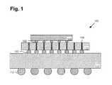
- FIG. 1illustrates an exemplary cross-sectional view of a conventional semiconductor package including a conventional interposer.
- FIG. 2illustrates an exemplary cross-sectional view of a semiconductor package including a semiconductor interposer having a cavity, according to one implementation of the present application.
- FIG. 3illustrates an exemplary cross-sectional view of another semiconductor package including a semiconductor interposer having a cavity, according to one implementation of the present application.
- FIG. 4illustrates an exemplary cross-sectional view of another semiconductor package including a semiconductor interposer having a cavity, according to one implementation of the present application.
- FIG. 5illustrates an exemplary cross-sectional view of another semiconductor package including a semiconductor interposer having a cavity, according to one implementation of the present application.
- FIG. 1illustrates an exemplary cross-sectional view of a conventional semiconductor package 100 including substrate 110 , conventional interposer 120 disposed on substrate 110 , and active die 130 disposed on conventional interposer 120 .
- Interposerssuch as conventional interposer 120
- conventional interposer 120may include several vias 124 filled with a conductive material.
- solder microbumps 132 or copper micro pillarsmay connect active die 130 with conventional interposer 120 and several solder bumps 122 may likewise connect conventional interposer 120 to substrate 110 , for example. Where external connection of semiconductor package 100 is required, solder balls 112 may be disposed on a bottom surface of substrate 110 .
- conventional interposer 120may route electrical connections on active die 130 to substrate 110 through vias 124 , for example.
- solder microbumps 132may result in undesirably limited thermal conduction paths out of active die 130 .
- Such inadequate thermal dissipationcan result in thermal, electrical or mechanical failure of active die 130 and semiconductor package 100 .
- semiconductor package 100is used to house multiple active dies, inadequate thermal dissipation from one active die, such as active die 130 , may result in undesirable thermal stress in the other active dies in the semiconductor package.
- conventional interposer 120is used to stack and interconnect multiple active dies, the total thickness of semiconductor package 100 may become unacceptably large.
- conventional interposer designsfail to adequately accommodate increased thermal dissipation requirements, complexity and functionality of semiconductor packages.
- FIG. 2illustrates an exemplary cross-sectional view of a semiconductor package including a semiconductor interposer having a cavity, according to one implementation of the present application.
- Semiconductor package 200may include substrate 210 , semiconductor interposer 240 having cavity 246 , intra-interposer die 260 disposed within cavity 246 of semiconductor interposer 240 , and top die 230 .
- Intra-interposer die 260 and top die 230may be active dies, each containing one or more active components, such as one or more transistors, for example.
- semiconductor interposer 240may include several through semiconductor vias (TSVs) 244 .
- semiconductor interposer 240may be a silicon interposer.
- through semiconductor vias 244may be referred to as through silicon vias 244 .
- TSVs 244may extend from top surface 247 to bottom surface 248 of semiconductor interposer 240 and may be formed by any appropriate technique known to those of ordinary skill in the art, for example, by deep reactive ion etching.
- TSVs 244may be formed before cavity 246 is etched.
- TSVs 244may be formed after cavity 246 is etched. Once formed, each of TSVs 244 may be lined by a dielectric and filled with a conductive filler.
- Cavity 246may be etched into semiconductor interposer 240 using any appropriate etching process known to those of ordinary skill in the art. Preferably, however, an anisotropic etching process is used in order to precisely control the dimensions of cavity 246 .
- suitable etching processesmay include an HNO 3 +HF wet etch, or a reactive ion dry etch.
- thermally conductive adhesive 250may contact intra-interposer die 260 on all sides except an exposed top surface 267 .
- thermally conductive adhesive 250may also be an electrical insulator.
- the increased contact surface area between intra-interposer die 260 and thermally conductive adhesive 250provides a much greater thermal dissipation capacity than conventional interposer structures.
- heat generated in intra-interposer die 260may be easily transferred to semiconductor interposer 240 where it can also be transferred to substrate 210 through TSVs 244 , or radiated directly to the ambient environment.
- mounting intra-interposer die 260 in cavity 246 of semiconductor interposer 240rather than on top surface 247 , serves to reduce the overall thickness of semiconductor package 200 .
- solder bumps 222may be 50 ⁇ m to 100 ⁇ m in diameter. However, solder bumps 222 may be any diameter suitable to a particular application.
- Top die 230may be electrically and thermally connected to semiconductor interposer 240 using several solder microbumps 232 , for example. Additionally, one or more solder microbumps 234 may serve as a direct die-to-die electrical contact between top die 230 and intra-interposer die 260 . Thus, where no direct electrical contact exists between intra-interposer die 260 and substrate 210 , electrical communication between substrate 210 and intra-interposer die 260 may be achieved through electrical connection with top die 230 . Finally, where external connection of semiconductor package 200 is required, several solder balls 212 may be deposited on a bottom surface of substrate 210 .
- FIG. 3illustrates an exemplary cross-sectional view of another semiconductor package including a semiconductor interposer having a cavity, according to one implementation of the present application.
- Semiconductor package 300is similar to that of semiconductor package 200 of FIG. 2 , including a substrate 310 , a semiconductor interposer 340 having a cavity 346 , an intra-interposer die 360 disposed within cavity 346 of semiconductor interposer 340 , and top die 330 .
- semiconductor interposer 340is flip-chip mounted to substrate 310 such that intra-interposer die 360 , disposed within cavity 346 , faces substrate 310 .
- intra-interposer die 360 and top die 330may be active dies, each containing one or more active components, such as one or more transistors, for example.
- semiconductor interposer 340may include several through semiconductor vias (TSVs) 344 .
- TSVsthrough semiconductor vias
- semiconductor interposer 340is a silicon interposer
- through semiconductor vias 344may be referred to as through silicon vias 344 .
- TSVs 344may extend from top surface 347 to bottom surface 348 of semiconductor interposer 340 .
- TSVs 344may be formed by any appropriate etch technique known to those of ordinary skill in the art, for example, deep reactive ion etching.
- TSVs 344may be formed before cavity 346 is etched.
- TSVs 344may be formed after cavity 346 is etched. Once formed, each of TSVs 344 may be lined by a dielectric and filled with a conductive filler.
- Cavity 346may be etched into semiconductor interposer 340 using any appropriate etching process known to those of ordinary skill in the art. Preferably, however, an anisotropic etching process is used in order to precisely control the dimensions of cavity 346 .
- a thermally conductive adhesive 350may be deposited in cavity 346 such that when intra-interposer die 360 is subsequently placed in cavity 346 , the gap between intra-interposer die 360 and cavity 346 may be completely filled with thermally conductive adhesive 350 .
- thermally conductive adhesive 350may contact intra-interposer die 360 on all sides except an exposed top surface 367 , which faces substrate 310 when semiconductor interposer 340 is flip-chip mounted to substrate 310 .
- thermally conductive adhesive 350may also be an electrical insulator.
- the increased contact surface area between intra-interposer die 360 and thermally conductive adhesive 350provides a much greater thermal dissipation capacity than conventional interposer structures.
- mounting intra-interposer die 360 in cavity 346 of semiconductor interposer 340rather than on top surface 347 or on bottom surface 348 , serves to reduce the overall thickness of semiconductor package 300 .
- Semiconductor interposer 340may be flip-chip mounted to substrate 310 using several solder bumps 322 , providing an electrical and thermal connection to substrate 310 .
- Intra-interposer die 360may also be directly electrically and thermally connected to substrate 310 using several solder bumps 324 , allowing additional heat transfer to take place directly to substrate 310 through solder bumps 322 .
- Top die 330may be electrically and thermally connected to semiconductor interposer 340 using several solder microbumps 332 . Because semiconductor interposer 340 is flip-chip mounted to substrate 310 such that cavity 346 faces substrate 310 , semiconductor interposer 340 may also provide thermal isolation between intra-interposer die 360 and top die 330 . Electrical communication between top die 330 and substrate may be achieved through TSVs 344 of flip-chip mounted semiconductor interposer 340 . Finally, where external connection of semiconductor package 300 is required, several solder balls 312 may be deposited on the bottom surface of substrate 310 .
- FIG. 4illustrates an exemplary cross-sectional view of another semiconductor package including a semiconductor interposer having a cavity, according to one implementation of the present application.
- Semiconductor package 400is similar to that of semiconductor package 200 of FIG. 2 , including a substrate 410 , a semiconductor interposer 440 having a cavity 446 , an intra-interposer die 460 disposed within cavity 446 of semiconductor interposer 440 , and a top die 430 .
- Intra-interposer die 460 and top die 430may be active dies, each containing one or more active components, such as one or more transistors, for example.
- semiconductor interposer 440may include several through semiconductor vias (TSVs) 444 , extending from top surface 447 to bottom surface 448 of semiconductor interposer 440 .
- semiconductor interposer 440may also include several TSVs 449 disposed in cavity 446 . TSVs 449 may extend from bottom surface 445 of cavity 446 to bottom surface 448 of semiconductor interposer 440 .
- through semiconductor vias 444 and 449may be referred to as through silicon vias 444 and 449 , respectively.
- TSVs 444 and 449may be formed by any appropriate etch technique known to those of ordinary skill in the art, for example, deep reactive ion etching. In one implementation, TSVs 444 and/or TSVs 449 may be formed before cavity 446 is etched. In another implementation, TSVs 444 and/or TSVs 449 may be formed after cavity 446 is etched. However, TSVs 444 and TSVs 449 need not be formed in the same manufacturing process. Instead, TSVs 444 and TSVs 449 may be formed in separate etching processes. Once formed, each of TSVs 444 and TSVs 449 may be lined by a dielectric and filled with a conductive filler such as copper.
- a conductive fillersuch as copper.
- Cavity 446may be etched into semiconductor interposer 440 using any appropriate etching process known to those of ordinary skill in the art. Preferably, however, an anisotropic etching process is used in order to precisely control the dimensions of cavity 446 .
- an anisotropic etching processis used in order to precisely control the dimensions of cavity 446 .
- solder microbumps 462may be deposited in cavity 446 in order to electrically connect intra-interposer die 460 with one or more of TSVs 449 , for example.
- thermally conductive adhesive 450may be deposited in cavity 446 , around solder microbumps 462 , such that when intra-interposer die 460 is subsequently placed in cavity 446 , the gaps between intra-interposer die 460 and cavity 446 may be completely filled with thermally conductive adhesive 450 .
- thermally conductive adhesive 450may contact intra-interposer die 460 on all sides except an exposed top surface 467 .
- thermally conductive adhesive 450may also be an electrical insulator to ensure electrical isolation between adjacent solder microbumps 462 as well as between intra-interposer die 460 and semiconductor interposer 440 . As in FIG.
- the increased contact surface area between intra-interposer die 460 and thermally conductive adhesive 450provides a much greater thermal dissipation capacity than conventional interposer structures.
- mounting intra-interposer die 460 in a cavity of semiconductor interposer 440 , rather than on top surface 447serves to reduce the overall thickness of semiconductor package 400 .
- Semiconductor interposer 440may be electrically and thermally connected to substrate 410 using solder bumps 422 and 424 , for example.
- solder bumps 422may electrically and thermally connect TSVs 444 to substrate 410
- solder bumps 424may electrically and thermally connect TSVs 449 to substrate 410 .
- additional thermal dissipation from intra-interposer die 460may be provided directly to substrate 410 through TSVs 449 .
- Top die 430may be electrically and thermally connected to semiconductor interposer 440 using several solder microbumps 432 , for example.
- electrical communication between top die 430 and substratemay be achieved through TSVs 444 of semiconductor interposer 440 .
- one or more solder microbumps 434may serve as a direct die-to-die electrical contact between top die 430 and intra-interposer die 460 .
- intra-interposer die 460may electrically communicate in two paths, directly with substrate 410 through TSVs 449 , and directly with top die 430 through solder microbumps 434 .
- several solder balls 412may be deposited on the bottom surface of substrate 410 .
- FIG. 5illustrates an exemplary cross-sectional view of another semiconductor package including a semiconductor interposer having a cavity, according to one implementation of the present application.
- Semiconductor package 500is similar to that of semiconductor package 200 of FIG. 2 , including a substrate 510 , a semiconductor interposer 540 having a cavity 546 , an intra-interposer die 560 disposed within cavity 546 of semiconductor interposer 540 , and a top die 530 .
- Intra-interposer die 560 and top die 530may be active dies, each containing one or more active components, such as one or more transistors, for example.
- semiconductor interposer 540may include several through semiconductor vias (TSVs) 544 .
- TSVs 544may extend from top surface 547 to bottom surface 548 of semiconductor interposer 540 .
- through semiconductor vias 544may be referred to as through silicon vias 544 .
- TSVs 544may be formed by any appropriate etch technique known to those of ordinary skill in the art, for example, deep reactive ion etching. In one implementation, TSVs 544 may be formed before cavity 546 is etched. In another implementation, TSVs 544 may be formed after cavity 546 is etched. Once formed, each of TSVs 544 may be lined by a dielectric and filled with a conductive filler.
- Cavity 546is similar to cavity 246 of FIG. 2 , except that cavity 546 may be etched entirely through semiconductor interposer 540 , extending from top surface 547 to bottom surface 548 of semiconductor interposer 540 . Cavity 546 may be etched into semiconductor interposer 540 using any appropriate etching process known to those of ordinary skill in the art. Preferably, however, an anisotropic etching process is used in order to precisely control the dimensions of cavity 546 .
- semiconductor interposer 540may be electrically and thermally connected to substrate 510 using several solder bumps 522 , for example.
- a thermal interface material (TIM) 552may then be deposited between substrate 510 and semiconductor interposer 540 under cavity 546 .
- TIM 552may be the same material as thermally conductive adhesive 250 of FIG. 2 , or may be a different thermally conductive material.
- a thermally conductive adhesive 550may be deposited in cavity 546 , over TIM 552 , such that when intra-interposer die 560 is subsequently placed in cavity 546 , the gap between intra-interposer die 560 and semiconductor interposer 540 may be completely filled with thermally conductive adhesive 550 .
- both thermal interface material 552 and thermally conductive adhesive 550may be electrical insulators to ensure electrical isolation between intra-interposer die 560 and semiconductor interposer 540 .
- the increased contact surface area between intra-interposer die 560 and thermally conductive adhesive 550provides greater thermal dissipation capacity than conventional interposer structures.
- TIM 552being in physical contact with substantially the entire area of substrate 510 under cavity 546 , also forms an increased contact surface area with substrate 510 , providing further increased thermal dissipation capacity in semiconductor package 500 .
- Mounting intra-interposer die 560 in cavity 546 of semiconductor interposer 540rather than on top surface 547 , serves to reduce the overall thickness of semiconductor package 500 .
- Top die 530may be electrically and thermally connected to semiconductor interposer 540 using several solder microbumps 532 , for example. Thus, electrical communication between top die 530 and substrate 510 may be achieved through TSVs 544 of semiconductor interposer 540 . Top die 530 may also be electrically and thermally connected to intra-interposer die 560 using several solder microbumps 534 , for example. Thus, where no direct electrical contact exists between intra-interposer die 560 and substrate 510 , electrical communication between substrate 510 and intra-interposer die 560 may be achieved through electrical connections with top die 530 . Finally, where external connection of semiconductor package 500 is required, array or matrix of solder balls 512 may be deposited on the bottom surface of substrate 510 .
- various implementations disclosed in the present applicationachieve a reduced semiconductor package thickness, as well as an increased thermal dissipation capability within the semiconductor package.
- the increased thermal dissipation capabilityadvantageously reduces occurrence of thermal, electrical and mechanical failures of the semiconductor dies and semiconductor package, as compared to semiconductor packages including conventional interposers.
Landscapes
- Engineering & Computer Science (AREA)
- Power Engineering (AREA)
- Microelectronics & Electronic Packaging (AREA)
- Physics & Mathematics (AREA)
- Condensed Matter Physics & Semiconductors (AREA)
- General Physics & Mathematics (AREA)
- Computer Hardware Design (AREA)
- Cooling Or The Like Of Semiconductors Or Solid State Devices (AREA)
Abstract
Description
Claims (28)
Priority Applications (1)
| Application Number | Priority Date | Filing Date | Title |
|---|---|---|---|
| US13/349,045US9548251B2 (en) | 2012-01-12 | 2012-01-12 | Semiconductor interposer having a cavity for intra-interposer die |
Applications Claiming Priority (1)
| Application Number | Priority Date | Filing Date | Title |
|---|---|---|---|
| US13/349,045US9548251B2 (en) | 2012-01-12 | 2012-01-12 | Semiconductor interposer having a cavity for intra-interposer die |
Publications (2)
| Publication Number | Publication Date |
|---|---|
| US20130181354A1 US20130181354A1 (en) | 2013-07-18 |
| US9548251B2true US9548251B2 (en) | 2017-01-17 |
Family
ID=48779423
Family Applications (1)
| Application Number | Title | Priority Date | Filing Date |
|---|---|---|---|
| US13/349,045Active2032-01-14US9548251B2 (en) | 2012-01-12 | 2012-01-12 | Semiconductor interposer having a cavity for intra-interposer die |
Country Status (1)
| Country | Link |
|---|---|
| US (1) | US9548251B2 (en) |
Cited By (4)
| Publication number | Priority date | Publication date | Assignee | Title |
|---|---|---|---|---|
| US10431648B2 (en) | 2014-05-02 | 2019-10-01 | Invensas Corporation | Making electrical components in handle wafers of integrated circuit packages |
| US20200350277A1 (en)* | 2012-02-23 | 2020-11-05 | Taiwan Semiconductor Manufacturing Company, Ltd. | Semiconductor device having reduced bump height variation |
| US11069658B2 (en)* | 2015-11-04 | 2021-07-20 | Taiwan Semiconductor Manufacturing Company, Ltd. | System on integrated chips and methods of forming same |
| US11515262B2 (en) | 2020-05-29 | 2022-11-29 | Samsung Electronics Co., Ltd. | Semiconductor package and method of fabricating the same |
Families Citing this family (26)
| Publication number | Priority date | Publication date | Assignee | Title |
|---|---|---|---|---|
| US20130154106A1 (en) | 2011-12-14 | 2013-06-20 | Broadcom Corporation | Stacked Packaging Using Reconstituted Wafers |
| US8558395B2 (en)* | 2012-02-21 | 2013-10-15 | Broadcom Corporation | Organic interface substrate having interposer with through-semiconductor vias |
| US8587132B2 (en) | 2012-02-21 | 2013-11-19 | Broadcom Corporation | Semiconductor package including an organic substrate and interposer having through-semiconductor vias |
| US8749072B2 (en) | 2012-02-24 | 2014-06-10 | Broadcom Corporation | Semiconductor package with integrated selectively conductive film interposer |
| KR20160036666A (en) | 2013-09-27 | 2016-04-04 | 인텔 코포레이션 | Die package with superposer substrate for passive components |
| CN105874590B (en)* | 2013-09-27 | 2019-08-13 | 英特尔公司 | double-sided die package |
| US9355997B2 (en) | 2014-03-12 | 2016-05-31 | Invensas Corporation | Integrated circuit assemblies with reinforcement frames, and methods of manufacture |
| US20150262902A1 (en) | 2014-03-12 | 2015-09-17 | Invensas Corporation | Integrated circuits protected by substrates with cavities, and methods of manufacture |
| US9741649B2 (en) | 2014-06-04 | 2017-08-22 | Invensas Corporation | Integrated interposer solutions for 2D and 3D IC packaging |
| US9412806B2 (en) | 2014-06-13 | 2016-08-09 | Invensas Corporation | Making multilayer 3D capacitors using arrays of upstanding rods or ridges |
| RU2659980C2 (en)* | 2014-07-02 | 2018-07-04 | Интел Корпорейшн | Electronic assembly, which includes the electronic devices that are stacked onto each other |
| US9252127B1 (en) | 2014-07-10 | 2016-02-02 | Invensas Corporation | Microelectronic assemblies with integrated circuits and interposers with cavities, and methods of manufacture |
| US9478504B1 (en) | 2015-06-19 | 2016-10-25 | Invensas Corporation | Microelectronic assemblies with cavities, and methods of fabrication |
| WO2017171889A1 (en)* | 2016-04-02 | 2017-10-05 | Intel Corporation | Systems, methods, and apparatuses for implementing a thermal solution for 3d packaging |
| CN106129023A (en)* | 2016-08-30 | 2016-11-16 | 华天科技(昆山)电子有限公司 | The fan-out packaging structure of two-sided attachment and method for packing |
| CN109844945A (en)* | 2016-09-30 | 2019-06-04 | 英特尔公司 | Semiconductor packages with high density interconnection |
| US10622311B2 (en)* | 2017-08-10 | 2020-04-14 | International Business Machines Corporation | High-density interconnecting adhesive tape |
| US11114308B2 (en) | 2018-09-25 | 2021-09-07 | International Business Machines Corporation | Controlling of height of high-density interconnection structure on substrate |
| WO2020147107A1 (en)* | 2019-01-18 | 2020-07-23 | 华为技术有限公司 | Integrated circuit comprising multiple interconnected interposers |
| US11380620B2 (en)* | 2019-06-14 | 2022-07-05 | Taiwan Semiconductor Manufacturing Company, Ltd. | Semiconductor package including cavity-mounted device |
| CN110211946A (en)* | 2019-06-17 | 2019-09-06 | 上海先方半导体有限公司 | A kind of chip-packaging structure and its manufacturing method |
| CN110335859B (en)* | 2019-07-29 | 2024-04-05 | 上海先方半导体有限公司 | Multi-chip packaging structure based on TSV and preparation method thereof |
| KR102377811B1 (en)* | 2019-08-09 | 2022-03-22 | 삼성전기주식회사 | Electronic component module and manufacturing method thereof |
| CN110634848A (en)* | 2019-08-29 | 2019-12-31 | 上海先方半导体有限公司 | Multi-chip stacking packaging structure and manufacturing method thereof |
| CN112466861B (en) | 2019-09-09 | 2025-03-28 | 台湾积体电路制造股份有限公司 | Packaging structure and forming method thereof |
| US20250046622A1 (en)* | 2023-08-04 | 2025-02-06 | Avago Technologies International Sales Pte. Limited | Hybrid substrates and manufacturing methods thereof |
Citations (76)
| Publication number | Priority date | Publication date | Assignee | Title |
|---|---|---|---|---|
| US5198963A (en) | 1991-11-21 | 1993-03-30 | Motorola, Inc. | Multiple integrated circuit module which simplifies handling and testing |
| US6002168A (en) | 1997-11-25 | 1999-12-14 | Tessera, Inc. | Microelectronic component with rigid interposer |
| US6031284A (en)* | 1997-03-14 | 2000-02-29 | Lg Semicon Co., Ltd. | Package body and semiconductor chip package using same |
| US6188578B1 (en) | 1999-06-11 | 2001-02-13 | Industrial Technology Research Institute | Integrated circuit package with multiple heat dissipation paths |
| US6306686B1 (en)* | 1998-02-04 | 2001-10-23 | International Business Machines Corporation | Method of fabricating an electronic package with interconnected chips |
| US20020030261A1 (en) | 1999-12-17 | 2002-03-14 | Rolda Ruben A. | Multi-flip-chip semiconductor assembly |
| US20020105070A1 (en)* | 1995-11-28 | 2002-08-08 | Hitachi, Ltd. | Semiconductor device, manufacturing method thereof and mounting board |
| US6461895B1 (en) | 1999-01-05 | 2002-10-08 | Intel Corporation | Process for making active interposer for high performance packaging applications |
| US20030036219A1 (en) | 2001-08-13 | 2003-02-20 | Mutsumi Masumoto | Semiconductor device manufacturing method |
| US20030143781A1 (en)* | 2002-01-31 | 2003-07-31 | Mclellan Neil Robert | Encapsulated integrated circuit package and method of manufacturing an integrated circuit package |
| US20030151148A1 (en)* | 2000-11-06 | 2003-08-14 | St Assembly Test Services Pte Ltd | Single unit automated assembly of flex enhanced ball grid array packages |
| US6709898B1 (en) | 2000-10-04 | 2004-03-23 | Intel Corporation | Die-in-heat spreader microelectronic package |
| US6743661B1 (en) | 2001-06-29 | 2004-06-01 | Novellus Systems, Inc. | Method of fabricating an integrated circuit package utilizing an interposer surrounded by a flexible dielectric material with conductive posts |
| US20040164390A1 (en)* | 2003-02-26 | 2004-08-26 | Sung-Fei Wang | [semiconductor package with a heat spreader] |
| US6791195B2 (en) | 2000-04-24 | 2004-09-14 | Nec Electronics Corporation | Semiconductor device and manufacturing method of the same |
| US6921968B2 (en)* | 2003-05-02 | 2005-07-26 | Advance Semiconductor Engineering, Inc. | Stacked flip chip package |
| US20050218518A1 (en) | 2002-01-07 | 2005-10-06 | Tongbi Jiang | Semiconductor device assemblies and packages including multiple semiconductor device components |
| US20060145328A1 (en) | 2005-01-06 | 2006-07-06 | Shih-Ping Hsu | Three dimensional package structure with semiconductor chip embedded in substrate and method for fabricating the same |
| US20060186536A1 (en) | 2005-02-02 | 2006-08-24 | Shih-Ping Hsu | Substrate assembly with direct electrical connection as a semiconductor package |
| US20060186531A1 (en) | 2005-02-22 | 2006-08-24 | Phoenix Precision Technology Corporation | Package structure with chip embedded in substrate |
| US20060220262A1 (en) | 2005-04-04 | 2006-10-05 | Torsten Meyer | Stacked die package |
| US20060258044A1 (en) | 2005-05-11 | 2006-11-16 | Infineon Technologies Ag | Method of manufacturing a semiconductor device comprising stacked chips and a corresponding semiconductor device |
| US7220667B2 (en) | 2002-08-14 | 2007-05-22 | Sony Corporation | Semiconductor device and method of fabricating the same |
| US20070132082A1 (en) | 2005-12-12 | 2007-06-14 | Intel Corporation | Copper plating connection for multi-die stack in substrate package |
| US20070209831A1 (en)* | 2000-09-25 | 2007-09-13 | Ibiden Co., Ltd. | Semiconductor element, method of manufacturing semiconductor element, multi-layer printed circuit board, and method of manufacturing multi-layer printed circuit board |
| US20070273049A1 (en) | 2006-05-12 | 2007-11-29 | Broadcom Corporation | Interconnect structure and formation for package stacking of molded plastic area array package |
| US20070290376A1 (en) | 2006-06-20 | 2007-12-20 | Broadcom Corporation | Integrated circuit (IC) package stacking and IC packages formed by same |
| US20080044944A1 (en) | 2003-11-10 | 2008-02-21 | Casio Computer Co., Ltd. | Semiconductor device including semiconductor element surrounded by an insulating member and wiring structures on upper and lower surfaces of the semiconductor element and insulating member, and manufacturing method thereof |
| US20080128882A1 (en)* | 2006-12-05 | 2008-06-05 | Samsung Electronics Co., Ltd. | Chip stack package and method of manufacturing the same |
| US20080157328A1 (en) | 2006-12-27 | 2008-07-03 | Nec Electronics Corporation | Semiconductor device and method for manufacturing same |
| US20080157322A1 (en) | 2006-12-27 | 2008-07-03 | Jia Miao Tang | Double side stacked die package |
| US20080246138A1 (en) | 2006-04-07 | 2008-10-09 | Texas Instruments Incorporated | Packed System of Semiconductor Chips Having a Semiconductor Interposer |
| US20080268638A1 (en) | 2007-04-25 | 2008-10-30 | Infineon Technologies Ag | Substrate with Feedthrough and Method for Producing the Same |
| US20090053858A1 (en) | 2007-08-24 | 2009-02-26 | Samsung Electronics Co., Ltd. | Method of manufacturing semiconductor package using redistribution substrate |
| US20090102030A1 (en) | 2007-10-22 | 2009-04-23 | Broadcom Corporation | Integrated circuit package with etched leadframe for package-on-package interconnects |
| US7585702B1 (en) | 2005-11-08 | 2009-09-08 | Altera Corporation | Structure and assembly procedure for low stress thin die flip chip packages designed for low-K Si and thin core substrate |
| US7675163B2 (en) | 2007-03-21 | 2010-03-09 | Sun Microsystems, Inc. | Carbon nanotubes for active direct and indirect cooling of electronics device |
| US20100084754A1 (en) | 2007-06-12 | 2010-04-08 | Samsung Electro-Mechanics Co., Ltd | Semiconductor package |
| US20100133534A1 (en) | 2008-12-03 | 2010-06-03 | Byung Tai Do | Integrated circuit packaging system with interposer and flip chip and method of manufacture thereof |
| US7834450B2 (en) | 2007-08-20 | 2010-11-16 | Samsung Electronics Co., Ltd. | Semiconductor package having memory devices stacked on logic device |
| US7838337B2 (en) | 2008-12-01 | 2010-11-23 | Stats Chippac, Ltd. | Semiconductor device and method of forming an interposer package with through silicon vias |
| US20100301474A1 (en) | 2008-09-25 | 2010-12-02 | Wen-Kun Yang | Semiconductor Device Package Structure and Method for the Same |
| US20110024906A1 (en) | 2007-10-09 | 2011-02-03 | Infineon Technologies Ag | Semiconductor chip package, semiconductor chip assembly, and method for fabricating a device |
| US20110024888A1 (en) | 2009-07-31 | 2011-02-03 | Stats Chippac, Ltd. | Semiconductor Device and Method of Mounting Die with TSV in Cavity of Substrate for Electrical Interconnect of FI-POP |
| US7901986B2 (en) | 2006-12-27 | 2011-03-08 | Shinko Electric Industries Co., Ltd. | Wiring substrate, manufacturing method thereof, and semiconductor device |
| US20110068444A1 (en)* | 2009-09-23 | 2011-03-24 | Stats Chippac, Ltd. | Semiconductor Device and Method of Forming Open Cavity in TSV Interposer to Contain Semiconductor Die in WLCSMP |
| KR20110036249A (en) | 2009-10-01 | 2011-04-07 | 앰코 테크놀로지 코리아 주식회사 | Wafer level package having through electrode and method for manufacturing same |
| US20110193235A1 (en)* | 2010-02-05 | 2011-08-11 | Taiwan Semiconductor Manufacturing Company, Ltd. | 3DIC Architecture with Die Inside Interposer |
| US8008125B2 (en)* | 2009-03-06 | 2011-08-30 | General Electric Company | System and method for stacked die embedded chip build-up |
| US8022555B2 (en) | 2007-05-08 | 2011-09-20 | Samsung Electronics Co., Ltd. | Semiconductor package and method of forming the same |
| US20110241185A1 (en) | 2010-04-05 | 2011-10-06 | International Business Machines Corporation | Signal shielding through-substrate vias for 3d integration |
| US20110254160A1 (en) | 2010-04-16 | 2011-10-20 | Taiwan Semiconductor Manufacturing Company, Ltd. | TSVs with Different Sizes in Interposers for Bonding Dies |
| US20110272819A1 (en) | 2010-05-07 | 2011-11-10 | Samsung Electronics Co., Ltd. | Wafer level package and methods of fabricating the same |
| US20110278732A1 (en) | 2010-05-13 | 2011-11-17 | Taiwan Semiconductor Manufacturing Company, Ltd. | Interconnect Structures for Substrate |
| US20110285030A1 (en) | 2006-07-12 | 2011-11-24 | Infineon Technologies Ag | Method for producing chip packages, and chip package produced in this way |
| US20120009738A1 (en) | 2010-07-06 | 2012-01-12 | Crawford Grant A | Misalignment correction for embedded microelectronic die applications |
| US20120018899A1 (en) | 2008-05-15 | 2012-01-26 | Stats Chippac, Ltd. | Semiconductor Device and Method of Conforming Conductive Vias Between Insulating Layers in Saw Streets |
| US20120062439A1 (en) | 2010-09-09 | 2012-03-15 | Advanced Semiconductor Engineering, Inc. | Semiconductor package integrated with conformal shield and antenna |
| US20120139105A1 (en) | 2010-12-06 | 2012-06-07 | Industrial Technology Research Institute | Semiconductor structure and manufacturing method thereof |
| US20120152605A1 (en) | 2010-12-20 | 2012-06-21 | Endicott Interconnect Technologies, Inc. | Circuitized substrate with dielectric interposer assembly and method |
| US20120168942A1 (en) | 2010-12-30 | 2012-07-05 | Stmicroelectronics Pte Ltd. | Through hole via filling using electroless plating |
| US20120211885A1 (en) | 2011-02-17 | 2012-08-23 | Choi Yunseok | Semiconductor package having through silicon via (tsv) interposer and method of manufacturing the semiconductor package |
| US20120225522A1 (en) | 2011-03-03 | 2012-09-06 | Broadcom Corporation | Package 3D Interconnection and Method of Making Same |
| US20120223429A1 (en) | 2011-03-03 | 2012-09-06 | Broadcom Corporation | Package 3D Interconnection and Method of Making Same |
| US20120228753A1 (en) | 2011-03-10 | 2012-09-13 | Chan Hoon Ko | Integrated circuit package-on-package system with underfilling structures and method of manufacture thereof |
| US20120241921A1 (en) | 2011-03-24 | 2012-09-27 | Seongmin Lee | Integrated circuit packaging system with interposer shield and method of manufacture thereof |
| US8310063B2 (en) | 2010-08-25 | 2012-11-13 | Advanced Semiconductor Engineering, Inc. | Semiconductor package structure and manufacturing process thereof |
| US20120313240A1 (en) | 2011-06-09 | 2012-12-13 | Shih-Lian Cheng | Semiconductor package and fabrication method thereof |
| US20120319293A1 (en) | 2011-06-17 | 2012-12-20 | Bok Eng Cheah | Microelectronic device, stacked die package and computing system containing same, method of manufacturing a multi-channel communication pathway in same, and method of enabling electrical communication between components of a stacked-die package |
| US8344516B2 (en) | 2006-08-11 | 2013-01-01 | International Business Machines Corporation | Integrated chip carrier with compliant interconnects |
| US20130000968A1 (en) | 2011-06-30 | 2013-01-03 | Broadcom Corporation | 1-Layer Interposer Substrate With Through-Substrate Posts |
| US20130062764A1 (en) | 2011-09-14 | 2013-03-14 | Stmicroelectronics Pte Ltd. | Semiconductor package with improved pillar bump process and structure |
| US20130075917A1 (en) | 2011-09-27 | 2013-03-28 | Broadcom Corporation | Multi-Chip and Multi-Substrate Reconstitution Based Packaging |
| US20130113098A1 (en) | 2011-11-08 | 2013-05-09 | Stmicroelectronics Pte Ltd. | Through via package |
| US8461672B2 (en) | 2007-07-27 | 2013-06-11 | Tessera, Inc. | Reconstituted wafer stack packaging with after-applied pad extensions |
| US20130147023A1 (en) | 2011-12-07 | 2013-06-13 | Taiwan Semiconductor Manufacturing Company, Ltd. | Integrated circuit ground shielding structure |
- 2012
- 2012-01-12USUS13/349,045patent/US9548251B2/enactiveActive
Patent Citations (79)
| Publication number | Priority date | Publication date | Assignee | Title |
|---|---|---|---|---|
| US5198963A (en) | 1991-11-21 | 1993-03-30 | Motorola, Inc. | Multiple integrated circuit module which simplifies handling and testing |
| US20020105070A1 (en)* | 1995-11-28 | 2002-08-08 | Hitachi, Ltd. | Semiconductor device, manufacturing method thereof and mounting board |
| US6031284A (en)* | 1997-03-14 | 2000-02-29 | Lg Semicon Co., Ltd. | Package body and semiconductor chip package using same |
| US6002168A (en) | 1997-11-25 | 1999-12-14 | Tessera, Inc. | Microelectronic component with rigid interposer |
| US6306686B1 (en)* | 1998-02-04 | 2001-10-23 | International Business Machines Corporation | Method of fabricating an electronic package with interconnected chips |
| US6461895B1 (en) | 1999-01-05 | 2002-10-08 | Intel Corporation | Process for making active interposer for high performance packaging applications |
| US6188578B1 (en) | 1999-06-11 | 2001-02-13 | Industrial Technology Research Institute | Integrated circuit package with multiple heat dissipation paths |
| US20020030261A1 (en) | 1999-12-17 | 2002-03-14 | Rolda Ruben A. | Multi-flip-chip semiconductor assembly |
| US6791195B2 (en) | 2000-04-24 | 2004-09-14 | Nec Electronics Corporation | Semiconductor device and manufacturing method of the same |
| US20070209831A1 (en)* | 2000-09-25 | 2007-09-13 | Ibiden Co., Ltd. | Semiconductor element, method of manufacturing semiconductor element, multi-layer printed circuit board, and method of manufacturing multi-layer printed circuit board |
| US6709898B1 (en) | 2000-10-04 | 2004-03-23 | Intel Corporation | Die-in-heat spreader microelectronic package |
| US20030151148A1 (en)* | 2000-11-06 | 2003-08-14 | St Assembly Test Services Pte Ltd | Single unit automated assembly of flex enhanced ball grid array packages |
| US6743661B1 (en) | 2001-06-29 | 2004-06-01 | Novellus Systems, Inc. | Method of fabricating an integrated circuit package utilizing an interposer surrounded by a flexible dielectric material with conductive posts |
| US20030036219A1 (en) | 2001-08-13 | 2003-02-20 | Mutsumi Masumoto | Semiconductor device manufacturing method |
| US20050218518A1 (en) | 2002-01-07 | 2005-10-06 | Tongbi Jiang | Semiconductor device assemblies and packages including multiple semiconductor device components |
| US20030143781A1 (en)* | 2002-01-31 | 2003-07-31 | Mclellan Neil Robert | Encapsulated integrated circuit package and method of manufacturing an integrated circuit package |
| US7220667B2 (en) | 2002-08-14 | 2007-05-22 | Sony Corporation | Semiconductor device and method of fabricating the same |
| US20040164390A1 (en)* | 2003-02-26 | 2004-08-26 | Sung-Fei Wang | [semiconductor package with a heat spreader] |
| US6921968B2 (en)* | 2003-05-02 | 2005-07-26 | Advance Semiconductor Engineering, Inc. | Stacked flip chip package |
| US20080044944A1 (en) | 2003-11-10 | 2008-02-21 | Casio Computer Co., Ltd. | Semiconductor device including semiconductor element surrounded by an insulating member and wiring structures on upper and lower surfaces of the semiconductor element and insulating member, and manufacturing method thereof |
| US20060145328A1 (en) | 2005-01-06 | 2006-07-06 | Shih-Ping Hsu | Three dimensional package structure with semiconductor chip embedded in substrate and method for fabricating the same |
| US20060186536A1 (en) | 2005-02-02 | 2006-08-24 | Shih-Ping Hsu | Substrate assembly with direct electrical connection as a semiconductor package |
| US20060186531A1 (en) | 2005-02-22 | 2006-08-24 | Phoenix Precision Technology Corporation | Package structure with chip embedded in substrate |
| US20060220262A1 (en) | 2005-04-04 | 2006-10-05 | Torsten Meyer | Stacked die package |
| US20060258044A1 (en) | 2005-05-11 | 2006-11-16 | Infineon Technologies Ag | Method of manufacturing a semiconductor device comprising stacked chips and a corresponding semiconductor device |
| US7585702B1 (en) | 2005-11-08 | 2009-09-08 | Altera Corporation | Structure and assembly procedure for low stress thin die flip chip packages designed for low-K Si and thin core substrate |
| US20070132082A1 (en) | 2005-12-12 | 2007-06-14 | Intel Corporation | Copper plating connection for multi-die stack in substrate package |
| US20080246138A1 (en) | 2006-04-07 | 2008-10-09 | Texas Instruments Incorporated | Packed System of Semiconductor Chips Having a Semiconductor Interposer |
| US8133761B2 (en) | 2006-04-07 | 2012-03-13 | Texas Instruments Incorporated | Packaged system of semiconductor chips having a semiconductor interposer |
| US20070273049A1 (en) | 2006-05-12 | 2007-11-29 | Broadcom Corporation | Interconnect structure and formation for package stacking of molded plastic area array package |
| US20070290376A1 (en) | 2006-06-20 | 2007-12-20 | Broadcom Corporation | Integrated circuit (IC) package stacking and IC packages formed by same |
| US20110285030A1 (en) | 2006-07-12 | 2011-11-24 | Infineon Technologies Ag | Method for producing chip packages, and chip package produced in this way |
| US8344516B2 (en) | 2006-08-11 | 2013-01-01 | International Business Machines Corporation | Integrated chip carrier with compliant interconnects |
| US20080128882A1 (en)* | 2006-12-05 | 2008-06-05 | Samsung Electronics Co., Ltd. | Chip stack package and method of manufacturing the same |
| US20080157322A1 (en) | 2006-12-27 | 2008-07-03 | Jia Miao Tang | Double side stacked die package |
| US20080157328A1 (en) | 2006-12-27 | 2008-07-03 | Nec Electronics Corporation | Semiconductor device and method for manufacturing same |
| US7901986B2 (en) | 2006-12-27 | 2011-03-08 | Shinko Electric Industries Co., Ltd. | Wiring substrate, manufacturing method thereof, and semiconductor device |
| US7675163B2 (en) | 2007-03-21 | 2010-03-09 | Sun Microsystems, Inc. | Carbon nanotubes for active direct and indirect cooling of electronics device |
| US20080268638A1 (en) | 2007-04-25 | 2008-10-30 | Infineon Technologies Ag | Substrate with Feedthrough and Method for Producing the Same |
| US8022555B2 (en) | 2007-05-08 | 2011-09-20 | Samsung Electronics Co., Ltd. | Semiconductor package and method of forming the same |
| US20100084754A1 (en) | 2007-06-12 | 2010-04-08 | Samsung Electro-Mechanics Co., Ltd | Semiconductor package |
| US8461672B2 (en) | 2007-07-27 | 2013-06-11 | Tessera, Inc. | Reconstituted wafer stack packaging with after-applied pad extensions |
| US7834450B2 (en) | 2007-08-20 | 2010-11-16 | Samsung Electronics Co., Ltd. | Semiconductor package having memory devices stacked on logic device |
| US20090053858A1 (en) | 2007-08-24 | 2009-02-26 | Samsung Electronics Co., Ltd. | Method of manufacturing semiconductor package using redistribution substrate |
| US20110024906A1 (en) | 2007-10-09 | 2011-02-03 | Infineon Technologies Ag | Semiconductor chip package, semiconductor chip assembly, and method for fabricating a device |
| US8202763B2 (en) | 2007-10-09 | 2012-06-19 | Infineon Technologies Ag | Semiconductor chip package, semiconductor chip assembly, and method for fabricating a device |
| US20090102030A1 (en) | 2007-10-22 | 2009-04-23 | Broadcom Corporation | Integrated circuit package with etched leadframe for package-on-package interconnects |
| US20100019360A1 (en) | 2007-10-22 | 2010-01-28 | Broadcom Corporation | Integrated circuit package with etched leadframe for package-on-package interconnects |
| US20120018899A1 (en) | 2008-05-15 | 2012-01-26 | Stats Chippac, Ltd. | Semiconductor Device and Method of Conforming Conductive Vias Between Insulating Layers in Saw Streets |
| US20100301474A1 (en) | 2008-09-25 | 2010-12-02 | Wen-Kun Yang | Semiconductor Device Package Structure and Method for the Same |
| US7838337B2 (en) | 2008-12-01 | 2010-11-23 | Stats Chippac, Ltd. | Semiconductor device and method of forming an interposer package with through silicon vias |
| US20100133534A1 (en) | 2008-12-03 | 2010-06-03 | Byung Tai Do | Integrated circuit packaging system with interposer and flip chip and method of manufacture thereof |
| US8008125B2 (en)* | 2009-03-06 | 2011-08-30 | General Electric Company | System and method for stacked die embedded chip build-up |
| US20110024888A1 (en) | 2009-07-31 | 2011-02-03 | Stats Chippac, Ltd. | Semiconductor Device and Method of Mounting Die with TSV in Cavity of Substrate for Electrical Interconnect of FI-POP |
| US20110068444A1 (en)* | 2009-09-23 | 2011-03-24 | Stats Chippac, Ltd. | Semiconductor Device and Method of Forming Open Cavity in TSV Interposer to Contain Semiconductor Die in WLCSMP |
| KR20110036249A (en) | 2009-10-01 | 2011-04-07 | 앰코 테크놀로지 코리아 주식회사 | Wafer level package having through electrode and method for manufacturing same |
| US20110193235A1 (en)* | 2010-02-05 | 2011-08-11 | Taiwan Semiconductor Manufacturing Company, Ltd. | 3DIC Architecture with Die Inside Interposer |
| US20110241185A1 (en) | 2010-04-05 | 2011-10-06 | International Business Machines Corporation | Signal shielding through-substrate vias for 3d integration |
| US20110254160A1 (en) | 2010-04-16 | 2011-10-20 | Taiwan Semiconductor Manufacturing Company, Ltd. | TSVs with Different Sizes in Interposers for Bonding Dies |
| US20110272819A1 (en) | 2010-05-07 | 2011-11-10 | Samsung Electronics Co., Ltd. | Wafer level package and methods of fabricating the same |
| US20110278732A1 (en) | 2010-05-13 | 2011-11-17 | Taiwan Semiconductor Manufacturing Company, Ltd. | Interconnect Structures for Substrate |
| US20120009738A1 (en) | 2010-07-06 | 2012-01-12 | Crawford Grant A | Misalignment correction for embedded microelectronic die applications |
| US8310063B2 (en) | 2010-08-25 | 2012-11-13 | Advanced Semiconductor Engineering, Inc. | Semiconductor package structure and manufacturing process thereof |
| US20120062439A1 (en) | 2010-09-09 | 2012-03-15 | Advanced Semiconductor Engineering, Inc. | Semiconductor package integrated with conformal shield and antenna |
| US20120139105A1 (en) | 2010-12-06 | 2012-06-07 | Industrial Technology Research Institute | Semiconductor structure and manufacturing method thereof |
| US20120152605A1 (en) | 2010-12-20 | 2012-06-21 | Endicott Interconnect Technologies, Inc. | Circuitized substrate with dielectric interposer assembly and method |
| US20120168942A1 (en) | 2010-12-30 | 2012-07-05 | Stmicroelectronics Pte Ltd. | Through hole via filling using electroless plating |
| US20120211885A1 (en) | 2011-02-17 | 2012-08-23 | Choi Yunseok | Semiconductor package having through silicon via (tsv) interposer and method of manufacturing the semiconductor package |
| US20120225522A1 (en) | 2011-03-03 | 2012-09-06 | Broadcom Corporation | Package 3D Interconnection and Method of Making Same |
| US20120223429A1 (en) | 2011-03-03 | 2012-09-06 | Broadcom Corporation | Package 3D Interconnection and Method of Making Same |
| US20120228753A1 (en) | 2011-03-10 | 2012-09-13 | Chan Hoon Ko | Integrated circuit package-on-package system with underfilling structures and method of manufacture thereof |
| US20120241921A1 (en) | 2011-03-24 | 2012-09-27 | Seongmin Lee | Integrated circuit packaging system with interposer shield and method of manufacture thereof |
| US20120313240A1 (en) | 2011-06-09 | 2012-12-13 | Shih-Lian Cheng | Semiconductor package and fabrication method thereof |
| US20120319293A1 (en) | 2011-06-17 | 2012-12-20 | Bok Eng Cheah | Microelectronic device, stacked die package and computing system containing same, method of manufacturing a multi-channel communication pathway in same, and method of enabling electrical communication between components of a stacked-die package |
| US20130000968A1 (en) | 2011-06-30 | 2013-01-03 | Broadcom Corporation | 1-Layer Interposer Substrate With Through-Substrate Posts |
| US20130062764A1 (en) | 2011-09-14 | 2013-03-14 | Stmicroelectronics Pte Ltd. | Semiconductor package with improved pillar bump process and structure |
| US20130075917A1 (en) | 2011-09-27 | 2013-03-28 | Broadcom Corporation | Multi-Chip and Multi-Substrate Reconstitution Based Packaging |
| US20130113098A1 (en) | 2011-11-08 | 2013-05-09 | Stmicroelectronics Pte Ltd. | Through via package |
| US20130147023A1 (en) | 2011-12-07 | 2013-06-13 | Taiwan Semiconductor Manufacturing Company, Ltd. | Integrated circuit ground shielding structure |
Cited By (6)
| Publication number | Priority date | Publication date | Assignee | Title |
|---|---|---|---|---|
| US20200350277A1 (en)* | 2012-02-23 | 2020-11-05 | Taiwan Semiconductor Manufacturing Company, Ltd. | Semiconductor device having reduced bump height variation |
| US11935866B2 (en)* | 2012-02-23 | 2024-03-19 | Taiwan Semiconductor Manufacturing Company, Ltd. | Semiconductor device having reduced bump height variation |
| US10431648B2 (en) | 2014-05-02 | 2019-10-01 | Invensas Corporation | Making electrical components in handle wafers of integrated circuit packages |
| US11069658B2 (en)* | 2015-11-04 | 2021-07-20 | Taiwan Semiconductor Manufacturing Company, Ltd. | System on integrated chips and methods of forming same |
| US11658150B2 (en) | 2015-11-04 | 2023-05-23 | Taiwan Semiconductor Manufacturing Company, Ltd. | System on integrated chips and methods of forming same |
| US11515262B2 (en) | 2020-05-29 | 2022-11-29 | Samsung Electronics Co., Ltd. | Semiconductor package and method of fabricating the same |
Also Published As
| Publication number | Publication date |
|---|---|
| US20130181354A1 (en) | 2013-07-18 |
Similar Documents
| Publication | Publication Date | Title |
|---|---|---|
| US9548251B2 (en) | Semiconductor interposer having a cavity for intra-interposer die | |
| US11239206B2 (en) | Dual sided fan-out package having low warpage across all temperatures | |
| US8288854B2 (en) | Semiconductor package and method for making the same | |
| TWI649849B (en) | Semiconductor package with high wiring density patch | |
| US9299689B2 (en) | Methods of fabricating semiconductor stack packages | |
| CN103378017B (en) | High density 3D encapsulates | |
| US9224681B2 (en) | CTE matched interposer and method of making | |
| TWI496270B (en) | Semiconductor package and method of manufacture | |
| TW202038348A (en) | Integrated antenna package structure and manufacturing method thereof | |
| US9397078B1 (en) | Semiconductor device assembly with underfill containment cavity | |
| US9520304B2 (en) | Semiconductor package and fabrication method thereof | |
| KR101601388B1 (en) | Semiconductor Package and Method of Fabricating the Same | |
| US12205906B2 (en) | Electronic package and fabrication method thereof | |
| US9397081B2 (en) | Fabrication method of semiconductor package having embedded semiconductor elements | |
| KR20130140643A (en) | Semiconductor chip device with polymeric filler trench | |
| KR20150123420A (en) | Semiconductor package and the method for manufacturing of the same | |
| US20140154842A1 (en) | Carrier, semiconductor package and fabrication method thereof | |
| CN103887258A (en) | Chip package using interposer substrate with through-silicon vias | |
| US8957516B2 (en) | Low cost and high performance flip chip package | |
| CN117913072A (en) | 3D packaging switching structure, forming method thereof and packaging device | |
| TWI797701B (en) | Semiconductor device and manufacturing method thereof | |
| CN115497881A (en) | Semiconductor package and method of manufacturing the same | |
| WO2025161508A1 (en) | Chip packaging structure, manufacturing method therefor, and electronic device | |
| CN118352342A (en) | Package structure and method of forming a package structure | |
| CN119725238A (en) | Semiconductor packaging structure |
Legal Events
| Date | Code | Title | Description |
|---|---|---|---|
| AS | Assignment | Owner name:BROADCOM CORPORATION, CALIFORNIA Free format text:ASSIGNMENT OF ASSIGNORS INTEREST;ASSIGNORS:KHAN, REZAUR RAHMAN;ZHAO, SAM ZIQUN;VORENKAMP, PIETER;AND OTHERS;SIGNING DATES FROM 20111228 TO 20120109;REEL/FRAME:027524/0249 | |
| AS | Assignment | Owner name:BANK OF AMERICA, N.A., AS COLLATERAL AGENT, NORTH CAROLINA Free format text:PATENT SECURITY AGREEMENT;ASSIGNOR:BROADCOM CORPORATION;REEL/FRAME:037806/0001 Effective date:20160201 Owner name:BANK OF AMERICA, N.A., AS COLLATERAL AGENT, NORTH Free format text:PATENT SECURITY AGREEMENT;ASSIGNOR:BROADCOM CORPORATION;REEL/FRAME:037806/0001 Effective date:20160201 | |
| STCF | Information on status: patent grant | Free format text:PATENTED CASE | |
| AS | Assignment | Owner name:AVAGO TECHNOLOGIES GENERAL IP (SINGAPORE) PTE. LTD., SINGAPORE Free format text:ASSIGNMENT OF ASSIGNORS INTEREST;ASSIGNOR:BROADCOM CORPORATION;REEL/FRAME:041706/0001 Effective date:20170120 Owner name:AVAGO TECHNOLOGIES GENERAL IP (SINGAPORE) PTE. LTD Free format text:ASSIGNMENT OF ASSIGNORS INTEREST;ASSIGNOR:BROADCOM CORPORATION;REEL/FRAME:041706/0001 Effective date:20170120 | |
| AS | Assignment | Owner name:BROADCOM CORPORATION, CALIFORNIA Free format text:TERMINATION AND RELEASE OF SECURITY INTEREST IN PATENTS;ASSIGNOR:BANK OF AMERICA, N.A., AS COLLATERAL AGENT;REEL/FRAME:041712/0001 Effective date:20170119 | |
| AS | Assignment | Owner name:AVAGO TECHNOLOGIES INTERNATIONAL SALES PTE. LIMITE Free format text:MERGER;ASSIGNOR:AVAGO TECHNOLOGIES GENERAL IP (SINGAPORE) PTE. LTD.;REEL/FRAME:047422/0464 Effective date:20180509 | |
| AS | Assignment | Owner name:AVAGO TECHNOLOGIES INTERNATIONAL SALES PTE. LIMITE Free format text:CORRECTIVE ASSIGNMENT TO CORRECT THE EXECUTION DATE PREVIOUSLY RECORDED AT REEL: 047422 FRAME: 0464. ASSIGNOR(S) HEREBY CONFIRMS THE MERGER;ASSIGNOR:AVAGO TECHNOLOGIES GENERAL IP (SINGAPORE) PTE. LTD.;REEL/FRAME:048883/0702 Effective date:20180905 | |
| MAFP | Maintenance fee payment | Free format text:PAYMENT OF MAINTENANCE FEE, 4TH YEAR, LARGE ENTITY (ORIGINAL EVENT CODE: M1551); ENTITY STATUS OF PATENT OWNER: LARGE ENTITY Year of fee payment:4 | |
| MAFP | Maintenance fee payment | Free format text:PAYMENT OF MAINTENANCE FEE, 8TH YEAR, LARGE ENTITY (ORIGINAL EVENT CODE: M1552); ENTITY STATUS OF PATENT OWNER: LARGE ENTITY Year of fee payment:8 |