US9543490B2 - Wafer-level light emitting diode package and method of fabricating the same - Google Patents
Wafer-level light emitting diode package and method of fabricating the sameDownload PDFInfo
- Publication number
- US9543490B2 US9543490B2US15/041,907US201615041907AUS9543490B2US 9543490 B2US9543490 B2US 9543490B2US 201615041907 AUS201615041907 AUS 201615041907AUS 9543490 B2US9543490 B2US 9543490B2
- Authority
- US
- United States
- Prior art keywords
- layer
- light emitting
- contact
- semiconductor layer
- insulation layer
- Prior art date
- Legal status (The legal status is an assumption and is not a legal conclusion. Google has not performed a legal analysis and makes no representation as to the accuracy of the status listed.)
- Active
Links
- 238000004519manufacturing processMethods0.000titleabstractdescription28
- 238000009413insulationMethods0.000claimsabstractdescription189
- 239000004065semiconductorSubstances0.000claimsabstractdescription172
- 230000001681protective effectEffects0.000claimsabstractdescription22
- 229910052751metalInorganic materials0.000claimsdescription28
- 239000002184metalSubstances0.000claimsdescription28
- 239000010410layerSubstances0.000description413
- 239000000758substrateSubstances0.000description62
- 238000000926separation methodMethods0.000description29
- VYPSYNLAJGMNEJ-UHFFFAOYSA-NSilicium dioxideChemical compoundO=[Si]=OVYPSYNLAJGMNEJ-UHFFFAOYSA-N0.000description23
- 238000000034methodMethods0.000description16
- 239000002356single layerSubstances0.000description12
- 229910052594sapphireInorganic materials0.000description9
- 239000010980sapphireSubstances0.000description9
- GWEVSGVZZGPLCZ-UHFFFAOYSA-NTitan oxideChemical compoundO=[Ti]=OGWEVSGVZZGPLCZ-UHFFFAOYSA-N0.000description8
- 229910052681coesiteInorganic materials0.000description8
- 229910052906cristobaliteInorganic materials0.000description8
- ZKATWMILCYLAPD-UHFFFAOYSA-Nniobium pentoxideChemical compoundO=[Nb](=O)O[Nb](=O)=OZKATWMILCYLAPD-UHFFFAOYSA-N0.000description8
- 239000000377silicon dioxideSubstances0.000description8
- 229910052682stishoviteInorganic materials0.000description8
- 229910052905tridymiteInorganic materials0.000description8
- 229910052581Si3N4Inorganic materials0.000description7
- 238000000059patterningMethods0.000description7
- HQVNEWCFYHHQES-UHFFFAOYSA-Nsilicon nitrideChemical compoundN12[Si]34N5[Si]62N3[Si]51N64HQVNEWCFYHHQES-UHFFFAOYSA-N0.000description7
- 229910052814silicon oxideInorganic materials0.000description7
- 238000005530etchingMethods0.000description6
- 230000017525heat dissipationEffects0.000description6
- 238000007747platingMethods0.000description6
- OAICVXFJPJFONN-UHFFFAOYSA-NPhosphorusChemical compound[P]OAICVXFJPJFONN-UHFFFAOYSA-N0.000description5
- XUIMIQQOPSSXEZ-UHFFFAOYSA-NSiliconChemical compound[Si]XUIMIQQOPSSXEZ-UHFFFAOYSA-N0.000description5
- 150000001875compoundsChemical class0.000description5
- 229910052710siliconInorganic materials0.000description5
- 239000010703siliconSubstances0.000description5
- 238000003491arrayMethods0.000description4
- 239000012535impuritySubstances0.000description4
- 238000012858packaging processMethods0.000description4
- 229910052782aluminiumInorganic materials0.000description3
- 230000015572biosynthetic processEffects0.000description3
- 239000007769metal materialSubstances0.000description3
- 238000000465mouldingMethods0.000description3
- 229910002601GaNInorganic materials0.000description2
- BQCADISMDOOEFD-UHFFFAOYSA-NSilverChemical compound[Ag]BQCADISMDOOEFD-UHFFFAOYSA-N0.000description2
- XAGFODPZIPBFFR-UHFFFAOYSA-NaluminiumChemical compound[Al]XAGFODPZIPBFFR-UHFFFAOYSA-N0.000description2
- 238000003486chemical etchingMethods0.000description2
- 238000006243chemical reactionMethods0.000description2
- 230000006866deteriorationEffects0.000description2
- 238000007599dischargingMethods0.000description2
- 238000009713electroplatingMethods0.000description2
- 238000000605extractionMethods0.000description2
- AMGQUBHHOARCQH-UHFFFAOYSA-Nindium;oxotinChemical compound[In].[Sn]=OAMGQUBHHOARCQH-UHFFFAOYSA-N0.000description2
- 238000012986modificationMethods0.000description2
- 230000004048modificationEffects0.000description2
- 230000003287optical effectEffects0.000description2
- 238000000206photolithographyMethods0.000description2
- 229920002120photoresistant polymerPolymers0.000description2
- 238000005498polishingMethods0.000description2
- 229920000642polymerPolymers0.000description2
- 238000002310reflectometryMethods0.000description2
- 229910052709silverInorganic materials0.000description2
- 239000004332silverSubstances0.000description2
- JMASRVWKEDWRBT-UHFFFAOYSA-NGallium nitrideChemical compound[Ga]#NJMASRVWKEDWRBT-UHFFFAOYSA-N0.000description1
- 238000005229chemical vapour depositionMethods0.000description1
- PMHQVHHXPFUNSP-UHFFFAOYSA-Mcopper(1+);methylsulfanylmethane;bromideChemical compoundBr[Cu].CSCPMHQVHHXPFUNSP-UHFFFAOYSA-M0.000description1
- 230000007613environmental effectEffects0.000description1
- 229910052733galliumInorganic materials0.000description1
- 238000010438heat treatmentMethods0.000description1
- 229910052738indiumInorganic materials0.000description1
- 238000011835investigationMethods0.000description1
- 230000031700light absorptionEffects0.000description1
- 239000000463materialSubstances0.000description1
- 238000001451molecular beam epitaxyMethods0.000description1
- 230000006798recombinationEffects0.000description1
- 238000005215recombinationMethods0.000description1
Images


Classifications
- H—ELECTRICITY
- H10—SEMICONDUCTOR DEVICES; ELECTRIC SOLID-STATE DEVICES NOT OTHERWISE PROVIDED FOR
- H10H—INORGANIC LIGHT-EMITTING SEMICONDUCTOR DEVICES HAVING POTENTIAL BARRIERS
- H10H20/00—Individual inorganic light-emitting semiconductor devices having potential barriers, e.g. light-emitting diodes [LED]
- H10H20/80—Constructional details
- H10H20/85—Packages
- H10H20/852—Encapsulations
- H10H20/854—Encapsulations characterised by their material, e.g. epoxy or silicone resins
- H01L33/62—
- H01L27/15—
- H01L27/153—
- H01L33/10—
- H01L33/22—
- H01L33/24—
- H01L33/38—
- H01L33/382—
- H01L33/405—
- H01L33/42—
- H01L33/44—
- H01L33/46—
- H01L33/486—
- H01L33/50—
- H01L33/502—
- H01L33/505—
- H01L33/507—
- H01L33/58—
- H01L33/642—
- H—ELECTRICITY
- H10—SEMICONDUCTOR DEVICES; ELECTRIC SOLID-STATE DEVICES NOT OTHERWISE PROVIDED FOR
- H10H—INORGANIC LIGHT-EMITTING SEMICONDUCTOR DEVICES HAVING POTENTIAL BARRIERS
- H10H20/00—Individual inorganic light-emitting semiconductor devices having potential barriers, e.g. light-emitting diodes [LED]
- H10H20/01—Manufacture or treatment
- H10H20/011—Manufacture or treatment of bodies, e.g. forming semiconductor layers
- H10H20/013—Manufacture or treatment of bodies, e.g. forming semiconductor layers having light-emitting regions comprising only Group III-V materials
- H10H20/0133—Manufacture or treatment of bodies, e.g. forming semiconductor layers having light-emitting regions comprising only Group III-V materials with a substrate not being Group III-V materials
- H10H20/01335—Manufacture or treatment of bodies, e.g. forming semiconductor layers having light-emitting regions comprising only Group III-V materials with a substrate not being Group III-V materials the light-emitting regions comprising nitride materials
- H—ELECTRICITY
- H10—SEMICONDUCTOR DEVICES; ELECTRIC SOLID-STATE DEVICES NOT OTHERWISE PROVIDED FOR
- H10H—INORGANIC LIGHT-EMITTING SEMICONDUCTOR DEVICES HAVING POTENTIAL BARRIERS
- H10H20/00—Individual inorganic light-emitting semiconductor devices having potential barriers, e.g. light-emitting diodes [LED]
- H10H20/01—Manufacture or treatment
- H10H20/011—Manufacture or treatment of bodies, e.g. forming semiconductor layers
- H10H20/018—Bonding of wafers
- H—ELECTRICITY
- H10—SEMICONDUCTOR DEVICES; ELECTRIC SOLID-STATE DEVICES NOT OTHERWISE PROVIDED FOR
- H10H—INORGANIC LIGHT-EMITTING SEMICONDUCTOR DEVICES HAVING POTENTIAL BARRIERS
- H10H20/00—Individual inorganic light-emitting semiconductor devices having potential barriers, e.g. light-emitting diodes [LED]
- H10H20/80—Constructional details
- H10H20/81—Bodies
- H10H20/811—Bodies having quantum effect structures or superlattices, e.g. tunnel junctions
- H10H20/812—Bodies having quantum effect structures or superlattices, e.g. tunnel junctions within the light-emitting regions, e.g. having quantum confinement structures
- H—ELECTRICITY
- H10—SEMICONDUCTOR DEVICES; ELECTRIC SOLID-STATE DEVICES NOT OTHERWISE PROVIDED FOR
- H10H—INORGANIC LIGHT-EMITTING SEMICONDUCTOR DEVICES HAVING POTENTIAL BARRIERS
- H10H20/00—Individual inorganic light-emitting semiconductor devices having potential barriers, e.g. light-emitting diodes [LED]
- H10H20/80—Constructional details
- H10H20/81—Bodies
- H10H20/814—Bodies having reflecting means, e.g. semiconductor Bragg reflectors
- H—ELECTRICITY
- H10—SEMICONDUCTOR DEVICES; ELECTRIC SOLID-STATE DEVICES NOT OTHERWISE PROVIDED FOR
- H10H—INORGANIC LIGHT-EMITTING SEMICONDUCTOR DEVICES HAVING POTENTIAL BARRIERS
- H10H20/00—Individual inorganic light-emitting semiconductor devices having potential barriers, e.g. light-emitting diodes [LED]
- H10H20/80—Constructional details
- H10H20/81—Bodies
- H10H20/815—Bodies having stress relaxation structures, e.g. buffer layers
- H—ELECTRICITY
- H10—SEMICONDUCTOR DEVICES; ELECTRIC SOLID-STATE DEVICES NOT OTHERWISE PROVIDED FOR
- H10H—INORGANIC LIGHT-EMITTING SEMICONDUCTOR DEVICES HAVING POTENTIAL BARRIERS
- H10H20/00—Individual inorganic light-emitting semiconductor devices having potential barriers, e.g. light-emitting diodes [LED]
- H10H20/80—Constructional details
- H10H20/81—Bodies
- H10H20/819—Bodies characterised by their shape, e.g. curved or truncated substrates
- H10H20/82—Roughened surfaces, e.g. at the interface between epitaxial layers
- H—ELECTRICITY
- H10—SEMICONDUCTOR DEVICES; ELECTRIC SOLID-STATE DEVICES NOT OTHERWISE PROVIDED FOR
- H10H—INORGANIC LIGHT-EMITTING SEMICONDUCTOR DEVICES HAVING POTENTIAL BARRIERS
- H10H20/00—Individual inorganic light-emitting semiconductor devices having potential barriers, e.g. light-emitting diodes [LED]
- H10H20/80—Constructional details
- H10H20/81—Bodies
- H10H20/819—Bodies characterised by their shape, e.g. curved or truncated substrates
- H10H20/821—Bodies characterised by their shape, e.g. curved or truncated substrates of the light-emitting regions, e.g. non-planar junctions
- H—ELECTRICITY
- H10—SEMICONDUCTOR DEVICES; ELECTRIC SOLID-STATE DEVICES NOT OTHERWISE PROVIDED FOR
- H10H—INORGANIC LIGHT-EMITTING SEMICONDUCTOR DEVICES HAVING POTENTIAL BARRIERS
- H10H20/00—Individual inorganic light-emitting semiconductor devices having potential barriers, e.g. light-emitting diodes [LED]
- H10H20/80—Constructional details
- H10H20/81—Bodies
- H10H20/822—Materials of the light-emitting regions
- H10H20/824—Materials of the light-emitting regions comprising only Group III-V materials, e.g. GaP
- H10H20/825—Materials of the light-emitting regions comprising only Group III-V materials, e.g. GaP containing nitrogen, e.g. GaN
- H—ELECTRICITY
- H10—SEMICONDUCTOR DEVICES; ELECTRIC SOLID-STATE DEVICES NOT OTHERWISE PROVIDED FOR
- H10H—INORGANIC LIGHT-EMITTING SEMICONDUCTOR DEVICES HAVING POTENTIAL BARRIERS
- H10H20/00—Individual inorganic light-emitting semiconductor devices having potential barriers, e.g. light-emitting diodes [LED]
- H10H20/80—Constructional details
- H10H20/83—Electrodes
- H10H20/831—Electrodes characterised by their shape
- H10H20/8312—Electrodes characterised by their shape extending at least partially through the bodies
- H—ELECTRICITY
- H10—SEMICONDUCTOR DEVICES; ELECTRIC SOLID-STATE DEVICES NOT OTHERWISE PROVIDED FOR
- H10H—INORGANIC LIGHT-EMITTING SEMICONDUCTOR DEVICES HAVING POTENTIAL BARRIERS
- H10H20/00—Individual inorganic light-emitting semiconductor devices having potential barriers, e.g. light-emitting diodes [LED]
- H10H20/80—Constructional details
- H10H20/83—Electrodes
- H10H20/831—Electrodes characterised by their shape
- H10H20/8314—Electrodes characterised by their shape extending at least partially onto an outer side surface of the bodies
- H—ELECTRICITY
- H10—SEMICONDUCTOR DEVICES; ELECTRIC SOLID-STATE DEVICES NOT OTHERWISE PROVIDED FOR
- H10H—INORGANIC LIGHT-EMITTING SEMICONDUCTOR DEVICES HAVING POTENTIAL BARRIERS
- H10H20/00—Individual inorganic light-emitting semiconductor devices having potential barriers, e.g. light-emitting diodes [LED]
- H10H20/80—Constructional details
- H10H20/83—Electrodes
- H10H20/832—Electrodes characterised by their material
- H10H20/833—Transparent materials
- H—ELECTRICITY
- H10—SEMICONDUCTOR DEVICES; ELECTRIC SOLID-STATE DEVICES NOT OTHERWISE PROVIDED FOR
- H10H—INORGANIC LIGHT-EMITTING SEMICONDUCTOR DEVICES HAVING POTENTIAL BARRIERS
- H10H20/00—Individual inorganic light-emitting semiconductor devices having potential barriers, e.g. light-emitting diodes [LED]
- H10H20/80—Constructional details
- H10H20/83—Electrodes
- H10H20/832—Electrodes characterised by their material
- H10H20/835—Reflective materials
- H—ELECTRICITY
- H10—SEMICONDUCTOR DEVICES; ELECTRIC SOLID-STATE DEVICES NOT OTHERWISE PROVIDED FOR
- H10H—INORGANIC LIGHT-EMITTING SEMICONDUCTOR DEVICES HAVING POTENTIAL BARRIERS
- H10H20/00—Individual inorganic light-emitting semiconductor devices having potential barriers, e.g. light-emitting diodes [LED]
- H10H20/80—Constructional details
- H10H20/84—Coatings, e.g. passivation layers or antireflective coatings
- H10H20/841—Reflective coatings, e.g. dielectric Bragg reflectors
- H—ELECTRICITY
- H10—SEMICONDUCTOR DEVICES; ELECTRIC SOLID-STATE DEVICES NOT OTHERWISE PROVIDED FOR
- H10H—INORGANIC LIGHT-EMITTING SEMICONDUCTOR DEVICES HAVING POTENTIAL BARRIERS
- H10H20/00—Individual inorganic light-emitting semiconductor devices having potential barriers, e.g. light-emitting diodes [LED]
- H10H20/80—Constructional details
- H10H20/85—Packages
- H10H20/8506—Containers
- H—ELECTRICITY
- H10—SEMICONDUCTOR DEVICES; ELECTRIC SOLID-STATE DEVICES NOT OTHERWISE PROVIDED FOR
- H10H—INORGANIC LIGHT-EMITTING SEMICONDUCTOR DEVICES HAVING POTENTIAL BARRIERS
- H10H20/00—Individual inorganic light-emitting semiconductor devices having potential barriers, e.g. light-emitting diodes [LED]
- H10H20/80—Constructional details
- H10H20/85—Packages
- H10H20/851—Wavelength conversion means
- H10H20/8511—Wavelength conversion means characterised by their material, e.g. binder
- H10H20/8512—Wavelength conversion materials
- H—ELECTRICITY
- H10—SEMICONDUCTOR DEVICES; ELECTRIC SOLID-STATE DEVICES NOT OTHERWISE PROVIDED FOR
- H10H—INORGANIC LIGHT-EMITTING SEMICONDUCTOR DEVICES HAVING POTENTIAL BARRIERS
- H10H20/00—Individual inorganic light-emitting semiconductor devices having potential barriers, e.g. light-emitting diodes [LED]
- H10H20/80—Constructional details
- H10H20/85—Packages
- H10H20/851—Wavelength conversion means
- H10H20/8514—Wavelength conversion means characterised by their shape, e.g. plate or foil
- H—ELECTRICITY
- H10—SEMICONDUCTOR DEVICES; ELECTRIC SOLID-STATE DEVICES NOT OTHERWISE PROVIDED FOR
- H10H—INORGANIC LIGHT-EMITTING SEMICONDUCTOR DEVICES HAVING POTENTIAL BARRIERS
- H10H20/00—Individual inorganic light-emitting semiconductor devices having potential barriers, e.g. light-emitting diodes [LED]
- H10H20/80—Constructional details
- H10H20/85—Packages
- H10H20/851—Wavelength conversion means
- H10H20/8515—Wavelength conversion means not being in contact with the bodies
- H—ELECTRICITY
- H10—SEMICONDUCTOR DEVICES; ELECTRIC SOLID-STATE DEVICES NOT OTHERWISE PROVIDED FOR
- H10H—INORGANIC LIGHT-EMITTING SEMICONDUCTOR DEVICES HAVING POTENTIAL BARRIERS
- H10H20/00—Individual inorganic light-emitting semiconductor devices having potential barriers, e.g. light-emitting diodes [LED]
- H10H20/80—Constructional details
- H10H20/85—Packages
- H10H20/855—Optical field-shaping means, e.g. lenses
- H—ELECTRICITY
- H10—SEMICONDUCTOR DEVICES; ELECTRIC SOLID-STATE DEVICES NOT OTHERWISE PROVIDED FOR
- H10H—INORGANIC LIGHT-EMITTING SEMICONDUCTOR DEVICES HAVING POTENTIAL BARRIERS
- H10H20/00—Individual inorganic light-emitting semiconductor devices having potential barriers, e.g. light-emitting diodes [LED]
- H10H20/80—Constructional details
- H10H20/85—Packages
- H10H20/857—Interconnections, e.g. lead-frames, bond wires or solder balls
- H—ELECTRICITY
- H10—SEMICONDUCTOR DEVICES; ELECTRIC SOLID-STATE DEVICES NOT OTHERWISE PROVIDED FOR
- H10H—INORGANIC LIGHT-EMITTING SEMICONDUCTOR DEVICES HAVING POTENTIAL BARRIERS
- H10H20/00—Individual inorganic light-emitting semiconductor devices having potential barriers, e.g. light-emitting diodes [LED]
- H10H20/80—Constructional details
- H10H20/85—Packages
- H10H20/858—Means for heat extraction or cooling
- H10H20/8582—Means for heat extraction or cooling characterised by their shape
- H—ELECTRICITY
- H10—SEMICONDUCTOR DEVICES; ELECTRIC SOLID-STATE DEVICES NOT OTHERWISE PROVIDED FOR
- H10H—INORGANIC LIGHT-EMITTING SEMICONDUCTOR DEVICES HAVING POTENTIAL BARRIERS
- H10H20/00—Individual inorganic light-emitting semiconductor devices having potential barriers, e.g. light-emitting diodes [LED]
- H10H20/80—Constructional details
- H10H20/85—Packages
- H10H20/858—Means for heat extraction or cooling
- H10H20/8585—Means for heat extraction or cooling being an interconnection
- H—ELECTRICITY
- H10—SEMICONDUCTOR DEVICES; ELECTRIC SOLID-STATE DEVICES NOT OTHERWISE PROVIDED FOR
- H10H—INORGANIC LIGHT-EMITTING SEMICONDUCTOR DEVICES HAVING POTENTIAL BARRIERS
- H10H29/00—Integrated devices, or assemblies of multiple devices, comprising at least one light-emitting semiconductor element covered by group H10H20/00
- H10H29/10—Integrated devices comprising at least one light-emitting semiconductor component covered by group H10H20/00
- H10H29/14—Integrated devices comprising at least one light-emitting semiconductor component covered by group H10H20/00 comprising multiple light-emitting semiconductor components
- H—ELECTRICITY
- H01—ELECTRIC ELEMENTS
- H01L—SEMICONDUCTOR DEVICES NOT COVERED BY CLASS H10
- H01L2924/00—Indexing scheme for arrangements or methods for connecting or disconnecting semiconductor or solid-state bodies as covered by H01L24/00
- H—ELECTRICITY
- H01—ELECTRIC ELEMENTS
- H01L—SEMICONDUCTOR DEVICES NOT COVERED BY CLASS H10
- H01L2924/00—Indexing scheme for arrangements or methods for connecting or disconnecting semiconductor or solid-state bodies as covered by H01L24/00
- H01L2924/0001—Technical content checked by a classifier
- H01L2924/0002—Not covered by any one of groups H01L24/00, H01L24/00 and H01L2224/00
- H01L2933/0016—
- H01L2933/0025—
- H01L2933/0033—
- H01L2933/0041—
- H01L2933/0075—
- H01L33/0079—
- H01L33/20—
- H—ELECTRICITY
- H10—SEMICONDUCTOR DEVICES; ELECTRIC SOLID-STATE DEVICES NOT OTHERWISE PROVIDED FOR
- H10H—INORGANIC LIGHT-EMITTING SEMICONDUCTOR DEVICES HAVING POTENTIAL BARRIERS
- H10H20/00—Individual inorganic light-emitting semiconductor devices having potential barriers, e.g. light-emitting diodes [LED]
- H10H20/01—Manufacture or treatment
- H10H20/032—Manufacture or treatment of electrodes
- H—ELECTRICITY
- H10—SEMICONDUCTOR DEVICES; ELECTRIC SOLID-STATE DEVICES NOT OTHERWISE PROVIDED FOR
- H10H—INORGANIC LIGHT-EMITTING SEMICONDUCTOR DEVICES HAVING POTENTIAL BARRIERS
- H10H20/00—Individual inorganic light-emitting semiconductor devices having potential barriers, e.g. light-emitting diodes [LED]
- H10H20/01—Manufacture or treatment
- H10H20/034—Manufacture or treatment of coatings
- H—ELECTRICITY
- H10—SEMICONDUCTOR DEVICES; ELECTRIC SOLID-STATE DEVICES NOT OTHERWISE PROVIDED FOR
- H10H—INORGANIC LIGHT-EMITTING SEMICONDUCTOR DEVICES HAVING POTENTIAL BARRIERS
- H10H20/00—Individual inorganic light-emitting semiconductor devices having potential barriers, e.g. light-emitting diodes [LED]
- H10H20/01—Manufacture or treatment
- H10H20/036—Manufacture or treatment of packages
- H10H20/0361—Manufacture or treatment of packages of wavelength conversion means
- H—ELECTRICITY
- H10—SEMICONDUCTOR DEVICES; ELECTRIC SOLID-STATE DEVICES NOT OTHERWISE PROVIDED FOR
- H10H—INORGANIC LIGHT-EMITTING SEMICONDUCTOR DEVICES HAVING POTENTIAL BARRIERS
- H10H20/00—Individual inorganic light-emitting semiconductor devices having potential barriers, e.g. light-emitting diodes [LED]
- H10H20/01—Manufacture or treatment
- H10H20/036—Manufacture or treatment of packages
- H10H20/0362—Manufacture or treatment of packages of encapsulations
- H—ELECTRICITY
- H10—SEMICONDUCTOR DEVICES; ELECTRIC SOLID-STATE DEVICES NOT OTHERWISE PROVIDED FOR
- H10H—INORGANIC LIGHT-EMITTING SEMICONDUCTOR DEVICES HAVING POTENTIAL BARRIERS
- H10H20/00—Individual inorganic light-emitting semiconductor devices having potential barriers, e.g. light-emitting diodes [LED]
- H10H20/01—Manufacture or treatment
- H10H20/036—Manufacture or treatment of packages
- H10H20/0364—Manufacture or treatment of packages of interconnections
- H—ELECTRICITY
- H10—SEMICONDUCTOR DEVICES; ELECTRIC SOLID-STATE DEVICES NOT OTHERWISE PROVIDED FOR
- H10H—INORGANIC LIGHT-EMITTING SEMICONDUCTOR DEVICES HAVING POTENTIAL BARRIERS
- H10H20/00—Individual inorganic light-emitting semiconductor devices having potential barriers, e.g. light-emitting diodes [LED]
- H10H20/01—Manufacture or treatment
- H10H20/036—Manufacture or treatment of packages
- H10H20/0365—Manufacture or treatment of packages of means for heat extraction or cooling
- H—ELECTRICITY
- H10—SEMICONDUCTOR DEVICES; ELECTRIC SOLID-STATE DEVICES NOT OTHERWISE PROVIDED FOR
- H10H—INORGANIC LIGHT-EMITTING SEMICONDUCTOR DEVICES HAVING POTENTIAL BARRIERS
- H10H20/00—Individual inorganic light-emitting semiconductor devices having potential barriers, e.g. light-emitting diodes [LED]
- H10H20/80—Constructional details
- H10H20/81—Bodies
- H10H20/819—Bodies characterised by their shape, e.g. curved or truncated substrates
Definitions
- the inventionrelates to a light emitting diode package and a method of fabricating the same and, more particularly, to a wafer—level light emitting diode package and a method of fabricating the same.
- a light emitting diodeis a semiconductor device that includes an N-type semiconductor and a P-type semiconductor, and emits light through recombination of holes and electrons.
- Such an LEDhas been used in a wide range of applications such as display devices, traffic lights, and backlight units. Further, considering the potential merits of lower power consumption and longer lifespan than existing electric bulbs or fluorescent lamps, the application range of LEDs has been expanded to general lighting by replacing existing incandescent lamps and fluorescent lamps.
- the LEDmay be used in an LED module.
- the LED moduleis manufactured through a process of fabricating an LED chip at a wafer level, a packaging process, and a modulation process. Specifically, semiconductor layers are grown on a substrate such as a sapphire substrate, and subjected to a wafer-level patterning process to fabricate LED chips having electrode pads, followed by division into individual chips (chip fabrication process). Then, after mounting the individual chips on a lead frame or a printed circuit board, the electrode pads are electrically connected to lead terminals via bonding wires, and the LED chips are covered by a molding member, thereby providing an LED package (packaging process). Then, the LED package is mounted on a circuit board such as a metal core printed circuit board (MC-PCB), thereby providing an LED module such as a light source module (modulation process).
- MC-PCBmetal core printed circuit board
- a housing and/or the molding membermay be provided to the LED chip to protect the LED chip from the external environment.
- a phosphormay be contained in the molding member to convert light emitted by the LED chip so that the LED package may emit a white light, thereby providing a white LED package.
- Such a white LED packagemay be mounted on the circuit board such as the MC-PCB and a secondary lens may be provided to the LED package to adjust orientation characteristics of light emitted from the LED package, thereby providing a desired white LED module.
- the conventional LED package including the lead frame or printed circuit boardmay be difficult to achieve miniaturization and satisfactory heat dissipation of the conventional LED package including the lead frame or printed circuit board. Furthermore, luminous efficiency of the LED may be deteriorated due to absorption of light by the lead frame or the printed circuit board, electric resistance heating by the lead terminals, and the like.
- the chip fabrication process, the packaging process, and the modulation processmay be separately carried out, thereby increasing time and costs for manufacturing the LED module.
- AC LEDsalternating current (AC) LEDs
- the AC LEDincludes an LED directly connected to an AC power source to permit continuous emission of light.
- AC LEDswhich can be used by being directly connected to a high voltage AC power source, is disclosed in U.S. Pat. No. 7,417,259, issued to Sakai, et. al.
- LED elementsare arranged in a two-dimensional pattern on an insulating substrate, for example, a sapphire substrate, and are connected in series to form LED arrays.
- the LED arraysare connected in series to each other, thereby providing a light emitting device that can be operated at high voltage. Further, such LED arrays may be connected in reverse parallel to each other on the sapphire substrate, thereby providing a single-chip light emitting device that can be operated to continuously emit light using an AC power supply.
- the AC-LEDincludes light emitting cells on a growth substrate, for example, on a sapphire substrate
- the AC-LEDrestricts the structure of the light emitting cells and may limit improvement of light extraction efficiency.
- investigationhas been made into a light emitting diode, for example, an AC-LED that is based on a substrate separation process and includes light emitting cells connected in series to each other.
- Exemplary embodiments of the inventionprovide a wafer-level LED package and a method of fabricating the same, which can be directly formed in a module on a circuit board without using a conventional lead frame or printed circuit board.
- Exemplary embodiments of the inventionalso provide a wafer-level LED package and a method of fabricating the same, which has high efficiency and exhibits improved heat dissipation.
- Exemplary embodiments of the inventionalso provide a method of fabricating an LED package, which may reduce manufacturing time and cost of an LED module.
- Exemplary embodiments of the inventionalso provide an LED module and a method of fabricating the same, which has high efficiency and exhibits improved heat dissipation.
- Exemplary embodiments of the inventionalso provide a wafer-level light emitting diode package and a method of fabricating the same, which includes a plurality of light emitting cells and may be directly formed in a module on a circuit board without using a conventional lead frame or printed circuit board.
- An exemplary embodiment of the present inventiondiscloses an LED package including: a semiconductor stack including a first conductive type semiconductor layer, an active layer, and a second conductive type semiconductor layer; a plurality of contact holes arranged in the second conductive type semiconductor layer and the active layer, the contact holes exposing the first conductive type semiconductor layer; a first bump arranged on a first side of the semiconductor stack, the first bump being electrically connected to the first conductive type semiconductor layer via the plurality of contact holes; a second bump arranged on the first side of the semiconductor stack, the second bump being electrically connected to the second conductive type semiconductor layer; and a protective insulation layer covering a sidewall of the semiconductor stack.
- An exemplary embodiment of the present inventionalso discloses a light emitting diode module including the LED package according to the aforementioned exemplary embodiments.
- the LED modulemay include a circuit board; the LED package mounted on the circuit board; and a lens to adjust an orientation angle of light emitted from the LED package.
- An exemplary embodiment of the present inventionalso discloses a method of fabricating an LED package.
- the methodincludes forming a semiconductor stack including a first conductive type semiconductor layer, an active layer, and a second conductive type semiconductor layer on a first substrate; patterning the semiconductor stack to form a chip separation region; patterning the second conductive type semiconductor layer and the active layer to form a plurality of contact holes exposing the first conductive type semiconductor layer; forming a protective insulation layer covering a sidewall of the semiconductor stack in the chip separation region; and forming a first bump and a second bump on the semiconductor stack.
- the first bumpis electrically connected to the first conductive type semiconductor layer via the plurality of contact holes
- the second bumpis electrically connected to the second conductive type semiconductor layer.
- An exemplary embodiment of the present inventionalso discloses a light emitting diode package.
- the LED packageincludes a plurality of light emitting cells each including a first conductive type semiconductor layer, an active layer, and a second conductive type semiconductor layer; a plurality of contact holes arranged in the second conductive type semiconductor layer and the active layer of each of the light emitting cells, the contact holes exposing the first conductive type semiconductor layer thereof; a protective insulation layer covering a sidewall of each of the light emitting cells; a connector located arranged on a first side of the light emitting cells and electrically connecting two adjacent light emitting cells to each other; a first bump arranged on the first side of the light emitting cells and electrically connected to the first conductive type semiconductor layer via the plurality of contact holes of a first light emitting cell of the light emitting cells; and a second bump arranged in the first side of the light emitting cells and electrically connected to the second conductive type semiconductor layer of a second light emitting cell of the light emitting cells.
- An exemplary embodiment of the present inventionalso discloses a light emitting diode module including the LED package described above.
- the moduleincludes a circuit board; the LED package arranged on the circuit board; and a lens to adjust an orientation angle of light emitted from the LED package.
- An exemplary embodiment of the present inventionalso discloses a method of fabricating an LED package including a plurality of light emitting cells.
- the methodincludes forming a semiconductor stack including a first conductive type semiconductor layer, an active layer, and a second conductive type semiconductor layer on a first substrate; patterning the semiconductor stack to form a chip separation region and a light emitting cell separation region: patterning the second conductive type semiconductor layer and the active layer to form a plurality of light emitting cells, each light emitting cell having a plurality of contact holes exposing the first conductive type semiconductor layer; forming a protective insulation layer covering a sidewall of the semiconductor stack in the chip separation region and the light emitting cell separation region; forming a connector connecting adjacent light emitting cells in series to each other; and forming a first bump and a second bump on the plurality of light emitting cells.
- the first bumpis electrically connected to the first conductive type semiconductor layer via the plurality of contact holes of a first light emitting cell of the light emitting cells
- the second bumpis electrically connected to the second conductive type semiconductor layer of a second light emitting cell of the light emitting cells.
- FIG. 1is a schematic sectional view of a light emitting diode package according to a first exemplary embodiment of the invention.
- FIG. 2is a schematic sectional view of a light emitting diode package according to a second exemplary embodiment of the invention.
- FIG. 3is a sectional view of a light emitting diode module including the light emitting diode package according to the first exemplary embodiment.
- FIG. 4 to FIG. 12show a method of fabricating the light emitting diode package according to the first exemplary embodiment, in which (a) is a plan view and (b) is a sectional view taken along line A-A of (a) in FIG. 5 to FIG. 10 .
- FIG. 13is a sectional view showing a method of fabricating the light emitting diode package according to the second exemplary embodiment of the invention.
- FIG. 14is a schematic sectional view of a light emitting diode package according to a third exemplary embodiment of the invention.
- FIG. 15is a schematic sectional view of a light emitting diode package according to a fourth exemplary embodiment of the invention.
- FIG. 16is a sectional view of a light emitting diode module including the light emitting diode package according to the third exemplary embodiment.
- FIG. 17 to FIG. 26show a method of fabricating the light emitting diode package according to the third exemplary embodiment, in which (a) is a plan view and (b) is a sectional view taken along line A-A of (a) in FIG. 18 to FIG. 23 .
- FIG. 27is a sectional view showing a method of fabricating the light emitting diode package according to the fourth exemplary embodiment of the invention.
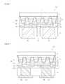
- FIG. 1is a schematic sectional view of an LED package 100 according to a first exemplary embodiment of the invention.
- the LED package 100may include a semiconductor stack 30 , a first contact layer 35 , a second contact layer 31 , a first insulation layer 33 , a second insulation layer 37 , a first electrode pad 39 a , a second electrode pad 39 b , a first bump 45 a , and a second bump 45 b .
- the LED package 100may further include an insulation layer 43 , a dummy bump 45 c , and a wavelength convertor 51 .
- the semiconductor stack 30includes a first conductive type upper semiconductor layer 25 , an active layer 27 , and a second conductive type lower semiconductor layer 29 .
- the active layer 27is interposed between the upper and lower semiconductor layers 25 , 29 .
- the active layer 27 and the upper and lower semiconductor layers 25 , 29may be composed of a III-N based compound semiconductor, for example, (Al, Ga, In)N semiconductor.
- Each of the upper and lower semiconductor layers 25 , 29may be a single layer or multiple layers.
- the upper and/or lower semiconductor layers 25 , 29may include a super lattice layer in addition to a contact layer and a clad layer.
- the active layer 27may have a single quantum well structure or a multi-quantum well structure.
- the first conductive typemay be an n-type and the second conductive type may be a p-type. Alternatively, the first conductive type may be a p-type and the second conductive type may be an n-type.
- the upper semiconductor layer 25can be formed of an n-type semiconductor layer having relatively low specific resistance, the upper semiconductor layer 25 may have a relatively high thickness. Therefore, a roughened surface R may be formed on an upper surface of the upper semiconductor layer 25 , in which the roughened surface R enhances extraction efficiency of light generated in the active layer 27 .
- the semiconductor stack 30has a plurality of contact holes 30 a (see FIG. 5( b ) ) formed through the second conductive type lower semiconductor layer 29 and the active layer 27 to expose the first conductive type upper semiconductor layer, and the first contact layer 35 contacts the first conductive type upper semiconductor layer 25 exposed in the plurality of contact holes.
- the second contact layer 31contacts the second conductive type lower semiconductor layer 29 .
- the second contact layer 31includes a reflective metal layer to reflect light generated in the active layer 27 . Further, the second contact layer 31 may form an ohmic contact with the second conductive type lower semiconductor layer 29 .
- the first insulation layer 33covers the second contact layer 31 . Further, the first insulation layer 33 covers a sidewall of the semiconductor stack 30 exposed in the plurality of contact holes 30 a . In addition, the first insulation layer 33 may cover a side surface of the semiconductor stack 30 . The first insulation layer 33 insulates the first contact layer 35 from the second contact layer 31 while insulating the second conductive type lower semiconductor layer 29 and the active layer 27 exposed in the plurality of contact holes 30 a from the first contact layer 35 .
- the first insulation layer 33may be composed of a single layer or multiple layers, such as a silicon oxide or silicon nitride film.
- the first insulation layer 33may be composed of a distributed Bragg reflector, which is formed by alternately stacking insulation layers having different indices of refraction, for example, SiO 2 /TiO 2 or SiO 2 /Nb 2 O 5 .
- the first contact layer 35is located under the first insulation layer 33 and contacts the first conductive type upper semiconductor layer 25 through the first insulation layer 33 in the plurality of contact holes 30 a .
- the first contact layer 35includes contact sections 35 a contacting the first conductive type upper semiconductor layer 25 , and a connecting section 35 b connecting the contact sections 35 a to each other. Therefore, the contact sections 35 a are electrically connected to each other by the connecting section 35 b .
- the first contact layer 35is formed under some regions of the first insulation layer 33 and may be composed of a reflective metal layer.
- the second insulation layer 37covers the first contact layer 35 under the first contact layer 35 .
- the second insulation layer 37covers the first insulation layer 33 while covering a side surface of the semiconductor stack 30 .
- the second insulation layer 37may be composed of a single layer or multiple layers. Further, the second insulation layer 37 may be a distributed Bragg reflector.
- the first and second electrode pads 39 a , 39 bare located under the second insulation layer 37 .
- the first electrode pad 39 amay be connected to the first contact layer 35 through the second insulation layer 37 .
- the second electrode pad 39 bmay be connected to the second contact layer 31 through the second insulation layer 37 and the first insulation layer 33 .
- the first bump 45 a and the second bump 45 bare located under the first and second electrode pads 39 a , 39 b to be connected thereto, respectively.
- the first and second bumps 45 a , 45 bmay be formed by plating.
- the first and second bumps 45 a , 45 bare terminals electrically connected to a circuit board such as an MC-PCB and have coplanar distal ends.
- the first electrode pad 39 amay be formed at the same level as that of the second electrode pad 39 b , so that the first bump 45 a and the second bump 45 b may also be formed on the same plane. Therefore, the first and second bumps 45 a , 45 b may have the same height.
- the dummy bump 45 cmay be located between the first bump 45 a and the second bump 45 b .
- the dummy bump 45 cmay be formed together with the first and second bumps 45 a and 45 b to provide a heat passage for discharging heat from the semiconductor stack 30 .
- the insulation layer 43may cover side surfaces of the first and second bumps 45 a , 45 b .
- the insulation layer 43may also cover a side surface of the dummy bump 45 c .
- the insulation layer 43fills spaces between the first bump 45 a , the second bump 45 b and the dummy bump 45 c to prevent moisture from entering the semiconductor stack 30 from outside.
- the insulation layer 43also covers side surfaces of the first and second electrode pads 39 a , 39 b to protect the first and second electrode pads 39 a , 39 b from external environmental factors such as moisture,
- the insulation layer 43may be configured to cover the overall side surfaces of the first and second bumps 45 a , 45 b , the invention is not limited thereto.
- the insulation layer 43may cover the side surfaces of the first and second bumps 45 a , 45 b except for some regions of the side surface near distal ends of the first and second bumps.
- the insulation layer 43is illustrated as covering the side surfaces of the first and second electrode pads 39 a and 39 b , but the invention is not limited thereto.
- another insulation layermay be used to cover the first and second electrode pads 39 a , 39 b and the insulation layer 43 may be formed under the other insulation layer.
- the first and second bumps 45 a , 45 bmay be connected to the first and second electrode pads 39 a , 39 b through the other insulation layer.
- the wavelength convertor 51may be located on the first conductive type upper semiconductor layer 25 opposite to the rest of the semiconductor stack 30 .
- the wavelength convertor 51may contact an upper surface of the first conductive type upper semiconductor layer 25 .
- the wavelength convertor 51may be a phosphor sheet having a uniform thickness without being limited thereto.
- the wavelength converter 51may be a substrate, for example, a sapphire substrate or a silicon substrate, which is doped with an impurity for wavelength conversion.
- the side surface of the semiconductor stack 30is covered with a protective insulation layer.
- the protective insulation layermay include, for example, the first insulation layer 33 and/or the second insulation layer 37 .
- the first contact layer 35may be covered with the second insulation layer 37 to be protected from an external environment and the second contact layer 31 may be covered with the first insulation layer 33 and the second insulation layer 37 to be protected from an external environment.
- the first and second electrode pads 39 a , 39 bare also protected by, for example, the insulation layer 43 . Accordingly, it is possible to prevent deterioration of the semiconductor stack 30 due to moisture.
- the wavelength convertor 51may be attached to the first conductive type upper semiconductor layer 25 at a wafer-level, and then divided together with the protective insulation layer during a chip separation process. Therefore, a side surface of the wavelength convertor 51 may be in a line with the protective insulation layer. That is, the side surface of the wavelength converter 51 may be flush along a straight line with a side surface of the protective insulation layer. Further, the side surface of the wavelength convertor 51 may be in a line with a side surface of the insulation layer 43 . Thus, the side surfaces of the wavelength converter 51 , the protective insulation layer, and the insulation layer 43 may all be flush along a straight line.
- FIG. 2is a schematic sectional view of a light emitting diode package 200 according to a second exemplary embodiment of the invention.
- the LED package 200is similar to the LED package 100 according to the above exemplary embodiment. In the present exemplary embodiment, however, first and second bumps 65 a , 65 b are formed in a substrate 61 .
- the substrate 61includes through-holes, which have the first and second bumps 65 a , 65 b formed therein, respectively.
- the substrate 61is an insulation substrate, for example, a sapphire substrate or a silicon substrate, but is not limited thereto.
- the substrate 61 having the first and second bumps 65 a , 65 bmay be attached to a first electrode pad 39 a and a second electrode pad 39 b .
- an insulation layer 49may cover side surfaces and bottom surfaces of the first and second electrode pads 39 a , 39 b .
- the insulation layer 49may have openings, which expose the first and second electrode pads 39 a , 39 b , and additional metal layers 67 a , 67 b are then formed in the openings.
- the additional metal layers 67 a , 67 bmay be composed of a bonding metal.
- FIG. 3is a sectional view of a light emitting diode module including the LED package 100 according to the first exemplary embodiment.
- the LED moduleincludes a circuit board 71 , for example, an MC-PCB, the LED package 100 , and a lens 81 .
- the circuit board 71for example, the MC-PCB, has connection pads 73 a , 73 b for mounting the LED packages 100 thereon.
- the first and second bumps 45 a , 45 b (see FIG. 1 ) of the LED) package 100are connected to the connection pads 73 a , 73 b , respectively.
- a plurality of LED packages 100may be mounted on the circuit board 71 and the lens 81 may be disposed on the LED packages 100 to adjust an orientation angle of light emitted from the LED packages 100 .
- the light emitting diode packages 200may be mounted on the circuit board instead of the LED packages 100 .
- FIG. 4 to FIG. 12show a method of fabricating the LED package 100 according to the first exemplary embodiment.
- (a)is a plan view and (b) is a sectional view taken along line A-A of (a).
- a semiconductor stack 30which includes a first conductive type semiconductor layer 25 , an active layer 27 and a second conductive type semiconductor layer 29 , is formed on a growth substrate 21 .
- the growth substrate 21may be a sapphire substrate but is not limited thereto. Alternatively, the growth substrate 21 may be another kind of heterogeneous substrate, for example, a silicon substrate.
- Each of the first and second conductive type semiconductor layers 25 , 29may be composed of a single layer or multiple layers.
- the active layer 27may have a single-quantum well structure or multi-quantum well structure.
- the compound semiconductor layersmay be formed of III-N based compound semiconductor on the growth substrate 21 by metal organic chemical vapor deposition (MOCVD) or molecular beam epitaxy (MBE).
- MOCVDmetal organic chemical vapor deposition
- MBEmolecular beam epitaxy
- a buffer layer(not shown) may be formed before forming the compound semiconductor layers.
- the buffer layeris formed to relieve lattice mismatch between the growth substrate 21 and the compound semiconductor layers and may be formed of a GaN-based material layer such as gallium nitride or aluminum nitride.
- the semiconductor stack 30is patterned to form a chip (package) separation region 30 b while patterning the second conductive type semiconductor layer 29 and the active layer 27 to form a plurality of contact holes 30 a exposing the first conductive type semiconductor layer 25 .
- the semiconductor stack 30may be patterned by photolithography and etching processes.
- the chip separation region 30 bis a region for dividing the LED package structure into individual LED packages and side surfaces of the first conductive type semiconductor layer 25 , the active layer 27 and the second conductive type semiconductor layer 29 are exposed on the chip separation region 30 b ,
- the chip separation region 30 bmay be configured to expose the substrate 21 without being limited thereto.
- the plurality of contact holes 30 amay have a circular shape, but is not limited thereto.
- the contact holes 30may have a variety of shapes.
- the second conductive type semiconductor layer 29 and the active layer 27are exposed to sidewalls of the plurality of contact holes 30 a . As shown, the contact holes 30 a may have slanted sidewalls.
- a second contact layer 31is formed on the second conductive type semiconductor layer 29 .
- the second contact layer 31is formed on the semiconductor stack 30 except for regions corresponding to the plurality of contact holes 30 a.
- the second contact layer 31may include a transparent conductive oxide film such as indium tin oxide (ITO) or a reflective metal layer such as silver (Ag) or aluminum (Al).
- ITOindium tin oxide
- the second contact layer 31may be composed of a single layer or multiple layers.
- the second contact layer 31may also be configured to form an ohmic contact with the second conductive type semiconductor layer 29 .
- the second contact layer 31may be formed before or after formation of the plurality of contact holes 30 a.
- a first insulation layer 33is formed to cover the second contact layer 31 .
- the first insulation layer 33may cover the side surface of the semiconductor stack 30 exposed to the chip separation region 30 b while covering the sidewalls of the plurality of contact holes 30 a .
- the first insulation layer 33may have openings 33 a , which expose the first conductive type semiconductor layer 25 in the plurality of contact holes 30 a.
- the first insulation layer 33may be composed of a single layer or multiple layers, such as a silicon oxide or silicon nitride film.
- the first insulation layer 33may be composed of a distributed Bragg reflector, which is formed by alternately stacking insulation layers having different indices of refraction.
- the first insulation layer 33may be formed by alternately stacking SiO 2 /TiO 2 or SiO 2 /Nb 2 O 5 .
- the first insulation layer 33may be formed to provide a distributed Bragg reflector having high reflectivity over a wide wavelength range of blue, green, and red light by adjusting the thickness of each of the insulation layers.
- a first contact layer 35is formed on the first insulation layer 33 .
- the first contact layer 35includes contact sections 35 a contacting the first conductive type upper semiconductor layer 25 exposed in the contact holes 30 a , and a connecting section 35 b connecting the contact sections 35 a to each other.
- the first contact layer 35may be composed of a reflective metal layer, but is not limited thereto.
- the first contact layer 35is formed on some regions of the semiconductor stack 30 , so that the first insulation layer 33 is exposed on other regions of the semiconductor stack 30 where the first contact layer 35 is not formed.
- a second insulation layer 37is formed on the first contact layer 35 .
- the second insulation layer 37may be composed of a single layer or multiple layers, such as a silicon oxide or silicon nitride film. Further, the second insulation layer 37 may be composed of a distributed Bragg reflector, which is formed by alternately stacking insulation layers having different indices of refraction.
- the second insulation layer 37may cover the first contact layer 35 while covering the first insulation layer 33 .
- the second insulation layer 37may also cover the side surface of the semiconductor stack 30 in the chip separation region 30 b.
- the second insulation layer 37has an opening 37 a which exposes the first contact layer 35 . Further, the second insulation layer 37 and the first insulation layer 33 are formed with an opening 37 b , which exposes the second contact layer 31 .
- first and second electrode pads 39 a , 39 bare formed on the second insulation layer 37 .
- the first electrode pad 39 ais connected to the first contact layer 35 through the opening 37 a and the second electrode pad 39 b is connected to the second contact layer 31 through the opening 37 b.
- the first electrode pad 39 ais separated from the second electrode pad 39 b and each of the first and second electrode pads 39 a , 39 b may have a relatively large area from a top perspective, for example, an area not less than 1 ⁇ 3 of the area of the LED package.
- an insulation layer 43is formed on the first and second electrode pads 39 a , 39 b .
- the insulation layer 43covers the first and second electrode pads 39 a , 39 b and has grooves which expose upper surfaces of the electrode pads 39 a , 39 b . Further, the insulation layer 43 may have a groove which exposes the second insulation layer 37 between the first and second electrode pads 39 a , 39 b.
- first and second bump 45 a , 45 bare formed in the grooves of the insulation layer 43 , and a dummy bump 45 c may be formed between the first bump and the second bump.
- the bumpsmay be formed by plating, for example, electroplating, using a metallic material. If necessary, a seed layer for plating may also be formed.
- the insulation layer 43may be removed.
- the insulation layer 43may be formed of a polymer such as photoresist and may be removed after the bumps are formed. Alternatively, the insulation layer 43 may remain to protect the side surfaces of the first and second bumps 45 a , 45 b.
- the insulation layer 43is illustrated as being directly formed on the first and second electrode pads 39 a , 39 b .
- another insulation layermay be formed to cover the first and second electrode pads 39 a , 39 b .
- the other insulation layermay be configured to have openings exposing the first and second electrode pads 39 a , 39 b . Then, the processes of forming the insulation layer 43 and the bumps may be carried out.
- the growth substrate 21is removed and a wavelength convertor 51 is attached to the first conductive type semiconductor layer 25 .
- the growth substrate 21may be removed by an optical technique such as laser lift-off (LLO), mechanical polishing or chemical etching.
- the exposed surface of the first conductive type semiconductor layer 25is subjected to anisotropic etching such as photoelectrochemical (PEC) etching to form a roughened surface on the exposed first conductive type semiconductor layer 25 .
- anisotropic etchingsuch as photoelectrochemical (PEC) etching to form a roughened surface on the exposed first conductive type semiconductor layer 25 .
- PECphotoelectrochemical
- the wavelength convertorsuch as a phosphor sheet containing phosphors may be attached to the first conductive type semiconductor layer 25 .
- the growth substrate 21may contain an impurity for converting a wavelength of light generated in the active layer 27 .
- the growth substrate 21may be used as the wavelength convertor 51 .
- the LED package structureis divided into individual packages along the chip separation region 30 b , thereby providing finished LED packages 100 .
- the second insulation layer 37is cut together with the wavelength convertor 51 so that cut planes thereof can be formed in a line.
- FIG. 13is a sectional view showing a method of fabricating the LED package 200 according to the second exemplary embodiment of the present invention.
- the processes until the first and second electrode pads 39 a , 39 b are formedare the same as those of the method of fabricating the LED package 100 described above ( FIGS. 10 ( a ) and ( b ) ).
- an insulation layer 49is formed to cover the first and second electrode pads 39 a , 39 b .
- the insulation layer 49may cover side surfaces of the first and second electrode pads 39 a , 39 b to protect the first and second electrode pads 39 a , 39 b .
- the insulation layer 49has openings which expose the first and second electrode pads 39 a , 39 b . Additional metal layers 67 a , 67 b are then formed in the openings.
- the additional metal layers 67 a , 67 bmay be composed of a bonding metal.
- the substrate 61is bonded to the first and second electrode pads 39 a , 39 b .
- the substrate 61may have through-holes, in which the first and second bumps 65 a , 65 b may be formed. Further, the first and second bumps may be formed at distal ends thereof with pads 69 a , 69 b .
- the substrate 61 having the first and second bumps 65 a , 65 b and the pads 69 a , 69 bmay be separately prepared and bonded to a wafer having the first and second electrode pads 39 a , 39 b.
- the growth substrate 21is removed and a wavelength convertor 51 may be attached to the first conductive type semiconductor layer 25 , followed by division of the LED package structure into individual LED packages.
- a wavelength convertor 51may be attached to the first conductive type semiconductor layer 25 , followed by division of the LED package structure into individual LED packages.
- the finished LED packages 200 as described in FIG. 2are provided.
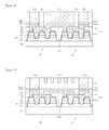
- FIG. 14is a sectional view of an LED package 300 according to a third exemplary embodiment of the present invention.
- the LED package 300may include a semiconductor stack 130 , which is divided into a plurality of light emitting cells (only two light emitting cells S 1 , S 2 are shown herein), a first contact layer 135 , a second contact layer 131 , a first insulation layer 133 , a second insulation layer 137 , a first electrode pad 139 a , a second electrode pad 139 b , a connector 139 c connecting adjacent light emitting cells to each other in series, a first bump 145 a and a second bump 145 b .
- the LED package 300may include a third insulation layer 141 , an insulation layer 143 , a dummy bump 145 c , a wavelength convertor 151 , and additional metal layers 140 a , 140 b.
- the semiconductor stack 130includes a first conductive type upper semiconductor layer 125 , an active layer 127 , and a second conductive type lower semiconductor layer 129 .
- the semiconductor stack 130 of the present exemplary embodimentis similar to the semiconductor stack 30 described in FIG. 1 , and a detailed description thereof will be omitted herein.
- Each of the light emitting cells S 1 , S 2has a plurality of contact holes 130 a (see FIG. 18( b ) ) extending through the second conductive type lower semiconductor layer 129 and the active layer 127 to expose the first conductive type upper semiconductor layer, and the first contact layer 135 contacts the first conductive type upper semiconductor layer 125 exposed in the plurality of contact holes.
- the light emitting cells S 1 , S 2are separated from each other by a cell separation region 130 b (see FIG. 18( b ) ).
- the second contact layer 131contacts the second conductive type lower semiconductor layer 129 of each of the light emitting cells S 1 , S 2 .
- the second contact layer 131includes a reflective metal layer to reflect light generated in the active layer 127 . Further, the second contact layer 131 may form an ohmic contact with the second conductive type lower semiconductor layer 129 .
- the first insulation layer 133covers the second contact layer 131 , Further, the first insulation layer 133 covers a sidewall of the semiconductor stack 130 exposed in the plurality of contact holes 130 a . In addition, the first insulation layer 133 may cover a side surface of each of the light emitting cells S 1 , S 2 .
- the first insulation layer 133insulates the first contact layer 135 from the second contact layer 131 while insulating the second conductive type lower semiconductor layer 129 and the active layer 127 exposed in the plurality of contact holes 130 a from the first contact layer 35 .
- the first insulation layer 133may be composed of a single layer or multiple layers, such as a silicon oxide or silicon nitride film.
- the first insulation layer 133may be composed of a distributed Bragg reflector, which is formed by alternately stacking insulation layers having different indices of refraction, for example, SiO 2 /TiO 2 or SiO 2 /Nb 2 O 5 .
- the first contact layer 135is located under the first insulation layer 133 and contacts the first conductive type upper semiconductor layer 125 through the first insulation layer 133 in the plurality of contact holes 130 a in each of the light emitting cells S 1 , S 2 .
- the first contact layer 135includes contact sections 135 a contacting the first conductive type upper semiconductor layer 125 , and a connecting section 135 b connecting the contact sections 135 a to each other. Therefore, the contact sections 135 a are electrically connected to each other by the connecting section 135 b .
- the first contact layers 135 located under the respective light emitting cells S 1 , S 2are separated from each other and formed under some regions of the first insulation layer 133 .
- the first contact layer 135may be composed of a reflective metal layer.
- the second insulation layer 137covers the first contact layer 135 under the first contact layer 135 .
- the second insulation layer 137may cover the first insulation layer 133 while covering the side surface of each of the light emitting cells S 1 , S 2 .
- the second insulation layer 137may be composed of a single layer or multiple layers.
- the second insulation layer 37may be composed of a distributed Bragg reflector.
- the first electrode pad 139 a and the second electrode pad 139 bare located under the second insulation layer 137 .
- the first electrode pad 139 amay be connected to the first contact layer 135 of a first light emitting cell S through the second insulation layer 137 .
- the second electrode pad 139 bmay be connected to the second contact layer 31 of a second light emitting cell S 2 through the second insulation layer 137 and the first insulation layer 133 .
- the connector 139 cis located under the second insulation layer 137 and electrically connects two adjacent light emitting cells S 1 , S 2 to each other through the second insulation layer 137 .
- the connector 139 cmay connect the second contact layer 131 of one light emitting cell S 1 to the first contact layer 135 of another light emitting cell S 2 adjacent thereto, so that the two light emitting cells S 1 , S 2 are connected in series to each other.
- two light emitting cells S 1 , S 2are illustrated. However, it should be understood that two or more light emitting cells may be connected in series to each other by a plurality of connectors 139 c .
- the first and second electrode pads 139 a , 139 bmay be connected in series to the light emitting cells S 1 , S 2 located at opposite ends of such series array.
- the third insulation layer 141may cover the first electrode pad 139 a , the second electrode pad 139 b and the connector 139 c under the first electrode pad 139 a , the second electrode pad 139 b and the connector 139 c ,
- the third insulation layer 141may have an opening exposing the first electrode pad 139 a and the second electrode pad 139 b .
- the third insulation layer 141may be formed of a silicon oxide or silicon nitride film.
- the first bump 145 a and the second bump 145 bare located under the first and second electrode pads 139 a , 139 b , respectively.
- the first and second bumps 145 a , 145 bmay be formed by plating.
- the first and second bumps 145 a , 145 bare terminals electrically connected to a circuit board such as an MC-PCB and have distal ends coplanar with each other.
- the first electrode pad 139 amay be formed at the same level as that of the second electrode pad 139 b , so that the first bump 45 a and the second bump 45 b may also be formed on the same plane. Therefore, the first and second bumps 45 a , 45 b may have the same height.
- the additional metal layers 140 a , 140 bmay be interposed between the first bump 145 a and the first electrode pad 139 a and between the second bump 145 b and the second electrode pad 139 b .
- the additional metal layers 140 a , 140 bare provided to form the first and second electrode pads 139 a , 139 b to be higher than the connector 139 c and may be located inside openings of the third insulation layer 141 .
- the first and second electrode pads 139 a , 139 b and the additional metal layers 140 a , 140 bmay constitute final electrode pads.
- the dummy bump 145 cmay be located between the first bump 145 a and the second bump 145 b .
- the dummy bump 145 cmay be formed together with the first and second bump 145 a , 145 b to provide a heat passage for discharging heat from the light emitting cells S 1 , S 2 .
- the dummy bump 145 cis separated from the connector 139 c by the third insulation layer 141 .
- the insulation layer 143may cover side surfaces of the first and second bumps 145 a , 145 b .
- the insulation layer 143may also cover a side surface of the dummy bump 145 c .
- the insulation layer 143fills spaces between the first bump 145 a , the second bump 145 b and the dummy bump 145 c to prevent moisture from entering the semiconductor stack 130 from outside.
- the insulation layer 143may be configured to cover the overall side surfaces of the first and second bumps 145 a , 145 b , the invention is not limited thereto.
- the insulation layer 143may cover the side surfaces of the first and second bumps 145 a , 145 b except for some regions of the side surface near distal ends of the first and second bumps.
- the wavelength convertor 151may be located on the light emitting cells S 1 , S 2 .
- the wavelength convertor 151may contact an upper surface of the first conductive type upper semiconductor layer 125 .
- the wavelength convertor 151also covers a cell separation region 130 b and a chip separation region.
- the wavelength convertor 151may be a phosphor sheet having a uniform thickness without being limited thereto.
- the wavelength converter 51may be a substrate, for example, a sapphire substrate or a silicon substrate, which is doped with an impurity for wavelength conversion.
- the side surfaces of the light emitting cells S 1 , S 2are covered with a protective insulation layer.
- the protective insulation layermay include, for example, the first insulation layer 133 and/or the second insulation layer 137 .
- the first contact layer 135may be covered with the second insulation layer 137 to be protected from external environment and the second contact layer 131 may be covered with the first insulation layer 133 and the second insulation layer 137 to be protected from external environment.
- the first and second electrode pads 139 a , 139 bare also protected by, for example, the third insulation layer 141 . Accordingly, it is possible to prevent deterioration of the light emitting cells S 1 , S 2 due to moisture.
- the wavelength convertor 151may be attached to the first conductive type upper semiconductor layer 125 at a wafer-level, and then divided together with the protective insulation layer during a chip separation process (or package separation process). Therefore, a side surface of the wavelength convertor 151 may be in a line with the protective insulation layer. Further, the side surface of the wavelength convertor 151 may be in a line with a side surface of the insulation layer 143 .
- FIG. 15is a schematic sectional view of a light emitting diode package 400 according to a fourth exemplary embodiment of the present invention.
- the LED package 400is similar to the LED package 300 according to the above exemplary embodiment. In present exemplary embodiment, however, first and second bumps 165 a , 165 b are formed in a substrate 161 .
- the substrate 161includes through-holes, which have the first and second bumps 165 a , 165 b formed therein, respectively.
- the substrate 161is an insulation substrate, for example, a sapphire substrate or a silicon substrate, but is not limited thereto.
- the substrate 161 having the first and second bumps 165 a , 165 bmay be attached to a third insulation layer 141 , and the first and second bumps 165 a , 165 b may be connected to first and second electrode pads 139 a , 139 b , respectively.
- the first and second bumps 165 a , 165 bmay be bonded to additional metal layers 140 a , 140 b , respectively.
- FIG. 16is a sectional view of a light emitting diode module including the LED packages 300 according to the third exemplary embodiment on a circuit board.
- the LED moduleincludes a circuit board 171 , for example, an MC-PCB, the LED package 300 , and a lens 181 .
- the circuit board 171for example, the MC-PCB, has connection pads 173 a , 173 b for mounting the LED packages 300 thereon.
- the first and second bumps 145 a , 145 b (see FIG. 14 ) of the LED package 300are connected to the connection pads 73 a , 73 b , respectively.
- a plurality of LED packages 300may be mounted on the circuit board 171 and the lens 181 may be disposed on the LED) packages 300 to adjust an orientation angle of light emitted from the LED packages 300 .
- the light emitting diode packages 400may be mounted on the circuit board.
- FIG. 17 to FIG. 25show a method of fabricating the LED package 300 according to the third exemplary embodiment.
- (a)is a plan view and (b) is a sectional view taken along line A-A of (a).
- a semiconductor stack 130which includes a first conductive type semiconductor layer 125 , an active layer 127 and a second conductive type semiconductor layer 129 , is formed on a growth substrate 121 .
- the growth substrate 121 and the semiconductor stack 130are similar to the substrate 21 and the semiconductor stack 30 described with reference to FIG. 4 , and a detailed description thereof will thus be omitted herein.
- the semiconductor stack 130is patterned to form a chip (package) separation region 130 c and a cell separation region 130 b while patterning the second conductive type semiconductor layer 129 and the active layer 127 to form light emitting cells S 1 , S 2 , each having a plurality of contact holes 130 a exposing the first conductive type semiconductor layer 125 ,
- the semiconductor stack 130may be patterned by photolithography and etching processes.
- the chip separation region 130 cis a region for dividing the LED package structure into individual LED packages and side surfaces of the first conductive type semiconductor layer 125 , the active layer 127 and the second conductive type semiconductor layer 129 are exposed at the chip separation region 130 c .
- the chip separation region 130 c and the cell separation region 130 bmay be configured to expose the substrate 121 without being limited thereto.
- the plurality of contact holes 130 amay have a circular shape, but is not limited thereto.
- the contact holes 130may have a variety of shapes.
- the second conductive type semiconductor layer 129 and the active layer 127are exposed to sidewalls of the plurality of contact holes 130 a .
- the contact holes 130 amay have slanted sidewalls.
- a second contact layer 131is formed on the second conductive type semiconductor layer 129 .
- the second contact layer 131is formed on the semiconductor stack 130 in each of the light emitting cells S 1 , S 2 except for regions corresponding to the plurality of contact holes 130 a.
- the second contact layer 131may include a transparent conductive oxide film such as indium tin oxide (ITO) or a reflective metal layer such as silver (Ag) or aluminum (Al).
- the second contact layer 131may be composed of a single layer or multiple layers.
- the second contact layer 131may also be configured to form an ohmic contact with the second conductive type semiconductor layer 129 .
- the second contact layer 131may be formed before or after the formation of the plurality of contact holes 130 a
- a first insulation layer 133is formed to cover the second contact layer 131 .
- the first insulation layer 133may cover the side surface of each of the light emitting cells S 1 , S 2 while covering the sidewalls of the plurality of contact holes 130 a .
- the first insulation layer 133may have openings 133 a , which expose the first conductive type semiconductor layer 125 in the plurality of contact holes 130 a.
- the first insulation layer 133may be composed of a single layer or multiple layers, such as a silicon oxide or silicon nitride film,
- the first insulation layer 133may be composed of a distributed Bragg reflector, which is formed by alternately stacking insulation layers having different indices of refraction.
- the first insulation layer 133may be formed by alternately stacking SiO 2 /TiO 2 or SiO 2 /Nb 2 O 5 .
- the first insulation layer 133may be formed to provide a distributed Bragg reflector having high reflectivity over a wide wavelength range of blue, green, and red light by adjusting the thickness of each of the insulation layers.
- a first contact layer 135is formed on the first insulation layer 133 .
- the first contact layer 135is formed on each of the light emitting cells S 1 , S 2 , and includes contact sections 35 a contacting the first conductive type upper semiconductor layer 125 exposed in the contact holes 130 a and a connecting section 135 b connecting the contact sections 135 a to each other.
- the first contact layer 135may be composed of a reflective metal layer, but is not limited thereto.
- the first contact layer 135is formed on some regions of each of the light emitting cells S 1 , S 2 , so that the first insulation layer 133 is exposed at other regions of the semiconductor stack 130 where the first contact layer 135 is not formed.
- a second insulation layer 137is formed on the first contact layer 135 .
- the second insulation layer 137may be composed of a single layer or multiple layers, such as a silicon oxide or silicon nitride film.
- the second insulation layer 137may be composed of a distributed Bragg reflector, which is formed by alternately stacking insulation layers having different indices of refraction.
- the second insulation layer 137may cover the first contact layer 135 while covering the first insulation layer 133 .
- the second insulation layer 137may also cover the side surface of the each of the light emitting cells S 1 , S 2 .
- the second insulation layer 137may fill in the chip separation region 130 c and the cell separation region 130 b.
- the second insulation layer 137has an opening 137 a which exposes the first contact layer 135 of each of the light emitting cells S 1 , S 2 . Further, the second insulation layer 137 and the first insulation layer 133 are formed with an opening 137 b , which exposes the second contact layer 131 .
- a connector 139 c and first and second electrode pads 139 a , 139 bare formed on the second insulation layer 137 .
- the first electrode pad 139 ais connected to the first contact layer 135 of a first light emitting cell S 1 through the opening 137 a and the second electrode pad 139 b is connected to the second contact layer 131 of a second light emitting cell S 2 through the opening 137 b .
- the connector 139 cconnects the first contact layer 135 and the second contact layer 131 of adjacent light emitting cells S 1 , S 2 to each other in series through the openings 137 a , 137 b.
- a third insulation layer 141is formed on the first and second electrode pads 139 a , 139 b and the connector 139 c .
- the third insulation layer 141covers the first and second electrode pads 139 a , 139 b and the connector 139 c , and has grooves which expose upper surfaces of the electrode pads 139 a , 139 b .
- the third insulation layer 141may have additional metal layers 140 a , 140 b formed in the grooves thereof.
- the additional metal layers 140 a , 140 hincrease the height of the electrode pads 139 a , 139 b , such that final electrode pads may have a greater height than the connector 139 c .
- the additional metal layers 140 a , 140 bmay be formed before the formation of the third insulation layer 141 .
- Upper surfaces of the additional metal layers 140 a , 140 bmay be substantially coplanar with an upper surface of the third insulation layer 141 .
- a patterned insulation layer 143is formed on the third insulation layer 141 .
- the patterned insulation layer 143has grooves, which expose the upper side of the first and second electrode pads 139 a , 139 b , for example, the additional metal layers 140 a , 140 b . Further, the patterned insulation layer 143 may have a groove exposing the third insulation layer 141 between the first electrode pad 139 a and the second electrode pad 139 b.
- first and second bumps 145 a , 145 bare formed in the grooves of the insulation layer 143 and a dummy bump 145 c may be formed between the first and second bumps.
- the bumpsmay be formed by plating, for example, electroplating. As needed, a seed layer for plating may also be formed.
- the insulation layer 143may be removed.
- the insulation layer 143may be formed of a polymer such as photoresist and may be removed after the bumps are formed.
- the insulation layer 143may remain to protect the side surfaces of the first and second bumps 145 a , 145 b.
- the growth substrate 121is removed and a wavelength convertor 151 is attached to the light emitting cells S 1 , S 2 .
- the growth substrate 21may be removed by an optical technique such as laser lift-off (LLO), mechanical polishing or chemical etching.
- the exposed surface of the first conductive type semiconductor layer 125is subjected to anisotropic etching such as PEC etching to form a roughened surface on the exposed first conductive type semiconductor layer 125 .
- the wavelength convertor 151such as a phosphor sheet containing phosphors, may be attached to the first conductive type semiconductor layer 125
- the growth substrate 121may contain an impurity for converting a wavelength of light generated in the active layer 127 .
- the growth substrate 121may be used as the wavelength convertor 151 .
- the LED package structureis divided into individual packages along the chip separation region 130 c , thereby providing finished LED packages 300 .
- the second insulation layer 137is cut together with the wavelength convertor 151 so that cut planes thereof can be formed in a line.
- FIG. 27is a sectional view explaining a method of fabricating the LED package 400 according to the fourth exemplary embodiment of the invention.
- the processes until the third insulation layer 141 and the additional metal layers 140 a , 1140 b are formedare the same as those of the method of fabricating the LED package 300 described above ( FIG. 24 ).
- the substrate 161is bonded to the third insulation layer 141 .
- the substrate 161may have through-holes, in which the first and second bumps 165 a , 165 b may be formed. Further, the first and second bumps 165 a , 165 b may be formed at distal ends thereof with pads (not shown).
- the substrate 161may have grooves partially formed on a lower surface thereof and filled with a metallic material 165 c .
- the metallic material 165 cimproves substrate heat dissipation.
- the substrate 161 having the first and second bumps 165 a , 165 bmay be separately prepared and bonded to a wafer having the first and second electrode pads 139 a , 139 b .
- the first and second bumps 165 a , 165 bmay be electrically connected to first and second electrode pads 139 a , 139 b , respectively.
- the growth substrate 121is removed and the wavelength convertor 151 may be attached to the light emitting cells S 1 , S 2 , followed by division of the LED package structure into individual LED packages.
- the finished LED packages 400 as described in FIG. 15are provided.
- the exemplary embodiments of the inventionprovide wafer-level LED packages which can be directly formed on a circuit board for a module without using a conventional lead frame or printed circuit board. Accordingly, the LED package may have high efficiency and exhibit improved heat dissipation while reducing time and cost for fabrication of the LED package. In addition, an LED module having the LED package mounted thereon may have high efficiency and exhibit improved heat dissipation.
- the LED packagemay include a plurality of light emitting cells connected in series to each other and arrays connected in reverse parallel to each other. Further, the plurality of light emitting cells may be connected to a bridge rectifier and may be used to form a bridge rectifier. Therefore, the LED module including the LED package may be operated by AC power without a separate AC/DC converter.
Landscapes
- Led Device Packages (AREA)
- Led Devices (AREA)
Abstract
Description
This application is a continuation of, and claims the benefits and priorities to, U.S. patent application Ser. No. 14/815,433, filed on Jul. 31, 2015, which is a continuation of U.S. patent application Ser. No. 14/708,029, filed on May 8, 2015, issued as U.S. Pat. No. 9,219,196, which is a continuation of U.S. patent application Ser. No. 13/194,317, filed on Jul. 29, 2011, issued as U.S. Pat. No. 9,070,851, which further claims priorities and benefits from and the benefits of Korean Patent Application No. 10-2010-0092807, filed on Sep. 24, 2010, and Korean Patent Application No. 10-2010-0092808, filed on Sep. 24, 2010. The above patent applications are hereby incorporated by reference for all purposes as if fully set forth herein.
Field of the Invention
The invention relates to a light emitting diode package and a method of fabricating the same and, more particularly, to a wafer—level light emitting diode package and a method of fabricating the same.
Description of the Background
A light emitting diode (LED) is a semiconductor device that includes an N-type semiconductor and a P-type semiconductor, and emits light through recombination of holes and electrons. Such an LED has been used in a wide range of applications such as display devices, traffic lights, and backlight units. Further, considering the potential merits of lower power consumption and longer lifespan than existing electric bulbs or fluorescent lamps, the application range of LEDs has been expanded to general lighting by replacing existing incandescent lamps and fluorescent lamps.
The LED may be used in an LED module. The LED module is manufactured through a process of fabricating an LED chip at a wafer level, a packaging process, and a modulation process. Specifically, semiconductor layers are grown on a substrate such as a sapphire substrate, and subjected to a wafer-level patterning process to fabricate LED chips having electrode pads, followed by division into individual chips (chip fabrication process). Then, after mounting the individual chips on a lead frame or a printed circuit board, the electrode pads are electrically connected to lead terminals via bonding wires, and the LED chips are covered by a molding member, thereby providing an LED package (packaging process). Then, the LED package is mounted on a circuit board such as a metal core printed circuit board (MC-PCB), thereby providing an LED module such as a light source module (modulation process).
In the packaging process, a housing and/or the molding member may be provided to the LED chip to protect the LED chip from the external environment. In addition, a phosphor may be contained in the molding member to convert light emitted by the LED chip so that the LED package may emit a white light, thereby providing a white LED package. Such a white LED package may be mounted on the circuit board such as the MC-PCB and a secondary lens may be provided to the LED package to adjust orientation characteristics of light emitted from the LED package, thereby providing a desired white LED module.
However, it may be difficult to achieve miniaturization and satisfactory heat dissipation of the conventional LED package including the lead frame or printed circuit board. Furthermore, luminous efficiency of the LED may be deteriorated due to absorption of light by the lead frame or the printed circuit board, electric resistance heating by the lead terminals, and the like.
In addition, the chip fabrication process, the packaging process, and the modulation process may be separately carried out, thereby increasing time and costs for manufacturing the LED module.
Meanwhile, alternating current (AC) LEDs have been produced and marketed. The AC LED includes an LED directly connected to an AC power source to permit continuous emission of light. One example of AC LEDs, which can be used by being directly connected to a high voltage AC power source, is disclosed in U.S. Pat. No. 7,417,259, issued to Sakai, et. al.
According to U.S. Pat. No. 7,417,259, LED elements are arranged in a two-dimensional pattern on an insulating substrate, for example, a sapphire substrate, and are connected in series to form LED arrays. The LED arrays are connected in series to each other, thereby providing a light emitting device that can be operated at high voltage. Further, such LED arrays may be connected in reverse parallel to each other on the sapphire substrate, thereby providing a single-chip light emitting device that can be operated to continuously emit light using an AC power supply.
Since the AC-LED includes light emitting cells on a growth substrate, for example, on a sapphire substrate, the AC-LED restricts the structure of the light emitting cells and may limit improvement of light extraction efficiency. Thus, investigation has been made into a light emitting diode, for example, an AC-LED that is based on a substrate separation process and includes light emitting cells connected in series to each other.
Exemplary embodiments of the invention provide a wafer-level LED package and a method of fabricating the same, which can be directly formed in a module on a circuit board without using a conventional lead frame or printed circuit board.
Exemplary embodiments of the invention also provide a wafer-level LED package and a method of fabricating the same, which has high efficiency and exhibits improved heat dissipation.
Exemplary embodiments of the invention also provide a method of fabricating an LED package, which may reduce manufacturing time and cost of an LED module.
Exemplary embodiments of the invention also provide an LED module and a method of fabricating the same, which has high efficiency and exhibits improved heat dissipation.
Exemplary embodiments of the invention also provide a wafer-level light emitting diode package and a method of fabricating the same, which includes a plurality of light emitting cells and may be directly formed in a module on a circuit board without using a conventional lead frame or printed circuit board.
Additional features of the invention will be set forth in the description which follows and in part will be apparent from the description, or may be learned by practice of the invention.
An exemplary embodiment of the present invention discloses an LED package including: a semiconductor stack including a first conductive type semiconductor layer, an active layer, and a second conductive type semiconductor layer; a plurality of contact holes arranged in the second conductive type semiconductor layer and the active layer, the contact holes exposing the first conductive type semiconductor layer; a first bump arranged on a first side of the semiconductor stack, the first bump being electrically connected to the first conductive type semiconductor layer via the plurality of contact holes; a second bump arranged on the first side of the semiconductor stack, the second bump being electrically connected to the second conductive type semiconductor layer; and a protective insulation layer covering a sidewall of the semiconductor stack.
An exemplary embodiment of the present invention also discloses a light emitting diode module including the LED package according to the aforementioned exemplary embodiments. The LED module may include a circuit board; the LED package mounted on the circuit board; and a lens to adjust an orientation angle of light emitted from the LED package.
An exemplary embodiment of the present invention also discloses a method of fabricating an LED package. The method includes forming a semiconductor stack including a first conductive type semiconductor layer, an active layer, and a second conductive type semiconductor layer on a first substrate; patterning the semiconductor stack to form a chip separation region; patterning the second conductive type semiconductor layer and the active layer to form a plurality of contact holes exposing the first conductive type semiconductor layer; forming a protective insulation layer covering a sidewall of the semiconductor stack in the chip separation region; and forming a first bump and a second bump on the semiconductor stack. The first bump is electrically connected to the first conductive type semiconductor layer via the plurality of contact holes, and the second bump is electrically connected to the second conductive type semiconductor layer.
An exemplary embodiment of the present invention also discloses a light emitting diode package. The LED package includes a plurality of light emitting cells each including a first conductive type semiconductor layer, an active layer, and a second conductive type semiconductor layer; a plurality of contact holes arranged in the second conductive type semiconductor layer and the active layer of each of the light emitting cells, the contact holes exposing the first conductive type semiconductor layer thereof; a protective insulation layer covering a sidewall of each of the light emitting cells; a connector located arranged on a first side of the light emitting cells and electrically connecting two adjacent light emitting cells to each other; a first bump arranged on the first side of the light emitting cells and electrically connected to the first conductive type semiconductor layer via the plurality of contact holes of a first light emitting cell of the light emitting cells; and a second bump arranged in the first side of the light emitting cells and electrically connected to the second conductive type semiconductor layer of a second light emitting cell of the light emitting cells.
An exemplary embodiment of the present invention also discloses a light emitting diode module including the LED package described above. The module includes a circuit board; the LED package arranged on the circuit board; and a lens to adjust an orientation angle of light emitted from the LED package.
An exemplary embodiment of the present invention also discloses a method of fabricating an LED package including a plurality of light emitting cells. The method includes forming a semiconductor stack including a first conductive type semiconductor layer, an active layer, and a second conductive type semiconductor layer on a first substrate; patterning the semiconductor stack to form a chip separation region and a light emitting cell separation region: patterning the second conductive type semiconductor layer and the active layer to form a plurality of light emitting cells, each light emitting cell having a plurality of contact holes exposing the first conductive type semiconductor layer; forming a protective insulation layer covering a sidewall of the semiconductor stack in the chip separation region and the light emitting cell separation region; forming a connector connecting adjacent light emitting cells in series to each other; and forming a first bump and a second bump on the plurality of light emitting cells. Here, the first bump is electrically connected to the first conductive type semiconductor layer via the plurality of contact holes of a first light emitting cell of the light emitting cells, and the second bump is electrically connected to the second conductive type semiconductor layer of a second light emitting cell of the light emitting cells.
It is to be understood that both the foregoing general description and the following detailed description are exemplary and explanatory and are intended to provide further explanation of the invention as claimed.
The accompanying drawings, which are included to provide a further understanding of the invention and are incorporated in and constitute a part of this specification, illustrate exemplary embodiments of the invention, and together with the description serve to explain the principles of the invention.
The invention is described more fully hereinafter with reference to the accompanying drawings, in which exemplary embodiments of the invention are shown. This invention may, however, be embodied in many different forms and should not be construed as limited to the exemplary embodiments set forth herein. Rather, these exemplary embodiments are provided so that this disclosure is thorough and will fully convey the scope of the invention to those skilled in the art. In the drawings, the sizes and relative sizes of layers and regions may be exaggerated for clarity. Like reference numerals in the drawings denote like elements.
It will be understood that when an element such as a layer, film, region or substrate is referred to as being “on” another element, it can be directly on the other element or intervening elements may also be present. In contrast, when an element is referred to as being “directly on” another element, there are no intervening elements present.
Referring toFIG. 1 , theLED package 100 may include asemiconductor stack 30, afirst contact layer 35, asecond contact layer 31, afirst insulation layer 33, asecond insulation layer 37, afirst electrode pad 39a, asecond electrode pad 39b, afirst bump 45a, and asecond bump 45b. TheLED package 100 may further include aninsulation layer 43, adummy bump 45c, and awavelength convertor 51.
Thesemiconductor stack 30 includes a first conductive typeupper semiconductor layer 25, anactive layer 27, and a second conductive typelower semiconductor layer 29. Theactive layer 27 is interposed between the upper and lower semiconductor layers25,29.
Theactive layer 27 and the upper and lower semiconductor layers25,29 may be composed of a III-N based compound semiconductor, for example, (Al, Ga, In)N semiconductor. Each of the upper and lower semiconductor layers25,29 may be a single layer or multiple layers. For example, the upper and/or lower semiconductor layers25,29 may include a super lattice layer in addition to a contact layer and a clad layer. Theactive layer 27 may have a single quantum well structure or a multi-quantum well structure. The first conductive type may be an n-type and the second conductive type may be a p-type. Alternatively, the first conductive type may be a p-type and the second conductive type may be an n-type. Since theupper semiconductor layer 25 can be formed of an n-type semiconductor layer having relatively low specific resistance, theupper semiconductor layer 25 may have a relatively high thickness. Therefore, a roughened surface R may be formed on an upper surface of theupper semiconductor layer 25, in which the roughened surface R enhances extraction efficiency of light generated in theactive layer 27.
Thesemiconductor stack 30 has a plurality of contact holes30a(seeFIG. 5(b) ) formed through the second conductive typelower semiconductor layer 29 and theactive layer 27 to expose the first conductive type upper semiconductor layer, and thefirst contact layer 35 contacts the first conductive typeupper semiconductor layer 25 exposed in the plurality of contact holes.
Thesecond contact layer 31 contacts the second conductive typelower semiconductor layer 29. Thesecond contact layer 31 includes a reflective metal layer to reflect light generated in theactive layer 27. Further, thesecond contact layer 31 may form an ohmic contact with the second conductive typelower semiconductor layer 29.
Thefirst insulation layer 33 covers thesecond contact layer 31. Further, thefirst insulation layer 33 covers a sidewall of thesemiconductor stack 30 exposed in the plurality of contact holes30a. In addition, thefirst insulation layer 33 may cover a side surface of thesemiconductor stack 30. Thefirst insulation layer 33 insulates thefirst contact layer 35 from thesecond contact layer 31 while insulating the second conductive typelower semiconductor layer 29 and theactive layer 27 exposed in the plurality of contact holes30afrom thefirst contact layer 35. Thefirst insulation layer 33 may be composed of a single layer or multiple layers, such as a silicon oxide or silicon nitride film. Alternatively, thefirst insulation layer 33 may be composed of a distributed Bragg reflector, which is formed by alternately stacking insulation layers having different indices of refraction, for example, SiO2/TiO2or SiO2/Nb2O5.
Thefirst contact layer 35 is located under thefirst insulation layer 33 and contacts the first conductive typeupper semiconductor layer 25 through thefirst insulation layer 33 in the plurality of contact holes30a. Thefirst contact layer 35 includescontact sections 35acontacting the first conductive typeupper semiconductor layer 25, and a connectingsection 35bconnecting thecontact sections 35ato each other. Therefore, thecontact sections 35aare electrically connected to each other by the connectingsection 35b. Thefirst contact layer 35 is formed under some regions of thefirst insulation layer 33 and may be composed of a reflective metal layer.
Thesecond insulation layer 37 covers thefirst contact layer 35 under thefirst contact layer 35. In addition, thesecond insulation layer 37 covers thefirst insulation layer 33 while covering a side surface of thesemiconductor stack 30. Thesecond insulation layer 37 may be composed of a single layer or multiple layers. Further, thesecond insulation layer 37 may be a distributed Bragg reflector.
The first andsecond electrode pads second insulation layer 37. Thefirst electrode pad 39amay be connected to thefirst contact layer 35 through thesecond insulation layer 37. Further, thesecond electrode pad 39bmay be connected to thesecond contact layer 31 through thesecond insulation layer 37 and thefirst insulation layer 33.
Thefirst bump 45aand thesecond bump 45bare located under the first andsecond electrode pads second bumps second bumps first electrode pad 39amay be formed at the same level as that of thesecond electrode pad 39b, so that thefirst bump 45aand thesecond bump 45bmay also be formed on the same plane. Therefore, the first andsecond bumps
Meanwhile, thedummy bump 45cmay be located between thefirst bump 45aand thesecond bump 45b. Thedummy bump 45cmay be formed together with the first andsecond bumps semiconductor stack 30.
Theinsulation layer 43 may cover side surfaces of the first andsecond bumps insulation layer 43 may also cover a side surface of thedummy bump 45c. In addition, theinsulation layer 43 fills spaces between thefirst bump 45a, thesecond bump 45band thedummy bump 45cto prevent moisture from entering thesemiconductor stack 30 from outside. Theinsulation layer 43 also covers side surfaces of the first andsecond electrode pads second electrode pads insulation layer 43 may be configured to cover the overall side surfaces of the first andsecond bumps insulation layer 43 may cover the side surfaces of the first andsecond bumps
In the present exemplary embodiment, theinsulation layer 43 is illustrated as covering the side surfaces of the first andsecond electrode pads second electrode pads insulation layer 43 may be formed under the other insulation layer. In this case, the first andsecond bumps second electrode pads
Thewavelength convertor 51 may be located on the first conductive typeupper semiconductor layer 25 opposite to the rest of thesemiconductor stack 30. Thewavelength convertor 51 may contact an upper surface of the first conductive typeupper semiconductor layer 25. Thewavelength convertor 51 may be a phosphor sheet having a uniform thickness without being limited thereto. Alternatively, thewavelength converter 51 may be a substrate, for example, a sapphire substrate or a silicon substrate, which is doped with an impurity for wavelength conversion.
In the present exemplary embodiment, the side surface of thesemiconductor stack 30 is covered with a protective insulation layer. The protective insulation layer may include, for example, thefirst insulation layer 33 and/or thesecond insulation layer 37. In addition, thefirst contact layer 35 may be covered with thesecond insulation layer 37 to be protected from an external environment and thesecond contact layer 31 may be covered with thefirst insulation layer 33 and thesecond insulation layer 37 to be protected from an external environment. The first andsecond electrode pads insulation layer 43. Accordingly, it is possible to prevent deterioration of thesemiconductor stack 30 due to moisture.
Thewavelength convertor 51 may be attached to the first conductive typeupper semiconductor layer 25 at a wafer-level, and then divided together with the protective insulation layer during a chip separation process. Therefore, a side surface of thewavelength convertor 51 may be in a line with the protective insulation layer. That is, the side surface of thewavelength converter 51 may be flush along a straight line with a side surface of the protective insulation layer. Further, the side surface of thewavelength convertor 51 may be in a line with a side surface of theinsulation layer 43. Thus, the side surfaces of thewavelength converter 51, the protective insulation layer, and theinsulation layer 43 may all be flush along a straight line.
Referring toFIG. 2 , theLED package 200 is similar to theLED package 100 according to the above exemplary embodiment. In the present exemplary embodiment, however, first andsecond bumps substrate 61.
Specifically, thesubstrate 61 includes through-holes, which have the first andsecond bumps substrate 61 is an insulation substrate, for example, a sapphire substrate or a silicon substrate, but is not limited thereto. Thesubstrate 61 having the first andsecond bumps first electrode pad 39aand asecond electrode pad 39b. In this case, to prevent the first andsecond electrode pads insulation layer 49 may cover side surfaces and bottom surfaces of the first andsecond electrode pads insulation layer 49 may have openings, which expose the first andsecond electrode pads additional metal layers additional metal layers
Referring toFIG. 3 , the LED module includes acircuit board 71, for example, an MC-PCB, theLED package 100, and alens 81. Thecircuit board 71, for example, the MC-PCB, hasconnection pads second bumps FIG. 1 ) of the LED)package 100 are connected to theconnection pads
A plurality ofLED packages 100 may be mounted on thecircuit board 71 and thelens 81 may be disposed on the LED packages100 to adjust an orientation angle of light emitted from the LED packages100.
In accordance with the second exemplary embodiment, the light emittingdiode packages 200 may be mounted on the circuit board instead of the LED packages100.
Referring toFIG. 4 , asemiconductor stack 30, which includes a first conductivetype semiconductor layer 25, anactive layer 27 and a second conductivetype semiconductor layer 29, is formed on agrowth substrate 21. Thegrowth substrate 21 may be a sapphire substrate but is not limited thereto. Alternatively, thegrowth substrate 21 may be another kind of heterogeneous substrate, for example, a silicon substrate. Each of the first and second conductive type semiconductor layers25,29 may be composed of a single layer or multiple layers. Further, theactive layer 27 may have a single-quantum well structure or multi-quantum well structure.
The compound semiconductor layers may be formed of III-N based compound semiconductor on thegrowth substrate 21 by metal organic chemical vapor deposition (MOCVD) or molecular beam epitaxy (MBE).
A buffer layer (not shown) may be formed before forming the compound semiconductor layers. The buffer layer is formed to relieve lattice mismatch between thegrowth substrate 21 and the compound semiconductor layers and may be formed of a GaN-based material layer such as gallium nitride or aluminum nitride.
Referring to (a) and (b) ofFIG. 5 , thesemiconductor stack 30 is patterned to form a chip (package)separation region 30bwhile patterning the second conductivetype semiconductor layer 29 and theactive layer 27 to form a plurality of contact holes30aexposing the first conductivetype semiconductor layer 25. Thesemiconductor stack 30 may be patterned by photolithography and etching processes.
Thechip separation region 30bis a region for dividing the LED package structure into individual LED packages and side surfaces of the first conductivetype semiconductor layer 25, theactive layer 27 and the second conductivetype semiconductor layer 29 are exposed on thechip separation region 30b, Advantageously, thechip separation region 30bmay be configured to expose thesubstrate 21 without being limited thereto.
The plurality of contact holes30amay have a circular shape, but is not limited thereto. The contact holes30 may have a variety of shapes. The second conductivetype semiconductor layer 29 and theactive layer 27 are exposed to sidewalls of the plurality of contact holes30a. As shown, the contact holes30amay have slanted sidewalls.
Referring to (a) and (b) ofFIG. 6 , asecond contact layer 31 is formed on the second conductivetype semiconductor layer 29. Thesecond contact layer 31 is formed on thesemiconductor stack 30 except for regions corresponding to the plurality of contact holes30a.
Thesecond contact layer 31 may include a transparent conductive oxide film such as indium tin oxide (ITO) or a reflective metal layer such as silver (Ag) or aluminum (Al). Thesecond contact layer 31 may be composed of a single layer or multiple layers. Thesecond contact layer 31 may also be configured to form an ohmic contact with the second conductivetype semiconductor layer 29.
Thesecond contact layer 31 may be formed before or after formation of the plurality of contact holes30a.
Referring to (a) and (b) ofFIG. 7 , afirst insulation layer 33 is formed to cover thesecond contact layer 31. Thefirst insulation layer 33 may cover the side surface of thesemiconductor stack 30 exposed to thechip separation region 30bwhile covering the sidewalls of the plurality of contact holes30a. Here, thefirst insulation layer 33 may haveopenings 33a, which expose the first conductivetype semiconductor layer 25 in the plurality of contact holes30a.
Thefirst insulation layer 33 may be composed of a single layer or multiple layers, such as a silicon oxide or silicon nitride film. Alternatively, thefirst insulation layer 33 may be composed of a distributed Bragg reflector, which is formed by alternately stacking insulation layers having different indices of refraction. For example, thefirst insulation layer 33 may be formed by alternately stacking SiO2/TiO2or SiO2/Nb2O5. Further, thefirst insulation layer 33 may be formed to provide a distributed Bragg reflector having high reflectivity over a wide wavelength range of blue, green, and red light by adjusting the thickness of each of the insulation layers.
Referring to (a) and (b) ofFIG. 8 , afirst contact layer 35 is formed on thefirst insulation layer 33. Thefirst contact layer 35 includescontact sections 35acontacting the first conductive typeupper semiconductor layer 25 exposed in the contact holes30a, and a connectingsection 35bconnecting thecontact sections 35ato each other. Thefirst contact layer 35 may be composed of a reflective metal layer, but is not limited thereto.
Thefirst contact layer 35 is formed on some regions of thesemiconductor stack 30, so that thefirst insulation layer 33 is exposed on other regions of thesemiconductor stack 30 where thefirst contact layer 35 is not formed.
Referring to (a) and (b) ofFIG. 9 , asecond insulation layer 37 is formed on thefirst contact layer 35, Thesecond insulation layer 37 may be composed of a single layer or multiple layers, such as a silicon oxide or silicon nitride film. Further, thesecond insulation layer 37 may be composed of a distributed Bragg reflector, which is formed by alternately stacking insulation layers having different indices of refraction.
Thesecond insulation layer 37 may cover thefirst contact layer 35 while covering thefirst insulation layer 33. Thesecond insulation layer 37 may also cover the side surface of thesemiconductor stack 30 in thechip separation region 30b.
Thesecond insulation layer 37 has anopening 37awhich exposes thefirst contact layer 35. Further, thesecond insulation layer 37 and thefirst insulation layer 33 are formed with anopening 37b, which exposes thesecond contact layer 31.
Referring to (a) and (b) ofFIG. 10 , first andsecond electrode pads second insulation layer 37. Thefirst electrode pad 39ais connected to thefirst contact layer 35 through the opening37aand thesecond electrode pad 39bis connected to thesecond contact layer 31 through theopening 37b.
Thefirst electrode pad 39ais separated from thesecond electrode pad 39band each of the first andsecond electrode pads
Referring toFIG. 11 , aninsulation layer 43 is formed on the first andsecond electrode pads insulation layer 43 covers the first andsecond electrode pads electrode pads insulation layer 43 may have a groove which exposes thesecond insulation layer 37 between the first andsecond electrode pads
Then, first andsecond bump insulation layer 43, and adummy bump 45cmay be formed between the first bump and the second bump.
The bumps may be formed by plating, for example, electroplating, using a metallic material. If necessary, a seed layer for plating may also be formed.
After the first andsecond bumps insulation layer 43 may be removed. For example, theinsulation layer 43 may be formed of a polymer such as photoresist and may be removed after the bumps are formed. Alternatively, theinsulation layer 43 may remain to protect the side surfaces of the first andsecond bumps
In the present exemplary embodiment, theinsulation layer 43 is illustrated as being directly formed on the first andsecond electrode pads second electrode pads second electrode pads insulation layer 43 and the bumps may be carried out.
Referring toFIG. 12 , thegrowth substrate 21 is removed and awavelength convertor 51 is attached to the first conductivetype semiconductor layer 25. Thegrowth substrate 21 may be removed by an optical technique such as laser lift-off (LLO), mechanical polishing or chemical etching.
Then, the exposed surface of the first conductivetype semiconductor layer 25 is subjected to anisotropic etching such as photoelectrochemical (PEC) etching to form a roughened surface on the exposed first conductivetype semiconductor layer 25.
Meanwhile, the wavelength convertor such as a phosphor sheet containing phosphors may be attached to the first conductivetype semiconductor layer 25.
Alternatively, thegrowth substrate 21 may contain an impurity for converting a wavelength of light generated in theactive layer 27. In this case, thegrowth substrate 21 may be used as thewavelength convertor 51.
Then, the LED package structure is divided into individual packages along thechip separation region 30b, thereby providing finished LED packages100. At this time, thesecond insulation layer 37 is cut together with thewavelength convertor 51 so that cut planes thereof can be formed in a line.
Referring toFIG. 13 , in the method of fabricating the LED)package 200 according to the present exemplary embodiment, the processes until the first andsecond electrode pads LED package 100 described above (FIGS. 10 (a) and (b) ).
After the first andsecond electrode pads insulation layer 49 is formed to cover the first andsecond electrode pads insulation layer 49 may cover side surfaces of the first andsecond electrode pads second electrode pads insulation layer 49 has openings which expose the first andsecond electrode pads Additional metal layers additional metal layers
Thesubstrate 61 is bonded to the first andsecond electrode pads substrate 61 may have through-holes, in which the first andsecond bumps pads substrate 61 having the first andsecond bumps pads second electrode pads
Then, as described with reference toFIG. 12 , thegrowth substrate 21 is removed and awavelength convertor 51 may be attached to the first conductivetype semiconductor layer 25, followed by division of the LED package structure into individual LED packages. As a result, thefinished LED packages 200 as described inFIG. 2 are provided.
Referring toFIG. 14 , theLED package 300 may include asemiconductor stack 130, which is divided into a plurality of light emitting cells (only two light emitting cells S1, S2 are shown herein), afirst contact layer 135, asecond contact layer 131, afirst insulation layer 133, asecond insulation layer 137, afirst electrode pad 139a, asecond electrode pad 139b, aconnector 139cconnecting adjacent light emitting cells to each other in series, afirst bump 145aand asecond bump 145b. Further, theLED package 300 may include athird insulation layer 141, aninsulation layer 143, adummy bump 145c, awavelength convertor 151, andadditional metal layers
Thesemiconductor stack 130 includes a first conductive typeupper semiconductor layer 125, anactive layer 127, and a second conductive typelower semiconductor layer 129. Thesemiconductor stack 130 of the present exemplary embodiment is similar to thesemiconductor stack 30 described inFIG. 1 , and a detailed description thereof will be omitted herein.
Each of the light emitting cells S1, S2 has a plurality of contact holes130a(seeFIG. 18(b) ) extending through the second conductive typelower semiconductor layer 129 and theactive layer 127 to expose the first conductive type upper semiconductor layer, and thefirst contact layer 135 contacts the first conductive typeupper semiconductor layer 125 exposed in the plurality of contact holes. The light emitting cells S1, S2 are separated from each other by acell separation region 130b(seeFIG. 18(b) ).
Thesecond contact layer 131 contacts the second conductive typelower semiconductor layer 129 of each of the light emitting cells S1, S2. Thesecond contact layer 131 includes a reflective metal layer to reflect light generated in theactive layer 127. Further, thesecond contact layer 131 may form an ohmic contact with the second conductive typelower semiconductor layer 129.
Thefirst insulation layer 133 covers thesecond contact layer 131, Further, thefirst insulation layer 133 covers a sidewall of thesemiconductor stack 130 exposed in the plurality of contact holes130a. In addition, thefirst insulation layer 133 may cover a side surface of each of the light emitting cells S1, S2. Thefirst insulation layer 133 insulates thefirst contact layer 135 from thesecond contact layer 131 while insulating the second conductive typelower semiconductor layer 129 and theactive layer 127 exposed in the plurality of contact holes130afrom thefirst contact layer 35. Thefirst insulation layer 133 may be composed of a single layer or multiple layers, such as a silicon oxide or silicon nitride film. Furthermore, thefirst insulation layer 133 may be composed of a distributed Bragg reflector, which is formed by alternately stacking insulation layers having different indices of refraction, for example, SiO2/TiO2or SiO2/Nb2O5.
Thefirst contact layer 135 is located under thefirst insulation layer 133 and contacts the first conductive typeupper semiconductor layer 125 through thefirst insulation layer 133 in the plurality of contact holes130ain each of the light emitting cells S1, S2. Thefirst contact layer 135 includescontact sections 135acontacting the first conductive typeupper semiconductor layer 125, and a connectingsection 135bconnecting thecontact sections 135ato each other. Therefore, thecontact sections 135aare electrically connected to each other by the connectingsection 135b. The first contact layers135 located under the respective light emitting cells S1, S2 are separated from each other and formed under some regions of thefirst insulation layer 133. Thefirst contact layer 135 may be composed of a reflective metal layer.
Thesecond insulation layer 137 covers thefirst contact layer 135 under thefirst contact layer 135. In addition, thesecond insulation layer 137 may cover thefirst insulation layer 133 while covering the side surface of each of the light emitting cells S1, S2. Thesecond insulation layer 137 may be composed of a single layer or multiple layers. Alternatively, thesecond insulation layer 37 may be composed of a distributed Bragg reflector.
Thefirst electrode pad 139aand thesecond electrode pad 139bare located under thesecond insulation layer 137. Thefirst electrode pad 139amay be connected to thefirst contact layer 135 of a first light emitting cell S through thesecond insulation layer 137. Further, thesecond electrode pad 139bmay be connected to thesecond contact layer 31 of a second light emitting cell S2 through thesecond insulation layer 137 and thefirst insulation layer 133.
Theconnector 139cis located under thesecond insulation layer 137 and electrically connects two adjacent light emitting cells S1, S2 to each other through thesecond insulation layer 137. Theconnector 139cmay connect thesecond contact layer 131 of one light emitting cell S1 to thefirst contact layer 135 of another light emitting cell S2 adjacent thereto, so that the two light emitting cells S1, S2 are connected in series to each other.
In the present exemplary embodiment, two light emitting cells S1, S2 are illustrated. However, it should be understood that two or more light emitting cells may be connected in series to each other by a plurality ofconnectors 139c. Here, the first andsecond electrode pads
Meanwhile, thethird insulation layer 141 may cover thefirst electrode pad 139a, thesecond electrode pad 139band theconnector 139cunder thefirst electrode pad 139a, thesecond electrode pad 139band theconnector 139c, Thethird insulation layer 141 may have an opening exposing thefirst electrode pad 139aand thesecond electrode pad 139b. Thethird insulation layer 141 may be formed of a silicon oxide or silicon nitride film.
Thefirst bump 145aand thesecond bump 145bare located under the first andsecond electrode pads second bumps second bumps first electrode pad 139amay be formed at the same level as that of thesecond electrode pad 139b, so that thefirst bump 45aand thesecond bump 45bmay also be formed on the same plane. Therefore, the first andsecond bumps
Theadditional metal layers first bump 145aand thefirst electrode pad 139aand between thesecond bump 145band thesecond electrode pad 139b. Here, theadditional metal layers second electrode pads connector 139cand may be located inside openings of thethird insulation layer 141. The first andsecond electrode pads additional metal layers
Meanwhile, thedummy bump 145cmay be located between thefirst bump 145aand thesecond bump 145b. Thedummy bump 145cmay be formed together with the first andsecond bump dummy bump 145cis separated from theconnector 139cby thethird insulation layer 141.
Theinsulation layer 143 may cover side surfaces of the first andsecond bumps insulation layer 143 may also cover a side surface of thedummy bump 145c. In addition, theinsulation layer 143 fills spaces between thefirst bump 145a, thesecond bump 145band thedummy bump 145cto prevent moisture from entering thesemiconductor stack 130 from outside. Although theinsulation layer 143 may be configured to cover the overall side surfaces of the first andsecond bumps insulation layer 143 may cover the side surfaces of the first andsecond bumps
Thewavelength convertor 151 may be located on the light emitting cells S1, S2. Thewavelength convertor 151 may contact an upper surface of the first conductive typeupper semiconductor layer 125. Thewavelength convertor 151 also covers acell separation region 130band a chip separation region. Thewavelength convertor 151 may be a phosphor sheet having a uniform thickness without being limited thereto. Alternatively, thewavelength converter 51 may be a substrate, for example, a sapphire substrate or a silicon substrate, which is doped with an impurity for wavelength conversion.
In the present embodiment, the side surfaces of the light emitting cells S1, S2 are covered with a protective insulation layer. The protective insulation layer may include, for example, thefirst insulation layer 133 and/or thesecond insulation layer 137, In addition, thefirst contact layer 135 may be covered with thesecond insulation layer 137 to be protected from external environment and thesecond contact layer 131 may be covered with thefirst insulation layer 133 and thesecond insulation layer 137 to be protected from external environment. Further, the first andsecond electrode pads third insulation layer 141. Accordingly, it is possible to prevent deterioration of the light emitting cells S1, S2 due to moisture.
Thewavelength convertor 151 may be attached to the first conductive typeupper semiconductor layer 125 at a wafer-level, and then divided together with the protective insulation layer during a chip separation process (or package separation process). Therefore, a side surface of thewavelength convertor 151 may be in a line with the protective insulation layer. Further, the side surface of thewavelength convertor 151 may be in a line with a side surface of theinsulation layer 143.
Referring toFIG. 15 , theLED package 400 is similar to theLED package 300 according to the above exemplary embodiment. In present exemplary embodiment, however, first andsecond bumps substrate 161.
Specifically, thesubstrate 161 includes through-holes, which have the first andsecond bumps substrate 161 is an insulation substrate, for example, a sapphire substrate or a silicon substrate, but is not limited thereto.
Thesubstrate 161 having the first andsecond bumps third insulation layer 141, and the first andsecond bumps second electrode pads second bumps additional metal layers
Referring toFIG. 16 , the LED module includes acircuit board 171, for example, an MC-PCB, theLED package 300, and alens 181. Thecircuit board 171, for example, the MC-PCB, hasconnection pads second bumps FIG. 14 ) of theLED package 300 are connected to theconnection pads
A plurality ofLED packages 300 may be mounted on thecircuit board 171 and thelens 181 may be disposed on the LED) packages300 to adjust an orientation angle of light emitted from the LED packages300.
In other exemplary embodiments, instead of the LED packages300, the light emittingdiode packages 400 may be mounted on the circuit board.
Referring toFIG. 17 , asemiconductor stack 130, which includes a first conductivetype semiconductor layer 125, anactive layer 127 and a second conductivetype semiconductor layer 129, is formed on agrowth substrate 121. Thegrowth substrate 121 and thesemiconductor stack 130 are similar to thesubstrate 21 and thesemiconductor stack 30 described with reference toFIG. 4 , and a detailed description thereof will thus be omitted herein.
Referring to (a) and (b) ofFIG. 18 , thesemiconductor stack 130 is patterned to form a chip (package)separation region 130cand acell separation region 130bwhile patterning the second conductivetype semiconductor layer 129 and theactive layer 127 to form light emitting cells S1, S2, each having a plurality of contact holes130aexposing the first conductivetype semiconductor layer 125, Thesemiconductor stack 130 may be patterned by photolithography and etching processes.
Thechip separation region 130cis a region for dividing the LED package structure into individual LED packages and side surfaces of the first conductivetype semiconductor layer 125, theactive layer 127 and the second conductivetype semiconductor layer 129 are exposed at thechip separation region 130c. Advantageously, thechip separation region 130cand thecell separation region 130bmay be configured to expose thesubstrate 121 without being limited thereto.
The plurality of contact holes130amay have a circular shape, but is not limited thereto. The contact holes130 may have a variety of shapes. The second conductivetype semiconductor layer 129 and theactive layer 127 are exposed to sidewalls of the plurality of contact holes130a. The contact holes130amay have slanted sidewalls.
Referring to (a) and (b) ofFIG. 19 , asecond contact layer 131 is formed on the second conductivetype semiconductor layer 129. Thesecond contact layer 131 is formed on thesemiconductor stack 130 in each of the light emitting cells S1, S2 except for regions corresponding to the plurality of contact holes130a.
Thesecond contact layer 131 may include a transparent conductive oxide film such as indium tin oxide (ITO) or a reflective metal layer such as silver (Ag) or aluminum (Al). Thesecond contact layer 131 may be composed of a single layer or multiple layers. Thesecond contact layer 131 may also be configured to form an ohmic contact with the second conductivetype semiconductor layer 129.
Thesecond contact layer 131 may be formed before or after the formation of the plurality of contact holes130a
Referring to (a) and (b) ofFIG. 20 , afirst insulation layer 133 is formed to cover thesecond contact layer 131. Thefirst insulation layer 133 may cover the side surface of each of the light emitting cells S1, S2 while covering the sidewalls of the plurality of contact holes130a. Here, thefirst insulation layer 133 may haveopenings 133a, which expose the first conductivetype semiconductor layer 125 in the plurality of contact holes130a.
Thefirst insulation layer 133 may be composed of a single layer or multiple layers, such as a silicon oxide or silicon nitride film, In addition, thefirst insulation layer 133 may be composed of a distributed Bragg reflector, which is formed by alternately stacking insulation layers having different indices of refraction. For example, thefirst insulation layer 133 may be formed by alternately stacking SiO2/TiO2or SiO2/Nb2O5. Further, thefirst insulation layer 133 may be formed to provide a distributed Bragg reflector having high reflectivity over a wide wavelength range of blue, green, and red light by adjusting the thickness of each of the insulation layers.
Referring to (a) and (b) ofFIG. 21 , afirst contact layer 135 is formed on thefirst insulation layer 133. Thefirst contact layer 135 is formed on each of the light emitting cells S1, S2, and includescontact sections 35acontacting the first conductive typeupper semiconductor layer 125 exposed in the contact holes130aand a connectingsection 135bconnecting thecontact sections 135ato each other. Thefirst contact layer 135 may be composed of a reflective metal layer, but is not limited thereto.
Thefirst contact layer 135 is formed on some regions of each of the light emitting cells S1, S2, so that thefirst insulation layer 133 is exposed at other regions of thesemiconductor stack 130 where thefirst contact layer 135 is not formed.
Referring to (a) and (b) ofFIG. 22 , asecond insulation layer 137 is formed on thefirst contact layer 135. Thesecond insulation layer 137 may be composed of a single layer or multiple layers, such as a silicon oxide or silicon nitride film. Alternatively, thesecond insulation layer 137 may be composed of a distributed Bragg reflector, which is formed by alternately stacking insulation layers having different indices of refraction.
Thesecond insulation layer 137 may cover thefirst contact layer 135 while covering thefirst insulation layer 133. Thesecond insulation layer 137 may also cover the side surface of the each of the light emitting cells S1, S2. In addition, thesecond insulation layer 137 may fill in thechip separation region 130cand thecell separation region 130b.
Thesecond insulation layer 137 has an opening137awhich exposes thefirst contact layer 135 of each of the light emitting cells S1, S2. Further, thesecond insulation layer 137 and thefirst insulation layer 133 are formed with anopening 137b, which exposes thesecond contact layer 131.
Referring to (a) and (b) ofFIG. 23 , aconnector 139cand first andsecond electrode pads second insulation layer 137. Thefirst electrode pad 139ais connected to thefirst contact layer 135 of a first light emitting cell S1 through the opening137aand thesecond electrode pad 139bis connected to thesecond contact layer 131 of a second light emitting cell S2 through theopening 137b. Further, theconnector 139cconnects thefirst contact layer 135 and thesecond contact layer 131 of adjacent light emitting cells S1, S2 to each other in series through theopenings 137a,137b.
Referring toFIG. 24 , athird insulation layer 141 is formed on the first andsecond electrode pads connector 139c. Thethird insulation layer 141 covers the first andsecond electrode pads connector 139c, and has grooves which expose upper surfaces of theelectrode pads third insulation layer 141 may haveadditional metal layers additional metal layers 140a,140hincrease the height of theelectrode pads connector 139c. Theadditional metal layers third insulation layer 141. Upper surfaces of theadditional metal layers third insulation layer 141.
Referring toFIG. 25 , a patternedinsulation layer 143 is formed on thethird insulation layer 141. The patternedinsulation layer 143 has grooves, which expose the upper side of the first andsecond electrode pads additional metal layers insulation layer 143 may have a groove exposing thethird insulation layer 141 between thefirst electrode pad 139aand thesecond electrode pad 139b.
Then, first andsecond bumps insulation layer 143 and adummy bump 145cmay be formed between the first and second bumps.
The bumps may be formed by plating, for example, electroplating. As needed, a seed layer for plating may also be formed.
After the first andsecond bumps insulation layer 143 may be removed. For example, theinsulation layer 143 may be formed of a polymer such as photoresist and may be removed after the bumps are formed. Alternatively, theinsulation layer 143 may remain to protect the side surfaces of the first andsecond bumps
Referring toFIG. 26 , thegrowth substrate 121 is removed and awavelength convertor 151 is attached to the light emitting cells S1, S2. Thegrowth substrate 21 may be removed by an optical technique such as laser lift-off (LLO), mechanical polishing or chemical etching.
Then, the exposed surface of the first conductivetype semiconductor layer 125 is subjected to anisotropic etching such as PEC etching to form a roughened surface on the exposed first conductivetype semiconductor layer 125.
Meanwhile, thewavelength convertor 151, such as a phosphor sheet containing phosphors, may be attached to the first conductivetype semiconductor layer 125
Alternatively, thegrowth substrate 121 may contain an impurity for converting a wavelength of light generated in theactive layer 127. In this case, thegrowth substrate 121 may be used as thewavelength convertor 151.
Then, the LED package structure is divided into individual packages along thechip separation region 130c, thereby providing finished LED packages300. At this time, thesecond insulation layer 137 is cut together with thewavelength convertor 151 so that cut planes thereof can be formed in a line.
Referring toFIG. 27 , in the method of fabricating theLED package 400 according to this embodiment, the processes until thethird insulation layer 141 and theadditional metal layers 140a,1140bare formed are the same as those of the method of fabricating theLED package 300 described above (FIG. 24 ).
In the present exemplary embodiment, thesubstrate 161 is bonded to thethird insulation layer 141. Thesubstrate 161 may have through-holes, in which the first andsecond bumps second bumps substrate 161 may have grooves partially formed on a lower surface thereof and filled with ametallic material 165c. Themetallic material 165cimproves substrate heat dissipation.
Alternatively, thesubstrate 161 having the first andsecond bumps second electrode pads second bumps second electrode pads
Then, as described with reference toFIG. 26 , thegrowth substrate 121 is removed and thewavelength convertor 151 may be attached to the light emitting cells S1, S2, followed by division of the LED package structure into individual LED packages. As a result, thefinished LED packages 400 as described inFIG. 15 are provided.
As such, the exemplary embodiments of the invention provide wafer-level LED packages which can be directly formed on a circuit board for a module without using a conventional lead frame or printed circuit board. Accordingly, the LED package may have high efficiency and exhibit improved heat dissipation while reducing time and cost for fabrication of the LED package. In addition, an LED module having the LED package mounted thereon may have high efficiency and exhibit improved heat dissipation.
Further, the LED package may include a plurality of light emitting cells connected in series to each other and arrays connected in reverse parallel to each other. Further, the plurality of light emitting cells may be connected to a bridge rectifier and may be used to form a bridge rectifier. Therefore, the LED module including the LED package may be operated by AC power without a separate AC/DC converter.
Although the invention has been illustrated with reference to some exemplary embodiments in conjunction with the drawings, it will be apparent to those skilled in the art that various modifications and changes can be made to the invention without departing from the spirit and scope of the invention. Further, it should be understood that some features of a certain embodiment may also be applied to other embodiment without departing from the spirit and scope of the invention. Therefore, it should be understood that the embodiments are provided by way of illustration only and are given to provide complete disclosure of the invention and to provide thorough understanding of the invention to those skilled in the art. Thus, it is intended that the invention covers the modifications and variations provided they fall within the scope of the appended claims and their equivalents.
Claims (20)
1. A light emitting diode (LED) package, comprising:
first and second light emitting cells, each comprising a first semiconductor layer, an active layer and a second semiconductor layer, wherein the second semiconductor layer and the active layer of each light emitting cell provides a contact region exposing the first semiconductor layer of each of the light emitting cells;
a first protective insulation layer covering a sidewall of each of the light emitting cells;
a connector located arranged on a first side of the light emitting cells and electrically connecting two adjacent light emitting cells to each other;
a first bump arranged on the first side of the light emitting cells and electrically connected to the first semiconductor layer via the contact region of the first light emitting cell;
a second bump arranged on the first side of the light emitting cells and electrically connected to the second semiconductor layer of the second light emitting cell;
a first contact layer arranged on the exposed first semiconductor layer;
a second contact layer arranged on the second semiconductor layer; and
a second protective insulation layer arranged between the first bump and the first contact layer,
wherein the first semiconductor layer comprises a roughened surface, and
wherein each light emitting cell comprises an inclined sidewall.
2. The LED package ofclaim 1 , wherein the second protective insulation layer covers a periphery of the semiconductor layers.
3. The LED package ofclaim 1 , wherein the second contact layer comprises a reflective layer.
4. The LED package ofclaim 1 , wherein the first contact layer further comprises a reflective layer.
5. The LED package ofclaim 1 , further comprising a third insulation layer covering the first electrode pad and the second electrode pad.
6. The LED package ofclaim 1 , further comprising a wavelength convertor arranged on a second side of the light emitting cells.
7. The LED package ofclaim 1 , wherein the first light emitting cell and the second light emitting cell are separated from each other.
8. The LED package ofclaim 1 , wherein the first protective insulation layer or the second protective insulation layer or the both include a distributed Bragg reflector.
9. The LED package ofclaim 1 , wherein the first electrode pad and the second electrode pad are located under the second protective insulation layer.
10. The LED package ofclaim 1 , wherein the second contact layer forms an ohmic contact with the second semiconductor layer.
11. A light emitting diode (LED) module, comprising:
a circuit board;
a LED package arranged on the circuit board; and
a light guide to adjust an orientation angle of light emitted from the LED package,
wherein the LED package includes:
first and second light emitting cells, each light emitting cell comprising a first semiconductor layer, an active layer and a second semiconductor layer and each light emitting cell having contact holes forming through the second semiconductor layer and the active layer and exposing the first semiconductor layer;
a first contact layer contacting with the first semiconductor layer of each light emitting cell;
a second contact layer contacting with the second semiconductor layer of each light emitting cell;
a first electrode pad connected to the first contact layer of the first light emitting cell;
a second electrode pad connected to the second contact layer of the second light emitting cell; and
a connector connecting the second contact layer of the first light emitting cell to the first contact layer of the second light emitting cell so that the first and second light emitting cells are connected in series to each other,
wherein the first contact layer has contact portions contacting with the first semiconductor layer and connecting portion connecting the contact portions to each other such that the contact portions are electrically connected to each other by the connecting portion.
12. The LED module ofclaim 11 , further comprising a connection pad on the circuit board having a first bump and a second bump, wherein the first bump is electrically connected to the first semiconductor layer of the first light emitting cell and the second bump is electrically connected to the second semiconductor layer of the second light emitting cell.
13. The LED module ofclaim 11 , further comprising a wavelength convertor between the light guide and the light emitting cell.
14. The LED module ofclaim 11 , further comprising:
a protective insulation layer covering a sidewall of the light emitting cell the sidewall exposed by the contact holes.
15. The LED module ofclaim 11 , wherein the circuit board comprises a metal core printed circuit board (MC-PCB), and the LED packages is arranged over the MC-PCB.
16. The LED module ofclaim 11 , wherein the contact holes are arranged along at least one side surface of the LED package.
17. The LED module ofclaim 11 , wherein the first contact layer includes a reflective layer.
18. The LED module ofclaim 11 , wherein the second contact layer includes a reflective layer.
19. The LED module ofclaim 11 , wherein the second contact layer forms an ohmic contact with the second semiconductor layer.
20. The LED module ofclaim 11 , wherein each light emitting cell has a inclined sidewall.
Priority Applications (6)
| Application Number | Priority Date | Filing Date | Title |
|---|---|---|---|
| US15/041,907US9543490B2 (en) | 2010-09-24 | 2016-02-11 | Wafer-level light emitting diode package and method of fabricating the same |
| US15/247,516US9882102B2 (en) | 2010-09-24 | 2016-08-25 | Wafer-level light emitting diode and wafer-level light emitting diode package |
| US15/389,413US10069048B2 (en) | 2010-09-24 | 2016-12-22 | Wafer-level light emitting diode package and method of fabricating the same |
| US16/101,287US10879437B2 (en) | 2010-09-24 | 2018-08-10 | Wafer-level light emitting diode package and method of fabricating the same |
| US16/138,370US10892386B2 (en) | 2010-09-24 | 2018-09-21 | Wafer-level light emitting diode package and method of fabricating the same |
| US17/103,905US20210083155A1 (en) | 2010-09-24 | 2020-11-24 | Wafer-level light emitting diode package and method of fabricating the same |
Applications Claiming Priority (10)
| Application Number | Priority Date | Filing Date | Title |
|---|---|---|---|
| KR1020100092808 | 2010-09-24 | ||
| KR1020100092807 | 2010-09-24 | ||
| KR1020100092807AKR101142965B1 (en) | 2010-09-24 | 2010-09-24 | Wafer-level light emitting diode package and method of fabricating the same |
| KR1020100092808AKR101138952B1 (en) | 2010-09-24 | 2010-09-24 | Wafer-level light emitting diode package having plurality of light emitting cells and method of fabricating the same |
| KR10-2010-0092807 | 2010-09-24 | ||
| KR10-2010-0092808 | 2010-09-24 | ||
| US13/194,317US9070851B2 (en) | 2010-09-24 | 2011-07-29 | Wafer-level light emitting diode package and method of fabricating the same |
| US14/708,029US9219196B2 (en) | 2010-09-24 | 2015-05-08 | Wafer-level light emitting diode package and method of fabricating the same |
| US14/815,433US9293664B2 (en) | 2010-09-24 | 2015-07-31 | Wafer-level light emitting diode package and method of fabricating the same |
| US15/041,907US9543490B2 (en) | 2010-09-24 | 2016-02-11 | Wafer-level light emitting diode package and method of fabricating the same |
Related Parent Applications (1)
| Application Number | Title | Priority Date | Filing Date |
|---|---|---|---|
| US14/815,433ContinuationUS9293664B2 (en) | 2010-09-24 | 2015-07-31 | Wafer-level light emitting diode package and method of fabricating the same |
Related Child Applications (2)
| Application Number | Title | Priority Date | Filing Date |
|---|---|---|---|
| US15/247,516ContinuationUS9882102B2 (en) | 2010-09-24 | 2016-08-25 | Wafer-level light emitting diode and wafer-level light emitting diode package |
| US15/389,413ContinuationUS10069048B2 (en) | 2010-09-24 | 2016-12-22 | Wafer-level light emitting diode package and method of fabricating the same |
Publications (2)
| Publication Number | Publication Date |
|---|---|
| US20160163941A1 US20160163941A1 (en) | 2016-06-09 |
| US9543490B2true US9543490B2 (en) | 2017-01-10 |
Family
ID=45869752
Family Applications (11)
| Application Number | Title | Priority Date | Filing Date |
|---|---|---|---|
| US13/194,317Active2033-10-22US9070851B2 (en) | 2010-09-24 | 2011-07-29 | Wafer-level light emitting diode package and method of fabricating the same |
| US14/462,029ActiveUS9048409B2 (en) | 2010-09-24 | 2014-08-18 | Wafer-level light emitting diode package and method of fabricating the same |
| US14/708,029ActiveUS9219196B2 (en) | 2010-09-24 | 2015-05-08 | Wafer-level light emitting diode package and method of fabricating the same |
| US14/721,433ActiveUS9153750B2 (en) | 2010-09-24 | 2015-05-26 | Wafer-level light emitting diode package and method of fabricating the same |
| US14/815,433ActiveUS9293664B2 (en) | 2010-09-24 | 2015-07-31 | Wafer-level light emitting diode package and method of fabricating the same |
| US15/041,907ActiveUS9543490B2 (en) | 2010-09-24 | 2016-02-11 | Wafer-level light emitting diode package and method of fabricating the same |
| US15/247,516ActiveUS9882102B2 (en) | 2010-09-24 | 2016-08-25 | Wafer-level light emitting diode and wafer-level light emitting diode package |
| US15/389,413ActiveUS10069048B2 (en) | 2010-09-24 | 2016-12-22 | Wafer-level light emitting diode package and method of fabricating the same |
| US16/101,287ActiveUS10879437B2 (en) | 2010-09-24 | 2018-08-10 | Wafer-level light emitting diode package and method of fabricating the same |
| US16/138,370ActiveUS10892386B2 (en) | 2010-09-24 | 2018-09-21 | Wafer-level light emitting diode package and method of fabricating the same |
| US17/103,905PendingUS20210083155A1 (en) | 2010-09-24 | 2020-11-24 | Wafer-level light emitting diode package and method of fabricating the same |
Family Applications Before (5)
| Application Number | Title | Priority Date | Filing Date |
|---|---|---|---|
| US13/194,317Active2033-10-22US9070851B2 (en) | 2010-09-24 | 2011-07-29 | Wafer-level light emitting diode package and method of fabricating the same |
| US14/462,029ActiveUS9048409B2 (en) | 2010-09-24 | 2014-08-18 | Wafer-level light emitting diode package and method of fabricating the same |
| US14/708,029ActiveUS9219196B2 (en) | 2010-09-24 | 2015-05-08 | Wafer-level light emitting diode package and method of fabricating the same |
| US14/721,433ActiveUS9153750B2 (en) | 2010-09-24 | 2015-05-26 | Wafer-level light emitting diode package and method of fabricating the same |
| US14/815,433ActiveUS9293664B2 (en) | 2010-09-24 | 2015-07-31 | Wafer-level light emitting diode package and method of fabricating the same |
Family Applications After (5)
| Application Number | Title | Priority Date | Filing Date |
|---|---|---|---|
| US15/247,516ActiveUS9882102B2 (en) | 2010-09-24 | 2016-08-25 | Wafer-level light emitting diode and wafer-level light emitting diode package |
| US15/389,413ActiveUS10069048B2 (en) | 2010-09-24 | 2016-12-22 | Wafer-level light emitting diode package and method of fabricating the same |
| US16/101,287ActiveUS10879437B2 (en) | 2010-09-24 | 2018-08-10 | Wafer-level light emitting diode package and method of fabricating the same |
| US16/138,370ActiveUS10892386B2 (en) | 2010-09-24 | 2018-09-21 | Wafer-level light emitting diode package and method of fabricating the same |
| US17/103,905PendingUS20210083155A1 (en) | 2010-09-24 | 2020-11-24 | Wafer-level light emitting diode package and method of fabricating the same |
Country Status (1)
| Country | Link |
|---|---|
| US (11) | US9070851B2 (en) |
Cited By (6)
| Publication number | Priority date | Publication date | Assignee | Title |
|---|---|---|---|---|
| US20170271557A1 (en)* | 2014-11-24 | 2017-09-21 | Oculus Vr, Llc | Micro-LED Device |
| US10580929B2 (en) | 2016-03-30 | 2020-03-03 | Seoul Viosys Co., Ltd. | UV light emitting diode package and light emitting diode module having the same |
| US10879437B2 (en) | 2010-09-24 | 2020-12-29 | Seoul Semiconductor Co., Ltd. | Wafer-level light emitting diode package and method of fabricating the same |
| US20210159366A1 (en)* | 2017-01-26 | 2021-05-27 | Epistar Corporation | Light-emitting device with reflective layer |
| US11348871B2 (en)* | 2017-08-29 | 2022-05-31 | Micron Technology, Inc. | Integrated assemblies |
| US12322732B2 (en) | 2017-02-09 | 2025-06-03 | Vuereal Inc. | Circuit and system integration onto a microdevice substrate |
Families Citing this family (258)
| Publication number | Priority date | Publication date | Assignee | Title |
|---|---|---|---|---|
| TWI440210B (en) | 2007-01-22 | 2014-06-01 | Cree Inc | Illumination device using external interconnection array of light-emitting device and manufacturing method thereof |
| CN102576789B (en)* | 2009-09-20 | 2016-08-24 | 维亚甘有限公司 | The wafer-class encapsulation of electronic device |
| SG191043A1 (en)* | 2010-12-22 | 2013-07-31 | Linxens Holding | Circuit for a light emitting component and method of manufacturing the same |
| JP5777879B2 (en)* | 2010-12-27 | 2015-09-09 | ローム株式会社 | Light emitting device, light emitting device unit, and light emitting device package |
| CN102683514B (en)* | 2011-03-06 | 2017-07-14 | 维亚甘有限公司 | LED package and manufacture method |
| US10074778B2 (en)* | 2011-03-22 | 2018-09-11 | Seoul Viosys Co., Ltd. | Light emitting diode package and method for manufacturing the same |
| US9728676B2 (en) | 2011-06-24 | 2017-08-08 | Cree, Inc. | High voltage monolithic LED chip |
| US10243121B2 (en)* | 2011-06-24 | 2019-03-26 | Cree, Inc. | High voltage monolithic LED chip with improved reliability |
| US9666764B2 (en)* | 2012-04-09 | 2017-05-30 | Cree, Inc. | Wafer level packaging of multiple light emitting diodes (LEDs) on a single carrier die |
| US12002915B2 (en) | 2011-06-24 | 2024-06-04 | Creeled, Inc. | Multi-segment monolithic LED chip |
| US9653643B2 (en)* | 2012-04-09 | 2017-05-16 | Cree, Inc. | Wafer level packaging of light emitting diodes (LEDs) |
| US11251348B2 (en) | 2011-06-24 | 2022-02-15 | Creeled, Inc. | Multi-segment monolithic LED chip |
| US8952395B2 (en) | 2011-07-26 | 2015-02-10 | Micron Technology, Inc. | Wafer-level solid state transducer packaging transducers including separators and associated systems and methods |
| US9299742B2 (en)* | 2011-08-15 | 2016-03-29 | Micron Technology, Inc. | High-voltage solid-state transducers and associated systems and methods |
| US8497146B2 (en) | 2011-08-25 | 2013-07-30 | Micron Technology, Inc. | Vertical solid-state transducers having backside terminals and associated systems and methods |
| TW201324705A (en)* | 2011-12-08 | 2013-06-16 | Genesis Photonics Inc | Electronic component |
| JP2013134875A (en)* | 2011-12-26 | 2013-07-08 | Stanley Electric Co Ltd | Filament lamp and filament |
| US9419182B2 (en) | 2012-01-05 | 2016-08-16 | Micron Technology, Inc. | Solid-state radiation transducer devices having at least partially transparent buried-contact elements, and associated systems and methods |
| US8587001B2 (en)* | 2012-02-13 | 2013-11-19 | Unistar Opto Corporation | Light-emitting diode light module free of jumper wires |
| JP5985322B2 (en)* | 2012-03-23 | 2016-09-06 | 株式会社東芝 | Semiconductor light emitting device and manufacturing method thereof |
| WO2013144801A1 (en)* | 2012-03-30 | 2013-10-03 | Koninklijke Philips N.V. | Sealed semiconductor light emitting device. |
| JPWO2013161208A1 (en)* | 2012-04-27 | 2015-12-21 | パナソニックIpマネジメント株式会社 | Light emitting element |
| JP2013232477A (en)* | 2012-04-27 | 2013-11-14 | Toshiba Corp | Light-emitting module |
| EP2859597B1 (en)* | 2012-06-07 | 2020-03-18 | Lumileds Holding B.V. | Chip scale light emitting device with metal pillars in a molding compound formed at wafer level |
| KR101926361B1 (en)* | 2012-06-13 | 2018-12-07 | 삼성전자주식회사 | Semiconductor Light Emitting Device, Light Emitting Apparatus and Manufacturing Method of the Semconductor Light Emitting Device |
| FR2992466A1 (en) | 2012-06-22 | 2013-12-27 | Soitec Silicon On Insulator | CONTACT IMPLEMENTATION METHOD FOR LED AND RESULTING STRUCTURE |
| FR2992465B1 (en)* | 2012-06-22 | 2015-03-20 | Soitec Silicon On Insulator | METHOD FOR THE COLLECTIVE PRODUCTION OF LEDS AND STRUCTURE FOR THE COLLECTIVE MANUFACTURE OF LEDS |
| JP5989420B2 (en)* | 2012-06-28 | 2016-09-07 | 株式会社東芝 | Semiconductor light emitting device |
| US11160148B2 (en) | 2017-06-13 | 2021-10-26 | Ideal Industries Lighting Llc | Adaptive area lamp |
| US11792898B2 (en) | 2012-07-01 | 2023-10-17 | Ideal Industries Lighting Llc | Enhanced fixtures for area lighting |
| US8816383B2 (en)* | 2012-07-06 | 2014-08-26 | Invensas Corporation | High performance light emitting diode with vias |
| US10804316B2 (en)* | 2012-08-07 | 2020-10-13 | Seoul Viosys Co., Ltd. | Wafer level light-emitting diode array |
| US10388690B2 (en) | 2012-08-07 | 2019-08-20 | Seoul Viosys Co., Ltd. | Wafer level light-emitting diode array |
| WO2014038794A1 (en)* | 2012-09-07 | 2014-03-13 | 서울바이오시스 주식회사 | Wafer level light-emitting diode array |
| KR101978968B1 (en)* | 2012-08-14 | 2019-05-16 | 삼성전자주식회사 | Semiconductor light emitting device and light emitting apparatus |
| US9147816B2 (en)* | 2012-08-24 | 2015-09-29 | Luminus Devices, Inc. | Wavelength converting material deposition methods and associated articles |
| US8748202B2 (en)* | 2012-09-14 | 2014-06-10 | Bridgelux, Inc. | Substrate free LED package |
| TWI455665B (en)* | 2012-11-05 | 2014-10-01 | Ritedia Corp | Flip-chip LED package module and its preparation method |
| US8963121B2 (en) | 2012-12-07 | 2015-02-24 | Micron Technology, Inc. | Vertical solid-state transducers and high voltage solid-state transducers having buried contacts and associated systems and methods |
| US9397282B2 (en)* | 2012-12-13 | 2016-07-19 | Cbrite Inc. | Active matrix light emitting diode array and projector display comprising it |
| JP6654219B2 (en)* | 2013-01-08 | 2020-02-26 | ローム株式会社 | Light emitting device and light emitting device package |
| JP2014150245A (en)* | 2013-01-08 | 2014-08-21 | Rohm Co Ltd | Light-emitting element and light-emitting element package |
| KR20140094752A (en) | 2013-01-22 | 2014-07-31 | 삼성전자주식회사 | An electronic device package and a packaging substrate for the same |
| JP2014150196A (en) | 2013-02-01 | 2014-08-21 | Toshiba Corp | Semiconductor light-emitting device and method of manufacturing the same |
| US9577172B2 (en)* | 2013-02-19 | 2017-02-21 | Koninklijke Philips N.V. | Light emitting die component formed by multilayer structures |
| DE102013103079A1 (en)* | 2013-03-26 | 2014-10-02 | Osram Opto Semiconductors Gmbh | Optoelectronic semiconductor chip and method for producing an optoelectronic semiconductor chip |
| JP6396419B2 (en)* | 2013-03-29 | 2018-09-26 | フィリップス ライティング ホールディング ビー ヴィ | Light emitting device having wavelength conversion element |
| JP6100598B2 (en)* | 2013-04-25 | 2017-03-22 | スタンレー電気株式会社 | Semiconductor light emitting device and semiconductor light emitting device |
| JP2014216470A (en)* | 2013-04-25 | 2014-11-17 | スタンレー電気株式会社 | Semiconductor light-emitting element |
| KR20140130618A (en)* | 2013-05-01 | 2014-11-11 | 서울바이오시스 주식회사 | Led module with a light emitting diode attached via solder paste and light emitting diode |
| JP6082653B2 (en)* | 2013-05-16 | 2017-02-15 | スタンレー電気株式会社 | Semiconductor light emitting device |
| DE102013109316A1 (en)* | 2013-05-29 | 2014-12-04 | Osram Opto Semiconductors Gmbh | Method for producing a plurality of optoelectronic semiconductor chips and optoelectronic semiconductor chip |
| KR102075147B1 (en) | 2013-06-05 | 2020-02-10 | 엘지이노텍 주식회사 | Light emitting device and light emitting device package |
| TWI661578B (en)* | 2013-06-20 | 2019-06-01 | 晶元光電股份有限公司 | Light-emitting device and light-emitting array |
| DE102013107531A1 (en)* | 2013-07-16 | 2015-01-22 | Osram Opto Semiconductors Gmbh | Optoelectronic semiconductor chip |
| WO2015008184A1 (en)* | 2013-07-18 | 2015-01-22 | Koninklijke Philips N.V. | Highly reflective flip chip led die |
| JP6608359B2 (en)* | 2013-07-19 | 2019-11-20 | ルミレッズ ホールディング ベーフェー | PCLED with optical element without substrate carrier |
| TWI616004B (en)* | 2013-11-27 | 2018-02-21 | 晶元光電股份有限公司 | Semiconductor light-emitting element |
| US11329195B2 (en) | 2013-08-27 | 2022-05-10 | Epistar Corporation | Semiconductor light-emitting device |
| US9761774B2 (en)* | 2014-12-16 | 2017-09-12 | Epistar Corporation | Light-emitting element with protective cushioning |
| US9461209B2 (en)* | 2013-11-27 | 2016-10-04 | Epistar Corporation | Semiconductor light-emitting device |
| DE102013110041B4 (en)* | 2013-09-12 | 2023-09-07 | OSRAM Opto Semiconductors Gesellschaft mit beschränkter Haftung | Optoelectronic semiconductor chip and optoelectronic component |
| US20150123559A1 (en)* | 2013-11-07 | 2015-05-07 | Posco Led Company Ltd. | Optical semiconductor lighting apparatus |
| TWI632692B (en)* | 2013-11-18 | 2018-08-11 | 晶元光電股份有限公司 | Semiconductor light-emitting device |
| CN104681686A (en)* | 2013-12-02 | 2015-06-03 | 晶元光电股份有限公司 | Semiconductor light emitting element |
| JP6428249B2 (en)* | 2013-12-25 | 2018-11-28 | 日亜化学工業株式会社 | Light emitting device |
| WO2015111134A1 (en)* | 2014-01-21 | 2015-07-30 | 創光科学株式会社 | Nitride semiconductor light emitting element |
| CN104900766B (en)* | 2014-03-07 | 2018-03-27 | 晶能光电(常州)有限公司 | A kind of preparation method of high voltage LED chip |
| JP6262036B2 (en)* | 2014-03-14 | 2018-01-17 | スタンレー電気株式会社 | Light emitting device |
| JP2015177031A (en)* | 2014-03-14 | 2015-10-05 | スタンレー電気株式会社 | Light emitting device |
| JP2015176960A (en)* | 2014-03-14 | 2015-10-05 | 株式会社東芝 | Light emitting device |
| DE102014103828A1 (en) | 2014-03-20 | 2015-09-24 | Osram Opto Semiconductors Gmbh | Optoelectronic component and method for producing optoelectronic semiconductor components |
| CN104953000B (en)* | 2014-03-27 | 2019-02-15 | 首尔伟傲世有限公司 | Light-emitting diodes and light-emitting devices |
| KR102374671B1 (en)* | 2015-03-13 | 2022-03-16 | 서울바이오시스 주식회사 | Light emitting diode |
| KR102162437B1 (en)* | 2014-05-15 | 2020-10-07 | 엘지이노텍 주식회사 | Light emitting device and light emitting device package including the device |
| TWI614920B (en) | 2014-05-19 | 2018-02-11 | 晶元光電股份有限公司 | Photoelectric element and method of manufacturing same |
| US10910350B2 (en)* | 2014-05-24 | 2021-02-02 | Hiphoton Co., Ltd. | Structure of a semiconductor array |
| US9577171B2 (en)* | 2014-06-03 | 2017-02-21 | Seoul Viosys Co., Ltd. | Light emitting device package having improved heat dissipation efficiency |
| US9728698B2 (en)* | 2014-06-03 | 2017-08-08 | Seoul Viosys Co., Ltd. | Light emitting device package having improved heat dissipation efficiency |
| KR20150139194A (en)* | 2014-06-03 | 2015-12-11 | 서울바이오시스 주식회사 | Light emitting diode and method of fabricating the same |
| KR20160010176A (en)* | 2014-07-18 | 2016-01-27 | 서울바이오시스 주식회사 | Light emitting device having improved thermal dissipation efficiency and method of fabricating the same |
| KR102019914B1 (en)* | 2014-06-11 | 2019-11-04 | 엘지이노텍 주식회사 | Light Emitting Device |
| KR102197082B1 (en)* | 2014-06-16 | 2020-12-31 | 엘지이노텍 주식회사 | Light emitting device and light emitting device package including the same |
| CN105244419A (en)* | 2014-06-18 | 2016-01-13 | 晶能光电(常州)有限公司 | Preparation method of wafer level thin-film flip LED chip |
| KR102407827B1 (en)* | 2015-01-27 | 2022-06-13 | 서울바이오시스 주식회사 | Light emitting device |
| US9978724B2 (en) | 2014-06-27 | 2018-05-22 | Bridgelux, Inc. | Red flip chip light emitting diode, package, and method of making the same |
| JP6529223B2 (en)* | 2014-06-30 | 2019-06-12 | 晶元光電股▲ふん▼有限公司Epistar Corporation | Photoelectric parts |
| KR102052040B1 (en)* | 2014-06-30 | 2019-12-04 | 에피스타 코포레이션 | Optoelectronic device and method for manufacturing the same |
| CN105280556B (en)* | 2014-07-22 | 2018-02-23 | 环视先进数字显示无锡有限公司 | A kind of integrated approach of LED display modules |
| CN105280759B (en)* | 2014-07-25 | 2018-12-14 | 晶能光电(常州)有限公司 | A kind of preparation method of wafer scale film flip LED chips |
| US10074777B2 (en) | 2014-08-27 | 2018-09-11 | Epistar Corporation | Light emitting diode structure with dielectric reflective layer |
| JP6318991B2 (en)* | 2014-08-30 | 2018-05-09 | 日亜化学工業株式会社 | Method for manufacturing light emitting device |
| KR102255305B1 (en)* | 2014-10-14 | 2021-05-24 | 삼성전자주식회사 | Vertical semiconductor light emitting device and method of fabricating light emitting device |
| KR102189133B1 (en)* | 2014-10-17 | 2020-12-09 | 엘지이노텍 주식회사 | Light emitting device and light emitting device package |
| KR102323686B1 (en)* | 2014-10-21 | 2021-11-11 | 서울바이오시스 주식회사 | Light emitting device and method of fabricating the same |
| CN107112403A (en) | 2014-10-22 | 2017-08-29 | 安相贞 | Support substrate for semiconductor element, semiconductor device including the same, and manufacturing method thereof |
| KR101719628B1 (en)* | 2014-10-27 | 2017-03-24 | 엘지이노텍 주식회사 | Light emitting device package |
| DE102014116079A1 (en)* | 2014-11-04 | 2016-05-04 | Osram Opto Semiconductors Gmbh | Optoelectronic component and method for its production |
| US9899585B2 (en) | 2014-11-18 | 2018-02-20 | PlayNitride Inc. | Light emitting device |
| US10090449B2 (en) | 2014-11-18 | 2018-10-02 | PlayNitride Inc. | Light emitting device |
| US9793438B2 (en)* | 2014-11-18 | 2017-10-17 | PlayNitride Inc. | Light emitting device |
| US20160141446A1 (en)* | 2014-11-18 | 2016-05-19 | PlayNitride Inc. | Method for manufacturing light emitting device |
| US9634202B2 (en)* | 2014-11-18 | 2017-04-25 | PlayNitride Inc. | Light emitting device |
| TWI677113B (en)* | 2014-12-24 | 2019-11-11 | 晶元光電股份有限公司 | Light-emitting device and manufacturing method thereof |
| FR3031238B1 (en)* | 2014-12-30 | 2016-12-30 | Aledia | OPTOELECTRONIC DEVICE WITH LIGHT EMITTING DIODES |
| US10535709B2 (en) | 2014-12-30 | 2020-01-14 | Aledia | Optoelectronic device with light-emitting diodes |
| KR102402260B1 (en) | 2015-01-08 | 2022-05-27 | 쑤저우 레킨 세미컨덕터 컴퍼니 리미티드 | Light emitting device package |
| DE102015100578A1 (en)* | 2015-01-15 | 2016-07-21 | Osram Opto Semiconductors Gmbh | Component and method for manufacturing a device |
| US10658546B2 (en) | 2015-01-21 | 2020-05-19 | Cree, Inc. | High efficiency LEDs and methods of manufacturing |
| JP2016146389A (en)* | 2015-02-06 | 2016-08-12 | 株式会社東芝 | Semiconductor light-emitting element and method of manufacturing the same |
| WO2016129873A2 (en)* | 2015-02-13 | 2016-08-18 | 서울바이오시스 주식회사 | Light-emitting element and light-emitting diode |
| KR102424364B1 (en)* | 2015-05-27 | 2022-07-25 | 서울바이오시스 주식회사 | Light emitting diode |
| KR101669122B1 (en)* | 2015-02-26 | 2016-10-25 | 엘지이노텍 주식회사 | The light- |
| JP6545981B2 (en)* | 2015-03-12 | 2019-07-17 | アルパッド株式会社 | Semiconductor light emitting device |
| US10270008B2 (en)* | 2015-03-16 | 2019-04-23 | Seoul Viosys Co., Ltd. | Light emitting element including metal bulk |
| KR102347480B1 (en)* | 2015-03-18 | 2022-01-07 | 서울바이오시스 주식회사 | Light-emitting diode including metal bulk |
| KR102347487B1 (en)* | 2015-03-16 | 2022-01-07 | 서울바이오시스 주식회사 | Light-emitting diode including metal bulk |
| KR102038443B1 (en) | 2015-03-26 | 2019-10-30 | 엘지이노텍 주식회사 | Light emitting device and light emitting device package |
| KR102434778B1 (en) | 2015-03-26 | 2022-08-23 | 쑤저우 레킨 세미컨덕터 컴퍼니 리미티드 | Light emitting device package |
| KR101771461B1 (en)* | 2015-04-24 | 2017-08-25 | 엘지전자 주식회사 | Display device using semiconductor light emitting device and method for manufacturing the same |
| US10147849B2 (en)* | 2015-05-05 | 2018-12-04 | Xiangneng Hualei Optoelectronic Co., Ltd | Manufacturing method of flip-chip structure of group III semiconductor light emitting device |
| KR102388284B1 (en)* | 2015-05-26 | 2022-04-19 | 쑤저우 레킨 세미컨덕터 컴퍼니 리미티드 | Light emitting device |
| KR102382886B1 (en)* | 2015-05-26 | 2022-04-05 | 쑤저우 레킨 세미컨덕터 컴퍼니 리미티드 | Light emitting device |
| JP6728949B2 (en)* | 2015-05-28 | 2020-07-22 | 日亜化学工業株式会社 | Light emitting device and manufacturing method thereof |
| CN104993031B (en)* | 2015-06-12 | 2018-03-06 | 映瑞光电科技(上海)有限公司 | High pressure flip LED chips and its manufacture method |
| JP2017005191A (en)* | 2015-06-15 | 2017-01-05 | 株式会社東芝 | Semiconductor light emitting device |
| DE102015111301B4 (en)* | 2015-07-13 | 2022-11-03 | OSRAM Opto Semiconductors Gesellschaft mit beschränkter Haftung | Optoelectronic semiconductor chip |
| DE102015111574A1 (en) | 2015-07-16 | 2017-01-19 | Osram Opto Semiconductors Gmbh | Optoelectronic arrangement and method for producing an optoelectronic device |
| DE102015112280A1 (en)* | 2015-07-28 | 2017-02-02 | Osram Opto Semiconductors Gmbh | Component with a metallic carrier and method for the production of components |
| TWI584496B (en)* | 2015-08-13 | 2017-05-21 | 隆達電子股份有限公司 | Semiconductor light emitting structure |
| WO2017030396A1 (en)* | 2015-08-18 | 2017-02-23 | 엘지이노텍(주) | Light-emitting element, light-emitting element package comprising light-emitting element, and light-emitting device comprising light-emitting element package |
| KR102554702B1 (en)* | 2015-08-25 | 2023-07-13 | 쑤저우 레킨 세미컨덕터 컴퍼니 리미티드 | Light emittimng device and light emitting device including the same |
| DE102015114590B4 (en) | 2015-09-01 | 2020-01-02 | Osram Opto Semiconductors Gmbh | Method for producing an optoelectronic component |
| DE102015114583A1 (en)* | 2015-09-01 | 2017-03-02 | Osram Opto Semiconductors Gmbh | Process for the production of optoelectronic semiconductor chips and optoelectronic semiconductor chip |
| JP6555043B2 (en)* | 2015-09-18 | 2019-08-07 | 日亜化学工業株式会社 | Light emitting element and light emitting device |
| CN106558597B (en) | 2015-09-30 | 2020-03-06 | 三星电子株式会社 | Light emitting device package |
| EP3357097B1 (en)* | 2015-10-01 | 2020-12-16 | Cree, Inc. | Low optical loss flip chip solid state lighting device |
| DE102015116970A1 (en) | 2015-10-06 | 2017-04-06 | Osram Opto Semiconductors Gmbh | Semiconductor laser and method for producing a semiconductor laser |
| US20170104135A1 (en)* | 2015-10-13 | 2017-04-13 | Sensor Electronic Technology, Inc. | Light Emitting Diode Mounting Structure |
| TWI772253B (en)* | 2015-11-13 | 2022-08-01 | 晶元光電股份有限公司 | Light-emitting device |
| CN106711316B (en)* | 2015-11-18 | 2020-09-04 | 晶元光电股份有限公司 | Light emitting element |
| KR102700918B1 (en)* | 2015-12-29 | 2024-09-02 | 루미리즈 홀딩 비.브이. | Flip chip LED with side reflectors and phosphors |
| JP6974324B2 (en) | 2015-12-29 | 2021-12-01 | ルミレッズ ホールディング ベーフェー | Flip chip LED with side reflector and phosphor |
| KR102624111B1 (en) | 2016-01-13 | 2024-01-12 | 서울바이오시스 주식회사 | UV Light Emitting Device |
| CN113948622B (en) | 2016-01-13 | 2024-11-29 | 首尔伟傲世有限公司 | Ultraviolet light-emitting element |
| CN105552180B (en)* | 2016-02-02 | 2018-06-26 | 映瑞光电科技(上海)有限公司 | A kind of production method of novel high-pressure LED |
| KR102455084B1 (en) | 2016-02-23 | 2022-10-14 | 쑤저우 레킨 세미컨덕터 컴퍼니 리미티드 | Light emitting package and display device having thereof |
| KR20170111974A (en)* | 2016-03-30 | 2017-10-12 | 엘지이노텍 주식회사 | Light emitting device, backlight unit and lighting device |
| US10529696B2 (en) | 2016-04-12 | 2020-01-07 | Cree, Inc. | High density pixelated LED and devices and methods thereof |
| KR102562064B1 (en)* | 2016-06-24 | 2023-08-02 | 서울바이오시스 주식회사 | Light emitting diode having plurality of light emitting cells and light emitting module having the same |
| EP4543170A3 (en)* | 2016-05-03 | 2025-05-07 | Seoul Viosys Co., Ltd. | Light emitting diode |
| DE102016108682A1 (en)* | 2016-05-11 | 2017-11-16 | Osram Opto Semiconductors Gmbh | Method for producing an optoelectronic component and optoelectronic component |
| WO2017213455A1 (en)* | 2016-06-10 | 2017-12-14 | 엘지이노텍 주식회사 | Semiconductor device |
| KR102550005B1 (en)* | 2016-07-15 | 2023-07-03 | 서울바이오시스 주식회사 | Uv light emitting diode |
| KR102530760B1 (en) | 2016-07-18 | 2023-05-11 | 삼성전자주식회사 | Semiconductor light emitting device |
| DE102016114571A1 (en)* | 2016-08-05 | 2018-02-08 | Osram Opto Semiconductors Gmbh | FILAMENT WITH A CARRIER |
| TWI688128B (en)* | 2016-10-06 | 2020-03-11 | 隆達電子股份有限公司 | Light emitting diode chip scale packaging structure and direct type backlight module |
| KR102738456B1 (en)* | 2016-11-10 | 2024-12-04 | 쑤저우 레킨 세미컨덕터 컴퍼니 리미티드 | Semiconductor device |
| CN207529966U (en) | 2016-11-14 | 2018-06-22 | 首尔伟傲世有限公司 | Light emitting diode with offside reflection layer |
| KR102650341B1 (en)* | 2016-11-25 | 2024-03-22 | 엘지전자 주식회사 | Display device using semiconductor light emitting device and method for manufacturing |
| KR102758847B1 (en)* | 2016-12-07 | 2025-01-23 | 엘지전자 주식회사 | Display device using semiconductor light emitting device |
| TWI648870B (en)* | 2016-12-09 | 2019-01-21 | 英屬開曼群島商錼創科技股份有限公司 | Light-emitting diode chip |
| KR20180073866A (en)* | 2016-12-23 | 2018-07-03 | 엘지이노텍 주식회사 | Semiconductor device |
| JP6855787B2 (en)* | 2016-12-26 | 2021-04-07 | 日亜化学工業株式会社 | Light emitting element |
| WO2018137139A1 (en)* | 2017-01-24 | 2018-08-02 | Goertek. Inc | Micro-led device, display apparatus and method for manufacturing a micro-led device |
| US10770440B2 (en)* | 2017-03-15 | 2020-09-08 | Globalfoundries Inc. | Micro-LED display assembly |
| US11329097B2 (en)* | 2017-03-27 | 2022-05-10 | Suzhou Lekin Semiconductor Co., Ltd. | Semiconductor device having a first pad not overlapping first connection electrodes and a second pad not overlapping second connection electrodes in a thickness direction |
| JP6928233B2 (en)* | 2017-04-05 | 2021-09-01 | 日亜化学工業株式会社 | Light emitting device |
| US10396248B2 (en)* | 2017-04-17 | 2019-08-27 | Lumens Co., Ltd. | Semiconductor light emitting diode |
| KR102382037B1 (en)* | 2017-05-04 | 2022-04-04 | 서울바이오시스 주식회사 | Highly reliable light emitting diode |
| US10224358B2 (en)* | 2017-05-09 | 2019-03-05 | Lumileds Llc | Light emitting device with reflective sidewall |
| KR102399464B1 (en)* | 2017-06-27 | 2022-05-19 | 주식회사 루멘스 | LED panel |
| US10916682B2 (en)* | 2017-07-11 | 2021-02-09 | PlayNitride Inc. | Micro light-emitting device and display apparatus |
| US10559727B2 (en)* | 2017-07-25 | 2020-02-11 | Shenzhen China Star Optoelectronics Semiconductor Display Technology Co., Ltd. | Manufacturing method of colorful Micro-LED, display modlue and terminals |
| JP7290001B2 (en) | 2017-08-03 | 2023-06-13 | クリーエルイーディー・インコーポレーテッド | High-density pixelated LED chips, chip array devices, and methods of making same |
| US10734363B2 (en) | 2017-08-03 | 2020-08-04 | Cree, Inc. | High density pixelated-LED chips and chip array devices |
| JP6903087B2 (en)* | 2017-09-26 | 2021-07-14 | 晶元光電股▲ふん▼有限公司Epistar Corporation | Light emitting element |
| US10892296B2 (en)* | 2017-11-27 | 2021-01-12 | Seoul Viosys Co., Ltd. | Light emitting device having commonly connected LED sub-units |
| US11527519B2 (en) | 2017-11-27 | 2022-12-13 | Seoul Viosys Co., Ltd. | LED unit for display and display apparatus having the same |
| US10892297B2 (en) | 2017-11-27 | 2021-01-12 | Seoul Viosys Co., Ltd. | Light emitting diode (LED) stack for a display |
| US12100696B2 (en) | 2017-11-27 | 2024-09-24 | Seoul Viosys Co., Ltd. | Light emitting diode for display and display apparatus having the same |
| US11282981B2 (en) | 2017-11-27 | 2022-03-22 | Seoul Viosys Co., Ltd. | Passivation covered light emitting unit stack |
| US10748881B2 (en) | 2017-12-05 | 2020-08-18 | Seoul Viosys Co., Ltd. | Light emitting device with LED stack for display and display apparatus having the same |
| US10886327B2 (en)* | 2017-12-14 | 2021-01-05 | Seoul Viosys Co., Ltd. | Light emitting stacked structure and display device having the same |
| KR102419272B1 (en)* | 2017-12-19 | 2022-07-11 | 엘지디스플레이 주식회사 | Light emitting sound device, sound output device and display device |
| US11552057B2 (en) | 2017-12-20 | 2023-01-10 | Seoul Viosys Co., Ltd. | LED unit for display and display apparatus having the same |
| US11522006B2 (en) | 2017-12-21 | 2022-12-06 | Seoul Viosys Co., Ltd. | Light emitting stacked structure and display device having the same |
| US11552061B2 (en) | 2017-12-22 | 2023-01-10 | Seoul Viosys Co., Ltd. | Light emitting device with LED stack for display and display apparatus having the same |
| US11355549B2 (en)* | 2017-12-29 | 2022-06-07 | Lumileds Llc | High density interconnect for segmented LEDs |
| US11114499B2 (en) | 2018-01-02 | 2021-09-07 | Seoul Viosys Co., Ltd. | Display device having light emitting stacked structure |
| US10784240B2 (en) | 2018-01-03 | 2020-09-22 | Seoul Viosys Co., Ltd. | Light emitting device with LED stack for display and display apparatus having the same |
| FR3077160B1 (en) | 2018-01-19 | 2022-01-21 | Commissariat Energie Atomique | OPTOELECTRONIC DEVICE COMPRISING A GRID AND A CATHODE COUPLED TO EACH OTHER |
| KR102427642B1 (en) | 2018-01-25 | 2022-08-01 | 삼성전자주식회사 | Semiconductor light emitting device |
| CN110085731A (en)* | 2018-01-25 | 2019-08-02 | 致伸科技股份有限公司 | Light source module |
| US11387389B2 (en) | 2018-01-29 | 2022-07-12 | Creeled, Inc. | Reflective layers for light-emitting diodes |
| US11923481B2 (en) | 2018-01-29 | 2024-03-05 | Creeled, Inc. | Reflective layers for light-emitting diodes |
| US11031527B2 (en) | 2018-01-29 | 2021-06-08 | Creeled, Inc. | Reflective layers for light-emitting diodes |
| US10529773B2 (en) | 2018-02-14 | 2020-01-07 | Cree, Inc. | Solid state lighting devices with opposing emission directions |
| JP6633111B2 (en)* | 2018-02-19 | 2020-01-22 | アルパッド株式会社 | Light emitting unit and semiconductor light emitting device |
| JP6717324B2 (en)* | 2018-02-27 | 2020-07-01 | 日亜化学工業株式会社 | Light emitting element |
| JP2019149480A (en)* | 2018-02-27 | 2019-09-05 | 豊田合成株式会社 | Semiconductor element, light-emitting device, and method for manufacturing light-emitting device |
| KR102607596B1 (en)* | 2018-05-11 | 2023-11-29 | 삼성전자주식회사 | Semiconductor light emitting device and semiconductor light emitting device package using the same |
| TWI770225B (en)* | 2018-07-12 | 2022-07-11 | 晶元光電股份有限公司 | Light-emitting device |
| DE102018117018A1 (en)* | 2018-07-13 | 2020-01-16 | Osram Opto Semiconductors Gmbh | OPTOELECTRONIC SEMICONDUCTOR COMPONENT WITH A SILVER-CONTAINING CURRENT EXPANSION STRUCTURE AND OPTOELECTRONIC DEVICE |
| DE102018118355A1 (en)* | 2018-07-30 | 2020-01-30 | Osram Opto Semiconductors Gmbh | Optoelectronic semiconductor chip and optoelectronic semiconductor component |
| DE102018119688B4 (en)* | 2018-08-14 | 2024-06-27 | OSRAM Opto Semiconductors Gesellschaft mit beschränkter Haftung | Optoelectronic semiconductor component with a first contact element which has a first and a second section and method for producing the optoelectronic semiconductor component |
| JP6826761B2 (en)* | 2018-08-31 | 2021-02-10 | 日亜化学工業株式会社 | Manufacturing method of semiconductor devices |
| US10811460B2 (en) | 2018-09-27 | 2020-10-20 | Lumileds Holding B.V. | Micrometer scale light emitting diode displays on patterned templates and substrates |
| US10923628B2 (en) | 2018-09-27 | 2021-02-16 | Lumileds Llc | Micrometer scale light emitting diode displays on patterned templates and substrates |
| TWI851085B (en)* | 2018-09-27 | 2024-08-01 | 美商亮銳公司 | Micrometer scale light emitting diode displays on patterned templates and substrates |
| US11201265B2 (en) | 2018-09-27 | 2021-12-14 | Lumileds Llc | Micro light emitting devices |
| US10964845B2 (en) | 2018-09-27 | 2021-03-30 | Lumileds Llc | Micro light emitting devices |
| DE102018125281A1 (en)* | 2018-10-12 | 2020-04-16 | Osram Opto Semiconductors Gmbh | Optoelectronic semiconductor component |
| US10923024B2 (en)* | 2018-12-13 | 2021-02-16 | Sct Ltd. | LED display module and method of making thereof |
| US10879441B2 (en) | 2018-12-17 | 2020-12-29 | Cree, Inc. | Interconnects for light emitting diode chips |
| US10903265B2 (en) | 2018-12-21 | 2021-01-26 | Cree, Inc. | Pixelated-LED chips and chip array devices, and fabrication methods |
| US11387392B2 (en)* | 2018-12-25 | 2022-07-12 | Nichia Corporation | Light-emitting device and display device |
| JP7348520B2 (en) | 2018-12-25 | 2023-09-21 | 日亜化学工業株式会社 | Light emitting device and display device |
| US11508876B2 (en)* | 2018-12-31 | 2022-11-22 | Seoul Viosys Co., Ltd. | Light emitting device package and display device having the same |
| KR102756386B1 (en) | 2019-01-15 | 2025-01-21 | 삼성디스플레이 주식회사 | Light emitting device, display device having the same |
| JP6989786B2 (en)* | 2019-01-30 | 2022-01-12 | 日亜化学工業株式会社 | Wavelength conversion parts and light emitting devices using them |
| CN111584690A (en)* | 2019-02-15 | 2020-08-25 | 新世纪光电股份有限公司 | Light emitting diode and method for manufacturing the same |
| US11437551B2 (en)* | 2019-03-19 | 2022-09-06 | Seoul Viosys Co., Ltd. | Light emitting device package and application thereof |
| JP7312789B2 (en)* | 2019-03-19 | 2023-07-21 | 晶元光電股▲ふん▼有限公司 | light emitting element |
| US10985294B2 (en) | 2019-03-19 | 2021-04-20 | Creeled, Inc. | Contact structures for light emitting diode chips |
| CN111725375A (en) | 2019-03-22 | 2020-09-29 | 新世纪光电股份有限公司 | Red light emitting diode and its manufacturing method |
| US10896897B2 (en)* | 2019-04-01 | 2021-01-19 | Sct Ltd. | LED display module and method of making thereof |
| EP3970203A4 (en)* | 2019-05-14 | 2023-05-10 | Seoul Viosys Co., Ltd | LED CHIP PACKAGE AND PROCESS FOR ITS MANUFACTURE |
| JP6843916B2 (en)* | 2019-05-14 | 2021-03-17 | 晶元光電股▲ふん▼有限公司Epistar Corporation | Photoelectric parts |
| FI128613B (en)* | 2019-06-19 | 2020-08-31 | Comptek Solutions Oy | PHOTO - ELECTRICAL DEVICE |
| US11094848B2 (en) | 2019-08-16 | 2021-08-17 | Creeled, Inc. | Light-emitting diode chip structures |
| DE102019122593A1 (en)* | 2019-08-22 | 2021-02-25 | OSRAM Opto Semiconductors Gesellschaft mit beschränkter Haftung | Optoelectronic semiconductor chip |
| WO2021087109A1 (en) | 2019-10-29 | 2021-05-06 | Cree, Inc. | Texturing for high density pixelated-led chips |
| KR102740584B1 (en) | 2019-11-21 | 2024-12-12 | 삼성전자주식회사 | Semiconductor light emitting device and a method for manufacturing the same |
| KR102198133B1 (en)* | 2019-11-28 | 2021-01-05 | 에피스타 코포레이션 | Optoelectronic device |
| KR102742687B1 (en) | 2019-12-03 | 2024-12-16 | 삼성전자주식회사 | Semiconductor light emmiting device |
| WO2021119906A1 (en)* | 2019-12-16 | 2021-06-24 | 厦门三安光电有限公司 | Light-emitting diode |
| US11749708B2 (en)* | 2020-01-03 | 2023-09-05 | Seoul Viosys Co., Ltd. | Light emitting device and LED display apparatus including the same |
| KR102809727B1 (en)* | 2020-03-09 | 2025-05-19 | 삼성디스플레이 주식회사 | Display device |
| GB2593698B (en)* | 2020-03-30 | 2022-12-07 | Plessey Semiconductors Ltd | Monolithic electronic device |
| JP7319551B2 (en)* | 2020-03-31 | 2023-08-02 | 日亜化学工業株式会社 | light emitting device |
| KR20220041484A (en)* | 2020-09-25 | 2022-04-01 | 삼성전자주식회사 | Micro light emitting device display apparatus and method of manufacturing the same |
| US11437548B2 (en) | 2020-10-23 | 2022-09-06 | Creeled, Inc. | Pixelated-LED chips with inter-pixel underfill materials, and fabrication methods |
| JP7277865B2 (en)* | 2020-10-29 | 2023-05-19 | 日亜化学工業株式会社 | Planar light source and manufacturing method thereof |
| US11901491B2 (en)* | 2020-10-29 | 2024-02-13 | Lumileds Llc | Light emitting diode devices |
| KR102447407B1 (en)* | 2020-11-12 | 2022-09-27 | 주식회사 에스엘바이오닉스 | semiconductor light emitting device |
| US20220173292A1 (en)* | 2020-11-30 | 2022-06-02 | Epistar Corporation | Semiconductor Device |
| TWI759041B (en)* | 2020-12-28 | 2022-03-21 | 友達光電股份有限公司 | Display panel and manufacturing method thereof |
| US12107190B2 (en)* | 2021-01-29 | 2024-10-01 | PlayNitride Display Co., Ltd. | Micro light-emitting diode and display panel |
| JP7223046B2 (en)* | 2021-02-24 | 2023-02-15 | 晶元光電股▲ふん▼有限公司 | photoelectric components |
| CN113745380A (en)* | 2021-08-16 | 2021-12-03 | 泉州三安半导体科技有限公司 | A light-emitting diode and lighting or display device |
| TWI784681B (en)* | 2021-08-20 | 2022-11-21 | 錼創顯示科技股份有限公司 | Micro light-emitting diode display device |
| KR102752045B1 (en)* | 2021-10-05 | 2025-01-09 | 삼성전자주식회사 | Semiconductor light emitting device, display apparatus including the same, and method of manufacturaing the same |
| US11935987B2 (en)* | 2021-11-03 | 2024-03-19 | Lumileds Llc | Light emitting diode arrays with a light-emitting pixel area |
| KR20230111840A (en)* | 2022-01-19 | 2023-07-26 | 삼성전자주식회사 | Light emitting diode module |
| US20240072099A1 (en)* | 2022-08-25 | 2024-02-29 | Creeled, Inc. | Light-emitting diode chip structures |
| WO2024113247A1 (en)* | 2022-11-30 | 2024-06-06 | 京东方科技集团股份有限公司 | Light-emitting diode chip and preparation method therefor, and display apparatus |
| WO2024129392A1 (en)* | 2022-12-16 | 2024-06-20 | Lumileds Llc | Shaped surface luminance led with adjustable luminance gradient |
Citations (437)
| Publication number | Priority date | Publication date | Assignee | Title |
|---|---|---|---|---|
| US3954534A (en) | 1974-10-29 | 1976-05-04 | Xerox Corporation | Method of forming light emitting diode array with dome geometry |
| US3974514A (en) | 1974-12-11 | 1976-08-10 | Rca Corporation | Electroluminescent edge-emitting diode comprising a light reflector in a groove |
| US4329625A (en) | 1978-07-24 | 1982-05-11 | Zaidan Hojin Handotai Kenkyu Shinkokai | Light-responsive light-emitting diode display |
| US4499655A (en) | 1981-03-18 | 1985-02-19 | General Electric Company | Method for making alignment-enhancing feed-through conductors for stackable silicon-on-sapphire |
| US4612083A (en) | 1984-07-20 | 1986-09-16 | Nec Corporation | Process of fabricating three-dimensional semiconductor device |
| US4712721A (en) | 1986-03-17 | 1987-12-15 | Raychem Corp. | Solder delivery systems |
| US4774632A (en) | 1987-07-06 | 1988-09-27 | General Electric Company | Hybrid integrated circuit chip package |
| US4807021A (en) | 1986-03-10 | 1989-02-21 | Kabushiki Kaisha Toshiba | Semiconductor device having stacking structure |
| US4824767A (en) | 1986-01-09 | 1989-04-25 | Intel Corporation | Dual glass contact process |
| US4978639A (en) | 1989-01-10 | 1990-12-18 | Avantek, Inc. | Method for the simultaneous formation of via-holes and wraparound plating on semiconductor chips |
| US5003359A (en) | 1989-12-29 | 1991-03-26 | David Sarnoff Research Center, Inc. | Optoelectronic integrated circuit |
| US5016138A (en) | 1987-10-27 | 1991-05-14 | Woodman John K | Three dimensional integrated circuit package |
| US5115441A (en) | 1991-01-03 | 1992-05-19 | At&T Bell Laboratories | Vertical cavity surface emmitting lasers with transparent electrodes |
| US5166097A (en) | 1990-11-26 | 1992-11-24 | The Boeing Company | Silicon wafers containing conductive feedthroughs |
| US5192987A (en) | 1991-05-17 | 1993-03-09 | Apa Optics, Inc. | High electron mobility transistor with GaN/Alx Ga1-x N heterojunctions |
| US5212115A (en) | 1991-03-04 | 1993-05-18 | Motorola, Inc. | Method for microelectronic device packaging employing capacitively coupled connections |
| US5229647A (en) | 1991-03-27 | 1993-07-20 | Micron Technology, Inc. | High density data storage using stacked wafers |
| US5256596A (en) | 1992-03-26 | 1993-10-26 | Motorola, Inc. | Top emitting VCSEL with implant |
| US5260169A (en) | 1991-02-05 | 1993-11-09 | Mitsubishi Denki Kabushiki Kaisha | Method for manufacturing semiconductor device |
| US5268326A (en) | 1992-09-28 | 1993-12-07 | Motorola, Inc. | Method of making dielectric and conductive isolated island |
| US5270261A (en) | 1991-09-13 | 1993-12-14 | International Business Machines Corporation | Three dimensional multichip package methods of fabrication |
| US5394010A (en) | 1991-03-13 | 1995-02-28 | Kabushiki Kaisha Toshiba | Semiconductor assembly having laminated semiconductor devices |
| US5393990A (en) | 1989-04-04 | 1995-02-28 | Siemens Corporate Research, Inc. | HEMT structure |
| US5399898A (en) | 1992-07-17 | 1995-03-21 | Lsi Logic Corporation | Multi-chip semiconductor arrangements using flip chip dies |
| US5408123A (en) | 1993-02-19 | 1995-04-18 | Murai; Takashi | Functional chip to be used while stacked on another chip and stack structure formed by the same |
| US5411918A (en) | 1990-07-18 | 1995-05-02 | Raychem Limited | Processing microchips |
| US5414281A (en) | 1992-08-25 | 1995-05-09 | Mitsubishi Cable Industries, Ltd. | Semiconductor light emitting element with reflecting layers |
| US5419806A (en) | 1993-02-11 | 1995-05-30 | Siemens Aktiengesellschaft | Method for manufacturing a three-dimensional circuit apparatus |
| US5420064A (en) | 1993-09-28 | 1995-05-30 | Nec Corporation | Method of manufacturing a dielectric isolation substrate |
| US5463280A (en) | 1994-03-03 | 1995-10-31 | National Service Industries, Inc. | Light emitting diode retrofit lamp |
| US5487999A (en) | 1991-06-04 | 1996-01-30 | Micron Technology, Inc. | Method for fabricating a penetration limited contact having a rough textured surface |
| US5491350A (en) | 1993-06-30 | 1996-02-13 | Hitachi Cable Ltd. | Light emitting diode and process for fabricating the same |
| US5528057A (en) | 1993-05-28 | 1996-06-18 | Omron Corporation | Semiconductor luminous element with light reflection and focusing configuration |
| US5557115A (en) | 1994-08-11 | 1996-09-17 | Rohm Co. Ltd. | Light emitting semiconductor device with sub-mount |
| US5563079A (en) | 1992-06-09 | 1996-10-08 | Goldstar Co., Ltd. | Method of making a field effect transistor |
| US5587342A (en) | 1995-04-03 | 1996-12-24 | Motorola, Inc. | Method of forming an electrical interconnect |
| US5608264A (en) | 1995-06-05 | 1997-03-04 | Harris Corporation | Surface mountable integrated circuit with conductive vias |
| US5618752A (en) | 1995-06-05 | 1997-04-08 | Harris Corporation | Method of fabrication of surface mountable integrated circuits |
| US5627106A (en) | 1994-05-06 | 1997-05-06 | United Microelectronics Corporation | Trench method for three dimensional chip connecting during IC fabrication |
| US5646067A (en) | 1995-06-05 | 1997-07-08 | Harris Corporation | Method of bonding wafers having vias including conductive material |
| US5648684A (en) | 1995-07-26 | 1997-07-15 | International Business Machines Corporation | Endcap chip with conductive, monolithic L-connect for multichip stack |
| US5682062A (en) | 1995-06-05 | 1997-10-28 | Harris Corporation | System for interconnecting stacked integrated circuits |
| US5696389A (en) | 1994-03-15 | 1997-12-09 | Kabushiki Kaisha Toshiba | Light-emitting semiconductor device |
| US5712175A (en) | 1994-09-12 | 1998-01-27 | Murata Manufacturing Co., Ltd. | Method of making semiconductor device having a schottky gate electrode |
| US5744828A (en) | 1995-07-13 | 1998-04-28 | Kabushiki Kaisha Toshiba | Semiconductor light emitting device with blocking layer |
| US5751013A (en) | 1994-07-21 | 1998-05-12 | Matsushita Electric Industrial Co., Ltd. | Semiconductor light-emitting device and production method thereof |
| US5757445A (en) | 1990-12-31 | 1998-05-26 | Kopin Corporation | Single crystal silicon tiles for display panels |
| US5756395A (en) | 1995-08-18 | 1998-05-26 | Lsi Logic Corporation | Process for forming metal interconnect structures for use with integrated circuit devices to form integrated circuit structures |
| US5767001A (en) | 1993-05-05 | 1998-06-16 | Siemens Aktiengesellschaft | Process for producing semiconductor components between which contact is made vertically |
| US5779924A (en) | 1996-03-22 | 1998-07-14 | Hewlett-Packard Company | Ordered interface texturing for a light emitting device |
| US5793062A (en) | 1995-08-10 | 1998-08-11 | Hewlett-Packard Company | Transparent substrate light emitting diodes with directed light output |
| US5793105A (en) | 1994-12-22 | 1998-08-11 | Pace; Benedict G. | Inverted chip bonded with high packaging efficiency |
| US5795619A (en) | 1995-12-13 | 1998-08-18 | National Science Council | Solder bump fabricated method incorporate with electroless deposit and dip solder |
| US5814889A (en) | 1995-06-05 | 1998-09-29 | Harris Corporation | Intergrated circuit with coaxial isolation and method |
| US5846879A (en) | 1993-05-05 | 1998-12-08 | Siemens Aktiengesellschaft | Contact structure for vertical chip connections |
| US5851894A (en) | 1995-05-05 | 1998-12-22 | Fraunhofer-Gesellschaft Zur Foerderung Der Angewandten Forschung E.V. | Method of vertically integrating microelectronic systems |
| US5886401A (en) | 1997-09-02 | 1999-03-23 | General Electric Company | Structure and fabrication method for interconnecting light emitting diodes with metallization extending through vias in a polymer film overlying the light emitting diodes |
| US5898185A (en) | 1997-01-24 | 1999-04-27 | International Business Machines Corporation | Hybrid organic-inorganic semiconductor light emitting diodes |
| US5903056A (en) | 1997-04-21 | 1999-05-11 | Lucent Technologies Inc. | Conductive polymer film bonding technique |
| US5930596A (en) | 1994-03-29 | 1999-07-27 | Siemens Aktiengesellschaft | Semiconductor component for vertical integration and manufacturing method |
| US5943597A (en) | 1998-06-15 | 1999-08-24 | Motorola, Inc. | Bumped semiconductor device having a trench for stress relief |
| US5959316A (en) | 1998-09-01 | 1999-09-28 | Hewlett-Packard Company | Multiple encapsulation of phosphor-LED devices |
| US5973396A (en) | 1996-02-16 | 1999-10-26 | Micron Technology, Inc. | Surface mount IC using silicon vias in an area array format or same size as die array |
| US5976769A (en) | 1995-07-14 | 1999-11-02 | Texas Instruments Incorporated | Intermediate layer lithography |
| US5986324A (en) | 1997-04-11 | 1999-11-16 | Raytheon Company | Heterojunction bipolar transistor |
| US5998232A (en) | 1998-01-16 | 1999-12-07 | Implant Sciences Corporation | Planar technology for producing light-emitting devices |
| US6004881A (en) | 1997-04-24 | 1999-12-21 | The United States Of America As Represented By The Secretary Of The Air Force | Digital wet etching of semiconductor materials |
| US6018167A (en) | 1996-12-27 | 2000-01-25 | Sharp Kabushiki Kaisha | Light-emitting device |
| US6046464A (en) | 1995-03-29 | 2000-04-04 | North Carolina State University | Integrated heterostructures of group III-V nitride semiconductor materials including epitaxial ohmic contact comprising multiple quantum well |
| US6066861A (en) | 1996-09-20 | 2000-05-23 | Siemens Aktiengesellschaft | Wavelength-converting casting composition and its use |
| US6071780A (en) | 1996-09-19 | 2000-06-06 | Fujitsu Limited | Compound semiconductor apparatus and method for manufacturing the apparatus |
| US6075710A (en) | 1998-02-11 | 2000-06-13 | Express Packaging Systems, Inc. | Low-cost surface-mount compatible land-grid array (LGA) chip scale package (CSP) for packaging solder-bumped flip chips |
| USRE36747E (en) | 1992-07-23 | 2000-06-27 | Toyoda Gosei Co., Ltd | Light-emitting device of gallium nitride compound semiconductor |
| US6091085A (en) | 1998-02-19 | 2000-07-18 | Agilent Technologies, Inc. | GaN LEDs with improved output coupling efficiency |
| US6114716A (en) | 1996-03-22 | 2000-09-05 | The Whitaker Corporation | Heterolithic microwave integrated circuits |
| US6150197A (en) | 1997-04-25 | 2000-11-21 | The Whitaker Corp. | Method of fabricating heterolithic microwave integrated circuits |
| US6153503A (en) | 1997-03-10 | 2000-11-28 | National Science Council | Continuous process for producing solder bumps on electrodes of semiconductor chips |
| US6177685B1 (en) | 1998-01-20 | 2001-01-23 | Sharp Kabushiki Kaisha | Nitride-type III-V HEMT having an InN 2DEG channel layer |
| US6185241B1 (en) | 1998-10-29 | 2001-02-06 | Xerox Corporation | Metal spatial filter to enhance model reflectivity in a vertical cavity surface emitting laser |
| US6194743B1 (en) | 1997-12-15 | 2001-02-27 | Agilent Technologies, Inc. | Nitride semiconductor light emitting device having a silver p-contact |
| US6197609B1 (en) | 1998-09-07 | 2001-03-06 | Rohm Co., Ltd. | Method for manufacturing semiconductor light emitting device |
| US6208680B1 (en) | 1997-12-23 | 2001-03-27 | Lucent Technologies Inc. | Optical devices having ZNS/CA-MG-fluoride multi-layered mirrors |
| US6222207B1 (en) | 1999-05-24 | 2001-04-24 | Lumileds Lighting, U.S. Llc | Diffusion barrier for increased mirror reflectivity in reflective solderable contacts on high power LED chip |
| US6268114B1 (en) | 1998-09-18 | 2001-07-31 | Taiwan Semiconductor Manufacturing Company, Ltd | Method for forming fine-pitched solder bumps |
| US6274924B1 (en) | 1998-11-05 | 2001-08-14 | Lumileds Lighting, U.S. Llc | Surface mountable LED package |
| US6278136B1 (en) | 1997-04-22 | 2001-08-21 | Kabushiki Kaisha Toshiba | Semiconductor light emitting element, its manufacturing method and light emitting device |
| US6307218B1 (en) | 1998-11-20 | 2001-10-23 | Lumileds Lighting, U.S., Llc | Electrode structures for light emitting devices |
| US6316820B1 (en) | 1997-07-25 | 2001-11-13 | Hughes Electronics Corporation | Passivation layer and process for semiconductor devices |
| US6326701B1 (en) | 1999-02-24 | 2001-12-04 | Sanyo Electric Co., Ltd. | Chip size package and manufacturing method thereof |
| US6331450B1 (en) | 1998-12-22 | 2001-12-18 | Toyoda Gosei Co., Ltd. | Method of manufacturing semiconductor device using group III nitride compound |
| US6345902B2 (en) | 1998-11-17 | 2002-02-12 | Ichikoh Industries, Ltd. | Light emitting diode mounting structure |
| US6362069B1 (en) | 2000-12-28 | 2002-03-26 | The Trustees Of Princeton University | Long-wavelength VCSELs and method of manufacturing same |
| US6369448B1 (en) | 2000-01-21 | 2002-04-09 | Lsi Logic Corporation | Vertically integrated flip chip semiconductor package |
| US20020040982A1 (en) | 2000-09-29 | 2002-04-11 | Toshiya Uemura | Light emitting unit |
| US6375340B1 (en) | 1999-07-08 | 2002-04-23 | Patent-Treuhand-Gesellschaft Fuer Elektrische Gluehlampen Mbh | Led component group with heat dissipating support |
| US20020063258A1 (en) | 1998-05-28 | 2002-05-30 | Kensaku Motoki | Gallium nitride-type semiconductor device |
| US20020068373A1 (en) | 2000-02-16 | 2002-06-06 | Nova Crystals, Inc. | Method for fabricating light emitting diodes |
| US20020070387A1 (en) | 2000-12-07 | 2002-06-13 | Bily Wang | Focusing cup on a folded frame for surface mount optoelectric semiconductor package |
| US6407448B2 (en) | 1998-05-30 | 2002-06-18 | Hyundai Electronics Industries Co., Inc. | Stackable ball grid array semiconductor package and fabrication method thereof |
| US6410942B1 (en) | 1999-12-03 | 2002-06-25 | Cree Lighting Company | Enhanced light extraction through the use of micro-LED arrays |
| US6424031B1 (en) | 2000-05-08 | 2002-07-23 | Amkor Technology, Inc. | Stackable package with heat sink |
| US6440836B1 (en) | 1999-03-16 | 2002-08-27 | Industrial Technology Research Institute | Method for forming solder bumps on flip chips and devices formed |
| US6451875B1 (en) | 1999-10-12 | 2002-09-17 | Sony Chemicals Corporation | Connecting material for anisotropically electroconductive connection |
| US6462358B1 (en) | 2001-09-13 | 2002-10-08 | United Epitaxy Company, Ltd. | Light emitting diode and method for manufacturing the same |
| US6469393B2 (en) | 1998-04-16 | 2002-10-22 | Sony Corporation | Semiconductor package and mount board |
| US6468821B2 (en) | 1999-01-11 | 2002-10-22 | Matsushita Electric Industrial Co., Ltd. | Method for fabricating semiconductor light-emitting unit |
| US6472718B2 (en) | 1996-09-27 | 2002-10-29 | Siemens Aktiengesellschaft | Semiconductor device |
| US6472688B2 (en) | 2000-03-02 | 2002-10-29 | Sharp Kabushiki Kaisha | Semiconductor light emitting device and display device using the same |
| JP2002319704A (en) | 2001-04-23 | 2002-10-31 | Matsushita Electric Works Ltd | Led chip |
| US6480389B1 (en) | 2002-01-04 | 2002-11-12 | Opto Tech Corporation | Heat dissipation structure for solid-state light emitting device package |
| US6486499B1 (en) | 1999-12-22 | 2002-11-26 | Lumileds Lighting U.S., Llc | III-nitride light-emitting device with increased light generating capability |
| US6489637B1 (en) | 1999-06-09 | 2002-12-03 | Sanyo Electric Co., Ltd. | Hybrid integrated circuit device |
| US6495862B1 (en) | 1998-12-24 | 2002-12-17 | Kabushiki Kaisha Toshiba | Nitride semiconductor LED with embossed lead-out surface |
| US6504301B1 (en) | 1999-09-03 | 2003-01-07 | Lumileds Lighting, U.S., Llc | Non-incandescent lightbulb package using light emitting diodes |
| US20030010989A1 (en) | 2001-07-11 | 2003-01-16 | Tomihisa Yukimoto | Light-emitting diode array |
| US6514782B1 (en) | 1999-12-22 | 2003-02-04 | Lumileds Lighting, U.S., Llc | Method of making a III-nitride light-emitting device with increased light generating capability |
| US6518079B2 (en) | 2000-12-20 | 2003-02-11 | Lumileds Lighting, U.S., Llc | Separation method for gallium nitride devices on lattice-mismatched substrates |
| US6518665B1 (en) | 1997-07-11 | 2003-02-11 | Delaware Capital Formation, Inc. | Enhanced underfill adhesion |
| US6518598B1 (en) | 2001-12-21 | 2003-02-11 | Epitech Corporation Ltd | III-nitride LED having a spiral electrode |
| US6517218B2 (en) | 2000-03-31 | 2003-02-11 | Relume Corporation | LED integrated heat sink |
| US20030067082A1 (en) | 2001-05-25 | 2003-04-10 | Mark Moshayedi | Apparatus and methods for stacking integrated circuit devices with interconnected stacking structure |
| US6547249B2 (en) | 2001-03-29 | 2003-04-15 | Lumileds Lighting U.S., Llc | Monolithic series/parallel led arrays formed on highly resistive substrates |
| US6555917B1 (en) | 2001-10-09 | 2003-04-29 | Amkor Technology, Inc. | Semiconductor package having stacked semiconductor chips and method of making the same |
| US6562643B2 (en) | 2000-10-06 | 2003-05-13 | Solidlite Corporation | Packaging types of light-emitting diode |
| US6573537B1 (en) | 1999-12-22 | 2003-06-03 | Lumileds Lighting, U.S., Llc | Highly reflective ohmic contacts to III-nitride flip-chip LEDs |
| US6576488B2 (en) | 2001-06-11 | 2003-06-10 | Lumileds Lighting U.S., Llc | Using electrophoresis to produce a conformally coated phosphor-converted light emitting semiconductor |
| US6580152B2 (en) | 2001-08-21 | 2003-06-17 | Oki Electric Industry Co., Ltd. | Semiconductor with plural side faces |
| US6580096B2 (en) | 2000-07-26 | 2003-06-17 | Axt, Inc. | Window for light-emitting diode |
| US6614172B2 (en) | 2000-02-02 | 2003-09-02 | Industrial Technology Research Institute | High efficiency white light emitting diode |
| US6630691B1 (en) | 1999-09-27 | 2003-10-07 | Lumileds Lighting U.S., Llc | Light emitting diode device comprising a luminescent substrate that performs phosphor conversion |
| US6630689B2 (en) | 2001-05-09 | 2003-10-07 | Lumileds Lighting, U.S. Llc | Semiconductor LED flip-chip with high reflectivity dielectric coating on the mesa |
| US6635508B2 (en) | 2001-06-01 | 2003-10-21 | Semiconductor Energy Laboratory Co., Ltd. | Organic semiconductor device and process of manufacturing the same |
| US6635902B1 (en) | 2002-05-24 | 2003-10-21 | Para Light Electronics Co., Ltd. | Serial connection structure of light emitting diode chip |
| US6638792B2 (en) | 2001-01-30 | 2003-10-28 | Micron Technology, Inc. | Method for fabricating BOC semiconductor package |
| US6642652B2 (en) | 2001-06-11 | 2003-11-04 | Lumileds Lighting U.S., Llc | Phosphor-converted light emitting device |
| US6642072B2 (en) | 1997-01-31 | 2003-11-04 | Matsushita Electric Industrial Co., Ltd. | Light-emitting element, semiconductor light-emitting device, and manufacturing methods therefor |
| US6642618B2 (en) | 2000-12-21 | 2003-11-04 | Lumileds Lighting U.S., Llc | Light-emitting device and production thereof |
| US6653216B1 (en) | 1998-06-08 | 2003-11-25 | Casio Computer Co., Ltd. | Transparent electrode forming apparatus and method of fabricating active matrix substrate |
| US6656828B1 (en) | 1999-01-22 | 2003-12-02 | Hitachi, Ltd. | Method of forming bump electrodes |
| US6657236B1 (en) | 1999-12-03 | 2003-12-02 | Cree Lighting Company | Enhanced light extraction in LEDs through the use of internal and external optical elements |
| US6658040B1 (en) | 2000-07-28 | 2003-12-02 | Agilent Technologies, Inc. | High speed VCSEL |
| US20030222270A1 (en) | 2002-05-31 | 2003-12-04 | Toshiya Uemura | Group III nitride compound semiconductor light-emitting element |
| US6661029B1 (en) | 2000-03-31 | 2003-12-09 | General Electric Company | Color tunable organic electroluminescent light source |
| US20030230606A1 (en) | 2001-09-17 | 2003-12-18 | Rita Devinie | Utility wristband |
| JP2004006582A (en) | 2002-04-12 | 2004-01-08 | Shiro Sakai | Light emitting device |
| US20040012958A1 (en) | 2001-04-23 | 2004-01-22 | Takuma Hashimoto | Light emitting device comprising led chip |
| US6686676B2 (en) | 2001-04-30 | 2004-02-03 | General Electric Company | UV reflectors and UV-based light sources having reduced UV radiation leakage incorporating the same |
| US20040026708A1 (en) | 2002-08-09 | 2004-02-12 | United Epitaxy Co., Ltd. | Sub-mount for high power light emitting diode |
| US6693306B2 (en) | 2002-07-22 | 2004-02-17 | United Epitaxy Company, Ltd. | Structure of a light emitting diode and method of making the same |
| US6696703B2 (en) | 1999-09-27 | 2004-02-24 | Lumileds Lighting U.S., Llc | Thin film phosphor-converted light emitting diode device |
| WO2004023568A1 (en) | 2002-08-29 | 2004-03-18 | Nitride Semiconductors Co.,Ltd. | Light-emitting device having light-emitting elements |
| US6730940B1 (en) | 2002-10-29 | 2004-05-04 | Lumileds Lighting U.S., Llc | Enhanced brightness light emitting device spot emitter |
| US6741029B2 (en) | 2001-03-30 | 2004-05-25 | Sumitomo Electric Industries, Ltd. | Light emission apparatus and method of fabricating the same |
| US6740906B2 (en) | 2001-07-23 | 2004-05-25 | Cree, Inc. | Light emitting diodes including modifications for submount bonding |
| US6751245B1 (en) | 1999-06-02 | 2004-06-15 | Optical Communication Products, Inc. | Single mode vertical cavity surface emitting laser |
| US6753599B2 (en) | 2001-02-12 | 2004-06-22 | Samsung Electronics Co., Ltd. | Semiconductor package and mounting structure on substrate thereof and stack structure thereof |
| US6756731B1 (en) | 1999-06-03 | 2004-06-29 | Sanken Electric Co., Ltd. | Semiconductor light emitting device resistible to ultraviolet light |
| US6759752B2 (en) | 2000-11-06 | 2004-07-06 | St Assembly Test Services Ltd. | Single unit automated assembly of flex enhanced ball grid array packages |
| US6768190B2 (en) | 2002-01-25 | 2004-07-27 | Advanced Semiconductor Engineering, Inc. | Stack type flip-chip package |
| US6775310B2 (en) | 2001-05-24 | 2004-08-10 | Rohm Co., Ltd. | Semiconductor light emitting device and manufacturing method thereof |
| US6791259B1 (en) | 1998-11-30 | 2004-09-14 | General Electric Company | Solid state illumination system containing a light emitting diode, a light scattering material and a luminescent material |
| US6791119B2 (en) | 2001-02-01 | 2004-09-14 | Cree, Inc. | Light emitting diodes including modifications for light extraction |
| US6798806B1 (en) | 2002-09-03 | 2004-09-28 | Finisar Corporation | Hybrid mirror VCSELs |
| US6800500B2 (en) | 1999-02-05 | 2004-10-05 | Lumileds Lighting U.S., Llc | III-nitride light emitting devices fabricated by substrate removal |
| US20040206970A1 (en) | 2003-04-16 | 2004-10-21 | Martin Paul S. | Alternating current light emitting device |
| US20040211972A1 (en) | 2003-04-22 | 2004-10-28 | Gelcore, Llc | Flip-chip light emitting diode |
| US6812502B1 (en) | 1999-11-04 | 2004-11-02 | Uni Light Technology Incorporation | Flip-chip light-emitting device |
| US6815254B2 (en) | 2003-03-10 | 2004-11-09 | Freescale Semiconductor, Inc. | Semiconductor package with multiple sides having package contacts |
| US6818545B2 (en) | 2001-03-05 | 2004-11-16 | Megic Corporation | Low fabrication cost, fine pitch and high reliability solder bump |
| US6818532B2 (en) | 2002-04-09 | 2004-11-16 | Oriol, Inc. | Method of etching substrates |
| US6822993B2 (en) | 1999-09-20 | 2004-11-23 | Jds Uniphase Corporation | Index guided vertical cavity surface emitting lasers |
| US6828596B2 (en) | 2002-06-13 | 2004-12-07 | Lumileds Lighting U.S., Llc | Contacting scheme for large and small area semiconductor light emitting flip chip devices |
| US6828665B2 (en) | 2002-10-18 | 2004-12-07 | Siliconware Precision Industries Co., Ltd. | Module device of stacked semiconductor packages and method for fabricating the same |
| US6833564B2 (en) | 2001-11-02 | 2004-12-21 | Lumileds Lighting U.S., Llc | Indium gallium nitride separate confinement heterostructure light emitting devices |
| US6838702B1 (en) | 2003-10-10 | 2005-01-04 | Lambda Opto Technology Co., Ltd | Light emitting diode |
| US20050001225A1 (en) | 2002-11-29 | 2005-01-06 | Toyoda Gosei Co., Ltd. | Light emitting apparatus and light emitting method |
| US20050006659A1 (en) | 2003-07-09 | 2005-01-13 | Ng Kee Yean | Light emitting diode utilizing a discrete wavelength-converting layer for color conversion |
| US6849472B2 (en) | 1997-09-30 | 2005-02-01 | Lumileds Lighting U.S., Llc | Nitride semiconductor device with reduced polarization fields |
| US6858880B2 (en) | 2001-11-22 | 2005-02-22 | Citizen Electronics Co., Ltd. | Light emitting diode device |
| US6861761B2 (en) | 2002-12-31 | 2005-03-01 | Advanced Semiconductor Engineering Inc. | Multi-chip stack flip-chip package |
| US6867505B2 (en) | 2001-02-06 | 2005-03-15 | Au Optronics Corp | Semiconductor device, a method for making the same, and an LCD monitor comprising the same |
| US20050056855A1 (en) | 2003-09-16 | 2005-03-17 | Ming-Der Lin | Light-emitting device with enlarged active light-emitting region |
| US6870311B2 (en) | 2002-06-07 | 2005-03-22 | Lumileds Lighting U.S., Llc | Light-emitting devices utilizing nanoparticles |
| US6869812B1 (en) | 2003-05-13 | 2005-03-22 | Heng Liu | High power AllnGaN based multi-chip light emitting diode |
| US6871982B2 (en) | 2003-01-24 | 2005-03-29 | Digital Optics International Corporation | High-density illumination system |
| US6876008B2 (en) | 2003-07-31 | 2005-04-05 | Lumileds Lighting U.S., Llc | Mount for semiconductor light emitting device |
| US20050077531A1 (en) | 2003-10-10 | 2005-04-14 | Kim Hyun Kyung | Wavelength converted light emitting apparatus using phosphor and manufacturing method thereof |
| US6885035B2 (en) | 1999-12-22 | 2005-04-26 | Lumileds Lighting U.S., Llc | Multi-chip semiconductor LED assembly |
| US6885690B2 (en) | 2001-09-15 | 2005-04-26 | Zarlink Semiconductor Ab | Transverse mode and polarization control of surface emitting lasers through the formation of a dielectric stack |
| US6888171B2 (en) | 2000-12-22 | 2005-05-03 | Dallan Luming Science & Technology Group Co., Ltd. | Light emitting diode |
| US20050104225A1 (en) | 2003-11-19 | 2005-05-19 | Yuan-Chang Huang | Conductive bumps with insulating sidewalls and method for fabricating |
| US20050110032A1 (en) | 2003-11-20 | 2005-05-26 | Sumitomo Electric Industries, Ltd. | Light-Emitting Diode and Semiconductor Light-Emitting Device |
| US6906416B2 (en) | 2002-10-08 | 2005-06-14 | Chippac, Inc. | Semiconductor multi-package module having inverted second package stacked over die-up flip-chip ball grid array (BGA) package |
| US6917057B2 (en) | 2002-12-31 | 2005-07-12 | Gelcore Llc | Layered phosphor coatings for LED devices |
| US6924160B2 (en) | 2001-12-31 | 2005-08-02 | Ritdisplay Corporation | Manufacturing method of organic flat light-emitting devices |
| US6924437B1 (en) | 2003-04-10 | 2005-08-02 | Cisco Technology, Inc. | Techniques for coupling an object to a circuit board using a surface mount coupling device |
| US6924514B2 (en) | 2002-02-19 | 2005-08-02 | Nichia Corporation | Light-emitting device and process for producing thereof |
| US6943433B2 (en) | 2002-03-06 | 2005-09-13 | Nichia Corporation | Semiconductor device and manufacturing method for same |
| US6946309B2 (en) | 1997-06-03 | 2005-09-20 | Lumileds Lighting U.S., Llc | III-Phosphide and III-Arsenide flip chip light-emitting devices |
| US20050208751A1 (en) | 2003-01-10 | 2005-09-22 | Se-Yong Oh | Solder bump structure and method for forming a solder bump |
| US6949771B2 (en) | 2001-04-25 | 2005-09-27 | Agilent Technologies, Inc. | Light source |
| US6953952B2 (en) | 2002-09-05 | 2005-10-11 | Nichia Corporation | Semiconductor device and an optical device using the semiconductor device |
| US6953255B2 (en) | 2001-10-09 | 2005-10-11 | Citizen Electronics Co., Ltd. | Edge light for a lighting panel |
| US6956245B2 (en) | 2002-05-31 | 2005-10-18 | Toyoda Gosei Co., Ltd. | Group III nitride compound semiconductor light-emitting element |
| US6957899B2 (en) | 2002-10-24 | 2005-10-25 | Hongxing Jiang | Light emitting diodes for high AC voltage operation and general lighting |
| US6960485B2 (en) | 2000-03-31 | 2005-11-01 | Toyoda Gosei Co., Ltd. | Light-emitting device using a group III nitride compound semiconductor and a method of manufacture |
| US20050248259A1 (en) | 2004-05-10 | 2005-11-10 | Roger Chang | Bent lead light emitting diode device having a heat dispersing capability |
| US6964877B2 (en) | 2003-03-28 | 2005-11-15 | Gelcore, Llc | LED power package |
| US6969626B2 (en) | 2004-02-05 | 2005-11-29 | Advanced Epitaxy Technology | Method for forming LED by a substrate removal process |
| US6972438B2 (en) | 2003-09-30 | 2005-12-06 | Cree, Inc. | Light emitting diode with porous SiC substrate and method for fabricating |
| US20050274970A1 (en) | 2004-06-14 | 2005-12-15 | Lumileds Lighting U.S., Llc | Light emitting device with transparent substrate having backside vias |
| US6977396B2 (en) | 2003-02-19 | 2005-12-20 | Lumileds Lighting U.S., Llc | High-powered light emitting device with improved thermal properties |
| US20060001035A1 (en) | 2004-06-22 | 2006-01-05 | Toyoda Gosei Co., Ltd. | Light emitting element and method of making same |
| US6995474B1 (en) | 2004-08-02 | 2006-02-07 | Hannstar Display Corp. | Electrical conducting structure and liquid crystal display device comprising the same |
| US6995402B2 (en) | 2003-10-03 | 2006-02-07 | Lumileds Lighting, U.S., Llc | Integrated reflector cup for a light emitting device mount |
| US6995401B2 (en) | 2002-10-23 | 2006-02-07 | Shin-Etsu Handotai Co., Ltd. | Light emitting device and method of fabricating the same |
| US7005324B2 (en) | 2002-09-24 | 2006-02-28 | Seiko Epson Corporation | Method of fabricating stacked semiconductor chips |
| US7005679B2 (en) | 2003-05-01 | 2006-02-28 | Cree, Inc. | Multiple component solid state white light |
| US20060043433A1 (en) | 2003-07-18 | 2006-03-02 | Sanyo Electric Co,. Ltd. | Light-emitting diode |
| US7009199B2 (en) | 2002-10-22 | 2006-03-07 | Cree, Inc. | Electronic devices having a header and antiparallel connected light emitting diodes for producing light from AC current |
| US7023022B2 (en) | 2000-11-16 | 2006-04-04 | Emcore Corporation | Microelectronic package having improved light extraction |
| US7026709B2 (en) | 2003-04-18 | 2006-04-11 | Advanced Semiconductor Engineering Inc. | Stacked chip-packaging structure |
| US20060081858A1 (en) | 2004-10-14 | 2006-04-20 | Chung-Hsiang Lin | Light emitting device with omnidirectional reflectors |
| US20060081869A1 (en) | 2004-10-20 | 2006-04-20 | Chi-Wei Lu | Flip-chip electrode light-emitting element formed by multilayer coatings |
| US7034340B2 (en) | 2003-03-07 | 2006-04-25 | Hitachi Cable, Ltd. | Light-emitting diode array |
| US7045828B2 (en) | 2001-08-09 | 2006-05-16 | Matsushita Electric Industrial Co., Ltd. | Card-type LED illumination source |
| US7049635B2 (en) | 2002-01-28 | 2006-05-23 | Nichia Corporation | Opposed terminal structure having a nitride semiconductor element |
| US7048361B2 (en) | 2003-11-05 | 2006-05-23 | Xerox Corporation | Ink jet apparatus |
| US7054345B2 (en) | 2003-06-27 | 2006-05-30 | Finisar Corporation | Enhanced lateral oxidation |
| US20060115927A1 (en) | 2002-11-29 | 2006-06-01 | Infineon Technologies Ag | Attachment of flip chips to substrates |
| US7067849B2 (en) | 2001-07-17 | 2006-06-27 | Lg Electronics Inc. | Diode having high brightness and method thereof |
| US7067361B2 (en) | 2000-05-10 | 2006-06-27 | Cree, Inc. | Methods of fabricating silicon carbide metal-semiconductor field effect transistors |
| US20060138443A1 (en) | 2004-12-23 | 2006-06-29 | Iii-N Technology, Inc. | Encapsulation and packaging of ultraviolet and deep-ultraviolet light emitting diodes |
| KR100599012B1 (en) | 2005-06-29 | 2006-07-12 | 서울옵토디바이스주식회사 | Light Emitting Diode Having Thermally Conductive Substrate And Method Of Manufacturing The Same |
| US7078252B2 (en) | 2002-10-31 | 2006-07-18 | Toyoda Gosei Co., Ltd. | Method of making group III nitride compound semiconductor light emitting element |
| US7080932B2 (en) | 2004-01-26 | 2006-07-25 | Philips Lumileds Lighting Company, Llc | LED with an optical system to increase luminance by recycling emitted light |
| KR100610650B1 (en) | 2005-06-17 | 2006-08-09 | (주) 파이오닉스 | LED package and manufacturing method |
| US20060183625A1 (en) | 2002-07-09 | 2006-08-17 | Kenichiro Miyahara | Substrate for forming thin film, thin film substrate, optical wave guide, luminescent element and substrate for carrying luminescent element |
| US7105860B2 (en) | 2004-03-22 | 2006-09-12 | Epitech Technology Corporation | Flip chip light-emitting diode package |
| US20060202225A1 (en) | 2004-09-17 | 2006-09-14 | Kim Hyun K | Submount for use in flipchip-structured light emitting device including transistor |
| US20060202272A1 (en) | 2005-03-11 | 2006-09-14 | Cree, Inc. | Wide bandgap transistors with gate-source field plates |
| US20060214173A1 (en) | 2005-03-28 | 2006-09-28 | Goldeneye, Inc. | Light emitting diodes and methods of fabrication |
| US7115998B2 (en) | 2002-08-29 | 2006-10-03 | Micron Technology, Inc. | Multi-component integrated circuit contacts |
| US7119003B2 (en) | 2001-06-20 | 2006-10-10 | International Business Machines Corporation | Extension of fatigue life for C4 solder ball to chip connection |
| US7119422B2 (en) | 2004-11-15 | 2006-10-10 | Unity Opto Technology Co., Ltd. | Solid-state semiconductor light emitting device |
| US7125734B2 (en) | 2005-03-09 | 2006-10-24 | Gelcore, Llc | Increased light extraction from a nitride LED |
| US7132691B1 (en) | 1998-09-10 | 2006-11-07 | Rohm Co., Ltd. | Semiconductor light-emitting device and method for manufacturing the same |
| US7138660B2 (en) | 2000-12-28 | 2006-11-21 | Toyoda Gosei Co., Ltd. | Light emitting device |
| US7141825B2 (en) | 2004-03-29 | 2006-11-28 | Stanley Electric Co., Ltd. | Semiconductor light emitting device capable of suppressing silver migration of reflection film made of silver |
| US7148517B2 (en) | 2004-04-29 | 2006-12-12 | Epistar Corporation | Light emitting diode and method of the same |
| US7154125B2 (en) | 2002-04-23 | 2006-12-26 | Sharp Kabushiki Kaisha | Nitride-based semiconductor light-emitting device and manufacturing method thereof |
| US7157294B2 (en) | 2001-06-06 | 2007-01-02 | Toyoda Gosei Co., Ltd. | Group III nitride compound semiconductor light-emitting element |
| US7170111B2 (en) | 2004-02-05 | 2007-01-30 | Cree, Inc. | Nitride heterojunction transistors having charge-transfer induced energy barriers and methods of fabricating the same |
| US7170151B2 (en) | 2003-01-16 | 2007-01-30 | Philips Lumileds Lighting Company, Llc | Accurate alignment of an LED assembly |
| US7173277B2 (en) | 2002-11-27 | 2007-02-06 | Matsushita Electric Industrial Co., Ltd. | Semiconductor light emitting device and method for fabricating the same |
| US7179670B2 (en) | 2004-03-05 | 2007-02-20 | Gelcore, Llc | Flip-chip light emitting diode device without sub-mount |
| US7183586B2 (en) | 2003-11-19 | 2007-02-27 | Nichia Corporation | Semiconductor element and manufacturing method for the same |
| US7186580B2 (en) | 2005-01-11 | 2007-03-06 | Semileds Corporation | Light emitting diodes (LEDs) with improved light extraction by roughening |
| US7186302B2 (en) | 2002-12-16 | 2007-03-06 | The Regents Of The University Of California | Fabrication of nonpolar indium gallium nitride thin films, heterostructures and devices by metalorganic chemical vapor deposition |
| US7190005B2 (en) | 2001-07-05 | 2007-03-13 | Gelcore, Llc | GaN LED with solderable backside metal |
| US7208772B2 (en) | 2004-09-01 | 2007-04-24 | Samsung Electro-Mechanics Co., Ltd. | High power light emitting diode package |
| US7211832B2 (en) | 2004-01-13 | 2007-05-01 | Toyoda Gosei Co., Ltd. | Light emitting apparatus |
| US7213942B2 (en) | 2002-10-24 | 2007-05-08 | Ac Led Lighting, L.L.C. | Light emitting diodes for high AC voltage operation and general lighting |
| US7217583B2 (en) | 2004-09-21 | 2007-05-15 | Cree, Inc. | Methods of coating semiconductor light emitting elements by evaporating solvent from a suspension |
| US7221044B2 (en) | 2005-01-21 | 2007-05-22 | Ac Led Lighting, L.L.C. | Heterogeneous integrated high voltage DC/AC light emitter |
| US20070114563A1 (en) | 2005-11-18 | 2007-05-24 | Samsung Electronics Co., Ltd. | Semiconductor device and method of fabricating the same |
| US20070145392A1 (en) | 2004-06-30 | 2007-06-28 | Cree, Inc. | Light emitting devices having current blocking structures and methods of fabricating light emitting devices having current blocking structures |
| US7265374B2 (en) | 2005-06-10 | 2007-09-04 | Arima Computer Corporation | Light emitting semiconductor device |
| US7271421B2 (en) | 2003-08-08 | 2007-09-18 | Hitachi Cable, Ltd. | Light-emitting diode array |
| US7276739B2 (en) | 2004-03-11 | 2007-10-02 | Chen-Lun Hsin Chen | Low thermal resistance light emitting diode |
| US7279783B1 (en) | 2003-10-29 | 2007-10-09 | Silicon Pipe, Inc. | Partitioned integrated circuit package with central clock driver |
| US7279350B2 (en) | 2005-01-14 | 2007-10-09 | Au Optronicscorp | White-light emitting devices and methods for manufacturing the same |
| US7285801B2 (en) | 2004-04-02 | 2007-10-23 | Lumination, Llc | LED with series-connected monolithically integrated mesas |
| US7285850B2 (en) | 2002-06-18 | 2007-10-23 | Micron Technology, Inc. | Support elements for semiconductor devices with peripherally located bond pads |
| US20070257901A1 (en) | 2004-04-19 | 2007-11-08 | Matsushita Electric Industrial Co., Ltd. | Semiconductor chip for driving light emitting element, light emitting device, and lighting device |
| US7298033B2 (en) | 2003-06-30 | 2007-11-20 | Samsung Electronics Co., Ltd. | Stack type ball grid array package and method for manufacturing the same |
| US20070284598A1 (en) | 2004-09-02 | 2007-12-13 | Yukio Shakuda | Semiconductor Light Emitting Device |
| US7310458B2 (en) | 2001-10-26 | 2007-12-18 | Staktek Group L.P. | Stacked module systems and methods |
| US7317211B2 (en) | 2003-03-14 | 2008-01-08 | Sony Corporation | Light-emitting device, light-emitting apparatus, image display apparatus, method of manufacturing light-emitting device, and method of manufacturing image display apparatus |
| US7321161B2 (en) | 2003-12-19 | 2008-01-22 | Philips Lumileds Lighting Company, Llc | LED package assembly with datum reference feature |
| US20080029761A1 (en) | 2006-08-01 | 2008-02-07 | Peng Jing | Through-hole vertical semiconductor devices or chips |
| US7335920B2 (en) | 2005-01-24 | 2008-02-26 | Cree, Inc. | LED with current confinement structure and surface roughening |
| US7335517B2 (en) | 1996-12-02 | 2008-02-26 | Kabushiki Kaisha Toshiba | Multichip semiconductor device, chip therefor and method of formation thereof |
| US7338169B2 (en) | 2003-08-01 | 2008-03-04 | Visx, Incorporated | Slit lamp for ophthalmic use |
| US7342357B2 (en) | 2001-01-24 | 2008-03-11 | Nichia Corporation | Light emitting diode, optical semiconductor device, epoxy resin composition suited for optical semiconductor device, and method for manufacturing the same |
| US7348212B2 (en) | 2005-09-13 | 2008-03-25 | Philips Lumileds Lighting Company Llc | Interconnects for semiconductor light emitting devices |
| US7355274B2 (en) | 2004-12-10 | 2008-04-08 | Samsung Electronics Co., Ltd. | Semiconductor package, manufacturing method thereof and IC chip |
| US20080090329A1 (en) | 2001-10-26 | 2008-04-17 | Staktek Group L.P. | Stacked Modules and Method |
| US20080087902A1 (en) | 2004-12-14 | 2008-04-17 | Seoul Opto Device Co., Ltd. | Light Emitting Device Having a Plurality of Light Emitting Cells and Package Mounting the Same |
| US7361940B2 (en) | 2004-12-16 | 2008-04-22 | Seoul Semiconductor Co., Ltd. | Leadframe and packaged light emitting diode |
| US7361938B2 (en) | 2004-06-03 | 2008-04-22 | Philips Lumileds Lighting Company Llc | Luminescent ceramic for a light emitting device |
| US7364982B2 (en) | 1999-06-09 | 2008-04-29 | Kabushiki Kaisha Toshiba | Process for preparing a bonding type semiconductor substrate |
| US7365427B2 (en) | 2006-04-21 | 2008-04-29 | Advanced Semiconductor Engineering, Inc. | Stackable semiconductor package |
| US7365374B2 (en) | 2005-05-03 | 2008-04-29 | Nitronex Corporation | Gallium nitride material structures including substrates and methods associated with the same |
| US20080099890A1 (en) | 2006-10-30 | 2008-05-01 | Powertech Technology Inc. | Ball grid array package structure |
| US7372082B2 (en) | 2004-07-09 | 2008-05-13 | Lg Electronics Inc. | Submount substrate for mounting light emitting device and method of fabricating the same |
| US20080111224A1 (en) | 2006-11-09 | 2008-05-15 | Byun Hak-Kyoon | Multi stack package and method of fabricating the same |
| US7375380B2 (en) | 2004-07-12 | 2008-05-20 | Rohm Co., Ltd. | Semiconductor light emitting device |
| JP2008130656A (en) | 2006-11-17 | 2008-06-05 | Sony Corp | Light-emitting diode, manufacturing method therefor, light source cell unit, light-emitting diode backlight, light-emitting diode lighting device, light-emitting diode display, and electronic equipment |
| KR100838197B1 (en) | 2007-08-10 | 2008-06-16 | 서울옵토디바이스주식회사 | Light Emitting Diodes with Improved Current Dissipation Performance |
| JP2008141015A (en) | 2006-12-01 | 2008-06-19 | Mitsubishi Cable Ind Ltd | Light emitting diode device |
| US7391105B2 (en) | 2003-08-28 | 2008-06-24 | Samsung Electronics Co., Ltd. | Unit semiconductor chip and multi chip package with center bonding pads and methods for manufacturing the same |
| US7391153B2 (en) | 2003-07-17 | 2008-06-24 | Toyoda Gosei Co., Ltd. | Light emitting device provided with a submount assembly for improved thermal dissipation |
| US7405433B2 (en) | 2005-02-22 | 2008-07-29 | Avago Technologies Ecbu Ip Pte Ltd | Semiconductor light emitting device |
| US20080182369A1 (en) | 2007-01-30 | 2008-07-31 | Postech Academy-Industry Foundation | T-gate forming method and metamorphic high electron mobility transistor fabricating method using the same |
| US20080179602A1 (en) | 2007-01-22 | 2008-07-31 | Led Lighting Fixtures, Inc. | Fault tolerant light emitters, systems incorporating fault tolerant light emitters and methods of fabricating fault tolerant light emitters |
| US7413918B2 (en) | 2005-01-11 | 2008-08-19 | Semileds Corporation | Method of making a light emitting diode |
| US7419894B2 (en) | 2002-08-28 | 2008-09-02 | Fujitsu Limited | Gate electrode and manufacturing method thereof, and semiconductor device and manufacturing method thereof |
| US7420814B2 (en) | 2004-10-07 | 2008-09-02 | Samsung Electronics Co., Ltd. | Package stack and manufacturing method thereof |
| JP4151284B2 (en) | 2001-03-05 | 2008-09-17 | 日亜化学工業株式会社 | Nitride semiconductor light-emitting element, light-emitting device, and manufacturing method thereof |
| US7432142B2 (en) | 2004-05-20 | 2008-10-07 | Cree, Inc. | Methods of fabricating nitride-based transistors having regrown ohmic contact regions |
| US7436000B2 (en) | 2005-01-26 | 2008-10-14 | Samsung Electronics Co., Ltd. | Two dimensional light source using light emitting diode and liquid crystal display device using the two dimensional light source |
| US7439166B1 (en) | 2005-06-11 | 2008-10-21 | Hrl Laboratories, Llc | Method for producing tiered gate structure devices |
| US7446341B2 (en) | 2002-09-26 | 2008-11-04 | Osram Gmbh | Radiation-emitting semiconductor element |
| US7456495B2 (en) | 2003-12-19 | 2008-11-25 | Infineon Technologies Ag | Semiconductor module with a semiconductor stack, and methods for its production |
| US7456035B2 (en) | 2003-07-29 | 2008-11-25 | Lumination Llc | Flip chip light emitting diode devices having thinned or removed substrates |
| US20080290364A1 (en) | 2007-05-24 | 2008-11-27 | Toyoda Gosei Co., Ltd. | Semiconductor light-emitting element and a producing method thereof |
| US7470938B2 (en) | 2004-03-30 | 2008-12-30 | Samsung Electro-Mechanics Co., Ltd. | Nitride semiconductor light emitting device |
| US7473934B2 (en) | 2003-07-30 | 2009-01-06 | Panasonic Corporation | Semiconductor light emitting device, light emitting module and lighting apparatus |
| US7474681B2 (en) | 2005-05-13 | 2009-01-06 | Industrial Technology Research Institute | Alternating current light-emitting device |
| US7486867B2 (en) | 2005-08-19 | 2009-02-03 | Qualcomm Mems Technologies, Inc. | Methods for forming layers within a MEMS device using liftoff processes to achieve a tapered edge |
| US7488989B2 (en) | 2003-06-10 | 2009-02-10 | Kabushiki Kaisha Toshiba | Semiconductor light emitting element, its manufacturing method and semiconductor light emitting device |
| US7489086B2 (en) | 2004-02-25 | 2009-02-10 | Lynk Labs, Inc. | AC light emitting diode and AC LED drive methods and apparatus |
| US7488988B2 (en) | 2005-10-20 | 2009-02-10 | Epistar Corporation | Light emitting device and method of forming the same |
| US7491976B2 (en) | 2000-11-16 | 2009-02-17 | Canon Kabushiki Kaisha | Light-emitting element array and image forming apparatus |
| US7501662B2 (en) | 2006-05-10 | 2009-03-10 | Rohm Co., Ltd. | Semiconductor light emitting element array illuminator using the same |
| US7511311B2 (en) | 2002-08-01 | 2009-03-31 | Nichia Corporation | Semiconductor light-emitting device, method for manufacturing the same, and light-emitting apparatus including the same |
| US20090085048A1 (en) | 2007-09-27 | 2009-04-02 | Seoul Opto Device Co., Ltd. | Ac light emitting diode |
| US7525248B1 (en) | 2005-01-26 | 2009-04-28 | Ac Led Lighting, L.L.C. | Light emitting diode lamp |
| US7524686B2 (en) | 2005-01-11 | 2009-04-28 | Semileds Corporation | Method of making light emitting diodes (LEDs) with improved light extraction by roughening |
| US7531843B2 (en) | 2004-08-31 | 2009-05-12 | Industrial Technology Research Institute | Structure of AC light-emitting diode dies |
| US7530712B2 (en) | 2006-03-17 | 2009-05-12 | Industrial Technology Research Institute | Reflective illumination device |
| US7535028B2 (en) | 2005-02-03 | 2009-05-19 | Ac Led Lighting, L.Lc. | Micro-LED based high voltage AC/DC indicator lamp |
| US20090140272A1 (en) | 2007-12-03 | 2009-06-04 | Goldeneye, Inc. | Solid-state light source |
| US7544524B2 (en) | 2005-05-13 | 2009-06-09 | Industrial Technology Research Institute | Alternating current light-emitting device |
| US20090152740A1 (en) | 2007-12-17 | 2009-06-18 | Soo-San Park | Integrated circuit package system with flip chip |
| US7554126B2 (en) | 2004-09-27 | 2009-06-30 | Panasonic Corporation | Semiconductor light-emitting element, manufacturing method and mounting method of the same and light-emitting device |
| US7557443B2 (en) | 2005-08-19 | 2009-07-07 | Micron Technology, Inc. | Microelectronic devices, stacked microelectronic devices, and methods for manufacturing microelectronic devices |
| US7564887B2 (en) | 2004-06-30 | 2009-07-21 | Finisar Corporation | Long wavelength vertical cavity surface emitting lasers |
| US7566910B2 (en) | 2004-11-23 | 2009-07-28 | Samsung Electro-Mechanics Co., Ltd. | GaN-based compound semiconductor light emitting device |
| US7566639B2 (en) | 2005-09-16 | 2009-07-28 | Rohm Co., Ltd. | Manufacturing method for nitride semiconductor device and nitride semiconductor light emitting device obtained with the same |
| US7573074B2 (en) | 2006-05-19 | 2009-08-11 | Bridgelux, Inc. | LED electrode |
| US7589355B2 (en) | 2005-06-10 | 2009-09-15 | Sony Corporation | Light emitting diode, method of manufacturing light emitting diode, light emitting diode backlight, light emitting diode illuminating device, light emitting diode display, and electronic apparatus |
| US7589408B2 (en) | 2006-05-30 | 2009-09-15 | Advanced Semiconductor Engineering, Inc. | Stackable semiconductor package |
| US7592633B2 (en) | 2005-05-18 | 2009-09-22 | Rohm Co., Ltd. | Semiconductor light emitting device |
| US7592637B2 (en) | 2005-06-17 | 2009-09-22 | Goldeneye, Inc. | Light emitting diodes with reflective electrode and side electrode |
| US7592194B2 (en) | 2004-04-30 | 2009-09-22 | Osram Opto Semiconductors Gmbh | Radiation-emitting and/or -receiving semiconductor component and method for the patterned application of a contact to a semiconductor body |
| US7601989B2 (en) | 2007-03-27 | 2009-10-13 | Philips Lumileds Lighting Company, Llc | LED with porous diffusing reflector |
| US7608921B2 (en) | 2006-12-07 | 2009-10-27 | Stats Chippac, Inc. | Multi-layer semiconductor package |
| US20090267085A1 (en) | 2005-03-11 | 2009-10-29 | Seoul Semiconductor Co., Ltd. | Led package having an array of light emitting cells coupled in series |
| US20090283787A1 (en) | 2007-11-14 | 2009-11-19 | Matthew Donofrio | Semiconductor light emitting diodes having reflective structures and methods of fabricating same |
| US7622746B1 (en) | 2006-03-17 | 2009-11-24 | Bridgelux, Inc. | Highly reflective mounting arrangement for LEDs |
| US7626210B2 (en) | 2006-06-09 | 2009-12-01 | Philips Lumileds Lighting Company, Llc | Low profile side emitting LED |
| US7626211B2 (en) | 2004-09-16 | 2009-12-01 | Hitachi Aic Inc. | LED reflecting plate and LED device |
| US7635643B2 (en) | 2006-04-26 | 2009-12-22 | International Business Machines Corporation | Method for forming C4 connections on integrated circuit chips and the resulting devices |
| US7635874B2 (en) | 2005-09-26 | 2009-12-22 | Avago Technologies Ecbu Ip (Singapore) Pte. Ltd. | Edge-emitting LED assembly |
| US7646036B2 (en) | 2007-02-05 | 2010-01-12 | Kabushiki Kaisha Toyota Chuo Kenkyusho | Electrode and Group III nitride-based compound semiconductor light-emitting device having the electrode |
| US7645688B2 (en) | 2006-04-25 | 2010-01-12 | Samsung Electro-Mechanics Co., Ltd. | Method of growing non-polar m-plane nitride semiconductor |
| US7648849B2 (en) | 2004-08-11 | 2010-01-19 | Samsung Electro-Mechanics Co., Ltd. | Nitride semiconductor light emitting diode having mesh DBR reflecting layer |
| US7652298B2 (en) | 2004-11-05 | 2010-01-26 | Neobulb Technologies, Inc. | Flip chip type LED lighting device manufacturing method |
| KR20100016631A (en) | 2007-04-26 | 2010-02-12 | 오스람 옵토 세미컨덕터스 게엠베하 | Optoelectronic component and method for producing a plurality of optoelectronic components |
| US7671374B2 (en) | 2007-01-31 | 2010-03-02 | Harvatek Corporation | LED chip package structure with a plurality of thick guiding pins and a method for manufacturing the same |
| US20100059785A1 (en) | 2008-09-05 | 2010-03-11 | Advanced Optoelectronic Technology Inc. | Light emitting device and method of fabricating the same |
| US20100078656A1 (en) | 2008-09-30 | 2010-04-01 | Seoul Opto Device Co., Ltd. | Light emitting device and method of fabricating the same |
| KR20100036617A (en) | 2008-09-30 | 2010-04-08 | 서울옵토디바이스주식회사 | Light emitting device and method of fabricating the same |
| US7705370B2 (en) | 2005-11-01 | 2010-04-27 | Massachusetts Institute Of Technology | Monolithically integrated photodetectors |
| US7709849B1 (en) | 2008-12-17 | 2010-05-04 | Seoul Semiconductor Co., Ltd. | Light emitting diode having plurality of light emitting cells and method of fabricating the same |
| US7709282B2 (en) | 2003-11-12 | 2010-05-04 | Panasonic Electric Works Co., Ltd. | Method for producing a light emitting device |
| US7714342B2 (en) | 2006-01-10 | 2010-05-11 | Samsung Electro-Mechanics Co., Ltd. | Chip coated light emitting diode package and manufacturing method thereof |
| US7714348B2 (en) | 2006-10-06 | 2010-05-11 | Ac-Led Lighting, L.L.C. | AC/DC light emitting diodes with integrated protection mechanism |
| US20100117188A1 (en) | 2007-03-05 | 2010-05-13 | General Electric Company | Method for producing trench isolation in silicon carbide and gallium nitride and articles made thereby |
| US7723735B2 (en) | 2005-04-18 | 2010-05-25 | Sony Corporation | Display device and a method of manufacturing the same |
| US7732825B2 (en) | 2007-03-13 | 2010-06-08 | Seoul Opto Device Co., Ltd. | AC light emitting diode |
| US20100148190A1 (en) | 2006-01-09 | 2010-06-17 | Seoul Opto Device Co., Ltd. | Light emitting diode with ito layer and method for fabricating the same |
| US20100155941A1 (en) | 2007-07-25 | 2010-06-24 | Fujitsu Microelectronics Limited | Semiconductor device |
| US20100163887A1 (en) | 2008-12-31 | 2010-07-01 | Seoul Opto Device Co., Ltd. | Light emitting device having a plurality of non-polar light emitting cells and a method of fabricating the same |
| US20100163900A1 (en) | 2008-12-31 | 2010-07-01 | Seoul Opto Device Co., Ltd. | Light emitting device having plurality of non-polar light emitting cells and method of fabricating the same |
| US7750485B2 (en) | 2005-07-05 | 2010-07-06 | Fujitsu Semiconductor Limited | Semiconductor device and method for manufacturing the same |
| US7750469B2 (en) | 2005-08-24 | 2010-07-06 | Samsung Electronics Co., Ltd. | Insulating layer between bumps of semiconductor chip, and display panel using the same with anisotropic conductive film between semiconductor chip and substrate |
| US20100176405A1 (en) | 2006-04-21 | 2010-07-15 | Cree, Inc. | Light Emitting Diode Lighting Package with Improved Heat Sink |
| US7759804B2 (en) | 2002-08-29 | 2010-07-20 | Renesas Technology Corp. | Semiconductor device and a method of manufacturing the same |
| US7763900B2 (en) | 2005-01-26 | 2010-07-27 | Seoul Opto Device Co., Ltd. | Light emitting device having a plurality of light emitting cells connected in series and method of fabricating the same |
| US7786498B2 (en) | 2007-03-29 | 2010-08-31 | Samsung Led Co., Ltd. | Light emitting device and package having the same |
| US7791103B2 (en) | 2007-02-16 | 2010-09-07 | Hitachi Cable, Ltd. | Group III nitride semiconductor substrate |
| US7795623B2 (en) | 2004-06-30 | 2010-09-14 | Cree, Inc. | Light emitting devices having current reducing structures and methods of forming light emitting devices having current reducing structures |
| US7824937B2 (en) | 2003-03-10 | 2010-11-02 | Toyoda Gosei Co., Ltd. | Solid element device and method for manufacturing the same |
| US7834364B2 (en) | 2005-08-09 | 2010-11-16 | Seoul Opto Device Co., Ltd. | AC light emitting diode and method for fabricating the same |
| US7838315B2 (en) | 2007-11-23 | 2010-11-23 | Samsung Led Co., Ltd. | Method of manufacturing vertical light emitting diode |
| US7843074B2 (en) | 2006-09-12 | 2010-11-30 | Lumination Llc | Underfill for light emitting device |
| US7868343B2 (en) | 2004-04-06 | 2011-01-11 | Cree, Inc. | Light-emitting devices having multiple encapsulation layers with at least one of the encapsulation layers including nanoparticles and methods of forming the same |
| US7868354B2 (en) | 2006-11-08 | 2011-01-11 | Duke University | GaN-based nitric oxide sensors and methods of making and using the same |
| US7893547B2 (en) | 2004-12-22 | 2011-02-22 | Siliconware Precision Industries Co., Ltd. | Semiconductor package with a support structure and fabrication method thereof |
| US7902572B2 (en) | 2005-11-03 | 2011-03-08 | Electronics And Telecommunications Research Institute | Field effect transistor and method for manufacturing the same |
| US7906788B2 (en) | 2004-12-22 | 2011-03-15 | Panasonic Corporation | Semiconductor light emitting device, illumination module, illumination apparatus, method for manufacturing semiconductor light emitting device, and method for manufacturing semiconductor light emitting element |
| US7923198B2 (en) | 2002-08-14 | 2011-04-12 | Fujitsu Limited | Method of manufacturing fine T-shaped electrode |
| US20110101414A1 (en) | 2009-04-15 | 2011-05-05 | The Regents Of The University Of California | Light emitting diodes with zinc oxide current spreading and light extraction layers deposited from low temperature aqueous solution |
| US7943286B2 (en) | 2007-03-27 | 2011-05-17 | Bae Systems Information And Electronic Systems Integration Inc. | Reproducible, high yield method for fabricating ultra-short T-gates on HFETs |
| US7951625B2 (en) | 2007-02-21 | 2011-05-31 | Panasonic Corporation | Semiconductor light emitting element and method for manufacturing semiconductor light emitting device |
| US7968897B2 (en) | 2004-03-09 | 2011-06-28 | Sanyo Electric Co., Ltd. | Light-emitting device having a support substrate and inclined sides |
| US7999271B2 (en) | 2006-12-22 | 2011-08-16 | Seoul Opto Device Co., Ltd. | Luminous element having a plurality of cells |
| US8021904B2 (en) | 2007-02-01 | 2011-09-20 | Cree, Inc. | Ohmic contacts to nitrogen polarity GaN |
| US8049330B2 (en) | 2005-06-14 | 2011-11-01 | Industrial Technology Research Institute | Wafer-level chip scale packaging for LED comprising carrier substrate with thermally conductive through holes and fill channels |
| US8097937B2 (en) | 2001-04-10 | 2012-01-17 | Osram Ag | Leadframe and housing for radiation-emitting component, radiation-emitting component, and a method for producing the component |
| US20120032218A1 (en)* | 2008-10-22 | 2012-02-09 | Pun Jae Choi | Semiconductor light emitting device |
| US8118451B2 (en) | 2008-03-13 | 2012-02-21 | Fraen Corporation | Reflective variable spot size lighting devices and systems |
| US8129917B2 (en) | 2006-11-20 | 2012-03-06 | Seoul Opto Device Co., Ltd. | Light emitting device for AC operation |
| US8149509B2 (en) | 2008-05-08 | 2012-04-03 | Musion Ip Limited | Projection screen and method of constructions |
| US8163582B2 (en) | 2007-04-23 | 2012-04-24 | Goldeneye, Inc. | Method for fabricating a light emitting diode chip including etching by a laser beam |
| US8179938B2 (en) | 2008-09-16 | 2012-05-15 | Samsung Electronics Co., Ltd. | Light-emitting element capable of increasing amount of light emitted, light-emitting device including the same, and method of manufacturing light-emitting element and light-emitting device |
| US8188488B2 (en) | 2003-05-27 | 2012-05-29 | Cree, Inc. | Power surface mount light emitting die package |
| US8207543B2 (en) | 2008-09-11 | 2012-06-26 | Bridgelux, Inc. | Series connected segmented LED |
| US8222672B2 (en) | 2006-03-30 | 2012-07-17 | Fujitsu Limited | Semiconductor device and manufacturing method thereof |
| US8237173B2 (en) | 2003-07-16 | 2012-08-07 | Panasonic Corporation | Semiconductor light emitting device, method of manufacturing the same, and lighting apparatus and display apparatus using the same |
| US8269238B2 (en) | 2007-03-05 | 2012-09-18 | Samsung Electronics Co., Ltd. | Photonic crystal light emitting device using photon-recycling |
| US8299476B2 (en) | 2006-09-30 | 2012-10-30 | Seoul Opto Device Co., Ltd. | Light emitting diode having light emitting cell with different size and light emitting device thereof |
| US8319246B2 (en) | 2009-09-25 | 2012-11-27 | Kabushiki Kaisha Toshiba | Semiconductor device and method for manufacturing same |
| US8334155B2 (en) | 2005-09-27 | 2012-12-18 | Philips Lumileds Lighting Company Llc | Substrate for growing a III-V light emitting device |
| US8334091B2 (en) | 2001-08-10 | 2012-12-18 | Fujitsu Limited | Resist pattern swelling material, and method for patterning using same |
| US8338844B2 (en) | 2008-08-28 | 2012-12-25 | Kabushiki Kaisha Toshiba | Semiconductor light emitting apparatus having stacked reflective dielectric films |
| US8337071B2 (en) | 2005-12-21 | 2012-12-25 | Cree, Inc. | Lighting device |
| US8350279B2 (en) | 2006-09-25 | 2013-01-08 | Seoul Opto Device Co., Ltd. | Light emitting diode having AlInGaP active layer and method of fabricating the same |
| US8450751B2 (en) | 2007-04-26 | 2013-05-28 | Osram Opto Semiconductors Gmbh | Optoelectronic semiconductor body and method for producing the same |
| US8476648B2 (en) | 2005-06-22 | 2013-07-02 | Seoul Opto Device Co., Ltd. | Light emitting device and method of manufacturing the same |
| US8581291B2 (en) | 2008-12-08 | 2013-11-12 | Kabushiki Kaisha Toshiba | Semiconductor device and method for manufacturing the same |
| US8716727B2 (en) | 2005-11-10 | 2014-05-06 | Seoul Opto Device Co., Ltd. | Ac light emitting device having photonic crystal structure and method of fabricating the same |
| US8809893B2 (en) | 2008-11-14 | 2014-08-19 | Samsung Electronics Co., Ltd. | Semiconductor light emitting device |
| US8821961B2 (en) | 2004-10-13 | 2014-09-02 | Commissariat A L'energie Atomique | MgO-based coating for electrically insulating semiconductive substrates and production method thereof |
| US8835937B2 (en) | 2004-02-20 | 2014-09-16 | Osram Opto Semiconductors Gmbh | Optoelectronic component, device comprising a plurality of optoelectronic components, and method for the production of an optoelectronic component |
| US8847266B2 (en) | 2007-02-13 | 2014-09-30 | Samsung Electronics Co., Ltd. | Semiconductor light emitting device |
| US8846521B2 (en) | 2007-09-28 | 2014-09-30 | Kabushiki Kaisha Toshiba | Method for manufacturing an electronic component package and electronic component package |
| US8847254B2 (en) | 2005-12-15 | 2014-09-30 | Seoul Semiconductor Co., Ltd. | Light emitting device |
| US8878245B2 (en) | 2006-11-30 | 2014-11-04 | Cree, Inc. | Transistors and method for making ohmic contact to transistors |
| US8896011B2 (en) | 2007-03-19 | 2014-11-25 | Seoul Viosys Co., Ltd. | Light emitting diode |
| US8928052B2 (en) | 2008-03-31 | 2015-01-06 | Osram Opto Semiconductors Gmbh | Optoelectronic semiconductor chip and method for producing same |
| US8964020B2 (en) | 2007-04-25 | 2015-02-24 | Stc.Unm | Solid-state microscope for selectively imaging a sample |
| US8981395B2 (en) | 2007-10-19 | 2015-03-17 | Samsung Electronics Co., Ltd. | Semiconductor light emitting device, method of manufacturing the same, and semiconductor light emitting device package using the same |
| US9070851B2 (en) | 2010-09-24 | 2015-06-30 | Seoul Semiconductor Co., Ltd. | Wafer-level light emitting diode package and method of fabricating the same |
Family Cites Families (42)
| Publication number | Priority date | Publication date | Assignee | Title |
|---|---|---|---|---|
| US1014013A (en) | 1906-04-12 | 1912-01-09 | Robert T J Martin | Pressed-metal seat. |
| US1017512A (en) | 1909-01-15 | 1912-02-13 | George Conderman | Vehicle-spring. |
| JP3139010B2 (en) | 1990-07-17 | 2001-02-26 | 大日本印刷株式会社 | Decorative sheet and method for producing the same |
| US5798537A (en) | 1995-08-31 | 1998-08-25 | Kabushiki Kaisha Toshiba | Blue light-emitting device |
| JPH118414A (en) | 1997-06-18 | 1999-01-12 | Sony Corp | Semiconductor device and semiconductor light emitting device |
| US6463088B1 (en) | 2000-07-07 | 2002-10-08 | Lucent Technologies Inc. | Mesa geometry semiconductor light emitter having chalcogenide dielectric coating |
| JP2004055803A (en)* | 2002-07-19 | 2004-02-19 | Renesas Technology Corp | Semiconductor device |
| JP4143732B2 (en) | 2002-10-16 | 2008-09-03 | スタンレー電気株式会社 | In-vehicle wavelength converter |
| JP4316358B2 (en)* | 2003-11-27 | 2009-08-19 | 株式会社東芝 | Semiconductor memory device and manufacturing method thereof |
| CN100365834C (en) | 2004-08-02 | 2008-01-30 | 晶元光电股份有限公司 | Light emitting diode with thermal channel bonding layer and light emitting diode array |
| US7821023B2 (en) | 2005-01-10 | 2010-10-26 | Cree, Inc. | Solid state lighting component |
| KR100896576B1 (en) | 2006-02-24 | 2009-05-07 | 삼성전기주식회사 | Nitride-based semiconductor light emitting device and its manufacturing method |
| US20080008964A1 (en)* | 2006-07-05 | 2008-01-10 | Chia-Hua Chan | Light emitting diode and method of fabricating a nano/micro structure |
| JP2008270416A (en)* | 2007-04-18 | 2008-11-06 | Sanken Electric Co Ltd | Method for forming a rough surface on an object |
| DE102008021403A1 (en)* | 2007-09-28 | 2009-04-02 | Osram Opto Semiconductors Gmbh | Optoelectronic semiconductor body and method for its production |
| US8536584B2 (en) | 2007-11-14 | 2013-09-17 | Cree, Inc. | High voltage wire bond free LEDS |
| JP5992662B2 (en) | 2008-02-29 | 2016-09-14 | オスラム オプト セミコンダクターズ ゲゼルシャフト ミット ベシュレンクテル ハフツングOsram Opto Semiconductors GmbH | Monolithic optoelectronic semiconductor body and manufacturing method thereof |
| KR101590074B1 (en)* | 2008-06-09 | 2016-01-29 | 니텍 인코포레이티드 | Ultraviolet light emitting diode with ac voltage operation |
| US7859094B2 (en) | 2008-09-25 | 2010-12-28 | Stats Chippac Ltd. | Integrated circuit package system for stackable devices |
| TWI464900B (en) | 2008-11-26 | 2014-12-11 | Epistar Corp | Photoelectric semiconductor device |
| JP4724222B2 (en) | 2008-12-12 | 2011-07-13 | 株式会社東芝 | Method for manufacturing light emitting device |
| CN101764183A (en) | 2008-12-23 | 2010-06-30 | 启耀光电股份有限公司 | light emitting device |
| TWI473246B (en) | 2008-12-30 | 2015-02-11 | Epistar Corp | LED Diode Grade Package |
| CN101515621B (en)* | 2009-02-19 | 2011-03-30 | 旭丽电子(广州)有限公司 | Light emitting diode chip, manufacturing method and packaging method |
| US7989824B2 (en)* | 2009-06-03 | 2011-08-02 | Koninklijke Philips Electronics N.V. | Method of forming a dielectric layer on a semiconductor light emitting device |
| DE102009035429A1 (en)* | 2009-07-31 | 2011-02-03 | Osram Opto Semiconductors Gmbh | LED chip |
| KR100986570B1 (en)* | 2009-08-31 | 2010-10-07 | 엘지이노텍 주식회사 | Semiconductor light emitting device and fabrication method thereof |
| US8183579B2 (en)* | 2010-03-02 | 2012-05-22 | Taiwan Semiconductor Manufacturing Company, Ltd. | LED flip-chip package structure with dummy bumps |
| JP5197654B2 (en)* | 2010-03-09 | 2013-05-15 | 株式会社東芝 | Semiconductor light emitting device and manufacturing method thereof |
| JP2011233650A (en) | 2010-04-26 | 2011-11-17 | Toshiba Corp | Semiconductor light-emitting device |
| CN105161402B (en) | 2010-04-30 | 2020-08-18 | 波士顿大学理事会 | High-efficiency ultraviolet light-emitting diode with energy band structure potential fluctuation |
| JP2011253975A (en)* | 2010-06-03 | 2011-12-15 | Toshiba Corp | Light emitting device and method for manufacturing the same |
| CN101937962A (en) | 2010-07-30 | 2011-01-05 | 晶科电子(广州)有限公司 | A kind of LED packaging structure and packaging method thereof |
| US8241932B1 (en) | 2011-03-17 | 2012-08-14 | Tsmc Solid State Lighting Ltd. | Methods of fabricating light emitting diode packages |
| US8748919B2 (en) | 2011-04-28 | 2014-06-10 | Palo Alto Research Center Incorporated | Ultraviolet light emitting device incorporating optically absorbing layers |
| US20160079471A1 (en) | 2012-10-05 | 2016-03-17 | Rayvio Corporation | Uv light emitting devices and systems and methods for production |
| WO2014168339A1 (en) | 2013-04-12 | 2014-10-16 | 서울바이오시스 주식회사 | Ultraviolet light-emitting device |
| KR102402260B1 (en) | 2015-01-08 | 2022-05-27 | 쑤저우 레킨 세미컨덕터 컴퍼니 리미티드 | Light emitting device package |
| US9696199B2 (en) | 2015-02-13 | 2017-07-04 | Taiwan Biophotonic Corporation | Optical sensor |
| KR101669122B1 (en) | 2015-02-26 | 2016-10-25 | 엘지이노텍 주식회사 | The light- |
| JP6545981B2 (en) | 2015-03-12 | 2019-07-17 | アルパッド株式会社 | Semiconductor light emitting device |
| KR102530758B1 (en) | 2016-06-21 | 2023-05-11 | 삼성전자주식회사 | Semiconductor light emitting device package |
- 2011
- 2011-07-29USUS13/194,317patent/US9070851B2/enactiveActive
- 2014
- 2014-08-18USUS14/462,029patent/US9048409B2/enactiveActive
- 2015
- 2015-05-08USUS14/708,029patent/US9219196B2/enactiveActive
- 2015-05-26USUS14/721,433patent/US9153750B2/enactiveActive
- 2015-07-31USUS14/815,433patent/US9293664B2/enactiveActive
- 2016
- 2016-02-11USUS15/041,907patent/US9543490B2/enactiveActive
- 2016-08-25USUS15/247,516patent/US9882102B2/enactiveActive
- 2016-12-22USUS15/389,413patent/US10069048B2/enactiveActive
- 2018
- 2018-08-10USUS16/101,287patent/US10879437B2/enactiveActive
- 2018-09-21USUS16/138,370patent/US10892386B2/enactiveActive
- 2020
- 2020-11-24USUS17/103,905patent/US20210083155A1/enactivePending
Patent Citations (487)
| Publication number | Priority date | Publication date | Assignee | Title |
|---|---|---|---|---|
| US3954534A (en) | 1974-10-29 | 1976-05-04 | Xerox Corporation | Method of forming light emitting diode array with dome geometry |
| US3974514A (en) | 1974-12-11 | 1976-08-10 | Rca Corporation | Electroluminescent edge-emitting diode comprising a light reflector in a groove |
| US4329625A (en) | 1978-07-24 | 1982-05-11 | Zaidan Hojin Handotai Kenkyu Shinkokai | Light-responsive light-emitting diode display |
| US4499655A (en) | 1981-03-18 | 1985-02-19 | General Electric Company | Method for making alignment-enhancing feed-through conductors for stackable silicon-on-sapphire |
| US4612083A (en) | 1984-07-20 | 1986-09-16 | Nec Corporation | Process of fabricating three-dimensional semiconductor device |
| US4824767A (en) | 1986-01-09 | 1989-04-25 | Intel Corporation | Dual glass contact process |
| US4807021A (en) | 1986-03-10 | 1989-02-21 | Kabushiki Kaisha Toshiba | Semiconductor device having stacking structure |
| US4712721A (en) | 1986-03-17 | 1987-12-15 | Raychem Corp. | Solder delivery systems |
| US4774632A (en) | 1987-07-06 | 1988-09-27 | General Electric Company | Hybrid integrated circuit chip package |
| US5016138A (en) | 1987-10-27 | 1991-05-14 | Woodman John K | Three dimensional integrated circuit package |
| US4978639A (en) | 1989-01-10 | 1990-12-18 | Avantek, Inc. | Method for the simultaneous formation of via-holes and wraparound plating on semiconductor chips |
| US5393990A (en) | 1989-04-04 | 1995-02-28 | Siemens Corporate Research, Inc. | HEMT structure |
| US5003359A (en) | 1989-12-29 | 1991-03-26 | David Sarnoff Research Center, Inc. | Optoelectronic integrated circuit |
| US5411918A (en) | 1990-07-18 | 1995-05-02 | Raychem Limited | Processing microchips |
| US5166097A (en) | 1990-11-26 | 1992-11-24 | The Boeing Company | Silicon wafers containing conductive feedthroughs |
| US5757445A (en) | 1990-12-31 | 1998-05-26 | Kopin Corporation | Single crystal silicon tiles for display panels |
| US5115441A (en) | 1991-01-03 | 1992-05-19 | At&T Bell Laboratories | Vertical cavity surface emmitting lasers with transparent electrodes |
| US5260169A (en) | 1991-02-05 | 1993-11-09 | Mitsubishi Denki Kabushiki Kaisha | Method for manufacturing semiconductor device |
| US5212115A (en) | 1991-03-04 | 1993-05-18 | Motorola, Inc. | Method for microelectronic device packaging employing capacitively coupled connections |
| US5394010A (en) | 1991-03-13 | 1995-02-28 | Kabushiki Kaisha Toshiba | Semiconductor assembly having laminated semiconductor devices |
| US5229647A (en) | 1991-03-27 | 1993-07-20 | Micron Technology, Inc. | High density data storage using stacked wafers |
| US5192987A (en) | 1991-05-17 | 1993-03-09 | Apa Optics, Inc. | High electron mobility transistor with GaN/Alx Ga1-x N heterojunctions |
| US5487999A (en) | 1991-06-04 | 1996-01-30 | Micron Technology, Inc. | Method for fabricating a penetration limited contact having a rough textured surface |
| US5270261A (en) | 1991-09-13 | 1993-12-14 | International Business Machines Corporation | Three dimensional multichip package methods of fabrication |
| US5256596A (en) | 1992-03-26 | 1993-10-26 | Motorola, Inc. | Top emitting VCSEL with implant |
| US5563079A (en) | 1992-06-09 | 1996-10-08 | Goldstar Co., Ltd. | Method of making a field effect transistor |
| US5399898A (en) | 1992-07-17 | 1995-03-21 | Lsi Logic Corporation | Multi-chip semiconductor arrangements using flip chip dies |
| USRE36747E (en) | 1992-07-23 | 2000-06-27 | Toyoda Gosei Co., Ltd | Light-emitting device of gallium nitride compound semiconductor |
| US5414281A (en) | 1992-08-25 | 1995-05-09 | Mitsubishi Cable Industries, Ltd. | Semiconductor light emitting element with reflecting layers |
| US5268326A (en) | 1992-09-28 | 1993-12-07 | Motorola, Inc. | Method of making dielectric and conductive isolated island |
| US5419806A (en) | 1993-02-11 | 1995-05-30 | Siemens Aktiengesellschaft | Method for manufacturing a three-dimensional circuit apparatus |
| US5408123A (en) | 1993-02-19 | 1995-04-18 | Murai; Takashi | Functional chip to be used while stacked on another chip and stack structure formed by the same |
| US5767001A (en) | 1993-05-05 | 1998-06-16 | Siemens Aktiengesellschaft | Process for producing semiconductor components between which contact is made vertically |
| US5846879A (en) | 1993-05-05 | 1998-12-08 | Siemens Aktiengesellschaft | Contact structure for vertical chip connections |
| US5528057A (en) | 1993-05-28 | 1996-06-18 | Omron Corporation | Semiconductor luminous element with light reflection and focusing configuration |
| US5491350A (en) | 1993-06-30 | 1996-02-13 | Hitachi Cable Ltd. | Light emitting diode and process for fabricating the same |
| US5420064A (en) | 1993-09-28 | 1995-05-30 | Nec Corporation | Method of manufacturing a dielectric isolation substrate |
| US5463280A (en) | 1994-03-03 | 1995-10-31 | National Service Industries, Inc. | Light emitting diode retrofit lamp |
| US5696389A (en) | 1994-03-15 | 1997-12-09 | Kabushiki Kaisha Toshiba | Light-emitting semiconductor device |
| US5930596A (en) | 1994-03-29 | 1999-07-27 | Siemens Aktiengesellschaft | Semiconductor component for vertical integration and manufacturing method |
| US5627106A (en) | 1994-05-06 | 1997-05-06 | United Microelectronics Corporation | Trench method for three dimensional chip connecting during IC fabrication |
| US5751013A (en) | 1994-07-21 | 1998-05-12 | Matsushita Electric Industrial Co., Ltd. | Semiconductor light-emitting device and production method thereof |
| US5557115A (en) | 1994-08-11 | 1996-09-17 | Rohm Co. Ltd. | Light emitting semiconductor device with sub-mount |
| US5712175A (en) | 1994-09-12 | 1998-01-27 | Murata Manufacturing Co., Ltd. | Method of making semiconductor device having a schottky gate electrode |
| US5793105A (en) | 1994-12-22 | 1998-08-11 | Pace; Benedict G. | Inverted chip bonded with high packaging efficiency |
| US6046464A (en) | 1995-03-29 | 2000-04-04 | North Carolina State University | Integrated heterostructures of group III-V nitride semiconductor materials including epitaxial ohmic contact comprising multiple quantum well |
| US5587342A (en) | 1995-04-03 | 1996-12-24 | Motorola, Inc. | Method of forming an electrical interconnect |
| US5851894A (en) | 1995-05-05 | 1998-12-22 | Fraunhofer-Gesellschaft Zur Foerderung Der Angewandten Forschung E.V. | Method of vertically integrating microelectronic systems |
| US5618752A (en) | 1995-06-05 | 1997-04-08 | Harris Corporation | Method of fabrication of surface mountable integrated circuits |
| US5814889A (en) | 1995-06-05 | 1998-09-29 | Harris Corporation | Intergrated circuit with coaxial isolation and method |
| US5646067A (en) | 1995-06-05 | 1997-07-08 | Harris Corporation | Method of bonding wafers having vias including conductive material |
| US5682062A (en) | 1995-06-05 | 1997-10-28 | Harris Corporation | System for interconnecting stacked integrated circuits |
| US5608264A (en) | 1995-06-05 | 1997-03-04 | Harris Corporation | Surface mountable integrated circuit with conductive vias |
| US5744828A (en) | 1995-07-13 | 1998-04-28 | Kabushiki Kaisha Toshiba | Semiconductor light emitting device with blocking layer |
| US5976769A (en) | 1995-07-14 | 1999-11-02 | Texas Instruments Incorporated | Intermediate layer lithography |
| US5648684A (en) | 1995-07-26 | 1997-07-15 | International Business Machines Corporation | Endcap chip with conductive, monolithic L-connect for multichip stack |
| US5793062A (en) | 1995-08-10 | 1998-08-11 | Hewlett-Packard Company | Transparent substrate light emitting diodes with directed light output |
| US5756395A (en) | 1995-08-18 | 1998-05-26 | Lsi Logic Corporation | Process for forming metal interconnect structures for use with integrated circuit devices to form integrated circuit structures |
| US5795619A (en) | 1995-12-13 | 1998-08-18 | National Science Council | Solder bump fabricated method incorporate with electroless deposit and dip solder |
| US5973396A (en) | 1996-02-16 | 1999-10-26 | Micron Technology, Inc. | Surface mount IC using silicon vias in an area array format or same size as die array |
| US5779924A (en) | 1996-03-22 | 1998-07-14 | Hewlett-Packard Company | Ordered interface texturing for a light emitting device |
| US6114716A (en) | 1996-03-22 | 2000-09-05 | The Whitaker Corporation | Heterolithic microwave integrated circuits |
| US6071780A (en) | 1996-09-19 | 2000-06-06 | Fujitsu Limited | Compound semiconductor apparatus and method for manufacturing the apparatus |
| US6066861A (en) | 1996-09-20 | 2000-05-23 | Siemens Aktiengesellschaft | Wavelength-converting casting composition and its use |
| US6472718B2 (en) | 1996-09-27 | 2002-10-29 | Siemens Aktiengesellschaft | Semiconductor device |
| US7335517B2 (en) | 1996-12-02 | 2008-02-26 | Kabushiki Kaisha Toshiba | Multichip semiconductor device, chip therefor and method of formation thereof |
| US6018167A (en) | 1996-12-27 | 2000-01-25 | Sharp Kabushiki Kaisha | Light-emitting device |
| US5898185A (en) | 1997-01-24 | 1999-04-27 | International Business Machines Corporation | Hybrid organic-inorganic semiconductor light emitting diodes |
| US6642072B2 (en) | 1997-01-31 | 2003-11-04 | Matsushita Electric Industrial Co., Ltd. | Light-emitting element, semiconductor light-emitting device, and manufacturing methods therefor |
| US6153503A (en) | 1997-03-10 | 2000-11-28 | National Science Council | Continuous process for producing solder bumps on electrodes of semiconductor chips |
| US5986324A (en) | 1997-04-11 | 1999-11-16 | Raytheon Company | Heterojunction bipolar transistor |
| US5903056A (en) | 1997-04-21 | 1999-05-11 | Lucent Technologies Inc. | Conductive polymer film bonding technique |
| US6278136B1 (en) | 1997-04-22 | 2001-08-21 | Kabushiki Kaisha Toshiba | Semiconductor light emitting element, its manufacturing method and light emitting device |
| US6004881A (en) | 1997-04-24 | 1999-12-21 | The United States Of America As Represented By The Secretary Of The Air Force | Digital wet etching of semiconductor materials |
| US6150197A (en) | 1997-04-25 | 2000-11-21 | The Whitaker Corp. | Method of fabricating heterolithic microwave integrated circuits |
| US6946309B2 (en) | 1997-06-03 | 2005-09-20 | Lumileds Lighting U.S., Llc | III-Phosphide and III-Arsenide flip chip light-emitting devices |
| US6518665B1 (en) | 1997-07-11 | 2003-02-11 | Delaware Capital Formation, Inc. | Enhanced underfill adhesion |
| US6316820B1 (en) | 1997-07-25 | 2001-11-13 | Hughes Electronics Corporation | Passivation layer and process for semiconductor devices |
| US5886401A (en) | 1997-09-02 | 1999-03-23 | General Electric Company | Structure and fabrication method for interconnecting light emitting diodes with metallization extending through vias in a polymer film overlying the light emitting diodes |
| US6849472B2 (en) | 1997-09-30 | 2005-02-01 | Lumileds Lighting U.S., Llc | Nitride semiconductor device with reduced polarization fields |
| US6194743B1 (en) | 1997-12-15 | 2001-02-27 | Agilent Technologies, Inc. | Nitride semiconductor light emitting device having a silver p-contact |
| US6208680B1 (en) | 1997-12-23 | 2001-03-27 | Lucent Technologies Inc. | Optical devices having ZNS/CA-MG-fluoride multi-layered mirrors |
| US5998232A (en) | 1998-01-16 | 1999-12-07 | Implant Sciences Corporation | Planar technology for producing light-emitting devices |
| US6177685B1 (en) | 1998-01-20 | 2001-01-23 | Sharp Kabushiki Kaisha | Nitride-type III-V HEMT having an InN 2DEG channel layer |
| US6075710A (en) | 1998-02-11 | 2000-06-13 | Express Packaging Systems, Inc. | Low-cost surface-mount compatible land-grid array (LGA) chip scale package (CSP) for packaging solder-bumped flip chips |
| US6091085A (en) | 1998-02-19 | 2000-07-18 | Agilent Technologies, Inc. | GaN LEDs with improved output coupling efficiency |
| US6469393B2 (en) | 1998-04-16 | 2002-10-22 | Sony Corporation | Semiconductor package and mount board |
| US20020063258A1 (en) | 1998-05-28 | 2002-05-30 | Kensaku Motoki | Gallium nitride-type semiconductor device |
| US6407448B2 (en) | 1998-05-30 | 2002-06-18 | Hyundai Electronics Industries Co., Inc. | Stackable ball grid array semiconductor package and fabrication method thereof |
| US6653216B1 (en) | 1998-06-08 | 2003-11-25 | Casio Computer Co., Ltd. | Transparent electrode forming apparatus and method of fabricating active matrix substrate |
| US5943597A (en) | 1998-06-15 | 1999-08-24 | Motorola, Inc. | Bumped semiconductor device having a trench for stress relief |
| US5959316A (en) | 1998-09-01 | 1999-09-28 | Hewlett-Packard Company | Multiple encapsulation of phosphor-LED devices |
| US6197609B1 (en) | 1998-09-07 | 2001-03-06 | Rohm Co., Ltd. | Method for manufacturing semiconductor light emitting device |
| US7132691B1 (en) | 1998-09-10 | 2006-11-07 | Rohm Co., Ltd. | Semiconductor light-emitting device and method for manufacturing the same |
| US6268114B1 (en) | 1998-09-18 | 2001-07-31 | Taiwan Semiconductor Manufacturing Company, Ltd | Method for forming fine-pitched solder bumps |
| US6185241B1 (en) | 1998-10-29 | 2001-02-06 | Xerox Corporation | Metal spatial filter to enhance model reflectivity in a vertical cavity surface emitting laser |
| US6274924B1 (en) | 1998-11-05 | 2001-08-14 | Lumileds Lighting, U.S. Llc | Surface mountable LED package |
| US6345902B2 (en) | 1998-11-17 | 2002-02-12 | Ichikoh Industries, Ltd. | Light emitting diode mounting structure |
| US6307218B1 (en) | 1998-11-20 | 2001-10-23 | Lumileds Lighting, U.S., Llc | Electrode structures for light emitting devices |
| US6791259B1 (en) | 1998-11-30 | 2004-09-14 | General Electric Company | Solid state illumination system containing a light emitting diode, a light scattering material and a luminescent material |
| US6331450B1 (en) | 1998-12-22 | 2001-12-18 | Toyoda Gosei Co., Ltd. | Method of manufacturing semiconductor device using group III nitride compound |
| US6495862B1 (en) | 1998-12-24 | 2002-12-17 | Kabushiki Kaisha Toshiba | Nitride semiconductor LED with embossed lead-out surface |
| US6468821B2 (en) | 1999-01-11 | 2002-10-22 | Matsushita Electric Industrial Co., Ltd. | Method for fabricating semiconductor light-emitting unit |
| US6656828B1 (en) | 1999-01-22 | 2003-12-02 | Hitachi, Ltd. | Method of forming bump electrodes |
| US6800500B2 (en) | 1999-02-05 | 2004-10-05 | Lumileds Lighting U.S., Llc | III-nitride light emitting devices fabricated by substrate removal |
| US6326701B1 (en) | 1999-02-24 | 2001-12-04 | Sanyo Electric Co., Ltd. | Chip size package and manufacturing method thereof |
| US6440836B1 (en) | 1999-03-16 | 2002-08-27 | Industrial Technology Research Institute | Method for forming solder bumps on flip chips and devices formed |
| US6222207B1 (en) | 1999-05-24 | 2001-04-24 | Lumileds Lighting, U.S. Llc | Diffusion barrier for increased mirror reflectivity in reflective solderable contacts on high power LED chip |
| US6593160B2 (en) | 1999-05-24 | 2003-07-15 | Lumileds Lighting, U.S., Llc | Diffusion barrier for increased mirror reflectivity in reflective solderable contacts on high power led chip |
| US6751245B1 (en) | 1999-06-02 | 2004-06-15 | Optical Communication Products, Inc. | Single mode vertical cavity surface emitting laser |
| US6756731B1 (en) | 1999-06-03 | 2004-06-29 | Sanken Electric Co., Ltd. | Semiconductor light emitting device resistible to ultraviolet light |
| US6489637B1 (en) | 1999-06-09 | 2002-12-03 | Sanyo Electric Co., Ltd. | Hybrid integrated circuit device |
| US7364982B2 (en) | 1999-06-09 | 2008-04-29 | Kabushiki Kaisha Toshiba | Process for preparing a bonding type semiconductor substrate |
| US6375340B1 (en) | 1999-07-08 | 2002-04-23 | Patent-Treuhand-Gesellschaft Fuer Elektrische Gluehlampen Mbh | Led component group with heat dissipating support |
| US6504301B1 (en) | 1999-09-03 | 2003-01-07 | Lumileds Lighting, U.S., Llc | Non-incandescent lightbulb package using light emitting diodes |
| US6822993B2 (en) | 1999-09-20 | 2004-11-23 | Jds Uniphase Corporation | Index guided vertical cavity surface emitting lasers |
| US6852558B2 (en) | 1999-09-20 | 2005-02-08 | Jds Uniphase Corporation | Methods for forming index guided vertical cavity surface emitting lasers |
| US6696703B2 (en) | 1999-09-27 | 2004-02-24 | Lumileds Lighting U.S., Llc | Thin film phosphor-converted light emitting diode device |
| US6630691B1 (en) | 1999-09-27 | 2003-10-07 | Lumileds Lighting U.S., Llc | Light emitting diode device comprising a luminescent substrate that performs phosphor conversion |
| US6451875B1 (en) | 1999-10-12 | 2002-09-17 | Sony Chemicals Corporation | Connecting material for anisotropically electroconductive connection |
| US6812502B1 (en) | 1999-11-04 | 2004-11-02 | Uni Light Technology Incorporation | Flip-chip light-emitting device |
| US6410942B1 (en) | 1999-12-03 | 2002-06-25 | Cree Lighting Company | Enhanced light extraction through the use of micro-LED arrays |
| US6657236B1 (en) | 1999-12-03 | 2003-12-02 | Cree Lighting Company | Enhanced light extraction in LEDs through the use of internal and external optical elements |
| US6521914B2 (en) | 1999-12-22 | 2003-02-18 | Lumileds Lighting, U.S., Llc | III-Nitride Light-emitting device with increased light generating capability |
| US6885035B2 (en) | 1999-12-22 | 2005-04-26 | Lumileds Lighting U.S., Llc | Multi-chip semiconductor LED assembly |
| US6514782B1 (en) | 1999-12-22 | 2003-02-04 | Lumileds Lighting, U.S., Llc | Method of making a III-nitride light-emitting device with increased light generating capability |
| US6573537B1 (en) | 1999-12-22 | 2003-06-03 | Lumileds Lighting, U.S., Llc | Highly reflective ohmic contacts to III-nitride flip-chip LEDs |
| US6486499B1 (en) | 1999-12-22 | 2002-11-26 | Lumileds Lighting U.S., Llc | III-nitride light-emitting device with increased light generating capability |
| US6369448B1 (en) | 2000-01-21 | 2002-04-09 | Lsi Logic Corporation | Vertically integrated flip chip semiconductor package |
| US6614172B2 (en) | 2000-02-02 | 2003-09-02 | Industrial Technology Research Institute | High efficiency white light emitting diode |
| US20020068373A1 (en) | 2000-02-16 | 2002-06-06 | Nova Crystals, Inc. | Method for fabricating light emitting diodes |
| US6472688B2 (en) | 2000-03-02 | 2002-10-29 | Sharp Kabushiki Kaisha | Semiconductor light emitting device and display device using the same |
| US6960485B2 (en) | 2000-03-31 | 2005-11-01 | Toyoda Gosei Co., Ltd. | Light-emitting device using a group III nitride compound semiconductor and a method of manufacture |
| US6661029B1 (en) | 2000-03-31 | 2003-12-09 | General Electric Company | Color tunable organic electroluminescent light source |
| US6517218B2 (en) | 2000-03-31 | 2003-02-11 | Relume Corporation | LED integrated heat sink |
| US6424031B1 (en) | 2000-05-08 | 2002-07-23 | Amkor Technology, Inc. | Stackable package with heat sink |
| US7067361B2 (en) | 2000-05-10 | 2006-06-27 | Cree, Inc. | Methods of fabricating silicon carbide metal-semiconductor field effect transistors |
| US6580096B2 (en) | 2000-07-26 | 2003-06-17 | Axt, Inc. | Window for light-emitting diode |
| US6658040B1 (en) | 2000-07-28 | 2003-12-02 | Agilent Technologies, Inc. | High speed VCSEL |
| US20020040982A1 (en) | 2000-09-29 | 2002-04-11 | Toshiya Uemura | Light emitting unit |
| US6562643B2 (en) | 2000-10-06 | 2003-05-13 | Solidlite Corporation | Packaging types of light-emitting diode |
| US6759752B2 (en) | 2000-11-06 | 2004-07-06 | St Assembly Test Services Ltd. | Single unit automated assembly of flex enhanced ball grid array packages |
| US7491976B2 (en) | 2000-11-16 | 2009-02-17 | Canon Kabushiki Kaisha | Light-emitting element array and image forming apparatus |
| US7023022B2 (en) | 2000-11-16 | 2006-04-04 | Emcore Corporation | Microelectronic package having improved light extraction |
| US20020070387A1 (en) | 2000-12-07 | 2002-06-13 | Bily Wang | Focusing cup on a folded frame for surface mount optoelectric semiconductor package |
| US6518079B2 (en) | 2000-12-20 | 2003-02-11 | Lumileds Lighting, U.S., Llc | Separation method for gallium nitride devices on lattice-mismatched substrates |
| US6642618B2 (en) | 2000-12-21 | 2003-11-04 | Lumileds Lighting U.S., Llc | Light-emitting device and production thereof |
| US6888171B2 (en) | 2000-12-22 | 2005-05-03 | Dallan Luming Science & Technology Group Co., Ltd. | Light emitting diode |
| US7138660B2 (en) | 2000-12-28 | 2006-11-21 | Toyoda Gosei Co., Ltd. | Light emitting device |
| US6362069B1 (en) | 2000-12-28 | 2002-03-26 | The Trustees Of Princeton University | Long-wavelength VCSELs and method of manufacturing same |
| US7157746B2 (en) | 2000-12-28 | 2007-01-02 | Toyoda Gosei Co., Ltd. | Light emitting device having a divalent-europium-activated alkaline earth metal orthosilicate phosphor |
| US7342357B2 (en) | 2001-01-24 | 2008-03-11 | Nichia Corporation | Light emitting diode, optical semiconductor device, epoxy resin composition suited for optical semiconductor device, and method for manufacturing the same |
| US6638792B2 (en) | 2001-01-30 | 2003-10-28 | Micron Technology, Inc. | Method for fabricating BOC semiconductor package |
| US7026659B2 (en) | 2001-02-01 | 2006-04-11 | Cree, Inc. | Light emitting diodes including pedestals |
| US20060131599A1 (en) | 2001-02-01 | 2006-06-22 | Cree, Inc. | Light emitting diodes including pedestals |
| US6791119B2 (en) | 2001-02-01 | 2004-09-14 | Cree, Inc. | Light emitting diodes including modifications for light extraction |
| US6867505B2 (en) | 2001-02-06 | 2005-03-15 | Au Optronics Corp | Semiconductor device, a method for making the same, and an LCD monitor comprising the same |
| US6753599B2 (en) | 2001-02-12 | 2004-06-22 | Samsung Electronics Co., Ltd. | Semiconductor package and mounting structure on substrate thereof and stack structure thereof |
| JP4151284B2 (en) | 2001-03-05 | 2008-09-17 | 日亜化学工業株式会社 | Nitride semiconductor light-emitting element, light-emitting device, and manufacturing method thereof |
| US6818545B2 (en) | 2001-03-05 | 2004-11-16 | Megic Corporation | Low fabrication cost, fine pitch and high reliability solder bump |
| US6547249B2 (en) | 2001-03-29 | 2003-04-15 | Lumileds Lighting U.S., Llc | Monolithic series/parallel led arrays formed on highly resistive substrates |
| US6741029B2 (en) | 2001-03-30 | 2004-05-25 | Sumitomo Electric Industries, Ltd. | Light emission apparatus and method of fabricating the same |
| US8097937B2 (en) | 2001-04-10 | 2012-01-17 | Osram Ag | Leadframe and housing for radiation-emitting component, radiation-emitting component, and a method for producing the component |
| US20040012958A1 (en) | 2001-04-23 | 2004-01-22 | Takuma Hashimoto | Light emitting device comprising led chip |
| JP2002319704A (en) | 2001-04-23 | 2002-10-31 | Matsushita Electric Works Ltd | Led chip |
| US6949771B2 (en) | 2001-04-25 | 2005-09-27 | Agilent Technologies, Inc. | Light source |
| US6686676B2 (en) | 2001-04-30 | 2004-02-03 | General Electric Company | UV reflectors and UV-based light sources having reduced UV radiation leakage incorporating the same |
| US6891197B2 (en) | 2001-05-09 | 2005-05-10 | Lumileds Lighting U.S., Llc | Semiconductor LED flip-chip with dielectric coating on the mesa |
| US6630689B2 (en) | 2001-05-09 | 2003-10-07 | Lumileds Lighting, U.S. Llc | Semiconductor LED flip-chip with high reflectivity dielectric coating on the mesa |
| US6775310B2 (en) | 2001-05-24 | 2004-08-10 | Rohm Co., Ltd. | Semiconductor light emitting device and manufacturing method thereof |
| US20030067082A1 (en) | 2001-05-25 | 2003-04-10 | Mark Moshayedi | Apparatus and methods for stacking integrated circuit devices with interconnected stacking structure |
| US6635508B2 (en) | 2001-06-01 | 2003-10-21 | Semiconductor Energy Laboratory Co., Ltd. | Organic semiconductor device and process of manufacturing the same |
| US7157294B2 (en) | 2001-06-06 | 2007-01-02 | Toyoda Gosei Co., Ltd. | Group III nitride compound semiconductor light-emitting element |
| US6642652B2 (en) | 2001-06-11 | 2003-11-04 | Lumileds Lighting U.S., Llc | Phosphor-converted light emitting device |
| US6576488B2 (en) | 2001-06-11 | 2003-06-10 | Lumileds Lighting U.S., Llc | Using electrophoresis to produce a conformally coated phosphor-converted light emitting semiconductor |
| US7119003B2 (en) | 2001-06-20 | 2006-10-10 | International Business Machines Corporation | Extension of fatigue life for C4 solder ball to chip connection |
| US7190005B2 (en) | 2001-07-05 | 2007-03-13 | Gelcore, Llc | GaN LED with solderable backside metal |
| US20030010989A1 (en) | 2001-07-11 | 2003-01-16 | Tomihisa Yukimoto | Light-emitting diode array |
| US7067849B2 (en) | 2001-07-17 | 2006-06-27 | Lg Electronics Inc. | Diode having high brightness and method thereof |
| US6740906B2 (en) | 2001-07-23 | 2004-05-25 | Cree, Inc. | Light emitting diodes including modifications for submount bonding |
| US7045828B2 (en) | 2001-08-09 | 2006-05-16 | Matsushita Electric Industrial Co., Ltd. | Card-type LED illumination source |
| US8334091B2 (en) | 2001-08-10 | 2012-12-18 | Fujitsu Limited | Resist pattern swelling material, and method for patterning using same |
| US6580152B2 (en) | 2001-08-21 | 2003-06-17 | Oki Electric Industry Co., Ltd. | Semiconductor with plural side faces |
| US6462358B1 (en) | 2001-09-13 | 2002-10-08 | United Epitaxy Company, Ltd. | Light emitting diode and method for manufacturing the same |
| US6885690B2 (en) | 2001-09-15 | 2005-04-26 | Zarlink Semiconductor Ab | Transverse mode and polarization control of surface emitting lasers through the formation of a dielectric stack |
| US20030230606A1 (en) | 2001-09-17 | 2003-12-18 | Rita Devinie | Utility wristband |
| US6953255B2 (en) | 2001-10-09 | 2005-10-11 | Citizen Electronics Co., Ltd. | Edge light for a lighting panel |
| US6555917B1 (en) | 2001-10-09 | 2003-04-29 | Amkor Technology, Inc. | Semiconductor package having stacked semiconductor chips and method of making the same |
| US20080090329A1 (en) | 2001-10-26 | 2008-04-17 | Staktek Group L.P. | Stacked Modules and Method |
| US7310458B2 (en) | 2001-10-26 | 2007-12-18 | Staktek Group L.P. | Stacked module systems and methods |
| US6833564B2 (en) | 2001-11-02 | 2004-12-21 | Lumileds Lighting U.S., Llc | Indium gallium nitride separate confinement heterostructure light emitting devices |
| US6858880B2 (en) | 2001-11-22 | 2005-02-22 | Citizen Electronics Co., Ltd. | Light emitting diode device |
| US6518598B1 (en) | 2001-12-21 | 2003-02-11 | Epitech Corporation Ltd | III-nitride LED having a spiral electrode |
| US6924160B2 (en) | 2001-12-31 | 2005-08-02 | Ritdisplay Corporation | Manufacturing method of organic flat light-emitting devices |
| US6480389B1 (en) | 2002-01-04 | 2002-11-12 | Opto Tech Corporation | Heat dissipation structure for solid-state light emitting device package |
| US6768190B2 (en) | 2002-01-25 | 2004-07-27 | Advanced Semiconductor Engineering, Inc. | Stack type flip-chip package |
| US7049635B2 (en) | 2002-01-28 | 2006-05-23 | Nichia Corporation | Opposed terminal structure having a nitride semiconductor element |
| US6924514B2 (en) | 2002-02-19 | 2005-08-02 | Nichia Corporation | Light-emitting device and process for producing thereof |
| US6943433B2 (en) | 2002-03-06 | 2005-09-13 | Nichia Corporation | Semiconductor device and manufacturing method for same |
| US6818532B2 (en) | 2002-04-09 | 2004-11-16 | Oriol, Inc. | Method of etching substrates |
| JP2004006582A (en) | 2002-04-12 | 2004-01-08 | Shiro Sakai | Light emitting device |
| US7154125B2 (en) | 2002-04-23 | 2006-12-26 | Sharp Kabushiki Kaisha | Nitride-based semiconductor light-emitting device and manufacturing method thereof |
| US6635902B1 (en) | 2002-05-24 | 2003-10-21 | Para Light Electronics Co., Ltd. | Serial connection structure of light emitting diode chip |
| US6956245B2 (en) | 2002-05-31 | 2005-10-18 | Toyoda Gosei Co., Ltd. | Group III nitride compound semiconductor light-emitting element |
| US20030222270A1 (en) | 2002-05-31 | 2003-12-04 | Toshiya Uemura | Group III nitride compound semiconductor light-emitting element |
| US6870311B2 (en) | 2002-06-07 | 2005-03-22 | Lumileds Lighting U.S., Llc | Light-emitting devices utilizing nanoparticles |
| US7095061B2 (en) | 2002-06-13 | 2006-08-22 | Philips Lumileds Lighting Company, Llc | Contacting scheme for large and small area semiconductor light emitting flip chip devices |
| US7652304B2 (en) | 2002-06-13 | 2010-01-26 | Philips Lumileds Lighting Company, Llc | Contacting scheme for large and small area semiconductor light emitting flip chip devices |
| US6828596B2 (en) | 2002-06-13 | 2004-12-07 | Lumileds Lighting U.S., Llc | Contacting scheme for large and small area semiconductor light emitting flip chip devices |
| US7285850B2 (en) | 2002-06-18 | 2007-10-23 | Micron Technology, Inc. | Support elements for semiconductor devices with peripherally located bond pads |
| US20060183625A1 (en) | 2002-07-09 | 2006-08-17 | Kenichiro Miyahara | Substrate for forming thin film, thin film substrate, optical wave guide, luminescent element and substrate for carrying luminescent element |
| US6693306B2 (en) | 2002-07-22 | 2004-02-17 | United Epitaxy Company, Ltd. | Structure of a light emitting diode and method of making the same |
| US7511311B2 (en) | 2002-08-01 | 2009-03-31 | Nichia Corporation | Semiconductor light-emitting device, method for manufacturing the same, and light-emitting apparatus including the same |
| US20040026708A1 (en) | 2002-08-09 | 2004-02-12 | United Epitaxy Co., Ltd. | Sub-mount for high power light emitting diode |
| US7923198B2 (en) | 2002-08-14 | 2011-04-12 | Fujitsu Limited | Method of manufacturing fine T-shaped electrode |
| US7419894B2 (en) | 2002-08-28 | 2008-09-02 | Fujitsu Limited | Gate electrode and manufacturing method thereof, and semiconductor device and manufacturing method thereof |
| US7719120B2 (en) | 2002-08-29 | 2010-05-18 | Micron Technology, Inc. | Multi-component integrated circuit contacts |
| US8183691B2 (en) | 2002-08-29 | 2012-05-22 | Renesas Electronics Corporation | Semiconductor device with pads overlapping wiring layers including dummy wiring |
| US7115998B2 (en) | 2002-08-29 | 2006-10-03 | Micron Technology, Inc. | Multi-component integrated circuit contacts |
| US7446028B2 (en) | 2002-08-29 | 2008-11-04 | Micron Technology, Inc. | Multi-component integrated circuit contacts |
| US7759804B2 (en) | 2002-08-29 | 2010-07-20 | Renesas Technology Corp. | Semiconductor device and a method of manufacturing the same |
| US7417259B2 (en) | 2002-08-29 | 2008-08-26 | Seoul Semiconductor Co., Ltd. | Light-emitting device having light-emitting elements |
| WO2004023568A1 (en) | 2002-08-29 | 2004-03-18 | Nitride Semiconductors Co.,Ltd. | Light-emitting device having light-emitting elements |
| US8268715B2 (en) | 2002-08-29 | 2012-09-18 | Micron Technology, Inc. | Multi-component integrated circuit contacts |
| US6798806B1 (en) | 2002-09-03 | 2004-09-28 | Finisar Corporation | Hybrid mirror VCSELs |
| US6953952B2 (en) | 2002-09-05 | 2005-10-11 | Nichia Corporation | Semiconductor device and an optical device using the semiconductor device |
| US7005324B2 (en) | 2002-09-24 | 2006-02-28 | Seiko Epson Corporation | Method of fabricating stacked semiconductor chips |
| US7446341B2 (en) | 2002-09-26 | 2008-11-04 | Osram Gmbh | Radiation-emitting semiconductor element |
| US6906416B2 (en) | 2002-10-08 | 2005-06-14 | Chippac, Inc. | Semiconductor multi-package module having inverted second package stacked over die-up flip-chip ball grid array (BGA) package |
| US6828665B2 (en) | 2002-10-18 | 2004-12-07 | Siliconware Precision Industries Co., Ltd. | Module device of stacked semiconductor packages and method for fabricating the same |
| US7009199B2 (en) | 2002-10-22 | 2006-03-07 | Cree, Inc. | Electronic devices having a header and antiparallel connected light emitting diodes for producing light from AC current |
| US6995401B2 (en) | 2002-10-23 | 2006-02-07 | Shin-Etsu Handotai Co., Ltd. | Light emitting device and method of fabricating the same |
| US7213942B2 (en) | 2002-10-24 | 2007-05-08 | Ac Led Lighting, L.L.C. | Light emitting diodes for high AC voltage operation and general lighting |
| US7210819B2 (en) | 2002-10-24 | 2007-05-01 | Ac Led Lighting L.L.C. | Light emitting diodes for high AC voltage operation and general lighting |
| US6957899B2 (en) | 2002-10-24 | 2005-10-25 | Hongxing Jiang | Light emitting diodes for high AC voltage operation and general lighting |
| US6969946B2 (en) | 2002-10-29 | 2005-11-29 | Lumileds Lighting U.S., Llc | Enhanced brightness light emitting device spot emitter |
| US6730940B1 (en) | 2002-10-29 | 2004-05-04 | Lumileds Lighting U.S., Llc | Enhanced brightness light emitting device spot emitter |
| US7078252B2 (en) | 2002-10-31 | 2006-07-18 | Toyoda Gosei Co., Ltd. | Method of making group III nitride compound semiconductor light emitting element |
| US7173277B2 (en) | 2002-11-27 | 2007-02-06 | Matsushita Electric Industrial Co., Ltd. | Semiconductor light emitting device and method for fabricating the same |
| US20050001225A1 (en) | 2002-11-29 | 2005-01-06 | Toyoda Gosei Co., Ltd. | Light emitting apparatus and light emitting method |
| US20060115927A1 (en) | 2002-11-29 | 2006-06-01 | Infineon Technologies Ag | Attachment of flip chips to substrates |
| US7186302B2 (en) | 2002-12-16 | 2007-03-06 | The Regents Of The University Of California | Fabrication of nonpolar indium gallium nitride thin films, heterostructures and devices by metalorganic chemical vapor deposition |
| US6861761B2 (en) | 2002-12-31 | 2005-03-01 | Advanced Semiconductor Engineering Inc. | Multi-chip stack flip-chip package |
| US6917057B2 (en) | 2002-12-31 | 2005-07-12 | Gelcore Llc | Layered phosphor coatings for LED devices |
| US20050208751A1 (en) | 2003-01-10 | 2005-09-22 | Se-Yong Oh | Solder bump structure and method for forming a solder bump |
| US6959856B2 (en) | 2003-01-10 | 2005-11-01 | Samsung Electronics Co., Ltd. | Solder bump structure and method for forming a solder bump |
| US7170151B2 (en) | 2003-01-16 | 2007-01-30 | Philips Lumileds Lighting Company, Llc | Accurate alignment of an LED assembly |
| US6871982B2 (en) | 2003-01-24 | 2005-03-29 | Digital Optics International Corporation | High-density illumination system |
| US6977396B2 (en) | 2003-02-19 | 2005-12-20 | Lumileds Lighting U.S., Llc | High-powered light emitting device with improved thermal properties |
| US7034340B2 (en) | 2003-03-07 | 2006-04-25 | Hitachi Cable, Ltd. | Light-emitting diode array |
| US6815254B2 (en) | 2003-03-10 | 2004-11-09 | Freescale Semiconductor, Inc. | Semiconductor package with multiple sides having package contacts |
| US7824937B2 (en) | 2003-03-10 | 2010-11-02 | Toyoda Gosei Co., Ltd. | Solid element device and method for manufacturing the same |
| US7317211B2 (en) | 2003-03-14 | 2008-01-08 | Sony Corporation | Light-emitting device, light-emitting apparatus, image display apparatus, method of manufacturing light-emitting device, and method of manufacturing image display apparatus |
| US6964877B2 (en) | 2003-03-28 | 2005-11-15 | Gelcore, Llc | LED power package |
| US6924437B1 (en) | 2003-04-10 | 2005-08-02 | Cisco Technology, Inc. | Techniques for coupling an object to a circuit board using a surface mount coupling device |
| US20040206970A1 (en) | 2003-04-16 | 2004-10-21 | Martin Paul S. | Alternating current light emitting device |
| US7026709B2 (en) | 2003-04-18 | 2006-04-11 | Advanced Semiconductor Engineering Inc. | Stacked chip-packaging structure |
| US20040211972A1 (en) | 2003-04-22 | 2004-10-28 | Gelcore, Llc | Flip-chip light emitting diode |
| US7005679B2 (en) | 2003-05-01 | 2006-02-28 | Cree, Inc. | Multiple component solid state white light |
| US6869812B1 (en) | 2003-05-13 | 2005-03-22 | Heng Liu | High power AllnGaN based multi-chip light emitting diode |
| US8188488B2 (en) | 2003-05-27 | 2012-05-29 | Cree, Inc. | Power surface mount light emitting die package |
| US7488989B2 (en) | 2003-06-10 | 2009-02-10 | Kabushiki Kaisha Toshiba | Semiconductor light emitting element, its manufacturing method and semiconductor light emitting device |
| US7054345B2 (en) | 2003-06-27 | 2006-05-30 | Finisar Corporation | Enhanced lateral oxidation |
| US7298033B2 (en) | 2003-06-30 | 2007-11-20 | Samsung Electronics Co., Ltd. | Stack type ball grid array package and method for manufacturing the same |
| US20050006659A1 (en) | 2003-07-09 | 2005-01-13 | Ng Kee Yean | Light emitting diode utilizing a discrete wavelength-converting layer for color conversion |
| US8237173B2 (en) | 2003-07-16 | 2012-08-07 | Panasonic Corporation | Semiconductor light emitting device, method of manufacturing the same, and lighting apparatus and display apparatus using the same |
| US7391153B2 (en) | 2003-07-17 | 2008-06-24 | Toyoda Gosei Co., Ltd. | Light emitting device provided with a submount assembly for improved thermal dissipation |
| US20060043433A1 (en) | 2003-07-18 | 2006-03-02 | Sanyo Electric Co,. Ltd. | Light-emitting diode |
| US7456035B2 (en) | 2003-07-29 | 2008-11-25 | Lumination Llc | Flip chip light emitting diode devices having thinned or removed substrates |
| US7473934B2 (en) | 2003-07-30 | 2009-01-06 | Panasonic Corporation | Semiconductor light emitting device, light emitting module and lighting apparatus |
| US6876008B2 (en) | 2003-07-31 | 2005-04-05 | Lumileds Lighting U.S., Llc | Mount for semiconductor light emitting device |
| US7338169B2 (en) | 2003-08-01 | 2008-03-04 | Visx, Incorporated | Slit lamp for ophthalmic use |
| US7271421B2 (en) | 2003-08-08 | 2007-09-18 | Hitachi Cable, Ltd. | Light-emitting diode array |
| US7391105B2 (en) | 2003-08-28 | 2008-06-24 | Samsung Electronics Co., Ltd. | Unit semiconductor chip and multi chip package with center bonding pads and methods for manufacturing the same |
| US20050056855A1 (en) | 2003-09-16 | 2005-03-17 | Ming-Der Lin | Light-emitting device with enlarged active light-emitting region |
| US6972438B2 (en) | 2003-09-30 | 2005-12-06 | Cree, Inc. | Light emitting diode with porous SiC substrate and method for fabricating |
| US6995402B2 (en) | 2003-10-03 | 2006-02-07 | Lumileds Lighting, U.S., Llc | Integrated reflector cup for a light emitting device mount |
| US6838702B1 (en) | 2003-10-10 | 2005-01-04 | Lambda Opto Technology Co., Ltd | Light emitting diode |
| US20050077531A1 (en) | 2003-10-10 | 2005-04-14 | Kim Hyun Kyung | Wavelength converted light emitting apparatus using phosphor and manufacturing method thereof |
| US7279783B1 (en) | 2003-10-29 | 2007-10-09 | Silicon Pipe, Inc. | Partitioned integrated circuit package with central clock driver |
| US7048361B2 (en) | 2003-11-05 | 2006-05-23 | Xerox Corporation | Ink jet apparatus |
| US7709282B2 (en) | 2003-11-12 | 2010-05-04 | Panasonic Electric Works Co., Ltd. | Method for producing a light emitting device |
| US20050104225A1 (en) | 2003-11-19 | 2005-05-19 | Yuan-Chang Huang | Conductive bumps with insulating sidewalls and method for fabricating |
| US7183586B2 (en) | 2003-11-19 | 2007-02-27 | Nichia Corporation | Semiconductor element and manufacturing method for the same |
| US20050110032A1 (en) | 2003-11-20 | 2005-05-26 | Sumitomo Electric Industries, Ltd. | Light-Emitting Diode and Semiconductor Light-Emitting Device |
| US7321161B2 (en) | 2003-12-19 | 2008-01-22 | Philips Lumileds Lighting Company, Llc | LED package assembly with datum reference feature |
| US7456495B2 (en) | 2003-12-19 | 2008-11-25 | Infineon Technologies Ag | Semiconductor module with a semiconductor stack, and methods for its production |
| US7211832B2 (en) | 2004-01-13 | 2007-05-01 | Toyoda Gosei Co., Ltd. | Light emitting apparatus |
| US7080932B2 (en) | 2004-01-26 | 2006-07-25 | Philips Lumileds Lighting Company, Llc | LED with an optical system to increase luminance by recycling emitted light |
| US7026181B2 (en) | 2004-02-05 | 2006-04-11 | Advanced Epitaxy Technology | Method for forming LED by a substrate removal process |
| US7170111B2 (en) | 2004-02-05 | 2007-01-30 | Cree, Inc. | Nitride heterojunction transistors having charge-transfer induced energy barriers and methods of fabricating the same |
| US6969626B2 (en) | 2004-02-05 | 2005-11-29 | Advanced Epitaxy Technology | Method for forming LED by a substrate removal process |
| US8835937B2 (en) | 2004-02-20 | 2014-09-16 | Osram Opto Semiconductors Gmbh | Optoelectronic component, device comprising a plurality of optoelectronic components, and method for the production of an optoelectronic component |
| US7489086B2 (en) | 2004-02-25 | 2009-02-10 | Lynk Labs, Inc. | AC light emitting diode and AC LED drive methods and apparatus |
| US8148905B2 (en) | 2004-02-25 | 2012-04-03 | Lynk Labs, Inc. | AC light emitting diode and AC LED drive methods and apparatus |
| US7179670B2 (en) | 2004-03-05 | 2007-02-20 | Gelcore, Llc | Flip-chip light emitting diode device without sub-mount |
| US7968897B2 (en) | 2004-03-09 | 2011-06-28 | Sanyo Electric Co., Ltd. | Light-emitting device having a support substrate and inclined sides |
| US7276739B2 (en) | 2004-03-11 | 2007-10-02 | Chen-Lun Hsin Chen | Low thermal resistance light emitting diode |
| US7105860B2 (en) | 2004-03-22 | 2006-09-12 | Epitech Technology Corporation | Flip chip light-emitting diode package |
| US7141825B2 (en) | 2004-03-29 | 2006-11-28 | Stanley Electric Co., Ltd. | Semiconductor light emitting device capable of suppressing silver migration of reflection film made of silver |
| US7470938B2 (en) | 2004-03-30 | 2008-12-30 | Samsung Electro-Mechanics Co., Ltd. | Nitride semiconductor light emitting device |
| US7285801B2 (en) | 2004-04-02 | 2007-10-23 | Lumination, Llc | LED with series-connected monolithically integrated mesas |
| US7868343B2 (en) | 2004-04-06 | 2011-01-11 | Cree, Inc. | Light-emitting devices having multiple encapsulation layers with at least one of the encapsulation layers including nanoparticles and methods of forming the same |
| US20070257901A1 (en) | 2004-04-19 | 2007-11-08 | Matsushita Electric Industrial Co., Ltd. | Semiconductor chip for driving light emitting element, light emitting device, and lighting device |
| US7148517B2 (en) | 2004-04-29 | 2006-12-12 | Epistar Corporation | Light emitting diode and method of the same |
| US7592194B2 (en) | 2004-04-30 | 2009-09-22 | Osram Opto Semiconductors Gmbh | Radiation-emitting and/or -receiving semiconductor component and method for the patterned application of a contact to a semiconductor body |
| US20050248259A1 (en) | 2004-05-10 | 2005-11-10 | Roger Chang | Bent lead light emitting diode device having a heat dispersing capability |
| US7432142B2 (en) | 2004-05-20 | 2008-10-07 | Cree, Inc. | Methods of fabricating nitride-based transistors having regrown ohmic contact regions |
| US7361938B2 (en) | 2004-06-03 | 2008-04-22 | Philips Lumileds Lighting Company Llc | Luminescent ceramic for a light emitting device |
| US20050274970A1 (en) | 2004-06-14 | 2005-12-15 | Lumileds Lighting U.S., Llc | Light emitting device with transparent substrate having backside vias |
| US20060001035A1 (en) | 2004-06-22 | 2006-01-05 | Toyoda Gosei Co., Ltd. | Light emitting element and method of making same |
| US7564887B2 (en) | 2004-06-30 | 2009-07-21 | Finisar Corporation | Long wavelength vertical cavity surface emitting lasers |
| US7795623B2 (en) | 2004-06-30 | 2010-09-14 | Cree, Inc. | Light emitting devices having current reducing structures and methods of forming light emitting devices having current reducing structures |
| US20070145392A1 (en) | 2004-06-30 | 2007-06-28 | Cree, Inc. | Light emitting devices having current blocking structures and methods of fabricating light emitting devices having current blocking structures |
| US7372082B2 (en) | 2004-07-09 | 2008-05-13 | Lg Electronics Inc. | Submount substrate for mounting light emitting device and method of fabricating the same |
| US7375380B2 (en) | 2004-07-12 | 2008-05-20 | Rohm Co., Ltd. | Semiconductor light emitting device |
| US6995474B1 (en) | 2004-08-02 | 2006-02-07 | Hannstar Display Corp. | Electrical conducting structure and liquid crystal display device comprising the same |
| US7648849B2 (en) | 2004-08-11 | 2010-01-19 | Samsung Electro-Mechanics Co., Ltd. | Nitride semiconductor light emitting diode having mesh DBR reflecting layer |
| US7531843B2 (en) | 2004-08-31 | 2009-05-12 | Industrial Technology Research Institute | Structure of AC light-emitting diode dies |
| US7208772B2 (en) | 2004-09-01 | 2007-04-24 | Samsung Electro-Mechanics Co., Ltd. | High power light emitting diode package |
| US20070284598A1 (en) | 2004-09-02 | 2007-12-13 | Yukio Shakuda | Semiconductor Light Emitting Device |
| US7626211B2 (en) | 2004-09-16 | 2009-12-01 | Hitachi Aic Inc. | LED reflecting plate and LED device |
| US20060202225A1 (en) | 2004-09-17 | 2006-09-14 | Kim Hyun K | Submount for use in flipchip-structured light emitting device including transistor |
| US7217583B2 (en) | 2004-09-21 | 2007-05-15 | Cree, Inc. | Methods of coating semiconductor light emitting elements by evaporating solvent from a suspension |
| US7554126B2 (en) | 2004-09-27 | 2009-06-30 | Panasonic Corporation | Semiconductor light-emitting element, manufacturing method and mounting method of the same and light-emitting device |
| US7420814B2 (en) | 2004-10-07 | 2008-09-02 | Samsung Electronics Co., Ltd. | Package stack and manufacturing method thereof |
| US8821961B2 (en) | 2004-10-13 | 2014-09-02 | Commissariat A L'energie Atomique | MgO-based coating for electrically insulating semiconductive substrates and production method thereof |
| US20060081858A1 (en) | 2004-10-14 | 2006-04-20 | Chung-Hsiang Lin | Light emitting device with omnidirectional reflectors |
| US20060081869A1 (en) | 2004-10-20 | 2006-04-20 | Chi-Wei Lu | Flip-chip electrode light-emitting element formed by multilayer coatings |
| US7652298B2 (en) | 2004-11-05 | 2010-01-26 | Neobulb Technologies, Inc. | Flip chip type LED lighting device manufacturing method |
| US7119422B2 (en) | 2004-11-15 | 2006-10-10 | Unity Opto Technology Co., Ltd. | Solid-state semiconductor light emitting device |
| US7566910B2 (en) | 2004-11-23 | 2009-07-28 | Samsung Electro-Mechanics Co., Ltd. | GaN-based compound semiconductor light emitting device |
| US7355274B2 (en) | 2004-12-10 | 2008-04-08 | Samsung Electronics Co., Ltd. | Semiconductor package, manufacturing method thereof and IC chip |
| US20080087902A1 (en) | 2004-12-14 | 2008-04-17 | Seoul Opto Device Co., Ltd. | Light Emitting Device Having a Plurality of Light Emitting Cells and Package Mounting the Same |
| US20100244060A1 (en) | 2004-12-14 | 2010-09-30 | Seoul Opto Device Co., Ltd. | Light emitting device having a plurality of light emitting cells and package mounting the same |
| US7838891B2 (en) | 2004-12-14 | 2010-11-23 | Seoul Opto Device Co., Ltd. | Light emitting device having a plurality of light emitting cells and package mounting the same |
| US7842959B2 (en) | 2004-12-14 | 2010-11-30 | Seoul Opto Device Co., Ltd. | Light emitting device having a plurality of light emitting cells and package mounting the same |
| US8643029B2 (en) | 2004-12-14 | 2014-02-04 | Seoul Opto Device Co., Ltd. | Light emitting device having a plurality of light emitting cells and package mounting the same |
| US8536612B2 (en) | 2004-12-14 | 2013-09-17 | Seoul Opto Device Co., Ltd. | Light emitting device having a pluralilty of light emitting cells and package mounting the same |
| US7723736B2 (en) | 2004-12-14 | 2010-05-25 | Seoul Opto Device Co., Ltd. | Light emitting device having a plurality of light emitting cells and package mounting the same |
| US8227272B2 (en) | 2004-12-14 | 2012-07-24 | Seoul Opto Device Co., Ltd. | Light emitting device having a pluralilty of light emitting cells and package mounting the same |
| US20110175129A1 (en) | 2004-12-14 | 2011-07-21 | Seoul Opto Device Co., Ltd. | Light emitting device having a pluralilty of light emitting cells and package mounting the same |
| US7361940B2 (en) | 2004-12-16 | 2008-04-22 | Seoul Semiconductor Co., Ltd. | Leadframe and packaged light emitting diode |
| US7893547B2 (en) | 2004-12-22 | 2011-02-22 | Siliconware Precision Industries Co., Ltd. | Semiconductor package with a support structure and fabrication method thereof |
| US7906788B2 (en) | 2004-12-22 | 2011-03-15 | Panasonic Corporation | Semiconductor light emitting device, illumination module, illumination apparatus, method for manufacturing semiconductor light emitting device, and method for manufacturing semiconductor light emitting element |
| US20060138443A1 (en) | 2004-12-23 | 2006-06-29 | Iii-N Technology, Inc. | Encapsulation and packaging of ultraviolet and deep-ultraviolet light emitting diodes |
| US7524686B2 (en) | 2005-01-11 | 2009-04-28 | Semileds Corporation | Method of making light emitting diodes (LEDs) with improved light extraction by roughening |
| US7413918B2 (en) | 2005-01-11 | 2008-08-19 | Semileds Corporation | Method of making a light emitting diode |
| US7186580B2 (en) | 2005-01-11 | 2007-03-06 | Semileds Corporation | Light emitting diodes (LEDs) with improved light extraction by roughening |
| US7279350B2 (en) | 2005-01-14 | 2007-10-09 | Au Optronicscorp | White-light emitting devices and methods for manufacturing the same |
| US7221044B2 (en) | 2005-01-21 | 2007-05-22 | Ac Led Lighting, L.L.C. | Heterogeneous integrated high voltage DC/AC light emitter |
| US7335920B2 (en) | 2005-01-24 | 2008-02-26 | Cree, Inc. | LED with current confinement structure and surface roughening |
| US7436000B2 (en) | 2005-01-26 | 2008-10-14 | Samsung Electronics Co., Ltd. | Two dimensional light source using light emitting diode and liquid crystal display device using the two dimensional light source |
| US7525248B1 (en) | 2005-01-26 | 2009-04-28 | Ac Led Lighting, L.L.C. | Light emitting diode lamp |
| US7763900B2 (en) | 2005-01-26 | 2010-07-27 | Seoul Opto Device Co., Ltd. | Light emitting device having a plurality of light emitting cells connected in series and method of fabricating the same |
| US7535028B2 (en) | 2005-02-03 | 2009-05-19 | Ac Led Lighting, L.Lc. | Micro-LED based high voltage AC/DC indicator lamp |
| US7405433B2 (en) | 2005-02-22 | 2008-07-29 | Avago Technologies Ecbu Ip Pte Ltd | Semiconductor light emitting device |
| US7125734B2 (en) | 2005-03-09 | 2006-10-24 | Gelcore, Llc | Increased light extraction from a nitride LED |
| US20090267085A1 (en) | 2005-03-11 | 2009-10-29 | Seoul Semiconductor Co., Ltd. | Led package having an array of light emitting cells coupled in series |
| US20110140135A1 (en) | 2005-03-11 | 2011-06-16 | Seoul Semiconductor Co., Ltd. | Led package having an array of light emitting cells coupled in series |
| US8937326B2 (en) | 2005-03-11 | 2015-01-20 | Seoul Semiconductor Co., Ltd. | LED package having an array of light emitting cells coupled in series |
| US8368190B2 (en) | 2005-03-11 | 2013-02-05 | Seoul Semiconductor Co., Ltd. | LED package having an array of light emitting cells coupled in series |
| US8159000B2 (en) | 2005-03-11 | 2012-04-17 | Seoul Semiconductor Co., Ltd. | LED package having an array of light emitting cells coupled in series |
| US8445933B2 (en) | 2005-03-11 | 2013-05-21 | Seoul Semiconductor Co., Ltd. | LED package having an array of light emitting cells coupled in series |
| US20060202272A1 (en) | 2005-03-11 | 2006-09-14 | Cree, Inc. | Wide bandgap transistors with gate-source field plates |
| US8076680B2 (en) | 2005-03-11 | 2011-12-13 | Seoul Semiconductor Co., Ltd. | LED package having an array of light emitting cells coupled in series |
| US20060214173A1 (en) | 2005-03-28 | 2006-09-28 | Goldeneye, Inc. | Light emitting diodes and methods of fabrication |
| US7723735B2 (en) | 2005-04-18 | 2010-05-25 | Sony Corporation | Display device and a method of manufacturing the same |
| US7365374B2 (en) | 2005-05-03 | 2008-04-29 | Nitronex Corporation | Gallium nitride material structures including substrates and methods associated with the same |
| US7474681B2 (en) | 2005-05-13 | 2009-01-06 | Industrial Technology Research Institute | Alternating current light-emitting device |
| US7544524B2 (en) | 2005-05-13 | 2009-06-09 | Industrial Technology Research Institute | Alternating current light-emitting device |
| US7592633B2 (en) | 2005-05-18 | 2009-09-22 | Rohm Co., Ltd. | Semiconductor light emitting device |
| US7589355B2 (en) | 2005-06-10 | 2009-09-15 | Sony Corporation | Light emitting diode, method of manufacturing light emitting diode, light emitting diode backlight, light emitting diode illuminating device, light emitting diode display, and electronic apparatus |
| US7265374B2 (en) | 2005-06-10 | 2007-09-04 | Arima Computer Corporation | Light emitting semiconductor device |
| US7439166B1 (en) | 2005-06-11 | 2008-10-21 | Hrl Laboratories, Llc | Method for producing tiered gate structure devices |
| US8049330B2 (en) | 2005-06-14 | 2011-11-01 | Industrial Technology Research Institute | Wafer-level chip scale packaging for LED comprising carrier substrate with thermally conductive through holes and fill channels |
| US7592637B2 (en) | 2005-06-17 | 2009-09-22 | Goldeneye, Inc. | Light emitting diodes with reflective electrode and side electrode |
| KR100610650B1 (en) | 2005-06-17 | 2006-08-09 | (주) 파이오닉스 | LED package and manufacturing method |
| US8476648B2 (en) | 2005-06-22 | 2013-07-02 | Seoul Opto Device Co., Ltd. | Light emitting device and method of manufacturing the same |
| WO2007001124A1 (en) | 2005-06-29 | 2007-01-04 | Seoul Opto Device Co., Ltd. | Light emitting diode having a thermal conductive substrate and method of fabricating the same |
| KR100599012B1 (en) | 2005-06-29 | 2006-07-12 | 서울옵토디바이스주식회사 | Light Emitting Diode Having Thermally Conductive Substrate And Method Of Manufacturing The Same |
| US7750485B2 (en) | 2005-07-05 | 2010-07-06 | Fujitsu Semiconductor Limited | Semiconductor device and method for manufacturing the same |
| US8076212B2 (en) | 2005-07-05 | 2011-12-13 | Fujitsu Semiconductor Limited | Semiconductor device and method for manufacturing the same |
| US7834364B2 (en) | 2005-08-09 | 2010-11-16 | Seoul Opto Device Co., Ltd. | AC light emitting diode and method for fabricating the same |
| US7557443B2 (en) | 2005-08-19 | 2009-07-07 | Micron Technology, Inc. | Microelectronic devices, stacked microelectronic devices, and methods for manufacturing microelectronic devices |
| US7486867B2 (en) | 2005-08-19 | 2009-02-03 | Qualcomm Mems Technologies, Inc. | Methods for forming layers within a MEMS device using liftoff processes to achieve a tapered edge |
| US7750469B2 (en) | 2005-08-24 | 2010-07-06 | Samsung Electronics Co., Ltd. | Insulating layer between bumps of semiconductor chip, and display panel using the same with anisotropic conductive film between semiconductor chip and substrate |
| US7348212B2 (en) | 2005-09-13 | 2008-03-25 | Philips Lumileds Lighting Company Llc | Interconnects for semiconductor light emitting devices |
| US7566639B2 (en) | 2005-09-16 | 2009-07-28 | Rohm Co., Ltd. | Manufacturing method for nitride semiconductor device and nitride semiconductor light emitting device obtained with the same |
| US7635874B2 (en) | 2005-09-26 | 2009-12-22 | Avago Technologies Ecbu Ip (Singapore) Pte. Ltd. | Edge-emitting LED assembly |
| US8334155B2 (en) | 2005-09-27 | 2012-12-18 | Philips Lumileds Lighting Company Llc | Substrate for growing a III-V light emitting device |
| US7488988B2 (en) | 2005-10-20 | 2009-02-10 | Epistar Corporation | Light emitting device and method of forming the same |
| US7705370B2 (en) | 2005-11-01 | 2010-04-27 | Massachusetts Institute Of Technology | Monolithically integrated photodetectors |
| US7902572B2 (en) | 2005-11-03 | 2011-03-08 | Electronics And Telecommunications Research Institute | Field effect transistor and method for manufacturing the same |
| US8716727B2 (en) | 2005-11-10 | 2014-05-06 | Seoul Opto Device Co., Ltd. | Ac light emitting device having photonic crystal structure and method of fabricating the same |
| US20070114563A1 (en) | 2005-11-18 | 2007-05-24 | Samsung Electronics Co., Ltd. | Semiconductor device and method of fabricating the same |
| US8847254B2 (en) | 2005-12-15 | 2014-09-30 | Seoul Semiconductor Co., Ltd. | Light emitting device |
| US8337071B2 (en) | 2005-12-21 | 2012-12-25 | Cree, Inc. | Lighting device |
| US20100148190A1 (en) | 2006-01-09 | 2010-06-17 | Seoul Opto Device Co., Ltd. | Light emitting diode with ito layer and method for fabricating the same |
| US7998761B2 (en) | 2006-01-09 | 2011-08-16 | Seoul Opto Device Co., Ltd. | Light emitting diode with ITO layer and method for fabricating the same |
| US7714342B2 (en) | 2006-01-10 | 2010-05-11 | Samsung Electro-Mechanics Co., Ltd. | Chip coated light emitting diode package and manufacturing method thereof |
| US7530712B2 (en) | 2006-03-17 | 2009-05-12 | Industrial Technology Research Institute | Reflective illumination device |
| US7622746B1 (en) | 2006-03-17 | 2009-11-24 | Bridgelux, Inc. | Highly reflective mounting arrangement for LEDs |
| US8222672B2 (en) | 2006-03-30 | 2012-07-17 | Fujitsu Limited | Semiconductor device and manufacturing method thereof |
| US20100176405A1 (en) | 2006-04-21 | 2010-07-15 | Cree, Inc. | Light Emitting Diode Lighting Package with Improved Heat Sink |
| US7365427B2 (en) | 2006-04-21 | 2008-04-29 | Advanced Semiconductor Engineering, Inc. | Stackable semiconductor package |
| US7645688B2 (en) | 2006-04-25 | 2010-01-12 | Samsung Electro-Mechanics Co., Ltd. | Method of growing non-polar m-plane nitride semiconductor |
| US7635643B2 (en) | 2006-04-26 | 2009-12-22 | International Business Machines Corporation | Method for forming C4 connections on integrated circuit chips and the resulting devices |
| US7501662B2 (en) | 2006-05-10 | 2009-03-10 | Rohm Co., Ltd. | Semiconductor light emitting element array illuminator using the same |
| US7573074B2 (en) | 2006-05-19 | 2009-08-11 | Bridgelux, Inc. | LED electrode |
| US7589408B2 (en) | 2006-05-30 | 2009-09-15 | Advanced Semiconductor Engineering, Inc. | Stackable semiconductor package |
| US7626210B2 (en) | 2006-06-09 | 2009-12-01 | Philips Lumileds Lighting Company, Llc | Low profile side emitting LED |
| US20080029761A1 (en) | 2006-08-01 | 2008-02-07 | Peng Jing | Through-hole vertical semiconductor devices or chips |
| US7843074B2 (en) | 2006-09-12 | 2010-11-30 | Lumination Llc | Underfill for light emitting device |
| US8350279B2 (en) | 2006-09-25 | 2013-01-08 | Seoul Opto Device Co., Ltd. | Light emitting diode having AlInGaP active layer and method of fabricating the same |
| US8299476B2 (en) | 2006-09-30 | 2012-10-30 | Seoul Opto Device Co., Ltd. | Light emitting diode having light emitting cell with different size and light emitting device thereof |
| US7714348B2 (en) | 2006-10-06 | 2010-05-11 | Ac-Led Lighting, L.L.C. | AC/DC light emitting diodes with integrated protection mechanism |
| US20080099890A1 (en) | 2006-10-30 | 2008-05-01 | Powertech Technology Inc. | Ball grid array package structure |
| US7868354B2 (en) | 2006-11-08 | 2011-01-11 | Duke University | GaN-based nitric oxide sensors and methods of making and using the same |
| US20080111224A1 (en) | 2006-11-09 | 2008-05-15 | Byun Hak-Kyoon | Multi stack package and method of fabricating the same |
| JP2008130656A (en) | 2006-11-17 | 2008-06-05 | Sony Corp | Light-emitting diode, manufacturing method therefor, light source cell unit, light-emitting diode backlight, light-emitting diode lighting device, light-emitting diode display, and electronic equipment |
| US8129917B2 (en) | 2006-11-20 | 2012-03-06 | Seoul Opto Device Co., Ltd. | Light emitting device for AC operation |
| US8878245B2 (en) | 2006-11-30 | 2014-11-04 | Cree, Inc. | Transistors and method for making ohmic contact to transistors |
| JP2008141015A (en) | 2006-12-01 | 2008-06-19 | Mitsubishi Cable Ind Ltd | Light emitting diode device |
| US7608921B2 (en) | 2006-12-07 | 2009-10-27 | Stats Chippac, Inc. | Multi-layer semiconductor package |
| US7999271B2 (en) | 2006-12-22 | 2011-08-16 | Seoul Opto Device Co., Ltd. | Luminous element having a plurality of cells |
| US20080179602A1 (en) | 2007-01-22 | 2008-07-31 | Led Lighting Fixtures, Inc. | Fault tolerant light emitters, systems incorporating fault tolerant light emitters and methods of fabricating fault tolerant light emitters |
| US20080182369A1 (en) | 2007-01-30 | 2008-07-31 | Postech Academy-Industry Foundation | T-gate forming method and metamorphic high electron mobility transistor fabricating method using the same |
| US7671374B2 (en) | 2007-01-31 | 2010-03-02 | Harvatek Corporation | LED chip package structure with a plurality of thick guiding pins and a method for manufacturing the same |
| US8021904B2 (en) | 2007-02-01 | 2011-09-20 | Cree, Inc. | Ohmic contacts to nitrogen polarity GaN |
| US7646036B2 (en) | 2007-02-05 | 2010-01-12 | Kabushiki Kaisha Toyota Chuo Kenkyusho | Electrode and Group III nitride-based compound semiconductor light-emitting device having the electrode |
| US8847266B2 (en) | 2007-02-13 | 2014-09-30 | Samsung Electronics Co., Ltd. | Semiconductor light emitting device |
| US7791103B2 (en) | 2007-02-16 | 2010-09-07 | Hitachi Cable, Ltd. | Group III nitride semiconductor substrate |
| US7951625B2 (en) | 2007-02-21 | 2011-05-31 | Panasonic Corporation | Semiconductor light emitting element and method for manufacturing semiconductor light emitting device |
| US8269238B2 (en) | 2007-03-05 | 2012-09-18 | Samsung Electronics Co., Ltd. | Photonic crystal light emitting device using photon-recycling |
| US20100117188A1 (en) | 2007-03-05 | 2010-05-13 | General Electric Company | Method for producing trench isolation in silicon carbide and gallium nitride and articles made thereby |
| US7768020B2 (en) | 2007-03-13 | 2010-08-03 | Seoul Opto Device Co., Ltd. | AC light emitting diode |
| US7732825B2 (en) | 2007-03-13 | 2010-06-08 | Seoul Opto Device Co., Ltd. | AC light emitting diode |
| US8896011B2 (en) | 2007-03-19 | 2014-11-25 | Seoul Viosys Co., Ltd. | Light emitting diode |
| US7943286B2 (en) | 2007-03-27 | 2011-05-17 | Bae Systems Information And Electronic Systems Integration Inc. | Reproducible, high yield method for fabricating ultra-short T-gates on HFETs |
| US7601989B2 (en) | 2007-03-27 | 2009-10-13 | Philips Lumileds Lighting Company, Llc | LED with porous diffusing reflector |
| US7786498B2 (en) | 2007-03-29 | 2010-08-31 | Samsung Led Co., Ltd. | Light emitting device and package having the same |
| US8163582B2 (en) | 2007-04-23 | 2012-04-24 | Goldeneye, Inc. | Method for fabricating a light emitting diode chip including etching by a laser beam |
| US8964020B2 (en) | 2007-04-25 | 2015-02-24 | Stc.Unm | Solid-state microscope for selectively imaging a sample |
| US8450751B2 (en) | 2007-04-26 | 2013-05-28 | Osram Opto Semiconductors Gmbh | Optoelectronic semiconductor body and method for producing the same |
| US20100117111A1 (en) | 2007-04-26 | 2010-05-13 | Stefan Illek | Optoelectronic Component and Method for the Manufacture of a Plurality of Optoelectronic Components |
| KR20100016631A (en) | 2007-04-26 | 2010-02-12 | 오스람 옵토 세미컨덕터스 게엠베하 | Optoelectronic component and method for producing a plurality of optoelectronic components |
| US20080290364A1 (en) | 2007-05-24 | 2008-11-27 | Toyoda Gosei Co., Ltd. | Semiconductor light-emitting element and a producing method thereof |
| US20100155941A1 (en) | 2007-07-25 | 2010-06-24 | Fujitsu Microelectronics Limited | Semiconductor device |
| US7880181B2 (en) | 2007-08-10 | 2011-02-01 | Seoul Opto Device Co., Ltd. | Light emitting diode with improved current spreading performance |
| KR100838197B1 (en) | 2007-08-10 | 2008-06-16 | 서울옵토디바이스주식회사 | Light Emitting Diodes with Improved Current Dissipation Performance |
| US20090039359A1 (en) | 2007-08-10 | 2009-02-12 | Seoul Opto Device Co., Ltd. | Light emitting diode with improved current spreading performance |
| US8269228B2 (en) | 2007-09-27 | 2012-09-18 | Seoul Opto Device Co., Ltd. | AC light emitting diode |
| US20090085048A1 (en) | 2007-09-27 | 2009-04-02 | Seoul Opto Device Co., Ltd. | Ac light emitting diode |
| US8846521B2 (en) | 2007-09-28 | 2014-09-30 | Kabushiki Kaisha Toshiba | Method for manufacturing an electronic component package and electronic component package |
| US8981395B2 (en) | 2007-10-19 | 2015-03-17 | Samsung Electronics Co., Ltd. | Semiconductor light emitting device, method of manufacturing the same, and semiconductor light emitting device package using the same |
| US20090283787A1 (en) | 2007-11-14 | 2009-11-19 | Matthew Donofrio | Semiconductor light emitting diodes having reflective structures and methods of fabricating same |
| US8368100B2 (en) | 2007-11-14 | 2013-02-05 | Cree, Inc. | Semiconductor light emitting diodes having reflective structures and methods of fabricating same |
| US7838315B2 (en) | 2007-11-23 | 2010-11-23 | Samsung Led Co., Ltd. | Method of manufacturing vertical light emitting diode |
| US20090140279A1 (en) | 2007-12-03 | 2009-06-04 | Goldeneye, Inc. | Substrate-free light emitting diode chip |
| US20090140272A1 (en) | 2007-12-03 | 2009-06-04 | Goldeneye, Inc. | Solid-state light source |
| US20090152740A1 (en) | 2007-12-17 | 2009-06-18 | Soo-San Park | Integrated circuit package system with flip chip |
| US8118451B2 (en) | 2008-03-13 | 2012-02-21 | Fraen Corporation | Reflective variable spot size lighting devices and systems |
| US8928052B2 (en) | 2008-03-31 | 2015-01-06 | Osram Opto Semiconductors Gmbh | Optoelectronic semiconductor chip and method for producing same |
| US8149509B2 (en) | 2008-05-08 | 2012-04-03 | Musion Ip Limited | Projection screen and method of constructions |
| US8338844B2 (en) | 2008-08-28 | 2012-12-25 | Kabushiki Kaisha Toshiba | Semiconductor light emitting apparatus having stacked reflective dielectric films |
| US20100059785A1 (en) | 2008-09-05 | 2010-03-11 | Advanced Optoelectronic Technology Inc. | Light emitting device and method of fabricating the same |
| US8207543B2 (en) | 2008-09-11 | 2012-06-26 | Bridgelux, Inc. | Series connected segmented LED |
| US8179938B2 (en) | 2008-09-16 | 2012-05-15 | Samsung Electronics Co., Ltd. | Light-emitting element capable of increasing amount of light emitted, light-emitting device including the same, and method of manufacturing light-emitting element and light-emitting device |
| US20110169040A1 (en) | 2008-09-30 | 2011-07-14 | Seoul Opto Device Co., Ltd. | Light emitting device and method of fabricating the same |
| US20100078656A1 (en) | 2008-09-30 | 2010-04-01 | Seoul Opto Device Co., Ltd. | Light emitting device and method of fabricating the same |
| KR20100036617A (en) | 2008-09-30 | 2010-04-08 | 서울옵토디바이스주식회사 | Light emitting device and method of fabricating the same |
| US8648369B2 (en) | 2008-09-30 | 2014-02-11 | Seoul Opto Device Co., Ltd. | Light emitting device and method of fabricating the same |
| US8288781B2 (en) | 2008-09-30 | 2012-10-16 | Seoul Opto Device Co., Ltd. | Light emitting device and method of fabricating the same |
| US20120032218A1 (en)* | 2008-10-22 | 2012-02-09 | Pun Jae Choi | Semiconductor light emitting device |
| US8809893B2 (en) | 2008-11-14 | 2014-08-19 | Samsung Electronics Co., Ltd. | Semiconductor light emitting device |
| US8581291B2 (en) | 2008-12-08 | 2013-11-12 | Kabushiki Kaisha Toshiba | Semiconductor device and method for manufacturing the same |
| US7709849B1 (en) | 2008-12-17 | 2010-05-04 | Seoul Semiconductor Co., Ltd. | Light emitting diode having plurality of light emitting cells and method of fabricating the same |
| US7846755B2 (en) | 2008-12-17 | 2010-12-07 | Seoul Semiconductor Co., Ltd. | Light emitting diode having plurality of light emitting cells and method of fabricating the same |
| US8211724B2 (en) | 2008-12-31 | 2012-07-03 | Seoul Opto Device Co., Ltd. | Light emitting device having a plurality of non-polar light emitting cells and a method of fabricating the same |
| US8183072B2 (en) | 2008-12-31 | 2012-05-22 | Seoul Opto Device Co., Ltd. | Light emitting device having plurality of non-polar light emitting cells and method of fabricating the same |
| US20100163887A1 (en) | 2008-12-31 | 2010-07-01 | Seoul Opto Device Co., Ltd. | Light emitting device having a plurality of non-polar light emitting cells and a method of fabricating the same |
| US20100163900A1 (en) | 2008-12-31 | 2010-07-01 | Seoul Opto Device Co., Ltd. | Light emitting device having plurality of non-polar light emitting cells and method of fabricating the same |
| KR20100079843A (en) | 2008-12-31 | 2010-07-08 | 서울옵토디바이스주식회사 | Light emitting device having plurality of non-polar light emitting cells and method of fabricating the same |
| US20110101414A1 (en) | 2009-04-15 | 2011-05-05 | The Regents Of The University Of California | Light emitting diodes with zinc oxide current spreading and light extraction layers deposited from low temperature aqueous solution |
| US8319246B2 (en) | 2009-09-25 | 2012-11-27 | Kabushiki Kaisha Toshiba | Semiconductor device and method for manufacturing same |
| US9070851B2 (en) | 2010-09-24 | 2015-06-30 | Seoul Semiconductor Co., Ltd. | Wafer-level light emitting diode package and method of fabricating the same |
Non-Patent Citations (17)
| Title |
|---|
| International Search Report and Written Opinion dated May 1, 2012, PCT/kr2011/006544. |
| Non-Final Office Action dated Apr. 13, 2012 for U.S. Appl. No. 13/345,348. |
| Non-Final Office Action issued on Jun. 13, 2013, in U.S. Appl. No. 13/865,719. |
| Non-Final Office Action of U.S. Appl. No. 12/123,162 dated Aug. 5, 2010. |
| Non-Final Office Action of U.S. Appl. No. 12/623,968 dated Jan. 17, 2012. |
| Non-Final Office Action of U.S. Appl. No. 12/623,990 dated Jan. 19, 2012. |
| Notice of Allowance dated Jan. 11, 2013 issued for U.S. Appl. No. 13/482,851. |
| Notice of Allowance issued on Oct. 1, 2013, in U.S. Appl. No. 13/865,719. |
| Notice of Allowance of related U.S. Appl. No. 12/623,968 dated May 21, 2012. |
| Notice of Allowance of related U.S. Appl. No. 13/345,348 dated Jun. 25, 2012. |
| Notice of Allowance of U.S. Appl. No. 12/123,162 dated Nov. 30, 2010. |
| Notice of Allowance of U.S. Appl. No. 12/623,990 dated Apr. 27, 2012. |
| Notice of Allowance of U.S. Appl. No. 12/624,011 dated Jan. 24, 2012. |
| Request for Ex Parte Reexamination re U.S. Pat. No. 9,070,851, CRU Control No. 90/013,725, filed Apr. 15, 2016. |
| US 7,282,743, 10/2007, Sakai et al. (withdrawn) |
| US 8,314,430, 11/2012, Illek et al. (withdrawn) |
| USPTO Decision on Request for Reexamination re U.S. Pat. No. 9,070,851, CRU Control No. 90/013,725, mailed May 18, 2016. |
Cited By (18)
| Publication number | Priority date | Publication date | Assignee | Title |
|---|---|---|---|---|
| US10879437B2 (en) | 2010-09-24 | 2020-12-29 | Seoul Semiconductor Co., Ltd. | Wafer-level light emitting diode package and method of fabricating the same |
| US10892386B2 (en) | 2010-09-24 | 2021-01-12 | Seoul Semiconductor Co., Ltd. | Wafer-level light emitting diode package and method of fabricating the same |
| US20210083155A1 (en)* | 2010-09-24 | 2021-03-18 | Seoul Semiconductor Co., Ltd. | Wafer-level light emitting diode package and method of fabricating the same |
| US20170271557A1 (en)* | 2014-11-24 | 2017-09-21 | Oculus Vr, Llc | Micro-LED Device |
| US10074774B2 (en)* | 2014-11-24 | 2018-09-11 | Oculus Vr, Llc | Micro-LED device |
| US10490699B2 (en)* | 2014-11-24 | 2019-11-26 | Facebook Technologies, Llc | Micro-LED device |
| US10854782B2 (en) | 2014-11-24 | 2020-12-01 | Facebook Technologies, Llc | Micro-LED device |
| US10580929B2 (en) | 2016-03-30 | 2020-03-03 | Seoul Viosys Co., Ltd. | UV light emitting diode package and light emitting diode module having the same |
| US20210159366A1 (en)* | 2017-01-26 | 2021-05-27 | Epistar Corporation | Light-emitting device with reflective layer |
| US20210391504A1 (en)* | 2017-01-26 | 2021-12-16 | Epistar Corporation | Light-emitting device |
| US11563149B2 (en)* | 2017-01-26 | 2023-01-24 | Epistar Corporation | Light-emitting device |
| US11721791B2 (en)* | 2017-01-26 | 2023-08-08 | Epistar Corporation | Light-emitting device with semiconductor stack and reflective layer on semiconductor stack |
| US20230335681A1 (en)* | 2017-01-26 | 2023-10-19 | Epistar Corporation | Light-emitting device with reflective layer |
| US12080831B2 (en)* | 2017-01-26 | 2024-09-03 | Epistar Corporation | Light-emitting device with semiconductor stack and reflective layer on semiconductor stack |
| US12322732B2 (en) | 2017-02-09 | 2025-06-03 | Vuereal Inc. | Circuit and system integration onto a microdevice substrate |
| US12419145B2 (en) | 2017-02-09 | 2025-09-16 | Vuereal Inc. | Circuit and system integration onto a microdevice substrate |
| US12426413B2 (en)* | 2017-02-09 | 2025-09-23 | Vuereal Inc. | Circuit and system integration onto a microdevice substrate |
| US11348871B2 (en)* | 2017-08-29 | 2022-05-31 | Micron Technology, Inc. | Integrated assemblies |
Also Published As
| Publication number | Publication date |
|---|---|
| US20190035990A1 (en) | 2019-01-31 |
| US10892386B2 (en) | 2021-01-12 |
| US20150255686A1 (en) | 2015-09-10 |
| US9293664B2 (en) | 2016-03-22 |
| US9882102B2 (en) | 2018-01-30 |
| US20150243844A1 (en) | 2015-08-27 |
| US10069048B2 (en) | 2018-09-04 |
| US9153750B2 (en) | 2015-10-06 |
| US20180351057A1 (en) | 2018-12-06 |
| US9048409B2 (en) | 2015-06-02 |
| US20160163941A1 (en) | 2016-06-09 |
| US20170104139A1 (en) | 2017-04-13 |
| US10879437B2 (en) | 2020-12-29 |
| US20160365382A1 (en) | 2016-12-15 |
| US20150340579A1 (en) | 2015-11-26 |
| US20210083155A1 (en) | 2021-03-18 |
| US9219196B2 (en) | 2015-12-22 |
| US9070851B2 (en) | 2015-06-30 |
| US20120074441A1 (en) | 2012-03-29 |
| US20140353708A1 (en) | 2014-12-04 |
Similar Documents
| Publication | Publication Date | Title |
|---|---|---|
| US10892386B2 (en) | Wafer-level light emitting diode package and method of fabricating the same | |
| US10580929B2 (en) | UV light emitting diode package and light emitting diode module having the same | |
| CN105679751B (en) | Wafer-level light-emitting diode package and method of making the same | |
| KR101138952B1 (en) | Wafer-level light emitting diode package having plurality of light emitting cells and method of fabricating the same | |
| KR101423717B1 (en) | Light emitting diode package having plurality of light emitting cells and method of fabricating the same | |
| KR101634369B1 (en) | Wafer-level light emitting diode package having plurality of light emitting cells and method of fabricating the same | |
| KR101660020B1 (en) | Wafer-level light emitting diode package and method of fabricating the same | |
| KR101797561B1 (en) | Wafer-level light emitting diode package and method of fabricating the same | |
| KR101873505B1 (en) | Wafer-level light emitting diode package | |
| KR101731058B1 (en) | Wafer-level light emitting diode package and method of fabricating the same | |
| KR101775664B1 (en) | Wafer-level light emitting diode package and method of fabricating the same |
Legal Events
| Date | Code | Title | Description |
|---|---|---|---|
| AS | Assignment | Owner name:SEOUL SEMICONDUCTOR CO., LTD., KOREA, REPUBLIC OF Free format text:ASSIGNMENT OF ASSIGNORS INTEREST;ASSIGNORS:SEO, WON CHEOL;CHO, DAE SUNG;REEL/FRAME:040408/0838 Effective date:20161121 | |
| FEPP | Fee payment procedure | Free format text:PAYOR NUMBER ASSIGNED (ORIGINAL EVENT CODE: ASPN); ENTITY STATUS OF PATENT OWNER: LARGE ENTITY | |
| STCF | Information on status: patent grant | Free format text:PATENTED CASE | |
| MAFP | Maintenance fee payment | Free format text:PAYMENT OF MAINTENANCE FEE, 4TH YEAR, LARGE ENTITY (ORIGINAL EVENT CODE: M1551); ENTITY STATUS OF PATENT OWNER: LARGE ENTITY Year of fee payment:4 | |
| MAFP | Maintenance fee payment | Free format text:PAYMENT OF MAINTENANCE FEE, 8TH YEAR, LARGE ENTITY (ORIGINAL EVENT CODE: M1552); ENTITY STATUS OF PATENT OWNER: LARGE ENTITY Year of fee payment:8 |