US9542635B2 - Foil composite card - Google Patents
Foil composite cardDownload PDFInfo
- Publication number
- US9542635B2 US9542635B2US12/006,168US616807AUS9542635B2US 9542635 B2US9542635 B2US 9542635B2US 616807 AUS616807 AUS 616807AUS 9542635 B2US9542635 B2US 9542635B2
- Authority
- US
- United States
- Prior art keywords
- layer
- pattern
- clear plastic
- layers
- card
- Prior art date
- Legal status (The legal status is an assumption and is not a legal conclusion. Google has not performed a legal analysis and makes no representation as to the accuracy of the status listed.)
- Active, expires
Links
Images


Classifications
- H—ELECTRICITY
- H01—ELECTRIC ELEMENTS
- H01L—SEMICONDUCTOR DEVICES NOT COVERED BY CLASS H10
- H01L23/00—Details of semiconductor or other solid state devices
- H01L23/57—Protection from inspection, reverse engineering or tampering
- B—PERFORMING OPERATIONS; TRANSPORTING
- B32—LAYERED PRODUCTS
- B32B—LAYERED PRODUCTS, i.e. PRODUCTS BUILT-UP OF STRATA OF FLAT OR NON-FLAT, e.g. CELLULAR OR HONEYCOMB, FORM
- B32B15/00—Layered products comprising a layer of metal
- B32B15/04—Layered products comprising a layer of metal comprising metal as the main or only constituent of a layer, which is next to another layer of the same or of a different material
- B—PERFORMING OPERATIONS; TRANSPORTING
- B32—LAYERED PRODUCTS
- B32B—LAYERED PRODUCTS, i.e. PRODUCTS BUILT-UP OF STRATA OF FLAT OR NON-FLAT, e.g. CELLULAR OR HONEYCOMB, FORM
- B32B37/00—Methods or apparatus for laminating, e.g. by curing or by ultrasonic bonding
- B32B37/12—Methods or apparatus for laminating, e.g. by curing or by ultrasonic bonding characterised by using adhesives
- B—PERFORMING OPERATIONS; TRANSPORTING
- B32—LAYERED PRODUCTS
- B32B—LAYERED PRODUCTS, i.e. PRODUCTS BUILT-UP OF STRATA OF FLAT OR NON-FLAT, e.g. CELLULAR OR HONEYCOMB, FORM
- B32B38/00—Ancillary operations in connection with laminating processes
- B32B38/06—Embossing
- B—PERFORMING OPERATIONS; TRANSPORTING
- B32—LAYERED PRODUCTS
- B32B—LAYERED PRODUCTS, i.e. PRODUCTS BUILT-UP OF STRATA OF FLAT OR NON-FLAT, e.g. CELLULAR OR HONEYCOMB, FORM
- B32B7/00—Layered products characterised by the relation between layers; Layered products characterised by the relative orientation of features between layers, or by the relative values of a measurable parameter between layers, i.e. products comprising layers having different physical, chemical or physicochemical properties; Layered products characterised by the interconnection of layers
- B32B7/04—Interconnection of layers
- B32B7/12—Interconnection of layers using interposed adhesives or interposed materials with bonding properties
- B—PERFORMING OPERATIONS; TRANSPORTING
- B42—BOOKBINDING; ALBUMS; FILES; SPECIAL PRINTED MATTER
- B42D—BOOKS; BOOK COVERS; LOOSE LEAVES; PRINTED MATTER CHARACTERISED BY IDENTIFICATION OR SECURITY FEATURES; PRINTED MATTER OF SPECIAL FORMAT OR STYLE NOT OTHERWISE PROVIDED FOR; DEVICES FOR USE THEREWITH AND NOT OTHERWISE PROVIDED FOR; MOVABLE-STRIP WRITING OR READING APPARATUS
- B42D25/00—Information-bearing cards or sheet-like structures characterised by identification or security features; Manufacture thereof
- B42D25/30—Identification or security features, e.g. for preventing forgery
- B42D25/328—Diffraction gratings; Holograms
- B—PERFORMING OPERATIONS; TRANSPORTING
- B42—BOOKBINDING; ALBUMS; FILES; SPECIAL PRINTED MATTER
- B42D—BOOKS; BOOK COVERS; LOOSE LEAVES; PRINTED MATTER CHARACTERISED BY IDENTIFICATION OR SECURITY FEATURES; PRINTED MATTER OF SPECIAL FORMAT OR STYLE NOT OTHERWISE PROVIDED FOR; DEVICES FOR USE THEREWITH AND NOT OTHERWISE PROVIDED FOR; MOVABLE-STRIP WRITING OR READING APPARATUS
- B42D25/00—Information-bearing cards or sheet-like structures characterised by identification or security features; Manufacture thereof
- B42D25/30—Identification or security features, e.g. for preventing forgery
- B42D25/36—Identification or security features, e.g. for preventing forgery comprising special materials
- B42D25/373—Metallic materials
- B—PERFORMING OPERATIONS; TRANSPORTING
- B42—BOOKBINDING; ALBUMS; FILES; SPECIAL PRINTED MATTER
- B42D—BOOKS; BOOK COVERS; LOOSE LEAVES; PRINTED MATTER CHARACTERISED BY IDENTIFICATION OR SECURITY FEATURES; PRINTED MATTER OF SPECIAL FORMAT OR STYLE NOT OTHERWISE PROVIDED FOR; DEVICES FOR USE THEREWITH AND NOT OTHERWISE PROVIDED FOR; MOVABLE-STRIP WRITING OR READING APPARATUS
- B42D25/00—Information-bearing cards or sheet-like structures characterised by identification or security features; Manufacture thereof
- B42D25/40—Manufacture
- B42D25/405—Marking
- B42D25/41—Marking using electromagnetic radiation
- B—PERFORMING OPERATIONS; TRANSPORTING
- B42—BOOKBINDING; ALBUMS; FILES; SPECIAL PRINTED MATTER
- B42D—BOOKS; BOOK COVERS; LOOSE LEAVES; PRINTED MATTER CHARACTERISED BY IDENTIFICATION OR SECURITY FEATURES; PRINTED MATTER OF SPECIAL FORMAT OR STYLE NOT OTHERWISE PROVIDED FOR; DEVICES FOR USE THEREWITH AND NOT OTHERWISE PROVIDED FOR; MOVABLE-STRIP WRITING OR READING APPARATUS
- B42D25/00—Information-bearing cards or sheet-like structures characterised by identification or security features; Manufacture thereof
- B42D25/40—Manufacture
- B42D25/405—Marking
- B42D25/425—Marking by deformation, e.g. embossing
- B—PERFORMING OPERATIONS; TRANSPORTING
- B42—BOOKBINDING; ALBUMS; FILES; SPECIAL PRINTED MATTER
- B42D—BOOKS; BOOK COVERS; LOOSE LEAVES; PRINTED MATTER CHARACTERISED BY IDENTIFICATION OR SECURITY FEATURES; PRINTED MATTER OF SPECIAL FORMAT OR STYLE NOT OTHERWISE PROVIDED FOR; DEVICES FOR USE THEREWITH AND NOT OTHERWISE PROVIDED FOR; MOVABLE-STRIP WRITING OR READING APPARATUS
- B42D25/00—Information-bearing cards or sheet-like structures characterised by identification or security features; Manufacture thereof
- B42D25/40—Manufacture
- B42D25/405—Marking
- B42D25/43—Marking by removal of material
- B42D25/435—Marking by removal of material using electromagnetic radiation, e.g. laser
- B—PERFORMING OPERATIONS; TRANSPORTING
- B42—BOOKBINDING; ALBUMS; FILES; SPECIAL PRINTED MATTER
- B42D—BOOKS; BOOK COVERS; LOOSE LEAVES; PRINTED MATTER CHARACTERISED BY IDENTIFICATION OR SECURITY FEATURES; PRINTED MATTER OF SPECIAL FORMAT OR STYLE NOT OTHERWISE PROVIDED FOR; DEVICES FOR USE THEREWITH AND NOT OTHERWISE PROVIDED FOR; MOVABLE-STRIP WRITING OR READING APPARATUS
- B42D25/00—Information-bearing cards or sheet-like structures characterised by identification or security features; Manufacture thereof
- B42D25/40—Manufacture
- B42D25/45—Associating two or more layers
- B42D25/465—Associating two or more layers using chemicals or adhesives
- B42D25/47—Associating two or more layers using chemicals or adhesives using adhesives
- G—PHYSICS
- G06—COMPUTING OR CALCULATING; COUNTING
- G06K—GRAPHICAL DATA READING; PRESENTATION OF DATA; RECORD CARRIERS; HANDLING RECORD CARRIERS
- G06K19/00—Record carriers for use with machines and with at least a part designed to carry digital markings
- G06K19/06—Record carriers for use with machines and with at least a part designed to carry digital markings characterised by the kind of the digital marking, e.g. shape, nature, code
- G06K19/06009—Record carriers for use with machines and with at least a part designed to carry digital markings characterised by the kind of the digital marking, e.g. shape, nature, code with optically detectable marking
- G06K19/06046—Constructional details
- G06K19/06065—Constructional details the marking being at least partially represented by holographic means
- G—PHYSICS
- G06—COMPUTING OR CALCULATING; COUNTING
- G06K—GRAPHICAL DATA READING; PRESENTATION OF DATA; RECORD CARRIERS; HANDLING RECORD CARRIERS
- G06K19/00—Record carriers for use with machines and with at least a part designed to carry digital markings
- G06K19/06—Record carriers for use with machines and with at least a part designed to carry digital markings characterised by the kind of the digital marking, e.g. shape, nature, code
- G06K19/067—Record carriers with conductive marks, printed circuits or semiconductor circuit elements, e.g. credit or identity cards also with resonating or responding marks without active components
- G06K19/07—Record carriers with conductive marks, printed circuits or semiconductor circuit elements, e.g. credit or identity cards also with resonating or responding marks without active components with integrated circuit chips
- G06K19/077—Constructional details, e.g. mounting of circuits in the carrier
- G06K19/07749—Constructional details, e.g. mounting of circuits in the carrier the record carrier being capable of non-contact communication, e.g. constructional details of the antenna of a non-contact smart card
- G06K19/0775—Constructional details, e.g. mounting of circuits in the carrier the record carrier being capable of non-contact communication, e.g. constructional details of the antenna of a non-contact smart card arrangements for connecting the integrated circuit to the antenna
- H—ELECTRICITY
- H01—ELECTRIC ELEMENTS
- H01L—SEMICONDUCTOR DEVICES NOT COVERED BY CLASS H10
- H01L21/00—Processes or apparatus adapted for the manufacture or treatment of semiconductor or solid state devices or of parts thereof
- H01L21/02—Manufacture or treatment of semiconductor devices or of parts thereof
- H01L21/04—Manufacture or treatment of semiconductor devices or of parts thereof the devices having potential barriers, e.g. a PN junction, depletion layer or carrier concentration layer
- H01L21/50—Assembly of semiconductor devices using processes or apparatus not provided for in a single one of the groups H01L21/18 - H01L21/326 or H10D48/04 - H10D48/07 e.g. sealing of a cap to a base of a container
- H01L21/56—Encapsulations, e.g. encapsulation layers, coatings
- H01L21/561—Batch processing
- H—ELECTRICITY
- H01—ELECTRIC ELEMENTS
- H01L—SEMICONDUCTOR DEVICES NOT COVERED BY CLASS H10
- H01L23/00—Details of semiconductor or other solid state devices
- H01L23/48—Arrangements for conducting electric current to or from the solid state body in operation, e.g. leads, terminal arrangements ; Selection of materials therefor
- H01L23/488—Arrangements for conducting electric current to or from the solid state body in operation, e.g. leads, terminal arrangements ; Selection of materials therefor consisting of soldered or bonded constructions
- H01L23/498—Leads, i.e. metallisations or lead-frames on insulating substrates, e.g. chip carriers
- H01L23/4985—Flexible insulating substrates
- H—ELECTRICITY
- H01—ELECTRIC ELEMENTS
- H01L—SEMICONDUCTOR DEVICES NOT COVERED BY CLASS H10
- H01L23/00—Details of semiconductor or other solid state devices
- H01L23/48—Arrangements for conducting electric current to or from the solid state body in operation, e.g. leads, terminal arrangements ; Selection of materials therefor
- H01L23/488—Arrangements for conducting electric current to or from the solid state body in operation, e.g. leads, terminal arrangements ; Selection of materials therefor consisting of soldered or bonded constructions
- H01L23/498—Leads, i.e. metallisations or lead-frames on insulating substrates, e.g. chip carriers
- H01L23/49855—Leads, i.e. metallisations or lead-frames on insulating substrates, e.g. chip carriers for flat-cards, e.g. credit cards
- B—PERFORMING OPERATIONS; TRANSPORTING
- B32—LAYERED PRODUCTS
- B32B—LAYERED PRODUCTS, i.e. PRODUCTS BUILT-UP OF STRATA OF FLAT OR NON-FLAT, e.g. CELLULAR OR HONEYCOMB, FORM
- B32B38/00—Ancillary operations in connection with laminating processes
- B32B2038/0052—Other operations not otherwise provided for
- B32B2038/0092—Metallizing
- B—PERFORMING OPERATIONS; TRANSPORTING
- B32—LAYERED PRODUCTS
- B32B—LAYERED PRODUCTS, i.e. PRODUCTS BUILT-UP OF STRATA OF FLAT OR NON-FLAT, e.g. CELLULAR OR HONEYCOMB, FORM
- B32B2310/00—Treatment by energy or chemical effects
- B32B2310/08—Treatment by energy or chemical effects by wave energy or particle radiation
- B32B2310/0806—Treatment by energy or chemical effects by wave energy or particle radiation using electromagnetic radiation
- B32B2310/0843—Treatment by energy or chemical effects by wave energy or particle radiation using electromagnetic radiation using laser
- B—PERFORMING OPERATIONS; TRANSPORTING
- B32—LAYERED PRODUCTS
- B32B—LAYERED PRODUCTS, i.e. PRODUCTS BUILT-UP OF STRATA OF FLAT OR NON-FLAT, e.g. CELLULAR OR HONEYCOMB, FORM
- B32B2367/00—Polyesters, e.g. PET, i.e. polyethylene terephthalate
- B—PERFORMING OPERATIONS; TRANSPORTING
- B32—LAYERED PRODUCTS
- B32B—LAYERED PRODUCTS, i.e. PRODUCTS BUILT-UP OF STRATA OF FLAT OR NON-FLAT, e.g. CELLULAR OR HONEYCOMB, FORM
- B32B2425/00—Cards, e.g. identity cards, credit cards
- B—PERFORMING OPERATIONS; TRANSPORTING
- B32—LAYERED PRODUCTS
- B32B—LAYERED PRODUCTS, i.e. PRODUCTS BUILT-UP OF STRATA OF FLAT OR NON-FLAT, e.g. CELLULAR OR HONEYCOMB, FORM
- B32B2429/00—Carriers for sound or information
- B—PERFORMING OPERATIONS; TRANSPORTING
- B32—LAYERED PRODUCTS
- B32B—LAYERED PRODUCTS, i.e. PRODUCTS BUILT-UP OF STRATA OF FLAT OR NON-FLAT, e.g. CELLULAR OR HONEYCOMB, FORM
- B32B38/00—Ancillary operations in connection with laminating processes
- B32B38/10—Removing layers, or parts of layers, mechanically or chemically
- H—ELECTRICITY
- H01—ELECTRIC ELEMENTS
- H01L—SEMICONDUCTOR DEVICES NOT COVERED BY CLASS H10
- H01L2924/00—Indexing scheme for arrangements or methods for connecting or disconnecting semiconductor or solid-state bodies as covered by H01L24/00
- H—ELECTRICITY
- H01—ELECTRIC ELEMENTS
- H01L—SEMICONDUCTOR DEVICES NOT COVERED BY CLASS H10
- H01L2924/00—Indexing scheme for arrangements or methods for connecting or disconnecting semiconductor or solid-state bodies as covered by H01L24/00
- H01L2924/0001—Technical content checked by a classifier
- H01L2924/0002—Not covered by any one of groups H01L24/00, H01L24/00 and H01L2224/00
Definitions
- the inventionis directed to the manufacture of a multi-layered (composite) card, or any like instrument or document.
- cardor “cards” as used herein, and in the appended claims, is intended to include a large variety of documents and instruments such as a financial cards, identification (including a National ID or Driver's License) cards, electronic passport pages, gift cards, documents for holding permanent and long lasting records such as medical records or security cards, or other plastic cards used for promotion of a product or organization.
- FIG. 4 of the '552 Patentshows security elements formed in a top layer 17 and FIG. 6 of the '552 Patent discusses the addition of holographic material and other security indicia after the sheets are cut into standard cards.
- the hologramsmay be formed by a hot stamping method at, or near, the top (or bottom) surface (level) of the card.
- a disadvantage to so placing the hologramsis that a counterfeiter may be able to alter the card without the tampering being readily apparent to someone examining or accepting the card.
- positioning the hologram close to the top or the bottom surface of the cardcreates an asymmetry in its construction, whereby, when the temperature varies, different portions (layers) of the card may be placed under different degrees of tension and contraction resulting in stresses which tend to distort the card and/or the hologram (e.g., the card fails to remain flat).
- the hologramwhen the hologram is placed at, or near, the top or the bottom surfaces it may be easily and inadvertently scratched or marred.
- composite cards formed in accordance with the inventioninclude a security layer formed at the center, or core layer, of the cards.
- Cards embodying the inventionmay include a hologram or diffraction grating formed at, or in, the center, or core layer, of the card with symmetrical layers formed above and below the center or core layer.
- a hologrammay be formed by embossing a designated area of the core layer with a diffraction pattern and vapor depositing a very thin layer of metal or metal compound (e.g., aluminum, zinc sulfide, etc.) on the embossed layer. Then, additional layers are selectively attached to the top and bottom surfaces of the core layer. In accordance with the invention, for each additional layer attached to the top surface of the core layer there is a corresponding like layer attached to the bottom surface of the core layer for producing a highly symmetrical structure (sandwich).
- metal or metal compounde.g., aluminum, zinc sulfide, etc.
- all the layersare made of a clear synthetic (e.g., plastic) material, whereby the pattern formed on, or within, the core layer may be seen by looking down at the top of the card or by looking up at the bottom of the card.
- a clear synthetic (e.g., plastic) materialwhereby the pattern formed on, or within, the core layer may be seen by looking down at the top of the card or by looking up at the bottom of the card.
- the layer of metal or metal compound deposited on the core layermay be made very thin to provide a “see-through” effect, under appropriate light conditions. However, where the layer of metal or metal compound deposited on the core layer is of “standard” thickness, the pattern may only be seen from the top or the bottom side of the core.
- a lasermay be used to remove selected portions of the metal formed on the embossed layer to impart a selected pattern or information to the holographic region.
- this step in making a card or a set of cardsmay be performed when the card or cards being processed are attached to, and part of, a large sheet of material, whereby the “lasering” of all the cards on the sheet can be done at the same time and relatively inexpensively.
- a hologrammay be formed in the core portion of a card and if the hologram includes a metal layer, laser equipment may be used to modify and/or alter the metal pattern at selected stages in the process of forming the card.
- laser equipmentmay be used to modify and/or alter the metal pattern at selected stages in the process of forming the card.
- each cardmay be individually “lasered” to produce desired alpha numeric information, bar codes information or a graphic image.
- Embodiments of the inventionmay include the use of a polyester film, or any other carrier, which includes a metallic or a high refractive index (HRI) transparent holographic foil that is pre-laminated between two sheets of a material (which could be PVC, PET or other thermoplastic resin) that has a thermo-plastic adhesive (which may have, but not necessarily has, been previously applied).
- the pre-laminated holographic foilcan have an unlimited number of patterns and may also be configured to include one, or several individual, hologram designs repeated in rows and columns across an entire sheet.
- the holographic designmay also have the appearance of full metal, or partial metal and partial white coverage (white reflecting hologram) on each individual card in the matrix. Utilizing this holographic foil pre-laminate in concert with standard plastic card materials, enables a plastic card manufacturer to produce “full-face” foil pattern design cards, or “full-face” registered hologram cards.
- These cardswould include the holographic foil pre-laminate as the center sheet in a standard card composition.
- the subsequent plastic cardcould be laser engraved using a standard YAG laser or any other suitable laser, thus removing the metal or material coatings of the holographic layer in one or more of the following: an alpha numeric, barcode or graphic design.
- the end resultis an inexpensive foil composite card that has a unique individualized holographic layer that has been permanently altered.
- plastic cards formed in accordance with the inventionare truly tamper resistant and are more secure foil cards than any of the known commercially available cards.
- FIG. 1is a cross sectional diagram of part of a card (instrument) embodying the invention
- FIG. 2is a diagram detailing some of the steps in forming a card embodying the invention
- FIG. 2Ais a diagram detailing the application of an embossing layer to a core layer to form a card embodying the invention
- FIG. 3is a cross sectional diagram of part of a card embodying the invention where the core layer includes a transparent material having a high refractive index;
- FIGS. 3 a , 3 b , 3 c , 3 dare cross sectional diagrams of steps in forming a card embodying the invention.
- FIG. 4is a diagram of the cross section of part of a card embodying the invention to which a laser beam is applied to form an additional ablated pattern in a metal layer in accordance with the invention
- FIG. 5is a diagram of a top view of a card including a holographic portion formed in accordance with the invention.
- FIG. 6is a cross sectional diagram of a card shown in FIG. 5 where all layers are made of clear (transparent) materials;
- FIG. 6Ais a cross sectional diagram of a card embodying the invention where one, or more, of the layers block the light;
- FIG. 7is a top view of a sheet containing an array of cards illustrating that a laser beam can be applied to all of the cards on the sheet;
- FIG. 8is a cross sectional diagram of a card with an integrated circuit (IC) chip and antenna embodying the invention.
- ICintegrated circuit
- FIG. 9is a cross sectional diagram of a dual interface card embodying the invention.
- FIG. 10is a cross sectional diagram of a card with a lasered window embodying the invention.
- FIG. 11is a cross sectional diagram of another card with a lasered window embodying the invention.
- FIG. 12is a cross sectional diagram of still another card with a lasered window embodying the invention.
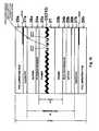
- a core 20comprised of a base layer 21 of a plastic material, which may be, for example, oriented polyester terephthalate (OPET) or polypropylene, or polystyrene, or any number of acrylics and/or a combination of these materials.
- the base layer 21is shown to have an upper surface 21 a and a lower, or bottom, surface 21 b .
- a patternis shown to be formed on, or above, surface 21 a of layer 21 .
- the patterncould be formed on surface 21 b .
- Two different methods of forming a patternare shown in FIGS. 2 and 2A .
- the surface 21 a of layer 21 in FIG. 2is embossed with a diffractive or holographic pattern.
- the surface 21 a of layer 21is coated with an embossing layer 200 which is then embossed with a diffractive pattern, 200 a.
- a layer 22 of aluminummay then be vapor deposited on the diffraction pattern to form a hologram.
- the use of vapor depositionis very significant in that it permits a very thin layer 22 , a few atoms thick, to be formed on surface 21 a and thus complete the formation of the hologram, using small amounts of metal.
- the thickness of the layercan be made very thin so it is nearly transparent and can provide a “see-through” effect.
- the metal layercan be made a little thicker so as to be more opaque.
- a clear adhesive primer layer 23 amay be coated over the patterned and metalized top surface ( 21 a ) and a similar clear adhesive primer layer 23 b may be coated over the bottom surface ( 21 b ) of the layer 21 .
- the core 20is completed by attaching these clear adhering layer ( 23 a , 23 b ) above and below the embossed base layer 21 .
- the clear layer 23 a , 23 bis a primer coating. It may be polyethylenamine or an acrylic based, or other, organic adhesive compound with solvent or water based carriers.
- the primer coatings 23 a , 23 bare fairly thin and yet fairly strong/sturdy. They also function to promote adhesion to layers 24 a , 24 b which are attached to the core 20 .
- clear PE adhesive layers 24 a , 24 bmay then be formed/attached to the top (outer) surfaces of their respectively layers 23 a , 23 b .
- Layers 24 a , 24 bmay be of polyethylene (PE) material, or polypropylene (PP), or high density polypropylene (HDPP), or ethylene Vinyl Acetate (EVA), or any of the different forms of PET or any of like materials, or mixtures of these materials.
- the clear materials used to form layers 24 a , 24 bmay contain other clear adhesion promoting compounds (e.g., ethyl acrylates, acrylic acid, etc.).
- the layers 24 a , 24 bmay be fairly thick and function to attach to the thin embossed hologram layer and coatings of core 20 .
- buffer layers 25 a , 25 bmay then be formed/attached to the top (outer) surfaces of layers 24 a , 24 b to complete what is defined as subassembly 30 .
- buffer (carrier) layer25 a , 25 b
- Subassembly 30is thick enough to be handled by automatic credit card manufacturing equipment.
- the base layer 21was approximately 0.002 inches thick and the adhesive backed layers ( 23 a , 23 b ) were each made to be approximately 0.0001 to 0.0003 inches thick. In other embodiments the layers 23 a , 23 b could be made either thinner or much thicker.
- adhesive layerscan be coated over the buffer or carrier layer and the two (i.e., the carrier and buffer layers on each side of a holographic layer) can be combined with the holographic layer. That is, adhesive can be applied to either side of the carrier foil interface and then pre-laminated together (3 sheets laminated to become one laminate; i.e., the prelaminate prior to platen lamination. Thus, the carrier sheet can hold the sub-assemblies for transfer to substrates for forming cards.
- FIG. 2Examining FIG. 2 in greater detail note some of the steps used in forming the core 20 .
- the base componentmay be a sheet 21 of plastic (e.g., PET or OPET or polypropylene, or polystyrene, or polymethyl, methacrylate, etc.) material whose thickness typically ranges from 0.0005 inches to more than 0.005 inches.
- layer 21was made, for example, 0.002 inches thick.
- a diffraction patternmay be formed on one side of layer 21 .
- a diffraction patternmay be formed directly in the plastic layer 21 by embossing (e.g., stamping) pattern(s) therein. Forming the pattern in a sheet of plastic (or in an embossing layer, as discussed below) is easier and less wearing on the embossing (stamping) equipment than forming a like pattern in a metal layer.
- a hologramis formed on one surface ( 21 a ) of plastic sheet 21 by vapor deposition of a metal layer (e.g., aluminum onto the diffraction patter.
- a metal layere.g., aluminum onto the diffraction patter.
- the hologrammay be formed by embossing the top surface 21 a to form a diffraction pattern and then metallizing the pattern.
- the surface 21 amay be coated by the vapor deposition of aluminum (or similar light reflective materials such as nickel, silver, zinc, or other like materials).
- a significant advantage of using vapor depositionis that very small amounts of the metal (light reflective material) need to be used to form the hologram resulting in a significant savings in the cost of manufacturing the card (or instrument).
- very thin layersallow a controllable amount of light to pass through. This enables the manufacture of a card, or document, in which an image (hologram) formed on a card is reflected (i.e., is visible) while also enabling a viewer to “see-through” the image.
- an imagehologram
- clear adhesive or “primer” coats 23 a , 23 bmay be applied to the top and bottom surfaces 21 a , 21 b , respectively, of plastic sheet 21 .
- the primer coatalso functions to fill in the ridges resulting from the formation of the diffraction grating.
- the clear layers 23 a , 23 bwhich may be of the type described above, may be attached to the top and bottom surfaces of “embossed” plastic sheet 21 on which the aluminum has been vapor deposited.
- Primer layers 23 a , 23 bmay be attached to base layer 21 by any one of a number of methods, such as, for example, gravure coating, roller coating, flexography or other like methods.
- the primersecures the bond to both sides of the holographic sheet (the embossed side and the blank side). This completes the formation of what is defined herein as the core assembly 20 .
- the PE layers 24 a , 24 bor any other suitable layer, as noted above, which function as an additional buffer between that bond and the outer buffer layers 25 a , 25 b are attached to the core assembly.
- the PE layers 24 a , 24 bmay also include an adhesive which promotes adhesion to the clear primer layers 23 a , 23 b attached to the top and bottom surfaces of layer 21 .
- Layers 24 a , 24 b , 25 a , 25 bmay be attached to each other and to the underlying layers by any one of a number of methods such as, for example, platen lamination, hot roll lamination, liquid adhesive lamination.
- a clear buffer layer 25 ais attached to the PE layer 24 a and a clear buffer layer 25 b is attached to the PE adhesive layer 24 b .
- All of layers 24 a and 24 b and layers 25 a , 25 bfunction as buffers, providing additional strength to the structure and at the same time protecting the hologram from being damaged or tampered with.
- Adding layers 25 a and 25 bcompletes the sub-assembly 30 which may then be customized to form cards with additional information.
- the hologramBy forming the hologram at, and within, the core level, the hologram will not be easily, or inadvertently, damaged since several additional layers will be attached to the top and bottom of the holographic layer. It is also not subject to easily being tampered or altered. Forming the hologram at the center of the structure minimizes the possibility of tampering while fully protecting the hologram. Another significant advantage of forming the hologram at the core of the structure is that the top and bottom surfaces stay flat due to equal shrinking and/or expansion of all the layers. Note that the card structure is formed so as to be symmetrical about the core layer.
- FIG. 2Aillustrates another method of forming the hologram.
- a clear embossing layer 200may be coated directly over a layer 21 (or 210 ).
- a primer coatingmay be formed on layer 21 / 210 and then the embossing layer 200 may attached/formed to the primer coating.
- the embossing layermay be composed, for example, of siloxane, acrylic, vinyl, linear polyester, urethane or any like materials and may be several (e.g., less than 0.5 to more than 5) microns thick.
- the embossing layersmay also be deposited as liquids and radiation cured, possibly in two steps—first as a soft easily embossable coating which then becomes hard and impervious.
- a diffraction patternis embossed (formed) in the embossing layer/coating 200 to form a desired pattern.
- Forming a pattern in the embossing layermay be desirable since it is even easier and less wearing on the embossing (stamping) equipment than forming a like pattern directly in the PET layer (as per FIG. 2 ).
- the sheetmay be processed as per steps 2 B, 3 and 4 shown in FIG. 2 .
- a hologrammay be formed by, for example, embossing a pattern in a carrier base material (e.g., a hard polyester) or by embossing the pattern in a coating previously applied to the carrier base material, or by embossing the pattern in a metal which was previously deposited onto the base carrier material or by depositing the metal onto a soft coating and then embossing.
- a carrier base materiale.g., a hard polyester
- the core 20may be part of a subassembly 30 which includes attaching layers 24 a , 24 b of clear PE and buffer layers 25 a , 25 b to the top and bottom surfaces of the core 20 .
- Layers 25 a , 25 bmay range in thickness from 0.001 to 0.005 inches, or more, and may be composed of PVC like materials.
- the subassembly 30may then be used to form a card, or any instrument, by attaching a layer 27 a , 27 b of clear or white PVC material to the top and bottom surfaces of the subassembly 30 .
- a layer 27 a , 27 b of clear or white PVC materialAs illustrated in FIG. 1 , information can be printed either on the outer surface (the surface facing away form the core) of layers 27 a , 27 b or on the inner surface or both.
- the printed informationmay include, for example, fixed data fields and advertising, and/or any other desired information.
- the card (or instrument)may be completed by adding clear PVC laminating films 29 a , 29 b to the top and bottom surfaces of the card.
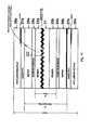
- FIG. 3is a cross-sectional diagram (not to scale) of a card embodying the invention.
- FIG. 3includes a core comprised of a layer 210 which may be (but not be) of the same material as layer 21 .
- the top surface 210 a of layer 210is embossed with a diffraction pattern giving a unique pattern to the structure.
- a high refractive index (HRI) layer 212can then be vapor deposited on the embossed layer. Due to the HRI property of layer 212 , there is no need to further metallize the layer.
- the HRI layermay be formed of zinc sulfide or zinc oxide or any material having like properties.
- Clear primer layer 23 ais attached to the top of HRI layer 212 overlying layer 210 and primer layer 23 b is attached to the bottom of layer 210 .
- clear layers 24 a and 24 bwhich may be of PE or any other suitable materials, are attached to layers 23 a and 23 b , respectively and additional layers ( 25 a , 25 b ) of clear (translucent) material may be attached to the top and bottom layers of layers 24 a , 24 b to form the subassembly 30 .
- Additional layers 27 a , 27 bmay be attached to the top and bottom layers of the sub-assembly.
- Informationmay be written or printed in any known manner on, or in, the layers 27 a , 27 b .
- laminating films 29 a , 29 bmay be attached to the top and bottom intermediate layers 27 a , 27 b to produce a card 40 whose core contents can not be altered without essentially destroying the card.
- FIGS. 3A, 3B, 3C, 3D and 3Eillustrate the forming/coating of an embossing layer 200 on stock (e.g., PET) material 210 ( FIG. 3A ), then embossing layer 200 with a diffraction pattern 200 a ( FIG. 3B ), then vapor depositing an HRI layer 212 a on the diffraction pattern ( FIG. 3C ), then coating clear primer layers 23 a , 23 b above layer 212 a and below layer 210 ( FIG. 3D ) to form a core assembly 20 .
- clear PE adhesive layer 24 ais formed above prime layer 23 a and clear PE adhesive layer 24 b , is formed below layer 23 b ( FIG. 3E ). Note that the steps and thicknesses of the layers to form the basic structures discussed above are summarized in Table I, below.
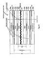
- FIG. 4includes a cross-sectional diagram (not to scale) of a portion of a card embodying the invention, which may be part of a sheet (not shown) on which a large number of cards are formed, and depicts a piece of laser equipment 410 for “lasering” (e.g., engraving or vaporizing) metal layer 22 .
- the core assembly 20is shown to have a layer 22 of aluminum deposited and embossed as discussed for FIGS. 1, 2, and 2A , above.
- Portions of the metal layermay be vaporized (see sections 401 a , 401 b , 401 c ) by the laser equipment 410 such that portions of the metal are selectively removed or “ablated” by “lasering” (e.g., eliminating or vaporizing) the metal to form any number of different patterns (e.g., graphic as well as alpha numeric information may be generated).
- the clear layers 29 a , 27 a , 25 a and 24 amay be selected to be transparent to the laser wavelength. Consequently, the laser beam can pass through the clear layers of the card to “write” on the holographic layer below the top surface of the card.
- the laser 410may be applied at several different stages of the card manufacturing process to form the desired patterns.
- the lasermay be applied to “write” on the metal layer after the core 20 is formed and before the attachment of the carrier layers 24 a , 24 b and 25 a , 25 b .
- the laser 410may be applied to form the desired pattern in the metal layer after the layers 24 a , 24 b , and 25 a , 25 b are attached to the core layer, and before layers 27 a and 27 b are attached.
- the lasermay be applied to form the desired pattern in the metal layer after the layers 27 a , 27 b are attached and before the layer 29 a , 29 b , are attached.
- the lasermay be applied to form the desired pattern in the metal layer after the layers 29 a , 29 b are attached, when the cards may be part of a full sheet or in individual card shape.
- FIG. 5shows a top view of a card 100 illustrating that the hologram may be located within a designated window or area 101 , shown in portion 601 .
- the hologrammay extend the full length and/or width of the card 100 .
- alpha numeric informationmay be produced by lasering within the holographic layer (e.g., layer 22 in FIG. 4 shown in portion 602 ).
- alpha numeric informationmay be produced by printing information on, or within, layers 27 a , 27 b , as discussed above.
- FIG. 6is a cross-sectional diagram (not to scale) of card 100 of FIG. 5 and is intended to show that the layers above and below the holographic layer, 21 , 22 / 212 , may be transparent or translucent to yield a “see-through” card with the hologram portion 601 and the lasered portion 602 being visible from the top side or from the bottom side of the card. Note that if layers 27 a , 27 b are made of a white material a bright light may be needed to observe the “see-through” effect.
- FIG. 6Ais a cross-sectional diagram (not to scale) intended to show that the layers above the holographic layer 21 , 22 / 212 , may be transparent or translucent so the holographic pattern may be seen from the top.
- one or more of the layers below the holographic layere.g., 27 b or 29 b
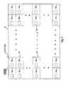
- FIG. 7shows the application of a laser beam generated by laser equipment 410 to a sheet 5 containing a large array of cards 100 in sheet form embodying the invention.
- the lasermay be applied to the entire sheet of cards which may be at the core stage, the sub-assembly stage, or any of the stages thereafter. Being able to apply the laser beam in this manner, at any time before the cards are separated from a sheet, is economically advantageous and saves much in the cost of handling and also adds significant additional security.
- FIG. 8illustrates that cards embodying the invention, shown in the various figures, may be modified by the addition of a semiconductor chip containing selected electronic circuits (an integrated circuit, IC) within the body of the card in, or within, a layer 30 dedicated to include an antenna carrier, with the antenna being connected to the chip module.
- ICintegrated circuit
- a radio frequency identification (RFID) cardThis enables the manufacture of a radio frequency identification (RFID) card.
- RFIDradio frequency identification
- the metal layer 22 / 212can act as a radio frequency shield to reduce reception from that side of the RFID antenna.
- FIG. 9illustrates that the chip (IC) and an antenna and carrier may be formed within a layer of the card and that, in addition, the chip may be accessed (read) by providing an external contact 901 along one side of the card.
- This type of cardmay be referred to as a dual interface card since it enables information on the card to be read or written via RFID and contact.
- FIG. 10illustrates that a window or opening can be formed by lasering through the metal layer within core layer 20 to enable the color or pattern of an underlying layer (e.g., 27 b ) to be seen from the top side of the card. Lasering through the metal layer forms (or opens) a window exposing an underlying layer (e.g., 27 b ) which may be black or white or colored or be of any preset pattern.
- an underlying layere.g., 27 b
- FIG. 11illustrates that a window or opening can be formed by lasering the metal layer within core layer 20 to enable a preprinted image formed on an underlying layer (e.g., 27 b ) to be seen from the top side of the card.
- lasering through the metal layerforms a window enabling the seeing or reading of a pre-printed pattern on an underlying layer (e.g., 27 b ).
- FIG. 12illustrates that a window or opening can be formed by lasering through the metal layer within core layer 20 to provide a “see-through” condition. That is, lasering through the metal layer forms a window which provides visibility through both sides (top and bottom) of the card. This may be viewed by applying a light source such as a flashlight in direct contact with one side of the card and viewing the light pattern on the other side.
- a light sourcesuch as a flashlight
Landscapes
- Engineering & Computer Science (AREA)
- Physics & Mathematics (AREA)
- Microelectronics & Electronic Packaging (AREA)
- General Physics & Mathematics (AREA)
- Computer Hardware Design (AREA)
- Manufacturing & Machinery (AREA)
- Condensed Matter Physics & Semiconductors (AREA)
- Power Engineering (AREA)
- Toxicology (AREA)
- General Health & Medical Sciences (AREA)
- Health & Medical Sciences (AREA)
- Theoretical Computer Science (AREA)
- Electromagnetism (AREA)
- Optics & Photonics (AREA)
- Chemical & Material Sciences (AREA)
- Chemical Kinetics & Catalysis (AREA)
- General Chemical & Material Sciences (AREA)
- Credit Cards Or The Like (AREA)
- Holo Graphy (AREA)
Abstract
Description
| TABLE I |
| Example of Steps and materials in forming core, sub assembly and card |
| step | I | III | IV | |||
| 1 | Start with | Start with | Start with | Start with base/central | ||
| base/central layer | base/central | base/ | layer | 21/210 | ||
| 21 of PET/ | layer | 21/210 | of PET/OPET material | |||
| material | of PET/OPET | PET/ | ||||
| material | material | |||||
| 1A | Deposit | Deposit embossing layer | ||||
| embossing | 200 on one surface of | |||||
| one surface of | ||||||
| 2 | Emboss one surface | Emboss top | Emboss one | Emboss top surface of | ||
| of | surface of | surface of | embossing layer | 200 | ||
| embossing | layer | 21 with | with | |||
| pattern | ||||||
| 200a | ||||||
| 3 | Vapor deposition of | Vapor | Vapor | Vapor deposition of | ||
| metal | ||||||
| 22 on pattern | deposition of | deposition of | ||||
| metal | ||||||
| 22 on | ||||||
| pattern | on | |||||
| 4 | Apply clear primer | Apply clear | Apply clear | Apply primer clear coats | ||
| coats 23a, 23b to | primer | primer coats | 23a, 23b to top and | |||
| top and bottom | 23a, 23b to top | 23a, 23b to top | bottom Where primer | |||
| Thickness: | and bottom | and | coat | 23a, 23b | ||
| .00002-.0002 | Thickness: | Thickness: | Thickness: | |||
| .00002-.0002 | .00002-.0002 | .00002-.0002 | ||||
| 5. | Form clear PE | Form clear PE | Form clear PE | Form clear PE adhesive | ||
| adhesive layers | adhesive layers | layers 24a, 24b fairly | ||||
| 24b-fairly thick, | 24a, 24b fairly | 24a, 24b fairly | thick, sticky | |||
| sticky | thick, sticky | thick, sticky | Thickness: | |||
| Thickness: | Thickness: | Thickness: | .0005-.005 | |||
| .0005-.005 | .0005-.005 | .0005-.005 | ||||
| 6. | Form clear buffer | Form clear | Form clear | Form clear | ||
| layer | ||||||
| 25a, 25b of | buffer | buffer layer | 25a, 25b of PVC | |||
| PVC material | ||||||
| 25a, 25b of | 25a, 25b of | thickness | ||||
| thickness | PVC material | PVC material | .0008-.005 | |||
| .0008-.005 | thickness | thickness | ||||
| .0008-.005 | .0008-.005 | |||||
| 7. | Form clear white | Form clear | Form clear | Form clear white PVC | ||
| PVC layer white PVC | white PVC layer | white | layer | 27a, | ||
| layer | ||||||
| 27a, | 27a, | 27a, 27b | Thickness .004 to .012 | |||
| Thickness .004 to | Thickness .004 | Thickness .004 | ||||
| .012 | to .012 | to .012 | ||||
| 8. | Form PVC | Form PVC | Form PVC | Form PVC | ||
| laminating film | ||||||
| 29a, | laminating film | film | 29a, | |||
| 29b | ||||||
| 29a, | 29a, 29b | Thickness .0008 to .005 | ||||
| Thickness .0008 to | Thickness | Thickness | ||||
| .005 | .0008 to .005 | .0008 to .005 | ||||
| All dimensions in inches | ||||||
Claims (1)
Priority Applications (5)
| Application Number | Priority Date | Filing Date | Title |
|---|---|---|---|
| US12/006,168US9542635B2 (en) | 2007-12-31 | 2007-12-31 | Foil composite card |
| US14/183,868US10373920B2 (en) | 2007-12-31 | 2014-02-19 | Foil composite card |
| US15/355,018US10332846B2 (en) | 2007-12-31 | 2016-11-17 | Foil composite card |
| US15/356,586US20170069581A1 (en) | 2007-12-31 | 2016-11-19 | Foil composite card |
| US16/452,740US11367693B2 (en) | 2007-12-31 | 2019-06-26 | Foil composite card |
Applications Claiming Priority (1)
| Application Number | Priority Date | Filing Date | Title |
|---|---|---|---|
| US12/006,168US9542635B2 (en) | 2007-12-31 | 2007-12-31 | Foil composite card |
Related Child Applications (3)
| Application Number | Title | Priority Date | Filing Date |
|---|---|---|---|
| US14/183,868ContinuationUS10373920B2 (en) | 2007-12-31 | 2014-02-19 | Foil composite card |
| US15/355,018DivisionUS10332846B2 (en) | 2007-12-31 | 2016-11-17 | Foil composite card |
| US15/356,586ContinuationUS20170069581A1 (en) | 2007-12-31 | 2016-11-19 | Foil composite card |
Publications (2)
| Publication Number | Publication Date |
|---|---|
| US20090169776A1 US20090169776A1 (en) | 2009-07-02 |
| US9542635B2true US9542635B2 (en) | 2017-01-10 |
Family
ID=40798798
Family Applications (5)
| Application Number | Title | Priority Date | Filing Date |
|---|---|---|---|
| US12/006,168Active2035-08-07US9542635B2 (en) | 2007-12-31 | 2007-12-31 | Foil composite card |
| US14/183,868Active2028-10-16US10373920B2 (en) | 2007-12-31 | 2014-02-19 | Foil composite card |
| US15/355,018Active2028-10-11US10332846B2 (en) | 2007-12-31 | 2016-11-17 | Foil composite card |
| US15/356,586AbandonedUS20170069581A1 (en) | 2007-12-31 | 2016-11-19 | Foil composite card |
| US16/452,740ActiveUS11367693B2 (en) | 2007-12-31 | 2019-06-26 | Foil composite card |
Family Applications After (4)
| Application Number | Title | Priority Date | Filing Date |
|---|---|---|---|
| US14/183,868Active2028-10-16US10373920B2 (en) | 2007-12-31 | 2014-02-19 | Foil composite card |
| US15/355,018Active2028-10-11US10332846B2 (en) | 2007-12-31 | 2016-11-17 | Foil composite card |
| US15/356,586AbandonedUS20170069581A1 (en) | 2007-12-31 | 2016-11-19 | Foil composite card |
| US16/452,740ActiveUS11367693B2 (en) | 2007-12-31 | 2019-06-26 | Foil composite card |
Country Status (1)
| Country | Link |
|---|---|
| US (5) | US9542635B2 (en) |
Cited By (16)
| Publication number | Priority date | Publication date | Assignee | Title |
|---|---|---|---|---|
| US20160271460A1 (en)* | 2014-08-08 | 2016-09-22 | Dunlop Sports Co., Ltd. | Patterned weighted tape for use on golf club |
| US9898699B2 (en) | 2014-12-23 | 2018-02-20 | Composecure, Llc | Smart metal card with radio frequency (RF) transmission capability |
| US10089570B2 (en) | 2013-11-18 | 2018-10-02 | Composecure, Llc | Card with metal layer and an antenna |
| US10311346B2 (en) | 2013-02-13 | 2019-06-04 | Composecure, Llc | Durable card |
| US10332846B2 (en) | 2007-12-31 | 2019-06-25 | Composecure, Llc | Foil composite card |
| US10452967B2 (en) | 2015-03-05 | 2019-10-22 | Composecure, Llc | Cards with special texture and color |
| US10479130B2 (en) | 2009-07-24 | 2019-11-19 | Composecure, L.L.C. | Card with embedded image |
| US10583683B1 (en) | 2017-02-03 | 2020-03-10 | Federal Card Services, LLC | Embedded metal card and related methods |
| US10679113B2 (en) | 2014-05-22 | 2020-06-09 | Composecure Llc | Transaction and ID cards having selected texture and coloring |
| US10783422B2 (en) | 2014-11-03 | 2020-09-22 | Composecure, Llc | Ceramic-containing and ceramic composite transaction cards |
| US11113593B2 (en) | 2019-08-15 | 2021-09-07 | Federal Card Services; LLC | Contactless metal cards with fingerprint sensor and display |
| US11341385B2 (en) | 2019-11-16 | 2022-05-24 | Federal Card Services, LLC | RFID enabled metal transaction card with shaped opening and shaped slit |
| US11347993B2 (en) | 2019-08-12 | 2022-05-31 | Federal Card Services, LLC | Dual interface metal cards and methods of manufacturing |
| US11416728B2 (en) | 2019-08-15 | 2022-08-16 | Federal Card Services, LLC | Durable dual interface metal transaction cards |
| US11455507B2 (en) | 2019-10-13 | 2022-09-27 | Federal Card Services, LLC | Metal transaction cards containing ceramic having selected coloring and texture |
| US11645487B2 (en) | 2019-08-14 | 2023-05-09 | Amatech Group Limited | Metal-containing dual interface smartcards |
Families Citing this family (54)
| Publication number | Priority date | Publication date | Assignee | Title |
|---|---|---|---|---|
| US20090033495A1 (en)* | 2007-08-03 | 2009-02-05 | Akash Abraham | Moldable radio frequency identification device |
| DE102009009263A1 (en)* | 2009-02-17 | 2010-08-19 | Giesecke & Devrient Gmbh | A method of making a window-containing final layer for a portable data carrier and final layer |
| DE102010034039A1 (en)* | 2010-08-11 | 2012-02-16 | Bundesdruckerei Gmbh | Method for producing a film for a security and / or value document |
| US9195932B2 (en) | 2010-08-12 | 2015-11-24 | Féinics Amatech Teoranta | Booster antenna configurations and methods |
| US9112272B2 (en) | 2010-08-12 | 2015-08-18 | Feinics Amatech Teoranta | Antenna modules for dual interface smart cards, booster antenna configurations, and methods |
| US9033250B2 (en) | 2010-08-12 | 2015-05-19 | Féinics Amatech Teoranta | Dual interface smart cards, and methods of manufacturing |
| US10457018B2 (en)* | 2010-11-15 | 2019-10-29 | Illinois Tool Works Inc. | Decorative and/or secure element for homogeneous card construction |
| US10733494B2 (en) | 2014-08-10 | 2020-08-04 | Féinics Amatech Teoranta | Contactless metal card constructions |
| US9836684B2 (en) | 2014-08-10 | 2017-12-05 | Féinics Amatech Teoranta | Smart cards, payment objects and methods |
| US10518518B2 (en) | 2013-01-18 | 2019-12-31 | Féinics Amatech Teoranta | Smart cards with metal layer(s) and methods of manufacture |
| US9812782B2 (en) | 2011-08-08 | 2017-11-07 | Féinics Amatech Teoranta | Coupling frames for RFID devices |
| US9489613B2 (en) | 2011-08-08 | 2016-11-08 | Féinics Amatech Teoranta | RFID transponder chip modules with a band of the antenna extending inward |
| US9622359B2 (en) | 2011-08-08 | 2017-04-11 | Féinics Amatech Teoranta | RFID transponder chip modules |
| US10867235B2 (en) | 2011-08-08 | 2020-12-15 | Féinics Amatech Teoranta | Metallized smartcard constructions and methods |
| US9475086B2 (en) | 2013-01-18 | 2016-10-25 | Féinics Amatech Teoranta | Smartcard with coupling frame and method of increasing activation distance of a transponder chip module |
| US9251458B2 (en) | 2011-09-11 | 2016-02-02 | Féinics Amatech Teoranta | Selective deposition of magnetic particles and using magnetic material as a carrier medium to deposit nanoparticles |
| US9697459B2 (en) | 2014-08-10 | 2017-07-04 | Féinics Amatech Teoranta | Passive smart cards, metal cards, payment objects and smart jewelry |
| US9634391B2 (en) | 2011-08-08 | 2017-04-25 | Féinics Amatech Teoranta | RFID transponder chip modules |
| US9798968B2 (en) | 2013-01-18 | 2017-10-24 | Féinics Amatech Teoranta | Smartcard with coupling frame and method of increasing activation distance of a transponder chip module |
| WO2013110625A1 (en) | 2012-01-23 | 2013-08-01 | Féinics Amatech Teoranta | Offsetting shielding and enhancing coupling in metallized smart cards |
| US8857722B2 (en) | 2012-07-20 | 2014-10-14 | CPI Card Group—Colorado, Inc. | Weighted transaction card |
| US10032099B2 (en) | 2012-07-20 | 2018-07-24 | CPI Card Group—Colorado, Inc. | Weighted transaction card |
| US10824931B2 (en) | 2012-08-30 | 2020-11-03 | Féinics Amatech Teoranta | Contactless smartcards with multiple coupling frames |
| US10552722B2 (en) | 2014-08-10 | 2020-02-04 | Féinics Amatech Teoranta | Smartcard with coupling frame antenna |
| US10783426B2 (en) | 2012-08-30 | 2020-09-22 | David Finn | Dual-interface metal hybrid smartcard |
| EP2722191B1 (en) | 2012-10-18 | 2015-05-06 | Bundesdruckerei GmbH | Identity card with physical unclonable function |
| US11354560B2 (en) | 2013-01-18 | 2022-06-07 | Amatech Group Limited | Smartcards with multiple coupling frames |
| US10248902B1 (en) | 2017-11-06 | 2019-04-02 | Féinics Amatech Teoranta | Coupling frames for RFID devices |
| US11354558B2 (en) | 2013-01-18 | 2022-06-07 | Amatech Group Limited | Contactless smartcards with coupling frames |
| US10977542B2 (en) | 2013-01-18 | 2021-04-13 | Amtech Group Limited Industrial Estate | Smart cards with metal layer(s) and methods of manufacture |
| US11551051B2 (en) | 2013-01-18 | 2023-01-10 | Amatech Group Limiied | Coupling frames for smartcards with various module opening shapes |
| US11341389B2 (en) | 2013-01-18 | 2022-05-24 | Amatech Group Limited | Manufacturing metal inlays for dual interface metal cards |
| US11928537B2 (en) | 2013-01-18 | 2024-03-12 | Amatech Group Limited | Manufacturing metal inlays for dual interface metal cards |
| US10599972B2 (en) | 2013-01-18 | 2020-03-24 | Féinics Amatech Teoranta | Smartcard constructions and methods |
| EP2784724A3 (en) | 2013-03-27 | 2015-04-22 | Féinics AmaTech Teoranta | Selective deposition of magnetic particles, and using magnetic material as a carrier medium to deposit other particles |
| WO2014200515A1 (en)* | 2013-06-12 | 2014-12-18 | Composecure, Llc | Plastic cards with high density particles |
| WO2015061611A1 (en) | 2013-10-25 | 2015-04-30 | Cpi Card Group - Colorado, Inc. | Multi-metal layered card |
| WO2015071017A1 (en) | 2013-11-13 | 2015-05-21 | Féinics Amatech Teoranta | Smartcard with coupling frame and method of increasing activation distance of a transponder chip module |
| CN105740165A (en) | 2014-12-10 | 2016-07-06 | 国际商业机器公司 | Method and apparatus for managing file system of unified storage system |
| US10127488B2 (en)* | 2014-12-30 | 2018-11-13 | Qvivr, Inc. | Systems and methods for creating dynamic programmable magnetic stripes |
| US10089568B2 (en) | 2016-06-01 | 2018-10-02 | CPI Card Group—Colorado, Inc. | IC chip card with integrated biometric sensor pads |
| DE102016009440A1 (en)* | 2016-08-03 | 2018-02-08 | Giesecke+Devrient Currency Technology Gmbh | Method for producing a security element |
| CN108023013B (en)* | 2016-11-01 | 2021-02-26 | 苏州贝骨新材料科技有限公司 | Preparation method of piezoelectric film sensor |
| US10163050B2 (en)* | 2016-11-29 | 2018-12-25 | Capital One Services, Llc | Wood inlay card and method for making the same |
| EP3582973B1 (en) | 2017-02-14 | 2023-06-28 | CPI Card Group - Colorado, Inc. | Edge-to-edge metal card and production method |
| WO2018178316A1 (en) | 2017-03-29 | 2018-10-04 | Féinics Amatech Teoranta | Smartcard with coupling frame antenna |
| EP3762871B1 (en) | 2018-03-07 | 2024-08-07 | X-Card Holdings, LLC | Metal card |
| CN113195242B (en)* | 2018-12-17 | 2022-09-20 | 兰克森控股公司 | Prelaminate for data pages of security documents and method of forming the same |
| US11106961B2 (en)* | 2019-10-09 | 2021-08-31 | Beauiiful Card Corporation | Mini smart card and method of manufacturing the same |
| CN110956247B (en)* | 2019-11-29 | 2024-02-23 | 金邦达有限公司 | Manufacturing method of electric aluminum PVC smart card with three-dimensional pattern |
| USD942538S1 (en) | 2020-07-30 | 2022-02-01 | Federal Card Services, LLC | Asymmetrical arrangement of contact pads and connection bridges of a transponder chip module |
| USD943024S1 (en) | 2020-07-30 | 2022-02-08 | Federal Card Services, LLC | Asymmetrical arrangement of contact pads and connection bridges of a transponder chip module |
| EP3939803B1 (en)* | 2020-09-29 | 2024-05-08 | Hueck Folien Gesellschaft m.b.H. | Polymer substrate for producing polymer valuable documents or polymer security documents |
| CN112862052B (en)* | 2021-02-20 | 2025-06-17 | 捷德(中国)科技有限公司 | Smart card and method for making smart card |
Citations (5)
| Publication number | Priority date | Publication date | Assignee | Title |
|---|---|---|---|---|
| US20010049004A1 (en)* | 1999-12-20 | 2001-12-06 | Applied Extrusion Technologies, Inc. | Holographic films |
| US6589642B1 (en)* | 2001-12-21 | 2003-07-08 | Kloeckner Pentaplast Of America, Inc. | Three part high moisture barrier for packages |
| US6644552B1 (en)* | 2002-07-09 | 2003-11-11 | John Herslow | Composite card |
| US20040031855A1 (en)* | 2002-07-02 | 2004-02-19 | Konica Corporation | IC card |
| US7063924B2 (en)* | 2002-12-20 | 2006-06-20 | Eastman Kodak Company | Security device with patterned metallic reflection |
Family Cites Families (87)
| Publication number | Priority date | Publication date | Assignee | Title |
|---|---|---|---|---|
| US4354851A (en) | 1977-02-17 | 1982-10-19 | United States Gypsum Company | Method for making a decorated, water-resistant, rigid panel and the product made thereby: transfer dye process onto rigid panel |
| US4202811A (en) | 1978-06-21 | 1980-05-13 | Dow Corning Corporation | Siloxane-epoxy molding compound with improved crack resistance |
| DE3151407C1 (en) | 1981-12-24 | 1983-10-13 | GAO Gesellschaft für Automation und Organisation mbH, 8000 München | ID card and process for its manufacture |
| US4469725A (en) | 1982-09-14 | 1984-09-04 | Fis Organisation Ag | Identification card |
| EP0201323B1 (en) | 1985-05-07 | 1994-08-17 | Dai Nippon Insatsu Kabushiki Kaisha | Article incorporating a transparent hologramm |
| EP0339763A3 (en) | 1988-04-28 | 1990-04-25 | Citizen Watch Co. Ltd. | Ic card |
| AU615582B2 (en) | 1988-11-10 | 1991-10-03 | Kyodo Printing Co., Ltd. | Optical card |
| US6938825B1 (en) | 1989-04-24 | 2005-09-06 | Ultracard, Inc. | Data system |
| JP2802520B2 (en) | 1989-10-20 | 1998-09-24 | 共同印刷株式会社 | Sealed optical card |
| GB9106128D0 (en)* | 1991-03-22 | 1991-05-08 | Amblehurst Ltd | Article |
| US5316791A (en) | 1993-01-21 | 1994-05-31 | Sdc Coatings Inc. | Process for improving impact resistance of coated plastic substrates |
| US6254951B1 (en) | 1994-09-27 | 2001-07-03 | Thomas A. Marmalich | Flexible wood fabric and method of manufacture |
| JPH09114944A (en) | 1995-10-19 | 1997-05-02 | Nippon Conlux Co Ltd | Card and processor for the same |
| DE19642040C1 (en) | 1996-10-11 | 1998-01-15 | Schreiner Etiketten | Label with hologram, written by laser beam passing through clear, protective upper film |
| CN1172141A (en) | 1997-07-21 | 1998-02-04 | 天津博苑高新材料有限公司 | Water-base laminated oil for making PVC card |
| US6296188B1 (en) | 1999-10-01 | 2001-10-02 | Perfect Plastic Printing Corporation | Transparent/translucent financial transaction card including an infrared light filter |
| US8397998B1 (en) | 1999-10-23 | 2013-03-19 | Ultracard, Inc. | Data storage device, apparatus and method for using same |
| US7101644B2 (en) | 2000-06-23 | 2006-09-05 | Dai Nippon Printing Co., Ltd. | Hologram transfer foil |
| AU2001267993A1 (en) | 2000-07-11 | 2002-01-21 | Pergo Ab | A process for the manufacturing of an improved decorative laminate and a decorative laminate obtained by the process |
| GB0025886D0 (en) | 2000-10-23 | 2000-12-06 | Murray Nicholas J | Method and apparatus for producing a transfer image and method and apparatus for transfering a coating |
| US6923378B2 (en) | 2000-12-22 | 2005-08-02 | Digimarc Id Systems | Identification card |
| JP2002260290A (en) | 2001-03-02 | 2002-09-13 | Tokyo Magnetic Printing Co Ltd | Optical card and its manufacturing method |
| CA2455305C (en)* | 2001-06-19 | 2013-02-19 | Nippon Carbide Kogyo Kabushiki Kaisha | Integrated circuit enclosed retroreflective product |
| US6586078B2 (en) | 2001-07-05 | 2003-07-01 | Soundcraft, Inc. | High pressure lamination of electronic cards |
| BR0211324B1 (en) | 2001-07-31 | 2014-06-10 | Avery Dennison Corp | Compliant label material, label and pressure sensitive adhesive label |
| AU2002353174A1 (en) | 2001-12-24 | 2003-07-15 | Digimarc Id Systems, Llc | Laser engraving methods and compositions |
| WO2003063060A2 (en)* | 2002-01-24 | 2003-07-31 | Broadcom Corporation | Asymmetric digital subscriber line modem apparatus and methods therefor |
| TWI276490B (en) | 2002-03-25 | 2007-03-21 | Ebara Corp | Electrolytic processing device, substrate processing apparatus having such an electrolytic processing device, and electrolytic processing device |
| WO2004048910A2 (en) | 2002-11-21 | 2004-06-10 | The Sherwin-Williams Company | Method of color matching wood stains |
| US7530491B2 (en) | 2003-01-03 | 2009-05-12 | American Express Travel Related Services Company, Inc. | Metal-containing transaction card and method of making the same |
| US7566001B2 (en)* | 2003-08-29 | 2009-07-28 | Semiconductor Energy Laboratory Co., Ltd. | IC card |
| US7364085B2 (en) | 2003-09-30 | 2008-04-29 | Digimarc Corporation | Identification document with printing that creates moving and three dimensional image effects with pulsed illumination |
| WO2005044561A1 (en) | 2003-10-27 | 2005-05-19 | Veritec, Inc. | Laminated cards and methods of manufacture for secure applications |
| US20050196604A1 (en) | 2004-03-05 | 2005-09-08 | Unifoil Corporation | Metallization process and product produced thereby |
| US7503503B2 (en) | 2004-05-06 | 2009-03-17 | Giesecke & Devrient Gmbh | Card laminate |
| JP4666575B2 (en) | 2004-11-08 | 2011-04-06 | 東京エレクトロン株式会社 | Manufacturing method of ceramic sprayed member, program for executing the method, storage medium, and ceramic sprayed member |
| KR20040111317A (en) | 2004-12-11 | 2004-12-31 | 주식회사 필톤 | Electronic card and the manufacturing method having antibiotic function |
| US20060172136A1 (en) | 2005-02-01 | 2006-08-03 | Takashi Komori | Coated member |
| ITRM20050074A1 (en) | 2005-02-18 | 2006-08-19 | Shock Line Di Coppola M & C S | MIXTURE TO BE USED FOR THE PRODUCTION OF TRANSFERABLE TO DECALCOMANIA, A TRANSFERABLE PRODUCT FOR DECAL SCALE AND ITS PROCESS OF PRODUCTION, AND PROCEDURE OF DECALING USER SUCH A TRANSFERABLE PRODUCT. |
| US7287704B2 (en) | 2005-05-03 | 2007-10-30 | Composecure, Llc | Laser markable secure documents |
| US20060292946A1 (en) | 2005-06-22 | 2006-12-28 | Perfect Plastic Printing Corporation | Financial Transaction Card With Embedded Fabric |
| WO2007037160A1 (en) | 2005-09-29 | 2007-04-05 | Olympus Corporation | Method of processing wood and compressed wood product |
| US20070089831A1 (en) | 2005-10-17 | 2007-04-26 | Celerino Florentino | Card with hologram formed over magnetic strip |
| US20090218401A1 (en) | 2006-05-11 | 2009-09-03 | Singular Id Pte Ltd | Method of identifying an object, an identification tag, an object adapted to be identified, and related device and system |
| DE102006034854A1 (en) | 2006-07-25 | 2008-01-31 | Ovd Kinegram Ag | A method for generating a laser mark in a security document and such a security document |
| US8608080B2 (en) | 2006-09-26 | 2013-12-17 | Feinics Amatech Teoranta | Inlays for security documents |
| US20080164307A1 (en) | 2007-01-05 | 2008-07-10 | Microsoft Corporation | Performing transactions with universal transaction card |
| US8283577B2 (en) | 2007-06-08 | 2012-10-09 | Dai Nippon Printing Co., Ltd. | Printed matter and its manufacturing method, and electromagnetic shielding material and its manufacturing method |
| US9542635B2 (en) | 2007-12-31 | 2017-01-10 | Composecure, Llc | Foil composite card |
| US8917302B2 (en) | 2008-02-25 | 2014-12-23 | International Business Machines Corporation | Apparatus and method to display information using an information layer laminate |
| KR101004843B1 (en) | 2008-09-05 | 2010-12-28 | 삼성전기주식회사 | Ceramic multilayer circuit board and manufacturing method thereof |
| US10479130B2 (en) | 2009-07-24 | 2019-11-19 | Composecure, L.L.C. | Card with embedded image |
| US8725589B1 (en) | 2009-07-30 | 2014-05-13 | Jpmorgan Chase Bank, N.A. | Methods for personalizing multi-layer transaction cards |
| US8393547B2 (en) | 2009-08-05 | 2013-03-12 | Perfect Plastic Printing Corporation | RF proximity financial transaction card having metallic foil layer(s) |
| US20110079344A1 (en) | 2009-10-03 | 2011-04-07 | Victor Shi-Yueh Sheu | Method for making a thin film having a metallic pattern layer |
| GB0919014D0 (en) | 2009-10-30 | 2009-12-16 | 3M Innovative Properties Co | Soll and stain resistant coating composition for finished leather substrates |
| PL2338940T3 (en) | 2009-12-23 | 2017-04-28 | Silicalia S.L. | Composition for coating |
| US8944810B2 (en) | 2010-02-02 | 2015-02-03 | Composecure, Llc | Metal card |
| BE1019331A5 (en) | 2010-05-10 | 2012-06-05 | Flooring Ind Ltd Sarl | FLOOR PANEL AND METHODS FOR MANUFACTURING FLOOR PANELS. |
| WO2012002992A1 (en) | 2010-06-28 | 2012-01-05 | Toray Plastics (America) Inc. | Releasable metalized embossed transfer film |
| US8991712B2 (en) | 2010-08-12 | 2015-03-31 | Féinics Amatech Teoranta | Coupling in and to RFID smart cards |
| US8469281B2 (en) | 2010-09-07 | 2013-06-25 | Identive Group, Inc. | RFID label with shielding element |
| EP2668526B1 (en) | 2011-01-28 | 2018-07-04 | Crane & Co., Inc. | A laser marked device |
| DE102011018342A1 (en) | 2011-04-20 | 2012-10-25 | Heraeus Materials Technology Gmbh & Co. Kg | Process for the preparation of a partially coated support structure |
| US8672232B2 (en) | 2011-06-27 | 2014-03-18 | Composecure, Llc | Combination card of metal and plastic |
| US9836684B2 (en) | 2014-08-10 | 2017-12-05 | Féinics Amatech Teoranta | Smart cards, payment objects and methods |
| ITMI20120706A1 (en) | 2012-04-27 | 2013-10-28 | St Microelectronics Srl | AN INTEGRATED CIRCUIT CARD FOR AUTHENTICATION AND A METHOD FOR THE AUTHENTICATION OF THE INTEGRATED CIRCUIT CARD |
| US9269032B2 (en) | 2012-10-28 | 2016-02-23 | Zlotech Llc | Glass-containing transaction card and method of making the same |
| US9422435B2 (en) | 2013-01-25 | 2016-08-23 | Ppg Industries Ohio, Inc. | Scratch and stain resistant coatings |
| US11087316B2 (en) | 2013-02-08 | 2021-08-10 | Taiwan Development & Construction Co. | Electronic tag and system and method for securing electronic tag |
| PL2956310T3 (en) | 2013-02-13 | 2019-12-31 | Composecure, Llc | Durable card |
| US9016591B2 (en) | 2013-08-08 | 2015-04-28 | Composecure, Llc | Plastic cards with high density particles |
| WO2015061611A1 (en) | 2013-10-25 | 2015-04-30 | Cpi Card Group - Colorado, Inc. | Multi-metal layered card |
| CN105793872B (en) | 2013-11-18 | 2019-01-01 | 安全创造有限责任公司 | Card with metal layer and antenna |
| US9569718B2 (en) | 2013-12-19 | 2017-02-14 | Composecure, Llc | Card with metal layer and electrostatic protection |
| US20150206047A1 (en) | 2014-01-20 | 2015-07-23 | John Herslow | Metal card with radio frequency (rf) transmission capability |
| US9634224B2 (en) | 2014-02-14 | 2017-04-25 | D-Wave Systems Inc. | Systems and methods for fabrication of superconducting circuits |
| US9844922B2 (en) | 2014-04-21 | 2017-12-19 | Travel Tags, Inc. | Bamboo laminate transaction card |
| NZ726408A (en) | 2014-05-22 | 2018-09-28 | Composecure Llc | Transaction and id cards having selected texture and coloring |
| CN107111766B (en) | 2014-11-03 | 2021-03-12 | 安全创造有限责任公司 | Ceramic Containing and Ceramic Composite Trading Cards |
| CN104360505A (en) | 2014-11-14 | 2015-02-18 | 京东方科技集团股份有限公司 | Display device and display system |
| EP3238139B1 (en) | 2014-12-23 | 2021-08-11 | Composecure LLC | Smart metal card with radio frequency (rf) transmission capability |
| US9390363B1 (en) | 2015-03-05 | 2016-07-12 | Composecure, Llc | Cards with special texture and color |
| US9390366B1 (en) | 2015-07-08 | 2016-07-12 | Composecure, Llc | Metal smart card with dual interface capability |
| PL3526273T3 (en) | 2016-10-13 | 2021-05-31 | Basf Se | Radiation curable polyesteracrylate-containing compositions |
| CN107068811B (en) | 2017-03-15 | 2019-06-18 | 京东方科技集团股份有限公司 | Manufacturing method of light emitting diode device and light emitting diode device |
| US10725595B2 (en) | 2018-04-24 | 2020-07-28 | Apple Inc. | Electronic devices with covers |
- 2007
- 2007-12-31USUS12/006,168patent/US9542635B2/enactiveActive
- 2014
- 2014-02-19USUS14/183,868patent/US10373920B2/enactiveActive
- 2016
- 2016-11-17USUS15/355,018patent/US10332846B2/enactiveActive
- 2016-11-19USUS15/356,586patent/US20170069581A1/ennot_activeAbandoned
- 2019
- 2019-06-26USUS16/452,740patent/US11367693B2/enactiveActive
Patent Citations (5)
| Publication number | Priority date | Publication date | Assignee | Title |
|---|---|---|---|---|
| US20010049004A1 (en)* | 1999-12-20 | 2001-12-06 | Applied Extrusion Technologies, Inc. | Holographic films |
| US6589642B1 (en)* | 2001-12-21 | 2003-07-08 | Kloeckner Pentaplast Of America, Inc. | Three part high moisture barrier for packages |
| US20040031855A1 (en)* | 2002-07-02 | 2004-02-19 | Konica Corporation | IC card |
| US6644552B1 (en)* | 2002-07-09 | 2003-11-11 | John Herslow | Composite card |
| US7063924B2 (en)* | 2002-12-20 | 2006-06-20 | Eastman Kodak Company | Security device with patterned metallic reflection |
Cited By (28)
| Publication number | Priority date | Publication date | Assignee | Title |
|---|---|---|---|---|
| US10332846B2 (en) | 2007-12-31 | 2019-06-25 | Composecure, Llc | Foil composite card |
| US10373920B2 (en) | 2007-12-31 | 2019-08-06 | Composecure, Llc | Foil composite card |
| US11367693B2 (en) | 2007-12-31 | 2022-06-21 | Composecure, Llc | Foil composite card |
| US10479130B2 (en) | 2009-07-24 | 2019-11-19 | Composecure, L.L.C. | Card with embedded image |
| US12151502B2 (en) | 2009-07-24 | 2024-11-26 | Composecure, Llc | Card with embedded image |
| US11915074B2 (en) | 2013-02-13 | 2024-02-27 | Composecure, Llc | Laser-personalized card having a hard coat subassembly and a core subassembly having non-metal layers with carbon particles |
| US10311346B2 (en) | 2013-02-13 | 2019-06-04 | Composecure, Llc | Durable card |
| US10395153B2 (en) | 2013-02-13 | 2019-08-27 | Composecure, Llc | Durable card |
| US10089570B2 (en) | 2013-11-18 | 2018-10-02 | Composecure, Llc | Card with metal layer and an antenna |
| US10922601B2 (en) | 2014-05-22 | 2021-02-16 | Composecure, Llc | Transaction and ID cards having selected texture and coloring |
| US10679113B2 (en) | 2014-05-22 | 2020-06-09 | Composecure Llc | Transaction and ID cards having selected texture and coloring |
| US10867233B2 (en) | 2014-05-22 | 2020-12-15 | Composecure Llc | Transaction and ID cards having selected texture and coloring |
| US12299514B2 (en) | 2014-05-22 | 2025-05-13 | Composecure, Llc | Transaction and ID cards having selected texture and coloring |
| US11853829B2 (en) | 2014-05-22 | 2023-12-26 | Composecure, Llc | Transaction and ID cards having selected texture and coloring |
| US20160271460A1 (en)* | 2014-08-08 | 2016-09-22 | Dunlop Sports Co., Ltd. | Patterned weighted tape for use on golf club |
| US11521035B2 (en) | 2014-11-03 | 2022-12-06 | Composecure, Llc | Ceramic-containing and ceramic composite transaction cards |
| US10783422B2 (en) | 2014-11-03 | 2020-09-22 | Composecure, Llc | Ceramic-containing and ceramic composite transaction cards |
| US9898699B2 (en) | 2014-12-23 | 2018-02-20 | Composecure, Llc | Smart metal card with radio frequency (RF) transmission capability |
| US10275703B2 (en) | 2014-12-23 | 2019-04-30 | Composecure, Llc | Smart metal card with radio frequency (RF) transmission capability |
| US10452967B2 (en) | 2015-03-05 | 2019-10-22 | Composecure, Llc | Cards with special texture and color |
| US10583683B1 (en) | 2017-02-03 | 2020-03-10 | Federal Card Services, LLC | Embedded metal card and related methods |
| US11347993B2 (en) | 2019-08-12 | 2022-05-31 | Federal Card Services, LLC | Dual interface metal cards and methods of manufacturing |
| US11645487B2 (en) | 2019-08-14 | 2023-05-09 | Amatech Group Limited | Metal-containing dual interface smartcards |
| US12277462B2 (en) | 2019-08-14 | 2025-04-15 | Federal Card Services, LLC | Metal-containing dual interface smartcards |
| US11416728B2 (en) | 2019-08-15 | 2022-08-16 | Federal Card Services, LLC | Durable dual interface metal transaction cards |
| US11113593B2 (en) | 2019-08-15 | 2021-09-07 | Federal Card Services; LLC | Contactless metal cards with fingerprint sensor and display |
| US11455507B2 (en) | 2019-10-13 | 2022-09-27 | Federal Card Services, LLC | Metal transaction cards containing ceramic having selected coloring and texture |
| US11341385B2 (en) | 2019-11-16 | 2022-05-24 | Federal Card Services, LLC | RFID enabled metal transaction card with shaped opening and shaped slit |
Also Published As
| Publication number | Publication date |
|---|---|
| US20170069580A1 (en) | 2017-03-09 |
| US20190378805A1 (en) | 2019-12-12 |
| US10373920B2 (en) | 2019-08-06 |
| US20090169776A1 (en) | 2009-07-02 |
| US20140166762A1 (en) | 2014-06-19 |
| US10332846B2 (en) | 2019-06-25 |
| US11367693B2 (en) | 2022-06-21 |
| US20170069581A1 (en) | 2017-03-09 |
Similar Documents
| Publication | Publication Date | Title |
|---|---|---|
| US11367693B2 (en) | Foil composite card | |
| US5351142A (en) | Semi-transparent reflective layer for a phase hologram | |
| US7503503B2 (en) | Card laminate | |
| US5513019A (en) | Semi-transparent reflective layer for a phase hologram | |
| US5310222A (en) | Optical device | |
| KR100706077B1 (en) | Laminates, in particular laminations in the form of cards and methods of making the laminates | |
| ES2269304T3 (en) | DECORATIVE FILM. | |
| JP4405915B2 (en) | Strip type security element | |
| US8006908B2 (en) | Data support with identifications written thereon by means of a laser beam and method for production thereof | |
| KR20070110201A (en) | Security glyph formed by hologram and color conversion ink | |
| BRPI0818567B1 (en) | SAFETY DOCUMENT AND PROCESS FOR YOUR PRODUCTION | |
| JP2023113602A (en) | LAMINATES, CERTIFICATES AND METHOD OF MANUFACTURING LAMINATES | |
| US20240100874A1 (en) | Three-dimensional display, authentication medium, and formation method | |
| JP2021157079A (en) | Security label | |
| US20230101526A1 (en) | Optically variable security devices | |
| BG986U1 (en) | Document security strip and secured document | |
| KR200353146Y1 (en) | Hologram Ultra violet curing system label | |
| JP3424521B2 (en) | Diffraction grating pattern transfer foil |
Legal Events
| Date | Code | Title | Description |
|---|---|---|---|
| AS | Assignment | Owner name:COMPOSECURE, LLC, NEW JERSEY Free format text:ASSIGNMENT OF ASSIGNORS INTEREST;ASSIGNOR:HERSLOW, JOHN;REEL/FRAME:020515/0447 Effective date:20071231 | |
| AS | Assignment | Owner name:KEYBANK NATIONAL ASSOCIATION, AS ADMINISTRATIVE AG Free format text:COLLATERAL ASSIGNMENT OF PATENTS;ASSIGNOR:COMPOSECURE, L.L.C.;REEL/FRAME:036065/0360 Effective date:20150511 | |
| AS | Assignment | Owner name:JPMORGAN CHASE BANK, N.A., AS ADMINISTRATIVE AGENT Free format text:SECURITY INTEREST;ASSIGNOR:COMPOSECURE, L.L.C;REEL/FRAME:039379/0341 Effective date:20160726 Owner name:COMPOSECURE, L.L.C., NEW JERSEY Free format text:RELEASE BY SECURED PARTY;ASSIGNOR:KEYBANK NATIONAL ASSOCIATION, AS ADMINISTRATIVE AGENT;REEL/FRAME:039387/0705 Effective date:20160726 | |
| STCF | Information on status: patent grant | Free format text:PATENTED CASE | |
| FEPP | Fee payment procedure | Free format text:ENTITY STATUS SET TO UNDISCOUNTED (ORIGINAL EVENT CODE: BIG.) | |
| AS | Assignment | Owner name:JPMORGAN CHASE BANK, N.A., AS ADMINISTRATIVE AGENT Free format text:SECURITY INTEREST;ASSIGNOR:COMPOSECURE, L.L.C.;REEL/FRAME:049651/0333 Effective date:20190702 Owner name:JPMORGAN CHASE BANK, N.A., AS ADMINISTRATIVE AGENT, ILLINOIS Free format text:SECURITY INTEREST;ASSIGNOR:COMPOSECURE, L.L.C.;REEL/FRAME:049651/0333 Effective date:20190702 | |
| MAFP | Maintenance fee payment | Free format text:PAYMENT OF MAINTENANCE FEE, 4TH YEAR, LARGE ENTITY (ORIGINAL EVENT CODE: M1551); ENTITY STATUS OF PATENT OWNER: LARGE ENTITY Year of fee payment:4 |