US9536971B2 - Semiconductor device comprising a transistor gate having multiple vertically oriented sidewalls - Google Patents
Semiconductor device comprising a transistor gate having multiple vertically oriented sidewallsDownload PDFInfo
- Publication number
- US9536971B2 US9536971B2US14/561,605US201414561605AUS9536971B2US 9536971 B2US9536971 B2US 9536971B2US 201414561605 AUS201414561605 AUS 201414561605AUS 9536971 B2US9536971 B2US 9536971B2
- Authority
- US
- United States
- Prior art keywords
- gate
- opposing
- laterally
- layer
- vertical spacing
- Prior art date
- Legal status (The legal status is an assumption and is not a legal conclusion. Google has not performed a legal analysis and makes no representation as to the accuracy of the status listed.)
- Expired - Lifetime
Links
Images


Classifications
- H—ELECTRICITY
- H01—ELECTRIC ELEMENTS
- H01L—SEMICONDUCTOR DEVICES NOT COVERED BY CLASS H10
- H01L21/00—Processes or apparatus adapted for the manufacture or treatment of semiconductor or solid state devices or of parts thereof
- H01L21/02—Manufacture or treatment of semiconductor devices or of parts thereof
- H01L21/04—Manufacture or treatment of semiconductor devices or of parts thereof the devices having potential barriers, e.g. a PN junction, depletion layer or carrier concentration layer
- H01L21/18—Manufacture or treatment of semiconductor devices or of parts thereof the devices having potential barriers, e.g. a PN junction, depletion layer or carrier concentration layer the devices having semiconductor bodies comprising elements of Group IV of the Periodic Table or AIIIBV compounds with or without impurities, e.g. doping materials
- H01L21/26—Bombardment with radiation
- H01L21/263—Bombardment with radiation with high-energy radiation
- H01L21/265—Bombardment with radiation with high-energy radiation producing ion implantation
- H01L21/26586—Bombardment with radiation with high-energy radiation producing ion implantation characterised by the angle between the ion beam and the crystal planes or the main crystal surface
- H01L29/4236—
- H—ELECTRICITY
- H10—SEMICONDUCTOR DEVICES; ELECTRIC SOLID-STATE DEVICES NOT OTHERWISE PROVIDED FOR
- H10D—INORGANIC ELECTRIC SEMICONDUCTOR DEVICES
- H10D64/00—Electrodes of devices having potential barriers
- H10D64/20—Electrodes characterised by their shapes, relative sizes or dispositions
- H10D64/27—Electrodes not carrying the current to be rectified, amplified, oscillated or switched, e.g. gates
- H10D64/311—Gate electrodes for field-effect devices
- H10D64/411—Gate electrodes for field-effect devices for FETs
- H10D64/511—Gate electrodes for field-effect devices for FETs for IGFETs
- H10D64/512—Disposition of the gate electrodes, e.g. buried gates
- H10D64/513—Disposition of the gate electrodes, e.g. buried gates within recesses in the substrate, e.g. trench gates, groove gates or buried gates
- H01L29/42368—
- H01L29/66621—
- H01L29/66659—
- H01L29/78—
- H01L29/7834—
- H—ELECTRICITY
- H10—SEMICONDUCTOR DEVICES; ELECTRIC SOLID-STATE DEVICES NOT OTHERWISE PROVIDED FOR
- H10D—INORGANIC ELECTRIC SEMICONDUCTOR DEVICES
- H10D30/00—Field-effect transistors [FET]
- H10D30/01—Manufacture or treatment
- H10D30/021—Manufacture or treatment of FETs having insulated gates [IGFET]
- H10D30/0221—Manufacture or treatment of FETs having insulated gates [IGFET] having asymmetry in the channel direction, e.g. lateral high-voltage MISFETs having drain offset region or extended-drain MOSFETs [EDMOS]
- H—ELECTRICITY
- H10—SEMICONDUCTOR DEVICES; ELECTRIC SOLID-STATE DEVICES NOT OTHERWISE PROVIDED FOR
- H10D—INORGANIC ELECTRIC SEMICONDUCTOR DEVICES
- H10D30/00—Field-effect transistors [FET]
- H10D30/60—Insulated-gate field-effect transistors [IGFET]
- H—ELECTRICITY
- H10—SEMICONDUCTOR DEVICES; ELECTRIC SOLID-STATE DEVICES NOT OTHERWISE PROVIDED FOR
- H10D—INORGANIC ELECTRIC SEMICONDUCTOR DEVICES
- H10D30/00—Field-effect transistors [FET]
- H10D30/60—Insulated-gate field-effect transistors [IGFET]
- H10D30/601—Insulated-gate field-effect transistors [IGFET] having lightly-doped drain or source extensions, e.g. LDD IGFETs or DDD IGFETs
- H10D30/608—Insulated-gate field-effect transistors [IGFET] having lightly-doped drain or source extensions, e.g. LDD IGFETs or DDD IGFETs having non-planar bodies, e.g. having recessed gate electrodes
- H—ELECTRICITY
- H10—SEMICONDUCTOR DEVICES; ELECTRIC SOLID-STATE DEVICES NOT OTHERWISE PROVIDED FOR
- H10D—INORGANIC ELECTRIC SEMICONDUCTOR DEVICES
- H10D64/00—Electrodes of devices having potential barriers
- H10D64/01—Manufacture or treatment
- H10D64/025—Manufacture or treatment forming recessed gates, e.g. by using local oxidation
- H10D64/027—Manufacture or treatment forming recessed gates, e.g. by using local oxidation by etching at gate locations
- H—ELECTRICITY
- H10—SEMICONDUCTOR DEVICES; ELECTRIC SOLID-STATE DEVICES NOT OTHERWISE PROVIDED FOR
- H10D—INORGANIC ELECTRIC SEMICONDUCTOR DEVICES
- H10D64/00—Electrodes of devices having potential barriers
- H10D64/20—Electrodes characterised by their shapes, relative sizes or dispositions
- H10D64/27—Electrodes not carrying the current to be rectified, amplified, oscillated or switched, e.g. gates
- H10D64/311—Gate electrodes for field-effect devices
- H10D64/411—Gate electrodes for field-effect devices for FETs
- H10D64/511—Gate electrodes for field-effect devices for FETs for IGFETs
- H10D64/514—Gate electrodes for field-effect devices for FETs for IGFETs characterised by the insulating layers
- H10D64/516—Gate electrodes for field-effect devices for FETs for IGFETs characterised by the insulating layers the thicknesses being non-uniform
Definitions
- This inventionrelates to the field of semiconductor manufacture and, more particularly, to a method used in the formation of a recessed access device (RAD) transistor gate, and a structure for a RAD transistor gate.
- RADrecessed access device
- V tthreshold voltage
- RAD transistorOne type of transistor which has been developed to overcome the short channel effect of a conventional transistor by forming a wider channel in the same horizontal space is referred to as a “recessed access device” or “RAD” transistor.
- One type of RAD transistorcomprises a transistor gate (word line) which is partially formed within a trench in a semiconductor wafer. The channel region is formed along the entire surface of the trench which, in effect, provides a wider channel without increasing the lateral space required by the transistor.
- FIG. 1depicts a semiconductor wafer 10 having a region 12 which is doped with n-type dopants, a pad oxide (pad dielectric) 14 which protects the wafer 10 from a patterned mask 16 , which is typically photoresist.
- An anisotropic etchis performed on the FIG. 1 structure to form the trench 20 within the wafer 10 as depicted in FIG. 2 .
- the transistor channel 22is formed within the wafer along the trench, and results from a conductively doped region within the wafer.
- the photoresist 16 and the pad oxide 14are removed and a transistor gate oxide layer 30 is formed over the exposed semiconductor wafer 10 .
- various blanket transistor gate layersare formed as depicted in FIG. 3 , such as a doped polysilicon layer 32 , a silicide layer 34 , and a nitride capping layer 36 .
- a patterned photoresist layer 38is formed which will be used to define the transistor gate.
- the FIG. 3 structureis anisotropically etched down to the gate oxide, and the photoresist layer 38 is removed to result in the transistor gate of FIG. 4 which comprises layers 32 , 34 , and 36 .
- a blanket spacer layer 50for example silicon nitride, is formed over the structure of FIG. 4 to result in the FIG. 5 structure, and a spacer etch is then performed to form insulative spacers 60 around the transistor gate as depicted in FIG. 6 , and to complete the transistor gate.
- implanted regions 12represent transistor source/drain regions, although other implanting steps may be performed which are not immediately germane to the present invention.
- FIGS. 1-6The structure of FIGS. 1-6 is formed using an ideal process.
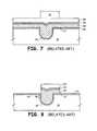
- a not-infrequent problem with semiconductor device formation, particularly with decreasing feature sizes,is misalignment of a photoresist mask. This may result in the process and structure depicted in FIGS. 7-10 .
- FIG. 7comprises a structure analogous to FIG. 3 wherein the mask 38 of FIG. 3 has been misaligned to result in mask 70 of FIG. 7 .
- capping nitride layer 36 , silicide layer 34 , and polysilicon layer 32are etched to result in the defined gate of FIG. 8 .
- This etchbecause of the misalignment of the mask 70 , removes a portion of the polysilicon layer 32 from the trench along trench portion 80 and exposes the channel region 22 as depicted.
- Wafer processingcontinues according to the method of FIGS. 1-6 to form spacer layer 50 as depicted in FIG. 9 , then a spacer etch is performed to result the device of FIG. 10 comprising insulative spacers 60 .
- the transistor of FIG. 10will have poor electrical operation and may even be nonfunctional.
- the application of the threshold voltage across the transistorrequires adequate electrical communication between the gate (layers 32 and 34 ) and each of the channel region 22 and the source/drain regions 12 .
- the gateoverlies the entire channel region 22 and also the source/drain region 12 on each side of the channel 22 .
- the gate 32 , 34does not overlie either of region 80 of the channel 22 or the source/drain region 12 on the left side of the gate.
- the nitride spacer 60has a portion interposed between gate layer 32 and region 80 of the channel 22 . This electrical insulator between the gate and the channel, along with the increased distance between gate layer 32 and portion 80 of channel 22 , decreases electrical coupling between the channel portion 80 and gate layer 32 .
- a method for forming a RAD transistor gate and a resulting RAD transistor which has more robust tolerance for mask misalignment over conventional processingwould be desirable.
- the present inventionprovides a new method which, among other advantages, reduces problems associated with the manufacture of semiconductor devices, particularly problems resulting from mask misalignment during the formation of a recessed access device (RAD) transistor.
- a pad oxide layer and a dielectric vertical spacing layerare formed over a semiconductor wafer substrate assembly comprising a semiconductor wafer, then a trench or opening is etched into the wafer through an opening in the vertical spacing layer.
- the wafer exposed at the trenchis implanted to form a channel region, and a gate oxide is provided within the trench.
- blanket gate layerssuch as a doped polysilicon layer, a silicide layer, and a capping layer are formed, with at least the polysilicon layer formed partially within the trench, and all the gate layers formed over the vertical spacing layer.
- the capping layer, the silicide layer, and the polysilicon layerare masked with a patterned photoresist layer, which will be used to pattern the transistor gate.
- This embodiment of the present inventionprovides for additional misalignment tolerance of this mask, which defines the transistor gate.
- the exposed portions of the capping layer, the silicide layer, and the polysilicon layerare overetched just far enough to ensure removal of the polysilicon layer from over the vertical spacing layer. During this etch, a portion of the vertical spacing layer which is exposed is partially etched, and prevents removal of the polysilicon layer from within the trench.
- An implantmay be performed to adjust the source/drain regions. Subsequently, a blanket conformal spacer layer is formed over the transistor gate and over the vertical spacing layer, then a vertical etch is performed to expose the semiconductor wafer. Wafer processing then continues as is known in the art to complete the semiconductor device.
- FIGS. 1-6are cross sections depicting the conventional formation of a recessed access device (RAD) transistor
- FIGS. 7-10are cross sections depicting the conventional formation of a RAD transistor, wherein a misaligned mask is used to pattern the transistor gate stack;
- FIGS. 11-16are cross sections depicting an embodiment of the present invention used to form a RAD transistor, wherein a misaligned mask is used to pattern the transistor gate stack;
- FIG. 17is a cross section of an embodiment of the present invention used to form a RAD transistor, wherein a properly aligned mask is used to pattern the transistor gate stack;
- FIG. 18is an isometric depiction of various components which may be manufactured using devices formed with an embodiment of the present invention.
- FIG. 19is a block diagram of an exemplary use of the invention to form part of a memory device having a storage transistor array.
- waferis to be understood as a semiconductor-based material including silicon, silicon-on-insulator (SOI) or silicon-on-sapphire (SOS) technology, doped and undoped semiconductors, epitaxial layers of silicon supported by a base semiconductor foundation, and other semiconductor structures.
- SOIsilicon-on-insulator
- SOSsilicon-on-sapphire
- doped and undoped semiconductorsepitaxial layers of silicon supported by a base semiconductor foundation, and other semiconductor structures.
- previous process stepsmay have been utilized to form regions or junctions in or over the base semiconductor structure or foundation.
- substrate assemblymay include a wafer with layers including dielectrics and conductors, and features such as transistors, formed thereover, depending on the particular stage of processing.
- the semiconductorneed not be silicon-based, but may be based on silicon-germanium, silicon-on-insulator, silicon-on-sapphire, germanium, or gallium arsenide, among others.
- the term “on” used with respect to two layers, one “on” the other,means at least some contact between the layers, while “over” means the layers are in close proximity, but possibly with one or more additional intervening layers such that contact is possible but not required. Neither “on” nor “over” implies any directionality as used herein.
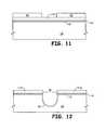
- FIGS. 11-16A first embodiment of an inventive method used to form a recessed access device (RAD) transistor is depicted in FIGS. 11-16 .
- FIG. 11depicts a semiconductor wafer 10 having a region 12 comprising n-type dopants.
- FIG. 11further depicts pad oxide (pad dielectric) 14 which protects against contamination, provides stress relief between the wafer 10 and the vertical spacing layer 110 , and functions as an etch stop layer during an etch of vertical spacing layer 110 .
- the vertical spacing layer 110may comprise any dielectric such as, by way of example only, silicon dioxide or silicon nitride. With present device sizes, the vertical spacing layer will be between about 100 ⁇ and about 500 ⁇ thick, and its thickness will depend on the gate overetch (polysilicon overetch).
- FIG. 11depicts a semiconductor wafer 10 having a region 12 comprising n-type dopants.
- FIG. 11further depicts pad oxide (pad dielectric) 14 which protects against contamination, provides stress relief between the wafer 10 and the
- FIG. 11further depicts a patterned mask 16 , such as photoresist, which is used to define a trench in wafer 10 .
- a patterned mask 16such as photoresist, which is used to define a trench in wafer 10 .
- an anisotropic etchis performed to form a trench 20 within the wafer 10 , then the mask layer 16 is removed to result in the structure of FIG. 12 .
- a conductively doped channel region 22may result from previous ion implantation into the wafer, or the wafer along the trench may be implanted subsequent to trench formation.
- a transistor gate oxide layeris grown on the exposed semiconductor wafer according to techniques known in the art to result in the gate oxide 30 of FIG. 13 .
- various blanket transistor gate layersare formed, such as a doped polysilicon layer 32 , a silicide layer 34 , and a nitride capping layer 36 .
- a patterned photoresist layer 70is formed which will be used to define the transistor gate. While mask 70 is intended to be centered over the trench 20 , mask 70 has been misaligned due to variations in the masking process.
- the FIG. 13 structureis anisotropically etched to remove all exposed gate layers down to the vertical spacing layer 110 , then the mask 70 is removed to result in the FIG. 14 structure.
- the etch of the FIG. 13 structureis preferably performed using an etch which removes polysilicon 32 and vertical spacing layer 110 at about the same rate.
- an etchantcomprising tetrafluoromethane (CF 4 ) would result in sufficiently similar etch rates for the vertical spacing layer and the polysilicon gate layer.
- an implantis typically performed to enhance the source/drain regions 12 .
- the FIG. 14 structurealso depicts the results of an intentional overetch of the polysilicon layer 32 .
- This overetchpartially etches the exposed portions of the vertical spacing layer, and ensures complete removal of the polysilicon layer 32 from over the vertical spacing layer 110 .
- it is preferable that the overetchis terminated prior to etching completely through vertical spacing layer 110 so that none of polysilicon layer 32 is removed from within the trench 20 in the wafer 10 .
- an unetched portion 140 of layer 110remains.
- an optional angled implantinto the semiconductor wafer 10 may be performed as depicted to more heavily dope the wafer, particularly into the wafer 10 at location 142 which is immediately under the unetched vertical spacing layer portion 140 which is interposed between the trench and the sidewall on the right-hand side of the transistor of FIG. 14 .
- Implanting this regionmay be advantageous for electrical operation of the transistor if the mask 70 at FIG. 13 has been misaligned to such an excessive degree that the original wafer doping 12 at FIG. 11 does not provide sufficient electrical communication between the source/drain region 12 and the channel 22 .
- an unetched portion of the vertical spacing layer similar to portion 140will remain under each side of conductive transistor gate layer 32 . That is, an unetched portion 140 of vertical spacing layer 110 will remain interposed between the trench and each vertically oriented transistor gate sidewall. In the FIG. 14 structure where mask misalignment has occurred, no unetched portion of vertical spacing layer 110 remains interposed between the trench and the transistor sidewall on the left side of the transistor gate as depicted.
- a blanket spacer layer 50for example silicon nitride, is formed over vertically oriented sidewalls of the conductive transistor gate layers 32 , 34 . Blanket spacer layer 50 is also formed over a horizontally oriented surface of the vertical spacing layer 110 of FIG. 14 to result in the FIG. 15 structure.
- a spacer etchis performed to provide insulative spacers 60 around the conductive layers 32 , 34 and the nonconductive layer 36 of the transistor gate as depicted in FIG. 16 to complete the transistor gate and the insulation layers surrounding the transistor gate. Wafer processing then continues according to techniques known in the art to form a completed semiconductor device.
- the inventive processresults in a complete fill of the trench with the polysilicon layer 32 , even in the case where the mask which defines the transistor gate stack is inadvertently misaligned to such an extent that one of the vertical edges of the mask overlies the trench.
- conventional processing as depicted in FIG. 10results in removal of a portion of the polysilicon layer 32 from the trench. This removal exposes the channel region 22 and also results in the formation of the dielectric spacer material 60 within the trench 20 in the wafer 10 .
- the missing portion of the gate electroderesults in decreased electrical interaction between the gate and the channel.
- This decreased interactionmay result in a higher threshold voltage for the transistor, and may prevent the transistor from activating during the application of V t .
- the etch of the gate polysilicon 32 and subsequent formation of the dielectric layer 60 within the trench 20 as depicted in FIG. 10effectively results in a thicker gate oxide at this location because the distance from the polysilicon layer 32 to the channel 22 is increased. This results in decreased electrical interaction between the gate layer 32 and the channel 22 at this location.
- This problem with conventional processingmay be overcome by the present invention, as may be determined by reviewing the FIG. 16 structure which has been formed using an embodiment of the present invention with a misaligned mask.
- the FIG. 16 structurecomprises a recess 20 in the semiconductor wafer 10 , with the recess filled with a transistor gate conductor 32 which, in the present embodiment, is doped polysilicon.
- a silicide layer 34overlies the gate conductor 32
- a capping layer 36overlies the silicide 34 .
- FIG. 16further depicts first and second cross sectional spacers 60 which, in the present embodiment, may comprise silicon nitride. Interposed between each spacer 60 and the wafer 10 is a portion of the vertical spacing layer 110 and the pad oxide 14 .
- the FIG. 16 structurealso comprises, at the right-hand side of the transistor, an unetched portion 140 of the vertical spacing layer 110 which is interposed between the transistor gate conductor 32 and the semiconductor wafer 10 . Further, a portion of the pad oxide 14 is interposed between unetched portion 140 of the vertical spacing layer 110 and the semiconductor wafer 10 . As depicted, the left-hand side of the transistor does not comprise an unetched portion of the vertical spacing layer 110 , but instead comprises only an etched portion of the vertical spacing layer. Both an etched portion of the vertical spacing layer and a portion of the pad oxide are interposed between the dielectric spacer 60 and the wafer 10 on the left-hand side of the FIG. 16 transistor.
- a vertically oriented edge of the polysilicon gate layer 32overlies the trench, whereas on the depicted right half of the transistor the vertically oriented edge of the polysilicon gate layer 32 does not overlie the trench.
- the vertically oriented left edgeextends below a horizontal upper surface (but does not extend below a horizontal lower surface) of the unetched portion 140 of layer 110 , and thus does not extend into the trench formed in the wafer.
- FIG. 16after etching the spacer layer 50 of FIG. 15 to complete the transistor and surrounding dielectric, a portion of the vertical spacing layer 110 on each side of the gate is exposed, as is a portion of the pad oxide layer 14 .
- FIG. 17depicts an embodiment of the invention wherein a properly aligned mask has been used to define the transistor gate stack.
- an unetched portion 140 of the vertical spacing layer 110remains interposed between the trench in the wafer 10 and each of the vertically oriented sidewalls of the transistor gate stack at an oblique angle.
- These unetched segments 140 of the vertical spacing layer 110are also interposed in a vertical direction between conductive transistor gate layer 32 and the semiconductor wafer 10 at a location on both sides of the trench.
- transistor gate 32is interposed between the two segments of layer 140 in this embodiment. Because the mask is properly aligned, neither of the cross sectional sidewalls in the mask which forms the transistor gate stack overlies the trench.
- a semiconductor device 180 formed in accordance with the inventionmay be attached along with other devices such as a microprocessor 182 to a printed circuit board 184 , for example to a computer motherboard or as a part of a memory module used in a personal computer, a minicomputer, or a mainframe 186 .
- FIG. 18may also represent use of device 180 in other electronic devices comprising a housing 186 , for example devices comprising a microprocessor 182 , related to telecommunications, the automobile industry, semiconductor test and manufacturing equipment, consumer electronics, or virtually any piece of consumer or industrial electronic equipment.
- FIG. 19is a simplified block diagram of a memory device such as a dynamic random access memory having word lines formed using an embodiment of the present invention.
- FIG. 19depicts a processor 182 coupled to a memory device 180 , and further depicts the following basic sections of a memory integrated circuit: control circuitry 190 ; row 192 and column 194 address buffers; row 196 and column 198 decoders; sense amplifiers 200 ; memory array 202 ; and data input/output 204 .
Landscapes
- Physics & Mathematics (AREA)
- High Energy & Nuclear Physics (AREA)
- Engineering & Computer Science (AREA)
- General Physics & Mathematics (AREA)
- Health & Medical Sciences (AREA)
- Toxicology (AREA)
- Crystallography & Structural Chemistry (AREA)
- Condensed Matter Physics & Semiconductors (AREA)
- Chemical & Material Sciences (AREA)
- Manufacturing & Machinery (AREA)
- Computer Hardware Design (AREA)
- Microelectronics & Electronic Packaging (AREA)
- Power Engineering (AREA)
- Insulated Gate Type Field-Effect Transistor (AREA)
- Semiconductor Memories (AREA)
- Metal-Oxide And Bipolar Metal-Oxide Semiconductor Integrated Circuits (AREA)
Abstract
Description
Claims (3)
Priority Applications (1)
| Application Number | Priority Date | Filing Date | Title |
|---|---|---|---|
| US14/561,605US9536971B2 (en) | 2005-07-08 | 2014-12-05 | Semiconductor device comprising a transistor gate having multiple vertically oriented sidewalls |
Applications Claiming Priority (4)
| Application Number | Priority Date | Filing Date | Title |
|---|---|---|---|
| US11/177,850US7282401B2 (en) | 2005-07-08 | 2005-07-08 | Method and apparatus for a self-aligned recessed access device (RAD) transistor gate |
| US11/863,535US8399920B2 (en) | 2005-07-08 | 2007-09-28 | Semiconductor device comprising a transistor gate having multiple vertically oriented sidewalls |
| US13/398,491US8916912B2 (en) | 2005-07-08 | 2012-02-16 | Semiconductor device comprising a transistor gate having multiple vertically oriented sidewalls |
| US14/561,605US9536971B2 (en) | 2005-07-08 | 2014-12-05 | Semiconductor device comprising a transistor gate having multiple vertically oriented sidewalls |
Related Parent Applications (1)
| Application Number | Title | Priority Date | Filing Date |
|---|---|---|---|
| US13/398,491DivisionUS8916912B2 (en) | 2005-07-08 | 2012-02-16 | Semiconductor device comprising a transistor gate having multiple vertically oriented sidewalls |
Publications (2)
| Publication Number | Publication Date |
|---|---|
| US20150108566A1 US20150108566A1 (en) | 2015-04-23 |
| US9536971B2true US9536971B2 (en) | 2017-01-03 |
Family
ID=37618794
Family Applications (4)
| Application Number | Title | Priority Date | Filing Date |
|---|---|---|---|
| US11/177,850Expired - LifetimeUS7282401B2 (en) | 2005-07-08 | 2005-07-08 | Method and apparatus for a self-aligned recessed access device (RAD) transistor gate |
| US11/863,535Active2027-01-17US8399920B2 (en) | 2005-07-08 | 2007-09-28 | Semiconductor device comprising a transistor gate having multiple vertically oriented sidewalls |
| US13/398,491Expired - LifetimeUS8916912B2 (en) | 2005-07-08 | 2012-02-16 | Semiconductor device comprising a transistor gate having multiple vertically oriented sidewalls |
| US14/561,605Expired - LifetimeUS9536971B2 (en) | 2005-07-08 | 2014-12-05 | Semiconductor device comprising a transistor gate having multiple vertically oriented sidewalls |
Family Applications Before (3)
| Application Number | Title | Priority Date | Filing Date |
|---|---|---|---|
| US11/177,850Expired - LifetimeUS7282401B2 (en) | 2005-07-08 | 2005-07-08 | Method and apparatus for a self-aligned recessed access device (RAD) transistor gate |
| US11/863,535Active2027-01-17US8399920B2 (en) | 2005-07-08 | 2007-09-28 | Semiconductor device comprising a transistor gate having multiple vertically oriented sidewalls |
| US13/398,491Expired - LifetimeUS8916912B2 (en) | 2005-07-08 | 2012-02-16 | Semiconductor device comprising a transistor gate having multiple vertically oriented sidewalls |
Country Status (1)
| Country | Link |
|---|---|
| US (4) | US7282401B2 (en) |
Cited By (1)
| Publication number | Priority date | Publication date | Assignee | Title |
|---|---|---|---|---|
| US12426259B2 (en) | 2022-05-25 | 2025-09-23 | Samsung Electronics Co., Ltd. | Integrated circuit device |
Families Citing this family (64)
| Publication number | Priority date | Publication date | Assignee | Title |
|---|---|---|---|---|
| US5977579A (en)* | 1998-12-03 | 1999-11-02 | Micron Technology, Inc. | Trench dram cell with vertical device and buried word lines |
| US7071043B2 (en) | 2002-08-15 | 2006-07-04 | Micron Technology, Inc. | Methods of forming a field effect transistor having source/drain material over insulative material |
| US6844591B1 (en)* | 2003-09-17 | 2005-01-18 | Micron Technology, Inc. | Method of forming DRAM access transistors |
| KR100593443B1 (en)* | 2004-02-11 | 2006-06-28 | 삼성전자주식회사 | Transistors and Manufacturing Methods |
| US7262089B2 (en)* | 2004-03-11 | 2007-08-28 | Micron Technology, Inc. | Methods of forming semiconductor structures |
| US7518182B2 (en)* | 2004-07-20 | 2009-04-14 | Micron Technology, Inc. | DRAM layout with vertical FETs and method of formation |
| US7547945B2 (en) | 2004-09-01 | 2009-06-16 | Micron Technology, Inc. | Transistor devices, transistor structures and semiconductor constructions |
| US7244659B2 (en)* | 2005-03-10 | 2007-07-17 | Micron Technology, Inc. | Integrated circuits and methods of forming a field effect transistor |
| US7384849B2 (en)* | 2005-03-25 | 2008-06-10 | Micron Technology, Inc. | Methods of forming recessed access devices associated with semiconductor constructions |
| US7364997B2 (en) | 2005-07-07 | 2008-04-29 | Micron Technology, Inc. | Methods of forming integrated circuitry and methods of forming local interconnects |
| US7282401B2 (en) | 2005-07-08 | 2007-10-16 | Micron Technology, Inc. | Method and apparatus for a self-aligned recessed access device (RAD) transistor gate |
| US7867851B2 (en)* | 2005-08-30 | 2011-01-11 | Micron Technology, Inc. | Methods of forming field effect transistors on substrates |
| US7867845B2 (en)* | 2005-09-01 | 2011-01-11 | Micron Technology, Inc. | Transistor gate forming methods and transistor structures |
| US7700441B2 (en) | 2006-02-02 | 2010-04-20 | Micron Technology, Inc. | Methods of forming field effect transistors, methods of forming field effect transistor gates, methods of forming integrated circuitry comprising a transistor gate array and circuitry peripheral to the gate array, and methods of forming integrated circuitry comprising a transistor gate array including first gates and second grounded isolation gates |
| US8008144B2 (en) | 2006-05-11 | 2011-08-30 | Micron Technology, Inc. | Dual work function recessed access device and methods of forming |
| US20070262395A1 (en)* | 2006-05-11 | 2007-11-15 | Gibbons Jasper S | Memory cell access devices and methods of making the same |
| US8860174B2 (en)* | 2006-05-11 | 2014-10-14 | Micron Technology, Inc. | Recessed antifuse structures and methods of making the same |
| US8852851B2 (en) | 2006-07-10 | 2014-10-07 | Micron Technology, Inc. | Pitch reduction technology using alternating spacer depositions during the formation of a semiconductor device and systems including same |
| US7602001B2 (en) | 2006-07-17 | 2009-10-13 | Micron Technology, Inc. | Capacitorless one transistor DRAM cell, integrated circuitry comprising an array of capacitorless one transistor DRAM cells, and method of forming lines of capacitorless one transistor DRAM cells |
| US7772632B2 (en) | 2006-08-21 | 2010-08-10 | Micron Technology, Inc. | Memory arrays and methods of fabricating memory arrays |
| US7589995B2 (en) | 2006-09-07 | 2009-09-15 | Micron Technology, Inc. | One-transistor memory cell with bias gate |
| US7960467B2 (en)* | 2006-11-30 | 2011-06-14 | Nissin Kogyo Co., Ltd. | Carbon fiber composite material and method of producing the same |
| US7923373B2 (en) | 2007-06-04 | 2011-04-12 | Micron Technology, Inc. | Pitch multiplication using self-assembling materials |
| KR101374323B1 (en)* | 2008-01-07 | 2014-03-17 | 삼성전자주식회사 | Semiconductor device and method of manufacturing the same |
| US9190494B2 (en)* | 2008-02-19 | 2015-11-17 | Micron Technology, Inc. | Systems and devices including fin field-effect transistors each having U-shaped semiconductor fin |
| US7742324B2 (en)* | 2008-02-19 | 2010-06-22 | Micron Technology, Inc. | Systems and devices including local data lines and methods of using, making, and operating the same |
| US8866254B2 (en) | 2008-02-19 | 2014-10-21 | Micron Technology, Inc. | Devices including fin transistors robust to gate shorts and methods of making the same |
| US8211786B2 (en)* | 2008-02-28 | 2012-07-03 | International Business Machines Corporation | CMOS structure including non-planar hybrid orientation substrate with planar gate electrodes and method for fabrication |
| US7915659B2 (en) | 2008-03-06 | 2011-03-29 | Micron Technology, Inc. | Devices with cavity-defined gates and methods of making the same |
| US7898857B2 (en) | 2008-03-20 | 2011-03-01 | Micron Technology, Inc. | Memory structure having volatile and non-volatile memory portions |
| US8546876B2 (en) | 2008-03-20 | 2013-10-01 | Micron Technology, Inc. | Systems and devices including multi-transistor cells and methods of using, making, and operating the same |
| US7808042B2 (en) | 2008-03-20 | 2010-10-05 | Micron Technology, Inc. | Systems and devices including multi-gate transistors and methods of using, making, and operating the same |
| US7969776B2 (en) | 2008-04-03 | 2011-06-28 | Micron Technology, Inc. | Data cells with drivers and methods of making and operating the same |
| US7989307B2 (en) | 2008-05-05 | 2011-08-02 | Micron Technology, Inc. | Methods of forming isolated active areas, trenches, and conductive lines in semiconductor structures and semiconductor structures including the same |
| US10151981B2 (en) | 2008-05-22 | 2018-12-11 | Micron Technology, Inc. | Methods of forming structures supported by semiconductor substrates |
| US8076229B2 (en)* | 2008-05-30 | 2011-12-13 | Micron Technology, Inc. | Methods of forming data cells and connections to data cells |
| US8148776B2 (en) | 2008-09-15 | 2012-04-03 | Micron Technology, Inc. | Transistor with a passive gate |
| US7824986B2 (en) | 2008-11-05 | 2010-11-02 | Micron Technology, Inc. | Methods of forming a plurality of transistor gates, and methods of forming a plurality of transistor gates having at least two different work functions |
| US8273634B2 (en)* | 2008-12-04 | 2012-09-25 | Micron Technology, Inc. | Methods of fabricating substrates |
| US8796155B2 (en) | 2008-12-04 | 2014-08-05 | Micron Technology, Inc. | Methods of fabricating substrates |
| US8247302B2 (en) | 2008-12-04 | 2012-08-21 | Micron Technology, Inc. | Methods of fabricating substrates |
| US8692310B2 (en) | 2009-02-09 | 2014-04-08 | Spansion Llc | Gate fringing effect based channel formation for semiconductor device |
| US8268543B2 (en)* | 2009-03-23 | 2012-09-18 | Micron Technology, Inc. | Methods of forming patterns on substrates |
| US9330934B2 (en)* | 2009-05-18 | 2016-05-03 | Micron Technology, Inc. | Methods of forming patterns on substrates |
| US20110129991A1 (en)* | 2009-12-02 | 2011-06-02 | Kyle Armstrong | Methods Of Patterning Materials, And Methods Of Forming Memory Cells |
| US8039340B2 (en) | 2010-03-09 | 2011-10-18 | Micron Technology, Inc. | Methods of forming an array of memory cells, methods of forming a plurality of field effect transistors, methods of forming source/drain regions and isolation trenches, and methods of forming a series of spaced trenches into a substrate |
| US8518788B2 (en) | 2010-08-11 | 2013-08-27 | Micron Technology, Inc. | Methods of forming a plurality of capacitors |
| US8455341B2 (en) | 2010-09-02 | 2013-06-04 | Micron Technology, Inc. | Methods of forming features of integrated circuitry |
| US8294511B2 (en) | 2010-11-19 | 2012-10-23 | Micron Technology, Inc. | Vertically stacked fin transistors and methods of fabricating and operating the same |
| KR101802220B1 (en)* | 2010-12-20 | 2017-11-29 | 삼성전자주식회사 | Semiconductor devices including a vertical channel transistor and methods of fabricating the same |
| US8575032B2 (en) | 2011-05-05 | 2013-11-05 | Micron Technology, Inc. | Methods of forming a pattern on a substrate |
| US9401363B2 (en) | 2011-08-23 | 2016-07-26 | Micron Technology, Inc. | Vertical transistor devices, memory arrays, and methods of forming vertical transistor devices |
| US9385132B2 (en) | 2011-08-25 | 2016-07-05 | Micron Technology, Inc. | Arrays of recessed access devices, methods of forming recessed access gate constructions, and methods of forming isolation gate constructions in the fabrication of recessed access devices |
| US9076680B2 (en) | 2011-10-18 | 2015-07-07 | Micron Technology, Inc. | Integrated circuitry, methods of forming capacitors, and methods of forming integrated circuitry comprising an array of capacitors and circuitry peripheral to the array |
| US9177794B2 (en) | 2012-01-13 | 2015-11-03 | Micron Technology, Inc. | Methods of patterning substrates |
| US8629048B1 (en) | 2012-07-06 | 2014-01-14 | Micron Technology, Inc. | Methods of forming a pattern on a substrate |
| US9105713B2 (en) | 2012-11-09 | 2015-08-11 | Infineon Technologies Austria Ag | Semiconductor device with metal-filled groove in polysilicon gate electrode |
| US9005463B2 (en) | 2013-05-29 | 2015-04-14 | Micron Technology, Inc. | Methods of forming a substrate opening |
| KR102483951B1 (en) | 2015-06-22 | 2023-01-03 | 삼성디스플레이 주식회사 | Liquid crystal display apparatus and method for manufacturing the same |
| US9831090B2 (en) | 2015-08-19 | 2017-11-28 | Taiwan Semiconductor Manufacturing Company, Ltd. | Method and structure for semiconductor device having gate spacer protection layer |
| US10170616B2 (en)* | 2016-09-19 | 2019-01-01 | Globalfoundries Inc. | Methods of forming a vertical transistor device |
| US10256310B1 (en)* | 2017-12-04 | 2019-04-09 | Vanguard International Semiconductor Corporation | Split-gate flash memory cell having a floating gate situated in a concave trench in a semiconductor substrate |
| US10944002B2 (en) | 2018-09-07 | 2021-03-09 | Micron Technology, Inc. | Integrated assemblies having a portion of a transistor gate extending into a recessed region of a semiconductor base, and methods of forming integrated assemblies |
| KR20220158340A (en)* | 2021-05-24 | 2022-12-01 | 삼성전자주식회사 | Semiconductor devices including gate structure and method of forming the same |
Citations (303)
| Publication number | Priority date | Publication date | Assignee | Title |
|---|---|---|---|---|
| JPS51147280U (en) | 1975-05-21 | 1976-11-26 | ||
| JPS58220464A (en) | 1982-06-17 | 1983-12-22 | Fujitsu Ltd | Semiconductor memory device |
| US4455740A (en) | 1979-12-07 | 1984-06-26 | Tokyo Shibaura Denki Kabushiki Kaisha | Method of manufacturing a self-aligned U-MOS semiconductor device |
| WO1986003341A1 (en) | 1984-11-27 | 1986-06-05 | American Telephone & Telegraph Company | Trench transistor |
| US4722910A (en) | 1986-05-27 | 1988-02-02 | Analog Devices, Inc. | Partially self-aligned metal contact process |
| US4835741A (en) | 1986-06-02 | 1989-05-30 | Texas Instruments Incorporated | Frasable electrically programmable read only memory cell using a three dimensional trench floating gate |
| US4922460A (en) | 1987-01-26 | 1990-05-01 | Mitsubishi Denki Kabushiki Kaisha | Semiconductor memory device with folded bit line structure suitable for high density |
| US4931409A (en) | 1988-01-30 | 1990-06-05 | Kabushiki Kaisha Toshiba | Method of manufacturing semiconductor device having trench isolation |
| US4937641A (en) | 1983-09-28 | 1990-06-26 | Hitachi, Ltd. | Semiconductor memory and method of producing the same |
| US4939793A (en) | 1986-04-17 | 1990-07-03 | Plessey Overseas Limited | Integrated circuit assembly with optically coupled components |
| US4939100A (en) | 1987-12-18 | 1990-07-03 | Commissariat A L'energie Atomique | Process for the production of a MIS transistor with a raised substrate/gate dielectric interface end |
| US4979004A (en) | 1988-01-29 | 1990-12-18 | Texas Instruments Incorporated | Floating gate memory cell and device |
| US5013680A (en) | 1990-07-18 | 1991-05-07 | Micron Technology, Inc. | Process for fabricating a DRAM array having feature widths that transcend the resolution limit of available photolithography |
| US5014110A (en) | 1988-06-03 | 1991-05-07 | Mitsubishi Denki Kabushiki Kaisha | Wiring structures for semiconductor memory device |
| US5021355A (en) | 1989-05-22 | 1991-06-04 | International Business Machines Corporation | Method of fabricating cross-point lightly-doped drain-source trench transistor |
| US5047117A (en) | 1990-09-26 | 1991-09-10 | Micron Technology, Inc. | Method of forming a narrow self-aligned, annular opening in a masking layer |
| JPH03219677A (en) | 1990-01-24 | 1991-09-27 | Fujitsu Ltd | semiconductor equipment |
| JPH0414253Y2 (en) | 1987-01-09 | 1992-03-31 | ||
| US5107459A (en) | 1990-04-20 | 1992-04-21 | International Business Machines Corporation | Stacked bit-line architecture for high density cross-point memory cell array |
| US5108938A (en) | 1989-03-21 | 1992-04-28 | Grumman Aerospace Corporation | Method of making a trench gate complimentary metal oxide semiconductor transistor |
| US5122848A (en) | 1991-04-08 | 1992-06-16 | Micron Technology, Inc. | Insulated-gate vertical field-effect transistor with high current drive and minimum overlap capacitance |
| US5160491A (en) | 1986-10-21 | 1992-11-03 | Texas Instruments Incorporated | Method of making a vertical MOS transistor |
| US5244824A (en) | 1990-09-05 | 1993-09-14 | Motorola, Inc. | Trench capacitor and transistor structure and method for making the same |
| US5254218A (en) | 1992-04-22 | 1993-10-19 | Micron Technology, Inc. | Masking layer having narrow isolated spacings and the method for forming said masking layer and the method for forming narrow isolated trenches defined by said masking layer |
| US5281548A (en) | 1992-07-28 | 1994-01-25 | Micron Technology, Inc. | Plug-based floating gate memory |
| US5358879A (en) | 1993-04-30 | 1994-10-25 | Loral Federal Systems Company | Method of making gate overlapped lightly doped drain for buried channel devices |
| US5371024A (en) | 1988-09-30 | 1994-12-06 | Kabushiki Kaisha Toshiba | Semiconductor device and process for manufacturing the same |
| US5376575A (en) | 1991-09-26 | 1994-12-27 | Hyundai Electronics Industries, Inc. | Method of making dynamic random access memory having a vertical transistor |
| US5392237A (en) | 1992-09-25 | 1995-02-21 | Rohm Co., Ltd. | Semiconductor memory device with EEPROM in trench with polysilicon/metal contacting to source and drain in virtual ground type array |
| US5413949A (en) | 1994-04-26 | 1995-05-09 | United Microelectronics Corporation | Method of making self-aligned MOSFET |
| JPH0778977B2 (en) | 1989-03-02 | 1995-08-23 | 松下電器産業株式会社 | Magnetic disk cartridge |
| US5446299A (en) | 1994-04-29 | 1995-08-29 | International Business Machines Corporation | Semiconductor random access memory cell on silicon-on-insulator with dual control gates |
| JPH07297297A (en) | 1994-04-22 | 1995-11-10 | Nec Corp | Semiconductor memory device and method of manufacturing |
| JPH07106435B2 (en) | 1991-04-15 | 1995-11-15 | 新日本製鐵株式会社 | Twin roll type continuous casting machine |
| US5480838A (en) | 1992-07-03 | 1996-01-02 | Mitsubishi Denki Kabushiki Kaisha | Method of manufacturing a semiconductor device having vertical transistor with tubular double-gate |
| US5496751A (en) | 1993-05-07 | 1996-03-05 | Vlsi Technology, Inc. | Method of forming an ESD and hot carrier resistant integrated circuit structure |
| US5502320A (en) | 1993-03-15 | 1996-03-26 | Kabushiki Kaisha Toshiba | Dynamic random access memory (DRAM) semiconductor device |
| US5514604A (en) | 1993-12-08 | 1996-05-07 | General Electric Company | Vertical channel silicon carbide metal-oxide-semiconductor field effect transistor with self-aligned gate for microwave and power applications, and method of making |
| US5532089A (en) | 1993-12-23 | 1996-07-02 | International Business Machines Corporation | Simplified fabrication methods for rim phase-shift masks |
| US5567634A (en) | 1995-05-01 | 1996-10-22 | National Semiconductor Corporation | Method of fabricating self-aligned contact trench DMOS transistors |
| US5574621A (en) | 1995-03-27 | 1996-11-12 | Motorola, Inc. | Integrated circuit capacitor having a conductive trench |
| US5573837A (en) | 1992-04-22 | 1996-11-12 | Micron Technology, Inc. | Masking layer having narrow isolated spacings and the method for forming said masking layer and the method for forming narrow isolated trenches defined by said masking layer |
| US5612559A (en) | 1993-11-24 | 1997-03-18 | Samsung Electronics Co., Ltd. | Semiconductor device having pillar shaped transistor and a method for manufacturing the same |
| US5619057A (en) | 1994-01-19 | 1997-04-08 | Sony Corporation | Complex film overlying a substrate with defined work function |
| JPH09129837A (en) | 1995-10-05 | 1997-05-16 | Lg Semicon Co Ltd | Semiconductor memory device and its preparation |
| EP0453998B1 (en) | 1990-04-21 | 1997-07-02 | Kabushiki Kaisha Toshiba | Semiconductor memory device having a bit line constituted by a semiconductor layer |
| WO1997044826A1 (en) | 1996-05-22 | 1997-11-27 | Siemens Aktiengesellschaft | Dram cell array and method of manufacturing it |
| US5693549A (en) | 1994-09-13 | 1997-12-02 | Lg Semicon Co., Ltd. | Method of fabricating thin film transistor with supplementary gates |
| US5714786A (en) | 1996-10-31 | 1998-02-03 | Micron Technology, Inc. | Transistors having controlled conductive spacers, uses of such transistors and methods of making such transistors |
| US5714412A (en) | 1996-12-02 | 1998-02-03 | Taiwan Semiconductor Manufacturing Company, Ltd | Multi-level, split-gate, flash memory cell and method of manufacture thereof |
| US5739066A (en) | 1996-09-17 | 1998-04-14 | Micron Technology, Inc. | Semiconductor processing methods of forming a conductive gate and line |
| US5753947A (en) | 1995-01-20 | 1998-05-19 | Micron Technology, Inc. | Very high-density DRAM cell structure and method for fabricating it |
| US5763305A (en) | 1996-08-16 | 1998-06-09 | United Microelectronics Corporation | Method for forming a semiconductor memory device with a capacitor |
| US5792690A (en) | 1997-05-15 | 1998-08-11 | Vanguard International Semiconductor Corporation | Method of fabricating a DRAM cell with an area equal to four times the used minimum feature |
| US5792687A (en) | 1996-08-01 | 1998-08-11 | Vanguard International Semiconductor Corporation | Method for fabricating high density integrated circuits using oxide and polysilicon spacers |
| US5817552A (en) | 1995-05-24 | 1998-10-06 | Siemens Aktiengesellschaft | Process of making a dram cell arrangement |
| US5841611A (en) | 1994-05-02 | 1998-11-24 | Matsushita Electric Industrial Co., Ltd. | Magnetoresistance effect device and magnetoresistance effect type head, memory device, and amplifying device using the same |
| US5869382A (en) | 1996-07-02 | 1999-02-09 | Sony Corporation | Structure of capacitor for dynamic random access memory and method of manufacturing thereof |
| US5869359A (en) | 1997-08-20 | 1999-02-09 | Prabhakar; Venkatraman | Process for forming silicon on insulator devices having elevated source and drain regions |
| US5909618A (en) | 1997-07-08 | 1999-06-01 | Micron Technology, Inc. | Method of making memory cell with vertical transistor and buried word and body lines |
| WO1999036961A1 (en) | 1998-01-14 | 1999-07-22 | Infineon Technologies Ag | Power mosfet |
| US5963469A (en) | 1998-02-24 | 1999-10-05 | Micron Technology, Inc. | Vertical bipolar read access for low voltage memory cell |
| JPH11274478A (en) | 1998-02-17 | 1999-10-08 | Internatl Business Mach Corp <Ibm> | High performance MOSFET device with raised source and drain |
| US5964750A (en) | 1994-03-15 | 1999-10-12 | Medolas Gesellschaft Fuer Medizintechnik Gmbh | Laser catheter for bypass surgery |
| US5972754A (en) | 1998-06-10 | 1999-10-26 | Mosel Vitelic, Inc. | Method for fabricating MOSFET having increased effective gate length |
| US5977579A (en) | 1998-12-03 | 1999-11-02 | Micron Technology, Inc. | Trench dram cell with vertical device and buried word lines |
| US6015990A (en) | 1997-02-27 | 2000-01-18 | Kabushiki Kaisha Toshiba | Semiconductor memory device and method of manufacturing the same |
| US6033963A (en) | 1999-08-30 | 2000-03-07 | Taiwan Semiconductor Manufacturing Company | Method of forming a metal gate for CMOS devices using a replacement gate process |
| US6037212A (en) | 1996-08-16 | 2000-03-14 | United Microelectronics Corp. | Method of fabricating a semiconductor memory cell having a tree-type capacitor |
| US6054355A (en) | 1997-06-30 | 2000-04-25 | Kabushiki Kaisha Toshiba | Method of manufacturing a semiconductor device which includes forming a dummy gate |
| US6059553A (en) | 1996-12-17 | 2000-05-09 | Texas Instruments Incorporated | Integrated circuit dielectrics |
| US6063669A (en) | 1996-02-26 | 2000-05-16 | Nec Corporation | Manufacturing method of semiconductor memory device having a trench gate electrode |
| WO2000019272B1 (en) | 1998-10-01 | 2000-05-25 | Micron Technology Inc | Methods of reducing proximity effects in lithographic processes |
| US6072209A (en) | 1997-07-08 | 2000-06-06 | Micro Technology, Inc. | Four F2 folded bit line DRAM cell structure having buried bit and word lines |
| DE19928781C1 (en) | 1999-06-23 | 2000-07-06 | Siemens Ag | DRAM cell array has deep word line trenches for increasing transistor channel length and has no fixed potential word lines separating adjacent memory cells |
| US6090700A (en) | 1996-03-15 | 2000-07-18 | Vanguard International Semiconductor Corporation | Metallization method for forming interconnects in an integrated circuit |
| JP2000208762A (en) | 1999-01-13 | 2000-07-28 | Sony Corp | Insulation gate field effect transistor and its manufacture |
| US6108191A (en) | 1996-05-21 | 2000-08-22 | Siemens Aktiengesellschaft | Multilayer capacitor with high specific capacitance and production process therefor |
| US6114735A (en) | 1999-07-02 | 2000-09-05 | Micron Technology, Inc. | Field effect transistors and method of forming field effect transistors |
| US6124611A (en) | 1998-10-30 | 2000-09-26 | Sony Corporation | Epitaxial channel vertical MOS transistor |
| US6150687A (en) | 1997-07-08 | 2000-11-21 | Micron Technology, Inc. | Memory cell having a vertical transistor with buried source/drain and dual gates |
| US6168996B1 (en) | 1997-08-28 | 2001-01-02 | Hitachi, Ltd. | Method of fabricating semiconductor device |
| JP2001024161A (en) | 1999-04-30 | 2001-01-26 | Sony Corp | Semiconductor memory cell |
| US6184086B1 (en) | 1995-11-20 | 2001-02-06 | Micron Technology Inc. | Method for forming a floating gate semiconductor device having a portion within a recess |
| US6187643B1 (en) | 1999-06-29 | 2001-02-13 | Varian Semiconductor Equipment Associates, Inc. | Simplified semiconductor device manufacturing using low energy high tilt angle and high energy post-gate ion implantation (PoGI) |
| US6191470B1 (en) | 1997-07-08 | 2001-02-20 | Micron Technology, Inc. | Semiconductor-on-insulator memory cell with buried word and body lines |
| TW428308B (en) | 1998-08-28 | 2001-04-01 | Semiconductor Tech Acad Res Ct | Memory structure in ferroelectric nonvolatile memory and readout method therefor |
| US6214670B1 (en) | 1999-07-22 | 2001-04-10 | Taiwan Semiconductor Manufacturing Company | Method for manufacturing short-channel, metal-gate CMOS devices with superior hot carrier performance |
| US6215149B1 (en) | 1998-08-18 | 2001-04-10 | Samsung Electronics Co., Ltd. | Trenched gate semiconductor device |
| US6225669B1 (en) | 1998-09-30 | 2001-05-01 | Advanced Micro Devices, Inc. | Non-uniform gate/dielectric field effect transistor |
| US6255165B1 (en) | 1999-10-18 | 2001-07-03 | Advanced Micro Devices, Inc. | Nitride plug to reduce gate edge lifting |
| US6259142B1 (en) | 1998-04-07 | 2001-07-10 | Advanced Micro Devices, Inc. | Multiple split gate semiconductor device and fabrication method |
| US6258650B1 (en) | 1995-09-19 | 2001-07-10 | Kabushiki Kaisha Toshiba | Method for manufacturing semiconductor memory device |
| US6274497B1 (en) | 1999-11-25 | 2001-08-14 | Taiwan Semiconductor Manufacturing Co., Ltd. | Copper damascene manufacturing process |
| US6297106B1 (en) | 1999-05-07 | 2001-10-02 | Chartered Semiconductor Manufacturing Ltd. | Transistors with low overlap capacitance |
| US20010025973A1 (en) | 2000-01-25 | 2001-10-04 | Satoru Yamada | Semiconductor integrated circuit device and process for manufacturing the same |
| US6300177B1 (en) | 2001-01-25 | 2001-10-09 | Chartered Semiconductor Manufacturing Inc. | Method to form transistors with multiple threshold voltages (VT) using a combination of different work function gate materials |
| US6303518B1 (en) | 1999-09-30 | 2001-10-16 | Novellus Systems, Inc. | Methods to improve chemical vapor deposited fluorosilicate glass (FSG) film adhesion to metal barrier or etch stop/diffusion barrier layers |
| US6306755B1 (en) | 1999-05-14 | 2001-10-23 | Koninklijke Philips Electronics N.V. (Kpenv) | Method for endpoint detection during dry etch of submicron features in a semiconductor device |
| US20010038123A1 (en) | 1999-08-11 | 2001-11-08 | Bin Yu | Transistor with dynamic source/drain extensions |
| US20010044181A1 (en) | 1996-11-06 | 2001-11-22 | Fujitsu Limited | Semiconductor device and method for fabricating the same |
| US6323506B1 (en) | 1999-12-21 | 2001-11-27 | Philips Electronics North America Corporation | Self-aligned silicon carbide LMOSFET |
| US6323528B1 (en) | 1991-03-06 | 2001-11-27 | Semiconductor Energy Laboratory Co,. Ltd. | Semiconductor device |
| US6331461B1 (en) | 1996-11-01 | 2001-12-18 | Micron Technology, Inc. | Semiconductor processing methods of forming devices on a substrate, forming device arrays on a substrate, forming conductive lines on a substrate, and forming capacitor arrays on a substrate, and integrated circuitry |
| US20010052617A1 (en) | 2000-03-01 | 2001-12-20 | Shindengen Electric Manufacturing Co., Ltd | Transistor and method of manufacturing the same |
| US6337497B1 (en) | 1997-05-16 | 2002-01-08 | International Business Machines Corporation | Common source transistor capacitor stack |
| US6340614B1 (en) | 2000-10-03 | 2002-01-22 | Vanguard International Semiconductor Corporation | Method of forming a DRAM cell |
| US6349052B1 (en) | 1999-09-13 | 2002-02-19 | Infineon Technologies Ag | DRAM cell arrangement and method for fabricating it |
| US6348385B1 (en) | 2000-11-30 | 2002-02-19 | Chartered Semiconductor Manufacturing Ltd. | Method for a short channel CMOS transistor with small overlay capacitance using in-situ doped spacers with a low dielectric constant |
| US20020022339A1 (en) | 2000-07-27 | 2002-02-21 | Markus Kirchhoff | Method for forming an insulator having a low dielectric constant on a semiconductor substrate |
| US6362506B1 (en) | 1998-08-26 | 2002-03-26 | Texas Instruments Incorporated | Minimization-feasible word line structure for DRAM cell |
| US6372554B1 (en) | 1998-09-04 | 2002-04-16 | Hitachi, Ltd. | Semiconductor integrated circuit device and method for production of the same |
| US6383879B1 (en) | 1999-12-03 | 2002-05-07 | Agere Systems Guardian Corp. | Semiconductor device having a metal gate with a work function compatible with a semiconductor device |
| US6383861B1 (en) | 1999-02-18 | 2002-05-07 | Micron Technology, Inc. | Method of fabricating a dual gate dielectric |
| US6391726B1 (en) | 1999-03-11 | 2002-05-21 | Micron Technology, Inc. | Method of fabricating integrated circuitry |
| JP2002151654A (en) | 2000-11-10 | 2002-05-24 | Sharp Corp | Dielectric capacitor element and method of manufacturing the same |
| US6399490B1 (en) | 2000-06-29 | 2002-06-04 | International Business Machines Corporation | Highly conformal titanium nitride deposition process for high aspect ratio structures |
| JP2002184958A (en) | 2000-12-14 | 2002-06-28 | Sony Corp | Semiconductor device and manufacturing method thereof |
| US6414356B1 (en) | 1998-03-30 | 2002-07-02 | Micron Technology, Inc. | Circuits and methods for dual-gated transistors |
| US6420786B1 (en) | 1996-02-02 | 2002-07-16 | Micron Technology, Inc. | Conductive spacer in a via |
| TW498332B (en) | 1999-05-14 | 2002-08-11 | Hitachi Ltd | Semiconductor device |
| US20020127796A1 (en) | 2001-03-12 | 2002-09-12 | Franz Hofmann | Method for producing a cell of a semiconductor memory |
| US20020127798A1 (en) | 2001-03-08 | 2002-09-12 | Kirk Prall | 2F2 memory device system and method |
| US20020130378A1 (en) | 2001-03-15 | 2002-09-19 | Leonard Forbes | Technique to mitigate short channel effects with vertical gate transistor with different gate materials |
| US20020135030A1 (en) | 2001-03-22 | 2002-09-26 | Mitsubishi Denki Kabushiki Kaisha | Semiconductor device and manufacturing method thereof |
| US6459138B2 (en) | 1999-09-02 | 2002-10-01 | Micron Technology, Inc. | Capacitor structures |
| US6458925B1 (en) | 1998-08-03 | 2002-10-01 | University Of Maryland, Baltimore | Peptide antagonists of zonulin and methods for use of the same |
| US6458653B1 (en) | 2001-01-05 | 2002-10-01 | Samsung Electronics Co., Ltd. | Method for forming lower electrode of cylinder-shaped capacitor preventing twin bit failure |
| US20020153579A1 (en) | 2001-04-19 | 2002-10-24 | Nec Corporation | Semiconductor device with thin film having high permittivity and uniform thickness |
| US6476444B1 (en) | 1999-03-18 | 2002-11-05 | Hyundai Electronics Industries Co., Ltd. | Semiconductor device and method for fabricating the same |
| US20020163039A1 (en) | 2001-05-04 | 2002-11-07 | Clevenger Lawrence A. | High dielectric constant materials as gate dielectrics (insulators) |
| US6495474B1 (en) | 2000-09-11 | 2002-12-17 | Agere Systems Inc. | Method of fabricating a dielectric layer |
| US6495890B1 (en) | 1999-09-29 | 2002-12-17 | Kabushiki Kaisha Toshiba | Field-effect transistor with multidielectric constant gate insulation layer |
| US20020192911A1 (en) | 2000-08-29 | 2002-12-19 | Parke Stephen A. | Damascene double gated transistors and related manufacturing methods |
| US6498062B2 (en) | 2001-04-27 | 2002-12-24 | Micron Technology, Inc. | DRAM access transistor |
| US6498087B2 (en) | 2000-12-01 | 2002-12-24 | Koninklijke Philips Electronics N.V. | Method of increasing the conductivity of a transparent conductive layer |
| US20030001290A1 (en) | 2001-06-29 | 2003-01-02 | Kabushiki Kaisha Toshiba | Semiconductor memory device and method for manufacturing the same |
| EP1271632A1 (en) | 2001-02-06 | 2003-01-02 | Matsushita Electric Industrial Co., Ltd. | Method of forming insulating film and method of producing semiconductor device |
| US20030042512A1 (en) | 2001-08-30 | 2003-03-06 | Micron Technology, Inc. | Vertical transistor and method of making |
| US6552401B1 (en) | 2000-11-27 | 2003-04-22 | Micron Technology | Use of gate electrode workfunction to improve DRAM refresh |
| US20030082863A1 (en) | 2001-11-01 | 2003-05-01 | Lim Kwan Yong | CMOS of semiconductor device and method for manufacturing the same |
| US6563183B1 (en) | 2001-12-31 | 2003-05-13 | Advanced Micro Devices, Inc. | Gate array with multiple dielectric properties and method for forming same |
| US20030094651A1 (en) | 2001-11-17 | 2003-05-22 | Hynix Semiconductor Inc. | Transistor in semiconductor devices and method of manufacturing the same |
| US6586808B1 (en) | 2002-06-06 | 2003-07-01 | Advanced Micro Devices, Inc. | Semiconductor device having multi-work function gate electrode and multi-segment gate dielectric |
| US20030161201A1 (en) | 2002-02-26 | 2003-08-28 | Michael Sommer | Semiconductor memory with vertical selection transistor |
| US20030164527A1 (en) | 2002-01-16 | 2003-09-04 | Fuji Electric Co., Ltd. | Semiconductor device and its manufacturing method |
| US20030168677A1 (en) | 2002-03-11 | 2003-09-11 | Fu-Chieh Hsu | One-transistor floating-body DRAM cell in bulk CMOS process with electrically isolated charge storage region |
| US20030170955A1 (en) | 2001-07-10 | 2003-09-11 | Takahiro Kawamura | Trench-gate semiconductor device and its manufacturing method |
| US20030169629A1 (en) | 2000-07-31 | 2003-09-11 | Bernd Goebel | Semiconductor memory cell configuration and a method for producing the configuration |
| US20030170941A1 (en) | 2001-05-23 | 2003-09-11 | International Business Machines Corporation | Method for low topography semiconductor device formation |
| US6624032B2 (en) | 1999-06-28 | 2003-09-23 | Intel Corporation | Structure and process flow for fabrication of dual gate floating body integrated MOS transistors |
| US6630720B1 (en) | 2001-12-26 | 2003-10-07 | Advanced Micro Devices, Inc. | Asymmetric semiconductor device having dual work function gate and method of fabrication |
| US6632714B2 (en) | 1999-03-08 | 2003-10-14 | Kabushiki Kaisha Toshiba | Method for manufacturing semiconductor memory |
| US6632723B2 (en) | 2001-04-26 | 2003-10-14 | Kabushiki Kaisha Toshiba | Semiconductor device |
| US6645869B1 (en) | 2002-09-26 | 2003-11-11 | Vanguard International Semiconductor Corporation | Etching back process to improve topographic planarization of a polysilicon layer |
| US6645818B1 (en) | 2002-11-13 | 2003-11-11 | Chartered Semiconductor Manufacturing Ltd. | Method to fabricate dual-metal gate for N- and P-FETs |
| US6656748B2 (en) | 2002-01-31 | 2003-12-02 | Texas Instruments Incorporated | FeRAM capacitor post stack etch clean/repair |
| US20030234414A1 (en) | 2002-06-21 | 2003-12-25 | Brown Kris K. | Memory cell and method for forming the same |
| US20040009644A1 (en) | 2001-05-30 | 2004-01-15 | Toshiharu Suzuki | Method for manufacturing channel gate type field effect transistor |
| US20040018679A1 (en) | 2001-03-03 | 2004-01-29 | Yu Young Sub | Storage electrode of a semiconductor memory device and method for fabricating the same |
| TW574746B (en) | 2002-12-19 | 2004-02-01 | Taiwan Semiconductor Mfg | Method for manufacturing MOSFET with recessed channel |
| US6686616B1 (en)* | 2000-05-10 | 2004-02-03 | Cree, Inc. | Silicon carbide metal-semiconductor field effect transistors |
| US20040034587A1 (en) | 2002-08-19 | 2004-02-19 | Amberson Matthew Gilbert | System and method for calculating intra-period volatility |
| US6696746B1 (en) | 1998-04-29 | 2004-02-24 | Micron Technology, Inc. | Buried conductors |
| JP2004071935A (en) | 2002-08-08 | 2004-03-04 | Toshiba Corp | Semiconductor device and method of manufacturing semiconductor device |
| US6706600B2 (en) | 2001-09-19 | 2004-03-16 | Oki Electric Industry Co., Ltd. | Method of fabricating a split-gate semiconductor device |
| US6717200B1 (en) | 1998-09-30 | 2004-04-06 | Siemens Aktiengesellschaft | Vertical field effect transistor with internal annular gate and method of production |
| US20040065919A1 (en) | 2002-10-03 | 2004-04-08 | Wilson Peter H. | Trench gate laterally diffused MOSFET devices and methods for making such devices |
| US6720232B1 (en) | 2003-04-10 | 2004-04-13 | Taiwan Semiconductor Manufacturing Company | Method of fabricating an embedded DRAM for metal-insulator-metal (MIM) capacitor structure |
| US20040070028A1 (en) | 2002-10-15 | 2004-04-15 | Semiconductor Components Industries, Llc | Method of forming a low resistance semiconductor device and structure therefor |
| US6724028B2 (en) | 2001-12-10 | 2004-04-20 | Hans Gude Gudesen | Matrix-addressable array of integrated transistor/memory structures |
| US6727137B2 (en) | 1997-08-22 | 2004-04-27 | Micron Technology, Inc. | Processing methods of forming integrated circuitry memory devices, methods of forming DRAM arrays, and related semiconductor masks |
| US20040092115A1 (en) | 2002-11-07 | 2004-05-13 | Winbond Electronics Corp. | Memory device having isolation trenches with different depths and the method for making the same |
| US6744097B2 (en) | 2001-08-02 | 2004-06-01 | Samsung Electronics Co., Ltd. | EEPROM memory cell and method of forming the same |
| US20040125636A1 (en) | 2001-03-14 | 2004-07-01 | Wlodek Kurjanowicz | Interleaved wordline architecture |
| US6767789B1 (en) | 1998-06-26 | 2004-07-27 | International Business Machines Corporation | Method for interconnection between transfer devices and storage capacitors in memory cells and device formed thereby |
| US20040150070A1 (en) | 2003-02-03 | 2004-08-05 | Nec Electronics Corporation | Semiconductor device and method for manufacturing the same |
| US20040159857A1 (en) | 2003-02-17 | 2004-08-19 | Renesas Technology Corp. | Semiconductor device having vertical transistor |
| US6784112B2 (en) | 2001-04-05 | 2004-08-31 | Matsushita Electric Industrial Co., Ltd. | Method for surface treatment of silicon based substrate |
| US20040184298A1 (en) | 2003-03-17 | 2004-09-23 | Hiroyuki Takahashi | Semiconductor memory device |
| US20040188738A1 (en) | 2002-03-06 | 2004-09-30 | Micron Technology, Inc. | Nanotube semiconductor devices and methods for making the same |
| US20040197995A1 (en) | 2003-04-01 | 2004-10-07 | Lee Yong-Kyu | Method of manufacturing twin-ONO-type SONOS memory using reverse self-alignment process |
| US20040222458A1 (en) | 2003-05-06 | 2004-11-11 | Mosel Vitelic, Inc. | Termination structure for trench DMOS device and method of making the same |
| US6818515B1 (en) | 2003-06-23 | 2004-11-16 | Promos Technologies Inc. | Method for fabricating semiconductor device with loop line pattern structure |
| US6818947B2 (en) | 2002-09-19 | 2004-11-16 | Fairchild Semiconductor Corporation | Buried gate-field termination structure |
| US20040232466A1 (en) | 2001-08-14 | 2004-11-25 | Albert Birner | Memory cell with trench capacitor and vertical select transistor and an annular contact-making region formed between them |
| US6825093B2 (en) | 2001-09-28 | 2004-11-30 | Infineon Technologies Ag | Process window enhancement for deep trench spacer conservation |
| US20040259311A1 (en) | 2003-06-17 | 2004-12-23 | Ji-Young Kim | Method of forming transistor having recess channel in semiconductor memory, and structure thereof |
| US20040266081A1 (en) | 2003-06-25 | 2004-12-30 | Chang-Woo Oh | Methods of forming field effect transistors including raised source/drain regions |
| US6844591B1 (en) | 2003-09-17 | 2005-01-18 | Micron Technology, Inc. | Method of forming DRAM access transistors |
| US20050017240A1 (en) | 2003-07-22 | 2005-01-27 | Pierre Fazan | Integrated circuit device, and method of fabricating same |
| US6849501B2 (en) | 1999-09-01 | 2005-02-01 | Micron Technology, Inc. | Methods for fabricating an improved floating gate memory cell |
| US6849496B2 (en) | 2000-12-06 | 2005-02-01 | Infineon Technologies Ag | DRAM with vertical transistor and trench capacitor memory cells and method of fabrication |
| US20050042833A1 (en) | 2003-08-20 | 2005-02-24 | Jong-Chul Park | Method of manufacturing integrated circuit device including recessed channel transistor |
| US6864536B2 (en) | 2000-12-20 | 2005-03-08 | Winbond Electronics Corporation | Electrostatic discharge protection circuit |
| US20050063224A1 (en) | 2003-09-24 | 2005-03-24 | Pierre Fazan | Low power programming technique for a floating body memory transistor, memory cell, and memory array |
| US20050066892A1 (en) | 2003-09-30 | 2005-03-31 | Tokyo Electron Limited | Deposition of silicon-containing films from hexachlorodisilane |
| JP2005093808A (en) | 2003-09-18 | 2005-04-07 | Fujio Masuoka | Memory cell unit, nonvolatile semiconductor memory device including the same, and memory cell array driving method |
| TWI231042B (en) | 2002-12-27 | 2005-04-11 | Wintek Corp | Method and device to promote the yield rate and uniformity of AMOLED panel |
| US6888770B2 (en) | 2003-05-09 | 2005-05-03 | Kabushiki Kaisha Toshiba | Semiconductor memory device |
| US6888198B1 (en) | 2001-06-04 | 2005-05-03 | Advanced Micro Devices, Inc. | Straddled gate FDSOI device |
| US20050104156A1 (en) | 2003-11-13 | 2005-05-19 | Texas Instruments Incorporated | Forming a semiconductor structure in manufacturing a semiconductor device using one or more epitaxial growth processes |
| US20050106838A1 (en) | 2003-11-17 | 2005-05-19 | Hoon Lim | Semiconductor devices with a source/drain formed on a recessed portion of an isolation layer and methods of fabricating the same |
| US6897109B2 (en) | 2001-09-11 | 2005-05-24 | Samsung Electronics Co., Ltd. | Methods of manufacturing integrated circuit devices having contact holes using multiple insulating layers |
| JP2005142203A (en) | 2003-11-04 | 2005-06-02 | Elpida Memory Inc | Semiconductor device and manufacturing method thereof |
| US20050124130A1 (en) | 2003-04-30 | 2005-06-09 | Leo Mathew | Semiconductor fabrication process with asymmetrical conductive spacers |
| US20050136616A1 (en) | 2003-12-19 | 2005-06-23 | Young-Sun Cho | Method of fabricating a recess channel array transistor using a mask layer with a high etch selectivity with respect to a silicon substrate |
| JP2005175090A (en) | 2003-12-09 | 2005-06-30 | Toshiba Corp | Semiconductor memory device and manufacturing method thereof |
| TWI235479B (en) | 2002-08-15 | 2005-07-01 | Intel Corp | Hourglass RAM |
| US20050158949A1 (en) | 2003-09-04 | 2005-07-21 | Manning Homer M. | Semiconductor devices |
| US20050167751A1 (en) | 2004-02-02 | 2005-08-04 | Kabushiki Kaisha Toshiba | Semiconductor memory device for storing data as state of majority carriers accumulated in channel body and method of manufacturing the same |
| US6930640B2 (en) | 2003-03-28 | 2005-08-16 | Gemtek Technology Co., Ltd. | Dual frequency band inverted-F antenna |
| US6939763B2 (en) | 2001-05-29 | 2005-09-06 | Infineon Technologies Ag | DRAM cell arrangement with vertical MOS transistors, and method for its fabrication |
| WO2005083770A1 (en) | 2004-03-02 | 2005-09-09 | Tae-Pok Rhee | Semiconductor device of high breakdown voltage and manufacturing method thereof |
| JP2005277430A (en) | 2005-04-13 | 2005-10-06 | Renesas Technology Corp | Semiconductor integrated circuit device and manufacturing method of the same |
| US6969662B2 (en) | 2001-06-18 | 2005-11-29 | Pierre Fazan | Semiconductor device |
| US20050275014A1 (en) | 2003-07-14 | 2005-12-15 | Samsung Electronics Co., Ltd. | Integration method of a semiconductor device having a recessed gate electrode |
| US20050275042A1 (en) | 2004-06-10 | 2005-12-15 | Samsung Electronics Co., Ltd. | Semiconductor device including a field effect transistor and method of forming thereof |
| US6979853B2 (en) | 2002-06-14 | 2005-12-27 | Infineon Technologies Ag | DRAM memory cell and memory cell array with fast read/write access |
| US20050287780A1 (en) | 2003-09-04 | 2005-12-29 | Micron Technology, Inc. | Semiconductor constructions |
| US20060046407A1 (en) | 2004-09-01 | 2006-03-02 | Werner Juengling | DRAM cells with vertical transistors |
| US20060043449A1 (en) | 2004-09-01 | 2006-03-02 | Tang Sanh D | Semiconductor constructions and transistors, and methods of forming semiconductor constructions and transistors |
| US20060046424A1 (en) | 2004-08-24 | 2006-03-02 | Chance Randal W | Methods of forming semiconductor constructions |
| US7022573B2 (en) | 2003-01-17 | 2006-04-04 | Nanya Technology Corporation | Stack gate with tip vertical memory and method for fabricating the same |
| US7027334B2 (en) | 2003-05-09 | 2006-04-11 | Kabushiki Kaisha Toshiba | Semiconductor memory device |
| US7030436B2 (en) | 2002-12-04 | 2006-04-18 | Micron Technology, Inc. | Embedded DRAM gain memory cell having MOS transistor body provided with a bi-polar transistor charge injecting means |
| US20060083058A1 (en) | 2004-10-04 | 2006-04-20 | Kabushiki Kaisha Toshiba | Semiconductor memory and FBC memory cell driving method |
| US7042009B2 (en) | 2004-06-30 | 2006-05-09 | Intel Corporation | High mobility tri-gate devices and methods of fabrication |
| US7049196B2 (en) | 1998-02-24 | 2006-05-23 | Micron Technology, Inc. | Vertical gain cell and array for a dynamic random access memory and method for forming the same |
| US20060113588A1 (en) | 2004-11-29 | 2006-06-01 | Sillicon-Based Technology Corp. | Self-aligned trench-type DMOS transistor structure and its manufacturing methods |
| US7064365B2 (en) | 2002-11-11 | 2006-06-20 | Samsung Electronics Co., Ltd. | Ferroelectric capacitors including a seed conductive film |
| US7071043B2 (en) | 2002-08-15 | 2006-07-04 | Micron Technology, Inc. | Methods of forming a field effect transistor having source/drain material over insulative material |
| US20060167741A1 (en) | 2005-01-25 | 2006-07-27 | Cisco Technology, Inc. | System and method for designing a supply chain |
| US7091092B2 (en) | 2000-09-27 | 2006-08-15 | Chartered Semiconductor Manufacturing Ltd. | Process flow for a performance enhanced MOSFET with self-aligned, recessed channel |
| US20060194410A1 (en) | 2005-02-28 | 2006-08-31 | Hiroyuki Sugaya | Semiconductor device with cavity and method of manufacture thereof |
| US20060204898A1 (en) | 2005-02-24 | 2006-09-14 | Martin Gutsche | Process for producing sublithographic structures |
| US20060216894A1 (en) | 2005-03-25 | 2006-09-28 | Parekh Kunal R | Methods of forming recessed access devices associated with semiconductor constructions |
| US20060216922A1 (en) | 2005-03-28 | 2006-09-28 | Tran Luan C | Integrated circuit fabrication |
| US7122449B2 (en) | 2002-06-10 | 2006-10-17 | Amberwave Systems Corporation | Methods of fabricating semiconductor structures having epitaxially grown source and drain elements |
| US7125774B2 (en) | 2003-09-09 | 2006-10-24 | Samsung Electronics Co., Ltd. | Method of manufacturing transistor having recessed channel |
| KR100640616B1 (en) | 2004-12-21 | 2006-11-01 | 삼성전자주식회사 | Field effect transistor structure including a buried gate pattern and a method of manufacturing a semiconductor device comprising the same |
| US7135371B2 (en) | 2002-12-31 | 2006-11-14 | Dongbu Electronics, Co., Ltd. | Methods of fabricating semiconductor devices |
| US20060264001A1 (en) | 2004-08-31 | 2006-11-23 | Luan Tran | Structures with increased photo-alignment margins |
| US7148527B2 (en) | 2002-12-18 | 2006-12-12 | Samsung Electronics Co., Ltd. | Semiconductor devices with enlarged recessed gate electrodes |
| US20060281254A1 (en) | 2005-06-09 | 2006-12-14 | Taiwan Semiconductor Manufacturing Co., Ltd. | Self-aligned conductive spacer process for sidewall control gate of high-speed random access memory |
| US20070001222A1 (en) | 2005-06-30 | 2007-01-04 | Freescale Semiconductor, Inc. | Single transistor memory cell with reduced recombination rates |
| US7160788B2 (en) | 2004-08-23 | 2007-01-09 | Micron Technology, Inc. | Methods of forming integrated circuits |
| US7179706B2 (en) | 2003-08-29 | 2007-02-20 | Micron Technology, Inc. | Permeable capacitor electrode |
| US20070048941A1 (en) | 2005-09-01 | 2007-03-01 | Micron Technology, Inc. | Transistor gate forming methods and transistor structures |
| US20070045712A1 (en) | 2005-09-01 | 2007-03-01 | Haller Gordon A | Memory cell layout and process flow |
| US20070048942A1 (en) | 2005-08-30 | 2007-03-01 | Micron Technology, Inc. | Methods of forming field effect transistors on substrates |
| US20070051997A1 (en) | 2005-08-31 | 2007-03-08 | Gordon Haller | Semiconductor memory device |
| US7199005B2 (en) | 2005-08-02 | 2007-04-03 | Micron Technology, Inc. | Methods of forming pluralities of capacitors |
| US7202127B2 (en) | 2004-08-27 | 2007-04-10 | Micron Technology, Inc. | Methods of forming a plurality of capacitors |
| US20070096204A1 (en) | 2005-10-28 | 2007-05-03 | Elpida Memory, Inc. | Method for manufacturing semiconductor device |
| US7214621B2 (en) | 2005-05-18 | 2007-05-08 | Micron Technology, Inc. | Methods of forming devices associated with semiconductor constructions |
| WO2007058840A1 (en) | 2005-11-15 | 2007-05-24 | 3M Innovative Properties Company | Cutting tool having variable movement at two simultaneously independent speeds in an x-direction into a work piece for making microstructures |
| US20070117310A1 (en) | 2005-03-15 | 2007-05-24 | Micron Technology, Inc. | Multiple deposition for integration of spacers in pitch multiplication process |
| US20070128856A1 (en) | 2005-03-15 | 2007-06-07 | Micron Technology, Inc. | Pitch reduced patterns relative to photolithography features |
| US20070148984A1 (en) | 2004-09-02 | 2007-06-28 | Micron Technology, Inc. | Method for integrated circuit fabrication using pitch multiplication |
| US20070158719A1 (en) | 2006-01-11 | 2007-07-12 | Promos Technologies Inc. | Dynamic random access memory structure and method for preparing the same |
| US7244659B2 (en) | 2005-03-10 | 2007-07-17 | Micron Technology, Inc. | Integrated circuits and methods of forming a field effect transistor |
| US7250650B2 (en) | 2002-11-21 | 2007-07-31 | Infineon Technologies Ag | Field-effect transistor structure and associated semiconductor memory cell |
| US20070178641A1 (en) | 2006-02-02 | 2007-08-02 | Micron Technology, Inc. | Methods of forming field effect transistors, methods of forming field effect transistor gates, methods of forming integrated circuitry comprising a transistor gate array and circuitry peripheral to the gate array, and methods of forming integrated circuitry comprising a transistor gate array including first gates and second grounded isolation gates |
| US7262089B2 (en) | 2004-03-11 | 2007-08-28 | Micron Technology, Inc. | Methods of forming semiconductor structures |
| US20070238308A1 (en) | 2006-04-07 | 2007-10-11 | Ardavan Niroomand | Simplified pitch doubling process flow |
| US7282401B2 (en) | 2005-07-08 | 2007-10-16 | Micron Technology, Inc. | Method and apparatus for a self-aligned recessed access device (RAD) transistor gate |
| US7285812B2 (en) | 2004-09-02 | 2007-10-23 | Micron Technology, Inc. | Vertical transistors |
| US20070261016A1 (en) | 2006-04-24 | 2007-11-08 | Sandhu Gurtej S | Masking techniques and templates for dense semiconductor fabrication |
| US20080012056A1 (en) | 2006-07-17 | 2008-01-17 | Micron Technology, Inc. | Capacitorless one transistor dram cell, integrated circuitry comprising an array of capacitorless one transistor dram cells, and method of forming lines of capacitorless one transistor dram cells |
| US20080042179A1 (en) | 2006-08-21 | 2008-02-21 | Micron Technology, Inc. | Memory arrays and methods of fabricating memory arrays |
| US20080061346A1 (en) | 2006-09-07 | 2008-03-13 | Micron Technology, Inc. | One-transistor memory cell with bias gate |
| US7349232B2 (en) | 2006-03-15 | 2008-03-25 | Micron Technology, Inc. | 6F2 DRAM cell design with 3F-pitch folded digitline sense amplifier |
| US7351666B2 (en) | 2006-03-17 | 2008-04-01 | International Business Machines Corporation | Layout and process to contact sub-lithographic structures |
| US7393789B2 (en) | 2005-09-01 | 2008-07-01 | Micron Technology, Inc. | Protective coating for planarization |
| US7396781B2 (en) | 2005-06-09 | 2008-07-08 | Micron Technology, Inc. | Method and apparatus for adjusting feature size and position |
| US7413981B2 (en) | 2005-07-29 | 2008-08-19 | Micron Technology, Inc. | Pitch doubled circuit layout |
| US7429536B2 (en) | 2005-05-23 | 2008-09-30 | Micron Technology, Inc. | Methods for forming arrays of small, closely spaced features |
| US7435536B2 (en) | 2004-09-02 | 2008-10-14 | Micron Technology, Inc. | Method to align mask patterns |
| US20080299774A1 (en) | 2007-06-04 | 2008-12-04 | Micron Technology, Inc. | Pitch multiplication using self-assembling materials |
| US20090035665A1 (en) | 2007-07-31 | 2009-02-05 | Micron Technology, Inc. | Process of semiconductor fabrication with mask overlay on pitch multiplied features and associated structures |
| US7488685B2 (en) | 2006-04-25 | 2009-02-10 | Micron Technology, Inc. | Process for improving critical dimension uniformity of integrated circuit arrays |
| US7495294B2 (en) | 2005-12-21 | 2009-02-24 | Sandisk Corporation | Flash devices with shared word lines |
| US7495946B2 (en) | 2006-03-02 | 2009-02-24 | Infineon Technologies Ag | Phase change memory fabricated using self-aligned processing |
| US7494870B2 (en) | 2007-01-12 | 2009-02-24 | Sandisk Corporation | Methods of forming NAND memory with virtual channel |
| US7504686B2 (en) | 2003-06-20 | 2009-03-17 | Sandisk Corporation | Self-aligned non-volatile memory cell |
| US7528440B2 (en) | 2003-03-04 | 2009-05-05 | Micron Technology, Inc. | Vertical gain cell |
| US7535745B2 (en) | 2005-06-20 | 2009-05-19 | Kabushiki Kaisha Toshiba | Ferroelectric memory device and method of manufacturing the same |
| US20090173994A1 (en) | 2008-01-07 | 2009-07-09 | Samsung Electronics Co., Ltd. | Recess gate transistor |
| US7560390B2 (en) | 2005-06-02 | 2009-07-14 | Micron Technology, Inc. | Multiple spacer steps for pitch multiplication |
| US7564087B2 (en) | 2002-08-29 | 2009-07-21 | Micron Technology, Inc. | Merged MOS-bipolar capacitor memory cell |
| US7567452B2 (en) | 2005-12-15 | 2009-07-28 | Samsung Electronics Co., Ltd. | Multi-level dynamic memory device having open bit line structure and method of driving the same |
| US7567087B2 (en) | 2005-01-25 | 2009-07-28 | Fujitsu Component Limited | Evaluation board and cable assembly evaluation method |
| US7576389B2 (en) | 2006-06-22 | 2009-08-18 | Elpida Memory, Inc. | Semiconductor device and manufacture method thereof |
| US7608503B2 (en) | 2004-11-22 | 2009-10-27 | Macronix International Co., Ltd. | Side wall active pin memory and manufacturing method |
| US7619311B2 (en) | 2007-02-02 | 2009-11-17 | Macronix International Co., Ltd. | Memory cell device with coplanar electrode surface and method |
| US7684245B2 (en) | 2007-10-30 | 2010-03-23 | Atmel Corporation | Non-volatile memory array architecture with joined word lines |
| US7732275B2 (en) | 2007-03-29 | 2010-06-08 | Sandisk Corporation | Methods of forming NAND flash memory with fixed charge |
| US7736980B2 (en) | 2006-03-02 | 2010-06-15 | Micron Technology, Inc. | Vertical gated access transistor |
| US7755132B2 (en) | 2006-08-16 | 2010-07-13 | Sandisk Corporation | Nonvolatile memories with shaped floating gates |
| US7759193B2 (en) | 2008-07-09 | 2010-07-20 | Micron Technology, Inc. | Methods of forming a plurality of capacitors |
| EP1003219B1 (en) | 1998-11-19 | 2011-12-28 | Qimonda AG | DRAM with stacked capacitor and buried word line |
| US20120009772A1 (en) | 2010-07-09 | 2012-01-12 | Suraj Mathew | Gate Constructions Of Recessed Access Devices And Methods Of Forming Gate Constructions Of Recessed Access Devices |
Family Cites Families (8)
| Publication number | Priority date | Publication date | Assignee | Title |
|---|---|---|---|---|
| JPH0645135B2 (en)* | 1990-10-08 | 1994-06-15 | 株式会社神戸製鋼所 | Gear pump for molten resin |
| US5467305A (en) | 1992-03-12 | 1995-11-14 | International Business Machines Corporation | Three-dimensional direct-write EEPROM arrays and fabrication methods |
| DE19524092C2 (en)* | 1995-07-01 | 1997-08-07 | Hewlett Packard Gmbh | Method and device for compressing and displaying digital data, in particular the heart rate of cardiotocographs |
| JP3219677B2 (en) | 1996-03-28 | 2001-10-15 | 三洋電機株式会社 | Rod sorting system |
| US6306775B1 (en) | 2000-06-21 | 2001-10-23 | Micron Technology, Inc. | Methods of selectively etching polysilicon relative to at least one of deposited oxide, thermally grown oxide and nitride, and methods of selectively etching polysilicon relative to BPSG |
| US6301726B1 (en) | 2000-11-27 | 2001-10-16 | Robert Pena | Method of installing a bathtub |
| US7221596B2 (en) | 2002-07-05 | 2007-05-22 | Impinj, Inc. | pFET nonvolatile memory |
| FR2853319B1 (en)* | 2003-04-03 | 2005-05-06 | Rhodia Chimie Sa | RETICULABLE COMPOSITION FOR BATTERY ELECTROLYTE |
- 2005
- 2005-07-08USUS11/177,850patent/US7282401B2/ennot_activeExpired - Lifetime
- 2007
- 2007-09-28USUS11/863,535patent/US8399920B2/enactiveActive
- 2012
- 2012-02-16USUS13/398,491patent/US8916912B2/ennot_activeExpired - Lifetime
- 2014
- 2014-12-05USUS14/561,605patent/US9536971B2/ennot_activeExpired - Lifetime
Patent Citations (383)
| Publication number | Priority date | Publication date | Assignee | Title |
|---|---|---|---|---|
| JPS51147280U (en) | 1975-05-21 | 1976-11-26 | ||
| US4455740A (en) | 1979-12-07 | 1984-06-26 | Tokyo Shibaura Denki Kabushiki Kaisha | Method of manufacturing a self-aligned U-MOS semiconductor device |
| JPS58220464A (en) | 1982-06-17 | 1983-12-22 | Fujitsu Ltd | Semiconductor memory device |
| US4937641A (en) | 1983-09-28 | 1990-06-26 | Hitachi, Ltd. | Semiconductor memory and method of producing the same |
| WO1986003341A1 (en) | 1984-11-27 | 1986-06-05 | American Telephone & Telegraph Company | Trench transistor |
| US4939793A (en) | 1986-04-17 | 1990-07-03 | Plessey Overseas Limited | Integrated circuit assembly with optically coupled components |
| US4722910A (en) | 1986-05-27 | 1988-02-02 | Analog Devices, Inc. | Partially self-aligned metal contact process |
| US4835741A (en) | 1986-06-02 | 1989-05-30 | Texas Instruments Incorporated | Frasable electrically programmable read only memory cell using a three dimensional trench floating gate |
| US5160491A (en) | 1986-10-21 | 1992-11-03 | Texas Instruments Incorporated | Method of making a vertical MOS transistor |
| JPH0414253Y2 (en) | 1987-01-09 | 1992-03-31 | ||
| US4922460A (en) | 1987-01-26 | 1990-05-01 | Mitsubishi Denki Kabushiki Kaisha | Semiconductor memory device with folded bit line structure suitable for high density |
| US4939100A (en) | 1987-12-18 | 1990-07-03 | Commissariat A L'energie Atomique | Process for the production of a MIS transistor with a raised substrate/gate dielectric interface end |
| US4979004A (en) | 1988-01-29 | 1990-12-18 | Texas Instruments Incorporated | Floating gate memory cell and device |
| US4931409A (en) | 1988-01-30 | 1990-06-05 | Kabushiki Kaisha Toshiba | Method of manufacturing semiconductor device having trench isolation |
| US5014110A (en) | 1988-06-03 | 1991-05-07 | Mitsubishi Denki Kabushiki Kaisha | Wiring structures for semiconductor memory device |
| US5371024A (en) | 1988-09-30 | 1994-12-06 | Kabushiki Kaisha Toshiba | Semiconductor device and process for manufacturing the same |
| JPH0778977B2 (en) | 1989-03-02 | 1995-08-23 | 松下電器産業株式会社 | Magnetic disk cartridge |
| US5108938A (en) | 1989-03-21 | 1992-04-28 | Grumman Aerospace Corporation | Method of making a trench gate complimentary metal oxide semiconductor transistor |
| US5021355A (en) | 1989-05-22 | 1991-06-04 | International Business Machines Corporation | Method of fabricating cross-point lightly-doped drain-source trench transistor |
| JPH03219677A (en) | 1990-01-24 | 1991-09-27 | Fujitsu Ltd | semiconductor equipment |
| US5107459A (en) | 1990-04-20 | 1992-04-21 | International Business Machines Corporation | Stacked bit-line architecture for high density cross-point memory cell array |
| EP0453998B1 (en) | 1990-04-21 | 1997-07-02 | Kabushiki Kaisha Toshiba | Semiconductor memory device having a bit line constituted by a semiconductor layer |
| US5013680A (en) | 1990-07-18 | 1991-05-07 | Micron Technology, Inc. | Process for fabricating a DRAM array having feature widths that transcend the resolution limit of available photolithography |
| US5244824A (en) | 1990-09-05 | 1993-09-14 | Motorola, Inc. | Trench capacitor and transistor structure and method for making the same |
| US5047117A (en) | 1990-09-26 | 1991-09-10 | Micron Technology, Inc. | Method of forming a narrow self-aligned, annular opening in a masking layer |
| US6822261B2 (en) | 1991-03-06 | 2004-11-23 | Semiconductor Energy Laboratory Co., Ltd. | Semiconductor device and method for forming the same |
| US6323528B1 (en) | 1991-03-06 | 2001-11-27 | Semiconductor Energy Laboratory Co,. Ltd. | Semiconductor device |
| US5122848A (en) | 1991-04-08 | 1992-06-16 | Micron Technology, Inc. | Insulated-gate vertical field-effect transistor with high current drive and minimum overlap capacitance |
| JPH07106435B2 (en) | 1991-04-15 | 1995-11-15 | 新日本製鐵株式会社 | Twin roll type continuous casting machine |
| US5504357A (en) | 1991-09-26 | 1996-04-02 | Hyundai Electronics Industries, Co., Ltd. | Dynamic random access memory having a vertical transistor |
| US5376575A (en) | 1991-09-26 | 1994-12-27 | Hyundai Electronics Industries, Inc. | Method of making dynamic random access memory having a vertical transistor |
| US5254218A (en) | 1992-04-22 | 1993-10-19 | Micron Technology, Inc. | Masking layer having narrow isolated spacings and the method for forming said masking layer and the method for forming narrow isolated trenches defined by said masking layer |
| US5573837A (en) | 1992-04-22 | 1996-11-12 | Micron Technology, Inc. | Masking layer having narrow isolated spacings and the method for forming said masking layer and the method for forming narrow isolated trenches defined by said masking layer |
| US5480838A (en) | 1992-07-03 | 1996-01-02 | Mitsubishi Denki Kabushiki Kaisha | Method of manufacturing a semiconductor device having vertical transistor with tubular double-gate |
| US5281548A (en) | 1992-07-28 | 1994-01-25 | Micron Technology, Inc. | Plug-based floating gate memory |
| US5392237A (en) | 1992-09-25 | 1995-02-21 | Rohm Co., Ltd. | Semiconductor memory device with EEPROM in trench with polysilicon/metal contacting to source and drain in virtual ground type array |
| US5472893A (en) | 1992-09-25 | 1995-12-05 | Rohm Co., Ltd. | Method of making a floating gate memory device |
| US5502320A (en) | 1993-03-15 | 1996-03-26 | Kabushiki Kaisha Toshiba | Dynamic random access memory (DRAM) semiconductor device |
| US5358879A (en) | 1993-04-30 | 1994-10-25 | Loral Federal Systems Company | Method of making gate overlapped lightly doped drain for buried channel devices |
| US5496751A (en) | 1993-05-07 | 1996-03-05 | Vlsi Technology, Inc. | Method of forming an ESD and hot carrier resistant integrated circuit structure |
| US5612559A (en) | 1993-11-24 | 1997-03-18 | Samsung Electronics Co., Ltd. | Semiconductor device having pillar shaped transistor and a method for manufacturing the same |
| US5514604A (en) | 1993-12-08 | 1996-05-07 | General Electric Company | Vertical channel silicon carbide metal-oxide-semiconductor field effect transistor with self-aligned gate for microwave and power applications, and method of making |
| US5532089A (en) | 1993-12-23 | 1996-07-02 | International Business Machines Corporation | Simplified fabrication methods for rim phase-shift masks |
| US5619057A (en) | 1994-01-19 | 1997-04-08 | Sony Corporation | Complex film overlying a substrate with defined work function |
| US5964750A (en) | 1994-03-15 | 1999-10-12 | Medolas Gesellschaft Fuer Medizintechnik Gmbh | Laser catheter for bypass surgery |
| US5798544A (en) | 1994-04-22 | 1998-08-25 | Nec Corporation | Semiconductor memory device having trench isolation regions and bit lines formed thereover |
| JPH07297297A (en) | 1994-04-22 | 1995-11-10 | Nec Corp | Semiconductor memory device and method of manufacturing |
| US5512770A (en) | 1994-04-26 | 1996-04-30 | United Microelectronics Corporation | MOSFET device structure three spaced-apart deep boron implanted channel regions aligned with gate electrode of NMOSFET device |
| US5413949A (en) | 1994-04-26 | 1995-05-09 | United Microelectronics Corporation | Method of making self-aligned MOSFET |
| US5446299A (en) | 1994-04-29 | 1995-08-29 | International Business Machines Corporation | Semiconductor random access memory cell on silicon-on-insulator with dual control gates |
| US5841611A (en) | 1994-05-02 | 1998-11-24 | Matsushita Electric Industrial Co., Ltd. | Magnetoresistance effect device and magnetoresistance effect type head, memory device, and amplifying device using the same |
| US5693549A (en) | 1994-09-13 | 1997-12-02 | Lg Semicon Co., Ltd. | Method of fabricating thin film transistor with supplementary gates |
| US6096596A (en) | 1995-01-20 | 2000-08-01 | Micron Technology Inc. | Very high-density DRAM cell structure and method for fabricating it |
| US5753947A (en) | 1995-01-20 | 1998-05-19 | Micron Technology, Inc. | Very high-density DRAM cell structure and method for fabricating it |
| US5574621A (en) | 1995-03-27 | 1996-11-12 | Motorola, Inc. | Integrated circuit capacitor having a conductive trench |
| US5567634A (en) | 1995-05-01 | 1996-10-22 | National Semiconductor Corporation | Method of fabricating self-aligned contact trench DMOS transistors |
| US5817552A (en) | 1995-05-24 | 1998-10-06 | Siemens Aktiengesellschaft | Process of making a dram cell arrangement |
| US6258650B1 (en) | 1995-09-19 | 2001-07-10 | Kabushiki Kaisha Toshiba | Method for manufacturing semiconductor memory device |
| JPH09129837A (en) | 1995-10-05 | 1997-05-16 | Lg Semicon Co Ltd | Semiconductor memory device and its preparation |
| US5687119A (en) | 1995-10-05 | 1997-11-11 | Lg Semicon Co., Ltd. | Semiconductor memory device with floating gate electrode |
| US6184086B1 (en) | 1995-11-20 | 2001-02-06 | Micron Technology Inc. | Method for forming a floating gate semiconductor device having a portion within a recess |
| US6420786B1 (en) | 1996-02-02 | 2002-07-16 | Micron Technology, Inc. | Conductive spacer in a via |
| US6063669A (en) | 1996-02-26 | 2000-05-16 | Nec Corporation | Manufacturing method of semiconductor memory device having a trench gate electrode |
| US6090700A (en) | 1996-03-15 | 2000-07-18 | Vanguard International Semiconductor Corporation | Metallization method for forming interconnects in an integrated circuit |
| US6108191A (en) | 1996-05-21 | 2000-08-22 | Siemens Aktiengesellschaft | Multilayer capacitor with high specific capacitance and production process therefor |
| WO1997044826A1 (en) | 1996-05-22 | 1997-11-27 | Siemens Aktiengesellschaft | Dram cell array and method of manufacturing it |
| US5869382A (en) | 1996-07-02 | 1999-02-09 | Sony Corporation | Structure of capacitor for dynamic random access memory and method of manufacturing thereof |
| US5792687A (en) | 1996-08-01 | 1998-08-11 | Vanguard International Semiconductor Corporation | Method for fabricating high density integrated circuits using oxide and polysilicon spacers |
| US6037212A (en) | 1996-08-16 | 2000-03-14 | United Microelectronics Corp. | Method of fabricating a semiconductor memory cell having a tree-type capacitor |
| US5763305A (en) | 1996-08-16 | 1998-06-09 | United Microelectronics Corporation | Method for forming a semiconductor memory device with a capacitor |
| US5739066A (en) | 1996-09-17 | 1998-04-14 | Micron Technology, Inc. | Semiconductor processing methods of forming a conductive gate and line |
| US6005273A (en) | 1996-10-31 | 1999-12-21 | Micron Technology, Inc. | Transistors having controlled conductive spacers, uses of such transistors and methods of making such transistors |
| US5714786A (en) | 1996-10-31 | 1998-02-03 | Micron Technology, Inc. | Transistors having controlled conductive spacers, uses of such transistors and methods of making such transistors |
| US7005710B1 (en) | 1996-10-31 | 2006-02-28 | Micron Technology, Inc. | Transistors having controlled conductive spacers, uses of such transistors and methods of making such transistors |
| US6090693A (en) | 1996-10-31 | 2000-07-18 | Micron Technology, Inc. | Transistors having controlled conductive spacers, uses of such transistors and methods of making such transistors |
| US6331461B1 (en) | 1996-11-01 | 2001-12-18 | Micron Technology, Inc. | Semiconductor processing methods of forming devices on a substrate, forming device arrays on a substrate, forming conductive lines on a substrate, and forming capacitor arrays on a substrate, and integrated circuitry |
| US20010044181A1 (en) | 1996-11-06 | 2001-11-22 | Fujitsu Limited | Semiconductor device and method for fabricating the same |
| US5714412A (en) | 1996-12-02 | 1998-02-03 | Taiwan Semiconductor Manufacturing Company, Ltd | Multi-level, split-gate, flash memory cell and method of manufacture thereof |
| US6059553A (en) | 1996-12-17 | 2000-05-09 | Texas Instruments Incorporated | Integrated circuit dielectrics |
| US6015990A (en) | 1997-02-27 | 2000-01-18 | Kabushiki Kaisha Toshiba | Semiconductor memory device and method of manufacturing the same |
| US5792690A (en) | 1997-05-15 | 1998-08-11 | Vanguard International Semiconductor Corporation | Method of fabricating a DRAM cell with an area equal to four times the used minimum feature |
| US6337497B1 (en) | 1997-05-16 | 2002-01-08 | International Business Machines Corporation | Common source transistor capacitor stack |
| US6054355A (en) | 1997-06-30 | 2000-04-25 | Kabushiki Kaisha Toshiba | Method of manufacturing a semiconductor device which includes forming a dummy gate |
| US6072209A (en) | 1997-07-08 | 2000-06-06 | Micro Technology, Inc. | Four F2 folded bit line DRAM cell structure having buried bit and word lines |
| US6191470B1 (en) | 1997-07-08 | 2001-02-20 | Micron Technology, Inc. | Semiconductor-on-insulator memory cell with buried word and body lines |
| US6818937B2 (en) | 1997-07-08 | 2004-11-16 | Micron Technology, Inc. | Memory cell having a vertical transistor with buried source/drain and dual gates |
| US5909618A (en) | 1997-07-08 | 1999-06-01 | Micron Technology, Inc. | Method of making memory cell with vertical transistor and buried word and body lines |
| US6150687A (en) | 1997-07-08 | 2000-11-21 | Micron Technology, Inc. | Memory cell having a vertical transistor with buried source/drain and dual gates |
| US5869359A (en) | 1997-08-20 | 1999-02-09 | Prabhakar; Venkatraman | Process for forming silicon on insulator devices having elevated source and drain regions |
| US6727137B2 (en) | 1997-08-22 | 2004-04-27 | Micron Technology, Inc. | Processing methods of forming integrated circuitry memory devices, methods of forming DRAM arrays, and related semiconductor masks |
| US6168996B1 (en) | 1997-08-28 | 2001-01-02 | Hitachi, Ltd. | Method of fabricating semiconductor device |
| US6459142B1 (en) | 1998-01-14 | 2002-10-01 | Infineon Technologies Ag | Power MOSFET |
| WO1999036961A1 (en) | 1998-01-14 | 1999-07-22 | Infineon Technologies Ag | Power mosfet |
| JPH11274478A (en) | 1998-02-17 | 1999-10-08 | Internatl Business Mach Corp <Ibm> | High performance MOSFET device with raised source and drain |
| US5963469A (en) | 1998-02-24 | 1999-10-05 | Micron Technology, Inc. | Vertical bipolar read access for low voltage memory cell |
| US7049196B2 (en) | 1998-02-24 | 2006-05-23 | Micron Technology, Inc. | Vertical gain cell and array for a dynamic random access memory and method for forming the same |
| US6414356B1 (en) | 1998-03-30 | 2002-07-02 | Micron Technology, Inc. | Circuits and methods for dual-gated transistors |
| US6259142B1 (en) | 1998-04-07 | 2001-07-10 | Advanced Micro Devices, Inc. | Multiple split gate semiconductor device and fabrication method |
| US6696746B1 (en) | 1998-04-29 | 2004-02-24 | Micron Technology, Inc. | Buried conductors |
| US5972754A (en) | 1998-06-10 | 1999-10-26 | Mosel Vitelic, Inc. | Method for fabricating MOSFET having increased effective gate length |
| US6127699A (en) | 1998-06-10 | 2000-10-03 | Mosel Vitelic, Inc. | Method for fabricating MOSFET having increased effective gate length |
| US6767789B1 (en) | 1998-06-26 | 2004-07-27 | International Business Machines Corporation | Method for interconnection between transfer devices and storage capacitors in memory cells and device formed thereby |
| US6458925B1 (en) | 1998-08-03 | 2002-10-01 | University Of Maryland, Baltimore | Peptide antagonists of zonulin and methods for use of the same |
| US6215149B1 (en) | 1998-08-18 | 2001-04-10 | Samsung Electronics Co., Ltd. | Trenched gate semiconductor device |
| US6362506B1 (en) | 1998-08-26 | 2002-03-26 | Texas Instruments Incorporated | Minimization-feasible word line structure for DRAM cell |
| TW428308B (en) | 1998-08-28 | 2001-04-01 | Semiconductor Tech Acad Res Ct | Memory structure in ferroelectric nonvolatile memory and readout method therefor |
| US6372554B1 (en) | 1998-09-04 | 2002-04-16 | Hitachi, Ltd. | Semiconductor integrated circuit device and method for production of the same |
| US6225669B1 (en) | 1998-09-30 | 2001-05-01 | Advanced Micro Devices, Inc. | Non-uniform gate/dielectric field effect transistor |
| US20010017390A1 (en) | 1998-09-30 | 2001-08-30 | Wei Long | Non-uniform gate/dielectric field effect transistor |
| US6717200B1 (en) | 1998-09-30 | 2004-04-06 | Siemens Aktiengesellschaft | Vertical field effect transistor with internal annular gate and method of production |
| US20010023045A1 (en) | 1998-10-01 | 2001-09-20 | Christophe Pierrat | Methods of reducing proximity effects in lithographic processes |
| US6284419B2 (en) | 1998-10-01 | 2001-09-04 | Micron Technology, Inc. | Methods of reducing proximity effects in lithographic processes |
| US6120952A (en) | 1998-10-01 | 2000-09-19 | Micron Technology, Inc. | Methods of reducing proximity effects in lithographic processes |
| US6319644B2 (en) | 1998-10-01 | 2001-11-20 | Micron Technology, Inc. | Methods of reducing proximity effects in lithographic processes |
| WO2000019272B1 (en) | 1998-10-01 | 2000-05-25 | Micron Technology Inc | Methods of reducing proximity effects in lithographic processes |
| US20010002304A1 (en) | 1998-10-01 | 2001-05-31 | Christophe Pierrat | Methods of reducing proximity effects in lithographic processes |
| EP1125167B1 (en) | 1998-10-01 | 2010-05-12 | Micron Technology, Inc. | Methods of reducing proximity effects in lithographic processes |
| US6124611A (en) | 1998-10-30 | 2000-09-26 | Sony Corporation | Epitaxial channel vertical MOS transistor |
| EP1003219B1 (en) | 1998-11-19 | 2011-12-28 | Qimonda AG | DRAM with stacked capacitor and buried word line |
| US5977579A (en) | 1998-12-03 | 1999-11-02 | Micron Technology, Inc. | Trench dram cell with vertical device and buried word lines |
| JP2000208762A (en) | 1999-01-13 | 2000-07-28 | Sony Corp | Insulation gate field effect transistor and its manufacture |
| US6383861B1 (en) | 1999-02-18 | 2002-05-07 | Micron Technology, Inc. | Method of fabricating a dual gate dielectric |
| US6632714B2 (en) | 1999-03-08 | 2003-10-14 | Kabushiki Kaisha Toshiba | Method for manufacturing semiconductor memory |
| US6391726B1 (en) | 1999-03-11 | 2002-05-21 | Micron Technology, Inc. | Method of fabricating integrated circuitry |
| US6476444B1 (en) | 1999-03-18 | 2002-11-05 | Hyundai Electronics Industries Co., Ltd. | Semiconductor device and method for fabricating the same |
| JP2001024161A (en) | 1999-04-30 | 2001-01-26 | Sony Corp | Semiconductor memory cell |
| EP1067597A3 (en) | 1999-05-07 | 2004-07-28 | Chartered Semiconductor Manufacturing Pte Ltd. | Transitors with low overlap capacitance |
| US6297106B1 (en) | 1999-05-07 | 2001-10-02 | Chartered Semiconductor Manufacturing Ltd. | Transistors with low overlap capacitance |
| US6473333B1 (en) | 1999-05-14 | 2002-10-29 | Hitachi, Ltd. | Storage circuit with layered structure element |
| US6306755B1 (en) | 1999-05-14 | 2001-10-23 | Koninklijke Philips Electronics N.V. (Kpenv) | Method for endpoint detection during dry etch of submicron features in a semiconductor device |
| TW498332B (en) | 1999-05-14 | 2002-08-11 | Hitachi Ltd | Semiconductor device |
| DE19928781C1 (en) | 1999-06-23 | 2000-07-06 | Siemens Ag | DRAM cell array has deep word line trenches for increasing transistor channel length and has no fixed potential word lines separating adjacent memory cells |
| US6624032B2 (en) | 1999-06-28 | 2003-09-23 | Intel Corporation | Structure and process flow for fabrication of dual gate floating body integrated MOS transistors |
| US6187643B1 (en) | 1999-06-29 | 2001-02-13 | Varian Semiconductor Equipment Associates, Inc. | Simplified semiconductor device manufacturing using low energy high tilt angle and high energy post-gate ion implantation (PoGI) |
| US6114735A (en) | 1999-07-02 | 2000-09-05 | Micron Technology, Inc. | Field effect transistors and method of forming field effect transistors |
| US6417085B1 (en) | 1999-07-02 | 2002-07-09 | Micron Technology, Inc. | Methods of forming a field effect transistor gate construction |
| US6214670B1 (en) | 1999-07-22 | 2001-04-10 | Taiwan Semiconductor Manufacturing Company | Method for manufacturing short-channel, metal-gate CMOS devices with superior hot carrier performance |
| US20010038123A1 (en) | 1999-08-11 | 2001-11-08 | Bin Yu | Transistor with dynamic source/drain extensions |
| US6033963A (en) | 1999-08-30 | 2000-03-07 | Taiwan Semiconductor Manufacturing Company | Method of forming a metal gate for CMOS devices using a replacement gate process |
| US6849501B2 (en) | 1999-09-01 | 2005-02-01 | Micron Technology, Inc. | Methods for fabricating an improved floating gate memory cell |
| US6459138B2 (en) | 1999-09-02 | 2002-10-01 | Micron Technology, Inc. | Capacitor structures |
| US6844230B2 (en) | 1999-09-02 | 2005-01-18 | Micron Technology, Inc. | Methods of forming capacitors and resultant capacitor structures |
| US6349052B1 (en) | 1999-09-13 | 2002-02-19 | Infineon Technologies Ag | DRAM cell arrangement and method for fabricating it |
| US6495890B1 (en) | 1999-09-29 | 2002-12-17 | Kabushiki Kaisha Toshiba | Field-effect transistor with multidielectric constant gate insulation layer |
| EP1089344A3 (en) | 1999-09-29 | 2003-07-23 | Kabushiki Kaisha Toshiba | Insulated gate field effect transistor and method of fabricating the same |
| US6303518B1 (en) | 1999-09-30 | 2001-10-16 | Novellus Systems, Inc. | Methods to improve chemical vapor deposited fluorosilicate glass (FSG) film adhesion to metal barrier or etch stop/diffusion barrier layers |
| US6255165B1 (en) | 1999-10-18 | 2001-07-03 | Advanced Micro Devices, Inc. | Nitride plug to reduce gate edge lifting |
| US6274497B1 (en) | 1999-11-25 | 2001-08-14 | Taiwan Semiconductor Manufacturing Co., Ltd. | Copper damascene manufacturing process |
| US6383879B1 (en) | 1999-12-03 | 2002-05-07 | Agere Systems Guardian Corp. | Semiconductor device having a metal gate with a work function compatible with a semiconductor device |
| US6323506B1 (en) | 1999-12-21 | 2001-11-27 | Philips Electronics North America Corporation | Self-aligned silicon carbide LMOSFET |
| US20040224476A1 (en) | 2000-01-25 | 2004-11-11 | Satoru Yamada | Semiconductor integrated circuit device |
| US20010025973A1 (en) | 2000-01-25 | 2001-10-04 | Satoru Yamada | Semiconductor integrated circuit device and process for manufacturing the same |
| US20010052617A1 (en) | 2000-03-01 | 2001-12-20 | Shindengen Electric Manufacturing Co., Ltd | Transistor and method of manufacturing the same |
| US6573559B2 (en) | 2000-03-01 | 2003-06-03 | Shindengen Electric Manufacturing Co., Ltd. | Transistor and method of manufacturing the same |
| US6686616B1 (en)* | 2000-05-10 | 2004-02-03 | Cree, Inc. | Silicon carbide metal-semiconductor field effect transistors |
| US6399490B1 (en) | 2000-06-29 | 2002-06-04 | International Business Machines Corporation | Highly conformal titanium nitride deposition process for high aspect ratio structures |
| US20020022339A1 (en) | 2000-07-27 | 2002-02-21 | Markus Kirchhoff | Method for forming an insulator having a low dielectric constant on a semiconductor substrate |
| US20030169629A1 (en) | 2000-07-31 | 2003-09-11 | Bernd Goebel | Semiconductor memory cell configuration and a method for producing the configuration |
| US20020192911A1 (en) | 2000-08-29 | 2002-12-19 | Parke Stephen A. | Damascene double gated transistors and related manufacturing methods |
| US6495474B1 (en) | 2000-09-11 | 2002-12-17 | Agere Systems Inc. | Method of fabricating a dielectric layer |
| US7091092B2 (en) | 2000-09-27 | 2006-08-15 | Chartered Semiconductor Manufacturing Ltd. | Process flow for a performance enhanced MOSFET with self-aligned, recessed channel |
| US6340614B1 (en) | 2000-10-03 | 2002-01-22 | Vanguard International Semiconductor Corporation | Method of forming a DRAM cell |
| JP2002151654A (en) | 2000-11-10 | 2002-05-24 | Sharp Corp | Dielectric capacitor element and method of manufacturing the same |
| US6552401B1 (en) | 2000-11-27 | 2003-04-22 | Micron Technology | Use of gate electrode workfunction to improve DRAM refresh |
| US6924190B2 (en) | 2000-11-27 | 2005-08-02 | Micron Technology, Inc. | Use of gate electrode workfunction to improve DRAM refresh |
| US6348385B1 (en) | 2000-11-30 | 2002-02-19 | Chartered Semiconductor Manufacturing Ltd. | Method for a short channel CMOS transistor with small overlay capacitance using in-situ doped spacers with a low dielectric constant |
| US6498087B2 (en) | 2000-12-01 | 2002-12-24 | Koninklijke Philips Electronics N.V. | Method of increasing the conductivity of a transparent conductive layer |
| US6849496B2 (en) | 2000-12-06 | 2005-02-01 | Infineon Technologies Ag | DRAM with vertical transistor and trench capacitor memory cells and method of fabrication |
| US7087956B2 (en) | 2000-12-14 | 2006-08-08 | Sony Corporation | Semiconductor device and it's manufacturing method |
| JP2002184958A (en) | 2000-12-14 | 2002-06-28 | Sony Corp | Semiconductor device and manufacturing method thereof |
| US20030011032A1 (en) | 2000-12-14 | 2003-01-16 | Taku Umebayashi | Semiconductor device and it's manufacturing method |
| US6864536B2 (en) | 2000-12-20 | 2005-03-08 | Winbond Electronics Corporation | Electrostatic discharge protection circuit |
| US6458653B1 (en) | 2001-01-05 | 2002-10-01 | Samsung Electronics Co., Ltd. | Method for forming lower electrode of cylinder-shaped capacitor preventing twin bit failure |
| US6300177B1 (en) | 2001-01-25 | 2001-10-09 | Chartered Semiconductor Manufacturing Inc. | Method to form transistors with multiple threshold voltages (VT) using a combination of different work function gate materials |
| US20030092238A1 (en) | 2001-02-06 | 2003-05-15 | Koji Eriguchi | Method of forming insulating film and method of producing semiconductor device |
| EP1271632A1 (en) | 2001-02-06 | 2003-01-02 | Matsushita Electric Industrial Co., Ltd. | Method of forming insulating film and method of producing semiconductor device |
| US20040018679A1 (en) | 2001-03-03 | 2004-01-29 | Yu Young Sub | Storage electrode of a semiconductor memory device and method for fabricating the same |
| US20020127798A1 (en) | 2001-03-08 | 2002-09-12 | Kirk Prall | 2F2 memory device system and method |
| US20020127796A1 (en) | 2001-03-12 | 2002-09-12 | Franz Hofmann | Method for producing a cell of a semiconductor memory |
| US6566193B2 (en) | 2001-03-12 | 2003-05-20 | Infineon Technologies Ag | Method for producing a cell of a semiconductor memory |
| US20040125636A1 (en) | 2001-03-14 | 2004-07-01 | Wlodek Kurjanowicz | Interleaved wordline architecture |
| US20020130378A1 (en) | 2001-03-15 | 2002-09-19 | Leonard Forbes | Technique to mitigate short channel effects with vertical gate transistor with different gate materials |
| US20020135030A1 (en) | 2001-03-22 | 2002-09-26 | Mitsubishi Denki Kabushiki Kaisha | Semiconductor device and manufacturing method thereof |
| US6784112B2 (en) | 2001-04-05 | 2004-08-31 | Matsushita Electric Industrial Co., Ltd. | Method for surface treatment of silicon based substrate |
| US20020153579A1 (en) | 2001-04-19 | 2002-10-24 | Nec Corporation | Semiconductor device with thin film having high permittivity and uniform thickness |
| US6632723B2 (en) | 2001-04-26 | 2003-10-14 | Kabushiki Kaisha Toshiba | Semiconductor device |
| WO2002089182A3 (en) | 2001-04-27 | 2003-11-06 | Micron Technology Inc | Recessed gat dram transistor and method |
| US6498062B2 (en) | 2001-04-27 | 2002-12-24 | Micron Technology, Inc. | DRAM access transistor |
| US20020163039A1 (en) | 2001-05-04 | 2002-11-07 | Clevenger Lawrence A. | High dielectric constant materials as gate dielectrics (insulators) |
| US20030170941A1 (en) | 2001-05-23 | 2003-09-11 | International Business Machines Corporation | Method for low topography semiconductor device formation |
| US6939763B2 (en) | 2001-05-29 | 2005-09-06 | Infineon Technologies Ag | DRAM cell arrangement with vertical MOS transistors, and method for its fabrication |
| US20040009644A1 (en) | 2001-05-30 | 2004-01-15 | Toshiharu Suzuki | Method for manufacturing channel gate type field effect transistor |
| EP1391939B1 (en) | 2001-05-30 | 2011-02-09 | Sony Corporation | Method for manufacturing trench gate type field effect transistor |
| US6888198B1 (en) | 2001-06-04 | 2005-05-03 | Advanced Micro Devices, Inc. | Straddled gate FDSOI device |
| US6969662B2 (en) | 2001-06-18 | 2005-11-29 | Pierre Fazan | Semiconductor device |
| US6707706B2 (en) | 2001-06-29 | 2004-03-16 | Kabushiki Kaisha Toshiba | Semiconductor memory device and method for manufacturing the same |
| JP2003017585A (en) | 2001-06-29 | 2003-01-17 | Toshiba Corp | Semiconductor storage device and method of manufacturing the same |
| US20030001290A1 (en) | 2001-06-29 | 2003-01-02 | Kabushiki Kaisha Toshiba | Semiconductor memory device and method for manufacturing the same |
| US20030170955A1 (en) | 2001-07-10 | 2003-09-11 | Takahiro Kawamura | Trench-gate semiconductor device and its manufacturing method |
| US7015543B2 (en) | 2001-07-10 | 2006-03-21 | Sony Corporation | Trench-gate semiconductor device and fabrication method thereof |
| US6744097B2 (en) | 2001-08-02 | 2004-06-01 | Samsung Electronics Co., Ltd. | EEPROM memory cell and method of forming the same |
| US6916711B2 (en) | 2001-08-02 | 2005-07-12 | Samsung Electronics Co., Ltd. | EEPROM memory cell and method of forming the same |
| US20040232466A1 (en) | 2001-08-14 | 2004-11-25 | Albert Birner | Memory cell with trench capacitor and vertical select transistor and an annular contact-making region formed between them |
| US20030042512A1 (en) | 2001-08-30 | 2003-03-06 | Micron Technology, Inc. | Vertical transistor and method of making |
| US6897109B2 (en) | 2001-09-11 | 2005-05-24 | Samsung Electronics Co., Ltd. | Methods of manufacturing integrated circuit devices having contact holes using multiple insulating layers |
| US6706600B2 (en) | 2001-09-19 | 2004-03-16 | Oki Electric Industry Co., Ltd. | Method of fabricating a split-gate semiconductor device |
| US6825093B2 (en) | 2001-09-28 | 2004-11-30 | Infineon Technologies Ag | Process window enhancement for deep trench spacer conservation |
| CN1417853A (en) | 2001-11-01 | 2003-05-14 | 海力士半导体有限公司 | CMOS device and its manufactrue |
| US20030082863A1 (en) | 2001-11-01 | 2003-05-01 | Lim Kwan Yong | CMOS of semiconductor device and method for manufacturing the same |
| US20030094651A1 (en) | 2001-11-17 | 2003-05-22 | Hynix Semiconductor Inc. | Transistor in semiconductor devices and method of manufacturing the same |
| US6724028B2 (en) | 2001-12-10 | 2004-04-20 | Hans Gude Gudesen | Matrix-addressable array of integrated transistor/memory structures |
| US6630720B1 (en) | 2001-12-26 | 2003-10-07 | Advanced Micro Devices, Inc. | Asymmetric semiconductor device having dual work function gate and method of fabrication |
| US6563183B1 (en) | 2001-12-31 | 2003-05-13 | Advanced Micro Devices, Inc. | Gate array with multiple dielectric properties and method for forming same |
| US20030164527A1 (en) | 2002-01-16 | 2003-09-04 | Fuji Electric Co., Ltd. | Semiconductor device and its manufacturing method |
| US6656748B2 (en) | 2002-01-31 | 2003-12-02 | Texas Instruments Incorporated | FeRAM capacitor post stack etch clean/repair |
| US20030161201A1 (en) | 2002-02-26 | 2003-08-28 | Michael Sommer | Semiconductor memory with vertical selection transistor |
| US20040188738A1 (en) | 2002-03-06 | 2004-09-30 | Micron Technology, Inc. | Nanotube semiconductor devices and methods for making the same |
| US20040061148A1 (en) | 2002-03-11 | 2004-04-01 | Monolithic System Technology, Inc. | One-transistor floating-body DRAM cell in bulk CMOS process with electrically isolated charge storage region |
| US20030168677A1 (en) | 2002-03-11 | 2003-09-11 | Fu-Chieh Hsu | One-transistor floating-body DRAM cell in bulk CMOS process with electrically isolated charge storage region |
| US6586808B1 (en) | 2002-06-06 | 2003-07-01 | Advanced Micro Devices, Inc. | Semiconductor device having multi-work function gate electrode and multi-segment gate dielectric |
| US7122449B2 (en) | 2002-06-10 | 2006-10-17 | Amberwave Systems Corporation | Methods of fabricating semiconductor structures having epitaxially grown source and drain elements |
| US6979853B2 (en) | 2002-06-14 | 2005-12-27 | Infineon Technologies Ag | DRAM memory cell and memory cell array with fast read/write access |
| US20030234414A1 (en) | 2002-06-21 | 2003-12-25 | Brown Kris K. | Memory cell and method for forming the same |
| US7084028B2 (en) | 2002-08-08 | 2006-08-01 | Kabushiki Kaisha Toshiba | Semiconductor device and method of manufacturing a semiconductor device |
| JP2004071935A (en) | 2002-08-08 | 2004-03-04 | Toshiba Corp | Semiconductor device and method of manufacturing semiconductor device |
| TWI235479B (en) | 2002-08-15 | 2005-07-01 | Intel Corp | Hourglass RAM |
| US7071043B2 (en) | 2002-08-15 | 2006-07-04 | Micron Technology, Inc. | Methods of forming a field effect transistor having source/drain material over insulative material |
| US7465616B2 (en) | 2002-08-15 | 2008-12-16 | Micron Technology, Inc. | Method of forming a field effect transistor |
| US20080311719A1 (en) | 2002-08-15 | 2008-12-18 | Tang Sanh D | Method Of Forming A Field Effect Transistor |
| US20040034587A1 (en) | 2002-08-19 | 2004-02-19 | Amberson Matthew Gilbert | System and method for calculating intra-period volatility |
| US7608876B2 (en) | 2002-08-29 | 2009-10-27 | Micron Technology, Inc. | Merged MOS-bipolar capacitor memory cell |
| US7564087B2 (en) | 2002-08-29 | 2009-07-21 | Micron Technology, Inc. | Merged MOS-bipolar capacitor memory cell |
| US6818947B2 (en) | 2002-09-19 | 2004-11-16 | Fairchild Semiconductor Corporation | Buried gate-field termination structure |
| US6645869B1 (en) | 2002-09-26 | 2003-11-11 | Vanguard International Semiconductor Corporation | Etching back process to improve topographic planarization of a polysilicon layer |
| US20040065919A1 (en) | 2002-10-03 | 2004-04-08 | Wilson Peter H. | Trench gate laterally diffused MOSFET devices and methods for making such devices |
| US20040070028A1 (en) | 2002-10-15 | 2004-04-15 | Semiconductor Components Industries, Llc | Method of forming a low resistance semiconductor device and structure therefor |
| US6753228B2 (en) | 2002-10-15 | 2004-06-22 | Semiconductor Components Industries, L.L.C. | Method of forming a low resistance semiconductor device and structure therefor |
| US20040092115A1 (en) | 2002-11-07 | 2004-05-13 | Winbond Electronics Corp. | Memory device having isolation trenches with different depths and the method for making the same |
| US7064365B2 (en) | 2002-11-11 | 2006-06-20 | Samsung Electronics Co., Ltd. | Ferroelectric capacitors including a seed conductive film |
| US6645818B1 (en) | 2002-11-13 | 2003-11-11 | Chartered Semiconductor Manufacturing Ltd. | Method to fabricate dual-metal gate for N- and P-FETs |
| US7250650B2 (en) | 2002-11-21 | 2007-07-31 | Infineon Technologies Ag | Field-effect transistor structure and associated semiconductor memory cell |
| US7030436B2 (en) | 2002-12-04 | 2006-04-18 | Micron Technology, Inc. | Embedded DRAM gain memory cell having MOS transistor body provided with a bi-polar transistor charge injecting means |
| US7148527B2 (en) | 2002-12-18 | 2006-12-12 | Samsung Electronics Co., Ltd. | Semiconductor devices with enlarged recessed gate electrodes |
| TW574746B (en) | 2002-12-19 | 2004-02-01 | Taiwan Semiconductor Mfg | Method for manufacturing MOSFET with recessed channel |
| TW200411832A (en) | 2002-12-19 | 2004-07-01 | Taiwan Semiconductor Mfg | Method for manufacturing MOSFET with recessed channel |
| TWI231042B (en) | 2002-12-27 | 2005-04-11 | Wintek Corp | Method and device to promote the yield rate and uniformity of AMOLED panel |
| US7135371B2 (en) | 2002-12-31 | 2006-11-14 | Dongbu Electronics, Co., Ltd. | Methods of fabricating semiconductor devices |
| US7022573B2 (en) | 2003-01-17 | 2006-04-04 | Nanya Technology Corporation | Stack gate with tip vertical memory and method for fabricating the same |
| US20040150070A1 (en) | 2003-02-03 | 2004-08-05 | Nec Electronics Corporation | Semiconductor device and method for manufacturing the same |
| US20040159857A1 (en) | 2003-02-17 | 2004-08-19 | Renesas Technology Corp. | Semiconductor device having vertical transistor |
| US7528440B2 (en) | 2003-03-04 | 2009-05-05 | Micron Technology, Inc. | Vertical gain cell |
| US20040184298A1 (en) | 2003-03-17 | 2004-09-23 | Hiroyuki Takahashi | Semiconductor memory device |
| US6930640B2 (en) | 2003-03-28 | 2005-08-16 | Gemtek Technology Co., Ltd. | Dual frequency band inverted-F antenna |
| US20040197995A1 (en) | 2003-04-01 | 2004-10-07 | Lee Yong-Kyu | Method of manufacturing twin-ONO-type SONOS memory using reverse self-alignment process |
| US7005349B2 (en) | 2003-04-01 | 2006-02-28 | Samsung Electronics Co., Ltd. | Method of manufacturing twin-ONO-type SONOS memory using reverse self-alignment process |
| US6720232B1 (en) | 2003-04-10 | 2004-04-13 | Taiwan Semiconductor Manufacturing Company | Method of fabricating an embedded DRAM for metal-insulator-metal (MIM) capacitor structure |
| US20050124130A1 (en) | 2003-04-30 | 2005-06-09 | Leo Mathew | Semiconductor fabrication process with asymmetrical conductive spacers |
| US20040222458A1 (en) | 2003-05-06 | 2004-11-11 | Mosel Vitelic, Inc. | Termination structure for trench DMOS device and method of making the same |
| US7027334B2 (en) | 2003-05-09 | 2006-04-11 | Kabushiki Kaisha Toshiba | Semiconductor memory device |
| US6888770B2 (en) | 2003-05-09 | 2005-05-03 | Kabushiki Kaisha Toshiba | Semiconductor memory device |
| US20040259311A1 (en) | 2003-06-17 | 2004-12-23 | Ji-Young Kim | Method of forming transistor having recess channel in semiconductor memory, and structure thereof |
| US7504686B2 (en) | 2003-06-20 | 2009-03-17 | Sandisk Corporation | Self-aligned non-volatile memory cell |
| US6818515B1 (en) | 2003-06-23 | 2004-11-16 | Promos Technologies Inc. | Method for fabricating semiconductor device with loop line pattern structure |
| US20040266081A1 (en) | 2003-06-25 | 2004-12-30 | Chang-Woo Oh | Methods of forming field effect transistors including raised source/drain regions |
| US20050275014A1 (en) | 2003-07-14 | 2005-12-15 | Samsung Electronics Co., Ltd. | Integration method of a semiconductor device having a recessed gate electrode |
| US20050017240A1 (en) | 2003-07-22 | 2005-01-27 | Pierre Fazan | Integrated circuit device, and method of fabricating same |
| US20050042833A1 (en) | 2003-08-20 | 2005-02-24 | Jong-Chul Park | Method of manufacturing integrated circuit device including recessed channel transistor |
| US7179706B2 (en) | 2003-08-29 | 2007-02-20 | Micron Technology, Inc. | Permeable capacitor electrode |
| US7125781B2 (en) | 2003-09-04 | 2006-10-24 | Micron Technology, Inc. | Methods of forming capacitor devices |
| US20050158949A1 (en) | 2003-09-04 | 2005-07-21 | Manning Homer M. | Semiconductor devices |
| US20050287780A1 (en) | 2003-09-04 | 2005-12-29 | Micron Technology, Inc. | Semiconductor constructions |
| WO2005024936B1 (en) | 2003-09-04 | 2005-08-04 | Micron Technology Inc | Support for vertically-oriented capacitors during the formation of a semiconductor device |
| US7125774B2 (en) | 2003-09-09 | 2006-10-24 | Samsung Electronics Co., Ltd. | Method of manufacturing transistor having recessed channel |
| US6844591B1 (en) | 2003-09-17 | 2005-01-18 | Micron Technology, Inc. | Method of forming DRAM access transistors |
| US20050106820A1 (en) | 2003-09-17 | 2005-05-19 | Micron Technology, Inc. | Dram access transistor and method of formation |
| JP2005093808A (en) | 2003-09-18 | 2005-04-07 | Fujio Masuoka | Memory cell unit, nonvolatile semiconductor memory device including the same, and memory cell array driving method |
| US20050063224A1 (en) | 2003-09-24 | 2005-03-24 | Pierre Fazan | Low power programming technique for a floating body memory transistor, memory cell, and memory array |
| US20050066892A1 (en) | 2003-09-30 | 2005-03-31 | Tokyo Electron Limited | Deposition of silicon-containing films from hexachlorodisilane |
| JP2005142203A (en) | 2003-11-04 | 2005-06-02 | Elpida Memory Inc | Semiconductor device and manufacturing method thereof |
| US20050104156A1 (en) | 2003-11-13 | 2005-05-19 | Texas Instruments Incorporated | Forming a semiconductor structure in manufacturing a semiconductor device using one or more epitaxial growth processes |
| US20050106838A1 (en) | 2003-11-17 | 2005-05-19 | Hoon Lim | Semiconductor devices with a source/drain formed on a recessed portion of an isolation layer and methods of fabricating the same |
| JP2005175090A (en) | 2003-12-09 | 2005-06-30 | Toshiba Corp | Semiconductor memory device and manufacturing method thereof |
| US7075151B2 (en) | 2003-12-09 | 2006-07-11 | Kabushiki Kaisha Toshiba | Semiconductor memory device for storing data as state of majority carriers accumulated in channel body and method of manufacturing the same |
| US20050136616A1 (en) | 2003-12-19 | 2005-06-23 | Young-Sun Cho | Method of fabricating a recess channel array transistor using a mask layer with a high etch selectivity with respect to a silicon substrate |
| US20050167751A1 (en) | 2004-02-02 | 2005-08-04 | Kabushiki Kaisha Toshiba | Semiconductor memory device for storing data as state of majority carriers accumulated in channel body and method of manufacturing the same |
| WO2005083770A1 (en) | 2004-03-02 | 2005-09-09 | Tae-Pok Rhee | Semiconductor device of high breakdown voltage and manufacturing method thereof |
| US7262089B2 (en) | 2004-03-11 | 2007-08-28 | Micron Technology, Inc. | Methods of forming semiconductor structures |
| US7319255B2 (en) | 2004-06-10 | 2008-01-15 | Samsung Electronics Co., Ltd. | Semiconductor device including a metal gate electrode formed in a trench and method of forming thereof |
| JP2005354069A (en) | 2004-06-10 | 2005-12-22 | Samsung Electronics Co Ltd | Semiconductor device including field effect transistor and method for forming the same |
| US20050275042A1 (en) | 2004-06-10 | 2005-12-15 | Samsung Electronics Co., Ltd. | Semiconductor device including a field effect transistor and method of forming thereof |
| US7042009B2 (en) | 2004-06-30 | 2006-05-09 | Intel Corporation | High mobility tri-gate devices and methods of fabrication |
| US7160788B2 (en) | 2004-08-23 | 2007-01-09 | Micron Technology, Inc. | Methods of forming integrated circuits |
| US20060046424A1 (en) | 2004-08-24 | 2006-03-02 | Chance Randal W | Methods of forming semiconductor constructions |
| US7122425B2 (en) | 2004-08-24 | 2006-10-17 | Micron Technology, Inc. | Methods of forming semiconductor constructions |
| US7202127B2 (en) | 2004-08-27 | 2007-04-10 | Micron Technology, Inc. | Methods of forming a plurality of capacitors |
| US20060264001A1 (en) | 2004-08-31 | 2006-11-23 | Luan Tran | Structures with increased photo-alignment margins |
| US7361569B2 (en) | 2004-08-31 | 2008-04-22 | Micron Technology, Inc. | Methods for increasing photo-alignment margins |
| US20060261393A1 (en) | 2004-09-01 | 2006-11-23 | Tang Sanh D | Semiconductor constructions and transistors, and methods of forming semiconductor constructions and transistors |
| US20060046407A1 (en) | 2004-09-01 | 2006-03-02 | Werner Juengling | DRAM cells with vertical transistors |
| US20060043449A1 (en) | 2004-09-01 | 2006-03-02 | Tang Sanh D | Semiconductor constructions and transistors, and methods of forming semiconductor constructions and transistors |
| US7547945B2 (en) | 2004-09-01 | 2009-06-16 | Micron Technology, Inc. | Transistor devices, transistor structures and semiconductor constructions |
| US20080142882A1 (en) | 2004-09-01 | 2008-06-19 | Tang Sanh D | Transistors |
| US20070148984A1 (en) | 2004-09-02 | 2007-06-28 | Micron Technology, Inc. | Method for integrated circuit fabrication using pitch multiplication |
| US7435536B2 (en) | 2004-09-02 | 2008-10-14 | Micron Technology, Inc. | Method to align mask patterns |
| US7547640B2 (en) | 2004-09-02 | 2009-06-16 | Micron Technology, Inc. | Method for integrated circuit fabrication using pitch multiplication |
| US7285812B2 (en) | 2004-09-02 | 2007-10-23 | Micron Technology, Inc. | Vertical transistors |
| US7455956B2 (en) | 2004-09-02 | 2008-11-25 | Micron Technology, Inc. | Method to align mask patterns |
| US20060083058A1 (en) | 2004-10-04 | 2006-04-20 | Kabushiki Kaisha Toshiba | Semiconductor memory and FBC memory cell driving method |
| US7608503B2 (en) | 2004-11-22 | 2009-10-27 | Macronix International Co., Ltd. | Side wall active pin memory and manufacturing method |
| US20060113588A1 (en) | 2004-11-29 | 2006-06-01 | Sillicon-Based Technology Corp. | Self-aligned trench-type DMOS transistor structure and its manufacturing methods |
| US7361545B2 (en) | 2004-12-21 | 2008-04-22 | Samsung Electronics Co., Ltd. | Field effect transistor with buried gate pattern |
| KR100640616B1 (en) | 2004-12-21 | 2006-11-01 | 삼성전자주식회사 | Field effect transistor structure including a buried gate pattern and a method of manufacturing a semiconductor device comprising the same |
| US7567087B2 (en) | 2005-01-25 | 2009-07-28 | Fujitsu Component Limited | Evaluation board and cable assembly evaluation method |
| US20060167741A1 (en) | 2005-01-25 | 2006-07-27 | Cisco Technology, Inc. | System and method for designing a supply chain |
| US7605090B2 (en) | 2005-02-24 | 2009-10-20 | Infineon Technologies Ag | Process for producing sublithographic structures |
| EP1696477B1 (en) | 2005-02-24 | 2009-09-02 | Infineon Technologies AG | Process of fabrication of sub-lithographic structures |
| US20100006983A1 (en) | 2005-02-24 | 2010-01-14 | Infineon Technologies Ag | Process for producing sublithographic structures |
| US20060204898A1 (en) | 2005-02-24 | 2006-09-14 | Martin Gutsche | Process for producing sublithographic structures |
| US8084190B2 (en) | 2005-02-24 | 2011-12-27 | Infineon Technologies Ag | Process for producing sublithographic structures |
| US20060194410A1 (en) | 2005-02-28 | 2006-08-31 | Hiroyuki Sugaya | Semiconductor device with cavity and method of manufacture thereof |
| US7244659B2 (en) | 2005-03-10 | 2007-07-17 | Micron Technology, Inc. | Integrated circuits and methods of forming a field effect transistor |
| US20080099847A1 (en) | 2005-03-10 | 2008-05-01 | Micron Technology, Inc. | Integrated Circuits and Methods of Forming a Field Effect Transistor |
| US20070117310A1 (en) | 2005-03-15 | 2007-05-24 | Micron Technology, Inc. | Multiple deposition for integration of spacers in pitch multiplication process |
| US7390746B2 (en) | 2005-03-15 | 2008-06-24 | Micron Technology, Inc. | Multiple deposition for integration of spacers in pitch multiplication process |
| US20070138526A1 (en) | 2005-03-15 | 2007-06-21 | Micron Technology, Inc. | Pitch reduced patterns relative to photolithography features |
| US20070128856A1 (en) | 2005-03-15 | 2007-06-07 | Micron Technology, Inc. | Pitch reduced patterns relative to photolithography features |
| US20080166856A1 (en) | 2005-03-25 | 2008-07-10 | Parekh Kunal R | Methods of Forming Recessed Access Devices Associated With Semiconductor Constructions |
| US20060216894A1 (en) | 2005-03-25 | 2006-09-28 | Parekh Kunal R | Methods of forming recessed access devices associated with semiconductor constructions |
| US7384849B2 (en) | 2005-03-25 | 2008-06-10 | Micron Technology, Inc. | Methods of forming recessed access devices associated with semiconductor constructions |
| US7648919B2 (en) | 2005-03-28 | 2010-01-19 | Tran Luan C | Integrated circuit fabrication |
| US20060216922A1 (en) | 2005-03-28 | 2006-09-28 | Tran Luan C | Integrated circuit fabrication |
| JP2005277430A (en) | 2005-04-13 | 2005-10-06 | Renesas Technology Corp | Semiconductor integrated circuit device and manufacturing method of the same |
| US7214621B2 (en) | 2005-05-18 | 2007-05-08 | Micron Technology, Inc. | Methods of forming devices associated with semiconductor constructions |
| US7429536B2 (en) | 2005-05-23 | 2008-09-30 | Micron Technology, Inc. | Methods for forming arrays of small, closely spaced features |
| US7560390B2 (en) | 2005-06-02 | 2009-07-14 | Micron Technology, Inc. | Multiple spacer steps for pitch multiplication |
| US7396781B2 (en) | 2005-06-09 | 2008-07-08 | Micron Technology, Inc. | Method and apparatus for adjusting feature size and position |
| US20060281254A1 (en) | 2005-06-09 | 2006-12-14 | Taiwan Semiconductor Manufacturing Co., Ltd. | Self-aligned conductive spacer process for sidewall control gate of high-speed random access memory |
| US7535745B2 (en) | 2005-06-20 | 2009-05-19 | Kabushiki Kaisha Toshiba | Ferroelectric memory device and method of manufacturing the same |
| US20070001222A1 (en) | 2005-06-30 | 2007-01-04 | Freescale Semiconductor, Inc. | Single transistor memory cell with reduced recombination rates |
| US20080012070A1 (en) | 2005-07-08 | 2008-01-17 | Werner Juengling | Apparatus for a self-aligned recessed access device (rad) transistor gate |
| US7282401B2 (en) | 2005-07-08 | 2007-10-16 | Micron Technology, Inc. | Method and apparatus for a self-aligned recessed access device (RAD) transistor gate |
| US7413981B2 (en) | 2005-07-29 | 2008-08-19 | Micron Technology, Inc. | Pitch doubled circuit layout |
| US7199005B2 (en) | 2005-08-02 | 2007-04-03 | Micron Technology, Inc. | Methods of forming pluralities of capacitors |
| US20070048942A1 (en) | 2005-08-30 | 2007-03-01 | Micron Technology, Inc. | Methods of forming field effect transistors on substrates |
| US8426273B2 (en) | 2005-08-30 | 2013-04-23 | Micron Technology, Inc. | Methods of forming field effect transistors on substrates |
| US20070051997A1 (en) | 2005-08-31 | 2007-03-08 | Gordon Haller | Semiconductor memory device |
| US20070045712A1 (en) | 2005-09-01 | 2007-03-01 | Haller Gordon A | Memory cell layout and process flow |
| US7393789B2 (en) | 2005-09-01 | 2008-07-01 | Micron Technology, Inc. | Protective coating for planarization |
| US20070166920A1 (en) | 2005-09-01 | 2007-07-19 | Tang Sanh D | Transistor gate forming methods and transistor structures |
| US20070048941A1 (en) | 2005-09-01 | 2007-03-01 | Micron Technology, Inc. | Transistor gate forming methods and transistor structures |
| US20070096204A1 (en) | 2005-10-28 | 2007-05-03 | Elpida Memory, Inc. | Method for manufacturing semiconductor device |
| WO2007058840A1 (en) | 2005-11-15 | 2007-05-24 | 3M Innovative Properties Company | Cutting tool having variable movement at two simultaneously independent speeds in an x-direction into a work piece for making microstructures |
| US7567452B2 (en) | 2005-12-15 | 2009-07-28 | Samsung Electronics Co., Ltd. | Multi-level dynamic memory device having open bit line structure and method of driving the same |
| US7495294B2 (en) | 2005-12-21 | 2009-02-24 | Sandisk Corporation | Flash devices with shared word lines |
| US20070158719A1 (en) | 2006-01-11 | 2007-07-12 | Promos Technologies Inc. | Dynamic random access memory structure and method for preparing the same |
| US20070178641A1 (en) | 2006-02-02 | 2007-08-02 | Micron Technology, Inc. | Methods of forming field effect transistors, methods of forming field effect transistor gates, methods of forming integrated circuitry comprising a transistor gate array and circuitry peripheral to the gate array, and methods of forming integrated circuitry comprising a transistor gate array including first gates and second grounded isolation gates |
| US7700441B2 (en) | 2006-02-02 | 2010-04-20 | Micron Technology, Inc. | Methods of forming field effect transistors, methods of forming field effect transistor gates, methods of forming integrated circuitry comprising a transistor gate array and circuitry peripheral to the gate array, and methods of forming integrated circuitry comprising a transistor gate array including first gates and second grounded isolation gates |
| US7902028B2 (en) | 2006-02-02 | 2011-03-08 | Micron Technology, Inc. | Methods of forming field effect transistors, methods of forming field effect transistor gates, methods of forming integrated circuitry comprising a transistor gate array and circuitry peripheral to the gate array, and methods of forming integrated circuitry comprising a transistor gate array including first gates and second grounded isolation gates |
| US7495946B2 (en) | 2006-03-02 | 2009-02-24 | Infineon Technologies Ag | Phase change memory fabricated using self-aligned processing |
| US7736980B2 (en) | 2006-03-02 | 2010-06-15 | Micron Technology, Inc. | Vertical gated access transistor |
| US7349232B2 (en) | 2006-03-15 | 2008-03-25 | Micron Technology, Inc. | 6F2 DRAM cell design with 3F-pitch folded digitline sense amplifier |
| US7351666B2 (en) | 2006-03-17 | 2008-04-01 | International Business Machines Corporation | Layout and process to contact sub-lithographic structures |
| US20070238308A1 (en) | 2006-04-07 | 2007-10-11 | Ardavan Niroomand | Simplified pitch doubling process flow |
| US20070238299A1 (en) | 2006-04-07 | 2007-10-11 | Micron Technology, Inc. | Simplified pitch doubling process flow |
| US20070261016A1 (en) | 2006-04-24 | 2007-11-08 | Sandhu Gurtej S | Masking techniques and templates for dense semiconductor fabrication |
| US7488685B2 (en) | 2006-04-25 | 2009-02-10 | Micron Technology, Inc. | Process for improving critical dimension uniformity of integrated circuit arrays |
| US7576389B2 (en) | 2006-06-22 | 2009-08-18 | Elpida Memory, Inc. | Semiconductor device and manufacture method thereof |
| US7602001B2 (en) | 2006-07-17 | 2009-10-13 | Micron Technology, Inc. | Capacitorless one transistor DRAM cell, integrated circuitry comprising an array of capacitorless one transistor DRAM cells, and method of forming lines of capacitorless one transistor DRAM cells |
| US20080012056A1 (en) | 2006-07-17 | 2008-01-17 | Micron Technology, Inc. | Capacitorless one transistor dram cell, integrated circuitry comprising an array of capacitorless one transistor dram cells, and method of forming lines of capacitorless one transistor dram cells |
| US7755132B2 (en) | 2006-08-16 | 2010-07-13 | Sandisk Corporation | Nonvolatile memories with shaped floating gates |
| US20080042179A1 (en) | 2006-08-21 | 2008-02-21 | Micron Technology, Inc. | Memory arrays and methods of fabricating memory arrays |
| US7589995B2 (en) | 2006-09-07 | 2009-09-15 | Micron Technology, Inc. | One-transistor memory cell with bias gate |
| US20090311845A1 (en) | 2006-09-07 | 2009-12-17 | Micron Technology, Inc. | One Transistor Memory Cell with Bias Gate |
| US20080061346A1 (en) | 2006-09-07 | 2008-03-13 | Micron Technology, Inc. | One-transistor memory cell with bias gate |
| US7494870B2 (en) | 2007-01-12 | 2009-02-24 | Sandisk Corporation | Methods of forming NAND memory with virtual channel |
| US7619311B2 (en) | 2007-02-02 | 2009-11-17 | Macronix International Co., Ltd. | Memory cell device with coplanar electrode surface and method |
| US7732275B2 (en) | 2007-03-29 | 2010-06-08 | Sandisk Corporation | Methods of forming NAND flash memory with fixed charge |
| US20080299774A1 (en) | 2007-06-04 | 2008-12-04 | Micron Technology, Inc. | Pitch multiplication using self-assembling materials |
| US20090035665A1 (en) | 2007-07-31 | 2009-02-05 | Micron Technology, Inc. | Process of semiconductor fabrication with mask overlay on pitch multiplied features and associated structures |
| US7684245B2 (en) | 2007-10-30 | 2010-03-23 | Atmel Corporation | Non-volatile memory array architecture with joined word lines |
| US20090173994A1 (en) | 2008-01-07 | 2009-07-09 | Samsung Electronics Co., Ltd. | Recess gate transistor |
| US7759193B2 (en) | 2008-07-09 | 2010-07-20 | Micron Technology, Inc. | Methods of forming a plurality of capacitors |
| US20120009772A1 (en) | 2010-07-09 | 2012-01-12 | Suraj Mathew | Gate Constructions Of Recessed Access Devices And Methods Of Forming Gate Constructions Of Recessed Access Devices |
Non-Patent Citations (36)
Cited By (1)
| Publication number | Priority date | Publication date | Assignee | Title |
|---|---|---|---|---|
| US12426259B2 (en) | 2022-05-25 | 2025-09-23 | Samsung Electronics Co., Ltd. | Integrated circuit device |
Also Published As
| Publication number | Publication date |
|---|---|
| US20080012070A1 (en) | 2008-01-17 |
| US20150108566A1 (en) | 2015-04-23 |
| US7282401B2 (en) | 2007-10-16 |
| US20070010058A1 (en) | 2007-01-11 |
| US8916912B2 (en) | 2014-12-23 |
| US8399920B2 (en) | 2013-03-19 |
| US20120139039A1 (en) | 2012-06-07 |
Similar Documents
| Publication | Publication Date | Title |
|---|---|---|
| US9536971B2 (en) | Semiconductor device comprising a transistor gate having multiple vertically oriented sidewalls | |
| KR20030000074A (en) | Semiconductor device having shared contact and fabrication method thereof | |
| US6399987B2 (en) | MOS transistor having self-aligned well bias area | |
| US6943416B2 (en) | Method and structure for reducing resistance of a semiconductor device feature | |
| JP4138035B2 (en) | Semiconductor device | |
| US7397070B2 (en) | Self-aligned transistor | |
| KR100436287B1 (en) | Transistor of a semiconductor device and method of manufacturing thereof | |
| KR100688005B1 (en) | Transistor structure including metal silicide gate and channel implant and method for manufacturing same | |
| KR20050064787A (en) | A method for forming a metal line of semiconductor device | |
| KR100620197B1 (en) | Manufacturing method of MOS transistor of semiconductor device | |
| KR100382730B1 (en) | Metal contact structure in semiconductor device and forming method thereof | |
| US6180474B1 (en) | Method for fabricating semiconductor device | |
| KR100356472B1 (en) | Method of manufacturing a semiconductor device | |
| KR20040026500A (en) | Method of fabricating flash memory devices | |
| KR100357195B1 (en) | method for forming contact metal line semiconductor device | |
| KR100533395B1 (en) | Method For Forming The Vertical Transitor | |
| KR100362195B1 (en) | A method for fabricating SRAM | |
| KR20070001590A (en) | Recess gate forming method of semiconductor device | |
| KR19990051933A (en) | Contact Forming Method of Semiconductor Device | |
| KR20010064326A (en) | Method for forming MOS transistor in semiconductor device | |
| KR20020014241A (en) | Method of forming metal interconnection in semiconductor device | |
| KR20030050671A (en) | Method for fabricating semiconductor device | |
| KR20060134319A (en) | Method of forming recessed gate of semiconductor device | |
| KR20020056207A (en) | Method of manufacturing a transistor in a semiconductor device | |
| KR19990065385A (en) | Contact hole formation method of semiconductor memory device |
Legal Events
| Date | Code | Title | Description |
|---|---|---|---|
| FEPP | Fee payment procedure | Free format text:PAYOR NUMBER ASSIGNED (ORIGINAL EVENT CODE: ASPN); ENTITY STATUS OF PATENT OWNER: LARGE ENTITY | |
| AS | Assignment | Owner name:U.S. BANK NATIONAL ASSOCIATION, AS COLLATERAL AGENT, CALIFORNIA Free format text:SECURITY INTEREST;ASSIGNOR:MICRON TECHNOLOGY, INC.;REEL/FRAME:038669/0001 Effective date:20160426 Owner name:U.S. BANK NATIONAL ASSOCIATION, AS COLLATERAL AGEN Free format text:SECURITY INTEREST;ASSIGNOR:MICRON TECHNOLOGY, INC.;REEL/FRAME:038669/0001 Effective date:20160426 | |
| AS | Assignment | Owner name:MORGAN STANLEY SENIOR FUNDING, INC., AS COLLATERAL AGENT, MARYLAND Free format text:PATENT SECURITY AGREEMENT;ASSIGNOR:MICRON TECHNOLOGY, INC.;REEL/FRAME:038954/0001 Effective date:20160426 Owner name:MORGAN STANLEY SENIOR FUNDING, INC., AS COLLATERAL Free format text:PATENT SECURITY AGREEMENT;ASSIGNOR:MICRON TECHNOLOGY, INC.;REEL/FRAME:038954/0001 Effective date:20160426 | |
| STCF | Information on status: patent grant | Free format text:PATENTED CASE | |
| AS | Assignment | Owner name:U.S. BANK NATIONAL ASSOCIATION, AS COLLATERAL AGENT, CALIFORNIA Free format text:CORRECTIVE ASSIGNMENT TO CORRECT THE REPLACE ERRONEOUSLY FILED PATENT #7358718 WITH THE CORRECT PATENT #7358178 PREVIOUSLY RECORDED ON REEL 038669 FRAME 0001. ASSIGNOR(S) HEREBY CONFIRMS THE SECURITY INTEREST;ASSIGNOR:MICRON TECHNOLOGY, INC.;REEL/FRAME:043079/0001 Effective date:20160426 Owner name:U.S. BANK NATIONAL ASSOCIATION, AS COLLATERAL AGEN Free format text:CORRECTIVE ASSIGNMENT TO CORRECT THE REPLACE ERRONEOUSLY FILED PATENT #7358718 WITH THE CORRECT PATENT #7358178 PREVIOUSLY RECORDED ON REEL 038669 FRAME 0001. ASSIGNOR(S) HEREBY CONFIRMS THE SECURITY INTEREST;ASSIGNOR:MICRON TECHNOLOGY, INC.;REEL/FRAME:043079/0001 Effective date:20160426 | |
| AS | Assignment | Owner name:JPMORGAN CHASE BANK, N.A., AS COLLATERAL AGENT, ILLINOIS Free format text:SECURITY INTEREST;ASSIGNORS:MICRON TECHNOLOGY, INC.;MICRON SEMICONDUCTOR PRODUCTS, INC.;REEL/FRAME:047540/0001 Effective date:20180703 Owner name:JPMORGAN CHASE BANK, N.A., AS COLLATERAL AGENT, IL Free format text:SECURITY INTEREST;ASSIGNORS:MICRON TECHNOLOGY, INC.;MICRON SEMICONDUCTOR PRODUCTS, INC.;REEL/FRAME:047540/0001 Effective date:20180703 | |
| AS | Assignment | Owner name:MICRON TECHNOLOGY, INC., IDAHO Free format text:RELEASE BY SECURED PARTY;ASSIGNOR:U.S. BANK NATIONAL ASSOCIATION, AS COLLATERAL AGENT;REEL/FRAME:047243/0001 Effective date:20180629 | |
| AS | Assignment | Owner name:MICRON TECHNOLOGY, INC., IDAHO Free format text:RELEASE BY SECURED PARTY;ASSIGNOR:MORGAN STANLEY SENIOR FUNDING, INC., AS COLLATERAL AGENT;REEL/FRAME:050937/0001 Effective date:20190731 | |
| AS | Assignment | Owner name:MICRON SEMICONDUCTOR PRODUCTS, INC., IDAHO Free format text:RELEASE BY SECURED PARTY;ASSIGNOR:JPMORGAN CHASE BANK, N.A., AS COLLATERAL AGENT;REEL/FRAME:051028/0001 Effective date:20190731 Owner name:MICRON TECHNOLOGY, INC., IDAHO Free format text:RELEASE BY SECURED PARTY;ASSIGNOR:JPMORGAN CHASE BANK, N.A., AS COLLATERAL AGENT;REEL/FRAME:051028/0001 Effective date:20190731 | |
| MAFP | Maintenance fee payment | Free format text:PAYMENT OF MAINTENANCE FEE, 4TH YEAR, LARGE ENTITY (ORIGINAL EVENT CODE: M1551); ENTITY STATUS OF PATENT OWNER: LARGE ENTITY Year of fee payment:4 | |
| MAFP | Maintenance fee payment | Free format text:PAYMENT OF MAINTENANCE FEE, 8TH YEAR, LARGE ENTITY (ORIGINAL EVENT CODE: M1552); ENTITY STATUS OF PATENT OWNER: LARGE ENTITY Year of fee payment:8 |