US9536967B2 - Recessed ohmic contacts in a III-N device - Google Patents
Recessed ohmic contacts in a III-N deviceDownload PDFInfo
- Publication number
- US9536967B2 US9536967B2US14/572,670US201414572670AUS9536967B2US 9536967 B2US9536967 B2US 9536967B2US 201414572670 AUS201414572670 AUS 201414572670AUS 9536967 B2US9536967 B2US 9536967B2
- Authority
- US
- United States
- Prior art keywords
- layer
- iii
- drain
- intermediate point
- forming
- Prior art date
- Legal status (The legal status is an assumption and is not a legal conclusion. Google has not performed a legal analysis and makes no representation as to the accuracy of the status listed.)
- Active
Links
Images


Classifications
- H01L29/41766—
- H—ELECTRICITY
- H01—ELECTRIC ELEMENTS
- H01L—SEMICONDUCTOR DEVICES NOT COVERED BY CLASS H10
- H01L21/00—Processes or apparatus adapted for the manufacture or treatment of semiconductor or solid state devices or of parts thereof
- H01L21/02—Manufacture or treatment of semiconductor devices or of parts thereof
- H01L21/04—Manufacture or treatment of semiconductor devices or of parts thereof the devices having potential barriers, e.g. a PN junction, depletion layer or carrier concentration layer
- H01L21/18—Manufacture or treatment of semiconductor devices or of parts thereof the devices having potential barriers, e.g. a PN junction, depletion layer or carrier concentration layer the devices having semiconductor bodies comprising elements of Group IV of the Periodic Table or AIIIBV compounds with or without impurities, e.g. doping materials
- H01L21/28—Manufacture of electrodes on semiconductor bodies using processes or apparatus not provided for in groups H01L21/20 - H01L21/268
- H01L21/283—Deposition of conductive or insulating materials for electrodes conducting electric current
- H01L21/285—Deposition of conductive or insulating materials for electrodes conducting electric current from a gas or vapour, e.g. condensation
- H01L21/28506—Deposition of conductive or insulating materials for electrodes conducting electric current from a gas or vapour, e.g. condensation of conductive layers
- H01L21/28575—Deposition of conductive or insulating materials for electrodes conducting electric current from a gas or vapour, e.g. condensation of conductive layers on semiconductor bodies comprising AIIIBV compounds
- H—ELECTRICITY
- H01—ELECTRIC ELEMENTS
- H01L—SEMICONDUCTOR DEVICES NOT COVERED BY CLASS H10
- H01L21/00—Processes or apparatus adapted for the manufacture or treatment of semiconductor or solid state devices or of parts thereof
- H01L21/02—Manufacture or treatment of semiconductor devices or of parts thereof
- H01L21/04—Manufacture or treatment of semiconductor devices or of parts thereof the devices having potential barriers, e.g. a PN junction, depletion layer or carrier concentration layer
- H01L21/18—Manufacture or treatment of semiconductor devices or of parts thereof the devices having potential barriers, e.g. a PN junction, depletion layer or carrier concentration layer the devices having semiconductor bodies comprising elements of Group IV of the Periodic Table or AIIIBV compounds with or without impurities, e.g. doping materials
- H01L21/30—Treatment of semiconductor bodies using processes or apparatus not provided for in groups H01L21/20 - H01L21/26
- H01L21/302—Treatment of semiconductor bodies using processes or apparatus not provided for in groups H01L21/20 - H01L21/26 to change their surface-physical characteristics or shape, e.g. etching, polishing, cutting
- H01L21/306—Chemical or electrical treatment, e.g. electrolytic etching
- H01L21/3065—Plasma etching; Reactive-ion etching
- H—ELECTRICITY
- H01—ELECTRIC ELEMENTS
- H01L—SEMICONDUCTOR DEVICES NOT COVERED BY CLASS H10
- H01L21/00—Processes or apparatus adapted for the manufacture or treatment of semiconductor or solid state devices or of parts thereof
- H01L21/02—Manufacture or treatment of semiconductor devices or of parts thereof
- H01L21/04—Manufacture or treatment of semiconductor devices or of parts thereof the devices having potential barriers, e.g. a PN junction, depletion layer or carrier concentration layer
- H01L21/18—Manufacture or treatment of semiconductor devices or of parts thereof the devices having potential barriers, e.g. a PN junction, depletion layer or carrier concentration layer the devices having semiconductor bodies comprising elements of Group IV of the Periodic Table or AIIIBV compounds with or without impurities, e.g. doping materials
- H01L21/30—Treatment of semiconductor bodies using processes or apparatus not provided for in groups H01L21/20 - H01L21/26
- H01L21/302—Treatment of semiconductor bodies using processes or apparatus not provided for in groups H01L21/20 - H01L21/26 to change their surface-physical characteristics or shape, e.g. etching, polishing, cutting
- H01L21/306—Chemical or electrical treatment, e.g. electrolytic etching
- H01L21/308—Chemical or electrical treatment, e.g. electrolytic etching using masks
- H01L21/3083—Chemical or electrical treatment, e.g. electrolytic etching using masks characterised by their size, orientation, disposition, behaviour, shape, in horizontal or vertical plane
- H01L21/3085—Chemical or electrical treatment, e.g. electrolytic etching using masks characterised by their size, orientation, disposition, behaviour, shape, in horizontal or vertical plane characterised by their behaviour during the process, e.g. soluble masks, redeposited masks
- H—ELECTRICITY
- H01—ELECTRIC ELEMENTS
- H01L—SEMICONDUCTOR DEVICES NOT COVERED BY CLASS H10
- H01L21/00—Processes or apparatus adapted for the manufacture or treatment of semiconductor or solid state devices or of parts thereof
- H01L21/02—Manufacture or treatment of semiconductor devices or of parts thereof
- H01L21/04—Manufacture or treatment of semiconductor devices or of parts thereof the devices having potential barriers, e.g. a PN junction, depletion layer or carrier concentration layer
- H01L21/18—Manufacture or treatment of semiconductor devices or of parts thereof the devices having potential barriers, e.g. a PN junction, depletion layer or carrier concentration layer the devices having semiconductor bodies comprising elements of Group IV of the Periodic Table or AIIIBV compounds with or without impurities, e.g. doping materials
- H01L21/30—Treatment of semiconductor bodies using processes or apparatus not provided for in groups H01L21/20 - H01L21/26
- H01L21/324—Thermal treatment for modifying the properties of semiconductor bodies, e.g. annealing, sintering
- H01L21/3245—Thermal treatment for modifying the properties of semiconductor bodies, e.g. annealing, sintering of AIIIBV compounds
- H01L29/66462—
- H01L29/7786—
- H—ELECTRICITY
- H10—SEMICONDUCTOR DEVICES; ELECTRIC SOLID-STATE DEVICES NOT OTHERWISE PROVIDED FOR
- H10D—INORGANIC ELECTRIC SEMICONDUCTOR DEVICES
- H10D30/00—Field-effect transistors [FET]
- H10D30/01—Manufacture or treatment
- H10D30/015—Manufacture or treatment of FETs having heterojunction interface channels or heterojunction gate electrodes, e.g. HEMT
- H—ELECTRICITY
- H10—SEMICONDUCTOR DEVICES; ELECTRIC SOLID-STATE DEVICES NOT OTHERWISE PROVIDED FOR
- H10D—INORGANIC ELECTRIC SEMICONDUCTOR DEVICES
- H10D30/00—Field-effect transistors [FET]
- H10D30/40—FETs having zero-dimensional [0D], one-dimensional [1D] or two-dimensional [2D] charge carrier gas channels
- H10D30/47—FETs having zero-dimensional [0D], one-dimensional [1D] or two-dimensional [2D] charge carrier gas channels having 2D charge carrier gas channels, e.g. nanoribbon FETs or high electron mobility transistors [HEMT]
- H10D30/471—High electron mobility transistors [HEMT] or high hole mobility transistors [HHMT]
- H10D30/475—High electron mobility transistors [HEMT] or high hole mobility transistors [HHMT] having wider bandgap layer formed on top of lower bandgap active layer, e.g. undoped barrier HEMTs such as i-AlGaN/GaN HEMTs
- H—ELECTRICITY
- H10—SEMICONDUCTOR DEVICES; ELECTRIC SOLID-STATE DEVICES NOT OTHERWISE PROVIDED FOR
- H10D—INORGANIC ELECTRIC SEMICONDUCTOR DEVICES
- H10D64/00—Electrodes of devices having potential barriers
- H10D64/20—Electrodes characterised by their shapes, relative sizes or dispositions
- H10D64/23—Electrodes carrying the current to be rectified, amplified, oscillated or switched, e.g. sources, drains, anodes or cathodes
- H10D64/251—Source or drain electrodes for field-effect devices
- H10D64/256—Source or drain electrodes for field-effect devices for lateral devices wherein the source or drain electrodes are recessed in semiconductor bodies
- H—ELECTRICITY
- H01—ELECTRIC ELEMENTS
- H01L—SEMICONDUCTOR DEVICES NOT COVERED BY CLASS H10
- H01L21/00—Processes or apparatus adapted for the manufacture or treatment of semiconductor or solid state devices or of parts thereof
- H01L21/02—Manufacture or treatment of semiconductor devices or of parts thereof
- H01L21/04—Manufacture or treatment of semiconductor devices or of parts thereof the devices having potential barriers, e.g. a PN junction, depletion layer or carrier concentration layer
- H01L21/18—Manufacture or treatment of semiconductor devices or of parts thereof the devices having potential barriers, e.g. a PN junction, depletion layer or carrier concentration layer the devices having semiconductor bodies comprising elements of Group IV of the Periodic Table or AIIIBV compounds with or without impurities, e.g. doping materials
- H01L21/28—Manufacture of electrodes on semiconductor bodies using processes or apparatus not provided for in groups H01L21/20 - H01L21/268
- H01L21/283—Deposition of conductive or insulating materials for electrodes conducting electric current
- H01L21/285—Deposition of conductive or insulating materials for electrodes conducting electric current from a gas or vapour, e.g. condensation
- H01L21/28506—Deposition of conductive or insulating materials for electrodes conducting electric current from a gas or vapour, e.g. condensation of conductive layers
- H01L21/28575—Deposition of conductive or insulating materials for electrodes conducting electric current from a gas or vapour, e.g. condensation of conductive layers on semiconductor bodies comprising AIIIBV compounds
- H01L21/28587—Deposition of conductive or insulating materials for electrodes conducting electric current from a gas or vapour, e.g. condensation of conductive layers on semiconductor bodies comprising AIIIBV compounds characterised by the sectional shape, e.g. T, inverted T
- H01L29/2003—
- H—ELECTRICITY
- H10—SEMICONDUCTOR DEVICES; ELECTRIC SOLID-STATE DEVICES NOT OTHERWISE PROVIDED FOR
- H10D—INORGANIC ELECTRIC SEMICONDUCTOR DEVICES
- H10D62/00—Semiconductor bodies, or regions thereof, of devices having potential barriers
- H10D62/80—Semiconductor bodies, or regions thereof, of devices having potential barriers characterised by the materials
- H10D62/85—Semiconductor bodies, or regions thereof, of devices having potential barriers characterised by the materials being Group III-V materials, e.g. GaAs
- H10D62/8503—Nitride Group III-V materials, e.g. AlN or GaN
Definitions
- This specificationrelates to semiconductor devices, in particular nitride-based devices such as transistors and diodes, which include one or more ohmic contacts.
- Transistors used in power electronic applicationshave typically been fabricated with silicon (Si) semiconductor materials.
- Common transistor devices for power applicationsinclude Si CoolMOS, Si Power MOSFETs, and Si Insulated Gate Bipolar Transistors (IGBTs).
- Si power devicesare inexpensive, they can suffer from a number of disadvantages, including relatively low switching speeds and high levels of electrical noise.
- SiCsilicon carbide
- III-Nitride or III-N semiconductor devicessuch as gallium nitride (GaN) devices, are now emerging as attractive candidates to carry large currents, support high voltages, and to provide very low on-resistance and fast switching times.
- Forming ohmic contacts to III-N material structuresis often achieved by depositing one or more metal layers on the III-N material and then annealing the structure, causing the metals and underlying III-N material to intermix and form an alloy. While such an alloying process for forming ohmic contacts has been shown to successfully result in low-resistivity ohmic contacts, the reliability and yield of this process has typically been lower than required for commercial scale production.
- a devicein a first aspect, includes a III-N layer having an upper side and a lower side, the lower side being opposite the upper side, and at least one conductive contact on the upper side of the III-N layer, the conductive contact extending into the III—N layer.
- the conductive contactcomprises a top side facing away from the lower side of the III-N layer, and a bottom side facing towards the lower side of the III-N layer.
- the bottom sideincludes a first end and a second end opposite the first end, a first side rising from the first end to an intermediate point closer to the top side than the first end, and a second side falling from the intermediate point to the second end, the second end being further from the top side than the intermediate point.
- a method for fabricating a deviceincludes forming a III-N layer having an upper side and a lower side, the lower side being opposite the upper side.
- the methodfurther includes forming a recess in a surface on the upper side of the III-N layer, the forming of the recess including etching the surface of the III-N layer using a resist pattern, and forming a conductive contact over the recess in the surface of the III-N layer.
- the conductive contactincludes a top side facing away from the lower side of the III-N layer, and a bottom side facing towards the lower side of the III-N layer.
- the bottom sidecomprises a first end and a second end opposite the first end, a first side rising from the first end to an intermediate point closer to the top side than the first end, and a second side falling from the intermediate point to the second end, the second end being further from the top side than the intermediate point.
- a method for fabricating a deviceincludes forming a recess in a surface of a III-N layer having a conductive channel therein, where forming the recess includes etching the surface of the III-N layer using a resist pattern, and forming a conductive contact over the recess in the surface of the III-N layer, the conductive contact being in electrical contact with the conductive channel, the conductive contact having a bottom side in contact with a bottom surface of the recess and a top side opposite the bottom.
- the etching of the surfacecauses the bottom surface of the recess to have a first end and a second end opposite the first end, a first side rising monotonically from the first end to an intermediate point closer to the top side of the conductive contact than the first end, and a second side falling monotonically from the intermediate point to the second end, the second end being further from the top side of the conductive contact than the intermediate point.
- a devicein a fourth aspect, includes a III-N layer having an upper side and a lower side, the lower side being opposite the upper side, and a conductive contact on the upper side of the III-N layer.
- the conductive contactincludes a top side facing away from the lower side of the III-N layer and a bottom side facing towards the lower side of the III-N layer, the bottom side including a first end, a second end opposite the first end, and an intermediate point between the first end and the second end.
- the devicefurther includes a 2DEG channel in the III-N layer, wherein the 2DEG channel includes a first portion below the intermediate point and second portions below the first and second ends, the second portions having a higher electron concentration than the first portion.
- the first sidemay rise monotonically from the first end to the intermediate point and the second side may fall monotonically from the intermediate point to the second end.
- the III-N layermay include a III-N channel layer and a III-N barrier layer, wherein a compositional difference between the III-N channel layer and the III-N barrier layer causes a 2DEG channel to be induced in the III-N channel layer adjacent to the III-N barrier layer.
- the first sidecan curve from the first end to the intermediate point and the second side can curve from the second end to the intermediate point, forming a substantially rounded trench shape in the bottom side of the conductive contact.
- the III-N layermay include a GaN layer, a III-N spacer layer on the GaN layer, and a III-N barrier layer on the III-N spacer layer. Additionally, the III-N spacer layer may have a larger bandgap than the III-N barrier layer. In the device, at least one of the first end and the second end may extend through the III-N spacer layer to contact the GaN layer.
- the III-N spacer layercan include AlN and the III-N barrier layer can include AlGaN.
- the conductive contactmay be a source contact, the device further including a drain contact and a gate contact, forming a transistor.
- the drain contactcan include a drain top side facing away from the lower side of the III-N layer, and a drain bottom side facing towards the lower side of the III-N layer, wherein the bottom layer comprises a drain first end and a drain second end opposite the drain first end, a drain first side rising from the drain first end to a drain intermediate point closer to the top side than the drain first end, and a drain second side falling from the drain intermediate point to a drain second end further from the top side than the drain intermediate point.
- the transistorcan be a lateral transistor having the drain, source, and gate on a same side.
- the drain first sidemay rise monotonically from the drain first end to the drain intermediate point and the drain second side may fall monotonically from the drain intermediate point to the drain second end.
- the conductive contactcan have a normalized contact resistance of 0.3 Ohm-mm or less.
- the first end and/or the second endmay have a width less than 300 nanometers.
- the III-N layermay be on a substrate.
- Forming the conductive contactcan include forming the conductive contact so that the first side rises monotonically from the first end to the intermediate point and the second side falls monotonically from the intermediate point to the second end.
- the method of forming the devicemay include heating the device to a temperature between 300° C. and 600° C. Heating the device may also include heating the device for one to three minutes.
- Etching the surface of the III-N layercan include performing a dry etch using a chlorine based gas. Furthermore, etching the surface of the III-N layer can include performing a plasma etch in Cl 2 plasma at an RF bias of 25 W or less.
- Forming the III-N layermay comprise forming a GaN layer, an AlN spacer layer on the GaN layer, and an AlGaN layer on the AlN spacer layer. Additionally, forming the recess can include forming the recess through the AlGaN layer up to the AlN spacer layer. Forming the recess may include forming the recess through the AlGaN layer and into the AlN spacer layer. Forming the recess can include forming the recess through the AlGaN layer and the AlN spacer layer and into the GaN layer.
- the III-N layermay include a recess, and the conductive contact is in the recess.
- a separation between the 2DEG channel and the first end of the bottom side of the conductive contactmay be less than a separation between the 2DEG channel and the intermediate point.
- the conductive contactcan be in ohmic contact with the 2DEG channel.
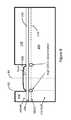
- FIG. 1Ais a plan view (top view) of an example III-Nitride (III-N) transistor.
- FIG. 1Bis a cross-sectional view of the transistor.
- FIG. 2is cross-sectional view of three example contacts.
- FIGS. 3-5are cross-sectional views of example devices where the source and drain contacts 110 and 112 are recessed to different depths.
- FIG. 6is a flow diagram of an example process for fabricating a semiconductor device.
- FIGS. 7A-7Fare cross-sectional views of an example semiconductor device during fabrication of the device.
- FIG. 8is a cross-sectional view of a semiconductor material structure including a recess.
- FIGS. 9A-9Bare band diagrams along the vertical dashed lines in FIG. 8 .
- FIG. 1Ais a plan view (top view) of an example III-Nitride (III-N) transistor 100 .
- FIG. 1Bis a cross-sectional view of the transistor 100 .
- the transistorincludes a substrate 102 (which may optionally be omitted) and a III-N layer 122 .
- the substratecan be silicon, SiC, AlN, GaN, sapphire, or any other suitable growth substrate for the growth of III-N materials.
- the III-N layer 122includes a III-N channel layer 104 and a III-N spacer layer 106 , and a III-N barrier layer 108 , where the compositions of layers 104 , 106 , and 108 are selected to induce the 2DEG 116 in the III-N channel layer 104 near the interface between the III-N channel layer 104 and the III-N spacer layer 106 .
- the spacer layer 106may be omitted.
- the III-N barrier layer 108is formed directly on the III-N channel layer 104 , and the compositions of layers 104 and 108 are selected to induce the 2DEG 116 in the III-N channel layer 104 near the interface between the III-N channel layer 104 and the III-N barrier layer 108 .
- a gate contact 118is deposited on the III-N layer 122 .
- the gate contact 118directly contacts the underlying III-N layer 122 (not shown).
- an insulator layer 120is included between the gate 118 and the underlying III-N layer 122 .
- Source and drain ohmic contacts 110 and 112are deposited on opposite sides of the gate 118 on the III-N layer 122 .
- the source and drain contacts 110 and 112form ohmic (or substantially ohmic) contacts to the device channel 116 .
- the transistor 100can be a lateral transistor having the gate 118 , drain 110 , and source 112 on a same side.
- a voltage applied to the gate 118relative to the source contact 112 , modulates the 2DEG charge density in the gate region of the device (i.e., the region directly under the gate).
- III-Nitride or III-N materials, layers, devices, and structuresrefer to a material, device, or structure comprised of a compound semiconductor material according to the stoichiometric formula B w Al x In y Ga z N, where w+x+y+z is about 1, and w, x, y, and z are each greater than or equal to zero and less than or equal to 1.
- the conductive channelcan be partially or entirely contained within a III-N material layer.
- the ohmic metals, of which source and drain contacts 110 and 112 are formedtypically include at least one metal with a relatively low metal work function, for example aluminum (Al) or titanium (Ti).
- the ohmic contacts 110 and 112include titanium, aluminum, nickel, or gold, or combinations thereof.
- the III-N layer 122includes a GaN layer 104 on the substrate 102 , an AlN spacer layer 106 on the GaN layer 104 , and an AlGaN layer 108 on the AlN spacer layer 106 .
- the AlN spacer layer 106can be useful, e.g., to increase mobility and lower an on-state resistance of the transistor 100 .
- the AlN spacer layer 106may be formed of AlN, or alternatively may be formed of another material having a larger bandgap than the AlGaN layer 108 .
- layer 106may be formed of AlInGaN, where the compositions of Al, In, and Ga are selected such that layer 106 has a larger bandgap than layer 108 .
- layer 106may be formed of AlGaN, where the fractional composition of Al in layer 106 is larger than that in layer 108 .
- the transistor 100can include an insulator layer 120 between the gate 118 and the AlGaN layer 108 .
- the insulator layer 120can also serve as a passivation layer, preventing or suppressing dispersion by preventing or suppressing voltage fluctuations at the uppermost III-N surface on either sides of the gate 118 .
- the insulator layer 120can be made of Si x N y , Al 2 O 3 , Sift, Al x Si y N, or the like, and can be prepared by metal organic chemical vapor deposition (MOCVD), low pressure chemical vapor deposition (LPCVD), plasma enhanced chemical vapor deposition (PECVD), chemical vapor deposition (CVD), sputtering, atomic layer deposition (ALD), high density chemical vapor deposition, or any suitable deposition process.
- MOCVDmetal organic chemical vapor deposition
- LPCVDlow pressure chemical vapor deposition
- PECVDplasma enhanced chemical vapor deposition
- CVDchemical vapor deposition
- sputteringatomic layer deposition
- ALDatomic layer deposition
- high density chemical vapor depositionor any suitable deposition process.
- the insulator layer 120is a Silicon Nitride (Si x N y ) layer formed by MOCVD.
- the source and drain contacts 110 and 112exhibit a normalized contact resistance that can be measured, in Ohm-mm, with respect the width W of the transistor 100 .
- the total resistance of each contact, measured in Ohmsis then equal to the normalized contact resistance (measured in Ohm-mm) multiplied by the width W (measured in millimeters) of the transistor.
- the ohmic contactsexhibit normalized resistances in the range of 0.8-2.0 Ohm-mm.
- the example transistor 100 of FIGS. 1A-Bcan have ohmic contacts that exhibit normalized resistances in the range of 0.2-0.3 Ohm-mm, e.g., by virtue of the shape and the depth of the ohmic contacts.
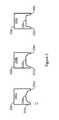
- FIG. 2is cross-sectional view of three example contacts 200 a - c that can be used, e.g., for any one or more of the source and/or drain contacts 110 and 112 of the example transistor 100 of FIGS. 1A-B .
- Each of the example contacts 200 a - cincludes a top side 208 a - c facing away from the substrate 102 and a bottom side facing in the opposite direction.
- each contact 200 a - cincludes a first end 202 a - c and a second end 206 a - c opposite the first end 202 a - c .
- Each contact 200 a - cincludes a first side that rises, e.g., monotonically, from the first end 202 a - c to an intermediate point 204 a - c closer to the top side 208 a - c than the first end 202 a - c and a second side that falls, e.g., monotonically, from the intermediate point 204 a - c to the second end 206 a - c .
- the second end 206 a - cis further from the top side 208 a than the intermediate point 204 a - c.
- the first ends 202 a and/or the second ends 206 a of the contacts 200 a - ccan have a width (“w”) where the end is flat or substantially flat.
- the widthcan be, e.g., between 20 and 300 nanometers, for example between 50 and 200 nanometers.
- the first example contact 200 ahas a first side that curves from the first end 202 a to the intermediate point 204 a and a second side that curves from the intermediate point 204 a to the second end 206 a , forming a substantially rounded trench shape in the bottom side of the contact 200 a .
- the second example contact 200 bhas a first side that rises in three line segments from the first end 202 b to the intermediate point 204 b and a second side that falls in three line segments from the intermediate point 204 b to the second end 206 b .
- the third example contact 200 chas a first side that rises in three line segments from the first end 202 c to the intermediate point 204 c and a second side that falls in three line segments from the intermediate point 204 c to the second end 206 c.
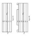
- FIGS. 3-5are cross-sectional views of example devices 300 , 400 , and 500 where the source and drain contacts 110 and 112 are recessed to different depths than they are in the example device 100 of FIG. 1 .
- FIG. 3shows an example device 300 where the source and drain contacts 110 and 112 are recessed through the spacer layer 106 to a top of a III-N channel layer 104 (e.g., so that the first and/or second end of the bottom side of the contact reach the top of the III-N channel layer 104 ).
- FIG. 4shows an example device 400 where the source and drain contacts 110 and 112 are recessed through the channel 116 of the III-N channel layer 104 .
- FIG. 5shows an example device 500 where the source and drain contacts 110 and 112 are recessed into the III-N barrier layer 108 but do not reach the spacer layer 106 .
- the recess depthcan affect the resistance of the contacts 110 and 112 .
- increasing the recess depthcan decrease the resistance up to a point where further increasing the recess depth does not decrease the resistance. Beyond a certain depth, the resistance may increase as the recess depth is increased.
- FIG. 6is a flow diagram of an example process 600 for fabricating a semiconductor device.
- the process 600can be used, e.g., to fabricate the devices 100 , 300 , 400 , and 500 of FIGS. 1A-B and 3 - 5 .
- a III-N layeris formed on a substrate ( 602 ).
- the substratecan be a silicon wafer.
- the III-N layercan include a GaN layer on the substrate; an AlN spacer layer on the GaN layer; and an AlGaN layer on the AlN spacer layer.
- the III-N layercan be formed by either directly growing the III-N layer on the substrate, or alternatively by growing the III-N layer or parts of the III-N layer on a first substrate, detaching the buffer layer from the first substrate, and bonding the buffer layer to the substrate. Forming the III-N layer can include using any appropriate deposition process.
- One or more recessesare formed in a surface of the III-N layer ( 604 ).
- the surface of the III-N layercan be etched using a patterned resist.
- Etching the surfacecan include performing a dry etch using a chlorine based gas.
- dry etching techniquese.g., plasma etching, digital plasma etching, or reactive ion etching (RIE), are used to form the recesses.
- the parameters of the etchingcan be adjusted to control the shape and depth of the recesses.
- the ion energy used during the etch, the pressure applied during the etch, and the resist pattern usedcan be varied to achieve a target depth and shape.
- the following processmay achieve a recess having the profile of the recesses in FIG. 1B in which source and drain contacts 110 and 112 , respectively, are deposited.
- a single layer photoresist layerhaving a thickness of between 1.1 and 1.2 microns is deposited over the surface and patterned to expose the underlying material in the regions is which the recess is formed.
- the photoresistacts as an etch mask, preventing material beneath it from being etched during a subsequent etch process.
- the recessis then etched in an ECR plasma etcher using Cl 2 as an etchant gas. 50 sccm of Cl 2 is injected into the chamber, the RF bias power is maintained at 20 W, and the chamber pressure is maintained at 2.5 mTorr. Following the etch, the device is removed from the etch chamber, and the photoresist mask is removed.
- Conductive contactsare formed over the one or more recesses ( 606 ). Due to the shape of the recesses, the conductive contacts have a bottom side including a first side rising, e.g., rising monotonically, from a first end to an intermediate point and a second side falling, e.g., falling monotonically, from the intermediate point to a second end opposite the first end.
- the deviceis heated at a certain temperature for a certain amount of time ( 608 ).
- the devicecan be heated to a temperature between 300° C. and 600° C.
- the devicecan be heated for one to three minutes.
- the heat applicationis performed at a temperature that is not sufficiently high to cause the contacts to alloy with the III-N layers.
- FIGS. 7A-7Fare cross-sectional views of an example semiconductor device 700 during fabrication of the device 700 .
- the device 700can be fabricated, e.g., using the process 600 illustrated in FIG. 6 .
- FIG. 7Ashows the device 700 after III-N layers 104 , 106 , and 108 have been formed on a substrate 102 , and insulator layer 120 has been formed on III-N layer 108 .
- FIG. 7Bshows the device 700 after a patterned photoresist 122 (or alternatively another masking layer) has been placed on the device 700 so that the device 700 can be etched. As shown, the photoresist layer 122 includes one or more apertures, so that some the III-N materials below the one or more apertures may be subsequently etched.
- FIG. 7Cshows the device 700 after the device 700 has been etched to leave recesses in one or more of the III-N layers (e.g., layer 108 ) below the apertures in the photoresist layer.
- the recessescan be etched to the top of the spacer layer 106 , as shown. As also seen in FIG. 7C , the etch is performed under conditions that cause III-N material below the outer portions of the aperture to etch at a higher rate than III-N material below the inner portion of the aperture, thereby resulting in the desired profile for the recess.
- FIG. 7Dshows the device 700 after the patterned resist 122 has been removed from the device 700 .
- FIG. 7Eshows the device 700 after source and drain contacts 110 and 112 have been formed over the recesses.
- FIG. 7Fshows the device 700 after a gate 118 has been formed between the source and drain contacts 110 and 112 , thereby forming a transistor.
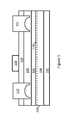
- FIG. 8shows a III-N semiconductor structure used in simulations to calculate band structures and electron carrier concentrations in regions below the source and drain electrodes of device 100 .
- FIG. 9Ais a band diagram of the semiconductor structure along line 82 (i.e., in layers 106 and 104 ), and
- FIG. 9Bis a band diagram of the semiconductor structure along line 84 (i.e., in the remaining portion of layer 108 and in layers 106 and 104 ).
- FIG. 9Ais a band diagram of the semiconductor structure along line 82 (i.e., in layers 106 and 104 )
- FIG. 9Bis a band diagram of the semiconductor structure along line 84 (i.e., in the remaining portion of layer 108 and in layers 106 and 104 ).
- line 92is the conduction band energy Ec (measured in eV, corresponding to the axis on the left)
- line 93is the valence band energy Ev (measured in eV, corresponding to the axis on the left)
- line 91is the electron carrier concentration n e (measured in cm ⁇ 3 , corresponding to the axis on the right).
- line 95is the conduction band energy Ec (measured in eV, corresponding to the axis on the left)
- line 96is the valence band energy Ev (measured in eV, corresponding to the axis on the left)
- line 94is the electron carrier concentration n e (measured in cm ⁇ 3 , corresponding to the axis on the right).
- the spike in electron carrier concentration 91 in FIG. 9Acorresponds to the position of the 2DEG channel 116 beneath the ends of the contact which extend downwards and contact the AlN spacer layer (i.e., ends 202 a - c and 206 a - c in FIG. 2 ), and the spike in electron carrier concentration 94 in FIG. 9A corresponds to the position of the 2DEG channel 116 beneath the center portion of the contact (i.e., portions 204 a - c in FIG. 2 ). As seen in FIG.
Landscapes
- Engineering & Computer Science (AREA)
- Physics & Mathematics (AREA)
- Microelectronics & Electronic Packaging (AREA)
- General Physics & Mathematics (AREA)
- Manufacturing & Machinery (AREA)
- Computer Hardware Design (AREA)
- Condensed Matter Physics & Semiconductors (AREA)
- Power Engineering (AREA)
- Plasma & Fusion (AREA)
- Junction Field-Effect Transistors (AREA)
- Electrodes Of Semiconductors (AREA)
- Chemical & Material Sciences (AREA)
- Materials Engineering (AREA)
Abstract
Description
Claims (24)
Priority Applications (5)
| Application Number | Priority Date | Filing Date | Title |
|---|---|---|---|
| US14/572,670US9536967B2 (en) | 2014-12-16 | 2014-12-16 | Recessed ohmic contacts in a III-N device |
| PCT/US2015/065597WO2016100225A1 (en) | 2014-12-16 | 2015-12-14 | Recessed ohmic contacts in a iii-n device |
| JP2017531822AJP6661637B2 (en) | 2014-12-16 | 2015-12-14 | Ohmic contact formed in recess of III-N device |
| CN201580068626.9ACN107112218B (en) | 2014-12-16 | 2015-12-14 | Recessed Ohmic Contacts in III-N Devices |
| TW104142358ATWI612660B (en) | 2014-12-16 | 2015-12-16 | Hollow contacts recessed in a group III nitride device |
Applications Claiming Priority (1)
| Application Number | Priority Date | Filing Date | Title |
|---|---|---|---|
| US14/572,670US9536967B2 (en) | 2014-12-16 | 2014-12-16 | Recessed ohmic contacts in a III-N device |
Publications (2)
| Publication Number | Publication Date |
|---|---|
| US20160172455A1 US20160172455A1 (en) | 2016-06-16 |
| US9536967B2true US9536967B2 (en) | 2017-01-03 |
Family
ID=56111966
Family Applications (1)
| Application Number | Title | Priority Date | Filing Date |
|---|---|---|---|
| US14/572,670ActiveUS9536967B2 (en) | 2014-12-16 | 2014-12-16 | Recessed ohmic contacts in a III-N device |
Country Status (5)
| Country | Link |
|---|---|
| US (1) | US9536967B2 (en) |
| JP (1) | JP6661637B2 (en) |
| CN (1) | CN107112218B (en) |
| TW (1) | TWI612660B (en) |
| WO (1) | WO2016100225A1 (en) |
Cited By (7)
| Publication number | Priority date | Publication date | Assignee | Title |
|---|---|---|---|---|
| US9735771B1 (en)* | 2016-07-21 | 2017-08-15 | Hella Kgaa Hueck & Co. | Hybrid switch including GaN HEMT and MOSFET |
| US10170580B2 (en) | 2017-05-23 | 2019-01-01 | Industrial Technology Research Institute | Structure of GaN-based transistor and method of fabricating the same |
| US10630285B1 (en) | 2017-11-21 | 2020-04-21 | Transphorm Technology, Inc. | Switching circuits having drain connected ferrite beads |
| US10756207B2 (en) | 2018-10-12 | 2020-08-25 | Transphorm Technology, Inc. | Lateral III-nitride devices including a vertical gate module |
| US11749656B2 (en) | 2020-06-16 | 2023-09-05 | Transphorm Technology, Inc. | Module configurations for integrated III-Nitride devices |
| US11810971B2 (en) | 2019-03-21 | 2023-11-07 | Transphorm Technology, Inc. | Integrated design for III-Nitride devices |
| US11973138B2 (en) | 2020-08-05 | 2024-04-30 | Transphorm Technology, Inc. | N-polar devices including a depleting layer with improved conductivity |
Families Citing this family (6)
| Publication number | Priority date | Publication date | Assignee | Title |
|---|---|---|---|---|
| US10068976B2 (en)* | 2016-07-21 | 2018-09-04 | Taiwan Semiconductor Manufacturing Co., Ltd. | Enhancement mode field-effect transistor with a gate dielectric layer recessed on a composite barrier layer for high static performance |
| JP2019192698A (en)* | 2018-04-19 | 2019-10-31 | 富士通株式会社 | Semiconductor device, method of manufacturing the same and amplifier |
| JP2020021765A (en)* | 2018-07-30 | 2020-02-06 | 株式会社アルバック | Method for manufacturing semiconductor device |
| DE102019218758A1 (en)* | 2019-12-03 | 2021-06-10 | Robert Bosch Gmbh | VERTICAL FIELD EFFECT TRANSISTORS AND METHOD OF FORMING A VERTICAL FIELD EFFECT TRANSISTOR |
| US12218202B2 (en)* | 2021-09-16 | 2025-02-04 | Wolfspeed, Inc. | Semiconductor device incorporating a substrate recess |
| CN117747420A (en)* | 2022-09-14 | 2024-03-22 | 华润微电子(重庆)有限公司 | A HEMT contact hole structure and its preparation method |
Citations (252)
| Publication number | Priority date | Publication date | Assignee | Title |
|---|---|---|---|---|
| US4300091A (en) | 1980-07-11 | 1981-11-10 | Rca Corporation | Current regulating circuitry |
| US4532439A (en) | 1982-09-13 | 1985-07-30 | Tokyo Shibaura Denki Kabushiki Kaisha | Mosfet logical circuit with increased noise margin |
| US4645562A (en) | 1985-04-29 | 1987-02-24 | Hughes Aircraft Company | Double layer photoresist technique for side-wall profile control in plasma etching processes |
| US4665508A (en) | 1985-05-23 | 1987-05-12 | Texas Instruments Incorporated | Gallium arsenide MESFET memory |
| US4728826A (en) | 1986-03-19 | 1988-03-01 | Siemens Aktiengesellschaft | MOSFET switch with inductive load |
| US4821093A (en) | 1986-08-18 | 1989-04-11 | The United States Of America As Represented By The Secretary Of The Army | Dual channel high electron mobility field effect transistor |
| US4914489A (en) | 1986-12-20 | 1990-04-03 | Fujitsu Limited | Constant current semiconductor device |
| US5051618A (en) | 1988-06-20 | 1991-09-24 | Idesco Oy | High voltage system using enhancement and depletion field effect transistors |
| US5329147A (en) | 1993-01-04 | 1994-07-12 | Xerox Corporation | High voltage integrated flyback circuit in 2 μm CMOS |
| US5618384A (en) | 1995-12-27 | 1997-04-08 | Chartered Semiconductor Manufacturing Pte, Ltd. | Method for forming residue free patterned conductor layers upon high step height integrated circuit substrates using reflow of photoresist |
| US5646069A (en) | 1995-06-07 | 1997-07-08 | Hughes Aircraft Company | Fabrication process for Alx In1-x As/Gay In1-y As power HFET ohmic contacts |
| US5663091A (en) | 1993-05-20 | 1997-09-02 | Actel Corporation | Method for fabricating an electrically programmable antifuse |
| JPH09306926A (en) | 1996-05-10 | 1997-11-28 | Hitachi Ltd | Semiconductor device and manufacturing method thereof |
| US5705847A (en) | 1996-06-10 | 1998-01-06 | Mitsubishi Denki Kabushiki Kaisha | Semiconductor device |
| US5714393A (en) | 1996-12-09 | 1998-02-03 | Motorola, Inc. | Diode-connected semiconductor device and method of manufacture |
| US5909103A (en) | 1997-07-24 | 1999-06-01 | Siliconix Incorporated | Safety switch for lithium ion battery |
| JPH11224950A (en) | 1997-11-14 | 1999-08-17 | Matsushita Electric Works Ltd | Semiconductor device |
| US5998810A (en) | 1994-12-19 | 1999-12-07 | Kabushiki Kaisha Toshiba | Semiconductor light-emitting diode having a p-type semiconductor layer formed on a light-emitting layer |
| US6008684A (en) | 1996-10-23 | 1999-12-28 | Industrial Technology Research Institute | CMOS output buffer with CMOS-controlled lateral SCR devices |
| JP2000058871A (en) | 1999-07-02 | 2000-02-25 | Citizen Watch Co Ltd | Integrated circuit of electronic apparatus |
| US6097046A (en) | 1993-04-30 | 2000-08-01 | Texas Instruments Incorporated | Vertical field effect transistor and diode |
| US6100571A (en) | 1998-06-16 | 2000-08-08 | Nec Corporation | Fet having non-overlapping field control electrode between gate and drain |
| US6292500B1 (en) | 1998-04-23 | 2001-09-18 | Matsushita Electric Industrial Co., Ltd. | Semiconductor laser device |
| US6307220B1 (en) | 1997-08-05 | 2001-10-23 | Semiconductor Energy Laboratory Co., Ltd. | Semiconductor device |
| US6316793B1 (en) | 1998-06-12 | 2001-11-13 | Cree, Inc. | Nitride based transistors on semi-insulating silicon carbide substrates |
| US6373082B1 (en) | 1997-12-04 | 2002-04-16 | Nec Corporation | Compound semiconductor field effect transistor |
| US6429468B1 (en) | 2000-12-30 | 2002-08-06 | National Science Council | In0.34A10.66AsSb0.15/InP HFET utilizing InP channels |
| US6475889B1 (en) | 2000-04-11 | 2002-11-05 | Cree, Inc. | Method of forming vias in silicon carbide and resulting devices and circuits |
| US6504235B2 (en) | 1997-07-25 | 2003-01-07 | Hughes Electronics Corporation | Passivation layer and process for semiconductor devices |
| US20030006437A1 (en) | 1998-09-22 | 2003-01-09 | Nec Corporation | Field effect transistor |
| US20030030056A1 (en) | 2001-08-06 | 2003-02-13 | Motorola, Inc. | Voltage and current reference circuits using different substrate-type components |
| US6548333B2 (en) | 2000-12-01 | 2003-04-15 | Cree, Inc. | Aluminum gallium nitride/gallium nitride high electron mobility transistors having a gate contact on a gallium nitride based cap segment |
| US6552373B2 (en) | 2000-03-28 | 2003-04-22 | Nec Corporation | Hetero-junction field effect transistor having an intermediate layer |
| US6580101B2 (en) | 2000-04-25 | 2003-06-17 | The Furukawa Electric Co., Ltd. | GaN-based compound semiconductor device |
| US6586781B2 (en) | 2000-02-04 | 2003-07-01 | Cree Lighting Company | Group III nitride based FETs and HEMTs with reduced trapping and method for producing the same |
| JP2003229566A (en) | 2001-11-27 | 2003-08-15 | Furukawa Electric Co Ltd:The | Power conversion device and GaN-based semiconductor device used therefor |
| JP2003244943A (en) | 2002-02-13 | 2003-08-29 | Honda Motor Co Ltd | Power supply booster |
| US6624452B2 (en) | 2000-07-28 | 2003-09-23 | The Regents Of The University Of California | Gallium nitride-based HFET and a method for fabricating a gallium nitride-based HFET |
| US6633195B2 (en) | 1999-01-22 | 2003-10-14 | Siemens Aktiengesellschaft | Hybrid power MOSFET |
| US6727531B1 (en) | 2000-08-07 | 2004-04-27 | Advanced Technology Materials, Inc. | Indium gallium nitride channel high electron mobility transistors, and method of making the same |
| US6746938B2 (en) | 2001-06-27 | 2004-06-08 | Hitachi, Ltd. | Manufacturing method for semiconductor device using photo sensitive polyimide etching mask to form viaholes |
| US20040119067A1 (en) | 2000-12-14 | 2004-06-24 | Nitronex Corporation | Gallium nitride materials and methods |
| JP2004253620A (en) | 2003-02-20 | 2004-09-09 | Nec Compound Semiconductor Devices Ltd | Field effect transistor and method of manufacturing the same |
| JP2004260114A (en) | 2003-02-27 | 2004-09-16 | Shin Etsu Handotai Co Ltd | Compound semiconductor element |
| WO2004098060A1 (en) | 2003-04-29 | 2004-11-11 | Kinectrics Inc | High speed bi-directional solid state switch |
| US6849882B2 (en) | 2001-05-11 | 2005-02-01 | Cree Inc. | Group-III nitride based high electron mobility transistor (HEMT) with barrier/spacer layer |
| US6867078B1 (en) | 2003-11-19 | 2005-03-15 | Freescale Semiconductor, Inc. | Method for forming a microwave field effect transistor with high operating voltage |
| WO2005036749A1 (en) | 2003-09-26 | 2005-04-21 | Semiconductor Components Industries, L.L.C. | Differential transistor and method therefor |
| US20050087763A1 (en)* | 2003-10-23 | 2005-04-28 | Matsushita Electric Industrial Co., Ltd. | Semiconductor device and method for fabricating the same |
| US20050133816A1 (en) | 2003-12-19 | 2005-06-23 | Zhaoyang Fan | III-nitride quantum-well field effect transistors |
| US6914273B2 (en) | 2002-08-26 | 2005-07-05 | University Of Florida Research Foundation, Inc. | GaN-type enhancement MOSFET using hetero structure |
| US20050189559A1 (en) | 2004-02-27 | 2005-09-01 | Kabushiki Kaisha Toshiba | Semiconductor device |
| WO2004070791A3 (en) | 2003-02-04 | 2005-09-22 | Great Wall Semiconductor | Bi-directional power switch |
| US6979863B2 (en) | 2003-04-24 | 2005-12-27 | Cree, Inc. | Silicon carbide MOSFETs with integrated antiparallel junction barrier Schottky free wheeling diodes and methods of fabricating the same |
| US6982204B2 (en) | 2002-07-16 | 2006-01-03 | Cree, Inc. | Nitride-based transistors and methods of fabrication thereof using non-etched contact recesses |
| JP2006033723A (en) | 2004-07-21 | 2006-02-02 | Sharp Corp | Optical coupling device for power control and electronic device using the optical coupling device for power control |
| JP2006032749A (en) | 2004-07-20 | 2006-02-02 | Toyota Motor Corp | Semiconductor device and manufacturing method thereof |
| CN1748320A (en) | 2002-12-16 | 2006-03-15 | 日本电气株式会社 | field effect transistor |
| US20060076677A1 (en) | 2004-10-12 | 2006-04-13 | International Business Machines Corporation | Resist sidewall spacer for C4 BLM undercut control |
| US7030428B2 (en) | 2001-12-03 | 2006-04-18 | Cree, Inc. | Strain balanced nitride heterojunction transistors |
| US7045404B2 (en) | 2004-01-16 | 2006-05-16 | Cree, Inc. | Nitride-based transistors with a protective layer and a low-damage recess and methods of fabrication thereof |
| US7053413B2 (en) | 2000-10-23 | 2006-05-30 | General Electric Company | Homoepitaxial gallium-nitride-based light emitting device and method for producing |
| US7071498B2 (en) | 2003-12-17 | 2006-07-04 | Nitronex Corporation | Gallium nitride material devices including an electrode-defining layer and methods of forming the same |
| US20060145189A1 (en) | 2004-12-30 | 2006-07-06 | Robert Beach | III-nitride power semiconductor with a field relaxation feature |
| US7078743B2 (en) | 2003-05-15 | 2006-07-18 | Matsushita Electric Industrial Co., Ltd. | Field effect transistor semiconductor device |
| US7084475B2 (en) | 2004-02-17 | 2006-08-01 | Velox Semiconductor Corporation | Lateral conduction Schottky diode with plural mesas |
| US20060189109A1 (en) | 2001-03-02 | 2006-08-24 | Amberwave Systems | Methods of fabricating contact regions for FET incorporating SiGe |
| US20060202272A1 (en) | 2005-03-11 | 2006-09-14 | Cree, Inc. | Wide bandgap transistors with gate-source field plates |
| US7109552B2 (en) | 2004-11-01 | 2006-09-19 | Silicon-Based Technology, Corp. | Self-aligned trench DMOS transistor structure and its manufacturing methods |
| US20060226442A1 (en) | 2005-04-07 | 2006-10-12 | An-Ping Zhang | GaN-based high electron mobility transistor and method for making the same |
| US7126212B2 (en) | 1999-10-01 | 2006-10-24 | Ziptronix, Inc. | Three dimensional device integration method and integrated device |
| US7125786B2 (en) | 2000-04-11 | 2006-10-24 | Cree, Inc. | Method of forming vias in silicon carbide and resulting devices and circuits |
| WO2006114883A1 (en) | 2005-04-22 | 2006-11-02 | Renesas Technology Corp. | Semiconductor device |
| WO2005070007A3 (en) | 2004-01-23 | 2006-11-23 | Int Rectifier Corp | Iii-nitride current control device and method of manufacture |
| US7161194B2 (en) | 2004-12-06 | 2007-01-09 | Cree, Inc. | High power density and/or linearity transistors |
| US20070018199A1 (en) | 2005-07-20 | 2007-01-25 | Cree, Inc. | Nitride-based transistors and fabrication methods with an etch stop layer |
| US7170111B2 (en) | 2004-02-05 | 2007-01-30 | Cree, Inc. | Nitride heterojunction transistors having charge-transfer induced energy barriers and methods of fabricating the same |
| US7169634B2 (en) | 2003-01-15 | 2007-01-30 | Advanced Power Technology, Inc. | Design and fabrication of rugged FRED |
| JP2007036218A (en) | 2005-06-27 | 2007-02-08 | Internatl Rectifier Corp | Active drive of normally-on and normally-off cascode connection configuration device through unsymmetrical cmos |
| US20070045670A1 (en) | 2005-08-31 | 2007-03-01 | Kabushiki Kaisha Toshiba | Nitride-based semiconductor device and method of manufacturing the same |
| US7199640B2 (en) | 2002-10-29 | 2007-04-03 | Dxp B.V. | Bi-directional double NMOS switch |
| US7217960B2 (en) | 2005-01-14 | 2007-05-15 | Matsushita Electric Industrial Co., Ltd. | Semiconductor device |
| US20070128743A1 (en) | 2005-12-05 | 2007-06-07 | National Chiao Tung University | Process of producing group III nitride based reflectors |
| US7230284B2 (en) | 2001-07-24 | 2007-06-12 | Cree, Inc. | Insulating gate AlGaN/GaN HEMT |
| US20070131968A1 (en) | 2005-11-25 | 2007-06-14 | Matsushita Electric Industrial Co., Ltd. | Field effect transistor |
| US20070145417A1 (en) | 2005-03-29 | 2007-06-28 | Brar Berinder P S | High voltage semiconductor device having a lateral channel and enhanced gate-to-drain separation |
| US7238560B2 (en) | 2004-07-23 | 2007-07-03 | Cree, Inc. | Methods of fabricating nitride-based transistors with a cap layer and a recessed gate |
| WO2007077666A1 (en) | 2005-12-28 | 2007-07-12 | Nec Corporation | Field effect transistor, and multilayered epitaxial film for use in preparation of field effect transistor |
| US7250641B2 (en) | 2004-06-15 | 2007-07-31 | Kabushiki Kaisha Toshiba | Nitride semiconductor device |
| US7253454B2 (en) | 2005-03-03 | 2007-08-07 | Cree, Inc. | High electron mobility transistor |
| JP2007215331A (en) | 2006-02-10 | 2007-08-23 | Hitachi Ltd | Booster circuit |
| US7265399B2 (en) | 2004-10-29 | 2007-09-04 | Cree, Inc. | Asymetric layout structures for transistors and methods of fabricating the same |
| JP2007227409A (en) | 2006-01-24 | 2007-09-06 | Oki Electric Ind Co Ltd | Gallium-nitride transistor and its fabrication process |
| US7268375B2 (en) | 2003-10-27 | 2007-09-11 | Sensor Electronic Technology, Inc. | Inverted nitride-based semiconductor structure |
| US20070210329A1 (en) | 2006-03-08 | 2007-09-13 | Sanken Electric Co., Ltd. | Warp-free semiconductor wafer, and devices using the same |
| WO2007108404A1 (en) | 2006-03-17 | 2007-09-27 | Sumitomo Chemical Company, Limited | Semiconductor field effect transistor and method for fabricating the same |
| US20070228477A1 (en) | 2006-03-31 | 2007-10-04 | Sanken Electric Co., Ltd. | Monolithic integrated circuit of a field-effect semiconductor device and a diode |
| US20070249119A1 (en) | 2006-04-21 | 2007-10-25 | Kabushiki Kaisha Toshiba | Nitride semiconductor device |
| WO2005070009A3 (en) | 2004-01-23 | 2007-11-22 | Int Rectifier Corp | Enhancement mode iii-nitride fet |
| US7304331B2 (en) | 2004-07-14 | 2007-12-04 | Kabushiki Kaisha Toshiba | Nitride semiconductor device such as transverse power FET for high frequency signal amplification or power control |
| US20070295985A1 (en) | 2001-02-23 | 2007-12-27 | Nitronex Corporation | Gallium nitride material devices and methods of forming the same |
| CN101107713A (en) | 2004-11-23 | 2008-01-16 | 克里公司 | Capping layer and/or passivation layer of nitride-based transistor, transistor structure and manufacturing method |
| US7321132B2 (en) | 2005-03-15 | 2008-01-22 | Lockheed Martin Corporation | Multi-layer structure for use in the fabrication of integrated circuit devices and methods for fabrication of same |
| US7326971B2 (en) | 2005-06-08 | 2008-02-05 | Cree, Inc. | Gallium nitride based high-electron mobility devices |
| US7332795B2 (en) | 2004-05-22 | 2008-02-19 | Cree, Inc. | Dielectric passivation for semiconductor devices |
| US20080073670A1 (en) | 2006-09-22 | 2008-03-27 | Korea Advanced Institute Of Science And Technology | Gallium nitride high electron mobility transistor having inner field-plate for high power applications |
| JP2008091699A (en) | 2006-10-03 | 2008-04-17 | Furukawa Electric Co Ltd:The | Manufacturing method of semiconductor transistor |
| US7364988B2 (en) | 2005-06-08 | 2008-04-29 | Cree, Inc. | Method of manufacturing gallium nitride based high-electron mobility devices |
| US7375407B2 (en) | 2004-11-22 | 2008-05-20 | Matsushita Electric Industrial Co., Ltd. | Schottky barrier diode and integrated circuit using the same |
| US7388236B2 (en) | 2006-03-29 | 2008-06-17 | Cree, Inc. | High efficiency and/or high power density wide bandgap transistors |
| JP2008199771A (en) | 2007-02-13 | 2008-08-28 | Fujitsu Ten Ltd | Boosting circuit control device and boosting circuit |
| US7419892B2 (en) | 2005-12-13 | 2008-09-02 | Cree, Inc. | Semiconductor devices including implanted regions and protective layers and methods of forming the same |
| US7429534B2 (en) | 2005-02-22 | 2008-09-30 | Sensor Electronic Technology, Inc. | Etching a nitride-based heterostructure |
| US7432142B2 (en) | 2004-05-20 | 2008-10-07 | Cree, Inc. | Methods of fabricating nitride-based transistors having regrown ohmic contact regions |
| WO2008120094A2 (en) | 2007-03-30 | 2008-10-09 | Picogiga International | Electronic device with improved ohmic contact |
| JP2008243848A (en) | 2007-03-23 | 2008-10-09 | Sanken Electric Co Ltd | Semiconductor device |
| US7436001B2 (en) | 2005-07-22 | 2008-10-14 | Samsung Electro-Mechanics Co., Ltd. | Vertical GaN-based LED and method of manufacturing the same |
| US20080258150A1 (en) | 2007-03-09 | 2008-10-23 | The Regents Of The University Of California | Method to fabricate iii-n field effect transistors using ion implantation with reduced dopant activation and damage recovery temperature |
| US20080272397A1 (en) | 2007-05-04 | 2008-11-06 | Alexei Koudymov | Semiconductor device with modulated field element |
| US7449730B2 (en) | 2005-12-28 | 2008-11-11 | Kabushiki Kaisha Toshiba | Nitride-based semiconductor device |
| US7465997B2 (en) | 2004-02-12 | 2008-12-16 | International Rectifier Corporation | III-nitride bidirectional switch |
| US7465967B2 (en) | 2005-03-15 | 2008-12-16 | Cree, Inc. | Group III nitride field effect transistors (FETS) capable of withstanding high temperature reverse bias test conditions |
| US20080308813A1 (en) | 2006-08-18 | 2008-12-18 | Chang Soo Suh | High breakdown enhancement mode gallium nitride based high electron mobility transistors with integrated slant field plate |
| US7482788B2 (en) | 2005-10-12 | 2009-01-27 | System General Corp. | Buck converter for both full load and light load operations |
| US7488992B2 (en) | 2003-12-04 | 2009-02-10 | Lockheed Martin Corporation | Electronic device comprising enhancement mode pHEMT devices, depletion mode pHEMT devices, and power pHEMT devices on a single substrate and method of creation |
| US20090050936A1 (en) | 2007-08-24 | 2009-02-26 | Tohru Oka | Nitride semiconductor device and power converter including the same |
| US7501670B2 (en) | 2007-03-20 | 2009-03-10 | Velox Semiconductor Corporation | Cascode circuit employing a depletion-mode, GaN-based FET |
| US7501669B2 (en) | 2003-09-09 | 2009-03-10 | Cree, Inc. | Wide bandgap transistor devices with field plates |
| WO2009036266A2 (en) | 2007-09-12 | 2009-03-19 | Transphorm Inc. | Iii-nitride bidirectional switches |
| US20090075455A1 (en) | 2007-09-14 | 2009-03-19 | Umesh Mishra | Growing N-polar III-nitride Structures |
| US20090072269A1 (en) | 2007-09-17 | 2009-03-19 | Chang Soo Suh | Gallium nitride diodes and integrated components |
| US7508014B2 (en) | 2004-11-19 | 2009-03-24 | Nichia Corporation | Field effect transistor including a gate electrode and an additional electrode |
| US20090085065A1 (en) | 2007-03-29 | 2009-04-02 | The Regents Of The University Of California | Method to fabricate iii-n semiconductor devices on the n-face of layers which are grown in the iii-face direction using wafer bonding and substrate removal |
| WO2009036181A3 (en) | 2007-09-14 | 2009-05-07 | Transphorm Inc | Iii-nitride devices with recessed gates |
| WO2009039041A3 (en) | 2007-09-17 | 2009-05-14 | Transphorm Inc | Enhancement mode gallium nitride power devices |
| US20090140262A1 (en) | 2006-09-20 | 2009-06-04 | Fujitsu Limited | Field-effect transistor |
| US7544963B2 (en) | 2005-04-29 | 2009-06-09 | Cree, Inc. | Binary group III-nitride based high electron mobility transistors |
| US7547928B2 (en)* | 2004-06-30 | 2009-06-16 | Interuniversitair Microelektronica Centrum (Imec) | AlGaN/GaN high electron mobility transistor devices |
| US7548112B2 (en) | 2005-07-21 | 2009-06-16 | Cree, Inc. | Switch mode power amplifier using MIS-HEMT with field plate extension |
| US7547925B2 (en) | 2005-11-14 | 2009-06-16 | Palo Alto Research Center Incorporated | Superlattice strain relief layer for semiconductor devices |
| WO2009076076A2 (en) | 2007-12-10 | 2009-06-18 | Transphorm Inc. | Insulated gate e-mode transistors |
| US7550783B2 (en) | 2004-05-11 | 2009-06-23 | Cree, Inc. | Wide bandgap HEMTs with source connected field plates |
| US7550781B2 (en) | 2004-02-12 | 2009-06-23 | International Rectifier Corporation | Integrated III-nitride power devices |
| US7566918B2 (en) | 2006-02-23 | 2009-07-28 | Cree, Inc. | Nitride based transistors for millimeter wave operation |
| US7566580B2 (en) | 2006-11-15 | 2009-07-28 | The Regents Of The University Of California | Method for heteroepitaxial growth of high-quality N-face GaN, InN, and AIN and their alloys by metal organic chemical vapor deposition |
| US7573078B2 (en) | 2004-05-11 | 2009-08-11 | Cree, Inc. | Wide bandgap transistors with multiple field plates |
| US7592211B2 (en) | 2006-01-17 | 2009-09-22 | Cree, Inc. | Methods of fabricating transistors including supported gate electrodes |
| US7598108B2 (en) | 2007-07-06 | 2009-10-06 | Sharp Laboratories Of America, Inc. | Gallium nitride-on-silicon interface using multiple aluminum compound buffer layers |
| US7601993B2 (en) | 2005-12-12 | 2009-10-13 | Oki Electric Industry Co., Ltd. | Semiconductor device having ohmic recessed electrode |
| US7605017B2 (en) | 2006-11-24 | 2009-10-20 | Nissan Motor Co., Ltd. | Method of manufacturing a semiconductor device and products made thereby |
| WO2009132039A2 (en) | 2008-04-23 | 2009-10-29 | Transphorm Inc. | Enhancement mode iii-n hemts |
| US7612363B2 (en) | 2004-09-14 | 2009-11-03 | Showa Denko K.K. | N-type group III nitride semiconductor stacked layer structure |
| US7612390B2 (en) | 2004-02-05 | 2009-11-03 | Cree, Inc. | Heterojunction transistors including energy barriers |
| US7615774B2 (en) | 2005-04-29 | 2009-11-10 | Cree.Inc. | Aluminum free group III-nitride based high electron mobility transistors |
| US7629627B2 (en) | 2006-04-18 | 2009-12-08 | University Of Massachusetts | Field effect transistor with independently biased gates |
| US7638818B2 (en) | 2005-09-07 | 2009-12-29 | Cree, Inc. | Robust transistors with fluorine treatment |
| US7655962B2 (en) | 2007-02-23 | 2010-02-02 | Sensor Electronic Technology, Inc. | Enhancement mode insulated gate heterostructure field-effect transistor with electrically isolated RF-enhanced source contact |
| US20100044752A1 (en) | 2008-08-22 | 2010-02-25 | Oki Electric Industry Co., Ltd. | Semiconductor device and manufacturing method |
| US20100065923A1 (en) | 2008-09-16 | 2010-03-18 | Alain Charles | Iii-nitride device with back-gate and field plate and process for its manufacture |
| US7692263B2 (en) | 2006-11-21 | 2010-04-06 | Cree, Inc. | High voltage GaN transistors |
| WO2010039463A2 (en) | 2008-09-23 | 2010-04-08 | Transphorm Inc. | Inductive load power switching circuits |
| JP2010087076A (en) | 2008-09-30 | 2010-04-15 | Oki Electric Ind Co Ltd | Semiconductor device |
| US7700973B2 (en) | 2003-10-10 | 2010-04-20 | The Regents Of The University Of California | GaN/AlGaN/GaN dispersion-free high electron mobility transistors |
| US7709859B2 (en) | 2004-11-23 | 2010-05-04 | Cree, Inc. | Cap layers including aluminum nitride for nitride-based transistors |
| US7709269B2 (en) | 2006-01-17 | 2010-05-04 | Cree, Inc. | Methods of fabricating transistors including dielectrically-supported gate electrodes |
| US7714360B2 (en) | 2005-07-13 | 2010-05-11 | Sanken Electric Co., Ltd. | Surface-stabilized semiconductor device |
| US7723739B2 (en) | 2005-09-05 | 2010-05-25 | Panasonic Electric Works Co., Ltd. | Semiconductor light emitting device and illuminating device using it |
| US7728356B2 (en) | 2007-06-01 | 2010-06-01 | The Regents Of The University Of California | P-GaN/AlGaN/AlN/GaN enhancement-mode field effect transistor |
| US20100133506A1 (en) | 2007-06-15 | 2010-06-03 | Rohm Co., Ltd. | Nitride semiconductor light emitting element and method for manufacturing nitride semiconductor |
| US7745851B2 (en) | 2006-04-13 | 2010-06-29 | Cree, Inc. | Polytype hetero-interface high electron mobility device and method of making |
| TW201027759A (en) | 2008-12-10 | 2010-07-16 | Transphorm Inc | Semiconductor heterostructure diodes |
| US7759699B2 (en) | 2005-07-06 | 2010-07-20 | International Rectifier Corporation | III-nitride enhancement mode devices |
| US7759700B2 (en) | 2005-12-01 | 2010-07-20 | Panasonic Corporation | Semiconductor device |
| US20100203234A1 (en) | 2003-04-09 | 2010-08-12 | Medtronic, Inc. | Shape memory alloy actuators |
| US7777254B2 (en) | 2007-06-11 | 2010-08-17 | Sanken Electric Co., Ltd. | Normally-off field-effect semiconductor device |
| US20100219445A1 (en) | 2007-09-27 | 2010-09-02 | Yasunori Yokoyama | Group iii nitride semiconductor light-emitting device, method for manufacturing the same, and lamp |
| US7795622B2 (en) | 2007-03-30 | 2010-09-14 | Fujitsu Limited | Compound semiconductor device |
| TW201036155A (en) | 2009-02-09 | 2010-10-01 | Transphorm Inc | III-nitride devices and circuits |
| US7811872B2 (en) | 2007-05-16 | 2010-10-12 | Oki Electric Industry Co., Ltd. | Method for manufacturing a field effect transistor having a field plate |
| US7812369B2 (en) | 2003-09-09 | 2010-10-12 | The Regents Of The University Of California | Fabrication of single or multiple gate field plates |
| US7834380B2 (en) | 2004-12-09 | 2010-11-16 | Panasonic Corporation | Field effect transistor and method for fabricating the same |
| WO2010132587A2 (en) | 2009-05-14 | 2010-11-18 | Transphorm Inc. | High voltage iii-nitride semiconductor devices |
| US7855401B2 (en) | 2005-06-29 | 2010-12-21 | Cree, Inc. | Passivation of wide band-gap based semiconductor devices with hydrogen-free sputtered nitrides |
| US7859020B2 (en) | 2007-08-31 | 2010-12-28 | Fujitsu Limited | Nitride semiconductor device, Doherty amplifier and drain voltage controlled amplifier |
| US7859014B2 (en) | 2004-06-24 | 2010-12-28 | Nec Corporation | Semiconductor device |
| US7859021B2 (en) | 2007-08-29 | 2010-12-28 | Sanken Electric Co., Ltd. | Field-effect semiconductor device |
| CN101312207B (en) | 2007-05-21 | 2011-01-05 | 西安捷威半导体有限公司 | Enhancement type HEMT device structure and its manufacture method |
| US7875537B2 (en) | 2007-08-29 | 2011-01-25 | Cree, Inc. | High temperature ion implantation of nitride based HEMTs |
| US7875910B2 (en) | 2003-03-03 | 2011-01-25 | Cree, Inc. | Integrated nitride and silicon carbide-based devices |
| US7884395B2 (en) | 2007-06-26 | 2011-02-08 | Kabushiki Kaisha Toshiba | Semiconductor apparatus |
| US7892974B2 (en) | 2000-04-11 | 2011-02-22 | Cree, Inc. | Method of forming vias in silicon carbide and resulting devices and circuits |
| US7893424B2 (en) | 2006-07-27 | 2011-02-22 | Osram Opto Semiconductors Gmbh | Semiconductor layer structure with superlattice |
| US7901994B2 (en) | 2004-01-16 | 2011-03-08 | Cree, Inc. | Methods of manufacturing group III nitride semiconductor devices with silicon nitride layers |
| WO2011031431A2 (en) | 2009-08-28 | 2011-03-17 | Transphorm Inc. | Semiconductor devices with field plates |
| KR20110033584A (en) | 2009-09-25 | 2011-03-31 | 삼성전기주식회사 | Semiconductor device and manufacturing method thereof |
| US7919791B2 (en) | 2002-03-25 | 2011-04-05 | Cree, Inc. | Doped group III-V nitride materials, and microelectronic devices and device precursor structures comprising same |
| US7932539B2 (en) | 2005-11-29 | 2011-04-26 | The Hong Kong University Of Science And Technology | Enhancement-mode III-N devices, circuits, and methods |
| US7935985B2 (en) | 2007-03-29 | 2011-05-03 | The Regents Of The University Of Califonia | N-face high electron mobility transistors with low buffer leakage and low parasitic resistance |
| US7948011B2 (en) | 2005-09-16 | 2011-05-24 | The Regents Of The University Of California | N-polar aluminum gallium nitride/gallium nitride enhancement-mode field effect transistor |
| US7956383B2 (en) | 2007-04-20 | 2011-06-07 | Panasonic Corporation | Field effect transistor |
| US7955984B2 (en) | 2006-12-28 | 2011-06-07 | Fujitsu Limited | High speed high power nitride semiconductor device |
| US7961482B2 (en) | 2007-05-09 | 2011-06-14 | International Rectifier Corporation | Bi-directional HEMT/GaN half-bridge circuit |
| US7965126B2 (en) | 2008-02-12 | 2011-06-21 | Transphorm Inc. | Bridge circuits and their components |
| US7985986B2 (en) | 2008-07-31 | 2011-07-26 | Cree, Inc. | Normally-off semiconductor devices |
| EP1998376B1 (en) | 2006-03-16 | 2011-08-03 | Fujitsu Ltd. | Compound semiconductor device and process for producing the same |
| WO2011072027A3 (en) | 2009-12-10 | 2011-09-22 | Transphorm Inc. | Reverse side engineered iii-nitride devices |
| US8039352B2 (en) | 2007-05-24 | 2011-10-18 | The Regents Of The University Of California | Polarization-induced barriers for N-face nitride-based electronics |
| US8044380B2 (en) | 2004-12-23 | 2011-10-25 | Lg Innotek Co., Ltd. | Nitride semiconductor light emitting device and fabrication method thereof |
| US8076698B2 (en) | 2005-07-08 | 2011-12-13 | Panasonic Corporation | Transistor and method for operating the same |
| US8076699B2 (en) | 2008-04-02 | 2011-12-13 | The Hong Kong Univ. Of Science And Technology | Integrated HEMT and lateral field-effect rectifier combinations, methods, and systems |
| US8093606B2 (en) | 2005-11-29 | 2012-01-10 | Rohm Co., Ltd. | Nitride semiconductor light emitting device |
| US8110425B2 (en) | 2007-03-20 | 2012-02-07 | Luminus Devices, Inc. | Laser liftoff structure and related methods |
| US8114717B2 (en) | 2005-11-15 | 2012-02-14 | The Regents Of The University Of California | Methods to shape the electric field in electron devices, passivate dislocations and point defects, and enhance the luminescence efficiency of optical devices |
| JP2009524242A5 (en) | 2007-01-16 | 2012-03-22 | ||
| US8178900B2 (en) | 2005-03-30 | 2012-05-15 | Eudyna Devices Inc. | Semiconductor device having GaN-based semiconductor layer and select composition ratio insulating film |
| US8223458B2 (en) | 2010-04-08 | 2012-07-17 | Hitachi Global Storage Technologies Netherlands B.V. | Magnetic head having an asymmetrical shape and systems thereof |
| US8237196B2 (en) | 2009-03-13 | 2012-08-07 | Kabushiki Kaisha Toshiba | Semiconductor device |
| US20120217512A1 (en) | 2009-11-19 | 2012-08-30 | Philippe Renaud | Lateral power transistor device and method of manufacturing the same |
| US20120223317A1 (en)* | 2011-03-01 | 2012-09-06 | National Semiconductor Corporation | Ohmic contact schemes for group iii-v devices having a two-dimensional electron gas layer |
| US8264003B2 (en) | 2006-03-20 | 2012-09-11 | International Rectifier Corporation | Merged cascode transistor |
| US20120267637A1 (en) | 2011-04-25 | 2012-10-25 | Samsung Electro-Mechanics Co., Ltd. | Nitride semiconductor device and manufacturing method thereof |
| US8361816B2 (en) | 2005-12-09 | 2013-01-29 | Samsung Electronics Co., Ltd. | Method of manufacturing vertical gallium nitride based light emitting diode |
| US8363437B2 (en) | 2008-09-12 | 2013-01-29 | Glacialtech, Inc. | Unidirectional MOSFET and applications thereof |
| US8389975B2 (en) | 2007-09-27 | 2013-03-05 | Showa Denko K.K. | Group III nitride semiconductor light-emitting device |
| US20130056744A1 (en) | 2011-09-06 | 2013-03-07 | Transphorm Inc. | Semiconductor Devices with Guard Rings |
| US8404042B2 (en) | 2006-11-17 | 2013-03-26 | Sumitomo Electric Industries, Ltd. | Group-III nitride crystal composite |
| WO2013052833A2 (en) | 2011-10-07 | 2013-04-11 | Transphorm Inc. | High power semiconductor electronic components with increased reliability |
| US8431960B2 (en) | 2009-04-08 | 2013-04-30 | Efficient Power Conversion Corporation | Dopant diffusion modulation in GaN buffer layers |
| US20130126943A1 (en) | 2010-07-14 | 2013-05-23 | Panasonic Corporation | Field-effect transistor |
| US8455885B2 (en) | 2006-11-15 | 2013-06-04 | The Regents Of The University Of California | Method for heteroepitaxial growth of high-quality N-face gallium nitride, indium nitride, and aluminum nitride and their alloys by metal organic chemical vapor deposition |
| US8471267B2 (en) | 2009-09-03 | 2013-06-25 | Panasonic Corporation | Semiconductor device and method for producing same |
| US8476125B2 (en) | 2006-12-15 | 2013-07-02 | University Of South Carolina | Fabrication technique for high frequency, high power group III nitride electronic devices |
| US8492779B2 (en) | 2002-08-19 | 2013-07-23 | Lg Innotek Co., Ltd. | Nitride semiconductor LED and fabrication method thereof |
| US8502323B2 (en) | 2007-08-03 | 2013-08-06 | The Hong Kong University Of Science And Technology | Reliable normally-off III-nitride active device structures, and related methods and systems |
| US8525231B2 (en) | 2010-03-26 | 2013-09-03 | Samsung Electro-Mechanics Co., Ltd. | Semiconductor device and method of manufacturing the same |
| US8530904B2 (en) | 2010-03-19 | 2013-09-10 | Infineon Technologies Austria Ag | Semiconductor device including a normally-on transistor and a normally-off transistor |
| US8603880B2 (en) | 2011-02-17 | 2013-12-10 | Fujitsu Limited | Semiconductor device including gate electrode provided over active region in P-type nitride semiconductor layer and method of manufacturing the same, and power supply apparatus |
| US20130328061A1 (en) | 2012-06-07 | 2013-12-12 | Hrl Laboratories, Llc. | Normally-off gallium nitride transistor with insulating gate and method of making the same |
| US20130334538A1 (en) | 2011-10-26 | 2013-12-19 | Triquint Semiconductor, Inc. | High electron mobility transistor structure and method |
| US8614460B2 (en) | 2008-01-24 | 2013-12-24 | Kabushiki Kaisha Toshiba | Semiconductor device and fabrication method of the semiconductor device |
| US8652948B2 (en) | 2007-11-21 | 2014-02-18 | Mitsubishi Chemical Corporation | Nitride semiconductor, nitride semiconductor crystal growth method, and nitride semiconductor light emitting element |
| US8674407B2 (en) | 2008-03-12 | 2014-03-18 | Renesas Electronics Corporation | Semiconductor device using a group III nitride-based semiconductor |
| US20140084346A1 (en) | 2011-05-25 | 2014-03-27 | Sharp Kabushiki Kaisha | Switching element |
| US20140099757A1 (en) | 2011-02-02 | 2014-04-10 | Transphorm Inc. | III-N Device Structures and Methods |
| US8698198B2 (en) | 2006-10-20 | 2014-04-15 | Kabushiki Kaisha Toshiba | Nitride semiconductor device |
| US8716141B2 (en) | 2011-03-04 | 2014-05-06 | Transphorm Inc. | Electrode configurations for semiconductor devices |
| US8742460B2 (en) | 2010-12-15 | 2014-06-03 | Transphorm Inc. | Transistors with isolation regions |
| US8772832B2 (en) | 2010-06-04 | 2014-07-08 | Hrl Laboratories, Llc | GaN HEMTs with a back gate connected to the source |
| US8785305B2 (en) | 2009-12-11 | 2014-07-22 | National Semiconductor Corporation | Backside stress compensation for gallium nitride or other nitride-based semiconductor devices |
| US8803246B2 (en) | 2012-07-16 | 2014-08-12 | Transphorm Inc. | Semiconductor electronic components with integrated current limiters |
| US20140264455A1 (en) | 2013-03-15 | 2014-09-18 | Transphorm Inc. | Carbon doping semiconductor devices |
| CN103477543B (en) | 2011-02-28 | 2016-06-29 | 特兰斯夫公司 | Electronic components with passive filters |
Family Cites Families (3)
| Publication number | Priority date | Publication date | Assignee | Title |
|---|---|---|---|---|
| EP2273553B1 (en)* | 2004-06-30 | 2020-02-12 | IMEC vzw | A method for fabricating AlGaN/GaN HEMT devices |
| JP2009246307A (en)* | 2008-03-31 | 2009-10-22 | Toshiba Corp | Semiconductor device and method of manufacturing the same |
| JP2011082216A (en)* | 2009-10-02 | 2011-04-21 | Fujitsu Ltd | Compound semiconductor device and method for manufacturing the same |
- 2014
- 2014-12-16USUS14/572,670patent/US9536967B2/enactiveActive
- 2015
- 2015-12-14WOPCT/US2015/065597patent/WO2016100225A1/enactiveApplication Filing
- 2015-12-14CNCN201580068626.9Apatent/CN107112218B/enactiveActive
- 2015-12-14JPJP2017531822Apatent/JP6661637B2/enactiveActive
- 2015-12-16TWTW104142358Apatent/TWI612660B/enactive
Patent Citations (310)
| Publication number | Priority date | Publication date | Assignee | Title |
|---|---|---|---|---|
| US4300091A (en) | 1980-07-11 | 1981-11-10 | Rca Corporation | Current regulating circuitry |
| US4532439A (en) | 1982-09-13 | 1985-07-30 | Tokyo Shibaura Denki Kabushiki Kaisha | Mosfet logical circuit with increased noise margin |
| US4645562A (en) | 1985-04-29 | 1987-02-24 | Hughes Aircraft Company | Double layer photoresist technique for side-wall profile control in plasma etching processes |
| US4665508A (en) | 1985-05-23 | 1987-05-12 | Texas Instruments Incorporated | Gallium arsenide MESFET memory |
| US4728826A (en) | 1986-03-19 | 1988-03-01 | Siemens Aktiengesellschaft | MOSFET switch with inductive load |
| US4821093A (en) | 1986-08-18 | 1989-04-11 | The United States Of America As Represented By The Secretary Of The Army | Dual channel high electron mobility field effect transistor |
| US4914489A (en) | 1986-12-20 | 1990-04-03 | Fujitsu Limited | Constant current semiconductor device |
| US5051618A (en) | 1988-06-20 | 1991-09-24 | Idesco Oy | High voltage system using enhancement and depletion field effect transistors |
| US5329147A (en) | 1993-01-04 | 1994-07-12 | Xerox Corporation | High voltage integrated flyback circuit in 2 μm CMOS |
| US6097046A (en) | 1993-04-30 | 2000-08-01 | Texas Instruments Incorporated | Vertical field effect transistor and diode |
| US5663091A (en) | 1993-05-20 | 1997-09-02 | Actel Corporation | Method for fabricating an electrically programmable antifuse |
| US5998810A (en) | 1994-12-19 | 1999-12-07 | Kabushiki Kaisha Toshiba | Semiconductor light-emitting diode having a p-type semiconductor layer formed on a light-emitting layer |
| US5646069A (en) | 1995-06-07 | 1997-07-08 | Hughes Aircraft Company | Fabrication process for Alx In1-x As/Gay In1-y As power HFET ohmic contacts |
| US5618384A (en) | 1995-12-27 | 1997-04-08 | Chartered Semiconductor Manufacturing Pte, Ltd. | Method for forming residue free patterned conductor layers upon high step height integrated circuit substrates using reflow of photoresist |
| JPH09306926A (en) | 1996-05-10 | 1997-11-28 | Hitachi Ltd | Semiconductor device and manufacturing method thereof |
| US5705847A (en) | 1996-06-10 | 1998-01-06 | Mitsubishi Denki Kabushiki Kaisha | Semiconductor device |
| US6008684A (en) | 1996-10-23 | 1999-12-28 | Industrial Technology Research Institute | CMOS output buffer with CMOS-controlled lateral SCR devices |
| US5714393A (en) | 1996-12-09 | 1998-02-03 | Motorola, Inc. | Diode-connected semiconductor device and method of manufacture |
| US5909103A (en) | 1997-07-24 | 1999-06-01 | Siliconix Incorporated | Safety switch for lithium ion battery |
| US6504235B2 (en) | 1997-07-25 | 2003-01-07 | Hughes Electronics Corporation | Passivation layer and process for semiconductor devices |
| US6307220B1 (en) | 1997-08-05 | 2001-10-23 | Semiconductor Energy Laboratory Co., Ltd. | Semiconductor device |
| JPH11224950A (en) | 1997-11-14 | 1999-08-17 | Matsushita Electric Works Ltd | Semiconductor device |
| US6373082B1 (en) | 1997-12-04 | 2002-04-16 | Nec Corporation | Compound semiconductor field effect transistor |
| US6292500B1 (en) | 1998-04-23 | 2001-09-18 | Matsushita Electric Industrial Co., Ltd. | Semiconductor laser device |
| US6316793B1 (en) | 1998-06-12 | 2001-11-13 | Cree, Inc. | Nitride based transistors on semi-insulating silicon carbide substrates |
| US6583454B2 (en) | 1998-06-12 | 2003-06-24 | Cree, Inc. | Nitride based transistors on semi-insulating silicon carbide substrates |
| US6486502B1 (en) | 1998-06-12 | 2002-11-26 | Cree, Inc. | Nitride based transistors on semi-insulating silicon carbide substrates |
| US6100571A (en) | 1998-06-16 | 2000-08-08 | Nec Corporation | Fet having non-overlapping field control electrode between gate and drain |
| US20030006437A1 (en) | 1998-09-22 | 2003-01-09 | Nec Corporation | Field effect transistor |
| US6633195B2 (en) | 1999-01-22 | 2003-10-14 | Siemens Aktiengesellschaft | Hybrid power MOSFET |
| JP2000058871A (en) | 1999-07-02 | 2000-02-25 | Citizen Watch Co Ltd | Integrated circuit of electronic apparatus |
| US7126212B2 (en) | 1999-10-01 | 2006-10-24 | Ziptronix, Inc. | Three dimensional device integration method and integrated device |
| US6586781B2 (en) | 2000-02-04 | 2003-07-01 | Cree Lighting Company | Group III nitride based FETs and HEMTs with reduced trapping and method for producing the same |
| US6552373B2 (en) | 2000-03-28 | 2003-04-22 | Nec Corporation | Hetero-junction field effect transistor having an intermediate layer |
| US6515303B2 (en) | 2000-04-11 | 2003-02-04 | Cree, Inc. | Method of forming vias in silicon carbide and resulting devices and circuits |
| US7125786B2 (en) | 2000-04-11 | 2006-10-24 | Cree, Inc. | Method of forming vias in silicon carbide and resulting devices and circuits |
| US6946739B2 (en) | 2000-04-11 | 2005-09-20 | Cree, Inc. | Layered semiconductor devices with conductive vias |
| US6475889B1 (en) | 2000-04-11 | 2002-11-05 | Cree, Inc. | Method of forming vias in silicon carbide and resulting devices and circuits |
| US7892974B2 (en) | 2000-04-11 | 2011-02-22 | Cree, Inc. | Method of forming vias in silicon carbide and resulting devices and circuits |
| US6649497B2 (en) | 2000-04-11 | 2003-11-18 | Cree, Inc. | Method of forming vias in silicon carbide and resulting devices and circuits |
| US6580101B2 (en) | 2000-04-25 | 2003-06-17 | The Furukawa Electric Co., Ltd. | GaN-based compound semiconductor device |
| US6624452B2 (en) | 2000-07-28 | 2003-09-23 | The Regents Of The University Of California | Gallium nitride-based HFET and a method for fabricating a gallium nitride-based HFET |
| US6727531B1 (en) | 2000-08-07 | 2004-04-27 | Advanced Technology Materials, Inc. | Indium gallium nitride channel high electron mobility transistors, and method of making the same |
| US7053413B2 (en) | 2000-10-23 | 2006-05-30 | General Electric Company | Homoepitaxial gallium-nitride-based light emitting device and method for producing |
| US6548333B2 (en) | 2000-12-01 | 2003-04-15 | Cree, Inc. | Aluminum gallium nitride/gallium nitride high electron mobility transistors having a gate contact on a gallium nitride based cap segment |
| US6777278B2 (en) | 2000-12-01 | 2004-08-17 | Cree, Inc. | Methods of fabricating aluminum gallium nitride/gallium nitride high electron mobility transistors having a gate contact on a gallium nitride based cap segment |
| US20040119067A1 (en) | 2000-12-14 | 2004-06-24 | Nitronex Corporation | Gallium nitride materials and methods |
| US6429468B1 (en) | 2000-12-30 | 2002-08-06 | National Science Council | In0.34A10.66AsSb0.15/InP HFET utilizing InP channels |
| US20070295985A1 (en) | 2001-02-23 | 2007-12-27 | Nitronex Corporation | Gallium nitride material devices and methods of forming the same |
| US20060189109A1 (en) | 2001-03-02 | 2006-08-24 | Amberwave Systems | Methods of fabricating contact regions for FET incorporating SiGe |
| US6849882B2 (en) | 2001-05-11 | 2005-02-01 | Cree Inc. | Group-III nitride based high electron mobility transistor (HEMT) with barrier/spacer layer |
| CN1596477A (en) | 2001-05-11 | 2005-03-16 | 美商克立股份有限公司 | Group-III nitride based high electron mobility transistor (hemt) with barrier/spacer layer |
| US6746938B2 (en) | 2001-06-27 | 2004-06-08 | Hitachi, Ltd. | Manufacturing method for semiconductor device using photo sensitive polyimide etching mask to form viaholes |
| US7230284B2 (en) | 2001-07-24 | 2007-06-12 | Cree, Inc. | Insulating gate AlGaN/GaN HEMT |
| US20070205433A1 (en) | 2001-07-24 | 2007-09-06 | Cree, Inc. | Insulating gate AlGaN/GaN HEMTs |
| US20030030056A1 (en) | 2001-08-06 | 2003-02-13 | Motorola, Inc. | Voltage and current reference circuits using different substrate-type components |
| JP2003229566A (en) | 2001-11-27 | 2003-08-15 | Furukawa Electric Co Ltd:The | Power conversion device and GaN-based semiconductor device used therefor |
| US7030428B2 (en) | 2001-12-03 | 2006-04-18 | Cree, Inc. | Strain balanced nitride heterojunction transistors |
| US8153515B2 (en) | 2001-12-03 | 2012-04-10 | Cree, Inc. | Methods of fabricating strain balanced nitride heterojunction transistors |
| JP2003244943A (en) | 2002-02-13 | 2003-08-29 | Honda Motor Co Ltd | Power supply booster |
| US7919791B2 (en) | 2002-03-25 | 2011-04-05 | Cree, Inc. | Doped group III-V nitride materials, and microelectronic devices and device precursor structures comprising same |
| US7550784B2 (en) | 2002-07-16 | 2009-06-23 | Cree, Inc. | Nitride-based transistors and methods of fabrication thereof using non-etched contact recesses |
| US6982204B2 (en) | 2002-07-16 | 2006-01-03 | Cree, Inc. | Nitride-based transistors and methods of fabrication thereof using non-etched contact recesses |
| US8492779B2 (en) | 2002-08-19 | 2013-07-23 | Lg Innotek Co., Ltd. | Nitride semiconductor LED and fabrication method thereof |
| US6914273B2 (en) | 2002-08-26 | 2005-07-05 | University Of Florida Research Foundation, Inc. | GaN-type enhancement MOSFET using hetero structure |
| US7199640B2 (en) | 2002-10-29 | 2007-04-03 | Dxp B.V. | Bi-directional double NMOS switch |
| CN1748320A (en) | 2002-12-16 | 2006-03-15 | 日本电气株式会社 | field effect transistor |
| US7973335B2 (en) | 2002-12-16 | 2011-07-05 | Nec Corporation | Field-effect transistor having group III nitride electrode structure |
| US7169634B2 (en) | 2003-01-15 | 2007-01-30 | Advanced Power Technology, Inc. | Design and fabrication of rugged FRED |
| WO2004070791A3 (en) | 2003-02-04 | 2005-09-22 | Great Wall Semiconductor | Bi-directional power switch |
| JP2004253620A (en) | 2003-02-20 | 2004-09-09 | Nec Compound Semiconductor Devices Ltd | Field effect transistor and method of manufacturing the same |
| JP2004260114A (en) | 2003-02-27 | 2004-09-16 | Shin Etsu Handotai Co Ltd | Compound semiconductor element |
| US7875910B2 (en) | 2003-03-03 | 2011-01-25 | Cree, Inc. | Integrated nitride and silicon carbide-based devices |
| US20100203234A1 (en) | 2003-04-09 | 2010-08-12 | Medtronic, Inc. | Shape memory alloy actuators |
| US6979863B2 (en) | 2003-04-24 | 2005-12-27 | Cree, Inc. | Silicon carbide MOSFETs with integrated antiparallel junction barrier Schottky free wheeling diodes and methods of fabricating the same |
| WO2004098060A1 (en) | 2003-04-29 | 2004-11-11 | Kinectrics Inc | High speed bi-directional solid state switch |
| US7078743B2 (en) | 2003-05-15 | 2006-07-18 | Matsushita Electric Industrial Co., Ltd. | Field effect transistor semiconductor device |
| US7812369B2 (en) | 2003-09-09 | 2010-10-12 | The Regents Of The University Of California | Fabrication of single or multiple gate field plates |
| US7501669B2 (en) | 2003-09-09 | 2009-03-10 | Cree, Inc. | Wide bandgap transistor devices with field plates |
| US7928475B2 (en) | 2003-09-09 | 2011-04-19 | Cree, Inc. | Wide bandgap transistor devices with field plates |
| WO2005036749A1 (en) | 2003-09-26 | 2005-04-21 | Semiconductor Components Industries, L.L.C. | Differential transistor and method therefor |
| US7700973B2 (en) | 2003-10-10 | 2010-04-20 | The Regents Of The University Of California | GaN/AlGaN/GaN dispersion-free high electron mobility transistors |
| US20050087763A1 (en)* | 2003-10-23 | 2005-04-28 | Matsushita Electric Industrial Co., Ltd. | Semiconductor device and method for fabricating the same |
| US7268375B2 (en) | 2003-10-27 | 2007-09-11 | Sensor Electronic Technology, Inc. | Inverted nitride-based semiconductor structure |
| US6867078B1 (en) | 2003-11-19 | 2005-03-15 | Freescale Semiconductor, Inc. | Method for forming a microwave field effect transistor with high operating voltage |
| US7488992B2 (en) | 2003-12-04 | 2009-02-10 | Lockheed Martin Corporation | Electronic device comprising enhancement mode pHEMT devices, depletion mode pHEMT devices, and power pHEMT devices on a single substrate and method of creation |
| US7071498B2 (en) | 2003-12-17 | 2006-07-04 | Nitronex Corporation | Gallium nitride material devices including an electrode-defining layer and methods of forming the same |
| US20050133816A1 (en) | 2003-12-19 | 2005-06-23 | Zhaoyang Fan | III-nitride quantum-well field effect transistors |
| US7906799B2 (en) | 2004-01-16 | 2011-03-15 | Cree, Inc. | Nitride-based transistors with a protective layer and a low-damage recess |
| US7901994B2 (en) | 2004-01-16 | 2011-03-08 | Cree, Inc. | Methods of manufacturing group III nitride semiconductor devices with silicon nitride layers |
| US7045404B2 (en) | 2004-01-16 | 2006-05-16 | Cree, Inc. | Nitride-based transistors with a protective layer and a low-damage recess and methods of fabrication thereof |
| US7382001B2 (en) | 2004-01-23 | 2008-06-03 | International Rectifier Corporation | Enhancement mode III-nitride FET |
| US8174048B2 (en) | 2004-01-23 | 2012-05-08 | International Rectifier Corporation | III-nitride current control device and method of manufacture |
| WO2005070007A3 (en) | 2004-01-23 | 2006-11-23 | Int Rectifier Corp | Iii-nitride current control device and method of manufacture |
| WO2005070009A3 (en) | 2004-01-23 | 2007-11-22 | Int Rectifier Corp | Enhancement mode iii-nitride fet |
| US7170111B2 (en) | 2004-02-05 | 2007-01-30 | Cree, Inc. | Nitride heterojunction transistors having charge-transfer induced energy barriers and methods of fabricating the same |
| US7612390B2 (en) | 2004-02-05 | 2009-11-03 | Cree, Inc. | Heterojunction transistors including energy barriers |
| US7465997B2 (en) | 2004-02-12 | 2008-12-16 | International Rectifier Corporation | III-nitride bidirectional switch |
| US7550781B2 (en) | 2004-02-12 | 2009-06-23 | International Rectifier Corporation | Integrated III-nitride power devices |
| US7084475B2 (en) | 2004-02-17 | 2006-08-01 | Velox Semiconductor Corporation | Lateral conduction Schottky diode with plural mesas |
| US20050189559A1 (en) | 2004-02-27 | 2005-09-01 | Kabushiki Kaisha Toshiba | Semiconductor device |
| US7038252B2 (en) | 2004-02-27 | 2006-05-02 | Kabushiki Kaisha Toshiba | Semiconductor device using a nitride semiconductor |
| US7573078B2 (en) | 2004-05-11 | 2009-08-11 | Cree, Inc. | Wide bandgap transistors with multiple field plates |
| US7550783B2 (en) | 2004-05-11 | 2009-06-23 | Cree, Inc. | Wide bandgap HEMTs with source connected field plates |
| US7915644B2 (en) | 2004-05-11 | 2011-03-29 | Cree, Inc. | Wide bandgap HEMTs with source connected field plates |
| US7432142B2 (en) | 2004-05-20 | 2008-10-07 | Cree, Inc. | Methods of fabricating nitride-based transistors having regrown ohmic contact regions |
| US7332795B2 (en) | 2004-05-22 | 2008-02-19 | Cree, Inc. | Dielectric passivation for semiconductor devices |
| US7250641B2 (en) | 2004-06-15 | 2007-07-31 | Kabushiki Kaisha Toshiba | Nitride semiconductor device |
| US7859014B2 (en) | 2004-06-24 | 2010-12-28 | Nec Corporation | Semiconductor device |
| US7547928B2 (en)* | 2004-06-30 | 2009-06-16 | Interuniversitair Microelektronica Centrum (Imec) | AlGaN/GaN high electron mobility transistor devices |
| US7304331B2 (en) | 2004-07-14 | 2007-12-04 | Kabushiki Kaisha Toshiba | Nitride semiconductor device such as transverse power FET for high frequency signal amplification or power control |
| JP2006032749A (en) | 2004-07-20 | 2006-02-02 | Toyota Motor Corp | Semiconductor device and manufacturing method thereof |
| US7777252B2 (en) | 2004-07-20 | 2010-08-17 | Toyota Jidosha Kabushiki Kaisha | III-V hemt devices |
| JP2006033723A (en) | 2004-07-21 | 2006-02-02 | Sharp Corp | Optical coupling device for power control and electronic device using the optical coupling device for power control |
| US7678628B2 (en) | 2004-07-23 | 2010-03-16 | Cree, Inc. | Methods of fabricating nitride-based transistors with a cap layer and a recessed gate |
| US7238560B2 (en) | 2004-07-23 | 2007-07-03 | Cree, Inc. | Methods of fabricating nitride-based transistors with a cap layer and a recessed gate |
| US7612363B2 (en) | 2004-09-14 | 2009-11-03 | Showa Denko K.K. | N-type group III nitride semiconductor stacked layer structure |
| US20060076677A1 (en) | 2004-10-12 | 2006-04-13 | International Business Machines Corporation | Resist sidewall spacer for C4 BLM undercut control |
| US7265399B2 (en) | 2004-10-29 | 2007-09-04 | Cree, Inc. | Asymetric layout structures for transistors and methods of fabricating the same |
| US7109552B2 (en) | 2004-11-01 | 2006-09-19 | Silicon-Based Technology, Corp. | Self-aligned trench DMOS transistor structure and its manufacturing methods |
| US7508014B2 (en) | 2004-11-19 | 2009-03-24 | Nichia Corporation | Field effect transistor including a gate electrode and an additional electrode |
| US7375407B2 (en) | 2004-11-22 | 2008-05-20 | Matsushita Electric Industrial Co., Ltd. | Schottky barrier diode and integrated circuit using the same |
| US7456443B2 (en) | 2004-11-23 | 2008-11-25 | Cree, Inc. | Transistors having buried n-type and p-type regions beneath the source region |
| US7709859B2 (en) | 2004-11-23 | 2010-05-04 | Cree, Inc. | Cap layers including aluminum nitride for nitride-based transistors |
| CN101107713A (en) | 2004-11-23 | 2008-01-16 | 克里公司 | Capping layer and/or passivation layer of nitride-based transistor, transistor structure and manufacturing method |
| US7161194B2 (en) | 2004-12-06 | 2007-01-09 | Cree, Inc. | High power density and/or linearity transistors |
| US7834380B2 (en) | 2004-12-09 | 2010-11-16 | Panasonic Corporation | Field effect transistor and method for fabricating the same |
| US8044380B2 (en) | 2004-12-23 | 2011-10-25 | Lg Innotek Co., Ltd. | Nitride semiconductor light emitting device and fabrication method thereof |
| US20060145189A1 (en) | 2004-12-30 | 2006-07-06 | Robert Beach | III-nitride power semiconductor with a field relaxation feature |
| US7217960B2 (en) | 2005-01-14 | 2007-05-15 | Matsushita Electric Industrial Co., Ltd. | Semiconductor device |
| US7429534B2 (en) | 2005-02-22 | 2008-09-30 | Sensor Electronic Technology, Inc. | Etching a nitride-based heterostructure |
| US7253454B2 (en) | 2005-03-03 | 2007-08-07 | Cree, Inc. | High electron mobility transistor |
| US20060202272A1 (en) | 2005-03-11 | 2006-09-14 | Cree, Inc. | Wide bandgap transistors with gate-source field plates |
| US7321132B2 (en) | 2005-03-15 | 2008-01-22 | Lockheed Martin Corporation | Multi-layer structure for use in the fabrication of integrated circuit devices and methods for fabrication of same |
| US7465967B2 (en) | 2005-03-15 | 2008-12-16 | Cree, Inc. | Group III nitride field effect transistors (FETS) capable of withstanding high temperature reverse bias test conditions |
| US20070145417A1 (en) | 2005-03-29 | 2007-06-28 | Brar Berinder P S | High voltage semiconductor device having a lateral channel and enhanced gate-to-drain separation |
| US8178900B2 (en) | 2005-03-30 | 2012-05-15 | Eudyna Devices Inc. | Semiconductor device having GaN-based semiconductor layer and select composition ratio insulating film |
| US20060226442A1 (en) | 2005-04-07 | 2006-10-12 | An-Ping Zhang | GaN-based high electron mobility transistor and method for making the same |
| WO2006114883A1 (en) | 2005-04-22 | 2006-11-02 | Renesas Technology Corp. | Semiconductor device |
| US7615774B2 (en) | 2005-04-29 | 2009-11-10 | Cree.Inc. | Aluminum free group III-nitride based high electron mobility transistors |
| US7544963B2 (en) | 2005-04-29 | 2009-06-09 | Cree, Inc. | Binary group III-nitride based high electron mobility transistors |
| US7364988B2 (en) | 2005-06-08 | 2008-04-29 | Cree, Inc. | Method of manufacturing gallium nitride based high-electron mobility devices |
| US7326971B2 (en) | 2005-06-08 | 2008-02-05 | Cree, Inc. | Gallium nitride based high-electron mobility devices |
| JP2007036218A (en) | 2005-06-27 | 2007-02-08 | Internatl Rectifier Corp | Active drive of normally-on and normally-off cascode connection configuration device through unsymmetrical cmos |
| US7855401B2 (en) | 2005-06-29 | 2010-12-21 | Cree, Inc. | Passivation of wide band-gap based semiconductor devices with hydrogen-free sputtered nitrides |
| US7759699B2 (en) | 2005-07-06 | 2010-07-20 | International Rectifier Corporation | III-nitride enhancement mode devices |
| US8076698B2 (en) | 2005-07-08 | 2011-12-13 | Panasonic Corporation | Transistor and method for operating the same |
| US7714360B2 (en) | 2005-07-13 | 2010-05-11 | Sanken Electric Co., Ltd. | Surface-stabilized semiconductor device |
| JP2009503815A (en) | 2005-07-20 | 2009-01-29 | クリー インコーポレイテッド | Nitride-based transistor and manufacturing method using etch stop layer |
| US20070018199A1 (en) | 2005-07-20 | 2007-01-25 | Cree, Inc. | Nitride-based transistors and fabrication methods with an etch stop layer |
| US7548112B2 (en) | 2005-07-21 | 2009-06-16 | Cree, Inc. | Switch mode power amplifier using MIS-HEMT with field plate extension |
| US7875914B2 (en) | 2005-07-21 | 2011-01-25 | Cree, Inc. | Switch mode power amplifier using mis-HEMT with field plate extension |
| US7436001B2 (en) | 2005-07-22 | 2008-10-14 | Samsung Electro-Mechanics Co., Ltd. | Vertical GaN-based LED and method of manufacturing the same |
| US20070045670A1 (en) | 2005-08-31 | 2007-03-01 | Kabushiki Kaisha Toshiba | Nitride-based semiconductor device and method of manufacturing the same |
| US7723739B2 (en) | 2005-09-05 | 2010-05-25 | Panasonic Electric Works Co., Ltd. | Semiconductor light emitting device and illuminating device using it |
| US7955918B2 (en) | 2005-09-07 | 2011-06-07 | Cree, Inc. | Robust transistors with fluorine treatment |
| US7638818B2 (en) | 2005-09-07 | 2009-12-29 | Cree, Inc. | Robust transistors with fluorine treatment |
| US7948011B2 (en) | 2005-09-16 | 2011-05-24 | The Regents Of The University Of California | N-polar aluminum gallium nitride/gallium nitride enhancement-mode field effect transistor |
| US7482788B2 (en) | 2005-10-12 | 2009-01-27 | System General Corp. | Buck converter for both full load and light load operations |
| US7547925B2 (en) | 2005-11-14 | 2009-06-16 | Palo Alto Research Center Incorporated | Superlattice strain relief layer for semiconductor devices |
| US8114717B2 (en) | 2005-11-15 | 2012-02-14 | The Regents Of The University Of California | Methods to shape the electric field in electron devices, passivate dislocations and point defects, and enhance the luminescence efficiency of optical devices |
| US20070131968A1 (en) | 2005-11-25 | 2007-06-14 | Matsushita Electric Industrial Co., Ltd. | Field effect transistor |
| US7932539B2 (en) | 2005-11-29 | 2011-04-26 | The Hong Kong University Of Science And Technology | Enhancement-mode III-N devices, circuits, and methods |
| US8093606B2 (en) | 2005-11-29 | 2012-01-10 | Rohm Co., Ltd. | Nitride semiconductor light emitting device |
| US7759700B2 (en) | 2005-12-01 | 2010-07-20 | Panasonic Corporation | Semiconductor device |
| US20070128743A1 (en) | 2005-12-05 | 2007-06-07 | National Chiao Tung University | Process of producing group III nitride based reflectors |
| US8361816B2 (en) | 2005-12-09 | 2013-01-29 | Samsung Electronics Co., Ltd. | Method of manufacturing vertical gallium nitride based light emitting diode |
| US7601993B2 (en) | 2005-12-12 | 2009-10-13 | Oki Electric Industry Co., Ltd. | Semiconductor device having ohmic recessed electrode |
| US7419892B2 (en) | 2005-12-13 | 2008-09-02 | Cree, Inc. | Semiconductor devices including implanted regions and protective layers and methods of forming the same |
| US7449730B2 (en) | 2005-12-28 | 2008-11-11 | Kabushiki Kaisha Toshiba | Nitride-based semiconductor device |
| US20090045438A1 (en) | 2005-12-28 | 2009-02-19 | Takashi Inoue | Field effect transistor, and multilayered epitaxial film for use in preparation of field effect transistor |
| WO2007077666A1 (en) | 2005-12-28 | 2007-07-12 | Nec Corporation | Field effect transistor, and multilayered epitaxial film for use in preparation of field effect transistor |
| US7755108B2 (en) | 2005-12-28 | 2010-07-13 | Kabushiki Kaisha Toshiba | Nitride-based semiconductor device |
| US8049252B2 (en) | 2006-01-17 | 2011-11-01 | Cree, Inc. | Methods of fabricating transistors including dielectrically-supported gate electrodes and related devices |
| US7709269B2 (en) | 2006-01-17 | 2010-05-04 | Cree, Inc. | Methods of fabricating transistors including dielectrically-supported gate electrodes |
| US7960756B2 (en) | 2006-01-17 | 2011-06-14 | Cree, Inc. | Transistors including supported gate electrodes |
| US7592211B2 (en) | 2006-01-17 | 2009-09-22 | Cree, Inc. | Methods of fabricating transistors including supported gate electrodes |
| JP2007227409A (en) | 2006-01-24 | 2007-09-06 | Oki Electric Ind Co Ltd | Gallium-nitride transistor and its fabrication process |
| JP2007215331A (en) | 2006-02-10 | 2007-08-23 | Hitachi Ltd | Booster circuit |
| US7566918B2 (en) | 2006-02-23 | 2009-07-28 | Cree, Inc. | Nitride based transistors for millimeter wave operation |
| US20070210329A1 (en) | 2006-03-08 | 2007-09-13 | Sanken Electric Co., Ltd. | Warp-free semiconductor wafer, and devices using the same |
| US7982242B2 (en) | 2006-03-08 | 2011-07-19 | Sanken Electric Co., Ltd. | Warp-free semiconductor wafer, and devices using the same |
| EP1998376B1 (en) | 2006-03-16 | 2011-08-03 | Fujitsu Ltd. | Compound semiconductor device and process for producing the same |
| WO2007108404A1 (en) | 2006-03-17 | 2007-09-27 | Sumitomo Chemical Company, Limited | Semiconductor field effect transistor and method for fabricating the same |
| US20110012110A1 (en) | 2006-03-17 | 2011-01-20 | Sumitomo Chemical Company, Limited | Semiconductor field effect transistor and method for fabricating the same |
| US8264003B2 (en) | 2006-03-20 | 2012-09-11 | International Rectifier Corporation | Merged cascode transistor |
| US7388236B2 (en) | 2006-03-29 | 2008-06-17 | Cree, Inc. | High efficiency and/or high power density wide bandgap transistors |
| US20070228477A1 (en) | 2006-03-31 | 2007-10-04 | Sanken Electric Co., Ltd. | Monolithic integrated circuit of a field-effect semiconductor device and a diode |
| US7745851B2 (en) | 2006-04-13 | 2010-06-29 | Cree, Inc. | Polytype hetero-interface high electron mobility device and method of making |
| US7629627B2 (en) | 2006-04-18 | 2009-12-08 | University Of Massachusetts | Field effect transistor with independently biased gates |
| US20070249119A1 (en) | 2006-04-21 | 2007-10-25 | Kabushiki Kaisha Toshiba | Nitride semiconductor device |
| US7893424B2 (en) | 2006-07-27 | 2011-02-22 | Osram Opto Semiconductors Gmbh | Semiconductor layer structure with superlattice |
| US20080308813A1 (en) | 2006-08-18 | 2008-12-18 | Chang Soo Suh | High breakdown enhancement mode gallium nitride based high electron mobility transistors with integrated slant field plate |
| US20090140262A1 (en) | 2006-09-20 | 2009-06-04 | Fujitsu Limited | Field-effect transistor |
| US20080073670A1 (en) | 2006-09-22 | 2008-03-27 | Korea Advanced Institute Of Science And Technology | Gallium nitride high electron mobility transistor having inner field-plate for high power applications |
| JP2008091699A (en) | 2006-10-03 | 2008-04-17 | Furukawa Electric Co Ltd:The | Manufacturing method of semiconductor transistor |
| US8698198B2 (en) | 2006-10-20 | 2014-04-15 | Kabushiki Kaisha Toshiba | Nitride semiconductor device |
| US7566580B2 (en) | 2006-11-15 | 2009-07-28 | The Regents Of The University Of California | Method for heteroepitaxial growth of high-quality N-face GaN, InN, and AIN and their alloys by metal organic chemical vapor deposition |
| US8455885B2 (en) | 2006-11-15 | 2013-06-04 | The Regents Of The University Of California | Method for heteroepitaxial growth of high-quality N-face gallium nitride, indium nitride, and aluminum nitride and their alloys by metal organic chemical vapor deposition |
| US8404042B2 (en) | 2006-11-17 | 2013-03-26 | Sumitomo Electric Industries, Ltd. | Group-III nitride crystal composite |
| US7893500B2 (en) | 2006-11-21 | 2011-02-22 | Cree, Inc. | High voltage GaN transistors |
| US7692263B2 (en) | 2006-11-21 | 2010-04-06 | Cree, Inc. | High voltage GaN transistors |
| US7605017B2 (en) | 2006-11-24 | 2009-10-20 | Nissan Motor Co., Ltd. | Method of manufacturing a semiconductor device and products made thereby |
| US8476125B2 (en) | 2006-12-15 | 2013-07-02 | University Of South Carolina | Fabrication technique for high frequency, high power group III nitride electronic devices |
| US7955984B2 (en) | 2006-12-28 | 2011-06-07 | Fujitsu Limited | High speed high power nitride semiconductor device |
| JP2009524242A5 (en) | 2007-01-16 | 2012-03-22 | ||
| JP2008199771A (en) | 2007-02-13 | 2008-08-28 | Fujitsu Ten Ltd | Boosting circuit control device and boosting circuit |
| US7655962B2 (en) | 2007-02-23 | 2010-02-02 | Sensor Electronic Technology, Inc. | Enhancement mode insulated gate heterostructure field-effect transistor with electrically isolated RF-enhanced source contact |
| US20080258150A1 (en) | 2007-03-09 | 2008-10-23 | The Regents Of The University Of California | Method to fabricate iii-n field effect transistors using ion implantation with reduced dopant activation and damage recovery temperature |
| US8110425B2 (en) | 2007-03-20 | 2012-02-07 | Luminus Devices, Inc. | Laser liftoff structure and related methods |
| US7501670B2 (en) | 2007-03-20 | 2009-03-10 | Velox Semiconductor Corporation | Cascode circuit employing a depletion-mode, GaN-based FET |
| JP2008243848A (en) | 2007-03-23 | 2008-10-09 | Sanken Electric Co Ltd | Semiconductor device |
| US7935985B2 (en) | 2007-03-29 | 2011-05-03 | The Regents Of The University Of Califonia | N-face high electron mobility transistors with low buffer leakage and low parasitic resistance |
| US20090085065A1 (en) | 2007-03-29 | 2009-04-02 | The Regents Of The University Of California | Method to fabricate iii-n semiconductor devices on the n-face of layers which are grown in the iii-face direction using wafer bonding and substrate removal |
| WO2008120094A2 (en) | 2007-03-30 | 2008-10-09 | Picogiga International | Electronic device with improved ohmic contact |
| US7795622B2 (en) | 2007-03-30 | 2010-09-14 | Fujitsu Limited | Compound semiconductor device |
| US7956383B2 (en) | 2007-04-20 | 2011-06-07 | Panasonic Corporation | Field effect transistor |
| US20080272397A1 (en) | 2007-05-04 | 2008-11-06 | Alexei Koudymov | Semiconductor device with modulated field element |
| US7961482B2 (en) | 2007-05-09 | 2011-06-14 | International Rectifier Corporation | Bi-directional HEMT/GaN half-bridge circuit |
| US7811872B2 (en) | 2007-05-16 | 2010-10-12 | Oki Electric Industry Co., Ltd. | Method for manufacturing a field effect transistor having a field plate |
| CN101312207B (en) | 2007-05-21 | 2011-01-05 | 西安捷威半导体有限公司 | Enhancement type HEMT device structure and its manufacture method |
| US8039352B2 (en) | 2007-05-24 | 2011-10-18 | The Regents Of The University Of California | Polarization-induced barriers for N-face nitride-based electronics |
| US7728356B2 (en) | 2007-06-01 | 2010-06-01 | The Regents Of The University Of California | P-GaN/AlGaN/AlN/GaN enhancement-mode field effect transistor |
| US7777254B2 (en) | 2007-06-11 | 2010-08-17 | Sanken Electric Co., Ltd. | Normally-off field-effect semiconductor device |
| US20100133506A1 (en) | 2007-06-15 | 2010-06-03 | Rohm Co., Ltd. | Nitride semiconductor light emitting element and method for manufacturing nitride semiconductor |
| US7884395B2 (en) | 2007-06-26 | 2011-02-08 | Kabushiki Kaisha Toshiba | Semiconductor apparatus |
| US7598108B2 (en) | 2007-07-06 | 2009-10-06 | Sharp Laboratories Of America, Inc. | Gallium nitride-on-silicon interface using multiple aluminum compound buffer layers |
| US8502323B2 (en) | 2007-08-03 | 2013-08-06 | The Hong Kong University Of Science And Technology | Reliable normally-off III-nitride active device structures, and related methods and systems |
| US20090050936A1 (en) | 2007-08-24 | 2009-02-26 | Tohru Oka | Nitride semiconductor device and power converter including the same |
| US7875537B2 (en) | 2007-08-29 | 2011-01-25 | Cree, Inc. | High temperature ion implantation of nitride based HEMTs |
| US7859021B2 (en) | 2007-08-29 | 2010-12-28 | Sanken Electric Co., Ltd. | Field-effect semiconductor device |
| US7985987B2 (en) | 2007-08-29 | 2011-07-26 | Sanken Electric Co., Ltd. | Field-effect semiconductor device |
| US7859020B2 (en) | 2007-08-31 | 2010-12-28 | Fujitsu Limited | Nitride semiconductor device, Doherty amplifier and drain voltage controlled amplifier |
| US7875907B2 (en) | 2007-09-12 | 2011-01-25 | Transphorm Inc. | III-nitride bidirectional switches |
| JP2010539712A (en) | 2007-09-12 | 2010-12-16 | トランスフォーム インコーポレイテッド | III-nitride bidirectional switch |
| WO2009036266A2 (en) | 2007-09-12 | 2009-03-19 | Transphorm Inc. | Iii-nitride bidirectional switches |
| EP2188842B1 (en) | 2007-09-12 | 2015-02-18 | Transphorm Inc. | Iii-nitride bidirectional switches |
| TW200924068A (en) | 2007-09-14 | 2009-06-01 | Transphorm Inc | III-nitride devices with recessed gates |
| US20090075455A1 (en) | 2007-09-14 | 2009-03-19 | Umesh Mishra | Growing N-polar III-nitride Structures |
| WO2009036181A3 (en) | 2007-09-14 | 2009-05-07 | Transphorm Inc | Iii-nitride devices with recessed gates |
| US7939391B2 (en) | 2007-09-14 | 2011-05-10 | Transphorm Inc. | III-Nitride devices with recessed gates |
| US7795642B2 (en) | 2007-09-14 | 2010-09-14 | Transphorm, Inc. | III-nitride devices with recessed gates |
| WO2009039028A3 (en) | 2007-09-17 | 2009-05-14 | Transphorm Inc | Gallium nitride diodes and integrated components |
| WO2009039041A3 (en) | 2007-09-17 | 2009-05-14 | Transphorm Inc | Enhancement mode gallium nitride power devices |
| TW200924201A (en) | 2007-09-17 | 2009-06-01 | Transphorm Inc | Gallium nitride diodes and integrated components |
| US20090072269A1 (en) | 2007-09-17 | 2009-03-19 | Chang Soo Suh | Gallium nitride diodes and integrated components |
| US7915643B2 (en) | 2007-09-17 | 2011-03-29 | Transphorm Inc. | Enhancement mode gallium nitride power devices |
| US8389975B2 (en) | 2007-09-27 | 2013-03-05 | Showa Denko K.K. | Group III nitride semiconductor light-emitting device |
| US20100219445A1 (en) | 2007-09-27 | 2010-09-02 | Yasunori Yokoyama | Group iii nitride semiconductor light-emitting device, method for manufacturing the same, and lamp |
| US8652948B2 (en) | 2007-11-21 | 2014-02-18 | Mitsubishi Chemical Corporation | Nitride semiconductor, nitride semiconductor crystal growth method, and nitride semiconductor light emitting element |
| WO2009076076A2 (en) | 2007-12-10 | 2009-06-18 | Transphorm Inc. | Insulated gate e-mode transistors |
| CN101897029B (en) | 2007-12-10 | 2015-08-12 | 特兰斯夫公司 | Insulated Gate E-Mode Transistor |
| US7851825B2 (en) | 2007-12-10 | 2010-12-14 | Transphorm Inc. | Insulated gate e-mode transistors |
| TW200947703A (en) | 2007-12-10 | 2009-11-16 | Transphorm Inc | Insulated gate e-mode transistors |
| US8614460B2 (en) | 2008-01-24 | 2013-12-24 | Kabushiki Kaisha Toshiba | Semiconductor device and fabrication method of the semiconductor device |
| US7965126B2 (en) | 2008-02-12 | 2011-06-21 | Transphorm Inc. | Bridge circuits and their components |
| US8674407B2 (en) | 2008-03-12 | 2014-03-18 | Renesas Electronics Corporation | Semiconductor device using a group III nitride-based semiconductor |
| US8076699B2 (en) | 2008-04-02 | 2011-12-13 | The Hong Kong Univ. Of Science And Technology | Integrated HEMT and lateral field-effect rectifier combinations, methods, and systems |
| WO2009132039A2 (en) | 2008-04-23 | 2009-10-29 | Transphorm Inc. | Enhancement mode iii-n hemts |
| US8519438B2 (en) | 2008-04-23 | 2013-08-27 | Transphorm Inc. | Enhancement mode III-N HEMTs |
| CN102017160B (en) | 2008-04-23 | 2013-05-08 | 特兰斯夫公司 | Enhanced Mode III-N HEMT |
| TW201010076A (en) | 2008-04-23 | 2010-03-01 | Transphorm Inc | Enhancement mode III-N HEMTs |
| US7985986B2 (en) | 2008-07-31 | 2011-07-26 | Cree, Inc. | Normally-off semiconductor devices |
| US20100044752A1 (en) | 2008-08-22 | 2010-02-25 | Oki Electric Industry Co., Ltd. | Semiconductor device and manufacturing method |
| US8363437B2 (en) | 2008-09-12 | 2013-01-29 | Glacialtech, Inc. | Unidirectional MOSFET and applications thereof |
| US20100065923A1 (en) | 2008-09-16 | 2010-03-18 | Alain Charles | Iii-nitride device with back-gate and field plate and process for its manufacture |
| TW201027912A (en) | 2008-09-23 | 2010-07-16 | Transphorm Inc | Inductive load power switching circuits |
| WO2010039463A2 (en) | 2008-09-23 | 2010-04-08 | Transphorm Inc. | Inductive load power switching circuits |
| JP2010087076A (en) | 2008-09-30 | 2010-04-15 | Oki Electric Ind Co Ltd | Semiconductor device |
| US7898004B2 (en) | 2008-12-10 | 2011-03-01 | Transphorm Inc. | Semiconductor heterostructure diodes |
| US8237198B2 (en) | 2008-12-10 | 2012-08-07 | Transphorm Inc. | Semiconductor heterostructure diodes |
| WO2010068554A3 (en) | 2008-12-10 | 2010-08-26 | Transphorm Inc. | Semiconductor heterostructure diodes |
| TW201027759A (en) | 2008-12-10 | 2010-07-16 | Transphorm Inc | Semiconductor heterostructure diodes |
| US7884394B2 (en) | 2009-02-09 | 2011-02-08 | Transphorm Inc. | III-nitride devices and circuits |
| WO2010090885A3 (en) | 2009-02-09 | 2010-10-21 | Transphorm Inc. | Iii-nitride devices and circuits |
| TW201036155A (en) | 2009-02-09 | 2010-10-01 | Transphorm Inc | III-nitride devices and circuits |
| US8237196B2 (en) | 2009-03-13 | 2012-08-07 | Kabushiki Kaisha Toshiba | Semiconductor device |
| US8431960B2 (en) | 2009-04-08 | 2013-04-30 | Efficient Power Conversion Corporation | Dopant diffusion modulation in GaN buffer layers |
| WO2010132587A2 (en) | 2009-05-14 | 2010-11-18 | Transphorm Inc. | High voltage iii-nitride semiconductor devices |
| US8390000B2 (en) | 2009-08-28 | 2013-03-05 | Transphorm Inc. | Semiconductor devices with field plates |
| WO2011031431A2 (en) | 2009-08-28 | 2011-03-17 | Transphorm Inc. | Semiconductor devices with field plates |
| US8471267B2 (en) | 2009-09-03 | 2013-06-25 | Panasonic Corporation | Semiconductor device and method for producing same |
| KR20110033584A (en) | 2009-09-25 | 2011-03-31 | 삼성전기주식회사 | Semiconductor device and manufacturing method thereof |
| US20120217512A1 (en) | 2009-11-19 | 2012-08-30 | Philippe Renaud | Lateral power transistor device and method of manufacturing the same |
| WO2011072027A3 (en) | 2009-12-10 | 2011-09-22 | Transphorm Inc. | Reverse side engineered iii-nitride devices |
| US8389977B2 (en) | 2009-12-10 | 2013-03-05 | Transphorm Inc. | Reverse side engineered III-nitride devices |
| US8785305B2 (en) | 2009-12-11 | 2014-07-22 | National Semiconductor Corporation | Backside stress compensation for gallium nitride or other nitride-based semiconductor devices |
| US8530904B2 (en) | 2010-03-19 | 2013-09-10 | Infineon Technologies Austria Ag | Semiconductor device including a normally-on transistor and a normally-off transistor |
| US8525231B2 (en) | 2010-03-26 | 2013-09-03 | Samsung Electro-Mechanics Co., Ltd. | Semiconductor device and method of manufacturing the same |
| US8223458B2 (en) | 2010-04-08 | 2012-07-17 | Hitachi Global Storage Technologies Netherlands B.V. | Magnetic head having an asymmetrical shape and systems thereof |
| US8772832B2 (en) | 2010-06-04 | 2014-07-08 | Hrl Laboratories, Llc | GaN HEMTs with a back gate connected to the source |
| US20130126943A1 (en) | 2010-07-14 | 2013-05-23 | Panasonic Corporation | Field-effect transistor |
| US8742460B2 (en) | 2010-12-15 | 2014-06-03 | Transphorm Inc. | Transistors with isolation regions |
| CN103493206B (en) | 2011-02-02 | 2016-05-18 | 特兰斯夫公司 | III-N device architecture and method |
| US20140099757A1 (en) | 2011-02-02 | 2014-04-10 | Transphorm Inc. | III-N Device Structures and Methods |
| US8603880B2 (en) | 2011-02-17 | 2013-12-10 | Fujitsu Limited | Semiconductor device including gate electrode provided over active region in P-type nitride semiconductor layer and method of manufacturing the same, and power supply apparatus |
| CN103477543B (en) | 2011-02-28 | 2016-06-29 | 特兰斯夫公司 | Electronic components with passive filters |
| US20120223317A1 (en)* | 2011-03-01 | 2012-09-06 | National Semiconductor Corporation | Ohmic contact schemes for group iii-v devices having a two-dimensional electron gas layer |
| US8716141B2 (en) | 2011-03-04 | 2014-05-06 | Transphorm Inc. | Electrode configurations for semiconductor devices |
| US20120267637A1 (en) | 2011-04-25 | 2012-10-25 | Samsung Electro-Mechanics Co., Ltd. | Nitride semiconductor device and manufacturing method thereof |
| US20140084346A1 (en) | 2011-05-25 | 2014-03-27 | Sharp Kabushiki Kaisha | Switching element |
| US20130056744A1 (en) | 2011-09-06 | 2013-03-07 | Transphorm Inc. | Semiconductor Devices with Guard Rings |
| WO2013052833A2 (en) | 2011-10-07 | 2013-04-11 | Transphorm Inc. | High power semiconductor electronic components with increased reliability |
| TW201322443A (en) | 2011-10-07 | 2013-06-01 | Transphorm Inc | High-power semiconductor electronic components with improved reliability |
| US8598937B2 (en) | 2011-10-07 | 2013-12-03 | Transphorm Inc. | High power semiconductor electronic components with increased reliability |
| US20130334538A1 (en) | 2011-10-26 | 2013-12-19 | Triquint Semiconductor, Inc. | High electron mobility transistor structure and method |
| US20130328061A1 (en) | 2012-06-07 | 2013-12-12 | Hrl Laboratories, Llc. | Normally-off gallium nitride transistor with insulating gate and method of making the same |
| US8803246B2 (en) | 2012-07-16 | 2014-08-12 | Transphorm Inc. | Semiconductor electronic components with integrated current limiters |
| US20140264455A1 (en) | 2013-03-15 | 2014-09-18 | Transphorm Inc. | Carbon doping semiconductor devices |
| US20140264370A1 (en) | 2013-03-15 | 2014-09-18 | Transphorm Inc. | Carbon doping semiconductor devices |
Non-Patent Citations (107)
| Title |
|---|
| Ando et al., "10-W/mm AlGaN-GaN HFET with a Field Modulating Plate," IEEE Electron Device Letters, 2003, 24(5):289-291. |
| Arulkumaran et al. "Surface Passivation Effects on AlGaN/GaN High-Electron-Mobility Transistors with SiO2, Si3N4, and Silicon Oxynitride," Applied Physics Letters, 2004, 84(4):613-615. |
| Arulkumaran et al., "Enhancement of Breakdown Voltage by AlN Buffer Layer Thickness in AlGaN/GaN High-electron-mobility Transistors on 4 in. Diameter Silicon," Applied Physics Letters, 2005, 86:123503-1-3. |
| Authorized officer Agnès Wittmann-Regis, International Preliminary Report on Patentability in PCT/US2013/035837, mailed Oct. 23, 2014, 6 pages. |
| Authorized officer Agnès Wittmann-Regis, International Preliminary Report on Patentability in PCT/US2014/046030, mailed Jan. 28, 2016, 9 pages. |
| Authorized officer Athina Nickitas-Etienne, International Preliminary Report on Patentability in PCT/US2012/027146, mailed Sep. 19, 2013, 9 pages. |
| Authorized officer Athina Nikitas-Etienne, International Preliminary Report on Patentability in PCT/US2009/066647, mailed Jun. 23, 2011, 12 pages. |
| Authorized officer Beate Giffo-Schmitt, International Preliminary Report on Patentability in PCT/US2010/021824, mailed Aug. 18, 2011, 6 pages. |
| Authorized officer Cheon Whan Cho, International Search Report and Written Opinion in PCT/US2009/066647, mailed Jul. 1, 2010, 16 pages. |
| Authorized officer Chung Keun Lee, International Search Report and Written Opinion in PCT/US2008/076030, mailed Mar. 23, 2009, 10 pages. |
| Authorized officer Chung Keun Lee, International Search Report and Written Opinion in PCT/US2008/076079, mailed Mar. 20, 2009, 11 pages. |
| Authorized officer Chung Keun Lee, International Search Report and Written Opinion in PCT/US2008/076199, mailed Mar. 24, 2009, 11 pages. |
| Authorized officer Dorothée Mülhausen, International Preliminary Report on Patentability in PCT/US2008/076199, mailed Apr. 1, 2010, 6 pages. |
| Authorized officer Dorothée Mülhausen, International Preliminary Report on Patentability, in PCT/US2009/041304, mailed Nov. 4, 2010, 8 pages. |
| Authorized Officer Gijsbertus Beijer, International Preliminary Report on Patentability in PCT/US2009/057554, mailed Mar. 29, 2011, 7 pages. |
| Authorized officer Hye Lyun Park, International Search Report and Written Opinion in PCT/US2013/050914, mailed Oct. 18, 2013, 11 pages. |
| Authorized officer Jeongmin Choi, International Search Report and Written Opinion in PCT/US2010/046193, mailed Apr. 26, 2011, 13 pages. |
| Authorized officer Jeongmin Choi, International Search Report and Written Opinion in PCT/US2012/027146, mailed Sep. 24, 2012, 12 pages. |
| Authorized officer June Young Son, International Search Report and Written Opinion in PCT/US2014/016298, mailed May 23, 2014, 15 pages. |
| Authorized officer June Young Son, International Search Report and Written Opinion in PCT/US2014/024191, mailed Aug. 7, 2014, 11 pages. |
| Authorized officer June Young Son, International Search Report and Written Opinion in PCT/US2014/046030, mailed Oct. 21, 2014, 12 pages. |
| Authorized officer Keon Hyeong Kim, International Search Report and Written Opinion in PCT/US2008/076160 mailed Mar. 18, 2009, 11 pages. |
| Authorized officer Keon Hyeong Kim, International Search Report and Written Opinion in PCT/US2008/085031, mailed Jun. 24, 2009, 11 pages. |
| Authorized officer Kihwan Moon, International Preliminary Report on Patentability in PCT/US2014/016298, mailed Aug. 27, 2015, 12 pages. |
| Authorized officer Kihwan Moon, International Preliminary Report on Patentability in PCT/US2014/024191, mailed Sep. 24, 2015, 8 pages. |
| Authorized officer Kwan Sik Sul, International Search Report and Written Opinion in PCT/US2011/063975, mailed May 18, 2012, 8 pages. |
| Authorized officer Kwan Sik Sul, International Search Report and Written Opinion in PCT/US2012/023160, mailed May 24, 2012, 9 pages. |
| Authorized officer Lingfei Bai, International Preliminary Report on Patentability in PCT/US2011/061407, mailed Jun. 6, 2013, 7 pages. |
| Authorized officer Nora Lindner, International Preliminary Report on Patentability in PCT/US2008/076079, mailed Apr. 1, 2010, 6 pages. |
| Authorized officer Nora Lindner, International Preliminary Report on Patentability in PCT/US2010/034579, mailed Nov. 24, 2011, 7 pages. |
| Authorized officer Nora Lindner, International Preliminary Report on Patentability in PCT/US2010/059486, mailed Jun. 21, 2012, 6 pages. |
| Authorized officer Nora Lindner, International Preliminary Report on Patentability in PCT/US2014/027523, mailed Sep. 24, 2015, 11 pages. |
| Authorized officer Philippe Bécamel, International Preliminary Report on Patentability in PCT/US2010/046193, mailed Mar. 8, 2012, 10 pages. |
| Authorized officer Sang Ho Lee, International Search Report and Written Opinion in PCT/US2010/034579, mailed Dec. 24, 2010, 9 pages. |
| Authorized officer Sang Ho Lee, International Search Report and Written Opinion in PCT/US2010/059486, mailed Jul. 26, 2011, 9 pages. |
| Authorized officer Sang Won Choi, International Search Report and Written Opinion in PCT/US2013/024470, mailed May 27, 2013, 12 pages. |
| Authorized officer Sang Won Choi, International Search Report and Written Opinion in PCT/US2013/048275, mailed Oct. 14, 2013, 17 pages. |
| Authorized officer Sang Won Choi, International Search Report and Written Opinion in PCT/US2015/065597, mailed Mar. 30, 2016, 16 pages. |
| Authorized officer Sang-Taek Kim, International Search Report and Written Opinion in PCT/US2011/061407, mailed May 22, 2012, 10 pages. |
| Authorized officer Simin Baharlou, International Preliminary Report on Patentability in PCT/US2008/076160, mailed Mar. 25, 2010, 6 pages. |
| Authorized officer Simin Baharlou, International Preliminary Report on Patentability in PCT/US2011/063975, mailed Jun. 27, 2013, 5 pages. |
| Authorized officer Simin Baharlou, International Preliminary Report on Patentability in PCT/US2012/023160, mailed Aug. 15, 2013, 6 pages. |
| Authorized officer Simin Baharlou, International Preliminary Report on Patentability in PCT/US2013/024470, mailed Aug. 14, 2014, 9 pages. |
| Authorized officer Simin Baharlou, International Preliminary Report on Patentability in PCT/US2013/048275, mailed Jan. 8, 2015, 14 pages. |
| Authorized officer Sung Chan Chung, International Search Report and Written Opinion for PCT/US2010/021824, mailed Aug. 23, 2010, 9 pages. |
| Authorized officer Sung Hee Kim, International Search Report and the Written Opinion in PCT/US2009/057554, mailed May 10, 2010, 13 pages. |
| Authorized officer Tae Hoon Kim, International Search Report and Written Opinion in PCT/US2009/041304, mailed Dec. 18, 2009, 13 pages. |
| Authorized officer Tae Hoon Kim, International Search Report and Written Opinion in PCT/US2013/035837, mailed Jul. 30, 2013, 9 pages. |
| Authorized officer Tae Hoon Kim, International Search Report and Written Opinion in PCT/US2014/027523, mailed Jul. 30, 2014, 14 pages. |
| Authorized officer Yolaine Cussac, International Preliminary Report on Patentability in PCT/US2008/076030, Mar. 25, 2010, 5 pages. |
| Authorized officer Yolaine Cussac, International Preliminary Report on Patentability in PCT/US2008/085031, mailed Jun. 24, 2010, 6 pages. |
| Authorized officer Yukari Nakamura, International Preliminary Report on Patentability in PCT/US2013/050914, mailed Jan. 29, 2015, 8 pages. |
| Barnett and Shinn, "Plastic and Elastic Properties of Compositionally Modulated Thin Films," Annu. Rev. Mater. Sci., 1994, 24:481-511. |
| Chen et al., "High-performance AlGaN/GaN Lateral Field-effect Rectifiers Compatible with High Electron Mobility Transistors," Applied Physics Letters, 2008, 92, 253501-1-3. |
| Cheng et al., "Flat GaN Epitaxial Layers Grown on Si(111) by Metalorganic Vapor Phase Epitaxy Using Step-graded AlGaN Intermediate Layers," Journal of Electronic Materials, 2006, 35(4):592-598. |
| Chinese First Office Action for Application No. 200880120050.6, Aug. 2, 2011, 10 pages. |
| Chinese First Office Action for Application No. 200980114639.X, May 14, 2012, 13 pages. |
| Chu et al., "1200-V Normally Off GaN-on-Si Field-effect Transistors with Low Dynamic On-Resistance," IEEE Electron Device Letters, 2011, 32(5):632-634. |
| Coffie et al., "Unpassivated p-GaN/AlGaN/GaN HEMTs with 7.1 W/mm at 10 GhZ," Electronic Letters, 2003, 39(19):1419-1420. |
| Coffie, "Characterizing and Suppressing DC-to-RF Dispersion in AlGaN/GaN High Electron Mobility Transistors," 2003, PhD Thesis, University of California, Santa Barbara, 169 pages. |
| Dora et al., "High Breakdown Voltage Achieved on AlGaN/GaN HEMTs with Integrated Slant Field Plates," IEEE Electron Device Letters, 2006, 27(9):713-715. |
| Dora et al., "ZrO2 Gate Dielectrics Produced by Ultraviolet Ozone Oxidation for GaN and AlGaN/GaN Transistors," J. Vac. Sci. Technol. B, 2006, 24(2)575-581. |
| Dora, "Understanding Material and Process Limits for High Breakdown Voltage AlGaN/GaN HEMTs," PhD Thesis, University of California, Santa Barbara, Mar. 2006, 157 pages. |
| European Search Report in Application No. 10 81 5813.0, mailed Mar. 12, 2013, 9 pages. |
| Fanciulli et al., "Structural and Electrical Properties of HfO2 Films Grown by Atomic Layer Deposition on Si, Ge, GaAs and GaN," Mat. Res. Soc. Symp. Proc., 2004, vol. 786, 6 pages. |
| Green et al., "The Effect of Surface Passivation on the Microwave Characteristics of Undoped AlGaN/GaN HEMT's," IEEE Electron Device Letters, 2000, 21(6):268 270. |
| Gu et al., "AlGaN/GaN MOS Transistors using Crystalline ZrO2 as Gate Dielectric," Proceedings of SPIE, 2007, vol. 6473, 64730S-1-8. |
| Higashiwaki et al. "AlGaN/GaN Heterostructure Field-Effect Transistors on 4H-SiC Substrates with Current-Gain Cutoff Frequency of 190 GHz," Applied Physics Express, 2008, 021103-1-3. |
| Hwang et al., "Effects of a Molecular Beam Epitaxy Grown AlN Passivation Layer on AlGaN/GaN Heterojunction Field Effect Transistors," Solid-State Electronics, 2004, 48:363-366. |
| Im et al., "Normally Off GaN MOSFET Based on AlGaN/GaN Heterostructure with Extremely High 2DEG Density Grown on Silicon Substrate," IEEE Electron Device Letters, 2010, 31(3):192-194. |
| Karmalkar and Mishra, "Enhancement of Breakdown Voltage in AlGaN/GaN High Electron Mobility Transistors Using a Field Plate," IEEE Transactions on Electron Devices, 2001, 48(8):1515-1521. |
| Karmalkar and Mishra, "Very High Voltage AlGaN/GaN High Electron Mobility Transistors Using a Field Plate Deposited on a Stepped Insulator," Solid-State Electronics, 2001, 45:1645-1652. |
| Keller et al., "GaN-GaN Junctions with Ultrathin AlN Interlayers: Expanding Heterojunction Design," Applied Physics Letters, 2002, 80(23):4387-4389. |
| Khan et al, "AlGaN/GaN Metal Oxide Semiconductor Heterostructure Field Effect Transistor," IEEE Electron Device Letters, 2000, 21(2):63-65. |
| Kim, "Process Development and Device Characteristics of AlGaN/GaN HEMTs for High Frequency Applications," PhD Thesis, University of Illinois at Urbana-Champaign, 2007, 120 pages. |
| Kumar et al., "High Transconductance Enhancement-mode AlGaN/GaN HEMTs on SiC Substrate," Electronics Letters, 2003, 39(24):1758-1760. |
| Kuraguchi et al., "Normally-off GaN-MISFET with Well-controlled Threshold Voltage," Phys. Stats. Sol., 2007, 204(6):2010-2013. |
| Lanford et al., "Recessed-gate Enhancement-mode GaN HEMT with High Threshold Voltage," Electronic Letters, 2005, 41(7):449-450. |
| Lee et al., "Self-aligned Process for Emitter- and Base-regrowth GaN HBTs and BJTs," Solid-State Electronics, 2001, 45:243-247. |
| Marchand et al., "Metalorganic Chemical Vapor Deposition on GaN on Si(111): Stress Control and Application to Filed-effect Transistors," Journal of Applied Physics, 2001, 89(12):7846-7851. |
| Mishra et al., "AlGaN/GaN HEMTs-An Overview of Device Operation and Applications," Proceedings of the IEEE, 2002, 90(6):1022-1031. |
| Nanjo et al., "Remarkable Breakdown Voltage Enhancement in AlGaN Channel High Electron Mobility Transistors," Applied Physics Letters 92 (2008), 3 pages. |
| Napierala et al., "Selective GaN Epitaxy on Si(111) Substrates Using Porous Aluminum Oxide Buffer Layers," Journal of the Electrochemical Society, 2006. 153(2):G125-G127, 4 pages. |
| Oka and Nozawa, "AlGaN/GaN Recessed MIS-gate HFET with High-threshold-voltage Normally-off Operation for Power Electronics Applications," IEEE Electron Device Letters, 2008, 29(7):668-670. |
| Palacios et al., "AlGaN/GaN HEMTs with an InGaN-based Back-barrier," Device Research Conference Digest, 2005, DRC '05 63rd, pp. 181-182. |
| Palacios et al., "AlGaN/GaN High Electron Mobility Transistors with InGaN Back-Barriers," IEEE Electron Device Letters, 2006, 27(1):13-15. |
| Palacios et al., "Nitride-based High Electron Mobility Transistors with a GaN Spacer," Applied Physics Letters, 2006, 89:073508-1-3. |
| Pei et al., "Effect of Dielectric Thickness on Power Performance of AlGaN/GaN HEMTs," IEEE Electron Device Letters, 2009, 30(4):313-315. |
| Rajan et al., "Advanced Transistor Structures Based on N-face GaN," 32M International Symposium on Compound Semiconductors (ISCS), Sep. 18-22, 2005, Europa-Park Rust, Germany, 2 pages. |
| Reiher et al., "Efficient Stress Relief in GaN Heteroepitaxy on Si(111) Using Low-temperature AlN Interlayers," Journal of Crystal Growth, 2003, 248:563-567. |
| Saito et al., "Recessed-gate Structure Approach Toward Normally Off High-voltage AlGaN/GaN HEMT for Power Electronics Applications," IEEE Transactions on Electron Device, 2006, 53(2):356-362. |
| Search Report and Action in TW Application No. 098132132, issued Dec. 6, 2012, 8 pages. |
| Search Report and Action in TW Application No. 098141930, issued Jul. 10, 2014, 7 pages. |
| Shelton et al., "Selective Area Growth and Characterization of AlGaN/GaN Heterojunction Bipolar Transistors by Metalorganic Chemical Vapor Deposition," IEEE Transactions on Electron Devices, 2001, 48(3):490-494. |
| Shen, "Advanced Polarization-based Design of AlGaN/GaN HEMTs," Jun. 2004, PhD Thesis, University of California, Santa Barbara, 192 pages. |
| Sugiura et al., "Enhancement-mode n-channel GaN MOSFETs Fabricated on p-GaN Using HfO2 as Gate Oxide," Electronics Letters, 2007, vol. 43, No. 17, 2 pages. |
| Suh et al. "High-Breakdown Enhancement-mode AlGaN/GaN HEMTs with Integrated Slant Field-Plate," Electron Devices Meeting, 2006, IEDM '06 International, 3 pages. |
| Tipirneni et al. "Silicon Dioxide-encapsulated High-Voltage AlGaN/GaN HFETs for Power-Switching Applications," IEEE Electron Devices Letters, 2007, 28(9):784-786. |
| Tracy Frost, "Planar, Low Switching Loss, Gallium Nitride Devices for Power Conversion Applications," SBIR N121-090 (Navy), 2012, 3 pages. |
| Vetury et al., "Direct Measurement of Gate Depletion in High Breakdown (405V) Al/GaN/GaN Heterostructure Field Effect Transistors," IEDM 98, 1998, pp. 55-58. |
| Wang et al., "Comparison of the Effect of Gate Dielectric Layer on 2DEG Carrier Concentration in Strained AlGaN/GaN Heterostructure," Mater. Res. Soc. Symp. Proc., 2007, vol. 831, 6 pages. |
| Wang et al., "Enhancement-mode Si3N4/AlGaN/GaN MISHFETs," IEEE Electron Device Letters, 2006, 27(10):793-795. |
| Wu et al., "A 97.8% Efficient GaN HEMT Boost Converter with 300-W Output Power at 1 MHz," Electronic Device Letters, 2008, IEEE, 29(8):824-826. |
| Wu, "AlGaN/GaN Microwave Power High-Mobility Transistors," PhD Thesis, University of California, Santa Barbara, Jul. 1997, 134 pages. |
| Yoshida, "AlGan/GaN Power FET," Furukawa Review, 2002, 21:7-11. |
| Zhang, "High Voltage GaN HEMTs with Low On-resistance for Switching Applications," PhD Thesis, University of California, Santa Barbara, Sep. 2002, 166 pages. |
| Zhanghong Content, Shanghai Institute of Metallurgy, Chinese Academy of Sciences, "Two-Dimensional Electron Gas and High Electron Mobility Transistor (HEMT)," Dec. 31, 1984, 17 pages. |
Cited By (13)
| Publication number | Priority date | Publication date | Assignee | Title |
|---|---|---|---|---|
| US9735771B1 (en)* | 2016-07-21 | 2017-08-15 | Hella Kgaa Hueck & Co. | Hybrid switch including GaN HEMT and MOSFET |
| US9954522B2 (en)* | 2016-07-21 | 2018-04-24 | HELLA GmbH & Co. KGaA | Hybrid switch including GaN HEMT and MOSFET |
| US10170580B2 (en) | 2017-05-23 | 2019-01-01 | Industrial Technology Research Institute | Structure of GaN-based transistor and method of fabricating the same |
| US11309884B1 (en) | 2017-11-21 | 2022-04-19 | Transphorm Technology, Inc. | Switching circuits having drain connected ferrite beads |
| US10897249B1 (en) | 2017-11-21 | 2021-01-19 | Transphorm Technology, Inc. | Switching circuits having drain connected ferrite beads |
| US10630285B1 (en) | 2017-11-21 | 2020-04-21 | Transphorm Technology, Inc. | Switching circuits having drain connected ferrite beads |
| US10756207B2 (en) | 2018-10-12 | 2020-08-25 | Transphorm Technology, Inc. | Lateral III-nitride devices including a vertical gate module |
| US12266725B2 (en) | 2018-10-12 | 2025-04-01 | Transphorm Technology, Inc. | Lateral III-nitride devices including a vertical gate module |
| US11810971B2 (en) | 2019-03-21 | 2023-11-07 | Transphorm Technology, Inc. | Integrated design for III-Nitride devices |
| US12324180B2 (en) | 2019-03-21 | 2025-06-03 | Transphorm Technology, Inc. | Integrated design for III-Nitride devices |
| US11749656B2 (en) | 2020-06-16 | 2023-09-05 | Transphorm Technology, Inc. | Module configurations for integrated III-Nitride devices |
| US12074150B2 (en) | 2020-06-16 | 2024-08-27 | Transphorm Technology, Inc. | Module configurations for integrated III-nitride devices |
| US11973138B2 (en) | 2020-08-05 | 2024-04-30 | Transphorm Technology, Inc. | N-polar devices including a depleting layer with improved conductivity |
Also Published As
| Publication number | Publication date |
|---|---|
| US20160172455A1 (en) | 2016-06-16 |
| CN107112218A (en) | 2017-08-29 |
| JP6661637B2 (en) | 2020-03-11 |
| JP2018503254A (en) | 2018-02-01 |
| CN107112218B (en) | 2020-09-01 |
| WO2016100225A1 (en) | 2016-06-23 |
| TW201633533A (en) | 2016-09-16 |
| TWI612660B (en) | 2018-01-21 |
Similar Documents
| Publication | Publication Date | Title |
|---|---|---|
| US9536967B2 (en) | Recessed ohmic contacts in a III-N device | |
| TWI514568B (en) | Enhanced mode gallium nitride high electron mobility transistor element and method of fabricating the same | |
| US9196679B2 (en) | Schottky diode with buried layer in GaN materials | |
| JP5805608B2 (en) | Method of making a transistor with a supported gate electrode and associated device | |
| JP5396369B2 (en) | Semiconductor substrate structure and semiconductor element | |
| CN107452791B (en) | Dual-channel HEMT device and method of making the same | |
| US9093284B2 (en) | Aluminum gallium nitride etch stop layer for gallium nitride based devices | |
| US9536966B2 (en) | Gate structures for III-N devices | |
| JP2007516615A (en) | Gallium nitride material device including electrode defining layer and method of forming the same | |
| US8896025B2 (en) | Method for fabricating semiconductor device | |
| CN103503152A (en) | Electrode configurations for semiconductor devices | |
| JP2014146666A (en) | Semiconductor device | |
| CN110476254B (en) | Heterojunction transistor with vertical structure | |
| JP2008078526A (en) | Nitride semiconductor device and its manufacturing method | |
| US20130143392A1 (en) | In-situ sin growth to enable schottky contact for gan devices | |
| US8592298B2 (en) | Fabrication of floating guard rings using selective regrowth | |
| CN110970488A (en) | electronic device | |
| TW201624701A (en) | HEMT compatible lateral rectifier structure | |
| US8558242B2 (en) | Vertical GaN-based metal insulator semiconductor FET | |
| US9269793B2 (en) | Method and system for a gallium nitride self-aligned vertical MESFET | |
| CN113644128A (en) | GaN-based high electron mobility transistor with groove-grid multi-channel structure and manufacturing method | |
| KR20140099686A (en) | hetero junction field effect transistor | |
| JP6680161B2 (en) | Switching element manufacturing method | |
| CN117747653A (en) | Gallium nitride power components | |
| KR20140069886A (en) | Power semiconductor device |
Legal Events
| Date | Code | Title | Description |
|---|---|---|---|
| AS | Assignment | Owner name:TRANSPHORM INC., CALIFORNIA Free format text:ASSIGNMENT OF ASSIGNORS INTEREST;ASSIGNORS:KIKKAWA, TOSHIHIDE;KIUCHI, KENJI;HOSODA, TSUTOMU;AND OTHERS;SIGNING DATES FROM 20151221 TO 20160105;REEL/FRAME:037455/0640 | |
| STCF | Information on status: patent grant | Free format text:PATENTED CASE | |
| AS | Assignment | Owner name:NEXPERIA B.V., NETHERLANDS Free format text:SECURITY INTEREST;ASSIGNOR:TRANSPHORM, INC.;REEL/FRAME:045853/0159 Effective date:20180404 | |
| AS | Assignment | Owner name:TRANSPHORM TECHNOLOGY, INC., CALIFORNIA Free format text:CHANGE OF NAME;ASSIGNOR:TRANSPHORM, INC.;REEL/FRAME:052091/0697 Effective date:20200212 | |
| MAFP | Maintenance fee payment | Free format text:PAYMENT OF MAINTENANCE FEE, 4TH YR, SMALL ENTITY (ORIGINAL EVENT CODE: M2551); ENTITY STATUS OF PATENT OWNER: SMALL ENTITY Year of fee payment:4 | |
| AS | Assignment | Owner name:RENESAS ELECTRONICS AMERICA INC., JAPAN Free format text:SECURITY INTEREST;ASSIGNORS:TRANSPHORM TECHNOLOGY, INC.;TRANSPHORM, INC.;REEL/FRAME:066713/0531 Effective date:20240301 | |
| FEPP | Fee payment procedure | Free format text:ENTITY STATUS SET TO UNDISCOUNTED (ORIGINAL EVENT CODE: BIG.); ENTITY STATUS OF PATENT OWNER: LARGE ENTITY | |
| MAFP | Maintenance fee payment | Free format text:PAYMENT OF MAINTENANCE FEE UNDER 1.28(C) (ORIGINAL EVENT CODE: M1559); ENTITY STATUS OF PATENT OWNER: LARGE ENTITY |