US9535709B1 - Booting system for motherboard - Google Patents
Booting system for motherboardDownload PDFInfo
- Publication number
- US9535709B1 US9535709B1US14/799,729US201514799729AUS9535709B1US 9535709 B1US9535709 B1US 9535709B1US 201514799729 AUS201514799729 AUS 201514799729AUS 9535709 B1US9535709 B1US 9535709B1
- Authority
- US
- United States
- Prior art keywords
- chip
- coupled
- terminal
- cache module
- bios
- Prior art date
- Legal status (The legal status is an assumption and is not a legal conclusion. Google has not performed a legal analysis and makes no representation as to the accuracy of the status listed.)
- Expired - Fee Related
Links
Images


Classifications
- G—PHYSICS
- G06—COMPUTING OR CALCULATING; COUNTING
- G06F—ELECTRIC DIGITAL DATA PROCESSING
- G06F9/00—Arrangements for program control, e.g. control units
- G06F9/06—Arrangements for program control, e.g. control units using stored programs, i.e. using an internal store of processing equipment to receive or retain programs
- G06F9/44—Arrangements for executing specific programs
- G06F9/4401—Bootstrapping
- G—PHYSICS
- G06—COMPUTING OR CALCULATING; COUNTING
- G06F—ELECTRIC DIGITAL DATA PROCESSING
- G06F1/00—Details not covered by groups G06F3/00 - G06F13/00 and G06F21/00
- G06F1/26—Power supply means, e.g. regulation thereof
- G—PHYSICS
- G06—COMPUTING OR CALCULATING; COUNTING
- G06F—ELECTRIC DIGITAL DATA PROCESSING
- G06F1/00—Details not covered by groups G06F3/00 - G06F13/00 and G06F21/00
- G06F1/26—Power supply means, e.g. regulation thereof
- G06F1/30—Means for acting in the event of power-supply failure or interruption, e.g. power-supply fluctuations
- G—PHYSICS
- G06—COMPUTING OR CALCULATING; COUNTING
- G06F—ELECTRIC DIGITAL DATA PROCESSING
- G06F9/00—Arrangements for program control, e.g. control units
- G06F9/06—Arrangements for program control, e.g. control units using stored programs, i.e. using an internal store of processing equipment to receive or retain programs
- G06F9/44—Arrangements for executing specific programs
- G06F9/4401—Bootstrapping
- G06F9/4405—Initialisation of multiprocessor systems
- G—PHYSICS
- G06—COMPUTING OR CALCULATING; COUNTING
- G06F—ELECTRIC DIGITAL DATA PROCESSING
- G06F9/00—Arrangements for program control, e.g. control units
- G06F9/06—Arrangements for program control, e.g. control units using stored programs, i.e. using an internal store of processing equipment to receive or retain programs
- G06F9/44—Arrangements for executing specific programs
- G06F9/445—Program loading or initiating
Definitions
- the subject matter hereingenerally relates to motherboard booting.
- BIOSBasic Input/Output System
- ROMRead Only Memory
- BIOSis by definition a firmware on the motherboard and plays a role for communications between the hardware and an operating system. Operation of a platform system, including hardware adjustments, can be adjusted by means of the BIOS in which basic input/output programs related and essential to the platform, system information settings, Power On Self Test (POST), system bootstrap programs, etc. are stored.
- POSTPower On Self Test
- BIOSWhen a platform system is powered up, the BIOS performs a test on the platform system. After the test is completed, the operating system is loaded into a memory such as dynamic random access memory (DRAM). If the BIOS is damaged or fails in function due to, for example, a virus attack, the platform system will not boot successfully.
- DRAMdynamic random access memory
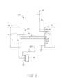
- FIG. 1is a block diagram of an example embodiment of a booting system for a motherboard.
- FIG. 2is a circuit diagram of an example embodiment of the booting system of FIG. 1 .
- Coupledis defined as connected, whether directly or indirectly through intervening components, and is not necessarily limited to physical connections.
- the connectioncan be such that the objects are permanently connected or releasably connected.
- comprisingwhen utilized, means “including, but not necessarily limited to”; it specifically indicates open-ended inclusion or membership in the so-described combination, group, series, and the like.
- the present disclosureis described in relation to a booting system for a motherboard.
- the booting systemincludes a Basic Input/Output System (BIOS) chip, and a south bridge chip.
- BIOSBasic Input/Output System
- the BIOS chipstores a plurality of boot procedures.
- the south bridge chipis coupled to the BIOS chip and includes a cache module.
- the cache moduleloads the plurality of boot procedures from the BIOS chip when the motherboard is powered on. When the motherboard crashes, the south bridge chip is configured to load the plurality of boot procedures in the cache module.
- FIGS. 1-2illustrate an embodiment of a booting system 100 .
- the booting system 100can include a motherboard 10 , a south bridge chip 20 coupled to the motherboard 10 , a jumper 30 coupled to the south bridge chip 20 , a BIOS chip 50 coupled to the south bridge chip 20 , and a standby power source 60 .
- a plurality of boot procedurescan be stored in the BIOS chip 50
- the standby power source 60can be P3V3_AUX, available to power the motherboard 10 .
- the south bridge chip 20is coupled to the BIOS chip 30 by a Serial Peripheral Interface (SPI) bus 70 .
- a cache module 21can be coupled to the south bridge chip 20 .
- a first terminal of the cache module 21is coupled to the standby power source 60
- a second terminal of the cache module 21is coupled to the jumper 30 .
- the cache module 21can be a Random-Access Memory (RAM), which has a memory space equal to the memory space of the BIOS chip 30 .
- RAMRandom-Access Memory
- the jumper 30can include a first terminal 1 , a second terminal 2 , a third terminal 3 , and a first resistor R 1 .
- a first terminal of the first resistor R 1is coupled to the standby power source 60
- a second terminal of the first resistor R 1is coupled to the first terminal 1 of the jumper 30 .
- the second terminal 2is coupled to the cache module 21 , and the third terminal 3 is grounded. In a default status, the second terminal 2 is coupled to the first terminal 1 , thus when the standby power source 60 is powered on, the second terminal 2 outputs a high level signal to control the cache module 21 to load the plurality of boot procedures from the BIOS chip 50 . If the second terminal 2 is coupled to the third terminal 3 when the standby power source 60 is powered on, the second terminal 2 outputs a low level signal, and the cache module 21 cannot load the plurality of boot procedures from the BIOS chip 50 .
- the BIOS chip 50is grounded.
- a first terminal of a second resistor R 2is coupled to the standby power source 60 , and a second terminal of the second resistor R 2 is coupled to the BIOS chip 50 .
- the standby power source 60is powered on, the south bridge chip 20 load the plurality of boot procedures from the BIOS chip 50 enabling the motherboard 10 to power on. Simultaneously, the second terminal 2 outputs a high level signal to control the cache module 21 to load the plurality of boot procedures from the BIOS chip 50 . If and when the motherboard 10 crashes, the south bridge chip 20 can load the plurality of boot procedures in the cache module 21 to power on or repower the motherboard 10 .
Landscapes
- Engineering & Computer Science (AREA)
- Theoretical Computer Science (AREA)
- Software Systems (AREA)
- Physics & Mathematics (AREA)
- General Engineering & Computer Science (AREA)
- General Physics & Mathematics (AREA)
- Computer Security & Cryptography (AREA)
- Stored Programmes (AREA)
Abstract
Description
Claims (16)
Applications Claiming Priority (3)
| Application Number | Priority Date | Filing Date | Title |
|---|---|---|---|
| CN201510376166 | 2015-07-01 | ||
| CN201510376166 | 2015-07-01 | ||
| CN201510376166.8 | 2015-07-01 |
Publications (2)
| Publication Number | Publication Date |
|---|---|
| US9535709B1true US9535709B1 (en) | 2017-01-03 |
| US20170003974A1 US20170003974A1 (en) | 2017-01-05 |
Family
ID=57682209
Family Applications (1)
| Application Number | Title | Priority Date | Filing Date |
|---|---|---|---|
| US14/799,729Expired - Fee RelatedUS9535709B1 (en) | 2015-07-01 | 2015-07-15 | Booting system for motherboard |
Country Status (1)
| Country | Link |
|---|---|
| US (1) | US9535709B1 (en) |
Citations (4)
| Publication number | Priority date | Publication date | Assignee | Title |
|---|---|---|---|---|
| US20030126511A1 (en)* | 2001-12-28 | 2003-07-03 | Jen-Tsung Yang | Module and method for automatic restoring BIOS device |
| US20050039081A1 (en)* | 2003-05-20 | 2005-02-17 | Wei-Han Chang | Method of backing up BIOS settings |
| US20090259837A1 (en)* | 2008-04-14 | 2009-10-15 | Asustek Computer Inc. | Computer system |
| US7822965B2 (en)* | 2007-02-14 | 2010-10-26 | Via Technologies, Inc. | BIOS file switching method and controller device thereof |
- 2015
- 2015-07-15USUS14/799,729patent/US9535709B1/ennot_activeExpired - Fee Related
Patent Citations (4)
| Publication number | Priority date | Publication date | Assignee | Title |
|---|---|---|---|---|
| US20030126511A1 (en)* | 2001-12-28 | 2003-07-03 | Jen-Tsung Yang | Module and method for automatic restoring BIOS device |
| US20050039081A1 (en)* | 2003-05-20 | 2005-02-17 | Wei-Han Chang | Method of backing up BIOS settings |
| US7822965B2 (en)* | 2007-02-14 | 2010-10-26 | Via Technologies, Inc. | BIOS file switching method and controller device thereof |
| US20090259837A1 (en)* | 2008-04-14 | 2009-10-15 | Asustek Computer Inc. | Computer system |
Also Published As
| Publication number | Publication date |
|---|---|
| US20170003974A1 (en) | 2017-01-05 |
Similar Documents
| Publication | Publication Date | Title |
|---|---|---|
| US11119838B2 (en) | Techniques for handling errors in persistent memory | |
| US9507604B2 (en) | Boot method and boot system | |
| US9507675B2 (en) | Systems and methods for recovering from uncorrected DRAM bit errors | |
| US10877845B2 (en) | Apparatus and method for diagnostic use of BIOS attributes to remediate configuration issues | |
| US10592253B2 (en) | Technologies for pre-memory phase initialization of a computing device | |
| US20170083470A1 (en) | System and Method for Providing Personality Switching in a Solid State Drive Device | |
| US20170168872A1 (en) | Task scheduling method and apparatus | |
| US9058257B2 (en) | Persistent block storage attached to memory bus | |
| US20140281464A1 (en) | Method of implementing magnetic random access memory (mram) for mobile system-on chip boot | |
| US20170115996A1 (en) | Reboot system and method for baseboard management controller | |
| US20170091017A1 (en) | Fault detecting device and method | |
| CN103593281A (en) | Test system and test method | |
| CN103605591A (en) | Method and device for controlling memory initialization of terminal system | |
| US20100274999A1 (en) | Control system and method for memory | |
| US20140281095A1 (en) | Computing device and method for integrating thunderbolt chip on motherboard | |
| US20110296072A1 (en) | System and method for controlling pci-e slots of computer | |
| KR102116096B1 (en) | Multisystem, and method of booting the same | |
| US9904640B2 (en) | Program loading system for multiple motherboards | |
| CN111475343B (en) | Computer state outage restoration method and device and terminal equipment | |
| US20140181496A1 (en) | Method, Apparatus and Processor for Reading Bios | |
| US8370565B2 (en) | Boot system | |
| US9535709B1 (en) | Booting system for motherboard | |
| US8874890B2 (en) | Server with plurality of network cards with remote restarting and wake-up functionality | |
| US8826056B2 (en) | Circuit protection system and method | |
| US20200043444A1 (en) | Apparatus and Method for Fast Memory Validation in a Baseboard Management Controller |
Legal Events
| Date | Code | Title | Description |
|---|---|---|---|
| AS | Assignment | Owner name:HONG FU JIN PRECISION INDUSTRY (SHENZHEN) CO., LTD Free format text:ASSIGNMENT OF ASSIGNORS INTEREST;ASSIGNOR:YANG, MENG-LIANG;REEL/FRAME:036093/0396 Effective date:20150710 Owner name:HON HAI PRECISION INDUSTRY CO., LTD., TAIWAN Free format text:ASSIGNMENT OF ASSIGNORS INTEREST;ASSIGNOR:YANG, MENG-LIANG;REEL/FRAME:036093/0396 Effective date:20150710 | |
| STCF | Information on status: patent grant | Free format text:PATENTED CASE | |
| AS | Assignment | Owner name:HONGFUJIN PRECISION ELECTRONICS(TIANJIN)CO.,LTD., Free format text:ASSIGNMENT OF ASSIGNORS INTEREST;ASSIGNORS:HONG FU JIN PRECISION INDUSTRY (SHENZHEN) CO., LTD.;HON HAI PRECISION INDUSTRY CO., LTD.;REEL/FRAME:045501/0324 Effective date:20180112 | |
| FEPP | Fee payment procedure | Free format text:MAINTENANCE FEE REMINDER MAILED (ORIGINAL EVENT CODE: REM.); ENTITY STATUS OF PATENT OWNER: LARGE ENTITY | |
| LAPS | Lapse for failure to pay maintenance fees | Free format text:PATENT EXPIRED FOR FAILURE TO PAY MAINTENANCE FEES (ORIGINAL EVENT CODE: EXP.); ENTITY STATUS OF PATENT OWNER: LARGE ENTITY | |
| STCH | Information on status: patent discontinuation | Free format text:PATENT EXPIRED DUE TO NONPAYMENT OF MAINTENANCE FEES UNDER 37 CFR 1.362 | |
| FP | Lapsed due to failure to pay maintenance fee | Effective date:20210103 |