US9530501B2 - Non-volatile static random access memory (NVSRAM) having a shared port - Google Patents
Non-volatile static random access memory (NVSRAM) having a shared portDownload PDFInfo
- Publication number
- US9530501B2 US9530501B2US14/588,177US201414588177AUS9530501B2US 9530501 B2US9530501 B2US 9530501B2US 201414588177 AUS201414588177 AUS 201414588177AUS 9530501 B2US9530501 B2US 9530501B2
- Authority
- US
- United States
- Prior art keywords
- coupled
- shared port
- transistor
- read
- block
- Prior art date
- Legal status (The legal status is an assumption and is not a legal conclusion. Google has not performed a legal analysis and makes no representation as to the accuracy of the status listed.)
- Active, expires
Links
Images


Classifications
- G—PHYSICS
- G11—INFORMATION STORAGE
- G11C—STATIC STORES
- G11C16/00—Erasable programmable read-only memories
- G—PHYSICS
- G11—INFORMATION STORAGE
- G11C—STATIC STORES
- G11C8/00—Arrangements for selecting an address in a digital store
- G11C8/16—Multiple access memory array, e.g. addressing one storage element via at least two independent addressing line groups
- G—PHYSICS
- G11—INFORMATION STORAGE
- G11C—STATIC STORES
- G11C11/00—Digital stores characterised by the use of particular electric or magnetic storage elements; Storage elements therefor
- G11C11/21—Digital stores characterised by the use of particular electric or magnetic storage elements; Storage elements therefor using electric elements
- G11C11/22—Digital stores characterised by the use of particular electric or magnetic storage elements; Storage elements therefor using electric elements using ferroelectric elements
- G—PHYSICS
- G11—INFORMATION STORAGE
- G11C—STATIC STORES
- G11C13/00—Digital stores characterised by the use of storage elements not covered by groups G11C11/00, G11C23/00, or G11C25/00
- G11C13/0002—Digital stores characterised by the use of storage elements not covered by groups G11C11/00, G11C23/00, or G11C25/00 using resistive RAM [RRAM] elements
- G11C13/0021—Auxiliary circuits
- G11C13/0023—Address circuits or decoders
- G11C13/0026—Bit-line or column circuits
- G—PHYSICS
- G11—INFORMATION STORAGE
- G11C—STATIC STORES
- G11C13/00—Digital stores characterised by the use of storage elements not covered by groups G11C11/00, G11C23/00, or G11C25/00
- G11C13/0002—Digital stores characterised by the use of storage elements not covered by groups G11C11/00, G11C23/00, or G11C25/00 using resistive RAM [RRAM] elements
- G11C13/0021—Auxiliary circuits
- G11C13/0023—Address circuits or decoders
- G11C13/0028—Word-line or row circuits
- G—PHYSICS
- G11—INFORMATION STORAGE
- G11C—STATIC STORES
- G11C13/00—Digital stores characterised by the use of storage elements not covered by groups G11C11/00, G11C23/00, or G11C25/00
- G11C13/0002—Digital stores characterised by the use of storage elements not covered by groups G11C11/00, G11C23/00, or G11C25/00 using resistive RAM [RRAM] elements
- G11C13/0021—Auxiliary circuits
- G11C13/003—Cell access
- G—PHYSICS
- G11—INFORMATION STORAGE
- G11C—STATIC STORES
- G11C13/00—Digital stores characterised by the use of storage elements not covered by groups G11C11/00, G11C23/00, or G11C25/00
- G11C13/0002—Digital stores characterised by the use of storage elements not covered by groups G11C11/00, G11C23/00, or G11C25/00 using resistive RAM [RRAM] elements
- G11C13/0021—Auxiliary circuits
- G11C13/004—Reading or sensing circuits or methods
- G—PHYSICS
- G11—INFORMATION STORAGE
- G11C—STATIC STORES
- G11C13/00—Digital stores characterised by the use of storage elements not covered by groups G11C11/00, G11C23/00, or G11C25/00
- G11C13/0002—Digital stores characterised by the use of storage elements not covered by groups G11C11/00, G11C23/00, or G11C25/00 using resistive RAM [RRAM] elements
- G11C13/0021—Auxiliary circuits
- G11C13/0069—Writing or programming circuits or methods
- G—PHYSICS
- G11—INFORMATION STORAGE
- G11C—STATIC STORES
- G11C8/00—Arrangements for selecting an address in a digital store
- G11C8/08—Word line control circuits, e.g. drivers, boosters, pull-up circuits, pull-down circuits, precharging circuits, for word lines
- G—PHYSICS
- G11—INFORMATION STORAGE
- G11C—STATIC STORES
- G11C11/00—Digital stores characterised by the use of particular electric or magnetic storage elements; Storage elements therefor
- G11C11/21—Digital stores characterised by the use of particular electric or magnetic storage elements; Storage elements therefor using electric elements
- G11C11/24—Digital stores characterised by the use of particular electric or magnetic storage elements; Storage elements therefor using electric elements using capacitors
- G—PHYSICS
- G11—INFORMATION STORAGE
- G11C—STATIC STORES
- G11C2213/00—Indexing scheme relating to G11C13/00 for features not covered by this group
- G11C2213/70—Resistive array aspects
- G11C2213/74—Array wherein each memory cell has more than one access device
- G—PHYSICS
- G11—INFORMATION STORAGE
- G11C—STATIC STORES
- G11C2213/00—Indexing scheme relating to G11C13/00 for features not covered by this group
- G11C2213/70—Resistive array aspects
- G11C2213/79—Array wherein the access device being a transistor
- G—PHYSICS
- G11—INFORMATION STORAGE
- G11C—STATIC STORES
- G11C7/00—Arrangements for writing information into, or reading information out from, a digital store
- G11C7/18—Bit line organisation; Bit line lay-out
Definitions
- NVMsnon-volatile memories
- NVSRAMsnon-volatile static random access memories
- Non-volatile static random access memorieshold the promise of having the benefits of both non-volatile memories (NVMs) and static random access memories (SRAMs).
- NVMsnon-volatile memories
- SRAMsstatic random access memories
- a type of NVM that is of particular interestis the resistive RAM (RRAM) which has a programmable resistor as the non-volatile element.
- RRAMresistive RAM
- the accessing for speed of reading and writingis similar to that of SRAMs.
- One of the difficultieshas been obtaining access speeds, especially the speed of reading, comparable to that of SRAMs.
- the write speedmay be slower as well but much, much faster than typical NVMs.
- FIG. 1is a block diagram of an NVSRAM showing elements useful for a read
- FIG. 2is a block diagram of the NVSRAM showing elements useful for a write
- FIG. 3is a circuit diagram of a portion of the NVSRAM of FIGS. 1 and 2 ;
- FIG. 4is a timing diagram for a read operation of the NVSRAM of FIGS. 1 and 2 ;
- FIG. 5is a circuit diagram of a portion of the NVSRAM of FIGS. 1 and 2 as an alternative to the portion of the NVSRAM of FIG. 3 ;
- FIG. 6is a circuit diagram of a portion of the NVSRAM of FIGS. 1 and 2 as a further alternative to the portion of the NVSRAM of FIG. 3 ;
- FIG. 7is a timing diagram of a write operation of the portion of the NVSRAM according to the further alternative of FIG. 6 .
- a shared port blockhas a plurality, for example 8, of bit cells that share a partial sense amplifier and write driver so as to reduce delays in reading as well as writing which is particularly effective for NVSRAMs that use a programmable resistance.
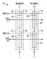
- FIG. 1Shown in FIG. 1 is a NVSRAM 10 having a shared port block 12 , a shared port block 14 , a shared port block 16 , a shared port block 18 , a read bit line RBL 0 coupled to shared port blocks 12 and 16 , a read bit line RBL 1 coupled to share port blocks 14 and 18 , decoded column address DCA signal lines 0 - 7 coupled to shared port blocks 12 , 14 , 16 , and 18 , a word line WLO coupled to shared port blocks 12 and 14 , and a word line WL 1 coupled to shared port blocks 16 and 18 .
- a variationcan be that not all of the shared port blocks on a given word line receive the same DCA signals.
- Shared port blocks 12 , 14 , 16 , and 18each have a shared port and a block.
- Shared port block 12has a shared port 20 and a block 22 .
- Shared port block 14has a shared port 24 and a block 26 .
- Shared port block 16has a shared port 28 and a block 30 .
- Shared port block 18has a shared port 32 and a block 34 .
- 8 memory cellsare in each of blocks 12 , 14 , 16 , and 18 .
- one of decoded column address signals 0 - 7is selected to be active, which may be by a logic “1,” and the remainder are maintained at the opposite logic state which may be a logic “0.”
- a word linesuch as word line WLO, is enabled, and the remainder of the word lines are kept disabled.
- a DCA signalsuch as DCA signal 0 , is selected, and the cells coupled to receive that signal receive an active signal. These cells include those in blocks 22 , 26 , 30 , and 34 .
- a read bit line, such as read bit line RBL 0is selected to receive data. More than one read bit line may be selected to receive data.
- the selected cells in blocks 22 and 26are coupled to shared ports 20 and 24 , respectively, where they are quickly strengthened and coupled to read bit lines RBL 0 and RBL 1 , respectively. This significantly speeds the sensing process compared to simply coupling the selected memory cell to the bit line.
- the memory elementstend to have relatively high resistance which makes providing a detectable signal on a bit line a significantly slower process than that for an SRAM.
- NVSRAM 10Shown in FIG. 2 is NVSRAM 10 further showing a write bit line WBL 0 coupled to shared ports 20 and 28 , a write bit line WBL 1 coupled to shared ports 24 and 32 , write bit line bar signals WBLB 0 0 - 7 coupled to blocks 22 and 30 , and a write bit line bar signal WBLB 1 coupled to blocks 26 and 34 .
- write bit line signal WBL 0contains data to be written into an NVSRAM cell in block 22
- write bit line WBL 1contains data to be written into an NVSRAM cell in block 26 .
- One of DCA signals 0 - 7is active which selects a cell in each of blocks 22 and 26 and is also received by blocks 30 and 34 but does not have the effect of selecting a cell in blocks 30 and 34 because word line WL 1 is not selected.
- One of write bit line bar signals WBLB 0 0 - 7 and one of write bit line bar signals WBLB 1 0 - 7are provided as the complement to the selected cell as part of the writing.
- the selection of the write bit line bar signalscorresponds to the selection of the DCA signals.
- write bit line bar signal WBLB 0 0will be the complement to the data provided by write bit line WBL 0 .
- the selected cellreceives both the true and complement of the data to be written.
- FIG. 3Shown in FIG. 3 is a circuit diagram of a portion of shared port block 12 showing shared port 20 and a portion of block 22 .
- Shared port 20has a capacitor 40 having a first terminal coupled to read word line RWL 0 and a second terminal coupled to a node 45 ; an N channel transistor 42 having a first current electrode coupled to write bit line WBL 0 , a gate coupled to word line WL 0 , and a second current electrode coupled to node 45 ; and an N channel transistor having a control electrode coupled to node 45 , a first current electrode coupled to read bit line RBL 0 , and a second current electrode coupled to a power supply terminal which may be ground.
- the portion of Block 22has a NVSRAM cell 46 and an NVSRAM cell 48 .
- NVSRAM cell 46has a programmable resistor 50 having a first terminal coupled to node 45 and a second terminal. NVSRAM cell 46 further has an N channel transistor 52 having a first current electrode coupled to the second current electrode of programmable resistor 50 , a control electrode coupled to decoded column address signal DCA 0 , and a second current electrode coupled to write bit line bar WBLB 0 . NVSRAM cell 48 has a programmable resistor 54 having a first terminal coupled to node 45 and a second terminal.
- NVSRAM cell 48further has an N channel transistor 56 having a first current electrode coupled to the second current electrode of programmable resistor 50 , a control electrode coupled to decoded column address signal DCA 1 , and a second current electrode coupled to write bit line bar WBLB 1 .
- Shown in FIG. 4is a timing diagram for reading an NVSRAM cell such as NVSRAM cell 46 .
- decoded column address DCA 0switches to a logic high which is followed by read word line RWL 0 switching to a logic high.
- Word line WL 0is held at a logic low during the read which keeps transistor 42 non-conductive.
- Write bit line WBLB 0is held at a logic low during the read.
- Read Bit line RBL 0is precharged to a logic high.
- transistor 52becomes conductive in response to decoded column address DCA 0 switching to a logic high which allows for a conductive path through variable resistor 50 between node 45 and write bit line bar WBLB 0 .
- read word line RWL 0switches to a logic high at time t 1 which causes node 45 to immediately rise.
- the voltage on node 45is coupled upward by capacitor 40 but decays more rapidly for the logic “1” case.
- logic “1”is the case for programmable resistor 50 being in its more conductive state and a logic “0” for its more resistive state.
- Transistor 44responds by becoming conductive and begins reducing the voltage on read bit line RBL 0 .
- a faster decline in voltage of node 45causes less voltage drop on read bit line RBL 0 .
- the faster decline in voltage of node 45occurs when programmable resistor 50 is in its lower resistive state.
- the comparative declineis shown in FIG.
- Read bit line RBL 0stops dropping sooner for the low resistance state, logic “1,” which results in the voltage on read bit line RBL 0 being at a higher level when the reduction in voltage has effectively stopped than for the logic “0” case in which transistor 44 continues to reduce the voltage on read bit line RBL 0 .
- the voltage on read bit line RBL 0 for the logic “0” caseis reduced about twice as much as for the logic “1” case.
- Transistor 44can be sized to optimize the gain for achieving a voltage differential between the conductive states that can be quickly and reliably obtained. The use of the amplification provided by transistor 44 is effective in avoiding the slow read access problem of attempting to reduce the voltage on read bit line RBL 0 through programmable resistor 50 .
- programmable resistor 50For a write of programmable resistor 50 , current is flowed in one direction through the programmable resistor for a logic “1” and the opposite direction for a logic “0.” The direction choice is achieved by having current be in one direction between write bit line WBL 0 and write bit line bar WBLB 0 for one state and the opposite direction to achieve the other state while transistor 52 is conductive.
- the voltage on write bit line WBL 0is coupled to programmable resistor 50 by word line WL 0 being a logic high, causing transistor 42 to be conductive.
- Transistor 52 being conductivecan be achieved in the same manner as for the read case.
- write bit line WBL 0is provided at a relatively high voltage, such as the positive power supply voltage, VDD, and write bit line bar WBLB is provided at a relatively low voltage such as ground.
- write bit line WBL 0is provided at the relatively low voltage, such as ground
- write bit line bar WBLBis provided at the relatively high voltage such as VDD.
- FIG. 5Shown in FIG. 5 is shared port block 12 which is a variation from that of FIG. 3 in which there is a write bit line WBL 0 - 7 for each NVSRAM cell instead of one shared by all of the NVSRAM cells so that there is a complementary pair of write bit lines for each NVSRAM cell.
- WBLB 0 - 7there is a corresponding write bit line WBL 0 - 7 .
- an N channel transistor 142has a first current electrode coupled to write bit line WBL 0 , a control electrode coupled to word line WL 0 , and a second current electrode coupled to node 45 .
- an N channel transistor 144has a first current electrode coupled to write bit line WBL 1 , a control electrode coupled to word line WL 0 , and a second current electrode coupled to node 45 .
- This variationis intended to speed up operation of the write by allowing a plurality of bits in a block to be written in concurrently. In this embodiment both logic “1”'s and logic “0”'s may be written simultaneously.
- FIG. 6Shown in FIG. 6 is shared port block 12 which is a variation from that of FIGS. 3 and 5 with the intent of increasing the programming current by increasing the voltage.
- Transistor 44alone would unlikely avoid breakdown so transistor 44 has been replaced by a transistor 244 and a transistor 246 and adding a read line RSWL 0 that is active during a read so that transistor 244 , during a read, functions in the same manner of transistor 44 during a read.
- Transistor 246is intended to share the voltage with transistor 244 during a high voltage write to protect transistor 244 from breakdown. For a high voltage write of a “1,” as shown in FIG.
- 2VDDis applied across NVSRAM cell 46 , 2VDD is applied to decoded column address DCA 0 , VDD is applied to word line WL 0 , ground is applied to write bit line WBL 0 , and 2VDD is applied to write bit line bar WBLB 0 .
- VDDis applied at decoded column address DCA 0
- 2VDDis applied to word line WL 0
- 2VDDis applied to write bit line WBL 0
- groundis applied to write bit line bar WBLB 0 .
- the higher voltage and and resulting higher currenthave the effect of faster programming.
- FIGS. 6 and 7In some technologies it is assumed that there will be transistors with breakdowns lower than the required voltages to achieve a change in logic state. In such a case, the embodiment of FIGS. 6 and 7 would be effective.
- the voltages of FIG. 7 applied to NVSRAM cell 46 and shared port 20 of FIG. 6allow programming voltages greater than the breakdown of transistors 42 , 50 , 244 , or 246 while controlling the voltage across each of the individual transistors to be at a lower voltage not exceeding its breakdown voltage.
- nonvolatile memory devicehaving a shared port block comprising a shared port communicatively coupled to a block, the block including a plurality of memory cells, wherein the shared port is operable to sense a voltage level at each of the plurality of memory cells.
- the nonvolatile memory devicefurther includes a plurality of decoded address signals communicatively coupled to the block, each of the plurality of decoded address signals operable to enable a corresponding one of the plurality of memory cells.
- the nonvolatile memory devicefurther includes a read signal communicatively coupled to the shared port, the read signal operable to enable a read operation associated with the block.
- the nonvolatile memory devicefurther includes a read word line signal communicatively coupled to the shared port block, the read word line signal operable to enable the read operation.
- the nonvolatile memory devicemay further include a first and second shared port block, each of the first and second shared port blocks communicatively coupled to the plurality of decoded address signals and to the read signal.
- the nonvolatile memory devicemay further include a write word line signal communicatively coupled to the shared port block.
- the nonvolatile memory devicemay further include a second shared port block comprising a second shared port communicatively coupled to a second block, the second block comprising a second plurality of memory cells, wherein the second shared port is operable to sense a voltage level at each of the second plurality of memory cells, and wherein the second block is communicatively coupled to the plurality of decoded address signals and a second read signal communicatively coupled to the second shared port, the second read signal operable to enable a read operation associated with the second block, and wherein the second shared port block is communicatively coupled to the read word line signal.
- a second shared port blockcomprising a second shared port communicatively coupled to a second block, the second block comprising a second plurality of memory cells, wherein the second shared port is operable to sense a voltage level at each of the second plurality of memory cells, and wherein the second block is communicatively coupled to the plurality of decoded address signals and a second read signal communicatively coupled to the second
- the nonvolatile memory devicemay further include a first word line signal communicatively coupled to the first shared port block and a second write word line signal communicatively coupled to the second shared port block.
- the nonvolatile memory devicemay have a further characterization by which the shared port block includes a capacitor having a first terminal coupled to the read word line signal and a second terminal coupled to the block, a first transistor having a first current electrode coupled to the second terminal of the capacitor, and having a control electrode coupled to a word line signal, and a second transistor having a first current electrode coupled to the read signal, and having a control electrode coupled to the first current electrode of the first transistor.
- the nonvolatile memory devicemay have a further characterization by which each of the plurality of memory cells includes a transistor having a control electrode coupled to a corresponding one of the plurality of decoded address signal and a variable resistance element having a first terminal coupled to a first current electrode of the transistor and having a second terminal coupled to the shared port.
- the nonvolatile memory devicemay have a further characterization by which the transistor of each of the plurality of memory cells further comprises a second current electrode coupled to a write bit line.
- the nonvolatile memory devicemay have a further characterization by which the shared port block includes a capacitor having a first terminal coupled to the read word line signal and a second terminal coupled to the block and a transistor having a first current electrode coupled to the read signal, and having a control electrode coupled to the second terminal of the capacitor.
- the nonvolatile memory devicemay have a further characterization by which each of the plurality of memory cells includes a first transistor having a control electrode coupled to a corresponding one of the plurality of decoded address signals, a variable resistance element having a first terminal coupled to a first current electrode of the first transistor and having a second terminal coupled to the shared port, and a second transistor having a control electrode coupled to a word line signal, and having a first current electrode coupled to the second terminal of the variable resistance element.
- the nonvolatile memory devicemay have a further characterization by which the first transistor of each of the plurality of memory cells further comprises a second current electrode coupled to a write bit line and the second transistor of each of the plurality of memory cells further comprises a second current electrode coupled to the write bit line.
- the nonvolatile memory devicemay have a further characterization by which the block includes eight memory cells.
- nonvolatile memory devicehaving a first, second, third, and fourth shared port block, each comprising a shared port communicatively coupled to a block, the block comprising a plurality of memory cells, wherein the shared port is operable to sense a voltage level at each of the plurality of memory cells.
- the nonvolatile memory devicefurther includes a plurality of decoded address signals communicatively coupled to each block, each of the plurality of decoded address signals operable to enable a corresponding one of the plurality of memory cells.
- the nonvolatile memory devicefurther includes a first read signal communicatively coupled to the first and second shared ports, the first read signal operable to enable a read operation associated with the first and second blocks.
- the nonvolatile memory devicefurther includes a second read signal communicatively coupled to the third and fourth shared ports, the second read signal operable to enable a read operation associated with the third and fourth blocks.
- the nonvolatile memory devicefurther includes a first read word line signal communicatively coupled to the first and third shared ports, the first read word line signal operable to enable the read operation associated with the first and third blocks.
- the nonvolatile memory devicefurther includes a second read word line signal communicatively coupled to the second and fourth shared ports, the second read word line signal operable to enable the read operation associated with the second and fourth blocks.
- the nonvolatile memory devicemay further include a first write word line signal communicatively coupled to the first and third shared port blocks and a second write word line signal communicatively coupled to the second and fourth shared port blocks.
- the nonvolatile memory devicemay have a further characterization by which the first shared port block includes a capacitor having a first terminal coupled to the first read word line signal and a second terminal coupled to the block, a first transistor having a first current electrode coupled to the second terminal of the capacitor, and having a control electrode coupled to the first write word line signal, and a second transistor having a first current electrode coupled to the first read signal, and having a control electrode coupled to the first current electrode of the first transistor.
- the nonvolatile memory devicemay have a further characterization by which each of the plurality of memory cells includes a transistor having a control electrode coupled to a corresponding one of the decoded address signals, and having a first current electrode coupled to a write bit line and a variable resistance element having a first terminal coupled to a second current electrode of the transistor and having a second terminal coupled to the shared port.
- the nonvolatile memory devicemay have a further characterization by which each shared port block includes a capacitor having a first terminal coupled to the first read word line signal and a second terminal coupled to the block and a transistor having a first current electrode coupled to the first read signal, and having a control electrode coupled to the second terminal of the capacitor.
- the nonvolatile memory devicemay have a further characterization by which each of the plurality of memory cells includes a first transistor having a control electrode coupled to a corresponding one of the plurality of decoded address signals, and having a first current electrode coupled to a write bit line, a variable resistance element having a first terminal coupled to a second current electrode of the transistor and having a second terminal coupled to the shared port, and a second transistor having a control electrode coupled to the word line signal, and having a first current electrode coupled to the second terminal of the variable resistance element, and having a second current electrode coupled to the write bit line.
- the nonvolatile memory devicemay further include a read line coupled to the first shared port block, a capacitor having a first terminal that receives the first read word line signal and a second terminal, a first transistor having a first current electrode that receives the first read signal, a control electrode coupled to the second terminal of the capacitor, and a second current electrode, and a second transistor having a first current electrode coupled to the second current electrode of the first transistor, a control electrode coupled to the read line, and a second current electrode coupled to a power supply terminal.
- the methodincludes receiving a read signal at a shared port block, the read signal operable to enable a read operation associated with the shared port block, the shared port block comprising a shared port communicatively coupled to a block, the block comprising a plurality of memory cells.
- the methodfurther includes receiving a plurality of decoded address signals at the shared port block, each of the plurality of decoded address signals operable to enable a corresponding one of the plurality of memory cells.
- the methodfurther includes receiving a read word line signal at the shared port block, the read word line signal operable to enable the read operation, wherein the shared port includes a capacitor having a first terminal coupled to the read word line signal and a first transistor having a control electrode coupled to a second terminal of the capacitor, and having a current electrode coupled to the read signal.
- Coupledis not intended to be limited to a direct coupling or a mechanical coupling.
Landscapes
- Engineering & Computer Science (AREA)
- Microelectronics & Electronic Packaging (AREA)
- Computer Hardware Design (AREA)
- Static Random-Access Memory (AREA)
- Theoretical Computer Science (AREA)
- Physics & Mathematics (AREA)
- General Engineering & Computer Science (AREA)
- General Physics & Mathematics (AREA)
Abstract
Description
Claims (20)
Priority Applications (1)
| Application Number | Priority Date | Filing Date | Title |
|---|---|---|---|
| US14/588,177US9530501B2 (en) | 2014-12-31 | 2014-12-31 | Non-volatile static random access memory (NVSRAM) having a shared port |
Applications Claiming Priority (1)
| Application Number | Priority Date | Filing Date | Title |
|---|---|---|---|
| US14/588,177US9530501B2 (en) | 2014-12-31 | 2014-12-31 | Non-volatile static random access memory (NVSRAM) having a shared port |
Publications (2)
| Publication Number | Publication Date |
|---|---|
| US20160188457A1 US20160188457A1 (en) | 2016-06-30 |
| US9530501B2true US9530501B2 (en) | 2016-12-27 |
Family
ID=56164308
Family Applications (1)
| Application Number | Title | Priority Date | Filing Date |
|---|---|---|---|
| US14/588,177Active2035-04-19US9530501B2 (en) | 2014-12-31 | 2014-12-31 | Non-volatile static random access memory (NVSRAM) having a shared port |
Country Status (1)
| Country | Link |
|---|---|
| US (1) | US9530501B2 (en) |
Cited By (3)
| Publication number | Priority date | Publication date | Assignee | Title |
|---|---|---|---|---|
| US20190088317A1 (en)* | 2017-09-18 | 2019-03-21 | Nxp Usa, Inc. | Resistive non-volatile memory and a method for sensing a memory cell in a resistive non-volatile memory |
| US10896730B1 (en)* | 2019-06-28 | 2021-01-19 | Arm Limited | D-MRAM devices and methods for replicating data and read and write operations |
| US12051466B2 (en)* | 2020-08-26 | 2024-07-30 | Taiwan Semiconductor Manufacturing Company, Ltd. | Memory cell including programmable resistors with transistor components |
Citations (24)
| Publication number | Priority date | Publication date | Assignee | Title |
|---|---|---|---|---|
| JPS60144977A (en) | 1984-01-06 | 1985-07-31 | Seiko Instr & Electronics Ltd | Nonvolatile ram cell |
| JPS611058A (en) | 1984-06-13 | 1986-01-07 | Seiko Instr & Electronics Ltd | Nonvolatile ram |
| US4809225A (en) | 1987-07-02 | 1989-02-28 | Ramtron Corporation | Memory cell with volatile and non-volatile portions having ferroelectric capacitors |
| US4980859A (en) | 1989-04-07 | 1990-12-25 | Xicor, Inc. | NOVRAM cell using two differential decouplable nonvolatile memory elements |
| US5349302A (en) | 1993-05-13 | 1994-09-20 | Honeywell Inc. | Sense amplifier input stage for single array memory |
| US6084799A (en)* | 1996-11-25 | 2000-07-04 | Kabushiki Kaisha Toshiba | Nonvolatile semiconductor memory having improved source line drive circuit |
| WO2000051131A1 (en) | 1999-02-22 | 2000-08-31 | Rose Research, L.L.C. | Self-calibrating self-regenerative comparator circuit and method |
| KR20020002823A (en) | 2000-06-30 | 2002-01-10 | 박종섭 | Non volatile sram cell |
| JP2002109875A (en) | 2000-09-29 | 2002-04-12 | Nec Corp | Shadow ram cell using ferroelectric capacitor, and nonvolatile memory device and its control method |
| US6625056B1 (en) | 2002-04-04 | 2003-09-23 | Mitsubishi Denki Kabushiki Kaisha | Semiconductor memory device having memory cells requiring no refresh operations |
| US6847568B2 (en) | 2001-03-14 | 2005-01-25 | Infineon Technologies Ag | Sense amplifier configuration for a semiconductor memory device |
| US20050122762A1 (en)* | 2003-12-09 | 2005-06-09 | Hynix Semiconductor Inc. | FeRAM having differential data |
| US6980459B2 (en) | 2002-10-24 | 2005-12-27 | Texas Instruments Incorporated | Non-volatile SRAM |
| US7079415B2 (en) | 2004-06-30 | 2006-07-18 | Stmicroelectronics, Inc. | Magnetic random access memory element |
| US20060203550A1 (en)* | 2005-03-10 | 2006-09-14 | Hynix Semiconductor Inc. | Flash Memory Device with Improved Erase Function and Method for Controlling Erase Operation of the Same |
| US7113437B2 (en) | 2003-03-26 | 2006-09-26 | Thin Film Electronics Asa | Sense amplifier systems and a matrix-addressable memory device provided therewith |
| WO2006121497A2 (en) | 2005-05-06 | 2006-11-16 | Intelleflex Corporation | Accurate persistent nodes |
| US7868663B2 (en) | 2007-09-04 | 2011-01-11 | Hynix Semiconductor Inc. | Receiver circuit for use in a semiconductor integrated circuit |
| JP2011081896A (en) | 2009-10-12 | 2011-04-21 | Numonyx Bv | Non-volatile sram cell that incorporates phase-change memory into cmos process |
| US20110216571A1 (en) | 2010-03-04 | 2011-09-08 | Semiconductor Energy Laboratory Co., Ltd. | Semiconductor memory device and semiconductor device |
| US8493806B1 (en) | 2012-01-03 | 2013-07-23 | United Microelectronics Corporation | Sense-amplifier circuit of memory and calibrating method thereof |
| US8638599B2 (en) | 2011-12-16 | 2014-01-28 | Renesas Electronics Corporation | Semiconductor storage device |
| US20150016183A1 (en) | 2013-07-12 | 2015-01-15 | Nvidia Corporation | Sense amplifier with transistor threshold compensation |
| US9202543B2 (en) | 2012-11-30 | 2015-12-01 | Intel Deutschland Gmbh | System and methods using a multiplexed reference for sense amplifiers |
- 2014
- 2014-12-31USUS14/588,177patent/US9530501B2/enactiveActive
Patent Citations (24)
| Publication number | Priority date | Publication date | Assignee | Title |
|---|---|---|---|---|
| JPS60144977A (en) | 1984-01-06 | 1985-07-31 | Seiko Instr & Electronics Ltd | Nonvolatile ram cell |
| JPS611058A (en) | 1984-06-13 | 1986-01-07 | Seiko Instr & Electronics Ltd | Nonvolatile ram |
| US4809225A (en) | 1987-07-02 | 1989-02-28 | Ramtron Corporation | Memory cell with volatile and non-volatile portions having ferroelectric capacitors |
| US4980859A (en) | 1989-04-07 | 1990-12-25 | Xicor, Inc. | NOVRAM cell using two differential decouplable nonvolatile memory elements |
| US5349302A (en) | 1993-05-13 | 1994-09-20 | Honeywell Inc. | Sense amplifier input stage for single array memory |
| US6084799A (en)* | 1996-11-25 | 2000-07-04 | Kabushiki Kaisha Toshiba | Nonvolatile semiconductor memory having improved source line drive circuit |
| WO2000051131A1 (en) | 1999-02-22 | 2000-08-31 | Rose Research, L.L.C. | Self-calibrating self-regenerative comparator circuit and method |
| KR20020002823A (en) | 2000-06-30 | 2002-01-10 | 박종섭 | Non volatile sram cell |
| JP2002109875A (en) | 2000-09-29 | 2002-04-12 | Nec Corp | Shadow ram cell using ferroelectric capacitor, and nonvolatile memory device and its control method |
| US6847568B2 (en) | 2001-03-14 | 2005-01-25 | Infineon Technologies Ag | Sense amplifier configuration for a semiconductor memory device |
| US6625056B1 (en) | 2002-04-04 | 2003-09-23 | Mitsubishi Denki Kabushiki Kaisha | Semiconductor memory device having memory cells requiring no refresh operations |
| US6980459B2 (en) | 2002-10-24 | 2005-12-27 | Texas Instruments Incorporated | Non-volatile SRAM |
| US7113437B2 (en) | 2003-03-26 | 2006-09-26 | Thin Film Electronics Asa | Sense amplifier systems and a matrix-addressable memory device provided therewith |
| US20050122762A1 (en)* | 2003-12-09 | 2005-06-09 | Hynix Semiconductor Inc. | FeRAM having differential data |
| US7079415B2 (en) | 2004-06-30 | 2006-07-18 | Stmicroelectronics, Inc. | Magnetic random access memory element |
| US20060203550A1 (en)* | 2005-03-10 | 2006-09-14 | Hynix Semiconductor Inc. | Flash Memory Device with Improved Erase Function and Method for Controlling Erase Operation of the Same |
| WO2006121497A2 (en) | 2005-05-06 | 2006-11-16 | Intelleflex Corporation | Accurate persistent nodes |
| US7868663B2 (en) | 2007-09-04 | 2011-01-11 | Hynix Semiconductor Inc. | Receiver circuit for use in a semiconductor integrated circuit |
| JP2011081896A (en) | 2009-10-12 | 2011-04-21 | Numonyx Bv | Non-volatile sram cell that incorporates phase-change memory into cmos process |
| US20110216571A1 (en) | 2010-03-04 | 2011-09-08 | Semiconductor Energy Laboratory Co., Ltd. | Semiconductor memory device and semiconductor device |
| US8638599B2 (en) | 2011-12-16 | 2014-01-28 | Renesas Electronics Corporation | Semiconductor storage device |
| US8493806B1 (en) | 2012-01-03 | 2013-07-23 | United Microelectronics Corporation | Sense-amplifier circuit of memory and calibrating method thereof |
| US9202543B2 (en) | 2012-11-30 | 2015-12-01 | Intel Deutschland Gmbh | System and methods using a multiplexed reference for sense amplifiers |
| US20150016183A1 (en) | 2013-07-12 | 2015-01-15 | Nvidia Corporation | Sense amplifier with transistor threshold compensation |
Non-Patent Citations (9)
| Title |
|---|
| Abe, K., et al., "Novel Hybrid DRAM/MRAM Design for Reducing Power of High Performance Mobile Cpu", IEEE International Electron Devices Meeting (IEDM), pp. 10.5.1-10.5.4, Dec. 10-13, 2012. |
| Choudhary, A., et al. "A Process Variation Tolerant Self-Compensation Sense Amplifier Design", http://scholarworks.umass.edu/cgi/viewcontent.cgi?article=1253%context-theses, University of Massachusetts-Amherst, Masters Theses, Sep. 2008, 107 pages. |
| Groeneveld, S., et al. "Offset Correction Techniques for Voltage Sense Amplifiers", http://eprints.eemcs.utwente.nl/8798/, University of Twente, Master Thesis, Aug. 2006, 72 pages. |
| Miyahara, M., et al. "A Low-Noise Self-Calibrating Dynamic Comparator for High-Speed ADCs", IEEE Asian Solid-State Circuits Conference, Nov. 3-5, 2008, pp. 269-272. |
| Non-final office action dated Mar. 29, 2016 in U.S. Appl. No. 14/682,475. |
| Notice of Allowance dated Aug. 3, 2016 in U.S. Appl. No. 14/682,475. |
| Notice of Allowance dated Nov. 4, 2015 in U.S. Appl. No. 14/572,780. |
| U.S. Appl. No. 14/572,780, Pelley, P. et al., "Non-Volatile Memory Using Bi-Directional Resistive Elements and Capacitive Elements", filed Dec. 17, 2014. |
| U.S. Appl. No. 14/682,475, Pelley, P. et al., "Mismatch-Compensated Sense Amplifier for Highly Scaled Technology", filed Apr. 9, 2015. |
Cited By (5)
| Publication number | Priority date | Publication date | Assignee | Title |
|---|---|---|---|---|
| US20190088317A1 (en)* | 2017-09-18 | 2019-03-21 | Nxp Usa, Inc. | Resistive non-volatile memory and a method for sensing a memory cell in a resistive non-volatile memory |
| US10403357B2 (en)* | 2017-09-18 | 2019-09-03 | Nxp Usa, Inc. | Resistive non-volatile memory and a method for sensing a memory cell in a resistive non-volatile memory |
| US10896730B1 (en)* | 2019-06-28 | 2021-01-19 | Arm Limited | D-MRAM devices and methods for replicating data and read and write operations |
| US12051466B2 (en)* | 2020-08-26 | 2024-07-30 | Taiwan Semiconductor Manufacturing Company, Ltd. | Memory cell including programmable resistors with transistor components |
| US12424279B2 (en) | 2020-08-26 | 2025-09-23 | Taiwan Semiconductor Manufacturing Company, Ltd. | Memory cell including programmable resistors with transistor components |
Also Published As
| Publication number | Publication date |
|---|---|
| US20160188457A1 (en) | 2016-06-30 |
Similar Documents
| Publication | Publication Date | Title |
|---|---|---|
| US7599210B2 (en) | Nonvolatile memory cell, storage device and nonvolatile logic circuit | |
| US7864617B2 (en) | Memory with reduced power supply voltage for a write operation | |
| US9786333B2 (en) | Dual-bit 3-T high density MTPROM array | |
| US9318158B2 (en) | Non-volatile memory using bi-directional resistive elements | |
| US10560085B2 (en) | Apparatuses for reducing off state leakage currents | |
| US9496030B2 (en) | Resistive memory device implementing selective memory cell refresh | |
| US11328784B2 (en) | Memory with cells having multiple select transistors | |
| US8320148B1 (en) | PMC-based non-volatile CAM | |
| US8451643B2 (en) | Semiconductor memory device rewriting data after execution of multiple read operations | |
| TW201316338A (en) | Resistive memory apparatus, layout structure, and sensing circuit thereof | |
| US9099176B1 (en) | Resistive switching memory device with diode select | |
| US9514810B1 (en) | Resistive non-volatile memory cell and method for programming same | |
| US9530501B2 (en) | Non-volatile static random access memory (NVSRAM) having a shared port | |
| US6985389B2 (en) | Phase change based memory device and method for operating same | |
| US9275724B2 (en) | Method of writing to and reading data from a three-dimensional two port register file | |
| US9792981B2 (en) | Memory with read circuitry and method of operating | |
| EP1684306B1 (en) | Phase change memory device and data writing method | |
| US9607663B2 (en) | Non-volatile dynamic random access memory (NVDRAM) with programming line | |
| US8913456B2 (en) | SRAM with improved write operation | |
| US9401198B1 (en) | Non-volatile dynamic random access memory (NVDRAM) | |
| US9558800B2 (en) | Non-volatile random access memory (NVRAM) | |
| US9208870B2 (en) | Multi-port memory devices and methods having programmable impedance elements | |
| US9595329B1 (en) | Non-volatile random access memory (NVRAM) with backup control | |
| JP2023180821A (en) | semiconductor equipment | |
| US9558811B1 (en) | Disturb-proof static RAM cells |
Legal Events
| Date | Code | Title | Description |
|---|---|---|---|
| AS | Assignment | Owner name:FREESCALE SEMICONDUCTOR, INC., TEXAS Free format text:ASSIGNMENT OF ASSIGNORS INTEREST;ASSIGNORS:PELLEY, PERRY H.;BAKER, FRANK K., JR.;RAMARAJU, RAVINDRARAJ;SIGNING DATES FROM 20141215 TO 20141217;REEL/FRAME:034611/0842 | |
| AS | Assignment | Owner name:CITIBANK, N.A., AS NOTES COLLATERAL AGENT, NEW YOR Free format text:SUPPLEMENT TO IP SECURITY AGREEMENT;ASSIGNOR:FREESCALE SEMICONDUCTOR, INC.;REEL/FRAME:035033/0923 Effective date:20150213 Owner name:CITIBANK, N.A., AS NOTES COLLATERAL AGENT, NEW YOR Free format text:SUPPLEMENT TO IP SECURITY AGREEMENT;ASSIGNOR:FREESCALE SEMICONDUCTOR, INC.;REEL/FRAME:035033/0001 Effective date:20150213 Owner name:CITIBANK, N.A., AS NOTES COLLATERAL AGENT, NEW YOR Free format text:SUPPLEMENT TO IP SECURITY AGREEMENT;ASSIGNOR:FREESCALE SEMICONDUCTOR, INC.;REEL/FRAME:035034/0019 Effective date:20150213 | |
| AS | Assignment | Owner name:FREESCALE SEMICONDUCTOR, INC., TEXAS Free format text:PATENT RELEASE;ASSIGNOR:CITIBANK, N.A., AS COLLATERAL AGENT;REEL/FRAME:037358/0001 Effective date:20151207 | |
| AS | Assignment | Owner name:MORGAN STANLEY SENIOR FUNDING, INC., MARYLAND Free format text:ASSIGNMENT AND ASSUMPTION OF SECURITY INTEREST IN PATENTS;ASSIGNOR:CITIBANK, N.A.;REEL/FRAME:037444/0535 Effective date:20151207 Owner name:MORGAN STANLEY SENIOR FUNDING, INC., MARYLAND Free format text:ASSIGNMENT AND ASSUMPTION OF SECURITY INTEREST IN PATENTS;ASSIGNOR:CITIBANK, N.A.;REEL/FRAME:037444/0444 Effective date:20151207 | |
| AS | Assignment | Owner name:MORGAN STANLEY SENIOR FUNDING, INC., MARYLAND Free format text:SUPPLEMENT TO THE SECURITY AGREEMENT;ASSIGNOR:FREESCALE SEMICONDUCTOR, INC.;REEL/FRAME:039138/0001 Effective date:20160525 | |
| AS | Assignment | Owner name:NXP, B.V., F/K/A FREESCALE SEMICONDUCTOR, INC., NETHERLANDS Free format text:RELEASE BY SECURED PARTY;ASSIGNOR:MORGAN STANLEY SENIOR FUNDING, INC.;REEL/FRAME:040925/0001 Effective date:20160912 Owner name:NXP, B.V., F/K/A FREESCALE SEMICONDUCTOR, INC., NE Free format text:RELEASE BY SECURED PARTY;ASSIGNOR:MORGAN STANLEY SENIOR FUNDING, INC.;REEL/FRAME:040925/0001 Effective date:20160912 | |
| AS | Assignment | Owner name:NXP B.V., NETHERLANDS Free format text:RELEASE BY SECURED PARTY;ASSIGNOR:MORGAN STANLEY SENIOR FUNDING, INC.;REEL/FRAME:040928/0001 Effective date:20160622 | |
| AS | Assignment | Owner name:NXP USA, INC., TEXAS Free format text:CHANGE OF NAME;ASSIGNOR:FREESCALE SEMICONDUCTOR INC.;REEL/FRAME:040579/0827 Effective date:20161107 | |
| AS | Assignment | Owner name:NXP USA, INC., TEXAS Free format text:CHANGE OF NAME;ASSIGNOR:FREESCALE SEMICONDUCTOR INC.;REEL/FRAME:040626/0683 Effective date:20161107 | |
| STCF | Information on status: patent grant | Free format text:PATENTED CASE | |
| AS | Assignment | Owner name:NXP USA, INC., TEXAS Free format text:CORRECTIVE ASSIGNMENT TO CORRECT THE ASSIGNMENT DOCUMENTATION - INITIAL CONVENYANCE LISTED CHANGE OF NAME. PREVIOUSLY RECORDED ON REEL 040579 FRAME 0827. ASSIGNOR(S) HEREBY CONFIRMS THE UPDATE CONVEYANCE TO MERGER AND CHANGE OF NAME;ASSIGNOR:FREESCALE SEMICONDUCTOR INC.;REEL/FRAME:040945/0252 Effective date:20161107 Owner name:NXP USA, INC., TEXAS Free format text:CORRECTIVE ASSIGNMENT TO CORRECT THE ASSIGNMENT DOCUMENTATION - INITIAL CONVENYANCE LISTED CHANGE OF NAME. PREVIOUSLY RECORDED ON REEL 040579 FRAME 0827. ASSIGNOR(S) HEREBY CONFIRMS THE UPDATE CONVEYANCE TO MERGER AND CHANGE OF NAME EFFECTIVE NOVEMBER 7, 2016;ASSIGNORS:NXP SEMICONDUCTORS USA, INC. (MERGED INTO);FREESCALE SEMICONDUCTOR, INC. (UNDER);REEL/FRAME:040945/0252 Effective date:20161107 | |
| AS | Assignment | Owner name:NXP USA, INC., TEXAS Free format text:CORRECTIVE ASSIGNMENT TO CORRECT THE NATURE OF CONVEYANCE PREVIOUSLY RECORDED AT REEL: 040626 FRAME: 0683. ASSIGNOR(S) HEREBY CONFIRMS THE MERGER AND CHANGE OF NAME;ASSIGNOR:FREESCALE SEMICONDUCTOR INC.;REEL/FRAME:041414/0883 Effective date:20161107 Owner name:NXP USA, INC., TEXAS Free format text:CORRECTIVE ASSIGNMENT TO CORRECT THE NATURE OF CONVEYANCE PREVIOUSLY RECORDED AT REEL: 040626 FRAME: 0683. ASSIGNOR(S) HEREBY CONFIRMS THE MERGER AND CHANGE OF NAME EFFECTIVE NOVEMBER 7, 2016;ASSIGNORS:NXP SEMICONDUCTORS USA, INC. (MERGED INTO);FREESCALE SEMICONDUCTOR, INC. (UNDER);SIGNING DATES FROM 20161104 TO 20161107;REEL/FRAME:041414/0883 | |
| AS | Assignment | Owner name:NXP B.V., NETHERLANDS Free format text:RELEASE BY SECURED PARTY;ASSIGNOR:MORGAN STANLEY SENIOR FUNDING, INC.;REEL/FRAME:050744/0097 Effective date:20190903 | |
| AS | Assignment | Owner name:NXP B.V., NETHERLANDS Free format text:CORRECTIVE ASSIGNMENT TO CORRECT THE REMOVEAPPLICATION 11759915 AND REPLACE IT WITH APPLICATION11759935 PREVIOUSLY RECORDED ON REEL 040928 FRAME 0001. ASSIGNOR(S) HEREBY CONFIRMS THE RELEASE OF SECURITYINTEREST;ASSIGNOR:MORGAN STANLEY SENIOR FUNDING, INC.;REEL/FRAME:052915/0001 Effective date:20160622 | |
| AS | Assignment | Owner name:NXP, B.V. F/K/A FREESCALE SEMICONDUCTOR, INC., NETHERLANDS Free format text:CORRECTIVE ASSIGNMENT TO CORRECT THE REMOVEAPPLICATION 11759915 AND REPLACE IT WITH APPLICATION11759935 PREVIOUSLY RECORDED ON REEL 040925 FRAME 0001. ASSIGNOR(S) HEREBY CONFIRMS THE RELEASE OF SECURITYINTEREST;ASSIGNOR:MORGAN STANLEY SENIOR FUNDING, INC.;REEL/FRAME:052917/0001 Effective date:20160912 | |
| MAFP | Maintenance fee payment | Free format text:PAYMENT OF MAINTENANCE FEE, 4TH YEAR, LARGE ENTITY (ORIGINAL EVENT CODE: M1551); ENTITY STATUS OF PATENT OWNER: LARGE ENTITY Year of fee payment:4 | |
| MAFP | Maintenance fee payment | Free format text:PAYMENT OF MAINTENANCE FEE, 8TH YEAR, LARGE ENTITY (ORIGINAL EVENT CODE: M1552); ENTITY STATUS OF PATENT OWNER: LARGE ENTITY Year of fee payment:8 |