US9523805B2 - Fine pitch wire grid polarizer - Google Patents
Fine pitch wire grid polarizerDownload PDFInfo
- Publication number
- US9523805B2 US9523805B2US14/035,478US201314035478AUS9523805B2US 9523805 B2US9523805 B2US 9523805B2US 201314035478 AUS201314035478 AUS 201314035478AUS 9523805 B2US9523805 B2US 9523805B2
- Authority
- US
- United States
- Prior art keywords
- wires
- polarizer
- etch
- wire
- resist
- Prior art date
- Legal status (The legal status is an assumption and is not a legal conclusion. Google has not performed a legal analysis and makes no representation as to the accuracy of the status listed.)
- Expired - Fee Related, expires
Links
- 239000000758substrateSubstances0.000claimsabstractdescription29
- 238000006243chemical reactionMethods0.000claimsabstractdescription9
- 239000006227byproductSubstances0.000claimsabstractdescription8
- 239000000463materialSubstances0.000claimsdescription55
- 238000000034methodMethods0.000claimsdescription19
- 238000005530etchingMethods0.000claimsdescription14
- 229910052751metalInorganic materials0.000claimsdescription6
- 239000002184metalSubstances0.000claimsdescription6
- 229910001092metal group alloyInorganic materials0.000claimsdescription3
- 229910001507metal halideInorganic materials0.000claimsdescription2
- 150000005309metal halidesChemical class0.000claimsdescription2
- 229910044991metal oxideInorganic materials0.000claimsdescription2
- 150000004706metal oxidesChemical class0.000claimsdescription2
- 238000000059patterningMethods0.000claimsdescription2
- 125000002524organometallic groupChemical group0.000claims1
- 238000000576coating methodMethods0.000description65
- 239000011248coating agentSubstances0.000description58
- 239000011295pitchSubstances0.000description27
- 239000010410layerSubstances0.000description24
- 238000004519manufacturing processMethods0.000description18
- 230000005670electromagnetic radiationEffects0.000description15
- 230000010287polarizationEffects0.000description10
- 239000010409thin filmSubstances0.000description10
- 239000011241protective layerSubstances0.000description9
- VYPSYNLAJGMNEJ-UHFFFAOYSA-NSilicium dioxideChemical compoundO=[Si]=OVYPSYNLAJGMNEJ-UHFFFAOYSA-N0.000description6
- 230000009286beneficial effectEffects0.000description6
- 229910052732germaniumInorganic materials0.000description6
- GNPVGFCGXDBREM-UHFFFAOYSA-Ngermanium atomChemical compound[Ge]GNPVGFCGXDBREM-UHFFFAOYSA-N0.000description6
- 239000010408filmSubstances0.000description5
- 229910052710siliconInorganic materials0.000description5
- 239000010703siliconSubstances0.000description5
- GWEVSGVZZGPLCZ-UHFFFAOYSA-NTitan oxideChemical compoundO=[Ti]=OGWEVSGVZZGPLCZ-UHFFFAOYSA-N0.000description4
- 230000015572biosynthetic processEffects0.000description4
- 235000012239silicon dioxideNutrition0.000description4
- 230000003466anti-cipated effectEffects0.000description3
- 238000005229chemical vapour depositionMethods0.000description3
- 230000004048modificationEffects0.000description3
- 238000012986modificationMethods0.000description3
- 238000005240physical vapour depositionMethods0.000description3
- 239000010453quartzSubstances0.000description3
- QPLDLSVMHZLSFG-UHFFFAOYSA-NCopper oxideChemical compound[Cu]=OQPLDLSVMHZLSFG-UHFFFAOYSA-N0.000description2
- 230000009471actionEffects0.000description2
- 229910052782aluminiumInorganic materials0.000description2
- XAGFODPZIPBFFR-UHFFFAOYSA-NaluminiumChemical compound[Al]XAGFODPZIPBFFR-UHFFFAOYSA-N0.000description2
- ADCOVFLJGNWWNZ-UHFFFAOYSA-Nantimony trioxideChemical compoundO=[Sb]O[Sb]=OADCOVFLJGNWWNZ-UHFFFAOYSA-N0.000description2
- 230000008901benefitEffects0.000description2
- ORTQZVOHEJQUHG-UHFFFAOYSA-Lcopper(II) chlorideChemical compoundCl[Cu]ClORTQZVOHEJQUHG-UHFFFAOYSA-L0.000description2
- 229910052735hafniumInorganic materials0.000description2
- VBJZVLUMGGDVMO-UHFFFAOYSA-Nhafnium atomChemical compound[Hf]VBJZVLUMGGDVMO-UHFFFAOYSA-N0.000description2
- CJNBYAVZURUTKZ-UHFFFAOYSA-Nhafnium(iv) oxideChemical compoundO=[Hf]=OCJNBYAVZURUTKZ-UHFFFAOYSA-N0.000description2
- MRELNEQAGSRDBK-UHFFFAOYSA-Nlanthanum(3+);oxygen(2-)Chemical compound[O-2].[O-2].[O-2].[La+3].[La+3]MRELNEQAGSRDBK-UHFFFAOYSA-N0.000description2
- PQXKHYXIUOZZFA-UHFFFAOYSA-Mlithium fluorideChemical compound[Li+].[F-]PQXKHYXIUOZZFA-UHFFFAOYSA-M0.000description2
- 238000001459lithographyMethods0.000description2
- PLDDOISOJJCEMH-UHFFFAOYSA-Nneodymium(3+);oxygen(2-)Chemical compound[O-2].[O-2].[O-2].[Nd+3].[Nd+3]PLDDOISOJJCEMH-UHFFFAOYSA-N0.000description2
- BPUBBGLMJRNUCC-UHFFFAOYSA-Noxygen(2-);tantalum(5+)Chemical compound[O-2].[O-2].[O-2].[O-2].[O-2].[Ta+5].[Ta+5]BPUBBGLMJRNUCC-UHFFFAOYSA-N0.000description2
- 229920000642polymerPolymers0.000description2
- 229910010271silicon carbideInorganic materials0.000description2
- HBMJWWWQQXIZIP-UHFFFAOYSA-Nsilicon carbideChemical compound[Si+]#[C-]HBMJWWWQQXIZIP-UHFFFAOYSA-N0.000description2
- PUZPDOWCWNUUKD-UHFFFAOYSA-Msodium fluorideChemical compound[F-].[Na+]PUZPDOWCWNUUKD-UHFFFAOYSA-M0.000description2
- 238000001228spectrumMethods0.000description2
- OGIDPMRJRNCKJF-UHFFFAOYSA-Ntitanium oxideInorganic materials[Ti]=OOGIDPMRJRNCKJF-UHFFFAOYSA-N0.000description2
- PFNQVRZLDWYSCW-UHFFFAOYSA-N(fluoren-9-ylideneamino) n-naphthalen-1-ylcarbamateChemical compoundC12=CC=CC=C2C2=CC=CC=C2C1=NOC(=O)NC1=CC=CC2=CC=CC=C12PFNQVRZLDWYSCW-UHFFFAOYSA-N0.000description1
- FRWYFWZENXDZMU-UHFFFAOYSA-N2-iodoquinolineChemical compoundC1=CC=CC2=NC(I)=CC=C21FRWYFWZENXDZMU-UHFFFAOYSA-N0.000description1
- WUPHOULIZUERAE-UHFFFAOYSA-N3-(oxolan-2-yl)propanoic acidChemical compoundOC(=O)CCC1CCCO1WUPHOULIZUERAE-UHFFFAOYSA-N0.000description1
- MARUHZGHZWCEQU-UHFFFAOYSA-N5-phenyl-2h-tetrazoleChemical compoundC1=CC=CC=C1C1=NNN=N1MARUHZGHZWCEQU-UHFFFAOYSA-N0.000description1
- 229910052582BNInorganic materials0.000description1
- PZNSFCLAULLKQX-UHFFFAOYSA-NBoron nitrideChemical compoundN#BPZNSFCLAULLKQX-UHFFFAOYSA-N0.000description1
- RYGMFSIKBFXOCR-UHFFFAOYSA-NCopperChemical compound[Cu]RYGMFSIKBFXOCR-UHFFFAOYSA-N0.000description1
- 229910021591Copper(I) chlorideInorganic materials0.000description1
- 229910017361Fe2SiInorganic materials0.000description1
- 229910052581Si3N4Inorganic materials0.000description1
- RTAQQCXQSZGOHL-UHFFFAOYSA-NTitaniumChemical compound[Ti]RTAQQCXQSZGOHL-UHFFFAOYSA-N0.000description1
- NRTOMJZYCJJWKI-UHFFFAOYSA-NTitanium nitrideChemical compound[Ti]#NNRTOMJZYCJJWKI-UHFFFAOYSA-N0.000description1
- 239000005083Zinc sulfideSubstances0.000description1
- MCMNRKCIXSYSNV-UHFFFAOYSA-NZrO2Inorganic materialsO=[Zr]=OMCMNRKCIXSYSNV-UHFFFAOYSA-N0.000description1
- YKTSYUJCYHOUJP-UHFFFAOYSA-N[O--].[Al+3].[Al+3].[O-][Si]([O-])([O-])[O-]Chemical compound[O--].[Al+3].[Al+3].[O-][Si]([O-])([O-])[O-]YKTSYUJCYHOUJP-UHFFFAOYSA-N0.000description1
- 238000010521absorption reactionMethods0.000description1
- 230000004075alterationEffects0.000description1
- 239000006117anti-reflective coatingSubstances0.000description1
- 238000000231atomic layer depositionMethods0.000description1
- 239000002585baseSubstances0.000description1
- LTPBRCUWZOMYOC-UHFFFAOYSA-Nberyllium oxideInorganic materialsO=[Be]LTPBRCUWZOMYOC-UHFFFAOYSA-N0.000description1
- 230000005540biological transmissionEffects0.000description1
- 229910052797bismuthInorganic materials0.000description1
- JCXGWMGPZLAOME-UHFFFAOYSA-Nbismuth atomChemical compound[Bi]JCXGWMGPZLAOME-UHFFFAOYSA-N0.000description1
- 229910000416bismuth oxideInorganic materials0.000description1
- 229910052810boron oxideInorganic materials0.000description1
- 229910052980cadmium sulfideInorganic materials0.000description1
- WUKWITHWXAAZEY-UHFFFAOYSA-Lcalcium difluorideChemical compound[F-].[F-].[Ca+2]WUKWITHWXAAZEY-UHFFFAOYSA-L0.000description1
- 229910001634calcium fluorideInorganic materials0.000description1
- 238000005266castingMethods0.000description1
- CETPSERCERDGAM-UHFFFAOYSA-Nceric oxideChemical compoundO=[Ce]=OCETPSERCERDGAM-UHFFFAOYSA-N0.000description1
- 229940044927ceric oxideDrugs0.000description1
- 229910000422cerium(IV) oxideInorganic materials0.000description1
- 229910052802copperInorganic materials0.000description1
- 239000010949copperSubstances0.000description1
- OXBLHERUFWYNTN-UHFFFAOYSA-Mcopper(I) chlorideChemical compound[Cu]ClOXBLHERUFWYNTN-UHFFFAOYSA-M0.000description1
- AQMRBJNRFUQADD-UHFFFAOYSA-Ncopper(I) sulfideChemical compound[S-2].[Cu+].[Cu+]AQMRBJNRFUQADD-UHFFFAOYSA-N0.000description1
- 229910001610cryoliteInorganic materials0.000description1
- 229960003280cupric chlorideDrugs0.000description1
- 229960004643cupric oxideDrugs0.000description1
- 229940045803cuprous chlorideDrugs0.000description1
- 238000000151depositionMethods0.000description1
- TYIXMATWDRGMPF-UHFFFAOYSA-Ndibismuth;oxygen(2-)Chemical compound[O-2].[O-2].[O-2].[Bi+3].[Bi+3]TYIXMATWDRGMPF-UHFFFAOYSA-N0.000description1
- JKWMSGQKBLHBQQ-UHFFFAOYSA-Ndiboron trioxideChemical compoundO=BOB=OJKWMSGQKBLHBQQ-UHFFFAOYSA-N0.000description1
- NTQGILPNLZZOJH-UHFFFAOYSA-NdisiliconChemical compound[Si]#[Si]NTQGILPNLZZOJH-UHFFFAOYSA-N0.000description1
- 238000004049embossingMethods0.000description1
- 238000009499grossingMethods0.000description1
- 150000002500ionsChemical class0.000description1
- YAFKGUAJYKXPDI-UHFFFAOYSA-Jlead tetrafluorideChemical compoundF[Pb](F)(F)FYAFKGUAJYKXPDI-UHFFFAOYSA-J0.000description1
- HWSZZLVAJGOAAY-UHFFFAOYSA-Llead(II) chlorideChemical compoundCl[Pb]ClHWSZZLVAJGOAAY-UHFFFAOYSA-L0.000description1
- ORUIBWPALBXDOA-UHFFFAOYSA-Lmagnesium fluorideChemical compound[F-].[F-].[Mg+2]ORUIBWPALBXDOA-UHFFFAOYSA-L0.000description1
- 229910001635magnesium fluorideInorganic materials0.000description1
- 239000000395magnesium oxideSubstances0.000description1
- CPLXHLVBOLITMK-UHFFFAOYSA-Nmagnesium oxideInorganic materials[Mg]=OCPLXHLVBOLITMK-UHFFFAOYSA-N0.000description1
- AXZKOIWUVFPNLO-UHFFFAOYSA-Nmagnesium;oxygen(2-)Chemical compound[O-2].[Mg+2]AXZKOIWUVFPNLO-UHFFFAOYSA-N0.000description1
- 229910000484niobium oxideInorganic materials0.000description1
- URLJKFSTXLNXLG-UHFFFAOYSA-Nniobium(5+);oxygen(2-)Chemical compound[O-2].[O-2].[O-2].[O-2].[O-2].[Nb+5].[Nb+5]URLJKFSTXLNXLG-UHFFFAOYSA-N0.000description1
- 230000003287optical effectEffects0.000description1
- TWNQGVIAIRXVLR-UHFFFAOYSA-Noxo(oxoalumanyloxy)alumaneChemical compoundO=[Al]O[Al]=OTWNQGVIAIRXVLR-UHFFFAOYSA-N0.000description1
- SIWVEOZUMHYXCS-UHFFFAOYSA-Noxo(oxoyttriooxy)yttriumChemical compoundO=[Y]O[Y]=OSIWVEOZUMHYXCS-UHFFFAOYSA-N0.000description1
- MMKQUGHLEMYQSG-UHFFFAOYSA-Noxygen(2-);praseodymium(3+)Chemical compound[O-2].[O-2].[O-2].[Pr+3].[Pr+3]MMKQUGHLEMYQSG-UHFFFAOYSA-N0.000description1
- RVTZCBVAJQQJTK-UHFFFAOYSA-Noxygen(2-);zirconium(4+)Chemical compound[O-2].[O-2].[Zr+4]RVTZCBVAJQQJTK-UHFFFAOYSA-N0.000description1
- 238000002161passivationMethods0.000description1
- PPPLOTGLKDTASM-UHFFFAOYSA-Apentasodium;pentafluoroaluminum(2-);tetrafluoroalumanuideChemical compound[F-].[F-].[F-].[F-].[F-].[F-].[F-].[F-].[F-].[F-].[F-].[F-].[F-].[F-].[Na+].[Na+].[Na+].[Na+].[Na+].[Al+3].[Al+3].[Al+3]PPPLOTGLKDTASM-UHFFFAOYSA-A0.000description1
- 238000005498polishingMethods0.000description1
- 229910003447praseodymium oxideInorganic materials0.000description1
- 230000008569processEffects0.000description1
- HYXGAEYDKFCVMU-UHFFFAOYSA-Nscandium oxideChemical compoundO=[Sc]O[Sc]=OHYXGAEYDKFCVMU-UHFFFAOYSA-N0.000description1
- 239000000377silicon dioxideSubstances0.000description1
- HQVNEWCFYHHQES-UHFFFAOYSA-Nsilicon nitrideChemical compoundN12[Si]34N5[Si]62N3[Si]51N64HQVNEWCFYHHQES-UHFFFAOYSA-N0.000description1
- 229910052814silicon oxideInorganic materials0.000description1
- 239000002356single layerSubstances0.000description1
- 239000011775sodium fluorideSubstances0.000description1
- 235000013024sodium fluorideNutrition0.000description1
- 238000000992sputter etchingMethods0.000description1
- 239000000126substanceSubstances0.000description1
- YPMOSINXXHVZIL-UHFFFAOYSA-NsulfanylideneantimonyChemical compound[Sb]=SYPMOSINXXHVZIL-UHFFFAOYSA-N0.000description1
- 230000002459sustained effectEffects0.000description1
- 229910052715tantalumInorganic materials0.000description1
- GUVRBAGPIYLISA-UHFFFAOYSA-Ntantalum atomChemical compound[Ta]GUVRBAGPIYLISA-UHFFFAOYSA-N0.000description1
- 229910001936tantalum oxideInorganic materials0.000description1
- PBCFLUZVCVVTBY-UHFFFAOYSA-Ntantalum pentoxideInorganic materialsO=[Ta](=O)O[Ta](=O)=OPBCFLUZVCVVTBY-UHFFFAOYSA-N0.000description1
- OCGWQDWYSQAFTO-UHFFFAOYSA-NtellanylideneleadChemical compound[Pb]=[Te]OCGWQDWYSQAFTO-UHFFFAOYSA-N0.000description1
- 229910052714telluriumInorganic materials0.000description1
- PORWMNRCUJJQNO-UHFFFAOYSA-Ntellurium atomChemical compound[Te]PORWMNRCUJJQNO-UHFFFAOYSA-N0.000description1
- GBECUEIQVRDUKB-UHFFFAOYSA-Mthallium monochlorideChemical compound[Tl]ClGBECUEIQVRDUKB-UHFFFAOYSA-M0.000description1
- 239000010936titaniumSubstances0.000description1
- 229910052719titaniumInorganic materials0.000description1
- 239000004408titanium dioxideSubstances0.000description1
- BYMUNNMMXKDFEZ-UHFFFAOYSA-KtrifluorolanthanumChemical compoundF[La](F)FBYMUNNMMXKDFEZ-UHFFFAOYSA-K0.000description1
- XRADHEAKQRNYQQ-UHFFFAOYSA-KtrifluoroneodymiumChemical compoundF[Nd](F)FXRADHEAKQRNYQQ-UHFFFAOYSA-K0.000description1
- MTPVUVINMAGMJL-UHFFFAOYSA-Ntrimethyl(1,1,2,2,2-pentafluoroethyl)silaneChemical compoundC[Si](C)(C)C(F)(F)C(F)(F)FMTPVUVINMAGMJL-UHFFFAOYSA-N0.000description1
- WFKWXMTUELFFGS-UHFFFAOYSA-NtungstenChemical compound[W]WFKWXMTUELFFGS-UHFFFAOYSA-N0.000description1
- 229910052721tungstenInorganic materials0.000description1
- 239000010937tungstenSubstances0.000description1
- 229910052720vanadiumInorganic materials0.000description1
- LEONUFNNVUYDNQ-UHFFFAOYSA-Nvanadium atomChemical compound[V]LEONUFNNVUYDNQ-UHFFFAOYSA-N0.000description1
- 229910052984zinc sulfideInorganic materials0.000description1
- DRDVZXDWVBGGMH-UHFFFAOYSA-Nzinc;sulfideChemical compound[S-2].[Zn+2]DRDVZXDWVBGGMH-UHFFFAOYSA-N0.000description1
Images


Classifications
- G—PHYSICS
- G02—OPTICS
- G02B—OPTICAL ELEMENTS, SYSTEMS OR APPARATUS
- G02B5/00—Optical elements other than lenses
- G02B5/30—Polarising elements
- G02B5/3025—Polarisers, i.e. arrangements capable of producing a definite output polarisation state from an unpolarised input state
- G02B5/3058—Polarisers, i.e. arrangements capable of producing a definite output polarisation state from an unpolarised input state comprising electrically conductive elements, e.g. wire grids, conductive particles
- B—PERFORMING OPERATIONS; TRANSPORTING
- B82—NANOTECHNOLOGY
- B82Y—SPECIFIC USES OR APPLICATIONS OF NANOSTRUCTURES; MEASUREMENT OR ANALYSIS OF NANOSTRUCTURES; MANUFACTURE OR TREATMENT OF NANOSTRUCTURES
- B82Y20/00—Nanooptics, e.g. quantum optics or photonic crystals
- Y—GENERAL TAGGING OF NEW TECHNOLOGICAL DEVELOPMENTS; GENERAL TAGGING OF CROSS-SECTIONAL TECHNOLOGIES SPANNING OVER SEVERAL SECTIONS OF THE IPC; TECHNICAL SUBJECTS COVERED BY FORMER USPC CROSS-REFERENCE ART COLLECTIONS [XRACs] AND DIGESTS
- Y10—TECHNICAL SUBJECTS COVERED BY FORMER USPC
- Y10T—TECHNICAL SUBJECTS COVERED BY FORMER US CLASSIFICATION
- Y10T428/00—Stock material or miscellaneous articles
- Y10T428/24—Structurally defined web or sheet [e.g., overall dimension, etc.]
- Y10T428/24479—Structurally defined web or sheet [e.g., overall dimension, etc.] including variation in thickness
- Y10T428/2457—Parallel ribs and/or grooves
Definitions
- Wire grid polarizersare typically formed with wires that are situated along a single plane. It would be beneficial to form wire grid polarizers with wires situated at multiple planes.
- a wire grid polarizer with wires that are situated along multiple planesmay be tuned to multiple wavelengths and may allow for a smoother Ts curve. See for example U.S. Publication numbers 20080037101 and 20080038467.
- nanometer-sized devicesuch as a wire grid polarizer
- very small spacing between adjacent featuresi.e. small pitch
- nanometer-sized devicesuch as a wire grid polarizer in which there is variable wire height, with wires situated at multiple planes, and/or with a wire array in which wires may be comprised of a different material than an adjacent wire.
- wire grid polarizeror polarizer
- the present inventionis directed to a polarizer with a repeated pattern of groups of parallel elongated wires disposed over a substrate.
- Each group of elongated wirescan comprise at least three wires.
- at least one wire at an interior of each groupcan be taller by more than 10 nanometers than outermost wires of each group and distance between the outermost wires in each group can be less than 1 micrometer.
- This embodimenthas an advantage of variable height wires, such that one wire is taller than another.
- the wirescan be a byproduct of an etch reaction.
- the present inventionis also directed to a method for making a polarizer.
- the methodcomprises a resist over a base, then patterning the resist and creating resist widths.
- An isotropic etch of the basecan then be performed, etching both vertically into the base laterally outside the resist and horizontally under the resist leaving a stem under the resist.
- Etch redepositionis allowed on the vertical sidewall of the stem, thus creating etch redeposition wires.
- the base outside the resistcan also be etched vertically, leaving a bottom step in the base.
- Etch redepositionis allowed to form on the vertical sidewall of the bottom step of the base, thus creating additional etch redeposition wires.
- This embodimenthas an advantage of wires made by etch reaction.
- the wirescan also have very fine pitch.
- FIG. 1is a schematic cross-sectional side view of a wire grid polarizer in accordance with an embodiment of the present invention
- FIG. 3is a schematic cross-sectional side view showing one step in making a wire grid polarizer, in accordance with an embodiment of the present invention
- FIG. 5is a schematic cross-sectional side view of a wire grid polarizer, in accordance with an embodiment of the present invention.
- FIG. 6is a schematic cross-sectional side view showing one step in the manufacture of a wire grid polarizer, in accordance with an embodiment of the present invention.
- FIG. 7is a schematic cross-sectional side view showing one step in the manufacture of a wire grid polarizer, in accordance with an embodiment of the present invention.
- FIG. 10is a schematic cross-sectional side view showing one step in the manufacture of a wire grid polarizer in accordance with an embodiment of the present invention.
- FIG. 11is a schematic cross-sectional side view of a wire grid polarizer, in accordance with an embodiment of the present invention.
- FIG. 12is a schematic cross-sectional side view of a multi-step wire grid polarizer in accordance with an embodiment of the present invention.
- FIG. 13is a schematic cross-sectional side view of a multi-step wire grid polarizer, in accordance with an embodiment of the present invention.
- FIG. 14is a schematic cross-sectional side view of a multi-step wire grid polarizer, in accordance with an embodiment of the present invention.
- FIG. 15is a schematic cross-sectional side view of a multi-step wire grid polarizer, in accordance with an embodiment of the present invention.
- FIG. 16is a schematic cross-sectional side view of a multi-step wire grid polarizer, in accordance with an embodiment of the present invention.
- FIG. 17is a schematic cross-sectional side view of a multi-step wire grid polarizer, in accordance with an embodiment of the present invention.
- FIG. 18is a schematic cross-sectional side view showing one step in the manufacture of a multi-step wire grid polarizer, in accordance with an embodiment of the present invention.
- FIG. 20is a schematic cross-sectional side view showing one step in the manufacture of a multi-step wire grid polarizer, in accordance with an embodiment of the present invention.
- FIG. 21is a schematic cross-sectional side view showing one step in the manufacture of a multi-step wire grid polarizer, in accordance with an embodiment of the present invention.
- FIG. 22is a schematic cross-sectional side view showing one step in the manufacture of a multi-step wire grid polarizer, in accordance with an embodiment of the present invention.
- FIG. 24is a schematic cross-sectional side view showing one step in the manufacture of multi-step wire grid polarizer, in accordance with an embodiment of the present invention.
- FIG. 25is a schematic cross-sectional side view showing one step in the manufacture of multi-step wire grid polarizer, in accordance with an embodiment of the present invention.
- FIG. 26is a schematic cross-sectional side view showing one step in the manufacture of multi-step wire grid polarizer, in accordance with an embodiment of the present invention.
- the wirescan have a width w of less than 15 nanometers.
- Polarizerswith pitch of 8-85 nanometers, may be used for polarization of electromagnetic radiation having wavelengths of around 16-170 nanometers.
- vanadium and hafniumcan be good materials of choice for the wires 12 .
- the central portion 25is preferentially removed because the protective layer 21 - 22 can be more resistant to the anisotropic etch than the wire 12 itself and thus after etching through the protective layer 22 on top of the wire, the anisotropic etch proceeds rapidly through the central portion 25 of the wire down to the substrate 34 while the side portions 26 of the wire etch more slowly due to the etch resistant protective layer 21 .
- the original wireis essentially cut in half, forming two rods 32 in place of the original wire 12 .
- an alternative added step prior to the anisotropic etchis to ion mill the top of the wires 12 , thus partially or totally removing the protective layer 22 prior to the anisotropic etch.
- the two rods 32can each be polarizing elements.
- the wire grid polarizercan now have twice as many polarizing elements as before this step 30 .
- rod group 32 awas formed of one original wire 12 a and rod group 32 b was formed of another original wire 12 b .
- Wire grid polarizerswithout the fine pitch method 30 described above, have been made by standard lithography and etching methods with pitches of around 100-150 nanometers and wire widths of around 50-75 nanometers. Thus, this method essentially cuts the pitch in half, allowing formation of wire grid polarizers by this method with pitches of around 50-75 nanometers and wire widths of around 25-38 nanometers, even with present lithography and etching methods.
- An added step 40shown in FIG. 4 , that may be useful for some wire grid polarizer applications is to apply a segmented coating 42 on top of the rods 32 .
- the segmented coating 42can be aligned with the rods 32 and can continue partially down both sides 43 of the rods 32 without coating the substrate 44 exposed between the rods 32 .
- This segmented coatingmay be applied by methods described in U.S. patent application Ser. Nos. 12/507,570, filed on Jul. 22, 2009 and 13/075,470, filed on Mar. 30, 2011, incorporated herein by reference.
- a polarizer 50includes a substrate 11 which can be transmissive of the wavelength of electromagnetic radiation used.
- germaniumcould be used in the infrared, silicon in the visible, and quartz in the ultraviolet.
- a repeated pattern of groups 53 of parallel elongated wires 52may be disposed on the substrate.
- the wires 52may comprise a material that can polarize the incident electromagnetic radiation.
- Each group 53 of elongated wires 52can comprise at least three wires.
- Each groupcan include one or more interior wires 52 c , such as one or more center wires, and outermost wires 52 o .
- the interior or center wires 52 ccan be taller than the outermost wires 52 o , such as by more than 3 nm in one aspect, more than about 10 nm in another aspect, more than about 20 nm in another aspect, or more than about 50 nm in another aspect.
- the distance between the outermost wires 52 o , and thus the width d 3 of each group 53can be less than 1 micrometer in one aspect, less than about 150 nm in another aspect, less than about 100 nm in another aspect or less than about 50 nm in another aspect.
- the wires 52can be a byproduct of an etch reaction, which material can be beneficial for some applications.
- the width d 3 of each group 53can be a resist width as will be described below, thus multiple wires can be formed for a single resist width, thus allowing manufacture of a wire grid polarizer having very fine pitch.
- a difference in height between the center wires 52 c and the outer wires 52 ocan be between about 0 nm to about 150 nm, more than about 3 nm in one aspect, more than about 20 nm in another aspect, or more than about 50 nm in another aspect, depending on the strength, duration, and type of etch, the height of wires created, and whether the wires were planarized.
- Wire width wShown in FIG. 5 is wire width w.
- Wire widthmay be determined by the type of etch during creation of that wire 52 , thin film material and/or substrate material, and whether adjacent wires combine to form a single wire as described below in the description of FIG. 11 .
- a maximum wire width of all wires 52 in the polarizer 10can be less than about 150 nm in one aspect, less than about 50 nm in another aspect, less than about 20 nm in another aspect, or less than about 10 nm in another aspect.
- a wire width w of one wiremay differ from a wire width w of an adjacent wire by more than 5 nm in one aspect, more than 10 nm in another aspect, more than 20 nm in another aspect, or more than 50 nm in another aspect.
- the distance between wires d in the groups of wires 53can vary depending on the width of the resist and the nature and length of the etches. For example, a more lateral or stronger initial isotropic etch can result in a smaller distance d 2 , shown in FIG. 5 , between the center wires 52 c in a group 53 .
- a distance d 1 between a center wire 52 c and an outer wire 52 odepends on the resist width R, as shown in FIG. 6 , the distance d 2 between the center wires 52 c , and the wire width w.
- the distance d 2 between the center wires 52 ccan be different from the distance d 1 between an outermost wire and an adjacent center wire by more than about 3 nm in one aspect, more than about 10 nm in another aspect, or more than about 20 nm in another aspect.
- the absolute value of d 2 minus d 1can be more than about 3 nm in one aspect, more than about 10 nm in another aspect, or more than about 20 nm in another aspect.
- a minimum distance d between adjacent wirescan be less than about 150 nm in one aspect, less than about 50 nm in another aspect, or less than about 20 nm in another aspect.
- a distance d 4 between adjacent groups 53can be determined a distance d 5 (see FIG. 6 ) between adjacent resist 61 and the width w of outermost wires 52 o in a group. This distance d 4 may be modified for tuning of the polarizer for desired wavelengths.
- a polarizer of the present inventioncan be made by disposing a resist 61 on a base 63 .
- the base 63can comprise a single material or can be layers of multiple materials.
- the base 63can comprise a thin film layer 62 disposed on a substrate 11 .
- the thin film 62may be applied on the substrate 11 by methods such as chemical vapor deposition or physical vapor deposition.
- the thin filmmay be a single layer of one material or may be multiple layers of different materials.
- the substrate 11can be a rigid material such as quartz, silicon, or germanium.
- the substrate 11can also be a flexible material such as a polymer.
- the resist 61may be patterned, providing resist widths R.
- the resist widths Rcan be less than about 1 micrometer in one aspect, less than about 100 nanometers in another aspect, less than about 75 nanometers in another aspect, or less than about 55 nanometers in another aspect.
- the resist width Rcan be the approximate distance d 3 between outermost wires 52 c in a group.
- an isotropic etchmay then be performed, etching both vertically 71 into the base 63 laterally outside the resist and horizontally 72 under the resist leaving a stem 73 , having vertical sidewalls, under the resist 61 .
- the aforementioned isotropic etch, or a subsequent isotropic etchcan be optimized for etch redeposition by etch chemistry, thus allowing etch redeposition along vertical sidewalls of the stem 73 creating etch redeposition wires 74 .
- the etch redeposition wires 74can be polarizing wires and thus polarizing wires may be formed as a byproduct of an etch reaction.
- an anisotropic etchcan then be performed, etching vertically 71 into the base 63 outside the resist leaving a bottom step 83 , having vertical sidewalls, in the base 63 .
- the aforementioned anisotropic etch, or a subsequent anisotropic etchcan be optimized for etch redeposition, thus allowing etch redeposition to occur along the vertical sidewalls of the bottom step and creating additional etch redeposition wires 84 .
- etch redeposition wires 74 & 84can be comprised of a material such as metal oxide, metal alloy, metal halide, metal carbide, and organometal, or combinations thereof. Multiple isotropic etches before an anisotropic etch, with each subsequent isotropic etch being less isotropic in nature than the previous isotropic etch, can result in more than four wires for every resist width R.
- the anisotropic etchmay continue, remove the resist, etch the base 63 between 91 the wires and substantially or totally remove the base 63 between 101 etch redeposition wires 74 & 84 , and leave at least four separate etch redeposition wires 74 and 84 for every original resist width R.
- a group of wirescan have three wires comprising a center wire 112 c and outer wires 112 o .
- the method of making this structureis similar to that described above except that the stem 73 can be smaller than if two center wires are desired.
- the stem 73can be substantially or completely etched away leaving a single center wire 112 c rather than two center wires 52 c as shown in FIG. 5 .
- the single center wire 112 ccan be higher than outer wires 112 o or can be approximately the same height as outer wires as was described above for the structure with at least four wires. If the center wires converge, and multiple isotropic etches are performed prior to the anisotropic etch, then there may be a structure with an odd number of at least five wires in each group.
- a structure with a single wire at the center of each groupmay be beneficial if it is desired to have a large difference between widths of wires in a group.
- a width w 1 of the center wire 72 ccan be substantially wider than a width w 2 of an outer wire 72 o of a group.
- a multi-step, nanometer sized device or polarizer 120includes a base 121 with a plurality of parallel multi-step ribs 122 disposed on the base 121 .
- the term polarizerwill hereafter be used, instead of nanometer sized device, because polarizer is the most typical application, but the device 120 can be used for other applications.
- Each rib 122comprises multiple adjacent steps S of different heights h or disposed at different elevational heights.
- Each rib 122includes an upper step S 1 with a top horizontal surface H 1 flanked by upper vertical surfaces V 1 . It will be appreciated that the terms horizontal and vertical are relative to the orientation of the device as shown in the figures, and that the device can be oriented at various different angles.
- Each ribalso includes at least one lower step or pair of steps (with one step on either side of the upper step) having two horizontal surfaces, each flanked by a vertical surface for that step and by a vertical surface of an adjacent step.
- steps or pairs of stepsare formed on both sides of the upper step, forming a cross-sectional stepped pyramid shape.
- the device in FIG. 12shows two lower steps S 2 and S 3 .
- Intermediate step S 2includes intermediate horizontal surfaces H 2 and intermediate vertical surfaces V 2 .
- Intermediate horizontal surfaces H 2flank the upper vertical surfaces V 1 and intermediate vertical surfaces V 2 .
- Lower step S 3includes lower horizontal surfaces H 3 and lower vertical surfaces V 3 .
- Lower horizontal surfaces H 3flank the intermediate vertical surfaces V 2 and lower vertical surfaces V 3 .
- the ribscan have more or less than two lower steps.
- Each step Sincludes a coating C along the vertical surfaces V of the step S.
- the coating C along the vertical surface V of any step Scan be separate from the coating C along a vertical surface V of an adjacent (upper or lower) step S, such as by the intervening horizontal surface H.
- a width or length HL of a horizontal surface H thereofcan be greater than a thickness of the coating C.
- FIG. 12there is no continuity of coating between the steps such that the coating C 1 of the upper step S 1 is physically separate from the coating C 2 of the intermediate step S 2 and the coating C 2 of the intermediate step S 2 is physically separate from the coating C 3 of the lower step S 3 .
- the coatings Ccan form pairs of coatings or coating pairs at different elevational heights, such as an upper coating pair C 1 , and at least one lower coating pair, such as intermediate coating pair C 2 and lower coating pair C 3 . If the device is used as a polarizer, and a coating C is selected that will polarize the wavelength of interest, then the coating C may be considered to be a polarizing coating rib. Thus, the coating may be a conductive coating and can define wires.
- the upper and lower stepscan be at different elevational heights h defining a cross-sectional stepped pyramid shape.
- the elevational heightsare not equal such that h 1 ⁇ h 2 ⁇ h 3 and h 1 >h 2 >h 3 .
- the height of the stepscan be determined by the depth of etching.
- Some embodiments of the present inventioncan have an elevational height of the upper step that is less than about 200 nm in one aspect or less than about 100 nm in another aspect.
- the rib, or steps or pairs of stepscan increase in width from the upper step so that the rib has a cross-sectional stepped pyramid shape.
- the coating material Ccan be or can include a metal such as aluminum, copper, germanium, titanium oxide, tantalum, or a metal alloy.
- the coating material Ccan also be a dielectric such as silicon, silicon carbide, Fe 2 Si, or hafnium. If the device is used as a wire grid polarizer, the coating material C can be a material that optimally polarizes the wavelengths of interest. For example, germanium could be used for infrared light, aluminum for visible light, or titanium oxide for ultraviolet light.
- the base 121 of polarizer 120 bcan comprise a substrate 131 and at least one thin film layer 132 .
- the substrate 131can comprise a material that is transparent to the incoming electromagnetic radiation.
- the substrate 131can be a rigid material such as quartz, silicon, or germanium.
- the substrate 131can also be a flexible material such as a casting film, polymer, or embossing substrate.
- the film layer 132can be an anti-reflective coating, a transmissive film, an absorbing film, or other film with the desired optical properties.
- the ribs 122 in the devicecan comprise the same material as the base 121 and can be are integrally formed in the base 121 , such as by etching, as shown in FIG. 12 . Alternatively, the ribs can be physically separate from the base, as shown in FIG. 13 . In addition, the ribs 122 can comprise a different material from the base 121 .
- the ribs 122can comprise at least two layers of different materials. Each step can comprise multiple layers of different materials. A step S can be made of a different material than another step S. Each step S can be made of different materials. Multiple layers may be used for desired polarization characteristics, such as optimizing T p , T s , contrast, or absorption.
- the coatings Ccan have very small widths CW.
- the width of the coatingcan be less than about 30 nm in one aspect, less than about 10 nm in another aspect, or less than about 5 nm in another aspect.
- the coating widthcan be selected or tuned based on the anticipated wavelength of the electromagnetic radiation and/or desired performance characteristics. Very narrow coating widths can be sustained by the structural support of the rib or steps thereof.
- a rib 122 of a polarizercan have vertical heights or length of vertical surfaces VL.
- a vertical length VL of one step Scan be the same as a vertical length VL of another step S, or all other steps S.
- a vertical length VL of one step Scan be different from a vertical length VL of another step S, or all other steps S.
- the steps Scan have unequal vertical lengths, VL 1 ⁇ VL 2 ⁇ VL 3 .
- a polarizer with different vertical lengths of vertical surfaces on different stepscan have coating of different heights.
- Each coating heightcan be tuned for optimal polarization of a wavelength of interest.
- a difference of vertical length VL of one step compared to any other stepcan be more than 10 nanometers in one aspect, 10 to 50 nanometers in another aspect, 50 to 100 nanometers in another aspect, or 100-200 nanometers in another aspect.
- VL 1 -VL 2 and VL 1 -VL 3can be between 50 to 100 nanometers.
- the vertical lengths VL of steps Scan be nanometer sized.
- the vertical length VL of any of the vertical surfacescan be less than about 100 nm in one aspect, less than about 50 nm in another aspect, or less than about 20 nm in another aspect.
- the vertical lengths VLcan be selected or tuned based on the anticipated wavelength of the electromagnetic radiation and/or desired performance characteristics.
- the horizontal length of the widest step or outside width of the lowermost pair of steps, shown as SL 1 in FIG. 14can be approximately the width (see RW in FIG. 18 ) of the resist feature used to form the step S.
- Resist features for presently manufactured wire grid polarizers for visible lighttypically have a width of about 50-100 nm.
- the outside width SL 1and thus a distance between the outermost coatings on a step, can be less than about 100 nm in one aspect, less than about 75 nm in another aspect, less than about 50 nm in another aspect, or 50-100 nm in another aspect.
- the width SL 1 of the outermost, lowermost pair of stepscan be selected or tuned based on the anticipated wavelength of the light and/or desired performance characteristics.
- a rib 122can have a depth or horizontal length HL of the horizontal surface of a step that is the approximate pitch between adjacent coatings.
- the horizontal length HL of a stepcan be less than about 50 nm in one aspect, less than about 25 nm in another aspect, or less than about 10 nm in another aspect.
- a maximum distance between adjacent coatingscan be less than about 50 nm and a minimum distance between adjacent coatings can be less than about 20 nm.
- the horizontal length HL of a stepmay be different from the horizontal length HL of other steps (HL 1 ⁇ HL 2 or HL 1 ⁇ HL 2 or HL 1 ⁇ HL 2 ⁇ HL 3 ).
- the horizontal length of stepsmay be adjusted in order to optimize polarization of the desired wavelengths.
- FIGS. 12 & 13have a step with the longest step length SL as the lowest step or the step closest to the base.
- a step, of a device 120 c or rib 122 cwith the longest step length SL 3 can be an intermediate step and a step with a shorter step length SL 5 can be the lowest step or the step closest to the base.
- the stepsneed not form a pyramid shape but rather the steps in the ribs can become wider or narrower moving from the outermost rib towards the base.
- the upper stepcan have the shortest step length or another step can have the shortest step length depending on the isotropic nature of each successive etch as described below. This embodiment may be useful for optimizing polarization of certain selected wavelengths.
- wires 173 of polarizer 120 dmay be disposed on the base 121 , physically separate from the multi-step ribs 122 , substantially parallel with the multi-step ribs 122 , and located between adjacent multi-step ribs 122 .
- Coating Ccan be a dielectric or metal.
- Wires 173can be dielectric or metal.
- Wires 173can be a different material than coating C. This allows use of polarizing ribs made of different materials. This can be beneficial for tuning the polarizer to multiple different wavelengths of electromagnetic radiation.
- a base 121can be prepared with either a single material or with layers of different materials.
- FIG. 13shows a base 121 comprised of a substrate 131 and a thin film 132 .
- the ribs 122can be the same material as the base 121 , the same material as the substrate 131 , the same material as the thin film 132 , or a different material than the base, substrate, or thin film.
- the ribs 122can be made of layers. Each layer can be the same material as another layer or can be a different material than another layer or layers.
- Each step Scan be a different material than another step S.
- a single step Scan be made of multiple layers of different materials. Layers of different materials can be formed by applying thin films on a substrate through processes such as chemical vapor deposition (CVD) or physical vapor deposition (PVD).
- CVDchemical vapor deposition
- PVDphysical vapor deposition
- the ribs 122can be formed by depositing a material on a base 121 or by ion milling into the base 121 .
- the ribs 122may also be formed in the base 121 by etching the base as shown in FIGS. 18-21 .
- the term “base”can include a single material or layers of multiple materials.
- a resist 181may be applied to the base 121 and the resist 181 may be patterned to create resist widths RW, as shown in FIG. 18 .
- an isotropic etchcan etch both vertically into the base laterally outside the resist 192 and horizontally under the resist 191 .
- At least one additional isotropic etchthat is more or less isotropic than the previous isotropic etch, may be performed.
- a second isotropic etchwhich is less isotropic in nature than that shown in FIG. 19 , is performed to etch both vertically into the base laterally outside the resist 192 and horizontally under the resist 191 .
- Each successive etch that that is either more or less isotropic than the previous etchcan result in formation of an additional step.
- an anisotropic etchmay be used to etch into the base laterally outside the resist 192 and to remove the resist 181 .
- the anisotropic etchcan be used to create a step having a step length SL that is about the same as the width of the resist RW.
- the resistcan be removed and the surface of the structure may be coated with a coating C, as shown in FIG. 22 .
- the coatingmay be conformal, non-conformal, segmented, atomic layer deposition, spin on, or etch redeposition.
- the coatingmay then be anisotropically etched to substantially remove the coating from horizontal surfaces while leaving a majority of the coating on vertical surfaces.
- the coatingis removed from horizontal surfaces in the anisotropic etch, while leaving a substantial portion of the coating on the vertical surfaces, because a thickness of the coating 222 on the horizontal surfaces, in a direction perpendicular to the main plane of the base, as shown by dashed line P, is less than a thickness of the coating 221 on the vertical surfaces, along this same direction P.
- additional isotropic etches 161 and 162may be performed.
- Various combinations of isotropic and anisotropic etchesmay be performed to create ribs of various shapes.
- a coatingis applied and etched as described above. Etching of the coating can also remove coating along horizontal surfaces 163 that are between the multi-step rib 122 c and the base 121 by use of a high bias etch.
- FIGS. 23-26show how to make the polarizer 120 d of FIG. 17 , which includes additional wires 173 in addition to coating C on multi-step ribs 122 .
- a thin first layer 171can be disposed on a base 121 .
- the material of this first layer 171can be the desired material of the final wires 173 , such as metal for example.
- a second layercan be applied over the first layer 171 .
- the second layercan be the desired material of the multi-stepped ribs 122 , such as an oxide or dielectric for example.
- Multi-stepped rib structures 122can then be formed as described above.
- the thickness of the second layer and the duration of the isotropic etchcan be timed such that the etch steps forming the multi-stepped ribs 122 end the surface of the first layer 171 .
- the final anisotropic stepcan be shortened in time in order to form a small final step.
- a length of the vertical surface of the upper two steps VL 1 and VL 2are significantly longer than a length of the vertical surface VL 3 of the lowest step.
- a thickness of the coating in a direction perpendicular P to the baseis much smaller along the vertical surface of the lowest step than along the vertical surface of upper steps.
- a coating Ccan then be applied as described above. As shown in FIG. 24 , the coating C thickness along a vertical surface of an upper step 241 can be much longer than the coating thickness along a vertical surface of the lowest step 242 . The coating thickness along the lowest step 242 is not very much thicker than the thickness along a horizontal portion of the structure 243 .
- An anisotropic etchmay be performed to remove coating from horizontal surfaces and from the lowest step vertical surface 252 . Due to the relatively smaller thickness of coating 242 along the vertical surface of the lowest step, as shown in FIG. 25 , the coating can be substantially removed from the vertical surface of this step 252 during this anisotropic etch of the coating while leaving the coating on the vertical surfaces of the upper steps 251 .
- An anisotropic etchwhich is optimized for etch redeposition, may then be performed.
- the coating C, the second layer or rib 122 material, and the etchmust be selected such that primarily the first layer 171 will be etched with minimal etching of the coating C or the ribs 122 .
- the etchcan be optimized for etch redeposition by etch chemistry.
- the anisotropic etchwill etch into the first layer 171 and can result in formation of etch redeposition wires 173 .
- the anisotropic etchcan continue and thus remove the first layer 171 between 175 the etch redeposition wires 173 and the multi-step ribs 122 , as shown in FIG. 17 .
- the anisotropic etchmay continue to etch into the base between the ribs 174 .
- the base 121may thus be etched between 174 the wires 173 and the multi-step ribs 122 to a depth of at least 1 nm.
Landscapes
- Physics & Mathematics (AREA)
- Engineering & Computer Science (AREA)
- Optics & Photonics (AREA)
- Nanotechnology (AREA)
- Chemical & Material Sciences (AREA)
- General Physics & Mathematics (AREA)
- Crystallography & Structural Chemistry (AREA)
- Biophysics (AREA)
- Life Sciences & Earth Sciences (AREA)
- Polarising Elements (AREA)
- Condensed Matter Physics & Semiconductors (AREA)
- Manufacturing & Machinery (AREA)
- Computer Hardware Design (AREA)
- Microelectronics & Electronic Packaging (AREA)
- Power Engineering (AREA)
Abstract
Description
This is a continuation of U.S. patent application Ser. No. 13/224,719, filed Sep. 2, 2011; which claims priority to U.S. Provisional Patent Application Ser. Nos. 61/384,796, filed on Sep. 21, 2010, and 61/384,802, filed on Sep. 21, 2010; which are hereby incorporated herein by reference in their entirety.
Nanometer-sized devices, such as wire grid polarizers, can be limited in performance by the distance between adjacent features, or the pitch of one feature to the next. For example, for effective polarization of electromagnetic radiation, the pitch in a wire grid polarizer should be less than half the wavelength of the electromagnetic radiation. Wire grid polarizers, with pitch smaller than half the wavelength of visible light, have been demonstrated. See for example U.S. Pat. Nos. 6,208,463; 6,122,103; and 6,243,199. For higher polarization contrast and to allow polarization of smaller wavelengths, such as for polarization of ultra-violet light and x-rays, smaller pitches are needed. Various methods have been proposed to solve this problem. See for example U.S. Pat. No. 7,692,860 and U.S. Publication numbers 2009/0041971 and 2009/0053655.
A desirable feature of wire grid polarizers is to polarize a broad spectrum of electromagnetic radiation with a single polarizer. Wire grid polarizers are typically formed with wires that are the same height. It would be beneficial to form wire grid polarizers with variable wire height in order to allow tuning of the wire grid polarizer for multiple wavelengths and to allow for a smoother Ts curve. Methods have been proposed for wire grid polarizers with different height wires. See for example U.S. Publication numbers 20080037101 and 20080038467.
Wire grid polarizers are typically formed with wires that are situated along a single plane. It would be beneficial to form wire grid polarizers with wires situated at multiple planes. A wire grid polarizer with wires that are situated along multiple planes may be tuned to multiple wavelengths and may allow for a smoother Ts curve. See for example U.S. Publication numbers 20080037101 and 20080038467.
Wire grid polarizers are typically formed with wires that are all comprised of single materials. A wire grid polarizer with some wires comprised one material and other wires comprised of a different material would be beneficial for tuning the wire grid polarizer to multiple wavelengths.
It has also been recognized that it would be advantageous to develop a nanometer-sized device, such as a wire grid polarizer, with very small spacing between adjacent features, i.e. small pitch. It has been recognized that it would be advantageous to develop a nanometer-sized device, such as a wire grid polarizer in which there is variable wire height, with wires situated at multiple planes, and/or with a wire array in which wires may be comprised of a different material than an adjacent wire.
The inventions described herein may have multiple uses, but a primary use is as a wire grid polarizer. The terms “wire grid polarizer” or “polarizer” will primarily be used for simplicity, but the invention may be used for other purposes.
The present invention is directed to a polarizer with a repeated pattern of groups of parallel elongated wires disposed over a substrate. Each group of elongated wires can comprise at least three wires. In one embodiment, at least one wire at an interior of each group can be taller by more than 10 nanometers than outermost wires of each group and distance between the outermost wires in each group can be less than 1 micrometer. This embodiment has an advantage of variable height wires, such that one wire is taller than another. In another embodiment, the wires can be a byproduct of an etch reaction.
In another embodiment, the present invention is also directed to a method for making a polarizer. The method comprises a resist over a base, then patterning the resist and creating resist widths. An isotropic etch of the base can then be performed, etching both vertically into the base laterally outside the resist and horizontally under the resist leaving a stem under the resist. Etch redeposition is allowed on the vertical sidewall of the stem, thus creating etch redeposition wires. The base outside the resist can also be etched vertically, leaving a bottom step in the base. Etch redeposition is allowed to form on the vertical sidewall of the bottom step of the base, thus creating additional etch redeposition wires. This embodiment has an advantage of wires made by etch reaction. The wires can also have very fine pitch.
- As used in this description and in the appended claims, the word “electromagnetic radiation” includes infrared, visible, ultraviolet, and x-ray regions of the electromagnetic spectrum.
- As used herein, the terms wire, rod, rail, and rib are used to describe various elongated structures having lengths significantly longer than width or height. Wires, rods, rails, and ribs can have various cross-sectional shapes. Wires, rods, and rails can refer to polarizing structures in a wire grid polarizer and ribs can refer to an elongated support structure for wires.
- As used herein, the term “substantially” refers to the complete or nearly complete extent or degree of an action, characteristic, property, state, structure, item, or result. For example, an object that is “substantially” enclosed would mean that the object is either completely enclosed or nearly completely enclosed. The exact allowable degree of deviation from absolute completeness may in some cases depend on the specific context. However, generally speaking the nearness of completion will be so as to have the same overall result as if absolute and total completion were obtained. The use of “substantially” is equally applicable when used in a negative connotation to refer to the complete or near complete lack of an action, characteristic, property, state, structure, item, or result.
Reference will now be made to the exemplary embodiments illustrated in the drawings, and specific language will be used herein to describe the same. It will nevertheless be understood that no limitation of the scope of the invention is thereby intended. Alterations and further modifications of the inventive features illustrated herein, and additional applications of the principles of the inventions as illustrated herein, which would occur to one skilled in the relevant art and having possession of this disclosure, are to be considered within the scope of the invention.
Fine Pitch Wire Grid Polarizer
As illustrated inFIG. 1 , apolarizer 10 includes an array of parallel,elongated wires 12 disposed on asubstrate 11. Thesubstrate 11 can be transmissive of the wavelength of electromagnetic radiation used. The wires can have a pitch of less than 80 nanometers. In one embodiment, the wires can have a pitch of 60-80 nanometers. In another embodiment, the wires can have a pitch of 8-85 nanometers. In another embodiment, the wires can have a pitch of 20-85 nanometers. In one embodiment, the wires can have a width w of less than 55 nanometers. In another embodiment, the wires can have a width w of less than 35 nanometers. In another embodiment, the wires can have a width w of less than 15 nanometers. Polarizers, with pitch of 8-85 nanometers, may be used for polarization of electromagnetic radiation having wavelengths of around 16-170 nanometers. For polarization of such electromagnetic radiation, vanadium and hafnium can be good materials of choice for thewires 12.
Thewires 12 can be formed of aluminum oxide; aluminum silicate; antimony trioxide; antimony sulphide; beryllium oxide; bismuth oxide; bismuth triflouride; boron nitride; boron oxide; cadmium sulfide; cadmium telluride; calcium fluoride; ceric oxide; chiolite; cryolite; cupric oxide; cupric chloride, cuprous chloride, cuprous sulfide; germanium; hafnium dioxide; lanthanum fluoride; lanthanum oxide; lead chloride; lead fluoride; lead telluride; lithium fluoride; magnesium fluoride; magnesium oxide; neodymium fluoride; neodymium oxide; niobium oxide; praseodymium oxide; scandium oxide; silicon; silicon oxide; disilicon trioxide; silicon carbide; silicon dioxide; sodium fluoride; silicon nitride; tantalum oxide; tantalum pentoxide; tellurium; titanium; titanium dioxide; titanium nitride, titanium carbide; thallous chloride; tungsten; yttrium oxide; zinc selenide; zinc sulfide; zirconium dioxide, and combinations thereof.
First Wire Grid Polarizer Manufacturing Method
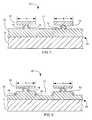
Thesecond step 30, shown inFIG. 3 , is to anisotropically etch the wire grid polarizer to form two parallel,elongated rods 32 substantially located at corners24a-bwhere the wires contacted thesubstrate 11. The anisotropic etch can preferentially remove wires at acentral portion 25 of thewire 12, thus exposing thesubstrate 34 in the location of theformer center 25 of thewire 12 while leaving wire material at corners24a-b. Thecentral portion 25 is preferentially removed because the protective layer21-22 can be more resistant to the anisotropic etch than thewire 12 itself and thus after etching through theprotective layer 22 on top of the wire, the anisotropic etch proceeds rapidly through thecentral portion 25 of the wire down to thesubstrate 34 while theside portions 26 of the wire etch more slowly due to the etch resistantprotective layer 21. Thus, the original wire is essentially cut in half, forming tworods 32 in place of theoriginal wire 12. Note, an alternative added step prior to the anisotropic etch is to ion mill the top of thewires 12, thus partially or totally removing theprotective layer 22 prior to the anisotropic etch.
The tworods 32 can each be polarizing elements. Thus the wire grid polarizer can now have twice as many polarizing elements as before thisstep 30. For example, inFIG. 3 ,rod group 32awas formed of oneoriginal wire 12aandrod group 32bwas formed of anotheroriginal wire 12b. There can be a pitch P1 within a wire group and a pitch P2 between groups. These two pitches can be the same or can be different, depending on the original wire width w, original wire pitch P, wire material, type of protective layer21-22, and nature of etch.
Wire grid polarizers, without thefine pitch method 30 described above, have been made by standard lithography and etching methods with pitches of around 100-150 nanometers and wire widths of around 50-75 nanometers. Thus, this method essentially cuts the pitch in half, allowing formation of wire grid polarizers by this method with pitches of around 50-75 nanometers and wire widths of around 25-38 nanometers, even with present lithography and etching methods.
An addedstep 40, shown inFIG. 4 , that may be useful for some wire grid polarizer applications is to apply asegmented coating 42 on top of therods 32. Thesegmented coating 42 can be aligned with therods 32 and can continue partially down bothsides 43 of therods 32 without coating thesubstrate 44 exposed between therods 32. This segmented coating may be applied by methods described in U.S. patent application Ser. Nos. 12/507,570, filed on Jul. 22, 2009 and 13/075,470, filed on Mar. 30, 2011, incorporated herein by reference.
Wire Grid Polarizer by Etch Redeposition
As illustrated inFIG. 5 , apolarizer 50 includes asubstrate 11 which can be transmissive of the wavelength of electromagnetic radiation used. For example, germanium could be used in the infrared, silicon in the visible, and quartz in the ultraviolet. A repeated pattern of groups53 of parallelelongated wires 52 may be disposed on the substrate. Thewires 52 may comprise a material that can polarize the incident electromagnetic radiation. Each group53 ofelongated wires 52 can comprise at least three wires. Each group can include one or moreinterior wires 52c, such as one or more center wires, and outermost wires52o. The interior orcenter wires 52ccan be taller than the outermost wires52o, such as by more than 3 nm in one aspect, more than about 10 nm in another aspect, more than about 20 nm in another aspect, or more than about 50 nm in another aspect. The distance between the outermost wires52o, and thus the width d3 of each group53, can be less than 1 micrometer in one aspect, less than about 150 nm in another aspect, less than about 100 nm in another aspect or less than about 50 nm in another aspect. Thewires 52 can be a byproduct of an etch reaction, which material can be beneficial for some applications. The width d3 of each group53 can be a resist width as will be described below, thus multiple wires can be formed for a single resist width, thus allowing manufacture of a wire grid polarizer having very fine pitch.
Shown inFIG. 5 are two groups ofwires wires 52cat the center of each group53 can be approximately equal in height and both can be taller than the outermost wires52oof each group, such that h1<h2.Center wires 52cof a group of wires53 can be higher h2 than the height h1 of outer wires52oin a group becausecenter wires 52ccan be formed first during initial isotropic etch(es). Having wires of different heights h can allow tuning the polarizer for different wavelengths and allow for smoothing out the s-polarization orientation of transmitted electromagnetic radiation over the spectrum of incident of electromagnetic radiation, or the Ts curve. Having some of the wires higher can increase polarizer contrast while having other wires shorter can improve transmission.
In one embodiment,center wires 52cand outer wires52ocan be made the same height h, such that h2=h1, by methods such as chemical mechanical polishing, fill and polish, spin on back etch, or other known planarization methods. Thus, a difference in height between thecenter wires 52cand the outer wires52ocan be between about 0 nm to about 150 nm, more than about 3 nm in one aspect, more than about 20 nm in another aspect, or more than about 50 nm in another aspect, depending on the strength, duration, and type of etch, the height of wires created, and whether the wires were planarized.
Shown inFIG. 5 is wire width w. Wire width may be determined by the type of etch during creation of thatwire 52, thin film material and/or substrate material, and whether adjacent wires combine to form a single wire as described below in the description ofFIG. 11 . A maximum wire width of allwires 52 in thepolarizer 10 can be less than about 150 nm in one aspect, less than about 50 nm in another aspect, less than about 20 nm in another aspect, or less than about 10 nm in another aspect. A wire width w of one wire may differ from a wire width w of an adjacent wire by more than 5 nm in one aspect, more than 10 nm in another aspect, more than 20 nm in another aspect, or more than 50 nm in another aspect.
The distance between wires d in the groups of wires53 can vary depending on the width of the resist and the nature and length of the etches. For example, a more lateral or stronger initial isotropic etch can result in a smaller distance d2, shown inFIG. 5 , between thecenter wires 52cin a group53. A distance d1 between acenter wire 52cand an outer wire52odepends on the resist width R, as shown inFIG. 6 , the distance d2 between thecenter wires 52c, and the wire width w. Thus, by adjusting the parameters above, the distance d2 between thecenter wires 52ccan be different from the distance d1 between an outermost wire and an adjacent center wire by more than about 3 nm in one aspect, more than about 10 nm in another aspect, or more than about 20 nm in another aspect. In other words, the absolute value of d2 minus d1 can be more than about 3 nm in one aspect, more than about 10 nm in another aspect, or more than about 20 nm in another aspect. A minimum distance d between adjacent wires can be less than about 150 nm in one aspect, less than about 50 nm in another aspect, or less than about 20 nm in another aspect.
As shown inFIG. 5 , pitch P is a distance between an edge of one wire and a corresponding edge of an adjacent wire. A minimum pitch of adjacent wires can be less than about 300 nm in one aspect, less than about 100 nm in another aspect, less than about 50 nm in another aspect, less than about 30 nm in another aspect, or less than about 20 nm in another aspect. The pitch of the wires can thus be much smaller than, even approximately one fourth the pitch of, the pitch of the resist.
A distance d4 between adjacent groups53 can be determined a distance d5 (seeFIG. 6 ) between adjacent resist61 and the width w of outermost wires52oin a group. This distance d4 may be modified for tuning of the polarizer for desired wavelengths.
As shown inFIG. 6 , a polarizer of the present invention can be made by disposing a resist61 on abase 63. The base63 can comprise a single material or can be layers of multiple materials. For example, in one embodiment the base63 can comprise athin film layer 62 disposed on asubstrate 11. Thethin film 62 may be applied on thesubstrate 11 by methods such as chemical vapor deposition or physical vapor deposition. The thin film may be a single layer of one material or may be multiple layers of different materials. Thesubstrate 11 can be a rigid material such as quartz, silicon, or germanium. Thesubstrate 11 can also be a flexible material such as a polymer.
The resist61 may be patterned, providing resist widths R. The resist widths R can be less than about 1 micrometer in one aspect, less than about 100 nanometers in another aspect, less than about 75 nanometers in another aspect, or less than about 55 nanometers in another aspect. The resist width R can be the approximate distance d3 betweenoutermost wires 52cin a group.
As shown inFIG. 7 , an isotropic etch may then be performed, etching both vertically71 into the base63 laterally outside the resist and horizontally72 under the resist leaving astem 73, having vertical sidewalls, under the resist61. The aforementioned isotropic etch, or a subsequent isotropic etch can be optimized for etch redeposition by etch chemistry, thus allowing etch redeposition along vertical sidewalls of thestem 73 creatingetch redeposition wires 74. Theetch redeposition wires 74 can be polarizing wires and thus polarizing wires may be formed as a byproduct of an etch reaction.
As shown inFIG. 8 , an anisotropic etch can then be performed, etching vertically71 into thebase 63 outside the resist leaving abottom step 83, having vertical sidewalls, in thebase 63. The aforementioned anisotropic etch, or a subsequent anisotropic etch can be optimized for etch redeposition, thus allowing etch redeposition to occur along the vertical sidewalls of the bottom step and creating additionaletch redeposition wires 84.
Depending on the material of the base and/or thin film and the type of etch, etchredeposition wires 74 &84 can be comprised of a material such as metal oxide, metal alloy, metal halide, metal carbide, and organometal, or combinations thereof. Multiple isotropic etches before an anisotropic etch, with each subsequent isotropic etch being less isotropic in nature than the previous isotropic etch, can result in more than four wires for every resist width R.
As shown inFIGS. 9-10 , the anisotropic etch may continue, remove the resist, etch the base63 between91 the wires and substantially or totally remove the base63 between101etch redeposition wires 74 &84, and leave at least four separateetch redeposition wires
As shown inFIG. 11 , a group of wires can have three wires comprising acenter wire 112cand outer wires112o. The method of making this structure is similar to that described above except that thestem 73 can be smaller than if two center wires are desired. Thus, as etch redeposition starts on both sides of thestem 73, thestem 73 can be substantially or completely etched away leaving asingle center wire 112crather than twocenter wires 52cas shown inFIG. 5 . Thesingle center wire 112ccan be higher than outer wires112oor can be approximately the same height as outer wires as was described above for the structure with at least four wires. If the center wires converge, and multiple isotropic etches are performed prior to the anisotropic etch, then there may be a structure with an odd number of at least five wires in each group.
A structure with a single wire at the center of each group may be beneficial if it is desired to have a large difference between widths of wires in a group. As shown inFIG. 11 , a width w1 of the center wire72c, can be substantially wider than a width w2 of an outer wire72oof a group.
Multi-Step Wire Grid Polarizer
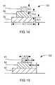
As illustrated inFIG. 12 , a multi-step, nanometer sized device orpolarizer 120 includes a base121 with a plurality of parallelmulti-step ribs 122 disposed on thebase 121. The term polarizer will hereafter be used, instead of nanometer sized device, because polarizer is the most typical application, but thedevice 120 can be used for other applications. Eachrib 122 comprises multiple adjacent steps S of different heights h or disposed at different elevational heights. Eachrib 122 includes an upper step S1 with a top horizontal surface H1 flanked by upper vertical surfaces V1. It will be appreciated that the terms horizontal and vertical are relative to the orientation of the device as shown in the figures, and that the device can be oriented at various different angles. Each rib also includes at least one lower step or pair of steps (with one step on either side of the upper step) having two horizontal surfaces, each flanked by a vertical surface for that step and by a vertical surface of an adjacent step. Thus, steps or pairs of steps are formed on both sides of the upper step, forming a cross-sectional stepped pyramid shape.
For example, the device inFIG. 12 shows two lower steps S2 and S3. Intermediate step S2 includes intermediate horizontal surfaces H2 and intermediate vertical surfaces V2. Intermediate horizontal surfaces H2 flank the upper vertical surfaces V1 and intermediate vertical surfaces V2. Lower step S3 includes lower horizontal surfaces H3 and lower vertical surfaces V3. Lower horizontal surfaces H3 flank the intermediate vertical surfaces V2 and lower vertical surfaces V3.
The ribs can have more or less than two lower steps. Each step S includes a coating C along the vertical surfaces V of the step S. The coating C along the vertical surface V of any step S can be separate from the coating C along a vertical surface V of an adjacent (upper or lower) step S, such as by the intervening horizontal surface H. Thus, a width or length HL of a horizontal surface H thereof can be greater than a thickness of the coating C. For example, inFIG. 12 there is no continuity of coating between the steps such that the coating C1 of the upper step S1 is physically separate from the coating C2 of the intermediate step S2 and the coating C2 of the intermediate step S2 is physically separate from the coating C3 of the lower step S3. The coatings C can form pairs of coatings or coating pairs at different elevational heights, such as an upper coating pair C1, and at least one lower coating pair, such as intermediate coating pair C2 and lower coating pair C3. If the device is used as a polarizer, and a coating C is selected that will polarize the wavelength of interest, then the coating C may be considered to be a polarizing coating rib. Thus, the coating may be a conductive coating and can define wires.
The upper and lower steps can be at different elevational heights h defining a cross-sectional stepped pyramid shape. For example, inFIG. 12 , the elevational heights are not equal such that h1≠h2≠h3 and h1>h2>h3. The height of the steps can be determined by the depth of etching. Some embodiments of the present invention can have an elevational height of the upper step that is less than about 200 nm in one aspect or less than about 100 nm in another aspect. The rib, or steps or pairs of steps, can increase in width from the upper step so that the rib has a cross-sectional stepped pyramid shape.
The coating material C can be or can include a metal such as aluminum, copper, germanium, titanium oxide, tantalum, or a metal alloy. The coating material C can also be a dielectric such as silicon, silicon carbide, Fe2Si, or hafnium. If the device is used as a wire grid polarizer, the coating material C can be a material that optimally polarizes the wavelengths of interest. For example, germanium could be used for infrared light, aluminum for visible light, or titanium oxide for ultraviolet light.
As shown inFIG. 13 , thebase 121 ofpolarizer 120bcan comprise asubstrate 131 and at least onethin film layer 132. Thesubstrate 131 can comprise a material that is transparent to the incoming electromagnetic radiation. Thesubstrate 131 can be a rigid material such as quartz, silicon, or germanium. Thesubstrate 131 can also be a flexible material such as a casting film, polymer, or embossing substrate. Thefilm layer 132 can be an anti-reflective coating, a transmissive film, an absorbing film, or other film with the desired optical properties.
Theribs 122 in the device can comprise the same material as thebase 121 and can be are integrally formed in thebase 121, such as by etching, as shown inFIG. 12 . Alternatively, the ribs can be physically separate from the base, as shown inFIG. 13 . In addition, theribs 122 can comprise a different material from thebase 121. Theribs 122 can comprise at least two layers of different materials. Each step can comprise multiple layers of different materials. A step S can be made of a different material than another step S. Each step S can be made of different materials. Multiple layers may be used for desired polarization characteristics, such as optimizing Tp, Ts, contrast, or absorption.
The coatings C can have very small widths CW. The width of the coating can be less than about 30 nm in one aspect, less than about 10 nm in another aspect, or less than about 5 nm in another aspect. The coating width can be selected or tuned based on the anticipated wavelength of the electromagnetic radiation and/or desired performance characteristics. Very narrow coating widths can be sustained by the structural support of the rib or steps thereof.
As shown inFIG. 14 , arib 122 of a polarizer can have vertical heights or length of vertical surfaces VL. In one embodiment, a vertical length VL of one step S can be the same as a vertical length VL of another step S, or all other steps S. In another embodiment, a vertical length VL of one step S can be different from a vertical length VL of another step S, or all other steps S. For example, the steps S can have substantially equal vertical lengths, VL1=VL2=VL3. Alternatively, the steps S can have unequal vertical lengths, VL1≠VL2≠VL3. A polarizer with different vertical lengths of vertical surfaces on different steps can have coating of different heights. Each coating height can be tuned for optimal polarization of a wavelength of interest. A difference of vertical length VL of one step compared to any other step can be more than 10 nanometers in one aspect, 10 to 50 nanometers in another aspect, 50 to 100 nanometers in another aspect, or 100-200 nanometers in another aspect. For example VL1-VL2 and VL1-VL3 can be between 50 to 100 nanometers.
The vertical lengths VL of steps S can be nanometer sized. For example the vertical length VL of any of the vertical surfaces can be less than about 100 nm in one aspect, less than about 50 nm in another aspect, or less than about 20 nm in another aspect. The vertical lengths VL can be selected or tuned based on the anticipated wavelength of the electromagnetic radiation and/or desired performance characteristics.
The horizontal length of the widest step or outside width of the lowermost pair of steps, shown as SL1 inFIG. 14 , can be approximately the width (see RW inFIG. 18 ) of the resist feature used to form the step S. Resist features for presently manufactured wire grid polarizers for visible light typically have a width of about 50-100 nm. Accordingly, the outside width SL1, and thus a distance between the outermost coatings on a step, can be less than about 100 nm in one aspect, less than about 75 nm in another aspect, less than about 50 nm in another aspect, or 50-100 nm in another aspect. Again, the width SL1 of the outermost, lowermost pair of steps can be selected or tuned based on the anticipated wavelength of the light and/or desired performance characteristics.
As shown inFIG. 15 , arib 122 can have a depth or horizontal length HL of the horizontal surface of a step that is the approximate pitch between adjacent coatings. The horizontal length HL of a step can be less than about 50 nm in one aspect, less than about 25 nm in another aspect, or less than about 10 nm in another aspect. A maximum distance between adjacent coatings can be less than about 50 nm and a minimum distance between adjacent coatings can be less than about 20 nm. The horizontal length HL of all steps can be approximately the same. (HL1=HL2=HL3). The horizontal length HL of a step may be different from the horizontal length HL of other steps (HL1≠HL2 or HL1≠HL2 or HL1≠HL2≠HL3). The horizontal length of steps may be adjusted in order to optimize polarization of the desired wavelengths.
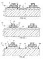
The embodiments shown inFIGS. 12 & 13 have a step with the longest step length SL as the lowest step or the step closest to the base. As shown inFIG. 16 , a step, of adevice 120corrib 122c, with the longest step length SL3 can be an intermediate step and a step with a shorter step length SL5 can be the lowest step or the step closest to the base.
Also as shown inFIG. 16 , the steps need not form a pyramid shape but rather the steps in the ribs can become wider or narrower moving from the outermost rib towards the base. The upper step can have the shortest step length or another step can have the shortest step length depending on the isotropic nature of each successive etch as described below. This embodiment may be useful for optimizing polarization of certain selected wavelengths.
As shown inFIG. 17 ,wires 173 ofpolarizer 120dmay be disposed on thebase 121, physically separate from themulti-step ribs 122, substantially parallel with themulti-step ribs 122, and located between adjacentmulti-step ribs 122. Coating C can be a dielectric or metal.Wires 173 can be dielectric or metal.Wires 173 can be a different material than coating C. This allows use of polarizing ribs made of different materials. This can be beneficial for tuning the polarizer to multiple different wavelengths of electromagnetic radiation.
Multi-Step Wire Grid Polarizer—How to Make
A base121 can be prepared with either a single material or with layers of different materials. For example,FIG. 13 shows a base121 comprised of asubstrate 131 and athin film 132. Theribs 122 can be the same material as thebase 121, the same material as thesubstrate 131, the same material as thethin film 132, or a different material than the base, substrate, or thin film. As shown inFIGS. 14 and 15 , theribs 122 can be made of layers. Each layer can be the same material as another layer or can be a different material than another layer or layers. Each step S can be a different material than another step S. A single step S can be made of multiple layers of different materials. Layers of different materials can be formed by applying thin films on a substrate through processes such as chemical vapor deposition (CVD) or physical vapor deposition (PVD).
Theribs 122 can be formed by depositing a material on a base121 or by ion milling into thebase 121. Theribs 122 may also be formed in thebase 121 by etching the base as shown inFIGS. 18-21 . For purposes of the description ofFIGS. 18-21 , the term “base” can include a single material or layers of multiple materials. A resist181 may be applied to thebase 121 and the resist181 may be patterned to create resist widths RW, as shown inFIG. 18 . As shown inFIG. 19 , an isotropic etch can etch both vertically into the base laterally outside the resist192 and horizontally under the resist191. At least one additional isotropic etch, that is more or less isotropic than the previous isotropic etch, may be performed. For example, as shown inFIG. 20 , a second isotropic etch, which is less isotropic in nature than that shown inFIG. 19 , is performed to etch both vertically into the base laterally outside the resist192 and horizontally under the resist191. Each successive etch that that is either more or less isotropic than the previous etch can result in formation of an additional step. As shown inFIG. 21 , an anisotropic etch may be used to etch into the base laterally outside the resist192 and to remove the resist181. The anisotropic etch can be used to create a step having a step length SL that is about the same as the width of the resist RW.
Step horizontal length HL and step vertical length VL can be controlled during step formation by the nature of the isotropic etches performed. A more isotropic etch can create a longer horizontal length HL for a step. A longer etch time can create a longer vertical step length VL.
After the ribs have been created, the resist can be removed and the surface of the structure may be coated with a coating C, as shown inFIG. 22 . The coating may be conformal, non-conformal, segmented, atomic layer deposition, spin on, or etch redeposition. The coating may then be anisotropically etched to substantially remove the coating from horizontal surfaces while leaving a majority of the coating on vertical surfaces. The coating is removed from horizontal surfaces in the anisotropic etch, while leaving a substantial portion of the coating on the vertical surfaces, because a thickness of thecoating 222 on the horizontal surfaces, in a direction perpendicular to the main plane of the base, as shown by dashed line P, is less than a thickness of thecoating 221 on the vertical surfaces, along this same direction P.
To form a structure as shown inFIG. 16 , following the previously described anisotropic etch step to etch primarily in the area outside the width of the resist192, additionalisotropic etches horizontal surfaces 163 that are between themulti-step rib 122cand the base121 by use of a high bias etch.
A coating C can then be applied as described above. As shown inFIG. 24 , the coating C thickness along a vertical surface of anupper step 241 can be much longer than the coating thickness along a vertical surface of thelowest step 242. The coating thickness along thelowest step 242 is not very much thicker than the thickness along a horizontal portion of thestructure 243.
An anisotropic etch may be performed to remove coating from horizontal surfaces and from the lowest stepvertical surface 252. Due to the relatively smaller thickness ofcoating 242 along the vertical surface of the lowest step, as shown inFIG. 25 , the coating can be substantially removed from the vertical surface of thisstep 252 during this anisotropic etch of the coating while leaving the coating on the vertical surfaces of theupper steps 251.
An anisotropic etch, which is optimized for etch redeposition, may then be performed. The coating C, the second layer orrib 122 material, and the etch must be selected such that primarily thefirst layer 171 will be etched with minimal etching of the coating C or theribs 122. The etch can be optimized for etch redeposition by etch chemistry. The anisotropic etch will etch into thefirst layer 171 and can result in formation ofetch redeposition wires 173. The anisotropic etch can continue and thus remove thefirst layer 171 between175 theetch redeposition wires 173 and themulti-step ribs 122, as shown inFIG. 17 . The anisotropic etch may continue to etch into the base between theribs 174. The base121 may thus be etched between174 thewires 173 and themulti-step ribs 122 to a depth of at least 1 nm.
It is to be understood that the above-referenced arrangements are only illustrative of the application for the principles of the present invention. Numerous modifications and alternative arrangements can be devised without departing from the spirit and scope of the present invention. While the present invention has been shown in the drawings and fully described above with particularity and detail in connection with what is presently deemed to be the most practical and preferred embodiment(s) of the invention, it will be apparent to those of ordinary skill in the art that numerous modifications can be made without departing from the principles and concepts of the invention as set forth herein.
Claims (19)
1. A polarizer, comprising:
a. a substrate;
b. a repeated pattern of groups of parallel, elongated, polarizing wires disposed over the substrate;
c. each group of wires comprising at least three wires;
d. a wire at an interior of each group is taller by more than 10 nanometers (nm) than outermost wires of each group; and
e. a distance between the outermost wires in each group is less than 1 micrometer.
2. The polarizer ofclaim 1 , wherein a wire at an interior of each group is taller by more than 20 nm than outermost wires of each group.
3. The polarizer ofclaim 1 , wherein:
a. the wire at an interior of each group includes two center wires; and
b. each group comprises at least four wires.
4. The polarizer ofclaim 3 , wherein the two center wires are approximately equal in height.
5. The polarizer ofclaim 3 , wherein a distance between the two center wires is different than a distance between an outermost wire and an adjacent center wire by more than about 10 nm.
6. The polarizer ofclaim 1 , wherein a minimum distance between adjacent wires is less than 50 nm.
7. The polarizer ofclaim 1 , wherein the distance between the outermost wires in each group is less than 150 nm.
8. The polarizer ofclaim 1 , wherein a width of the wires is less than 20 nm.
9. The polarizer ofclaim 1 , wherein a minimum pitch of adjacent wires is less than 50 nm.
10. The polarizer ofclaim 1 , wherein the wires are etch redeposition wires and comprise a material that is a byproduct of an etch reaction.
11. The polarizer ofclaim 1 , wherein a wire width of one wire differs from a wire width of an adjacent wire by more than 20 nm.
12. A polarizer, comprising:
a. a substrate;
b. a repeated pattern of groups of parallel, elongated, polarizing wires disposed over the substrate;
c. the polarizing wires are etch redeposition wires, comprising a material that is a byproduct of an etch reaction;
d. the wire at an interior of each group includes two center wires that are approximately equal in height;
e. each group comprises at least four wires;
f. the two center wires are taller by more than 10 nanometers than outermost wires of each group.
13. The polarizer ofclaim 12 , wherein a minimum distance between adjacent wires is less than 50 nanometers.
14. The polarizer ofclaim 12 , wherein a distance between the two center wires is different than a distance between an outermost wire and an adjacent center wire by more than about 10 nanometers.
15. The polarizer ofclaim 12 , wherein a width of the wires is less than 20 nanometers.
16. A method for making a polarizer, the method comprising:
a. applying a resist over a base;
b. patterning the resist and creating resist widths;
c. performing an isotropic etch of the base and etching both vertically into the base laterally outside the resist and horizontally under the resist leaving a stem, having vertical sidewalls, under the resist;
d. allowing etch redeposition along the vertical sidewalls of the stem creating etch redeposition polarizing wires as a byproduct of an etch reaction;
e. performing an anisotropic etch and etching vertically into the base outside the resist leaving a bottom step, having vertical sidewalls, in the base;
f. allowing etch redeposition along the vertical sidewalls of the bottom step and creating etch redeposition polarizing wires as a byproduct of an etch reaction.
17. The method ofclaim 16 , further comprising etching to remove the resist, substantially removing the base between the wires, and leaving at least three separate polarizing etch redeposition wires for every original resist width.
18. The method ofclaim 16 , wherein the resist widths are less than 100 nm.
19. The method ofclaim 16 , wherein the wires comprise of a material selected from the group consisting of metal oxide, metal alloy, metal halide, metal carbide, organometallic, and combinations thereof.
Priority Applications (1)
| Application Number | Priority Date | Filing Date | Title |
|---|---|---|---|
| US14/035,478US9523805B2 (en) | 2010-09-21 | 2013-09-24 | Fine pitch wire grid polarizer |
Applications Claiming Priority (4)
| Application Number | Priority Date | Filing Date | Title |
|---|---|---|---|
| US38480210P | 2010-09-21 | 2010-09-21 | |
| US38479610P | 2010-09-21 | 2010-09-21 | |
| US13/224,719US8611007B2 (en) | 2010-09-21 | 2011-09-02 | Fine pitch wire grid polarizer |
| US14/035,478US9523805B2 (en) | 2010-09-21 | 2013-09-24 | Fine pitch wire grid polarizer |
Related Parent Applications (1)
| Application Number | Title | Priority Date | Filing Date |
|---|---|---|---|
| US13/224,719ContinuationUS8611007B2 (en) | 2010-09-21 | 2011-09-02 | Fine pitch wire grid polarizer |
Publications (2)
| Publication Number | Publication Date |
|---|---|
| US20140016197A1 US20140016197A1 (en) | 2014-01-16 |
| US9523805B2true US9523805B2 (en) | 2016-12-20 |
Family
ID=46926937
Family Applications (2)
| Application Number | Title | Priority Date | Filing Date |
|---|---|---|---|
| US13/224,719Expired - Fee RelatedUS8611007B2 (en) | 2010-09-21 | 2011-09-02 | Fine pitch wire grid polarizer |
| US14/035,478Expired - Fee RelatedUS9523805B2 (en) | 2010-09-21 | 2013-09-24 | Fine pitch wire grid polarizer |
Family Applications Before (1)
| Application Number | Title | Priority Date | Filing Date |
|---|---|---|---|
| US13/224,719Expired - Fee RelatedUS8611007B2 (en) | 2010-09-21 | 2011-09-02 | Fine pitch wire grid polarizer |
Country Status (5)
| Country | Link |
|---|---|
| US (2) | US8611007B2 (en) |
| JP (1) | JP5686227B2 (en) |
| KR (1) | KR101496689B1 (en) |
| CN (1) | CN103907173B (en) |
| WO (1) | WO2013032570A1 (en) |
Cited By (2)
| Publication number | Priority date | Publication date | Assignee | Title |
|---|---|---|---|---|
| US20220019015A1 (en)* | 2020-07-14 | 2022-01-20 | Facebook Technologies, Llc | Inorganic matrix nanoimprint lithographs and methods of making thereof |
| US11644084B2 (en) | 2018-10-04 | 2023-05-09 | Kinematics, Llc | Force sensing slew drive |
Families Citing this family (44)
| Publication number | Priority date | Publication date | Assignee | Title |
|---|---|---|---|---|
| US8755113B2 (en) | 2006-08-31 | 2014-06-17 | Moxtek, Inc. | Durable, inorganic, absorptive, ultra-violet, grid polarizer |
| US8611007B2 (en) | 2010-09-21 | 2013-12-17 | Moxtek, Inc. | Fine pitch wire grid polarizer |
| US8913321B2 (en) | 2010-09-21 | 2014-12-16 | Moxtek, Inc. | Fine pitch grid polarizer |
| US20150077851A1 (en) | 2010-12-30 | 2015-03-19 | Moxtek, Inc. | Multi-layer absorptive wire grid polarizer |
| US8913320B2 (en)* | 2011-05-17 | 2014-12-16 | Moxtek, Inc. | Wire grid polarizer with bordered sections |
| US8873144B2 (en)* | 2011-05-17 | 2014-10-28 | Moxtek, Inc. | Wire grid polarizer with multiple functionality sections |
| US8922890B2 (en) | 2012-03-21 | 2014-12-30 | Moxtek, Inc. | Polarizer edge rib modification |
| WO2013158975A1 (en)* | 2012-04-20 | 2013-10-24 | Washington University | Sensor for spectral-polarization imaging |
| JP6433895B2 (en)* | 2012-08-10 | 2018-12-05 | テマセク ポリテクニックTemasek Polytechnic | Optical diffraction grating |
| JP5867439B2 (en)* | 2013-03-29 | 2016-02-24 | ウシオ電機株式会社 | Grid polarizing element and optical alignment apparatus |
| KR102082783B1 (en)* | 2013-07-23 | 2020-03-02 | 삼성디스플레이 주식회사 | Wire grid polarizer and organic light emitting display apparatus comprising the same |
| US10371898B2 (en)* | 2013-09-05 | 2019-08-06 | Southern Methodist University | Enhanced coupling strength grating having a cover layer |
| WO2015060939A1 (en)* | 2013-10-24 | 2015-04-30 | Moxtek, Inc. | Wire grid polarizer with side region |
| US9354374B2 (en) | 2013-10-24 | 2016-05-31 | Moxtek, Inc. | Polarizer with wire pair over rib |
| JP5862699B2 (en)* | 2014-03-11 | 2016-02-16 | ウシオ電機株式会社 | Grid polarizing element and optical alignment apparatus |
| JP2015219319A (en)* | 2014-05-15 | 2015-12-07 | デクセリアルズ株式会社 | Inorganic polarizer and method for manufacturing the same |
| IL232866B (en)* | 2014-05-29 | 2020-08-31 | Elta Systems Ltd | Polarization rotator |
| US9632224B2 (en)* | 2014-06-25 | 2017-04-25 | Moxtek, Inc. | Broadband, selectively-absorptive wire grid polarizer |
| US10088616B2 (en) | 2014-09-19 | 2018-10-02 | Toyota Motor Engineering & Manufacturing North America, Inc. | Panel with reduced glare |
| EP3023820B1 (en)* | 2014-11-18 | 2023-12-27 | Samsung Display Co., Ltd. | Wire grid polarizing plate, display device including the same, and method of fabricating said display device |
| CN104459863A (en)* | 2014-12-04 | 2015-03-25 | 京东方科技集团股份有限公司 | Wire gating polaroid, manufacturing method of wire gating polaroid, display panel and display device |
| KR20160070883A (en)* | 2014-12-10 | 2016-06-21 | 삼성디스플레이 주식회사 | Wire grid polarizer and method for manufacturing the same |
| US10054717B2 (en)* | 2015-04-03 | 2018-08-21 | Moxtek, Inc. | Oxidation and moisture barrier layers for wire grid polarizer |
| US10534120B2 (en) | 2015-04-03 | 2020-01-14 | Moxtek, Inc. | Wire grid polarizer with protected wires |
| US9995864B2 (en)* | 2015-04-03 | 2018-06-12 | Moxtek, Inc. | Wire grid polarizer with silane protective coating |
| KR20160143443A (en)* | 2015-06-05 | 2016-12-14 | 코오롱인더스트리 주식회사 | Wire Grid Polarizer And Liquid Crystal Display Device Including The Same |
| US20170059758A1 (en) | 2015-08-24 | 2017-03-02 | Moxtek, Inc. | Small-Pitch Wire Grid Polarizer |
| JP6884501B2 (en)* | 2015-08-25 | 2021-06-09 | 大日本印刷株式会社 | Polarizer |
| KR102546954B1 (en)* | 2015-09-03 | 2023-06-23 | 삼성디스플레이 주식회사 | Wire grid polarizer plate and method for manufacturing the smae |
| JP6225967B2 (en)* | 2015-09-10 | 2017-11-08 | ウシオ電機株式会社 | Grid polarizing element and optical alignment apparatus |
| KR20190061065A (en)* | 2016-10-12 | 2019-06-04 | 어플라이드 머티어리얼스, 인코포레이티드 | METHOD FOR MANUFACTURING POLARIZER DEVICE, POLARIZER DEVICE, AND DISPLAY SYSTEM WITH POLARIZER DEVICE |
| JP6401837B1 (en)* | 2017-08-10 | 2018-10-10 | デクセリアルズ株式会社 | Polarizing plate and optical device |
| CN109975910B (en) | 2017-12-28 | 2022-02-18 | 迪睿合株式会社 | Polarizing plate, method for manufacturing the same, and optical device |
| US11079528B2 (en)* | 2018-04-12 | 2021-08-03 | Moxtek, Inc. | Polarizer nanoimprint lithography |
| JP7279304B2 (en)* | 2018-06-12 | 2023-05-23 | ウシオ電機株式会社 | Vacuum UV light polarizer |
| KR102509317B1 (en)* | 2018-06-12 | 2023-03-14 | 우시오덴키 가부시키가이샤 | Vacuum ultraviolet light polarizing device, vacuum ultraviolet light polarizing device, vacuum ultraviolet light polarization method and alignment method |
| JP7200510B2 (en)* | 2018-06-12 | 2023-01-10 | ウシオ電機株式会社 | Orientation method and photo-alignment device |
| JP6577641B2 (en)* | 2018-08-20 | 2019-09-18 | デクセリアルズ株式会社 | Polarizing plate, method for producing the same, and optical instrument |
| KR102845551B1 (en) | 2019-11-04 | 2025-08-14 | 삼성전자주식회사 | Image sensor |
| CN111090958B (en)* | 2019-12-30 | 2021-11-30 | 西北工业大学 | Electromagnetic wave time domain efficient numerical mixing method based on sub-grid technology |
| CN111665588B (en)* | 2020-05-06 | 2022-02-11 | 山东科技大学 | Bifunctional polarizer based on vanadium dioxide and Dirac semi-metal composite super-surface |
| CN111679356B (en)* | 2020-06-22 | 2022-07-29 | 京东方科技集团股份有限公司 | Polarizer and preparation method |
| CN114879386B (en)* | 2022-07-11 | 2022-09-23 | 华南师范大学 | Spin-photon transport control device based on pyramid helix array metamaterial |
| KR102823310B1 (en)* | 2024-08-23 | 2025-06-23 | 주식회사 씨엔에스 | Transparent Construction Material Including Sound Insulation Plate with Light Reflection Reduction Function that can Prevent Surface Charge and Prevent Antifouling at The Same Time, and Manufacturing Method of Transparent Construction Material Including Sound Insulation Plate Using It |
Citations (199)
| Publication number | Priority date | Publication date | Assignee | Title |
|---|---|---|---|---|
| US2224214A (en) | 1937-12-28 | 1940-12-10 | Polaroid Corp | Light polarizing body |
| US2287598A (en) | 1937-12-28 | 1942-06-23 | Polaroid Corp | Method of manufacturing lightpolarizing bodies |
| US2748659A (en) | 1951-02-26 | 1956-06-05 | Jenaer Glaswerk Schott & Gen | Light source, searchlight or the like for polarized light |
| US2887566A (en) | 1952-11-14 | 1959-05-19 | Marks Polarized Corp | Glare-eliminating optical system |
| US3046839A (en) | 1959-01-12 | 1962-07-31 | Polaroid Corp | Processes for preparing light polarizing materials |
| US3213753A (en) | 1962-01-24 | 1965-10-26 | Polaroid Corp | Multilayer lenticular light polarizing device |
| US3235630A (en) | 1962-07-17 | 1966-02-15 | Little Inc A | Method of making an optical tool |
| US3291550A (en) | 1965-04-16 | 1966-12-13 | Polaroid Corp | Metallic grid light-polarizing device |
| US3291871A (en) | 1962-11-13 | 1966-12-13 | Little Inc A | Method of forming fine wire grids |
| US3293331A (en) | 1962-11-13 | 1966-12-20 | Little Inc A | Method of forming replicas of contoured substrates |
| US3479168A (en) | 1964-03-09 | 1969-11-18 | Polaroid Corp | Method of making metallic polarizer by drawing fusion |
| US3653741A (en) | 1970-02-16 | 1972-04-04 | Alvin M Marks | Electro-optical dipolar material |
| US3877789A (en) | 1972-11-08 | 1975-04-15 | Marie G R P | Mode transformer for light or millimeter electromagnetic waves |
| US3969545A (en) | 1973-03-01 | 1976-07-13 | Texas Instruments Incorporated | Light polarizing material method and apparatus |
| US4009933A (en) | 1975-05-07 | 1977-03-01 | Rca Corporation | Polarization-selective laser mirror |
| US4049944A (en) | 1973-02-28 | 1977-09-20 | Hughes Aircraft Company | Process for fabricating small geometry semiconductive devices including integrated components |
| US4068260A (en) | 1976-02-20 | 1978-01-10 | Minolta Camera Kabushiki Kaisha | Combination optical low pass filter capable of phase and amplitude modulation |
| US4220705A (en) | 1978-07-26 | 1980-09-02 | Sanritsu Denki Kabushikikaisha | Process for manufacturing a multi-colored display polarizer |
| US4289381A (en) | 1979-07-02 | 1981-09-15 | Hughes Aircraft Company | High selectivity thin film polarizer |
| JPS5842003Y2 (en) | 1982-05-20 | 1983-09-22 | 財団法人石炭技術研究所 | Device for adjusting the descending characteristics of filtration material in continuous filtration equipment |
| US4456515A (en) | 1978-04-25 | 1984-06-26 | Siemens Aktiengesellschaft | Method for making polarizers comprising a multiplicity of parallel electrically conductive strips on a glass carrier |
| US4512638A (en) | 1982-08-31 | 1985-04-23 | Westinghouse Electric Corp. | Wire grid polarizer |
| US4514479A (en) | 1980-07-01 | 1985-04-30 | The United States Of America As Represented By The Secretary Of The Navy | Method of making near infrared polarizers |
| US4515441A (en) | 1982-10-13 | 1985-05-07 | Westinghouse Electric Corp. | Dielectric polarizer for high average and high peak power operation |
| SU1283685A1 (en) | 1985-02-20 | 1987-01-15 | Предприятие П/Я А-1705 | Grating-polarizer |
| US4763972A (en) | 1985-09-27 | 1988-08-16 | Thomson-Csf | Differential absorption polarizer, a method of forming same and device implementing said method |
| DE3707984A1 (en) | 1987-03-12 | 1988-09-22 | Max Planck Gesellschaft | POLARIZING MIRROR FOR OPTICAL RADIATION |
| US4799776A (en) | 1985-07-02 | 1989-01-24 | Semiconductor Energy Laboratory Co., Ltd. | Ferroelectric liquid crystal display device having a single polarizer |
| US4818076A (en) | 1982-12-02 | 1989-04-04 | Merck Patent Gesellschaft Mit Beschrankter Haftung | Color-selective circular polarizer and its use |
| US4915463A (en) | 1988-10-18 | 1990-04-10 | The United States Of America As Represented By The Department Of Energy | Multilayer diffraction grating |
| US4939526A (en) | 1988-12-22 | 1990-07-03 | Hughes Aircraft Company | Antenna system having azimuth rotating directive beam with selectable polarization |
| US4946231A (en) | 1989-05-19 | 1990-08-07 | The United States Of America As Represented By The Secretary Of The Army | Polarizer produced via photographic image of polarizing grid |
| US4966438A (en) | 1988-04-08 | 1990-10-30 | Societe Anonyme Dite: Alcatel Cit | Dielectric layer polarizer |
| US4991937A (en) | 1988-06-29 | 1991-02-12 | Nec Corporation | Birefringence diffraction grating type polarizer |
| US5029988A (en) | 1988-06-29 | 1991-07-09 | Nec Corporation | Birefringence diffraction grating type polarizer |
| JPH0384502U (en) | 1989-12-18 | 1991-08-27 | ||
| US5061050A (en) | 1989-10-18 | 1991-10-29 | Matsushita Electric Industrial Co., Ltd. | Polarizer |
| US5124841A (en) | 1989-10-13 | 1992-06-23 | Mitsubishi Rayon Co., Ltd. | Polarization forming optical device and polarization beam splitter |
| US5157526A (en) | 1990-07-06 | 1992-10-20 | Hitachi, Ltd. | Unabsorbing type polarizer, method for manufacturing the same, polarized light source using the same, and apparatus for liquid crystal display using the same |
| US5177635A (en) | 1989-09-07 | 1993-01-05 | Max-Planck-Gesellschaft Zur Foerderung Der Wissenschaften E.V. | Polarizer for infrared radiation |
| US5225920A (en) | 1990-04-06 | 1993-07-06 | Matsushita Electric Industrial Co., Ltd. | Liquid crystal modulator including a diffuser with plural phase shifting regions |
| US5235449A (en) | 1990-03-02 | 1993-08-10 | Hitachi, Ltd. | Polarizer with patterned diacetylene layer, method for producing the same, and liquid crystal display device including such polarizer |
| US5245471A (en) | 1991-06-14 | 1993-09-14 | Tdk Corporation | Polarizers, polarizer-equipped optical elements, and method of manufacturing the same |
| US5279689A (en) | 1989-06-30 | 1994-01-18 | E. I. Du Pont De Nemours And Company | Method for replicating holographic optical elements |
| EP0300563B1 (en) | 1987-07-20 | 1994-03-02 | Koninklijke Philips Electronics N.V. | Method of manufacturing semiconductor devices in which a surface of a semiconductor structure is selectively treated |
| JPH06174907A (en) | 1992-12-04 | 1994-06-24 | Shimadzu Corp | How to make a metal grid |
| US5383053A (en) | 1992-04-07 | 1995-01-17 | Hughes Aircraft Company | Virtual image display having a high efficiency grid beamsplitter |
| US5422756A (en) | 1992-05-18 | 1995-06-06 | Minnesota Mining And Manufacturing Company | Backlighting system using a retroreflecting polarizer |
| US5510215A (en) | 1995-01-25 | 1996-04-23 | Eastman Kodak Company | Method for patterning multilayer dielectric color filter |
| US5559634A (en) | 1991-06-13 | 1996-09-24 | Minnesota Mining And Manufacturing Company | Retroreflecting polarizer |
| US5619356A (en) | 1993-09-16 | 1997-04-08 | Sharp Kabushiki Kaisha | Reflective liquid crystal display device having a compensator with a retardation value between 0.15 μm and 0.38 μm and a single polarizer |
| JPH1073722A (en) | 1996-08-30 | 1998-03-17 | Sony Corp | Polarizing optical element and its production |
| US5748368A (en) | 1994-12-29 | 1998-05-05 | Sony Corporation | Polarization optical element |
| JPH10153706A (en) | 1996-11-25 | 1998-06-09 | Ricoh Co Ltd | Polarizer and method of manufacturing the same |
| US5838403A (en) | 1996-02-14 | 1998-11-17 | Physical Optics Corporation | Liquid crystal display system with internally reflecting waveguide for backlighting and non-Lambertian diffusing |
| JPH1114814A (en) | 1997-06-19 | 1999-01-22 | Ricoh Co Ltd | Optical element |
| US5890095A (en) | 1997-01-21 | 1999-03-30 | Nichols Research Corporation | System for receiving and enhancing electromagnetic radiation input signals |
| JPH11142650A (en) | 1997-11-13 | 1999-05-28 | Fuji Elelctrochem Co Ltd | Grid polarizer |
| US5912762A (en) | 1996-08-12 | 1999-06-15 | Li; Li | Thin film polarizing device |
| JPH11174396A (en) | 1997-12-16 | 1999-07-02 | Ricoh Co Ltd | Magneto-optical element and magneto-optical device |
| JPH11237507A (en) | 1998-02-23 | 1999-08-31 | Nippon Telegr & Teleph Corp <Ntt> | Polarizer and method for producing the same |
| US5973833A (en) | 1997-08-29 | 1999-10-26 | Lightware, Inc. | High efficiency polarizing converter |
| JPH11306581A (en) | 1998-04-24 | 1999-11-05 | Ricoh Co Ltd | Broadband polarization splitter and optical head using the broadband polarization splitter |
| US5991075A (en) | 1996-11-25 | 1999-11-23 | Ricoh Company, Ltd. | Light polarizer and method of producing the light polarizer |
| US6081376A (en) | 1998-07-16 | 2000-06-27 | Moxtek | Reflective optical polarizer device with controlled light distribution and liquid crystal display incorporating the same |
| US6122103A (en) | 1999-06-22 | 2000-09-19 | Moxtech | Broadband wire grid polarizer for the visible spectrum |
| JP2000284117A (en) | 1999-03-30 | 2000-10-13 | Fuji Elelctrochem Co Ltd | Grid polarizer and method of manufacturing the same |
| JP2001074935A (en) | 1999-09-03 | 2001-03-23 | Sumitomo Chem Co Ltd | Wire grid type polarizing optical element |
| US6208463B1 (en) | 1998-05-14 | 2001-03-27 | Moxtek | Polarizer apparatus for producing a generally polarized beam of light |
| US6234634B1 (en) | 1999-07-28 | 2001-05-22 | Moxtek | Image projection system with a polarizing beam splitter |
| US6243199B1 (en) | 1999-09-07 | 2001-06-05 | Moxtek | Broad band wire grid polarizing beam splitter for use in the visible wavelength region |
| US6251297B1 (en) | 1997-12-22 | 2001-06-26 | Tdk Corporation | Method of manufacturing polarizing plate |
| US6288840B1 (en) | 1999-06-22 | 2001-09-11 | Moxtek | Imbedded wire grid polarizer for the visible spectrum |
| US6291797B1 (en) | 1996-08-13 | 2001-09-18 | Nippon Sheet Glass Co., Ltd. | Laser machining method for glass substrate, diffraction type optical device fabricated by the machining method, and method of manufacturing optical device |
| US20010053023A1 (en) | 2000-05-22 | 2001-12-20 | Jasco Corporation | Wire grid type polarizer and method of manufacturing the same |
| US20020015135A1 (en) | 1999-07-28 | 2002-02-07 | Moxtek | Image projection system with a polarizing beam splitter |
| US6424436B1 (en) | 1999-04-06 | 2002-07-23 | Nec Corporation | Holographic element |
| US6426837B1 (en) | 1999-03-22 | 2002-07-30 | Mems Optical, Inc. | Diffractive selectively polarizing beam splitter and beam routing prisms produced thereby |
| US20020167727A1 (en) | 2001-03-27 | 2002-11-14 | Hansen Douglas P. | Patterned wire grid polarizer and method of use |
| US6496239B2 (en) | 1995-07-11 | 2002-12-17 | Rolic Ag | Optical component for producing linearly polarized light |
| US20020191286A1 (en) | 2001-03-12 | 2002-12-19 | Michael Gale | Polarisers and mass-production method and apparatus for polarisers |
| US6514674B1 (en) | 1999-03-11 | 2003-02-04 | Canon Kabushiki Kaisha | Method of forming an optical element |
| US6532111B2 (en) | 2001-03-05 | 2003-03-11 | Eastman Kodak Company | Wire grid polarizer |
| US20030161029A1 (en) | 2002-02-26 | 2003-08-28 | Kurtz Andrew F. | Micro-mechanical polarization-based modulator |
| WO2003069381A3 (en) | 2002-02-12 | 2003-11-13 | Unaxis Balzers Ltd | Optical component comprising submicron hollow spaces |
| US6654168B1 (en) | 1998-03-31 | 2003-11-25 | Corning Incorporated | Inorganic visible light reflection polarizer |
| US20030224116A1 (en) | 2002-05-30 | 2003-12-04 | Erli Chen | Non-conformal overcoat for nonometer-sized surface structure |
| US20030227678A1 (en) | 2002-05-09 | 2003-12-11 | Moxtek, Inc. | Corrosion resistant wire-grid polarizer and method of fabrication |
| US6665119B1 (en) | 2002-10-15 | 2003-12-16 | Eastman Kodak Company | Wire grid polarizer |
| AU2003267964A1 (en) | 2002-06-18 | 2003-12-31 | Nanoopto Corporation | Optical components exhibiting enhanced functionality and method of making same |
| US20040008416A1 (en) | 2002-07-11 | 2004-01-15 | Canon Kabushiki Kaisha | Polarization separation element and optical apparatus using the same |
| US20040047039A1 (en) | 2002-06-17 | 2004-03-11 | Jian Wang | Wide angle optical device and method for making same |
| US20040047388A1 (en) | 2002-06-17 | 2004-03-11 | Jian Wang | Optical device and method for making same |
| US6714350B2 (en) | 2001-10-15 | 2004-03-30 | Eastman Kodak Company | Double sided wire grid polarizer |
| JP2004157159A (en) | 2002-11-01 | 2004-06-03 | Ricoh Opt Ind Co Ltd | Inorganic polarizing element, polarizing optical element, and liquid crystal element |
| WO2004013684A3 (en) | 2002-08-01 | 2004-07-29 | Nanoopto Corp | Precision phase retardation devices and method of making same |
| US20040174596A1 (en) | 2003-03-05 | 2004-09-09 | Ricoh Optical Industries Co., Ltd. | Polarization optical device and manufacturing method therefor |
| US20040201890A1 (en) | 2002-12-30 | 2004-10-14 | Ian Crosby | Microlens including wire-grid polarizer and methods of manufacture |
| US6809864B2 (en) | 2001-06-29 | 2004-10-26 | Osmic, Inc | Multi-layer structure with variable bandpass for monochromatization and spectroscopy |
| US6811274B2 (en) | 2002-12-04 | 2004-11-02 | General Electric Company | Polarization sensitive optical substrate |
| US6813077B2 (en) | 2001-06-19 | 2004-11-02 | Corning Incorporated | Method for fabricating an integrated optical isolator and a novel wire grid structure |
| JP2004309903A (en) | 2003-04-09 | 2004-11-04 | Ricoh Opt Ind Co Ltd | Inorganic polarizing element, polarizing optical element, and liquid crystal element |
| US6816290B2 (en) | 2000-07-05 | 2004-11-09 | Sony Corporation | Image display element, and image display device |
| US20040258355A1 (en) | 2003-06-17 | 2004-12-23 | Jian Wang | Micro-structure induced birefringent waveguiding devices and methods of making same |
| DE10327963A1 (en) | 2003-06-19 | 2005-01-05 | Carl Zeiss Jena Gmbh | Polarization beam splitter for microscopy or projection system or UV lithography using grid array with parallel grid lines formed by multi-layer system with alternating non-metallic dielectric layers with differing optical characteristics |
| KR20050017871A (en) | 2003-08-11 | 2005-02-23 | 엘지전자 주식회사 | A fabrication method of a wire grid polarizer |
| US20050046941A1 (en) | 2002-11-06 | 2005-03-03 | Sony Corporation | Method for manufacturing divided waveplate filter |
| US20050078374A1 (en) | 2003-10-09 | 2005-04-14 | International Business Machines Corporation | Dispersive element, diffraction grating, color display device, demultiplexer, and diffraction grating manufacture |
| US20050084613A1 (en) | 2003-08-19 | 2005-04-21 | Jian Wang | Sub-micron-scale patterning method and system |
| US20050122587A1 (en) | 1993-12-21 | 2005-06-09 | 3M Innovative Properties Company | Optical polarizer |
| JP2005195824A (en) | 2004-01-07 | 2005-07-21 | Asahi Kasei Chemicals Corp | Wire grid polarizer |
| US6927915B2 (en) | 2002-06-17 | 2005-08-09 | Canon Kabushiki Kaisha | Diffractive optical element, and optical system and optical apparatus provided with the same |
| US20050175100A1 (en) | 2004-02-05 | 2005-08-11 | Masahito Yamane | Data processing device and method of same, and encoding device and decoding device |
| US20050190445A1 (en) | 2004-02-27 | 2005-09-01 | Yoshio Fukuzaki | Wire grid polarizer |
| US20050195485A1 (en) | 2004-03-04 | 2005-09-08 | Hideaki Hirai | Optical device, method of producing the same, optical pickup, and optical information processing device |
| US6943941B2 (en) | 2003-02-27 | 2005-09-13 | Asml Netherlands B.V. | Stationary and dynamic radial transverse electric polarizer for high numerical aperture systems |
| US6972906B2 (en) | 2000-12-27 | 2005-12-06 | Technion Research And Development Foundation Ltd. | Space-variant subwavelength polarization grating and applications thereof |
| US20050275944A1 (en) | 2004-06-11 | 2005-12-15 | Wang Jian J | Optical films and methods of making the same |
| US20050277063A1 (en) | 2004-04-15 | 2005-12-15 | Wang Jian J | Optical films and methods of making the same |
| JP2006047813A (en) | 2004-08-06 | 2006-02-16 | Asahi Kasei Corp | Inorganic material selective pattern forming method and grid-type polarizing element |
| DE102004041222A1 (en) | 2004-08-26 | 2006-03-02 | Carl Zeiss Jena Gmbh | Photonic crystal structure, for a frequency selective reflector or diffractive polarization-dependent band splitter, has grate bars on a substrate of alternating low and high refractive material layers |
| US7009768B2 (en) | 2002-06-04 | 2006-03-07 | Canon Kabushiki Kaisha | Optical component and method of manufacturing same |
| WO2006036546A1 (en) | 2004-09-23 | 2006-04-06 | Eastman Kodak Company | Low fill factor wire grid polarizer |
| US20060072194A1 (en) | 2004-10-06 | 2006-04-06 | Lg Electronics Inc. | Wire grid polarizer and fabrication method thereof |
| US20060087602A1 (en) | 2004-10-27 | 2006-04-27 | Terufusa Kunisada | Polarizer and method for producing it |
| US20060092513A1 (en) | 2004-11-04 | 2006-05-04 | Canon Kabushiki Kaisha | Polarizing beam splitter and display including the same |
| US7046442B2 (en) | 2003-12-05 | 2006-05-16 | Enplas Corporation | Wire grid polarizer |
| US7046441B2 (en) | 2003-12-31 | 2006-05-16 | Industrial Technology Research Institute | High transmittance sub-wavelength structure polarization module |
| JP2006133402A (en) | 2004-11-04 | 2006-05-25 | Canon Inc | Polarization separating element and optical system having the same |
| US20060113279A1 (en) | 2004-11-30 | 2006-06-01 | Little Michael J | Non-photolithographic method for forming a wire grid polarizer for optical and infrared wavelengths |
| US20060127830A1 (en) | 2004-12-15 | 2006-06-15 | Xuegong Deng | Structures for polarization and beam control |
| US7075722B2 (en) | 2000-05-31 | 2006-07-11 | Canon Kabushiki Kaisha | Diffractive optical element and optical system having the same |
| US7085050B2 (en) | 2001-12-13 | 2006-08-01 | Sharp Laboratories Of America, Inc. | Polarized light beam splitter assembly including embedded wire grid polarizer |
| JP2006201540A (en) | 2005-01-21 | 2006-08-03 | Asahi Kasei Corp | Wire grid polarizing plate and manufacturing method thereof |
| US7113335B2 (en) | 2002-12-30 | 2006-09-26 | Sales Tasso R | Grid polarizer with suppressed reflectivity |
| US20060215263A1 (en) | 2004-09-23 | 2006-09-28 | Eastman Kodak Company | Wire grid polarizers with optical features |
| US7116478B2 (en) | 2003-09-01 | 2006-10-03 | Canon Kabushiki Kaisha | Polarization beam splitter and optical system using the same, and image displaying apparatus, using the same |
| US7129183B2 (en) | 2002-03-25 | 2006-10-31 | Sanyo Electric Co., Ltd. | Method of forming grating microstrutures by anodic oxidation |
| US7142363B2 (en) | 2003-03-13 | 2006-11-28 | Asahi Glass Company, Limited | Diffraction element and optical device |
| JP2006330178A (en) | 2005-05-24 | 2006-12-07 | Sony Corp | Optical device and method for manufacturing optical device |
| US7155073B2 (en) | 2004-05-07 | 2006-12-26 | Canon Kabushiki Kaisha | Polarization element and optical device using polarization element |
| US7158302B2 (en) | 2003-10-23 | 2007-01-02 | Industry Technology Research Institute | Wire grid polarizer with double metal layers |
| WO2005101112A3 (en) | 2004-04-15 | 2007-02-08 | Nanoopto Corp | Optical films and methods of making the same |
| JP2007058100A (en) | 2005-08-26 | 2007-03-08 | Ricoh Co Ltd | Optical element, light source unit, optical scanning device, image forming device |
| US7203001B2 (en) | 2003-12-19 | 2007-04-10 | Nanoopto Corporation | Optical retarders and related devices and systems |
| KR100707083B1 (en) | 2005-11-24 | 2007-04-13 | 엘지전자 주식회사 | Line lattice polarizer and its manufacturing method |
| JP2007101859A (en) | 2005-10-04 | 2007-04-19 | Fujifilm Corp | Polarized light separating element and manufacturing method thereof |
| US7220371B2 (en) | 2003-08-25 | 2007-05-22 | Enplas Corporation | Wire grid polarizer and method for producing same |
| US7227684B2 (en) | 2002-08-21 | 2007-06-05 | Jian Wang | Method and system for providing beam polarization |
| US20070183035A1 (en) | 2005-10-31 | 2007-08-09 | Koji Asakawa | Short-wavelength polarizing elements and the manufacture and use thereof |
| US7256938B2 (en) | 2004-03-17 | 2007-08-14 | General Atomics | Method for making large scale multilayer dielectric diffraction gratings on thick substrates using reactive ion etching |
| US7268946B2 (en) | 2003-02-10 | 2007-09-11 | Jian Wang | Universal broadband polarizer, devices incorporating same, and method of making same |
| US20070217008A1 (en) | 2006-03-17 | 2007-09-20 | Wang Jian J | Polarizer films and methods of making the same |
| US20070242352A1 (en) | 2006-04-13 | 2007-10-18 | Macmaster Steven William | Wire-grid polarizers, methods of fabrication thereof and their use in transmissive displays |
| US20070242187A1 (en) | 2005-10-17 | 2007-10-18 | Hiroshi Yamaki | Wire grid polarizer and liquid crystal display device using the polarizer |
| US7297386B2 (en) | 2002-02-20 | 2007-11-20 | Dai Nippon Printing Co., Ltd. | Antireflection structure |
| US20070297052A1 (en) | 2006-06-26 | 2007-12-27 | Bin Wang | Cube wire-grid polarizing beam splitter |
| US20080038467A1 (en) | 2006-08-11 | 2008-02-14 | Eastman Kodak Company | Nanostructured pattern method of manufacture |
| US20080037101A1 (en) | 2006-08-11 | 2008-02-14 | Eastman Kodak Company | Wire grid polarizer |
| US20080055549A1 (en) | 2006-08-31 | 2008-03-06 | Perkins Raymond T | Projection Display with an Inorganic, Dielectric Grid Polarizer |
| US20080055721A1 (en) | 2006-08-31 | 2008-03-06 | Perkins Raymond T | Light Recycling System with an Inorganic, Dielectric Grid Polarizer |
| US20080055720A1 (en) | 2006-08-31 | 2008-03-06 | Perkins Raymond T | Optical Data Storage System with an Inorganic, Dielectric Grid Polarizer |
| US20080055719A1 (en) | 2006-08-31 | 2008-03-06 | Perkins Raymond T | Inorganic, Dielectric Grid Polarizer |
| US20080055722A1 (en) | 2006-08-31 | 2008-03-06 | Perkins Raymond T | Optical Polarization Beam Combiner/Splitter with an Inorganic, Dielectric Grid Polarizer |
| US20080055723A1 (en) | 2006-08-31 | 2008-03-06 | Eric Gardner | Durable, Inorganic, Absorptive, Ultra-Violet, Grid Polarizer |
| US20080094547A1 (en) | 2006-10-20 | 2008-04-24 | Tatsuya Sugita | Wire grid polarized and liquid crystal display device using the same |
| US7375887B2 (en) | 2001-03-27 | 2008-05-20 | Moxtek, Inc. | Method and apparatus for correcting a visible light beam using a wire-grid polarizer |
| US20080137188A1 (en) | 2006-12-07 | 2008-06-12 | Atsushi Sato | Wire grid polarizer and method of manufacturing the same |
| US20080192346A1 (en) | 2007-02-13 | 2008-08-14 | Samsung Electronics Co., Ltd. | Wire grid polarizer and method of fabricating the same |
| US20080316599A1 (en) | 2007-06-22 | 2008-12-25 | Bin Wang | Reflection-Repressed Wire-Grid Polarizer |
| US20090009865A1 (en)* | 2007-07-06 | 2009-01-08 | Semiconductor Energy Laboratory Co., Ltd. | Polarizer and display device including polarizer |
| DE10341596B4 (en) | 2003-09-05 | 2009-01-29 | Carl Zeiss | Polarization beam splitter |
| US20090040607A1 (en) | 2007-08-10 | 2009-02-12 | Seiko Epson Corporation | Optical element, liquid crystal device, and display |
| US20090041971A1 (en) | 2006-08-15 | 2009-02-12 | Api Nanofabrication And Research Corp. | Polarizer films and methods of making the same |
| US20090053655A1 (en) | 2006-08-15 | 2009-02-26 | Nanoopto Corporation | Methods for forming patterned structures |
| US20090109377A1 (en) | 2007-10-31 | 2009-04-30 | Seiko Epson Corporation | Optical element, liquid crystal device, and electronic apparatus |
| US7561332B2 (en) | 2004-11-30 | 2009-07-14 | Agoura Technologies, Inc. | Applications and fabrication techniques for large scale wire grid polarizers |
| US7570424B2 (en) | 2004-12-06 | 2009-08-04 | Moxtek, Inc. | Multilayer wire-grid polarizer |
| US7619816B2 (en) | 2004-12-15 | 2009-11-17 | Api Nanofabrication And Research Corp. | Structures for polarization and beam control |
| US7630133B2 (en) | 2004-12-06 | 2009-12-08 | Moxtek, Inc. | Inorganic, dielectric, grid polarizer and non-zero order diffraction grating |
| US20100103517A1 (en) | 2008-10-29 | 2010-04-29 | Mark Alan Davis | Segmented film deposition |
| US7722194B2 (en) | 2007-06-07 | 2010-05-25 | Seiko Epson Corporation | Optical element having a reflected light diffusing function and a polarization separation function and a projection display device |
| US7800823B2 (en) | 2004-12-06 | 2010-09-21 | Moxtek, Inc. | Polarization device to polarize and further control light |
| US20100328768A1 (en) | 2009-06-25 | 2010-12-30 | Michael Lines | Nano fractal diffuser |
| EP2270553A1 (en) | 2009-07-03 | 2011-01-05 | Sony Corporation | Optical element, method for producing the same, and display apparatus |
| US20110080640A1 (en) | 2008-04-03 | 2011-04-07 | Asahi Glass Company, Limited | Wire-grid polarizer and process for producing the same |
| US20110096396A1 (en) | 2008-07-10 | 2011-04-28 | Asahi Glass Company, Limited | Wire-grid polarizer and process for producing the same |
| WO2011056496A2 (en) | 2009-10-26 | 2011-05-12 | 3M Innovative Properties Company | Apparatus and method for providing a structured surface on a substrate |
| US7944544B2 (en) | 2007-06-07 | 2011-05-17 | Seiko Epson Corporation | Liquid crystal device having a diffraction function layer that includes a flat portion and a non-flat portion with a grid disposed in the non-flat portion |
| US7961393B2 (en) | 2004-12-06 | 2011-06-14 | Moxtek, Inc. | Selectively absorptive wire-grid polarizer |
| US8009355B2 (en) | 2006-12-05 | 2011-08-30 | Canon Kabushiki Kaisha | Optical element having periodic structure and optical apparatus using the same |
| US20110235181A1 (en) | 2008-09-29 | 2011-09-29 | Sony Corporation | Optical film, antireflection optical element and master |
| US8138534B2 (en) | 2008-05-14 | 2012-03-20 | International Business Machines Corporation | Anti-reflection structures for CMOS image sensors |
| US20120075699A1 (en) | 2008-10-29 | 2012-03-29 | Mark Alan Davis | Segmented film deposition |
| US20120250154A1 (en) | 2010-09-21 | 2012-10-04 | Mark Alan Davis | Fine pitch wire grid polarizer |
| US20130077164A1 (en) | 2011-05-17 | 2013-03-28 | Mark Alan Davis | Wire grid polarizer with multiple functionality sections |
| US20130201557A1 (en) | 2011-05-17 | 2013-08-08 | Mark Alan Davis | Wire grid polarizer with bordered sections |
| US20130250411A1 (en) | 2012-03-21 | 2013-09-26 | Vern Bangerter | Polarizer edge rib modification |
| US20130258471A1 (en) | 2010-09-21 | 2013-10-03 | Moxtek, Inc. | Fine pitch grid polarizer |
Family Cites Families (287)
| Publication number | Priority date | Publication date | Assignee | Title |
|---|---|---|---|---|
| US2237567A (en) | 1939-05-04 | 1941-04-08 | Polaroid Corp | Light polarizer and process of manufacturing the same |
| CH230613A (en) | 1939-11-08 | 1944-01-15 | Ges Foerderung Forschung Technische Physik Eth Zuerich | Arrangement for displaying a television picture. |
| US2605352A (en) | 1940-08-28 | 1952-07-29 | Fischer Ernst Friedrich | Deformable medium for controlling a light stream |
| US2403731A (en) | 1943-04-01 | 1946-07-09 | Eastman Kodak Co | Beam splitter |
| USRE25169E (en) | 1954-06-01 | 1962-05-15 | Colored light system | |
| US2815452A (en) | 1954-11-12 | 1957-12-03 | Baird Associates Inc | Interferometer |
| US3084590A (en) | 1959-02-26 | 1963-04-09 | Gen Electric | Optical system |
| NL254460A (en) | 1960-08-02 | |||
| US3436143A (en) | 1965-11-30 | 1969-04-01 | Bell Telephone Labor Inc | Grid type magic tee |
| US3566099A (en) | 1968-09-16 | 1971-02-23 | Polaroid Corp | Light projection assembly |
| US3627431A (en) | 1969-12-22 | 1971-12-14 | John Victor Komarniski | Densitometer |
| US3631288A (en) | 1970-01-23 | 1971-12-28 | Polaroid Corp | Simplified polarized light projection assembly |
| US3731986A (en) | 1971-04-22 | 1973-05-08 | Int Liquid Xtal Co | Display devices utilizing liquid crystal light modulation |
| CH558023A (en) | 1972-08-29 | 1975-01-15 | Battelle Memorial Institute | POLARIZING DEVICE. |
| US3857628A (en) | 1973-08-29 | 1974-12-31 | Hoffmann La Roche | Selective polarizer arrangement for liquid crystal displays |
| US3857627A (en) | 1973-08-29 | 1974-12-31 | Hoffmann La Roche | Polarizer arrangement for liquid crystal displays |
| US3912369A (en) | 1974-07-02 | 1975-10-14 | Gen Electric | Single polarizer reflective liquid crystal display |
| US4025688A (en) | 1974-08-01 | 1977-05-24 | Polaroid Corporation | Polarizer lamination |
| CH582894A5 (en) | 1975-03-17 | 1976-12-15 | Bbc Brown Boveri & Cie | |
| US4104598A (en) | 1975-06-09 | 1978-08-01 | Hughes Aircraft Company | Laser internal coupling modulation arrangement with wire grid polarizer serving as a reflector and coupler |
| DE2529112C3 (en) | 1975-06-30 | 1978-03-23 | Siemens Ag, 1000 Berlin Und 8000 Muenchen | Ultrasonic applicator for line-by-line ultrasound scanning of bodies |
| US4073571A (en) | 1976-05-05 | 1978-02-14 | Hughes Aircraft Company | Circularly polarized light source |
| US4181756A (en) | 1977-10-05 | 1980-01-01 | Fergason James L | Process for increasing display brightness of liquid crystal displays by bleaching polarizers using screen-printing techniques |
| DE2915847C2 (en) | 1978-09-29 | 1986-01-16 | Nitto Electric Industrial Co., Ltd., Ibaraki, Osaka | Electro-optically activated display |
| US4221464A (en) | 1978-10-17 | 1980-09-09 | Hughes Aircraft Company | Hybrid Brewster's angle wire grid infrared polarizer |
| US4308079A (en) | 1980-06-16 | 1981-12-29 | Martin Marietta Corporation | Durability of adhesively bonded aluminum structures and method for inhibiting the conversion of aluminum oxide to aluminum hydroxide |
| DE3169810D1 (en) | 1980-07-28 | 1985-05-15 | Bbc Brown Boveri & Cie | Homeotropic nematic display with an internal reflector |
| US4441791A (en) | 1980-09-02 | 1984-04-10 | Texas Instruments Incorporated | Deformable mirror light modulator |
| US4466704A (en) | 1981-07-20 | 1984-08-21 | Polaroid Corporation | Patterned polarizer having differently dyed areas |
| US4532619A (en) | 1982-01-22 | 1985-07-30 | Hitachi, Ltd. | Method and apparatus for reducing semiconductor laser optical noise |
| US4515443A (en) | 1982-12-29 | 1985-05-07 | The United States Of America As Represented By The Secretary Of The Army | Passive optical system for background suppression in starring imagers |
| US4560599A (en) | 1984-02-13 | 1985-12-24 | Marquette University | Assembling multilayers of polymerizable surfactant on a surface of a solid material |
| FR2564605B1 (en) | 1984-05-18 | 1987-12-24 | Commissariat Energie Atomique | LIQUID CRYSTAL CELL CAPABLE OF PRESENTING A HOMEOTROPIC STRUCTURE, WITH BIREFRINGENCE COMPENSATED FOR THIS STRUCTURE |
| US4679910A (en) | 1985-03-20 | 1987-07-14 | Hughes Aircraft Company | Dual liquid-crystal cell-based visible-to-infrared dynamic image converter |
| US4688897A (en) | 1985-06-17 | 1987-08-25 | Hughes Aircraft Company | Liquid crystal device |
| US4712881A (en) | 1985-06-21 | 1987-12-15 | The United States Of America As Represented By The Secretary Of The Army | Birefringent artificial dielectric structures |
| JPS6231822A (en) | 1985-08-02 | 1987-02-10 | Hitachi Ltd | Liquid crystal displaying element |
| US4743093A (en) | 1985-09-16 | 1988-05-10 | Eastman Kodak Company | Optical disc player lens |
| JPS6275418A (en) | 1985-09-27 | 1987-04-07 | Alps Electric Co Ltd | Liquid crystal element |
| US4724436A (en) | 1986-09-22 | 1988-02-09 | Environmental Research Institute Of Michigan | Depolarizing radar corner reflector |
| US4743092A (en) | 1986-11-26 | 1988-05-10 | The United States Of America As Represented By The Secretary Of The Army | Polarizing grids for far-infrared and method for making same |
| US4759611A (en) | 1986-12-19 | 1988-07-26 | Polaroid Corporation, Patent Department | Liquid crystal display having silylated light polarizers |
| US4795233A (en) | 1987-03-09 | 1989-01-03 | Honeywell Inc. | Fiber optic polarizer |
| US4840757A (en) | 1987-05-19 | 1989-06-20 | S. D. Warren Company | Replicating process for interference patterns |
| DE3738951C1 (en) | 1987-11-17 | 1989-05-03 | Heinrich Dipl-Ing Marpert | Joint for transmitting the torque of a first shaft to a second shaft |
| FR2623649B1 (en) | 1987-11-23 | 1992-05-15 | Asulab Sa | LIQUID CRYSTAL DISPLAY CELL |
| US4865670A (en) | 1988-02-05 | 1989-09-12 | Mortimer Marks | Method of making a high quality polarizer |
| US4893905A (en) | 1988-06-10 | 1990-01-16 | Hughes Aircraft Company | Optical light valve system for providing phase conjugated beam of controllable intensity |
| JPH0215238A (en) | 1988-07-04 | 1990-01-18 | Stanley Electric Co Ltd | Anisotropy compensated homeotropic liquid crystal display |
| JPH0223304A (en) | 1988-07-12 | 1990-01-25 | Toray Ind Inc | Visible polarizing film |
| US4895769A (en) | 1988-08-09 | 1990-01-23 | Polaroid Corporation | Method for preparing light polarizer |
| US4913529A (en) | 1988-12-27 | 1990-04-03 | North American Philips Corp. | Illumination system for an LCD display system |
| US4870649A (en) | 1988-12-28 | 1989-09-26 | American Telephone And Telegraph Company, At&T Bell Laboratories | Tranverse mode control in solid state lasers |
| US4974941A (en) | 1989-03-08 | 1990-12-04 | Hercules Incorporated | Process of aligning and realigning liquid crystal media |
| US5599551A (en) | 1989-06-06 | 1997-02-04 | Kelly; Patrick D. | Genital lubricants containing zinc as an anti-viral agent |
| US5486949A (en) | 1989-06-20 | 1996-01-23 | The Dow Chemical Company | Birefringent interference polarizer |
| EP0405582A3 (en) | 1989-06-30 | 1992-07-08 | E.I. Du Pont De Nemours And Company | Method for making optically readable media containing embossed information |
| US5235443A (en) | 1989-07-10 | 1993-08-10 | Hoffmann-La Roche Inc. | Polarizer device |
| FR2653234A1 (en) | 1989-10-13 | 1991-04-19 | Philips Electronique Lab | DEVICE OF THE MIRROR TYPE IN THE FIELD OF X-UV RAYS. |
| JP2924055B2 (en) | 1989-12-08 | 1999-07-26 | セイコーエプソン株式会社 | Reflective liquid crystal display |
| US5267029A (en) | 1989-12-28 | 1993-11-30 | Katsumi Kurematsu | Image projector |
| US5401587A (en) | 1990-03-27 | 1995-03-28 | Kabushiki Kaisha Toyota Chuo Kenkyusho | Anisotropic nanophase composite material and method of producing same |
| JP2681304B2 (en) | 1990-05-16 | 1997-11-26 | 日本ビクター株式会社 | Display device |
| KR920010809B1 (en) | 1990-05-19 | 1992-12-17 | 주식회사 금성사 | Lcd projector |
| US5083857A (en) | 1990-06-29 | 1992-01-28 | Texas Instruments Incorporated | Multi-level deformable mirror device |
| US5115305A (en) | 1990-07-05 | 1992-05-19 | Baur Thomas G | Electrically addressable liquid crystal projection system with high efficiency and light output |
| JP2902456B2 (en) | 1990-08-09 | 1999-06-07 | 株式会社豊田中央研究所 | Inorganic polarizing thin film |
| US5113285A (en) | 1990-09-28 | 1992-05-12 | Honeywell Inc. | Full color three-dimensional flat panel display |
| JPH07104450B2 (en) | 1990-10-17 | 1995-11-13 | スタンレー電気株式会社 | Biaxial optical element and manufacturing method thereof |
| FR2669126B1 (en) | 1990-11-09 | 1993-01-22 | Thomson Csf | SYSTEM FOR VIEWING IMAGES PROVIDED BY A SPATIAL MODULATOR WITH ENERGY TRANSFER. |
| US5387953A (en) | 1990-12-27 | 1995-02-07 | Canon Kabushiki Kaisha | Polarization illumination device and projector having the same |
| US5092774A (en) | 1991-01-09 | 1992-03-03 | National Semiconductor Corporation | Mechanically compliant high frequency electrical connector |
| JP2698218B2 (en) | 1991-01-18 | 1998-01-19 | シャープ株式会社 | Reflective liquid crystal display device and method of manufacturing the same |
| US5122887A (en) | 1991-03-05 | 1992-06-16 | Sayett Group, Inc. | Color display utilizing twisted nematic LCDs and selective polarizers |
| EP0518111B1 (en) | 1991-05-29 | 1997-04-09 | Matsushita Electric Industrial Co., Ltd. | Projection image display system |
| EP0518333B1 (en) | 1991-06-14 | 2002-08-28 | Hughes Aircraft Company | Method for inducing tilted perpendicular alignment in liquid crystals |
| EP0522620B1 (en) | 1991-06-28 | 1997-09-03 | Koninklijke Philips Electronics N.V. | Display device |
| US5122907A (en) | 1991-07-03 | 1992-06-16 | Polatomic, Inc. | Light polarizer and method of manufacture |
| JP2754964B2 (en) | 1991-08-13 | 1998-05-20 | 日本電気株式会社 | Multi-pole connector mating structure |
| US5196953A (en) | 1991-11-01 | 1993-03-23 | Rockwell International Corporation | Compensator for liquid crystal display, having two types of layers with different refractive indices alternating |
| DE69129807T2 (en) | 1991-11-20 | 1999-02-25 | Hamamatsu Photonics K.K., Hamamatsu, Shizuoka | Light amplification polarizer |
| JP2796005B2 (en) | 1992-02-10 | 1998-09-10 | 三菱電機株式会社 | Projection exposure apparatus and polarizer |
| WO1994000792A1 (en) | 1992-06-30 | 1994-01-06 | Citizen Watch Co., Ltd. | Liquid crystal display unit and liquid crystal projector using this liquid crystal display unit |
| WO1994009401A1 (en) | 1992-10-20 | 1994-04-28 | Hughes-Jvc Technology Corporation | Liquid crystal light valve with minimized double reflection |
| US5480748A (en) | 1992-10-21 | 1996-01-02 | International Business Machines Corporation | Protection of aluminum metallization against chemical attack during photoresist development |
| JPH06138413A (en) | 1992-10-29 | 1994-05-20 | Canon Inc | Plate-type polarization separation device and polarization illumination device using the polarization separation device |
| JP3250853B2 (en) | 1992-11-09 | 2002-01-28 | 松下電器産業株式会社 | Liquid crystal display device and projection display device using the same |
| US5325218A (en) | 1992-12-31 | 1994-06-28 | Minnesota Mining And Manufacturing Company | Cholesteric polarizer for liquid crystal display and overhead projector |
| US5333072A (en) | 1992-12-31 | 1994-07-26 | Minnesota Mining And Manufacturing Company | Reflective liquid crystal display overhead projection system using a reflective linear polarizer and a fresnel lens |
| TW289095B (en) | 1993-01-11 | 1996-10-21 | ||
| GB2274922B (en) | 1993-01-21 | 1996-10-23 | Sharp Kk | Liquid crystal projector |
| DE59403063D1 (en) | 1993-02-17 | 1997-07-17 | Hoffmann La Roche | Optical component |
| US5522111A (en) | 1993-03-02 | 1996-06-04 | Marshalltown Trowel Company | Finishing trowel handle |
| US5594561A (en) | 1993-03-31 | 1997-01-14 | Palomar Technologies Corporation | Flat panel display with elliptical diffuser and fiber optic plate |
| JP3168765B2 (en) | 1993-04-01 | 2001-05-21 | 松下電器産業株式会社 | Polarizing device and projection display device using the polarizing device |
| US5349192A (en) | 1993-05-20 | 1994-09-20 | Wisconsin Alumni Research Foundation | Solid state detector for polarized x-rays |
| US5486935A (en) | 1993-06-29 | 1996-01-23 | Kaiser Aerospace And Electronics Corporation | High efficiency chiral nematic liquid crystal rear polarizer for liquid crystal displays having a notch polarization bandwidth of 100 nm to 250 nm |
| US5391091A (en) | 1993-06-30 | 1995-02-21 | American Nucleonics Corporation | Connection system for blind mate electrical connector applications |
| WO1995004303A1 (en) | 1993-07-27 | 1995-02-09 | Physical Optics Corporation | High-brightness directional viewing screen |
| DE69433486T2 (en) | 1993-09-10 | 2004-10-14 | Nippon Kayaku K.K. | POLARIZER, POLARIZATION PLATE AND METHOD FOR THE PRODUCTION THEREOF |
| US5514478A (en) | 1993-09-29 | 1996-05-07 | Alcan International Limited | Nonabrasive, corrosion resistant, hydrophilic coatings for aluminum surfaces, methods of application, and articles coated therewith |
| EP0672266B1 (en) | 1993-10-01 | 2001-05-23 | Raytheon Company | Active matrix liquid crystal subtractive color display with integral light confinement |
| US5576854A (en) | 1993-11-12 | 1996-11-19 | Hughes-Jvc Technology Corporation | Liquid crystal light valve projector with improved contrast ratio and with 0.27 wavelength compensation for birefringence in the liquid crystal light valve |
| US6122403A (en) | 1995-07-27 | 2000-09-19 | Digimarc Corporation | Computer system linked by using information in data objects |
| US5499126A (en) | 1993-12-02 | 1996-03-12 | Ois Optical Imaging Systems, Inc. | Liquid crystal display with patterned retardation films |
| US5517356A (en) | 1993-12-15 | 1996-05-14 | Corning Incorporated | Glass polarizer for visible light |
| US5430573A (en) | 1993-12-15 | 1995-07-04 | Corning Incorporated | UV-absorbing, polarizing glass article |
| BE1007993A3 (en) | 1993-12-17 | 1995-12-05 | Philips Electronics Nv | LIGHTING SYSTEM FOR A COLOR IMAGE PROJECTION DEVICE AND circular polarizer SUITABLE FOR USE IN SUCH A LIGHTING SYSTEM AND COLOR IMAGE PROJECTION DEVICE CONTAINING SUCH LIGHTING SYSTEM WITH circular polarizer. |
| US5882774A (en) | 1993-12-21 | 1999-03-16 | Minnesota Mining And Manufacturing Company | Optical film |
| US5455589A (en) | 1994-01-07 | 1995-10-03 | Millitech Corporation | Compact microwave and millimeter wave radar |
| GB2286058A (en) | 1994-01-21 | 1995-08-02 | Sharp Kk | Switchable holographic apparatus |
| JP3278521B2 (en) | 1994-01-28 | 2002-04-30 | 松下電器産業株式会社 | Rear projection type image display |
| US5969861A (en) | 1994-02-07 | 1999-10-19 | Nikon Corporation | Polarizing optical system |
| JP2765471B2 (en) | 1994-02-15 | 1998-06-18 | 日本電気株式会社 | Projection type liquid crystal display |
| US5504603A (en) | 1994-04-04 | 1996-04-02 | Rockwell International Corporation | Optical compensator for improved gray scale performance in liquid crystal display |
| US5638197A (en) | 1994-04-04 | 1997-06-10 | Rockwell International Corp. | Inorganic thin film compensator for improved gray scale performance in twisted nematic liquid crystal displays and method of making |
| JPH10501075A (en) | 1994-05-31 | 1998-01-27 | フィリップス エレクトロニクス ネムローゼ フェンノートシャップ | Display device having diffusion display panel |
| US5485499A (en) | 1994-08-05 | 1996-01-16 | Moxtek, Inc. | High throughput reflectivity and resolution x-ray dispersive and reflective structures for the 100 eV to 5000 eV energy range and method of making the devices |
| US5513023A (en) | 1994-10-03 | 1996-04-30 | Hughes Aircraft Company | Polarizing beamsplitter for reflective light valve displays having opposing readout beams onto two opposing surfaces of the polarizer |
| US6049428A (en) | 1994-11-18 | 2000-04-11 | Optiva, Inc. | Dichroic light polarizers |
| KR0147607B1 (en) | 1994-11-25 | 1998-09-15 | 김광호 | Optic system of reflection type lcd projector |
| US5917562A (en) | 1994-12-16 | 1999-06-29 | Sharp Kabushiki Kaisha | Autostereoscopic display and spatial light modulator |
| JP2864464B2 (en) | 1994-12-22 | 1999-03-03 | 日本ビクター株式会社 | Reflective active matrix display panel and method of manufacturing the same |
| EP0722253A3 (en) | 1995-01-10 | 1996-10-30 | Ibm | Arrangements for projection displays employing reflective light valves |
| US5652667A (en) | 1995-02-03 | 1997-07-29 | Victor Company Of Japan, Ltd. | Liquid crystal display apparatus |
| US5808795A (en) | 1995-03-06 | 1998-09-15 | Nikon Corporation | Projection type display apparatus |
| US6062694A (en) | 1995-03-06 | 2000-05-16 | Nikon Corporation | Projection type display apparatus |
| JP3005706B2 (en) | 1995-03-13 | 2000-02-07 | 極東開発工業株式会社 | Flooring of dump truck bed |
| US5719695A (en) | 1995-03-31 | 1998-02-17 | Texas Instruments Incorporated | Spatial light modulator with superstructure light shield |
| US5751388A (en) | 1995-04-07 | 1998-05-12 | Honeywell Inc. | High efficiency polarized display |
| US5535047A (en) | 1995-04-18 | 1996-07-09 | Texas Instruments Incorporated | Active yoke hidden hinge digital micromirror device |
| US5864427A (en) | 1995-05-23 | 1999-01-26 | Kyocera Corporation | Polarizer and production method thereof |
| JP3935936B2 (en) | 1995-06-26 | 2007-06-27 | スリーエム カンパニー | Transflective display with reflective polarizing transflective reflector |
| US5686979A (en) | 1995-06-26 | 1997-11-11 | Minnesota Mining And Manufacturing Company | Optical panel capable of switching between reflective and transmissive states |
| EP1598693A3 (en) | 1995-07-17 | 2005-11-30 | Seiko Epson Corporation | Reflective mode colour liquid crystal display having enhanced luminosity |
| US5978056A (en) | 1995-10-15 | 1999-11-02 | Victor Company Of Japan, Ltd | Reflection-type display apparatus having antireflection films |
| JPH09146061A (en) | 1995-11-17 | 1997-06-06 | Matsushita Electric Ind Co Ltd | LCD projection equipment |
| JPH09159988A (en) | 1995-12-12 | 1997-06-20 | Nikon Corp | Projection display device |
| US6181386B1 (en) | 1995-12-29 | 2001-01-30 | Duke University | Projecting images |
| CA2193790C (en) | 1995-12-29 | 2001-03-13 | Duke University | Projecting images |
| US5751466A (en) | 1996-01-11 | 1998-05-12 | University Of Alabama At Huntsville | Photonic bandgap apparatus and method for delaying photonic signals |
| JP3282986B2 (en) | 1996-02-28 | 2002-05-20 | 富士通株式会社 | Liquid crystal display |
| US5867316A (en) | 1996-02-29 | 1999-02-02 | Minnesota Mining And Manufacturing Company | Multilayer film having a continuous and disperse phase |
| US5828489A (en) | 1996-04-12 | 1998-10-27 | Rockwell International Corporation | Narrow wavelength polarizing beamsplitter |
| JP3767047B2 (en) | 1996-04-26 | 2006-04-19 | セイコーエプソン株式会社 | Projection display |
| US5826959A (en) | 1996-05-09 | 1998-10-27 | Pioneer Electronic Corporation | Projection image display apparatus |
| JP3738505B2 (en) | 1996-05-10 | 2006-01-25 | 株式会社ニコン | Projection display |
| US5841494A (en) | 1996-06-26 | 1998-11-24 | Hall; Dennis R. | Transflective LCD utilizing chiral liquid crystal filter/mirrors |
| JP3834130B2 (en) | 1996-07-19 | 2006-10-18 | 株式会社リコー | Digital camera |
| US5982541A (en) | 1996-08-12 | 1999-11-09 | Nationsl Research Council Of Canada | High efficiency projection displays having thin film polarizing beam-splitters |
| JP3557317B2 (en) | 1996-09-02 | 2004-08-25 | テキサス インスツルメンツ インコーポレイテツド | Projector device and color separation / synthesis device |
| US6096155A (en) | 1996-09-27 | 2000-08-01 | Digital Optics Corporation | Method of dicing wafer level integrated multiple optical elements |
| US5833360A (en) | 1996-10-17 | 1998-11-10 | Compaq Computer Corporation | High efficiency lamp apparatus for producing a beam of polarized light |
| US6390626B2 (en) | 1996-10-17 | 2002-05-21 | Duke University | Image projection system engine assembly |
| US5914818A (en) | 1996-11-29 | 1999-06-22 | Texas Instruments Incorporated | Offset projection lens for use with reflective spatial light modulators |
| US6056407A (en) | 1996-12-18 | 2000-05-02 | Seiko Epson Corporation | Projection display device |
| JPH10186302A (en) | 1996-12-27 | 1998-07-14 | Fujitsu Ltd | Display device and polarized light source device |
| US6008951A (en) | 1996-12-31 | 1999-12-28 | Texas Instruments Incorporated | Offset projection zoom lens with fixed rear group for reflective spatial light modulators |
| US6075235A (en) | 1997-01-02 | 2000-06-13 | Chun; Cornell Seu Lun | High-resolution polarization-sensitive imaging sensors |
| US5886754A (en) | 1997-01-17 | 1999-03-23 | Industrial Technology Research Institute | Liquid crystal display projector |
| JPH10260403A (en) | 1997-01-20 | 1998-09-29 | Seiko Epson Corp | Liquid crystal devices and electronic equipment |
| US6249378B1 (en) | 1997-02-28 | 2001-06-19 | Nikon Corporation | Mirror and projection type display apparatus |
| ATE404902T1 (en) | 1997-03-10 | 2008-08-15 | Fujifilm Corp | OPTICAL COMPENSATION FILM FOR LIQUID CRYSTAL DISPLAYS |
| US5958345A (en) | 1997-03-14 | 1999-09-28 | Moxtek, Inc. | Thin film sample support |
| US6010221A (en) | 1997-05-22 | 2000-01-04 | Nikon Corporation | Projection type display apparatus |
| US5844722A (en) | 1997-06-05 | 1998-12-01 | Hughes-Jvc Technology Corporation | Internal aperture mask for embedded optics |
| US6055103A (en) | 1997-06-28 | 2000-04-25 | Sharp Kabushiki Kaisha | Passive polarisation modulating optical element and method of making such an element |
| US6247816B1 (en) | 1997-08-07 | 2001-06-19 | International Business Machines Corporation | Optical system for projection displays using spatial light modulators |
| US5930050A (en) | 1997-10-21 | 1999-07-27 | Texas Instruments Incorporated | Anamorphic lens for providing wide-screen images generated by a spatial light modulator |
| US5907427A (en) | 1997-10-24 | 1999-05-25 | Time Domain Corporation | Photonic band gap device and method using a periodicity defect region to increase photonic signal delay |
| US6486997B1 (en) | 1997-10-28 | 2002-11-26 | 3M Innovative Properties Company | Reflective LCD projection system using wide-angle Cartesian polarizing beam splitter |
| US7023602B2 (en) | 1999-05-17 | 2006-04-04 | 3M Innovative Properties Company | Reflective LCD projection system using wide-angle Cartesian polarizing beam splitter and color separation and recombination prisms |
| US6005918A (en) | 1997-12-19 | 1999-12-21 | Picker International, Inc. | X-ray tube window heat shield |
| US6016173A (en) | 1998-02-18 | 2000-01-18 | Displaytech, Inc. | Optics arrangement including a compensator cell and static wave plate for use in a continuously viewable, reflection mode, ferroelectric liquid crystal spatial light modulating system |
| US5900976A (en) | 1998-02-20 | 1999-05-04 | Displaytech, Inc. | Display system including a polarizing beam splitter |
| US6496287B1 (en) | 1998-04-09 | 2002-12-17 | Rolic Ag | Optical identification element |
| US6108131A (en) | 1998-05-14 | 2000-08-22 | Moxtek | Polarizer apparatus for producing a generally polarized beam of light |
| US5943171A (en) | 1998-06-03 | 1999-08-24 | International Business Machines Corporation | Head mounted displays utilizing reflection light valves |
| US6250762B1 (en) | 1998-07-02 | 2001-06-26 | U.S. Philips Corporation | Image projection system |
| DE69904338T2 (en) | 1998-08-21 | 2003-10-16 | Olivier M. Parriaux | DEVICE FOR MEASURING TRANSLATION, ROTATION OR SPEED BY INTERFERENCE OF LIGHT BEAMS |
| US6082861A (en) | 1998-09-16 | 2000-07-04 | International Business Machines Corporation | Optical system and method for high contrast projection display |
| US6331060B1 (en) | 1998-10-08 | 2001-12-18 | Sony Corporation | Projection-type display device and method of adjustment thereof |
| US6172816B1 (en) | 1998-10-23 | 2001-01-09 | Duke University | Optical component adjustment for mitigating tolerance sensitivities |
| US6172813B1 (en) | 1998-10-23 | 2001-01-09 | Duke University | Projection lens and system including a reflecting linear polarizer |
| US6185041B1 (en) | 1998-10-23 | 2001-02-06 | Duke University | Projection lens and system |
| US6215547B1 (en) | 1998-11-19 | 2001-04-10 | Eastman Kodak Company | Reflective liquid crystal modulator based printing system |
| US5986730A (en) | 1998-12-01 | 1999-11-16 | Moxtek | Dual mode reflective/transmissive liquid crystal display apparatus |
| US6181458B1 (en) | 1998-12-18 | 2001-01-30 | Eastman Kodak Company | Mechanical grating device with optical coating and method of making mechanical grating device with optical coating |
| US6490017B1 (en) | 1999-01-28 | 2002-12-03 | Duke University | Separating white light into polarized, colored light |
| JP3743190B2 (en) | 1999-02-02 | 2006-02-08 | セイコーエプソン株式会社 | Electro-optical device mounting unit and projection display device using the same |
| JP3603650B2 (en) | 1999-03-08 | 2004-12-22 | セイコーエプソン株式会社 | Adjustment mechanism and projection display device using the same |
| EP1045272A3 (en) | 1999-04-12 | 2004-02-25 | Matsushita Electric Industrial Co., Ltd. | Reflective color liquid crystal display device |
| US6010121A (en) | 1999-04-21 | 2000-01-04 | Lee; Chi Ping | Work piece clamping device of workbench |
| US6515785B1 (en) | 1999-04-22 | 2003-02-04 | 3M Innovative Properties Company | Optical devices using reflecting polarizing materials |
| EP1065559B1 (en) | 1999-07-01 | 2008-04-23 | Sanyo Electric Co., Ltd. | Rear projection display device |
| US7306338B2 (en) | 1999-07-28 | 2007-12-11 | Moxtek, Inc | Image projection system with a polarizing beam splitter |
| US6666556B2 (en) | 1999-07-28 | 2003-12-23 | Moxtek, Inc | Image projection system with a polarizing beam splitter |
| US6282025B1 (en) | 1999-08-02 | 2001-08-28 | New Focus, Inc. | Optical polarization beam combiner/splitter |
| US6398364B1 (en) | 1999-10-06 | 2002-06-04 | Optical Coating Laboratory, Inc. | Off-axis image projection display system |
| US6310345B1 (en) | 1999-10-12 | 2001-10-30 | The United States Of America As Represented By The Secretary Of The Army | Polarization-resolving infrared imager |
| US6781640B1 (en) | 1999-11-15 | 2004-08-24 | Sharp Laboratories Of America, Inc. | Projection display having polarization compensator |
| US6375330B1 (en) | 1999-12-30 | 2002-04-23 | Gain Micro-Optics, Inc. | Reflective liquid-crystal-on-silicon projection engine architecture |
| HK1048592A1 (en) | 2000-02-14 | 2003-04-11 | Merck & Co., Inc. | Estrogen receptor modulators |
| US6340230B1 (en) | 2000-03-10 | 2002-01-22 | Optical Coating Laboratory, Inc. | Method of using a retarder plate to improve contrast in a reflective imaging system |
| EP1143744B1 (en) | 2000-03-17 | 2008-09-24 | Hitachi, Ltd. | Image display device |
| US6661475B1 (en) | 2000-03-23 | 2003-12-09 | Infocus Corporation | Color video projection system employing reflective liquid crystal display device |
| US6624936B2 (en) | 2000-05-11 | 2003-09-23 | 3M Innovative Properties Company | Color-compensated information displays |
| US6411749B2 (en) | 2000-05-11 | 2002-06-25 | Micro-Optice, Inc. | In-line fiber optic polarization combiner/divider |
| JP3642267B2 (en) | 2000-07-05 | 2005-04-27 | セイコーエプソン株式会社 | Illumination optical system and projector equipped with the same |
| US6704469B1 (en) | 2000-09-12 | 2004-03-09 | Finisar Corporation | Polarization beam combiner/splitter |
| US6409525B1 (en) | 2000-12-11 | 2002-06-25 | Tyco Electronics Corporation | Terminal position housing assembly |
| JP3891266B2 (en)* | 2000-12-28 | 2007-03-14 | 富士電機ホールディングス株式会社 | Light guide plate and liquid crystal display device provided with the light guide plate |
| US6585378B2 (en) | 2001-03-20 | 2003-07-01 | Eastman Kodak Company | Digital cinema projector |
| AU2002248784A1 (en) | 2001-04-20 | 2002-11-05 | Corning Precision Lens Incorporated | Methods and apparatus for positioning optical prisms |
| WO2002095487A1 (en) | 2001-05-18 | 2002-11-28 | 3M Innovative Properties Company | Polarization arrangement |
| DE10124803A1 (en) | 2001-05-22 | 2002-11-28 | Zeiss Carl | Polarizer and microlithography projection system with polarizer |
| US20020181824A1 (en) | 2001-05-30 | 2002-12-05 | Shangyuan Huang | Compact polarization beam combiner/splitter |
| US6669343B2 (en) | 2001-05-31 | 2003-12-30 | Koninklijke Philips Electronics N.V. | Image display system |
| US6511183B2 (en) | 2001-06-02 | 2003-01-28 | Koninklijke Philips Electronics N.V. | Digital image projector with oriented fixed-polarization-axis polarizing beamsplitter |
| US6609795B2 (en) | 2001-06-11 | 2003-08-26 | 3M Innovative Properties Company | Polarizing beam splitter |
| GB0119176D0 (en) | 2001-08-06 | 2001-09-26 | Ocuity Ltd | Optical switching apparatus |
| US6893130B2 (en) | 2001-08-06 | 2005-05-17 | Advanced Digital Optics, Inc. | Color management system having a field lens |
| US6899432B2 (en) | 2001-08-06 | 2005-05-31 | Advanced Digital Optics, Inc. | Color management system having a transmissive panel and optical isolator |
| US6857747B2 (en) | 2001-08-06 | 2005-02-22 | Advanced Digital Optics, Inc. | Color management system |
| WO2003019247A1 (en) | 2001-08-24 | 2003-03-06 | Asahi Glass Company, Limited | Multi-layer diffraction type polarizer and liquid crystal element |
| US6547396B1 (en) | 2001-12-27 | 2003-04-15 | Infocus Corporation | Stereographic projection system |
| US6829090B2 (en) | 2001-10-01 | 2004-12-07 | Sony Corporation | Prism, projection device and optical component |
| US6922287B2 (en) | 2001-10-12 | 2005-07-26 | Unaxis Balzers Aktiengesellschaft | Light coupling element |
| JP3949924B2 (en) | 2001-10-15 | 2007-07-25 | シャープ株式会社 | Reflective liquid crystal display device substrate and reflective liquid crystal display device using the same |
| JP2003202523A (en) | 2001-11-02 | 2003-07-18 | Nec Viewtechnology Ltd | Polarization unit, polarization illumination device and projection type display device using the illumination device |
| US6739723B1 (en) | 2001-12-07 | 2004-05-25 | Delta Electronics, Inc. | Polarization recapture system for liquid crystal-based data projectors |
| US20030117708A1 (en) | 2001-12-21 | 2003-06-26 | Koninklijke Philips Electronics N.V. | Sealed enclosure for a wire-grid polarizer and subassembly for a display system |
| US6947215B2 (en) | 2001-12-27 | 2005-09-20 | Canon Kabushiki Kaisha | Optical element, optical functional device, polarization conversion device, image display apparatus, and image display system |
| US6909473B2 (en) | 2002-01-07 | 2005-06-21 | Eastman Kodak Company | Display apparatus and method |
| US7061561B2 (en) | 2002-01-07 | 2006-06-13 | Moxtek, Inc. | System for creating a patterned polarization compensator |
| US20050008839A1 (en) | 2002-01-30 | 2005-01-13 | Cramer Ronald Dean | Method for hydrophilizing materials using hydrophilic polymeric materials with discrete charges |
| EP1478965A1 (en) | 2002-02-28 | 2004-11-24 | 3M Innovative Properties Company | Compound polarization beam splitters |
| US7050234B2 (en) | 2002-05-01 | 2006-05-23 | Adc Telecommunications, Inc. | Lossless beam combination in a dual fiber collimator using a polarizing beamsplitter |
| US6899440B2 (en) | 2002-05-17 | 2005-05-31 | Infocus Corporation | Polarized light source system with mirror and polarization converter |
| TW523119U (en) | 2002-05-24 | 2003-03-01 | Coretronic Corp | Structure of polarizer module |
| US6876784B2 (en) | 2002-05-30 | 2005-04-05 | Nanoopto Corporation | Optical polarization beam combiner/splitter |
| US6805445B2 (en) | 2002-06-05 | 2004-10-19 | Eastman Kodak Company | Projection display using a wire grid polarization beamsplitter with compensator |
| US7131737B2 (en) | 2002-06-05 | 2006-11-07 | Moxtek, Inc. | Housing for mounting a beamsplitter and a spatial light modulator with an output optical path |
| US6823093B2 (en) | 2002-06-11 | 2004-11-23 | Jds Uniphase Corporation | Tunable micro-optic architecture for combining light beam outputs of dual capillary polarization-maintaining optical fibers |
| GB0219541D0 (en) | 2002-08-22 | 2002-10-02 | Secr Defence | Method and apparatus for stand-off chemical detection |
| JP4736430B2 (en) | 2002-08-29 | 2011-07-27 | ソニー株式会社 | Optical head and optical recording medium driving apparatus |
| US7324180B2 (en) | 2002-09-06 | 2008-01-29 | Dai Nippon Printing Co., Ltd. | Laminated retardation optical element, process of producing the same, and liquid crystal display |
| US6809873B2 (en) | 2002-09-09 | 2004-10-26 | Eastman Kodak Company | Color illumination system for spatial light modulators using multiple double telecentric relays |
| US6751003B2 (en) | 2002-09-12 | 2004-06-15 | Eastman Kodak Company | Apparatus and method for selectively exposing photosensitive materials using a reflective light modulator |
| US6920272B2 (en) | 2002-10-09 | 2005-07-19 | Nanoopto Corporation | Monolithic tunable lasers and reflectors |
| US7013064B2 (en) | 2002-10-09 | 2006-03-14 | Nanoopto Corporation | Freespace tunable optoelectronic device and method |
| JP3599052B2 (en) | 2002-12-13 | 2004-12-08 | ソニー株式会社 | Image display device |
| CN1438544A (en)* | 2003-02-28 | 2003-08-27 | 北京大学 | Method for deep etching multi-layer high depth-width-ratio silicon stairs |
| WO2004085670A2 (en) | 2003-03-24 | 2004-10-07 | Perkinelmer Las, Inc. | Polarization detection |
| US7159987B2 (en) | 2003-04-21 | 2007-01-09 | Seiko Epson Corporation | Display device, lighting device and projector |
| US20040227994A1 (en) | 2003-05-16 | 2004-11-18 | Jiaying Ma | Polarizing beam splitter and projection systems using the polarizing beam splitter |
| US6846089B2 (en) | 2003-05-16 | 2005-01-25 | 3M Innovative Properties Company | Method for stacking surface structured optical films |
| US7206133B2 (en) | 2003-05-22 | 2007-04-17 | Optical Research Associates | Light distribution apparatus and methods for illuminating optical systems |
| WO2004106982A2 (en) | 2003-05-22 | 2004-12-09 | Optical Research Associates | Optical combiner designs and head mounted displays |
| US6769779B1 (en) | 2003-07-22 | 2004-08-03 | Eastman Kodak Company | Housing for mounting modulation and polarization components in alignment with an optical path |
| US6821135B1 (en) | 2003-08-06 | 2004-11-23 | Tyco Electronics Corporation | Alignment plate for aligning connector terminals |
| JP2005121906A (en) | 2003-10-16 | 2005-05-12 | Fuji Photo Film Co Ltd | Reflection type optical modulation array element and exposure device |
| JP4311170B2 (en) | 2003-11-14 | 2009-08-12 | 富士ゼロックス株式会社 | Image forming apparatus and communication method between image forming apparatus and IC memory |
| KR20050057767A (en) | 2003-12-11 | 2005-06-16 | 엘지전자 주식회사 | Method and apparatus for inproving resolution and display apparatus thereof |
| JP2005202104A (en)* | 2004-01-15 | 2005-07-28 | Nikon Corp | Polarizing element manufacturing method, polarizing element, image projecting apparatus manufacturing method, and image projecting apparatus |
| WO2005071671A2 (en) | 2004-01-16 | 2005-08-04 | Koninklijke Philips Electronics N.V. | Optical system |
| US7234816B2 (en) | 2004-02-03 | 2007-06-26 | 3M Innovative Properties Company | Polarizing beam splitter assembly adhesive |
| US7142375B2 (en) | 2004-02-12 | 2006-11-28 | Nanoopto Corporation | Films for optical use and methods of making such films |
| CN100337143C (en) | 2004-03-03 | 2007-09-12 | 株式会社日立制作所 | Optical unit and projection-type image display apparatus using the same |
| US7025464B2 (en) | 2004-03-30 | 2006-04-11 | Goldeneye, Inc. | Projection display systems utilizing light emitting diodes and light recycling |
| US20060001969A1 (en) | 2004-07-02 | 2006-01-05 | Nanoopto Corporation | Gratings, related optical devices and systems, and methods of making such gratings |
| US7261418B2 (en) | 2004-11-12 | 2007-08-28 | 3M Innovative Properties Company | Projection apparatus |
| KR100656999B1 (en) | 2005-01-19 | 2006-12-13 | 엘지전자 주식회사 | Method of manufacturing mold for manufacturing lattice of line lattice polarizing film and line lattice polarizing film |
| JP4652110B2 (en) | 2005-04-21 | 2011-03-16 | 株式会社日立製作所 | Projection-type image display device |
| US8237876B2 (en) | 2005-05-25 | 2012-08-07 | Kim Leong Tan | Tilted C-plate retarder compensator and display systems incorporating the same |
| US7475991B2 (en) | 2005-12-22 | 2009-01-13 | 3M Innovative Properties Company | Polarizing beamsplitter assembly |
| US7907609B2 (en) | 2006-01-06 | 2011-03-15 | Qualcomm, Incorporated | Method and apparatus for enhancing RoHC performance when encountering silence suppression |
| JP2007257750A (en) | 2006-03-24 | 2007-10-04 | Hitachi Media Electoronics Co Ltd | Optical pickup and optical disk apparatus |
| JP3126910U (en) | 2006-04-04 | 2006-11-16 | シンク精機株式会社 | Plate crusher |
| WO2008016753A2 (en) | 2006-08-01 | 2008-02-07 | Colorlink, Inc. | Compensation schemes for lcos projection systems using form birefringent polarization beam splitters |
| JPWO2008105261A1 (en) | 2007-02-27 | 2010-06-03 | 日本ゼオン株式会社 | Grid polarizer |
| US7789515B2 (en) | 2007-05-17 | 2010-09-07 | Moxtek, Inc. | Projection device with a folded optical path and wire-grid polarizer |
| JP5288910B2 (en) | 2008-07-01 | 2013-09-11 | 株式会社北川鉄工所 | Casting device |
| KR20100035783A (en) | 2008-09-29 | 2010-04-07 | 삼성전자주식회사 | Polarizer, method for manufacturing the same, display substrate and black light asamble having the polarizer |
| US20100239828A1 (en) | 2009-03-19 | 2010-09-23 | Cornaby Sterling W | Resistively heated small planar filament |
| JP5527074B2 (en) | 2009-11-16 | 2014-06-18 | セイコーエプソン株式会社 | Polarizing element and projector |
| TWI418726B (en) | 2011-06-28 | 2013-12-11 | Pegatron Corp | Variable color lighting module and lamp |
- 2011
- 2011-09-02USUS13/224,719patent/US8611007B2/ennot_activeExpired - Fee Related
- 2012
- 2012-06-25JPJP2014528388Apatent/JP5686227B2/ennot_activeExpired - Fee Related
- 2012-06-25CNCN201280042224.8Apatent/CN103907173B/ennot_activeExpired - Fee Related
- 2012-06-25WOPCT/US2012/043979patent/WO2013032570A1/enactiveApplication Filing
- 2012-06-25KRKR1020147005086Apatent/KR101496689B1/ennot_activeExpired - Fee Related
- 2013
- 2013-09-24USUS14/035,478patent/US9523805B2/ennot_activeExpired - Fee Related
Patent Citations (218)
| Publication number | Priority date | Publication date | Assignee | Title |
|---|---|---|---|---|
| US2224214A (en) | 1937-12-28 | 1940-12-10 | Polaroid Corp | Light polarizing body |
| US2287598A (en) | 1937-12-28 | 1942-06-23 | Polaroid Corp | Method of manufacturing lightpolarizing bodies |
| US2748659A (en) | 1951-02-26 | 1956-06-05 | Jenaer Glaswerk Schott & Gen | Light source, searchlight or the like for polarized light |
| US2887566A (en) | 1952-11-14 | 1959-05-19 | Marks Polarized Corp | Glare-eliminating optical system |
| US3046839A (en) | 1959-01-12 | 1962-07-31 | Polaroid Corp | Processes for preparing light polarizing materials |
| US3213753A (en) | 1962-01-24 | 1965-10-26 | Polaroid Corp | Multilayer lenticular light polarizing device |
| US3235630A (en) | 1962-07-17 | 1966-02-15 | Little Inc A | Method of making an optical tool |
| US3291871A (en) | 1962-11-13 | 1966-12-13 | Little Inc A | Method of forming fine wire grids |
| US3293331A (en) | 1962-11-13 | 1966-12-20 | Little Inc A | Method of forming replicas of contoured substrates |
| US3479168A (en) | 1964-03-09 | 1969-11-18 | Polaroid Corp | Method of making metallic polarizer by drawing fusion |
| US3536373A (en) | 1964-03-09 | 1970-10-27 | Polaroid Corp | Light polarizer |
| US3291550A (en) | 1965-04-16 | 1966-12-13 | Polaroid Corp | Metallic grid light-polarizing device |
| US3653741A (en) | 1970-02-16 | 1972-04-04 | Alvin M Marks | Electro-optical dipolar material |
| US3877789A (en) | 1972-11-08 | 1975-04-15 | Marie G R P | Mode transformer for light or millimeter electromagnetic waves |
| US4049944A (en) | 1973-02-28 | 1977-09-20 | Hughes Aircraft Company | Process for fabricating small geometry semiconductive devices including integrated components |
| US3969545A (en) | 1973-03-01 | 1976-07-13 | Texas Instruments Incorporated | Light polarizing material method and apparatus |
| US4009933A (en) | 1975-05-07 | 1977-03-01 | Rca Corporation | Polarization-selective laser mirror |
| US4068260A (en) | 1976-02-20 | 1978-01-10 | Minolta Camera Kabushiki Kaisha | Combination optical low pass filter capable of phase and amplitude modulation |
| US4456515A (en) | 1978-04-25 | 1984-06-26 | Siemens Aktiengesellschaft | Method for making polarizers comprising a multiplicity of parallel electrically conductive strips on a glass carrier |
| US4220705A (en) | 1978-07-26 | 1980-09-02 | Sanritsu Denki Kabushikikaisha | Process for manufacturing a multi-colored display polarizer |
| US4289381A (en) | 1979-07-02 | 1981-09-15 | Hughes Aircraft Company | High selectivity thin film polarizer |
| US4514479A (en) | 1980-07-01 | 1985-04-30 | The United States Of America As Represented By The Secretary Of The Navy | Method of making near infrared polarizers |
| JPS5842003Y2 (en) | 1982-05-20 | 1983-09-22 | 財団法人石炭技術研究所 | Device for adjusting the descending characteristics of filtration material in continuous filtration equipment |
| US4512638A (en) | 1982-08-31 | 1985-04-23 | Westinghouse Electric Corp. | Wire grid polarizer |
| US4515441A (en) | 1982-10-13 | 1985-05-07 | Westinghouse Electric Corp. | Dielectric polarizer for high average and high peak power operation |
| US4818076A (en) | 1982-12-02 | 1989-04-04 | Merck Patent Gesellschaft Mit Beschrankter Haftung | Color-selective circular polarizer and its use |
| SU1283685A1 (en) | 1985-02-20 | 1987-01-15 | Предприятие П/Я А-1705 | Grating-polarizer |
| US4799776A (en) | 1985-07-02 | 1989-01-24 | Semiconductor Energy Laboratory Co., Ltd. | Ferroelectric liquid crystal display device having a single polarizer |
| US4763972A (en) | 1985-09-27 | 1988-08-16 | Thomson-Csf | Differential absorption polarizer, a method of forming same and device implementing said method |
| DE3707984A1 (en) | 1987-03-12 | 1988-09-22 | Max Planck Gesellschaft | POLARIZING MIRROR FOR OPTICAL RADIATION |
| EP0300563B1 (en) | 1987-07-20 | 1994-03-02 | Koninklijke Philips Electronics N.V. | Method of manufacturing semiconductor devices in which a surface of a semiconductor structure is selectively treated |
| US4966438A (en) | 1988-04-08 | 1990-10-30 | Societe Anonyme Dite: Alcatel Cit | Dielectric layer polarizer |
| US4991937A (en) | 1988-06-29 | 1991-02-12 | Nec Corporation | Birefringence diffraction grating type polarizer |
| US5029988A (en) | 1988-06-29 | 1991-07-09 | Nec Corporation | Birefringence diffraction grating type polarizer |
| US4915463A (en) | 1988-10-18 | 1990-04-10 | The United States Of America As Represented By The Department Of Energy | Multilayer diffraction grating |
| US4939526A (en) | 1988-12-22 | 1990-07-03 | Hughes Aircraft Company | Antenna system having azimuth rotating directive beam with selectable polarization |
| US4946231A (en) | 1989-05-19 | 1990-08-07 | The United States Of America As Represented By The Secretary Of The Army | Polarizer produced via photographic image of polarizing grid |
| US5279689A (en) | 1989-06-30 | 1994-01-18 | E. I. Du Pont De Nemours And Company | Method for replicating holographic optical elements |
| US5177635A (en) | 1989-09-07 | 1993-01-05 | Max-Planck-Gesellschaft Zur Foerderung Der Wissenschaften E.V. | Polarizer for infrared radiation |
| US5124841A (en) | 1989-10-13 | 1992-06-23 | Mitsubishi Rayon Co., Ltd. | Polarization forming optical device and polarization beam splitter |
| US5061050A (en) | 1989-10-18 | 1991-10-29 | Matsushita Electric Industrial Co., Ltd. | Polarizer |
| JPH0384502U (en) | 1989-12-18 | 1991-08-27 | ||
| US5235449A (en) | 1990-03-02 | 1993-08-10 | Hitachi, Ltd. | Polarizer with patterned diacetylene layer, method for producing the same, and liquid crystal display device including such polarizer |
| US5225920A (en) | 1990-04-06 | 1993-07-06 | Matsushita Electric Industrial Co., Ltd. | Liquid crystal modulator including a diffuser with plural phase shifting regions |
| US5157526A (en) | 1990-07-06 | 1992-10-20 | Hitachi, Ltd. | Unabsorbing type polarizer, method for manufacturing the same, polarized light source using the same, and apparatus for liquid crystal display using the same |
| US5559634A (en) | 1991-06-13 | 1996-09-24 | Minnesota Mining And Manufacturing Company | Retroreflecting polarizer |
| US5245471A (en) | 1991-06-14 | 1993-09-14 | Tdk Corporation | Polarizers, polarizer-equipped optical elements, and method of manufacturing the same |
| US5383053A (en) | 1992-04-07 | 1995-01-17 | Hughes Aircraft Company | Virtual image display having a high efficiency grid beamsplitter |
| US5422756A (en) | 1992-05-18 | 1995-06-06 | Minnesota Mining And Manufacturing Company | Backlighting system using a retroreflecting polarizer |
| JPH06174907A (en) | 1992-12-04 | 1994-06-24 | Shimadzu Corp | How to make a metal grid |
| US5619356A (en) | 1993-09-16 | 1997-04-08 | Sharp Kabushiki Kaisha | Reflective liquid crystal display device having a compensator with a retardation value between 0.15 μm and 0.38 μm and a single polarizer |
| US20050122587A1 (en) | 1993-12-21 | 2005-06-09 | 3M Innovative Properties Company | Optical polarizer |
| US5748368A (en) | 1994-12-29 | 1998-05-05 | Sony Corporation | Polarization optical element |
| US5510215A (en) | 1995-01-25 | 1996-04-23 | Eastman Kodak Company | Method for patterning multilayer dielectric color filter |
| US6496239B2 (en) | 1995-07-11 | 2002-12-17 | Rolic Ag | Optical component for producing linearly polarized light |
| US5838403A (en) | 1996-02-14 | 1998-11-17 | Physical Optics Corporation | Liquid crystal display system with internally reflecting waveguide for backlighting and non-Lambertian diffusing |
| US5912762A (en) | 1996-08-12 | 1999-06-15 | Li; Li | Thin film polarizing device |
| US6291797B1 (en) | 1996-08-13 | 2001-09-18 | Nippon Sheet Glass Co., Ltd. | Laser machining method for glass substrate, diffraction type optical device fabricated by the machining method, and method of manufacturing optical device |
| US20020040892A1 (en) | 1996-08-13 | 2002-04-11 | Nippon Sheet Glass Co., Ltd. | Laser processing method to a glass substrate and an optical diffraction element obtained thereby, and a method for manufacturing optical elements |
| JPH1073722A (en) | 1996-08-30 | 1998-03-17 | Sony Corp | Polarizing optical element and its production |
| US5991075A (en) | 1996-11-25 | 1999-11-23 | Ricoh Company, Ltd. | Light polarizer and method of producing the light polarizer |
| JPH10153706A (en) | 1996-11-25 | 1998-06-09 | Ricoh Co Ltd | Polarizer and method of manufacturing the same |
| US5890095A (en) | 1997-01-21 | 1999-03-30 | Nichols Research Corporation | System for receiving and enhancing electromagnetic radiation input signals |
| JPH1114814A (en) | 1997-06-19 | 1999-01-22 | Ricoh Co Ltd | Optical element |
| US5973833A (en) | 1997-08-29 | 1999-10-26 | Lightware, Inc. | High efficiency polarizing converter |
| JPH11142650A (en) | 1997-11-13 | 1999-05-28 | Fuji Elelctrochem Co Ltd | Grid polarizer |
| JPH11174396A (en) | 1997-12-16 | 1999-07-02 | Ricoh Co Ltd | Magneto-optical element and magneto-optical device |
| US6251297B1 (en) | 1997-12-22 | 2001-06-26 | Tdk Corporation | Method of manufacturing polarizing plate |
| JPH11237507A (en) | 1998-02-23 | 1999-08-31 | Nippon Telegr & Teleph Corp <Ntt> | Polarizer and method for producing the same |
| US6654168B1 (en) | 1998-03-31 | 2003-11-25 | Corning Incorporated | Inorganic visible light reflection polarizer |
| JPH11306581A (en) | 1998-04-24 | 1999-11-05 | Ricoh Co Ltd | Broadband polarization splitter and optical head using the broadband polarization splitter |
| US6208463B1 (en) | 1998-05-14 | 2001-03-27 | Moxtek | Polarizer apparatus for producing a generally polarized beam of light |
| US6081376A (en) | 1998-07-16 | 2000-06-27 | Moxtek | Reflective optical polarizer device with controlled light distribution and liquid crystal display incorporating the same |
| US6514674B1 (en) | 1999-03-11 | 2003-02-04 | Canon Kabushiki Kaisha | Method of forming an optical element |
| US6426837B1 (en) | 1999-03-22 | 2002-07-30 | Mems Optical, Inc. | Diffractive selectively polarizing beam splitter and beam routing prisms produced thereby |
| JP2000284117A (en) | 1999-03-30 | 2000-10-13 | Fuji Elelctrochem Co Ltd | Grid polarizer and method of manufacturing the same |
| US6424436B1 (en) | 1999-04-06 | 2002-07-23 | Nec Corporation | Holographic element |
| US6288840B1 (en) | 1999-06-22 | 2001-09-11 | Moxtek | Imbedded wire grid polarizer for the visible spectrum |
| US6122103A (en) | 1999-06-22 | 2000-09-19 | Moxtech | Broadband wire grid polarizer for the visible spectrum |
| US6234634B1 (en) | 1999-07-28 | 2001-05-22 | Moxtek | Image projection system with a polarizing beam splitter |
| US20020015135A1 (en) | 1999-07-28 | 2002-02-07 | Moxtek | Image projection system with a polarizing beam splitter |
| JP2001074935A (en) | 1999-09-03 | 2001-03-23 | Sumitomo Chem Co Ltd | Wire grid type polarizing optical element |
| US6243199B1 (en) | 1999-09-07 | 2001-06-05 | Moxtek | Broad band wire grid polarizing beam splitter for use in the visible wavelength region |
| US20010053023A1 (en) | 2000-05-22 | 2001-12-20 | Jasco Corporation | Wire grid type polarizer and method of manufacturing the same |
| US7075722B2 (en) | 2000-05-31 | 2006-07-11 | Canon Kabushiki Kaisha | Diffractive optical element and optical system having the same |
| US6816290B2 (en) | 2000-07-05 | 2004-11-09 | Sony Corporation | Image display element, and image display device |
| US6972906B2 (en) | 2000-12-27 | 2005-12-06 | Technion Research And Development Foundation Ltd. | Space-variant subwavelength polarization grating and applications thereof |
| US6532111B2 (en) | 2001-03-05 | 2003-03-11 | Eastman Kodak Company | Wire grid polarizer |
| US20020191286A1 (en) | 2001-03-12 | 2002-12-19 | Michael Gale | Polarisers and mass-production method and apparatus for polarisers |
| US7375887B2 (en) | 2001-03-27 | 2008-05-20 | Moxtek, Inc. | Method and apparatus for correcting a visible light beam using a wire-grid polarizer |
| US20020167727A1 (en) | 2001-03-27 | 2002-11-14 | Hansen Douglas P. | Patterned wire grid polarizer and method of use |
| US6813077B2 (en) | 2001-06-19 | 2004-11-02 | Corning Incorporated | Method for fabricating an integrated optical isolator and a novel wire grid structure |
| US6809864B2 (en) | 2001-06-29 | 2004-10-26 | Osmic, Inc | Multi-layer structure with variable bandpass for monochromatization and spectroscopy |
| US6844971B2 (en) | 2001-10-15 | 2005-01-18 | Eastman Kodak Company | Double sided wire grid polarizer |
| US6714350B2 (en) | 2001-10-15 | 2004-03-30 | Eastman Kodak Company | Double sided wire grid polarizer |
| US7085050B2 (en) | 2001-12-13 | 2006-08-01 | Sharp Laboratories Of America, Inc. | Polarized light beam splitter assembly including embedded wire grid polarizer |
| US7026046B2 (en) | 2002-02-12 | 2006-04-11 | Unaxis Balzers Ltd. | Component comprising submicron hollow spaces |
| WO2003069381A3 (en) | 2002-02-12 | 2003-11-13 | Unaxis Balzers Ltd | Optical component comprising submicron hollow spaces |
| US7297386B2 (en) | 2002-02-20 | 2007-11-20 | Dai Nippon Printing Co., Ltd. | Antireflection structure |
| US20030161029A1 (en) | 2002-02-26 | 2003-08-28 | Kurtz Andrew F. | Micro-mechanical polarization-based modulator |
| US7129183B2 (en) | 2002-03-25 | 2006-10-31 | Sanyo Electric Co., Ltd. | Method of forming grating microstrutures by anodic oxidation |
| US20030227678A1 (en) | 2002-05-09 | 2003-12-11 | Moxtek, Inc. | Corrosion resistant wire-grid polarizer and method of fabrication |
| US6785050B2 (en) | 2002-05-09 | 2004-08-31 | Moxtek, Inc. | Corrosion resistant wire-grid polarizer and method of fabrication |
| US20030224116A1 (en) | 2002-05-30 | 2003-12-04 | Erli Chen | Non-conformal overcoat for nonometer-sized surface structure |
| US7009768B2 (en) | 2002-06-04 | 2006-03-07 | Canon Kabushiki Kaisha | Optical component and method of manufacturing same |
| US20040047039A1 (en) | 2002-06-17 | 2004-03-11 | Jian Wang | Wide angle optical device and method for making same |
| US20040047388A1 (en) | 2002-06-17 | 2004-03-11 | Jian Wang | Optical device and method for making same |
| US6927915B2 (en) | 2002-06-17 | 2005-08-09 | Canon Kabushiki Kaisha | Diffractive optical element, and optical system and optical apparatus provided with the same |
| AU2003267964A1 (en) | 2002-06-18 | 2003-12-31 | Nanoopto Corporation | Optical components exhibiting enhanced functionality and method of making same |
| US20040008416A1 (en) | 2002-07-11 | 2004-01-15 | Canon Kabushiki Kaisha | Polarization separation element and optical apparatus using the same |
| US7050233B2 (en) | 2002-08-01 | 2006-05-23 | Nanoopto Corporation | Precision phase retardation devices and method of making same |
| WO2004013684A3 (en) | 2002-08-01 | 2004-07-29 | Nanoopto Corp | Precision phase retardation devices and method of making same |
| CN1692291A (en) | 2002-08-01 | 2005-11-02 | 纳诺普托公司 | Precision phase retardation devices and method of making same |
| US7227684B2 (en) | 2002-08-21 | 2007-06-05 | Jian Wang | Method and system for providing beam polarization |
| US6665119B1 (en) | 2002-10-15 | 2003-12-16 | Eastman Kodak Company | Wire grid polarizer |
| JP2004157159A (en) | 2002-11-01 | 2004-06-03 | Ricoh Opt Ind Co Ltd | Inorganic polarizing element, polarizing optical element, and liquid crystal element |
| US20050046941A1 (en) | 2002-11-06 | 2005-03-03 | Sony Corporation | Method for manufacturing divided waveplate filter |
| US6811274B2 (en) | 2002-12-04 | 2004-11-02 | General Electric Company | Polarization sensitive optical substrate |
| US7113335B2 (en) | 2002-12-30 | 2006-09-26 | Sales Tasso R | Grid polarizer with suppressed reflectivity |
| US20040201890A1 (en) | 2002-12-30 | 2004-10-14 | Ian Crosby | Microlens including wire-grid polarizer and methods of manufacture |
| US7268946B2 (en) | 2003-02-10 | 2007-09-11 | Jian Wang | Universal broadband polarizer, devices incorporating same, and method of making same |
| US7545564B2 (en) | 2003-02-10 | 2009-06-09 | Api Nanofabrication And Research Corporation | Universal broadband polarizer, devices incorporating same, and method of making same |
| US7221501B2 (en) | 2003-02-27 | 2007-05-22 | Asml Netherlands B.V. | Stationary and dynamic radial transverse electric polarizer for high numerical aperture systems |
| US6943941B2 (en) | 2003-02-27 | 2005-09-13 | Asml Netherlands B.V. | Stationary and dynamic radial transverse electric polarizer for high numerical aperture systems |
| US20050259324A1 (en) | 2003-02-27 | 2005-11-24 | Asml Netherlands B.V. | Stationary and dynamic radial transverse electric polarizer for high numerical aperture systems |
| US7511884B2 (en) | 2003-02-27 | 2009-03-31 | Asml Netherlands B.V. | Stationary and dynamic radial transverse electric polarizer for high numerical aperture systems |
| US20040174596A1 (en) | 2003-03-05 | 2004-09-09 | Ricoh Optical Industries Co., Ltd. | Polarization optical device and manufacturing method therefor |
| US7142363B2 (en) | 2003-03-13 | 2006-11-28 | Asahi Glass Company, Limited | Diffraction element and optical device |
| JP2004309903A (en) | 2003-04-09 | 2004-11-04 | Ricoh Opt Ind Co Ltd | Inorganic polarizing element, polarizing optical element, and liquid crystal element |
| US20040258355A1 (en) | 2003-06-17 | 2004-12-23 | Jian Wang | Micro-structure induced birefringent waveguiding devices and methods of making same |
| DE10327963A1 (en) | 2003-06-19 | 2005-01-05 | Carl Zeiss Jena Gmbh | Polarization beam splitter for microscopy or projection system or UV lithography using grid array with parallel grid lines formed by multi-layer system with alternating non-metallic dielectric layers with differing optical characteristics |
| KR20050017871A (en) | 2003-08-11 | 2005-02-23 | 엘지전자 주식회사 | A fabrication method of a wire grid polarizer |
| US20050084613A1 (en) | 2003-08-19 | 2005-04-21 | Jian Wang | Sub-micron-scale patterning method and system |
| US7220371B2 (en) | 2003-08-25 | 2007-05-22 | Enplas Corporation | Wire grid polarizer and method for producing same |
| US7116478B2 (en) | 2003-09-01 | 2006-10-03 | Canon Kabushiki Kaisha | Polarization beam splitter and optical system using the same, and image displaying apparatus, using the same |
| DE10341596B4 (en) | 2003-09-05 | 2009-01-29 | Carl Zeiss | Polarization beam splitter |
| US20050078374A1 (en) | 2003-10-09 | 2005-04-14 | International Business Machines Corporation | Dispersive element, diffraction grating, color display device, demultiplexer, and diffraction grating manufacture |
| US7158302B2 (en) | 2003-10-23 | 2007-01-02 | Industry Technology Research Institute | Wire grid polarizer with double metal layers |
| US7046442B2 (en) | 2003-12-05 | 2006-05-16 | Enplas Corporation | Wire grid polarizer |
| US7203001B2 (en) | 2003-12-19 | 2007-04-10 | Nanoopto Corporation | Optical retarders and related devices and systems |
| US7046441B2 (en) | 2003-12-31 | 2006-05-16 | Industrial Technology Research Institute | High transmittance sub-wavelength structure polarization module |
| JP2005195824A (en) | 2004-01-07 | 2005-07-21 | Asahi Kasei Chemicals Corp | Wire grid polarizer |
| US20050175100A1 (en) | 2004-02-05 | 2005-08-11 | Masahito Yamane | Data processing device and method of same, and encoding device and decoding device |
| US20050190445A1 (en) | 2004-02-27 | 2005-09-01 | Yoshio Fukuzaki | Wire grid polarizer |
| US20050195485A1 (en) | 2004-03-04 | 2005-09-08 | Hideaki Hirai | Optical device, method of producing the same, optical pickup, and optical information processing device |
| US7256938B2 (en) | 2004-03-17 | 2007-08-14 | General Atomics | Method for making large scale multilayer dielectric diffraction gratings on thick substrates using reactive ion etching |
| WO2005101112A3 (en) | 2004-04-15 | 2007-02-08 | Nanoopto Corp | Optical films and methods of making the same |
| US20050277063A1 (en) | 2004-04-15 | 2005-12-15 | Wang Jian J | Optical films and methods of making the same |
| US7155073B2 (en) | 2004-05-07 | 2006-12-26 | Canon Kabushiki Kaisha | Polarization element and optical device using polarization element |
| US7236655B2 (en) | 2004-05-07 | 2007-06-26 | Canon Kabushiki Kaisha | Polarization element and optical device using polarization element |
| WO2005123277A3 (en) | 2004-06-11 | 2006-04-27 | Nanoopto Corp | Optical films and methods of making the same |
| US20050275944A1 (en) | 2004-06-11 | 2005-12-15 | Wang Jian J | Optical films and methods of making the same |
| JP2006047813A (en) | 2004-08-06 | 2006-02-16 | Asahi Kasei Corp | Inorganic material selective pattern forming method and grid-type polarizing element |
| DE102004041222A1 (en) | 2004-08-26 | 2006-03-02 | Carl Zeiss Jena Gmbh | Photonic crystal structure, for a frequency selective reflector or diffractive polarization-dependent band splitter, has grate bars on a substrate of alternating low and high refractive material layers |
| US7414784B2 (en) | 2004-09-23 | 2008-08-19 | Rohm And Haas Denmark Finance A/S | Low fill factor wire grid polarizer and method of use |
| US7466484B2 (en) | 2004-09-23 | 2008-12-16 | Rohm And Haas Denmark Finance A/S | Wire grid polarizers and optical elements containing them |
| US20060215263A1 (en) | 2004-09-23 | 2006-09-28 | Eastman Kodak Company | Wire grid polarizers with optical features |
| WO2006036546A1 (en) | 2004-09-23 | 2006-04-06 | Eastman Kodak Company | Low fill factor wire grid polarizer |
| US20060072194A1 (en) | 2004-10-06 | 2006-04-06 | Lg Electronics Inc. | Wire grid polarizer and fabrication method thereof |
| US20060087602A1 (en) | 2004-10-27 | 2006-04-27 | Terufusa Kunisada | Polarizer and method for producing it |
| JP2006133402A (en) | 2004-11-04 | 2006-05-25 | Canon Inc | Polarization separating element and optical system having the same |
| US20060092513A1 (en) | 2004-11-04 | 2006-05-04 | Canon Kabushiki Kaisha | Polarizing beam splitter and display including the same |
| US7561332B2 (en) | 2004-11-30 | 2009-07-14 | Agoura Technologies, Inc. | Applications and fabrication techniques for large scale wire grid polarizers |
| US20060113279A1 (en) | 2004-11-30 | 2006-06-01 | Little Michael J | Non-photolithographic method for forming a wire grid polarizer for optical and infrared wavelengths |
| US20120008205A1 (en) | 2004-12-06 | 2012-01-12 | Perkins Raymond T | Multilayer wire-grid polarizer with off-set wire-grid dielectric grid |
| US7961393B2 (en) | 2004-12-06 | 2011-06-14 | Moxtek, Inc. | Selectively absorptive wire-grid polarizer |
| US7570424B2 (en) | 2004-12-06 | 2009-08-04 | Moxtek, Inc. | Multilayer wire-grid polarizer |
| US7800823B2 (en) | 2004-12-06 | 2010-09-21 | Moxtek, Inc. | Polarization device to polarize and further control light |
| US7630133B2 (en) | 2004-12-06 | 2009-12-08 | Moxtek, Inc. | Inorganic, dielectric, grid polarizer and non-zero order diffraction grating |
| US7619816B2 (en) | 2004-12-15 | 2009-11-17 | Api Nanofabrication And Research Corp. | Structures for polarization and beam control |
| US20060127830A1 (en) | 2004-12-15 | 2006-06-15 | Xuegong Deng | Structures for polarization and beam control |
| JP2006201540A (en) | 2005-01-21 | 2006-08-03 | Asahi Kasei Corp | Wire grid polarizing plate and manufacturing method thereof |
| JP2006330178A (en) | 2005-05-24 | 2006-12-07 | Sony Corp | Optical device and method for manufacturing optical device |
| JP2007058100A (en) | 2005-08-26 | 2007-03-08 | Ricoh Co Ltd | Optical element, light source unit, optical scanning device, image forming device |
| JP2007101859A (en) | 2005-10-04 | 2007-04-19 | Fujifilm Corp | Polarized light separating element and manufacturing method thereof |
| US20070242187A1 (en) | 2005-10-17 | 2007-10-18 | Hiroshi Yamaki | Wire grid polarizer and liquid crystal display device using the polarizer |
| US20070183035A1 (en) | 2005-10-31 | 2007-08-09 | Koji Asakawa | Short-wavelength polarizing elements and the manufacture and use thereof |
| KR100707083B1 (en) | 2005-11-24 | 2007-04-13 | 엘지전자 주식회사 | Line lattice polarizer and its manufacturing method |
| US20070217008A1 (en) | 2006-03-17 | 2007-09-20 | Wang Jian J | Polarizer films and methods of making the same |
| US20070242352A1 (en) | 2006-04-13 | 2007-10-18 | Macmaster Steven William | Wire-grid polarizers, methods of fabrication thereof and their use in transmissive displays |
| US20070297052A1 (en) | 2006-06-26 | 2007-12-27 | Bin Wang | Cube wire-grid polarizing beam splitter |
| US20080037101A1 (en) | 2006-08-11 | 2008-02-14 | Eastman Kodak Company | Wire grid polarizer |
| US20080038467A1 (en) | 2006-08-11 | 2008-02-14 | Eastman Kodak Company | Nanostructured pattern method of manufacture |
| US20090053655A1 (en) | 2006-08-15 | 2009-02-26 | Nanoopto Corporation | Methods for forming patterned structures |
| US20090041971A1 (en) | 2006-08-15 | 2009-02-12 | Api Nanofabrication And Research Corp. | Polarizer films and methods of making the same |
| US20080055719A1 (en) | 2006-08-31 | 2008-03-06 | Perkins Raymond T | Inorganic, Dielectric Grid Polarizer |
| US20080055722A1 (en) | 2006-08-31 | 2008-03-06 | Perkins Raymond T | Optical Polarization Beam Combiner/Splitter with an Inorganic, Dielectric Grid Polarizer |
| US20080055720A1 (en) | 2006-08-31 | 2008-03-06 | Perkins Raymond T | Optical Data Storage System with an Inorganic, Dielectric Grid Polarizer |
| US20080055549A1 (en) | 2006-08-31 | 2008-03-06 | Perkins Raymond T | Projection Display with an Inorganic, Dielectric Grid Polarizer |
| US20080055721A1 (en) | 2006-08-31 | 2008-03-06 | Perkins Raymond T | Light Recycling System with an Inorganic, Dielectric Grid Polarizer |
| US20080055723A1 (en) | 2006-08-31 | 2008-03-06 | Eric Gardner | Durable, Inorganic, Absorptive, Ultra-Violet, Grid Polarizer |
| US20080094547A1 (en) | 2006-10-20 | 2008-04-24 | Tatsuya Sugita | Wire grid polarized and liquid crystal display device using the same |
| US8009355B2 (en) | 2006-12-05 | 2011-08-30 | Canon Kabushiki Kaisha | Optical element having periodic structure and optical apparatus using the same |
| US20080137188A1 (en) | 2006-12-07 | 2008-06-12 | Atsushi Sato | Wire grid polarizer and method of manufacturing the same |
| US7692860B2 (en) | 2006-12-07 | 2010-04-06 | Cheil Industries, Inc. | Wire grid polarizer and method of manufacturing the same |
| US20080192346A1 (en) | 2007-02-13 | 2008-08-14 | Samsung Electronics Co., Ltd. | Wire grid polarizer and method of fabricating the same |
| US7944544B2 (en) | 2007-06-07 | 2011-05-17 | Seiko Epson Corporation | Liquid crystal device having a diffraction function layer that includes a flat portion and a non-flat portion with a grid disposed in the non-flat portion |
| US7722194B2 (en) | 2007-06-07 | 2010-05-25 | Seiko Epson Corporation | Optical element having a reflected light diffusing function and a polarization separation function and a projection display device |
| US20080316599A1 (en) | 2007-06-22 | 2008-12-25 | Bin Wang | Reflection-Repressed Wire-Grid Polarizer |
| US20090009865A1 (en)* | 2007-07-06 | 2009-01-08 | Semiconductor Energy Laboratory Co., Ltd. | Polarizer and display device including polarizer |
| US7755718B2 (en) | 2007-08-10 | 2010-07-13 | Seiko Epson Corporation | Optical element, liquid crystal device, and display |
| US20090040607A1 (en) | 2007-08-10 | 2009-02-12 | Seiko Epson Corporation | Optical element, liquid crystal device, and display |
| US20090109377A1 (en) | 2007-10-31 | 2009-04-30 | Seiko Epson Corporation | Optical element, liquid crystal device, and electronic apparatus |
| US20110080640A1 (en) | 2008-04-03 | 2011-04-07 | Asahi Glass Company, Limited | Wire-grid polarizer and process for producing the same |
| US8138534B2 (en) | 2008-05-14 | 2012-03-20 | International Business Machines Corporation | Anti-reflection structures for CMOS image sensors |
| US20110096396A1 (en) | 2008-07-10 | 2011-04-28 | Asahi Glass Company, Limited | Wire-grid polarizer and process for producing the same |
| US20110235181A1 (en) | 2008-09-29 | 2011-09-29 | Sony Corporation | Optical film, antireflection optical element and master |
| US20100103517A1 (en) | 2008-10-29 | 2010-04-29 | Mark Alan Davis | Segmented film deposition |
| US20120075699A1 (en) | 2008-10-29 | 2012-03-29 | Mark Alan Davis | Segmented film deposition |
| US20100328768A1 (en) | 2009-06-25 | 2010-12-30 | Michael Lines | Nano fractal diffuser |
| US20130155516A1 (en) | 2009-06-25 | 2013-06-20 | Michael Lines | Nano fractal diffuser |
| EP2270553A1 (en) | 2009-07-03 | 2011-01-05 | Sony Corporation | Optical element, method for producing the same, and display apparatus |
| WO2011056496A2 (en) | 2009-10-26 | 2011-05-12 | 3M Innovative Properties Company | Apparatus and method for providing a structured surface on a substrate |
| US20120250154A1 (en) | 2010-09-21 | 2012-10-04 | Mark Alan Davis | Fine pitch wire grid polarizer |
| US20130258471A1 (en) | 2010-09-21 | 2013-10-03 | Moxtek, Inc. | Fine pitch grid polarizer |
| US20130077164A1 (en) | 2011-05-17 | 2013-03-28 | Mark Alan Davis | Wire grid polarizer with multiple functionality sections |
| US20130201557A1 (en) | 2011-05-17 | 2013-08-08 | Mark Alan Davis | Wire grid polarizer with bordered sections |
| US20130250411A1 (en) | 2012-03-21 | 2013-09-26 | Vern Bangerter | Polarizer edge rib modification |
Non-Patent Citations (72)
| Title |
|---|
| Auton et al, "Grid Polarizers for Use in the Near Infrared." Infrared Physics, 1972, vol. 12, pp. 95-100. |
| Auton, "Infrared Transmission Polarizers by Photolithography." Applied Optics Jun. 1967 vol. 6, No. 6, pp. 1023-1027. |
| Baur, "A new type of beam splitting polarizer cube." Meadowlark Optics, 2005, pp. 1-9. |
| Bird et al., "The Wire Grid as a Near-Infrared Polarizer." J. Op. Soc. Am. vol. 50 No. 9 (1960). |
| Brummelaar et al., "Beam combining optical components," Chara Technical Report, Jan. 5, 1998, pp. TR61-1 to TR 61-17, No. 61. |
| Bruzzone, et al., "High-performance LCoS optical engine using cartesian polarizer technlogy," SID 03 Digest, 2003, pp. 1-4. |
| Chen, et al. "Novel polymer patterns formed by lithographically induced self-assembly (LISA).", American Chemical Society, Jan. 2005, pp. 818-821, vol. 21, No. 3. |
| Chen, J. et al. "Optimum film compensation modes for TN and VA LCDs." SID 98 Digest, pp. 315-318, 1998. |
| Compact Disc Audio, http://hyperphusics.phy-astr.gsu.edu/hbase/audio/cdplay.html. |
| Dainty, et al, "Measurements of light scattering by characterized random rough surface." Waves in Random Media 3 (1991). |
| Deguzman et al., "Stacked subwavelength gratings as circular polarization filters." Applied Optices, Nov. 1, 2001, pp. 5731-5737, vol. 40, No. 31. |
| Deng et al. "Multiscale structures for polarization control by using imprint and UV lithography." Proc. of SPIE, 2005, pp. 1-12. vol. 6003. |
| Deng et al. "Wideband antireflective polarizers based on integrated diffractive multilayer microstructures." Optics Letters, Feb. 1, 2006, pp. 344-346, vol. 31., No. 3. |
| DeSanto et al, "Rough surface scattering." Waves in Random Media 1 (1991). |
| Enger et al, "Optical elements with ultrahigh spatial-frequency surface corrugations." Applied Optics Oct. 15, 1983, vol. 22, No. 20 pp. 3220-3228. |
| Flanders, "Application of .100 Delta linewidth structures fabricated by shadowing techniques." J. Vac. Sci. Technol., 19(4), Nov./Dec. 1981. |
| Flanders, "Application of .100 Δ linewidth structures fabricated by shadowing techniques." J. Vac. Sci. Technol., 19(4), Nov./Dec. 1981. |
| Flanders, "Submicron periodicity gratings as artificial anisotropic dielectrics." Appl. Phys. Lett. 42 (6), Mar. 15, 1983, pp. 492-494. |
| Fritsch, et al., "A liquid-crystal phase modulator for large-screen projection." IEEE, Sep. 1989, pp. 1882-1887, vol. 36, No. 9. |
| Glytsis et al, "High-spatial-frequency binary and multilevel stairstep gratings: polarization-selective mirrors and broadband antireflection surfaces." Applied Optics Aug. 1, 1992 vol. 31, No. 22 pp. 4459-4470. |
| Haggans et al., "Lamellar gratings as polarization components for specularly reflected beams." Journal of Modern Optics, 1993, vol. 40, No. 4, pp. 675-686. |
| Haisma et al. "Mold-assisted nanolithography: a process for reliable pattern replication." Journal Vac. Sci. Technology B, Nov./Dec. 1996, pp. 4124-4128, vol. 14, No. 6. |
| Handbook of Optics vol. II, 2nd Edition, pp. 3.32-3.35. |
| Handbook of Optics, 1978, pp. 10-68-10-77. |
| Hass et al, "Sheet Infrared Transmission Polarizers." Applied Optics Aug. 1965, vol. 4, No. 8 pp. 1027-1031. |
| Ho, G H et al. "the mechanical-optical properties of wire-grid type polarizer in projection display system." SID 02 Digest, pp. 648-651, 2002. |
| Knop, "Reflection Grating Polarizer for the Infrared." Optics Communications vol. 26, No. 3, Sep. 1978. |
| Kostal et al. "Adding parts for a greater whole." SPIE' s oeMagazine, May 2003, pp. 24-26. |
| Kostal et al. "MEMS Meets Nano-optics the marriage of MEMES and nano-optics promises a new and viable platform for tunable optical filters." www.fiberoptictechnology.net, Fiber Optic Technology, Nov. 2005, pp. 8-13. |
| Kostal, Hubert "Nano-optic devices enable integrated fabrication." www.laserfocuswold.com, Jun. 2004 pp. 155, 157-159. |
| Kostal, Hubert "Nano-optics: robust, optical devices for demanding applications." Military & Aerospace Electronics, Jul. 2005, 6 pages. |
| Kostal, Hubert, NanoTechnology "using advanced lithography to pattern nano-optic devices." www.solid-state.com, Sep. 2005, p. 26 and 29. |
| Kuta et al. "Coupled-wave analysis of lamellar metal transmission gratings for the visible and the infrared." J. Opt. Soc. Am. A/vol. 12, No. 5 /May 1995. |
| Lavin, "Specular Reflection." Monographs on App. Opt. No. 2. |
| Li Li et al , "Visible broadband, wide-angle, thin-film multilayer polarizing beam splitter." Applied Optics May 1, 1996, vol. 35, No. 13, pp. 2221-2224. |
| Lloyd William Taylor, Manual of Advanced Undergraduate Experiments in Physics, p. 302 (1959). |
| Lockbihler et al. "Diffraction from highly conducting wire gratings of arbitrary cross-section." Journal of Modern Optics, 1993, vol. 40, No. 7, pp. 1273-1298. |
| Lopez, et al. "Wave-plate polarizing beam splitter based on a form-birefringent multilayer grating." Optics Letters, vol. 23, No. 20, pp. 1627-1629, Oct. 15, 1998. |
| Maystre & Dainty, Modern Analysis of Scattering Phenomena Proceeding from International Workshop held at Domaine deTournon, Aix en Provence, France Sep. 5-8, 1990. |
| Moshier et al. "The Corrosion and Passively of Aluminum Exposed to Dilute Sodium Sulfate Solutions." Corrosion Science vol. 27. No. 8 pp. 785-801 1987. |
| N.M. Ceglio, Invited Review "Revolution in X-Ray Optics." J. X-Ray Science & Tech. 1, 7-78 (1989). |
| Nordin et al., "Micropolarizer array for infrared imaging polarimetry." J. Op. Soc. Am. A. vol. 16 No. 5 , May 1999. |
| Novak et al., "Far infrared polarizing grids for use at cryogenic temperatures." Applied Optics, Aug. 15, 1989/vol. 28, No. 15, pp. 3425-3427. |
| Optics 9th Edition, pp. 338-339 (1980). |
| Park, et al. "Nano-optics redefine rules for optical processing." NanoOptic Corp, 3 pages. |
| Pentico, Eric et al., "New, High Performance, Durable Polarizers for Projection Displays." SID 01 Digest, 2001, pp. 1287-1289. |
| ProFlux, www.moxtek.comm pp. 1-4. |
| Richter, Ivan et al. "Design considerations of form birefringent microstructures." Applied Optics, vol. 34, No. 14, pp. 2421-2429, May 10, 1995. |
| Robinson et al., "Wide Field of View Compensation Scheme for Cube Polarizing Beam Splitters." SID 03 Digest, pp. 1-4, www.colorlink.com. |
| Savas et al. "Achromatic interferometric lithography for 100-nm-period gratings and grids." Journal Vac. Sci. Technology B, Nov./Dec. 1995, pp. 2732-2735, vol. 13, No. 6. |
| Scandurra, et al. "Corrosion Inhibition of Al Metal in Microelectronic Devices Assemble in Plastic Packages." Journal of the Electrochemical Society, 148 (8) B289-B292 (2001). |
| Sonek et al., "Ultraviolet grating polarizers." J. Vac. Sci. Technol., 19(4), Nov./Dec. 1981, pp. 921-923. |
| Stenkamp et al, "Grid polarizer for the visible spectral region." SPIE vol. 2213 pp. 288-296. |
| Takano, Kuniyoshi et al. "Cube polarizers by the use of metal particles in anodic alumina films." Applied Optics, vol. 33, No. 16, 3507-3512, Jun. 1, 1994. |
| Tamada et al., "Aluminum-wire grid polarizer for a compact magneto-optic pickup device." 2 pages. |
| Tyan et al., "Polarizing beam splitter based on the anisotropic spectral reflectivity characteristic of form-birefringent multilayer gratings." Optics Letters, May 15, 1996, pp. 761-763, vol. 21, No. 10. |
| Tyan, Rong-Chung et al. "Design, fabrication, and characterization of form-birefringent multilayer polarizing beam splitter." Optical Society of America, vol. 14, No. 7, pp. 1627-1636, Jul. 1997. |
| U.S. Appl. No. 13/075,470, filed Mar. 30, 2011; Mark Alan Davis; office action dated Oct. 7, 2013. |
| U.S. Appl. No. 13/224,719, filed Sep. 2, 2011; Mark Alan Davis; notice of allowance dated Oct. 1, 2013. |
| U.S. Appl. No. 13/326,566, filed Dec. 15, 2011; Mark Alan Davis; office action dated Dec. 16, 2013. |
| U.S. Appl. No. 13/495,296, filed Jun. 13, 2012; Michael Lines; office action dated Sep. 25, 2013. |
| VLSI Technology, 2nd Edition, pp. 198-199 dated 1988. |
| Wang et al. "Diffractive optics: nanoimprint lithography enables fabrication of subwavelength optics." LaserFocusWorld, http://lfw.pennnet.com/Articles/Article-Dispaly.cf . . . Apr. 19, 2006, 6 pages. |
| Wang et al. "Fabrication of a new broadband waveguide polarizer with a double-layer 190 nm period metal-gratings using nanoimprint lithography." Journal Vac. Sci. Technology B, Nov./Dec. 1999, pp. 2957-2960, vol. 17, No. 6. |
| Wang et al. "High-performance large-area ultra-broadband (UV to IR) nanowire-grid polarizers and polarizing beam-splitters." Proc. of SPIE 2005, pp. 1-12, vol. 5931. |
| Wang et al. "High-performance nanowire-grid polarizers" Optical Society of America. 2005, pp. 195-197, vol. 30, No. 2. |
| Wang et al. "Monolithically integrated isolators based on nanowire-grid polarizers." IEEE, Photonics Technology Letters, Feb. 2005, pp. 396-398, vol. 17, No. 2. |
| Wang, et al., "Innovatic High-Performance Nanowrie-Grid Polarizers and integrated Isolators," IEEE Journal of Selected Topics in Quantum Electronics, pp. 241-253, vol. 11 No. 1 Jan./Feb. 2005. |
| Wang, Jian et al. "Free-Space nano-optical devices and integration: design, fabrication, and manufacturing." Bell Labs Technical Journal, 2005 pp. 107-127, vol. 10, No. 3. |
| Whitbourn et al, "Phase shifts in transmission line models of thin periodic metal grids." Applied Optics Aug. 15, 1989 vol. 28, No. 15, pp. 3511-3515. |
| Zamzicchi et al., "Corrosion Inhibitors for Aluminum Films." David Sarnoff Research Center, Princeton, NJ 08543-5300. |
| Zhang et al., "A broad-angle polarization beam splitter based on a simple dielectric periodic structure." Optices Express, Oct. 29, 2007, 6 pages, vol. 15, No. 22. |
Cited By (3)
| Publication number | Priority date | Publication date | Assignee | Title |
|---|---|---|---|---|
| US11644084B2 (en) | 2018-10-04 | 2023-05-09 | Kinematics, Llc | Force sensing slew drive |
| US20220019015A1 (en)* | 2020-07-14 | 2022-01-20 | Facebook Technologies, Llc | Inorganic matrix nanoimprint lithographs and methods of making thereof |
| US11543584B2 (en)* | 2020-07-14 | 2023-01-03 | Meta Platforms Technologies, Llc | Inorganic matrix nanoimprint lithographs and methods of making thereof with reduced carbon |
Also Published As
| Publication number | Publication date |
|---|---|
| WO2013032570A1 (en) | 2013-03-07 |
| US20120250154A1 (en) | 2012-10-04 |
| CN103907173B (en) | 2015-06-03 |
| KR20140054139A (en) | 2014-05-08 |
| KR101496689B1 (en) | 2015-02-27 |
| CN103907173A (en) | 2014-07-02 |
| JP2014527203A (en) | 2014-10-09 |
| JP5686227B2 (en) | 2015-03-18 |
| US20140016197A1 (en) | 2014-01-16 |
| US8611007B2 (en) | 2013-12-17 |
Similar Documents
| Publication | Publication Date | Title |
|---|---|---|
| US9523805B2 (en) | Fine pitch wire grid polarizer | |
| US8913321B2 (en) | Fine pitch grid polarizer | |
| US20140300964A1 (en) | Wire grid polarizer with substrate channels | |
| JP7746302B2 (en) | Gradient encapsulation of waveguide gratings | |
| US9570305B2 (en) | Self-aligned double patterning | |
| WO2010134176A1 (en) | Method for forming uneven pattern | |
| US20120282779A1 (en) | Sidewall image transfer process employing a cap material layer for a metal nitride layer | |
| US11226556B2 (en) | Patterning of multi-depth optical devices | |
| US11390518B2 (en) | Formation of antireflective surfaces | |
| JP4760135B2 (en) | Optical device and optical device manufacturing method | |
| WO2015056191A1 (en) | Polarizer and a method for forming the same | |
| CN220820288U (en) | Vertical Photon Grating Filter | |
| US11183395B2 (en) | Semiconductor device and fabrication method thereof | |
| US20220011471A1 (en) | Air-gap encapsulation of nanostructured optical devices | |
| JP2011133912A (en) | Method for producing optical apparatus | |
| US20090168170A1 (en) | Wire grid polarizer and method for fabricating the same | |
| WO2019225518A1 (en) | Method for manufacturing substrate having uneven structure | |
| TW202239698A (en) | Nanoimprint and etch fabrication of optical devices | |
| KR102873571B1 (en) | Air-gap encapsulation of nanostructured optical devices | |
| WO2015060939A1 (en) | Wire grid polarizer with side region | |
| US11892676B2 (en) | Self-aligned formation of angled optical device structures | |
| CN117289546A (en) | Processing method of wire grid polarizer |
Legal Events
| Date | Code | Title | Description |
|---|---|---|---|
| STCF | Information on status: patent grant | Free format text:PATENTED CASE | |
| FEPP | Fee payment procedure | Free format text:MAINTENANCE FEE REMINDER MAILED (ORIGINAL EVENT CODE: REM.); ENTITY STATUS OF PATENT OWNER: LARGE ENTITY | |
| LAPS | Lapse for failure to pay maintenance fees | Free format text:PATENT EXPIRED FOR FAILURE TO PAY MAINTENANCE FEES (ORIGINAL EVENT CODE: EXP.); ENTITY STATUS OF PATENT OWNER: LARGE ENTITY | |
| STCH | Information on status: patent discontinuation | Free format text:PATENT EXPIRED DUE TO NONPAYMENT OF MAINTENANCE FEES UNDER 37 CFR 1.362 | |
| FP | Lapsed due to failure to pay maintenance fee | Effective date:20201220 |