US9516758B2 - Extremely stretchable electronics - Google Patents
Extremely stretchable electronicsDownload PDFInfo
- Publication number
- US9516758B2 US9516758B2US14/488,544US201414488544AUS9516758B2US 9516758 B2US9516758 B2US 9516758B2US 201414488544 AUS201414488544 AUS 201414488544AUS 9516758 B2US9516758 B2US 9516758B2
- Authority
- US
- United States
- Prior art keywords
- stretchable
- flexible
- electrical interconnect
- flexible electrical
- interconnect
- Prior art date
- Legal status (The legal status is an assumption and is not a legal conclusion. Google has not performed a legal analysis and makes no representation as to the accuracy of the status listed.)
- Active
Links
- 239000000758substrateSubstances0.000claimsabstractdescription62
- 239000000463materialSubstances0.000claimsdescription25
- 239000004065semiconductorSubstances0.000claimsdescription21
- 238000000034methodMethods0.000claimsdescription14
- 229920000642polymerPolymers0.000claimsdescription14
- 239000013078crystalSubstances0.000claimsdescription10
- 238000006073displacement reactionMethods0.000claimsdescription10
- 239000004642PolyimideSubstances0.000claimsdescription9
- 229920001721polyimidePolymers0.000claimsdescription9
- 238000002161passivationMethods0.000claimsdescription7
- 238000004519manufacturing processMethods0.000claimsdescription3
- 239000012528membraneSubstances0.000claimsdescription3
- 230000005855radiationEffects0.000claimsdescription3
- 239000000126substanceSubstances0.000claimsdescription3
- 239000010410layerSubstances0.000claims14
- 230000008878couplingEffects0.000claims2
- 238000010168coupling processMethods0.000claims2
- 238000005859coupling reactionMethods0.000claims2
- 239000007769metal materialSubstances0.000claims2
- 239000013047polymeric layerSubstances0.000claims1
- 238000000926separation methodMethods0.000abstractdescription3
- 239000004205dimethyl polysiloxaneSubstances0.000description25
- 229920000435poly(dimethylsiloxane)Polymers0.000description25
- 230000008901benefitEffects0.000description7
- XUIMIQQOPSSXEZ-UHFFFAOYSA-NSiliconChemical compound[Si]XUIMIQQOPSSXEZ-UHFFFAOYSA-N0.000description6
- 229910052710siliconInorganic materials0.000description6
- 239000010703siliconSubstances0.000description6
- 229910052751metalInorganic materials0.000description4
- 239000002184metalSubstances0.000description4
- 239000004033plasticSubstances0.000description4
- 230000006835compressionEffects0.000description3
- 238000007906compressionMethods0.000description3
- 238000009795derivationMethods0.000description3
- 229920001971elastomerPolymers0.000description3
- 239000000806elastomerSubstances0.000description3
- 239000002074nanoribbonSubstances0.000description3
- VYPSYNLAJGMNEJ-UHFFFAOYSA-NSilicium dioxideChemical compoundO=[Si]=OVYPSYNLAJGMNEJ-UHFFFAOYSA-N0.000description2
- 238000005336crackingMethods0.000description2
- 238000005530etchingMethods0.000description2
- 239000012530fluidSubstances0.000description2
- 239000007788liquidSubstances0.000description2
- 229920002120photoresistant polymerPolymers0.000description2
- VYZAMTAEIAYCRO-UHFFFAOYSA-NChromiumChemical compound[Cr]VYZAMTAEIAYCRO-UHFFFAOYSA-N0.000description1
- -1PolydimethylsiloxanePolymers0.000description1
- 230000004913activationEffects0.000description1
- QVGXLLKOCUKJST-UHFFFAOYSA-Natomic oxygenChemical compound[O]QVGXLLKOCUKJST-UHFFFAOYSA-N0.000description1
- 229910052804chromiumInorganic materials0.000description1
- 239000011651chromiumSubstances0.000description1
- 230000003247decreasing effectEffects0.000description1
- 238000001035dryingMethods0.000description1
- 238000005538encapsulationMethods0.000description1
- 238000005516engineering processMethods0.000description1
- 239000012212insulatorSubstances0.000description1
- 239000011159matrix materialSubstances0.000description1
- 229910021421monocrystalline siliconInorganic materials0.000description1
- 230000003287optical effectEffects0.000description1
- 239000001301oxygenSubstances0.000description1
- 229910052760oxygenInorganic materials0.000description1
- 230000000737periodic effectEffects0.000description1
- 235000012239silicon dioxideNutrition0.000description1
- 239000000377silicon dioxideSubstances0.000description1
- 238000009987spinningMethods0.000description1
- 238000010023transfer printingMethods0.000description1
Images


Classifications
- H—ELECTRICITY
- H05—ELECTRIC TECHNIQUES NOT OTHERWISE PROVIDED FOR
- H05K—PRINTED CIRCUITS; CASINGS OR CONSTRUCTIONAL DETAILS OF ELECTRIC APPARATUS; MANUFACTURE OF ASSEMBLAGES OF ELECTRICAL COMPONENTS
- H05K1/00—Printed circuits
- H05K1/02—Details
- H05K1/0277—Bendability or stretchability details
- H05K1/0283—Stretchable printed circuits
- H—ELECTRICITY
- H01—ELECTRIC ELEMENTS
- H01L—SEMICONDUCTOR DEVICES NOT COVERED BY CLASS H10
- H01L23/00—Details of semiconductor or other solid state devices
- H01L23/28—Encapsulations, e.g. encapsulating layers, coatings, e.g. for protection
- H01L23/31—Encapsulations, e.g. encapsulating layers, coatings, e.g. for protection characterised by the arrangement or shape
- H01L23/3107—Encapsulations, e.g. encapsulating layers, coatings, e.g. for protection characterised by the arrangement or shape the device being completely enclosed
- H01L23/3121—Encapsulations, e.g. encapsulating layers, coatings, e.g. for protection characterised by the arrangement or shape the device being completely enclosed a substrate forming part of the encapsulation
- H—ELECTRICITY
- H01—ELECTRIC ELEMENTS
- H01L—SEMICONDUCTOR DEVICES NOT COVERED BY CLASS H10
- H01L23/00—Details of semiconductor or other solid state devices
- H01L23/48—Arrangements for conducting electric current to or from the solid state body in operation, e.g. leads, terminal arrangements ; Selection of materials therefor
- H01L23/488—Arrangements for conducting electric current to or from the solid state body in operation, e.g. leads, terminal arrangements ; Selection of materials therefor consisting of soldered or bonded constructions
- H01L23/498—Leads, i.e. metallisations or lead-frames on insulating substrates, e.g. chip carriers
- H01L23/4985—Flexible insulating substrates
- H—ELECTRICITY
- H01—ELECTRIC ELEMENTS
- H01L—SEMICONDUCTOR DEVICES NOT COVERED BY CLASS H10
- H01L23/00—Details of semiconductor or other solid state devices
- H01L23/52—Arrangements for conducting electric current within the device in operation from one component to another, i.e. interconnections, e.g. wires, lead frames
- H01L23/522—Arrangements for conducting electric current within the device in operation from one component to another, i.e. interconnections, e.g. wires, lead frames including external interconnections consisting of a multilayer structure of conductive and insulating layers inseparably formed on the semiconductor body
- H01L23/528—Layout of the interconnection structure
- H—ELECTRICITY
- H01—ELECTRIC ELEMENTS
- H01L—SEMICONDUCTOR DEVICES NOT COVERED BY CLASS H10
- H01L23/00—Details of semiconductor or other solid state devices
- H01L23/564—Details not otherwise provided for, e.g. protection against moisture
- H—ELECTRICITY
- H01—ELECTRIC ELEMENTS
- H01L—SEMICONDUCTOR DEVICES NOT COVERED BY CLASS H10
- H01L25/00—Assemblies consisting of a plurality of semiconductor or other solid state devices
- H01L25/16—Assemblies consisting of a plurality of semiconductor or other solid state devices the devices being of types provided for in two or more different subclasses of H10B, H10D, H10F, H10H, H10K or H10N, e.g. forming hybrid circuits
- H—ELECTRICITY
- H05—ELECTRIC TECHNIQUES NOT OTHERWISE PROVIDED FOR
- H05K—PRINTED CIRCUITS; CASINGS OR CONSTRUCTIONAL DETAILS OF ELECTRIC APPARATUS; MANUFACTURE OF ASSEMBLAGES OF ELECTRICAL COMPONENTS
- H05K1/00—Printed circuits
- H—ELECTRICITY
- H05—ELECTRIC TECHNIQUES NOT OTHERWISE PROVIDED FOR
- H05K—PRINTED CIRCUITS; CASINGS OR CONSTRUCTIONAL DETAILS OF ELECTRIC APPARATUS; MANUFACTURE OF ASSEMBLAGES OF ELECTRICAL COMPONENTS
- H05K1/00—Printed circuits
- H05K1/18—Printed circuits structurally associated with non-printed electric components
- H05K1/189—Printed circuits structurally associated with non-printed electric components characterised by the use of a flexible or folded printed circuit
- H—ELECTRICITY
- H05—ELECTRIC TECHNIQUES NOT OTHERWISE PROVIDED FOR
- H05K—PRINTED CIRCUITS; CASINGS OR CONSTRUCTIONAL DETAILS OF ELECTRIC APPARATUS; MANUFACTURE OF ASSEMBLAGES OF ELECTRICAL COMPONENTS
- H05K3/00—Apparatus or processes for manufacturing printed circuits
- H05K3/30—Assembling printed circuits with electric components, e.g. with resistor
- H05K3/32—Assembling printed circuits with electric components, e.g. with resistor electrically connecting electric components or wires to printed circuits
- H05K3/325—Assembling printed circuits with electric components, e.g. with resistor electrically connecting electric components or wires to printed circuits by abutting or pinching, i.e. without alloying process; mechanical auxiliary parts therefor
- H05K3/326—Assembling printed circuits with electric components, e.g. with resistor electrically connecting electric components or wires to printed circuits by abutting or pinching, i.e. without alloying process; mechanical auxiliary parts therefor the printed circuit having integral resilient or deformable parts, e.g. tabs or parts of flexible circuits
- A—HUMAN NECESSITIES
- A61—MEDICAL OR VETERINARY SCIENCE; HYGIENE
- A61F—FILTERS IMPLANTABLE INTO BLOOD VESSELS; PROSTHESES; DEVICES PROVIDING PATENCY TO, OR PREVENTING COLLAPSING OF, TUBULAR STRUCTURES OF THE BODY, e.g. STENTS; ORTHOPAEDIC, NURSING OR CONTRACEPTIVE DEVICES; FOMENTATION; TREATMENT OR PROTECTION OF EYES OR EARS; BANDAGES, DRESSINGS OR ABSORBENT PADS; FIRST-AID KITS
- A61F2/00—Filters implantable into blood vessels; Prostheses, i.e. artificial substitutes or replacements for parts of the body; Appliances for connecting them with the body; Devices providing patency to, or preventing collapsing of, tubular structures of the body, e.g. stents
- A61F2/95—Instruments specially adapted for placement or removal of stents or stent-grafts
- A61F2/958—Inflatable balloons for placing stents or stent-grafts
- H—ELECTRICITY
- H01—ELECTRIC ELEMENTS
- H01L—SEMICONDUCTOR DEVICES NOT COVERED BY CLASS H10
- H01L2924/00—Indexing scheme for arrangements or methods for connecting or disconnecting semiconductor or solid-state bodies as covered by H01L24/00
- H—ELECTRICITY
- H01—ELECTRIC ELEMENTS
- H01L—SEMICONDUCTOR DEVICES NOT COVERED BY CLASS H10
- H01L2924/00—Indexing scheme for arrangements or methods for connecting or disconnecting semiconductor or solid-state bodies as covered by H01L24/00
- H01L2924/0001—Technical content checked by a classifier
- H01L2924/0002—Not covered by any one of groups H01L24/00, H01L24/00 and H01L2224/00
- H—ELECTRICITY
- H05—ELECTRIC TECHNIQUES NOT OTHERWISE PROVIDED FOR
- H05K—PRINTED CIRCUITS; CASINGS OR CONSTRUCTIONAL DETAILS OF ELECTRIC APPARATUS; MANUFACTURE OF ASSEMBLAGES OF ELECTRICAL COMPONENTS
- H05K2201/00—Indexing scheme relating to printed circuits covered by H05K1/00
- H05K2201/09—Shape and layout
- H05K2201/09209—Shape and layout details of conductors
- H05K2201/09218—Conductive traces
- H05K2201/09263—Meander
- H—ELECTRICITY
- H05—ELECTRIC TECHNIQUES NOT OTHERWISE PROVIDED FOR
- H05K—PRINTED CIRCUITS; CASINGS OR CONSTRUCTIONAL DETAILS OF ELECTRIC APPARATUS; MANUFACTURE OF ASSEMBLAGES OF ELECTRICAL COMPONENTS
- H05K2201/00—Indexing scheme relating to printed circuits covered by H05K1/00
- H05K2201/10—Details of components or other objects attached to or integrated in a printed circuit board
- H05K2201/10007—Types of components
- H05K2201/10106—Light emitting diode [LED]
- Y—GENERAL TAGGING OF NEW TECHNOLOGICAL DEVELOPMENTS; GENERAL TAGGING OF CROSS-SECTIONAL TECHNOLOGIES SPANNING OVER SEVERAL SECTIONS OF THE IPC; TECHNICAL SUBJECTS COVERED BY FORMER USPC CROSS-REFERENCE ART COLLECTIONS [XRACs] AND DIGESTS
- Y10—TECHNICAL SUBJECTS COVERED BY FORMER USPC
- Y10T—TECHNICAL SUBJECTS COVERED BY FORMER US CLASSIFICATION
- Y10T29/00—Metal working
- Y10T29/49—Method of mechanical manufacture
- Y10T29/49002—Electrical device making
- Y10T29/49117—Conductor or circuit manufacturing
- Y10T29/49124—On flat or curved insulated base, e.g., printed circuit, etc.
- Y10T29/4913—Assembling to base an electrical component, e.g., capacitor, etc.
- Y—GENERAL TAGGING OF NEW TECHNOLOGICAL DEVELOPMENTS; GENERAL TAGGING OF CROSS-SECTIONAL TECHNOLOGIES SPANNING OVER SEVERAL SECTIONS OF THE IPC; TECHNICAL SUBJECTS COVERED BY FORMER USPC CROSS-REFERENCE ART COLLECTIONS [XRACs] AND DIGESTS
- Y10—TECHNICAL SUBJECTS COVERED BY FORMER USPC
- Y10T—TECHNICAL SUBJECTS COVERED BY FORMER US CLASSIFICATION
- Y10T29/00—Metal working
- Y10T29/49—Method of mechanical manufacture
- Y10T29/49002—Electrical device making
- Y10T29/49117—Conductor or circuit manufacturing
- Y10T29/49124—On flat or curved insulated base, e.g., printed circuit, etc.
- Y10T29/49155—Manufacturing circuit on or in base
- Y—GENERAL TAGGING OF NEW TECHNOLOGICAL DEVELOPMENTS; GENERAL TAGGING OF CROSS-SECTIONAL TECHNOLOGIES SPANNING OVER SEVERAL SECTIONS OF THE IPC; TECHNICAL SUBJECTS COVERED BY FORMER USPC CROSS-REFERENCE ART COLLECTIONS [XRACs] AND DIGESTS
- Y10—TECHNICAL SUBJECTS COVERED BY FORMER USPC
- Y10T—TECHNICAL SUBJECTS COVERED BY FORMER US CLASSIFICATION
- Y10T29/00—Metal working
- Y10T29/49—Method of mechanical manufacture
- Y10T29/49002—Electrical device making
- Y10T29/49117—Conductor or circuit manufacturing
- Y10T29/49204—Contact or terminal manufacturing
Definitions
- the present inventionrelates to systems, apparatuses, and methods utilizing expandable or stretchable integrated circuitry, and more particularly to extremely stretchable integrated circuitry.
- stretchable electronicscontinues to grow due to the demand of high performance and mechanically unconstrained applications of the future.
- stretchable electronicshave been thus far limited in stretchability. This has limited the ability of stretchable electronics to accommodate applications that require more extreme stretchability. Therefore a need exists for extremely stretchable electronics.
- the inventioncomprises a method of making stretchable electronics, which in some embodiments can be out of high quality single crystal semiconductor materials or other semiconductor materials, that are typically rigid.
- single crystal semiconductor materialsare brittle and cannot typically withstand strains of greater than about +/ ⁇ 2%.
- This inventiondescribes a method of electronics that are capable of stretching and compressing while withstanding high translational strains, such as in the range of ⁇ 100,000% to +100,000%, and/or high rotational strains, such as to an extent greater than 180°, while maintaining electrical performance found in their unstrained state.
- the stretching and compressingmay be accomplished by fabricating integrated circuits (ICs) out of thin membrane single crystal semiconductors, which are formed into “islands” that are mechanically and electrically connected by “interconnects,” and transferring said ICs onto an elastomeric substrate capable of stretching and compressing.
- ICsintegrated circuits
- the islandsare regions of non-stretchable/compressible ICs
- the interconnectsare regions of material formed in a way to be highly stretchable/compressible.
- the underlying elastomeric substrateis much more compliant than the islands, so that minimal strain is transferred into the islands while the majority of the strain is transferred to the interconnects, which only contain electrical connections and not ICs.
- Each interconnectattaches one island to another island, and is capable of accommodating strain between the two aforementioned islands, including translation, rotation, or a combination of translation with rotation of one island relative to another. Even though the interconnects may be made of a rigid material, they act like weak springs rather than rigid plates or beams. This configuration thereby allows for the making of extremely stretchable electronics.
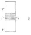
- FIG. 1depicts an overhead view of an embodiment of the present invention showing two device islands connected edge-to-edge by a monolithically formed extremely stretchable interconnect, prior to being stretched.
- FIG. 2depicts an overhead view of an embodiment of the present invention showing two device islands connected edge-to-edge by two extremely stretchable interconnects.
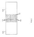
- FIG. 3depicts an overhead view of an embodiment of the present invention showing two device islands connected edge-to-edge by three extremely stretchable interconnects; in this case, the long bars of the interconnects are rotated by 90° which allows them to be longer than if they were not rotated.
- FIG. 4depicts four device islands arranged in a square matrix in an embodiment of the present invention, with each edge connected by an extremely stretchable interconnect to its nearest neighbors island edge, and the interconnects are formed so as to maximize the amount of chip area that is used for either an island or interconnect.
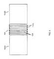
- FIG. 5depicts the case of FIG. 1 , with the short bars widened for extra mechanical strength at those locations.
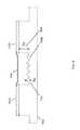
- FIGS. 6A and 6Bdepict embodiments of the present invention, where FIG. 6A is a side view of device islands and extremely stretchable interconnects transferred onto an elastomeric substrate.
- the substratehas been molded to have posts that are of the same area as the device islands (note that in embodiments these could be smaller or larger than the device islands).
- the height “h” of the molded post regionsmay range from, but is not limited to, about 1-1000 ⁇ m.
- the interconnectsare located in between these regions as shown, FIG. 6B Side view as before, with a similarly shaped elastomeric superstrate to serve as an encapsulation layer protecting the devices from direct mechanical contact.
- FIG. 7depicts a side view of a two-layer PDMS substrate in an embodiment of the present invention comprising silicon device islands adhered to top layer, free-standing interconnects, and square wave ripples in the lower layer PDMS to promote increased stretching through the substrate.
- FIG. 8depicts an embodiment of the present invention with a side view of two layers of cured jDhotoresist (SU-8 50 and SU-8 2002) used to make the two-layer PDMS substrate described in FIG. 7 .
- FIG. 9depicts an embodiment of the present invention with a side view of a two-layer PDMS substrate consisting of sinusoidal waves in the lower layer of PDMS to promote increased stretching through the substrate.
- the present inventionaccomplishes extremely stretchable electronics by forming the electronics on discrete islands 102 of silicon.
- the term “stretchable”, and roots and derivations thereof, when used to modify circuitry or components thereofis meant to encompass circuitry that comprises components having soft or elastic properties capable of being made longer or wider without tearing or breaking, and it is also meant to encompass circuitry having components (whether or not the components themselves are individually stretchable as stated above) that are configured in such a way so as to accommodate and remain functional when applied to a stretchable, inflatable, or otherwise expandable surface.
- the term “expandable”, and roots and derivations thereof, when used to modify circuitry or components thereofis also meant to have the meaning ascribed above. Thus, “stretch” and “expand”, and all derivations thereof, may be used interchangeably when referring to the present invention.
- the discrete islands mention aboveare discrete operative (in embodiments, arranged in a “device island” arrangement) and are themselves capable of performing the functionality described herein, or portions thereof.
- such functionality of the operative devicescan include integrated circuits, physical sensors (e.g. temperature, pH, light, radiation etc), biological and/or chemical sensors, amplifiers, A/D and D/A converters, optical collectors, electromechanical transducers, piezo-electric actuators, light emitting electronics which include LEDs, and combinations thereof.
- CMOScomplementary metal-oxide-semiconductor
- the discrete islands 102may range from about, but not limited to, 10-100 ⁇ m in size measured on an edge or by diameter, and connecting said islands 102 A-B with one or more extremely stretchable interconnects 104 .
- the novel geometry of the interconnects 104is what makes them extremely compliant.
- Each interconnect 104is patterned and etched so that its structural form has width and thickness dimensions that may be of comparable size (such as their ratio or inverse ratio not exceeding about a factor of 10); and may be preferably equal in size. In embodiments, the dimensions may not be greater than about Sum (e.g. where both dimensions are about 1 ⁇ m or less).
- the interconnect 104may be formed in a boustrophedonic style such that it effectively comprises long bars 108 and short bars 110 as shown in FIG. 1 .
- This unique geometryminimizes the stresses that are produced in the interconnect 104 when subsequently stretched because it has the effective form of a wire, and behaves very differently than interconnect form factors having one dimension greatly exceeding the other two (for example plates).
- Plate type structuresprimarily relieve stress only about a single axis via buckling, and withstand only a slight amount of shear stress before cracking. This invention may relieve stress about all three axes, including shears and any other stress.
- the interconnect 104may be formed out of rigid materials, after being stretched it may have a restorative force which helps prevent its wire-like form from getting tangled or knotted when re-compressing to the unstretched state. Another advantage of the boustrophedonic geometry is that it minimizes the initial separation distance between the islands 102 A-B. This is illustrated in FIG. 1 .
- One or more interconnects 104may be formed in various ways, as shown in FIGS. 2-4 .
- the parts of the interconnect 104 where the majority of stresses build up during stretchingmay be the short linking bars.
- the short linking bars 110 Amay be made several micrometers wider than the longer bars 108 , as shown in FIG. 5 .
- connection point of the interconnect 104 to the device island 102may be anywhere along the device island edge, or may be at a point on the surface of the device island 102 (in which case the interconnect may be located just above the plane of the device island).
- device islands 102may be made on any suitable material substrate, provided that a top membrane layer of said substrate that contains the ICs can be freed from the bulk of the substrate and transfer printed onto an elastomeric substrate.
- the interconnects 104may be formed either monolithically (i.e., out of the same semiconductor material as the device islands) or may be formed out of another material.
- the stretchable electronicsarc fabricated on a silicon-on-insulator (SOI) wafer, having a 1 ⁇ m thick top silicon layer and a 1 ⁇ m thick buried oxide layer. Devices arc formed on the top silicon wafer, and arranged into a square pattern of islands 102 A-D and interconnects 104 of the general form shown in FIG.
- SOIsilicon-on-insulator
- the islands 102are 100 ⁇ m on an edge, and the interconnects 104 are 1 ⁇ m wide, and the space between each long bar is 1 ⁇ m, and the interconnects 104 comprise 10 long bars 108 , all about 100 jam long.
- the islands 102 and interconnects 104are formed in an etching step which removes the excess silicon.
- the islands 102 and interconnects 104are coated with a 1 ⁇ m layer of polyimide that is patterned to only cover the islands 102 and interconnects 104 .
- the islands 102 and interconnects 104are released in an HF etch which undercuts the underlying buried oxide.
- the islands 102 and interconnects 104are transfer printed with a Polydimethylsiloxane (PDMS) stamp onto an elastomeric substrate 602 .
- PDMSPolydimethylsiloxane
- the backsides of the islands 102may be coated with a layer of polyimide (patterned to only cover the islands 102 and interconnects 104 ), and an additional layer of evaporated 3 nm chromium and 30 nm silicon dioxide selectively over the island regions to improve adhesion to the elastomeric substrate 602 at those locations, and not along the interconnects 102 .
- the elastomeric substrate 602may be PDMS or another highly compliant material.
- the elastomeric substrate 602may additionally be molded or etched into the shape shown in FIG. 6A-B , to further increase selective adhesion in the device island region but not the interconnect region, and to reduce the amount of material strain in the elastomeric substrate 602 that is transferred to the device islands 102 .
- the interconnectsmay accommodate stretching the device islands apart by approximately up to 800 ⁇ m.
- the interconnects 104 of this examplemay be capable of accommodating lateral shear displacements of about 800 ⁇ m. In general, they may be capable of accommodating any relative displacement of the two islands such that they remain approximately within 800 ⁇ m of each other.
- the interconnects 104may accommodate corkscrew type rotations of one island relative to another about any of the three axes of rotation. This feature may be limited only by the interconnects becoming entangled within each other. In any practical application, the completed stretchable device may not be so severely rotated, and the interconnect may easily accommodate rotations of up to 180°. It is noted that by increasing the number of long bars 108 used in the interconnect 104 , or by increasing the length of the long bars 108 , the interconnect may be able to accommodate even larger displacement strains. In embodiments, there may be no practical upper limit to the amount of displacement enabled through the present invention.
- the elastomeric substrate 602may comprise two layers separated by a height.
- the top “contact” layercontacts the device island 102 as in the embodiment illustrated in FIG. 6 .
- FIG. 7shows the bottom layer 702 may be a “wavy” layer containing ripples or square waves molded into the substrate 602 during elastomer fabrication. These square waves enable additional stretching, whose extent depends on the amplitude and wavelength of the waves pattern-molded in the elastomer 602 .
- FIG. 7shows one non-limiting layout and topology of an elastomeric substrate 602 relative to the position of the interconnects 104 and device islands 102 A-B.
- a two layer molded substratecan be fabricated using two step process consisting of two types of negative photoresist (SU-8 50 and SU-8 2002; Microchem Corporation).
- the negative resistscan be spin-coated on a transfer silicon wafer with spin speeds of 3000 rpm.
- the SU-8 50 layercan be spun on the wafer, and subsequently cured with UV radiation.
- the SU-8 2002can be spun and cured with a photo-mask and an alignment tool.
- the thickness of the SU-8 50 and SU-8 2002are 40-50 ⁇ m 708 and 2-10 ⁇ m 704 , respectively.
- the 40-50 ⁇ m thick regions of SU-8 50contain ripples 702 of SU-8 2002 (in this instance in the form of square waves) on their surfaces.
- liquid PDMScan be poured over the SU-8 patterns to form a substrate in the shape of the SU-8 molds 802 , as shown in FIG. 8 .
- the amplitude of the ripples in the SU-8 mold 802can be varied by changing the spin speed used for spinning the thin layer of SU-8 2002.
- the interconnects 104are free-standing.
- the entire substrate-device configurationcan be immersed in non-cured elastomer (fluid layer) layer followed by a cured layer of PDMS to encapsulate the fluid and devices.
- the PDMS in the lower layermay be designed with periodic sinusoidal ripples 702 B.
- this ripple configurationmay be achieved by bonding Si nanoribbons on the surface of pre-strained PDMS in a uniform parallel pattern.
- the release of the prestrain in the PDMS substrategenerates sinusoidal waves along the thin Si-nanoribbons (caused by buckling) and the surface of the PDMS substrate.
- the amplitude and wavelength of these waves 702 Bmay depend on the extent of uniaxial pre-strain exerted on the PDMS and on the mechanical properties of the Si-nanoribbons.
- the wavy surface on the PDMSmay be used as a transfer mold.
- Two-part liquid plastic solutioncan be poured over the wavy PDMS substrate and cured at room temperature over time ( ⁇ 2 hrs). Once the plastic hardens, the plastic substrate can be peeled away from the PDMS.
- This new plastic transfer substrate with wavy surface featurescan be used to produce more PDMS substrates containing wave features.
- the wavy PDMSmay serve as the lower layer of PDMS as in the previous embodiment.
- a top layer of PDMScan be plasma bonded to this lower layer of PDMS using oxygen plasma surface activation to produce the substrate illustrated in FIG. 9 .
- the PDMS transfer stampis stretched after the islands 102 A-B and interconnects 104 are picked up.
- a subsequent transfer to another elastomeric substrate 602may place these pre-stretched devices in a configuration, which allows the new elastomeric substrate to undergo compression.
- the devicesmay be able to accommodate that compression because the interconnects are pre-stretched.
- the interconnects 104are not made out of the same material as the device islands 102 .
- the islands 102 A-Bare completely isolated from each other by etching, with no interconnects in between.
- a layer of polyimidemay then be deposited, contact vias etched to various locations on the surface of the device island 102 , and then metal interconnects 104 deposited and patterned into a boustrophedonic pattern, followed by another layer of polyimide. Both layers of polyimide may now be patterned and etched to leave a small border around the interconnects 104 (thereby fully encapsulating the interconnects).
- interconnectsmay have the advantage that they arc already fully encapsulated in polyimide and will not adhere as well to the elastomeric substrate as the device islands will.
- the other advantageis that these interconnects may not be limited to only connecting along the edge of an island.
- the contact viamay be etched anywhere on the surface of the island 102 , including near the center. This may allow for easier connections to devices, more connections than possible only along an edge, increased strain compliance, decreased strain at the contact vias, and multiple layers of interconnects made with polymer passivation layers in between, allowing even more interconnects, or allowing one device island 102 A to connect to a non-neighboring device island 102 B.
- the device islands 102are fabricated and transfer printed onto the elastomeric substrate 602 , or substrate comprising a polymeric release layer and polymeric non-release layer.
- the interconnects 104are formed as described above, which may be possible because they do not require any high temperature processing, and then in the latter case, the release layer is etched and the devices that are on the non-release layer, are transfer printed onto another elastomeric substrate 602 .
- the islands 102may be transferred onto the elastomeric substrate using pick and place technology so that islands 102 that are initially fabricated very close to each other are spread apart when they are transfer printed. This allows the interconnects 104 to be fabricated in a pattern that resembles their stretched configuration (if desired), to allow compression.
- the present inventionmay comprise a stretchable electrical interconnect 104 , including an electrical interconnect 104 for connecting two electrical contacts 102 A-B (e.g. device islands 102 A-B), where the electrical interconnect 104 may be arranged boustrophedonicially to define rungs 108 (i.e. long bars 108 ) between the contacts 102 A-B, and where the rungs 108 may be substantially parallel with one another and where a plurality of rungs 108 may have substantially the same length and displacement therebetween.
- the ratio of the length of the plurality of rungs 108 and the displacement between the plurality of rungs 108may be large, such as at least 10:1, 100:1, 1000:1, and the like.
- the electrical integrity of the electrical interconnect 104may be maintained as stretched, such as to displacements that are increased to 1000%, 10000%, 100000%, and the like during stretching.
- the rungs 108may be substantially perpendicular to the contacts 102 A-B
- the interconnection 104may have a trace width and/or inter-rung spacing ranging between 0.1-10 microns.
- the two electrical contacts 102 A-Bmay be located on an elastomeric substrate 602 , the electrical contacts 102 A-B may be bonded to the substrate 602 and the interconnection 104 not bonded to the substrate 602 , the electrical contacts 102 A-B may be semiconductor circuits, metal contacts, and the like.
- the present inventionmay comprise a stretchable electrical interconnect 104 , including an electrical interconnect 104 for connecting two electrical contacts 102 A-B, where the electrical interconnect 104 is arranged boustrophedonicially to define rungs 108 between the contacts 102 A-B, and where the interconnect 104 maintains electrical conductivity and electrical integrity when a displacement between the contacts 102 A-B is increased, such as by 1000%, 10000%, 100000%, and the like.
- the present inventionmay electrically interconnect two electrical contacts 102 A-B with a stretchable interconnection 104 that has the ability to twist between the two electrical contacts 102 A-B by up to approximately 180 degrees while maintaining electrical integrity of the stretchable interconnection 104 .
- the present inventionmay be a device including a body having a stretchable surface (e.g. an elastomeric substrate 602 ), and a stretchable electronic circuit including (i) a first discrete operative device 102 A, (ii) a second discrete operative device 102 B, and (iii) a stretchable interconnect 104 connecting the first discrete operative device 102 A to the second discrete operative device 102 B, where the interconnect 104 may have a substantially boustrophedonic pattern and be able to maintain electrical conductivity when stretched, such as up to 1000%, 10000%, 100000%, and the like.
- the stretchable electronic circuitmay be affixed to the stretchable surface of the body.
- connectionmay be to a metal contact, to a semiconductor device, and the like.
- the first discrete operative device 102 A, the second discrete operative device 102 B, and the stretchable interconnect 104may all be made from the same material, and that material may be a semiconductor material.
- the present inventionmay attach at least two isolated electronic components (which in embodiments may be discrete operative devices) 102 A-B to an elastomeric substrate 602 , and arrange an electrical interconnection 104 between the components 102 A-B in a boustrophedonic pattern interconnecting the two isolated electronic components 102 A-B with the electrical interconnection 104 .
- the elastomeric substrate 602may then be stretched such that components 102 A-B separate relative to one another, where the electrical interconnection 104 maintains substantially identical electrical performance characteristics that the electrical interconnection 104 had in a pre-stretched form.
- the stretchingmay be a translational stretching, where the separation between the isolated electronic components 102 A-B increases by a percent as a result of the stretching, such as 10%, 100%, 1000%, 10000%, 100000%, and the like.
- the stretchingmay be a rotational stretching, where the rotation may be greater than a certain rotation angle, such as 90°, 180°, 270°, 360°, and the like, where the stretching may be in all three axes.
- the electrical interconnection 104may be made from semiconductive material.
- the electrical interconnection 104may be made from the same semiconductor material as the isolated electronic components 102 A-B, fabricated at the same time as the isolated electronic components 102 A-B, and the like.
- the semiconductor materialmay be a single crystal semiconductor material.
- the electrical interconnection 104may made of a different material than the isolated electronic components 102 A-B, such as a metal.
- the interconnect material 104may be loosely bound to the elastomeric substrate 602 , not connected at all, raised above the surface of the elastomeric substrate 602 , and the like.
- the at least two isolated semiconductor circuitsmay be fabricated on an upper surface 604 of the elastomeric substrate 602 separated by a lower surface 608 of the elastomeric substrate 602 , and the electrical interconnection 104 may be fabricated at the level of the upper surface 604 of the elastomeric substrate 602 .
- the electrical interconnection 104may have no direct contact with the lower level 608 , and thereby be substantially free from adhesion to the lower level 608 during stretching.
- the lower surface 608 of the elastomeric substrate 602may include a wavy form 702 , where the wavy form 704 may allow the elastomeric substrate 602 to expand during stretching.
Landscapes
- Engineering & Computer Science (AREA)
- Microelectronics & Electronic Packaging (AREA)
- Physics & Mathematics (AREA)
- Condensed Matter Physics & Semiconductors (AREA)
- General Physics & Mathematics (AREA)
- Computer Hardware Design (AREA)
- Power Engineering (AREA)
- Geometry (AREA)
- Metallurgy (AREA)
- Manufacturing & Machinery (AREA)
- Micromachines (AREA)
- Measuring Leads Or Probes (AREA)
Abstract
Description
Claims (33)
Priority Applications (3)
| Application Number | Priority Date | Filing Date | Title |
|---|---|---|---|
| US14/488,544US9516758B2 (en) | 2008-10-07 | 2014-09-17 | Extremely stretchable electronics |
| US15/337,389US9894757B2 (en) | 2008-10-07 | 2016-10-28 | Extremely stretchable electronics |
| US15/850,129US10383219B2 (en) | 2008-10-07 | 2017-12-21 | Extremely stretchable electronics |
Applications Claiming Priority (7)
| Application Number | Priority Date | Filing Date | Title |
|---|---|---|---|
| US10336108P | 2008-10-07 | 2008-10-07 | |
| US11300708P | 2008-11-10 | 2008-11-10 | |
| US11362208P | 2008-11-12 | 2008-11-12 | |
| US12/575,008US9289132B2 (en) | 2008-10-07 | 2009-10-07 | Catheter balloon having stretchable integrated circuitry and sensor array |
| US12/616,922US8389862B2 (en) | 2008-10-07 | 2009-11-12 | Extremely stretchable electronics |
| US13/767,262US9012784B2 (en) | 2008-10-07 | 2013-02-14 | Extremely stretchable electronics |
| US14/488,544US9516758B2 (en) | 2008-10-07 | 2014-09-17 | Extremely stretchable electronics |
Related Parent Applications (1)
| Application Number | Title | Priority Date | Filing Date |
|---|---|---|---|
| US13/767,262ContinuationUS9012784B2 (en) | 2008-10-07 | 2013-02-14 | Extremely stretchable electronics |
Related Child Applications (1)
| Application Number | Title | Priority Date | Filing Date |
|---|---|---|---|
| US15/337,389ContinuationUS9894757B2 (en) | 2008-10-07 | 2016-10-28 | Extremely stretchable electronics |
Publications (2)
| Publication Number | Publication Date |
|---|---|
| US20150069617A1 US20150069617A1 (en) | 2015-03-12 |
| US9516758B2true US9516758B2 (en) | 2016-12-06 |
Family
ID=56291135
Family Applications (5)
| Application Number | Title | Priority Date | Filing Date |
|---|---|---|---|
| US12/616,922Active2031-02-06US8389862B2 (en) | 2008-10-07 | 2009-11-12 | Extremely stretchable electronics |
| US13/767,262ActiveUS9012784B2 (en) | 2008-10-07 | 2013-02-14 | Extremely stretchable electronics |
| US14/488,544ActiveUS9516758B2 (en) | 2008-10-07 | 2014-09-17 | Extremely stretchable electronics |
| US15/337,389ActiveUS9894757B2 (en) | 2008-10-07 | 2016-10-28 | Extremely stretchable electronics |
| US15/850,129ActiveUS10383219B2 (en) | 2008-10-07 | 2017-12-21 | Extremely stretchable electronics |
Family Applications Before (2)
| Application Number | Title | Priority Date | Filing Date |
|---|---|---|---|
| US12/616,922Active2031-02-06US8389862B2 (en) | 2008-10-07 | 2009-11-12 | Extremely stretchable electronics |
| US13/767,262ActiveUS9012784B2 (en) | 2008-10-07 | 2013-02-14 | Extremely stretchable electronics |
Family Applications After (2)
| Application Number | Title | Priority Date | Filing Date |
|---|---|---|---|
| US15/337,389ActiveUS9894757B2 (en) | 2008-10-07 | 2016-10-28 | Extremely stretchable electronics |
| US15/850,129ActiveUS10383219B2 (en) | 2008-10-07 | 2017-12-21 | Extremely stretchable electronics |
Country Status (1)
| Country | Link |
|---|---|
| US (5) | US8389862B2 (en) |
Cited By (47)
| Publication number | Priority date | Publication date | Assignee | Title |
|---|---|---|---|---|
| US20170169918A1 (en)* | 2015-12-10 | 2017-06-15 | Electronics And Telecommunications Research Institute | Stretchable wire and method of fabricating the same |
| US10032709B2 (en) | 2012-10-09 | 2018-07-24 | Mc10, Inc. | Embedding thin chips in polymer |
| USD825537S1 (en) | 2014-10-15 | 2018-08-14 | Mc10, Inc. | Electronic device having antenna |
| US10186546B2 (en) | 2008-10-07 | 2019-01-22 | Mc10, Inc. | Systems, methods, and devices having stretchable integrated circuitry for sensing and delivering therapy |
| US10258282B2 (en) | 2013-11-22 | 2019-04-16 | Mc10, Inc. | Conformal sensor systems for sensing and analysis of cardiac activity |
| US10277386B2 (en) | 2016-02-22 | 2019-04-30 | Mc10, Inc. | System, devices, and method for on-body data and power transmission |
| US10288590B2 (en) | 2013-10-08 | 2019-05-14 | Smith & Nephew Plc | PH indicator device and formulation |
| US10296819B2 (en) | 2012-10-09 | 2019-05-21 | Mc10, Inc. | Conformal electronics integrated with apparel |
| US10300371B2 (en) | 2015-10-01 | 2019-05-28 | Mc10, Inc. | Method and system for interacting with a virtual environment |
| US10325951B2 (en) | 2008-10-07 | 2019-06-18 | Mc10, Inc. | Methods and applications of non-planar imaging arrays |
| US10334724B2 (en) | 2013-05-14 | 2019-06-25 | Mc10, Inc. | Conformal electronics including nested serpentine interconnects |
| US10383219B2 (en) | 2008-10-07 | 2019-08-13 | Mc10, Inc. | Extremely stretchable electronics |
| US10447347B2 (en) | 2016-08-12 | 2019-10-15 | Mc10, Inc. | Wireless charger and high speed data off-loader |
| US10532211B2 (en) | 2015-10-05 | 2020-01-14 | Mc10, Inc. | Method and system for neuromodulation and stimulation |
| US10673280B2 (en) | 2016-02-22 | 2020-06-02 | Mc10, Inc. | System, device, and method for coupled hub and sensor node on-body acquisition of sensor information |
| US10986465B2 (en) | 2015-02-20 | 2021-04-20 | Medidata Solutions, Inc. | Automated detection and configuration of wearable devices based on on-body status, location, and/or orientation |
| US11076997B2 (en) | 2017-07-25 | 2021-08-03 | Smith & Nephew Plc | Restriction of sensor-monitored region for sensor-enabled wound dressings |
| US11154235B2 (en) | 2016-04-19 | 2021-10-26 | Medidata Solutions, Inc. | Method and system for measuring perspiration |
| US11324424B2 (en) | 2017-03-09 | 2022-05-10 | Smith & Nephew Plc | Apparatus and method for imaging blood in a target region of tissue |
| US11395872B2 (en) | 2008-01-08 | 2022-07-26 | Smith & Nephew, Inc. | Sustained variable negative pressure wound treatment and method of controlling same |
| US11559438B2 (en) | 2017-11-15 | 2023-01-24 | Smith & Nephew Plc | Integrated sensor enabled wound monitoring and/or therapy dressings and systems |
| US11596553B2 (en) | 2017-09-27 | 2023-03-07 | Smith & Nephew Plc | Ph sensing for sensor enabled negative pressure wound monitoring and therapy apparatuses |
| US11633153B2 (en) | 2017-06-23 | 2023-04-25 | Smith & Nephew Plc | Positioning of sensors for sensor enabled wound monitoring or therapy |
| US11633147B2 (en) | 2017-09-10 | 2023-04-25 | Smith & Nephew Plc | Sensor enabled wound therapy dressings and systems implementing cybersecurity |
| US11638664B2 (en) | 2017-07-25 | 2023-05-02 | Smith & Nephew Plc | Biocompatible encapsulation and component stress relief for sensor enabled negative pressure wound therapy dressings |
| US11690570B2 (en) | 2017-03-09 | 2023-07-04 | Smith & Nephew Plc | Wound dressing, patch member and method of sensing one or more wound parameters |
| US11697889B2 (en) | 2017-12-20 | 2023-07-11 | International Business Machines Corporation | Three-dimensionally stretchable single crystalline semiconductor membrane |
| US11717447B2 (en) | 2016-05-13 | 2023-08-08 | Smith & Nephew Plc | Sensor enabled wound monitoring and therapy apparatus |
| US11744741B2 (en) | 2008-03-12 | 2023-09-05 | Smith & Nephew, Inc. | Negative pressure dressing and method of using same |
| US11759144B2 (en) | 2017-09-10 | 2023-09-19 | Smith & Nephew Plc | Systems and methods for inspection of encapsulation and components in sensor equipped wound dressings |
| US11791030B2 (en) | 2017-05-15 | 2023-10-17 | Smith & Nephew Plc | Wound analysis device and method |
| US11839464B2 (en) | 2017-09-28 | 2023-12-12 | Smith & Nephew, Plc | Neurostimulation and monitoring using sensor enabled wound monitoring and therapy apparatus |
| US11883262B2 (en) | 2017-04-11 | 2024-01-30 | Smith & Nephew Plc | Component positioning and stress relief for sensor enabled wound dressings |
| US11925735B2 (en) | 2017-08-10 | 2024-03-12 | Smith & Nephew Plc | Positioning of sensors for sensor enabled wound monitoring or therapy |
| US11931165B2 (en) | 2017-09-10 | 2024-03-19 | Smith & Nephew Plc | Electrostatic discharge protection for sensors in wound therapy |
| US11944418B2 (en) | 2018-09-12 | 2024-04-02 | Smith & Nephew Plc | Device, apparatus and method of determining skin perfusion pressure |
| US11957545B2 (en) | 2017-09-26 | 2024-04-16 | Smith & Nephew Plc | Sensor positioning and optical sensing for sensor enabled wound therapy dressings and systems |
| US11969538B2 (en) | 2018-12-21 | 2024-04-30 | T.J.Smith And Nephew, Limited | Wound therapy systems and methods with multiple power sources |
| US12011942B2 (en) | 2019-03-18 | 2024-06-18 | Smith & Nephew Plc | Rules for sensor integrated substrates |
| US12016994B2 (en) | 2019-10-07 | 2024-06-25 | Smith & Nephew Plc | Sensor enabled negative pressure wound monitoring apparatus with different impedances inks |
| US12033738B2 (en) | 2017-05-15 | 2024-07-09 | Smith & Nephew Plc | Negative pressure wound therapy system using eulerian video magnification |
| US12178597B2 (en) | 2017-03-09 | 2024-12-31 | Smith & Nephew Plc | Device, apparatus and method of determining skin perfusion pressure |
| US12178580B2 (en) | 2019-12-23 | 2024-12-31 | Alimetry Limited | Electrode patch and connection system |
| US12186165B2 (en) | 2018-09-28 | 2025-01-07 | T.J.Smith And Nephew, Limited | Optical fibers for optically sensing through wound dressings |
| US12186164B2 (en) | 2018-10-16 | 2025-01-07 | Smith & Nephew Plc | Systems and method for applying biocompatible encapsulation to sensor enabled wound monitoring and therapy dressings |
| US12299772B2 (en) | 2020-04-21 | 2025-05-13 | T.J.Smith And Nephew, Limited | Wound treatment management using augmented reality overlay |
| US12409071B2 (en) | 2018-08-29 | 2025-09-09 | Smith & Nephew Plc | Component positioning and encapsulation for sensor enabled wound dressings |
Families Citing this family (137)
| Publication number | Priority date | Publication date | Assignee | Title |
|---|---|---|---|---|
| US7834424B2 (en)* | 2006-09-12 | 2010-11-16 | The Board Of Trustees Of The Leland Stanford Junior University | Extendable connector and network |
| EP2185070A1 (en)* | 2007-08-22 | 2010-05-19 | Commonwealth Scientific And Industrial Research Organisation | A system, garment and method |
| US9545216B2 (en) | 2011-08-05 | 2017-01-17 | Mc10, Inc. | Catheter balloon methods and apparatus employing sensing elements |
| US9119533B2 (en) | 2008-10-07 | 2015-09-01 | Mc10, Inc. | Systems, methods, and devices having stretchable integrated circuitry for sensing and delivering therapy |
| US8886334B2 (en) | 2008-10-07 | 2014-11-11 | Mc10, Inc. | Systems, methods, and devices using stretchable or flexible electronics for medical applications |
| JP5646492B2 (en) | 2008-10-07 | 2014-12-24 | エムシー10 インコーポレイテッドMc10,Inc. | Stretchable integrated circuit and device with sensor array |
| US9012763B2 (en)* | 2009-03-13 | 2015-04-21 | Sunlight Photonics Inc. | Stretchable photovoltaic devices and carriers |
| US20120065937A1 (en)* | 2009-10-01 | 2012-03-15 | Mc10, Inc. | Methods and apparatus for measuring technical parameters of equipment, tools and components via conformal electronics |
| WO2011041727A1 (en) | 2009-10-01 | 2011-04-07 | Mc10, Inc. | Protective cases with integrated electronics |
| US20130192356A1 (en)* | 2009-10-01 | 2013-08-01 | Mc10, Inc. | Methods and apparatus for measuring technical parameters of equipment, tools, and components via conformal electronics |
| US10130274B2 (en)* | 2010-06-15 | 2018-11-20 | Ecole Polytechnique Federale De Lausanne (Epfl) | PDMS-based stretchable multi-electrode and chemotrode array for epidural and subdural neuronal recording, electrical stimulation and drug delivery |
| US9702839B2 (en) | 2011-03-11 | 2017-07-11 | Mc10, Inc. | Integrated devices to facilitate quantitative assays and diagnostics |
| JP2014523633A (en) | 2011-05-27 | 2014-09-11 | エムシー10 インコーポレイテッド | Electronic, optical and / or mechanical devices and systems and methods of manufacturing these devices and systems |
| US9757050B2 (en) | 2011-08-05 | 2017-09-12 | Mc10, Inc. | Catheter balloon employing force sensing elements |
| JP6129838B2 (en) | 2011-09-01 | 2017-05-17 | エムシー10 インコーポレイテッドMc10,Inc. | Electronic device that detects the condition of the tissue |
| JP6277130B2 (en) | 2011-10-05 | 2018-02-14 | エムシーテン、インコーポレイテッド | Medical device and method of manufacturing the same |
| CN104219999A (en) | 2012-01-30 | 2014-12-17 | 感官系统公司 | Sensors, interfaces and sensor systems for data collection and integrated remote monitoring of conditions at or near body surfaces |
| US9752259B2 (en) | 2012-04-09 | 2017-09-05 | The Hong Kong Research Intitute Of Textiles And Apparel Limited | Stretchable electrical interconnect and method of making same |
| US9247637B2 (en) | 2012-06-11 | 2016-01-26 | Mc10, Inc. | Strain relief structures for stretchable interconnects |
| US9226402B2 (en) | 2012-06-11 | 2015-12-29 | Mc10, Inc. | Strain isolation structures for stretchable electronics |
| US9168094B2 (en) | 2012-07-05 | 2015-10-27 | Mc10, Inc. | Catheter device including flow sensing |
| US9295842B2 (en) | 2012-07-05 | 2016-03-29 | Mc10, Inc. | Catheter or guidewire device including flow sensing and use thereof |
| US8895865B2 (en)* | 2012-09-07 | 2014-11-25 | Conor P. Lenahan | Conductive connections allowing XYZ translation |
| US9288898B2 (en)* | 2012-09-18 | 2016-03-15 | Palo Alto Research Center Incorporated | Reconfigurable stretchable connector substrate |
| US20140198034A1 (en) | 2013-01-14 | 2014-07-17 | Thalmic Labs Inc. | Muscle interface device and method for interacting with content displayed on wearable head mounted displays |
| US10497633B2 (en) | 2013-02-06 | 2019-12-03 | The Board Of Trustees Of The University Of Illinois | Stretchable electronic systems with fluid containment |
| US9613911B2 (en)* | 2013-02-06 | 2017-04-04 | The Board Of Trustees Of The University Of Illinois | Self-similar and fractal design for stretchable electronics |
| US10840536B2 (en) | 2013-02-06 | 2020-11-17 | The Board Of Trustees Of The University Of Illinois | Stretchable electronic systems with containment chambers |
| US9862594B2 (en) | 2013-03-15 | 2018-01-09 | Versana Micro Inc. | Wearable device having a monolithically integrated multi-sensor device on a semiconductor substrate and method therefor |
| WO2014186370A1 (en) | 2013-05-13 | 2014-11-20 | Thalmic Labs Inc. | Systems, articles and methods for wearable electronic devices that accommodate different user forms |
| US8927338B1 (en) | 2013-06-13 | 2015-01-06 | International Business Machines Corporation | Flexible, stretchable electronic devices |
| US8742325B1 (en)* | 2013-07-31 | 2014-06-03 | Google Inc. | Photodetector array on curved substrate |
| CA2920485A1 (en) | 2013-08-05 | 2015-02-12 | Mc10, Inc. | Flexible temperature sensor including conformable electronics |
| US20150124566A1 (en) | 2013-10-04 | 2015-05-07 | Thalmic Labs Inc. | Systems, articles and methods for wearable electronic devices employing contact sensors |
| US10188309B2 (en) | 2013-11-27 | 2019-01-29 | North Inc. | Systems, articles, and methods for electromyography sensors |
| US11426123B2 (en) | 2013-08-16 | 2022-08-30 | Meta Platforms Technologies, Llc | Systems, articles and methods for signal routing in wearable electronic devices that detect muscle activity of a user using a set of discrete and separately enclosed pod structures |
| US10042422B2 (en) | 2013-11-12 | 2018-08-07 | Thalmic Labs Inc. | Systems, articles, and methods for capacitive electromyography sensors |
| US11921471B2 (en) | 2013-08-16 | 2024-03-05 | Meta Platforms Technologies, Llc | Systems, articles, and methods for wearable devices having secondary power sources in links of a band for providing secondary power in addition to a primary power source |
| US8987707B2 (en)* | 2013-08-20 | 2015-03-24 | Wisconsin Alumni Research Foundation | Stretchable transistors with buckled carbon nanotube films as conducting channels |
| US9788789B2 (en)* | 2013-08-30 | 2017-10-17 | Thalmic Labs Inc. | Systems, articles, and methods for stretchable printed circuit boards |
| EP2845726A1 (en)* | 2013-09-04 | 2015-03-11 | Nederlandse Organisatie voor toegepast -natuurwetenschappelijk onderzoek TNO | Electrically interconnecting foil |
| KR20160065948A (en) | 2013-10-07 | 2016-06-09 | 엠씨10, 인크 | Conformal sensor systems for sensing and analysis |
| US10076279B2 (en) | 2013-10-22 | 2018-09-18 | Neba Health, Llc | System and method for a compact EEG headset |
| US9521748B1 (en) | 2013-12-09 | 2016-12-13 | Multek Technologies, Ltd. | Mechanical measures to limit stress and strain in deformable electronics |
| US9338915B1 (en) | 2013-12-09 | 2016-05-10 | Flextronics Ap, Llc | Method of attaching electronic module on fabrics by stitching plated through holes |
| CN105874606B (en) | 2014-01-06 | 2021-01-12 | Mc10股份有限公司 | Encapsulated conformal electronic systems and devices and methods of making and using the same |
| US10485118B2 (en) | 2014-03-04 | 2019-11-19 | Mc10, Inc. | Multi-part flexible encapsulation housing for electronic devices and methods of making the same |
| EP3117206A4 (en) | 2014-03-12 | 2017-11-15 | Mc10, Inc. | Quantification of a change in assay |
| KR101574521B1 (en)* | 2014-03-18 | 2015-12-04 | 한국과학기술연구원 | Material having latent shape using hierarchical structural levels and electrode comprising of the same |
| US10199008B2 (en) | 2014-03-27 | 2019-02-05 | North Inc. | Systems, devices, and methods for wearable electronic devices as state machines |
| US9591758B2 (en)* | 2014-03-27 | 2017-03-07 | Intel Corporation | Flexible electronic system with wire bonds |
| CA2946814A1 (en) | 2014-04-28 | 2015-11-12 | King Abdullah University Of Science And Technology | Smart thermal patch for adaptive thermotherapy |
| FR3020957B1 (en) | 2014-05-19 | 2021-07-23 | Commissariat Energie Atomique | SKIN DEVICE, ESPECIALLY FOR MEDICAL APPLICATION. |
| US9880632B2 (en) | 2014-06-19 | 2018-01-30 | Thalmic Labs Inc. | Systems, devices, and methods for gesture identification |
| US9287236B2 (en) | 2014-07-17 | 2016-03-15 | Freescale Semiconductor, Inc. | Flexible packaged integrated circuit |
| KR102255198B1 (en) | 2014-08-12 | 2021-05-25 | 삼성디스플레이 주식회사 | Stretchable substrate and organic light emitting display comprising the same |
| US9899330B2 (en) | 2014-10-03 | 2018-02-20 | Mc10, Inc. | Flexible electronic circuits with embedded integrated circuit die |
| US10297572B2 (en)* | 2014-10-06 | 2019-05-21 | Mc10, Inc. | Discrete flexible interconnects for modules of integrated circuits |
| US9571913B2 (en) | 2014-10-30 | 2017-02-14 | Smartear, Inc. | Smart flexible interactive earplug |
| EP3213529A4 (en)* | 2014-10-30 | 2018-06-06 | Smartear Inc. | Smart flexible interactive earplug |
| US10185811B2 (en) | 2014-11-06 | 2019-01-22 | Empire Technology Development Llc | Pill removal detection from pill package |
| US9807221B2 (en) | 2014-11-28 | 2017-10-31 | Thalmic Labs Inc. | Systems, devices, and methods effected in response to establishing and/or terminating a physical communications link |
| US9380698B1 (en)* | 2014-12-05 | 2016-06-28 | VivaLnk, Inc. | Stretchable electronic patch having a foldable circuit layer |
| US10306755B2 (en) | 2014-12-08 | 2019-05-28 | Fujikura Ltd. | Stretchable board |
| US10631401B2 (en) | 2014-12-15 | 2020-04-21 | Robert Bosch Gmbh | Modular deformable platform |
| WO2016109652A1 (en) | 2015-01-02 | 2016-07-07 | Arizona Board Of Regents On Behalf Of Arizona State University | Archimedean spiral design for deformable electronics |
| KR102327582B1 (en) | 2015-01-06 | 2021-11-17 | 삼성디스플레이 주식회사 | Stretchable display and manufacturing method thereof |
| US9747015B2 (en)* | 2015-02-12 | 2017-08-29 | Qualcomm Incorporated | Efficient display of content on wearable displays |
| US9734779B2 (en) | 2015-02-12 | 2017-08-15 | Qualcomm Incorporated | Efficient operation of wearable displays |
| KR102396298B1 (en) | 2015-03-02 | 2022-05-11 | 삼성디스플레이 주식회사 | Flexible display apparatus |
| WO2016140961A1 (en) | 2015-03-02 | 2016-09-09 | Mc10, Inc. | Perspiration sensor |
| KR102282492B1 (en) | 2015-03-10 | 2021-07-27 | 삼성디스플레이 주식회사 | Organic light emitting diode display |
| US10154583B1 (en) | 2015-03-27 | 2018-12-11 | Flex Ltd | Mechanical strain reduction on flexible and rigid-flexible circuits |
| US10078435B2 (en) | 2015-04-24 | 2018-09-18 | Thalmic Labs Inc. | Systems, methods, and computer program products for interacting with electronically displayed presentation materials |
| KR102432345B1 (en) | 2015-04-30 | 2022-08-12 | 삼성디스플레이 주식회사 | Stretchable display |
| US10182284B2 (en)* | 2015-06-11 | 2019-01-15 | Facebook Technologies, Llc | Connector assembly for detachable audio system |
| US9841548B2 (en)* | 2015-06-30 | 2017-12-12 | Apple Inc. | Electronic devices with soft input-output components |
| US10026721B2 (en)* | 2015-06-30 | 2018-07-17 | Apple Inc. | Electronic devices with soft input-output components |
| WO2017015000A1 (en) | 2015-07-17 | 2017-01-26 | Mc10, Inc. | Conductive stiffener, method of making a conductive stiffener, and conductive adhesive and encapsulation layers |
| US10709384B2 (en) | 2015-08-19 | 2020-07-14 | Mc10, Inc. | Wearable heat flux devices and methods of use |
| US10393685B2 (en)* | 2015-08-19 | 2019-08-27 | Research Foundation Of The City University Of New York | Cell-on-chip stretchable platform for mammalian cells with integrated impedance spectroscpy technique |
| US9832863B2 (en) | 2015-09-25 | 2017-11-28 | Intel Corporation | Method of fabricating a stretchable computing device |
| KR102456062B1 (en) | 2015-10-16 | 2022-10-18 | 삼성디스플레이 주식회사 | Display device |
| WO2017070030A1 (en) | 2015-10-21 | 2017-04-27 | Massachusetts Institute Of Technology | Nanowire fet imaging system and related techniques |
| US9992880B2 (en) | 2015-11-12 | 2018-06-05 | Multek Technologies Limited | Rigid-bend printed circuit board fabrication |
| US10062832B2 (en)* | 2015-11-30 | 2018-08-28 | Sabic Global Technologies, B.V. | Methods and systems for making piezoelectric cantilever actuators |
| US10206575B2 (en) | 2015-12-04 | 2019-02-19 | Adil Al-Mayah | Apparatus and method for using internal inclusion for mechanical characterization of soft materials |
| US10798817B2 (en)* | 2015-12-11 | 2020-10-06 | Intel Corporation | Method for making a flexible wearable circuit |
| USD794611S1 (en) | 2016-01-19 | 2017-08-15 | Smartear, Inc. | In-ear utility device |
| USD798843S1 (en) | 2016-01-19 | 2017-10-03 | Smartear, Inc. | In-ear utility device |
| TWI629012B (en)* | 2016-02-24 | 2018-07-11 | 國立清華大學 | Intelligent insole |
| USD795224S1 (en) | 2016-03-08 | 2017-08-22 | Smartear, Inc. | In-ear utility device |
| US20170347177A1 (en) | 2016-05-25 | 2017-11-30 | Smartear, Inc. | In-Ear Utility Device Having Sensors |
| US10045130B2 (en) | 2016-05-25 | 2018-08-07 | Smartear, Inc. | In-ear utility device having voice recognition |
| US9838771B1 (en) | 2016-05-25 | 2017-12-05 | Smartear, Inc. | In-ear utility device having a humidity sensor |
| US10990174B2 (en) | 2016-07-25 | 2021-04-27 | Facebook Technologies, Llc | Methods and apparatus for predicting musculo-skeletal position information using wearable autonomous sensors |
| US11216069B2 (en) | 2018-05-08 | 2022-01-04 | Facebook Technologies, Llc | Systems and methods for improved speech recognition using neuromuscular information |
| FR3054640B1 (en) | 2016-07-28 | 2020-06-12 | Linxens Holding | LIGHT EMITTING DEVICE |
| US10199323B2 (en)* | 2016-08-30 | 2019-02-05 | Apple Inc. | Flexible circuit substrate with temporary supports and equalized lateral expansion |
| US10600928B1 (en) | 2016-09-20 | 2020-03-24 | Apple Inc. | Systems with photovoltaic cells |
| US10461685B2 (en)* | 2016-10-04 | 2019-10-29 | Global Solar Energy, Inc. | Foldable photovoltaic assembly with non-perpendicular interconnection |
| DE102016122251A1 (en)* | 2016-11-18 | 2018-05-24 | Infineon Technologies Austria Ag | Method of forming semiconductor devices and semiconductor device |
| US11127585B2 (en)* | 2016-11-22 | 2021-09-21 | King Abdullah University Of Science And Technology | Out-of-plane deformable semiconductor substrate, method of making an out-of-plane deformable semiconductor substrate, and an in-plane and out-of-plane deformable semiconductor substrate |
| US10410634B2 (en) | 2017-05-18 | 2019-09-10 | Smartear, Inc. | Ear-borne audio device conversation recording and compressed data transmission |
| US10582285B2 (en) | 2017-09-30 | 2020-03-03 | Smartear, Inc. | Comfort tip with pressure relief valves and horn |
| USD883491S1 (en) | 2017-09-30 | 2020-05-05 | Smartear, Inc. | In-ear device |
| WO2019079757A1 (en) | 2017-10-19 | 2019-04-25 | Ctrl-Labs Corporation | Systems and methods for identifying biological structures associated with neuromuscular source signals |
| US12357828B2 (en) | 2017-12-05 | 2025-07-15 | Ecole Polytechnique Federale De Lausanne (Epfl) | System for planning and/or providing neuromodulation |
| US11907423B2 (en) | 2019-11-25 | 2024-02-20 | Meta Platforms Technologies, Llc | Systems and methods for contextualized interactions with an environment |
| US11961494B1 (en) | 2019-03-29 | 2024-04-16 | Meta Platforms Technologies, Llc | Electromagnetic interference reduction in extended reality environments |
| US11481030B2 (en) | 2019-03-29 | 2022-10-25 | Meta Platforms Technologies, Llc | Methods and apparatus for gesture detection and classification |
| US11150730B1 (en) | 2019-04-30 | 2021-10-19 | Facebook Technologies, Llc | Devices, systems, and methods for controlling computing devices via neuromuscular signals of users |
| US10937414B2 (en) | 2018-05-08 | 2021-03-02 | Facebook Technologies, Llc | Systems and methods for text input using neuromuscular information |
| US11567573B2 (en) | 2018-09-20 | 2023-01-31 | Meta Platforms Technologies, Llc | Neuromuscular text entry, writing and drawing in augmented reality systems |
| US11493993B2 (en) | 2019-09-04 | 2022-11-08 | Meta Platforms Technologies, Llc | Systems, methods, and interfaces for performing inputs based on neuromuscular control |
| US10592001B2 (en) | 2018-05-08 | 2020-03-17 | Facebook Technologies, Llc | Systems and methods for improved speech recognition using neuromuscular information |
| WO2020018255A1 (en)* | 2018-07-20 | 2020-01-23 | Shenzhen Royole Technologies Co. Ltd. | Stretchable electronics and hybrid integration method for fabricating the same |
| CN110767350B (en)* | 2018-07-27 | 2021-04-20 | 浙江清华柔性电子技术研究院 | Preparation method of lead applied to extensible electronic device |
| WO2020047429A1 (en) | 2018-08-31 | 2020-03-05 | Ctrl-Labs Corporation | Camera-guided interpretation of neuromuscular signals |
| EP3653260A1 (en) | 2018-11-13 | 2020-05-20 | GTX medical B.V. | Sensor in clothing of limbs or footwear |
| EP3886693A4 (en) | 2018-11-27 | 2022-06-08 | Facebook Technologies, LLC. | Methods and apparatus for autocalibration of a wearable electrode sensor system |
| AT521919B1 (en)* | 2018-12-13 | 2022-07-15 | Johann Kuebel Ing | Device for emitting light |
| US11768262B2 (en) | 2019-03-14 | 2023-09-26 | Massachusetts Institute Of Technology | Interface responsive to two or more sensor modalities |
| CN109920334B (en) | 2019-03-27 | 2021-04-27 | 京东方科技集团股份有限公司 | Array substrate and display device |
| KR102612034B1 (en)* | 2019-05-02 | 2023-12-12 | 한국전자통신연구원 | Flexible electronic device |
| WO2021031188A1 (en)* | 2019-08-22 | 2021-02-25 | Boe Technology Group Co., Ltd. | Stretchable display panel, display apparatus, and method of fabricating stretchable display panel |
| EP3827875B1 (en) | 2019-11-27 | 2023-07-05 | ONWARD Medical N.V. | Neuromodulation system |
| US11464451B1 (en) | 2020-03-11 | 2022-10-11 | Huxley Medical, Inc. | Patch for improved biometric data capture and related processes |
| US11123011B1 (en) | 2020-03-23 | 2021-09-21 | Nix, Inc. | Wearable systems, devices, and methods for measurement and analysis of body fluids |
| JP7264136B2 (en)* | 2020-08-28 | 2023-04-25 | 横河電機株式会社 | FORCE DETECTION DEVICE, FORCE DETECTION SYSTEM AND METHOD FOR MANUFACTURING FORCE DETECTION DEVICE |
| US12225638B2 (en)* | 2021-02-12 | 2025-02-11 | William Marsh Rice University | Integrated microheater array for efficient and localized heating of magnetic nanoparticles at microwave frequencies |
| US11868531B1 (en) | 2021-04-08 | 2024-01-09 | Meta Platforms Technologies, Llc | Wearable device providing for thumb-to-finger-based input gestures detected based on neuromuscular signals, and systems and methods of use thereof |
| US11660005B1 (en) | 2021-06-04 | 2023-05-30 | Huxley Medical, Inc. | Processing and analyzing biometric data |
| US12178552B1 (en) | 2021-06-04 | 2024-12-31 | Huxley Medical, Inc. | Systems and processes for detecting oxygen saturation and compensating for skin tone variation |
| US12114980B1 (en) | 2021-08-24 | 2024-10-15 | Huxley Medical, Inc. | Photoplethysmography sensors and processes |
| US12279853B1 (en) | 2021-08-24 | 2025-04-22 | Huxley Medical, Inc. | Photoplethysmography sensors and processes |
| CN114171497B (en)* | 2021-11-30 | 2023-02-03 | 中国农业大学 | Malleable electronic devices, flexible substrates, and methods of making the same |
Citations (451)
| Publication number | Priority date | Publication date | Assignee | Title |
|---|---|---|---|---|
| US3716861A (en) | 1971-03-22 | 1973-02-13 | J Root | Serpentine antenna mounted on a rotatable capacitive coupler |
| US3805427A (en) | 1972-12-18 | 1974-04-23 | H Epstein | Medical alarm bracelet |
| US3949410A (en) | 1975-01-23 | 1976-04-06 | International Business Machines Corporation | Jet nozzle structure for electrohydrodynamic droplet formation and ink jet printing system therewith |
| US4058418A (en) | 1974-04-01 | 1977-11-15 | Solarex Corporation | Fabrication of thin film solar cells utilizing epitaxial deposition onto a liquid surface to obtain lateral growth |
| US4304235A (en) | 1978-09-12 | 1981-12-08 | Kaufman John George | Electrosurgical electrode |
| US4392451A (en) | 1980-12-31 | 1983-07-12 | The Boeing Company | Apparatus for forming thin-film heterojunction solar cells employing materials selected from the class of I-III-VI2 chalcopyrite compounds |
| US4416288A (en) | 1980-08-14 | 1983-11-22 | The Regents Of The University Of California | Apparatus and method for reconstructing subsurface electrophysiological patterns |
| US4471003A (en) | 1980-11-25 | 1984-09-11 | Cann Gordon L | Magnetoplasmadynamic apparatus and process for the separation and deposition of materials |
| US4487162A (en) | 1980-11-25 | 1984-12-11 | Cann Gordon L | Magnetoplasmadynamic apparatus for the separation and deposition of materials |
| US4658153A (en) | 1984-06-18 | 1987-04-14 | Amnon Brosh | Planar coil apparatus for providing a frequency output vs. position |
| US4663828A (en) | 1985-10-11 | 1987-05-12 | Energy Conversion Devices, Inc. | Process and apparatus for continuous production of lightweight arrays of photovoltaic cells |
| US4761335A (en) | 1985-03-07 | 1988-08-02 | National Starch And Chemical Corporation | Alpha-particle protection of semiconductor devices |
| US4763275A (en) | 1986-02-20 | 1988-08-09 | Carlin John A | Force accumulating device for sporting protective gear |
| US4766670A (en) | 1987-02-02 | 1988-08-30 | International Business Machines Corporation | Full panel electronic packaging structure and method of making same |
| US4784720A (en) | 1985-05-03 | 1988-11-15 | Texas Instruments Incorporated | Trench etch process for a single-wafer RIE dry etch reactor |
| US4855017A (en) | 1985-05-03 | 1989-08-08 | Texas Instruments Incorporated | Trench etch process for a single-wafer RIE dry etch reactor |
| US5041973A (en) | 1988-10-25 | 1991-08-20 | London Health Association | Cardiac mapping system simulator |
| US5086785A (en) | 1989-08-10 | 1992-02-11 | Abrams/Gentille Entertainment Inc. | Angular displacement sensors |
| US5118400A (en) | 1990-01-29 | 1992-06-02 | Spire Corporation | Method of making biocompatible electrodes |
| US5147519A (en) | 1990-07-27 | 1992-09-15 | Motorola, Inc. | Method of manufacturing elastomers containing fine line conductors |
| US5178957A (en) | 1989-05-02 | 1993-01-12 | Minnesota Mining And Manufacturing Company | Noble metal-polymer composites and flexible thin-film conductors prepared therefrom |
| JPH0587511A (en) | 1991-07-24 | 1993-04-06 | Yamaha Corp | Bending detection device |
| US5204144A (en) | 1991-05-10 | 1993-04-20 | Celestech, Inc. | Method for plasma deposition on apertured substrates |
| EP0585670A2 (en) | 1992-08-12 | 1994-03-09 | Reliant Laser Corporation | Electro-optical system for measuring and analying accumulated short-wave and long-wave ultraviolet radiation exposure |
| US5313094A (en) | 1992-01-28 | 1994-05-17 | International Business Machines Corportion | Thermal dissipation of integrated circuits using diamond paths |
| US5331966A (en) | 1991-04-05 | 1994-07-26 | Medtronic, Inc. | Subcutaneous multi-electrode sensing system, method and pacer |
| US5360987A (en) | 1993-11-17 | 1994-11-01 | At&T Bell Laboratories | Semiconductor photodiode device with isolation region |
| US5403700A (en) | 1990-02-14 | 1995-04-04 | Eli Lilly And Company | Method of making a thin film electrical component |
| US5427096A (en) | 1993-11-19 | 1995-06-27 | Cmc Assemblers, Inc. | Water-degradable electrode |
| US5434751A (en) | 1994-04-11 | 1995-07-18 | Martin Marietta Corporation | Reworkable high density interconnect structure incorporating a release layer |
| US5455178A (en) | 1990-05-03 | 1995-10-03 | Hoffmann-La Roche Inc. | Microoptical sensor and method |
| US5469845A (en) | 1991-08-28 | 1995-11-28 | Nellcor Incorporated | Disposable pulse oximeter sensor |
| US5501893A (en) | 1992-12-05 | 1996-03-26 | Robert Bosch Gmbh | Method of anisotropically etching silicon |
| US5525815A (en) | 1994-10-03 | 1996-06-11 | General Electric Company | Diamond film structure with high thermal conductivity |
| US5539935A (en) | 1992-01-10 | 1996-07-30 | Rush, Iii; Gus A. | Sports helmet |
| US5545291A (en) | 1993-12-17 | 1996-08-13 | The Regents Of The University Of California | Method for fabricating self-assembling microstructures |
| US5549108A (en) | 1992-09-25 | 1996-08-27 | Ep Technologies, Inc. | Cardiac mapping and ablation systems |
| US5560974A (en) | 1991-03-22 | 1996-10-01 | Kappler Safety Group, Inc. | Breathable non-woven composite barrier fabric and fabrication process |
| US5567975A (en) | 1994-06-30 | 1996-10-22 | Santa Barbara Research Center | Group II-VI radiation detector for simultaneous visible and IR detection |
| US5625471A (en) | 1994-11-02 | 1997-04-29 | Litel Instruments | Dual plate holographic imaging technique and masks |
| US5648148A (en) | 1993-12-30 | 1997-07-15 | Saint Gobain/Norton Industrial Ceramics Corp. | Thermal management of electronic components using synthetic diamond |
| US5687737A (en) | 1992-10-09 | 1997-11-18 | Washington University | Computerized three-dimensional cardiac mapping with interactive visual displays |
| US5691245A (en) | 1996-10-28 | 1997-11-25 | He Holdings, Inc. | Methods of forming two-sided HDMI interconnect structures |
| US5746207A (en) | 1993-03-23 | 1998-05-05 | Mclaughlin; James Andrew | Profiled biosignal electrode device |
| US5753529A (en) | 1994-05-05 | 1998-05-19 | Siliconix Incorporated | Surface mount and flip chip technology for total integrated circuit isolation |
| US5767578A (en) | 1994-10-12 | 1998-06-16 | Siliconix Incorporated | Surface mount and flip chip technology with diamond film passivation for total integated circuit isolation |
| US5772905A (en) | 1995-11-15 | 1998-06-30 | Regents Of The University Of Minnesota | Nanoimprint lithography |
| US5790151A (en) | 1996-03-27 | 1998-08-04 | Imaging Technology International Corp. | Ink jet printhead and method of making |
| US5811790A (en) | 1996-02-22 | 1998-09-22 | Canon Kabushiki Kaisha | Photoelectric conversion device having thermal conductive member |
| US5817008A (en) | 1996-10-31 | 1998-10-06 | Spacelabs Medical, Inc. | Conformal pulse oximetry sensor and monitor |
| US5817242A (en) | 1995-08-04 | 1998-10-06 | International Business Machines Corporation | Stamp for a lithographic process |
| US5824186A (en) | 1993-12-17 | 1998-10-20 | The Regents Of The University Of California | Method and apparatus for fabricating self-assembling microstructures |
| US5860974A (en) | 1993-07-01 | 1999-01-19 | Boston Scientific Corporation | Heart ablation catheter with expandable electrode and method of coupling energy to an electrode on a catheter shaft |
| US5871443A (en) | 1992-09-25 | 1999-02-16 | Ep Technologies, Inc. | Cardiac mapping and ablation systems |
| US5904545A (en) | 1993-12-17 | 1999-05-18 | The Regents Of The University Of California | Apparatus for fabricating self-assembling microstructures |
| US5907477A (en) | 1995-09-19 | 1999-05-25 | Micron Communications, Inc. | Substrate assembly including a compartmental dam for use in the manufacturing of an enclosed electrical circuit using an encapsulant |
| US5907189A (en) | 1997-05-29 | 1999-05-25 | Lsi Logic Corporation | Conformal diamond coating for thermal improvement of electronic packages |
| US5915180A (en) | 1994-04-06 | 1999-06-22 | Denso Corporation | Process for producing a semiconductor device having a single thermal oxidizing step |
| US5917534A (en) | 1995-06-29 | 1999-06-29 | Eastman Kodak Company | Light-emitting diode arrays with integrated photodetectors formed as a monolithic device and methods and apparatus for using same |
| US5919155A (en) | 1992-12-31 | 1999-07-06 | Alza Corporation | Electrotransport system having flexible connector means |
| US5928001A (en) | 1997-09-08 | 1999-07-27 | Motorola, Inc. | Surface mountable flexible interconnect |
| WO1999038211A1 (en) | 1998-01-22 | 1999-07-29 | Fraunhofer-Gesellschaft zur Förderung der angewandten Forschung e.V. | Microsystem and method for the production thereof |
| US5955781A (en) | 1998-01-13 | 1999-09-21 | International Business Machines Corporation | Embedded thermal conductors for semiconductor chips |
| US5976683A (en) | 1996-10-24 | 1999-11-02 | Leybold Systems Gmbh | Coating system transparent to light and reflecting thermal radiation |
| US5978972A (en) | 1996-06-14 | 1999-11-09 | Johns Hopkins University | Helmet system including at least three accelerometers and mass memory and method for recording in real-time orthogonal acceleration data of a head |
| US5998291A (en) | 1997-04-07 | 1999-12-07 | Raytheon Company | Attachment method for assembly of high density multiple interconnect structures |
| US6024702A (en) | 1997-09-03 | 2000-02-15 | Pmt Corporation | Implantable electrode manufactured with flexible printed circuit |
| US6057212A (en) | 1998-05-04 | 2000-05-02 | International Business Machines Corporation | Method for making bonded metal back-plane substrates |
| US6063046A (en) | 1997-04-11 | 2000-05-16 | Allum; John H. | Method and apparatus for the diagnosis and rehabilitation of balance disorders |
| US6080608A (en) | 1993-10-29 | 2000-06-27 | Vlsi Technology, Inc. | Polysilicon pillar heat sinks for semiconductor on insulator circuits |
| US6097984A (en) | 1998-11-25 | 2000-08-01 | Medtronic, Inc. | System and method of stimulation for treating gastro-esophageal reflux disease |
| US6121110A (en) | 1998-05-11 | 2000-09-19 | Samsung Electronics Co., Ltd. | Trench isolation method for semiconductor device |
| US6165391A (en) | 1996-01-23 | 2000-12-26 | Nimbus Manufacturing (Uk) Limited | Manufacture of optical data storage disc |
| US6165885A (en) | 1995-08-02 | 2000-12-26 | International Business Machines Corporation | Method of making components with solder balls |
| US6171730B1 (en) | 1997-11-07 | 2001-01-09 | Canon Kabushiki Kaisha | Exposure method and exposure apparatus |
| US6181551B1 (en) | 1998-04-15 | 2001-01-30 | Dell Usa, L.P. | Pin soldering enhancement and method |
| US6225149B1 (en) | 1999-05-03 | 2001-05-01 | Feng Yuan Gan | Methods to fabricate thin film transistors and circuits |
| US6236883B1 (en) | 1999-02-03 | 2001-05-22 | The Trustees Of Columbia University In The City Of New York | Methods and systems for localizing reentrant circuits from electrogram features |
| US20010003043A1 (en) | 1999-04-21 | 2001-06-07 | Andres Metspalu | Method and device for imaging and analysis of biopolymer arrays |
| US6265326B1 (en) | 1997-07-04 | 2001-07-24 | Fuji Electric Co., Ltd. | Method for forming thermal oxide film of silicon carbide semiconductor device |
| US20010012918A1 (en) | 1995-07-28 | 2001-08-09 | Swanson David K. | Systems and methods for conducting electrophysiological testing using high-voltage energy pulses to stun tissue |
| US6274508B1 (en) | 1999-02-05 | 2001-08-14 | Alien Technology Corporation | Apparatuses and methods used in forming assemblies |
| US6276775B1 (en) | 1999-04-29 | 2001-08-21 | Hewlett-Packard Company | Variable drop mass inkjet drop generator |
| US6277712B1 (en) | 1999-03-31 | 2001-08-21 | Samsung Electronics Co., Ltd. | Multilayered wafer with thick sacrificial layer using porous silicon or porous silicon oxide and fabrication method thereof |
| US6281038B1 (en) | 1999-02-05 | 2001-08-28 | Alien Technology Corporation | Methods for forming assemblies |
| US6284418B1 (en) | 1998-11-16 | 2001-09-04 | Cambridge Scientific, Inc. | Biopolymer-based optical element |
| US20010021867A1 (en) | 1993-03-16 | 2001-09-13 | Kordis Thomas F. | Cardiac mapping and ablation systems |
| US6291896B1 (en) | 1999-02-16 | 2001-09-18 | Alien Technology Corporation | Functionally symmetric integrated circuit die |
| US6301500B1 (en) | 1998-04-14 | 2001-10-09 | U.S. Philips Corporation | Electro-stimulation apparatus using electrode matrix and a counter electrode |
| US6316278B1 (en) | 1999-03-16 | 2001-11-13 | Alien Technology Corporation | Methods for fabricating a multiple modular assembly |
| US6316283B1 (en) | 1998-03-25 | 2001-11-13 | Asulab Sa | Batch manufacturing method for photovoltaic cells |
| US6317175B1 (en) | 1990-12-31 | 2001-11-13 | Kopin Corporation | Single crystal silicon arrayed devices with optical shield between transistor and substrate |
| US6322895B1 (en) | 1995-08-03 | 2001-11-27 | Qinetiq Limited | Biomaterial |
| US6334960B1 (en) | 1999-03-11 | 2002-01-01 | Board Of Regents, The University Of Texas System | Step and flash imprint lithography |
| US6344616B1 (en) | 1999-06-28 | 2002-02-05 | Nec Corporation | Cable capable of connecting between integrated circuit elements in a reduced space |
| US20020021445A1 (en) | 2000-07-21 | 2002-02-21 | Sergey Bozhevolnyi | Surface plasmon polariton band gap structures |
| US20020026127A1 (en) | 2000-03-23 | 2002-02-28 | Balbierz Daniel J. | Tissue biopsy and treatment apparatus and method |
| US6360615B1 (en) | 2000-06-06 | 2002-03-26 | Technoskin, Llc | Wearable effect-emitting strain gauge device |
| US6380729B1 (en) | 1999-02-16 | 2002-04-30 | Alien Technology Corporation | Testing integrated circuit dice |
| US6403397B1 (en) | 2000-06-28 | 2002-06-11 | Agere Systems Guardian Corp. | Process for fabricating organic semiconductor device involving selective patterning |
| US20020082515A1 (en) | 1999-07-01 | 2002-06-27 | Campbell Thomas H. | Thermography catheter |
| US6413790B1 (en) | 1999-07-21 | 2002-07-02 | E Ink Corporation | Preferred methods for producing electrical circuit elements used to control an electronic display |
| US6414783B2 (en) | 1990-12-31 | 2002-07-02 | Kopin Corporation | Method of transferring semiconductors |
| US6417025B1 (en) | 2001-04-02 | 2002-07-09 | Alien Technology Corporation | Integrated circuit packages assembled utilizing fluidic self-assembly |
| US6421016B1 (en) | 2000-10-23 | 2002-07-16 | Motorola, Inc. | Antenna system with channeled RF currents |
| US6420266B1 (en) | 1999-11-02 | 2002-07-16 | Alien Technology Corporation | Methods for creating elements of predetermined shape and apparatuses using these elements |
| US20020094701A1 (en) | 2000-11-29 | 2002-07-18 | Biegelsen David Kalman | Stretchable interconnects using stress gradient films |
| US6433401B1 (en) | 1999-04-06 | 2002-08-13 | Analog Devices Imi, Inc. | Microfabricated structures with trench-isolation using bonded-substrates and cavities |
| US20020110766A1 (en) | 2001-02-09 | 2002-08-15 | Industrial Technology Research Institute | Process method of using excimer laser for forming micro spherical and non-spherical polymeric structure array |
| US20020113739A1 (en) | 2000-12-14 | 2002-08-22 | Howard David Amundson | Arrayed-segment loop antenna |
| US20020128700A1 (en) | 2001-03-08 | 2002-09-12 | Cross Thomas E. | Lead with adjustable angular and spatial relationships between electrodes |
| US6451191B1 (en) | 1999-11-18 | 2002-09-17 | 3M Innovative Properties Company | Film based addressable programmable electronic matrix articles and methods of manufacturing and using the same |
| US6459418B1 (en) | 1995-07-20 | 2002-10-01 | E Ink Corporation | Displays combining active and non-active inks |
| US20020151934A1 (en) | 2001-04-12 | 2002-10-17 | Levine Paul A. | System and method for programmably controlling electrode activation sequence in a multi-site cardiac stimulation device |
| US6468638B2 (en) | 1999-03-16 | 2002-10-22 | Alien Technology Corporation | Web process interconnect in electronic assemblies |
| US6479395B1 (en) | 1999-11-02 | 2002-11-12 | Alien Technology Corporation | Methods for forming openings in a substrate and apparatuses with these openings and methods for creating assemblies with openings |
| US6504105B1 (en) | 1993-10-28 | 2003-01-07 | International Business Machines Corporation | Solder ball connections and assembly process |
| US20030006527A1 (en) | 2001-06-22 | 2003-01-09 | Rabolt John F. | Method of fabricating micron-and submicron-scale elastomeric templates for surface patterning |
| US20030017848A1 (en) | 2001-07-17 | 2003-01-23 | Engstrom G. Eric | Personalizing electronic devices and smart covering |
| US6517995B1 (en) | 1999-09-14 | 2003-02-11 | Massachusetts Institute Of Technology | Fabrication of finely featured devices by liquid embossing |
| US20030032892A1 (en) | 2001-04-25 | 2003-02-13 | Erlach Julian Van | Nanodevices, microdevices and sensors on in-vivo structures and method for the same |
| US6527964B1 (en) | 1999-11-02 | 2003-03-04 | Alien Technology Corporation | Methods and apparatuses for improved flow in performing fluidic self assembly |
| US20030045025A1 (en) | 2000-01-26 | 2003-03-06 | Coyle Anthony L. | Method of fabricating a molded package for micromechanical devices |
| WO2003021679A2 (en) | 2001-09-03 | 2003-03-13 | National Microelectronic Research Centre University College Cork - National University Of Ireland Cork | Integrated circuit structure and a method of making an integrated circuit structure |
| US6555408B1 (en) | 1999-02-05 | 2003-04-29 | Alien Technology Corporation | Methods for transferring elements from a template to a substrate |
| US20030082889A1 (en) | 2001-10-30 | 2003-05-01 | Junya Maruyama | Semiconductor device and method of manufacturing the same |
| US20030087476A1 (en) | 2001-09-06 | 2003-05-08 | Toyoharu Oohata | Method of transferring devices, method of arranging devices using the same, and method of manufacturing an image display system |
| US6567158B1 (en) | 1999-01-26 | 2003-05-20 | Consiglio Nazionale Delle Ricerche | Fiber optic sensor with photochromic transducer, and corresponding method |
| US20030097165A1 (en) | 2001-11-16 | 2003-05-22 | The Regents Of The University Of California. | Flexible electrode array for artificial vision |
| US6580151B2 (en) | 1997-10-15 | 2003-06-17 | Stmicroelectronics S.A. | Mechanical resistance of a single-crystal silicon wafer |
| US6590346B1 (en) | 2001-07-16 | 2003-07-08 | Alien Technology Corporation | Double-metal background driven displays |
| US20030138704A1 (en) | 2002-01-23 | 2003-07-24 | Ping Mei | Optical-mechanical feature fabrication during manufacture of semiconductors and other micro-devices and nano-devices that include micron and sub-micron features |
| US20030149456A1 (en) | 2002-02-01 | 2003-08-07 | Rottenberg William B. | Multi-electrode cardiac lead adapter with multiplexer |
| US6606247B2 (en) | 2001-05-31 | 2003-08-12 | Alien Technology Corporation | Multi-feature-size electronic structures |
| US6606079B1 (en) | 1999-02-16 | 2003-08-12 | Alien Technology Corporation | Pixel integrated circuit |
| US6608370B1 (en) | 2002-01-28 | 2003-08-19 | Motorola, Inc. | Semiconductor wafer having a thin die and tethers and methods of making the same |
| US20030162507A1 (en) | 2002-02-20 | 2003-08-28 | Vatt Gregory B. | Semiconductor structure for high speed digital and radio frequency processing |
| US6613979B1 (en) | 1995-01-06 | 2003-09-02 | Quell Corporation | Electrical circuit suspension system |
| US20030171691A1 (en) | 1999-06-25 | 2003-09-11 | Casscells S. Ward | Method and apparatus for detecting vulnerable atherosclerotic plaque |
| US6623579B1 (en) | 1999-11-02 | 2003-09-23 | Alien Technology Corporation | Methods and apparatus for fluidic self assembly |
| US20030178316A1 (en) | 2000-06-30 | 2003-09-25 | President And Fellows Of Harvard College | Electric microcontact printing method and apparatus |
| US6639578B1 (en) | 1995-07-20 | 2003-10-28 | E Ink Corporation | Flexible displays |
| US20030214408A1 (en) | 2002-05-14 | 2003-11-20 | Motorola, Inc. | Apparel having multiple alternative sensors and corresponding method |
| US6657289B1 (en) | 2001-07-13 | 2003-12-02 | Alien Technology Corporation | Apparatus relating to block configurations and fluidic self-assembly processes |
| US6655286B2 (en) | 2001-01-19 | 2003-12-02 | Lucent Technologies Inc. | Method for preventing distortions in a flexibly transferred feature pattern |
| US20030222282A1 (en) | 2002-04-29 | 2003-12-04 | Fjelstad Joseph C. | Direct-connect signaling system |
| US6661037B2 (en) | 2001-07-20 | 2003-12-09 | Microlink Devices, Inc. | Low emitter resistance contacts to GaAs high speed HBT |
| US20030227116A1 (en) | 2002-04-29 | 2003-12-11 | Marcus Halik | Surface-functionalized inorganic semiconductor particles as electrical semiconductors for microelectronics applications |
| US6665044B1 (en) | 1999-02-05 | 2003-12-16 | Alien Technology Corporation | Apparatuses and methods for forming electronic assemblies |
| US6666821B2 (en) | 2001-01-08 | 2003-12-23 | Medtronic, Inc. | Sensor system |
| US6667548B2 (en) | 2001-04-06 | 2003-12-23 | Intel Corporation | Diamond heat spreading and cooling technique for integrated circuits |
| US20030236455A1 (en) | 2000-10-05 | 2003-12-25 | Scimed Life Systems, Inc. | Probe assembly for mapping and ablating pulmonary vein tissue and method of using same |
| US20040006264A1 (en) | 2001-11-20 | 2004-01-08 | Mojarradi Mohammad M. | Neural prosthetic micro system |
| US20040005723A1 (en) | 2002-04-02 | 2004-01-08 | Nanosys, Inc. | Methods of making, positioning and orienting nanostructures, nanostructure arrays and nanostructure devices |
| US6683663B1 (en) | 1999-02-05 | 2004-01-27 | Alien Technology Corporation | Web fabrication of devices |
| US20040026684A1 (en) | 2002-04-02 | 2004-02-12 | Nanosys, Inc. | Nanowire heterostructures for encoding information |
| US6693384B1 (en) | 2002-02-01 | 2004-02-17 | Alien Technology Corporation | Interconnect structure for electronic devices |
| US6706402B2 (en) | 2001-07-25 | 2004-03-16 | Nantero, Inc. | Nanotube films and articles |
| US20040061543A1 (en) | 2002-09-26 | 2004-04-01 | Yun-Woo Nam | Flexible MEMS transducer and manufacturing method thereof, and flexible MEMS wireless microphone |
| US6720469B1 (en) | 1998-03-11 | 2004-04-13 | The University Court Of The University Of Glasgow | Cell adhesion |
| US6723576B2 (en) | 2000-06-30 | 2004-04-20 | Seiko Epson Corporation | Disposing method for semiconductor elements |
| US20040079464A1 (en) | 2001-02-26 | 2004-04-29 | Hiroyuki Kumakura | Manufacturing method for electric device |
| US20040081384A1 (en) | 2002-10-25 | 2004-04-29 | Datesman Aaron M. | Multiple-mode planar-waveguide sensor, fabrication materials and techniques |
| US6731353B1 (en) | 2001-08-17 | 2004-05-04 | Alien Technology Corporation | Method and apparatus for transferring blocks |
| US6730990B2 (en) | 2000-06-30 | 2004-05-04 | Seiko Epson Corporation | Mountable microstructure and optical transmission apparatus |
| US20040092806A1 (en) | 2001-12-11 | 2004-05-13 | Sagon Stephen W | Microelectrode catheter for mapping and ablation |
| US20040095658A1 (en) | 2002-09-05 | 2004-05-20 | Nanosys, Inc. | Nanocomposites |
| US20040106334A1 (en) | 2000-06-14 | 2004-06-03 | Tatsuo Suzuki | Microparticle arrangement film, electrical connection film, electrical connection structure, and microparticle arrangement method |
| US20040112964A1 (en) | 2002-09-30 | 2004-06-17 | Nanosys, Inc. | Applications of nano-enabled large area macroelectronic substrates incorporating nanowires and nanowire composites |
| US6762510B2 (en) | 2001-05-08 | 2004-07-13 | Koninklijke Philips Electronics N.V. | Flexible integrated monolithic circuit |
| US20040136866A1 (en) | 2002-06-27 | 2004-07-15 | Nanosys, Inc. | Planar nanowire based sensor elements, devices, systems and methods for using and making same |
| US20040135094A1 (en) | 2002-11-25 | 2004-07-15 | Hamamatsu Photonics K.K. | UV sensor |
| US20040138558A1 (en) | 2002-11-14 | 2004-07-15 | Dunki-Jacobs Robert J | Methods and devices for detecting tissue cells |
| US20040146560A1 (en) | 2002-09-05 | 2004-07-29 | Nanosys, Inc. | Oriented nanostructures and methods of preparing |
| US20040149921A1 (en) | 2003-02-05 | 2004-08-05 | Alexander Smyk | Personal solar adviser |
| US20040155290A1 (en) | 2003-01-17 | 2004-08-12 | Mech Brian V. | Chip level hermetic and biocompatible electronics package using SOI wafers |
| US6775906B1 (en) | 2000-10-20 | 2004-08-17 | Silverbrook Research Pty Ltd | Method of manufacturing an integrated circuit carrier |
| US6780696B1 (en) | 2000-09-12 | 2004-08-24 | Alien Technology Corporation | Method and apparatus for self-assembly of functional blocks on a substrate facilitated by electrode pairs |
| US6784450B2 (en) | 2001-07-20 | 2004-08-31 | Microlink Devices, Inc. | Graded base GaAsSb for high speed GaAs HBT |
| US6784844B1 (en) | 1999-10-08 | 2004-08-31 | Nokia Mobile Phone Limited | Antenna assembly and method of construction |
| US20040171969A1 (en) | 1997-10-24 | 2004-09-02 | Creative Sports Technologies, Inc. | Head gear including a data augmentation unit for detecting head motion and providing feedback relating to the head motion |
| US6787052B1 (en) | 2000-06-19 | 2004-09-07 | Vladimir Vaganov | Method for fabricating microstructures with deep anisotropic etching of thick silicon wafers |
| US20040178466A1 (en) | 2003-01-31 | 2004-09-16 | Foveon, Inc. | Vertical color filter sensor group and semiconductor integrated circuit fabrication method for fabricating same |
| US20040178390A1 (en) | 2002-09-05 | 2004-09-16 | Nanosys, Inc. | Organic species that facilitate charge transfer to or from nanostructures |
| US20040192062A1 (en) | 2003-03-24 | 2004-09-30 | Mikelson Hans Peter | Process to pattern thick TiW metal layers using uniform and selective etching |
| US20040192082A1 (en) | 2003-03-28 | 2004-09-30 | Sigurd Wagner | Stretchable and elastic interconnects |
| US20040200734A1 (en) | 2002-12-19 | 2004-10-14 | Co Man Sung | Nanotube-based sensors for biomolecules |
| US20040203486A1 (en) | 2002-07-31 | 2004-10-14 | Robert Shepherd | Smart pouch cover for mobile device |
| US20040206448A1 (en) | 2003-04-17 | 2004-10-21 | Nanosys, Inc. | Structures, systems and methods for joining articles and materials and uses therefor |
| US20040211459A1 (en) | 2002-07-31 | 2004-10-28 | Kyocera Corporation | Photovoltaic power generation system |
| US20040211458A1 (en) | 2003-04-28 | 2004-10-28 | General Electric Company | Tandem photovoltaic cell stacks |
| US6814898B1 (en) | 2000-10-17 | 2004-11-09 | Seagate Technology Llc | Imprint lithography utilizing room temperature embossing |
| US20040221370A1 (en) | 2002-10-01 | 2004-11-11 | Nellcor Puritan Bennett Incorporated | Headband with tension indicator |
| US20040229830A1 (en) | 1995-03-05 | 2004-11-18 | Katsuro Tachibana | Delivery of therapeutic compositions using ultrasound |
| US6826509B2 (en) | 2000-10-11 | 2004-11-30 | Riddell, Inc. | System and method for measuring the linear and rotational acceleration of a body part |
| US20040243204A1 (en) | 2003-04-30 | 2004-12-02 | The Regents Of The University Of California | Stretchable polymer-based electronic device |
| US20040250950A1 (en) | 2003-04-17 | 2004-12-16 | Nanosys, Inc. | Structures, systems and methods for joining articles and materials and uses therefor |
| US20040252559A1 (en) | 2003-06-12 | 2004-12-16 | International Business Machines Corporation | Transplanted magnetic random access memory (MRAM) devices on thermally-sensitive substrates using laser transfer and method for making the same |
| US6836744B1 (en) | 2000-08-18 | 2004-12-28 | Fareid A. Asphahani | Portable system for analyzing human gait |
| US6844673B1 (en) | 2001-12-06 | 2005-01-18 | Alien Technology Corporation | Split-fabrication for light emitting display structures |
| US20050021103A1 (en) | 1998-08-05 | 2005-01-27 | Dilorenzo Daniel John | Apparatus and method for closed-loop intracranial stimulation for optimal control of neurological disease |
| US20050020094A1 (en) | 2003-07-21 | 2005-01-27 | Micron Technology, Inc. | Strained semiconductor by full wafer bonding |
| US6850312B2 (en) | 1999-03-16 | 2005-02-01 | Alien Technology Corporation | Apparatuses and methods for flexible displays |
| US6848162B2 (en) | 2002-08-02 | 2005-02-01 | Matrics, Inc. | System and method of transferring dies using an adhesive surface |
| US6856830B2 (en) | 2001-07-19 | 2005-02-15 | Bin He | Method and apparatus of three dimension electrocardiographic imaging |
| US20050038498A1 (en) | 2003-04-17 | 2005-02-17 | Nanosys, Inc. | Medical device applications of nanostructured surfaces |
| US6864570B2 (en) | 1993-12-17 | 2005-03-08 | The Regents Of The University Of California | Method and apparatus for fabricating self-assembling microstructures |
| US6864435B2 (en) | 2001-04-25 | 2005-03-08 | Alien Technology Corporation | Electrical contacts for flexible displays |
| US6863219B1 (en) | 2001-08-17 | 2005-03-08 | Alien Technology Corporation | Apparatuses and methods for forming electronic assemblies |
| US20050067293A1 (en) | 2003-09-29 | 2005-03-31 | Toshiki Naito | Producing method of flexible wired circuit board |
| US6878871B2 (en) | 2002-09-05 | 2005-04-12 | Nanosys, Inc. | Nanostructure and nanocomposite based compositions and photovoltaic devices |
| US6881979B2 (en) | 2000-12-15 | 2005-04-19 | University Of Houston | One-chip micro-integrated optoelectronic sensor |
| US20050082526A1 (en) | 2003-10-15 | 2005-04-21 | International Business Machines Corporation | Techniques for layer transfer processing |
| US6885030B2 (en) | 2002-03-28 | 2005-04-26 | Kabushiki Kaisha Toshiba | Active matrix substrate, method of manufacturing the same, and display device |
| US6887450B2 (en) | 2002-01-02 | 2005-05-03 | Zyvex Corporation | Directional assembly of carbon nanotube strings |
| US20050096513A1 (en) | 1997-11-11 | 2005-05-05 | Irvine Sensors Corporation | Wearable biomonitor with flexible thinned integrated circuit |
| US20050113744A1 (en) | 2003-11-21 | 2005-05-26 | Cyberkinetics, Inc. | Agent delivery systems and related methods under control of biological electrical signals |
| US6900094B2 (en) | 2001-06-14 | 2005-05-31 | Amberwave Systems Corporation | Method of selective removal of SiGe alloys |
| US20050124712A1 (en) | 2003-12-05 | 2005-06-09 | 3M Innovative Properties Company | Process for producing photonic crystals |
| US20050133954A1 (en) | 2003-12-19 | 2005-06-23 | Homola Andrew M. | Composite stamper for imprint lithography |
| US20050139683A1 (en) | 2003-12-26 | 2005-06-30 | Curitel Communications, Inc. | Communication terminal equipped with a replaceable cover and method of changing themes of communication terminal using the same |
| US6917061B2 (en) | 2001-07-20 | 2005-07-12 | Microlink Devices, Inc. | AlGaAs or InGaP low turn-on voltage GaAs-based heterojunction bipolar transistor |
| US20050171524A1 (en) | 2004-01-09 | 2005-08-04 | Barrx, Inc. | Devices and methods for treatment of luminal tissue |
| US6936181B2 (en) | 2001-10-11 | 2005-08-30 | Kovio, Inc. | Methods for patterning using liquid embossing |
| US20050203366A1 (en) | 2004-03-12 | 2005-09-15 | Donoghue John P. | Neurological event monitoring and therapy systems and related methods |
| US6950220B2 (en) | 2002-03-18 | 2005-09-27 | E Ink Corporation | Electro-optic displays, and methods for driving same |
| US6949199B1 (en) | 2001-08-16 | 2005-09-27 | Seagate Technology Llc | Heat-transfer-stamp process for thermal imprint lithography |
| US20050214962A1 (en) | 2004-03-29 | 2005-09-29 | Daniels John J | Light active sheet and methods for making the same |
| US20050227389A1 (en) | 2004-04-13 | 2005-10-13 | Rabin Bhattacharya | Deformable organic devices |
| US20050238967A1 (en) | 2004-04-27 | 2005-10-27 | The Board Of Trustees Of The University Of Illinois | Composite patterning devices for soft lithography |
| US6965160B2 (en) | 2002-08-15 | 2005-11-15 | Micron Technology, Inc. | Semiconductor dice packages employing at least one redistribution layer |
| US20050255686A1 (en) | 2004-05-11 | 2005-11-17 | Takaharu Yamano | Method of manufacturing semiconductor device |
| US20050261561A1 (en) | 2004-05-24 | 2005-11-24 | Christopher W. Jones | Blood testing and therapeutic compound delivery system |
| US20050260706A1 (en) | 2002-06-24 | 2005-11-24 | Tufts University | Silk biomaterials and methods of use thereof |
| WO2005122285A2 (en) | 2004-06-04 | 2005-12-22 | The Board Of Trustees Of The University Of Illinois | Methods and devices for fabricating and assembling printable semiconductor elements |
| US20060003709A1 (en) | 2004-06-30 | 2006-01-05 | Nokia Corporation | Protective enclosure for a mobile terminal |
| US6984934B2 (en) | 2001-07-10 | 2006-01-10 | The Trustees Of Princeton University | Micro-lens arrays for display intensity enhancement |
| US6987314B1 (en) | 2004-06-08 | 2006-01-17 | Amkor Technology, Inc. | Stackable semiconductor package with solder on pads on which second semiconductor package is stacked |
| US6989285B2 (en) | 1996-05-20 | 2006-01-24 | Micron Technology, Inc. | Method of fabrication of stacked semiconductor devices |
| US20060049485A1 (en) | 2004-08-19 | 2006-03-09 | Microlink Devices, Inc. | High on-state breakdown heterojunction bipolar transistor |
| US20060056161A1 (en) | 2004-09-10 | 2006-03-16 | Samsung Electronics Co., Ltd. | Flexible device, flexible pressure sensor, and fabrication method thereof |
| US20060071349A1 (en) | 2004-10-06 | 2006-04-06 | Nobuaki Tokushige | Semiconductor device and semiconductor device unit |
| US20060076561A1 (en) | 2002-05-17 | 2006-04-13 | Kabushiki Kaisha Toshiba | Active matrix type display device and method of manufacturing the same |
| US7029951B2 (en) | 2003-09-12 | 2006-04-18 | International Business Machines Corporation | Cooling system for a semiconductor device and method of fabricating same |
| US20060084012A1 (en) | 2004-10-14 | 2006-04-20 | Nuzzo Ralph G | Decal transfer lithography |
| US20060084394A1 (en) | 2001-01-22 | 2006-04-20 | Engstrom G E | Visualization supplemented wireless wireless mobile telephony |
| US7033961B1 (en) | 2003-07-15 | 2006-04-25 | Rf Micro Devices, Inc. | Epitaxy/substrate release layer |
| US20060085976A1 (en) | 2004-10-22 | 2006-04-27 | Formfactor, Inc. | Electroform spring built on mandrel transferable to other surface |
| US20060106321A1 (en) | 2003-01-16 | 2006-05-18 | Galil Medical Ltd. | Device, system, and method for detecting, localizing, and characterizing plaque-induced stenosis of a blood vessel |
| US20060102525A1 (en) | 2004-11-12 | 2006-05-18 | Xerox Corporation | Systems and methods for transporting particles |
| US7054784B2 (en) | 1994-11-21 | 2006-05-30 | Phatrat Technology, Inc. | Sport monitoring systems |
| US20060119853A1 (en) | 2004-11-04 | 2006-06-08 | Mesophotonics Limited | Metal nano-void photonic crystal for enhanced raman spectroscopy |
| US20060129056A1 (en) | 2004-12-10 | 2006-06-15 | Washington University | Electrocorticography telemitter |
| US20060128346A1 (en) | 2004-12-13 | 2006-06-15 | Nec Corporation | Flexible circuit board, electronic circuit device, and mobile communication terminal |
| US20060127817A1 (en) | 2004-12-10 | 2006-06-15 | Eastman Kodak Company | In-line fabrication of curved surface transistors |
| US20060134893A1 (en) | 2004-12-16 | 2006-06-22 | Savage Donald E | Fabrication of strained heterojunction structures |
| US20060132025A1 (en) | 2004-12-22 | 2006-06-22 | Eastman Kodak Company | Flexible display designed for minimal mechanical strain |
| US7067903B2 (en) | 2002-11-07 | 2006-06-27 | Kabushiki Kaisha Kobe Seiko Sho | Heat spreader and semiconductor device and package using the same |
| US20060154398A1 (en) | 2003-06-20 | 2006-07-13 | Acellent Technologies, Inc. | Method of manufacturing a structural health monitoring layer |
| US20060159837A1 (en) | 2003-06-06 | 2006-07-20 | Tufts University | Method for forming inorganic coatings |
| US20060160560A1 (en) | 2003-06-12 | 2006-07-20 | Michael Josenhans | Mobile communication device cover and method for its operation |
| US20060173364A1 (en) | 2004-10-29 | 2006-08-03 | Worcester Polytechnic Institute | Multi-channel electrophysiologic signal data acquisition system on an integrated circuit |
| US20060169989A1 (en) | 2003-03-28 | 2006-08-03 | Rabin Bhattacharya | Deformable organic devices |
| US20060177479A1 (en) | 2005-02-08 | 2006-08-10 | University Of Washington | Methods and devices for promoting epithelial cell differentiation and keratinization |
| US20060178655A1 (en) | 2001-01-09 | 2006-08-10 | Santini John T Jr | Implantable, tissue conforming drug delivery device |
| US7116318B2 (en) | 2002-04-24 | 2006-10-03 | E Ink Corporation | Backplanes for display applications, and components for use therein |
| US20060255341A1 (en) | 2005-04-21 | 2006-11-16 | Aonex Technologies, Inc. | Bonded intermediate substrate and method of making same |
| US20060264767A1 (en) | 2005-05-17 | 2006-11-23 | Cardiovu, Inc. | Programmable ECG sensor patch |
| US20060273279A1 (en) | 2003-01-07 | 2006-12-07 | Massachusetts Institute Of Technology | Electrospun pharmaceutical compositions |
| US7148512B2 (en) | 2004-03-12 | 2006-12-12 | Hon Hai Precision Industry Co., Ltd. | Thermal interface with silver-filled carbon nanotubes |
| US20060279191A1 (en) | 2005-06-10 | 2006-12-14 | Geohegan David B | Fabrication of high thermal conductivity arrays of carbon nanotubes and their composites |
| US20060286488A1 (en) | 2003-12-01 | 2006-12-21 | Rogers John A | Methods and devices for fabricating three-dimensional nanoscale structures |
| US20060286785A1 (en) | 2004-06-04 | 2006-12-21 | The Board Of Trustees Of The University Of Illinois | A Stretchable Form of Single Crystal Silicon for High Performance Electronics on Rubber Substrates |
| US7158277B2 (en) | 2002-03-07 | 2007-01-02 | Acreo Ab | Electrochemical device |
| WO2007003019A2 (en) | 2005-07-01 | 2007-01-11 | K.U. Leuven Research & Development | Means for functional restoration of a damaged nervous system |
| US20070009968A1 (en) | 2005-07-08 | 2007-01-11 | The Board Of Trustees Of The University Of Illinois | Photonic crystal biosensor structure and fabrication method |
| US7169546B2 (en) | 2002-03-01 | 2007-01-30 | Dai Nippon Printing Co., Ltd. | Thermally transferable image protective sheet, method for protective layer formation, and record produced by said method |
| US7169669B2 (en) | 2001-12-04 | 2007-01-30 | Origin Energy Solar Pty. Ltd. | Method of making thin silicon sheets for solar cells |
| US20070027514A1 (en) | 2005-07-29 | 2007-02-01 | Medtronic, Inc. | Electrical stimulation lead with conformable array of electrodes |
| US20070032089A1 (en) | 2004-06-04 | 2007-02-08 | The Board Of Trustees Of The University Of Illinois | Printable Semiconductor Structures and Related Methods of Making and Assembling |
| US20070031607A1 (en) | 2000-12-19 | 2007-02-08 | Alexander Dubson | Method and apparatus for coating medical implants |
| US20070043416A1 (en) | 2005-08-19 | 2007-02-22 | Cardiac Pacemakers, Inc. | Implantable electrode array |
| US7186624B2 (en) | 2000-11-27 | 2007-03-06 | Kopin Corporation | Bipolar transistor with lattice matched base layer |
| US20070058254A1 (en) | 2003-11-11 | 2007-03-15 | Tae Il Kim | Advertising sheet using micro-prism retroreflective sheet and method for manufacturing the same |
| US20070073130A1 (en) | 2003-11-06 | 2007-03-29 | Dudley Finch | Shape-memory polymer coated electrodes |
| US20070108389A1 (en) | 2005-11-15 | 2007-05-17 | Nokia Corporation | UV radiation meter using visible light sensors |
| US7223609B2 (en) | 2003-08-14 | 2007-05-29 | Agilent Technologies, Inc. | Arrays for multiplexed surface plasmon resonance detection of biological molecules |
| US20070123756A1 (en) | 2005-10-14 | 2007-05-31 | Konica Minolta Sensing, Inc. | Vital information measuring device |
| US7253442B2 (en) | 2004-04-02 | 2007-08-07 | Tsing Hua University | Thermal interface material with carbon nanotubes |
| US7252664B2 (en) | 2000-05-12 | 2007-08-07 | Cardima, Inc. | System and method for multi-channel RF energy delivery with coagulum reduction |
| US7255919B2 (en) | 2002-03-13 | 2007-08-14 | Mitsui Mining & Smelting Co., Ltd. | Mold release layer transferring film and laminate film |
| US20070187862A1 (en) | 2003-04-10 | 2007-08-16 | Trustees Of Tufts College | Concentrated aqueous silk fibroin solution and use thereof |
| US7265298B2 (en) | 2003-05-30 | 2007-09-04 | The Regents Of The University Of California | Serpentine and corduroy circuits to enhance the stretchability of a stretchable electronic device |
| US20070212730A1 (en) | 2005-04-20 | 2007-09-13 | Trustees Of Tufts College | Covalently immobilized protein gradients in three-dimensional porous scaffolds |
| US20070213616A1 (en) | 2005-10-20 | 2007-09-13 | Thomas Anderson | Systems and methods for arteriotomy localization |
| US20070233208A1 (en) | 2006-03-28 | 2007-10-04 | Eastman Kodak Company | Light therapy bandage with imbedded emitters |
| US20070227586A1 (en) | 2006-03-31 | 2007-10-04 | Kla-Tencor Technologies Corporation | Detection and ablation of localized shunting defects in photovoltaics |
| WO2007116344A1 (en) | 2006-04-07 | 2007-10-18 | Koninklijke Philips Electronics N.V. | Elastically deformable integrated-circuit device |
| US7291146B2 (en) | 2003-09-12 | 2007-11-06 | Minnow Medical, Inc. | Selectable eccentric remodeling and/or ablation of atherosclerotic material |
| US7293353B2 (en) | 2005-01-20 | 2007-11-13 | Samsung Electro Mechanics Co., Ltd. | Method of fabricating rigid flexible printed circuit board |
| WO2007136726A2 (en) | 2006-05-18 | 2007-11-29 | Ndi Medical, Llc | Portable assemblies, systems, and methods for providing functional or therapeutic neurostimulation |
| US7302751B2 (en) | 2004-04-30 | 2007-12-04 | Hewlett-Packard Development Company, L.P. | Method of fabricating a rat's nest RFID antenna |
| US20080000871A1 (en) | 2005-08-29 | 2008-01-03 | Kahp-Yang Suh | Method for forming nanostructure having high aspect ratio and method for forming nanopattern using the same |
| US20080008626A1 (en) | 2006-06-22 | 2008-01-10 | Chung Hua University | Microarray bioprobe device integrated with a semiconductor amplifier module on a flexible substrate |
| US20080038236A1 (en) | 2006-03-06 | 2008-02-14 | Artecel Sciences, Inc. | Biocompatible scaffolds and adipose-derived stem cells |
| US20080041617A1 (en) | 2006-08-18 | 2008-02-21 | Industrial Technology Research Institute | Flexible electronic assembly |
| US20080046080A1 (en) | 2006-07-07 | 2008-02-21 | Interuniversitair Microelektronica Centrum (Imec) | Method for forming packaged microelectronic devices and devices thus obtained |
| US20080054875A1 (en) | 2006-09-01 | 2008-03-06 | Ivi Smart Technologies, Inc. | Biometric sensor and sensor panel |
| US20080055581A1 (en) | 2004-04-27 | 2008-03-06 | Rogers John A | Devices and methods for pattern generation by ink lithography |
| WO2008030960A2 (en) | 2006-09-06 | 2008-03-13 | The Board Of Trustees Of The University Of Illinois | Controlled buckling structures in semiconductor interconnects and nanomembranes for stretchable electronics |
| US20080077225A1 (en) | 2006-09-22 | 2008-03-27 | Carlin Donald B | Accuracy lumen sizing and stent expansion |
| US20080074383A1 (en) | 2006-09-27 | 2008-03-27 | Dean Kenneth A | Portable electronic device having appearance customizable housing |
| US20080085272A1 (en) | 2004-06-11 | 2008-04-10 | Trustees Of Tufts College | Silk-Based Drug Delivery System |
| US20080096620A1 (en) | 2006-10-20 | 2008-04-24 | Lee Min-Soo | Mobile terminal and case for mobile terminal |
| US20080102096A1 (en) | 2006-09-25 | 2008-05-01 | Ela Medical S.A.S. | Implantable biocompatible component integrating an active sensor for measurement of a physiological parameter, a micro-electromechanical system or an integrated circuit |
| US20080108942A1 (en) | 2006-10-04 | 2008-05-08 | Dexcom, Inc. | Analyte sensor |
| US20080108171A1 (en) | 2006-09-20 | 2008-05-08 | Rogers John A | Release strategies for making transferable semiconductor structures, devices and device components |
| US7374968B2 (en) | 2005-01-28 | 2008-05-20 | Hewlett-Packard Development Company, L.P. | Method of utilizing a contact printing stamp |
| US20080139894A1 (en) | 2006-12-08 | 2008-06-12 | Joanna Szydlo-Moore | Devices and systems for remote physiological monitoring |
| US20080140152A1 (en) | 2006-12-06 | 2008-06-12 | Spinal Modulation, Inc. | Implantable flexible circuit leads and methods of use |
| US20080152281A1 (en) | 2006-09-01 | 2008-06-26 | Pacific Biosciences Of California, Inc. | Substrates, systems and methods for analyzing materials |
| US20080157234A1 (en) | 2006-12-27 | 2008-07-03 | Ji Ho Hong | Semiconductor device and method of manufacturing the same |
| US20080157235A1 (en) | 2004-06-04 | 2008-07-03 | Rogers John A | Controlled buckling structures in semiconductor interconnects and nanomembranes for stretchable electronics |
| US20080183076A1 (en) | 2007-01-26 | 2008-07-31 | The Regents Of The University Of Michigan | High-resolution mapping of bio-electric fields |
| US20080188912A1 (en) | 2004-09-10 | 2008-08-07 | Minnow Medical, Inc. | System for inducing desirable temperature effects on body tissue |
| US20080193749A1 (en) | 2007-02-13 | 2008-08-14 | Thompson D Scott | Molded optical articles and methods of making same |
| US20080203431A1 (en) | 2006-11-08 | 2008-08-28 | Garcia Michael A | GaN-BASED NITRIC OXIDE SENSORS AND METHODS OF MAKING AND USING THE SAME |
| US20080204021A1 (en) | 2004-06-17 | 2008-08-28 | Koninklijke Philips Electronics N.V. | Flexible and Wearable Radio Frequency Coil Garments for Magnetic Resonance Imaging |
| US20080203268A1 (en) | 2006-08-04 | 2008-08-28 | Formfactor, Inc. | Adjustment mechanism |
| US20080211087A1 (en) | 2006-12-20 | 2008-09-04 | Infineon Technologies Ag | Chip module and method for producing a chip module |
| US20080212102A1 (en) | 2006-07-25 | 2008-09-04 | Nuzzo Ralph G | Multispectral plasmonic crystal sensors |
| US7425523B2 (en) | 2004-07-05 | 2008-09-16 | Dai Nippon Printing Co., Ltd. | Thermal transfer recording material and thermal transfer recording method |
| US20080239755A1 (en) | 1999-02-23 | 2008-10-02 | Parker Jeffery R | Light redirecting films and film systems |
| US20080237840A1 (en) | 2007-03-26 | 2008-10-02 | Endicott Interconnect Technologies, Inc. | Flexible circuit electronic package with standoffs |
| US20080257586A1 (en) | 2007-04-18 | 2008-10-23 | Industrial Technology Research Institute | Flexible circuit structure with stretchability and method of manufacturing the same |
| US20080259576A1 (en) | 2005-10-13 | 2008-10-23 | Nxp B.V. | Electronic Device or Circuit and Method for Fabricating the Same |
| US20080280360A1 (en) | 2004-10-12 | 2008-11-13 | Trustees Of Tufts College | Method for Producing Biomaterial Scaffolds |
| US20080287167A1 (en) | 2007-04-04 | 2008-11-20 | Motorola, Inc. | Method and apparatus for controlling a skin texture surface on a device |
| US20080288037A1 (en) | 2005-04-28 | 2008-11-20 | Jordan Matthew Neysmith | Flexible Circuit Electrode Array |
| US20080293919A1 (en) | 2005-01-14 | 2008-11-27 | Kaplan David L | Fibrous Protein Fusions and Use Thereof in the Formation of Advanced Organic/Inorganic Composite Materials |
| US20080313552A1 (en) | 2005-05-13 | 2008-12-18 | Imbibo Ncorporated | Method for Customizing Cover for Electronic Device |
| US20090000377A1 (en) | 2007-06-29 | 2009-01-01 | Shipps J Clay | Brain impact measurement system |
| US20090004737A1 (en) | 2006-11-21 | 2009-01-01 | Borenstein Jeffrey T | Microfluidic Devices and Methods for Fabricating the Same |
| US20090015560A1 (en) | 2007-07-13 | 2009-01-15 | Motorola, Inc. | Method and apparatus for controlling a display of a device |
| US20090017884A1 (en) | 2006-03-09 | 2009-01-15 | Carmel Rotschild | Method and system for using a cellular phone in water activities |
| US20090028910A1 (en) | 2003-12-19 | 2009-01-29 | University Of North Carolina At Chapel Hill | Methods for Fabrication Isolated Micro-and Nano-Structures Using Soft or Imprint Lithography |
| US7487587B2 (en) | 2005-03-22 | 2009-02-10 | Interuniversitair Microelektronica Centrum Vzw (Imec) | Methods of producing a composite substrate |
| US20090048556A1 (en) | 2007-08-17 | 2009-02-19 | Isis Biopolymer Llc | Iontophoretic drug delivery system |
| US20090054742A1 (en) | 2007-08-22 | 2009-02-26 | Bozena Kaminska | Apparatus for signal detection, processing and communication |
| US7509835B2 (en) | 2003-12-12 | 2009-03-31 | Beck Gregory S | Helmet with shock detector, helmet attachment device with shock detector and methods |
| US20090088750A1 (en) | 2007-09-28 | 2009-04-02 | Tyco Healthcare Group Lp | Insulating Boot with Silicone Overmold for Electrosurgical Forceps |
| US7526389B2 (en) | 2000-10-11 | 2009-04-28 | Riddell, Inc. | Power management of a system for measuring the acceleration of a body part |
| US20090149930A1 (en) | 2007-12-07 | 2009-06-11 | Thermage, Inc. | Apparatus and methods for cooling a treatment apparatus configured to non-invasively deliver electromagnetic energy to a patient's tissue |
| US20090154736A1 (en) | 2007-12-17 | 2009-06-18 | Electronics And Telecommunications Research Institute | Apparatus for generating directional sound and mobile terminal using the same |
| US20090184254A1 (en) | 2008-01-22 | 2009-07-23 | Noriyuki Miura | Ultraviolet sensor and method of manufacturing ultraviolet sensor |
| JP2009170173A (en) | 2008-01-11 | 2009-07-30 | Denso Corp | El element, and manufacturing method thereof |
| US20090198293A1 (en) | 2003-12-19 | 2009-08-06 | Lawrence Cauller | Microtransponder Array for Implant |
| US20090202614A1 (en) | 2005-08-02 | 2009-08-13 | Trustees Of Tufts College | Methods for stepwise deposition of silk fibroin coatings |
| US20090199960A1 (en) | 2004-06-04 | 2009-08-13 | Nuzzo Ralph G | Pattern Transfer Printing by Kinetic Control of Adhesion to an Elastomeric Stamp |
| US20090208555A1 (en) | 2003-12-24 | 2009-08-20 | Biotronik Vi Patent Ag | Control of the degradation of biodegradable implants using a coating |
| US20090215385A1 (en) | 2005-02-15 | 2009-08-27 | Vodafone Group Pic | Security for wireless communication |
| US20090221896A1 (en) | 2006-02-23 | 2009-09-03 | Rickert Joern | Probe For Data Transmission Between A Brain And A Data Processing Device |
| US20090225751A1 (en) | 2007-05-22 | 2009-09-10 | Koenck Steven E | Mobile nodal based communication system, method and apparatus |
| WO2009111641A1 (en) | 2008-03-05 | 2009-09-11 | The Board Of Trustees Of The University Of Illinois | Stretchable and foldable electronic devices |
| US20090232963A1 (en) | 2008-03-13 | 2009-09-17 | Trustees Of Tufts College | Diazonium salt modification of silk polymer |
| WO2009114689A1 (en) | 2008-03-12 | 2009-09-17 | The Trustees Of The University Of Pennsylvania | Flexible and scalable sensor arrays for recording and modulating physiologic activity |
| US7593086B2 (en) | 2005-10-14 | 2009-09-22 | Samsung Mobile Display Co., Ltd. | Flexible flat panel display |
| US20090247909A1 (en) | 2008-03-25 | 2009-10-01 | Comfort Lab. Inc. | Shoe or insole fitting navigation system |
| US20090261828A1 (en) | 2008-04-17 | 2009-10-22 | Universitat Zurich | Coil assembly and multiple coil arrangement for magnetic resonance imaging |
| US7618260B2 (en) | 2004-02-27 | 2009-11-17 | Daniel Simon R | Wearable modular interface strap |
| US20090289246A1 (en) | 2006-08-09 | 2009-11-26 | Gernot Schneider | Method for producing at least one multilayer body, and multilayer body |
| US7629691B2 (en) | 2004-06-16 | 2009-12-08 | Honeywell International Inc. | Conductor geometry for electronic circuits fabricated on flexible substrates |
| US7633761B2 (en) | 2005-12-12 | 2009-12-15 | Samsung Electronics Co., Ltd. | Flexible circuit film and display panel assembly having the same |
| US20090317639A1 (en) | 2008-06-24 | 2009-12-24 | Interuniversitair Microelektronica Centrum Vzw (Imec) | Method for manufacturing a stretchable electronic device |
| US20090322480A1 (en) | 2008-06-30 | 2009-12-31 | Robert Leon Benedict | Rfid tag and method of vehicle attachment thereof |
| US20100028451A1 (en) | 2006-09-26 | 2010-02-04 | Trustees Of Tufts College | Silk microspheres for encapsulation and controlled release |
| US20100046902A1 (en) | 2006-11-03 | 2010-02-25 | Trustees Of Tufts College | Biopolymer photonic crystals and method of manufacturing the same |
| US20100052112A1 (en) | 2008-04-03 | 2010-03-04 | Rogers John A | Printable, Flexible and Stretchable Diamond for Thermal Management |
| US20100063404A1 (en) | 2006-11-03 | 2010-03-11 | Trustees Of Tufts College | Biopolymer optical waveguide and method of manufacturing the same |
| US20100070068A1 (en) | 2006-11-03 | 2010-03-18 | Trustees Of Tufts College | Biopolymer sensor and method of manufacturing the same |
| US20100068740A1 (en) | 2006-11-03 | 2010-03-18 | Trustees Of Tufts College | Microfluidic device with a cylindrical microchannel and a method for fabricating same |
| US20100073669A1 (en) | 2008-09-19 | 2010-03-25 | Sensors For Medicine & Science, Inc. | Optical sensor assembly |
| WO2010036807A1 (en) | 2008-09-24 | 2010-04-01 | The Board Of Trustees Of The University Of Illinois | Arrays of ultrathin silicon solar microcells |
| US20100090824A1 (en) | 2008-10-14 | 2010-04-15 | Hong Kong Applied Science And Technology Research Institute Co., Ltd. | Miniature and Multi-Band RF Coil Design |
| US20100090781A1 (en) | 2005-09-30 | 2010-04-15 | Kenichi Yamamoto | Sheet-like composite electronic component and method for manufacturing same |
| US7700402B2 (en) | 2003-10-24 | 2010-04-20 | Leonhard Kurz Stiftung & Co. Kg | Method for production of a film |
| WO2010046883A1 (en) | 2008-10-23 | 2010-04-29 | L'oreal | A device for dispensing a preparation, with automatic or semi-automatic adjustment of the properties of the preparation by means of an integrated sensor of the surroundings |
| US7709961B2 (en) | 2005-11-02 | 2010-05-04 | Second Sight Medical Products, Inc. | Implantable microelectronic device and method of manufacture |
| US20100120116A1 (en) | 2006-11-03 | 2010-05-13 | Trustees Of Tufts College | Nanopatterned biopolymer optical device and method of manufacturing the same |
| US20100121420A1 (en) | 2007-04-30 | 2010-05-13 | Peter Depew Fiset | Uva1-led phototherapy device and method |
| US20100117660A1 (en) | 2007-01-19 | 2010-05-13 | Douglas Malcolm F | Cable for a capacitive proximity sensor |
| US7727199B2 (en) | 2004-10-28 | 2010-06-01 | Medtronic Vascular, Inc. | Methods and devices to deliver injected agents to an aneurysm site |
| US20100152619A1 (en) | 2008-12-16 | 2010-06-17 | 24/8 Llc | System, method, and computer-program product for measuring pressure points |
| US7742795B2 (en) | 2005-03-28 | 2010-06-22 | Minnow Medical, Inc. | Tuned RF energy for selective treatment of atheroma and other target tissues and/or structures |
| US20100176705A1 (en) | 2007-06-08 | 2010-07-15 | Koninklijke Philips Electronics N.V. | Light output device |
| US20100178304A1 (en) | 2007-05-29 | 2010-07-15 | Trustees Of Tufts College | Method for silk fibroin gelation using sonication |
| US7759167B2 (en) | 2005-11-23 | 2010-07-20 | Imec | Method for embedding dies |
| US20100191328A1 (en) | 2007-02-27 | 2010-07-29 | Trustees Of Tufts College | Tissue-engineered silk organs |
| US20100200752A1 (en) | 2009-02-06 | 2010-08-12 | Siliconfile Technologies Inc. | Image sensor capable of judging proximity to subject |
| US20100245011A1 (en) | 2009-01-16 | 2010-09-30 | Alkiviades Chatzopoulos | Integrated or printed margarita shaped inductor |
| US20100252840A1 (en) | 2009-04-06 | 2010-10-07 | Cree, Inc. | High voltage low current surface emitting led |
| US20100283069A1 (en) | 2007-01-17 | 2010-11-11 | John Rogers | Optical systems fabricated by printing-based assembly |
| WO2010132552A1 (en) | 2009-05-12 | 2010-11-18 | The Board Of Trustees Of The University Of Illinois | Printed assemblies of ultrathin, microscale inorganic light emitting diodes for deformable and semitransparent displays |
| US20100298895A1 (en) | 2008-10-07 | 2010-11-25 | Roozbeh Ghaffari | Systems, methods, and devices using stretchable or flexible electronics for medical applications |
| US20100321161A1 (en) | 2009-06-23 | 2010-12-23 | Avery Dennison Corporation | Washable rfid device for apparel tracking |
| US20100324455A1 (en) | 2009-05-23 | 2010-12-23 | Lasercure Sciences, Inc. | Devices for management of foot injuries and methods of use and manufacture thereof |
| US7857781B2 (en) | 1998-04-21 | 2010-12-28 | Zoll Circulation, Inc. | Indwelling heat exchange catheter and method of using same |
| US20100327387A1 (en) | 2009-06-26 | 2010-12-30 | Ichiro Kasai | Avalanche Photodiode |
| WO2011003181A1 (en) | 2009-07-06 | 2011-01-13 | Autonomous Identity Management Systems Inc. - Aims | Gait-based authentication system |
| US20110011179A1 (en) | 2009-07-16 | 2011-01-20 | Gustafsson Goeran | Moister sensor |
| US7884540B2 (en) | 2006-07-26 | 2011-02-08 | Samsung Electronics Co., Ltd. | Organic light emitting diode display with flexible conductive film |
| US20110034912A1 (en) | 2008-10-07 | 2011-02-10 | Mc10, Inc. | Systems,methods, and devices having stretchable integrated circuitry for sensing and delivering therapy |
| US20110051384A1 (en) | 2006-02-02 | 2011-03-03 | Arno Kriechbaum | Printed circuit board element having at least one component embedded therein and method for embedding at least one component in a printed circuit board element |
| US20110068672A1 (en) | 2010-09-22 | 2011-03-24 | Ghulam Hasnain | Distributed LED-Based Light Source |
| US7935056B2 (en) | 2004-09-02 | 2011-05-03 | Proteus Biomedical, Inc. | Intravascularly implantable integrated circuits |
| US20110101789A1 (en) | 2008-12-01 | 2011-05-05 | Salter Jr Thomas Steven | Rf power harvesting circuit |
| US20110121822A1 (en) | 2009-11-23 | 2011-05-26 | Harris Corporation | Planar communications antenna having an epicyclic structure and isotropic radiation, and associated methods |
| US7960246B2 (en) | 2004-06-04 | 2011-06-14 | Imec | Method for the manufacture of electronic devices on substrates and devices related thereto |
| US20110140897A1 (en) | 2011-02-16 | 2011-06-16 | Connor Kent Purks | Circuits, systems, and methods for monitoring and reporting foot impact, foot placement, shoe life, and other running/walking characteristics |
| US20110147715A1 (en) | 2008-06-16 | 2011-06-23 | Purdue Research Foundation | Medium Scale Carbon Nanotube Thin Film Integrated Circuits on Flexible Plastic Substrates |
| WO2011084450A1 (en) | 2009-12-16 | 2011-07-14 | The Board Of Trustees Of The University Of Illinois | Electrophysiology in-vivo using conformal electronics |
| US20110170225A1 (en) | 2010-01-08 | 2011-07-14 | John Rogers | High Resolution Printing of Charge |
| US20110175735A1 (en) | 2010-01-19 | 2011-07-21 | Avery Dennison Corporation | Medication regimen compliance monitoring systems and methods |
| US20110184320A1 (en) | 2010-01-26 | 2011-07-28 | Shipps J Clay | Measurement system using body mounted physically decoupled sensor |
| US20110187798A1 (en) | 2007-07-19 | 2011-08-04 | Rogers John A | High Resolution Electrohydrodynamic Jet Printing for Manufacturing Systems |
| US20110230747A1 (en) | 2010-03-17 | 2011-09-22 | Rogers John A | Implantable biomedical devices on bioresorbable substrates |
| US20120016258A1 (en) | 2010-07-14 | 2012-01-19 | Prima-Temp, Inc. | Wireless vaginal sensor probe |
| US20120052268A1 (en) | 2009-01-30 | 2012-03-01 | Universiteit Gent | Stretchable electronic device |
| US20120051005A1 (en) | 2009-01-30 | 2012-03-01 | Universiteit Gent | Stretchable electronic device |
| US20120065937A1 (en) | 2009-10-01 | 2012-03-15 | Mc10, Inc. | Methods and apparatus for measuring technical parameters of equipment, tools and components via conformal electronics |
| US20120074546A1 (en) | 2010-09-24 | 2012-03-29 | Chooi Mei Chong | Multi-chip Semiconductor Packages and Assembly Thereof |
| US20120087216A1 (en) | 2010-10-12 | 2012-04-12 | P.S.L. Limited | Watch |
| US20120092222A1 (en) | 2009-07-03 | 2012-04-19 | Murata Manufacturing Co., Ltd. | Antenna and antenna module |
| US20120091594A1 (en) | 2010-10-18 | 2012-04-19 | Christof Landesberger | Method of Producing a Chip Package, and Chip Package |
| US20120092178A1 (en) | 2009-10-01 | 2012-04-19 | Mc10, Inc. | Methods and apparatus for conformal sensing of change in motion at an arbitrarily-shaped surface |
| US20120105528A1 (en) | 2010-11-01 | 2012-05-03 | Alleyne Andrew | High Resolution Sensing and Control of Electrohydrodynamic Jet Printing |
| US20120108012A1 (en) | 2009-07-09 | 2012-05-03 | Hiroyuki Yasuda | Film for semiconductor and semiconductor device manufacturing method |
| US20120157989A1 (en) | 2004-09-10 | 2012-06-21 | Vessix Vascular, Inc. | Tuned rf energy and electrical tissue characterization for selective treatment of target tissues |
| US20120157986A1 (en) | 2006-10-18 | 2012-06-21 | Vessix Vascular, Inc. | Inducing desirable temperature effects on body tissue |
| US20120165759A1 (en) | 2009-12-16 | 2012-06-28 | Rogers John A | Waterproof stretchable optoelectronics |
| US20120172697A1 (en) | 2010-12-30 | 2012-07-05 | Roy Urman | Catheter with sheet array of electrodes |
| US20120256308A1 (en) | 2011-04-11 | 2012-10-11 | Imec | Method for Sealing a Micro-Cavity |
| US20120261551A1 (en) | 2011-01-14 | 2012-10-18 | Rogers John A | Optical component array having adjustable curvature |
| US20120316455A1 (en) | 2011-06-10 | 2012-12-13 | Aliphcom | Wearable device and platform for sensory input |
| US20130041235A1 (en) | 2009-12-16 | 2013-02-14 | John A. Rogers | Flexible and Stretchable Electronic Systems for Epidermal Electronics |
| US20130211761A1 (en) | 2012-02-10 | 2013-08-15 | Nxp B.V. | Calibration method, calibration device and measurement device |
| WO2013034987A3 (en) | 2011-09-08 | 2013-08-22 | Offshore Incorporations (Cayman) Limited, | Sensor device and system for fitness equipment |
| US20130245388A1 (en) | 2011-09-01 | 2013-09-19 | Mc10, Inc. | Electronics for detection of a condition of tissue |
| WO2013170032A2 (en) | 2012-05-09 | 2013-11-14 | Aliphcom | System and method for monitoring the health of a user |
| US20130316442A1 (en) | 2011-02-07 | 2013-11-28 | Ecole Polytechnique Federale De Lausanne (Epfl) | Monitoring system for cell culture |
| US20130321373A1 (en) | 2012-05-31 | 2013-12-05 | Semiconductor Energy Laboratory Co., Ltd. | Electronic device, program, and recording medium |
Family Cites Families (407)
| Publication number | Priority date | Publication date | Assignee | Title |
|---|---|---|---|---|
| CA689395A (en) | 1961-05-26 | 1964-06-23 | Colgate-Palmolive Company | Compositions for and processes of removing stains |
| US3892905A (en) | 1970-08-12 | 1975-07-01 | Du Pont | Cold water soluble plastic films |
| US3838240A (en) | 1973-04-04 | 1974-09-24 | Rca Corp | Bonding tool and method of bonding therewith |
| US4136162A (en) | 1974-07-05 | 1979-01-23 | Schering Aktiengesellschaft | Medicament carriers in the form of film having active substance incorporated therein |
| US4278474A (en) | 1980-03-25 | 1981-07-14 | The United States Of America As Represented By The United States Department Of Energy | Device for conversion of electromagnetic radiation into electrical current |
| US4968137A (en) | 1986-12-05 | 1990-11-06 | The State Of Oregon Acting By And Through The State Board Of Higher Education On Behalf Of Oregon Health Sciences University | Devices and procedures for in vitro testing of pulse oximetry monitors |
| JPH01223064A (en) | 1988-03-02 | 1989-09-06 | Hitachi Ltd | Drive wheel slip prevention device |
| AU614170B2 (en) | 1988-08-26 | 1991-08-22 | Minnesota Mining And Manufacturing Company | A steam sensitive composition and a sterilization indicator composition containing the same |
| US4911169A (en) | 1989-03-13 | 1990-03-27 | Ferrari Robert K | Biomedical electrode with limb band |
| US5059424A (en) | 1989-11-01 | 1991-10-22 | Ndm Acquisition Corp. | Hydrogel wound dressing product |
| US6387052B1 (en) | 1991-01-29 | 2002-05-14 | Edwards Lifesciences Corporation | Thermodilution catheter having a safe, flexible heating element |
| JPH0614922B2 (en) | 1991-02-15 | 1994-03-02 | 日本光電工業株式会社 | Calibration test equipment for pulse oximeter |
| JPH04290489A (en) | 1991-03-19 | 1992-10-15 | Shin Etsu Polymer Co Ltd | Manufacture of heat seal connector and connection by means of the obtained connector |
| US5184516A (en) | 1991-07-31 | 1993-02-09 | Hughes Aircraft Company | Conformal circuit for structural health monitoring and assessment |
| JPH05102228A (en) | 1991-10-07 | 1993-04-23 | Seiko Epson Corp | Manufacture of semiconductor device |
| JPH06118441A (en) | 1991-11-05 | 1994-04-28 | Tadanobu Kato | Display cell |
| US5272375A (en) | 1991-12-26 | 1993-12-21 | E. I. Du Pont De Nemours And Company | Electronic assembly with optimum heat dissipation |
| US5491651A (en) | 1992-05-15 | 1996-02-13 | Key, Idea Development | Flexible wearable computer |
| US5471982A (en) | 1992-09-29 | 1995-12-05 | Ep Technologies, Inc. | Cardiac mapping and ablation systems |
| US5316017A (en) | 1992-10-07 | 1994-05-31 | Greenleaf Medical Systems, Inc. | Man-machine interface for a joint measurement system |
| US5617870A (en) | 1993-04-29 | 1997-04-08 | Scimed Life Systems, Inc. | Intravascular flow measurement system |
| JP3218797B2 (en) | 1993-05-20 | 2001-10-15 | 株式会社日立製作所 | Method for manufacturing high-frequency circuit module |
| US5326521A (en) | 1993-05-26 | 1994-07-05 | East Douglas A | Method for preparing silicone mold tooling |
| WO1995006240A1 (en) | 1993-08-24 | 1995-03-02 | Metrika Laboratories, Inc. | Novel disposable electronic assay device |
| US5454270A (en) | 1994-06-06 | 1995-10-03 | Motorola, Inc. | Hermetically sealed pressure sensor and method thereof |
| US7386401B2 (en) | 1994-11-21 | 2008-06-10 | Phatrat Technology, Llc | Helmet that reports impact information, and associated methods |
| US5674198A (en) | 1995-06-23 | 1997-10-07 | Cordis Corporation | Tandem balloon catheter |
| US5678737A (en) | 1995-10-25 | 1997-10-21 | Prototype Development Corp. | Vented liquid dispenser and attachment cap therefor |
| NL1001890C2 (en) | 1995-12-13 | 1997-06-17 | Cordis Europ | Catheter with plate-shaped electrode array. |
| SE9600334D0 (en) | 1996-01-30 | 1996-01-30 | Radi Medical Systems | Combined flow, pressure and temperature sensor |
| US5880369A (en) | 1996-03-15 | 1999-03-09 | Analog Devices, Inc. | Micromachined device with enhanced dimensional control |
| US6628987B1 (en) | 2000-09-26 | 2003-09-30 | Medtronic, Inc. | Method and system for sensing cardiac contractions during vagal stimulation-induced cardiopalegia |
| AU4322097A (en) | 1996-10-17 | 1998-05-15 | Seiko Epson Corporation | Semiconductor device, method for manufacturing the same, circuit board, and flexible substrate |
| US6980196B1 (en) | 1997-03-18 | 2005-12-27 | Massachusetts Institute Of Technology | Printable electronic display |
| AUPO662497A0 (en) | 1997-05-05 | 1997-05-29 | Cardiac Crc Nominees Pty Limited | An epicardial electrode array |
| EP0952542B1 (en) | 1997-06-23 | 2003-10-29 | Rohm Co., Ltd. | Ic module and ic card |
| DE19748173A1 (en) | 1997-10-31 | 1999-05-06 | Ahlers Horst Dr Ing Habil | Biodegradable electronic components |
| US6002344A (en) | 1997-11-21 | 1999-12-14 | Bandy; William R. | System and method for electronic inventory |
| ES2219788T3 (en) | 1997-12-31 | 2004-12-01 | Societe D'applications Electroniques Pour La Physique, La Science Et L'industrie | TRAINING CAPTOR OF MOISTURE MEASUREMENT AND MANUFACTURING PROCEDURE OF THESE COLLECTORS. |
| JP3219043B2 (en) | 1998-01-07 | 2001-10-15 | 日本電気株式会社 | Semiconductor device packaging method and semiconductor device |
| US6270872B1 (en) | 1998-05-19 | 2001-08-07 | Schering-Plough Healthcare Products, Inc. | Parylene coated devices with adhesive |
| JP3511895B2 (en) | 1998-06-05 | 2004-03-29 | 株式会社村田製作所 | Manufacturing method of ceramic multilayer substrate |
| WO2000069234A1 (en) | 1999-05-07 | 2000-11-16 | The Furukawa Electric Co., Ltd. | Wiring method and wiring device |
| JP3447619B2 (en) | 1999-06-25 | 2003-09-16 | 株式会社東芝 | Active matrix substrate manufacturing method, intermediate transfer substrate |
| WO2001031082A1 (en) | 1999-10-28 | 2001-05-03 | P1 Diamond, Inc. | Improved diamond thermal management components |
| US6641860B1 (en) | 2000-01-03 | 2003-11-04 | T-Ink, L.L.C. | Method of manufacturing printed circuit boards |
| US6220916B1 (en) | 2000-01-21 | 2001-04-24 | Philip D. Bart | Toy band with pre-recorded message |
| US6389315B1 (en) | 2000-02-25 | 2002-05-14 | Medtronic, Inc. | Implantable medical device incorporating self-timed logic |
| WO2001066833A1 (en) | 2000-03-06 | 2001-09-13 | University Of Connecticut | Apparatus and method for fabrication of photonic crystals |
| JP4360015B2 (en) | 2000-03-17 | 2009-11-11 | セイコーエプソン株式会社 | Method for manufacturing organic EL display, method for arranging semiconductor element, method for manufacturing semiconductor device |
| EP1296833A4 (en) | 2000-05-24 | 2006-01-18 | Silverbrook Res Pty Ltd | Printed page tag encoder |
| CN1214286C (en) | 2000-06-22 | 2005-08-10 | 皇家菲利浦电子有限公司 | Method for forming an optical image, mask for the method, method for manufacturing a device by the method, and equipment for implementing the method |
| US6511478B1 (en) | 2000-06-30 | 2003-01-28 | Scimed Life Systems, Inc. | Medical probe with reduced number of temperature sensor wires |
| DE60114318T2 (en) | 2000-07-03 | 2006-07-13 | Matsushita Electric Works, Ltd., Kadoma | Capacitive moisture sensor and method for its manufacture |
| DE10037715A1 (en) | 2000-08-02 | 2002-02-14 | Endress Hauser Gmbh Co | Device for measuring the level of a product in a container |
| JP2002092984A (en) | 2000-09-18 | 2002-03-29 | Hitachi Maxell Ltd | Stamper, manufacturing method thereof, and plastic substrate |
| US6980184B1 (en) | 2000-09-27 | 2005-12-27 | Alien Technology Corporation | Display devices and integrated circuits |
| AU2002239286A1 (en) | 2000-11-21 | 2002-06-03 | Alien Technology Corporation | Display device and methods of manufacture and control |
| GB0029312D0 (en) | 2000-12-01 | 2001-01-17 | Philips Corp Intellectual Pty | Flexible electronic device |
| US20020070443A1 (en) | 2000-12-08 | 2002-06-13 | Xiao-Chun Mu | Microelectronic package having an integrated heat sink and build-up layers |
| WO2002050652A2 (en) | 2000-12-18 | 2002-06-27 | Human Bionics Llc, | Method and system for initiating activity based on sensed electrophysiological data |
| US20020079572A1 (en) | 2000-12-22 | 2002-06-27 | Khan Reza-Ur Rahman | Enhanced die-up ball grid array and method for making the same |
| US7078582B2 (en) | 2001-01-17 | 2006-07-18 | 3M Innovative Properties Company | Stretch removable adhesive articles and methods |
| EP1379161B1 (en) | 2001-02-08 | 2006-11-08 | Mini-Mitter Company, Inc | Skin patch including a temperature sensor |
| WO2002071137A1 (en) | 2001-03-06 | 2002-09-12 | Koninklijke Philips Electronics N.V. | Display device |
| JP2004527905A (en) | 2001-03-14 | 2004-09-09 | ユニバーシティー オブ マサチューセッツ | Nano manufacturing |
| US6600363B2 (en) | 2001-04-05 | 2003-07-29 | Cornell Research Foundation, Inc. | Folded floating-gate differential pair amplifier |
| KR100380107B1 (en) | 2001-04-30 | 2003-04-11 | 삼성전자주식회사 | Circuit board having a heating means and multichip package having hermetic sealing part |
| US6455931B1 (en) | 2001-05-15 | 2002-09-24 | Raytheon Company | Monolithic microelectronic array structure having substrate islands and its fabrication |
| US6533731B2 (en) | 2001-05-15 | 2003-03-18 | Lifecheck, Llc | Method and apparatus for measuring heat flow |
| US20020173033A1 (en) | 2001-05-17 | 2002-11-21 | Kyle Hammerick | Device and method or three-dimensional spatial localization and functional interconnection of different types of cells |
| US6988667B2 (en) | 2001-05-31 | 2006-01-24 | Alien Technology Corporation | Methods and apparatuses to identify devices |
| US6626940B2 (en) | 2001-06-15 | 2003-09-30 | Scimed Life Systems, Inc. | Medical device activation system |
| US6410971B1 (en) | 2001-07-12 | 2002-06-25 | Ferrotec (Usa) Corporation | Thermoelectric module with thin film substrates |
| US6770966B2 (en) | 2001-07-31 | 2004-08-03 | Intel Corporation | Electronic assembly including a die having an integrated circuit and a layer of diamond to transfer heat |
| JP4638626B2 (en) | 2001-08-01 | 2011-02-23 | 北川工業株式会社 | Magnetic body molding method, magnetic body, and printed circuit board |
| US10902491B2 (en) | 2001-08-21 | 2021-01-26 | Bookit Oy | Product/service reservation and delivery facilitation with semantic analysis enabled dialog assistance |
| AUPR795401A0 (en) | 2001-09-28 | 2001-10-18 | University Of Queensland, The | Components based on melanin and melanin-like bio-molecules and processes for their production |
| US7193504B2 (en) | 2001-10-09 | 2007-03-20 | Alien Technology Corporation | Methods and apparatuses for identification |
| JP4263400B2 (en) | 2001-12-21 | 2009-05-13 | 株式会社ブリヂストン | Road friction coefficient estimation method and road friction coefficient estimation device |
| US7309620B2 (en) | 2002-01-11 | 2007-12-18 | The Penn State Research Foundation | Use of sacrificial layers in the manufacture of high performance systems on tailored substrates |
| DE10202123A1 (en) | 2002-01-21 | 2003-07-31 | Infineon Technologies Ag | Method and device for integrating electronics in textiles |
| KR20040105705A (en) | 2002-01-23 | 2004-12-16 | 에이리언 테크놀로지 코포레이션 | Apparatus incorporating small-feature-size and large-feature-size components and method for making same |
| JP3975272B2 (en) | 2002-02-21 | 2007-09-12 | 独立行政法人産業技術総合研究所 | Ultrafine fluid jet device |
| US20060134713A1 (en) | 2002-03-21 | 2006-06-22 | Lifescan, Inc. | Biosensor apparatus and methods of use |
| JP2003297974A (en) | 2002-03-29 | 2003-10-17 | Seiko Epson Corp | Semiconductor device, electro-optical device, and method of manufacturing semiconductor device |
| WO2003083906A2 (en) | 2002-04-01 | 2003-10-09 | California Institute Of Technology | An integrated circuit-integrated flexible shear-stress sensor skin |
| EP1498456A4 (en) | 2002-04-22 | 2009-06-10 | Konica Corp | Organic semiconductor composition, organic semiconductor element, and process for producing the same |
| US6946205B2 (en) | 2002-04-25 | 2005-09-20 | Matsushita Electric Industrial Co., Ltd. | Wiring transfer sheet and method for producing the same, and wiring board and method for producing the same |
| WO2004001103A2 (en) | 2002-06-24 | 2003-12-31 | Tufts University | Silk biomaterials and methods of use thereof |
| EP1594841A1 (en) | 2002-07-31 | 2005-11-16 | Schering Aktiengesellschaft | Vegfr-2 and vegfr-3 inhibitory anthranylamidopyridines |
| CN100427850C (en) | 2002-08-07 | 2008-10-22 | 菲尼克斯咨询有限公司 | Temperature-adjustable wearing article |
| NL1021298C2 (en) | 2002-08-19 | 2004-02-20 | Tno | Vehicle operation that uses a road surface-tire interaction model. |
| EP1530510A1 (en) | 2002-08-27 | 2005-05-18 | Nanosys GMBH | Method for applying a hydrophobic coating to the surface of a porous substrate, maintaining its porosity |
| US7227240B2 (en) | 2002-09-10 | 2007-06-05 | Semiconductor Components Industries, L.L.C. | Semiconductor device with wire bond inductor and method |
| US6887792B2 (en) | 2002-09-17 | 2005-05-03 | Hewlett-Packard Development Company, L.P. | Embossed mask lithography |
| JP2006501690A (en) | 2002-09-30 | 2006-01-12 | ナノシス・インコーポレイテッド | Applications of large-area macroelectronic substrates incorporating nano-enabled, nanowires and nanowire hybrids |
| WO2004032193A2 (en) | 2002-09-30 | 2004-04-15 | Nanosys, Inc. | Large-area nanoenabled macroelectronic substrates and uses therefor |
| US7102605B2 (en) | 2002-09-30 | 2006-09-05 | Nanosys, Inc. | Integrated displays using nanowire transistors |
| US8111165B2 (en) | 2002-10-02 | 2012-02-07 | Orthocare Innovations Llc | Active on-patient sensor, method and system |
| US7303875B1 (en) | 2002-10-10 | 2007-12-04 | Nanosys, Inc. | Nano-chem-FET based biosensors |
| US20040085469A1 (en) | 2002-10-30 | 2004-05-06 | Eastman Kodak Company | Method to eliminate bus voltage drop effects for pixel source follower amplifiers |
| WO2004069030A2 (en) | 2003-01-31 | 2004-08-19 | Verimetra, Inc. | Medical and surgical devices with an integrated sensor |
| EP1601612A2 (en) | 2003-03-11 | 2005-12-07 | Nanosys, Inc. | Process for producing nanocrystals and nanocrystals produced thereby |
| AU2004224345B2 (en) | 2003-03-21 | 2010-02-18 | Welch Allyn, Inc. | Personal status physiologic monitor system and architecture and related monitoring methods |
| US7253735B2 (en) | 2003-03-24 | 2007-08-07 | Alien Technology Corporation | RFID tags and processes for producing RFID tags |
| WO2004086530A1 (en) | 2003-03-25 | 2004-10-07 | Koninklijke Philips Electronics N.V. | Flexible electroluminescent device |
| EP1467224A1 (en) | 2003-04-07 | 2004-10-13 | CSEM Centre Suisse d'Electronique et de Microtechnique SA | Optical proximity detector |
| WO2005005679A2 (en) | 2003-04-28 | 2005-01-20 | Nanosys, Inc. | Super-hydrophobic surfaces, methods of their construction and uses therefor |
| TWI427709B (en) | 2003-05-05 | 2014-02-21 | Nanosys Inc | Nanofiber surfaces for use in enhanced surface area applications |
| US7803574B2 (en) | 2003-05-05 | 2010-09-28 | Nanosys, Inc. | Medical device applications of nanostructured surfaces |
| AU2003902270A0 (en) | 2003-05-09 | 2003-05-29 | Origin Energy Solar Pty Ltd | Separating and assembling semiconductor strips |
| AU2003902273A0 (en) | 2003-05-12 | 2003-05-29 | Freund, Carlos Alfredo | Barrier release system |
| US7244326B2 (en) | 2003-05-16 | 2007-07-17 | Alien Technology Corporation | Transfer assembly for manufacturing electronic devices |
| EP1634052A4 (en) | 2003-06-06 | 2008-04-30 | Univ Illinois | DETECTION CHIP AND APPARATUS FOR TOUCH DETECTION AND / OR FLOW |
| JP2005278133A (en) | 2003-07-03 | 2005-10-06 | Fuji Photo Film Co Ltd | Solid state imaging device and optical device |
| WO2005017962A2 (en) | 2003-08-04 | 2005-02-24 | Nanosys, Inc. | System and process for producing nanowire composites and electronic substrates therefrom |
| JP2005052212A (en) | 2003-08-05 | 2005-03-03 | Axiom Co Ltd | Skin sensor |
| EP1665120B1 (en) | 2003-08-09 | 2013-04-17 | Alien Technology Corporation | Methods and apparatuses to identify devices |
| JP4554176B2 (en) | 2003-08-19 | 2010-09-29 | 株式会社ブリヂストン | Road surface condition estimation method |
| EP2382920A1 (en) | 2003-08-20 | 2011-11-02 | Philometron, Inc. | Hydration monitoring |
| JP2005072528A (en) | 2003-08-28 | 2005-03-17 | Shin Etsu Chem Co Ltd | Thin-layer field effect transistor and manufacturing method thereof |
| JP2005085830A (en) | 2003-09-05 | 2005-03-31 | Sony Corp | Thin film device and method for manufacturing the same |
| KR20060098432A (en) | 2003-09-24 | 2006-09-18 | 코닌클리즈케 필립스 일렉트로닉스 엔.브이. | Semiconductor device, identification label, information transfer medium and semiconductor device manufacturing method |
| EP1519220A1 (en) | 2003-09-27 | 2005-03-30 | 3M Innovative Properties Company | Electrochemical display device |
| GB0323286D0 (en) | 2003-10-04 | 2003-11-05 | Koninkl Philips Electronics Nv | Device and method of making a device having a flexible layer structure |
| GB0323285D0 (en) | 2003-10-04 | 2003-11-05 | Koninkl Philips Electronics Nv | Device and method of making a device having a patterned layer on a flexible substrate |
| US20110071439A1 (en) | 2003-10-22 | 2011-03-24 | Wicab, Inc. | Tactile input system |
| JP2005126595A (en) | 2003-10-24 | 2005-05-19 | Dainippon Ink & Chem Inc | Polyurethane resin composition and hot melt adhesive comprising the same |
| US20050107716A1 (en) | 2003-11-14 | 2005-05-19 | Media Lab Europe | Methods and apparatus for positioning and retrieving information from a plurality of brain activity sensors |
| US8025960B2 (en) | 2004-02-02 | 2011-09-27 | Nanosys, Inc. | Porous substrates, articles, systems and compositions comprising nanofibers and methods of their use and production |
| US20050204811A1 (en) | 2004-02-03 | 2005-09-22 | Neff Samuel R | System and method for measuring flow in implanted cerebrospinal fluid shunts |
| JP3811495B2 (en) | 2004-02-05 | 2006-08-23 | 松下電器産業株式会社 | Actuator and method of manufacturing flat electrode support for actuator |
| US7727228B2 (en) | 2004-03-23 | 2010-06-01 | Medtronic Cryocath Lp | Method and apparatus for inflating and deflating balloon catheters |
| MXPA06011114A (en) | 2004-03-29 | 2007-01-25 | Articulated Technologies Llc | Roll-to-roll fabricated light sheet and encapsulated semiconductor circuit devices. |
| US7259030B2 (en) | 2004-03-29 | 2007-08-21 | Articulated Technologies, Llc | Roll-to-roll fabricated light sheet and encapsulated semiconductor circuit devices |
| US7526103B2 (en) | 2004-04-15 | 2009-04-28 | Donnelly Corporation | Imaging system for vehicle |
| JP4814873B2 (en) | 2004-04-28 | 2011-11-16 | アイユーシーエフ‐エイチワイユー | Flexible electro-optical device and manufacturing method thereof |
| TWI255572B (en) | 2004-05-05 | 2006-05-21 | Advanced Connectek Inc | A portable electrical power unit with transmission display |
| US7473816B2 (en) | 2004-05-18 | 2009-01-06 | Lohmann & Rauscher, Inc. | Multilayer moisture management fabric |
| JP5215661B2 (en) | 2004-05-21 | 2013-06-19 | アガマトリックス インコーポレーテッド | Electrochemical cell and method for making an electrochemical cell |
| AU2004203059A1 (en) | 2004-06-08 | 2005-12-22 | The Government Of The United States Of America As Represented By The Secretary Of The Department Of Health And Human Services, Centers For Disease Control And Prevention | Apparatus and method for assessing peripheral circulation to evaluate a physiological condition |
| CA2472809A1 (en) | 2004-06-30 | 2005-12-30 | Intelligent Devices Inc. | Rfid sensor tag with on-board processing |
| US7764990B2 (en) | 2004-07-01 | 2010-07-27 | Suunto Oy | Method and device for measuring exercise level during exercise and for measuring fatigue |
| JP2006044383A (en) | 2004-08-02 | 2006-02-16 | Fuji Heavy Ind Ltd | Vehicle tire information display device |
| US20080262321A1 (en) | 2004-08-06 | 2008-10-23 | Ramot At Tel Aviv University Ltd. | Early Detection of Harmful Agents: Method, System and Kit |
| WO2006026748A1 (en) | 2004-08-31 | 2006-03-09 | Lifescan Scotland Limited | Method of manufacturing an auto-calibrating sensor |
| WO2006028996A2 (en) | 2004-09-03 | 2006-03-16 | Trustees Of Tufts College | Emulsan-alginate microspheres and methods of use thereof |
| JP2006118441A (en) | 2004-10-21 | 2006-05-11 | Toyota Motor Corp | Control device for internal combustion engine |
| US7933554B2 (en) | 2004-11-04 | 2011-04-26 | The United States Of America As Represented By The Secretary Of The Army | Systems and methods for short range wireless communication |
| JP4825488B2 (en) | 2004-11-09 | 2011-11-30 | 株式会社リコー | Image forming apparatus |
| US7999023B2 (en) | 2004-12-03 | 2011-08-16 | 3M Innovative Properties Company | Process for making pressure sensitive adhesive hydrogels |
| JP2006186294A (en) | 2004-12-03 | 2006-07-13 | Toppan Printing Co Ltd | Thin film transistor and manufacturing method thereof |
| US8118740B2 (en) | 2004-12-20 | 2012-02-21 | Ipventure, Inc. | Moisture sensor for skin |
| US8195308B2 (en) | 2004-12-22 | 2012-06-05 | Proteus Biomedical, Inc. | Implantable hermetically sealed structures |
| JP4137061B2 (en) | 2005-01-11 | 2008-08-20 | 株式会社カイジョー | Wire loop shape, semiconductor device having the wire loop shape, and wire bonding method |
| US20090291508A1 (en) | 2008-05-20 | 2009-11-26 | Rapid Pathogen Screening Inc. | Nanoparticles in diagnostic tests |
| DK1854342T3 (en) | 2005-02-28 | 2014-09-22 | Commw Scient Ind Res Org | FLEXIBLE ELECTRONIC DEVICE |
| EP2412306B1 (en) | 2005-03-09 | 2017-08-30 | DELTA, Dansk Elektronik, Lys & Akustik | A three-dimensional adhesive device having a microelectronic system embedded therein |
| WO2006104069A1 (en) | 2005-03-28 | 2006-10-05 | Pioneer Corporation | Gate insulating film, organic transistor, method for manufacturing organic el display, and display |
| US7300631B2 (en) | 2005-05-02 | 2007-11-27 | Bioscale, Inc. | Method and apparatus for detection of analyte using a flexural plate wave device and magnetic particles |
| EP1891479B1 (en) | 2005-05-10 | 2014-04-09 | Dow Corning Corporation | Sub-micron decal transfer lithography |
| US7609178B2 (en) | 2006-04-20 | 2009-10-27 | Pressure Profile Systems, Inc. | Reconfigurable tactile sensor input device |
| US20070027374A1 (en) | 2005-05-19 | 2007-02-01 | Foss Analytical Ab | Optical blood analyte monitor |
| US20060266475A1 (en) | 2005-05-24 | 2006-11-30 | American Standard Circuits, Inc. | Thermally conductive interface |
| US8608789B2 (en) | 2005-05-24 | 2013-12-17 | Trireme Medical, Inc. | Delivery system for bifurcation stents |
| US8024022B2 (en) | 2005-05-25 | 2011-09-20 | Alfred E. Mann Foundation For Scientific Research | Hermetically sealed three-dimensional electrode array |
| MY151572A (en) | 2005-06-02 | 2014-06-13 | Univ Illinois | Printable semiconductor structures and related methods of making and assembling |
| EP1915774B1 (en) | 2005-06-02 | 2015-05-20 | The Board Of Trustees Of The University Of Illinois | Printable semiconductor structures and related methods of making and assembling |
| US20060276702A1 (en) | 2005-06-03 | 2006-12-07 | Mcginnis William | Neurophysiological wireless bio-sensor |
| WO2007002579A2 (en) | 2005-06-23 | 2007-01-04 | Bioveris Corporation | Assay cartridges and methods for point of care instruments |
| WO2007000037A1 (en) | 2005-06-29 | 2007-01-04 | Mitchell, Richard, J. | Bendable high flux led array |
| US20070027485A1 (en) | 2005-07-29 | 2007-02-01 | Kallmyer Todd A | Implantable medical device bus system and method |
| US8657814B2 (en) | 2005-08-22 | 2014-02-25 | Medtronic Ablation Frontiers Llc | User interface for tissue ablation system |
| US8005526B2 (en) | 2005-08-31 | 2011-08-23 | The Regents Of The University Of Michigan | Biologically integrated electrode devices |
| US7355515B2 (en) | 2005-09-23 | 2008-04-08 | Honeywell International, Inc. | Magnetic security device for securing doors |
| JP2007183919A (en) | 2005-12-05 | 2007-07-19 | Nec Corp | Rfid tag |
| TW200724881A (en) | 2005-12-16 | 2007-07-01 | Kuender & Co Ltd | Circuit board monitoring system |
| US20070139451A1 (en) | 2005-12-20 | 2007-06-21 | Somasiri Nanayakkara L | Microfluidic device having hydrophilic microchannels |
| WO2007075928A2 (en) | 2005-12-22 | 2007-07-05 | Provex Technologies, Llc. | Integrated patch and assay device with visual detection means |
| US9629567B2 (en) | 2006-01-12 | 2017-04-25 | Biosense Webster, Inc. | Mapping of complex fractionated atrial electrogram |
| BRPI0707961A2 (en) | 2006-02-28 | 2011-05-10 | Coloplast As | Method for detecting detachment of a dressing, appropriate dressing for applying the method, sensor assembly, and shield to reduce capacitive coupling from the environmental vicinity to the dressing electrodes |
| EP1991723A2 (en) | 2006-03-03 | 2008-11-19 | The Board Of Trustees Of The University Of Illinois | Methods of making spatially aligned nanotubes and nanotube arrays |
| DE102006011596A1 (en) | 2006-03-10 | 2007-09-13 | Mühlbauer Ag | Method for fixing and contacting RFID chip modules for producing transponders with a textile substrate and transponders for textile fabrics |
| JP2007266380A (en) | 2006-03-29 | 2007-10-11 | Matsushita Electric Ind Co Ltd | Semiconductor imaging device and manufacturing method thereof |
| US20080009771A1 (en) | 2006-03-29 | 2008-01-10 | Joel Perry | Exoskeleton |
| US8552597B2 (en) | 2006-03-31 | 2013-10-08 | Siemens Corporation | Passive RF energy harvesting scheme for wireless sensor |
| US7809441B2 (en) | 2006-05-17 | 2010-10-05 | Cardiac Pacemakers, Inc. | Implantable medical device with chemical sensor and related methods |
| US20080036097A1 (en) | 2006-08-10 | 2008-02-14 | Teppei Ito | Semiconductor package, method of production thereof and encapsulation resin |
| US20080091089A1 (en) | 2006-10-12 | 2008-04-17 | Kenneth Shane Guillory | Single use, self-contained surface physiological monitor |
| US20080100423A1 (en) | 2006-10-31 | 2008-05-01 | Geissler Technologies, Llc. | Power management in radio frequency devices |
| US20100036211A1 (en) | 2006-11-07 | 2010-02-11 | Washington State University | Systems and methods for measuring physiological parameters of a body |
| WO2008064689A2 (en) | 2006-11-28 | 2008-06-05 | University Of Tartu | A shape changing manipulator comprising self-sensing actuators made of an electroactive polymer material |
| WO2008085904A1 (en) | 2007-01-05 | 2008-07-17 | Charles Stark Draper Laboratory, Inc. | Biodegradable electronic devices |
| JP2008202022A (en) | 2007-01-23 | 2008-09-04 | Fujifilm Corp | Curable composition for optical nanoimprint lithography and pattern forming method using the same |
| US7709812B2 (en) | 2007-02-01 | 2010-05-04 | Barrington L. Simon | Ultraviolet radiation monitoring device and a method of using the same |
| US20080200973A1 (en) | 2007-02-20 | 2008-08-21 | General Electric Company | Method and system using MRI compatibility defibrillation pads |
| US20080262381A1 (en) | 2007-04-12 | 2008-10-23 | Magneto Inertial Sensing Technology, Inc. | Infant SID Monitor Based On Accelerometer |
| WO2008133956A2 (en) | 2007-04-23 | 2008-11-06 | Hansen Medical, Inc. | Robotic instrument control system |
| US8140154B2 (en) | 2007-06-13 | 2012-03-20 | Zoll Medical Corporation | Wearable medical treatment device |
| US8994528B2 (en) | 2007-06-15 | 2015-03-31 | Board Of Regents, The University Of Texas System | Thin flexible sensor |
| JP4344760B2 (en) | 2007-06-15 | 2009-10-14 | シャープ株式会社 | Solid-state imaging device and electronic apparatus including the same |
| US8877565B2 (en) | 2007-06-28 | 2014-11-04 | Intel Corporation | Method of forming a multilayer substrate core structure using sequential microvia laser drilling and substrate core structure formed according to the method |
| US9808557B2 (en) | 2007-08-10 | 2017-11-07 | Trustees Of Tufts College | Tubular silk compositions and methods of use thereof |
| US8116841B2 (en) | 2007-09-14 | 2012-02-14 | Corventis, Inc. | Adherent device with multiple physiological sensors |
| US20090076349A1 (en) | 2007-09-14 | 2009-03-19 | Corventis, Inc. | Adherent Multi-Sensor Device with Implantable Device Communication Capabilities |
| DE102007046886B4 (en) | 2007-09-28 | 2010-07-29 | Dieter Miehlich | EMS garment and electrode as well as EMS module for it |
| US7739791B2 (en) | 2007-10-26 | 2010-06-22 | Delphi Technologies, Inc. | Method of producing an overmolded electronic module with a flexible circuit pigtail |
| US9599891B2 (en) | 2007-11-05 | 2017-03-21 | Trustees Of Tufts College | Fabrication of silk fibroin photonic structures by nanocontact imprinting |
| US8608310B2 (en) | 2007-11-07 | 2013-12-17 | University Of Washington Through Its Center For Commercialization | Wireless powered contact lens with biosensor |
| KR101526288B1 (en) | 2007-12-10 | 2015-06-10 | 뉴로나노 아베 | Medical electrode, electrode bundle and electrode bundle array |
| US8290557B2 (en) | 2007-12-12 | 2012-10-16 | Medtronic, Inc. | Implantable optical sensor and method for use |
| WO2011044695A1 (en) | 2009-10-13 | 2011-04-21 | Cynetic Designs Ltd. | An inductively coupled power and data transmission system |
| JP2009158839A (en) | 2007-12-27 | 2009-07-16 | Sharp Corp | Semiconductor package, semiconductor device, and wire bonding method |
| GB0800797D0 (en) | 2008-01-16 | 2008-02-27 | Cambridge Entpr Ltd | Neural interface |
| JP2011511668A (en) | 2008-02-07 | 2011-04-14 | トラスティーズ オブ タフツ カレッジ | Three-dimensional silk hydroxyapatite composition |
| US8609471B2 (en) | 2008-02-29 | 2013-12-17 | Freescale Semiconductor, Inc. | Packaging an integrated circuit die using compression molding |
| US8728025B2 (en) | 2008-03-10 | 2014-05-20 | S.E.A. Medical Systems, Inc. | Intravenous fluid monitoring |
| KR20110000744A (en) | 2008-03-26 | 2011-01-05 | 코닌클리즈케 필립스 일렉트로닉스 엔.브이. | Light emitting diode devices |
| US9068282B2 (en) | 2008-04-08 | 2015-06-30 | Trustees Of Tufts College | System and method for making biomaterial structures |
| CA2721961A1 (en) | 2008-05-15 | 2009-11-19 | Trustees Of Tufts College | Silk polymer-based adenosine release: therapeutic potential for epilepsy |
| EP2307054A4 (en) | 2008-06-18 | 2013-02-06 | Tufts College | HOLOGRAPHIC PRODUCTS EDIBLE IN SILK |
| DE102008044902A1 (en) | 2008-08-29 | 2010-03-04 | Siemens Aktiengesellschaft | Apparatus and method for generating, storing and transmitting electrical energy |
| WO2010036992A2 (en) | 2008-09-26 | 2010-04-01 | Trustees Of Tufts College | Active silk muco-adhesives, silk electrogelation process, and devices |
| US20100152629A1 (en) | 2008-10-02 | 2010-06-17 | Haas Jr Douglas D | Integrated system to assist in the rehabilitation and/or exercising of a single leg after stroke or other unilateral injury |
| US9123614B2 (en) | 2008-10-07 | 2015-09-01 | Mc10, Inc. | Methods and applications of non-planar imaging arrays |
| JP5646492B2 (en) | 2008-10-07 | 2014-12-24 | エムシー10 インコーポレイテッドMc10,Inc. | Stretchable integrated circuit and device with sensor array |
| WO2010042957A2 (en) | 2008-10-07 | 2010-04-15 | Mc10, Inc. | Systems, devices, and methods utilizing stretchable electronics to measure tire or road surface conditions |
| US8372726B2 (en) | 2008-10-07 | 2013-02-12 | Mc10, Inc. | Methods and applications of non-planar imaging arrays |
| US9119533B2 (en) | 2008-10-07 | 2015-09-01 | Mc10, Inc. | Systems, methods, and devices having stretchable integrated circuitry for sensing and delivering therapy |
| US9545216B2 (en) | 2011-08-05 | 2017-01-17 | Mc10, Inc. | Catheter balloon methods and apparatus employing sensing elements |
| US20100271191A1 (en) | 2008-10-07 | 2010-10-28 | De Graff Bassel | Systems, devices, and methods utilizing stretchable electronics to measure tire or road surface conditions |
| US8389862B2 (en) | 2008-10-07 | 2013-03-05 | Mc10, Inc. | Extremely stretchable electronics |
| MX2011003618A (en) | 2008-10-09 | 2011-06-16 | Tufts College | Modified silk films containing glycerol. |
| US9750592B2 (en) | 2008-10-10 | 2017-09-05 | Carsten Nils Gutt | Arrangement for implanting and method for implanting |
| EP2345069B1 (en) | 2008-10-27 | 2016-02-17 | Nxp B.V. | Method of manufacturing a biocompatible electrode |
| KR101013557B1 (en) | 2008-11-06 | 2011-02-14 | 주식회사 하이닉스반도체 | Flexible semiconductor package and wire bonding device for manufacturing same |
| EP2356680B1 (en) | 2008-11-12 | 2015-04-08 | Mc10, Inc. | Extremely stretchable electronics |
| WO2010057142A2 (en) | 2008-11-17 | 2010-05-20 | Trustees Of Tufts College | Surface modification of silk fibroin matrices with poly(ethylene glycol) useful as anti adhesion barriers and anti thrombotic materials |
| WO2010065957A2 (en) | 2008-12-05 | 2010-06-10 | Trustees Of Tufts College | Vascularized living skin constructs and methods of use thereof |
| US8362882B2 (en) | 2008-12-10 | 2013-01-29 | Immersion Corporation | Method and apparatus for providing Haptic feedback from Haptic textile |
| JP5694947B2 (en) | 2008-12-11 | 2015-04-01 | エムシー10 インコーポレイテッドMc10,Inc. | Device using extensible electronic components for medical applications |
| EP2386117A4 (en) | 2009-01-12 | 2017-12-27 | Mc10, Inc. | Methods and applications of non-planar imaging arrays |
| FR2940904B1 (en) | 2009-01-13 | 2012-08-31 | Urgo Laboratoires | INTERFACE PRESSURE MEASURING SYSTEM |
| CA2789009C (en) | 2009-02-12 | 2017-03-21 | Trustees Of Tufts College | Nanoimprinting of silk fibroin structures for biomedical and biophotonic applications |
| WO2010102310A2 (en) | 2009-03-03 | 2010-09-10 | Mc10, Inc. | Systems, methods, and devices having stretchable integrated circuitry for sensing and delivering therapy |
| AU2010257120A1 (en) | 2009-03-04 | 2011-10-27 | Trustees Of Tufts College | Silk fibroin systems for antibiotic delivery |
| EP2406604B1 (en) | 2009-03-13 | 2013-05-15 | Koninklijke Philips Electronics N.V. | Zero heat flux temperature sensing device |
| US8130496B2 (en) | 2009-04-01 | 2012-03-06 | Intel Corporation | Device and method for mitigating radio frequency interference |
| US20110087076A1 (en) | 2009-04-03 | 2011-04-14 | Intrapace, Inc. | Feedback systems and methods for communicating diagnostic and/or treatment signals to enhance obesity treatments |
| US8332053B1 (en) | 2009-04-28 | 2012-12-11 | Hrl Laboratories, Llc | Method for fabrication of a stretchable electronic skin |
| US20120070427A1 (en) | 2009-06-01 | 2012-03-22 | Trustees Of Tufts College | Vortex-induced silk fibroin gelation for encapsulation and delivery |
| CA2766794A1 (en) | 2009-06-30 | 2011-01-06 | Abbott Laboratories | Markers of xmrv infection and uses thereof |
| JP2012532614A (en) | 2009-07-10 | 2012-12-20 | タフツ ユニバーシティー/トラスティーズ オブ タフツ カレッジ | Biosilk protein-based nucleic acid delivery system |
| EP2453931A4 (en) | 2009-07-14 | 2014-04-30 | Tufts College | ELECTROFILIATED SILK MATERIAL SYSTEMS FOR HEALING |
| WO2011046652A2 (en) | 2009-07-20 | 2011-04-21 | Trustees Of Tufts College | All-protein implantable, resorbable reflectors |
| US8293486B2 (en) | 2009-07-21 | 2012-10-23 | Trustees Of Tufts College | Functionalization of silk material by avidin-biotin interaction |
| US20110019370A1 (en) | 2009-07-27 | 2011-01-27 | Gainteam Holdings Limited | Flexible circuit module |
| EP2474054A4 (en) | 2009-08-31 | 2013-03-13 | Tufts University Trustees Of Tufts College | SILK-BASED TRANSISTOR DEVICES |
| US20110066042A1 (en) | 2009-09-15 | 2011-03-17 | Texas Instruments Incorporated | Estimation of blood flow and hemodynamic parameters from a single chest-worn sensor, and other circuits, devices and processes |
| WO2011043786A1 (en) | 2009-09-17 | 2011-04-14 | Zipline Medical, Inc. | Rapid closing surgical closure device |
| US20110071603A1 (en) | 2009-09-24 | 2011-03-24 | Joshua John Edward Moore | Cyclic Heat Therapy Device |
| JP2013506058A (en) | 2009-09-28 | 2013-02-21 | タフツ ユニバーシティー/トラスティーズ オブ タフツ カレッジ | Stretched silk egel fiber and method for producing the same |
| JP5730317B2 (en) | 2009-09-29 | 2015-06-10 | タフツ ユニバーシティー/トラスティーズ オブ タフツ カレッジ | Silk nanospheres and silk microspheres and methods for producing them |
| WO2011041727A1 (en) | 2009-10-01 | 2011-04-07 | Mc10, Inc. | Protective cases with integrated electronics |
| US20130192356A1 (en) | 2009-10-01 | 2013-08-01 | Mc10, Inc. | Methods and apparatus for measuring technical parameters of equipment, tools, and components via conformal electronics |
| US20120215127A1 (en) | 2009-10-14 | 2012-08-23 | National University Corporation Nagoya University | In vivo flow sensor |
| US8690799B2 (en) | 2009-10-15 | 2014-04-08 | Masimo Corporation | Acoustic respiratory monitoring sensor having multiple sensing elements |
| WO2011050283A2 (en) | 2009-10-22 | 2011-04-28 | Corventis, Inc. | Remote detection and monitoring of functional chronotropic incompetence |
| EP2507746B1 (en) | 2009-11-30 | 2015-10-14 | Corning Incorporated | Rfid condition latching |
| JP5570193B2 (en) | 2009-12-01 | 2014-08-13 | キヤノン株式会社 | Image management apparatus and image management method |
| EP2509497A4 (en) | 2009-12-17 | 2014-02-05 | Mc10 Inc | Methods and apparatus for conformal sensing of force and/or change in motion |
| US8618914B2 (en) | 2010-01-05 | 2013-12-31 | The Regents Of The University Of California | MEMS sensor enabled RFID system and method for operating the same |
| EP2510190B1 (en) | 2010-01-08 | 2020-12-02 | Services Petroliers Schlumberger | Wirelessly actuated hydrostatic set module |
| US20110185611A1 (en) | 2010-01-29 | 2011-08-04 | Global Emergency Resources, Llc | Apparatus and method for rapid identification and tracking of individuals in an emergency situation |
| US8930147B2 (en) | 2010-02-05 | 2015-01-06 | Prima-Temp, Inc. | Multi-sensor patch and system |
| US9468517B2 (en) | 2010-02-08 | 2016-10-18 | Endospan Ltd. | Thermal energy application for prevention and management of endoleaks in stent-grafts |
| US8178209B2 (en) | 2010-03-04 | 2012-05-15 | Xerox Corporation | Fuser member having fluorinated polyimide outer layer |
| WO2011112931A1 (en) | 2010-03-12 | 2011-09-15 | The Board Of Trustees Of The University Of Illinois | Waterproof stretchable optoelectronics |
| JP2012013676A (en) | 2010-03-15 | 2012-01-19 | Seiko Instruments Inc | Ultraviolet measuring device and electronic wrist watch with ultraviolet measuring function |
| EP2556392A4 (en) | 2010-04-07 | 2014-03-19 | Mc10 Inc | Methods and apparatus for measuring technical parameters of equipment, tools and components via conformal electronics |
| GB201005889D0 (en) | 2010-04-08 | 2010-05-26 | Cambridge Entpr Ltd | Tuning of mechanical properties of polymers |
| JP6192032B2 (en) | 2010-04-22 | 2017-09-06 | リーフ ヘルスケア インコーポレイテッド | A system for monitoring a patient's physiological status |
| JP5763751B2 (en) | 2010-05-08 | 2015-08-12 | ザ、リージェンツ、オブ、ザ、ユニバーシティ、オブ、カリフォルニアThe Regents Of The University Of California | SEM scanner detection apparatus, system and method for early detection of ulcers |
| CN102907184B (en) | 2010-05-20 | 2016-08-24 | 3M创新有限公司 | Adhesion Enhancement for Flexible Circuit Cover Films |
| US9849024B2 (en) | 2010-06-11 | 2017-12-26 | Oasis Medical Solutions | Apparatus for therapeutic cooling and warming of a body portion of a human or mammal |
| EP2597779B1 (en) | 2010-07-23 | 2016-10-12 | Panasonic Intellectual Property Corporation of America | Nfc communication apparatus and method for controlling same |
| US8198109B2 (en) | 2010-08-27 | 2012-06-12 | Quarkstar Llc | Manufacturing methods for solid state light sheet or strip with LEDs connected in series for general illumination |
| US8830068B2 (en) | 2010-09-15 | 2014-09-09 | Colorado State University Research Foundation | Multi-sensor environmental and physiological monitor system and methods of use |
| CN202478392U (en) | 2010-10-20 | 2012-10-10 | 美敦力阿迪安卢森堡有限责任公司 | Associated system of catheter device |
| TWI513451B (en) | 2010-10-25 | 2015-12-21 | Medtronic Ardian Luxembourg | Devices, systems and methods for evaluation and feedback of neuromodulation treatment |
| CN103200862B (en) | 2010-11-08 | 2016-08-03 | 皇家飞利浦电子股份有限公司 | Location-based wireless medical devices |
| US8456021B2 (en) | 2010-11-24 | 2013-06-04 | Texas Instruments Incorporated | Integrated circuit device having die bonded to the polymer side of a polymer substrate |
| US11064910B2 (en) | 2010-12-08 | 2021-07-20 | Activbody, Inc. | Physical activity monitoring system |
| FR2968532B1 (en) | 2010-12-14 | 2013-04-26 | Commissariat Energie Atomique | DEVICE AND METHOD FOR DETERMINING AN EXCRETION RATE OF A BODILY FLUID BY AN INDIVIDUAL OR ANIMAL |
| WO2012094264A2 (en) | 2011-01-05 | 2012-07-12 | Jenny Buettner | Adhesively attachable material and method for fabrication thereof |
| WO2012112407A1 (en) | 2011-02-14 | 2012-08-23 | Chung Wayne | Wireless physiological sensor system and method |
| EP2498196A2 (en) | 2011-02-17 | 2012-09-12 | Broadcom Corporation | Bio-medical unit system for medication control |
| WO2012125425A2 (en) | 2011-03-11 | 2012-09-20 | Proteus Biomedical, Inc. | Wearable personal body associated device with various physical configurations |
| US9702839B2 (en) | 2011-03-11 | 2017-07-11 | Mc10, Inc. | Integrated devices to facilitate quantitative assays and diagnostics |
| CN202068986U (en) | 2011-04-19 | 2011-12-14 | 江苏太阳鸟校园服饰有限公司 | Anti-ultraviolet intelligent early warning garment |
| US9765934B2 (en) | 2011-05-16 | 2017-09-19 | The Board Of Trustees Of The University Of Illinois | Thermally managed LED arrays assembled by printing |
| JP2014523633A (en) | 2011-05-27 | 2014-09-11 | エムシー10 インコーポレイテッド | Electronic, optical and / or mechanical devices and systems and methods of manufacturing these devices and systems |
| WO2012167096A2 (en) | 2011-06-03 | 2012-12-06 | The Board Of Trustees Of The University Of Illinois | Conformable actively multiplexed high-density surface electrode array for brain interfacing |
| US9018532B2 (en) | 2011-06-09 | 2015-04-28 | Multi-Fineline Electronix, Inc. | Stretchable circuit assemblies |
| US8620218B2 (en) | 2011-06-29 | 2013-12-31 | Broadcom Corporation | Power harvesting and use in a near field communications (NFC) device |
| WO2013010171A1 (en) | 2011-07-14 | 2013-01-17 | Mc10, Inc. | Detection of a force on a foot or footwear |
| US9555644B2 (en) | 2011-07-14 | 2017-01-31 | The Board Of Trustees Of The University Of Illinois | Non-contact transfer printing |
| US9757050B2 (en) | 2011-08-05 | 2017-09-12 | Mc10, Inc. | Catheter balloon employing force sensing elements |
| US9176530B2 (en) | 2011-08-17 | 2015-11-03 | Apple Inc. | Bi-stable spring with flexible display |
| US8702619B2 (en) | 2011-08-26 | 2014-04-22 | Symap Holding Limited | Mapping sympathetic nerve distribution for renal ablation and catheters for same |
| US20130116520A1 (en) | 2011-09-01 | 2013-05-09 | Masoud Roham | Single and multi node, semi-disposable wearable medical electronic patches for bio-signal monitoring and robust feature extraction |
| WO2013049188A1 (en) | 2011-09-26 | 2013-04-04 | Northeastern University | Customizable embedded sensors |
| BR112014007634A2 (en) | 2011-09-28 | 2017-04-11 | Mc10 Inc | electronic circuit for detecting the property of a surface |
| JP6277130B2 (en) | 2011-10-05 | 2018-02-14 | エムシーテン、インコーポレイテッド | Medical device and method of manufacturing the same |
| US8836136B2 (en) | 2011-10-17 | 2014-09-16 | Invensas Corporation | Package-on-package assembly with wire bond vias |
| US9333025B2 (en) | 2011-10-24 | 2016-05-10 | Ethicon Endo-Surgery, Llc | Battery initialization clip |
| KR101831938B1 (en) | 2011-12-09 | 2018-02-23 | 삼성전자주식회사 | Method of fabricating fan-out wafer level pacakge and the package formed by the method |
| JP5892780B2 (en) | 2011-12-19 | 2016-03-23 | 日東電工株式会社 | Manufacturing method of semiconductor device |
| US9603560B2 (en) | 2012-01-26 | 2017-03-28 | The University Of Akron | Flexible electrode for detecting changes in temperature, humidity, and sodium ion concentration in sweat |
| US9320907B2 (en) | 2012-02-02 | 2016-04-26 | The United States Government, As Represented By The Department Of Veterans Affairs | Integrated surface stimulation device for pain management and wound therapy |
| TW201337342A (en) | 2012-02-14 | 2013-09-16 | Fujifilm Corp | Mirror film, method of manufacturing the same, and mirror film for solar thermal power generation device or solar power generation device |
| EP2817708B1 (en) | 2012-02-21 | 2020-08-26 | Zebra Technologies Corporation | Method and apparatus for implementing near field communications with a printer |
| US9184798B2 (en) | 2012-03-12 | 2015-11-10 | Broadcom Corporation | Near field communications (NFC) device having adjustable gain |
| ITMI20120494A1 (en) | 2012-03-27 | 2013-09-28 | B10Nix S R L | APPARATUS AND METHOD FOR THE ACQUISITION AND ANALYSIS OF A MUSCULAR ACTIVITY |
| US9649055B2 (en) | 2012-03-30 | 2017-05-16 | General Electric Company | System and methods for physiological monitoring |
| US8895864B2 (en) | 2012-03-30 | 2014-11-25 | Nokia Corporation | Deformable apparatus and method |
| JP2015521303A (en) | 2012-03-30 | 2015-07-27 | ザ ボード オブ トラスティーズ オブ ザ ユニヴァーシ | An electronic device that can be attached to the surface and can be attached to an accessory |
| US20130261464A1 (en) | 2012-03-30 | 2013-10-03 | Rahul Singh | Conformal fetal heart monitor and system for use therewith |
| US20130316645A1 (en) | 2012-05-23 | 2013-11-28 | Health & Life Co., Ltd. | Near field communication enabled medical device system |
| US8803089B2 (en) | 2012-06-01 | 2014-08-12 | Landauer, Inc. | System and method for wireless, motion and position-sensing, integrating radiation sensor for occupational and environmental dosimetry |
| US9226402B2 (en) | 2012-06-11 | 2015-12-29 | Mc10, Inc. | Strain isolation structures for stretchable electronics |
| US9247637B2 (en) | 2012-06-11 | 2016-01-26 | Mc10, Inc. | Strain relief structures for stretchable interconnects |
| US20130331914A1 (en) | 2012-06-11 | 2013-12-12 | Martin Lee | Thermal therapy system and method of use |
| US8948832B2 (en) | 2012-06-22 | 2015-02-03 | Fitbit, Inc. | Wearable heart rate monitor |
| US20140002242A1 (en) | 2012-06-27 | 2014-01-02 | John Michael Fenkanyn | Tire rfid tag reader portal system and method |
| US9168094B2 (en) | 2012-07-05 | 2015-10-27 | Mc10, Inc. | Catheter device including flow sensing |
| US9295842B2 (en) | 2012-07-05 | 2016-03-29 | Mc10, Inc. | Catheter or guidewire device including flow sensing and use thereof |
| JP5977456B2 (en) | 2012-09-21 | 2016-08-24 | プロテウス デジタル ヘルス, インコーポレイテッド | Wireless wearable device, system, and method |
| WO2014058473A1 (en) | 2012-10-09 | 2014-04-17 | Mc10, Inc. | Conformal electronics integrated with apparel |
| US9171794B2 (en) | 2012-10-09 | 2015-10-27 | Mc10, Inc. | Embedding thin chips in polymer |
| US20140188426A1 (en) | 2012-12-27 | 2014-07-03 | Steven FASTERT | Monitoring hit count for impact events |
| KR20150110570A (en) | 2013-01-08 | 2015-10-02 | 엠씨10, 인크 | Application for monitoring a property of a surface |
| WO2014124044A1 (en) | 2013-02-06 | 2014-08-14 | The Board Of Trustees Of The University Of Illinois | Self-similar and fractal design for stretchable electronics |
| US20130290427A1 (en) | 2013-03-04 | 2013-10-31 | Hello Inc. | Wearable device with unique user ID and telemetry system in communication with one or more social networks |
| US20150164377A1 (en) | 2013-03-13 | 2015-06-18 | Vaidhi Nathan | System and method of body motion analytics recognition and alerting |
| US10456038B2 (en) | 2013-03-15 | 2019-10-29 | Cercacor Laboratories, Inc. | Cloud-based physiological monitoring system |
| US20140308930A1 (en) | 2013-04-12 | 2014-10-16 | Bao Tran | Timely, glanceable information on a wearable device |
| WO2014183124A1 (en) | 2013-05-10 | 2014-11-13 | Amiigo, Inc. | Platform for generating sensor data |
| US9706647B2 (en) | 2013-05-14 | 2017-07-11 | Mc10, Inc. | Conformal electronics including nested serpentine interconnects |
| EP3003149A4 (en) | 2013-06-03 | 2017-06-14 | Kacyvenski, Isaiah | Motion sensor and analysis |
| US10524661B2 (en) | 2013-06-12 | 2020-01-07 | Proactive Live, Inc. | Sleep monitoring and stimulation |
| AU2014288938B2 (en) | 2013-06-17 | 2019-03-14 | Nyxoah SA | Dynamic modification of modulation throughout a therapy period |
| KR20160022375A (en) | 2013-06-21 | 2016-02-29 | 엠씨10, 인크 | Band with conformable electronics |
| US20150035743A1 (en) | 2013-07-31 | 2015-02-05 | Plantronics, Inc. | Wrist Worn Platform for Sensors |
| CA2920485A1 (en) | 2013-08-05 | 2015-02-12 | Mc10, Inc. | Flexible temperature sensor including conformable electronics |
| KR20160065948A (en) | 2013-10-07 | 2016-06-09 | 엠씨10, 인크 | Conformal sensor systems for sensing and analysis |
| CA2924005A1 (en) | 2013-10-09 | 2015-04-16 | Mc10, Inc. | Utility gear including conformal sensors |
| JP6372734B2 (en) | 2013-10-24 | 2018-08-15 | Tdk株式会社 | Biosensor inspection apparatus and inspection method |
| CN105873499A (en) | 2013-11-04 | 2016-08-17 | 心脏起搏器股份公司 | Heart failure detection and risk stratification system |
| EP3071096A4 (en) | 2013-11-22 | 2017-08-09 | Mc10, Inc. | Conformal sensor systems for sensing and analysis of cardiac activity |
| US8989053B1 (en) | 2013-11-29 | 2015-03-24 | Fedex Corporate Services, Inc. | Association management in a wireless node network |
| US9615794B2 (en) | 2013-12-03 | 2017-04-11 | Qualcomm Incorporated | Method, devices and systems for sensor with removable nodes |
| KR20160106582A (en) | 2014-01-03 | 2016-09-12 | 엠씨10, 인크 | Catheter or guidewire device including flow sensing and use thereof |
| CN105848570B (en) | 2014-01-03 | 2019-09-03 | Mc10股份有限公司 | Integrating device for low-power quantitative measurment |
| CN105874606B (en) | 2014-01-06 | 2021-01-12 | Mc10股份有限公司 | Encapsulated conformal electronic systems and devices and methods of making and using the same |
| CN106030798A (en) | 2014-02-24 | 2016-10-12 | Mc10股份有限公司 | Conformal electronics with deformation indicators |
| US10485118B2 (en) | 2014-03-04 | 2019-11-19 | Mc10, Inc. | Multi-part flexible encapsulation housing for electronic devices and methods of making the same |
| EP3117206A4 (en) | 2014-03-12 | 2017-11-15 | Mc10, Inc. | Quantification of a change in assay |
| WO2015145471A1 (en) | 2014-03-28 | 2015-10-01 | Lini Mario | Body temperature regulating device and method |
| US20150371511A1 (en) | 2014-06-23 | 2015-12-24 | Hirschmann Car Communication Inc. | Long life container tracking device and method for detecting movement of container structure |
| US20150373487A1 (en) | 2014-06-23 | 2015-12-24 | Hirschmann Car Communication Inc. | Long life container tracking device and method for detecting tampering with the tracking device |
| WO2016003482A1 (en) | 2014-07-01 | 2016-01-07 | Mc10, Inc. | Conformal electronic devices |
| WO2016010983A1 (en) | 2014-07-15 | 2016-01-21 | Avery Dennison Corporation | Health patch |
| US20160015962A1 (en) | 2014-07-16 | 2016-01-21 | Mehdi Shokoueinejad Maragheh | Smart Patch For Wound Management |
| US11219413B2 (en) | 2014-08-26 | 2022-01-11 | Dexcom, Inc. | Systems and methods for securing a continuous analyte sensor to a host |
| US9993203B2 (en) | 2014-09-05 | 2018-06-12 | VivaLnk, Inc. | Electronic stickers with modular structures |
| JP2017528908A (en) | 2014-09-22 | 2017-09-28 | エムシー10 インコーポレイテッドMc10,Inc. | Method and apparatus for shaping and looping bonding wires that function as stretchable and bendable interconnects |
| US9899330B2 (en) | 2014-10-03 | 2018-02-20 | Mc10, Inc. | Flexible electronic circuits with embedded integrated circuit die |
| US10297572B2 (en) | 2014-10-06 | 2019-05-21 | Mc10, Inc. | Discrete flexible interconnects for modules of integrated circuits |
| USD781270S1 (en) | 2014-10-15 | 2017-03-14 | Mc10, Inc. | Electronic device having antenna |
| CN107005282A (en) | 2014-11-18 | 2017-08-01 | Mc10股份有限公司 | The systems, devices and methods activated for electronic installation |
| US10393414B2 (en) | 2014-12-19 | 2019-08-27 | Palo Alto Research Center Incorporated | Flexible thermal regulation device |
| CN107427230A (en) | 2015-02-05 | 2017-12-01 | Mc10股份有限公司 | For the method and system with environmental interaction |
| WO2016134306A1 (en) | 2015-02-20 | 2016-08-25 | Mc10, Inc. | Automated detection and configuration of wearable devices based on on-body status, location, and/or orientation |
| WO2016140961A1 (en) | 2015-03-02 | 2016-09-09 | Mc10, Inc. | Perspiration sensor |
| US10849788B2 (en) | 2015-03-19 | 2020-12-01 | University Of Southern California | Polymer substrate retinal patch coated with adhesives |
| US20160338646A1 (en) | 2015-05-20 | 2016-11-24 | Mc10, Inc. | Ultra-thin wearable sensing device |
| US20180111353A1 (en) | 2015-06-15 | 2018-04-26 | Mc10, Inc. | Buffered adhesive structures for wearable patches |
| WO2016205385A1 (en) | 2015-06-15 | 2016-12-22 | Mc10, Inc. | Moisture wicking adhesives for skin-mounted devices |
| US20160371957A1 (en) | 2015-06-22 | 2016-12-22 | Mc10, Inc. | Method and system for structural health monitoring |
| WO2017015000A1 (en) | 2015-07-17 | 2017-01-26 | Mc10, Inc. | Conductive stiffener, method of making a conductive stiffener, and conductive adhesive and encapsulation layers |
| US10709384B2 (en) | 2015-08-19 | 2020-07-14 | Mc10, Inc. | Wearable heat flux devices and methods of use |
| US20170083312A1 (en) | 2015-09-22 | 2017-03-23 | Mc10, Inc. | Method and system for crowd-sourced algorithm development |
| EP4079383A3 (en) | 2015-10-01 | 2023-02-22 | Medidata Solutions, Inc. | Method and system for interacting with a virtual environment |
| US10532211B2 (en) | 2015-10-05 | 2020-01-14 | Mc10, Inc. | Method and system for neuromodulation and stimulation |
| US10673280B2 (en) | 2016-02-22 | 2020-06-02 | Mc10, Inc. | System, device, and method for coupled hub and sensor node on-body acquisition of sensor information |
| US10277386B2 (en) | 2016-02-22 | 2019-04-30 | Mc10, Inc. | System, devices, and method for on-body data and power transmission |
| CN109310340A (en) | 2016-04-19 | 2019-02-05 | Mc10股份有限公司 | Method and system for measuring sweat |
| WO2018013569A1 (en) | 2016-07-11 | 2018-01-18 | Mc10, Inc. | Multi-sensor blood pressure measurement system |
| WO2018013656A1 (en) | 2016-07-12 | 2018-01-18 | Mc10, Inc. | Single wearable device system for measuring blood pressure |
| US10447347B2 (en) | 2016-08-12 | 2019-10-15 | Mc10, Inc. | Wireless charger and high speed data off-loader |
| WO2018057911A1 (en) | 2016-09-23 | 2018-03-29 | Mc10, Inc. | Methods and systems for connecting a power source to mobile devices |
| WO2018081778A1 (en) | 2016-10-31 | 2018-05-03 | Mc10, Inc. | Closed loop respiratory monitoring system for sleep quality characterization |
| US20190265168A1 (en) | 2016-11-01 | 2019-08-29 | Mc10, Inc. | Materials and methods for the quantification of a fluid |
| CN110234303A (en) | 2016-12-21 | 2019-09-13 | Mc10股份有限公司 | Buffering adhesive construction for wearable patch |
| CN110325107A (en) | 2017-01-18 | 2019-10-11 | Mc10股份有限公司 | Use the digital stethoscope of mechanical acoustic sensor suite |
- 2009
- 2009-11-12USUS12/616,922patent/US8389862B2/enactiveActive
- 2013
- 2013-02-14USUS13/767,262patent/US9012784B2/enactiveActive
- 2014
- 2014-09-17USUS14/488,544patent/US9516758B2/enactiveActive
- 2016
- 2016-10-28USUS15/337,389patent/US9894757B2/enactiveActive
- 2017
- 2017-12-21USUS15/850,129patent/US10383219B2/enactiveActive
Patent Citations (538)
| Publication number | Priority date | Publication date | Assignee | Title |
|---|---|---|---|---|
| US3716861A (en) | 1971-03-22 | 1973-02-13 | J Root | Serpentine antenna mounted on a rotatable capacitive coupler |
| US3805427A (en) | 1972-12-18 | 1974-04-23 | H Epstein | Medical alarm bracelet |
| US4058418A (en) | 1974-04-01 | 1977-11-15 | Solarex Corporation | Fabrication of thin film solar cells utilizing epitaxial deposition onto a liquid surface to obtain lateral growth |
| US3949410A (en) | 1975-01-23 | 1976-04-06 | International Business Machines Corporation | Jet nozzle structure for electrohydrodynamic droplet formation and ink jet printing system therewith |
| US4304235A (en) | 1978-09-12 | 1981-12-08 | Kaufman John George | Electrosurgical electrode |
| US4416288A (en) | 1980-08-14 | 1983-11-22 | The Regents Of The University Of California | Apparatus and method for reconstructing subsurface electrophysiological patterns |
| US4487162A (en) | 1980-11-25 | 1984-12-11 | Cann Gordon L | Magnetoplasmadynamic apparatus for the separation and deposition of materials |
| US4471003A (en) | 1980-11-25 | 1984-09-11 | Cann Gordon L | Magnetoplasmadynamic apparatus and process for the separation and deposition of materials |
| US4392451A (en) | 1980-12-31 | 1983-07-12 | The Boeing Company | Apparatus for forming thin-film heterojunction solar cells employing materials selected from the class of I-III-VI2 chalcopyrite compounds |
| US4658153A (en) | 1984-06-18 | 1987-04-14 | Amnon Brosh | Planar coil apparatus for providing a frequency output vs. position |
| US4761335A (en) | 1985-03-07 | 1988-08-02 | National Starch And Chemical Corporation | Alpha-particle protection of semiconductor devices |
| US4784720A (en) | 1985-05-03 | 1988-11-15 | Texas Instruments Incorporated | Trench etch process for a single-wafer RIE dry etch reactor |
| US4855017A (en) | 1985-05-03 | 1989-08-08 | Texas Instruments Incorporated | Trench etch process for a single-wafer RIE dry etch reactor |
| US4663828A (en) | 1985-10-11 | 1987-05-12 | Energy Conversion Devices, Inc. | Process and apparatus for continuous production of lightweight arrays of photovoltaic cells |
| US4763275A (en) | 1986-02-20 | 1988-08-09 | Carlin John A | Force accumulating device for sporting protective gear |
| US4766670A (en) | 1987-02-02 | 1988-08-30 | International Business Machines Corporation | Full panel electronic packaging structure and method of making same |
| US5041973A (en) | 1988-10-25 | 1991-08-20 | London Health Association | Cardiac mapping system simulator |
| US5178957A (en) | 1989-05-02 | 1993-01-12 | Minnesota Mining And Manufacturing Company | Noble metal-polymer composites and flexible thin-film conductors prepared therefrom |
| US5086785A (en) | 1989-08-10 | 1992-02-11 | Abrams/Gentille Entertainment Inc. | Angular displacement sensors |
| US5118400A (en) | 1990-01-29 | 1992-06-02 | Spire Corporation | Method of making biocompatible electrodes |
| US5403700A (en) | 1990-02-14 | 1995-04-04 | Eli Lilly And Company | Method of making a thin film electrical component |
| US5455178A (en) | 1990-05-03 | 1995-10-03 | Hoffmann-La Roche Inc. | Microoptical sensor and method |
| US5147519A (en) | 1990-07-27 | 1992-09-15 | Motorola, Inc. | Method of manufacturing elastomers containing fine line conductors |
| US6414783B2 (en) | 1990-12-31 | 2002-07-02 | Kopin Corporation | Method of transferring semiconductors |
| US6317175B1 (en) | 1990-12-31 | 2001-11-13 | Kopin Corporation | Single crystal silicon arrayed devices with optical shield between transistor and substrate |
| US5560974A (en) | 1991-03-22 | 1996-10-01 | Kappler Safety Group, Inc. | Breathable non-woven composite barrier fabric and fabrication process |
| US5331966A (en) | 1991-04-05 | 1994-07-26 | Medtronic, Inc. | Subcutaneous multi-electrode sensing system, method and pacer |
| US5204144A (en) | 1991-05-10 | 1993-04-20 | Celestech, Inc. | Method for plasma deposition on apertured substrates |
| JPH0587511A (en) | 1991-07-24 | 1993-04-06 | Yamaha Corp | Bending detection device |
| US5469845A (en) | 1991-08-28 | 1995-11-28 | Nellcor Incorporated | Disposable pulse oximeter sensor |
| US5539935A (en) | 1992-01-10 | 1996-07-30 | Rush, Iii; Gus A. | Sports helmet |
| US5313094A (en) | 1992-01-28 | 1994-05-17 | International Business Machines Corportion | Thermal dissipation of integrated circuits using diamond paths |
| US5306917A (en) | 1992-08-12 | 1994-04-26 | Reliant Laser Corporation | Electro-optical system for measuring and analyzing accumulated short-wave and long-wave ultraviolet radiation exposure |
| EP0585670A2 (en) | 1992-08-12 | 1994-03-09 | Reliant Laser Corporation | Electro-optical system for measuring and analying accumulated short-wave and long-wave ultraviolet radiation exposure |
| US5549108A (en) | 1992-09-25 | 1996-08-27 | Ep Technologies, Inc. | Cardiac mapping and ablation systems |
| US5871443A (en) | 1992-09-25 | 1999-02-16 | Ep Technologies, Inc. | Cardiac mapping and ablation systems |
| US5687737A (en) | 1992-10-09 | 1997-11-18 | Washington University | Computerized three-dimensional cardiac mapping with interactive visual displays |
| US5501893A (en) | 1992-12-05 | 1996-03-26 | Robert Bosch Gmbh | Method of anisotropically etching silicon |
| US5919155A (en) | 1992-12-31 | 1999-07-06 | Alza Corporation | Electrotransport system having flexible connector means |
| US20010021867A1 (en) | 1993-03-16 | 2001-09-13 | Kordis Thomas F. | Cardiac mapping and ablation systems |
| US5746207A (en) | 1993-03-23 | 1998-05-05 | Mclaughlin; James Andrew | Profiled biosignal electrode device |
| US5860974A (en) | 1993-07-01 | 1999-01-19 | Boston Scientific Corporation | Heart ablation catheter with expandable electrode and method of coupling energy to an electrode on a catheter shaft |
| US6504105B1 (en) | 1993-10-28 | 2003-01-07 | International Business Machines Corporation | Solder ball connections and assembly process |
| US6080608A (en) | 1993-10-29 | 2000-06-27 | Vlsi Technology, Inc. | Polysilicon pillar heat sinks for semiconductor on insulator circuits |
| US5360987A (en) | 1993-11-17 | 1994-11-01 | At&T Bell Laboratories | Semiconductor photodiode device with isolation region |
| US5427096A (en) | 1993-11-19 | 1995-06-27 | Cmc Assemblers, Inc. | Water-degradable electrode |
| US5824186A (en) | 1993-12-17 | 1998-10-20 | The Regents Of The University Of California | Method and apparatus for fabricating self-assembling microstructures |
| US5545291A (en) | 1993-12-17 | 1996-08-13 | The Regents Of The University Of California | Method for fabricating self-assembling microstructures |
| US5783856A (en) | 1993-12-17 | 1998-07-21 | The Regents Of The University Of California | Method for fabricating self-assembling microstructures |
| US5904545A (en) | 1993-12-17 | 1999-05-18 | The Regents Of The University Of California | Apparatus for fabricating self-assembling microstructures |
| US6864570B2 (en) | 1993-12-17 | 2005-03-08 | The Regents Of The University Of California | Method and apparatus for fabricating self-assembling microstructures |
| US5648148A (en) | 1993-12-30 | 1997-07-15 | Saint Gobain/Norton Industrial Ceramics Corp. | Thermal management of electronic components using synthetic diamond |
| US5915180A (en) | 1994-04-06 | 1999-06-22 | Denso Corporation | Process for producing a semiconductor device having a single thermal oxidizing step |
| US5434751A (en) | 1994-04-11 | 1995-07-18 | Martin Marietta Corporation | Reworkable high density interconnect structure incorporating a release layer |
| US5753529A (en) | 1994-05-05 | 1998-05-19 | Siliconix Incorporated | Surface mount and flip chip technology for total integrated circuit isolation |
| US5757081A (en) | 1994-05-05 | 1998-05-26 | Siliconix Incorporated | Surface mount and flip chip technology for total integrated circuit isolation |
| US5567975A (en) | 1994-06-30 | 1996-10-22 | Santa Barbara Research Center | Group II-VI radiation detector for simultaneous visible and IR detection |
| US5525815A (en) | 1994-10-03 | 1996-06-11 | General Electric Company | Diamond film structure with high thermal conductivity |
| US5767578A (en) | 1994-10-12 | 1998-06-16 | Siliconix Incorporated | Surface mount and flip chip technology with diamond film passivation for total integated circuit isolation |
| US5625471A (en) | 1994-11-02 | 1997-04-29 | Litel Instruments | Dual plate holographic imaging technique and masks |
| US7054784B2 (en) | 1994-11-21 | 2006-05-30 | Phatrat Technology, Inc. | Sport monitoring systems |
| US6613979B1 (en) | 1995-01-06 | 2003-09-02 | Quell Corporation | Electrical circuit suspension system |
| US20040229830A1 (en) | 1995-03-05 | 2004-11-18 | Katsuro Tachibana | Delivery of therapeutic compositions using ultrasound |
| US5917534A (en) | 1995-06-29 | 1999-06-29 | Eastman Kodak Company | Light-emitting diode arrays with integrated photodetectors formed as a monolithic device and methods and apparatus for using same |
| US6459418B1 (en) | 1995-07-20 | 2002-10-01 | E Ink Corporation | Displays combining active and non-active inks |
| US6639578B1 (en) | 1995-07-20 | 2003-10-28 | E Ink Corporation | Flexible displays |
| US20010012918A1 (en) | 1995-07-28 | 2001-08-09 | Swanson David K. | Systems and methods for conducting electrophysiological testing using high-voltage energy pulses to stun tissue |
| US6165885A (en) | 1995-08-02 | 2000-12-26 | International Business Machines Corporation | Method of making components with solder balls |
| US6322895B1 (en) | 1995-08-03 | 2001-11-27 | Qinetiq Limited | Biomaterial |
| US5817242A (en) | 1995-08-04 | 1998-10-06 | International Business Machines Corporation | Stamp for a lithographic process |
| US5907477A (en) | 1995-09-19 | 1999-05-25 | Micron Communications, Inc. | Substrate assembly including a compartmental dam for use in the manufacturing of an enclosed electrical circuit using an encapsulant |
| US5772905A (en) | 1995-11-15 | 1998-06-30 | Regents Of The University Of Minnesota | Nanoimprint lithography |
| US6165391A (en) | 1996-01-23 | 2000-12-26 | Nimbus Manufacturing (Uk) Limited | Manufacture of optical data storage disc |
| US5811790A (en) | 1996-02-22 | 1998-09-22 | Canon Kabushiki Kaisha | Photoelectric conversion device having thermal conductive member |
| US5790151A (en) | 1996-03-27 | 1998-08-04 | Imaging Technology International Corp. | Ink jet printhead and method of making |
| US6989285B2 (en) | 1996-05-20 | 2006-01-24 | Micron Technology, Inc. | Method of fabrication of stacked semiconductor devices |
| US5978972A (en) | 1996-06-14 | 1999-11-09 | Johns Hopkins University | Helmet system including at least three accelerometers and mass memory and method for recording in real-time orthogonal acceleration data of a head |
| US5976683A (en) | 1996-10-24 | 1999-11-02 | Leybold Systems Gmbh | Coating system transparent to light and reflecting thermal radiation |
| US5691245A (en) | 1996-10-28 | 1997-11-25 | He Holdings, Inc. | Methods of forming two-sided HDMI interconnect structures |
| US5817008A (en) | 1996-10-31 | 1998-10-06 | Spacelabs Medical, Inc. | Conformal pulse oximetry sensor and monitor |
| US5998291A (en) | 1997-04-07 | 1999-12-07 | Raytheon Company | Attachment method for assembly of high density multiple interconnect structures |
| US6063046A (en) | 1997-04-11 | 2000-05-16 | Allum; John H. | Method and apparatus for the diagnosis and rehabilitation of balance disorders |
| US5907189A (en) | 1997-05-29 | 1999-05-25 | Lsi Logic Corporation | Conformal diamond coating for thermal improvement of electronic packages |
| US6265326B1 (en) | 1997-07-04 | 2001-07-24 | Fuji Electric Co., Ltd. | Method for forming thermal oxide film of silicon carbide semiconductor device |
| US6024702A (en) | 1997-09-03 | 2000-02-15 | Pmt Corporation | Implantable electrode manufactured with flexible printed circuit |
| US5928001A (en) | 1997-09-08 | 1999-07-27 | Motorola, Inc. | Surface mountable flexible interconnect |
| US6580151B2 (en) | 1997-10-15 | 2003-06-17 | Stmicroelectronics S.A. | Mechanical resistance of a single-crystal silicon wafer |
| US20040171969A1 (en) | 1997-10-24 | 2004-09-02 | Creative Sports Technologies, Inc. | Head gear including a data augmentation unit for detecting head motion and providing feedback relating to the head motion |
| US6171730B1 (en) | 1997-11-07 | 2001-01-09 | Canon Kabushiki Kaisha | Exposure method and exposure apparatus |
| US20050096513A1 (en) | 1997-11-11 | 2005-05-05 | Irvine Sensors Corporation | Wearable biomonitor with flexible thinned integrated circuit |
| US5955781A (en) | 1998-01-13 | 1999-09-21 | International Business Machines Corporation | Embedded thermal conductors for semiconductor chips |
| WO1999038211A1 (en) | 1998-01-22 | 1999-07-29 | Fraunhofer-Gesellschaft zur Förderung der angewandten Forschung e.V. | Microsystem and method for the production thereof |
| US6720469B1 (en) | 1998-03-11 | 2004-04-13 | The University Court Of The University Of Glasgow | Cell adhesion |
| US6316283B1 (en) | 1998-03-25 | 2001-11-13 | Asulab Sa | Batch manufacturing method for photovoltaic cells |
| US6301500B1 (en) | 1998-04-14 | 2001-10-09 | U.S. Philips Corporation | Electro-stimulation apparatus using electrode matrix and a counter electrode |
| US6181551B1 (en) | 1998-04-15 | 2001-01-30 | Dell Usa, L.P. | Pin soldering enhancement and method |
| US7857781B2 (en) | 1998-04-21 | 2010-12-28 | Zoll Circulation, Inc. | Indwelling heat exchange catheter and method of using same |
| US6057212A (en) | 1998-05-04 | 2000-05-02 | International Business Machines Corporation | Method for making bonded metal back-plane substrates |
| US6121110A (en) | 1998-05-11 | 2000-09-19 | Samsung Electronics Co., Ltd. | Trench isolation method for semiconductor device |
| US20050021103A1 (en) | 1998-08-05 | 2005-01-27 | Dilorenzo Daniel John | Apparatus and method for closed-loop intracranial stimulation for optimal control of neurological disease |
| US6284418B1 (en) | 1998-11-16 | 2001-09-04 | Cambridge Scientific, Inc. | Biopolymer-based optical element |
| US6097984A (en) | 1998-11-25 | 2000-08-01 | Medtronic, Inc. | System and method of stimulation for treating gastro-esophageal reflux disease |
| US6567158B1 (en) | 1999-01-26 | 2003-05-20 | Consiglio Nazionale Delle Ricerche | Fiber optic sensor with photochromic transducer, and corresponding method |
| US6236883B1 (en) | 1999-02-03 | 2001-05-22 | The Trustees Of Columbia University In The City Of New York | Methods and systems for localizing reentrant circuits from electrogram features |
| US6683663B1 (en) | 1999-02-05 | 2004-01-27 | Alien Technology Corporation | Web fabrication of devices |
| US6281038B1 (en) | 1999-02-05 | 2001-08-28 | Alien Technology Corporation | Methods for forming assemblies |
| US6665044B1 (en) | 1999-02-05 | 2003-12-16 | Alien Technology Corporation | Apparatuses and methods for forming electronic assemblies |
| US6274508B1 (en) | 1999-02-05 | 2001-08-14 | Alien Technology Corporation | Apparatuses and methods used in forming assemblies |
| US6555408B1 (en) | 1999-02-05 | 2003-04-29 | Alien Technology Corporation | Methods for transferring elements from a template to a substrate |
| US6380729B1 (en) | 1999-02-16 | 2002-04-30 | Alien Technology Corporation | Testing integrated circuit dice |
| US6291896B1 (en) | 1999-02-16 | 2001-09-18 | Alien Technology Corporation | Functionally symmetric integrated circuit die |
| US6606079B1 (en) | 1999-02-16 | 2003-08-12 | Alien Technology Corporation | Pixel integrated circuit |
| US20080239755A1 (en) | 1999-02-23 | 2008-10-02 | Parker Jeffery R | Light redirecting films and film systems |
| US6334960B1 (en) | 1999-03-11 | 2002-01-01 | Board Of Regents, The University Of Texas System | Step and flash imprint lithography |
| US6468638B2 (en) | 1999-03-16 | 2002-10-22 | Alien Technology Corporation | Web process interconnect in electronic assemblies |
| US6850312B2 (en) | 1999-03-16 | 2005-02-01 | Alien Technology Corporation | Apparatuses and methods for flexible displays |
| US6316278B1 (en) | 1999-03-16 | 2001-11-13 | Alien Technology Corporation | Methods for fabricating a multiple modular assembly |
| US6277712B1 (en) | 1999-03-31 | 2001-08-21 | Samsung Electronics Co., Ltd. | Multilayered wafer with thick sacrificial layer using porous silicon or porous silicon oxide and fabrication method thereof |
| US6433401B1 (en) | 1999-04-06 | 2002-08-13 | Analog Devices Imi, Inc. | Microfabricated structures with trench-isolation using bonded-substrates and cavities |
| US20010003043A1 (en) | 1999-04-21 | 2001-06-07 | Andres Metspalu | Method and device for imaging and analysis of biopolymer arrays |
| US6276775B1 (en) | 1999-04-29 | 2001-08-21 | Hewlett-Packard Company | Variable drop mass inkjet drop generator |
| US6225149B1 (en) | 1999-05-03 | 2001-05-01 | Feng Yuan Gan | Methods to fabricate thin film transistors and circuits |
| US20030171691A1 (en) | 1999-06-25 | 2003-09-11 | Casscells S. Ward | Method and apparatus for detecting vulnerable atherosclerotic plaque |
| US6344616B1 (en) | 1999-06-28 | 2002-02-05 | Nec Corporation | Cable capable of connecting between integrated circuit elements in a reduced space |
| US20020082515A1 (en) | 1999-07-01 | 2002-06-27 | Campbell Thomas H. | Thermography catheter |
| US6413790B1 (en) | 1999-07-21 | 2002-07-02 | E Ink Corporation | Preferred methods for producing electrical circuit elements used to control an electronic display |
| US6517995B1 (en) | 1999-09-14 | 2003-02-11 | Massachusetts Institute Of Technology | Fabrication of finely featured devices by liquid embossing |
| US6784844B1 (en) | 1999-10-08 | 2004-08-31 | Nokia Mobile Phone Limited | Antenna assembly and method of construction |
| US6586338B2 (en) | 1999-11-02 | 2003-07-01 | Alien Technology Corporation | Methods for creating elements of predetermined shape and apparatus using these elements |
| US6420266B1 (en) | 1999-11-02 | 2002-07-16 | Alien Technology Corporation | Methods for creating elements of predetermined shape and apparatuses using these elements |
| US6527964B1 (en) | 1999-11-02 | 2003-03-04 | Alien Technology Corporation | Methods and apparatuses for improved flow in performing fluidic self assembly |
| US6623579B1 (en) | 1999-11-02 | 2003-09-23 | Alien Technology Corporation | Methods and apparatus for fluidic self assembly |
| US6479395B1 (en) | 1999-11-02 | 2002-11-12 | Alien Technology Corporation | Methods for forming openings in a substrate and apparatuses with these openings and methods for creating assemblies with openings |
| US6451191B1 (en) | 1999-11-18 | 2002-09-17 | 3M Innovative Properties Company | Film based addressable programmable electronic matrix articles and methods of manufacturing and using the same |
| US20030045025A1 (en) | 2000-01-26 | 2003-03-06 | Coyle Anthony L. | Method of fabricating a molded package for micromechanical devices |
| US20020026127A1 (en) | 2000-03-23 | 2002-02-28 | Balbierz Daniel J. | Tissue biopsy and treatment apparatus and method |
| US7252664B2 (en) | 2000-05-12 | 2007-08-07 | Cardima, Inc. | System and method for multi-channel RF energy delivery with coagulum reduction |
| US6360615B1 (en) | 2000-06-06 | 2002-03-26 | Technoskin, Llc | Wearable effect-emitting strain gauge device |
| US20040106334A1 (en) | 2000-06-14 | 2004-06-03 | Tatsuo Suzuki | Microparticle arrangement film, electrical connection film, electrical connection structure, and microparticle arrangement method |
| US6787052B1 (en) | 2000-06-19 | 2004-09-07 | Vladimir Vaganov | Method for fabricating microstructures with deep anisotropic etching of thick silicon wafers |
| US6403397B1 (en) | 2000-06-28 | 2002-06-11 | Agere Systems Guardian Corp. | Process for fabricating organic semiconductor device involving selective patterning |
| US6730990B2 (en) | 2000-06-30 | 2004-05-04 | Seiko Epson Corporation | Mountable microstructure and optical transmission apparatus |
| US6723576B2 (en) | 2000-06-30 | 2004-04-20 | Seiko Epson Corporation | Disposing method for semiconductor elements |
| US20030178316A1 (en) | 2000-06-30 | 2003-09-25 | President And Fellows Of Harvard College | Electric microcontact printing method and apparatus |
| US20020021445A1 (en) | 2000-07-21 | 2002-02-21 | Sergey Bozhevolnyi | Surface plasmon polariton band gap structures |
| US6836744B1 (en) | 2000-08-18 | 2004-12-28 | Fareid A. Asphahani | Portable system for analyzing human gait |
| US6780696B1 (en) | 2000-09-12 | 2004-08-24 | Alien Technology Corporation | Method and apparatus for self-assembly of functional blocks on a substrate facilitated by electrode pairs |
| US20030236455A1 (en) | 2000-10-05 | 2003-12-25 | Scimed Life Systems, Inc. | Probe assembly for mapping and ablating pulmonary vein tissue and method of using same |
| US7526389B2 (en) | 2000-10-11 | 2009-04-28 | Riddell, Inc. | Power management of a system for measuring the acceleration of a body part |
| US6826509B2 (en) | 2000-10-11 | 2004-11-30 | Riddell, Inc. | System and method for measuring the linear and rotational acceleration of a body part |
| US20050177335A1 (en) | 2000-10-11 | 2005-08-11 | Riddell, Inc. | System and method for measuring the linear and rotational acceleration of a body part |
| US6814898B1 (en) | 2000-10-17 | 2004-11-09 | Seagate Technology Llc | Imprint lithography utilizing room temperature embossing |
| US6775906B1 (en) | 2000-10-20 | 2004-08-17 | Silverbrook Research Pty Ltd | Method of manufacturing an integrated circuit carrier |
| US6421016B1 (en) | 2000-10-23 | 2002-07-16 | Motorola, Inc. | Antenna system with channeled RF currents |
| US7186624B2 (en) | 2000-11-27 | 2007-03-06 | Kopin Corporation | Bipolar transistor with lattice matched base layer |
| US6743982B2 (en) | 2000-11-29 | 2004-06-01 | Xerox Corporation | Stretchable interconnects using stress gradient films |
| US20020094701A1 (en) | 2000-11-29 | 2002-07-18 | Biegelsen David Kalman | Stretchable interconnects using stress gradient films |
| US20020113739A1 (en) | 2000-12-14 | 2002-08-22 | Howard David Amundson | Arrayed-segment loop antenna |
| US6881979B2 (en) | 2000-12-15 | 2005-04-19 | University Of Houston | One-chip micro-integrated optoelectronic sensor |
| US20070031607A1 (en) | 2000-12-19 | 2007-02-08 | Alexander Dubson | Method and apparatus for coating medical implants |
| US6666821B2 (en) | 2001-01-08 | 2003-12-23 | Medtronic, Inc. | Sensor system |
| US20060178655A1 (en) | 2001-01-09 | 2006-08-10 | Santini John T Jr | Implantable, tissue conforming drug delivery device |
| US6655286B2 (en) | 2001-01-19 | 2003-12-02 | Lucent Technologies Inc. | Method for preventing distortions in a flexibly transferred feature pattern |
| US20060084394A1 (en) | 2001-01-22 | 2006-04-20 | Engstrom G E | Visualization supplemented wireless wireless mobile telephony |
| US20020110766A1 (en) | 2001-02-09 | 2002-08-15 | Industrial Technology Research Institute | Process method of using excimer laser for forming micro spherical and non-spherical polymeric structure array |
| US20040079464A1 (en) | 2001-02-26 | 2004-04-29 | Hiroyuki Kumakura | Manufacturing method for electric device |
| US20020128700A1 (en) | 2001-03-08 | 2002-09-12 | Cross Thomas E. | Lead with adjustable angular and spatial relationships between electrodes |
| US6566744B2 (en) | 2001-04-02 | 2003-05-20 | Alien Technology Corporation | Integrated circuit packages assembled utilizing fluidic self-assembly |
| US6417025B1 (en) | 2001-04-02 | 2002-07-09 | Alien Technology Corporation | Integrated circuit packages assembled utilizing fluidic self-assembly |
| US7132313B2 (en) | 2001-04-06 | 2006-11-07 | Intel Corporation | Diamond heat spreading and cooling technique for integrated circuits |
| US6667548B2 (en) | 2001-04-06 | 2003-12-23 | Intel Corporation | Diamond heat spreading and cooling technique for integrated circuits |
| US20020151934A1 (en) | 2001-04-12 | 2002-10-17 | Levine Paul A. | System and method for programmably controlling electrode activation sequence in a multi-site cardiac stimulation device |
| US20030032892A1 (en) | 2001-04-25 | 2003-02-13 | Erlach Julian Van | Nanodevices, microdevices and sensors on in-vivo structures and method for the same |
| US6864435B2 (en) | 2001-04-25 | 2005-03-08 | Alien Technology Corporation | Electrical contacts for flexible displays |
| US6762510B2 (en) | 2001-05-08 | 2004-07-13 | Koninklijke Philips Electronics N.V. | Flexible integrated monolithic circuit |
| US6606247B2 (en) | 2001-05-31 | 2003-08-12 | Alien Technology Corporation | Multi-feature-size electronic structures |
| US6816380B2 (en) | 2001-05-31 | 2004-11-09 | Alien Technology Corporation | Electronic devices with small functional elements supported on a carrier |
| US6900094B2 (en) | 2001-06-14 | 2005-05-31 | Amberwave Systems Corporation | Method of selective removal of SiGe alloys |
| US20030006527A1 (en) | 2001-06-22 | 2003-01-09 | Rabolt John F. | Method of fabricating micron-and submicron-scale elastomeric templates for surface patterning |
| US6984934B2 (en) | 2001-07-10 | 2006-01-10 | The Trustees Of Princeton University | Micro-lens arrays for display intensity enhancement |
| US6657289B1 (en) | 2001-07-13 | 2003-12-02 | Alien Technology Corporation | Apparatus relating to block configurations and fluidic self-assembly processes |
| US6590346B1 (en) | 2001-07-16 | 2003-07-08 | Alien Technology Corporation | Double-metal background driven displays |
| US20030017848A1 (en) | 2001-07-17 | 2003-01-23 | Engstrom G. Eric | Personalizing electronic devices and smart covering |
| US6856830B2 (en) | 2001-07-19 | 2005-02-15 | Bin He | Method and apparatus of three dimension electrocardiographic imaging |
| US6661037B2 (en) | 2001-07-20 | 2003-12-09 | Microlink Devices, Inc. | Low emitter resistance contacts to GaAs high speed HBT |
| US6917061B2 (en) | 2001-07-20 | 2005-07-12 | Microlink Devices, Inc. | AlGaAs or InGaP low turn-on voltage GaAs-based heterojunction bipolar transistor |
| US6784450B2 (en) | 2001-07-20 | 2004-08-31 | Microlink Devices, Inc. | Graded base GaAsSb for high speed GaAs HBT |
| US6706402B2 (en) | 2001-07-25 | 2004-03-16 | Nantero, Inc. | Nanotube films and articles |
| US6949199B1 (en) | 2001-08-16 | 2005-09-27 | Seagate Technology Llc | Heat-transfer-stamp process for thermal imprint lithography |
| US6731353B1 (en) | 2001-08-17 | 2004-05-04 | Alien Technology Corporation | Method and apparatus for transferring blocks |
| US6863219B1 (en) | 2001-08-17 | 2005-03-08 | Alien Technology Corporation | Apparatuses and methods for forming electronic assemblies |
| WO2003021679A2 (en) | 2001-09-03 | 2003-03-13 | National Microelectronic Research Centre University College Cork - National University Of Ireland Cork | Integrated circuit structure and a method of making an integrated circuit structure |
| US20050233546A1 (en) | 2001-09-06 | 2005-10-20 | Toyoharu Oohata | Method of transferring devices, method of arranging devices using the same, and method of manufacturing an image display system |
| US20030087476A1 (en) | 2001-09-06 | 2003-05-08 | Toyoharu Oohata | Method of transferring devices, method of arranging devices using the same, and method of manufacturing an image display system |
| US6936181B2 (en) | 2001-10-11 | 2005-08-30 | Kovio, Inc. | Methods for patterning using liquid embossing |
| US20030082889A1 (en) | 2001-10-30 | 2003-05-01 | Junya Maruyama | Semiconductor device and method of manufacturing the same |
| US20030097165A1 (en) | 2001-11-16 | 2003-05-22 | The Regents Of The University Of California. | Flexible electrode array for artificial vision |
| US20040006264A1 (en) | 2001-11-20 | 2004-01-08 | Mojarradi Mohammad M. | Neural prosthetic micro system |
| US7169669B2 (en) | 2001-12-04 | 2007-01-30 | Origin Energy Solar Pty. Ltd. | Method of making thin silicon sheets for solar cells |
| US6844673B1 (en) | 2001-12-06 | 2005-01-18 | Alien Technology Corporation | Split-fabrication for light emitting display structures |
| US20040092806A1 (en) | 2001-12-11 | 2004-05-13 | Sagon Stephen W | Microelectrode catheter for mapping and ablation |
| US6887450B2 (en) | 2002-01-02 | 2005-05-03 | Zyvex Corporation | Directional assembly of carbon nanotube strings |
| US20030138704A1 (en) | 2002-01-23 | 2003-07-24 | Ping Mei | Optical-mechanical feature fabrication during manufacture of semiconductors and other micro-devices and nano-devices that include micron and sub-micron features |
| US6608370B1 (en) | 2002-01-28 | 2003-08-19 | Motorola, Inc. | Semiconductor wafer having a thin die and tethers and methods of making the same |
| US20030149456A1 (en) | 2002-02-01 | 2003-08-07 | Rottenberg William B. | Multi-electrode cardiac lead adapter with multiplexer |
| US6693384B1 (en) | 2002-02-01 | 2004-02-17 | Alien Technology Corporation | Interconnect structure for electronic devices |
| US20030162507A1 (en) | 2002-02-20 | 2003-08-28 | Vatt Gregory B. | Semiconductor structure for high speed digital and radio frequency processing |
| US7169546B2 (en) | 2002-03-01 | 2007-01-30 | Dai Nippon Printing Co., Ltd. | Thermally transferable image protective sheet, method for protective layer formation, and record produced by said method |
| US7158277B2 (en) | 2002-03-07 | 2007-01-02 | Acreo Ab | Electrochemical device |
| US7255919B2 (en) | 2002-03-13 | 2007-08-14 | Mitsui Mining & Smelting Co., Ltd. | Mold release layer transferring film and laminate film |
| US6950220B2 (en) | 2002-03-18 | 2005-09-27 | E Ink Corporation | Electro-optic displays, and methods for driving same |
| US7223632B2 (en) | 2002-03-28 | 2007-05-29 | Kabushiki Kaisha Toshiba | Active matrix substrate, method of manufacturing the same, and display device |
| US6885030B2 (en) | 2002-03-28 | 2005-04-26 | Kabushiki Kaisha Toshiba | Active matrix substrate, method of manufacturing the same, and display device |
| US7081642B2 (en) | 2002-03-28 | 2006-07-25 | Kabushiki Kaisha Toshiba | Active matrix substrate display device |
| US20040026684A1 (en) | 2002-04-02 | 2004-02-12 | Nanosys, Inc. | Nanowire heterostructures for encoding information |
| US20040005723A1 (en) | 2002-04-02 | 2004-01-08 | Nanosys, Inc. | Methods of making, positioning and orienting nanostructures, nanostructure arrays and nanostructure devices |
| US6872645B2 (en) | 2002-04-02 | 2005-03-29 | Nanosys, Inc. | Methods of positioning and/or orienting nanostructures |
| US7116318B2 (en) | 2002-04-24 | 2006-10-03 | E Ink Corporation | Backplanes for display applications, and components for use therein |
| US20030222282A1 (en) | 2002-04-29 | 2003-12-04 | Fjelstad Joseph C. | Direct-connect signaling system |
| US20030227116A1 (en) | 2002-04-29 | 2003-12-11 | Marcus Halik | Surface-functionalized inorganic semiconductor particles as electrical semiconductors for microelectronics applications |
| US20030214408A1 (en) | 2002-05-14 | 2003-11-20 | Motorola, Inc. | Apparel having multiple alternative sensors and corresponding method |
| US20060076561A1 (en) | 2002-05-17 | 2006-04-13 | Kabushiki Kaisha Toshiba | Active matrix type display device and method of manufacturing the same |
| US20100196447A1 (en) | 2002-06-24 | 2010-08-05 | Trustees Of Tufts College | Silk biomaterials and methods of use thereof |
| US20050260706A1 (en) | 2002-06-24 | 2005-11-24 | Tufts University | Silk biomaterials and methods of use thereof |
| US7674882B2 (en) | 2002-06-24 | 2010-03-09 | Trustees Of Tufts College | Silk biomaterials and methods of use thereof |
| US20040136866A1 (en) | 2002-06-27 | 2004-07-15 | Nanosys, Inc. | Planar nanowire based sensor elements, devices, systems and methods for using and making same |
| US20040211459A1 (en) | 2002-07-31 | 2004-10-28 | Kyocera Corporation | Photovoltaic power generation system |
| US20040203486A1 (en) | 2002-07-31 | 2004-10-14 | Robert Shepherd | Smart pouch cover for mobile device |
| US6848162B2 (en) | 2002-08-02 | 2005-02-01 | Matrics, Inc. | System and method of transferring dies using an adhesive surface |
| US6965160B2 (en) | 2002-08-15 | 2005-11-15 | Micron Technology, Inc. | Semiconductor dice packages employing at least one redistribution layer |
| US20040095658A1 (en) | 2002-09-05 | 2004-05-20 | Nanosys, Inc. | Nanocomposites |
| US6878871B2 (en) | 2002-09-05 | 2005-04-12 | Nanosys, Inc. | Nanostructure and nanocomposite based compositions and photovoltaic devices |
| US20040146560A1 (en) | 2002-09-05 | 2004-07-29 | Nanosys, Inc. | Oriented nanostructures and methods of preparing |
| US6949206B2 (en) | 2002-09-05 | 2005-09-27 | Nanosys, Inc. | Organic species that facilitate charge transfer to or from nanostructures |
| US20040178390A1 (en) | 2002-09-05 | 2004-09-16 | Nanosys, Inc. | Organic species that facilitate charge transfer to or from nanostructures |
| US20040061543A1 (en) | 2002-09-26 | 2004-04-01 | Yun-Woo Nam | Flexible MEMS transducer and manufacturing method thereof, and flexible MEMS wireless microphone |
| US6967362B2 (en) | 2002-09-26 | 2005-11-22 | Samsung Electronics Co., Ltd. | Flexible MEMS transducer and manufacturing method thereof, and flexible MEMS wireless microphone |
| US20040112964A1 (en) | 2002-09-30 | 2004-06-17 | Nanosys, Inc. | Applications of nano-enabled large area macroelectronic substrates incorporating nanowires and nanowire composites |
| US20040221370A1 (en) | 2002-10-01 | 2004-11-11 | Nellcor Puritan Bennett Incorporated | Headband with tension indicator |
| US20040081384A1 (en) | 2002-10-25 | 2004-04-29 | Datesman Aaron M. | Multiple-mode planar-waveguide sensor, fabrication materials and techniques |
| US7067903B2 (en) | 2002-11-07 | 2006-06-27 | Kabushiki Kaisha Kobe Seiko Sho | Heat spreader and semiconductor device and package using the same |
| US20040138558A1 (en) | 2002-11-14 | 2004-07-15 | Dunki-Jacobs Robert J | Methods and devices for detecting tissue cells |
| US20040135094A1 (en) | 2002-11-25 | 2004-07-15 | Hamamatsu Photonics K.K. | UV sensor |
| US20040200734A1 (en) | 2002-12-19 | 2004-10-14 | Co Man Sung | Nanotube-based sensors for biomolecules |
| US20060273279A1 (en) | 2003-01-07 | 2006-12-07 | Massachusetts Institute Of Technology | Electrospun pharmaceutical compositions |
| US7842780B2 (en) | 2003-01-07 | 2010-11-30 | Trustees Of Tufts College | Silk fibroin materials and use thereof |
| US20100279112A1 (en) | 2003-01-07 | 2010-11-04 | Trustees Of Tufts College | Silk fibroin materials and use thereof |
| US20060106321A1 (en) | 2003-01-16 | 2006-05-18 | Galil Medical Ltd. | Device, system, and method for detecting, localizing, and characterizing plaque-induced stenosis of a blood vessel |
| US20080090322A1 (en) | 2003-01-17 | 2008-04-17 | Mech Brian V | Method of forming an implantable electronic device chip level hermetic and biocompatible electronics package using SOI wafers |
| US7291540B2 (en) | 2003-01-17 | 2007-11-06 | Second Sight Medical Products, Inc. | Method of forming an implantable electronic device chip level hermetic and biocompatible electronics package using SOI wafers |
| US20040155290A1 (en) | 2003-01-17 | 2004-08-12 | Mech Brian V. | Chip level hermetic and biocompatible electronics package using SOI wafers |
| US7190051B2 (en) | 2003-01-17 | 2007-03-13 | Second Sight Medical Products, Inc. | Chip level hermetic and biocompatible electronics package using SOI wafers |
| US20040178466A1 (en) | 2003-01-31 | 2004-09-16 | Foveon, Inc. | Vertical color filter sensor group and semiconductor integrated circuit fabrication method for fabricating same |
| US20040149921A1 (en) | 2003-02-05 | 2004-08-05 | Alexander Smyk | Personal solar adviser |
| US20040192062A1 (en) | 2003-03-24 | 2004-09-30 | Mikelson Hans Peter | Process to pattern thick TiW metal layers using uniform and selective etching |
| US7491892B2 (en) | 2003-03-28 | 2009-02-17 | Princeton University | Stretchable and elastic interconnects |
| US20040192082A1 (en) | 2003-03-28 | 2004-09-30 | Sigurd Wagner | Stretchable and elastic interconnects |
| US20060169989A1 (en) | 2003-03-28 | 2006-08-03 | Rabin Bhattacharya | Deformable organic devices |
| US20070187862A1 (en) | 2003-04-10 | 2007-08-16 | Trustees Of Tufts College | Concentrated aqueous silk fibroin solution and use thereof |
| US7635755B2 (en) | 2003-04-10 | 2009-12-22 | Trustees Of Tufts College | Concentrated aqueous silk fibroin solution and use thereof |
| US20090234026A1 (en) | 2003-04-10 | 2009-09-17 | Trustees Of Tufts College | Concentrated aqueous silk fibroin solution and use thereof |
| US20100055438A1 (en) | 2003-04-10 | 2010-03-04 | Trustees Of Tufts College | Concentrated aqueous silk fibroin solution and use thereof |
| US20040206448A1 (en) | 2003-04-17 | 2004-10-21 | Nanosys, Inc. | Structures, systems and methods for joining articles and materials and uses therefor |
| US20040250950A1 (en) | 2003-04-17 | 2004-12-16 | Nanosys, Inc. | Structures, systems and methods for joining articles and materials and uses therefor |
| US20050038498A1 (en) | 2003-04-17 | 2005-02-17 | Nanosys, Inc. | Medical device applications of nanostructured surfaces |
| US20040211458A1 (en) | 2003-04-28 | 2004-10-28 | General Electric Company | Tandem photovoltaic cell stacks |
| US20040243204A1 (en) | 2003-04-30 | 2004-12-02 | The Regents Of The University Of California | Stretchable polymer-based electronic device |
| US7337012B2 (en) | 2003-04-30 | 2008-02-26 | Lawrence Livermore National Security, Llc | Stretchable polymer-based electronic device |
| US7265298B2 (en) | 2003-05-30 | 2007-09-04 | The Regents Of The University Of California | Serpentine and corduroy circuits to enhance the stretchability of a stretchable electronic device |
| US7871661B2 (en) | 2003-05-30 | 2011-01-18 | Lawrence Livermore National Security, Llc | Serpentine and corduroy circuits to enhance the stretchablity of a stretchable electronic device |
| US20060159837A1 (en) | 2003-06-06 | 2006-07-20 | Tufts University | Method for forming inorganic coatings |
| US20100203226A1 (en) | 2003-06-06 | 2010-08-12 | Trustees Of Tufts College | Method for forming inorganic coatings |
| US7727575B2 (en) | 2003-06-06 | 2010-06-01 | Trustees Of Tufts College | Method for forming inorganic coatings |
| US20040252559A1 (en) | 2003-06-12 | 2004-12-16 | International Business Machines Corporation | Transplanted magnetic random access memory (MRAM) devices on thermally-sensitive substrates using laser transfer and method for making the same |
| US20060160560A1 (en) | 2003-06-12 | 2006-07-20 | Michael Josenhans | Mobile communication device cover and method for its operation |
| US20060154398A1 (en) | 2003-06-20 | 2006-07-13 | Acellent Technologies, Inc. | Method of manufacturing a structural health monitoring layer |
| US7033961B1 (en) | 2003-07-15 | 2006-04-25 | Rf Micro Devices, Inc. | Epitaxy/substrate release layer |
| US20050020094A1 (en) | 2003-07-21 | 2005-01-27 | Micron Technology, Inc. | Strained semiconductor by full wafer bonding |
| US20060244105A1 (en) | 2003-07-21 | 2006-11-02 | Micron Technology, Inc. | Strained semiconductor by full wafer bonding |
| US7223609B2 (en) | 2003-08-14 | 2007-05-29 | Agilent Technologies, Inc. | Arrays for multiplexed surface plasmon resonance detection of biological molecules |
| US7029951B2 (en) | 2003-09-12 | 2006-04-18 | International Business Machines Corporation | Cooling system for a semiconductor device and method of fabricating same |
| US7291146B2 (en) | 2003-09-12 | 2007-11-06 | Minnow Medical, Inc. | Selectable eccentric remodeling and/or ablation of atherosclerotic material |
| US20120157987A1 (en) | 2003-09-12 | 2012-06-21 | Vessix Vascular, Inc. | Selectable Eccentric Remodeling and/or Ablation of Atherosclerotic Material |
| US7170164B2 (en) | 2003-09-12 | 2007-01-30 | International Business Machines Corporation | Cooling system for a semiconductor device and method of fabricating same |
| US20050067293A1 (en) | 2003-09-29 | 2005-03-31 | Toshiki Naito | Producing method of flexible wired circuit board |
| US20050082526A1 (en) | 2003-10-15 | 2005-04-21 | International Business Machines Corporation | Techniques for layer transfer processing |
| US7700402B2 (en) | 2003-10-24 | 2010-04-20 | Leonhard Kurz Stiftung & Co. Kg | Method for production of a film |
| US20070073130A1 (en) | 2003-11-06 | 2007-03-29 | Dudley Finch | Shape-memory polymer coated electrodes |
| US20070058254A1 (en) | 2003-11-11 | 2007-03-15 | Tae Il Kim | Advertising sheet using micro-prism retroreflective sheet and method for manufacturing the same |
| US20050113744A1 (en) | 2003-11-21 | 2005-05-26 | Cyberkinetics, Inc. | Agent delivery systems and related methods under control of biological electrical signals |
| US20060286488A1 (en) | 2003-12-01 | 2006-12-21 | Rogers John A | Methods and devices for fabricating three-dimensional nanoscale structures |
| US7704684B2 (en) | 2003-12-01 | 2010-04-27 | The Board Of Trustees Of The University Of Illinois | Methods and devices for fabricating three-dimensional nanoscale structures |
| US20050124712A1 (en) | 2003-12-05 | 2005-06-09 | 3M Innovative Properties Company | Process for producing photonic crystals |
| US7509835B2 (en) | 2003-12-12 | 2009-03-31 | Beck Gregory S | Helmet with shock detector, helmet attachment device with shock detector and methods |
| US20090028910A1 (en) | 2003-12-19 | 2009-01-29 | University Of North Carolina At Chapel Hill | Methods for Fabrication Isolated Micro-and Nano-Structures Using Soft or Imprint Lithography |
| US20050133954A1 (en) | 2003-12-19 | 2005-06-23 | Homola Andrew M. | Composite stamper for imprint lithography |
| US20090198293A1 (en) | 2003-12-19 | 2009-08-06 | Lawrence Cauller | Microtransponder Array for Implant |
| US20090208555A1 (en) | 2003-12-24 | 2009-08-20 | Biotronik Vi Patent Ag | Control of the degradation of biodegradable implants using a coating |
| US20050139683A1 (en) | 2003-12-26 | 2005-06-30 | Curitel Communications, Inc. | Communication terminal equipped with a replaceable cover and method of changing themes of communication terminal using the same |
| US20050171524A1 (en) | 2004-01-09 | 2005-08-04 | Barrx, Inc. | Devices and methods for treatment of luminal tissue |
| US7618260B2 (en) | 2004-02-27 | 2009-11-17 | Daniel Simon R | Wearable modular interface strap |
| US20050203366A1 (en) | 2004-03-12 | 2005-09-15 | Donoghue John P. | Neurological event monitoring and therapy systems and related methods |
| US7148512B2 (en) | 2004-03-12 | 2006-12-12 | Hon Hai Precision Industry Co., Ltd. | Thermal interface with silver-filled carbon nanotubes |
| US20050214962A1 (en) | 2004-03-29 | 2005-09-29 | Daniels John J | Light active sheet and methods for making the same |
| US7253442B2 (en) | 2004-04-02 | 2007-08-07 | Tsing Hua University | Thermal interface material with carbon nanotubes |
| US20050227389A1 (en) | 2004-04-13 | 2005-10-13 | Rabin Bhattacharya | Deformable organic devices |
| US20050238967A1 (en) | 2004-04-27 | 2005-10-27 | The Board Of Trustees Of The University Of Illinois | Composite patterning devices for soft lithography |
| US7195733B2 (en) | 2004-04-27 | 2007-03-27 | The Board Of Trustees Of The University Of Illinois | Composite patterning devices for soft lithography |
| US20080055581A1 (en) | 2004-04-27 | 2008-03-06 | Rogers John A | Devices and methods for pattern generation by ink lithography |
| US7302751B2 (en) | 2004-04-30 | 2007-12-04 | Hewlett-Packard Development Company, L.P. | Method of fabricating a rat's nest RFID antenna |
| US20050255686A1 (en) | 2004-05-11 | 2005-11-17 | Takaharu Yamano | Method of manufacturing semiconductor device |
| US20050261561A1 (en) | 2004-05-24 | 2005-11-24 | Christopher W. Jones | Blood testing and therapeutic compound delivery system |
| US20060038182A1 (en) | 2004-06-04 | 2006-02-23 | The Board Of Trustees Of The University | Stretchable semiconductor elements and stretchable electrical circuits |
| US7622367B1 (en) | 2004-06-04 | 2009-11-24 | The Board Of Trustees Of The University Of Illinois | Methods and devices for fabricating and assembling printable semiconductor elements |
| US20100289124A1 (en) | 2004-06-04 | 2010-11-18 | The Board Of Trustees Of The University Of Illinois | Printable Semiconductor Structures and Related Methods of Making and Assembling |
| US20070032089A1 (en) | 2004-06-04 | 2007-02-08 | The Board Of Trustees Of The University Of Illinois | Printable Semiconductor Structures and Related Methods of Making and Assembling |
| US20060286785A1 (en) | 2004-06-04 | 2006-12-21 | The Board Of Trustees Of The University Of Illinois | A Stretchable Form of Single Crystal Silicon for High Performance Electronics on Rubber Substrates |
| US7943491B2 (en) | 2004-06-04 | 2011-05-17 | The Board Of Trustees Of The University Of Illinois | Pattern transfer printing by kinetic control of adhesion to an elastomeric stamp |
| US7960246B2 (en) | 2004-06-04 | 2011-06-14 | Imec | Method for the manufacture of electronic devices on substrates and devices related thereto |
| US7982296B2 (en) | 2004-06-04 | 2011-07-19 | The Board Of Trustees Of The University Of Illinois | Methods and devices for fabricating and assembling printable semiconductor elements |
| US20100072577A1 (en) | 2004-06-04 | 2010-03-25 | The Board Of Trustees Of The University Of Illinois | Methods and Devices for Fabricating and Assembling Printable Semiconductor Elements |
| US20100059863A1 (en) | 2004-06-04 | 2010-03-11 | The Board Of Trustees Of The University Of Illinois | Stretchable Form of Single Crystal Silicon for High Performance Electronics on Rubber Substrates |
| US20110220890A1 (en) | 2004-06-04 | 2011-09-15 | The Board Of Trustees Of The University Of Illinois | Methods and Devices for Fabricating and Assembling Printable Semiconductor Elements |
| US8039847B2 (en) | 2004-06-04 | 2011-10-18 | The Board Of Trustees Of The University Of Illinois | Printable semiconductor structures and related methods of making and assembling |
| US8198621B2 (en) | 2004-06-04 | 2012-06-12 | The Board Of Trustees Of The University Of Illinois | Stretchable form of single crystal silicon for high performance electronics on rubber substrates |
| US8217381B2 (en) | 2004-06-04 | 2012-07-10 | The Board Of Trustees Of The University Of Illinois | Controlled buckling structures in semiconductor interconnects and nanomembranes for stretchable electronics |
| US20120327608A1 (en) | 2004-06-04 | 2012-12-27 | Rogers John A | Controlled Buckling Structures in Semiconductor Interconnects and Nanomembranes for Stretchable Electronics |
| US20090294803A1 (en) | 2004-06-04 | 2009-12-03 | The Board Of Trustees Of The University Of Illinois | Methods and devices for fabricating and assembling printable semiconductor elements |
| US20130100618A1 (en) | 2004-06-04 | 2013-04-25 | The Board Of Trustees Of The University Of Illinoi | Stretchable Form of Single Crystal Silicon for High Performance Electronics on Rubber Substrates |
| US7799699B2 (en) | 2004-06-04 | 2010-09-21 | The Board Of Trustees Of The University Of Illinois | Printable semiconductor structures and related methods of making and assembling |
| US8440546B2 (en) | 2004-06-04 | 2013-05-14 | The Board Of Trustees Of The University Of Illinois | Methods and devices for fabricating and assembling printable semiconductor elements |
| US20130320503A1 (en) | 2004-06-04 | 2013-12-05 | The Board Of Trustees Of The University Of Illinois | Methods and devices for fabricating and assembling printable semiconductor elements |
| US8664699B2 (en) | 2004-06-04 | 2014-03-04 | The Board Of Trustees Of The University Of Illinois | Methods and devices for fabricating and assembling printable semiconductor elements |
| US8729524B2 (en) | 2004-06-04 | 2014-05-20 | The Board Of Trustees Of The University Of Illinois | Controlled buckling structures in semiconductor interconnects and nanomembranes for stretchable electronics |
| US20080157235A1 (en) | 2004-06-04 | 2008-07-03 | Rogers John A | Controlled buckling structures in semiconductor interconnects and nanomembranes for stretchable electronics |
| US8754396B2 (en) | 2004-06-04 | 2014-06-17 | The Board Of Trustees Of The University Of Illinois | Stretchable form of single crystal silicon for high performance electronics on rubber substrates |
| US20090199960A1 (en) | 2004-06-04 | 2009-08-13 | Nuzzo Ralph G | Pattern Transfer Printing by Kinetic Control of Adhesion to an Elastomeric Stamp |
| US20140191236A1 (en) | 2004-06-04 | 2014-07-10 | The Board Of Trustees Of The University Of Iiiinois | Methods and Devices for Fabricating and Assembling Printable Semiconductor Elements |
| US7557367B2 (en) | 2004-06-04 | 2009-07-07 | The Board Of Trustees Of The University Of Illinois | Stretchable semiconductor elements and stretchable electrical circuits |
| US20140374872A1 (en) | 2004-06-04 | 2014-12-25 | The Board Of Trustees Of The University Of Illinois | Controlled Buckling Structures in Semiconductor Interconnects and Nanomembranes for Stretchable Electronics |
| US7521292B2 (en) | 2004-06-04 | 2009-04-21 | The Board Of Trustees Of The University Of Illinois | Stretchable form of single crystal silicon for high performance electronics on rubber substrates |
| WO2005122285A2 (en) | 2004-06-04 | 2005-12-22 | The Board Of Trustees Of The University Of Illinois | Methods and devices for fabricating and assembling printable semiconductor elements |
| US20150001462A1 (en) | 2004-06-04 | 2015-01-01 | The Board Of Trustees Of The University Of Illinois | Stretchable Form of Single Crystal Silicon for High Performance Electronics on Rubber Substrates |
| US6987314B1 (en) | 2004-06-08 | 2006-01-17 | Amkor Technology, Inc. | Stackable semiconductor package with solder on pads on which second semiconductor package is stacked |
| US20080085272A1 (en) | 2004-06-11 | 2008-04-10 | Trustees Of Tufts College | Silk-Based Drug Delivery System |
| US7629691B2 (en) | 2004-06-16 | 2009-12-08 | Honeywell International Inc. | Conductor geometry for electronic circuits fabricated on flexible substrates |
| US20080204021A1 (en) | 2004-06-17 | 2008-08-28 | Koninklijke Philips Electronics N.V. | Flexible and Wearable Radio Frequency Coil Garments for Magnetic Resonance Imaging |
| US20060003709A1 (en) | 2004-06-30 | 2006-01-05 | Nokia Corporation | Protective enclosure for a mobile terminal |
| US7425523B2 (en) | 2004-07-05 | 2008-09-16 | Dai Nippon Printing Co., Ltd. | Thermal transfer recording material and thermal transfer recording method |
| US20060049485A1 (en) | 2004-08-19 | 2006-03-09 | Microlink Devices, Inc. | High on-state breakdown heterojunction bipolar transistor |
| US7935056B2 (en) | 2004-09-02 | 2011-05-03 | Proteus Biomedical, Inc. | Intravascularly implantable integrated circuits |
| US20090273909A1 (en) | 2004-09-10 | 2009-11-05 | Samsung Electronics Co., Ltd. | Flexible device, flexible pressure sensor, and fabrication method thereof |
| US20080188912A1 (en) | 2004-09-10 | 2008-08-07 | Minnow Medical, Inc. | System for inducing desirable temperature effects on body tissue |
| US20120157989A1 (en) | 2004-09-10 | 2012-06-21 | Vessix Vascular, Inc. | Tuned rf energy and electrical tissue characterization for selective treatment of target tissues |
| US8107248B2 (en) | 2004-09-10 | 2012-01-31 | Samsung Electronics Co., Ltd. | Flexible device, flexible pressure sensor |
| US20060056161A1 (en) | 2004-09-10 | 2006-03-16 | Samsung Electronics Co., Ltd. | Flexible device, flexible pressure sensor, and fabrication method thereof |
| US20060071349A1 (en) | 2004-10-06 | 2006-04-06 | Nobuaki Tokushige | Semiconductor device and semiconductor device unit |
| US20080280360A1 (en) | 2004-10-12 | 2008-11-13 | Trustees Of Tufts College | Method for Producing Biomaterial Scaffolds |
| US20060084012A1 (en) | 2004-10-14 | 2006-04-20 | Nuzzo Ralph G | Decal transfer lithography |
| US20060085976A1 (en) | 2004-10-22 | 2006-04-27 | Formfactor, Inc. | Electroform spring built on mandrel transferable to other surface |
| US7727199B2 (en) | 2004-10-28 | 2010-06-01 | Medtronic Vascular, Inc. | Methods and devices to deliver injected agents to an aneurysm site |
| US20060173364A1 (en) | 2004-10-29 | 2006-08-03 | Worcester Polytechnic Institute | Multi-channel electrophysiologic signal data acquisition system on an integrated circuit |
| US20060119853A1 (en) | 2004-11-04 | 2006-06-08 | Mesophotonics Limited | Metal nano-void photonic crystal for enhanced raman spectroscopy |
| US20060102525A1 (en) | 2004-11-12 | 2006-05-18 | Xerox Corporation | Systems and methods for transporting particles |
| US20060129056A1 (en) | 2004-12-10 | 2006-06-15 | Washington University | Electrocorticography telemitter |
| US20060127817A1 (en) | 2004-12-10 | 2006-06-15 | Eastman Kodak Company | In-line fabrication of curved surface transistors |
| US20060128346A1 (en) | 2004-12-13 | 2006-06-15 | Nec Corporation | Flexible circuit board, electronic circuit device, and mobile communication terminal |
| US20060134893A1 (en) | 2004-12-16 | 2006-06-22 | Savage Donald E | Fabrication of strained heterojunction structures |
| US20060132025A1 (en) | 2004-12-22 | 2006-06-22 | Eastman Kodak Company | Flexible display designed for minimal mechanical strain |
| US20080293919A1 (en) | 2005-01-14 | 2008-11-27 | Kaplan David L | Fibrous Protein Fusions and Use Thereof in the Formation of Advanced Organic/Inorganic Composite Materials |
| US7293353B2 (en) | 2005-01-20 | 2007-11-13 | Samsung Electro Mechanics Co., Ltd. | Method of fabricating rigid flexible printed circuit board |
| US7374968B2 (en) | 2005-01-28 | 2008-05-20 | Hewlett-Packard Development Company, L.P. | Method of utilizing a contact printing stamp |
| US20060177479A1 (en) | 2005-02-08 | 2006-08-10 | University Of Washington | Methods and devices for promoting epithelial cell differentiation and keratinization |
| US20090215385A1 (en) | 2005-02-15 | 2009-08-27 | Vodafone Group Pic | Security for wireless communication |
| US7487587B2 (en) | 2005-03-22 | 2009-02-10 | Interuniversitair Microelektronica Centrum Vzw (Imec) | Methods of producing a composite substrate |
| US8431828B2 (en) | 2005-03-22 | 2013-04-30 | Imec | Composite substrate |
| US20090107704A1 (en) | 2005-03-22 | 2009-04-30 | Interuniversitair Microelektronica Centrum Vzw (Imec) | Composite substrate |
| US20120157988A1 (en) | 2005-03-28 | 2012-06-21 | Vessix Vascular, Inc. | Tuned rf energy for selective treatment of atheroma and other target tissues and/or structures |
| US7742795B2 (en) | 2005-03-28 | 2010-06-22 | Minnow Medical, Inc. | Tuned RF energy for selective treatment of atheroma and other target tissues and/or structures |
| US20070212730A1 (en) | 2005-04-20 | 2007-09-13 | Trustees Of Tufts College | Covalently immobilized protein gradients in three-dimensional porous scaffolds |
| US20060255341A1 (en) | 2005-04-21 | 2006-11-16 | Aonex Technologies, Inc. | Bonded intermediate substrate and method of making same |
| US20080288037A1 (en) | 2005-04-28 | 2008-11-20 | Jordan Matthew Neysmith | Flexible Circuit Electrode Array |
| US20080313552A1 (en) | 2005-05-13 | 2008-12-18 | Imbibo Ncorporated | Method for Customizing Cover for Electronic Device |
| US20060264767A1 (en) | 2005-05-17 | 2006-11-23 | Cardiovu, Inc. | Programmable ECG sensor patch |
| US20060279191A1 (en) | 2005-06-10 | 2006-12-14 | Geohegan David B | Fabrication of high thermal conductivity arrays of carbon nanotubes and their composites |
| WO2007003019A2 (en) | 2005-07-01 | 2007-01-11 | K.U. Leuven Research & Development | Means for functional restoration of a damaged nervous system |
| US20080208268A1 (en) | 2005-07-01 | 2008-08-28 | Interuniversitair Microelektronica Centrum Vzw | Means for Functional Restoration of a Damaged Nervous System |
| US20070009968A1 (en) | 2005-07-08 | 2007-01-11 | The Board Of Trustees Of The University Of Illinois | Photonic crystal biosensor structure and fabrication method |
| US20070027514A1 (en) | 2005-07-29 | 2007-02-01 | Medtronic, Inc. | Electrical stimulation lead with conformable array of electrodes |
| US20090202614A1 (en) | 2005-08-02 | 2009-08-13 | Trustees Of Tufts College | Methods for stepwise deposition of silk fibroin coatings |
| US20070043416A1 (en) | 2005-08-19 | 2007-02-22 | Cardiac Pacemakers, Inc. | Implantable electrode array |
| US20080000871A1 (en) | 2005-08-29 | 2008-01-03 | Kahp-Yang Suh | Method for forming nanostructure having high aspect ratio and method for forming nanopattern using the same |
| US20100090781A1 (en) | 2005-09-30 | 2010-04-15 | Kenichi Yamamoto | Sheet-like composite electronic component and method for manufacturing same |
| US20080259576A1 (en) | 2005-10-13 | 2008-10-23 | Nxp B.V. | Electronic Device or Circuit and Method for Fabricating the Same |
| US20070123756A1 (en) | 2005-10-14 | 2007-05-31 | Konica Minolta Sensing, Inc. | Vital information measuring device |
| US7593086B2 (en) | 2005-10-14 | 2009-09-22 | Samsung Mobile Display Co., Ltd. | Flexible flat panel display |
| US20070213616A1 (en) | 2005-10-20 | 2007-09-13 | Thomas Anderson | Systems and methods for arteriotomy localization |
| US7709961B2 (en) | 2005-11-02 | 2010-05-04 | Second Sight Medical Products, Inc. | Implantable microelectronic device and method of manufacture |
| US20070108389A1 (en) | 2005-11-15 | 2007-05-17 | Nokia Corporation | UV radiation meter using visible light sensors |
| US7759167B2 (en) | 2005-11-23 | 2010-07-20 | Imec | Method for embedding dies |
| US7633761B2 (en) | 2005-12-12 | 2009-12-15 | Samsung Electronics Co., Ltd. | Flexible circuit film and display panel assembly having the same |
| US20110051384A1 (en) | 2006-02-02 | 2011-03-03 | Arno Kriechbaum | Printed circuit board element having at least one component embedded therein and method for embedding at least one component in a printed circuit board element |
| US20090221896A1 (en) | 2006-02-23 | 2009-09-03 | Rickert Joern | Probe For Data Transmission Between A Brain And A Data Processing Device |
| US20080038236A1 (en) | 2006-03-06 | 2008-02-14 | Artecel Sciences, Inc. | Biocompatible scaffolds and adipose-derived stem cells |
| US20090017884A1 (en) | 2006-03-09 | 2009-01-15 | Carmel Rotschild | Method and system for using a cellular phone in water activities |
| US20070233208A1 (en) | 2006-03-28 | 2007-10-04 | Eastman Kodak Company | Light therapy bandage with imbedded emitters |
| US20070227586A1 (en) | 2006-03-31 | 2007-10-04 | Kla-Tencor Technologies Corporation | Detection and ablation of localized shunting defects in photovoltaics |
| WO2007116344A1 (en) | 2006-04-07 | 2007-10-18 | Koninklijke Philips Electronics N.V. | Elastically deformable integrated-circuit device |
| WO2007136726A2 (en) | 2006-05-18 | 2007-11-29 | Ndi Medical, Llc | Portable assemblies, systems, and methods for providing functional or therapeutic neurostimulation |
| US20080008626A1 (en) | 2006-06-22 | 2008-01-10 | Chung Hua University | Microarray bioprobe device integrated with a semiconductor amplifier module on a flexible substrate |
| US20080046080A1 (en) | 2006-07-07 | 2008-02-21 | Interuniversitair Microelektronica Centrum (Imec) | Method for forming packaged microelectronic devices and devices thus obtained |
| US20080212102A1 (en) | 2006-07-25 | 2008-09-04 | Nuzzo Ralph G | Multispectral plasmonic crystal sensors |
| US7705280B2 (en) | 2006-07-25 | 2010-04-27 | The Board Of Trustees Of The University Of Illinois | Multispectral plasmonic crystal sensors |
| US7884540B2 (en) | 2006-07-26 | 2011-02-08 | Samsung Electronics Co., Ltd. | Organic light emitting diode display with flexible conductive film |
| US20080203268A1 (en) | 2006-08-04 | 2008-08-28 | Formfactor, Inc. | Adjustment mechanism |
| US20090289246A1 (en) | 2006-08-09 | 2009-11-26 | Gernot Schneider | Method for producing at least one multilayer body, and multilayer body |
| US20080041617A1 (en) | 2006-08-18 | 2008-02-21 | Industrial Technology Research Institute | Flexible electronic assembly |
| US20080054875A1 (en) | 2006-09-01 | 2008-03-06 | Ivi Smart Technologies, Inc. | Biometric sensor and sensor panel |
| US20080152281A1 (en) | 2006-09-01 | 2008-06-26 | Pacific Biosciences Of California, Inc. | Substrates, systems and methods for analyzing materials |
| WO2008030960A2 (en) | 2006-09-06 | 2008-03-13 | The Board Of Trustees Of The University Of Illinois | Controlled buckling structures in semiconductor interconnects and nanomembranes for stretchable electronics |
| US20110316120A1 (en) | 2006-09-20 | 2011-12-29 | The Board Of Trustees Of The University Of Illinois | Release Strategies for Making Transferable Semiconductor Structures, Devices and Device Components |
| US20110171813A1 (en) | 2006-09-20 | 2011-07-14 | The Board Of Trustees Of The University Of Illinois | Release Strategies for Making Transferable Semiconductor Structures, Devices and Device Components |
| US7932123B2 (en) | 2006-09-20 | 2011-04-26 | The Board Of Trustees Of The University Of Illinois | Release strategies for making transferable semiconductor structures, devices and device components |
| US20080108171A1 (en) | 2006-09-20 | 2008-05-08 | Rogers John A | Release strategies for making transferable semiconductor structures, devices and device components |
| US20080077225A1 (en) | 2006-09-22 | 2008-03-27 | Carlin Donald B | Accuracy lumen sizing and stent expansion |
| US20080102096A1 (en) | 2006-09-25 | 2008-05-01 | Ela Medical S.A.S. | Implantable biocompatible component integrating an active sensor for measurement of a physiological parameter, a micro-electromechanical system or an integrated circuit |
| US20100028451A1 (en) | 2006-09-26 | 2010-02-04 | Trustees Of Tufts College | Silk microspheres for encapsulation and controlled release |
| US20080074383A1 (en) | 2006-09-27 | 2008-03-27 | Dean Kenneth A | Portable electronic device having appearance customizable housing |
| US20080108942A1 (en) | 2006-10-04 | 2008-05-08 | Dexcom, Inc. | Analyte sensor |
| US20120158101A1 (en) | 2006-10-18 | 2012-06-21 | Vessix Vascular, Inc. | System for inducing desirable temperature effects on body tissue |
| US20120157986A1 (en) | 2006-10-18 | 2012-06-21 | Vessix Vascular, Inc. | Inducing desirable temperature effects on body tissue |
| US20080096620A1 (en) | 2006-10-20 | 2008-04-24 | Lee Min-Soo | Mobile terminal and case for mobile terminal |
| US20100063404A1 (en) | 2006-11-03 | 2010-03-11 | Trustees Of Tufts College | Biopolymer optical waveguide and method of manufacturing the same |
| US20100068740A1 (en) | 2006-11-03 | 2010-03-18 | Trustees Of Tufts College | Microfluidic device with a cylindrical microchannel and a method for fabricating same |
| US20100070068A1 (en) | 2006-11-03 | 2010-03-18 | Trustees Of Tufts College | Biopolymer sensor and method of manufacturing the same |
| US20100096763A1 (en) | 2006-11-03 | 2010-04-22 | Trustees Of Tufts College | Biopolymer optofluidic device and method of manufacturing the same |
| US20100065784A1 (en) | 2006-11-03 | 2010-03-18 | Trustees Of Tufts College | Electroactive biopolymer optical and electro-optical devices and method of manufacturing the same |
| US20100046902A1 (en) | 2006-11-03 | 2010-02-25 | Trustees Of Tufts College | Biopolymer photonic crystals and method of manufacturing the same |
| US20100120116A1 (en) | 2006-11-03 | 2010-05-13 | Trustees Of Tufts College | Nanopatterned biopolymer optical device and method of manufacturing the same |
| US20080203431A1 (en) | 2006-11-08 | 2008-08-28 | Garcia Michael A | GaN-BASED NITRIC OXIDE SENSORS AND METHODS OF MAKING AND USING THE SAME |
| US20090004737A1 (en) | 2006-11-21 | 2009-01-01 | Borenstein Jeffrey T | Microfluidic Devices and Methods for Fabricating the Same |
| US20080140152A1 (en) | 2006-12-06 | 2008-06-12 | Spinal Modulation, Inc. | Implantable flexible circuit leads and methods of use |
| US20080139894A1 (en) | 2006-12-08 | 2008-06-12 | Joanna Szydlo-Moore | Devices and systems for remote physiological monitoring |
| US20080211087A1 (en) | 2006-12-20 | 2008-09-04 | Infineon Technologies Ag | Chip module and method for producing a chip module |
| US20080157234A1 (en) | 2006-12-27 | 2008-07-03 | Ji Ho Hong | Semiconductor device and method of manufacturing the same |
| US7972875B2 (en) | 2007-01-17 | 2011-07-05 | The Board Of Trustees Of The University Of Illinois | Optical systems fabricated by printing-based assembly |
| US20110266561A1 (en) | 2007-01-17 | 2011-11-03 | John Rogers | Optical Systems Fabricated by Printing-Based Assembly |
| US20100283069A1 (en) | 2007-01-17 | 2010-11-11 | John Rogers | Optical systems fabricated by printing-based assembly |
| US20100117660A1 (en) | 2007-01-19 | 2010-05-13 | Douglas Malcolm F | Cable for a capacitive proximity sensor |
| US20080183076A1 (en) | 2007-01-26 | 2008-07-31 | The Regents Of The University Of Michigan | High-resolution mapping of bio-electric fields |
| US20080193749A1 (en) | 2007-02-13 | 2008-08-14 | Thompson D Scott | Molded optical articles and methods of making same |
| US20100191328A1 (en) | 2007-02-27 | 2010-07-29 | Trustees Of Tufts College | Tissue-engineered silk organs |
| US20080237840A1 (en) | 2007-03-26 | 2008-10-02 | Endicott Interconnect Technologies, Inc. | Flexible circuit electronic package with standoffs |
| US20080287167A1 (en) | 2007-04-04 | 2008-11-20 | Motorola, Inc. | Method and apparatus for controlling a skin texture surface on a device |
| US20080257586A1 (en) | 2007-04-18 | 2008-10-23 | Industrial Technology Research Institute | Flexible circuit structure with stretchability and method of manufacturing the same |
| US20100121420A1 (en) | 2007-04-30 | 2010-05-13 | Peter Depew Fiset | Uva1-led phototherapy device and method |
| US20090225751A1 (en) | 2007-05-22 | 2009-09-10 | Koenck Steven E | Mobile nodal based communication system, method and apparatus |
| US20100178304A1 (en) | 2007-05-29 | 2010-07-15 | Trustees Of Tufts College | Method for silk fibroin gelation using sonication |
| US20100176705A1 (en) | 2007-06-08 | 2010-07-15 | Koninklijke Philips Electronics N.V. | Light output device |
| US20090000377A1 (en) | 2007-06-29 | 2009-01-01 | Shipps J Clay | Brain impact measurement system |
| US20090015560A1 (en) | 2007-07-13 | 2009-01-15 | Motorola, Inc. | Method and apparatus for controlling a display of a device |
| US20110187798A1 (en) | 2007-07-19 | 2011-08-04 | Rogers John A | High Resolution Electrohydrodynamic Jet Printing for Manufacturing Systems |
| US20090048556A1 (en) | 2007-08-17 | 2009-02-19 | Isis Biopolymer Llc | Iontophoretic drug delivery system |
| US20090054742A1 (en) | 2007-08-22 | 2009-02-26 | Bozena Kaminska | Apparatus for signal detection, processing and communication |
| US20090088750A1 (en) | 2007-09-28 | 2009-04-02 | Tyco Healthcare Group Lp | Insulating Boot with Silicone Overmold for Electrosurgical Forceps |
| US20090149930A1 (en) | 2007-12-07 | 2009-06-11 | Thermage, Inc. | Apparatus and methods for cooling a treatment apparatus configured to non-invasively deliver electromagnetic energy to a patient's tissue |
| US20090154736A1 (en) | 2007-12-17 | 2009-06-18 | Electronics And Telecommunications Research Institute | Apparatus for generating directional sound and mobile terminal using the same |
| JP2009170173A (en) | 2008-01-11 | 2009-07-30 | Denso Corp | El element, and manufacturing method thereof |
| US20090184254A1 (en) | 2008-01-22 | 2009-07-23 | Noriyuki Miura | Ultraviolet sensor and method of manufacturing ultraviolet sensor |
| WO2009111641A1 (en) | 2008-03-05 | 2009-09-11 | The Board Of Trustees Of The University Of Illinois | Stretchable and foldable electronic devices |
| US20140140020A1 (en) | 2008-03-05 | 2014-05-22 | John A. Rogers | Stretchable and Foldable Electronic Devices |
| US8552299B2 (en) | 2008-03-05 | 2013-10-08 | The Board Of Trustees Of The University Of Illinois | Stretchable and foldable electronic devices |
| US8905772B2 (en) | 2008-03-05 | 2014-12-09 | The Board Of Trustees Of The University Of Illinois | Stretchable and foldable electronic devices |
| US20100002402A1 (en) | 2008-03-05 | 2010-01-07 | Rogers John A | Stretchable and Foldable Electronic Devices |
| US20110054583A1 (en) | 2008-03-12 | 2011-03-03 | Brian Litt | Flexible and Scalable Sensor Arrays for Recording and Modulating Physiologic Activity |
| WO2009114689A1 (en) | 2008-03-12 | 2009-09-17 | The Trustees Of The University Of Pennsylvania | Flexible and scalable sensor arrays for recording and modulating physiologic activity |
| US20090232963A1 (en) | 2008-03-13 | 2009-09-17 | Trustees Of Tufts College | Diazonium salt modification of silk polymer |
| US20090247909A1 (en) | 2008-03-25 | 2009-10-01 | Comfort Lab. Inc. | Shoe or insole fitting navigation system |
| US20100052112A1 (en) | 2008-04-03 | 2010-03-04 | Rogers John A | Printable, Flexible and Stretchable Diamond for Thermal Management |
| US20090261828A1 (en) | 2008-04-17 | 2009-10-22 | Universitat Zurich | Coil assembly and multiple coil arrangement for magnetic resonance imaging |
| US20110147715A1 (en) | 2008-06-16 | 2011-06-23 | Purdue Research Foundation | Medium Scale Carbon Nanotube Thin Film Integrated Circuits on Flexible Plastic Substrates |
| US20090317639A1 (en) | 2008-06-24 | 2009-12-24 | Interuniversitair Microelektronica Centrum Vzw (Imec) | Method for manufacturing a stretchable electronic device |
| US8207473B2 (en) | 2008-06-24 | 2012-06-26 | Imec | Method for manufacturing a stretchable electronic device |
| US20090322480A1 (en) | 2008-06-30 | 2009-12-31 | Robert Leon Benedict | Rfid tag and method of vehicle attachment thereof |
| US20100073669A1 (en) | 2008-09-19 | 2010-03-25 | Sensors For Medicine & Science, Inc. | Optical sensor assembly |
| US20140216524A1 (en) | 2008-09-24 | 2014-08-07 | John A. Rogers | Arrays of ultrathin silicon solar microcells |
| US8679888B2 (en) | 2008-09-24 | 2014-03-25 | The Board Of Trustees Of The University Of Illinois | Arrays of ultrathin silicon solar microcells |
| WO2010036807A1 (en) | 2008-09-24 | 2010-04-01 | The Board Of Trustees Of The University Of Illinois | Arrays of ultrathin silicon solar microcells |
| US20110277813A1 (en) | 2008-09-24 | 2011-11-17 | Rogers John A | Arrays of Ultrathin Silicon Solar Microcells |
| US20110034912A1 (en) | 2008-10-07 | 2011-02-10 | Mc10, Inc. | Systems,methods, and devices having stretchable integrated circuitry for sensing and delivering therapy |
| US20100298895A1 (en) | 2008-10-07 | 2010-11-25 | Roozbeh Ghaffari | Systems, methods, and devices using stretchable or flexible electronics for medical applications |
| US20100090824A1 (en) | 2008-10-14 | 2010-04-15 | Hong Kong Applied Science And Technology Research Institute Co., Ltd. | Miniature and Multi-Band RF Coil Design |
| WO2010046883A1 (en) | 2008-10-23 | 2010-04-29 | L'oreal | A device for dispensing a preparation, with automatic or semi-automatic adjustment of the properties of the preparation by means of an integrated sensor of the surroundings |
| US20110101789A1 (en) | 2008-12-01 | 2011-05-05 | Salter Jr Thomas Steven | Rf power harvesting circuit |
| US20100152619A1 (en) | 2008-12-16 | 2010-06-17 | 24/8 Llc | System, method, and computer-program product for measuring pressure points |
| US20100245011A1 (en) | 2009-01-16 | 2010-09-30 | Alkiviades Chatzopoulos | Integrated or printed margarita shaped inductor |
| US20120051005A1 (en) | 2009-01-30 | 2012-03-01 | Universiteit Gent | Stretchable electronic device |
| US20120052268A1 (en) | 2009-01-30 | 2012-03-01 | Universiteit Gent | Stretchable electronic device |
| US20100200752A1 (en) | 2009-02-06 | 2010-08-12 | Siliconfile Technologies Inc. | Image sensor capable of judging proximity to subject |
| US20100252840A1 (en) | 2009-04-06 | 2010-10-07 | Cree, Inc. | High voltage low current surface emitting led |
| US20100317132A1 (en) | 2009-05-12 | 2010-12-16 | Rogers John A | Printed Assemblies of Ultrathin, Microscale Inorganic Light Emitting Diodes for Deformable and Semitransparent Displays |
| US8865489B2 (en) | 2009-05-12 | 2014-10-21 | The Board Of Trustees Of The University Of Illinois | Printed assemblies of ultrathin, microscale inorganic light emitting diodes for deformable and semitransparent displays |
| WO2010132552A1 (en) | 2009-05-12 | 2010-11-18 | The Board Of Trustees Of The University Of Illinois | Printed assemblies of ultrathin, microscale inorganic light emitting diodes for deformable and semitransparent displays |
| US20100324455A1 (en) | 2009-05-23 | 2010-12-23 | Lasercure Sciences, Inc. | Devices for management of foot injuries and methods of use and manufacture thereof |
| US20100321161A1 (en) | 2009-06-23 | 2010-12-23 | Avery Dennison Corporation | Washable rfid device for apparel tracking |
| US20100327387A1 (en) | 2009-06-26 | 2010-12-30 | Ichiro Kasai | Avalanche Photodiode |
| US20120092222A1 (en) | 2009-07-03 | 2012-04-19 | Murata Manufacturing Co., Ltd. | Antenna and antenna module |
| WO2011003181A1 (en) | 2009-07-06 | 2011-01-13 | Autonomous Identity Management Systems Inc. - Aims | Gait-based authentication system |
| US20120108012A1 (en) | 2009-07-09 | 2012-05-03 | Hiroyuki Yasuda | Film for semiconductor and semiconductor device manufacturing method |
| US20110011179A1 (en) | 2009-07-16 | 2011-01-20 | Gustafsson Goeran | Moister sensor |
| US20120092178A1 (en) | 2009-10-01 | 2012-04-19 | Mc10, Inc. | Methods and apparatus for conformal sensing of change in motion at an arbitrarily-shaped surface |
| US20120065937A1 (en) | 2009-10-01 | 2012-03-15 | Mc10, Inc. | Methods and apparatus for measuring technical parameters of equipment, tools and components via conformal electronics |
| US20110121822A1 (en) | 2009-11-23 | 2011-05-26 | Harris Corporation | Planar communications antenna having an epicyclic structure and isotropic radiation, and associated methods |
| US20130041235A1 (en) | 2009-12-16 | 2013-02-14 | John A. Rogers | Flexible and Stretchable Electronic Systems for Epidermal Electronics |
| US20120165759A1 (en) | 2009-12-16 | 2012-06-28 | Rogers John A | Waterproof stretchable optoelectronics |
| WO2011084450A1 (en) | 2009-12-16 | 2011-07-14 | The Board Of Trustees Of The University Of Illinois | Electrophysiology in-vivo using conformal electronics |
| US20120157804A1 (en) | 2009-12-16 | 2012-06-21 | Rogers John A | High-Speed, High-Resolution Electrophysiology In-Vivo Using Conformal Electronics |
| US20110170225A1 (en) | 2010-01-08 | 2011-07-14 | John Rogers | High Resolution Printing of Charge |
| US20110175735A1 (en) | 2010-01-19 | 2011-07-21 | Avery Dennison Corporation | Medication regimen compliance monitoring systems and methods |
| US20110184320A1 (en) | 2010-01-26 | 2011-07-28 | Shipps J Clay | Measurement system using body mounted physically decoupled sensor |
| US20110230747A1 (en) | 2010-03-17 | 2011-09-22 | Rogers John A | Implantable biomedical devices on bioresorbable substrates |
| US20120016258A1 (en) | 2010-07-14 | 2012-01-19 | Prima-Temp, Inc. | Wireless vaginal sensor probe |
| US20110068672A1 (en) | 2010-09-22 | 2011-03-24 | Ghulam Hasnain | Distributed LED-Based Light Source |
| US20120074546A1 (en) | 2010-09-24 | 2012-03-29 | Chooi Mei Chong | Multi-chip Semiconductor Packages and Assembly Thereof |
| US20120087216A1 (en) | 2010-10-12 | 2012-04-12 | P.S.L. Limited | Watch |
| US20120091594A1 (en) | 2010-10-18 | 2012-04-19 | Christof Landesberger | Method of Producing a Chip Package, and Chip Package |
| US20120105528A1 (en) | 2010-11-01 | 2012-05-03 | Alleyne Andrew | High Resolution Sensing and Control of Electrohydrodynamic Jet Printing |
| US20120172697A1 (en) | 2010-12-30 | 2012-07-05 | Roy Urman | Catheter with sheet array of electrodes |
| US20120261551A1 (en) | 2011-01-14 | 2012-10-18 | Rogers John A | Optical component array having adjustable curvature |
| US20130316442A1 (en) | 2011-02-07 | 2013-11-28 | Ecole Polytechnique Federale De Lausanne (Epfl) | Monitoring system for cell culture |
| US20110140897A1 (en) | 2011-02-16 | 2011-06-16 | Connor Kent Purks | Circuits, systems, and methods for monitoring and reporting foot impact, foot placement, shoe life, and other running/walking characteristics |
| US20120256308A1 (en) | 2011-04-11 | 2012-10-11 | Imec | Method for Sealing a Micro-Cavity |
| US20120316455A1 (en) | 2011-06-10 | 2012-12-13 | Aliphcom | Wearable device and platform for sensory input |
| US20130245388A1 (en) | 2011-09-01 | 2013-09-19 | Mc10, Inc. | Electronics for detection of a condition of tissue |
| WO2013034987A3 (en) | 2011-09-08 | 2013-08-22 | Offshore Incorporations (Cayman) Limited, | Sensor device and system for fitness equipment |
| US20130211761A1 (en) | 2012-02-10 | 2013-08-15 | Nxp B.V. | Calibration method, calibration device and measurement device |
| WO2013170032A2 (en) | 2012-05-09 | 2013-11-14 | Aliphcom | System and method for monitoring the health of a user |
| US20130321373A1 (en) | 2012-05-31 | 2013-12-05 | Semiconductor Energy Laboratory Co., Ltd. | Electronic device, program, and recording medium |
Non-Patent Citations (16)
| Title |
|---|
| Canadian Office Action corresponding to co-pending Canadian Patent Application Serial No. CA 2,780,747, Canadian Patent Office, dated Jan. 11, 2016; (7 pages). |
| Demura et al., "Immobilization of Glucose Oxidase with Bombyx mori Silk Fibroin by Only Stretching Treatment and its Application to Glucose Sensor," Biotechnology and Bioengineering, vol. 33, 598-603 (6 pages) (1989). |
| European Search Report corresponding to co-pending European Patent Application Serial No. EP 15157469.6, European Patent Office, dated Sep. 15, 2015; (6 pages). |
| European Search Report corresponding to co-pending European Patent Application Serial No. EP 15157473.8, European Patent Office, dated Sep. 15, 2015; (7 pages). |
| Halsted, "Ligature and Suture Material," Journal of the American Medical Association, vol. LX, No. 15, 1119-1126, (8 pages) (Apr. 12, 1913). |
| Kim et al., "Complementary Metal Oxide Silicon Integrated Circuits Incorporating Monolithically Integrated Stretchable Wavy Interconnects," Applied Physics Letters, vol. 93, 044102-044102.3 (3 pages) (Jul. 31, 2008). |
| Kim et al., "Dissolvable Films of Silk Fibroin for Ultrathin Conformal Bio-Integrated Electronics," Nature, 1-8 (8 pages) (Apr. 18, 2010). |
| Kim et al., "Materials and Noncoplanar Mesh Designs for Integrated Circuits with Linear Elastic Responses to Extreme Mechanical Deformations," PNAS, vol. 105, No. 48, 18675-18680 (6 pages) (Dec. 2, 2008). |
| Kim et al., "Stretchable and Foldable Silicon Integrated Circuits," Science, vol. 320, 507-511 (5 pages) (Apr. 25, 2008). |
| Ko et al., "A Hemispherical Electronic Eye Camera Based on Compressible Silicon Optoelectronics," Nature, vol. 454, 748-753 (6 pages) (Aug. 7, 2008). |
| Lawrence et al., "Bioactive Silk Protein Biomaterial Systems for Optical Devices," Biomacromolecules, vol. 9, 1214-1220 (7 pages) (Nov. 4, 2008). |
| Meitl et al., "Transfer Printing by Kinetic Control of Adhesion to an Elastomeric Stamp," Nature, vol. 5, 33-38 (6 pages) (Jan. 2006). |
| Omenetto et al., "A New Route for Silk," Nature Photonics, vol. 2, 641-643 (3 pages) (Nov. 2008). |
| Omenetto et al., "New Opportunities for an Ancient Material," Science, vol. 329, 528-531 (5 pages) (Jul. 30, 2010). |
| Tsukada et al., "Structural Changes of Silk Fibroin Membranes Induced by Immersion in Methanol Aqueous Solutions," Journal of Polymer Science, vol. 32, 961-968 (8 pages) (1994). |
| Wang et al., "Controlled Release From Multilayer Silk Biomaterial Coatings to Modulate Vascular Cell Responses" Biomaterials, 29, 894-903 (10 pages) (Nov. 28, 2008). |
Cited By (59)
| Publication number | Priority date | Publication date | Assignee | Title |
|---|---|---|---|---|
| US11395872B2 (en) | 2008-01-08 | 2022-07-26 | Smith & Nephew, Inc. | Sustained variable negative pressure wound treatment and method of controlling same |
| US11744741B2 (en) | 2008-03-12 | 2023-09-05 | Smith & Nephew, Inc. | Negative pressure dressing and method of using same |
| US10325951B2 (en) | 2008-10-07 | 2019-06-18 | Mc10, Inc. | Methods and applications of non-planar imaging arrays |
| US10186546B2 (en) | 2008-10-07 | 2019-01-22 | Mc10, Inc. | Systems, methods, and devices having stretchable integrated circuitry for sensing and delivering therapy |
| US10383219B2 (en) | 2008-10-07 | 2019-08-13 | Mc10, Inc. | Extremely stretchable electronics |
| US10032709B2 (en) | 2012-10-09 | 2018-07-24 | Mc10, Inc. | Embedding thin chips in polymer |
| US10296819B2 (en) | 2012-10-09 | 2019-05-21 | Mc10, Inc. | Conformal electronics integrated with apparel |
| US10334724B2 (en) | 2013-05-14 | 2019-06-25 | Mc10, Inc. | Conformal electronics including nested serpentine interconnects |
| US10288590B2 (en) | 2013-10-08 | 2019-05-14 | Smith & Nephew Plc | PH indicator device and formulation |
| US10258282B2 (en) | 2013-11-22 | 2019-04-16 | Mc10, Inc. | Conformal sensor systems for sensing and analysis of cardiac activity |
| USD825537S1 (en) | 2014-10-15 | 2018-08-14 | Mc10, Inc. | Electronic device having antenna |
| US10986465B2 (en) | 2015-02-20 | 2021-04-20 | Medidata Solutions, Inc. | Automated detection and configuration of wearable devices based on on-body status, location, and/or orientation |
| US10300371B2 (en) | 2015-10-01 | 2019-05-28 | Mc10, Inc. | Method and system for interacting with a virtual environment |
| US10532211B2 (en) | 2015-10-05 | 2020-01-14 | Mc10, Inc. | Method and system for neuromodulation and stimulation |
| US20170169918A1 (en)* | 2015-12-10 | 2017-06-15 | Electronics And Telecommunications Research Institute | Stretchable wire and method of fabricating the same |
| US9842669B2 (en)* | 2015-12-10 | 2017-12-12 | Electronics And Telecommunications Research Institute | Stretchable wire and method of fabricating the same |
| US10277386B2 (en) | 2016-02-22 | 2019-04-30 | Mc10, Inc. | System, devices, and method for on-body data and power transmission |
| US10567152B2 (en) | 2016-02-22 | 2020-02-18 | Mc10, Inc. | System, devices, and method for on-body data and power transmission |
| US10673280B2 (en) | 2016-02-22 | 2020-06-02 | Mc10, Inc. | System, device, and method for coupled hub and sensor node on-body acquisition of sensor information |
| US11154235B2 (en) | 2016-04-19 | 2021-10-26 | Medidata Solutions, Inc. | Method and system for measuring perspiration |
| US11992326B2 (en) | 2016-04-19 | 2024-05-28 | Medidata Solutions, Inc. | Method and system for measuring perspiration |
| US11717447B2 (en) | 2016-05-13 | 2023-08-08 | Smith & Nephew Plc | Sensor enabled wound monitoring and therapy apparatus |
| US10447347B2 (en) | 2016-08-12 | 2019-10-15 | Mc10, Inc. | Wireless charger and high speed data off-loader |
| US11690570B2 (en) | 2017-03-09 | 2023-07-04 | Smith & Nephew Plc | Wound dressing, patch member and method of sensing one or more wound parameters |
| US12178597B2 (en) | 2017-03-09 | 2024-12-31 | Smith & Nephew Plc | Device, apparatus and method of determining skin perfusion pressure |
| US11324424B2 (en) | 2017-03-09 | 2022-05-10 | Smith & Nephew Plc | Apparatus and method for imaging blood in a target region of tissue |
| US11883262B2 (en) | 2017-04-11 | 2024-01-30 | Smith & Nephew Plc | Component positioning and stress relief for sensor enabled wound dressings |
| US12245920B2 (en) | 2017-04-11 | 2025-03-11 | Smith & Nephew Plc | Component positioning and stress relief for sensor enabled wound dressings |
| US12424307B2 (en) | 2017-05-15 | 2025-09-23 | Smith & Nephew Plc | Wound analysis device and method |
| US12033738B2 (en) | 2017-05-15 | 2024-07-09 | Smith & Nephew Plc | Negative pressure wound therapy system using eulerian video magnification |
| US11791030B2 (en) | 2017-05-15 | 2023-10-17 | Smith & Nephew Plc | Wound analysis device and method |
| US12102447B2 (en) | 2017-06-23 | 2024-10-01 | Smith & Nephew Plc | Positioning of sensors for sensor enabled wound monitoring or therapy |
| US11633153B2 (en) | 2017-06-23 | 2023-04-25 | Smith & Nephew Plc | Positioning of sensors for sensor enabled wound monitoring or therapy |
| US11076997B2 (en) | 2017-07-25 | 2021-08-03 | Smith & Nephew Plc | Restriction of sensor-monitored region for sensor-enabled wound dressings |
| US11638664B2 (en) | 2017-07-25 | 2023-05-02 | Smith & Nephew Plc | Biocompatible encapsulation and component stress relief for sensor enabled negative pressure wound therapy dressings |
| US12214111B2 (en) | 2017-08-10 | 2025-02-04 | Smith & Nephew Plc | Positioning of sensors for sensor enabled wound monitoring or therapy |
| US11925735B2 (en) | 2017-08-10 | 2024-03-12 | Smith & Nephew Plc | Positioning of sensors for sensor enabled wound monitoring or therapy |
| US12114994B2 (en) | 2017-09-10 | 2024-10-15 | Smith & Nephew Plc | Sensor enabled wound therapy dressings and systems implementing cybersecurity |
| US11633147B2 (en) | 2017-09-10 | 2023-04-25 | Smith & Nephew Plc | Sensor enabled wound therapy dressings and systems implementing cybersecurity |
| US11759144B2 (en) | 2017-09-10 | 2023-09-19 | Smith & Nephew Plc | Systems and methods for inspection of encapsulation and components in sensor equipped wound dressings |
| US11931165B2 (en) | 2017-09-10 | 2024-03-19 | Smith & Nephew Plc | Electrostatic discharge protection for sensors in wound therapy |
| US11957545B2 (en) | 2017-09-26 | 2024-04-16 | Smith & Nephew Plc | Sensor positioning and optical sensing for sensor enabled wound therapy dressings and systems |
| US12097092B2 (en) | 2017-09-27 | 2024-09-24 | Smith & Nephew Plc | pH sensing for sensor enabled negative pressure wound monitoring and therapy apparatuses |
| US11596553B2 (en) | 2017-09-27 | 2023-03-07 | Smith & Nephew Plc | Ph sensing for sensor enabled negative pressure wound monitoring and therapy apparatuses |
| US11839464B2 (en) | 2017-09-28 | 2023-12-12 | Smith & Nephew, Plc | Neurostimulation and monitoring using sensor enabled wound monitoring and therapy apparatus |
| US12290352B2 (en) | 2017-09-28 | 2025-05-06 | Smith & Nephew Plc | Neurostimulation and monitoring using sensor enabled wound monitoring and therapy apparatus |
| US11559438B2 (en) | 2017-11-15 | 2023-01-24 | Smith & Nephew Plc | Integrated sensor enabled wound monitoring and/or therapy dressings and systems |
| US11697889B2 (en) | 2017-12-20 | 2023-07-11 | International Business Machines Corporation | Three-dimensionally stretchable single crystalline semiconductor membrane |
| US12409071B2 (en) | 2018-08-29 | 2025-09-09 | Smith & Nephew Plc | Component positioning and encapsulation for sensor enabled wound dressings |
| US11944418B2 (en) | 2018-09-12 | 2024-04-02 | Smith & Nephew Plc | Device, apparatus and method of determining skin perfusion pressure |
| US12186165B2 (en) | 2018-09-28 | 2025-01-07 | T.J.Smith And Nephew, Limited | Optical fibers for optically sensing through wound dressings |
| US12186164B2 (en) | 2018-10-16 | 2025-01-07 | Smith & Nephew Plc | Systems and method for applying biocompatible encapsulation to sensor enabled wound monitoring and therapy dressings |
| US12226565B2 (en) | 2018-12-21 | 2025-02-18 | T.J.Smith And Nephew, Limited | Wound therapy systems and methods with multiple power sources |
| US11969538B2 (en) | 2018-12-21 | 2024-04-30 | T.J.Smith And Nephew, Limited | Wound therapy systems and methods with multiple power sources |
| US12011942B2 (en) | 2019-03-18 | 2024-06-18 | Smith & Nephew Plc | Rules for sensor integrated substrates |
| US12016994B2 (en) | 2019-10-07 | 2024-06-25 | Smith & Nephew Plc | Sensor enabled negative pressure wound monitoring apparatus with different impedances inks |
| US12178580B2 (en) | 2019-12-23 | 2024-12-31 | Alimetry Limited | Electrode patch and connection system |
| US12245862B2 (en) | 2019-12-23 | 2025-03-11 | Alimetry Limited | Electrode patch and connection system |
| US12299772B2 (en) | 2020-04-21 | 2025-05-13 | T.J.Smith And Nephew, Limited | Wound treatment management using augmented reality overlay |
Also Published As
| Publication number | Publication date |
|---|---|
| US8389862B2 (en) | 2013-03-05 |
| US20130313713A1 (en) | 2013-11-28 |
| US9894757B2 (en) | 2018-02-13 |
| US20100116526A1 (en) | 2010-05-13 |
| US9012784B2 (en) | 2015-04-21 |
| US20150069617A1 (en) | 2015-03-12 |
| US20180302980A1 (en) | 2018-10-18 |
| US10383219B2 (en) | 2019-08-13 |
| US20170110417A1 (en) | 2017-04-20 |
Similar Documents
| Publication | Publication Date | Title |
|---|---|---|
| US10383219B2 (en) | Extremely stretchable electronics | |
| EP2356680B1 (en) | Extremely stretchable electronics | |
| CA2780747C (en) | Extremely stretchable electronics | |
| EP2712491B1 (en) | Flexible electronic structure | |
| CN101416302A (en) | Elastically deformable integrated circuit devices | |
| CN105706536A (en) | Strain relief structures for stretchable interconnects | |
| WO2009111641A1 (en) | Stretchable and foldable electronic devices | |
| KR20150069079A (en) | stretchable device and manufacturing method of the same | |
| US10679946B2 (en) | Methods and devices for solderless integration of multiple semiconductor dies on flexible substrates | |
| US20210153347A1 (en) | Stretchable/conformable electronic and optoelectronic circuits, methods, and applications | |
| JP2022545952A (en) | Variable stiffness module | |
| KR100809284B1 (en) | Tactile sensor array and manufacturing method | |
| HK1161421B (en) | Extremely stretchable electronics | |
| HK1159848B (en) | Stretchable and foldable electronic devices |
Legal Events
| Date | Code | Title | Description |
|---|---|---|---|
| AS | Assignment | Owner name:MC10, INC., MASSACHUSETTS Free format text:ASSIGNMENT OF ASSIGNORS INTEREST;ASSIGNORS:GHAFFARI, ROOZBEH;ARORA, WILLIAM;SIGNING DATES FROM 20091120 TO 20100423;REEL/FRAME:034503/0416 | |
| STCF | Information on status: patent grant | Free format text:PATENTED CASE | |
| FEPP | Fee payment procedure | Free format text:PAYOR NUMBER ASSIGNED (ORIGINAL EVENT CODE: ASPN); ENTITY STATUS OF PATENT OWNER: SMALL ENTITY | |
| AS | Assignment | Owner name:WINDHAM-MC INVESTMENT I, LLC, MARYLAND Free format text:SECURITY INTEREST;ASSIGNOR:MC10, INC.;REEL/FRAME:052296/0969 Effective date:20191112 Owner name:ABERDARE PARTNERS IV, LP, CALIFORNIA Free format text:SECURITY INTEREST;ASSIGNOR:MC10, INC.;REEL/FRAME:052296/0969 Effective date:20191112 Owner name:ABERDARE VENTURES IV, LP, CALIFORNIA Free format text:SECURITY INTEREST;ASSIGNOR:MC10, INC.;REEL/FRAME:052296/0969 Effective date:20191112 Owner name:NORTH BRIDGE VENTURE PARTNERS VI, L.P., MASSACHUSETTS Free format text:SECURITY INTEREST;ASSIGNOR:MC10, INC.;REEL/FRAME:052296/0969 Effective date:20191112 Owner name:NORTH BRIDGE VENTURE PARTNERS 7, L.P., MASSACHUSETTS Free format text:SECURITY INTEREST;ASSIGNOR:MC10, INC.;REEL/FRAME:052296/0969 Effective date:20191112 Owner name:LABORATORY CORPORATION OF AMERICA HOLDINGS, NORTH CAROLINA Free format text:SECURITY INTEREST;ASSIGNOR:MC10, INC.;REEL/FRAME:052296/0969 Effective date:20191112 Owner name:BRAEMAR ENERGY VENTURES III, L.P., NEW YORK Free format text:SECURITY INTEREST;ASSIGNOR:MC10, INC.;REEL/FRAME:052296/0969 Effective date:20191112 Owner name:WINDHAM LIFE SCIENCES PARTNERS, LP, MARYLAND Free format text:SECURITY INTEREST;ASSIGNOR:MC10, INC.;REEL/FRAME:052296/0969 Effective date:20191112 | |
| MAFP | Maintenance fee payment | Free format text:PAYMENT OF MAINTENANCE FEE, 4TH YR, SMALL ENTITY (ORIGINAL EVENT CODE: M2551); ENTITY STATUS OF PATENT OWNER: SMALL ENTITY Year of fee payment:4 | |
| AS | Assignment | Owner name:MC10, INC., MASSACHUSETTS Free format text:RELEASE BY SECURED PARTY;ASSIGNORS:BRAEMAR ENERGY VENTURES III, L.P.;NORTH BRIDGE VENTURE PARTNERS VI, L.P.;NORTH BRIDGE VENTURE PARTNERS 7, L.P.;AND OTHERS;REEL/FRAME:054456/0903 Effective date:20200930 Owner name:MEDIDATA SOLUTIONS, INC., NEW YORK Free format text:ASSIGNMENT OF ASSIGNORS INTEREST;ASSIGNOR:MC10, INC.;REEL/FRAME:054476/0075 Effective date:20200930 | |
| FEPP | Fee payment procedure | Free format text:ENTITY STATUS SET TO UNDISCOUNTED (ORIGINAL EVENT CODE: BIG.); ENTITY STATUS OF PATENT OWNER: LARGE ENTITY | |
| MAFP | Maintenance fee payment | Free format text:PAYMENT OF MAINTENANCE FEE, 8TH YEAR, LARGE ENTITY (ORIGINAL EVENT CODE: M1552); ENTITY STATUS OF PATENT OWNER: LARGE ENTITY Year of fee payment:8 |