US9515621B2 - Multimode RF amplifier system - Google Patents
Multimode RF amplifier systemDownload PDFInfo
- Publication number
- US9515621B2 US9515621B2US13/689,883US201213689883AUS9515621B2US 9515621 B2US9515621 B2US 9515621B2US 201213689883 AUS201213689883 AUS 201213689883AUS 9515621 B2US9515621 B2US 9515621B2
- Authority
- US
- United States
- Prior art keywords
- amplifier
- circuit
- auxiliary
- supply voltage
- signal
- Prior art date
- Legal status (The legal status is an assumption and is not a legal conclusion. Google has not performed a legal analysis and makes no representation as to the accuracy of the status listed.)
- Active
Links
- 230000003321amplificationEffects0.000claimsdescription122
- 238000003199nucleic acid amplification methodMethods0.000claimsdescription122
- 239000004065semiconductorSubstances0.000claimsdescription61
- 230000005540biological transmissionEffects0.000claimsdescription26
- 230000001105regulatory effectEffects0.000claimsdescription25
- 239000003990capacitorSubstances0.000claimsdescription16
- 238000005516engineering processMethods0.000claimsdescription6
- XUIMIQQOPSSXEZ-UHFFFAOYSA-NSiliconChemical compound[Si]XUIMIQQOPSSXEZ-UHFFFAOYSA-N0.000claimsdescription5
- 230000007774longtermEffects0.000claimsdescription5
- 229910052710siliconInorganic materials0.000claimsdescription5
- 239000010703siliconSubstances0.000claimsdescription5
- 230000000295complement effectEffects0.000claimsdescription3
- 229910044991metal oxideInorganic materials0.000claimsdescription3
- 150000004706metal oxidesChemical class0.000claimsdescription3
- 238000004891communicationMethods0.000abstractdescription106
- 238000000034methodMethods0.000abstractdescription13
- 230000006870functionEffects0.000description37
- 238000005259measurementMethods0.000description16
- JBRZTFJDHDCESZ-UHFFFAOYSA-NAsGaChemical compound[As]#[Ga]JBRZTFJDHDCESZ-UHFFFAOYSA-N0.000description8
- 229910001218Gallium arsenideInorganic materials0.000description8
- 238000002955isolationMethods0.000description8
- 238000010295mobile communicationMethods0.000description8
- 230000008569processEffects0.000description8
- 230000004044responseEffects0.000description8
- 238000009529body temperature measurementMethods0.000description5
- 238000004519manufacturing processMethods0.000description5
- 238000012986modificationMethods0.000description4
- 230000004048modificationEffects0.000description4
- 229910002601GaNInorganic materials0.000description3
- JMASRVWKEDWRBT-UHFFFAOYSA-NGallium nitrideChemical compound[Ga]#NJMASRVWKEDWRBT-UHFFFAOYSA-N0.000description3
- 229910000577Silicon-germaniumInorganic materials0.000description3
- 238000013461designMethods0.000description3
- GKSPIZSKQWTXQG-UHFFFAOYSA-N(2,5-dioxopyrrolidin-1-yl) 4-[1-(pyridin-2-yldisulfanyl)ethyl]benzoateChemical compoundC=1C=C(C(=O)ON2C(CCC2=O)=O)C=CC=1C(C)SSC1=CC=CC=N1GKSPIZSKQWTXQG-UHFFFAOYSA-N0.000description2
- IJGRMHOSHXDMSA-UHFFFAOYSA-NAtomic nitrogenChemical compoundN#NIJGRMHOSHXDMSA-UHFFFAOYSA-N0.000description2
- 238000010586diagramMethods0.000description2
- 230000003595spectral effectEffects0.000description2
- 239000000758substrateSubstances0.000description2
- 238000010897surface acoustic wave methodMethods0.000description2
- 230000001360synchronised effectEffects0.000description2
- HEZMWWAKWCSUCB-PHDIDXHHSA-N(3R,4R)-3,4-dihydroxycyclohexa-1,5-diene-1-carboxylic acidChemical compoundO[C@@H]1C=CC(C(O)=O)=C[C@H]1OHEZMWWAKWCSUCB-PHDIDXHHSA-N0.000description1
- 229910000530Gallium indium arsenideInorganic materials0.000description1
- 230000001594aberrant effectEffects0.000description1
- 229910052782aluminiumInorganic materials0.000description1
- XAGFODPZIPBFFR-UHFFFAOYSA-NaluminiumChemical compound[Al]XAGFODPZIPBFFR-UHFFFAOYSA-N0.000description1
- 230000002238attenuated effectEffects0.000description1
- 229910052790berylliumInorganic materials0.000description1
- ATBAMAFKBVZNFJ-UHFFFAOYSA-Nberyllium atomChemical compound[Be]ATBAMAFKBVZNFJ-UHFFFAOYSA-N0.000description1
- 230000001413cellular effectEffects0.000description1
- 239000000919ceramicSubstances0.000description1
- 230000000694effectsEffects0.000description1
- 229910052732germaniumInorganic materials0.000description1
- GNPVGFCGXDBREM-UHFFFAOYSA-Ngermanium atomChemical compound[Ge]GNPVGFCGXDBREM-UHFFFAOYSA-N0.000description1
- 229910052738indiumInorganic materials0.000description1
- APFVFJFRJDLVQX-UHFFFAOYSA-Nindium atomChemical compound[In]APFVFJFRJDLVQX-UHFFFAOYSA-N0.000description1
- 239000012212insulatorSubstances0.000description1
- 238000012886linear functionMethods0.000description1
- 150000004767nitridesChemical class0.000description1
- 229910052757nitrogenInorganic materials0.000description1
- -1pHEMTInorganic materials0.000description1
- 230000010363phase shiftEffects0.000description1
- 238000012545processingMethods0.000description1
- 230000000644propagated effectEffects0.000description1
- 230000001681protective effectEffects0.000description1
- 229920006395saturated elastomerPolymers0.000description1
- 238000001228spectrumMethods0.000description1
Images


Classifications
- H—ELECTRICITY
- H03—ELECTRONIC CIRCUITRY
- H03F—AMPLIFIERS
- H03F3/00—Amplifiers with only discharge tubes or only semiconductor devices as amplifying elements
- H03F3/20—Power amplifiers, e.g. Class B amplifiers, Class C amplifiers
- H03F3/21—Power amplifiers, e.g. Class B amplifiers, Class C amplifiers with semiconductor devices only
- H03F3/211—Power amplifiers, e.g. Class B amplifiers, Class C amplifiers with semiconductor devices only using a combination of several amplifiers
- H—ELECTRICITY
- H03—ELECTRONIC CIRCUITRY
- H03F—AMPLIFIERS
- H03F1/00—Details of amplifiers with only discharge tubes, only semiconductor devices or only unspecified devices as amplifying elements
- H03F1/02—Modifications of amplifiers to raise the efficiency, e.g. gliding Class A stages, use of an auxiliary oscillation
- H03F1/0205—Modifications of amplifiers to raise the efficiency, e.g. gliding Class A stages, use of an auxiliary oscillation in transistor amplifiers
- H03F1/0277—Selecting one or more amplifiers from a plurality of amplifiers
- H—ELECTRICITY
- H03—ELECTRONIC CIRCUITRY
- H03F—AMPLIFIERS
- H03F3/00—Amplifiers with only discharge tubes or only semiconductor devices as amplifying elements
- H03F3/189—High-frequency amplifiers, e.g. radio frequency amplifiers
- H03F3/19—High-frequency amplifiers, e.g. radio frequency amplifiers with semiconductor devices only
- H03F3/195—High-frequency amplifiers, e.g. radio frequency amplifiers with semiconductor devices only in integrated circuits
- H—ELECTRICITY
- H03—ELECTRONIC CIRCUITRY
- H03F—AMPLIFIERS
- H03F3/00—Amplifiers with only discharge tubes or only semiconductor devices as amplifying elements
- H03F3/20—Power amplifiers, e.g. Class B amplifiers, Class C amplifiers
- H03F3/24—Power amplifiers, e.g. Class B amplifiers, Class C amplifiers of transmitter output stages
- H03F3/245—Power amplifiers, e.g. Class B amplifiers, Class C amplifiers of transmitter output stages with semiconductor devices only
- H—ELECTRICITY
- H03—ELECTRONIC CIRCUITRY
- H03F—AMPLIFIERS
- H03F3/00—Amplifiers with only discharge tubes or only semiconductor devices as amplifying elements
- H03F3/72—Gated amplifiers, i.e. amplifiers which are rendered operative or inoperative by means of a control signal
- H—ELECTRICITY
- H03—ELECTRONIC CIRCUITRY
- H03F—AMPLIFIERS
- H03F2200/00—Indexing scheme relating to amplifiers
- H03F2200/429—Two or more amplifiers or one amplifier with filters for different frequency bands are coupled in parallel at the input or output
- H—ELECTRICITY
- H03—ELECTRONIC CIRCUITRY
- H03F—AMPLIFIERS
- H03F2200/00—Indexing scheme relating to amplifiers
- H03F2200/507—A switch being used for switching on or off a supply or supplying circuit in an IC-block amplifier circuit
- H—ELECTRICITY
- H03—ELECTRONIC CIRCUITRY
- H03F—AMPLIFIERS
- H03F2200/00—Indexing scheme relating to amplifiers
- H03F2200/537—A transformer being used as coupling element between two amplifying stages
- H—ELECTRICITY
- H03—ELECTRONIC CIRCUITRY
- H03F—AMPLIFIERS
- H03F2203/00—Indexing scheme relating to amplifiers with only discharge tubes or only semiconductor devices as amplifying elements covered by H03F3/00
- H03F2203/20—Indexing scheme relating to power amplifiers, e.g. Class B amplifiers, Class C amplifiers
- H03F2203/21—Indexing scheme relating to power amplifiers, e.g. Class B amplifiers, Class C amplifiers with semiconductor devices only
- H03F2203/211—Indexing scheme relating to power amplifiers, e.g. Class B amplifiers, Class C amplifiers with semiconductor devices only using a combination of several amplifiers
- H03F2203/21145—Output signals are combined by switching a plurality of paralleled power amplifiers to a common output
- H—ELECTRICITY
- H03—ELECTRONIC CIRCUITRY
- H03F—AMPLIFIERS
- H03F2203/00—Indexing scheme relating to amplifiers with only discharge tubes or only semiconductor devices as amplifying elements covered by H03F3/00
- H03F2203/72—Indexing scheme relating to gated amplifiers, i.e. amplifiers which are rendered operative or inoperative by means of a control signal
- H03F2203/7209—Indexing scheme relating to gated amplifiers, i.e. amplifiers which are rendered operative or inoperative by means of a control signal the gated amplifier being switched from a first band to a second band
- H—ELECTRICITY
- H03—ELECTRONIC CIRCUITRY
- H03F—AMPLIFIERS
- H03F2203/00—Indexing scheme relating to amplifiers with only discharge tubes or only semiconductor devices as amplifying elements covered by H03F3/00
- H03F2203/72—Indexing scheme relating to gated amplifiers, i.e. amplifiers which are rendered operative or inoperative by means of a control signal
- H03F2203/7227—Indexing scheme relating to gated amplifiers, i.e. amplifiers which are rendered operative or inoperative by means of a control signal the gated amplifier being switched on or off by a switch in the supply circuit of the amplifier
Definitions
- This disclosurerelates generally to multimode radio frequency (RF) power amplification devices and methods of operating the same.
- RFradio frequency
- RF front-end modulesgenerally use parallel RF amplifiers.
- Each RF amplifieramplifies an RF signal formatted in accordance with an RF communication standard or a set of RF communication standards.
- multimode RF front-end modulesmay include multiple parallel RF amplifiers to amplify RF signals formatted in accordance with 2G Global System for Mobile Communications (GSM) standards, 3G standards, 4G Long Term Evolution (LTE) standards, and the like.
- GSMGlobal System for Mobile Communications
- LTELong Term Evolution
- the 2G GSM standardincludes a Digital Communication System (DCS) specification; a Personal Communications Service (PCS) specification; a GSM-850 specification; a GSM-900 specification; Enhanced Data Rates for GSM Evolution (EDGE) specifications, such as an EDGE-850 specification, an EDGE-950 specification, an EDGE-1800 specification, or an EDGE-1900 specification; a General Packet Radio Service specification; and/or the like.
- the 3G standardmay include Wideband Code Division Multiple Access (W-CDMA) specifications, Time Division Synchronous Code Division Multiple Access (TD-SCDMA) specifications, a High Speed Packet Access (HSPA) specification, and/or the like.
- W-CDMAWideband Code Division Multiple Access
- TD-SCDMATime Division Synchronous Code Division Multiple Access
- HSPAHigh Speed Packet Access
- the 4G LTE standardmay include 4G LTE specifications such as a Multiple-Input and Multiple-Output (MIMO) specification, and/or the like. These RF communication standards and associated specifications may have different spectral, output power, frequency band, and power management requirements.
- MIMOMultiple-Input and Multiple-Output
- RF front-end modulescapable of handling as many RF communication standards and specifications as possible.
- RF front-end modulesuse multiple parallel RF amplifiers, because generally a single RF amplifier architecture is not capable of providing amplification in accordance with the multitude of RF communication standards and specifications.
- the power support circuitry needed to support all of these parallel RF amplifierscan be spatially inefficient and therefore expensive.
- RF amplification architecturesoften employ duplicate power control components to control the various parallel RF amplifiers.
- some types of RF amplifiersreceive supply voltages from RF switching converters. While RF switching converters are power efficient, they can also be very noisy. As a result, power support circuitry is often segregated from the RF amplifiers on a separate die.
- Embodiments disclosed in the detailed descriptioninclude electronic devices having a multimode radio frequency (RF) power amplifier system.
- the multimode RF amplifier systemmay support one or more RF communication standards.
- Various embodiments of multimode RF amplifier systems, devices, and techniquesare disclosed.
- a first RF amplifierincludes an RF amplifier circuit and an auxiliary circuit.
- the auxiliary circuitmay provide a service or a utility to a second RF amplifier.
- the first RF amplifiermay support a first RF communication standard.
- the second RF amplifiermay support a second RF communication standard.
- the auxiliary circuitmay provide the service or the utility only when the first RF amplifier is not transmitting, or is only transmitting to the second RF amplifier.
- the auxiliary circuitmay generate a supply voltage to power the second RF amplifier.
- the auxiliary circuitmay provide a service or a utility to both the first RF amplifier and the second RF amplifier.
- a multimode RF amplifier systemmay include a first RF amplifier.
- the first RF amplifiermay be packaged in a first electronic package.
- the first RF amplifiermay generate a first RF output signal to support a data transmission based on a first RF communication standard or a data transmission in a first band of frequencies of a communication system.
- the communication systemmay include a wireless communication network.
- the first RF amplifiermay include a first RF amplifier circuit and an auxiliary circuit.
- the auxiliary circuitmay include various embodiments of circuitry to provide a service or a function to the first RF amplifier circuit and to one or more other RF amplifiers not in the first electronic package.
- the auxiliary circuitmay provide the service or the utility to the other RF amplifiers while the first RF amplifier is not generating the first RF output signal for transmission over a band of operation in a communication network.
- the auxiliary circuitmay only provide the service or the utility to a second RF amplifier that is in a second electronic package, and may or may not provide the service or the utility to the first RF amplifier.
- the auxiliary circuitmay generate a supply voltage with a switching circuit and provide the supply voltage to the second RF amplifier while the first RF amplifier is not generating the first RF output signal.
- the multimode RF amplifier systemmay include a second RF amplifier packaged in a second electronic package.
- the second RF amplifiermay generate a second RF output signal to support a data transmission based on a second RF communication standard or a data transmission in a second band of frequencies of the communication system.
- the first RF amplifiermay amplify an RF signal from a 2G Global System for Mobile Communications (GSM) mobile communications network.
- GSMGlobal System for Mobile Communications
- the RF signalmay be formatted in accordance with a 2G GSM standard, including one or more RF communication specifications provided within the 2G GSM standard.
- the second RF amplifiermay amplify an RF signal from a 3G mobile communication network and/or a 4G Long Term Evolution (LTE) mobile communication network.
- LTELong Term Evolution
- the RF signalmay be formatted in accordance with a 3G standard or a 4G LTE standard, including one or more RF communication specifications provided within the 3G standard and/or the 4G LTE standard.
- the first RF amplifiermay support data transmission in a 900 MHz band of a 2G GSM mobile communications network.
- the second RF amplifiermay support data transmission in a 1900 MHz band of a 2G GSM mobile communications network.
- the first RF amplifiermay support a first operational mode of an RF communication standard, while the second RF amplifier may support a second operational mode of the same RF communication standard.
- the auxiliary circuitmay provide a service or a utility to a second RF amplifier that includes a second RF amplifier circuit, and to a third RF amplifier that includes a third RF amplifier circuit.
- the auxiliary circuitmay provide the service or the utility only when the first RF amplifier is not transmitting.
- the auxiliary circuitmay provide the service or the utility to only one of the first or second amplifiers at a time.
- the auxiliary circuitmay generate a supply voltage for the second RF amplifier circuit.
- the auxiliary circuitmay not provide the supply voltage to the third RF amplifier circuit at the same time.
- the auxiliary circuitmay simultaneously provide a service or a utility to both the second RF amplifier circuit and the third RF amplifier circuit while the first RF amplifier circuit is disabled.
- one embodiment of the multimode RF amplifier systemmay include a first RF amplifier configured to generate a first RF output signal.
- the first RF amplifiermay further include an auxiliary circuit configured to provide a utility to a second RF amplifier that is not used by the first RF amplifier to generate the first RF output signal.
- the utility provided by the auxiliary circuitmay enable the second RF amplifier to generate a second RF output signal.
- the first RF amplifiermay disable generation of the first RF output signal while the auxiliary circuit enables the second RF amplifier to generate the second RF output signal.
- the auxiliary circuitmay be configured to generate a supply voltage.
- the supply voltagemay be a supply voltage generated by a switching circuit.
- the auxiliary circuitmay include control circuitry including a control signal output, and the control circuitry may be configured to govern the operation of the second RF amplifier as a function of one of a parameter, a command, a signal, and/or a combination thereof received from a master device.
- the master devicemay be a controller, a processor, a digital modem, or digital transceiver of an electronic device.
- an electronic devicemay include an electronic module board.
- the electronic module boardmay include a first electronic package and a second electronic package.
- the first electronic packagemay include a first RF amplifier configured to generate a first modulated RF output signal based on a first RF communication standard.
- the first RF amplifiermay further include a first RF amplifier circuit, a control bus interface, an auxiliary circuit, and an auxiliary signal interface.
- the control interfacemay communicate with an internal or external master device.
- the master device and an RF switching converterare configured to generate a supply voltage when the first RF amplifier circuit is not used.
- the electronic module boardmay also include a control bus interface configured to interface with a controller and provide control signals to a second RF amplifier.
- the control bus interfacemay include a mobile industry processor interface (MIPI) RF front-end (RFFE) control interface.
- the second electronic package of the electronic devicemay include the second RF amplifier.
- a second RF amplifier circuitmay include a power supply input configured to receive the supply voltage generated by the RF switching converter. The supply voltage is used by the second RF amplifier to generate a second modulated RF output signal based on the second RF communication standard.
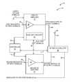
- FIG. 1illustrates an embodiment of a communication device or mobile terminal that includes an example of a multimode radio frequency (RF) power amplifier system having first RF amplifier, second RF amplifier, and RF switch circuitry.
- RFradio frequency
- FIG. 2illustrates another embodiment of the communication device or mobile terminal that includes another example of a multimode RF amplifier system having an auxiliary circuit configured as a power supply switching circuit.
- FIG. 3illustrates another embodiment of the communication device or mobile terminal that includes an example of an auxiliary circuit having control circuitry and a power supply switching circuit.
- FIG. 4illustrates another embodiment of the communication device or mobile terminal that includes an example of a multimode RF amplifier system having an auxiliary circuit that includes control circuitry, a power supply switching circuit, and RF switch circuitry.
- FIG. 5illustrates another embodiment of the communication device or mobile terminal that includes an example of a multimode RF amplifier system having a first RF amplifier, a second RF amplifier, and a third RF amplifier.
- FIG. 6illustrates another embodiment of the communication device or mobile terminal that includes an example of a multimode RF amplifier system having a first RF amplifier and a multi-standard RF amplifier.
- FIG. 7illustrates an exemplary RF module that includes one embodiment of an RF amplification device formed on a single semiconductor die.
- FIG. 8illustrates another embodiment of an RF amplification device formed on separate semiconductor dice.
- the multimode RF amplifier systemmay include a first RF amplifier having a first RF amplifier circuit and an auxiliary circuit configured to provide a service or a utility to a second RF amplifier.
- the first RF amplifier circuitmay support a first RF communication standard.
- the multimode RF amplifier systemmay also include a second RF amplifier having a second RF amplifier circuit.
- the second RF amplifier circuitmay support a second RF communication standard.
- the service or the utilitymay be provided only when the first RF amplifier is not transmitting or the first RF amplifier circuit is disabled.
- the auxiliary circuitmay generate a supply voltage for the second RF amplifier circuit.
- the auxiliary circuitmay provide the service or the utility to both the first RF amplifier and second RF amplifier.
- a multimode RF amplifier systemmay include a first RF amplifier and a second RF amplifier.
- a first electronic packagemay include the first RF amplifier, which may have a first RF amplifier circuit and an auxiliary circuit.
- a second electronic packagemay include the second RF amplifier, which may have a second RF amplifier circuit.
- the first RF amplifier circuitmay support a first RF communication standard.
- the second RF amplifier circuitmay support a second RF communication standard.
- the first RF amplifier circuitmay support a first operational mode of an RF communication standard, while the second RF amplifier circuit may support a second operational mode of the same RF communication standard.
- the auxiliary circuitmay provide a service or a utility to the second RF amplifier or the second RF amplifier circuit. In some embodiments, the auxiliary circuit may provide the service or the utility only when the first RF amplifier is not transmitting. For example, the auxiliary circuit may generate a supply voltage for the second RF amplifier circuit while a transmit enable state of the first RF amplifier circuit is set to off. However, the auxiliary circuit may not provide the same supply voltage to the first RF amplifier circuit while the transmit enable state of the first RF amplifier circuit is set to on. In other embodiments, the auxiliary circuit may provide the service or the utility to both the first RF amplifier and the second RF amplifier.
- the first RF amplifiermay include a first RF amplifier circuit configured to generate a first RF output signal.
- the first RF amplifiermay further include an auxiliary circuit configured to provide a utility to a second RF amplifier that is not used by the first RF amplifier to generate the first RF output signal.
- the utility provided by the auxiliary circuitmay enable the second RF amplifier to generate a second RF output signal.
- the first RF amplifiermay disable generation of the first RF output signal while the auxiliary circuit enables the second RF amplifier to generate the second RF output signal.
- the auxiliary circuitmay disable generation of the first RF output signal while the second RF amplifier generates the second RF output signal.
- the auxiliary circuitmay generate a supply voltage and provide the supply voltage to the second RF amplifier circuit.
- the supply voltagemay be a supply voltage generated by a switching circuit.
- the auxiliary circuitmay include control circuitry.
- the control circuitrymay include a control interface configured to receive control signals.
- the control circuitrymay include a control bus interface configured to receive control information for the second RF amplifier.
- the control circuitrymay provide or receive control signals from the second RF amplifier.
- the control circuitrymay receive control signals from the second RF amplifier.
- the control circuitrymay provide the control signals from the second RF amplifier to a controller via the control interface.
- the control circuitrymay provide information contained in the control signals to the controller via a control bus.
- control circuitrymay include a control signal interface configured to provide or receive control signals for various circuits.
- control circuitrymay govern the operation of the second RF amplifier as a function of one of a parameter, a command, a signal, and/or a combination thereof received from a master device.
- a master devicemay be a controller, a processor, a digital modem, a digital transceiver, and/or the like.
- an electronic devicemay include an electronic module board having a first RF amplifier.
- the first RF amplifierhas a first RF amplifier circuit configured to generate a first modulated RF output signal based on a first RF communication standard, and an RF switching converter configured to generate a supply voltage while the first RF amplifier circuit is unused.
- the electronic devicemay further include a first electronic package. At least a portion of the electronic module board may mount to the first electronic package.
- the electronic module boardmay also include a control bus interface configured to interface with a controller and a control interface configured to provide control signals to a second RF amplifier.
- the control bus interfacemay include a mobile industry processor interface (MIPI) RF front-end (RFFE) control interface.
- MIPImobile industry processor interface
- RFFERF front-end
- the electronic devicemay include a second electronic package that includes the second RF amplifier having a second RF amplifier circuit.
- the second RF amplifier circuitmay include a power supply input configured to receive the supply voltage generated by the RF switching converter.
- the second RF amplifiermay generate a second modulated RF output signal based on a second RF communication standard.
- an auxiliary circuit of the first RF amplifiermay be configured to provide a utility that is not used by the first RF amplifier but rather is used by a second RF amplifier.
- the utilitymay include generating or providing a current, a voltage, a command, a command interface, a microprocessor interface, a control interface, a measurement means or circuit, a supply voltage, a switch interface, and/or some combination thereof.
- the first RF amplifiermay include an auxiliary circuit configured to provide a service or a utility to the second RF amplifier, wherein the first RF amplifier is disabled while providing the service or the utility to the second RF amplifier.
- the first RF amplifiermay include control circuitry configured to control both the first RF amplifier and the second RF amplifier.
- the control circuitrymay configure the first RF amplifier to generate a first RF output signal only when the second RF amplifier is disabled or a transmit enable state of the second RF amplifier is set to off.
- the control circuitrymay configure the auxiliary circuit to support generation of a second RF output signal by the second RF amplifier only when the transmit enable state of the first RF amplifier is set to off.
- another embodiment of a multi-standard RF amplifier systemmay include a first RF amplifier in a first package and a second RF amplifier in a second package.
- the first RF amplifiermay include a first RF input configured to receive a first modulated RF input signal and a first RF output configured to generate a first RF output signal as a function of the first modulated RF input signal.
- the second RF amplifiermay include a second RF input configured to receive a second modulated RF input signal and a second RF output configured to generate a second RF output signal as a function of the second modulated RF input signal.
- the first RF amplifiermay be combined with an auxiliary circuit.
- the auxiliary circuitmay include an auxiliary signals interface configured to provide or receive auxiliary signals.
- the auxiliary circuitmay provide a service or a utility to the second RF amplifier.
- the auxiliary circuitmay include a switch-mode power supply converter configured to power the second RF amplifier.
- the service or the utility provided by the auxiliary circuitmay be generating and providing a supply voltage to the second RF amplifier.
- the auxiliary circuitmay provide the supply voltage to the second RF amplifier via the auxiliary signals interface.
- the auxiliary circuitmay include control circuitry having a first control interface in communication with the first RF amplifier, a second control interface in communication with the second RF amplifier, and a control bus interface.
- the second control interfacemay provide or receive control signals for the second RF amplifier to the auxiliary signals interface.
- the control circuitrymay further provide RF switch control signals to RF switch circuitry.
- the control circuitrymay provide the RF switch control signals to the RF switch circuitry via the auxiliary signals interface.
- some portion of the RF switch circuitrymay be in the same electronic package that includes the first RF amplifier and the auxiliary circuit.
- the control circuitrymay provide the RF switch control signals to the RF switch circuitry.
- the control circuitrymay provide a service or a utility to both the first RF amplifier and the second RF amplifier independent of a transmit enable state of the first RF amplifier and a transmit enable state of the second RF amplifier.
- control circuitrymay include a MIPI RFFE control circuit.
- control bus interfacemay communicate with a controller or microprocessor.
- the auxiliary circuitmay include an RF switch circuit.
- the RF switch circuitmay receive the first RF output signal and the second RF output signal.
- the RF switch circuitmay selectively provide the first RF output signal and the second RF output signal to an antenna for transmission.
- the control circuitrymay configure the RF switch circuit to switchably couple the antenna to one of several switch ports to provide a modulated RF receiver signal.
- FIG. 1depicts an embodiment of an electronic device 10 having a multimode RF amplifier system 20 .
- Embodiments of the electronic device 10may include a communication device, a mobile terminal, an information device, a computing device, a sensor system, an entertainment device, and/or some combination thereof.
- Embodiments of the electronic device 10may be configured to operate in a variety of modes and within various communication networks.
- some embodiments of the electronic device 10may be configured to operate in some combination of a 2G Global System for Mobile Communications (GSM)-based communication network, various embodiments of a 3G communication network, embodiments of a 4G Long Term Evolution (LTE) communication network, and embodiments of a Time Division Long Term Evolution (TD-LTE) communication network.
- GSMGlobal System for Mobile Communications
- LTELong Term Evolution
- TD-LTETime Division Long Term Evolution
- Some embodiments of the electronic device 10may include a digital baseband circuit or a digital modem circuit configured to interface with the multimode RF amplifier system 20 .
- the multimode RF amplifier system 20may support a combination of a GSM-based communication network and at least one of the various embodiments of an LTE communication network.
- the multimode RF amplifier system 20may support a 3G communication network.
- the multimode RF amplifier system 20may further support an embodiment of a 4G LTE communication network.
- the multimode RF amplifier system 20may support a combination of a TD-LTE communication network and at least one of the 3G communication network and the 4G LTE communication network.
- FIG. 1further depicts a block diagram of an embodiment of the multimode RF amplifier system 20 including a first RF amplifier 22 , a second RF amplifier 24 , a controller 26 , and RF switch circuitry 28 .
- the controller 26may be a processor. In some embodiments, the controller 26 may be a portion of or in communication with a digital baseband circuit or a digital modem circuit (not shown) of the electronic device 10 .
- some embodiments of the multimode RF amplifier system 20may include two or more modules or electronic packages configured to support multiple RF communication standards. For example, a first electronic package may include the first RF amplifier 22 . A second electronic package may include the second RF amplifier 24 .
- the first RF amplifier 22may include a first RF amplifier circuit 30 and auxiliary circuitry 32 .
- the first RF amplifier 22may be configured to support one or more RF communication standards, operational modes of an RF communication standard, one or more frequency bands associated with an RF communication standard, and/or some combination thereof.
- the first RF amplifier circuit 30may also be configured to support one or more RF communication standards, operational modes of an RF communication standard, one or more frequency bands associated with an RF communication standard, and/or some combination thereof.
- the first RF amplifier 22may receive one or more supply voltages 34 .
- the one or more supply voltages 34may be received from one or more power supply sources.
- the supply voltages 34may include multiple supply voltages.
- the supply voltages 34may include only one supply voltage.
- the one or more supply voltages 34may include a battery voltage received from a battery used to power the electronic device 10 .
- the supply voltages 34may be generated by a buck RF switching converter, a boost RF switching converter, a buck/boost RF switching converter, a charge pump, a multiple output charge pump, a linear regulator, a low-dropout linear regulator, a battery, and/or some combination thereof.
- the first RF amplifier 22may receive one or more first modulated RF input signals 36 .
- the first RF amplifier 22may provide the first modulated RF input signals 36 to the first RF amplifier circuit 30 .
- the electronic device 10may generate a respective one of the first modulated RF input signals 36 to be transmitted.
- the first RF amplifier circuit 30may generate a respective one of first modulated RF output signals 38 as a function of the respective one of the first modulated RF input signals 36 to be transmitted.
- the first RF amplifier 22may provide the respective one of the first modulated RF output signals 38 to be transmitted to the RF switch circuitry 28 .
- the electronic device 10may generate the respective one of the first modulated RF input signals 36 based on a mode of operation of the electronic device 10 and/or the available communication network.
- the electronic device 10may be configured to operate in a selected band of operation as a function of a selected modulation scheme or standard.
- the respective one of the first modulated RF input signals 36may include a low band GSM transmit signal or a high band GSM transmit signal.
- the electronic device 10may be configured as a quad-band GSM communication system.
- the electronic device 10may selectively provide the first RF amplifier circuit 30 with a respective one of the first modulated RF input signals 36 as a low band GSM transmit signal for operating in a 900 MHz band of a 2G GSM network, a high band GSM transmit signal for operating in a 1800 MHz band of a 2G GSM network, a low band GSM transmit signal for operating in an 850 MHz band of a 2G GSM network, and a high band GSM transmit signal for operating in a 1900 MHz band of a 2G GSM network for transmission.
- the first RF amplifier circuit 30may include a low band RF amplifier circuit and a high band RF amplifier circuit.
- the low band RF amplifier circuitmay be configured to receive the low band GSM transmit signals and the high band RF amplifier circuit may be configured to receive the high band GSM transmit signals.
- the low band RF amplifier circuitmay generate a low band GSM output signal in response to the low band GSM transmit signals.
- the low band RF amplifier circuitmay provide the low band GSM output signal as the respective one of the first modulated RF output signals 38 .
- the high band RF amplifier circuitmay generate a high band GSM output signal in response to the high band GSM transmit signals.
- the high band RF amplifier circuitmay provide the high band GSM output signal as the respective one of the first modulated RF output signals 38 .
- the electronic device 10may be configured as a tri-band GSM communication device.
- the first RF amplifier 22may be configured to operate in three frequency bands of operation.
- the first modulated RF input signals 36may include the low band GSM transmit signal for operating in the 850 MHz band of a 2G GSM network, the high band GSM transmit signal for operating in the 1800 MHz band of the 2G GSM network, and the high band GSM transmit signal operating in the 1900 MHz band of the 2G GSM network.
- the first modulated RF input signals 36may include the low band GSM transmit signal for operating in the 900 MHz band of the 2G GSM network, the high band GSM transmit signal for operating in the 1800 MHz band of the 2G GSM network, and the high band GSM transmit signal for operating in the 1900 MHz band of the 2G GSM network.
- the first modulated RF input signals 36may further include a respective first modulated RF input signal 36 to support a general packet radio service (GPRS).
- GPRSgeneral packet radio service
- the respective one of the first modulated RF input signals 36may include an eight phase-shift keying (8-PSK) encoded input signal to support a 2.5G data service, a 2.75G data service, and/or a combination thereof provided by a communication network.
- the first modulated RF input signals 36may include an 8-PSK encoded transmit signal to support an Enhanced Data Rates for a GSM Evolution (EDGE) service.
- EDGEEnhanced Data Rates for a GSM Evolution
- the EDGE servicemay also be referred to as an enhanced GPRS (EGPRS) service.
- EGPRSenhanced GPRS
- the controller 26may configure the first RF amplifier circuit 30 to generate a respective one of the first modulated RF output signals 38 as a function of one of the first modulated RF input signals 36 .
- the controller 26may include a first control interface configured to send and/or receive one or more first control signals 40 to or from the first RF amplifier 22 .
- the first RF amplifier 22may provide the first control signals 40 to the first RF amplifier circuit 30 and the auxiliary circuitry 32 .
- the controller 26may configure the first RF amplifier circuit 30 to transmit the respective one of the first modulated RF output signals 38 as a function of the first control signals 40 .
- the first control signals 40may include a transmit enable signal, a first RF amplifier circuit enable signal, one or more band select signals, one or more power mode signals, calibration signals, a power detector signal, one or more band select signals, one or more mode of operation control signals, a gain control signal, an output power mode signal, and/or some combination thereof.
- the first control signals 40may include a target supply voltage.
- the target supply voltagemay be a V RAMP signal.
- the V RAMP signalmay be a differential signal.
- the V RAMP signalmay be a digital signal or a differential digital signal.
- the first control signals 40may include auxiliary circuitry control signals.
- the auxiliary circuitry control signalsmay include the V RAMP signal for the second RF amplifier 24 .
- the auxiliary circuitry control signalsmay include an auxiliary circuit enable signal.
- the controller 26may provide only one V RAMP signal that may be operationally shared. For example, in some modes of operation of the multimode RF amplifier system 20 , the controller 26 may use the only one V RAMP signal to govern an operation of the first RF amplifier 22 and the second RF amplifier 24 .
- the first control signals 40may include one or more control bus signals configured to form a serial control bus or a parallel control bus.
- the control bus signalsmay include a MIPI RFFE control bus.
- the controller 26may include a MIPI RFFE control circuit configured to interface with the MIPI RFFE control bus.
- the first RF amplifier 22may include a MIPI RFFE control circuit configured to interface with the MIPI RFFE control bus.
- the first RF amplifier circuit 30may include a MIPI RFFE control circuit configured to interface with the MIPI RFFE control bus.
- the first RF amplifier 22may include a corresponding first control interface configured to receive and/or send the first control signals 40 .
- the controller 26may configure the first RF amplifier circuit 30 to operate in a high-gain mode of operation or a low-gain mode of operation. In the high-gain mode of operation, the first RF amplifier circuit 30 may operate in a high-power output mode. In the low-gain mode of operation, the first RF amplifier circuit 30 may operate in a low-power output mode.
- the controller 26may also include a second control interface configured to send and/or receive one or more second control signals 42 to the second RF amplifier 24 .
- the second RF amplifier 24may include a corresponding second control interface configured to receive and/or send the second control signals 42 .
- the controller 26may govern the operation of the second RF amplifier 24 as a function of the second control signals 42 .
- the second control signals 42may include a transmit enable signal, a first RF amplifier circuit enable signal, one or more band select signals, one or more power mode signals, calibration signals, a power detector signal, one or more mode of operation control signals, a gain control signal, an output power mode signal, and/or some combination thereof.
- the second control signals 42may include a target supply voltage.
- the target supply voltagemay be a V RAMP signal.
- the second control signals 42may include one or more control bus signals configured to form a serial control bus or a parallel control bus.
- control bus signalsmay be for a MIPI RFFE control bus.
- the second RF amplifier 24may provide a V RAMP signal via auxiliary signals 46 to the auxiliary circuitry 32 .
- the auxiliary circuitry 32may generate one or more supply voltages as a function of the V RAMP signal provided by the second RF amplifier 24 .
- the controller 26may configure the second RF amplifier 24 to operate in a selected band of operation based on a control signal received from a communication network.
- the controller 26may configure the second RF amplifier 24 to support one or more of the various embodiments of the 3G communication network standards and/or the several embodiments of the 4G LTE communication network standards.
- the controller 26may configure the second RF amplifier 24 to operate within one of the allocated frequency bands for a 3G communication network.
- the controller 26may further include an RF switch control interface configured to send and/or receive one or more RF switch control signals 44 to the RF switch circuitry 28 .
- the RF switch circuitry 28may include a corresponding RF switch control interface configured to receive and/or send the RF switch control signals 44 .
- some embodiments of the RF switch circuitry 28may include an RF switch circuit having an antenna port, multiple switch ports, and a switch circuit control interface.
- the switch circuit control interfacemay be in communication with the controller 26 via the RF switch control signals 44 .
- the controller 26may configure the RF switch control signals 44 to control the operation of the RF switch circuit as a function of a modulation mode in which the electronic device 10 is configured to operate.
- the RF switch circuitry 28may include a MIPI RFFE control circuit. Similar to the first control signals 40 and the second control signals 42 , in some embodiments, the RF switch control signals 44 may include a MIPI RFFE control bus.
- the first control interface and the second control interface of the controller 26 , the first RF amplifier 22 , and the second RF amplifier 24may include digital output interfaces, digital input interfaces, analog output interfaces, and analog input interfaces.
- the controller 26may be configured to read or write various parameter values, control settings, and register values to the first RF amplifier 22 to govern the operation of the first RF amplifier circuit 30 and the auxiliary circuitry 32 .
- the controller 26may assert and/or de-assert the first control signals 40 to govern the operation of the first RF amplifier 22 , the first RF amplifier circuit 30 , the auxiliary circuitry 32 , and/or some combination thereof.
- the controller 26may sense a signal level of at least one of the first control signals 40 to detect an interrupt signal, a status, an operational mode, an error condition, a calibration state, a calibration value, and/or some combination thereof.
- the controller 26may include an analog-to-digital converter configured to receive an analog level signal from the first RF amplifier 22 .
- the controller 26may configure the auxiliary circuitry 32 to generate or receive one or more of the auxiliary signals 46 via the first control signals 40 .
- the auxiliary circuitry 32may include an auxiliary signal interface configured to provide one or more of the auxiliary signals 46 to the second RF amplifier 24 .
- the auxiliary signal interfacemay be further configured to receive one or more of the auxiliary signals 46 from the second RF amplifier 24 .
- the second RF amplifier 24may provide the auxiliary signals 46 that include control signals, feedback signals, feed-forward control signals, power supply signals, supply voltages, data signals, analog signals, and digital data signals.
- auxiliary circuitry 32may be configured to provide a service or a utility to the second RF amplifier 24 while the first RF amplifier circuit 30 is disabled. In other embodiments, the auxiliary circuitry 32 may be further configured to provide a service or a utility to both the first RF amplifier 22 and the second RF amplifier 24 . In still other embodiments, the auxiliary circuitry 32 may be configured to provide a service or a utility to a portion of the electronic device 10 to generate one or more second modulated RF output signals 52 that are unsupported by the first RF amplifier circuit 30 .
- auxiliary circuitry 32may be configured to provide a service or a utility to the second RF amplifier 24 as a function of a selected modulation mode or a characteristic of a data transmission to be sent by the electronic device 10 .
- Some embodiments of the auxiliary circuitry 32may include multiple auxiliary circuits to provide two or more services or utilities.
- a first service or utilitymay include generating a supply voltage to be provided to a second RF amplifier circuit 48 .
- a second service or utilitymay be to provide a control function to the second RF amplifier circuit 48 or the second RF amplifier 24 .
- the second RF amplifier 24may be configured to support one or more RF communication standards, operational modes of an RF communication standard, one or more frequency bands associated with an RF communication standard, and/or some combination thereof.
- the second RF amplifier circuit 48may be configured to support one or more RF communication standards, operational modes of an RF communication standard, one or more frequency bands associated with an RF communication standard, and/or some combination thereof.
- the second RF amplifier 24may include an auxiliary signals interface configured to receive and provide the one or more auxiliary signals 46 .
- the auxiliary signals 46may include one or more supply voltages generated by the auxiliary circuitry 32 to enable the operation of the second RF amplifier 24 .
- the one or more supply voltagesmay correspond to one or more supply voltages provided to the second RF amplifier circuit 48 while the first RF amplifier circuit 30 is disabled.
- the auxiliary signals 46may include an analog measurement signal of a temperature or a voltage associated with the second RF amplifier 24 .
- the second RF amplifier 24may be configured to selectively provide a temperature measurement of a portion of the second RF amplifier circuit 48 as one of the auxiliary signals 46 to the first RF amplifier 22 .
- the second RF amplifier 24may be further configured to provide an analog measurement of a supply voltage used by the second RF amplifier circuit 48 .
- the second RF amplifier 24may provide the analog measurement signal to the controller 26 as one of the second control signals 42 .
- the second RF amplifier 24may include the second RF amplifier circuit 48 .
- the second RF amplifier 24may receive one or more second modulated RF input signals 50 .
- the controller 26may configure the second RF amplifier 24 to provide one of the second modulated RF input signals 50 to the second RF amplifier circuit 48 .
- the second RF amplifier circuit 48may be configured to receive a respective one of the second modulated RF input signals 50 .
- the second RF amplifier circuit 48may include one or more second RF amplifier outputs configured to selectively generate the second modulated RF output signals 52 .
- the controller 26may generate band select signals to configure the second RF amplifier circuit 48 and the second RF amplifier 24 to generate a selected one of the second modulated RF output signals 52 .
- the second RF amplifier 24may provide the generated one of the second modulated RF output signals 52 to the RF switch circuitry 28 for transmission.
- the RF switch circuitry 28may include an antenna interface in communication with an antenna signal path 54 .
- the antenna signal path 54may provide a communication path between the antenna interface of the RF switch circuitry 28 and an antenna 56 .
- the antenna signal path 54may include front-end circuitry configured to couple the antenna 56 to the RF switch circuit of the RF switch circuitry 28 .
- the antenna signal path 54may include a transmission line.
- the impedance of the transmission line at the antenna 56may be substantially matched to an impedance of the antenna 56 .
- the impedance of the transmission line at the RF switch circuitry 28may be substantially matched to the impedance of the RF switch circuitry 28 .
- the RF switch circuitry 28may be configured to output one or more modulated RF receiver signals 58 .
- the modulated RF receiver signals 58may be a differential signal.
- the RF switch circuitry 28may include filter circuitry (not shown) and front-end circuitry (not shown) configured to interface with the RF switch circuit of the RF switch circuitry 28 .
- the filter circuitrymay include a number of filter circuits.
- some of the filter circuitsmay include a filter input and a filter output.
- some of the filter circuitsmay include a surface acoustic wave (SAW) filter.
- SAWsurface acoustic wave
- some of the filter circuitsmay be configured as duplexer circuits.
- each duplexer circuitmay include an antenna port, a transmit signal port, and a receive signal port.
- the RF switch circuitmay switchably couple the antenna 56 to one of the number of switch ports of the RF switch circuit based on the RF switch control signals 44 provided to the RF switch circuitry 28 .
- the RF switch circuitry 28may provide each of the first modulated RF output signals 38 to a respective switch port.
- Each of the first modulated RF output signals 38may be associated with a respective one of the modulated RF receiver signals 58 .
- the RF switch circuitmay switchably couple the antenna port of the RF switch circuit to a filter circuit configured to obtain the respective one of the modulated RF receiver signals 58 .
- the filter circuitmay band-pass filter the signal present at the antenna port of the RF switch circuit to obtain the respective one of the modulated RF receiver signals 58 .
- the controller 26may configure the first RF amplifier 22 to generate a GSM high band transmit signal as the generated one of the first modulated RF output signals 38 to be transmitted.
- the controller 26may further configure the RF switch circuitry 28 to switchably provide the GSM high band transmit signal to the antenna 56 .
- the controller 26may configure the RF switch circuit to switchably couple the antenna 56 to a filter input of a filter circuit configured as a GSM high band receive filter.
- the GSM high band receive filtermay band-pass filter the GSM high band receive signal to provide a GSM high band receiver signal as one of the modulated RF receiver signals 58 .
- the controller 26may configure the first RF amplifier 22 to generate a GSM low band transmit signal as the generated one of the first modulated RF output signals 38 for transmission.
- the controller 26may further configure the RF switch circuitry 28 to switchably provide the GSM low band transmit signal to the antenna 56 .
- the controller 26may configure the RF switch circuit to switchably couple the antenna 56 to a filter input of a filter circuit configured as a GSM low band receive filter.
- the GSM low band receive filtermay band-pass filter the GSM low band receive signal to provide a GSM low band receiver signal as one of the modulated RF receiver signals 58 .
- the RF switch circuitry 28may include a duplexer circuit for each of the second modulated RF output signals 52 .
- the second RF amplifier 24may be configured to provide each of the second modulated RF output signals 52 to a transmit signal port of a respective duplexer circuit.
- the controller 26may configure the RF switch circuit to switchably couple the receive signal port of the respective duplexer circuit to the antenna port of the respective duplexer circuit.
- the respective duplexer circuitmay band-pass filter the signal present at the antenna port of the RF switch circuit to provide a respective one of the modulated RF receiver signals 58 that is associated with the one of the second modulated RF output signals 52 provided to the transmit signal port of the respective duplexer circuit.
- the antenna port of each of the respective duplexer circuitsmay be in communication with a respective switch port of the RF switch circuit.
- the RF switch circuitry 28may include a duplexer circuit configured to support one of the 3G frequency bands.
- the controller 26may configure the RF switch circuit to switchably couple the antenna 56 to the antenna port of the duplexer circuit.
- the electronic device 10may generate a respective one of the second modulated RF input signals 50 that corresponds to the one of the 3G frequency bands in which the electronic device 10 is configured to operate.
- the duplexer circuitmay obtain a respective one of the modulated RF receiver signals 58 as an output at the receive signal port of the duplexer.
- the second RF amplifier 24may include the duplexer circuits.
- the controller 26may govern the operation of the second RF amplifier 24 via the second control signals 42 .
- the controller 26may read or write various parameter values, control settings, and register values of the second RF amplifier 24 to govern the operation of the second RF amplifier circuit 48 .
- the controller 26may assert and/or de-assert one or more of the second control signals 42 to govern the operation of the second RF amplifier 24 .
- the controller 26may sense a signal level of one or more of the second control signals 42 to detect an interrupt signal, a status, an operational mode, an error condition, a calibration state, a calibration value, and/or some combination thereof related to the operation of the second RF amplifier 24 .
- the controller 26may include an analog-to-digital converter configured to receive an analog level signal from the second RF amplifier 24 .
- the controller 26may govern operation and/or determine the status of the second RF amplifier circuit 48 via the second control signals 42 .
- the controller 26may read and/or write various parameter values, control settings, and register values of the second RF amplifier circuit 48 .
- the controller 26may configure the second RF amplifier circuit 48 as a function of the various parameter values, control settings, and register values.
- some of the second control signals 42may provide various control level signals to set a mode of operation of the second RF amplifier 24 .
- the controller 26may generate one or more of the second control signals 42 to set a gain of the second RF amplifier circuit 48 and/or calibrate portions of the second RF amplifier circuit 48 .
- the controller 26may set one or more of the second control signals 42 to configure the second RF amplifier 24 to generate a respective one of the second modulated RF output signals 52 with a respective one of the second modulated RF input signals 50 .
- the first RF amplifier 22may be configured to provide an analog measurement signal to the controller 26 .
- the first RF amplifier 22may provide an analog temperature measurement signal corresponding to a temperature measurement for a portion of the first RF amplifier 22 to the controller 26 .
- the temperature measurementmay correspond to a temperature of the first RF amplifier circuit 30 , the auxiliary circuitry 32 , a portion of the auxiliary circuitry 32 , or some combination thereof.
- the first RF amplifier 22may be configured to selectively provide a temperature measurement of one of the portions, circuits, sub-circuits, circuitry, or sub-circuitry of the first RF amplifier 22 as the analog measurement signal.
- the first RF amplifier 22may be further configured to selectively provide an analog measurement signal based on one of the supply voltages 34 provided to the first RF amplifier 22 .
- the first RF amplifier 22may be configured to provide a voltage measurement of the battery voltage as the analog measurement signal to the controller 26 .
- the first RF amplifier 22may be configured to further provide a voltage measurement of a supply voltage to the first RF amplifier circuit 30 as the analog measurement signal.
- the auxiliary circuitry 32may include a digital-to-analog converter.
- the controller 26may configure the auxiliary circuitry 32 to digitize a selected one of the auxiliary signals 46 generated by the second RF amplifier 24 .
- the auxiliary circuitry 32may digitize the selected one of the auxiliary signals 46 and provide a digital measurement of the selected one of the auxiliary signals 46 to the controller 26 via the first control signals 40 .
- the service or the utility of the digital-to-analog convertermay be used only to sample the auxiliary signals 46 generated by the second RF amplifier 24 or provided to the second RF amplifier 24 .
- the digital-to-analog convertermay provide a service or a utility to both the first RF amplifier 22 and the second RF amplifier 24 .
- the one or more first control signals 40may include a target supply voltage.
- the target supply voltagemay be a V RAMP signal.
- the auxiliary circuitry 32may use a target supply voltage to generate one or more supply voltage voltages provided to the second RF amplifier 24 .
- the target supply voltagemay be provided from the second RF amplifier 24 to the auxiliary circuitry 32 as one of the auxiliary signals 46 .
- the auxiliary circuitry 32may use the target supply voltage to generate a modulated supply voltage that is provided to an output stage of the second RF amplifier circuit 48 .
- the first RF amplifier 22may be selectively configured to provide an analog voltage measurement of the supply voltages generated by the auxiliary circuitry 32 to the controller 26 .
- the first control signals 40may include a first transmit enable signal provided to the first RF amplifier 22 .
- the first RF amplifier circuit 30may operate in a transmit enabled state and a transmit disabled state.
- the controller 26may de-assert the first transmit enable signal to disable generation of the first modulated RF output signals 38 .
- the first RF amplifier 22may set the transmit enable state of the first RF amplifier circuit 30 to the transmit disabled state.
- the controller 26may assert the first transmit enable signal to enable the first RF amplifier 22 to transmit a respective one of the first modulated RF output signals 38 .
- the first control signals 40may further include an auxiliary circuitry enable signal having an on state and an off state.
- the controller 26may enable the auxiliary circuitry 32 by asserting the auxiliary circuitry enable signal.
- the controller 26may disable the auxiliary circuitry 32 by de-asserting the auxiliary circuitry enable signal.
- the operation of the first RF amplifier circuit 30 and the auxiliary circuitry 32may be mutually exclusive.
- the controller 26may configure the auxiliary circuitry 32 to be in an off state while the first RF amplifier circuit 30 is in an on state.
- the controller 26may configure the first RF amplifier circuit 30 to be in an off state while the auxiliary circuitry 32 is in an on state.
- the first control signals 40may include a transmit enable signal configured to enable and disable the first RF amplifier circuit 30 .
- the controller 26may assert the transmit enable signal to enable the first RF amplifier 22 to generate the first modulated RF output signals 38 as a function of the one of the first modulated RF input signals 36 .
- the first RF amplifier 22may automatically disable the auxiliary circuitry 32 based on the assertion of the transmit enable signal.
- the controller 26may de-assert the transmit enable signal to disable the first RF amplifier circuit 30 , and automatically enable the auxiliary circuitry 32 based on the de-assertion of the transmit enable signal.
- the auxiliary circuitry 32may provide a utility or a service to the second RF amplifier 24 that is not used by the first RF amplifier 22 to generate the first modulated RF output signals 38 .
- the auxiliary circuitry 32may provide a service or a utility to the second RF amplifier 24 to enable the second RF amplifier circuit 48 to generate a respective one of the second modulated RF output signals 52 .
- the auxiliary circuitry 32may include a power supply circuit configured to generate supply voltages to enable the operation of the second RF amplifier 24 .
- a supply voltagemay include a modulated supply voltage that is substantially related to a target supply voltage.
- the target supply voltagemay be related to an envelope of a respective one of the second modulated RF input signals 50 to be transmitted.
- the supply voltages generated by the auxiliary circuitry 32are provided to the second RF amplifier circuit 48 .
- the second RF amplifier circuit 48may use the generated supply voltages to generate a respective one of the second modulated RF output signals 52 .
- the auxiliary circuitry 32may not provide the supply voltages to the first RF amplifier circuit 30 .
- the supply voltages generated by the auxiliary circuitry 32may not be used by the first RF amplifier 22 to generate any of the first modulated RF output signals 38 .
- the first RF amplifier 22 or the controller 26may disable the power supply circuit of the auxiliary circuitry 32 while the first RF amplifier circuit 30 is generating a respective one of the first modulated RF output signals 38 .
- the auxiliary circuitry 32may provide one or more supply voltages as the auxiliary signals 46 to the second RF amplifier 24 .
- the supply voltagesmay be provided to the second RF amplifier 24 .
- the voltage level of the supply voltagesmay be a function of the supply voltages 34 and the target supply voltage.
- the supply voltagesmay be generated as a function of a V RAMP signal.
- the second RF amplifier circuit 48may use the one or more supply voltages to generate a respective one of the second modulated RF output signals 52 .
- the auxiliary circuitry 32may disable the first RF amplifier circuit 30 while generating the supply voltages for the second RF amplifier 24 .
- the first control signals 40may include one or more band select control signals.
- the band select control signalsmay select a band of operation of the first RF amplifier 22 .
- the first RF amplifier 22may include a first RF signal path and a second RF signal path.
- the first RF amplifier circuit 30may include a high band RF amplifier circuit and a low band RF amplifier circuit.
- the first RF signal pathmay include the high band RF amplifier circuit.
- the second RF signal pathmay include the low band RF amplifier circuit.
- the first RF amplifier 22may configure the first RF amplifier circuit 30 to enable one of the high band RF amplifier circuit and the low band RF amplifier circuit.
- the band select control signalsmay further configure the first RF signal path to operate in one of the 1800 MHz band or the 1900 MHz band.
- the band select control signalsmay further configure the second RF signal path to operate in one of the 850 MHz band or the 900 MHz band.
- the first RF amplifier 22may be configured to disable those portions of the first RF amplifier 22 that are unused as a function of the band selected for transmission.
- the first control signals 40may further include one or more power mode signals to govern the gain of the first RF amplifier 22 while generating the one or more first modulated RF output signals 38 .
- the power mode signalsmay configure the first RF amplifier 22 to operate in a high power mode, a medium power mode, a low power mode, and/or an ultra low power mode.
- the first RF amplifier 22may adjust a quiescent current or bias current to maintain linear operation of the first RF amplifier 22 during a data transmission.
- the first control signals 40may further include one or more modulation mode signals.
- the controller 26may selectively set the one or more modulation mode signals to select a different modulation mode.
- the first RF amplifier 22may be configured to provide a respective one of the first modulated RF output signals 38 .
- the first RF amplifier 22 and the first RF amplifier circuit 30generate a high band GSM output signal as a function of a first modulation mode.
- the first RF amplifier 22 and the first RF amplifier circuit 30generate a Wideband Code Division Multiplexing (WCDM) modulated output signal for transmission as a function of a second modulation mode.
- WCDMWideband Code Division Multiplexing
- the first control signals 40may further include one or more calibration control signals.
- the controller 26may use the calibration control signals to calibrate the first RF amplifier 22 , the first RF amplifier circuit 30 , and the auxiliary circuitry 32 .
- the first control signals 40may further include one or more auxiliary circuitry control signals to configure the auxiliary circuitry 32 to provide a utility or service.
- the controller 26may set the auxiliary circuitry control signals to govern the operation of the auxiliary circuitry 32 to provide a selected utility or service to the second RF amplifier 24 .
- the auxiliary circuitry control signalsmay configure the auxiliary circuitry 32 to provide at least one supply voltage to the second RF amplifier 24 .
- the second control signals 42may include control signals similar to the first control signals 40 .
- the one or more second control signals 42may include one or more band select control signals, power mode signals, modulation mode signals, a transmit enable signal, and/or a combination thereof.
- the second control signals 42may include one or more modulation mode signals.
- the modulation mode signalsmay configure the second RF amplifier 24 to operate in one of a number of modulation modes.
- the modulation mode signalsmay configure the second RF amplifier 24 to generate one of the one or more second modulated RF output signals 52 as a function of a selected modulation algorithm or scheme.
- Example modulation algorithms or schemesmay include Gaussian minimum-shift keying (GMSK) modulation, 8-PSK modulation, Wideband Code Division Multiple Access (W-CDMA) modulation, or orthogonal frequency division multiple access (OFDMA) modulation.
- GMSKGaussian minimum-shift keying
- W-CDMAWideband Code Division Multiple Access
- OFDMAorthogonal frequency division multiple access
- the band select signalsmay configure the second RF amplifier 24 to generate a respective one of the one or more second modulated RF output signals 52 in a particular band of operation of the communication network.
- the power mode signalsmay configure the second RF amplifier circuit 48 to operate in a desired output power mode or along a selected iso-gain curve.
- the power mode signalsmay configure the second RF amplifier circuit 48 to operate in a high power mode, a medium power mode, a low power mode, an ultra low power mode, and a standby mode based on control information provided to the electronic device 10 from the communication network.
- the auxiliary signals 46may include one or more feedback signals, feed-forward signals, or control signals generated by the second RF amplifier 24 .
- the second RF amplifier 24may provide a feedback voltage or current to the auxiliary circuitry 32 .
- the auxiliary circuitry 32may use the feedback voltage or current to regulate a supply voltage provided to the second RF amplifier circuit 48 .
- the controller 26may configure the auxiliary circuitry 32 to generate supply voltages to enable the second RF amplifier circuit 48 .
- the controller 26may configure the auxiliary circuitry 32 to provide a regulated DC supply voltage to the second RF amplifier circuit 48 .
- the second RF amplifier 24may configure the auxiliary circuitry 32 to operate as one of a buck switch-mode power supply, a boost switch-mode power supply, a buck/boost switch-mode power supply, or a pseudo-envelope tracking power supply.
- the multimode RF amplifier system 20may include multiple packages of integrated circuits, integrated circuit modules, discrete components, and/or combinations thereof.
- the multimode RF amplifier system 20may include a first package that includes the first RF amplifier 22 and a second package that includes the second RF amplifier 24 .
- the multimode RF amplifier system 20may include a third package that includes the RF switch circuitry 28 .
- the controller 26may be remote from the multimode RF amplifier system 20 .
- FIG. 2depicts a block diagram of an embodiment of a multimode RF amplifier system 20 A configured to provide the supply voltages from first RF amplifier 22 A to the second RF amplifier 24 .
- the multimode RF amplifier system 20 Amay include an embodiment of auxiliary circuitry 32 A having a power supply switching circuit 60 .
- the power supply switching circuit 60may provide the supply voltages to the second RF amplifier 24 as one or more supply voltages.
- the auxiliary signals 46may include the supply voltages provided to the second RF amplifier 24 .
- the power supply switching circuit 60may generate at least one of the supply voltages as a function of an expected output power of a respective one of the second modulated RF output signals 52 to be transmitted.
- at least one of the supply voltagesis generated as a function of an envelope of the respective one of the second modulated RF output signals 52 to be transmitted.
- the electronic device 10may be configured to operate in a communication network using a modulation algorithm, scheme, or frequency band that is unsupported by the first RF amplifier 22 A.
- the electronic device 10may receive a user input to a user interface or via a user interface device to select a mode of operation that is supported by the second RF amplifier 24 .
- the controller 26may configure the first RF amplifier circuit 30 to cease transmission or disable the first RF amplifier circuit 30 .
- the controller 26may configure the power supply switching circuit to generate at least one of the supply voltages as a function of a mode of operation of the second RF amplifier 24 or the second RF amplifier circuit 48 .
- the controller 26may provide the power supply switching circuit 60 with a target supply voltage level for at least some of the supply voltages to be generated.
- the target supply voltage levelmay be a DC voltage level.
- the target supply voltage levelmay be based on a minimum voltage parameter associated with a sub-circuit of the second RF amplifier circuit 48 .
- the second RF amplifier circuit 48may include a driver circuit, biasing circuitry, Complementary Metal-Oxide Semiconductor (CMOS) logic circuitry, and an output stage.
- CMOS logic circuitrymay be configured to receive a logic circuitry supply voltage.
- the biasing circuitrymay be configured to receive a biasing circuitry supply voltage.
- the output stagemay be configured to receive an output stage supply voltage.
- the output stagemay be configured to operate with an output stage supply voltage that is a modulated supply voltage that substantially tracks an envelope of the respective one of the second modulated RF input signals 50 to be transmitted.
- the driver circuitmay be configured to receive a driver circuit supply voltage. In other embodiments, the driver circuit may be configured to receive the output stage supply voltage.
- the controller 26may configure the power supply switching circuit 60 to generate the driver circuit supply voltage, the logic circuitry supply voltage, and the biasing circuitry supply voltage as a function of minimum voltage parameters associated with each of the driver circuit, the CMOS logic circuitry, and the biasing circuitry.
- the power supply switching circuit 60may be configured to provide the driver circuit supply voltage, the logic circuitry supply voltage, and the biasing circuitry supply voltage to the second RF amplifier 24 as the auxiliary signals 46 .
- the power supply switching circuit 60may be a charge pump configured to generate one or more charge pump output voltages.
- the charge pump output voltagesmay be generated as a function of a charge pump clock and a voltage level of at least one of the supply voltages 34 .
- the controller 26may configure the power supply switching circuit 60 to generate the charge pump output voltages as a function of a battery voltage.
- the charge pump voltagesmay be provided as a set of the supply voltages to the second RF amplifier 24 .
- some embodiments of the power supply switching circuit 60may include a switching network, charge pump control circuitry, an output capacitor for each of the supply voltages to be generated by the charge pump, and only two flying capacitors arranged in the switching network.
- the charge pump control circuitrymay control the switching network to switchably couple the only two flying capacitors in various arrangements with respect to one of the supply voltages 34 , ground, and each of the output capacitors to generate the charge pump output voltages.
- the power supply switching circuit 60may be configured to operate as a buck switching power converter to provide the one or more supply voltages to the second RF amplifier 24 .
- the power supply switching circuit 60may be configured to operate as a bang-bang switch-mode power converter.
- the controller 26may configure the power supply switching circuit 60 to generate one or more supply voltages to enable the second RF amplifier circuit 48 to generate a respective one of the second modulated RF output signals 52 .
- the controller 26may configure the power supply switching circuit 60 to provide a supply voltage to the output stage of the second RF amplifier circuit 48 based on an expected dynamic range of a respective one of the second modulated RF input signals 50 used to generate the respective one of the second modulated RF output signals 52 .
- the controller 26may configure the power supply switching circuit 60 to generate the supply voltage based on a target supply voltage level to maintain linear function of the second RF amplifier circuit 48 .
- the controller 26may configure the power supply switching circuit 60 to operate as a boost switch-mode power supply.
- the controller 26may obtain a voltage measurement of the battery voltage from the first RF amplifier 22 A. Based on a target supply voltage level and the voltage measurement of the battery voltage, the controller 26 may configure the boost switch-mode power supply to generate a supply voltage that is greater than the battery voltage.
- the power supply switching circuit 60may provide the supply voltage to the output stage of the second RF amplifier circuit 48 .
- the controller 26may configure the boost switch-mode power supply to provide a supply voltage that is substantially equal to the target supply voltage level that is greater than the battery voltage.
- the power supply switching circuit 60may be configured to operate as a buck-boost switch-mode power supply.
- the controller 26may configure the power supply switching circuit 60 to generate the supply voltage to be provided to the second RF amplifier circuit 48 by either bucking or boosting the battery voltage as a function of the battery voltage and the target supply voltage level.
- the power supply switching circuit 60may be configured to operate as an envelope tracking power supply.
- the controller 26may provide a target supply voltage as one of the first control signals 40 .
- the target supply voltagemay be a V RAMP signal.
- the V RAMP signalmay be a differential V RAMP signal.
- the V RAMP signalmay be frequency-compensated to compensate for a frequency response of the power supply switching circuit 60 .
- the power supply switching circuit 60may generate a modulated supply voltage that substantially tracks the envelope of the respective one of the second modulated RF input signals 50 used to generate a respective one of the second modulated RF output signals 52 to be transmitted.
- the power supply switching circuit 60may provide the modulated supply voltage to the second RF amplifier circuit 48 .
- the second RF amplifier circuit 48may generate the respective one of the second modulated RF output signals 52 as a function of the respective one of the second modulated RF input signals 50 and the modulated supply voltage.
- the multimode RF amplifier system 20 Bincludes another embodiment of first RF amplifier 22 B.
- the first RF amplifier 22 Bmay be in communication with the controller 26 via a control bus 62 .
- the first RF amplifier 22 Bmay be further configured to receive a V RAMP signal 64 .
- the first RF amplifier 22 Bmay be in communication with second RF amplifier 24 A and RF switch circuitry 28 A via auxiliary signals 46 A.
- Some embodiments of the second RF amplifier 24 A and the RF switch circuitry 28 Amay be substantially similar to the embodiments of the second RF amplifier 24 and the RF switch circuitry 28 depicted in FIG. 1 and FIG. 2 .
- the controller 26may govern the operation of the second RF amplifier 24 A and the RF switch circuitry 28 A via the auxiliary signals 46 A.
- the auxiliary signals 46 Amay include some or all of the one or more RF switch control signals 44 .
- the embodiments of auxiliary circuitry 32 Bmay be similar to the embodiments of the auxiliary circuitry 32 and the auxiliary circuitry 32 A, depicted in FIG. 1 and FIG. 2 , respectively.
- the auxiliary circuitry 32 Bmay further include control circuitry 66 configured to control the second RF amplifier 24 A and the RF switch circuitry 28 A via the auxiliary signals 46 A.
- the control circuitry 66may include a control interface in communication with the control bus 62 and further configured to receive the V RAMP signal 64 .
- the control circuitry 66may include a differential interface configured to receive a differential V RAMP signal 64 .
- the control bus 62may be a serial control bus.
- the control bus 62may be a multi-signal serial control bus.
- the control bus 62may include a clock signal, a slave select signal, a master output slave input signal, and/or a slave output master input signal.
- control bus 62may include a two wire bus.
- the control bus 62may include a serial data line signal and a serial clock signal.
- the control bus 62may be a single-signal control bus.
- the control bus 62may include a UNI/O bus that has a serial clock and a data input/output signal.
- the control bus 62may be a parallel control bus.
- the control bus 62may be an asynchronous bus.
- the control bus 62may be a synchronous bus.
- the control bus 62may include an RFFE control bus.
- the control bus 62may be a MIPI RFFE control bus.
- the control bus 62 and the first RF amplifier 22 Bmay each include a MIPI RFFE control bus interface.
- the control circuitry 66may include a MIPI RFFE control interface control circuit.
- control circuitry 66may include control register circuitry, memory, logic unit circuitry, combinational logic, state machine circuitry, a microcontroller, digital logic circuitry, analog control circuitry, digital buffer circuitry, analog buffer circuitry, comparator circuitry, counter circuitry, control bus interface circuitry, firmware, an address decoder, read only memory (ROM), random access memory (RAM), flash memory, signal line driver circuitry, and/or a combination thereof.
- control circuitry 66may further include the MIPI RFFE control bus interface.
- control bus 62may further include analog interfaces, as previously described.
- the control circuitry 66may be configured to receive control information via the control bus 62 and the V RAMP signal 64 .
- the controller 26may configure the control circuitry 66 to govern the operation of the first RF amplifier 22 B, the second RF amplifier 24 A, and the RF switch circuitry 28 A as a function of the control information.
- the control informationmay include various control signals, parameter values, control settings, and register values to govern the operation of the second RF amplifier 24 A, the RF switch circuitry 28 A, and the first RF amplifier circuit 30 .
- control circuitry 66can be configured to send and/or receive control signals to govern the operation of the second RF amplifier 24 A, the RF switch circuitry 28 A, the first RF amplifier circuit 30 , and the power supply switching circuit 60 .
- the control circuitry 66may interface with the power supply switching circuit 60 via one or more power supply control signals 68 .
- the control circuitry 66may interface with the first RF amplifier circuit 30 via one or more first RF amplifier control signals 70 .
- the control circuitry 66may interface with the auxiliary signal interface of the auxiliary circuitry 32 B via one or more auxiliary control signals 72 .
- the auxiliary control signals 72may include control signals to govern the operation of the second RF amplifier 24 A and the RF switch circuitry 28 A.
- the auxiliary control signals 72may include feedback signals or control signals provided by the second RF amplifier 24 A and the RF switch circuitry 28 A.
- the controller 26may provide control information to the control circuitry 66 via the control bus 62 .
- the control informationmay include a command, a register setting, a parameter setting, and/or a combination thereof.
- the controller 26may query the control circuitry 66 to request the control information and/or status information. For example, the controller 26 may query the control circuitry 66 to obtain a measurement of a voltage or current.
- the control circuitry 66may configure the auxiliary circuitry 32 B to provide a service or a utility for the first RF amplifier 22 B, the second RF amplifier 24 A, the first RF amplifier circuit 30 , the second RF amplifier circuit 48 , and/or a combination thereof.
- the power supply switching circuit 60may interface with the auxiliary signal interface of the auxiliary circuitry 32 B via one or more power supply signals 74 .
- the power supply switching circuit 60may generate one or more supply voltages.
- the one or more supply voltagesmay be provided to the second RF amplifier 24 A as the power supply signals 74 .
- the power supply signals 74may include control signals, feedback signals, feed-forward signals, and/or a combination thereof from the second RF amplifier 24 A.
- control circuitry 66may receive control information from the controller 26 . Based on the control information received from the controller 26 , the control circuitry 66 may configure the operation of the first RF amplifier circuit 30 via the first RF amplifier control signals 70 . Similarly, the control circuitry 66 may configure the operation of the power supply switching circuit 60 via the power supply control signals 68 . In addition, the control circuitry 66 may configure the operation of the second RF amplifier 24 A via the auxiliary signals 46 A as a function of the control information. Likewise, in some embodiments, the control circuitry 66 may govern control of the RF switch circuitry 28 A via the auxiliary signals 46 A.
- control circuitry 66may provide the second control signals 42 as control signal(s) via the auxiliary signals 46 A.
- control circuitry 66may be configured to provide the RF switch control signals 44 to the RF switch circuitry 28 A via the auxiliary signals 46 A.
- FIG. 4depicts another embodiment of the electronic device 10 having an embodiment of a multimode RF amplifier system 20 C.
- the multimode RF amplifier system 20 Cmay include an embodiment of the first RF amplifier 22 C that is similar to the first RF amplifier 22 B depicted in FIG. 3 .
- auxiliary circuitry 32 Cmay further include some portions of the RF switch circuitry 28 A depicted in FIG. 3 .
- the first RF amplifier 22 Cmay further include RF switch circuitry 76 that is similar to the RF switch circuitry 28 and 28 A, depicted in FIGS. 1-3 .
- the control circuitry 66may be further configured to govern the operation of the RF switch circuitry 76 via one or more switch control signals 78 .
- the switch control signals 78may be similar to the RF switch control signals 44 , which are described above with respect to FIG. 1 .
- the auxiliary circuitry 32 Cmay be in communication with the second RF amplifier 24 A via auxiliary signals 46 B.
- the auxiliary signals 46 Bmay include the auxiliary control signals 72 and one or more power supply signals 74 .
- the controller 26may govern the operation of the second RF amplifier 24 A via the auxiliary signals 46 B.
- the auxiliary signals 46 Bmay include control signals and power supply signals.
- the control circuitry 66may receive a control parameter or a command from the controller 26 via the control bus 62 .
- the control parameter or the commandmay instruct the control circuitry 66 to govern the operation of the second RF amplifier 24 A via the auxiliary signals 46 B.
- the control parameter or the commandmay instruct the control circuitry 66 to govern the operation of the power supply switching circuit 60 via the one or more power supply control signals 68 .
- control circuitry 66may configure the power supply switching circuit 60 to provide one or more supply voltages to the second RF amplifier circuit 48 based on the control parameter or the command. For example, the control circuitry 66 may configure the power supply switching circuit 60 to generate a supply voltage that is a modulated supply voltage, which substantially tracks an envelope of a second modulated RF input signal 50 to be provided to the second RF amplifier circuit 48 for transmission. As another example, the control circuitry 66 may configure the power supply switching circuit 60 to provide a supply voltage based on a power mode of operation of the second RF amplifier circuit 48 .
- the power supply switching circuit 60may operate in a high power mode, a medium power mode, and/or a low power mode based on an expected output power of a data transmission to be sent.
- the auxiliary signals 46 Bmay include a control signal to configure the operation of the second RF amplifier circuit 48 .
- the auxiliary control signals 72may include feedback signals or control signals provided by the second RF amplifier 24 A.
- the RF switch circuitry 76uses the switch control signals 78 .
- the first RF amplifier 22 Cmay receive the one or more second modulated RF output signals 52 from the second RF amplifier 24 A.
- the second modulated RF output signals 52may be provided to the RF switch circuitry 76 .
- the RF switch circuitry 76may provide the one or more modulated RF receiver signals 58 as an output to a digital baseband circuit or a digital modem circuit of the electronic device 10 .
- FIG. 5depicts another embodiment of the electronic device 10 including another embodiment of a multimode RF amplifier system 20 D that has the second RF amplifier 24 A and a third RF amplifier 80 .
- the third RF amplifier 80may include a third RF amplifier circuit 82 configured to receive one or more third modulated RF input signals 84 .
- the third RF amplifier circuit 82may be configured to support one or more RF communication standards, one or more operational modes of an RF communication standard, one or more frequency bands associated with an RF communication standard, and/or a combination thereof.
- the third RF amplifier circuit 82may be configured to generate one or more third modulated RF output signal(s) 86 based on the third modulated RF input signal(s) 84 , as described below.
- the second RF amplifier 24 A and the third RF amplifier 80may be in communication with the first RF amplifier 22 C via auxiliary signals 46 C.
- the auxiliary signals 46 Care similar to the auxiliary signals 46 B provided to the second RF amplifier 24 A and the second RF amplifier circuit 48 in the embodiment described with respect to FIG. 4 .
- the auxiliary signals 46 Cmay further include additional control signals and power supply signals to support the operation of the third RF amplifier 80 .
- some of the auxiliary signals 46 Cmay be shared between the second RF amplifier 24 A and the third RF amplifier 80 .
- the auxiliary signals 46 Cmay include supply voltages that may be shared by the second RF amplifier circuit 48 and the third RF amplifier circuit 82 .
- the control circuitry 66may enable and disable the second RF amplifier circuit 48 and the third RF amplifier circuit 82 to ensure mutually exclusive operation.
- the third RF amplifier circuit 82may generate a respective one of one or more of the third modulated RF output signals 86 in response to receipt of a respective one of the third modulated RF input signals 84 .
- the third RF amplifier 80may provide the respective one of the third modulated RF output signals 86 to the RF switch circuitry 76 .
- the controller 26may configure the auxiliary circuitry 32 C to provide a service or a utility to the third RF amplifier 80 based on a mode of operation of the electronic device 10 .
- the service or the utilitymay include providing a supply voltage to enable operation of the third RF amplifier circuit 82 .
- the service or the utilitymay be to provide control functions via the control circuitry 66 .
- the controller 26may configure the operation of the third RF amplifier circuit 82 via the control bus 62 even though the third RF amplifier 80 does not include circuitry to interface with the controller 26 via the control bus 62 .
- the auxiliary circuitry 32 Cmay switchably couple the third RF amplifier 80 to the antenna 56 in order to transmit a respective one of the third modulated RF output signals 86 and provide a respective one of the modulated RF receiver signals 58 associated with the third modulated RF output signals 86 to the electronic device 10 .
- the RF switch circuitry 76may include filter circuitry associated with the third modulated RF output signals 86 .
- the RF switch circuitry 76may include a duplexer for each of the third modulated RF output signals 86 .
- the controller 26may instruct the control circuitry 66 to configure the RF switch circuitry 76 to switchably couple the antenna port of the RF switch circuit to a switch port that receives the respective one of the third modulated RF output signals 86 generated by the third RF amplifier circuit 82 .
- the duplexer circuitmay provide a respective one of the modulated RF receiver signals 58 that is associated with the one of the third modulated RF output signals 86 generated by the third RF amplifier circuit 82 .
- the third RF amplifier 80may include the filter circuitry associated with the third RF amplifier circuit 82 .
- the controller 26may configure the operation of the third RF amplifier 80 via the control bus 62 and/or the V RAMP signal 64 .
- the controller 26may configure the control circuitry 66 to generate various control signals or provide control settings and/or parameters via the auxiliary signals 46 C to the third RF amplifier 80 .
- the controller 26may configure the power supply switching circuit 60 to generate one or more supply voltages for use by the third RF amplifier 80 .
- the first RF amplifier circuit 30 , the second RF amplifier circuit 48 , and the third RF amplifier circuit 82may each support a different RF communication standard or mode of operation within a communication network.
- the electronic device 10may selectively enable one of the first RF amplifier circuit 30 , the second RF amplifier circuit 48 , and the third RF amplifier circuit 82 based on a selection of a desired band of transmission, data rate, and/or application.
- the second RF amplifier 24 Amay support a 3G standard while the third RF amplifier may support a 4G LTE standard.
- the second RF amplifier 24 Amay support a first frequency band of a transmission standard or communication network standard
- the third RF amplifier 80may support a second frequency band of the transmission standard or communication network standard.
- the second RF amplifier 24 Amay be packaged in an electronic package without the third RF amplifier 80 .
- second RF amplifier circuit 48may be packaged in an electronic package without the third RF amplifier circuit 82 .
- the second RF amplifier circuit 48 and the third RF amplifier circuit 82may be packaged in the same electronic package.
- the first RF amplifier circuit 30may be disabled or cease to generate a respective one of the first modulated RF output signals 38 ( FIGS. 1-3 ) when either the second RF amplifier circuit 48 or the third RF amplifier circuit 82 is enabled to transmit.
- FIG. 6depicts another embodiment of the electronic device 10 that includes a multimode RF amplifier system 20 E.
- the multimode RF amplifier system 20 Emay be similar to the multimode RF amplifier system 20 C ( FIG. 4 ), except that the second RF amplifier 24 A is replaced by multi-standard RF amplifier 88 that includes a multi-standard RF amplifier circuit 87 in communication with the first RF amplifier 22 C via auxiliary signals 46 D.
- the auxiliary signals 46 Dmay include control signals and power supply signals generated or received by the control circuitry 66 and the power supply switching circuit 60 .
- the auxiliary signals 46 Dmay permit the control circuitry 66 to enable and control the operation of the multi-standard RF amplifier 88 and the multi-standard RF amplifier circuit 87 based on control parameters and commands received from the controller 26 .
- the auxiliary signals 46 Dinclude control signals, feedback signals, feed-forward control signals, power supply signals, supply voltages, data signals, analog signals, and digital data signals.
- the supply voltagesmay include supply voltages for various portions of the multi-standard RF amplifier circuit 87 .
- the multi-standard RF amplifier circuit 87may include logic circuitry, bias circuitry, driver stage circuitry, and output stage circuitry.
- the logic circuitrymay be configured to govern the operation of the various portions of the multi-standard RF amplifier circuit 87 .
- the bias circuitrymay be configured to bias various portions of the multi-standard RF amplifier circuit 87 or to selectively provide supply voltages to the various portions of the multi-standard RF amplifier circuit 87 .
- the driver stage circuitrymay be configured to receive one or more modulated RF input signals 85 .
- the driver stage circuitrymay act as a pre-amplifier.
- the output stage circuitrymay be configured to receive an output from the driver stage circuitry and generate the one or more modulated RF output signals 89 .
- the auxiliary signals 46 Dmay include a logic circuitry supply voltage, a driver stage circuitry supply voltage, a bias circuitry supply voltage, an output stage circuitry supply voltage, and/or a combination thereof. Although described with respect to an embodiment of the multi-standard RF amplifier circuit 87 , this is by way of example and not by limitation. Thus, the description of the auxiliary signals 46 D may be applicable to the various other embodiments described in FIGS. 1-5 .
- the multi-standard RF amplifier circuit 87may be configured to receive the one or more modulated RF input signals 85 .
- the multi-standard RF amplifier circuit 87may generate a respective one of the one or more modulated RF output signals 89 .
- the electronic device 10may include a digital baseband circuit or digital modem circuit configured to provide a respective one of the modulated RF input signals 85 to the multi-standard RF amplifier circuit 87 based on a selection of an RF communication standard to use within a communication network.
- the digital baseband circuit or digital modem circuitmay be configured to generate different modulated RF input signals 85 .
- the digital baseband circuit or digital modem circuitmay provide the modulated RF input signals 85 via a single transmission path.
- the multi-standard RF amplifier circuit 87may be configured to support one or more RF communication standards.
- the multi-standard RF amplifier circuit 87may be configured to receive modulated RF input signals 85 that are specified in both a 3G standard and a 4G LTE standard.
- the multi-standard RF amplifier 88may be configured to cooperatively operate with the multi-standard RF amplifier circuit 87 to supply one or more frequency bands associated with an RF communication standard.
- the multi-standard RF amplifier circuit 87may be configured to support a first frequency band, a second frequency band, and a third frequency band.
- a non-limiting list of example frequency bandsmay include UMTS Terrestrial Radio Access (UTRA) frequency bands, Time Division Duplex (TDD) frequency bands, and Frequency Division Duplex (FDD) frequency bands. Further examples may include frequency bands associated with the various embodiments of the one or more 3G standards and/or one or more of the embodiments of the 4G LTE standards.
- UTRAUMTS Terrestrial Radio Access
- TDDTime Division Duplex
- FDDFrequency Division Duplex
- Further examplesmay include frequency bands associated with the various embodiments of the one or more 3G standards and/or one or more of the embodiments of the 4G LTE standards.
- the auxiliary circuitry 32 Cmay provide various services and/or utilities to the multi-standard RF amplifier 88 and/or multi-standard RF amplifier circuit 87 as a function of the RF communication standard to be used.
- the controller 26may configure the operation of the multi-standard RF amplifier 88 and/or the multi-standard RF amplifier circuit 87 via the auxiliary signals 46 D.
- the controller 26may configure the multi-standard RF amplifier circuit 87 to generate a respective one of the modulated RF output signals 89 as a function of a respective one of the modulated RF input signals 85 .
- the embodimentsmay be manufactured based on a fabrication process for GaAs, GaAs MESFET, InGaP, GaN, SiGe, SiGe Bipolar Complementary Metal-Oxide Silicon (Bi-CMOS), SiGe bipolar, Ge, GaAs HBT, pHEMT, InGaAs HEMT, GaAs pHEMT, CMOS, CMOS HEMT, Nitride HEMT, and/or some combination thereof.
- the fabrication processmay include a GaAs bipolar or MOS process. Still other fabrication processes may include GaAs in combination with Beryllium, Germanium, Nitrogen, Aluminum, Indium, and/or a combination thereof.
- the circuits and modules of the electronic device 10may be implemented in a desired semiconductor process.
- a CMOS processmay be used to fabricate a die that includes the control circuitry 66 .
- a different fabrication processmay be used to fabricate a die that includes an embodiment of the first RF amplifier circuit 30 .
- Still another fabrication processmay be used to fabricate a die that includes the second RF amplifier circuit 48 .
- the multimode RF amplifier system 20 Emay include two or more integrated chip packages or dies that are interconnected via a module board, a laminate, a laminated printed circuit board, a circuit board, a substrate, a ceramic substrate, and/or a combination thereof.
- the multimode RF amplifier system 20 Emay include an electronic module board configured to receive a first integrated circuit and a second integrated circuit.
- the first integrated circuitmay be a first die and the second integrated circuit may be a second die.
- the first integrated circuitmay include the first RF amplifier circuit 30 .
- the second integrated circuitmay include a portion of an embodiment of the auxiliary circuitry 32 C.
- the second integrated circuitmay include an RF switch circuit.
- a 2G GSM RF amplifiermay include an auxiliary circuit 32 C configured to provided a utility or a service to one or more non-2G GSM RF amplifiers.
- the 2G GSM RF amplifier and the auxiliary circuitmay be located in a first electronic package or electronic module.
- a non-2G GSM RF amplifier that uses the utility or the service provided by the auxiliary circuitmay be in a second electronic package or electronic module.
- the multimode RF amplifier system 20 Emay include various forms of electronic packages and/or electronic modules.
- some embodiments of the multimode RF amplifier system 20 Emay include first RF amplifier 22 C having a first integrated circuit and a second integrated circuit mounted on an electronic module board.
- the first integrated circuitmay be a first semiconductor die and the second integrated circuit may be a second semiconductor die.
- the first semiconductor diemay include the first RF amplifier circuit 30 .
- the second semiconductor diemay include a portion of the auxiliary circuitry 32 C.
- the second semiconductor diemay include a portion of the power supply switching circuit 60 .
- the second semiconductor diemay include a portion of the control circuitry 66 .
- the multimode RF amplifier system 20 Emay further include a third semiconductor die.
- the third semiconductor diemay include a portion of the RF switch circuitry 76 .
- the second semiconductor diemay further include a portion of the RF switch circuitry 76 .
- the multimode RF amplifier system 20 Emay be in a first electronic package.
- the multimode RF amplifier system 20 Emay include a pin grid array (PGA), a leadless chip carrier (LCC), a small-outline integrated circuit (SOIC), a plastic leaded chip carrier (PLCC), a plastic quad flat pack (PQFP), a land grid array (LGA), a ball grid array (BGA), a flip-chip ball grid array (FCBGA), a system in package (SiP), and/or a multi-chip module (MCM).
- PGApin grid array
- LCCleadless chip carrier
- SOICsmall-outline integrated circuit
- PLCCplastic leaded chip carrier
- PQFPplastic quad flat pack
- LGAland grid array
- BGAball grid array
- FCBGAflip-chip ball grid array
- SiPsystem in package
- MCMmulti-chip module
- an electronic package or electronic moduleincludes multiple dies, a wafer board, a flip chip, a sing die in a package or a module, a wafer-level chip scale package (WL-CSP), and
- An example non-2G GSM RF amplifiermay include a 3G RF amplifier or a 4G LTE RF amplifier.
- the auxiliary circuitmay include a switching circuit configured to provide a supply voltage to the one or more non-2G GSM RF amplifiers.
- the utility or the service provided by the auxiliary circuit to the one or more non-2G GSM RF amplifiersmay be unused by the 2G GSM RF amplifiers.
- the operation of the 2G GSM RF amplifiersmay be unaffected by operation of the switching circuit because operation of the 2G GSM RF amplifiers and the one or more non-2G GSM RF amplifiers may be mutually exclusive.
- placing the one or more non-2G GSM RF amplifiers in a separate package or module from the switching circuitmay isolate the one or more non-2G GSM RF amplifiers from the fundamental and harmonic frequencies generated by the switching circuit. As a result, the one or more non-2G GSM RF amplifiers may be less likely to become victim circuits of signals emitted or generated by the switching circuit.
- the auxiliary circuit packaged with the 2G GSM RF amplifiersmay further provide a utility or a service to both the 2G GSM RF amplifiers and the non-2G GSM RF amplifiers.
- the auxiliary circuitmay be located in the package of the 2G GSM RF amplifiers.
- the auxiliary circuitmay include the control circuitry 66 .
- the control circuitry 66may include a control bus configured to interface with a master device, a controller, or a processor.
- the 2G GSM RF amplifiersmay be controlled via the control circuitry.
- the 2G GSM RF amplifiersmay include one or more interfaces to control the one or more non-2G GSM RF amplifiers.
- the auxiliary circuitmay further include an RF switch circuit.
- the RF switch circuitmay include a first RF interface configured to receive a 2G RF amplifier output signal.
- a 2G GSM RF amplifier output signalmay be a 2G GSM low band transmit signal or a 2G GSM high band transmit signal.
- the RF switch circuitmay include one or more RF interfaces configured to receive a non-2G GSM RF amplifier output signal from the one or more non-2G GSM RF amplifiers.
- the multimode RF amplifier system 20 Emay be provided in or integrated into any communication device, mobile terminal, and/or computing-based device. Examples, without limitation, may include a set top box, a digital set top box, an entertainment unit, a navigation device, a communications device, a fixed location data unit, a mobile location data unit, a cellular phone, a portable computer, a desktop computer, a personal digital assistant (PDA), a monitor, a computer monitor, a television, a tuner, a radio, a satellite radio, a music player, a digital music player, a portable music player, a digital video player, a video player, a digital video disc (DVD) player, a mobile terminal, a security system, a sensor system, and a portable digital video player.
- PDApersonal digital assistant
- a processormay be a microprocessor, but in the alternative, the processor may be any conventional processor, a controller, a control unit, a microcontroller, or a state machine.
- a processormay also be implemented as a combination of computing devices. As a non-limiting example, computing devices may include a combination of a DSP, a microprocessor, a plurality of microprocessors, one or more microprocessors in conjunction with a DSP core, or any other such configuration.
- the embodiments disclosed hereinmay be embodied in hardware and in instructions that are stored in hardware, and may reside, for example, in RAM, flash memory, ROM, Electrically Programmable ROM (EPROM), Electrically Erasable Programmable ROM (EEPROM), registers, a hard disk, a removable disk, a CD-ROM, or any other form of computer-readable medium known in the art.
- An exemplary storage mediummay be coupled to the processor such that the processor or the controller may read information from, and write information to, the storage medium. In the alternative, the storage medium may be integral to the processor.
- FIG. 7illustrates an exemplary RF module 91 .
- the RF module 91is an integrated circuit (IC) package assembly mounted on an IC package (not shown).
- the RF module 91includes one embodiment of an RF amplification device 90 formed on a semiconductor die 92 .
- the semiconductor die 92may be a Silicon Germanium-type semiconductor die.
- the RF module 91includes a Single-Pole Multi Throw (SPMT) switch 93 formed on a semiconductor die 96 , and a plurality of RF filters (referred to generically as elements 95 , and specifically as elements 95 A- 95 I).
- SPMTSingle-Pole Multi Throw
- the RF amplification device 90includes a first RF amplification circuit 98 , a second RF amplification circuit 100 , a third RF amplification circuit 102 , and a fourth RF amplification circuit 104 .
- Each RF amplification circuit 98 , 100 , 102 , 104is formed on the semiconductor die 92 .
- An RF power converter 106is also formed on the semiconductor die 92 .
- the RF power converter 106is configured to generate a regulated supply voltage V REG1 from a power source voltage V POWBAT , such as a battery voltage from a battery or a rectified DC voltage from an external AC-to-DC converter.
- the RF power converter 106is also configured to generate a modulated supply voltage V MOD1 from the power source voltage V POWBAT .
- the RF power converter 106includes a voltage regulation circuit (VRC) 110 formed on the semiconductor die 92 and an RF switching converter 112 formed on the semiconductor die 92 .
- VRCvoltage regulation circuit
- the VRC 110is configured to generate the regulated supply voltage, V REG1 from the power source voltage V POWBAT .
- the VRC 110may be a low-dropout (LDO) regulation circuit. So long as the VRC 110 is not saturated, the VRC 110 can provide the regulated supply voltage V REG1 so that the regulated supply voltage V REG1 has a regulated voltage level. Accordingly, the regulated voltage level of the regulated supply voltage V REG1 is provided steadily despite glitches and sudden changes in the power source voltage V POWBAT .
- the VRC 110sets the regulated voltage level of the regulated supply voltage V REG1 at a desired regulated voltage level.
- the VRC 110receives a supply voltage control signal 114 , which, in this example, is a voltage.
- the VRC 110is configured to set the regulated supply voltage V REG1 in accordance with a supply voltage control signal level of the supply voltage control signal 114 .
- the VRC 110may include feedback circuitry and/or the like in order to drive the regulated supply voltage V REG1 to the regulated voltage level indicated by the supply voltage control signal level of the supply voltage control signal 114 .
- a power controller 116is formed on the semiconductor die 92 .
- the power controller 116is configured to enable and disable the VRC 110 .
- the power controller 116is also configured to enable and disable the RF switching converter 112 .
- the power controller 116is configured to set the VRC 110 so that the regulated supply voltage V REG1 is configured to enable and disable the first RF amplification circuit 98 and the second RF amplification circuit 100 .
- the power controller 116sets the VRC 110 so that the regulated supply voltage V REG1 is provided to the first RF amplification circuit 98 .
- the power controller 116operates an SPMT switch 117 so that the supply voltage control signal 114 is provided to the VRC 110 .
- the RF switching converter 112is disabled.
- the power controller 116sets the VRC 110 so that the regulated supply voltage V REG1 is provided to the second RF amplification circuit 100 . Furthermore, the power controller 116 operates the SPMT switch 117 so that the supply voltage control signal 114 is provided to the VRC 110 . Finally, the RF switching converter 112 is disabled.
- the first RF amplification circuit 98is configured amplify a first RF signal 119 using the regulated supply voltage V REG1 from the VRC 110 .
- the first RF signal 119is formatted in accordance with a 2G GSM standard and, more specifically, may be formatted in accordance with a GSM-850 specification or a GSM-900 specification. Both the GSM-850 specification and the GSM-900 specification employ Time Division Multiple Access (TDMA) multiplexing.
- the second RF amplification circuit 100is configured to amplify a second RF signal 120 using the regulated supply voltage V REG1 from the VRC 110 .
- the first RF signal 119is formatted in accordance with the 2G GSM standard and, more specifically, may be formatted in accordance with a Digital Communication System (DCS) specification or a Personal Communications Service (PCS) specification. Both the DCS specification and the PCS specification employ TDMA multiplexing. However, the DCS specification and the PCS specification are provided with frequency bands that are higher than frequency bands for the GSM-850 specification and the GSM-900 specification. As such, the first RF amplification circuit 98 may be considered a low band 2G GSM amplification circuit, while the second RF amplification circuit 100 may be considered a high band 2G GSM amplification circuit.
- DCSDigital Communication System
- PCSPersonal Communications Service
- the first RF amplification circuit 98 and the second RF amplification circuit 100are each operably associated with the VRC 110 such that an amplification gain of the first RF amplification circuit 98 and an amplification gain of the second RF amplification circuit 100 are set by the regulated voltage level.
- the regulated voltage level of the regulated supply voltage V REG1varies, so do the amplification gains of the first RF amplification circuit 98 and the second RF amplification circuit 100 . This allows both the first RF signal 119 and the second RF signal 120 to comply with burst mask requirements for a given timeslot.
- the supply voltage control signal level of the supply voltage control signal 114ramps up and ramps down from a maximum value.
- the amplification gain of the first RF amplification circuit 98 and the second RF amplification circuit 100are thus adjusted so that the first RF signal 119 and the second RF signal 120 comply with a burst mask specified for a timeslot.
- the third RF amplification circuit 102is coupled to the RF power converter 106 so as to receive the modulated supply voltage V MOD1 .
- a base current circuit (BBC) 121is coupled to provide the quiescent operating current 122 .
- the power controller 116operates the base current circuit 121 , so that the quiescent operating current 122 is provided to the third RF amplification circuit 102 .
- the power controller 116enables the RF switching converter 112 and operates the SPMT switch 117 so that the supply voltage control signal 114 is provided to the base current circuit 121 .
- the VRC 110is also disabled.
- the third RF amplification circuit 102is configured to amplify a third RF signal 126 using the modulated supply voltage V MOD1 from the RF switching converter 112 .
- the fourth RF amplification circuit 104is also coupled to the RF power converter 106 so as to receive the modulated supply voltage V MOD1 .
- the base current circuit 121is coupled to provide a quiescent operating current 124 .
- the power controller 116operates the base current circuit 121 , so that the quiescent operating current 124 is provided to the fourth RF amplification circuit 104 .
- the power controller 116enables the RF switching converter 112 and operates the SPMT switch 117 so that the supply voltage control signal 114 is provided to the base current circuit 121 .
- the VRC 110is disabled.
- the fourth RF amplification circuit 104is configured to amplify a fourth RF signal 128 using the modulated supply voltage V MOD1 from the RF switching converter 112 .
- the third RF signal 126is formatted in accordance with a 3G standard or a 4G LTE standard and, more specifically, may be formatted in accordance with an EDGE-850 specification, an EDGE-950 specification, and other 3G and 4G LTE specifications within lower frequency bands.
- the fourth RF signal 128is formatted in accordance with a 3G standard or a 4G LTE standard and, more specifically, may be formatted in accordance with 3G and 4G LTE specifications within higher frequency bands.
- the specifications defined within the 3G standard and the 4G LTE standardemploy either W-CDMA multiplexing or OFDMA multiplexing.
- an envelope of the third RF signal 126 and an envelope of the fourth RF signal 128varies.
- the supply voltage control signal level of the supply voltage control signal 114is varied to adjust the envelopes of the third RF signal 126 and the envelope of the fourth RF signal 128 accordingly. This provides modulation of the modulated supply voltage V MOD1 .
- the RF switching converter 112has a switching controller, a switching circuit, and an RF filter.
- the switching circuitis configured to generate a pulsed output voltage from the power source voltage V POWBAT .
- the switching circuitmay include one or more switches, such as switchable transistors, that can be turned on and turned off to present the pulsed output voltage in at least two different voltage states. In this manner, the switching circuit produces the pulses in the pulsed output voltage.
- the RF filteris configured to convert the pulsed output voltage from the switching circuit into the modulated supply voltage V MOD1 .
- the RF switching converter 112may produce a high level of spurious emissions. Without protective measures, these spurious emissions may propagate through the semiconductor die 92 and pollute the output spectrum of the third RF signal 126 and the fourth RF signal 128 .
- the third RF amplification circuit 102 and the fourth RF amplification circuit 104are both formed on the semiconductor die 92 such that both are electromagnetically isolated from the RF power converter 106 and, in particular, from the RF switching converter 112 . As such, the third RF amplification circuit 102 and the fourth RF amplification circuit 104 are protected from spurious emissions generated by the RF power converter 106 .
- the electromagnetic isolationis such that the spurious emissions do not reach the third RF amplification circuit 102 and the fourth RF amplification circuit 104 .
- the electromagnetic isolationis such that the spurious emissions are sufficiently attenuated at the third RF amplification circuit 102 and the fourth RF amplification circuit 104 such that the third RF amplification circuit 102 and the fourth RF amplification circuit 104 comply with design margins and spectral requirements (barring aberrant or sporadic electromagnetic emission anomalies).
- the electromagnetic isolationprotects the third RF amplification circuit 102 and the fourth RF amplification circuit 104 from electromagnetic interference.
- the first RF amplification circuit 98 and the second RF amplification circuit 100are not electromagnetically isolated from the RF power converter 106 , and in particular, from the RF switching converter 112 . Nevertheless, as discussed above, the power controller 116 disables the RF switching converter 112 while either the first RF amplification circuit 98 or the second RF amplification circuit 100 is enabled. As such, the RF switching converter 112 does not produce spurious emissions (or at least not significant levels of spurious emissions) when the first RF amplification circuit 98 and the second RF amplification circuit 100 are enabled.
- this embodimentallows for noisy auxiliary circuits, such as the RF switching converter 112 , needed by the third RF amplification circuit 102 and the fourth RF amplification circuit 104 to be placed with circuitry that does not need it, such as the first RF amplification circuit 98 and the second RF amplification circuit 100 .
- the RF amplification device 90thus protects the third RF amplification circuit 102 and the fourth RF amplification circuit 104 from spurious emissions from the RF switching converter 112 .
- the RF switching converter 112does not interfere with the performance of the first RF amplification circuit 98 and the second RF amplification circuit 100 since the RF switching converter 112 is disabled when the first RF amplification circuit 98 and the second RF amplification circuit 100 are enabled.
- a first active region 130 and a second active region 132are each formed on the semiconductor die 92 .
- the active regions 130 , 132are layered structures in which active semiconductor components are built.
- the second active region 132is formed on the semiconductor die 92 such that the first active region 130 and the second active region 132 are electromagnetically isolated. More specifically, the second active region 132 in FIG. 7 is discontinuous with the first active region 130 so as to provide electromagnetic isolation between the first active region 130 and the second active region 132 .
- both the first active region 130 and the second active region 132are formed with a Bi-CMOS technology.
- the first RF amplification circuit 98 , the second RF amplification circuit 100 , and the RF power converter 106are each formed by the first active region 130 .
- the third RF amplification circuit 102 and the fourth RF amplification circuit 104are each formed by the second active region 132 .
- the electromagnetic isolation between the first active region 130 and the second active region 132thereby electromagnetically isolates the third RF amplification circuit 102 and the fourth RF amplification circuit 104 from the RF power converter 106 , and in particular the RF switching converter 112 .
- electromagnetic isolationcan be provided by through isolation regions, dielectric isolation, electromagnetic shielding, and/or the like.
- the semiconductor die 96may be a Silicon (Si)-type semiconductor die. Furthermore, components on the semiconductor die 96 may be formed through a Si-On-Insulator (SOI) technology.
- a switch controller 134is configured to operate the SMPT switch 93 so that either the first RF signal 119 , the second RF signal 120 , the third RF signal 126 , or the fourth RF signal 128 is propagated by an antenna 136 .
- the SMPT switch 93may also receive various RF signals (not shown) from the antenna 136 and may transmit the RF signals to downstream receive circuitry.
- FIG. 8illustrates a block layout of another embodiment of an RF amplification device 138 .
- the RF amplification device 138 described aboveincludes the first RF amplification circuit 98 , the second RF amplification circuit 100 , the third RF amplification circuit 102 , and the fourth RF amplification circuit 104 described above with respect to FIG. 7 .
- the RF amplification device 138includes one embodiment of the power controller 116 , which in this example is a MIPI controller 116 ( 1 ), as well as a MIPI interface 140 .
- the first RF amplification circuit 98 and the second RF amplification circuit 100are formed on a semiconductor die 142 .
- the RF power converter 106 described aboveincluding the VRC 110 and the RF switching converter 112 , is formed on the semiconductor die 142 , along with the MIPI controller 116 ( 1 ) and the MIPI interface 140 .
- the third RF amplification circuit 102 and the fourth RF amplification circuit 104are formed on a semiconductor die 144 .
- the third RF amplification circuit 102 and the fourth RF amplification circuit 104are both formed on the separate semiconductor die 144 so as to be electromagnetically isolated from the RF power converter 106 .
- the semiconductor die 142 and the semiconductor die 144may be mounted either on a single IC package or on separate IC packages.
- the semiconductor dice 142 , 144may each be a Gallium Arsenide (GaAs)-type die, a Gallium Nitride (GaN)-type die, a Si-type die, a SiGe-type die, and/or the like.
- the semiconductor die 142 and the semiconductor die 144do not have to be the same type of semiconductor die.
- Bi-CMOS technologies, CMOS technologies, or SOI technologiesmay be used to form semiconductor components on the semiconductor dice 142 , 144 .
Landscapes
- Engineering & Computer Science (AREA)
- Power Engineering (AREA)
- Microelectronics & Electronic Packaging (AREA)
- Amplifiers (AREA)
Abstract
Description
Claims (33)
Priority Applications (1)
| Application Number | Priority Date | Filing Date | Title |
|---|---|---|---|
| US13/689,883US9515621B2 (en) | 2011-11-30 | 2012-11-30 | Multimode RF amplifier system |
Applications Claiming Priority (2)
| Application Number | Priority Date | Filing Date | Title |
|---|---|---|---|
| US201161564967P | 2011-11-30 | 2011-11-30 | |
| US13/689,883US9515621B2 (en) | 2011-11-30 | 2012-11-30 | Multimode RF amplifier system |
Publications (2)
| Publication Number | Publication Date |
|---|---|
| US20130135043A1 US20130135043A1 (en) | 2013-05-30 |
| US9515621B2true US9515621B2 (en) | 2016-12-06 |
Family
ID=48466285
Family Applications (1)
| Application Number | Title | Priority Date | Filing Date |
|---|---|---|---|
| US13/689,883ActiveUS9515621B2 (en) | 2011-11-30 | 2012-11-30 | Multimode RF amplifier system |
Country Status (1)
| Country | Link |
|---|---|
| US (1) | US9515621B2 (en) |
Cited By (25)
| Publication number | Priority date | Publication date | Assignee | Title |
|---|---|---|---|---|
| US10056864B2 (en)* | 2017-01-12 | 2018-08-21 | Qualcomm Incorporated | Efficient wideband envelope tracking power amplifier |
| US20200036337A1 (en) | 2018-07-24 | 2020-01-30 | Qorvo Us, Inc. | Envelope tracking amplifier apparatus |
| US10630375B1 (en)* | 2018-10-19 | 2020-04-21 | Qorvo Us, Inc. | Envelope tracking amplifier apparatus |
| CN111670540A (en)* | 2018-10-26 | 2020-09-15 | 三星电子株式会社 | Method and apparatus for selectively supplying voltage to multiple amplifiers using a switching regulator |
| US10819287B2 (en) | 2018-10-19 | 2020-10-27 | Qorvo Us, Inc. | Multi-voltage generation circuit and related envelope tracking amplifier apparatus |
| US10903796B2 (en) | 2018-10-19 | 2021-01-26 | Qorvo Us, Inc. | Voltage generation circuit and related envelope tracking amplifier apparatus |
| US10931248B2 (en) | 2018-10-19 | 2021-02-23 | Qorvo Us, Inc. | Distributed envelope tracking amplifier circuit and related apparatus |
| US10938350B2 (en) | 2019-03-13 | 2021-03-02 | Qorvo Us, Inc. | Multi-mode envelope tracking target voltage circuit and related apparatus |
| US10951175B2 (en) | 2018-09-04 | 2021-03-16 | Qorvo Us, Inc. | Envelope tracking circuit and related power amplifier apparatus |
| US10992264B2 (en) | 2019-03-13 | 2021-04-27 | Qorvo Us, Inc. | Envelope tracking circuit and related apparatus |
| US11038464B2 (en) | 2019-05-30 | 2021-06-15 | Qorvo Us, Inc. | Envelope tracking amplifier apparatus |
| US11088658B2 (en) | 2019-03-13 | 2021-08-10 | Qorvo Us, Inc. | Envelope tracking amplifier apparatus |
| US11088659B2 (en) | 2018-10-19 | 2021-08-10 | Qorvo Us, Inc. | Multi-amplifier envelope tracking circuit and related apparatus |
| US20210306018A1 (en)* | 2020-03-31 | 2021-09-30 | Murata Manufacturing Co., Ltd. | Radio frequency module and communication device |
| US11139780B2 (en) | 2019-04-24 | 2021-10-05 | Qorvo Us, Inc. | Envelope tracking apparatus |
| US11146213B2 (en) | 2019-01-15 | 2021-10-12 | Qorvo Us, Inc. | Multi-radio access technology envelope tracking amplifier apparatus |
| US11323075B2 (en) | 2019-05-30 | 2022-05-03 | Qorvo Us, Inc. | Envelope tracking amplifier apparatus |
| US11626843B1 (en)* | 2017-10-31 | 2023-04-11 | Cable Television Laboratories, Inc. | Systems and methods for full duplex amplification |
| US20230170856A1 (en)* | 2021-12-01 | 2023-06-01 | Rgb Systems, Inc. | Audio amplifer with fast wake-up power supply |
| US20230299729A1 (en)* | 2022-03-17 | 2023-09-21 | Skyworks Solutions, Inc. | Power amplifiers with broadband matching networks |
| US11906992B2 (en) | 2021-09-16 | 2024-02-20 | Qorvo Us, Inc. | Distributed power management circuit |
| US12101063B2 (en) | 2021-02-19 | 2024-09-24 | Qorvo Us, Inc. | Distributed power management apparatus |
| EP4293921A4 (en)* | 2022-05-02 | 2024-10-30 | Samsung Electronics Co., Ltd. | FEM MODULE COMPRISING A SWITCH AND ELECTRONIC DEVICE COMPRISING IT |
| US12231098B2 (en) | 2019-07-25 | 2025-02-18 | Qorvo Us, Inc. | Multi-mode power management apparatus |
| US12255592B2 (en) | 2021-04-07 | 2025-03-18 | Samsung Electronics Co., Ltd. | Electronic device including a plurality of power amplifiers and operating method thereof |
Families Citing this family (57)
| Publication number | Priority date | Publication date | Assignee | Title |
|---|---|---|---|---|
| US9112452B1 (en) | 2009-07-14 | 2015-08-18 | Rf Micro Devices, Inc. | High-efficiency power supply for a modulated load |
| US9431974B2 (en) | 2010-04-19 | 2016-08-30 | Qorvo Us, Inc. | Pseudo-envelope following feedback delay compensation |
| US9099961B2 (en) | 2010-04-19 | 2015-08-04 | Rf Micro Devices, Inc. | Output impedance compensation of a pseudo-envelope follower power management system |
| EP3376667B1 (en) | 2010-04-19 | 2021-07-28 | Qorvo US, Inc. | Pseudo-envelope following power management system |
| WO2012047738A1 (en) | 2010-09-29 | 2012-04-12 | Rf Micro Devices, Inc. | SINGLE μC-BUCKBOOST CONVERTER WITH MULTIPLE REGULATED SUPPLY OUTPUTS |
| US9247496B2 (en) | 2011-05-05 | 2016-01-26 | Rf Micro Devices, Inc. | Power loop control based envelope tracking |
| US9246460B2 (en)* | 2011-05-05 | 2016-01-26 | Rf Micro Devices, Inc. | Power management architecture for modulated and constant supply operation |
| US9379667B2 (en) | 2011-05-05 | 2016-06-28 | Rf Micro Devices, Inc. | Multiple power supply input parallel amplifier based envelope tracking |
| US9178627B2 (en) | 2011-05-31 | 2015-11-03 | Rf Micro Devices, Inc. | Rugged IQ receiver based RF gain measurements |
| US9263996B2 (en) | 2011-07-20 | 2016-02-16 | Rf Micro Devices, Inc. | Quasi iso-gain supply voltage function for envelope tracking systems |
| US8942652B2 (en) | 2011-09-02 | 2015-01-27 | Rf Micro Devices, Inc. | Split VCC and common VCC power management architecture for envelope tracking |
| WO2013063364A1 (en) | 2011-10-26 | 2013-05-02 | Rf Micro Devices, Inc. | Average frequency control of switcher for envelope tracking |
| US9250643B2 (en) | 2011-11-30 | 2016-02-02 | Rf Micro Devices, Inc. | Using a switching signal delay to reduce noise from a switching power supply |
| US9256234B2 (en) | 2011-12-01 | 2016-02-09 | Rf Micro Devices, Inc. | Voltage offset loop for a switching controller |
| US9041365B2 (en) | 2011-12-01 | 2015-05-26 | Rf Micro Devices, Inc. | Multiple mode RF power converter |
| US9494962B2 (en) | 2011-12-02 | 2016-11-15 | Rf Micro Devices, Inc. | Phase reconfigurable switching power supply |
| US9298198B2 (en) | 2011-12-28 | 2016-03-29 | Rf Micro Devices, Inc. | Noise reduction for envelope tracking |
| US9225231B2 (en) | 2012-09-14 | 2015-12-29 | Rf Micro Devices, Inc. | Open loop ripple cancellation circuit in a DC-DC converter |
| US9197256B2 (en) | 2012-10-08 | 2015-11-24 | Rf Micro Devices, Inc. | Reducing effects of RF mixer-based artifact using pre-distortion of an envelope power supply signal |
| WO2014062902A1 (en) | 2012-10-18 | 2014-04-24 | Rf Micro Devices, Inc | Transitioning from envelope tracking to average power tracking |
| US9627975B2 (en) | 2012-11-16 | 2017-04-18 | Qorvo Us, Inc. | Modulated power supply system and method with automatic transition between buck and boost modes |
| US9929696B2 (en) | 2013-01-24 | 2018-03-27 | Qorvo Us, Inc. | Communications based adjustments of an offset capacitive voltage |
| US9178472B2 (en) | 2013-02-08 | 2015-11-03 | Rf Micro Devices, Inc. | Bi-directional power supply signal based linear amplifier |
| US9203353B2 (en) | 2013-03-14 | 2015-12-01 | Rf Micro Devices, Inc. | Noise conversion gain limited RF power amplifier |
| WO2014152903A2 (en) | 2013-03-14 | 2014-09-25 | Rf Micro Devices, Inc | Envelope tracking power supply voltage dynamic range reduction |
| US9479118B2 (en) | 2013-04-16 | 2016-10-25 | Rf Micro Devices, Inc. | Dual instantaneous envelope tracking |
| US9418950B2 (en)* | 2013-04-24 | 2016-08-16 | Skyworks Solutions, Inc. | Multiple band multiple mode transceiver front end flip-chip architecture and circuitry with integrated power amplifiers |
| US9374005B2 (en) | 2013-08-13 | 2016-06-21 | Rf Micro Devices, Inc. | Expanded range DC-DC converter |
| US9614476B2 (en) | 2014-07-01 | 2017-04-04 | Qorvo Us, Inc. | Group delay calibration of RF envelope tracking |
| KR102029490B1 (en)* | 2014-09-01 | 2019-10-07 | 삼성전기주식회사 | Voltage regulator of low-drop-output and rf switch controll device having the same |
| US9467095B2 (en) | 2014-10-13 | 2016-10-11 | Intel Corporation | Switchable dual core power amplifier |
| US9866366B2 (en)* | 2014-11-06 | 2018-01-09 | Skyworks Solutions, Inc. | Mobile device front end architecture for time division duplexing |
| US9461590B2 (en)* | 2014-12-12 | 2016-10-04 | Intel Corporation | Envelope tracking in connection with simultaneous transmission in one or more frequency bands |
| US9515622B2 (en) | 2014-12-23 | 2016-12-06 | Nokia Technologies Oy | Reconfigurable bias and supply drivers for radio frequency power amplifiers |
| TWI628942B (en) | 2015-02-05 | 2018-07-01 | 絡達科技股份有限公司 | Communication module, communication device capable of self-detecting operation status and detecting method thereof |
| US9838058B2 (en) | 2015-02-15 | 2017-12-05 | Skyworks Solutions, Inc. | Power amplification system with variable supply voltage |
| US9912297B2 (en) | 2015-07-01 | 2018-03-06 | Qorvo Us, Inc. | Envelope tracking power converter circuitry |
| US9941844B2 (en) | 2015-07-01 | 2018-04-10 | Qorvo Us, Inc. | Dual-mode envelope tracking power converter circuitry |
| US10042798B2 (en) | 2015-12-30 | 2018-08-07 | Mediatek Singapore Pte. Ltd. | System comprising a master device and a slave device having multiple integrated circuit die, wireless communication unit and method therefor |
| US9614477B1 (en)* | 2016-01-12 | 2017-04-04 | Avago Technologies General Ip (Singapore) Pte. Ltd. | Envelope tracking supply modulators for multiple power amplifiers |
| US9973147B2 (en) | 2016-05-10 | 2018-05-15 | Qorvo Us, Inc. | Envelope tracking power management circuit |
| US10340854B2 (en) | 2016-07-29 | 2019-07-02 | Qualcomm Incorporated | Selecting between boosted supply and battery supply |
| CN106549638A (en)* | 2016-10-31 | 2017-03-29 | 唯捷创芯(天津)电子技术股份有限公司 | A kind of suppression harmonic wave and spuious radio-frequency power amplifier, chip and communication terminal |
| US10491361B2 (en)* | 2017-10-31 | 2019-11-26 | Cable Television Laboratories, Inc | Systems and methods for full duplex amplification |
| US10476437B2 (en) | 2018-03-15 | 2019-11-12 | Qorvo Us, Inc. | Multimode voltage tracker circuit |
| US11581854B2 (en)* | 2018-04-26 | 2023-02-14 | Mediatek Inc. | Envelope tracking supply modulator topology for wipe-bandwidth radio frequency transmitter |
| JP7314257B2 (en) | 2018-09-19 | 2023-07-25 | アカーシュ・システムズ・インコーポレイテッド | System and method for satellite communications |
| US11256642B2 (en)* | 2019-05-14 | 2022-02-22 | Qorvo Us, Inc. | Envelope tracking amplifier apparatus incorporating single-wire peer-to-peer bus |
| KR102863076B1 (en)* | 2019-09-18 | 2025-09-19 | 삼성전자주식회사 | Power modulating circuit comprising switching circuit and wireless communication device |
| US11249499B2 (en)* | 2020-03-04 | 2022-02-15 | Cisco Technology, Inc. | Linear transimpedance amplifier dual regulator architecture and tuning |
| US11394432B2 (en) | 2020-06-26 | 2022-07-19 | Avago Technologies International Sales Pte. Limited | Front end module (FEM) with integrated functionality |
| US11909435B2 (en)* | 2020-11-02 | 2024-02-20 | Samsung Electronics Co., Ltd. | Method for multi-band communication and electronic device thereof |
| CN112994734B (en)* | 2021-02-10 | 2022-04-12 | 西南电子技术研究所(中国电子科技集团公司第十研究所) | K-band radio frequency front-end four-channel antenna interface unit board |
| US12255678B2 (en) | 2022-06-28 | 2025-03-18 | Silicon Laboratories Inc. | Interrupt driven reconfiguration of configurable receiver front end module |
| US11901924B2 (en) | 2022-06-28 | 2024-02-13 | Silicon Laboratories Inc. | Power variation correction for a transmitter |
| US12431929B2 (en) | 2022-06-28 | 2025-09-30 | Silicon Laboratories Inc. | Configurable receiver front end module having configurable detection capabilities |
| US12218702B2 (en)* | 2022-06-28 | 2025-02-04 | Silicon Laboratories Inc. | Providing a single filter for transmit and receive modes |
Citations (405)
| Publication number | Priority date | Publication date | Assignee | Title |
|---|---|---|---|---|
| US3969682A (en) | 1974-10-21 | 1976-07-13 | Oberheim Electronics Inc. | Circuit for dynamic control of phase shift |
| US3980964A (en) | 1974-05-20 | 1976-09-14 | Grodinsky Robert M | Noise reduction circuit |
| US4587552A (en) | 1983-09-02 | 1986-05-06 | Rca Corporation | Apparatus for generating the magnitude of the vector sum of two orthogonal signals as for use in a digital TV receiver |
| US4692889A (en) | 1984-09-28 | 1987-09-08 | Rca Corporation | Circuitry for calculating magnitude of vector sum from its orthogonal components in digital television receiver |
| US4831258A (en) | 1988-03-04 | 1989-05-16 | Exergen Corporation | Dual sensor radiation detector |
| US4996500A (en) | 1989-10-24 | 1991-02-26 | Hewlett-Packard Company | Automatic control system |
| US5099203A (en) | 1990-06-05 | 1992-03-24 | Continental Electronics Corporation | Power amplifier having multiple switched stages and method of operating same |
| US5146504A (en) | 1990-12-07 | 1992-09-08 | Motorola, Inc. | Speech selective automatic gain control |
| US5187396A (en) | 1991-05-22 | 1993-02-16 | Benchmarq Microelectronics, Inc. | Differential comparator powered from signal input terminals for use in power switching applications |
| CN1076567A (en) | 1992-03-13 | 1993-09-22 | 莫托罗拉公司 | High efficiency dual mode power amplifier apparatus |
| US5311309A (en) | 1990-06-01 | 1994-05-10 | Thomson Consumer Electronics, Inc. | Luminance processing system for compressing and expanding video data |
| US5317217A (en) | 1990-11-29 | 1994-05-31 | Deutsche Thomson-Brandt Gmbh | Universal active filter |
| US5339041A (en) | 1993-07-06 | 1994-08-16 | The Boeing Company | High efficiency power amplifier |
| US5351087A (en) | 1990-06-01 | 1994-09-27 | Thomson Consumer Electronics, Inc. | Two stage interpolation system |
| US5414614A (en) | 1994-06-06 | 1995-05-09 | Motorola, Inc. | Dynamically configurable switched capacitor power supply and method |
| US5420643A (en) | 1990-06-01 | 1995-05-30 | Thomson Consumer Electronics, Inc. | Chrominance processing system for compressing and expanding video data |
| US5457620A (en) | 1993-07-30 | 1995-10-10 | At&T Ipm Corp. | Current estimating circuit for switch mode power supply |
| US5486871A (en) | 1990-06-01 | 1996-01-23 | Thomson Consumer Electronics, Inc. | Automatic letterbox detection |
| US5532916A (en) | 1992-09-02 | 1996-07-02 | Nec Corporation | Voltage converting circuit and multiphase clock generating circuit used for driving the same |
| US5541547A (en) | 1995-05-03 | 1996-07-30 | Sun Microsystems, Inc. | Test generator system for controllably inducing power pin latch-up and signal pin latch-up in a CMOS device |
| US5581454A (en) | 1994-11-22 | 1996-12-03 | Collins; Hansel | High power switched capacitor voltage conversion and regulation apparatus |
| EP0755121A2 (en) | 1995-07-21 | 1997-01-22 | Nec Corporation | Exponential and logarithmic conversion circuit |
| US5646621A (en) | 1994-11-02 | 1997-07-08 | Advanced Micro Devices, Inc. | Delta-sigma ADC with multi-stage decimation filter and gain compensation filter |
| US5715526A (en) | 1995-09-08 | 1998-02-03 | Qualcomm Incorporated | Apparatus and method for controlling transmission power in a cellular communications system |
| US5767744A (en) | 1995-11-22 | 1998-06-16 | Qsc Audio Products, Inc. | Lightweight fixed frequency discontinuous resonant power supply for audio amplifiers |
| US5822318A (en) | 1994-07-29 | 1998-10-13 | Qualcomm Incorporated | Method and apparatus for controlling power in a variable rate communication system |
| CN1211355A (en) | 1996-02-14 | 1999-03-17 | 格莱纳瑞电子公司 | Linear transmitter using predistortion |
| US5898342A (en) | 1998-01-20 | 1999-04-27 | Advanced Micro Devices | Power amplifier arrangement and method for data signal interface |
| US5905407A (en) | 1997-07-30 | 1999-05-18 | Motorola, Inc. | High efficiency power amplifier using combined linear and switching techniques with novel feedback system |
| US5936464A (en) | 1997-11-03 | 1999-08-10 | Motorola, Inc. | Method and apparatus for reducing distortion in a high efficiency power amplifier |
| US6043610A (en) | 1998-07-16 | 2000-03-28 | Durel Corporation | Battery operated power supply including a low level boost and a high level boost |
| US6043707A (en) | 1999-01-07 | 2000-03-28 | Motorola, Inc. | Method and apparatus for operating a radio-frequency power amplifier as a variable-class linear amplifier |
| US6055168A (en) | 1998-03-04 | 2000-04-25 | National Semiconductor Corporation | Capacitor DC-DC converter with PFM and gain hopping |
| US6070181A (en) | 1998-03-27 | 2000-05-30 | Chun-Shan Institute Of Science And Technology | Method and circuit for envelope detection using a peel cone approximation |
| WO2000048306A1 (en) | 1999-02-09 | 2000-08-17 | Tropian, Inc. | High-efficiency amplifier output level and burst control |
| US6118343A (en) | 1999-05-10 | 2000-09-12 | Tyco Electronics Logistics Ag | Power Amplifier incorporating single drain switch and single negative voltage generator |
| US6133777A (en) | 1998-03-13 | 2000-10-17 | Stmicroelectronics S.A. | Selector circuit for the switching over of analog signals with amplitudes greater than that of the supply voltage |
| EP1047188A2 (en) | 1999-04-23 | 2000-10-25 | Linear Technology Corporation | Offset voltage cancellation system for radio frequency power controllers |
| US6141541A (en) | 1997-12-31 | 2000-10-31 | Motorola, Inc. | Method, device, phone and base station for providing envelope-following for variable envelope radio frequency signals |
| US6147478A (en) | 1999-09-17 | 2000-11-14 | Texas Instruments Incorporated | Hysteretic regulator and control method having switching frequency independent from output filter |
| US6166598A (en) | 1999-07-22 | 2000-12-26 | Motorola, Inc. | Power amplifying circuit with supply adjust to control adjacent and alternate channel power |
| US6198645B1 (en) | 1998-07-02 | 2001-03-06 | National Semiconductor Corporation | Buck and boost switched capacitor gain stage with optional shared rest state |
| US6204731B1 (en) | 1998-12-05 | 2001-03-20 | Institute Of Microelectronics | Power amplifier |
| US6256482B1 (en) | 1997-04-07 | 2001-07-03 | Frederick H. Raab | Power- conserving drive-modulation method for envelope-elimination-and-restoration (EER) transmitters |
| US6300826B1 (en) | 2000-05-05 | 2001-10-09 | Ericsson Telefon Ab L M | Apparatus and method for efficiently amplifying wideband envelope signals |
| US6313681B1 (en) | 1998-10-27 | 2001-11-06 | Nec Corporation | Variable delay circuit |
| US6348780B1 (en) | 2000-09-22 | 2002-02-19 | Texas Instruments Incorporated | Frequency control of hysteretic power converter by adjusting hystersis levels |
| US6400775B1 (en) | 1998-01-06 | 2002-06-04 | Alcatel | Method and a system for digitally linearizing an amplifier |
| US20020071497A1 (en) | 2000-10-31 | 2002-06-13 | Erik Bengtsson | IQ modulation systems and methods that use separate phase and amplitude signal paths and perform modulation within a phase locked loop |
| US6426680B1 (en) | 1999-05-26 | 2002-07-30 | Broadcom Corporation | System and method for narrow band PLL tuning |
| US20020125869A1 (en) | 2001-03-09 | 2002-09-12 | Groom Terry J. | Self-clocking multiphase power supply controller |
| US6483281B2 (en) | 2000-02-11 | 2002-11-19 | Champion Microelectronic Corporation | Low power mode and feedback arrangement for a switching power converter |
| US20020176188A1 (en) | 2001-05-25 | 2002-11-28 | Infineon Technologies N.A. Inc. | Offset cancellation of charge pump based phase detector |
| US20030031271A1 (en) | 2001-08-07 | 2003-02-13 | Bozeki John Janos | Isolator eliminator for a linear transmitter |
| US20030062950A1 (en) | 2001-09-28 | 2003-04-03 | Kunihiro Hamada | Transmission power controller circuit |
| US6559689B1 (en) | 2000-10-02 | 2003-05-06 | Allegro Microsystems, Inc. | Circuit providing a control voltage to a switch and including a capacitor |
| US6566935B1 (en) | 1999-08-31 | 2003-05-20 | Stmicroelectronics S.A. | Power supply circuit with a voltage selector |
| EP1317105A1 (en) | 2001-11-30 | 2003-06-04 | Texas Instruments Incorporated | Line driver using a class G amplifier and a programmable peak detector |
| US6583610B2 (en) | 2001-03-12 | 2003-06-24 | Semtech Corporation | Virtual ripple generation in switch-mode power supplies |
| US20030137286A1 (en) | 2002-01-23 | 2003-07-24 | Donald Kimball | Capacitorless DC-DC converter |
| US20030146791A1 (en) | 2002-02-06 | 2003-08-07 | Shvarts Emanuil Y. | Variable output power supply |
| US20030153289A1 (en) | 2000-05-30 | 2003-08-14 | Hughes James David | Digitized automatic gain control system and methods for a controlled gain receiver |
| US6617930B2 (en) | 2000-08-25 | 2003-09-09 | Sharp Kabushiki Kaisha | Power supply circuit for transmitter |
| US6621808B1 (en) | 1999-08-13 | 2003-09-16 | International Business Machines Corporation | Adaptive power control based on a rake receiver configuration in wideband CDMA cellular systems (WCDMA) and methods of operation |
| US6624712B1 (en) | 2002-06-11 | 2003-09-23 | Motorola, Inc. | Method and apparatus for power modulating to prevent instances of clipping |
| US20030198063A1 (en) | 2002-04-18 | 2003-10-23 | Smyth David Bruce | Audio band conducted emissions suppression on power feeders |
| US20030206603A1 (en) | 2002-05-03 | 2003-11-06 | Husted Paul J. | Systems and methods to provide wideband magnitude and phase imbalance calibration and compensation in quadrature receivers |
| US6646501B1 (en) | 2002-06-25 | 2003-11-11 | Nortel Networks Limited | Power amplifier configuration |
| US20030220953A1 (en) | 2002-05-17 | 2003-11-27 | Texas Instruments Incorporated | Circuits, systems, and methods implementing approximations for logarithm, inverse logrithm,and reciprocal |
| US6658445B1 (en) | 2000-05-17 | 2003-12-02 | Chun-Shan Institute Of Science And Technology | Apparatus and method for demodulating a square root of the sum of two squares |
| US20030232622A1 (en) | 2002-02-17 | 2003-12-18 | Samsung Electronics Co., Ltd. | Apparatus and method for transmitting and receiving uplink power offset information in a mobile communication system supporting HSDPA |
| WO2004002006A1 (en) | 2002-06-20 | 2003-12-31 | Motorola, Inc. | Method for tuning an envelope tracking amplification system |
| US6681101B1 (en) | 2000-01-11 | 2004-01-20 | Skyworks Solutions, Inc. | RF transmitter with extended efficient power control range |
| US6686727B2 (en) | 2000-08-18 | 2004-02-03 | Advanced Energy Industries, Inc. | Method for power conversion using combining transformer |
| US6690652B1 (en) | 1998-10-26 | 2004-02-10 | International Business Machines Corporation | Adaptive power control in wideband CDMA cellular systems (WCDMA) and methods of operation |
| US6701141B2 (en) | 1999-05-18 | 2004-03-02 | Lockheed Martin Corporation | Mixed signal true time delay digital beamformer |
| US6703080B2 (en) | 2002-05-20 | 2004-03-09 | Eni Technology, Inc. | Method and apparatus for VHF plasma processing with load mismatch reliability and stability |
| US20040047329A1 (en) | 2000-09-25 | 2004-03-11 | Huawei Technologies Co., Ltd. | Method for multiple time slot power control |
| US20040051384A1 (en) | 2002-09-13 | 2004-03-18 | Analog Devices, Inc. | Multi-channel power supply selector |
| US6728163B2 (en) | 2002-08-23 | 2004-04-27 | Micron Technology, Inc. | Controlling a delay lock loop circuit |
| US20040124913A1 (en) | 2002-12-31 | 2004-07-01 | Pallab Midya | Power amplifier circuit and method using bandlimited signal component estimates |
| US20040127173A1 (en) | 2002-12-30 | 2004-07-01 | Motorola, Inc. | Multiple mode transmitter |
| US20040132424A1 (en) | 2003-01-08 | 2004-07-08 | Lucent Technologies Inc. | Method and apparatus for suppressing local oscillator leakage in a wireless transmitter |
| CN1518209A (en) | 2003-01-15 | 2004-08-04 | 3 | A Non-Correlation Adaptive Predistorter |
| GB2398648A (en) | 2003-02-19 | 2004-08-25 | Nujira Ltd | Amplifier power supply whose voltage tracks a signal envelope |
| US20040184569A1 (en) | 2001-07-16 | 2004-09-23 | Raghu Challa | Digital voltage gain amplifier for zero if architecture |
| WO2004082135A2 (en) | 2003-03-12 | 2004-09-23 | Analog Devices, Inc. | Closed loop power control of non-constant envelope waveforms using sample/hold |
| US20040196095A1 (en) | 2002-07-31 | 2004-10-07 | Nec Corporation | Charge pump-type booster circuit |
| US20040219891A1 (en) | 2003-04-30 | 2004-11-04 | Aristotle Hadjichristos | Polar modulation transmitter |
| US6819938B2 (en) | 2001-06-26 | 2004-11-16 | Qualcomm Incorporated | System and method for power control calibration and a wireless communication device |
| US20040239301A1 (en) | 2003-04-16 | 2004-12-02 | Hidenori Kobayashi | Power system |
| EP1492227A1 (en) | 2003-06-24 | 2004-12-29 | Northrop Grumman Corporation | Multi-mode amplifier system |
| US20040267842A1 (en) | 2003-06-24 | 2004-12-30 | Texas Instruments Incorporated | Device with dB-to-linear gain conversion |
| US20050008093A1 (en) | 2003-07-08 | 2005-01-13 | Toru Matsuura | Modulation circuit device, modulation method and radio communication device |
| US20050032499A1 (en) | 2003-08-08 | 2005-02-10 | Cho Jin Wook | Radio frequency power detecting circuit and method therefor |
| WO2005013084A2 (en) | 2003-07-31 | 2005-02-10 | Cradle Technologies, Inc. | Method and system for performing operations on data and transferring data |
| US20050047180A1 (en) | 2003-08-26 | 2005-03-03 | Samsung Electronics Co., Ltd. | Voltage boosting circuit and method |
| US20050064830A1 (en) | 2003-09-16 | 2005-03-24 | Nokia Corporation | Hybrid switched mode/linear power amplifier power supply for use in polar transmitter |
| US20050079835A1 (en) | 2002-10-03 | 2005-04-14 | Shinichiro Takabayashi | Transmitting method and transmitter apparatus |
| US6885176B2 (en) | 2002-06-21 | 2005-04-26 | Stmicroelectronics S.R.L. | PWM control circuit for the post-adjustment of multi-output switching power supplies |
| US20050093630A1 (en) | 2003-10-30 | 2005-05-05 | Whittaker Edward J. | Power level controlling of first amplification stage for an integrated rf power amplifier |
| US20050110562A1 (en) | 2003-11-20 | 2005-05-26 | Ian Robinson | Variable supply amplifier system |
| US20050122171A1 (en) | 2003-12-08 | 2005-06-09 | Osamu Miki | Power source circuit for high frequency power amplifying circuit and semiconductor integrated circuit for power source and electronics component for power source |
| US20050156582A1 (en) | 2004-01-21 | 2005-07-21 | Analog Devices, Inc. | Switched noise filter circuit for a dc-dc converter |
| US20050157778A1 (en) | 2004-01-15 | 2005-07-21 | Trachewsky Jason A. | Orthogonal normalization for a radio frequency integrated circuit |
| US20050156662A1 (en) | 2004-01-16 | 2005-07-21 | Arun Raghupathy | Amplifier predistortion and autocalibration method and apparatus |
| EP1557955A1 (en) | 2002-10-28 | 2005-07-27 | Matsushita Electric Industrial Co., Ltd. | Transmitter |
| US20050184713A1 (en) | 2004-02-20 | 2005-08-25 | Ming Xu | Two-stage voltage regulators with adjustable intermediate bus voltage, adjustable switching frequency, and adjustable number of active phases |
| EP1569330A1 (en) | 2004-02-20 | 2005-08-31 | Research In Motion Limited | Method and apparatus for improving power amplifier efficience in wireless communication systems having high peak to average power ratios |
| US20050200407A1 (en) | 2001-12-12 | 2005-09-15 | Renesas Technology Corp. | High frequency power amplifier and wireless communication module |
| US20050208907A1 (en) | 2004-03-18 | 2005-09-22 | Ryo Yamazaki | Detecting and maintaining linearity in a power amplifier system through envelope power comparisons |
| US6958596B1 (en) | 2002-12-20 | 2005-10-25 | Intersil Americas Inc. | Compensation sample and hold for voltage regulator amplifier |
| US20050258891A1 (en) | 2004-05-21 | 2005-11-24 | Tomoyuki Ito | Power supply apparatus provided with regulation function |
| US20050286616A1 (en) | 2004-06-28 | 2005-12-29 | Venkat Kodavati | Integrated radio circuit having multiple function I/O modules |
| US20060006946A1 (en) | 2004-07-08 | 2006-01-12 | Lawrence Burns | Method and apparatus for an improved power amplifier |
| US6995995B2 (en) | 2003-12-03 | 2006-02-07 | Fairchild Semiconductor Corporation | Digital loop for regulating DC/DC converter with segmented switching |
| WO2006021774A1 (en) | 2004-08-25 | 2006-03-02 | Siemens Aktiengesellschaft | A method of controlling a linear power amplifier |
| US20060062324A1 (en) | 2004-09-17 | 2006-03-23 | Masashi Naito | Distortion compensation quadrature modulator and radio transmitter |
| US7038536B2 (en) | 2001-08-29 | 2006-05-02 | Tropian, Inc. | Power supply processing for power amplifiers |
| US20060097711A1 (en) | 2004-11-09 | 2006-05-11 | Brandt Randy L | DC-DC converter having magnetic feedback |
| US7053718B2 (en) | 2003-09-25 | 2006-05-30 | Silicon Laboratories Inc. | Stacked RF power amplifier |
| US20060114069A1 (en) | 2004-08-20 | 2006-06-01 | Hiroaki Kojima | Phase-locked loop circuit |
| US20060128324A1 (en) | 2004-12-14 | 2006-06-15 | Motorola, Inc. | Amplifier with varying supply voltage and input attenuation based upon supply voltage |
| US20060147062A1 (en) | 2005-01-06 | 2006-07-06 | Nec Electronics Corporation | Voltage supply circuit and microphone unit |
| WO2006070319A1 (en) | 2004-12-27 | 2006-07-06 | Koninklijke Philips Electronics N.V. | Transmitter apparatus |
| WO2006073208A1 (en) | 2005-01-06 | 2006-07-13 | Matsushita Electric Industrial Co., Ltd. | Polar modulator and wireless communication apparatus using the same |
| US20060154637A1 (en) | 2003-07-08 | 2006-07-13 | Thales | Method for estimating a carrier leak, an estimator and modulation system provided with automatic control of a carrier using said system |
| US20060178119A1 (en) | 2005-02-09 | 2006-08-10 | Nokia Corporation | Variable bandwidth envelope modulator for use with envelope elimination and restoration transmitter architecture and method |
| US20060181340A1 (en) | 2005-02-17 | 2006-08-17 | Zywyn Corporation | Regulating charge pump |
| US7099635B2 (en) | 1999-02-09 | 2006-08-29 | Matsushita Electric Industrial Co., Ltd. | High-efficiency modulating RF amplifier |
| US20060220627A1 (en) | 2005-03-29 | 2006-10-05 | Samsung Electronics Co., Ltd. | DC-DC converter utilizing a modified Schmitt trigger circuit and method of modulating a pulse width |
| US20060244513A1 (en) | 2005-04-28 | 2006-11-02 | Chih-Jen Yen | Charge pump |
| US20060270366A1 (en) | 2005-05-24 | 2006-11-30 | Dmitriy Rozenblit | Dual voltage regulator for a supply voltage controlled power amplifier in a closed power control loop |
| US20070008804A1 (en) | 2005-07-11 | 2007-01-11 | Taiwan Semiconductor Manufacturing Co., Ltd. | High voltage wordline driver with a three stage level shifter |
| US20070008757A1 (en) | 2003-09-02 | 2007-01-11 | Hiroshi Usui | Synchronous commutation dc-dc converter |
| US7164893B2 (en) | 2001-08-31 | 2007-01-16 | Motorola, Inc. | Method and apparatus for optimizing supply modulation in a transmitter |
| US20070014382A1 (en) | 2005-07-15 | 2007-01-18 | Nokia Corporation | Reconfigurable transmitter |
| US7170341B2 (en) | 2003-08-05 | 2007-01-30 | Motorola, Inc. | Low power consumption adaptive power amplifier |
| US20070024365A1 (en) | 2005-07-29 | 2007-02-01 | Texas Instruments, Inc. | Class-D amplifier system |
| US20070024360A1 (en) | 2005-07-27 | 2007-02-01 | Artesyn Technologies, Inc. | Power supply providing ultrafast modulation of output voltage |
| US20070054635A1 (en) | 2005-09-08 | 2007-03-08 | Black Greg R | Wireless transmitter having polar loop controller with current feedback and methods |
| US20070063681A1 (en) | 2005-09-16 | 2007-03-22 | Amazion Electronics, Inc. | Direct mode pulse width modulation for DC to DC converters |
| US7200365B2 (en) | 1998-10-27 | 2007-04-03 | Murata Manufacturing Co., Ltd. | Composite high frequency component and mobile communication device including the same |
| US20070082622A1 (en) | 2004-12-22 | 2007-04-12 | Nokia Corporation | Interoperability improvement between receivers and transmitters in a mobile station |
| US7233130B1 (en) | 2005-08-05 | 2007-06-19 | Rf Micro Devices, Inc. | Active ripple reduction switched mode power supplies |
| US20070146076A1 (en) | 2004-02-06 | 2007-06-28 | Mitsubishi Electric Corporation | Power amplifier unit, communication terminal and control method of power amplifier unit |
| US20070159256A1 (en) | 2005-12-27 | 2007-07-12 | Fujitsu Limited | Timing controller and timing control method |
| US7253589B1 (en) | 2004-07-09 | 2007-08-07 | National Semiconductor Corporation | Dual-source CMOS battery charger |
| US7254157B1 (en) | 2002-03-27 | 2007-08-07 | Xilinx, Inc. | Method and apparatus for generating a phase locked spread spectrum clock signal |
| US20070184794A1 (en) | 2006-02-03 | 2007-08-09 | Quantance, Inc. | RF Power Amplifier Controller Circuit Including Calibrated Phase Control Loop |
| US20070182392A1 (en) | 2006-02-01 | 2007-08-09 | Junji Nishida | DC-DC converter capable of performing for wide and dynamic voltage range |
| US20070183532A1 (en) | 2006-02-06 | 2007-08-09 | Nokia Corporation | Method and system for transmitter envelope delay calibration |
| WO2007107919A1 (en) | 2006-03-17 | 2007-09-27 | Nxp B.V. | Supply circuit with ripple compensation |
| US7279875B2 (en) | 2005-06-16 | 2007-10-09 | Ge Gan | High switching frequency DC-DC converter with fast response time |
| US20070249304A1 (en) | 2005-03-25 | 2007-10-25 | Pulsewave Rf, Inc. | Radio frequency power amplifier and method using a controlled supply |
| US20070259628A1 (en) | 2006-05-08 | 2007-11-08 | Harris Corporation | Multiband radio with transmitter output power optimization |
| US7304537B2 (en) | 2002-02-01 | 2007-12-04 | Avago Technologies Korea Co., Ltd | Power amplification apparatus of a portable terminal |
| US20070290749A1 (en) | 2006-06-04 | 2007-12-20 | Wangmyong Woo | Systems, Methods, and Apparatuses for Multi-Path Orthogonal Recursive Predistortion |
| US20080003950A1 (en) | 2006-06-30 | 2008-01-03 | Nokia Corporation | Controlling switching mode power supply of power amplifier |
| CN101106357A (en) | 2006-07-14 | 2008-01-16 | 沃福森微电子有限公司 | Amplifier circuit, method of starting and stopping amplifier circuit |
| US20080044041A1 (en) | 2006-08-21 | 2008-02-21 | John Christopher Tucker | Energy-efficient consumer device audio power output stage |
| US7348847B2 (en) | 2005-04-28 | 2008-03-25 | Sige Semiconductor Inc. | Integrated implementation of a collector boost scheme and method therefor |
| US20080081572A1 (en) | 2006-09-29 | 2008-04-03 | Ahmadreza Rofougaran | Method and System for Minimizing Power Consumption in a Communication System |
| US20080104432A1 (en) | 2006-10-30 | 2008-05-01 | Quantance, Inc. | Power combining power supply system |
| CN101201891A (en) | 2006-12-12 | 2008-06-18 | 财团法人工业技术研究院 | RFID reader and circuit and method for echo cancellation therein |
| US20080150619A1 (en) | 2006-12-22 | 2008-06-26 | Lesso John P | Charge pump circuit and methods of operation thereof |
| US7394233B1 (en) | 2004-12-02 | 2008-07-01 | Nortel Networks Limited | High efficiency modulated power supply |
| US20080157745A1 (en) | 2006-12-28 | 2008-07-03 | Fujitsu Limited | Circuit system, circuit unit, power supply unit, and power supply method |
| US7405618B2 (en) | 2003-03-04 | 2008-07-29 | Samsung Electronics Co., Ltd. | Method and apparatus for controlling a power amplifier in a mobile communication system |
| US7411316B2 (en) | 2005-02-03 | 2008-08-12 | Richtek Technology Corp. | Dual-input power converter and control methods thereof |
| US7414330B2 (en) | 2006-03-02 | 2008-08-19 | Himax Technologies Limited | Power switch device |
| US20080205095A1 (en) | 2007-02-22 | 2008-08-28 | Stmicroelectronics Sa | Ripple compensator and switching converter having such a ripple compensator |
| US20080224769A1 (en) | 2007-03-13 | 2008-09-18 | Piotr Markowski | Power supply providing ultrafast modulation of output voltage |
| US20080242246A1 (en) | 2005-07-27 | 2008-10-02 | Nxp B.V. | Rf Transmitter With Compensation of Differential Path Delay |
| US20080252278A1 (en) | 2006-12-06 | 2008-10-16 | Jonne Jalmar Sebastian Lindeberg | System and Method for Controlling a Hysteretic Mode Converter |
| US20080259656A1 (en) | 2007-04-23 | 2008-10-23 | Active-Semi International, Inc. | Regulating output current from a primary side power converter by clamping an error signal |
| US20080258831A1 (en) | 2006-01-10 | 2008-10-23 | Nec Corporation | Amplifying apparatus |
| US20080280577A1 (en) | 2006-01-31 | 2008-11-13 | International Business Machines Corporation | Receiver and integrated am-fm/iq demodulators for gigabit-rate data detection |
| US7453711B2 (en) | 2004-03-26 | 2008-11-18 | Rohm Co., Ltd. | Step-up power supply unit and portable apparatus utilizing the same |
| US20090004981A1 (en) | 2007-06-27 | 2009-01-01 | Texas Instruments Incorporated | High efficiency digital transmitter incorporating switching power supply and linear power amplifier |
| US20090015229A1 (en) | 2007-07-14 | 2009-01-15 | Kotikalapoodi Sridhar V | Bi-directional DC power converter |
| US20090015299A1 (en) | 2007-07-11 | 2009-01-15 | Matsushita Electric Industrial Co., Ltd. | Output circuit |
| US20090039947A1 (en) | 2007-08-08 | 2009-02-12 | Advanced Analogic Technologies, Inc. | Time-Multiplexed-Capacitor DC/DC Converter with Multiple Outputs |
| US20090045872A1 (en) | 2005-03-07 | 2009-02-19 | Peter Blakeborough Kenington | Integrated transceiver with envelope tracking |
| US20090082006A1 (en) | 2007-09-14 | 2009-03-26 | Stmicroelectronics Sa | Method for notch filtering a digital signal, and corresponding electronic device |
| US7515885B2 (en) | 2001-04-11 | 2009-04-07 | Panasonic Corporation | Communications signal amplifiers having independent power control and amplitude modulation |
| US20090097591A1 (en) | 2007-10-10 | 2009-04-16 | Samsung Electronics Co., Ltd. | Apparatus and method for envelope tracking power amplification in wireless communication system |
| US7528807B2 (en) | 2003-07-31 | 2009-05-05 | Lg Electronics Inc. | Power supply and driving method thereof and apparatus and method for driving electro-luminescence display device using the same |
| US7529523B1 (en) | 2004-08-23 | 2009-05-05 | Rf Micro Devices, Inc. | N-th order curve fit for power calibration in a mobile terminal |
| CN101427459A (en) | 2006-05-05 | 2009-05-06 | 诺基亚公司 | Method and arrangement for optimizing efficiency of a power amplifier |
| US20090140706A1 (en) | 2007-12-03 | 2009-06-04 | System method and apparatus for a multi-phase dc-to-dc converter | |
| US20090160548A1 (en) | 2007-12-20 | 2009-06-25 | Fujitsu Limited | Power amplifying apparatus |
| US20090167260A1 (en) | 2005-06-28 | 2009-07-02 | Manfred Pauritsch | Electrical Power Supply Arrangement and Use Thereof |
| US20090174466A1 (en) | 2008-01-08 | 2009-07-09 | Novatek Microelectronics Corp. | Charge pump circuit |
| US20090190699A1 (en) | 2002-06-11 | 2009-07-30 | Interdigital Technology Corporation | Gain control method and apparatus |
| US20090191826A1 (en) | 2008-01-29 | 2009-07-30 | Matsushita Electric Industrial Co., Ltd. | High-Efficiency Envelope Tracking Systems and Methods for Radio Frequency Power Amplifiers |
| US20090218995A1 (en) | 2008-03-03 | 2009-09-03 | Samsung Electronics Co., Ltd. | Apparatus and method for bias modulator using zero current switching |
| US20090230934A1 (en) | 2008-03-12 | 2009-09-17 | Sony Ericsson Mobile Communications Ab | Switched mode voltage converter with low-current mode and methods of performing voltage conversion with low-current mode |
| US7595569B2 (en) | 2004-02-17 | 2009-09-29 | Agere Systems Inc. | Versatile and intelligent power controller |
| US7609114B2 (en) | 2007-09-04 | 2009-10-27 | Upi Semiconductor Corporation | Voltage generating apparatus and methods |
| US7615979B2 (en) | 2005-11-28 | 2009-11-10 | David J. Caldwell | Flexible power converter and simplified process controller |
| US20090284235A1 (en) | 2008-05-13 | 2009-11-19 | Micrel, Inc. | Adaptive Compensation Scheme for LC Circuits In Feedback Loops |
| US20090289720A1 (en) | 2008-05-23 | 2009-11-26 | Matsushita Electric Industrial Co., Ltd. | High-Efficiency Envelope Tracking Systems and Methods for Radio Frequency Power Amplifiers |
| US7627622B2 (en) | 2003-11-14 | 2009-12-01 | International Business Machines Corporation | System and method of curve fitting |
| US20090319065A1 (en) | 2008-06-19 | 2009-12-24 | Texas Instruments Incorporated | Efficient Asynchronous Sample Rate Conversion |
| US20090326624A1 (en) | 2008-06-27 | 2009-12-31 | Medtronic, Inc. | Multi-mode switched capacitor dc-dc voltage converter |
| US20100001793A1 (en) | 2006-12-12 | 2010-01-07 | Koninklijke Philips Electronics N.V. | High efficiency modulating rf amplifier |
| US20100002473A1 (en) | 2008-07-07 | 2010-01-07 | Advanced Analogic Technologies, Inc. | Multiple-Output Dual-Polarity DC/DC Converters and Voltage Regulators |
| US7646108B2 (en) | 2006-09-29 | 2010-01-12 | Intel Corporation | Multiple output voltage regulator |
| CN101626355A (en) | 2009-08-11 | 2010-01-13 | 北京天碁科技有限公司 | Calibration device and calibration method of multi-input multi-output (MIMO) terminal |
| CN101635697A (en) | 2009-08-04 | 2010-01-27 | 京信通信系统(中国)有限公司 | Transmitter and transmitter signal processing method |
| US20100019749A1 (en) | 2008-07-28 | 2010-01-28 | Texas Instruments Incorporated | Switching power supply device |
| US20100019840A1 (en) | 2007-01-24 | 2010-01-28 | Kiyohiko Takahashi | Power amplifier |
| GB2462204A (en) | 2008-07-31 | 2010-02-03 | Motorola Inc | Control of Power converters including high-order output filters |
| US20100026250A1 (en) | 2008-07-29 | 2010-02-04 | John Stewart Petty | Multimode voltage regulator circuit |
| US20100045247A1 (en) | 2005-04-20 | 2010-02-25 | Nxp B.V. | Parallel arranged linear amplifier and dc-dc converter |
| US7679433B1 (en) | 2007-02-02 | 2010-03-16 | National Semiconductor Corporation | Circuit and method for RF power amplifier power regulation and modulation envelope tracking |
| US7684216B2 (en) | 2007-03-28 | 2010-03-23 | Fairchild Korea Semiconductor, Ltd. | Quasi resonant switching mode power supply |
| US7696735B2 (en) | 2007-03-30 | 2010-04-13 | Intel Corporation | Switched capacitor converters |
| US7724837B2 (en) | 2003-02-20 | 2010-05-25 | Sony Ericsson Mobile Communications Ab | Efficient modulation of RF signals |
| GB2465552A (en) | 2008-11-18 | 2010-05-26 | Nujira Ltd | Tracking power supplies for a multi-stage transmitter amplifier |
| US20100171553A1 (en) | 2008-12-25 | 2010-07-08 | Yoichi Okubo | Power circuit |
| US7755431B2 (en) | 2007-12-24 | 2010-07-13 | Samsung Electronics Co., Ltd. | Apparatus for power amplification based on envelope elimination and restoration (EER) and push-pull switching |
| US20100181973A1 (en) | 2007-03-26 | 2010-07-22 | Austriamicrosystems Ag | Voltage Converter with Connected Capacitors and Device for the Compensation of the Capacitors Voltages |
| US7764060B2 (en) | 2003-12-09 | 2010-07-27 | Nujira Limited | Transformer based voltage supply |
| JP2010166157A (en) | 2009-01-13 | 2010-07-29 | Gunma Univ | Envelope tracking power supply circuit and amplifier |
| EP2214304A1 (en) | 2009-01-30 | 2010-08-04 | Alcatel-Lucent Deutschland AG | Switch mode assisted linear amplifier for baseband signal amplification |
| US7773691B2 (en) | 2005-04-25 | 2010-08-10 | Rf Micro Devices, Inc. | Power control system for a continuous time mobile transmitter |
| US7773965B1 (en) | 2006-09-21 | 2010-08-10 | Rf Micro Devices, Inc. | Calibrated quadrature very low intermediate frequency receiver |
| US7777459B2 (en) | 2006-12-30 | 2010-08-17 | Advanced Analogic Technologies, Inc. | High-efficiency DC/DC voltage converter including capacitive switching pre-converter and down inductive switching post-regulator |
| US7782036B1 (en) | 2008-01-07 | 2010-08-24 | National Semiconductor Corporation | Adaptive on-time control for switching regulators |
| US7783269B2 (en) | 2007-09-20 | 2010-08-24 | Quantance, Inc. | Power amplifier controller with polar transmitter |
| US7800427B2 (en) | 2006-11-21 | 2010-09-21 | Samsung Electronics Co., Ltd. | Switched capacitor circuit with inverting amplifier and offset unit |
| US7805115B1 (en) | 2003-06-02 | 2010-09-28 | Analog Devices, Inc. | Variable filter systems and methods for enhanced data rate communication systems |
| US20100253309A1 (en) | 2009-04-06 | 2010-10-07 | Xiaoyu Xi | Accurate current limit for peak current mode dc-dc converter |
| CN101867284A (en) | 2010-05-31 | 2010-10-20 | 华为技术有限公司 | Control method of fast tracking power supply, fast tracking power supply and system |
| US20100266066A1 (en) | 2007-11-05 | 2010-10-21 | Nec Corporation | Power amplifier and radio wave transmitter having the same |
| EP2244366A1 (en) | 2008-02-08 | 2010-10-27 | Sumitomo Electric Industries, Ltd. | Envelope tracking power supply circuit and high-frequency amplifier including envelope tracking power supply circuit |
| US20100289568A1 (en) | 2009-05-12 | 2010-11-18 | Number 14 B.V. | Low-Noise, Low-Power, Low Drift Offset Correction in Operational and Instrumentation Amplifiers |
| US20100301947A1 (en) | 2006-06-19 | 2010-12-02 | Renesas Technology Corp. | Rf power amplifier |
| US20100308654A1 (en) | 2009-06-09 | 2010-12-09 | Silergy Technology | Mixed mode control for switching regulator with fast transient responses |
| US7852150B1 (en) | 2007-12-20 | 2010-12-14 | The Tc Group A/S | Switching amplifier driven by a controlled power supply |
| CN201674399U (en) | 2010-05-14 | 2010-12-15 | 珠海世纪鼎利通信科技股份有限公司 | A low ripple power supply device |
| US7856048B1 (en) | 2006-11-20 | 2010-12-21 | Marvell International, Ltd. | On-chip IQ imbalance and LO leakage calibration for transceivers |
| US20100321127A1 (en) | 2008-02-21 | 2010-12-23 | Advantest Corporation | Test apparatus for digital modulated signal |
| US20100327971A1 (en) | 2009-06-26 | 2010-12-30 | Fujitsu Limited | Transmission device, distortion compensation device, and distortion compensation method |
| US20100327825A1 (en) | 2007-03-30 | 2010-12-30 | Intersil Americas Inc. | Switching regulator circuit, system, and method for providing input current measurement without a dedicated input current sense element |
| US7863828B2 (en) | 2007-05-02 | 2011-01-04 | Cirrus Logic, Inc. | Power supply DC voltage offset detector |
| US20110018626A1 (en) | 2008-10-24 | 2011-01-27 | Advantest Corporation | Quadrature amplitude demodulator and demodulation method |
| US7880547B2 (en) | 2007-01-10 | 2011-02-01 | Samsung Electro-Mechanics | Systems and methods for power amplifiers with voltage boosting multi-primary transformers |
| US7884681B1 (en) | 2008-04-30 | 2011-02-08 | Rf Micro Devices, Inc. | Radio frequency power amplifier improvements using pre-distortion of an amplitude modulation power supply |
| US7898327B2 (en) | 2008-08-29 | 2011-03-01 | Nokia Corporation | Correcting distortions at output of power amplifier |
| US7898268B2 (en) | 2008-02-15 | 2011-03-01 | Infineon Technologies Ag | Circuit and method for capacitor effective series resistance measurement |
| US20110058601A1 (en) | 2009-09-07 | 2011-03-10 | Samsung Electronics Co., Ltd. | Apparatus and method for envelope tracking power amplifier in wireless communication system |
| US7907010B2 (en) | 2003-04-07 | 2011-03-15 | Nxp B.V. | Digital amplifier |
| US7915961B1 (en) | 2008-05-13 | 2011-03-29 | National Semiconductor Corporation | Power amplifier multiple stage control for polar modulation circuit |
| US7917105B2 (en) | 2006-02-03 | 2011-03-29 | Quantance, Inc. | RF power amplifier controller circuit with compensation for output impedance mismatch |
| US7920023B2 (en) | 2006-09-05 | 2011-04-05 | New Transducers Limited | Switching amplifier |
| US7923974B2 (en) | 2008-01-04 | 2011-04-12 | Chil Semiconductor Corporation | Modification of switch activation order in a power supply |
| US20110084760A1 (en) | 2009-10-09 | 2011-04-14 | Richtek Technology Corp. | Highly efficient class-g amplifier and control method thereof |
| US20110084756A1 (en) | 2009-10-09 | 2011-04-14 | Dialog Semiconductor Gmbh | Reduced capacitor charge-pump |
| US20110109387A1 (en) | 2009-11-10 | 2011-05-12 | Samsung Electronics Co., Ltd. | Power amplification apparatus for envelope modulation of highfrequency signal and method for controlling the same |
| US20110148385A1 (en) | 2009-12-22 | 2011-06-23 | Fairchild Semiconductor Corporation | Selectively activated three-state charge pump |
| US20110148375A1 (en) | 2009-12-22 | 2011-06-23 | Yamaha Corporation | Power amplifying circuit, DC-DC converter, peak holding circuit, and output voltage control circuit including the peak holding circuit |
| US7994864B2 (en) | 2008-12-15 | 2011-08-09 | Mediatek Inc. | Audio out unit |
| US20110193629A1 (en) | 2010-02-10 | 2011-08-11 | Zhaozheng Hou | Tracking power supply, method for controlling power supply, and communication apparatus |
| US8000117B2 (en) | 2008-08-13 | 2011-08-16 | Intersil Americas Inc. | Buck boost function based on a capacitor bootstrap input buck converter |
| US8008970B1 (en) | 2010-06-07 | 2011-08-30 | Skyworks Solutions, Inc. | Apparatus and method for enabled switch detection |
| US8022761B2 (en) | 2007-05-18 | 2011-09-20 | Quantance, Inc. | Error driven RF power amplifier control with increased efficiency |
| US8026765B2 (en) | 2009-04-12 | 2011-09-27 | Roberto Michele Giovannotto | Audio frequency amplifier |
| US20110234182A1 (en) | 2008-05-09 | 2011-09-29 | Nujira Limited | Modulated supply stage with feedback to switched supply |
| US20110235827A1 (en) | 2006-06-30 | 2011-09-29 | Lesso John P | Amplifier circuit and methods of operation thereof |
| EP2372904A1 (en) | 2008-12-25 | 2011-10-05 | NEC Corporation | Power amplication device |
| US8044639B2 (en) | 2007-10-23 | 2011-10-25 | Rohm Co., Ltd. | Selector circuit |
| US20110260706A1 (en) | 2008-12-24 | 2011-10-27 | Kimihiro Nishijima | Power Supply Apparatus |
| US8054126B2 (en) | 2009-07-23 | 2011-11-08 | Sungkyunkwan University Foundation For Corporate Collaboration | Dynamic bias supply devices |
| US20110279180A1 (en) | 2009-02-05 | 2011-11-17 | Nec Corporation | Power amplifier and power amplifying method |
| US8068622B2 (en) | 2006-12-13 | 2011-11-29 | Cirrus Logic, Inc. | Method and apparatus for controlling a selectable voltage audio power output stage |
| US20110298539A1 (en) | 2010-06-04 | 2011-12-08 | Quantance, Inc. | Rf power amplifier circuit with mismatch tolerance |
| US20110298433A1 (en) | 2010-06-04 | 2011-12-08 | Apple Inc. | Switching power supply inductor arrangement |
| US20110304400A1 (en) | 2010-06-14 | 2011-12-15 | Harman International Industries, Incorporated | High efficiency balanced output amplifier system |
| US8081199B2 (en) | 2009-06-26 | 2011-12-20 | Panasonic Corporation | Light emitting element drive apparatus, planar illumination apparatus, and liquid crystal display apparatus |
| US8093951B1 (en) | 2009-04-14 | 2012-01-10 | Cirrus Logic, Inc. | Pulse-width modulated (PWM) audio power amplifier having output signal magnitude controlled pulse voltage and switching frequency |
| US20120025919A1 (en) | 2010-07-28 | 2012-02-02 | Active-Semi, Inc. | Synchronization of multiple high frequency switching power converters in an integrated circuit |
| US20120025907A1 (en) | 2010-07-28 | 2012-02-02 | Korea Advanced Institute Of Science And Technology | Power amplifier |
| US20120034893A1 (en) | 2010-02-01 | 2012-02-09 | Rf Micro Devices, Inc. | Envelope power supply calibration of a multi-mode radio frequency power amplifier |
| US20120032658A1 (en) | 2009-08-24 | 2012-02-09 | Micrel, Inc. | Buck-Boost Converter Using Timers for Mode Transition Control |
| US20120049953A1 (en) | 2010-08-25 | 2012-03-01 | Rf Micro Devices, Inc. | Multi-mode/multi-band power management system |
| US20120049894A1 (en) | 2010-04-20 | 2012-03-01 | Rf Micro Devices, Inc. | Dc-dc converter current sensing |
| US20120074916A1 (en) | 2008-11-25 | 2012-03-29 | St-Ericsson Sa | Switch-Mode Voltage Regulator |
| GB2484475A (en) | 2010-10-11 | 2012-04-18 | Toshiba Res Europ Ltd | A power supply modulator for an RF amplifier, using a current-output class G amplifier |
| US8164388B2 (en) | 2009-09-18 | 2012-04-24 | Yamaha Corporation | Amplifying apparatus |
| US20120098595A1 (en) | 2010-04-19 | 2012-04-26 | Rf Micro Devices, Inc. | Quadrature power amplifier architecture |
| US8174313B2 (en) | 2010-05-17 | 2012-05-08 | Avago Technologies Wireless Ip (Singapore) Pte. Ltd. | Apparatus and method for controlling power amplifier |
| US20120119813A1 (en) | 2010-11-16 | 2012-05-17 | Rf Micro Devices, Inc. | Digital fast db to gain multiplier for envelope tracking systems |
| US8183929B2 (en) | 2010-04-09 | 2012-05-22 | Viasat, Inc. | Multi-chip doherty amplifier with integrated power detection |
| US20120133299A1 (en) | 2010-11-30 | 2012-05-31 | Infineon Technologies Ag | Multi Channel LED Driver |
| US20120139516A1 (en) | 2010-12-02 | 2012-06-07 | Richtek Technology Corporation, R.O.C. | Power supply circuit with adaptive input selection and method for power supply |
| US8198941B2 (en) | 2007-08-03 | 2012-06-12 | Wolfson Microelectronics Plc | Amplifier circuit and method of amplifying a signal in an amplifier circuit |
| US8204456B2 (en) | 2010-09-15 | 2012-06-19 | Fujitsu Semiconductor Limited | Systems and methods for spurious emission cancellation |
| US20120154054A1 (en) | 2010-12-17 | 2012-06-21 | Skyworks Solutions, Inc. | Apparatus and methods for oscillation suppression |
| US20120154035A1 (en) | 2010-12-21 | 2012-06-21 | Fujitsu Limited | Amplifying device |
| US20120170334A1 (en) | 2011-01-03 | 2012-07-05 | Paolo Menegoli | Hysteretic CL power converter |
| US20120176196A1 (en) | 2011-01-10 | 2012-07-12 | Rf Micro Devices, Inc. | Power management system for multi-carriers transmitter |
| US20120194274A1 (en) | 2011-02-01 | 2012-08-02 | Paul Fowers | Integrated circuit, wireless communication unit and method for providing a power supply |
| US20120200354A1 (en) | 2011-02-07 | 2012-08-09 | Nujira Ltd | Apparatus and methods for envelope tracking calibration |
| US8242813B1 (en) | 2009-10-05 | 2012-08-14 | Adaptive Digital Power, Inc. | Adaptive non-positive inductor current detector (ANPICD) |
| US20120212197A1 (en) | 2011-02-18 | 2012-08-23 | Iowa State University Research Foundation, Inc. | System and Method for Providing Power Via a Spurious-Noise-Free Switching Device |
| US8253485B2 (en) | 2010-03-31 | 2012-08-28 | Sony Europe Limited | Power amplifier |
| US20120236444A1 (en) | 2011-03-14 | 2012-09-20 | Qualcomm Incorporated | Charge pump electrostatic discharge protection |
| US8274332B2 (en) | 2007-04-23 | 2012-09-25 | Dali Systems Co. Ltd. | N-way Doherty distributed power amplifier with power tracking |
| US20120244916A1 (en) | 2011-03-25 | 2012-09-27 | R2 Semiconductor, Inc. | Multimode Operation DC-DC Converter |
| US20120249103A1 (en) | 2011-04-01 | 2012-10-04 | Maxim Integrated Products, Inc. | Systems and methods for integrated switch-mode dc-dc converters for power supplies |
| US8289084B2 (en) | 2010-06-07 | 2012-10-16 | Renesas Electronics Corporation | RF power amplifier device and operating method thereof |
| US20120269240A1 (en) | 2011-04-25 | 2012-10-25 | Skyworks Solutions, Inc. | Apparatus and methods for envelope tracking |
| US20120274235A1 (en) | 2011-04-26 | 2012-11-01 | Green Solution Technology Co., Ltd. | Power Converting Circuit and Converting Controller |
| WO2012151594A2 (en) | 2011-05-05 | 2012-11-08 | Rf Micro Devices, Inc. | Power managent system for pseudo-envelope and average power tracking |
| US20120299647A1 (en) | 2010-04-20 | 2012-11-29 | Rf Micro Devices, Inc. | Pa envelope power supply undershoot compensation |
| US20120313701A1 (en) | 2010-04-19 | 2012-12-13 | Rf Micro Devices, Inc. | Pseudo-envelope follower power management system with high frequency ripple current compensation |
| WO2012172544A1 (en) | 2011-06-16 | 2012-12-20 | Fleischer David Leonardo | Method and system for boosting the supply of power amplifier |
| US8358113B2 (en) | 2008-08-07 | 2013-01-22 | Richtek Technology Corp. | Current balance in a multi-phase power converter with constant on-time control |
| US8364101B2 (en) | 2009-03-19 | 2013-01-29 | Fujitsu Limited | Amplifying device and transmitter apparatus |
| US8362837B2 (en) | 2011-05-23 | 2013-01-29 | Vyycore Ltd. | System and a method for amplifying a signal by multiple non-linear power amplifiers |
| US20130034139A1 (en) | 2011-02-07 | 2013-02-07 | Rf Micro Devices, Inc. | Group delay calibration method for power amplifier envelope tracking |
| US20130038305A1 (en) | 2010-04-28 | 2013-02-14 | St-Ericsson Sa | Direct Current Voltage Conversion Circuit |
| US20130094553A1 (en) | 2011-10-14 | 2013-04-18 | Samsung Electronics Co. Ltd. | Apparatus and method for calibration of supply modulation in transmitter |
| US20130107769A1 (en) | 2011-10-26 | 2013-05-02 | Rf Micro Devices, Inc. | Average frequency control of switcher for envelope tracking |
| US20130106378A1 (en) | 2011-10-26 | 2013-05-02 | Rf Micro Devices, Inc. | Rf switching converter with ripple correction |
| US8446135B2 (en) | 2011-02-24 | 2013-05-21 | Richtek Technology Corp. | Control circuit and method for a ripple regulator system |
| US20130134956A1 (en) | 2011-11-30 | 2013-05-30 | Rf Micro Devices, Inc. | Using a switching signal delay to reduce noise from a switching power supply |
| US20130141169A1 (en) | 2011-12-01 | 2013-06-06 | Rf Micro Devices, Inc. | Linear amplifier power supply modulation for envelope tracking |
| US20130141072A1 (en) | 2011-12-02 | 2013-06-06 | Rf Micro Devices, Inc. | Phase reconfigurable switching power supply |
| US20130141068A1 (en) | 2011-12-01 | 2013-06-06 | Rf Micro Devices, Inc. | Average power tracking controller |
| US20130141064A1 (en) | 2011-12-01 | 2013-06-06 | Rf Micro Devices, Inc. | Voltage offset loop for a switching controller |
| US20130147445A1 (en) | 2010-04-20 | 2013-06-13 | Rf Micro Devices, Inc. | Voltage multiplier charge pump buck |
| US20130154729A1 (en) | 2011-12-16 | 2013-06-20 | Rf Micro Devices, Inc. | Dynamic loadline power amplifier with baseband linearization |
| US20130169245A1 (en) | 2011-12-28 | 2013-07-04 | Rf Micro Devices, Inc. | Noise reduction for envelope tracking |
| US20130181521A1 (en) | 2010-09-29 | 2013-07-18 | Rf Micro Devices, Inc | Single +82 c-buckboost converter with multiple regulated supply outputs |
| US8493141B2 (en) | 2010-04-19 | 2013-07-23 | Rf Micro Devices, Inc. | Pseudo-envelope following power management system |
| US20130214858A1 (en) | 2012-02-17 | 2013-08-22 | Quantance, Inc. | Dynamic power supply employing a linear driver and a switching regulator |
| US8519788B2 (en) | 2010-04-19 | 2013-08-27 | Rf Micro Devices, Inc. | Boost charge-pump with fractional ratio and offset loop for supply modulation |
| US20130229235A1 (en) | 2010-11-17 | 2013-09-05 | Masami Ohnishi | High-frequency amplifier, and high-frequency module and wireless transceiver using same |
| US20130238913A1 (en) | 2012-03-08 | 2013-09-12 | Shih-Chao Huang | Apparatus and method for power management |
| US8541993B2 (en) | 2009-07-22 | 2013-09-24 | Wolfson Microelectronics Plc | DC-DC converters operable in a discontinuous switching mode |
| US8542061B2 (en) | 2010-04-20 | 2013-09-24 | Rf Micro Devices, Inc. | Charge pump based power amplifier envelope power supply and bias power supply |
| US8558616B2 (en) | 2010-11-22 | 2013-10-15 | Fujitsu Limited | Amplifying apparatus |
| US20130271221A1 (en) | 2010-04-20 | 2013-10-17 | Rf Micro Devices, Inc. | Direct current (dc)-dc converter having a multi-stage output filter |
| US20130328613A1 (en) | 2012-06-11 | 2013-12-12 | Rf Micro Devices, Inc. | Power source multiplexer |
| US8611402B2 (en) | 2011-02-02 | 2013-12-17 | Rf Micro Devices, Inc. | Fast envelope system calibration |
| US8618868B2 (en) | 2011-08-17 | 2013-12-31 | Rf Micro Devices, Inc. | Single charge-pump buck-boost for providing independent voltages |
| US8626091B2 (en) | 2011-07-15 | 2014-01-07 | Rf Micro Devices, Inc. | Envelope tracking with variable compression |
| US8624760B2 (en) | 2011-02-07 | 2014-01-07 | Rf Micro Devices, Inc. | Apparatuses and methods for rate conversion and fractional delay calculation using a coefficient look up table |
| US20140009227A1 (en) | 2010-04-19 | 2014-01-09 | Rf Micro Devices, Inc. | Output impedance compensation of a pseudo-envelope follower power management system |
| US20140009200A1 (en) | 2010-04-19 | 2014-01-09 | Rf Micro Devices, Inc. | Programmable delay circuitry |
| US8638165B2 (en) | 2011-06-06 | 2014-01-28 | Qualcomm Incorporated | Switched-capacitor DC blocking amplifier |
| US20140028392A1 (en) | 2012-01-16 | 2014-01-30 | Nujira Limited | Pre-distortion in rf path in combination with shaping table in envelope path for envelope tracking amplifier |
| US20140028370A1 (en) | 2012-01-16 | 2014-01-30 | Nujira Limited | Crest Factor Reduction Applied To Shaping Table To Increase Power Amplifier Efficiency Of Envelope Tracking Amplifier |
| US8648657B1 (en) | 2012-08-13 | 2014-02-11 | Broadcom Corporation | Mobile device including a power amplifier with selectable voltage supply |
| US20140042999A1 (en) | 2012-08-10 | 2014-02-13 | Texas Instruments Incorporated | Switched mode assisted linear regulator with ac coupling with capacitive charge control |
| US20140049321A1 (en) | 2012-08-15 | 2014-02-20 | Skyworks Solutions, Inc. | Systems, circuits and methods related to controllers for radio-frequency power amplifiers |
| US20140057684A1 (en) | 2011-05-05 | 2014-02-27 | Rf Micro Devices, Inc. | Power loop control based envelope tracking |
| US20140055197A1 (en) | 2011-05-05 | 2014-02-27 | Rf Micro Devices, Inc. | Power management architecture for modulated and constant supply operation |
| US20140062590A1 (en) | 2011-05-05 | 2014-03-06 | Rf Micro Devices, Inc. | Multiple power supply input parallel amplifier based envelope tracking |
| US20140077787A1 (en) | 2012-09-14 | 2014-03-20 | Rf Micro Devices, Inc. | Open loop ripple cancellation circuit in a dc-dc converter |
| US8693676B2 (en) | 2009-04-07 | 2014-04-08 | Futurewei Technologies, Inc. | Power efficiency of a line driver |
| US20140097895A1 (en) | 2010-04-19 | 2014-04-10 | Rf Micro Devices, Inc. | Pseudo-envelope following feedback delay compensation |
| US20140099906A1 (en) | 2012-10-08 | 2014-04-10 | Rf Micro Devices, Inc. | Reducing effects of rf mixer-based artifact using pre-distortion of an envelope power supply signal |
| US20140099907A1 (en) | 2011-05-31 | 2014-04-10 | Rf Micro Devices, Inc. | Rugged iq receiver based rf gain measurements |
| US20140103995A1 (en) | 2012-10-15 | 2014-04-17 | Andreas Langer | Control Circuit and Method for Controlling an Operation of a Power Amplifier |
| US20140111178A1 (en) | 2012-10-18 | 2014-04-24 | Rf Micro Devices, Inc. | Transitioning from envelope tracking to average power tracking |
| US8718582B2 (en)* | 2008-02-08 | 2014-05-06 | Qualcomm Incorporated | Multi-mode power amplifiers |
| US8718579B2 (en) | 2012-03-04 | 2014-05-06 | Quantance, Inc. | Envelope tracking power amplifier system with delay calibration |
| US8717100B2 (en) | 2011-03-15 | 2014-05-06 | Skyworks Solutions, Inc. | Apparatus and methods for capacitive load reduction |
| US20140139199A1 (en) | 2012-11-16 | 2014-05-22 | Rf Micro Devices, Inc. | Modulated power supply system and method with automatic transition between buck and boost modes |
| US8744382B2 (en) | 2010-01-30 | 2014-06-03 | Huawei Technologies Co., Ltd. | Fast tracking power supply device, fast tracking power supply control method, and communication equipment |
| US8749307B2 (en) | 2010-09-02 | 2014-06-10 | Samsung Electronics Co., Ltd. | Apparatus and method for a tunable multi-mode multi-band power amplifier module |
| US8760228B2 (en) | 2011-06-24 | 2014-06-24 | Rf Micro Devices, Inc. | Differential power management and power amplifier architecture |
| US20140184335A1 (en) | 2012-12-28 | 2014-07-03 | Peregrine Semiconductor Corporation | Amplifiers Operating in Envelope Tracking Mode or Non-Envelope Tracking Mode |
| US20140203868A1 (en) | 2013-01-24 | 2014-07-24 | Rf Micro Devices, Inc. | Communications based adjustments of a parallel amplifier power supply |
| US8792840B2 (en) | 2011-07-15 | 2014-07-29 | Rf Micro Devices, Inc. | Modified switching ripple for envelope tracking system |
| US20140225674A1 (en) | 2013-02-08 | 2014-08-14 | Rf Micro Devices, Inc. | Bi-directional power supply signal based linear amplifier |
| US8824978B2 (en) | 2012-10-30 | 2014-09-02 | Eta Devices, Inc. | RF amplifier architecture and related techniques |
| US8829993B2 (en) | 2012-10-30 | 2014-09-09 | Eta Devices, Inc. | Linearization circuits and methods for multilevel power amplifier systems |
| US20140266428A1 (en) | 2013-03-14 | 2014-09-18 | Rf Micro Devices, Inc. | Envelope tracking power supply voltage dynamic range reduction |
| US20140266427A1 (en) | 2013-03-14 | 2014-09-18 | Rf Micro Devices, Inc. | Noise conversion gain limited rf power amplifier |
| US20140285164A1 (en) | 2013-03-22 | 2014-09-25 | Fujitsu Limited | Power supply device and semiconductor integrated circuit device |
| US20140306769A1 (en) | 2013-04-16 | 2014-10-16 | Rf Micro Devices, Inc. | Dual instantaneous envelope tracking |
| US8878606B2 (en) | 2011-10-26 | 2014-11-04 | Rf Micro Devices, Inc. | Inductance based parallel amplifier phase compensation |
| US8909175B1 (en) | 2013-06-27 | 2014-12-09 | Crestcom, Inc. | Transmitter and method for RF power amplifier having a bandwidth controlled, detroughed envelope tracking signal |
| US8942651B2 (en) | 2010-04-20 | 2015-01-27 | Rf Micro Devices, Inc. | Cascaded converged power amplifier |
| US8942652B2 (en) | 2011-09-02 | 2015-01-27 | Rf Micro Devices, Inc. | Split VCC and common VCC power management architecture for envelope tracking |
| US8947162B2 (en) | 2011-02-15 | 2015-02-03 | Nujira Limited | Power control |
| US8952710B2 (en) | 2011-07-15 | 2015-02-10 | Rf Micro Devices, Inc. | Pulsed behavior modeling with steady state average conditions |
| US8957728B2 (en) | 2011-10-06 | 2015-02-17 | Rf Micro Devices, Inc. | Combined filter and transconductance amplifier |
| US20150048891A1 (en) | 2013-08-13 | 2015-02-19 | Rf Micro Devices, Inc. | Expanded range dc-dc converter |
| US8975959B2 (en) | 2011-11-30 | 2015-03-10 | Rf Micro Devices, Inc. | Monotonic conversion of RF power amplifier calibration data |
| US8981847B2 (en) | 2012-02-09 | 2015-03-17 | Skyworks Solutions, Inc. | Apparatus and methods for envelope tracking |
| US8994345B2 (en) | 2009-01-14 | 2015-03-31 | Nujira Limited | Control of multi-level supply stage |
| US9020451B2 (en) | 2012-07-26 | 2015-04-28 | Rf Micro Devices, Inc. | Programmable RF notch filter for envelope tracking |
| US9019011B2 (en) | 2011-06-01 | 2015-04-28 | Rf Micro Devices, Inc. | Method of power amplifier calibration for an envelope tracking system |
| US9024688B2 (en) | 2011-10-26 | 2015-05-05 | Rf Micro Devices, Inc. | Dual parallel amplifier based DC-DC converter |
| US9041364B2 (en) | 2011-12-01 | 2015-05-26 | Rf Micro Devices, Inc. | RF power converter |
| US9041365B2 (en) | 2011-12-01 | 2015-05-26 | Rf Micro Devices, Inc. | Multiple mode RF power converter |
| US9077405B2 (en) | 2010-04-20 | 2015-07-07 | Rf Micro Devices, Inc. | High efficiency path based power amplifier circuitry |
| US9112452B1 (en) | 2009-07-14 | 2015-08-18 | Rf Micro Devices, Inc. | High-efficiency power supply for a modulated load |
- 2012
- 2012-11-30USUS13/689,883patent/US9515621B2/enactiveActive
Patent Citations (455)
| Publication number | Priority date | Publication date | Assignee | Title |
|---|---|---|---|---|
| US3980964A (en) | 1974-05-20 | 1976-09-14 | Grodinsky Robert M | Noise reduction circuit |
| US3969682A (en) | 1974-10-21 | 1976-07-13 | Oberheim Electronics Inc. | Circuit for dynamic control of phase shift |
| US4587552A (en) | 1983-09-02 | 1986-05-06 | Rca Corporation | Apparatus for generating the magnitude of the vector sum of two orthogonal signals as for use in a digital TV receiver |
| US4692889A (en) | 1984-09-28 | 1987-09-08 | Rca Corporation | Circuitry for calculating magnitude of vector sum from its orthogonal components in digital television receiver |
| US4831258A (en) | 1988-03-04 | 1989-05-16 | Exergen Corporation | Dual sensor radiation detector |
| US4996500A (en) | 1989-10-24 | 1991-02-26 | Hewlett-Packard Company | Automatic control system |
| US5311309A (en) | 1990-06-01 | 1994-05-10 | Thomson Consumer Electronics, Inc. | Luminance processing system for compressing and expanding video data |
| US5420643A (en) | 1990-06-01 | 1995-05-30 | Thomson Consumer Electronics, Inc. | Chrominance processing system for compressing and expanding video data |
| US5486871A (en) | 1990-06-01 | 1996-01-23 | Thomson Consumer Electronics, Inc. | Automatic letterbox detection |
| US5351087A (en) | 1990-06-01 | 1994-09-27 | Thomson Consumer Electronics, Inc. | Two stage interpolation system |
| US5099203A (en) | 1990-06-05 | 1992-03-24 | Continental Electronics Corporation | Power amplifier having multiple switched stages and method of operating same |
| US5317217A (en) | 1990-11-29 | 1994-05-31 | Deutsche Thomson-Brandt Gmbh | Universal active filter |
| US5146504A (en) | 1990-12-07 | 1992-09-08 | Motorola, Inc. | Speech selective automatic gain control |
| US5187396A (en) | 1991-05-22 | 1993-02-16 | Benchmarq Microelectronics, Inc. | Differential comparator powered from signal input terminals for use in power switching applications |
| CN1076567A (en) | 1992-03-13 | 1993-09-22 | 莫托罗拉公司 | High efficiency dual mode power amplifier apparatus |
| US5532916A (en) | 1992-09-02 | 1996-07-02 | Nec Corporation | Voltage converting circuit and multiphase clock generating circuit used for driving the same |
| US5339041A (en) | 1993-07-06 | 1994-08-16 | The Boeing Company | High efficiency power amplifier |
| US5457620A (en) | 1993-07-30 | 1995-10-10 | At&T Ipm Corp. | Current estimating circuit for switch mode power supply |
| US5414614A (en) | 1994-06-06 | 1995-05-09 | Motorola, Inc. | Dynamically configurable switched capacitor power supply and method |
| US5822318A (en) | 1994-07-29 | 1998-10-13 | Qualcomm Incorporated | Method and apparatus for controlling power in a variable rate communication system |
| US5646621A (en) | 1994-11-02 | 1997-07-08 | Advanced Micro Devices, Inc. | Delta-sigma ADC with multi-stage decimation filter and gain compensation filter |
| US5581454A (en) | 1994-11-22 | 1996-12-03 | Collins; Hansel | High power switched capacitor voltage conversion and regulation apparatus |
| US5541547A (en) | 1995-05-03 | 1996-07-30 | Sun Microsystems, Inc. | Test generator system for controllably inducing power pin latch-up and signal pin latch-up in a CMOS device |
| EP0755121A2 (en) | 1995-07-21 | 1997-01-22 | Nec Corporation | Exponential and logarithmic conversion circuit |
| US5715526A (en) | 1995-09-08 | 1998-02-03 | Qualcomm Incorporated | Apparatus and method for controlling transmission power in a cellular communications system |
| US5767744A (en) | 1995-11-22 | 1998-06-16 | Qsc Audio Products, Inc. | Lightweight fixed frequency discontinuous resonant power supply for audio amplifiers |
| CN1211355A (en) | 1996-02-14 | 1999-03-17 | 格莱纳瑞电子公司 | Linear transmitter using predistortion |
| US6256482B1 (en) | 1997-04-07 | 2001-07-03 | Frederick H. Raab | Power- conserving drive-modulation method for envelope-elimination-and-restoration (EER) transmitters |
| US5905407A (en) | 1997-07-30 | 1999-05-18 | Motorola, Inc. | High efficiency power amplifier using combined linear and switching techniques with novel feedback system |
| US5936464A (en) | 1997-11-03 | 1999-08-10 | Motorola, Inc. | Method and apparatus for reducing distortion in a high efficiency power amplifier |
| US6141541A (en) | 1997-12-31 | 2000-10-31 | Motorola, Inc. | Method, device, phone and base station for providing envelope-following for variable envelope radio frequency signals |
| US6400775B1 (en) | 1998-01-06 | 2002-06-04 | Alcatel | Method and a system for digitally linearizing an amplifier |
| US5898342A (en) | 1998-01-20 | 1999-04-27 | Advanced Micro Devices | Power amplifier arrangement and method for data signal interface |
| US6055168A (en) | 1998-03-04 | 2000-04-25 | National Semiconductor Corporation | Capacitor DC-DC converter with PFM and gain hopping |
| US6133777A (en) | 1998-03-13 | 2000-10-17 | Stmicroelectronics S.A. | Selector circuit for the switching over of analog signals with amplitudes greater than that of the supply voltage |
| US6070181A (en) | 1998-03-27 | 2000-05-30 | Chun-Shan Institute Of Science And Technology | Method and circuit for envelope detection using a peel cone approximation |
| TW461168B (en) | 1998-07-02 | 2001-10-21 | Nat Semiconductor Corp | Buck and boost switched capacitor gain stage with optional shared rest stage |
| US6198645B1 (en) | 1998-07-02 | 2001-03-06 | National Semiconductor Corporation | Buck and boost switched capacitor gain stage with optional shared rest state |
| US6043610A (en) | 1998-07-16 | 2000-03-28 | Durel Corporation | Battery operated power supply including a low level boost and a high level boost |
| US6690652B1 (en) | 1998-10-26 | 2004-02-10 | International Business Machines Corporation | Adaptive power control in wideband CDMA cellular systems (WCDMA) and methods of operation |
| US6313681B1 (en) | 1998-10-27 | 2001-11-06 | Nec Corporation | Variable delay circuit |
| US7200365B2 (en) | 1998-10-27 | 2007-04-03 | Murata Manufacturing Co., Ltd. | Composite high frequency component and mobile communication device including the same |
| US6204731B1 (en) | 1998-12-05 | 2001-03-20 | Institute Of Microelectronics | Power amplifier |
| US6043707A (en) | 1999-01-07 | 2000-03-28 | Motorola, Inc. | Method and apparatus for operating a radio-frequency power amplifier as a variable-class linear amplifier |
| WO2000048306A1 (en) | 1999-02-09 | 2000-08-17 | Tropian, Inc. | High-efficiency amplifier output level and burst control |
| US7099635B2 (en) | 1999-02-09 | 2006-08-29 | Matsushita Electric Industrial Co., Ltd. | High-efficiency modulating RF amplifier |
| EP1047188A2 (en) | 1999-04-23 | 2000-10-25 | Linear Technology Corporation | Offset voltage cancellation system for radio frequency power controllers |
| US6118343A (en) | 1999-05-10 | 2000-09-12 | Tyco Electronics Logistics Ag | Power Amplifier incorporating single drain switch and single negative voltage generator |
| US6701141B2 (en) | 1999-05-18 | 2004-03-02 | Lockheed Martin Corporation | Mixed signal true time delay digital beamformer |
| US6426680B1 (en) | 1999-05-26 | 2002-07-30 | Broadcom Corporation | System and method for narrow band PLL tuning |
| US6166598A (en) | 1999-07-22 | 2000-12-26 | Motorola, Inc. | Power amplifying circuit with supply adjust to control adjacent and alternate channel power |
| US6621808B1 (en) | 1999-08-13 | 2003-09-16 | International Business Machines Corporation | Adaptive power control based on a rake receiver configuration in wideband CDMA cellular systems (WCDMA) and methods of operation |
| US6566935B1 (en) | 1999-08-31 | 2003-05-20 | Stmicroelectronics S.A. | Power supply circuit with a voltage selector |
| US6147478A (en) | 1999-09-17 | 2000-11-14 | Texas Instruments Incorporated | Hysteretic regulator and control method having switching frequency independent from output filter |
| US6681101B1 (en) | 2000-01-11 | 2004-01-20 | Skyworks Solutions, Inc. | RF transmitter with extended efficient power control range |
| US6483281B2 (en) | 2000-02-11 | 2002-11-19 | Champion Microelectronic Corporation | Low power mode and feedback arrangement for a switching power converter |
| US6300826B1 (en) | 2000-05-05 | 2001-10-09 | Ericsson Telefon Ab L M | Apparatus and method for efficiently amplifying wideband envelope signals |
| US6658445B1 (en) | 2000-05-17 | 2003-12-02 | Chun-Shan Institute Of Science And Technology | Apparatus and method for demodulating a square root of the sum of two squares |
| US20030153289A1 (en) | 2000-05-30 | 2003-08-14 | Hughes James David | Digitized automatic gain control system and methods for a controlled gain receiver |
| US6686727B2 (en) | 2000-08-18 | 2004-02-03 | Advanced Energy Industries, Inc. | Method for power conversion using combining transformer |
| US6617930B2 (en) | 2000-08-25 | 2003-09-09 | Sharp Kabushiki Kaisha | Power supply circuit for transmitter |
| US6348780B1 (en) | 2000-09-22 | 2002-02-19 | Texas Instruments Incorporated | Frequency control of hysteretic power converter by adjusting hystersis levels |
| US20040047329A1 (en) | 2000-09-25 | 2004-03-11 | Huawei Technologies Co., Ltd. | Method for multiple time slot power control |
| US6559689B1 (en) | 2000-10-02 | 2003-05-06 | Allegro Microsystems, Inc. | Circuit providing a control voltage to a switch and including a capacitor |
| US20020071497A1 (en) | 2000-10-31 | 2002-06-13 | Erik Bengtsson | IQ modulation systems and methods that use separate phase and amplitude signal paths and perform modulation within a phase locked loop |
| US20020125869A1 (en) | 2001-03-09 | 2002-09-12 | Groom Terry J. | Self-clocking multiphase power supply controller |
| US6583610B2 (en) | 2001-03-12 | 2003-06-24 | Semtech Corporation | Virtual ripple generation in switch-mode power supplies |
| US7515885B2 (en) | 2001-04-11 | 2009-04-07 | Panasonic Corporation | Communications signal amplifiers having independent power control and amplitude modulation |
| US20020176188A1 (en) | 2001-05-25 | 2002-11-28 | Infineon Technologies N.A. Inc. | Offset cancellation of charge pump based phase detector |
| US6819938B2 (en) | 2001-06-26 | 2004-11-16 | Qualcomm Incorporated | System and method for power control calibration and a wireless communication device |
| US20040184569A1 (en) | 2001-07-16 | 2004-09-23 | Raghu Challa | Digital voltage gain amplifier for zero if architecture |
| US20030031271A1 (en) | 2001-08-07 | 2003-02-13 | Bozeki John Janos | Isolator eliminator for a linear transmitter |
| US7038536B2 (en) | 2001-08-29 | 2006-05-02 | Tropian, Inc. | Power supply processing for power amplifiers |
| US7164893B2 (en) | 2001-08-31 | 2007-01-16 | Motorola, Inc. | Method and apparatus for optimizing supply modulation in a transmitter |
| US20030062950A1 (en) | 2001-09-28 | 2003-04-03 | Kunihiro Hamada | Transmission power controller circuit |
| EP1317105A1 (en) | 2001-11-30 | 2003-06-04 | Texas Instruments Incorporated | Line driver using a class G amplifier and a programmable peak detector |
| US20050200407A1 (en) | 2001-12-12 | 2005-09-15 | Renesas Technology Corp. | High frequency power amplifier and wireless communication module |
| US20030137286A1 (en) | 2002-01-23 | 2003-07-24 | Donald Kimball | Capacitorless DC-DC converter |
| US7304537B2 (en) | 2002-02-01 | 2007-12-04 | Avago Technologies Korea Co., Ltd | Power amplification apparatus of a portable terminal |
| US20030146791A1 (en) | 2002-02-06 | 2003-08-07 | Shvarts Emanuil Y. | Variable output power supply |
| US20030232622A1 (en) | 2002-02-17 | 2003-12-18 | Samsung Electronics Co., Ltd. | Apparatus and method for transmitting and receiving uplink power offset information in a mobile communication system supporting HSDPA |
| US7254157B1 (en) | 2002-03-27 | 2007-08-07 | Xilinx, Inc. | Method and apparatus for generating a phase locked spread spectrum clock signal |
| US20030198063A1 (en) | 2002-04-18 | 2003-10-23 | Smyth David Bruce | Audio band conducted emissions suppression on power feeders |
| US20030206603A1 (en) | 2002-05-03 | 2003-11-06 | Husted Paul J. | Systems and methods to provide wideband magnitude and phase imbalance calibration and compensation in quadrature receivers |
| US20030220953A1 (en) | 2002-05-17 | 2003-11-27 | Texas Instruments Incorporated | Circuits, systems, and methods implementing approximations for logarithm, inverse logrithm,and reciprocal |
| US6703080B2 (en) | 2002-05-20 | 2004-03-09 | Eni Technology, Inc. | Method and apparatus for VHF plasma processing with load mismatch reliability and stability |
| US20090190699A1 (en) | 2002-06-11 | 2009-07-30 | Interdigital Technology Corporation | Gain control method and apparatus |
| US6624712B1 (en) | 2002-06-11 | 2003-09-23 | Motorola, Inc. | Method and apparatus for power modulating to prevent instances of clipping |
| WO2004002006A1 (en) | 2002-06-20 | 2003-12-31 | Motorola, Inc. | Method for tuning an envelope tracking amplification system |
| US6885176B2 (en) | 2002-06-21 | 2005-04-26 | Stmicroelectronics S.R.L. | PWM control circuit for the post-adjustment of multi-output switching power supplies |
| US6646501B1 (en) | 2002-06-25 | 2003-11-11 | Nortel Networks Limited | Power amplifier configuration |
| US20040196095A1 (en) | 2002-07-31 | 2004-10-07 | Nec Corporation | Charge pump-type booster circuit |
| US6728163B2 (en) | 2002-08-23 | 2004-04-27 | Micron Technology, Inc. | Controlling a delay lock loop circuit |
| US20040051384A1 (en) | 2002-09-13 | 2004-03-18 | Analog Devices, Inc. | Multi-channel power supply selector |
| US6744151B2 (en) | 2002-09-13 | 2004-06-01 | Analog Devices, Inc. | Multi-channel power supply selector |
| US20050079835A1 (en) | 2002-10-03 | 2005-04-14 | Shinichiro Takabayashi | Transmitting method and transmitter apparatus |
| EP1557955A1 (en) | 2002-10-28 | 2005-07-27 | Matsushita Electric Industrial Co., Ltd. | Transmitter |
| US6958596B1 (en) | 2002-12-20 | 2005-10-25 | Intersil Americas Inc. | Compensation sample and hold for voltage regulator amplifier |
| US20040127173A1 (en) | 2002-12-30 | 2004-07-01 | Motorola, Inc. | Multiple mode transmitter |
| US20040124913A1 (en) | 2002-12-31 | 2004-07-01 | Pallab Midya | Power amplifier circuit and method using bandlimited signal component estimates |
| US20040132424A1 (en) | 2003-01-08 | 2004-07-08 | Lucent Technologies Inc. | Method and apparatus for suppressing local oscillator leakage in a wireless transmitter |
| CN1518209A (en) | 2003-01-15 | 2004-08-04 | 3 | A Non-Correlation Adaptive Predistorter |
| GB2398648A (en) | 2003-02-19 | 2004-08-25 | Nujira Ltd | Amplifier power supply whose voltage tracks a signal envelope |
| US7724837B2 (en) | 2003-02-20 | 2010-05-25 | Sony Ericsson Mobile Communications Ab | Efficient modulation of RF signals |
| US7405618B2 (en) | 2003-03-04 | 2008-07-29 | Samsung Electronics Co., Ltd. | Method and apparatus for controlling a power amplifier in a mobile communication system |
| WO2004082135A2 (en) | 2003-03-12 | 2004-09-23 | Analog Devices, Inc. | Closed loop power control of non-constant envelope waveforms using sample/hold |
| US7907010B2 (en) | 2003-04-07 | 2011-03-15 | Nxp B.V. | Digital amplifier |
| US20040239301A1 (en) | 2003-04-16 | 2004-12-02 | Hidenori Kobayashi | Power system |
| US20040219891A1 (en) | 2003-04-30 | 2004-11-04 | Aristotle Hadjichristos | Polar modulation transmitter |
| US7805115B1 (en) | 2003-06-02 | 2010-09-28 | Analog Devices, Inc. | Variable filter systems and methods for enhanced data rate communication systems |
| US20040267842A1 (en) | 2003-06-24 | 2004-12-30 | Texas Instruments Incorporated | Device with dB-to-linear gain conversion |
| US7043213B2 (en) | 2003-06-24 | 2006-05-09 | Northrop Grumman Corporation | Multi-mode amplifier system |
| US20040266366A1 (en) | 2003-06-24 | 2004-12-30 | Ian Robinson | Multi-mode amplifier system |
| EP1492227A1 (en) | 2003-06-24 | 2004-12-29 | Northrop Grumman Corporation | Multi-mode amplifier system |
| US20060154637A1 (en) | 2003-07-08 | 2006-07-13 | Thales | Method for estimating a carrier leak, an estimator and modulation system provided with automatic control of a carrier using said system |
| US20050008093A1 (en) | 2003-07-08 | 2005-01-13 | Toru Matsuura | Modulation circuit device, modulation method and radio communication device |
| WO2005013084A2 (en) | 2003-07-31 | 2005-02-10 | Cradle Technologies, Inc. | Method and system for performing operations on data and transferring data |
| US7528807B2 (en) | 2003-07-31 | 2009-05-05 | Lg Electronics Inc. | Power supply and driving method thereof and apparatus and method for driving electro-luminescence display device using the same |
| US7170341B2 (en) | 2003-08-05 | 2007-01-30 | Motorola, Inc. | Low power consumption adaptive power amplifier |
| CN101416385A (en) | 2003-08-05 | 2009-04-22 | 摩托罗拉公司(在特拉华州注册的公司) | Low power consumption adaptive power amplifier related application |
| US20050032499A1 (en) | 2003-08-08 | 2005-02-10 | Cho Jin Wook | Radio frequency power detecting circuit and method therefor |
| US20050047180A1 (en) | 2003-08-26 | 2005-03-03 | Samsung Electronics Co., Ltd. | Voltage boosting circuit and method |
| US20070008757A1 (en) | 2003-09-02 | 2007-01-11 | Hiroshi Usui | Synchronous commutation dc-dc converter |
| US7653366B2 (en) | 2003-09-16 | 2010-01-26 | Nokia Corporation | Hybrid switched mode/linear power amplifier power supply for use in polar transmitter |
| US20050064830A1 (en) | 2003-09-16 | 2005-03-24 | Nokia Corporation | Hybrid switched mode/linear power amplifier power supply for use in polar transmitter |
| US7058373B2 (en) | 2003-09-16 | 2006-06-06 | Nokia Corporation | Hybrid switched mode/linear power amplifier power supply for use in polar transmitter |
| CN1898860A (en) | 2003-09-25 | 2007-01-17 | 硅实验室公司 | Stacked RF power amplifier |
| US7053718B2 (en) | 2003-09-25 | 2006-05-30 | Silicon Laboratories Inc. | Stacked RF power amplifier |
| US20050093630A1 (en) | 2003-10-30 | 2005-05-05 | Whittaker Edward J. | Power level controlling of first amplification stage for an integrated rf power amplifier |
| US7627622B2 (en) | 2003-11-14 | 2009-12-01 | International Business Machines Corporation | System and method of curve fitting |
| US20050110562A1 (en) | 2003-11-20 | 2005-05-26 | Ian Robinson | Variable supply amplifier system |
| US6995995B2 (en) | 2003-12-03 | 2006-02-07 | Fairchild Semiconductor Corporation | Digital loop for regulating DC/DC converter with segmented switching |
| US20050122171A1 (en) | 2003-12-08 | 2005-06-09 | Osamu Miki | Power source circuit for high frequency power amplifying circuit and semiconductor integrated circuit for power source and electronics component for power source |
| US7764060B2 (en) | 2003-12-09 | 2010-07-27 | Nujira Limited | Transformer based voltage supply |
| US20050157778A1 (en) | 2004-01-15 | 2005-07-21 | Trachewsky Jason A. | Orthogonal normalization for a radio frequency integrated circuit |
| US20050156662A1 (en) | 2004-01-16 | 2005-07-21 | Arun Raghupathy | Amplifier predistortion and autocalibration method and apparatus |
| US20050156582A1 (en) | 2004-01-21 | 2005-07-21 | Analog Devices, Inc. | Switched noise filter circuit for a dc-dc converter |
| US20070146076A1 (en) | 2004-02-06 | 2007-06-28 | Mitsubishi Electric Corporation | Power amplifier unit, communication terminal and control method of power amplifier unit |
| US7595569B2 (en) | 2004-02-17 | 2009-09-29 | Agere Systems Inc. | Versatile and intelligent power controller |
| US20050184713A1 (en) | 2004-02-20 | 2005-08-25 | Ming Xu | Two-stage voltage regulators with adjustable intermediate bus voltage, adjustable switching frequency, and adjustable number of active phases |
| EP1569330A1 (en) | 2004-02-20 | 2005-08-31 | Research In Motion Limited | Method and apparatus for improving power amplifier efficience in wireless communication systems having high peak to average power ratios |
| US20050208907A1 (en) | 2004-03-18 | 2005-09-22 | Ryo Yamazaki | Detecting and maintaining linearity in a power amplifier system through envelope power comparisons |
| US7453711B2 (en) | 2004-03-26 | 2008-11-18 | Rohm Co., Ltd. | Step-up power supply unit and portable apparatus utilizing the same |
| US20050258891A1 (en) | 2004-05-21 | 2005-11-24 | Tomoyuki Ito | Power supply apparatus provided with regulation function |
| US20050286616A1 (en) | 2004-06-28 | 2005-12-29 | Venkat Kodavati | Integrated radio circuit having multiple function I/O modules |
| US20060006946A1 (en) | 2004-07-08 | 2006-01-12 | Lawrence Burns | Method and apparatus for an improved power amplifier |
| US7253589B1 (en) | 2004-07-09 | 2007-08-07 | National Semiconductor Corporation | Dual-source CMOS battery charger |
| US20060114069A1 (en) | 2004-08-20 | 2006-06-01 | Hiroaki Kojima | Phase-locked loop circuit |
| US7529523B1 (en) | 2004-08-23 | 2009-05-05 | Rf Micro Devices, Inc. | N-th order curve fit for power calibration in a mobile terminal |
| WO2006021774A1 (en) | 2004-08-25 | 2006-03-02 | Siemens Aktiengesellschaft | A method of controlling a linear power amplifier |
| US20060062324A1 (en) | 2004-09-17 | 2006-03-23 | Masashi Naito | Distortion compensation quadrature modulator and radio transmitter |
| US20060097711A1 (en) | 2004-11-09 | 2006-05-11 | Brandt Randy L | DC-DC converter having magnetic feedback |
| US7394233B1 (en) | 2004-12-02 | 2008-07-01 | Nortel Networks Limited | High efficiency modulated power supply |
| US7539466B2 (en) | 2004-12-14 | 2009-05-26 | Motorola, Inc. | Amplifier with varying supply voltage and input attenuation based upon supply voltage |
| US20060128324A1 (en) | 2004-12-14 | 2006-06-15 | Motorola, Inc. | Amplifier with varying supply voltage and input attenuation based upon supply voltage |
| US20070082622A1 (en) | 2004-12-22 | 2007-04-12 | Nokia Corporation | Interoperability improvement between receivers and transmitters in a mobile station |
| WO2006070319A1 (en) | 2004-12-27 | 2006-07-06 | Koninklijke Philips Electronics N.V. | Transmitter apparatus |
| US20060147062A1 (en) | 2005-01-06 | 2006-07-06 | Nec Electronics Corporation | Voltage supply circuit and microphone unit |
| WO2006073208A1 (en) | 2005-01-06 | 2006-07-13 | Matsushita Electric Industrial Co., Ltd. | Polar modulator and wireless communication apparatus using the same |
| US7411316B2 (en) | 2005-02-03 | 2008-08-12 | Richtek Technology Corp. | Dual-input power converter and control methods thereof |
| US20060178119A1 (en) | 2005-02-09 | 2006-08-10 | Nokia Corporation | Variable bandwidth envelope modulator for use with envelope elimination and restoration transmitter architecture and method |
| US20060181340A1 (en) | 2005-02-17 | 2006-08-17 | Zywyn Corporation | Regulating charge pump |
| US20090045872A1 (en) | 2005-03-07 | 2009-02-19 | Peter Blakeborough Kenington | Integrated transceiver with envelope tracking |
| US7715811B2 (en) | 2005-03-07 | 2010-05-11 | Andrew Llc | Integrated transceiver with envelope tracking |
| US20070249304A1 (en) | 2005-03-25 | 2007-10-25 | Pulsewave Rf, Inc. | Radio frequency power amplifier and method using a controlled supply |
| US20060220627A1 (en) | 2005-03-29 | 2006-10-05 | Samsung Electronics Co., Ltd. | DC-DC converter utilizing a modified Schmitt trigger circuit and method of modulating a pulse width |
| US20100045247A1 (en) | 2005-04-20 | 2010-02-25 | Nxp B.V. | Parallel arranged linear amplifier and dc-dc converter |
| US7773691B2 (en) | 2005-04-25 | 2010-08-10 | Rf Micro Devices, Inc. | Power control system for a continuous time mobile transmitter |
| US20060244513A1 (en) | 2005-04-28 | 2006-11-02 | Chih-Jen Yen | Charge pump |
| US7348847B2 (en) | 2005-04-28 | 2008-03-25 | Sige Semiconductor Inc. | Integrated implementation of a collector boost scheme and method therefor |
| US20060270366A1 (en) | 2005-05-24 | 2006-11-30 | Dmitriy Rozenblit | Dual voltage regulator for a supply voltage controlled power amplifier in a closed power control loop |
| US7279875B2 (en) | 2005-06-16 | 2007-10-09 | Ge Gan | High switching frequency DC-DC converter with fast response time |
| US20090167260A1 (en) | 2005-06-28 | 2009-07-02 | Manfred Pauritsch | Electrical Power Supply Arrangement and Use Thereof |
| US20070008804A1 (en) | 2005-07-11 | 2007-01-11 | Taiwan Semiconductor Manufacturing Co., Ltd. | High voltage wordline driver with a three stage level shifter |
| US20070014382A1 (en) | 2005-07-15 | 2007-01-18 | Nokia Corporation | Reconfigurable transmitter |
| US20080242246A1 (en) | 2005-07-27 | 2008-10-02 | Nxp B.V. | Rf Transmitter With Compensation of Differential Path Delay |
| US20070024360A1 (en) | 2005-07-27 | 2007-02-01 | Artesyn Technologies, Inc. | Power supply providing ultrafast modulation of output voltage |
| US20090261908A1 (en) | 2005-07-27 | 2009-10-22 | Artesyn Technologies, Inc. | Power supply providing ultrafast modulation of output voltage |
| US20070024365A1 (en) | 2005-07-29 | 2007-02-01 | Texas Instruments, Inc. | Class-D amplifier system |
| US7262658B2 (en) | 2005-07-29 | 2007-08-28 | Texas Instruments Incorporated | Class-D amplifier system |
| US7233130B1 (en) | 2005-08-05 | 2007-06-19 | Rf Micro Devices, Inc. | Active ripple reduction switched mode power supplies |
| US20070054635A1 (en) | 2005-09-08 | 2007-03-08 | Black Greg R | Wireless transmitter having polar loop controller with current feedback and methods |
| US20070063681A1 (en) | 2005-09-16 | 2007-03-22 | Amazion Electronics, Inc. | Direct mode pulse width modulation for DC to DC converters |
| US7615979B2 (en) | 2005-11-28 | 2009-11-10 | David J. Caldwell | Flexible power converter and simplified process controller |
| US20070159256A1 (en) | 2005-12-27 | 2007-07-12 | Fujitsu Limited | Timing controller and timing control method |
| US20080258831A1 (en) | 2006-01-10 | 2008-10-23 | Nec Corporation | Amplifying apparatus |
| US20080280577A1 (en) | 2006-01-31 | 2008-11-13 | International Business Machines Corporation | Receiver and integrated am-fm/iq demodulators for gigabit-rate data detection |
| US20070182392A1 (en) | 2006-02-01 | 2007-08-09 | Junji Nishida | DC-DC converter capable of performing for wide and dynamic voltage range |
| US7917105B2 (en) | 2006-02-03 | 2011-03-29 | Quantance, Inc. | RF power amplifier controller circuit with compensation for output impedance mismatch |
| US20070184794A1 (en) | 2006-02-03 | 2007-08-09 | Quantance, Inc. | RF Power Amplifier Controller Circuit Including Calibrated Phase Control Loop |
| CN101379695A (en) | 2006-02-06 | 2009-03-04 | 诺基亚公司 | Method and system for transmitter envelope delay calibration |
| US20070183532A1 (en) | 2006-02-06 | 2007-08-09 | Nokia Corporation | Method and system for transmitter envelope delay calibration |
| US7414330B2 (en) | 2006-03-02 | 2008-08-19 | Himax Technologies Limited | Power switch device |
| CN101405671A (en) | 2006-03-17 | 2009-04-08 | Nxp股份有限公司 | Supply circuit with ripple compensation |
| WO2007107919A1 (en) | 2006-03-17 | 2007-09-27 | Nxp B.V. | Supply circuit with ripple compensation |
| CN101427459A (en) | 2006-05-05 | 2009-05-06 | 诺基亚公司 | Method and arrangement for optimizing efficiency of a power amplifier |
| US20070259628A1 (en) | 2006-05-08 | 2007-11-08 | Harris Corporation | Multiband radio with transmitter output power optimization |
| US20070290749A1 (en) | 2006-06-04 | 2007-12-20 | Wangmyong Woo | Systems, Methods, and Apparatuses for Multi-Path Orthogonal Recursive Predistortion |
| WO2007149346A2 (en) | 2006-06-16 | 2007-12-27 | Pulsewave Rf, Inc. | Radio frequency power amplifier and method using a controlled supply |
| US20100301947A1 (en) | 2006-06-19 | 2010-12-02 | Renesas Technology Corp. | Rf power amplifier |
| US20080003950A1 (en) | 2006-06-30 | 2008-01-03 | Nokia Corporation | Controlling switching mode power supply of power amplifier |
| US20110235827A1 (en) | 2006-06-30 | 2011-09-29 | Lesso John P | Amplifier circuit and methods of operation thereof |
| CN101106357A (en) | 2006-07-14 | 2008-01-16 | 沃福森微电子有限公司 | Amplifier circuit, method of starting and stopping amplifier circuit |
| US20080044041A1 (en) | 2006-08-21 | 2008-02-21 | John Christopher Tucker | Energy-efficient consumer device audio power output stage |
| US7920023B2 (en) | 2006-09-05 | 2011-04-05 | New Transducers Limited | Switching amplifier |
| US7773965B1 (en) | 2006-09-21 | 2010-08-10 | Rf Micro Devices, Inc. | Calibrated quadrature very low intermediate frequency receiver |
| US7646108B2 (en) | 2006-09-29 | 2010-01-12 | Intel Corporation | Multiple output voltage regulator |
| US20080081572A1 (en) | 2006-09-29 | 2008-04-03 | Ahmadreza Rofougaran | Method and System for Minimizing Power Consumption in a Communication System |
| US7454238B2 (en) | 2006-10-30 | 2008-11-18 | Quantance, Inc. | Power combining power supply system |
| CN101548476A (en) | 2006-10-30 | 2009-09-30 | 匡坦斯公司 | Power combined power supply system |
| US20080104432A1 (en) | 2006-10-30 | 2008-05-01 | Quantance, Inc. | Power combining power supply system |
| US7856048B1 (en) | 2006-11-20 | 2010-12-21 | Marvell International, Ltd. | On-chip IQ imbalance and LO leakage calibration for transceivers |
| US7800427B2 (en) | 2006-11-21 | 2010-09-21 | Samsung Electronics Co., Ltd. | Switched capacitor circuit with inverting amplifier and offset unit |
| US20080252278A1 (en) | 2006-12-06 | 2008-10-16 | Jonne Jalmar Sebastian Lindeberg | System and Method for Controlling a Hysteretic Mode Converter |
| CN101201891A (en) | 2006-12-12 | 2008-06-18 | 财团法人工业技术研究院 | RFID reader and circuit and method for echo cancellation therein |
| US20100001793A1 (en) | 2006-12-12 | 2010-01-07 | Koninklijke Philips Electronics N.V. | High efficiency modulating rf amplifier |
| US8068622B2 (en) | 2006-12-13 | 2011-11-29 | Cirrus Logic, Inc. | Method and apparatus for controlling a selectable voltage audio power output stage |
| US20080150619A1 (en) | 2006-12-22 | 2008-06-26 | Lesso John P | Charge pump circuit and methods of operation thereof |
| US20080157745A1 (en) | 2006-12-28 | 2008-07-03 | Fujitsu Limited | Circuit system, circuit unit, power supply unit, and power supply method |
| US7777459B2 (en) | 2006-12-30 | 2010-08-17 | Advanced Analogic Technologies, Inc. | High-efficiency DC/DC voltage converter including capacitive switching pre-converter and down inductive switching post-regulator |
| US7880547B2 (en) | 2007-01-10 | 2011-02-01 | Samsung Electro-Mechanics | Systems and methods for power amplifiers with voltage boosting multi-primary transformers |
| US20100019840A1 (en) | 2007-01-24 | 2010-01-28 | Kiyohiko Takahashi | Power amplifier |
| US7965140B2 (en) | 2007-01-24 | 2011-06-21 | Nec Corporation | Power amplifier |
| US7679433B1 (en) | 2007-02-02 | 2010-03-16 | National Semiconductor Corporation | Circuit and method for RF power amplifier power regulation and modulation envelope tracking |
| US20080205095A1 (en) | 2007-02-22 | 2008-08-28 | Stmicroelectronics Sa | Ripple compensator and switching converter having such a ripple compensator |
| US20090184764A1 (en) | 2007-03-13 | 2009-07-23 | Piotr Markowski | Power supply providing ultrafast modulation of output voltage |
| US7859336B2 (en) | 2007-03-13 | 2010-12-28 | Astec International Limited | Power supply providing ultrafast modulation of output voltage |
| CN101669280A (en) | 2007-03-13 | 2010-03-10 | 雅达电子国际有限公司 | Power supply providing ultrafast modulation of output voltage |
| US20080224769A1 (en) | 2007-03-13 | 2008-09-18 | Piotr Markowski | Power supply providing ultrafast modulation of output voltage |
| US20100181973A1 (en) | 2007-03-26 | 2010-07-22 | Austriamicrosystems Ag | Voltage Converter with Connected Capacitors and Device for the Compensation of the Capacitors Voltages |
| US7684216B2 (en) | 2007-03-28 | 2010-03-23 | Fairchild Korea Semiconductor, Ltd. | Quasi resonant switching mode power supply |
| US20100327825A1 (en) | 2007-03-30 | 2010-12-30 | Intersil Americas Inc. | Switching regulator circuit, system, and method for providing input current measurement without a dedicated input current sense element |
| US7696735B2 (en) | 2007-03-30 | 2010-04-13 | Intel Corporation | Switched capacitor converters |
| US20080259656A1 (en) | 2007-04-23 | 2008-10-23 | Active-Semi International, Inc. | Regulating output current from a primary side power converter by clamping an error signal |
| US8274332B2 (en) | 2007-04-23 | 2012-09-25 | Dali Systems Co. Ltd. | N-way Doherty distributed power amplifier with power tracking |
| US7894216B2 (en) | 2007-05-02 | 2011-02-22 | Cirrus Logic, Inc. | Switching power converter with efficient switching control signal period generation |
| US7863828B2 (en) | 2007-05-02 | 2011-01-04 | Cirrus Logic, Inc. | Power supply DC voltage offset detector |
| US8022761B2 (en) | 2007-05-18 | 2011-09-20 | Quantance, Inc. | Error driven RF power amplifier control with increased efficiency |
| US20090004981A1 (en) | 2007-06-27 | 2009-01-01 | Texas Instruments Incorporated | High efficiency digital transmitter incorporating switching power supply and linear power amplifier |
| US20090015299A1 (en) | 2007-07-11 | 2009-01-15 | Matsushita Electric Industrial Co., Ltd. | Output circuit |
| US20090015229A1 (en) | 2007-07-14 | 2009-01-15 | Kotikalapoodi Sridhar V | Bi-directional DC power converter |
| US8198941B2 (en) | 2007-08-03 | 2012-06-12 | Wolfson Microelectronics Plc | Amplifier circuit and method of amplifying a signal in an amplifier circuit |
| US20090039947A1 (en) | 2007-08-08 | 2009-02-12 | Advanced Analogic Technologies, Inc. | Time-Multiplexed-Capacitor DC/DC Converter with Multiple Outputs |
| US7609114B2 (en) | 2007-09-04 | 2009-10-27 | Upi Semiconductor Corporation | Voltage generating apparatus and methods |
| US20090082006A1 (en) | 2007-09-14 | 2009-03-26 | Stmicroelectronics Sa | Method for notch filtering a digital signal, and corresponding electronic device |
| US7783269B2 (en) | 2007-09-20 | 2010-08-24 | Quantance, Inc. | Power amplifier controller with polar transmitter |
| US20100311365A1 (en) | 2007-09-20 | 2010-12-09 | Quantance, Inc. | Power Amplifier Controller With Polar Transmitter |
| US20090097591A1 (en) | 2007-10-10 | 2009-04-16 | Samsung Electronics Co., Ltd. | Apparatus and method for envelope tracking power amplification in wireless communication system |
| US8044639B2 (en) | 2007-10-23 | 2011-10-25 | Rohm Co., Ltd. | Selector circuit |
| US20100266066A1 (en) | 2007-11-05 | 2010-10-21 | Nec Corporation | Power amplifier and radio wave transmitter having the same |
| US20090140706A1 (en) | 2007-12-03 | 2009-06-04 | System method and apparatus for a multi-phase dc-to-dc converter | |
| US20090160548A1 (en) | 2007-12-20 | 2009-06-25 | Fujitsu Limited | Power amplifying apparatus |
| US7852150B1 (en) | 2007-12-20 | 2010-12-14 | The Tc Group A/S | Switching amplifier driven by a controlled power supply |
| US7755431B2 (en) | 2007-12-24 | 2010-07-13 | Samsung Electronics Co., Ltd. | Apparatus for power amplification based on envelope elimination and restoration (EER) and push-pull switching |
| US7923974B2 (en) | 2008-01-04 | 2011-04-12 | Chil Semiconductor Corporation | Modification of switch activation order in a power supply |
| US7782036B1 (en) | 2008-01-07 | 2010-08-24 | National Semiconductor Corporation | Adaptive on-time control for switching regulators |
| US20090174466A1 (en) | 2008-01-08 | 2009-07-09 | Novatek Microelectronics Corp. | Charge pump circuit |
| US20090191826A1 (en) | 2008-01-29 | 2009-07-30 | Matsushita Electric Industrial Co., Ltd. | High-Efficiency Envelope Tracking Systems and Methods for Radio Frequency Power Amplifiers |
| EP2244366A1 (en) | 2008-02-08 | 2010-10-27 | Sumitomo Electric Industries, Ltd. | Envelope tracking power supply circuit and high-frequency amplifier including envelope tracking power supply circuit |
| US8718582B2 (en)* | 2008-02-08 | 2014-05-06 | Qualcomm Incorporated | Multi-mode power amplifiers |
| US7898268B2 (en) | 2008-02-15 | 2011-03-01 | Infineon Technologies Ag | Circuit and method for capacitor effective series resistance measurement |
| US20100321127A1 (en) | 2008-02-21 | 2010-12-23 | Advantest Corporation | Test apparatus for digital modulated signal |
| US20090218995A1 (en) | 2008-03-03 | 2009-09-03 | Samsung Electronics Co., Ltd. | Apparatus and method for bias modulator using zero current switching |
| US20090230934A1 (en) | 2008-03-12 | 2009-09-17 | Sony Ericsson Mobile Communications Ab | Switched mode voltage converter with low-current mode and methods of performing voltage conversion with low-current mode |
| US7884681B1 (en) | 2008-04-30 | 2011-02-08 | Rf Micro Devices, Inc. | Radio frequency power amplifier improvements using pre-distortion of an amplitude modulation power supply |
| US20110234182A1 (en) | 2008-05-09 | 2011-09-29 | Nujira Limited | Modulated supply stage with feedback to switched supply |
| US20090284235A1 (en) | 2008-05-13 | 2009-11-19 | Micrel, Inc. | Adaptive Compensation Scheme for LC Circuits In Feedback Loops |
| US7915961B1 (en) | 2008-05-13 | 2011-03-29 | National Semiconductor Corporation | Power amplifier multiple stage control for polar modulation circuit |
| US20090289720A1 (en) | 2008-05-23 | 2009-11-26 | Matsushita Electric Industrial Co., Ltd. | High-Efficiency Envelope Tracking Systems and Methods for Radio Frequency Power Amplifiers |
| US20090319065A1 (en) | 2008-06-19 | 2009-12-24 | Texas Instruments Incorporated | Efficient Asynchronous Sample Rate Conversion |
| US20090326624A1 (en) | 2008-06-27 | 2009-12-31 | Medtronic, Inc. | Multi-mode switched capacitor dc-dc voltage converter |
| US20100002473A1 (en) | 2008-07-07 | 2010-01-07 | Advanced Analogic Technologies, Inc. | Multiple-Output Dual-Polarity DC/DC Converters and Voltage Regulators |
| US20100019749A1 (en) | 2008-07-28 | 2010-01-28 | Texas Instruments Incorporated | Switching power supply device |
| US20100026250A1 (en) | 2008-07-29 | 2010-02-04 | John Stewart Petty | Multimode voltage regulator circuit |
| GB2462204A (en) | 2008-07-31 | 2010-02-03 | Motorola Inc | Control of Power converters including high-order output filters |
| US20100027301A1 (en) | 2008-07-31 | 2010-02-04 | Motorola, Inc. | Band-pass current mode control scheme for switching power converters with higher-order output filters |
| US8358113B2 (en) | 2008-08-07 | 2013-01-22 | Richtek Technology Corp. | Current balance in a multi-phase power converter with constant on-time control |
| US8000117B2 (en) | 2008-08-13 | 2011-08-16 | Intersil Americas Inc. | Buck boost function based on a capacitor bootstrap input buck converter |
| US7898327B2 (en) | 2008-08-29 | 2011-03-01 | Nokia Corporation | Correcting distortions at output of power amplifier |
| US20110018626A1 (en) | 2008-10-24 | 2011-01-27 | Advantest Corporation | Quadrature amplitude demodulator and demodulation method |
| US20120068767A1 (en) | 2008-11-18 | 2012-03-22 | Nujira Limited | Power supply arrangement for multi-stage amplifier |
| US8659355B2 (en) | 2008-11-18 | 2014-02-25 | Nujira Limited | Power supply arrangement for multi-stage amplifier |
| GB2465552A (en) | 2008-11-18 | 2010-05-26 | Nujira Ltd | Tracking power supplies for a multi-stage transmitter amplifier |
| US20120074916A1 (en) | 2008-11-25 | 2012-03-29 | St-Ericsson Sa | Switch-Mode Voltage Regulator |
| US7994864B2 (en) | 2008-12-15 | 2011-08-09 | Mediatek Inc. | Audio out unit |
| US20110260706A1 (en) | 2008-12-24 | 2011-10-27 | Kimihiro Nishijima | Power Supply Apparatus |
| EP2372904A1 (en) | 2008-12-25 | 2011-10-05 | NEC Corporation | Power amplication device |
| US20100171553A1 (en) | 2008-12-25 | 2010-07-08 | Yoichi Okubo | Power circuit |
| JP2010166157A (en) | 2009-01-13 | 2010-07-29 | Gunma Univ | Envelope tracking power supply circuit and amplifier |
| US8994345B2 (en) | 2009-01-14 | 2015-03-31 | Nujira Limited | Control of multi-level supply stage |
| EP2214304A1 (en) | 2009-01-30 | 2010-08-04 | Alcatel-Lucent Deutschland AG | Switch mode assisted linear amplifier for baseband signal amplification |
| US20110279180A1 (en) | 2009-02-05 | 2011-11-17 | Nec Corporation | Power amplifier and power amplifying method |
| US8364101B2 (en) | 2009-03-19 | 2013-01-29 | Fujitsu Limited | Amplifying device and transmitter apparatus |
| US20100253309A1 (en) | 2009-04-06 | 2010-10-07 | Xiaoyu Xi | Accurate current limit for peak current mode dc-dc converter |
| US8693676B2 (en) | 2009-04-07 | 2014-04-08 | Futurewei Technologies, Inc. | Power efficiency of a line driver |
| US8026765B2 (en) | 2009-04-12 | 2011-09-27 | Roberto Michele Giovannotto | Audio frequency amplifier |
| US8093951B1 (en) | 2009-04-14 | 2012-01-10 | Cirrus Logic, Inc. | Pulse-width modulated (PWM) audio power amplifier having output signal magnitude controlled pulse voltage and switching frequency |
| US20100289568A1 (en) | 2009-05-12 | 2010-11-18 | Number 14 B.V. | Low-Noise, Low-Power, Low Drift Offset Correction in Operational and Instrumentation Amplifiers |
| US20100308654A1 (en) | 2009-06-09 | 2010-12-09 | Silergy Technology | Mixed mode control for switching regulator with fast transient responses |
| US8081199B2 (en) | 2009-06-26 | 2011-12-20 | Panasonic Corporation | Light emitting element drive apparatus, planar illumination apparatus, and liquid crystal display apparatus |
| US20100327971A1 (en) | 2009-06-26 | 2010-12-30 | Fujitsu Limited | Transmission device, distortion compensation device, and distortion compensation method |
| US8159297B2 (en) | 2009-06-26 | 2012-04-17 | Fujitsu Limited | Transmission device, distortion compensation device, and distortion compensation method |
| US9112452B1 (en) | 2009-07-14 | 2015-08-18 | Rf Micro Devices, Inc. | High-efficiency power supply for a modulated load |
| US8541993B2 (en) | 2009-07-22 | 2013-09-24 | Wolfson Microelectronics Plc | DC-DC converters operable in a discontinuous switching mode |
| US8054126B2 (en) | 2009-07-23 | 2011-11-08 | Sungkyunkwan University Foundation For Corporate Collaboration | Dynamic bias supply devices |
| CN101635697A (en) | 2009-08-04 | 2010-01-27 | 京信通信系统(中国)有限公司 | Transmitter and transmitter signal processing method |
| CN101626355A (en) | 2009-08-11 | 2010-01-13 | 北京天碁科技有限公司 | Calibration device and calibration method of multi-input multi-output (MIMO) terminal |
| US20120032658A1 (en) | 2009-08-24 | 2012-02-09 | Micrel, Inc. | Buck-Boost Converter Using Timers for Mode Transition Control |
| US20110058601A1 (en) | 2009-09-07 | 2011-03-10 | Samsung Electronics Co., Ltd. | Apparatus and method for envelope tracking power amplifier in wireless communication system |
| US8164388B2 (en) | 2009-09-18 | 2012-04-24 | Yamaha Corporation | Amplifying apparatus |
| US8242813B1 (en) | 2009-10-05 | 2012-08-14 | Adaptive Digital Power, Inc. | Adaptive non-positive inductor current detector (ANPICD) |
| US20110084760A1 (en) | 2009-10-09 | 2011-04-14 | Richtek Technology Corp. | Highly efficient class-g amplifier and control method thereof |
| US20110084756A1 (en) | 2009-10-09 | 2011-04-14 | Dialog Semiconductor Gmbh | Reduced capacitor charge-pump |
| US20110109387A1 (en) | 2009-11-10 | 2011-05-12 | Samsung Electronics Co., Ltd. | Power amplification apparatus for envelope modulation of highfrequency signal and method for controlling the same |
| US20110148385A1 (en) | 2009-12-22 | 2011-06-23 | Fairchild Semiconductor Corporation | Selectively activated three-state charge pump |
| US20110148375A1 (en) | 2009-12-22 | 2011-06-23 | Yamaha Corporation | Power amplifying circuit, DC-DC converter, peak holding circuit, and output voltage control circuit including the peak holding circuit |
| US8744382B2 (en) | 2010-01-30 | 2014-06-03 | Huawei Technologies Co., Ltd. | Fast tracking power supply device, fast tracking power supply control method, and communication equipment |
| US20120034893A1 (en) | 2010-02-01 | 2012-02-09 | Rf Micro Devices, Inc. | Envelope power supply calibration of a multi-mode radio frequency power amplifier |
| US8253487B2 (en) | 2010-02-10 | 2012-08-28 | Huawei Technologies Co., Ltd. | Tracking power supply, method for controlling power supply, and communication apparatus |
| US20110193629A1 (en) | 2010-02-10 | 2011-08-11 | Zhaozheng Hou | Tracking power supply, method for controlling power supply, and communication apparatus |
| US8253485B2 (en) | 2010-03-31 | 2012-08-28 | Sony Europe Limited | Power amplifier |
| US8183929B2 (en) | 2010-04-09 | 2012-05-22 | Viasat, Inc. | Multi-chip doherty amplifier with integrated power detection |
| US9099961B2 (en) | 2010-04-19 | 2015-08-04 | Rf Micro Devices, Inc. | Output impedance compensation of a pseudo-envelope follower power management system |
| US8633766B2 (en) | 2010-04-19 | 2014-01-21 | Rf Micro Devices, Inc. | Pseudo-envelope follower power management system with high frequency ripple current compensation |
| US8981848B2 (en) | 2010-04-19 | 2015-03-17 | Rf Micro Devices, Inc. | Programmable delay circuitry |
| US20140009200A1 (en) | 2010-04-19 | 2014-01-09 | Rf Micro Devices, Inc. | Programmable delay circuitry |
| US20140097895A1 (en) | 2010-04-19 | 2014-04-10 | Rf Micro Devices, Inc. | Pseudo-envelope following feedback delay compensation |
| US20150180422A1 (en) | 2010-04-19 | 2015-06-25 | Rf Micro Devices, Inc. | Pseudo-envelope following power management system |
| US20130307617A1 (en) | 2010-04-19 | 2013-11-21 | Rf Micro Devices, Inc. | Pseudo-envelope following power management system |
| US20120170690A1 (en) | 2010-04-19 | 2012-07-05 | Rf Micro Devices, Inc. | Auto configurable 2/3 wire serial interface |
| US20120313701A1 (en) | 2010-04-19 | 2012-12-13 | Rf Micro Devices, Inc. | Pseudo-envelope follower power management system with high frequency ripple current compensation |
| US20140009227A1 (en) | 2010-04-19 | 2014-01-09 | Rf Micro Devices, Inc. | Output impedance compensation of a pseudo-envelope follower power management system |
| US8493141B2 (en) | 2010-04-19 | 2013-07-23 | Rf Micro Devices, Inc. | Pseudo-envelope following power management system |
| US8519788B2 (en) | 2010-04-19 | 2013-08-27 | Rf Micro Devices, Inc. | Boost charge-pump with fractional ratio and offset loop for supply modulation |
| US20120098595A1 (en) | 2010-04-19 | 2012-04-26 | Rf Micro Devices, Inc. | Quadrature power amplifier architecture |
| US20140125408A1 (en) | 2010-04-19 | 2014-05-08 | Rf Micro Devices, Inc. | Output impedance compensation of a pseudo-envelope follower power management system |
| US20130271221A1 (en) | 2010-04-20 | 2013-10-17 | Rf Micro Devices, Inc. | Direct current (dc)-dc converter having a multi-stage output filter |
| US20120299647A1 (en) | 2010-04-20 | 2012-11-29 | Rf Micro Devices, Inc. | Pa envelope power supply undershoot compensation |
| US9077405B2 (en) | 2010-04-20 | 2015-07-07 | Rf Micro Devices, Inc. | High efficiency path based power amplifier circuitry |
| US20130147445A1 (en) | 2010-04-20 | 2013-06-13 | Rf Micro Devices, Inc. | Voltage multiplier charge pump buck |
| US8542061B2 (en) | 2010-04-20 | 2013-09-24 | Rf Micro Devices, Inc. | Charge pump based power amplifier envelope power supply and bias power supply |
| US8942651B2 (en) | 2010-04-20 | 2015-01-27 | Rf Micro Devices, Inc. | Cascaded converged power amplifier |
| US20120049894A1 (en) | 2010-04-20 | 2012-03-01 | Rf Micro Devices, Inc. | Dc-dc converter current sensing |
| US20130038305A1 (en) | 2010-04-28 | 2013-02-14 | St-Ericsson Sa | Direct Current Voltage Conversion Circuit |
| CN201674399U (en) | 2010-05-14 | 2010-12-15 | 珠海世纪鼎利通信科技股份有限公司 | A low ripple power supply device |
| US8174313B2 (en) | 2010-05-17 | 2012-05-08 | Avago Technologies Wireless Ip (Singapore) Pte. Ltd. | Apparatus and method for controlling power amplifier |
| CN101867284A (en) | 2010-05-31 | 2010-10-20 | 华为技术有限公司 | Control method of fast tracking power supply, fast tracking power supply and system |
| EP2579456A1 (en) | 2010-05-31 | 2013-04-10 | Huawei Technologies Co., Ltd. | Control method for fast tracking power source, fast tracking power source and system |
| US8183917B2 (en) | 2010-06-04 | 2012-05-22 | Quantance, Inc. | RF power amplifier circuit with mismatch tolerance |
| US20110298433A1 (en) | 2010-06-04 | 2011-12-08 | Apple Inc. | Switching power supply inductor arrangement |
| US20110298539A1 (en) | 2010-06-04 | 2011-12-08 | Quantance, Inc. | Rf power amplifier circuit with mismatch tolerance |
| US8289084B2 (en) | 2010-06-07 | 2012-10-16 | Renesas Electronics Corporation | RF power amplifier device and operating method thereof |
| US8008970B1 (en) | 2010-06-07 | 2011-08-30 | Skyworks Solutions, Inc. | Apparatus and method for enabled switch detection |
| US20110304400A1 (en) | 2010-06-14 | 2011-12-15 | Harman International Industries, Incorporated | High efficiency balanced output amplifier system |
| US20120025919A1 (en) | 2010-07-28 | 2012-02-02 | Active-Semi, Inc. | Synchronization of multiple high frequency switching power converters in an integrated circuit |
| US20120025907A1 (en) | 2010-07-28 | 2012-02-02 | Korea Advanced Institute Of Science And Technology | Power amplifier |
| US20120049953A1 (en) | 2010-08-25 | 2012-03-01 | Rf Micro Devices, Inc. | Multi-mode/multi-band power management system |
| US8571498B2 (en) | 2010-08-25 | 2013-10-29 | Rf Micro Devices, Inc. | Multi-mode/multi-band power management system |
| US8749307B2 (en) | 2010-09-02 | 2014-06-10 | Samsung Electronics Co., Ltd. | Apparatus and method for a tunable multi-mode multi-band power amplifier module |
| US8204456B2 (en) | 2010-09-15 | 2012-06-19 | Fujitsu Semiconductor Limited | Systems and methods for spurious emission cancellation |
| US20130181521A1 (en) | 2010-09-29 | 2013-07-18 | Rf Micro Devices, Inc | Single +82 c-buckboost converter with multiple regulated supply outputs |
| GB2484475A (en) | 2010-10-11 | 2012-04-18 | Toshiba Res Europ Ltd | A power supply modulator for an RF amplifier, using a current-output class G amplifier |
| US9075673B2 (en) | 2010-11-16 | 2015-07-07 | Rf Micro Devices, Inc. | Digital fast dB to gain multiplier for envelope tracking systems |
| US20120119813A1 (en) | 2010-11-16 | 2012-05-17 | Rf Micro Devices, Inc. | Digital fast db to gain multiplier for envelope tracking systems |
| US8782107B2 (en) | 2010-11-16 | 2014-07-15 | Rf Micro Devices, Inc. | Digital fast CORDIC for envelope tracking generation |
| US20130229235A1 (en) | 2010-11-17 | 2013-09-05 | Masami Ohnishi | High-frequency amplifier, and high-frequency module and wireless transceiver using same |
| US8558616B2 (en) | 2010-11-22 | 2013-10-15 | Fujitsu Limited | Amplifying apparatus |
| US20120133299A1 (en) | 2010-11-30 | 2012-05-31 | Infineon Technologies Ag | Multi Channel LED Driver |
| US20120139516A1 (en) | 2010-12-02 | 2012-06-07 | Richtek Technology Corporation, R.O.C. | Power supply circuit with adaptive input selection and method for power supply |
| US20120154054A1 (en) | 2010-12-17 | 2012-06-21 | Skyworks Solutions, Inc. | Apparatus and methods for oscillation suppression |
| US20120154035A1 (en) | 2010-12-21 | 2012-06-21 | Fujitsu Limited | Amplifying device |
| US20120170334A1 (en) | 2011-01-03 | 2012-07-05 | Paolo Menegoli | Hysteretic CL power converter |
| US8588713B2 (en) | 2011-01-10 | 2013-11-19 | Rf Micro Devices, Inc. | Power management system for multi-carriers transmitter |
| US20120176196A1 (en) | 2011-01-10 | 2012-07-12 | Rf Micro Devices, Inc. | Power management system for multi-carriers transmitter |
| US20120194274A1 (en) | 2011-02-01 | 2012-08-02 | Paul Fowers | Integrated circuit, wireless communication unit and method for providing a power supply |
| US8803605B2 (en) | 2011-02-01 | 2014-08-12 | Mediatek Singapore Pte. Ltd. | Integrated circuit, wireless communication unit and method for providing a power supply |
| US8611402B2 (en) | 2011-02-02 | 2013-12-17 | Rf Micro Devices, Inc. | Fast envelope system calibration |
| US20130034139A1 (en) | 2011-02-07 | 2013-02-07 | Rf Micro Devices, Inc. | Group delay calibration method for power amplifier envelope tracking |
| US20120200354A1 (en) | 2011-02-07 | 2012-08-09 | Nujira Ltd | Apparatus and methods for envelope tracking calibration |
| US8624760B2 (en) | 2011-02-07 | 2014-01-07 | Rf Micro Devices, Inc. | Apparatuses and methods for rate conversion and fractional delay calculation using a coefficient look up table |
| US8942313B2 (en) | 2011-02-07 | 2015-01-27 | Rf Micro Devices, Inc. | Group delay calibration method for power amplifier envelope tracking |
| US8947162B2 (en) | 2011-02-15 | 2015-02-03 | Nujira Limited | Power control |
| US20120212197A1 (en) | 2011-02-18 | 2012-08-23 | Iowa State University Research Foundation, Inc. | System and Method for Providing Power Via a Spurious-Noise-Free Switching Device |
| US8446135B2 (en) | 2011-02-24 | 2013-05-21 | Richtek Technology Corp. | Control circuit and method for a ripple regulator system |
| US20120236444A1 (en) | 2011-03-14 | 2012-09-20 | Qualcomm Incorporated | Charge pump electrostatic discharge protection |
| US8717100B2 (en) | 2011-03-15 | 2014-05-06 | Skyworks Solutions, Inc. | Apparatus and methods for capacitive load reduction |
| US8725218B2 (en) | 2011-03-25 | 2014-05-13 | R2 Semiconductor, Inc. | Multimode operation DC-DC converter |
| US20120244916A1 (en) | 2011-03-25 | 2012-09-27 | R2 Semiconductor, Inc. | Multimode Operation DC-DC Converter |
| US20120249103A1 (en) | 2011-04-01 | 2012-10-04 | Maxim Integrated Products, Inc. | Systems and methods for integrated switch-mode dc-dc converters for power supplies |
| US20120269240A1 (en) | 2011-04-25 | 2012-10-25 | Skyworks Solutions, Inc. | Apparatus and methods for envelope tracking |
| US20120274235A1 (en) | 2011-04-26 | 2012-11-01 | Green Solution Technology Co., Ltd. | Power Converting Circuit and Converting Controller |
| US20140057684A1 (en) | 2011-05-05 | 2014-02-27 | Rf Micro Devices, Inc. | Power loop control based envelope tracking |
| US20140062590A1 (en) | 2011-05-05 | 2014-03-06 | Rf Micro Devices, Inc. | Multiple power supply input parallel amplifier based envelope tracking |
| US20140055197A1 (en) | 2011-05-05 | 2014-02-27 | Rf Micro Devices, Inc. | Power management architecture for modulated and constant supply operation |
| WO2012151594A2 (en) | 2011-05-05 | 2012-11-08 | Rf Micro Devices, Inc. | Power managent system for pseudo-envelope and average power tracking |
| US8362837B2 (en) | 2011-05-23 | 2013-01-29 | Vyycore Ltd. | System and a method for amplifying a signal by multiple non-linear power amplifiers |
| US20140099907A1 (en) | 2011-05-31 | 2014-04-10 | Rf Micro Devices, Inc. | Rugged iq receiver based rf gain measurements |
| US9019011B2 (en) | 2011-06-01 | 2015-04-28 | Rf Micro Devices, Inc. | Method of power amplifier calibration for an envelope tracking system |
| US8638165B2 (en) | 2011-06-06 | 2014-01-28 | Qualcomm Incorporated | Switched-capacitor DC blocking amplifier |
| WO2012172544A1 (en) | 2011-06-16 | 2012-12-20 | Fleischer David Leonardo | Method and system for boosting the supply of power amplifier |
| US8760228B2 (en) | 2011-06-24 | 2014-06-24 | Rf Micro Devices, Inc. | Differential power management and power amplifier architecture |
| US8952710B2 (en) | 2011-07-15 | 2015-02-10 | Rf Micro Devices, Inc. | Pulsed behavior modeling with steady state average conditions |
| US8626091B2 (en) | 2011-07-15 | 2014-01-07 | Rf Micro Devices, Inc. | Envelope tracking with variable compression |
| US8792840B2 (en) | 2011-07-15 | 2014-07-29 | Rf Micro Devices, Inc. | Modified switching ripple for envelope tracking system |
| US8624576B2 (en) | 2011-08-17 | 2014-01-07 | Rf Micro Devices, Inc. | Charge-pump system for providing independent voltages |
| US8618868B2 (en) | 2011-08-17 | 2013-12-31 | Rf Micro Devices, Inc. | Single charge-pump buck-boost for providing independent voltages |
| US8942652B2 (en) | 2011-09-02 | 2015-01-27 | Rf Micro Devices, Inc. | Split VCC and common VCC power management architecture for envelope tracking |
| US8957728B2 (en) | 2011-10-06 | 2015-02-17 | Rf Micro Devices, Inc. | Combined filter and transconductance amplifier |
| US20130094553A1 (en) | 2011-10-14 | 2013-04-18 | Samsung Electronics Co. Ltd. | Apparatus and method for calibration of supply modulation in transmitter |
| US9024688B2 (en) | 2011-10-26 | 2015-05-05 | Rf Micro Devices, Inc. | Dual parallel amplifier based DC-DC converter |
| US20130107769A1 (en) | 2011-10-26 | 2013-05-02 | Rf Micro Devices, Inc. | Average frequency control of switcher for envelope tracking |
| US20130106378A1 (en) | 2011-10-26 | 2013-05-02 | Rf Micro Devices, Inc. | Rf switching converter with ripple correction |
| US8878606B2 (en) | 2011-10-26 | 2014-11-04 | Rf Micro Devices, Inc. | Inductance based parallel amplifier phase compensation |
| US20130134956A1 (en) | 2011-11-30 | 2013-05-30 | Rf Micro Devices, Inc. | Using a switching signal delay to reduce noise from a switching power supply |
| US8975959B2 (en) | 2011-11-30 | 2015-03-10 | Rf Micro Devices, Inc. | Monotonic conversion of RF power amplifier calibration data |
| US9041364B2 (en) | 2011-12-01 | 2015-05-26 | Rf Micro Devices, Inc. | RF power converter |
| US20130141064A1 (en) | 2011-12-01 | 2013-06-06 | Rf Micro Devices, Inc. | Voltage offset loop for a switching controller |
| US20130141169A1 (en) | 2011-12-01 | 2013-06-06 | Rf Micro Devices, Inc. | Linear amplifier power supply modulation for envelope tracking |
| US20150234402A1 (en) | 2011-12-01 | 2015-08-20 | Rf Micro Devices, Inc. | Multiple mode rf power converter |
| US9041365B2 (en) | 2011-12-01 | 2015-05-26 | Rf Micro Devices, Inc. | Multiple mode RF power converter |
| US20130141068A1 (en) | 2011-12-01 | 2013-06-06 | Rf Micro Devices, Inc. | Average power tracking controller |
| US8947161B2 (en) | 2011-12-01 | 2015-02-03 | Rf Micro Devices, Inc. | Linear amplifier power supply modulation for envelope tracking |
| US20130141072A1 (en) | 2011-12-02 | 2013-06-06 | Rf Micro Devices, Inc. | Phase reconfigurable switching power supply |
| US20130154729A1 (en) | 2011-12-16 | 2013-06-20 | Rf Micro Devices, Inc. | Dynamic loadline power amplifier with baseband linearization |
| US20130169245A1 (en) | 2011-12-28 | 2013-07-04 | Rf Micro Devices, Inc. | Noise reduction for envelope tracking |
| US20140028392A1 (en) | 2012-01-16 | 2014-01-30 | Nujira Limited | Pre-distortion in rf path in combination with shaping table in envelope path for envelope tracking amplifier |
| US20140028370A1 (en) | 2012-01-16 | 2014-01-30 | Nujira Limited | Crest Factor Reduction Applied To Shaping Table To Increase Power Amplifier Efficiency Of Envelope Tracking Amplifier |
| US8981847B2 (en) | 2012-02-09 | 2015-03-17 | Skyworks Solutions, Inc. | Apparatus and methods for envelope tracking |
| US20130214858A1 (en) | 2012-02-17 | 2013-08-22 | Quantance, Inc. | Dynamic power supply employing a linear driver and a switching regulator |
| US8718579B2 (en) | 2012-03-04 | 2014-05-06 | Quantance, Inc. | Envelope tracking power amplifier system with delay calibration |
| US20130238913A1 (en) | 2012-03-08 | 2013-09-12 | Shih-Chao Huang | Apparatus and method for power management |
| US20130328613A1 (en) | 2012-06-11 | 2013-12-12 | Rf Micro Devices, Inc. | Power source multiplexer |
| US8981839B2 (en) | 2012-06-11 | 2015-03-17 | Rf Micro Devices, Inc. | Power source multiplexer |
| US9020451B2 (en) | 2012-07-26 | 2015-04-28 | Rf Micro Devices, Inc. | Programmable RF notch filter for envelope tracking |
| US20140042999A1 (en) | 2012-08-10 | 2014-02-13 | Texas Instruments Incorporated | Switched mode assisted linear regulator with ac coupling with capacitive charge control |
| US8648657B1 (en) | 2012-08-13 | 2014-02-11 | Broadcom Corporation | Mobile device including a power amplifier with selectable voltage supply |
| US20140049321A1 (en) | 2012-08-15 | 2014-02-20 | Skyworks Solutions, Inc. | Systems, circuits and methods related to controllers for radio-frequency power amplifiers |
| US20140077787A1 (en) | 2012-09-14 | 2014-03-20 | Rf Micro Devices, Inc. | Open loop ripple cancellation circuit in a dc-dc converter |
| US20140099906A1 (en) | 2012-10-08 | 2014-04-10 | Rf Micro Devices, Inc. | Reducing effects of rf mixer-based artifact using pre-distortion of an envelope power supply signal |
| US8884696B2 (en) | 2012-10-15 | 2014-11-11 | Intel Mobile Communications GmbH | Control circuit and method for controlling an operation of a power amplifier |
| US20140103995A1 (en) | 2012-10-15 | 2014-04-17 | Andreas Langer | Control Circuit and Method for Controlling an Operation of a Power Amplifier |
| US20140111178A1 (en) | 2012-10-18 | 2014-04-24 | Rf Micro Devices, Inc. | Transitioning from envelope tracking to average power tracking |
| US8829993B2 (en) | 2012-10-30 | 2014-09-09 | Eta Devices, Inc. | Linearization circuits and methods for multilevel power amplifier systems |
| US8824978B2 (en) | 2012-10-30 | 2014-09-02 | Eta Devices, Inc. | RF amplifier architecture and related techniques |
| US20140139199A1 (en) | 2012-11-16 | 2014-05-22 | Rf Micro Devices, Inc. | Modulated power supply system and method with automatic transition between buck and boost modes |
| US20140184335A1 (en) | 2012-12-28 | 2014-07-03 | Peregrine Semiconductor Corporation | Amplifiers Operating in Envelope Tracking Mode or Non-Envelope Tracking Mode |
| US20140203868A1 (en) | 2013-01-24 | 2014-07-24 | Rf Micro Devices, Inc. | Communications based adjustments of a parallel amplifier power supply |
| US20140203869A1 (en) | 2013-01-24 | 2014-07-24 | Rf Micro Devices, Inc. | Communications based adjustments of an offset capacitive voltage |
| US20140225674A1 (en) | 2013-02-08 | 2014-08-14 | Rf Micro Devices, Inc. | Bi-directional power supply signal based linear amplifier |
| US20140266428A1 (en) | 2013-03-14 | 2014-09-18 | Rf Micro Devices, Inc. | Envelope tracking power supply voltage dynamic range reduction |
| US20140266427A1 (en) | 2013-03-14 | 2014-09-18 | Rf Micro Devices, Inc. | Noise conversion gain limited rf power amplifier |
| US20140285164A1 (en) | 2013-03-22 | 2014-09-25 | Fujitsu Limited | Power supply device and semiconductor integrated circuit device |
| US20140306769A1 (en) | 2013-04-16 | 2014-10-16 | Rf Micro Devices, Inc. | Dual instantaneous envelope tracking |
| US8909175B1 (en) | 2013-06-27 | 2014-12-09 | Crestcom, Inc. | Transmitter and method for RF power amplifier having a bandwidth controlled, detroughed envelope tracking signal |
| US20150048891A1 (en) | 2013-08-13 | 2015-02-19 | Rf Micro Devices, Inc. | Expanded range dc-dc converter |
Non-Patent Citations (235)
| Title |
|---|
| Advisory Action for U.S. Appl. No. 13/222,484, mailed Jun. 14, 2013, 3 pages. |
| Advisory Action for U.S. Appl. No. 13/297,470, mailed Sep. 19, 2014, 3 pages. |
| Advisory Action for U.S. Appl. No. 13/661,227, mailed May 12, 2015, 3 pages. |
| Advisory Action for U.S. Appl. No. 13/689,922, mailed Dec. 18, 2015, 3 pages. |
| Advisory Action for U.S. Appl. No. 13/714,600, mailed Mar. 14, 2016, 3 pages. |
| Advisory Action for U.S. Appl. No. 13/714,600, mailed May 26, 2015, 3 pages. |
| Advisory Action for U.S. Appl. No. 13/876,518, mailed Aug. 15, 2016, 3 pages. |
| Advisory Action for U.S. Appl. No. 14/082,629, mailed Jan. 22, 2016, 3 pages. |
| Author Unknown, "Automatically," Definition, Dictionary.com Unabridged, 2015, pp. 1-6, http://dictionary.reference.com/browse/automatically. |
| Choi, J. et al., "A New Power Management IC Architecture for Envelope Tracking Power Amplifier," IEEE Transactions on Microwave Theory and Techniques, vol. 59, No. 7, Jul. 2011, pp. 1796-1802. |
| Cidronali, A. et al., "A 240W Dual-Band 870 and 2140 MHz Envelope Tracking GaN PA Designed by a Probability Distribution Conscious Approach," IEEE MTT-S International Microwave Symposium Digest, Jun. 5-10, 2011, 4 pages. |
| Combined Search and Examination Report for European Patent Application No. 12725911.7, mailed Jun. 15, 2016, 14 pages. |
| Communication under Rule 164(2)(a) EPC for European Patent Application No. 12725911.7, mailed Feb. 17, 2016, 8 pages. |
| Corrected Notice of Allowability for U.S. Appl. No. 13/689,940, mailed Nov. 17, 2015, 4 pages. |
| Corrected Notice of Allowance for U.S. Appl. No. 13/297,470, mailed Apr. 6, 2015, 11 pages. |
| Corrected Notice of Allowance for U.S. Appl. No. 13/297,470, mailed Jun. 5, 2015, 11 pages. |
| Dixon, N., "Standardisation Boosts Momentum for Envelope Tracking," Microwave Engineers, Europe, Apr. 20, 2011, 2 pages, http://www.mwee.com/en/standardisation-boosts-momentum-for-envelope-tracking.html?cmp-ids=71&news-ids=222901746. |
| European Examination Report for European Patent Application No. 14162682.0, mailed May 22, 2015, 5 pages. |
| European Search Report for European Patent Application No. 14190851.7, issued Mar. 5, 2015, 6 pages. |
| European Search Report for Patent Application No. 14162682.0, issued Aug. 27, 2014, 7 pages. |
| Examination Report for European Patent Application No. 11720630.0, mailed Aug. 16, 2013, 5 pages. |
| Examination Report for European Patent Application No. 14190851.7, mailed May 2, 2016, 5 pages. |
| Extended European Search Report for application 06740532.4 mailed Dec. 7, 2010, 7 pages. |
| Extended European Search Report for European Patent Application No. 12794149.0, issued Oct. 29, 2014, 6 pages. |
| Final Office Action for U.S. Appl. No. 11/113,873, now U.S. Pat. No. 7,773,691, mailed Jul. 30, 2008, 19 pages. |
| Final Office Action for U.S. Appl. No. 11/113,873, now U.S. Pat. No. 7,773,691, mailed May 4, 2009, 20 pages. |
| Final Office Action for U.S. Appl. No. 13/222,484 mailed Apr. 10, 2013, 10 pages. |
| Final Office Action for U.S. Appl. No. 13/297,470, mailed Oct. 25, 2013, 17 pages. |
| Final Office Action for U.S. Appl. No. 13/661,227, mailed Feb. 6, 2015, 24 pages. |
| Final Office Action for U.S. Appl. No. 13/661,227, mailed Feb. 9, 2016, 28 pages. |
| Final Office Action for U.S. Appl. No. 13/689,922, mailed Oct. 6, 2015, 20 pages. |
| Final Office Action for U.S. Appl. No. 13/714,600, mailed Dec. 24, 2015, 15 pages. |
| Final Office Action for U.S. Appl. No. 13/714,600, mailed Mar. 10, 2015, 14 pages. |
| Final Office Action for U.S. Appl. No. 13/714,600, mailed Oct. 5, 2016, 15 pages. |
| Final Office Action for U.S. Appl. No. 13/747,749, mailed Mar. 20, 2015, 35 pages. |
| Final Office Action for U.S. Appl. No. 13/876,518, mailed Jun. 2, 2016, 14 pages. |
| Final Office Action for U.S. Appl. No. 14/082,629, mailed Nov. 4, 2015, 17 pages. |
| Final Office Action for U.S. Appl. No. 14/082,629, mailed Sep. 8, 2016, 13 pages. |
| Final Office Action for U.S. Appl. No. 14/163,256, mailed Nov. 2, 2015, 10 pages. |
| First Office Action and Search Report for Chinese Patent Application No. 201210596632.X, mailed Jun. 25, 2015, 16 pages. |
| First Office Action and Search Report for Chinese Patent Application No. 201280007941.7, issued May 13, 2015, 13 pages. |
| First Office Action for Chinese Patent Application No. 201180030273.5, issued Dec. 3, 2014, 15 pages (with English translation). |
| First Office Action for Chinese Patent Application No. 201180067293.X, mailed Aug. 6, 2015, 13 pages. |
| First Office Action for Chinese Patent Application No. 201280026559.0, issued Nov. 3, 2014, 14 pages (with English translation). |
| First Office Action for Chinese Patent Application No. 201280042523.1, issued Dec. 4, 2015, 12 pages. |
| First Office Action for Chinese Patent Application No. 201280052694.2, issued Mar. 24, 2015, 35 pages. |
| First Office Action for Chinese Patent Application No. 201280052739.6, mailed Mar. 3, 2016, 31 pages. |
| Hassan, Muhammad, et al., "A Combined Series-Parallel Hybrid Envelope Amplifier for Envelope Tracking Mobile Terminal RF Power Amplifier Applications," IEEE Journal of Solid-State Circuits, vol. 47, No. 5, May 1, 2012, pp. 1185-1198. |
| Hekkala, A. et al., "Adaptive Time Misalignment Compensation in Envelope Tracking Amplifiers," International Symposium on Spread Spectrum Techniques and Applications, Aug. 2008, pp. 761-765. |
| Hoversten, John, et al., "Codesign of PA, Supply, and Signal Processing for Linear Supply-Modulated RF Transmitters," IEEE Transactions on Microwave Theory and Techniques, vol. 60, No. 6, Jun. 2012, pp. 2010-2020. |
| International Preliminary Report on Patentability and Written Opinion for PCT/US2012/067230, mailed Jun. 12, 2014, 7 pages. |
| International Preliminary Report on Patentability for PCT/US11/49243 mailed Nov. 13, 2012, 33 pages. |
| International Preliminary Report on Patentability for PCT/US2011/033037 mailed Oct. 23, 2012, 7 pages. |
| International Preliminary Report on Patentability for PCT/US2011/044857 mailed Mar. 7, 2013, 6 pages. |
| International Preliminary Report on Patentability for PCT/US2011/054106 mailed Apr. 11, 2013, 8 pages. |
| International Preliminary Report on Patentability for PCT/US2011/061007 mailed May 30, 2013, 11 pages. |
| International Preliminary Report on Patentability for PCT/US2011/061009 mailed May 30, 2013, 10 pages. |
| International Preliminary Report on Patentability for PCT/US2011/064255, mailed Jun. 20, 2013, 7 pages. |
| International Preliminary Report on Patentability for PCT/US2012/023495, mailed Aug. 15, 2013, 10 pages. |
| International Preliminary Report on Patentability for PCT/US2012/024124, mailed Aug. 22, 2013, 8 pages. |
| International Preliminary Report on Patentability for PCT/US2012/040317, mailed Dec. 12, 2013, 5 pages. |
| International Preliminary Report on Patentability for PCT/US2012/046887, mailed Jan. 30, 2014, 8 pages. |
| International Preliminary Report on Patentability for PCT/US2012/053654, mailed Mar. 13, 2014, 7 pages. |
| International Preliminary Report on Patentability for PCT/US2012/062070 mailed May 8, 2014, 8 pages. |
| International Preliminary Report on Patentability for PCT/US2012/062110 mailed May 8, 2014, 9 pages. |
| International Preliminary Report on Patentability for PCT/US2013/052277, mailed Feb. 5, 2015, 9 pages. |
| International Preliminary Report on Patentability for PCT/US2013/065403, mailed Apr. 30, 2015, 8 pages. |
| International Preliminary Report on Patentability for PCT/US2014/012927, mailed Aug. 6, 2015, 9 pages. |
| International Preliminary Report on Patentability for PCT/US2014/028089, mailed Sep. 24, 2015, 8 pages. |
| International Preliminary Report on Patentability for PCT/US2014/028178, mailed Sep. 24, 2015, 11 pages. |
| International Search Report and Written Opinion for PCT/US2012/053654 mailed Feb. 15, 2013, 11 pages. |
| International Search Report and Written Opinion for PCT/US2012/062070, mailed Jan. 21, 2013, 12 pages. |
| International Search Report and Written Opinion for PCT/US2012/062110 issued Apr. 8, 2014, 12 pages. |
| International Search Report and Written Opinion for PCT/US2012/067230 mailed Feb. 21, 2013, 10 pages. |
| International Search Report and Written Opinion for PCT/US2013/052277, mailed Jan. 7, 2014, 14 pages. |
| International Search Report and Written Opinion for PCT/US2013/065403, mailed Feb. 5, 2014, 11 pages. |
| International Search Report and Written Opinion for PCT/US2014/012927, mailed Sep. 30, 2014, 11 pages. |
| International Search Report and Written Opinion for PCT/US2014/028089, mailed Jul. 17, 2014, 10 pages. |
| International Search Report and Written Opinion for PCT/US2014/028178, mailed Sep. 30, 2014, 17 pages. |
| International Search Report for PCT/US06/12619 mailed May 8, 2007, 2 pages. |
| International Search Report for PCT/US11/033037, mailed Aug. 9, 2011, 10 pages. |
| International Search Report for PCT/US11/49243, mailed Dec. 22, 2011, 9 pages. |
| International Search Report for PCT/US2011/044857, mailed Oct. 24, 2011, 10 pages. |
| International Search Report for PCT/US2011/054106 mailed Feb. 9, 2012, 11 pages. |
| International Search Report for PCT/US2011/061007 mailed Aug. 16, 2012, 16 pages. |
| International Search Report for PCT/US2011/061009 mailed Feb. 8, 2012, 14 pages. |
| International Search Report for PCT/US2011/064255 mailed Apr. 3, 2012, 12 pages. |
| International Search Report for PCT/US2012/023495 mailed May 7, 2012, 13 pages. |
| International Search Report for PCT/US2012/024124 mailed Aug. 24, 2012, 14 pages. |
| International Search Report for PCT/US2012/046887 mailed Dec. 21, 2012, 12 pages. |
| International Search Report for PCT/US2012/40317 mailed Sep. 7, 2012, 7 pages. |
| Invitation pursuant to Article 94(3) and Rule 71(1) EPC for European Patent Application No. 11720630.0 issued Mar. 18, 2014, 4 pages. |
| Invitation to Pay Additional Fees and Partial International Search Report for PCT/US2014/028178, mailed Jul. 24, 2014, 7 pages. |
| Invitation to Pay Additional Fees and Where Applicable Protest Fee for PCT/US2012/024124 mailed Jun. 1, 2012, 7 pages. |
| Kim et al., "High Efficiency and Wideband Envelope Tracking Power Amplifiers with Sweet Spot Tracking," 2010 IEEE Radio Frequency Integrated Circuits Symposium, May 5-7, 2010, pp. 255-258. |
| Kim, N. et al, "Ripple Feedback Filter Suitable for Analog/Digital Mixed-Mode Audio Amplifier for Improved Efficiency and Stability," Power Electronics Specialists Conference, vol. 1, Jun. 23, 2002, pp. 45-49. |
| Knutson, P, et al., "An Optimal Approach to Digital Raster Mapper Design," 1991 IEEE International Conference on Consumer Electronics held Jun. 5-7, 1991, vol. 37, Issue 4, published Nov. 1991, pp. 746-752. |
| Le-Hanh-Phuc et al., "A 32nm Fully Intergrated Reconfigurable Switched-Capacitor DC-DC Convertor Delivering 0.55W/mm2 at 81% Efficiency," IEEE International Solid State Circuits Conference, Feb. 20-24, 2010, pp. 210-212. |
| Li et al., "A Highly Efficient SiGe Differential Power Amplifier Using an Envelope-Tracking Technique for 3GPP LTE Applications," IEEE Bipolar/BiCMOS Circuits and Technology Meeting (BCTM), Oct. 4-6, 2010, pp. 121-124. |
| Lie, Donald Y.C. et al., "Design of Highly-Efficient Wideband RF Polar Transmitters Using Envelope-Tracking (ET) for Mobile WiMAX/Wibro Applications," IEEE 8th International Conference on ASIC (ASCION), Oct. 20-23, 2009, pp. 347-350. |
| Lie, Donald Y.C. et al., "Highly Efficient and Linear Class E SiGe Power Amplifier Design," 8th International Conference on Solid-State and Integrated Circuit Technology (ICSICT), Oct. 23-26, 2006, pp. 1526-1529. |
| Non-Final Office Action and Examiner Initiated Interview Summary for U.S. Appl. No. 13/876,518, mailed Sep. 22, 2016, 18 pages. |
| Non-final Office Action for U.S. Appl. 11/113,873, now U.S. Pat. No. 7,773,691, mailed Feb. 3, 2010, 21 pages. |
| Non-final Office Action for U.S. Appl. No 13/089,917 mailed Nov. 23, 2012, 6 pages. |
| Non-final Office Action for U.S. Appl. No. 11/113,873, now U.S. Pat. No. 7,773,691, mailed Feb. 1, 2008, 17 pages. |
| Non-final Office Action for U.S. Appl. No. 11/113,873, now U.S. Pat. No. 7,773,691, mailed Nov. 26, 2008, 22 pages. |
| Non-final Office Action for U.S. Appl. No. 12/112,006 mailed Apr. 5, 2010, 6 pages. |
| Non-Final Office Action for U.S. Appl. No. 12/836,307, mailed Nov. 5, 2013, 6 pages. |
| Non-Final Office Action for U.S. Appl. No. 12/836,307, mailed Sep. 25, 2014, 5 pages. |
| Non-Final Office Action for U.S. Appl. No. 13/188,024, mailed Feb. 5, 2013, 8 pages. |
| Non-final Office Action for U.S. Appl. No. 13/218,400 mailed Nov. 8, 2012, 7 pages. |
| Non-final Office Action for U.S. Appl. No. 13/222,453 mailed Dec. 6, 2012, 13 pages. |
| Non-final Office Action for U.S. Appl. No. 13/222,484 mailed Nov. 8, 2012, 9 pages. |
| Non-Final Office Action for U.S. Appl. No. 13/297,470 mailed May 8, 2013, 15 pages. |
| Non-Final Office Action for U.S. Appl. No. 13/297,470, mailed Feb. 20, 2014, 16 pages. |
| Non-Final Office Action for U.S. Appl. No. 13/297,470, mailed Oct. 20, 2014, 22 pages. |
| Non-Final Office Action for U.S. Appl. No. 13/367,973 mailed Apr. 25, 2014, 5 pages. |
| Non-Final Office Action for U.S. Appl. No. 13/367,973, mailed Sep. 24, 2013, 8 pages. |
| Non-Final Office Action for U.S. Appl. No. 13/423,649, mailed May 22, 2013, 7 pages. |
| Non-Final Office Action for U.S. Appl. No. 13/486,012, mailed Jul. 28, 2014, 7 pages. |
| Non-Final Office Action for U.S. Appl. No. 13/550,049, mailed Nov. 25, 2013, 6 pages. |
| Non-Final Office Action for U.S. Appl. No. 13/552,768, mailed Apr. 20, 2015, 12 pages. |
| Non-Final Office Action for U.S. Appl. No. 13/647,815 mailed May 2, 2014, 6 pages. |
| Non-Final Office Action for U.S. Appl. No. 13/661,227, mailed Jul. 27, 2015, 25 pages. |
| Non-Final Office Action for U.S. Appl. No. 13/661,227, mailed Sep. 29, 2014, 24 pages. |
| Non-Final Office Action for U.S. Appl. No. 13/661,552, mailed Feb. 21, 2014, 5 pages. |
| Non-Final Office Action for U.S. Appl. No. 13/684,826 mailed Apr. 3, 2014, 5 pages. |
| Non-Final Office Action for U.S. Appl. No. 13/689,922, mailed Apr. 20, 2015, 19 pages. |
| Non-Final Office Action for U.S. Appl. No. 13/689,940, mailed May 14, 2015, 7 pages. |
| Non-Final Office Action for U.S. Appl. No. 13/692,084 mailed Apr. 10, 2014, 6 pages. |
| Non-Final Office Action for U.S. Appl. No. 13/714,600 mailed May 9, 2014, 14 pages. |
| Non-Final Office Action for U.S. Appl. No. 13/714,600, mailed Jul. 17, 2015, 14 pages. |
| Non-Final Office Action for U.S. Appl. No. 13/714,600, mailed May 4, 2016, 14 pages. |
| Non-Final Office Action for U.S. Appl. No. 13/714,600, mailed Oct. 15, 2014, 13 pages. |
| Non-Final Office Action for U.S. Appl. No. 13/727,911, mailed Apr. 20, 2015, 10 pages. |
| Non-Final Office Action for U.S. Appl. No. 13/747,725, mailed Oct. 7, 2014, 6 pages. |
| Non-Final Office Action for U.S. Appl. No. 13/747,749, mailed Nov. 12, 2014, 32 pages. |
| Non-Final Office Action for U.S. Appl. No. 13/782,142, mailed Sep. 4, 2014, 6 pages. |
| Non-Final Office Action for U.S. Appl. No. 13/876,518, mailed Jan. 20, 2016, 16 pages. |
| Non-Final Office Action for U.S. Appl. No. 13/951,976 mailed Apr. 4, 2014, 7 pages. |
| Non-Final Office Action for U.S. Appl. No. 14/022,940, mailed Dec. 20, 2013, 5 pages. |
| Non-Final Office Action for U.S. Appl. No. 14/048,109, mailed Feb. 18, 2015, 8 pages. |
| Non-Final Office Action for U.S. Appl. No. 14/056,292, mailed Mar. 6, 2015, 8 pages. |
| Non-Final Office Action for U.S. Appl. No. 14/072,120, mailed Apr. 14, 2015, 8 pages. |
| Non-Final Office Action for U.S. Appl. No. 14/072,225, mailed Aug. 15, 2014, 4 pages. |
| Non-Final Office Action for U.S. Appl. No. 14/072,225, mailed Aug. 18, 2015, 4 pages. |
| Non-Final Office Action for U.S. Appl. No. 14/082,629, mailed Jun. 18, 2015, 15 pages. |
| Non-Final Office Action for U.S. Appl. No. 14/082,629, mailed Mar. 16, 2016, 23 pages. |
| Non-Final Office Action for U.S. Appl. No. 14/101,770, mailed Sep. 21, 2015, 5 pages. |
| Non-Final Office Action for U.S. Appl. No. 14/122,852, mailed Feb. 27, 2015, 5 pages. |
| Non-Final Office Action for U.S. Appl. No. 14/163,229, mailed Apr. 23, 2015, 9 pages. |
| Non-Final Office Action for U.S. Appl. No. 14/163,256, mailed Apr. 23, 2015, 9 pages. |
| Non-Final Office Action for U.S. Appl. No. 14/254,215, mailed Oct. 15, 2015, 5 pages. |
| Non-Final Office Action for U.S. Appl. No. 14/458,341, mailed Nov. 12, 2015, 5 pages. |
| Non-Final Office Action for U.S. Appl. No. 14/702,192, mailed Oct. 7, 2015, 7 pages. |
| Notice of Allowance and Examiner Initiated Interview Summary for U.S. Appl. No. 13/661,227, mailed May 13, 2016, 10 pages. |
| Notice of Allowance for U.S. Appl. No. 11/113,873, now U.S. Pat. No. 7,773,691, mailed Jun. 9, 2010, 7 pages. |
| Notice of Allowance for U.S. Appl. No. 12/112,006 mailed Jul. 19, 2010, 6 pages. |
| Notice of Allowance for U.S. Appl. No. 12/836,307 mailed May 5, 2014, 6 pages. |
| Notice of Allowance for U.S. Appl. No. 12/836,307, mailed Mar. 2, 2015, 6 pages. |
| Notice of Allowance for U.S. Appl. No. 13/188,024, mailed Jun. 18, 2013, 7 pages. |
| Notice of Allowance for U.S. Appl. No. 13/218,400 mailed Apr. 11, 2013, 7 pages. |
| Notice of Allowance for U.S. Appl. No. 13/222,453 mailed Feb. 21, 2013, 7 pages. |
| Notice of Allowance for U.S. Appl. No. 13/222,453, mailed Aug. 22, 2013, 8 pages. |
| Notice of Allowance for U.S. Appl. No. 13/222,484, mailed Aug. 26, 2013, 8 pages. |
| Notice of Allowance for U.S. Appl. No. 13/297,470, mailed Feb. 25, 2015, 15 pages. |
| Notice of Allowance for U.S. Appl. No. 13/297,490, mailed Feb. 27, 2014, 7 pages. |
| Notice of Allowance for U.S. Appl. No. 13/316,229 mailed Nov. 14, 2012, 9 pages. |
| Notice of Allowance for U.S. Appl. No. 13/316,229, mailed Aug. 29, 2013, 8 pages. |
| Notice of Allowance for U.S. Appl. No. 13/343,840, mailed Jul. 1, 2013, 8 pages. |
| Notice of Allowance for U.S. Appl. No. 13/363,888, mailed Jul. 18, 2013, 9 pages. |
| Notice of Allowance for U.S. Appl. No. 13/367,973, mailed Sep. 15, 2014, 7 pages. |
| Notice of Allowance for U.S. Appl. No. 13/423,649, mailed Aug. 30, 2013, 8 pages. |
| Notice of Allowance for U.S. Appl. No. 13/486,012, mailed Nov. 21, 2014, 8 pages. |
| Notice of Allowance for U.S. Appl. No. 13/531,719, mailed Dec. 30, 2013, 7 pages. |
| Notice of Allowance for U.S. Appl. No. 13/548,283, mailed Sep. 3, 2014, 7 pages. |
| Notice of Allowance for U.S. Appl. No. 13/550,049, mailed Mar. 6, 2014, 5 pages. |
| Notice of Allowance for U.S. Appl. No. 13/550,060, mailed Aug. 16, 2013, 8 pages. |
| Notice of Allowance for U.S. Appl. No. 13/552,768, mailed Sep. 22, 2015, 9 pages. |
| Notice of Allowance for U.S. Appl. No. 13/602,856, mailed Sep. 24, 2013, 9 pages. |
| Notice of Allowance for U.S. Appl. No. 13/647,815, mailed Sep. 19, 2014, 6 pages. |
| Notice of Allowance for U.S. Appl. No. 13/661,164, mailed Jun. 3, 2015, 6 pages. |
| Notice of Allowance for U.S. Appl. No. 13/661,164, mailed Oct. 21, 2015, 7 pages. |
| Notice of Allowance for U.S. Appl. No. 13/661,552, mailed Jun. 13, 2014, 5 pages. |
| Notice of Allowance for U.S. Appl. No. 13/684,826, mailed Jul. 18, 2014, 7 pages. |
| Notice of Allowance for U.S. Appl. No. 13/684,826, mailed Sep. 8, 2014, 6 pages. |
| Notice of Allowance for U.S. Appl. No. 13/689,922, mailed Mar. 18, 2016, 9 pages. |
| Notice of Allowance for U.S. Appl. No. 13/689,940, mailed Aug. 3, 2015, 6 pages. |
| Notice of Allowance for U.S. Appl. No. 13/689,940, mailed Sep. 16, 2015, 7 pages. |
| Notice of Allowance for U.S. Appl. No. 13/690,187, mailed Dec. 19, 2014, 8 pages. |
| Notice of Allowance for U.S. Appl. No. 13/690,187, mailed Sep. 3, 2014, 9 pages. |
| Notice of Allowance for U.S. Appl. No. 13/692,084, mailed Jul. 23, 2014, 7 pages. |
| Notice of Allowance for U.S. Appl. No. 13/727,911, mailed Nov. 10, 2015, 8 pages. |
| Notice of Allowance for U.S. Appl. No. 13/727,911, mailed Sep. 14, 2015, 8 pages. |
| Notice of Allowance for U.S. Appl. No. 13/747,694, mailed Dec. 22, 2014, 9 pages. |
| Notice of Allowance for U.S. Appl. No. 13/747,725, mailed Feb. 2, 2015, 10 pages. |
| Notice of Allowance for U.S. Appl. No. 13/747,725, mailed May 13, 2015, 9 pages. |
| Notice of Allowance for U.S. Appl. No. 13/747,725, mailed Oct. 28, 2015, 9 pages. |
| Notice of Allowance for U.S. Appl. No. 13/747,725, mailed Sep. 1, 2015, 9 pages. |
| Notice of Allowance for U.S. Appl. No. 13/747,749, mailed Jun. 4, 2015, 8 pages. |
| Notice of Allowance for U.S. Appl. No. 13/747,749, mailed Oct. 2, 2015, 8 pages. |
| Notice of Allowance for U.S. Appl. No. 13/914,888, mailed Oct. 17, 2014, 10 pages. |
| Notice of Allowance for U.S. Appl. No. 13/948,291, mailed Feb. 11, 2015, 7 pages. |
| Notice of Allowance for U.S. Appl. No. 13/948,291, mailed Jul. 17, 2015, 8 pages. |
| Notice of Allowance for U.S. Appl. No. 13/951,976, mailed Dec. 26, 2014, 9 pages. |
| Notice of Allowance for U.S. Appl. No. 14/022,858 mailed May 27, 2014, 6 pages. |
| Notice of Allowance for U.S. Appl. No. 14/022,858, mailed Feb. 17, 2015, 7 pages. |
| Notice of Allowance for U.S. Appl. No. 14/022,858, mailed Oct. 25, 2013, 9 pages. |
| Notice of Allowance for U.S. Appl. No. 14/022,940, mailed Jun. 10, 2014, 7 pages. |
| Notice of Allowance for U.S. Appl. No. 14/027,416, mailed Aug. 11, 2015, 9 pages. |
| Notice of Allowance for U.S. Appl. No. 14/072,120, mailed Jul. 30, 2015, 7 pages. |
| Notice of Allowance for U.S. Appl. No. 14/072,140, mailed Aug. 20, 2015, 6 pages. |
| Notice of Allowance for U.S. Appl. No. 14/072,140, mailed Aug. 27, 2014, 8 pages. |
| Notice of Allowance for U.S. Appl. No. 14/072,140, mailed Dec. 2, 2014, 8 pages. |
| Notice of Allowance for U.S. Appl. No. 14/072,225, mailed Feb. 3, 2016, 7 pages. |
| Notice of Allowance for U.S. Appl. No. 14/072,225, mailed Jan. 22, 2015, 7 pages. |
| Notice of Allowance for U.S. Appl. No. 14/101,770, mailed Apr. 11, 2016, 6 pages. |
| Notice of Allowance for U.S. Appl. No. 14/151,167, mailed Mar. 4, 2016, 7 pages. |
| Notice of Allowance for U.S. Appl. No. 14/163,229, mailed Nov. 5, 2015, 8 pages. |
| Notice of Allowance for U.S. Appl. No. 14/163,256, mailed Feb. 10, 2016, 8 pages. |
| Notice of Allowance for U.S. Appl. No. 14/176,611, mailed Apr. 27, 2015, 7 pages. |
| Notice of Allowance for U.S. Appl. No. 14/212,154, mailed Jul. 17, 2015, 8 pages. |
| Notice of Allowance for U.S. Appl. No. 14/212,199, mailed Jul. 20, 2015, 8 pages. |
| Notice of Allowance for U.S. Appl. No. 14/254,215, mailed Feb. 18, 2016, 7 pages. |
| Notice of Allowance for U.S. Appl. No. 14/458,341, mailed Feb. 18, 2016, 6 pages. |
| Notice of Allowance for U.S. Appl. No. 14/638,374, mailed Aug. 30, 2016, 7 pages. |
| Notice of Allowance for U.S. Appl. No. 14/702,192, mailed Feb. 22, 2016, 8 pages. |
| Quayle Action for U.S. Appl. No. 13/531,719, mailed Oct. 10, 2013, 5 pages. |
| Sahu, B. et al., "Adaptive Power Management of Linear RF Power Amplifiers in Mobile Handsets-An Integrated System Design Approach," submission for IEEE Asia Pacific Microwave Conference, Mar. 2004, 4 pages. |
| Second Office Action for Chinese Patent Application No. 201180030273.5, issued Aug. 14, 2015, 8 pages. |
| Unknown, "Nujira Files 100th Envelope Tracking Patent," CS: Compound Semiconductor, Apr. 11, 2011, 1 page. |
| Wang, Feipeng et al., An Improved Power-Added Efficiency 19-dBm Hybrid Envelope Elimination and Restoration Power Amplifier for 802.11g WLAN Applications, IEEE Transactions on Microwave Theory and Techniques, vol. 54, No. 12, Dec. 2006, pp. 4086-4099. |
| Wu, Patrick Y. et al., "A Two-Phase Switching Hybrid Supply Modulator for RF Power Amplifiers with 9% Efficiency Improvement," IEEE Journal of Solid-State Circuits, vol. 45, No. 12, Dec. 2010, pp. 2543-2556. |
| Yousefzadeh, Vahid et al., "Band Separation and Efficiency Optimization in Linear-Assisted Switching Power Amplifiers," 37th IEEE Power Electronics Specialists Conference, Jun. 18-22, 2006, 7 pages. |
| Yun, Hu et al., "Study of envelope tracking power amplifier design," Journal of Circuits and Systems, vol. 15, No. 6, Dec. 2010, pp. 6-10. |
Cited By (34)
| Publication number | Priority date | Publication date | Assignee | Title |
|---|---|---|---|---|
| US10056864B2 (en)* | 2017-01-12 | 2018-08-21 | Qualcomm Incorporated | Efficient wideband envelope tracking power amplifier |
| US11626843B1 (en)* | 2017-10-31 | 2023-04-11 | Cable Television Laboratories, Inc. | Systems and methods for full duplex amplification |
| US10797650B2 (en) | 2018-07-24 | 2020-10-06 | Qorvo Us, Inc. | Envelope tracking amplifier apparatus |
| US20200036337A1 (en) | 2018-07-24 | 2020-01-30 | Qorvo Us, Inc. | Envelope tracking amplifier apparatus |
| US10951175B2 (en) | 2018-09-04 | 2021-03-16 | Qorvo Us, Inc. | Envelope tracking circuit and related power amplifier apparatus |
| US11108363B2 (en) | 2018-09-04 | 2021-08-31 | Qorvo Us, Inc. | Envelope tracking circuit and related power amplifier apparatus |
| US11764737B2 (en) | 2018-09-04 | 2023-09-19 | Qorvo Us, Inc. | Envelope tracking circuit and related power amplifier apparatus |
| US10903796B2 (en) | 2018-10-19 | 2021-01-26 | Qorvo Us, Inc. | Voltage generation circuit and related envelope tracking amplifier apparatus |
| US10630375B1 (en)* | 2018-10-19 | 2020-04-21 | Qorvo Us, Inc. | Envelope tracking amplifier apparatus |
| US10931248B2 (en) | 2018-10-19 | 2021-02-23 | Qorvo Us, Inc. | Distributed envelope tracking amplifier circuit and related apparatus |
| US10819287B2 (en) | 2018-10-19 | 2020-10-27 | Qorvo Us, Inc. | Multi-voltage generation circuit and related envelope tracking amplifier apparatus |
| US11057012B2 (en) | 2018-10-19 | 2021-07-06 | Qorvo Us, Inc. | Distributed envelope tracking amplifier circuit and related apparatus |
| US11431295B2 (en) | 2018-10-19 | 2022-08-30 | Qorvo Us, Inc. | Multi-voltage generation circuit and related envelope tracking amplifier apparatus |
| US11088659B2 (en) | 2018-10-19 | 2021-08-10 | Qorvo Us, Inc. | Multi-amplifier envelope tracking circuit and related apparatus |
| US11108359B2 (en) | 2018-10-19 | 2021-08-31 | Qorvo Us, Inc. | Multi-amplifier envelope tracking circuit and related apparatus |
| CN111670540A (en)* | 2018-10-26 | 2020-09-15 | 三星电子株式会社 | Method and apparatus for selectively supplying voltage to multiple amplifiers using a switching regulator |
| US11146213B2 (en) | 2019-01-15 | 2021-10-12 | Qorvo Us, Inc. | Multi-radio access technology envelope tracking amplifier apparatus |
| US10938350B2 (en) | 2019-03-13 | 2021-03-02 | Qorvo Us, Inc. | Multi-mode envelope tracking target voltage circuit and related apparatus |
| US11088658B2 (en) | 2019-03-13 | 2021-08-10 | Qorvo Us, Inc. | Envelope tracking amplifier apparatus |
| US10992264B2 (en) | 2019-03-13 | 2021-04-27 | Qorvo Us, Inc. | Envelope tracking circuit and related apparatus |
| US11139780B2 (en) | 2019-04-24 | 2021-10-05 | Qorvo Us, Inc. | Envelope tracking apparatus |
| US11323075B2 (en) | 2019-05-30 | 2022-05-03 | Qorvo Us, Inc. | Envelope tracking amplifier apparatus |
| US11038464B2 (en) | 2019-05-30 | 2021-06-15 | Qorvo Us, Inc. | Envelope tracking amplifier apparatus |
| US12231098B2 (en) | 2019-07-25 | 2025-02-18 | Qorvo Us, Inc. | Multi-mode power management apparatus |
| US20210306018A1 (en)* | 2020-03-31 | 2021-09-30 | Murata Manufacturing Co., Ltd. | Radio frequency module and communication device |
| US11528044B2 (en)* | 2020-03-31 | 2022-12-13 | Murata Manufacturing Co., Ltd. | Radio frequency module and communication device |
| US12101063B2 (en) | 2021-02-19 | 2024-09-24 | Qorvo Us, Inc. | Distributed power management apparatus |
| US12255592B2 (en) | 2021-04-07 | 2025-03-18 | Samsung Electronics Co., Ltd. | Electronic device including a plurality of power amplifiers and operating method thereof |
| US11906992B2 (en) | 2021-09-16 | 2024-02-20 | Qorvo Us, Inc. | Distributed power management circuit |
| US20230170856A1 (en)* | 2021-12-01 | 2023-06-01 | Rgb Systems, Inc. | Audio amplifer with fast wake-up power supply |
| US12267049B2 (en)* | 2021-12-01 | 2025-04-01 | Rgb Systems, Inc. | Audio amplifer with fast wake-up power supply |
| US20230299729A1 (en)* | 2022-03-17 | 2023-09-21 | Skyworks Solutions, Inc. | Power amplifiers with broadband matching networks |
| US20230327615A1 (en)* | 2022-03-17 | 2023-10-12 | Skyworks Solutions, Inc. | Power amplifier systems with balun and shunt capacitor |
| EP4293921A4 (en)* | 2022-05-02 | 2024-10-30 | Samsung Electronics Co., Ltd. | FEM MODULE COMPRISING A SWITCH AND ELECTRONIC DEVICE COMPRISING IT |
Also Published As
| Publication number | Publication date |
|---|---|
| US20130135043A1 (en) | 2013-05-30 |
Similar Documents
| Publication | Publication Date | Title |
|---|---|---|
| US9515621B2 (en) | Multimode RF amplifier system | |
| US10566943B2 (en) | Apparatus and methods for biasing of power amplifiers | |
| US10236829B2 (en) | Dynamic error vector magnitude duty cycle correction | |
| US10080192B2 (en) | Apparatus and methods for envelope tracking systems | |
| US10310527B2 (en) | Programmable low dropout regulators with fast transient response when programming output voltage | |
| US9859853B2 (en) | Output matching of power amplifiers | |
| US8717100B2 (en) | Apparatus and methods for capacitive load reduction | |
| US8810285B2 (en) | Semiconductor integrated circuit apparatus and radio-frequency power amplifier module | |
| JP4921235B2 (en) | Transmitter, RF transmission signal processing circuit for use therein, and method of operating transmitter | |
| JP5283746B2 (en) | Transmitter and RF transmission signal processing circuit for use therein |
Legal Events
| Date | Code | Title | Description |
|---|---|---|---|
| AS | Assignment | Owner name:BANK OF AMERICA, N.A., AS ADMINISTRATIVE AGENT, TE Free format text:NOTICE OF GRANT OF SECURITY INTEREST IN PATENTS;ASSIGNOR:RF MICRO DEVICES, INC.;REEL/FRAME:030045/0831 Effective date:20130319 | |
| AS | Assignment | Owner name:RF MICRO DEVICES, INC., NORTH CAROLINA Free format text:ASSIGNMENT OF ASSIGNORS INTEREST;ASSIGNORS:HIETALA, ALEXANDER WAYNE;ORTIZ, JEFFERY PETER;HALCHIN, DAVID;AND OTHERS;SIGNING DATES FROM 20060327 TO 20131111;REEL/FRAME:031604/0219 | |
| AS | Assignment | Owner name:RF MICRO DEVICES, INC., NORTH CAROLINA Free format text:TERMINATION AND RELEASE OF SECURITY INTEREST IN PATENTS (RECORDED 3/19/13 AT REEL/FRAME 030045/0831);ASSIGNOR:BANK OF AMERICA, N.A., AS ADMINISTRATIVE AGENT;REEL/FRAME:035334/0363 Effective date:20150326 | |
| AS | Assignment | Owner name:QORVO US, INC., NORTH CAROLINA Free format text:MERGER;ASSIGNOR:RF MICRO DEVICES, INC.;REEL/FRAME:039196/0941 Effective date:20160330 | |
| STCF | Information on status: patent grant | Free format text:PATENTED CASE | |
| FEPP | Fee payment procedure | Free format text:MAINTENANCE FEE REMINDER MAILED (ORIGINAL EVENT CODE: REM.); ENTITY STATUS OF PATENT OWNER: LARGE ENTITY | |
| FEPP | Fee payment procedure | Free format text:SURCHARGE FOR LATE PAYMENT, LARGE ENTITY (ORIGINAL EVENT CODE: M1554); ENTITY STATUS OF PATENT OWNER: LARGE ENTITY | |
| MAFP | Maintenance fee payment | Free format text:PAYMENT OF MAINTENANCE FEE, 4TH YEAR, LARGE ENTITY (ORIGINAL EVENT CODE: M1551); ENTITY STATUS OF PATENT OWNER: LARGE ENTITY Year of fee payment:4 | |
| MAFP | Maintenance fee payment | Free format text:PAYMENT OF MAINTENANCE FEE, 8TH YEAR, LARGE ENTITY (ORIGINAL EVENT CODE: M1552); ENTITY STATUS OF PATENT OWNER: LARGE ENTITY Year of fee payment:8 |