US9515218B2 - Vertical pillar structured photovoltaic devices with mirrors and optical claddings - Google Patents
Vertical pillar structured photovoltaic devices with mirrors and optical claddingsDownload PDFInfo
- Publication number
- US9515218B2 US9515218B2US12/945,492US94549210AUS9515218B2US 9515218 B2US9515218 B2US 9515218B2US 94549210 AUS94549210 AUS 94549210AUS 9515218 B2US9515218 B2US 9515218B2
- Authority
- US
- United States
- Prior art keywords
- layer
- structures
- photovoltaic device
- cladding layer
- planar reflective
- Prior art date
- Legal status (The legal status is an assumption and is not a legal conclusion. Google has not performed a legal analysis and makes no representation as to the accuracy of the status listed.)
- Expired - Fee Related, expires
Links
- 238000005253claddingMethods0.000titleclaimsdescription134
- 230000003287optical effectEffects0.000titledescription2
- 239000000758substrateSubstances0.000claimsabstractdescription55
- 230000005611electricityEffects0.000claimsabstractdescription20
- 239000000463materialSubstances0.000claimsdescription81
- 239000004065semiconductorSubstances0.000claimsdescription37
- 230000008878couplingEffects0.000claimsdescription36
- 238000010168coupling processMethods0.000claimsdescription36
- 238000005859coupling reactionMethods0.000claimsdescription36
- 229910052751metalInorganic materials0.000claimsdescription33
- 239000002184metalSubstances0.000claimsdescription33
- XLOMVQKBTHCTTD-UHFFFAOYSA-NZinc monoxideChemical compound[Zn]=OXLOMVQKBTHCTTD-UHFFFAOYSA-N0.000claimsdescription32
- 229910052782aluminiumInorganic materials0.000claimsdescription18
- 239000004020conductorSubstances0.000claimsdescription17
- 239000011787zinc oxideSubstances0.000claimsdescription16
- 150000001875compoundsChemical class0.000claimsdescription15
- XAGFODPZIPBFFR-UHFFFAOYSA-NaluminiumChemical compound[Al]XAGFODPZIPBFFR-UHFFFAOYSA-N0.000claimsdescription9
- 229910052804chromiumInorganic materials0.000claimsdescription9
- 229910052710siliconInorganic materials0.000claimsdescription9
- 239000010703siliconSubstances0.000claimsdescription9
- AMGQUBHHOARCQH-UHFFFAOYSA-Nindium;oxotinChemical compound[In].[Sn]=OAMGQUBHHOARCQH-UHFFFAOYSA-N0.000claimsdescription8
- KYKLWYKWCAYAJY-UHFFFAOYSA-Noxotin;zincChemical compound[Zn].[Sn]=OKYKLWYKWCAYAJY-UHFFFAOYSA-N0.000claimsdescription8
- 229910052709silverInorganic materials0.000claimsdescription8
- 238000002834transmittanceMethods0.000claimsdescription8
- YVTHLONGBIQYBO-UHFFFAOYSA-Nzinc indium(3+) oxygen(2-)Chemical compound[O--].[Zn++].[In+3]YVTHLONGBIQYBO-UHFFFAOYSA-N0.000claimsdescription8
- 229910052802copperInorganic materials0.000claimsdescription5
- 229910052732germaniumInorganic materials0.000claimsdescription5
- GNPVGFCGXDBREM-UHFFFAOYSA-Ngermanium atomChemical compound[Ge]GNPVGFCGXDBREM-UHFFFAOYSA-N0.000claimsdescription5
- 229910052737goldInorganic materials0.000claimsdescription5
- 229910052763palladiumInorganic materials0.000claimsdescription5
- 229910052719titaniumInorganic materials0.000claimsdescription5
- 239000010410layerSubstances0.000description498
- 238000000034methodMethods0.000description50
- 238000002161passivationMethods0.000description27
- 239000002019doping agentSubstances0.000description19
- 238000005530etchingMethods0.000description16
- 238000000576coating methodMethods0.000description15
- VYPSYNLAJGMNEJ-UHFFFAOYSA-NSilicium dioxideChemical compoundO=[Si]=OVYPSYNLAJGMNEJ-UHFFFAOYSA-N0.000description12
- 230000008020evaporationEffects0.000description12
- 238000001704evaporationMethods0.000description12
- 238000004519manufacturing processMethods0.000description12
- 238000000137annealingMethods0.000description10
- 238000000231atomic layer depositionMethods0.000description10
- 238000000151depositionMethods0.000description10
- 238000001459lithographyMethods0.000description10
- 239000000126substanceSubstances0.000description10
- 238000002207thermal evaporationMethods0.000description10
- 230000000694effectsEffects0.000description9
- 230000000717retained effectEffects0.000description9
- 238000004544sputter depositionMethods0.000description9
- XUIMIQQOPSSXEZ-UHFFFAOYSA-NSiliconChemical compound[Si]XUIMIQQOPSSXEZ-UHFFFAOYSA-N0.000description8
- 238000005229chemical vapour depositionMethods0.000description8
- 238000007747platingMethods0.000description8
- 229910052581Si3N4Inorganic materials0.000description7
- 239000011248coating agentSubstances0.000description7
- 230000008021depositionEffects0.000description7
- 238000000206photolithographyMethods0.000description7
- 239000002904solventSubstances0.000description7
- 239000004205dimethyl polysiloxaneSubstances0.000description6
- 238000000609electron-beam lithographyMethods0.000description6
- 229920002120photoresistant polymerPolymers0.000description6
- 229920000435poly(dimethylsiloxane)Polymers0.000description6
- 229910018503SF6Inorganic materials0.000description5
- 229910052681coesiteInorganic materials0.000description5
- 229910052906cristobaliteInorganic materials0.000description5
- 239000013078crystalSubstances0.000description5
- 239000007789gasSubstances0.000description5
- 238000005468ion implantationMethods0.000description5
- 230000005855radiationEffects0.000description5
- 239000000377silicon dioxideSubstances0.000description5
- 229910052682stishoviteInorganic materials0.000description5
- 229910052905tridymiteInorganic materials0.000description5
- 235000012431wafersNutrition0.000description5
- XKRFYHLGVUSROY-UHFFFAOYSA-NArgonChemical compound[Ar]XKRFYHLGVUSROY-UHFFFAOYSA-N0.000description4
- 239000010949copperSubstances0.000description4
- WRQGPGZATPOHHX-UHFFFAOYSA-Nethyl 2-oxohexanoateChemical compoundCCCCC(=O)C(=O)OCCWRQGPGZATPOHHX-UHFFFAOYSA-N0.000description4
- 150000002500ionsChemical class0.000description4
- -1polydimethylsiloxanePolymers0.000description4
- 238000005096rolling processMethods0.000description4
- 238000001228spectrumMethods0.000description4
- PFNQVRZLDWYSCW-UHFFFAOYSA-N(fluoren-9-ylideneamino) n-naphthalen-1-ylcarbamateChemical compoundC12=CC=CC=C2C2=CC=CC=C2C1=NOC(=O)NC1=CC=CC2=CC=CC=C12PFNQVRZLDWYSCW-UHFFFAOYSA-N0.000description3
- WUPHOULIZUERAE-UHFFFAOYSA-N3-(oxolan-2-yl)propanoic acidChemical compoundOC(=O)CCC1CCCO1WUPHOULIZUERAE-UHFFFAOYSA-N0.000description3
- MARUHZGHZWCEQU-UHFFFAOYSA-N5-phenyl-2h-tetrazoleChemical compoundC1=CC=CC=C1C1=NNN=N1MARUHZGHZWCEQU-UHFFFAOYSA-N0.000description3
- JBRZTFJDHDCESZ-UHFFFAOYSA-NAsGaChemical compound[As]#[Ga]JBRZTFJDHDCESZ-UHFFFAOYSA-N0.000description3
- 229910002601GaNInorganic materials0.000description3
- 229910001218Gallium arsenideInorganic materials0.000description3
- JMASRVWKEDWRBT-UHFFFAOYSA-NGallium nitrideChemical compound[Ga]#NJMASRVWKEDWRBT-UHFFFAOYSA-N0.000description3
- KWYUFKZDYYNOTN-UHFFFAOYSA-MPotassium hydroxideChemical compound[OH-].[K+]KWYUFKZDYYNOTN-UHFFFAOYSA-M0.000description3
- KTSFMFGEAAANTF-UHFFFAOYSA-N[Cu].[Se].[Se].[In]Chemical compound[Cu].[Se].[Se].[In]KTSFMFGEAAANTF-UHFFFAOYSA-N0.000description3
- 229910052980cadmium sulfideInorganic materials0.000description3
- UHYPYGJEEGLRJD-UHFFFAOYSA-Ncadmium(2+);selenium(2-)Chemical compound[Se-2].[Cd+2]UHYPYGJEEGLRJD-UHFFFAOYSA-N0.000description3
- 238000007598dipping methodMethods0.000description3
- 239000012777electrically insulating materialSubstances0.000description3
- 239000004332silverSubstances0.000description3
- 239000007787solidSubstances0.000description3
- 238000004528spin coatingMethods0.000description3
- 238000000992sputter etchingMethods0.000description3
- 1250000040661-hydroxyethyl groupChemical group[H]OC([H])([*])C([H])([H])[H]0.000description2
- 238000009623Bosch processMethods0.000description2
- PNEYBMLMFCGWSK-UHFFFAOYSA-Naluminium oxideInorganic materials[O-2].[O-2].[O-2].[Al+3].[Al+3]PNEYBMLMFCGWSK-UHFFFAOYSA-N0.000description2
- 229910052786argonInorganic materials0.000description2
- 239000012298atmosphereSubstances0.000description2
- 229910052810boron oxideInorganic materials0.000description2
- 229910052593corundumInorganic materials0.000description2
- 230000003247decreasing effectEffects0.000description2
- 238000000708deep reactive-ion etchingMethods0.000description2
- JKWMSGQKBLHBQQ-UHFFFAOYSA-Ndiboron trioxideChemical groupO=BOB=OJKWMSGQKBLHBQQ-UHFFFAOYSA-N0.000description2
- 238000009826distributionMethods0.000description2
- 230000005684electric fieldEffects0.000description2
- 238000000407epitaxyMethods0.000description2
- 229910021478group 5 elementInorganic materials0.000description2
- 229910021476group 6 elementInorganic materials0.000description2
- CJNBYAVZURUTKZ-UHFFFAOYSA-Nhafnium(IV) oxideInorganic materialsO=[Hf]=OCJNBYAVZURUTKZ-UHFFFAOYSA-N0.000description2
- 239000012535impuritySubstances0.000description2
- 238000003825pressingMethods0.000description2
- 125000002572propoxy groupChemical group[*]OC([H])([H])C(C([H])([H])[H])([H])[H]0.000description2
- HQVNEWCFYHHQES-UHFFFAOYSA-Nsilicon nitrideChemical compoundN12[Si]34N5[Si]62N3[Si]51N64HQVNEWCFYHHQES-UHFFFAOYSA-N0.000description2
- 229910052814silicon oxideInorganic materials0.000description2
- 239000002356single layerSubstances0.000description2
- ZTKBVWUYLHTIBB-UHFFFAOYSA-Ntri(propan-2-yl)boraneChemical compoundCC(C)B(C(C)C)C(C)CZTKBVWUYLHTIBB-UHFFFAOYSA-N0.000description2
- AJSTXXYNEIHPMD-UHFFFAOYSA-Ntriethyl borateChemical compoundCCOB(OCC)OCCAJSTXXYNEIHPMD-UHFFFAOYSA-N0.000description2
- WXRGABKACDFXMG-UHFFFAOYSA-NtrimethylboraneChemical compoundCB(C)CWXRGABKACDFXMG-UHFFFAOYSA-N0.000description2
- NHDIQVFFNDKAQU-UHFFFAOYSA-Ntripropan-2-yl borateChemical compoundCC(C)OB(OC(C)C)OC(C)CNHDIQVFFNDKAQU-UHFFFAOYSA-N0.000description2
- 238000001039wet etchingMethods0.000description2
- 229910001845yogo sapphireInorganic materials0.000description2
- 206010073306Exposure to radiationDiseases0.000description1
- 239000004809TeflonSubstances0.000description1
- 229920006362Teflon®Polymers0.000description1
- 229910052768actinideInorganic materials0.000description1
- 150000001255actinidesChemical class0.000description1
- 239000000654additiveSubstances0.000description1
- 230000000996additive effectEffects0.000description1
- 229910052787antimonyInorganic materials0.000description1
- 229910052785arsenicInorganic materials0.000description1
- 238000000429assemblyMethods0.000description1
- 230000000712assemblyEffects0.000description1
- 229910052788bariumInorganic materials0.000description1
- 229910052790berylliumInorganic materials0.000description1
- 229910052797bismuthInorganic materials0.000description1
- 229910052796boronInorganic materials0.000description1
- 229910052791calciumInorganic materials0.000description1
- 238000004210cathodic protectionMethods0.000description1
- 239000002800charge carrierSubstances0.000description1
- 238000001311chemical methods and processMethods0.000description1
- 238000010276constructionMethods0.000description1
- 238000001312dry etchingMethods0.000description1
- 238000005516engineering processMethods0.000description1
- 239000010408filmSubstances0.000description1
- 229910052733galliumInorganic materials0.000description1
- 239000011521glassSubstances0.000description1
- 239000011796hollow space materialSubstances0.000description1
- 238000005286illuminationMethods0.000description1
- 229910052738indiumInorganic materials0.000description1
- 238000000025interference lithographyMethods0.000description1
- 229910052747lanthanoidInorganic materials0.000description1
- 150000002602lanthanoidsChemical class0.000description1
- 239000007788liquidSubstances0.000description1
- 229910052749magnesiumInorganic materials0.000description1
- 239000000203mixtureSubstances0.000description1
- 229910052750molybdenumInorganic materials0.000description1
- 229910052758niobiumInorganic materials0.000description1
- 229910052757nitrogenInorganic materials0.000description1
- 238000009377nuclear transmutationMethods0.000description1
- 229910052760oxygenInorganic materials0.000description1
- 229910052698phosphorusInorganic materials0.000description1
- 230000000704physical effectEffects0.000description1
- 229910052699poloniumInorganic materials0.000description1
- 229920000642polymerPolymers0.000description1
- 238000010248power generationMethods0.000description1
- 239000002243precursorSubstances0.000description1
- 229910052705radiumInorganic materials0.000description1
- 229910052706scandiumInorganic materials0.000description1
- 229910021477seaborgiumInorganic materials0.000description1
- 229910052711seleniumInorganic materials0.000description1
- 238000005389semiconductor device fabricationMethods0.000description1
- 150000003384small moleculesChemical class0.000description1
- 241000894007speciesSpecies0.000description1
- 229910052712strontiumInorganic materials0.000description1
- 229910052717sulfurInorganic materials0.000description1
- SFZCNBIFKDRMGX-UHFFFAOYSA-Nsulfur hexafluorideChemical compoundFS(F)(F)(F)(F)FSFZCNBIFKDRMGX-UHFFFAOYSA-N0.000description1
- 229960000909sulfur hexafluorideDrugs0.000description1
- 229910052714telluriumInorganic materials0.000description1
- 229910052716thalliumInorganic materials0.000description1
- 239000010409thin filmSubstances0.000description1
- 238000011282treatmentMethods0.000description1
- 229910052721tungstenInorganic materials0.000description1
- 229910052720vanadiumInorganic materials0.000description1
- 238000001429visible spectrumMethods0.000description1
- 229910052727yttriumInorganic materials0.000description1
Images


Classifications
- H01L31/1804—
- H—ELECTRICITY
- H10—SEMICONDUCTOR DEVICES; ELECTRIC SOLID-STATE DEVICES NOT OTHERWISE PROVIDED FOR
- H10F—INORGANIC SEMICONDUCTOR DEVICES SENSITIVE TO INFRARED RADIATION, LIGHT, ELECTROMAGNETIC RADIATION OF SHORTER WAVELENGTH OR CORPUSCULAR RADIATION
- H10F71/00—Manufacture or treatment of devices covered by this subclass
- H10F71/121—The active layers comprising only Group IV materials
- H—ELECTRICITY
- H10—SEMICONDUCTOR DEVICES; ELECTRIC SOLID-STATE DEVICES NOT OTHERWISE PROVIDED FOR
- H10F—INORGANIC SEMICONDUCTOR DEVICES SENSITIVE TO INFRARED RADIATION, LIGHT, ELECTROMAGNETIC RADIATION OF SHORTER WAVELENGTH OR CORPUSCULAR RADIATION
- H10F71/00—Manufacture or treatment of devices covered by this subclass
- H01L31/03529—
- H01L31/056—
- H01L31/068—
- H01L31/075—
- H01L31/103—
- H01L31/105—
- H—ELECTRICITY
- H10—SEMICONDUCTOR DEVICES; ELECTRIC SOLID-STATE DEVICES NOT OTHERWISE PROVIDED FOR
- H10F—INORGANIC SEMICONDUCTOR DEVICES SENSITIVE TO INFRARED RADIATION, LIGHT, ELECTROMAGNETIC RADIATION OF SHORTER WAVELENGTH OR CORPUSCULAR RADIATION
- H10F10/00—Individual photovoltaic cells, e.g. solar cells
- H10F10/10—Individual photovoltaic cells, e.g. solar cells having potential barriers
- H10F10/14—Photovoltaic cells having only PN homojunction potential barriers
- H—ELECTRICITY
- H10—SEMICONDUCTOR DEVICES; ELECTRIC SOLID-STATE DEVICES NOT OTHERWISE PROVIDED FOR
- H10F—INORGANIC SEMICONDUCTOR DEVICES SENSITIVE TO INFRARED RADIATION, LIGHT, ELECTROMAGNETIC RADIATION OF SHORTER WAVELENGTH OR CORPUSCULAR RADIATION
- H10F10/00—Individual photovoltaic cells, e.g. solar cells
- H10F10/10—Individual photovoltaic cells, e.g. solar cells having potential barriers
- H10F10/17—Photovoltaic cells having only PIN junction potential barriers
- H—ELECTRICITY
- H10—SEMICONDUCTOR DEVICES; ELECTRIC SOLID-STATE DEVICES NOT OTHERWISE PROVIDED FOR
- H10F—INORGANIC SEMICONDUCTOR DEVICES SENSITIVE TO INFRARED RADIATION, LIGHT, ELECTROMAGNETIC RADIATION OF SHORTER WAVELENGTH OR CORPUSCULAR RADIATION
- H10F30/00—Individual radiation-sensitive semiconductor devices in which radiation controls the flow of current through the devices, e.g. photodetectors
- H10F30/20—Individual radiation-sensitive semiconductor devices in which radiation controls the flow of current through the devices, e.g. photodetectors the devices having potential barriers, e.g. phototransistors
- H10F30/21—Individual radiation-sensitive semiconductor devices in which radiation controls the flow of current through the devices, e.g. photodetectors the devices having potential barriers, e.g. phototransistors the devices being sensitive to infrared, visible or ultraviolet radiation
- H10F30/22—Individual radiation-sensitive semiconductor devices in which radiation controls the flow of current through the devices, e.g. photodetectors the devices having potential barriers, e.g. phototransistors the devices being sensitive to infrared, visible or ultraviolet radiation the devices having only one potential barrier, e.g. photodiodes
- H10F30/221—Individual radiation-sensitive semiconductor devices in which radiation controls the flow of current through the devices, e.g. photodetectors the devices having potential barriers, e.g. phototransistors the devices being sensitive to infrared, visible or ultraviolet radiation the devices having only one potential barrier, e.g. photodiodes the potential barrier being a PN homojunction
- H—ELECTRICITY
- H10—SEMICONDUCTOR DEVICES; ELECTRIC SOLID-STATE DEVICES NOT OTHERWISE PROVIDED FOR
- H10F—INORGANIC SEMICONDUCTOR DEVICES SENSITIVE TO INFRARED RADIATION, LIGHT, ELECTROMAGNETIC RADIATION OF SHORTER WAVELENGTH OR CORPUSCULAR RADIATION
- H10F30/00—Individual radiation-sensitive semiconductor devices in which radiation controls the flow of current through the devices, e.g. photodetectors
- H10F30/20—Individual radiation-sensitive semiconductor devices in which radiation controls the flow of current through the devices, e.g. photodetectors the devices having potential barriers, e.g. phototransistors
- H10F30/21—Individual radiation-sensitive semiconductor devices in which radiation controls the flow of current through the devices, e.g. photodetectors the devices having potential barriers, e.g. phototransistors the devices being sensitive to infrared, visible or ultraviolet radiation
- H10F30/22—Individual radiation-sensitive semiconductor devices in which radiation controls the flow of current through the devices, e.g. photodetectors the devices having potential barriers, e.g. phototransistors the devices being sensitive to infrared, visible or ultraviolet radiation the devices having only one potential barrier, e.g. photodiodes
- H10F30/223—Individual radiation-sensitive semiconductor devices in which radiation controls the flow of current through the devices, e.g. photodetectors the devices having potential barriers, e.g. phototransistors the devices being sensitive to infrared, visible or ultraviolet radiation the devices having only one potential barrier, e.g. photodiodes the potential barrier being a PIN barrier
- H—ELECTRICITY
- H10—SEMICONDUCTOR DEVICES; ELECTRIC SOLID-STATE DEVICES NOT OTHERWISE PROVIDED FOR
- H10F—INORGANIC SEMICONDUCTOR DEVICES SENSITIVE TO INFRARED RADIATION, LIGHT, ELECTROMAGNETIC RADIATION OF SHORTER WAVELENGTH OR CORPUSCULAR RADIATION
- H10F77/00—Constructional details of devices covered by this subclass
- H10F77/10—Semiconductor bodies
- H10F77/14—Shape of semiconductor bodies; Shapes, relative sizes or dispositions of semiconductor regions within semiconductor bodies
- H10F77/148—Shapes of potential barriers
- H—ELECTRICITY
- H10—SEMICONDUCTOR DEVICES; ELECTRIC SOLID-STATE DEVICES NOT OTHERWISE PROVIDED FOR
- H10F—INORGANIC SEMICONDUCTOR DEVICES SENSITIVE TO INFRARED RADIATION, LIGHT, ELECTROMAGNETIC RADIATION OF SHORTER WAVELENGTH OR CORPUSCULAR RADIATION
- H10F77/00—Constructional details of devices covered by this subclass
- H10F77/40—Optical elements or arrangements
- H10F77/42—Optical elements or arrangements directly associated or integrated with photovoltaic cells, e.g. light-reflecting means or light-concentrating means
- H10F77/48—Back surface reflectors [BSR]
- Y—GENERAL TAGGING OF NEW TECHNOLOGICAL DEVELOPMENTS; GENERAL TAGGING OF CROSS-SECTIONAL TECHNOLOGIES SPANNING OVER SEVERAL SECTIONS OF THE IPC; TECHNICAL SUBJECTS COVERED BY FORMER USPC CROSS-REFERENCE ART COLLECTIONS [XRACs] AND DIGESTS
- Y02—TECHNOLOGIES OR APPLICATIONS FOR MITIGATION OR ADAPTATION AGAINST CLIMATE CHANGE
- Y02E—REDUCTION OF GREENHOUSE GAS [GHG] EMISSIONS, RELATED TO ENERGY GENERATION, TRANSMISSION OR DISTRIBUTION
- Y02E10/00—Energy generation through renewable energy sources
- Y02E10/50—Photovoltaic [PV] energy
- Y02E10/52—PV systems with concentrators
- Y—GENERAL TAGGING OF NEW TECHNOLOGICAL DEVELOPMENTS; GENERAL TAGGING OF CROSS-SECTIONAL TECHNOLOGIES SPANNING OVER SEVERAL SECTIONS OF THE IPC; TECHNICAL SUBJECTS COVERED BY FORMER USPC CROSS-REFERENCE ART COLLECTIONS [XRACs] AND DIGESTS
- Y02—TECHNOLOGIES OR APPLICATIONS FOR MITIGATION OR ADAPTATION AGAINST CLIMATE CHANGE
- Y02E—REDUCTION OF GREENHOUSE GAS [GHG] EMISSIONS, RELATED TO ENERGY GENERATION, TRANSMISSION OR DISTRIBUTION
- Y02E10/00—Energy generation through renewable energy sources
- Y02E10/50—Photovoltaic [PV] energy
- Y02E10/547—Monocrystalline silicon PV cells
- Y—GENERAL TAGGING OF NEW TECHNOLOGICAL DEVELOPMENTS; GENERAL TAGGING OF CROSS-SECTIONAL TECHNOLOGIES SPANNING OVER SEVERAL SECTIONS OF THE IPC; TECHNICAL SUBJECTS COVERED BY FORMER USPC CROSS-REFERENCE ART COLLECTIONS [XRACs] AND DIGESTS
- Y02—TECHNOLOGIES OR APPLICATIONS FOR MITIGATION OR ADAPTATION AGAINST CLIMATE CHANGE
- Y02E—REDUCTION OF GREENHOUSE GAS [GHG] EMISSIONS, RELATED TO ENERGY GENERATION, TRANSMISSION OR DISTRIBUTION
- Y02E10/00—Energy generation through renewable energy sources
- Y02E10/50—Photovoltaic [PV] energy
- Y02E10/548—Amorphous silicon PV cells
- Y—GENERAL TAGGING OF NEW TECHNOLOGICAL DEVELOPMENTS; GENERAL TAGGING OF CROSS-SECTIONAL TECHNOLOGIES SPANNING OVER SEVERAL SECTIONS OF THE IPC; TECHNICAL SUBJECTS COVERED BY FORMER USPC CROSS-REFERENCE ART COLLECTIONS [XRACs] AND DIGESTS
- Y02—TECHNOLOGIES OR APPLICATIONS FOR MITIGATION OR ADAPTATION AGAINST CLIMATE CHANGE
- Y02P—CLIMATE CHANGE MITIGATION TECHNOLOGIES IN THE PRODUCTION OR PROCESSING OF GOODS
- Y02P70/00—Climate change mitigation technologies in the production process for final industrial or consumer products
- Y02P70/50—Manufacturing or production processes characterised by the final manufactured product
- Y02P70/521—
Definitions
- a photovoltaic devicealso called a solar cell is a solid state device that converts the energy of sunlight directly into electricity by the photovoltaic effect. Assemblies of cells are used to make solar modules, also known as solar panels. The energy generated from these solar modules, referred to as solar power, is an example of solar energy.
- the photovoltaic effectis the creation of a voltage (or a corresponding electric current) in a material upon exposure to light. Though the photovoltaic effect is directly related to the photoelectric effect, the two processes are different and should be distinguished. In the photoelectric effect, electrons are ejected from a material's surface upon exposure to radiation of sufficient energy. The photovoltaic effect is different in that the generated electrons are transferred between different bands (i.e. from the valence to conduction bands) within the material, resulting in the buildup of a voltage between two electrodes.
- Photovoltaicsis a method for generating electric power by using solar cells to convert energy from the sun into electricity.
- the photovoltaic effectrefers to photons of light—packets of solar energy—knocking electrons into a higher state of energy to create electricity. At higher state of energy, the electron is able to escape from its normal position associated with a single atom in the semiconductor to become part of the current in an electrical circuit.
- These photonscontain different amounts of energy that correspond to the different wavelengths of the solar spectrum. When photons strike a PV cell, they may be reflected or absorbed, or they may pass right through. The absorbed photons can generate electricity.
- the term photovoltaicdenotes the unbiased operating mode of a photodiode in which current through the device is entirely due to the light energy. Virtually all photovoltaic devices are some type of photodiode.
- a conventional solar celloften has opaque electrodes on a surface that receives light. Any light incident on such opaque electrodes is either reflected away from the solar cell or absorbed by the opaque electrodes, and thus does not contribute to generation of electricity. Therefore, a photovoltaic device that does not have this drawback is desired.
- a photovoltaic deviceoperable to convert light to electricity, comprising a substrate, a plurality of structures essentially perpendicular to the substrate, one or more recesses between the structures, each recess having a sidewall and a bottom wall, and a planar reflective layer disposed on the bottom wall of each recess, wherein the structures are a single crystalline semiconductor material and wherein the sidewall of each recess is free of the planar reflective layer.
- light incident on the planar reflective layeris not wasted but reflected to the structures to be absorbed and converted to electricity.
- This photovoltaic devicecan also be used as a photo detector.
- FIG. 1Ais a schematic cross sectional view of a photovoltaic device according to an embodiment.
- FIG. 1Bis a process of manufacturing the photovoltaic device of FIG. 1A , according to an embodiment.
- FIG. 2Ais a schematic cross sectional view of a photovoltaic device according to an embodiment.
- FIG. 2Bis a process of manufacturing the photovoltaic device of FIG. 2A , according to an embodiment.
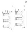
- FIG. 3Ais a schematic cross sectional view of a photovoltaic device according to an embodiment.
- FIG. 3Bis a process of manufacturing the photovoltaic device of FIG. 3A , according to an embodiment.
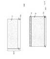
- FIG. 4Ashows a method of print coating a resist layer, according to an embodiment.
- FIG. 4Bshows a method of print coating a resist layer, according to another embodiment.
- FIG. 5shows a schematic of light concentration in the structures of the photovoltaic device.
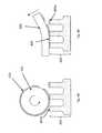
- FIG. 6shows an exemplary top cross sectional view of the photovoltaic device.
- FIG. 7shows an exemplary perspective view of the photovoltaic device.
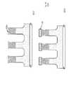
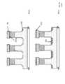
- FIGS. 8A-8Cshows schematics of drawing electrical current from the photovoltaic devices of FIG. 1A , FIG. 2A and FIG. 3A , respectively.
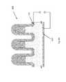
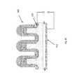
- FIG. 9shows an alternative stripe-shaped structures of the photovoltaic device.
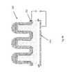
- FIG. 10shows an alternative mesh-shaped structures of the photovoltaic device.
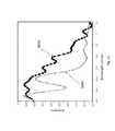
- FIG. 11shows the effect with and without a cladding layer on the absorptance spectrum of an exemplary photovoltaic device having pillars with radius of 125 nm, pitch of 800 nm and height of 5 microns, and the cladding layer has a thickness of 175 nm.
- a photovoltaic deviceoperable to convert light to electricity, comprising a substrate, a plurality of structures essentially perpendicular to the substrate, one or more recesses between the structures, each recess having a sidewall and a bottom wall, and a planar reflective layer disposed on the bottom wall of each recess, wherein the structures comprise a single crystalline semiconductor material and wherein the sidewall of each recess is free of the planar reflective layer.
- photovoltaic deviceas used herein means a device that can generate electrical power by converting light such as solar radiation into electricity.
- An electrically conductive materialcan be a material with essentially zero band gap.
- the electrical conductivity of an electrically conductive materialis generally above 10 3 S/cm.
- a semiconductorcan be a material with a finite band gap upto about 3 eV and general has an electrical conductivity in the range of 10 3 to 10 ⁇ 8 S/cm.
- An electrically insulating materialcan be a material with a band gap greater than about 3 eV and generally has an electrical conductivity below 10 ⁇ 8 S/cm.
- structures essentially perpendicular to the substratemeans that angles between the structures and the substrate are from 85° to 90°.
- recesas used herein means a hollow space in the substrate and is open to a space outside the substrate.
- the single crystalline semiconductor materialis selected from a group consisting of silicon, germanium, group III-V compound materials, group II-VI compound materials, and quaternary materials.
- a group III-V compound material as used hereinmeans a compound consisting of a group III element and a group V element.
- a group III elementcan be B, Al, Ga, In, Tl, Sc, Y, the lanthanide series of elements and the actinide series of elements.
- a group V elementcan be V, Nb, Ta, Db, N, P, As, Sb and Bi.
- a group II-VI compound material as used hereinmeans a compound consisting of a group II element and a group VI element.
- a group II elementcan be Be, Mg, Ca, Sr, Ba and Ra.
- a group VI elementcan be Cr, Mo, W, Sg, O, S, Se, Te, and Po.
- a quaternary materialis a compound consisting of four elements.
- the structuresare cylinders or prisms with a cross-section selected from a group consisting of elliptical, circular, rectangular, and polygonal cross-sections, strips, or a mesh.
- the term “mesh” as used hereinmeans a web-like pattern or construction.
- the structuresare pillars with diameters from 50 nm to 5000 nm, heights from 1000 nm to 20000 nm, a center-to-center distance between two closest pillars of 300 nm to 15000 nm.
- the structureshave an overhanging portion along an entire contour of a top surface of the structures.
- overhanging portionmeans a portion of the structures that project over the sidewall of the recesses.
- contour of a top surface of the structuresmeans the edge of the top surface of the structures.
- the top surface of the structurescan be broken by the recesses. An edge of the top surface is the boundary on the top surface between the structures and the recesses.
- each recesshas a rounded or beveled inner edge between the sidewall and the bottom wall thereof.
- the planar reflective layeris a material selected from a group consisting of ZnO, Al, Au, Ag, Pd, Cr, Cu, Ti, and a combination thereof; the planar reflective layer is an electrically conductive material; the planar reflective layer is a metal; the planar reflective layer has a reflectance (i.e., the fraction of incident electromagnetic power that is reflected) of at least 50% for visible light (i.e., light have a wavelength from 390 to 750 nm) of any wavelength; the planar reflective layer has a thickness of at least 5 nm; the planar reflective layers in all the recesses are connected; the planar reflective layer is functional to reflect light incident thereon to the structures so that the light is absorbed by the structures; and/or the planar reflective layer is functional as an electrode of the photovoltaic device.
- the term “electrode” as used hereinmeans a conductor used to establish electrical contact with the photovoltaic device.
- the substratehas a flat surface opposite the structures.
- the flat surfacehas a doped layer and optionally a metal layer metal layer disposed on and forming an Ohmic contact with the doped layer.
- An Ohmic contactis a region a current-voltage (I-V) curve across which is linear and symmetric.
- total area of the planar reflective layeris at least 40% of a surface area of the flat surface.
- the substratehas a thickness of at least 50 microns.
- the structuresare pillars arranged in an array; each structure is about 5 microns in height; a pitch of the structures is from 300 nm to 15 microns.
- the photovoltaic devicefurther comprises a passivation layer, a continuous cladding layer and optionally a coupling layer, wherein: the passivation layer is disposed on the sidewall, and on the bottom wall under the planar reflective layer; a top surface of the structures is free of the passivation layer; and the passivation layer is effective to passivate the sidewall and the bottom wall; the continuous cladding layer is disposed over an entire exposed portion of the passivation layer and the planar reflective layer, and the top surface of the structures; the coupling layer is disposed on the cladding layer and only above the top surface; and/or each of the structures has a top portion and a bottom portion having dissimilar conduction types.
- passivationand “passivate” as used herein means a process of eliminating dangling bonds (i.e., unsatisfied valence on immobilized atoms).
- cladding layeras used herein means a layer of substance surrounding the structures.
- continuousas used herein means having no gaps, holes, or breaks.
- coupling layeras used herein means a layer effective to guide light into the structures.
- the structureshave one of the following doping profiles: (i) the bottom portion is intrinsic and the top portion is p type; (ii) the bottom portion is n type and the top portion is p type; (iii) the bottom portion is intrinsic and the top portion is n type; (iv) the bottom portion is p type and the top portion is n type.
- the top portionhas a height of 1 micron to 20 micron; the passivation layer has a thickness from 1 nm to 100 nm; the passivation layer is an electrically insulating material selected from a group consisting of HfO 2 , SiO 2 , Si 3 N 4 , Al 2 O 3 , an organic molecule monolayer; the cladding layer is substantially transparent to visible light with a transmittance of at least 50%; the cladding layer is made of an electrically conductive material; the cladding layer is a transparent conductive oxide; the cladding layer is a material selected from a group consisting of indium tin oxide, aluminum doped zinc oxide, zinc indium oxide, and zinc tin oxide; the cladding layer has a thickness from 50 nm to 5000 nm; the cladding layer forms an Ohmic contact with the top portion; the cladding layer forms an Ohmic contact with the planar reflective layer; the cladding layer is functional as an electrode of the photovolt
- the photovoltaic devicefurther comprises a junction layer, a continuous cladding layer and optionally a coupling layer, wherein: the junction layer is a doped semiconductor; the junction layer is disposed on the sidewall, on the bottom wall under the planar reflective layer, and on a top surface of the structures; and the junction layer is effective to passivate the sidewall and the bottom wall; the continuous cladding layer is disposed over an entire exposed portion of the junction layer, the planar reflective layer and the top surface; and/or the coupling layer is disposed on the cladding layer and only above the top surface.
- the junction layeris a doped semiconductor
- the junction layeris disposed on the sidewall, on the bottom wall under the planar reflective layer, and on a top surface of the structures
- the junction layeris effective to passivate the sidewall and the bottom wall
- the continuous cladding layeris disposed over an entire exposed portion of the junction layer, the planar reflective layer and the top surface
- the coupling layeris disposed on the cladding layer and
- the structuresare a doped semiconductor and the structures and the junction layer have opposite conduction types; or the structures are an intrinsic semiconductor.
- An intrinsic semiconductoralso called an undoped semiconductor or i-type semiconductor, is a substantially pure semiconductor without any significant dopant species present. The number of charge carriers is therefore determined by the properties of the material itself instead of the amount of impurities. In intrinsic semiconductors the number of excited electrons and the number of holes are substantially equal. External electric field is not substantially screened in an intrinsic semiconductor because the intrinsic semiconductor does not have mobile electrons or holes supplied by dopants. It is thus more efficient to remove and/or collect electrons and/or holes generated in an intrinsic semiconductor by photons
- the junction layerhas a thickness from 5 nm to 100 nm; the cladding layer is substantially transparent to visible light with a transmittance of at least 50%; the cladding layer is made of an electrically conductive material; the cladding layer is a transparent conductive oxide; the cladding layer is a material selected from a group consisting of indium tin oxide, aluminum doped zinc oxide, zinc indium oxide, and zinc tin oxide; the cladding layer has a thickness from 50 nm to 5000 nm; the cladding layer forms an Ohmic contact with the top portion; the cladding layer forms an Ohmic contact with the planar reflective layer; the cladding layer is functional as an electrode of the photovoltaic device; the doped layer has an opposite conduction type from the junction layer; the doped layer is electrically connected to each of the structures; the doped layer, the structures and the junction layer form a p-n or p-i-n junction; the cladding layer has a thickness
- the photovoltaic devicefurther comprises a junction layer, a continuous cladding layer and optionally a coupling layer, wherein: the junction layer is a doped semiconductor; the junction layer is disposed on the sidewall, on the bottom wall under the planar reflective layer, and on a top surface of the structures; and the junction layer is effective to passivate the sidewall and the bottom wall; the continuous cladding layer is disposed over an entire exposed portion of the junction layer, the planar reflective layer and the top surface; the coupling layer is disposed on the cladding layer and only above the top surface; and/or; each of the structures has a top portion and a bottom portion having dissimilar conduction types.
- the top portion and the junction layerhave the same conduction type; and the structures have one of the following doping profiles: (i) the bottom portion is intrinsic and the top portion is p type; (ii) the bottom portion is n type and the top portion is p type; (iii) the bottom portion is intrinsic and the top portion is n type; (iv) the bottom portion is p type and the top portion is n type.
- the junction layerhas a thickness from 5 nm to 100 nm; the cladding layer is substantially transparent to visible light with a transmittance of at least 50%; the cladding layer is made of an electrically conductive material; the cladding layer is a transparent conductive oxide; the cladding layer is a material selected from a group consisting of indium tin oxide, aluminum doped zinc oxide, zinc indium oxide, and zinc tin oxide; the cladding layer has a thickness from 50 nm to 5000 nm; the cladding layer forms an Ohmic contact with the top portion; the cladding layer forms an Ohmic contact with the planar reflective layer; the cladding layer is functional as an electrode of the photovoltaic device; the doped layer has an opposite conduction type from the junction layer; the doped layer is electrically connected to the bottom portion of each of the structures; the doped layer, the bottom portion, the top portion and the junction layer form a p-n or p-i-n junction;
- a method of making the photovoltaic devicecomprises: generating a pattern of openings in a resist layer using a lithography technique; forming the structures and recesses by etching the substrate; depositing the planar reflective layer such that the sidewall of each recess is free of the planar reflective layer.
- a resist layer as used hereinmeans a thin layer used to transfer a pattern to the substrate which the resist layer is deposited upon.
- a resist layercan be patterned via lithography to form a (sub)micrometer-scale, temporary mask that protects selected areas of the underlying substrate during subsequent processing steps.
- the resistis generally proprietary mixtures of a polymer or its precursor and other small molecules (e.g.
- Photoacid generatorsthat have been specially formulated for a given lithography technology. Resists used during photolithography are called photoresists. Resists used during e-beam lithography are called e-beam resists.
- a lithography techniquecan be photolithography, e-beam lithography, holographic lithography. Photolithography is a process used in microfabrication to selectively remove parts of a thin film or the bulk of a substrate. It uses light to transfer a geometric pattern from a photo mask to a light-sensitive chemical photo resist, or simply “resist,” on the substrate. A series of chemical treatments then engraves the exposure pattern into the material underneath the photo resist.
- E-beam lithographyis the practice of scanning a beam of electrons in a patterned fashion across a surface covered with a film (called the resist), (“exposing” the resist) and of selectively removing either exposed or non-exposed regions of the resist (“developing”).
- the purpose, as with photolithography,is to create very small structures in the resist that can subsequently be transferred to the substrate material, often by etching. It was developed for manufacturing integrated circuits, and is also used for creating nanotechnology artifacts.
- the method of making the photovoltaic devicefurther comprises: coating the substrate with the resist layer; developing (i.e., selectively removing either exposed or non-exposed regions of the resist) the pattern in the resist layer; depositing a mask layer; and lifting off the resist layer.
- a mask layer as used hereinmeans a layer that protects an underlying portion of the substrate from being etched.
- the method of making the photovoltaic devicefurther comprises ion implantation or depositing a dopant layer.
- a dopantalso called a doping agent, is a trace impurity element that is inserted into a substance (in very low concentrations) in order to alter the electrical properties or the optical properties of the substance.
- Ion implantationis process by which ions of a material can be implanted into another solid, thereby changing the physical properties of the solid. Ion implantation is used in semiconductor device fabrication and in metal finishing, as well as various applications in materials science research.
- the ionsintroduce both a chemical change in the target, in that they can be a different element than the target or induce a nuclear transmutation, and a structural change, in that the crystal structure of the target can be damaged or even destroyed by the energetic collision cascades.
- the structures and recessesare formed by deep etch followed by isotropic etch.
- a deep etchis a highly anisotropic etch process used to create deep, steep-sided holes and trenches in wafers, with aspect ratios of often 20:1 or more.
- An exemplary deep etchis the Bosch process.
- the Bosch processalso known as pulsed or time-multiplexed etching, alternates repeatedly between two modes to achieve nearly vertical structures: 1. a standard, nearly isotropic plasma etch, wherein the plasma contains some ions, which attack the wafer from a nearly vertical direction (For silicon, this often uses sulfur hexafluoride (SF 6 )); 2.
- a chemically inert passivation layerfor instance, C 4 F 8 source gas yields a substance similar to Teflon.
- the passivation layerprotects the entire substrate from further chemical attack and prevents further etching.
- the directional ions that bombard the substrateattack the passivation layer at the bottom of the trench (but not along the sides). They collide with it and sputter it off, exposing the substrate to the chemical etchant.
- These etch/deposit stepsare repeated many times over resulting in a large number of very small isotropic etch steps taking place only at the bottom of the etched pits.
- Isotropic etchis non-directional removal of material from a substrate via a chemical process using an etchant substance.
- the etchantmay be a corrosive liquid or a chemically active ionized gas, known as a plasma.
- the method of making the photovoltaic devicefurther comprises applying a resist layer by a print coating method, the print coating method comprising: coating a roller of a flexible material with a resist layer; transferring the resist layer to a surface of a substrate by rolling the roller on the surface, wherein the surface is flat or textured.
- the rolleris polydimethylsiloxane.
- the method of making the photovoltaic devicefurther comprises applying a resist layer by a print coating method, the print coating method comprising: coating a stamp of a flexible material with a resist layer; transferring the resist layer to a surface of a substrate by pressing the stamp on the surface, wherein the surface is flat or textured.
- the stampis polydimethylsiloxane.
- a method of converting light to electricitycomprises: exposing the photovoltaic device to light; drawing an electrical current from the photovoltaic device.
- the electrical currentcan be drawn from the planar reflective layer.
- a photo detectorcomprises the photovoltaic device, wherein the photo detector is functional to output an electrical signal when exposed to light.
- a method of detecting lightcomprises exposing the photovoltaic device to light; measuring an electrical signal from the photovoltaic device.
- the electrical signalcan be an electrical current, an electrical voltage, an electrical conductance and/or an electrical resistance.
- a bias voltageis applied to the structures in the photovoltaic device.
- photovoltaic devicesproduce direct current electricity from sun light, which can be used to power equipment or to recharge a battery.
- a practical application of photovoltaicswas to power orbiting satellites and other spacecraft, but today the majority of photovoltaic modules are used for grid connected power generation. In this case an inverter is required to convert the DC to AC.
- an inverteris required to convert the DC to AC.
- the radiationis sunlight and for this reason the devices are known as solar cells.
- Solar cellsare often electrically connected and encapsulated as a module.
- Photovoltaic modulesoften have a sheet of glass on the front (sun up) side, allowing light to pass while protecting the semiconductor wafers from the elements (rain, hail, etc.).
- Solar cellsare also usually connected in series in modules, creating an additive voltage. Connecting cells in parallel will yield a higher current. Modules are then interconnected, in series or parallel, or both, to create an array with the desired peak DC voltage and current.
- the photovoltaic devicecan also be associated with buildings: either integrated into them, mounted on them or mounted nearby on the ground.
- the photovoltaic devicecan be retrofitted into existing buildings, usually mounted on top of the existing roof structure or on the existing walls.
- the photovoltaic devicecan be located separately from the building but connected by cable to supply power for the building.
- the photovoltaic devicecan be used as a principal or ancillary source of electrical power.
- the photovoltaic devicecan be incorporated into the roof or walls of a building.
- the photovoltaic devicecan also be used for space applications such as in satellites, spacecrafts, space stations, etc.
- the photovoltaic devicecan be used as main or auxiliary power sources for land vehicles, marine vehicles (boats) and trains.
- Other applicationsinclude road signs, surveillance cameras, parking meters, personal mobile electronics (e.g., cell phones, smart phones, laptop computers, personal media players).
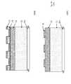
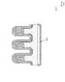
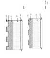
- FIG. 1Ashows a schematic cross-section of a photovoltaic device 100 , according to an embodiment.
- the photovoltaic device 100comprises a substrate 105 , a plurality of structures 120 essentially perpendicular to the substrate 105 and one or more recesses 130 between the structures 120 .
- Each recess 130has a sidewall 130 a and a bottom wall 130 b .
- the sidewall 130 a and the bottom wall 130 bboth have a passivation layer 131 .
- a top surface 120 a of the structures 120is free of the passivation layer 131 .
- the bottom wall 130 bhas a planar reflective layer 132 disposed on the passivation layer 131 .
- the sidewall 130 adoes not have any planar reflective layer.
- Each structure 120has a top portion 121 and a bottom portion 122 , the top portion 121 and the bottom portion 122 having dissimilar conduction types.
- dissimilar conduction typesmeans that the top portion 121 and the bottom portion 122 cannot be both p type, or both n type.
- the structures 120can have one of the following four doping profiles (i.e., doping level distribution): (i) the bottom portion 122 is intrinsic and the top portion 121 is p type; (ii) the bottom portion 122 is n type and the top portion 121 is p type; (iii) the bottom portion 122 is intrinsic and the top portion 121 is n type; (iv) the bottom portion 122 is p type and the top portion 121 is n type.
- the top portion 121can have a doping profile with decreasing doping levels in a direction from the top surface 120 a to the bottom portion 122 .
- the structures 120are a single crystalline semiconductor material.
- a continuous cladding layer 140is disposed over an entire exposed portion of the passivation layer 131 and the planar reflective layer 132 , and over the top surface 120 a .
- the photovoltaic device 100can further comprise a coupling layer 160 disposed on the cladding layer 140 and only directly above the top surface 120 a.
- the structures 120can comprise any suitable single crystalline semiconductor material, such as silicon, germanium, group III-V compound materials (e.g., gallium arsenide, gallium nitride, etc.), group II-VI compound materials (e.g., cadmium selenide, cadmium sulfide, cadmium telluride, zinc oxide, zinc selenide, etc.), quaternary materials (e.g., copper indium gallium selenide).
- group III-V compound materialse.g., gallium arsenide, gallium nitride, etc.
- group II-VI compound materialse.g., cadmium selenide, cadmium sulfide, cadmium telluride, zinc oxide, zinc selenide, etc.
- quaternary materialse.g., copper indium gallium selenide.
- the structures 120can have any cross-sectional shape.
- the structures 120can be cylinders or prisms with elliptical, circular, rectangular, polygonal cross-sections.
- the structures 120can also be strips as shown in FIG. 9 , or a mesh as shown in FIG. 10 .
- the structures 120are pillars with diameters from 50 nm to 5000 nm, heights from 1000 nm to 20000 nm, a center-to-center distance between two closest pillars of 300 nm to 15000 nm.
- the top portion 121preferably has a height of 1 micron to 20 micron.
- the top portion 121preferably has a gradient of doping levels, with a highest doping level at the top surface 120 a .
- the structures 120have an overhanging portion 124 along an entire contour of the top surface 120 a of the structures 120 .
- Each recess 130preferably has a rounded or beveled inner edge between the sidewall 130 a and the bottom wall 130 b.
- the passivation layer 131can be any suitable electrically insulating material, such as HfO 2 , SiO 2 , Si 3 N 4 , Al 2 O 3 , an organic molecule monolayer, etc.
- the passivation layer 131can have any suitable thickness, such as from 1 nm to 100 nm.
- the passivation layer 131is effective to passivate the sidewall 130 a and the bottom wall 130 b.
- the planar reflective layer 132can be any suitable material, such as ZnO, Al, Au, Ag, Pd, Cr, Cu, Ti, a combination thereof, etc.
- the planar reflective layer 132preferably is an electrically conductive material, more preferably a metal.
- the planar reflective layer 132preferably has a reflectance of at least 50%, more preferably has a reflectance of at least 70%, most preferably has a reflectance of at least 90%, for visible light of any wavelength.
- the planar reflective layer 132has a thickness of preferably at least 5 nm, more preferably at least 20 nm.
- the planar reflective layer 132 in all the recesses 130is preferably connected.
- the planar reflective layer 132is functional to reflect light incident thereon to the structures 120 so the light is absorbed by the structures 120 .
- a photovoltaic deviceoften has opaque electrodes on a surface that receives light. Any light incident on such opaque electrodes is either reflected away from the photovoltaic device or absorbed by the opaque electrodes, and thus does not contribute to generation of electricity.
- the planar reflective layer 132preferably is functional as an electrode of the photovoltaic device 100 .
- the cladding layer 140is substantially transparent to visible light, preferably with a transmittance of at least 50%, more preferably at least 70%, most preferably at least 90%.
- the cladding layer 140is an electrically conductive material.
- the cladding layer 140preferably is a transparent conductive oxide, such as ITO (indium tin oxide), AZO (aluminum doped zinc oxide), ZIO (zinc indium oxide), ZTO (zinc tin oxide), etc.
- the cladding layer 140can have a thickness from 50 nm to 5000 nm.
- the cladding layer 140preferably forms an Ohmic contact with the top portions 121 of the structures 120 .
- the cladding layer 140preferably forms an Ohmic contact with the planar reflective layer 132 .
- the cladding layer 140preferably is functional as an electrode of the photovoltaic device 100 .
- the substrate 105preferably has a flat surface 150 opposite the structures 120 .
- the flat surface 150can have a doped layer 151 of the opposite conduction type from the top portions 121 , i.e. if the top portion 121 is n type, the doped layer 151 is p type; if the top portion 121 is p type, the doped layer 151 is n type.
- the doped layer 151is electrically connected to the bottom portion 122 of each of the structures 120 . If the bottom portion 122 is intrinsic, the top portion 121 , the bottom portion 122 and the doped layer 151 form a p-i-n junction.
- the flat surface 150can also have a metal layer 152 disposed on the doped layer 151 .
- the metal layer 152forms an Ohmic contact with the doped layer 151 .
- the substrate 105preferably has a thickness of at least 50 microns. Total area of the planar reflective layer 132 is preferable at least 40% of a surface area of the flat surface 150 .
- the coupling layer 160can be the same material as the cladding layer 140 or different material from the cladding layer 140 .
- refractive index of the structure 120 n 1 , refractive index of the cladding layer 140 n 2 , refractive index of the coupling layer 160 n 3 , refractive index of the space between the structures 120 n 4preferably satisfy relations of n 1 >n 2 >n 4 and n 1 >n 3 >n 4 , which lead to enhanced light concentration in the structures 120 .
- FIG. 11shows the effect of the cladding layer.
- FIG. 11shows an absorptance spectrum 5000 of an exemplary photovoltaic device 100 , wherein the structures 120 are pillars with radius of 125 nm, pitch of 800 nm and height of 5 microns and the cladding layer 140 has a thickness of 175 nm.
- FIG. 11also shows an absorptance spectrum 5000 of an identical photovoltaic device 100 except without the cladding layer 140 . It is apparent that the exemplary photovoltaic device 100 with the cladding layer 140 has much higher absorptance across the entire visible spectrum and thus has much higher photovoltaic efficiency (i.e., a percentage of incident light that is converted into electricity).
- the structures 120are pillars arranged in an array, such as a rectangular array, a hexagonal array, a square array, concentric ring. Each structure 120 is about 5 microns in height. A pitch of the structures 120 is from 300 nm to 15 microns. The term “pitch” is defined as a distance of a structure 120 to a nearest neighbor of the structure 120 along a direction parallel to the substrate 105 . The cladding layer 140 is about 175 nm thick.
- arrayas used herein means a spatial arrangement having a particular order.
- a method of making the photovoltaic device 100 as shown in FIG. 1Bcomprises the following steps:
- step 1000providing the substrate 105 having the doped layer 151 and an epi layer 11 disposed on the doped layer 151 .
- Epitaxyis a process of growing a crystal of a particular orientation on top of another crystal, where the orientation is determined by the underlying crystal.
- epi layeras used herein means a layer grown by epitaxy.
- step 1001an upper layer 12 of the epi layer 11 is doped by ion implantation.
- a resist layer 14is applied on the doped upper layer 12 .
- the resist layer 14can be applied by spin coating.
- the resist layer 14can be a photo resist or an e-beam resist.
- step 1003lithography is performed.
- the resist layer 14now has a pattern of openings in which the doped upper layer 12 is exposed. Shapes and locations of the openings correspond to the shapes and locations of the recesses 130 .
- the resolution of the lithographyis limited by the wavelength of the radiation used.
- Photolithography tools using deep ultraviolet (DUV) lightwith wavelengths of approximately 248 and 193 nm, allows minimum feature sizes down to about 50 nm.
- E-beam lithography tools using electron energy of 1 keV to 50 keVallows minimum feature sizes down to a few nanometers.
- DUVdeep ultraviolet
- a mask layer 15is deposited.
- the depositioncan be done using a technique such as thermal evaporation, e-beam evaporation, sputtering.
- the mask layer 15can be a metal such as Cr or Al, or a dielectric such as SiO 2 or Si 3 N 4 .
- the thickness of the mask layer 15can be determined by a depth of the recesses 130 and etching selectivity (i.e., ratio of etching rates of the mask layer 15 and the substrate 105 ).
- step 1005remainder of the resist layer 14 is lift off by a suitable solvent or ashed in a resist asher to remove any mask layer 15 support thereon. A portion of the mask layer 15 in the openings of the resist layer 14 is retained. A portion of the doped upper layer 12 is now exposed through the retained mask layer 15 .
- step 1006the exposed portion of the doped upper layer 12 and the portion of the epi layer 11 directly therebelow are deep etched to a desired depth (e.g., 1 to 20 microns) followed by an isotropic etch, until the epi layer 11 is partially exposed, to form the structures 120 with the overhanging portion 124 and the recesses 130 with the beveled inner edge.
- a desired depthe.g. 1 to 20 microns
- An isotropic etche.g., 1 to 20 microns
- Each of the structures 120now has the top portion 121 which is part of the upper doped layer 12 and a bottom portion 122 which is part of the epi layer 11 .
- Deep etchingincludes alternating deposition and etch steps and can lead to “scalloping” on the sidewall 130 b of the recesses 130 , i.e. the sidewall 130 b is not smooth.
- the sidewall 130 bcan be smoothed by thermal annealing or dipping into an etchant such as potassium hydroxide (KOH) followed by rinsing.
- KOHpotassium hydroxide
- the deep etchingcan use gases such as C 4 F 8 and SF 6 .
- the passivation layer 131is conformally (i.e., isotropically) deposited on surfaces of the recesses 130 and a top surface 15 a of the retained mask layer 15 .
- a conformal layer, such as the passivation 131is a layer that covers a morphologically uneven surface and has an essentially uniform thickness.
- the passivation layer 131can be deposited by a suitable technique such as plating, chemical vapor deposition or atomic layer deposition.
- a resist layer 16is selectively applied such that the sidewall 130 a and bottom wall 130 b of the recesses are free of the resist layer 16 and a top surface 131 a of the passivation layer 131 is completely covered by the resist layer 16 .
- the resist layer 16can be selectively applied by a suitable method such as a print coating method detailed hereinbelow according an embodiment.
- a metal layer 17is anisotropically deposited (i.e., non-conformally) such that the resist layer 16 and the bottom wall 130 b are covered by the metal layer 17 while the sidewall 130 a is free of the metal layer 17 .
- the metal layer 17can be deposited by a suitable technique such as thermal evaporation, e-beam evaporation.
- the metal 17can be any suitable metal such as aluminum.
- step 1010the resist layer 16 is lift off by a suitable solvent or ashed in a resist asher to remove any metal layer 17 support thereon.
- the top surface 131 a of the passivation layer 131is now exposed.
- the top surface 131 a of the passivation layer 131is selected removed by a suitable technique such as ion milling, dry etching, sputtering, while leaving the passivation layer 131 on the sidewall 130 a and bottom wall 130 b of the recesses 130 intact.
- the top surface 15 a of the retained mask layer 15is now exposed.
- the metal layer 17 on the bottom wall 130 bprotects the passivation layer 131 underneath from being removed.
- step 1012the retained mask layer 15 and the metal layer 17 are removed by a suitable technique such as wet etch in a suitable etchant. Now the top surface 120 a of the structures 120 is exposed.
- a resist layer 18is selectively applied such that the sidewall 130 a and bottom wall 130 b of the recesses are free of the resist layer 18 and the top surface 120 a of the structures 120 is completely covered by the resist layer 18 .
- the resist layer 18can be selectively applied by a suitable method such as the print coating method detailed hereinbelow according an embodiment.
- the planar reflective layer 132is anisotropically deposited (i.e., non-conformally) such that the resist layer 18 and the bottom wall 130 b are covered by the planar reflective layer 132 while the sidewall 130 a is free of the planar reflective layer 132 .
- the planar reflective layer 132can be deposited by a suitable technique such as thermal evaporation, e-beam evaporation.
- the planar reflective layer 132can be any suitable material such as silver.
- step 1015the resist layer 18 is lift off by a suitable solvent or ashed in a resist asher to remove any portion of the planar reflective layer 132 support thereon.
- the top surface 120 a of the structures 120is now exposed.
- the cladding layer 140is conformally (i.e., isotropically) deposited such that the planar reflective layer 132 , the passivation layer 131 and the top surface 120 a are completely covered.
- the cladding layer 140can be deposited by a suitable technique such as plating, chemical vapor deposition or atomic layer deposition.
- the coupling layer 160can be then deposited using a suitable technique such as sputtering, thermal evaporation or e-beam evaporation.
- step 1017the metal layer 152 is deposited on the doped layer 151 .
- the methodcan further comprise one or more steps of thermal annealing.
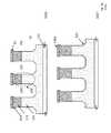
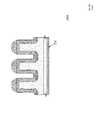
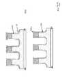
- FIG. 2Ashows a schematic cross-section of a photovoltaic device 200 , according to another embodiment.
- the photovoltaic device 200comprises a substrate 205 , a plurality of structures 220 essentially perpendicular to the substrate 205 and one or more recesses 230 between the structures 220 .
- Each recess 230has a sidewall 230 a and a bottom wall 230 b .
- the sidewall 230 a , the bottom wall 230 b of each recess 230 and a top surface 220 a of the structures 220have a junction layer 231 disposed thereon.
- the junction layer 231is a doped semiconductor.
- the bottom wall 230 bhas a planar reflective layer 232 disposed on the junction layer 231 .
- the sidewall 230 adoes not have any planar reflective layer.
- the structures 220are a single crystalline semiconductor material.
- the structure 220can be an intrinsic semiconductor or a doped semiconductor. If the structure 220 is a doped semiconductor, the structures 220 and the junction layer 231 have opposite conduction types, i.e., if the structures 220 are p type, the junction layer 231 is n type; if the structures 220 are n type, the junction layer 231 is p type.
- a continuous cladding layer 240is disposed over an entire exposed junction layer 231 , the planar reflective layer 232 and the top surface 220 a .
- the photovoltaic device 200can further comprise a coupling layer 260 disposed on the cladding layer 240 and only directly above the top surface 220 a.
- the structures 220can comprise any suitable single crystalline semiconductor material, such as silicon, germanium, group III-V compound materials (e.g., gallium arsenide, gallium nitride, etc.), group II-VI compound materials (e.g., cadmium selenide, cadmium sulfide, cadmium telluride, zinc oxide, zinc selenide, etc.), quaternary materials (e.g., copper indium gallium selenide).
- group III-V compound materialse.g., gallium arsenide, gallium nitride, etc.
- group II-VI compound materialse.g., cadmium selenide, cadmium sulfide, cadmium telluride, zinc oxide, zinc selenide, etc.
- quaternary materialse.g., copper indium gallium selenide.
- the structures 220can have any cross-sectional shape.
- the structures 220can be cylinders or prisms with elliptical, circular, rectangular, polygonal cross-sections.
- the structures 220can also be strips as shown in FIG. 9 , or a mesh as shown in FIG. 10 .
- the structures 220are pillars with diameters from 50 nm to 5000 nm, heights from 1000 nm to 20000 nm, a center-to-center distance between two closest pillars of 300 nm to 15000 nm.
- the structures 220have an overhanging portion 224 along an entire contour of the top surface 220 a of the structures 220 .
- Each recess 230preferably has a rounded or beveled inner edge between the sidewall 230 a and the bottom wall 230 b.
- the junction layer 231preferably has a thickness from 5 nm to 100 nm.
- the junction layer 231is effective to passivate surfaces of the structures 220 .
- the planar reflective layer 232can be any suitable material, such as ZnO, Al, Au, Ag, Pd, Cr, Cu, Ti, a combination thereof, etc.
- the planar reflective layer 232preferably is an electrically conductive material, more preferably a metal.
- the planar reflective layer 232preferably has a reflectance of at least 50%, more preferably has a reflectance of at least 70%, most preferably has a reflectance of at least 90%, for visible light of any wavelength.
- the planar reflective layer 232has a thickness of preferably at least 5 nm, more preferably at least 20 nm.
- the planar reflective layer 232 in all the recesses 230is preferably connected.
- the planar reflective layer 232is functional to reflect light incident thereon to the structures 220 so the light is absorbed by the structures 220 .
- the planar reflective layer 232preferably is functional as an electrode of the photovoltaic device 200 .
- the cladding layer 240is substantially transparent to visible light, preferably with a transmittance of at least 50%, more preferably at least 70%, most preferably at least 90%.
- the cladding layer 240is made of an electrically conductive material.
- the cladding layer 240preferably is made of a transparent conductive oxide, such as ITO (indium tin oxide), AZO (aluminum doped zinc oxide), ZIO (zinc indium oxide), ZTO (zinc tin oxide), etc.
- the cladding layer 240can have a thickness of 50 nm to 5000 nm.
- the cladding layer 240preferably forms an Ohmic contact with the junction layer 231 .
- the cladding layer 240preferably forms an Ohmic contact with the planar reflective layer 232 .
- the cladding layer 240preferably is functional as an electrode of the photovoltaic device 200 .
- the substrate 205preferably has a flat surface 250 opposite the structures 220 .
- the flat surface 250can have a doped layer 251 of the opposite conduction type from the junction layer 231 , i.e. if the junction layer 231 is n type, the doped layer 251 is p type; if the junction layer 231 is p type, the doped layer 251 is n type.
- the doped layer 251is electrically connected to each of the structures 220 . If the structures 220 are intrinsic, the junction layer 231 , the structures 220 and the doped layer 251 form a p-i-n junction. If the structures 220 are is n-type or p-type, the junction layer 231 and the structures 220 form a p-n junction.
- the flat surface 250can also have a metal layer 252 disposed on the doped layer 251 .
- the metal layer 252forms an Ohmic contact with the doped layer 251 .
- the substrate 205preferably has a thickness of at least 50 microns. Total area of the planar reflective layer 232 is preferable at least 40% of a surface area of the flat surface 250 .
- the coupling layer 260can be of the same material as the cladding layer 240 or different material from the cladding layer 240 .
- refractive index of the structure 220 n 1 , refractive index of the cladding layer 240 n 2 , refractive index of the coupling layer 260 n 3 , refractive index of the space between the structures 220 n 4preferably satisfy relations of n 1 >n 2 >n 4 and n 1 >n 3 >n 4 , which lead to enhanced light concentration in the structures 220 .
- the structures 220are pillars arranged in an array, such as a rectangular array, a hexagonal array, a square array, concentric ring. Each pillar is about 5 microns in height. A pitch of the structures 220 is from 300 nm to 15 microns.
- the cladding layer 240is about 175 nm thick.
- a method of making the photovoltaic device 200 as shown in FIG. 2Bcomprises the following steps:
- step 2000providing the substrate 205 having the doped layer 251 and an epi layer 21 disposed on the doped layer 251 .
- a resist layer 24is applied on the epi layer 21 .
- the resist layer 24can be applied by spin coating.
- the resist layer 24can be a photo resist or an e-beam resist.
- step 2002lithography is performed.
- the resist layer 24now has a pattern of openings in which the epi layer 21 is exposed. Shapes and locations of the openings correspond to the shapes and locations of the recesses 230 .
- the resolution of the lithographyis limited by the wavelength of the radiation used.
- Photolithography tools using deep ultraviolet (DUV) lightwith wavelengths of approximately 248 and 193 nm, allows minimum feature sizes down to about 50 nm.
- E-beam lithography tools using electron energy of 1 keV to 50 keVallows minimum feature sizes down to a few nanometers.
- DUVdeep ultraviolet
- a mask layer 25is deposited.
- the depositioncan be done using a technique such as thermal evaporation, e-beam evaporation, sputtering.
- the mask layer 25can be a metal such as Cr or Al, or a dielectric such as SiO 2 or Si 3 N 4 .
- the thickness of the mask layer 25can be determined by a depth of the recesses 230 and etching selectivity (i.e., ratio of etching rates of the mask layer 25 and the substrate 205 ).
- step 2004remainder of the resist layer 24 is lift off by a suitable solvent or ashed in a resist asher to remove any mask layer 25 support thereon. A portion of the mask layer 25 in the openings of the resist layer 24 is retained. A portion of the epi layer 21 is now exposed through the retained mask layer 25 .
- the exposed portion of the epi layer 21is deep etched to a desired depth (e.g., 1 to 20 microns) followed by an isotropic etch, to form the structures 220 with the overhanging portion 224 and the recesses 230 with the beveled inner edge.
- Deep etchingincludes alternating deposition and etch steps and can lead to “scalloping” on the sidewall 230 b of the recesses 230 , i.e. the sidewall 230 b is not smooth.
- the sidewall 230 bcan be smoothed by thermal annealing or dipping into an etchant such as potassium hydroxide (KOH) followed by rinsing.
- KOHpotassium hydroxide
- the deep etchingcan use gases such as C 4 F 8 and SF 6 .
- step 2006the mask layer 25 is removed by a suitable such as wet etching with suitable etchant, ion milling, sputtering.
- suitable etchantion milling, sputtering.
- the top surface 220 a of the structures 220is exposed.
- a dopant layer 22is conformally (i.e., isotropically) deposited on surfaces of the recesses 230 and a top surface 220 a of the structures 220 .
- the dopant layer 22can be deposited by a suitable technique such as plating, chemical vapor deposition or atomic layer deposition.
- the dopant layer 22can comprise any suitable material such as trimethylboron, triisopropylborane ((C 3 H 7 ) 3 B), triethoxyborane ((C 2 H 5 O) 3 B, and/or triisopropoxyborane ((C 3 H 7 O) 3 B.
- a shield layer 23is conformally (i.e., isotropically) deposited on surfaces of the dopant layer 22 .
- the shield layer 23can be deposited by a suitable technique such as plating, chemical vapor deposition or atomic layer deposition.
- the shield layer 23has a suitable material (such as silicon oxide, silicon nitride) and a suitable thickness (e.g., at least 10 nm, at least 100 nm or at least 1 micron) effective to prevent the dopant layer 22 from evaporation in step 2009 .
- step 2009the dopant layer 22 is diffused into the sidewall 230 b , the bottom wall 230 a and the top surface 220 a by thermal annealing, which forms the junction layer 231 thereon.
- Thermal annealingcan be conducted, for example, at about 850° C. for 10 to 30 minutes under a suitable atmosphere (e.g., argon).
- step 2010the shield layer 23 is removed by a suitable technique such as wet etch using a suitable etchant such as HF.
- a suitable etchantsuch as HF.
- a resist layer 26is selectively applied such that the sidewall 230 a and bottom wall 230 b of the recesses 230 are free of the resist layer 26 and a top surface 231 a of the junction layer 231 is completely covered by the resist layer 26 .
- the resist layer 26can be selectively applied by a suitable method such as the print coating method detailed hereinbelow according an embodiment.
- the planar reflective layer 232is anisotropically deposited (i.e., non-conformally) such that the resist layer 26 and the bottom wall 230 b are covered by the planar reflective layer 232 while the sidewall 230 a is free of the planar reflective layer 232 .
- the planar reflective layer 232can be deposited by a suitable technique such as thermal evaporation, e-beam evaporation.
- the planar reflective layer 232can be any suitable material such as silver.
- step 2013the resist layer 26 is lift off by a suitable solvent or ashed in a resist asher to remove any portion of the planar reflective layer 232 support thereon.
- the top surface 231 a of the junction layer 220is now exposed.
- the cladding layer 240is conformally (i.e., isotropically) deposited such that the planar reflective layer 232 , the junction layer 231 and the top surface 231 a are completely covered.
- the cladding layer 240can be deposited by a suitable technique such as plating, chemical vapor deposition or atomic layer deposition.
- the coupling layer 260can be then deposited using a suitable technique such as sputtering, thermal evaporation or e-beam evaporation.
- step 2015the metal layer 252 is deposited on the doped layer 251 .
- the methodcan further comprise one or more steps of thermal annealing.
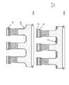
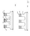
- FIG. 3Ashows a schematic cross-section of a photovoltaic device 300 , according to an embodiment.
- the photovoltaic device 300comprises a substrate 305 , a plurality of structures 320 essentially perpendicular to the substrate 305 and one or more recesses 330 between the structures 320 .
- Each recess 330has a sidewall 330 a and a bottom wall 330 b .
- the sidewall 330 a , the bottom wall 330 b of each recess 330 and a top surfaces 320 a of the structures 320have a junction layer 331 disposed thereon.
- the junction layer 331is a doped semiconductor.
- the bottom wall 330 bhas a planar reflective layer 332 disposed on the junction layer 331 .
- the sidewall 330 adoes not have any planar reflective layer.
- Each structure 320has a top portion 321 and a bottom portion 322 .
- the structures 320can have one of the following four doping profiles (i.e., doping level distribution): (i) the bottom portion 322 is intrinsic and the top portion 321 is p type; (ii) the bottom portion 322 is n type and the top portion 321 is p type; (iii) the bottom portion 322 is intrinsic and the top portion 321 is n type; (iv) the bottom portion 322 is p type and the top portion 321 is n type.
- the top portion 321can have a doping profile with decreasing doping levels in a direction from the top surface 320 a to the bottom portion 322 .
- the structures 320are a single crystalline semiconductor material.
- the top portion 321 of the structures 320 and the junction layer 331are semiconductor materials of the same conduction types, i.e., if the top portion 321 is p type, the junction layer 331 is p type; if the top portion 321 is n type, the junction layer 331 is n type.
- a continuous cladding layer 340is disposed over an entire exposed portion of the junction layer 331 and the planar reflective layer 332 .
- the photovoltaic device 300can further comprise a coupling layer 360 disposed on the cladding layer 340 and only directly above the top surface 320 a.
- the structures 320can comprise any suitable single crystalline semiconductor material, such as silicon, germanium, group III-V compound materials (e.g., gallium arsenide, gallium nitride, etc.), group II-VI compound materials (e.g., cadmium selenide, cadmium sulfide, cadmium telluride, zinc oxide, zinc selenide, etc.), quaternary materials (e.g., copper indium gallium selenide).
- group III-V compound materialse.g., gallium arsenide, gallium nitride, etc.
- group II-VI compound materialse.g., cadmium selenide, cadmium sulfide, cadmium telluride, zinc oxide, zinc selenide, etc.
- quaternary materialse.g., copper indium gallium selenide.
- the structures 320can have any cross-sectional shape.
- the structures 320can be cylinders or prisms with elliptical, circular, rectangular, polygonal cross-sections.
- the structures 320can also be strips as shown in FIG. 9 , or a mesh as shown in FIG. 10 .
- the structures 320are pillars with diameters from 50 nm to 5000 nm, heights from 1000 nm to 20000 nm, a center-to-center distance between two closest pillars of 300 nm to 15000 nm.
- the top portion 321preferably has a height of 1 micron to 20 micron.
- the top portion 321preferably has a gradient of doping levels, with a highest doping level at the top surface 320 a .
- the structures 320have an overhanging portion 324 along an entire contour of the top surface 320 a of the structures 320 .
- Each recess 330preferably has a rounded or beveled inner edge between the sidewall 130 a and the bottom wall 330 b.
- the junction layer 331preferably has a thickness from 5 nm to 100 nm.
- the junction layer 331is effective to passivate surfaces of the structures 320 .
- the planar reflective layer 332can be any suitable material, such as ZnO, Al, Au, Ag, Pd, Cr, Cu, Ti, a combination thereof, etc.
- the planar reflective layer 332preferably is an electrically conductive material, more preferably a metal.
- the planar reflective layer 332preferably has a reflectance of at least 50%, more preferably has a reflectance of at least 70%, most preferably has a reflectance of at least 90%, for visible light of any wavelength.
- the planar reflective layer 332has a thickness of preferably at least 5 nm, more preferably at least 20 nm.
- the planar reflective layer 332 in all the recesses 330is preferably connected.
- the planar reflective layer 332is functional to reflect light incident thereon to the structures 320 so the light is absorbed by the structures 320 .
- the planar reflective layer 332preferably is functional as an electrode of the photovoltaic device 300 .
- the cladding layer 340is substantially transparent to visible light, preferably with a transmittance of at least 50%, more preferably at least 70%, most preferably at least 90%.
- the cladding layer 340is made of an electrically conductive material.
- the cladding layer 340preferably is made of a transparent conductive oxide, such as ITO (indium tin oxide), AZO (aluminum doped zinc oxide), ZIO (zinc indium oxide), ZTO (zinc tin oxide), etc.
- the cladding layer 340can have a thickness of 50 nm to 5000 nm.
- the cladding layer 340preferably forms an Ohmic contact with the top portions 321 of the structures 320 .
- the cladding layer 340preferably forms an Ohmic contact with the planar reflective layer 332 .
- the cladding layer 340preferably is functional as an electrode of the photovoltaic device 300 .
- the substrate 305preferable has a flat surface 350 opposite the structures 320 .
- the flat surface 350can have a doped layer 351 of the opposite conduction type from the junction layer 331 , i.e. if the junction layer 331 is n type, the doped layer 351 is also p type; if the junction layer 331 is p type, the doped layer 351 is also n type.
- the doped layer 351is electrically connected to the bottom portion 322 of each of the structures 320 . If the bottom portion 322 is intrinsic, the junction layer 331 and the top portion 321 form a p-i-n junction with the bottom portion 322 and the doped layer 351 .
- the flat surface 350can also have a metal layer 352 disposed on the doped layer 351 .
- the metal layer 352forms an Ohmic contact with the doped layer 351 .
- the substrate 305preferably has a thickness of at least 50 microns. Total area of the planar reflective layer 332 is preferable at least 40% of a surface area of the flat surface 350 .
- the coupling layer 360can be of the same material as the cladding layer 340 or different material from the cladding layer 340 .
- refractive index of the structure 320 n 1 , refractive index of the cladding layer 340 n 2 , refractive index of the coupling layer 360 n 3 , refractive index of the space between the structures 320 n 4preferably satisfy relations of n 1 >n 2 >n 4 and n 1 >n 3 >n 4 , which lead to enhanced light concentration in the structures 320 .
- the structures 320are pillars arranged in an array, such as a rectangular array, a hexagonal array, a square array, concentric ring. Each pillar is about 5 microns in height.
- a pitch of the structures 320is from 300 nm to 15 microns.
- the “pitch”is defined as a distance of a structure 320 to a nearest neighbor of the structure 320 along a direction parallel to the substrate 305 .
- the cladding layer 340is about 175 nm thick.
- a method of making the photovoltaic device 300 as shown in FIG. 3Bcomprises the following steps:
- step 3000providing the substrate 305 having the doped layer 351 and an epi layer 31 disposed on the doped layer 351 .
- an upper layer 32 of the epi layer 31is doped by ion implantation.
- a resist layer 34is applied on the doped upper layer 32 .
- the resist layer 34can be applied by spin coating.
- the resist layer 34can be a photo resist or an e-beam resist.
- step 3003lithography is performed.
- the resist layer 34now has a pattern of openings in which the doped upper layer 32 is exposed. Shapes and locations of the openings correspond to the shapes and locations of the recesses 330 .
- the resolution of the lithographyis limited by the wavelength of the radiation used.
- Photolithography tools using deep ultraviolet (DUV) lightwith wavelengths of approximately 248 and 193 nm, allows minimum feature sizes down to about 50 nm.
- E-beam lithography tools using electron energy of 1 keV to 50 keVallows minimum feature sizes down to a few nanometers.
- DUVdeep ultraviolet
- a mask layer 35is deposited.
- the depositioncan be done using a technique such as thermal evaporation, e-beam evaporation, sputtering.
- the mask layer 35can be a metal such as Cr or Al, or a dielectric such as SiO 2 or Si 3 N 4 .
- the thickness of the mask layer 35can be determined by a depth of the recesses 330 and etching selectivity (i.e., ratio of etching rates of the mask layer 35 and the substrate 305 ).
- step 3005remainder of the resist layer 34 is lift off by a suitable solvent or ashed in a resist asher to remove any mask layer 35 support thereon. A portion of the mask layer 35 in the openings of the resist layer 34 is retained. A portion of the doped upper layer 32 is now exposed through the retained mask layer 35 .
- step 3006the exposed portion of the doped upper layer 32 and the portion of the epi layer 31 directly therebelow are deep etched to a desired depth (e.g., 1 to 20 microns) followed by an isotropic etch, until the epi layer 31 is partially exposed, to form the structures 320 with the overhanging portion 324 and the recesses 330 with the beveled inner edge.
- a desired depthe.g. 1 to 20 microns
- an isotropic etche.g., 1 to 20 microns
- Each of the structures 320now has the top portion 321 which is part of the upper doped layer 32 and a bottom portion 322 which is part of the epi layer 31 .
- Deep etchingincludes alternating deposition and etch steps and can lead to “scalloping” on the sidewall 330 b of the recesses 330 , i.e.
- the sidewall 330 bis not smooth.
- the sidewall 330 bcan be smoothed by thermal annealing or dipping into an etchant such as potassium hydroxide (KOH) followed by rinsing.
- KOHpotassium hydroxide
- the deep etchingcan use gases such as C 4 F 8 and SF 6 .
- step 3007the mask layer 35 is removed by a suitable such as wet etching with suitable etchant, ion milling, sputtering.
- suitable etchantion milling, sputtering.
- the top surface 320 a of the structures 320is exposed.
- a dopant layer 39is conformally (i.e., isotropically) deposited on surfaces of the recesses 330 and a top surface 320 a of the structures 320 .
- the dopant layer 39can be deposited by a suitable technique such as plating, chemical vapor deposition or atomic layer deposition.
- the dopant layer 39can comprise any suitable material such as trimethylboron, triisopropylborane ((C 3 H 7 ) 3 B), triethoxyborane ((C 2 H 5 O) 3 B, and/or triisopropoxyborane ((C 3 H 7 O) 3 B.
- a shield layer 33is conformally (i.e., isotropically) deposited on surfaces of the dopant layer 39 .
- the shield layer 33can be deposited by a suitable technique such as plating, chemical vapor deposition or atomic layer deposition.
- the shield layer 33has a suitable material (such as silicon oxide, silicon nitride) and a suitable thickness (e.g., at least 10 nm, at least 100 nm or at least 1 micron) effective to prevent the dopant layer 39 from evaporation in step 3010 .
- step 3010the dopant layer 39 is diffused into the sidewall 330 b , the bottom wall 330 a and the top surface 320 a by thermal annealing, which forms the junction layer 331 thereon.
- Thermal annealingcan be conducted, for example, at about 850° C. for 10 to 30 minutes under a suitable atmosphere (e.g., argon).
- step 3011the shield layer 33 is removed by a suitable technique such as wet etch using a suitable etchant such as HF.
- a suitable etchantsuch as HF.
- a resist layer 36is selectively applied such that the sidewall 330 a and bottom wall 330 b of the recesses 330 are free of the resist layer 36 and a top surface 331 a of the junction layer 331 is completely covered by the resist layer 36 .
- the resist layer 36can be selectively applied by a suitable method such as the print coating method detailed hereinbelow according an embodiment.
- the planar reflective layer 332is anisotropically deposited (i.e., non-conformally) such that the resist layer 36 and the bottom wall 330 b are covered by the planar reflective layer 332 while the sidewall 330 a is free of the planar reflective layer 332 .
- the planar reflective layer 332can be deposited by a suitable technique such as thermal evaporation, e-beam evaporation.
- the planar reflective layer 332can be any suitable material such as silver.
- step 3014the resist layer 36 is lift off by a suitable solvent or ashed in a resist asher to remove any portion of the planar reflective layer 332 support thereon.
- the top surface 331 a of the junction layer 320is now exposed.
- the cladding layer 340is conformally (i.e., isotropically) deposited such that the planar reflective layer 332 , the junction layer 331 and the top surface 331 a are completely covered.
- the cladding layer 340can be deposited by a suitable technique such as plating, chemical vapor deposition or atomic layer deposition.
- the coupling layer 360can be then deposited using a suitable technique such as sputtering, thermal evaporation or e-beam evaporation.
- step 3016the metal layer 352 is deposited on the doped layer 351 .
- the methodcan further comprise one or more steps of thermal annealing.
- FIG. 6shows an exemplary top cross sectional view of the photovoltaic device 100 , 200 or 300 .
- FIG. 7shows an exemplary perspective view of the photovoltaic device 100 , 200 or 300 .
- An embodiment of the print method used in steps 1008 , 1013 , 2011 and 3012comprises: coating a roller 410 of a flexible material such as polydimethylsiloxane (PDMS) with a resist layer 420 ; transferring the resist layer 420 to a surface 405 a of a substrate 405 by rolling the roller 410 on the surface 405 a .
- the surface 405 acan be flat or textured. During rolling the roller 410 , the surface 405 a can face upward or downward.
- Another embodiment of the print method used in steps 1008 , 1013 , 2011 and 3012comprises: coating a stamp 430 of a flexible material such as polydimethylsiloxane (PDMS) with a resist layer 420 ; transferring the resist layer 420 to a surface 405 a of a substrate 405 by pressing the stamp 430 on the surface 405 a .
- the surface 405 acan be flat or textured. During rolling the roller 410 , the surface 405 a can face upward or downward.
- a method of converting light to electricitycomprises: exposing the photovoltaic device 100 , 200 or 300 to light; reflecting light to the structures 120 , 220 or 320 using the planar reflective layer 132 , 232 or 332 ; absorbing the light and converting the light to electricity using the structures 120 , 220 or 320 ; drawing an electrical current from the photovoltaic device 100 , 200 or 300 .
- the electrical currentcan be drawn from the metal layer 152 and/or the planar reflective layer 132 , the metal layer 252 and/or the planar reflective layer 232 , the metal layer 352 and/or the planar reflective layer 332 , respectively, in the photovoltaic device 100 , 200 or 300 .
- a photo detectorcomprises the photovoltaic device 100 , 200 or 300 , wherein the photo detector is functional to output an electrical signal when exposed to light.
- a method of detecting lightcomprises: exposing the photovoltaic device 100 , 200 or 300 to light; measuring an electrical signal from the photovoltaic device 100 , 200 or 300 .
- the electrical signalcan be an electrical current, an electrical voltage, an electrical conductance and/or an electrical resistance.
- a bias voltagecan be applied to the structures 120 , 220 and 320 respectively in the photovoltaic device 100 , 200 or 300 when measuring the electrical signal.
Landscapes
- Photovoltaic Devices (AREA)
- Life Sciences & Earth Sciences (AREA)
- Chemical & Material Sciences (AREA)
- Crystallography & Structural Chemistry (AREA)
- Sustainable Development (AREA)
Abstract
Description
Claims (27)
Priority Applications (19)
| Application Number | Priority Date | Filing Date | Title |
|---|---|---|---|
| US12/945,492US9515218B2 (en) | 2008-09-04 | 2010-11-12 | Vertical pillar structured photovoltaic devices with mirrors and optical claddings |
| US13/106,851US9082673B2 (en) | 2009-10-05 | 2011-05-12 | Passivated upstanding nanostructures and methods of making the same |
| KR1020137015038AKR101464681B1 (en) | 2010-11-12 | 2011-11-11 | Vertical pillar structured photovoltaic devices with mirrors and optical claddings |
| CN201180054442.9ACN103201858B (en) | 2010-11-12 | 2011-11-11 | There is the column structure photovoltaic apparatus of speculum and optics clad |
| TW100141376ATWI559565B (en) | 2010-11-12 | 2011-11-11 | Vertical column structure photovoltaic device with mirror and optical coating |
| PCT/US2011/060348WO2012065048A1 (en) | 2010-11-12 | 2011-11-11 | Vertical pillar structured photovoltaic devices with mirrors and optical claddings |
| US13/925,429US9304035B2 (en) | 2008-09-04 | 2013-06-24 | Vertical waveguides with various functionality on integrated circuits |
| US14/503,598US9410843B2 (en) | 2008-09-04 | 2014-10-01 | Nanowire arrays comprising fluorescent nanowires and substrate |
| US14/516,162US20160111562A1 (en) | 2008-09-04 | 2014-10-16 | Multispectral and polarization-selective detector |
| US14/516,402US20160111460A1 (en) | 2008-09-04 | 2014-10-16 | Back-lit photodetector |
| US14/632,739US9601529B2 (en) | 2008-09-04 | 2015-02-26 | Light absorption and filtering properties of vertically oriented semiconductor nano wires |
| US14/704,143US20150303333A1 (en) | 2008-09-04 | 2015-05-05 | Passivated upstanding nanostructures and methods of making the same |
| US14/705,380US9337220B2 (en) | 2008-09-04 | 2015-05-06 | Solar blind ultra violet (UV) detector and fabrication methods of the same |
| US15/057,153US20160178840A1 (en) | 2008-09-04 | 2016-03-01 | Optical waveguides in image sensors |
| US15/082,514US20160211394A1 (en) | 2008-11-13 | 2016-03-28 | Nano wire array based solar energy harvesting device |
| US15/090,155US20160216523A1 (en) | 2008-09-04 | 2016-04-04 | Vertical waveguides with various functionality on integrated circuits |
| US15/093,928US20160225811A1 (en) | 2008-09-04 | 2016-04-08 | Nanowire structured color filter arrays and fabrication method of the same |
| US15/149,252US20160254301A1 (en) | 2008-09-04 | 2016-05-09 | Solar blind ultra violet (uv) detector and fabrication methods of the same |
| US15/225,264US20160344964A1 (en) | 2008-09-04 | 2016-08-01 | Methods for fabricating and using nanowires |
Applications Claiming Priority (68)
| Application Number | Priority Date | Filing Date | Title |
|---|---|---|---|
| US12/204,686US7646943B1 (en) | 2008-09-04 | 2008-09-04 | Optical waveguides in image sensors |
| US12/270,233US8274039B2 (en) | 2008-11-13 | 2008-11-13 | Vertical waveguides with various functionality on integrated circuits |
| US12/472,264US8269985B2 (en) | 2009-05-26 | 2009-05-26 | Determination of optimal diameters for nanowires |
| US12/472,271US20100304061A1 (en) | 2009-05-26 | 2009-05-26 | Fabrication of high aspect ratio features in a glass layer by etching |
| US12/478,598US8546742B2 (en) | 2009-06-04 | 2009-06-04 | Array of nanowires in a single cavity with anti-reflective coating on substrate |
| US12/573,582US8791470B2 (en) | 2009-10-05 | 2009-10-05 | Nano structured LEDs |
| US12/575,221US8384007B2 (en) | 2009-10-07 | 2009-10-07 | Nano wire based passive pixel image sensor |
| US12/621,497US20110115041A1 (en) | 2009-11-19 | 2009-11-19 | Nanowire core-shell light pipes |
| US12/633,313US20100148221A1 (en) | 2008-11-13 | 2009-12-08 | Vertical photogate (vpg) pixel structure with nanowires |
| US12/633,297US8889455B2 (en) | 2009-12-08 | 2009-12-08 | Manufacturing nanowire photo-detector grown on a back-side illuminated image sensor |
| US12/633,323US8735797B2 (en) | 2009-12-08 | 2009-12-08 | Nanowire photo-detector grown on a back-side illuminated image sensor |
| US12/633,318US8519379B2 (en) | 2009-12-08 | 2009-12-08 | Nanowire structured photodiode with a surrounding epitaxially grown P or N layer |
| US12/633,305US8299472B2 (en) | 2009-12-08 | 2009-12-08 | Active pixel sensor with nanowire structured photodetectors |
| US12/648,942US8229255B2 (en) | 2008-09-04 | 2009-12-29 | Optical waveguides in image sensors |
| US35742910P | 2010-06-22 | 2010-06-22 | |
| US12/910,664US9000353B2 (en) | 2010-06-22 | 2010-10-22 | Light absorption and filtering properties of vertically oriented semiconductor nano wires |
| US12/945,492US9515218B2 (en) | 2008-09-04 | 2010-11-12 | Vertical pillar structured photovoltaic devices with mirrors and optical claddings |
| US12/966,535US8890271B2 (en) | 2010-06-30 | 2010-12-13 | Silicon nitride light pipes for image sensors |
| US12/966,573US8866065B2 (en) | 2010-12-13 | 2010-12-13 | Nanowire arrays comprising fluorescent nanowires |
| US12/966,514US9406709B2 (en) | 2010-06-22 | 2010-12-13 | Methods for fabricating and using nanowires |
| US12/967,880US8748799B2 (en) | 2010-12-14 | 2010-12-14 | Full color single pixel including doublet or quadruplet si nanowires for image sensors |
| US12/974,499US8507840B2 (en) | 2010-12-21 | 2010-12-21 | Vertically structured passive pixel arrays and methods for fabricating the same |
| US12/982,269US9299866B2 (en) | 2010-12-30 | 2010-12-30 | Nanowire array based solar energy harvesting device |
| US13/047,392US8835831B2 (en) | 2010-06-22 | 2011-03-14 | Polarized light detecting device and fabrication methods of the same |
| US13/048,635US8835905B2 (en) | 2010-06-22 | 2011-03-15 | Solar blind ultra violet (UV) detector and fabrication methods of the same |
| US13/106,851US9082673B2 (en) | 2009-10-05 | 2011-05-12 | Passivated upstanding nanostructures and methods of making the same |
| US13/288,131US20130112256A1 (en) | 2011-11-03 | 2011-11-03 | Vertical pillar structured photovoltaic devices with wavelength-selective mirrors |
| US13/494,661US8754359B2 (en) | 2009-12-08 | 2012-06-12 | Nanowire photo-detector grown on a back-side illuminated image sensor |
| US13/543,307US20140007928A1 (en) | 2012-07-06 | 2012-07-06 | Multi-junction photovoltaic devices |
| US13/543,556US8766272B2 (en) | 2009-12-08 | 2012-07-06 | Active pixel sensor with nanowire structured photodetectors |
| US13/556,041US9429723B2 (en) | 2008-09-04 | 2012-07-23 | Optical waveguides in image sensors |
| US13/570,027US8471190B2 (en) | 2008-11-13 | 2012-08-08 | Vertical waveguides with various functionality on integrated circuits |
| US13/621,607US8514411B2 (en) | 2009-05-26 | 2012-09-17 | Determination of optimal diameters for nanowires |
| US13/693,207US20140150857A1 (en) | 2012-12-04 | 2012-12-04 | Multi-junction multi-tab photovoltaic devices |
| US13/925,429US9304035B2 (en) | 2008-09-04 | 2013-06-24 | Vertical waveguides with various functionality on integrated circuits |
| US13/963,847US9343490B2 (en) | 2013-08-09 | 2013-08-09 | Nanowire structured color filter arrays and fabrication method of the same |
| US13/971,523US8810808B2 (en) | 2009-05-26 | 2013-08-20 | Determination of optimal diameters for nanowires |
| US201361869727P | 2013-08-25 | 2013-08-25 | |
| US13/975,553US8710488B2 (en) | 2009-12-08 | 2013-08-26 | Nanowire structured photodiode with a surrounding epitaxially grown P or N layer |
| US14/021,672US9177985B2 (en) | 2009-06-04 | 2013-09-09 | Array of nanowires in a single cavity with anti-reflective coating on substrate |
| US14/032,166US20150075599A1 (en) | 2013-09-19 | 2013-09-19 | Pillar structured multijunction photovoltaic devices |
| US14/068,864US9263613B2 (en) | 2009-12-08 | 2013-10-31 | Nanowire photo-detector grown on a back-side illuminated image sensor |
| US201461968816P | 2014-03-21 | 2014-03-21 | |
| US14/274,448US20140246684A1 (en) | 2009-10-05 | 2014-05-09 | Nano structured leds |
| US14/281,108US9123841B2 (en) | 2009-12-08 | 2014-05-19 | Nanowire photo-detector grown on a back-side illuminated image sensor |
| US14/291,888US9543458B2 (en) | 2010-12-14 | 2014-05-30 | Full color single pixel including doublet or quadruplet Si nanowires for image sensors |
| US14/293,164US9490283B2 (en) | 2009-11-19 | 2014-06-02 | Active pixel sensor with nanowire structured photodetectors |
| US14/311,954US9478685B2 (en) | 2014-06-23 | 2014-06-23 | Vertical pillar structured infrared detector and fabrication method for the same |
| US14/322,503US20160005892A1 (en) | 2014-07-02 | 2014-07-02 | Vertical pillar structure photovoltaic devices and method for making the same |
| US14/334,848US20160020347A1 (en) | 2014-07-18 | 2014-07-18 | Bifacial photovoltaic devices |
| US14/450,812US20140339666A1 (en) | 2010-06-22 | 2014-08-04 | Polarized light detecting device and fabrication methods of the same |
| US14/459,398US20140353575A1 (en) | 2008-09-04 | 2014-08-14 | Determination of optimal diameters for nanowires |
| US14/487,375US9054008B2 (en) | 2010-06-22 | 2014-09-16 | Solar blind ultra violet (UV) detector and fabrication methods of the same |
| US14/501,983US20150053860A1 (en) | 2009-12-08 | 2014-09-30 | Manufacturing nanowire photo-detector grown on a back-side illuminated image sensor |
| US14/503,598US9410843B2 (en) | 2008-09-04 | 2014-10-01 | Nanowire arrays comprising fluorescent nanowires and substrate |
| US14/516,402US20160111460A1 (en) | 2008-09-04 | 2014-10-16 | Back-lit photodetector |
| US14/516,162US20160111562A1 (en) | 2008-09-04 | 2014-10-16 | Multispectral and polarization-selective detector |
| US14/563,781US20160161426A1 (en) | 2014-12-08 | 2014-12-08 | Pillar Based Amorphous and Polycrystalline Photoconductors for X-ray Image Sensors |
| US14/632,739US9601529B2 (en) | 2008-09-04 | 2015-02-26 | Light absorption and filtering properties of vertically oriented semiconductor nano wires |
| US14/704,143US20150303333A1 (en) | 2008-09-04 | 2015-05-05 | Passivated upstanding nanostructures and methods of making the same |
| US14/705,380US9337220B2 (en) | 2008-09-04 | 2015-05-06 | Solar blind ultra violet (UV) detector and fabrication methods of the same |
| US201562161485P | 2015-05-14 | 2015-05-14 | |
| US15/057,153US20160178840A1 (en) | 2008-09-04 | 2016-03-01 | Optical waveguides in image sensors |
| US201662307018P | 2016-03-11 | 2016-03-11 | |
| US15/082,514US20160211394A1 (en) | 2008-11-13 | 2016-03-28 | Nano wire array based solar energy harvesting device |
| US15/090,155US20160216523A1 (en) | 2008-09-04 | 2016-04-04 | Vertical waveguides with various functionality on integrated circuits |
| US15/093,928US20160225811A1 (en) | 2008-09-04 | 2016-04-08 | Nanowire structured color filter arrays and fabrication method of the same |
| US15/149,252US20160254301A1 (en) | 2008-09-04 | 2016-05-09 | Solar blind ultra violet (uv) detector and fabrication methods of the same |
Related Parent Applications (2)
| Application Number | Title | Priority Date | Filing Date |
|---|---|---|---|
| US12/633,318Continuation-In-PartUS8519379B2 (en) | 2008-09-04 | 2009-12-08 | Nanowire structured photodiode with a surrounding epitaxially grown P or N layer |
| US13/047,392Continuation-In-PartUS8835831B2 (en) | 2008-09-04 | 2011-03-14 | Polarized light detecting device and fabrication methods of the same |
Related Child Applications (2)
| Application Number | Title | Priority Date | Filing Date |
|---|---|---|---|
| US12/966,573Continuation-In-PartUS8866065B2 (en) | 2008-09-04 | 2010-12-13 | Nanowire arrays comprising fluorescent nanowires |
| US12/974,499Continuation-In-PartUS8507840B2 (en) | 2008-09-04 | 2010-12-21 | Vertically structured passive pixel arrays and methods for fabricating the same |
Publications (2)
| Publication Number | Publication Date |
|---|---|
| US20110226937A1 US20110226937A1 (en) | 2011-09-22 |
| US9515218B2true US9515218B2 (en) | 2016-12-06 |
Family
ID=44646486
Family Applications (1)
| Application Number | Title | Priority Date | Filing Date |
|---|---|---|---|
| US12/945,492Expired - Fee RelatedUS9515218B2 (en) | 2008-09-04 | 2010-11-12 | Vertical pillar structured photovoltaic devices with mirrors and optical claddings |
Country Status (5)
| Country | Link |
|---|---|
| US (1) | US9515218B2 (en) |
| KR (1) | KR101464681B1 (en) |
| CN (1) | CN103201858B (en) |
| TW (1) | TWI559565B (en) |
| WO (1) | WO2012065048A1 (en) |
Cited By (4)
| Publication number | Priority date | Publication date | Assignee | Title |
|---|---|---|---|---|
| US20150048441A1 (en)* | 2013-08-16 | 2015-02-19 | Taiwan Semiconductor Manufacturing Company Limited | Semiconductor arrangement with one or more semiconductor columns |
| US20150048442A1 (en)* | 2013-08-16 | 2015-02-19 | Taiwan Semiconductor Manufacturing Company Limited | Semiconductor arrangement with one or more semiconductor columns |
| US20160284649A1 (en)* | 2015-03-26 | 2016-09-29 | Globalwafers Co., Ltd. | Nanostructured chip and method of producing the same |
| US12243948B2 (en)* | 2013-05-22 | 2025-03-04 | W&W Sens Devices, Inc. | Microstructure enhanced absorption photosensitive devices |
Families Citing this family (42)
| Publication number | Priority date | Publication date | Assignee | Title |
|---|---|---|---|---|
| FR2896315B1 (en)* | 2005-11-08 | 2010-09-17 | Cit Alcatel | AMPLIFIER OPTICAL FIBER |
| US8269985B2 (en) | 2009-05-26 | 2012-09-18 | Zena Technologies, Inc. | Determination of optimal diameters for nanowires |
| US8384007B2 (en) | 2009-10-07 | 2013-02-26 | Zena Technologies, Inc. | Nano wire based passive pixel image sensor |
| US9478685B2 (en) | 2014-06-23 | 2016-10-25 | Zena Technologies, Inc. | Vertical pillar structured infrared detector and fabrication method for the same |
| US8890271B2 (en)* | 2010-06-30 | 2014-11-18 | Zena Technologies, Inc. | Silicon nitride light pipes for image sensors |
| US8507840B2 (en) | 2010-12-21 | 2013-08-13 | Zena Technologies, Inc. | Vertically structured passive pixel arrays and methods for fabricating the same |
| US9082673B2 (en) | 2009-10-05 | 2015-07-14 | Zena Technologies, Inc. | Passivated upstanding nanostructures and methods of making the same |
| US8229255B2 (en) | 2008-09-04 | 2012-07-24 | Zena Technologies, Inc. | Optical waveguides in image sensors |
| US8735797B2 (en) | 2009-12-08 | 2014-05-27 | Zena Technologies, Inc. | Nanowire photo-detector grown on a back-side illuminated image sensor |
| US8546742B2 (en) | 2009-06-04 | 2013-10-01 | Zena Technologies, Inc. | Array of nanowires in a single cavity with anti-reflective coating on substrate |
| US9406709B2 (en) | 2010-06-22 | 2016-08-02 | President And Fellows Of Harvard College | Methods for fabricating and using nanowires |
| US8791470B2 (en) | 2009-10-05 | 2014-07-29 | Zena Technologies, Inc. | Nano structured LEDs |
| US20150075599A1 (en)* | 2013-09-19 | 2015-03-19 | Zena Technologies, Inc. | Pillar structured multijunction photovoltaic devices |
| US8835831B2 (en) | 2010-06-22 | 2014-09-16 | Zena Technologies, Inc. | Polarized light detecting device and fabrication methods of the same |
| US9343490B2 (en) | 2013-08-09 | 2016-05-17 | Zena Technologies, Inc. | Nanowire structured color filter arrays and fabrication method of the same |
| US8866065B2 (en) | 2010-12-13 | 2014-10-21 | Zena Technologies, Inc. | Nanowire arrays comprising fluorescent nanowires |
| US8274039B2 (en) | 2008-11-13 | 2012-09-25 | Zena Technologies, Inc. | Vertical waveguides with various functionality on integrated circuits |
| US9000353B2 (en) | 2010-06-22 | 2015-04-07 | President And Fellows Of Harvard College | Light absorption and filtering properties of vertically oriented semiconductor nano wires |
| US9515218B2 (en) | 2008-09-04 | 2016-12-06 | Zena Technologies, Inc. | Vertical pillar structured photovoltaic devices with mirrors and optical claddings |
| US8299472B2 (en) | 2009-12-08 | 2012-10-30 | Young-June Yu | Active pixel sensor with nanowire structured photodetectors |
| US9299866B2 (en)* | 2010-12-30 | 2016-03-29 | Zena Technologies, Inc. | Nanowire array based solar energy harvesting device |
| US8748799B2 (en) | 2010-12-14 | 2014-06-10 | Zena Technologies, Inc. | Full color single pixel including doublet or quadruplet si nanowires for image sensors |
| US8889455B2 (en) | 2009-12-08 | 2014-11-18 | Zena Technologies, Inc. | Manufacturing nanowire photo-detector grown on a back-side illuminated image sensor |
| US8519379B2 (en) | 2009-12-08 | 2013-08-27 | Zena Technologies, Inc. | Nanowire structured photodiode with a surrounding epitaxially grown P or N layer |
| US8716049B2 (en)* | 2010-02-23 | 2014-05-06 | Applied Materials, Inc. | Growth of group III-V material layers by spatially confined epitaxy |
| TWI419317B (en)* | 2010-08-09 | 2013-12-11 | Memsor Corp | Photosensitive structure manufacturing method |
| US9257583B2 (en)* | 2011-05-25 | 2016-02-09 | Hitachi, Ltd. | Solar cell |
| EP2798624A4 (en)* | 2011-12-29 | 2015-09-30 | Hearts On Fire Company Llc | Mounted display case |
| TWI557753B (en)* | 2014-02-17 | 2016-11-11 | 聖高拜塑膠製品公司 | Transparent composite including a solar control layer and a method of forming the same |
| TW201722704A (en) | 2015-10-15 | 2017-07-01 | 聖高拜塑膠製品公司 | Seasonal solar control composite |
| CN106026858A (en)* | 2016-06-24 | 2016-10-12 | 国网安徽省电力公司黄山供电公司 | Solar energy power generation system for power grid |
| JP2018174231A (en)* | 2017-03-31 | 2018-11-08 | ソニーセミコンダクタソリューションズ株式会社 | Solid-state imaging device and electronic device |
| CN108735834B (en)* | 2017-04-18 | 2021-01-22 | 京东方科技集团股份有限公司 | Photodiode, X-ray detection substrate and manufacturing method thereof |
| WO2019079381A1 (en)* | 2017-10-19 | 2019-04-25 | Spy Eye, Llc | Ultra-dense led projector |
| US10768515B2 (en) | 2017-12-12 | 2020-09-08 | Tectus Corporation | Method for manufacturing ultra-dense LED projector using thinned gallium nitride |
| US10388641B2 (en) | 2017-10-19 | 2019-08-20 | Tectus Corporation | Ultra-dense LED projector |
| EP3599642A1 (en)* | 2018-07-25 | 2020-01-29 | Nederlandse Organisatie voor toegepast- natuurwetenschappelijk onderzoek TNO | Photovoltaic device and method of manufacturing the same |
| CN111834489B (en)* | 2019-04-17 | 2022-04-19 | 中国科学院苏州纳米技术与纳米仿生研究所 | Silicon-based deep ultraviolet avalanche photodiode and preparation method thereof |
| CN110206172A (en)* | 2019-06-10 | 2019-09-06 | 苏州大学 | A kind of passive cooling system based on micro-nano structure |
| CN112103278B (en)* | 2020-08-06 | 2021-05-11 | 常熟理工学院 | A kind of silicon-based tandem solar cell with microstructure and preparation method thereof |
| US11764315B2 (en)* | 2020-09-16 | 2023-09-19 | Maxeon Solar Pte. Ltd. | Solar cell separation with edge coating |
| US11721796B2 (en) | 2021-03-29 | 2023-08-08 | Tectus Corporation | LED displays fabricated using hybrid bonding |
Citations (493)
| Publication number | Priority date | Publication date | Assignee | Title |
|---|---|---|---|---|
| US1918848A (en) | 1929-04-26 | 1933-07-18 | Norwich Res Inc | Polarizing refracting bodies |
| US3903427A (en) | 1973-12-28 | 1975-09-02 | Hughes Aircraft Co | Solar cell connections |
| US4017332A (en) | 1975-02-27 | 1977-04-12 | Varian Associates | Solar cells employing stacked opposite conductivity layers |
| US4292512A (en) | 1978-06-19 | 1981-09-29 | Bell Telephone Laboratories, Incorporated | Optical monitoring photodiode system |
| US4316048A (en) | 1980-06-20 | 1982-02-16 | International Business Machines Corporation | Energy conversion |
| US4357415A (en) | 1980-03-06 | 1982-11-02 | Eastman Kodak Company | Method of making a solid-state color imaging device having a color filter array using a photocrosslinkable barrier |
| US4387265A (en) | 1981-07-17 | 1983-06-07 | University Of Delaware | Tandem junction amorphous semiconductor photovoltaic cell |
| US4394571A (en) | 1981-05-18 | 1983-07-19 | Honeywell Inc. | Optically enhanced Schottky barrier IR detector |
| US4400221A (en) | 1981-07-08 | 1983-08-23 | The United States Of America As Represented By The Secretary Of The Air Force | Fabrication of gallium arsenide-germanium heteroface junction device |
| US4443890A (en) | 1980-12-02 | 1984-04-17 | Thomson-Csf | Optical-connection direct-light modulation information transmission system with a passband extended towards the low frequencies and continuous waves |
| US4513168A (en) | 1984-04-19 | 1985-04-23 | Varian Associates, Inc. | Three-terminal solar cell circuit |
| US4531055A (en) | 1983-01-05 | 1985-07-23 | The United States Of America As Represented By The Secretary Of The Air Force | Self-guarding Schottky barrier infrared detector array |
| WO1986003347A1 (en) | 1984-11-20 | 1986-06-05 | Hughes Aircraft Company | Solid state laser employing diamond having color centers as a laser active material |
| US4620237A (en) | 1984-10-22 | 1986-10-28 | Xerox Corporation | Fast scan jitter measuring system for raster scanners |
| US4678772A (en) | 1983-02-28 | 1987-07-07 | Yissum Research Development Company Of The Hebrew University Of Jerusalem | Compositions containing glycyrrhizin |
| US4827335A (en) | 1986-08-29 | 1989-05-02 | Kabushiki Kaisha Toshiba | Color image reading apparatus with two color separation filters each having two filter elements |
| US4846556A (en) | 1987-05-14 | 1989-07-11 | Toppan Printing Co., Ltd. | Color filter and method of manufacturing the same |
| US4857973A (en) | 1987-05-14 | 1989-08-15 | The United States Of America As Represented By The Secretary Of The Air Force | Silicon waveguide with monolithically integrated Schottky barrier photodetector |
| US4876586A (en) | 1987-12-21 | 1989-10-24 | Sangamo-Weston, Incorporated | Grooved Schottky barrier photodiode for infrared sensing |
| US4880613A (en) | 1987-01-12 | 1989-11-14 | Sumitomo Electric Industries, Ltd. | Light emitting element comprising diamond and method for producing the same |
| US4896941A (en) | 1985-04-27 | 1990-01-30 | Doryokuro Kakunenryo Kaihatsu Jigyodan | Image-transmitting fiber |
| US4950625A (en) | 1988-06-13 | 1990-08-21 | Sumitomo Electric Industries, Ltd. | Diamond laser crystal and method manufacturing the same |
| US4972244A (en) | 1988-06-16 | 1990-11-20 | Commissariat A L'energie Atomique | Photodiode and photodiode array on a II-VI material and processes for the production thereof |
| US4971928A (en) | 1990-01-16 | 1990-11-20 | General Motors Corporation | Method of making a light emitting semiconductor having a rear reflecting surface |
| US4990988A (en) | 1989-06-09 | 1991-02-05 | The United States Of America As Represented By The Administrator Of The National Aeronautics And Space Administration | Laterally stacked Schottky diodes for infrared sensor applications |
| US5071490A (en) | 1988-03-18 | 1991-12-10 | Sharp Kabushiki Kaisha | Tandem stacked amorphous solar cell device |
| US5081049A (en) | 1988-07-18 | 1992-01-14 | Unisearch Limited | Sculpted solar cell surfaces |
| US5096520A (en) | 1990-08-01 | 1992-03-17 | Faris Sades M | Method for producing high efficiency polarizing filters |
| US5124543A (en) | 1989-08-09 | 1992-06-23 | Ricoh Company, Ltd. | Light emitting element, image sensor and light receiving element with linearly varying waveguide index |
| US5217911A (en) | 1990-06-29 | 1993-06-08 | Mitsubishi Denki Kabushiki Kaisha | Method of producing a semiconductor structure including a Schottky junction |
| US5247349A (en) | 1982-11-16 | 1993-09-21 | Stauffer Chemical Company | Passivation and insulation of III-V devices with pnictides, particularly amorphous pnictides having a layer-like structure |
| US5272518A (en) | 1990-12-17 | 1993-12-21 | Hewlett-Packard Company | Colorimeter and calibration system |
| US5311047A (en) | 1988-11-16 | 1994-05-10 | National Science Council | Amorphous SI/SIC heterojunction color-sensitive phototransistor |
| US5347147A (en) | 1990-11-28 | 1994-09-13 | Jones Barbara L | Light emitting diamond device |
| US5362972A (en) | 1990-04-20 | 1994-11-08 | Hitachi, Ltd. | Semiconductor device using whiskers |
| US5374841A (en) | 1991-12-18 | 1994-12-20 | Texas Instruments Incorporated | HgCdTe S-I-S two color infrared detector |
| US5391896A (en) | 1992-09-02 | 1995-02-21 | Midwest Research Institute | Monolithic multi-color light emission/detection device |
| US5401968A (en) | 1989-12-29 | 1995-03-28 | Honeywell Inc. | Binary optical microlens detector array |
| US5449626A (en) | 1991-12-27 | 1995-09-12 | Hezel; Rudolf | Method for manufacture of a solar cell |
| US5468652A (en) | 1993-07-14 | 1995-11-21 | Sandia Corporation | Method of making a back contacted solar cell |
| US5602661A (en) | 1993-02-17 | 1997-02-11 | Hoffmann-La Roche Inc. | Optical component |
| US5612780A (en) | 1996-06-05 | 1997-03-18 | Harris Corporation | Device for detecting light emission from optical fiber |
| US5671914A (en) | 1995-11-06 | 1997-09-30 | Spire Corporation | Multi-band spectroscopic photodetector array |
| US5696863A (en) | 1982-08-06 | 1997-12-09 | Kleinerman; Marcos Y. | Distributed fiber optic temperature sensors and systems |
| US5723945A (en) | 1996-04-09 | 1998-03-03 | Electro Plasma, Inc. | Flat-panel display |
| US5747796A (en) | 1995-07-13 | 1998-05-05 | Sharp Kabushiki Kaisha | Waveguide type compact optical scanner and manufacturing method thereof |
| US5767507A (en) | 1996-07-15 | 1998-06-16 | Trustees Of Boston University | Polarization sensitive photodetectors and detector arrays |
| US5798535A (en) | 1996-12-20 | 1998-08-25 | Motorola, Inc. | Monolithic integration of complementary transistors and an LED array |
| US5844290A (en) | 1996-06-27 | 1998-12-01 | Nec Corporation | Solid state image pick-up device and method for manufacturing the same |
| US5853446A (en) | 1996-04-16 | 1998-12-29 | Corning Incorporated | Method for forming glass rib structures |
| US5857053A (en) | 1997-06-17 | 1999-01-05 | Lucent Technologies Inc. | Optical fiber filter |
| US5877492A (en) | 1995-09-14 | 1999-03-02 | Nec Corporation | Contact type image sensor comprising a plurality of microlenses |
| US5880495A (en) | 1998-01-08 | 1999-03-09 | Omnivision Technologies, Inc. | Active pixel with a pinned photodiode |
| US5885881A (en) | 1996-04-24 | 1999-03-23 | Northern Telecom Limited | Planar wave guide cladding |
| US5900623A (en) | 1997-08-11 | 1999-05-04 | Chrontel, Inc. | Active pixel sensor using CMOS technology with reverse biased photodiodes |
| US5943463A (en) | 1996-06-17 | 1999-08-24 | Sharp Kabushiki Kaisha | Color image sensor and a production method of an optical waveguide array for use therein |
| US5968528A (en) | 1997-05-23 | 1999-10-19 | The Procter & Gamble Company | Skin care compositions |
| US6013871A (en) | 1997-07-02 | 2000-01-11 | Curtin; Lawrence F. | Method of preparing a photovoltaic device |
| WO2000002379A1 (en) | 1998-07-01 | 2000-01-13 | Cmos Sensor, Inc. | Silicon butting contact image sensor chip with line transfer and pixel readout (ltpr) structure |
| US6033582A (en) | 1996-01-22 | 2000-03-07 | Etex Corporation | Surface modification of medical implants |
| US6037243A (en) | 1997-11-06 | 2000-03-14 | Electronics And Telecommunications Research Institute | Method for manufacturing silicon nanometer structure using silicon nitride film |
| US6046466A (en) | 1997-09-12 | 2000-04-04 | Nikon Corporation | Solid-state imaging device |
| US6074892A (en) | 1996-05-07 | 2000-06-13 | Ciena Corporation | Semiconductor hetero-interface photodetector |
| US6100551A (en) | 1995-04-13 | 2000-08-08 | Eastman Kodak Company | Active pixel sensor integrated with a pinned photodiode |
| GB2348399A (en) | 1999-03-31 | 2000-10-04 | Univ Glasgow | Reactive ion etching with control of etch gas flow rate, pressure and rf power |
| JP2000324396A (en) | 1999-05-06 | 2000-11-24 | Olympus Optical Co Ltd | Solid image pickup element and method for driving the same |
| US6270548B1 (en) | 1997-04-17 | 2001-08-07 | James Wilbert Campbell | Sintering process for diamond and diamond growth |
| US6301420B1 (en) | 1998-05-01 | 2001-10-09 | The Secretary Of State For Defence In Her Britannic Majesty's Government Of The United Kingdom Of Great Britain And Northern Ireland | Multicore optical fibre |
| US6326649B1 (en) | 1999-01-13 | 2001-12-04 | Agere Systems, Inc. | Pin photodiode having a wide bandwidth |
| US20020003201A1 (en) | 1998-02-02 | 2002-01-10 | Gang Yu | Image sensors made from organic semiconductors |
| US20020020846A1 (en) | 2000-04-20 | 2002-02-21 | Bo Pi | Backside illuminated photodiode array |
| US20020021879A1 (en) | 2000-07-10 | 2002-02-21 | Lee Kevin K. | Graded index waveguide |
| US6388243B1 (en) | 1999-03-01 | 2002-05-14 | Photobit Corporation | Active pixel sensor with fully-depleted buried photoreceptor |
| US6388648B1 (en) | 1996-11-05 | 2002-05-14 | Clarity Visual Systems, Inc. | Color gamut and luminance matching techniques for image display systems |
| JP2002151715A (en) | 2000-11-08 | 2002-05-24 | Sharp Corp | Thin film solar cell |
| US20020071468A1 (en) | 1999-09-27 | 2002-06-13 | Sandstrom Richard L. | Injection seeded F2 laser with pre-injection filter |
| US6407439B1 (en) | 1999-08-19 | 2002-06-18 | Epitaxial Technologies, Llc | Programmable multi-wavelength detector array |
| US20020104821A1 (en) | 1996-10-04 | 2002-08-08 | Michael Bazylenko | Reactive ion etching of silica structures |
| US20020109082A1 (en) | 2001-02-13 | 2002-08-15 | Yoshikazu Nakayama And Daiken Chemical Co., Ltd. | Light receiving and emitting probe and light receiving and emitting probe apparatus |
| US20020117675A1 (en)* | 2001-02-09 | 2002-08-29 | Angelo Mascarenhas | Isoelectronic co-doping |
| WO2002069623A1 (en) | 2001-02-28 | 2002-09-06 | Sony Corporation | Image input device |
| US20020130311A1 (en) | 2000-08-22 | 2002-09-19 | Lieber Charles M. | Doped elongated semiconductors, growing such semiconductors, devices including such semiconductors and fabricating such devices |
| US6459034B2 (en) | 2000-06-01 | 2002-10-01 | Sharp Kabushiki Kaisha | Multi-junction solar cell |
| US6463204B1 (en) | 1998-12-18 | 2002-10-08 | Fujitsu Network Communications, Inc. | Modular lightpipe system |
| US20020172820A1 (en) | 2001-03-30 | 2002-11-21 | The Regents Of The University Of California | Methods of fabricating nanostructures and nanowires and devices fabricated therefrom |
| US20030003300A1 (en) | 2001-07-02 | 2003-01-02 | Korgel Brian A. | Light-emitting nanoparticles and method of making same |
| US20030006363A1 (en) | 2001-04-27 | 2003-01-09 | Campbell Scott Patrick | Optimization of alignment between elements in an image sensor |
| US6542231B1 (en) | 2000-08-22 | 2003-04-01 | Thermo Finnegan Llc | Fiber-coupled liquid sample analyzer with liquid flow cell |
| US20030077907A1 (en) | 1999-08-06 | 2003-04-24 | Kao David Y. | Method for forming an etch mask during the manufacture of a semiconductor device |
| US6563995B2 (en) | 2001-04-02 | 2003-05-13 | Lightwave Electronics | Optical wavelength filtering apparatus with depressed-index claddings |
| US20030089899A1 (en) | 2000-08-22 | 2003-05-15 | Lieber Charles M. | Nanoscale wires and related devices |
| US6566723B1 (en) | 2002-01-10 | 2003-05-20 | Agilent Technologies, Inc. | Digital color image sensor with elevated two-color photo-detector and related circuitry |
| US20030132480A1 (en) | 2002-01-16 | 2003-07-17 | Duc Chau | Self-aligned trench mosfets and methods for making the same |
| US20030160176A1 (en) | 2000-06-26 | 2003-08-28 | Ratnakar Vispute | Mgzno based uv detectors |
| US20030189202A1 (en) | 2002-04-05 | 2003-10-09 | Jun Li | Nanowire devices and methods of fabrication |
| US20030227090A1 (en) | 2002-05-31 | 2003-12-11 | Ichiro Okabe | Dual damascene semiconductor devices |
| WO2003107439A1 (en) | 2002-06-12 | 2003-12-24 | Rwe Schott Solar, Inc. | Photovoltaic module with light reflecting backskin |
| US6680216B2 (en) | 2000-03-09 | 2004-01-20 | General Electric Company | Method of making imager structure |
| US20040011975A1 (en) | 2002-07-17 | 2004-01-22 | Nicoli David F. | Sensors and methods for high-sensitivity optical particle counting and sizing |
| US20040021062A1 (en)* | 2001-11-16 | 2004-02-05 | Zaidi Saleem H. | Enhanced optical absorption and radiation tolerance in thin-film solar cells and photodetectors |
| US20040026684A1 (en) | 2002-04-02 | 2004-02-12 | Nanosys, Inc. | Nanowire heterostructures for encoding information |
| US6709929B2 (en) | 2001-06-25 | 2004-03-23 | North Carolina State University | Methods of forming nano-scale electronic and optoelectronic devices using non-photolithographically defined nano-channel templates |
| US20040058058A1 (en) | 2000-04-12 | 2004-03-25 | Shchegolikhin Alexander Nikitovich | Raman-active taggants and thier recognition |
| US20040065362A1 (en) | 2001-01-31 | 2004-04-08 | Takenori Watabe | Solar cell and method for producing the same |
| US6720594B2 (en) | 2002-01-07 | 2004-04-13 | Xerox Corporation | Image sensor array with reduced pixel crosstalk |
| US20040075464A1 (en) | 2002-07-08 | 2004-04-22 | Btg International Limited | Nanostructures and methods for manufacturing the same |
| US20040095658A1 (en) | 2002-09-05 | 2004-05-20 | Nanosys, Inc. | Nanocomposites |
| US20040109666A1 (en) | 2002-12-10 | 2004-06-10 | John Kim | Optoelectronic devices employing fibers for light collection and emission |
| US20040114847A1 (en) | 2002-08-19 | 2004-06-17 | Jan-Malte Fischer | Method of efficient carrier generation in silicon waveguide systems for switching/modulating purposes using parallel pump and signal waveguides |
| US20040118337A1 (en) | 2002-09-30 | 2004-06-24 | Canon Kabushiki Kaisha | Method for growing silicon film, method for manufacturing solar cell, semiconductor substrate, and solar cell |
| US20040122328A1 (en) | 2000-06-19 | 2004-06-24 | University Of Washington | Integrated optical scanning image acquisition and display |
| US20040118377A1 (en) | 2002-12-19 | 2004-06-24 | Bloms Jason K. | Fuel allocation at idle or light engine load |
| US20040124366A1 (en) | 2002-10-02 | 2004-07-01 | Haishan Zeng | Apparatus and methods relating to high speed spectroscopy and excitation-emission matrices |
| US6771314B1 (en) | 1998-03-31 | 2004-08-03 | Intel Corporation | Orange-green-blue (OGB) color system for digital image sensor applications |
| US20040156610A1 (en) | 1997-05-16 | 2004-08-12 | Btg International Limited | Optical devices and methods of fabrication thereof |
| US20040155247A1 (en) | 2000-12-21 | 2004-08-12 | Stephan Benthien | Image sensor device comprising central locking |
| US20040160522A1 (en) | 1994-01-28 | 2004-08-19 | California Institute Of Technology | Active pixel sensor with intra-pixel charge transfer |
| US20040180461A1 (en) | 2003-03-12 | 2004-09-16 | Taiwan Semiconductor Manufacturing Company | Light guide for image sensor |
| US6805139B1 (en) | 1999-10-20 | 2004-10-19 | Mattson Technology, Inc. | Systems and methods for photoresist strip and residue treatment in integrated circuit manufacturing |
| US20040213307A1 (en) | 2002-07-19 | 2004-10-28 | President And Fellows Of Harvard College | Nanoscale coherent optical components |
| US6812473B1 (en) | 1999-06-30 | 2004-11-02 | Hoya Corporation | Electron beam drawing mask blank, electron beam drawing mask, and method of manufacturing the same |
| US20040217086A1 (en) | 2002-09-11 | 2004-11-04 | Matsushita Electric Industrial Co., Ltd. | Pattern formation method |
| US20040223681A1 (en) | 2003-04-23 | 2004-11-11 | Block Bruce A. | On-chip optical signal routing |
| US20040241965A1 (en) | 2003-05-28 | 2004-12-02 | Charles Merritt | High aspect ratio microelectrode arrays |
| US20040252957A1 (en) | 2003-06-16 | 2004-12-16 | The Regents Of The University Of California | Apparatus for optical measurements on low-index non-solid materials based on arrow waveguides |
| US20040261840A1 (en) | 2003-06-30 | 2004-12-30 | Advent Solar, Inc. | Emitter wrap-through back contact solar cells on thin silicon wafers |
| US20050009224A1 (en) | 2003-06-20 | 2005-01-13 | The Regents Of The University Of California | Nanowire array and nanowire solar cells and methods for forming the same |
| US20050035381A1 (en) | 2003-08-13 | 2005-02-17 | Holm Paige M. | Vertically integrated photosensor for CMOS imagers |
| TWI228782B (en) | 2004-01-19 | 2005-03-01 | Toppoly Optoelectronics Corp | Method of fabricating display panel |
| US20050082676A1 (en) | 2003-10-17 | 2005-04-21 | International Business Machines Corporation | Silicon chip carrier with through-vias using laser assisted chemical vapor deposition of conductor |
| US20050087601A1 (en) | 2003-10-24 | 2005-04-28 | Gerst Carl W.Iii | Light pipe illumination system and method |
| US20050095699A1 (en) | 2002-10-30 | 2005-05-05 | Akihiro Miyauchi | Functioning substrate with a group of columnar micro pillars and its manufacturing method |
| US20050109388A1 (en) | 2003-11-05 | 2005-05-26 | Canon Kabushiki Kaisha | Photovoltaic device and manufacturing method thereof |
| US20050116271A1 (en) | 2003-12-02 | 2005-06-02 | Yoshiaki Kato | Solid-state imaging device and manufacturing method thereof |
| US20050133476A1 (en) | 2003-12-17 | 2005-06-23 | Islam M. S. | Methods of bridging lateral nanowires and device using same |
| WO2005064337A1 (en) | 2003-12-22 | 2005-07-14 | Koninklijke Philips Electronics N.V. | Optical nanowire biosensor based on energy transfer |
| US20050164514A1 (en) | 2004-01-28 | 2005-07-28 | Shahid Rauf | Method for etching a quartz layer in a photoresistless semiconductor mask |
| US6927145B1 (en) | 2004-02-02 | 2005-08-09 | Advanced Micro Devices, Inc. | Bitline hard mask spacer flow for memory cell scaling |
| US20050190453A1 (en) | 2004-03-01 | 2005-09-01 | Hideki Dobashi | Image sensor |
| JP2005252210A (en) | 2004-02-03 | 2005-09-15 | Sharp Corp | Solar cell |
| US20050201704A1 (en) | 2004-02-12 | 2005-09-15 | Panorama Flat Ltd. | Apparatus, method, and computer program product for transverse waveguided display system |
| US20050218468A1 (en) | 2004-03-18 | 2005-10-06 | Owen Mark D | Micro-reflectors on a substrate for high-density LED array |
| US20050224707A1 (en) | 2002-06-25 | 2005-10-13 | Commissariat A A'energie Atomique | Imager |
| TW200536048A (en) | 2004-04-16 | 2005-11-01 | Ind Tech Res Inst | Metal nanoline process and its application on aligned growth of carbon nanotube or silicon nanowrie |
| TW200535914A (en) | 2003-12-22 | 2005-11-01 | Koninkl Philips Electronics Nv | Fabricating a set of semiconducting nanowires, and electric device comprising a set of nanowires |
| US6960526B1 (en) | 2003-10-10 | 2005-11-01 | The United States Of America As Represented By The Secretary Of The Army | Method of fabricating sub-100 nanometer field emitter tips comprising group III-nitride semiconductors |
| US20050242409A1 (en) | 2004-04-28 | 2005-11-03 | Advanced Chip Engineering Technology Inc. | Imagine sensor with a protection layer |
| US6967120B2 (en) | 2002-07-19 | 2005-11-22 | Dongbu Anam Semiconductor | Pinned photodiode for a CMOS image sensor and fabricating method thereof |
| JP2005328135A (en) | 2004-05-12 | 2005-11-24 | Sony Corp | Ad conversion method and semiconductor apparatus for detecting physical quantity distribution |
| US6969899B2 (en) | 2003-12-08 | 2005-11-29 | Taiwan Semiconductor Manufacturing Co., Ltd. | Image sensor with light guides |
| US20050284517A1 (en) | 2004-06-29 | 2005-12-29 | Sanyo Electric Co., Ltd. | Photovoltaic cell, photovoltaic cell module, method of fabricating photovoltaic cell and method of repairing photovoltaic cell |
| US6987258B2 (en) | 2001-12-19 | 2006-01-17 | Intel Corporation | Integrated circuit-based compound eye image sensor using a light pipe bundle |
| US20060011362A1 (en) | 2002-01-14 | 2006-01-19 | China Petroleum & Chemical Corporation | Power transmission unit of an impactor, a hydraulic jet impactor and the application thereof |
| US20060027071A1 (en) | 2004-08-06 | 2006-02-09 | Barnett Ronald J | Tensegrity musical structures |
| US20060038990A1 (en) | 2004-08-20 | 2006-02-23 | Habib Youssef M | Nanowire optical sensor system and methods for making and using same |
| US7052927B1 (en) | 2004-01-27 | 2006-05-30 | Raytheon Company | Pin detector apparatus and method of fabrication |
| US20060113622A1 (en) | 2004-11-30 | 2006-06-01 | International Business Machines Corporation | A damascene copper wiring image sensor |
| US20060115230A1 (en) | 2002-12-13 | 2006-06-01 | Tetsuya Komoguchi | Solid-state imaging device and production method therefor |
| US20060121371A1 (en) | 2004-12-03 | 2006-06-08 | Innolux Display Corp. | Color filter having nanoparticles for liquid crystal display |
| US7064372B2 (en) | 2002-09-30 | 2006-06-20 | Nanosys, Inc. | Large-area nanoenabled macroelectronic substrates and uses therefor |
| US20060146323A1 (en) | 2005-01-06 | 2006-07-06 | Alexandre Bratkovski | Nanowires for surface-enhanced raman scattering molecular sensors |
| US20060162766A1 (en) | 2003-06-26 | 2006-07-27 | Advent Solar, Inc. | Back-contacted solar cells with integral conductive vias and method of making |
| US20060180197A1 (en) | 2005-02-15 | 2006-08-17 | Gui John Y | Layer-to-layer interconnects for photoelectric devices and methods of fabricating the same |
| EP0809303B1 (en) | 1996-05-22 | 2006-09-06 | Eastman Kodak Company | A color active pixel sensor with electronic shuttering, anti-blooming and low cross-talk |
| US7106938B2 (en) | 2004-03-16 | 2006-09-12 | Regents Of The University Of Minnesota | Self assembled three-dimensional photonic crystal |
| US7105428B2 (en) | 2004-04-30 | 2006-09-12 | Nanosys, Inc. | Systems and methods for nanowire growth and harvesting |
| US20060208320A1 (en) | 2005-03-15 | 2006-09-21 | Kabushiki Kaisha Toshiba | MIS-type semiconductor device |
| US20060257071A1 (en) | 2005-05-11 | 2006-11-16 | Fitel Usa Corp. | Optical fiber filter for suppression of amplified spontaneous emission |
| US20060260674A1 (en) | 2004-04-06 | 2006-11-23 | Tran Bao Q | Nano ic |
| US20060273262A1 (en) | 2000-12-20 | 2006-12-07 | Michel Sayag | Light stimulating and collecting methods and apparatus for storage-phosphor image plates |
| US20060273389A1 (en) | 2005-05-23 | 2006-12-07 | International Business Machines Corporation | Vertical FET with nanowire channels and a silicided bottom contact |
| US20060284118A1 (en) | 2005-06-15 | 2006-12-21 | Board Of Trustees Of Michigan State University | Process and apparatus for modifying a surface in a work region |
| US7153720B2 (en) | 2002-12-09 | 2006-12-26 | Quantum Semiconductor Llc | CMOS image sensor |
| WO2007000879A1 (en) | 2005-06-29 | 2007-01-04 | National University Corporation NARA Institute of Science and Technology | Solid-state imaging element and signal reading method thereof |
| US7163659B2 (en) | 2002-12-03 | 2007-01-16 | Hewlett-Packard Development Company, L.P. | Free-standing nanowire sensor and method for detecting an analyte in a fluid |
| US20070012985A1 (en) | 2004-03-23 | 2007-01-18 | Nanosys, Inc. | Nanowire capacitor and methods of making same |
| US20070012980A1 (en) | 2002-09-30 | 2007-01-18 | Nanosys, Inc. | Large-area nanoenabled macroelectronic substrates and uses therefor |
| US20070025504A1 (en) | 2003-06-20 | 2007-02-01 | Tumer Tumay O | System for molecular imaging |
| US20070023799A1 (en) | 2005-08-01 | 2007-02-01 | Micro Technology, Inc. | Structure and method for building a light tunnel for use with imaging devices |
| US20070029545A1 (en) | 2003-02-24 | 2007-02-08 | Ignis Innovation Inc | Pixel having an organic light emitting diode and method of fabricating the pixel |
| US20070052050A1 (en) | 2005-09-07 | 2007-03-08 | Bart Dierickx | Backside thinned image sensor with integrated lens stack |
| US7192533B2 (en) | 2002-03-28 | 2007-03-20 | Koninklijke Philips Electronics N.V. | Method of manufacturing nanowires and electronic device |
| US20070076481A1 (en) | 2005-10-03 | 2007-04-05 | Rockwell Scientific Licensing, Llc | Multimode focal plane array with electrically isolated commons for independent sub-array biasing |
| US20070082255A1 (en) | 2005-10-06 | 2007-04-12 | Gongquan Sun | Fuel cells and fuel cell catalysts incorporating a nanoring support |
| US7208783B2 (en) | 2004-11-09 | 2007-04-24 | Micron Technology, Inc. | Optical enhancement of integrated circuit photodetectors |
| US20070099292A1 (en) | 2001-04-10 | 2007-05-03 | Bioprocessors Corp. | Reactor systems having a light-interacting component |
| US20070104441A1 (en) | 2005-11-08 | 2007-05-10 | Massachusetts Institute Of Technology | Laterally-integrated waveguide photodetector apparatus and related coupling methods |
| US20070107773A1 (en) | 2005-11-17 | 2007-05-17 | Palo Alto Research Center Incorporated | Bifacial cell with extruded gridline metallization |
| US20070108371A1 (en) | 2005-11-16 | 2007-05-17 | Eastman Kodak Company | PMOS pixel structure with low cross talk for active pixel image sensors |
| US20070120254A1 (en) | 2003-12-23 | 2007-05-31 | Koninklijke Philips Electronics N.C. | Semiconductor device comprising a pn-heterojunction |
| JP2007134562A (en) | 2005-11-11 | 2007-05-31 | Sharp Corp | Solid-state imaging device and manufacturing method thereof |
| US20070126037A1 (en) | 2005-12-06 | 2007-06-07 | Sotomitsu Ikeda | Electric device having nanowires, manufacturing method thereof, and electric device assembly |
| JP2007152548A (en) | 2005-12-01 | 2007-06-21 | Samsung Electronics Co Ltd | Method for producing nanowire using porous template and nanowire structure |
| US20070138459A1 (en) | 2005-10-13 | 2007-06-21 | Wong Stanislaus S | Ternary oxide nanostructures and methods of making same |
| US20070139740A1 (en) | 2005-12-20 | 2007-06-21 | Fujitsu Limited | Image processing circuit and image processing method |
| US20070138380A1 (en) | 2005-12-16 | 2007-06-21 | Adkisson James W | Funneled light pipe for pixel sensors |
| US20070138376A1 (en) | 2005-08-24 | 2007-06-21 | The Trustees Of Boston College | Nanoscale optical microscope |
| US20070140638A1 (en) | 2004-05-13 | 2007-06-21 | The Regents Of The University Of California | Nanowires and nanoribbons as subwavelength optical waveguides and their use as components in photonic circuits and devices |
| US20070137697A1 (en) | 2005-08-24 | 2007-06-21 | The Trustees Of Boston College | Apparatus and methods for solar energy conversion using nanoscale cometal structures |
| US7235475B2 (en) | 2004-12-23 | 2007-06-26 | Hewlett-Packard Development Company, L.P. | Semiconductor nanowire fluid sensor and method for fabricating the same |
| US20070148599A1 (en) | 2005-09-13 | 2007-06-28 | Randall True | Multiple step printing methods for microbarcodes |
| US20070145512A1 (en) | 2004-09-27 | 2007-06-28 | Rhodes Howard E | Photogate stack with nitride insulating cap over conductive layer |
| US20070155025A1 (en) | 2006-01-04 | 2007-07-05 | Anping Zhang | Nanowire structures and devices for use in large-area electronics and methods of making the same |
| US20070152248A1 (en) | 2006-01-05 | 2007-07-05 | Korea Advanced Institute Of Science & Technology | Complementary metal oxide semiconductor image sensor and method for fabricating the same |
| US7241434B2 (en) | 2000-08-11 | 2007-07-10 | Bellataire International, Llc | High pressure and high temperature production of diamonds |
| JP2007184566A (en) | 2005-12-06 | 2007-07-19 | Canon Inc | Semiconductor device using semiconductor nanowire, display device and imaging device using the same |
| US20070172623A1 (en) | 2003-12-18 | 2007-07-26 | Tesa Ag | Optical data store with several storage layers |
| JP2007520877A (en) | 2003-12-23 | 2007-07-26 | コーニンクレッカ フィリップス エレクトロニクス エヌ ヴィ | Semiconductor device with heterojunction |
| US20070172970A1 (en) | 2006-01-25 | 2007-07-26 | Fujifilm Corporation | Method of manufacturing a solid-state imaging device |
| US20070170418A1 (en) | 2005-12-02 | 2007-07-26 | Bowers Michael J | Broad-emission nanocrystals and methods of making and using same |
| US7253017B1 (en) | 2002-06-22 | 2007-08-07 | Nanosolar, Inc. | Molding technique for fabrication of optoelectronic devices |
| US20070187787A1 (en) | 2006-02-16 | 2007-08-16 | Ackerson Kristin M | Pixel sensor structure including light pipe and method for fabrication thereof |
| US7262400B2 (en) | 2005-12-02 | 2007-08-28 | Taiwan Semiconductor Manufacturing Co., Ltd. | Image sensor device having an active layer overlying a substrate and an isolating region in the active layer |
| US20070200054A1 (en) | 2006-02-24 | 2007-08-30 | Tower Semiconductor Ltd. | Via wave guide with curved light concentrator for image sensing devices |
| US7265328B2 (en) | 2005-08-22 | 2007-09-04 | Micron Technology, Inc. | Method and apparatus providing an optical guide for an imager pixel having a ring of air-filled spaced slots around a photosensor |
| US20070205483A1 (en) | 2006-01-27 | 2007-09-06 | Williams R S | Mixed-scale electronic interface |
| US20070217754A1 (en) | 2005-10-07 | 2007-09-20 | Takashi Sasaki | Optical fiber, optical transmission line, optical module and optical transmission system |
| US20070228421A1 (en) | 2005-12-06 | 2007-10-04 | Shunsuke Shioya | Semiconductor device using semiconductor nanowire and display apparatus and image pick-up apparatus using the same |
| US20070238265A1 (en) | 2005-04-05 | 2007-10-11 | Keiichi Kurashina | Plating apparatus and plating method |
| US20070238285A1 (en) | 2006-03-31 | 2007-10-11 | Applied Materials, Inc. | Method for making an improved thin film solar cell interconnect using etch and deposition process |
| US20070241260A1 (en) | 2004-09-30 | 2007-10-18 | Osram Opto Semiconductors Gmbh | Radiation detector with an epitaxially grown semiconductor body |
| US7285812B2 (en) | 2004-09-02 | 2007-10-23 | Micron Technology, Inc. | Vertical transistors |
| US20070248958A1 (en) | 2004-09-15 | 2007-10-25 | Microchip Biotechnologies, Inc. | Microfluidic devices |
| US20070246689A1 (en) | 2006-04-11 | 2007-10-25 | Jiaxin Ge | Transparent thin polythiophene films having improved conduction through use of nanomaterials |
| CN100350429C (en) | 2003-02-28 | 2007-11-21 | 索尼株式会社 | Image processing device, method, and program |
| US20070272828A1 (en) | 2006-05-24 | 2007-11-29 | Micron Technology, Inc. | Method and apparatus providing dark current reduction in an active pixel sensor |
| JP2007317961A (en) | 2006-05-26 | 2007-12-06 | Sharp Corp | Integrated circuit device, method for manufacturing the same, and display device |
| US20070278500A1 (en) | 2006-04-25 | 2007-12-06 | Gigno Technology Co., Ltd. | Package module of light emitting diode |
| US7306963B2 (en) | 2004-11-30 | 2007-12-11 | Spire Corporation | Precision synthesis of quantum dot nanostructures for fluorescent and optoelectronic devices |
| US7307327B2 (en) | 2005-08-04 | 2007-12-11 | Micron Technology, Inc. | Reduced crosstalk CMOS image sensors |
| US20070285378A1 (en) | 2006-06-09 | 2007-12-13 | Philips Lumileds Lighting Company, Llc | LED Backlight for LCD with Color Uniformity Recalibration Over Lifetime |
| US20070290193A1 (en) | 2006-01-18 | 2007-12-20 | The Board Of Trustees Of The University Of Illinois | Field effect transistor devices and methods |
| US20070290265A1 (en) | 2001-10-12 | 2007-12-20 | Augusto Carlos J | Method of Fabricating Heterojunction Photodiodes with CMOS |
| US7311889B2 (en) | 2002-06-19 | 2007-12-25 | Fujitsu Limited | Carbon nanotubes, process for their production, and catalyst for production of carbon nanotubes |
| US20080001498A1 (en) | 2005-07-18 | 2008-01-03 | Fritz Muller | Driving apparatus for a linear motion of elongated bodies |
| US20080006319A1 (en) | 2006-06-05 | 2008-01-10 | Martin Bettge | Photovoltaic and photosensing devices based on arrays of aligned nanostructures |
| US20080006891A1 (en)* | 2004-10-25 | 2008-01-10 | Gadeken Larry L | Direct energy conversion devices with a substantially continuous depletion region and methods thereof |
| US7326915B2 (en) | 2005-04-01 | 2008-02-05 | Em4, Inc. | Wavelength stabilization for broadband light sources |
| US20080029701A1 (en) | 2006-07-25 | 2008-02-07 | Matsushita Electric Industrial Co. Ltd. | Night-vision imaging apparatus, control method of the same, and headlight module |
| US7330404B2 (en) | 2003-10-10 | 2008-02-12 | Seagate Technology Llc | Near-field optical transducers for thermal assisted magnetic and optical data storage |
| US20080036038A1 (en) | 2006-03-10 | 2008-02-14 | Hersee Stephen D | PULSED GROWTH OF CATALYST-FREE GROWITH OF GaN NANOWIRES AND APPLICATION IN GROUP III NITRIDE SEMICONDUCTOR BULK MATERIAL |
| TW200810100A (en) | 2006-08-11 | 2008-02-16 | United Microelectronics Corp | Image sensor and the method for manufacturing the same |
| US20080044984A1 (en) | 2006-08-16 | 2008-02-21 | Taiwan Semiconductor Manufacturing Co., Ltd. | Methods of avoiding wafer breakage during manufacture of backside illuminated image sensors |
| US7335962B2 (en) | 2004-07-08 | 2008-02-26 | Micron Technology, Inc. | Photonic crystal-based lens elements for use in an image sensor |
| US7336860B2 (en) | 2003-04-07 | 2008-02-26 | Eksigent Technologies, Llc | Microfluidic detection device having reduced dispersion and method for making same |
| US20080047601A1 (en) | 2006-08-22 | 2008-02-28 | Somnath Nag | High Efficiency Solar Cells and Manufacturing Methods |
| US20080047604A1 (en) | 2006-08-25 | 2008-02-28 | General Electric Company | Nanowires in thin-film silicon solar cells |
| US7339110B1 (en) | 2003-04-10 | 2008-03-04 | Sunpower Corporation | Solar cell and method of manufacture |
| US20080055451A1 (en) | 2006-08-29 | 2008-03-06 | Sony Corporation | Solid-state imaging device and imaging apparatus |
| US20080065451A1 (en) | 2006-09-08 | 2008-03-13 | Hon Hai Precision Industry Co., Ltd. | System and method for converting electronic orders to work orders |
| TW200814308A (en) | 2006-04-17 | 2008-03-16 | Cdm Optics Inc | Arrayed imaging systems and associated methods |
| US20080073742A1 (en) | 2006-09-26 | 2008-03-27 | Adkisson James W | Stacked image package |
| US20080079076A1 (en) | 2006-09-29 | 2008-04-03 | Dong Sun Sheen | Semiconductor device having reduced standby leakage current and increased driving current and method for manufacturing the same |
| US20080079022A1 (en) | 2006-09-29 | 2008-04-03 | Kazushige Yamamoto | Optical device having photoelectric conversion layer |
| US20080083963A1 (en)* | 2006-10-04 | 2008-04-10 | International Business Machines Corporation | P-i-n semiconductor diodes and methods of forming the same |
| US20080090401A1 (en) | 2006-10-17 | 2008-04-17 | Alexandre Bratkovski | Independently addressable interdigitated nanowires |
| US20080096308A1 (en) | 2006-10-13 | 2008-04-24 | Charles Santori | Methods for coupling diamond structures to photonic devices |
| US20080108170A1 (en) | 2004-12-23 | 2008-05-08 | International Business Machines Corporation | Cmos imager with cu wiring and method of eliminating high reflectivity interfaces therefrom |
| US20080116537A1 (en) | 2006-11-17 | 2008-05-22 | Adkisson James W | Cmos imager array with recessed dielectric |
| US7381966B2 (en) | 2006-04-13 | 2008-06-03 | Integrated Micro Sensors, Inc. | Single-chip monolithic dual-band visible- or solar-blind photodetector |
| US20080128760A1 (en) | 2006-12-04 | 2008-06-05 | Electronics And Telecommunications Research Institute | Schottky barrier nanowire field effect transistor and method for fabricating the same |
| WO2008069565A1 (en) | 2006-12-05 | 2008-06-12 | Lg Chem, Ltd. | Method for high resolution ink-jet print using pre-patterned substrate and conductive substrate manufactured using the same |
| US20080137188A1 (en) | 2006-12-07 | 2008-06-12 | Atsushi Sato | Wire grid polarizer and method of manufacturing the same |
| US7388147B2 (en) | 2003-04-10 | 2008-06-17 | Sunpower Corporation | Metal contact structure for solar cell and method of manufacture |
| US20080143906A1 (en) | 2006-10-12 | 2008-06-19 | Cambrios Technologies Corporation | Nanowire-based transparent conductors and applications thereof |
| US20080149914A1 (en) | 2006-12-22 | 2008-06-26 | Qunano Ab | Nanoelectronic structure and method of producing such |
| US20080149944A1 (en)* | 2006-12-22 | 2008-06-26 | Qunano Ab | Led with upstanding nanowire structure and method of producing such |
| US20080157253A1 (en) | 2006-04-13 | 2008-07-03 | Integrated Micro Sensors Inc. | Single-Chip Monolithic Dual-Band Visible- or Solar-Blind Photodetector |
| WO2008079076A1 (en) | 2006-12-22 | 2008-07-03 | Qunano Ab | Led with upstanding nanowire structure and method of producing such |
| US20080166883A1 (en) | 2006-01-04 | 2008-07-10 | Taiwan Semiconductor Manufacturing Co., Ltd. | Hemi-spherical structure and method for fabricating the same |
| US20080169017A1 (en) | 2007-01-11 | 2008-07-17 | General Electric Company | Multilayered Film-Nanowire Composite, Bifacial, and Tandem Solar Cells |
| US20080169019A1 (en) | 2007-01-11 | 2008-07-17 | General Electric Company | Nanowall Solar Cells and Optoelectronic Devices |
| US20080173615A1 (en) | 2006-12-04 | 2008-07-24 | Jin Wuk Kim | Etch resist solution, method of fabricating thin film pattern using the same and method of fabricating an LCD device using the same |
| US20080178924A1 (en) | 2007-01-30 | 2008-07-31 | Solasta, Inc. | Photovoltaic cell and method of making thereof |
| US20080188029A1 (en) | 2003-07-02 | 2008-08-07 | Rhodes Howard E | Pinned photodiode structure and method of formation |
| US20080191298A1 (en) | 2007-02-09 | 2008-08-14 | Intersil Americas Inc. | Ambient light detectors using conventional cmos image sensor process |
| US20080191278A1 (en) | 2004-03-26 | 2008-08-14 | Semiconductor Energy Laboratory Co., Ltd. | Semiconductor device, method for manufacturing the same, liquid crystal television, and EL television |
| US7416911B2 (en) | 2003-06-24 | 2008-08-26 | California Institute Of Technology | Electrochemical method for attaching molecular and biomolecular structures to semiconductor microstructures and nanostructures |
| US20080211945A1 (en) | 2007-01-10 | 2008-09-04 | Jong-Wook Hong | Image sensor with extended dynamic range |
| US20080218740A1 (en) | 2006-04-28 | 2008-09-11 | Williams R Stanley | Nanowire-based photonic devices |
| US20080225140A1 (en) | 2007-03-16 | 2008-09-18 | Stmicroelectronics (Research & Development) Limited | Image sensors |
| US20080233280A1 (en) | 2007-03-22 | 2008-09-25 | Graciela Beatriz Blanchet | Method to form a pattern of functional material on a substrate by treating a surface of a stamp |
| US20080237568A1 (en) | 2007-04-02 | 2008-10-02 | Nobuhiko Kobayashi | Methods of making nano-scale structures having controlled size, nanowire structures and methods of making the nanowire structures |
| US20080246123A1 (en) | 2007-04-09 | 2008-10-09 | Kamins Theodore I | Methods for controlling catalyst nanoparticle positioning and apparatus for growing a nanowire |
| US20080248304A1 (en) | 2003-07-08 | 2008-10-09 | Brian Korgel | Growth of single crystal nanowires |
| US20080246020A1 (en) | 2006-06-20 | 2008-10-09 | Takahiro Kawashima | Nanowire, method for fabricating the same, and device having nanowires |
| US20080251780A1 (en) | 2007-04-11 | 2008-10-16 | General Electric Company | Light-emitting device and article |
| US20080260225A1 (en) | 2004-10-06 | 2008-10-23 | Harold Szu | Infrared Multi-Spectral Camera and Process of Using Infrared Multi-Spectral Camera |
| US20080258747A1 (en) | 2007-04-19 | 2008-10-23 | Oc Oerlikon Balzers Ag | Test equipment for automated quality control of thin film solar modules |
| US20080266556A1 (en) | 2007-04-25 | 2008-10-30 | Kamins Theodore I | Nanowire configured to couple electromagnetic radiation to selected guided wave, devices using same, and methods of fabricating same |
| US20080264478A1 (en) | 2007-02-26 | 2008-10-30 | Lg Electronics Inc. | Thin-film solar cell and method of manufacturing the same |
| US20080266572A1 (en) | 2007-04-24 | 2008-10-30 | Kamins Theodore I | Optical device and method of making the same |
| WO2008131313A2 (en) | 2007-04-18 | 2008-10-30 | Invisage Technologies, Inc. | Materials systems and methods for optoelectronic devices |
| US20080277646A1 (en) | 2005-03-28 | 2008-11-13 | Samsung Electronics Co., Ltd. | Vertical Type Nanotube Semiconductor Device |
| TW200845402A (en) | 2006-10-26 | 2008-11-16 | Omnivision Tech Inc | Image sensor having curved micro-mirrors over the sensing photodiode and method for fabricating |
| US20080283883A1 (en)* | 2007-05-16 | 2008-11-20 | Cheon Man Shim | Image Sensor and Method for Manufacturing the Same |
| US20080283728A1 (en) | 2007-05-15 | 2008-11-20 | Sony Corporation | Solid-state image pickup device and a method of manufacturing the same, and image pickup apparatus |
| WO2008143727A2 (en) | 2007-02-27 | 2008-11-27 | The Regents Of The University Of California | Nanowire photodetector and image sensor with internal gain |
| US20080297281A1 (en) | 2007-06-01 | 2008-12-04 | Georgia Tech Research Corporation | Piezo-on-diamond resonators and resonator systems |
| US7462774B2 (en) | 2003-05-21 | 2008-12-09 | Nanosolar, Inc. | Photovoltaic devices fabricated from insulating nanostructured template |
| US20080311712A1 (en) | 2005-08-18 | 2008-12-18 | Anwar Abul F | Insulated gate silicon nanowire transistor and method of manufacture |
| US20080311693A1 (en) | 2005-06-03 | 2008-12-18 | Graeme Douglas Maxwell | Method of Aligning Optical Components With Waveguides |
| US7471428B2 (en) | 2004-03-12 | 2008-12-30 | Seiko Epson Corporation | Contact image sensor module and image reading device equipped with the same |
| US20090001498A1 (en) | 2007-06-26 | 2009-01-01 | Shih-Yuan Wang | Nanowire photodiodes and methods of making nanowire photodiodes |
| US20090020687A1 (en) | 2007-07-18 | 2009-01-22 | Mesa Imaging Ag | Reference Pixel Array with Varying Sensitivities for TOF Sensor |
| US20090020150A1 (en)* | 2007-07-19 | 2009-01-22 | Atwater Harry A | Structures of ordered arrays of semiconductors |
| US20090032687A1 (en) | 2007-08-01 | 2009-02-05 | Silverbrook Research Pty Ltd | Two dimensional contact image sensor with frontlighting |
| US7491269B2 (en) | 2001-12-04 | 2009-02-17 | Thales | Method for catalytic growth of nanotubes or nanofibers comprising a NiSi alloy diffusion barrier |
| US20090046362A1 (en) | 2007-04-10 | 2009-02-19 | Lingjie Jay Guo | Roll to roll nanoimprint lithography |
| US20090046749A1 (en) | 2004-08-04 | 2009-02-19 | Kiminori Mizuuchi | Coherent light source |
| US20090052029A1 (en) | 2006-10-12 | 2009-02-26 | Cambrios Technologies Corporation | Functional films formed by highly oriented deposition of nanowires |
| US20090050204A1 (en) | 2007-08-03 | 2009-02-26 | Illuminex Corporation. | Photovoltaic device using nanostructured material |
| US20090057650A1 (en) | 2000-08-22 | 2009-03-05 | President And Fellows Of Harvard College | Nanoscale wires and related devices |
| WO2008135905A3 (en) | 2007-05-07 | 2009-03-12 | Nxp Bv | A photosensitive device and a method of manufacturing a photosensitive device |
| US20090072145A1 (en) | 2007-09-13 | 2009-03-19 | Honeywell International Inc. | Nanowire multispectral imaging array |
| US7507293B2 (en) | 2002-10-28 | 2009-03-24 | Hewlett-Packard Development Company, L.P. | Photonic crystals with nanowire-based fabrication |
| TW200915551A (en) | 2007-05-10 | 2009-04-01 | Koninkl Philips Electronics Nv | Spectrum detector and manufacturing method therefore |
| US20090104160A1 (en) | 2007-02-01 | 2009-04-23 | Moraga Biotechnology Corporation | Mobilization of Stem Cells After Trauma and Methods Therefor |
| US20090121136A1 (en) | 2007-11-12 | 2009-05-14 | Commissariat A L'energie Atomique | Electromagnetic radiation detector with nanowire thermometer and method for producing same |
| US20090120498A1 (en) | 2007-11-09 | 2009-05-14 | Semiconductor Energy Laboratory Co., Ltd. | Photoelectric conversion device and method for manufacturing the same |
| FR2923651A1 (en) | 2007-11-13 | 2009-05-15 | Commissariat Energie Atomique | PN junction forming method for nanowire of e.g. LED, involves polarizing conductor element such that regions are created in nanowire, where regions comprise conductivity carriers provided with PN junction between them |
| US20090127442A1 (en) | 2007-11-20 | 2009-05-21 | Hong-Wei Lee | Anti-resonant reflecting optical waveguide for imager light pipe |
| US20090146198A1 (en) | 2007-12-11 | 2009-06-11 | Samsung Electronics Co., Ltd | Photodiodes, image sensing devices and image sensors |
| US20090153961A1 (en) | 2005-07-22 | 2009-06-18 | Zeon Corporation | Grid Polarizer and Method for Manufacturing the Same |
| US20090151782A1 (en) | 2007-12-18 | 2009-06-18 | Lg Electronics Inc. | Hetero-junction silicon solar cell and fabrication method thereof |
| US20090165844A1 (en) | 2007-12-31 | 2009-07-02 | Banpil Photonics Inc. | Hybrid photovoltaic device |
| US20090173976A1 (en) | 2002-09-19 | 2009-07-09 | Augusto Carlos J R P | Light-Sensing Device for Multi-Spectral Imaging |
| US20090179225A1 (en) | 2008-01-14 | 2009-07-16 | International Business Machines Corporation | Photo detector device |
| US20090179289A1 (en) | 2004-11-29 | 2009-07-16 | Samsung Electronics Co., Ltd. | Image sensor microlens structures and methods of forming the same |
| US20090189145A1 (en) | 2008-01-30 | 2009-07-30 | Shih-Yuan Wang | Photodetectors, Photovoltaic Devices And Methods Of Making The Same |
| US20090189144A1 (en) | 2008-01-29 | 2009-07-30 | Nathaniel Quitoriano | Device For Absorbing Or Emitting Light And Methods Of Making The Same |
| US20090188552A1 (en) | 2008-01-30 | 2009-07-30 | Shih-Yuan Wang | Nanowire-Based Photovoltaic Cells And Methods For Fabricating The Same |
| US20090194160A1 (en)* | 2008-02-03 | 2009-08-06 | Alan Hap Chin | Thin-film photovoltaic devices and related manufacturing methods |
| WO2009099841A2 (en) | 2008-02-01 | 2009-08-13 | Qualcomm Incorporated | Method and apparatus for facilitating concatenated codes for beacon channels |
| US20090201400A1 (en) | 2008-02-08 | 2009-08-13 | Omnivision Technologies, Inc. | Backside illuminated image sensor with global shutter and storage capacitor |
| US20090199597A1 (en) | 2008-02-07 | 2009-08-13 | Danley Jeffrey D | Systems and methods for collapsing air lines in nanostructured optical fibers |
| US20090206405A1 (en) | 2008-02-15 | 2009-08-20 | Doyle Brian S | Fin field effect transistor structures having two dielectric thicknesses |
| US20090211622A1 (en) | 2008-02-21 | 2009-08-27 | Sunlight Photonics Inc. | Multi-layered electro-optic devices |
| US7582587B2 (en) | 2003-02-11 | 2009-09-01 | Eurecat S.A. | Passivation of sulphur hydroconversion catalyst |
| US7582857B2 (en) | 2006-04-18 | 2009-09-01 | The Trustees Of The University Of Pennsylvania | Sensor and polarimetric filters for real-time extraction of polarimetric information at the focal plane |
| US20090224245A1 (en) | 2006-09-29 | 2009-09-10 | Semiconductor Energy Laboratory Co., Ltd. | Display device |
| US20090223558A1 (en)* | 2008-03-07 | 2009-09-10 | Tsinghua University | Solar cell |
| US20090224349A1 (en) | 2006-11-15 | 2009-09-10 | International Business Machines Corporation | Image sensor including spatially different active and dark pixel interconnect patterns |
| US20090230039A1 (en) | 2008-03-14 | 2009-09-17 | Albonia Innovative Technologies Ltd. | Electrostatic Desalination And Water Purification |
| US20090233445A1 (en) | 2008-03-12 | 2009-09-17 | City University Of Hong Kong | Method of making diamond nanopillars |
| WO2009116018A2 (en) | 2008-03-21 | 2009-09-24 | Oerlikon Trading Ag, Trübbach | Photovoltaic cell and methods for producing a photovoltaic cell |
| US20090243016A1 (en) | 2008-03-27 | 2009-10-01 | Texas Instruments Incorporated | Semiconductor device |
| US20090242018A1 (en) | 2006-04-12 | 2009-10-01 | Seh-Won Ahn | Thin-film solar cell and fabrication method thereof |
| US20090244514A1 (en) | 2008-03-26 | 2009-10-01 | Samsung Electronics Co., Ltd. | Distance measuring sensors including vertical photogate and three-dimensional color image sensors including distance measuring sensors |
| TW200941716A (en) | 2007-03-12 | 2009-10-01 | Nantero Inc | Electromagnetic and thermal sensors using carbon nanotubes and methods of making same |
| US7598482B1 (en) | 2005-07-29 | 2009-10-06 | Imec | Wavelength-sensitive detector with elongate nanostructures |
| US20090260687A1 (en)* | 2008-04-03 | 2009-10-22 | Samsung Electronics Co., Ltd. | Solar cell |
| US20090261438A1 (en) | 2008-04-17 | 2009-10-22 | Choi Kyoung Jin | Visible-range semiconductor nanowire-based photosensor and method for manufacturing the same |
| US20090266418A1 (en) | 2008-02-18 | 2009-10-29 | Board Of Regents, The University Of Texas System | Photovoltaic devices based on nanostructured polymer films molded from porous template |
| US20090272423A1 (en) | 2003-06-26 | 2009-11-05 | Kyocera Corporation | Multi-Junction Type Solar Cell Device |
| US20090278998A1 (en) | 2007-09-27 | 2009-11-12 | Ostendo Technologies, Inc. | Quantum Photonic Imagers and Methods of Fabrication Thereof |
| US7622367B1 (en) | 2004-06-04 | 2009-11-24 | The Board Of Trustees Of The University Of Illinois | Methods and devices for fabricating and assembling printable semiconductor elements |
| US20090289320A1 (en) | 2008-05-21 | 2009-11-26 | International Business Machines Corporation | Fast p-i-n photodetector with high responsitivity |
| US7646943B1 (en) | 2008-09-04 | 2010-01-12 | Zena Technologies, Inc. | Optical waveguides in image sensors |
| US7646138B2 (en) | 2006-11-21 | 2010-01-12 | Interuniversitair Microelektronica Centrum (Imec) | Diamond enhanced thickness shear mode resonator |
| US20100006817A1 (en) | 2008-07-09 | 2010-01-14 | Qunano Ab | Optoelectronic semiconductor device |
| US7647695B2 (en) | 2003-12-30 | 2010-01-19 | Lockheed Martin Corporation | Method of matching harnesses of conductors with apertures in connectors |
| US7649665B2 (en) | 2005-08-24 | 2010-01-19 | The Trustees Of Boston College | Apparatus and methods for optical switching using nanoscale optics |
| WO2009137241A3 (en) | 2008-04-14 | 2010-01-21 | Bandgap Engineering, Inc. | Process for fabricating nanowire arrays |
| US20100019252A1 (en) | 2008-07-24 | 2010-01-28 | Alexandre Bratkovski | Nanowire-Based Light-Emitting Diodes and Light-Detection Devices With Nanocrystalline Outer Surface |
| US20100019355A1 (en) | 2008-07-25 | 2010-01-28 | Theodore I Kamins | Multi-Level Nanowire Structure And Method Of Making The Same |
| US20100019296A1 (en) | 2008-07-24 | 2010-01-28 | Cha Dae-Kil | Image sensor having nanodot |
| TWI320235B (en) | 2003-06-30 | 2010-02-01 | Emitter wrap-through back contact solar cells on thin silicon wafers | |
| US7655860B2 (en) | 2005-04-01 | 2010-02-02 | North Carolina State University | Nano-structured photovoltaic solar cell and related methods |
| US20100025710A1 (en)* | 2008-08-01 | 2010-02-04 | Oki Semiconductor Co., Ltd. | Semiconductor device and fabrication method thereof |
| WO2010019887A1 (en) | 2008-08-14 | 2010-02-18 | Brookhaven Science Associates | Structured pillar electrodes |
| US20100078055A1 (en) | 2005-08-22 | 2010-04-01 | Ruxandra Vidu | Nanostructure and photovoltaic cell implementing same |
| US20100078056A1 (en) | 2008-10-01 | 2010-04-01 | International Business Machines Corporation | Optical tandem photovoltaic cell panels |
| WO2010039631A1 (en) | 2008-09-30 | 2010-04-08 | The Regents Of The University Of California | Photonic crystal solar cell |
| US20100090341A1 (en) | 2008-10-14 | 2010-04-15 | Molecular Imprints, Inc. | Nano-patterned active layers formed by nano-imprint lithography |
| US7704806B2 (en) | 2005-04-07 | 2010-04-27 | Lg Display Co., Ltd. | Thin film transistor having silicon nanowire and method of fabricating the same |
| US20100101633A1 (en) | 2008-10-23 | 2010-04-29 | Min Park | Photovoltaic device and method for manufacturing the same |
| US20100104494A1 (en) | 2008-10-24 | 2010-04-29 | Meng Yu-Fei | Enhanced Optical Properties of Chemical Vapor Deposited Single Crystal Diamond by Low-Pressure/High-Temperature Annealing |
| US20100110433A1 (en) | 2008-10-24 | 2010-05-06 | Thales | Polarimetric imaging device optimized for polarization contrast |
| US7713779B2 (en) | 2004-07-21 | 2010-05-11 | Commissariat A L'energie Atomique | Photoactive nanocomposite and method for the production thereof |
| US20100116976A1 (en) | 2008-11-13 | 2010-05-13 | Zena Technologies, Inc. | Vertical waveguides with various functionality on integrated circuits |
| US20100126573A1 (en) | 2008-11-26 | 2010-05-27 | Microlink Devices, Inc. | Solar cell with a backside via to contact the emitter layer |
| US20100136721A1 (en) | 2005-08-14 | 2010-06-03 | Samsung Electronics Co., Ltd. | Nitride-based white light emitting device and manufacturing method thereof |
| US20100132779A1 (en) | 2007-05-30 | 2010-06-03 | Jusung Engineering Co., Ltd. | Solar cell and method of fabricating the same |
| US20100133986A1 (en) | 2008-12-03 | 2010-06-03 | Yoon-Jin Kim | Light emission device and display device using same as light source |
| US7732769B2 (en) | 2005-11-08 | 2010-06-08 | General Atomics | Apparatus and methods for use in flash detection |
| US7732839B2 (en) | 2005-10-26 | 2010-06-08 | Panasonic Corporation | Semiconductor device and method for fabricating the same |
| US7736954B2 (en) | 2005-08-26 | 2010-06-15 | Sematech, Inc. | Methods for nanoscale feature imprint molding |
| US20100148221A1 (en) | 2008-11-13 | 2010-06-17 | Zena Technologies, Inc. | Vertical photogate (vpg) pixel structure with nanowires |
| WO2010067958A2 (en) | 2008-12-10 | 2010-06-17 | 한양대학교 산학협력단 | Solar battery with a reusable substrate, and manufacturing method thereof |
| US7740824B2 (en) | 2002-11-21 | 2010-06-22 | Herman Philip Godfried | Optical quality diamond material |
| US20100163714A1 (en) | 2008-09-04 | 2010-07-01 | Zena Technologies, Inc. | Optical waveguides in image sensors |
| US20100163941A1 (en) | 2008-12-30 | 2010-07-01 | Seung-Man Jung | Image sensor and method for manufacturing the same |
| US20100178018A1 (en) | 2007-09-06 | 2010-07-15 | Augusto Carlos J R P | Photonic Via Waveguide for Pixel Arrays |
| US20100186809A1 (en) | 2007-06-19 | 2010-07-29 | Lars Samuelson | Nanowire- based solar cell structure |
| US20100200065A1 (en) | 2009-02-12 | 2010-08-12 | Kyu Hyun Choi | Photovoltaic Cell and Fabrication Method Thereof |
| US20100207103A1 (en) | 2007-06-20 | 2010-08-19 | New Jersey Institute Of Technology | Method of Forming Nanotube Vertical Field Effect Transistor |
| US20100218816A1 (en) | 2009-11-19 | 2010-09-02 | International Business Machines Corporation | Grid-line-free contact for a photovoltaic cell |
| US7790495B2 (en) | 2007-10-26 | 2010-09-07 | International Business Machines Corporation | Optoelectronic device with germanium photodetector |
| US20100229939A1 (en) | 2009-03-13 | 2010-09-16 | Shen Kuo-Hung | Thin-film solar cell |
| US20100230653A1 (en) | 2009-03-16 | 2010-09-16 | Industrial Technology Research Institute | Phase-change memory element and method for fabricating the same |
| US20100240104A1 (en) | 2007-12-19 | 2010-09-23 | Xiao Zhang | Conversion of knot rejects from chemical pulping |
| US20100237454A1 (en) | 2006-09-07 | 2010-09-23 | Sony Corporation | Light-receiving device and method for manufacturing light-receiving device |
| US20100244108A1 (en) | 2009-03-31 | 2010-09-30 | Glenn Eric Kohnke | Cmos image sensor on a semiconductor-on-insulator substrate and process for making same |
| US20100244169A1 (en) | 2009-03-31 | 2010-09-30 | Sony Corporation | Solid-state imaging device, fabrication method thereof, imaging apparatus, and fabrication method of anti-reflection structure |
| US20100249877A1 (en) | 2007-11-21 | 2010-09-30 | The Trustees Of Boston College | Apparatus and Methods for Visual Perception Using an Array of Nanoscale Waveguides |
| US20100258184A1 (en) | 2009-04-09 | 2010-10-14 | E. I. Du Pont De Nemours And Company | Glass compositions used in conductors for photovoltaic cells |
| US20100276572A1 (en) | 2005-06-02 | 2010-11-04 | Sony Corporation | Semiconductor image sensor module and method of manufacturing the same |
| US20100277607A1 (en) | 2007-09-28 | 2010-11-04 | Regents Of The University Of Minnesota | Image sensor with high dynamic range imaging and integrated motion detection |
| US20100282314A1 (en) | 2009-05-06 | 2010-11-11 | Thinsilicion Corporation | Photovoltaic cells and methods to enhance light trapping in semiconductor layer stacks |
| US20100304061A1 (en) | 2009-05-26 | 2010-12-02 | Zena Technologies, Inc. | Fabrication of high aspect ratio features in a glass layer by etching |
| US20100302440A1 (en) | 2009-05-26 | 2010-12-02 | Zena Technologies, Inc. | Determination of optimal diameters for nanowires |
| US20100308214A1 (en) | 2009-06-04 | 2010-12-09 | Zena Technologies, Inc. | Array of nanowires in a single cavity with anti-reflective coating on substrate |
| US20100313952A1 (en) | 2009-06-10 | 2010-12-16 | Thinsilicion Corporation | Photovoltaic modules and methods of manufacturing photovoltaic modules having multiple semiconductor layer stacks |
| TW201044610A (en) | 2009-04-30 | 2010-12-16 | Hewlett Packard Development Co | Photonic device and method of making same |
| US20100320444A1 (en) | 2009-06-22 | 2010-12-23 | Banpil Photonics, Inc. | Integrated Image Sensor System on Common Substrate |
| US20100319763A1 (en) | 2009-06-18 | 2010-12-23 | Park Hyunjung | Solar cell and method for manufacturing the same |
| US7872324B2 (en) | 2006-12-04 | 2011-01-18 | Electronics And Telecommunications Research Institute | Suspended nanowire sensor and method for fabricating the same |
| US20110018424A1 (en) | 2008-07-25 | 2011-01-27 | Hiroshi Takada | Transparent electrode and production method of same |
| US20110037133A1 (en) | 2009-08-17 | 2011-02-17 | Tzung-I Su | Semiconductor Photodetector Structure and the Fabrication Method Thereof |
| US20110036396A1 (en) | 2008-04-30 | 2011-02-17 | The Regents Of The University Of California | Method and apparatus for fabricating optoelectromechanical devices by structural transfer using re-usable substrate |
| US20110049572A1 (en) | 2009-08-28 | 2011-03-03 | Samsung Electro-Mechanics Co., Ltd. | Semiconductor device and method for manufacturing of the same |
| US20110050042A1 (en) | 2009-08-25 | 2011-03-03 | Samsung Electronics Co., Ltd. | Apparatus for generating electrical energy and method for manufacturing the same |
| US20110057231A1 (en) | 2009-09-08 | 2011-03-10 | Samsung Electro-Mechanics Co., Ltd. | Semiconductor device and method for manufacturing of the same |
| US20110057234A1 (en) | 2009-09-08 | 2011-03-10 | Samsung Electro-Mechanics Co., Ltd. | Semiconductor device and method for manufacturing of the same |
| US20110057286A1 (en) | 2009-09-08 | 2011-03-10 | Samsung Electro-Mechanics Co., Ltd. | Semiconductor device and method for manufacturing of the same |
| US20110080508A1 (en) | 2006-03-24 | 2011-04-07 | Panasonic Corporation | Solid-state image pickup device |
| US20110084212A1 (en) | 2009-09-22 | 2011-04-14 | Irvine Sensors Corporation | Multi-layer photon counting electronic module |
| US7948555B2 (en) | 2007-11-12 | 2011-05-24 | Samsung Electronics Co., Ltd. | Camera module and electronic apparatus having the same |
| US20110127490A1 (en) | 2009-11-30 | 2011-06-02 | The Royal Institution For The Advancement Of Learning / Mcgill University | Method of Growing Uniform Semiconductor Nanowires without Foreign Metal Catalyst and Devices Thereof |
| US20110133060A1 (en) | 2009-12-08 | 2011-06-09 | Zena Technologies, Inc. | Active pixel sensor with nanowire structured photodetectors |
| US20110133160A1 (en) | 2009-12-08 | 2011-06-09 | Zena Technologies, Inc. | Nanowire structured photodiode with a surrounding epitaxially grown p or n layer |
| US20110139176A1 (en) | 2009-12-11 | 2011-06-16 | David Cheung | Low damage photoresist strip method for low-k dielectrics |
| WO2011074457A1 (en) | 2009-12-15 | 2011-06-23 | ソニー株式会社 | Photoelectric conversion element and method for manufacturing photoelectric conversion element |
| US20110147870A1 (en) | 2008-02-15 | 2011-06-23 | Kah Wee Ang | Photodetector with valence-mending adsorbate region and a method of fabrication thereof |
| US20110146771A1 (en) | 2009-05-27 | 2011-06-23 | The Regents Of The University Of California | Nanoneedle plasmonic photodetectors and solar cells |
| US20110180894A1 (en) | 2008-09-04 | 2011-07-28 | Qunano Ab | Nanostructured photodiode |
| US20110195577A1 (en) | 2010-02-05 | 2011-08-11 | Tokyo Electron Limited | Semiconductor device manufacturing method and plasma etching apparatus |
| US20110220191A1 (en) | 2008-09-09 | 2011-09-15 | Vanguard Solar, Inc. | Solar cells and photodetectors with semiconducting nanostructures |
| US20110226937A1 (en) | 2008-09-04 | 2011-09-22 | Zena Technologies, Inc. | Vertical pillar structured photovoltaic devices with mirrors and optical claddings |
| US8035184B1 (en) | 2008-09-25 | 2011-10-11 | Banpil Photonics, Inc. | Broadband imaging device |
| US20110249322A1 (en) | 2007-04-25 | 2011-10-13 | Shih-Yuan Wang | Nanowire-based opto-electronic device |
| US20110249219A1 (en) | 2010-04-13 | 2011-10-13 | Allan Evans | Integrated display and photovoltaic element |
| US20110253982A1 (en) | 2008-10-28 | 2011-10-20 | The Regents Of The University Of California | Vertical group iii-v nanowires on si, heterostructures, flexible arrays and fabrication |
| US20110272014A1 (en) | 2008-12-19 | 2011-11-10 | Mathai Sagi V | Photovoltaic Structure And Method Of Fabication Employing Nanowire In Stub |
| TW201140859A (en) | 2010-05-07 | 2011-11-16 | Huang-Chung Cheng | Coaxial nanowire solar cell structure |
| US8063450B2 (en) | 2006-09-19 | 2011-11-22 | Qunano Ab | Assembly of nanoscaled field effect transistors |
| US20110297214A1 (en) | 2010-06-08 | 2011-12-08 | Sundiode Inc. | Multi-junction solar cell having sidewall bi-layer electrical interconnect |
| US20110309240A1 (en) | 2010-06-22 | 2011-12-22 | Zena Technologies, Inc. | Polarized light detecting device and fabrication methods of the same |
| US20110309237A1 (en) | 2010-06-22 | 2011-12-22 | President And Fellows Of Harvard College | Light absorption and filtering properties of vertically oriented semiconductor nano wires |
| US8084728B2 (en) | 2005-07-06 | 2011-12-27 | Capella Microsystems, Corp. | Optical sensing device |
| US20110315988A1 (en) | 2009-10-05 | 2011-12-29 | Zena Technologies, Inc. | Passivated upstanding nanostructures and methods of making the same |
| US20110316106A1 (en) | 2010-06-29 | 2011-12-29 | Himax Imaging, Inc. | Light pipe etch control for cmos fabrication |
| US8093675B2 (en) | 2007-08-31 | 2012-01-10 | Sharp Kabushiki Kaisha | Photoelectric conversion element, photoelectric conversion element assembly and photoelectric conversion module |
| US20120006390A1 (en) | 2009-12-08 | 2012-01-12 | Yijie Huo | Nano-wire solar cell or detector |
| US20120009714A1 (en) | 2004-07-08 | 2012-01-12 | Chandra Mouli | Deuterated structures for image sensors and methods for forming the same |
| US20120014837A1 (en) | 2010-02-19 | 2012-01-19 | Pacific Biosciences Of California, Inc. | Illumination of integrated analytical systems |
| US20120029328A1 (en) | 2009-04-13 | 2012-02-02 | Terumo Kabushiki Kaisha | Fluorescence sensor, needle-type fluorescence sensor, and method for measuring analyte |
| US20120031454A1 (en) | 2010-08-09 | 2012-02-09 | International Business Machines Corporation | Efficient nanoscale solar cell and fabrication method |
| US8118170B2 (en) | 2006-01-06 | 2012-02-21 | Fujitsu Limited | Particulate size classification apparatus and method |
| US20120060905A1 (en) | 2010-09-10 | 2012-03-15 | International Business Machines Corporation | Nanowires formed by employing solder nanodots |
| US8143658B2 (en) | 2007-03-27 | 2012-03-27 | Qunano Ab | Charge storage nanostructure |
| US20120075513A1 (en) | 2009-06-11 | 2012-03-29 | Chipman Russell A | Microgrid imaging polarimeters with frequency domain reconstruction |
| US8154127B1 (en) | 2007-07-30 | 2012-04-10 | Hewlett-Packard Development Company, L.P. | Optical device and method of making the same |
| US8193524B2 (en) | 2008-09-24 | 2012-06-05 | International Business Machines Corporation | Nanoelectronic device |
| US20120153124A1 (en) | 2010-12-21 | 2012-06-21 | Zena Technologies, Inc. | Vertically structured passive pixel arrays and methods for fabricating the same |
| US8208776B2 (en) | 2007-01-10 | 2012-06-26 | Nec Corporation | Optical control device |
| US8212136B2 (en) | 2006-01-24 | 2012-07-03 | Sony Corporation | Exercise audio reproducing device, exercise audio reproducing method, and exercise audio reproducing program |
| US8212138B2 (en) | 2003-05-16 | 2012-07-03 | The United States Of America As Represented By The Administrator Of National Aeronautics And Space Administration | Reverse bias protected solar array with integrated bypass battery |
| US8222705B2 (en) | 2009-05-29 | 2012-07-17 | Sony Corporation | Solid-state image pickup device, method of manufacturing the same and electronic apparatus |
| US20120192939A1 (en) | 2010-03-23 | 2012-08-02 | The California Institute Of Technology | Heterojunction wire array solar cells |
| US20120196401A1 (en) | 2009-06-08 | 2012-08-02 | International Business Machines Corporation | Nano/Microwire Solar Cell Fabricated by Nano/Microsphere Lithography |
| US20120196383A1 (en) | 2009-06-01 | 2012-08-02 | Arthur Nitkowski | Integrated optofluidic system using microspheres |
| US8242353B2 (en) | 2009-03-16 | 2012-08-14 | International Business Machines Corporation | Nanowire multijunction solar cell |
| US20120280345A1 (en) | 2011-05-05 | 2012-11-08 | Agency For Science, Technology And Research | Photodetector and a method of forming the same |
| US20120298843A1 (en) | 2009-12-08 | 2012-11-29 | Zena Technologies, Inc. | Nanowire photo-detector grown on a back-side illuminated imager sensor |
| US20120313078A1 (en) | 2010-02-25 | 2012-12-13 | Takashi Fukui | Semiconductor device and method for manufacturing semiconductor device |
| US20120318336A1 (en) | 2011-06-17 | 2012-12-20 | International Business Machines Corporation | Contact for silicon heterojunction solar cells |
| US20120322164A1 (en) | 2009-10-16 | 2012-12-20 | Cornell University | Nanowire array structures for sensing, solar cell and other applications |
| US20130000704A1 (en) | 2011-06-30 | 2013-01-03 | International Business Machines Corporation | Three-dimensional conductive electrode for solar cell |
| US20130037100A1 (en) | 2010-04-09 | 2013-02-14 | Charlotte PLATZER BJÖRKMAN | Thin Film Photovoltaic Solar Cells |
| US8384007B2 (en) | 2009-10-07 | 2013-02-26 | Zena Technologies, Inc. | Nano wire based passive pixel image sensor |
| US20130112256A1 (en) | 2011-11-03 | 2013-05-09 | Young-June Yu | Vertical pillar structured photovoltaic devices with wavelength-selective mirrors |
| US20130125965A1 (en) | 2011-11-23 | 2013-05-23 | Quswami, Inc. | Nanopillar tunneling photovoltaic cell |
| US20130174904A1 (en) | 2010-09-30 | 2013-07-11 | Mitsubishi Materials Corporation | Composition for antireflective film for solar cell, antireflective film for solar cell, method for manufacturing antireflective film for solar cell, and solar cell |
| US20130220406A1 (en) | 2012-02-27 | 2013-08-29 | Sharp Kabushiki Kaisha | Vertical junction solar cell structure and method |
| US20140045209A1 (en) | 2010-05-21 | 2014-02-13 | The Trustees Of Princeton University | Structures for Enhancement of Local Electric Field, Light Absorption, Light Radiation, Material Detection and Methods for Making and Using of the Same |
| US20140096816A1 (en) | 2010-12-22 | 2014-04-10 | Harry A. Atwater | Heterojunction microwire array semiconductor devices |
| US20140117401A1 (en) | 2012-10-26 | 2014-05-01 | Glo Ab | Nanowire LED Structure and Method for Manufacturing the Same |
| US8748799B2 (en) | 2010-12-14 | 2014-06-10 | Zena Technologies, Inc. | Full color single pixel including doublet or quadruplet si nanowires for image sensors |
| US8791470B2 (en) | 2009-10-05 | 2014-07-29 | Zena Technologies, Inc. | Nano structured LEDs |
| US8866065B2 (en) | 2010-12-13 | 2014-10-21 | Zena Technologies, Inc. | Nanowire arrays comprising fluorescent nanowires |
| US20150171272A1 (en) | 2013-12-12 | 2015-06-18 | Zhijiong Luo | Semiconductor plate device |
- 2010
- 2010-11-12USUS12/945,492patent/US9515218B2/ennot_activeExpired - Fee Related
- 2011
- 2011-11-11CNCN201180054442.9Apatent/CN103201858B/ennot_activeExpired - Fee Related
- 2011-11-11KRKR1020137015038Apatent/KR101464681B1/ennot_activeExpired - Fee Related
- 2011-11-11WOPCT/US2011/060348patent/WO2012065048A1/enactiveApplication Filing
- 2011-11-11TWTW100141376Apatent/TWI559565B/ennot_activeIP Right Cessation
Patent Citations (567)
| Publication number | Priority date | Publication date | Assignee | Title |
|---|---|---|---|---|
| US1918848A (en) | 1929-04-26 | 1933-07-18 | Norwich Res Inc | Polarizing refracting bodies |
| US3903427A (en) | 1973-12-28 | 1975-09-02 | Hughes Aircraft Co | Solar cell connections |
| US4017332A (en) | 1975-02-27 | 1977-04-12 | Varian Associates | Solar cells employing stacked opposite conductivity layers |
| US4292512A (en) | 1978-06-19 | 1981-09-29 | Bell Telephone Laboratories, Incorporated | Optical monitoring photodiode system |
| US4357415A (en) | 1980-03-06 | 1982-11-02 | Eastman Kodak Company | Method of making a solid-state color imaging device having a color filter array using a photocrosslinkable barrier |
| US4316048A (en) | 1980-06-20 | 1982-02-16 | International Business Machines Corporation | Energy conversion |
| US4443890A (en) | 1980-12-02 | 1984-04-17 | Thomson-Csf | Optical-connection direct-light modulation information transmission system with a passband extended towards the low frequencies and continuous waves |
| US4394571A (en) | 1981-05-18 | 1983-07-19 | Honeywell Inc. | Optically enhanced Schottky barrier IR detector |
| US4400221A (en) | 1981-07-08 | 1983-08-23 | The United States Of America As Represented By The Secretary Of The Air Force | Fabrication of gallium arsenide-germanium heteroface junction device |
| US4387265A (en) | 1981-07-17 | 1983-06-07 | University Of Delaware | Tandem junction amorphous semiconductor photovoltaic cell |
| US5696863A (en) | 1982-08-06 | 1997-12-09 | Kleinerman; Marcos Y. | Distributed fiber optic temperature sensors and systems |
| US5247349A (en) | 1982-11-16 | 1993-09-21 | Stauffer Chemical Company | Passivation and insulation of III-V devices with pnictides, particularly amorphous pnictides having a layer-like structure |
| US4531055A (en) | 1983-01-05 | 1985-07-23 | The United States Of America As Represented By The Secretary Of The Air Force | Self-guarding Schottky barrier infrared detector array |
| US4678772A (en) | 1983-02-28 | 1987-07-07 | Yissum Research Development Company Of The Hebrew University Of Jerusalem | Compositions containing glycyrrhizin |
| US4513168A (en) | 1984-04-19 | 1985-04-23 | Varian Associates, Inc. | Three-terminal solar cell circuit |
| US4620237A (en) | 1984-10-22 | 1986-10-28 | Xerox Corporation | Fast scan jitter measuring system for raster scanners |
| WO1986003347A1 (en) | 1984-11-20 | 1986-06-05 | Hughes Aircraft Company | Solid state laser employing diamond having color centers as a laser active material |
| US4896941A (en) | 1985-04-27 | 1990-01-30 | Doryokuro Kakunenryo Kaihatsu Jigyodan | Image-transmitting fiber |
| US4827335A (en) | 1986-08-29 | 1989-05-02 | Kabushiki Kaisha Toshiba | Color image reading apparatus with two color separation filters each having two filter elements |
| US4880613A (en) | 1987-01-12 | 1989-11-14 | Sumitomo Electric Industries, Ltd. | Light emitting element comprising diamond and method for producing the same |
| US4846556A (en) | 1987-05-14 | 1989-07-11 | Toppan Printing Co., Ltd. | Color filter and method of manufacturing the same |
| US4857973A (en) | 1987-05-14 | 1989-08-15 | The United States Of America As Represented By The Secretary Of The Air Force | Silicon waveguide with monolithically integrated Schottky barrier photodetector |
| US4876586A (en) | 1987-12-21 | 1989-10-24 | Sangamo-Weston, Incorporated | Grooved Schottky barrier photodiode for infrared sensing |
| US5071490A (en) | 1988-03-18 | 1991-12-10 | Sharp Kabushiki Kaisha | Tandem stacked amorphous solar cell device |
| US4950625A (en) | 1988-06-13 | 1990-08-21 | Sumitomo Electric Industries, Ltd. | Diamond laser crystal and method manufacturing the same |
| US4972244A (en) | 1988-06-16 | 1990-11-20 | Commissariat A L'energie Atomique | Photodiode and photodiode array on a II-VI material and processes for the production thereof |
| US5081049A (en) | 1988-07-18 | 1992-01-14 | Unisearch Limited | Sculpted solar cell surfaces |
| US5311047A (en) | 1988-11-16 | 1994-05-10 | National Science Council | Amorphous SI/SIC heterojunction color-sensitive phototransistor |
| US4990988A (en) | 1989-06-09 | 1991-02-05 | The United States Of America As Represented By The Administrator Of The National Aeronautics And Space Administration | Laterally stacked Schottky diodes for infrared sensor applications |
| US5124543A (en) | 1989-08-09 | 1992-06-23 | Ricoh Company, Ltd. | Light emitting element, image sensor and light receiving element with linearly varying waveguide index |
| US5401968A (en) | 1989-12-29 | 1995-03-28 | Honeywell Inc. | Binary optical microlens detector array |
| US4971928A (en) | 1990-01-16 | 1990-11-20 | General Motors Corporation | Method of making a light emitting semiconductor having a rear reflecting surface |
| US5362972A (en) | 1990-04-20 | 1994-11-08 | Hitachi, Ltd. | Semiconductor device using whiskers |
| US5217911A (en) | 1990-06-29 | 1993-06-08 | Mitsubishi Denki Kabushiki Kaisha | Method of producing a semiconductor structure including a Schottky junction |
| US5096520A (en) | 1990-08-01 | 1992-03-17 | Faris Sades M | Method for producing high efficiency polarizing filters |
| US5347147A (en) | 1990-11-28 | 1994-09-13 | Jones Barbara L | Light emitting diamond device |
| US5272518A (en) | 1990-12-17 | 1993-12-21 | Hewlett-Packard Company | Colorimeter and calibration system |
| US5374841A (en) | 1991-12-18 | 1994-12-20 | Texas Instruments Incorporated | HgCdTe S-I-S two color infrared detector |
| US5449626A (en) | 1991-12-27 | 1995-09-12 | Hezel; Rudolf | Method for manufacture of a solar cell |
| US5391896A (en) | 1992-09-02 | 1995-02-21 | Midwest Research Institute | Monolithic multi-color light emission/detection device |
| US5602661A (en) | 1993-02-17 | 1997-02-11 | Hoffmann-La Roche Inc. | Optical component |
| US5468652A (en) | 1993-07-14 | 1995-11-21 | Sandia Corporation | Method of making a back contacted solar cell |
| US20040160522A1 (en) | 1994-01-28 | 2004-08-19 | California Institute Of Technology | Active pixel sensor with intra-pixel charge transfer |
| US6100551A (en) | 1995-04-13 | 2000-08-08 | Eastman Kodak Company | Active pixel sensor integrated with a pinned photodiode |
| US5747796A (en) | 1995-07-13 | 1998-05-05 | Sharp Kabushiki Kaisha | Waveguide type compact optical scanner and manufacturing method thereof |
| US5877492A (en) | 1995-09-14 | 1999-03-02 | Nec Corporation | Contact type image sensor comprising a plurality of microlenses |
| US5671914A (en) | 1995-11-06 | 1997-09-30 | Spire Corporation | Multi-band spectroscopic photodetector array |
| US6033582A (en) | 1996-01-22 | 2000-03-07 | Etex Corporation | Surface modification of medical implants |
| US5723945A (en) | 1996-04-09 | 1998-03-03 | Electro Plasma, Inc. | Flat-panel display |
| US5853446A (en) | 1996-04-16 | 1998-12-29 | Corning Incorporated | Method for forming glass rib structures |
| US5885881A (en) | 1996-04-24 | 1999-03-23 | Northern Telecom Limited | Planar wave guide cladding |
| US6074892A (en) | 1996-05-07 | 2000-06-13 | Ciena Corporation | Semiconductor hetero-interface photodetector |
| EP0809303B1 (en) | 1996-05-22 | 2006-09-06 | Eastman Kodak Company | A color active pixel sensor with electronic shuttering, anti-blooming and low cross-talk |
| US5612780A (en) | 1996-06-05 | 1997-03-18 | Harris Corporation | Device for detecting light emission from optical fiber |
| US5943463A (en) | 1996-06-17 | 1999-08-24 | Sharp Kabushiki Kaisha | Color image sensor and a production method of an optical waveguide array for use therein |
| US5844290A (en) | 1996-06-27 | 1998-12-01 | Nec Corporation | Solid state image pick-up device and method for manufacturing the same |
| US5767507A (en) | 1996-07-15 | 1998-06-16 | Trustees Of Boston University | Polarization sensitive photodetectors and detector arrays |
| US20020104821A1 (en) | 1996-10-04 | 2002-08-08 | Michael Bazylenko | Reactive ion etching of silica structures |
| US6388648B1 (en) | 1996-11-05 | 2002-05-14 | Clarity Visual Systems, Inc. | Color gamut and luminance matching techniques for image display systems |
| US5798535A (en) | 1996-12-20 | 1998-08-25 | Motorola, Inc. | Monolithic integration of complementary transistors and an LED array |
| US6270548B1 (en) | 1997-04-17 | 2001-08-07 | James Wilbert Campbell | Sintering process for diamond and diamond growth |
| US20040156610A1 (en) | 1997-05-16 | 2004-08-12 | Btg International Limited | Optical devices and methods of fabrication thereof |
| US5968528A (en) | 1997-05-23 | 1999-10-19 | The Procter & Gamble Company | Skin care compositions |
| US5857053A (en) | 1997-06-17 | 1999-01-05 | Lucent Technologies Inc. | Optical fiber filter |
| US6013871A (en) | 1997-07-02 | 2000-01-11 | Curtin; Lawrence F. | Method of preparing a photovoltaic device |
| US5900623A (en) | 1997-08-11 | 1999-05-04 | Chrontel, Inc. | Active pixel sensor using CMOS technology with reverse biased photodiodes |
| US6046466A (en) | 1997-09-12 | 2000-04-04 | Nikon Corporation | Solid-state imaging device |
| US6037243A (en) | 1997-11-06 | 2000-03-14 | Electronics And Telecommunications Research Institute | Method for manufacturing silicon nanometer structure using silicon nitride film |
| US5880495A (en) | 1998-01-08 | 1999-03-09 | Omnivision Technologies, Inc. | Active pixel with a pinned photodiode |
| US20020003201A1 (en) | 1998-02-02 | 2002-01-10 | Gang Yu | Image sensors made from organic semiconductors |
| US6771314B1 (en) | 1998-03-31 | 2004-08-03 | Intel Corporation | Orange-green-blue (OGB) color system for digital image sensor applications |
| US6301420B1 (en) | 1998-05-01 | 2001-10-09 | The Secretary Of State For Defence In Her Britannic Majesty's Government Of The United Kingdom Of Great Britain And Northern Ireland | Multicore optical fibre |
| WO2000002379A1 (en) | 1998-07-01 | 2000-01-13 | Cmos Sensor, Inc. | Silicon butting contact image sensor chip with line transfer and pixel readout (ltpr) structure |
| US6463204B1 (en) | 1998-12-18 | 2002-10-08 | Fujitsu Network Communications, Inc. | Modular lightpipe system |
| US6326649B1 (en) | 1999-01-13 | 2001-12-04 | Agere Systems, Inc. | Pin photodiode having a wide bandwidth |
| US6388243B1 (en) | 1999-03-01 | 2002-05-14 | Photobit Corporation | Active pixel sensor with fully-depleted buried photoreceptor |
| GB2348399A (en) | 1999-03-31 | 2000-10-04 | Univ Glasgow | Reactive ion etching with control of etch gas flow rate, pressure and rf power |
| JP2000324396A (en) | 1999-05-06 | 2000-11-24 | Olympus Optical Co Ltd | Solid image pickup element and method for driving the same |
| US6812473B1 (en) | 1999-06-30 | 2004-11-02 | Hoya Corporation | Electron beam drawing mask blank, electron beam drawing mask, and method of manufacturing the same |
| US20030077907A1 (en) | 1999-08-06 | 2003-04-24 | Kao David Y. | Method for forming an etch mask during the manufacture of a semiconductor device |
| US6407439B1 (en) | 1999-08-19 | 2002-06-18 | Epitaxial Technologies, Llc | Programmable multi-wavelength detector array |
| US20020071468A1 (en) | 1999-09-27 | 2002-06-13 | Sandstrom Richard L. | Injection seeded F2 laser with pre-injection filter |
| US6805139B1 (en) | 1999-10-20 | 2004-10-19 | Mattson Technology, Inc. | Systems and methods for photoresist strip and residue treatment in integrated circuit manufacturing |
| US6680216B2 (en) | 2000-03-09 | 2004-01-20 | General Electric Company | Method of making imager structure |
| US20040058058A1 (en) | 2000-04-12 | 2004-03-25 | Shchegolikhin Alexander Nikitovich | Raman-active taggants and thier recognition |
| US20020020846A1 (en) | 2000-04-20 | 2002-02-21 | Bo Pi | Backside illuminated photodiode array |
| US6459034B2 (en) | 2000-06-01 | 2002-10-01 | Sharp Kabushiki Kaisha | Multi-junction solar cell |
| US20040122328A1 (en) | 2000-06-19 | 2004-06-24 | University Of Washington | Integrated optical scanning image acquisition and display |
| US20030160176A1 (en) | 2000-06-26 | 2003-08-28 | Ratnakar Vispute | Mgzno based uv detectors |
| US20020021879A1 (en) | 2000-07-10 | 2002-02-21 | Lee Kevin K. | Graded index waveguide |
| US7241434B2 (en) | 2000-08-11 | 2007-07-10 | Bellataire International, Llc | High pressure and high temperature production of diamonds |
| US20030089899A1 (en) | 2000-08-22 | 2003-05-15 | Lieber Charles M. | Nanoscale wires and related devices |
| US6542231B1 (en) | 2000-08-22 | 2003-04-01 | Thermo Finnegan Llc | Fiber-coupled liquid sample analyzer with liquid flow cell |
| US20090057650A1 (en) | 2000-08-22 | 2009-03-05 | President And Fellows Of Harvard College | Nanoscale wires and related devices |
| US20020130311A1 (en) | 2000-08-22 | 2002-09-19 | Lieber Charles M. | Doped elongated semiconductors, growing such semiconductors, devices including such semiconductors and fabricating such devices |
| JP2002151715A (en) | 2000-11-08 | 2002-05-24 | Sharp Corp | Thin film solar cell |
| US20060273262A1 (en) | 2000-12-20 | 2006-12-07 | Michel Sayag | Light stimulating and collecting methods and apparatus for storage-phosphor image plates |
| US20040155247A1 (en) | 2000-12-21 | 2004-08-12 | Stephan Benthien | Image sensor device comprising central locking |
| US20040065362A1 (en) | 2001-01-31 | 2004-04-08 | Takenori Watabe | Solar cell and method for producing the same |
| US20020117675A1 (en)* | 2001-02-09 | 2002-08-29 | Angelo Mascarenhas | Isoelectronic co-doping |
| US20020109082A1 (en) | 2001-02-13 | 2002-08-15 | Yoshikazu Nakayama And Daiken Chemical Co., Ltd. | Light receiving and emitting probe and light receiving and emitting probe apparatus |
| EP1367819A1 (en) | 2001-02-28 | 2003-12-03 | Sony Corporation | Image input device |
| WO2002069623A1 (en) | 2001-02-28 | 2002-09-06 | Sony Corporation | Image input device |
| US20030103744A1 (en) | 2001-02-28 | 2003-06-05 | Yoshimi Koyama | Image input device |
| US20080092938A1 (en) | 2001-03-30 | 2008-04-24 | Arun Majumdar | Methods of fabricating nanostructures and nanowires and devices fabricated therefrom |
| US20020172820A1 (en) | 2001-03-30 | 2002-11-21 | The Regents Of The University Of California | Methods of fabricating nanostructures and nanowires and devices fabricated therefrom |
| US20070164270A1 (en) | 2001-03-30 | 2007-07-19 | Arun Majumdar | Methods of fabricating nanostructures and nanowires and devices fabricated therefrom |
| US20050161662A1 (en) | 2001-03-30 | 2005-07-28 | Arun Majumdar | Methods of fabricating nanostructures and nanowires and devices fabricated therefrom |
| US6996147B2 (en) | 2001-03-30 | 2006-02-07 | The Regents Of The University Of California | Methods of fabricating nanostructures and nanowires and devices fabricated therefrom |
| CN1306619C (en) | 2001-03-30 | 2007-03-21 | 加利福尼亚大学董事会 | Nanowires and devices fabricated therefrom |
| US6563995B2 (en) | 2001-04-02 | 2003-05-13 | Lightwave Electronics | Optical wavelength filtering apparatus with depressed-index claddings |
| US20070099292A1 (en) | 2001-04-10 | 2007-05-03 | Bioprocessors Corp. | Reactor systems having a light-interacting component |
| US20030006363A1 (en) | 2001-04-27 | 2003-01-09 | Campbell Scott Patrick | Optimization of alignment between elements in an image sensor |
| US6709929B2 (en) | 2001-06-25 | 2004-03-23 | North Carolina State University | Methods of forming nano-scale electronic and optoelectronic devices using non-photolithographically defined nano-channel templates |
| US20030003300A1 (en) | 2001-07-02 | 2003-01-02 | Korgel Brian A. | Light-emitting nanoparticles and method of making same |
| US20070290265A1 (en) | 2001-10-12 | 2007-12-20 | Augusto Carlos J | Method of Fabricating Heterojunction Photodiodes with CMOS |
| US7109517B2 (en) | 2001-11-16 | 2006-09-19 | Zaidi Saleem H | Method of making an enhanced optical absorption and radiation tolerance in thin-film solar cells and photodetectors |
| US20040021062A1 (en)* | 2001-11-16 | 2004-02-05 | Zaidi Saleem H. | Enhanced optical absorption and radiation tolerance in thin-film solar cells and photodetectors |
| US7491269B2 (en) | 2001-12-04 | 2009-02-17 | Thales | Method for catalytic growth of nanotubes or nanofibers comprising a NiSi alloy diffusion barrier |
| US6987258B2 (en) | 2001-12-19 | 2006-01-17 | Intel Corporation | Integrated circuit-based compound eye image sensor using a light pipe bundle |
| US6720594B2 (en) | 2002-01-07 | 2004-04-13 | Xerox Corporation | Image sensor array with reduced pixel crosstalk |
| US6566723B1 (en) | 2002-01-10 | 2003-05-20 | Agilent Technologies, Inc. | Digital color image sensor with elevated two-color photo-detector and related circuitry |
| US20060011362A1 (en) | 2002-01-14 | 2006-01-19 | China Petroleum & Chemical Corporation | Power transmission unit of an impactor, a hydraulic jet impactor and the application thereof |
| US20030132480A1 (en) | 2002-01-16 | 2003-07-17 | Duc Chau | Self-aligned trench mosfets and methods for making the same |
| US7192533B2 (en) | 2002-03-28 | 2007-03-20 | Koninklijke Philips Electronics N.V. | Method of manufacturing nanowires and electronic device |
| US20040026684A1 (en) | 2002-04-02 | 2004-02-12 | Nanosys, Inc. | Nanowire heterostructures for encoding information |
| US20030189202A1 (en) | 2002-04-05 | 2003-10-09 | Jun Li | Nanowire devices and methods of fabrication |
| US20030227090A1 (en) | 2002-05-31 | 2003-12-11 | Ichiro Okabe | Dual damascene semiconductor devices |
| WO2003107439A1 (en) | 2002-06-12 | 2003-12-24 | Rwe Schott Solar, Inc. | Photovoltaic module with light reflecting backskin |
| US7311889B2 (en) | 2002-06-19 | 2007-12-25 | Fujitsu Limited | Carbon nanotubes, process for their production, and catalyst for production of carbon nanotubes |
| US7253017B1 (en) | 2002-06-22 | 2007-08-07 | Nanosolar, Inc. | Molding technique for fabrication of optoelectronic devices |
| US20050224707A1 (en) | 2002-06-25 | 2005-10-13 | Commissariat A A'energie Atomique | Imager |
| US20040075464A1 (en) | 2002-07-08 | 2004-04-22 | Btg International Limited | Nanostructures and methods for manufacturing the same |
| TWI318418B (en) | 2002-07-08 | 2009-12-11 | Qunano Ab | Photoelectric device, and solar cell and photodetector using the same |
| US20040011975A1 (en) | 2002-07-17 | 2004-01-22 | Nicoli David F. | Sensors and methods for high-sensitivity optical particle counting and sizing |
| US7254151B2 (en) | 2002-07-19 | 2007-08-07 | President & Fellows Of Harvard College | Nanoscale coherent optical components |
| US20040213307A1 (en) | 2002-07-19 | 2004-10-28 | President And Fellows Of Harvard College | Nanoscale coherent optical components |
| US6967120B2 (en) | 2002-07-19 | 2005-11-22 | Dongbu Anam Semiconductor | Pinned photodiode for a CMOS image sensor and fabricating method thereof |
| US20040114847A1 (en) | 2002-08-19 | 2004-06-17 | Jan-Malte Fischer | Method of efficient carrier generation in silicon waveguide systems for switching/modulating purposes using parallel pump and signal waveguides |
| US6904187B2 (en) | 2002-08-19 | 2005-06-07 | Massachusetts Institute Of Technology | Method of efficient carrier generation in silicon waveguide systems for switching/modulating purposes using parallel pump and signal waveguides |
| US20040095658A1 (en) | 2002-09-05 | 2004-05-20 | Nanosys, Inc. | Nanocomposites |
| US20040217086A1 (en) | 2002-09-11 | 2004-11-04 | Matsushita Electric Industrial Co., Ltd. | Pattern formation method |
| US20090173976A1 (en) | 2002-09-19 | 2009-07-09 | Augusto Carlos J R P | Light-Sensing Device for Multi-Spectral Imaging |
| US20040118337A1 (en) | 2002-09-30 | 2004-06-24 | Canon Kabushiki Kaisha | Method for growing silicon film, method for manufacturing solar cell, semiconductor substrate, and solar cell |
| US20070012980A1 (en) | 2002-09-30 | 2007-01-18 | Nanosys, Inc. | Large-area nanoenabled macroelectronic substrates and uses therefor |
| US7064372B2 (en) | 2002-09-30 | 2006-06-20 | Nanosys, Inc. | Large-area nanoenabled macroelectronic substrates and uses therefor |
| US20040124366A1 (en) | 2002-10-02 | 2004-07-01 | Haishan Zeng | Apparatus and methods relating to high speed spectroscopy and excitation-emission matrices |
| US7507293B2 (en) | 2002-10-28 | 2009-03-24 | Hewlett-Packard Development Company, L.P. | Photonic crystals with nanowire-based fabrication |
| US20050095699A1 (en) | 2002-10-30 | 2005-05-05 | Akihiro Miyauchi | Functioning substrate with a group of columnar micro pillars and its manufacturing method |
| US20110135814A1 (en) | 2002-10-30 | 2011-06-09 | Akihiro Miyauchi | Functioning substrate with a group of columnar micro pillars and its manufacturing method |
| US7740824B2 (en) | 2002-11-21 | 2010-06-22 | Herman Philip Godfried | Optical quality diamond material |
| US7163659B2 (en) | 2002-12-03 | 2007-01-16 | Hewlett-Packard Development Company, L.P. | Free-standing nanowire sensor and method for detecting an analyte in a fluid |
| US7153720B2 (en) | 2002-12-09 | 2006-12-26 | Quantum Semiconductor Llc | CMOS image sensor |
| US20040109666A1 (en) | 2002-12-10 | 2004-06-10 | John Kim | Optoelectronic devices employing fibers for light collection and emission |
| US20060115230A1 (en) | 2002-12-13 | 2006-06-01 | Tetsuya Komoguchi | Solid-state imaging device and production method therefor |
| US20040118377A1 (en) | 2002-12-19 | 2004-06-24 | Bloms Jason K. | Fuel allocation at idle or light engine load |
| US7582587B2 (en) | 2003-02-11 | 2009-09-01 | Eurecat S.A. | Passivation of sulphur hydroconversion catalyst |
| US20070029545A1 (en) | 2003-02-24 | 2007-02-08 | Ignis Innovation Inc | Pixel having an organic light emitting diode and method of fabricating the pixel |
| CN100350429C (en) | 2003-02-28 | 2007-11-21 | 索尼株式会社 | Image processing device, method, and program |
| US20040180461A1 (en) | 2003-03-12 | 2004-09-16 | Taiwan Semiconductor Manufacturing Company | Light guide for image sensor |
| US7336860B2 (en) | 2003-04-07 | 2008-02-26 | Eksigent Technologies, Llc | Microfluidic detection device having reduced dispersion and method for making same |
| US7388147B2 (en) | 2003-04-10 | 2008-06-17 | Sunpower Corporation | Metal contact structure for solar cell and method of manufacture |
| US7339110B1 (en) | 2003-04-10 | 2008-03-04 | Sunpower Corporation | Solar cell and method of manufacture |
| US20040223681A1 (en) | 2003-04-23 | 2004-11-11 | Block Bruce A. | On-chip optical signal routing |
| US8212138B2 (en) | 2003-05-16 | 2012-07-03 | The United States Of America As Represented By The Administrator Of National Aeronautics And Space Administration | Reverse bias protected solar array with integrated bypass battery |
| US7462774B2 (en) | 2003-05-21 | 2008-12-09 | Nanosolar, Inc. | Photovoltaic devices fabricated from insulating nanostructured template |
| US20040241965A1 (en) | 2003-05-28 | 2004-12-02 | Charles Merritt | High aspect ratio microelectrode arrays |
| US20040252957A1 (en) | 2003-06-16 | 2004-12-16 | The Regents Of The University Of California | Apparatus for optical measurements on low-index non-solid materials based on arrow waveguides |
| US20050009224A1 (en) | 2003-06-20 | 2005-01-13 | The Regents Of The University Of California | Nanowire array and nanowire solar cells and methods for forming the same |
| US20070025504A1 (en) | 2003-06-20 | 2007-02-01 | Tumer Tumay O | System for molecular imaging |
| US7416911B2 (en) | 2003-06-24 | 2008-08-26 | California Institute Of Technology | Electrochemical method for attaching molecular and biomolecular structures to semiconductor microstructures and nanostructures |
| US20060162766A1 (en) | 2003-06-26 | 2006-07-27 | Advent Solar, Inc. | Back-contacted solar cells with integral conductive vias and method of making |
| US20090272423A1 (en) | 2003-06-26 | 2009-11-05 | Kyocera Corporation | Multi-Junction Type Solar Cell Device |
| TWI320235B (en) | 2003-06-30 | 2010-02-01 | Emitter wrap-through back contact solar cells on thin silicon wafers | |
| US20040261840A1 (en) | 2003-06-30 | 2004-12-30 | Advent Solar, Inc. | Emitter wrap-through back contact solar cells on thin silicon wafers |
| US20080188029A1 (en) | 2003-07-02 | 2008-08-07 | Rhodes Howard E | Pinned photodiode structure and method of formation |
| US20080248304A1 (en) | 2003-07-08 | 2008-10-09 | Brian Korgel | Growth of single crystal nanowires |
| US20050035381A1 (en) | 2003-08-13 | 2005-02-17 | Holm Paige M. | Vertically integrated photosensor for CMOS imagers |
| US7330404B2 (en) | 2003-10-10 | 2008-02-12 | Seagate Technology Llc | Near-field optical transducers for thermal assisted magnetic and optical data storage |
| US6960526B1 (en) | 2003-10-10 | 2005-11-01 | The United States Of America As Represented By The Secretary Of The Army | Method of fabricating sub-100 nanometer field emitter tips comprising group III-nitride semiconductors |
| US20050082676A1 (en) | 2003-10-17 | 2005-04-21 | International Business Machines Corporation | Silicon chip carrier with through-vias using laser assisted chemical vapor deposition of conductor |
| US20050087601A1 (en) | 2003-10-24 | 2005-04-28 | Gerst Carl W.Iii | Light pipe illumination system and method |
| US20080271783A1 (en)* | 2003-11-05 | 2008-11-06 | Canon Kabushiki Kaisha | Photovoltaic device and manufacturing method thereof |
| US20050109388A1 (en) | 2003-11-05 | 2005-05-26 | Canon Kabushiki Kaisha | Photovoltaic device and manufacturing method thereof |
| US20050116271A1 (en) | 2003-12-02 | 2005-06-02 | Yoshiaki Kato | Solid-state imaging device and manufacturing method thereof |
| CN1624925A (en) | 2003-12-02 | 2005-06-08 | 松下电器产业株式会社 | Solid-state imaging device and manufacturing method thereof |
| US6969899B2 (en) | 2003-12-08 | 2005-11-29 | Taiwan Semiconductor Manufacturing Co., Ltd. | Image sensor with light guides |
| US20050133476A1 (en) | 2003-12-17 | 2005-06-23 | Islam M. S. | Methods of bridging lateral nanowires and device using same |
| US20070172623A1 (en) | 2003-12-18 | 2007-07-26 | Tesa Ag | Optical data store with several storage layers |
| TW200535914A (en) | 2003-12-22 | 2005-11-01 | Koninkl Philips Electronics Nv | Fabricating a set of semiconducting nanowires, and electric device comprising a set of nanowires |
| WO2005064337A1 (en) | 2003-12-22 | 2005-07-14 | Koninklijke Philips Electronics N.V. | Optical nanowire biosensor based on energy transfer |
| US20070196239A1 (en) | 2003-12-22 | 2007-08-23 | Koninklijke Philips Electronics N.V. | Optical nanowire biosensor based on energy transfer |
| US20080224115A1 (en) | 2003-12-22 | 2008-09-18 | Erik Petrus Antonius Maria Bakkers | Fabricating a Set of Semiconducting Nanowires, and Electric Device Comprising a Set of Nanowires |
| JP2007520877A (en) | 2003-12-23 | 2007-07-26 | コーニンクレッカ フィリップス エレクトロニクス エヌ ヴィ | Semiconductor device with heterojunction |
| US20070120254A1 (en) | 2003-12-23 | 2007-05-31 | Koninklijke Philips Electronics N.C. | Semiconductor device comprising a pn-heterojunction |
| US7647695B2 (en) | 2003-12-30 | 2010-01-19 | Lockheed Martin Corporation | Method of matching harnesses of conductors with apertures in connectors |
| TWI228782B (en) | 2004-01-19 | 2005-03-01 | Toppoly Optoelectronics Corp | Method of fabricating display panel |
| US7052927B1 (en) | 2004-01-27 | 2006-05-30 | Raytheon Company | Pin detector apparatus and method of fabrication |
| US20050164514A1 (en) | 2004-01-28 | 2005-07-28 | Shahid Rauf | Method for etching a quartz layer in a photoresistless semiconductor mask |
| US6927145B1 (en) | 2004-02-02 | 2005-08-09 | Advanced Micro Devices, Inc. | Bitline hard mask spacer flow for memory cell scaling |
| JP2005252210A (en) | 2004-02-03 | 2005-09-15 | Sharp Corp | Solar cell |
| US20050201704A1 (en) | 2004-02-12 | 2005-09-15 | Panorama Flat Ltd. | Apparatus, method, and computer program product for transverse waveguided display system |
| US20050190453A1 (en) | 2004-03-01 | 2005-09-01 | Hideki Dobashi | Image sensor |
| US7471428B2 (en) | 2004-03-12 | 2008-12-30 | Seiko Epson Corporation | Contact image sensor module and image reading device equipped with the same |
| US7106938B2 (en) | 2004-03-16 | 2006-09-12 | Regents Of The University Of Minnesota | Self assembled three-dimensional photonic crystal |
| US20050218468A1 (en) | 2004-03-18 | 2005-10-06 | Owen Mark D | Micro-reflectors on a substrate for high-density LED array |
| US20070012985A1 (en) | 2004-03-23 | 2007-01-18 | Nanosys, Inc. | Nanowire capacitor and methods of making same |
| US20080191278A1 (en) | 2004-03-26 | 2008-08-14 | Semiconductor Energy Laboratory Co., Ltd. | Semiconductor device, method for manufacturing the same, liquid crystal television, and EL television |
| US20060260674A1 (en) | 2004-04-06 | 2006-11-23 | Tran Bao Q | Nano ic |
| TW200536048A (en) | 2004-04-16 | 2005-11-01 | Ind Tech Res Inst | Metal nanoline process and its application on aligned growth of carbon nanotube or silicon nanowrie |
| US20050242409A1 (en) | 2004-04-28 | 2005-11-03 | Advanced Chip Engineering Technology Inc. | Imagine sensor with a protection layer |
| US7105428B2 (en) | 2004-04-30 | 2006-09-12 | Nanosys, Inc. | Systems and methods for nanowire growth and harvesting |
| JP2005328135A (en) | 2004-05-12 | 2005-11-24 | Sony Corp | Ad conversion method and semiconductor apparatus for detecting physical quantity distribution |
| US20070140638A1 (en) | 2004-05-13 | 2007-06-21 | The Regents Of The University Of California | Nanowires and nanoribbons as subwavelength optical waveguides and their use as components in photonic circuits and devices |
| US7622367B1 (en) | 2004-06-04 | 2009-11-24 | The Board Of Trustees Of The University Of Illinois | Methods and devices for fabricating and assembling printable semiconductor elements |
| US20050284517A1 (en) | 2004-06-29 | 2005-12-29 | Sanyo Electric Co., Ltd. | Photovoltaic cell, photovoltaic cell module, method of fabricating photovoltaic cell and method of repairing photovoltaic cell |
| US7335962B2 (en) | 2004-07-08 | 2008-02-26 | Micron Technology, Inc. | Photonic crystal-based lens elements for use in an image sensor |
| US20120009714A1 (en) | 2004-07-08 | 2012-01-12 | Chandra Mouli | Deuterated structures for image sensors and methods for forming the same |
| US7713779B2 (en) | 2004-07-21 | 2010-05-11 | Commissariat A L'energie Atomique | Photoactive nanocomposite and method for the production thereof |
| US20090046749A1 (en) | 2004-08-04 | 2009-02-19 | Kiminori Mizuuchi | Coherent light source |
| US20060027071A1 (en) | 2004-08-06 | 2006-02-09 | Barnett Ronald J | Tensegrity musical structures |
| US20060038990A1 (en) | 2004-08-20 | 2006-02-23 | Habib Youssef M | Nanowire optical sensor system and methods for making and using same |
| US7521322B2 (en) | 2004-09-02 | 2009-04-21 | Micron Technology, Inc. | Vertical transistors |
| US7285812B2 (en) | 2004-09-02 | 2007-10-23 | Micron Technology, Inc. | Vertical transistors |
| US20070248958A1 (en) | 2004-09-15 | 2007-10-25 | Microchip Biotechnologies, Inc. | Microfluidic devices |
| US20070145512A1 (en) | 2004-09-27 | 2007-06-28 | Rhodes Howard E | Photogate stack with nitride insulating cap over conductive layer |
| US20070241260A1 (en) | 2004-09-30 | 2007-10-18 | Osram Opto Semiconductors Gmbh | Radiation detector with an epitaxially grown semiconductor body |
| US20080260225A1 (en) | 2004-10-06 | 2008-10-23 | Harold Szu | Infrared Multi-Spectral Camera and Process of Using Infrared Multi-Spectral Camera |
| US20080006891A1 (en)* | 2004-10-25 | 2008-01-10 | Gadeken Larry L | Direct energy conversion devices with a substantially continuous depletion region and methods thereof |
| US7208783B2 (en) | 2004-11-09 | 2007-04-24 | Micron Technology, Inc. | Optical enhancement of integrated circuit photodetectors |
| US20090179289A1 (en) | 2004-11-29 | 2009-07-16 | Samsung Electronics Co., Ltd. | Image sensor microlens structures and methods of forming the same |
| US20070114622A1 (en) | 2004-11-30 | 2007-05-24 | International Business Machines Corporation | Damascene copper wiring optical image sensor |
| US7306963B2 (en) | 2004-11-30 | 2007-12-11 | Spire Corporation | Precision synthesis of quantum dot nanostructures for fluorescent and optoelectronic devices |
| US20060113622A1 (en) | 2004-11-30 | 2006-06-01 | International Business Machines Corporation | A damascene copper wiring image sensor |
| US20060121371A1 (en) | 2004-12-03 | 2006-06-08 | Innolux Display Corp. | Color filter having nanoparticles for liquid crystal display |
| US7235475B2 (en) | 2004-12-23 | 2007-06-26 | Hewlett-Packard Development Company, L.P. | Semiconductor nanowire fluid sensor and method for fabricating the same |
| US20080108170A1 (en) | 2004-12-23 | 2008-05-08 | International Business Machines Corporation | Cmos imager with cu wiring and method of eliminating high reflectivity interfaces therefrom |
| US20060146323A1 (en) | 2005-01-06 | 2006-07-06 | Alexandre Bratkovski | Nanowires for surface-enhanced raman scattering molecular sensors |
| US20060180197A1 (en) | 2005-02-15 | 2006-08-17 | Gui John Y | Layer-to-layer interconnects for photoelectric devices and methods of fabricating the same |
| US20060208320A1 (en) | 2005-03-15 | 2006-09-21 | Kabushiki Kaisha Toshiba | MIS-type semiconductor device |
| US20080277646A1 (en) | 2005-03-28 | 2008-11-13 | Samsung Electronics Co., Ltd. | Vertical Type Nanotube Semiconductor Device |
| US7326915B2 (en) | 2005-04-01 | 2008-02-05 | Em4, Inc. | Wavelength stabilization for broadband light sources |
| US7655860B2 (en) | 2005-04-01 | 2010-02-02 | North Carolina State University | Nano-structured photovoltaic solar cell and related methods |
| US20070238265A1 (en) | 2005-04-05 | 2007-10-11 | Keiichi Kurashina | Plating apparatus and plating method |
| US7704806B2 (en) | 2005-04-07 | 2010-04-27 | Lg Display Co., Ltd. | Thin film transistor having silicon nanowire and method of fabricating the same |
| US20060257071A1 (en) | 2005-05-11 | 2006-11-16 | Fitel Usa Corp. | Optical fiber filter for suppression of amplified spontaneous emission |
| US7272287B2 (en) | 2005-05-11 | 2007-09-18 | Fitel Usa Corp | Optical fiber filter for suppression of amplified spontaneous emission |
| US7446025B2 (en) | 2005-05-23 | 2008-11-04 | International Business Machines Corporation | Method of forming vertical FET with nanowire channels and a silicided bottom contact |
| US20060273389A1 (en) | 2005-05-23 | 2006-12-07 | International Business Machines Corporation | Vertical FET with nanowire channels and a silicided bottom contact |
| US7230286B2 (en) | 2005-05-23 | 2007-06-12 | International Business Machines Corporation | Vertical FET with nanowire channels and a silicided bottom contact |
| US20100276572A1 (en) | 2005-06-02 | 2010-11-04 | Sony Corporation | Semiconductor image sensor module and method of manufacturing the same |
| US20080311693A1 (en) | 2005-06-03 | 2008-12-18 | Graeme Douglas Maxwell | Method of Aligning Optical Components With Waveguides |
| US20060284118A1 (en) | 2005-06-15 | 2006-12-21 | Board Of Trustees Of Michigan State University | Process and apparatus for modifying a surface in a work region |
| WO2007000879A1 (en) | 2005-06-29 | 2007-01-04 | National University Corporation NARA Institute of Science and Technology | Solid-state imaging element and signal reading method thereof |
| US8084728B2 (en) | 2005-07-06 | 2011-12-27 | Capella Microsystems, Corp. | Optical sensing device |
| US20080001498A1 (en) | 2005-07-18 | 2008-01-03 | Fritz Muller | Driving apparatus for a linear motion of elongated bodies |
| US20090153961A1 (en) | 2005-07-22 | 2009-06-18 | Zeon Corporation | Grid Polarizer and Method for Manufacturing the Same |
| US7598482B1 (en) | 2005-07-29 | 2009-10-06 | Imec | Wavelength-sensitive detector with elongate nanostructures |
| US20090266974A1 (en) | 2005-07-29 | 2009-10-29 | Anne Verhulst | Wavelength-sensitive detector with elongate nanostructures |
| US20070023799A1 (en) | 2005-08-01 | 2007-02-01 | Micro Technology, Inc. | Structure and method for building a light tunnel for use with imaging devices |
| US7307327B2 (en) | 2005-08-04 | 2007-12-11 | Micron Technology, Inc. | Reduced crosstalk CMOS image sensors |
| US20100136721A1 (en) | 2005-08-14 | 2010-06-03 | Samsung Electronics Co., Ltd. | Nitride-based white light emitting device and manufacturing method thereof |
| US20080311712A1 (en) | 2005-08-18 | 2008-12-18 | Anwar Abul F | Insulated gate silicon nanowire transistor and method of manufacture |
| US7265328B2 (en) | 2005-08-22 | 2007-09-04 | Micron Technology, Inc. | Method and apparatus providing an optical guide for an imager pixel having a ring of air-filled spaced slots around a photosensor |
| US20100078055A1 (en) | 2005-08-22 | 2010-04-01 | Ruxandra Vidu | Nanostructure and photovoltaic cell implementing same |
| US7649665B2 (en) | 2005-08-24 | 2010-01-19 | The Trustees Of Boston College | Apparatus and methods for optical switching using nanoscale optics |
| US20070138376A1 (en) | 2005-08-24 | 2007-06-21 | The Trustees Of Boston College | Nanoscale optical microscope |
| JP2009506546A (en) | 2005-08-24 | 2009-02-12 | ザ トラスティーズ オブ ボストン カレッジ | Apparatus and method for solar energy conversion using nanoscale co-metallic structures |
| US20070137697A1 (en) | 2005-08-24 | 2007-06-21 | The Trustees Of Boston College | Apparatus and methods for solar energy conversion using nanoscale cometal structures |
| US7736954B2 (en) | 2005-08-26 | 2010-06-15 | Sematech, Inc. | Methods for nanoscale feature imprint molding |
| US20070052050A1 (en) | 2005-09-07 | 2007-03-08 | Bart Dierickx | Backside thinned image sensor with integrated lens stack |
| US20070148599A1 (en) | 2005-09-13 | 2007-06-28 | Randall True | Multiple step printing methods for microbarcodes |
| US20070076481A1 (en) | 2005-10-03 | 2007-04-05 | Rockwell Scientific Licensing, Llc | Multimode focal plane array with electrically isolated commons for independent sub-array biasing |
| US20070082255A1 (en) | 2005-10-06 | 2007-04-12 | Gongquan Sun | Fuel cells and fuel cell catalysts incorporating a nanoring support |
| US20070217754A1 (en) | 2005-10-07 | 2007-09-20 | Takashi Sasaki | Optical fiber, optical transmission line, optical module and optical transmission system |
| US20070138459A1 (en) | 2005-10-13 | 2007-06-21 | Wong Stanislaus S | Ternary oxide nanostructures and methods of making same |
| US7732839B2 (en) | 2005-10-26 | 2010-06-08 | Panasonic Corporation | Semiconductor device and method for fabricating the same |
| US20070104441A1 (en) | 2005-11-08 | 2007-05-10 | Massachusetts Institute Of Technology | Laterally-integrated waveguide photodetector apparatus and related coupling methods |
| US7732769B2 (en) | 2005-11-08 | 2010-06-08 | General Atomics | Apparatus and methods for use in flash detection |
| JP2007134562A (en) | 2005-11-11 | 2007-05-31 | Sharp Corp | Solid-state imaging device and manufacturing method thereof |
| US20070108371A1 (en) | 2005-11-16 | 2007-05-17 | Eastman Kodak Company | PMOS pixel structure with low cross talk for active pixel image sensors |
| US20070107773A1 (en) | 2005-11-17 | 2007-05-17 | Palo Alto Research Center Incorporated | Bifacial cell with extruded gridline metallization |
| JP2007152548A (en) | 2005-12-01 | 2007-06-21 | Samsung Electronics Co Ltd | Method for producing nanowire using porous template and nanowire structure |
| US20070170418A1 (en) | 2005-12-02 | 2007-07-26 | Bowers Michael J | Broad-emission nanocrystals and methods of making and using same |
| US7262400B2 (en) | 2005-12-02 | 2007-08-28 | Taiwan Semiconductor Manufacturing Co., Ltd. | Image sensor device having an active layer overlying a substrate and an isolating region in the active layer |
| US20070228421A1 (en) | 2005-12-06 | 2007-10-04 | Shunsuke Shioya | Semiconductor device using semiconductor nanowire and display apparatus and image pick-up apparatus using the same |
| JP2007184566A (en) | 2005-12-06 | 2007-07-19 | Canon Inc | Semiconductor device using semiconductor nanowire, display device and imaging device using the same |
| US20070126037A1 (en) | 2005-12-06 | 2007-06-07 | Sotomitsu Ikeda | Electric device having nanowires, manufacturing method thereof, and electric device assembly |
| US7524694B2 (en) | 2005-12-16 | 2009-04-28 | International Business Machines Corporation | Funneled light pipe for pixel sensors |
| US20070138380A1 (en) | 2005-12-16 | 2007-06-21 | Adkisson James W | Funneled light pipe for pixel sensors |
| US20070139740A1 (en) | 2005-12-20 | 2007-06-21 | Fujitsu Limited | Image processing circuit and image processing method |
| US20080166883A1 (en) | 2006-01-04 | 2008-07-10 | Taiwan Semiconductor Manufacturing Co., Ltd. | Hemi-spherical structure and method for fabricating the same |
| US20070155025A1 (en) | 2006-01-04 | 2007-07-05 | Anping Zhang | Nanowire structures and devices for use in large-area electronics and methods of making the same |
| US20070152248A1 (en) | 2006-01-05 | 2007-07-05 | Korea Advanced Institute Of Science & Technology | Complementary metal oxide semiconductor image sensor and method for fabricating the same |
| US8118170B2 (en) | 2006-01-06 | 2012-02-21 | Fujitsu Limited | Particulate size classification apparatus and method |
| US20070290193A1 (en) | 2006-01-18 | 2007-12-20 | The Board Of Trustees Of The University Of Illinois | Field effect transistor devices and methods |
| US8212136B2 (en) | 2006-01-24 | 2012-07-03 | Sony Corporation | Exercise audio reproducing device, exercise audio reproducing method, and exercise audio reproducing program |
| US20070172970A1 (en) | 2006-01-25 | 2007-07-26 | Fujifilm Corporation | Method of manufacturing a solid-state imaging device |
| JP2007201091A (en) | 2006-01-25 | 2007-08-09 | Fujifilm Corp | Manufacturing method of solid-state imaging device |
| US20070205483A1 (en) | 2006-01-27 | 2007-09-06 | Williams R S | Mixed-scale electronic interface |
| US20070187787A1 (en) | 2006-02-16 | 2007-08-16 | Ackerson Kristin M | Pixel sensor structure including light pipe and method for fabrication thereof |
| US20080145965A1 (en) | 2006-02-24 | 2008-06-19 | Tower Semiconductor Ltd. | Via Wave Guide With Curved Light Concentrator For Image Sensing Devices |
| US20070200054A1 (en) | 2006-02-24 | 2007-08-30 | Tower Semiconductor Ltd. | Via wave guide with curved light concentrator for image sensing devices |
| US7358583B2 (en) | 2006-02-24 | 2008-04-15 | Tower Semiconductor Ltd. | Via wave guide with curved light concentrator for image sensing devices |
| US20080036038A1 (en) | 2006-03-10 | 2008-02-14 | Hersee Stephen D | PULSED GROWTH OF CATALYST-FREE GROWITH OF GaN NANOWIRES AND APPLICATION IN GROUP III NITRIDE SEMICONDUCTOR BULK MATERIAL |
| US20110080508A1 (en) | 2006-03-24 | 2011-04-07 | Panasonic Corporation | Solid-state image pickup device |
| US20070238285A1 (en) | 2006-03-31 | 2007-10-11 | Applied Materials, Inc. | Method for making an improved thin film solar cell interconnect using etch and deposition process |
| US20070246689A1 (en) | 2006-04-11 | 2007-10-25 | Jiaxin Ge | Transparent thin polythiophene films having improved conduction through use of nanomaterials |
| US20090242018A1 (en) | 2006-04-12 | 2009-10-01 | Seh-Won Ahn | Thin-film solar cell and fabrication method thereof |
| US20080157253A1 (en) | 2006-04-13 | 2008-07-03 | Integrated Micro Sensors Inc. | Single-Chip Monolithic Dual-Band Visible- or Solar-Blind Photodetector |
| US7381966B2 (en) | 2006-04-13 | 2008-06-03 | Integrated Micro Sensors, Inc. | Single-chip monolithic dual-band visible- or solar-blind photodetector |
| TW200814308A (en) | 2006-04-17 | 2008-03-16 | Cdm Optics Inc | Arrayed imaging systems and associated methods |
| US7582857B2 (en) | 2006-04-18 | 2009-09-01 | The Trustees Of The University Of Pennsylvania | Sensor and polarimetric filters for real-time extraction of polarimetric information at the focal plane |
| US20070278500A1 (en) | 2006-04-25 | 2007-12-06 | Gigno Technology Co., Ltd. | Package module of light emitting diode |
| US20080218740A1 (en) | 2006-04-28 | 2008-09-11 | Williams R Stanley | Nanowire-based photonic devices |
| US20070272828A1 (en) | 2006-05-24 | 2007-11-29 | Micron Technology, Inc. | Method and apparatus providing dark current reduction in an active pixel sensor |
| JP2007317961A (en) | 2006-05-26 | 2007-12-06 | Sharp Corp | Integrated circuit device, method for manufacturing the same, and display device |
| US20080006319A1 (en) | 2006-06-05 | 2008-01-10 | Martin Bettge | Photovoltaic and photosensing devices based on arrays of aligned nanostructures |
| US20070285378A1 (en) | 2006-06-09 | 2007-12-13 | Philips Lumileds Lighting Company, Llc | LED Backlight for LCD with Color Uniformity Recalibration Over Lifetime |
| US20080246020A1 (en) | 2006-06-20 | 2008-10-09 | Takahiro Kawashima | Nanowire, method for fabricating the same, and device having nanowires |
| US20080029701A1 (en) | 2006-07-25 | 2008-02-07 | Matsushita Electric Industrial Co. Ltd. | Night-vision imaging apparatus, control method of the same, and headlight module |
| TW200810100A (en) | 2006-08-11 | 2008-02-16 | United Microelectronics Corp | Image sensor and the method for manufacturing the same |
| US20080044984A1 (en) | 2006-08-16 | 2008-02-21 | Taiwan Semiconductor Manufacturing Co., Ltd. | Methods of avoiding wafer breakage during manufacture of backside illuminated image sensors |
| US20080047601A1 (en) | 2006-08-22 | 2008-02-28 | Somnath Nag | High Efficiency Solar Cells and Manufacturing Methods |
| US20080047604A1 (en) | 2006-08-25 | 2008-02-28 | General Electric Company | Nanowires in thin-film silicon solar cells |
| US20080055451A1 (en) | 2006-08-29 | 2008-03-06 | Sony Corporation | Solid-state imaging device and imaging apparatus |
| US20100237454A1 (en) | 2006-09-07 | 2010-09-23 | Sony Corporation | Light-receiving device and method for manufacturing light-receiving device |
| US20080065451A1 (en) | 2006-09-08 | 2008-03-13 | Hon Hai Precision Industry Co., Ltd. | System and method for converting electronic orders to work orders |
| US8063450B2 (en) | 2006-09-19 | 2011-11-22 | Qunano Ab | Assembly of nanoscaled field effect transistors |
| US20080073742A1 (en) | 2006-09-26 | 2008-03-27 | Adkisson James W | Stacked image package |
| US20080088014A1 (en) | 2006-09-26 | 2008-04-17 | Adkisson James W | Stacked imager package |
| US20080079076A1 (en) | 2006-09-29 | 2008-04-03 | Dong Sun Sheen | Semiconductor device having reduced standby leakage current and increased driving current and method for manufacturing the same |
| US20080079022A1 (en) | 2006-09-29 | 2008-04-03 | Kazushige Yamamoto | Optical device having photoelectric conversion layer |
| US20090224245A1 (en) | 2006-09-29 | 2009-09-10 | Semiconductor Energy Laboratory Co., Ltd. | Display device |
| CN100568516C (en) | 2006-10-04 | 2009-12-09 | 国际商业机器公司 | P-I-N semiconductor diode and method of forming same |
| US20080083963A1 (en)* | 2006-10-04 | 2008-04-10 | International Business Machines Corporation | P-i-n semiconductor diodes and methods of forming the same |
| US20080143906A1 (en) | 2006-10-12 | 2008-06-19 | Cambrios Technologies Corporation | Nanowire-based transparent conductors and applications thereof |
| US20090052029A1 (en) | 2006-10-12 | 2009-02-26 | Cambrios Technologies Corporation | Functional films formed by highly oriented deposition of nanowires |
| US20080096308A1 (en) | 2006-10-13 | 2008-04-24 | Charles Santori | Methods for coupling diamond structures to photonic devices |
| US20080090401A1 (en) | 2006-10-17 | 2008-04-17 | Alexandre Bratkovski | Independently addressable interdigitated nanowires |
| TW200845402A (en) | 2006-10-26 | 2008-11-16 | Omnivision Tech Inc | Image sensor having curved micro-mirrors over the sensing photodiode and method for fabricating |
| US20090224349A1 (en) | 2006-11-15 | 2009-09-10 | International Business Machines Corporation | Image sensor including spatially different active and dark pixel interconnect patterns |
| US20080116537A1 (en) | 2006-11-17 | 2008-05-22 | Adkisson James W | Cmos imager array with recessed dielectric |
| US7646138B2 (en) | 2006-11-21 | 2010-01-12 | Interuniversitair Microelektronica Centrum (Imec) | Diamond enhanced thickness shear mode resonator |
| US7872324B2 (en) | 2006-12-04 | 2011-01-18 | Electronics And Telecommunications Research Institute | Suspended nanowire sensor and method for fabricating the same |
| US20080173615A1 (en) | 2006-12-04 | 2008-07-24 | Jin Wuk Kim | Etch resist solution, method of fabricating thin film pattern using the same and method of fabricating an LCD device using the same |
| US20080128760A1 (en) | 2006-12-04 | 2008-06-05 | Electronics And Telecommunications Research Institute | Schottky barrier nanowire field effect transistor and method for fabricating the same |
| WO2008069565A1 (en) | 2006-12-05 | 2008-06-12 | Lg Chem, Ltd. | Method for high resolution ink-jet print using pre-patterned substrate and conductive substrate manufactured using the same |
| US20080137188A1 (en) | 2006-12-07 | 2008-06-12 | Atsushi Sato | Wire grid polarizer and method of manufacturing the same |
| US7692860B2 (en) | 2006-12-07 | 2010-04-06 | Cheil Industries, Inc. | Wire grid polarizer and method of manufacturing the same |
| US20080149914A1 (en) | 2006-12-22 | 2008-06-26 | Qunano Ab | Nanoelectronic structure and method of producing such |
| US20080149944A1 (en)* | 2006-12-22 | 2008-06-26 | Qunano Ab | Led with upstanding nanowire structure and method of producing such |
| US8049203B2 (en) | 2006-12-22 | 2011-11-01 | Qunano Ab | Nanoelectronic structure and method of producing such |
| WO2008079076A1 (en) | 2006-12-22 | 2008-07-03 | Qunano Ab | Led with upstanding nanowire structure and method of producing such |
| US8455857B2 (en) | 2006-12-22 | 2013-06-04 | Qunano Ab | Nanoelectronic structure and method of producing such |
| US8067299B2 (en) | 2006-12-22 | 2011-11-29 | Qunano Ab | Nanoelectronic structure and method of producing such |
| US8208776B2 (en) | 2007-01-10 | 2012-06-26 | Nec Corporation | Optical control device |
| US20080211945A1 (en) | 2007-01-10 | 2008-09-04 | Jong-Wook Hong | Image sensor with extended dynamic range |
| CN101221993B (en) | 2007-01-11 | 2012-05-09 | 通用电气公司 | Nanowall solar cells and optoelectronic devices |
| US20080169017A1 (en) | 2007-01-11 | 2008-07-17 | General Electric Company | Multilayered Film-Nanowire Composite, Bifacial, and Tandem Solar Cells |
| US20080169019A1 (en) | 2007-01-11 | 2008-07-17 | General Electric Company | Nanowall Solar Cells and Optoelectronic Devices |
| US20080178924A1 (en) | 2007-01-30 | 2008-07-31 | Solasta, Inc. | Photovoltaic cell and method of making thereof |
| US20090104160A1 (en) | 2007-02-01 | 2009-04-23 | Moraga Biotechnology Corporation | Mobilization of Stem Cells After Trauma and Methods Therefor |
| US20080191298A1 (en) | 2007-02-09 | 2008-08-14 | Intersil Americas Inc. | Ambient light detectors using conventional cmos image sensor process |
| US20080264478A1 (en) | 2007-02-26 | 2008-10-30 | Lg Electronics Inc. | Thin-film solar cell and method of manufacturing the same |
| WO2008143727A2 (en) | 2007-02-27 | 2008-11-27 | The Regents Of The University Of California | Nanowire photodetector and image sensor with internal gain |
| US20100295019A1 (en) | 2007-02-27 | 2010-11-25 | The Regents Of The University Of California | Nanowire photodetector and image sensor with internal gain |
| TW200941716A (en) | 2007-03-12 | 2009-10-01 | Nantero Inc | Electromagnetic and thermal sensors using carbon nanotubes and methods of making same |
| US20080225140A1 (en) | 2007-03-16 | 2008-09-18 | Stmicroelectronics (Research & Development) Limited | Image sensors |
| US20080233280A1 (en) | 2007-03-22 | 2008-09-25 | Graciela Beatriz Blanchet | Method to form a pattern of functional material on a substrate by treating a surface of a stamp |
| US8143658B2 (en) | 2007-03-27 | 2012-03-27 | Qunano Ab | Charge storage nanostructure |
| US20080237568A1 (en) | 2007-04-02 | 2008-10-02 | Nobuhiko Kobayashi | Methods of making nano-scale structures having controlled size, nanowire structures and methods of making the nanowire structures |
| US20080246123A1 (en) | 2007-04-09 | 2008-10-09 | Kamins Theodore I | Methods for controlling catalyst nanoparticle positioning and apparatus for growing a nanowire |
| US20090046362A1 (en) | 2007-04-10 | 2009-02-19 | Lingjie Jay Guo | Roll to roll nanoimprint lithography |
| US20080251780A1 (en) | 2007-04-11 | 2008-10-16 | General Electric Company | Light-emitting device and article |
| US20100187404A1 (en) | 2007-04-18 | 2010-07-29 | Ethan Jacob Dukenfield Klem | Materials, systems and methods for optoelectronic devices |
| WO2008131313A2 (en) | 2007-04-18 | 2008-10-30 | Invisage Technologies, Inc. | Materials systems and methods for optoelectronic devices |
| US20090152664A1 (en) | 2007-04-18 | 2009-06-18 | Ethan Jacob Dukenfield Klem | Materials, Systems and Methods for Optoelectronic Devices |
| US20080258747A1 (en) | 2007-04-19 | 2008-10-23 | Oc Oerlikon Balzers Ag | Test equipment for automated quality control of thin film solar modules |
| US7719688B2 (en) | 2007-04-24 | 2010-05-18 | Hewlett-Packard Development Company, L.P. | Optical device and method of making the same |
| US20080266572A1 (en) | 2007-04-24 | 2008-10-30 | Kamins Theodore I | Optical device and method of making the same |
| US20080266556A1 (en) | 2007-04-25 | 2008-10-30 | Kamins Theodore I | Nanowire configured to couple electromagnetic radiation to selected guided wave, devices using same, and methods of fabricating same |
| US20110249322A1 (en) | 2007-04-25 | 2011-10-13 | Shih-Yuan Wang | Nanowire-based opto-electronic device |
| US7719678B2 (en) | 2007-04-25 | 2010-05-18 | Hewlett-Packard Development Company, L.P. | Nanowire configured to couple electromagnetic radiation to selected guided wave, devices using same, and methods of fabricating same |
| US20100127153A1 (en) | 2007-05-07 | 2010-05-27 | Nxp B.V. | Photosensitive device and a method of manufacturing a photosensitive device |
| CN101675522B (en) | 2007-05-07 | 2012-08-29 | Nxp股份有限公司 | A photosensitive device and a method of manufacturing a photosensitive device |
| US8330090B2 (en) | 2007-05-07 | 2012-12-11 | Nxp, B.V. | Photosensitive device and method of manufacturing a photosensitive device using nanowire diodes |
| WO2008135905A3 (en) | 2007-05-07 | 2009-03-12 | Nxp Bv | A photosensitive device and a method of manufacturing a photosensitive device |
| TW200915551A (en) | 2007-05-10 | 2009-04-01 | Koninkl Philips Electronics Nv | Spectrum detector and manufacturing method therefore |
| US20080283728A1 (en) | 2007-05-15 | 2008-11-20 | Sony Corporation | Solid-state image pickup device and a method of manufacturing the same, and image pickup apparatus |
| TW200847412A (en) | 2007-05-16 | 2008-12-01 | Dongbu Hitek Co Ltd | Image sensor and method for manufacturing the same |
| JP2008288585A (en) | 2007-05-16 | 2008-11-27 | Dongbu Hitek Co Ltd | Image sensor and manufacturing method thereof |
| US20080283883A1 (en)* | 2007-05-16 | 2008-11-20 | Cheon Man Shim | Image Sensor and Method for Manufacturing the Same |
| US20100132779A1 (en) | 2007-05-30 | 2010-06-03 | Jusung Engineering Co., Ltd. | Solar cell and method of fabricating the same |
| CN101681941B (en) | 2007-05-30 | 2011-07-20 | 周星工程股份有限公司 | Solar cell and manufacturing method thereof |
| US20080297281A1 (en) | 2007-06-01 | 2008-12-04 | Georgia Tech Research Corporation | Piezo-on-diamond resonators and resonator systems |
| US20100186809A1 (en) | 2007-06-19 | 2010-07-29 | Lars Samuelson | Nanowire- based solar cell structure |
| US20100207103A1 (en) | 2007-06-20 | 2010-08-19 | New Jersey Institute Of Technology | Method of Forming Nanotube Vertical Field Effect Transistor |
| US20090001498A1 (en) | 2007-06-26 | 2009-01-01 | Shih-Yuan Wang | Nanowire photodiodes and methods of making nanowire photodiodes |
| US7663202B2 (en) | 2007-06-26 | 2010-02-16 | Hewlett-Packard Development Company, L.P. | Nanowire photodiodes and methods of making nanowire photodiodes |
| US20090020687A1 (en) | 2007-07-18 | 2009-01-22 | Mesa Imaging Ag | Reference Pixel Array with Varying Sensitivities for TOF Sensor |
| US20090020150A1 (en)* | 2007-07-19 | 2009-01-22 | Atwater Harry A | Structures of ordered arrays of semiconductors |
| US8154127B1 (en) | 2007-07-30 | 2012-04-10 | Hewlett-Packard Development Company, L.P. | Optical device and method of making the same |
| US20090032687A1 (en) | 2007-08-01 | 2009-02-05 | Silverbrook Research Pty Ltd | Two dimensional contact image sensor with frontlighting |
| US20090050204A1 (en) | 2007-08-03 | 2009-02-26 | Illuminex Corporation. | Photovoltaic device using nanostructured material |
| US8093675B2 (en) | 2007-08-31 | 2012-01-10 | Sharp Kabushiki Kaisha | Photoelectric conversion element, photoelectric conversion element assembly and photoelectric conversion module |
| US20100178018A1 (en) | 2007-09-06 | 2010-07-15 | Augusto Carlos J R P | Photonic Via Waveguide for Pixel Arrays |
| US20090072145A1 (en) | 2007-09-13 | 2009-03-19 | Honeywell International Inc. | Nanowire multispectral imaging array |
| US20090278998A1 (en) | 2007-09-27 | 2009-11-12 | Ostendo Technologies, Inc. | Quantum Photonic Imagers and Methods of Fabrication Thereof |
| US20100277607A1 (en) | 2007-09-28 | 2010-11-04 | Regents Of The University Of Minnesota | Image sensor with high dynamic range imaging and integrated motion detection |
| US7790495B2 (en) | 2007-10-26 | 2010-09-07 | International Business Machines Corporation | Optoelectronic device with germanium photodetector |
| US20090120498A1 (en) | 2007-11-09 | 2009-05-14 | Semiconductor Energy Laboratory Co., Ltd. | Photoelectric conversion device and method for manufacturing the same |
| US20090121136A1 (en) | 2007-11-12 | 2009-05-14 | Commissariat A L'energie Atomique | Electromagnetic radiation detector with nanowire thermometer and method for producing same |
| US8067736B2 (en) | 2007-11-12 | 2011-11-29 | Commissariat A L'energie Atomique | Electromagnetic radiation detector with nanowire thermometer and method for producing same |
| US7948555B2 (en) | 2007-11-12 | 2011-05-24 | Samsung Electronics Co., Ltd. | Camera module and electronic apparatus having the same |
| FR2923651A1 (en) | 2007-11-13 | 2009-05-15 | Commissariat Energie Atomique | PN junction forming method for nanowire of e.g. LED, involves polarizing conductor element such that regions are created in nanowire, where regions comprise conductivity carriers provided with PN junction between them |
| US20090127442A1 (en) | 2007-11-20 | 2009-05-21 | Hong-Wei Lee | Anti-resonant reflecting optical waveguide for imager light pipe |
| US20100249877A1 (en) | 2007-11-21 | 2010-09-30 | The Trustees Of Boston College | Apparatus and Methods for Visual Perception Using an Array of Nanoscale Waveguides |
| US20090146198A1 (en) | 2007-12-11 | 2009-06-11 | Samsung Electronics Co., Ltd | Photodiodes, image sensing devices and image sensors |
| CN101459185A (en) | 2007-12-11 | 2009-06-17 | 三星电子株式会社 | Photodiodes, image sensing devices and image sensors |
| US20090151782A1 (en) | 2007-12-18 | 2009-06-18 | Lg Electronics Inc. | Hetero-junction silicon solar cell and fabrication method thereof |
| US20100240104A1 (en) | 2007-12-19 | 2010-09-23 | Xiao Zhang | Conversion of knot rejects from chemical pulping |
| US20090165844A1 (en) | 2007-12-31 | 2009-07-02 | Banpil Photonics Inc. | Hybrid photovoltaic device |
| US20090179225A1 (en) | 2008-01-14 | 2009-07-16 | International Business Machines Corporation | Photo detector device |
| US8030729B2 (en) | 2008-01-29 | 2011-10-04 | Hewlett-Packard Development Company, L.P. | Device for absorbing or emitting light and methods of making the same |
| US20090189144A1 (en) | 2008-01-29 | 2009-07-30 | Nathaniel Quitoriano | Device For Absorbing Or Emitting Light And Methods Of Making The Same |
| US20090189145A1 (en) | 2008-01-30 | 2009-07-30 | Shih-Yuan Wang | Photodetectors, Photovoltaic Devices And Methods Of Making The Same |
| US20090188552A1 (en) | 2008-01-30 | 2009-07-30 | Shih-Yuan Wang | Nanowire-Based Photovoltaic Cells And Methods For Fabricating The Same |
| WO2009099841A2 (en) | 2008-02-01 | 2009-08-13 | Qualcomm Incorporated | Method and apparatus for facilitating concatenated codes for beacon channels |
| US20090194160A1 (en)* | 2008-02-03 | 2009-08-06 | Alan Hap Chin | Thin-film photovoltaic devices and related manufacturing methods |
| US20090199597A1 (en) | 2008-02-07 | 2009-08-13 | Danley Jeffrey D | Systems and methods for collapsing air lines in nanostructured optical fibers |
| US20090201400A1 (en) | 2008-02-08 | 2009-08-13 | Omnivision Technologies, Inc. | Backside illuminated image sensor with global shutter and storage capacitor |
| US20090206405A1 (en) | 2008-02-15 | 2009-08-20 | Doyle Brian S | Fin field effect transistor structures having two dielectric thicknesses |
| US20110147870A1 (en) | 2008-02-15 | 2011-06-23 | Kah Wee Ang | Photodetector with valence-mending adsorbate region and a method of fabrication thereof |
| US20090266418A1 (en) | 2008-02-18 | 2009-10-29 | Board Of Regents, The University Of Texas System | Photovoltaic devices based on nanostructured polymer films molded from porous template |
| US20090211622A1 (en) | 2008-02-21 | 2009-08-27 | Sunlight Photonics Inc. | Multi-layered electro-optic devices |
| US20090223558A1 (en)* | 2008-03-07 | 2009-09-10 | Tsinghua University | Solar cell |
| US20090233445A1 (en) | 2008-03-12 | 2009-09-17 | City University Of Hong Kong | Method of making diamond nanopillars |
| US20090230039A1 (en) | 2008-03-14 | 2009-09-17 | Albonia Innovative Technologies Ltd. | Electrostatic Desalination And Water Purification |
| WO2009116018A2 (en) | 2008-03-21 | 2009-09-24 | Oerlikon Trading Ag, Trübbach | Photovoltaic cell and methods for producing a photovoltaic cell |
| JP2009236914A (en) | 2008-03-26 | 2009-10-15 | Samsung Electronics Co Ltd | Distance measurement sensor and 3d color image sensor provided with the same |
| US20090244514A1 (en) | 2008-03-26 | 2009-10-01 | Samsung Electronics Co., Ltd. | Distance measuring sensors including vertical photogate and three-dimensional color image sensors including distance measuring sensors |
| US7626685B2 (en) | 2008-03-26 | 2009-12-01 | Samsung Electronics Co., Ltd. | Distance measuring sensors including vertical photogate and three-dimensional color image sensors including distance measuring sensors |
| US20090243016A1 (en) | 2008-03-27 | 2009-10-01 | Texas Instruments Incorporated | Semiconductor device |
| US20090260687A1 (en)* | 2008-04-03 | 2009-10-22 | Samsung Electronics Co., Ltd. | Solar cell |
| WO2009137241A3 (en) | 2008-04-14 | 2010-01-21 | Bandgap Engineering, Inc. | Process for fabricating nanowire arrays |
| US20090261438A1 (en) | 2008-04-17 | 2009-10-22 | Choi Kyoung Jin | Visible-range semiconductor nanowire-based photosensor and method for manufacturing the same |
| US20110036396A1 (en) | 2008-04-30 | 2011-02-17 | The Regents Of The University Of California | Method and apparatus for fabricating optoelectromechanical devices by structural transfer using re-usable substrate |
| US7902540B2 (en) | 2008-05-21 | 2011-03-08 | International Business Machines Corporation | Fast P-I-N photodetector with high responsitivity |
| US20090289320A1 (en) | 2008-05-21 | 2009-11-26 | International Business Machines Corporation | Fast p-i-n photodetector with high responsitivity |
| US20090305454A1 (en) | 2008-05-21 | 2009-12-10 | International Business Machines Corporation | Fast p-i-n photodetector with high responsitivity |
| US20100006817A1 (en) | 2008-07-09 | 2010-01-14 | Qunano Ab | Optoelectronic semiconductor device |
| US20100019296A1 (en) | 2008-07-24 | 2010-01-28 | Cha Dae-Kil | Image sensor having nanodot |
| US20100019252A1 (en) | 2008-07-24 | 2010-01-28 | Alexandre Bratkovski | Nanowire-Based Light-Emitting Diodes and Light-Detection Devices With Nanocrystalline Outer Surface |
| US20100019355A1 (en) | 2008-07-25 | 2010-01-28 | Theodore I Kamins | Multi-Level Nanowire Structure And Method Of Making The Same |
| US20110018424A1 (en) | 2008-07-25 | 2011-01-27 | Hiroshi Takada | Transparent electrode and production method of same |
| US20100025710A1 (en)* | 2008-08-01 | 2010-02-04 | Oki Semiconductor Co., Ltd. | Semiconductor device and fabrication method thereof |
| WO2010019887A1 (en) | 2008-08-14 | 2010-02-18 | Brookhaven Science Associates | Structured pillar electrodes |
| US20110248315A1 (en) | 2008-08-14 | 2011-10-13 | Brookhaven Science Associates | Structured pillar electrodes |
| TW201027730A (en) | 2008-09-04 | 2010-07-16 | Zena Technologies Inc | Optical waveguides in image sensors |
| US20100163714A1 (en) | 2008-09-04 | 2010-07-01 | Zena Technologies, Inc. | Optical waveguides in image sensors |
| US20110226937A1 (en) | 2008-09-04 | 2011-09-22 | Zena Technologies, Inc. | Vertical pillar structured photovoltaic devices with mirrors and optical claddings |
| US20130020620A1 (en) | 2008-09-04 | 2013-01-24 | Zena Technologies, Inc. | Optical waveguides in image sensors |
| US7646943B1 (en) | 2008-09-04 | 2010-01-12 | Zena Technologies, Inc. | Optical waveguides in image sensors |
| US20110180894A1 (en) | 2008-09-04 | 2011-07-28 | Qunano Ab | Nanostructured photodiode |
| US20110220191A1 (en) | 2008-09-09 | 2011-09-15 | Vanguard Solar, Inc. | Solar cells and photodetectors with semiconducting nanostructures |
| US8193524B2 (en) | 2008-09-24 | 2012-06-05 | International Business Machines Corporation | Nanoelectronic device |
| US8035184B1 (en) | 2008-09-25 | 2011-10-11 | Banpil Photonics, Inc. | Broadband imaging device |
| WO2010039631A1 (en) | 2008-09-30 | 2010-04-08 | The Regents Of The University Of California | Photonic crystal solar cell |
| US20100078056A1 (en) | 2008-10-01 | 2010-04-01 | International Business Machines Corporation | Optical tandem photovoltaic cell panels |
| US20100090341A1 (en) | 2008-10-14 | 2010-04-15 | Molecular Imprints, Inc. | Nano-patterned active layers formed by nano-imprint lithography |
| US20100101633A1 (en) | 2008-10-23 | 2010-04-29 | Min Park | Photovoltaic device and method for manufacturing the same |
| US20100110433A1 (en) | 2008-10-24 | 2010-05-06 | Thales | Polarimetric imaging device optimized for polarization contrast |
| US20100104494A1 (en) | 2008-10-24 | 2010-04-29 | Meng Yu-Fei | Enhanced Optical Properties of Chemical Vapor Deposited Single Crystal Diamond by Low-Pressure/High-Temperature Annealing |
| US20110253982A1 (en) | 2008-10-28 | 2011-10-20 | The Regents Of The University Of California | Vertical group iii-v nanowires on si, heterostructures, flexible arrays and fabrication |
| TW201034172A (en) | 2008-11-13 | 2010-09-16 | Zena Technologies Inc | Vertical waveguides with various functionality on integrated circuits |
| US8274039B2 (en) | 2008-11-13 | 2012-09-25 | Zena Technologies, Inc. | Vertical waveguides with various functionality on integrated circuits |
| US8471190B2 (en) | 2008-11-13 | 2013-06-25 | Zena Technologies, Inc. | Vertical waveguides with various functionality on integrated circuits |
| US20100148221A1 (en) | 2008-11-13 | 2010-06-17 | Zena Technologies, Inc. | Vertical photogate (vpg) pixel structure with nanowires |
| US20100116976A1 (en) | 2008-11-13 | 2010-05-13 | Zena Technologies, Inc. | Vertical waveguides with various functionality on integrated circuits |
| US20100126573A1 (en) | 2008-11-26 | 2010-05-27 | Microlink Devices, Inc. | Solar cell with a backside via to contact the emitter layer |
| US20100133986A1 (en) | 2008-12-03 | 2010-06-03 | Yoon-Jin Kim | Light emission device and display device using same as light source |
| WO2010067958A2 (en) | 2008-12-10 | 2010-06-17 | 한양대학교 산학협력단 | Solar battery with a reusable substrate, and manufacturing method thereof |
| US20110272014A1 (en) | 2008-12-19 | 2011-11-10 | Mathai Sagi V | Photovoltaic Structure And Method Of Fabication Employing Nanowire In Stub |
| US20100163941A1 (en) | 2008-12-30 | 2010-07-01 | Seung-Man Jung | Image sensor and method for manufacturing the same |
| US20100200065A1 (en) | 2009-02-12 | 2010-08-12 | Kyu Hyun Choi | Photovoltaic Cell and Fabrication Method Thereof |
| US20100229939A1 (en) | 2009-03-13 | 2010-09-16 | Shen Kuo-Hung | Thin-film solar cell |
| US8242353B2 (en) | 2009-03-16 | 2012-08-14 | International Business Machines Corporation | Nanowire multijunction solar cell |
| US7888155B2 (en) | 2009-03-16 | 2011-02-15 | Industrial Technology Research Institute | Phase-change memory element and method for fabricating the same |
| US20100230653A1 (en) | 2009-03-16 | 2010-09-16 | Industrial Technology Research Institute | Phase-change memory element and method for fabricating the same |
| US20100244108A1 (en) | 2009-03-31 | 2010-09-30 | Glenn Eric Kohnke | Cmos image sensor on a semiconductor-on-insulator substrate and process for making same |
| US20100244169A1 (en) | 2009-03-31 | 2010-09-30 | Sony Corporation | Solid-state imaging device, fabrication method thereof, imaging apparatus, and fabrication method of anti-reflection structure |
| US20100258184A1 (en) | 2009-04-09 | 2010-10-14 | E. I. Du Pont De Nemours And Company | Glass compositions used in conductors for photovoltaic cells |
| US20120029328A1 (en) | 2009-04-13 | 2012-02-02 | Terumo Kabushiki Kaisha | Fluorescence sensor, needle-type fluorescence sensor, and method for measuring analyte |
| TW201044610A (en) | 2009-04-30 | 2010-12-16 | Hewlett Packard Development Co | Photonic device and method of making same |
| US20100282314A1 (en) | 2009-05-06 | 2010-11-11 | Thinsilicion Corporation | Photovoltaic cells and methods to enhance light trapping in semiconductor layer stacks |
| US8514411B2 (en) | 2009-05-26 | 2013-08-20 | Zena Technologies, Inc. | Determination of optimal diameters for nanowires |
| US8810808B2 (en) | 2009-05-26 | 2014-08-19 | Zena Technologies, Inc. | Determination of optimal diameters for nanowires |
| US20100304061A1 (en) | 2009-05-26 | 2010-12-02 | Zena Technologies, Inc. | Fabrication of high aspect ratio features in a glass layer by etching |
| US8269985B2 (en) | 2009-05-26 | 2012-09-18 | Zena Technologies, Inc. | Determination of optimal diameters for nanowires |
| US20100302440A1 (en) | 2009-05-26 | 2010-12-02 | Zena Technologies, Inc. | Determination of optimal diameters for nanowires |
| US20110146771A1 (en) | 2009-05-27 | 2011-06-23 | The Regents Of The University Of California | Nanoneedle plasmonic photodetectors and solar cells |
| US8222705B2 (en) | 2009-05-29 | 2012-07-17 | Sony Corporation | Solid-state image pickup device, method of manufacturing the same and electronic apparatus |
| US20120258563A1 (en) | 2009-05-29 | 2012-10-11 | Sony Corporation | Solid-state image pickup device, method of manufacturing the same and electronic apparatus |
| US20120196383A1 (en) | 2009-06-01 | 2012-08-02 | Arthur Nitkowski | Integrated optofluidic system using microspheres |
| US20100308214A1 (en) | 2009-06-04 | 2010-12-09 | Zena Technologies, Inc. | Array of nanowires in a single cavity with anti-reflective coating on substrate |
| US8546742B2 (en) | 2009-06-04 | 2013-10-01 | Zena Technologies, Inc. | Array of nanowires in a single cavity with anti-reflective coating on substrate |
| US20120196401A1 (en) | 2009-06-08 | 2012-08-02 | International Business Machines Corporation | Nano/Microwire Solar Cell Fabricated by Nano/Microsphere Lithography |
| US20100313952A1 (en) | 2009-06-10 | 2010-12-16 | Thinsilicion Corporation | Photovoltaic modules and methods of manufacturing photovoltaic modules having multiple semiconductor layer stacks |
| US20120075513A1 (en) | 2009-06-11 | 2012-03-29 | Chipman Russell A | Microgrid imaging polarimeters with frequency domain reconstruction |
| US20100319763A1 (en) | 2009-06-18 | 2010-12-23 | Park Hyunjung | Solar cell and method for manufacturing the same |
| US20100320444A1 (en) | 2009-06-22 | 2010-12-23 | Banpil Photonics, Inc. | Integrated Image Sensor System on Common Substrate |
| US20110037133A1 (en) | 2009-08-17 | 2011-02-17 | Tzung-I Su | Semiconductor Photodetector Structure and the Fabrication Method Thereof |
| US20110050042A1 (en) | 2009-08-25 | 2011-03-03 | Samsung Electronics Co., Ltd. | Apparatus for generating electrical energy and method for manufacturing the same |
| US20110049572A1 (en) | 2009-08-28 | 2011-03-03 | Samsung Electro-Mechanics Co., Ltd. | Semiconductor device and method for manufacturing of the same |
| US20110057234A1 (en) | 2009-09-08 | 2011-03-10 | Samsung Electro-Mechanics Co., Ltd. | Semiconductor device and method for manufacturing of the same |
| US20110057231A1 (en) | 2009-09-08 | 2011-03-10 | Samsung Electro-Mechanics Co., Ltd. | Semiconductor device and method for manufacturing of the same |
| US20110057286A1 (en) | 2009-09-08 | 2011-03-10 | Samsung Electro-Mechanics Co., Ltd. | Semiconductor device and method for manufacturing of the same |
| US20110084212A1 (en) | 2009-09-22 | 2011-04-14 | Irvine Sensors Corporation | Multi-layer photon counting electronic module |
| US20110315988A1 (en) | 2009-10-05 | 2011-12-29 | Zena Technologies, Inc. | Passivated upstanding nanostructures and methods of making the same |
| US8791470B2 (en) | 2009-10-05 | 2014-07-29 | Zena Technologies, Inc. | Nano structured LEDs |
| US8384007B2 (en) | 2009-10-07 | 2013-02-26 | Zena Technologies, Inc. | Nano wire based passive pixel image sensor |
| US20120322164A1 (en) | 2009-10-16 | 2012-12-20 | Cornell University | Nanowire array structures for sensing, solar cell and other applications |
| US20100218816A1 (en) | 2009-11-19 | 2010-09-02 | International Business Machines Corporation | Grid-line-free contact for a photovoltaic cell |
| US20110127490A1 (en) | 2009-11-30 | 2011-06-02 | The Royal Institution For The Advancement Of Learning / Mcgill University | Method of Growing Uniform Semiconductor Nanowires without Foreign Metal Catalyst and Devices Thereof |
| US20110133060A1 (en) | 2009-12-08 | 2011-06-09 | Zena Technologies, Inc. | Active pixel sensor with nanowire structured photodetectors |
| US8299472B2 (en) | 2009-12-08 | 2012-10-30 | Young-June Yu | Active pixel sensor with nanowire structured photodetectors |
| US8766272B2 (en) | 2009-12-08 | 2014-07-01 | Zena Technologies, Inc. | Active pixel sensor with nanowire structured photodetectors |
| US20110133160A1 (en) | 2009-12-08 | 2011-06-09 | Zena Technologies, Inc. | Nanowire structured photodiode with a surrounding epitaxially grown p or n layer |
| US20130341749A1 (en) | 2009-12-08 | 2013-12-26 | Zena Technologies, Inc. | Nanowire structured photodiode with a surrounding epitaxially grown p or n layer |
| JP2013513253A (en) | 2009-12-08 | 2013-04-18 | ゼーナ テクノロジーズ,インク. | Vertical photogate (VPG) pixel structure with nanowires |
| US20120298843A1 (en) | 2009-12-08 | 2012-11-29 | Zena Technologies, Inc. | Nanowire photo-detector grown on a back-side illuminated imager sensor |
| US20120006390A1 (en) | 2009-12-08 | 2012-01-12 | Yijie Huo | Nano-wire solar cell or detector |
| US20110139176A1 (en) | 2009-12-11 | 2011-06-16 | David Cheung | Low damage photoresist strip method for low-k dielectrics |
| WO2011074457A1 (en) | 2009-12-15 | 2011-06-23 | ソニー株式会社 | Photoelectric conversion element and method for manufacturing photoelectric conversion element |
| US20120240999A1 (en) | 2009-12-15 | 2012-09-27 | Sony Corporation | Photoelectric conversion device and method of manufacturing photoelectric conversion device |
| US20110195577A1 (en) | 2010-02-05 | 2011-08-11 | Tokyo Electron Limited | Semiconductor device manufacturing method and plasma etching apparatus |
| US20120014837A1 (en) | 2010-02-19 | 2012-01-19 | Pacific Biosciences Of California, Inc. | Illumination of integrated analytical systems |
| US20120313078A1 (en) | 2010-02-25 | 2012-12-13 | Takashi Fukui | Semiconductor device and method for manufacturing semiconductor device |
| US20120192939A1 (en) | 2010-03-23 | 2012-08-02 | The California Institute Of Technology | Heterojunction wire array solar cells |
| US20130037100A1 (en) | 2010-04-09 | 2013-02-14 | Charlotte PLATZER BJÖRKMAN | Thin Film Photovoltaic Solar Cells |
| US20110249219A1 (en) | 2010-04-13 | 2011-10-13 | Allan Evans | Integrated display and photovoltaic element |
| TW201140859A (en) | 2010-05-07 | 2011-11-16 | Huang-Chung Cheng | Coaxial nanowire solar cell structure |
| US20140045209A1 (en) | 2010-05-21 | 2014-02-13 | The Trustees Of Princeton University | Structures for Enhancement of Local Electric Field, Light Absorption, Light Radiation, Material Detection and Methods for Making and Using of the Same |
| US20110297214A1 (en) | 2010-06-08 | 2011-12-08 | Sundiode Inc. | Multi-junction solar cell having sidewall bi-layer electrical interconnect |
| US20110309237A1 (en) | 2010-06-22 | 2011-12-22 | President And Fellows Of Harvard College | Light absorption and filtering properties of vertically oriented semiconductor nano wires |
| US9000353B2 (en) | 2010-06-22 | 2015-04-07 | President And Fellows Of Harvard College | Light absorption and filtering properties of vertically oriented semiconductor nano wires |
| US8835831B2 (en) | 2010-06-22 | 2014-09-16 | Zena Technologies, Inc. | Polarized light detecting device and fabrication methods of the same |
| US20110309240A1 (en) | 2010-06-22 | 2011-12-22 | Zena Technologies, Inc. | Polarized light detecting device and fabrication methods of the same |
| US20110309331A1 (en) | 2010-06-22 | 2011-12-22 | Zena Technologies, Inc. | Solar blind ultra violet (uv) detector and fabrication methods of the same |
| US20110316106A1 (en) | 2010-06-29 | 2011-12-29 | Himax Imaging, Inc. | Light pipe etch control for cmos fabrication |
| US20120031454A1 (en) | 2010-08-09 | 2012-02-09 | International Business Machines Corporation | Efficient nanoscale solar cell and fabrication method |
| US20120060905A1 (en) | 2010-09-10 | 2012-03-15 | International Business Machines Corporation | Nanowires formed by employing solder nanodots |
| US20130174904A1 (en) | 2010-09-30 | 2013-07-11 | Mitsubishi Materials Corporation | Composition for antireflective film for solar cell, antireflective film for solar cell, method for manufacturing antireflective film for solar cell, and solar cell |
| CN103201858B (en) | 2010-11-12 | 2016-09-07 | 立那工业股份有限公司 | There is the column structure photovoltaic apparatus of speculum and optics clad |
| US8866065B2 (en) | 2010-12-13 | 2014-10-21 | Zena Technologies, Inc. | Nanowire arrays comprising fluorescent nanowires |
| US8748799B2 (en) | 2010-12-14 | 2014-06-10 | Zena Technologies, Inc. | Full color single pixel including doublet or quadruplet si nanowires for image sensors |
| US20120153124A1 (en) | 2010-12-21 | 2012-06-21 | Zena Technologies, Inc. | Vertically structured passive pixel arrays and methods for fabricating the same |
| US20140096816A1 (en) | 2010-12-22 | 2014-04-10 | Harry A. Atwater | Heterojunction microwire array semiconductor devices |
| US20120280345A1 (en) | 2011-05-05 | 2012-11-08 | Agency For Science, Technology And Research | Photodetector and a method of forming the same |
| US20120318336A1 (en) | 2011-06-17 | 2012-12-20 | International Business Machines Corporation | Contact for silicon heterojunction solar cells |
| US20130000704A1 (en) | 2011-06-30 | 2013-01-03 | International Business Machines Corporation | Three-dimensional conductive electrode for solar cell |
| US20130112256A1 (en) | 2011-11-03 | 2013-05-09 | Young-June Yu | Vertical pillar structured photovoltaic devices with wavelength-selective mirrors |
| US20130125965A1 (en) | 2011-11-23 | 2013-05-23 | Quswami, Inc. | Nanopillar tunneling photovoltaic cell |
| US20130220406A1 (en) | 2012-02-27 | 2013-08-29 | Sharp Kabushiki Kaisha | Vertical junction solar cell structure and method |
| US20140117401A1 (en) | 2012-10-26 | 2014-05-01 | Glo Ab | Nanowire LED Structure and Method for Manufacturing the Same |
| US20150171272A1 (en) | 2013-12-12 | 2015-06-18 | Zhijiong Luo | Semiconductor plate device |
Non-Patent Citations (230)
| Title |
|---|
| "CMOS image sensor pixel optical efficiency and optical crosstalk optimization using FDTD Solutions" www.lumerical.com/fdtd-microlens/cmos-image-sensor-pixel-microlens.php, Mar. 19, 2009. |
| A. Gu et al., "Design and growth of III-V nanowire solar cell arrays on low cost substrates," Conf. Record, 35rd IEEE Photovoltaic Specialists Conference, Honolulu, Jun. 2010, pp. 20-25. |
| Adler, Nanowire Lawns Make for Sheets of Image Sensors, NewScientist.com, Jul. 28, 2008. |
| Babinec et al., High-Flux, Low-Power Diamond Nanowire Single-Photon Source Arrays: An Enabling Material for Optical and Quantum Computing and Cryptography, obtained on Jul. 22, 2010 at URL: . |
| Babinec et al., High-Flux, Low-Power Diamond Nanowire Single-Photon Source Arrays: An Enabling Material for Optical and Quantum Computing and Cryptography, obtained on Jul. 22, 2010 at URL: <http://otd.harvard.edu/technologies/tech.php?case=3702>. |
| Baillie et al., 'Zero-space microlenses for CMOS image sensors: optical modeling and lithographic process development', Publication Date May 2004, http://adsabs.harvard.edu/abs/2004SPIE.5377..953B, pp. 1-2.vbTab. |
| Baomin Wang and Paul W. Leu, Nanotechology 23 (2012) 194003, 7 pages. |
| Barclay et al., Chip-Based Microcavities Coupled to NV Centers in Single Crystal Diamond, Applied Physics Letters, Nov. 12, 2009, vol. 95, Issue 19. |
| Bernstein et al. "Modern Physics", Chapter 14, Section 6, pp. 420-421, 2000 by Prentice-Hall Inc. |
| Berstein et al., "Modern Physics", Chapter 14, Section 6, pp. 420-421, 2000, Prentice-Hall, Inc. |
| Brouri et al., Photon Antibunching in the Flurescence of Individual Colored Centers in Diamond, Optics Letters, Sep. 1, 2000, vol. 25, Issue 17. |
| Canadian Office Action of Canadian Application No. 3,676,376, dated Oct. 11, 2013. |
| Catrysse, et al., An Integrated Color Pixel in 0.18pm CMOS Technology, Proceedings IEDM 2001, pp. 559-562. |
| Choi et al., Optimization of sidewall roughness in silica waveguides to reduce propagation losses, May 2001, Lasers and Electro-Optics, 2001. CLEO '01. Technical Digest. Summaries of papers presented at the Conference on, pp. 175-176. |
| Chung, Sung-Wook et al. Silicon Nanowire Devices. Applied Physics Letters, vol. 76, No. 15 (Apr. 10, 2000), pp. 2068-2070. |
| CMOS image sensor pixel microlens array optimization using FDTD Solutions, http://www.lumerical-com/ fdtd-microlens/cmos-image-sensor-pixel-microlens.php, pp. 1-2, Jun. 25, 2008. |
| Corrected Notice of Allowability issued on Oct. 14, 2014 in U.S. Appl. No. 12/966,535. |
| Decision issued Mar. 28, 2016 in Taiwanese Application 103143553. |
| Decision issued on Jan. 30, 2016 in Taiwanese Application 099142971. |
| Deptuch et al., Vertically Integrated Circuits at Fermilab, IEEE Transactions on Nuclear Science, Aug. 2010, vol. 54, Issue 4, pp. 2178-2186. |
| Ekroll, On the Nature of Simultaneous Color Contrast, Dissertation, University of Kiel, 2005. |
| Fan et al., Large-Scale, Heterogeneous Integration of Nanowire Arrays for Image Sensor Circuitry, Proceedings of the National Academy of Sciences (PNAS) of the United States of America, Aug. 12, 2008, vol. 105, No. 32. |
| Fang et al., Fabrication of Slantingly-Aligned Silicon Nanowire Arrays for Solar Cell Applications, Nanotechnology, 2008, vol. 19, No. 25. |
| Furumiya, et al. "High-sensitivity and no-crosstalk pixel technology for embedded CMOS image sensor"; IEEE Electron Device Letters, vol. 48, No. 10, Oct. 2001. |
| Gadelrab et al., The Source-Gated Amorphous Silicon Photo-Transistor, IEEE Transactions on Electron Devices, Oct. 1997, vol. 44, No. 10, pp. 1789-1794. |
| Gambino et al., 'CMOS Imager with Copper Wiring and Lightpipe,' Electron Devices Meeting, 2006. IEDM'06, International Publication Date: Dec. 11-13, 2006, pp. 1-4. |
| Garnett et al., Light Trapping in Silicon Nanowire Solar Cells, Nanoletters, Jan. 28, 2010, vol. 10, No. 3, pp. 1082-1087. |
| Ge et al., Orientation-Controlled Growth of Single-Crystal Silicon-Nanowire Arrays, Advanced Materials, Jan. 18, 2005, vol. 17, No. 1, pp. 56-61. |
| Geyer et al., Model for the Mass Transport during Metal-Assisted Chemical Etching with Contiguous Metal Films as Catalysts, J. Phys. Chem. C 2012, 116, 13446-13451. |
| Guillaumée, et al., Polarization Sensitive Silicon Photodiodes Using Nanostructured Metallic Grids, Applied Physics Letters 94, 2009. |
| Hanrath et al., Nucleation and Growth of Germanium Nanowires Seeded by Organic Monolayer-Coated Gold Nanocrystals, J. Am. Chem. Soc., Feb. 20, 2002, vol. 124, No. 7, pp. 1424-1429. |
| Hanrath et al., Supercritical Fluid-Liquid-Solid (SFLS) Synthesis of Si and Ge Nanowires Seeded by Colloidal Metal Nanocrystals, Advanced Materials, Mar. 4, 2003, vol. 15, No. 5, pp. 437-440. |
| Hochbaum et al., Controlled Growth of Si Nanowire Arrays for Device Integration, Nano Letters, Mar. 2005, vol. 5, No. 3, pp. 457-460. |
| Holmes et al., Control of Thickness and Orientation of Solution-Grown Silicon Nanowires, Science, Feb. 25, 2000, vol. 287, No. 5457, pp. 1471-1473. |
| Hopkins, Addressing sidewall roughness using dry etching silicon and Si02, Jul. 1, 2004, ElectroIQ, vol. 47, Issue 7. |
| International Preliminary Report and Written Opinion re PCT/US2010/059468, mailed Jun. 21, 2012. |
| International Preliminary Report and Written Opinion re PCT/US2010/059491, mailed Jun. 21, 2012. |
| International Preliminary Report and Written Opinion re PCT/US2010/059496, mailed Jun. 21, 2012. |
| International Preliminary Report and Written Opinion re PCT/US2010/059504, mailed Jun. 21, 2012. |
| International Preliminary Report on Patentability for PCT International Application No. PCT/US2010/035722, mailed Nov. 3, 2011. |
| International Preliminary Report on Patentability for PCT International Patent Application No. PCT/U62009/055963, mailed Mar. 17, 2011. |
| International Preliminary Report on Patentability issued Feb. 9, 2016 in International Application PCT/US2014/050544. |
| International Preliminary Report on Patentability issued on Mar. 22, 2016 in International Application PCT/US2014/056558. |
| International Search Report and Written Opinion for International Application No. PCT/US2014/050544 mailed Jan. 9, 2015. |
| International Search Report and Written Opinion for International Application No. PCT/US2014/056558 mailed Dec. 12, 2014. |
| International Search Report and Written Opinion for PCT International Application No. PCT/US2010/035722, mailed Jul. 20, 2010. |
| International Search Report and Written Opinion for PCT International Application No. PCT/US2010/035726, mailed Jul. 21, 2010. |
| International Search Report and Written Opinion for PCT International Application No. PCT/US2010/057227, mailed Jan. 26, 2011. |
| International Search Report and Written Opinion for PCT International Patent Application No. PCT/US2009/055963, mailed Oct. 15, 2009.vbTab. |
| International Search Report and Written Opinion for PCT International Patent Application No. PCT/US2009/063592, mailed Jan. 13, 2010. |
| International Search Report and Written Opinion for PCT International Patent Application No. PCT/US2010/035727, mailed Sep. 27, 2010. |
| International Search Report and Written Opinion for PCT International Patent Application No. PCT/US2010/051435, mailed Dec. 3, 2010. |
| International Search Report and Written Opinion for PCT International Patent Application No. PCT/US2010/051446, mailed Jan. 3, 2011. |
| International Search Report and Written Opinion for PCT International Patent Application No. PCT/US2010/059468, mailed Feb. 11, 2011. |
| International Search Report and Written Opinion for PCT International Patent Application No. PCT/US2010/059491, mailed Feb. 9, 2011. |
| International Search Report and Written Opinion for PCT International Patent Application No. PCT/US2010/059501, mailed Feb. 15, 2011. |
| International Search Report and Written Opinion for PCT International Patent Application No. PCT/US2010/059504, mailed Apr. 7, 2011. |
| International Search Report and Written Opinion for PCT International Patent Application No. PCT/US2011/060348, mailed Mar. 9, 2012. |
| International Search Report and Written Opinion for PCT International Patent Application No. PCT/US2011/064635, mailed Apr. 13, 2012. |
| International Search Report and Written Opinion for PCT International Patent Application No. PCT/US2011/066097, mailed Mar. 12, 2012. |
| International Search Report and Written Opinion for PCT International Patent Application No. PCT/US2011/067712, mailed May 3, 2012. |
| International Search Report and Written Opinion mailed Feb. 9, 2016 in International Application PCT/US2015/55710. |
| International Search Report and Written Opinion mailed Jan. 8, 2016 in International Application No. PCT/US2015/055728. |
| International Search Report and Written Opinion mailed Nov. 27, 2015 in International Application No. PCT/US2015/038999. |
| International Search Report and Written Opinion mailed Nov. 27, 2015 in International Application PCT/US2015/038999. |
| International Search Report and Written Opinion re PCT/US2011/57325, mailed Jun. 22, 2012. |
| Jin-Kon Kim; 'New Functional Nanomaterials Based on Block Copolymers' http://www.ziu.edu.cn/adver/subjectizyhd/jz0707061313.html, Jul. 7, 2011. |
| Jin-Kon Kim; 'New Functional Nanomaterials Based on Block Copolymers' http://www.ziu.edu.cn/adver/subjectizyhd/jz0707061313.html. |
| Juan et al., High Aspect Ratio Polymide Etching Using an Oxygen Plasma Generated by Electron Cyclotron Resonance Source, Journal of Vacuum Science and Technology, Jan./Feb. 1994, vol. 12, No. 1., pp. 422-426. |
| Junger, et. al., Polarization- and wavelength-sensitive sub-wavelength structures fabricated in the metal layers of deep submicron CMOS processes, Proc. of SPIE, vol. 7712, 2010. |
| Kalkofen et al., Atomic Layer Deposition of Boron Oxide as Dopant Source for Shallow Doping of Silicon, Meeting Abstract 943, 217th ECS Meeting, MA2010-01, Apr. 25-30, 2010, Vancouver Canada, E1-Advanced Gate Stack, Source / Drain, and Channel Engineering for Si-Based CMOS 6: New Materials, Processes, and Equipment. |
| Kane, Why Nanowires Make Great Photodetectors, EurekAlert.com article, Apr. 25, 2007. |
| Kempa, Thomas J. et al. Single and Tandem Axial p-i-n Nanowire Photovoltaic Devices. Nano Letters. 2008, vol. 8, No. 10, 3456-3460. |
| Kim et al., Electronic Structure of Vertically Aligned Mn-Doped CoFe2O4 Nanowires and Their Application as Humidity Sensors and Photodetectors, Journal of Physical Chemistry C, Apr. 7, 2009. |
| Kim, Y.S. et al., "ITO/AU/ITO multilayer thin films for transparent conducting electrode applications", Applied Surface Science, vol. 254 (2007), pp. 1524-1527. |
| Kosonocky, et al., 160×244 Element PtSi Schottky-Barrier IR-CCD Image Sensor, IEEE Transactions on Electron Devices, vol. Ed-32, No. 8, Aug. 1985. |
| Law, et al., 'Semiconductor Nanowires and Nanotubes'; Annu. Rev. Mater. Res. 2004, 34:83-122. |
| Lee et al., Vertical Pillar-Superlattice Array and Graphene Hybrid Light Emitting Diodes, Nano Letters, 2010, vol. 10, pp. 2783-2788. |
| Lin et al., Fabrication of Nanowire Anisotropic Conductive Film for Ultra-fine Pitch Flip Chip Interconnection, Electronic Components and Technology Conference, Jun. 20, 2005, 55th Proceedings, pp. 66-70. |
| Lin et al., Reducing Dark Current in a High-Speed Si-Based Interdigitated Trench-Electrode MSM Photodetector, IEEE Transactions on Electron Devices, May 2003, vol. 50, No. 5, pp. 1306-1313. |
| Loncar et al., Diamond Nanotechnology, SPIE Newsroom, May 18, 2010, obtained at url: . |
| Loncar et al., Diamond Nanotechnology, SPIE Newsroom, May 18, 2010, obtained at url: <http://spie.org/x40194.xml?ArticleID=x40194>. |
| Loose et al., CMOS Detector Technology, Scientific Detector Workshop, Sicily, 2005, Experimental Astronomy, vol. 19, Issue 1-3, pp. 111-134. |
| Lu et al., Growth of Single Crystal Silicon Nanowires in Supercritical Solution from Tethered Gold Particles on a Silicon Substrate, NanoLetters, Jan. 2003, vol. 3, No. 1, pp. 93-99. |
| Lugstein et al., Ga/Au Alloy Catalyst for Single Crystal Silicon-Nanowire Epitaxy, Applied Physics Letters, Jan. 8, 2007, vol. 90, No. 2, pp. 023109-1-023109-3. |
| Madou, Properties and Growth of Silicon, Including Crystalline Silicon, Fundamentals of Microfabrication, 2nd Ed., CRC Press, 2002, pp. 125-204. |
| Makarova et al., Fabrication of High Density, High-Aspect-Ratio Polyimide Nanofilters, Journal of Vacuum Science and Technology, Nov./Dec. 2009, vol. 27, No. 6., pp. 2585-2587. |
| Mei-Ling Kuo et al. "Realization of a near-perfect antireflection coating for silicon solar energy utilization" (Nov. 1, 2008, vol. 33, No. 21, Optics Letters). |
| Morales et al., A Laser Ablation Method for the Synthesis of Crystalline Semiconductor Nanowires, Science, Jan. 9, 1998, vol. 279, pp. 208-211. |
| Mukhopadhyay, When PDMS Isn't the Best, American Chemical Society, May 1, 2007. |
| N.L. Dmitruk, et al.; 'Modeling and Measurement of Optical Response of 1D Array of Metallic Nanowires for Sensing and Detection Application'; 26th International Conference on Microelectronics (MIEL 2008), Nis, Serbia, May 11-14, 2008. |
| Nguyen et al., Deep Reactive Ion etching of Polyimide for Microfluidic Applications, Journal of the Korean Physical Society, Sep. 2007, vol. 51, No. 3, pp. 984-988. |
| Notice of Allowance issued Jan. 30, 2015 in U.S. Appl. No. 14/487,375. |
| Notice of Allowance issued Jun. 22, 2016 in U.S. Appl. No. 14/293,164. |
| Notice of Allowance issued on Dec. 1, 2014 in U.S. Appl. No. 12/910,664. |
| Notice of Allowance mailed Aug. 30, 2016 in U.S. Appl. No. 14/291,888. |
| Office Action dated Oct. 6, 2015 in Taiwanese Application No. 100141376. |
| Office Action dated Sep. 11, 2015 in Taiwanese Application No. 103143553. |
| Office Action for U.S. Appl. No. 12/633,313 mailed Apr. 9, 2015. |
| Office Action for U.S. Appl. No. 12/633,313 mailed Oct. 21, 2015. |
| Office Action for U.S. Appl. No. 12/945,429 mailed Sep. 4, 2015. |
| Office Action for U.S. Appl. No. 12/945,492 mailed Jan. 16, 2015. |
| Office Action for U.S. Appl. No. 12/966,514 mailed Mar. 10, 2015. |
| Office Action for U.S. Appl. No. 12/966,514 mailed Nov. 2, 2015. |
| Office Action for U.S. Appl. No. 12/982,269 mailed May 22, 2015. |
| Office Action for U.S. Appl. No. 12/982,269, mailed Jan. 15, 2015. |
| Office Action for U.S. Appl. No. 13/288,131 mailed Apr. 17, 2015. |
| Office Action for U.S. Appl. No. 13/288,131 mailed Oct. 22, 2015. |
| Office Action for U.S. Appl. No. 13/543,307 mailed Apr. 17, 2015. |
| Office Action for U.S. Appl. No. 13/693,207 mailed May 7, 2015. |
| Office Action for U.S. Appl. No. 13/963,847 mailed Mar. 12, 2015. |
| Office Action for U.S. Appl. No. 13/963,847 mailed Sep. 1, 2015. |
| Office Action for U.S. Appl. No. 14/068,864 mailed Jun. 15, 2015. |
| Office Action for U.S. Appl. No. 14/274,448 mailed Aug. 26, 2015. |
| Office Action for U.S. Appl. No. 14/281,108 mailed Apr. 6, 2015. |
| Office Action for U.S. Appl. No. 14/293,164 mailed Aug. 14, 2015. |
| Office Action for U.S. Appl. No. 14/450,812 mailed Apr. 1, 2015. |
| Office Action for U.S. Appl. No. 14/450,812 mailed Jul. 23, 2015. |
| Office Action for U.S. Appl. No. 14/450,812 mailed Oct. 28, 2015. |
| Office Action for U.S. Appl. No. 14/459,398 mailed Sep. 16, 2015. |
| Office Action issued Apr. 14, 2016 in U.S. Appl. No. 14/704,143. |
| Office Action issued Apr. 21, 2016 in U.S. Appl. No. 14/322,503. |
| Office Action issued Apr. 27, 2016 in U.S. Appl. No. 14/291,888. |
| Office Action issued Apr. 3, 2015 in Chinese Application No. 201180051048.X. |
| Office Action issued Apr. 6, 2016 in Taiwanese Application 100149997. |
| Office Action issued Aug. 12, 2015 in Chinese Application No. 201180054442.9. |
| Office Action issued Aug. 22, 2016 in U.S. Appl. No. 14/450,812. |
| Office Action issued Dec. 25, 2015 in Chinese Application No. 201410264248.9. |
| Office Action issued Dec. 28, 2015 in Taiwanese Application No. 102149110. |
| Office Action issued Dec. 30, 2015 in Taiwanese Application No. 104123757. |
| Office Action issued Feb. 1, 2016 in Taiwanese Application 102124069. |
| Office Action issued Feb. 23, 2015 in U.S. Appl. No. 13/925,429. |
| Office Action issued Feb. 25, 2016 in Chinese Application No. 201180051048.X. |
| Office Action issued Feb. 4, 2016 in U.S. Appl. No. 14/274,448. |
| Office Action issued Feb. 6, 2016 in Chinese Application No. 201180054442.9. |
| Office Action issued Jan. 14, 2016 in U.S. Appl. No. 14/459,398. |
| Office Action issued Jan. 15, 2016 in Chinese Application No. 201180066970.6. |
| Office Action issued Jan. 15, 2016 in U.S. Appl. No. 14/632,739. |
| Office Action issued Jan. 4, 2016 in U.S. Appl. No. 14/293,164. |
| Office Action issued Jan. 4, 2016 in U.S. Appl. No. 14/311,954. |
| Office Action issued Jan. 5, 2016 in U.S. Appl. No. 14/291,888. |
| Office Action issued Jan. 7, 2016 in U.S. Appl. No. 14/322,503. |
| Office Action issued Jul. 6, 2016 in U.S. Appl. No. 14/334,848. |
| Office Action issued Jul. 9, 2015 in Taiwanese Application No. 102124069. |
| Office Action issued Jun. 1, 2016 in U.S. Appl. No. 13/693,207. |
| Office Action issued Jun. 16, 2016 in Taiwanese Application 100138526. |
| Office Action issued Jun. 17, 2016 in Chinese Application 201410264248.9. |
| Office Action issued Jun. 23, 2015 in Chinese Application No. 201310284409.6. |
| Office Action issued Jun. 29, 2016 in Chinese Application 201280030352.0. |
| Office Action issued Jun. 3, 2016 in U.S. Appl. No. 14/459,398. |
| Office Action issued Mar. 19, 2015 in Chinese Application No. 201180065814.8. |
| Office Action issued Mar. 7, 2016 in U.S. Appl. No. 14/450,812. |
| Office Action issued May 15, 2015 in U.S. Appl. No. 14/274,448. |
| Office Action issued May 16, 2016 in U.S. Appl. No. 12/633,313. |
| Office Action issued May 22, 2015 in Taiwanese Application No. 099142971. |
| Office Action issued Nov. 17, 2015 in Taiwanese Application 103102171. |
| Office Action issued Nov. 20, 2015 in Taiwanese Application 104108370. |
| Office Action issued Nov. 9, 2015 in U.S. Appl. No. 14/503,598. |
| Office Action issued Oct. 16, 2015 in Taiwanese Application No. 103145582. |
| Office Action issued Oct. 22, 2015 in Taiwanese Application No. 103139449. |
| Office Action issued on Jan. 16, 2015 in Chinese Application No. 201180054442.9. |
| Office Action issued on Jan. 28, 2014 in Taiwanese Application No. 100146327. |
| Office Action issued on Jun. 19, 2014 in Taiwanese Application No. 099133891. |
| Office Action issued on Mar. 17, 2014 in Korean Application No. 10-2013-7018243. |
| Office Action issued on Mar. 18, 2015 in Chinese Application No. 201180066970.6. |
| Office Action issued on Mar. 4, 2015 in U.S. Appl. No. 13/556,041. |
| Office Action issued on May 5, 2015 in Chinese Application No. 201410264248.9. |
| Office Action issued on Nov. 11, 2014 in Taiwanese Application No. 098129911. |
| Office Action issued on Nov. 25, 2015 in Japanese Application No. 2015-005091. |
| Office Action issued on Nov. 27, 2015 in Taiwanese Application No. 100138526. |
| Office Action issued on Oct. 29, 2014 in Korean Application No. 10-2013-7020107. |
| Office Action mailed Mar. 29, 2016 in Japanese Application No. 2014-138265. |
| Office Action mailed May 26, 2015 in Japanese Application No. 2014 138265. |
| Office Action mailed Sep. 30, 2015 in Japanese Application No. 2014-094365. |
| Ozgur Yavuzcetin, et al.; 'Index-tuned Anti-reflective Coating using a Nanostructured Metamaterial'; http://www.umass.edu/research/rld/bioportal/vuewtech.php?tid=40, Feb. 28, 2007. |
| Ozgur Yavuzcetin, et al.; 'Index-tuned Anti-reflective Coating using a Nanostructured Metamaterial'; http://www.umass.edu/research/rld/bioportal/vuewtech.php?tid=40. |
| Pain et al., A Back-Illuminated Megapixel CMOS Image Sensor, IEEE Workshop on Charge-Coupled Devices and Advanced Image Sensors, Karuizawa, Japan, Jun. 9-11, 2005, Jet Propulsion Laboratory, National Aeronautics and Space Administration, Pasadena California. |
| Parraga et al., Color and Luminance Information in Natural Scenes, Journal of Optical Society of America A, Optics, Image, Science and Vision, Jun. 1998, vol. 15, No. 6. |
| Philipp, H.R. et al., "Optical Constants of Silicon in the Region 1 to 10 ev", Physical Review, vol. 120, No. 1, pp. 37-38. |
| Reynard Corporation; 'Anti-Reflection Coatings (AR)', http://www.reynardcorp.com/coating-anti-reflection.php, undated. |
| Reynard Corporation; 'Anti-Reflection Coatings (AR)', http://www.reynardcorp.com/coating-anti-reflection.php. |
| Rosfjord et al., Nanowire Single-Photon Detector with an Integrated Optical Cavity and Anti-Reflection Coating, Optics Express: The International Electronic Journal of Optics, Jan. 23, 2006, vol. 14, No. 2, pp. 527-534. |
| Rugani, First All-Nanowire Sensor, Technology Review, Aug. 13, 2008, Published by MIT. |
| Rutter, Diamond-Based Nanowire Devices Advance Quantum Science, SEAS Communications, Feb. 14, 2010, obtained at url:. |
| Rutter, Diamond-Based Nanowire Devices Advance Quantum Science, SEAS Communications, Feb. 14, 2010, obtained at url:<http://news.harvard.edu/gazette/story/2010/02/digging-deep-into-diamonds/>. |
| Sangmoo Jeon, et al., Nano Lett. 2012, 12, 2971-2976. |
| Sangmoo Jeong et al., J. Vac. Sci. Technol. A 30(6), Nov./Dec. 2012. |
| Sarkar et. al., Integrated polarization-analyzing CMOS image sensor for detecting incoming light ray direction, Sensors Application Symposium (SAS) p. 194-199, 1010 IEEE. |
| Sarkar et. al., Integrated polarization-analyzing CMOS image sensor for detecting incoming light ray direction, Sensors Application Symposium (SAS), Mar. 29, 2012, p. 194-199, 1010 IEEE. |
| Schmidt et al., Realization of a Silicon Nanowire Vertical Surround-Gate Field-Effect Effect Transistor, Small, Jan. 2006, vol. 2, No. 1, pp. 85-88. |
| Seo, et. al., "Multicolored vertical silicon nanowires," Nano Letters, vol. 11 issue 4, pp. 1851-1856, 2010. |
| Shimizu et al., Homoepitaxial Growth of Vertical Si Nanowires on Si(100) Substrate using Anodic Aluminum Oxide Template, (abstract only), Materials Research Society, Fall 2007. |
| Shimizu et al., Homoepitaxial Growth of Vertical Si Nanowires on Si(100) Substrate using Anodic Aluminum Oxide Template, (abstract only), Materials Research Society. |
| Song et al., Vertically Standing Ge Nanowires on GaAs(110) Substrates, Nanotechnology 19, Feb. 21, 2008. |
| T. H. Hsu, et al. 'Light Guide for Pixel Crosstalk Improvement in Deep Submicron CMOS Image Sensor'; IEEE Electron Device Letters, vol. 25, No. 1, Jan. 2004. |
| Taiwanese Office Action of Taiwan Patent Application No. 099116881, issued Jul. 18, 2013 (8 pages). |
| Thelander et al., Nanowire-Based One-Dimensional Electronics, Materials Today, Oct. 2006, vol. 9, No. 10, pp. 28-35. |
| Trentler, Timothy J. et al. Solution-Liquid-Solid Growth of Cyrstalline III-V Semiconductors: An Analogy to Vapor Liquid-Solid Growth. vol. 270(5243), Dec. 15, 1995, pp. 1791-1794. |
| Tseng, et al. 'Crosstalk improvement technology applicable to 0.14 mum CMOS image sensor'; IEEE International Electron Devices Meeting, Dec. 13-15, 2004; IEDM Technical Digest, pp. 997-1000.vbTab. |
| Tseng, et al. 'Crosstalk improvement technology applicable to 0.14 μm CMOS image sensor'; IEEE International Electron Devices Meeting, Dec. 13-15, 2004; IEDM Technical Digest, pp. 997-1000.vbTab. |
| U.S. Final Office Action for U.S. Appl. No. 12/966,514, mailed Mar. 19, 2013, 50 pages. |
| U.S. Final Office Action for U.S. Appl. No. 13/494,661, mailed Mar. 7, 2013, 10 pages. |
| U.S. Office Action for U.S. Appl. No. 12/573,582, dated Jun. 28, 2012. |
| U.S. Office Action for U.S. Appl. No. 12/633,313 mailed Aug. 1, 2014. |
| U.S. Office Action for U.S. Appl. No. 12/633,313, dated Aug. 1, 2013, 20 pages. |
| U.S. Office Action for U.S. Appl. No. 12/910,664, mailed Feb. 26, 2014. |
| U.S. Office Action for U.S. Appl. No. 12/945,492 mailed May 13, 2014. |
| U.S. Office Action for U.S. Appl. No. 12/966,514 mailed Sep. 23, 2014. |
| U.S. Office Action for U.S. Appl. No. 12/966,514, dated Aug. 15, 2013, 17 pages. |
| U.S. Office Action for U.S. Appl. No. 12/966,514, mailed Feb. 25, 2014. |
| U.S. Office Action for U.S. Appl. No. 12/966,535, mailed Jun. 14, 2013, 22 pages. |
| U.S. Office Action for U.S. Appl. No. 12/966,573, dated Aug. 6, 2013, 13 pages. |
| U.S. Office Action for U.S. Appl. No. 12/982,269 mailed Jun. 11, 2014. |
| U.S. Office Action for U.S. Appl. No. 13/048,635, mailed Jun. 6, 2013, 24 pages. |
| U.S. Office Action for U.S. Appl. No. 13/106,851 mailed May 29, 2014. |
| U.S. Office Action for U.S. Appl. No. 13/494,661, notification date Nov. 7, 2012. |
| U.S. Office Action for U.S. Appl. No. 13/543,307 mailed Dec. 24, 2014. |
| U.S. Office Action for U.S. Appl. No. 13/556,041 mailed Jun. 12, 2014. |
| U.S. Office Action for U.S. Appl. No. 13/693,207 mailed Oct. 9, 2014. |
| U.S. Office Action for U.S. Appl. No. 13/925,429 mailed Nov. 4, 2014. |
| U.S. Office Action for U.S. Appl. No. 14/274,448 mailed Dec. 5, 2014. |
| University of California San Diego, Class ECE 183 Lab 1, 2013. |
| Verheijen, Marcel A. et al. Growth Kinetics of Heterostructured GaP-GaAs Nanowires. J. Am. Chem. Soc. 2006, 128, 1353-1359. |
| Wagner, R.S. and Ellis, W.C. Vapor-Liquid-Solid Mechanism of Single Crystal Growth. Applied Physics Letters. vol. 4, No. 5 (Mar. 1, 1964), pp. 89-90. |
| Wang, Introduction to Nanotechnology-Where Opportunities arise & Great Future Being Built from Small Things, Fall 2008. |
| Wang, Introduction to Nanotechnology-Where Opportunities arise & Great Future Being Built from Small Things. |
| William Shockley and H. Queisser, Detailed Balance Limit of Efficiency of p-n Junction Solar Cells, J. of Appl. Physics, Mar. 1961, 32(3). |
| Wong et al., Lateral Nanoconcentrator Nanowire Multijunction Photovoltaic Cells, GCEP Progress report, Apr. 20, 2009, pp. 1-18. |
| Ye et al., Fabrication Techniques of High Aspect Ratio Vertical Lightpipes Using a Dielectric Photo Mask, SPIE, Proceedings, Feb. 2010, vol. 7591. |
| Zhang et al., Ultrahigh Responsivity Visible and Infrared Detection Using Silicon Nanowire Phototransistors, Nanoletters, May 14, 2010, vol. 10, No. 6, pp. 2117-2120. |
Cited By (7)
| Publication number | Priority date | Publication date | Assignee | Title |
|---|---|---|---|---|
| US12243948B2 (en)* | 2013-05-22 | 2025-03-04 | W&W Sens Devices, Inc. | Microstructure enhanced absorption photosensitive devices |
| US20150048441A1 (en)* | 2013-08-16 | 2015-02-19 | Taiwan Semiconductor Manufacturing Company Limited | Semiconductor arrangement with one or more semiconductor columns |
| US20150048442A1 (en)* | 2013-08-16 | 2015-02-19 | Taiwan Semiconductor Manufacturing Company Limited | Semiconductor arrangement with one or more semiconductor columns |
| US9764950B2 (en)* | 2013-08-16 | 2017-09-19 | Taiwan Semiconductor Manufacturing Company Limited | Semiconductor arrangement with one or more semiconductor columns |
| US9978863B2 (en)* | 2013-08-16 | 2018-05-22 | Taiwan Semiconductor Manufacturing Company Limited | Semiconductor arrangement with one or more semiconductor columns |
| US20160284649A1 (en)* | 2015-03-26 | 2016-09-29 | Globalwafers Co., Ltd. | Nanostructured chip and method of producing the same |
| US10103108B2 (en)* | 2015-03-26 | 2018-10-16 | Globalwafers Co., Ltd. | Nanostructured chip and method of producing the same |
Also Published As
| Publication number | Publication date |
|---|---|
| KR20130113480A (en) | 2013-10-15 |
| CN103201858B (en) | 2016-09-07 |
| KR101464681B1 (en) | 2014-11-27 |
| US20110226937A1 (en) | 2011-09-22 |
| CN103201858A (en) | 2013-07-10 |
| TWI559565B (en) | 2016-11-21 |
| TW201240120A (en) | 2012-10-01 |
| WO2012065048A1 (en) | 2012-05-18 |
Similar Documents
| Publication | Publication Date | Title |
|---|---|---|
| US9515218B2 (en) | Vertical pillar structured photovoltaic devices with mirrors and optical claddings | |
| US9299866B2 (en) | Nanowire array based solar energy harvesting device | |
| US20130112256A1 (en) | Vertical pillar structured photovoltaic devices with wavelength-selective mirrors | |
| US20150075599A1 (en) | Pillar structured multijunction photovoltaic devices | |
| US20110162699A1 (en) | Solar cell with funnel-like groove structure | |
| US7109517B2 (en) | Method of making an enhanced optical absorption and radiation tolerance in thin-film solar cells and photodetectors | |
| US20140007928A1 (en) | Multi-junction photovoltaic devices | |
| KR100847741B1 (en) | A point contact heterojunction silicon solar cell having a passivation layer at a VII-n junction interface and a method of manufacturing the same | |
| US20140150857A1 (en) | Multi-junction multi-tab photovoltaic devices | |
| US20140329352A1 (en) | Photovoltaic Cell and Fabrication Method Thereof | |
| US20110048518A1 (en) | Nanostructured thin film inorganic solar cells | |
| Nielson et al. | Microfabrication of microsystem-enabled photovoltaic (MEPV) cells | |
| US20160020347A1 (en) | Bifacial photovoltaic devices | |
| KR101772432B1 (en) | SOLAR CELL USING MULTIBAND Si-Ge THIN FILM SILICON CRYSTAL AND EFFICIENCY IMPROVEMENT METHOD THEREOF | |
| RU2485627C1 (en) | Photovoltaic converter manufacturing method | |
| Dutta et al. | High-efficiency solar cells based on micro-nano scale structures | |
| US20230402558A1 (en) | Hot carrier solar cell and tandem solar cell | |
| Choi et al. | Interdigitated front contact solar cells fabricated by CMOS process technologies |
Legal Events
| Date | Code | Title | Description |
|---|---|---|---|
| AS | Assignment | Owner name:ZENA TECHNOLOGIES, INC., MASSACHUSETTS Free format text:ASSIGNMENT OF ASSIGNORS INTEREST;ASSIGNORS:YU, YOUNG-JUNE;WOBER, MUNIB;REEL/FRAME:026422/0767 Effective date:20110510 | |
| FEPP | Fee payment procedure | Free format text:PAYOR NUMBER ASSIGNED (ORIGINAL EVENT CODE: ASPN); ENTITY STATUS OF PATENT OWNER: LARGE ENTITY | |
| STCF | Information on status: patent grant | Free format text:PATENTED CASE | |
| AS | Assignment | Owner name:WU, XIANHONG, CALIFORNIA Free format text:SECURITY INTEREST;ASSIGNOR:ZENA TECHNOLOGIES, INC.;REEL/FRAME:041901/0038 Effective date:20151015 | |
| AS | Assignment | Owner name:HABBAL, FAWWAZ, MASSACHUSETTS Free format text:SECURITY INTEREST;ASSIGNOR:ZENA TECHNOLOGIES, INC.;REEL/FRAME:041941/0895 Effective date:20161230 | |
| AS | Assignment | Owner name:PILLSBURY WINTHROP SHAW PITTMAN LLP, VIRGINIA Free format text:SECURITY INTEREST;ASSIGNOR:ZENA TECHNOLOGIES, INC.;REEL/FRAME:042107/0543 Effective date:20170320 | |
| FEPP | Fee payment procedure | Free format text:MAINTENANCE FEE REMINDER MAILED (ORIGINAL EVENT CODE: REM.); ENTITY STATUS OF PATENT OWNER: LARGE ENTITY | |
| LAPS | Lapse for failure to pay maintenance fees | Free format text:PATENT EXPIRED FOR FAILURE TO PAY MAINTENANCE FEES (ORIGINAL EVENT CODE: EXP.); ENTITY STATUS OF PATENT OWNER: LARGE ENTITY | |
| STCH | Information on status: patent discontinuation | Free format text:PATENT EXPIRED DUE TO NONPAYMENT OF MAINTENANCE FEES UNDER 37 CFR 1.362 | |
| FP | Lapsed due to failure to pay maintenance fee | Effective date:20201206 |