US9513695B2 - Methods of managing power in network computer systems - Google Patents
Methods of managing power in network computer systemsDownload PDFInfo
- Publication number
- US9513695B2 US9513695B2US13/952,567US201313952567AUS9513695B2US 9513695 B2US9513695 B2US 9513695B2US 201313952567 AUS201313952567 AUS 201313952567AUS 9513695 B2US9513695 B2US 9513695B2
- Authority
- US
- United States
- Prior art keywords
- memory
- disk
- rom
- data
- processor
- Prior art date
- Legal status (The legal status is an assumption and is not a legal conclusion. Google has not performed a legal analysis and makes no representation as to the accuracy of the status listed.)
- Expired - Fee Related, expires
Links
Images


Classifications
- G—PHYSICS
- G06—COMPUTING OR CALCULATING; COUNTING
- G06F—ELECTRIC DIGITAL DATA PROCESSING
- G06F1/00—Details not covered by groups G06F3/00 - G06F13/00 and G06F21/00
- G06F1/26—Power supply means, e.g. regulation thereof
- G06F1/32—Means for saving power
- G06F1/3203—Power management, i.e. event-based initiation of a power-saving mode
- G06F1/3234—Power saving characterised by the action undertaken
- G06F1/329—Power saving characterised by the action undertaken by task scheduling
- G—PHYSICS
- G06—COMPUTING OR CALCULATING; COUNTING
- G06F—ELECTRIC DIGITAL DATA PROCESSING
- G06F1/00—Details not covered by groups G06F3/00 - G06F13/00 and G06F21/00
- G06F1/26—Power supply means, e.g. regulation thereof
- G06F1/32—Means for saving power
- G06F1/3203—Power management, i.e. event-based initiation of a power-saving mode
- G06F1/3206—Monitoring of events, devices or parameters that trigger a change in power modality
- G06F1/3209—Monitoring remote activity, e.g. over telephone lines or network connections
- G—PHYSICS
- G06—COMPUTING OR CALCULATING; COUNTING
- G06F—ELECTRIC DIGITAL DATA PROCESSING
- G06F1/00—Details not covered by groups G06F3/00 - G06F13/00 and G06F21/00
- G06F1/26—Power supply means, e.g. regulation thereof
- G06F1/32—Means for saving power
- G06F1/3203—Power management, i.e. event-based initiation of a power-saving mode
- G06F1/3234—Power saving characterised by the action undertaken
- G06F1/3287—Power saving characterised by the action undertaken by switching off individual functional units in the computer system
- G—PHYSICS
- G06—COMPUTING OR CALCULATING; COUNTING
- G06F—ELECTRIC DIGITAL DATA PROCESSING
- G06F3/00—Input arrangements for transferring data to be processed into a form capable of being handled by the computer; Output arrangements for transferring data from processing unit to output unit, e.g. interface arrangements
- G06F3/06—Digital input from, or digital output to, record carriers, e.g. RAID, emulated record carriers or networked record carriers
- G06F3/0601—Interfaces specially adapted for storage systems
- G06F3/0602—Interfaces specially adapted for storage systems specifically adapted to achieve a particular effect
- G06F3/061—Improving I/O performance
- G—PHYSICS
- G06—COMPUTING OR CALCULATING; COUNTING
- G06F—ELECTRIC DIGITAL DATA PROCESSING
- G06F3/00—Input arrangements for transferring data to be processed into a form capable of being handled by the computer; Output arrangements for transferring data from processing unit to output unit, e.g. interface arrangements
- G06F3/06—Digital input from, or digital output to, record carriers, e.g. RAID, emulated record carriers or networked record carriers
- G06F3/0601—Interfaces specially adapted for storage systems
- G06F3/0602—Interfaces specially adapted for storage systems specifically adapted to achieve a particular effect
- G06F3/0625—Power saving in storage systems
- G—PHYSICS
- G06—COMPUTING OR CALCULATING; COUNTING
- G06F—ELECTRIC DIGITAL DATA PROCESSING
- G06F3/00—Input arrangements for transferring data to be processed into a form capable of being handled by the computer; Output arrangements for transferring data from processing unit to output unit, e.g. interface arrangements
- G06F3/06—Digital input from, or digital output to, record carriers, e.g. RAID, emulated record carriers or networked record carriers
- G06F3/0601—Interfaces specially adapted for storage systems
- G06F3/0628—Interfaces specially adapted for storage systems making use of a particular technique
- G06F3/0638—Organizing or formatting or addressing of data
- G—PHYSICS
- G06—COMPUTING OR CALCULATING; COUNTING
- G06F—ELECTRIC DIGITAL DATA PROCESSING
- G06F3/00—Input arrangements for transferring data to be processed into a form capable of being handled by the computer; Output arrangements for transferring data from processing unit to output unit, e.g. interface arrangements
- G06F3/06—Digital input from, or digital output to, record carriers, e.g. RAID, emulated record carriers or networked record carriers
- G06F3/0601—Interfaces specially adapted for storage systems
- G06F3/0628—Interfaces specially adapted for storage systems making use of a particular technique
- G06F3/0653—Monitoring storage devices or systems
- G—PHYSICS
- G06—COMPUTING OR CALCULATING; COUNTING
- G06F—ELECTRIC DIGITAL DATA PROCESSING
- G06F3/00—Input arrangements for transferring data to be processed into a form capable of being handled by the computer; Output arrangements for transferring data from processing unit to output unit, e.g. interface arrangements
- G06F3/06—Digital input from, or digital output to, record carriers, e.g. RAID, emulated record carriers or networked record carriers
- G06F3/0601—Interfaces specially adapted for storage systems
- G06F3/0668—Interfaces specially adapted for storage systems adopting a particular infrastructure
- G06F3/0671—In-line storage system
- G06F3/0673—Single storage device
- G06F3/0674—Disk device
- G—PHYSICS
- G06—COMPUTING OR CALCULATING; COUNTING
- G06F—ELECTRIC DIGITAL DATA PROCESSING
- G06F3/00—Input arrangements for transferring data to be processed into a form capable of being handled by the computer; Output arrangements for transferring data from processing unit to output unit, e.g. interface arrangements
- G06F3/06—Digital input from, or digital output to, record carriers, e.g. RAID, emulated record carriers or networked record carriers
- G06F3/0601—Interfaces specially adapted for storage systems
- G06F3/0668—Interfaces specially adapted for storage systems adopting a particular infrastructure
- G06F3/0671—In-line storage system
- G06F3/0683—Plurality of storage devices
- G06F3/0689—Disk arrays, e.g. RAID, JBOD
- G—PHYSICS
- G06—COMPUTING OR CALCULATING; COUNTING
- G06F—ELECTRIC DIGITAL DATA PROCESSING
- G06F9/00—Arrangements for program control, e.g. control units
- G06F9/06—Arrangements for program control, e.g. control units using stored programs, i.e. using an internal store of processing equipment to receive or retain programs
- G06F9/46—Multiprogramming arrangements
- G06F9/50—Allocation of resources, e.g. of the central processing unit [CPU]
- G06F9/5094—Allocation of resources, e.g. of the central processing unit [CPU] where the allocation takes into account power or heat criteria
- Y02B60/1246—
- Y02B60/1282—
- Y02B60/142—
- Y02B60/144—
- Y—GENERAL TAGGING OF NEW TECHNOLOGICAL DEVELOPMENTS; GENERAL TAGGING OF CROSS-SECTIONAL TECHNOLOGIES SPANNING OVER SEVERAL SECTIONS OF THE IPC; TECHNICAL SUBJECTS COVERED BY FORMER USPC CROSS-REFERENCE ART COLLECTIONS [XRACs] AND DIGESTS
- Y02—TECHNOLOGIES OR APPLICATIONS FOR MITIGATION OR ADAPTATION AGAINST CLIMATE CHANGE
- Y02D—CLIMATE CHANGE MITIGATION TECHNOLOGIES IN INFORMATION AND COMMUNICATION TECHNOLOGIES [ICT], I.E. INFORMATION AND COMMUNICATION TECHNOLOGIES AIMING AT THE REDUCTION OF THEIR OWN ENERGY USE
- Y02D10/00—Energy efficient computing, e.g. low power processors, power management or thermal management
Definitions
- the embodiments of the inventionrelate to the organization and mapping of memory into processor address space.
- non-volatile memory integrated circuitswere too slow to be used in main memory of server computer systems.
- improvements in non-volatile memory integrated circuitsparticularly for the latest generation of NOR FLASH EEPROM integrated circuits, read access times have been reduced.
- a non-volatile memory integrated circuitmay conserve power over that of the typical dynamic random access memory (DRAM) integrated circuit without significant read access time penalties.
- DRAMdynamic random access memory
- Cache memorymay be used to improve read and write access times of data with main memory.
- a computer systemmay include a cache coherency protocol and system to avoid stale data and maintain current data within cache memory.
- FIG. 1is a functional block diagram of an exemplary computer system illustrating an exemplary memory hierarchy with a disk-read-only-memory (disk-ROM).
- disk-ROMdisk-read-only-memory
- FIG. 2illustrates an address mapping of physical address space of a system into processor address space of one or more local processors or execution units and an address mapping of processor address space into virtual address space of application memory space.
- FIG. 3Ais a high level functional block diagram of a disk-ROM.
- FIG. 3Bis a detailed functional block diagram of an embodiment of a disk-ROM.
- FIG. 3Cis a detailed functional block diagram of another embodiment of a disk-ROM.
- FIG. 4is a functional block diagram illustrating a computing system with a processor complex coupled to a disk-ROM.
- FIG. 5is a functional block diagram illustrating a computing network with a plurality of processor complexes coupled to a shared network cloud of one or more disk-ROMs.
- FIG. 6is a diagram to illustrate partitioning of shared disk-ROM storage space amongst a plurality of processor complexes.
- FIG. 7is a diagram to illustrate a pooled disk-ROM storage space that may be shared by one or more processor complexes.
- FIG. 8is a block diagram of a packet routed in the interconnect network of the computing network of FIG. 5 .
- FIG. 9is an exemplary block diagram of memory space within a disk-ROM.
- FIG. 10illustrates a block diagram of a cache memory and a cache line.
- interconnectis used herein to describe communication paths between elements.
- the interconnectmay be considered to be a bus of related signal lines.
- the hardware layer in a typical computing systemusually includes a central processing unit or processor, a main memory, and a block-based or block-accessible storage device (e.g., a disk like storage device such as a hard disk drive, a solid state drive, an optical drive, etc.).
- a disk like storage devicesuch as a hard disk drive, a solid state drive, an optical drive, etc.
- One aspect to embodiments of the inventionis a disk-read-only-memory (disk-ROM) that straddles the hardware layers between main memory and the block accessible storage device.
- a disk-ROM as defined hereinis not an optical disk, such as a compact-disc-read-only-memory (CDROM) optical disk.
- a disk-ROMis an electronic solid state device including a memory space formed of non-volatile memory circuit cells.
- a disk-ROMis coupled to a memory or input/output interconnect so that it can be read and written with data blocks as if it were a hard drive disk storage device and can also be randomly read to access random memory locations at the expected data granularity (e.g., one byte (8 bits), half-word (16 bits), word (32 bits), a double word (64 bits), or a quad word (128 bits) at a time by a machine or processor instruction as if it were random accessible main memory.
- expected data granularitye.g., one byte (8 bits), half-word (16 bits), word (32 bits), a double word (64 bits), or a quad word (128 bits
- a data blockis a sequence of a plurality of bytes having a nominal length often referred to as a block size.
- the block sizeis larger than the expected data granularity (i.e., the number of bytes) that can accessed by a machine or processor instruction and can vary over a range such as from 128 bytes to tens of kilo-bytes for example. Data structured in this manner is often referred to as blocked data.
- the expected data granularitysuch as a byte, is a contiguous sequence of a fixed number of binary digits (bits) generally set by the underlying computer operating system or computer hardware.
- Memory locations as used hereinmay refer to the expected data granularity, such as a byte.
- the disk ROM memory arrayis laid out as individual byte addressable locations corresponding to the expected data granularity of the machine instructions, such as a load instruction.
- FIG. 9illustrates a block diagram of the memory space provided by solid state non-volatile memory circuit cells within a disk-ROM 900 .
- a data block 902 with a block length of eight bytesis stored in the disk-ROM 900 .
- the data block 902includes in this case eight bytes 904 A- 904 H of data.
- Other data blocksmay have a different number of bytes.
- Each byte of data, such as byte 904 B,is made up of a fixed eights bits 908 A- 908 H of data.
- Datacan be stored into a disk-ROM, as if it were a disk, and this data can then be read out as if the disk-ROM were memory. In this manner, the data is written into the disk-ROM a whole block at a time but read out from the disk-ROM one byte at a time.
- the data block 902is initially written into the disk-ROM as a whole.
- the bytes/bits within a disk-ROMare randomly read accessible.
- a data byte, such as data byte 904 B, amongst all the data bytes in the disk ROMcan be randomly addressed and read out from the disk-ROM 900 .
- the typical file system structurewould have required that the entire block, such as block 902 , be read out from memory in order to access the data byte or bit of interest resulting in an inefficient use of memory bandwidth.
- the entire blocksuch as block 902
- Datacan also be written as blocks into the disk-ROM and read out as blocks from the disk-ROM as if it were a disk. In this manner, the data is written into the disk-ROM a whole block at a time and read out from the disk-ROM a whole block at a time. Referring to FIG. 9 , the data block 902 is initially written into the disk-ROM as a whole. If the whole block of data is desired, the data block 902 can be read out from the disk-ROM as a whole.
- the data in a disk-ROMcan also be made directly available to a processor or in response to a random access from anywhere within a processor complex without an additional data transfer, as if it were data stored in main memory.
- the memory space of the disk-ROMcan be mapped into the processor memory space of a computer system so that it can be read as if it were a read-only-memory (ROM).
- Software functionalitycan be added to make this memory view of the disk-ROM appear writable by buffering written data in main memory or within the disk-ROM.
- a computer system 100including a processor core 104 , one or more levels of cache memory 102 A- 102 N, a DRAM main memory 101 , a block-based or block-accessible storage device 133 (e.g., a disk like storage device such as a hard disk drive), and a disk-ROM 110 coupled together as shown.
- the DRAM main memory 101 and the disk-ROM 110may be coupled together by the memory interconnect 109 .
- the block accessible storage device 133may couple to the memory interconnect 109 through an input/output (I/O) controller 107 .
- an input/output (I/O) controller 107may also be coupled between the disk-ROM 110 and the memory interconnect 109 .
- the disk-ROM 110may couple to an input/output interconnect 119 and function as a memory mapped I/O device.
- the processor core 104may be a multiprocessor core including one or more execution engines 114 A- 114 N. While the one or more levels of cache memory 102 A- 102 N are shown external to the processor core 104 to emphasize the memory hierarchy, one or more levels of cache memory (CL 1 -CLN) 102 A- 102 N may be integrated within the processor core 104 .
- the processor core 104may further include a memory controller or memory management unit (MMU) 116 .
- the computer system 100has a memory hierarchy between the processor core 104 through to the block accessible storage device 133 .
- the memory hierarchymay include one or more levels of cache memory (CL 1 -CLN) 102 A- 102 N, a DRAM main memory 101 , and the block accessible storage device 133 .
- the memory hierarchy and block accessible storage deviceare used to store a disk ROM software driver (SD) 150 for address mapping and data coherence of the data in the disk-ROM 110 .
- SDdisk ROM software driver
- the software driver 150executes on the processor core 104 and may program the memory management unit 116 for address mapping and data coherence of the data in the disk-ROM 110 . Accordingly, the disk-ROM software driver 150 may be referred to as a data mapping software driver.
- a computer systemmay have more than one processor core, each associated with its own levels of cache memory 102 A- 102 N and main memory 101 to form a plurality of processor complexes.
- processor coretypically, the memory closest or nearest to the processor (the fastest memory) has the fastest access times while the memory furthest from the processor (the slower memory) has slower access times.
- the computer system 100 and its memory hierarchyfurther include a disk-ROM 110 .
- the disk-ROM 110straddles the hardware layers of main memory 101 and block accessible storage device 133 as shown.
- the disk-ROM 110includes its own memory array that can be read and written with data blocks as if it were a hard drive disk storage device and it can be randomly read using a random read memory request to access random memory locations in the disk-ROM as if it were a randomly accessible main memory.
- the software driver 150which is stored in a processor readable medium, can trap write requests and buffer them so that a memory array in the disk-ROM also appears to be randomly writable by a processor.
- the block accessible storage device 133includes a disk drive controller 160 to read blocks of data from a disk and write blocks of data onto the disk. Typically to read data from the block accessible storage device, blocks of data are initially transferred from the disk driver controller 160 to the main memory 101 . To write data into block accessible storage device, blocks of data are first prepared in main memory 101 and then transferred to the disk driver controller 160 and the block accessible storage device 133 .
- application programs working in cooperation with the operating systemmay use the services of a memory management unit 116 , integrated with the processor core 104 or not, bring forward data from the block accessible storage device into main memory 135 and then the levels of cache memory 102 A- 102 N to allow the execution engines 114 A- 114 N to actively process the data.
- These programs, the operating system, or the memory management unit 116may cause blocks of data to be read from the block accessible storage device 133 into the main memory 135 .
- Cache lines in a cache tablemay be used to represent the status of data stored in the one or more levels of the cache memory 102 A- 102 N.
- a valid bit in each cache line associated with the cache memorymay be set to indicate that data stored in the cache memory accurately mirrors that stored in the DRAM memory 101 . If the data in memory is updated so that the cache memory no longer mirrors that in memory, the valid bit can be cleared to indicate invalid data is stored in the cache memory. Alternatively, the changed data from memory can be read into cache memory to update it so that the valid bit setting is true.
- a dirty bitmay also be included in the cache table to represent the status of data stored in the cache memory and the main memory.
- a dirty bit in the cache linemay be set. After the data is written into main memory 101 the dirty bit may be cleared.
- the cache lines in a cache tablemay also contain other bits, which provide information about the state of the memory data in all of the caches in the system.
- data stored in the memory array of the disk-ROM 110may also be cached into the levels of cache memory 102 A- 102 N to mirror the data and provide faster access thereto.
- the status of data in the memory array of the disk-ROM 110may become incoherent in that the data initially stored in the cache memory may at some point no longer mirror that stored in the memory array of the disk-ROM 110 .
- the software driver 150may then invalidate the cache lines in the cache table by clearing the valid bit of the cache lines associated with address locations of data that changed.
- the software driver 150may cause data to be read from the memory array of the disk-ROM by using a random read memory access to read a random memory location or a block read access to read a consecutive sequence of memory locations.
- the software driver 150may carry out operations to bring all of the caches in the system back into a coherent state with the contents of the memory array of disk-ROM 110 .
- the memory locations in the memory array of the disk-ROM 110are block accessible so that they may be read and written like the block accessible storage device 133 .
- the hard disk drive storage 133may be bypassed to perform a block write access into the memory array to write or read a sequence of data in a respective sequence of memory locations in the memory array.
- the memory locations in the memory array of the disk-ROM 110are also randomly read accessible so that they may be read like the DRAM main memory 101 . In this manner, both the hard disk drive storage 133 and the DRAM main memory 101 may be bypassed to perform a random read memory access from the memory array of the disk-ROM to read out data stored in one memory location of a respective sequence of memory locations that was stored by a block write access.
- the random read access into memory locations of the memory array in the disk-ROM 110avoids the typical file system sequence of operations in operating systems, which first read data from the disk storage 133 into main memory 101 before a processor can gain access to it.
- the computer system 100 with disk-ROM 110Upon power up, the computer system 100 with disk-ROM 110 is initialized by the software driver 150 . Upon request, the software driver 150 maps some or all of the physical addressable space of the disk-ROM 110 into the processor memory (address) space 200 .
- FIG. 2an address mapping of the physical address space of system DRAM (DRAM main memory) 201 and the disk-ROM 210 into a processor address space or a processor memory space 200 for one or more local processors of a processor complex is illustrated.
- FIG. 2further illustrates an address mapping of the processor address space 200 into virtual address space or application memory space 220 .
- the physical address range (space) 201 of DRAM main memoryincludes addresses 205 into its memory locations.
- the physical address range (space) 210 of the disk-ROMincludes addresses 215 into its memory locations.
- the physical address space 201 of DRAM main memoryis mapped into an address range 202 of the processor memory space 200 .
- All or a part of the physical address space 210 of the disk ROM 210may be mapped into an address range 212 of the processor memory space 200 . That is, some or all of the address locations 215 of a memory array in the disk-ROM 110 may be mapped into the processor address space 200 .
- Note that while the memory array of the disk-ROMis block accessible so that it can be read and written like a disk, it also has the capability of being read like a random access memory (byte-wise accessible at an expected data granularity) that allows its memory locations to mapped into the processor address space 200 .
- One or more portions of DRAM main memory 202 in the processor address space 200may be mapped into one or more address ranges 225 A- 225 B of the virtual address space or application memory space 220 .
- One or more portions of the disk ROM 212 in the processor address space 200may be mapped into one or more address ranges 235 A- 235 B of the virtual address space or application memory space 220 .
- the mapping of the physical address space of the disk ROM through the processor address space 200 and into the virtual address space 220 for software applications running on one or more processor cores of the systemis procedurally performed by the disk-ROM software driver 150 upon request.
- the software applicationsinteract with the software driver 150 using a memory map file system call to map all or a part of the physical address space 210 of the disk-ROM, as comprising a portion of the processor address space 200 of the processor complex, into its own virtual address space 220 .
- a memory map file system callis used to map files or devices into memory.
- a UNIX operating systeme.g., Linux, Solaris, BSD and their variants
- memory map file system call or instructionis MMAP.
- the MMAP call or instructionhas a number of attributes associated with it.
- the PROT-WRITE attribute of the PROT argument of MMAP system callsmay be set so that pages in the memory array of the disk-ROM can be randomly written by a processor and the data updated in the disk-ROM by the software driver 150 .
- the MMAP file system callgenerates one or more pointers so that virtual addresses in the application virtual memory space directly point to the memory locations in the memory array of the disk-ROM 110 .
- the MMAP file system callsets up the pointers in the application's virtual address space so that when the processor core executes a memory access instruction on behalf of the application, it does a virtual to physical address translation, and if that physical address points to the memory array inside the Disk-ROM then the processor performs a random read access directly from the Disk-ROM of a particular cache line that has the requested data, instead of having to invoke a disk-like controller to make the desired data available.
- the MMAP file system callpoints to pages of memory locations into the memory array of disk-ROM device 110 so that the data is available to the processor whenever it wants it without transferring the data from the disk-ROM to another device.
- the MMAP file system callsimply opens up a window into the disk-ROM so that a processor can readily access its data, eliminating the time it takes to make data transfers into main memory or some other device.
- the window of addressable memory locations into the disk-ROMis selectable so that it can be made as large or small as desired for a given processor complex.
- the software driver 150may set up multiple portions of a memory array in a disk-ROM to be accessible to the respective multiple processors at the same time. These portions may or may not overlap. Additionally while only one disk-ROM is shown in FIG. 1 , a plurality of disk-ROM devices may be coupled to the memory interconnect 109 or I/O interconnect 119 so that a plurality of windows into each respective memory array may be opened.
- the software driver 150together with the MMAP file system calls requested by applications, avoids involving the processor to copy data from the disk-ROM into another device so that the data is quickly made readily available to the processor without any additional intervention.
- mapping of the dataAfter data is indirectly loaded into the memory array of the disk-ROM through a block access controller, the mapping of the data first into the processor address space, and then an association of these addresses to application virtual addresses by the MMAP file system call provides a more direct access to the data in the disk-ROM through random read memory operations.
- a random read memory request to the address locations assigned to the memory array of the disk-ROMsubstantially directly provides the data to the requesting processor.
- the disk ROM 110 Aincludes a memory access controller 310 coupled to a memory array 320 .
- the memory array 320may be accessed with read and write block access in order to access a consecutive sequence of memory locations 330 A- 330 C in a block 330 .
- the memory array 320may also be randomly accessed by a random read memory access request to read random memory locations, such as random memory locations 331 A- 331 B in the memory array.
- the memory access controller 310couples to a memory or input/output (MIO) interconnect 301 to provide external access to the disk-ROM 110 A.
- MIOmemory or input/output
- An internal memory interconnect 318couples the memory array 320 and the memory controller 310 together.
- the memory access controller 310includes a read/write block controller 332 and a random read memory controller 331 coupled together as shown.
- the read and write block controller 332 and the random read memory controller 331are coupled together to arbitrate who has access to the memory array 320 to avoid conflicts in accessing memory locations therein.
- Bidirectional data interconnects 311 - 312 and their bidirectional drivers/receiversenable read and write block accesses to occur through the read/write block controller 332 into the memory array 320 .
- the read/write block controller 332couples to the memory array 320 through the interconnects 312 and 318 .
- the read/write block controller 332couples to a system through the interconnects 311 and 301 .
- Unidirectional data interconnect 315 and drivers and unidirectional interconnect 316 and its receiversenable random read memory accesses to occur into the memory array through the random read memory controller 331 .
- the random read memory controller 331couples to the memory array 320 through the interconnects 316 and 318 .
- the random read memory controller 331couples to a system through the interconnects 315 and 301 .
- the disk ROM 110 Bcouples to a system via system interconnect 301 .
- the system interconnectconveys data 301 D, control 301 C, and address 301 A which may reside on different signals in the interconnect or be time multiplexed on the same set of signals.
- the disk ROM 110 Bincludes a processor interface 352 , a read/write block access controller 332 , one or more interconnect bus controllers 351 A- 351 B, and the memory array 320 coupled together as shown.
- the memory array 320may be made up of one or more types of memory such as a first type of memory, memory type A 321 A, and a second type of memory, memory type B 321 B.
- One memory type that may be used within the memory array 320is a flash electrically erasable programmable read only memory (EEPROM).
- EEPROMelectrically erasable programmable read only memory
- DRAMdynamic random access memory
- Yet another type of memory that may be used in the memory array 320is a phase change memory.
- At least one of the memory types in the memory array, memory type A 321 A or memory type B 321 Bsupports both block read/write access and random read access. The other memory type in the memory array need not support random read access but may.
- the memory array 320is a homogeneous array of non-volatile or flash memory array.
- the memory arraymay be uniformly formed out of NOR flash electrically erasable programmable read only memory (EEPROM) integrated circuit devices or memory modules.
- EEPROMelectrically erasable programmable read only memory
- a plurality of memory type's 321 A- 321 B in the memory array 320may be different so that the memory array 320 is a heterogeneous memory array.
- the memory type A 321 Ais a DRAM device while the second memory type 321 B is a NOR flash memory device.
- the one or more memory types in the memory array 320may be coupled respectively to one or more memory type interconnect controllers, such as interconnect bus controllers 351 A- 351 B for the respective memory types 321 A- 321 B.
- An output data interconnect of the one or more interconnect bus controllers 351 A and 351 Bare coupled together and to a first interconnect input of the bidirectional bus multiplexer 361 .
- a first bidirectional interconnect of the one or more bus interconnect controllers 351 A and 351 Bare coupled together and to a bidirectional interconnect port of the read/write block access controller 332 .
- the interconnect bus controllers 351 A- 351 Bmay be programmable to properly interface to the different types of memory devices that may be used as the first type memory 321 A and the second type memory 321 B to form a heterogeneous memory array 320 .
- Programmable control of a heterogeneous memory arrayis further described in U.S. patent application Ser. No. 11/864,763 now U.S. Pat. No. 8051253 entitled SYSTEMS AND APPARATUS WITH PROGRAMMABLE MEMORY CONTROL FOR HETEROGENEOUS MAIN MEMORY by Kenneth Alan Okin et al. filed on Sep. 28, 2007 which is incorporated herein by reference.
- the processor interface 352includes a bidirectional bus multiplexer 361 , a command type detector 362 , an address range detector 363 , an address remapper 365 , and a data path controller 364 coupled together as shown.
- the data interconnect 301 Dcouples to the directional bus multiplexer 361 .
- the control interconnect 301 Cincluding read/write control signals, couples into the command type detector 362 .
- the address interconnect 301 Acouples into the address range detector 363 and the address remapper 365 .
- the data path controller 364generates control signals to control elements of the disk-ROM 110 B including the one or more interconnect bus controllers 351 A and 351 B and the bidirectional bus multiplexer 361 .
- the data path controller 364In response to a random read memory request, the data path controller 364 generates random read memory access control signals to form a substantially direct unidirectional data path from the memory array through the one or more interconnect bus controllers 351 A- 351 B and the bidirectional bus multiplexer 361 out to the data interconnect 301 D of the system interconnect 301 .
- the data path controller 364In the case of a read or write block access to the memory array 320 , the data path controller 364 generates control signals to form a data path between the memory array 320 and the data interconnect 301 D through the bus multiplexer 361 , the read and write block access controller 332 , and the one or more memory interconnect bus controllers 351 A- 351 B.
- the command type detector 362is coupled to the control interconnect 301 C to receive control signals thereon.
- the command type detector 362determines if a command type is a random read access, a block read access, or a block write access in response to the control signals.
- the command type detector 362is coupled to the data path controller 364 to communicate the type of command being asserted.
- the address range detector 363is coupled to the address interconnect 310 A (and any multiplexed address/data lines) to receive the address signals thereon.
- the address range detectordecodes the address signals to determine if the address is within a range for a block access under control of the read/write block access controller 332 or if it is within an address range for a substantially direct random read memory access through the bus multiplexer 361 and a memory interconnect controller 351 A- 351 B.
- the address range detector 363is coupled to the data path controller 364 to communicate the type of address range detected (whether the address is within a range for a block access or a direct random read memory access) that is to be executed.
- the address remapper 365is also coupled to the address interconnect 310 A (and any multiplexed address/data lines) to receive the address signals thereon.
- the address remapper 365receives the address signals on address interconnect 301 A decodes them into an initial address and maps the address presented on the processor interconnect 301 A into a physical address into the memory array 320 .
- the address remapper 365controls the mapping of addresses in the processor memory space to physical locations in the memory array 320 .
- the address remapper 365is coupled to the data path controller 364 to communicate the physical address to it.
- a first memory devicee.g., DRAM memory
- a second memory devicee.g., flash memory
- a first memory type A 321 A in the memory arrayis a DRAM device while the second memory type 321 B is a NOR flash memory device.
- datacan be stored in a cache burst fashion with the DRAM initially and then when it is likely to be used it may be transparently remapped and moved to the NOR flash memory device in the memory array 320 over a period of time while appearing at the same external processor address.
- the transfer of data between the memory types 321 A- 321 Bis transparent to the processors that may be coupled to the disk ROM 110 B by the interconnect 301 .
- the address remapper 365facilitates the transfer of data between memory type 321 A and memory type 321 B.
- the address remapper 365controls the transparent transfer of data between the first memory device and the second memory device, as well as any other memory device in the memory array.
- the transparent transfer of data between memory devices of a memory arrayis further described in U.S. patent application Ser. No. 11/935,224 now U.S. Pat. No. 7774556 entitled ASYMMETRIC MEMORY MIGRATION IN HYBRID MAIN MEMORY filed by Vijay Karamcheti. et al. on Nov. 5, 2007 which is incorporated herein by reference.
- the read/write block access controller 332has a first bidirectional interconnect port coupled to a second input to the bidirectional bus multiplexer 361 and a second bidirectional bus port coupled to the one or more interconnect controllers 351 A- 351 B.
- the read/write block access controller 332controls the transfer of a block of data between the memory array and the system interconnect 301 in response to a read or write block access into the disk-ROM.
- the read/write block access controller 332may include a direct-memory-access (DMA) engine in order to read and write data blocks between the system interconnect 301 and the memory array 320 .
- the read/write block access controllermay also be able to move data between different memories internal to the disk-ROM.
- the controller 332may optionally include a block buffer to buffer blocks of memory therein.
- the memory array 320may include a block buffer to buffer blocks of memory before being read out or written into the memory locations in the memory array.
- the read/write block access controller 332may be coupled to status lines from the memory devices 321 A- 321 B to determine if a block transfer of data has been completed and they are ready for additional accesses.
- Data, address, and control port D/A/C respectively of each of the one or more memory types 321 A and 321 Bare coupled to the interconnect controllers 351 A- 351 B by the respective interconnects 318 A and 318 B to transfer data into and out of the memory array, to receive address signals from the remapper 365 and access physical memory locations in the array 320 , and to receive control signals from the data path controller 364 (e.g., a read/write control signal).
- Status ports S of each of the memory types/devicesinclude status signals that are coupled to the read/write block access controller 332 .
- the disk ROM 110 Cincludes the elements of the disk ROM 110 B previously described with reference to FIG. 3 b . Those elements are incorporated herein and not repeated to be brief.
- the disk ROM 110 Cincludes an internal router 371 with a routing table 372 that is coupled to a plurality of system interconnects 301 A- 301 N.
- the internal router 371facilitates routing of packets of information within a shared network cloud that is described further herein.
- the router 371selects the one or more external system interconnects 301 A- 301 N that are to be active with the internal interconnect system 381 .
- the internal system interconnect 381includes a data interconnect 301 D, a control interconnect 301 C, and an address interconnect 301 A.
- the data interconnect 381 D of the internal interconnect 381is coupled to the bus multiplexer 361 .
- the control interconnect 381 C of the internal interconnectis coupled into the command type detector 362 .
- the address interconnect 381 A of the internal interconnect 381is coupled into the address range detector 363 and the address remapper 365 . As before, these may be on different signals or time multiplexed on the same set of signals.
- the router 371reads the address signals representing the addresses on the external system interconnect 301 A- 301 N to determine if the given disk ROM 110 C and its internal interconnect 381 should be active to receive or transmit packets of information over one or more of the external system interconnect 301 A- 301 N.
- one or more of the external systems interconnects 301 A- 301 Nare actively coupled to the internal interconnect 381 . That is, one or more of the external interconnect are multiplexed to the internal interconnect 381 by a bidirectional bus multiplexer/mapper 373 in the router 371 .
- the routerincludes a packetizer/depacketizer 374 to packetize data on the internal data interconnect 381 D with a source and destination address into a packet for transmission over an interconnect network.
- the packetizer/depacketizer 374further parses the fields of received packets from an interconnect network to depacketize the data, address, and control on the external data interconnect so that data can be written internally onto the internal data interconnect 381 D and into the memory array 320 .
- FIG. 8illustrates fields that may be in a packet for transfer over an interconnect network of a shared network.
- a processor complex 400is coupled to a disk ROM for 110 by an external interconnect 440 .
- the processor complex 400includes a plurality of processors 402 A- 402 N, a memory including a plurality of memory devices 404 A- 404 M, one or more input/output controllers 406 A- 406 B, and a bridge port 420 coupled together as showing in FIG. 4 by an internal interconnect 430 .
- the plurality of processors 402 A- 402 Nshare the memory devices 404 A- 404 M, including cache memory (e.g. one or more levels of cache memory 102 A- 102 N within the plurality of processors 402 A- 402 N), that provide and support the main memory of the processor complex.
- the processor complex 400is cache coherent within its boundaries. That is, the devices coupled to the internal interconnect 430 are subject to a cache coherency system so that it is a coherent interconnect network.
- Storage devices that couple to the external interconnect 440such as the disk-ROM 110 , are considered to be outside the boundaries of the processor complex 400 and are not subject to its cache coherency system.
- the disk-ROM 110does not participate in the cache coherency system of the processor complex. Instead, coherent status of the data in the disk-ROM 110 may be established by a different mechanism, such as the through an automated software process provided by the software driver 150 .
- the external interconnect 440may be considered to be a non-coherent interconnect network if changes are made to external data having addresses that were previously mapped into the processor memory space.
- the disk-ROM 110may have some of its data stored in a cache memory 1000 inside some processor complex.
- One or more block write accesses into the memory array 320 of the disk-ROM 110may write one or more sequences of data into respective sequences of memory locations in the memory array of the disk-ROM overwriting data that was mirrored in the cache memory 1000 .
- Changes to data stored in the disk-ROMare not directly propagated to all of the processors in a computer system. Instead, the software driver 150 may generate a plurality of memory change notifications if the data has changed as a result of the one or more block write accesses.
- each of the one or more cache lines 1001 in the cache memorymay include a data field 1002 of one or more bytes of data, a tag field 1003 , an index field 1004 , a displacement field 1005 , a dirty bit D 1006 , a valid bit 1007 , and a network field 1010 formed of one or more network bits NB 1 -NB N 1010 A- 1010 N.
- the tag field 1003 , the index field 1004 , and the displacement field 1005are used to indicate the address into the memory array 320 of the disk-ROM 110 or the DRAM main memory.
- the network bits in the network field 1010may be used to support cache coherency over a network computer system such as shown in FIG. 5 .
- a cache line 1001may be invalidated (updated) to indicate the data 1002 has changed and that the cache line needs updating.
- the valid bit 1007is set or cleared to indicate invalid data is in the cache line 1001 .
- the dirty bit 1006may be set or cleared to indicate that data in the memory array in the disk-ROM or DRAM main memory needs to be updated with the contents of the data field from the cache line to avoid an immediate write back.
- a cache linemay also be updated by fetching the changed data associated with the same memory location. However, it may be an inefficient use of resources to constantly invalidate or update a cache line for each single change notification. It may be more efficient to batch a plurality of change notifications together and periodically invalidate or update a plurality of cache lines 1001 associated with the plurality of change notifications.
- the software driverworking in cooperation with the disk-ROM controller, accumulates a plurality of memory change notifications in memory devices 404 A- 404 M of a main memory in the processor complex.
- the software driverinvalidates or updates a plurality of cache lines 1001 in the cache memory 1000 of the processor complex in response to the accumulated plurality of memory change notifications. This provides cache coherency for the data stored in the memory array of the disk-ROM.
- the software drivermay wait to invalidate or update the cache lines until one or more block write accesses have changed data and before the next random read memory tries to access the respective sequences of memory locations in the memory array that were changed when written by the one or more block write accesses.
- a single processor complex 400is illustrated.
- a computing systemmay include a plurality of processor complexes 400 coupled to a plurality of disk ROM's 110 by an interconnection network.
- the software driver 150executing on one or more execution units in one or more of the processors in each of the plurality of processor complexes may cooperate with each other to provide cache coherency within the respective processor complexes with respect to accesses against the plurality of disk-ROMs that are outside the boundaries of the cache coherency system in each.
- Each cache line 1001 in each cache memory 1001may include one or more network bits NB 1 -NB N 1010 A- 1010 N to indicate the status of a given line within a network computer system.
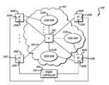
- a network computer system 500including a plurality of processor complexes 400 A- 400 N coupled to a shared memory network 501 .
- the shared memory network 501includes a plurality of disk ROMs 510 A- 510 M coupled together by an interconnection network 540 with possibly one or more external routers R 542 (or switches).
- the interconnection network 540may be a mesh network supported by internal and external routers to selectively interconnect each of the processor complexes to each of the disk-ROMs 510 A- 510 M of the shared memory network 501 .
- the interconnect network 540is a hypertransport (HT) routable point to point mesh network.
- the plurality of disk ROM's 510 A- 510 M instantiated in the shared memory network 501may be one or more of the disk ROM's 110 A- 110 C respectively illustrated by the functional block diagrams of FIGS. 3A-3C .
- the four or more processor complexes 400 A- 400 Nmay read and write blocks of data into and out of any disk-ROM in the shared memory cloud as if it were a disk file system. Furthermore, one or more processor complexes 400 A- 400 N may randomly read memory locations of any disk-ROM in the shared memory cloud as if it were a read only memory. That is, the disk ROM devices 510 A- 510 M may be read and written to as if they were disk-like devices and may be read from as if they were read only memory devices.
- All or selected portions of the physical memory locations of the plurality of disk ROM devices 510 A- 510 Mmay be mapped in to each of the processor memory spaces 200 A- 200 M of each of the respective four or more processor complexes (PC) 400 A- 400 N. All or portion of the memory array in each disk-ROM may be mapped into some or all of the processor complexes' address spaces at the same time. In this manner, some or all of the processors can access data somewhere in the memory arrays of the Disk ROMs 510 A- 510 M independently of each other.
- PCprocessor complexes
- the mapping software drivers 150 in each processor complex 400 A- 400 Ninitiate the block read/write accesses with the plurality of disk-ROM devices 510 A- 510 M and cooperate with each other to coordinate accesses into each disk-ROM device to avoid disk-ROM resource contentions.
- the mapping software drivers 150 in each processor complex 400 A- 400 Nfurther cooperate with each other to invalidate a plurality of cache lines 1001 in respective cache memories 1000 of the one or more processor complexes 400 A- 400 N in response to an accumulated plurality of memory change notifications.
- This cooperation amongst each processor complex 400 A- 400 Nprovides coherency of data in the plurality of networked disk ROM devices 510 A- 510 M.
- the network bits 1010 A- 1010 N in the network field 1010 of each cache linemay facilitate the cooperation amongst processor complexes and coherency of data in the plurality of networked disk ROM devices 510 A- 510 M.
- the networking computer system 500may further include a power controller 599 coupled to the plurality of processor complexes 400 A- 400 N in order to selectively power down one or more processor complexes when the demand for computations on the network computer system 500 have diminished and its respective processor load has decreased sufficiently enough to near zero.
- the power controller 599monitors the load on the processor complexes in order to selectively power up (power on or wake) and power down (power off or sleep) one or more processor complexes without losing access to the information stored in the one or more disk-ROM devices. That is, the power controller 599 keeps the plurality of disk-ROMS 510 A- 501 M powered on while it powers off one or more inactive processor complexes 400 A- 400 N.
- main memory data in a main memory of the processor complexis transferred into one or more of the plurality of disk-ROM devices 510 A- 510 M.
- the power controller 599can power back on one or more processor complexes to execute a process and its one or more instructions.
- main memory data previously saved in one or more of the disk-ROM devices 510 A- 501 Mmay be transferred from the one or more of the plurality of disk-ROM devices back into the main memory of the processor complex 400 A- 400 N.
- each processor complex 400 A- 400 Nhas one or more processors execute a distributed network control software driver 520 A- 520 N each of which is in communication with the power controller 530 .
- each processor complexcooperates with the others to come up with a consistent network-level decision on those that stay up (powered on) and those that get shut down (powered down).
- the functionality of the network control software drivermay be merged with the functionality of the disk-ROM software driver 150 .
- a centralized network control software driver 530is optionally executed by the power controller 599 to make a consistent network-level decision on those processor complexes that stay up (powered on) and those that get shut down (powered down).
- the communication of information between the processor complexes 400 A- 400 N, the disk ROM devices 510 A- 510 M, and the external routers 542 over the interconnect network 540is by way of packets.
- the packet 800includes a source address 801 , a destination address 802 , a packet-type 803 , and a data field 804 including a plurality of data.
- the packet-typeindicates the type of requested memory access desired by the packet 800 .
- the packet-type 803may be a read block request, a write block request, or a read random access request.
- the total memory space provided by the plurality of disk ROM's 510 A- 510 Mmay be partitioned in one embodiment of the invention and selectively assigned to one or more respective processor complexes. In another embodiment of the invention, the total memory space provided by the plurality of disk ROM's may be concatenated (pooled) together as one large pool of shared memory space.
- the total memory space provided by the plurality of disk ROM's 510 A- 510 M in a networked computer system 500may be partitioned with the partitions being selectively assigned to one or more respective processor complexes.
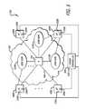
- FIG. 6an exemplary diagram of the total disk ROM memory space 600 in a shared memory network is illustrated including disk ROM space 510 A′- 510 D′ provided by four disk-ROM devices 510 A- 510 D.
- the shared disk ROM space 600 provided by the plurality of disk ROM's 510 A- 510 D in the cloud 501may be partitioned into a plurality of partitions.
- the shared disk ROM space 600may be partitioned into a first partition 610 A, a second partition 610 B, and a third partition 610 C.
- a partitionmay extend over the memory space of a plurality of disk-ROM devices.
- the first partition 610 Aextends over the disk-ROM space 510 A′ and a portion of the disk-ROM space 510 B′.
- the plurality of partitionsmay be assigned to one or more processor complexes (PC) 400 A- 400 N for use. If a processor complex is powered down by the power controller 599 to conserve energy, its assigned partition may be reassigned to one or more of the other processor complexes that remain powered up.
- PCprocessor complexes
- main memory 404 A- 404 MBefore the power controller 599 powers down a processor complex, its data stored in main memory 404 A- 404 M may be transferred for storage into one or more of the disk ROM devices 510 A- 510 M in the shared memory network cloud 501 . While the processor complexes (PC) 400 A- 400 N may be powered up when a process needs processing and powered down to conserve energy, the shared memory cloud 501 including the disk ROM devices 510 A- 510 M may remain powered up to maintain the state of the data stored therein.
- PCprocessor complexes
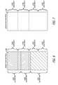
- the total memory space provided by the plurality of disk ROM's 510 A- 501 M in a networked computer system 500may be concatenated or pooled together as one large pool of shared memory space. In this case, there may be no dedicated memory space assigned to a single processor complex.
- the pooled disk ROM space 700includes disk ROM space 510 A′ from disk ROM 1 510 A, disk ROM space 510 B′ from disk ROM 2 510 B, disk ROM space 510 C′ from disk ROM 3 510 C, and disk ROM space 510 D′ from disk ROM 4 510 D.
- the pooled disk ROM space 700 within the disk ROM devicesmay be constantly powered up and ready for access by the one or more processor complexes (PC) 400 A- 400 N.
- PCprocessor complexes
- all or portions of the pooled disk ROM space 700may be used by any one or more of the one or more processor complexes (PC) 400 A- 400 N.
- PCprocessor complexes
- a network computer systemneed not use just one type of shared memory space.
- a first plurality of disk-ROM's in the networked computer system 500may be concatenated or pooled together as one large pool of shared memory space while a second plurality of disk-ROM's in the networked computer system 500 may be partitioned with the partitions being selectively assigned to one or more respective processor complexes.
- the embodiments of the inventionalso relate to an apparatus for performing the operations and functions described herein.
- This apparatusmay be specially constructed for the required purposes, or it may comprise a general-purpose computer selectively activated or reconfigured by a computer program stored in a storage device of the computer.
- the elements of the embodiments of the inventionare essentially the code segments or instructions to perform the processes and functions.
- the algorithm processesmay be written in a computer programming language and then converted to machine code segments, loaded into a computer, and then executed to perform the processes in an automated fashion.
- the program or code segmentscan be stored in a processor, computer, or machine readable medium such as a storage device.
- the code segmentsmay also be downloaded via computer networks such as the Internet, Intranet, etc and stored in the processor, computer, or a storage device (e.g., a machine readable medium).
- the elements of the embodiments of the inventionare essentially the code segments to perform the necessary tasks.
- the program or code segmentscan be stored in a processor readable storage medium or storage device.
- the processor readable storage mediummay include any medium that can store or transfer information. Examples of the processor readable storage medium include an electronic circuit, a semiconductor memory device, a read only memory (ROM), a flash memory, an erasable programmable read only memory (EPROM), a floppy diskette, a CD-ROM, an optical disk, a hard disk, a fiber optic medium, a radio frequency (RF) link, etc.
- the code segmentsmay be downloaded via computer networks such as the Internet, Intranet, etc., by means of a computer data signal that may include any signal that can propagate over a transmission medium such as electronic network channels, optical fibers, air, electromagnetic, RF links, etc. and stored into the processor readable storage medium.
- a computer data signalmay include any signal that can propagate over a transmission medium such as electronic network channels, optical fibers, air, electromagnetic, RF links, etc. and stored into the processor readable storage medium.
Landscapes
- Engineering & Computer Science (AREA)
- Theoretical Computer Science (AREA)
- General Engineering & Computer Science (AREA)
- Physics & Mathematics (AREA)
- General Physics & Mathematics (AREA)
- Human Computer Interaction (AREA)
- Software Systems (AREA)
- Computer Hardware Design (AREA)
- Computing Systems (AREA)
- Memory System Of A Hierarchy Structure (AREA)
Abstract
Description
Claims (8)
Priority Applications (2)
| Application Number | Priority Date | Filing Date | Title |
|---|---|---|---|
| US13/952,567US9513695B2 (en) | 2008-06-24 | 2013-07-26 | Methods of managing power in network computer systems |
| US15/092,492US10156890B2 (en) | 2008-06-24 | 2016-04-06 | Network computer systems with power management |
Applications Claiming Priority (3)
| Application Number | Priority Date | Filing Date | Title |
|---|---|---|---|
| US7533108P | 2008-06-24 | 2008-06-24 | |
| US12/490,941US8521967B1 (en) | 2008-06-24 | 2009-06-24 | Network computing systems having shared memory clouds with addresses of disk-read-only memories mapped into processor address spaces |
| US13/952,567US9513695B2 (en) | 2008-06-24 | 2013-07-26 | Methods of managing power in network computer systems |
Related Parent Applications (1)
| Application Number | Title | Priority Date | Filing Date |
|---|---|---|---|
| US12/490,941DivisionUS8521967B1 (en) | 2008-06-24 | 2009-06-24 | Network computing systems having shared memory clouds with addresses of disk-read-only memories mapped into processor address spaces |
Related Child Applications (1)
| Application Number | Title | Priority Date | Filing Date |
|---|---|---|---|
| US15/092,492ContinuationUS10156890B2 (en) | 2008-06-24 | 2016-04-06 | Network computer systems with power management |
Publications (2)
| Publication Number | Publication Date |
|---|---|
| US20150032940A1 US20150032940A1 (en) | 2015-01-29 |
| US9513695B2true US9513695B2 (en) | 2016-12-06 |
Family
ID=52391474
Family Applications (2)
| Application Number | Title | Priority Date | Filing Date |
|---|---|---|---|
| US13/952,567Expired - Fee RelatedUS9513695B2 (en) | 2008-06-24 | 2013-07-26 | Methods of managing power in network computer systems |
| US15/092,492ActiveUS10156890B2 (en) | 2008-06-24 | 2016-04-06 | Network computer systems with power management |
Family Applications After (1)
| Application Number | Title | Priority Date | Filing Date |
|---|---|---|---|
| US15/092,492ActiveUS10156890B2 (en) | 2008-06-24 | 2016-04-06 | Network computer systems with power management |
Country Status (1)
| Country | Link |
|---|---|
| US (2) | US9513695B2 (en) |
Cited By (1)
| Publication number | Priority date | Publication date | Assignee | Title |
|---|---|---|---|---|
| US20160299714A1 (en)* | 2013-07-18 | 2016-10-13 | Synaptic Laboratories Limited | Computing architecture with peripherals |
Families Citing this family (9)
| Publication number | Priority date | Publication date | Assignee | Title |
|---|---|---|---|---|
| US10262721B2 (en) | 2016-03-10 | 2019-04-16 | Micron Technology, Inc. | Apparatuses and methods for cache invalidate |
| US10673811B2 (en)* | 2016-07-25 | 2020-06-02 | ColorTokens, Inc. | Updating address mapping for local and network resources |
| US10684955B2 (en)* | 2017-04-21 | 2020-06-16 | Micron Technology, Inc. | Memory devices and methods which may facilitate tensor memory access with memory maps based on memory operations |
| US10572286B2 (en) | 2017-04-26 | 2020-02-25 | International Business Machines Corporation | Memory access optimization in a processor complex |
| US10592451B2 (en) | 2017-04-26 | 2020-03-17 | International Business Machines Corporation | Memory access optimization for an I/O adapter in a processor complex |
| US10956315B2 (en) | 2018-07-24 | 2021-03-23 | Micron Technology, Inc. | Memory devices and methods which may facilitate tensor memory access |
| US11809899B2 (en)* | 2019-06-28 | 2023-11-07 | Intel Corporation | Methods and apparatus for accelerating virtual machine migration |
| US10877552B1 (en)* | 2019-09-19 | 2020-12-29 | Amazon Technologies, Inc. | Dynamic power reduction through data transfer request limiting |
| US11429769B1 (en)* | 2020-10-30 | 2022-08-30 | Xilinx, Inc. | Implementing a hardware description language memory using heterogeneous memory primitives |
Citations (80)
| Publication number | Priority date | Publication date | Assignee | Title |
|---|---|---|---|---|
| US4757533A (en) | 1985-09-11 | 1988-07-12 | Computer Security Corporation | Security system for microcomputers |
| US5012408A (en) | 1990-03-15 | 1991-04-30 | Digital Equipment Corporation | Memory array addressing system for computer systems with multiple memory arrays |
| US5379401A (en) | 1992-03-31 | 1995-01-03 | Intel Corporation | Flash memory card including circuitry for selectively providing masked and unmasked ready/busy output signals |
| US5404485A (en) | 1993-03-08 | 1995-04-04 | M-Systems Flash Disk Pioneers Ltd. | Flash file system |
| US5404478A (en) | 1989-12-28 | 1995-04-04 | Hitachi, Ltd. | Method of managing a virtual storage for a multi-processor system |
| US5701438A (en) | 1995-09-29 | 1997-12-23 | Intel Corporation | Logical relocation of memory based on memory device type |
| US5710733A (en) | 1996-01-22 | 1998-01-20 | Silicon Graphics, Inc. | Processor-inclusive memory module |
| US5935253A (en)* | 1991-10-17 | 1999-08-10 | Intel Corporation | Method and apparatus for powering down an integrated circuit having a core that operates at a speed greater than the bus frequency |
| US6088750A (en) | 1994-12-13 | 2000-07-11 | International Business Machines Corporation | Method and system for arbitrating between bus masters having diverse bus acquisition protocols |
| US6185704B1 (en) | 1997-04-11 | 2001-02-06 | Texas Instruments Incorporated | System signaling schemes for processor and memory module |
| US6314501B1 (en) | 1998-07-23 | 2001-11-06 | Unisys Corporation | Computer system and method for operating multiple operating systems in different partitions of the computer system and for allowing the different partitions to communicate with one another through shared memory |
| US20020017720A1 (en) | 2000-03-03 | 2002-02-14 | Hirotaka Nishizawa | Semiconductor device |
| US20020051350A1 (en) | 2000-10-20 | 2002-05-02 | Mitsubishi Denki Kabushiki Kaisha | Load adjustment board and data processing apparatus |
| US6393545B1 (en) | 1919-04-30 | 2002-05-21 | Canon Kabushiki Kaisha | Method apparatus and system for managing virtual memory with virtual-physical mapping |
| US6397317B1 (en) | 1998-09-04 | 2002-05-28 | Sharp Kabushiki Kaisha | Data processing method and apparatus having address conversion |
| US20020118593A1 (en) | 2001-02-27 | 2002-08-29 | Fujitsu Limited | Memory system |
| US20020133684A1 (en) | 2001-01-17 | 2002-09-19 | Honeywell International, Inc. | Enhanced memory module architecture |
| US20020138600A1 (en) | 2001-03-26 | 2002-09-26 | International Business Machines Corporation | Method, apparatus and program for multi-machine network install using writeable media |
| US20020181315A1 (en) | 2001-06-01 | 2002-12-05 | Samsung Electronics Co., Ltd. | Nonvolatile semiconductor memory device having selective multiple-speed operation mode |
| US20030061383A1 (en)* | 2001-09-25 | 2003-03-27 | Zilka Anthony M. | Predicting processor inactivity for a controlled transition of power states |
| US6549959B1 (en) | 1999-08-30 | 2003-04-15 | Ati International Srl | Detecting modification to computer memory by a DMA device |
| US6564326B2 (en) | 1999-07-06 | 2003-05-13 | Walter A. Helbig, Sr. | Method and apparatus for enhancing computer system security |
| US20030090879A1 (en) | 2001-06-14 | 2003-05-15 | Doblar Drew G. | Dual inline memory module |
| US20030137862A1 (en) | 2001-07-12 | 2003-07-24 | Brunelle Steven J. | Reversed memory module socket, motherboard and test system including same, and method of modifying motherboard |
| US20030174569A1 (en) | 2002-03-12 | 2003-09-18 | Hossein Amidi | System and method for translation of SDRAM and DDR signals |
| US20030188083A1 (en) | 2002-03-27 | 2003-10-02 | Kumar Mohan J. | Method and apparatus for setting timing parameters |
| US20040026791A1 (en) | 1998-03-09 | 2004-02-12 | King Jerrold L. | Apparatus for forming a stack of packaged memory dice |
| US20040117581A1 (en) | 2002-12-13 | 2004-06-17 | Samsung Electronics Co., Ltd. | Computer system and control method thereof |
| US20040160835A1 (en) | 2000-12-14 | 2004-08-19 | Altman Erik R. | Symmetric multi-processing system |
| US6785780B1 (en) | 2000-08-31 | 2004-08-31 | Micron Technology, Inc. | Distributed processor memory module and method |
| US20040186948A1 (en) | 1991-07-26 | 2004-09-23 | Lofgren Karl M. J. | Device and method for controlling solid-state memory system |
| US20040193783A1 (en) | 2003-03-26 | 2004-09-30 | Manish Sharma | Computer system with operating system permitting dynamic reallocation of main memory |
| US20040236877A1 (en) | 1997-12-17 | 2004-11-25 | Lee A. Burton | Switch/network adapter port incorporating shared memory resources selectively accessible by a direct execution logic element and one or more dense logic devices in a fully buffered dual in-line memory module format (FB-DIMM) |
| US20050044303A1 (en) | 2000-01-05 | 2005-02-24 | Perego Richard E. | Memory system including an integrated circuit buffer device |
| US20050166026A1 (en) | 2000-01-05 | 2005-07-28 | Fred Ware | Configurable width buffered module having switch elements |
| US20050204088A1 (en) | 2004-02-12 | 2005-09-15 | Via Technologies Inc. | Data acquisition methods |
| US20050235131A1 (en) | 2004-04-20 | 2005-10-20 | Ware Frederick A | Memory controller for non-homogeneous memory system |
| US20050240745A1 (en) | 2003-12-18 | 2005-10-27 | Sundar Iyer | High speed memory control and I/O processor system |
| US20050251617A1 (en) | 2004-05-07 | 2005-11-10 | Sinclair Alan W | Hybrid non-volatile memory system |
| US6970968B1 (en) | 1998-02-13 | 2005-11-29 | Intel Corporation | Memory module controller for providing an interface between a system memory controller and a plurality of memory devices on a memory module |
| US20050273570A1 (en) | 2004-06-03 | 2005-12-08 | Desouter Marc A | Virtual space manager for computer having a physical address extension feature |
| US20050289317A1 (en) | 2004-06-24 | 2005-12-29 | Ming-Shi Liou | Method and related apparatus for accessing memory |
| US20060015749A1 (en) | 2000-06-30 | 2006-01-19 | Millind Mittal | Method and apparatus for secure execution using a secure memory partition |
| US6990044B2 (en) | 2002-12-18 | 2006-01-24 | Hynix Semiconductor Inc. | Composite memory device |
| US20060050488A1 (en) | 2004-09-03 | 2006-03-09 | Staktel Group, L.P. | High capacity thin module system and method |
| US7034955B2 (en) | 2000-12-11 | 2006-04-25 | Texas Instruments Incorporated | Using a processor enhanced memory module to accelerate hardcopy image processing within existing printer controller |
| US20060106984A1 (en) | 2004-11-18 | 2006-05-18 | International Business Machines Corporation | Methods and apparatus for efficient memory usage |
| US20060149857A1 (en) | 1997-12-05 | 2006-07-06 | Holman Thomas J | Memory system including a memory module having a memory module controller |
| US7091598B2 (en) | 2001-01-19 | 2006-08-15 | Renesas Technology Corporation | Electronic circuit device |
| US20060195631A1 (en) | 2005-01-31 | 2006-08-31 | Ramasubramanian Rajamani | Memory buffers for merging local data from memory modules |
| US20060230250A1 (en) | 2005-04-12 | 2006-10-12 | Nokia Corporation | Memory interface for volatile and non-volatile memory devices |
| US7123521B1 (en) | 2005-04-27 | 2006-10-17 | Micron Technology, Inc. | Random cache read |
| US20070016704A1 (en) | 1993-09-01 | 2007-01-18 | Eliyahou Harari | Removable Mother/Daughter Peripheral Card |
| US7196554B2 (en) | 2003-07-07 | 2007-03-27 | Infineon Technologies Ag | Integrated clock supply chip for a memory module, memory module comprising the integrated clock supply chip, and method for operating the memory module under test conditions |
| US20070245092A1 (en) | 2006-04-12 | 2007-10-18 | Hsin-Chung Yeh | Non-volatile memory sharing apparatus for multiple processors and method thereof |
| US20070276977A1 (en) | 2006-05-24 | 2007-11-29 | International Business Machines Corporation | Systems and methods for providing memory modules with multiple hub devices |
| US20080001303A1 (en) | 2006-06-29 | 2008-01-03 | Sandisk Corporation | Stacked, interconnected semiconductor packages |
| US7318164B2 (en)* | 2001-12-13 | 2008-01-08 | International Business Machines Corporation | Conserving energy in a data processing system by selectively powering down processors |
| US20080024899A1 (en) | 2006-07-27 | 2008-01-31 | Hitachi Global Storage Technologies Netherlands B.V. | Disk drive with nonvolatile memory having multiple modes of operation |
| US20080028186A1 (en) | 2006-07-28 | 2008-01-31 | Drc Computer Corporation | FPGA Co-Processor For Accelerated Computation |
| US20080082750A1 (en) | 2006-09-28 | 2008-04-03 | Okin Kenneth A | Methods of communicating to, memory modules in a memory channel |
| US20080082751A1 (en) | 2006-09-28 | 2008-04-03 | Okin Kenneth A | Memory modules and programmable heterogeneous memory controllers for main memory |
| US20080082732A1 (en) | 2006-09-28 | 2008-04-03 | Vijay Karamcheti | Systems and apparatus for main memory with non-volatile type memory modules, and related technologies |
| US20080082733A1 (en) | 2006-09-28 | 2008-04-03 | Vijay Karamcheti | Methods for main memory with non-volatile type memory modules, and related technologies |
| US20080082734A1 (en) | 2006-09-28 | 2008-04-03 | Vijay Karamcheti | Methods for main memory in a system with a memory controller configured to control access to non-volatile memory, and related technologies |
| US20080082766A1 (en) | 2006-09-28 | 2008-04-03 | Okin Kenneth A | Systems and apparatus with programmable memory control for heterogeneous main memory |
| US20080082731A1 (en) | 2006-09-28 | 2008-04-03 | Vijay Karamcheti | Main memory in a system with a memory controller configured to control access to non-volatile memory, and related technologies |
| US20080094808A1 (en) | 2006-10-23 | 2008-04-24 | Ruban Kanapathippillai | Methods and apparatus of dual inline memory modules for flash memory |
| US20080115006A1 (en) | 2006-07-31 | 2008-05-15 | Michael John Sebastian Smith | System and method for adjusting the timing of signals associated with a memory system |
| US20080229085A1 (en) | 2007-03-14 | 2008-09-18 | Apple Inc. | Switching Drivers Between Processors |
| US20090080442A1 (en)* | 2007-09-26 | 2009-03-26 | Narayan Ananth S | Conserving power in a multi-node environment |
| US20090210616A1 (en) | 2008-02-12 | 2009-08-20 | Vijay Karamcheti | Memory modules for two-dimensional main memory |
| US20090240869A1 (en)* | 2008-03-20 | 2009-09-24 | Schooner Information Technology, Inc. | Sharing Data Fabric for Coherent-Distributed Caching of Multi-Node Shared-Distributed Flash Memory |
| US20090254689A1 (en) | 2008-02-12 | 2009-10-08 | Vijay Karamcheti | Methods and apparatus for two-dimensional main memory |
| US7734890B2 (en) | 2006-10-06 | 2010-06-08 | Okralabs Llc | Method and system for using a distributable virtual address space |
| US7774556B2 (en) | 2006-11-04 | 2010-08-10 | Virident Systems Inc. | Asymmetric memory migration in hybrid main memory |
| US20110077795A1 (en)* | 2009-02-13 | 2011-03-31 | American Power Conversion Corporation | Data center control |
| US8370672B2 (en)* | 2010-02-26 | 2013-02-05 | Microsoft Corporation | Reducing power consumption of distributed storage systems |
| US8521967B1 (en)* | 2008-06-24 | 2013-08-27 | Virident Systems, Inc. | Network computing systems having shared memory clouds with addresses of disk-read-only memories mapped into processor address spaces |
| US20130246825A1 (en)* | 2011-03-25 | 2013-09-19 | Research In Motion Limited | Method and system for dynamically power scaling a cache memory of a multi-core processing system |
Family Cites Families (14)
| Publication number | Priority date | Publication date | Assignee | Title |
|---|---|---|---|---|
| DE19540915A1 (en)* | 1994-11-10 | 1996-05-15 | Raymond Engineering | Redundant arrangement of solid state memory modules |
| US6052753A (en)* | 1997-01-21 | 2000-04-18 | Alliedsignal Inc. | Fault tolerant data bus |
| US5997168A (en)* | 1997-04-14 | 1999-12-07 | Electronic Data Systems Corporation | Optimizing the operation of an equipment control system |
| JP3563256B2 (en)* | 1998-02-13 | 2004-09-08 | 富士通株式会社 | Remote control method for power saving function, information processing device, and storage medium |
| US6990598B2 (en)* | 2001-03-21 | 2006-01-24 | Gallitzin Allegheny Llc | Low power reconfigurable systems and methods |
| US20060248360A1 (en)* | 2001-05-18 | 2006-11-02 | Fung Henry T | Multi-server and multi-CPU power management system and method |
| US6985952B2 (en)* | 2001-10-31 | 2006-01-10 | International Business Machines Corporation | Energy-induced process migration |
| JP4086722B2 (en) | 2003-06-24 | 2008-05-14 | 株式会社荏原製作所 | Substrate holding device and polishing device |
| US7257678B2 (en)* | 2004-10-01 | 2007-08-14 | Advanced Micro Devices, Inc. | Dynamic reconfiguration of cache memory |
| JP4634268B2 (en)* | 2005-10-03 | 2011-02-16 | 株式会社日立製作所 | Storage system power saving method and storage system |
| EP1996993B1 (en)* | 2006-01-10 | 2015-03-11 | Cupp Computing As | Dual mode power-saving computing system |
| US7856549B2 (en)* | 2007-01-24 | 2010-12-21 | Hewlett-Packard Development Company, L.P. | Regulating power consumption |
| US7774631B1 (en)* | 2007-06-30 | 2010-08-10 | Emc Corporation | Method and system for minimizing power consumption in a multiprocessor data storage system |
| KR20110007205A (en)* | 2008-04-21 | 2011-01-21 | 어댑티브 컴퓨팅 엔터프라이즈 인코포레이티드 | Systems and Methods for Managing Energy Consumption in Compute Environments |
- 2013
- 2013-07-26USUS13/952,567patent/US9513695B2/ennot_activeExpired - Fee Related
- 2016
- 2016-04-06USUS15/092,492patent/US10156890B2/enactiveActive
Patent Citations (84)
| Publication number | Priority date | Publication date | Assignee | Title |
|---|---|---|---|---|
| US6393545B1 (en) | 1919-04-30 | 2002-05-21 | Canon Kabushiki Kaisha | Method apparatus and system for managing virtual memory with virtual-physical mapping |
| US4757533A (en) | 1985-09-11 | 1988-07-12 | Computer Security Corporation | Security system for microcomputers |
| US5404478A (en) | 1989-12-28 | 1995-04-04 | Hitachi, Ltd. | Method of managing a virtual storage for a multi-processor system |
| US5012408A (en) | 1990-03-15 | 1991-04-30 | Digital Equipment Corporation | Memory array addressing system for computer systems with multiple memory arrays |
| US20040186948A1 (en) | 1991-07-26 | 2004-09-23 | Lofgren Karl M. J. | Device and method for controlling solid-state memory system |
| US5935253A (en)* | 1991-10-17 | 1999-08-10 | Intel Corporation | Method and apparatus for powering down an integrated circuit having a core that operates at a speed greater than the bus frequency |
| US5379401A (en) | 1992-03-31 | 1995-01-03 | Intel Corporation | Flash memory card including circuitry for selectively providing masked and unmasked ready/busy output signals |
| US5404485A (en) | 1993-03-08 | 1995-04-04 | M-Systems Flash Disk Pioneers Ltd. | Flash file system |
| US20070016704A1 (en) | 1993-09-01 | 2007-01-18 | Eliyahou Harari | Removable Mother/Daughter Peripheral Card |
| US6088750A (en) | 1994-12-13 | 2000-07-11 | International Business Machines Corporation | Method and system for arbitrating between bus masters having diverse bus acquisition protocols |
| US5701438A (en) | 1995-09-29 | 1997-12-23 | Intel Corporation | Logical relocation of memory based on memory device type |
| US5710733A (en) | 1996-01-22 | 1998-01-20 | Silicon Graphics, Inc. | Processor-inclusive memory module |
| US6185704B1 (en) | 1997-04-11 | 2001-02-06 | Texas Instruments Incorporated | System signaling schemes for processor and memory module |
| US20060149857A1 (en) | 1997-12-05 | 2006-07-06 | Holman Thomas J | Memory system including a memory module having a memory module controller |
| US20040236877A1 (en) | 1997-12-17 | 2004-11-25 | Lee A. Burton | Switch/network adapter port incorporating shared memory resources selectively accessible by a direct execution logic element and one or more dense logic devices in a fully buffered dual in-line memory module format (FB-DIMM) |
| US6970968B1 (en) | 1998-02-13 | 2005-11-29 | Intel Corporation | Memory module controller for providing an interface between a system memory controller and a plurality of memory devices on a memory module |
| US20040026791A1 (en) | 1998-03-09 | 2004-02-12 | King Jerrold L. | Apparatus for forming a stack of packaged memory dice |
| US6314501B1 (en) | 1998-07-23 | 2001-11-06 | Unisys Corporation | Computer system and method for operating multiple operating systems in different partitions of the computer system and for allowing the different partitions to communicate with one another through shared memory |
| US6397317B1 (en) | 1998-09-04 | 2002-05-28 | Sharp Kabushiki Kaisha | Data processing method and apparatus having address conversion |
| US6564326B2 (en) | 1999-07-06 | 2003-05-13 | Walter A. Helbig, Sr. | Method and apparatus for enhancing computer system security |
| US6549959B1 (en) | 1999-08-30 | 2003-04-15 | Ati International Srl | Detecting modification to computer memory by a DMA device |
| US20050166026A1 (en) | 2000-01-05 | 2005-07-28 | Fred Ware | Configurable width buffered module having switch elements |
| US20050044303A1 (en) | 2000-01-05 | 2005-02-24 | Perego Richard E. | Memory system including an integrated circuit buffer device |
| US20020017720A1 (en) | 2000-03-03 | 2002-02-14 | Hirotaka Nishizawa | Semiconductor device |
| US20060015749A1 (en) | 2000-06-30 | 2006-01-19 | Millind Mittal | Method and apparatus for secure execution using a secure memory partition |
| US6785780B1 (en) | 2000-08-31 | 2004-08-31 | Micron Technology, Inc. | Distributed processor memory module and method |
| US20020051350A1 (en) | 2000-10-20 | 2002-05-02 | Mitsubishi Denki Kabushiki Kaisha | Load adjustment board and data processing apparatus |
| US7034955B2 (en) | 2000-12-11 | 2006-04-25 | Texas Instruments Incorporated | Using a processor enhanced memory module to accelerate hardcopy image processing within existing printer controller |
| US20040160835A1 (en) | 2000-12-14 | 2004-08-19 | Altman Erik R. | Symmetric multi-processing system |
| US20020133684A1 (en) | 2001-01-17 | 2002-09-19 | Honeywell International, Inc. | Enhanced memory module architecture |
| US6765812B2 (en) | 2001-01-17 | 2004-07-20 | Honeywell International Inc. | Enhanced memory module architecture |
| US7091598B2 (en) | 2001-01-19 | 2006-08-15 | Renesas Technology Corporation | Electronic circuit device |
| US20020118593A1 (en) | 2001-02-27 | 2002-08-29 | Fujitsu Limited | Memory system |
| US20020138600A1 (en) | 2001-03-26 | 2002-09-26 | International Business Machines Corporation | Method, apparatus and program for multi-machine network install using writeable media |
| US20020181315A1 (en) | 2001-06-01 | 2002-12-05 | Samsung Electronics Co., Ltd. | Nonvolatile semiconductor memory device having selective multiple-speed operation mode |
| US20030090879A1 (en) | 2001-06-14 | 2003-05-15 | Doblar Drew G. | Dual inline memory module |
| US20030137862A1 (en) | 2001-07-12 | 2003-07-24 | Brunelle Steven J. | Reversed memory module socket, motherboard and test system including same, and method of modifying motherboard |
| US20030061383A1 (en)* | 2001-09-25 | 2003-03-27 | Zilka Anthony M. | Predicting processor inactivity for a controlled transition of power states |
| US7318164B2 (en)* | 2001-12-13 | 2008-01-08 | International Business Machines Corporation | Conserving energy in a data processing system by selectively powering down processors |
| US20030174569A1 (en) | 2002-03-12 | 2003-09-18 | Hossein Amidi | System and method for translation of SDRAM and DDR signals |
| US20030188083A1 (en) | 2002-03-27 | 2003-10-02 | Kumar Mohan J. | Method and apparatus for setting timing parameters |
| US20040117581A1 (en) | 2002-12-13 | 2004-06-17 | Samsung Electronics Co., Ltd. | Computer system and control method thereof |
| US6990044B2 (en) | 2002-12-18 | 2006-01-24 | Hynix Semiconductor Inc. | Composite memory device |
| US20040193783A1 (en) | 2003-03-26 | 2004-09-30 | Manish Sharma | Computer system with operating system permitting dynamic reallocation of main memory |
| US7196554B2 (en) | 2003-07-07 | 2007-03-27 | Infineon Technologies Ag | Integrated clock supply chip for a memory module, memory module comprising the integrated clock supply chip, and method for operating the memory module under test conditions |
| US20050240745A1 (en) | 2003-12-18 | 2005-10-27 | Sundar Iyer | High speed memory control and I/O processor system |
| US20050204088A1 (en) | 2004-02-12 | 2005-09-15 | Via Technologies Inc. | Data acquisition methods |
| US20050235131A1 (en) | 2004-04-20 | 2005-10-20 | Ware Frederick A | Memory controller for non-homogeneous memory system |
| US20050251617A1 (en) | 2004-05-07 | 2005-11-10 | Sinclair Alan W | Hybrid non-volatile memory system |
| US20050273570A1 (en) | 2004-06-03 | 2005-12-08 | Desouter Marc A | Virtual space manager for computer having a physical address extension feature |
| US20050289317A1 (en) | 2004-06-24 | 2005-12-29 | Ming-Shi Liou | Method and related apparatus for accessing memory |
| US20060050488A1 (en) | 2004-09-03 | 2006-03-09 | Staktel Group, L.P. | High capacity thin module system and method |
| US7324352B2 (en) | 2004-09-03 | 2008-01-29 | Staktek Group L.P. | High capacity thin module system and method |
| US20060106984A1 (en) | 2004-11-18 | 2006-05-18 | International Business Machines Corporation | Methods and apparatus for efficient memory usage |
| US20060195631A1 (en) | 2005-01-31 | 2006-08-31 | Ramasubramanian Rajamani | Memory buffers for merging local data from memory modules |
| US20060230250A1 (en) | 2005-04-12 | 2006-10-12 | Nokia Corporation | Memory interface for volatile and non-volatile memory devices |
| US7123521B1 (en) | 2005-04-27 | 2006-10-17 | Micron Technology, Inc. | Random cache read |
| US20070245092A1 (en) | 2006-04-12 | 2007-10-18 | Hsin-Chung Yeh | Non-volatile memory sharing apparatus for multiple processors and method thereof |
| US20070276977A1 (en) | 2006-05-24 | 2007-11-29 | International Business Machines Corporation | Systems and methods for providing memory modules with multiple hub devices |
| US20080001303A1 (en) | 2006-06-29 | 2008-01-03 | Sandisk Corporation | Stacked, interconnected semiconductor packages |
| US20080024899A1 (en) | 2006-07-27 | 2008-01-31 | Hitachi Global Storage Technologies Netherlands B.V. | Disk drive with nonvolatile memory having multiple modes of operation |
| US20080028186A1 (en) | 2006-07-28 | 2008-01-31 | Drc Computer Corporation | FPGA Co-Processor For Accelerated Computation |
| US20080115006A1 (en) | 2006-07-31 | 2008-05-15 | Michael John Sebastian Smith | System and method for adjusting the timing of signals associated with a memory system |
| US20080082734A1 (en) | 2006-09-28 | 2008-04-03 | Vijay Karamcheti | Methods for main memory in a system with a memory controller configured to control access to non-volatile memory, and related technologies |
| US20080082733A1 (en) | 2006-09-28 | 2008-04-03 | Vijay Karamcheti | Methods for main memory with non-volatile type memory modules, and related technologies |
| US20080082751A1 (en) | 2006-09-28 | 2008-04-03 | Okin Kenneth A | Memory modules and programmable heterogeneous memory controllers for main memory |
| US20080082766A1 (en) | 2006-09-28 | 2008-04-03 | Okin Kenneth A | Systems and apparatus with programmable memory control for heterogeneous main memory |
| US20080082731A1 (en) | 2006-09-28 | 2008-04-03 | Vijay Karamcheti | Main memory in a system with a memory controller configured to control access to non-volatile memory, and related technologies |
| US20080082750A1 (en) | 2006-09-28 | 2008-04-03 | Okin Kenneth A | Methods of communicating to, memory modules in a memory channel |
| US8051253B2 (en) | 2006-09-28 | 2011-11-01 | Virident Systems, Inc. | Systems and apparatus with programmable memory control for heterogeneous main memory |
| US20080082732A1 (en) | 2006-09-28 | 2008-04-03 | Vijay Karamcheti | Systems and apparatus for main memory with non-volatile type memory modules, and related technologies |
| US7734890B2 (en) | 2006-10-06 | 2010-06-08 | Okralabs Llc | Method and system for using a distributable virtual address space |
| US20080094808A1 (en) | 2006-10-23 | 2008-04-24 | Ruban Kanapathippillai | Methods and apparatus of dual inline memory modules for flash memory |
| US7774556B2 (en) | 2006-11-04 | 2010-08-10 | Virident Systems Inc. | Asymmetric memory migration in hybrid main memory |
| US20080229085A1 (en) | 2007-03-14 | 2008-09-18 | Apple Inc. | Switching Drivers Between Processors |
| US20090080442A1 (en)* | 2007-09-26 | 2009-03-26 | Narayan Ananth S | Conserving power in a multi-node environment |
| US20090210636A1 (en) | 2008-02-12 | 2009-08-20 | Vijay Karamcheti | Methods and systems for two-dimensional main memory |
| US20090254689A1 (en) | 2008-02-12 | 2009-10-08 | Vijay Karamcheti | Methods and apparatus for two-dimensional main memory |
| US20090210616A1 (en) | 2008-02-12 | 2009-08-20 | Vijay Karamcheti | Memory modules for two-dimensional main memory |
| US20090240869A1 (en)* | 2008-03-20 | 2009-09-24 | Schooner Information Technology, Inc. | Sharing Data Fabric for Coherent-Distributed Caching of Multi-Node Shared-Distributed Flash Memory |
| US8521967B1 (en)* | 2008-06-24 | 2013-08-27 | Virident Systems, Inc. | Network computing systems having shared memory clouds with addresses of disk-read-only memories mapped into processor address spaces |
| US20110077795A1 (en)* | 2009-02-13 | 2011-03-31 | American Power Conversion Corporation | Data center control |
| US8370672B2 (en)* | 2010-02-26 | 2013-02-05 | Microsoft Corporation | Reducing power consumption of distributed storage systems |
| US20130246825A1 (en)* | 2011-03-25 | 2013-09-19 | Research In Motion Limited | Method and system for dynamically power scaling a cache memory of a multi-core processing system |
Non-Patent Citations (9)
| Title |
|---|
| Candea, George et al, "Microreboot A Technique for Cheap Recovery", 2004, Publisher: USENIX Association. 14 pages. |
| Cheung, Raymond, "AQ1207:MPC824x Architecture and Applications", "Smart Networks Developer Forum 2003 Asia", Oct. 20, 2003, Publisher: Motorola, Published in: US. 48 pages. |
| Connor, Deni, "Kmart shines its Blue Light on solid state disks", May 7, 2001, Publisher: itworld.com, Published in: US. 2 pages. |
| Lee, Hyung Gyu, "Energy Aware Memory Allocation in Heterogeneous Non-Volatile Memory Systems", Aug. 25, 2003, Publisher: Seoul National University, Published in: Korea. 4 pages. |
| Microsoft Computer Dictionary, Fifth edition, 2002, 8 pages. |
| Nand FLash Memory, by Micron 2004, 57 pages. |
| Tseng, Hung-Wei et al, "An Energy Efficient Virtual Memory System with Flash Memory as the Secondary Storage", "ISLPED '06", Oct. 4, 2006, pp. 418-423, Publisher: Dept. of CS and Info Engineering, National Taiwan University, Published in: Taipei, Taiwan. 6 pages. |
| Unknown Author, "3.5 in SATA SSD Drive", "www.SuperTalent.com", Aug. 17, 2007, pp. 1-3, Publisher: Super Talent Technology, Published in: US. 3 pages. |
| Williams, Martyn, "Solid-state disks coming on strong", "Infoworld.com", Jun. 7, 2007, Publisher: Macworld, The Mac Experts, Published in: US. 2 pages. |
Cited By (1)
| Publication number | Priority date | Publication date | Assignee | Title |
|---|---|---|---|---|
| US20160299714A1 (en)* | 2013-07-18 | 2016-10-13 | Synaptic Laboratories Limited | Computing architecture with peripherals |
Also Published As
| Publication number | Publication date |
|---|---|
| US20160342195A1 (en) | 2016-11-24 |
| US20150032940A1 (en) | 2015-01-29 |
| US10156890B2 (en) | 2018-12-18 |
Similar Documents
| Publication | Publication Date | Title |
|---|---|---|
| US8745314B1 (en) | Methods for a random read and read/write block accessible memory | |
| US10156890B2 (en) | Network computer systems with power management | |
| US7814279B2 (en) | Low-cost cache coherency for accelerators | |
| US9274961B2 (en) | Method for building multi-processor system with nodes having multiple cache coherency domains | |
| US9952975B2 (en) | Memory network to route memory traffic and I/O traffic | |
| US10296399B2 (en) | Data coherency model and protocol at cluster level | |
| JP2022054407A (en) | Systems, apparatus and methods for dynamically providing coherent memory domains | |
| US7577816B2 (en) | Remote translation mechanism for a multinode system | |
| JP4805314B2 (en) | Offloading Input/Output (I/O) Virtualization Operations to a Processor | |
| CN108153683B (en) | Apparatus and method for transferring data between address ranges in memory | |
| US20140040561A1 (en) | Handling cache write-back and cache eviction for cache coherence | |
| JP2004192620A (en) | Method and data processing system for microprocessor communication using processor interconnected in multiprocessor system | |
| CN114153754B (en) | Data transmission method and device for computing cluster and storage medium | |
| US7222220B2 (en) | Multiprocessing system employing address switches to control mixed broadcast snooping and directory based coherency protocols transparent to active devices | |
| US20090182893A1 (en) | Cache coherence in a virtual machine managed system | |
| US9542317B2 (en) | System and a method for data processing with management of a cache consistency in a network of processors with cache memories | |
| US11860781B1 (en) | Clean engine for write-back cache memory | |
| JP2004192619A (en) | Method, processing unit and data processing system for microprocessor communication in multiprocessor system | |
| CN106951390A (en) | It is a kind of to reduce the NUMA system construction method of cross-node Memory accessing delay | |
| US7155576B1 (en) | Pre-fetching and invalidating packet information in a cache memory | |
| US20100042787A1 (en) | Cache injection directing tool | |
| US7904676B2 (en) | Method and system for achieving varying manners of memory access | |
| JP2004192621A (en) | Method and data processing system for microprocessor communication in cluster based multiprocessor system | |
| US8762647B2 (en) | Multicore processor system and multicore processor | |
| EP0392184A2 (en) | Hierarchical memory organization |
Legal Events
| Date | Code | Title | Description |
|---|---|---|---|
| AS | Assignment | Owner name:VIRIDENT SYSTEMS, INC., CALIFORNIA Free format text:ASSIGNMENT OF ASSIGNORS INTEREST;ASSIGNORS:KARAMCHETI, VIJAY;OKIN, KENNETH A.;GANAPATHY, KUMAR;SIGNING DATES FROM 20090722 TO 20090803;REEL/FRAME:031159/0860 | |
| STCF | Information on status: patent grant | Free format text:PATENTED CASE | |
| AS | Assignment | Owner name:VIRIDENT SYSTEMS, LLC, CALIFORNIA Free format text:CHANGE OF NAME;ASSIGNOR:VIRIDENT SYSTEMS, INC.;REEL/FRAME:042438/0935 Effective date:20160725 | |
| FEPP | Fee payment procedure | Free format text:PETITION RELATED TO MAINTENANCE FEES GRANTED (ORIGINAL EVENT CODE: PTGR) | |
| MAFP | Maintenance fee payment | Free format text:PAYMENT OF MAINTENANCE FEE, 4TH YEAR, LARGE ENTITY (ORIGINAL EVENT CODE: M1551); ENTITY STATUS OF PATENT OWNER: LARGE ENTITY Year of fee payment:4 | |
| AS | Assignment | Owner name:WESTERN DIGITAL TECHNOLOGIES, INC., CALIFORNIA Free format text:ASSIGNMENT OF ASSIGNORS INTEREST;ASSIGNOR:VIRIDENT SYSTEMS, LLC;REEL/FRAME:053180/0472 Effective date:20200610 | |
| AS | Assignment | Owner name:JPMORGAN CHASE BANK, N.A., AS AGENT, ILLINOIS Free format text:SECURITY INTEREST;ASSIGNOR:WESTERN DIGITAL TECHNOLOGIES, INC.;REEL/FRAME:053926/0446 Effective date:20200828 | |
| AS | Assignment | Owner name:WESTERN DIGITAL TECHNOLOGIES, INC., CALIFORNIA Free format text:RELEASE OF SECURITY INTEREST AT REEL 053926 FRAME 0446;ASSIGNOR:JPMORGAN CHASE BANK, N.A.;REEL/FRAME:058966/0321 Effective date:20220203 | |
| AS | Assignment | Owner name:JPMORGAN CHASE BANK, N.A., ILLINOIS Free format text:PATENT COLLATERAL AGREEMENT - A&R LOAN AGREEMENT;ASSIGNOR:WESTERN DIGITAL TECHNOLOGIES, INC.;REEL/FRAME:064715/0001 Effective date:20230818 Owner name:JPMORGAN CHASE BANK, N.A., ILLINOIS Free format text:PATENT COLLATERAL AGREEMENT - DDTL LOAN AGREEMENT;ASSIGNOR:WESTERN DIGITAL TECHNOLOGIES, INC.;REEL/FRAME:067045/0156 Effective date:20230818 | |
| FEPP | Fee payment procedure | Free format text:MAINTENANCE FEE REMINDER MAILED (ORIGINAL EVENT CODE: REM.); ENTITY STATUS OF PATENT OWNER: LARGE ENTITY | |
| LAPS | Lapse for failure to pay maintenance fees | Free format text:PATENT EXPIRED FOR FAILURE TO PAY MAINTENANCE FEES (ORIGINAL EVENT CODE: EXP.); ENTITY STATUS OF PATENT OWNER: LARGE ENTITY | |
| STCH | Information on status: patent discontinuation | Free format text:PATENT EXPIRED DUE TO NONPAYMENT OF MAINTENANCE FEES UNDER 37 CFR 1.362 | |
| FP | Lapsed due to failure to pay maintenance fee | Effective date:20241206 |