US9513349B2 - Scissor type magnetic sensor with high magnetic moment bias structure for reduced signal asymmetry - Google Patents
Scissor type magnetic sensor with high magnetic moment bias structure for reduced signal asymmetryDownload PDFInfo
- Publication number
- US9513349B2 US9513349B2US14/174,776US201414174776AUS9513349B2US 9513349 B2US9513349 B2US 9513349B2US 201414174776 AUS201414174776 AUS 201414174776AUS 9513349 B2US9513349 B2US 9513349B2
- Authority
- US
- United States
- Prior art keywords
- magnetic
- layer
- layers
- sensor
- free
- Prior art date
- Legal status (The legal status is an assumption and is not a legal conclusion. Google has not performed a legal analysis and makes no representation as to the accuracy of the status listed.)
- Active
Links
- 230000005291magnetic effectEffects0.000titleclaimsabstractdescription223
- 229910001030Iron–nickel alloyInorganic materials0.000claimsabstractdescription8
- 239000000463materialSubstances0.000claimsdescription24
- 230000008878couplingEffects0.000claimsdescription13
- 238000010168coupling processMethods0.000claimsdescription13
- 238000005859coupling reactionMethods0.000claimsdescription13
- 239000002885antiferromagnetic materialSubstances0.000claimsdescription6
- 239000000696magnetic materialSubstances0.000abstractdescription7
- 229910003321CoFeInorganic materials0.000abstractdescription3
- 101000993059Homo sapiens Hereditary hemochromatosis proteinProteins0.000abstractdescription3
- 230000005415magnetizationEffects0.000description35
- 239000000725suspensionSubstances0.000description6
- 229910003271Ni-FeInorganic materials0.000description5
- PNEYBMLMFCGWSK-UHFFFAOYSA-Naluminium oxideInorganic materials[O-2].[O-2].[O-2].[Al+3].[Al+3]PNEYBMLMFCGWSK-UHFFFAOYSA-N0.000description4
- 230000008859changeEffects0.000description4
- 230000004888barrier functionEffects0.000description3
- 230000009467reductionEffects0.000description3
- 239000000956alloySubstances0.000description2
- 229910045601alloyInorganic materials0.000description2
- 230000001419dependent effectEffects0.000description2
- 230000000694effectsEffects0.000description2
- CPLXHLVBOLITMK-UHFFFAOYSA-Nmagnesium oxideInorganic materials[Mg]=OCPLXHLVBOLITMK-UHFFFAOYSA-N0.000description2
- 238000004519manufacturing processMethods0.000description2
- 230000004044responseEffects0.000description2
- 125000006850spacer groupChemical group0.000description2
- PBCFLUZVCVVTBY-UHFFFAOYSA-Ntantalum pentoxideInorganic materialsO=[Ta](=O)O[Ta](=O)=OPBCFLUZVCVVTBY-UHFFFAOYSA-N0.000description2
- 230000005641tunnelingEffects0.000description2
- 229910017750AgSnInorganic materials0.000description1
- 229910020598Co FeInorganic materials0.000description1
- 229910002519Co-FeInorganic materials0.000description1
- 229910017947MgOxInorganic materials0.000description1
- 229910019041PtMnInorganic materials0.000description1
- 229910052581Si3N4Inorganic materials0.000description1
- 229910020776SixNyInorganic materials0.000description1
- 230000000712assemblyEffects0.000description1
- 238000000429assemblyMethods0.000description1
- 238000004590computer programMethods0.000description1
- 239000004020conductorSubstances0.000description1
- 229910052593corundumInorganic materials0.000description1
- 230000004907fluxEffects0.000description1
- 230000001939inductive effectEffects0.000description1
- 238000009413insulationMethods0.000description1
- 239000000203mixtureSubstances0.000description1
- 230000035699permeabilityEffects0.000description1
- 229910001845yogo sapphireInorganic materials0.000description1
Images


Classifications
- G—PHYSICS
- G01—MEASURING; TESTING
- G01R—MEASURING ELECTRIC VARIABLES; MEASURING MAGNETIC VARIABLES
- G01R33/00—Arrangements or instruments for measuring magnetic variables
- G01R33/02—Measuring direction or magnitude of magnetic fields or magnetic flux
- G01R33/06—Measuring direction or magnitude of magnetic fields or magnetic flux using galvano-magnetic devices
- G01R33/09—Magnetoresistive devices
- G01R33/098—Magnetoresistive devices comprising tunnel junctions, e.g. tunnel magnetoresistance sensors
- G—PHYSICS
- G11—INFORMATION STORAGE
- G11B—INFORMATION STORAGE BASED ON RELATIVE MOVEMENT BETWEEN RECORD CARRIER AND TRANSDUCER
- G11B5/00—Recording by magnetisation or demagnetisation of a record carrier; Reproducing by magnetic means; Record carriers therefor
- G11B5/127—Structure or manufacture of heads, e.g. inductive
- G11B5/33—Structure or manufacture of flux-sensitive heads, i.e. for reproduction only; Combination of such heads with means for recording or erasing only
- G11B5/39—Structure or manufacture of flux-sensitive heads, i.e. for reproduction only; Combination of such heads with means for recording or erasing only using magneto-resistive devices or effects
- G11B5/3903—Structure or manufacture of flux-sensitive heads, i.e. for reproduction only; Combination of such heads with means for recording or erasing only using magneto-resistive devices or effects using magnetic thin film layers or their effects, the films being part of integrated structures
- G11B5/3906—Details related to the use of magnetic thin film layers or to their effects
- G11B5/3929—Disposition of magnetic thin films not used for directly coupling magnetic flux from the track to the MR film or for shielding
- G11B5/3932—Magnetic biasing films
- G—PHYSICS
- G11—INFORMATION STORAGE
- G11B—INFORMATION STORAGE BASED ON RELATIVE MOVEMENT BETWEEN RECORD CARRIER AND TRANSDUCER
- G11B5/00—Recording by magnetisation or demagnetisation of a record carrier; Reproducing by magnetic means; Record carriers therefor
- G11B5/127—Structure or manufacture of heads, e.g. inductive
- G11B5/33—Structure or manufacture of flux-sensitive heads, i.e. for reproduction only; Combination of such heads with means for recording or erasing only
- G11B5/39—Structure or manufacture of flux-sensitive heads, i.e. for reproduction only; Combination of such heads with means for recording or erasing only using magneto-resistive devices or effects
- G11B5/3903—Structure or manufacture of flux-sensitive heads, i.e. for reproduction only; Combination of such heads with means for recording or erasing only using magneto-resistive devices or effects using magnetic thin film layers or their effects, the films being part of integrated structures
- G11B5/398—Specially shaped layers
- G—PHYSICS
- G11—INFORMATION STORAGE
- G11B—INFORMATION STORAGE BASED ON RELATIVE MOVEMENT BETWEEN RECORD CARRIER AND TRANSDUCER
- G11B5/00—Recording by magnetisation or demagnetisation of a record carrier; Reproducing by magnetic means; Record carriers therefor
- G11B5/127—Structure or manufacture of heads, e.g. inductive
- G11B5/33—Structure or manufacture of flux-sensitive heads, i.e. for reproduction only; Combination of such heads with means for recording or erasing only
- G11B5/39—Structure or manufacture of flux-sensitive heads, i.e. for reproduction only; Combination of such heads with means for recording or erasing only using magneto-resistive devices or effects
- G11B2005/3996—Structure or manufacture of flux-sensitive heads, i.e. for reproduction only; Combination of such heads with means for recording or erasing only using magneto-resistive devices or effects large or giant magnetoresistive effects [GMR], e.g. as generated in spin-valve [SV] devices
- G—PHYSICS
- G11—INFORMATION STORAGE
- G11B—INFORMATION STORAGE BASED ON RELATIVE MOVEMENT BETWEEN RECORD CARRIER AND TRANSDUCER
- G11B5/00—Recording by magnetisation or demagnetisation of a record carrier; Reproducing by magnetic means; Record carriers therefor
- G11B5/127—Structure or manufacture of heads, e.g. inductive
- G11B5/33—Structure or manufacture of flux-sensitive heads, i.e. for reproduction only; Combination of such heads with means for recording or erasing only
- G11B5/39—Structure or manufacture of flux-sensitive heads, i.e. for reproduction only; Combination of such heads with means for recording or erasing only using magneto-resistive devices or effects
- G11B5/3903—Structure or manufacture of flux-sensitive heads, i.e. for reproduction only; Combination of such heads with means for recording or erasing only using magneto-resistive devices or effects using magnetic thin film layers or their effects, the films being part of integrated structures
- G11B5/3906—Details related to the use of magnetic thin film layers or to their effects
- G11B5/3909—Arrangements using a magnetic tunnel junction
- G—PHYSICS
- G11—INFORMATION STORAGE
- G11B—INFORMATION STORAGE BASED ON RELATIVE MOVEMENT BETWEEN RECORD CARRIER AND TRANSDUCER
- G11B5/00—Recording by magnetisation or demagnetisation of a record carrier; Reproducing by magnetic means; Record carriers therefor
- G11B5/127—Structure or manufacture of heads, e.g. inductive
- G11B5/33—Structure or manufacture of flux-sensitive heads, i.e. for reproduction only; Combination of such heads with means for recording or erasing only
- G11B5/39—Structure or manufacture of flux-sensitive heads, i.e. for reproduction only; Combination of such heads with means for recording or erasing only using magneto-resistive devices or effects
- G11B5/3903—Structure or manufacture of flux-sensitive heads, i.e. for reproduction only; Combination of such heads with means for recording or erasing only using magneto-resistive devices or effects using magnetic thin film layers or their effects, the films being part of integrated structures
- G11B5/3906—Details related to the use of magnetic thin film layers or to their effects
- G11B5/3912—Arrangements in which the active read-out elements are transducing in association with active magnetic shields, e.g. magnetically coupled shields
Definitions
- the present inventionrelates to magnetic data recording and more particularly to a magnetic sensor having a back edge magnetic bias structure formed of a high magnetic moment material.
- the magnetic disk driveincludes a rotating magnetic disk, write and read heads that are suspended by a suspension arm adjacent to a surface of the rotating magnetic disk and an actuator that swings the suspension arm to place the read and write heads over selected circular tracks on the rotating disk.
- the read and write headsare directly located on a slider that has an air bearing surface (ABS).
- ABSair bearing surface
- the suspension armbiases the slider into contact with the surface of the disk when the disk is not rotating, but when the disk rotates air is swirled by the rotating disk.
- the write and read headsare employed for writing magnetic impressions to and reading magnetic impressions from the rotating disk.
- the read and write headsare connected to processing circuitry that operates according to a computer program to implement the writing and reading functions.
- the write headincludes at least one coil, a write pole and one or more return poles.
- a resulting magnetic fieldcauses a magnetic flux to flow through the coil, which results in a magnetic write field emitting from the tip of the write pole.
- This magnetic fieldis sufficiently strong that it locally magnetizes a portion of the adjacent magnetic media, thereby recording a bit of data.
- the write fieldthen, travels through a magnetically soft under-layer of the magnetic medium to return to the return pole of the write head.
- a magnetoresistive sensorsuch as a Giant Magnetoresistive (GMR) sensor or a Tunnel Junction Magnetoresistive (TMR) sensor can be employed to read a magnetic signal from the magnetic media.
- the magnetoresistive sensorhas an electrical resistance that changes in response to an external magnetic field. This change in electrical resistance can be detected by processing circuitry in order to read magnetic data from the magnetic media.
- pinning of the pinned layer structurerequires the use of a relatively thick layer of anti-ferromagnetic material (AFM layer) and also requires a complex pinning layer structure such as an AP coupled structure that includes first and second magnetic layers that are anti-parallel coupled across a non-magnetic anti-parallel coupling layer, with one of the magnetic layers being exchange coupled with the AFM layer.
- AFM layeranti-ferromagnetic material
- AP coupled structuresuch as an AP coupled structure that includes first and second magnetic layers that are anti-parallel coupled across a non-magnetic anti-parallel coupling layer, with one of the magnetic layers being exchange coupled with the AFM layer.
- a scissor sensor designOne type of sensor that shows promise in reducing gap spacing is a scissor sensor design.
- Such a sensorincludes two magnetic free layers that have magnetizations that are biased in directions that are orthogonal to one another.
- a pinned layer structureis not necessary so the complex, thick pinning structure can be eliminated.
- such sensorpresent challenges with regard to design and sensor performance, such as biasing of the two magnetic free layers. Therefore, there remains a need for a scissor sensor design that can provide a sensor that is practical to manufacture, while providing superior magnetic performance and reliability.
- a magnetic sensorhaving first and second magnetic free layers that are anti-parallel coupled with one another by a non-magnetic anti-parallel coupling layer located there-between.
- the magnetic bias layershave a back edge located opposite from a media facing surface.
- the sensoralso includes a magnetic bias layer that extends from the back edge of the first and second magnetic free layers and that is formed of a magnetic material having a high magnetic moment.
- the high magnetic moment magnetic bias layeradvantageously reduces signal asymmetry while also maintaining high signal amplitude. While it has been believed that a high magnetic moment material could not be used because such materials have a low magnetic coercivity and do not, therefore, maintain their magnetization as a result of their inherent high magnetic moment, it has been found, surprisingly, that high magnetic moment materials can be used as a bias structure in such a sensor if certain design considerations are taken into account and that performance advantages can be achieved through the use of such materials.
- the magnetic bias structurecan be constructed of a material such as NiFe having a high Fe content, or from a CoFe alloy.
- FIG. 1is a schematic illustration of a disk drive system in which the invention might be embodied
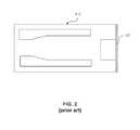
- FIG. 2is view of a slider illustrating the location of a magnetic head thereon, as seen from the medium facing surface;
- FIG. 3is an enlarged view of a magnetic sensor as seen from the medium facing surface
- FIG. 4is a top down cross sectional view of the magnetic sensor as seen from line 4 - 4 FIG. 3 ;
- FIG. 5is an exploded schematic view of a scissor type magnetic sensor illustrating the effect of magnetic biasing on magnetizations of magnetic free layers of a scissor type magnetic sensor;
- FIG. 6is a side, cross sectional view as seen from line 6 - 6 of FIG. 4 ;
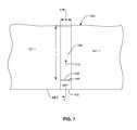
- FIG. 7is top down cross sectional view similar to that of FIG. 4 of a sensor according to an alternate embodiment.
- FIG. 8is a side, cross sectional view according to an alternate embodiment.
- the disk drive 100includes a housing 101 . At least one rotatable magnetic disk 112 is supported on a spindle 114 and rotated by a disk drive motor 118 .
- the magnetic recording on each diskis in the form of annular patterns of concentric data tracks (not shown) on the magnetic disk 112 .
- At least one slider 113is positioned near the magnetic disk 112 , each slider 113 supporting one or more magnetic head assemblies 121 . As the magnetic disk rotates, slider 113 moves in and out over the disk surface 122 so that the magnetic head assembly 121 can access different tracks of the magnetic disk where desired data are written.
- Each slider 113is attached to an actuator arm 119 by way of a suspension 115 .
- the suspension 115provides a slight spring force which biases the slider 113 against the disk surface 122 .
- Each actuator arm 119is attached to an actuator means 127 .
- the actuator means 127 as shown in FIG. 1may be a voice coil motor (VCM).
- the VCMcomprises a coil movable within a fixed magnetic field, the direction and speed of the coil movements being controlled by the motor current signals supplied by the controller 129 .
- the rotation of the magnetic disk 112generates an air bearing between the slider 113 and the disk surface 122 , which exerts an upward force or lift on the slider.
- the air bearingthus counter-balances the slight spring force of the suspension 115 and supports the slider 113 off and slightly above the disk surface by a small, substantially constant spacing during normal operation.
- control unit 129The various components of the disk storage system are controlled in operation by control signals generated by control unit 129 , such as access control signals and internal clock signals.
- control unit 129comprises logic control circuits, storage, means and a microprocessor.
- the control unit 129generates control signals to control various system operations such as drive motor control signals on line 123 and head position and seek control signals on line 128 .
- the control signals on line 128provide the desired current profiles to optimally move and position the slider 113 to the desired data track on the media 112 .
- Write and read signalsare communicated to and from write and read heads 121 by way of recording channel 125 .
- FIG. 2is a media facing surface (MFS) view of the slider 113 , and as can be seen, the magnetic 121 head, including an inductive write head and a read sensor, is located at a trailing edge of the slider.
- MFSmedia facing surface
- FIG. 3shows a view of a magnetic read head 300 as viewed from the air media facing surface.
- the read head 300is a scissor type magnetoresistive sensor having a sensor stack 302 that includes first and second magnetic free layers 304 , 306 that are anti-parallel coupled across a non-magnetic layer 308 that can be a non-magnetic, electrically insulating barrier layer such as MgOx or an electrically insulating spacer layer such as AgSn.
- a capping layer structure 310can be provided at the top of the sensor stack 302 to protect the layers of the sensor stack during manufacture.
- the sensor stack 302can also include a seed layer structure 312 at its bottom to promote a desired grain growth in the above formed layers.
- the first and second magnetic layers 304 , 306can be constructed of multiple layers of magnetic material.
- the first magnetic layer 304can be constructed of: a layer of Ni—Fe; a layer of Co—Hf deposited over the layer of Ni—Fe; a layer of Co—Fe—B deposited over the layer of Co—Hf; and a layer of Co—Fe—B.
- the second magnetic layer 306can be constructed of: a layer of Co—Fe; a layer of Co—Fe—B; and a layer of Ni—Fe deposited over the layer of Co—Hf.
- the capping layer structure 310can also be constructed as a multi-layer structure and can include first and second layers of Ru with a layer of Ta sandwiched there-between.
- the seed layer structure 312can include a layer of Ta and a layer of Ru formed over the layer of Ta.
- the sensor stack 302is sandwiched between leading and trailing magnetic shields 314 , 316 , each of which can be constructed of a magnetic material such as Ni—Fe, or a composition having a high magnetic permeability ( ) to provide effective magnetic shielding.
- leading and trailing magnetic shields 314 , 316each of which can be constructed of a magnetic material such as Ni—Fe, or a composition having a high magnetic permeability ( ) to provide effective magnetic shielding.
- the shields 314 , 316can be constructed of an electrically conductive material so that they can function as electrical leads as well as functioning as magnetic shields.
- the electrical resistance across the sensor stack 302depends upon the direction of magnetization of the magnetic free layers 304 , 306 relative to one another. The closer the magnetizations of the layers 304 , 306 are to being parallel to one another, the lower the electrical resistance will be, and, conversely, the closer the magnetizations of the layers 304 , 306 are to being anti-parallel to one another, the higher the electrical resistance will be. Since the orientations of the magnetizations of the layers 304 , 306 are free to move in response to an external magnetic field, this change in magnetization direction and resulting change in electrical resistance can be used to detect a magnetic field such as from an adjacent magnetic media (not shown in FIG. 3 ).
- the relative orientations of the magnetizations of the layers 304 , 306will be described in greater detail below with reference to FIG. 4 . If the non-magnetic layer 308 is an electrically insulating barrier layer, then the sensor operates based on the spin dependent tunneling effect of electrons tunneling through the barrier layer. On the other hand, if the layer 308 is an electrically conductive spacer layer, then the change in electrical resistance results from the spin dependent scattering phenomenon.
- the sensor 300also can include an anti-parallel soft magnetic side shield structures 318 at either side of the sensor stack 302 .
- Each of the side shield structures 318is separated from the sensor stack 302 and from the bottom shield 314 by a thin, non-magnetic, electrically insulating layer 320 , which can be a material such as alumina, SixNy, Ta 2 O 5 , or MgO.
- Each of the side shield structures 318includes first and second soft magnetic layers 322 , 324 that are anti-parallel coupled with one another across an anti-parallel coupling layer 326 .
- the soft magnetic layers 322 , 324are constructed of a material such as NiFe, NiFeCr, CoNiFe, or an alloy thereof that a low magnetic coercivity and a high magnetization saturation.
- the soft magnetic layers 322 , 324can be constructed of the same materials as one another or can be constructed of different materials having differing magnetic moments (Bs).
- a seed layer 332can be provided at the bottom of the shield structure 318 to provide a desired grain structure in the layers 322 , 324 , 326 formed there-above.
- the soft magnetic layers 322 , 324have magnetizations 334 , 336 respectively that are oriented in opposite directions, each parallel with the air bearing surface.
- FIG. 4shows a top down, cross sectional view as seen from line 4 - 4 of FIG. 3 .
- FIG. 4shows the sensor stack 302 having a front edge 402 that extends to the media facing surface (MFS) and has a back edge 404 opposite the front edge 402 .
- the distance between the front edge 402 and back edge 404defines the stripe height of the sensor stack 302 .
- the sensor 300also includes a magnetic bias structure 406 that extends from the back edge 404 of the sensor stack 302 in a direction away from the media facing surface (MFS).
- the space behind the side shields 318 and at either side of the bias structure 406can be filled with a non-magnetic, electrically insulating fill material such as alumina (Al 2 O 3 ) 321 .
- the magnetic bias structure 406is constructed of a material having a high magnetic moment.
- the magnetic bias structure 406is preferably constructed of a material having a magnetic moment of at least 1.0 T, and more preferably 1.6 T or greater. Previously it had been believed that a bias structure had to be constructed of a hard magnetic material having a high magnetic coercivity.
- Such materialsonce magnetized, maintain their magnetization as a result of their high magnetic coercivity. It has been believed that in order to prevent the bias structure from becoming de-magnetized and losing its ability to provide a magnetic bias field, a magnetic bias structure had to be constructed of such a high magnetic moment material. Such high coercivity materials necessarily have a relatively low magnetic moment such as 0.5 T or lower.
- the bias structure 406can be constructed of a material having a high magnetic moment even if such material has a lower magnetic coercivity (e.g. is magnetically soft). What's more, the inventors have found that the use of such a magnetic bias structure 406 results in a decrease in signal asymmetry, and also, surprisingly, maintains high signal amplitude.
- the magnetic bias structure 406can be constructed of a magnetic material having a high magnetic moment of at least 1.0 T. Suitable materials for the magnetic bias structure include NiFe having a high Fe content, such as greater than 40 atomic percent. More specifically the bias structure could be constructed of Ni—Fe having an Fe content of 50-60 atomic percent. This material has a magnetic moment of about 1.6 T.
- the magnetic bias structure 406can also be constructed of CoFe, which has a magnetic moment of about 2.4 T.
- the bias layercan maintain its magnetization 410 ( FIG. 4 ) even when made of a low coercivity, high magnetic moment material if certain design considerations are met.
- the bias structure 406can be constructed with a length L measured perpendicular to the media facing surface MFS, and has a width W measured parallel with the media facing surface MFS. If the width W is small relative to the length L, the magnetic bias structure has a shape enhanced magnetic anisotropy that keeps the magnetization 410 aligned in the desired direction even though the bias layer structure 406 has a low magnetic coercivity.
- the magnetization 410 of the bias structure 406can be maintained by exchange coupling with a layer of anti-ferromagnetic material.
- a layer of anti-ferromagnetic materialsuch as IrMn or PtMn 602 can be exchange coupled with the magnetic bias structure 406 .
- the AFM layer 602can be formed beneath the bias layer 406 as shown in FIG. 6 , or could alternatively also be formed above the bias layer 406 (as shown in FIG. 8 ). While the AFM layer 602 does not in and of itself have a net magnetization of its own, when is exchange coupled with a layer of magnetic material such as the bias layer 406 it strongly pins the magnetization of that layer.
- the magnetic bias structureis separated from the sensor stack 302 by a non-magnetic, electrically insulating layer 408 , such as alumina, Si 3 N 4 , MgO, Ta 2 O 5 , or a combination thereof.
- the soft magnetic bias structurehas a magnetization 410 that is oriented in a direction that is perpendicular to the media facing surface MFS, as shown.
- FIG. 5shows an exploded schematic view of the sensor 300 .
- the free layers 304 , 306have magnetizations 338 , 340 that are oriented generally orthogonal to one another.
- the magnetizations 338 , 340would tend to align anti-parallel to one another in a direction parallel with the media facing surface MFS, as a result of the anti-parallel coupling of the free layers 304 , 306 and a magnetic anisotropy in a direction parallel with the media facing surface MFS.
- the presence of the magnetic field from the magnetization 410 of the bias structure 406causes the magnetizations 338 , 340 to rotate so that they are generally orthogonal as shown.
- the magnetizations 338 , 340can respond to a magnetic field by rotating in a scissoring fashion. While the bias layer rotates the magnetizations 338 , 340 of the free layers 304 , 306 in desired orthogonal directions, the magnetization 410 of the bias layer 406 does not prevent the magnetizations 338 , 340 from flipping direction (e.g. with magnetization 336 pointing to the right and 338 pointing to the left), which would render the sensor 300 incompatible with the signal processing circuitry and would, therefore, render the sensor 300 useless.
- the magnetizations 334 , 336 from the layers 322 , 324 of the soft side shield structure 318prevent this.
- the magnetic layer 322is aligned with the bottom free layer 304 and the upper magnetic layer 324 is aligned with the upper free layer 306 . Therefore, the magnetization 334 tends to pull the magnetization 338 in one direction parallel with the media facing surface MFS, whereas the magnetization 336 tends to pull the magnetization 340 in an opposite direction parallel with the media facing surface MFS. This effectively prevents the magnetizations 338 , 340 from flipping direction and improves the reliability of the sensor.
- This embodimentincludes a sensor 700 that can be similar to that described above with reference to FIGS. 3, 4 and 6 , except that the side shield structures 318 , described above with reference to FIGS. 3, 4 and 6 , have been omitted.
- the magnetic biasing from the bias structure 406maintains proper orientation of the magnetic layers of the sensor structure 302 without such side shields.
- the non-magnetic, electrically insulating fill layer 321can extend to the media facing surface (MFS) adjacent to the sides of the sensor stack 302 . Also, since the material 321 is non-magnetic, and electrically insulating, the insulation layers 320 described above with reference to FIG. 3 are unnecessary.
Landscapes
- Engineering & Computer Science (AREA)
- Manufacturing & Machinery (AREA)
- Physics & Mathematics (AREA)
- Condensed Matter Physics & Semiconductors (AREA)
- General Physics & Mathematics (AREA)
- Magnetic Heads (AREA)
Abstract
Description
Claims (16)
Priority Applications (1)
| Application Number | Priority Date | Filing Date | Title |
|---|---|---|---|
| US14/174,776US9513349B2 (en) | 2014-02-06 | 2014-02-06 | Scissor type magnetic sensor with high magnetic moment bias structure for reduced signal asymmetry |
Applications Claiming Priority (1)
| Application Number | Priority Date | Filing Date | Title |
|---|---|---|---|
| US14/174,776US9513349B2 (en) | 2014-02-06 | 2014-02-06 | Scissor type magnetic sensor with high magnetic moment bias structure for reduced signal asymmetry |
Publications (2)
| Publication Number | Publication Date |
|---|---|
| US20150221325A1 US20150221325A1 (en) | 2015-08-06 |
| US9513349B2true US9513349B2 (en) | 2016-12-06 |
Family
ID=53755357
Family Applications (1)
| Application Number | Title | Priority Date | Filing Date |
|---|---|---|---|
| US14/174,776ActiveUS9513349B2 (en) | 2014-02-06 | 2014-02-06 | Scissor type magnetic sensor with high magnetic moment bias structure for reduced signal asymmetry |
Country Status (1)
| Country | Link |
|---|---|
| US (1) | US9513349B2 (en) |
Cited By (4)
| Publication number | Priority date | Publication date | Assignee | Title |
|---|---|---|---|---|
| US9852755B2 (en)* | 2016-04-28 | 2017-12-26 | Tdk Corporation | Thin film magnetic head, head gimbals assembly, head arm assembly, and magnetic disk unit |
| US10381032B2 (en)* | 2018-01-12 | 2019-08-13 | Western Digital Technologies, Inc. | Magnetic sensors with effectively shaped side shields |
| US20240153533A1 (en)* | 2022-11-08 | 2024-05-09 | Western Digital Technologies, Inc. | Two-Dimensional Magnetic Recording Read Head with TaOx Layer for Flat Middle Shield Topography and Method of Forming Thereof |
| US12106787B1 (en)* | 2023-05-23 | 2024-10-01 | Western Digital Technologies, Inc. | DFL read head with SiOx cap layer on AlOx refill layers |
Families Citing this family (6)
| Publication number | Priority date | Publication date | Assignee | Title |
|---|---|---|---|---|
| US9449621B1 (en)* | 2015-03-26 | 2016-09-20 | Western Digital (Fremont), Llc | Dual free layer magnetic reader having a rear bias structure having a high aspect ratio |
| US9659586B1 (en)* | 2015-11-12 | 2017-05-23 | Seagate Technology Llc | Reader with free layer experiencing opposite phase-shifted media torques |
| US10783907B1 (en) | 2019-09-04 | 2020-09-22 | Seagate Technology Llc | Reader with bi-layered side shields |
| US11087785B1 (en)* | 2020-06-29 | 2021-08-10 | Western Digital Technologies, Inc. | Effective rear hard bias for dual free layer read heads |
| US11380355B2 (en)* | 2020-10-27 | 2022-07-05 | Headway Technologies, Inc. | Adaptive bias control for magnetic recording head |
| US20240071413A1 (en)* | 2022-08-31 | 2024-02-29 | Western Digital Technologies, Inc. | Dual Free Layer TMR Reader With Shaped Rear Bias and Methods of Forming Thereof |
Citations (36)
| Publication number | Priority date | Publication date | Assignee | Title |
|---|---|---|---|---|
| US5576914A (en) | 1994-11-14 | 1996-11-19 | Read-Rite Corporation | Compact read/write head having biased GMR element |
| US5818685A (en)* | 1997-05-05 | 1998-10-06 | Read-Rite Corporation | CIP GMR sensor coupled to biasing magnet with spacer therebetween |
| US20010008712A1 (en)* | 1998-12-22 | 2001-07-19 | Hisayuki Yazawa | Thin film magnetic head |
| US6778357B2 (en)* | 2000-11-10 | 2004-08-17 | Seagate Technology Llc | Electrodeposited high-magnetic-moment material at writer gap pole |
| US6781798B2 (en)* | 2002-07-15 | 2004-08-24 | International Business Machines Corporation | CPP sensor with dual self-pinned AP pinned layer structures |
| US6833976B2 (en)* | 2002-05-15 | 2004-12-21 | International Business Machine Corporation | Thin film magnetic recording inductive write head with laminated write gap |
| US6980406B2 (en)* | 2003-07-30 | 2005-12-27 | Hitachi Global Storage Technologies Netherlands, B.V. | Magnetic bias pinning layer for GMR sensor of a magnetic head for a hard disk drive |
| US7271986B2 (en) | 2002-05-15 | 2007-09-18 | Seagate Technology Llc | V-shape magnetic field sensor with anisotropy induced orthogonal magnetic alignment |
| US7397638B2 (en)* | 2005-07-22 | 2008-07-08 | Hitachi Global Storage Technologies Netherlands B.V. | Magnetoresistive sensor having an in stack bias structure with NiFeCr spacer layer for improved bias layer pinning |
| US20090135529A1 (en)* | 2007-11-28 | 2009-05-28 | Tdk Corporation | Magneto-resistive effect device of the cpp type, and magnetic disk system |
| US20090257154A1 (en)* | 2008-04-11 | 2009-10-15 | Hitachi Global Storage Technologies Netherlands B.V. | Scissoring-type current-perpendicular-to-the-plane giant magnetoresistance (cpp-gmr) sensors with damped free layer structures |
| US7639456B2 (en)* | 2005-10-06 | 2009-12-29 | Hitachi Global Storage Technologies Netherlands B.V. | Double mill process for patterning current perpendicular to plane (CPP) magnetoresistive devices to minimize barrier shorting and barrier damage |
| US20100097729A1 (en)* | 2008-10-20 | 2010-04-22 | Hardayal Singh Gill | Cpp dual free layer magnetoresistive head for magnetic data storage |
| US7705586B2 (en)* | 2004-09-27 | 2010-04-27 | Nxp B.V. | Magnetic sensor for input devices |
| US7804668B2 (en)* | 2006-11-16 | 2010-09-28 | Headway Technologies, Inc. | Enhanced hard bias in thin film magnetoresistive sensors with perpendicular easy axis growth of hard bias and strong shield-hard bias coupling |
| US20110007426A1 (en) | 2009-07-13 | 2011-01-13 | Seagate Technology Llc | Trapezoidal back bias and trilayer reader geometry to enhance device performance |
| US20110026169A1 (en)* | 2009-07-28 | 2011-02-03 | Hardayal Singh Gill | Dual cpp gmr head using a scissor sensor |
| US20110228428A1 (en)* | 2010-03-19 | 2011-09-22 | Seagate Technology Llc | Trilayer reader with current constraint at the abs |
| US20110317313A1 (en)* | 2010-06-28 | 2011-12-29 | Tdk Corporation | Magnetoresistive element and thin film magnetic head |
| US8147994B2 (en)* | 2009-02-26 | 2012-04-03 | Tdk Corporation | Layered structure having FePt system magnetic layer and magnetoresistive effect element using the same |
| US8179642B2 (en)* | 2009-09-22 | 2012-05-15 | Tdk Corporation | Magnetoresistive effect element in CPP structure and magnetic disk device |
| US20120229935A1 (en) | 2011-03-08 | 2012-09-13 | Seagate Technology Llc | Magnetic Element With Increased Scissoring Angle |
| US8390963B2 (en)* | 2011-04-25 | 2013-03-05 | Seagate Technology Llc | Trilayer reader with current constraint at the ABS |
| US20140022668A1 (en)* | 2011-10-03 | 2014-01-23 | Kabushiki Kaisha Toshiba | Magnetic head |
| US8749926B1 (en)* | 2012-11-30 | 2014-06-10 | HGST Netherlands B.V. | Scissor magnetic read head with wrap-around magnetic shield |
| US8891208B2 (en)* | 2013-03-29 | 2014-11-18 | Tdk Corporation | CPP-type magnetoresistive element including a rear bias structure and lower shields with inclined magnetizations |
| US8889019B1 (en)* | 2013-05-31 | 2014-11-18 | HGST Netherlands B.V. | Super shallow laminated hard mask stencil for magnetic read sensor fabrication |
| US8907666B2 (en)* | 2011-09-30 | 2014-12-09 | HGST Netherlands B.V. | Magnetic bias structure for magnetoresistive sensor having a scissor structure |
| US8932667B2 (en)* | 2008-04-30 | 2015-01-13 | Seagate Technology Llc | Hard magnet with cap and seed layers and data storage device read/write head incorporating the same |
| US8976492B1 (en)* | 2013-10-29 | 2015-03-10 | HGST Netherlands B.V. | Magnetic head having two domain control layers for stabilizing magnetization of the hard bias layer |
| US9001472B2 (en)* | 2011-06-23 | 2015-04-07 | Seagate Technology Llc | Shield stabilization configuration with applied bias |
| US9007725B1 (en)* | 2014-10-07 | 2015-04-14 | Western Digital (Fremont), Llc | Sensor with positive coupling between dual ferromagnetic free layer laminates |
| US9076468B1 (en)* | 2014-03-12 | 2015-07-07 | HGST Netherlands B.V. | Scissor magnetic read sensor with shape enhanced soft magnetic side shield for improved stability |
| US9153258B2 (en)* | 2013-12-03 | 2015-10-06 | HGST Netherlands B.V. | Scissor magnetic read sensor with novel multi-layer bias structure for uniform free layer biasing |
| US9280992B1 (en)* | 2015-07-28 | 2016-03-08 | HGST Netherlands B.V. | Hybrid longitudinal-field bias side shield for a scissor magnetic sensor and methods of making the same |
| US9384763B1 (en)* | 2015-03-26 | 2016-07-05 | Western Digital (Fremont), Llc | Dual free layer magnetic reader having a rear bias structure including a soft bias layer |
- 2014
- 2014-02-06USUS14/174,776patent/US9513349B2/enactiveActive
Patent Citations (40)
| Publication number | Priority date | Publication date | Assignee | Title |
|---|---|---|---|---|
| US5576914A (en) | 1994-11-14 | 1996-11-19 | Read-Rite Corporation | Compact read/write head having biased GMR element |
| US5818685A (en)* | 1997-05-05 | 1998-10-06 | Read-Rite Corporation | CIP GMR sensor coupled to biasing magnet with spacer therebetween |
| US20010008712A1 (en)* | 1998-12-22 | 2001-07-19 | Hisayuki Yazawa | Thin film magnetic head |
| US6778357B2 (en)* | 2000-11-10 | 2004-08-17 | Seagate Technology Llc | Electrodeposited high-magnetic-moment material at writer gap pole |
| US6833976B2 (en)* | 2002-05-15 | 2004-12-21 | International Business Machine Corporation | Thin film magnetic recording inductive write head with laminated write gap |
| US7271986B2 (en) | 2002-05-15 | 2007-09-18 | Seagate Technology Llc | V-shape magnetic field sensor with anisotropy induced orthogonal magnetic alignment |
| US6781798B2 (en)* | 2002-07-15 | 2004-08-24 | International Business Machines Corporation | CPP sensor with dual self-pinned AP pinned layer structures |
| US6980406B2 (en)* | 2003-07-30 | 2005-12-27 | Hitachi Global Storage Technologies Netherlands, B.V. | Magnetic bias pinning layer for GMR sensor of a magnetic head for a hard disk drive |
| US7705586B2 (en)* | 2004-09-27 | 2010-04-27 | Nxp B.V. | Magnetic sensor for input devices |
| US7397638B2 (en)* | 2005-07-22 | 2008-07-08 | Hitachi Global Storage Technologies Netherlands B.V. | Magnetoresistive sensor having an in stack bias structure with NiFeCr spacer layer for improved bias layer pinning |
| US7639456B2 (en)* | 2005-10-06 | 2009-12-29 | Hitachi Global Storage Technologies Netherlands B.V. | Double mill process for patterning current perpendicular to plane (CPP) magnetoresistive devices to minimize barrier shorting and barrier damage |
| US7804668B2 (en)* | 2006-11-16 | 2010-09-28 | Headway Technologies, Inc. | Enhanced hard bias in thin film magnetoresistive sensors with perpendicular easy axis growth of hard bias and strong shield-hard bias coupling |
| US20090135529A1 (en)* | 2007-11-28 | 2009-05-28 | Tdk Corporation | Magneto-resistive effect device of the cpp type, and magnetic disk system |
| US20090257154A1 (en)* | 2008-04-11 | 2009-10-15 | Hitachi Global Storage Technologies Netherlands B.V. | Scissoring-type current-perpendicular-to-the-plane giant magnetoresistance (cpp-gmr) sensors with damped free layer structures |
| US8233247B2 (en) | 2008-04-11 | 2012-07-31 | Hitachi Global Storage Technologies Netherlands B.V. | Scissoring-type current-perpendicular-to-the-plane giant magnetoresistance (CPP-GMR) sensors with damped free layer structures |
| US8932667B2 (en)* | 2008-04-30 | 2015-01-13 | Seagate Technology Llc | Hard magnet with cap and seed layers and data storage device read/write head incorporating the same |
| US20100097729A1 (en)* | 2008-10-20 | 2010-04-22 | Hardayal Singh Gill | Cpp dual free layer magnetoresistive head for magnetic data storage |
| US8018691B2 (en)* | 2008-10-20 | 2011-09-13 | Hitachi Global Storage Technologies Netherlands B.V. | CPP dual free layer magnetoresistive head for magnetic data storage |
| US8147994B2 (en)* | 2009-02-26 | 2012-04-03 | Tdk Corporation | Layered structure having FePt system magnetic layer and magnetoresistive effect element using the same |
| US20110007426A1 (en) | 2009-07-13 | 2011-01-13 | Seagate Technology Llc | Trapezoidal back bias and trilayer reader geometry to enhance device performance |
| US8724265B2 (en)* | 2009-07-13 | 2014-05-13 | Seagate Technology Llc | Trapezoidal back bias and trilayer reader geometry with predetermined magnetization shape |
| US20110026169A1 (en)* | 2009-07-28 | 2011-02-03 | Hardayal Singh Gill | Dual cpp gmr head using a scissor sensor |
| US8179642B2 (en)* | 2009-09-22 | 2012-05-15 | Tdk Corporation | Magnetoresistive effect element in CPP structure and magnetic disk device |
| US20110228428A1 (en)* | 2010-03-19 | 2011-09-22 | Seagate Technology Llc | Trilayer reader with current constraint at the abs |
| US8144437B2 (en)* | 2010-06-28 | 2012-03-27 | Tdk Corporation | Magnetoresistive element and thin film magnetic head |
| US20110317313A1 (en)* | 2010-06-28 | 2011-12-29 | Tdk Corporation | Magnetoresistive element and thin film magnetic head |
| US20120229935A1 (en) | 2011-03-08 | 2012-09-13 | Seagate Technology Llc | Magnetic Element With Increased Scissoring Angle |
| US8390963B2 (en)* | 2011-04-25 | 2013-03-05 | Seagate Technology Llc | Trilayer reader with current constraint at the ABS |
| US9001472B2 (en)* | 2011-06-23 | 2015-04-07 | Seagate Technology Llc | Shield stabilization configuration with applied bias |
| US8907666B2 (en)* | 2011-09-30 | 2014-12-09 | HGST Netherlands B.V. | Magnetic bias structure for magnetoresistive sensor having a scissor structure |
| US20140022668A1 (en)* | 2011-10-03 | 2014-01-23 | Kabushiki Kaisha Toshiba | Magnetic head |
| US8749926B1 (en)* | 2012-11-30 | 2014-06-10 | HGST Netherlands B.V. | Scissor magnetic read head with wrap-around magnetic shield |
| US8891208B2 (en)* | 2013-03-29 | 2014-11-18 | Tdk Corporation | CPP-type magnetoresistive element including a rear bias structure and lower shields with inclined magnetizations |
| US8889019B1 (en)* | 2013-05-31 | 2014-11-18 | HGST Netherlands B.V. | Super shallow laminated hard mask stencil for magnetic read sensor fabrication |
| US8976492B1 (en)* | 2013-10-29 | 2015-03-10 | HGST Netherlands B.V. | Magnetic head having two domain control layers for stabilizing magnetization of the hard bias layer |
| US9153258B2 (en)* | 2013-12-03 | 2015-10-06 | HGST Netherlands B.V. | Scissor magnetic read sensor with novel multi-layer bias structure for uniform free layer biasing |
| US9076468B1 (en)* | 2014-03-12 | 2015-07-07 | HGST Netherlands B.V. | Scissor magnetic read sensor with shape enhanced soft magnetic side shield for improved stability |
| US9007725B1 (en)* | 2014-10-07 | 2015-04-14 | Western Digital (Fremont), Llc | Sensor with positive coupling between dual ferromagnetic free layer laminates |
| US9384763B1 (en)* | 2015-03-26 | 2016-07-05 | Western Digital (Fremont), Llc | Dual free layer magnetic reader having a rear bias structure including a soft bias layer |
| US9280992B1 (en)* | 2015-07-28 | 2016-03-08 | HGST Netherlands B.V. | Hybrid longitudinal-field bias side shield for a scissor magnetic sensor and methods of making the same |
Non-Patent Citations (1)
| Title |
|---|
| Zhu J.G., "New Heights for Hard Disk Drives," Materials Today, Jul./Aug. 2003, pp. 22-31. |
Cited By (6)
| Publication number | Priority date | Publication date | Assignee | Title |
|---|---|---|---|---|
| US9852755B2 (en)* | 2016-04-28 | 2017-12-26 | Tdk Corporation | Thin film magnetic head, head gimbals assembly, head arm assembly, and magnetic disk unit |
| US10381032B2 (en)* | 2018-01-12 | 2019-08-13 | Western Digital Technologies, Inc. | Magnetic sensors with effectively shaped side shields |
| US10839845B2 (en) | 2018-01-12 | 2020-11-17 | Western Digital Technologies, Inc. | Magnetic sensors with effectively shaped side shields |
| US20240153533A1 (en)* | 2022-11-08 | 2024-05-09 | Western Digital Technologies, Inc. | Two-Dimensional Magnetic Recording Read Head with TaOx Layer for Flat Middle Shield Topography and Method of Forming Thereof |
| US12131759B2 (en)* | 2022-11-08 | 2024-10-29 | Western Digital Technologies, Inc. | Two-dimensional magnetic recording read head with TaOx layer for flat middle shield topography and method of forming thereof |
| US12106787B1 (en)* | 2023-05-23 | 2024-10-01 | Western Digital Technologies, Inc. | DFL read head with SiOx cap layer on AlOx refill layers |
Also Published As
| Publication number | Publication date |
|---|---|
| US20150221325A1 (en) | 2015-08-06 |
Similar Documents
| Publication | Publication Date | Title |
|---|---|---|
| US8749926B1 (en) | Scissor magnetic read head with wrap-around magnetic shield | |
| US9076468B1 (en) | Scissor magnetic read sensor with shape enhanced soft magnetic side shield for improved stability | |
| US9153258B2 (en) | Scissor magnetic read sensor with novel multi-layer bias structure for uniform free layer biasing | |
| US9513349B2 (en) | Scissor type magnetic sensor with high magnetic moment bias structure for reduced signal asymmetry | |
| US8018691B2 (en) | CPP dual free layer magnetoresistive head for magnetic data storage | |
| US7242556B2 (en) | CPP differential GMR sensor having antiparallel stabilized free layers for perpendicular recording | |
| US7333304B2 (en) | CPP sensor having hard bias stabilization placed at back edge of the stripe | |
| US7652856B2 (en) | Current perpendicular to plane (CPP) magnetoresistive sensor having strong pinning and small gap thickness | |
| US7881019B2 (en) | Two step corner recess for secondary stray field reduction in a perpendicular magnetic recording head | |
| US9099122B2 (en) | Scissor sensor with back edge bias structure and novel dielectric layer | |
| US20150002961A1 (en) | Scissor magnetic sensor having a back edge soft magnetic bias structure | |
| US20090262464A1 (en) | Perpendicular magnetic write head having a wrap around shield constructed of a low permeability material for reduced adjacent track erasure | |
| US7280314B2 (en) | Lower saturation field structure for perpendicular AFC pole | |
| US7333305B2 (en) | Magnetoresistive sensor with in-stack bias layer pinned at the back edge of the sensor stripe | |
| US7268986B2 (en) | Double tunnel junction using self-pinned center ferromagnet | |
| US7265946B2 (en) | Multilayer self-pinned structure for CPP GMR | |
| US7612970B2 (en) | Magnetoresistive sensor with a free layer stabilized by direct coupling to in stack antiferromagnetic layer | |
| US8068315B2 (en) | Current perpendicular to plane GMR and TMR sensors with improved magnetic properties using Ru/Si seed layers | |
| US7408749B2 (en) | CPP GMR/TMR structure providing higher dR | |
| EP1653450B1 (en) | Double notched shield and pole structure for stray field reduction in a magnetic head | |
| US9087525B2 (en) | Layered synthetic anti-ferromagnetic upper shield | |
| US7352541B2 (en) | CPP GMR using Fe based synthetic free layer | |
| US7301735B2 (en) | Higher flip threshold structure for in-stack bias layer | |
| US7330340B2 (en) | Magnetoresistive sensor with free layer bias adjustment capability | |
| US7397638B2 (en) | Magnetoresistive sensor having an in stack bias structure with NiFeCr spacer layer for improved bias layer pinning |
Legal Events
| Date | Code | Title | Description |
|---|---|---|---|
| AS | Assignment | Owner name:HGST NETHERLANDS B.V., NETHERLANDS Free format text:ASSIGNMENT OF ASSIGNORS INTEREST;ASSIGNORS:HO, KUOK S.;SONG, SUPING;REEL/FRAME:032591/0343 Effective date:20140204 | |
| AS | Assignment | Owner name:HGST NETHERLANDS B.V., NETHERLANDS Free format text:ASSIGNMENT OF ASSIGNORS INTEREST;ASSIGNOR:GILL, HARDAYAL S.;REEL/FRAME:032742/0014 Effective date:20140314 | |
| FEPP | Fee payment procedure | Free format text:PAYOR NUMBER ASSIGNED (ORIGINAL EVENT CODE: ASPN); ENTITY STATUS OF PATENT OWNER: LARGE ENTITY | |
| STCF | Information on status: patent grant | Free format text:PATENTED CASE | |
| AS | Assignment | Owner name:WESTERN DIGITAL TECHNOLOGIES, INC., CALIFORNIA Free format text:ASSIGNMENT OF ASSIGNORS INTEREST;ASSIGNOR:HGST NETHERLANDS B.V.;REEL/FRAME:040829/0516 Effective date:20160831 | |
| AS | Assignment | Owner name:JPMORGAN CHASE BANK, N.A., AS AGENT, ILLINOIS Free format text:SECURITY INTEREST;ASSIGNOR:WESTERN DIGITAL TECHNOLOGIES, INC.;REEL/FRAME:052915/0566 Effective date:20200113 | |
| MAFP | Maintenance fee payment | Free format text:PAYMENT OF MAINTENANCE FEE, 4TH YEAR, LARGE ENTITY (ORIGINAL EVENT CODE: M1551); ENTITY STATUS OF PATENT OWNER: LARGE ENTITY Year of fee payment:4 | |
| AS | Assignment | Owner name:WESTERN DIGITAL TECHNOLOGIES, INC., CALIFORNIA Free format text:RELEASE OF SECURITY INTEREST AT REEL 052915 FRAME 0566;ASSIGNOR:JPMORGAN CHASE BANK, N.A.;REEL/FRAME:059127/0001 Effective date:20220203 | |
| AS | Assignment | Owner name:JPMORGAN CHASE BANK, N.A., ILLINOIS Free format text:PATENT COLLATERAL AGREEMENT - A&R LOAN AGREEMENT;ASSIGNOR:WESTERN DIGITAL TECHNOLOGIES, INC.;REEL/FRAME:064715/0001 Effective date:20230818 Owner name:JPMORGAN CHASE BANK, N.A., ILLINOIS Free format text:PATENT COLLATERAL AGREEMENT - DDTL LOAN AGREEMENT;ASSIGNOR:WESTERN DIGITAL TECHNOLOGIES, INC.;REEL/FRAME:067045/0156 Effective date:20230818 | |
| FEPP | Fee payment procedure | Free format text:MAINTENANCE FEE REMINDER MAILED (ORIGINAL EVENT CODE: REM.); ENTITY STATUS OF PATENT OWNER: LARGE ENTITY | |
| FEPP | Fee payment procedure | Free format text:7.5 YR SURCHARGE - LATE PMT W/IN 6 MO, LARGE ENTITY (ORIGINAL EVENT CODE: M1555); ENTITY STATUS OF PATENT OWNER: LARGE ENTITY | |
| MAFP | Maintenance fee payment | Free format text:PAYMENT OF MAINTENANCE FEE, 8TH YEAR, LARGE ENTITY (ORIGINAL EVENT CODE: M1552); ENTITY STATUS OF PATENT OWNER: LARGE ENTITY Year of fee payment:8 |