US9507739B2 - Configurable memory circuit system and method - Google Patents
Configurable memory circuit system and methodDownload PDFInfo
- Publication number
- US9507739B2 US9507739B2US14/922,388US201514922388AUS9507739B2US 9507739 B2US9507739 B2US 9507739B2US 201514922388 AUS201514922388 AUS 201514922388AUS 9507739 B2US9507739 B2US 9507739B2
- Authority
- US
- United States
- Prior art keywords
- dram
- circuits
- circuit
- physical memory
- memory circuit
- Prior art date
- Legal status (The legal status is an assumption and is not a legal conclusion. Google has not performed a legal analysis and makes no representation as to the accuracy of the status listed.)
- Active
Links
Images


Classifications
- G—PHYSICS
- G06—COMPUTING OR CALCULATING; COUNTING
- G06F—ELECTRIC DIGITAL DATA PROCESSING
- G06F13/00—Interconnection of, or transfer of information or other signals between, memories, input/output devices or central processing units
- G06F13/14—Handling requests for interconnection or transfer
- G06F13/16—Handling requests for interconnection or transfer for access to memory bus
- G—PHYSICS
- G06—COMPUTING OR CALCULATING; COUNTING
- G06F—ELECTRIC DIGITAL DATA PROCESSING
- G06F13/00—Interconnection of, or transfer of information or other signals between, memories, input/output devices or central processing units
- G06F13/38—Information transfer, e.g. on bus
- G06F13/42—Bus transfer protocol, e.g. handshake; Synchronisation
- G06F13/4204—Bus transfer protocol, e.g. handshake; Synchronisation on a parallel bus
- G06F13/4221—Bus transfer protocol, e.g. handshake; Synchronisation on a parallel bus being an input/output bus, e.g. ISA bus, EISA bus, PCI bus, SCSI bus
- G—PHYSICS
- G11—INFORMATION STORAGE
- G11C—STATIC STORES
- G11C11/00—Digital stores characterised by the use of particular electric or magnetic storage elements; Storage elements therefor
- G11C11/21—Digital stores characterised by the use of particular electric or magnetic storage elements; Storage elements therefor using electric elements
- G11C11/34—Digital stores characterised by the use of particular electric or magnetic storage elements; Storage elements therefor using electric elements using semiconductor devices
- G11C11/40—Digital stores characterised by the use of particular electric or magnetic storage elements; Storage elements therefor using electric elements using semiconductor devices using transistors
- G11C11/401—Digital stores characterised by the use of particular electric or magnetic storage elements; Storage elements therefor using electric elements using semiconductor devices using transistors forming cells needing refreshing or charge regeneration, i.e. dynamic cells
- G11C11/4063—Auxiliary circuits, e.g. for addressing, decoding, driving, writing, sensing or timing
- G—PHYSICS
- G11—INFORMATION STORAGE
- G11C—STATIC STORES
- G11C7/00—Arrangements for writing information into, or reading information out from, a digital store
- G11C7/10—Input/output [I/O] data interface arrangements, e.g. I/O data control circuits, I/O data buffers
- G—PHYSICS
- G11—INFORMATION STORAGE
- G11C—STATIC STORES
- G11C11/00—Digital stores characterised by the use of particular electric or magnetic storage elements; Storage elements therefor
- G11C11/21—Digital stores characterised by the use of particular electric or magnetic storage elements; Storage elements therefor using electric elements
- G11C11/34—Digital stores characterised by the use of particular electric or magnetic storage elements; Storage elements therefor using electric elements using semiconductor devices
- G11C11/40—Digital stores characterised by the use of particular electric or magnetic storage elements; Storage elements therefor using electric elements using semiconductor devices using transistors
- G11C11/401—Digital stores characterised by the use of particular electric or magnetic storage elements; Storage elements therefor using electric elements using semiconductor devices using transistors forming cells needing refreshing or charge regeneration, i.e. dynamic cells
- G11C11/406—Management or control of the refreshing or charge-regeneration cycles
- G11C11/40611—External triggering or timing of internal or partially internal refresh operations, e.g. auto-refresh or CAS-before-RAS triggered refresh
Definitions
- U.S. application Ser. No. 14/090,342is a continuation-in-part of U.S. application Ser. No. 13/367,182, filed Feb. 6, 2012, now U.S. Pat. No. 8,868,829, which is a continuation of U.S. application Ser. No. 11/929,636 filed Oct. 30, 2007, now U.S. Pat. No. 8,244,971, which is a continuation of PCT application serial no. PCT/US2007/016385 filed Jul. 18, 2007, which is a continuation-in-part of each of U.S. application Ser. No. 11/461,439, filed Jul. 31, 2006, now U.S. Pat. No. 7,580,312, U.S. application Ser. No.
- U.S. application Ser. No. 14/090,342is also a continuation-in-part of U.S. application Ser. No. 12/507,682 filed on Jul. 22, 2009, now U.S. Pat. No. 8,949,519, which is a continuation of U.S. application Ser. No. 11/461,427, filed Jul. 31, 2006, now U.S. Pat. No. 7,609,567, which is a continuation-in-part of U.S. application Ser. No. 11/474,075 filed Jun. 23, 2006 now U.S. Pat. No. 7,515,453 which claims benefit of U.S. provisional application 60/693,631 filed Jun. 24, 2005, each of which is incorporated herein by reference.
- U.S. application Ser. No. 14/090,342is also a continuation-in-part of U.S. application Ser. No. 11/672,921 filed on Feb. 8, 2007, which claims the benefit of U.S. provisional application 60/722,414, filed Feb. 9, 2006 and U.S. provisional application 60/865,624 filed Nov. 13, 2006 and which is a continuation-in-part of each of: U.S. application Ser. No. 11/461,437 filed Jul. 31, 2006 now U.S. Pat. No. 8,077,535; U.S. application Ser. No. 11/702,981 filed Feb. 5, 2007 now U.S. Pat. No. 8,089,795; and U.S. application Ser. No. 11/702,960 filed Feb. 5, 2007, each of which is incorporated herein by reference.
- U.S. application Ser. No. 14/090,342is also a continuation-in-part of U.S. application Ser. No. 13/620,425, filed on Sep. 14, 2012, now U.S. Pat. No. 8,797,779, which is a continuation of U.S. application Ser. No. 13/341,844, filed on Dec. 30, 2011, now U.S. Pat. No. 8,566,556, which is a divisional of U.S. application Ser. No. 11/702,981, filed on Feb. 5, 2007 now U.S. Pat. No. 8,089,795, which claims the benefit of U.S. provisional application 60/865,624, filed Nov. 13, 2006, and claims the benefit of U.S.
- U.S. application Ser. No. 14/090,342is also a continuation-in-part of U.S. application Ser. No. 13/615,008, now U.S. Pat. No. 8,631,220, filed on Sep. 13, 2012, which is a continuation application of U.S. application Ser. No. 11/939,440, filed Nov. 13, 2007, now U.S. Pat. No. 8,327,104, which is continuation-in-part of U.S. application Ser. No. 11/524,811, filed Sep. 20, 2006, now U.S. Pat. No. 7,590,796, which is a continuation-in-part of U.S. application Ser. No. 11/461,439, filed Jul. 31, 2006, now U.S. Pat. No. 7,580,312.
- U.S. application Ser. No. 11/939,440also claims the benefit of priority to U.S. provisional application 60/865,627, filed Nov. 13, 2006, each of which is incorporated herein by reference.
- U.S. application Ser. No. 14/090,342is also a continuation-in-part of U.S. application Ser. No. 13/618,246, now U.S. Pat. No. 8,615,679, filed on Sep. 13, 2012, which is a continuation of U.S. patent application Ser. No. 13/280,251, filed Oct. 24, 2011, now U.S. Pat. No. 8,386,833, which is continuation of U.S. patent application Ser. No. 11/763,365, filed Jun. 14, 2007, now U.S. Pat. No. 8,060,774, which is a continuation-in part of U.S. patent application Ser. No. 11/474,076, filed on Jun. 23, 2006, which claims the benefit of U.S.
- U.S. patent application Ser. No. 11/763,365is also a continuation-in-part of U.S. patent application Ser. No. 11/515,223, filed on Sep. 1, 2006, now U.S. Pat. No. 8,619,452, which claims the benefit of U.S. provisional patent application 60/713,815, filed on Sep. 2, 2005.
- U.S. patent application Ser. No. 11/763,365also claimed the benefit of U.S. provisional patent application 60/814,234, filed on Jun. 16, 2006, each of which is incorporated herein by reference.
- U.S. application Ser. No. 14/090,342is also a continuation-in-part of U.S. application Ser. No. 13/620,565, filed on Sep. 14, 2012, now U.S. Pat. No. 8,811,065, which is a continuation of U.S. application Ser. No. 11/515,223, filed on Sep. 1, 2006, now U.S. Pat. No. 8,619,452, which claims the benefit of U.S. provisional patent application 60/713,815, filed Sep. 2, 2005, each of which is incorporated herein by reference.
- U.S. application Ser. No. 14/090,342is also a continuation-in-part of U.S. application Ser. No. 13/620,645, filed on Sep. 14, 2012, now abandoned, which is a continuation of U.S. application Ser. No. 11/929,655, filed on Oct. 30, 2007, now abandoned, which is a continuation of U.S. application Ser. No. 11/828,181, filed on Jul. 25, 2007, now abandoned, which claims the benefit of U.S. provisional application 60/823,229, filed Aug. 22, 2006, and which is a continuation-in-part of U.S. application Ser. No. 11/584,179, filed on Oct. 20, 2006, now U.S. Pat. No.
- U.S. application Ser. No. 14/090,342is also a continuation-in-part of U.S. application Ser. No. 13/473,827, filed May 17, 2012, now U.S. Pat. No. 8,631,193, which is a divisional of U.S. application Ser. No. 12/378,328, filed Feb. 14, 2009, now U.S. Pat. No. 8,438,328, which claims the benefit of U.S. provisional application 61/030,534, filed on Feb. 21, 2008, each of which is incorporated herein by reference.
- U.S. application Ser. No. 14/090,342is also a continuation-in-part of U.S. application Ser. No. 13/620,793, filed on Sep. 15, 2012, now U.S. Pat. No. 8,977,806, which is a continuation of U.S. application Ser. No. 12/057,306, filed Mar. 27, 2008, now U.S. Pat. No. 8,397,013, which is a continuation-in-part of U.S. application Ser. No. 11/611,374, filed on Dec. 15, 2006, now U.S. Pat. No. 8,055,833, which claims the benefit of U.S. provisional application 60/849,631, filed Oct. 5, 2006, each of which is incorporated herein by reference.
- U.S. application Ser. No. 14/090,342is also a continuation-in-part of U.S. application Ser. No. 13/620,424, filed on Sep. 14, 2012, now U.S. Pat. No. 8,751,732, which is a continuation of U.S. application Ser. No. 13/276,212, filed Oct. 18, 2011, now U.S. Pat. No. 8,370,566, which is a continuation of U.S. application Ser. No. 11/611,374, filed Dec. 15, 2006, now U.S. Pat. No. 8,055,833, which claims the benefit of U.S. provisional application 60/849,631, filed Oct. 5, 2006, each of which is incorporated herein by reference.
- U.S. application Ser. No. 14/090,342is also a continuation-in-part of U.S. application Ser. No. 13/597,895, filed Aug. 29, 2012, now U.S. Pat. No. 8,675,429, which is a continuation of U.S. application Ser. No. 13/367,259, filed Feb. 6, 2012, now U.S. Pat. No. 8,279,690, which is a divisional of U.S. application Ser. No. 11/941,589, filed Nov. 16, 2007, now U.S. Pat. No. 8,111,566, each of which is incorporated herein by reference.
- U.S. application Ser. No. 14/090,342is also a continuation-in-part of U.S. application Ser. No. 13/455,691, filed Apr. 25, 2012, now U.S. Pat. No. 8,710,862, which is a continuation of U.S. patent application Ser. No. 12/797,557 filed Jun. 9, 2010, now U.S. Pat. No. 8,169,233, which claims the benefit of U.S. provisional application 61/185,585, filed on Jun. 9, 2009, each of which is incorporated herein by reference.
- U.S. application Ser. No. 14/090,342is also a continuation-in-part of U.S. application Ser. No. 13/620,412, filed Sep. 14, 2012, now U.S. Pat. No. 8,705,240, which is a continuation of U.S. patent application Ser. No. 13/279,068, filed Oct. 21, 2011, now U.S. Pat. No. 8,730,670, which is a divisional of U.S. patent application Ser. No. 12/203,100, filed Sep. 2, 2008, now U.S. Pat. No. 8,081,474, which claims the benefit of U.S. provisional application 61/014,740, filed Dec. 18, 2007, each of which is incorporated herein by reference.
- U.S. application Ser. No. 14/090,342is also a continuation-in-part of U.S. application Ser. No. 13/898,002, filed May 20, 2013, now U.S. Pat. No. 8,760,936, which is a continuation of U.S. application Ser. No. 13/411,489, filed Mar. 2, 2012, now U.S. Pat. No. 8,446,781, which is a continuation of U.S. application Ser. No. 11/939,432, filed Nov. 13, 2007, now U.S. Pat. No. 8,130,560, which claims the benefit of U.S. provisional application 60/865,623, filed Nov. 13, 2006, each of which is incorporated herein by reference.
- U.S. application Ser. No. 14/090,342is also a continuation-in-part of U.S. application Ser. No. 13/620,207, filed Sep. 14, 2012, now U.S. Pat. No. 8,819,356, which is a continuation of U.S. application Ser. No. 12/508,496, filed Jul. 23, 2009, now U.S. Pat. No. 8,335,894, which claims the benefit of U.S. provisional application 61/083,878, filed Jul. 25, 2008, each of which is incorporated herein by reference.
- This inventionrelates generally to memory.
- a memory subsystemincluding an interface circuit adapted for coupling with a plurality of memory circuits and a system.
- the interface circuitis operable to interface the memory circuits and the system for emulating at least one memory circuit with at least one aspect that is different from at least one aspect of at least one of the plurality of memory circuits.
- Such aspectincludes a signal, a capacity, a timing, and/or a logical interface.
- a memory subsystemincluding an interface circuit adapted for communication with a system and a majority of address or control signals of a first number of memory circuits.
- the interface circuitincludes emulation logic for emulating at least one memory circuit of a second number.
- a memory circuit power management system and methodare provided.
- an interface circuitis in communication with a plurality of physical memory circuits and a system.
- the interface circuitis operable to interface the physical memory circuits and the system for simulating at least one virtual memory circuit with a first power behavior that is different from a second power behavior of the physical memory circuits.
- a memory circuit power management system and methodare provided.
- an interface circuitis in communication with a plurality of memory circuits and a system.
- the interface circuitis operable to interface the memory circuits and the system for performing a power management operation in association with at least a portion of the memory circuits.
- Such power management operationis performed during a latency associated with one or more commands directed to at least a portion of the memory circuits.
- an apparatus and methodare provided for communicating with a plurality of physical memory circuits.
- at least one virtual memory circuitis simulated where at least one aspect (e.g. power-related aspect, etc.) of such virtual memory circuit(s) is different from at least one aspect of at least one of the physical memory circuits.
- such simulationmay be carried out by a system (or component thereof), an interface circuit, etc.
- an power saving system and methodare provided.
- at least one of a plurality of memory circuitsis identified that is not currently being accessed.
- a power saving operationis initiated in association with the at least one memory circuit.
- FIG. 1shows a system coupled to multiple memory circuits and an interface circuit according to one embodiment of this invention.
- FIG. 2shows a buffered stack of DRAM circuits each having a dedicated data path from the buffer chip and sharing a single address, control, and clock bus.
- FIG. 3shows a buffered stack of DRAM circuits having two address, control, and clock busses and two data busses.
- FIG. 4shows a buffered stack of DRAM circuits having one address, control, and clock bus and two data busses.
- FIG. 5shows a buffered stack of DRAM circuits having one address, control, and clock bus and one data bus.
- FIG. 6shows a buffered stack of DRAM circuits in which the buffer chip is located in the middle of the stack of DRAM chips.
- FIG. 7is a flow chart showing one method of storing information.
- FIG. 8shows a high capacity DIMM using buffered stacks of DRAM chips according to one embodiment of this invention.
- FIG. 9is a timing diagram showing one embodiment of how the buffer chip makes a buffered stack of DRAM circuits appear to the system or memory controller to use longer column address strobe (CAS) latency DRAM chips than is actually used by the physical DRAM chips.
- CAScolumn address strobe
- FIG. 10shows a timing diagram showing the write data timing expected by DRAM in a buffered stack, in accordance with another embodiment of this invention.
- FIG. 11is a timing diagram showing how write control signals are delayed by a buffer chip in accordance with another embodiment of this invention.
- FIG. 12is a timing diagram showing early write data from a memory controller or an advanced memory buffer (AMB) according to yet another embodiment of this invention.
- AMBadvanced memory buffer
- FIG. 13is a timing diagram showing address bus conflicts caused by delayed write operations.
- FIG. 14is a timing diagram showing variable delay of an activate operation through a buffer chip.
- FIG. 15is a timing diagram showing variable delay of a precharge operation through a buffer chip.
- FIG. 16shows a buffered stack of DRAM circuits and the buffer chip which presents them to the system as if they were a single, larger DRAM circuit, in accordance with one embodiment of this invention.
- FIG. 17is a flow chart showing a method of refreshing a plurality of memory circuits, in accordance with one embodiment of this invention.
- FIG. 18shows a block diagram of another embodiment of the invention.
- FIG. 19illustrates a multiple memory circuit framework, in accordance with one embodiment.
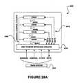
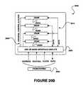
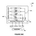
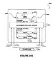
- FIGS. 20A-Eshow a stack of dynamic random access memory (DRAM) circuits that utilize one or more interface circuits, in accordance with various embodiments.
- DRAMdynamic random access memory
- FIGS. 21A-Dshow a memory module which uses dynamic random access memory (DRAM) circuits with various interface circuits, in accordance with different embodiments.
- DRAMdynamic random access memory
- FIGS. 22A-Eshow a memory module which uses DRAM circuits with an advanced memory buffer (AMB) chip and various other interface circuits, in accordance with various embodiments.
- AMBadvanced memory buffer
- FIG. 23shows a system in which four 512 Mb DRAM circuits are mapped to a single 2 Gb DRAM circuit, in accordance with yet another embodiment.
- FIG. 24shows a memory system comprising FB-DIMM modules using DRAM circuits with AMB chips, in accordance with another embodiment.
- FIG. 1illustrates a system 100 including a system device 106 coupled to an interface circuit 102 , which is in turn coupled to a plurality of physical memory circuits 104 A-N.
- the physical memory circuitsmay be any type of memory circuits.
- each physical memory circuitis a separate memory chip.
- eachmay be a DDR2 DRAM.
- the memory circuitsmay be symmetrical, meaning each has the same capacity, type, speed, etc., while in other embodiments they may be asymmetrical. For ease of illustration only, three such memory circuits are shown, but actual embodiments may use any plural number of memory circuits.
- the memory chipsmay optionally be coupled to a memory module (not shown), such as a DIMM.
- the system devicemay be any type of system capable of requesting and/or initiating a process that results in an access of the memory circuits.
- the systemmay include a memory controller (not shown) through which it accesses the memory circuits.
- the interface circuitmay include any circuit or logic capable of directly or indirectly communicating with the memory circuits, such as a buffer chip, advanced memory buffer (AMB) chip, etc.
- the interface circuitinterfaces a plurality of signals 108 between the system device and the memory circuits. Such signals may include, for example, data signals, address signals, control signals, clock signals, and so forth. In some embodiments, all of the signals communicated between the system device and the memory circuits are communicated via the interface circuit. In other embodiments, some other signals 110 are communicated directly between the system device (or some component thereof, such as a memory controller, an AMB, or a register) and the memory circuits, without passing through the interface circuit. In some such embodiments, the majority of signals are communicated via the interface circuit, such that L>M.
- the interface circuitpresents to the system device an interface to emulated memory devices which differ in some aspect from the physical memory circuits which are actually present.
- the interface circuitmay tell the system device that the number of emulated memory circuits is different than the actual number of physical memory circuits.
- the terms “emulating”, “emulated”, “emulation”, and the likewill be used in this disclosure to signify emulation, simulation, disguising, transforming, converting, and the like, which results in at least one characteristic of the memory circuits appearing to the system device to be different than the actual, physical characteristic.
- the emulated characteristicmay be electrical in nature, physical in nature, logical in nature (e.g.
- An example of an emulated electrical characteristicmight be a signal, or a voltage level.
- An example of an emulated physical characteristicmight be a number of pins or wires, a number of signals, or a memory capacity.
- An example of an emulated protocol characteristicmight be a timing, or a specific protocol such as DDR3.
- an emulated signalsuch signal may be a control signal such as an address signal, a data signal, or a control signal associated with an activate operation, precharge operation, write operation, mode register read operation, refresh operation, etc.
- the interface circuitmay emulate the number of signals, type of signals, duration of signal assertion, and so forth. It may combine multiple signals to emulate another signal.
- the interface circuitmay present to the system device an emulated interface to e.g. DDR3 memory, while the physical memory chips are, in fact, DDR2 memory.
- the interface circuitmay emulate an interface to one version of a protocol such as DDR2 with 5-5-5 latency timing, while the physical memory chips are built to another version of the protocol such as DDR2 with 3-3-3 latency timing.
- the interface circuitmay emulate an interface to a memory having a first capacity that is different than the actual combined capacity of the physical memory chips.
- An emulated timingmay relate to latency of e.g. a column address strobe (CAS) latency, a row address to column address latency (tRCD), a row precharge latency (tRP), an activate to precharge latency (tRAS), and so forth.
- CAS latencyis related to the timing of accessing a column of data.
- tRCDis the latency required between the row address strobe (RAS) and CAS.
- tRPis the latency required to terminate an open row and open access to the next row.
- tRASis the latency required to access a certain row of data between an activate operation and a precharge operation.
- the interface circuitmay be operable to receive a signal from the system device and communicate the signal to one or more of the memory circuits after a delay (which may be hidden from the system device). Such delay may be fixed, or in some embodiments it may be variable. If variable, the delay may depend on e.g. a function of the current signal or a previous signal, a combination of signals, or the like. The delay may include a cumulative delay associated with any one or more of the signals. The delay may result in a time shift of the signal forward or backward in time with respect to other signals. Different delays may be applied to different signals.
- the interface circuitmay similarly be operable to receive a signal from a memory circuit and communicate the signal to the system device after a delay.
- the interface circuitmay take the form of, or incorporate, or be incorporated into, a register, an AMB, a buffer, or the like, and may comply with Joint Electron Device Engineering Council (JEDEC) standards, and may have forwarding, storing, and/or buffering capabilities.
- JEDECJoint Electron Device Engineering Council
- the interface circuitmay perform operations without the system device's knowledge.
- One particularly useful such operationis a power-saving operation.
- the interface circuitmay identify one or more of the memory circuits which are not currently being accessed by the system device, and perform the power saving operation on those. In one such embodiment, the identification may involve determining whether any page (or other portion) of memory is being accessed.
- the power saving operationmay be a power down operation, such as a precharge power down operation.
- the interface circuitmay include one or more devices which together perform the emulation and related operations.
- the interface circuitmay be coupled or packaged with the memory devices, or with the system device or a component thereof, or separately.
- the memory circuits and the interface circuitare coupled to a DIMM.
- FIG. 2illustrates one embodiment of a system 200 including a system device (e.g. host system 204 , etc.) which communicates address, control, clock, and data signals with a memory subsystem 201 via an interface.
- a system devicee.g. host system 204 , etc.
- FIG. 2illustrates one embodiment of a system 200 including a system device (e.g. host system 204 , etc.) which communicates address, control, clock, and data signals with a memory subsystem 201 via an interface.
- a system devicee.g. host system 204 , etc.
- the memory subsystemincludes a buffer chip 202 which presents the host system with emulated interface to emulated memory, and a plurality of physical memory circuits which, in the example shown, are DRAM chips 206 A-D.
- the DRAM chipsare stacked, and the buffer chip is placed electrically between them and the host system.
- a stackmay refer to any collection of memory circuits (e.g. DRAM circuits, flash memory circuits, or combinations of memory circuit technologies, etc.).
- the buffer chip bufferscommunicates signals between the host system and the DRAM chips, and presents to the host system an emulated interface to present the memory as though it were a smaller number of larger capacity DRAM chips, although in actuality there is a larger number of smaller capacity DRAM chips in the memory subsystem. For example, there may be eight 512 Mb physical DRAM chips, but the buffer chip buffers and emulates them to appear as a single 4 Gb DRAM chip, or as two 2 Gb DRAM chips. Although the drawing shows four DRAM chips, this is for ease of illustration only; the invention is, of course, not limited to using four DRAM chips.
- the buffer chipis coupled to send address, control, and clock signals 208 to the DRAM chips via a single, shared address, control, and clock bus, but each DRAM chip has its own, dedicated data path for sending and receiving data signals 210 to/from the buffer chip.
- the reference number 1will be used to denote the interface between the host system and the buffer chip
- the reference number 2will be used to denote the address, control, and clock interface between the buffer chip and the physical memory circuits
- the reference number 3will be used to denote the data interface between the buffer chip and the physical memory circuits, regardless of the specifics of how any of those interfaces is implemented in the various embodiments and configurations described below.
- FIG. 2there is a single address, control, and clock interface channel 2 and four data interface channels 3 ; this implementation may thus be said to have a “1A4D” configuration (wherein “1 A” means one address, control, and clock channel in interface 2 , and “4D” means four data channels in interface 3 ).
- the DRAM chipsare physically arranged on a single side of the buffer chip.
- the buffer chipmay, optionally, be a part of the stack of DRAM chips, and may optionally be the bottommost chip in the stack. Or, it may be separate from the stack.
- FIG. 3illustrates another embodiment of a system 301 in which the buffer chip 303 is interfaced to a host system 304 and is coupled to the DRAM chips 307 A- 307 D somewhat differently than in the system of FIG. 2 .
- Each shared bushas two or more DRAM chips coupled to it. As shown, the sharing need not necessarily be the same in the data busses as it is in the address, control, and clock busses.
- This embodimenthas a “2A2D” configuration.
- FIG. 4illustrates another embodiment of a system 411 in which the buffer chip 413 is interfaced to a host system 404 and is coupled to the DRAM chips 417 A- 417 D somewhat differently than in the system of FIG. 2 or 3 .
- Each shared bushas two or more DRAM chips coupled to it.
- This implementationhas a “1A2D” configuration.
- FIG. 5illustrates another embodiment of a system 521 in which the buffer chip 523 is interfaced to a host system 504 and is coupled to the DRAM chips 527 A- 527 D somewhat differently than in the system of FIGS. 2 through 4 .
- This implementationhas a “1A1D” configuration.
- FIG. 6illustrates another embodiment of a system 631 in which the buffer chip 633 is interfaced to a host system 604 and is coupled to the DRAM chips 637 A- 637 D somewhat differently than in the system of FIGS. 2 through 5 .
- Each shared bushas two or more DRAM chips coupled to it. Further, in the example shown, the DRAM chips are physically arranged on both sides of the buffer chip. There may be, for example, sixteen DRAM chips, with the eight DRAM chips on each side of the buffer chip arranged in two stacks of four chips each. This implementation has a “2A4D” configuration.
- FIGS. 2 through 6are not intended to be an exhaustive listing of all possible permutations of data paths, busses, and buffer chip configurations, and are only illustrative of some ways in which the host system device can be in electrical contact only with the load of the buffer chip and thereby be isolated from whatever physical memory circuits, data paths, busses, etc. exist on the (logical) other side of the buffer chip.
- FIG. 7illustrates one embodiment of a method 700 for storing at least a portion of information received in association with a first operation, for use in performing a second operation.
- a methodmay be practiced in a variety of systems, such as, but not limited to, those of FIGS. 1-6 .
- the methodmay be performed by the interface circuit of FIG. 1 or the buffer chip of FIG. 2 .
- first informationis received ( 702 ) in association with a first operation to be performed on at least one of the memory circuits (DRAM chips).
- the first informationmay be received prior to, simultaneously with, or subsequent to the instigation of the first operation.
- the first operationmay be, for example, a row operation, in which case the first information may include e.g. address values received by the buffer chip via the address bus from the host system. At least a portion of the first information is then stored ( 704 ).
- the buffer chipalso receives ( 706 ) second information associated with a second operation. For convenience, this receipt is shown as being after the storing of the first information, but it could also happen prior to or simultaneously with the storing.
- the second operationmay be, for example, a column operation.
- the buffer chipperforms ( 708 ) the second operation, utilizing the stored portion of the first information, and the second information.
- the buffer chipmay receive from the host system's memory controller more address bits than are required to address any given one of the DRAM chips.
- the extra address bitsmay be decoded by the buffer chip to individually select the DRAM chips, utilizing separate chip select signals (not shown) to each of the DRAM chips in the stack.
- a stack of four x4 1 Gb DRAM chips behind the buffer chipmay appear to the host system as a single x4 4 Gb DRAM circuit, in which case the memory controller may provide sixteen row address bits and three bank address bits during a row operation (e.g. an activate operation), and provide eleven column address bits and three bank address bits during a column operation (e.g. a read or write operation).
- the individual DRAM chips in the stackmay require only fourteen row address bits and three bank address bits for a row operation, and eleven column address bits and three bank address bits during a column operation.
- the buffer chipmay receive two address bits more than are needed by any of the DRAM chips.
- the buffer chipstores ( 704 ) these two extra bits during the row operation (in addition to using them to select the correct one of the DRAM chips), then uses them later, during the column operation, to select the correct one of the DRAM chips.
- mapping between a system address (from the host system to the buffer chip) and a device address (from the buffer chip to a DRAM chip)may be performed in various manners.
- lower order system row address and bank address bitsmay be mapped directly to the device row address and bank address bits, with the most significant system row address bits (and, optionally, the most significant bank address bits) being stored for use in the subsequent column operation.
- what is storedis the decoded version of those bits; in other words, the extra bits may be stored either prior to or after decoding.
- the stored bitsmay be stored, for example, in an internal lookup table (not shown) in the buffer chip, for one or more clock cycles.
- the buffer chipmay have four 512 Mb DRAM chips with which it emulates a single 2 Gb DRAM chip.
- the systemwill present fifteen row address bits, from which the buffer chip may use the fourteen low order bits (or, optionally, some other set of fourteen bits) to directly address the DRAM chips.
- the systemwill present three bank address bits, from which the buffer chip may use the two low order bits (or, optionally, some other set of two bits) to directly address the DRAM chips.
- the most significant bank address bit (or other unused bit) and the most significant row address bit (or other unused bit)are used to generate the four DRAM chip select signals, and are stored for later reuse.
- the stored bitsare again used to generate the four DRAM chip select signals.
- the unused bank addressis not stored during the row operation, as it will be re-presented during the subsequent column operation.
- addressesmay be mapped between four 1 Gb DRAM circuits to emulate a single 4 Gb DRAM circuit.
- Sixteen row address bits and three bank address bitscome from the host system, of which the low order fourteen address bits and all three bank address bits are mapped directly to the DRAM circuits.
- the two most significant row address bitsare decoded to generate four chip select signals, and are stored using the bank address bits as the index.
- the stored row address bitsare again used to generate the four chip select signals.
- a particular mapping techniquemay be chosen, to ensure that there are no unnecessary combinational logic circuits in the critical timing path between the address input pins and address output pins of the buffer chip.
- Corresponding combinational logic circuitsmay instead be used to generate the individual chip select signals. This may allow the capacitive loading on the address outputs of the buffer chip to be much higher than the loading on the individual chip select signal outputs of the buffer chip.
- the address mappingmay be performed by the buffer chip using some of the bank address signals from the host system to generate the chip select signals.
- the buffer chipmay store the higher order row address bits during a row operation, using the bank address as the index, and then use the stored address bits as part of the DRAM circuit bank address during a column operation.
- four 512 Mb DRAM chipsmay be used in emulating a single 2 Gb DRAM.
- Fifteen row address bitscome from the host system, of which the low order fourteen are mapped directly to the DRAM chips.
- Three bank address bitscome from the host system, of which the least significant bit is used as a DRAM circuit bank address bit for the DRAM chips.
- the most significant row address bitmay be used as an additional DRAM circuit bank address bit.
- the two most significant bank address bitsare decoded to generate the four chip select signals.
- the most significant row address bitmay be stored during the row operation, and reused during the column operation with the least significant bank address bit, to form the DRAM circuit bank address.
- the column address from the host system memory controllermay be mapped directly as the column address to the DRAM chips in the stack, since each of the DRAM chips may have the same page size, regardless any differences in the capacities of the (asymmetrical) DRAM chips.
- address bit A[ 10 ]may be used by the memory controller to enable or disable auto-precharge during a column operation, in which case the buffer chip may forward that bit to the DRAM circuits without any modification during a column operation.
- the simulated DRAM circuitmay be desirable to determine whether the simulated DRAM circuit behaves according to a desired DRAM standard or other design specification. Behavior of many DRAM circuits is specified by the JEDEC standards, and it may be desirable to exactly emulate a particular JEDEC standard DRAM.
- the JEDEC standarddefines control signals that a DRAM circuit must accept and the behavior of the DRAM circuit as a result of such control signals.
- the JEDEC specification for DDR2 DRAMis known as JESD79-2B. If it is desired to determine whether a standard is met, the following algorithm may be used. Using a set of software verification tools, it checks for formal verification of logic, that protocol behavior of the simulated DRAM circuit is the same as the desired standard or other design specification.
- Suitable verification toolsinclude: Magellan, supplied by Synopsys, Inc. of 700 E. Middlefield Rd., Mt. View, Calif. 94043; Incisive, supplied by Cadence Design Systems, Inc., of 2655 Sealy Ave., San Jose, Calif. 95134; tools supplied by Jasper Design Automation, Inc. of 100 View St. #100, Mt. View, Calif. 94041; Verix, supplied by Real Intent, Inc., of 505 N. Mathilda Ave. #210, Sunnyvale, Calif. 94085; 0-In, supplied by Mentor Graphics Corp. of 8005 SW Boeckman Rd., Wilsonville, Oreg. 97070; and others.
- an assertionmay be written that no two DRAM control signals are allowed to be issued to an address, control, and clock bus at the same time.
- the verification processallows a designer to prove that the emulated DRAM circuit exactly meets the required standard etc. If, for example, an address mapping that uses a common bus for data and a common bus for address, results in a control and clock bus that does not meet a required specification, alternative designs for buffer chips with other bus arrangements or alternative designs for the sideband signal interconnect between two or more buffer chips may be used and tested for compliance.
- Such sideband signalsconvey the power management signals, for example.
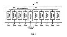
- FIG. 8illustrates a high capacity DIMM 800 using a plurality of buffered stacks of DRAM circuits 802 and a register device 804 , according to one embodiment of this invention.
- the registerperforms the addressing and control of the buffered stacks.
- the DIMMmay be an FB-DIMM, in which case the register is an AMB.
- the emulationis performed at the DIMM level.
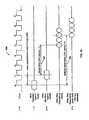
- FIG. 9is a timing diagram illustrating a timing design 900 of a buffer chip which makes a buffered stack of DRAM chips mimic a larger DRAM circuit having longer CAS latency, in accordance with another embodiment of this invention.
- Any delay through a buffer chipmay be made transparent to the host system's memory controller, by using such a method. Such a delay may be a result of the buffer chip being located electrically between the memory bus of the host system and the stacked DRAM circuits, since some or all of the signals that connect the memory bus to the DRAM circuits pass through the buffer chip. A finite amount of time may be needed for these signals to traverse through the buffer chip.
- the buffer chipmay cause a one-half clock cycle delay between the buffer chip receiving address and control signals from the host system memory controller (or, optionally, from a register chip or an AMB), and the address and control signals being valid at the inputs of the stacked DRAM circuits.
- Data signalsmay also have a one-half clock cycle delay in either direction to/from the host system. Other amounts of delay are, of course, possible, and the half-clock cycle example is for illustration only.
- the cumulative delay through the buffer chipis the sum of a delay of the address and control signals and a delay of the data signals.
- FIG. 9illustrates an example where the buffer chip is using DRAM chips having a native CAS latency of i clocks, and the buffer chip delay is j clocks, thus the buffer chip emulates a DRAM having a CAS latency of i+j clocks.
- the DRAM chipshave a native CAS latency 906 of four clocks (from t 1 to t 5 ), and the total latency through the buffer chip is two clocks (one clock delay 902 from t 0 to t 1 for address and control signals, plus one clock delay 904 from t 5 to t 6 for data signals), and the buffer chip emulates a DRAM having a six clock CAS latency 908 .
- the reference numbers 1 , 2 , and/or 3 at the left marginindicate which of the interfaces correspond to the signals or values illustrated on the associated waveforms.
- the “Clock” signal shown as a square wave on the uppermost waveformis indicated as belonging to the interface 1 between the host system and the buffer chip; the “Control Input to Buffer” signal is also part of the interface 1 ; the “Control Input to DRAM” waveform is part of the interface 2 from the buffer chip to the physical memory circuits; the “Data Output from DRAM” waveform is part of the interface 3 from the physical memory circuits to the buffer chip; and the “Data Output from Buffer” shown in the lowermost waveform is part of the interface 1 from the buffer chip to the host system.
- FIG. 10is a timing diagram illustrating a timing design 1000 of write data timing expected by a DRAM circuit in a buffered stack.
- Emulation of a larger capacity DRAM circuit having higher CAS latencymay, in some implementations, create a problem with the timing of write operations.
- the DDR2 SDRAM protocolmay specify that the write CAS latency 1002 is one less than the read CAS latency. Therefore, since the buffered stack appears as a DDR2 SDRAM with a read CAS latency of six clocks, the memory controller may use a buffered stack write CAS latency of five clocks 1004 when scheduling a write operation to the memory.
- the memory controllerissues the write operation at t 0 .
- the write operationis issued to the DRAM chips at t 1 .
- the buffer chipmay alleviate by delaying write operations.
- the waveform “Write Data Expected by DRAM”is not shown as belonging to interface 1 , interface 2 , or interface 3 , for the simple reason that there is no such signal present in any of those interfaces. That waveform represents only what is expected by the DRAM, not what is actually provided to the DRAM.
- FIG. 11is a timing illustrating a timing design 1100 showing how the buffer chip does this.
- the memory controllerissues the write operation at t 0 .
- the write operationappeared at the DRAM circuits one clock later at t 1 , due to the inherent delay through the buffer chip.
- FIG. 12is a timing diagram illustrating operation of an FB-DIMM's AMB, which may be designed to send write data earlier to buffered stacks instead of delaying the write address and operation (as in FIG. 11 ). Specifically, it may use an early write CAS latency 1202 to compensate the timing of the buffer chip write operation. If the buffer chip has a cumulative (address and data) inherent delay of two clocks, the AMB may send the write data to the buffered stack two clocks early. This may not be possible in the case of registered DIMMs, in which the memory controller sends the write data directly to the buffered stacks (rather than via the AMB). In another embodiment, the memory controller itself could be designed to send write data early, to compensate for the j clocks of cumulative inherent delay caused by the buffer chip.
- the memory controllerissues the write operation at t 0 .
- the write operationarrives at the DRAM at t 1 .
- FIG. 13is a timing diagram 1300 illustrating bus conflicts which can be caused by delayed write operations.
- the delaying of write addresses and write operationsmay be performed by a buffer chip, a register, an AMB, etc. in a manner that is completely transparent to the memory controller of the host system. And, because the memory controller is unaware of this delay, it may schedule subsequent operations such as activate or precharge operations, which may collide with the delayed writes on the address bus to the DRAM chips in the stack.
- the memory controllerissues a write operation 1302 at time t 0 .
- the buffer chip or AMBdelays the write operation, such that it appears on the bus to the DRAM chips at time t 3 .
- the memory controllerissued an activate operation (control signal) 1304 which, after a one-clock inherent delay through the buffer chip, appears on the bus to the DRAM chips at time t 3 , colliding with the delayed write.
- FIGS. 14 and 15are a timing diagram 1400 and a timing diagram 1500 illustrating methods of avoiding such collisions. If the cumulative latency through the buffer chip is two clock cycles, and the native read CAS latency of the DRAM chips is four clock cycles, then in order to hide the delay of the address and control signals and the data signals through the buffer chip, the buffer chip presents the host system with an interface to an emulated memory having a read CAS latency of six clock cycles. And if the tRCD and tRP of the DRAM chips are four clock cycles each, the buffer chip tells the host system that they are six clock cycles each in order to allow the buffer chip to delay the activate and precharge operations to avoid collisions in a manner that is transparent to the host system.
- a buffered stack that uses 4-4-4 DRAM chipsmay appear to the host system as one larger DRAM that uses 6-6-6 timing.
- the memory controllermay schedule a column operation to a bank six clock cycles (at time t 6 ) after an activate (row) operation (at time t 0 ) to the same bank.
- the DRAM chips in the stackactually have a tRCD of four clock cycles. This gives the buffer chip time to delay the activate operation by up to two clock cycles, avoiding any conflicts on the address bus between the buffer chip and the DRAM chips, while ensuring correct read and write timing on the channel between the memory controller and the buffered stack.
- the buffer chipmay issue the activate operation to the DRAM chips one, two, or three clock cycles after it receives the activate operation from the memory controller, register, or AMB.
- the actual delay selectedmay depend on the presence or absence of other DRAM operations that may conflict with the activate operation, and may optionally change from one activate operation to another. In other words, the delay may be dynamic.
- a one-clock delay ( 1402 A, 1502 A)may be accomplished simply by the inherent delay through the buffer chip.
- a two-clock delay ( 1402 B, 1502 B)may be accomplished by adding one clock of additional delay to the one-clock inherent delay
- a three-clock delay1402 C, 1502 C
- a read, write, or activate operation issued by the memory controller at time t 6will, after a one-clock inherent delay through the buffer chip, be issued to the DRAM chips at time t 7 .
- a preceding activate or precharge operation issued by the memory controller at time t 0will, depending upon the delay, be issued to the DRAM chips at time t 1 , t 2 , or t 3 , each of which is at least the tRCD or tRP of four clocks earlier than the t 7 issuance of the read, write, or activate operation.
- the memory controllermay schedule a subsequent activate (row) operation to a bank a minimum of six clock cycles after issuing a precharge operation to that bank.
- the buffer chipmay have the ability to delay issuing the precharge operation to the DRAM chips by up to two clock cycles, in order to avoid any conflicts on the address bus, or in order to satisfy the tRAS requirements of the DRAM chips.
- the precharge operation to the same bankmay be delayed by the buffer chip to satisfy the tRAS requirements of the DRAM.
- the buffer chipmay issue the precharge operation to the DRAM chips one, two, or three clock cycles after it is received. The delay selected may depend on the presence or absence of address bus conflicts or tRAS violations, and may change from one precharge operation to another.
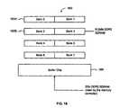
- FIG. 16illustrates a buffered stack 1600 according to one embodiment of this invention.
- the buffered stackincludes four 512 Mb DDR2 DRAM circuits (chips) 1602 which a buffer chip 1604 maps to a single 2 Gb DDR2 DRAM.
- the multiple DRAM chipsappear to the memory controller as though they were a single, larger DRAM, the combined power dissipation of the actual DRAM chips may be much higher than the power dissipation of a monolithic DRAM of the same capacity. In other words, the physical DRAM may consume significantly more power than would be consumed by the emulated DRAM.
- a DIMM containing multiple buffered stacksmay dissipate much more power than a standard DIMM of the same actual capacity using monolithic DRAM circuits.
- This increased power dissipationmay limit the widespread adoption of DIMMs that use buffered stacks.
- the DRAM circuitsmay be opportunistically placed in low power states or modes.
- the DRAM circuitsmay be placed in a precharge power down mode using the clock enable (CKE) pin of the DRAM circuits.
- CKEclock enable
- a single rank registered DIMMmay contain a plurality of buffered stacks, each including four x4 512 Mb DDR2 SDRAM chips and appear (to the memory controller via emulation by the buffer chip) as a single x4 2 Gb DDR2 SDRAM.
- the JEDEC standardindicates that a 2 Gb DDR2 SDRAM may generally have eight banks, shown in FIG. 16 as Bank 0 to Bank 7 . Therefore, the buffer chip may map each 512 Mb DRAM chip in the stack to two banks of the equivalent 2 Gb DRAM, as shown; the first DRAM chip 1602 A is treated as containing banks 0 and 1 , 1602 B is treated as containing banks 2 and 4 , and so forth.
- the memory controllermay open and close pages in the DRAM banks based on memory requests it receives from the rest of the host system. In some embodiments, no more than one page may be able to be open in a bank at any given time. In the embodiment shown in FIG. 16 , each DRAM chip may therefore have up to two pages open at a time. When a DRAM chip has no open pages, the power management scheme may place it in the precharge power down mode.
- the clock enable inputs of the DRAM chipsmay be controlled by the buffer chip, or by another chip (not shown) on the R-DIMM, or by an AMB (not shown) in the case of an FB-DIMM, or by the memory controller, to implement the power management technique.
- the power management techniquemay be particularly effective if it implements a closed page policy.
- Another optional power management techniquemay include mapping a plurality of DRAM circuits to a single bank of the larger capacity emulated DRAM.
- a buffered stack(not shown) of sixteen x4 256 Mb DDR2 SDRAM chips may be used in emulating a single x4 4 Gb DDR2 SDRAM.
- the 4 Gb DRAMis specified by JEDEC as having eight banks of 512 Mbs each, so two of the 256 Mb DRAM chips may be mapped by the buffer chip to emulate each bank (whereas in FIG. 16 one DRAM was used to emulate two banks).
- the memory controllersince only one page can be open in a bank at any given time, only one of the two DRAM chips emulating that bank can be in the active state at any given time. If the memory controller opens a page in one of the two DRAM chips, the other may be placed in the precharge power down mode. Thus, if a number p of DRAM chips are used to emulate one bank, at least p ⁇ 1 of them may be in a power down mode at any given time; in other words, at least p ⁇ 1 of the p chips are always in power down mode, although the particular powered down chips will tend to change over time, as the memory controller opens and closes various pages of memory.
- the power saving operationmay comprise operating in precharge power down mode except when refresh is required.
- FIG. 17is a flow chart 1700 illustrating one embodiment of a method of refreshing a plurality of memory circuits.
- a refresh control signalis received ( 1702 ) e.g. from a memory controller which intends to refresh an emulated memory circuit.
- a plurality of refresh control signalsare sent ( 1704 ) e.g. by a buffer chip to a plurality of physical memory circuits at different times.
- These refresh control signalsmay optionally include the received refresh control signal or an instantiation or copy thereof. They may also, or instead, include refresh control signals that are different in at least one aspect (format, content, etc.) from the received signal.
- At least one first refresh control signalmay be sent to a first subset of the physical memory circuits at a first time, and at least one second refresh control signal may be sent to a second subset of the physical memory circuits at a second time.
- Each refresh signalmay be sent to one physical memory circuit, or to a plurality of physical memory circuits, depending upon the particular implementation.
- the refresh control signalsmay be sent to the physical memory circuits after a delay in accordance with a particular timing.
- the timing in which they are sent to the physical memory circuitsmay be selected to minimize an electrical current drawn by the memory, or to minimize a power consumption of the memory. This may be accomplished by staggering a plurality of refresh control signals.
- the timingmay be selected to comply with e.g. a tRFC parameter associated with the memory circuits.
- physical DRAM circuitsmay receive periodic refresh operations to maintain integrity of data stored therein.
- a memory controllermay initiate refresh operations by issuing refresh control signals to the DRAM circuits with sufficient frequency to prevent any loss of data in the DRAM circuits. After a refresh control signal is issued, a minimum time tRFC may be required to elapse before another control signal may be issued to that DRAM circuit.
- the tRFC parameter valuemay increase as the size of the DRAM circuit increases.
- the buffer chipWhen the buffer chip receives a refresh control signal from the memory controller, it may refresh the smaller DRAM circuits within the span of time specified by the tRFC of the emulated DRAM circuit. Since the tRFC of the larger, emulated DRAM is longer than the tRFC of the smaller, physical DRAM circuits, it may not be necessary to issue any or all of the refresh control signals to the physical DRAM circuits simultaneously. Refresh control signals may be issued separately to individual DRAM circuits or to groups of DRAM circuits, provided that the tRFC requirements of all physical DRAMs has been met by the time the emulated DRAM's tRFC has elapsed. In use, the refreshes may be spaced in time to minimize the peak current draw of the combination buffer chip and DRAM circuit set during a refresh operation.
- FIG. 18illustrates one embodiment of an interface circuit such as may be utilized in any of the above-described memory systems, for interfacing between a system and memory circuits.
- the interface circuitmay be included in the buffer chip, for example.
- the interface circuitincludes a system address signal interface for sending/receiving address signals to/from the host system, a system control signal interface for sending/receiving control signals to/from the host system, a system clock signal interface for sending/receiving clock signals to/from the host system, and a system data signal interface for sending/receiving data signals to/from the host system.
- the interface circuitfurther includes a memory address signal interface for sending/receiving address signals to/from the physical memory, a memory control signal interface for sending/receiving control signals to/from the physical memory, a memory clock signal interface for sending/receiving clock signals to/from the physical memory, and a memory data signal interface for sending/receiving data signals to/from the physical memory.
- the host systemincludes a set of memory attribute expectations, or built-in parameters of the physical memory with which it has been designed to work (or with which it has been told, e.g. by the buffer circuit, it is working). Accordingly, the host system includes a set of memory interaction attributes, or built-in parameters according to which the host system has been designed to operate in its interactions with the memory. These memory interaction attributes and expectations will typically, but not necessarily, be embodied in the host system's memory controller.
- the physical memoryitself has a set of physical attributes.
- These expectations and attributesmay include, by way of example only, memory timing, memory capacity, memory latency, memory functionality, memory type, memory protocol, memory power consumption, memory current requirements, and so forth.
- the interface circuitincludes memory physical attribute storage for storing values or parameters of various physical attributes of the physical memory circuits.
- the interface circuitfurther includes system emulated attribute storage. These storage systems may be read/write capable stores, or they may simply be a set of hard-wired logic or values, or they may simply be inherent in the operation of the interface circuit.
- the interface circuitincludes emulation logic which operates according to the stored memory physical attributes and the stored system emulation attributes, to present to the system an interface to an emulated memory which differs in at least one attribute from the actual physical memory.
- the emulation logicmay, in various embodiments, alter a timing, value, latency, etc. of any of the address, control, clock, and/or data signals it sends to or receives from the system and/or the physical memory. Some such signals may pass through unaltered, while others may be altered.
- the emulation logicmay be embodied as, for example, hard wired logic, a state machine, software executing on a processor, and so forth.
- the physical memory circuits employed in practicing this inventionmay be any type of memory whatsoever, such as: DRAM, DDR DRAM, DDR2 DRAM, DDR3 DRAM, SDRAM, QDR DRAM, DRDRAM, FPM DRAM, VDRAM, EDO DRAM, BEDO DRAM, MDRAM, SGRAM, MRAM, IRAM, NAND flash, NOR flash, PSRAM, wetware memory, etc.
- the physical memory circuitsmay be coupled to any type of memory module, such as: DIMM, R-DIMM, SO-DIMM, FB-DIMM, unbuffered DIMM, etc.
- the system device which accesses the memorymay be any type of system device, such as: desktop computer, laptop computer, workstation, server, consumer electronic device, television, personal digital assistant (PDA), mobile phone, printer or other peripheral device, etc.
- desktop computerlaptop computer, workstation, server, consumer electronic device, television, personal digital assistant (PDA), mobile phone, printer or other peripheral device, etc.
- PDApersonal digital assistant
- FIG. 19illustrates a multiple memory circuit framework 1900 , in accordance with one embodiment. As shown, included are an interface circuit 1902 , a plurality of memory circuits 1904 A, 1904 B, 1904 N, and a system 1906 . In the context of the present description, such memory circuits 1904 A, 1904 B, 1904 N may include any circuit capable of serving as memory.
- the memory circuits 1904 A, 1904 B, 1904 Nmay include a monolithic memory circuit, a semiconductor die, a chip, a packaged memory circuit, or any other type of tangible memory circuit.
- the memory circuits 1904 A, 1904 B, 1904 Nmay take the form of a dynamic random access memory (DRAM) circuit.
- DRAMdynamic random access memory
- Such DRAMmay take any form including, but not limited to, synchronous DRAM (SDRAM), double data rate synchronous DRAM (DDR SDRAM, DDR2 SDRAM, DDR3 SDRAM, etc.), graphics double data rate DRAM (GDDR, GDDR2, GDDR3, etc.), quad data rate DRAM (QDR DRAM), RAMBUS XDR DRAM (XDR DRAM), fast page mode DRAM (FPM DRAM), video DRAM (VDRAM), extended data out DRAM (EDO DRAM), burst EDO RAM (BEDO DRAM), multibank DRAM (MDRAM), synchronous graphics RAM (SGRAM), and/or any other type of DRAM.
- SDRAMsynchronous DRAM
- DDR SDRAMdouble data rate synchronous DRAM
- DDR2 SDRAMDDR2 SDRAM, DDR3 SDRAM, etc.
- graphics double data rate DRAMGDDR, GDDR2, GDDR3, etc.
- quad data rate DRAMQDR DRAM
- RAMBUS XDR DRAMXDR DRAM
- At least one of the memory circuits 1904 A, 1904 B, 1904 Nmay include magnetic random access memory (MRAM), intelligent random access memory (IRAM), distributed network architecture (DNA) memory, window random access memory (WRAM), flash memory (e.g. NAND, NOR, etc.), pseudostatic random access memory (PSRAM), wetware memory, memory based on semiconductor, atomic, molecular, optical, organic, biological, chemical, or nanoscale technology, and/or any other type of volatile or nonvolatile, random or non-random access, serial or parallel access memory circuit.
- MRAMmagnetic random access memory
- IRAMintelligent random access memory
- DNAdistributed network architecture
- WRAMwindow random access memory
- PSRAMpseudostatic random access memory
- wetware memorymemory based on semiconductor, atomic, molecular, optical, organic, biological, chemical, or nanoscale technology, and/or any other type of volatile or nonvolatile, random or non-random access, serial or parallel access memory circuit.
- the memory circuits 1904 A, 1904 B, 1904 Nmay or may not be positioned on at least one dual in-line memory module (DIMM) (not shown).
- the DIMMmay include a registered DIMM (R-DIMM), a small outline-DIMM (SO-DIMM), a fully buffered DIMM (FB-DIMM), an unbuffered DIMM (UDIMM), single inline memory module (SIMM), a MiniDIMM, a very low profile (VLP) R-DIMM, etc.
- the memory circuits 1904 A, 1904 B, 1904 Nmay or may not be positioned on any type of material forming a substrate, card, module, sheet, fabric, board, carrier or other any other type of solid or flexible entity, form, or object.
- the memory circuits 1904 A, 1904 B, 1904 Nmay or may not be positioned in or on any desired entity, form, or object for packaging purposes.
- the memory circuits 1904 A, 1904 B, 1904 Nmay or may not be organized into ranks Such ranks may refer to any arrangement of such memory circuits 1904 A, 1904 B, 1904 N on any of the foregoing entities, forms, objects, etc.
- the system 1906may include any system capable of requesting and/or initiating a process that results in an access of the memory circuits 1904 A, 1904 B, 1904 N. As an option, the system 1906 may accomplish this utilizing a memory controller (not shown), or any other desired mechanism.
- a system 1906may include a system in the form of a desktop computer, a lap-top computer, a server, a storage system, a networking system, a workstation, a personal digital assistant (PDA), a mobile phone, a television, a computer peripheral (e.g. printer, etc.), a consumer electronics system, a communication system, and/or any other software and/or hardware, for that matter.
- PDApersonal digital assistant
- the interface circuit 1902may, in the context of the present description, refer to any circuit capable of interfacing (e.g. communicating, buffering, etc.) with the memory circuits 1904 A, 1904 B, 1904 N and the system 1906 .
- the interface circuit 1902may, in the context of different embodiments, include a circuit capable of directly (e.g. via wire, bus, connector, and/or any other direct communication medium, etc.) and/or indirectly (e.g. via wireless, optical, capacitive, electric field, magnetic field, electromagnetic field, and/or any other indirect communication medium, etc.) communicating with the memory circuits 1904 A, 1904 B, 1904 N and the system 1906 .
- the communicationmay use a direct connection (e.g.
- point-to-pointsingle-drop bus, multi-drop bus, serial bus, parallel bus, link, and/or any other direct connection, etc.
- indirect connectione.g. through intermediate circuits, intermediate logic, an intermediate bus or busses, and/or any other indirect connection, etc.
- the interface circuit 1902may include one or more circuits, such as a buffer (e.g. buffer chip, etc.), register (e.g. register chip, etc.), advanced memory buffer (AMB) (e.g. AMB chip, etc.), a component positioned on at least one DIMM, etc.
- the registermay, in various embodiments, include a JEDEC Solid State Technology Association (known as JEDEC) standard register (a JEDEC register), a register with forwarding, storing, and/or buffering capabilities, etc.
- JEDECJEDEC Solid State Technology Association
- the register chips, buffer chips, and/or any other interface circuit(s) 1902may be intelligent, that is, include logic that are capable of one or more functions such as gathering and/or storing information; inferring, predicting, and/or storing state and/or status; performing logical decisions; and/or performing operations on input signals, etc.
- the interface circuit 1902may optionally be manufactured in monolithic form, packaged form, printed form, and/or any other manufactured form of circuit, for that matter.
- a plurality of the aforementioned interface circuits 1902may serve, in combination, to interface the memory circuits 1904 A, 1904 B, 1904 N and the system 1906 .
- one, two, three, four, or more interface circuits 1902may be utilized for such interfacing purposes.
- multiple interface circuits 1902may be relatively configured or connected in any desired manner.
- the interface circuits 1902may be configured or connected in parallel, serially, or in various combinations thereof.
- the multiple interface circuits 1902may use direct connections to each other, indirect connections to each other, or even a combination thereof.
- any number of the interface circuits 1902may be allocated to any number of the memory circuits 1904 A, 1904 B, 1904 N.
- each of the plurality of interface circuits 1902may be the same or different. Even still, the interface circuits 1902 may share the same or similar interface tasks and/or perform different interface tasks.
- memory circuits 1904 A, 1904 B, 1904 N, interface circuit 1902 , and system 1906are shown to be separate parts, it is contemplated that any of such parts (or portion(s) thereof) may be integrated in any desired manner. In various embodiments, such optional integration may involve simply packaging such parts together (e.g. stacking the parts to form a stack of DRAM circuits, a DRAM stack, a plurality of DRAM stacks, a hardware stack, where a stack may refer to any bundle, collection, or grouping of parts and/or circuits, etc.) and/or integrating them monolithically.
- At least one interface circuit 1902may be packaged with at least one of the memory circuits 1904 A, 1904 B, 1904 N.
- a DRAM stackmay or may not include at least one interface circuit (or portion(s) thereof).
- different numbers of the interface circuit 1902 (or portion(s) thereof)may be packaged together. Such different packaging arrangements, when employed, may optionally improve the utilization of a monolithic silicon implementation, for example.
- the interface circuit 1902may be capable of various functionality, in the context of different embodiments.
- the interface circuit 1902may interface a plurality of signals 1908 that are connected between the memory circuits 1904 A, 1904 B, 1904 N and the system 1906 .
- the signalsmay, for example, include address signals, data signals, control signals, enable signals, clock signals, reset signals, or any other signal used to operate or associated with the memory circuits, system, or interface circuit(s), etc.
- the signalsmay be those that: use a direct connection, use an indirect connection, use a dedicated connection, may be encoded across several connections, and/or may be otherwise encoded (e.g. time-multiplexed, etc.) across one or more connections.
- the interfaced signals 1908may represent all of the signals that are connected between the memory circuits 1904 A, 1904 B, 1904 N and the system 1906 . In other aspects, at least a portion of signals 1910 may use direct connections between the memory circuits 1904 A, 1904 B, 1904 N and the system 1906 . Moreover, the number of interfaced signals 1908 (e.g. vs. a number of the signals that use direct connections 1910 , etc.) may vary such that the interfaced signals 1908 may include at least a majority of the total number of signal connections between the memory circuits 1904 A, 1904 B, 1904 N and the system 1906 (e.g. L>M, with L and M as shown in FIG. 19 ). In other embodiments, L may be less than or equal to M. In still other embodiments L and/or M may be zero.
- the interface circuit 1902may or may not be operable to interface a first number of memory circuits 1904 A, 1904 B, 1904 N and the system 1906 for simulating a second number of memory circuits to the system 1906 .
- the first number of memory circuits 1904 A, 1904 B, 1904 Nshall hereafter be referred to, where appropriate for clarification purposes, as the “physical” memory circuits or memory circuits, but are not limited to be so.
- the physical memory circuitsmay include a single physical memory circuit.
- the at least one simulated memory circuit seen by the system 1906shall hereafter be referred to, where appropriate for clarification purposes, as the at least one “virtual” memory circuit.
- the second number of virtual memory circuitsmay be more than, equal to, or less than the first number of physical memory circuits 1904 A, 1904 B, 1904 N.
- the second number of virtual memory circuitsmay include a single memory circuit. Of course, however, any number of memory circuits may be simulated.
- the term simulatedmay refer to any simulating, emulating, disguising, transforming, modifying, changing, altering, shaping, converting, etc., that results in at least one aspect of the memory circuits 1904 A, 1904 B, 1904 N appearing different to the system 1906 .
- such aspectmay include, for example, a number, a signal, a memory capacity, a timing, a latency, a design parameter, a logical interface, a control system, a property, a behavior (e.g. power behavior including, but not limited to a power consumption, current consumption, current waveform, power parameters, power metrics, any other aspect of power management or behavior, etc.), and/or any other aspect, for that matter.
- the simulationmay be electrical in nature, logical in nature, protocol in nature, and/or performed in any other desired manner. For instance, in the context of electrical simulation, a number of pins, wires, signals, etc. may be simulated. In the context of logical simulation, a particular function or behavior may be simulated. In the context of protocol, a particular protocol (e.g. DDR3, etc.) may be simulated. Further, in the context of protocol, the simulation may effect conversion between different protocols (e.g. DDR2 and DDR3) or may effect conversion between different versions of the same protocol (e.g. conversion of 4-4-4 DDR2 to 6-6-6 DDR2).
- the interface circuit 1902may or may not be operable to interface the memory circuits 1904 A, 1904 B, 1904 N and the system 1906 for simulating at least one virtual memory circuit, where the virtual memory circuit includes at least one aspect that is different from at least one aspect of one or more of the physical memory circuits 1904 A, 1904 B, 1904 N.
- Such aspectmay, in one embodiment, include power behavior (e.g. a power consumption, current consumption, current waveform, any other aspect of power management or behavior, etc.).
- the interface circuit 1902is operable to interface the physical memory circuits 1904 A, 1904 B, 1904 N and the system 1906 for simulating at least one virtual memory circuit with a first power behavior that is different from a second power behavior of the physical memory circuits 1904 A, 1904 B, 1904 N.
- Such power behavior simulationmay effect or result in a reduction or other modification of average power consumption, reduction or other modification of peak power consumption or other measure of power consumption, reduction or other modification of peak current consumption or other measure of current consumption, and/or modification of other power behavior (e.g. parameters, metrics, etc.).
- such power behavior simulationmay be provided by the interface circuit 1902 performing various power management.
- the interface circuit 1902may perform a power management operation in association with only a portion of the memory circuits.
- a portion of memory circuitsmay refer to any row, column, page, bank, rank, sub-row, sub-column, sub-page, sub-bank, sub-rank, any other subdivision thereof, and/or any other portion or portions of one or more memory circuits.
- such portionmay even refer to an entire one or more memory circuits (which may be deemed a portion of such multiple memory circuits, etc.).
- the portion of memory circuitsmay refer to any portion or portions of one or more memory circuits. This applies to both physical and virtual memory circuits.
- the power management operationmay be performed by the interface circuit 1902 during a latency associated with one or more commands directed to at least a portion of the plurality of memory circuits 1904 A, 1904 B, 1904 N.
- command(s)may refer to any control signal (e.g. one or more address signals; one or more data signals; a combination of one or more control signals; a sequence of one or more control signals; a signal associated with an activate (or active) operation, precharge operation, write operation, read operation, a mode register write operation, a mode register read operation, a refresh operation, or other encoded or direct operation, command or control signal; etc.).
- control signale.g. one or more address signals; one or more data signals; a combination of one or more control signals; a sequence of one or more control signals; a signal associated with an activate (or active) operation, precharge operation, write operation, read operation, a mode register write operation, a mode register read operation, a refresh operation, or other encoded or direct operation, command or control signal;
- such virtual memory circuit(s)may include a first latency that is different than a second latency associated with at least one of the plurality of memory circuits 1904 A, 1904 B, 1904 N. In use, such first latency may be used to accommodate the power management operation.
- the interface circuit 1902performs the power management operation in association with at least a portion of the memory circuits, in an autonomous manner.
- Such autonomous performancerefers to the ability of the interface circuit 1902 to perform the power management operation without necessarily requiring the receipt of an associated power management command from the system 1906 .
- interface circuit 1902may receive a first number of power management signals from the system 1906 and may communicate a second number of power management signals that is the same or different from the first number of power management signals to at least a portion of the memory circuits 1904 A, 1904 B, 1904 N.
- power management signalsmay refer to any signal associated with power management, examples of which will be set forth hereinafter during the description of other embodiments.
- the second number of power management signalsmay be utilized to perform power management of the portion(s) of memory circuits in a manner that is independent from each other and/or independent from the first number of power management signals received from the system 1906 (which may or may not also be utilized in a manner that is independent from each other).
- a number of the aforementioned ranksmay be less than the first number of power management signals.
- the interface circuit 1902may be capable of a power management operation that takes the form of a power saving operation.
- the term power saving operationmay refer to any operation that results in at least some power savings.
- the aforementioned simulation of a different power behaviormay be achieved utilizing a power saving operation.
- the power management, power behavior simulation, and thus the power saving operationmay optionally include applying a power saving command to one or more memory circuits based on at least one state of one or more memory circuits.
- a power saving commandmay include, for example, initiating a power down operation applied to one or more memory circuits.
- such statemay depend on identification of the current, past or predictable future status of one or more memory circuits, a predetermined combination of commands issued to the one or more memory circuits, a predetermined pattern of commands issued to the one or more memory circuits, a predetermined absence of commands issued to the one or more memory circuits, any command(s) issued to the one or more memory circuits, and/or any command(s) issued to one or more memory circuits other than the one or more memory circuits.
- such statusmay refer to any property of the memory circuit that may be monitored, stored, and/or predicted.
- At least one of a plurality of memory circuitsmay be identified that is not currently being accessed by the system. Such status identification may involve determining whether a portion(s) is being accessed in at least one of the plurality of memory circuits. Of course, any other technique may be used that results in the identification of at least one of the memory circuits (or portion(s) thereof) that is not being accessed, e.g. in a non-accessed state. In other embodiments, other such states may be detected or identified and used for power management.
- a power saving operationmay be initiated in association with the non-accessed memory circuit (or portion thereof).
- such power saving operationmay involve a power down operation (e.g. entry into a precharge power down mode, as opposed to an exit therefrom, etc.).
- a power management signalincluding, but not limited to a clock enable signal (CKE), chip select signal, in combination with other signals and optionally commands.
- CKEclock enable signal
- use of a non-power management signale.g. control signal, etc.
- any non-power management signale.g. control signal, etc.
- the interface circuitmay be operable to interface the memory circuits and the system for simulating at least one virtual memory circuit, where the virtual memory circuit includes at least one aspect that is different from at least one aspect of one or more of the physical memory circuits.
- the virtual memory circuitincludes at least one aspect that is different from at least one aspect of one or more of the physical memory circuits.
- such aspectmay include, for example, a signal, a memory capacity, a timing, a logical interface, etc.
- one or more of such aspectsmay be simulated for supporting a power management operation.
- the simulated timingmay include a simulated latency (e.g. time delay, etc.).
- a simulated latencymay include a column address strobe (CAS) latency (e.g. a latency associated with accessing a column of data).
- CAScolumn address strobe
- tRCDrow address to column address latency
- the latencymay be that between the row address strobe (RAS) and CAS.
- the simulated latencymay include a row precharge latency (tRP).
- the tRPmay include the latency to terminate access to an open row.
- the simulated latencymay include an activate to precharge latency (tRAS).
- the tRASmay include the latency between an activate operation and a precharge operation.
- the simulated latencymay include a row cycle time (tRC).
- the tRCmay include the latency between consecutive activate operations to the same bank of a DRAM circuit.
- the simulated latencymay include a read latency, write latency, or latency associated with any other operation(s), command(s), or combination or sequence of operations or commands.
- the simulated latencymay include simulation of any latency parameter that corresponds to the time between two events.
- a first interface circuitmay delay address and control signals for certain operations or commands by a clock cycles.
- amay not necessarily include the register delay (which is typically a one clock cycle delay through a JEDEC register).
- a second interface circuitmay delay data signals by d clock cycles.
- the first and second interface circuitsmay be the same or different circuits or components in various embodiments.
- the delays a and dmay or may not be different for different memory circuits.
- the delays a and dmay apply to address and/or control and/or data signals.
- the delays a and dmay not be integer or even constant multiples of the clock cycle and may be less than one clock cycle or zero.
- the interface circuitsmay make the stack of DRAM circuits appear to a memory controller (or any other component, system, or part(s) of a system) as one (or more) larger capacity virtual DRAM circuits with a read latency of i+j clocks, where i is the inherent read latency of the physical DRAM circuits.
- the interface circuitsmay be operable for simulating at least one virtual memory circuit with a first latency that may be different (e.g. equal, longer, shorter, etc.) than a second latency of at least one of the physical memory circuits.
- the interface circuitsmay thus have the ability to simulate virtual DRAM circuits with a possibly different (e.g. increased, decreased, equal, etc.) read or other latency to the system, thus making transparent the delay of some or all of the address, control, clock, enable, and data signals through the interface circuits.
- This simulated aspectmay be used to accommodate power management of the DRAM circuits. More information regarding such use will be set forth hereinafter in greater detail during reference to different embodiments outlined in subsequent figures.
- the interface circuitmay be operable to receive a signal from the system and communicate the signal to at least one of the memory circuits after a delay.
- the signalmay refer to one of more of a control signal, a data signal, a clock signal, an enable signal, a reset signal, a logical or physical signal, a combination or pattern of such signals, or a sequence of such signals, and/or any other signal for that matter.
- such delaymay be fixed or variable (e.g. a function of a current signal, and/or a previous signal, and/or a signal that will be communicated, after a delay, at a future time, etc.).
- the interface circuitmay be operable to receive one or more signals from at least one of the memory circuits and communicate the signal(s) to the system after a delay.
- the signal delaymay include a cumulative delay associated with one or more of the aforementioned signals. Even still, the signal delay may result in a time shift of the signal (e.g. forward and/or back in time) with respect to other signals. Of course, such forward and backward time shift may or may not be equal in magnitude.
- the time shiftingmay be accomplished utilizing a plurality of delay functions which each apply a different delay to a different signal.
- the aforementioned time shiftingmay be coordinated among multiple signals such that different signals are subject to shifts with different relative directions/magnitudes. For example, such time shifting may be performed in an organized manner. Yet again, more information regarding such use of delay in the context of power management will be set forth hereinafter in greater detail during reference to subsequent figures.
- FIGS. 20A-Eshow a stack of DRAM circuits 2000 that utilize one or more interface circuits, in accordance with various embodiments.
- the stack of DRAM circuits 2000may be implemented in the context of the architecture of FIG. 19 .
- the stack of DRAM circuits 2000may be implemented in any other desired environment (e.g. using other memory types, using different memory types within a stack, etc.). It should also be noted that the aforementioned definitions may apply during the present description.
- one or more interface circuits 2002may be placed electrically between an electronic system 2004 and a stack of DRAM circuits 2006 A-D. Thus the interface circuits 2002 electrically sit between the electronic system 2004 and the stack of DRAM circuits 2006 A-D.
- the interface circuit(s) 2002may include any interface circuit that meets the definition set forth during reference to FIG. 19 .
- the interface circuit(s) 2002may be capable of interfacing (e.g. buffering, etc.) the stack of DRAM circuits 2006 A-D to electrically and/or logically resemble at least one larger capacity virtual DRAM circuit to the system 2004 .
- a stack or buffered stackmay be utilized. In this way, the stack of DRAM circuits 2006 A-D may appear as a smaller quantity of larger capacity virtual DRAM circuits to the system 2004 .
- the stack of DRAM circuits 2006 A-Dmay include eight 512 Mb DRAM circuits.
- the interface circuit(s) 2002may buffer the stack of eight 512 Mb DRAM circuits to resemble a single 4 Gb virtual DRAM circuit to a memory controller (not shown) of the associated system 2004 .
- the interface circuit(s) 2002may buffer the stack of eight 512 Mb DRAM circuits to resemble two 2 Gb virtual DRAM circuits to a memory controller of an associated system 2004 .
- the stack of DRAM circuits 2006 A-Dmay include any number of DRAM circuits.
- the interface circuit(s) 2002may be connected to 1, 2, 4, 8 or more DRAM circuits 2006 A-D.
- the interface circuit(s) 2002may be connected to an odd number of DRAM circuits 2006 A-D.
- the DRAM circuits 2006 A-Dmay be arranged in a single stack.
- the DRAM circuits 2006 A-Dmay also be arranged in a plurality of stacks
- the DRAM circuits 2006 A-Dmay be arranged on, located on, or connected to a single side of the interface circuit(s) 2002 , as shown in FIGS. 20A-D .
- the DRAM circuits 2006 A-Dmay be arranged on, located on, or connected to both sides of the interface circuit(s) 2002 shown in FIG. 20E .
- the interface circuit(s) 2002may be connected to 16 DRAM circuits with 8 DRAM circuits on either side of the interface circuit(s) 2002 , where the 8 DRAM circuits on each side of the interface circuit(s) 2002 are arranged in two stacks of four DRAM circuits.
- other arrangements and numbers of DRAM circuitsare possible (e.g. to implement error-correction coding, ECC, etc.)
- the interface circuit(s) 2002may optionally be a part of the stack of DRAM circuits 2006 A-D. Of course, however, interface circuit(s) 2002 may also be separate from the stack of DRAM circuits 2006 A-D. In addition, interface circuit(s) 2002 may be physically located anywhere in the stack of DRAM circuits 2006 A-D, where such interface circuit(s) 2002 electrically sits between the electronic system 2004 and the stack of DRAM circuits 2006 A-D.
- the interface circuit(s) 2002may be located at the bottom of the stack of DRAM circuits 2006 A-D (e.g. the bottom-most circuit in the stack) as shown in FIGS. 20A-2D .
- the interface circuit(s) 2002may be located in the middle of the stack of DRAM circuits 2006 A-D.
- the interface circuit(s) 2002may be located at the top of the stack of DRAM circuits 2006 A-D (e.g. the top-most circuit in the stack).
- the interface circuit(s) 2002may also be located anywhere between the two extremities of the stack of DRAM circuits 2006 A-D.
- the interface circuit(s) 2002may not be in the stack of DRAM circuits 2006 A-D and may be located in a separate package(s).
- the electrical connections between the interface circuit(s) 2002 and the stack of DRAM circuits 2006 A-Dmay be configured in any desired manner.
- address, control (e.g. command, etc.), and clock signalsmay be common to all DRAM circuits 2006 A-D in the stack (e.g. using one common bus).
- each DRAM circuit 2006 A-Dthere may be individual address, control and clock busses to each DRAM circuit 2006 A-D.
- data signalsmay be wired as one common bus, several busses, or as an individual bus to each DRAM circuit 2006 A-D.
- any combinations of such configurationsmay also be utilized.
- the DRAM circuits 2006 A-Dmay have one common address, control and clock bus 2008 with individual data busses 2010 .
- the DRAM circuits 2006 A-Dmay have two address, control and clock busses 2008 along with two data busses 2010 .
- the DRAM circuits 2006 A-Dmay have one address, control and clock bus 2008 together with two data busses 2010 .
- the DRAM circuits 2006 A-Dmay have one common address, control and clock bus 2008 and one common data bus 2010 . It should be noted that any other permutations and combinations of such address, control, clock and data buses may be utilized.
- the interface circuit(s) 2002may be split into several chips that, in combination, perform power management functions. Such power management functions may optionally introduce a delay in various signals.
- register chipthere may be a single register chip that electrically sits between a memory controller and a number of stacks of DRAM circuits.
- the register chipmay, for example, perform the signaling to the DRAM circuits.
- Such register chipmay be connected electrically to a number of other interface circuits that sit electrically between the register chip and the stacks of DRAM circuits. Such interface circuits in the stacks of DRAM circuits may then perform the aforementioned delay, as needed.
- each DRAM stackthere may be no need for an interface circuit in each DRAM stack.
- the register chipmay perform the signaling to the DRAM circuits directly.
- each stackmay be a single memory (e.g. DRAM) circuit.
- combinations of the above implementationsmay be used.
- register chipsmay be used in combination with other interface circuits, or registers may be utilized alone.
- FIGS. 21A-Dshow a memory module 2100 which uses DRAM circuits or stacks of DRAM circuits (e.g. DRAM stacks) with various interface circuits, in accordance with different embodiments.
- the memory module 2100may be implemented in the context of the architecture and environment of FIGS. 19 and/or 20 . Of course, however, the memory module 2100 may be implemented in any desired environment. It should also be noted that the aforementioned definitions may apply during the present description.
- FIG. 21Ashows two register chips 2104 driving address and control signals to DRAM circuits 2102 .
- the DRAM circuits 2102may send/receive data signals to and/or from a system (e.g. memory controller) using the DRAM data bus, as shown.
- a systeme.g. memory controller
- FIG. 21Bshows one register chip 2104 driving address and control signals to DRAM circuits 2102 .
- register chips 2104may be utilized, in various embodiments.
- FIG. 21Cshows register chips 2104 driving address and control signals to DRAM circuits 2102 and/or intelligent interface circuits 2103 .
- the DRAM data busis connected to the intelligent interface circuits 2103 (not shown explicitly).
- the register chip(s) 2104may drive some, all, or none of the control and/or address signals to intelligent interface circuits 2103 .
- FIG. 21Dshows register chips 2104 driving address and control signals to the DRAM circuits 2102 and/or intelligent interface circuits 2103 .
- the register chip(s) 2104may drive some, all, or none of the control and/or address signals to intelligent interface circuits 2103 .
- the DRAM data busis connected to the intelligent interface circuits 2103 .
- this FIG.illustrates that either one (in the case of DRAM stack 2106 ) or two (in the case of the other DRAM stacks 2102 ) stacks of DRAM circuits 2102 may be associated with a single intelligent interface circuit 2103 .
- any number of stacks of DRAM circuits 2102may be associated with each intelligent interface circuit 2103 .
- an AMB chipmay be utilized with an FB-DIMM, as will be described in more detail with respect to FIGS. 22A-E .
- FIGS. 22A-Eshow a memory module 2200 which uses DRAM circuits or stacks of DRAM circuits (e.g. DRAM stacks) 2202 with an AMB chip 2204 , in accordance with various embodiments.
- the memory module 2200may be implemented in the context of the architecture and environment of FIGS. 19-21 .
- the memory module 2200may be implemented in any desired environment. It should also be noted that the aforementioned definitions may apply during the present description.
- FIG. 22Ashows the AMB chip 2204 driving address and control signals to the DRAM circuits 2202 .
- the AMB chip 2204sends/receives data to/from the DRAM circuits 2202 .
- FIG. 22Bshows the AMB chip 2204 driving address and control signals to a register 2206 .
- the register 2206may drive address and control signals to the DRAM circuits 2202 .
- the DRAM circuitssend/receive data to/from the AMB.
- a DRAM data busmay be connected to the AMB chip 2204 .
- FIG. 22Cshows the AMB chip 2204 driving address and control to the register 2206 .
- the register 2206may drive address and control signals to the DRAM circuits 2202 and/or the intelligent interface circuits 2203 .
- This FIG.illustrates that the register 2206 may drive zero, one, or more address and/or control signals to one or more intelligent interface circuits 2203 .
- each DRAM data busis connected to the interface circuit 2203 (not shown explicitly).
- the intelligent interface circuit data busis connected to the AMB chip 2204 .
- the AMB data busis connected to the system.
- FIG. 22Dshows the AMB chip 2204 driving address and/or control signals to the DRAM circuits 2202 and/or the intelligent interface circuits 2203 .
- This FIG.illustrates that the AMB chip 2204 may drive zero, one, or more address and/or control signals to one or more intelligent interface circuits 2203 .
- each DRAM data busis connected to the intelligent interface circuits 2203 (not shown explicitly).
- the intelligent interface circuit data busis connected to the AMB chip 2204 .
- the AMB data busis connected to the system.
- FIG. 22Eshows the AMB chip 2204 driving address and control to one or more intelligent interface circuits 2203 .
- the intelligent interface circuits 2203then drive address and control to each DRAM circuit 2202 (not shown explicitly).
- each DRAM data busis connected to the intelligent interface circuits 2203 (also not shown explicitly).
- the intelligent interface circuit data busis connected to the AMB chip 2204 .
- the AMB data busis connected to the system.
- register chipsmay be utilized in conjunction with the intelligent interface circuits.
- register chipsmay be utilized alone and/or with or without stacks of DRAM circuits.
- FIG. 23shows a system 2300 in which four 512 Mb DRAM circuits appear, through simulation, as (e.g. mapped to) a single 2 Gb virtual DRAM circuit, in accordance with yet another embodiment.
- the system 2300may be implemented in the context of the architecture and environment of FIGS. 19-22 .
- the system 2300may be implemented in any desired environment. It should also be noted that the aforementioned definitions may apply during the present description.
- a stack of memory circuits that is interfaced by the interface circuit for the purpose of simulationmay include four 512 Mb physical DRAM circuits 2302 A-D that appear to a memory controller as a single 2 Gb virtual DRAM circuit.
- the buffered stackmay include various numbers of physical DRAM circuits including two, four, eight, sixteen or even more physical DRAM circuits that appear to the memory controller as a single larger capacity virtual DRAM circuit or multiple larger capacity virtual DRAM circuits.
- the number of physical DRAM circuits in the buffered stackmay be an odd number. For example, an odd number of circuits may be used to provide data redundancy or data checking or other features.
- one or more control signals (e.g. power management signals) 2306may be connected between the interface circuit 2304 and the DRAM circuits 2302 A-D in the stack.
- the interface circuit 2304may be connected to a control signal (e.g. power management signal) 2308 from the system, where the system uses the control signal 2308 to control one aspect (e.g. power behavior) of the 2 Gb virtual DRAM circuit in the stack.
- the interface circuit 2304may control the one aspect (e.g. power behavior) of all the DRAM circuits 2302 A-D in response to a control signal 2308 from the system to the 2 Gb virtual DRAM circuit.
- the interface circuit 2304may also, using control signals 2306 , control the one aspect (e.g. power behavior) of one or more of the DRAM circuits 2302 A-D in the stack in the absence of a control signal 2308 from the system to the 2 Gb virtual DRAM circuit.
- the buffered stacks 2300may also be used in combination together on a DIMM such that the DIMM appears to the memory controller as a larger capacity DIMM.
- the buffered stacksmay be arranged in one or more ranks on the DIMM. All the virtual DRAM circuits on the DIMM that respond in parallel to a control signal 2308 (e.g. chip select signal, clock enable signal, etc.) from the memory controller belong to a single rank.
- the interface circuit 2304may use a plurality of control signals 2306 instead of control signal 2308 to control DRAM circuits 2302 A-D.
- the interface circuit 2304may use all the control signals 2306 in parallel in response to the control signal 2308 to do power management of the DRAM circuits 2302 A-D in one example.
- the interface circuit 2304may use at least one but not all the control signals 2306 in response to the control signal 2308 to do power management of the DRAM circuits 2302 A-D. In yet another example, the interface circuit 2304 may use at least one control signal 2306 in the absence of the control signal 2308 to do power management of the DRAM circuits 2302 A-D.
- the number of banks per DRAM circuitmay be defined by JEDEC standards for many DRAM circuit technologies.
- multiple physical DRAM circuits 2302 A-Dmay be stacked and interfaced by an interface circuit 2304 and may appear as at least one larger capacity virtual DRAM circuit to the memory controller.
- the stackmay include four 512 Mb DDR2 physical SDRAM circuits that appear to the memory controller as a single 2 Gb virtual DDR2 SDRAM circuit.
- each bank of a virtual DRAM circuit seen by the memory controllermay correspond to a portion of a physical DRAM circuit. That is, each physical DRAM circuit may be mapped to multiple banks of a virtual DRAM circuit. For example, in one embodiment, four 512 Mb DDR2 physical SDRAM circuits through simulation may appear to the memory controller as a single 2 Gb virtual DDR2 SDRAM circuit. A 2 Gb DDR2 SDRAM may have eight banks as specified by the JEDEC standards. Therefore, in this embodiment, the interface circuit 2304 may map each 512 Mb physical DRAM circuit to two banks of the 2 Gb virtual DRAM. Thus, in the context of the present embodiment, a one-circuit-to-many-bank configuration (one physical DRAM circuit to many banks of a virtual DRAM circuit) may be utilized.
- each physical DRAM circuitmay be mapped to a single bank of a virtual DRAM circuit.
- eight 512 Mb DDR2 physical SDRAM circuitsmay appear to the memory controller, through simulation, as a single 4 Gb virtual DDR2 SDRAM circuit.
- a 4 Gb DDR2 SDRAMmay have eight banks as specified by the JEDEC standards. Therefore, the interface circuit 2304 may map each 512 Mb physical DRAM circuit to a single bank of the 4 Gb virtual DRAM. In this way, a one-circuit-to-one-bank configuration (one physical DRAM circuit to one bank of a virtual DRAM circuit) may be utilized.
- a plurality of physical DRAM circuitsmay be mapped to a single bank of a virtual DRAM circuit.
- sixteen 256 Mb DDR2 physical SDRAM circuitsmay appear to the memory controller, through simulation, as a single 4 Gb virtual DDR2 SDRAM circuit.
- a 4 Gb DDR2 SDRAM circuitmay be specified by JEDEC to have eight banks, such that each bank of the 4 Gb DDR2 SDRAM circuit may be 512 Mb.
- two of the 256 Mb DDR2 physical SDRAM circuitsmay be mapped by the interface circuit 2304 to a single bank of the 4 Gb virtual DDR2 SDRAM circuit seen by the memory controller. Accordingly, a many-circuit-to-one-bank configuration (many physical DRAM circuits to one bank of a virtual DRAM circuit) may be utilized.
- multiple physical DRAM circuits 2302 A-D in the stackmay be buffered by the interface circuit 2304 and may appear as at least one larger capacity virtual DRAM circuit to the memory controller.
- the buffered stackmay include four 512 Mb DDR2 physical SDRAM circuits that appear to the memory controller as a single 2 Gb DDR2 virtual SDRAM circuit.
- the combined power dissipation of all four DRAM circuits 2302 A-D in the stack when they are activemay be higher than the power dissipation of a monolithic (e.g. constructed without stacks) 2 Gb DDR2 SDRAM.
- the power dissipation of a DIMM constructed from buffered stacksmay be much higher than a DIMM constructed without buffered stacks.
- a DIMM containing multiple buffered stacksmay dissipate much more power than a standard DIMM built using monolithic DRAM circuits.
- power managementmay be utilized to reduce the power dissipation of DIMMs that contain buffered stacks of DRAM circuits.
- power management schemesmay be utilized for one-circuit-to-many-bank, one-circuit-to-one-bank, and many-circuit-to-one-bank configurations.
- Memorye.g. DRAM
- DDR2 SDRAMfor example, power management may be initiated using the CKE and chip select (CS#) inputs and optionally in combination with a command to place the DDR2 SDRAM in various power down modes.
- CS#chip select
- DDR2 SDRAMFour power saving modes for DDR2 SDRAM may be utilized, in accordance with various different embodiments (or even in combination, in other embodiments).
- two active power down modes, precharge power down mode, and self-refresh modemay be utilized. If CKE is de-asserted while CS# is asserted, the DDR2 SDRAM may enter an active or precharge power down mode. If CKE is de-asserted while CS# is asserted in combination with the refresh command, the DDR2 SDRAM may enter the self refresh mode.
- the DDR2 SDRAMmay enter precharge power down mode. If power down occurs when there are no rows active in any bank, the DDR2 SDRAM may enter one of the two active power down modes.
- the two active power down modesmay include fast exit active power down mode or slow exit active power down mode.
- the selection of fast exit mode or slow exit modemay be determined by the configuration of a mode register.
- the maximum duration for either the active power down mode or the precharge power down modemay be limited by the refresh requirements of the DDR2 SDRAM and may further be equal to tRFC(MAX).
- DDR2 SDRAMsmay require CKE to remain stable for a minimum time of tCKE(MIN). DDR2 SDRAMs may also require a minimum time of tXP(MIN) between exiting precharge power down mode or active power down mode and a subsequent non-read command. Furthermore, DDR2 SDRAMs may also require a minimum time of tXARD(MIN) between exiting active power down mode (e.g. fast exit) and a subsequent read command. Similarly, DDR2 SDRAMs may require a minimum time of tXARDS(MIN) between exiting active power down mode (e.g. slow exit) and a subsequent read command.
- the SDRAMmay require a power down entry latency of three clock cycles.
- the SDRAMmay require a power down exit latency of two clock cycles.
- the power down entry latency and power down exit latencymay be different, but this does not necessarily affect the operation of power management described here.
- a minimum total of five clock cyclesmay be required to enter and then immediately exit a power down mode (e.g. three cycles to satisfy tCKE(min) due to entry latency plus two cycles to satisfy tXP(MIN) or tXARD(MIN) due to exit latency). These five clock cycles may be hidden from the memory controller if power management is not being performed by the controller itself.
- tCKE(min)due to entry latency plus two cycles to satisfy tXP(MIN) or tXARD(MIN) due to exit latency
- tXP(MIN)tXARD(MIN) due to exit latency
- the minimum power down entry latency for a DRAM circuitmay be n clocks.
- the minimum power down exit latency of a DRAM circuitmay be x clocks.
- DRAM operationssuch as precharge or activate may require a certain period of time to complete.
- the DRAM, or portion(s) thereof (e.g. bank, etc.) to which the operation is directedmay be unable to perform another operation.
- a precharge operation in a bank of a DRAM circuitmay require a certain period of time to complete (specified as tRP for DDR2).
- the memory controllermay not necessarily be allowed to direct another operation (e.g. activate, etc.) to the same bank of the DRAM circuit.
- the period of time between the initiation of an operation and the completion of that operationmay thus be a command operation period.
- the memory controllermay not necessarily be allowed to direct another operation to a particular DRAM circuit or portion thereof during a command operation period of various commands or operations.
- the command operation period of a precharge operation or commandmay be equal to tRP.
- the command operation period of an activate commandmay be equal to tRCD.
- the command operation periodneed not be limited to a single command.
- a command operation periodcan also be defined for a sequence, combination, or pattern of commands.
- the power management schemes described hereinthus need not be limited to a single command and associated command operation period; the schemes may equally be applied to sequences, patterns, and combinations of commands.
- a commandmay have a first command operation period in a DRAM circuit to which the command is directed to, and also have a second command operation period in another DRAM circuit to which the command is not directed to.
- the first and second command operation periodsneed not be the same.
- a commandmay have different command operation periods in different mappings of physical DRAM circuits to the banks of a virtual DRAM circuit, and also under different conditions.
- command operation periodsmay be specified in nanoseconds.
- tRPmay be specified in nanoseconds, and may vary according to the speed grade of a DRAM circuit.
- tRPmay be defined in JEDEC standards (e.g. currently JEDEC Standard No. 21-C for DDR2 SDRAM).
- JEDEC standardse.g. currently JEDEC Standard No. 21-C for DDR2 SDRAM.
- tRPmay be measured as an integer number of clock cycles.
- the tRPmay not necessarily be specified to be an exact number clock cycles.
- the minimum value of tRPmay be equivalent to three clock cycles or more.
- power management schemesmay be based on an interface circuit identifying at least one memory (e.g. DRAM, etc.) circuit that is not currently being accessed by the system.
- a power saving operationmay be initiated in association with the at least one memory circuit.
- such power saving operationmay involve a power down operation, and in particular, a precharge power down operation, using the CKE pin of the DRAM circuits (e.g. a CKE power management scheme).
- a power down operationand in particular, a precharge power down operation, using the CKE pin of the DRAM circuits (e.g. a CKE power management scheme).
- Other similar power management schemesusing other power down control methods and power down modes, with different commands and alternative memory circuit technologies, may also be used.
- the presence of the schememay be transparent to the memory controller. Accordingly, the power down entry latency and the power down exit latency may be hidden from the memory controller. In one embodiment, the power down entry and exit latencies may be hidden from the memory controller by opportunistically placing at least one first DRAM circuit into a power down mode and, if required, bringing at least one second DRAM circuit out of power down mode during a command operation period when the at least one first DRAM circuit is not being accessed by the system.
- the identification of the appropriate command operation period during which at least one first DRAM circuit in a stack may be placed in power down mode or brought out of power down modemay be based on commands directed to the first DRAM circuit (e.g. based on commands directed to itself) or on commands directed to a second DRAM circuit (e.g. based on commands directed to other DRAM circuits).
- the command operation period of the DRAM circuitmay be used to hide the power down entry and/or exit latencies.
- the existing command operation periods of the physical DRAM circuitsmay be used to the hide the power down entry and/or exit latencies if the delays associated with one or more operations are long enough to hide the power down entry and/or exit latencies.
- the command operation period of a virtual DRAM circuitmay be used to hide the power down entry and/or exit latencies by making the command operation period of the virtual DRAM circuit longer than the command operation period of the physical DRAM circuits.
- the interface circuitmay simulate a plurality of physical DRAM circuits to appear as at least one virtual DRAM circuit with at least one command operation period that is different from that of the physical DRAM circuits.
- This embodimentmay be used if the existing command operation periods of the physical DRAM circuits are not long enough to hide the power down entry and/or exit latencies, thus necessitating the interface circuit to increase the command operation periods by simulating a virtual DRAM circuit with at least one different (e.g. longer, etc.) command operation period from that of the physical DRAM circuits.
- Row cycle time based power managementis an example of a power management scheme that uses the command operation period of DRAM circuits to hide power down entry and exit latencies.
- the interface circuitmay place at least one first physical DRAM circuit into power down mode based on the commands directed to a second physical DRAM circuit.
- Power management schemessuch as a row cycle time based scheme may be best suited for a many-circuit-to-one-bank configuration of DRAM circuits.
- a plurality of physical DRAM circuitsmay be mapped to a single bank of a larger capacity virtual DRAM circuit seen by the memory controller.
- sixteen 256 Mb DDR2 physical SDRAM circuitsmay appear to the memory controller as a single 4 Gb virtual DDR2 SDRAM circuit. Since a 4 Gb DDR2 SDRAM circuit is specified by the JEDEC standards to have eight physical banks, two of the 256 Mb DDR2 physical SDRAM circuits may be mapped by the interface circuit to a single bank of the virtual 4 Gb DDR2 SDRAM circuit.
- bank 0 of the virtual 4 Gb DDR2 SDRAM circuitmay be mapped by the interface circuit to two 256 Mb DDR2 physical SDRAM circuits (e.g. DRAM A and DRAM B).
- DRAM A and DRAM B256 Mb DDR2 physical SDRAM circuits
- bank 0 of the virtual 4 Gb DDR2 SDRAM circuitmay be mapped by the interface circuit to two 256 Mb DDR2 physical SDRAM circuits (e.g. DRAM A and DRAM B).
- DRAM A and DRAM B256 Mb DDR2 physical SDRAM circuits
- the memory controllermay be unable to issue a second activate command to bank 0 of the 4 Gb virtual DRAM until a period tRC has elapsed from the time the first activate command was issued by the memory controller.
- the command operation period of an activate commandmay be tRC.
- the parameter tRCmay be much longer than the power down entry and exit latencies.
- the interface circuitmay place DRAM B in the precharge power down mode during the activate command operation period (e.g. for period tRC).
- the first activate commandis directed by the interface circuit to DRAM B, then it may place DRAM A in the precharge power down mode during the command operation period of the first activate command.
- the power saving operationmay, for example, comprise operating in precharge power down mode except when refresh is required. Of course, power savings may also occur in other embodiments without such continuity.
- Row precharge time based power managementis an example of a power management scheme that, in one embodiment, uses the precharge command operation period (that is the command operation period of precharge commands, tRP) of physical DRAM circuits to hide power down entry and exit latencies.
- a row precharge time based power management schememay be implemented that uses the precharge command operation period of virtual DRAM circuits to hide power down entry and exit latencies.
- the interface circuitmay place at least one DRAM circuit into power down mode based on commands directed to the same at least one DRAM circuit.
- Power management schemessuch as the row precharge time based scheme may be best suited for many-circuit-to-one-bank and one-circuit-to-one-bank configurations of physical DRAM circuits.
- a row precharge time based power management schememay be particularly efficient when the memory controller implements a closed page policy.
- a row precharge time based power management schememay power down a physical DRAM circuit after a precharge or autoprecharge command closes an open bank. This power management scheme allows each physical DRAM circuit to enter power down mode when not in use. While the specific memory circuit technology used in this example is DDR2 and the command used here is the precharge or autoprecharge command, the scheme may be utilized in any desired context. This power management scheme uses an algorithm to determine if there is any required delay as well as the timing of the power management in terms of the command operation period.
- the interface circuitmay place that DRAM circuit into precharge power down mode during the command operation period of the precharge or autoprecharge command.
- the precharge power down modemay be initiated following the precharge or autoprecharge command to the open bank in that physical DRAM circuit.
- the physical DRAM circuitmay be brought out of precharge power down mode before the earliest time a subsequent activate command may arrive at the inputs of the physical DRAM circuit.
- the power down entry and power down exit latenciesmay be hidden from the memory controller.
- a plurality of physical DRAM circuitsmay appear to the memory controller as at least one larger capacity virtual DRAM circuit with a tRP(virtual) that is larger than that of the physical DRAM circuits [e.g. larger than tRP(physical)].
- the physical DRAM circuitsmay, through simulation, appear to the memory controller as a larger capacity virtual DRAM with tRP(virtual) equal to tRP(physical)+m, where m may be an integer multiple of the clock cycle, or may be a non-integer multiple of the clock cycle, or may be a constant or variable multiple of the clock cycle, or may be less than one clock cycle, or may be zero. Note that m may or may not be equal to j.
- the interface circuitmay place a physical DRAM circuit into precharge power down mode in a subsequent clock cycle after a precharge or autoprecharge command to the open bank in the physical DRAM circuit has been received by the physical DRAM circuit. Additionally, the physical DRAM circuit may be brought out of precharge power down mode before the earliest time a subsequent activate command may arrive at the inputs of the physical DRAM circuit. Thus, the power down entry and power down exit latency may be hidden from the memory controller.
- the interface circuitmay make the stack of physical DRAM circuits appear to the memory controller as at least one larger capacity virtual DRAM circuit with tRP(virtual) and tRCD(virtual) that are larger than that of the physical DRAM circuits in the stack [e.g. larger than tRP(physical) and tRCD(physical) respectively, where tRCD(physical) is the tRCD of the physical DRAM circuits].
- the stack of physical DRAM circuitsmay appear to the memory controller as a larger capacity virtual DRAM with tRP(virtual) and tRCD(virtual) equal to [tRP(physical)+m] and tRCD(physical)+1] respectively.
- 1may be an integer multiple of the clock cycle, or may be a non-integer multiple of the clock cycle, or may be constant or variable multiple of the clock cycle, or may be less than a clock cycle, or may be zero. Also, 1 may or may not be equal to j and/or m.
- the interface circuitmay use the following sequence of events to implement a row precharge time based power management scheme and also hide the power down entry and exit latencies from the memory controller.
- the interface circuitmay place that physical DRAM circuit into precharge power down mode in a subsequent clock cycle after the precharge or autoprecharge command has been received by that physical DRAM circuit.
- the interface circuitmay continue to keep the physical DRAM circuit in the precharge power down mode until the interface circuit receives a subsequent activate command to that physical DRAM circuit.
- the interface circuitmay then bring the physical DRAM circuit out of precharge power down mode by asserting the CKE input of the physical DRAM in a following clock cycle.
- the interface circuitmay also delay the address and control signals associated with the activate command for a minimum of x clock cycles before sending the signals associated with the activate command to the physical DRAM circuit.
- the row precharge time based power management scheme described aboveis suitable for many-circuit-to-one-bank and one-circuit-to-one-bank configurations since there is a guaranteed minimum period of time (e.g. a keep-out period) of at least tRP(physical) after a precharge command to a physical DRAM circuit during which the memory controller will not issue a subsequent activate command to the same physical DRAM circuit.
- the command operation period of a precharge commandapplies to the entire DRAM circuit.
- a precharge command to a first portion(s)e.g.
- the interface circuitmay map two banks of the 2 Gb virtual DRAM circuit to each 512 Mb physical DRAM circuit.
- banks 0 and 1 of the 2 Gb virtual DRAM circuitmay be mapped to a single 512 Mb physical DRAM circuit (e.g. DRAM C).
- bank 0 of the virtual DRAM circuitmay have an open page while bank 1 of the virtual DRAM circuit may have no open page.
- the interface circuitmay signal DRAM C to enter the precharge power down mode after the precharge or autoprecharge command has been received by DRAM C.
- the interface circuitmay accomplish this by de-asserting the CKE input of DRAM C during a clock cycle subsequent to the clock cycle in which DRAM C received the precharge or autoprecharge command.
- the memory controllermay issue an activate command to the bank 1 of the 2 Gb virtual DRAM circuit on the next clock cycle after it issued the precharge command to bank 0 of the virtual DRAM circuit.
- DRAM Cmay have just entered a power down mode and may need to exit power down immediately.
- the command operation period of the precharge command to bank 0 of the 2 Gb virtual DRAM circuitmay not be sufficiently long enough to hide the power down entry latency of DRAM C even if the command operation period of the activate command to bank 1 of the 2 Gb virtual DRAM circuit is long enough to hide the power down exit latency of DRAM C, which would then cause the simulated 2 Gb virtual DRAM circuit to not be in compliance with the DDR2 protocol. It is therefore difficult, in a simple fashion, to hide the power management latency during the command operation period of precharge commands in a one-circuit-to-many-bank configuration.
- Row activate time based power managementis a power management scheme that, in one embodiment, may use the activate command operation period (that is the command operation period of activate commands) of DRAM circuits to hide power down entry latency and power down exit latency.
- a row activate time based power management schememay be used for one-circuit-to-many-bank configurations.
- the power down entry latency of a physical DRAM circuitmay be hidden behind the command operation period of an activate command directed to a different physical DRAM circuit.
- the power down exit latency of a physical DRAM circuitmay be hidden behind the command operation period of an activate command directed to itself.
- the activate command operation periods that are used to hide power down entry and exit latenciesmay be tRRD and tRCD respectively.
- a row activate time based power management schememay be used for many-circuit-to-one-bank and one-circuit-to-one-bank configurations.
- the power down entry and exit latencies of a physical DRAM circuitmay be hidden behind the command operation period of an activate command directed to itself.
- the command operation period of an activate commandmay be tRCD.
- a row activate time based power management schememay place a first DRAM circuit that has no open banks into a power down mode when an activate command is issued to a second DRAM circuit if the first and second DRAM circuits are part of a plurality of physical DRAM circuits that appear as a single virtual DRAM circuit to the memory controller.
- This power management schememay allow each DRAM circuit to enter power down mode when not in use.
- This embodimentmay be used in one-circuit-to-many-bank configurations of DRAM circuits. While the specific memory circuit technology used in this example is DDR2 and the command used here is the activate command, the scheme may be utilized in any desired context. The scheme uses an algorithm to determine if there is any required delay as well as the timing of the power management in terms of the command operation period.
- a plurality of banks of a virtual DRAM circuitmay be mapped to a single physical DRAM circuit.
- four 512 Mb DDR2 SDRAM circuits through simulationmay appear to the memory controller as a single 2 Gb virtual DDR2 SDRAM circuit with eight banks Therefore, the interface circuit may map two banks of the 2 Gb virtual DRAM circuit to each 512 Mb physical DRAM circuit.
- banks 0 and 1 of the 2 Gb virtual DRAM circuitmay be mapped to a first 512 Mb physical DRAM circuit (e.g. DRAM P).
- banks 2 and 3 of the 2 Gb virtual DRAM circuitmay be mapped to a second 512 Mb physical DRAM circuit (e.g.
- banks 4 and 5 of the 2 Gb virtual DRAM circuitmay be mapped to a third 512 Mb physical DRAM circuit (e.g. DRAM R), and banks 6 and 7 of the 2 Gb virtual DRAM circuit may be mapped to a fourth 512 Mb physical DRAM circuit (e.g. DRAM S).
- a third 512 Mb physical DRAM circuite.g. DRAM R
- banks 6 and 7 of the 2 Gb virtual DRAM circuitmay be mapped to a fourth 512 Mb physical DRAM circuit (e.g. DRAM S).
- bank 0 of the virtual DRAM circuitmay have an open page while all the other banks of the virtual DRAM circuit may have no open pages.
- the interface circuitmay not be able to place DRAM P in precharge power down mode after the precharge or autoprecharge command has been received by DRAM P. This may be because the memory controller may issue an activate command to bank 1 of the 2 Gb virtual DRAM circuit in the very next cycle.
- a row precharge time based power management schememay not be used in a one-circuit-to-many-bank configuration since there is no guaranteed keep-out period after a precharge or autoprecharge command to a physical DRAM circuit.
- the memory controllermay ensure a minimum period of time, tRRD(MIN), between activate commands to the single 2 Gb virtual DRAM circuit.
- tRRD(MIN)a minimum period of time between activate commands to the single 2 Gb virtual DRAM circuit.
- the active bank N to active bank M command period tRRDmay be variable with a minimum value of tRRD(MIN) (e.g. 2 clock cycles, etc.).
- the parameter tRRDmay be specified in nanoseconds and may be defined in JEDEC Standard No. 21-C.
- tRRDmay be measured as an integer number of clock cycles.
- tRRDmay not be specified to be an exact number of clock cycles.
- the tRRD parametermay mean an activate command to a second bank B of a DRAM circuit (either physical DRAM circuit or virtual DRAM circuit) may not be able to follow an activate command to a first bank A of the same DRAM circuit in less than tRRD clock cycles.
- a first number of physical DRAM circuits that have no open pagesmay be placed in power down mode when an activate command is issued to another physical DRAM circuit that through simulation is part of the same virtual DRAM circuit.
- the interface circuitmay keep DRAM P in precharge standby mode until the memory controller issues an activate command to one of DRAM Q, DRAM R, and DRAM S.
- the interface circuitmay then immediately place DRAM P into precharge power down mode if tRRD(MIN) ⁇ n.
- the additional typical one clock cycle delay through a JEDEC registerhelps to hide the power down entry latency if tRRD(MIN) by itself is not sufficiently long to hide the power down entry latency.
- a row activate time power management schemerequire 1 to be larger than or equal to x (where x is the power down exit latency) so that when the memory controller issues an activate command to a bank of the virtual DRAM circuit, and if the corresponding physical DRAM circuit is in precharge power down mode, the interface circuit can hide the power down exit latency of the physical DRAM circuit behind the row activate time tRCD of the virtual DRAM circuit.
- the interface circuitwhen the interface circuit receives an activate command that is directed to a DRAM circuit that is in precharge power down mode, it will delay the activate command by at least x clock cycles while simultaneously bringing the DRAM circuit out of power down mode. Since 1 ⁇ x, the command operation period of the activate command may overlap the power down exit latency, thus allowing the interface circuit to hide the power down exit latency behind the row activate time.
- DRAM Pmay be placed into precharge power down mode after the memory controller issued a precharge or autoprecharge command to the last open page in DRAM P and then issued an activate command to one of DRAM Q, DRAM R, and DRAM S.
- the interface circuitmay immediately bring DRAM P out of precharge power down mode while delaying the activate command to DRAM P by at least x clock cycles. Since 1 ⁇ x, DRAM P may be ready to receive the delayed activate command when the interface circuit sends the activate command to DRAM P.
- each physical DRAM circuitis mapped to one bank (or portion(s) thereof) of a larger capacity virtual DRAM circuit, it may be certain that no command may be issued to a physical DRAM circuit for a minimum of tRCD(virtual) clock cycles after an activate command has been issued to the physical DRAM circuit.
- the interface circuitmay place the physical DRAM circuit into active power down mode on the clock cycle after the activate command has been received by the physical DRAM circuit and bring the physical DRAM circuit out of active power down mode before the earliest time a subsequent read or write command may arrive at the inputs of the physical DRAM circuit.
- the power down entry and power down exit latenciesmay be hidden from the memory controller.
- the command and power down mode used for the activate command based power-management schememay be the activate command and precharge or active power down modes, but other similar power down schemes may use different power down modes, with different commands, and indeed even alternative DRAM circuit technologies may be used.
- Refresh cycle time based power managementis a power management scheme that uses the refresh command operation period (that is the command operation period of refresh commands) of virtual DRAM circuits to hide power down entry and exit latencies.
- the interface circuitplaces at least one physical DRAM circuit into power down mode based on commands directed to a different physical DRAM circuit.
- a refresh cycle time based power management scheme that uses the command operation period of virtual DRAM circuitsmay be used for many-circuit-to-one-bank, one-circuit-to-one-bank, and one-circuit-to-many-bank configurations.
- Refresh commands to a DRAM circuitmay have a command operation period that is specified by the refresh cycle time, tRFC.
- the minimum and maximum values of the refresh cycle time, tRFCmay be specified in nanoseconds and may further be defined in the JEDEC standards (e.g. JEDEC Standard No. 21-C for DDR2 SDRAM, etc.).
- the minimum value of tRFCe.g. tRFC(MIN)] may vary as a function of the capacity of the DRAM circuit. Larger capacity DRAM circuits may have larger values of tRFC(MIN) than smaller capacity DRAM circuits.
- the parameter tRFCmay be measured as an integer number of clock cycles, although optionally the tRFC may not be specified to be an exact number clock cycles.
- a memory controllermay initiate refresh operations by issuing refresh control signals to the DRAM circuits with sufficient frequency to prevent any loss of data in the DRAM circuits.
- a minimum timee.g. denoted by tRFC
- tRFCrefresh cycle time
- the interface circuitWhen the interface circuit receives a refresh command from the memory controller, it may refresh the smaller capacity physical DRAM circuits within the span of time specified by the tRFC associated with the larger capacity virtual DRAM circuit. Since the tRFC of the virtual DRAM circuit may be larger than that of the associated physical DRAM circuits, it may not be necessary to issue refresh commands to all of the physical DRAM circuits simultaneously. Refresh commands may be issued separately to individual physical DRAM circuits or may be issued to groups of physical DRAM circuits, provided that the tRFC requirement of the physical DRAM circuits is satisfied by the time the tRFC of the virtual DRAM circuit has elapsed.
- the interface circuitmay place a physical DRAM circuit into power down mode for some period of the tRFC of the virtual DRAM circuit when other physical DRAM circuits are being refreshed.
- four 512 Mb physical DRAM circuitse.g. DRAM W, DRAM X, DRAM Y, DRAM Z
- the memory controllerissues a refresh command to the 2 Gb virtual DRAM circuit, it may not issue another command to the 2 Gb virtual DRAM circuit at least until a period of time, tRFC(MIN)(virtual), has elapsed.
- the interface circuitmay stagger the refresh commands to DRAM W, DRAM X, DRAM Y, DRAM Z such that that total time needed to refresh all the four physical DRAM circuits is less than or equal to the tRFC(MIN)(virtual) of the virtual DRAM circuit.
- the interface circuitmay place each of the physical DRAM circuits into precharge power down mode either before or after the respective refresh operations.
- the interface circuitmay place DRAM Y and DRAM Z into power down mode while issuing refresh commands to DRAM W and DRAM X.
- the interface circuitmay bring DRAM Y and DRAM Z out of power down mode and issue refresh commands to both of them.
- the interface circuitmay place both of them in a power down mode.
- the interface circuitmay optionally bring DRAM W and DRAM X out of power down mode such that when DRAM Y and DRAM Z have finished their refresh operations, all four DRAM circuits are in the precharge standby state and ready to receive the next command from the memory controller.
- the memory controllermay place DRAM W, DRAM X, DRAM Y, and DRAM Z into precharge power down mode after the respective refresh operations if the power down exit latency of the DRAM circuits may be hidden behind the command operation period of the activate command of the virtual 2 Gb DRAM circuit.
- FIG. 24shows a memory system 2400 comprising FB-DIMM modules using DRAM circuits with AMB chips, in accordance with another embodiment.
- the memory system 2400may be implemented in the context of the architecture and environment of FIGS. 19-23 .
- the memory system 2400may be implemented in any desired environment. It should also be noted that the aforementioned definitions may apply during the present description.
- the memory circuit power management schememay be associated with an FB-DIMM memory system that uses DDR2 SDRAM circuits.
- DDR3 SDRAMmay provide similar control inputs and modes for power management and the example described in this section can be used with other types of buffering schemes and other memory circuit technologies. Therefore, the description of the specific example should not be construed as limiting in any manner.
- a memory controller 2402may place commands and write data into frames and send the frames to interface circuits (e.g. AMB chip 2404 , etc.). Further, in the FB-DIMM memory system 2400 , there may be one AMB chip 2404 on each of a plurality of DIMMs 2406 A-C. For the memory controller 2402 to address and control DRAM circuits, it may issue commands that are placed into frames.
- the command frames or command and data framesmay then be sent by the memory controller 2402 to the nearest AMB chip 2404 through a dedicated outbound path, which may be denoted as a southbound lane.
- the AMB chip 2404 closest to the memory controller 2402may then relay the frames to the next AMB chip 2404 via its own southbound lane. In this manner, the frames may be relayed to each AMB chip 2404 in the FB-DIMM memory channel.
- each AMB chip 2404may partially decode the frames to determine if a given frame contains commands targeted to the DRAM circuits on that the associated DIMM 2406 A-C. If a frame contains a read command addressed to a set of DRAM circuits on a given DIMM 2406 A-C, the AMB chip 2404 on the associated DIMM 2406 A-C accesses DRAM circuits 2408 to retrieve the requested data. The data may be placed into frames and returned to the memory controller 2402 through a similar frame relay process on the northbound lanes as that described for the southbound lanes.
- variable-latency schedulingTwo classes of scheduling algorithms may be utilized for AMB chips 2404 to return data frames to the memory controller 2402 , including variable-latency scheduling and fixed-latency scheduling.
- variable latency schedulingafter a read command is issued to the DRAM circuits 2408 , the DRAM circuits 2408 return data to the AMB chip 2404 .
- the AMB chip 2404then constructs a data frame, and as soon as it can, places the data frame onto the northbound lanes to return the data to the memory controller 2402 .
- the variable latency scheduling algorithmmay ensure the shortest latency for any given request in the FB-DIMM channel.
- DRAM circuits 2408 located on the DIMMe.g. the DIMM 2406 A, etc.
- DRAM circuits 2408 located on the DIMMe.g. the DIMM 2406 C, etc.
- the memory controller 2402may be sophisticated, such that command frames may be scheduled appropriately to ensure that data return frames do not collide on the northbound lanes.
- variable latency schedulingmay be easily performed since there may be limited situations where data frames may collide on the northbound lanes.
- variable latency schedulingmay be far more difficult if the memory controller 2402 has to be designed to account for situations where the FB-DIMM channel can be configured with one DIMM, eight DIMMs, or any other number of DIMMs. Consequently, the fixed latency scheduling algorithm may be utilized in an FB-DIMM memory system 2400 to simplify memory controller design.
- every DIMM 2406 A-Cis configured to provide equal access latency from the perspective of the memory controller 2402 .
- the access latency of every DIMM 2406 A-Cmay be equalized to the access latency of the slowest-responding DIMM (e.g. the DIMM 2406 C, etc.).
- the AMB chips 2404 that are not the slowest responding AMB chip 2404e.g. the AMB chip 2404 of the DIMM 2406 C, etc.
- AMB chips 2404may then hold the data for a number of cycles before this data is returned to the memory controller 2402 via the northbound lanes.
- the data return delaymay be different for each AMB chip 2404 in the FB-DIMM channel.
- the data return delay valuemay depend on the distance of the DIMM 2406 A-C from the memory controller 2402 as well as the access latency of the DRAM circuits 2408 (e.g. the respective delay values may be computed for each AMB chip 2404 in a given FB-DIMM channel, and programmed into the appropriate AMB chip 2404 .
- the AMB chips 2404may use the programmed delay values to perform differing classes of memory circuit power management algorithms.
- the large delay valueensures that the AMB chip 2404 can place DRAM circuits 2408 into power down modes and move them to active modes as needed.
- the AMB chip 2404can place DRAM circuits 2408 into power down modes selectively after certain commands, as long as these commands provide the required command operation periods to hide the minimum power down entry latency. For example, the AMB chip 2404 can choose to place the DRAM circuits 2408 into a power down mode after a refresh command, and the DRAM circuits 2408 can be kept in the power down mode until a command is issued by the memory controller 2402 to access the specific set of DRAM circuits 2408 . Finally, in cases where the programmed data delay is smaller than x, the AMB chip 2404 may choose to implement power management algorithms to a selected subset of DRAM circuits 2408 .
- CKE power managementthere are various optional characteristics and benefits available when using CKE power management in FB-DIMMs.
- the schemes describedare not limited to be used by themselves. For example, it is possible to use a trigger that is more complex than a single command in order to initiate power management.
- power management schemesmay be initiated by the detection of combinations of commands, or patterns of commands, or by the detection of an absence of commands for a certain period of time, or by any other mechanism.
- Power management schemesmay also use multiple triggers including forming a class of power management schemes using multiple commands or multiple combinations of commands. Power management schemes may also be used in combination. Thus, for example, a row precharge time based power management scheme may be used in combination with a row activate time command based power management scheme.
- An interface circuitmay optionally be a part of the stack of DRAM circuits. Of course, however, the interface circuit may also be separate from the stack of DRAM circuits. In addition, the interface circuit may be physically located anywhere in the stack of DRAM circuits, where such interface circuit electrically sits between the electronic system and the stack of DRAM circuits.
- the interface circuitmay be split into several chips that in combination perform the power management functions described.
- the register chipmay optionally perform the signaling to the DRAM circuits.
- the register chipmay further be connected electrically to a number of interface circuits that sit electrically between the register chip and a stack of DRAM circuits.
- the interface circuits in the stacks of DRAM circuitsmay then perform the required delay if it is needed.
- a plurality of register chips and buffer chipsmay sit electrically between the stacks of DRAM circuits and the system, where both the register chips and the buffer chips perform the signaling to the DRAM circuits as well as delaying the address, control, and data signals to the DRAM circuits.
- each stackmay be a single memory circuit.
- the power management schemes described for the DRAM circuitsmay also be extended to the interface circuits.
- the interface circuitshave information that a signal, bus, or other connection will not be used for a period of time. During this period of time, the interface circuits may perform power management on themselves, on other interface circuits, or cooperatively. Such power management may, for example, use an intelligent signaling mechanism (e.g. encoded signals, sideband signals, etc.) between interface circuits (e.g. register chips, buffer chips, AMB chips, etc.).
- an intelligent signaling mechanisme.g. encoded signals, sideband signals, etc.
- the simulated DRAM circuitincluding any power management scheme or CAS latency simulation or any other simulation behaves according to a desired DRAM standard or other design specification.
- a behavior of many DRAM circuitsis specified by the JEDEC standards and it may be desirable, in some embodiments, to exactly simulate a particular JEDEC standard DRAM.
- the JEDEC standardmay define control signals that a DRAM circuit must accept and the behavior of the DRAM circuit as a result of such control signals.
- the JEDEC specification for a DDR2 SDRAMmay include JESD79-2B (and any associated revisions).
- an algorithmmay be used. Such algorithm may check, using a set of software verification tools for formal verification of logic, that protocol behavior of the simulated DRAM circuit is the same as a desired standard or other design specification. This formal verification may be feasible because the DRAM protocol described in a DRAM standard may, in various embodiments, be limited to a few protocol commands (e.g. approximately 15 protocol commands in the case of the JEDEC DDR2 specification, for example).
- Examples of the aforementioned software verification toolsinclude MAGELLAN supplied by SYNOPSYS, or other software verification tools, such as INCISIVE supplied by CADENCE, verification tools supplied by JASPER, VERIX supplied by REAL INTENT, 0-IN supplied by MENTOR CORPORATION, etc. These software verification tools may use written assertions that correspond to the rules established by the DRAM protocol and specification.
- the written assertionsmay be further included in code that forms the logic description for the interface circuit.
- a proofmay be constructed that determines whether the desired design requirements are met. In this way, one may test various embodiments for compliance with a standard, multiple standards, or other design specification.
- assertionsmay be written that there are no conflicts on the address bus, command bus or between any clock, control, enable, reset or other signals necessary to operate or associated with the interface circuits and/or DRAM circuits.
- the aforementioned algorithmmay allow a designer to prove that the simulated DRAM circuit exactly meets the required standard or other design specification. If, for example, an address mapping that uses a common bus for data and a common bus for address results in a control and clock bus that does not meet a required specification, alternative designs for the interface circuit with other bus arrangements or alternative designs for the interconnect between the components of the interface circuit may be used and tested for compliance with the desired standard or other design specification.
Landscapes
- Engineering & Computer Science (AREA)
- Theoretical Computer Science (AREA)
- Physics & Mathematics (AREA)
- General Engineering & Computer Science (AREA)
- General Physics & Mathematics (AREA)
- Microelectronics & Electronic Packaging (AREA)
- Computer Hardware Design (AREA)
- Dram (AREA)
Abstract
Description
Claims (20)
Priority Applications (2)
| Application Number | Priority Date | Filing Date | Title |
|---|---|---|---|
| US14/922,388US9507739B2 (en) | 2005-06-24 | 2015-10-26 | Configurable memory circuit system and method |
| US15/358,335US10013371B2 (en) | 2005-06-24 | 2016-11-22 | Configurable memory circuit system and method |
Applications Claiming Priority (71)
| Application Number | Priority Date | Filing Date | Title |
|---|---|---|---|
| US69363105P | 2005-06-24 | 2005-06-24 | |
| US71381505P | 2005-09-02 | 2005-09-02 | |
| US72241406P | 2006-02-09 | 2006-02-09 | |
| US77241406P | 2006-02-09 | 2006-02-09 | |
| US81423406P | 2006-06-16 | 2006-06-16 | |
| US11/474,076US20070014168A1 (en) | 2005-06-24 | 2006-06-23 | Method and circuit for configuring memory core integrated circuit dies with memory interface integrated circuit dies |
| US11/474,075US7515453B2 (en) | 2005-06-24 | 2006-06-23 | Integrated memory core and memory interface circuit |
| US11/461,437US8077535B2 (en) | 2006-07-31 | 2006-07-31 | Memory refresh apparatus and method |
| US11/461,427US7609567B2 (en) | 2005-06-24 | 2006-07-31 | System and method for simulating an aspect of a memory circuit |
| US11/461,439US7580312B2 (en) | 2006-07-31 | 2006-07-31 | Power saving system and method for use with a plurality of memory circuits |
| US82322906P | 2006-08-22 | 2006-08-22 | |
| US11/515,167US8796830B1 (en) | 2006-09-01 | 2006-09-01 | Stackable low-profile lead frame package |
| US11/515,223US8619452B2 (en) | 2005-09-02 | 2006-09-01 | Methods and apparatus of stacking DRAMs |
| US11/524,812US7386656B2 (en) | 2006-07-31 | 2006-09-20 | Interface circuit system and method for performing power management operations in conjunction with only a portion of a memory circuit |
| US11/524,730US7472220B2 (en) | 2006-07-31 | 2006-09-20 | Interface circuit system and method for performing power management operations utilizing power management signals |
| US11/524,716US7392338B2 (en) | 2006-07-31 | 2006-09-20 | Interface circuit system and method for autonomously performing power management operations in conjunction with a plurality of memory circuits |
| US11/524,811US7590796B2 (en) | 2006-07-31 | 2006-09-20 | System and method for power management in memory systems |
| US11/538,041US20080082763A1 (en) | 2006-10-02 | 2006-10-02 | Apparatus and method for power management of memory circuits by a system or component thereof |
| US84963106P | 2006-10-05 | 2006-10-05 | |
| US11/584,179US7581127B2 (en) | 2006-07-31 | 2006-10-20 | Interface circuit system and method for performing power saving operations during a command-related latency |
| US86562406P | 2006-11-13 | 2006-11-13 | |
| US86562706P | 2006-11-13 | 2006-11-13 | |
| US86562306P | 2006-11-13 | 2006-11-13 | |
| US11/611,374US8055833B2 (en) | 2006-10-05 | 2006-12-15 | System and method for increasing capacity, performance, and flexibility of flash storage |
| US11/702,981US8089795B2 (en) | 2006-02-09 | 2007-02-05 | Memory module with memory stack and interface with enhanced capabilities |
| US11/702,960US20080126690A1 (en) | 2006-02-09 | 2007-02-05 | Memory module with memory stack |
| US11/672,921US9542352B2 (en) | 2006-02-09 | 2007-02-08 | System and method for reducing command scheduling constraints of memory circuits |
| US11/762,010US8041881B2 (en) | 2006-07-31 | 2007-06-12 | Memory device with emulated characteristics |
| US11/762,013US8090897B2 (en) | 2006-07-31 | 2007-06-12 | System and method for simulating an aspect of a memory circuit |
| US11/763,365US8060774B2 (en) | 2005-06-24 | 2007-06-14 | Memory systems and memory modules |
| PCT/US2007/016385WO2008063251A2 (en) | 2006-07-31 | 2007-07-18 | Memory circuit system and method |
| US11/828,181US20080028136A1 (en) | 2006-07-31 | 2007-07-25 | Method and apparatus for refresh management of memory modules |
| US11/929,655US20080109598A1 (en) | 2006-07-31 | 2007-10-30 | Method and apparatus for refresh management of memory modules |
| US11/929,636US8244971B2 (en) | 2006-07-31 | 2007-10-30 | Memory circuit system and method |
| US11/939,432US8130560B1 (en) | 2006-11-13 | 2007-11-13 | Multi-rank partial width memory modules |
| US11/939,440US8327104B2 (en) | 2006-07-31 | 2007-11-13 | Adjusting the timing of signals associated with a memory system |
| US11/941,589US8111566B1 (en) | 2007-11-16 | 2007-11-16 | Optimal channel design for memory devices for providing a high-speed memory interface |
| US1474007P | 2007-12-18 | 2007-12-18 | |
| US3053408P | 2008-02-21 | 2008-02-21 | |
| US12/057,306US8397013B1 (en) | 2006-10-05 | 2008-03-27 | Hybrid memory module |
| US12/144,396US8386722B1 (en) | 2008-06-23 | 2008-06-23 | Stacked DIMM memory interface |
| US8387808P | 2008-07-25 | 2008-07-25 | |
| US12/203,100US8081474B1 (en) | 2007-12-18 | 2008-09-02 | Embossed heat spreader |
| US12/378,328US8438328B2 (en) | 2008-02-21 | 2009-02-14 | Emulation of abstracted DIMMs using abstracted DRAMs |
| US18558509P | 2009-06-09 | 2009-06-09 | |
| US12/507,682US8949519B2 (en) | 2005-06-24 | 2009-07-22 | Simulating a memory circuit |
| US12/508,496US8335894B1 (en) | 2008-07-25 | 2009-07-23 | Configurable memory system with interface circuit |
| US12/797,557US8169233B2 (en) | 2009-06-09 | 2010-06-09 | Programming of DIMM termination resistance values |
| US13/276,212US8370566B2 (en) | 2006-10-05 | 2011-10-18 | System and method for increasing capacity, performance, and flexibility of flash storage |
| US13/279,068US8730670B1 (en) | 2007-12-18 | 2011-10-21 | Embossed heat spreader |
| US13/280,251US8386833B2 (en) | 2005-06-24 | 2011-10-24 | Memory systems and memory modules |
| US13/341,844US8566556B2 (en) | 2006-02-09 | 2011-12-30 | Memory module with memory stack and interface with enhanced capabilities |
| US13/367,259US8279690B1 (en) | 2007-11-16 | 2012-02-06 | Optimal channel design for memory devices for providing a high-speed memory interface |
| US13/367,182US8868829B2 (en) | 2006-07-31 | 2012-02-06 | Memory circuit system and method |
| US13/411,489US8446781B1 (en) | 2006-11-13 | 2012-03-02 | Multi-rank partial width memory modules |
| US13/455,691US8710862B2 (en) | 2009-06-09 | 2012-04-25 | Programming of DIMM termination resistance values |
| US13/473,827US8631193B2 (en) | 2008-02-21 | 2012-05-17 | Emulation of abstracted DIMMS using abstracted DRAMS |
| US13/597,895US8675429B1 (en) | 2007-11-16 | 2012-08-29 | Optimal channel design for memory devices for providing a high-speed memory interface |
| US13/615,008US8631220B2 (en) | 2006-07-31 | 2012-09-13 | Adjusting the timing of signals associated with a memory system |
| US13/620,424US8751732B2 (en) | 2006-10-05 | 2012-09-14 | System and method for increasing capacity, performance, and flexibility of flash storage |
| US13/620,645US20130132661A1 (en) | 2006-07-31 | 2012-09-14 | Method and apparatus for refresh management of memory modules |
| US13/620,199US8762675B2 (en) | 2008-06-23 | 2012-09-14 | Memory system for synchronous data transmission |
| US13/620,412US8705240B1 (en) | 2007-12-18 | 2012-09-14 | Embossed heat spreader |
| US13/620,207US8819356B2 (en) | 2008-07-25 | 2012-09-14 | Configurable multirank memory system with interface circuit |
| US13/620,565US8811065B2 (en) | 2005-09-02 | 2012-09-14 | Performing error detection on DRAMs |
| US13/618,246US8615679B2 (en) | 2005-06-24 | 2012-09-14 | Memory modules with reliability and serviceability functions |
| US13/620,425US8797779B2 (en) | 2006-02-09 | 2012-09-14 | Memory module with memory stack and interface with enhanced capabilites |
| US13/620,793US8977806B1 (en) | 2006-10-05 | 2012-09-15 | Hybrid memory module |
| US13/898,002US8760936B1 (en) | 2006-11-13 | 2013-05-20 | Multi-rank partial width memory modules |
| US14/090,342US9171585B2 (en) | 2005-06-24 | 2013-11-26 | Configurable memory circuit system and method |
| US14/922,388US9507739B2 (en) | 2005-06-24 | 2015-10-26 | Configurable memory circuit system and method |
Related Parent Applications (1)
| Application Number | Title | Priority Date | Filing Date |
|---|---|---|---|
| US14/090,342ContinuationUS9171585B2 (en) | 2005-06-24 | 2013-11-26 | Configurable memory circuit system and method |
Related Child Applications (16)
| Application Number | Title | Priority Date | Filing Date |
|---|---|---|---|
| US11/461,427Continuation-In-PartUS7609567B2 (en) | 2005-06-24 | 2006-07-31 | System and method for simulating an aspect of a memory circuit |
| US11/524,811Continuation-In-PartUS7590796B2 (en) | 2005-06-24 | 2006-09-20 | System and method for power management in memory systems |
| US11/702,981Continuation-In-PartUS8089795B2 (en) | 2005-06-24 | 2007-02-05 | Memory module with memory stack and interface with enhanced capabilities |
| US11/762,010Continuation-In-PartUS8041881B2 (en) | 2005-06-24 | 2007-06-12 | Memory device with emulated characteristics |
| US11/763,365Continuation-In-PartUS8060774B2 (en) | 2005-06-24 | 2007-06-14 | Memory systems and memory modules |
| US12/057,306Continuation-In-PartUS8397013B1 (en) | 2005-06-24 | 2008-03-27 | Hybrid memory module |
| US13/276,212ContinuationUS8370566B2 (en) | 2005-06-24 | 2011-10-18 | System and method for increasing capacity, performance, and flexibility of flash storage |
| US13/279,068DivisionUS8730670B1 (en) | 2005-06-24 | 2011-10-21 | Embossed heat spreader |
| US13/367,259DivisionUS8279690B1 (en) | 2005-06-24 | 2012-02-06 | Optimal channel design for memory devices for providing a high-speed memory interface |
| US13/411,489ContinuationUS8446781B1 (en) | 2005-06-24 | 2012-03-02 | Multi-rank partial width memory modules |
| US13/455,691ContinuationUS8710862B2 (en) | 2005-06-24 | 2012-04-25 | Programming of DIMM termination resistance values |
| US13/473,827DivisionUS8631193B2 (en) | 2005-06-24 | 2012-05-17 | Emulation of abstracted DIMMS using abstracted DRAMS |
| US13/620,565ContinuationUS8811065B2 (en) | 2005-06-24 | 2012-09-14 | Performing error detection on DRAMs |
| US13/620,199ContinuationUS8762675B2 (en) | 2005-06-24 | 2012-09-14 | Memory system for synchronous data transmission |
| US14/090,342Continuation-In-PartUS9171585B2 (en) | 2005-06-24 | 2013-11-26 | Configurable memory circuit system and method |
| US15/358,335ContinuationUS10013371B2 (en) | 2005-06-24 | 2016-11-22 | Configurable memory circuit system and method |
Publications (2)
| Publication Number | Publication Date |
|---|---|
| US20160048466A1 US20160048466A1 (en) | 2016-02-18 |
| US9507739B2true US9507739B2 (en) | 2016-11-29 |
Family
ID=55302268
Family Applications (1)
| Application Number | Title | Priority Date | Filing Date |
|---|---|---|---|
| US14/922,388ActiveUS9507739B2 (en) | 2005-06-24 | 2015-10-26 | Configurable memory circuit system and method |
Country Status (1)
| Country | Link |
|---|---|
| US (1) | US9507739B2 (en) |
Cited By (2)
| Publication number | Priority date | Publication date | Assignee | Title |
|---|---|---|---|---|
| US11609816B2 (en) | 2018-05-11 | 2023-03-21 | Rambus Inc. | Efficient storage of error correcting code information |
| US11791325B2 (en) | 2020-07-27 | 2023-10-17 | Samsung Electronics Co, Ltd. | Semiconductor package including interposer |
Families Citing this family (3)
| Publication number | Priority date | Publication date | Assignee | Title |
|---|---|---|---|---|
| US20180357001A1 (en)* | 2015-12-16 | 2018-12-13 | Hewlett Packard Enterprise Development Lp | Allocate memory based on memory type request |
| KR102612003B1 (en) | 2016-07-11 | 2023-12-08 | 삼성전자주식회사 | Solid state drive device and storage system having the same |
| RU2659742C1 (en)* | 2017-08-17 | 2018-07-03 | Акционерное общество "Лаборатория Касперского" | Method for emulating the execution of files comprising instructions, different from machine instructions |
Citations (743)
| Publication number | Priority date | Publication date | Assignee | Title |
|---|---|---|---|---|
| US3800292A (en) | 1972-10-05 | 1974-03-26 | Honeywell Inf Systems | Variable masking for segmented memory |
| US4069452A (en) | 1976-09-15 | 1978-01-17 | Dana Laboratories, Inc. | Apparatus for automatically detecting values of periodically time varying signals |
| US4323965A (en) | 1980-01-08 | 1982-04-06 | Honeywell Information Systems Inc. | Sequential chip select decode apparatus and method |
| US4334307A (en) | 1979-12-28 | 1982-06-08 | Honeywell Information Systems Inc. | Data processing system with self testing and configuration mapping capability |
| US4345319A (en) | 1978-06-28 | 1982-08-17 | Cselt-Centro Studi E Laboratori Telecomunicazioni S.P.A. | Self-correcting, solid-state-mass-memory organized by bits and with reconfiguration capability for a stored program control system |
| US4392212A (en) | 1979-11-12 | 1983-07-05 | Fujitsu Limited | Semiconductor memory device with decoder for chip selection/write in |
| EP0132129A2 (en) | 1983-07-14 | 1985-01-23 | BURROUGHS CORPORATION (a Michigan corporation) | Address translation buffer |
| US4500958A (en) | 1982-04-21 | 1985-02-19 | Digital Equipment Corporation | Memory controller with data rotation arrangement |
| US4525921A (en) | 1981-07-13 | 1985-07-02 | Irvine Sensors Corporation | High-density electronic processing package-structure and fabrication |
| US4566082A (en) | 1983-03-23 | 1986-01-21 | Tektronix, Inc. | Memory pack addressing system |
| US4592019A (en) | 1983-08-31 | 1986-05-27 | At&T Bell Laboratories | Bus oriented LIFO/FIFO memory |
| US4628407A (en) | 1983-04-22 | 1986-12-09 | Cray Research, Inc. | Circuit module with enhanced heat transfer and distribution |
| US4646128A (en) | 1980-09-16 | 1987-02-24 | Irvine Sensors Corporation | High-density electronic processing package--structure and fabrication |
| JPS62121978U (en) | 1986-01-28 | 1987-08-03 | ||
| US4698748A (en) | 1983-10-07 | 1987-10-06 | Essex Group, Inc. | Power-conserving control system for turning-off the power and the clocking for data transactions upon certain system inactivity |
| US4706166A (en) | 1986-04-25 | 1987-11-10 | Irvine Sensors Corporation | High-density electronic modules--process and product |
| US4710903A (en) | 1986-03-31 | 1987-12-01 | Wang Laboratories, Inc. | Pseudo-static memory subsystem |
| US4764846A (en) | 1987-01-05 | 1988-08-16 | Irvine Sensors Corporation | High density electronic package comprising stacked sub-modules |
| US4780843A (en) | 1983-11-07 | 1988-10-25 | Motorola, Inc. | Wait mode power reduction system and method for data processor |
| US4794597A (en) | 1986-03-28 | 1988-12-27 | Mitsubishi Denki Kabushiki Kaisha | Memory device equipped with a RAS circuit |
| US4796232A (en) | 1987-10-20 | 1989-01-03 | Contel Corporation | Dual port memory controller |
| US4807191A (en) | 1988-01-04 | 1989-02-21 | Motorola, Inc. | Redundancy for a block-architecture memory |
| US4841440A (en) | 1983-04-26 | 1989-06-20 | Nec Corporation | Control processor for controlling a peripheral unit |
| US4862347A (en) | 1986-04-22 | 1989-08-29 | International Business Machine Corporation | System for simulating memory arrays in a logic simulation machine |
| US4884237A (en) | 1984-03-28 | 1989-11-28 | International Business Machines Corporation | Stacked double density memory module using industry standard memory chips |
| JPH01171047U (en) | 1988-05-20 | 1989-12-04 | ||
| US4887240A (en) | 1987-12-15 | 1989-12-12 | National Semiconductor Corporation | Staggered refresh for dram array |
| US4888687A (en) | 1987-05-04 | 1989-12-19 | Prime Computer, Inc. | Memory control system |
| US4899107A (en) | 1988-09-30 | 1990-02-06 | Micron Technology, Inc. | Discrete die burn-in for nonpackaged die |
| US4912678A (en) | 1987-09-26 | 1990-03-27 | Mitsubishi Denki Kabushiki Kaisha | Dynamic random access memory device with staggered refresh |
| US4916575A (en) | 1988-08-08 | 1990-04-10 | Asten Francis C Van | Multiple circuit board module |
| US4922451A (en) | 1987-03-23 | 1990-05-01 | International Business Machines Corporation | Memory re-mapping in a microcomputer system |
| US4935734A (en) | 1985-09-11 | 1990-06-19 | Pilkington Micro-Electronics Limited | Semi-conductor integrated circuits/systems |
| US4937791A (en) | 1988-06-02 | 1990-06-26 | The California Institute Of Technology | High performance dynamic ram interface |
| US4956694A (en) | 1988-11-04 | 1990-09-11 | Dense-Pac Microsystems, Inc. | Integrated circuit chip stacking |
| US4982265A (en) | 1987-06-24 | 1991-01-01 | Hitachi, Ltd. | Semiconductor integrated circuit device and method of manufacturing the same |
| US4983533A (en) | 1987-10-28 | 1991-01-08 | Irvine Sensors Corporation | High-density electronic modules - process and product |
| US5025364A (en) | 1987-06-29 | 1991-06-18 | Hewlett-Packard Company | Microprocessor emulation system with memory mapping using variable definition and addressing of memory space |
| JPH0329357Y2 (en) | 1987-07-22 | 1991-06-21 | ||
| JPH03276487A (en) | 1990-03-26 | 1991-12-06 | Hitachi Ltd | semiconductor storage device |
| US5072424A (en) | 1985-07-12 | 1991-12-10 | Anamartic Limited | Wafer-scale integrated circuit memory |
| JPH03286234A (en) | 1990-03-30 | 1991-12-17 | Matsushita Electric Ind Co Ltd | Memory control device |
| US5083266A (en) | 1986-12-26 | 1992-01-21 | Kabushiki Kaisha Toshiba | Microcomputer which enters sleep mode for a predetermined period of time on response to an activity of an input/output device |
| US5104820A (en) | 1989-07-07 | 1992-04-14 | Irvine Sensors Corporation | Method of fabricating electronic circuitry unit containing stacked IC layers having lead rerouting |
| JPH04327474A (en) | 1991-04-26 | 1992-11-17 | Toshiba Corp | Elevator platform notification device |
| US5193072A (en) | 1990-12-21 | 1993-03-09 | Vlsi Technology, Inc. | Hidden refresh of a dynamic random access memory |
| US5212666A (en) | 1989-07-10 | 1993-05-18 | Seiko Epson Corporation | Memory apparatus having flexibly designed memory capacity |
| US5220672A (en) | 1990-12-25 | 1993-06-15 | Mitsubishi Denki Kabushiki Kaisha | Low power consuming digital circuit device |
| US5222014A (en) | 1992-03-02 | 1993-06-22 | Motorola, Inc. | Three-dimensional multi-chip pad array carrier |
| US5241266A (en) | 1992-04-10 | 1993-08-31 | Micron Technology, Inc. | Built-in test circuit connection for wafer level burnin and testing of individual dies |
| JPH05274227A (en) | 1992-03-24 | 1993-10-22 | Shikoku Nippon Denki Software Kk | Electronic disk device |
| US5257233A (en) | 1990-10-31 | 1993-10-26 | Micron Technology, Inc. | Low power memory module using restricted RAM activation |
| JPH05298192A (en) | 1992-04-23 | 1993-11-12 | Mitsubishi Electric Corp | Information processing equipment |
| US5278796A (en) | 1991-04-12 | 1994-01-11 | Micron Technology, Inc. | Temperature-dependent DRAM refresh circuit |
| US5282177A (en) | 1992-04-08 | 1994-01-25 | Micron Technology, Inc. | Multiple register block write method and circuit for video DRAMs |
| US5332922A (en) | 1990-04-26 | 1994-07-26 | Hitachi, Ltd. | Multi-chip semiconductor package |
| US5347428A (en) | 1992-12-03 | 1994-09-13 | Irvine Sensors Corporation | Module comprising IC memory stack dedicated to and structurally combined with an IC microprocessor chip |
| US5369749A (en) | 1989-05-17 | 1994-11-29 | Ibm Corporation | Method and apparatus for the direct transfer of information between application programs running on distinct processors without utilizing the services of one or both operating systems |
| US5384745A (en) | 1992-04-27 | 1995-01-24 | Mitsubishi Denki Kabushiki Kaisha | Synchronous semiconductor memory device |
| US5388265A (en) | 1992-03-06 | 1995-02-07 | Intel Corporation | Method and apparatus for placing an integrated circuit chip in a reduced power consumption state |
| US5390078A (en) | 1993-08-30 | 1995-02-14 | At&T Global Information Solutions Company | Apparatus for using an active circuit board as a heat sink |
| US5390334A (en) | 1990-10-29 | 1995-02-14 | International Business Machines Corporation | Workstation power management by page placement control |
| US5392251A (en) | 1993-07-13 | 1995-02-21 | Micron Semiconductor, Inc. | Controlling dynamic memory refresh cycle time |
| WO1995005676A1 (en) | 1993-08-13 | 1995-02-23 | Irvine Sensors Corporation | Stack of ic chips as substitute for single ic chip |
| US5408190A (en) | 1991-06-04 | 1995-04-18 | Micron Technology, Inc. | Testing apparatus having substrate interconnect for discrete die burn-in for nonpackaged die |
| JPH07141870A (en) | 1993-11-19 | 1995-06-02 | Hitachi Ltd | Semiconductor memory device |
| US5432729A (en) | 1993-04-23 | 1995-07-11 | Irvine Sensors Corporation | Electronic module comprising a stack of IC chips each interacting with an IC chip secured to the stack |
| EP0644547A3 (en) | 1993-09-13 | 1995-07-12 | Ibm | Integrated multichip memory module, structure and fabrication. |
| US5448511A (en) | 1994-06-01 | 1995-09-05 | Storage Technology Corporation | Memory stack with an integrated interconnect and mounting structure |
| US5467455A (en) | 1993-11-03 | 1995-11-14 | Motorola, Inc. | Data processing system and method for performing dynamic bus termination |
| US5483497A (en) | 1993-08-24 | 1996-01-09 | Fujitsu Limited | Semiconductor memory having a plurality of banks usable in a plurality of bank configurations |
| US5498886A (en) | 1991-11-05 | 1996-03-12 | Monolithic System Technology, Inc. | Circuit module redundancy architecture |
| JPH0877097A (en) | 1994-09-08 | 1996-03-22 | Ricoh Co Ltd | Memory system |
| US5502333A (en) | 1994-03-30 | 1996-03-26 | International Business Machines Corporation | Semiconductor stack structures and fabrication/sparing methods utilizing programmable spare circuit |
| US5513135A (en) | 1994-12-02 | 1996-04-30 | International Business Machines Corporation | Synchronous memory packaged in single/dual in-line memory module and method of fabrication |
| US5513339A (en) | 1992-09-30 | 1996-04-30 | At&T Corp. | Concurrent fault simulation of circuits with both logic elements and functional circuits |
| US5519832A (en) | 1992-11-13 | 1996-05-21 | Digital Equipment Corporation | Method and apparatus for displaying module diagnostic results |
| US5526320A (en) | 1994-12-23 | 1996-06-11 | Micron Technology Inc. | Burst EDO memory device |
| US5530836A (en) | 1994-08-12 | 1996-06-25 | International Business Machines Corporation | Method and apparatus for multiple memory bank selection |
| US5550781A (en) | 1989-05-08 | 1996-08-27 | Hitachi Maxell, Ltd. | Semiconductor apparatus with two activating modes of different number of selected word lines at refreshing |
| US5559990A (en) | 1992-02-14 | 1996-09-24 | Advanced Micro Devices, Inc. | Memories with burst mode access |
| US5561622A (en) | 1993-09-13 | 1996-10-01 | International Business Machines Corporation | Integrated memory cube structure |
| US5566344A (en) | 1994-12-20 | 1996-10-15 | National Semiconductor Corporation | In-system programming architecture for a multiple chip processor |
| US5590071A (en) | 1995-11-16 | 1996-12-31 | International Business Machines Corporation | Method and apparatus for emulating a high capacity DRAM |
| US5598376A (en) | 1994-12-23 | 1997-01-28 | Micron Technology, Inc. | Distributed write data drivers for burst access memories |
| US5604714A (en) | 1995-11-30 | 1997-02-18 | Micron Technology, Inc. | DRAM having multiple column address strobe operation |
| US5608262A (en) | 1995-02-24 | 1997-03-04 | Lucent Technologies Inc. | Packaging multi-chip modules without wire-bond interconnection |
| US5610864A (en) | 1994-12-23 | 1997-03-11 | Micron Technology, Inc. | Burst EDO memory device with maximized write cycle timing |
| US5627791A (en) | 1996-02-16 | 1997-05-06 | Micron Technology, Inc. | Multiple bank memory with auto refresh to specified bank |
| US5640337A (en) | 1992-07-10 | 1997-06-17 | Lsi Logic Corp. | Method and apparatus for interim in-situ testing of an electronic system with an inchoate ASIC |
| US5640364A (en) | 1994-12-23 | 1997-06-17 | Micron Technology, Inc. | Self-enabling pulse trapping circuit |
| WO1997025674A1 (en) | 1995-12-22 | 1997-07-17 | Micron Technology, Inc. | Circuit and method for enabling a function in a multiple memory device module |
| US5652724A (en) | 1994-12-23 | 1997-07-29 | Micron Technology, Inc. | Burst EDO memory device having pipelined output buffer |
| US5654204A (en) | 1994-07-20 | 1997-08-05 | Anderson; James C. | Die sorter |
| US5661677A (en) | 1996-05-15 | 1997-08-26 | Micron Electronics, Inc. | Circuit and method for on-board programming of PRD Serial EEPROMS |
| JPH09231127A (en) | 1996-02-09 | 1997-09-05 | Internatl Business Mach Corp <Ibm> | Method for controlling memory operation and computer system |
| US5668773A (en) | 1994-12-23 | 1997-09-16 | Micron Technology, Inc. | Synchronous burst extended data out DRAM |
| US5675549A (en) | 1994-12-23 | 1997-10-07 | Micron Technology, Inc. | Burst EDO memory device address counter |
| US5680342A (en) | 1996-04-10 | 1997-10-21 | International Business Machines Corporation | Memory module package with address bus buffering |
| US5682354A (en) | 1995-11-06 | 1997-10-28 | Micron Technology, Inc. | CAS recognition in burst extended data out DRAM |
| US5692121A (en) | 1995-04-14 | 1997-11-25 | International Business Machines Corporation | Recovery unit for mirrored processors |
| US5692202A (en) | 1995-12-29 | 1997-11-25 | Intel Corporation | System, apparatus, and method for managing power in a computer system |
| US5696929A (en) | 1995-10-03 | 1997-12-09 | Intel Corporation | Flash EEPROM main memory in a computer system |
| US5717654A (en) | 1995-02-10 | 1998-02-10 | Micron Technology, Inc. | Burst EDO memory device with maximized write cycle timing |
| USRE35733E (en) | 1991-11-26 | 1998-02-17 | Circuit Components Incorporated | Device for interconnecting integrated circuit packages to circuit boards |
| US5721859A (en) | 1994-12-23 | 1998-02-24 | Micron Technology, Inc. | Counter control circuit in a burst memory |
| US5724288A (en) | 1995-08-30 | 1998-03-03 | Micron Technology, Inc. | Data communication for memory |
| US5729504A (en) | 1995-12-14 | 1998-03-17 | Micron Technology, Inc. | Continuous burst edo memory device |
| US5729503A (en) | 1994-12-23 | 1998-03-17 | Micron Technology, Inc. | Address transition detection on a synchronous design |
| US5742792A (en) | 1993-04-23 | 1998-04-21 | Emc Corporation | Remote data mirroring |
| US5748914A (en) | 1995-10-19 | 1998-05-05 | Rambus, Inc. | Protocol for communication with dynamic memory |
| US5752045A (en) | 1995-07-14 | 1998-05-12 | United Microelectronics Corporation | Power conservation in synchronous SRAM cache memory blocks of a computer system |
| US5760478A (en) | 1996-08-20 | 1998-06-02 | International Business Machines Corporation | Clock skew minimization system and method for integrated circuits |
| US5761703A (en) | 1996-08-16 | 1998-06-02 | Unisys Corporation | Apparatus and method for dynamic memory refresh |
| US5765203A (en) | 1995-12-19 | 1998-06-09 | Seagate Technology, Inc. | Storage and addressing method for a buffer memory control system for accessing user and error imformation |
| US5781766A (en) | 1996-05-13 | 1998-07-14 | National Semiconductor Corporation | Programmable compensating device to optimize performance in a DRAM controller chipset |
| US5787457A (en) | 1996-10-18 | 1998-07-28 | International Business Machines Corporation | Cached synchronous DRAM architecture allowing concurrent DRAM operations |
| US5798961A (en) | 1994-08-23 | 1998-08-25 | Emc Corporation | Non-volatile memory module |
| US5802395A (en) | 1996-07-08 | 1998-09-01 | International Business Machines Corporation | High density memory modules with improved data bus performance |
| US5802555A (en) | 1995-03-15 | 1998-09-01 | Texas Instruments Incorporated | Computer system including a refresh controller circuit having a row address strobe multiplexer and associated method |
| JPH10233091A (en) | 1997-02-21 | 1998-09-02 | Hitachi Ltd | Semiconductor storage device and data processing device |
| JPH10260895A (en) | 1997-03-19 | 1998-09-29 | Hitachi Ltd | Semiconductor storage device and computer system using the same |
| US5819065A (en) | 1995-06-28 | 1998-10-06 | Quickturn Design Systems, Inc. | System and method for emulating memory |
| US5818788A (en) | 1997-05-30 | 1998-10-06 | Nec Corporation | Circuit technique for logic integrated DRAM with SIMD architecture and a method for controlling low-power, high-speed and highly reliable operation |
| US5831833A (en) | 1995-07-17 | 1998-11-03 | Nec Corporation | Bear chip mounting printed circuit board and a method of manufacturing thereof by photoetching |
| US5835435A (en) | 1997-12-02 | 1998-11-10 | Intel Corporation | Method and apparatus for dynamically placing portions of a memory in a reduced power consumtion state |
| US5838177A (en) | 1997-01-06 | 1998-11-17 | Micron Technology, Inc. | Adjustable output driver circuit having parallel pull-up and pull-down elements |
| US5838165A (en) | 1996-08-21 | 1998-11-17 | Chatter; Mukesh | High performance self modifying on-the-fly alterable logic FPGA, architecture and method |
| US5841580A (en) | 1990-04-18 | 1998-11-24 | Rambus, Inc. | Integrated circuit I/O using a high performance bus interface |
| US5845108A (en) | 1995-12-22 | 1998-12-01 | Samsung Electronics, Co., Ltd. | Semiconductor memory device using asynchronous signal |
| US5843807A (en) | 1993-03-29 | 1998-12-01 | Staktek Corporation | Method of manufacturing an ultra-high density warp-resistant memory module |
| US5850368A (en) | 1995-06-01 | 1998-12-15 | Micron Technology, Inc. | Burst EDO memory address counter |
| WO1999000734A1 (en) | 1997-06-27 | 1999-01-07 | Hitachi, Ltd. | Memory module and data processing system |
| US5860106A (en) | 1995-07-13 | 1999-01-12 | Intel Corporation | Method and apparatus for dynamically adjusting power/performance characteristics of a memory subsystem |
| US5870350A (en) | 1997-05-21 | 1999-02-09 | International Business Machines Corporation | High performance, high bandwidth memory bus architecture utilizing SDRAMs |
| US5870347A (en) | 1997-03-11 | 1999-02-09 | Micron Technology, Inc. | Multi-bank memory input/output line selection |
| US5872907A (en) | 1991-12-16 | 1999-02-16 | International Business Machines Corporation | Fault tolerant design for identification of AC defects including variance of cycle time to maintain system operation |
| US5875142A (en) | 1997-06-17 | 1999-02-23 | Micron Technology, Inc. | Integrated circuit with temperature detector |
| US5878279A (en) | 1995-08-03 | 1999-03-02 | Sgs-Thomson Microelectronics S.A. | HDLC integrated circuit using internal arbitration to prioritize access to a shared internal bus amongst a plurality of devices |
| JPH1173773A (en) | 1997-07-03 | 1999-03-16 | Samsung Electron Co Ltd | Semiconductor device |
| JPH1196081A (en) | 1997-09-22 | 1999-04-09 | Chishiki Joho Kenkyusho:Kk | Storage device control method, storage device, and storage device manufacturing method |
| US5901105A (en) | 1995-04-05 | 1999-05-04 | Ong; Adrian E | Dynamic random access memory having decoding circuitry for partial memory blocks |
| US5903500A (en) | 1997-04-11 | 1999-05-11 | Intel Corporation | 1.8 volt output buffer on flash memories |
| US5905688A (en) | 1997-04-01 | 1999-05-18 | Lg Semicon Co., Ltd. | Auto power down circuit for a semiconductor memory device |
| US5907512A (en) | 1989-08-14 | 1999-05-25 | Micron Technology, Inc. | Mask write enablement for memory devices which permits selective masked enablement of plural segments |
| JPH11149775A (en) | 1994-06-28 | 1999-06-02 | Nec Corp | Memory selection circuit and semiconductor memory device |
| US5910010A (en) | 1994-04-26 | 1999-06-08 | Hitachi, Ltd. | Semiconductor integrated circuit device, and process and apparatus for manufacturing the same |
| US5913072A (en) | 1997-04-08 | 1999-06-15 | Wieringa; Fred | Image processing system in which image processing programs stored in a personal computer are selectively executed through user interface of a scanner |
| US5915167A (en) | 1997-04-04 | 1999-06-22 | Elm Technology Corporation | Three dimensional structure memory |
| US5917758A (en) | 1996-11-04 | 1999-06-29 | Micron Technology, Inc. | Adjustable output driver circuit |
| US5923611A (en) | 1996-12-20 | 1999-07-13 | Micron Technology, Inc. | Memory having a plurality of external clock signal inputs |
| US5924111A (en) | 1995-10-17 | 1999-07-13 | Huang; Chu-Kai | Method and system for interleaving data in multiple memory bank partitions |
| US5926435A (en) | 1996-12-31 | 1999-07-20 | Hyundai Electronics Industries Co., Ltd. | Apparatus for saving power consumption in semiconductor memory devices |
| US5929650A (en) | 1997-02-04 | 1999-07-27 | Motorola, Inc. | Method and apparatus for performing operative testing on an integrated circuit |
| JPH11224221A (en) | 1998-02-04 | 1999-08-17 | Matsushita Electric Ind Co Ltd | Memory control device and method |
| US5943254A (en) | 1995-02-22 | 1999-08-24 | International Business Machines Corporation | Multichip semiconductor structures with consolidated circuitry and programmable ESD protection for input/output nodes |
| US5949254A (en) | 1996-11-26 | 1999-09-07 | Micron Technology, Inc. | Adjustable output driver circuit |
| US5953215A (en) | 1997-12-01 | 1999-09-14 | Karabatsos; Chris | Apparatus and method for improving computer memory speed and capacity |
| US5953263A (en) | 1997-02-10 | 1999-09-14 | Rambus Inc. | Synchronous memory device having a programmable register and method of controlling same |
| US5956233A (en) | 1997-12-19 | 1999-09-21 | Texas Instruments Incorporated | High density single inline memory module |
| US5960468A (en) | 1997-04-30 | 1999-09-28 | Sony Corporation | Asynchronous memory interface for a video processor with a 2N sized buffer and N+1 bit wide gray coded counters |
| US5959923A (en) | 1990-06-19 | 1999-09-28 | Dell Usa, L.P. | Digital computer having a system for sequentially refreshing an expandable dynamic RAM memory circuit |
| US5963429A (en) | 1997-08-20 | 1999-10-05 | Sulzer Intermedics Inc. | Printed circuit substrate with cavities for encapsulating integrated circuits |
| US5963464A (en) | 1998-02-26 | 1999-10-05 | International Business Machines Corporation | Stackable memory card |
| US5966727A (en) | 1996-07-12 | 1999-10-12 | Dux Inc. | Combination flash memory and dram memory board interleave-bypass memory access method, and memory access device incorporating both the same |
| US5966724A (en) | 1996-01-11 | 1999-10-12 | Micron Technology, Inc. | Synchronous memory device with dual page and burst mode operations |
| US5969996A (en) | 1995-04-25 | 1999-10-19 | Hiachi, Ltd. | Semiconductor memory device and memory system |
| US5973392A (en) | 1997-04-02 | 1999-10-26 | Nec Corporation | Stacked carrier three-dimensional memory module and semiconductor device using the same |
| US5978304A (en) | 1998-06-30 | 1999-11-02 | Lsi Logic Corporation | Hierarchical, adaptable-configuration dynamic random access memory |
| US5995424A (en) | 1997-07-16 | 1999-11-30 | Tanisys Technology, Inc. | Synchronous memory test system |
| US5995443A (en) | 1990-04-18 | 1999-11-30 | Rambus Inc. | Synchronous memory device |
| US6001671A (en) | 1996-04-18 | 1999-12-14 | Tessera, Inc. | Methods for manufacturing a semiconductor package having a sacrificial layer |
| US6014339A (en) | 1997-04-03 | 2000-01-11 | Fujitsu Limited | Synchronous DRAM whose power consumption is minimized |
| US6016282A (en) | 1998-05-28 | 2000-01-18 | Micron Technology, Inc. | Clock vernier adjustment |
| US6026050A (en) | 1997-07-09 | 2000-02-15 | Micron Technology, Inc. | Method and apparatus for adaptively adjusting the timing of a clock signal used to latch digital signals, and memory device using same |
| US6026027A (en) | 1994-01-31 | 2000-02-15 | Norand Corporation | Flash memory system having memory cache |
| US6029250A (en) | 1998-09-09 | 2000-02-22 | Micron Technology, Inc. | Method and apparatus for adaptively adjusting the timing offset between a clock signal and digital signals transmitted coincident with that clock signal, and memory device and system using same |
| US6034916A (en) | 1997-11-18 | 2000-03-07 | Samsung Electronics Co., Ltd. | Data masking circuits and methods for integrated circuit memory devices, including data strobe signal synchronization |
| US6038673A (en) | 1998-11-03 | 2000-03-14 | Intel Corporation | Computer system with power management scheme for DRAM devices |
| US6044032A (en) | 1998-12-03 | 2000-03-28 | Micron Technology, Inc. | Addressing scheme for a double data rate SDRAM |
| US6044028A (en) | 1995-10-16 | 2000-03-28 | Seiko Epson Corporation | Semiconductor storage device and electronic equipment using the same |
| US6047344A (en) | 1997-03-05 | 2000-04-04 | Kabushiki Kaisha Toshiba | Semiconductor memory device with multiplied internal clock |
| US6047073A (en) | 1994-11-02 | 2000-04-04 | Advanced Micro Devices, Inc. | Digital wavetable audio synthesizer with delay-based effects processing |
| US6047361A (en) | 1996-08-21 | 2000-04-04 | International Business Machines Corporation | Memory control device, with a common synchronous interface coupled thereto, for accessing asynchronous memory devices and different synchronous devices |
| US6053948A (en) | 1995-06-07 | 2000-04-25 | Synopsys, Inc. | Method and apparatus using a memory model |
| US6058451A (en) | 1997-12-22 | 2000-05-02 | Emc Corporation | Method and apparatus for refreshing a non-clocked memory |
| US6065092A (en) | 1994-11-30 | 2000-05-16 | Hitachi Micro Systems, Inc. | Independent and cooperative multichannel memory architecture for use with master device |
| US6073223A (en) | 1997-07-21 | 2000-06-06 | Hewlett-Packard Company | Memory controller and method for intermittently activating and idling a clock signal for a synchronous memory |
| US6075744A (en) | 1997-10-10 | 2000-06-13 | Rambus Inc. | Dram core refresh with reduced spike current |
| US6075730A (en) | 1997-10-10 | 2000-06-13 | Rambus Incorporated | High performance cost optimized memory with delayed memory writes |
| US6079025A (en) | 1990-06-01 | 2000-06-20 | Vadem | System and method of computer operating mode control for power consumption reduction |
| US6078546A (en) | 1997-03-18 | 2000-06-20 | Samsung Electronics Co., Ltd. | Synchronous semiconductor memory device with double data rate scheme |
| US6088290A (en) | 1997-08-13 | 2000-07-11 | Kabushiki Kaisha Toshiba | Semiconductor memory device having a power-down mode |
| US6091251A (en) | 1991-06-04 | 2000-07-18 | Wood; Alan G. | Discrete die burn-in for nonpackaged die |
| WO2000045270A1 (en) | 1999-01-28 | 2000-08-03 | Infineon Technologies, Ag | Techniques for improving memory access in a virtual memory system |
| US6101612A (en) | 1998-10-30 | 2000-08-08 | Micron Technology, Inc. | Apparatus for aligning clock and data signals received from a RAM |
| US6101564A (en) | 1995-08-03 | 2000-08-08 | Sgs-Thomson Microelectronics S.A. | Device for organizing the access to a memory bus |
| US6108795A (en) | 1998-10-30 | 2000-08-22 | Micron Technology, Inc. | Method for aligning clock and data signals received from a RAM |
| US6111812A (en) | 1999-07-23 | 2000-08-29 | Micron Technology, Inc. | Method and apparatus for adjusting control signal timing in a memory device |
| USRE36839E (en) | 1995-02-14 | 2000-08-29 | Philips Semiconductor, Inc. | Method and apparatus for reducing power consumption in digital electronic circuits |
| US6125072A (en) | 1998-07-21 | 2000-09-26 | Seagate Technology, Inc. | Method and apparatus for contiguously addressing a memory system having vertically expanded multiple memory arrays |
| US6134638A (en) | 1997-08-13 | 2000-10-17 | Compaq Computer Corporation | Memory controller supporting DRAM circuits with different operating speeds |
| US6154370A (en) | 1998-07-21 | 2000-11-28 | Lucent Technologies Inc. | Recessed flip-chip package |
| US6166991A (en) | 1999-11-03 | 2000-12-26 | Cypress Semiconductor Corp. | Circuit, architecture and method for reducing power consumption in a synchronous integrated circuit |
| US6181640B1 (en) | 1997-06-24 | 2001-01-30 | Hyundai Electronics Industries Co., Ltd. | Control circuit for semiconductor memory device |
| US6199151B1 (en) | 1998-06-05 | 2001-03-06 | Intel Corporation | Apparatus and method for storing a device row indicator for use in a subsequent page-miss memory cycle |
| US6208168B1 (en) | 1997-06-27 | 2001-03-27 | Samsung Electronics Co., Ltd. | Output driver circuits having programmable pull-up and pull-down capability for driving variable loads |
| US6216246B1 (en) | 1996-05-24 | 2001-04-10 | Jeng-Jye Shau | Methods to make DRAM fully compatible with SRAM using error correction code (ECC) mechanism |
| US6222739B1 (en) | 1998-01-20 | 2001-04-24 | Viking Components | High-density computer module with stacked parallel-plane packaging |
| US6226709B1 (en) | 1997-10-24 | 2001-05-01 | Compaq Computer Corporation | Memory refresh control system |
| US6226730B1 (en) | 1998-06-05 | 2001-05-01 | Intel Corporation | Achieving page hit memory cycles on a virtual address reference |
| US20010000822A1 (en) | 1998-04-28 | 2001-05-03 | Dell Timothy Jay | Dynamic configuration of memory module using presence detect data |
| US6233650B1 (en) | 1998-04-01 | 2001-05-15 | Intel Corporation | Using FET switches for large memory arrays |
| US6233192B1 (en) | 1998-03-05 | 2001-05-15 | Sharp Kabushiki Kaisha | Semiconductor memory device |
| WO2001037090A1 (en) | 1999-11-18 | 2001-05-25 | Sun Microsystems, Inc. | A memory expansion module with stacked memory packages |
| US6240048B1 (en) | 1999-06-29 | 2001-05-29 | Nec Corporation | Synchronous type semiconductor memory system with less power consumption |
| US20010003198A1 (en) | 1999-11-30 | 2001-06-07 | Chung-Che Wu | Method for timing setting of a system memory |
| JP2001167001A (en) | 1999-10-28 | 2001-06-22 | Hewlett Packard Co <Hp> | Self-recovery memory configuration |
| US6253278B1 (en) | 1996-08-15 | 2001-06-26 | Micron Technology, Inc. | Synchronous DRAM modules including multiple clock out signals for increasing processing speed |
| US6252807B1 (en) | 1999-08-06 | 2001-06-26 | Mitsubishi Electric Engineering Company, Limited | Memory device with reduced power consumption when byte-unit accessed |
| US6262938B1 (en) | 1999-03-03 | 2001-07-17 | Samsung Electronics Co., Ltd. | Synchronous DRAM having posted CAS latency and method for controlling CAS latency |
| US20010011322A1 (en) | 1998-06-22 | 2001-08-02 | Patrick F. Stolt | Data strobe for faster data access from a memory array |
| US6274395B1 (en) | 1999-12-23 | 2001-08-14 | Lsi Logic Corporation | Method and apparatus for maintaining test data during fabrication of a semiconductor wafer |
| US6279069B1 (en) | 1996-12-26 | 2001-08-21 | Intel Corporation | Interface for flash EEPROM memory arrays |
| US20010019509A1 (en) | 1999-12-22 | 2001-09-06 | Ari Aho | Memory controller |
| US20010021137A1 (en) | 2000-03-13 | 2001-09-13 | Yasukazu Kai | Dynamic random access memory |
| US20010021106A1 (en) | 1999-01-14 | 2001-09-13 | Rick Weber | Stacked printed circuit board memory module |
| US6295572B1 (en) | 1994-01-24 | 2001-09-25 | Advanced Micro Devices, Inc. | Integrated SCSI and ethernet controller on a PCI local bus |
| US6297966B1 (en) | 1998-12-24 | 2001-10-02 | Foxconn Precision Components Co., Ltd. | Memory module having improved heat dissipation and shielding |
| US6298426B1 (en) | 1997-12-31 | 2001-10-02 | Intel Corporation | Controller configurable for use with multiple memory organizations |
| US6307769B1 (en) | 1999-09-02 | 2001-10-23 | Micron Technology, Inc. | Semiconductor devices having mirrored terminal arrangements, devices including same, and methods of testing such semiconductor devices |
| US6317352B1 (en) | 2000-09-18 | 2001-11-13 | Intel Corporation | Apparatus for implementing a buffered daisy chain connection between a memory controller and memory modules |
| US6317381B1 (en) | 1999-12-07 | 2001-11-13 | Micron Technology, Inc. | Method and system for adaptively adjusting control signal timing in a memory device |
| US6324120B2 (en) | 1990-04-18 | 2001-11-27 | Rambus Inc. | Memory device having a variable data output length |
| US20010046129A1 (en) | 2000-05-24 | 2001-11-29 | International Business Machines Corporation | Interposer for connecting two substrates and resulting assembly |
| WO2001090900A1 (en) | 2000-05-23 | 2001-11-29 | Smart Modular Technologies, (Ma) Inc. | The method of emulating different protocol of flash memory |
| US20010046163A1 (en) | 2000-05-19 | 2001-11-29 | Fujitsu Limited | Memory system and memory controller with reliable data latch operation |
| US6327664B1 (en) | 1999-04-30 | 2001-12-04 | International Business Machines Corporation | Power management on a memory card having a signal processing element |
| US20010052062A1 (en) | 1994-03-01 | 2001-12-13 | G. Jack Lipovski | Parallel computer within dynamic random access memory |
| WO2001097160A1 (en) | 2000-06-14 | 2001-12-20 | Bull Hn Information Systems, Inc. | Method and data processing system for emulating virtual memory working spaces |
| US6336174B1 (en) | 1999-08-09 | 2002-01-01 | Maxtor Corporation | Hardware assisted memory backup system and method |
| US20020002662A1 (en) | 1998-07-13 | 2002-01-03 | Olarig Sompong Paul | Method and apparatus for supporting heterogeneous memory in computer systems |
| US6338108B1 (en) | 1997-04-15 | 2002-01-08 | Nec Corporation | Coprocessor-integrated packet-type memory LSI, packet-type memory/coprocessor bus, and control method thereof |
| US6338113B1 (en) | 1998-06-10 | 2002-01-08 | Mitsubishi Denki Kabushiki Kaisha | Memory module system having multiple memory modules |
| US20020004897A1 (en) | 2000-07-05 | 2002-01-10 | Min-Cheng Kao | Data processing apparatus for executing multiple instruction sets |
| US6341347B1 (en) | 1999-05-11 | 2002-01-22 | Sun Microsystems, Inc. | Thread switch logic in a multiple-thread processor |
| US6343019B1 (en) | 1997-12-22 | 2002-01-29 | Micron Technology, Inc. | Apparatus and method of stacking die on a substrate |
| US20020015340A1 (en) | 2000-07-03 | 2002-02-07 | Victor Batinovich | Method and apparatus for memory module circuit interconnection |
| US20020019961A1 (en) | 1998-08-28 | 2002-02-14 | Blodgett Greg A. | Device and method for repairing a semiconductor memory |
| US6353561B1 (en) | 1998-09-18 | 2002-03-05 | Fujitsu Limited | Semiconductor integrated circuit and method for controlling the same |
| US6356105B1 (en) | 2000-06-28 | 2002-03-12 | Intel Corporation | Impedance control system for a center tapped termination bus |
| US6356500B1 (en) | 2000-08-23 | 2002-03-12 | Micron Technology, Inc. | Reduced power DRAM device and method |
| US20020038405A1 (en) | 1998-09-30 | 2002-03-28 | Michael W. Leddige | Method and apparatus for implementing multiple memory buses on a memory module |
| US20020040416A1 (en) | 2000-07-19 | 2002-04-04 | Tsern Ely K. | Memory controller with power management logic |
| US20020041507A1 (en) | 2000-10-10 | 2002-04-11 | Woo Steven C. | Methods and systems for reducing heat flux in memory systems |
| US6381188B1 (en) | 1999-01-12 | 2002-04-30 | Samsung Electronics Co., Ltd. | DRAM capable of selectively performing self-refresh operation for memory bank |
| US6381668B1 (en) | 1997-03-21 | 2002-04-30 | International Business Machines Corporation | Address mapping for system memory |
| US20020051398A1 (en) | 2000-09-12 | 2002-05-02 | Seiko Epson Corporation | Semiconductor device, method for refreshing the same, system memory, and electronics apparatus |
| US6389514B1 (en) | 1999-03-25 | 2002-05-14 | Hewlett-Packard Company | Method and computer system for speculatively closing pages in memory |
| US6392304B1 (en) | 1998-11-12 | 2002-05-21 | United Memories, Inc. | Multi-chip memory apparatus and associated method |
| US20020060948A1 (en) | 2000-11-21 | 2002-05-23 | Nai-Shung Chang | Clock device for supporting multiplicity of memory module types |
| US20020060945A1 (en) | 2000-11-20 | 2002-05-23 | Fujitsu Limited | Synchronous semiconductor device and method for latching input signals |
| US20020064083A1 (en) | 2000-11-24 | 2002-05-30 | Ryu Dong-Ryul | Clock generating circuits controlling activation of a delay locked loop circuit on transition to a standby mode of a semiconductor memory device and methods for operating the same |
| US20020064073A1 (en) | 2000-11-30 | 2002-05-30 | Pien Chien | Dram module and method of using sram to replace damaged dram cell |
| US6414868B1 (en) | 1999-06-07 | 2002-07-02 | Sun Microsystems, Inc. | Memory expansion module including multiple memory banks and a bank control circuit |
| US20020089831A1 (en) | 2001-01-09 | 2002-07-11 | Forthun John A. | Module with one side stacked memory |
| US20020089970A1 (en) | 1998-01-08 | 2002-07-11 | Kabushiki Kaisha Toshiba | Multimedia private branch exchanger and private branch exchange system |
| US6421754B1 (en) | 1994-12-22 | 2002-07-16 | Texas Instruments Incorporated | System management mode circuits, systems and methods |
| US20020094671A1 (en) | 1996-03-07 | 2002-07-18 | Distefano Thomas H. | Methods for providing void-free layers for semiconductor assemblies |
| US6424532B2 (en) | 1998-06-12 | 2002-07-23 | Nec Corporation | Heat sink and memory module with heat sink |
| US6430103B2 (en) | 2000-02-03 | 2002-08-06 | Hitachi, Ltd. | Semiconductor integrated circuit device with memory banks and read buffer capable of storing data read out from one memory bank when data of another memory bank is outputting |
| US6429029B1 (en) | 1997-01-15 | 2002-08-06 | Formfactor, Inc. | Concurrent design and subsequent partitioning of product and test die |
| US6438057B1 (en) | 2001-07-06 | 2002-08-20 | Infineon Technologies Ag | DRAM refresh timing adjustment device, system and method |
| US6442698B2 (en) | 1998-11-04 | 2002-08-27 | Intel Corporation | Method and apparatus for power management in a memory subsystem |
| US6445591B1 (en) | 2000-08-10 | 2002-09-03 | Nortel Networks Limited | Multilayer circuit board |
| US20020121650A1 (en) | 2001-03-01 | 2002-09-05 | Masanori Minamio | Resin-encapsulated semiconductor device and method for manufacturing the same |
| US20020129204A1 (en) | 2001-03-06 | 2002-09-12 | Lance Leighnor | Hypercache RAM based disk emulation and method |
| US6453400B1 (en) | 1997-09-16 | 2002-09-17 | Nec Corporation | Semiconductor integrated circuit device |
| US6452826B1 (en) | 2000-10-26 | 2002-09-17 | Samsung Electronics Co., Ltd. | Memory module system |
| US6453434B2 (en) | 1998-10-02 | 2002-09-17 | International Business Machines Corporation | Dynamically-tunable memory controller |
| US6453402B1 (en) | 1999-07-13 | 2002-09-17 | Micron Technology, Inc. | Method for synchronizing strobe and data signals from a RAM |
| US6457095B1 (en) | 1999-12-13 | 2002-09-24 | Intel Corporation | Method and apparatus for synchronizing dynamic random access memory exiting from a low power state |
| US6455348B1 (en) | 1998-03-12 | 2002-09-24 | Matsushita Electric Industrial Co., Ltd. | Lead frame, resin-molded semiconductor device, and method for manufacturing the same |
| US6459651B1 (en) | 2000-09-16 | 2002-10-01 | Samsung Electronics Co., Ltd. | Semiconductor memory device having data masking pin and memory system including the same |
| JP2002288037A (en) | 2001-03-27 | 2002-10-04 | Sony Corp | Memory control device and method |
| US6470417B1 (en) | 2000-06-12 | 2002-10-22 | International Business Machines Corporation | Emulation of next generation DRAM technology |
| US6473831B1 (en) | 1999-10-01 | 2002-10-29 | Avido Systems Corporation | Method and system for providing universal memory bus and module |
| US6476476B1 (en) | 2001-08-16 | 2002-11-05 | Amkor Technology, Inc. | Integrated circuit package including pin and barrel interconnects |
| US20020165706A1 (en) | 2001-05-03 | 2002-11-07 | Raynham Michael B. | Memory controller emulator |
| US6480929B1 (en) | 1998-10-31 | 2002-11-12 | Advanced Micro Devices Inc. | Pseudo-concurrency between a volatile memory and a non-volatile memory on a same data bus |
| US20020167092A1 (en) | 2001-05-08 | 2002-11-14 | Fee Setho Sing | Interposer, packages including the interposer, and methods |
| US20020174274A1 (en) | 2001-05-15 | 2002-11-21 | Wu Kun Ho | DDR and QDR converter and interface card, motherboard and memory module interface using the same |
| US20020172024A1 (en) | 2001-05-21 | 2002-11-21 | Hui Chong Chin | Method for encapsulating intermediate conductive elements connecting a semiconductor die to a substrate and semiconductor devices so packaged |
| US6487102B1 (en) | 2000-09-18 | 2002-11-26 | Intel Corporation | Memory module having buffer for isolating stacked memory devices |
| US6490161B1 (en) | 2002-01-08 | 2002-12-03 | International Business Machines Corporation | Peripheral land grid array package with improved thermal performance |
| US6489669B2 (en) | 2000-09-11 | 2002-12-03 | Rohm Co., Ltd. | Integrated circuit device |
| US20020184438A1 (en) | 2001-05-31 | 2002-12-05 | Fujitsu Limited | Memory control system |
| US6492726B1 (en) | 2000-09-22 | 2002-12-10 | Chartered Semiconductor Manufacturing Ltd. | Chip scale packaging with multi-layer flip chip arrangement and ball grid array interconnection |
| US6493789B2 (en) | 1995-10-19 | 2002-12-10 | Rambus Inc. | Memory device which receives write masking and automatic precharge information |
| US6496440B2 (en) | 1999-03-01 | 2002-12-17 | Micron Technology, Inc. | Method and system for accessing rows in multiple memory banks within an integrated circuit |
| US6498766B2 (en) | 2000-05-22 | 2002-12-24 | Samsung Electronics Co., Ltd. | Integrated circuit memory devices that utilize indication signals to increase reliability of reading and writing operations and methods of operating same |
| US20030002262A1 (en) | 2001-07-02 | 2003-01-02 | Martin Benisek | Electronic printed circuit board having a plurality of identically designed, housing-encapsulated semiconductor memories |
| US20030011993A1 (en) | 2001-06-28 | 2003-01-16 | Intel Corporation | Heat transfer apparatus |
| US6510097B2 (en) | 2001-02-15 | 2003-01-21 | Oki Electric Industry Co., Ltd. | DRAM interface circuit providing continuous access across row boundaries |
| US6510503B2 (en) | 1998-07-27 | 2003-01-21 | Mosaid Technologies Incorporated | High bandwidth memory interface |
| JP2003023349A (en) | 2001-07-05 | 2003-01-24 | Toshiba Corp | Semiconductor buffer capacity adjustment method, semiconductor buffer capacity adjustment system, and semiconductor device |
| US6512392B2 (en) | 1998-04-17 | 2003-01-28 | International Business Machines Corporation | Method for testing semiconductor devices |
| US20030021175A1 (en) | 2001-07-27 | 2003-01-30 | Jong Tae Kwak | Low power type Rambus DRAM |
| US20030026155A1 (en) | 2001-08-01 | 2003-02-06 | Mitsubishi Denki Kabushiki Kaisha | Semiconductor memory module and register buffer device for use in the same |
| US20030026159A1 (en) | 2001-07-31 | 2003-02-06 | Infineon Technologies North America Corp. | Fuse programmable I/O organization |
| US6521984B2 (en) | 2000-11-07 | 2003-02-18 | Mitsubishi Denki Kabushiki Kaisha | Semiconductor module with semiconductor devices attached to upper and lower surface of a semiconductor substrate |
| US6526473B1 (en) | 1999-04-07 | 2003-02-25 | Samsung Electronics Co., Ltd. | Memory module system for controlling data input and output by connecting selected memory modules to a data line |
| US6526471B1 (en) | 1998-09-18 | 2003-02-25 | Digeo, Inc. | Method and apparatus for a high-speed memory subsystem |
| US6526484B1 (en) | 1998-11-16 | 2003-02-25 | Infineon Technologies Ag | Methods and apparatus for reordering of the memory requests to achieve higher average utilization of the command and data bus |
| US20030039158A1 (en) | 1998-04-10 | 2003-02-27 | Masashi Horiguchi | Semiconductor device, such as a synchronous dram, including a control circuit for reducing power consumption |
| US20030041295A1 (en) | 2001-08-24 | 2003-02-27 | Chien-Tzu Hou | Method of defects recovery and status display of dram |
| US20030061458A1 (en) | 2001-09-25 | 2003-03-27 | Wilcox Jeffrey R. | Memory control with lookahead power management |
| US20030061459A1 (en) | 2001-09-27 | 2003-03-27 | Nagi Aboulenein | Method and apparatus for memory access scheduling to reduce memory access latency |
| US6545895B1 (en) | 2002-04-22 | 2003-04-08 | High Connection Density, Inc. | High capacity SDRAM memory module with stacked printed circuit boards |
| US6553450B1 (en) | 2000-09-18 | 2003-04-22 | Intel Corporation | Buffer to multiply memory interface |
| US20030083855A1 (en) | 2001-10-30 | 2003-05-01 | Hiroyuki Fukuyama | Method for generating logic simulation model |
| US6560158B2 (en) | 2001-04-27 | 2003-05-06 | Samsung Electronics Co., Ltd. | Power down voltage control method and apparatus |
| US20030088743A1 (en) | 2001-11-08 | 2003-05-08 | Rader Sheila M. | Mobile wireless communication device architectures and methods therefor |
| US6563759B2 (en) | 2000-07-04 | 2003-05-13 | Hitachi, Ltd. | Semiconductor memory device |
| US6564285B1 (en) | 1994-06-03 | 2003-05-13 | Intel Corporation | Synchronous interface for a nonvolatile memory |
| US6563337B2 (en) | 2001-06-28 | 2003-05-13 | Intel Corporation | Driver impedance control mechanism |
| US20030093614A1 (en) | 2001-10-22 | 2003-05-15 | Sun Microsystems | Dram power management |
| US20030101392A1 (en) | 2001-11-26 | 2003-05-29 | Lee Chen-Tsai | Method of testing memory with continuous, varying data |
| US6574150B2 (en) | 2000-07-19 | 2003-06-03 | Oki Electric Industry Co., Ltd. | Dynamic random access memory with low power consumption |
| US20030105932A1 (en) | 2001-11-30 | 2003-06-05 | David Howard S. | Emulation of memory clock enable pin and use of chip select for memory power control |
| US20030110339A1 (en) | 2001-12-10 | 2003-06-12 | International Business Machines Corporation | Chip to chip interface for interconnecting chips |
| US6584036B2 (en) | 2001-03-14 | 2003-06-24 | Atmos Corporation | SRAM emulator |
| US20030117875A1 (en) | 2001-12-21 | 2003-06-26 | Lee Kang Seol | Power-up signal generator for semiconductor memory devices |
| US20030126338A1 (en) | 2001-12-31 | 2003-07-03 | Dodd James M. | Memory bus termination with memory unit having termination control |
| US20030123389A1 (en) | 2001-12-31 | 2003-07-03 | Russell Patrick Gene | Apparatus and method for controlling data transmission |
| US6590822B2 (en) | 2001-05-07 | 2003-07-08 | Samsung Electronics Co., Ltd. | System and method for performing partial array self-refresh operation in a semiconductor memory device |
| US20030131160A1 (en) | 2001-10-22 | 2003-07-10 | Hampel Craig E. | Timing calibration apparatus and method for a memory device signaling system |
| US20030127737A1 (en) | 2002-01-10 | 2003-07-10 | Norio Takahashi | Semiconductor device |
| US6594770B1 (en) | 1998-11-30 | 2003-07-15 | Fujitsu Limited | Semiconductor integrated circuit device |
| US6597617B2 (en) | 2000-05-24 | 2003-07-22 | Mitsubishi Denki Kabushiki Kaisha | Semiconductor device with reduced current consumption in standby state |
| US20030145163A1 (en) | 2002-01-25 | 2003-07-31 | Jong-Cheul Seo | Electronic system and refresh method |
| US20030158995A1 (en) | 2002-02-15 | 2003-08-21 | Ming-Hsien Lee | Method for DRAM control with adjustable page size |
| US6614700B2 (en) | 2001-04-05 | 2003-09-02 | Infineon Technologies Ag | Circuit configuration with a memory array |
| US20030164543A1 (en) | 2002-03-04 | 2003-09-04 | Teck Kheng Lee | Interposer configured to reduce the profiles of semiconductor device assemblies and packages including the same and methods |
| US20030164539A1 (en) | 2002-03-01 | 2003-09-04 | Sampson Taiwan Ltd. | Method for stacking semiconductor package units and stacked package |
| US6618267B1 (en) | 1998-09-22 | 2003-09-09 | International Business Machines Corporation | Multi-level electronic package and method for making same |
| US6618791B1 (en) | 2000-09-29 | 2003-09-09 | Intel Corporation | System and method for controlling power states of a memory device via detection of a chip select signal |
| US6621760B1 (en) | 2000-01-13 | 2003-09-16 | Intel Corporation | Method, apparatus, and system for high speed data transfer using source synchronous data strobe |
| US20030174569A1 (en) | 2002-03-12 | 2003-09-18 | Hossein Amidi | System and method for translation of SDRAM and DDR signals |
| US20030182513A1 (en) | 2002-03-22 | 2003-09-25 | Dodd James M. | Memory system with burst length shorter than prefetch length |
| US6629282B1 (en) | 1999-11-05 | 2003-09-30 | Advantest Corp. | Module based flexible semiconductor test system |
| US6628538B2 (en) | 2000-03-10 | 2003-09-30 | Hitachi, Ltd. | Memory module including module data wirings available as a memory access data bus |
| US20030183934A1 (en) | 2002-03-29 | 2003-10-02 | Barrett Joseph C. | Method and apparatus for stacking multiple die in a flip chip semiconductor package |
| US6631086B1 (en) | 2002-07-22 | 2003-10-07 | Advanced Micro Devices, Inc. | On-chip repair of defective address of core flash memory cells |
| US6630729B2 (en) | 2000-09-04 | 2003-10-07 | Siliconware Precision Industries Co., Ltd. | Low-profile semiconductor package with strengthening structure |
| US20030191915A1 (en) | 2002-04-09 | 2003-10-09 | Alankar Saxena | Method, system, and apparatus for reducing power consumption of a memory |
| US20030191888A1 (en) | 2002-04-09 | 2003-10-09 | Klein Dean A. | Method and system for dynamically operating memory in a power-saving error correction mode |
| US20030189868A1 (en) | 2002-04-09 | 2003-10-09 | Riesenman Robert J. | Early power-down digital memory device and method |
| US20030189870A1 (en) | 2002-04-05 | 2003-10-09 | Wilcox Jeffrey R. | Individual memory page activity timing method and system |
| US20030200474A1 (en) | 2002-04-17 | 2003-10-23 | Fujitsu Limited | Clock control apparatus and method for a memory controller |
| US20030200382A1 (en) | 2002-04-18 | 2003-10-23 | Wells Owen Newton | Methods and apparatus for backing up a memory device |
| US6639820B1 (en) | 2002-06-27 | 2003-10-28 | Intel Corporation | Memory buffer arrangement |
| US20030205802A1 (en) | 2002-02-20 | 2003-11-06 | Segaram Para Kanagasabai | Method of bonding a semiconductor die without an ESD circuit and a separate ESD circuit to an external lead, and a semiconductor device made thereby |
| US20030206476A1 (en) | 2002-05-06 | 2003-11-06 | Micron Technology, Inc. | Low power consumption memory device having row-to-column short |
| US6650594B1 (en) | 2002-07-12 | 2003-11-18 | Samsung Electronics Co., Ltd. | Device and method for selecting power down exit |
| US20030217303A1 (en) | 2002-05-20 | 2003-11-20 | Hitachi, Ltd. | Interface circuit |
| US6658016B1 (en) | 1999-03-05 | 2003-12-02 | Broadcom Corporation | Packet switching fabric having a segmented ring with token based resource control protocol and output queuing control |
| US6658530B1 (en) | 2000-10-12 | 2003-12-02 | Sun Microsystems, Inc. | High-performance memory module |
| US6657634B1 (en) | 1999-02-25 | 2003-12-02 | Ati International Srl | Dynamic graphics and/or video memory power reducing circuit and method |
| US6657918B2 (en) | 1994-10-06 | 2003-12-02 | Mosaid Technologies Incorporated | Delayed locked loop implementation in a synchronous dynamic random access memory |
| US20030223290A1 (en) | 2002-06-04 | 2003-12-04 | Park Myun-Joo | Semiconductor memory device with data bus scheme for reducing high frequency noise |
| US6659512B1 (en) | 2002-07-18 | 2003-12-09 | Hewlett-Packard Development Company, L.P. | Integrated circuit package employing flip-chip technology and method of assembly |
| US20030229821A1 (en) | 2002-05-15 | 2003-12-11 | Kenneth Ma | Method and apparatus for adaptive power management of memory |
| US20030227798A1 (en) | 2002-06-07 | 2003-12-11 | Pax George E | Reduced power registered memory module and method |
| US6664625B2 (en) | 2002-03-05 | 2003-12-16 | Fujitsu Limited | Mounting structure of a semiconductor device |
| US6665227B2 (en) | 2001-10-24 | 2003-12-16 | Hewlett-Packard Development Company, L.P. | Method and apparatus for reducing average power in RAMs by dynamically changing the bias on PFETs contained in memory cells |
| US6665224B1 (en) | 2002-05-22 | 2003-12-16 | Infineon Technologies Ag | Partial refresh for synchronous dynamic random access memory (SDRAM) circuits |
| US20030231540A1 (en) | 2002-06-18 | 2003-12-18 | Nanoamp Solutions, Inc. | DRAM with total self refresh and control circuit |
| US20030230801A1 (en) | 2002-06-18 | 2003-12-18 | Tongbi Jiang | Semiconductor device assemblies and packages including multiple semiconductor devices and methods |
| US20030231542A1 (en) | 2002-06-14 | 2003-12-18 | Zaharinova-Papazova Vesselina K. | Power governor for dynamic ram |
| US6668242B1 (en) | 1998-09-25 | 2003-12-23 | Infineon Technologies North America Corp. | Emulator chip package that plugs directly into the target system |
| US20040000708A1 (en) | 2001-10-26 | 2004-01-01 | Staktek Group, L.P. | Memory expansion and chip scale stacking system and method |
| US6674154B2 (en) | 2001-03-01 | 2004-01-06 | Matsushita Electric Industrial Co., Ltd. | Lead frame with multiple rows of external terminals |
| US6684292B2 (en) | 2001-09-28 | 2004-01-27 | Hewlett-Packard Development Company, L.P. | Memory module resync |
| US6690191B2 (en) | 2001-12-21 | 2004-02-10 | Sun Microsystems, Inc. | Bi-directional output buffer |
| US20040034732A1 (en) | 2002-08-15 | 2004-02-19 | Network Appliance, Inc. | Apparatus and method for placing memory into self-refresh state |
| US20040034755A1 (en) | 2002-08-16 | 2004-02-19 | Laberge Paul A. | Latency reduction using negative clock edge and read flags |
| US20040037133A1 (en) | 2002-08-23 | 2004-02-26 | Park Myun-Joo | Semiconductor memory system having multiple system data buses |
| US6701446B2 (en) | 1997-10-10 | 2004-03-02 | Rambus Inc. | Power control system for synchronous memory device |
| US20040042503A1 (en) | 2002-08-30 | 2004-03-04 | Derek Shaeffer | Circuits and methods for data multiplexing |
| US20040044808A1 (en) | 2002-08-29 | 2004-03-04 | Intel Corporation (A Delaware Corporation) | Slave I/O driver calibration using error-nulling master reference |
| US20040047228A1 (en) | 2001-10-11 | 2004-03-11 | Cascade Semiconductor Corporation | Asynchronous hidden refresh of semiconductor memory |
| US20040049624A1 (en) | 2002-09-06 | 2004-03-11 | Oak Technology, Inc. | Network to computer internal interface |
| US6705877B1 (en) | 2003-01-17 | 2004-03-16 | High Connection Density, Inc. | Stackable memory module with variable bandwidth |
| US6708144B1 (en) | 1997-01-27 | 2004-03-16 | Unisys Corporation | Spreadsheet driven I/O buffer synthesis process |
| US6711043B2 (en) | 2000-08-14 | 2004-03-23 | Matrix Semiconductor, Inc. | Three-dimensional memory cache system |
| US6714891B2 (en) | 2001-12-14 | 2004-03-30 | Intel Corporation | Method and apparatus for thermal management of a power supply to a high performance processor in a computer system |
| US6714433B2 (en) | 2001-06-15 | 2004-03-30 | Sun Microsystems, Inc. | Memory module with equal driver loading |
| US6713856B2 (en) | 2002-09-03 | 2004-03-30 | Ultratera Corporation | Stacked chip package with enhanced thermal conductivity |
| US20040064647A1 (en) | 2002-06-27 | 2004-04-01 | Microsoft Corporation | Method and apparatus to reduce power consumption and improve read/write performance of hard disk drives using non-volatile memory |
| US20040064767A1 (en) | 2002-09-27 | 2004-04-01 | Infineon Technologies North America Corp. | Method of self-repairing dynamic random access memory |
| US6724684B2 (en) | 2001-12-24 | 2004-04-20 | Hynix Semiconductor Inc. | Apparatus for pipe latch control circuit in synchronous memory device |
| US20040083324A1 (en) | 2002-10-24 | 2004-04-29 | Josef Rabinovitz | Large array of mass data storage devices connected to a computer by a serial link |
| US6730540B2 (en) | 2002-04-18 | 2004-05-04 | Tru-Si Technologies, Inc. | Clock distribution networks and conductive lines in semiconductor integrated circuits |
| US6731527B2 (en) | 2001-07-11 | 2004-05-04 | Micron Technology, Inc. | Architecture for a semiconductor memory device for minimizing interference and cross-coupling between control signal lines and power lines |
| US6731009B1 (en) | 2000-03-20 | 2004-05-04 | Cypress Semiconductor Corporation | Multi-die assembly |
| US20040088475A1 (en) | 2002-10-31 | 2004-05-06 | Infineon Technologies North America Corp. | Memory device with column select being variably delayed |
| US6742098B1 (en) | 2000-10-03 | 2004-05-25 | Intel Corporation | Dual-port buffer-to-memory interface |
| US6744687B2 (en) | 2002-05-13 | 2004-06-01 | Hynix Semiconductor Inc. | Semiconductor memory device with mode register and method for controlling deep power down mode therein |
| US6751696B2 (en) | 1990-04-18 | 2004-06-15 | Rambus Inc. | Memory device having a programmable register |
| US6751113B2 (en) | 2002-03-07 | 2004-06-15 | Netlist, Inc. | Arrangement of integrated circuits in a memory module |
| US20040117723A1 (en) | 2002-11-29 | 2004-06-17 | Foss Richard C. | Error correction scheme for memory |
| WO2004051645A1 (en) | 2002-12-04 | 2004-06-17 | Koninklijke Philips Electronics N.V. | Portable media player with adaptative playback buffer control |
| US6754132B2 (en) | 2001-10-19 | 2004-06-22 | Samsung Electronics Co., Ltd. | Devices and methods for controlling active termination resistors in a memory system |
| US6754129B2 (en) | 2002-01-24 | 2004-06-22 | Micron Technology, Inc. | Memory module with integrated bus termination |
| US20040123173A1 (en) | 2002-12-23 | 2004-06-24 | Emberling Brian D. | Controlling the propagation of a control signal by means of variable I/O delay compensation using a programmable delay circuit and detection sequence |
| US6757751B1 (en) | 2000-08-11 | 2004-06-29 | Harrison Gene | High-speed, multiple-bank, stacked, and PCB-mounted memory module |
| US20040125635A1 (en) | 2002-11-21 | 2004-07-01 | Maksim Kuzmenka | Memory system and memory subsystem |
| US20040133736A1 (en) | 2003-01-03 | 2004-07-08 | Samsung Electronics Co., Ltd. | Memory module device for use in high-frequency operation |
| US20040133374A1 (en) | 2003-01-07 | 2004-07-08 | Guide Technology, Inc. | System for providing a calibrated path for multi-signal cables in testing of integrated circuits |
| US6762948B2 (en) | 2001-10-23 | 2004-07-13 | Samsung Electronics Co., Ltd. | Semiconductor memory device having first and second memory architecture and memory system using the same |
| US20040139359A1 (en) | 2003-01-09 | 2004-07-15 | Samson Eric C. | Power/performance optimized memory controller considering processor power states |
| US6765812B2 (en) | 2001-01-17 | 2004-07-20 | Honeywell International Inc. | Enhanced memory module architecture |
| US6766469B2 (en) | 2000-01-25 | 2004-07-20 | Hewlett-Packard Development Company, L.P. | Hot-replace of memory |
| US20040145963A1 (en) | 2003-01-17 | 2004-07-29 | Byon Gyung-Su | Semiconductor device including duty cycle correction circuit |
| US6771526B2 (en) | 2002-02-11 | 2004-08-03 | Micron Technology, Inc. | Method and apparatus for data transfer |
| US6772359B2 (en) | 1999-11-30 | 2004-08-03 | Hyundai Electronics Industries Co., Ltd. | Clock control circuit for Rambus DRAM |
| US20040151038A1 (en) | 2002-11-29 | 2004-08-05 | Hermann Ruckerbauer | Memory module and method for operating a memory module in a data memory system |
| US6785767B2 (en) | 2000-12-26 | 2004-08-31 | Intel Corporation | Hybrid mass storage system and method with two different types of storage medium |
| US20040177079A1 (en) | 2003-03-05 | 2004-09-09 | Ilya Gluhovsky | Modeling overlapping of memory references in a queueing system model |
| US20040174765A1 (en) | 2003-03-04 | 2004-09-09 | Samsung Electronics Co., Ltd. | Double data rate synchronous dynamic random access memory semiconductor device |
| US6791877B2 (en) | 2001-06-11 | 2004-09-14 | Renesas Technology Corporation | Semiconductor device with non-volatile memory and random access memory |
| US20040178824A1 (en) | 2003-03-11 | 2004-09-16 | Micron Technology, Inc. | Low skew clock input buffer and method |
| US20040186956A1 (en) | 2000-01-05 | 2004-09-23 | Richard Perego | Configurable width buffered module |
| US6799241B2 (en) | 2002-01-03 | 2004-09-28 | Intel Corporation | Method for dynamically adjusting a memory page closing policy |
| US20040188704A1 (en) | 2000-09-29 | 2004-09-30 | Intel Corporation, A Delaware Corporation | Buffering and interleaving data transfer between a chipset and memory modules |
| US6801989B2 (en) | 2001-06-28 | 2004-10-05 | Micron Technology, Inc. | Method and system for adjusting the timing offset between a clock signal and respective digital signals transmitted along with that clock signal, and memory device and computer system using same |
| US20040195682A1 (en) | 2001-05-25 | 2004-10-07 | Naoto Kimura | Semiconductor device |
| US20040196732A1 (en) | 2003-04-03 | 2004-10-07 | Sang-Bo Lee | Multi-stage output multiplexing circuits and methods for double data rate synchronous memory devices |
| US20040205433A1 (en) | 2003-04-14 | 2004-10-14 | International Business Machines Corporation | High reliability memory module with a fault tolerant address and command bus |
| US6807655B1 (en) | 2002-05-17 | 2004-10-19 | Lsi Logic Corporation | Adaptive off tester screening method based on intrinsic die parametric measurements |
| US6807650B2 (en) | 2002-06-03 | 2004-10-19 | International Business Machines Corporation | DDR-II driver impedance adjustment control algorithm and interface circuits |
| US20040208173A1 (en) | 2003-04-15 | 2004-10-21 | Infineon Technologies Ag | Scheduler for signaling a time out |
| US6810475B1 (en) | 1998-10-06 | 2004-10-26 | Texas Instruments Incorporated | Processor with pipeline conflict resolution using distributed arbitration and shadow registers |
| US6816991B2 (en) | 2001-11-27 | 2004-11-09 | Sun Microsystems, Inc. | Built-in self-testing for double data rate input/output |
| US20040225858A1 (en) | 2003-05-09 | 2004-11-11 | Brueggen Christopher M. | Systems and methods for processor memory allocation |
| US6819602B2 (en) | 2002-05-10 | 2004-11-16 | Samsung Electronics Co., Ltd. | Multimode data buffer and method for controlling propagation delay time |
| US6820163B1 (en) | 2000-09-18 | 2004-11-16 | Intel Corporation | Buffering data transfer between a chipset and memory modules |
| US20040228166A1 (en) | 2003-03-07 | 2004-11-18 | Georg Braun | Buffer chip and method for actuating one or more memory arrangements |
| US20040230932A1 (en) | 2002-09-27 | 2004-11-18 | Rory Dickmann | Method for controlling semiconductor chips and control apparatus |
| US20040228203A1 (en) | 2003-05-16 | 2004-11-18 | Kie-Bong Koo | Data input device in semiconductor memory device |
| US20040236877A1 (en) | 1997-12-17 | 2004-11-25 | Lee A. Burton | Switch/network adapter port incorporating shared memory resources selectively accessible by a direct execution logic element and one or more dense logic devices in a fully buffered dual in-line memory module format (FB-DIMM) |
| US6826104B2 (en) | 2000-03-24 | 2004-11-30 | Kabushiki Kaisha Toshiba | Synchronous semiconductor memory |
| US20040250989A1 (en) | 2003-02-11 | 2004-12-16 | Yun-Hyeok Im | Clothespin type heat dissipating apparatus for semiconductor module |
| US20040257847A1 (en) | 2003-04-21 | 2004-12-23 | Yoshinori Matsui | Memory module and memory system |
| US20040256638A1 (en) | 2000-01-05 | 2004-12-23 | Richard Perego | Configurable width buffered module having a bypass circuit |
| US20040260957A1 (en) | 2003-06-20 | 2004-12-23 | Jeddeloh Joseph M. | System and method for selective memory module power management |
| US20040257857A1 (en) | 2003-06-23 | 2004-12-23 | Hitachi, Ltd. | Storage system that is connected to external storage |
| US20040268161A1 (en) | 2003-06-30 | 2004-12-30 | Ross Jason M | Reference voltage generator |
| US20040264255A1 (en) | 2003-06-24 | 2004-12-30 | Micron Technology, Inc. | Memory device having data paths with multiple speeds |
| US6845027B2 (en) | 2000-06-30 | 2005-01-18 | Infineon Technologies Ag | Semiconductor chip |
| US6845055B1 (en) | 2003-11-06 | 2005-01-18 | Fujitsu Limited | Semiconductor memory capable of transitioning from a power-down state in a synchronous mode to a standby state in an asynchronous mode without setting by a control register |
| US6844754B2 (en) | 2002-06-20 | 2005-01-18 | Renesas Technology Corp. | Data bus |
| US20050021874A1 (en) | 2003-07-25 | 2005-01-27 | Georgiou Christos J. | Single chip protocol converter |
| US20050018495A1 (en) | 2004-01-29 | 2005-01-27 | Netlist, Inc. | Arrangement of integrated circuits in a memory module |
| US6850449B2 (en) | 2002-10-11 | 2005-02-01 | Nec Electronics Corp. | Semiconductor memory device having mode storing one bit data in two memory cells and method of controlling same |
| US20050028038A1 (en) | 2003-07-30 | 2005-02-03 | Pomaranski Ken Gary | Persistent volatile memory fault tracking |
| US20050024963A1 (en) | 2003-07-08 | 2005-02-03 | Infineon Technologies Ag | Semiconductor memory module |
| US20050027928A1 (en) | 2003-07-31 | 2005-02-03 | M-Systems Flash Disk Pioneers, Ltd. | SDRAM memory device with an embedded NAND flash controller |
| US6854043B2 (en) | 2002-07-05 | 2005-02-08 | Hewlett-Packard Development Company, L.P. | System and method for multi-modal memory controller system operation |
| US20050034004A1 (en) | 2003-08-08 | 2005-02-10 | Bunker Michael S. | Method and apparatus for sending data |
| US20050036350A1 (en) | 2003-08-13 | 2005-02-17 | So Byung-Se | Memory module |
| US20050044302A1 (en) | 2003-08-06 | 2005-02-24 | Pauley Robert S. | Non-standard dual in-line memory modules with more than two ranks of memory per module and multiple serial-presence-detect devices to simulate multiple modules |
| US20050044303A1 (en) | 2000-01-05 | 2005-02-24 | Perego Richard E. | Memory system including an integrated circuit buffer device |
| US20050044305A1 (en) | 2003-07-08 | 2005-02-24 | Infineon Technologies Ag | Semiconductor memory module |
| US6862653B1 (en) | 2000-09-18 | 2005-03-01 | Intel Corporation | System and method for controlling data flow direction in a memory system |
| US20050047192A1 (en) | 2003-09-03 | 2005-03-03 | Renesas Technology Corp. | Semiconductor integrated circuit |
| JP2005062914A (en) | 2003-08-08 | 2005-03-10 | Melco Holdings Inc | Memory module and memory auxiliary module |
| WO2004044754A3 (en) | 2002-11-08 | 2005-03-24 | Intel Corp | Interleaved mirrored memory systems |
| US20050071543A1 (en) | 2003-09-29 | 2005-03-31 | Ellis Robert M. | Memory buffer device integrating refresh |
| US6878570B2 (en) | 1999-09-27 | 2005-04-12 | Samsung Electronics Co., Ltd. | Thin stacked package and manufacturing method thereof |
| US20050078532A1 (en) | 2003-07-30 | 2005-04-14 | Hermann Ruckerbauer | Semiconductor memory module |
| US20050081085A1 (en) | 2003-09-29 | 2005-04-14 | Ellis Robert M. | Memory buffer device integrating ECC |
| US20050086548A1 (en) | 2002-11-15 | 2005-04-21 | Haid Christopher J. | Automatic power savings stand-by control for non-volatile memory |
| JP2005108224A (en) | 2003-09-29 | 2005-04-21 | Hewlett-Packard Development Co Lp | Improved raid memory system |
| US20050102590A1 (en) | 2003-11-06 | 2005-05-12 | International Business Machines Corporation | Method for performing a burn-in test |
| US20050099834A1 (en) | 2003-11-06 | 2005-05-12 | Elpida Memory, Inc | Stacked memory, memory module and memory system |
| US6894933B2 (en) | 2003-01-21 | 2005-05-17 | Infineon Technologies Ag | Buffer amplifier architecture for semiconductor memory circuits |
| US20050105318A1 (en) | 2002-10-31 | 2005-05-19 | Seiji Funaba | Memory module, memory chip, and memory system |
| US20050108460A1 (en) | 2003-11-14 | 2005-05-19 | Intel Corporation | Partial bank DRAM refresh |
| US6898683B2 (en) | 2000-12-19 | 2005-05-24 | Fujitsu Limited | Clock synchronized dynamic memory and clock synchronized integrated circuit |
| US6906407B2 (en) | 2002-07-09 | 2005-06-14 | Lucent Technologies Inc. | Field programmable gate array assembly |
| US20050127531A1 (en) | 2000-05-16 | 2005-06-16 | Tay Wuu Y. | Method for ball grid array chip packages having improved testing and stacking characteristics |
| US6908314B2 (en) | 2003-07-15 | 2005-06-21 | Alcatel | Tailored interconnect module |
| US20050138304A1 (en) | 2003-12-18 | 2005-06-23 | Siva Ramakrishnan | Performing memory RAS operations over a point-to-point interconnect |
| US20050138267A1 (en) | 2003-12-23 | 2005-06-23 | Bains Kuljit S. | Integral memory buffer and serial presence detect capability for fully-buffered memory modules |
| US20050135176A1 (en) | 2003-12-18 | 2005-06-23 | Siva Ramakrishnan | Synchronizing memory copy operations with memory accesses |
| US20050139977A1 (en) | 2003-12-25 | 2005-06-30 | Elpida Memory, Inc | Semiconductor integrated circuit device |
| US20050141199A1 (en) | 2003-12-24 | 2005-06-30 | Super Talent Electronics Inc. | Heat Sink Riveted to Memory Module with Upper Slots and Open Bottom Edge for Air Flow |
| US6912778B2 (en) | 2001-07-19 | 2005-07-05 | Micron Technology, Inc. | Methods of fabricating full-wafer silicon probe cards for burn-in and testing of semiconductor devices |
| US6914786B1 (en) | 2001-06-14 | 2005-07-05 | Lsi Logic Corporation | Converter device |
| US6917219B2 (en) | 2003-03-12 | 2005-07-12 | Xilinx, Inc. | Multi-chip programmable logic device having configurable logic circuitry and configuration data storage on different dice |
| US20050152212A1 (en) | 2004-01-14 | 2005-07-14 | Sunplus Technology Co., Ltd. | Memory controller capable of estimating memory power consumption |
| US6922371B2 (en) | 2001-06-05 | 2005-07-26 | Nec Electronics Corporation | Semiconductor storage device |
| US20050166026A1 (en) | 2000-01-05 | 2005-07-28 | Fred Ware | Configurable width buffered module having switch elements |
| US20050193183A1 (en) | 1998-03-10 | 2005-09-01 | Barth Richard M. | Method and apparatus for initializing dynamic random access memory (DRAM) devices |
| US20050194991A1 (en) | 2004-03-08 | 2005-09-08 | Navneet Dour | Method and apparatus for PVT controller for programmable on die termination |
| US20050194676A1 (en) | 2004-03-04 | 2005-09-08 | Matsushita Electric Industrial Co., Ltd. | Resin-encapsulated semiconductor device and lead frame, and method for manufacturing the same |
| US20050195629A1 (en) | 2004-03-02 | 2005-09-08 | Leddige Michael W. | Interchangeable connection arrays for double-sided memory module placement |
| US6943450B2 (en) | 2001-08-29 | 2005-09-13 | Micron Technology, Inc. | Packaged microelectronic devices and methods of forming same |
| US6944748B2 (en) | 2000-07-27 | 2005-09-13 | Stmicroelectronics Sa | Signal processor executing variable size instructions using parallel memory banks that do not include any no-operation type codes, and corresponding method |
| US20050201063A1 (en) | 2004-03-15 | 2005-09-15 | Hae-Hyung Lee | Semiconductor module with heat sink and method thereof |
| US20050204111A1 (en) | 2004-03-10 | 2005-09-15 | Rohit Natarajan | Command scheduling for dual-data-rate two (DDR2) memory devices |
| US6947341B2 (en) | 1999-04-14 | 2005-09-20 | Micron Technology, Inc. | Integrated semiconductor memory chip with presence detect data capability |
| US6951982B2 (en) | 2002-11-22 | 2005-10-04 | Micron Technology, Inc. | Packaged microelectronic component assemblies |
| US6952794B2 (en) | 2002-10-10 | 2005-10-04 | Ching-Hung Lu | Method, system and apparatus for scanning newly added disk drives and automatically updating RAID configuration and rebuilding RAID data |
| US20050224948A1 (en) | 2004-04-08 | 2005-10-13 | Jong-Joo Lee | Semiconductor device package having buffered memory module and method thereof |
| US20050232049A1 (en) | 2004-04-20 | 2005-10-20 | Hynix Semiconductor Inc. | Semiconductor memory device |
| US20050235119A1 (en) | 2002-10-04 | 2005-10-20 | Microsoft Corporation | Methods and mechanisms for proactive memory management |
| US20050235131A1 (en) | 2004-04-20 | 2005-10-20 | Ware Frederick A | Memory controller for non-homogeneous memory system |
| US20050237838A1 (en) | 2004-04-27 | 2005-10-27 | Jong-Tae Kwak | Refresh control circuit and method for multi-bank structure DRAM |
| US6961281B2 (en) | 2003-09-12 | 2005-11-01 | Sun Microsystems, Inc. | Single rank memory module for use in a two-rank memory module system |
| US20050246558A1 (en) | 2004-04-29 | 2005-11-03 | Ku Joseph W | Power management using a pre-determined thermal characteristic of a memory module |
| US20050243635A1 (en) | 2002-08-26 | 2005-11-03 | Micron Technology, Inc. | Power savings in active standby mode |
| US20050249011A1 (en) | 2001-02-23 | 2005-11-10 | Canon Kabushiki Kaisha | Memory control device having less power consumption for backup |
| US6968416B2 (en) | 2002-02-15 | 2005-11-22 | International Business Machines Corporation | Method, system, and program for processing transaction requests during a pendency of a delayed read request in a system including a bus, a target device and devices capable of accessing the target device over the bus |
| US6968419B1 (en) | 1998-02-13 | 2005-11-22 | Intel Corporation | Memory module having a memory module controller controlling memory transactions for a plurality of memory devices |
| US20050259504A1 (en) | 2004-05-21 | 2005-11-24 | Paul Murtugh | DRAM interface circuits having enhanced skew, slew rate and impedance control |
| US6970968B1 (en) | 1998-02-13 | 2005-11-29 | Intel Corporation | Memory module controller for providing an interface between a system memory controller and a plurality of memory devices on a memory module |
| US20050263312A1 (en) | 2003-09-16 | 2005-12-01 | Bolken Todd O | Moisture-resistant electronic device package and methods of assembly |
| US20050269715A1 (en) | 2004-06-08 | 2005-12-08 | Cheol-Joon Yoo | Semiconductor package, mold used in manufacturing the same, and method for manufacturing the same |
| US20050278474A1 (en) | 2004-05-26 | 2005-12-15 | Perersen Ryan M | Method of increasing DDR memory bandwidth in DDR SDRAM modules |
| US20050281096A1 (en) | 2004-03-05 | 2005-12-22 | Bhakta Jayesh R | High-density memory module utilizing low-density memory components |
| US20050281123A1 (en) | 2002-03-19 | 2005-12-22 | Micron Technology, Inc. | Memory with address management |
| US20050283572A1 (en) | 2004-06-16 | 2005-12-22 | Yuzo Ishihara | Semiconductor integrated circuit and power-saving control method thereof |
| US6980021B1 (en) | 2004-06-18 | 2005-12-27 | Inphi Corporation | Output buffer with time varying source impedance for driving capacitively-terminated transmission lines |
| US20050289292A1 (en) | 2004-06-29 | 2005-12-29 | Morrow Warren R | System and method for thermal throttling of memory modules |
| US20050289317A1 (en) | 2004-06-24 | 2005-12-29 | Ming-Shi Liou | Method and related apparatus for accessing memory |
| US20050285174A1 (en) | 2004-06-28 | 2005-12-29 | Nec Corporation | Stacked semiconductor memory device |
| US20050286334A1 (en) | 2004-06-29 | 2005-12-29 | Nec Corporation | Stacked semiconductor memory device |
| US20060002201A1 (en) | 2002-11-20 | 2006-01-05 | Micron Technology, Inc. | Active termination control |
| US20060010339A1 (en) | 2004-06-24 | 2006-01-12 | Klein Dean A | Memory system and method having selective ECC during low power refresh |
| US6992501B2 (en) | 2004-03-15 | 2006-01-31 | Staktek Group L.P. | Reflection-control system and method |
| US20060026484A1 (en) | 2001-06-08 | 2006-02-02 | Broadcom Corporation | System and method for interleaving data in a communication device |
| US20060039204A1 (en) | 2004-08-23 | 2006-02-23 | Cornelius William P | Method and apparatus for encoding memory control signals to reduce pin count |
| US20060041711A1 (en) | 2002-11-28 | 2006-02-23 | Renesas Technology Corporation | Memory module, memory system, and information device |
| US20060041730A1 (en) | 2004-08-19 | 2006-02-23 | Larson Douglas A | Memory command delay balancing in a daisy-chained memory topology |
| US20060038597A1 (en) | 2004-08-20 | 2006-02-23 | Eric Becker | Delay circuit with reset-based forward path static delay |
| US20060039205A1 (en) | 2004-08-23 | 2006-02-23 | Cornelius William P | Reducing the number of power and ground pins required to drive address signals to memory modules |
| US7007095B2 (en) | 2001-12-07 | 2006-02-28 | Redback Networks Inc. | Method and apparatus for unscheduled flow control in packet form |
| US7007175B2 (en) | 2001-04-02 | 2006-02-28 | Via Technologies, Inc. | Motherboard with reduced power consumption |
| US20060044909A1 (en) | 2004-08-31 | 2006-03-02 | Kinsley Thomas H | Method and system for reducing the peak current in refreshing dynamic random access memory devices |
| US20060044913A1 (en) | 2004-08-31 | 2006-03-02 | Klein Dean A | Memory system and method using ECC to achieve low power refresh |
| US7010736B1 (en) | 2002-07-22 | 2006-03-07 | Advanced Micro Devices, Inc. | Address sequencer within BIST (Built-in-Self-Test) system |
| US20060049502A1 (en) | 2004-09-03 | 2006-03-09 | Staktek Group, L.P. | Module thermal management system and method |
| US20060056244A1 (en) | 2004-09-15 | 2006-03-16 | Ware Frederick A | Memory systems with variable delays for write data signals |
| US20060062047A1 (en) | 2004-03-05 | 2006-03-23 | Bhakta Jayesh R | Memory module decoder |
| US20060067141A1 (en) | 2000-01-05 | 2006-03-30 | Perego Richard E | Integrated circuit buffer device |
| US7024518B2 (en) | 1998-02-13 | 2006-04-04 | Intel Corporation | Dual-port buffer-to-memory interface |
| US7028215B2 (en) | 2002-05-03 | 2006-04-11 | Hewlett-Packard Development Company, L.P. | Hot mirroring in a computer system with redundant memory subsystems |
| US7026708B2 (en) | 2001-10-26 | 2006-04-11 | Staktek Group L.P. | Low profile chip scale stacking system and method |
| US20060085616A1 (en) | 2004-10-20 | 2006-04-20 | Zeighami Roy M | Method and system for dynamically adjusting DRAM refresh rate |
| US7033861B1 (en) | 2005-05-18 | 2006-04-25 | Staktek Group L.P. | Stacked module systems and method |
| US20060087900A1 (en) | 2004-10-21 | 2006-04-27 | Infineon Technologies Ag | Semi-conductor component, as well as a process for the in-or output of test data |
| US20060090054A1 (en) | 2004-10-25 | 2006-04-27 | Hee-Joo Choi | System controlling interface timing in memory module and related method |
| US20060090031A1 (en) | 2004-10-21 | 2006-04-27 | Microsoft Corporation | Using external memory devices to improve system performance |
| US7043599B1 (en) | 2002-06-20 | 2006-05-09 | Rambus Inc. | Dynamic memory supporting simultaneous refresh and data-access transactions |
| US7043611B2 (en) | 2002-12-11 | 2006-05-09 | Lsi Logic Corporation | Reconfigurable memory controller |
| US7046538B2 (en) | 2004-09-01 | 2006-05-16 | Micron Technology, Inc. | Memory stacking system and method |
| US7045396B2 (en) | 1999-12-16 | 2006-05-16 | Amkor Technology, Inc. | Stackable semiconductor package and method for manufacturing same |
| US7045901B2 (en) | 2000-05-19 | 2006-05-16 | Megic Corporation | Chip-on-chip connection with second chip located in rectangular open window hole in printed circuit board |
| DE102004053316A1 (en) | 2004-11-04 | 2006-05-18 | Infineon Technologies Ag | Operating parameters e.g. operating temperatures, reading and selecting method for e.g. dynamic RAM, involves providing memory with registers to store parameters, where read and write access on register takes place similar to access on cell |
| US20060106951A1 (en) | 2004-11-18 | 2006-05-18 | Bains Kuljit S | Command controlling different operations in different chips |
| US20060112214A1 (en) | 2004-11-24 | 2006-05-25 | Tsuei-Chi Yeh | Method for applying downgraded DRAM to an electronic device and the electronic device thereof |
| US20060112219A1 (en) | 2004-11-19 | 2006-05-25 | Gaurav Chawla | Functional partitioning method for providing modular data storage systems |
| US7053478B2 (en) | 2001-10-26 | 2006-05-30 | Staktek Group L.P. | Pitch change and chip scale stacking system |
| US7053470B1 (en) | 2005-02-19 | 2006-05-30 | Azul Systems, Inc. | Multi-chip package having repairable embedded memories on a system chip with an EEPROM chip storing repair information |
| US20060117152A1 (en) | 2004-01-05 | 2006-06-01 | Smart Modular Technologies Inc., A California Corporation | Transparent four rank memory module for standard two rank sub-systems |
| US20060117160A1 (en) | 2004-12-01 | 2006-06-01 | Intel Corporation | Method to consolidate memory usage to reduce power consumption |
| US7058776B2 (en) | 2002-07-30 | 2006-06-06 | Samsung Electronics Co., Ltd. | Asynchronous memory using source synchronous transfer and system employing the same |
| US7058863B2 (en) | 2001-04-26 | 2006-06-06 | Kabushiki Kaisha Toshiba | Semiconductor integrated circuit |
| US20060123265A1 (en) | 2004-12-03 | 2006-06-08 | Hermann Ruckerbauer | Semiconductor memory module |
| US20060120193A1 (en) | 2004-12-03 | 2006-06-08 | Casper Stephen L | System and method for reducing power consumption during extended refresh periods of dynamic random access memory devices |
| US20060118933A1 (en) | 2004-12-07 | 2006-06-08 | Tessera, Inc. | Stackable frames for packaging microelectronic devices |
| US7061823B2 (en) | 2004-08-24 | 2006-06-13 | Promos Technologies Inc. | Limited output address register technique providing selectively variable write latency in DDR2 (double data rate two) integrated circuit memory devices |
| US7062689B2 (en) | 2001-12-20 | 2006-06-13 | Arm Limited | Method and apparatus for memory self testing |
| US20060129755A1 (en) | 2004-12-10 | 2006-06-15 | Siva Raghuram | Memory rank decoder for a Multi-Rank Dual Inline Memory Module (DIMM) |
| US20060129712A1 (en) | 2004-12-10 | 2006-06-15 | Siva Raghuram | Buffer chip for a multi-rank dual inline memory module (DIMM) |
| US20060129740A1 (en) | 2004-12-13 | 2006-06-15 | Hermann Ruckerbauer | Memory device, memory controller and method for operating the same |
| US20060126369A1 (en) | 2004-12-10 | 2006-06-15 | Siva Raghuram | Stacked DRAM memory chip for a dual inline memory module (DIMM) |
| US20060133173A1 (en) | 2004-12-21 | 2006-06-22 | Jain Sandeep K | Method, apparatus, and system for active refresh management |
| US20060136791A1 (en) | 2004-12-16 | 2006-06-22 | Klaus Nierle | Test method, control circuit and system for reduced time combined write window and retention testing |
| US7066741B2 (en) | 1999-09-24 | 2006-06-27 | Staktek Group L.P. | Flexible circuit connector for stacked chip module |
| US20060149982A1 (en) | 2004-12-30 | 2006-07-06 | Vogt Pete D | Memory power saving state |
| US20060149857A1 (en) | 1997-12-05 | 2006-07-06 | Holman Thomas J | Memory system including a memory module having a memory module controller |
| US7075175B2 (en) | 2004-04-22 | 2006-07-11 | Qualcomm Incorporated | Systems and methods for testing packaged dies |
| US7079441B1 (en) | 2005-02-04 | 2006-07-18 | Infineon Technologies Ag | Methods and apparatus for implementing a power down in a memory device |
| US7079396B2 (en) | 2004-06-14 | 2006-07-18 | Sun Microsystems, Inc. | Memory module cooling |
| US7085152B2 (en) | 2003-12-29 | 2006-08-01 | Intel Corporation | Memory system segmented power supply and control |
| US20060174082A1 (en) | 2005-02-03 | 2006-08-03 | Bellows Mark D | Method and apparatus for managing write-to-read turnarounds in an early read after write memory system |
| US7089438B2 (en) | 2002-06-25 | 2006-08-08 | Micron Technology, Inc. | Circuit, system and method for selectively turning off internal clock drivers |
| US20060179333A1 (en) | 2005-02-09 | 2006-08-10 | International Business Machines Corporation | Power management via DIMM read operation limiter |
| US20060179334A1 (en) | 2005-02-09 | 2006-08-10 | International Business Machines Corporation | Dynamic power management via DIMM read operation limiter |
| US20060179262A1 (en) | 2005-02-09 | 2006-08-10 | International Business Machines Corporation | Streaming reads for early processing in a cascaded memory subsystem with buffered memory devices |
| US20060176744A1 (en) | 2005-02-10 | 2006-08-10 | Micron Technology, Inc. | Low power chip select (CS) latency option |
| US7093101B2 (en) | 2002-11-21 | 2006-08-15 | Microsoft Corporation | Dynamic data structures for tracking file system free space in a flash memory device |
| US20060181953A1 (en) | 2005-02-11 | 2006-08-17 | Eric Rotenberg | Systems, methods and devices for providing variable-latency write operations in memory devices |
| US20060180926A1 (en) | 2005-02-11 | 2006-08-17 | Rambus, Inc. | Heat spreader clamping mechanism for semiconductor modules |
| US20060195631A1 (en) | 2005-01-31 | 2006-08-31 | Ramasubramanian Rajamani | Memory buffers for merging local data from memory modules |
| JP2006236388A (en) | 1997-06-27 | 2006-09-07 | Renesas Technology Corp | Memory module and data processing system |
| US20060203590A1 (en) | 2005-03-10 | 2006-09-14 | Yuki Mori | Dynamic random access memories and method for testing performance of the same |
| US7111143B2 (en) | 2003-12-30 | 2006-09-19 | Infineon Technologies Ag | Burst mode implementation in a memory device |
| US7117309B2 (en) | 2003-04-14 | 2006-10-03 | Hewlett-Packard Development Company, L.P. | Method of detecting sequential workloads to increase host read throughput |
| WO2006072040A3 (en) | 2004-12-31 | 2006-10-05 | Intel Corp | Operating system-independent memory power management |
| US7120727B2 (en) | 2003-06-19 | 2006-10-10 | Micron Technology, Inc. | Reconfigurable memory module and method |
| US7119428B2 (en) | 2004-03-01 | 2006-10-10 | Hitachi, Ltd. | Semiconductor device |
| US20060233012A1 (en) | 2005-03-30 | 2006-10-19 | Elpida Memory, Inc. | Semiconductor storage device having a plurality of stacked memory chips |
| US20060236165A1 (en) | 2005-03-21 | 2006-10-19 | Cepulis Darren J | Managing memory health |
| US7126399B1 (en) | 2004-05-27 | 2006-10-24 | Altera Corporation | Memory interface phase-shift circuitry to support multiple frequency ranges |
| US20060248261A1 (en) | 2005-04-18 | 2006-11-02 | Jacob Bruce L | System and method for performing multi-rank command scheduling in DDR SDRAM memory systems |
| US20060248387A1 (en) | 2005-04-15 | 2006-11-02 | Microsoft Corporation | In-line non volatile memory disk read cache and write buffer |
| US7133960B1 (en) | 2003-12-31 | 2006-11-07 | Intel Corporation | Logical to physical address mapping of chip selects |
| US7136978B2 (en) | 2002-09-11 | 2006-11-14 | Renesas Technology Corporation | System and method for using dynamic random access memory and flash memory |
| US7138823B2 (en) | 2005-01-20 | 2006-11-21 | Micron Technology, Inc. | Apparatus and method for independent control of on-die termination for output buffers of a memory device |
| US20060262586A1 (en) | 2004-03-05 | 2006-11-23 | Solomon Jeffrey C | Memory module with a circuit providing load isolation and memory domain translation |
| US20060277355A1 (en) | 2005-06-01 | 2006-12-07 | Mark Ellsberry | Capacity-expanding memory device |
| US7149824B2 (en) | 2002-07-10 | 2006-12-12 | Micron Technology, Inc. | Dynamically setting burst length of memory device by applying signal to at least one external pin during a read or write transaction |
| US7149145B2 (en) | 2004-07-19 | 2006-12-12 | Micron Technology, Inc. | Delay stage-interweaved analog DLL/PLL |
| US20060294295A1 (en) | 2005-06-24 | 2006-12-28 | Yukio Fukuzo | DRAM chip device well-communicated with flash memory chip and multi-chip package comprising such a device |
| US20070005998A1 (en) | 2005-06-30 | 2007-01-04 | Sandeep Jain | Various apparatuses and methods for reduced power states in system memory |
| US20070011421A1 (en) | 2005-07-07 | 2007-01-11 | Keller Thomas W Jr | Method and system for decreasing power consumption in memory arrays having usage-driven power management |
| US7173863B2 (en) | 2004-03-08 | 2007-02-06 | Sandisk Corporation | Flash controller cache architecture |
| US7177206B2 (en) | 2003-10-29 | 2007-02-13 | Hynix Semiconductor Inc. | Power supply circuit for delay locked loop and its method |
| US20070050530A1 (en) | 2005-06-24 | 2007-03-01 | Rajan Suresh N | Integrated memory core and memory interface circuit |
| US20070058471A1 (en) | 2005-09-02 | 2007-03-15 | Rajan Suresh N | Methods and apparatus of stacking DRAMs |
| US20070070669A1 (en) | 2005-09-26 | 2007-03-29 | Rambus Inc. | Memory module including a plurality of integrated circuit memory devices and a plurality of buffer devices in a matrix topology |
| US7205789B1 (en) | 2004-08-26 | 2007-04-17 | Chris Karabatsos | Termination arrangement for high speed data rate multi-drop data bit connections |
| US7210059B2 (en) | 2003-08-19 | 2007-04-24 | Micron Technology, Inc. | System and method for on-board diagnostics of memory modules |
| US20070091696A1 (en) | 2003-12-09 | 2007-04-26 | Tim Niggemeier | Memory controller |
| US20070106860A1 (en) | 2005-11-10 | 2007-05-10 | International Business Machines Corporation | Redistribution of memory to reduce computer system power consumption |
| US7218566B1 (en) | 2005-04-28 | 2007-05-15 | Network Applicance, Inc. | Power management of memory via wake/sleep cycles |
| US7224595B2 (en) | 2004-07-30 | 2007-05-29 | International Business Machines Corporation | 276-Pin buffered memory module with enhanced fault tolerance |
| US7228264B2 (en) | 2001-04-04 | 2007-06-05 | Infineon Technologies Ag | Program-controlled unit |
| US7231562B2 (en) | 2003-01-11 | 2007-06-12 | Infineon Technologies Ag | Memory module, test system and method for testing one or a plurality of memory modules |
| US20070136537A1 (en) | 2005-12-14 | 2007-06-14 | Sun Microsystems, Inc. | System memory board subsystem using dram with stacked dedicated high speed point to point links |
| US7233541B2 (en) | 2004-06-16 | 2007-06-19 | Sony Corporation | Storage device |
| US7234081B2 (en) | 2004-02-04 | 2007-06-19 | Hewlett-Packard Development Company, L.P. | Memory module with testing logic |
| US20070152313A1 (en) | 2005-12-29 | 2007-07-05 | Shanggar Periaman | Stacked die semiconductor package |
| US7243185B2 (en) | 2004-04-05 | 2007-07-10 | Super Talent Electronics, Inc. | Flash memory system with a high-speed flash controller |
| US20070162700A1 (en) | 2005-12-16 | 2007-07-12 | Microsoft Corporation | Optimizing write and wear performance for a memory |
| US7254036B2 (en) | 2004-04-09 | 2007-08-07 | Netlist, Inc. | High density memory module using stacked printed circuit boards |
| US20070188997A1 (en) | 2006-02-14 | 2007-08-16 | Sun Microsystems, Inc. | Interconnect design for reducing radiated emissions |
| US20070192563A1 (en) | 2006-02-09 | 2007-08-16 | Rajan Suresh N | System and method for translating an address associated with a command communicated between a system and memory circuits |
| US20070195613A1 (en) | 2006-02-09 | 2007-08-23 | Rajan Suresh N | Memory module with memory stack and interface with enhanced capabilities |
| WO2007095080A2 (en) | 2006-02-09 | 2007-08-23 | Metaram, Inc. | Memory circuit system and method |
| US20070204075A1 (en) | 2006-02-09 | 2007-08-30 | Rajan Suresh N | System and method for reducing command scheduling constraints of memory circuits |
| US20070216445A1 (en) | 2006-03-14 | 2007-09-20 | Inphi Corporation | Output buffer with switchable output impedance |
| US7274583B2 (en) | 2004-12-31 | 2007-09-25 | Postech | Memory system having multi-terminated multi-drop bus |
| US20070247194A1 (en) | 2006-04-24 | 2007-10-25 | Inphi Corporation | Output buffer to drive AC-coupled terminated transmission lines |
| US7296754B2 (en) | 2004-05-11 | 2007-11-20 | Renesas Technology Corp. | IC card module |
| US7302598B2 (en) | 2001-10-26 | 2007-11-27 | Fujitsu Limited | Apparatus to reduce the internal frequency of an integrated circuit by detecting a drop in the voltage and frequency |
| US20070279084A1 (en) | 2006-06-02 | 2007-12-06 | Kyung Suk Oh | Integrated circuit with graduated on-die termination |
| US7307863B2 (en) | 2005-08-02 | 2007-12-11 | Inphi Corporation | Programmable strength output buffer for RDIMM address register |
| US20070285895A1 (en) | 2004-02-23 | 2007-12-13 | Infineon Technologies Ag | Cooling System For Device Having Power Semiconductors And Method For Cooling The Device |
| US20070288683A1 (en) | 2006-06-07 | 2007-12-13 | Microsoft Corporation | Hybrid memory device with single interface |
| US20070288687A1 (en) | 2006-06-09 | 2007-12-13 | Microsoft Corporation | High speed nonvolatile memory device |
| US20070288686A1 (en) | 2006-06-08 | 2007-12-13 | Bitmicro Networks, Inc. | Optimized placement policy for solid state storage devices |
| US20070290333A1 (en) | 2006-06-16 | 2007-12-20 | Intel Corporation | Chip stack with a higher power chip on the outside of the stack |
| US20080002447A1 (en) | 2006-06-29 | 2008-01-03 | Smart Modular Technologies, Inc. | Memory supermodule utilizing point to point serial data links |
| US7317250B2 (en) | 2004-09-30 | 2008-01-08 | Kingston Technology Corporation | High density memory card assembly |
| US20080010435A1 (en) | 2005-06-24 | 2008-01-10 | Michael John Sebastian Smith | Memory systems and memory modules |
| US20080025122A1 (en) | 2006-07-31 | 2008-01-31 | Metaram, Inc. | Memory refresh system and method |
| US20080028136A1 (en) | 2006-07-31 | 2008-01-31 | Schakel Keith R | Method and apparatus for refresh management of memory modules |
| US20080027702A1 (en) | 2005-06-24 | 2008-01-31 | Metaram, Inc. | System and method for simulating a different number of memory circuits |
| US20080025108A1 (en) | 2006-07-31 | 2008-01-31 | Metaram, Inc. | System and method for delaying a signal communicated from a system to at least one of a plurality of memory circuits |
| US20080028135A1 (en) | 2006-07-31 | 2008-01-31 | Metaram, Inc. | Multiple-component memory interface system and method |
| US20080028137A1 (en) | 2006-07-31 | 2008-01-31 | Schakel Keith R | Method and Apparatus For Refresh Management of Memory Modules |
| US20080025137A1 (en) | 2005-06-24 | 2008-01-31 | Metaram, Inc. | System and method for simulating an aspect of a memory circuit |
| US20080025136A1 (en) | 2006-07-31 | 2008-01-31 | Metaram, Inc. | System and method for storing at least a portion of information received in association with a first operation for use in performing a second operation |
| US7327613B2 (en) | 2004-04-28 | 2008-02-05 | Hynix Semiconductor Inc. | Input circuit for a memory device |
| US20080031072A1 (en) | 2006-07-31 | 2008-02-07 | Metaram, Inc. | Power saving system and method for use with a plurality of memory circuits |
| US20080031030A1 (en) | 2006-07-31 | 2008-02-07 | Metaram, Inc. | System and method for power management in memory systems |
| US7336490B2 (en) | 2004-11-24 | 2008-02-26 | Hewlett-Packard Development Company, L.P. | Multi-chip module with power system |
| US20080056014A1 (en) | 2006-07-31 | 2008-03-06 | Suresh Natarajan Rajan | Memory device with emulated characteristics |
| US20080062773A1 (en) | 2006-07-31 | 2008-03-13 | Suresh Natarajan Rajan | System and method for simulating an aspect of a memory circuit |
| US20080082763A1 (en) | 2006-10-02 | 2008-04-03 | Metaram, Inc. | Apparatus and method for power management of memory circuits by a system or component thereof |
| US20080086588A1 (en) | 2006-10-05 | 2008-04-10 | Metaram, Inc. | System and Method for Increasing Capacity, Performance, and Flexibility of Flash Storage |
| US20080089034A1 (en) | 2006-10-13 | 2008-04-17 | Dell Products L.P. | Heat dissipation apparatus utilizing empty component slot |
| US20080098277A1 (en) | 2006-10-23 | 2008-04-24 | International Business Machines Corporation | High density high reliability memory module with power gating and a fault tolerant address and command bus |
| US20080115006A1 (en) | 2006-07-31 | 2008-05-15 | Michael John Sebastian Smith | System and method for adjusting the timing of signals associated with a memory system |
| US20080126624A1 (en) | 2006-11-27 | 2008-05-29 | Edoardo Prete | Memory buffer and method for buffering data |
| US20080126690A1 (en) | 2006-02-09 | 2008-05-29 | Rajan Suresh N | Memory module with memory stack |
| US20080130364A1 (en) | 1997-08-07 | 2008-06-05 | Guterman Daniel C | Novel Multi-State Memory |
| US7386656B2 (en) | 2006-07-31 | 2008-06-10 | Metaram, Inc. | Interface circuit system and method for performing power management operations in conjunction with only a portion of a memory circuit |
| US7392338B2 (en) | 2006-07-31 | 2008-06-24 | Metaram, Inc. | Interface circuit system and method for autonomously performing power management operations in conjunction with a plurality of memory circuits |
| US20080155136A1 (en) | 2006-12-22 | 2008-06-26 | Tomonori Hishino | Memory controller, computer, and data read method |
| US20080159027A1 (en) | 2006-12-28 | 2008-07-03 | Young Ju Kim | Semiconductor memory device with mirror function module and using the same |
| US7408393B1 (en) | 2007-03-08 | 2008-08-05 | Inphi Corporation | Master-slave flip-flop and clocking scheme |
| US7409492B2 (en) | 2006-03-29 | 2008-08-05 | Hitachi, Ltd. | Storage system using flash memory modules logically grouped for wear-leveling and RAID |
| JP2008179994A (en) | 2007-01-25 | 2008-08-07 | Shin Nikkei Co Ltd | Functional panel |
| US20080195894A1 (en) | 2007-02-12 | 2008-08-14 | Micron Technology, Inc. | Memory array error correction apparatus, systems, and methods |
| US7414917B2 (en) | 2005-07-29 | 2008-08-19 | Infineon Technologies | Re-driving CAwD and rD signal lines |
| US20080215832A1 (en) | 2007-03-01 | 2008-09-04 | Allen James J | Data bus bandwidth scheduling in an fbdimm memory system operating in variable latency mode |
| US20080256282A1 (en) | 2007-04-16 | 2008-10-16 | Zhendong Guo | Calibration of Read/Write Memory Access via Advanced Memory Buffer |
| WO2008063251A3 (en) | 2006-07-31 | 2008-10-16 | Metaram Inc | Memory circuit system and method |
| US7441064B2 (en) | 2005-07-11 | 2008-10-21 | Via Technologies, Inc. | Flexible width data protocol |
| US20080282341A1 (en) | 2007-05-09 | 2008-11-13 | Sony Computer Entertainment Inc. | Methods and apparatus for random number generation in a multiprocessor system |
| US20080282084A1 (en) | 2007-05-09 | 2008-11-13 | Sony Computer Entertainment Inc. | Methods and apparatus for secure operating system distribution in a multiprocessor system |
| US7457122B2 (en) | 2006-02-22 | 2008-11-25 | Fu Zhun Precision Industry (Shen Zhen) Co., Ltd. | Memory module assembly including a clip for mounting a heat sink thereon |
| US7472220B2 (en) | 2006-07-31 | 2008-12-30 | Metaram, Inc. | Interface circuit system and method for performing power management operations utilizing power management signals |
| US7474576B2 (en) | 2006-07-24 | 2009-01-06 | Kingston Technology Corp. | Repairing Advanced-Memory Buffer (AMB) with redundant memory buffer for repairing DRAM on a fully-buffered memory-module |
| US7480774B2 (en) | 2003-04-01 | 2009-01-20 | International Business Machines Corporation | Method for performing a command cancel function in a DRAM |
| US20090024789A1 (en) | 2007-07-18 | 2009-01-22 | Suresh Natarajan Rajan | Memory circuit system and method |
| US20090024790A1 (en) | 2006-07-31 | 2009-01-22 | Suresh Natarajan Rajan | Memory circuit system and method |
| US20090049266A1 (en) | 2004-12-04 | 2009-02-19 | Reinhard Kuhne | Memory system with sector buffers |
| US7496777B2 (en) | 2005-10-12 | 2009-02-24 | Sun Microsystems, Inc. | Power throttling in a memory system |
| US20090063865A1 (en) | 2007-08-31 | 2009-03-05 | Berenbaum Alan D | Configurable Signature for Authenticating Data or Program Code |
| US20090063896A1 (en) | 2007-09-04 | 2009-03-05 | International Business Machines Corporation | System and method for providing dram device-level repair via address remappings external to the device |
| US20090070520A1 (en) | 2007-09-06 | 2009-03-12 | Nagamasa Mizushima | Semiconductor storage device and method of controlling semiconductor storage device |
| US20090089480A1 (en) | 2007-09-28 | 2009-04-02 | Kok Lye Wah | Supporting un-buffered memory modules on a platform configured for registered memory modules |
| US20090109613A1 (en) | 2006-01-17 | 2009-04-30 | Qimonda Ag | Memory module heat sink |
| US7539800B2 (en) | 2004-07-30 | 2009-05-26 | International Business Machines Corporation | System, method and storage medium for providing segment level sparing |
| US20090180926A1 (en) | 2005-04-22 | 2009-07-16 | Alverix, Inc. | Assay test strips and reading same |
| US7573136B2 (en) | 2002-06-27 | 2009-08-11 | Micron Technology, Inc. | Semiconductor device assemblies and packages including multiple semiconductor device components |
| US20090216939A1 (en) | 2008-02-21 | 2009-08-27 | Smith Michael J S | Emulation of abstracted DIMMs using abstracted DRAMs |
| US7606245B2 (en) | 2000-12-11 | 2009-10-20 | Cisco Technology, Inc. | Distributed packet processing architecture for network access servers |
| US20100005218A1 (en) | 2008-07-01 | 2010-01-07 | International Business Machines Corporation | Enhanced cascade interconnected memory system |
| US7738252B2 (en) | 2006-01-09 | 2010-06-15 | Ocz Technology, Group, Inc. | Method and apparatus for thermal management of computer memory modules |
| US7791889B2 (en) | 2005-02-16 | 2010-09-07 | Hewlett-Packard Development Company, L.P. | Redundant power beneath circuit board |
| US7911798B2 (en) | 2007-11-09 | 2011-03-22 | Chih-I Chang | Memory heat sink device provided with a larger heat dissipating area |
| US7934070B2 (en) | 2005-02-09 | 2011-04-26 | International Business Machines Corporation | Streaming reads for early processing in a cascaded memory subsystem with buffered memory devices |
| US7990797B2 (en) | 2009-02-11 | 2011-08-02 | Stec, Inc. | State of health monitored flash backed dram module |
| US8080874B1 (en) | 2007-09-14 | 2011-12-20 | Google Inc. | Providing additional space between an integrated circuit and a circuit board for positioning a component therebetween |
| US8081474B1 (en) | 2007-12-18 | 2011-12-20 | Google Inc. | Embossed heat spreader |
| DE102005036528B4 (en) | 2005-07-29 | 2012-01-26 | Qimonda Ag | Memory module and method for operating a memory module |
| US8111566B1 (en) | 2007-11-16 | 2012-02-07 | Google, Inc. | Optimal channel design for memory devices for providing a high-speed memory interface |
| US8116144B2 (en) | 2008-10-15 | 2012-02-14 | Hewlett-Packard Development Company, L.P. | Memory module having a memory device configurable to different data pin configurations |
| US8130560B1 (en) | 2006-11-13 | 2012-03-06 | Google Inc. | Multi-rank partial width memory modules |
| US8169233B2 (en) | 2009-06-09 | 2012-05-01 | Google Inc. | Programming of DIMM termination resistance values |
| US8335894B1 (en) | 2008-07-25 | 2012-12-18 | Google Inc. | Configurable memory system with interface circuit |
| US8386722B1 (en) | 2008-06-23 | 2013-02-26 | Google Inc. | Stacked DIMM memory interface |
| US8397013B1 (en) | 2006-10-05 | 2013-03-12 | Google Inc. | Hybrid memory module |
| US8796830B1 (en) | 2006-09-01 | 2014-08-05 | Google Inc. | Stackable low-profile lead frame package |
Family Cites Families (1)
| Publication number | Priority date | Publication date | Assignee | Title |
|---|---|---|---|---|
| US6442666B1 (en) | 1999-01-28 | 2002-08-27 | Infineon Technologies Ag | Techniques for improving memory access in a virtual memory system |
- 2015
- 2015-10-26USUS14/922,388patent/US9507739B2/enactiveActive
Patent Citations (930)
| Publication number | Priority date | Publication date | Assignee | Title |
|---|---|---|---|---|
| US3800292A (en) | 1972-10-05 | 1974-03-26 | Honeywell Inf Systems | Variable masking for segmented memory |
| US4069452A (en) | 1976-09-15 | 1978-01-17 | Dana Laboratories, Inc. | Apparatus for automatically detecting values of periodically time varying signals |
| US4345319A (en) | 1978-06-28 | 1982-08-17 | Cselt-Centro Studi E Laboratori Telecomunicazioni S.P.A. | Self-correcting, solid-state-mass-memory organized by bits and with reconfiguration capability for a stored program control system |
| US4392212A (en) | 1979-11-12 | 1983-07-05 | Fujitsu Limited | Semiconductor memory device with decoder for chip selection/write in |
| US4334307A (en) | 1979-12-28 | 1982-06-08 | Honeywell Information Systems Inc. | Data processing system with self testing and configuration mapping capability |
| US4323965A (en) | 1980-01-08 | 1982-04-06 | Honeywell Information Systems Inc. | Sequential chip select decode apparatus and method |
| US4646128A (en) | 1980-09-16 | 1987-02-24 | Irvine Sensors Corporation | High-density electronic processing package--structure and fabrication |
| US4525921A (en) | 1981-07-13 | 1985-07-02 | Irvine Sensors Corporation | High-density electronic processing package-structure and fabrication |
| US4500958A (en) | 1982-04-21 | 1985-02-19 | Digital Equipment Corporation | Memory controller with data rotation arrangement |
| US4566082A (en) | 1983-03-23 | 1986-01-21 | Tektronix, Inc. | Memory pack addressing system |
| US4628407A (en) | 1983-04-22 | 1986-12-09 | Cray Research, Inc. | Circuit module with enhanced heat transfer and distribution |
| US4841440A (en) | 1983-04-26 | 1989-06-20 | Nec Corporation | Control processor for controlling a peripheral unit |
| EP0132129A2 (en) | 1983-07-14 | 1985-01-23 | BURROUGHS CORPORATION (a Michigan corporation) | Address translation buffer |
| US4592019A (en) | 1983-08-31 | 1986-05-27 | At&T Bell Laboratories | Bus oriented LIFO/FIFO memory |
| US4698748A (en) | 1983-10-07 | 1987-10-06 | Essex Group, Inc. | Power-conserving control system for turning-off the power and the clocking for data transactions upon certain system inactivity |
| US4780843A (en) | 1983-11-07 | 1988-10-25 | Motorola, Inc. | Wait mode power reduction system and method for data processor |
| US4884237A (en) | 1984-03-28 | 1989-11-28 | International Business Machines Corporation | Stacked double density memory module using industry standard memory chips |
| US5072424A (en) | 1985-07-12 | 1991-12-10 | Anamartic Limited | Wafer-scale integrated circuit memory |
| US4935734A (en) | 1985-09-11 | 1990-06-19 | Pilkington Micro-Electronics Limited | Semi-conductor integrated circuits/systems |
| JPS62121978U (en) | 1986-01-28 | 1987-08-03 | ||
| US4794597A (en) | 1986-03-28 | 1988-12-27 | Mitsubishi Denki Kabushiki Kaisha | Memory device equipped with a RAS circuit |
| US4710903A (en) | 1986-03-31 | 1987-12-01 | Wang Laboratories, Inc. | Pseudo-static memory subsystem |
| US4862347A (en) | 1986-04-22 | 1989-08-29 | International Business Machine Corporation | System for simulating memory arrays in a logic simulation machine |
| US4706166A (en) | 1986-04-25 | 1987-11-10 | Irvine Sensors Corporation | High-density electronic modules--process and product |
| US5083266A (en) | 1986-12-26 | 1992-01-21 | Kabushiki Kaisha Toshiba | Microcomputer which enters sleep mode for a predetermined period of time on response to an activity of an input/output device |
| US4764846A (en) | 1987-01-05 | 1988-08-16 | Irvine Sensors Corporation | High density electronic package comprising stacked sub-modules |
| US4922451A (en) | 1987-03-23 | 1990-05-01 | International Business Machines Corporation | Memory re-mapping in a microcomputer system |
| US4888687A (en) | 1987-05-04 | 1989-12-19 | Prime Computer, Inc. | Memory control system |
| US4982265A (en) | 1987-06-24 | 1991-01-01 | Hitachi, Ltd. | Semiconductor integrated circuit device and method of manufacturing the same |
| US5025364A (en) | 1987-06-29 | 1991-06-18 | Hewlett-Packard Company | Microprocessor emulation system with memory mapping using variable definition and addressing of memory space |
| JPH0329357Y2 (en) | 1987-07-22 | 1991-06-21 | ||
| US4912678A (en) | 1987-09-26 | 1990-03-27 | Mitsubishi Denki Kabushiki Kaisha | Dynamic random access memory device with staggered refresh |
| US4796232A (en) | 1987-10-20 | 1989-01-03 | Contel Corporation | Dual port memory controller |
| US4983533A (en) | 1987-10-28 | 1991-01-08 | Irvine Sensors Corporation | High-density electronic modules - process and product |
| US4887240A (en) | 1987-12-15 | 1989-12-12 | National Semiconductor Corporation | Staggered refresh for dram array |
| US4807191A (en) | 1988-01-04 | 1989-02-21 | Motorola, Inc. | Redundancy for a block-architecture memory |
| JPH01171047U (en) | 1988-05-20 | 1989-12-04 | ||
| US4937791A (en) | 1988-06-02 | 1990-06-26 | The California Institute Of Technology | High performance dynamic ram interface |
| US4916575A (en) | 1988-08-08 | 1990-04-10 | Asten Francis C Van | Multiple circuit board module |
| US4899107A (en) | 1988-09-30 | 1990-02-06 | Micron Technology, Inc. | Discrete die burn-in for nonpackaged die |
| US4956694A (en) | 1988-11-04 | 1990-09-11 | Dense-Pac Microsystems, Inc. | Integrated circuit chip stacking |
| US5550781A (en) | 1989-05-08 | 1996-08-27 | Hitachi Maxell, Ltd. | Semiconductor apparatus with two activating modes of different number of selected word lines at refreshing |
| US5369749A (en) | 1989-05-17 | 1994-11-29 | Ibm Corporation | Method and apparatus for the direct transfer of information between application programs running on distinct processors without utilizing the services of one or both operating systems |
| US5104820A (en) | 1989-07-07 | 1992-04-14 | Irvine Sensors Corporation | Method of fabricating electronic circuitry unit containing stacked IC layers having lead rerouting |
| US5212666A (en) | 1989-07-10 | 1993-05-18 | Seiko Epson Corporation | Memory apparatus having flexibly designed memory capacity |
| US5907512A (en) | 1989-08-14 | 1999-05-25 | Micron Technology, Inc. | Mask write enablement for memory devices which permits selective masked enablement of plural segments |
| JPH03276487A (en) | 1990-03-26 | 1991-12-06 | Hitachi Ltd | semiconductor storage device |
| JPH03286234A (en) | 1990-03-30 | 1991-12-17 | Matsushita Electric Ind Co Ltd | Memory control device |
| US5995443A (en) | 1990-04-18 | 1999-11-30 | Rambus Inc. | Synchronous memory device |
| US5841580A (en) | 1990-04-18 | 1998-11-24 | Rambus, Inc. | Integrated circuit I/O using a high performance bus interface |
| US6038195A (en) | 1990-04-18 | 2000-03-14 | Rambus Inc. | Synchronous memory device having a delay time register and method of operating same |
| US6032214A (en) | 1990-04-18 | 2000-02-29 | Rambus Inc. | Method of operating a synchronous memory device having a variable data output length |
| US6426916B2 (en) | 1990-04-18 | 2002-07-30 | Rambus Inc. | Memory device having a variable data output length and a programmable register |
| US6101152A (en) | 1990-04-18 | 2000-08-08 | Rambus Inc. | Method of operating a synchronous memory device |
| US6182184B1 (en) | 1990-04-18 | 2001-01-30 | Rambus Inc. | Method of operating a memory device having a variable data input length |
| US6378020B2 (en) | 1990-04-18 | 2002-04-23 | Rambus Inc. | System having double data transfer rate and intergrated circuit therefor |
| US6807598B2 (en) | 1990-04-18 | 2004-10-19 | Rambus Inc. | Integrated circuit device having double data rate capability |
| US7110322B2 (en) | 1990-04-18 | 2006-09-19 | Rambus Inc. | Memory module including an integrated circuit device |
| US6260097B1 (en) | 1990-04-18 | 2001-07-10 | Rambus | Method and apparatus for controlling a synchronous memory device |
| US6751696B2 (en) | 1990-04-18 | 2004-06-15 | Rambus Inc. | Memory device having a programmable register |
| US6266285B1 (en) | 1990-04-18 | 2001-07-24 | Rambus Inc. | Method of operating a memory device having write latency |
| US6452863B2 (en) | 1990-04-18 | 2002-09-17 | Rambus Inc. | Method of operating a memory device having a variable data input length |
| US5954804A (en) | 1990-04-18 | 1999-09-21 | Rambus Inc. | Synchronous memory device having an internal register |
| US6034918A (en) | 1990-04-18 | 2000-03-07 | Rambus Inc. | Method of operating a memory having a variable data output length and a programmable register |
| US6035365A (en) | 1990-04-18 | 2000-03-07 | Rambus Inc. | Dual clocked synchronous memory device having a delay time register and method of operating same |
| US5915105A (en) | 1990-04-18 | 1999-06-22 | Rambus Inc. | Integrated circuit I/O using a high performance bus interface |
| US6314051B1 (en) | 1990-04-18 | 2001-11-06 | Rambus Inc. | Memory device having write latency |
| US6697295B2 (en) | 1990-04-18 | 2004-02-24 | Rambus Inc. | Memory device having a programmable register |
| US6324120B2 (en) | 1990-04-18 | 2001-11-27 | Rambus Inc. | Memory device having a variable data output length |
| US6584037B2 (en) | 1990-04-18 | 2003-06-24 | Rambus Inc | Memory device which samples data after an amount of time transpires |
| US6032215A (en) | 1990-04-18 | 2000-02-29 | Rambus Inc. | Synchronous memory device utilizing two external clocks |
| US6564281B2 (en) | 1990-04-18 | 2003-05-13 | Rambus Inc. | Synchronous memory device having automatic precharge |
| US6546446B2 (en) | 1990-04-18 | 2003-04-08 | Rambus Inc. | Synchronous memory device having automatic precharge |
| US5332922A (en) | 1990-04-26 | 1994-07-26 | Hitachi, Ltd. | Multi-chip semiconductor package |
| US6079025A (en) | 1990-06-01 | 2000-06-20 | Vadem | System and method of computer operating mode control for power consumption reduction |
| US5959923A (en) | 1990-06-19 | 1999-09-28 | Dell Usa, L.P. | Digital computer having a system for sequentially refreshing an expandable dynamic RAM memory circuit |
| US5390334A (en) | 1990-10-29 | 1995-02-14 | International Business Machines Corporation | Workstation power management by page placement control |
| US6862202B2 (en) | 1990-10-31 | 2005-03-01 | Micron Technology, Inc. | Low power memory module using restricted device activation |
| US20040057317A1 (en) | 1990-10-31 | 2004-03-25 | Scott Schaefer | Low power memory module using restricted device activation |
| US20020145900A1 (en) | 1990-10-31 | 2002-10-10 | Scott Schaefer | Low power memory module using restricted RAM activation |
| US5257233A (en) | 1990-10-31 | 1993-10-26 | Micron Technology, Inc. | Low power memory module using restricted RAM activation |
| US5193072A (en) | 1990-12-21 | 1993-03-09 | Vlsi Technology, Inc. | Hidden refresh of a dynamic random access memory |
| US5220672A (en) | 1990-12-25 | 1993-06-15 | Mitsubishi Denki Kabushiki Kaisha | Low power consuming digital circuit device |
| US5278796A (en) | 1991-04-12 | 1994-01-11 | Micron Technology, Inc. | Temperature-dependent DRAM refresh circuit |
| JPH04327474A (en) | 1991-04-26 | 1992-11-17 | Toshiba Corp | Elevator platform notification device |
| US5408190A (en) | 1991-06-04 | 1995-04-18 | Micron Technology, Inc. | Testing apparatus having substrate interconnect for discrete die burn-in for nonpackaged die |
| US6091251A (en) | 1991-06-04 | 2000-07-18 | Wood; Alan G. | Discrete die burn-in for nonpackaged die |
| US5843799A (en) | 1991-11-05 | 1998-12-01 | Monolithic System Technology, Inc. | Circuit module redundancy architecture process |
| US5498886A (en) | 1991-11-05 | 1996-03-12 | Monolithic System Technology, Inc. | Circuit module redundancy architecture |
| USRE35733E (en) | 1991-11-26 | 1998-02-17 | Circuit Components Incorporated | Device for interconnecting integrated circuit packages to circuit boards |
| US5872907A (en) | 1991-12-16 | 1999-02-16 | International Business Machines Corporation | Fault tolerant design for identification of AC defects including variance of cycle time to maintain system operation |
| US5559990A (en) | 1992-02-14 | 1996-09-24 | Advanced Micro Devices, Inc. | Memories with burst mode access |
| US5222014A (en) | 1992-03-02 | 1993-06-22 | Motorola, Inc. | Three-dimensional multi-chip pad array carrier |
| US5388265A (en) | 1992-03-06 | 1995-02-07 | Intel Corporation | Method and apparatus for placing an integrated circuit chip in a reduced power consumption state |
| JPH05274227A (en) | 1992-03-24 | 1993-10-22 | Shikoku Nippon Denki Software Kk | Electronic disk device |
| US5282177A (en) | 1992-04-08 | 1994-01-25 | Micron Technology, Inc. | Multiple register block write method and circuit for video DRAMs |
| US5241266A (en) | 1992-04-10 | 1993-08-31 | Micron Technology, Inc. | Built-in test circuit connection for wafer level burnin and testing of individual dies |
| JPH05298192A (en) | 1992-04-23 | 1993-11-12 | Mitsubishi Electric Corp | Information processing equipment |
| US5384745A (en) | 1992-04-27 | 1995-01-24 | Mitsubishi Denki Kabushiki Kaisha | Synchronous semiconductor memory device |
| US5640337A (en) | 1992-07-10 | 1997-06-17 | Lsi Logic Corp. | Method and apparatus for interim in-situ testing of an electronic system with an inchoate ASIC |
| US5513339A (en) | 1992-09-30 | 1996-04-30 | At&T Corp. | Concurrent fault simulation of circuits with both logic elements and functional circuits |
| US5519832A (en) | 1992-11-13 | 1996-05-21 | Digital Equipment Corporation | Method and apparatus for displaying module diagnostic results |
| US5347428A (en) | 1992-12-03 | 1994-09-13 | Irvine Sensors Corporation | Module comprising IC memory stack dedicated to and structurally combined with an IC microprocessor chip |
| US5843807A (en) | 1993-03-29 | 1998-12-01 | Staktek Corporation | Method of manufacturing an ultra-high density warp-resistant memory module |
| US5432729A (en) | 1993-04-23 | 1995-07-11 | Irvine Sensors Corporation | Electronic module comprising a stack of IC chips each interacting with an IC chip secured to the stack |
| US5742792A (en) | 1993-04-23 | 1998-04-21 | Emc Corporation | Remote data mirroring |
| US5392251A (en) | 1993-07-13 | 1995-02-21 | Micron Semiconductor, Inc. | Controlling dynamic memory refresh cycle time |
| WO1995005676A1 (en) | 1993-08-13 | 1995-02-23 | Irvine Sensors Corporation | Stack of ic chips as substitute for single ic chip |
| US5581498A (en) | 1993-08-13 | 1996-12-03 | Irvine Sensors Corporation | Stack of IC chips in lieu of single IC chip |
| US5483497A (en) | 1993-08-24 | 1996-01-09 | Fujitsu Limited | Semiconductor memory having a plurality of banks usable in a plurality of bank configurations |
| US5390078A (en) | 1993-08-30 | 1995-02-14 | At&T Global Information Solutions Company | Apparatus for using an active circuit board as a heat sink |
| EP0644547A3 (en) | 1993-09-13 | 1995-07-12 | Ibm | Integrated multichip memory module, structure and fabrication. |
| US5502667A (en) | 1993-09-13 | 1996-03-26 | International Business Machines Corporation | Integrated multichip memory module structure |
| US5702984A (en) | 1993-09-13 | 1997-12-30 | International Business Machines Corporation | Integrated mulitchip memory module, structure and fabrication |
| US5561622A (en) | 1993-09-13 | 1996-10-01 | International Business Machines Corporation | Integrated memory cube structure |
| US5563086A (en) | 1993-09-13 | 1996-10-08 | International Business Machines Corporation | Integrated memory cube, structure and fabrication |
| US5467455A (en) | 1993-11-03 | 1995-11-14 | Motorola, Inc. | Data processing system and method for performing dynamic bus termination |
| JPH07141870A (en) | 1993-11-19 | 1995-06-02 | Hitachi Ltd | Semiconductor memory device |
| US6295572B1 (en) | 1994-01-24 | 2001-09-25 | Advanced Micro Devices, Inc. | Integrated SCSI and ethernet controller on a PCI local bus |
| US6026027A (en) | 1994-01-31 | 2000-02-15 | Norand Corporation | Flash memory system having memory cache |
| US20010052062A1 (en) | 1994-03-01 | 2001-12-13 | G. Jack Lipovski | Parallel computer within dynamic random access memory |
| US5502333A (en) | 1994-03-30 | 1996-03-26 | International Business Machines Corporation | Semiconductor stack structures and fabrication/sparing methods utilizing programmable spare circuit |
| US5910010A (en) | 1994-04-26 | 1999-06-08 | Hitachi, Ltd. | Semiconductor integrated circuit device, and process and apparatus for manufacturing the same |
| US5448511A (en) | 1994-06-01 | 1995-09-05 | Storage Technology Corporation | Memory stack with an integrated interconnect and mounting structure |
| US6564285B1 (en) | 1994-06-03 | 2003-05-13 | Intel Corporation | Synchronous interface for a nonvolatile memory |
| JPH11149775A (en) | 1994-06-28 | 1999-06-02 | Nec Corp | Memory selection circuit and semiconductor memory device |
| JP3304893B2 (en) | 1994-06-28 | 2002-07-22 | 日本電気株式会社 | Memory selection circuit and semiconductor memory device |
| US5654204A (en) | 1994-07-20 | 1997-08-05 | Anderson; James C. | Die sorter |
| US5834838A (en) | 1994-07-20 | 1998-11-10 | Anderson; James C. | Pin array set-up device |
| US5530836A (en) | 1994-08-12 | 1996-06-25 | International Business Machines Corporation | Method and apparatus for multiple memory bank selection |
| US5798961A (en) | 1994-08-23 | 1998-08-25 | Emc Corporation | Non-volatile memory module |
| JPH0877097A (en) | 1994-09-08 | 1996-03-22 | Ricoh Co Ltd | Memory system |
| US20050265506A1 (en) | 1994-10-06 | 2005-12-01 | Mosaid Technologies, Inc. | Delay locked loop implementation in a synchronous dynamic random access memory |
| US6992950B2 (en) | 1994-10-06 | 2006-01-31 | Mosaid Technologies Incorporated | Delay locked loop implementation in a synchronous dynamic random access memory |
| US6657918B2 (en) | 1994-10-06 | 2003-12-02 | Mosaid Technologies Incorporated | Delayed locked loop implementation in a synchronous dynamic random access memory |
| US6657919B2 (en) | 1994-10-06 | 2003-12-02 | Mosaid Technologies Incorporated | Delayed locked loop implementation in a synchronous dynamic random access memory |
| US6047073A (en) | 1994-11-02 | 2000-04-04 | Advanced Micro Devices, Inc. | Digital wavetable audio synthesizer with delay-based effects processing |
| US6065092A (en) | 1994-11-30 | 2000-05-16 | Hitachi Micro Systems, Inc. | Independent and cooperative multichannel memory architecture for use with master device |
| US5513135A (en) | 1994-12-02 | 1996-04-30 | International Business Machines Corporation | Synchronous memory packaged in single/dual in-line memory module and method of fabrication |
| US5623686A (en) | 1994-12-20 | 1997-04-22 | National Semiconductor Corporation | Non-volatile memory control and data loading architecture for multiple chip processor |
| US5581779A (en) | 1994-12-20 | 1996-12-03 | National Semiconductor Corporation | Multiple chip processor architecture with memory interface control register for in-system programming |
| US5566344A (en) | 1994-12-20 | 1996-10-15 | National Semiconductor Corporation | In-system programming architecture for a multiple chip processor |
| US5606710A (en) | 1994-12-20 | 1997-02-25 | National Semiconductor Corporation | Multiple chip package processor having feed through paths on one die |
| US6421754B1 (en) | 1994-12-22 | 2002-07-16 | Texas Instruments Incorporated | System management mode circuits, systems and methods |
| US5610864A (en) | 1994-12-23 | 1997-03-11 | Micron Technology, Inc. | Burst EDO memory device with maximized write cycle timing |
| US5757703A (en) | 1994-12-23 | 1998-05-26 | Micron Technology, Inc. | Distributed write data drivers for burst access memories |
| US5802010A (en) | 1994-12-23 | 1998-09-01 | Micron Technology, Inc. | Burst EDO memory device |
| US5706247A (en) | 1994-12-23 | 1998-01-06 | Micron Technology, Inc. | Self-enabling pulse-trapping circuit |
| US5831932A (en) | 1994-12-23 | 1998-11-03 | Micron Technology, Inc. | Self-enabling pulse-trapping circuit |
| US5526320A (en) | 1994-12-23 | 1996-06-11 | Micron Technology Inc. | Burst EDO memory device |
| US5721859A (en) | 1994-12-23 | 1998-02-24 | Micron Technology, Inc. | Counter control circuit in a burst memory |
| US5812488A (en) | 1994-12-23 | 1998-09-22 | Micron Technology, Inc. | Synchronous burst extended data out dram |
| US5963504A (en) | 1994-12-23 | 1999-10-05 | Micron Technology, Inc. | Address transition detection in a synchronous design |
| US5661695A (en) | 1994-12-23 | 1997-08-26 | Micron Technolgy, Inc. | Burst EDO memory device |
| US5652724A (en) | 1994-12-23 | 1997-07-29 | Micron Technology, Inc. | Burst EDO memory device having pipelined output buffer |
| US5668773A (en) | 1994-12-23 | 1997-09-16 | Micron Technology, Inc. | Synchronous burst extended data out DRAM |
| US5675549A (en) | 1994-12-23 | 1997-10-07 | Micron Technology, Inc. | Burst EDO memory device address counter |
| US5696732A (en) | 1994-12-23 | 1997-12-09 | Micron Technology, Inc. | Burst EDO memory device |
| US5729503A (en) | 1994-12-23 | 1998-03-17 | Micron Technology, Inc. | Address transition detection on a synchronous design |
| US5640364A (en) | 1994-12-23 | 1997-06-17 | Micron Technology, Inc. | Self-enabling pulse trapping circuit |
| US5598376A (en) | 1994-12-23 | 1997-01-28 | Micron Technology, Inc. | Distributed write data drivers for burst access memories |
| US5717654A (en) | 1995-02-10 | 1998-02-10 | Micron Technology, Inc. | Burst EDO memory device with maximized write cycle timing |
| USRE36839E (en) | 1995-02-14 | 2000-08-29 | Philips Semiconductor, Inc. | Method and apparatus for reducing power consumption in digital electronic circuits |
| US5943254A (en) | 1995-02-22 | 1999-08-24 | International Business Machines Corporation | Multichip semiconductor structures with consolidated circuitry and programmable ESD protection for input/output nodes |
| US5608262A (en) | 1995-02-24 | 1997-03-04 | Lucent Technologies Inc. | Packaging multi-chip modules without wire-bond interconnection |
| US5802555A (en) | 1995-03-15 | 1998-09-01 | Texas Instruments Incorporated | Computer system including a refresh controller circuit having a row address strobe multiplexer and associated method |
| US5901105A (en) | 1995-04-05 | 1999-05-04 | Ong; Adrian E | Dynamic random access memory having decoding circuitry for partial memory blocks |
| US5692121A (en) | 1995-04-14 | 1997-11-25 | International Business Machines Corporation | Recovery unit for mirrored processors |
| US5969996A (en) | 1995-04-25 | 1999-10-19 | Hiachi, Ltd. | Semiconductor memory device and memory system |
| US5850368A (en) | 1995-06-01 | 1998-12-15 | Micron Technology, Inc. | Burst EDO memory address counter |
| US6053948A (en) | 1995-06-07 | 2000-04-25 | Synopsys, Inc. | Method and apparatus using a memory model |
| US5819065A (en) | 1995-06-28 | 1998-10-06 | Quickturn Design Systems, Inc. | System and method for emulating memory |
| US5860106A (en) | 1995-07-13 | 1999-01-12 | Intel Corporation | Method and apparatus for dynamically adjusting power/performance characteristics of a memory subsystem |
| US5752045A (en) | 1995-07-14 | 1998-05-12 | United Microelectronics Corporation | Power conservation in synchronous SRAM cache memory blocks of a computer system |
| US5831833A (en) | 1995-07-17 | 1998-11-03 | Nec Corporation | Bear chip mounting printed circuit board and a method of manufacturing thereof by photoetching |
| US6101564A (en) | 1995-08-03 | 2000-08-08 | Sgs-Thomson Microelectronics S.A. | Device for organizing the access to a memory bus |
| US5878279A (en) | 1995-08-03 | 1999-03-02 | Sgs-Thomson Microelectronics S.A. | HDLC integrated circuit using internal arbitration to prioritize access to a shared internal bus amongst a plurality of devices |
| US6002613A (en) | 1995-08-30 | 1999-12-14 | Micron, Technology, Inc. | Data communication for memory |
| US5724288A (en) | 1995-08-30 | 1998-03-03 | Micron Technology, Inc. | Data communication for memory |
| US5696929A (en) | 1995-10-03 | 1997-12-09 | Intel Corporation | Flash EEPROM main memory in a computer system |
| US6044028A (en) | 1995-10-16 | 2000-03-28 | Seiko Epson Corporation | Semiconductor storage device and electronic equipment using the same |
| US5924111A (en) | 1995-10-17 | 1999-07-13 | Huang; Chu-Kai | Method and system for interleaving data in multiple memory bank partitions |
| US6493789B2 (en) | 1995-10-19 | 2002-12-10 | Rambus Inc. | Memory device which receives write masking and automatic precharge information |
| US5748914A (en) | 1995-10-19 | 1998-05-05 | Rambus, Inc. | Protocol for communication with dynamic memory |
| US6496897B2 (en) | 1995-10-19 | 2002-12-17 | Rambus Inc. | Semiconductor memory device which receives write masking information |
| US5831931A (en) | 1995-11-06 | 1998-11-03 | Micron Technology, Inc. | Address strobe recognition in a memory device |
| US5682354A (en) | 1995-11-06 | 1997-10-28 | Micron Technology, Inc. | CAS recognition in burst extended data out DRAM |
| US5590071A (en) | 1995-11-16 | 1996-12-31 | International Business Machines Corporation | Method and apparatus for emulating a high capacity DRAM |
| US5604714A (en) | 1995-11-30 | 1997-02-18 | Micron Technology, Inc. | DRAM having multiple column address strobe operation |
| US5703813A (en) | 1995-11-30 | 1997-12-30 | Micron Technology, Inc. | DRAM having multiple column address strobe operation |
| US5729504A (en) | 1995-12-14 | 1998-03-17 | Micron Technology, Inc. | Continuous burst edo memory device |
| US5946265A (en) | 1995-12-14 | 1999-08-31 | Micron Technology, Inc. | Continuous burst EDO memory device |
| US5765203A (en) | 1995-12-19 | 1998-06-09 | Seagate Technology, Inc. | Storage and addressing method for a buffer memory control system for accessing user and error imformation |
| WO1997025674A1 (en) | 1995-12-22 | 1997-07-17 | Micron Technology, Inc. | Circuit and method for enabling a function in a multiple memory device module |
| US5845108A (en) | 1995-12-22 | 1998-12-01 | Samsung Electronics, Co., Ltd. | Semiconductor memory device using asynchronous signal |
| US5884088A (en) | 1995-12-29 | 1999-03-16 | Intel Corporation | System, apparatus and method for managing power in a computer system |
| US5692202A (en) | 1995-12-29 | 1997-11-25 | Intel Corporation | System, apparatus, and method for managing power in a computer system |
| US5966724A (en) | 1996-01-11 | 1999-10-12 | Micron Technology, Inc. | Synchronous memory device with dual page and burst mode operations |
| JPH09231127A (en) | 1996-02-09 | 1997-09-05 | Internatl Business Mach Corp <Ibm> | Method for controlling memory operation and computer system |
| US5627791A (en) | 1996-02-16 | 1997-05-06 | Micron Technology, Inc. | Multiple bank memory with auto refresh to specified bank |
| US20020094671A1 (en) | 1996-03-07 | 2002-07-18 | Distefano Thomas H. | Methods for providing void-free layers for semiconductor assemblies |
| US5680342A (en) | 1996-04-10 | 1997-10-21 | International Business Machines Corporation | Memory module package with address bus buffering |
| US6001671A (en) | 1996-04-18 | 1999-12-14 | Tessera, Inc. | Methods for manufacturing a semiconductor package having a sacrificial layer |
| US5781766A (en) | 1996-05-13 | 1998-07-14 | National Semiconductor Corporation | Programmable compensating device to optimize performance in a DRAM controller chipset |
| US5661677A (en) | 1996-05-15 | 1997-08-26 | Micron Electronics, Inc. | Circuit and method for on-board programming of PRD Serial EEPROMS |
| US5859792A (en) | 1996-05-15 | 1999-01-12 | Micron Electronics, Inc. | Circuit for on-board programming of PRD serial EEPROMs |
| US5963463A (en) | 1996-05-15 | 1999-10-05 | Micron Electronics, Inc. | Method for on-board programming of PRD serial EEPROMS |
| US6243282B1 (en) | 1996-05-15 | 2001-06-05 | Micron Technology Inc. | Apparatus for on-board programming of serial EEPROMs |
| US6216246B1 (en) | 1996-05-24 | 2001-04-10 | Jeng-Jye Shau | Methods to make DRAM fully compatible with SRAM using error correction code (ECC) mechanism |
| US6070217A (en) | 1996-07-08 | 2000-05-30 | International Business Machines Corporation | High density memory module with in-line bus switches being enabled in response to read/write selection state of connected RAM banks to improve data bus performance |
| US5802395A (en) | 1996-07-08 | 1998-09-01 | International Business Machines Corporation | High density memory modules with improved data bus performance |
| US5966727A (en) | 1996-07-12 | 1999-10-12 | Dux Inc. | Combination flash memory and dram memory board interleave-bypass memory access method, and memory access device incorporating both the same |
| US6253278B1 (en) | 1996-08-15 | 2001-06-26 | Micron Technology, Inc. | Synchronous DRAM modules including multiple clock out signals for increasing processing speed |
| US5761703A (en) | 1996-08-16 | 1998-06-02 | Unisys Corporation | Apparatus and method for dynamic memory refresh |
| US5760478A (en) | 1996-08-20 | 1998-06-02 | International Business Machines Corporation | Clock skew minimization system and method for integrated circuits |
| US6047361A (en) | 1996-08-21 | 2000-04-04 | International Business Machines Corporation | Memory control device, with a common synchronous interface coupled thereto, for accessing asynchronous memory devices and different synchronous devices |
| US5838165A (en) | 1996-08-21 | 1998-11-17 | Chatter; Mukesh | High performance self modifying on-the-fly alterable logic FPGA, architecture and method |
| US5787457A (en) | 1996-10-18 | 1998-07-28 | International Business Machines Corporation | Cached synchronous DRAM architecture allowing concurrent DRAM operations |
| US6326810B1 (en) | 1996-11-04 | 2001-12-04 | Micron Technology, Inc. | Adjustable output driver circuit |
| US5917758A (en) | 1996-11-04 | 1999-06-29 | Micron Technology, Inc. | Adjustable output driver circuit |
| US6437600B1 (en) | 1996-11-04 | 2002-08-20 | Micron Technology, Inc. | Adjustable output driver circuit |
| US5949254A (en) | 1996-11-26 | 1999-09-07 | Micron Technology, Inc. | Adjustable output driver circuit |
| US6084434A (en) | 1996-11-26 | 2000-07-04 | Micron Technology, Inc. | Adjustable output driver circuit |
| US5923611A (en) | 1996-12-20 | 1999-07-13 | Micron Technology, Inc. | Memory having a plurality of external clock signal inputs |
| US6279069B1 (en) | 1996-12-26 | 2001-08-21 | Intel Corporation | Interface for flash EEPROM memory arrays |
| US5926435A (en) | 1996-12-31 | 1999-07-20 | Hyundai Electronics Industries Co., Ltd. | Apparatus for saving power consumption in semiconductor memory devices |
| US6069504A (en) | 1997-01-06 | 2000-05-30 | Micron Technnology, Inc. | Adjustable output driver circuit having parallel pull-up and pull-down elements |
| US5838177A (en) | 1997-01-06 | 1998-11-17 | Micron Technology, Inc. | Adjustable output driver circuit having parallel pull-up and pull-down elements |
| US6429029B1 (en) | 1997-01-15 | 2002-08-06 | Formfactor, Inc. | Concurrent design and subsequent partitioning of product and test die |
| US6708144B1 (en) | 1997-01-27 | 2004-03-16 | Unisys Corporation | Spreadsheet driven I/O buffer synthesis process |
| US5929650A (en) | 1997-02-04 | 1999-07-27 | Motorola, Inc. | Method and apparatus for performing operative testing on an integrated circuit |
| US5953263A (en) | 1997-02-10 | 1999-09-14 | Rambus Inc. | Synchronous memory device having a programmable register and method of controlling same |
| JPH10233091A (en) | 1997-02-21 | 1998-09-02 | Hitachi Ltd | Semiconductor storage device and data processing device |
| US6047344A (en) | 1997-03-05 | 2000-04-04 | Kabushiki Kaisha Toshiba | Semiconductor memory device with multiplied internal clock |
| US5870347A (en) | 1997-03-11 | 1999-02-09 | Micron Technology, Inc. | Multi-bank memory input/output line selection |
| US6078546A (en) | 1997-03-18 | 2000-06-20 | Samsung Electronics Co., Ltd. | Synchronous semiconductor memory device with double data rate scheme |
| JPH10260895A (en) | 1997-03-19 | 1998-09-29 | Hitachi Ltd | Semiconductor storage device and computer system using the same |
| US6381668B1 (en) | 1997-03-21 | 2002-04-30 | International Business Machines Corporation | Address mapping for system memory |
| US5905688A (en) | 1997-04-01 | 1999-05-18 | Lg Semicon Co., Ltd. | Auto power down circuit for a semiconductor memory device |
| US5973392A (en) | 1997-04-02 | 1999-10-26 | Nec Corporation | Stacked carrier three-dimensional memory module and semiconductor device using the same |
| US6014339A (en) | 1997-04-03 | 2000-01-11 | Fujitsu Limited | Synchronous DRAM whose power consumption is minimized |
| US5915167A (en) | 1997-04-04 | 1999-06-22 | Elm Technology Corporation | Three dimensional structure memory |
| US5913072A (en) | 1997-04-08 | 1999-06-15 | Wieringa; Fred | Image processing system in which image processing programs stored in a personal computer are selectively executed through user interface of a scanner |
| US5903500A (en) | 1997-04-11 | 1999-05-11 | Intel Corporation | 1.8 volt output buffer on flash memories |
| US6338108B1 (en) | 1997-04-15 | 2002-01-08 | Nec Corporation | Coprocessor-integrated packet-type memory LSI, packet-type memory/coprocessor bus, and control method thereof |
| US5960468A (en) | 1997-04-30 | 1999-09-28 | Sony Corporation | Asynchronous memory interface for a video processor with a 2N sized buffer and N+1 bit wide gray coded counters |
| US5870350A (en) | 1997-05-21 | 1999-02-09 | International Business Machines Corporation | High performance, high bandwidth memory bus architecture utilizing SDRAMs |
| US5818788A (en) | 1997-05-30 | 1998-10-06 | Nec Corporation | Circuit technique for logic integrated DRAM with SIMD architecture and a method for controlling low-power, high-speed and highly reliable operation |
| US5875142A (en) | 1997-06-17 | 1999-02-23 | Micron Technology, Inc. | Integrated circuit with temperature detector |
| US6002627A (en) | 1997-06-17 | 1999-12-14 | Micron Technology, Inc. | Integrated circuit with temperature detector |
| US6181640B1 (en) | 1997-06-24 | 2001-01-30 | Hyundai Electronics Industries Co., Ltd. | Control circuit for semiconductor memory device |
| WO1999000734A1 (en) | 1997-06-27 | 1999-01-07 | Hitachi, Ltd. | Memory module and data processing system |
| US6362656B2 (en) | 1997-06-27 | 2002-03-26 | Samsung Electronics Co., Ltd. | Integrated circuit memory devices having programmable output driver circuits therein |
| JP2006236388A (en) | 1997-06-27 | 2006-09-07 | Renesas Technology Corp | Memory module and data processing system |
| US6208168B1 (en) | 1997-06-27 | 2001-03-27 | Samsung Electronics Co., Ltd. | Output driver circuits having programmable pull-up and pull-down capability for driving variable loads |
| JPH1173773A (en) | 1997-07-03 | 1999-03-16 | Samsung Electron Co Ltd | Semiconductor device |
| US6026050A (en) | 1997-07-09 | 2000-02-15 | Micron Technology, Inc. | Method and apparatus for adaptively adjusting the timing of a clock signal used to latch digital signals, and memory device using same |
| US5995424A (en) | 1997-07-16 | 1999-11-30 | Tanisys Technology, Inc. | Synchronous memory test system |
| US6073223A (en) | 1997-07-21 | 2000-06-06 | Hewlett-Packard Company | Memory controller and method for intermittently activating and idling a clock signal for a synchronous memory |
| US20080130364A1 (en) | 1997-08-07 | 2008-06-05 | Guterman Daniel C | Novel Multi-State Memory |
| US6134638A (en) | 1997-08-13 | 2000-10-17 | Compaq Computer Corporation | Memory controller supporting DRAM circuits with different operating speeds |
| US6088290A (en) | 1997-08-13 | 2000-07-11 | Kabushiki Kaisha Toshiba | Semiconductor memory device having a power-down mode |
| US5963429A (en) | 1997-08-20 | 1999-10-05 | Sulzer Intermedics Inc. | Printed circuit substrate with cavities for encapsulating integrated circuits |
| US6453400B1 (en) | 1997-09-16 | 2002-09-17 | Nec Corporation | Semiconductor integrated circuit device |
| JPH1196081A (en) | 1997-09-22 | 1999-04-09 | Chishiki Joho Kenkyusho:Kk | Storage device control method, storage device, and storage device manufacturing method |
| US6075730A (en) | 1997-10-10 | 2000-06-13 | Rambus Incorporated | High performance cost optimized memory with delayed memory writes |
| US6701446B2 (en) | 1997-10-10 | 2004-03-02 | Rambus Inc. | Power control system for synchronous memory device |
| US6266292B1 (en) | 1997-10-10 | 2001-07-24 | Rambus, Inc. | DRAM core refresh with reduced spike current |
| US6597616B2 (en) | 1997-10-10 | 2003-07-22 | Rambus Inc. | DRAM core refresh with reduced spike current |
| US6075744A (en) | 1997-10-10 | 2000-06-13 | Rambus Inc. | Dram core refresh with reduced spike current |
| US6343042B1 (en) | 1997-10-10 | 2002-01-29 | Rambus, Inc. | DRAM core refresh with reduced spike current |
| US6226709B1 (en) | 1997-10-24 | 2001-05-01 | Compaq Computer Corporation | Memory refresh control system |
| US6034916A (en) | 1997-11-18 | 2000-03-07 | Samsung Electronics Co., Ltd. | Data masking circuits and methods for integrated circuit memory devices, including data strobe signal synchronization |
| US5953215A (en) | 1997-12-01 | 1999-09-14 | Karabatsos; Chris | Apparatus and method for improving computer memory speed and capacity |
| US5835435A (en) | 1997-12-02 | 1998-11-10 | Intel Corporation | Method and apparatus for dynamically placing portions of a memory in a reduced power consumtion state |
| US20060149857A1 (en) | 1997-12-05 | 2006-07-06 | Holman Thomas J | Memory system including a memory module having a memory module controller |
| US20040236877A1 (en) | 1997-12-17 | 2004-11-25 | Lee A. Burton | Switch/network adapter port incorporating shared memory resources selectively accessible by a direct execution logic element and one or more dense logic devices in a fully buffered dual in-line memory module format (FB-DIMM) |
| US5956233A (en) | 1997-12-19 | 1999-09-21 | Texas Instruments Incorporated | High density single inline memory module |
| US6343019B1 (en) | 1997-12-22 | 2002-01-29 | Micron Technology, Inc. | Apparatus and method of stacking die on a substrate |
| US6058451A (en) | 1997-12-22 | 2000-05-02 | Emc Corporation | Method and apparatus for refreshing a non-clocked memory |
| US6298426B1 (en) | 1997-12-31 | 2001-10-02 | Intel Corporation | Controller configurable for use with multiple memory organizations |
| US20020089970A1 (en) | 1998-01-08 | 2002-07-11 | Kabushiki Kaisha Toshiba | Multimedia private branch exchanger and private branch exchange system |
| US6222739B1 (en) | 1998-01-20 | 2001-04-24 | Viking Components | High-density computer module with stacked parallel-plane packaging |
| JPH11224221A (en) | 1998-02-04 | 1999-08-17 | Matsushita Electric Ind Co Ltd | Memory control device and method |
| US7024518B2 (en) | 1998-02-13 | 2006-04-04 | Intel Corporation | Dual-port buffer-to-memory interface |
| US6970968B1 (en) | 1998-02-13 | 2005-11-29 | Intel Corporation | Memory module controller for providing an interface between a system memory controller and a plurality of memory devices on a memory module |
| US6968419B1 (en) | 1998-02-13 | 2005-11-22 | Intel Corporation | Memory module having a memory module controller controlling memory transactions for a plurality of memory devices |
| US5963464A (en) | 1998-02-26 | 1999-10-05 | International Business Machines Corporation | Stackable memory card |
| US6233192B1 (en) | 1998-03-05 | 2001-05-15 | Sharp Kabushiki Kaisha | Semiconductor memory device |
| US7581121B2 (en) | 1998-03-10 | 2009-08-25 | Rambus Inc. | System for a memory device having a power down mode and method |
| US20050193183A1 (en) | 1998-03-10 | 2005-09-01 | Barth Richard M. | Method and apparatus for initializing dynamic random access memory (DRAM) devices |
| US6455348B1 (en) | 1998-03-12 | 2002-09-24 | Matsushita Electric Industrial Co., Ltd. | Lead frame, resin-molded semiconductor device, and method for manufacturing the same |
| US6233650B1 (en) | 1998-04-01 | 2001-05-15 | Intel Corporation | Using FET switches for large memory arrays |
| US20030039158A1 (en) | 1998-04-10 | 2003-02-27 | Masashi Horiguchi | Semiconductor device, such as a synchronous dram, including a control circuit for reducing power consumption |
| US6512392B2 (en) | 1998-04-17 | 2003-01-28 | International Business Machines Corporation | Method for testing semiconductor devices |
| US20010000822A1 (en) | 1998-04-28 | 2001-05-03 | Dell Timothy Jay | Dynamic configuration of memory module using presence detect data |
| US6016282A (en) | 1998-05-28 | 2000-01-18 | Micron Technology, Inc. | Clock vernier adjustment |
| US6226730B1 (en) | 1998-06-05 | 2001-05-01 | Intel Corporation | Achieving page hit memory cycles on a virtual address reference |
| US6199151B1 (en) | 1998-06-05 | 2001-03-06 | Intel Corporation | Apparatus and method for storing a device row indicator for use in a subsequent page-miss memory cycle |
| US6338113B1 (en) | 1998-06-10 | 2002-01-08 | Mitsubishi Denki Kabushiki Kaisha | Memory module system having multiple memory modules |
| US6424532B2 (en) | 1998-06-12 | 2002-07-23 | Nec Corporation | Heat sink and memory module with heat sink |
| US20010011322A1 (en) | 1998-06-22 | 2001-08-02 | Patrick F. Stolt | Data strobe for faster data access from a memory array |
| US5978304A (en) | 1998-06-30 | 1999-11-02 | Lsi Logic Corporation | Hierarchical, adaptable-configuration dynamic random access memory |
| US20020002662A1 (en) | 1998-07-13 | 2002-01-03 | Olarig Sompong Paul | Method and apparatus for supporting heterogeneous memory in computer systems |
| US6154370A (en) | 1998-07-21 | 2000-11-28 | Lucent Technologies Inc. | Recessed flip-chip package |
| US6125072A (en) | 1998-07-21 | 2000-09-26 | Seagate Technology, Inc. | Method and apparatus for contiguously addressing a memory system having vertically expanded multiple memory arrays |
| US20080120458A1 (en) | 1998-07-27 | 2008-05-22 | Peter Gillingham | High bandwidth memory interface |
| US20080065820A1 (en) | 1998-07-27 | 2008-03-13 | Peter Gillingham | High bandwidth memory interface |
| US7299330B2 (en) | 1998-07-27 | 2007-11-20 | Mosaid Technologies Incorporated | High bandwidth memory interface |
| US6510503B2 (en) | 1998-07-27 | 2003-01-21 | Mosaid Technologies Incorporated | High bandwidth memory interface |
| US6779097B2 (en) | 1998-07-27 | 2004-08-17 | Mosaid Technologies Incorporated | High bandwidth memory interface |
| US20020019961A1 (en) | 1998-08-28 | 2002-02-14 | Blodgett Greg A. | Device and method for repairing a semiconductor memory |
| US6029250A (en) | 1998-09-09 | 2000-02-22 | Micron Technology, Inc. | Method and apparatus for adaptively adjusting the timing offset between a clock signal and digital signals transmitted coincident with that clock signal, and memory device and system using same |
| US6353561B1 (en) | 1998-09-18 | 2002-03-05 | Fujitsu Limited | Semiconductor integrated circuit and method for controlling the same |
| US6526471B1 (en) | 1998-09-18 | 2003-02-25 | Digeo, Inc. | Method and apparatus for a high-speed memory subsystem |
| US6618267B1 (en) | 1998-09-22 | 2003-09-09 | International Business Machines Corporation | Multi-level electronic package and method for making same |
| US6668242B1 (en) | 1998-09-25 | 2003-12-23 | Infineon Technologies North America Corp. | Emulator chip package that plugs directly into the target system |
| US6587912B2 (en) | 1998-09-30 | 2003-07-01 | Intel Corporation | Method and apparatus for implementing multiple memory buses on a memory module |
| US20020038405A1 (en) | 1998-09-30 | 2002-03-28 | Michael W. Leddige | Method and apparatus for implementing multiple memory buses on a memory module |
| US6453434B2 (en) | 1998-10-02 | 2002-09-17 | International Business Machines Corporation | Dynamically-tunable memory controller |
| US6810475B1 (en) | 1998-10-06 | 2004-10-26 | Texas Instruments Incorporated | Processor with pipeline conflict resolution using distributed arbitration and shadow registers |
| US6108795A (en) | 1998-10-30 | 2000-08-22 | Micron Technology, Inc. | Method for aligning clock and data signals received from a RAM |
| US6330683B1 (en) | 1998-10-30 | 2001-12-11 | Micron Technology, Inc. | Method for aligning clock and data signals received from a RAM |
| US6101612A (en) | 1998-10-30 | 2000-08-08 | Micron Technology, Inc. | Apparatus for aligning clock and data signals received from a RAM |
| US6260154B1 (en) | 1998-10-30 | 2001-07-10 | Micron Technology, Inc. | Apparatus for aligning clock and data signals received from a RAM |
| US6480929B1 (en) | 1998-10-31 | 2002-11-12 | Advanced Micro Devices Inc. | Pseudo-concurrency between a volatile memory and a non-volatile memory on a same data bus |
| US6038673A (en) | 1998-11-03 | 2000-03-14 | Intel Corporation | Computer system with power management scheme for DRAM devices |
| US6442698B2 (en) | 1998-11-04 | 2002-08-27 | Intel Corporation | Method and apparatus for power management in a memory subsystem |
| US20020124195A1 (en) | 1998-11-04 | 2002-09-05 | Puthiya K. Nizar | Method and apparatus for power management in a memory subsystem |
| US6392304B1 (en) | 1998-11-12 | 2002-05-21 | United Memories, Inc. | Multi-chip memory apparatus and associated method |
| US6526484B1 (en) | 1998-11-16 | 2003-02-25 | Infineon Technologies Ag | Methods and apparatus for reordering of the memory requests to achieve higher average utilization of the command and data bus |
| US6594770B1 (en) | 1998-11-30 | 2003-07-15 | Fujitsu Limited | Semiconductor integrated circuit device |
| US6044032A (en) | 1998-12-03 | 2000-03-28 | Micron Technology, Inc. | Addressing scheme for a double data rate SDRAM |
| US6297966B1 (en) | 1998-12-24 | 2001-10-02 | Foxconn Precision Components Co., Ltd. | Memory module having improved heat dissipation and shielding |
| US6381188B1 (en) | 1999-01-12 | 2002-04-30 | Samsung Electronics Co., Ltd. | DRAM capable of selectively performing self-refresh operation for memory bank |
| US20020034068A1 (en) | 1999-01-14 | 2002-03-21 | Rick Weber | Stacked printed circuit board memory module and method of augmenting memory therein |
| US6418034B1 (en) | 1999-01-14 | 2002-07-09 | Micron Technology, Inc. | Stacked printed circuit board memory module and method of augmenting memory therein |
| US20010021106A1 (en) | 1999-01-14 | 2001-09-13 | Rick Weber | Stacked printed circuit board memory module |
| WO2000045270A1 (en) | 1999-01-28 | 2000-08-03 | Infineon Technologies, Ag | Techniques for improving memory access in a virtual memory system |
| US6657634B1 (en) | 1999-02-25 | 2003-12-02 | Ati International Srl | Dynamic graphics and/or video memory power reducing circuit and method |
| US6496440B2 (en) | 1999-03-01 | 2002-12-17 | Micron Technology, Inc. | Method and system for accessing rows in multiple memory banks within an integrated circuit |
| US6262938B1 (en) | 1999-03-03 | 2001-07-17 | Samsung Electronics Co., Ltd. | Synchronous DRAM having posted CAS latency and method for controlling CAS latency |
| US6658016B1 (en) | 1999-03-05 | 2003-12-02 | Broadcom Corporation | Packet switching fabric having a segmented ring with token based resource control protocol and output queuing control |
| US6389514B1 (en) | 1999-03-25 | 2002-05-14 | Hewlett-Packard Company | Method and computer system for speculatively closing pages in memory |
| US6526473B1 (en) | 1999-04-07 | 2003-02-25 | Samsung Electronics Co., Ltd. | Memory module system for controlling data input and output by connecting selected memory modules to a data line |
| US6947341B2 (en) | 1999-04-14 | 2005-09-20 | Micron Technology, Inc. | Integrated semiconductor memory chip with presence detect data capability |
| US6327664B1 (en) | 1999-04-30 | 2001-12-04 | International Business Machines Corporation | Power management on a memory card having a signal processing element |
| US6341347B1 (en) | 1999-05-11 | 2002-01-22 | Sun Microsystems, Inc. | Thread switch logic in a multiple-thread processor |
| US6414868B1 (en) | 1999-06-07 | 2002-07-02 | Sun Microsystems, Inc. | Memory expansion module including multiple memory banks and a bank control circuit |
| US6240048B1 (en) | 1999-06-29 | 2001-05-29 | Nec Corporation | Synchronous type semiconductor memory system with less power consumption |
| US6453402B1 (en) | 1999-07-13 | 2002-09-17 | Micron Technology, Inc. | Method for synchronizing strobe and data signals from a RAM |
| US6304511B1 (en) | 1999-07-23 | 2001-10-16 | Micron Technology, Inc. | Method and apparatus for adjusting control signal timing in a memory device |
| US6111812A (en) | 1999-07-23 | 2000-08-29 | Micron Technology, Inc. | Method and apparatus for adjusting control signal timing in a memory device |
| US6252807B1 (en) | 1999-08-06 | 2001-06-26 | Mitsubishi Electric Engineering Company, Limited | Memory device with reduced power consumption when byte-unit accessed |
| US6336174B1 (en) | 1999-08-09 | 2002-01-01 | Maxtor Corporation | Hardware assisted memory backup system and method |
| US6307769B1 (en) | 1999-09-02 | 2001-10-23 | Micron Technology, Inc. | Semiconductor devices having mirrored terminal arrangements, devices including same, and methods of testing such semiconductor devices |
| US7066741B2 (en) | 1999-09-24 | 2006-06-27 | Staktek Group L.P. | Flexible circuit connector for stacked chip module |
| US6878570B2 (en) | 1999-09-27 | 2005-04-12 | Samsung Electronics Co., Ltd. | Thin stacked package and manufacturing method thereof |
| US6473831B1 (en) | 1999-10-01 | 2002-10-29 | Avido Systems Corporation | Method and system for providing universal memory bus and module |
| JP2001167001A (en) | 1999-10-28 | 2001-06-22 | Hewlett Packard Co <Hp> | Self-recovery memory configuration |
| US6363031B2 (en) | 1999-11-03 | 2002-03-26 | Cypress Semiconductor Corp. | Circuit, architecture and method for reducing power consumption in a synchronous integrated circuit |
| US6166991A (en) | 1999-11-03 | 2000-12-26 | Cypress Semiconductor Corp. | Circuit, architecture and method for reducing power consumption in a synchronous integrated circuit |
| US6629282B1 (en) | 1999-11-05 | 2003-09-30 | Advantest Corp. | Module based flexible semiconductor test system |
| WO2001037090A1 (en) | 1999-11-18 | 2001-05-25 | Sun Microsystems, Inc. | A memory expansion module with stacked memory packages |
| US6683372B1 (en) | 1999-11-18 | 2004-01-27 | Sun Microsystems, Inc. | Memory expansion module with stacked memory packages and a serial storage unit |
| US6772359B2 (en) | 1999-11-30 | 2004-08-03 | Hyundai Electronics Industries Co., Ltd. | Clock control circuit for Rambus DRAM |
| US20010003198A1 (en) | 1999-11-30 | 2001-06-07 | Chung-Che Wu | Method for timing setting of a system memory |
| US6317381B1 (en) | 1999-12-07 | 2001-11-13 | Micron Technology, Inc. | Method and system for adaptively adjusting control signal timing in a memory device |
| US6457095B1 (en) | 1999-12-13 | 2002-09-24 | Intel Corporation | Method and apparatus for synchronizing dynamic random access memory exiting from a low power state |
| US7045396B2 (en) | 1999-12-16 | 2006-05-16 | Amkor Technology, Inc. | Stackable semiconductor package and method for manufacturing same |
| US20010019509A1 (en) | 1999-12-22 | 2001-09-06 | Ari Aho | Memory controller |
| US6274395B1 (en) | 1999-12-23 | 2001-08-14 | Lsi Logic Corporation | Method and apparatus for maintaining test data during fabrication of a semiconductor wafer |
| US20050156934A1 (en) | 2000-01-05 | 2005-07-21 | Perego Richard E. | System featuring memory modules that include an integrated circuit buffer devices |
| US7010642B2 (en) | 2000-01-05 | 2006-03-07 | Rambus Inc. | System featuring a controller device and a memory module that includes an integrated circuit buffer device and a plurality of integrated circuit memory devices |
| US20080034130A1 (en) | 2000-01-05 | 2008-02-07 | Rambus Inc. | Buffered Memory Having A Control Bus And Dedicated Data Lines |
| US20050193163A1 (en) | 2000-01-05 | 2005-09-01 | Perego Richard E. | Integrated circuit buffer device |
| US7363422B2 (en) | 2000-01-05 | 2008-04-22 | Rambus Inc. | Configurable width buffered module |
| US20050210196A1 (en) | 2000-01-05 | 2005-09-22 | Perego Richard E | Memory module having an integrated circuit buffer device |
| US20050207255A1 (en) | 2000-01-05 | 2005-09-22 | Perego Richard E | System having a controller device, a buffer device and a plurality of memory devices |
| US20050223179A1 (en) | 2000-01-05 | 2005-10-06 | Perego Richard E | Buffer device and method of operation in a buffer device |
| US20050149662A1 (en) | 2000-01-05 | 2005-07-07 | Perego Richard E. | System having a plurality of integrated circuit buffer devices |
| US20050041504A1 (en) | 2000-01-05 | 2005-02-24 | Perego Richard E. | Method of operating a memory system including an integrated circuit buffer device |
| US20040186956A1 (en) | 2000-01-05 | 2004-09-23 | Richard Perego | Configurable width buffered module |
| US20050044303A1 (en) | 2000-01-05 | 2005-02-24 | Perego Richard E. | Memory system including an integrated circuit buffer device |
| US20050166026A1 (en) | 2000-01-05 | 2005-07-28 | Fred Ware | Configurable width buffered module having switch elements |
| US20040256638A1 (en) | 2000-01-05 | 2004-12-23 | Richard Perego | Configurable width buffered module having a bypass circuit |
| US20060067141A1 (en) | 2000-01-05 | 2006-03-30 | Perego Richard E | Integrated circuit buffer device |
| US7000062B2 (en) | 2000-01-05 | 2006-02-14 | Rambus Inc. | System and method featuring a controller device and a memory module that includes an integrated circuit buffer device and a plurality of integrated circuit memory devices |
| US7003618B2 (en) | 2000-01-05 | 2006-02-21 | Rambus Inc. | System featuring memory modules that include an integrated circuit buffer devices |
| US6621760B1 (en) | 2000-01-13 | 2003-09-16 | Intel Corporation | Method, apparatus, and system for high speed data transfer using source synchronous data strobe |
| US6839290B2 (en) | 2000-01-13 | 2005-01-04 | Intel Corporation | Method, apparatus, and system for high speed data transfer using source synchronous data strobe |
| US6766469B2 (en) | 2000-01-25 | 2004-07-20 | Hewlett-Packard Development Company, L.P. | Hot-replace of memory |
| US6430103B2 (en) | 2000-02-03 | 2002-08-06 | Hitachi, Ltd. | Semiconductor integrated circuit device with memory banks and read buffer capable of storing data read out from one memory bank when data of another memory bank is outputting |
| US6628538B2 (en) | 2000-03-10 | 2003-09-30 | Hitachi, Ltd. | Memory module including module data wirings available as a memory access data bus |
| US20010021137A1 (en) | 2000-03-13 | 2001-09-13 | Yasukazu Kai | Dynamic random access memory |
| US6731009B1 (en) | 2000-03-20 | 2004-05-04 | Cypress Semiconductor Corporation | Multi-die assembly |
| US6826104B2 (en) | 2000-03-24 | 2004-11-30 | Kabushiki Kaisha Toshiba | Synchronous semiconductor memory |
| US20050127531A1 (en) | 2000-05-16 | 2005-06-16 | Tay Wuu Y. | Method for ball grid array chip packages having improved testing and stacking characteristics |
| US20010046163A1 (en) | 2000-05-19 | 2001-11-29 | Fujitsu Limited | Memory system and memory controller with reliable data latch operation |
| US7045901B2 (en) | 2000-05-19 | 2006-05-16 | Megic Corporation | Chip-on-chip connection with second chip located in rectangular open window hole in printed circuit board |
| US6498766B2 (en) | 2000-05-22 | 2002-12-24 | Samsung Electronics Co., Ltd. | Integrated circuit memory devices that utilize indication signals to increase reliability of reading and writing operations and methods of operating same |
| WO2001090900A1 (en) | 2000-05-23 | 2001-11-29 | Smart Modular Technologies, (Ma) Inc. | The method of emulating different protocol of flash memory |
| US6434660B1 (en) | 2000-05-23 | 2002-08-13 | Centennial Technologies, Inc. | Emulating one tape protocol of flash memory to a different type protocol of flash memory |
| US6597617B2 (en) | 2000-05-24 | 2003-07-22 | Mitsubishi Denki Kabushiki Kaisha | Semiconductor device with reduced current consumption in standby state |
| US20010046129A1 (en) | 2000-05-24 | 2001-11-29 | International Business Machines Corporation | Interposer for connecting two substrates and resulting assembly |
| US20040027902A1 (en) | 2000-05-24 | 2004-02-12 | Mitsubishi Denki Kabushiki Kaisha | Semiconductor device with reduced current consumption in standby state |
| US6470417B1 (en) | 2000-06-12 | 2002-10-22 | International Business Machines Corporation | Emulation of next generation DRAM technology |
| WO2001097160A1 (en) | 2000-06-14 | 2001-12-20 | Bull Hn Information Systems, Inc. | Method and data processing system for emulating virtual memory working spaces |
| US6356105B1 (en) | 2000-06-28 | 2002-03-12 | Intel Corporation | Impedance control system for a center tapped termination bus |
| US6845027B2 (en) | 2000-06-30 | 2005-01-18 | Infineon Technologies Ag | Semiconductor chip |
| US20020015340A1 (en) | 2000-07-03 | 2002-02-07 | Victor Batinovich | Method and apparatus for memory module circuit interconnection |
| US6563759B2 (en) | 2000-07-04 | 2003-05-13 | Hitachi, Ltd. | Semiconductor memory device |
| US20020004897A1 (en) | 2000-07-05 | 2002-01-10 | Min-Cheng Kao | Data processing apparatus for executing multiple instruction sets |
| US20020040416A1 (en) | 2000-07-19 | 2002-04-04 | Tsern Ely K. | Memory controller with power management logic |
| US7003639B2 (en) | 2000-07-19 | 2006-02-21 | Rambus Inc. | Memory controller with power management logic |
| US6574150B2 (en) | 2000-07-19 | 2003-06-03 | Oki Electric Industry Co., Ltd. | Dynamic random access memory with low power consumption |
| US6944748B2 (en) | 2000-07-27 | 2005-09-13 | Stmicroelectronics Sa | Signal processor executing variable size instructions using parallel memory banks that do not include any no-operation type codes, and corresponding method |
| US6445591B1 (en) | 2000-08-10 | 2002-09-03 | Nortel Networks Limited | Multilayer circuit board |
| US6757751B1 (en) | 2000-08-11 | 2004-06-29 | Harrison Gene | High-speed, multiple-bank, stacked, and PCB-mounted memory module |
| US6711043B2 (en) | 2000-08-14 | 2004-03-23 | Matrix Semiconductor, Inc. | Three-dimensional memory cache system |
| US6356500B1 (en) | 2000-08-23 | 2002-03-12 | Micron Technology, Inc. | Reduced power DRAM device and method |
| US6630729B2 (en) | 2000-09-04 | 2003-10-07 | Siliconware Precision Industries Co., Ltd. | Low-profile semiconductor package with strengthening structure |
| US20040016994A1 (en) | 2000-09-04 | 2004-01-29 | Siliconware Precision Industries Co., Ltd. | Semiconductor package and fabricating method thereof |
| US6489669B2 (en) | 2000-09-11 | 2002-12-03 | Rohm Co., Ltd. | Integrated circuit device |
| US20020051398A1 (en) | 2000-09-12 | 2002-05-02 | Seiko Epson Corporation | Semiconductor device, method for refreshing the same, system memory, and electronics apparatus |
| US6459651B1 (en) | 2000-09-16 | 2002-10-01 | Samsung Electronics Co., Ltd. | Semiconductor memory device having data masking pin and memory system including the same |
| US6487102B1 (en) | 2000-09-18 | 2002-11-26 | Intel Corporation | Memory module having buffer for isolating stacked memory devices |
| US6820163B1 (en) | 2000-09-18 | 2004-11-16 | Intel Corporation | Buffering data transfer between a chipset and memory modules |
| US6747887B2 (en) | 2000-09-18 | 2004-06-08 | Intel Corporation | Memory module having buffer for isolating stacked memory devices |
| US6862653B1 (en) | 2000-09-18 | 2005-03-01 | Intel Corporation | System and method for controlling data flow direction in a memory system |
| US6317352B1 (en) | 2000-09-18 | 2001-11-13 | Intel Corporation | Apparatus for implementing a buffered daisy chain connection between a memory controller and memory modules |
| US20030035312A1 (en) | 2000-09-18 | 2003-02-20 | Intel Corporation | Memory module having buffer for isolating stacked memory devices |
| US6553450B1 (en) | 2000-09-18 | 2003-04-22 | Intel Corporation | Buffer to multiply memory interface |
| US6492726B1 (en) | 2000-09-22 | 2002-12-10 | Chartered Semiconductor Manufacturing Ltd. | Chip scale packaging with multi-layer flip chip arrangement and ball grid array interconnection |
| US6618791B1 (en) | 2000-09-29 | 2003-09-09 | Intel Corporation | System and method for controlling power states of a memory device via detection of a chip select signal |
| US20040188704A1 (en) | 2000-09-29 | 2004-09-30 | Intel Corporation, A Delaware Corporation | Buffering and interleaving data transfer between a chipset and memory modules |
| US6742098B1 (en) | 2000-10-03 | 2004-05-25 | Intel Corporation | Dual-port buffer-to-memory interface |
| US20020041507A1 (en) | 2000-10-10 | 2002-04-11 | Woo Steven C. | Methods and systems for reducing heat flux in memory systems |
| US6658530B1 (en) | 2000-10-12 | 2003-12-02 | Sun Microsystems, Inc. | High-performance memory module |
| US6452826B1 (en) | 2000-10-26 | 2002-09-17 | Samsung Electronics Co., Ltd. | Memory module system |
| US6521984B2 (en) | 2000-11-07 | 2003-02-18 | Mitsubishi Denki Kabushiki Kaisha | Semiconductor module with semiconductor devices attached to upper and lower surface of a semiconductor substrate |
| US20020060945A1 (en) | 2000-11-20 | 2002-05-23 | Fujitsu Limited | Synchronous semiconductor device and method for latching input signals |
| US20020060948A1 (en) | 2000-11-21 | 2002-05-23 | Nai-Shung Chang | Clock device for supporting multiplicity of memory module types |
| US20020064083A1 (en) | 2000-11-24 | 2002-05-30 | Ryu Dong-Ryul | Clock generating circuits controlling activation of a delay locked loop circuit on transition to a standby mode of a semiconductor memory device and methods for operating the same |
| US20020064073A1 (en) | 2000-11-30 | 2002-05-30 | Pien Chien | Dram module and method of using sram to replace damaged dram cell |
| US7606245B2 (en) | 2000-12-11 | 2009-10-20 | Cisco Technology, Inc. | Distributed packet processing architecture for network access servers |
| US6898683B2 (en) | 2000-12-19 | 2005-05-24 | Fujitsu Limited | Clock synchronized dynamic memory and clock synchronized integrated circuit |
| US6785767B2 (en) | 2000-12-26 | 2004-08-31 | Intel Corporation | Hybrid mass storage system and method with two different types of storage medium |
| US20020089831A1 (en) | 2001-01-09 | 2002-07-11 | Forthun John A. | Module with one side stacked memory |
| US6765812B2 (en) | 2001-01-17 | 2004-07-20 | Honeywell International Inc. | Enhanced memory module architecture |
| US6510097B2 (en) | 2001-02-15 | 2003-01-21 | Oki Electric Industry Co., Ltd. | DRAM interface circuit providing continuous access across row boundaries |
| US20050249011A1 (en) | 2001-02-23 | 2005-11-10 | Canon Kabushiki Kaisha | Memory control device having less power consumption for backup |
| US20020121650A1 (en) | 2001-03-01 | 2002-09-05 | Masanori Minamio | Resin-encapsulated semiconductor device and method for manufacturing the same |
| US6674154B2 (en) | 2001-03-01 | 2004-01-06 | Matsushita Electric Industrial Co., Ltd. | Lead frame with multiple rows of external terminals |
| US6710430B2 (en) | 2001-03-01 | 2004-03-23 | Matsushita Electric Industrial Co., Ltd. | Resin-encapsulated semiconductor device and method for manufacturing the same |
| US20020129204A1 (en) | 2001-03-06 | 2002-09-12 | Lance Leighnor | Hypercache RAM based disk emulation and method |
| US6584036B2 (en) | 2001-03-14 | 2003-06-24 | Atmos Corporation | SRAM emulator |
| JP2002288037A (en) | 2001-03-27 | 2002-10-04 | Sony Corp | Memory control device and method |
| US7007175B2 (en) | 2001-04-02 | 2006-02-28 | Via Technologies, Inc. | Motherboard with reduced power consumption |
| US7228264B2 (en) | 2001-04-04 | 2007-06-05 | Infineon Technologies Ag | Program-controlled unit |
| US6614700B2 (en) | 2001-04-05 | 2003-09-02 | Infineon Technologies Ag | Circuit configuration with a memory array |
| US7058863B2 (en) | 2001-04-26 | 2006-06-06 | Kabushiki Kaisha Toshiba | Semiconductor integrated circuit |
| US6560158B2 (en) | 2001-04-27 | 2003-05-06 | Samsung Electronics Co., Ltd. | Power down voltage control method and apparatus |
| US20020165706A1 (en) | 2001-05-03 | 2002-11-07 | Raynham Michael B. | Memory controller emulator |
| US6590822B2 (en) | 2001-05-07 | 2003-07-08 | Samsung Electronics Co., Ltd. | System and method for performing partial array self-refresh operation in a semiconductor memory device |
| US6819617B2 (en) | 2001-05-07 | 2004-11-16 | Samsung Electronics Co., Ltd. | System and method for performing partial array self-refresh operation in a semiconductor memory device |
| US20020167092A1 (en) | 2001-05-08 | 2002-11-14 | Fee Setho Sing | Interposer, packages including the interposer, and methods |
| US20020174274A1 (en) | 2001-05-15 | 2002-11-21 | Wu Kun Ho | DDR and QDR converter and interface card, motherboard and memory module interface using the same |
| US20020172024A1 (en) | 2001-05-21 | 2002-11-21 | Hui Chong Chin | Method for encapsulating intermediate conductive elements connecting a semiconductor die to a substrate and semiconductor devices so packaged |
| US20040195682A1 (en) | 2001-05-25 | 2004-10-07 | Naoto Kimura | Semiconductor device |
| US20020184438A1 (en) | 2001-05-31 | 2002-12-05 | Fujitsu Limited | Memory control system |
| US6922371B2 (en) | 2001-06-05 | 2005-07-26 | Nec Electronics Corporation | Semiconductor storage device |
| US20060026484A1 (en) | 2001-06-08 | 2006-02-02 | Broadcom Corporation | System and method for interleaving data in a communication device |
| US6791877B2 (en) | 2001-06-11 | 2004-09-14 | Renesas Technology Corporation | Semiconductor device with non-volatile memory and random access memory |
| US6914786B1 (en) | 2001-06-14 | 2005-07-05 | Lsi Logic Corporation | Converter device |
| US6714433B2 (en) | 2001-06-15 | 2004-03-30 | Sun Microsystems, Inc. | Memory module with equal driver loading |
| US6801989B2 (en) | 2001-06-28 | 2004-10-05 | Micron Technology, Inc. | Method and system for adjusting the timing offset between a clock signal and respective digital signals transmitted along with that clock signal, and memory device and computer system using same |
| US20030011993A1 (en) | 2001-06-28 | 2003-01-16 | Intel Corporation | Heat transfer apparatus |
| US6563337B2 (en) | 2001-06-28 | 2003-05-13 | Intel Corporation | Driver impedance control mechanism |
| US20030002262A1 (en) | 2001-07-02 | 2003-01-02 | Martin Benisek | Electronic printed circuit board having a plurality of identically designed, housing-encapsulated semiconductor memories |
| JP2003023349A (en) | 2001-07-05 | 2003-01-24 | Toshiba Corp | Semiconductor buffer capacity adjustment method, semiconductor buffer capacity adjustment system, and semiconductor device |
| US6438057B1 (en) | 2001-07-06 | 2002-08-20 | Infineon Technologies Ag | DRAM refresh timing adjustment device, system and method |
| US6731527B2 (en) | 2001-07-11 | 2004-05-04 | Micron Technology, Inc. | Architecture for a semiconductor memory device for minimizing interference and cross-coupling between control signal lines and power lines |
| US6912778B2 (en) | 2001-07-19 | 2005-07-05 | Micron Technology, Inc. | Methods of fabricating full-wafer silicon probe cards for burn-in and testing of semiconductor devices |
| US6646939B2 (en) | 2001-07-27 | 2003-11-11 | Hynix Semiconductor Inc. | Low power type Rambus DRAM |
| US20030021175A1 (en) | 2001-07-27 | 2003-01-30 | Jong Tae Kwak | Low power type Rambus DRAM |
| US20030026159A1 (en) | 2001-07-31 | 2003-02-06 | Infineon Technologies North America Corp. | Fuse programmable I/O organization |
| US20030026155A1 (en) | 2001-08-01 | 2003-02-06 | Mitsubishi Denki Kabushiki Kaisha | Semiconductor memory module and register buffer device for use in the same |
| US6650588B2 (en) | 2001-08-01 | 2003-11-18 | Mitsubishi Denki Kabushiki Kaisha | Semiconductor memory module and register buffer device for use in the same |
| US6476476B1 (en) | 2001-08-16 | 2002-11-05 | Amkor Technology, Inc. | Integrated circuit package including pin and barrel interconnects |
| US20030041295A1 (en) | 2001-08-24 | 2003-02-27 | Chien-Tzu Hou | Method of defects recovery and status display of dram |
| US6943450B2 (en) | 2001-08-29 | 2005-09-13 | Micron Technology, Inc. | Packaged microelectronic devices and methods of forming same |
| US20030061458A1 (en) | 2001-09-25 | 2003-03-27 | Wilcox Jeffrey R. | Memory control with lookahead power management |
| US6820169B2 (en) | 2001-09-25 | 2004-11-16 | Intel Corporation | Memory control with lookahead power management |
| US20030061459A1 (en) | 2001-09-27 | 2003-03-27 | Nagi Aboulenein | Method and apparatus for memory access scheduling to reduce memory access latency |
| US6684292B2 (en) | 2001-09-28 | 2004-01-27 | Hewlett-Packard Development Company, L.P. | Memory module resync |
| US20040047228A1 (en) | 2001-10-11 | 2004-03-11 | Cascade Semiconductor Corporation | Asynchronous hidden refresh of semiconductor memory |
| US6862249B2 (en) | 2001-10-19 | 2005-03-01 | Samsung Electronics Co., Ltd. | Devices and methods for controlling active termination resistors in a memory system |
| US6754132B2 (en) | 2001-10-19 | 2004-06-22 | Samsung Electronics Co., Ltd. | Devices and methods for controlling active termination resistors in a memory system |
| US20050132158A1 (en) | 2001-10-22 | 2005-06-16 | Rambus Inc. | Memory device signaling system and method with independent timing calibration for parallel signal paths |
| US20030131160A1 (en) | 2001-10-22 | 2003-07-10 | Hampel Craig E. | Timing calibration apparatus and method for a memory device signaling system |
| US20030093614A1 (en) | 2001-10-22 | 2003-05-15 | Sun Microsystems | Dram power management |
| US6938119B2 (en) | 2001-10-22 | 2005-08-30 | Sun Microsystems, Inc. | DRAM power management |
| US6762948B2 (en) | 2001-10-23 | 2004-07-13 | Samsung Electronics Co., Ltd. | Semiconductor memory device having first and second memory architecture and memory system using the same |
| US6665227B2 (en) | 2001-10-24 | 2003-12-16 | Hewlett-Packard Development Company, L.P. | Method and apparatus for reducing average power in RAMs by dynamically changing the bias on PFETs contained in memory cells |
| US7026708B2 (en) | 2001-10-26 | 2006-04-11 | Staktek Group L.P. | Low profile chip scale stacking system and method |
| US20040000708A1 (en) | 2001-10-26 | 2004-01-01 | Staktek Group, L.P. | Memory expansion and chip scale stacking system and method |
| US7053478B2 (en) | 2001-10-26 | 2006-05-30 | Staktek Group L.P. | Pitch change and chip scale stacking system |
| US7302598B2 (en) | 2001-10-26 | 2007-11-27 | Fujitsu Limited | Apparatus to reduce the internal frequency of an integrated circuit by detecting a drop in the voltage and frequency |
| US20030083855A1 (en) | 2001-10-30 | 2003-05-01 | Hiroyuki Fukuyama | Method for generating logic simulation model |
| US20030088743A1 (en) | 2001-11-08 | 2003-05-08 | Rader Sheila M. | Mobile wireless communication device architectures and methods therefor |
| US20030101392A1 (en) | 2001-11-26 | 2003-05-29 | Lee Chen-Tsai | Method of testing memory with continuous, varying data |
| US6816991B2 (en) | 2001-11-27 | 2004-11-09 | Sun Microsystems, Inc. | Built-in self-testing for double data rate input/output |
| US20030105932A1 (en) | 2001-11-30 | 2003-06-05 | David Howard S. | Emulation of memory clock enable pin and use of chip select for memory power control |
| US7007095B2 (en) | 2001-12-07 | 2006-02-28 | Redback Networks Inc. | Method and apparatus for unscheduled flow control in packet form |
| US20030110339A1 (en) | 2001-12-10 | 2003-06-12 | International Business Machines Corporation | Chip to chip interface for interconnecting chips |
| US6714891B2 (en) | 2001-12-14 | 2004-03-30 | Intel Corporation | Method and apparatus for thermal management of a power supply to a high performance processor in a computer system |
| US7062689B2 (en) | 2001-12-20 | 2006-06-13 | Arm Limited | Method and apparatus for memory self testing |
| US6690191B2 (en) | 2001-12-21 | 2004-02-10 | Sun Microsystems, Inc. | Bi-directional output buffer |
| US20030117875A1 (en) | 2001-12-21 | 2003-06-26 | Lee Kang Seol | Power-up signal generator for semiconductor memory devices |
| US6724684B2 (en) | 2001-12-24 | 2004-04-20 | Hynix Semiconductor Inc. | Apparatus for pipe latch control circuit in synchronous memory device |
| US20030123389A1 (en) | 2001-12-31 | 2003-07-03 | Russell Patrick Gene | Apparatus and method for controlling data transmission |
| US20030126338A1 (en) | 2001-12-31 | 2003-07-03 | Dodd James M. | Memory bus termination with memory unit having termination control |
| US6799241B2 (en) | 2002-01-03 | 2004-09-28 | Intel Corporation | Method for dynamically adjusting a memory page closing policy |
| US6490161B1 (en) | 2002-01-08 | 2002-12-03 | International Business Machines Corporation | Peripheral land grid array package with improved thermal performance |
| US20030127737A1 (en) | 2002-01-10 | 2003-07-10 | Norio Takahashi | Semiconductor device |
| US6754129B2 (en) | 2002-01-24 | 2004-06-22 | Micron Technology, Inc. | Memory module with integrated bus termination |
| US20030145163A1 (en) | 2002-01-25 | 2003-07-31 | Jong-Cheul Seo | Electronic system and refresh method |
| US6771526B2 (en) | 2002-02-11 | 2004-08-03 | Micron Technology, Inc. | Method and apparatus for data transfer |
| US6968416B2 (en) | 2002-02-15 | 2005-11-22 | International Business Machines Corporation | Method, system, and program for processing transaction requests during a pendency of a delayed read request in a system including a bus, a target device and devices capable of accessing the target device over the bus |
| US20030158995A1 (en) | 2002-02-15 | 2003-08-21 | Ming-Hsien Lee | Method for DRAM control with adjustable page size |
| US20030205802A1 (en) | 2002-02-20 | 2003-11-06 | Segaram Para Kanagasabai | Method of bonding a semiconductor die without an ESD circuit and a separate ESD circuit to an external lead, and a semiconductor device made thereby |
| US20030164539A1 (en) | 2002-03-01 | 2003-09-04 | Sampson Taiwan Ltd. | Method for stacking semiconductor package units and stacked package |
| US20030164543A1 (en) | 2002-03-04 | 2003-09-04 | Teck Kheng Lee | Interposer configured to reduce the profiles of semiconductor device assemblies and packages including the same and methods |
| US6664625B2 (en) | 2002-03-05 | 2003-12-16 | Fujitsu Limited | Mounting structure of a semiconductor device |
| US6873534B2 (en) | 2002-03-07 | 2005-03-29 | Netlist, Inc. | Arrangement of integrated circuits in a memory module |
| US6751113B2 (en) | 2002-03-07 | 2004-06-15 | Netlist, Inc. | Arrangement of integrated circuits in a memory module |
| US6930900B2 (en) | 2002-03-07 | 2005-08-16 | Netlist, Inc. | Arrangement of integrated circuits in a memory module |
| US6930903B2 (en) | 2002-03-07 | 2005-08-16 | Netlist, Inc. | Arrangement of integrated circuits in a memory module |
| US20030174569A1 (en) | 2002-03-12 | 2003-09-18 | Hossein Amidi | System and method for translation of SDRAM and DDR signals |
| US20050281123A1 (en) | 2002-03-19 | 2005-12-22 | Micron Technology, Inc. | Memory with address management |
| US20030182513A1 (en) | 2002-03-22 | 2003-09-25 | Dodd James M. | Memory system with burst length shorter than prefetch length |
| US6795899B2 (en) | 2002-03-22 | 2004-09-21 | Intel Corporation | Memory system with burst length shorter than prefetch length |
| US20030183934A1 (en) | 2002-03-29 | 2003-10-02 | Barrett Joseph C. | Method and apparatus for stacking multiple die in a flip chip semiconductor package |
| US20030189870A1 (en) | 2002-04-05 | 2003-10-09 | Wilcox Jeffrey R. | Individual memory page activity timing method and system |
| US20030191888A1 (en) | 2002-04-09 | 2003-10-09 | Klein Dean A. | Method and system for dynamically operating memory in a power-saving error correction mode |
| US20030191915A1 (en) | 2002-04-09 | 2003-10-09 | Alankar Saxena | Method, system, and apparatus for reducing power consumption of a memory |
| US7103730B2 (en) | 2002-04-09 | 2006-09-05 | Intel Corporation | Method, system, and apparatus for reducing power consumption of a memory |
| US20030189868A1 (en) | 2002-04-09 | 2003-10-09 | Riesenman Robert J. | Early power-down digital memory device and method |
| US7085941B2 (en) | 2002-04-17 | 2006-08-01 | Fujitsu Limited | Clock control apparatus and method, for a memory controller, that processes a block access into single continuous macro access while minimizing power consumption |
| US20030200474A1 (en) | 2002-04-17 | 2003-10-23 | Fujitsu Limited | Clock control apparatus and method for a memory controller |
| US20030200382A1 (en) | 2002-04-18 | 2003-10-23 | Wells Owen Newton | Methods and apparatus for backing up a memory device |
| US6730540B2 (en) | 2002-04-18 | 2004-05-04 | Tru-Si Technologies, Inc. | Clock distribution networks and conductive lines in semiconductor integrated circuits |
| US6545895B1 (en) | 2002-04-22 | 2003-04-08 | High Connection Density, Inc. | High capacity SDRAM memory module with stacked printed circuit boards |
| US7028215B2 (en) | 2002-05-03 | 2006-04-11 | Hewlett-Packard Development Company, L.P. | Hot mirroring in a computer system with redundant memory subsystems |
| US20030206476A1 (en) | 2002-05-06 | 2003-11-06 | Micron Technology, Inc. | Low power consumption memory device having row-to-column short |
| US6819602B2 (en) | 2002-05-10 | 2004-11-16 | Samsung Electronics Co., Ltd. | Multimode data buffer and method for controlling propagation delay time |
| US6744687B2 (en) | 2002-05-13 | 2004-06-01 | Hynix Semiconductor Inc. | Semiconductor memory device with mode register and method for controlling deep power down mode therein |
| US20030229821A1 (en) | 2002-05-15 | 2003-12-11 | Kenneth Ma | Method and apparatus for adaptive power management of memory |
| US6807655B1 (en) | 2002-05-17 | 2004-10-19 | Lsi Logic Corporation | Adaptive off tester screening method based on intrinsic die parametric measurements |
| US20030217303A1 (en) | 2002-05-20 | 2003-11-20 | Hitachi, Ltd. | Interface circuit |
| US6665224B1 (en) | 2002-05-22 | 2003-12-16 | Infineon Technologies Ag | Partial refresh for synchronous dynamic random access memory (SDRAM) circuits |
| US6807650B2 (en) | 2002-06-03 | 2004-10-19 | International Business Machines Corporation | DDR-II driver impedance adjustment control algorithm and interface circuits |
| US20030223290A1 (en) | 2002-06-04 | 2003-12-04 | Park Myun-Joo | Semiconductor memory device with data bus scheme for reducing high frequency noise |
| US20040184324A1 (en) | 2002-06-07 | 2004-09-23 | Pax George E | Reduced power registered memory module and method |
| US20030227798A1 (en) | 2002-06-07 | 2003-12-11 | Pax George E | Reduced power registered memory module and method |
| US20030231542A1 (en) | 2002-06-14 | 2003-12-18 | Zaharinova-Papazova Vesselina K. | Power governor for dynamic ram |
| US20030231540A1 (en) | 2002-06-18 | 2003-12-18 | Nanoamp Solutions, Inc. | DRAM with total self refresh and control circuit |
| US20030230801A1 (en) | 2002-06-18 | 2003-12-18 | Tongbi Jiang | Semiconductor device assemblies and packages including multiple semiconductor devices and methods |
| US6844754B2 (en) | 2002-06-20 | 2005-01-18 | Renesas Technology Corp. | Data bus |
| US7043599B1 (en) | 2002-06-20 | 2006-05-09 | Rambus Inc. | Dynamic memory supporting simultaneous refresh and data-access transactions |
| US7089438B2 (en) | 2002-06-25 | 2006-08-08 | Micron Technology, Inc. | Circuit, system and method for selectively turning off internal clock drivers |
| US6639820B1 (en) | 2002-06-27 | 2003-10-28 | Intel Corporation | Memory buffer arrangement |
| US7573136B2 (en) | 2002-06-27 | 2009-08-11 | Micron Technology, Inc. | Semiconductor device assemblies and packages including multiple semiconductor device components |
| US20040064647A1 (en) | 2002-06-27 | 2004-04-01 | Microsoft Corporation | Method and apparatus to reduce power consumption and improve read/write performance of hard disk drives using non-volatile memory |
| US6854043B2 (en) | 2002-07-05 | 2005-02-08 | Hewlett-Packard Development Company, L.P. | System and method for multi-modal memory controller system operation |
| US6906407B2 (en) | 2002-07-09 | 2005-06-14 | Lucent Technologies Inc. | Field programmable gate array assembly |
| US7149824B2 (en) | 2002-07-10 | 2006-12-12 | Micron Technology, Inc. | Dynamically setting burst length of memory device by applying signal to at least one external pin during a read or write transaction |
| US6650594B1 (en) | 2002-07-12 | 2003-11-18 | Samsung Electronics Co., Ltd. | Device and method for selecting power down exit |
| US6659512B1 (en) | 2002-07-18 | 2003-12-09 | Hewlett-Packard Development Company, L.P. | Integrated circuit package employing flip-chip technology and method of assembly |
| US7010736B1 (en) | 2002-07-22 | 2006-03-07 | Advanced Micro Devices, Inc. | Address sequencer within BIST (Built-in-Self-Test) system |
| US6631086B1 (en) | 2002-07-22 | 2003-10-07 | Advanced Micro Devices, Inc. | On-chip repair of defective address of core flash memory cells |
| US7058776B2 (en) | 2002-07-30 | 2006-06-06 | Samsung Electronics Co., Ltd. | Asynchronous memory using source synchronous transfer and system employing the same |
| US20040034732A1 (en) | 2002-08-15 | 2004-02-19 | Network Appliance, Inc. | Apparatus and method for placing memory into self-refresh state |
| US20040034755A1 (en) | 2002-08-16 | 2004-02-19 | Laberge Paul A. | Latency reduction using negative clock edge and read flags |
| US20040037133A1 (en) | 2002-08-23 | 2004-02-26 | Park Myun-Joo | Semiconductor memory system having multiple system data buses |
| US7215561B2 (en) | 2002-08-23 | 2007-05-08 | Samsung Electronics Co., Ltd. | Semiconductor memory system having multiple system data buses |
| US7277333B2 (en) | 2002-08-26 | 2007-10-02 | Micron Technology, Inc. | Power savings in active standby mode |
| US20050243635A1 (en) | 2002-08-26 | 2005-11-03 | Micron Technology, Inc. | Power savings in active standby mode |
| US20040044808A1 (en) | 2002-08-29 | 2004-03-04 | Intel Corporation (A Delaware Corporation) | Slave I/O driver calibration using error-nulling master reference |
| US20040042503A1 (en) | 2002-08-30 | 2004-03-04 | Derek Shaeffer | Circuits and methods for data multiplexing |
| US6713856B2 (en) | 2002-09-03 | 2004-03-30 | Ultratera Corporation | Stacked chip package with enhanced thermal conductivity |
| US20040049624A1 (en) | 2002-09-06 | 2004-03-11 | Oak Technology, Inc. | Network to computer internal interface |
| US7136978B2 (en) | 2002-09-11 | 2006-11-14 | Renesas Technology Corporation | System and method for using dynamic random access memory and flash memory |
| US6986118B2 (en) | 2002-09-27 | 2006-01-10 | Infineon Technologies Ag | Method for controlling semiconductor chips and control apparatus |
| US20040230932A1 (en) | 2002-09-27 | 2004-11-18 | Rory Dickmann | Method for controlling semiconductor chips and control apparatus |
| US7028234B2 (en) | 2002-09-27 | 2006-04-11 | Infineon Technologies Ag | Method of self-repairing dynamic random access memory |
| US20040064767A1 (en) | 2002-09-27 | 2004-04-01 | Infineon Technologies North America Corp. | Method of self-repairing dynamic random access memory |
| US20050235119A1 (en) | 2002-10-04 | 2005-10-20 | Microsoft Corporation | Methods and mechanisms for proactive memory management |
| US6952794B2 (en) | 2002-10-10 | 2005-10-04 | Ching-Hung Lu | Method, system and apparatus for scanning newly added disk drives and automatically updating RAID configuration and rebuilding RAID data |
| US6850449B2 (en) | 2002-10-11 | 2005-02-01 | Nec Electronics Corp. | Semiconductor memory device having mode storing one bit data in two memory cells and method of controlling same |
| US20040083324A1 (en) | 2002-10-24 | 2004-04-29 | Josef Rabinovitz | Large array of mass data storage devices connected to a computer by a serial link |
| US7035150B2 (en) | 2002-10-31 | 2006-04-25 | Infineon Technologies Ag | Memory device with column select being variably delayed |
| US20040088475A1 (en) | 2002-10-31 | 2004-05-06 | Infineon Technologies North America Corp. | Memory device with column select being variably delayed |
| US20060050574A1 (en) | 2002-10-31 | 2006-03-09 | Harald Streif | Memory device with column select being variably delayed |
| US20050105318A1 (en) | 2002-10-31 | 2005-05-19 | Seiji Funaba | Memory module, memory chip, and memory system |
| WO2004044754A3 (en) | 2002-11-08 | 2005-03-24 | Intel Corp | Interleaved mirrored memory systems |
| US20050086548A1 (en) | 2002-11-15 | 2005-04-21 | Haid Christopher J. | Automatic power savings stand-by control for non-volatile memory |
| US7245541B2 (en) | 2002-11-20 | 2007-07-17 | Micron Technology, Inc. | Active termination control |
| US20060002201A1 (en) | 2002-11-20 | 2006-01-05 | Micron Technology, Inc. | Active termination control |
| US7093101B2 (en) | 2002-11-21 | 2006-08-15 | Microsoft Corporation | Dynamic data structures for tracking file system free space in a flash memory device |
| US20040125635A1 (en) | 2002-11-21 | 2004-07-01 | Maksim Kuzmenka | Memory system and memory subsystem |
| US6951982B2 (en) | 2002-11-22 | 2005-10-04 | Micron Technology, Inc. | Packaged microelectronic component assemblies |
| US7613880B2 (en) | 2002-11-28 | 2009-11-03 | Renesas Technology Corp. | Memory module, memory system, and information device |
| US20060041711A1 (en) | 2002-11-28 | 2006-02-23 | Renesas Technology Corporation | Memory module, memory system, and information device |
| US20040117723A1 (en) | 2002-11-29 | 2004-06-17 | Foss Richard C. | Error correction scheme for memory |
| US20040151038A1 (en) | 2002-11-29 | 2004-08-05 | Hermann Ruckerbauer | Memory module and method for operating a memory module in a data memory system |
| WO2004051645A1 (en) | 2002-12-04 | 2004-06-17 | Koninklijke Philips Electronics N.V. | Portable media player with adaptative playback buffer control |
| US7043611B2 (en) | 2002-12-11 | 2006-05-09 | Lsi Logic Corporation | Reconfigurable memory controller |
| US20040123173A1 (en) | 2002-12-23 | 2004-06-24 | Emberling Brian D. | Controlling the propagation of a control signal by means of variable I/O delay compensation using a programmable delay circuit and detection sequence |
| KR20040062717A (en) | 2003-01-03 | 2004-07-09 | 삼성전자주식회사 | memory module device for use in high frequency operation |
| US20040133736A1 (en) | 2003-01-03 | 2004-07-08 | Samsung Electronics Co., Ltd. | Memory module device for use in high-frequency operation |
| US20040133374A1 (en) | 2003-01-07 | 2004-07-08 | Guide Technology, Inc. | System for providing a calibrated path for multi-signal cables in testing of integrated circuits |
| US20040139359A1 (en) | 2003-01-09 | 2004-07-15 | Samson Eric C. | Power/performance optimized memory controller considering processor power states |
| US7231562B2 (en) | 2003-01-11 | 2007-06-12 | Infineon Technologies Ag | Memory module, test system and method for testing one or a plurality of memory modules |
| US20040145963A1 (en) | 2003-01-17 | 2004-07-29 | Byon Gyung-Su | Semiconductor device including duty cycle correction circuit |
| US6705877B1 (en) | 2003-01-17 | 2004-03-16 | High Connection Density, Inc. | Stackable memory module with variable bandwidth |
| US6894933B2 (en) | 2003-01-21 | 2005-05-17 | Infineon Technologies Ag | Buffer amplifier architecture for semiconductor memory circuits |
| US20040250989A1 (en) | 2003-02-11 | 2004-12-16 | Yun-Hyeok Im | Clothespin type heat dissipating apparatus for semiconductor module |
| US20040174765A1 (en) | 2003-03-04 | 2004-09-09 | Samsung Electronics Co., Ltd. | Double data rate synchronous dynamic random access memory semiconductor device |
| US20040177079A1 (en) | 2003-03-05 | 2004-09-09 | Ilya Gluhovsky | Modeling overlapping of memory references in a queueing system model |
| US20040228166A1 (en) | 2003-03-07 | 2004-11-18 | Georg Braun | Buffer chip and method for actuating one or more memory arrangements |
| US6847582B2 (en) | 2003-03-11 | 2005-01-25 | Micron Technology, Inc. | Low skew clock input buffer and method |
| US20040178824A1 (en) | 2003-03-11 | 2004-09-16 | Micron Technology, Inc. | Low skew clock input buffer and method |
| US6917219B2 (en) | 2003-03-12 | 2005-07-12 | Xilinx, Inc. | Multi-chip programmable logic device having configurable logic circuitry and configuration data storage on different dice |
| US7480774B2 (en) | 2003-04-01 | 2009-01-20 | International Business Machines Corporation | Method for performing a command cancel function in a DRAM |
| US20040196732A1 (en) | 2003-04-03 | 2004-10-07 | Sang-Bo Lee | Multi-stage output multiplexing circuits and methods for double data rate synchronous memory devices |
| US20040205433A1 (en) | 2003-04-14 | 2004-10-14 | International Business Machines Corporation | High reliability memory module with a fault tolerant address and command bus |
| US20060236201A1 (en) | 2003-04-14 | 2006-10-19 | Gower Kevin C | High reliability memory module with a fault tolerant address and command bus |
| US7366947B2 (en) | 2003-04-14 | 2008-04-29 | International Business Machines Corporation | High reliability memory module with a fault tolerant address and command bus |
| US7117309B2 (en) | 2003-04-14 | 2006-10-03 | Hewlett-Packard Development Company, L.P. | Method of detecting sequential workloads to increase host read throughput |
| US20040208173A1 (en) | 2003-04-15 | 2004-10-21 | Infineon Technologies Ag | Scheduler for signaling a time out |
| US20060262587A1 (en) | 2003-04-21 | 2006-11-23 | Elpida Memory, Inc. | Memory module and memory system |
| US20040257847A1 (en) | 2003-04-21 | 2004-12-23 | Yoshinori Matsui | Memory module and memory system |
| US20040225858A1 (en) | 2003-05-09 | 2004-11-11 | Brueggen Christopher M. | Systems and methods for processor memory allocation |
| US20040228203A1 (en) | 2003-05-16 | 2004-11-18 | Kie-Bong Koo | Data input device in semiconductor memory device |
| US7120727B2 (en) | 2003-06-19 | 2006-10-10 | Micron Technology, Inc. | Reconfigurable memory module and method |
| US7428644B2 (en) | 2003-06-20 | 2008-09-23 | Micron Technology, Inc. | System and method for selective memory module power management |
| US7437579B2 (en) | 2003-06-20 | 2008-10-14 | Micron Technology, Inc. | System and method for selective memory module power management |
| US20040260957A1 (en) | 2003-06-20 | 2004-12-23 | Jeddeloh Joseph M. | System and method for selective memory module power management |
| US20060206738A1 (en) | 2003-06-20 | 2006-09-14 | Jeddeloh Joseph M | System and method for selective memory module power management |
| US20040257857A1 (en) | 2003-06-23 | 2004-12-23 | Hitachi, Ltd. | Storage system that is connected to external storage |
| US20040264255A1 (en) | 2003-06-24 | 2004-12-30 | Micron Technology, Inc. | Memory device having data paths with multiple speeds |
| US20040268161A1 (en) | 2003-06-30 | 2004-12-30 | Ross Jason M | Reference voltage generator |
| US7061784B2 (en) | 2003-07-08 | 2006-06-13 | Infineon Technologies Ag | Semiconductor memory module |
| US20050024963A1 (en) | 2003-07-08 | 2005-02-03 | Infineon Technologies Ag | Semiconductor memory module |
| US20050044305A1 (en) | 2003-07-08 | 2005-02-24 | Infineon Technologies Ag | Semiconductor memory module |
| US6908314B2 (en) | 2003-07-15 | 2005-06-21 | Alcatel | Tailored interconnect module |
| US20050021874A1 (en) | 2003-07-25 | 2005-01-27 | Georgiou Christos J. | Single chip protocol converter |
| US20050028038A1 (en) | 2003-07-30 | 2005-02-03 | Pomaranski Ken Gary | Persistent volatile memory fault tracking |
| US20050078532A1 (en) | 2003-07-30 | 2005-04-14 | Hermann Ruckerbauer | Semiconductor memory module |
| US20050027928A1 (en) | 2003-07-31 | 2005-02-03 | M-Systems Flash Disk Pioneers, Ltd. | SDRAM memory device with an embedded NAND flash controller |
| US20050044302A1 (en) | 2003-08-06 | 2005-02-24 | Pauley Robert S. | Non-standard dual in-line memory modules with more than two ranks of memory per module and multiple serial-presence-detect devices to simulate multiple modules |
| US20050034004A1 (en) | 2003-08-08 | 2005-02-10 | Bunker Michael S. | Method and apparatus for sending data |
| JP2005062914A (en) | 2003-08-08 | 2005-03-10 | Melco Holdings Inc | Memory module and memory auxiliary module |
| US20050036350A1 (en) | 2003-08-13 | 2005-02-17 | So Byung-Se | Memory module |
| US7210059B2 (en) | 2003-08-19 | 2007-04-24 | Micron Technology, Inc. | System and method for on-board diagnostics of memory modules |
| US20050047192A1 (en) | 2003-09-03 | 2005-03-03 | Renesas Technology Corp. | Semiconductor integrated circuit |
| US6961281B2 (en) | 2003-09-12 | 2005-11-01 | Sun Microsystems, Inc. | Single rank memory module for use in a two-rank memory module system |
| US20050263312A1 (en) | 2003-09-16 | 2005-12-01 | Bolken Todd O | Moisture-resistant electronic device package and methods of assembly |
| JP2005108224A (en) | 2003-09-29 | 2005-04-21 | Hewlett-Packard Development Co Lp | Improved raid memory system |
| US20050071543A1 (en) | 2003-09-29 | 2005-03-31 | Ellis Robert M. | Memory buffer device integrating refresh |
| US20050081085A1 (en) | 2003-09-29 | 2005-04-14 | Ellis Robert M. | Memory buffer device integrating ECC |
| US7177206B2 (en) | 2003-10-29 | 2007-02-13 | Hynix Semiconductor Inc. | Power supply circuit for delay locked loop and its method |
| US20050102590A1 (en) | 2003-11-06 | 2005-05-12 | International Business Machines Corporation | Method for performing a burn-in test |
| US20050099834A1 (en) | 2003-11-06 | 2005-05-12 | Elpida Memory, Inc | Stacked memory, memory module and memory system |
| US6845055B1 (en) | 2003-11-06 | 2005-01-18 | Fujitsu Limited | Semiconductor memory capable of transitioning from a power-down state in a synchronous mode to a standby state in an asynchronous mode without setting by a control register |
| US20050108460A1 (en) | 2003-11-14 | 2005-05-19 | Intel Corporation | Partial bank DRAM refresh |
| US20070091696A1 (en) | 2003-12-09 | 2007-04-26 | Tim Niggemeier | Memory controller |
| US20050135176A1 (en) | 2003-12-18 | 2005-06-23 | Siva Ramakrishnan | Synchronizing memory copy operations with memory accesses |
| US7127567B2 (en) | 2003-12-18 | 2006-10-24 | Intel Corporation | Performing memory RAS operations over a point-to-point interconnect |
| US20050138304A1 (en) | 2003-12-18 | 2005-06-23 | Siva Ramakrishnan | Performing memory RAS operations over a point-to-point interconnect |
| US20050138267A1 (en) | 2003-12-23 | 2005-06-23 | Bains Kuljit S. | Integral memory buffer and serial presence detect capability for fully-buffered memory modules |
| US20050141199A1 (en) | 2003-12-24 | 2005-06-30 | Super Talent Electronics Inc. | Heat Sink Riveted to Memory Module with Upper Slots and Open Bottom Edge for Air Flow |
| US20050139977A1 (en) | 2003-12-25 | 2005-06-30 | Elpida Memory, Inc | Semiconductor integrated circuit device |
| US7085152B2 (en) | 2003-12-29 | 2006-08-01 | Intel Corporation | Memory system segmented power supply and control |
| US7111143B2 (en) | 2003-12-30 | 2006-09-19 | Infineon Technologies Ag | Burst mode implementation in a memory device |
| US7133960B1 (en) | 2003-12-31 | 2006-11-07 | Intel Corporation | Logical to physical address mapping of chip selects |
| US20060117152A1 (en) | 2004-01-05 | 2006-06-01 | Smart Modular Technologies Inc., A California Corporation | Transparent four rank memory module for standard two rank sub-systems |
| US20050152212A1 (en) | 2004-01-14 | 2005-07-14 | Sunplus Technology Co., Ltd. | Memory controller capable of estimating memory power consumption |
| US20050018495A1 (en) | 2004-01-29 | 2005-01-27 | Netlist, Inc. | Arrangement of integrated circuits in a memory module |
| US7234081B2 (en) | 2004-02-04 | 2007-06-19 | Hewlett-Packard Development Company, L.P. | Memory module with testing logic |
| US20070285895A1 (en) | 2004-02-23 | 2007-12-13 | Infineon Technologies Ag | Cooling System For Device Having Power Semiconductors And Method For Cooling The Device |
| US7119428B2 (en) | 2004-03-01 | 2006-10-10 | Hitachi, Ltd. | Semiconductor device |
| US20050195629A1 (en) | 2004-03-02 | 2005-09-08 | Leddige Michael W. | Interchangeable connection arrays for double-sided memory module placement |
| US20050194676A1 (en) | 2004-03-04 | 2005-09-08 | Matsushita Electric Industrial Co., Ltd. | Resin-encapsulated semiconductor device and lead frame, and method for manufacturing the same |
| US7286436B2 (en) | 2004-03-05 | 2007-10-23 | Netlist, Inc. | High-density memory module utilizing low-density memory components |
| US20060262586A1 (en) | 2004-03-05 | 2006-11-23 | Solomon Jeffrey C | Memory module with a circuit providing load isolation and memory domain translation |
| US20060062047A1 (en) | 2004-03-05 | 2006-03-23 | Bhakta Jayesh R | Memory module decoder |
| US7289386B2 (en) | 2004-03-05 | 2007-10-30 | Netlist, Inc. | Memory module decoder |
| US20050281096A1 (en) | 2004-03-05 | 2005-12-22 | Bhakta Jayesh R | High-density memory module utilizing low-density memory components |
| US7619912B2 (en) | 2004-03-05 | 2009-11-17 | Netlist, Inc. | Memory module decoder |
| US7532537B2 (en) | 2004-03-05 | 2009-05-12 | Netlist, Inc. | Memory module with a circuit providing load isolation and memory domain translation |
| US20050194991A1 (en) | 2004-03-08 | 2005-09-08 | Navneet Dour | Method and apparatus for PVT controller for programmable on die termination |
| US7173863B2 (en) | 2004-03-08 | 2007-02-06 | Sandisk Corporation | Flash controller cache architecture |
| US20050204111A1 (en) | 2004-03-10 | 2005-09-15 | Rohit Natarajan | Command scheduling for dual-data-rate two (DDR2) memory devices |
| US20050201063A1 (en) | 2004-03-15 | 2005-09-15 | Hae-Hyung Lee | Semiconductor module with heat sink and method thereof |
| US6992501B2 (en) | 2004-03-15 | 2006-01-31 | Staktek Group L.P. | Reflection-control system and method |
| US7243185B2 (en) | 2004-04-05 | 2007-07-10 | Super Talent Electronics, Inc. | Flash memory system with a high-speed flash controller |
| US20050224948A1 (en) | 2004-04-08 | 2005-10-13 | Jong-Joo Lee | Semiconductor device package having buffered memory module and method thereof |
| US7254036B2 (en) | 2004-04-09 | 2007-08-07 | Netlist, Inc. | High density memory module using stacked printed circuit boards |
| US7269708B2 (en) | 2004-04-20 | 2007-09-11 | Rambus Inc. | Memory controller for non-homogenous memory system |
| US20050232049A1 (en) | 2004-04-20 | 2005-10-20 | Hynix Semiconductor Inc. | Semiconductor memory device |
| US20050235131A1 (en) | 2004-04-20 | 2005-10-20 | Ware Frederick A | Memory controller for non-homogeneous memory system |
| US7075175B2 (en) | 2004-04-22 | 2006-07-11 | Qualcomm Incorporated | Systems and methods for testing packaged dies |
| US20050237838A1 (en) | 2004-04-27 | 2005-10-27 | Jong-Tae Kwak | Refresh control circuit and method for multi-bank structure DRAM |
| US7327613B2 (en) | 2004-04-28 | 2008-02-05 | Hynix Semiconductor Inc. | Input circuit for a memory device |
| US20050246558A1 (en) | 2004-04-29 | 2005-11-03 | Ku Joseph W | Power management using a pre-determined thermal characteristic of a memory module |
| US7296754B2 (en) | 2004-05-11 | 2007-11-20 | Renesas Technology Corp. | IC card module |
| US7079446B2 (en) | 2004-05-21 | 2006-07-18 | Integrated Device Technology, Inc. | DRAM interface circuits having enhanced skew, slew rate and impedance control |
| US20050259504A1 (en) | 2004-05-21 | 2005-11-24 | Paul Murtugh | DRAM interface circuits having enhanced skew, slew rate and impedance control |
| US20050278474A1 (en) | 2004-05-26 | 2005-12-15 | Perersen Ryan M | Method of increasing DDR memory bandwidth in DDR SDRAM modules |
| US7126399B1 (en) | 2004-05-27 | 2006-10-24 | Altera Corporation | Memory interface phase-shift circuitry to support multiple frequency ranges |
| US20050269715A1 (en) | 2004-06-08 | 2005-12-08 | Cheol-Joon Yoo | Semiconductor package, mold used in manufacturing the same, and method for manufacturing the same |
| US7079396B2 (en) | 2004-06-14 | 2006-07-18 | Sun Microsystems, Inc. | Memory module cooling |
| US7233541B2 (en) | 2004-06-16 | 2007-06-19 | Sony Corporation | Storage device |
| US20050283572A1 (en) | 2004-06-16 | 2005-12-22 | Yuzo Ishihara | Semiconductor integrated circuit and power-saving control method thereof |
| US6980021B1 (en) | 2004-06-18 | 2005-12-27 | Inphi Corporation | Output buffer with time varying source impedance for driving capacitively-terminated transmission lines |
| US20060010339A1 (en) | 2004-06-24 | 2006-01-12 | Klein Dean A | Memory system and method having selective ECC during low power refresh |
| US20050289317A1 (en) | 2004-06-24 | 2005-12-29 | Ming-Shi Liou | Method and related apparatus for accessing memory |
| US20050285174A1 (en) | 2004-06-28 | 2005-12-29 | Nec Corporation | Stacked semiconductor memory device |
| US20050286334A1 (en) | 2004-06-29 | 2005-12-29 | Nec Corporation | Stacked semiconductor memory device |
| US20050289292A1 (en) | 2004-06-29 | 2005-12-29 | Morrow Warren R | System and method for thermal throttling of memory modules |
| US7149145B2 (en) | 2004-07-19 | 2006-12-12 | Micron Technology, Inc. | Delay stage-interweaved analog DLL/PLL |
| US7539800B2 (en) | 2004-07-30 | 2009-05-26 | International Business Machines Corporation | System, method and storage medium for providing segment level sparing |
| US7224595B2 (en) | 2004-07-30 | 2007-05-29 | International Business Machines Corporation | 276-Pin buffered memory module with enhanced fault tolerance |
| US20060041730A1 (en) | 2004-08-19 | 2006-02-23 | Larson Douglas A | Memory command delay balancing in a daisy-chained memory topology |
| US20060038597A1 (en) | 2004-08-20 | 2006-02-23 | Eric Becker | Delay circuit with reset-based forward path static delay |
| US20060039204A1 (en) | 2004-08-23 | 2006-02-23 | Cornelius William P | Method and apparatus for encoding memory control signals to reduce pin count |
| US20060039205A1 (en) | 2004-08-23 | 2006-02-23 | Cornelius William P | Reducing the number of power and ground pins required to drive address signals to memory modules |
| US7061823B2 (en) | 2004-08-24 | 2006-06-13 | Promos Technologies Inc. | Limited output address register technique providing selectively variable write latency in DDR2 (double data rate two) integrated circuit memory devices |
| US7205789B1 (en) | 2004-08-26 | 2007-04-17 | Chris Karabatsos | Termination arrangement for high speed data rate multi-drop data bit connections |
| US20060044913A1 (en) | 2004-08-31 | 2006-03-02 | Klein Dean A | Memory system and method using ECC to achieve low power refresh |
| US20060044909A1 (en) | 2004-08-31 | 2006-03-02 | Kinsley Thomas H | Method and system for reducing the peak current in refreshing dynamic random access memory devices |
| US20060198178A1 (en) | 2004-09-01 | 2006-09-07 | Kinsley Thomas H | Memory stacking system and method |
| US7269042B2 (en) | 2004-09-01 | 2007-09-11 | Micron Technology, Inc. | Memory stacking system and method |
| US7046538B2 (en) | 2004-09-01 | 2006-05-16 | Micron Technology, Inc. | Memory stacking system and method |
| US20060049502A1 (en) | 2004-09-03 | 2006-03-09 | Staktek Group, L.P. | Module thermal management system and method |
| US20060056244A1 (en) | 2004-09-15 | 2006-03-16 | Ware Frederick A | Memory systems with variable delays for write data signals |
| US7317250B2 (en) | 2004-09-30 | 2008-01-08 | Kingston Technology Corporation | High density memory card assembly |
| US20060085616A1 (en) | 2004-10-20 | 2006-04-20 | Zeighami Roy M | Method and system for dynamically adjusting DRAM refresh rate |
| DE102004051345B4 (en) | 2004-10-21 | 2013-08-22 | Qimonda Ag | Semiconductor device, method for inputting and / or outputting test data, and memory module |
| US20060087900A1 (en) | 2004-10-21 | 2006-04-27 | Infineon Technologies Ag | Semi-conductor component, as well as a process for the in-or output of test data |
| US20060090031A1 (en) | 2004-10-21 | 2006-04-27 | Microsoft Corporation | Using external memory devices to improve system performance |
| US20060090054A1 (en) | 2004-10-25 | 2006-04-27 | Hee-Joo Choi | System controlling interface timing in memory module and related method |
| DE102004053316A1 (en) | 2004-11-04 | 2006-05-18 | Infineon Technologies Ag | Operating parameters e.g. operating temperatures, reading and selecting method for e.g. dynamic RAM, involves providing memory with registers to store parameters, where read and write access on register takes place similar to access on cell |
| US20060106951A1 (en) | 2004-11-18 | 2006-05-18 | Bains Kuljit S | Command controlling different operations in different chips |
| US20060112219A1 (en) | 2004-11-19 | 2006-05-25 | Gaurav Chawla | Functional partitioning method for providing modular data storage systems |
| US7499281B2 (en) | 2004-11-24 | 2009-03-03 | Hewlett-Packard Development Company, L.P. | Multi-chip module with power system |
| US20060112214A1 (en) | 2004-11-24 | 2006-05-25 | Tsuei-Chi Yeh | Method for applying downgraded DRAM to an electronic device and the electronic device thereof |
| US7336490B2 (en) | 2004-11-24 | 2008-02-26 | Hewlett-Packard Development Company, L.P. | Multi-chip module with power system |
| US20060117160A1 (en) | 2004-12-01 | 2006-06-01 | Intel Corporation | Method to consolidate memory usage to reduce power consumption |
| US20060123265A1 (en) | 2004-12-03 | 2006-06-08 | Hermann Ruckerbauer | Semiconductor memory module |
| US20060120193A1 (en) | 2004-12-03 | 2006-06-08 | Casper Stephen L | System and method for reducing power consumption during extended refresh periods of dynamic random access memory devices |
| US20090049266A1 (en) | 2004-12-04 | 2009-02-19 | Reinhard Kuhne | Memory system with sector buffers |
| US20060118933A1 (en) | 2004-12-07 | 2006-06-08 | Tessera, Inc. | Stackable frames for packaging microelectronic devices |
| US20060129755A1 (en) | 2004-12-10 | 2006-06-15 | Siva Raghuram | Memory rank decoder for a Multi-Rank Dual Inline Memory Module (DIMM) |
| US7200021B2 (en) | 2004-12-10 | 2007-04-03 | Infineon Technologies Ag | Stacked DRAM memory chip for a dual inline memory module (DIMM) |
| US20060126369A1 (en) | 2004-12-10 | 2006-06-15 | Siva Raghuram | Stacked DRAM memory chip for a dual inline memory module (DIMM) |
| US7266639B2 (en) | 2004-12-10 | 2007-09-04 | Infineon Technologies Ag | Memory rank decoder for a multi-rank Dual Inline Memory Module (DIMM) |
| US20060129712A1 (en) | 2004-12-10 | 2006-06-15 | Siva Raghuram | Buffer chip for a multi-rank dual inline memory module (DIMM) |
| US20060129740A1 (en) | 2004-12-13 | 2006-06-15 | Hermann Ruckerbauer | Memory device, memory controller and method for operating the same |
| US20060136791A1 (en) | 2004-12-16 | 2006-06-22 | Klaus Nierle | Test method, control circuit and system for reduced time combined write window and retention testing |
| US20060133173A1 (en) | 2004-12-21 | 2006-06-22 | Jain Sandeep K | Method, apparatus, and system for active refresh management |
| US20060149982A1 (en) | 2004-12-30 | 2006-07-06 | Vogt Pete D | Memory power saving state |
| WO2006072040A3 (en) | 2004-12-31 | 2006-10-05 | Intel Corp | Operating system-independent memory power management |
| US7274583B2 (en) | 2004-12-31 | 2007-09-25 | Postech | Memory system having multi-terminated multi-drop bus |
| US7138823B2 (en) | 2005-01-20 | 2006-11-21 | Micron Technology, Inc. | Apparatus and method for independent control of on-die termination for output buffers of a memory device |
| US20060195631A1 (en) | 2005-01-31 | 2006-08-31 | Ramasubramanian Rajamani | Memory buffers for merging local data from memory modules |
| US20060174082A1 (en) | 2005-02-03 | 2006-08-03 | Bellows Mark D | Method and apparatus for managing write-to-read turnarounds in an early read after write memory system |
| US7079441B1 (en) | 2005-02-04 | 2006-07-18 | Infineon Technologies Ag | Methods and apparatus for implementing a power down in a memory device |
| US20060179333A1 (en) | 2005-02-09 | 2006-08-10 | International Business Machines Corporation | Power management via DIMM read operation limiter |
| US7934070B2 (en) | 2005-02-09 | 2011-04-26 | International Business Machines Corporation | Streaming reads for early processing in a cascaded memory subsystem with buffered memory devices |
| US7337293B2 (en) | 2005-02-09 | 2008-02-26 | International Business Machines Corporation | Streaming reads for early processing in a cascaded memory subsystem with buffered memory devices |
| US20060179334A1 (en) | 2005-02-09 | 2006-08-10 | International Business Machines Corporation | Dynamic power management via DIMM read operation limiter |
| US20060179262A1 (en) | 2005-02-09 | 2006-08-10 | International Business Machines Corporation | Streaming reads for early processing in a cascaded memory subsystem with buffered memory devices |
| US20060176744A1 (en) | 2005-02-10 | 2006-08-10 | Micron Technology, Inc. | Low power chip select (CS) latency option |
| US20060180926A1 (en) | 2005-02-11 | 2006-08-17 | Rambus, Inc. | Heat spreader clamping mechanism for semiconductor modules |
| US20060181953A1 (en) | 2005-02-11 | 2006-08-17 | Eric Rotenberg | Systems, methods and devices for providing variable-latency write operations in memory devices |
| US7791889B2 (en) | 2005-02-16 | 2010-09-07 | Hewlett-Packard Development Company, L.P. | Redundant power beneath circuit board |
| US7053470B1 (en) | 2005-02-19 | 2006-05-30 | Azul Systems, Inc. | Multi-chip package having repairable embedded memories on a system chip with an EEPROM chip storing repair information |
| US20060203590A1 (en) | 2005-03-10 | 2006-09-14 | Yuki Mori | Dynamic random access memories and method for testing performance of the same |
| US20060236165A1 (en) | 2005-03-21 | 2006-10-19 | Cepulis Darren J | Managing memory health |
| US20060233012A1 (en) | 2005-03-30 | 2006-10-19 | Elpida Memory, Inc. | Semiconductor storage device having a plurality of stacked memory chips |
| US20060248387A1 (en) | 2005-04-15 | 2006-11-02 | Microsoft Corporation | In-line non volatile memory disk read cache and write buffer |
| US20060248261A1 (en) | 2005-04-18 | 2006-11-02 | Jacob Bruce L | System and method for performing multi-rank command scheduling in DDR SDRAM memory systems |
| US20090180926A1 (en) | 2005-04-22 | 2009-07-16 | Alverix, Inc. | Assay test strips and reading same |
| US7218566B1 (en) | 2005-04-28 | 2007-05-15 | Network Applicance, Inc. | Power management of memory via wake/sleep cycles |
| US7033861B1 (en) | 2005-05-18 | 2006-04-25 | Staktek Group L.P. | Stacked module systems and method |
| US20060277355A1 (en) | 2005-06-01 | 2006-12-07 | Mark Ellsberry | Capacity-expanding memory device |
| WO2007002324A3 (en) | 2005-06-24 | 2007-04-12 | Metaram Inc | An integrated memory core and memory interface circuit |
| US20080025137A1 (en) | 2005-06-24 | 2008-01-31 | Metaram, Inc. | System and method for simulating an aspect of a memory circuit |
| US20080010435A1 (en) | 2005-06-24 | 2008-01-10 | Michael John Sebastian Smith | Memory systems and memory modules |
| US7515453B2 (en) | 2005-06-24 | 2009-04-07 | Metaram, Inc. | Integrated memory core and memory interface circuit |
| US20070050530A1 (en) | 2005-06-24 | 2007-03-01 | Rajan Suresh N | Integrated memory core and memory interface circuit |
| US20080027702A1 (en) | 2005-06-24 | 2008-01-31 | Metaram, Inc. | System and method for simulating a different number of memory circuits |
| US20090290442A1 (en) | 2005-06-24 | 2009-11-26 | Rajan Suresh N | Method and circuit for configuring memory core integrated circuit dies with memory interface integrated circuit dies |
| US20090285031A1 (en) | 2005-06-24 | 2009-11-19 | Suresh Natarajan Rajan | System and method for simulating an aspect of a memory circuit |
| US7609567B2 (en) | 2005-06-24 | 2009-10-27 | Metaram, Inc. | System and method for simulating an aspect of a memory circuit |
| US20060294295A1 (en) | 2005-06-24 | 2006-12-28 | Yukio Fukuzo | DRAM chip device well-communicated with flash memory chip and multi-chip package comprising such a device |
| US20070005998A1 (en) | 2005-06-30 | 2007-01-04 | Sandeep Jain | Various apparatuses and methods for reduced power states in system memory |
| US20070011421A1 (en) | 2005-07-07 | 2007-01-11 | Keller Thomas W Jr | Method and system for decreasing power consumption in memory arrays having usage-driven power management |
| US7441064B2 (en) | 2005-07-11 | 2008-10-21 | Via Technologies, Inc. | Flexible width data protocol |
| US7414917B2 (en) | 2005-07-29 | 2008-08-19 | Infineon Technologies | Re-driving CAwD and rD signal lines |
| DE102005036528B4 (en) | 2005-07-29 | 2012-01-26 | Qimonda Ag | Memory module and method for operating a memory module |
| US7307863B2 (en) | 2005-08-02 | 2007-12-11 | Inphi Corporation | Programmable strength output buffer for RDIMM address register |
| US20070058471A1 (en) | 2005-09-02 | 2007-03-15 | Rajan Suresh N | Methods and apparatus of stacking DRAMs |
| US20100020585A1 (en) | 2005-09-02 | 2010-01-28 | Rajan Suresh N | Methods and apparatus of stacking drams |
| US7599205B2 (en) | 2005-09-02 | 2009-10-06 | Metaram, Inc. | Methods and apparatus of stacking DRAMs |
| WO2007028109A3 (en) | 2005-09-02 | 2008-01-10 | Metaram Inc | Methods and apparatus of stacking drams |
| US20080170425A1 (en) | 2005-09-02 | 2008-07-17 | Rajan Suresh N | Methods and apparatus of stacking drams |
| US7379316B2 (en) | 2005-09-02 | 2008-05-27 | Metaram, Inc. | Methods and apparatus of stacking DRAMs |
| US20070070669A1 (en) | 2005-09-26 | 2007-03-29 | Rambus Inc. | Memory module including a plurality of integrated circuit memory devices and a plurality of buffer devices in a matrix topology |
| WO2007038225A3 (en) | 2005-09-26 | 2007-06-14 | Rambus Inc | A memory module including a plurality of integrated circuit memory devices and a plurality of buffer devices in a matrix topology |
| US7464225B2 (en) | 2005-09-26 | 2008-12-09 | Rambus Inc. | Memory module including a plurality of integrated circuit memory devices and a plurality of buffer devices in a matrix topology |
| US20070088995A1 (en) | 2005-09-26 | 2007-04-19 | Rambus Inc. | System including a buffered memory module |
| US7496777B2 (en) | 2005-10-12 | 2009-02-24 | Sun Microsystems, Inc. | Power throttling in a memory system |
| US20070106860A1 (en) | 2005-11-10 | 2007-05-10 | International Business Machines Corporation | Redistribution of memory to reduce computer system power consumption |
| US20070136537A1 (en) | 2005-12-14 | 2007-06-14 | Sun Microsystems, Inc. | System memory board subsystem using dram with stacked dedicated high speed point to point links |
| US20070162700A1 (en) | 2005-12-16 | 2007-07-12 | Microsoft Corporation | Optimizing write and wear performance for a memory |
| US20070152313A1 (en) | 2005-12-29 | 2007-07-05 | Shanggar Periaman | Stacked die semiconductor package |
| US7738252B2 (en) | 2006-01-09 | 2010-06-15 | Ocz Technology, Group, Inc. | Method and apparatus for thermal management of computer memory modules |
| US20090109613A1 (en) | 2006-01-17 | 2009-04-30 | Qimonda Ag | Memory module heat sink |
| US20070195613A1 (en) | 2006-02-09 | 2007-08-23 | Rajan Suresh N | Memory module with memory stack and interface with enhanced capabilities |
| US20080109595A1 (en) | 2006-02-09 | 2008-05-08 | Rajan Suresh N | System and method for reducing command scheduling constraints of memory circuits |
| US20070192563A1 (en) | 2006-02-09 | 2007-08-16 | Rajan Suresh N | System and method for translating an address associated with a command communicated between a system and memory circuits |
| US20080126690A1 (en) | 2006-02-09 | 2008-05-29 | Rajan Suresh N | Memory module with memory stack |
| US20080120443A1 (en) | 2006-02-09 | 2008-05-22 | Suresh Natarajan Rajan | System and method for reducing command scheduling constraints of memory circuits |
| WO2007095080A2 (en) | 2006-02-09 | 2007-08-23 | Metaram, Inc. | Memory circuit system and method |
| US20070204075A1 (en) | 2006-02-09 | 2007-08-30 | Rajan Suresh N | System and method for reducing command scheduling constraints of memory circuits |
| US20070188997A1 (en) | 2006-02-14 | 2007-08-16 | Sun Microsystems, Inc. | Interconnect design for reducing radiated emissions |
| US7457122B2 (en) | 2006-02-22 | 2008-11-25 | Fu Zhun Precision Industry (Shen Zhen) Co., Ltd. | Memory module assembly including a clip for mounting a heat sink thereon |
| US20070216445A1 (en) | 2006-03-14 | 2007-09-20 | Inphi Corporation | Output buffer with switchable output impedance |
| US7409492B2 (en) | 2006-03-29 | 2008-08-05 | Hitachi, Ltd. | Storage system using flash memory modules logically grouped for wear-leveling and RAID |
| US20070247194A1 (en) | 2006-04-24 | 2007-10-25 | Inphi Corporation | Output buffer to drive AC-coupled terminated transmission lines |
| US20070279084A1 (en) | 2006-06-02 | 2007-12-06 | Kyung Suk Oh | Integrated circuit with graduated on-die termination |
| US20070288683A1 (en) | 2006-06-07 | 2007-12-13 | Microsoft Corporation | Hybrid memory device with single interface |
| US20070288686A1 (en) | 2006-06-08 | 2007-12-13 | Bitmicro Networks, Inc. | Optimized placement policy for solid state storage devices |
| US20070288687A1 (en) | 2006-06-09 | 2007-12-13 | Microsoft Corporation | High speed nonvolatile memory device |
| US20070290333A1 (en) | 2006-06-16 | 2007-12-20 | Intel Corporation | Chip stack with a higher power chip on the outside of the stack |
| US20080002447A1 (en) | 2006-06-29 | 2008-01-03 | Smart Modular Technologies, Inc. | Memory supermodule utilizing point to point serial data links |
| US7474576B2 (en) | 2006-07-24 | 2009-01-06 | Kingston Technology Corp. | Repairing Advanced-Memory Buffer (AMB) with redundant memory buffer for repairing DRAM on a fully-buffered memory-module |
| US20080025122A1 (en) | 2006-07-31 | 2008-01-31 | Metaram, Inc. | Memory refresh system and method |
| US20100271888A1 (en) | 2006-07-31 | 2010-10-28 | Google Inc. | System and Method for Delaying a Signal Communicated from a System to at Least One of a Plurality of Memory Circuits |
| US7386656B2 (en) | 2006-07-31 | 2008-06-10 | Metaram, Inc. | Interface circuit system and method for performing power management operations in conjunction with only a portion of a memory circuit |
| US8340953B2 (en) | 2006-07-31 | 2012-12-25 | Google, Inc. | Memory circuit simulation with power saving capabilities |
| US7392338B2 (en) | 2006-07-31 | 2008-06-24 | Metaram, Inc. | Interface circuit system and method for autonomously performing power management operations in conjunction with a plurality of memory circuits |
| US8041881B2 (en) | 2006-07-31 | 2011-10-18 | Google Inc. | Memory device with emulated characteristics |
| US7581127B2 (en) | 2006-07-31 | 2009-08-25 | Metaram, Inc. | Interface circuit system and method for performing power saving operations during a command-related latency |
| US8019589B2 (en) | 2006-07-31 | 2011-09-13 | Google Inc. | Memory apparatus operable to perform a power-saving operation |
| US20080123459A1 (en) | 2006-07-31 | 2008-05-29 | Metaram, Inc. | Combined signal delay and power saving system and method for use with a plurality of memory circuits |
| US20080239858A1 (en) | 2006-07-31 | 2008-10-02 | Suresh Natarajan Rajan | Interface circuit system and method for autonomously performing power management operations in conjunction with a plurality of memory circuits |
| US20080239857A1 (en) | 2006-07-31 | 2008-10-02 | Suresh Natarajan Rajan | Interface circuit system and method for performing power management operations in conjunction with only a portion of a memory circuit |
| US20080126692A1 (en) | 2006-07-31 | 2008-05-29 | Suresh Natarajan Rajan | Memory device with emulated characteristics |
| US20100281280A1 (en) | 2006-07-31 | 2010-11-04 | Google Inc. | Interface Circuit System And Method For Performing Power Management Operations In Conjunction With Only A Portion Of A Memory Circuit |
| WO2008063251A3 (en) | 2006-07-31 | 2008-10-16 | Metaram Inc | Memory circuit system and method |
| US7580312B2 (en) | 2006-07-31 | 2009-08-25 | Metaram, Inc. | Power saving system and method for use with a plurality of memory circuits |
| US20080126689A1 (en) | 2006-07-31 | 2008-05-29 | Suresh Natarajan Rajan | Memory device with emulated characteristics |
| US20100257304A1 (en) | 2006-07-31 | 2010-10-07 | Google Inc. | Apparatus and method for power management of memory circuits by a system or component thereof |
| US20080115006A1 (en) | 2006-07-31 | 2008-05-15 | Michael John Sebastian Smith | System and method for adjusting the timing of signals associated with a memory system |
| US20080109597A1 (en) | 2006-07-31 | 2008-05-08 | Schakel Keith R | Method and apparatus for refresh management of memory modules |
| US7472220B2 (en) | 2006-07-31 | 2008-12-30 | Metaram, Inc. | Interface circuit system and method for performing power management operations utilizing power management signals |
| US20080133825A1 (en) | 2006-07-31 | 2008-06-05 | Suresh Natarajan Rajan | System and method for simulating an aspect of a memory circuit |
| US7761724B2 (en) | 2006-07-31 | 2010-07-20 | Google Inc. | Interface circuit system and method for performing power management operations in conjunction with only a portion of a memory circuit |
| US20080109206A1 (en) | 2006-07-31 | 2008-05-08 | Rajan Suresh N | Memory device with emulated characteristics |
| US20080028136A1 (en) | 2006-07-31 | 2008-01-31 | Schakel Keith R | Method and apparatus for refresh management of memory modules |
| US20090024790A1 (en) | 2006-07-31 | 2009-01-22 | Suresh Natarajan Rajan | Memory circuit system and method |
| US20080109598A1 (en) | 2006-07-31 | 2008-05-08 | Schakel Keith R | Method and apparatus for refresh management of memory modules |
| US20080104314A1 (en) | 2006-07-31 | 2008-05-01 | Rajan Suresh N | Memory device with emulated characteristics |
| US20080103753A1 (en) | 2006-07-31 | 2008-05-01 | Rajan Suresh N | Memory device with emulated characteristics |
| US7730338B2 (en) | 2006-07-31 | 2010-06-01 | Google Inc. | Interface circuit system and method for autonomously performing power management operations in conjunction with a plurality of memory circuits |
| US7724589B2 (en) | 2006-07-31 | 2010-05-25 | Google Inc. | System and method for delaying a signal communicated from a system to at least one of a plurality of memory circuits |
| US20080027697A1 (en) | 2006-07-31 | 2008-01-31 | Metaram, Inc. | Memory circuit simulation system and method with power saving capabilities |
| US20080025108A1 (en) | 2006-07-31 | 2008-01-31 | Metaram, Inc. | System and method for delaying a signal communicated from a system to at least one of a plurality of memory circuits |
| US20080028135A1 (en) | 2006-07-31 | 2008-01-31 | Metaram, Inc. | Multiple-component memory interface system and method |
| US20080028137A1 (en) | 2006-07-31 | 2008-01-31 | Schakel Keith R | Method and Apparatus For Refresh Management of Memory Modules |
| US20080027703A1 (en) | 2006-07-31 | 2008-01-31 | Metaram, Inc. | Memory circuit simulation system and method with refresh capabilities |
| US20080025136A1 (en) | 2006-07-31 | 2008-01-31 | Metaram, Inc. | System and method for storing at least a portion of information received in association with a first operation for use in performing a second operation |
| US20080062773A1 (en) | 2006-07-31 | 2008-03-13 | Suresh Natarajan Rajan | System and method for simulating an aspect of a memory circuit |
| US20080056014A1 (en) | 2006-07-31 | 2008-03-06 | Suresh Natarajan Rajan | Memory device with emulated characteristics |
| US20080126687A1 (en) | 2006-07-31 | 2008-05-29 | Suresh Natarajan Rajan | Memory device with emulated characteristics |
| US20080031072A1 (en) | 2006-07-31 | 2008-02-07 | Metaram, Inc. | Power saving system and method for use with a plurality of memory circuits |
| US20080126688A1 (en) | 2006-07-31 | 2008-05-29 | Suresh Natarajan Rajan | Memory device with emulated characteristics |
| US20080037353A1 (en) | 2006-07-31 | 2008-02-14 | Metaram, Inc. | Interface circuit system and method for performing power saving operations during a command-related latency |
| US7590796B2 (en) | 2006-07-31 | 2009-09-15 | Metaram, Inc. | System and method for power management in memory systems |
| US20080031030A1 (en) | 2006-07-31 | 2008-02-07 | Metaram, Inc. | System and method for power management in memory systems |
| US8796830B1 (en) | 2006-09-01 | 2014-08-05 | Google Inc. | Stackable low-profile lead frame package |
| US20080082763A1 (en) | 2006-10-02 | 2008-04-03 | Metaram, Inc. | Apparatus and method for power management of memory circuits by a system or component thereof |
| US8397013B1 (en) | 2006-10-05 | 2013-03-12 | Google Inc. | Hybrid memory module |
| US20080086588A1 (en) | 2006-10-05 | 2008-04-10 | Metaram, Inc. | System and Method for Increasing Capacity, Performance, and Flexibility of Flash Storage |
| US20080089034A1 (en) | 2006-10-13 | 2008-04-17 | Dell Products L.P. | Heat dissipation apparatus utilizing empty component slot |
| US7480147B2 (en) | 2006-10-13 | 2009-01-20 | Dell Products L.P. | Heat dissipation apparatus utilizing empty component slot |
| US20080098277A1 (en) | 2006-10-23 | 2008-04-24 | International Business Machines Corporation | High density high reliability memory module with power gating and a fault tolerant address and command bus |
| US8130560B1 (en) | 2006-11-13 | 2012-03-06 | Google Inc. | Multi-rank partial width memory modules |
| US20080126624A1 (en) | 2006-11-27 | 2008-05-29 | Edoardo Prete | Memory buffer and method for buffering data |
| US20080155136A1 (en) | 2006-12-22 | 2008-06-26 | Tomonori Hishino | Memory controller, computer, and data read method |
| US20080159027A1 (en) | 2006-12-28 | 2008-07-03 | Young Ju Kim | Semiconductor memory device with mirror function module and using the same |
| JP2008179994A (en) | 2007-01-25 | 2008-08-07 | Shin Nikkei Co Ltd | Functional panel |
| US20080195894A1 (en) | 2007-02-12 | 2008-08-14 | Micron Technology, Inc. | Memory array error correction apparatus, systems, and methods |
| US20080215832A1 (en) | 2007-03-01 | 2008-09-04 | Allen James J | Data bus bandwidth scheduling in an fbdimm memory system operating in variable latency mode |
| US7408393B1 (en) | 2007-03-08 | 2008-08-05 | Inphi Corporation | Master-slave flip-flop and clocking scheme |
| US20080256282A1 (en) | 2007-04-16 | 2008-10-16 | Zhendong Guo | Calibration of Read/Write Memory Access via Advanced Memory Buffer |
| US20080282084A1 (en) | 2007-05-09 | 2008-11-13 | Sony Computer Entertainment Inc. | Methods and apparatus for secure operating system distribution in a multiprocessor system |
| US20080282341A1 (en) | 2007-05-09 | 2008-11-13 | Sony Computer Entertainment Inc. | Methods and apparatus for random number generation in a multiprocessor system |
| US20090024789A1 (en) | 2007-07-18 | 2009-01-22 | Suresh Natarajan Rajan | Memory circuit system and method |
| US20090063865A1 (en) | 2007-08-31 | 2009-03-05 | Berenbaum Alan D | Configurable Signature for Authenticating Data or Program Code |
| US20090063896A1 (en) | 2007-09-04 | 2009-03-05 | International Business Machines Corporation | System and method for providing dram device-level repair via address remappings external to the device |
| US20090070520A1 (en) | 2007-09-06 | 2009-03-12 | Nagamasa Mizushima | Semiconductor storage device and method of controlling semiconductor storage device |
| US8080874B1 (en) | 2007-09-14 | 2011-12-20 | Google Inc. | Providing additional space between an integrated circuit and a circuit board for positioning a component therebetween |
| US20090089480A1 (en) | 2007-09-28 | 2009-04-02 | Kok Lye Wah | Supporting un-buffered memory modules on a platform configured for registered memory modules |
| US7911798B2 (en) | 2007-11-09 | 2011-03-22 | Chih-I Chang | Memory heat sink device provided with a larger heat dissipating area |
| US8111566B1 (en) | 2007-11-16 | 2012-02-07 | Google, Inc. | Optimal channel design for memory devices for providing a high-speed memory interface |
| US8081474B1 (en) | 2007-12-18 | 2011-12-20 | Google Inc. | Embossed heat spreader |
| US20090216939A1 (en) | 2008-02-21 | 2009-08-27 | Smith Michael J S | Emulation of abstracted DIMMs using abstracted DRAMs |
| US8386722B1 (en) | 2008-06-23 | 2013-02-26 | Google Inc. | Stacked DIMM memory interface |
| US20100005218A1 (en) | 2008-07-01 | 2010-01-07 | International Business Machines Corporation | Enhanced cascade interconnected memory system |
| US8335894B1 (en) | 2008-07-25 | 2012-12-18 | Google Inc. | Configurable memory system with interface circuit |
| US8116144B2 (en) | 2008-10-15 | 2012-02-14 | Hewlett-Packard Development Company, L.P. | Memory module having a memory device configurable to different data pin configurations |
| US7990797B2 (en) | 2009-02-11 | 2011-08-02 | Stec, Inc. | State of health monitored flash backed dram module |
| US8169233B2 (en) | 2009-06-09 | 2012-05-01 | Google Inc. | Programming of DIMM termination resistance values |
Non-Patent Citations (343)
| Title |
|---|
| "Buffer Device for Memory Modules (DIMM)", IP.com Prior Art Database, , Feb. 10, 2007, 1 pg. |
| "Buffer Device for Memory Modules (DIMM)", IP.com Prior Art Database, [retrieved on Sep. 9, 2008] Retrieved from the Internet: , 2 pp. |
| "Buffer Device for Memory Modules (DIMM)", IP.com Prior Art Database, [retrieved on Sep. 9, 2008] Retrieved from the Internet: <URL: <http://www.priorartdatabase.com/IPCOM/00014850/>, 2 pp. |
| "Buffer Device for Memory Modules (DIMM)", IP.com Prior Art Database, <URL: http://ip.com/IPCOM/000144850>, Feb. 10, 2007, 1 pg. |
| "JEDEC Standard, DDR2 SDRAM Specification", Jan. 31, 2005, pp. 1-113, XP055099338, Retrieved from the Internet: URL:http://cs.ecs.baylor.edu/″maurer/CS15338/JESD79-2B.pdf [retrieved on Jan. 30, 2014]. |
| BIOS and Kernel Developer's Guide (BKDG) Family 10h Processor, Sep. 7, 2007, Published for Processor Family Purchasers. |
| English Translation of Office Action from co-pending Japanese patent application No. 2012-132119, dated Jan. 7, 2014. |
| English Translation of Office Action from co-pending Japanese patent application No. P2012-197675, Dec. 3, 2013. |
| English Translation of Office Action from co-pending Japanese patent application No. P2012-197678, Dec. 3, 2013. |
| English Translation of Office Action from co-pending Korean patent application No. 10-2008-7019582, dated Sep. 16, 2013. |
| English Translation of Office Action from co-pending Korean patent application No. 10-2013-7004006, Dated Apr. 12, 2013. |
| English Translation of Office Action from co-pending Korean patent application No. 10-2013-7004006, dated Dec. 26, 2013. |
| English translation of Office Action from co-pending Korean patent application No. KR1020087005172, dated Dec. 20, 2012. |
| English translation of Office Action from co-pending Korean patent application No. KR1020087019582, Dated Mar. 13, 2013. |
| EPO Communication for Co-pending European patent application No. EP11194862.6, dated May 5, 2013. |
| European Search Report from co-pending European application No. 11194862.6-2212/2450800, Dated Apr. 12, 2012. |
| European Search Report from co-pending European application No. 11194876.6-2212/2450798, Dated Apr. 12, 2012. |
| European Search Report from co-pending European application No. 11194883.2-2212, Dated Apr. 27, 2012. |
| Extended European Search Report for co-pending European patent application No. EP12150807.1, dated Feb. 1, 2013, mailed Mar. 22, 2013. |
| Fang et al., W. Power Complexity Analysis of Adiabatic SRAM, 6th Int. Conference on ASIC, vol. 1, Oct. 2005, pp. 334-337. |
| Final Office Action from U.S. Appl. No. 11/461,420 Dated Apr. 28, 2010. |
| Final Office Action from U.S. Appl. No. 11/461,420 Dated Jul. 20, 2011. |
| Final Office Action from U.S. Appl. No. 11/461,430 Dated Sep. 8, 2008. |
| Final Office Action from U.S. Appl. No. 11/461,435 Dated Jan. 28, 2009. |
| Final Office Action from U.S. Appl. No. 11/461,435 Dated May 13, 2010. |
| Final Office Action from U.S. Appl. No. 11/515,167 Dated Jun. 3, 2010. |
| Final Office Action from U.S. Appl. No. 11/553,390 Dated Jun. 24, 2010. |
| Final Office Action from U.S. Appl. No. 11/588,739 Dated Dec. 15, 2010. |
| Final Office Action from U.S. Appl. No. 11/672,921 Dated Feb. 16, 2012. |
| Final Office Action from U.S. Appl. No. 11/672,921 Dated Jul. 23, 2010. |
| Final Office Action from U.S. Appl. No. 11/672,921, Dated May 24, 2013. |
| Final Office Action from U.S. Appl. No. 11/672,924 Dated Feb. 16, 2012. |
| Final Office Action from U.S. Appl. No. 11/672,924 Dated Sep. 7, 2010. |
| Final Office Action from U.S. Appl. No. 11/672,924, Dated Feb. 1, 2013. |
| Final Office Action from U.S. Appl. No. 11/672,924, dated May 8, 2014. |
| Final Office Action from U.S. Appl. No. 11/702,960 Dated Jun. 21, 2010. |
| Final Office Action from U.S. Appl. No. 11/828,181 Dated Feb. 23, 2012. |
| Final Office Action from U.S. Appl. No. 11/828,181, Dated Jun. 20, 2013. |
| Final Office Action from U.S. Appl. No. 11/828,182 Dated Dec. 22, 2010. |
| Final Office Action from U.S. Appl. No. 11/855,805, Dated Jun. 14, 2012. |
| Final Office Action from U.S. Appl. No. 11/855,805, Dated May 26, 2011. |
| Final Office Action from U.S. Appl. No. 11/858,518 Dated Apr. 21, 2010. |
| Final Office Action from U.S. Appl. No. 11/858,518, Dated Apr. 17, 2012. |
| Final Office Action from U.S. Appl. No. 11/929,225 Dated Aug. 27, 2010. |
| Final Office Action from U.S. Appl. No. 11/929,225 Dated Feb. 16, 2012. |
| Final Office Action from U.S. Appl. No. 11/929,225, Dated May 24, 2013. |
| Final Office Action from U.S. Appl. No. 11/929,261 Dated Sep. 7, 2010. |
| Final Office Action from U.S. Appl. No. 11/929,286 Dated Aug. 20, 2010. |
| Final Office Action from U.S. Appl. No. 11/929,403 Dated Aug. 31, 2010. |
| Final Office Action from U.S. Appl. No. 11/929,417 Dated Aug. 31, 2010. |
| Final Office Action from U.S. Appl. No. 11/929,432 Dated Aug. 20, 2010. |
| Final Office Action from U.S. Appl. No. 11/929,450 Dated Aug. 20, 2010. |
| Final Office Action from U.S. Appl. No. 11/929,500 Dated Jun. 24, 2010. |
| Final Office Action from U.S. Appl. No. 11/929,571 Dated Mar. 3, 2011. |
| Final Office Action from U.S. Appl. No. 11/929,631 Dated Nov. 18, 2010. |
| Final Office Action from U.S. Appl. No. 11/929,655 Dated Jan. 19, 2012. |
| Final Office Action from U.S. Appl. No. 11/929,655 Dated Nov. 22, 2010. |
| Final Office Action from U.S. Appl. No. 11/939,432 Dated Feb. 19, 2009. |
| Final Office Action from U.S. Appl. No. 11/939,440 Dated Dec. 12, 2011. |
| Final Office Action from U.S. Appl. No. 11/939,440 Dated May 19, 2011. |
| Final Office Action from U.S. Appl. No. 12/057,306 Dated Jun. 15, 2011. |
| Final Office Action from U.S. Appl. No. 12/378,328 Dated Feb. 3, 2012. |
| Final Office Action from U.S. Appl. No. 12/507,682 Dated Mar. 29, 2011. |
| Final Office Action from U.S. Appl. No. 12/507,682, dated Apr. 2, 2014. |
| Final Office Action from U.S. Appl. No. 12/574,628 Dated Mar. 3, 2011. |
| Final Office Action from U.S. Appl. No. 12/769,428 Dated Jun. 16, 2011. |
| Final Office Action from U.S. Appl. No. 13/276,212, Dated Aug. 30, 2012. |
| Final Office Action from U.S. Appl. No. 13/280,251, Dated Sep. 12, 2012. |
| Final Office Action from U.S. Appl. No. 13/315,933, Dated Aug. 24, 2012. |
| Final Office Action from U.S. Appl. No. 13/315,933, Dated May 3, 2013. |
| Final Office Action from U.S. Appl. No. 13/343,852, dated Apr. 18, 2014. |
| Final Office Action from U.S. Appl. No. 13/367,182, dated Apr. 1, 2014. |
| Final Office Action from U.S. Appl. No. 13/367,182, Dated Aug. 8, 2013. |
| Final Office Action from U.S. Appl. No. 13/620,601, dated Mar. 3, 2014. |
| Final Office Action from U.S. Appl. No. 13/620,650, Dated Aug. 30, 2013. |
| Final Office Action from U.S. Appl. No. 13/620,793, dated Nov. 13, 2013. |
| Final Rejection From U.S. Appl. No. 11/461,437 Dated Nov. 10, 2009. |
| Final Rejection From U.S. Appl. No. 11/762,010 Dated Dec. 4, 2009. |
| Form AO-120 as filed in U.S. Pat. No. 7,472,220 on Jun. 17, 2009. |
| German Office Action from German Patent Application No. 11 2006 001 810.8-55 Dated Feb. 18, 2009 (With Translation). |
| German Office Action from German Patent Application No. 11 2006 002 300.4-55 Dated May 11, 2009 (With Translation). |
| Great Britain Office Action from GB Patent Application No. GB0800734.6 Dated Mar. 1, 2010. |
| Great Britain Office Action from GB Patent Application No. GB0803913.3 Dated Mar. 1, 2010. |
| International Preliminary Examination Report From PCT Application No. PCT/US07/016385 Dated Feb. 3, 2009. |
| International Search Report for Application No. EP12150807 Dated Feb. 16, 2012. |
| International Search Report From PCT Application No. PCT/US06/34390 Dated on Nov. 21, 2007. |
| Kellerbauer, R. "Die Schnelle Million," with translation, "The Quick Million: Memory Expansion for 1040 ST and Mega ST 1," Dec. 1991. |
| Non-Final Office Action from U.S. Appl. No. 11/461,420 Dated Jul. 23, 2009. |
| Non-Final Office Action from U.S. Appl. No. 11/461,427 Dated Sep. 5, 2008. |
| Non-Final Office Action from U.S. Appl. No. 11/461,430 Dated Feb. 19, 2009. |
| Non-Final Office Action from U.S. Appl. No. 11/461,435 Dated Aug. 5, 2009. |
| Non-Final Office Action from U.S. Appl. No. 11/461,437 Dated Jan. 26, 2009. |
| Non-Final Office Action from U.S. Appl. No. 11/461,437 Dated Jan. 4, 2011. |
| Non-Final Office Action from U.S. Appl. No. 11/461,441 Dated Apr. 2, 2009. |
| Non-Final Office Action from U.S. Appl. No. 11/461,520 Dated Feb. 29, 2012. |
| Non-Final Office Action from U.S. Appl. No. 11/474,076 Dated Nov. 3, 2008. |
| Non-Final Office Action from U.S. Appl. No. 11/515,167 Dated Sep. 25, 2009. |
| Non-Final Office Action from U.S. Appl. No. 11/515,223 Dated Sep. 22, 2009. |
| Non-Final Office Action from U.S. Appl. No. 11/524,811 Dated Sep. 17, 2008. |
| Non-Final Office Action from U.S. Appl. No. 11/538,041 Dated Jun. 10, 2009. |
| Non-Final Office Action from U.S. Appl. No. 11/553,372 Dated Jan. 5, 2011. |
| Non-Final Office Action from U.S. Appl. No. 11/553,372 Dated Jun. 25, 2009. |
| Non-Final Office Action from U.S. Appl. No. 11/553,372 Dated Nov. 14, 2011. |
| Non-Final Office Action from U.S. Appl. No. 11/553,372, Dated May 3, 2012. |
| Non-Final Office Action from U.S. Appl. No. 11/553,390 Dated Sep. 9, 2009. |
| Non-Final Office Action from U.S. Appl. No. 11/553,390, dated Dec. 31, 2013. |
| Non-Final Office Action from U.S. Appl. No. 11/553,390, dated Jul. 8, 2014. |
| Non-Final Office Action from U.S. Appl. No. 11/553,399 Dated Jul. 7, 2009. |
| Non-Final Office Action from U.S. Appl. No. 11/588,739 Dated Dec. 29, 2009. |
| Non-Final Office Action from U.S. Appl. No. 11/588,739 Dated Oct. 13, 2011. |
| Non-Final Office Action from U.S. Appl. No. 11/611,374 Dated Mar. 23, 2009. |
| Non-Final Office Action from U.S. Appl. No. 11/672,921 Dated May 27, 2011. |
| Non-Final Office Action from U.S. Appl. No. 11/672,921, Dated Oct. 1, 2012. |
| Non-Final Office Action from U.S. Appl. No. 11/672,924 Dated Jun. 8, 2011. |
| Non-Final Office Action from U.S. Appl. No. 11/702,960 Dated Jun. 23, 2011. |
| Non-Final Office Action from U.S. Appl. No. 11/702,960 Dated Sep. 25, 2009. |
| Non-Final Office Action from U.S. Appl. No. 11/702,981 Dated Aug. 19, 2009. |
| Non-Final Office Action from U.S. Appl. No. 11/702,981 Dated Mar. 11, 2009. |
| Non-Final Office Action from U.S. Appl. No. 11/762,010 Dated Mar. 20, 2009. |
| Non-Final Office Action from U.S. Appl. No. 11/762,013 Dated Jun. 5, 2009. |
| Non-Final Office Action from U.S. Appl. No. 11/763,365 Dated Oct. 28, 2009. |
| Non-Final Office Action from U.S. Appl. No. 11/828,181 Dated Jun. 27, 2011. |
| Non-Final Office Action from U.S. Appl. No. 11/828,181 Dated Mar. 2, 2010. |
| Non-Final Office Action from U.S. Appl. No. 11/828,182 Dated Jun. 27, 2011. |
| Non-Final Office Action from U.S. Appl. No. 11/828,182 Dated Mar. 29, 2010. |
| Non-Final Office Action from U.S. Appl. No. 11/828,182, Dated Jun. 20, 2013. |
| Non-Final Office Action from U.S. Appl. No. 11/855,805 Dated Sep. 21, 2010. |
| Non-Final Office Action from U.S. Appl. No. 11/855,826 Dated Jan. 13, 2011. |
| Non-Final Office Action from U.S. Appl. No. 11/858,518 Dated Aug. 14, 2009. |
| Non-Final Office Action from U.S. Appl. No. 11/858,518 Dated Sep. 27, 2011. |
| Non-Final Office Action from U.S. Appl. No. 11/858,518 Dated Sep. 8, 2010. |
| Non-Final Office Action from U.S. Appl. No. 11/929,225 Dated Jun. 8, 2011. |
| Non-Final Office Action from U.S. Appl. No. 11/929,225, Dated Sep. 17, 2012. |
| Non-Final Office Action from U.S. Appl. No. 11/929,403 Dated Mar. 31, 2011. |
| Non-Final Office Action from U.S. Appl. No. 11/929,432 Dated Jan. 14, 2010. |
| Non-Final Office Action from U.S. Appl. No. 11/929,500 Dated Oct. 13, 2009. |
| Non-Final Office Action from U.S. Appl. No. 11/929,571 Dated Mar. 3, 2010. |
| Non-Final Office Action from U.S. Appl. No. 11/929,631 Dated Mar. 3, 2010. |
| Non-Final Office Action from U.S. Appl. No. 11/929,631 Dated Nov. 1, 2011. |
| Non-Final Office Action from U.S. Appl. No. 11/929,636 Dated Mar. 9, 2010. |
| Non-Final Office Action from U.S. Appl. No. 11/929,655 Dated Jun. 24, 2011. |
| Non-Final Office Action from U.S. Appl. No. 11/929,655 Dated Mar. 3, 2010. |
| Non-Final Office Action from U.S. Appl. No. 11/929,655, Dated Jun. 21, 2013. |
| Non-Final Office Action from U.S. Appl. No. 11/939,432 Dated Apr. 12, 2010. |
| Non-Final Office Action from U.S. Appl. No. 11/939,432 Dated Feb. 6, 2009. |
| Non-Final Office Action from U.S. Appl. No. 11/939,440 Dated Sep. 17, 2010. |
| Non-Final Office Action from U.S. Appl. No. 11/941,589 Dated Oct. 1, 2009. |
| Non-Final Office Action from U.S. Appl. No. 12/057,306 Dated Oct. 8, 2010. |
| Non-Final Office Action from U.S. Appl. No. 12/111,819 Dated Apr. 27, 2009. |
| Non-Final Office Action from U.S. Appl. No. 12/111,828 Dated Apr. 17, 2009. |
| Non-Final Office Action from U.S. Appl. No. 12/144,396, Dated May 29, 2012. |
| Non-Final Office Action from U.S. Appl. No. 12/203,100 Dated Dec. 1, 2010. |
| Non-Final Office Action from U.S. Appl. No. 12/378,328 Dated Jul. 15, 2011. |
| Non-Final Office Action from U.S. Appl. No. 12/507,682 Dated Mar. 8, 2010. |
| Non-Final Office Action from U.S. Appl. No. 12/507,683, Dated Aug. 27, 2013. |
| Non-Final Office Action from U.S. Appl. No. 12/508,496 Dated Oct. 11, 2011. |
| Non-Final Office Action from U.S. Appl. No. 12/574,628 Dated Jun. 10, 2010. |
| Non-Final Office Action from U.S. Appl. No. 12/574,628 Dated Sep. 20, 2011. |
| Non-Final Office Action from U.S. Appl. No. 12/769,428 Dated Nov. 8, 2010. |
| Non-Final Office Action from U.S. Appl. No. 12/797,557 Dated Jun. 21, 2011. |
| Non-Final Office Action from U.S. Appl. No. 12/816,756 Dated Feb. 7, 2011. |
| Non-Final Office Action from U.S. Appl. No. 12/838,896 Dated Sep. 3, 2010. |
| Non-Final Office Action from U.S. Appl. No. 13/165,713, Dated May 22, 2012. |
| Non-Final Office Action from U.S. Appl. No. 13/165,713, Dated May 31, 2012. |
| Non-Final Office Action from U.S. Appl. No. 13/260,650, Dated Feb. 1, 2013. |
| Non-Final Office Action from U.S. Appl. No. 13/276,212 Dated Mar. 15, 2012. |
| Non-Final Office Action from U.S. Appl. No. 13/279,068, dated Sep. 30, 2013. |
| Non-Final Office Action from U.S. Appl. No. 13/280,251, Dated Jun. 12, 2012. |
| Non-Final Office Action from U.S. Appl. No. 13/315,933, Dated Aug. 27, 2013. |
| Non-Final Office Action from U.S. Appl. No. 13/343,612 Dated Mar. 29, 2012. |
| Non-Final Office Action from U.S. Appl. No. 13/343,852, dated Sep. 27, 2013. |
| Non-Final Office Action from U.S. Appl. No. 13/367,182, Dated Aug. 31, 2012. |
| Non-Final Office Action from U.S. Appl. No. 13/367,182, dated Jan. 29, 2014. |
| Non-Final Office Action from U.S. Appl. No. 13/411,489, Dated Oct. 17, 2012. |
| Non-Final Office Action from U.S. Appl. No. 13/455,691, Dated Jun. 4, 2013. |
| Non-Final Office Action from U.S. Appl. No. 13/471,283, Dated Dec. 7, 2012. |
| Non-Final Office Action from U.S. Appl. No. 13/536,093, Dated Mar. 1, 2013. |
| Non-Final Office Action from U.S. Appl. No. 13/620,199, Dated Jun. 17, 2013. |
| Non-Final Office Action from U.S. Appl. No. 13/620,207, Dated Jun. 20, 2013. |
| Non-Final Office Action from U.S. Appl. No. 13/620,233, Dated Aug. 2, 2013. |
| Non-Final Office Action from U.S. Appl. No. 13/620,291, Dated Sep. 12, 2013. |
| Non-Final Office Action from U.S. Appl. No. 13/620,565, Dated May 24, 2013. |
| Non-Final Office Action from U.S. Appl. No. 13/620,601, Dated Aug. 23, 2013. |
| Non-Final Office Action from U.S. Appl. No. 13/620,645, Dated Jun. 26, 2013. |
| Non-Final Office Action from U.S. Appl. No. 13/620,793, dated Apr. 9, 2014. |
| Non-Final Office Action from U.S. Appl. No. 13/620,793, Dated May 6, 2013. |
| Non-Final Office Action from U.S. Appl. No. 13/898,002, dated Oct. 10, 2013. |
| Non-Final Office Action from U.S. Appl. No. 14/090,342, dated Aug. 13, 2014. |
| Non-Final Rejection From U.S. Appl. No. 11/672,921 Dated Dec. 8, 2009. |
| Non-Final Rejection From U.S. Appl. No. 11/672,924 Dated Dec. 14, 2009. |
| Non-Final Rejection From U.S. Appl. No. 11/929,225 Dated Dec. 14, 2009. |
| Non-Final Rejection From U.S. Appl. No. 11/929,261 Dated Dec. 14, 2009. |
| Notice of Allowability from U.S. Appl. No. 11/855,826 Dated Aug. 15, 2011. |
| Notice of Allowance from U.S. Appl. No. 11/461,420, Dated Sep. 5, 2012. |
| Notice of Allowance from U.S. Appl. No. 11/461,430 Dated Sep. 9, 2009. |
| Notice of Allowance from U.S. Appl. No. 11/461,435, Dated Mar. 6, 2013. |
| Notice of Allowance from U.S. Appl. No. 11/461,437 Dated Jul. 25, 2011. |
| Notice of Allowance from U.S. Appl. No. 11/474,075 Dated Nov. 26, 2008. |
| Notice of Allowance from U.S. Appl. No. 11/515,167, dated Apr. 2, 2014. |
| Notice of Allowance from U.S. Appl. No. 11/515,223 Dated Feb. 4, 2011. |
| Notice of Allowance from U.S. Appl. No. 11/515,223 Dated Jul. 30, 2010. |
| Notice of Allowance from U.S. Appl. No. 11/515,223 Dated Nov. 29, 2011. |
| Notice of Allowance from U.S. Appl. No. 11/515,223, Dated Jul. 18, 2013. |
| Notice of Allowance from U.S. Appl. No. 11/515,223, Dated Mar. 18, 2013. |
| Notice of Allowance from U.S. Appl. No. 11/515,223, dated Oct. 24, 2013. |
| Notice of Allowance from U.S. Appl. No. 11/553,372 Dated Aug. 4, 2010. |
| Notice of Allowance from U.S. Appl. No. 11/553,372 Dated Mar. 12, 2010. |
| Notice of Allowance from U.S. Appl. No. 11/553,372 Dated Sep. 30, 2009. |
| Notice of Allowance from U.S. Appl. No. 11/553,390, dated Mar. 11, 2015. |
| Notice of Allowance from U.S. Appl. No. 11/553,390, dated Nov. 21, 2014. |
| Notice of Allowance from U.S. Appl. No. 11/553,399 Dated Dec. 3, 2010. |
| Notice of Allowance from U.S. Appl. No. 11/553,399 Dated Mar. 18, 2011. |
| Notice of Allowance from U.S. Appl. No. 11/553,399 Dated Mar. 22, 2010. |
| Notice of Allowance from U.S. Appl. No. 11/553,399 Dated Oct. 13, 2009. |
| Notice of Allowance from U.S. Appl. No. 11/611,374 Dated Apr. 5, 2010. |
| Notice of Allowance from U.S. Appl. No. 11/611,374 Dated Jul. 19, 2010. |
| Notice of Allowance from U.S. Appl. No. 11/611,374 Dated Jun. 24, 2011. |
| Notice of Allowance from U.S. Appl. No. 11/611,374 Dated Mar. 4, 2011. |
| Notice of Allowance from U.S. Appl. No. 11/611,374 Dated Nov. 30, 2009. |
| Notice of Allowance from U.S. Appl. No. 11/611,374 Dated Oct. 29, 2010. |
| Notice of Allowance from U.S. Appl. No. 11/611,374 Dated Sep. 15, 2009. |
| Notice of Allowance from U.S. Appl. No. 11/702,981 Dated Apr. 25, 2011. |
| Notice of Allowance from U.S. Appl. No. 11/702,981 Dated Aug. 5, 2011. |
| Notice of Allowance from U.S. Appl. No. 11/762,010 Dated Feb. 18, 2011. |
| Notice of Allowance from U.S. Appl. No. 11/762,010 Dated Jul. 2, 2010. |
| Notice of Allowance from U.S. Appl. No. 11/762,010 Dated Jun. 8, 2011. |
| Notice of Allowance from U.S. Appl. No. 11/762,010 Dated Oct. 22, 2010. |
| Notice of Allowance from U.S. Appl. No. 11/762,013 Dated Aug. 17, 2010. |
| Notice of Allowance from U.S. Appl. No. 11/762,013 Dated Dec. 7, 2010. |
| Notice of Allowance from U.S. Appl. No. 11/762,013 Dated Feb. 22, 2011. |
| Notice of Allowance from U.S. Appl. No. 11/762,013 Dated Jun. 20, 2011. |
| Notice of Allowance from U.S. Appl. No. 11/763,365 Dated Jun. 24, 2011. |
| Notice of Allowance from U.S. Appl. No. 11/763,365 Dated Jun. 29, 2010. |
| Notice of Allowance from U.S. Appl. No. 11/763,365 Dated Mar. 1, 2011. |
| Notice of Allowance from U.S. Appl. No. 11/763,365 Dated Oct. 20, 2010. |
| Notice of Allowance from U.S. Appl. No. 11/929,320 Dated May 5, 2011. |
| Notice of Allowance from U.S. Appl. No. 11/929,320 Dated Sep. 29, 2010. |
| Notice of Allowance from U.S. Appl. No. 11/929,483 Dated Jun. 23, 2011. |
| Notice of Allowance from U.S. Appl. No. 11/929,483 Dated Mar. 4, 2011. |
| Notice of Allowance from U.S. Appl. No. 11/929,483 Dated Oct. 7, 2010. |
| Notice of Allowance from U.S. Appl. No. 11/929,500 Dated Feb. 24, 2011. |
| Notice of Allowance from U.S. Appl. No. 11/929,500 Dated Jun. 13, 2011. |
| Notice of Allowance from U.S. Appl. No. 11/929,500 Dated Sep. 27, 2011. |
| Notice of Allowance from U.S. Appl. No. 11/929,571 Dated Sep. 27, 2011. |
| Notice of Allowance from U.S. Appl. No. 11/929,631, Dated May 28, 2013. |
| Notice of Allowance from U.S. Appl. No. 11/929,631, Dated May 3, 2012. |
| Notice of Allowance from U.S. Appl. No. 11/929,636, Dated Apr. 17, 2012. |
| Notice of Allowance from U.S. Appl. No. 11/939,432 Dated Dec. 1, 2009. |
| Notice of Allowance from U.S. Appl. No. 11/939,432 Dated Feb. 18, 2011. |
| Notice of Allowance from U.S. Appl. No. 11/939,432 Dated Oct. 24, 2011. |
| Notice of Allowance from U.S. Appl. No. 11/939,432 Dated Sep. 24, 2009. |
| Notice of Allowance from U.S. Appl. No. 11/939,440 Dated Mar. 30, 2012. |
| Notice of Allowance from U.S. Appl. No. 11/941,589 Dated Jun. 15, 2011. |
| Notice of Allowance from U.S. Appl. No. 11/941,589 Dated Oct. 25, 2010. |
| Notice of Allowance from U.S. Appl. No. 11/941,589 Dated Sep. 30, 2011. |
| Notice of Allowance from U.S. Appl. No. 12/057,306, Dated Oct. 10, 2012. |
| Notice of Allowance from U.S. Appl. No. 12/111,819 Dated Mar. 10, 2010. |
| Notice of Allowance from U.S. Appl. No. 12/111,819 Dated Nov. 20, 2009. |
| Notice of Allowance from U.S. Appl. No. 12/111,828 Dated Dec. 15, 2009. |
| Notice of Allowance from U.S. Appl. No. 12/144,396 Dated Feb. 1, 2011. |
| Notice of Allowance from U.S. Appl. No. 12/144,396, Dated Oct. 11, 2012. |
| Notice of Allowance from U.S. Appl. No. 12/203,100 Dated Jun. 17, 2011. |
| Notice of Allowance from U.S. Appl. No. 12/378,328, Dated Feb. 27, 2013. |
| Notice of Allowance from U.S. Appl. No. 12/507,682, dated Sep. 26, 2014. |
| Notice of Allowance from U.S. Appl. No. 12/508,496, Dated Sep. 17, 2012. |
| Notice of Allowance from U.S. Appl. No. 12/574,628 Dated Mar. 6, 2012. |
| Notice of Allowance from U.S. Appl. No. 12/769,428 Dated Nov. 28, 2011. |
| Notice of Allowance from U.S. Appl. No. 12/797,557 Dated Dec. 28, 2011. |
| Notice of Allowance from U.S. Appl. No. 12/816,756 Dated Oct. 3, 2011. |
| Notice of Allowance from U.S. Appl. No. 12/838,896 Dated Apr. 19, 2011. |
| Notice of Allowance from U.S. Appl. No. 12/838,896 Dated Jan. 18, 2012. |
| Notice of Allowance from U.S. Appl. No. 13/141,844, Dated Feb. 5, 2013. |
| Notice of Allowance from U.S. Appl. No. 13/181,716, Dated Apr. 3, 2013. |
| Notice of Allowance from U.S. Appl. No. 13/181,716, Dated Jul. 22, 2013. |
| Notice of Allowance from U.S. Appl. No. 13/181,747, Dated Jul. 9, 2013. |
| Notice of Allowance from U.S. Appl. No. 13/181,747, dated Oct. 28, 2013. |
| Notice of Allowance from U.S. Appl. No. 13/182,234, Dated Jul. 22, 2013. |
| Notice of Allowance from U.S. Appl. No. 13/182,234, Dated May 1, 2013. |
| Notice of Allowance from U.S. Appl. No. 13/279,068, dated Jan. 21, 2014. |
| Notice of Allowance from U.S. Appl. No. 13/315,933, dated Feb. 26,2014. |
| Notice of Allowance from U.S. Appl. No. 13/341,844, Dated May 30, 2013. |
| Notice of Allowance from U.S. Appl. No. 13/341,844, Dated Sep. 17, 2013. |
| Notice of Allowance from U.S. Appl. No. 13/367,182, dated Jul. 18, 2014. |
| Notice of Allowance from U.S. Appl. No. 13/455,691, dated Dec. 31, 2013. |
| Notice of Allowance from U.S. Appl. No. 13/455,691, dated Mar. 10, 2014. |
| Notice of Allowance from U.S. Appl. No. 13/471,283, Dated Jun. 28, 2013. |
| Notice of Allowance from U.S. Appl. No. 13/471,283, Dated Mar. 21, 2013. |
| Notice of Allowance from U.S. Appl. No. 13/471,283, dated Oct. 15, 2013. |
| Notice of Allowance from U.S. Appl. No. 13/473,827, Dated Feb. 15, 2013. |
| Notice of Allowance from U.S. Appl. No. 13/473,827, dated Nov. 20, 2013. |
| Notice of Allowance from U.S. Appl. No. 13/597,895, Dated Jun. 25, 2013. |
| Notice of Allowance from U.S. Appl. No. 13/597,895, dated Oct. 29, 2013. |
| Notice of Allowance from U.S. Appl. No. 13/615,008, Dated Aug. 15, 2013. |
| Notice of Allowance from U.S. Appl. No. 13/615,008, dated Dec. 3, 2013. |
| Notice of Allowance from U.S. Appl. No. 13/618,246, Dated Apr. 23, 2013. |
| Notice of Allowance from U.S. Appl. No. 13/618,246, dated Nov. 14, 2013. |
| Notice of Allowance from U.S. Appl. No. 13/620,199, dated Mar. 11, 2014. |
| Notice of Allowance from U.S. Appl. No. 13/620,199, dated Nov. 13, 2013. |
| Notice of Allowance from U.S. Appl. No. 13/620,207, dated Mar. 6, 2014. |
| Notice of Allowance from U.S. Appl. No. 13/620,207, dated Oct. 9, 2013. |
| Notice of Allowance from U.S. Appl. No. 13/620,412, dated Jan. 21, 2014. |
| Notice of Allowance from U.S. Appl. No. 13/620,412, dated Sep. 25, 2013. |
| Notice of Allowance from U.S. Appl. No. 13/620,424, dated Feb. 11, 2014. |
| Notice of Allowance from U.S. Appl. No. 13/620,424, Dated May 29, 2013. |
| Notice of Allowance from U.S. Appl. No. 13/620,424, Dated Sep. 11, 2013. |
| Notice of Allowance from U.S. Appl. No. 13/620,425, Dated Aug. 20, 2013. |
| Notice of Allowance from U.S. Appl. No. 13/620,425, dated Dec. 11, 2013. |
| Notice of Allowance from U.S. Appl. No. 13/620,425, dated Jan. 13, 2014. |
| Notice of Allowance from U.S. Appl. No. 13/620,425, dated Mar. 31, 2014. |
| Notice of Allowance from U.S. Appl. No. 13/620,565, dated Feb. 24, 2014. |
| Notice of Allowance from U.S. Appl. No. 13/620,565, dated Jun. 4, 2014. |
| Notice of Allowance from U.S. Appl. No. 13/620,565, dated Sep. 27, 2013. |
| Notice of Allowance from U.S. Appl. No. 13/620,601, dated Aug. 13, 2014. |
| Notice of Allowance from U.S. Appl. No. 13/620,601, dated Jan. 7, 2015. |
| Notice of Allowance from U.S. Appl. No. 13/620,793, dated Jan. 22, 2015. |
| Notice of Allowance from U.S. Appl. No. 13/620,793, dated Oct. 9, 2014. |
| Notice of Allowance from U.S. Appl. No. 13/898,002, dated Feb. 3, 2014. |
| Notice of Allowance from U.S. Appl. No. 14/090,342, dated Dec. 11, 2014. |
| Notice of Allowance from U.S. Appl. No. 14/090,342, dated Jun. 1, 2015. |
| Office Action from co-pending European Patent Application No. 13191796.5, dated Jun. 9, 2015. |
| Office Action from co-pending European patent application No. EP12150798, Dated Jan. 3, 2013. |
| Office Action from co-pending Japanese Application No. P2014-096048, dated Jul. 28, 2015. |
| Office Action from co-pending Japanese patent application No. 2012-132119, Dated Mar. 6, 2013. |
| Office Action from co-pending Korean patent application No. 10-2013-7029741, dated Dec. 20, 2013. |
| Office Action from co-pending Korean patent application No. 10-2014-7005128, dated Apr. 10, 2014. |
| Office Action from Japanese Application No. JP2012-197675, dated Jul. 29, 2014. |
| Office Action from Japanese Application No. JP2012-197678, dated Jul. 29, 2014. |
| Office Action from U.S. Appl. No. 11/929,417 Dated Mar. 31, 2011. |
| Office Action, including English translation, from co-pending Japanese application No. 2008-529353, Dated Dec. 27, 2012. |
| Office Action, including English translation, from co-pending Japanese application No. 2008-529353, Dated Jan. 10, 2012. |
| Office Action, including English translation, from co-pending Japanese application No. 2008-529353, Dated Jul. 31, 2012. |
| Pavan et al., P. A Complete Model of E2PROM Memory Cells for Circuit Simulations, IEEE Transactions on Computer-Aided Design of Integrated Circuits and Systems, vol. 22, No. 8, Aug. 2003, pp. 1072-1079. |
| Preliminary Report on Patentability From PCT Application No. PCT/US06/24360 Dated on Jan. 10, 2008. |
| Search Report and Written Opinion From PCT Application No. PCT/US07/03460 Dated on Feb. 14, 2008. |
| Search Report from co-pending European Patent Application No. 13191794, dated Dec. 12, 2013. |
| Search Report from co-pending European Patent Application No. 13191796, dated Feb. 10, 2014. |
| Skerlj et al. "Buffer Device for Memory Modules". 2006, p. 1. |
| Supplemental European Search Report and Search Opinion issued Sep. 21, 2009 in European Application No. 07870726.2, 8 pp. |
| Using Two Chip Selects to Enable Quad Rank, Retrieved on Feb. 26, 2008 From ip.com # 000132468D. |
| Woo et al. ("An Optimized 3D,Stacked Memory Architecture by Exploiting Excessive, High,Density TSV Bandwidth, by Dong Hyuk Woo," 987-1-4244-5659-8/09/02009, IEEE, 2009 doi:10.1109/HPCA.2010.5416628), 12 pages. |
| Written Opinion From PCT Application No. PCT/US06/24360 Dated on Jan. 8, 2007. |
| Written Opinion From PCT Application No. PCT/US06/34390 Dated on Nov. 21, 2007. |
| Wu et al., "eNVy: A Non-Volatile, Main Memory Storage System", ASPLOS-VI Proceedings, Oct. 4-7, 1994. SIGARCH Computer Architecture News 22 (Special Issue Oct. 1994), pp. 86-97. |
Cited By (3)
| Publication number | Priority date | Publication date | Assignee | Title |
|---|---|---|---|---|
| US11609816B2 (en) | 2018-05-11 | 2023-03-21 | Rambus Inc. | Efficient storage of error correcting code information |
| US11934269B2 (en) | 2018-05-11 | 2024-03-19 | Cadence Design Systems, Inc. | Efficient storage of error correcting code information |
| US11791325B2 (en) | 2020-07-27 | 2023-10-17 | Samsung Electronics Co, Ltd. | Semiconductor package including interposer |
Also Published As
| Publication number | Publication date |
|---|---|
| US20160048466A1 (en) | 2016-02-18 |
Similar Documents
| Publication | Publication Date | Title |
|---|---|---|
| US8868829B2 (en) | Memory circuit system and method | |
| US8209479B2 (en) | Memory circuit system and method | |
| US8667312B2 (en) | Performing power management operations | |
| EP3364298B1 (en) | Memory circuit system and method | |
| US7730338B2 (en) | Interface circuit system and method for autonomously performing power management operations in conjunction with a plurality of memory circuits | |
| US7590796B2 (en) | System and method for power management in memory systems | |
| US7472220B2 (en) | Interface circuit system and method for performing power management operations utilizing power management signals | |
| US8407412B2 (en) | Power management of memory circuits by virtual memory simulation | |
| US8745321B2 (en) | Simulating a memory standard | |
| US9507739B2 (en) | Configurable memory circuit system and method | |
| US10013371B2 (en) | Configurable memory circuit system and method | |
| HK1260117A1 (en) | Memory circuit system and method | |
| HK1260117B (en) | Memory circuit system and method |
Legal Events
| Date | Code | Title | Description |
|---|---|---|---|
| AS | Assignment | Owner name:GOOGLE INC., CALIFORNIA Free format text:ASSIGNMENT OF ASSIGNORS INTEREST;ASSIGNOR:METARAM, INC.;REEL/FRAME:036882/0713 Effective date:20100427 Owner name:GOOGLE INC., CALIFORNIA Free format text:ASSIGNMENT OF ASSIGNORS INTEREST;ASSIGNOR:METARAM, INC.;REEL/FRAME:036882/0559 Effective date:20090911 Owner name:METARAM, INC., CALIFORNIA Free format text:ASSIGNMENT OF ASSIGNORS INTEREST;ASSIGNORS:RAJAN, SURESH NATARAJAN;SCHAKEL, KEITH R.;SMITH, MICHAEL JOHN;AND OTHERS;SIGNING DATES FROM 20050727 TO 20060728;REEL/FRAME:036958/0433 Owner name:GOOGLE INC., CALIFORNIA Free format text:ASSIGNMENT OF ASSIGNORS INTEREST;ASSIGNORS:RAJAN, SURESH NATARAJAN;SCHAKEL, KEITH R.;SMITH, MICHAEL JOHN;AND OTHERS;SIGNING DATES FROM 20050727 TO 20060728;REEL/FRAME:036958/0548 | |
| STCF | Information on status: patent grant | Free format text:PATENTED CASE | |
| AS | Assignment | Owner name:GOOGLE LLC, CALIFORNIA Free format text:CHANGE OF NAME;ASSIGNOR:GOOGLE INC.;REEL/FRAME:044097/0658 Effective date:20170929 | |
| MAFP | Maintenance fee payment | Free format text:PAYMENT OF MAINTENANCE FEE, 4TH YEAR, LARGE ENTITY (ORIGINAL EVENT CODE: M1551); ENTITY STATUS OF PATENT OWNER: LARGE ENTITY Year of fee payment:4 | |
| MAFP | Maintenance fee payment | Free format text:PAYMENT OF MAINTENANCE FEE, 8TH YEAR, LARGE ENTITY (ORIGINAL EVENT CODE: M1552); ENTITY STATUS OF PATENT OWNER: LARGE ENTITY Year of fee payment:8 |