US9507104B2 - Apparatus providing simplified alignment of optical fiber in photonic integrated circuits - Google Patents
Apparatus providing simplified alignment of optical fiber in photonic integrated circuitsDownload PDFInfo
- Publication number
- US9507104B2 US9507104B2US15/134,167US201615134167AUS9507104B2US 9507104 B2US9507104 B2US 9507104B2US 201615134167 AUS201615134167 AUS 201615134167AUS 9507104 B2US9507104 B2US 9507104B2
- Authority
- US
- United States
- Prior art keywords
- lens
- optical fiber
- actuator
- integrated circuit
- heads
- Prior art date
- Legal status (The legal status is an assumption and is not a legal conclusion. Google has not performed a legal analysis and makes no representation as to the accuracy of the status listed.)
- Active
Links
- 239000013307optical fiberSubstances0.000titleclaimsabstractdescription30
- 230000003287optical effectEffects0.000claimsdescription26
- 238000000034methodMethods0.000claimsdescription15
- 238000005452bendingMethods0.000claimsdescription4
- 238000004519manufacturing processMethods0.000abstract1
- 229910052710siliconInorganic materials0.000description3
- 239000010703siliconSubstances0.000description3
- 239000000758substrateSubstances0.000description3
- LEVVHYCKPQWKOP-UHFFFAOYSA-N[Si].[Ge]Chemical compound[Si].[Ge]LEVVHYCKPQWKOP-UHFFFAOYSA-N0.000description2
- -1e.g.Substances0.000description2
- 229910052732germaniumInorganic materials0.000description2
- GNPVGFCGXDBREM-UHFFFAOYSA-Ngermanium atomChemical compound[Ge]GNPVGFCGXDBREM-UHFFFAOYSA-N0.000description2
- 239000000463materialSubstances0.000description2
- 230000008569processEffects0.000description2
- 230000004044responseEffects0.000description2
- 239000004065semiconductorSubstances0.000description2
- 241000408659DarpaSpecies0.000description1
- 230000003213activating effectEffects0.000description1
- 239000012190activatorSubstances0.000description1
- 239000000853adhesiveSubstances0.000description1
- 230000001070adhesive effectEffects0.000description1
- 230000004075alterationEffects0.000description1
- 230000008859changeEffects0.000description1
- 238000005253claddingMethods0.000description1
- 230000008878couplingEffects0.000description1
- 238000010168coupling processMethods0.000description1
- 238000005859coupling reactionMethods0.000description1
- 230000000737periodic effectEffects0.000description1
- 230000001902propagating effectEffects0.000description1
- 230000008054signal transmissionEffects0.000description1
- 238000006467substitution reactionMethods0.000description1
Images


Classifications
- G—PHYSICS
- G02—OPTICS
- G02B—OPTICAL ELEMENTS, SYSTEMS OR APPARATUS
- G02B6/00—Light guides; Structural details of arrangements comprising light guides and other optical elements, e.g. couplings
- G02B6/24—Coupling light guides
- G02B6/42—Coupling light guides with opto-electronic elements
- G02B6/4201—Packages, e.g. shape, construction, internal or external details
- G02B6/4219—Mechanical fixtures for holding or positioning the elements relative to each other in the couplings; Alignment methods for the elements, e.g. measuring or observing methods especially used therefor
- G02B6/422—Active alignment, i.e. moving the elements in response to the detected degree of coupling or position of the elements
- G02B6/4226—Positioning means for moving the elements into alignment, e.g. alignment screws, deformation of the mount
- G—PHYSICS
- G02—OPTICS
- G02B—OPTICAL ELEMENTS, SYSTEMS OR APPARATUS
- G02B6/00—Light guides; Structural details of arrangements comprising light guides and other optical elements, e.g. couplings
- G02B6/24—Coupling light guides
- G02B6/26—Optical coupling means
- G02B6/30—Optical coupling means for use between fibre and thin-film device
- G—PHYSICS
- G02—OPTICS
- G02B—OPTICAL ELEMENTS, SYSTEMS OR APPARATUS
- G02B6/00—Light guides; Structural details of arrangements comprising light guides and other optical elements, e.g. couplings
- G02B6/24—Coupling light guides
- G02B6/26—Optical coupling means
- G02B6/32—Optical coupling means having lens focusing means positioned between opposed fibre ends
- G—PHYSICS
- G02—OPTICS
- G02B—OPTICAL ELEMENTS, SYSTEMS OR APPARATUS
- G02B6/00—Light guides; Structural details of arrangements comprising light guides and other optical elements, e.g. couplings
- G02B6/24—Coupling light guides
- G02B6/42—Coupling light guides with opto-electronic elements
- G02B6/4201—Packages, e.g. shape, construction, internal or external details
- G02B6/4204—Packages, e.g. shape, construction, internal or external details the coupling comprising intermediate optical elements, e.g. lenses, holograms
- G02B6/4206—Optical features
- G—PHYSICS
- G02—OPTICS
- G02B—OPTICAL ELEMENTS, SYSTEMS OR APPARATUS
- G02B6/00—Light guides; Structural details of arrangements comprising light guides and other optical elements, e.g. couplings
- G02B6/24—Coupling light guides
- G02B6/42—Coupling light guides with opto-electronic elements
- G02B6/4201—Packages, e.g. shape, construction, internal or external details
- G02B6/4219—Mechanical fixtures for holding or positioning the elements relative to each other in the couplings; Alignment methods for the elements, e.g. measuring or observing methods especially used therefor
- G02B6/422—Active alignment, i.e. moving the elements in response to the detected degree of coupling or position of the elements
- G02B6/4225—Active alignment, i.e. moving the elements in response to the detected degree of coupling or position of the elements by a direct measurement of the degree of coupling, e.g. the amount of light power coupled to the fibre or the opto-electronic element
- G—PHYSICS
- G02—OPTICS
- G02B—OPTICAL ELEMENTS, SYSTEMS OR APPARATUS
- G02B6/00—Light guides; Structural details of arrangements comprising light guides and other optical elements, e.g. couplings
- G02B6/24—Coupling light guides
- G02B6/42—Coupling light guides with opto-electronic elements
- G02B6/4201—Packages, e.g. shape, construction, internal or external details
- G02B6/4219—Mechanical fixtures for holding or positioning the elements relative to each other in the couplings; Alignment methods for the elements, e.g. measuring or observing methods especially used therefor
- G02B6/422—Active alignment, i.e. moving the elements in response to the detected degree of coupling or position of the elements
- G02B6/4227—Active alignment methods, e.g. procedures and algorithms
- G—PHYSICS
- G02—OPTICS
- G02B—OPTICAL ELEMENTS, SYSTEMS OR APPARATUS
- G02B6/00—Light guides; Structural details of arrangements comprising light guides and other optical elements, e.g. couplings
- G02B6/24—Coupling light guides
- G02B6/42—Coupling light guides with opto-electronic elements
- G02B6/4201—Packages, e.g. shape, construction, internal or external details
- G02B6/4219—Mechanical fixtures for holding or positioning the elements relative to each other in the couplings; Alignment methods for the elements, e.g. measuring or observing methods especially used therefor
- G02B6/4236—Fixing or mounting methods of the aligned elements
- G02B6/4239—Adhesive bonding; Encapsulation with polymer material
- Y—GENERAL TAGGING OF NEW TECHNOLOGICAL DEVELOPMENTS; GENERAL TAGGING OF CROSS-SECTIONAL TECHNOLOGIES SPANNING OVER SEVERAL SECTIONS OF THE IPC; TECHNICAL SUBJECTS COVERED BY FORMER USPC CROSS-REFERENCE ART COLLECTIONS [XRACs] AND DIGESTS
- Y10—TECHNICAL SUBJECTS COVERED BY FORMER USPC
- Y10T—TECHNICAL SUBJECTS COVERED BY FORMER US CLASSIFICATION
- Y10T29/00—Metal working
- Y10T29/42—Piezoelectric device making
- Y—GENERAL TAGGING OF NEW TECHNOLOGICAL DEVELOPMENTS; GENERAL TAGGING OF CROSS-SECTIONAL TECHNOLOGIES SPANNING OVER SEVERAL SECTIONS OF THE IPC; TECHNICAL SUBJECTS COVERED BY FORMER USPC CROSS-REFERENCE ART COLLECTIONS [XRACs] AND DIGESTS
- Y10—TECHNICAL SUBJECTS COVERED BY FORMER USPC
- Y10T—TECHNICAL SUBJECTS COVERED BY FORMER US CLASSIFICATION
- Y10T29/00—Metal working
- Y10T29/49—Method of mechanical manufacture
Definitions
- Embodiments of the inventionprovide alignment structures for optically aligning an optical fiber to a photonic device in photonic integrated circuits.
- Optical signal transmissionmay be used to communicate signals between separated integrated circuit chips to provide inter-chip connections and within components on the same integrated circuit chip to provide inter-chip connections.
- a photonic devicee.g., a waveguide
- Such couplingrequires precise optical alignment between the optical fiber and the photonic device.
- MEMSmicroelectromechanical systems
- complex MEMS structuresare expensive to implement and time-consuming to fabricate.
- a structure for aligning an optical fiber to a photonic deviceshould account for alignment changes which may occur during use, for example, due to temperature changes or other perturbating influences which may occur. What is needed is a simple structure for optically aligning and maintaining optical alignment of an optical fiber to a photonic device on an integrated circuit chip.
- FIG. 1is a perspective view of an embodiment of an optical alignment structure
- FIG. 2is a cross-sectional view showing greater detail of a portion of the FIG. 1 embodiment
- FIG. 3is another cross-sectional view showing greater detail of a portion of the FIG. 1 embodiment
- FIG. 4is an enlargement of a portion of FIG. 1 ;
- FIGS. 5A through 5Fshow in cross-sectional view operational movements of actuator heads depicted in FIG. 1 ;
- FIG. 6is a cross-sectional view of another embodiment
- FIG. 7is a cross-sectional view of another embodiment
- FIG. 8is a cross-sectional view of another embodiment
- FIG. 9is a cross-sectional view of another embodiment
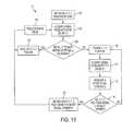
- FIG. 10is a cross-sectional view of another embodiment
- FIG. 11is a perspective view of a signal detector
- FIG. 12is a top view of another signal detector.
- FIG. 13illustrates a control system which can be used to dynamically optically align an optical fiber with a photonic device.
- Embodiments described hereinprovide a simplified structure for optically aligning an optical fiber with a photonic device, the latter being provided on an integrated circuit photonics chip which contains optical devices for propagating and processing light signals.
- the structurecan be fabricated using known MEMS techniques on a semiconductor, e.g., silicon, substrate of an integrated circuit photonics chip.
- An alignment lensis provided between the optical fiber and photonic device. The lens is moveable in three directions (x, y and z) to produce and maintain optical alignment of the optical fiber and photonic device.
- a pair of lower actuator headshold the lens from below and are respectively provided at the free ends of a pair of cantilever arms.
- Another upper actuator headis provided at the free end of another cantilever arm and holds the lens from above and in place on the lower pair of actuator heads.
- a respective motive sourcee.g., a piezoelectric structure, is associated with each of the cantilever arms. The motive source is arranged to bend the arms to move the respective actuator heads and thus the lens in the three directions to acquire and maintain optical alignment between the optical fiber and photonic device.
- the cantilever arms connected to the lower actuatorscan be non-bendable, or another fixed structure can be used, to support the lower actuator heads with a respective motive source provided between the lower actuator heads and fixed structure to affect their movement.
- motive sourcescan also be provided between the lens and fixed actuator heads.
- a control loopcan be used to acquire a received optical signal and establish and maintain optical alignment by appropriately activating the motive sources in response to the received optical signal to move the actuator heads and hold the lens in a position which optically aligns the optical fiber and photonic device.
- FIG. 1shows a perspective view of an embodiment of the invention
- FIGS. 2 and 3show in cross-section details of elements of the FIG. 1 embodiment.
- An integrated circuit photonics chip 9formed of a semiconductor, e.g., silicon, substrate which includes photonic devices, and which may also include electrical devices and circuits on the same chip, is shown.
- the chip 9includes a fabricated waveguide 17 , having a waveguide core 17 a and associated cladding 17 b .
- the waveguide 17receives or transmits an optical signal from or to an optical fiber 11 which is adhered by an adhesive at one end to a cradle 13 fabricated on the integrated circuit chip 9 and which has a curved upper surface which accepts the curved outer surface of optical fiber 11 .
- Optical signals transmitted between the optical fiber 11 and waveguide 17pass through a lens 15 .
- the lens 15may take various forms, including but not limited to, a ball lens, a barrel lens and a spherical lens. In the following discussion a ball lens is discussed as an example of lens 15 .
- the lens 15is adjustably held in the optical path between the optical fiber 11 and waveguide 17 by lower actuator heads 21 a , 21 b which have downwardly inclined faces 26 a , 26 b ( FIG. 2 ) which engage with a lower surface of lens 15 .
- the lower actuator heads 21 a , 21 bare provided at the free ends of respective cantilever arms 23 a , 23 b .
- the support ends of the cantilever arms 23 a , 23 bare integrally connected to respective bases 20 a , 20 b which are fabricated on integrated circuit chip 9 .
- the cantilever arms 23 a , 23 bare independently bendable in the x axis direction as shown in FIGS. 2 and 4 , by virtue of respective motive sources which may take the form of respective independent piezoelectric structures 25 a , 25 b provided along the length of each of the cantilever arms 23 a , 23 b .
- the piezoelectric structures 251 , 25 bmay take the form of a known biomorphic structure which includes a first layer of silicon and a second layer of piezoelectric material such as PZT or PMN.
- the independent bending of the cantilever arms 23 a , 23 bcauses independent movement of the actuator heads 21 a , 21 b in the x axis direction in accordance with voltages applied to the piezoelectric structures 25 a , 25 b.
- the lens 15is also held at its upper surface by an upper actuator 21 c which may be in the form of a cap or other structure for engaging with a portion of the upper surface of lens 15 .
- the upper actuator 21 cis provided at the free end of a cantilever arm 23 c .
- a motive sourceis provided along the side of cantilever arm 23 c and can be in the form of a piezoelectric structure 25 c .
- the piezoelectric structure 25 ccauses bending of cantilever arm 23 c and thus movement of the lens 15 in the y axis direction, as shown in FIGS. 1 and 3 .
- the independent movement of the cantilever arms 23 a , 23 b and 23 c by the corresponding piezoelectric structures 25 a , 25 b , and 25 cenables the lens 15 to be moved in the x, y, and z axis directions shown in FIGS. 1-4 .
- FIG. 2shows a cross-sectional view along the lines 2 - 2 of FIG. 1 .
- the FIG. 2 cross-sectionis through the lens 15 and lower actuator heads 21 a , 21 b .
- FIG. 3shows a cross-sectional view through the optical fiber 11 , lens 15 and waveguide 17 along lines 3 - 3 of FIG. 1 .
- each lower actuator head 21 a , 21 bhas a sloped face 26 a , 26 b on which lens 15 rests.
- FIG. 1shows a cross-sectional view along the lines 2 - 2 of FIG. 1 .
- FIG. 2shows a cross-sectional view along the lines 2 - 2 of FIG. 1 .
- the FIG. 2 cross-sectionis through the lens 15 and lower actuator heads 21 a , 21 b .
- FIG. 3shows a cross-sectional view through the optical fiber 11 , lens 15 and waveguide 17 along lines 3 - 3 of FIG. 1 .
- FIG. 2shows the lower actuator heads 21 a , 21 b as having a planar downwardly sloping face 26 a , 26 b ; however, as described below, other profiles can be used for the faces of the actuator heads 21 a , 21 b.
- FIGS. 5A-5Fshow how lens 15 is moveable in the x axis and z axis directions in accordance with movement of the lower actuator heads 21 a , 21 b upon actuation by respective piezoelectric structures 25 a , 25 b .
- cantilever arm 23 cwhich holds actuator head 21 c on the top of lens 15 , is bendable up and down.
- FIG. 5Ashows by arrow A lens 15 moving upwardly when the piezoelectric structures 25 a , 25 b are each activated to bend respective cantilever arms 23 a , 23 b and move both actuator heads 21 a , 21 b towards one another, while FIG.
- FIG. 5Bshows by arrow B lens 15 moving downwardly when the piezoelectric structures 25 a , 25 b are each activated to bend respective cantilever arms 23 a , 23 b and move both the actuator heads 21 a , 21 b away from one another.
- FIGS. 5C and 5Dshow by respective arrows C and D movement of lens 15 to the left and right respectively when the piezoelectric structures 25 a , 25 b are each activated to bend respective cantilever arms 23 a , 23 b and move both actuator heads 21 a , 21 b to the left and to the right.
- FIG. 5Eshows by arrow E a leftward upward movement of lens 15 when actuator 21 b is not operated by piezoelectric structure 25 b , and actuator 21 a is moved to the left by operation of piezoelectric structure 25 a and the bending of cantilever arm 23 a .
- FIG. 5Fshows by arrow F movement of lens 15 when piezoelectric structure 25 b bends cantilever arm 23 b to move actuator head 21 b to the right while actuator head 21 a remains stationary.
- cantilever arm 23 cis bendable in the z axis direction as actuator 21 c moves up and down in response to movement of the lens 15 by the actuator heads 21 a . 21 b .
- the piezoelectric structure 25 c associated with cantilever arm 23 ccauses arm 23 c to bend in the y axis direction to move actuator 21 c and lens 15 along the y axis.
- lens 15is moveable along all three axes x, y and z.
- FIG. 6shows in cross section modified lower actuator heads 21 a ′ and 21 b ′, each provided with respective downwardly inclined stepped surfaces 30 a , 30 b for contacting lens 15 .
- the stepped surfaces 30 b , 30 aprovide a stepped incremental adjustment of lens 15 when moving in the directions indicted by FIGS. 5A, 5B, 5E and 5F .
- FIG. 7shows other modified lower actuator heads 21 a ′′ and 21 b ′′ which have respective curved actuator surfaces 30 a ′ and 30 b′.
- Movement of the actuator heads 21 a , 21 b , 21 c in the embodiments described aboveoccurs by appropriate electrical actuation of respective piezoelectric structures 25 a , 25 b , 25 c which bend respective cantilever arms 23 a , 23 b , 23 c .
- the cantilever arms 23 a , 23 b for lower activator heads 21 a , 21 bcan be non-bendable and piezoelectric structures 25 a , 25 b omitted from the cantilever arms 23 a , 23 b .
- piezoelectric structures 35 a , 35 bcan be located between respective non-bendable cantilever arms 23 a , 23 b and their associated actuator heads 21 a , 21 b .
- the piezoelectric structures 35 a , 35 bare each independently operated to expand and compress as shown by arrows H thereby moving the respective actuator heads 21 a and 21 b to position lens 15 in the manner shown in FIGS. 5A-5F .
- the cantilever arms 23 a , 23 bcan be omitted and the piezoelectric structures 35 a , 35 b attached directly to support bases 20 a ′ and 20 b ′ fabricated on the chip 9 .
- the piezoelectric structures 35 a , 35 bcan be formed directly on the surfaces of the lower actuator heads 21 a , 21 b where they directly engage with the lens 15 and compress or contact in the directions of arrows Ito move lens 15 .
- FIG. 11illustrates a signal detector 29 fabricated on waveguide core 17 a which can be formed of germanium or germanium-silicon and which receives an optical signal from waveguide core 17 a corresponding to an optical signal transmitting to waveguide 17 from optical fiber 11 .
- Signal detector 29outputs an electrical signal 31 corresponding to the received optical signal.
- FIG. 12illustrates a signal detector 41 which can also be formed of germanium or germanium silicon which can be coupled to an optical fiber 11 receiving an optical signal from a waveguide 17 .
- Signal detector 41is evanescently coupled to optical fiber 11 by a waveguide 39 and can also provide an output signal 31 .
- Detectors 29 and 41can provide output signals representing the strength of a received optical signal which can be used by a control system to control the position of lens 15 .
- FIG. 13illustrates one example of a control system 51 which receives the signal strength output signals from either detector 29 or detector 41 and which provides actuating signals for piezoelectric structures 25 a , 25 b , 25 c (or 35 a , 35 b , and 25 c ).
- the control system 51can be implemented as a hardware circuit structure integrated on integrated circuit chip 9 or as software running on a processor structure integrated on chip integrated circuit 9 , or as a combination of the two.
- the control system 51will be described as the operational steps which are executed by the circuit structure, programmed processor structure, or combination of the two.
- step 101an initial central x axis, y axis, and z axis position of lens 15 is set and the piezoelectric structures ( 25 a , 25 b , 25 c or 35 a , 35 b , 25 c ) are actuated to obtain this central lens 15 position.
- an optical signal strengthis acquired from either detector 29 or 41 , depending on whether waveguide 17 is receiving an optical signal from optical fiber 11 or vice versa.
- step 105the signal strength of the received optical signal is compared with a reference signal strength to see if it is within an acceptable tolerance range, e.g., above a pre-set amplitude level.
- the current x, y, z position of lens 15is held by maintaining the current actuation state of the piezoelectric structures 25 a , 25 b , 25 c or 35 a , 35 b , 25 c at step 107 .
- the operational flowthen returns to step 103 , with or without a predetermined delay 119 , where another signal is acquired from either detector 29 or 41 .
- a predetermined delayshown as an option by the dotted step 119 , will cause a periodic rather than a continuous acquisition of a signal from the detector 29 or 41 after an x, y, z position is set for lens 15 .
- control system 51actuates the piezoelectric structures 25 a , 25 b , 25 c (or 35 a , 35 b , 25 c ) to change the x, y and z lens position by setting a new x, y, z lens 15 position in step 109 .
- a signalis then acquired in step 111 from either detector 29 or 41 , and a signal strength at that new x, y, z lens position is measured and stored in step 113 .
- step 115a determination is made if all possible x, y, z positions of lens 15 have been set and corresponding signal strength values stored.
- the x, y, z position having the highest stored signal strengthis set as the position of lens 15 and the piezoelectric structures 25 a , 25 b , 25 c (or 35 a , 35 b , 25 c ) correspondingly actuated in step 117 to set the lens 15 at that position.
- the control system 51reverts back to step 103 , with or without the predetermined delay 119 .
- step 115If in step 115 not all x, y, z positions have been set for lens 15 and corresponding signal strengths stored, the control system 51 returns to step 109 and the operation implemented by steps 109 - 115 repeats until a yes condition is detected in step 115 .
- control system 51starts from an initial central x, y, z lens 15 position and if the signal strength, which can be checked periodically or continuously, is not within an acceptable tolerance range as detected at step 105 , it finds a new x, y, z position for lens 15 where signal strength is a maximum and sets that as the new x, y, z lens 15 position.
- the control system 51operates dynamically to periodically or continuously shift lens 15 , if adjustment is needed, to set it at the best position to optionally align the optical fiber 11 and waveguide 17 .
- FIG. 13represents but one example of a control process which can be implemented by control system 51 and used to adjust lens 15 to a position which best aligns optical signals between optical fiber 11 and a waveguide 17 .
- Other control processes 51can also be used.
- the structures illustrated hereinare fabricated on integrated circuit photonics chip 9 using known MEMS techniques which fabricate and shape structures from the substrate material of the chip 9 .
Landscapes
- Physics & Mathematics (AREA)
- General Physics & Mathematics (AREA)
- Optics & Photonics (AREA)
- Optical Couplings Of Light Guides (AREA)
- Optical Recording Or Reproduction (AREA)
- Mechanical Light Control Or Optical Switches (AREA)
Abstract
Description
Claims (10)
Priority Applications (4)
| Application Number | Priority Date | Filing Date | Title |
|---|---|---|---|
| US15/134,167US9507104B2 (en) | 2013-01-02 | 2016-04-20 | Apparatus providing simplified alignment of optical fiber in photonic integrated circuits |
| US15/362,578US9715070B2 (en) | 2013-01-02 | 2016-11-28 | Apparatus providing simplified alignment of optical fiber in photonic integrated circuits |
| US15/640,041US9958624B2 (en) | 2013-01-02 | 2017-06-30 | Apparatus providing simplified alignment of optical fiber in photonic integrated circuits |
| US15/936,033US10656354B2 (en) | 2013-01-02 | 2018-03-26 | Apparatus providing simplified alignment of optical fiber in photonic integrated circuits |
Applications Claiming Priority (2)
| Application Number | Priority Date | Filing Date | Title |
|---|---|---|---|
| US13/732,557US9341787B2 (en) | 2013-01-02 | 2013-01-02 | Apparatus providing simplified alignment of optical fiber in photonic integrated circuits |
| US15/134,167US9507104B2 (en) | 2013-01-02 | 2016-04-20 | Apparatus providing simplified alignment of optical fiber in photonic integrated circuits |
Related Parent Applications (1)
| Application Number | Title | Priority Date | Filing Date |
|---|---|---|---|
| US13/732,557DivisionUS9341787B2 (en) | 2013-01-02 | 2013-01-02 | Apparatus providing simplified alignment of optical fiber in photonic integrated circuits |
Related Child Applications (1)
| Application Number | Title | Priority Date | Filing Date |
|---|---|---|---|
| US15/362,578ContinuationUS9715070B2 (en) | 2013-01-02 | 2016-11-28 | Apparatus providing simplified alignment of optical fiber in photonic integrated circuits |
Publications (2)
| Publication Number | Publication Date |
|---|---|
| US20160231519A1 US20160231519A1 (en) | 2016-08-11 |
| US9507104B2true US9507104B2 (en) | 2016-11-29 |
Family
ID=49950050
Family Applications (5)
| Application Number | Title | Priority Date | Filing Date |
|---|---|---|---|
| US13/732,557Active2034-06-17US9341787B2 (en) | 2013-01-02 | 2013-01-02 | Apparatus providing simplified alignment of optical fiber in photonic integrated circuits |
| US15/134,167ActiveUS9507104B2 (en) | 2013-01-02 | 2016-04-20 | Apparatus providing simplified alignment of optical fiber in photonic integrated circuits |
| US15/362,578ActiveUS9715070B2 (en) | 2013-01-02 | 2016-11-28 | Apparatus providing simplified alignment of optical fiber in photonic integrated circuits |
| US15/640,041ActiveUS9958624B2 (en) | 2013-01-02 | 2017-06-30 | Apparatus providing simplified alignment of optical fiber in photonic integrated circuits |
| US15/936,033ActiveUS10656354B2 (en) | 2013-01-02 | 2018-03-26 | Apparatus providing simplified alignment of optical fiber in photonic integrated circuits |
Family Applications Before (1)
| Application Number | Title | Priority Date | Filing Date |
|---|---|---|---|
| US13/732,557Active2034-06-17US9341787B2 (en) | 2013-01-02 | 2013-01-02 | Apparatus providing simplified alignment of optical fiber in photonic integrated circuits |
Family Applications After (3)
| Application Number | Title | Priority Date | Filing Date |
|---|---|---|---|
| US15/362,578ActiveUS9715070B2 (en) | 2013-01-02 | 2016-11-28 | Apparatus providing simplified alignment of optical fiber in photonic integrated circuits |
| US15/640,041ActiveUS9958624B2 (en) | 2013-01-02 | 2017-06-30 | Apparatus providing simplified alignment of optical fiber in photonic integrated circuits |
| US15/936,033ActiveUS10656354B2 (en) | 2013-01-02 | 2018-03-26 | Apparatus providing simplified alignment of optical fiber in photonic integrated circuits |
Country Status (7)
| Country | Link |
|---|---|
| US (5) | US9341787B2 (en) |
| EP (1) | EP2941661B1 (en) |
| JP (1) | JP6153625B2 (en) |
| KR (1) | KR101883540B1 (en) |
| CN (1) | CN104884986B (en) |
| TW (1) | TWI551910B (en) |
| WO (1) | WO2014107321A1 (en) |
Cited By (1)
| Publication number | Priority date | Publication date | Assignee | Title |
|---|---|---|---|---|
| US9715070B2 (en) | 2013-01-02 | 2017-07-25 | Micron Technology, Inc. | Apparatus providing simplified alignment of optical fiber in photonic integrated circuits |
Families Citing this family (16)
| Publication number | Priority date | Publication date | Assignee | Title |
|---|---|---|---|---|
| PT2968479T (en) | 2013-03-14 | 2019-08-07 | Icahn School Med Mount Sinai | Therapeutic acid ceramidase compositions and methods of making and using them |
| US9417411B2 (en) | 2014-02-21 | 2016-08-16 | Aurrion, Inc. | Optical and thermal interface for photonic integrated circuits |
| US9876575B2 (en)* | 2014-04-30 | 2018-01-23 | Infinera Corporation | Hybrid optical transmitter and/or receiver structure |
| US9513447B1 (en)* | 2015-05-14 | 2016-12-06 | Huawei Technologies Co.., Ltd. | Active photonic integrated circuit (PIC) with embedded coupling efficiency monitoring |
| ITUA20161818A1 (en)* | 2016-03-18 | 2017-09-18 | St Microelectronics Srl | MEMS PROJECTIVE DEVICE FOR A FLYING SPOT TYPE PICOPROJECTOR AND ITS MANUFACTURING METHOD |
| CN108663353B (en)* | 2017-03-31 | 2020-10-30 | 苏州星帆华镭光电科技有限公司 | Vibration light path component and laser-induced breakdown spectrometer with same |
| CN107121265B (en)* | 2017-05-10 | 2020-05-26 | 深圳市惠富康光通信有限公司 | Detection equipment and control method for C-lens assembly process |
| FR3071327B1 (en)* | 2017-09-21 | 2019-08-30 | Thales | METHOD AND SYSTEM FOR ALIGNING THE OPTICAL AXIS OF AN OPTICAL CABLE WITH AN OPTOELECTRONIC COMPONENT |
| CN108490572B (en)* | 2018-03-12 | 2021-04-23 | Oppo广东移动通信有限公司 | Laser projection modules, depth cameras and electronic devices |
| CN109324375A (en)* | 2018-10-11 | 2019-02-12 | 菲尼萨光电通讯(上海)有限公司 | Optical coupling device and its coupling process based on optical power scanning feedback |
| JP7159835B2 (en)* | 2018-12-12 | 2022-10-25 | 日本電信電話株式会社 | optical connection structure |
| CN110018544A (en)* | 2019-05-14 | 2019-07-16 | 南开大学 | A kind of efficient automatic coupling device of spatial light based on photon lantern and its implementation |
| US12061367B2 (en) | 2019-09-12 | 2024-08-13 | Technische Universiteit Eindhoven | Apparatus arranged for aligning an optical component with an on-chip port as well as a corresponding system and method |
| CN114488434B (en)* | 2022-02-14 | 2023-06-02 | 清华大学 | Optical fiber automatic coupling system and method |
| US12265254B1 (en) | 2022-09-29 | 2025-04-01 | Lightsynq Technologies Inc. | Self-aligned fabrication process for coupling of photonic waveguides |
| WO2025021941A1 (en)* | 2023-07-26 | 2025-01-30 | Ams-Osram International Gmbh | Arrangement and aligning method |
Citations (28)
| Publication number | Priority date | Publication date | Assignee | Title |
|---|---|---|---|---|
| JPS5735815A (en) | 1980-07-23 | 1982-02-26 | Nippon Telegr & Teleph Corp <Ntt> | Fine adjusting device for axis alignment of optical fiber |
| JPS5735814A (en) | 1980-07-23 | 1982-02-26 | Nippon Telegr & Teleph Corp <Ntt> | Fine adjusting device for axis alignment of optical fiber |
| US4520570A (en) | 1983-12-30 | 1985-06-04 | International Business Machines Corporation | Piezoelectric x-y-positioner |
| US4626066A (en) | 1983-12-30 | 1986-12-02 | At&T Bell Laboratories | Optical coupling device utilizing a mirror and cantilevered arm |
| US5049775A (en) | 1988-09-30 | 1991-09-17 | Boston University | Integrated micromechanical piezoelectric motor |
| US5231286A (en) | 1990-08-31 | 1993-07-27 | Olympus Optical Co., Ltd. | Scanning probe microscope utilizing an optical element in a waveguide for dividing the center part of the laser beam perpendicular to the waveguide |
| JPH0743548A (en) | 1993-07-29 | 1995-02-14 | Sumitomo Electric Ind Ltd | Optical fiber aligner |
| US5602955A (en) | 1995-06-07 | 1997-02-11 | Mcdonnell Douglas Corporation | Microactuator for precisely aligning an optical fiber and an associated fabrication method |
| JP2000111816A (en) | 1998-10-06 | 2000-04-21 | Trw Inc | Active matching photonics assembly body |
| JP2001083372A (en) | 1999-09-09 | 2001-03-30 | Hitachi Ltd | Optical coupling device |
| US20010026660A1 (en) | 2000-03-22 | 2001-10-04 | Hiroyuki Asakura | Optical device, optical communication component and optical transmission apparatus |
| JP2001337247A (en) | 2000-03-22 | 2001-12-07 | Matsushita Electric Ind Co Ltd | Optical device, optical communication component, and optical transmission device |
| US6587612B1 (en) | 2000-09-06 | 2003-07-01 | Southwest Research Institute | Thermally actuated spectroscopic optical switch |
| US20030227560A1 (en) | 2002-06-05 | 2003-12-11 | Christer Mattsson | Digital camera system with piezoelectric actuators |
| JP2004286966A (en) | 2003-03-20 | 2004-10-14 | Oyokoden Lab Co Ltd | Lens fixing device and manufacturing method therefor |
| US6935042B2 (en) | 2002-11-08 | 2005-08-30 | Nanolign, Inc. | Dynamic micro-positioner and aligner |
| TW200532267A (en) | 2003-11-19 | 2005-10-01 | Corning Inc | Active photonic band-gap optical fiber |
| US6990853B2 (en) | 2002-12-18 | 2006-01-31 | Palo Alto Research Center Incorporated | Alignment-tolerant lens structures for acoustic force actuation of cantilevers |
| US20070114890A1 (en) | 2005-11-23 | 2007-05-24 | Churchill David L | Slotted beam piezoelectric composite |
| US20070263963A1 (en) | 2006-05-09 | 2007-11-15 | Lucent Technologies Inc. | Method, apparatus and system for self-aligning components, sub-assemblies and assemblies |
| NL2000876C2 (en) | 2007-09-24 | 2009-03-26 | Univ Delft Tech | Optical fiber alignment device with MEMS actuator, has wedge parts biased into position in direct contact with their position altering devices |
| US7555333B2 (en) | 2000-06-19 | 2009-06-30 | University Of Washington | Integrated optical scanning image acquisition and display |
| US7558168B2 (en) | 2004-12-15 | 2009-07-07 | Hon Hai Precision Industry Co., Ltd. | Optical pickup device with a tilt adjusting actuator |
| TW200942878A (en) | 2008-04-10 | 2009-10-16 | Yuan-Feng Zhouzhao | Revolving ellipsoid air-hole photon-crystal optical fiber |
| US20110013869A1 (en)* | 2009-01-30 | 2011-01-20 | Bardia Pezeshki | Micromechanically aligned optical assembly |
| US20110181150A1 (en) | 2008-05-30 | 2011-07-28 | The Trustees Of The University Of Pennsylvania | Piezoelectric aln rf mem switches monolithically integrated with aln contour-mode resonators |
| US20110317972A1 (en) | 2010-06-25 | 2011-12-29 | Agency For Science, Technology And Research | Optical device, optical arrangement and optical element holder |
| US20140185983A1 (en) | 2013-01-02 | 2014-07-03 | Micron Technology, Inc. | Apparatus providing simplified alignment of optical fiber in photonic integrated circuits |
Family Cites Families (5)
| Publication number | Priority date | Publication date | Assignee | Title |
|---|---|---|---|---|
| US4385373A (en)* | 1980-11-10 | 1983-05-24 | Eastman Kodak Company | Device for focus and alignment control in optical recording and/or playback apparatus |
| US6095697A (en) | 1998-03-31 | 2000-08-01 | Honeywell International Inc. | Chip-to-interface alignment |
| US20030012545A1 (en)* | 2001-07-05 | 2003-01-16 | Bellman Robert A. | Broad-band variable optical attenuator |
| US20080054757A1 (en)* | 2006-08-31 | 2008-03-06 | Vladimir Anatolyevich Aksyuk | Tip-tilt actuator |
| US8604663B2 (en)* | 2010-11-15 | 2013-12-10 | DigitalOptics Corporation MEMS | Motion controlled actuator |
- 2013
- 2013-01-02USUS13/732,557patent/US9341787B2/enactiveActive
- 2013-12-19CNCN201380069230.7Apatent/CN104884986B/enactiveActive
- 2013-12-19EPEP13819135.8Apatent/EP2941661B1/enactiveActive
- 2013-12-19JPJP2015550496Apatent/JP6153625B2/enactiveActive
- 2013-12-19WOPCT/US2013/076474patent/WO2014107321A1/enactiveApplication Filing
- 2013-12-19KRKR1020157020766Apatent/KR101883540B1/enactiveActive
- 2013-12-31TWTW102149302Apatent/TWI551910B/enactive
- 2016
- 2016-04-20USUS15/134,167patent/US9507104B2/enactiveActive
- 2016-11-28USUS15/362,578patent/US9715070B2/enactiveActive
- 2017
- 2017-06-30USUS15/640,041patent/US9958624B2/enactiveActive
- 2018
- 2018-03-26USUS15/936,033patent/US10656354B2/enactiveActive
Patent Citations (30)
| Publication number | Priority date | Publication date | Assignee | Title |
|---|---|---|---|---|
| JPS5735815A (en) | 1980-07-23 | 1982-02-26 | Nippon Telegr & Teleph Corp <Ntt> | Fine adjusting device for axis alignment of optical fiber |
| JPS5735814A (en) | 1980-07-23 | 1982-02-26 | Nippon Telegr & Teleph Corp <Ntt> | Fine adjusting device for axis alignment of optical fiber |
| US4520570A (en) | 1983-12-30 | 1985-06-04 | International Business Machines Corporation | Piezoelectric x-y-positioner |
| US4626066A (en) | 1983-12-30 | 1986-12-02 | At&T Bell Laboratories | Optical coupling device utilizing a mirror and cantilevered arm |
| US5049775A (en) | 1988-09-30 | 1991-09-17 | Boston University | Integrated micromechanical piezoelectric motor |
| US5231286A (en) | 1990-08-31 | 1993-07-27 | Olympus Optical Co., Ltd. | Scanning probe microscope utilizing an optical element in a waveguide for dividing the center part of the laser beam perpendicular to the waveguide |
| JPH0743548A (en) | 1993-07-29 | 1995-02-14 | Sumitomo Electric Ind Ltd | Optical fiber aligner |
| US5602955A (en) | 1995-06-07 | 1997-02-11 | Mcdonnell Douglas Corporation | Microactuator for precisely aligning an optical fiber and an associated fabrication method |
| JP2000111816A (en) | 1998-10-06 | 2000-04-21 | Trw Inc | Active matching photonics assembly body |
| US6205266B1 (en) | 1998-10-06 | 2001-03-20 | Trw Inc. | Active alignment photonics assembly |
| JP2001083372A (en) | 1999-09-09 | 2001-03-30 | Hitachi Ltd | Optical coupling device |
| US20010026660A1 (en) | 2000-03-22 | 2001-10-04 | Hiroyuki Asakura | Optical device, optical communication component and optical transmission apparatus |
| JP2001337247A (en) | 2000-03-22 | 2001-12-07 | Matsushita Electric Ind Co Ltd | Optical device, optical communication component, and optical transmission device |
| US7555333B2 (en) | 2000-06-19 | 2009-06-30 | University Of Washington | Integrated optical scanning image acquisition and display |
| US6587612B1 (en) | 2000-09-06 | 2003-07-01 | Southwest Research Institute | Thermally actuated spectroscopic optical switch |
| US20030227560A1 (en) | 2002-06-05 | 2003-12-11 | Christer Mattsson | Digital camera system with piezoelectric actuators |
| US6710950B2 (en) | 2002-06-05 | 2004-03-23 | Nokia Mobile Phones Limited | Piezoelectric actuator for digital camera optical system |
| US6935042B2 (en) | 2002-11-08 | 2005-08-30 | Nanolign, Inc. | Dynamic micro-positioner and aligner |
| US6990853B2 (en) | 2002-12-18 | 2006-01-31 | Palo Alto Research Center Incorporated | Alignment-tolerant lens structures for acoustic force actuation of cantilevers |
| JP2004286966A (en) | 2003-03-20 | 2004-10-14 | Oyokoden Lab Co Ltd | Lens fixing device and manufacturing method therefor |
| TW200532267A (en) | 2003-11-19 | 2005-10-01 | Corning Inc | Active photonic band-gap optical fiber |
| US7558168B2 (en) | 2004-12-15 | 2009-07-07 | Hon Hai Precision Industry Co., Ltd. | Optical pickup device with a tilt adjusting actuator |
| US20070114890A1 (en) | 2005-11-23 | 2007-05-24 | Churchill David L | Slotted beam piezoelectric composite |
| US20070263963A1 (en) | 2006-05-09 | 2007-11-15 | Lucent Technologies Inc. | Method, apparatus and system for self-aligning components, sub-assemblies and assemblies |
| NL2000876C2 (en) | 2007-09-24 | 2009-03-26 | Univ Delft Tech | Optical fiber alignment device with MEMS actuator, has wedge parts biased into position in direct contact with their position altering devices |
| TW200942878A (en) | 2008-04-10 | 2009-10-16 | Yuan-Feng Zhouzhao | Revolving ellipsoid air-hole photon-crystal optical fiber |
| US20110181150A1 (en) | 2008-05-30 | 2011-07-28 | The Trustees Of The University Of Pennsylvania | Piezoelectric aln rf mem switches monolithically integrated with aln contour-mode resonators |
| US20110013869A1 (en)* | 2009-01-30 | 2011-01-20 | Bardia Pezeshki | Micromechanically aligned optical assembly |
| US20110317972A1 (en) | 2010-06-25 | 2011-12-29 | Agency For Science, Technology And Research | Optical device, optical arrangement and optical element holder |
| US20140185983A1 (en) | 2013-01-02 | 2014-07-03 | Micron Technology, Inc. | Apparatus providing simplified alignment of optical fiber in photonic integrated circuits |
Non-Patent Citations (3)
| Title |
|---|
| Notice of Rejection mailed Sep. 20, 2016 in corresponding Japanese Patent Application No. 2015-550496, 7 pages. |
| Office Action mailed Sep. 24, 2015 in Taiwan Application No. 102149302, 4 pages. |
| Zhang, et al. "A Silicon Platform with MEMS Active Alignment Function and Its Potential Application in Si-Photonics Packaging", IEEE Journal of Selected Topics in Quantum Electronics, Jan. 2010. |
Cited By (3)
| Publication number | Priority date | Publication date | Assignee | Title |
|---|---|---|---|---|
| US9715070B2 (en) | 2013-01-02 | 2017-07-25 | Micron Technology, Inc. | Apparatus providing simplified alignment of optical fiber in photonic integrated circuits |
| US9958624B2 (en) | 2013-01-02 | 2018-05-01 | Micron Technology, Inc. | Apparatus providing simplified alignment of optical fiber in photonic integrated circuits |
| US10656354B2 (en) | 2013-01-02 | 2020-05-19 | Micron Technology, Inc. | Apparatus providing simplified alignment of optical fiber in photonic integrated circuits |
Also Published As
| Publication number | Publication date |
|---|---|
| US20140185983A1 (en) | 2014-07-03 |
| EP2941661B1 (en) | 2022-09-07 |
| US10656354B2 (en) | 2020-05-19 |
| TWI551910B (en) | 2016-10-01 |
| JP2016502154A (en) | 2016-01-21 |
| US20160231519A1 (en) | 2016-08-11 |
| US20180003905A1 (en) | 2018-01-04 |
| CN104884986A (en) | 2015-09-02 |
| US20180224614A1 (en) | 2018-08-09 |
| US9341787B2 (en) | 2016-05-17 |
| KR101883540B1 (en) | 2018-07-30 |
| US20170139163A1 (en) | 2017-05-18 |
| JP6153625B2 (en) | 2017-06-28 |
| EP2941661A1 (en) | 2015-11-11 |
| TW201435420A (en) | 2014-09-16 |
| US9715070B2 (en) | 2017-07-25 |
| US9958624B2 (en) | 2018-05-01 |
| WO2014107321A1 (en) | 2014-07-10 |
| KR20150103218A (en) | 2015-09-09 |
| CN104884986B (en) | 2017-09-29 |
Similar Documents
| Publication | Publication Date | Title |
|---|---|---|
| US9507104B2 (en) | Apparatus providing simplified alignment of optical fiber in photonic integrated circuits | |
| US6577793B2 (en) | Optical switch | |
| KR101015634B1 (en) | Apparatus comprising directional energy processing components, alignment methods of directional energy processing components, and optical assemblies | |
| EP1505419A2 (en) | Method and system for maintaining active alignment in an optical switch using dedicated directing elements | |
| US9746611B2 (en) | Systems and methods for tiltable grating out-couplers | |
| US20160131846A1 (en) | Mode size converters for reducing a modal profile of incoming light | |
| US6415068B1 (en) | Microlens switching assembly and method | |
| US6377718B1 (en) | Micromechanical phase-shifting gate optical modulator | |
| US6954579B2 (en) | Method and apparatus for changing the optical intensity of an optical signal using a movable light transmissive structure | |
| US6898342B2 (en) | Fiber-aligning optical switch | |
| US7050670B2 (en) | Method and system for aligning and maintaining alignment of an optical switch using sensors | |
| KR100620990B1 (en) | Variable Optical Attenuator for Optical Communication Using Polymer Lens and Optical Fiber | |
| KR100631835B1 (en) | Contiber-type PLC optical attenuator and manufacturing method thereof | |
| JPH10197751A (en) | Optical axis adjustment method and optical axis adjustment device for waveguide and optical fiber | |
| Haake et al. | In package micro-aligner for fiber-optic packaging | |
| US20190033539A1 (en) | Optical module and method for manufacturing the optical module | |
| US20230042123A1 (en) | Rotational and translational micropositioners using deformable microelectromechanical systems | |
| JP2019117394A (en) | Optical communication device and manufacturing method therefor | |
| JPH07270647A (en) | Multi-fiber optical fiber alignment mechanism |
Legal Events
| Date | Code | Title | Description |
|---|---|---|---|
| FEPP | Fee payment procedure | Free format text:PAYOR NUMBER ASSIGNED (ORIGINAL EVENT CODE: ASPN); ENTITY STATUS OF PATENT OWNER: LARGE ENTITY | |
| AS | Assignment | Owner name:U.S. BANK NATIONAL ASSOCIATION, AS COLLATERAL AGENT, CALIFORNIA Free format text:SECURITY INTEREST;ASSIGNOR:MICRON TECHNOLOGY, INC.;REEL/FRAME:038669/0001 Effective date:20160426 Owner name:U.S. BANK NATIONAL ASSOCIATION, AS COLLATERAL AGEN Free format text:SECURITY INTEREST;ASSIGNOR:MICRON TECHNOLOGY, INC.;REEL/FRAME:038669/0001 Effective date:20160426 | |
| AS | Assignment | Owner name:MORGAN STANLEY SENIOR FUNDING, INC., AS COLLATERAL AGENT, MARYLAND Free format text:PATENT SECURITY AGREEMENT;ASSIGNOR:MICRON TECHNOLOGY, INC.;REEL/FRAME:038954/0001 Effective date:20160426 Owner name:MORGAN STANLEY SENIOR FUNDING, INC., AS COLLATERAL Free format text:PATENT SECURITY AGREEMENT;ASSIGNOR:MICRON TECHNOLOGY, INC.;REEL/FRAME:038954/0001 Effective date:20160426 | |
| STCF | Information on status: patent grant | Free format text:PATENTED CASE | |
| AS | Assignment | Owner name:U.S. BANK NATIONAL ASSOCIATION, AS COLLATERAL AGENT, CALIFORNIA Free format text:CORRECTIVE ASSIGNMENT TO CORRECT THE REPLACE ERRONEOUSLY FILED PATENT #7358718 WITH THE CORRECT PATENT #7358178 PREVIOUSLY RECORDED ON REEL 038669 FRAME 0001. ASSIGNOR(S) HEREBY CONFIRMS THE SECURITY INTEREST;ASSIGNOR:MICRON TECHNOLOGY, INC.;REEL/FRAME:043079/0001 Effective date:20160426 Owner name:U.S. BANK NATIONAL ASSOCIATION, AS COLLATERAL AGEN Free format text:CORRECTIVE ASSIGNMENT TO CORRECT THE REPLACE ERRONEOUSLY FILED PATENT #7358718 WITH THE CORRECT PATENT #7358178 PREVIOUSLY RECORDED ON REEL 038669 FRAME 0001. ASSIGNOR(S) HEREBY CONFIRMS THE SECURITY INTEREST;ASSIGNOR:MICRON TECHNOLOGY, INC.;REEL/FRAME:043079/0001 Effective date:20160426 | |
| AS | Assignment | Owner name:JPMORGAN CHASE BANK, N.A., AS COLLATERAL AGENT, ILLINOIS Free format text:SECURITY INTEREST;ASSIGNORS:MICRON TECHNOLOGY, INC.;MICRON SEMICONDUCTOR PRODUCTS, INC.;REEL/FRAME:047540/0001 Effective date:20180703 Owner name:JPMORGAN CHASE BANK, N.A., AS COLLATERAL AGENT, IL Free format text:SECURITY INTEREST;ASSIGNORS:MICRON TECHNOLOGY, INC.;MICRON SEMICONDUCTOR PRODUCTS, INC.;REEL/FRAME:047540/0001 Effective date:20180703 | |
| AS | Assignment | Owner name:MICRON TECHNOLOGY, INC., IDAHO Free format text:RELEASE BY SECURED PARTY;ASSIGNOR:U.S. BANK NATIONAL ASSOCIATION, AS COLLATERAL AGENT;REEL/FRAME:047243/0001 Effective date:20180629 | |
| AS | Assignment | Owner name:MICRON TECHNOLOGY, INC., IDAHO Free format text:RELEASE BY SECURED PARTY;ASSIGNOR:MORGAN STANLEY SENIOR FUNDING, INC., AS COLLATERAL AGENT;REEL/FRAME:050937/0001 Effective date:20190731 | |
| AS | Assignment | Owner name:MICRON SEMICONDUCTOR PRODUCTS, INC., IDAHO Free format text:RELEASE BY SECURED PARTY;ASSIGNOR:JPMORGAN CHASE BANK, N.A., AS COLLATERAL AGENT;REEL/FRAME:051028/0001 Effective date:20190731 Owner name:MICRON TECHNOLOGY, INC., IDAHO Free format text:RELEASE BY SECURED PARTY;ASSIGNOR:JPMORGAN CHASE BANK, N.A., AS COLLATERAL AGENT;REEL/FRAME:051028/0001 Effective date:20190731 | |
| MAFP | Maintenance fee payment | Free format text:PAYMENT OF MAINTENANCE FEE, 4TH YEAR, LARGE ENTITY (ORIGINAL EVENT CODE: M1551); ENTITY STATUS OF PATENT OWNER: LARGE ENTITY Year of fee payment:4 | |
| MAFP | Maintenance fee payment | Free format text:PAYMENT OF MAINTENANCE FEE, 8TH YEAR, LARGE ENTITY (ORIGINAL EVENT CODE: M1552); ENTITY STATUS OF PATENT OWNER: LARGE ENTITY Year of fee payment:8 |