US9503708B2 - Systems and methods for reducing z-thickness and zero-order effects in depth cameras - Google Patents
Systems and methods for reducing z-thickness and zero-order effects in depth camerasDownload PDFInfo
- Publication number
- US9503708B2 US9503708B2US14/743,738US201514743738AUS9503708B2US 9503708 B2US9503708 B2US 9503708B2US 201514743738 AUS201514743738 AUS 201514743738AUS 9503708 B2US9503708 B2US 9503708B2
- Authority
- US
- United States
- Prior art keywords
- light
- optical element
- facet
- projection
- diffractive optical
- Prior art date
- Legal status (The legal status is an assumption and is not a legal conclusion. Google has not performed a legal analysis and makes no representation as to the accuracy of the status listed.)
- Active
Links
Images


Classifications
- H04N13/0271—
- G—PHYSICS
- G01—MEASURING; TESTING
- G01B—MEASURING LENGTH, THICKNESS OR SIMILAR LINEAR DIMENSIONS; MEASURING ANGLES; MEASURING AREAS; MEASURING IRREGULARITIES OF SURFACES OR CONTOURS
- G01B11/00—Measuring arrangements characterised by the use of optical techniques
- G01B11/24—Measuring arrangements characterised by the use of optical techniques for measuring contours or curvatures
- G01B11/25—Measuring arrangements characterised by the use of optical techniques for measuring contours or curvatures by projecting a pattern, e.g. one or more lines, moiré fringes on the object
- G—PHYSICS
- G01—MEASURING; TESTING
- G01B—MEASURING LENGTH, THICKNESS OR SIMILAR LINEAR DIMENSIONS; MEASURING ANGLES; MEASURING AREAS; MEASURING IRREGULARITIES OF SURFACES OR CONTOURS
- G01B11/00—Measuring arrangements characterised by the use of optical techniques
- G—PHYSICS
- G02—OPTICS
- G02B—OPTICAL ELEMENTS, SYSTEMS OR APPARATUS
- G02B26/00—Optical devices or arrangements for the control of light using movable or deformable optical elements
- G02B26/08—Optical devices or arrangements for the control of light using movable or deformable optical elements for controlling the direction of light
- G02B26/0808—Optical devices or arrangements for the control of light using movable or deformable optical elements for controlling the direction of light by means of one or more diffracting elements
- G—PHYSICS
- G02—OPTICS
- G02B—OPTICAL ELEMENTS, SYSTEMS OR APPARATUS
- G02B27/00—Optical systems or apparatus not provided for by any of the groups G02B1/00 - G02B26/00, G02B30/00
- G02B27/0075—Optical systems or apparatus not provided for by any of the groups G02B1/00 - G02B26/00, G02B30/00 with means for altering, e.g. increasing, the depth of field or depth of focus
- G—PHYSICS
- G02—OPTICS
- G02B—OPTICAL ELEMENTS, SYSTEMS OR APPARATUS
- G02B27/00—Optical systems or apparatus not provided for by any of the groups G02B1/00 - G02B26/00, G02B30/00
- G02B27/30—Collimators
- G—PHYSICS
- G02—OPTICS
- G02B—OPTICAL ELEMENTS, SYSTEMS OR APPARATUS
- G02B27/00—Optical systems or apparatus not provided for by any of the groups G02B1/00 - G02B26/00, G02B30/00
- G02B27/42—Diffraction optics, i.e. systems including a diffractive element being designed for providing a diffractive effect
- G02B27/4205—Diffraction optics, i.e. systems including a diffractive element being designed for providing a diffractive effect having a diffractive optical element [DOE] contributing to image formation, e.g. whereby modulation transfer function MTF or optical aberrations are relevant
- G—PHYSICS
- G02—OPTICS
- G02B—OPTICAL ELEMENTS, SYSTEMS OR APPARATUS
- G02B27/00—Optical systems or apparatus not provided for by any of the groups G02B1/00 - G02B26/00, G02B30/00
- G02B27/42—Diffraction optics, i.e. systems including a diffractive element being designed for providing a diffractive effect
- G02B27/4233—Diffraction optics, i.e. systems including a diffractive element being designed for providing a diffractive effect having a diffractive element [DOE] contributing to a non-imaging application
- G02B27/425—Diffraction optics, i.e. systems including a diffractive element being designed for providing a diffractive effect having a diffractive element [DOE] contributing to a non-imaging application in illumination systems
- G—PHYSICS
- G02—OPTICS
- G02B—OPTICAL ELEMENTS, SYSTEMS OR APPARATUS
- G02B27/00—Optical systems or apparatus not provided for by any of the groups G02B1/00 - G02B26/00, G02B30/00
- G02B27/48—Laser speckle optics
- G06K9/2036—
- G06T7/0057—
- G—PHYSICS
- G06—COMPUTING OR CALCULATING; COUNTING
- G06V—IMAGE OR VIDEO RECOGNITION OR UNDERSTANDING
- G06V10/00—Arrangements for image or video recognition or understanding
- G06V10/10—Image acquisition
- G06V10/12—Details of acquisition arrangements; Constructional details thereof
- G06V10/14—Optical characteristics of the device performing the acquisition or on the illumination arrangements
- G06V10/145—Illumination specially adapted for pattern recognition, e.g. using gratings
- H—ELECTRICITY
- H04—ELECTRIC COMMUNICATION TECHNIQUE
- H04N—PICTORIAL COMMUNICATION, e.g. TELEVISION
- H04N13/00—Stereoscopic video systems; Multi-view video systems; Details thereof
- H04N13/20—Image signal generators
- H04N13/204—Image signal generators using stereoscopic image cameras
- H04N13/239—Image signal generators using stereoscopic image cameras using two 2D image sensors having a relative position equal to or related to the interocular distance
- H—ELECTRICITY
- H04—ELECTRIC COMMUNICATION TECHNIQUE
- H04N—PICTORIAL COMMUNICATION, e.g. TELEVISION
- H04N13/00—Stereoscopic video systems; Multi-view video systems; Details thereof
- H04N13/20—Image signal generators
- H04N13/271—Image signal generators wherein the generated image signals comprise depth maps or disparity maps
- H—ELECTRICITY
- H04—ELECTRIC COMMUNICATION TECHNIQUE
- H04N—PICTORIAL COMMUNICATION, e.g. TELEVISION
- H04N23/00—Cameras or camera modules comprising electronic image sensors; Control thereof
- H04N23/56—Cameras or camera modules comprising electronic image sensors; Control thereof provided with illuminating means
- G—PHYSICS
- G02—OPTICS
- G02B—OPTICAL ELEMENTS, SYSTEMS OR APPARATUS
- G02B27/00—Optical systems or apparatus not provided for by any of the groups G02B1/00 - G02B26/00, G02B30/00
- G02B27/0025—Optical systems or apparatus not provided for by any of the groups G02B1/00 - G02B26/00, G02B30/00 for optical correction, e.g. distorsion, aberration
- G—PHYSICS
- G02—OPTICS
- G02B—OPTICAL ELEMENTS, SYSTEMS OR APPARATUS
- G02B27/00—Optical systems or apparatus not provided for by any of the groups G02B1/00 - G02B26/00, G02B30/00
- G02B27/42—Diffraction optics, i.e. systems including a diffractive element being designed for providing a diffractive effect
- G02B27/4233—Diffraction optics, i.e. systems including a diffractive element being designed for providing a diffractive effect having a diffractive element [DOE] contributing to a non-imaging application
- G—PHYSICS
- G03—PHOTOGRAPHY; CINEMATOGRAPHY; ANALOGOUS TECHNIQUES USING WAVES OTHER THAN OPTICAL WAVES; ELECTROGRAPHY; HOLOGRAPHY
- G03B—APPARATUS OR ARRANGEMENTS FOR TAKING PHOTOGRAPHS OR FOR PROJECTING OR VIEWING THEM; APPARATUS OR ARRANGEMENTS EMPLOYING ANALOGOUS TECHNIQUES USING WAVES OTHER THAN OPTICAL WAVES; ACCESSORIES THEREFOR
- G03B17/00—Details of cameras or camera bodies; Accessories therefor
- G03B17/48—Details of cameras or camera bodies; Accessories therefor adapted for combination with other photographic or optical apparatus
- G03B17/54—Details of cameras or camera bodies; Accessories therefor adapted for combination with other photographic or optical apparatus with projector
- G06K2209/40—
- G—PHYSICS
- G06—COMPUTING OR CALCULATING; COUNTING
- G06T—IMAGE DATA PROCESSING OR GENERATION, IN GENERAL
- G06T2207/00—Indexing scheme for image analysis or image enhancement
- G06T2207/10—Image acquisition modality
- G06T2207/10028—Range image; Depth image; 3D point clouds
- G—PHYSICS
- G06—COMPUTING OR CALCULATING; COUNTING
- G06T—IMAGE DATA PROCESSING OR GENERATION, IN GENERAL
- G06T2207/00—Indexing scheme for image analysis or image enhancement
- G06T2207/10—Image acquisition modality
- G06T2207/10141—Special mode during image acquisition
- G06T2207/10152—Varying illumination
- G—PHYSICS
- G06—COMPUTING OR CALCULATING; COUNTING
- G06T—IMAGE DATA PROCESSING OR GENERATION, IN GENERAL
- G06T2207/00—Indexing scheme for image analysis or image enhancement
- G06T2207/20—Special algorithmic details
- G06T2207/20228—Disparity calculation for image-based rendering
- G—PHYSICS
- G06—COMPUTING OR CALCULATING; COUNTING
- G06V—IMAGE OR VIDEO RECOGNITION OR UNDERSTANDING
- G06V2201/00—Indexing scheme relating to image or video recognition or understanding
- G06V2201/12—Acquisition of 3D measurements of objects
- H—ELECTRICITY
- H04—ELECTRIC COMMUNICATION TECHNIQUE
- H04N—PICTORIAL COMMUNICATION, e.g. TELEVISION
- H04N13/00—Stereoscopic video systems; Multi-view video systems; Details thereof
- H04N2013/0074—Stereoscopic image analysis
- H04N2013/0081—Depth or disparity estimation from stereoscopic image signals
Definitions
- Depth camera systemscapture a scene and estimate the depth (or “z-distance”) of each pixel in a scene, thereby generating a “depth map,” an example of which is shown in FIG. 1 .
- depth camera systemscan be classified into passive depth cameras and active type depth cameras.
- Active type depth camerasgenerally include an illumination component which emits light onto a scene.
- theseinclude “time-of-flight” active depth cameras, which emit diffuse modulated illumination onto the scene and “structured light” active depth cameras, which emit a collimated illumination pattern.
- an active depth cameraincludes an active illumination component S I , an image acquisition component S A , and a processing component S P , where the processing component implements a depth estimation algorithm.
- the illumination system S Iilluminates the scene with diffuse or collimated light, which can be constant over time, pulsed, or modulated.
- the illuminationmay be concentrated in a single wavelength or span a range of wavelengths.
- Some active illumination components S Iuse a light emitter such as a laser and one or more optical elements to generate a collimated beam having a pattern.
- one or more diffractive optical elementsare used to replicate an incident collimated beam over a collection of collimated beams which comprise the illumination pattern.
- FIG. 2is an example of a pattern emitted by an illumination component S I .
- a bright spote.g., a large white spot
- This bright spotis often called the “zero-order” or “0th order” and is the result of direct propagation of the incident collimated beam upon the diffractive element(s) traveling through the optical elements that generate the pattern.
- 1% to 5% (or more) of the optical energy emitted by the light emitteris concentrated in the zero-order spot, and the zero-order spot may be 100 to 500 times brighter than any other portion of the pattern.
- This high concentration of optical energy in one locationis a limiting factor or bottleneck for generating practical patterns because, for example, an excessively strong collimated zero order may not pass consumer electronics laser safety requirements.
- FIG. 3Ais a schematic diagram of an image acquisition component S A and an active illumination component S I , with x, y, and z axes labeled.
- the z axiscorresponds to the main optical axis of the element, e.g., the axis along the field of view of the image acquisition component S A and the axis along which the illumination component S I emits light.
- an illumination component S I used in such systemshas a co-linear optics package in which a light emitting component (e.g., a laser) is aligned on the same axis as various optical components such as a refractive lens and a separate diffractive optical element for generating the pattern.
- a light emitting componente.g., a laser
- Such an illumination componentgenerally has a thickness of at least 7 mm along the direction of the emission optical axis (or projection optical axis).
- Embodiments of the present inventionrelate to depth camera systems having reduced thickness and reduced zero-order effects and methods of operating the same.
- a projection systemconfigured to emit patterned light along a projection optical axis includes: a diffractive optical element configured to perform a collimation function and to perform a pattern generation function; and a light emitter configured to emit light toward the diffractive optical element, wherein the collimation function is configured to collimate the light emitted from the light emitter, and wherein the pattern generation function is configured to collimate the light emitted from the light emitter, the patterned light having substantially no collimated zero-order.
- the projection systemmay further include a housing enclosing the light emitter and the diffractive optical element, the housing having an opening to expose the diffractive optical element.
- the projection systemmay have no packaging layer between the light emitter and housing.
- the projection systemmay have a thickness along the projection optical axis less than or equal to 3.5 mm.
- the diffractive optical elementmay have a first facet and a second facet, wherein the first facet is configured to perform the collimation function, and wherein the second facet is configured to perform the pattern generation function.
- the diffractive optical elementmay have a single facet configured to perform both the collimation optical function and the pattern generation function.
- a length of an optical path from the light emitter to the diffractive optical elementis greater than or equal to 1 mm.
- the light emittermay be configured to emit light along a direction non-coaxial to the projection optical axis wherein the projection system further includes a micro-mirror arranged to direct the light emitted by the light emitter in the direction of the projection optical axis.
- the light emittermay be configured to emit light along a direction orthogonal to the projection optical axis.
- a depth camera systemincludes: a projection system configured to emit patterned light along a projection optical axis, the projection system including: a diffractive optical element configured to perform a collimation function and to perform a pattern generation function; and a light emitter configured to emit light toward the diffractive optical element, wherein the collimation function is configured to supply the pattern generation function with a collimated input, wherein the pattern generation function is configured to replicate the collimated beam to produce the patterned light, the patterned light having substantially no collimated zero-order; a first image sensor; a second image sensor; and a processor coupled to the first image sensor, the second image sensor, the projection system, and memory, the memory storing instructions that, when executed by the processor, cause the processor to: control the projection system to emit the pattern onto a scene; control the first image sensor and the second image sensor to capture a first image and a second image, the first image and the second image being captured substantially simultaneously; process the first image and the second image; and generate a
- the depth camera systemmay further include a housing enclosing the light emitter and the diffractive optical element, the housing having an opening to expose the diffractive optical element.
- the depth camera systemmay include no packaging layer between the light emitter and housing.
- the housingmay have a thickness along the projection optical axis less than or equal to 3.5 mm.
- a length of an optical path from the light emitter to the diffractive optical elementmay be greater than or equal to 1 mm.
- the light emittermay be configured to emit light along a direction non-parallel to the projection optical axis, and wherein the projection system further includes a micro-mirror arranged to reflect the light emitted by the light emitter in the direction of the projection optical axis.
- the light emittermay be configured to emit light along a direction orthogonal to the projection optical axis.
- the diffractive optical elementmay have a first facet and a second facet, wherein the first facet is configured to perform the collimation function, and wherein the second facet is configured to perform the pattern generation function.
- the diffractive optical elementmay have an optically functional facet configured to perform both the collimation function and the pattern generation function.
- a method for projecting a pattern onto a scene along a projection optical axisincludes: applying power to a light emitter to emit light along a first direction, the first direction being non-coaxial with the projection optical axis; directing the emitted light from the first direction toward the projection optical axis; collimating the emitted light; and replicating the collimated emitted light into the pattern, the pattern having substantially no collimated zero-order.
- the collimating the emitted light and the replicating the collimated emitted light into the patternmay be performed by a single diffractive optical element.
- the single diffractive optical elementmay have a first facet and a second facet, wherein the first facet is configured to collimate the emitted light, and wherein the second facet is configured to replicate the collimated light into the pattern.
- the diffractive optical elementmay have an optically functional facet configured to perform both the collimation optical function and the pattern generation function.
- FIG. 1is an example of a depth map generated by a depth camera.
- FIG. 2is an example of a pattern emitted by an active illumination component.
- FIG. 3Ais a schematic illustration of a computing device with an integrated depth camera.
- FIG. 3Bis a schematic diagram of an image acquisition component S A and an active illumination component S I , with x, y, and z axes labeled.
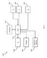
- FIG. 4is a block diagram illustrating a depth camera system according to one embodiment of the present invention.
- FIG. 5is a cutaway side view of an active illumination component according to one embodiment of the present invention.
- FIG. 6is an example of a pattern where the zero-order has been substantially diffused and defocused by a diffractive optical element according to one embodiment of the present invention.
- FIG. 7is a graph illustrating the depth reconstruction error by a stereo camera depth reconstruction system according to one embodiment of the present invention as a function of misalignment of the optical axis of the active illumination component S I .
- aspects of embodiments of the present inventionare directed to a systems and methods enabling an active depth camera system having a small thickness or small z-height.
- the thickness of an active depth camera system according to some embodiments of the present inventionis less than or equal to 3.5 mm.
- aspects of embodiments of the present inventionare directed to an illumination component S I capable of projecting patterned light in an illumination pattern in which a zero-order effect is reduced or negligible.
- the zero-order effectis reduced by diffusing and spreading the zero-order spot over a larger area so that there is substantially no collimated zero-order in the patterned light emitted by the illumination component S I .
- FIG. 4is a block diagram illustrating a depth camera system according to one embodiment of the present invention.
- an active depth cameraincludes an active illumination component S I 106 , an image acquisition component S A including a camera 102 (the embodiment in FIG. 4 shows a second camera 104 for stereo imaging, but embodiments of the present invention are not limited thereto), and a processing component S P 108 , where the processing component implements a depth estimation algorithm.
- the illumination component S Iilluminates the scene with diffuse or collimated light which can be constant over time, pulsed, or modulated.
- the illuminationmay be concentrated in a single wavelength or span a range of wavelengths.
- the image acquisition component S Aacquires image information from the scene, which includes both ambient illumination and illumination from the active illumination component S I .
- the captured image informationmay be stored in a plurality of frames, which may be acquired at regular intervals, such as at a frequency in the range of 5 Hz to 500 Hz.
- the image acquisition component S Amay include a single image sensor or multiple image sensors.
- the image sensor or image sensorsmay be, for example, a semiconductor charge coupled device (CCD) image sensor or a complementary metal-oxide-semiconductor (CMOS) image sensor.
- CCDsemiconductor charge coupled device
- CMOScomplementary metal-oxide-semiconductor
- the processing component S Pprocesses the captured image information and generates an estimated depth map of the scene I D using any of a variety of techniques for generating a depth map using active illumination, such as those described in more detail in R. Szeliski. “Computer Vision: Algorithms and Applications”, Springer, 2010.
- the processing component S Pmay be any computing device capable of performing the processing of the captured images such as: a general purpose processor coupled to memory storing instructions to be executed by the processor; a field programmable gate array (FPGA) configured to perform the processing; an application specific integrated circuit (ASIC) designed to perform the processing (such as a graphics processing unit); or combinations thereof.
- the computationsmay be spread across multiple processing components operating in parallel and/or in series.
- an active illumination component S Iincludes a light emitter, a collimation optics lens, and a diffractive optical element (DOE).
- the light emittermay be a laser diode (e.g., in a TO-Can package). Because the light emitter may emit light having a large angular spread, the collimation optics lens is used to collect and collimate the emitted light. The diffractive optical element may then be used to replicate the collimated beam to form patterned light that is projected onto particular portions of the scene in an illumination pattern such as the pattern shown in FIG. 2 .
- FIG. 5is a side view of an active illumination component S I according to one embodiment of the present invention.
- an active illumination component S I 106includes a laser emitter having p- and n-type layers 500 and 510 connected (e.g., wire bonded) to leads 540 , a micro-mirror (or mirror) 520 , and a dual-function diffractive optical element (DOE) 550 .
- the componentsare encapsulated by lower housing 530 and upper housing 560 .
- the laser emitteris arranged to emit light in a direction orthogonal (e.g., perpendicular) to the optical axis (or emission optical axis or projection optical axis) 580 of the active illumination component 106 (depicted by the dotted line) and the micro-mirror 520 is arranged at an angle (e.g., a 45 degree angle) with respect to the orientation of the laser emitter and the optical axis 580 so that the light emitted by the laser emitter is reflected in the direction of the optical axis 580 .
- an anglee.g., a 45 degree angle
- a different light emitting elementsuch as a light-emitting diode (LED) is used in place of a laser diode.
- LEDlight-emitting diode
- the laser emitteris arranged to emit light along an axis that is non-coaxial to the optical axis 580 .
- the angle between the axis of the light emitter and the optical axis 580may be greater than or less than 90 degrees and the micro-mirror 520 may be arranged at a suitable angle to direct the light emitted by the laser emitter toward the direction of the optical axis 580 , thereby creating a folded optical path.
- the axis of the light emitter and the optical axis 580may be parallel but non-coaxial and one or more mirrors may be used to direct the light emitted by the light emitter toward the optical axis 580 .
- the collimation optics lensis arranged at a distance from the laser emitter, where the distance is generally more than 1 mm.
- the dual-function DOE 550has a first side (or first facet) closer to (and facing) the micro-mirror 520 and a second side (or second facet) further away from and facing away from the micro-mirror 520 .
- the first facet of the DOE 550may have a shape that performs a first function (or first optical function) to collimate the reflected light beam (a collimation function or collimation optical function) and the second facet that performs a second function (or second optical function) to replicate the collimated beam in order to produce the patterned light in the illumination pattern (a pattern generation function or pattern generation optical function).
- one facet of the dual-function DOEperforms both the first function and the second function (e.g., the first function and the second function are performed by the same facet of the DOE and that same facet may be either the facet facing the micro-mirror 520 or may be the facet facing away from the micro-mirror 520 ).
- the functionsare performed by the different facets of the dual-function DOE or by the same facet of the DOE depends on manufacturing constraints.
- the integration of the collimation and pattern generation functions into a single diffractive optical elementregardless of whether the functions are split onto two facets or superposed onto one fact, results in a zero order that is diffuse, not collimated.
- a multi-function DOE according to one embodiment of the present inventionis also described in U.S. Provisional Patent Application No. 62/133,252, titled “An Ultrathin 3D Depth Sensor and Projection System” filed in the U.S. Patent and Trademark Office on Mar. 13, 2015, the entire disclosure of which is incorporated herein by reference.
- FIG. 6is an example of patterned light (or an illumination pattern) where the zero-order has been substantially diffused and defocused by a dual-function DOE according to one embodiment of the present invention as compared to, for example, the illumination pattern shown in FIG. 2 .
- the total thickness of the device 630is the sum of: the thickness 600 of the package of the laser emitter; the distance 610 between the mirror and the dual-function DOE; and the thickness 620 of the dual-function DOE.
- the thickness 600is 0.78 mm
- the distance 610is 0.80 mm
- the thickness 620 of the dual-function DOE 550is in the range 0.75 mm-1.00 mm and therefore a total thickness 630 is in the range 2.33 mm-2.83 mm.
- the overall thickness of the deviceis reduced because only a single DOE 550 is used, rather than multiple DOEs that split the emitted light by cascading the beam through multiple stages.
- the thickness of the devicee.g., along the optical axis
- embodiments of the present inventionare more resilient towards manufacturing errors and tolerances when compared to cascade or tiling methods, which are extremely sensitive to misalignment between the diffractive optical elements.
- the laser emitteris included within the housing 530 and 560 without additional packaging material between the laser emitter and the DOE 550 .
- the laser emitter 500may be included as a laser diode with appropriate contacts and without a protective TO-Can package located between the laser diode and the housing 530 and 560 . This allows the package to be sealed (e.g., hermetically sealed) for environmental resilience of the laser emitter 500 .
- Some embodiments of the inventionare also directed to an image acquisition component S A that is robust with respect to misalignment of the active illumination component S I , such as a multi-camera (or stereo) image acquisition system S A .
- a multi-camera (or stereo) image acquisition system S Asuch as a multi-camera (or stereo) image acquisition system S A .
- the image acquisition system S A shown in FIG. 3A and FIG. 4includes first and second cameras 102 and 104 .
- Such a multi-camera systemmay be used with stereo depth reconstruction algorithms (such as those described in R. Szeliski. “Computer Vision: Algorithms and Applications,” Springer, 2010.) in which patterned light applied to the scene by the active illumination component S I is used to introduce texture onto the scene and knowledge about the pattern itself is not directly used to perform the depth estimation.
- FIG. 7is a graph illustrating the depth error (in meters) by a stereo camera depth reconstruction system as a function of misalignment, in units of degrees, of the optical axis of the active illumination component S I .
- the error rateis relatively low, at less than about 1 millimeter, when the misalignment less than about 12 degrees.
- an active depth camera system having a single camerais very sensitive to misalignments between the illumination source S I and assumes precise calibration of the components and a rigid alignment between the image acquisition system S A and the illumination source S I .
- the single camera systemis intolerant of misalignments greater than 1 degree.
- the arrangement of components and the use of a folded optical path as in embodiments of the present inventionmay result in tolerances that are larger (or looser) than those observed in comparative active illumination components having an on-axis optical path (e.g., an optical path without mirrors).
- heating of components such as the mirrore.g., heating from the laser diode
- the tolerance of the direction of propagation of the light beam after reflection by the micro-mirror 520may be in the range of 1 to 5 degrees due to variability in the angle of light emitted by the laser emitter 500 and variability in the angle of the micro mirror 520 .
- an active illumination system having a folded optical pathsuch as in embodiments of the present invention would generally not be usable with depth camera systems that require a high degree of alignment between the illumination system S I and the image acquisition system S A .
- a multi-camera depth reconstruction system as described above with respect to FIG. 7is robust throughout the misalignment 1 to 5 degrees expected be exhibited by an active illumination system S I according to embodiments of the present invention. Therefore, aspects of embodiments of the present invention are directed to making an active illumination system S I having a folded optical path practical for use in a depth camera system.
Landscapes
- Physics & Mathematics (AREA)
- General Physics & Mathematics (AREA)
- Engineering & Computer Science (AREA)
- Optics & Photonics (AREA)
- Multimedia (AREA)
- Signal Processing (AREA)
- Computer Vision & Pattern Recognition (AREA)
- Theoretical Computer Science (AREA)
- Artificial Intelligence (AREA)
- Measurement Of Optical Distance (AREA)
- Length Measuring Devices By Optical Means (AREA)
- Diffracting Gratings Or Hologram Optical Elements (AREA)
- Electromagnetism (AREA)
- Radar, Positioning & Navigation (AREA)
- Remote Sensing (AREA)
- Lenses (AREA)
Abstract
Description
Claims (22)
Priority Applications (1)
| Application Number | Priority Date | Filing Date | Title |
|---|---|---|---|
| US14/743,738US9503708B2 (en) | 2014-11-03 | 2015-06-18 | Systems and methods for reducing z-thickness and zero-order effects in depth cameras |
Applications Claiming Priority (3)
| Application Number | Priority Date | Filing Date | Title |
|---|---|---|---|
| US201462074592P | 2014-11-03 | 2014-11-03 | |
| US201562133252P | 2015-03-13 | 2015-03-13 | |
| US14/743,738US9503708B2 (en) | 2014-11-03 | 2015-06-18 | Systems and methods for reducing z-thickness and zero-order effects in depth cameras |
Publications (2)
| Publication Number | Publication Date |
|---|---|
| US20160127714A1 US20160127714A1 (en) | 2016-05-05 |
| US9503708B2true US9503708B2 (en) | 2016-11-22 |
Family
ID=55854181
Family Applications (3)
| Application Number | Title | Priority Date | Filing Date |
|---|---|---|---|
| US14/743,738ActiveUS9503708B2 (en) | 2014-11-03 | 2015-06-18 | Systems and methods for reducing z-thickness and zero-order effects in depth cameras |
| US14/743,742Active2035-12-31US9778476B2 (en) | 2014-11-03 | 2015-06-18 | 3D depth sensor and projection system and methods of operating thereof |
| US15/274,994ActiveUS9826216B1 (en) | 2014-11-03 | 2016-09-23 | Systems and methods for compact space-time stereo three-dimensional depth sensing |
Family Applications After (2)
| Application Number | Title | Priority Date | Filing Date |
|---|---|---|---|
| US14/743,742Active2035-12-31US9778476B2 (en) | 2014-11-03 | 2015-06-18 | 3D depth sensor and projection system and methods of operating thereof |
| US15/274,994ActiveUS9826216B1 (en) | 2014-11-03 | 2016-09-23 | Systems and methods for compact space-time stereo three-dimensional depth sensing |
Country Status (1)
| Country | Link |
|---|---|
| US (3) | US9503708B2 (en) |
Cited By (5)
| Publication number | Priority date | Publication date | Assignee | Title |
|---|---|---|---|---|
| TWI638136B (en)* | 2017-08-18 | 2018-10-11 | 財團法人工業技術研究院 | 3d image measurement system |
| CN108664892A (en)* | 2018-04-03 | 2018-10-16 | Oppo广东移动通信有限公司 | Image Acquisition structure and electronic device |
| US10122146B2 (en) | 2016-04-05 | 2018-11-06 | Aquifi, Inc. | Thin laser package for optical applications |
| US10241244B2 (en) | 2016-07-29 | 2019-03-26 | Lumentum Operations Llc | Thin film total internal reflection diffraction grating for single polarization or dual polarization |
| US11425356B2 (en)* | 2017-10-05 | 2022-08-23 | Brown University | System and method to calibrate an uncollimated laser diode for 3D imaging applications |
Families Citing this family (74)
| Publication number | Priority date | Publication date | Assignee | Title |
|---|---|---|---|---|
| US10895753B2 (en)* | 2014-11-14 | 2021-01-19 | Ahead Optoelectronics, Inc. | Structured light generation device and diffractive optical element thereof |
| US10186034B2 (en)* | 2015-01-20 | 2019-01-22 | Ricoh Company, Ltd. | Image processing apparatus, system, image processing method, calibration method, and computer-readable recording medium |
| US9674504B1 (en) | 2015-12-22 | 2017-06-06 | Aquifi, Inc. | Depth perceptive trinocular camera system |
| US10827163B2 (en)* | 2016-08-09 | 2020-11-03 | Facebook Technologies, Llc | Multiple emitter illumination source for depth information determination |
| US10305247B2 (en) | 2016-08-30 | 2019-05-28 | Apple Inc. | Radiation source with a small-angle scanning array |
| US10021372B2 (en)* | 2016-09-16 | 2018-07-10 | Qualcomm Incorporated | Systems and methods for improved depth sensing |
| US10362295B2 (en)* | 2016-09-19 | 2019-07-23 | Apple Inc. | Optical apparatus with beam steering and position feedback |
| CN107976860A (en)* | 2016-10-28 | 2018-05-01 | 深圳奥比中光科技有限公司 | Area array projection device and depth camera |
| CN206350069U (en)* | 2016-11-08 | 2017-07-21 | 聚晶半导体股份有限公司 | Image pickup module and image pickup apparatus |
| US10129377B2 (en)* | 2017-01-04 | 2018-11-13 | Essential Products, Inc. | Integrated structure including image capture and depth sensing components |
| JP6782433B2 (en)* | 2017-03-22 | 2020-11-11 | パナソニックIpマネジメント株式会社 | Image recognition device |
| CN106990548A (en)* | 2017-05-09 | 2017-07-28 | 深圳奥比中光科技有限公司 | Array laser projection arrangement and depth camera |
| CN106990659A (en)* | 2017-05-09 | 2017-07-28 | 深圳奥比中光科技有限公司 | Laser projection device |
| CN107026392B (en)* | 2017-05-15 | 2022-12-09 | 奥比中光科技集团股份有限公司 | VCSEL array light source |
| US10554957B2 (en)* | 2017-06-04 | 2020-02-04 | Google Llc | Learning-based matching for active stereo systems |
| WO2019018851A1 (en) | 2017-07-21 | 2019-01-24 | California Institute Of Technology | Ultra-thin planar lens-less camera |
| US10922828B2 (en)* | 2017-07-31 | 2021-02-16 | Samsung Electronics Co., Ltd. | Meta projector and electronic apparatus including the same |
| KR102464366B1 (en)* | 2017-07-31 | 2022-11-07 | 삼성전자주식회사 | Meta projector and electronic apparatus including the same |
| WO2019033110A1 (en)* | 2017-08-11 | 2019-02-14 | California Institute Of Technology | Lensless 3-dimensional imaging using directional sensing elements |
| CN109756725A (en)* | 2017-08-25 | 2019-05-14 | 华为技术有限公司 | Structured light projector, 3D camera module and terminal equipment |
| US10466360B1 (en)* | 2017-08-31 | 2019-11-05 | Facebook Technologies, Llc | Depth measurement using scanning diffractive optical elements |
| CN107705276B (en)* | 2017-09-11 | 2021-03-02 | Oppo广东移动通信有限公司 | Image processing method and device, electronic device, and computer-readable storage medium |
| CN107678225A (en)* | 2017-09-19 | 2018-02-09 | 深圳奥比中光科技有限公司 | Structured light projection module based on high density VCSEL array light source |
| US11126060B2 (en)* | 2017-10-02 | 2021-09-21 | Liqxtal Technology Inc. | Tunable light projector |
| CN107741682A (en)* | 2017-10-20 | 2018-02-27 | 深圳奥比中光科技有限公司 | Light sources project device |
| CN107742631B (en)* | 2017-10-26 | 2020-02-14 | 京东方科技集团股份有限公司 | Depth imaging device, display panel, method of manufacturing depth imaging device, and apparatus |
| CN107748475A (en) | 2017-11-06 | 2018-03-02 | 深圳奥比中光科技有限公司 | Structured light projection module, depth camera and the method for manufacturing structured light projection module |
| WO2019104329A1 (en)* | 2017-11-27 | 2019-05-31 | Optecks, Llc | Medical three-dimensional (3d) scanning and mapping system |
| CN109903719A (en)* | 2017-12-08 | 2019-06-18 | 宁波盈芯信息科技有限公司 | A kind of the structure light coding method for generating pattern and device of space-time code |
| US10762664B2 (en)* | 2017-12-29 | 2020-09-01 | Intel Corporation | Multi-camera processor with feature matching |
| US11341350B2 (en) | 2018-01-05 | 2022-05-24 | Packsize Llc | Systems and methods for volumetric sizing |
| CN114995015B (en)* | 2018-01-15 | 2024-08-23 | 奥比中光科技集团股份有限公司 | Multifunctional lighting module |
| CN108363267A (en)* | 2018-02-14 | 2018-08-03 | 深圳奥比中光科技有限公司 | The structured light projection module of regular array light source |
| CN108388062A (en)* | 2018-02-27 | 2018-08-10 | 广东欧珀移动通信有限公司 | Laser projection module, depth camera and electronic device |
| KR102455382B1 (en) | 2018-03-02 | 2022-10-18 | 엘지전자 주식회사 | Mobile terminal and method for controlling the same |
| CN108490632B (en)* | 2018-03-12 | 2020-01-10 | Oppo广东移动通信有限公司 | Laser projection module, depth camera and electronic device |
| CN108490628B (en)* | 2018-03-12 | 2020-01-10 | Oppo广东移动通信有限公司 | Structured light projector, depth camera and electronic device |
| CN108490595B (en)* | 2018-03-12 | 2022-09-09 | 深圳市欢太科技有限公司 | Structured light projection module, image acquisition device and electronic equipment |
| CN108594454B (en) | 2018-03-23 | 2019-12-13 | 深圳奥比中光科技有限公司 | Structured light projection module and depth camera |
| NL2020697B1 (en)* | 2018-03-30 | 2019-10-07 | Anteryon Wafer Optics B V | optical module |
| CN108646426A (en)* | 2018-04-03 | 2018-10-12 | Oppo广东移动通信有限公司 | Laser projection module, image capturing device and electronic equipment |
| CN108594456A (en)* | 2018-04-03 | 2018-09-28 | Oppo广东移动通信有限公司 | Structured light projection module, depth camera and electronic device |
| CN108490636A (en)* | 2018-04-03 | 2018-09-04 | Oppo广东移动通信有限公司 | Structured light projectors, optoelectronic devices and electronic devices |
| KR102526929B1 (en)* | 2018-04-04 | 2023-05-02 | 삼성전자 주식회사 | Optical source module comprising transparent menmber formed meta surface and electronic device comprising the same |
| CN108490725B (en)* | 2018-04-16 | 2020-06-12 | 深圳奥比中光科技有限公司 | VCSEL array light source, pattern projector and depth camera |
| TWI661232B (en)* | 2018-05-10 | 2019-06-01 | 視銳光科技股份有限公司 | Integrated structure of flood illuminator and dot projector |
| JP7285470B2 (en)* | 2018-05-17 | 2023-06-02 | パナソニックIpマネジメント株式会社 | Projection system, projection apparatus and projection method |
| US10310362B2 (en) | 2018-06-29 | 2019-06-04 | Intel Corporation | LED pattern projector for 3D camera platforms |
| CN108931202B (en)* | 2018-07-13 | 2021-05-07 | Oppo广东移动通信有限公司 | Detection method and apparatus, electronic apparatus, computer equipment and readable storage medium |
| US11067820B2 (en)* | 2018-07-31 | 2021-07-20 | Himax Technologies Limited | Structured light projector and three-dimensional image sensing module |
| US11006094B2 (en)* | 2018-08-02 | 2021-05-11 | Himax Technologies Limited | Depth sensing apparatus and operation method thereof |
| TWI699734B (en)* | 2018-08-09 | 2020-07-21 | 奇景光電股份有限公司 | Depth sensing apparatus and operation method thereof |
| RU2690757C1 (en) | 2018-08-21 | 2019-06-05 | Самсунг Электроникс Ко., Лтд. | System for synthesis of intermediate types of light field and method of its operation |
| CN109270699A (en)* | 2018-10-23 | 2019-01-25 | 宁波盈芯信息科技有限公司 | A kind of VCSEL laser speckle projector |
| CN109188712A (en)* | 2018-10-23 | 2019-01-11 | Oppo广东移动通信有限公司 | Light emitter component, depth camera and electronic device |
| US10460473B1 (en)* | 2018-12-14 | 2019-10-29 | Zoox, Inc. | Camera calibration system |
| DE102019206374A1 (en) | 2019-05-03 | 2020-11-05 | Audi Ag | Detection device with at least one sensor device, an evaluation device, a light source and a carrier medium |
| US12062885B2 (en) | 2019-07-25 | 2024-08-13 | Trinamix Gmbh | Light module and a method for its operation |
| WO2021076148A1 (en) | 2019-10-18 | 2021-04-22 | Google Llc | Diffractive optical elements for large-field image display |
| US11157774B2 (en)* | 2019-11-14 | 2021-10-26 | Zoox, Inc. | Depth data model training with upsampling, losses, and loss balancing |
| US11580654B2 (en)* | 2019-12-30 | 2023-02-14 | Qualcomm Incorporated | Alternating light distributions for active depth sensing |
| KR102743015B1 (en)* | 2020-03-06 | 2024-12-17 | 엘지이노텍 주식회사 | Camera module |
| WO2021216528A1 (en)* | 2020-04-21 | 2021-10-28 | Magik Eye Inc. | Diffractive optical element with collimator function |
| KR102680498B1 (en)* | 2020-05-21 | 2024-07-03 | 엘지이노텍 주식회사 | Camera module |
| EP4204888A4 (en) | 2020-08-31 | 2024-01-10 | Arc-Y-Tec Ltd. | A multi-directional pattern projector and a hyper-resolution pattern projector |
| KR20220047035A (en) | 2020-10-08 | 2022-04-15 | 삼성전자주식회사 | Device and method for measuring depth of object |
| US11327158B1 (en) | 2020-10-19 | 2022-05-10 | Aeva, Inc. | Techniques to compensate for mirror Doppler spreading in coherent LiDAR systems using matched filtering |
| KR102661114B1 (en)* | 2020-11-10 | 2024-04-25 | 삼성전자주식회사 | Camera module test apparatus, camera module test method and image generating device |
| WO2022109887A1 (en)* | 2020-11-25 | 2022-06-02 | 欧菲光集团股份有限公司 | Transmitting module, image capturing module and electronic device |
| US12188763B2 (en)* | 2021-09-08 | 2025-01-07 | Lumentum Operations Llc | Dot projector including hybrid refractive-diffractive optical elements |
| US12113951B2 (en) | 2021-10-08 | 2024-10-08 | Google Llc | High-resolution pseudo-random dots projector module for depth sensing |
| TW202319805A (en)* | 2021-11-12 | 2023-05-16 | 邑流微測股份有限公司 | Optical imaging system |
| WO2023232818A1 (en)* | 2022-06-03 | 2023-12-07 | Nil Technology Aps | Optical elements providing collimation and fan-out or diffusion |
| GB202402783D0 (en)* | 2024-02-27 | 2024-04-10 | Sintef Tto As | Projection device |
Citations (9)
| Publication number | Priority date | Publication date | Assignee | Title |
|---|---|---|---|---|
| US20020071472A1 (en) | 1999-04-30 | 2002-06-13 | Metrologic Instruments, Inc. | DOE-based systems and devices for producing laser beams having modified beam characteristics |
| US20020196415A1 (en) | 2001-06-26 | 2002-12-26 | Olympus Optical Co., Ltd. | Three-dimensional information acquisition apparatus, projection pattern in three-dimensional information acquisition, and three-dimensional information acquisition method |
| US20090185274A1 (en) | 2008-01-21 | 2009-07-23 | Prime Sense Ltd. | Optical designs for zero order reduction |
| US20100284082A1 (en)* | 2008-01-21 | 2010-11-11 | Primesense Ltd. | Optical pattern projection |
| US7970177B2 (en) | 2006-03-23 | 2011-06-28 | Tyzx, Inc. | Enhancing stereo depth measurements with projected texture |
| US20130294468A1 (en) | 2012-05-02 | 2013-11-07 | Lawrence Livermore National Security, Llc | Diffractive optical elements for transformation of modes in lasers |
| US8749796B2 (en) | 2011-08-09 | 2014-06-10 | Primesense Ltd. | Projectors of structured light |
| US8995057B2 (en) | 2010-11-02 | 2015-03-31 | Asahi Glass Company, Limited | Diffractive optical element and measurement instrument |
| US20150234291A1 (en) | 2010-12-28 | 2015-08-20 | Carl Zeiss Smt Gmbh | Illumination system of a microlithographic projection exposure apparatus |
Family Cites Families (11)
| Publication number | Priority date | Publication date | Assignee | Title |
|---|---|---|---|---|
| JPH09243943A (en) | 1996-03-13 | 1997-09-19 | Minolta Co Ltd | Laser beam scanning optical device |
| FR2748824B1 (en) | 1996-05-15 | 1998-06-26 | Commissariat Energie Atomique | DIFFRACTIVE OPTICAL WITH OPENING SYNTHESIS AND LASER CUTTING DEVICE INCORPORATING SUCH AN OPTICAL |
| US6744502B2 (en) | 2001-09-28 | 2004-06-01 | Pe Corporation (Ny) | Shaped illumination geometry and intensity using a diffractive optical element |
| CA2390781C (en) | 2002-06-14 | 2009-09-22 | Institut National D'optique | Line generator optical apparatus |
| EP1533646A1 (en) | 2003-11-21 | 2005-05-25 | Heptagon OY | Optical pattern generating device |
| JP5104205B2 (en)* | 2007-10-24 | 2012-12-19 | セイコーエプソン株式会社 | Image display device |
| EP2166304A1 (en) | 2008-09-23 | 2010-03-24 | Sick Ag | Lighting unit and method for creating a pattern dissimilar to itself |
| US8786682B2 (en)* | 2009-03-05 | 2014-07-22 | Primesense Ltd. | Reference image techniques for three-dimensional sensing |
| US8576293B2 (en) | 2010-05-18 | 2013-11-05 | Aptina Imaging Corporation | Multi-channel imager |
| US10580128B2 (en) | 2013-01-10 | 2020-03-03 | Akoya Biosciences, Inc. | Whole slide multispectral imaging systems and methods |
| US9325973B1 (en) | 2014-07-08 | 2016-04-26 | Aquifi, Inc. | Dynamically reconfigurable optical pattern generator module useable with a system to rapidly reconstruct three-dimensional data |
- 2015
- 2015-06-18USUS14/743,738patent/US9503708B2/enactiveActive
- 2015-06-18USUS14/743,742patent/US9778476B2/enactiveActive
- 2016
- 2016-09-23USUS15/274,994patent/US9826216B1/enactiveActive
Patent Citations (10)
| Publication number | Priority date | Publication date | Assignee | Title |
|---|---|---|---|---|
| US20020071472A1 (en) | 1999-04-30 | 2002-06-13 | Metrologic Instruments, Inc. | DOE-based systems and devices for producing laser beams having modified beam characteristics |
| US20020196415A1 (en) | 2001-06-26 | 2002-12-26 | Olympus Optical Co., Ltd. | Three-dimensional information acquisition apparatus, projection pattern in three-dimensional information acquisition, and three-dimensional information acquisition method |
| US7970177B2 (en) | 2006-03-23 | 2011-06-28 | Tyzx, Inc. | Enhancing stereo depth measurements with projected texture |
| US20090185274A1 (en) | 2008-01-21 | 2009-07-23 | Prime Sense Ltd. | Optical designs for zero order reduction |
| US20100284082A1 (en)* | 2008-01-21 | 2010-11-11 | Primesense Ltd. | Optical pattern projection |
| US8630039B2 (en) | 2008-01-21 | 2014-01-14 | Primesense Ltd. | Optical designs for zero order reduction |
| US8995057B2 (en) | 2010-11-02 | 2015-03-31 | Asahi Glass Company, Limited | Diffractive optical element and measurement instrument |
| US20150234291A1 (en) | 2010-12-28 | 2015-08-20 | Carl Zeiss Smt Gmbh | Illumination system of a microlithographic projection exposure apparatus |
| US8749796B2 (en) | 2011-08-09 | 2014-06-10 | Primesense Ltd. | Projectors of structured light |
| US20130294468A1 (en) | 2012-05-02 | 2013-11-07 | Lawrence Livermore National Security, Llc | Diffractive optical elements for transformation of modes in lasers |
Cited By (7)
| Publication number | Priority date | Publication date | Assignee | Title |
|---|---|---|---|---|
| US10122146B2 (en) | 2016-04-05 | 2018-11-06 | Aquifi, Inc. | Thin laser package for optical applications |
| US10241244B2 (en) | 2016-07-29 | 2019-03-26 | Lumentum Operations Llc | Thin film total internal reflection diffraction grating for single polarization or dual polarization |
| US10802183B2 (en) | 2016-07-29 | 2020-10-13 | Lumentum Operations Llc | Thin film total internal reflection diffraction grating for single polarization or dual polarization |
| TWI638136B (en)* | 2017-08-18 | 2018-10-11 | 財團法人工業技術研究院 | 3d image measurement system |
| US10921119B2 (en) | 2017-08-18 | 2021-02-16 | Industrial Technology Research Institute | Three dimensional image measurement system |
| US11425356B2 (en)* | 2017-10-05 | 2022-08-23 | Brown University | System and method to calibrate an uncollimated laser diode for 3D imaging applications |
| CN108664892A (en)* | 2018-04-03 | 2018-10-16 | Oppo广东移动通信有限公司 | Image Acquisition structure and electronic device |
Also Published As
| Publication number | Publication date |
|---|---|
| US20160127713A1 (en) | 2016-05-05 |
| US9826216B1 (en) | 2017-11-21 |
| US9778476B2 (en) | 2017-10-03 |
| US20160127714A1 (en) | 2016-05-05 |
Similar Documents
| Publication | Publication Date | Title |
|---|---|---|
| US9503708B2 (en) | Systems and methods for reducing z-thickness and zero-order effects in depth cameras | |
| US10122146B2 (en) | Thin laser package for optical applications | |
| US10003726B2 (en) | Illumination module for near eye-to-eye display system | |
| CN104360571B (en) | Optical device and imaging system | |
| US10001583B2 (en) | Structured light projection using a compound patterned mask | |
| US20200192206A1 (en) | Structured light projector, three-dimensional camera module and terminal device | |
| CN107783353B (en) | Apparatus and system for capturing stereoscopic images | |
| US20220252893A1 (en) | Light projection apparatus | |
| US20210199982A1 (en) | Illumination system having different light sources adapt to different work surfaces | |
| KR102184042B1 (en) | Camera apparatus | |
| CN108885334B (en) | Lighting module | |
| US10942362B2 (en) | Projector, electronic device having projector, and method for obtaining depth information of image data | |
| US11575875B2 (en) | Multi-image projector and electronic device having multi-image projector | |
| JP6626552B1 (en) | Multi-image projector and electronic device having multi-image projector | |
| KR102103919B1 (en) | Multi-image projector and electronic device having multi-image projector | |
| CN111541151A (en) | A light-emitting device, laser equipment and electronic equipment | |
| WO2016149136A2 (en) | 3d depth sensor and projection system and methods of operating thereof | |
| US20240251150A1 (en) | Systems and methods for projecting illumination from a device edge | |
| TWI749280B (en) | Structured light emitting module, structured light sensing module, and electronic device | |
| EP4622253A1 (en) | Information generation device and camera device | |
| US9977305B2 (en) | Spatial information capturing device | |
| TWM520146U (en) | Spatial information extractor |
Legal Events
| Date | Code | Title | Description |
|---|---|---|---|
| AS | Assignment | Owner name:AQUIFI, INC., CALIFORNIA Free format text:ASSIGNMENT OF ASSIGNORS INTEREST;ASSIGNORS:HAZEGHI, ARYAN;MARIN, GIULIO;PERUCH, FRANCESCO;AND OTHERS;REEL/FRAME:035897/0647 Effective date:20150622 | |
| STCF | Information on status: patent grant | Free format text:PATENTED CASE | |
| AS | Assignment | Owner name:COMERICA BANK, MICHIGAN Free format text:SECURITY INTEREST;ASSIGNOR:AQUIFI, INC.;REEL/FRAME:050111/0671 Effective date:20190726 | |
| FEPP | Fee payment procedure | Free format text:SURCHARGE FOR LATE PAYMENT, SMALL ENTITY (ORIGINAL EVENT CODE: M2554); ENTITY STATUS OF PATENT OWNER: SMALL ENTITY | |
| MAFP | Maintenance fee payment | Free format text:PAYMENT OF MAINTENANCE FEE, 4TH YR, SMALL ENTITY (ORIGINAL EVENT CODE: M2551); ENTITY STATUS OF PATENT OWNER: SMALL ENTITY Year of fee payment:4 | |
| AS | Assignment | Owner name:PACKSIZE INTERNATIONAL, LLC, UTAH Free format text:ASSIGNMENT OF ASSIGNORS INTEREST;ASSIGNOR:AQUIFI, INC.;REEL/FRAME:058189/0976 Effective date:20211029 | |
| AS | Assignment | Owner name:PACKSIZE LLC, UNITED STATES Free format text:ASSIGNMENT OF ASSIGNORS INTEREST;ASSIGNOR:PACKSIZE INTERNATIONAL, LLC;REEL/FRAME:058287/0582 Effective date:20211123 | |
| AS | Assignment | Owner name:AQUIFI, INC., CALIFORNIA Free format text:RELEASE BY SECURED PARTY;ASSIGNOR:COMERICA BANK;REEL/FRAME:058353/0680 Effective date:20211208 | |
| FEPP | Fee payment procedure | Free format text:ENTITY STATUS SET TO UNDISCOUNTED (ORIGINAL EVENT CODE: BIG.); ENTITY STATUS OF PATENT OWNER: LARGE ENTITY | |
| MAFP | Maintenance fee payment | Free format text:PAYMENT OF MAINTENANCE FEE, 8TH YEAR, LARGE ENTITY (ORIGINAL EVENT CODE: M1552); ENTITY STATUS OF PATENT OWNER: LARGE ENTITY Year of fee payment:8 | |
| AS | Assignment | Owner name:JPMORGAN CHASE BANK, N.A., ILLINOIS Free format text:SECURITY INTEREST;ASSIGNOR:PACKSIZE LLC;REEL/FRAME:068730/0393 Effective date:20240819 | |
| AS | Assignment | Owner name:JPMORGAN CHASE BANK, N.A., ILLINOIS Free format text:SECURITY INTEREST;ASSIGNOR:PACKSIZE LLC;REEL/FRAME:071282/0082 Effective date:20250515 |