US9502642B2 - Magnetic tunnel junctions, methods used while forming magnetic tunnel junctions, and methods of forming magnetic tunnel junctions - Google Patents
Magnetic tunnel junctions, methods used while forming magnetic tunnel junctions, and methods of forming magnetic tunnel junctionsDownload PDFInfo
- Publication number
- US9502642B2 US9502642B2US14/684,110US201514684110AUS9502642B2US 9502642 B2US9502642 B2US 9502642B2US 201514684110 AUS201514684110 AUS 201514684110AUS 9502642 B2US9502642 B2US 9502642B2
- Authority
- US
- United States
- Prior art keywords
- magnetic
- absorbing
- crystalline
- tunnel insulator
- forming
- Prior art date
- Legal status (The legal status is an assumption and is not a legal conclusion. Google has not performed a legal analysis and makes no representation as to the accuracy of the status listed.)
- Active
Links
Images


Classifications
- H01L43/10—
- H—ELECTRICITY
- H10—SEMICONDUCTOR DEVICES; ELECTRIC SOLID-STATE DEVICES NOT OTHERWISE PROVIDED FOR
- H10N—ELECTRIC SOLID-STATE DEVICES NOT OTHERWISE PROVIDED FOR
- H10N50/00—Galvanomagnetic devices
- H10N50/80—Constructional details
- H10N50/85—Materials of the active region
- G—PHYSICS
- G11—INFORMATION STORAGE
- G11C—STATIC STORES
- G11C11/00—Digital stores characterised by the use of particular electric or magnetic storage elements; Storage elements therefor
- G11C11/02—Digital stores characterised by the use of particular electric or magnetic storage elements; Storage elements therefor using magnetic elements
- G11C11/16—Digital stores characterised by the use of particular electric or magnetic storage elements; Storage elements therefor using magnetic elements using elements in which the storage effect is based on magnetic spin effect
- H01L43/02—
- H01L43/08—
- H01L43/12—
- H—ELECTRICITY
- H10—SEMICONDUCTOR DEVICES; ELECTRIC SOLID-STATE DEVICES NOT OTHERWISE PROVIDED FOR
- H10B—ELECTRONIC MEMORY DEVICES
- H10B61/00—Magnetic memory devices, e.g. magnetoresistive RAM [MRAM] devices
- H—ELECTRICITY
- H10—SEMICONDUCTOR DEVICES; ELECTRIC SOLID-STATE DEVICES NOT OTHERWISE PROVIDED FOR
- H10N—ELECTRIC SOLID-STATE DEVICES NOT OTHERWISE PROVIDED FOR
- H10N50/00—Galvanomagnetic devices
- H10N50/01—Manufacture or treatment
- H—ELECTRICITY
- H10—SEMICONDUCTOR DEVICES; ELECTRIC SOLID-STATE DEVICES NOT OTHERWISE PROVIDED FOR
- H10N—ELECTRIC SOLID-STATE DEVICES NOT OTHERWISE PROVIDED FOR
- H10N50/00—Galvanomagnetic devices
- H10N50/10—Magnetoresistive devices
- H—ELECTRICITY
- H10—SEMICONDUCTOR DEVICES; ELECTRIC SOLID-STATE DEVICES NOT OTHERWISE PROVIDED FOR
- H10N—ELECTRIC SOLID-STATE DEVICES NOT OTHERWISE PROVIDED FOR
- H10N50/00—Galvanomagnetic devices
- H10N50/80—Constructional details
Definitions
- Embodiments disclosed hereinpertain to magnetic tunnel junctions, to methods used while forming magnetic tunnel junctions, and to methods of forming magnetic tunnel junctions.
- a magnetic tunnel junctionis an integrated circuit component having two conductive magnetic electrodes separated by a thin non-magnetic tunnel insulator material (e.g., dielectric material).
- the insulator materialis sufficiently thin such that electrons can tunnel from one magnetic electrode to the other through the insulator material under appropriate conditions.
- At least one of the magnetic electrodescan have its overall magnetization direction switched between two states at a normal operating write or erase current/voltage, and is commonly referred to as the “free” or “recording” electrode.
- the other magnetic electrodeis commonly referred to as the “reference”, “fixed”, or “pinned” electrode, and whose overall magnetization direction will not switch upon application of the normal operating write or erase current/voltage.
- the reference electrode and the recording electrodeare electrically coupled to respective conductive nodes.
- a magnetic tunnel junctioncan be programmed into one of at least two states, and those states can be sensed by measuring current flow through the magnetic tunnel junction. Since magnetic tunnel junctions can be “programmed” between two current-conducting states, they have been proposed for use in memory integrated circuitry. Additionally, magnetic tunnel junctions may be used in logic or other circuitry apart from or in addition to memory.
- the overall magnetization direction of the recording electrodecan be switched by a current-induced external magnetic field or by using a spin-polarized current to result in a spin-transfer torque (STT) effect.
- Charge carrierssuch as electrons
- An electric currentis generally unpolarized (having about 50% “spin-up” and about 50% “spin-down” electrons).
- a spin-polarized currentis one with significantly more electrons of either spin.
- spin angular momentumcan be transferred to that material, thereby affecting its magnetization orientation. This can be used to excite oscillations or even flip (i.e., switch) the orientation/domain direction of the magnetic material if the spin-polarized current is of sufficient magnitude.
- An alloy or other mixture of Co and Feis one common material proposed for use as a polarizer material and/or as at least part of the magnetic recording material of a recording electrode in a magnetic tunnel junction.
- a more specific exampleis Co x Fe y B z where x and y are each 10-80 and z is 0-50, and may be abbreviated as CoFe or CoFeB.
- MgOis an ideal material for the non-magnetic tunnel insulator. Ideally such materials are each crystalline having a body-centered-cubic (bcc) 001 lattice. Such materials may be deposited using any suitable technique, for example by physical vapor deposition.
- One technique usable to ultimately produce the bcc 001 lattice in such materialsincludes initially forming CoFe to be amorphous and upon which MgO-comprising tunnel insulator material is deposited. During and/or after the depositing, the MgO tunnel insulator, the CoFe, and the tunnel insulator ideally individually achieve a uniform bcc 001 lattice structure.
- Bcc 001 MgOacts as a template during the crystallization of CoFe.
- B in the finished magnetic tunnel junction constructionundesirably reduces tunneling magnetoresistance (TMR) of the magnetic tunnel junction.
- FIG. 1is a diagrammatic sectional view of a substrate fragment in process in the fabrication of a magnetic tunnel junction in accordance with an embodiment of the invention.
- FIG. 2is a view of the FIG. 1 substrate fragment at a processing step subsequent to that shown by FIG. 1 .
- FIG. 3is a view of the FIG. 2 substrate fragment at a processing step subsequent to that shown by FIG. 2 .
- FIG. 4is a view of the FIG. 3 substrate fragment at a processing step subsequent to that shown by FIG. 3 , and in one embodiment is a view of a magnetic tunnel junction in accordance with an embodiment of the invention independent of method of manufacture.
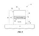
- FIG. 5is a view of the FIG. 4 substrate fragment at a processing step subsequent to that shown by FIG. 4 .
- Example methods of forming a magnetic tunnel junction in accordance with some embodiments of the inventionare initially described with reference to FIGS. 1-5 with respect to a substrate fragment 10 , and which may comprise a semiconductor substrate.
- a substrate fragment 10which may comprise a semiconductor substrate.
- semiconductor substrateor “semiconductive substrate” is defined to mean any construction comprising semiconductive material, including, but not limited to, bulk semiconductive materials such as a semiconductive wafer (either alone or in assemblies comprising other materials thereon), and semiconductive material layers (either alone or in assemblies comprising other materials).
- substraterefers to any supporting structure, including, but not limited to, the semiconductive substrates described above. Referring to FIG.
- substrate fragment 10comprises a base or substrate 11 showing various materials having been formed as an elevational stack there-over. Materials may be aside, elevationally inward, or elevationally outward of the FIG. 1 -depicted materials. For example, other partially or wholly fabricated components of integrated circuitry may be provided somewhere about or within fragment 10 .
- Substrate 11may comprise any one or more of conductive (i.e., electrically herein), semiconductive, or insulative/insulator (i.e., electrically herein) materials. Regardless, any of the materials, regions, and structures described herein may be homogenous or non-homogenous, and regardless may be continuous or discontinuous over any material which such overlie. Further, unless otherwise stated, each material may be formed using any suitable or yet-to-be-developed technique, with atomic layer deposition, chemical vapor deposition, physical vapor deposition, epitaxial growth, diffusion doping, and ion implanting being examples.
- First magnetic (i.e., ferrimagnetic or ferromagnetic herein) electrode material 12(i.e., electrically conductive) is formed over substrate 11 .
- magnetic electrode material 12comprises Co and Fe (e.g., an alloy comprising Co and Fe).
- magnetic electrode material 12is amorphous, and in one embodiment comprises B. Any suitable compositions may be used, with Co 40 Fe 40 B 20 being an example that includes B. Characterization of a material or region as being “amorphous” where used in this document requires at least 90% by volume of the stated material or region to be amorphous.
- First electrode material 12may contain non-magnetic insulator, semiconductive, and/or conductive material or regions. However, first material 12 is characterized as being overall and collectively magnetic and conductive even though it may have one or more regions therein that are intrinsically locally non-magnetic and/or non-conductive. First electrode material 12 may comprise, consist essentially of, or consist of Co, Fe, and B.
- first electrode material 12is about 10 Angstroms to about 500 Angstroms.
- thicknessby itself (no preceding directional adjective) is defined as the mean straight-line distance through a given material or region perpendicularly from a closest surface of an immediately adjacent material of different composition or of an immediately adjacent region.
- the various materials and regions described hereinmay be of substantially constant thickness or of variable thicknesses. If of variable thickness, thickness refers to average thickness unless otherwise indicated.
- “different composition”only requires those portions of two stated materials that may be directly against one another to be chemically and/or physically different, for example if such materials are not homogenous.
- “different composition”only requires that those portions of the two stated materials or regions that are closest to one another be chemically and/or physically different if such materials or regions are not homogenous.
- a material, region, or structureis “directly against” another when there is at least some physical touching contact of the stated materials, regions, or structures relative one another.
- “over”, “on”, and “against” not preceded by “directly”encompass “directly against” as well as construction where intervening material(s), region(s), or structure(s) result(s) in no physical touching contact of the stated materials, regions, or structures relative one another.
- Non-magnetic tunnel insulator 14comprising MgO is formed over first material 12 .
- Tunnel insulator 14may comprise, consist essentially of, or consist of MgO.
- An example thicknessis about 50 Angstroms to about 200 Angstroms.
- MgO of tunnel insulator material 14 , Co, Fe, and B (of first material 12 )are directly against one another.
- Second magnetic electrode material 16is formed over tunnel insulator material 14 . Any aspect(s) or attribute(s) described above for first material 12 may apply with respect to second material 16 .
- at least one of first material 12 and second material 16comprises Co, Fe, and B.
- a stack 20is formed that comprises amorphous first magnetic electrode material 12 , non-magnetic tunnel insulator material 14 comprising MgO over first material 12 , and amorphous second magnetic electrode material 16 over tunnel insulator material 14 , and wherein at least one of first material 12 and second material 16 comprises Co, Fe, and B.
- elevational positions of materials 12 and 16may be reversed and/or an orientation other than an elevational stack may be used (e.g., lateral; diagonal; a combination of one or more of elevational, horizontal, diagonal; etc.).
- elevationale.g., lateral; diagonal; a combination of one or more of elevational, horizontal, diagonal; etc.
- “elevational”, “upper”, “lower”, “top”, and “bottom”are with reference to the vertical direction.
- “Horizontal”refers to a general direction along a primary surface relative to which the substrate is processed during fabrication, and vertical is a direction generally orthogonal thereto.
- vertical and “horizontal” as used hereinare generally perpendicular directions relative one another and independent of orientation of the substrate in three-dimensional space.
- each of materials 12 and 16are amorphous, such materials are crystallized into crystalline first magnetic electrode material 12 and crystalline second magnetic electrode material 16 .
- Annealing substrate fragment 10 at about 350° C. in an inert atmosphereis an example technique for causing such crystallizing.
- Characterization of a material or region as being “crystalline” where used in this documentrequires at least 90% by volume of the stated material or region to be crystalline.
- Tunnel insulator material 14ideally is also crystalline either initially as-formed or becomes so while crystallizing an amorphous first magnetic electrode material 12 and/or an amorphous second magnetic electrode material 16 .
- One of crystalline first material 12 and crystalline second material 16comprises magnetic reference material of the magnetic tunnel junction being formed.
- the other of crystalline first material 12 and crystalline second material 16comprises magnetic recording material of a magnetic tunnel junction being formed.
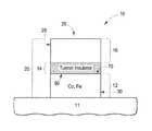
- crystalline first material 12 , tunnel insulator material 14 , and crystalline second material 16are patterned to form a magnetic tunnel junction structure or construction 25 having opposing sidewalls 28 and 30 that individually comprise crystalline first material 12 , tunnel insulator material 14 , and crystalline second material 16 .
- Any existing or yet-to-be developed patterning technique(s)may be used.
- An example techniqueincludes photolithographic masking and etch (e.g., with or without pitch multiplication).
- the above-described processing and patterning processesstack 20 to form opposing sidewalls 28 and 30 after the act of crystallizing materials 12 , 14 , and/or 16 . Alternately, such or other patterning when used may be conducted to form sidewalls 28 and 30 before the act of crystallizing materials 12 , 14 , and/or 16 .
- a B-absorbing materialis formed over sidewalls 28 , 30 of each of crystalline first electrode material 12 , tunnel insulator material 14 , and crystalline second magnetic electrode material 16 .
- all of each of sidewalls 28 and 30is covered with B-absorbing material 40 .
- An example technique of forming B-absorbing materialis by a conformal deposition of material 40 followed by anisotropic etch thereof to largely remove material 40 from horizontal surfaces.
- B-absorbing material 40is formed to have a minimum lateral thickness of about 10 Angstroms to about 200 Angstroms, and in one embodiment a minimum lateral thickness of no more than about 100 Angstroms.
- Bis absorbed from the at least one of crystalline first material 12 or crystalline second material 16 that comprises Co, Fe, and B laterally into B-absorbing material 40 that is over sidewall 28 and over sidewall 30 .
- a B-absorbing materialis a material having a composition that has an affinity for B, thus an affinity to absorb B there-into. The absorbing of B may occur predominantly (i.e., more than 50% herein) during the forming of B-absorbing material 40 or predominantly thereafter.
- B-absorbing material 40is annealed at a temperature of about 50° C. to about 450° C., for example which may facilitate the absorbing of B.
- at least some of the absorbed Bchemically reacts with the B-absorbing material to form a reaction product comprising B. Alternately or additionally, none or some of the absorbed B may not so react.
- crystallization and B-absorptionoccurs after sidewalls of the stack are formed (e.g., after patterning the stack).
- the B-absorbing materialis formed over the opposing sidewalls of each of the amorphous first magnetic electrode material, the tunnel insulator material, and the amorphous second magnetic electrode material prior to crystallizing the amorphous first and second magnetic electrode materials into crystalline first and second magnetic electrode materials, with the act of crystallizing also absorbing B from the at least one of the first and second materials comprising Co, Fe, and B laterally into the B-absorbing material that is over the opposing sidewalls.
- the B-absorbing materialis conductive at least after the absorbing, and in one embodiment before and after the absorbing.
- Example conductive B-absorbing materialscomprise elemental-form metals or an alloy of two or more metal elements.
- Example metal elementscomprise Al, Ta, and W. Such may react with absorbed B to form one or more conductive aluminum borides, tantalum borides, or tungsten borides, respectively.
- the B-absorbing materialis semiconductive at least after the absorbing, and in one embodiment before and after the absorbing.
- An example semiconductive B-absorbing materialis MN.
- absorbed B in such materialmay form material 40 to comprise a semiconductive mixture of aluminum nitride and aluminum boride.
- the B-absorbing materialis insulative at least after the absorbing of B, and in one embodiment before and after the absorbing of B.
- Example insulative B-absorbing materialscomprise Al 2 O 3 , a combination of SiO 2 and Al 2 O 3 , and a combination of Si 3 N 4 and MN (with sufficient Si 3 N 4 in the composition to render it insulative as opposed to semiconductive due to presence of MN).
- any remnant of the B-absorbing material, any remnant of any reaction product of B with the B-absorbing material, and the absorbed Bare removed.
- the B-absorbing materialis conductive or semiconductive (at least after the absorbing) to preclude electrode materials 12 and 16 from being electrically shorted together in the finished circuitry construction.
- FIG. 5by way of example shows such subsequent processing whereby B-absorbing material 40 (not shown) from FIG. 4 has been removed from the substrate (e.g., by selective etching).
- the B-absorbing materialis insulative at least after the act of absorbing
- the B-absorbing material, any remnant of any reaction product of B with the B-absorbing material, and the absorbed Bare incorporated into a finished circuit construction encompassing the magnetic tunnel junction being formed.
- tunnel insulator 14 and magnetic electrode materials 12 and/or 16 from which the B was absorbedare devoid of B after the absorbing of B.
- devoid of Bmeans 0 atomic % B to no more than 0.1 atomic % B.
- An embodiment of the inventionencompasses a method used while forming a magnetic tunnel junction.
- Such a methodincludes forming non-magnetic tunnel insulator material comprising MgO over magnetic electrode material (regardless of whether crystalline or amorphous) comprising Co and Fe (regardless of whether magnetic electrode material of more than one magnetic electrode of a magnetic tunnel junction is formed).
- Bis proximate (i.e., within 100 Angstroms herein) opposing facing surfaces of the tunnel insulator material and the magnetic electrode material (i.e., regardless of whether B is in the magnetic electrode material and regardless of whether MgO, Co, Fe, and B are directly against one another).
- Bbeing proximate opposing surfaces 50 and 70 of tunnel insulator material 14 and magnetic electrode material 12 , respectively, a result of B being within or part of material 12 .
- Bmay be within MgO regardless of whether B is within magnetic electrode material 12 and/or 16 .
- some other B-containing material having minimum thickness no greater than 100 Angstromsmay be between magnetic electrode material 12 or 16 and tunnel dielectric 14 , with such B therein thereby being proximate opposing facing surfaces of the tunnel insulator material and the magnetic electrode material.
- B-absorbing materialis formed over a sidewall (e.g., one or both of sidewalls 28 , 30 ) of at least one of the magnetic electrode material and the tunnel insulator material. B that is proximate opposing surfaces 50 , 70 is absorbed laterally into the B-absorbing material. Any other attribute(s) or aspect(s) as described above and/or shown in the Figures may be used.
- Embodiments of the inventionencompass a magnetic tunnel junction (i.e., a structure) independent of method of manufacture.
- a magnetic tunnel junctioncomprises a conductive first magnetic electrode comprising magnetic recording material and a conductive second magnetic electrode spaced from the first electrode and comprising magnetic reference material.
- a non-magnetic tunnel insulator materialis between the first and second electrodes. At least one of the magnetic recording material and the magnetic reference material comprises Co and Fe.
- the tunnel insulator materialcomprises MgO.
- the first magnetic electrode, the second magnetic electrode, and the tunnel insulator materialcomprise a stack having opposing sidewalls. Insulative material is laterally proximate, in one embodiment directly against, the opposing stack sidewalls.
- the insulative materialcomprises B, at least one of Si and Al, and at least one of N and O.
- the insulative materialcomprises Al and in one embodiment comprises N. In one embodiment, the insulative material comprises Al and N. In one embodiment, the insulative material comprises O and in one embodiment comprises Al and O. In one embodiment, B is present in the insulative material at a concentration of at least about 10 atomic percent and in one embodiment at least about 20 atomic percent. Any other attribute(s) or aspect(s) as described above and/or shown in the Figures may be used in magnetic tunnel junction device embodiments.
- FIGS. 1-5depict single magnetic tunnel junctions (SMTJs). However, dual magnetic tunnel junctions (DMTJs) or more than dual (two) magnetic tunnel junctions are contemplated.
- a method used while forming a magnetic tunnel junctioncomprises forming non-magnetic tunnel insulator material over magnetic electrode material.
- the tunnel insulator materialcomprises MgO and the magnetic electrode material comprises Co and Fe.
- Bis proximate opposing facing surfaces of the tunnel insulator material and the magnetic electrode material.
- B-absorbing materialis formed over a sidewall of at least one of the magnetic electrode material and the tunnel insulator material. B is absorbed from proximate the opposing facing surfaces laterally into the B-absorbing material.
- a method of forming a magnetic tunnel junctioncomprises forming a stack comprising amorphous first magnetic electrode material, non-magnetic tunnel insulator material comprising MgO over the first material, and amorphous second magnetic electrode material over the tunnel insulator material. At least one of the first and second materials comprises Co, Fe, and B.
- the amorphous first and second magnetic electrode materialsare crystallized into crystalline first and second magnetic electrode materials.
- One of the crystalline first material and the crystalline second materialcomprises magnetic reference material of the magnetic tunnel junction being formed.
- the other of the crystalline first material and the crystalline second materialcomprises magnetic recording material of the magnetic tunnel junction being formed.
- B-absorbing materialis formed over opposing sidewalls of each of the crystalline first magnetic electrode material, the tunnel insulator material, and the second magnetic electrode material. B is absorbed from said at least one of the crystalline first and second materials comprising Co, Fe, and B laterally into the B-absorbing material that is over said opposing sidewalls.
- a method of forming a magnetic tunnel junctioncomprises forming amorphous first magnetic electrode material over a substrate.
- the first materialcomprises Co, Fe, and B.
- Non-magnetic tunnel insulator materialcomprising MgO is formed over the first material.
- Amorphous second magnetic electrode materialis formed over the tunnel insulator material, and comprises Co, Fe, and B. After forming the amorphous first and second magnetic electrode materials and the tunnel insulator material over the substrate, the amorphous first and second magnetic electrode materials are crystallized into crystalline first and second magnetic electrode materials.
- the crystalline first material, the tunnel insulator material, and the crystalline second materialare patterned to form a magnetic tunnel junction structure having opposing sidewalls that individually comprise the crystalline first material, the tunnel insulator material, and the crystalline second material.
- One of the crystalline first material and the crystalline second materialcomprises magnetic reference material of the magnetic tunnel junction being formed.
- the other of the crystalline first material and the crystalline second materialcomprises magnetic recording material of the magnetic tunnel junction being formed. All of said opposing sidewalls are covered with B-absorbing material. B is absorbed from the first and second materials laterally into the B-absorbing material that covers all of said opposing sidewalls. At least some of the absorbed B is reacted with the B-absorbing material to form a reaction product comprising B.
- a magnetic tunnel junctioncomprises a conductive first magnetic electrode comprising magnetic recording material and a conductive second magnetic electrode spaced from the first electrode and comprising magnetic reference material.
- a non-magnetic tunnel insulator materialis between the first and second electrodes. At least one of the magnetic recording material and the magnetic reference material comprises Co and Fe.
- the tunnel insulator materialcomprises MgO.
- the first magnetic electrode, the second magnetic electrode, and the tunnel insulator materialcomprise a stack having opposing sidewalls. Insulative material is laterally proximate the opposing stack sidewalls.
- Such insulative materialcomprises B, at least one of Si and Al, and at least one of N and O.
- a method of forming a magnetic tunnel junctioncomprises forming a stack comprising amorphous first magnetic electrode material, non-magnetic tunnel insulator material comprising MgO over the first material, and amorphous second magnetic electrode material over the tunnel insulator material. At least one of the first and second materials comprises Co, Fe, and B. B-absorbing material is formed over opposing sidewalls of each of the amorphous first magnetic electrode material, the tunnel insulator material, and the amorphous second magnetic electrode material. The amorphous first and second magnetic electrode materials are crystallized into crystalline first and second magnetic electrode materials. One of the crystalline first material and the crystalline second material comprises magnetic reference material of the magnetic tunnel junction being formed.
- the other of the crystalline first material and the crystalline second materialcomprises magnetic recording material of the magnetic tunnel junction being formed.
- the act of crystallizingalso absorbs B from said at least one of the first and second materials comprising Co, Fe, and B laterally into the B-absorbing material that is over said opposing sidewalls.
Landscapes
- Engineering & Computer Science (AREA)
- Manufacturing & Machinery (AREA)
- Computer Hardware Design (AREA)
- Hall/Mr Elements (AREA)
- Thin Magnetic Films (AREA)
- Mram Or Spin Memory Techniques (AREA)
Abstract
Description
Claims (14)
Priority Applications (8)
| Application Number | Priority Date | Filing Date | Title |
|---|---|---|---|
| US14/684,110US9502642B2 (en) | 2015-04-10 | 2015-04-10 | Magnetic tunnel junctions, methods used while forming magnetic tunnel junctions, and methods of forming magnetic tunnel junctions |
| PCT/US2016/018015WO2016164108A1 (en) | 2015-04-10 | 2016-02-16 | Magnetic tunnel junctions, methods used while forming magnetic tunnel junctions, and methods of forming magnetic tunnel junctions |
| KR1020177023394AKR101903308B1 (en) | 2015-04-10 | 2016-02-16 | Magnetic tunnel junctions, methods used during formation of magnetic tunnel junctions, and methods of forming magnetic tunnel junctions |
| EP16777011.4AEP3281236A4 (en) | 2015-04-10 | 2016-02-16 | Magnetic tunnel junctions, methods used while forming magnetic tunnel junctions, and methods of forming magnetic tunnel junctions |
| CN201680011709.9ACN107408627B (en) | 2015-04-10 | 2016-02-16 | Magnetic tunnel junction, method for forming magnetic tunnel junction, and method for forming magnetic tunnel junction |
| JP2017544889AJP6622317B2 (en) | 2015-04-10 | 2016-02-16 | Magnetic tunnel junction, method used in forming a magnetic tunnel junction, and method for forming a magnetic tunnel junction |
| TW105106929ATWI619279B (en) | 2015-04-10 | 2016-03-07 | Magnetic tunneling junction surface, method for forming magnetic tunneling junction surface and method for forming magnetic tunneling junction surface |
| US15/345,636US9941466B2 (en) | 2015-04-10 | 2016-11-08 | Magnetic tunnel junctions, methods used while forming magnetic tunnel junctions, and methods of forming magnetic tunnel junctions |
Applications Claiming Priority (1)
| Application Number | Priority Date | Filing Date | Title |
|---|---|---|---|
| US14/684,110US9502642B2 (en) | 2015-04-10 | 2015-04-10 | Magnetic tunnel junctions, methods used while forming magnetic tunnel junctions, and methods of forming magnetic tunnel junctions |
Related Child Applications (1)
| Application Number | Title | Priority Date | Filing Date |
|---|---|---|---|
| US15/345,636DivisionUS9941466B2 (en) | 2015-04-10 | 2016-11-08 | Magnetic tunnel junctions, methods used while forming magnetic tunnel junctions, and methods of forming magnetic tunnel junctions |
Publications (2)
| Publication Number | Publication Date |
|---|---|
| US20160301001A1 US20160301001A1 (en) | 2016-10-13 |
| US9502642B2true US9502642B2 (en) | 2016-11-22 |
Family
ID=57072876
Family Applications (2)
| Application Number | Title | Priority Date | Filing Date |
|---|---|---|---|
| US14/684,110ActiveUS9502642B2 (en) | 2015-04-10 | 2015-04-10 | Magnetic tunnel junctions, methods used while forming magnetic tunnel junctions, and methods of forming magnetic tunnel junctions |
| US15/345,636ActiveUS9941466B2 (en) | 2015-04-10 | 2016-11-08 | Magnetic tunnel junctions, methods used while forming magnetic tunnel junctions, and methods of forming magnetic tunnel junctions |
Family Applications After (1)
| Application Number | Title | Priority Date | Filing Date |
|---|---|---|---|
| US15/345,636ActiveUS9941466B2 (en) | 2015-04-10 | 2016-11-08 | Magnetic tunnel junctions, methods used while forming magnetic tunnel junctions, and methods of forming magnetic tunnel junctions |
Country Status (7)
| Country | Link |
|---|---|
| US (2) | US9502642B2 (en) |
| EP (1) | EP3281236A4 (en) |
| JP (1) | JP6622317B2 (en) |
| KR (1) | KR101903308B1 (en) |
| CN (1) | CN107408627B (en) |
| TW (1) | TWI619279B (en) |
| WO (1) | WO2016164108A1 (en) |
Cited By (1)
| Publication number | Priority date | Publication date | Assignee | Title |
|---|---|---|---|---|
| US20180175287A1 (en)* | 2015-07-20 | 2018-06-21 | Headway Technologies, Inc. | Magnetic Tunnel Junction with Low Defect Rate after High Temperature Anneal for Magnetic Device Applications |
Families Citing this family (4)
| Publication number | Priority date | Publication date | Assignee | Title |
|---|---|---|---|---|
| US9502642B2 (en) | 2015-04-10 | 2016-11-22 | Micron Technology, Inc. | Magnetic tunnel junctions, methods used while forming magnetic tunnel junctions, and methods of forming magnetic tunnel junctions |
| US9257136B1 (en) | 2015-05-05 | 2016-02-09 | Micron Technology, Inc. | Magnetic tunnel junctions |
| US9680089B1 (en) | 2016-05-13 | 2017-06-13 | Micron Technology, Inc. | Magnetic tunnel junctions |
| CN113113444A (en)* | 2021-06-11 | 2021-07-13 | 南京南机智农农机科技研究院有限公司 | Metal-based programmable logic circuit for in-memory computation and preparation method thereof |
Citations (82)
| Publication number | Priority date | Publication date | Assignee | Title |
|---|---|---|---|---|
| US5640343A (en) | 1996-03-18 | 1997-06-17 | International Business Machines Corporation | Magnetic memory array using magnetic tunnel junction devices in the memory cells |
| US5898548A (en)* | 1997-10-24 | 1999-04-27 | International Business Machines Corporation | Shielded magnetic tunnel junction magnetoresistive read head |
| US5949600A (en)* | 1995-09-06 | 1999-09-07 | Kabushiki Kaisha Toshiba | Signal reproduction method and magnetic recording and reproducing apparatus using tunnel current |
| US5994899A (en)* | 1995-09-14 | 1999-11-30 | Research Development Corporation Of Japan | Asymmetrical magneto-impedance element having a thin magnetic wire with a spiral magnetic anisotropy |
| US6034882A (en) | 1998-11-16 | 2000-03-07 | Matrix Semiconductor, Inc. | Vertically stacked field programmable nonvolatile memory and method of fabrication |
| US6048632A (en)* | 1997-08-22 | 2000-04-11 | Nec Research Institute | Self-biasing, non-magnetic, giant magnetoresistance sensor |
| US20020018355A1 (en) | 1998-11-16 | 2002-02-14 | Johnson Mark G. | Vertically stacked field programmable nonvolatile memory and method of fabrication |
| US20020079524A1 (en) | 2000-12-26 | 2002-06-27 | Charles Dennison | Lower electrode isolation in a double-wide trench |
| US6600184B1 (en) | 2002-03-25 | 2003-07-29 | International Business Machines Corporation | System and method for improving magnetic tunnel junction sensor magnetoresistance |
| US6603677B2 (en) | 2000-12-07 | 2003-08-05 | Commissariat A L'energie Atomique | Three-layered stacked magnetic spin polarization device with memory |
| US20040057295A1 (en) | 2001-01-19 | 2004-03-25 | Nozomu Matsukawa | Magnetic storage element, production method and driving method therefor, and memory array |
| US6788502B1 (en) | 1999-09-02 | 2004-09-07 | International Business Machines Corporation | Co-Fe supermalloy free layer for magnetic tunnel junction heads |
| US20050006682A1 (en) | 2003-07-10 | 2005-01-13 | Jun-Soo Bae | Magnetic random access memory devices having titanium-rich lower electrodes with oxide layer and oriented tunneling barrier, and methods for forming the same |
| US20050174835A1 (en) | 2004-02-06 | 2005-08-11 | Unity Semiconductor Corporation | Multi-resistive state element with reactive metal |
| US20050247964A1 (en) | 2003-12-18 | 2005-11-10 | Pietambaram Srinivas V | Synthetic antiferromagnet structures for use in MTJs in MRAM technology |
| US20050254289A1 (en) | 2003-07-23 | 2005-11-17 | Kabushiki Kaisha Toshiba | Magnetic memory device and method of manufacturing the same |
| US7009278B2 (en) | 2003-11-24 | 2006-03-07 | Sharp Laboratories Of America, Inc. | 3d rram |
| US20070096229A1 (en) | 2005-10-28 | 2007-05-03 | Masatoshi Yoshikawa | Magnetoresistive element and magnetic memory device |
| US7233024B2 (en) | 2003-03-31 | 2007-06-19 | Sandisk 3D Llc | Three-dimensional memory device incorporating segmented bit line memory array |
| US20070243638A1 (en) | 2006-04-14 | 2007-10-18 | Maglc Technologies, Inc. | Novel method to form a nonmagnetic cap for the NiFe(free) MTJ stack to enhance dR/R |
| JP2008034857A (en) | 2006-07-31 | 2008-02-14 | Magic Technologies Inc | Magnetic tunnel junction element and method for forming the same |
| US20080144234A1 (en) | 2006-12-15 | 2008-06-19 | Tsann Lin | Current-perpendicular-to-plane sensor with dual keeper layers |
| KR20080084590A (en) | 2007-03-15 | 2008-09-19 | 소니 가부시끼가이샤 | Memory and Memory |
| US20090261314A1 (en) | 2008-04-16 | 2009-10-22 | Samsung Electronics Co., Ltd. | Non-volatile memory device and method of fabricating the same |
| US20090261343A1 (en) | 2002-12-19 | 2009-10-22 | Sandisk 3D Llc | High-density nonvolatile memory and methods of making the same |
| JP2009267411A (en) | 2008-04-25 | 2009-11-12 | Seagate Technology Llc | Storage device including memory cell having a plurality of memory layers |
| US7629637B2 (en) | 2007-02-27 | 2009-12-08 | Kabushiki Kaisha Toshiba | Magnetic random access memory and write method thereof |
| US20090323385A1 (en) | 2008-06-30 | 2009-12-31 | ScanDisk 3D LLC | Method for fabricating high density pillar structures by double patterning using positive photoresist |
| JP2010010688A (en) | 2008-06-26 | 2010-01-14 | Samsung Electronics Co Ltd | Non-volatile memory element, and method of manufacturing the same |
| JP2010034153A (en) | 2008-07-25 | 2010-02-12 | Toshiba Corp | Magnetic random access memory and method for writing the same |
| US20100135061A1 (en) | 2008-12-02 | 2010-06-03 | Shaoping Li | Non-Volatile Memory Cell with Ferroelectric Layer Configurations |
| US7755076B2 (en) | 2007-04-17 | 2010-07-13 | Macronix International Co., Ltd. | 4F2 self align side wall active phase change memory |
| KR20100083402A (en) | 2009-01-13 | 2010-07-22 | 삼성전자주식회사 | Resistive random access memory device and method for fabricating the same |
| WO2010101340A1 (en) | 2009-03-05 | 2010-09-10 | 광주과학기술원 | Resistance change memory device with three-dimensional structure, and device array, electronic product and manufacturing method therefor |
| JP2010232214A (en) | 2009-03-25 | 2010-10-14 | Toshiba Corp | Nonvolatile memory device and method of manufacturing nonvolatile memory device |
| US20100259962A1 (en) | 2009-04-08 | 2010-10-14 | Tianhong Yan | Three-Dimensional Array of Re-Programmable Non-Volatile Memory Elements Having Vertical Bit Lines and a Single-Sided Word Line Architecture |
| JP2010263211A (en) | 2009-05-04 | 2010-11-18 | Samsung Electronics Co Ltd | Multilayer memory device |
| US20110062538A1 (en) | 2007-10-11 | 2011-03-17 | Everspin Technologies, Inc. | Magnetic element having reduced current density |
| US7944738B2 (en) | 2008-11-05 | 2011-05-17 | Micron Technology, Inc. | Spin torque transfer cell structure utilizing field-induced antiferromagnetic or ferromagnetic coupling |
| US20110149646A1 (en) | 2009-12-18 | 2011-06-23 | Micron Technology, Inc. | Transient heat assisted sttram cell for lower programming current |
| US7983065B2 (en) | 2009-04-08 | 2011-07-19 | Sandisk 3D Llc | Three-dimensional array of re-programmable non-volatile memory elements having vertical bit lines |
| US20110318848A1 (en) | 2008-09-03 | 2011-12-29 | Canon Anelva Corporation | FERROMAGNETIC PREFERRED GRAIN GROWTH PROMOTION SEED LAYER FOR AMORPHOUS OR MICROCRYSTALLINE MgO TUNNEL BARRIER |
| US8102700B2 (en) | 2008-09-30 | 2012-01-24 | Micron Technology, Inc. | Unidirectional spin torque transfer magnetic memory cell structure |
| US20120056285A1 (en) | 2010-09-07 | 2012-03-08 | Sony Corporation | Memory element and memory device |
| US20120068139A1 (en) | 2010-09-16 | 2012-03-22 | Kabushiki Kaisha Toshiba | Magnetoresistive element and magnetic memory |
| US20120087179A1 (en) | 2010-10-07 | 2012-04-12 | Jung Ha Chang | Magneto-resistance element and semiconductor memory device including the same |
| US20120127603A1 (en) | 2010-11-23 | 2012-05-24 | Hitachi Global Storage Technologies Netherlands B. V. | Magnetic tunnel junction having a magnetic insertion layer and methods of producing the same |
| WO2012074662A2 (en) | 2010-12-02 | 2012-06-07 | Micron Technology, Inc. | Arrays of nonvolatile memory cells |
| US20120193216A1 (en) | 2009-10-05 | 2012-08-02 | Canon Anelva Corporation | Substrate cooling device, sputtering apparatus and method for manufacturing electronic device |
| US8310861B2 (en) | 2008-09-30 | 2012-11-13 | Micron Technology, Inc. | STT-MRAM cell structure incorporating piezoelectric stress material |
| US20130037862A1 (en) | 2011-08-12 | 2013-02-14 | Kabushiki Kaisha Toshiba | Magnetic random access memory |
| US20130071954A1 (en) | 2010-12-10 | 2013-03-21 | Avalanche Technology Inc. | Magnetic random access memory (mram) with enhanced magnetic stiffness and method of making same |
| US8431458B2 (en) | 2010-12-27 | 2013-04-30 | Micron Technology, Inc. | Methods of forming a nonvolatile memory cell and methods of forming an array of nonvolatile memory cells |
| US20130148418A1 (en) | 2011-12-07 | 2013-06-13 | Agency For Science, Technology And Research | Magnetoresistive device and a writing method for a magnetoresistive device |
| US20130177781A1 (en) | 2009-09-15 | 2013-07-11 | Roman Chepulskyy | Magnetic element having perpendicular anisotropy with enhanced efficiency |
| JP2013140891A (en) | 2012-01-05 | 2013-07-18 | Toshiba Corp | Manufacturing method of magnetoresistance effect element |
| US20130181305A1 (en) | 2010-09-17 | 2013-07-18 | Kabushiki Kaisha Toshiba | Magnetoresistive element and magnetic random access memory |
| US20130224521A1 (en) | 2012-02-28 | 2013-08-29 | Headway Technologies, Inc. | High Thermal Stability Reference Structure with Out-of-Plane Aniotropy for Magnetic Device Applications |
| US20130236639A1 (en) | 2012-03-08 | 2013-09-12 | Matthew J. Carey | Method for making a current-perpendicular-to-the-plane (cpp) magnetoresistive sensor containing a ferromagnetic alloy requiring post-deposition annealing |
| US8559141B1 (en) | 2007-05-07 | 2013-10-15 | Western Digital (Fremont), Llc | Spin tunneling magnetic element promoting free layer crystal growth from a barrier layer interface |
| US20130307097A1 (en) | 2012-05-15 | 2013-11-21 | Ge Yi | Magnetoresistive random access memory cell design |
| US8609439B2 (en) | 2011-01-13 | 2013-12-17 | Crocus Technology Sa | Magnetic tunnel junction comprising a polarizing layer |
| US20140027869A1 (en) | 2012-07-27 | 2014-01-30 | Qualcomm Incorporated | AMORPHOUS ALLOY SPACER FOR PERPENDICULAR MTJs |
| US20140038314A1 (en) | 2010-12-10 | 2014-02-06 | Avalanche Technology, Inc. | Magnetic random access memory (mram) with enhanced magnetic stiffness and method of making same |
| US20140084401A1 (en) | 2012-09-21 | 2014-03-27 | Kabushiki Kaisha Toshiba | Magnetoresistive element and magnetic memory |
| US20140117477A1 (en) | 2012-10-31 | 2014-05-01 | Jongchul PARK | Magnetic memory devices and methods of fabricating the same |
| US20140131649A1 (en) | 2012-11-14 | 2014-05-15 | Kabushiki Kaisha Toshiba | Magnetoresistance element and magnetic memory |
| US20140145792A1 (en) | 2012-11-27 | 2014-05-29 | Headway Technologies, Inc. | Free Layer with Out-of-Plane Anisotropy for Magnetic Device Applications |
| US20140175581A1 (en) | 2012-12-24 | 2014-06-26 | T3Memory, Inc. | Magnetoresistive element having a novel cap multilayer |
| US20140248719A1 (en) | 2010-12-10 | 2014-09-04 | Avalanche Technology Inc. | Mtj manufacturing method utilizing in-situ annealing and etch back |
| US8836056B2 (en) | 2012-09-26 | 2014-09-16 | Intel Corporation | Perpendicular MTJ stacks with magnetic anisotropy enhancing layer and crystallization barrier layer |
| US20140269033A1 (en) | 2013-03-14 | 2014-09-18 | Kabushiki Kaisha Toshiba | Magnetic memory |
| US8842465B2 (en) | 2011-12-01 | 2014-09-23 | Sony Corporation | Memory element and memory apparatus |
| US20140284742A1 (en) | 2013-03-22 | 2014-09-25 | Kazuya Sawada | Magnetoresistive element |
| US20150069562A1 (en) | 2013-09-10 | 2015-03-12 | Micron Technology, Inc. | Magnetic Tunnel Junctions And Methods Of Forming Magnetic Tunnel Junctions |
| US20150137289A1 (en) | 2012-07-30 | 2015-05-21 | The Regents Of The University Of California | Multiple-bits-per-cell voltage-controlled magnetic memory |
| US9099124B1 (en) | 2014-09-28 | 2015-08-04 | HGST Netherlands B.V. | Tunneling magnetoresistive (TMR) device with MgO tunneling barrier layer and nitrogen-containing layer for minimization of boron diffusion |
| US20150280113A1 (en) | 2014-03-27 | 2015-10-01 | Lam Research Corporation | Method to etch non-volatile metal materials |
| US9177573B1 (en) | 2015-04-30 | 2015-11-03 | HGST Netherlands B.V. | Tunneling magnetoresistive (TMR) device with magnesium oxide tunneling barrier layer and free layer having insertion layer |
| WO2016094048A1 (en) | 2014-12-08 | 2016-06-16 | Micron Technology, Inc. | Magnetic tunnel junctions |
| WO2016164108A1 (en) | 2015-04-10 | 2016-10-13 | Micron Technology, Inc. | Magnetic tunnel junctions, methods used while forming magnetic tunnel junctions, and methods of forming magnetic tunnel junctions |
| WO2016178758A1 (en) | 2015-05-07 | 2016-11-10 | Micron Technology, Inc. | Magnetic tunnel junctions |
Family Cites Families (45)
| Publication number | Priority date | Publication date | Assignee | Title |
|---|---|---|---|---|
| US6538921B2 (en) | 2000-08-17 | 2003-03-25 | Nve Corporation | Circuit selection of magnetic memory cells and related cell structures |
| JP4405103B2 (en) | 2001-04-20 | 2010-01-27 | 株式会社東芝 | Semiconductor memory device |
| US6735058B2 (en) | 2002-02-04 | 2004-05-11 | International Business Machines Corporation | Current-perpendicular-to-plane read head with an amorphous magnetic bottom shield layer and an amorphous nonmagnetic bottom lead layer |
| US6963500B2 (en) | 2003-03-14 | 2005-11-08 | Applied Spintronics Technology, Inc. | Magnetic tunneling junction cell array with shared reference layer for MRAM applications |
| US6949435B2 (en) | 2003-12-08 | 2005-09-27 | Sharp Laboratories Of America, Inc. | Asymmetric-area memory cell |
| US7098495B2 (en) | 2004-07-26 | 2006-08-29 | Freescale Semiconducor, Inc. | Magnetic tunnel junction element structures and methods for fabricating the same |
| US7324313B2 (en) | 2004-09-30 | 2008-01-29 | Hitachi Global Storage Technologies Netherlands B.V. | Read sensor having an in-stack biasing structure and an AP coupled free layer structure for increased magnetic stability |
| TWI266413B (en)* | 2004-11-09 | 2006-11-11 | Ind Tech Res Inst | Magnetic random access memory with lower bit line current and manufacture method thereof |
| US7351483B2 (en) | 2004-11-10 | 2008-04-01 | International Business Machines Corporation | Magnetic tunnel junctions using amorphous materials as reference and free layers |
| US7532442B2 (en) | 2005-09-19 | 2009-05-12 | Hitachi Global Storage Technologies Netherlands B.V. | Magnetoresistive (MR) elements having pinning layers formed from permanent magnetic material |
| US7423849B2 (en) | 2005-09-19 | 2008-09-09 | Hitachi Global Sotrage Technologies Netherlands B.V. | Magnetoresistive (MR) elements having pinned layers with canted magnetic moments |
| US7732881B2 (en) | 2006-11-01 | 2010-06-08 | Avalanche Technology, Inc. | Current-confined effect of magnetic nano-current-channel (NCC) for magnetic random access memory (MRAM) |
| US8508984B2 (en) | 2006-02-25 | 2013-08-13 | Avalanche Technology, Inc. | Low resistance high-TMR magnetic tunnel junction and process for fabrication thereof |
| US8063459B2 (en)* | 2007-02-12 | 2011-11-22 | Avalanche Technologies, Inc. | Non-volatile magnetic memory element with graded layer |
| JP4585476B2 (en) | 2006-03-16 | 2010-11-24 | 株式会社東芝 | Patterned medium and magnetic recording apparatus |
| US7598579B2 (en) | 2007-01-30 | 2009-10-06 | Magic Technologies, Inc. | Magnetic tunnel junction (MTJ) to reduce spin transfer magnetization switching current |
| US20090218645A1 (en)* | 2007-02-12 | 2009-09-03 | Yadav Technology Inc. | multi-state spin-torque transfer magnetic random access memory |
| US20090046397A1 (en) | 2007-08-15 | 2009-02-19 | Freescale Semiconductor, Inc. | Methods and apparatus for a synthetic anti-ferromagnet structure with improved thermal stability |
| US8004881B2 (en) | 2007-12-19 | 2011-08-23 | Qualcomm Incorporated | Magnetic tunnel junction device with separate read and write paths |
| US8802451B2 (en)* | 2008-02-29 | 2014-08-12 | Avalanche Technology Inc. | Method for manufacturing high density non-volatile magnetic memory |
| US8057925B2 (en)* | 2008-03-27 | 2011-11-15 | Magic Technologies, Inc. | Low switching current dual spin filter (DSF) element for STT-RAM and a method for making the same |
| US8482966B2 (en)* | 2008-09-24 | 2013-07-09 | Qualcomm Incorporated | Magnetic element utilizing protective sidewall passivation |
| JP2010080806A (en) | 2008-09-29 | 2010-04-08 | Canon Anelva Corp | Method of manufacturing magnetoresistive element, and storage medium for the same |
| JP5588642B2 (en)* | 2009-09-02 | 2014-09-10 | エイチジーエスティーネザーランドビーブイ | Tunnel junction type magnetoresistive head and manufacturing method thereof |
| US8225489B2 (en) | 2010-03-26 | 2012-07-24 | Tdk Corporation | Method of manufacturing magnetoresistive element having a pair of free layers |
| US9647202B2 (en) | 2011-02-16 | 2017-05-09 | Avalanche Technology, Inc. | Magnetic random access memory with perpendicular enhancement layer |
| JP2012204432A (en) | 2011-03-24 | 2012-10-22 | Toshiba Corp | Magnetic random access memory and manufacturing method thereof |
| US8790798B2 (en) | 2011-04-18 | 2014-07-29 | Alexander Mikhailovich Shukh | Magnetoresistive element and method of manufacturing the same |
| US8541855B2 (en) | 2011-05-10 | 2013-09-24 | Magic Technologies, Inc. | Co/Ni multilayers with improved out-of-plane anisotropy for magnetic device applications |
| CN103563000B (en) | 2011-05-19 | 2016-12-07 | 加利福尼亚大学董事会 | Voltage-controlled magnetic anisotropy (VCMA) switching and electromagnetic memory (MERAM) |
| US8507114B2 (en) | 2011-06-30 | 2013-08-13 | Seagate Technology Llc | Recording layer for heat assisted magnetic recording |
| JP5542761B2 (en)* | 2011-09-20 | 2014-07-09 | 株式会社東芝 | Magnetoresistive element and manufacturing method thereof |
| JP5665707B2 (en)* | 2011-09-21 | 2015-02-04 | 株式会社東芝 | Magnetoresistive element, magnetic memory, and method of manufacturing magnetoresistive element |
| JP5856490B2 (en)* | 2012-01-20 | 2016-02-09 | ルネサスエレクトロニクス株式会社 | Magnetoresistive element and magnetic memory |
| US20130187247A1 (en) | 2012-01-23 | 2013-07-25 | Qualcomm Incorporated | Multi-bit magnetic tunnel junction memory and method of forming same |
| JP5514256B2 (en)* | 2012-05-18 | 2014-06-04 | 株式会社東芝 | Magnetic memory element and manufacturing method thereof |
| TWI498888B (en)* | 2012-06-28 | 2015-09-01 | Ind Tech Res Inst | Perpendicularly magnetized magnetic tunnel junction device |
| US20140001586A1 (en) | 2012-06-28 | 2014-01-02 | Industrial Technology Research Institute | Perpendicularly magnetized magnetic tunnel junction device |
| JP2014135449A (en)* | 2013-01-11 | 2014-07-24 | Toshiba Corp | Magnetoresistance effect element and method of manufacturing the same |
| US20140203383A1 (en) | 2013-01-24 | 2014-07-24 | T3Memory, Inc. | Perpendicular magnetoresistive memory element |
| JP6078643B2 (en) | 2013-05-22 | 2017-02-08 | 株式会社日立製作所 | Spin wave device |
| US9608197B2 (en) | 2013-09-18 | 2017-03-28 | Micron Technology, Inc. | Memory cells, methods of fabrication, and semiconductor devices |
| US9281466B2 (en) | 2014-04-09 | 2016-03-08 | Micron Technology, Inc. | Memory cells, semiconductor structures, semiconductor devices, and methods of fabrication |
| US9461094B2 (en) | 2014-07-17 | 2016-10-04 | Qualcomm Incorporated | Switching film structure for magnetic random access memory (MRAM) cell |
| US9842989B2 (en) | 2015-02-27 | 2017-12-12 | Globalfoundries Singapore Pte. Ltd. | Magnetic memory with high thermal budget |
- 2015
- 2015-04-10USUS14/684,110patent/US9502642B2/enactiveActive
- 2016
- 2016-02-16CNCN201680011709.9Apatent/CN107408627B/enactiveActive
- 2016-02-16EPEP16777011.4Apatent/EP3281236A4/ennot_activeCeased
- 2016-02-16WOPCT/US2016/018015patent/WO2016164108A1/ennot_activeCeased
- 2016-02-16KRKR1020177023394Apatent/KR101903308B1/enactiveActive
- 2016-02-16JPJP2017544889Apatent/JP6622317B2/enactiveActive
- 2016-03-07TWTW105106929Apatent/TWI619279B/enactive
- 2016-11-08USUS15/345,636patent/US9941466B2/enactiveActive
Patent Citations (98)
| Publication number | Priority date | Publication date | Assignee | Title |
|---|---|---|---|---|
| US5949600A (en)* | 1995-09-06 | 1999-09-07 | Kabushiki Kaisha Toshiba | Signal reproduction method and magnetic recording and reproducing apparatus using tunnel current |
| US5994899A (en)* | 1995-09-14 | 1999-11-30 | Research Development Corporation Of Japan | Asymmetrical magneto-impedance element having a thin magnetic wire with a spiral magnetic anisotropy |
| US5640343A (en) | 1996-03-18 | 1997-06-17 | International Business Machines Corporation | Magnetic memory array using magnetic tunnel junction devices in the memory cells |
| US6048632A (en)* | 1997-08-22 | 2000-04-11 | Nec Research Institute | Self-biasing, non-magnetic, giant magnetoresistance sensor |
| US5898548A (en)* | 1997-10-24 | 1999-04-27 | International Business Machines Corporation | Shielded magnetic tunnel junction magnetoresistive read head |
| US6034882A (en) | 1998-11-16 | 2000-03-07 | Matrix Semiconductor, Inc. | Vertically stacked field programmable nonvolatile memory and method of fabrication |
| US20020018355A1 (en) | 1998-11-16 | 2002-02-14 | Johnson Mark G. | Vertically stacked field programmable nonvolatile memory and method of fabrication |
| CN1339159A (en) | 1998-11-16 | 2002-03-06 | 矩阵半导体公司 | Vertical stack field programmable nonvolatile memory and method of manufacture |
| US6788502B1 (en) | 1999-09-02 | 2004-09-07 | International Business Machines Corporation | Co-Fe supermalloy free layer for magnetic tunnel junction heads |
| US6603677B2 (en) | 2000-12-07 | 2003-08-05 | Commissariat A L'energie Atomique | Three-layered stacked magnetic spin polarization device with memory |
| US20020079524A1 (en) | 2000-12-26 | 2002-06-27 | Charles Dennison | Lower electrode isolation in a double-wide trench |
| US20040057295A1 (en) | 2001-01-19 | 2004-03-25 | Nozomu Matsukawa | Magnetic storage element, production method and driving method therefor, and memory array |
| US6600184B1 (en) | 2002-03-25 | 2003-07-29 | International Business Machines Corporation | System and method for improving magnetic tunnel junction sensor magnetoresistance |
| US20090261343A1 (en) | 2002-12-19 | 2009-10-22 | Sandisk 3D Llc | High-density nonvolatile memory and methods of making the same |
| US7233024B2 (en) | 2003-03-31 | 2007-06-19 | Sandisk 3D Llc | Three-dimensional memory device incorporating segmented bit line memory array |
| US20050006682A1 (en) | 2003-07-10 | 2005-01-13 | Jun-Soo Bae | Magnetic random access memory devices having titanium-rich lower electrodes with oxide layer and oriented tunneling barrier, and methods for forming the same |
| US20050254289A1 (en) | 2003-07-23 | 2005-11-17 | Kabushiki Kaisha Toshiba | Magnetic memory device and method of manufacturing the same |
| US7009278B2 (en) | 2003-11-24 | 2006-03-07 | Sharp Laboratories Of America, Inc. | 3d rram |
| US20050247964A1 (en) | 2003-12-18 | 2005-11-10 | Pietambaram Srinivas V | Synthetic antiferromagnet structures for use in MTJs in MRAM technology |
| US20100157657A1 (en) | 2004-02-06 | 2010-06-24 | Unity Semiconductor Corporation | Multi-resistive state memory device with conductive oxide electrodes |
| US20050174835A1 (en) | 2004-02-06 | 2005-08-11 | Unity Semiconductor Corporation | Multi-resistive state element with reactive metal |
| US20070096229A1 (en) | 2005-10-28 | 2007-05-03 | Masatoshi Yoshikawa | Magnetoresistive element and magnetic memory device |
| US20070243638A1 (en) | 2006-04-14 | 2007-10-18 | Maglc Technologies, Inc. | Novel method to form a nonmagnetic cap for the NiFe(free) MTJ stack to enhance dR/R |
| US7595520B2 (en) | 2006-07-31 | 2009-09-29 | Magic Technologies, Inc. | Capping layer for a magnetic tunnel junction device to enhance dR/R and a method of making the same |
| JP2008034857A (en) | 2006-07-31 | 2008-02-14 | Magic Technologies Inc | Magnetic tunnel junction element and method for forming the same |
| US20080144234A1 (en) | 2006-12-15 | 2008-06-19 | Tsann Lin | Current-perpendicular-to-plane sensor with dual keeper layers |
| US7629637B2 (en) | 2007-02-27 | 2009-12-08 | Kabushiki Kaisha Toshiba | Magnetic random access memory and write method thereof |
| KR20080084590A (en) | 2007-03-15 | 2008-09-19 | 소니 가부시끼가이샤 | Memory and Memory |
| US7660153B2 (en) | 2007-03-15 | 2010-02-09 | Sony Corporation | Memory device and memory |
| US7755076B2 (en) | 2007-04-17 | 2010-07-13 | Macronix International Co., Ltd. | 4F2 self align side wall active phase change memory |
| US8559141B1 (en) | 2007-05-07 | 2013-10-15 | Western Digital (Fremont), Llc | Spin tunneling magnetic element promoting free layer crystal growth from a barrier layer interface |
| US20110062538A1 (en) | 2007-10-11 | 2011-03-17 | Everspin Technologies, Inc. | Magnetic element having reduced current density |
| US20090261314A1 (en) | 2008-04-16 | 2009-10-22 | Samsung Electronics Co., Ltd. | Non-volatile memory device and method of fabricating the same |
| JP2009267411A (en) | 2008-04-25 | 2009-11-12 | Seagate Technology Llc | Storage device including memory cell having a plurality of memory layers |
| US8098520B2 (en) | 2008-04-25 | 2012-01-17 | Seagate Technology Llc | Storage device including a memory cell having multiple memory layers |
| US8124968B2 (en) | 2008-06-26 | 2012-02-28 | Samsung Electronics Co., Ltd. | Non-volatile memory device |
| JP2010010688A (en) | 2008-06-26 | 2010-01-14 | Samsung Electronics Co Ltd | Non-volatile memory element, and method of manufacturing the same |
| US20090323385A1 (en) | 2008-06-30 | 2009-12-31 | ScanDisk 3D LLC | Method for fabricating high density pillar structures by double patterning using positive photoresist |
| US8553450B2 (en) | 2008-07-25 | 2013-10-08 | Kabushiki Kaisha Toshiba | Magnetic random access memory and write method of the same |
| JP2010034153A (en) | 2008-07-25 | 2010-02-12 | Toshiba Corp | Magnetic random access memory and method for writing the same |
| US20110318848A1 (en) | 2008-09-03 | 2011-12-29 | Canon Anelva Corporation | FERROMAGNETIC PREFERRED GRAIN GROWTH PROMOTION SEED LAYER FOR AMORPHOUS OR MICROCRYSTALLINE MgO TUNNEL BARRIER |
| US8310861B2 (en) | 2008-09-30 | 2012-11-13 | Micron Technology, Inc. | STT-MRAM cell structure incorporating piezoelectric stress material |
| US8102700B2 (en) | 2008-09-30 | 2012-01-24 | Micron Technology, Inc. | Unidirectional spin torque transfer magnetic memory cell structure |
| US8218357B2 (en) | 2008-11-05 | 2012-07-10 | Micron Technology, Inc. | Spin torque transfer cell structure utilizing field-induced antiferromagnetic or ferromagnetic coupling |
| US7944738B2 (en) | 2008-11-05 | 2011-05-17 | Micron Technology, Inc. | Spin torque transfer cell structure utilizing field-induced antiferromagnetic or ferromagnetic coupling |
| US20100135061A1 (en) | 2008-12-02 | 2010-06-03 | Shaoping Li | Non-Volatile Memory Cell with Ferroelectric Layer Configurations |
| KR20100083402A (en) | 2009-01-13 | 2010-07-22 | 삼성전자주식회사 | Resistive random access memory device and method for fabricating the same |
| US8338224B2 (en) | 2009-01-13 | 2012-12-25 | Samsung Electronics Co., Ltd. | Resistance-type random access memory device having three-dimensional bit line and word line patterning |
| US20110309322A1 (en) | 2009-03-05 | 2011-12-22 | Gwangju Institute Of Science And Technology | Resistance change memory device with three-dimensional structure, and device array, electronic product and manufacturing method therefor |
| WO2010101340A1 (en) | 2009-03-05 | 2010-09-10 | 광주과학기술원 | Resistance change memory device with three-dimensional structure, and device array, electronic product and manufacturing method therefor |
| US8536556B2 (en) | 2009-03-25 | 2013-09-17 | Kabushiki Kaisha Toshiba | Nonvolatile memory device and method for manufacturing nonvolatile memory device |
| JP2010232214A (en) | 2009-03-25 | 2010-10-14 | Toshiba Corp | Nonvolatile memory device and method of manufacturing nonvolatile memory device |
| US7983065B2 (en) | 2009-04-08 | 2011-07-19 | Sandisk 3D Llc | Three-dimensional array of re-programmable non-volatile memory elements having vertical bit lines |
| US20100259962A1 (en) | 2009-04-08 | 2010-10-14 | Tianhong Yan | Three-Dimensional Array of Re-Programmable Non-Volatile Memory Elements Having Vertical Bit Lines and a Single-Sided Word Line Architecture |
| JP2012523647A (en) | 2009-04-08 | 2012-10-04 | サンディスク スリーディー,エルエルシー | Three-dimensional array of reprogrammable non-volatile memory elements having vertical bit lines |
| JP2010263211A (en) | 2009-05-04 | 2010-11-18 | Samsung Electronics Co Ltd | Multilayer memory device |
| US20130177781A1 (en) | 2009-09-15 | 2013-07-11 | Roman Chepulskyy | Magnetic element having perpendicular anisotropy with enhanced efficiency |
| US20120193216A1 (en) | 2009-10-05 | 2012-08-02 | Canon Anelva Corporation | Substrate cooling device, sputtering apparatus and method for manufacturing electronic device |
| US20110149646A1 (en) | 2009-12-18 | 2011-06-23 | Micron Technology, Inc. | Transient heat assisted sttram cell for lower programming current |
| US20120056285A1 (en) | 2010-09-07 | 2012-03-08 | Sony Corporation | Memory element and memory device |
| US20120068139A1 (en) | 2010-09-16 | 2012-03-22 | Kabushiki Kaisha Toshiba | Magnetoresistive element and magnetic memory |
| US20130181305A1 (en) | 2010-09-17 | 2013-07-18 | Kabushiki Kaisha Toshiba | Magnetoresistive element and magnetic random access memory |
| US20120087179A1 (en) | 2010-10-07 | 2012-04-12 | Jung Ha Chang | Magneto-resistance element and semiconductor memory device including the same |
| US20120127603A1 (en) | 2010-11-23 | 2012-05-24 | Hitachi Global Storage Technologies Netherlands B. V. | Magnetic tunnel junction having a magnetic insertion layer and methods of producing the same |
| WO2012074662A2 (en) | 2010-12-02 | 2012-06-07 | Micron Technology, Inc. | Arrays of nonvolatile memory cells |
| EP2647048A2 (en) | 2010-12-02 | 2013-10-09 | Micron Technology, Inc. | Arrays of nonvolatile memory cells |
| US20140248719A1 (en) | 2010-12-10 | 2014-09-04 | Avalanche Technology Inc. | Mtj manufacturing method utilizing in-situ annealing and etch back |
| US20130071954A1 (en) | 2010-12-10 | 2013-03-21 | Avalanche Technology Inc. | Magnetic random access memory (mram) with enhanced magnetic stiffness and method of making same |
| US20140038314A1 (en) | 2010-12-10 | 2014-02-06 | Avalanche Technology, Inc. | Magnetic random access memory (mram) with enhanced magnetic stiffness and method of making same |
| US8431458B2 (en) | 2010-12-27 | 2013-04-30 | Micron Technology, Inc. | Methods of forming a nonvolatile memory cell and methods of forming an array of nonvolatile memory cells |
| US8609439B2 (en) | 2011-01-13 | 2013-12-17 | Crocus Technology Sa | Magnetic tunnel junction comprising a polarizing layer |
| US20130037862A1 (en) | 2011-08-12 | 2013-02-14 | Kabushiki Kaisha Toshiba | Magnetic random access memory |
| US8842465B2 (en) | 2011-12-01 | 2014-09-23 | Sony Corporation | Memory element and memory apparatus |
| US20130148418A1 (en) | 2011-12-07 | 2013-06-13 | Agency For Science, Technology And Research | Magnetoresistive device and a writing method for a magnetoresistive device |
| JP2013140891A (en) | 2012-01-05 | 2013-07-18 | Toshiba Corp | Manufacturing method of magnetoresistance effect element |
| US20130241015A1 (en) | 2012-01-05 | 2013-09-19 | Akiko Nomachi | Magnetoresistive element and method of manufacturing the same |
| US20130224521A1 (en) | 2012-02-28 | 2013-08-29 | Headway Technologies, Inc. | High Thermal Stability Reference Structure with Out-of-Plane Aniotropy for Magnetic Device Applications |
| US20130236639A1 (en) | 2012-03-08 | 2013-09-12 | Matthew J. Carey | Method for making a current-perpendicular-to-the-plane (cpp) magnetoresistive sensor containing a ferromagnetic alloy requiring post-deposition annealing |
| US20130307097A1 (en) | 2012-05-15 | 2013-11-21 | Ge Yi | Magnetoresistive random access memory cell design |
| US20140027869A1 (en) | 2012-07-27 | 2014-01-30 | Qualcomm Incorporated | AMORPHOUS ALLOY SPACER FOR PERPENDICULAR MTJs |
| US20150137289A1 (en) | 2012-07-30 | 2015-05-21 | The Regents Of The University Of California | Multiple-bits-per-cell voltage-controlled magnetic memory |
| US20140084401A1 (en) | 2012-09-21 | 2014-03-27 | Kabushiki Kaisha Toshiba | Magnetoresistive element and magnetic memory |
| KR20150031311A (en) | 2012-09-26 | 2015-03-23 | 인텔 코포레이션 | Perpendicular mtj stacks including magnetic anisotropy enhancing layer and crystallization barrier layer |
| US8836056B2 (en) | 2012-09-26 | 2014-09-16 | Intel Corporation | Perpendicular MTJ stacks with magnetic anisotropy enhancing layer and crystallization barrier layer |
| US20140117477A1 (en) | 2012-10-31 | 2014-05-01 | Jongchul PARK | Magnetic memory devices and methods of fabricating the same |
| US20140131649A1 (en) | 2012-11-14 | 2014-05-15 | Kabushiki Kaisha Toshiba | Magnetoresistance element and magnetic memory |
| US20140145792A1 (en) | 2012-11-27 | 2014-05-29 | Headway Technologies, Inc. | Free Layer with Out-of-Plane Anisotropy for Magnetic Device Applications |
| US20140175581A1 (en) | 2012-12-24 | 2014-06-26 | T3Memory, Inc. | Magnetoresistive element having a novel cap multilayer |
| US20140269033A1 (en) | 2013-03-14 | 2014-09-18 | Kabushiki Kaisha Toshiba | Magnetic memory |
| US20140284742A1 (en) | 2013-03-22 | 2014-09-25 | Kazuya Sawada | Magnetoresistive element |
| US20150069562A1 (en) | 2013-09-10 | 2015-03-12 | Micron Technology, Inc. | Magnetic Tunnel Junctions And Methods Of Forming Magnetic Tunnel Junctions |
| WO2015038240A1 (en) | 2013-09-10 | 2015-03-19 | Micron Technology, Inc. | Magnetic tunnel junctions and methods of forming magnetic tunnel junctions |
| US20150280113A1 (en) | 2014-03-27 | 2015-10-01 | Lam Research Corporation | Method to etch non-volatile metal materials |
| US9099124B1 (en) | 2014-09-28 | 2015-08-04 | HGST Netherlands B.V. | Tunneling magnetoresistive (TMR) device with MgO tunneling barrier layer and nitrogen-containing layer for minimization of boron diffusion |
| WO2016094048A1 (en) | 2014-12-08 | 2016-06-16 | Micron Technology, Inc. | Magnetic tunnel junctions |
| WO2016164108A1 (en) | 2015-04-10 | 2016-10-13 | Micron Technology, Inc. | Magnetic tunnel junctions, methods used while forming magnetic tunnel junctions, and methods of forming magnetic tunnel junctions |
| US9177573B1 (en) | 2015-04-30 | 2015-11-03 | HGST Netherlands B.V. | Tunneling magnetoresistive (TMR) device with magnesium oxide tunneling barrier layer and free layer having insertion layer |
| WO2016178758A1 (en) | 2015-05-07 | 2016-11-10 | Micron Technology, Inc. | Magnetic tunnel junctions |
Non-Patent Citations (58)
| Title |
|---|
| Annealing influence on the Gilbert damping parameter and the exchange constant of CoFeB thin films; Conca te al.; Applied Physics Letter 104; May 8, 2014; pp. 182407-1-182401-4. |
| Annealing of CoFeB/MgO based single and double barrier magnetic tunnel junctions: Tunnel magnetoresistance, bias dependence, and output voltage; Feng et al; Journal of Applied Physics, vol. 105, Feb. 11, 2009; pp. 033916-1 to 033916-7. |
| Atomic and Electronic Structure of CoFeb/MgO Interface from First Principles; Burton et al.; Applied Physics Letters, vol. 89; Oct. 5, 2006; pp. 142507-1 to 142507-3. |
| Bai et al.; Boron diffusion induced symmetry reduction and scattering in CoFeB/MgO/CoFeB magnetic tunnel junctions; Physical Review B 87; Jan. 23, 2013; pp. 014114-1-014114-6. |
| Banderia et al.; Comparison of Synthethic Antiferromagnets and Hard Ferromagnets as Reference Layer in Magnetic Tunnel Junctions With Perpendicular Magnetic Anisotropy; IEEE Magnetics Letters, vol. 1; Jul. 8, 2010; 4 pp. |
| Boron diffusion in magnetic tunnel junctions with MgO (001) barriers and CoFeB electrodes; Kurt et al.; Applied Physics Letters, vol. 96; Jun. 28, 2010; pp. 262501-1 to 262501-3. |
| Boron diffusion induced symmetry reduction and scattering in CoFeB/MgO/CoFeB Magnetic tunnel junctions; Bai et al.; The American Physical Society; Physical Review B, vol. 87; Jan. 23, 2013; pp. 014114-1 to 014114-6. |
| Boron migration due to annealing in CoFeB/MgO/CoFeB interfaces: A combined hard x-ray photoelectron spectroscopy and x-ray absorption studies; Rumaiz et al.; Applied Physics Letters, vol. 99; Nov. 28, 2011; pp. 222502-1 to 222502-3. |
| Boron segregation in crystallized MgO/amorphous-Co 40 Fe 40 B 20 Co 40 Fe 40 B 20 Co 40 Fe 40 B 20 thin films; You et al.; Journal of Applied Physics, vol. 104, Aug. 5, 2008; pp. 033517-1 to 033517-6. |
| Bouchikhaoui et al.; On the role of Ta cap in the recrystallization process of CoFeB layers; Applied Physics Letters 103; Oct. 3, 2013; pp. 14212-1-14212-5. |
| Brataas et al.; Spin Pumping and Spin Transfer; Condensed Matter > Mesoscale and Nanoscale Physics; Cornell University; Mar. 6, 2012; pp. 1-30. |
| Burton et al.; Atomic and Electronic Structure of the Co Fe B MgO Interface From First Principles; Applied Physics Letters 89; Oct. 5, 2006; pp. 142507-1142507-3. |
| Butler et al.; Spin-dependent tunneling conductance of Fe/MgO/Fe sandwiches; Physical Review B, vol. 63; Jan. 8, 2000; pp. 054416-1-054416-12. |
| Comparative material issues for fast reliable switching in STT-RAMs; Munira et al.; 2011 11th IEEE International Conference on Nanotechnology; Aug. 15-18, 2012; pp. 1403-1408. |
| Comparison of Synthetic Antiferromagnets and Hard Ferromagnets as Reference Layer in Magnetic Tunnel Junctions With Perpendicular Magnetic Anisotropy; Bandiera et al.; Spin Electronics; IEE Magnetics Letters, vol. 1; Jul. 8, 2010; 4 pp. |
| Conca et al.; Annealing influence on the Gilbert damping parameter and the exchange constant of CoFeB thin films; Applied Physics Letters 104; May 8, 2014; pp. 182407-1-182407-4. |
| Damping of Cox-Fe80-xB20 ultrathin films with perendicular magnetic anisotropy; Devolder et al.; Applied Physics Letters 102; Jan. 15, 2013; pp. 022407-1-022407-4. |
| Devolder et al.; Damping of CoxFe80-xB20 ultrathin films with perpendicular magnetic anisotropy; Applied Physics Letters 102; Jan. 15, 2013; pp. 022407-1-022407-4. |
| Exchange coupling of bilayers and synthetic antiferromagnets pinned to MnPt; Rickart et al.; The European Physical Journal B; Mar. 8, 2005; pp. 1-6. |
| Feng et al.; Annealing of CoFeB/MgO Based Single and Double Barrier Magnetic Tunnel Junctions: Tunnel Magnetoresistance, Bias Dependence, and Output Voltage; Journal of Applied Physics 105; Feb. 11, 2009; pp. 033916-1-033916-7. |
| Giant tunnelling magnetoresistance at room temperature with MgO (100) tunnel barriers; Parkin et al.; nature materials, vol. 3; Oct. 31, 2004; pp. 862-867. |
| Hopp et al.; Chemical Composition and Iron Oxidation State of the Amorphous Silicate Matrix in Acfer 094; 46th Lunar and Planetary Science Conference; Jan. 27, 2015; 2 pp. |
| Jang et al.; Variation in the properties of the interface in a CoFeB/MgO/CoFeB tunnel junction during thermal anealing; Applied Physics Letters 91; Sep. 4, 2007; pp. 102104-1-102104-3. |
| Jiang et al.; Sputtered FeCoN soft magnetic thin films with high resistivity; IEEE Transactions on Magnetics, vol. 39, No. 6; Nov. 2003; pp. 3559-3562. |
| Kuo et al.; Microstructure and magnetic properties of FeCoN thin films; Journal of Applied Physics vol. 83, No. 11; Jun. 1, 1998; pp. 6643-6645. |
| Kurt et al.; Boron diffusion in magnetic tunnel junctions with MgO (001) barriers and CoFeB electrodes; Applied Physics Letters 96; Jun. 28, 2010; pp. 262501-1-262501-3. |
| Liu et al.; Ferromagnetic resonance and damping properties of CoFeB thin films as free layers in MgO-based magnetic tunnel junctions; Journal of Applied Physics 110; Aug. 8, 2011; pp. 033910-1-033910-5. |
| Magnetic Tunnel Junctions; Zhu et al.; Materialstoday; vol. 9, No. 11; Nov. 2006; pp. 36-45. |
| Magnetoresistive Random-Access Memory; www.wikipedia.org/wiki/RAM; As downloaded from the Internet Jul. 28, 2013; 10 pp. |
| Mathon et al.; Theory of tunneling magnetoresistance of an epitaxial FeO/MgO/Fe(?001)? junction; Physical Review B, vol. 63; May 10, 2001; pp. 220403-1-220403-4. |
| MgO barrier-perpendicular magnetic tunnel junctions with CoFe/Pd multilayers and ferromagnetic insertion layers; Mizunuma et al.; Laboratory for Nanoelectronics and Spintronics, Research Institute of Dec. 11, 2009; 17 pp. |
| Microstructure and magnetic properties of FeCoN thin films; Kuo et al.; Journal of Applied Physics, vol. 83, No. 11; Jun. 1, 1998; pp. 6643-6645. |
| Mizunuma et al.; MgO barrier-perpendicular magnetic tunnel junctions with CoFe/Pd multilayers and ferromagnetic insertion layers; Applied Physics Letters; Dec. 11, 2009; 17 pp. |
| Munira et al.; Comparative material issues for fast reliable switching in STT-RAMs; 2011 11th IEEE International Conference on Nanotechnology; Aug. 15-18, 2011; pp. 1403-1408. |
| On the role of Ta cap in the recrystallization process of CoFeB layers; Bouchikhaoui et al.; Applied Physics Letters, vol. 103; Oct. 3, 2013; pp. 142412-1 to 142412-5. |
| Parkin et al.; Giant tunnelling magnetoresistance at room temperature with MgO (100) tunnel barriers; Nature Materials, vol. 3; Dec. 31, 2004; pp. 862-867. |
| Rickart et al.; Exchange coupling of bilayers and synthetic antiferromagnets pinned to MnPt; The European Physics Journal B; Jan. 8, 2005; pp. 1-6. |
| Rumaiz et al.; Boron migration due to annealing in CoFeB/MgO/CoFeB interfaces: A combined hard x-ray photoelectron spectroscopy and x-ray absorption studies; Applied Physics Letters 99; Nov. 28, 2011; pp. 222502-1-222502-3. |
| Spin Pumping and Spin Transfer; Brataas et al.; arXiv:1108.0385v3[cond-ma.tmes-hall]; Mar. 6, 2012; pp. 1-30. |
| Spin-dependent tunneling conductance of FezMgOzFe sandwiches; Butler et al.; The American Physical.Society; Physical Review B, vol. 63; Jan. 8, 2001; pp. 054416-1 to 054416-12. |
| Spin-Transfer Torque; www.wikipedia.org/wiki/Spin-transfer-torque; As downloaded from the Internet Aug. 2, 2013; 2 pp. |
| Sputtered FeCoN Soft Magnetic Thin Films With High Resistivity; Jiang et al.; IEEE Transactions on Magnetics, vol. 39, No. 6; Nov. 2003; pp. 3559-3562. |
| Status and Challenges for Non-Volatile Spin-Transfer Torque RAM (STT-RAM); Krounbi et al.; International Symposium on Advanced Gate Stack-Technology; Sep. 23, 2010; 28 pp. |
| Sun et al.; Effect of Subvolume Excitation and Spin-Torque Efficiency on Magnetic Switching; Physical Review B-84; Aug. 19, 2011; pp. 064413-1-064413-9. |
| Theory of tunneling magnetoresistance of an epitaxial FeÕMgOÕFe/001 junction; Manthan et al.; The American Physical Society; Physical Review B, vol. 63; May 10, 2001; pp. 220403-1 to 220403-4. |
| Tsunoda et al.; A Novel MTJ for STT-MRAM With a Dummy Free Layer and Dual Tunnel Junctions; Electron Device Meeting; Dec. 10-13, 2012; pp. 29.1.1-29.1.4. |
| Tunnel Magnetoresistance; www.wikipedia.org/wiki/tunnel-manetoresistance; As downloaded from the Internet Jul. 28, 2013; 5 pp. |
| U.S. Appl. No. 14/228,104, filed Mar. 27, 2014, Micron Technology, Inc. |
| U.S. Appl. No. 14/563,303, filed Dec. 8, 2014, Chen et al. |
| U.S. Appl. No. 14/687,280, filed Apr. 15, 2015, Siddik et al. |
| U.S. Appl. No. 14/687,317, filed Apr. 15, 2015, Siddik. |
| U.S. Appl. No. 14/690,803, filed Apr. 20, 2015, Hineman. |
| U.S. Appl. No. 14/704,023, filed May 5, 2015, Siddik. |
| U.S. Appl. No. 14/706,182, filed May 7, 2015, Harms et al. |
| Variation in the properties of the interface in a CoFeB/MgO/CoFeB tunnel junction during thermal annealing; Jang et al.; Applied Physics Letters, vol. 91; Sep. 4, 2007; pp. 102104-1 to 102104-3. |
| You et al.; Boron segregation in crystallized MgO/amorphous-Co40Fe40B20 thin films; Journal of Applied Physics 104; Aug. 5, 2008; pp. 033517-1-033517-6. |
| Zhang et al.; Large magnetoresistance in bcc Co/MgO/Co and FeCo/MgO/FeCo tunnel junctions; The American Physical Society; Physical Review B, vol. 70; Nov. 17, 2004; pp. 172407-1 to 172407-4. |
| Zhang et al.; Large magnetoresistance in bcc Co/MgO/Co and FeCo/MgO/FeCo tunnel junctions;.Physical Review B 70; Nov. 17, 2004; pp. 172407-1-172407-4. |
Cited By (5)
| Publication number | Priority date | Publication date | Assignee | Title |
|---|---|---|---|---|
| US20180175287A1 (en)* | 2015-07-20 | 2018-06-21 | Headway Technologies, Inc. | Magnetic Tunnel Junction with Low Defect Rate after High Temperature Anneal for Magnetic Device Applications |
| US10763428B2 (en)* | 2015-07-20 | 2020-09-01 | Taiwan Semiconductor Manufacturing Company, Ltd. | Magnetic tunnel junction with low defect rate after high temperature anneal for magnetic device applications |
| US11309489B2 (en) | 2015-07-20 | 2022-04-19 | Taiwan Semiconductor Manufacturing Company, Ltd. | Magnetic tunnel junction with low defect rate after high temperature anneal for magnetic device applications |
| US20220238798A1 (en)* | 2015-07-20 | 2022-07-28 | Taiwan Semiconductor Manufacturing Company, Ltd. | Magnetic Tunnel Junction with Low Defect Rate after High Temperature Anneal for Magnetic Device Applications |
| US12167701B2 (en)* | 2015-07-20 | 2024-12-10 | Taiwan Semiconductor Manufacturing Company, Ltd. | Magnetic tunnel junction with low defect rate after high temperature anneal for magnetic device applications |
Also Published As
| Publication number | Publication date |
|---|---|
| KR20170107513A (en) | 2017-09-25 |
| KR101903308B1 (en) | 2018-11-13 |
| WO2016164108A1 (en) | 2016-10-13 |
| US20160301001A1 (en) | 2016-10-13 |
| TW201709575A (en) | 2017-03-01 |
| US9941466B2 (en) | 2018-04-10 |
| US20170077393A1 (en) | 2017-03-16 |
| EP3281236A4 (en) | 2018-10-10 |
| EP3281236A1 (en) | 2018-02-14 |
| JP6622317B2 (en) | 2019-12-18 |
| CN107408627B (en) | 2020-10-16 |
| TWI619279B (en) | 2018-03-21 |
| JP2018518037A (en) | 2018-07-05 |
| CN107408627A (en) | 2017-11-28 |
Similar Documents
| Publication | Publication Date | Title |
|---|---|---|
| US9941466B2 (en) | Magnetic tunnel junctions, methods used while forming magnetic tunnel junctions, and methods of forming magnetic tunnel junctions | |
| US9960346B2 (en) | Magnetic tunnel junctions | |
| JP6908639B2 (en) | Magnetic tunnel junction | |
| KR101903309B1 (en) | Methods of forming magnetic electrodes of magnetic tunnel junctions and methods of forming magnetic tunnel junctions | |
| KR101903310B1 (en) | Magnetic tunnel junction |
Legal Events
| Date | Code | Title | Description |
|---|---|---|---|
| AS | Assignment | Owner name:MICRON TECHNOLOGY, INC., IDAHO Free format text:ASSIGNMENT OF ASSIGNORS INTEREST;ASSIGNOR:SANDHU, GURTEJ S.;REEL/FRAME:035385/0329 Effective date:20150410 | |
| FEPP | Fee payment procedure | Free format text:PAYOR NUMBER ASSIGNED (ORIGINAL EVENT CODE: ASPN); ENTITY STATUS OF PATENT OWNER: LARGE ENTITY | |
| AS | Assignment | Owner name:U.S. BANK NATIONAL ASSOCIATION, AS COLLATERAL AGENT, CALIFORNIA Free format text:SECURITY INTEREST;ASSIGNOR:MICRON TECHNOLOGY, INC.;REEL/FRAME:038669/0001 Effective date:20160426 Owner name:U.S. BANK NATIONAL ASSOCIATION, AS COLLATERAL AGEN Free format text:SECURITY INTEREST;ASSIGNOR:MICRON TECHNOLOGY, INC.;REEL/FRAME:038669/0001 Effective date:20160426 | |
| AS | Assignment | Owner name:MORGAN STANLEY SENIOR FUNDING, INC., AS COLLATERAL AGENT, MARYLAND Free format text:PATENT SECURITY AGREEMENT;ASSIGNOR:MICRON TECHNOLOGY, INC.;REEL/FRAME:038954/0001 Effective date:20160426 Owner name:MORGAN STANLEY SENIOR FUNDING, INC., AS COLLATERAL Free format text:PATENT SECURITY AGREEMENT;ASSIGNOR:MICRON TECHNOLOGY, INC.;REEL/FRAME:038954/0001 Effective date:20160426 | |
| STCF | Information on status: patent grant | Free format text:PATENTED CASE | |
| AS | Assignment | Owner name:U.S. BANK NATIONAL ASSOCIATION, AS COLLATERAL AGENT, CALIFORNIA Free format text:CORRECTIVE ASSIGNMENT TO CORRECT THE REPLACE ERRONEOUSLY FILED PATENT #7358718 WITH THE CORRECT PATENT #7358178 PREVIOUSLY RECORDED ON REEL 038669 FRAME 0001. ASSIGNOR(S) HEREBY CONFIRMS THE SECURITY INTEREST;ASSIGNOR:MICRON TECHNOLOGY, INC.;REEL/FRAME:043079/0001 Effective date:20160426 Owner name:U.S. BANK NATIONAL ASSOCIATION, AS COLLATERAL AGEN Free format text:CORRECTIVE ASSIGNMENT TO CORRECT THE REPLACE ERRONEOUSLY FILED PATENT #7358718 WITH THE CORRECT PATENT #7358178 PREVIOUSLY RECORDED ON REEL 038669 FRAME 0001. ASSIGNOR(S) HEREBY CONFIRMS THE SECURITY INTEREST;ASSIGNOR:MICRON TECHNOLOGY, INC.;REEL/FRAME:043079/0001 Effective date:20160426 | |
| AS | Assignment | Owner name:JPMORGAN CHASE BANK, N.A., AS COLLATERAL AGENT, ILLINOIS Free format text:SECURITY INTEREST;ASSIGNORS:MICRON TECHNOLOGY, INC.;MICRON SEMICONDUCTOR PRODUCTS, INC.;REEL/FRAME:047540/0001 Effective date:20180703 Owner name:JPMORGAN CHASE BANK, N.A., AS COLLATERAL AGENT, IL Free format text:SECURITY INTEREST;ASSIGNORS:MICRON TECHNOLOGY, INC.;MICRON SEMICONDUCTOR PRODUCTS, INC.;REEL/FRAME:047540/0001 Effective date:20180703 | |
| AS | Assignment | Owner name:MICRON TECHNOLOGY, INC., IDAHO Free format text:RELEASE BY SECURED PARTY;ASSIGNOR:U.S. BANK NATIONAL ASSOCIATION, AS COLLATERAL AGENT;REEL/FRAME:047243/0001 Effective date:20180629 | |
| AS | Assignment | Owner name:MICRON TECHNOLOGY, INC., IDAHO Free format text:RELEASE BY SECURED PARTY;ASSIGNOR:MORGAN STANLEY SENIOR FUNDING, INC., AS COLLATERAL AGENT;REEL/FRAME:050937/0001 Effective date:20190731 | |
| AS | Assignment | Owner name:MICRON SEMICONDUCTOR PRODUCTS, INC., IDAHO Free format text:RELEASE BY SECURED PARTY;ASSIGNOR:JPMORGAN CHASE BANK, N.A., AS COLLATERAL AGENT;REEL/FRAME:051028/0001 Effective date:20190731 Owner name:MICRON TECHNOLOGY, INC., IDAHO Free format text:RELEASE BY SECURED PARTY;ASSIGNOR:JPMORGAN CHASE BANK, N.A., AS COLLATERAL AGENT;REEL/FRAME:051028/0001 Effective date:20190731 | |
| MAFP | Maintenance fee payment | Free format text:PAYMENT OF MAINTENANCE FEE, 4TH YEAR, LARGE ENTITY (ORIGINAL EVENT CODE: M1551); ENTITY STATUS OF PATENT OWNER: LARGE ENTITY Year of fee payment:4 | |
| MAFP | Maintenance fee payment | Free format text:PAYMENT OF MAINTENANCE FEE, 8TH YEAR, LARGE ENTITY (ORIGINAL EVENT CODE: M1552); ENTITY STATUS OF PATENT OWNER: LARGE ENTITY Year of fee payment:8 |