US9502518B2 - Multi-channel gate-all-around FET - Google Patents
Multi-channel gate-all-around FETDownload PDFInfo
- Publication number
- US9502518B2 US9502518B2US14/312,418US201414312418AUS9502518B2US 9502518 B2US9502518 B2US 9502518B2US 201414312418 AUS201414312418 AUS 201414312418AUS 9502518 B2US9502518 B2US 9502518B2
- Authority
- US
- United States
- Prior art keywords
- gate
- transistor
- nanowires
- source
- hard mask
- Prior art date
- Legal status (The legal status is an assumption and is not a legal conclusion. Google has not performed a legal analysis and makes no representation as to the accuracy of the status listed.)
- Active
Links
Images


Classifications
- H01L29/42392—
- H—ELECTRICITY
- H10—SEMICONDUCTOR DEVICES; ELECTRIC SOLID-STATE DEVICES NOT OTHERWISE PROVIDED FOR
- H10D—INORGANIC ELECTRIC SEMICONDUCTOR DEVICES
- H10D30/00—Field-effect transistors [FET]
- H10D30/60—Insulated-gate field-effect transistors [IGFET]
- H10D30/67—Thin-film transistors [TFT]
- H10D30/6729—Thin-film transistors [TFT] characterised by the electrodes
- H10D30/673—Thin-film transistors [TFT] characterised by the electrodes characterised by the shapes, relative sizes or dispositions of the gate electrodes
- H10D30/6735—Thin-film transistors [TFT] characterised by the electrodes characterised by the shapes, relative sizes or dispositions of the gate electrodes having gates fully surrounding the channels, e.g. gate-all-around
- B—PERFORMING OPERATIONS; TRANSPORTING
- B82—NANOTECHNOLOGY
- B82Y—SPECIFIC USES OR APPLICATIONS OF NANOSTRUCTURES; MEASUREMENT OR ANALYSIS OF NANOSTRUCTURES; MANUFACTURE OR TREATMENT OF NANOSTRUCTURES
- B82Y10/00—Nanotechnology for information processing, storage or transmission, e.g. quantum computing or single electron logic
- H01L29/0649—
- H01L29/0673—
- H01L29/1037—
- H01L29/1608—
- H01L29/161—
- H01L29/165—
- H01L29/167—
- H01L29/36—
- H01L29/42364—
- H01L29/51—
- H01L29/518—
- H01L29/66439—
- H01L29/66545—
- H01L29/66742—
- H01L29/6681—
- H01L29/775—
- H01L29/785—
- H01L29/78618—
- H01L29/78696—
- H—ELECTRICITY
- H10—SEMICONDUCTOR DEVICES; ELECTRIC SOLID-STATE DEVICES NOT OTHERWISE PROVIDED FOR
- H10D—INORGANIC ELECTRIC SEMICONDUCTOR DEVICES
- H10D30/00—Field-effect transistors [FET]
- H10D30/01—Manufacture or treatment
- H10D30/014—Manufacture or treatment of FETs having zero-dimensional [0D] or one-dimensional [1D] channels, e.g. quantum wire FETs, single-electron transistors [SET] or Coulomb blockade transistors
- H—ELECTRICITY
- H10—SEMICONDUCTOR DEVICES; ELECTRIC SOLID-STATE DEVICES NOT OTHERWISE PROVIDED FOR
- H10D—INORGANIC ELECTRIC SEMICONDUCTOR DEVICES
- H10D30/00—Field-effect transistors [FET]
- H10D30/01—Manufacture or treatment
- H10D30/021—Manufacture or treatment of FETs having insulated gates [IGFET]
- H10D30/024—Manufacture or treatment of FETs having insulated gates [IGFET] of fin field-effect transistors [FinFET]
- H10D30/0243—Manufacture or treatment of FETs having insulated gates [IGFET] of fin field-effect transistors [FinFET] using dummy structures having essentially the same shapes as the semiconductor bodies, e.g. to provide stability
- H—ELECTRICITY
- H10—SEMICONDUCTOR DEVICES; ELECTRIC SOLID-STATE DEVICES NOT OTHERWISE PROVIDED FOR
- H10D—INORGANIC ELECTRIC SEMICONDUCTOR DEVICES
- H10D30/00—Field-effect transistors [FET]
- H10D30/01—Manufacture or treatment
- H10D30/021—Manufacture or treatment of FETs having insulated gates [IGFET]
- H10D30/031—Manufacture or treatment of FETs having insulated gates [IGFET] of thin-film transistors [TFT]
- H10D30/0321—Manufacture or treatment of FETs having insulated gates [IGFET] of thin-film transistors [TFT] comprising silicon, e.g. amorphous silicon or polysilicon
- H10D30/0323—Manufacture or treatment of FETs having insulated gates [IGFET] of thin-film transistors [TFT] comprising silicon, e.g. amorphous silicon or polysilicon comprising monocrystalline silicon
- H—ELECTRICITY
- H10—SEMICONDUCTOR DEVICES; ELECTRIC SOLID-STATE DEVICES NOT OTHERWISE PROVIDED FOR
- H10D—INORGANIC ELECTRIC SEMICONDUCTOR DEVICES
- H10D30/00—Field-effect transistors [FET]
- H10D30/40—FETs having zero-dimensional [0D], one-dimensional [1D] or two-dimensional [2D] charge carrier gas channels
- H10D30/43—FETs having zero-dimensional [0D], one-dimensional [1D] or two-dimensional [2D] charge carrier gas channels having 1D charge carrier gas channels, e.g. quantum wire FETs or transistors having 1D quantum-confined channels
- H—ELECTRICITY
- H10—SEMICONDUCTOR DEVICES; ELECTRIC SOLID-STATE DEVICES NOT OTHERWISE PROVIDED FOR
- H10D—INORGANIC ELECTRIC SEMICONDUCTOR DEVICES
- H10D30/00—Field-effect transistors [FET]
- H10D30/60—Insulated-gate field-effect transistors [IGFET]
- H10D30/62—Fin field-effect transistors [FinFET]
- H—ELECTRICITY
- H10—SEMICONDUCTOR DEVICES; ELECTRIC SOLID-STATE DEVICES NOT OTHERWISE PROVIDED FOR
- H10D—INORGANIC ELECTRIC SEMICONDUCTOR DEVICES
- H10D30/00—Field-effect transistors [FET]
- H10D30/60—Insulated-gate field-effect transistors [IGFET]
- H10D30/67—Thin-film transistors [TFT]
- H10D30/6704—Thin-film transistors [TFT] having supplementary regions or layers in the thin films or in the insulated bulk substrates for controlling properties of the device
- H10D30/6713—Thin-film transistors [TFT] having supplementary regions or layers in the thin films or in the insulated bulk substrates for controlling properties of the device characterised by the properties of the source or drain regions, e.g. compositions or sectional shapes
- H—ELECTRICITY
- H10—SEMICONDUCTOR DEVICES; ELECTRIC SOLID-STATE DEVICES NOT OTHERWISE PROVIDED FOR
- H10D—INORGANIC ELECTRIC SEMICONDUCTOR DEVICES
- H10D30/00—Field-effect transistors [FET]
- H10D30/60—Insulated-gate field-effect transistors [IGFET]
- H10D30/67—Thin-film transistors [TFT]
- H10D30/6757—Thin-film transistors [TFT] characterised by the structure of the channel, e.g. transverse or longitudinal shape or doping profile
- H—ELECTRICITY
- H10—SEMICONDUCTOR DEVICES; ELECTRIC SOLID-STATE DEVICES NOT OTHERWISE PROVIDED FOR
- H10D—INORGANIC ELECTRIC SEMICONDUCTOR DEVICES
- H10D62/00—Semiconductor bodies, or regions thereof, of devices having potential barriers
- H10D62/10—Shapes, relative sizes or dispositions of the regions of the semiconductor bodies; Shapes of the semiconductor bodies
- H10D62/113—Isolations within a component, i.e. internal isolations
- H10D62/115—Dielectric isolations, e.g. air gaps
- H—ELECTRICITY
- H10—SEMICONDUCTOR DEVICES; ELECTRIC SOLID-STATE DEVICES NOT OTHERWISE PROVIDED FOR
- H10D—INORGANIC ELECTRIC SEMICONDUCTOR DEVICES
- H10D62/00—Semiconductor bodies, or regions thereof, of devices having potential barriers
- H10D62/10—Shapes, relative sizes or dispositions of the regions of the semiconductor bodies; Shapes of the semiconductor bodies
- H10D62/117—Shapes of semiconductor bodies
- H10D62/118—Nanostructure semiconductor bodies
- H10D62/119—Nanowire, nanosheet or nanotube semiconductor bodies
- H10D62/121—Nanowire, nanosheet or nanotube semiconductor bodies oriented parallel to substrates
- H—ELECTRICITY
- H10—SEMICONDUCTOR DEVICES; ELECTRIC SOLID-STATE DEVICES NOT OTHERWISE PROVIDED FOR
- H10D—INORGANIC ELECTRIC SEMICONDUCTOR DEVICES
- H10D62/00—Semiconductor bodies, or regions thereof, of devices having potential barriers
- H10D62/10—Shapes, relative sizes or dispositions of the regions of the semiconductor bodies; Shapes of the semiconductor bodies
- H10D62/17—Semiconductor regions connected to electrodes not carrying current to be rectified, amplified or switched, e.g. channel regions
- H10D62/213—Channel regions of field-effect devices
- H10D62/221—Channel regions of field-effect devices of FETs
- H10D62/235—Channel regions of field-effect devices of FETs of IGFETs
- H10D62/292—Non-planar channels of IGFETs
- H—ELECTRICITY
- H10—SEMICONDUCTOR DEVICES; ELECTRIC SOLID-STATE DEVICES NOT OTHERWISE PROVIDED FOR
- H10D—INORGANIC ELECTRIC SEMICONDUCTOR DEVICES
- H10D62/00—Semiconductor bodies, or regions thereof, of devices having potential barriers
- H10D62/60—Impurity distributions or concentrations
- H—ELECTRICITY
- H10—SEMICONDUCTOR DEVICES; ELECTRIC SOLID-STATE DEVICES NOT OTHERWISE PROVIDED FOR
- H10D—INORGANIC ELECTRIC SEMICONDUCTOR DEVICES
- H10D62/00—Semiconductor bodies, or regions thereof, of devices having potential barriers
- H10D62/80—Semiconductor bodies, or regions thereof, of devices having potential barriers characterised by the materials
- H10D62/82—Heterojunctions
- H10D62/822—Heterojunctions comprising only Group IV materials heterojunctions, e.g. Si/Ge heterojunctions
- H—ELECTRICITY
- H10—SEMICONDUCTOR DEVICES; ELECTRIC SOLID-STATE DEVICES NOT OTHERWISE PROVIDED FOR
- H10D—INORGANIC ELECTRIC SEMICONDUCTOR DEVICES
- H10D62/00—Semiconductor bodies, or regions thereof, of devices having potential barriers
- H10D62/80—Semiconductor bodies, or regions thereof, of devices having potential barriers characterised by the materials
- H10D62/83—Semiconductor bodies, or regions thereof, of devices having potential barriers characterised by the materials being Group IV materials, e.g. B-doped Si or undoped Ge
- H10D62/832—Semiconductor bodies, or regions thereof, of devices having potential barriers characterised by the materials being Group IV materials, e.g. B-doped Si or undoped Ge being Group IV materials comprising two or more elements, e.g. SiGe
- H10D62/8325—Silicon carbide
- H—ELECTRICITY
- H10—SEMICONDUCTOR DEVICES; ELECTRIC SOLID-STATE DEVICES NOT OTHERWISE PROVIDED FOR
- H10D—INORGANIC ELECTRIC SEMICONDUCTOR DEVICES
- H10D62/00—Semiconductor bodies, or regions thereof, of devices having potential barriers
- H10D62/80—Semiconductor bodies, or regions thereof, of devices having potential barriers characterised by the materials
- H10D62/83—Semiconductor bodies, or regions thereof, of devices having potential barriers characterised by the materials being Group IV materials, e.g. B-doped Si or undoped Ge
- H10D62/834—Semiconductor bodies, or regions thereof, of devices having potential barriers characterised by the materials being Group IV materials, e.g. B-doped Si or undoped Ge further characterised by the dopants
- H—ELECTRICITY
- H10—SEMICONDUCTOR DEVICES; ELECTRIC SOLID-STATE DEVICES NOT OTHERWISE PROVIDED FOR
- H10D—INORGANIC ELECTRIC SEMICONDUCTOR DEVICES
- H10D64/00—Electrodes of devices having potential barriers
- H10D64/01—Manufacture or treatment
- H10D64/017—Manufacture or treatment using dummy gates in processes wherein at least parts of the final gates are self-aligned to the dummy gates, i.e. replacement gate processes
- H—ELECTRICITY
- H10—SEMICONDUCTOR DEVICES; ELECTRIC SOLID-STATE DEVICES NOT OTHERWISE PROVIDED FOR
- H10D—INORGANIC ELECTRIC SEMICONDUCTOR DEVICES
- H10D64/00—Electrodes of devices having potential barriers
- H10D64/20—Electrodes characterised by their shapes, relative sizes or dispositions
- H10D64/27—Electrodes not carrying the current to be rectified, amplified, oscillated or switched, e.g. gates
- H10D64/311—Gate electrodes for field-effect devices
- H10D64/411—Gate electrodes for field-effect devices for FETs
- H10D64/511—Gate electrodes for field-effect devices for FETs for IGFETs
- H10D64/514—Gate electrodes for field-effect devices for FETs for IGFETs characterised by the insulating layers
- H—ELECTRICITY
- H10—SEMICONDUCTOR DEVICES; ELECTRIC SOLID-STATE DEVICES NOT OTHERWISE PROVIDED FOR
- H10D—INORGANIC ELECTRIC SEMICONDUCTOR DEVICES
- H10D64/00—Electrodes of devices having potential barriers
- H10D64/60—Electrodes characterised by their materials
- H10D64/66—Electrodes having a conductor capacitively coupled to a semiconductor by an insulator, e.g. MIS electrodes
- H10D64/68—Electrodes having a conductor capacitively coupled to a semiconductor by an insulator, e.g. MIS electrodes characterised by the insulator, e.g. by the gate insulator
- H10D64/693—Electrodes having a conductor capacitively coupled to a semiconductor by an insulator, e.g. MIS electrodes characterised by the insulator, e.g. by the gate insulator the insulator comprising nitrogen, e.g. nitrides, oxynitrides or nitrogen-doped materials
Definitions
- the present disclosuregenerally relates to field effect transistor (FET) structures with wrap-around gates and, in particular, to a high performance multi-channel gate-all-around FET.
- FETfield effect transistor
- a 3D transistor structureis shown and described below in comparison with a traditional 2-D planar transistor.
- a 3D transistoris an electronic switching device in which the planar semiconducting channel of a traditional FET is replaced by a semiconducting fin that extends outward, normal to the substrate surface.
- the gatewhich controls current flow in the fin, wraps around three sides of the fin so as to influence the current flow from three surfaces instead of one.
- FinFET transistorsare now well known in the art and are used throughout the semiconductor industry to provide high speed and high reliability transistor performance for devices having gate dimensions smaller than about 25 nm.
- GAA FETgate-all-around
- SCEshort channel effects
- a high performance gate-all-around (GAA) FETis described in which vertically stacked silicon nanowires carry substantially the same drive current as the fin in a conventional FinFET device, but at a lower operating voltage, and with greater reliability.
- GAA FETsOne problem that occurs in existing nanowire GAA FETs is that, when a conductive material is used to form the wrap-around gate, a short circuit can develop between the source and drain regions and the conductive gate portion that underlies the channel.
- the vertically stacked nanowire device described hereinavoids such short circuits by forming insulating barriers in contact with the source and drain regions, with a temporary gate structure in place.
- An array of silicon nanowiresis formed from a tall multi-layer fin by removing material between the silicon layers. Finally, a permanent replacement metal gate stack is wrapped around the silicon nanowires.
- FIG. 1Ais a pictorial perspective view of a conventional planar FET according to the prior art.
- FIG. 1Bis a pictorial perspective view of a prior art FinFET.
- FIG. 2is a pictorial perspective view of a gate-all-around (GAA) FET (left), compared with that of a FinFET (right), according to the prior art.
- GAAgate-all-around
- FIG. 3is a high-level flow diagram summarizing a processing sequence for fabricating a multi-channel GAA FET according to one exemplary embodiment described herein.
- FIG. 4is a cross-sectional view of a layered stack of alternating silicon and silicon germanium (SiGe) films.
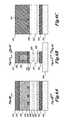
- FIGS. 5A-5Dillustrate formation of a patterned hard mask and a sacrificial gate structure, according to one embodiment.
- FIG. 5Ais a longitudinal cross-sectional view along a line cut through the center of the gate region of a partially formed GAA FET.
- FIG. 5Bis a transverse cross-sectional view along a line cut across and through the partially formed GAA FET.
- FIG. 5Cis a longitudinal cross-sectional view along a line cut through the sidewall spacer of the partially formed GAA FET.
- FIG. 5Dis a horizontal cross-sectional view along a line cut through the gate region of the partially formed GAA FET.
- FIGS. 6A-10Cshow views corresponding to those of FIGS. 5A-5C , at various times during formation of the GAA FET, according to one embodiment.
- references throughout the specification to conventional thin film deposition techniques for depositing silicon nitride, silicon dioxide, metals, or similar materialsinclude such processes as chemical vapor deposition (CVD), low-pressure chemical vapor deposition (LPCVD), metal organic chemical vapor deposition (MOCVD), plasma-enhanced chemical vapor deposition (PECVD), plasma vapor deposition (PVD), atomic layer deposition (ALD), molecular beam epitaxy (MBE), electroplating, electro-less plating, and the like.
- CVDchemical vapor deposition
- LPCVDlow-pressure chemical vapor deposition
- MOCVDmetal organic chemical vapor deposition
- PECVDplasma-enhanced chemical vapor deposition
- PVDplasma vapor deposition
- ALDatomic layer deposition
- MBEmolecular beam epitaxy
- electroplatingelectro-less plating, and the like.
- a description that references CVDmay alternatively be done using PVD, or a description that specifies electroplating may alternatively be accomplished using electro-less plating.
- reference to conventional techniques of thin film formationmay include growing a film in-situ.
- controlled growth of an oxide to a desired thicknesscan be achieved by exposing a silicon surface to oxygen gas or to moisture in a heated chamber.
- photoresistcan also be used to pattern a hard mask (e.g., a silicon nitride hard mask), which, in turn, can be used to pattern an underlying film.
- a hard maske.g., a silicon nitride hard mask
- etching techniquesknown in the art of semiconductor fabrication for selective removal of polysilicon, silicon nitride, silicon dioxide, metals, photoresist, polyimide, or similar materials includes such processes as wet chemical etching, reactive ion (plasma) etching (RIE), washing, wet cleaning, pre-cleaning, spray cleaning, chemical-mechanical planarization (CMP) and the like. Specific embodiments are described herein with reference to examples of such processes. However, the present disclosure and the reference to certain deposition techniques should not be limited to those described. In some instances, two such techniques may be interchangeable. For example, stripping photoresist may entail immersing a sample in a wet chemical bath or, alternatively, spraying wet chemicals directly onto the sample.
- RIEreactive ion
- CMPchemical-mechanical planarization
- FIGS. 1A and 1Bprovide general information about FinFETs, familiar to those skilled in the art of transistor design.
- FIG. 1Ashows a conventional planar transistor 130 built on a silicon substrate 132 .
- FIG. 1Aa non-FinFET device, is included herein for comparison with the FinFET shown in FIG. 1B .
- Parts of the conventional planar transistorinclude an active region 134 , a source 136 , a drain 138 , a planar conducting channel 140 , and a gate 142 .
- a gate dielectricnot shown, electrically isolates the channel from the gate, as is well known in the art.
- the active region 134occupies a top layer of the substrate that may be doped with impurities to create a well having a net negative or net positive charge.
- the conventional planar transistor 130When the conventional planar transistor 130 is on, current flows from the source 136 to the drain 138 , through the planar conducting channel 140 . Current flow in the planar conducting channel is controlled by the gate 142 by application of a gate voltage. An electric field associated with the gate voltage has the effect of turning on the conventional planar transistor 130 if the gate voltage exceeds a certain threshold. If the applied gate voltage drops below the threshold voltage, the conventional planar transistor 130 shuts off and current ceases to flow from the source 136 to the drain 138 . Because the gate 142 can only influence the planar conducting channel 140 from one side (i.e., from the top of the planar conducting channel 140 ), charge leakage into the silicon substrate 132 tends to occur at the channel/substrate junction.
- FIG. 1Bshows a conventional FinFET device 150 built on the silicon substrate 132 .
- parts of the conventional FinFET device 150include an active region 134 , a source 152 , a drain 154 , a conducting fin channel 156 , and a wrap-around gate 158 .
- the active region 134 of the conventional FinFET device 150may be doped with impurities to create a well having a net negative or net positive charge.
- the switching characteristics, and therefore the overall speed, of the conventional FinFET device 150is also improved over those of the conventional planar transistor 130 .
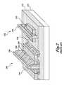
- FIG. 2shows an example of an existing nanowire gate-all-around (GAA) FET 160 , as described in U.S. Patent Application Publication No. 2013/0341596 to Chang et al., of IBM.
- the GAA FET 160is shown next to a slightly different perspective view of the conventional FinFET device 150 for direct comparison.
- the GAA FET 160includes a source region 162 , a drain region 164 , sidewall spacers 166 , and a wrap-around gate 168 .
- the GAA FET 160includes nanowires 165 . It is noted that portions of the nanowires 165 are fully surrounded by the sidewall spacers 166 , and by the wrap-around gate 168 .
- the central portions of the nanowires 165 that are surrounded by, and therefore controlled by, the wrap-around gate 168are silicon nanowire channels, analogous to the conducting fin channels 156 .
- the conducting fin channels 156provide about twice as much drive current as a silicon nanowire channel.
- one row of nanowires 165 as shown in FIG. 2is limited to low power applications.
- FIG. 3shows a high-level sequence of actions in an inventive method 170 of fabricating a multi-channel gate-all-around FET, according to one embodiment.
- a multi-channel GAA FinFET devicethat includes a 3D matrix of nanowires can be built on a silicon-on-insulator type (SOI) wafer for use in high performance, high power applications.
- SOIsilicon-on-insulator type
- the method 170begins with an SOI wafer that includes a layer of buried oxide (BOX) within a silicon substrate.
- BOXburied oxide
- a typical BOX layer of an SOI waferhas a thickness within the range of about 5-100 nm.
- the region of silicon located above the BOX layeris an electrically active region where GAA FETs will be formed.
- the thickness of the active regionis within the range of about 5-35 nm.
- SOI wafersare generally much more expensive than bulk silicon wafers.
- SOI waferscan be fabricated from bulk silicon wafers.
- a layered stack of silicon alternating with SiGe filmsis formed.
- a patterned hard maskis formed on top of the layered stack and a sacrificial gate structure is formed, including sacrificial sidewall spacers adjacent to a silicon gate.
- the hard mask outside the gate regionis removed and SiGe layers underneath the gate are recessed.
- doped source and drain regionsare formed adjacent to the layered stack underneath the gate.
- An inter-layer dielectric (ILD)is then formed on top of the doped source and drain regions.
- the sacrificial spacersare removed, and the layered stack outside the gate region is etched to form semiconducting fins.
- SiGeis removed from the fins to form a matrix of silicon channels, or nanowires.
- the silicon channelsare surrounded by a permanent gate structure.
- FIG. 4illustrates the initial process step 172 in which a layered stack of Si and SiGe are formed on a silicon substrate according to one embodiment.
- an SOI waferis obtained that includes a silicon substrate 183 , a BOX layer 184 in the substrate 183 , and an active layer 187 of silicon, in which GAA devices will be formed.
- a first layer of silicon germanium (SiGe) 185is initially formed on top of the active layer 187 , for example, by epitaxial growth or by another method of deposition known in the art.
- the first layer of SiGe 185is then oxidized so as to drive the SiGe downward through the active layer 187 , thus diffusing the SiGe atoms through the silicon lattice.
- a layered stack of SiGe layers alternating with silicon layerscan be formed on a silicon substrate instead of on an SOI substrate.
- FIGS. 5A-10Cillustrate further steps in the method 170 .
- Ais a cross-sectional schematic view along a cut line through the gate region of the GAA FinFET device
- Bis a cross-sectional view through the source, drain, and gate along a cut line aligned with one of the silicon nanowire channels
- Cis a cross-sectional view along a cut line through a source/drain region of the GAA FinFET device
- Dis a horizontal cross-sectional view along a cut line through the gate stack.
- arrows on each cut linerepresent the direction of an observer's eye looking at the corresponding cut plane.
- FIGS. 5A-5Dillustrate the process step 174 in which sacrificial structures are formed according to one embodiment.
- a thin oxideis deposited or grown on the top layer of silicon 190 .
- a hard mask 191is deposited and patterned.
- the hard mask 191can be made of, for example, an oxide such as alumina (Al 2 O 3 ) having a thickness in the range of about 20-40 nm.
- the hard mask 191will be used at a later time when etching the layered Si/SiGe stack to form elongated fins.
- a sacrificial gate stackis deposited.
- the sacrificial gate stackincludes a sacrificial gate 193 made of a 50-150 nm thick layer of amorphous silicon, followed by a 3-10 nm layer of a sacrificial high-k gate dielectric 195 such as, for example, halfnium oxide (HfO 2 ) as shown in FIG. 5A .
- the sacrificial gate stackis then patterned using a hard mask (not shown), for example, a layer of SiN having a thickness within the range of about 20-50 nm.
- Etching the sacrificial gate stack to form the structure shown in FIG. 5Bis straightforward, because the aspect ratio, or height-to-width ratio, of the gate is fairly small. For example, the aspect ratio shown in FIG.
- the SiN hard maskis removed.
- a sacrificial spacer layer 197 made of SiNis blanket deposited over the patterned gate stack to form a substantially planar SiN surface.
- the thickness of the sacrificial spacer layer 197 over the sacrificial gate stack as shown in FIG. 5Ais in the range of about 20-50 nm, whereas the thickness of the sacrificial spacer layer 197 as shown in FIG. 5C is in the range of about 70-200 nm.
- the sacrificial spacer layer 197is then patterned to form sidewalls on the sacrificial gate structure, as shown in FIG. 5B . Whereas the spacer layer is typically removed from the top of the gate, in the present process, the spacer remains in place covering the sacrificial gate.
- FIGS. 6A-6Cillustrate the process step 176 in which the layered stack of SiGe and silicon is patterned outside the sacrificial gate, according to one embodiment.
- the sacrificial spacer layer 197is used as a mask for etching through the hard mask 191 as shown in FIG. 6B .
- the sacrificial spacer layer 197again is used as a mask for etching through the layered stack of SiGe and silicon, down to the substrate 183 , in the source and drain regions.
- the etching chemistry used to remove the layered stackis hydrogen bromide (HBr), and the BOX layer 184 is etched using a fluorocarbon chemistry such as CF 4 .
- a lateral etchis then performed that preferentially attacks the SiGe layers 185 and 189 in the regions beneath the sacrificial spacer layer 197 , using an etch chemistry that has high selectivity to silicon, silicon, SiO 2 , and SiN.
- Such a processcan entail exposure of the SiGe to a dry, gas phase hydrochloric acid (HCL), or a wet SC1 clean, wherein SC1 is a mixture that includes ammonium hydroxide (NH 3 OH), HCL, and hydrogen peroxide (H 2 O 2 ), as is known to those skilled in the art.
- the lateral etchis timed to consume all of the SiGe outside the spacer, and to stop after about 6-15 nm of the SiGe underneath the spacer has been consumed.
- the resulting lateral undercut depthapproximately matches the spacer sidewall thickness 199 .
- FIGS. 7A-7Cillustrate the process step 178 in which source and drain regions of the GAA transistor are formed, according to one embodiment.
- the areas where the SiGe was removed underneath the spacersare filled with SiN, HfO 2 , or another suitable dielectric fill material 211 .
- the fill operationincludes a conformal deposition up to the level of the top layer of silicon 190 , followed by a highly anisotropic etch back step in which the dielectric fill material 211 outside the spacers is removed in the vertical direction, down to the level of the substrate 183 , without any significant lateral erosion.
- a source region 213 a and a drain region 213 bare then formed on either side of the gate stack.
- the source and drain formationincludes epitaxial growth of a semiconductor film during which dopants are introduced and incorporated into the film while it is being deposited.
- the in-situ doped filmcan be, for example, boron-doped SiGe.
- the in-situ doped filmcan be, for example, arsenic- or phosphorous-doped silicon or silicon carbide (SiC).
- an inter-layer dielectric (ILD) 215such as SiO 2 is deposited on top of each of the source and drain regions 213 a and 213 b , respectively.
- the ILD 215can be a ULK dielectric having a dielectric constant less than about 4.0.
- the ILDis then planarized using a chemical-mechanical planarization (CMP) process, as is well known in the art.
- CMPchemical-mechanical planarization
- FIGS. 8A-8Cillustrate the process step 179 in which the sacrificial spacer layer is replaced and fins are formed, according to one embodiment.
- the entire sacrificial spacer layer 197is removed from either side of the gate stack, as shown in FIGS. 8B and 8C .
- the spacer removal processentails a combination dry and wet etch step followed by a wet cleaning step, wherein the etch chemistries used are selective to the underlying hard mask 191 .
- fins 221are formed by etching the layered stack of silicon and SiN, as shown in FIG. 8C , using the hard mask 191 .
- the fins 221include the active layer 187 and the top layer of silicon 190 , separated by layers of the dielectric fill material 211 .
- the sacrificial gate dielectric 195acts as a mask to protect the sacrificial gate 193 .
- the sacrificial gate dielectric 195is then removed using, for example, a high temperature, isotropic chlorine-based reactive ion etch (RIE) process.
- RIEreactive ion etch
- Such a chemistrywill selectively consume HfO 2 without eroding the amorphous silicon sacrificial gate 193 .
- such an isotropic, chemically-dominated etch processwill selectively remove the thin layer of HfO 2 without incurring lateral erosion of the ILD 215 .
- a permanent low-k spacer 223replaces the sacrificial spacer layer 197 .
- the permanent low-k spacer 223can be made of a type of doped SiN such as, for example, a SiN that contains boron and carbon, e.g., SiBCN, or a SiN that contains oxygen and carbon, e.g., SiOCN.
- the permanent low-k spacer 223is etched back to the surface of the sacrificial gate 193 , which is below the height of the ILD 215 , as shown in FIG. 8B . This can be done by an RIE process or the like.
- FIGS. 9A-9Cillustrate the process step 180 in which a matrix of silicon channels is formed according to one embodiment.
- the channelscan be referred to as silicon nanowires.
- the ILD 215is etched back to the height of the permanent low-k spacer 223 using a standard CMP process.
- the sacrificial gate 193is selectively removed prior to forming the channel matrix.
- the sacrificial gate 193can be etched in a process that selectively attacks silicon while preserving the permanent low-k spacer 223 and the remaining hard mask 191 , which is to remain present in the final GAA device.
- Such a processcan employ, for example, a Cl 2 - and/or HBr-based chemistry.
- finsare formed inside the gate region by etching the layered stack of silicon and SiGe, as shown in FIG. 9B , using the hard mask 191 .
- the finsare an intermediate structure formed prior to forming an array of channels.
- the finsare not shown in FIG. 9A, 9B , or 9 C.
- the gate dielectric 195acts as a mask to protect the sacrificial gate 193 .
- the SiGe layers 185 and 189are then removed from the gate region as shown in FIGS. 9A and 9B , thus forming the channel matrix shown in FIGS. 9A, 9B, and 9C .
- the channel matrixincludes an upper array of conducting channels 235 and a lower array of conducting channels 237 that couple the charge reservoirs that make up the source region 213 a and the drain region 213 b .
- the channelsappear to be suspended, however, it is noted that the ends of the channels shown in FIG. 9C are well-supported by the source and drain regions and by the fins 221 outside the gate region.
- the channel length between the source and the drain regionsis less than about 20 nm. Removal of the SiGe layers 185 and 189 employs an isotropic etch that attacks silicon selectively, while leaving behind SiN and SiO 2 , as described above in steps 234 and 204 .
- the dielectric fill material 211 in the gate areaprotects the source and drain regions 213 a and 213 b , respectively, from being eroded.
- the silicon nanowires thus formedare designed to carry a drive current consistent with a linear current density in the range of about 0.5-3.0 mA/ ⁇ m.
- the linear current densityis normalized to be the current per effective channel width.
- FIGS. 10A-10Cillustrate the process step 181 in which fabrication of the GAA FET is completed by forming a permanent gate stack according to one embodiment.
- an optional hydrogen bakecan be performed in which exposed portions of the silicon channels within the gate region, shown in FIG. 9A as having a square cross section, are rounded. It may be advantageous for the silicon channel, or nanowire, to have a circular-cylindrical shape to prevent charging that would otherwise occur if the shape of the cross-section had corners or points, such as a rectangular cylinder. Corner rounding by use of a hydrogen bake is known in the art.
- a permanent gate stackis formed as the last step in the process.
- the current processforms barriers between the gate and the source/drain regions first, i.e., the hard mask 191 and the fill dielectric material 211 , and a replacement metal gate is formed last.
- exposed portions of the silicon channels within the gate regionare oxidized to form a replacement gate oxide 239 .
- the replacement gate oxide 239desirably has a high dielectric constant such as that of HfO 2 , for example.
- a replacement gate 241is deposited and planarized to the same height as the permanent low-k spacers 223 and the ILD 215 , in the usual way.
- the replacement gatethus fully surrounds each one of the silicon nanowires within the arrays of conducting channels 235 and 237 .
- the replacement gateis desirably made of a conductive gate material e.g., a metal.
- the replacement gate 241can be made of a semiconducting material such as, for example, polysilicon.
- the hard mask 191thus provides additional electrical insulation between the replacement gate 241 and the array of conducting channels 235 at the corners of the replacement gate 241 where the electric field tends to be strong because of the concentration of charge present at points and corner features. It is this additional barrier, as well as the dielectric fill material 211 , that prevents short circuits that otherwise would cause current leakage between the replacement gate 241 and the source and drain regions 213 a and 213 b.
- the process described hereinincludes only one photolithography mask layer, at the beginning of the process, to pattern the hard mask 191 . All other patterning in the process described herein is accomplished through the use of self-aligned structures that act as masks for adjacent materials. Some of the self-aligned structures are temporary structures that are removed and replaced by other materials in the final device configuration. By avoiding the use of lithography wherever possible, many conventional processing steps can be skipped. For example, none of the usual steps involving coating the wafer surface with a photoresist mask, developing the photoresist, or cleaning off the photoresist are needed. Consequently, many of the usual sources of particles and contamination are also eliminated.
Landscapes
- Engineering & Computer Science (AREA)
- Chemical & Material Sciences (AREA)
- Nanotechnology (AREA)
- Physics & Mathematics (AREA)
- Mathematical Physics (AREA)
- Theoretical Computer Science (AREA)
- Crystallography & Structural Chemistry (AREA)
- Thin Film Transistor (AREA)
- Insulated Gate Type Field-Effect Transistor (AREA)
Abstract
Description
Claims (18)
Priority Applications (2)
| Application Number | Priority Date | Filing Date | Title |
|---|---|---|---|
| US14/312,418US9502518B2 (en) | 2014-06-23 | 2014-06-23 | Multi-channel gate-all-around FET |
| US14/984,688US9748352B2 (en) | 2014-06-23 | 2015-12-30 | Multi-channel gate-all-around FET |
Applications Claiming Priority (1)
| Application Number | Priority Date | Filing Date | Title |
|---|---|---|---|
| US14/312,418US9502518B2 (en) | 2014-06-23 | 2014-06-23 | Multi-channel gate-all-around FET |
Related Child Applications (1)
| Application Number | Title | Priority Date | Filing Date |
|---|---|---|---|
| US14/984,688DivisionUS9748352B2 (en) | 2014-06-23 | 2015-12-30 | Multi-channel gate-all-around FET |
Publications (2)
| Publication Number | Publication Date |
|---|---|
| US20150372104A1 US20150372104A1 (en) | 2015-12-24 |
| US9502518B2true US9502518B2 (en) | 2016-11-22 |
Family
ID=54870409
Family Applications (2)
| Application Number | Title | Priority Date | Filing Date |
|---|---|---|---|
| US14/312,418ActiveUS9502518B2 (en) | 2014-06-23 | 2014-06-23 | Multi-channel gate-all-around FET |
| US14/984,688ActiveUS9748352B2 (en) | 2014-06-23 | 2015-12-30 | Multi-channel gate-all-around FET |
Family Applications After (1)
| Application Number | Title | Priority Date | Filing Date |
|---|---|---|---|
| US14/984,688ActiveUS9748352B2 (en) | 2014-06-23 | 2015-12-30 | Multi-channel gate-all-around FET |
Country Status (1)
| Country | Link |
|---|---|
| US (2) | US9502518B2 (en) |
Cited By (26)
| Publication number | Priority date | Publication date | Assignee | Title |
|---|---|---|---|---|
| US20150194489A1 (en)* | 2014-01-07 | 2015-07-09 | Commissariat A L'energie Atomique Et Aux Ene Alt | Nanowire semiconductor device partially surrounded by a grating |
| US20170263707A1 (en)* | 2015-10-20 | 2017-09-14 | Globalfoundries Inc. | Expitaxially regrown heterostructure nanowire lateral tunnel field effect transistor |
| US10170304B1 (en) | 2017-10-25 | 2019-01-01 | Globalfoundries Inc. | Self-aligned nanotube structures |
| US10249709B2 (en)* | 2017-02-02 | 2019-04-02 | International Business Machines Corporation | Stacked nanosheet field effect transistor device with substrate isolation |
| US10256351B2 (en) | 2015-06-15 | 2019-04-09 | Stmicroelectronics, Inc. | Semi-floating gate FET |
| US10347742B2 (en) | 2016-11-14 | 2019-07-09 | Tokyo Electron Limited | Method of forming gate spacer for nanowire FET device |
| US10424651B2 (en) | 2018-01-26 | 2019-09-24 | International Business Machines Corporation | Forming nanosheet transistor using sacrificial spacer and inner spacers |
| US10573521B2 (en) | 2018-01-30 | 2020-02-25 | International Business Machines Corporation | Gate metal patterning to avoid gate stack attack due to excessive wet etching |
| US10629752B1 (en) | 2018-10-11 | 2020-04-21 | Applied Materials, Inc. | Gate all-around device |
| US10714617B2 (en) | 2017-11-30 | 2020-07-14 | Samsung Electronics Co., Ltd. | Semiconductor device |
| US10748815B2 (en)* | 2018-10-26 | 2020-08-18 | Imec Vzw | Three-dimensional semiconductor device and method of manufacturing same |
| US10749030B2 (en) | 2017-12-08 | 2020-08-18 | Samsung Electronics Co., Ltd. | Semiconductor devices |
| WO2020174355A1 (en)* | 2019-02-27 | 2020-09-03 | International Business Machines Corporation | Transistor channel having vertically stacked nanosheets coupled by fin-shaped bridge regions |
| US10903077B2 (en)* | 2018-07-16 | 2021-01-26 | Tokyo Electron Limited | Methods to protect nitride layers during formation of silicon germanium nano-wires in microelectronic workpieces |
| US10903369B2 (en) | 2019-02-27 | 2021-01-26 | International Business Machines Corporation | Transistor channel having vertically stacked nanosheets coupled by fin-shaped bridge regions |
| US10957698B2 (en) | 2018-09-17 | 2021-03-23 | International Business Machines Corporation | Reduction of multi-threshold voltage patterning damage in nanosheet device structure |
| US20210233779A1 (en)* | 2020-01-23 | 2021-07-29 | Applied Materials, Inc. | 3D-NAND Memory Cell Structure |
| US11171133B2 (en) | 2019-12-20 | 2021-11-09 | Samsung Electronics Co., Ltd. | Semiconductor device |
| US11183562B2 (en) | 2019-06-11 | 2021-11-23 | Samsung Electronics Co., Ltd. | Semiconductor device |
| US11189635B2 (en) | 2019-04-01 | 2021-11-30 | Applied Materials, Inc. | 3D-NAND mold |
| US11233122B2 (en) | 2020-01-14 | 2022-01-25 | Samsung Electronics Co., Ltd. | Semiconductor devices |
| US11430513B1 (en) | 2021-08-02 | 2022-08-30 | International Business Machines Corporation | Non-volatile memory structure and method for low programming voltage for cross bar array |
| US11688778B2 (en) | 2020-01-15 | 2023-06-27 | Samsung Electronics Co., Ltd. | Semiconductor device including three-dimensional field-effect transistor with curved multi-layered source/drain pattern |
| US11705503B2 (en) | 2017-12-27 | 2023-07-18 | Samsung Electronics Co., Ltd. | Semiconductor device including non-sacrificial gate spacers and method of fabricating the same |
| US12310073B2 (en) | 2021-07-09 | 2025-05-20 | Taiwan Semiconductor Manufacturing Company, Ltd. | Transistors having two-dimensional semiconductor channels |
| US12396225B2 (en) | 2021-12-06 | 2025-08-19 | International Business Machines Corporation | Method to release nano sheet after nano sheet fin recess |
Families Citing this family (141)
| Publication number | Priority date | Publication date | Assignee | Title |
|---|---|---|---|---|
| US9132436B2 (en) | 2012-09-21 | 2015-09-15 | Applied Materials, Inc. | Chemical control features in wafer process equipment |
| US10256079B2 (en) | 2013-02-08 | 2019-04-09 | Applied Materials, Inc. | Semiconductor processing systems having multiple plasma configurations |
| US9431512B2 (en)* | 2014-06-18 | 2016-08-30 | Globalfoundries Inc. | Methods of forming nanowire devices with spacers and the resulting devices |
| US9490340B2 (en) | 2014-06-18 | 2016-11-08 | Globalfoundries Inc. | Methods of forming nanowire devices with doped extension regions and the resulting devices |
| US9608116B2 (en) | 2014-06-27 | 2017-03-28 | Taiwan Semiconductor Manufacturing Company, Ltd. | FINFETs with wrap-around silicide and method forming the same |
| US9881993B2 (en)* | 2014-06-27 | 2018-01-30 | Taiwan Semiconductor Manufacturing Company Limited | Method of forming semiconductor structure with horizontal gate all around structure |
| US9966240B2 (en) | 2014-10-14 | 2018-05-08 | Applied Materials, Inc. | Systems and methods for internal surface conditioning assessment in plasma processing equipment |
| US11637002B2 (en) | 2014-11-26 | 2023-04-25 | Applied Materials, Inc. | Methods and systems to enhance process uniformity |
| US20160225652A1 (en) | 2015-02-03 | 2016-08-04 | Applied Materials, Inc. | Low temperature chuck for plasma processing systems |
| CN106158637B (en)* | 2015-03-31 | 2019-04-26 | 中芯国际集成电路制造(上海)有限公司 | Fin field effect transistor and method of forming the same |
| US9385195B1 (en) | 2015-03-31 | 2016-07-05 | Stmicroelectronics, Inc. | Vertical gate-all-around TFET |
| US9627277B2 (en)* | 2015-06-09 | 2017-04-18 | International Business Machines Corporation | Method and structure for enabling controlled spacer RIE |
| US9997463B2 (en) | 2015-07-01 | 2018-06-12 | Stmicroelectronics, Inc. | Modular interconnects for gate-all-around transistors |
| US9741593B2 (en) | 2015-08-06 | 2017-08-22 | Applied Materials, Inc. | Thermal management systems and methods for wafer processing systems |
| US10504700B2 (en) | 2015-08-27 | 2019-12-10 | Applied Materials, Inc. | Plasma etching systems and methods with secondary plasma injection |
| US9608099B1 (en)* | 2015-09-22 | 2017-03-28 | International Business Machines Corporation | Nanowire semiconductor device |
| US9853163B2 (en) | 2015-09-30 | 2017-12-26 | Stmicroelectronics, Inc. | Gate all around vacuum channel transistor |
| US9899387B2 (en)* | 2015-11-16 | 2018-02-20 | Taiwan Semiconductor Manufacturing Company, Ltd. | Multi-gate device and method of fabrication thereof |
| US10217817B2 (en)* | 2016-01-27 | 2019-02-26 | International Business Machines Corporation | Sacrificial layer for channel surface retention and inner spacer formation in stacked-channel FETs |
| US10157748B2 (en) | 2016-02-08 | 2018-12-18 | Taiwan Semiconductor Manufacturing Co., Ltd. | Fin profile improvement for high performance transistor |
| US10090205B2 (en)* | 2016-02-08 | 2018-10-02 | Taiwan Semiconductor Manufacturing Co., Ltd. | Fin profile improvement for high performance transistor |
| US9773886B1 (en)* | 2016-03-15 | 2017-09-26 | Samsung Electronics Co., Ltd. | Nanosheet and nanowire devices having doped internal spacers and methods of manufacturing the same |
| US10439039B2 (en)* | 2016-03-25 | 2019-10-08 | Qualcomm Incorporated | Integrated circuits including a FinFET and a nanostructure FET |
| TWI686351B (en) | 2016-04-01 | 2020-03-01 | 聯華電子股份有限公司 | Nanowire transistor and method for fabricating the same |
| CN116110941A (en)* | 2016-04-25 | 2023-05-12 | 应用材料公司 | Forming horizontal surrounding gate element nanowire air gap spacing |
| US10068984B2 (en)* | 2016-04-27 | 2018-09-04 | Taiwan Semiconductor Manufacturing Company, Ltd. | Method of manufacturing high-k dielectric using HfO/Ti/Hfo layers |
| US9953874B2 (en)* | 2016-04-28 | 2018-04-24 | Taiwan Semiconductor Manufacturing Company, Ltd. | FinFETs and methods of forming FinFETs |
| US10177199B2 (en) | 2016-05-03 | 2019-01-08 | Tsinghua University | Method for making three dimensional complementary metal oxide semiconductor carbon nanotube thin film transistor circuit |
| US9966416B2 (en)* | 2016-05-03 | 2018-05-08 | Tsinghua Univeristy | Three dimensional complementary metal oxide semiconductor carbon nanotube thin film transistor circuit |
| US10304936B2 (en) | 2016-05-04 | 2019-05-28 | International Business Machines Corporation | Protection of high-K dielectric during reliability anneal on nanosheet structures |
| US10504754B2 (en) | 2016-05-19 | 2019-12-10 | Applied Materials, Inc. | Systems and methods for improved semiconductor etching and component protection |
| US11004985B2 (en) | 2016-05-30 | 2021-05-11 | Samsung Electronics Co., Ltd. | Semiconductor device having multi-thickness nanowire |
| KR20170135115A (en) | 2016-05-30 | 2017-12-08 | 삼성전자주식회사 | Semiconductor device and method for fabricating the same |
| KR102506426B1 (en)* | 2016-06-07 | 2023-03-08 | 삼성전자주식회사 | Semiconductor device |
| KR102465536B1 (en) | 2016-06-08 | 2022-11-14 | 삼성전자주식회사 | Method of manufacturing semiconductor devices |
| US9865484B1 (en) | 2016-06-29 | 2018-01-09 | Applied Materials, Inc. | Selective etch using material modification and RF pulsing |
| US10134905B2 (en) | 2016-06-30 | 2018-11-20 | International Business Machines Corporation | Semiconductor device including wrap around contact, and method of forming the semiconductor device |
| TWI739879B (en)* | 2016-08-10 | 2021-09-21 | 日商東京威力科創股份有限公司 | Extension region for a semiconductor device |
| US9831324B1 (en)* | 2016-08-12 | 2017-11-28 | International Business Machines Corporation | Self-aligned inner-spacer replacement process using implantation |
| US11088033B2 (en)* | 2016-09-08 | 2021-08-10 | International Business Machines Corporation | Low resistance source-drain contacts using high temperature silicides |
| US9653289B1 (en)* | 2016-09-19 | 2017-05-16 | International Business Machines Corporation | Fabrication of nano-sheet transistors with different threshold voltages |
| US9704995B1 (en)* | 2016-09-20 | 2017-07-11 | Advanced Micro Devices, Inc. | Gate all around device architecture with local oxide |
| KR102551589B1 (en) | 2016-09-29 | 2023-07-04 | 삼성전자주식회사 | Semiconductor device and method for fabricating the same |
| US10546729B2 (en) | 2016-10-04 | 2020-01-28 | Applied Materials, Inc. | Dual-channel showerhead with improved profile |
| US10340340B2 (en)* | 2016-10-20 | 2019-07-02 | International Business Machines Corporation | Multiple-threshold nanosheet transistors |
| KR102574454B1 (en) | 2016-12-16 | 2023-09-04 | 삼성전자 주식회사 | Semiconductor devices and method of manufacturing the same |
| EP3340308B1 (en)* | 2016-12-22 | 2022-09-07 | IMEC vzw | Method for forming transistors on a substrate |
| US11245020B2 (en) | 2017-01-04 | 2022-02-08 | International Business Machines Corporation | Gate-all-around field effect transistor having multiple threshold voltages |
| US10128347B2 (en)* | 2017-01-04 | 2018-11-13 | International Business Machines Corporation | Gate-all-around field effect transistor having multiple threshold voltages |
| US9935014B1 (en)* | 2017-01-12 | 2018-04-03 | International Business Machines Corporation | Nanosheet transistors having different gate dielectric thicknesses on the same chip |
| US10170584B2 (en) | 2017-01-27 | 2019-01-01 | International Business Machines Corporation | Nanosheet field effect transistors with partial inside spacers |
| US10068794B2 (en) | 2017-01-31 | 2018-09-04 | Advanced Micro Devices, Inc. | Gate all around device architecture with hybrid wafer bond technique |
| US10431429B2 (en) | 2017-02-03 | 2019-10-01 | Applied Materials, Inc. | Systems and methods for radial and azimuthal control of plasma uniformity |
| KR102285641B1 (en) | 2017-03-10 | 2021-08-03 | 삼성전자주식회사 | Semiconductor device and method for fabricating the same |
| US10943834B2 (en) | 2017-03-13 | 2021-03-09 | Applied Materials, Inc. | Replacement contact process |
| KR102400558B1 (en)* | 2017-04-05 | 2022-05-20 | 삼성전자주식회사 | semiconductor device |
| US10297663B2 (en) | 2017-04-19 | 2019-05-21 | International Business Machines Corporation | Gate fill utilizing replacement spacer |
| TWI758464B (en)* | 2017-04-20 | 2022-03-21 | 美商微材料有限責任公司 | Selective formation of silicon-containing spacer |
| US10756174B2 (en) | 2017-04-26 | 2020-08-25 | Taiwan Semiconductor Manufacturing Co., Ltd. | Multiple-stacked semiconductor nanowires and source/drain spacers |
| US10304728B2 (en) | 2017-05-01 | 2019-05-28 | Advanced Micro Devices, Inc. | Double spacer immersion lithography triple patterning flow and method |
| US10186510B2 (en) | 2017-05-01 | 2019-01-22 | Advanced Micro Devices, Inc. | Vertical gate all around library architecture |
| US10008583B1 (en)* | 2017-05-08 | 2018-06-26 | Samsung Electronics Co., Ltd. | Gate-all-around nanosheet field-effect transistors and methods of manufacturing the same |
| US11276590B2 (en) | 2017-05-17 | 2022-03-15 | Applied Materials, Inc. | Multi-zone semiconductor substrate supports |
| US11276559B2 (en) | 2017-05-17 | 2022-03-15 | Applied Materials, Inc. | Semiconductor processing chamber for multiple precursor flow |
| JP7176860B6 (en) | 2017-05-17 | 2022-12-16 | アプライド マテリアルズ インコーポレイテッド | Semiconductor processing chamber to improve precursor flow |
| US10453750B2 (en)* | 2017-06-22 | 2019-10-22 | Globalfoundries Inc. | Stacked elongated nanoshapes of different semiconductor materials and structures that incorporate the nanoshapes |
| US10211307B2 (en) | 2017-07-18 | 2019-02-19 | Taiwan Semiconductor Manufacturing Co., Ltd. | Methods of manufacturing inner spacers in a gate-all-around (GAA) FET through multi-layer spacer replacement |
| US10297458B2 (en) | 2017-08-07 | 2019-05-21 | Applied Materials, Inc. | Process window widening using coated parts in plasma etch processes |
| CN109390400A (en)* | 2017-08-08 | 2019-02-26 | 中芯国际集成电路制造(上海)有限公司 | Ring grid field effect transistor and forming method thereof |
| KR102388463B1 (en) | 2017-08-21 | 2022-04-20 | 삼성전자주식회사 | Semiconductor device including channel pattern and manufacturing method thereof |
| CN109427779B (en)* | 2017-08-22 | 2021-07-13 | 中芯国际集成电路制造(上海)有限公司 | Semiconductor structure and method of forming the same |
| EP3676873A4 (en)* | 2017-08-29 | 2021-05-26 | Micron Technology, Inc. | DEVICES AND SYSTEMS INCLUDING STRING DRIVERS WITH HIGH GAP MATERIAL AND METHODS OF FORMING |
| KR102385567B1 (en) | 2017-08-29 | 2022-04-12 | 삼성전자주식회사 | Semiconductor devices and method of manufacturing semiconductor devices |
| US10699956B2 (en) | 2017-08-30 | 2020-06-30 | Taiwan Semiconductor Manufacturing Co., Ltd. | Method of manufacturing a semiconductor device and a semiconductor device |
| US10403550B2 (en)* | 2017-08-30 | 2019-09-03 | Taiwan Semiconductor Manufacturing Co., Ltd. | Method of manufacturing a semiconductor device and a semiconductor device |
| CN111052395A (en) | 2017-08-31 | 2020-04-21 | 美光科技公司 | Semiconductor device, transistor and related method for contacting metal oxide semiconductor device |
| EP3676878A4 (en) | 2017-08-31 | 2020-11-04 | Micron Technology, Inc. | SEMICONDUCTOR COMPONENTS, HYBRID TRANSISTORS AND RELATED PROCESSES |
| KR102353931B1 (en)* | 2017-09-13 | 2022-01-21 | 삼성전자주식회사 | Semiconductor device and method for manufacturing the same |
| KR102353251B1 (en) | 2017-09-28 | 2022-01-19 | 삼성전자주식회사 | Semiconductor devices and methods of manufacturing the same |
| KR102465537B1 (en) | 2017-10-18 | 2022-11-11 | 삼성전자주식회사 | Semiconductor devices |
| US10170484B1 (en)* | 2017-10-18 | 2019-01-01 | Globalfoundries Inc. | Integrated circuit structure incorporating multiple gate-all-around field effect transistors having different drive currents and method |
| US10818777B2 (en)* | 2017-10-30 | 2020-10-27 | Taiwan Semiconductor Manufacturing Co., Ltd. | Method of manufacturing a semiconductor device and a semiconductor device |
| US10714592B2 (en) | 2017-10-30 | 2020-07-14 | Taiwan Semiconductor Manufacturing Co., Ltd. | Method of manufacturing a semiconductor device and a semiconductor device |
| US10192819B1 (en) | 2017-11-16 | 2019-01-29 | Globalfoundries Inc. | Integrated circuit structure incorporating stacked field effect transistors |
| US10090193B1 (en) | 2017-11-16 | 2018-10-02 | Globalfoundries Inc. | Integrated circuit structure incorporating a stacked pair of field effect transistors and a buried interconnect and method |
| US10304832B1 (en) | 2017-11-16 | 2019-05-28 | Globalfoundries Inc. | Integrated circuit structure incorporating stacked field effect transistors and method |
| US10566330B2 (en)* | 2017-12-11 | 2020-02-18 | Samsung Electronics Co., Ltd. | Dielectric separation of partial GAA FETs |
| US10903054B2 (en) | 2017-12-19 | 2021-01-26 | Applied Materials, Inc. | Multi-zone gas distribution systems and methods |
| US11328909B2 (en) | 2017-12-22 | 2022-05-10 | Applied Materials, Inc. | Chamber conditioning and removal processes |
| US10854426B2 (en) | 2018-01-08 | 2020-12-01 | Applied Materials, Inc. | Metal recess for semiconductor structures |
| US10192867B1 (en) | 2018-02-05 | 2019-01-29 | Globalfoundries Inc. | Complementary FETs with wrap around contacts and method of forming same |
| US10964512B2 (en) | 2018-02-15 | 2021-03-30 | Applied Materials, Inc. | Semiconductor processing chamber multistage mixing apparatus and methods |
| US12086520B2 (en) | 2018-02-16 | 2024-09-10 | Coventor, Inc. | System and method for multi-material mesh generation from fill-fraction voxel data |
| US10319600B1 (en) | 2018-03-12 | 2019-06-11 | Applied Materials, Inc. | Thermal silicon etch |
| US10734525B2 (en)* | 2018-03-14 | 2020-08-04 | Globalfoundries Inc. | Gate-all-around transistor with spacer support and methods of forming same |
| US10886137B2 (en) | 2018-04-30 | 2021-01-05 | Applied Materials, Inc. | Selective nitride removal |
| US11139402B2 (en) | 2018-05-14 | 2021-10-05 | Synopsys, Inc. | Crystal orientation engineering to achieve consistent nanowire shapes |
| US10388755B1 (en)* | 2018-06-04 | 2019-08-20 | International Business Machines Corporation | Stacked nanosheets with self-aligned inner spacers and metallic source/drain |
| US10861750B2 (en) | 2018-07-02 | 2020-12-08 | Taiwan Semiconductor Manufacturing Co., Ltd. | Method of manufacturing a semiconductor device and a semiconductor device |
| US10872778B2 (en) | 2018-07-06 | 2020-12-22 | Applied Materials, Inc. | Systems and methods utilizing solid-phase etchants |
| US10755941B2 (en) | 2018-07-06 | 2020-08-25 | Applied Materials, Inc. | Self-limiting selective etching systems and methods |
| US10714392B2 (en)* | 2018-07-18 | 2020-07-14 | International Business Machines Corporation | Optimizing junctions of gate all around structures with channel pull back |
| KR102473659B1 (en) | 2018-08-08 | 2022-12-02 | 삼성전자주식회사 | Semiconductor devices |
| US11367783B2 (en) | 2018-08-17 | 2022-06-21 | Taiwan Semiconductor Manufacturing Co., Ltd. | Method of manufacturing a semiconductor device |
| US11049755B2 (en) | 2018-09-14 | 2021-06-29 | Applied Materials, Inc. | Semiconductor substrate supports with embedded RF shield |
| US10892198B2 (en) | 2018-09-14 | 2021-01-12 | Applied Materials, Inc. | Systems and methods for improved performance in semiconductor processing |
| US11062887B2 (en) | 2018-09-17 | 2021-07-13 | Applied Materials, Inc. | High temperature RF heater pedestals |
| US11417534B2 (en) | 2018-09-21 | 2022-08-16 | Applied Materials, Inc. | Selective material removal |
| US10910375B2 (en)* | 2018-09-28 | 2021-02-02 | Taiwan Semiconductor Manufacturing Co., Ltd. | Semiconductor device and method of fabrication thereof |
| US10756096B2 (en) | 2018-10-05 | 2020-08-25 | Globalfoundries Inc. | Integrated circuit structure with complementary field effect transistor and buried metal interconnect and method |
| US11682560B2 (en) | 2018-10-11 | 2023-06-20 | Applied Materials, Inc. | Systems and methods for hafnium-containing film removal |
| US11121002B2 (en) | 2018-10-24 | 2021-09-14 | Applied Materials, Inc. | Systems and methods for etching metals and metal derivatives |
| US11437242B2 (en) | 2018-11-27 | 2022-09-06 | Applied Materials, Inc. | Selective removal of silicon-containing materials |
| DE102019115490B4 (en) | 2018-11-30 | 2022-10-20 | Taiwan Semiconductor Manufacturing Co. Ltd. | SEMICONDUCTOR DEVICE AND METHOD OF PRODUCTION THEREOF |
| US11387362B2 (en)* | 2018-11-30 | 2022-07-12 | Taiwan Semiconductor Manufacturing Co., Ltd. | Semiconductor device and manufacturing method thereof |
| US11721527B2 (en) | 2019-01-07 | 2023-08-08 | Applied Materials, Inc. | Processing chamber mixing systems |
| US10920319B2 (en) | 2019-01-11 | 2021-02-16 | Applied Materials, Inc. | Ceramic showerheads with conductive electrodes |
| US11264458B2 (en) | 2019-05-20 | 2022-03-01 | Synopsys, Inc. | Crystal orientation engineering to achieve consistent nanowire shapes |
| KR102822351B1 (en) | 2019-05-27 | 2025-06-18 | 삼성전자주식회사 | Integrated circuits and method of manufacturing the same |
| KR102836171B1 (en) | 2019-05-27 | 2025-07-18 | 삼성전자주식회사 | Semiconductor devices and methods of manufacturing the same |
| US11037832B2 (en)* | 2019-05-29 | 2021-06-15 | International Business Machines Corporation | Threshold voltage adjustment by inner spacer material selection |
| KR102789288B1 (en) | 2019-06-17 | 2025-04-01 | 삼성전자주식회사 | Integrated circuits and method of manufacturing the same |
| US11158738B2 (en) | 2019-06-18 | 2021-10-26 | Samsung Electronics Co., Ltd | Method of forming isolation dielectrics for stacked field effect transistors (FETs) |
| KR102720155B1 (en) | 2019-09-17 | 2024-10-21 | 삼성전자주식회사 | Integrated circuit device and method of manufacturing the same |
| US11145765B2 (en)* | 2019-09-26 | 2021-10-12 | Taiwan Semiconductor Manufacturing Co., Ltd. | Gate-all-around structure with self substrate isolation and methods of forming the same |
| US11264327B2 (en)* | 2019-10-30 | 2022-03-01 | Taiwan Semiconductor Manufacturing Co., Ltd. | Backside power rail structure and methods of forming same |
| CN112784522A (en)* | 2019-11-07 | 2021-05-11 | 科文托尔公司 | System and method for performing reflow modeling in a virtual manufacturing environment |
| EP3882978A1 (en) | 2020-03-16 | 2021-09-22 | Samsung Electronics Co., Ltd. | Vertical type transistor, inverter including the same, and vertical type semiconductor device including the same |
| US11961763B2 (en) | 2020-07-13 | 2024-04-16 | Taiwan Semiconductor Manufacturing Co., Ltd. | Self-aligned metal gate for multigate device and method of forming thereof |
| KR20220072941A (en) | 2020-11-25 | 2022-06-03 | 삼성전자주식회사 | Semiconductor device |
| KR20220077737A (en) | 2020-12-02 | 2022-06-09 | 삼성전자주식회사 | Integrated circuit device |
| US11424367B2 (en) | 2020-12-16 | 2022-08-23 | International Business Machines Corporation | Wrap-around contacts including localized metal silicide |
| US12040375B2 (en) | 2021-03-18 | 2024-07-16 | Taiwan Semiconductor Manufacturing Company, Ltd. | Multi-silicide structure for a semiconductor device and a method for manufacturing the same |
| US20220416042A1 (en)* | 2021-06-25 | 2022-12-29 | Intel Corporation | Gate-all-around integrated circuit structures having gate height reduction by fin hard mask removal post dummy gate patterning removal |
| US12249643B2 (en) | 2021-09-23 | 2025-03-11 | International Business Machines Corporation | Stacked planar field effect transistors with 2D material channels |
| US12136656B2 (en) | 2021-09-27 | 2024-11-05 | International Business Machines Corporation | Semiconductor structure having two-dimensional channel |
| US11862640B2 (en) | 2021-09-29 | 2024-01-02 | Advanced Micro Devices, Inc. | Cross field effect transistor (XFET) library architecture power routing |
| US12308370B2 (en) | 2021-09-29 | 2025-05-20 | Advanced Micro Devices, Inc. | Cross field effect transistors (XFETs) in integrated circuits |
| US12382662B2 (en) | 2021-11-30 | 2025-08-05 | International Business Machines Corporation | Wrap-around-contact for 2D-channel gate-all-around field-effect-transistors |
| US11935930B2 (en) | 2021-11-30 | 2024-03-19 | International Business Machines Corporation | Wrap-around-contact for 2D-channel gate-all-around field-effect-transistors |
| CN114927422B (en)* | 2022-04-01 | 2024-10-01 | 中国科学院微电子研究所 | Semiconductor device manufacturing method |
Citations (25)
| Publication number | Priority date | Publication date | Assignee | Title |
|---|---|---|---|---|
| US20060049429A1 (en)* | 2004-09-07 | 2006-03-09 | Sungmin Kim | Field effect transistor (FET) having wire channels and method of fabricating the same |
| US20060216897A1 (en)* | 2005-03-24 | 2006-09-28 | Samsung Electronics Co., Ltd. | Semiconductor device having a round-shaped nano-wire transistor channel and method of manufacturing same |
| US20070029586A1 (en)* | 2005-08-08 | 2007-02-08 | Freescale Semiconductor, Inc. | Multi-channel transistor structure and method of making thereof |
| US20080014689A1 (en)* | 2006-07-07 | 2008-01-17 | Texas Instruments Incorporated | Method for making planar nanowire surround gate mosfet |
| US20080017934A1 (en)* | 2006-05-18 | 2008-01-24 | Samsung Electronic Co., Ltd. | Wire-type semiconductor devices and methods of fabricating the same |
| US20080135949A1 (en)* | 2006-12-08 | 2008-06-12 | Agency For Science, Technology And Research | Stacked silicon-germanium nanowire structure and method of forming the same |
| US7427794B2 (en) | 2002-08-23 | 2008-09-23 | Intel Corporation | Tri-gate devices and methods of fabrication |
| US7456476B2 (en) | 2003-06-27 | 2008-11-25 | Intel Corporation | Nonplanar semiconductor device with partially or fully wrapped around gate electrode and methods of fabrication |
| US20090090976A1 (en) | 2005-09-28 | 2009-04-09 | Intel Corporation | Process for integrating planar and non-planar cmos transistors on a bulk substrate and article made thereby |
| US20100207208A1 (en)* | 2009-02-17 | 2010-08-19 | International Business Machines Corporation | Nanowire mesh device and method of fabricating same |
| US20110057163A1 (en)* | 2008-06-09 | 2011-03-10 | National Institute Of Advanced Industrial Science And Technology | Nano-wire field effect transistor, method for manufacturing the transistor, and integrated circuit including the transistor |
| US20110108804A1 (en)* | 2009-02-04 | 2011-05-12 | International Business Machines Corporation | Maskless Process for Suspending and Thinning Nanowires |
| US20110133162A1 (en)* | 2009-12-04 | 2011-06-09 | International Business Machines Corporation | Gate-All-Around Nanowire Field Effect Transistors |
| US7973389B2 (en) | 2007-07-18 | 2011-07-05 | Intel Corporation | Isolated tri-gate transistor fabricated on bulk substrate |
| US20110309333A1 (en)* | 2010-06-21 | 2011-12-22 | International Business Machines Corporation | Semiconductor devices fabricated by doped material layer as dopant source |
| US20120007051A1 (en)* | 2010-07-06 | 2012-01-12 | International Business Machines Corporation | Process for Forming a Surrounding Gate for a Nanowire Using a Sacrificial Patternable Dielectric |
| US8120073B2 (en) | 2008-12-31 | 2012-02-21 | Intel Corporation | Trigate transistor having extended metal gate electrode |
| US8541274B1 (en)* | 2012-09-11 | 2013-09-24 | Globalfoundries Inc. | Methods of forming 3-D semiconductor devices with a nanowire gate structure wherein the nanowire gate structure is formed after source/drain formation |
| US20130270512A1 (en)* | 2011-12-19 | 2013-10-17 | Marko Radosavljevic | Cmos implementation of germanium and iii-v nanowires and nanoribbons in gate-all-around architecture |
| US20130302955A1 (en)* | 2012-04-16 | 2013-11-14 | Commissariat A L'energie Atomique Et Aux Ene Alt | Method for producing a transistor structure with superimposed nanowires and with a surrounding gate |
| US20130341596A1 (en)* | 2012-06-21 | 2013-12-26 | International Business Machines Corporation | Nanowire fet and finfet |
| US8679902B1 (en)* | 2012-09-27 | 2014-03-25 | International Business Machines Corporation | Stacked nanowire field effect transistor |
| US8728885B1 (en)* | 2012-12-27 | 2014-05-20 | Globalfoundries Inc. | Methods of forming a three-dimensional semiconductor device with a nanowire channel structure |
| US8778768B1 (en)* | 2013-03-12 | 2014-07-15 | International Business Machines Corporation | Non-replacement gate nanomesh field effect transistor with epitixially grown source and drain |
| US20140264276A1 (en)* | 2013-03-12 | 2014-09-18 | International Business Machines Corporation | Non-replacement gate nanomesh field effect transistor with pad regions |
Family Cites Families (2)
| Publication number | Priority date | Publication date | Assignee | Title |
|---|---|---|---|---|
| US8753942B2 (en)* | 2010-12-01 | 2014-06-17 | Intel Corporation | Silicon and silicon germanium nanowire structures |
| US9257527B2 (en)* | 2014-02-14 | 2016-02-09 | International Business Machines Corporation | Nanowire transistor structures with merged source/drain regions using auxiliary pillars |
- 2014
- 2014-06-23USUS14/312,418patent/US9502518B2/enactiveActive
- 2015
- 2015-12-30USUS14/984,688patent/US9748352B2/enactiveActive
Patent Citations (25)
| Publication number | Priority date | Publication date | Assignee | Title |
|---|---|---|---|---|
| US7427794B2 (en) | 2002-08-23 | 2008-09-23 | Intel Corporation | Tri-gate devices and methods of fabrication |
| US7456476B2 (en) | 2003-06-27 | 2008-11-25 | Intel Corporation | Nonplanar semiconductor device with partially or fully wrapped around gate electrode and methods of fabrication |
| US20060049429A1 (en)* | 2004-09-07 | 2006-03-09 | Sungmin Kim | Field effect transistor (FET) having wire channels and method of fabricating the same |
| US20060216897A1 (en)* | 2005-03-24 | 2006-09-28 | Samsung Electronics Co., Ltd. | Semiconductor device having a round-shaped nano-wire transistor channel and method of manufacturing same |
| US20070029586A1 (en)* | 2005-08-08 | 2007-02-08 | Freescale Semiconductor, Inc. | Multi-channel transistor structure and method of making thereof |
| US20090090976A1 (en) | 2005-09-28 | 2009-04-09 | Intel Corporation | Process for integrating planar and non-planar cmos transistors on a bulk substrate and article made thereby |
| US20080017934A1 (en)* | 2006-05-18 | 2008-01-24 | Samsung Electronic Co., Ltd. | Wire-type semiconductor devices and methods of fabricating the same |
| US20080014689A1 (en)* | 2006-07-07 | 2008-01-17 | Texas Instruments Incorporated | Method for making planar nanowire surround gate mosfet |
| US20080135949A1 (en)* | 2006-12-08 | 2008-06-12 | Agency For Science, Technology And Research | Stacked silicon-germanium nanowire structure and method of forming the same |
| US7973389B2 (en) | 2007-07-18 | 2011-07-05 | Intel Corporation | Isolated tri-gate transistor fabricated on bulk substrate |
| US20110057163A1 (en)* | 2008-06-09 | 2011-03-10 | National Institute Of Advanced Industrial Science And Technology | Nano-wire field effect transistor, method for manufacturing the transistor, and integrated circuit including the transistor |
| US8120073B2 (en) | 2008-12-31 | 2012-02-21 | Intel Corporation | Trigate transistor having extended metal gate electrode |
| US20110108804A1 (en)* | 2009-02-04 | 2011-05-12 | International Business Machines Corporation | Maskless Process for Suspending and Thinning Nanowires |
| US20100207208A1 (en)* | 2009-02-17 | 2010-08-19 | International Business Machines Corporation | Nanowire mesh device and method of fabricating same |
| US20110133162A1 (en)* | 2009-12-04 | 2011-06-09 | International Business Machines Corporation | Gate-All-Around Nanowire Field Effect Transistors |
| US20110309333A1 (en)* | 2010-06-21 | 2011-12-22 | International Business Machines Corporation | Semiconductor devices fabricated by doped material layer as dopant source |
| US20120007051A1 (en)* | 2010-07-06 | 2012-01-12 | International Business Machines Corporation | Process for Forming a Surrounding Gate for a Nanowire Using a Sacrificial Patternable Dielectric |
| US20130270512A1 (en)* | 2011-12-19 | 2013-10-17 | Marko Radosavljevic | Cmos implementation of germanium and iii-v nanowires and nanoribbons in gate-all-around architecture |
| US20130302955A1 (en)* | 2012-04-16 | 2013-11-14 | Commissariat A L'energie Atomique Et Aux Ene Alt | Method for producing a transistor structure with superimposed nanowires and with a surrounding gate |
| US20130341596A1 (en)* | 2012-06-21 | 2013-12-26 | International Business Machines Corporation | Nanowire fet and finfet |
| US8541274B1 (en)* | 2012-09-11 | 2013-09-24 | Globalfoundries Inc. | Methods of forming 3-D semiconductor devices with a nanowire gate structure wherein the nanowire gate structure is formed after source/drain formation |
| US8679902B1 (en)* | 2012-09-27 | 2014-03-25 | International Business Machines Corporation | Stacked nanowire field effect transistor |
| US8728885B1 (en)* | 2012-12-27 | 2014-05-20 | Globalfoundries Inc. | Methods of forming a three-dimensional semiconductor device with a nanowire channel structure |
| US8778768B1 (en)* | 2013-03-12 | 2014-07-15 | International Business Machines Corporation | Non-replacement gate nanomesh field effect transistor with epitixially grown source and drain |
| US20140264276A1 (en)* | 2013-03-12 | 2014-09-18 | International Business Machines Corporation | Non-replacement gate nanomesh field effect transistor with pad regions |
Non-Patent Citations (2)
| Title |
|---|
| "How Intel's 3D tech redefines the transistor (FAQ)", http://www.cnet.com/news/how-intels-3d-tech-redefines-the-transistor-faq/, May 4, 2011, 4 pages. |
| Singh. et al., "Ultra-Narrow Silicon Nanowire Gate-All-Around CMOS Devices: Impact of Diameter, Channel-Orientation and Low Temperature on Device Performance," Electron Devices Meeting, 2006. IEDM '06. International, Issue Date: Dec. 11-13, 2006.* |
Cited By (46)
| Publication number | Priority date | Publication date | Assignee | Title |
|---|---|---|---|---|
| US20150194489A1 (en)* | 2014-01-07 | 2015-07-09 | Commissariat A L'energie Atomique Et Aux Ene Alt | Nanowire semiconductor device partially surrounded by a grating |
| US9728405B2 (en)* | 2014-01-07 | 2017-08-08 | Commissariat à l'énergie atomique et aux énergies alternatives | Nanowire semiconductor device partially surrounded by a gate |
| US10741698B2 (en) | 2015-06-15 | 2020-08-11 | Stmicroelectronics, Inc. | Semi-floating gate FET |
| US10256351B2 (en) | 2015-06-15 | 2019-04-09 | Stmicroelectronics, Inc. | Semi-floating gate FET |
| US9960233B2 (en)* | 2015-10-20 | 2018-05-01 | Globalfoundries Inc. | Expitaxially regrown heterostructure nanowire lateral tunnel field effect transistor |
| US20170263707A1 (en)* | 2015-10-20 | 2017-09-14 | Globalfoundries Inc. | Expitaxially regrown heterostructure nanowire lateral tunnel field effect transistor |
| US10347742B2 (en) | 2016-11-14 | 2019-07-09 | Tokyo Electron Limited | Method of forming gate spacer for nanowire FET device |
| US10916637B2 (en) | 2016-11-14 | 2021-02-09 | Tokyo Electron Limited | Method of forming gate spacer for nanowire FET device |
| US10249709B2 (en)* | 2017-02-02 | 2019-04-02 | International Business Machines Corporation | Stacked nanosheet field effect transistor device with substrate isolation |
| US10170304B1 (en) | 2017-10-25 | 2019-01-01 | Globalfoundries Inc. | Self-aligned nanotube structures |
| US10916658B2 (en) | 2017-11-30 | 2021-02-09 | Samsung Electronics Co., Ltd. | Semiconductor device |
| US12300751B2 (en) | 2017-11-30 | 2025-05-13 | Samsung Electronics Co., Ltd. | Semiconductor device |
| US10714617B2 (en) | 2017-11-30 | 2020-07-14 | Samsung Electronics Co., Ltd. | Semiconductor device |
| US11637205B2 (en) | 2017-11-30 | 2023-04-25 | Samsung Electronics Co., Ltd. | Semiconductor device |
| US11211495B2 (en) | 2017-12-08 | 2021-12-28 | Samsung Electronics Co., Ltd. | Semiconductor devices |
| US12382653B2 (en) | 2017-12-08 | 2025-08-05 | Samsung Electronics Co., Ltd. | Semiconductor devices |
| US11784256B2 (en) | 2017-12-08 | 2023-10-10 | Samsung Electronics Co., Ltd. | Semiconductor devices |
| US10749030B2 (en) | 2017-12-08 | 2020-08-18 | Samsung Electronics Co., Ltd. | Semiconductor devices |
| US11705503B2 (en) | 2017-12-27 | 2023-07-18 | Samsung Electronics Co., Ltd. | Semiconductor device including non-sacrificial gate spacers and method of fabricating the same |
| US10424651B2 (en) | 2018-01-26 | 2019-09-24 | International Business Machines Corporation | Forming nanosheet transistor using sacrificial spacer and inner spacers |
| US10573521B2 (en) | 2018-01-30 | 2020-02-25 | International Business Machines Corporation | Gate metal patterning to avoid gate stack attack due to excessive wet etching |
| US11276576B2 (en)* | 2018-01-30 | 2022-03-15 | International Business Machines Corporation | Gate metal patterning to avoid gate stack attack due to excessive wet etching |
| US10903077B2 (en)* | 2018-07-16 | 2021-01-26 | Tokyo Electron Limited | Methods to protect nitride layers during formation of silicon germanium nano-wires in microelectronic workpieces |
| US10957698B2 (en) | 2018-09-17 | 2021-03-23 | International Business Machines Corporation | Reduction of multi-threshold voltage patterning damage in nanosheet device structure |
| US11024746B2 (en) | 2018-10-11 | 2021-06-01 | Applied Materrials, Inc. | Gate all-around device |
| US10629752B1 (en) | 2018-10-11 | 2020-04-21 | Applied Materials, Inc. | Gate all-around device |
| US10748815B2 (en)* | 2018-10-26 | 2020-08-18 | Imec Vzw | Three-dimensional semiconductor device and method of manufacturing same |
| US10957799B2 (en) | 2019-02-27 | 2021-03-23 | International Business Machines Corporation | Transistor channel having vertically stacked nanosheets coupled by fin-shaped bridge regions |
| GB2595125B (en)* | 2019-02-27 | 2022-11-09 | Ibm | Transistor channel having vertically stacked nanosheets coupled by fin-shaped bridge regions |
| WO2020174355A1 (en)* | 2019-02-27 | 2020-09-03 | International Business Machines Corporation | Transistor channel having vertically stacked nanosheets coupled by fin-shaped bridge regions |
| GB2595125A (en)* | 2019-02-27 | 2021-11-17 | Ibm | Transistor channel having vertically stacked nanosheets coupled by fin-shaped bridge regions |
| US10903369B2 (en) | 2019-02-27 | 2021-01-26 | International Business Machines Corporation | Transistor channel having vertically stacked nanosheets coupled by fin-shaped bridge regions |
| US11189635B2 (en) | 2019-04-01 | 2021-11-30 | Applied Materials, Inc. | 3D-NAND mold |
| US11183562B2 (en) | 2019-06-11 | 2021-11-23 | Samsung Electronics Co., Ltd. | Semiconductor device |
| US11862682B2 (en) | 2019-06-11 | 2024-01-02 | Samsung Electronics Co., Ltd. | Semiconductor device |
| US11171133B2 (en) | 2019-12-20 | 2021-11-09 | Samsung Electronics Co., Ltd. | Semiconductor device |
| US11699703B2 (en) | 2019-12-20 | 2023-07-11 | Samsung Electronics Co., Ltd. | Semiconductor device |
| US11233122B2 (en) | 2020-01-14 | 2022-01-25 | Samsung Electronics Co., Ltd. | Semiconductor devices |
| US11695041B2 (en) | 2020-01-14 | 2023-07-04 | Samsung Electronics Co., Ltd. | Method of manufacturing a semiconductor device |
| US11688778B2 (en) | 2020-01-15 | 2023-06-27 | Samsung Electronics Co., Ltd. | Semiconductor device including three-dimensional field-effect transistor with curved multi-layered source/drain pattern |
| US12027596B2 (en) | 2020-01-15 | 2024-07-02 | Samsung Electronics Co., Ltd. | Semiconductor device with source/drain pattern including buffer layer |
| US11587796B2 (en)* | 2020-01-23 | 2023-02-21 | Applied Materials, Inc. | 3D-NAND memory cell structure |
| US20210233779A1 (en)* | 2020-01-23 | 2021-07-29 | Applied Materials, Inc. | 3D-NAND Memory Cell Structure |
| US12310073B2 (en) | 2021-07-09 | 2025-05-20 | Taiwan Semiconductor Manufacturing Company, Ltd. | Transistors having two-dimensional semiconductor channels |
| US11430513B1 (en) | 2021-08-02 | 2022-08-30 | International Business Machines Corporation | Non-volatile memory structure and method for low programming voltage for cross bar array |
| US12396225B2 (en) | 2021-12-06 | 2025-08-19 | International Business Machines Corporation | Method to release nano sheet after nano sheet fin recess |
Also Published As
| Publication number | Publication date |
|---|---|
| US20160111513A1 (en) | 2016-04-21 |
| US20150372104A1 (en) | 2015-12-24 |
| US9748352B2 (en) | 2017-08-29 |
Similar Documents
| Publication | Publication Date | Title |
|---|---|---|
| US9502518B2 (en) | Multi-channel gate-all-around FET | |
| US10170546B2 (en) | Fully substrate-isolated FinFET transistor | |
| US10163684B2 (en) | Fabrication of silicon germanium-on-insulator FinFET | |
| US10256341B2 (en) | Self-aligned silicon germanium FinFET with relaxed channel region | |
| US9484348B2 (en) | Structure and method to increase contact area in unmerged EPI integration for CMOS FinFETs | |
| US10886386B2 (en) | Dual width FinFET | |
| KR101612646B1 (en) | Non-planar transistors and methods of fabrication thereof | |
| US10319647B2 (en) | Semiconductor structure with overlapping fins having different directions, and methods of fabricating the same | |
| US9953976B2 (en) | Effective device formation for advanced technology nodes with aggressive fin-pitch scaling |
Legal Events
| Date | Code | Title | Description |
|---|---|---|---|
| AS | Assignment | Owner name:INTERNATIONAL BUSINESS MACHINES CORPORATION, NEW Y Free format text:ASSIGNMENT OF ASSIGNORS INTEREST;ASSIGNOR:YEH, CHUN-CHEN;REEL/FRAME:033161/0023 Effective date:20140617 Owner name:STMICROELECTRONICS, INC., TEXAS Free format text:ASSIGNMENT OF ASSIGNORS INTEREST;ASSIGNOR:LIU, QING;REEL/FRAME:033161/0053 Effective date:20140617 Owner name:GLOBALFOUNDRIES INC., CAYMAN ISLANDS Free format text:ASSIGNMENT OF ASSIGNORS INTEREST;ASSIGNORS:XIE, RUILONG;CAI, XIUYU;SIGNING DATES FROM 20140617 TO 20140623;REEL/FRAME:033161/0030 | |
| STCF | Information on status: patent grant | Free format text:PATENTED CASE | |
| AS | Assignment | Owner name:WILMINGTON TRUST, NATIONAL ASSOCIATION, DELAWARE Free format text:SECURITY AGREEMENT;ASSIGNOR:GLOBALFOUNDRIES INC.;REEL/FRAME:049490/0001 Effective date:20181127 | |
| MAFP | Maintenance fee payment | Free format text:PAYMENT OF MAINTENANCE FEE, 4TH YEAR, LARGE ENTITY (ORIGINAL EVENT CODE: M1551); ENTITY STATUS OF PATENT OWNER: LARGE ENTITY Year of fee payment:4 | |
| AS | Assignment | Owner name:GLOBALFOUNDRIES INC., CAYMAN ISLANDS Free format text:RELEASE BY SECURED PARTY;ASSIGNOR:WILMINGTON TRUST, NATIONAL ASSOCIATION;REEL/FRAME:054479/0842 Effective date:20200410 Owner name:TAIWAN SEMICONDUCTOR MANUFACTURING CO., LTD., TAIWAN Free format text:ASSIGNMENT OF ASSIGNORS INTEREST;ASSIGNOR:GLOBALFOUNDRIES INC.;REEL/FRAME:054482/0862 Effective date:20200515 | |
| AS | Assignment | Owner name:GLOBALFOUNDRIES INC., CAYMAN ISLANDS Free format text:RELEASE BY SECURED PARTY;ASSIGNOR:WILMINGTON TRUST, NATIONAL ASSOCIATION;REEL/FRAME:054636/0001 Effective date:20201117 | |
| MAFP | Maintenance fee payment | Free format text:PAYMENT OF MAINTENANCE FEE, 8TH YEAR, LARGE ENTITY (ORIGINAL EVENT CODE: M1552); ENTITY STATUS OF PATENT OWNER: LARGE ENTITY Year of fee payment:8 |