US9502516B2 - Recessed access devices and gate electrodes - Google Patents
Recessed access devices and gate electrodesDownload PDFInfo
- Publication number
- US9502516B2 US9502516B2US14/247,968US201414247968AUS9502516B2US 9502516 B2US9502516 B2US 9502516B2US 201414247968 AUS201414247968 AUS 201414247968AUS 9502516 B2US9502516 B2US 9502516B2
- Authority
- US
- United States
- Prior art keywords
- gate
- gate material
- access device
- rad
- structures
- Prior art date
- Legal status (The legal status is an assumption and is not a legal conclusion. Google has not performed a legal analysis and makes no representation as to the accuracy of the status listed.)
- Active
Links
- 239000000463materialSubstances0.000claimsabstractdescription300
- 239000004065semiconductorSubstances0.000claimsabstractdescription105
- 239000000758substrateSubstances0.000claimsdescription79
- 239000012212insulatorSubstances0.000claimsdescription68
- 229910021420polycrystalline siliconInorganic materials0.000claimsdescription37
- 229920005591polysiliconPolymers0.000claimsdescription36
- VYPSYNLAJGMNEJ-UHFFFAOYSA-NSilicium dioxideChemical compoundO=[Si]=OVYPSYNLAJGMNEJ-UHFFFAOYSA-N0.000claimsdescription18
- 239000003990capacitorSubstances0.000claimsdescription15
- 239000000377silicon dioxideSubstances0.000claimsdescription9
- 229910052581Si3N4Inorganic materials0.000claimsdescription7
- 235000012239silicon dioxideNutrition0.000claimsdescription7
- HQVNEWCFYHHQES-UHFFFAOYSA-Nsilicon nitrideChemical compoundN12[Si]34N5[Si]62N3[Si]51N64HQVNEWCFYHHQES-UHFFFAOYSA-N0.000claimsdescription7
- 239000003989dielectric materialSubstances0.000claims7
- 238000002955isolationMethods0.000claims1
- 230000006870functionEffects0.000abstractdescription49
- 238000000034methodMethods0.000description49
- 238000004519manufacturing processMethods0.000description33
- 125000006850spacer groupChemical group0.000description32
- 230000015572biosynthetic processEffects0.000description27
- 238000005755formation reactionMethods0.000description27
- 229910052751metalInorganic materials0.000description20
- 239000002184metalSubstances0.000description20
- 230000004888barrier functionEffects0.000description16
- 238000005530etchingMethods0.000description16
- 230000000873masking effectEffects0.000description14
- XUIMIQQOPSSXEZ-UHFFFAOYSA-NSiliconChemical compound[Si]XUIMIQQOPSSXEZ-UHFFFAOYSA-N0.000description12
- 229910052710siliconInorganic materials0.000description12
- 239000010703siliconSubstances0.000description12
- 230000007423decreaseEffects0.000description11
- 239000010405anode materialSubstances0.000description10
- 239000002019doping agentSubstances0.000description10
- 239000010406cathode materialSubstances0.000description9
- 229910001092metal group alloyInorganic materials0.000description9
- 239000004020conductorSubstances0.000description7
- 230000003247decreasing effectEffects0.000description7
- 238000005137deposition processMethods0.000description6
- CMIQNFUKBYANIP-UHFFFAOYSA-Nruthenium tantalumChemical compound[Ru].[Ta]CMIQNFUKBYANIP-UHFFFAOYSA-N0.000description6
- 239000011810insulating materialSubstances0.000description5
- 150000004767nitridesChemical class0.000description5
- 229910052594sapphireInorganic materials0.000description5
- 239000010980sapphireSubstances0.000description5
- 230000005684electric fieldEffects0.000description4
- 150000002739metalsChemical class0.000description4
- 239000002210silicon-based materialSubstances0.000description4
- MZLGASXMSKOWSE-UHFFFAOYSA-Ntantalum nitrideChemical compound[Ta]#NMZLGASXMSKOWSE-UHFFFAOYSA-N0.000description4
- 238000009792diffusion processMethods0.000description3
- 239000000126substanceSubstances0.000description3
- 235000012431wafersNutrition0.000description3
- 238000009825accumulationMethods0.000description2
- 230000015556catabolic processEffects0.000description2
- 238000007796conventional methodMethods0.000description2
- 230000009977dual effectEffects0.000description2
- RYGMFSIKBFXOCR-UHFFFAOYSA-NCopperChemical compound[Cu]RYGMFSIKBFXOCR-UHFFFAOYSA-N0.000description1
- RTAQQCXQSZGOHL-UHFFFAOYSA-NTitaniumChemical compound[Ti]RTAQQCXQSZGOHL-UHFFFAOYSA-N0.000description1
- 229910052782aluminiumInorganic materials0.000description1
- XAGFODPZIPBFFR-UHFFFAOYSA-NaluminiumChemical compound[Al]XAGFODPZIPBFFR-UHFFFAOYSA-N0.000description1
- 229910052802copperInorganic materials0.000description1
- 239000010949copperSubstances0.000description1
- 230000007547defectEffects0.000description1
- 230000008021depositionEffects0.000description1
- 230000000694effectsEffects0.000description1
- 238000010438heat treatmentMethods0.000description1
- 238000010348incorporationMethods0.000description1
- 229910021332silicideInorganic materials0.000description1
- FVBUAEGBCNSCDD-UHFFFAOYSA-Nsilicide(4-)Chemical compound[Si-4]FVBUAEGBCNSCDD-UHFFFAOYSA-N0.000description1
- 239000010936titaniumSubstances0.000description1
- 229910052719titaniumInorganic materials0.000description1
- WFKWXMTUELFFGS-UHFFFAOYSA-NtungstenChemical compound[W]WFKWXMTUELFFGS-UHFFFAOYSA-N0.000description1
- 229910052721tungstenInorganic materials0.000description1
- 239000010937tungstenSubstances0.000description1
Images


Classifications
- H01L29/4236—
- H—ELECTRICITY
- H10—SEMICONDUCTOR DEVICES; ELECTRIC SOLID-STATE DEVICES NOT OTHERWISE PROVIDED FOR
- H10D—INORGANIC ELECTRIC SEMICONDUCTOR DEVICES
- H10D64/00—Electrodes of devices having potential barriers
- H10D64/20—Electrodes characterised by their shapes, relative sizes or dispositions
- H10D64/27—Electrodes not carrying the current to be rectified, amplified, oscillated or switched, e.g. gates
- H10D64/311—Gate electrodes for field-effect devices
- H10D64/411—Gate electrodes for field-effect devices for FETs
- H10D64/511—Gate electrodes for field-effect devices for FETs for IGFETs
- H10D64/512—Disposition of the gate electrodes, e.g. buried gates
- H10D64/513—Disposition of the gate electrodes, e.g. buried gates within recesses in the substrate, e.g. trench gates, groove gates or buried gates
- H01L21/823425—
- H01L21/82345—
- H01L29/407—
- H01L29/66621—
- H01L29/7831—
- H—ELECTRICITY
- H10—SEMICONDUCTOR DEVICES; ELECTRIC SOLID-STATE DEVICES NOT OTHERWISE PROVIDED FOR
- H10D—INORGANIC ELECTRIC SEMICONDUCTOR DEVICES
- H10D30/00—Field-effect transistors [FET]
- H10D30/60—Insulated-gate field-effect transistors [IGFET]
- H10D30/611—Insulated-gate field-effect transistors [IGFET] having multiple independently-addressable gate electrodes influencing the same channel
- H—ELECTRICITY
- H10—SEMICONDUCTOR DEVICES; ELECTRIC SOLID-STATE DEVICES NOT OTHERWISE PROVIDED FOR
- H10D—INORGANIC ELECTRIC SEMICONDUCTOR DEVICES
- H10D64/00—Electrodes of devices having potential barriers
- H10D64/01—Manufacture or treatment
- H10D64/025—Manufacture or treatment forming recessed gates, e.g. by using local oxidation
- H10D64/027—Manufacture or treatment forming recessed gates, e.g. by using local oxidation by etching at gate locations
- H—ELECTRICITY
- H10—SEMICONDUCTOR DEVICES; ELECTRIC SOLID-STATE DEVICES NOT OTHERWISE PROVIDED FOR
- H10D—INORGANIC ELECTRIC SEMICONDUCTOR DEVICES
- H10D64/00—Electrodes of devices having potential barriers
- H10D64/111—Field plates
- H10D64/117—Recessed field plates, e.g. trench field plates or buried field plates
- H—ELECTRICITY
- H10—SEMICONDUCTOR DEVICES; ELECTRIC SOLID-STATE DEVICES NOT OTHERWISE PROVIDED FOR
- H10D—INORGANIC ELECTRIC SEMICONDUCTOR DEVICES
- H10D84/00—Integrated devices formed in or on semiconductor substrates that comprise only semiconducting layers, e.g. on Si wafers or on GaAs-on-Si wafers
- H10D84/01—Manufacture or treatment
- H10D84/0123—Integrating together multiple components covered by H10D12/00 or H10D30/00, e.g. integrating multiple IGBTs
- H10D84/0126—Integrating together multiple components covered by H10D12/00 or H10D30/00, e.g. integrating multiple IGBTs the components including insulated gates, e.g. IGFETs
- H10D84/013—Manufacturing their source or drain regions, e.g. silicided source or drain regions
- H10D84/0133—Manufacturing common source or drain regions between multiple IGFETs
- H—ELECTRICITY
- H10—SEMICONDUCTOR DEVICES; ELECTRIC SOLID-STATE DEVICES NOT OTHERWISE PROVIDED FOR
- H10D—INORGANIC ELECTRIC SEMICONDUCTOR DEVICES
- H10D84/00—Integrated devices formed in or on semiconductor substrates that comprise only semiconducting layers, e.g. on Si wafers or on GaAs-on-Si wafers
- H10D84/01—Manufacture or treatment
- H10D84/0123—Integrating together multiple components covered by H10D12/00 or H10D30/00, e.g. integrating multiple IGBTs
- H10D84/0126—Integrating together multiple components covered by H10D12/00 or H10D30/00, e.g. integrating multiple IGBTs the components including insulated gates, e.g. IGFETs
- H10D84/0135—Manufacturing their gate conductors
- H10D84/014—Manufacturing their gate conductors the gate conductors having different materials or different implants
- H—ELECTRICITY
- H10—SEMICONDUCTOR DEVICES; ELECTRIC SOLID-STATE DEVICES NOT OTHERWISE PROVIDED FOR
- H10D—INORGANIC ELECTRIC SEMICONDUCTOR DEVICES
- H10D84/00—Integrated devices formed in or on semiconductor substrates that comprise only semiconducting layers, e.g. on Si wafers or on GaAs-on-Si wafers
- H10D84/01—Manufacture or treatment
- H10D84/02—Manufacture or treatment characterised by using material-based technologies
- H10D84/03—Manufacture or treatment characterised by using material-based technologies using Group IV technology, e.g. silicon technology or silicon-carbide [SiC] technology
- H10D84/038—Manufacture or treatment characterised by using material-based technologies using Group IV technology, e.g. silicon technology or silicon-carbide [SiC] technology using silicon technology, e.g. SiGe
Definitions
- the inventionrelates to MOSFET devices and, in particular, to recessed access devices for semiconductor devices and methods of making the same.
- the access devicesmay include semiconductor structures such as transistor devices, and can be in the form of planar or recessed access device structures.
- the gate electrode of an access deviceis biased, by an access device driver circuit, providing “on” and “off” states for the access device and facilitating the access and storage of data in the memory circuit utilizing the access devices.
- the device driver circuitprovides “on” and “off” states for the access device and facilitating the access and storage of data in the memory circuit utilizing the access devices.
- FIG. 1illustrates a conventional planar access device (PAD) or transistor device, used with semiconductor memory circuits.
- a gate stack 60is formed over a semiconductor substrate 50 .
- the gate stack 60includes a gate-oxide layer 62 , a gate electrode 64 , an insulator cap 66 , and sidewall spacers 68 .
- Source and drain regions 54are located on either side of the gate stack 60 forming the transistor device.
- FIG. 2illustrates a conventional recessed access device (RAD) used with semiconductor memory circuits.
- the RAD structureincludes a gate stack 70 formed in trenches of a semiconductor substrate 50 .
- the gate stack 70includes a gate-oxide layer 72 , a gate electrode 74 , an insulator cap 76 , and sidewall spacers 78 .
- Source and drain regions 54are located on either side of the gate stack 70 forming the RAD device.
- the PAD and RAD structures illustrated in FIGS. 1 and 2may be used as access devices for memory circuits.
- fabrication processesare developed to accommodate the shrinking dimensions.
- subthreshold leakagea leakage path in the transistor
- GIDLgate induced drain leakage
- junction leakagea leakage type occurs when the access device is in accumulation, or the “off” state.
- Subthreshold leakageis the leakage of charge between the source and drain of the access device and increases with smaller transistor dimensions, specifically the effective length of the gate in an access device.
- One way of reducing the subthreshold leakageis to apply a more negative voltage to the gate electrode of the access device in the “off” state. For example, in an “off” state, a negative voltage is applied to the PAD gate electrode 64 or the RAD gate electrode 74 , illustrated in FIGS. 1 and 2 , respectively. However, the application of a more negative voltage to the gate electrode results in higher GIDL current in the access device.
- Another way of reducing the subthreshold leakageis to apply a more negative voltage to the substrate 50 . However, the application of a more negative voltage to the substrate results in increased junction leakage.
- Subthreshold leakagemay also be decreased by employing a high work function difference between the source and drain regions and a gate electrode, for example, by employing a P+ gate and an N+ source/drain region.
- GIDL currentincreases in such cases.
- the RAD gate stack 70increases the effective length of a gate in an access device compared to the PAD gate stack 60 .
- the increased length of the gatetends to decrease the amount of subthreshold leakage in the access device.
- the GIDL current from the RAD gate stack 70is greater than the GIDL current of PAD gate stack 60 . It is believed that the increased amount of GIDL loss in the RAD gate stack 70 is the result of the increased overlap of the source/drain regions 54 with the gate electrode 74 .
- an access devicefor use with memory devices and other semiconductor devices that may be able to reduce subthreshold leakage, junction leakage, and gate induced drain leakage simultaneously. It is also desirable to develop processes for fabricating such devices using conventional semiconductor fabrication processes.
- FIG. 1illustrates a cross-sectional view of a conventional planar access device such as a memory access device
- FIG. 2illustrates a cross-sectional view of a conventional recessed access device such as a memory access device
- FIG. 3illustrates a cross-sectional view of a planar access device according to embodiments of the invention
- FIGS. 4A-4Eillustrate cross-sectional views of various process steps in the fabrication of the planar access device illustrated in FIG. 3 according to embodiments of the invention
- FIG. 5illustrates a cross-sectional view of a recessed access device structure according to embodiments of the invention
- FIGS. 6A-6Eillustrate cross-sectional views of various process steps in the fabrication of the recessed access device structure illustrated in FIG. 5 according to embodiments of the invention
- FIG. 7Aillustrates a cross-sectional view of a recessed access device structure according to embodiments of the invention
- FIGS. 7B-7Dillustrate cross-sectional views of various process steps in the fabrication of the recessed access device structure illustrated in FIG. 7A according to embodiments of the invention
- FIG. 7Eillustrates a cross-sectional view of a spherical recessed access device structure according to embodiments of the invention.
- FIG. 8illustrates a cross-sectional view of a planar access device according to embodiments of the invention.
- FIGS. 9A-9Dillustrate cross-sectional views of various process steps in the fabrication of the planar access device illustrated in FIG. 8 according to embodiments of the invention.
- FIG. 10illustrates a cross-sectional view of a recessed access device structure according to embodiments of the invention.
- FIGS. 11A-11Dillustrate cross-sectional views of various process steps in the fabrication of the recessed access device illustrated in FIG. 10 according to embodiments of the invention
- FIG. 12illustrates an access device driver according to embodiments of the invention which may be used to supply voltages to a planar or recessed access device
- FIG. 13illustrates an access device driver according to embodiments of the invention which may be used to supply voltages to a planar or recessed access device
- FIG. 14illustrates a cross-sectional view of a planar access device according to embodiments of the invention.
- FIGS. 15A-15Dillustrate cross-sectional views of various process steps in the fabrication of the planar access device illustrated in FIG. 14 according to embodiments of the invention
- FIG. 16illustrates a cross-sectional view of a recessed access device according to embodiments of the invention.
- FIGS. 17A-17Dillustrate cross-sectional views of various process steps in the fabrication of the recessed access device of FIG. 16 according to embodiments of the invention.
- Embodiments of the inventionrelate to planar and recessed access transistor devices used in semiconductor devices. More particularly, embodiments of the invention relate to planar and recessed access devices that may be used with CMOS semiconductor devices or memory devices such as DRAM memory devices. However, the embodiments of the invention are not limited to such devices as the planar and recessed access devices of the invention may be used with any semiconductor device.
- a planar or recessed access devicemay include a gate electrode having two or more gate materials wherein each of the gate materials has a different work function than the other gate materials of the gate electrode.
- the presence of the two or more work functions in the gate electrodemay help to reduce the amount of gate induced drain leakage that occurs in the gate stack or recessed access device. Furthermore, the reduction of the gate induced drain leakage may be accomplished without sacrificing additional losses due to subthreshold leakage or junction leakage, which is controlled by the difference and margin bias provided by the different work function materials in the gate electrode.
- a planar or recessed access devicemay include a gate electrode having two or more electrically isolated regions.
- the electrically isolated regions of the gate electrodemay be supplied by different voltage supplies such that different voltages may be supplied to and across the length of a gate electrode. Further, the same voltage may be supplied to each of the electrically isolated regions.
- the planar and recessed access devicesmay be turned into an “on” state or an “off” state depending upon the voltages supplied by the different voltage supplies.
- the electrically isolated regionsallow different margin biases to be supplied to different portions of the gate electrode, which in turn may be used to control gate induced drain leakage in the planar or recessed access device.
- the voltages supplied to the electrically isolated regions during the “on” state and “off” statemay be altered to control the subthreshold leakage and junction leakage of the planar or recessed access device. In this manner, the gate induced drain leakage may be controlled or reduced without sacrificing losses to subthreshold leakage and junction leakage.
- a planar or recessed access devicemay include a gate electrode having a cathode region and an anode region, wherein the cathode and anode form a diode in the gate electrode.
- Each of the cathode and anodemay be connected to separate voltage supplies such that different or similar voltages may be supplied to and across the length of the gate electrode.
- the voltages supplied to the anode and cathodemay be tailored such that when the gate stack or recessed access device is in an “off” state the gate induced drain leakage is minimized.
- the margin bias provided across the diodemay also be used to minimize the subthreshold leakage and junction leakage.
- an access device drivermay supply two or more voltages to a planar or recessed access device.
- Access device driversmay be able to provide dissimilar or similar voltages to a planar or recessed access device having two or more electrically isolated regions in a gate electrode or to a gate electrode comprising a diode.
- the control of voltages to the planar or recessed access device by the access device drivermay facilitate the control of the gate induced drain leakage, subthreshold leakage, and junction leakage of a planar or recessed access device.
- an access device of a memory cellincludes one or more gates in a memory or semiconductor device that are capable of reducing an amount of gate-induced drain leakage (GIDL) in the access device.
- An access devicemay include a gate electrode or gate diode capable of accepting two voltages simultaneously.
- the access devicemay include gate electrodes comprising two or more materials having different work functions.
- gate-induced drain leakagemay be reduced by forming an access device or transistor gate stack from materials having differing work functions.
- an access device or gate stackmay be formed from two or more materials having dissimilar work functions.
- a material having a higher work functionmay be used to form those portions of the gate stack where sub-threshold leakage is problematic while a material having a lower work function may be used to form those portions of the gate stack where gate-induced drain leakage is a concern.
- a gate stack having two or more gate materialsmay be formed such that a gate material closest to a storage capacitor has a lower work function than the gate material closest to the bitline of a memory device.
- the dissimilar work function materialsmay be separated by a barrier layer and strapped together by a metal or conductive strap.
- the barrier layermay comprise a conductive material and may serve as a conductive strap.
- embodiments of the present inventionmay employ one or more materials in the gate stack of an access device to decrease or control GIDL.
- access devices according to embodiments of the inventionmay be used in semiconductor devices as planar access devices or transistors incorporated with memory devices.
- Embodiments of the inventionare especially useful in memory devices such as in dynamic random access memory (DRAM) devices but are not limited to such use.
- DRAMdynamic random access memory
- the access device 100may include one or more gate stacks 120 formed over a semiconductor substrate 110 .
- Gate stacks 120may include an oxide layer 121 and a gate electrode over the oxide layer.
- the gate electrodemay include a first gate material 122 having a first work function associated therewith and a second gate material 124 having a second work function associated therewith. As illustrated in FIG. 3 , the gate materials may be separated by a separator 123 .
- One or more straps 126may overlie the first gate material 122 and second gate material 124 .
- the straps 126may provide an electrical connection between the first and second gate materials.
- a gate stack 120may also include an insulator cap 130 and sidewall spacers 128 as known and used with conventional planar access devices.
- the gate stacks 120may overlie source and drain regions 112 in the semiconductor substrate 110 .
- the semiconductor substrate 110may include semiconductor substrates conventionally used with or for the fabrication of memory devices, access devices, and other semiconductor devices.
- the semiconductor substrate 110may include a silicon-containing structure such as silicon, silicon-on-insulator structures, and silicon-on-sapphire structures.
- Oxide layer 121may include any oxide material that may be used to form oxide layers 121 capable of being used with conventional gate stacks devices and particularly with gate stacks or other transistor devices integrated with memory devices or semiconductor devices.
- the gate electrodes of embodiments of the inventionmay include multiple gate materials.
- a gate electrodemay include a first gate material 122 and a second gate material 124 .
- the first gate material 122 and the second gate material 124have differing work functions.
- Use of gate materials having differing work functions to form the gate electrodesmay reduce the effects of gate induced drain leakage (GIDL) in the access device 100 .
- the first gate material 122 of the gate stack 120 illustrated in FIG. 3may include an N+ doped polysilicon material and the second gate material 124 may include a P+ doped polysilicon material.
- the N+ doping of the first gate material 122provides the first gate material 122 with a lower work function than the P+ doped material of the second gate material 124 .
- the P+ second gate material 124maintains a high threshold voltage V t for the access device 100 , thereby reducing the subthreshold leakage while the N+ first gate material 122 decreases the GIDL in the access device 100 .
- a gate electrodemay include gate materials having differing work functions in a horizontal cross-section of the gate electrode as illustrated in FIG. 3 as well as differing work functions in a vertical cross-section of the gate electrode.
- the first gate materialmay include a varying work function across a vertical cross-section from the oxide layer 121 to the insulator cap 130 .
- the second gate material 124may include a varying work function across a vertical cross-section from the oxide layer 121 to the insulator cap 130 .
- a separator 123may be positioned between the first gate material 122 and the second gate material 124 and may include insulating materials, conductive materials, metals, or other materials capable of separating the gate materials.
- separator 123may be formed of a nitride, an oxide, a silicide, a conductive metal, or a metallic alloy.
- the separator 123may prevent cross-diffusion of the first gate material 122 with the second gate material 124 or prevent cross-diffusion of dopants between the gate materials, especially during subsequent heating processes utilized in the fabrication of a semiconductor device.
- the strap 126may be a conductive strap providing an electrical connection between the first gate material 122 and the second gate material 124 .
- Exemplary materials that may be used as a conductive strap 126include metals, as well as conductive silicon materials, doped silicon materials including conductively doped polycrystalline silicon, and other conductors.
- the strap 126need not be conductive. For instance, if the separator 123 provides an electrical connection between the first gate material 122 and the second gate material 124 , the strap 126 may not provide an electrical connection between the gate materials. In those embodiments where such an electrical connection between the first gate material 122 and the second gate material 124 exists, a conductive strap 126 is not necessary but may be used.
- the insulator cap 130 of the gate stacks 120may include any insulating material that may be used as an insulating layer for conventional planar devices.
- the insulator cap 130may be formed of a nitride or an oxide, such as silicon dioxide.
- the sidewall spacers 128may be formed from materials used to form spacers 128 with conventional gate stack devices and access devices 100 .
- the spacers 128may include materials such as silicon dioxide or other oxides, silicon nitride, or other nitrides, or silicon oxynitride.
- the gate stacks 120 of embodiments of the inventionmay be produced using fabrication processes used to form conventional semiconductor devices and particularly memory devices.
- the gate stacks illustrated in FIG. 3may be formed using conventional CMOS or memory device fabrication processes as illustrated in FIGS. 4A-4E .
- a polysilicon layer 122 Amay be deposited over a gate-oxide layer 121 overlying a semiconductor substrate 110 .
- the polysilicon layer 122 Amay then be masked and etched according to conventional processes to form the first gate material 122 of the gate stack 120 as illustrated in FIG. 4B .
- a separator layer 123 Amay be deposited over the first gate material 122 and the semiconductor substrate 110 .
- Etching of the separator layer 123 Aleaves the separator 123 formed on the sides of the first gate material 122 .
- a second polysilicon material 124 Amay be deposited over the first gate material 122 , the separator 123 , and the semiconductor substrate 110 as illustrated in FIG. 4C .
- Masking and etching of the second polysilicon material 124 Amay result in the formation of the second gate material 124 of the gate stacks 120 as illustrated in FIG. 4D .
- a strap material 126 A deposited over the first gate material 122 , separator 123 , and second gate material 124 as illustrated in FIG. 4Dmay be masked and etched to form the strap 126 illustrated in FIG. 4E .
- Conventional masking, etching, doping, and deposition processesmay be used to complete the formation of the gate stacks 120 including the formation of the insulator caps 130 and sidewall spacers 128 , and the doping of the source and drain regions 112 .
- first gate material 122separator 123
- second gate material 124may be formed in any desired order.
- first gate material 122 and the second gate material 124may be formed simultaneously out of the same polysilicon material. Subsequent doping of the first gate material 122 and second gate material 124 may establish a desired difference in work function of the two materials.
- the oxide layer 121 overlying the semiconductor substrate 110may be a continuous oxide layer (not shown) which may be etched or otherwise removed during the fabrication process.
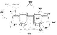
- an access device 150may include one or more recessed access device (RAD) structures 170 wherein the RAD structures 170 include two or more materials having different work functions.
- RAD structures 170include two or more materials having different work functions.
- exemplary RAD structures 170 according to embodiments of the inventionare illustrated in FIG. 5 .
- the RAD structures 170may be formed in trenches of a semiconductor substrate 160 between active areas 162 such as source and drain regions or bitlines and storage capacitors for memory devices.
- the trenches in the semiconductor substrate 160may be lined with a gate-oxide 171 as used with conventional RAD structures.
- the RAD structures 170may include a first gate material 172 overlying a second gate material 174 in a trench of the semiconductor substrate 160 .
- the first gate material 172 and the second gate material 174may be separated by a metal barrier 173 or other conductive barrier as illustrated in FIG. 5 .
- the RAD structures 170may also include a strap 176 overlying the first gate material 172 and an insulator cap 180 overlying the strap 176 .
- Gate electrode sidewall spacers 178may also be formed with the RAD structures 170 to complete the trenched gate stack.
- the second gate material 174 of the RAD structures 170may be formed of a material having a higher work function than the first gate material 172 .
- the second gate material 174 used to form the RAD structures 170 illustrated in FIG. 5may include a P+ doped polysilicon material and the first gate material 172 may include an N+ doped polysilicon material.
- Other materials having differing work functionsmay also be used to form RAD structures 170 according to embodiments of the invention.
- the metal barrier 173 between the first gate material 172 and the second gate material 174may provide an ohmic contact between the two gate materials.
- the metal barrier 173may include metals such as tungsten, aluminum, copper, or titanium.
- the metal barrier 173may be formed from one or more metal layers. The metal layers may include similar or dissimilar metals.
- the metal barrier 173may be substituted with a barrier material (not shown) that may provide an electrical connection or conduction between the first gate material 172 and the second gate material 174 .
- the barrier materialmay prevent diffusion of dopants between the two gate materials.
- the barrier layermay also be an insulator or may include layers of conductors, conductors and insulators, or insulators.
- the strap 176may be a conductive material, such as a metal, a conductive silicon material, a doped silicon material, or another conductor. In other embodiments, the strap 176 need not be conductive.
- the insulator cap 180 of the RAD structures 170may include any insulating material that may be used as an insulating layer for conventional planar or recessed access devices.
- the insulator cap 180may be formed of a nitride or an oxide such as silicon dioxide.
- the sidewall spacers 178may be formed from materials used to form spacers 178 with conventional planar or recessed access devices.
- the sidewall spacers 178may include materials such as silicon dioxide or other oxides, silicon nitride, or other nitrides, or silicon oxynitride.
- the RAD structures 170 of embodiments of the inventionmay be produced using fabrication processes used to form conventional semiconductor devices and particularly memory devices.
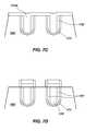
- the RAD structures 170 illustrated in FIG. 5may be formed using conventional CMOS or memory device fabrication processes similar to the steps illustrated in FIGS. 6A-6E .
- a semiconductor substrate 160 having trenches formed thereinmay be provided.
- Gate-oxide 171may be grown in the trenches as used with conventional RAD structures.
- a polysilicon layer 174 Amay be deposited over the semiconductor substrate 160 and in the trenches. Masking and/or etching of the polysilicon layer 174 A may be performed to form the second gate material 174 in the bottoms of the trenches of the semiconductor substrate 160 as illustrated in FIG.
- a barrier layer 173 Amay be deposited over the second gate material 174 and the semiconductor substrate 160 . Masking and/or etching of the barrier layer 173 A may form the metal barrier 173 over the second gate material 174 in the bottom of the trenches as illustrated in FIG. 6C .
- a second polysilicon layer 172 Amay be deposited over the semiconductor substrate 160 and in the trenches over the metal barrier 173 as illustrated in FIG. 6C . Masking and/or etching of the second polysilicon layer 172 A may form the first gate material 172 as illustrated in FIG. 6D .
- the masking and/or etching of the second polysilicon layer 172 Amay be performed such that a portion of the first gate material 172 extends above a surface of the semiconductor substrate 160 .
- a strap material 176 A deposited over the first gate material 172may be masked and/or etched to form the strap 176 over the first gate material 172 as illustrated in FIG. 6E .
- Conventional masking, etching, doping, and deposition processesmay be used to complete the formation of the RAD structures 170 , including the formation of insulator caps 180 and sidewall spacers 178 , and the doping of the active areas 162 .
- FIGS. 6A-6EAlthough methods for forming the RAD structures 170 of particular embodiments of the invention are illustrated in FIGS. 6A-6E , it is understood that other methods and processes may also be used to fabricate RAD structures 170 according to embodiments of the invention.
- the gate stacks 120 and RAD structures 170 of embodiments of the inventionmay reduce GIDL, reduce junction leakage, reduce subthreshold leakage, and increase the drive of the access device.
- the combination of multiple work functions in the gate electrodes of the gate stack 120 and RAD structures 170allows sub-threshold leakage to be controlled or reduced using a high work function material while also employing a low work function material to reduce GIDL.
- the increased margin to GIDL provided by the dual work function gate electrodeallows the negative access device bias to be pushed more negative, which in turn may reduce the subthreshold leakage.
- the decreased subthreshold leakagemay allow a less negative substrate bias to be used with embodiments of the invention to decrease junction leakage and increase the drive of the access device.
- an access device 150 ′ having one or more RAD structures 170 ′ with two or more materials having different work functionsmay include a RAD structure 170 ′ having a first gate material 172 ′ positioned along at least a portion of the sidewalls of the RAD structure 170 ′ and a second gate material 174 ′ at least partially surrounded by the first gate material 172 ′ as illustrated in FIG. 7A .
- trenches in the semiconductor substrate 160 ′may include a gate-oxide 171 ′ layer on the sidewalls of the trenches.
- the first gate material 172 ′may be positioned along at least a portion of the gate-oxide 171 ′ layer and the second gate material 174 ′ may be positioned with respect to the first gate material 172 ′ as illustrated.
- a barrier layer(not shown) may be formed between the first gate material 172 ′ and the second gate material 174 ′.
- the RAD structures 170 ′may also include a strap 176 ′ overlying the first gate material 172 ′ and second gate material 174 ′ and an insulator cap 180 ′ overlying the strap 176 ′.
- Gate electrode sidewall spacers 178 ′may also be formed with the RAD structures 170 ′ to complete the trenched gate stack 170 ′.
- the second gate material 174 ′ of the RAD structures 170 ′may be formed of a material having a higher work function than the first gate material 172 ′.
- the second gate material 174 ′ used to form the RAD structures 170 ′ illustrated in FIG. 7Amay include a p-doped polysilicon material and the first gate material 172 ′ may include an n-doped polysilicon material.
- Other materials having differing work functionsmay also be used to form RAD structures 170 ′ according to embodiments of the invention.
- the RAD structures 170 ′ of embodiments of the inventionmay be produced using fabrication processes used to form conventional semiconductor devices and particularly memory devices.
- the RAD structures 170 ′ illustrated in FIG. 7Amay be formed using conventional CMOS or memory device fabrication processes similar to the steps illustrated in FIGS. 7B-7D .
- a semiconductor substrate 160 ′ having trenches formed thereinmay be provided.
- Oxide 171 ′may be grown in the trenches as used with conventional RAD structures.
- a polysilicon layer 172 A′may be deposited over the semiconductor substrate 160 ′ and in the trenches.
- the polysilicon layer 172 A′may be doped n-type according to conventional doping techniques.
- An isotropic spacer etch selective to the oxide 171 ′may be performed to remove the polysilicon layer 172 A′ in the bottom of a trench, leaving the n-doped polysilicon layer 172 ′ on the sidewalls of the trench as illustrated in FIG. 7C .
- a second gate material layer 174 A′ formed of a material having a higher work function than the first gate material 172 ′may be deposited over the substrate 160 ′ and in the trenches as illustrated in FIG. 7C .
- Masking and/or etching of the second gate material layer 174 A′may be used to form the second gate material 174 ′ as illustrated in FIG. 7D .
- a RAD structure 170 ′including the formation of a strap 176 ′, formation of insulator caps 180 ′, and formation of sidewall spacers 178 ′ as illustrated in FIG. 7A .
- FIGS. 7B-7DAlthough methods for forming the RAD structures 170 ′ of particular embodiments of the invention are illustrated in FIGS. 7B-7D , it is understood that other methods and processes may also be used to fabricate RAD structures 170 ′ according to embodiments of the invention.
- the RAD structures 170 ′ of embodiments of the inventionmay reduce GIDL, reduce junction leakage, reduce subthreshold leakage, and increase the drive of the access device.
- the combination of multiple work functions in the gate electrodesallows sub-threshold leakage to be controlled or reduced using a high work function material while also employing a low work function material to reduce GIDL.
- the increased margin to GIDL provided by the dual work function gate electrodeallows the negative access device bias to be pushed more negative, which in turn may reduce the subthreshold leakage.
- the decreased subthreshold leakagemay allow a less negative substrate bias to be used with embodiments of the invention to decrease junction leakage and increase the drive of the access device.
- FIG. 7Ean SRAD structure according to embodiments of the invention is illustrated in FIG. 7E .
- the SRAD structure 170 ′ illustrated in FIG. 7Emay include the same characteristics as a RAD structure and may be formed using similar processes.
- a gate electrode in an access devicemay be separated into two or more electrically isolated regions.
- the two or more electrically isolated regionsmay be connected to an access device driver capable of supplying the same or different voltages to each of the two or more electrically isolated regions.
- the access device 200may include one or more gate stacks 220 formed over a semiconductor substrate 210 .
- the gate stacks 220may be positioned next to or over active areas 212 in the semiconductor substrate 210 just as conventional gate stacks are positioned with conventional planar access devices.
- the gate stacks 220may include a gate electrode overlying an oxide layer 241 .
- the gate electrodemay include a first gate material 242 and a second gate material 244 separated by an insulator layer 243 .
- An insulator cap 246may overlie the first gate material 242 , the second gate material 244 , and the insulator layer 243 .
- the gate stack 220may also include sidewall spacers 248 as known and used with conventional planar access device structures.
- Gate stacks 220may be incorporated with access devices 200 such as memory devices, CMOS structures, or other devices and structures where conventional gate stacks may be used.
- the semiconductor substrate 210may include semiconductor substrates conventionally used with or for the fabrication of memory devices, access devices, and other semiconductor devices.
- the semiconductor substrate 210may include one or more silicon-containing structures such as silicon wafers, silicon-on-insulator structures, or silicon-on-sapphire structures.
- the active areas 212 of the semiconductor substrate 210may be doped with an n-type, p-type, or other type dopant similar to active areas associated with conventional gate stack formations.
- the first gate material 242 and the second gate material 244 of a gate stack 220may be formed of the same material, such as polysilicon. In other embodiments, the first gate material 242 and the second gate material 244 may be formed of different materials or they may be formed of the same material but doped with different dopants to alter the characteristics of the gate materials.
- the gate stack 220 illustrated in FIG. 8illustrate gate stacks 220 having two gate electrode regions—the first gate material 242 defining a first region and the second gate material 244 defining a second region—it is understood that two or more regions may be defined and incorporated with embodiments of the present invention. In such instances, two or more gate material regions may be separated by two or more insulator layers 243 positioned in the gate material regions.
- the insulator layer 243 positioned between the first gate material 242 and the second gate material 244may include any dielectric layer or suitable material capable of acting as an insulator between the two gate materials.
- the insulator layer 243may include a layer of silicon nitride (SiN), silicon dioxide (SiO 2 ), or other similar insulating material.
- Insulator caps 246 and sidewall spacers 248are used with conventional planar access devices, and the insulator caps 246 and sidewall spacers 248 incorporated with the gate stacks 220 of various embodiments of the invention may include conventional insulator caps and sidewall spacers formed according to conventional fabrication processes.
- the gate stacks 220may be formed using conventional gate stack fabrication processes, with the formation of the second gate material 244 and the insulator layer 243 being added to such processes.
- processes that may be used for the fabrication of the gate stack 220 illustrated in FIG. 8are illustrated in FIGS. 9A-9D .
- a polysilicon layer 242 Amay be deposited over a gate-oxide layer 241 overlying a semiconductor substrate 210 .
- the polysilicon layer 242 Amay be masked and etched such that one or more first gate material 242 formations remain positioned over the oxide layer 241 as illustrated in FIG. 9B .
- An insulator layer 243 Amay be deposited over the first gate material 242 formations.
- the insulator layer 243 Amay be etched to remove all but the insulator layer 243 portions next to the first gate material 242 formations as illustrated in FIG. 9C .
- a vertical isotropic etchmay be used to etch the insulator layer 243 A such that only insulator layer 243 remains on the sides of the first gate material 242 .
- a second polysilicon layer 244 Amay be formed over the structure as illustrated in FIG. 9C .
- the second polysilicon layer 244 Amay be masked and etched to form the second gate material 244 formations as illustrated in FIG. 9D .
- Conventional masking, etching, doping, and deposition processesmay be used to complete the formation of the gate stack 220 including the formation of the insulator caps 246 and sidewall spacers 248 , and the doping of the active areas 212 .
- the oxide layer 241may include a continuous oxide layer (not shown) across the expanse of the semiconductor substrate 210 that may be etched to the desired form during the processing steps.
- a continuous oxide layer(not shown) may be deposited across the entire portion of a semiconductor substrate 210 where a gate stack 220 is to be formed.
- the components of the gate stacksuch as the first gate material 242 , insulator layer 243 , second gate material 244 , and insulator cap 246 may be formed over the continuous oxide layer.
- the gate stack 220 and the continuous oxide layermay then be etched to form the structures illustrated in FIG. 9D .
- the gate stacks 220may be driven by an access device driver capable of providing two or more voltages to the different electrically isolated regions of the gate stacks 220 simultaneously.
- the gate stacks 220 illustrated in FIG. 8may be driven by an access device driver capable of supplying a first voltage to the first gate material 242 and a second voltage to the second gate material 244 .
- the voltages supplied by the access device drivermay be selected such that the voltages applied to the first gate material 242 and the second gate material 244 are the same or different, depending on the desired “on” or “off” state of the gate stack 220 .
- a gate stack 220may include two or more gate materials.
- an access device drivermay be adapted to deliver voltages to each of the gate materials to control the operations of the gate stack 220 .
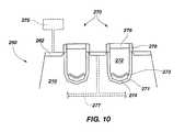
- a RAD structure 270may be incorporated into an access device 250 .
- a RAD structure 270 according to embodiments of the inventionmay be similar to a conventional RAD structure having a single gate material.
- the RAD structures 270 of particular embodiments of the inventionmay include a first gate material 272 and a second gate material 274 separated by an insulator layer 273 .
- a RAD structure 270 according to particular embodiments of the inventionis illustrated in FIG. 10 .
- the RAD structure 270 illustrated in FIG. 10includes two gate materials, a first gate material 272 and a second gate material 274 , positioned in a trench in a semiconductor substrate 210 .
- a gate-oxide layer 271may coat or overlie the sides of the trench in the semiconductor substrate 210 .
- the first gate material 272 and the second gate material 274may be separated by an insulator layer 273 .
- the RAD structures 270may be positioned next to or over active areas 262 in the semiconductor substrate 210 just as RAD structures are positioned with conventional access devices.
- An insulator cap 276may overlie the gate materials of a RAD structure 270 and sidewall spacers 278 may border the sides of the RAD structure 270 as illustrated in FIG. 10 .
- the insulator cap 276 and sidewall spacers 278may be similar to insulator caps and sidewall spacers employed with conventional RAD devices.
- RAD structure 270 illustrated in FIG. 10shows a first gate material 272 and a second gate material 274 separated by an insulator layer 273
- embodiments of the inventionmay include two or more gate materials separated by two or more insulator layers.
- RAD structures 270may be incorporated with access devices 250 such as memory devices, CMOS structures, or other devices and structures where RAD structures 270 may be used.
- Semiconductor substrates 210may include semiconductor substrates conventionally used with or for the fabrication of memory devices, access devices, and other semiconductor devices.
- the semiconductor substrate 210may include one or more silicon-containing structures such as silicon wafers, silicon-on-insulator structures, or silicon-on-sapphire structures.
- the active areas 262 of the semiconductor substrate 210may be doped with an n-type, p-type, or other type dopant similar to active areas associated with conventional RAD structure formations.
- the gate materials forming the first gate material 272 and the second gate material 274may include materials used to form conventional gate electrodes.
- the gate materials used with the RAD structures 270 according to embodiments of the inventionmay include materials such as polysilicon materials.
- the same gate materialmay be used to form the first gate material 272 and the second gate material 274 or the two gate materials may be formed from different gate materials.
- the first gate material 272 and the second gate material 274may be doped with different dopants to alter the characteristics of the gate materials.
- the first gate material 272may have a lower work function than the second gate material 274 and may be located closer to a storage capacitor 275 (shown in broken lines) than the second gate material 274 , which may be located closer to a bitline 277 (shown in broken lines) than the first gate material 272 .
- the insulator layer 273 positioned between the first gate material 272 and the second gate material 274may include any dielectric layer or suitable material capable of acting as an insulator between the two gate materials.
- the insulator layer 273may include a layer of silicon nitride (Si 3 N 4 ), silicon dioxide (SiO 2 ), or other similar insulating material.
- the RAD structures 270 according to embodiments of the inventionmay be formed using conventional RAD structure fabrication processes. For example, a process that may be used to fabricate a RAD structure according to embodiments of the invention is illustrated in FIGS. 11A-11D .
- RAD structures 270may be formed in a trench in a semiconductor device wherein the trench includes a gate-oxide layer as may be fabricated for conventional RAD structures.
- a polysilicon layer 272 Amay be deposited over a semiconductor substrate 210 having trenches lined with a gate-oxide layer 271 material.
- the polysilicon layer 272 Amay be etched, leaving a first gate material 272 deposited over the gate-oxide layer 271 in the bottom of a trench as illustrated in FIG. 11B .
- An insulator material layer 273 A deposited over the first gate material 272 and the gate-oxide layer 271may be etched to form the insulator layer 273 over the first gate material 272 .
- the etching of the insulator material layer 273 Amay be performed so that the gate-oxide layer 271 remains on the surface of the trenches in the semiconductor substrate 210 .
- a second polysilicon layer 274 Amay be deposited over the semiconductor substrate 210 and in the trenches, covering the insulator layer 273 and filling the trenches as illustrated in FIG. 11C . Selective masking and etching of the second polysilicon layer 274 A forms the second gate material 274 formations as illustrated in FIG. 11D .
- RAD structures 270Conventional masking, etching, doping, and deposition processes may be used to complete the formation of the RAD structures 270 including the formation of the insulator caps 276 and sidewall spacers 278 , and the doping of the active areas 262 .
- masking of the trenches, contacts between RAD structures, and metal layers above the RAD structuresmay be performed such that contact may be made to the bottom portion of the RAD structure 270 , and the first gate material 272 , as well as to the top portion of the RAD structure 270 and the second gate material 274 .
- the contactmay be connected to an access device driver capable of supplying desired voltages to the first gate material 272 and second gate material 274 .
- the RAD structures 270may be driven by an access device driver capable of providing two or more voltages to the RAD structure 270 simultaneously.
- the RAD structure 270 illustrated in FIG. 10may be driven by an access device driver capable of supplying a first voltage to the first gate material 272 and a second voltage to the second gate material 274 .
- the voltages supplied by the access device drivermay be selected such that the voltages applied to the first gate material 272 and the second gate material 274 are the same or different, depending on the desired “on” or “off” state of the RAD structure 270 .
- the RAD structures 270may include two or more gate materials.
- an access device drivermay be adapted to deliver voltages to each of the gate materials to control the operations of the RAD structures 270 .
- the gate stacks 220 and RAD structures 270 having multiple electrically isolated regionsmay reduce the amount of gate induced drain leakage (GIDL), junction leakage, and subthreshold leakage while increasing the drive of the access device.
- the gate stacks 220 and RAD structures 270reduce the amount of GIDL while preserving a negative gate electrode bias. This may be accomplished by applying different voltages to the first and second gate electrodes of the gate stacks 220 and RAD structures 270 . Therefore, in the “off” state, one of the negative gate electrode bias may be made more negative while the other remains “off,” but at a less negative bias—thereby decreasing GIDL current. The more negative word line bias on one portion of the gate results in decreased subthreshold leakage. Further, a less negative substrate bias may be used, which would decrease junction leakage and increase the drive of the access device.
- GIDLgate induced drain leakage
- junction leakagejunction leakage
- subthreshold leakagesubthreshold leakage
- planar or recessed access devicesmay also include gate electrodes comprised of diodes.
- the incorporation of a diode structure with the gate electrodewould allow two voltages to be applied to the electrode structure: a first voltage across the anode of the diode and a second voltage across the cathode of the diode.
- the access device 300may include one or more gate stacks 320 formed over a semiconductor substrate 310 .
- the gate stacks 320may be positioned next to or over active areas such as storage capacitors 312 and bitline contacts 313 in the semiconductor substrate 310 just as conventional gate stacks are positioned with conventional access devices.
- the gate stacks 320may include a gate electrode overlying an oxide layer 321 , wherein the gate electrode comprises an anode 324 and a cathode 322 .
- the anode 324may be positioned closest to a bitline contact 313 active area while the cathode 322 may be positioned closest to the storage capacitor 312 active areas.
- An insulator cap 330may overlie the gate electrode and sidewall spacers 328 may be positioned on the sides of the gate stack 320 in a manner similar to conventional gate stacks.
- the gate stacks 320may be incorporated with access devices 300 such as memory devices, CMOS structures, or other devices and structures where gate stacks 320 may be used.
- the semiconductor substrate 310may include semiconductor substrates conventionally used with or for the fabrication of memory devices, access devices, and other semiconductor devices.
- the semiconductor substrate 310may include, but is not limited to, one or more silicon containing materials such as silicon, silicon-on-insulator structures, or silicon-on-sapphire structures.
- the bitline contacts 313 and storage capacitor 312 of the semiconductor substrate 310may be doped with an n-type, p-type, or other type dopant to form the desired active areas, which are similar to those formed in conventional gate stack formations.
- the insulator caps 330 and sidewall spacers 328may include materials used to form the insulator caps and sidewall spacers of conventional gate stack devices.
- the anode 324 of the gate stack 320may be formed of materials conventionally used to form anodes in semiconductor devices.
- the anode 324may also be formed of a doped material such as a p-type doped material.
- the anode 324may be formed of a Ruthenium-Tantalum (Ru x Ta y ) metal alloy or a tantalum nitride (TaN) metal alloy.
- the cathode 322 of the gate stack 320may be formed of materials conventionally used to form cathodes in semiconductor devices.
- the cathode 322may also be formed of a doped material such as an n-type doped material.
- the cathode 322may be formed of a Ruthenium-Tantalum (Ru x Ta y ) metal alloy or a tantalum nitride (TaN) metal alloy.
- a gate stack 320 of an access device 300may be fabricated according to the steps illustrated in FIGS. 15A-15D .
- the gate stacks 320 of embodiments of the present inventionmay be formed over semiconductor substrates 310 having oxide layers 321 formed thereon as with a conventional gate stack fabrication method.
- the oxide layer 321may be a discontinuous oxide layer 321 as illustrated in FIG. 15A or a continuous oxide layer which is etched or otherwise partially removed to form the oxide layer 321 illustrated in FIG. 15A .
- an anode material 324 Amay be deposited over a semiconductor substrate 310 having oxide layers 321 .
- the anode material 324 Amay be masked and etched according to conventional techniques to form anode 324 portions of the gate stack 320 as illustrated in FIG. 15B .
- a cathode material 322 Amay be deposited over the anode 324 portions of the gate stack 320 as well as the semiconductor substrate 310 having oxide layers 321 as illustrated in FIG. 15C .
- the cathode material 322 A and anode portionsmay be masked and etched to form the anode 324 and cathode 322 diode structures of the gate stacks 320 as illustrated in FIG. 15D .
- Conventional gate stack fabrication techniquesmay then be used to form the insulator cap 330 and sidewall spacers 328 , completing the formation of the gate stacks 320 .
- the active areas in the semiconductor substrate 310may also be formed using conventional methods of fabrication.
- the bitline contacts 313 and the storage capacitors 312may be doped with an n-type dopant to form N+ doped active areas.
- anode 324 portions of the gate stacks 320 illustrated in FIGS. 15A-15Dare shown as being fabricated before the cathode 322 portions of the gate stacks 320 , it is understood that the order of formation of the cathode 322 portions and anode 324 portions is not critical. Therefore, the cathode 322 portions may be formed before the anode 324 portions according to embodiments of the invention.
- the structuresmay be masked, etched, polished, or otherwise formed such that the center of the gate stack 320 is positioned at the interface of the anode 324 portions and the cathode 322 portions of the gate stack.
- CMPchemical mechanical planarization
- an anode material 324 A and cathode material 322 Amay be selected such that the work function of the two materials is different.
- the cathode material 322 A and anode material 324 Amay each comprise Ruthenium-Tantalum which may be represented by the chemical formula Ru x Ta y wherein x and y may be selected according to the desired work functions for the diode.
- the anode 324may be formed of an Ru x Ta y material wherein x and y are selected such that the anode 324 exhibits a work function of about 5.0 eV.
- the cathode 322may be formed of an Ru x Ta y material wherein x and y are selected such that the cathode 322 exhibits a work function of about 4.2 eV. Other values of x and y may be selected such that the work functions of the two materials is different.
- the gate stacks 320may be formed as one long diode having approximately equal cathode 322 and anode 324 regions within the gate stack 320 .
- the anode 324 regionsmay be positioned closest to the bitline contacts 313 while the cathode 322 regions may be positioned closest to the storage capacitors 312 .
- the anode 324 of a gate stack 320is held at a negative word line voltage while the cathode 322 is held at a higher voltage than the anode 324 .
- the difference in voltages between the cathode 322 and anode 324creates a reverse bias across the diode.
- the bias level of the cathode 322may be determined by the breakdown voltage of the reversed biased diode gate.
- the cathode 322 region bias levelmay decrease the voltage difference between the storage capacitors 312 and the gate stack 320 , which in turn may decrease the electric field in the gate stack 320 area.
- the decreased electric field in the gate stack 320 areamay help to reduce the gate-induced drain leakage in a gate stack 320 formed according to embodiments of the invention.
- the anode 324 and the cathode 322 of the gate electrode or gate stack 320are both driven to the same positive level as with conventional gate stack devices.
- the diode of the gate stacks 320may include a Schottky-Barrier type diode.
- the anode 324may be a metal layer and the cathode 322 may be a polysilicon material that is doped, for example, a polysilicon material that is slightly doped N+.
- Embodiments of the inventionmay also include gate stacks 320 formed of Schottky-Barrier type diodes.
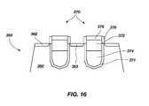
- an access device 350may include one or more recessed access device (RAD) structures 370 comprising diodes as illustrated in FIG. 16 .
- the RAD structures 370may include a diode comprised of an anode 374 and a cathode 372 formed in a trench in a semiconductor substrate 360 .
- the anode 374may be formed in the bottom of a trench and the cathode 372 may lie on top of the anode 374 and may extend beyond the surface of the semiconductor substrate 360 .
- the RAD structures 370may be positioned in trenches in a semiconductor substrate 360 just as conventional RAD structures are positioned.
- the trenches in the semiconductor substrate 360may be lined with oxide 371 layers such that the cathode 372 and anode 374 may be in contact with the oxide 371 layer rather than a wall of a trench.
- the RAD structures 370may also include an insulator cap 376 and sidewall spacers 378 similar to those used with conventional RAD structures.
- the RAD structures 370may be incorporated with access devices 350 such as memory devices, CMOS structures, or other conventional devices and structures employing the use of RAD structures 370 .
- the semiconductor substrate 360may include semiconductor substrates conventionally used with or for the fabrication of memory devices, access devices, and other semiconductor devices.
- the semiconductor substrate 360may include one or more silicon-containing structures such as silicon wafers, silicon-on-insulator structures, or silicon-on-sapphire structures.
- the bitline contacts 363 and storage capacitors 362 of the semiconductor substrate 360may be doped with an n-type, p-type, or other type dopant to form the desired active areas, which are similar to those formed with conventional RAD structure formations.
- the insulator caps 376 and sidewall spacers 378may include materials used to form the insulator caps and sidewall spacers of conventional gate stack devices.
- the anode 374 of the RAD structure 370may be formed of materials conventionally used to form anodes in semiconductor devices.
- the anode 374may also be formed of a doped material such as a p-type doped material.
- the anode 374may be formed of a Ruthenium-Tantalum (Ru x Ta y ) metal alloy or a tantalum nitride (TaN) metal alloy.
- the cathode 372 of the RAD structure 370may be formed of materials conventionally used to form cathodes in semiconductor devices.
- the cathode 372may also be formed of a doped material such as an n-type doped material.
- the cathode 372may be formed of a Ruthenium-Tantalum (Ru x Ta y ) metal alloy or a tantalum nitride (TaN) metal alloy.
- a RAD structure 370such as that illustrated in FIG. 16 , may be fabricated according to the processes illustrated in FIGS. 17A-17D .
- a RAD structure 370may be fabricated in the trenches of a semiconductor substrate 360 as with conventional RAD structures.
- the trenchesmay include an oxide 371 layer, such as a gate-oxide layer, covering the surfaces of the trenches.
- an anode material 374 Amay be deposited over and in an oxide 371 layered trench in a semiconductor substrate 360 .
- the anode material 374 Amay then be masked and etched according to conventional processes to leave a portion of the anode material 374 A in the trenches which forms the anode 374 of the RAD structure 370 as illustrated in FIG. 17B .
- the etching of the anode material 374 A to form the anode 374may be selective to the oxide 371 layer such that the oxide 371 layer remains on the walls of the trenches.
- a cathode material 372 Amay then be deposited over the semiconductor substrate 360 and in the trenches over the anode 374 . Deposition of the cathode material 372 A may be accomplished using conventional deposition processes.
- the cathode material 372 Amay be masked and etched according to conventional processes to form the cathode 372 structure illustrated in FIG. 17D .
- Conventional RAD structure fabrication processesmay be employed to form an insulator cap 376 and sidewall spacers 378 of the RAD structure 370 according to embodiments of the invention.
- the active areas in the semiconductor substrate 360such as the bitline contacts 363 and storage capacitors 362 , may also be formed using conventional processes for forming active areas.
- the bitline contacts 363 and the storage capacitors 362may be doped with an n-type dopant to form N+ doped active areas.
- the anode material 374 A and cathode material 372 Amay be selected such that the work function of the two materials is different.
- the cathode material 372 A and anode material 374 Amay each comprise Ruthenium-Tantalum which may be represented by the chemical formula Ru x Ta y wherein x and y may be selected according to the desired work functions for the diode.
- the anode 374may be formed of an Ru x Ta y material wherein x and y are selected such that the anode 374 exhibits a work function of about 5.0 eV.
- the cathode 372may be formed of an Ru x Ta y material wherein x and y are selected such that the cathode 372 exhibits a work function of about 4.2 eV. Other values of x and y may be selected such that the work functions of the formed materials are different.
- the gate electrodes formed by the RAD structures 370 of particular embodiments of the inventionmay be formed as long diodes in the trenches of the semiconductor substrate 360 .
- the bottom portion of the RAD structure 370 in the trenches of the semiconductor substrate 360is the anode 374 and the top portion is the cathode 372 of the diode.
- the anode 374may be held at a negative word line voltage while the cathode 372 may be held at a higher voltage to create a reverse biased diode.
- the difference in voltages between the cathode 372 and the anode 374may create a reverse bias across the diode.
- the bias level of the cathode 372may be determined by the breakdown voltage of the reversed biased diode gate.
- the cathode 372 region bias levelmay decrease the voltage difference between storage capacitors 362 and the RAD structure 370 , which in turn may decrease the electric field in the gate electrode area.
- the decreased electric field in the RAD structure 370 areamay help to reduce the gate-induced drain leakage in a RAD structure 370 formed according to embodiments of the invention.
- both the anode 374 and the cathode 372may be driven to the same positive level as with conventional recessed access devices.
- the diode of the RAD structure 370may be formed such that a Schottky-Barrier diode is formed in the RAD structure 370 .
- the anode 374may be a metal layer deposited in the trenches of the semiconductor substrate 360 and recessed so that it remains only in the bottom of the trenches.
- the cathode 372may be a polysilicon material deposited over the metal anode 374 that is doped, for example, a polysilicon material that is slightly doped N+.
- Embodiments of the inventionmay also include RAD structures 370 formed of other Schottky-Barrier type diodes.
- the gate stacks 320 and RAD structures 370may use two separate access device voltages to bias the diode formed by the anodes 374 and cathodes 372 of the gate electrodes.
- An access device driversuch as those described herein, capable of providing multiple voltage levels may be combined with the gate stacks 320 and RAD structures 370 to carry out particular embodiments of the invention.
- an access device drivermay be capable of driving the devices and structures of embodiments of the invention.
- Access device drivers and driver circuits used with embodiments of the inventionmay be able to turn two or more portions of the gate electrodes of a gate stack or recessed access device “on” and “off.”
- the access device drivers of embodiments of the inventionare modified to provide separate bias levels onto the anode and cathode regions of a diode in a gate electrode or onto the electrically isolated regions of a gate electrode for a planar or recessed access device.
- access device driversmay be capable of applying a negative gate electrode voltage to one portion of a gate electrode and a ground voltage to another portion of the gate electrode.
- the driverwould be able to supply two or more voltages to the gate electrode of a planar or recessed access device.
- the access device drivermay include two outputs which may accommodate one or more diodes connected between the outputs as illustrated in FIG. 13 .
- the access device driver illustrated in FIG. 13may be incorporated with an access device to operate the gate stacks 220 or RAD structures 270 having two or more electrically isolated regions such as those illustrated in FIGS. 8 and 10 .
- the contact of the access device driver labeled 1may be connected to the second gate materials of a gate stack 220 or a RAD structure 270
- the contact of the access device driver labeled 2may be connected to the first gate material of the same gate stack 220 or RAD structure 270 .
- differing bias levelsmay be applied by the access device driver to the first gate material and second gate material of a gate stack 220 or RAD structure 270 .
- an access device driversuch as that illustrated in FIG. 12 may be used to supply separate bias levels to a gate stack or gate electrode of a planar or recessed access device, having a diode in the gate electrode.
- the access device driver illustrated in FIG. 12may be used to supply voltages to the anodes and cathodes of the planar and recessed gates electrodes illustrated in FIGS. 14 and 16 , respectively.
- the access device driversmay also include resistive devices (not shown) positioned between one of the outputs of the access device driver and the access device, such as a recessed or planar access device.
- resistive devicespositioned between one of the outputs of the access device driver and the access device, such as a recessed or planar access device.
- the presence of a resistive device between one of the outputs of the access device driver and one of the electrically isolated regions in the access devicemay limit the current path between the two, or more, separate power supplies utilized by the driver.
- the ability to apply different bias levels to the different portions of the planar or recessed access device gate electrodesallows the amount of gate induced drain leakage (GIDL) to be controlled. Furthermore, the ability to turn one portion of the gate electrode “off” at a lower voltage than the other ensures that subthreshold leakage may be minimized. Further more, if subthreshold leakage is minimized, the substrate bias may be reduced to decrease junction leakage.
- GIDLgate induced drain leakage
- the access device drivers according to embodiments of the inventionmay be used with CMOS applications, memory devices such as DRAM, and with any other semiconductor devices where it may be desirable to turn different portions of a gate electrode to different “off” or “on” states to control or reduce GIDL, subthreshold leakage, or junction leakage.
Landscapes
- Semiconductor Memories (AREA)
- Non-Volatile Memory (AREA)
Abstract
Description
Claims (12)
Priority Applications (1)
| Application Number | Priority Date | Filing Date | Title |
|---|---|---|---|
| US14/247,968US9502516B2 (en) | 2006-05-11 | 2014-04-08 | Recessed access devices and gate electrodes |
Applications Claiming Priority (6)
| Application Number | Priority Date | Filing Date | Title |
|---|---|---|---|
| US11/432,270US8008144B2 (en) | 2006-05-11 | 2006-05-11 | Dual work function recessed access device and methods of forming |
| US11/432,442US20070262395A1 (en) | 2006-05-11 | 2006-05-11 | Memory cell access devices and methods of making the same |
| US11/495,805US8860174B2 (en) | 2006-05-11 | 2006-07-28 | Recessed antifuse structures and methods of making the same |
| US13/196,527US8710583B2 (en) | 2006-05-11 | 2011-08-02 | Dual work function recessed access device and methods of forming |
| US13/276,141US8692320B2 (en) | 2006-05-11 | 2011-10-18 | Recessed memory cell access devices and gate electrodes |
| US14/247,968US9502516B2 (en) | 2006-05-11 | 2014-04-08 | Recessed access devices and gate electrodes |
Related Parent Applications (1)
| Application Number | Title | Priority Date | Filing Date |
|---|---|---|---|
| US13/276,141DivisionUS8692320B2 (en) | 2006-05-11 | 2011-10-18 | Recessed memory cell access devices and gate electrodes |
Publications (2)
| Publication Number | Publication Date |
|---|---|
| US20140217498A1 US20140217498A1 (en) | 2014-08-07 |
| US9502516B2true US9502516B2 (en) | 2016-11-22 |
Family
ID=38684331
Family Applications (3)
| Application Number | Title | Priority Date | Filing Date |
|---|---|---|---|
| US11/432,442AbandonedUS20070262395A1 (en) | 2006-05-11 | 2006-05-11 | Memory cell access devices and methods of making the same |
| US13/276,141ActiveUS8692320B2 (en) | 2006-05-11 | 2011-10-18 | Recessed memory cell access devices and gate electrodes |
| US14/247,968ActiveUS9502516B2 (en) | 2006-05-11 | 2014-04-08 | Recessed access devices and gate electrodes |
Family Applications Before (2)
| Application Number | Title | Priority Date | Filing Date |
|---|---|---|---|
| US11/432,442AbandonedUS20070262395A1 (en) | 2006-05-11 | 2006-05-11 | Memory cell access devices and methods of making the same |
| US13/276,141ActiveUS8692320B2 (en) | 2006-05-11 | 2011-10-18 | Recessed memory cell access devices and gate electrodes |
Country Status (1)
| Country | Link |
|---|---|
| US (3) | US20070262395A1 (en) |
Families Citing this family (22)
| Publication number | Priority date | Publication date | Assignee | Title |
|---|---|---|---|---|
| US8860174B2 (en)* | 2006-05-11 | 2014-10-14 | Micron Technology, Inc. | Recessed antifuse structures and methods of making the same |
| US20070262395A1 (en) | 2006-05-11 | 2007-11-15 | Gibbons Jasper S | Memory cell access devices and methods of making the same |
| US8008144B2 (en) | 2006-05-11 | 2011-08-30 | Micron Technology, Inc. | Dual work function recessed access device and methods of forming |
| US7838371B2 (en)* | 2006-11-06 | 2010-11-23 | Nxp B.V. | Method of manufacturing a FET gate |
| KR101374323B1 (en)* | 2008-01-07 | 2014-03-17 | 삼성전자주식회사 | Semiconductor device and method of manufacturing the same |
| US7964922B2 (en)* | 2008-08-15 | 2011-06-21 | International Business Machines Corporation | Structure, design structure and method of manufacturing dual metal gate VT roll-up structure |
| US8003463B2 (en)* | 2008-08-15 | 2011-08-23 | International Business Machines Corporation | Structure, design structure and method of manufacturing dual metal gate Vt roll-up structure |
| US7824986B2 (en) | 2008-11-05 | 2010-11-02 | Micron Technology, Inc. | Methods of forming a plurality of transistor gates, and methods of forming a plurality of transistor gates having at least two different work functions |
| US8492845B2 (en)* | 2010-11-05 | 2013-07-23 | International Business Machines Corporation | Gate-to-gate recessed strap and methods of manufacture of same |
| US8743628B2 (en) | 2011-08-08 | 2014-06-03 | Micron Technology, Inc. | Line driver circuits, methods, and apparatuses |
| KR101853316B1 (en) | 2012-03-29 | 2018-04-30 | 삼성전자주식회사 | Transistor, semiconductor device and a semiconductor module including the same |
| US8896060B2 (en)* | 2012-06-01 | 2014-11-25 | Taiwan Semiconductor Manufacturing Company, Ltd. | Trench power MOSFET |
| KR102055333B1 (en) | 2014-01-29 | 2020-01-22 | 에스케이하이닉스 주식회사 | Dual work function bruied gate type transistor, method for manufacturing the same and electronic device having the same |
| US9620603B2 (en)* | 2015-04-23 | 2017-04-11 | Macronix International Co., Ltd. | Semiconductor device with a P-N junction for reduced charge leakage and method of manufacturing the same |
| CN108292671B (en)* | 2015-12-17 | 2022-01-18 | 英特尔公司 | Semiconductor device and method for manufacturing the same |
| US10325964B2 (en)* | 2016-11-15 | 2019-06-18 | Taiwan Semiconductor Manufacturing Co., Ltd. | OLED merged spacer device |
| KR102511942B1 (en) | 2016-12-16 | 2023-03-23 | 에스케이하이닉스 주식회사 | Semiconductor device having buried gate structure and method for manufacturing the same |
| CN108807535B (en)* | 2017-05-05 | 2021-07-13 | 中芯国际集成电路制造(上海)有限公司 | Fin field effect transistor and method of forming the same |
| KR102404645B1 (en) | 2017-08-28 | 2022-06-03 | 삼성전자주식회사 | Semiconductor device |
| US11424335B2 (en)* | 2017-09-26 | 2022-08-23 | Intel Corporation | Group III-V semiconductor devices having dual workfunction gate electrodes |
| US11411118B2 (en) | 2020-09-10 | 2022-08-09 | Micron Technology, Inc. | Integrated assemblies |
| US11424360B1 (en) | 2021-02-04 | 2022-08-23 | Nanya Technology Corporation | Semiconductor device and method for manufacturing the same |
Citations (120)
| Publication number | Priority date | Publication date | Assignee | Title |
|---|---|---|---|---|
| US4636834A (en) | 1983-12-12 | 1987-01-13 | International Business Machines Corporation | Submicron FET structure and method of making |
| US4714519A (en) | 1987-03-30 | 1987-12-22 | Motorola, Inc. | Method for fabricating MOS transistors having gates with different work functions |
| US5013680A (en) | 1990-07-18 | 1991-05-07 | Micron Technology, Inc. | Process for fabricating a DRAM array having feature widths that transcend the resolution limit of available photolithography |
| US5122848A (en) | 1991-04-08 | 1992-06-16 | Micron Technology, Inc. | Insulated-gate vertical field-effect transistor with high current drive and minimum overlap capacitance |
| US5208177A (en) | 1992-02-07 | 1993-05-04 | Micron Technology, Inc. | Local field enhancement for better programmability of antifuse PROM |
| US5547890A (en) | 1995-05-05 | 1996-08-20 | Vanguard International Semiconductor Corporation | DRAM cell with a cradle-type capacitor |
| US5583065A (en) | 1994-11-23 | 1996-12-10 | Sony Corporation | Method of making a MOS semiconductor device |
| US5619057A (en) | 1994-01-19 | 1997-04-08 | Sony Corporation | Complex film overlying a substrate with defined work function |
| US5714412A (en) | 1996-12-02 | 1998-02-03 | Taiwan Semiconductor Manufacturing Company, Ltd | Multi-level, split-gate, flash memory cell and method of manufacture thereof |
| US5909618A (en) | 1997-07-08 | 1999-06-01 | Micron Technology, Inc. | Method of making memory cell with vertical transistor and buried word and body lines |
| US5937280A (en)* | 1997-01-15 | 1999-08-10 | United Microelectronics Corp. | Method of manufacturing a ROM |
| US5941701A (en) | 1998-07-14 | 1999-08-24 | Ceramoptec Ind Inc | Device and method to treat oral disease in felines |
| US5953614A (en) | 1997-10-09 | 1999-09-14 | Lsi Logic Corporation | Process for forming self-aligned metal silicide contacts for MOS structure using single silicide-forming step |
| US5960270A (en) | 1997-08-11 | 1999-09-28 | Motorola, Inc. | Method for forming an MOS transistor having a metallic gate electrode that is formed after the formation of self-aligned source and drain regions |
| US5963469A (en) | 1998-02-24 | 1999-10-05 | Micron Technology, Inc. | Vertical bipolar read access for low voltage memory cell |
| US5977579A (en) | 1998-12-03 | 1999-11-02 | Micron Technology, Inc. | Trench dram cell with vertical device and buried word lines |
| US6033963A (en) | 1999-08-30 | 2000-03-07 | Taiwan Semiconductor Manufacturing Company | Method of forming a metal gate for CMOS devices using a replacement gate process |
| US6072209A (en) | 1997-07-08 | 2000-06-06 | Micro Technology, Inc. | Four F2 folded bit line DRAM cell structure having buried bit and word lines |
| US6090692A (en) | 1995-07-26 | 2000-07-18 | Lg Semicon Co., Ltd. | Fabrication method for semiconductor memory device |
| US6121100A (en) | 1997-12-31 | 2000-09-19 | Intel Corporation | Method of fabricating a MOS transistor with a raised source/drain extension |
| US6130453A (en) | 1999-01-04 | 2000-10-10 | International Business Machines Corporation | Flash memory structure with floating gate in vertical trench |
| US6147377A (en) | 1998-03-30 | 2000-11-14 | Advanced Micro Devices, Inc. | Fully recessed semiconductor device |
| US6150687A (en) | 1997-07-08 | 2000-11-21 | Micron Technology, Inc. | Memory cell having a vertical transistor with buried source/drain and dual gates |
| US6187619B1 (en) | 1998-02-17 | 2001-02-13 | Shye-Lin Wu | Method to fabricate short-channel MOSFETs with an improvement in ESD resistance |
| US6191470B1 (en) | 1997-07-08 | 2001-02-20 | Micron Technology, Inc. | Semiconductor-on-insulator memory cell with buried word and body lines |
| US6215149B1 (en) | 1998-08-18 | 2001-04-10 | Samsung Electronics Co., Ltd. | Trenched gate semiconductor device |
| US6225669B1 (en) | 1998-09-30 | 2001-05-01 | Advanced Micro Devices, Inc. | Non-uniform gate/dielectric field effect transistor |
| US6259142B1 (en) | 1998-04-07 | 2001-07-10 | Advanced Micro Devices, Inc. | Multiple split gate semiconductor device and fabrication method |
| US6294434B1 (en) | 2000-09-27 | 2001-09-25 | Vanguard International Semiconductor Corporation | Method of forming a metal silicide layer on a polysilicon gate structure and on a source/drain region of a MOSFET device |
| US6300177B1 (en) | 2001-01-25 | 2001-10-09 | Chartered Semiconductor Manufacturing Inc. | Method to form transistors with multiple threshold voltages (VT) using a combination of different work function gate materials |
| US6313046B1 (en) | 1997-10-09 | 2001-11-06 | Micron Technology, Inc. | Method of forming materials between conductive electrical components, and insulating materials |
| US6343114B1 (en) | 1999-12-30 | 2002-01-29 | Turnstone Systems, Inc. | Remotely addressable maintenance unit |
| US20020028541A1 (en) | 2000-08-14 | 2002-03-07 | Lee Thomas H. | Dense arrays and charge storage devices, and methods for making same |
| US6373114B1 (en) | 1998-10-23 | 2002-04-16 | Micron Technology, Inc. | Barrier in gate stack for improved gate dielectric integrity |
| US6383879B1 (en) | 1999-12-03 | 2002-05-07 | Agere Systems Guardian Corp. | Semiconductor device having a metal gate with a work function compatible with a semiconductor device |
| US20020106858A1 (en) | 1999-11-30 | 2002-08-08 | Jun-Fei Zheng | Work function tuning for MOSFET gate electrodes |
| US20020132473A1 (en) | 2001-03-13 | 2002-09-19 | Applied Materials ,Inc. | Integrated barrier layer structure for copper contact level metallization |
| US20020146878A1 (en) | 2001-04-05 | 2002-10-10 | Mitsubishi Denki Kabushiki Kaisha | Semiconductor device |
| US6476444B1 (en) | 1999-03-18 | 2002-11-05 | Hyundai Electronics Industries Co., Ltd. | Semiconductor device and method for fabricating the same |
| US6498062B2 (en) | 2001-04-27 | 2002-12-24 | Micron Technology, Inc. | DRAM access transistor |
| US6534837B1 (en) | 1998-09-18 | 2003-03-18 | Intel Corporation | Semiconductor device |
| US6534402B1 (en) | 2001-11-01 | 2003-03-18 | Winbond Electronics Corp. | Method of fabricating self-aligned silicide |
| US6548870B1 (en) | 2000-05-01 | 2003-04-15 | Hynix Semiconductor Inc. | Semiconductor device |
| US6552401B1 (en) | 2000-11-27 | 2003-04-22 | Micron Technology | Use of gate electrode workfunction to improve DRAM refresh |
| US6562713B1 (en) | 2002-02-19 | 2003-05-13 | International Business Machines Corporation | Method of protecting semiconductor areas while exposing a gate |
| US6566708B1 (en) | 2000-11-17 | 2003-05-20 | Koninklijke Philips Electronics N.V. | Trench-gate field-effect transistors with low gate-drain capacitance and their manufacture |
| US6607958B2 (en) | 2000-03-27 | 2003-08-19 | Kabushiki Kaisha Toshiba | Semiconductor device and method of manufacturing the same |
| US20030170955A1 (en) | 2001-07-10 | 2003-09-11 | Takahiro Kawamura | Trench-gate semiconductor device and its manufacturing method |
| US6630720B1 (en) | 2001-12-26 | 2003-10-07 | Advanced Micro Devices, Inc. | Asymmetric semiconductor device having dual work function gate and method of fabrication |
| US20030203566A1 (en) | 2002-04-26 | 2003-10-30 | Micron Technology, Inc. | Semiconductor constructions, and methods of forming semiconductor constructions |
| US6653698B2 (en) | 2001-12-20 | 2003-11-25 | International Business Machines Corporation | Integration of dual workfunction metal gate CMOS devices |
| US6696746B1 (en) | 1998-04-29 | 2004-02-24 | Micron Technology, Inc. | Buried conductors |
| US20040113202A1 (en)* | 2002-08-23 | 2004-06-17 | Kocon Christopher B. | Method and apparatus for improved MOS gating to reduce miller capacitance and switching losses |
| US20040212024A1 (en) | 2003-04-23 | 2004-10-28 | Chang-Woo Oh | Metal oxide semiconductor field effect transistors (MOSFETs) including recessed channel regions and methods of fabricating the same |
| WO2004107421A1 (en) | 2003-06-03 | 2004-12-09 | Koninklijke Philips Electronics N.V. | Formation of junctions and silicides with reduced thermal budget |
| US6841834B2 (en) | 2001-12-13 | 2005-01-11 | International Business Machines Corporation | Doubly asymmetric double gate transistor structure |
| US6844578B2 (en) | 2001-03-28 | 2005-01-18 | Seiko Instruments Inc. | Semiconductor integrated circuit device and manufacturing method therefor |
| US6844591B1 (en) | 2003-09-17 | 2005-01-18 | Micron Technology, Inc. | Method of forming DRAM access transistors |
| US20050048729A1 (en) | 2003-08-29 | 2005-03-03 | Jae-Man Yoon | Method of manufacturing a transistor |
| US20050139926A1 (en) | 2003-12-26 | 2005-06-30 | Kabushiki Kaisha Toshiba | Semiconductor device and method for manufacturing same |
| US20050167695A1 (en)* | 2004-02-02 | 2005-08-04 | Hamza Yilmaz | Semiconductor device containing dielectrically isolated pn junction for enhanced breakdown characteristics |
| US6939765B2 (en) | 2003-07-14 | 2005-09-06 | Samsung Electronics Co., Ltd. | Integration method of a semiconductor device having a recessed gate electrode |
| US20050202632A1 (en) | 2004-03-10 | 2005-09-15 | Yi Ding | Fabrication of conductive lines interconnecting first conductive gates in nonvolatile memories having second conductive gates provided by conductive gate lines, wherein the adjacent conductive gate lines for the adjacent columns are spaced from each other, and non-volatile memory structures |
| US6956263B1 (en) | 1999-12-28 | 2005-10-18 | Intel Corporation | Field effect transistor structure with self-aligned raised source/drain extensions |
| US20050233533A1 (en) | 2004-04-16 | 2005-10-20 | Texas Instruments, Incorporated | Semiconductor device having multiple work functions and method of manufacture therefor |
| US20050242392A1 (en)* | 2004-04-30 | 2005-11-03 | Siliconix Incorporated | Super trench MOSFET including buried source electrode and method of fabricating the same |
| US6963108B1 (en) | 2003-10-10 | 2005-11-08 | Advanced Micro Devices, Inc. | Recessed channel |
| US20050275042A1 (en) | 2004-06-10 | 2005-12-15 | Samsung Electronics Co., Ltd. | Semiconductor device including a field effect transistor and method of forming thereof |
| JP2006013332A (en) | 2004-06-29 | 2006-01-12 | Sumitomo Electric Ind Ltd | Connector, manufacturing method and connection method thereof, and connected electronic device |
| US6987040B2 (en) | 2000-08-28 | 2006-01-17 | Semiconductor Components Industries, L.L.C. | Trench MOSFET with increased channel density |
| US20060017099A1 (en) | 2004-07-23 | 2006-01-26 | Jae-Choel Paik | MOS transistor having a recessed gate electrode and fabrication method thereof |
| US20060046354A1 (en) | 2004-09-02 | 2006-03-02 | Dwayne Kreipl | Recessed gate dielectric antifuse |
| JP2006100403A (en) | 2004-09-28 | 2006-04-13 | Fujitsu Ltd | Field effect transistor and manufacturing method thereof |
| US7029966B2 (en) | 2003-09-18 | 2006-04-18 | International Business Machines Corporation | Process options of forming silicided metal gates for advanced CMOS devices |
| US20060084247A1 (en) | 2004-10-20 | 2006-04-20 | Kaiping Liu | Transistors, integrated circuits, systems, and processes of manufacture with improved work function modulation |
| US7045406B2 (en) | 2002-12-03 | 2006-05-16 | Asm International, N.V. | Method of forming an electrode with adjusted work function |
| US20060131636A1 (en) | 2004-12-16 | 2006-06-22 | Samsung Electronics Co., Ltd. | Non-volatile memory device having improved erase efficiency and method of manufacturing the same |
| US7071043B2 (en) | 2002-08-15 | 2006-07-04 | Micron Technology, Inc. | Methods of forming a field effect transistor having source/drain material over insulative material |
| US20060157796A1 (en) | 2005-01-14 | 2006-07-20 | Min-Joo Kim | Semiconductor device having dual gate electrode and related method of formation |
| US7122425B2 (en) | 2004-08-24 | 2006-10-17 | Micron Technology, Inc. | Methods of forming semiconductor constructions |
| US7141858B2 (en) | 2002-01-30 | 2006-11-28 | The Regents Of The University Of California | Dual work function CMOS gate technology based on metal interdiffusion |
| US7148100B2 (en) | 2002-04-11 | 2006-12-12 | Samsung Electronics Co., Ltd | Methods of forming electronic devices including high-k dielectric layers and electrode barrier layers |
| US20070015325A1 (en) | 2005-07-14 | 2007-01-18 | Matthias Goldbach | Manufacturing method for an integrated semiconductor structure and corresponding integrated semiconductor structure |
| US20070026595A1 (en) | 2005-07-26 | 2007-02-01 | Fujitsu Limited | Method for fabricating semiconductor device and method for designing semiconductor device |
| US20070077713A1 (en) | 2005-10-04 | 2007-04-05 | Samsung Electronics Co., Ltd. | Semiconductor device having recessed gate electrode and method of fabricating the same |
| EP1772898A1 (en) | 2005-10-06 | 2007-04-11 | Interuniversitair Microelektronica Centrum ( Imec) | Method for forming a silicide gate |
| US7214621B2 (en) | 2005-05-18 | 2007-05-08 | Micron Technology, Inc. | Methods of forming devices associated with semiconductor constructions |
| US7229873B2 (en) | 2005-08-10 | 2007-06-12 | Texas Instruments Incorporated | Process for manufacturing dual work function metal gates in a microelectronics device |
| EP1801856A1 (en) | 2005-12-23 | 2007-06-27 | Interuniversitair Microelektronica Centrum ( Imec) | Method for gate electrode height control |
| US7244659B2 (en) | 2005-03-10 | 2007-07-17 | Micron Technology, Inc. | Integrated circuits and methods of forming a field effect transistor |
| US7262089B2 (en) | 2004-03-11 | 2007-08-28 | Micron Technology, Inc. | Methods of forming semiconductor structures |
| JP2007251030A (en) | 2006-03-17 | 2007-09-27 | Renesas Technology Corp | Semiconductor device manufacturing method and semiconductor device |
| US7282401B2 (en) | 2005-07-08 | 2007-10-16 | Micron Technology, Inc. | Method and apparatus for a self-aligned recessed access device (RAD) transistor gate |
| US7285812B2 (en) | 2004-09-02 | 2007-10-23 | Micron Technology, Inc. | Vertical transistors |
| US20070262395A1 (en) | 2006-05-11 | 2007-11-15 | Gibbons Jasper S | Memory cell access devices and methods of making the same |
| US20070262415A1 (en) | 2006-05-11 | 2007-11-15 | Casey Smith | Recessed antifuse structures and methods of making the same |
| US20070264771A1 (en) | 2006-05-11 | 2007-11-15 | Venkatesan Ananthan | Dual work function recessed access device and methods of forming |
| WO2007139041A1 (en) | 2006-05-25 | 2007-12-06 | Nec Corporation | Method for forming metal compound layer, method for manufacturing semiconductor device, and apparatus for forming metal compound layer |
| US7316950B2 (en) | 2003-04-22 | 2008-01-08 | National University Of Singapore | Method of fabricating a CMOS device with dual metal gate electrodes |
| US20080017921A1 (en) | 2006-07-19 | 2008-01-24 | Jin Hyo Jung | Semiconductor Device and Manufacturing Method Thereof |
| US7332433B2 (en) | 2005-09-22 | 2008-02-19 | Sematech Inc. | Methods of modulating the work functions of film layers |
| US7349232B2 (en) | 2006-03-15 | 2008-03-25 | Micron Technology, Inc. | 6F2 DRAM cell design with 3F-pitch folded digitline sense amplifier |
| US20080099801A1 (en) | 2006-10-25 | 2008-05-01 | Kun-Hsien Lee | Metal-oxide-semiconductor transistor and method of forming the same |
| US7384849B2 (en) | 2005-03-25 | 2008-06-10 | Micron Technology, Inc. | Methods of forming recessed access devices associated with semiconductor constructions |
| US20080146012A1 (en) | 2006-12-15 | 2008-06-19 | Taiwan Semiconductor Manufacturing Company, Ltd. | Novel method to adjust work function by plasma assisted metal incorporated dielectric |
| US7408806B2 (en) | 2005-03-07 | 2008-08-05 | Samsung Electronics Co., Ltd. | Memory array architecture for a memory device and method of operating the memory array architecture |
| US20080230844A1 (en) | 2007-03-20 | 2008-09-25 | Chen-Hua Yu | Semiconductor Device with Multiple Silicide Regions |
| US7456469B2 (en) | 2005-05-24 | 2008-11-25 | Elpida Memory Inc. | Semiconductor device having cell transistor with recess channel structure |
| US7470588B2 (en) | 2005-09-22 | 2008-12-30 | Samsung Electronics Co., Ltd. | Transistors including laterally extended active regions and methods of fabricating the same |
| US20090035901A1 (en) | 2007-08-03 | 2009-02-05 | Shian-Jyh Lin | Method for fabricating memory device with recess channel mos transistor |
| US7563677B2 (en) | 2005-09-12 | 2009-07-21 | Samsung Electronics Co., Ltd. | Recessed gate electrode and method of forming the same and semiconductor device having the recessed gate electrode and method of manufacturing the same |
| US20090230463A1 (en) | 2008-03-14 | 2009-09-17 | Advanced Micro Devices, Inc. | Integrated circuit long and short channel metal gate devices and method of manufacture |
| US7666727B2 (en) | 2004-03-31 | 2010-02-23 | Intel Corporation | Semiconductor device having a laterally modulated gate workfunction and method of fabrication |
| US7824986B2 (en) | 2008-11-05 | 2010-11-02 | Micron Technology, Inc. | Methods of forming a plurality of transistor gates, and methods of forming a plurality of transistor gates having at least two different work functions |
| US7867851B2 (en) | 2005-08-30 | 2011-01-11 | Micron Technology, Inc. | Methods of forming field effect transistors on substrates |
| US7875919B2 (en) | 2008-03-31 | 2011-01-25 | International Business Machines Corporation | Shallow trench capacitor compatible with high-K / metal gate |
| US7902597B2 (en) | 2006-03-22 | 2011-03-08 | Samsung Electronics Co., Ltd. | Transistors with laterally extended active regions and methods of fabricating same |
| US20110260242A1 (en) | 2010-04-27 | 2011-10-27 | Hynix Semiconductor Inc. | Transistor of semiconductor device and method for manufacturing the same |
| US8404543B2 (en) | 2009-06-30 | 2013-03-26 | Hynix Semiconductor Inc. | Method for fabricating semiconductor device with buried gate |
| US20130161734A1 (en) | 2011-12-22 | 2013-06-27 | Nan Ya Technology Corporation | Transistor structure and method for preparing the same |
Family Cites Families (1)
| Publication number | Priority date | Publication date | Assignee | Title |
|---|---|---|---|---|
| DK1425272T3 (en) | 2001-08-31 | 2011-11-21 | Novartis Ag | Optical isomers of an iloperidone metabolite |
- 2006
- 2006-05-11USUS11/432,442patent/US20070262395A1/ennot_activeAbandoned
- 2011
- 2011-10-18USUS13/276,141patent/US8692320B2/enactiveActive
- 2014
- 2014-04-08USUS14/247,968patent/US9502516B2/enactiveActive
Patent Citations (137)
| Publication number | Priority date | Publication date | Assignee | Title |
|---|---|---|---|---|
| US4636834A (en) | 1983-12-12 | 1987-01-13 | International Business Machines Corporation | Submicron FET structure and method of making |
| US4714519A (en) | 1987-03-30 | 1987-12-22 | Motorola, Inc. | Method for fabricating MOS transistors having gates with different work functions |
| US5013680A (en) | 1990-07-18 | 1991-05-07 | Micron Technology, Inc. | Process for fabricating a DRAM array having feature widths that transcend the resolution limit of available photolithography |
| US5122848A (en) | 1991-04-08 | 1992-06-16 | Micron Technology, Inc. | Insulated-gate vertical field-effect transistor with high current drive and minimum overlap capacitance |
| US5208177A (en) | 1992-02-07 | 1993-05-04 | Micron Technology, Inc. | Local field enhancement for better programmability of antifuse PROM |
| US5619057A (en) | 1994-01-19 | 1997-04-08 | Sony Corporation | Complex film overlying a substrate with defined work function |
| US5583065A (en) | 1994-11-23 | 1996-12-10 | Sony Corporation | Method of making a MOS semiconductor device |
| US5547890A (en) | 1995-05-05 | 1996-08-20 | Vanguard International Semiconductor Corporation | DRAM cell with a cradle-type capacitor |
| US6090692A (en) | 1995-07-26 | 2000-07-18 | Lg Semicon Co., Ltd. | Fabrication method for semiconductor memory device |
| US5714412A (en) | 1996-12-02 | 1998-02-03 | Taiwan Semiconductor Manufacturing Company, Ltd | Multi-level, split-gate, flash memory cell and method of manufacture thereof |
| US5937280A (en)* | 1997-01-15 | 1999-08-10 | United Microelectronics Corp. | Method of manufacturing a ROM |
| US5909618A (en) | 1997-07-08 | 1999-06-01 | Micron Technology, Inc. | Method of making memory cell with vertical transistor and buried word and body lines |
| US6191470B1 (en) | 1997-07-08 | 2001-02-20 | Micron Technology, Inc. | Semiconductor-on-insulator memory cell with buried word and body lines |
| US6150687A (en) | 1997-07-08 | 2000-11-21 | Micron Technology, Inc. | Memory cell having a vertical transistor with buried source/drain and dual gates |
| US6072209A (en) | 1997-07-08 | 2000-06-06 | Micro Technology, Inc. | Four F2 folded bit line DRAM cell structure having buried bit and word lines |
| US5960270A (en) | 1997-08-11 | 1999-09-28 | Motorola, Inc. | Method for forming an MOS transistor having a metallic gate electrode that is formed after the formation of self-aligned source and drain regions |
| US5953614A (en) | 1997-10-09 | 1999-09-14 | Lsi Logic Corporation | Process for forming self-aligned metal silicide contacts for MOS structure using single silicide-forming step |
| US6313046B1 (en) | 1997-10-09 | 2001-11-06 | Micron Technology, Inc. | Method of forming materials between conductive electrical components, and insulating materials |
| US6121100A (en) | 1997-12-31 | 2000-09-19 | Intel Corporation | Method of fabricating a MOS transistor with a raised source/drain extension |
| US6187619B1 (en) | 1998-02-17 | 2001-02-13 | Shye-Lin Wu | Method to fabricate short-channel MOSFETs with an improvement in ESD resistance |
| US5963469A (en) | 1998-02-24 | 1999-10-05 | Micron Technology, Inc. | Vertical bipolar read access for low voltage memory cell |
| US6147377A (en) | 1998-03-30 | 2000-11-14 | Advanced Micro Devices, Inc. | Fully recessed semiconductor device |
| US6259142B1 (en) | 1998-04-07 | 2001-07-10 | Advanced Micro Devices, Inc. | Multiple split gate semiconductor device and fabrication method |
| US6696746B1 (en) | 1998-04-29 | 2004-02-24 | Micron Technology, Inc. | Buried conductors |
| US5941701A (en) | 1998-07-14 | 1999-08-24 | Ceramoptec Ind Inc | Device and method to treat oral disease in felines |
| US6215149B1 (en) | 1998-08-18 | 2001-04-10 | Samsung Electronics Co., Ltd. | Trenched gate semiconductor device |
| US6534837B1 (en) | 1998-09-18 | 2003-03-18 | Intel Corporation | Semiconductor device |
| US6225669B1 (en) | 1998-09-30 | 2001-05-01 | Advanced Micro Devices, Inc. | Non-uniform gate/dielectric field effect transistor |
| US6373114B1 (en) | 1998-10-23 | 2002-04-16 | Micron Technology, Inc. | Barrier in gate stack for improved gate dielectric integrity |
| US5977579A (en) | 1998-12-03 | 1999-11-02 | Micron Technology, Inc. | Trench dram cell with vertical device and buried word lines |
| US6130453A (en) | 1999-01-04 | 2000-10-10 | International Business Machines Corporation | Flash memory structure with floating gate in vertical trench |
| US6476444B1 (en) | 1999-03-18 | 2002-11-05 | Hyundai Electronics Industries Co., Ltd. | Semiconductor device and method for fabricating the same |
| US6033963A (en) | 1999-08-30 | 2000-03-07 | Taiwan Semiconductor Manufacturing Company | Method of forming a metal gate for CMOS devices using a replacement gate process |
| US20020106858A1 (en) | 1999-11-30 | 2002-08-08 | Jun-Fei Zheng | Work function tuning for MOSFET gate electrodes |
| US6383879B1 (en) | 1999-12-03 | 2002-05-07 | Agere Systems Guardian Corp. | Semiconductor device having a metal gate with a work function compatible with a semiconductor device |
| US6956263B1 (en) | 1999-12-28 | 2005-10-18 | Intel Corporation | Field effect transistor structure with self-aligned raised source/drain extensions |
| US6343114B1 (en) | 1999-12-30 | 2002-01-29 | Turnstone Systems, Inc. | Remotely addressable maintenance unit |
| US6607958B2 (en) | 2000-03-27 | 2003-08-19 | Kabushiki Kaisha Toshiba | Semiconductor device and method of manufacturing the same |
| US6548870B1 (en) | 2000-05-01 | 2003-04-15 | Hynix Semiconductor Inc. | Semiconductor device |
| US20020028541A1 (en) | 2000-08-14 | 2002-03-07 | Lee Thomas H. | Dense arrays and charge storage devices, and methods for making same |
| US6987040B2 (en) | 2000-08-28 | 2006-01-17 | Semiconductor Components Industries, L.L.C. | Trench MOSFET with increased channel density |
| US6294434B1 (en) | 2000-09-27 | 2001-09-25 | Vanguard International Semiconductor Corporation | Method of forming a metal silicide layer on a polysilicon gate structure and on a source/drain region of a MOSFET device |
| US6566708B1 (en) | 2000-11-17 | 2003-05-20 | Koninklijke Philips Electronics N.V. | Trench-gate field-effect transistors with low gate-drain capacitance and their manufacture |
| US6924190B2 (en) | 2000-11-27 | 2005-08-02 | Micron Technology, Inc. | Use of gate electrode workfunction to improve DRAM refresh |
| US6552401B1 (en) | 2000-11-27 | 2003-04-22 | Micron Technology | Use of gate electrode workfunction to improve DRAM refresh |
| US6300177B1 (en) | 2001-01-25 | 2001-10-09 | Chartered Semiconductor Manufacturing Inc. | Method to form transistors with multiple threshold voltages (VT) using a combination of different work function gate materials |
| US20020132473A1 (en) | 2001-03-13 | 2002-09-19 | Applied Materials ,Inc. | Integrated barrier layer structure for copper contact level metallization |
| US6844578B2 (en) | 2001-03-28 | 2005-01-18 | Seiko Instruments Inc. | Semiconductor integrated circuit device and manufacturing method therefor |
| US20020146878A1 (en) | 2001-04-05 | 2002-10-10 | Mitsubishi Denki Kabushiki Kaisha | Semiconductor device |
| US6498062B2 (en) | 2001-04-27 | 2002-12-24 | Micron Technology, Inc. | DRAM access transistor |
| US20030170955A1 (en) | 2001-07-10 | 2003-09-11 | Takahiro Kawamura | Trench-gate semiconductor device and its manufacturing method |
| US6534402B1 (en) | 2001-11-01 | 2003-03-18 | Winbond Electronics Corp. | Method of fabricating self-aligned silicide |
| US6841834B2 (en) | 2001-12-13 | 2005-01-11 | International Business Machines Corporation | Doubly asymmetric double gate transistor structure |
| US6653698B2 (en) | 2001-12-20 | 2003-11-25 | International Business Machines Corporation | Integration of dual workfunction metal gate CMOS devices |
| US6630720B1 (en) | 2001-12-26 | 2003-10-07 | Advanced Micro Devices, Inc. | Asymmetric semiconductor device having dual work function gate and method of fabrication |
| US7141858B2 (en) | 2002-01-30 | 2006-11-28 | The Regents Of The University Of California | Dual work function CMOS gate technology based on metal interdiffusion |
| US6562713B1 (en) | 2002-02-19 | 2003-05-13 | International Business Machines Corporation | Method of protecting semiconductor areas while exposing a gate |
| US7148100B2 (en) | 2002-04-11 | 2006-12-12 | Samsung Electronics Co., Ltd | Methods of forming electronic devices including high-k dielectric layers and electrode barrier layers |
| US20030203566A1 (en) | 2002-04-26 | 2003-10-30 | Micron Technology, Inc. | Semiconductor constructions, and methods of forming semiconductor constructions |
| US7071043B2 (en) | 2002-08-15 | 2006-07-04 | Micron Technology, Inc. | Methods of forming a field effect transistor having source/drain material over insulative material |
| US20040113202A1 (en)* | 2002-08-23 | 2004-06-17 | Kocon Christopher B. | Method and apparatus for improved MOS gating to reduce miller capacitance and switching losses |
| US7045406B2 (en) | 2002-12-03 | 2006-05-16 | Asm International, N.V. | Method of forming an electrode with adjusted work function |
| US7316950B2 (en) | 2003-04-22 | 2008-01-08 | National University Of Singapore | Method of fabricating a CMOS device with dual metal gate electrodes |
| US20040212024A1 (en) | 2003-04-23 | 2004-10-28 | Chang-Woo Oh | Metal oxide semiconductor field effect transistors (MOSFETs) including recessed channel regions and methods of fabricating the same |
| US20060141728A1 (en) | 2003-06-03 | 2006-06-29 | Koninklijke Philips Electronics N.V. | Formation of junctions and silicides with reduced thermal budget |
| WO2004107421A1 (en) | 2003-06-03 | 2004-12-09 | Koninklijke Philips Electronics N.V. | Formation of junctions and silicides with reduced thermal budget |
| US6939765B2 (en) | 2003-07-14 | 2005-09-06 | Samsung Electronics Co., Ltd. | Integration method of a semiconductor device having a recessed gate electrode |
| US20050048729A1 (en) | 2003-08-29 | 2005-03-03 | Jae-Man Yoon | Method of manufacturing a transistor |
| US6844591B1 (en) | 2003-09-17 | 2005-01-18 | Micron Technology, Inc. | Method of forming DRAM access transistors |
| US7029966B2 (en) | 2003-09-18 | 2006-04-18 | International Business Machines Corporation | Process options of forming silicided metal gates for advanced CMOS devices |
| US6963108B1 (en) | 2003-10-10 | 2005-11-08 | Advanced Micro Devices, Inc. | Recessed channel |
| US20050139926A1 (en) | 2003-12-26 | 2005-06-30 | Kabushiki Kaisha Toshiba | Semiconductor device and method for manufacturing same |
| US20050167695A1 (en)* | 2004-02-02 | 2005-08-04 | Hamza Yilmaz | Semiconductor device containing dielectrically isolated pn junction for enhanced breakdown characteristics |
| US20050202632A1 (en) | 2004-03-10 | 2005-09-15 | Yi Ding | Fabrication of conductive lines interconnecting first conductive gates in nonvolatile memories having second conductive gates provided by conductive gate lines, wherein the adjacent conductive gate lines for the adjacent columns are spaced from each other, and non-volatile memory structures |
| US7262089B2 (en) | 2004-03-11 | 2007-08-28 | Micron Technology, Inc. | Methods of forming semiconductor structures |
| US7666727B2 (en) | 2004-03-31 | 2010-02-23 | Intel Corporation | Semiconductor device having a laterally modulated gate workfunction and method of fabrication |
| US20050233533A1 (en) | 2004-04-16 | 2005-10-20 | Texas Instruments, Incorporated | Semiconductor device having multiple work functions and method of manufacture therefor |
| US20050242392A1 (en)* | 2004-04-30 | 2005-11-03 | Siliconix Incorporated | Super trench MOSFET including buried source electrode and method of fabricating the same |
| US20050275042A1 (en) | 2004-06-10 | 2005-12-15 | Samsung Electronics Co., Ltd. | Semiconductor device including a field effect transistor and method of forming thereof |
| US7319255B2 (en) | 2004-06-10 | 2008-01-15 | Samsung Electronics Co., Ltd. | Semiconductor device including a metal gate electrode formed in a trench and method of forming thereof |
| JP2006013332A (en) | 2004-06-29 | 2006-01-12 | Sumitomo Electric Ind Ltd | Connector, manufacturing method and connection method thereof, and connected electronic device |
| US20060017099A1 (en) | 2004-07-23 | 2006-01-26 | Jae-Choel Paik | MOS transistor having a recessed gate electrode and fabrication method thereof |
| US7122425B2 (en) | 2004-08-24 | 2006-10-17 | Micron Technology, Inc. | Methods of forming semiconductor constructions |
| US7285812B2 (en) | 2004-09-02 | 2007-10-23 | Micron Technology, Inc. | Vertical transistors |
| US20060046354A1 (en) | 2004-09-02 | 2006-03-02 | Dwayne Kreipl | Recessed gate dielectric antifuse |
| JP2006100403A (en) | 2004-09-28 | 2006-04-13 | Fujitsu Ltd | Field effect transistor and manufacturing method thereof |
| US7564061B2 (en) | 2004-09-28 | 2009-07-21 | Fujitsu Limited | Field effect transistor and production method thereof |
| US20060081947A1 (en) | 2004-09-28 | 2006-04-20 | Fujitsu Limited | Field effect transistor and production method thereof |
| US20060084247A1 (en) | 2004-10-20 | 2006-04-20 | Kaiping Liu | Transistors, integrated circuits, systems, and processes of manufacture with improved work function modulation |
| US20080261366A1 (en) | 2004-12-16 | 2008-10-23 | Samsung Electronics Co., Ltd. | Non-volatile memory device having improved erase efficiency and method of manufacturing the same |
| JP2006173633A (en) | 2004-12-16 | 2006-06-29 | Samsung Electronics Co Ltd | Nonvolatile memory device with improved erase efficiency and manufacturing method |
| US20060131636A1 (en) | 2004-12-16 | 2006-06-22 | Samsung Electronics Co., Ltd. | Non-volatile memory device having improved erase efficiency and method of manufacturing the same |
| US20060157796A1 (en) | 2005-01-14 | 2006-07-20 | Min-Joo Kim | Semiconductor device having dual gate electrode and related method of formation |
| US7408806B2 (en) | 2005-03-07 | 2008-08-05 | Samsung Electronics Co., Ltd. | Memory array architecture for a memory device and method of operating the memory array architecture |
| US7244659B2 (en) | 2005-03-10 | 2007-07-17 | Micron Technology, Inc. | Integrated circuits and methods of forming a field effect transistor |
| US7384849B2 (en) | 2005-03-25 | 2008-06-10 | Micron Technology, Inc. | Methods of forming recessed access devices associated with semiconductor constructions |
| US7214621B2 (en) | 2005-05-18 | 2007-05-08 | Micron Technology, Inc. | Methods of forming devices associated with semiconductor constructions |
| US7456469B2 (en) | 2005-05-24 | 2008-11-25 | Elpida Memory Inc. | Semiconductor device having cell transistor with recess channel structure |
| US7282401B2 (en) | 2005-07-08 | 2007-10-16 | Micron Technology, Inc. | Method and apparatus for a self-aligned recessed access device (RAD) transistor gate |
| US20070015325A1 (en) | 2005-07-14 | 2007-01-18 | Matthias Goldbach | Manufacturing method for an integrated semiconductor structure and corresponding integrated semiconductor structure |
| US7202535B2 (en) | 2005-07-14 | 2007-04-10 | Infineon Technologies Ag | Manufacturing method for an integrated semiconductor structure and corresponding integrated semiconductor structure |
| US20070026595A1 (en) | 2005-07-26 | 2007-02-01 | Fujitsu Limited | Method for fabricating semiconductor device and method for designing semiconductor device |
| US7229873B2 (en) | 2005-08-10 | 2007-06-12 | Texas Instruments Incorporated | Process for manufacturing dual work function metal gates in a microelectronics device |
| US7867851B2 (en) | 2005-08-30 | 2011-01-11 | Micron Technology, Inc. | Methods of forming field effect transistors on substrates |
| US7563677B2 (en) | 2005-09-12 | 2009-07-21 | Samsung Electronics Co., Ltd. | Recessed gate electrode and method of forming the same and semiconductor device having the recessed gate electrode and method of manufacturing the same |
| US7332433B2 (en) | 2005-09-22 | 2008-02-19 | Sematech Inc. | Methods of modulating the work functions of film layers |
| US7470588B2 (en) | 2005-09-22 | 2008-12-30 | Samsung Electronics Co., Ltd. | Transistors including laterally extended active regions and methods of fabricating the same |
| US20070077713A1 (en) | 2005-10-04 | 2007-04-05 | Samsung Electronics Co., Ltd. | Semiconductor device having recessed gate electrode and method of fabricating the same |
| EP1772898A1 (en) | 2005-10-06 | 2007-04-11 | Interuniversitair Microelektronica Centrum ( Imec) | Method for forming a silicide gate |
| US7709380B2 (en) | 2005-12-23 | 2010-05-04 | Imec | Method for gate electrode height control |
| EP1801856A1 (en) | 2005-12-23 | 2007-06-27 | Interuniversitair Microelektronica Centrum ( Imec) | Method for gate electrode height control |
| US20070148886A1 (en) | 2005-12-23 | 2007-06-28 | Anabela Veloso | Method for gate electrode height control |
| JP2007208242A (en) | 2005-12-23 | 2007-08-16 | Interuniv Micro Electronica Centrum Vzw | Control method of gate electrode height |
| US7349232B2 (en) | 2006-03-15 | 2008-03-25 | Micron Technology, Inc. | 6F2 DRAM cell design with 3F-pitch folded digitline sense amplifier |
| JP2007251030A (en) | 2006-03-17 | 2007-09-27 | Renesas Technology Corp | Semiconductor device manufacturing method and semiconductor device |
| US20070221970A1 (en) | 2006-03-17 | 2007-09-27 | Renesas Technology Corp. | Manufacturing method of semiconductor device and semiconductor device |
| US7902597B2 (en) | 2006-03-22 | 2011-03-08 | Samsung Electronics Co., Ltd. | Transistors with laterally extended active regions and methods of fabricating same |
| US20070264771A1 (en) | 2006-05-11 | 2007-11-15 | Venkatesan Ananthan | Dual work function recessed access device and methods of forming |
| US8692320B2 (en)* | 2006-05-11 | 2014-04-08 | Micron Technology, Inc. | Recessed memory cell access devices and gate electrodes |
| US20120061751A1 (en) | 2006-05-11 | 2012-03-15 | Micron Technology, Inc. | Recessed memory cell access devices and gate electrodes |
| US20070262395A1 (en) | 2006-05-11 | 2007-11-15 | Gibbons Jasper S | Memory cell access devices and methods of making the same |
| US20070262415A1 (en) | 2006-05-11 | 2007-11-15 | Casey Smith | Recessed antifuse structures and methods of making the same |
| US20090170252A1 (en) | 2006-05-25 | 2009-07-02 | Takashi Nakagawa | Formation method of metallic compound layer, manufacturing method of semiconductor device, and formation apparatus for metallic compound layer |
| US7968463B2 (en) | 2006-05-25 | 2011-06-28 | Renesas Electronics Corporation | Formation method of metallic compound layer, manufacturing method of semiconductor device, and formation apparatus for metallic compound layer |
| WO2007139041A1 (en) | 2006-05-25 | 2007-12-06 | Nec Corporation | Method for forming metal compound layer, method for manufacturing semiconductor device, and apparatus for forming metal compound layer |
| US20080017921A1 (en) | 2006-07-19 | 2008-01-24 | Jin Hyo Jung | Semiconductor Device and Manufacturing Method Thereof |
| US20080099801A1 (en) | 2006-10-25 | 2008-05-01 | Kun-Hsien Lee | Metal-oxide-semiconductor transistor and method of forming the same |
| US20080146012A1 (en) | 2006-12-15 | 2008-06-19 | Taiwan Semiconductor Manufacturing Company, Ltd. | Novel method to adjust work function by plasma assisted metal incorporated dielectric |
| US20080230844A1 (en) | 2007-03-20 | 2008-09-25 | Chen-Hua Yu | Semiconductor Device with Multiple Silicide Regions |
| US20090035901A1 (en) | 2007-08-03 | 2009-02-05 | Shian-Jyh Lin | Method for fabricating memory device with recess channel mos transistor |
| US20090230463A1 (en) | 2008-03-14 | 2009-09-17 | Advanced Micro Devices, Inc. | Integrated circuit long and short channel metal gate devices and method of manufacture |
| US7875919B2 (en) | 2008-03-31 | 2011-01-25 | International Business Machines Corporation | Shallow trench capacitor compatible with high-K / metal gate |
| US7824986B2 (en) | 2008-11-05 | 2010-11-02 | Micron Technology, Inc. | Methods of forming a plurality of transistor gates, and methods of forming a plurality of transistor gates having at least two different work functions |
| US8034687B2 (en) | 2008-11-05 | 2011-10-11 | Micron Technology, Inc. | Methods of forming a plurality of transistor gates, and methods of forming a plurality of transistor gates having at least two different work functions |
| US8404543B2 (en) | 2009-06-30 | 2013-03-26 | Hynix Semiconductor Inc. | Method for fabricating semiconductor device with buried gate |
| US20110260242A1 (en) | 2010-04-27 | 2011-10-27 | Hynix Semiconductor Inc. | Transistor of semiconductor device and method for manufacturing the same |
| US20130161734A1 (en) | 2011-12-22 | 2013-06-27 | Nan Ya Technology Corporation | Transistor structure and method for preparing the same |
Non-Patent Citations (4)
| Title |
|---|
| International Search Report for International Application No. PCT/US2009/061823, mailed May 17, 2010, 3 pages. |
| Spee et al., Low Temperature Deposition of TiN Ceramic Material by Metal Organic and/or Plasma Enhanced CVD, Journal DE Physique IV, Jun. 1995; vol. 5: C5-719-C5-734. |
| Supplementary European Search Report for EP09825209, dated Nov. 16, 2012, 9 pages. |
| Zamouche et al., Investigation of Fast Diffusing Impurities in Silicon by a Transient Ion Drift Method, Appl. Phys. Lett., Jan. 1995; 66(5): 631-633. |
Also Published As
| Publication number | Publication date |
|---|---|
| US20120061751A1 (en) | 2012-03-15 |
| US20140217498A1 (en) | 2014-08-07 |
| US20070262395A1 (en) | 2007-11-15 |
| US8692320B2 (en) | 2014-04-08 |
Similar Documents
| Publication | Publication Date | Title |
|---|---|---|
| US9502516B2 (en) | Recessed access devices and gate electrodes | |
| US11791390B2 (en) | Semiconductor device having an air gap and method for fabricating the same | |
| US11935939B2 (en) | Semiconductor device having buried gate structure and method for fabricating the same | |
| US11694930B2 (en) | Semiconductor device having buried gate structure and method for fabricating the same | |
| US11075272B2 (en) | Semiconductor device having buried gate structure and method for fabricating the same | |
| US12080712B2 (en) | Semiconductor device | |
| KR102396085B1 (en) | Semiconductor device having buried gate structure and method for manufacturing the same, memory cell having the same and electronic device having the same | |
| US9543433B2 (en) | Dual work function recessed access device and methods of forming | |
| US7569878B2 (en) | Fabricating a memory cell array | |
| US7465633B2 (en) | Methods of forming field effect transistors and capacitor-free dynamic random access memory cells | |
| US6677205B2 (en) | Integrated spacer for gate/source/drain isolation in a vertical array structure | |
| US11342436B2 (en) | Semiconductor devices | |
| US9659941B2 (en) | Integrated circuit structure with methods of electrically connecting same | |
| US10770465B1 (en) | Method used in forming integrated circuitry | |
| US10607998B1 (en) | Integrated circuitry, DRAM circuitry, method of forming a plurality of conductive vias, and method of forming DRAM circuitry | |
| US20110175162A1 (en) | Semiconductor memory device and method for fabricating the same | |
| US20090152613A1 (en) | Semiconductor memory device having a floating body capacitor and method of manufacturing the same | |
| US8264892B2 (en) | Semiconductor device and method of controlling the same | |
| US20230171953A1 (en) | Semiconductor device and method for fabricating the same | |
| US12432903B2 (en) | Semiconductor structure and method for fabricating same | |
| US12193216B2 (en) | Semiconductor device having buried gate structure and method for fabricating the same | |
| US20230328950A1 (en) | Semiconductor memory device | |
| US20250318241A1 (en) | Semiconductor device and method for fabricating the same | |
| KR20250147407A (en) | Semiconductor device and method for fabricating the same |
Legal Events
| Date | Code | Title | Description |
|---|---|---|---|
| FEPP | Fee payment procedure | Free format text:PAYOR NUMBER ASSIGNED (ORIGINAL EVENT CODE: ASPN); ENTITY STATUS OF PATENT OWNER: LARGE ENTITY | |
| AS | Assignment | Owner name:U.S. BANK NATIONAL ASSOCIATION, AS COLLATERAL AGENT, CALIFORNIA Free format text:SECURITY INTEREST;ASSIGNOR:MICRON TECHNOLOGY, INC.;REEL/FRAME:038669/0001 Effective date:20160426 Owner name:U.S. BANK NATIONAL ASSOCIATION, AS COLLATERAL AGEN Free format text:SECURITY INTEREST;ASSIGNOR:MICRON TECHNOLOGY, INC.;REEL/FRAME:038669/0001 Effective date:20160426 | |
| AS | Assignment | Owner name:MORGAN STANLEY SENIOR FUNDING, INC., AS COLLATERAL AGENT, MARYLAND Free format text:PATENT SECURITY AGREEMENT;ASSIGNOR:MICRON TECHNOLOGY, INC.;REEL/FRAME:038954/0001 Effective date:20160426 Owner name:MORGAN STANLEY SENIOR FUNDING, INC., AS COLLATERAL Free format text:PATENT SECURITY AGREEMENT;ASSIGNOR:MICRON TECHNOLOGY, INC.;REEL/FRAME:038954/0001 Effective date:20160426 | |
| STCF | Information on status: patent grant | Free format text:PATENTED CASE | |
| CC | Certificate of correction | ||
| AS | Assignment | Owner name:U.S. BANK NATIONAL ASSOCIATION, AS COLLATERAL AGENT, CALIFORNIA Free format text:CORRECTIVE ASSIGNMENT TO CORRECT THE REPLACE ERRONEOUSLY FILED PATENT #7358718 WITH THE CORRECT PATENT #7358178 PREVIOUSLY RECORDED ON REEL 038669 FRAME 0001. ASSIGNOR(S) HEREBY CONFIRMS THE SECURITY INTEREST;ASSIGNOR:MICRON TECHNOLOGY, INC.;REEL/FRAME:043079/0001 Effective date:20160426 Owner name:U.S. BANK NATIONAL ASSOCIATION, AS COLLATERAL AGEN Free format text:CORRECTIVE ASSIGNMENT TO CORRECT THE REPLACE ERRONEOUSLY FILED PATENT #7358718 WITH THE CORRECT PATENT #7358178 PREVIOUSLY RECORDED ON REEL 038669 FRAME 0001. ASSIGNOR(S) HEREBY CONFIRMS THE SECURITY INTEREST;ASSIGNOR:MICRON TECHNOLOGY, INC.;REEL/FRAME:043079/0001 Effective date:20160426 | |
| AS | Assignment | Owner name:JPMORGAN CHASE BANK, N.A., AS COLLATERAL AGENT, ILLINOIS Free format text:SECURITY INTEREST;ASSIGNORS:MICRON TECHNOLOGY, INC.;MICRON SEMICONDUCTOR PRODUCTS, INC.;REEL/FRAME:047540/0001 Effective date:20180703 Owner name:JPMORGAN CHASE BANK, N.A., AS COLLATERAL AGENT, IL Free format text:SECURITY INTEREST;ASSIGNORS:MICRON TECHNOLOGY, INC.;MICRON SEMICONDUCTOR PRODUCTS, INC.;REEL/FRAME:047540/0001 Effective date:20180703 | |
| AS | Assignment | Owner name:MICRON TECHNOLOGY, INC., IDAHO Free format text:RELEASE BY SECURED PARTY;ASSIGNOR:U.S. BANK NATIONAL ASSOCIATION, AS COLLATERAL AGENT;REEL/FRAME:047243/0001 Effective date:20180629 | |
| AS | Assignment | Owner name:MICRON TECHNOLOGY, INC., IDAHO Free format text:RELEASE BY SECURED PARTY;ASSIGNOR:MORGAN STANLEY SENIOR FUNDING, INC., AS COLLATERAL AGENT;REEL/FRAME:050937/0001 Effective date:20190731 | |
| AS | Assignment | Owner name:MICRON TECHNOLOGY, INC., IDAHO Free format text:RELEASE BY SECURED PARTY;ASSIGNOR:JPMORGAN CHASE BANK, N.A., AS COLLATERAL AGENT;REEL/FRAME:051028/0001 Effective date:20190731 Owner name:MICRON SEMICONDUCTOR PRODUCTS, INC., IDAHO Free format text:RELEASE BY SECURED PARTY;ASSIGNOR:JPMORGAN CHASE BANK, N.A., AS COLLATERAL AGENT;REEL/FRAME:051028/0001 Effective date:20190731 | |
| MAFP | Maintenance fee payment | Free format text:PAYMENT OF MAINTENANCE FEE, 4TH YEAR, LARGE ENTITY (ORIGINAL EVENT CODE: M1551); ENTITY STATUS OF PATENT OWNER: LARGE ENTITY Year of fee payment:4 | |
| MAFP | Maintenance fee payment | Free format text:PAYMENT OF MAINTENANCE FEE, 8TH YEAR, LARGE ENTITY (ORIGINAL EVENT CODE: M1552); ENTITY STATUS OF PATENT OWNER: LARGE ENTITY Year of fee payment:8 |