US9496308B2 - Process module for increasing the response of backside illuminated photosensitive imagers and associated methods - Google Patents
Process module for increasing the response of backside illuminated photosensitive imagers and associated methodsDownload PDFInfo
- Publication number
- US9496308B2 US9496308B2US13/493,891US201213493891AUS9496308B2US 9496308 B2US9496308 B2US 9496308B2US 201213493891 AUS201213493891 AUS 201213493891AUS 9496308 B2US9496308 B2US 9496308B2
- Authority
- US
- United States
- Prior art keywords
- region
- semiconductor substrate
- textured region
- textured
- junction
- Prior art date
- Legal status (The legal status is an assumption and is not a legal conclusion. Google has not performed a legal analysis and makes no representation as to the accuracy of the status listed.)
- Active, expires
Links
- 238000000034methodMethods0.000titleclaimsabstractdescription74
- 230000008569processEffects0.000titleclaimsdescription34
- 230000001965increasing effectEffects0.000titledescription14
- 230000004044responseEffects0.000titledescription9
- 239000004065semiconductorSubstances0.000claimsabstractdescription174
- 239000000758substrateSubstances0.000claimsabstractdescription119
- 230000005670electromagnetic radiationEffects0.000claimsabstractdescription62
- 238000012546transferMethods0.000claimsabstractdescription37
- 239000000463materialSubstances0.000claimsdescription126
- 229910052751metalInorganic materials0.000claimsdescription34
- 239000002184metalSubstances0.000claimsdescription34
- 238000002955isolationMethods0.000claimsdescription25
- 238000005530etchingMethods0.000claimsdescription13
- 239000003989dielectric materialSubstances0.000claimsdescription12
- 238000001020plasma etchingMethods0.000claimsdescription8
- 230000008021depositionEffects0.000claimsdescription6
- 238000003486chemical etchingMethods0.000claimsdescription5
- 229910021426porous siliconInorganic materials0.000claimsdescription5
- 241000237503PectinidaeSpecies0.000claimsdescription4
- 230000003667anti-reflective effectEffects0.000claimsdescription4
- 238000009826distributionMethods0.000claimsdescription4
- 239000002105nanoparticleSubstances0.000claimsdescription4
- 235000020637scallopNutrition0.000claimsdescription4
- 239000002096quantum dotSubstances0.000claimsdescription3
- 239000010410layerSubstances0.000description64
- 239000002019doping agentSubstances0.000description44
- XUIMIQQOPSSXEZ-UHFFFAOYSA-NSiliconChemical compound[Si]XUIMIQQOPSSXEZ-UHFFFAOYSA-N0.000description32
- 239000010703siliconSubstances0.000description32
- 229910052710siliconInorganic materials0.000description31
- 230000005855radiationEffects0.000description27
- 238000004519manufacturing processMethods0.000description26
- 238000010521absorption reactionMethods0.000description23
- -1diamond)Chemical compound0.000description12
- 230000003287optical effectEffects0.000description12
- 229910021420polycrystalline siliconInorganic materials0.000description12
- 238000000151depositionMethods0.000description11
- 229920005591polysiliconPolymers0.000description11
- 150000001875compoundsChemical class0.000description10
- 238000013461designMethods0.000description10
- 230000004048modificationEffects0.000description9
- 238000012986modificationMethods0.000description9
- 229910021417amorphous siliconInorganic materials0.000description8
- 230000000694effectsEffects0.000description8
- 230000010287polarizationEffects0.000description8
- 238000012545processingMethods0.000description8
- 229910000530Gallium indium arsenideInorganic materials0.000description7
- 238000000137annealingMethods0.000description7
- 238000002834transmittanceMethods0.000description7
- 238000001514detection methodMethods0.000description5
- 238000005286illuminationMethods0.000description5
- 239000007943implantSubstances0.000description5
- 239000012212insulatorSubstances0.000description5
- 239000011229interlayerSubstances0.000description5
- 230000000670limiting effectEffects0.000description5
- 239000000203mixtureSubstances0.000description5
- 238000001228spectrumMethods0.000description5
- VYPSYNLAJGMNEJ-UHFFFAOYSA-NSilicium dioxideChemical compoundO=[Si]=OVYPSYNLAJGMNEJ-UHFFFAOYSA-N0.000description4
- 229910052782aluminiumInorganic materials0.000description4
- XAGFODPZIPBFFR-UHFFFAOYSA-NaluminiumChemical compound[Al]XAGFODPZIPBFFR-UHFFFAOYSA-N0.000description4
- WATWJIUSRGPENY-UHFFFAOYSA-Nantimony atomChemical compound[Sb]WATWJIUSRGPENY-UHFFFAOYSA-N0.000description4
- 230000008901benefitEffects0.000description4
- 230000006870functionEffects0.000description4
- 238000003384imaging methodMethods0.000description4
- 238000010348incorporationMethods0.000description4
- 229910052738indiumInorganic materials0.000description4
- 150000004767nitridesChemical class0.000description4
- 239000002245particleSubstances0.000description4
- 230000002829reductive effectEffects0.000description4
- 125000006850spacer groupChemical group0.000description4
- 241000894007speciesSpecies0.000description4
- 229910052717sulfurInorganic materials0.000description4
- 229910002601GaNInorganic materials0.000description3
- 229910001218Gallium arsenideInorganic materials0.000description3
- JMASRVWKEDWRBT-UHFFFAOYSA-NGallium nitrideChemical compound[Ga]#NJMASRVWKEDWRBT-UHFFFAOYSA-N0.000description3
- 229910000673Indium arsenideInorganic materials0.000description3
- NINIDFKCEFEMDL-UHFFFAOYSA-NSulfurChemical compound[S]NINIDFKCEFEMDL-UHFFFAOYSA-N0.000description3
- XLOMVQKBTHCTTD-UHFFFAOYSA-NZinc monoxideChemical compound[Zn]=OXLOMVQKBTHCTTD-UHFFFAOYSA-N0.000description3
- KXNLCSXBJCPWGL-UHFFFAOYSA-N[Ga].[As].[In]Chemical compound[Ga].[As].[In]KXNLCSXBJCPWGL-UHFFFAOYSA-N0.000description3
- 230000009471actionEffects0.000description3
- FTWRSWRBSVXQPI-UHFFFAOYSA-Nalumanylidynearsane;gallanylidynearsaneChemical compound[As]#[Al].[As]#[Ga]FTWRSWRBSVXQPI-UHFFFAOYSA-N0.000description3
- RNQKDQAVIXDKAG-UHFFFAOYSA-Naluminum galliumChemical compound[Al].[Ga]RNQKDQAVIXDKAG-UHFFFAOYSA-N0.000description3
- AJGDITRVXRPLBY-UHFFFAOYSA-Naluminum indiumChemical compound[Al].[In]AJGDITRVXRPLBY-UHFFFAOYSA-N0.000description3
- 239000004020conductorSubstances0.000description3
- 230000008878couplingEffects0.000description3
- 238000010168coupling processMethods0.000description3
- 238000005859coupling reactionMethods0.000description3
- 238000001914filtrationMethods0.000description3
- APFVFJFRJDLVQX-UHFFFAOYSA-Nindium atomChemical compound[In]APFVFJFRJDLVQX-UHFFFAOYSA-N0.000description3
- 150000002500ionsChemical class0.000description3
- 230000001678irradiating effectEffects0.000description3
- 239000011593sulfurSubstances0.000description3
- SKJCKYVIQGBWTN-UHFFFAOYSA-N(4-hydroxyphenyl) methanesulfonateChemical compoundCS(=O)(=O)OC1=CC=C(O)C=C1SKJCKYVIQGBWTN-UHFFFAOYSA-N0.000description2
- PFNQVRZLDWYSCW-UHFFFAOYSA-N(fluoren-9-ylideneamino) n-naphthalen-1-ylcarbamateChemical compoundC12=CC=CC=C2C2=CC=CC=C2C1=NOC(=O)NC1=CC=CC2=CC=CC=C12PFNQVRZLDWYSCW-UHFFFAOYSA-N0.000description2
- IHGSAQHSAGRWNI-UHFFFAOYSA-N1-(4-bromophenyl)-2,2,2-trifluoroethanoneChemical compoundFC(F)(F)C(=O)C1=CC=C(Br)C=C1IHGSAQHSAGRWNI-UHFFFAOYSA-N0.000description2
- WUPHOULIZUERAE-UHFFFAOYSA-N3-(oxolan-2-yl)propanoic acidChemical compoundOC(=O)CCC1CCCO1WUPHOULIZUERAE-UHFFFAOYSA-N0.000description2
- MARUHZGHZWCEQU-UHFFFAOYSA-N5-phenyl-2h-tetrazoleChemical compoundC1=CC=CC=C1C1=NNN=N1MARUHZGHZWCEQU-UHFFFAOYSA-N0.000description2
- JBRZTFJDHDCESZ-UHFFFAOYSA-NAsGaChemical compound[As]#[Ga]JBRZTFJDHDCESZ-UHFFFAOYSA-N0.000description2
- 229910015900BF3Inorganic materials0.000description2
- PZNSFCLAULLKQX-UHFFFAOYSA-NBoron nitrideChemical compoundN#BPZNSFCLAULLKQX-UHFFFAOYSA-N0.000description2
- OKTJSMMVPCPJKN-UHFFFAOYSA-NCarbonChemical compound[C]OKTJSMMVPCPJKN-UHFFFAOYSA-N0.000description2
- ZAMOUSCENKQFHK-UHFFFAOYSA-NChlorine atomChemical compound[Cl]ZAMOUSCENKQFHK-UHFFFAOYSA-N0.000description2
- 229910005540GaPInorganic materials0.000description2
- GPXJNWSHGFTCBW-UHFFFAOYSA-NIndium phosphideChemical compound[In]#PGPXJNWSHGFTCBW-UHFFFAOYSA-N0.000description2
- 229910000661Mercury cadmium tellurideInorganic materials0.000description2
- 229910000577Silicon-germaniumInorganic materials0.000description2
- 239000005083Zinc sulfideSubstances0.000description2
- DBKNIEBLJMAJHX-UHFFFAOYSA-N[As]#BChemical compound[As]#BDBKNIEBLJMAJHX-UHFFFAOYSA-N0.000description2
- 229910045601alloyInorganic materials0.000description2
- 239000000956alloySubstances0.000description2
- 229910052787antimonyInorganic materials0.000description2
- 238000003491arrayMethods0.000description2
- 229910052785arsenicInorganic materials0.000description2
- NWAIGJYBQQYSPW-UHFFFAOYSA-NazanylidyneindiganeChemical compound[In]#NNWAIGJYBQQYSPW-UHFFFAOYSA-N0.000description2
- 239000002585baseSubstances0.000description2
- 230000015572biosynthetic processEffects0.000description2
- 229910052796boronInorganic materials0.000description2
- WTEOIRVLGSZEPR-UHFFFAOYSA-Nboron trifluorideChemical compoundFB(F)FWTEOIRVLGSZEPR-UHFFFAOYSA-N0.000description2
- 229910052980cadmium sulfideInorganic materials0.000description2
- 229910052799carbonInorganic materials0.000description2
- 239000000969carrierSubstances0.000description2
- 238000006243chemical reactionMethods0.000description2
- 239000000460chlorineSubstances0.000description2
- 229910052801chlorineInorganic materials0.000description2
- 239000011248coating agentSubstances0.000description2
- 238000000576coating methodMethods0.000description2
- 230000003247decreasing effectEffects0.000description2
- 230000002708enhancing effectEffects0.000description2
- 229910052731fluorineInorganic materials0.000description2
- 229910052733galliumInorganic materials0.000description2
- VTGARNNDLOTBET-UHFFFAOYSA-Ngallium antimonideChemical compound[Sb]#[Ga]VTGARNNDLOTBET-UHFFFAOYSA-N0.000description2
- HZXMRANICFIONG-UHFFFAOYSA-Ngallium phosphideChemical compound[Ga]#PHZXMRANICFIONG-UHFFFAOYSA-N0.000description2
- 229910052732germaniumInorganic materials0.000description2
- GNPVGFCGXDBREM-UHFFFAOYSA-Ngermanium atomChemical compound[Ge]GNPVGFCGXDBREM-UHFFFAOYSA-N0.000description2
- 238000002513implantationMethods0.000description2
- RPQDHPTXJYYUPQ-UHFFFAOYSA-Nindium arsenideChemical compound[In]#[As]RPQDHPTXJYYUPQ-UHFFFAOYSA-N0.000description2
- 238000013532laser treatmentMethods0.000description2
- 150000002739metalsChemical class0.000description2
- BASFCYQUMIYNBI-UHFFFAOYSA-NplatinumChemical compound[Pt]BASFCYQUMIYNBI-UHFFFAOYSA-N0.000description2
- 238000003672processing methodMethods0.000description2
- 229910052711seleniumInorganic materials0.000description2
- 239000011669seleniumSubstances0.000description2
- 239000000377silicon dioxideSubstances0.000description2
- 235000012239silicon dioxideNutrition0.000description2
- 239000002210silicon-based materialSubstances0.000description2
- 229910052709silverInorganic materials0.000description2
- 239000004332silverSubstances0.000description2
- 229910052984zinc sulfideInorganic materials0.000description2
- 229910000980Aluminium gallium arsenideInorganic materials0.000description1
- PIGFYZPCRLYGLF-UHFFFAOYSA-NAluminum nitrideChemical compound[Al]#NPIGFYZPCRLYGLF-UHFFFAOYSA-N0.000description1
- 229910015844BCl3Inorganic materials0.000description1
- 229910052582BNInorganic materials0.000description1
- ZOXJGFHDIHLPTG-UHFFFAOYSA-NBoronChemical compound[B]ZOXJGFHDIHLPTG-UHFFFAOYSA-N0.000description1
- 229910004611CdZnTeInorganic materials0.000description1
- KZBUYRJDOAKODT-UHFFFAOYSA-NChlorineChemical compoundClClKZBUYRJDOAKODT-UHFFFAOYSA-N0.000description1
- 229910020323ClF3Inorganic materials0.000description1
- LFQSCWFLJHTTHZ-UHFFFAOYSA-NEthanolChemical compoundCCOLFQSCWFLJHTTHZ-UHFFFAOYSA-N0.000description1
- YCKRFDGAMUMZLT-UHFFFAOYSA-NFluorine atomChemical compound[F]YCKRFDGAMUMZLT-UHFFFAOYSA-N0.000description1
- XPDWGBQVDMORPB-UHFFFAOYSA-NFluoroformChemical compoundFC(F)FXPDWGBQVDMORPB-UHFFFAOYSA-N0.000description1
- 229910005542GaSbInorganic materials0.000description1
- GYHNNYVSQQEPJS-UHFFFAOYSA-NGalliumChemical compound[Ga]GYHNNYVSQQEPJS-UHFFFAOYSA-N0.000description1
- 229910006160GeF4Inorganic materials0.000description1
- 241000699670Mus sp.Species0.000description1
- 229910018503SF6Inorganic materials0.000description1
- BUGBHKTXTAQXES-UHFFFAOYSA-NSeleniumChemical compound[Se]BUGBHKTXTAQXES-UHFFFAOYSA-N0.000description1
- 229910003910SiCl4Inorganic materials0.000description1
- 229910004014SiF4Inorganic materials0.000description1
- 229910003818SiH2Cl2Inorganic materials0.000description1
- BQCADISMDOOEFD-UHFFFAOYSA-NSilverChemical compound[Ag]BQCADISMDOOEFD-UHFFFAOYSA-N0.000description1
- 229910009035WF6Inorganic materials0.000description1
- LEVVHYCKPQWKOP-UHFFFAOYSA-N[Si].[Ge]Chemical compound[Si].[Ge]LEVVHYCKPQWKOP-UHFFFAOYSA-N0.000description1
- 239000003929acidic solutionSubstances0.000description1
- 230000004913activationEffects0.000description1
- 230000002411adverseEffects0.000description1
- AUCDRFABNLOFRE-UHFFFAOYSA-Nalumane;indiumChemical compound[AlH3].[In]AUCDRFABNLOFRE-UHFFFAOYSA-N0.000description1
- LVQULNGDVIKLPK-UHFFFAOYSA-Naluminium antimonideChemical compound[Sb]#[Al]LVQULNGDVIKLPK-UHFFFAOYSA-N0.000description1
- MDPILPRLPQYEEN-UHFFFAOYSA-Naluminium arsenideChemical compound[As]#[Al]MDPILPRLPQYEEN-UHFFFAOYSA-N0.000description1
- 239000006117anti-reflective coatingSubstances0.000description1
- RBFQJDQYXXHULB-UHFFFAOYSA-NarsaneChemical compound[AsH3]RBFQJDQYXXHULB-UHFFFAOYSA-N0.000description1
- RQNWIZPPADIBDY-UHFFFAOYSA-Narsenic atomChemical compound[As]RQNWIZPPADIBDY-UHFFFAOYSA-N0.000description1
- 229910000070arsenic hydrideInorganic materials0.000description1
- 239000003637basic solutionSubstances0.000description1
- 230000009286beneficial effectEffects0.000description1
- 230000005540biological transmissionEffects0.000description1
- FFBGYFUYJVKRNV-UHFFFAOYSA-NboranylidynephosphaneChemical compoundP#BFFBGYFUYJVKRNV-UHFFFAOYSA-N0.000description1
- AQCDIIAORKRFCD-UHFFFAOYSA-Ncadmium selenideChemical compound[Cd]=[Se]AQCDIIAORKRFCD-UHFFFAOYSA-N0.000description1
- QWUZMTJBRUASOW-UHFFFAOYSA-Ncadmium tellanylidenezincChemical compound[Zn].[Cd].[Te]QWUZMTJBRUASOW-UHFFFAOYSA-N0.000description1
- MCMSPRNYOJJPIZ-UHFFFAOYSA-Ncadmium;mercury;telluriumChemical compound[Cd]=[Te]=[Hg]MCMSPRNYOJJPIZ-UHFFFAOYSA-N0.000description1
- 238000004364calculation methodMethods0.000description1
- 230000001427coherent effectEffects0.000description1
- 230000000295complement effectEffects0.000description1
- 239000002131composite materialSubstances0.000description1
- 238000010276constructionMethods0.000description1
- 238000007796conventional methodMethods0.000description1
- PMHQVHHXPFUNSP-UHFFFAOYSA-Mcopper(1+);methylsulfanylmethane;bromideChemical compoundBr[Cu].CSCPMHQVHHXPFUNSP-UHFFFAOYSA-M0.000description1
- 239000013078crystalSubstances0.000description1
- 238000005137deposition processMethods0.000description1
- 238000010586diagramMethods0.000description1
- 229910003460diamondInorganic materials0.000description1
- 239000010432diamondSubstances0.000description1
- RWRIWBAIICGTTQ-UHFFFAOYSA-NdifluoromethaneChemical compoundFCFRWRIWBAIICGTTQ-UHFFFAOYSA-N0.000description1
- 238000005516engineering processMethods0.000description1
- 239000011737fluorineSubstances0.000description1
- NBVXSUQYWXRMNV-UHFFFAOYSA-NfluoromethaneChemical compoundFCNBVXSUQYWXRMNV-UHFFFAOYSA-N0.000description1
- PCHJSUWPFVWCPO-UHFFFAOYSA-NgoldChemical compound[Au]PCHJSUWPFVWCPO-UHFFFAOYSA-N0.000description1
- 229910052737goldInorganic materials0.000description1
- 239000010931goldSubstances0.000description1
- WMIYKQLTONQJES-UHFFFAOYSA-NhexafluoroethaneChemical compoundFC(F)(F)C(F)(F)FWMIYKQLTONQJES-UHFFFAOYSA-N0.000description1
- BHEPBYXIRTUNPN-UHFFFAOYSA-Nhydridophosphorus(.) (triplet)Chemical compound[PH]BHEPBYXIRTUNPN-UHFFFAOYSA-N0.000description1
- 229910000041hydrogen chlorideInorganic materials0.000description1
- WPYVAWXEWQSOGY-UHFFFAOYSA-Nindium antimonideChemical compound[Sb]#[In]WPYVAWXEWQSOGY-UHFFFAOYSA-N0.000description1
- 229910003437indium oxideInorganic materials0.000description1
- PJXISJQVUVHSOJ-UHFFFAOYSA-Nindium(iii) oxideChemical compound[O-2].[O-2].[O-2].[In+3].[In+3]PJXISJQVUVHSOJ-UHFFFAOYSA-N0.000description1
- 230000001939inductive effectEffects0.000description1
- 238000002329infrared spectrumMethods0.000description1
- 239000004615ingredientSubstances0.000description1
- 230000003993interactionEffects0.000description1
- 230000031700light absorptionEffects0.000description1
- 239000006193liquid solutionSubstances0.000description1
- 238000001459lithographyMethods0.000description1
- 230000007246mechanismEffects0.000description1
- YVUZUKYBUMROPQ-UHFFFAOYSA-Nmercury zincChemical compound[Zn].[Hg]YVUZUKYBUMROPQ-UHFFFAOYSA-N0.000description1
- 229910044991metal oxideInorganic materials0.000description1
- 150000004706metal oxidesChemical class0.000description1
- 229910021424microcrystalline siliconInorganic materials0.000description1
- 229910021421monocrystalline siliconInorganic materials0.000description1
- 238000003333near-infrared imagingMethods0.000description1
- 229910052757nitrogenInorganic materials0.000description1
- 230000003647oxidationEffects0.000description1
- 238000007254oxidation reactionMethods0.000description1
- TWNQGVIAIRXVLR-UHFFFAOYSA-Noxo(oxoalumanyloxy)alumaneChemical compoundO=[Al]O[Al]=OTWNQGVIAIRXVLR-UHFFFAOYSA-N0.000description1
- 230000036961partial effectEffects0.000description1
- 238000002161passivationMethods0.000description1
- 230000000737periodic effectEffects0.000description1
- 229910052698phosphorusInorganic materials0.000description1
- 238000000206photolithographyMethods0.000description1
- 229910052697platinumInorganic materials0.000description1
- 239000011148porous materialSubstances0.000description1
- 239000000843powderSubstances0.000description1
- 230000000541pulsatile effectEffects0.000description1
- 230000006798recombinationEffects0.000description1
- 238000005215recombinationMethods0.000description1
- 230000009467reductionEffects0.000description1
- 230000008439repair processEffects0.000description1
- HBMJWWWQQXIZIP-UHFFFAOYSA-Nsilicon carbideChemical compound[Si+]#[C-]HBMJWWWQQXIZIP-UHFFFAOYSA-N0.000description1
- 229910052814silicon oxideInorganic materials0.000description1
- FDNAPBUWERUEDA-UHFFFAOYSA-Nsilicon tetrachlorideChemical compoundCl[Si](Cl)(Cl)ClFDNAPBUWERUEDA-UHFFFAOYSA-N0.000description1
- ABTOQLMXBSRXSM-UHFFFAOYSA-Nsilicon tetrafluorideChemical compoundF[Si](F)(F)FABTOQLMXBSRXSM-UHFFFAOYSA-N0.000description1
- 238000012995silicone-based technologyMethods0.000description1
- 239000007787solidSubstances0.000description1
- 239000011343solid materialSubstances0.000description1
- 239000000243solutionSubstances0.000description1
- 238000010561standard procedureMethods0.000description1
- SFZCNBIFKDRMGX-UHFFFAOYSA-Nsulfur hexafluorideChemical compoundFS(F)(F)(F)(F)FSFZCNBIFKDRMGX-UHFFFAOYSA-N0.000description1
- 239000000725suspensionSubstances0.000description1
- 229910052714telluriumInorganic materials0.000description1
- PPMWWXLUCOODDK-UHFFFAOYSA-NtetrafluorogermaneChemical compoundF[Ge](F)(F)FPPMWWXLUCOODDK-UHFFFAOYSA-N0.000description1
- TXEYQDLBPFQVAA-UHFFFAOYSA-NtetrafluoromethaneChemical compoundFC(F)(F)FTXEYQDLBPFQVAA-UHFFFAOYSA-N0.000description1
- XOLBLPGZBRYERU-UHFFFAOYSA-Ntin dioxideChemical compoundO=[Sn]=OXOLBLPGZBRYERU-UHFFFAOYSA-N0.000description1
- 229910001887tin oxideInorganic materials0.000description1
- FAQYAMRNWDIXMY-UHFFFAOYSA-NtrichloroboraneChemical compoundClB(Cl)ClFAQYAMRNWDIXMY-UHFFFAOYSA-N0.000description1
- JOHWNGGYGAVMGU-UHFFFAOYSA-NtrifluorochlorineChemical compoundFCl(F)FJOHWNGGYGAVMGU-UHFFFAOYSA-N0.000description1
- NXHILIPIEUBEPD-UHFFFAOYSA-Htungsten hexafluorideChemical compoundF[W](F)(F)(F)(F)FNXHILIPIEUBEPD-UHFFFAOYSA-H0.000description1
- 238000001429visible spectrumMethods0.000description1
- 239000011800void materialSubstances0.000description1
- XLYOFNOQVPJJNP-UHFFFAOYSA-NwaterSubstancesOXLYOFNOQVPJJNP-UHFFFAOYSA-N0.000description1
- HWLMPLVKPZILMO-UHFFFAOYSA-Nzinc mercury(1+) selenium(2-)Chemical compound[Zn+2].[Se-2].[Hg+]HWLMPLVKPZILMO-UHFFFAOYSA-N0.000description1
- 239000011787zinc oxideSubstances0.000description1
- DRDVZXDWVBGGMH-UHFFFAOYSA-Nzinc;sulfideChemical compound[S-2].[Zn+2]DRDVZXDWVBGGMH-UHFFFAOYSA-N0.000description1
Images


Classifications
- H01L27/1464—
- H—ELECTRICITY
- H10—SEMICONDUCTOR DEVICES; ELECTRIC SOLID-STATE DEVICES NOT OTHERWISE PROVIDED FOR
- H10F—INORGANIC SEMICONDUCTOR DEVICES SENSITIVE TO INFRARED RADIATION, LIGHT, ELECTROMAGNETIC RADIATION OF SHORTER WAVELENGTH OR CORPUSCULAR RADIATION
- H10F39/00—Integrated devices, or assemblies of multiple devices, comprising at least one element covered by group H10F30/00, e.g. radiation detectors comprising photodiode arrays
- H10F39/011—Manufacture or treatment of image sensors covered by group H10F39/12
- H10F39/024—Manufacture or treatment of image sensors covered by group H10F39/12 of coatings or optical elements
- H01L27/1462—
- H01L27/14629—
- H—ELECTRICITY
- H04—ELECTRIC COMMUNICATION TECHNIQUE
- H04H—BROADCAST COMMUNICATION
- H04H20/00—Arrangements for broadcast or for distribution combined with broadcast
- H04H20/53—Arrangements specially adapted for specific applications, e.g. for traffic information or for mobile receivers
- H04H20/57—Arrangements specially adapted for specific applications, e.g. for traffic information or for mobile receivers for mobile receivers
- H—ELECTRICITY
- H04—ELECTRIC COMMUNICATION TECHNIQUE
- H04H—BROADCAST COMMUNICATION
- H04H20/00—Arrangements for broadcast or for distribution combined with broadcast
- H04H20/53—Arrangements specially adapted for specific applications, e.g. for traffic information or for mobile receivers
- H04H20/59—Arrangements specially adapted for specific applications, e.g. for traffic information or for mobile receivers for emergency or urgency
- H—ELECTRICITY
- H04—ELECTRIC COMMUNICATION TECHNIQUE
- H04H—BROADCAST COMMUNICATION
- H04H20/00—Arrangements for broadcast or for distribution combined with broadcast
- H04H20/65—Arrangements characterised by transmission systems for broadcast
- H04H20/71—Wireless systems
- H04H20/72—Wireless systems of terrestrial networks
- H—ELECTRICITY
- H04—ELECTRIC COMMUNICATION TECHNIQUE
- H04W—WIRELESS COMMUNICATION NETWORKS
- H04W4/00—Services specially adapted for wireless communication networks; Facilities therefor
- H04W4/90—Services for handling of emergency or hazardous situations, e.g. earthquake and tsunami warning systems [ETWS]
- H—ELECTRICITY
- H10—SEMICONDUCTOR DEVICES; ELECTRIC SOLID-STATE DEVICES NOT OTHERWISE PROVIDED FOR
- H10F—INORGANIC SEMICONDUCTOR DEVICES SENSITIVE TO INFRARED RADIATION, LIGHT, ELECTROMAGNETIC RADIATION OF SHORTER WAVELENGTH OR CORPUSCULAR RADIATION
- H10F39/00—Integrated devices, or assemblies of multiple devices, comprising at least one element covered by group H10F30/00, e.g. radiation detectors comprising photodiode arrays
- H10F39/011—Manufacture or treatment of image sensors covered by group H10F39/12
- H10F39/014—Manufacture or treatment of image sensors covered by group H10F39/12 of CMOS image sensors
- H—ELECTRICITY
- H10—SEMICONDUCTOR DEVICES; ELECTRIC SOLID-STATE DEVICES NOT OTHERWISE PROVIDED FOR
- H10F—INORGANIC SEMICONDUCTOR DEVICES SENSITIVE TO INFRARED RADIATION, LIGHT, ELECTROMAGNETIC RADIATION OF SHORTER WAVELENGTH OR CORPUSCULAR RADIATION
- H10F39/00—Integrated devices, or assemblies of multiple devices, comprising at least one element covered by group H10F30/00, e.g. radiation detectors comprising photodiode arrays
- H10F39/011—Manufacture or treatment of image sensors covered by group H10F39/12
- H10F39/016—Manufacture or treatment of image sensors covered by group H10F39/12 of thin-film-based image sensors
- H—ELECTRICITY
- H10—SEMICONDUCTOR DEVICES; ELECTRIC SOLID-STATE DEVICES NOT OTHERWISE PROVIDED FOR
- H10F—INORGANIC SEMICONDUCTOR DEVICES SENSITIVE TO INFRARED RADIATION, LIGHT, ELECTROMAGNETIC RADIATION OF SHORTER WAVELENGTH OR CORPUSCULAR RADIATION
- H10F39/00—Integrated devices, or assemblies of multiple devices, comprising at least one element covered by group H10F30/00, e.g. radiation detectors comprising photodiode arrays
- H10F39/10—Integrated devices
- H10F39/12—Image sensors
- H10F39/199—Back-illuminated image sensors
- H—ELECTRICITY
- H10—SEMICONDUCTOR DEVICES; ELECTRIC SOLID-STATE DEVICES NOT OTHERWISE PROVIDED FOR
- H10F—INORGANIC SEMICONDUCTOR DEVICES SENSITIVE TO INFRARED RADIATION, LIGHT, ELECTROMAGNETIC RADIATION OF SHORTER WAVELENGTH OR CORPUSCULAR RADIATION
- H10F39/00—Integrated devices, or assemblies of multiple devices, comprising at least one element covered by group H10F30/00, e.g. radiation detectors comprising photodiode arrays
- H10F39/80—Constructional details of image sensors
- H10F39/805—Coatings
- H—ELECTRICITY
- H10—SEMICONDUCTOR DEVICES; ELECTRIC SOLID-STATE DEVICES NOT OTHERWISE PROVIDED FOR
- H10F—INORGANIC SEMICONDUCTOR DEVICES SENSITIVE TO INFRARED RADIATION, LIGHT, ELECTROMAGNETIC RADIATION OF SHORTER WAVELENGTH OR CORPUSCULAR RADIATION
- H10F39/00—Integrated devices, or assemblies of multiple devices, comprising at least one element covered by group H10F30/00, e.g. radiation detectors comprising photodiode arrays
- H10F39/80—Constructional details of image sensors
- H10F39/806—Optical elements or arrangements associated with the image sensors
- H10F39/8067—Reflectors
- H01L31/0232—
- H01L31/18—
- H—ELECTRICITY
- H04—ELECTRIC COMMUNICATION TECHNIQUE
- H04W—WIRELESS COMMUNICATION NETWORKS
- H04W48/00—Access restriction; Network selection; Access point selection
- H04W48/16—Discovering, processing access restriction or access information
- H—ELECTRICITY
- H10—SEMICONDUCTOR DEVICES; ELECTRIC SOLID-STATE DEVICES NOT OTHERWISE PROVIDED FOR
- H10F—INORGANIC SEMICONDUCTOR DEVICES SENSITIVE TO INFRARED RADIATION, LIGHT, ELECTROMAGNETIC RADIATION OF SHORTER WAVELENGTH OR CORPUSCULAR RADIATION
- H10F71/00—Manufacture or treatment of devices covered by this subclass
- H—ELECTRICITY
- H10—SEMICONDUCTOR DEVICES; ELECTRIC SOLID-STATE DEVICES NOT OTHERWISE PROVIDED FOR
- H10F—INORGANIC SEMICONDUCTOR DEVICES SENSITIVE TO INFRARED RADIATION, LIGHT, ELECTROMAGNETIC RADIATION OF SHORTER WAVELENGTH OR CORPUSCULAR RADIATION
- H10F77/00—Constructional details of devices covered by this subclass
- H10F77/40—Optical elements or arrangements
Definitions
- CMOS imagershave improved performance.
- CCDsCharge-coupled devices
- CMOS imagersutilize front side illumination (FSI).
- FSIfront side illumination
- electromagnetic radiationis incident upon the semiconductor surface containing the CMOS devices and circuits.
- Backside illumination CMOS imagershave also been used, and in many designs electromagnetic radiation is incident on the semiconductor surface opposite the CMOS devices and circuits.
- CMOS sensorsare typically manufactured from silicon and can covert visible incident light into a photocurrent and ultimately into a digital image.
- Silicon-based technologies for detecting infrared incident electromagnetic radiationhave been problematic, however, because silicon is an indirect bandgap semiconductor having a bandgap of about 1.1 eV. Thus the absorption of electromagnetic radiation having wavelengths of greater than about 1100 nm is, therefore, very low in silicon.
- a backside-illuminated photosensitive imager devicecan include a semiconductor substrate having multiple doped regions forming a least one junction, a textured region coupled to the semiconductor substrate and positioned to interact with electromagnetic radiation, wherein the textured region includes surface features sized and positioned to facilitate tuning to a preselected wavelength of light, and a dielectric region positioned between the textured region and the at least one junction.
- the dielectric regionis positioned to isolate the at least one junction from the textured region, and the semiconductor substrate and the textured region are positioned such that incoming electromagnetic radiation passes through the semiconductor substrate before contacting the textured region.
- the deviceincludes an electrical transfer element coupled to the semiconductor substrate to transfer an electrical signal from the at least one junction.
- the dielectric regionis positioned to physically isolate the textured region from the at least one junction. In other aspects, the dielectric region is positioned to electrically isolate the textured region from the at least one junction.
- the surface featureshave an average center-to-center distance of one half wavelength of the preselected wavelength of light, multiples of one half wavelength of the preselected wavelength of light, or at least one half wavelength of the preselected wavelength of light, wherein the preselected wavelength in this context is scaled by the refractive index of the surrounding material.
- the center-to-center distance of the featuresis substantially uniform across the textured region.
- the surface featureshave an average height of about a multiple of a quarter wavelength of the preselected wavelength of light, wherein the preselected wavelength is scaled by the refractive index of the surrounding material.
- the surface featurescan be sized and positioned to reduce specular reflection.
- the devicecan include a reflecting region coupled to the textured region opposite the dielectric region and positioned to reflect electromagnetic radiation passing through the textured region back through the textured region.
- Various reflective materialscan be included in the reflecting region including, without limitation, a Bragg reflector, a metal reflector, a metal reflector over a dielectric material, and the like, including combinations thereof.
- one or more dielectric layersare positioned between the reflecting region and the textured region.
- a lenscan be optically coupled to the semiconductor substrate and positioned to focus incident electromagnetic radiation into the semiconductor substrate.
- the preselected wavelength of lightcan be any wavelength or wavelength distribution.
- the preselected wavelength of lightcan be in the near infrared or infrared range.
- the preselected wavelength of lightcan be greater than or equal to about 800 nm.
- one or more anti-reflective layerscan be deposited on the semiconductor substrate at a surface opposite the at least one junction such that incident light passes through the anti-reflective layer prior to contacting the semiconductor substrate.
- at least one isolation featurecan be formed in the semiconductor substrate, where the at least one isolation feature is positioned to reflect light impinging thereon back into the semiconductor substrate.
- the present disclosureadditionally provides various methods of making a backside-illuminated photosensitive imager device.
- One such methodcan include forming at least one junction at a surface of a semiconductor substrate, forming a dielectric region over the at least one junction, and forming a textured region over the dielectric region.
- the textured regioncan include surface features sized and positioned to facilitate tuning to a preselected wavelength of light.
- the dielectric regionisolates the at least one junction from the textured region, and the semiconductor substrate and the textured region are positioned such that incoming electromagnetic radiation passes through the semiconductor substrate before contacting the textured region.
- the methodcan also include coupling an electrical transfer element to the semiconductor substrate such that the electrical transfer element is operable to transfer an electrical signal from the at least one junction.
- the forming of the textured regioncan include depositing a mask on the dielectric region, etching the dielectric region through the mask to form surface features, and removing the mask from the dielectric region. The surface features can be further etched to round exposed edges.
- forming the textured regionfurther includes depositing a first semiconductor material on the dielectric region, texturing the first semiconductor material to form a mask, depositing a second semiconductor material on the mask, and etching the second semiconductor material to form the textured region.
- texturing the second semiconductor materialfurther includes etching the second semiconductor material to form a plurality of scallops pointing toward the semiconductor substrate.
- first and second semiconductor materialsinclude silicon, polysilicon, amorphous silicon, or the like, including combinations thereof.
- FIG. 1is a schematic diagram of a four transistor active pixel sensor (APS) of a CMOS imager in accordance with one aspect of the present disclosure
- FIG. 2is a schematic view of a photosensitive device in accordance with another aspect of the present disclosure.
- FIG. 3is a schematic view of a pixel of a photosensitive device with a BSI photodiode in accordance with yet another aspect of the present disclosure
- FIG. 4illustrates light trapping in a thin semiconductor layer with a planar illuminated side and a textured opposing side in accordance with a further aspect of the present disclosure
- FIG. 5is a graph showing calculated absorptance of infrared radiation in a thin silicon photodetector with light trapping and different amounts of light reflected back from the illuminated surface;
- FIG. 6is a schematic view of a photosensitive device in accordance with another aspect of the present disclosure.
- FIG. 7is a depiction of a method of making a photosensitive imager device in accordance with another aspect of the present disclosure.
- FIG. 8 ais a schematic view of a photosensitive device in accordance with yet another aspect of the present disclosure.
- FIG. 8 bis a schematic view of a photosensitive device in accordance with yet another aspect of the present disclosure.
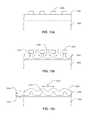
- FIG. 9 ais a top view of a textured region in accordance with one aspect of the present disclosure.
- FIG. 9 bis a cross-sectional view of a textured surface in accordance with an aspect of the present disclosure.
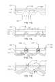
- FIG. 10 ais a cross-sectional view of a photosensitive device during manufacture in accordance with another aspect of the present disclosure
- FIG. 10 bis a cross-sectional view of a photosensitive device during manufacture in accordance with another aspect of the present disclosure.
- FIG. 10 cis a cross-sectional view of a photosensitive device during manufacture in accordance with another aspect of the present disclosure.
- FIG. 11 ais a cross-sectional view of a photosensitive device during manufacture in accordance with yet another aspect of the present disclosure
- FIG. 11 bis a cross-sectional view of a photosensitive device during manufacture in accordance with yet another aspect of the present disclosure
- FIG. 11 cis a cross-sectional view of a photosensitive device during manufacture in accordance with yet another aspect of the present disclosure.
- FIG. 11 dis a cross-sectional view of a photosensitive device during manufacture in accordance with yet another aspect of the present disclosure.
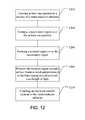
- FIG. 12is a depiction of a method of making a photosensitive imager device in accordance with another aspect of the present disclosure.
- tuningrefers to selectively enhancing a device for a property of light at a desired wavelength or range of wavelengths.
- a property of lightcan be absorptance, quantum efficiency, polarization, and the like.
- textured surfacerefers to a surface having a topology with nano- to micron-sized surface variations formed by the irradiation of laser pulses or other texturing methods.
- other texturing methodscan include chemical etching. While the characteristics of such a surface can be variable depending on the materials and techniques employed, in one aspect such a surface can be several hundred nanometers thick and made up of nanocrystallites (e.g. from about 10 to about 50 nanometers) and nanopores.
- such a surfacecan include micron-sized structures (e.g. about 500 nm to about 60 ⁇ m). In yet another aspect, the surface can include nano-sized and/or micron-sized structures from about 5 nm and about 500 ⁇ m.
- surface modifyingand “surface modification” refer to the altering of a surface of a semiconductor material using a variety of surface modification techniques.
- Non-limiting examples of such techniquesinclude plasma etching, reactive ion etching, porous silicon etching, lasing, chemical etching (e.g. anisotropic etching, isotropic etching), nanoimprinting, material deposition, selective epitaxial growth, and the like, including combinations thereof.
- surface modificationcan include processes using primarily laser radiation or laser radiation in combination with a dopant, whereby the laser radiation facilitates the incorporation of the dopant into a surface of the semiconductor material.
- surface modificationincludes doping of a substrate such as a semiconductor material.
- target regionrefers to an area of a substrate that is intended to be doped or surface modified.
- the target region of the substratecan vary as the surface modifying process progresses. For example, after a first target region is doped or surface modified, a second target region may be selected on the same substrate.
- fluencerefers to the amount of energy from a single pulse of laser radiation that passes through a unit area. In other words, “fluence” can be described as the energy surface density of one laser pulse.
- detectionrefers to the sensing, absorption, and/or collection of electromagnetic radiation.
- backside illuminationrefers to a device architecture design whereby electromagnetic radiation is incident on a surface of a semiconductor material that is opposite a surface containing the device circuitry. In other words, electromagnetic radiation is incident upon and passes through a semiconductor material prior to contacting the device circuitry.
- the term “substantially”refers to the complete or nearly complete extent or degree of an action, characteristic, property, state, structure, item, or result.
- an object that is “substantially” enclosedwould mean that the object is either completely enclosed or nearly completely enclosed.
- the exact allowable degree of deviation from absolute completenessmay in some cases depend on the specific context. However, generally speaking the nearness of completion will be so as to have the same overall result as if absolute and total completion were obtained.
- the use of “substantially”is equally applicable when used in a negative connotation to refer to the complete or near complete lack of an action, characteristic, property, state, structure, item, or result.
- compositions that is “substantially free of” particleswould either completely lack particles, or so nearly completely lack particles that the effect would be the same as if it completely lacked particles.
- a composition that is “substantially free of” an ingredient or elementmay still actually contain such item as long as there is no measurable effect thereof.
- the term “about”is used to provide flexibility to a numerical range endpoint by providing that a given value may be “a little above” or “a little below” the endpoint.
- Electromagnetic radiationcan be present across a broad wavelength range, including visible range wavelengths (approximately 350 nm to 800 nm) and non-visible wavelengths (longer than about 800 nm or shorter than 350 nm).
- the infrared spectrumis often described as including a near infrared portion of the spectrum including wavelengths of approximately 800 nm to 1300 nm, a short wave infrared portion of the spectrum including wavelengths of approximately 1300 nm to 3 micrometers, and a mid to long wave infrared (or thermal infrared) portion of the spectrum including wavelengths greater than about 3 micrometers up to about 30 micrometers.
- infraredportions of the electromagnetic spectrum unless otherwise noted.
- silicon photodetecting imagershave limited light absorption/detection properties.
- silicon based detectorsare mostly transparent to infrared light. While other mostly opaque materials (e.g. InGaAs) can be used to detect infrared electromagnetic radiation having wavelengths greater than about 1000 nm, silicon is still commonly used because it is relatively cheap to manufacture and can be used to detect wavelengths in the visible spectrum (i.e. visible light, 350 nm-800 nm).
- Traditional silicon materialsrequire substantial path lengths to detect photons having wavelengths longer than approximately 700 nm. While visible light can be absorbed at relatively shallow depths in silicon, absorptance of longer wavelengths (e.g. 900 nm) in silicon of a standard wafer depth (e.g. approximately 750 ⁇ m) is poor if at all.
- the devices of the present disclosureincrease the absorptance of semiconductor materials by increasing the propagation path length for longer wavelengths as compared to traditional materials.
- the absorption depth in conventional silicon detectorsis the depth into silicon at which the radiation intensity is reduced to about 36% of the value at the surface of the semiconductor.
- the increased propagation path lengthresults in an apparent reduction in the absorption depth, or a reduced apparent or effective absorption depth.
- the effective absorption depth of siliconcan be reduced such that these longer wavelengths can be absorbed in material thicknesses of less than or equal to about 850 ⁇ m.
- these devicesare able to absorb longer wavelengths (e.g. >1000 nm for silicon) within a thinner semiconductor material.
- the response rate or response speedcan also be increased by using thinner semiconductor materials.
- BSI photosensitive imager devicesand associated methods are provided. Such devices provide, among other things, enhanced response in the infrared light portion of the electromagnetic spectrum and improved response and quantum efficiency in converting electromagnetic radiation to electrical signals. Quantum efficiency can be defined as the percentage of photons that are converted into electrons and collected by a sensing circuit.
- QEInternal QE
- EQEExternal QE
- the EQEis always lower than the IQE since there will inevitably be recombination effects and optical losses (e.g. transmission and reflection losses).
- One reason for improved performance with BSIis a higher fill factor or, in other words, the percentage if incident light that is incident on a photosensitive region of the device.
- FSIfront side-illuminated sensor
- a photosensitive diodecan include a semiconductor substrate having multiple doped regions forming at least one junction, a textured region coupled to the semiconductor substrate and positioned to interact with electromagnetic radiation where the textured region includes surface features sized and positioned to facilitate tuning to a preselected wavelength of light, and a dielectric region positioned between the textured region and the at least one junction.
- the dielectric regionis positioned to isolate the at least one junction from the textured region, and the semiconductor substrate and the textured region are positioned such that incoming electromagnetic radiation passes through the semiconductor substrate before contacting the textured region.
- the dielectric regioncan be a passivation region.
- the multiple doped regionscan include at least one cathode region and at least one anode region.
- doped regionscan include an n-type dopant and/or a p-type dopant as is discussed below, thereby creating a p-n junction.
- a photosensitive devicecan include an i-type region to form a p-i-n junction.
- a photosensitive pixelcan include a semiconductor substrate having multiple doped regions forming at least one junction, a textured region coupled to the semiconductor substrate and positioned to interact with electromagnetic radiation where the textured region includes surface features sized and positioned to facilitate tuning to a preselected wavelength of light, and a dielectric region positioned between the textured region and the at least one junction. The dielectric region is positioned to isolate the at least one junction from the textured region, and the semiconductor substrate and the textured region are positioned such that incoming electromagnetic radiation passes through the semiconductor substrate before contacting the textured region. Additionally, the photosensitive pixel also includes an electrical transfer element coupled to the semiconductor substrate and operable to transfer an electrical signal from the at least one junction.
- a photosensitive imagercan include multiple photosensitive pixels. Additionally, an electrical transfer element can include a variety of devices, including without limitation, transistors, sensing nodes, transfer gates, transfer electrodes, and the like.
- Photosensitive or photo detecting imagersinclude photodiodes or pixels that are capable of absorbing electromagnetic radiation within a given wavelength range.
- Such imagerscan be passive pixel sensors (PPS), active pixel sensors (APS), digital pixel sensor imagers (DPS), or the like, with one difference being the image sensor read out architecture.
- a semiconducting photosensitive imagercan be a three or four transistor active pixel sensor (3T APS or 4T APS).
- 3T APS or 4T APStransistor active pixel sensor
- additional componentsare also contemplated, and would necessarily vary depending on the particular configuration and intended results. As an example, a 4T configuration as is shown in FIG.
- photosensor diode 110can be a conventional pinned photodiode as used in current state of the art complimentary metal-oxide-semiconductor (CMOS) imagers.
- CMOScomplimentary metal-oxide-semiconductor
- Photosensitive imagerscan be front side illumination (FSI) or back side illumination (BSI) devices.
- FSIfront side illumination
- BSIback side illumination
- incident lightenters the semiconductor device by first passing by transistors and metal circuitry. The light, however, can scatter off of the transistors and circuitry prior to entering the light sensing portion of the imager, thus causing optical loss and noise.
- a lenscan be disposed on the topside of a FSI pixel to direct and focus the incident light to the light sensing active region of the device, thus partially avoiding the circuitry.
- the lenscan be a micro-lens.
- incident lightenters the device via the light sensing portion and is mostly absorbed prior to reaching the circuitry.
- BSI designsallow for smaller pixel architecture and a higher fill factor for the imager. It should also be understood that devices according to aspects of the present disclosure can be incorporated into CMOS imager architectures, charge-coupled device (CCD) imager architectures, and the like.
- a BSI photosensitive diode 200can include a semiconductor substrate 202 having multiple doped regions 204 , 206 forming at least one junction, and a textured region 208 coupled to the semiconductor substrate 202 and positioned to interact with electromagnetic radiation 212 .
- the multiple doped regions 204 , 206can have the same doping profile or different doping profiles, depending on the device. While the device shown in FIG. 2 contains three doped regions, it should be noted that other aspects containing one or more doped regions are considered to be within the present scope.
- the semiconductor substrate 202can be doped, and thus can be considered to be a doped region in some aspects.
- a dielectric region 210is positioned between the textured region 208 and the at least one junction.
- the dielectric regioncan have a thickness in the range of about 1 nm to about 2 ⁇ m.
- the dielectric regioncan have a thickness in the range of about 10 nm to about 100 nm.
- the dielectric regioncan have a thickness of less than about 50 nm.
- the dielectric region 210can be positioned to isolate the at least one junction from the textured region 208 , and the semiconductor substrate 202 and the textured region 208 can be positioned such that incoming electromagnetic radiation 212 passes through the semiconductor substrate 202 before contacting the textured region 208 .
- the photosensitive diodeis backside illuminated by electromagnetic radiation 212 that is incident on the side of the semiconductor substrate 202 opposite the multiple doped regions 204 , 206 .
- a BSI photosensitive imager device 300is provided.
- the BSI photosensitive imager devicecan include a semiconductor substrate 302 having multiple doped regions 304 , 306 forming a least one junction, and a textured region 308 coupled to the semiconductor substrate 302 and positioned to interact with electromagnetic radiation 310 .
- a dielectric region 312can be positioned between the textured region 308 and the at least one junction to isolate the at least one junction from the textured region.
- the semiconductor substrate 302 and the textured region 308are positioned such that incoming electromagnetic radiation 310 passes through the semiconductor substrate 302 before contacting the textured region 308 .
- an optional dielectric region or reflecting region 314can be coupled to the textured region 308 .
- An electrical transfer element 316can be coupled to the semiconductor substrate 302 to transfer an electrical signal from the at least one junction.
- Side wall insulators 318 and 320can also be formed about the transfer element 316 and also around the dielectric and textured regions 312 , 314 , respectively, to facilitate proper spacing away from the transfer element 316 .
- a drain junction region 322can be electrically coupled to the transfer element 316 to receive charge transferred thereto by the transfer element.
- the various devices according to aspects of the present disclosurecan exhibit increased quantum efficiency over traditional photosensitive devices. Any increase in the quantum efficiency makes a large difference in the signal to noise ratio. More complex structures can provide not only increased quantum efficiency but also good uniformity from pixel to pixel.
- devices of the present disclosureexhibit increased responsivity as compared to traditional photosensitive devices.
- the responsivitycan be greater than or equal to 0.8 A/W for wavelengths greater than 1000 nm for semiconductor substrate that is less than 100 ⁇ m thick. In other embodiment the responsivity can be greater than 0.5 A/W for wavelengths greater than 1100 nm for semiconductor substrate that is less than 50 ⁇ m thick.
- semiconductor materialsare contemplated for use with the devices and methods according to aspects of the present disclosure.
- Non-limiting examples of such semiconductor materialscan include group IV materials, compounds and alloys comprised of materials from groups II and VI, compounds and alloys comprised of materials from groups III and V, and combinations thereof.
- exemplary group IV materialscan include silicon, carbon (e.g. diamond), germanium, and combinations thereof.
- Various exemplary combinations of group IV materialscan include silicon carbide (SiC) and silicon germanium (SiGe).
- the semiconductor materialcan be or include silicon.
- Exemplary silicon materialscan include amorphous silicon (a-Si), microcrystalline silicon, multicrystalline silicon, and monocrystalline silicon, as well as other crystal types.
- the semiconductor materialcan include at least one of silicon, carbon, germanium, aluminum nitride, gallium nitride, indium gallium arsenide, aluminum gallium arsenide, and combinations thereof.
- Exemplary combinations of group II-VI materialscan include cadmium selenide (CdSe), cadmium sulfide (CdS), cadmium telluride (CdTe), zinc oxide (ZnO), zinc selenide (ZnSe), zinc sulfide (ZnS), zinc telluride (ZnTe), cadmium zinc telluride (CdZnTe, CZT), mercury cadmium telluride (HgCdTe), mercury zinc telluride (HgZnTe), mercury zinc selenide (HgZnSe), and combinations thereof.
- CdSecadmium selenide
- CdScadmium sulfide
- CdTecadmium telluride
- ZnOzinc oxide
- ZnSezinc selenide
- ZnSzinc sulfide
- ZnTezinc telluride
- CdZnTecadmium zinc telluride
- Exemplary combinations of group III-V materialscan include aluminum antimonide (AlSb), aluminum arsenide (AlAs), aluminum nitride (AlN), aluminum phosphide (AlP), boron nitride (BN), boron phosphide (BP), boron arsenide (BAs), gallium antimonide (GaSb), gallium arsenide (GaAs), gallium nitride (GaN), gallium phosphide (GaP), indium antimonide (InSb), indium arsenide (InAs), indium nitride (InN), indium phosphide (InP), aluminum gallium arsenide (AlGaAs, Al x Ga 1 ⁇ x As), indium gallium arsenide (InGaAs, In x Ga 1 ⁇ x As), indium gallium phosphide (InGaP), aluminum indium arsenide (AlInAs),
- the semiconductor substratecan be of any thickness that allows electromagnetic radiation detection and conversion functionality, and thus any such thickness of semiconductor material is considered to be within the present scope.
- the textured regionincreases the efficiency of the device such that the semiconductor substrate can be thinner than has previously been possible. Decreasing the thickness of the semiconductor substrate reduces the amount of semiconductor material required to make such a device.
- the semiconductor substratehas a thickness of from about 500 nm to about 50 ⁇ m.
- the semiconductor substratehas a thickness of less than or equal to about 100 ⁇ m.
- the semiconductor substratehas a thickness of from about 1 ⁇ m to about 10 ⁇ m.
- the semiconductor substratecan have a thickness of from about 5 ⁇ m to about 50 ⁇ m.
- the semiconductor substratecan have a thickness of from about 5 ⁇ m to about 10 ⁇ m.
- the semiconductor materialis monocrystalline.
- the semiconductor materialis multicrystalline.
- the semiconductor materialis microcrystalline. It is also contemplated that the semiconductor material can be amorphous. Specific nonlimiting examples include amorphous silicon or amorphous selenium.
- the semiconductor materials of the present disclosurecan also be made using a variety of manufacturing processes. In some cases the manufacturing procedures can affect the efficiency of the device, and may be taken into account in achieving a desired result. Exemplary manufacturing processes can include Czochralski (Cz) processes, magnetic Czochralski (mCz) processes, Float Zone (FZ) processes, epitaxial growth or deposition processes, and the like. It is contemplated that the semiconductor materials used in the present invention can be a combination of monocrystalline material with epitaxially grown layers formed thereon.
- dopant materialsare contemplated for the formation of the multiple doped regions, and any such dopant that can be used in such processes to surface modify a material is considered to be within the present scope. It should be noted that the particular dopant utilized can vary depending on the material being doped, as well as the intended use of the resulting material. For example, the selection of potential dopants may differ depending on whether or not tuning of the photosensitive device is desired.
- a dopantcan be either charge donating or accepting dopant species. More specifically, an electron donating or a hole donating species can cause a region to become more positive or negative in polarity as compared to the semiconductor substrate.
- the doped regioncan be p-doped.
- the doped regioncan be n-doped.
- a highly doped regioncan also be formed on or near the doped region to create a pinned diode.
- the semiconductor substratecan be negative in polarity, and a doped region and a highly doped region can be doped with p+ and n dopants respectively.
- variations of n( ⁇ ), n( ⁇ ), n(+), n(++), p( ⁇ ), p( ⁇ ), p(+), or p(++) type doping of the regionscan be used.
- non-limiting examples of dopant materialscan include S, F, B, P, N, As, Se, Te, Ge, Ar, Ga, In, Sb, and combinations thereof.
- the scope of dopant materialsshould include, not only the dopant materials themselves, but also materials in forms that deliver such dopants (i.e. dopant carriers).
- S dopant materialsincludes not only S, but also any material capable being used to dope S into the target region, such as, for example, H 2 S, SF 6 , SO 2 , and the like, including combinations thereof.
- the dopantcan be S.
- Sulfurcan be present at an ion dosage level of between about 5 ⁇ 10 14 ions/cm 2 and about 1 ⁇ 10 16 ions/cm 2 .
- fluorine-containing compoundscan include ClF 3 , PF 5 , F 2 SF 6 , BF 3 , GeF 4 , WF 6 , SiF 4 , HF, CF 4 , CHF 3 , CH 2 F 2 , CH 3 F, C 2 F 6 , C 2 HF 5 , C 3 F 8 , C 4 F 8 , NF 3 , and the like, including combinations thereof.
- Non-limiting examples of boron-containing compoundscan include B(CH 3 ) 3 , BF 3 , BCl 3 , BN, C 2 B 10 H 12 , borosilica, B 2 H 6 , and the like, including combinations thereof.
- Non-limiting examples of phosphorous-containing compoundscan include PF 5 , PH 3 , and the like, including combinations thereof.
- Non-limiting examples of chlorine-containing compoundscan include Cl 2 , SiH 2 Cl 2 , HCl, SiCl 4 , and the like, including combinations thereof
- Dopantscan also include arsenic-containing compounds such as AsH 3 and the like, as well as antimony-containing compounds. Additionally, dopant materials can include mixtures or combinations across dopant groups, i.e.
- the dopant materialcan have a density that is greater than air.
- the dopant materialcan include Se, H 2 S, SF 6 , or mixtures thereof.
- the dopantcan be SF 6 and can have a predetermined concentration range of about 5.0 ⁇ 10 ⁇ 8 mol/cm 3 to about 5.0 ⁇ 10 ⁇ 4 mol/cm 3 .
- SF 6 gasis a good carrier for the incorporation of sulfur into the semiconductor material via a laser process without significant adverse effects on the material.
- dopantscan also be liquid solutions of n-type or p-type dopant materials dissolved in a solution such as water, alcohol, or an acid or basic solution. Dopants can also be solid materials applied as a powder or as a suspension dried onto the wafer.
- the semiconductor substratecan be annealed for a variety of reasons, including dopant activation, semiconductor damage repair, and the like.
- the semiconductor substratecan be annealed prior to texturing, following texturing, during texturing, or any combination thereof.
- Annealingcan enhance the semiconductive properties of the device, including increasing the photoresponse properties of the semiconductor materials by reducing any imperfections in the material. Additionally, annealing can reduce damage that may occur during the texturing process.
- any known annealcan be beneficial and would be considered to be within the present scope, annealing at lower temperatures can be particularly useful. Such a “low temperature” anneal can greatly enhance the external quantum efficiency of devices utilizing such materials.
- the semiconductor substratecan be annealed to a temperature of from about 300° C. to about 1100 C.°. In another aspect, the semiconductor substrate can be annealed to a temperature of from about 500° C. to about 900° C. In yet another aspect, the semiconductor substrate can be annealed to a temperature of from about 700° C. to about 800° C. In a further aspect, the semiconductor substrate can be annealed to a temperature that is less than or equal to about 850° C.
- the duration of the annealing procedurecan vary according to the specific type of anneal being performed, as well as according to the materials being used. For example, rapid annealing processes can be used, and as such, the duration of the anneal may be shorter as compared to other techniques. Various rapid thermal anneal techniques are known, all of which should be considered to be within the present scope.
- the semiconductor substratecan be annealed by a rapid annealing process for a duration of greater than or equal to about 1 ⁇ s.
- the duration of the rapid annealing processcan be from about 1 ⁇ s to about 1 ms.
- a baking or furnace anneal processcan be used having durations that may be longer compared to a rapid anneal.
- the semiconductor substratecan be annealed by a baking anneal process for a duration of greater than or equal to about 1 ms to several hours.
- dielectric region configurationsare contemplated, and any configuration that can be incorporated into a photosensitive device is considered to be within the present scope.
- One benefit to such a dielectric regionpertains to the isolation provided between the textured region and the doped regions that form the junction.
- the dielectric regioncan be positioned to physically isolate the textured region from the junction. In this way, the creation of the textured region can be isolated from the doped regions, thus precluding undesirable effects of the texturing process from affecting the junction.
- the dielectric regioncan be a dielectric material, and thus the dielectric region could be used to electrically isolate the textured region from the junction.
- the dielectric regionis coupled directly to at least one of the doped regions forming the junction.
- the dielectric regioncan be made from a variety of materials, and such materials can vary depending on the device design and desired characteristics. Non-limiting examples of such materials can include oxides, nitrides, oxynitrides, and the like, including combinations thereof.
- the dielectric regionincludes an oxide.
- the dielectric regioncan be of various thicknesses. In one aspect, for example, the dielectric region has a thickness of from about 100 nm to about 1 micron. In another aspect, the dielectric region has a thickness of from about 5 nm to about 100 nm. In yet another aspect, the dielectric region has a thickness of from about 20 nm to about 50 nm.
- the thickness of the dielectric materialwould be increased to account for the texturing.
- the thickness ranges for the dielectric region provided herewould be measured as the thickness of the dielectric region not including the textured portion.
- the textured regioncan function to diffuse electromagnetic radiation, to redirect electromagnetic radiation, to absorb electromagnetic radiation, and the like, thus increasing the quantum efficiency of the device.
- electromagnetic radiation passing through the semiconductor substratecan contact the textured region.
- the textured regioncan include surface features to thus increase the effective absorption length of the photosensitive pixel.
- Such surface featurescan be to micron-sized and/or nano-sized, and can be any shape or configurations. Non-limiting examples of such shapes and configurations include cones, pillars, pyramids, micolenses, quantum dots, inverted features, gratings, protrusions, scallops, and the like, including combinations thereof. Additionally, factors such as manipulating the feature sizes, dimensions, material type, dopant profiles, texture location, etc.
- tuning the devicecan allow the diffusing region to be tunable for a specific wavelength.
- tuning the devicecan allow specific wavelengths or ranges of wavelengths to be absorbed.
- tuning the devicecan allow specific wavelengths or ranges of wavelengths to be reduced or eliminated via filtering.
- Tuningcan also be accomplished through the relative location of the texture region within the device, modifying the dopant profile(s) of regions within the device, dopant selection, and the like. Additionally, material composition near the textured region can create a wavelength specific photosensing pixel device. It should be noted that a wavelength specific photosensing pixel can differ from one pixel to the next, and can be incorporated into an imaging array. For example a 4 ⁇ 4 array can include a blue pixel, a green pixel, a red pixel, and infrared light absorbing pixel, or a blue pixel, two green pixels, and a red pixel.
- the textured regionscan also be made to be selective to polarized light and light of particular polarizations.
- the textured regionincludes a one dimensional grating of grooves on a high index of refraction material then the scattering of the light will depend upon the polarization of the light and the pixels can select light of specific linear polarizations.
- Textured regionscan allow a photosensitive device to experience multiple passes of incident electromagnetic radiation within the device, particularly at longer wavelengths (i.e. infrared). Such internal reflection increases the effective absorption length to be greater than the thickness of the semiconductor substrate. This increase in absorption length increases the quantum efficiency of the device, leading to an improved signal to noise ratio.
- the materials used for producing the textured regioncan vary depending on the design and the desired characteristics of the device. As such, any material that can be utilized in the construction of a textured region is considered to be within the present scope. Non-limiting examples of such materials include semiconductor materials, dielectric materials, conductive materials (e.g. metals), silicon, polysilicon, amorphous silicon, transparent conductive oxides, and the like, including composites and combinations thereof.
- the textured layercan be a textured polysilicon layer.
- a polysilicon layercan be deposited onto the dielectric region and then textured to form the textured region.
- the textured layercan be a textured dielectric layer.
- the textured regioncan be a portion of the dielectric layer making up the dielectric region.
- the textured layercan be a transparent conductive oxide or another semiconductor material.
- the textured regioncan be a textured portion of the dielectric region or the textured region can be formed from other dielectric material deposited over the dielectric region.
- forming the textured regioncan include depositing a semiconductor material on the dielectric region and texturing the semiconductor material to form the textured region.
- the semiconductor materialcan be bonded or adhered to the dielectric region. The texturing process can texture the entire semiconductor material or only a portion of the semiconductor material.
- a polysilicon layercan be deposited over the dielectric region and textured and patterned by an appropriate technique (e.g. a porous silicon etch) to form the textured region.
- a polysilicon layercan be deposited over the dielectric region and textured and patterned by using a mask, photolithography, and an etch to define a specific structure or pattern.
- the textured regioncan have a surface morphology that is designed to focus or otherwise direct electromagnetic radiation, thus enhancing the quantum efficiency of the device.
- the textured regionhas a surface morphology operable to direct electromagnetic radiation into the semiconductor substrate.
- various surface morphologiesinclude sloping, pyramidal, inverted pyramidal, spherical, square, rectangular, parabolic, ellipsoidal, asymmetric, symmetric, scallops, gratings, pillars, cones, microlenses, quantum dots, and the like, including combinations thereof.
- FIG. 4shows a textured device 400 having a surface morphology that affects the near infrared wavelength response.
- a semiconductor substrate 402is shown having an illuminated surface 404 to receive incident electromagnetic radiation 406 .
- the semiconductor substrate 402further has a textured region 408 (e.g. dielectric) coupled thereto at a surface that is opposite to the illuminated surface 404 .
- the textured region 408has a surface morphology configured in an undulating pattern 410 with grooves, ridges, or similar patterns to produce an internal reflection that is not specular.
- the absorption coefficient of siliconis very low in the near infrared. Electromagnetic radiation under normal incidence, represented by arrow 412 , is reflected from the illuminated surface 404 , and this is shown as arrow 414 .
- ⁇is the absorption coefficient in reciprocal cm
- dis the thickness of the sample in cm
- T 1is the transmittance of radiation incident on the first surface.
- T 2is the transmittance of radiation striking the second surface from the semiconductor side.
- R 1is the amount of radiation reflected back into the semiconductor for radiation striking the first surface from the semiconductor side.
- R 2is the amount of radiation reflected back into the semiconductor for radiation striking the second surface from the semiconductor side.
- the illuminated side 404is polished but the opposing side 410 is a textured dielectric material 408 with a reflecting region 422 (see FIG. 4 ).
- the texturingcan be realized in a fashion to produce a true diffuse scattering (i.e. a Lambertian scattering) at the infrared wavelengths.
- the reflectance of the polished front side to the scattered light radiationis determined by solid angle considerations. Any incident light with an angle of incidence greater than the critical angle ⁇ c , 424 , will be totally internally reflected 420 .
- the transmittanceis then determined by the area of the surface ( ⁇ 2 ) within the critical angle ⁇ c , 424 , in this case 17° for silicon and air.
- Equation (IV)the enhancement in absorptance described by Equation (IV) then varies with the fraction of light radiation reflected back from the illuminated surface and thickness of the sample, as is illustrated in FIG. 5 .
- the techniques described hereinhave been used to enhance the absorptance at infrared and red light radiation, they are also applicable to visible light as the thickness of the silicon layer becomes thinner. Scattering and multiple internal reflections can also be used to increase the absorptance at yellow, green and even blue light that will not be totally absorbed in single passes within thin silicon layers. These techniques can be applied then to visible imagers with thin silicon absorption layers.
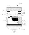
- FIG. 6shows a cross-section of a BSI photosensitive pixel device 600 .
- the photosensitive pixel devicecan include a semiconductor substrate 602 that can be referred to as bulk semiconductor material.
- the semiconductor substrate 602includes at least one doped region 604 , 605 , that can be doped with a charge donating species, such as an electron donating or hole donating species, to cause the region to become more n-type or p-type as compared to the semiconductor substrate.
- the doped regioncan be p-doped.
- the doped regioncan be n-doped.
- the devicecan further include various metal regions 606 , at least one via 608 , a dielectric region 610 , isolation element(s) 612 , such as trench isolation elements, and an electrical transfer element 614 .
- Trench isolation elementscan maintain pixel to pixel uniformity by reducing optical and electrical crosstalk.
- the isolation elementscan be shallow or deep trench isolation.
- the trench isolation elements of FIG. 6are shown as deep trench isolation elements.
- the isolation elementscan include various materials, including, without limitation, dielectric materials, reflective materials, conductive materials, light diffusing features, and the like. These isolation regions can be configured to reflect incident light until it is absorbed, thereby increase the effective absorption length of the device.
- a lens 624 and an anti-reflective coating 616can be disposed on the backside of the pixel following thinning and trench isolation.
- a color filter 618can be optically coupled to the lens to allow specific wavelength filtering of the electromagnetic radiation.
- a textured region 620can be coupled to the semiconductor substrate 602 opposite the lens 624 in order to provide diffusive scattering and reflection of the incident electromagnetic radiation that passes through to the front side of the pixel. Thus the electromagnetic radiation can be focused within the semiconductor substrate 602 to the combined action of the textured region 620 and the isolation features 612 .
- side wall insulators 622can be formed about the transfer element 606 and also around textured region 620 to facilitate proper spacing.
- isolation featurescan maintain pixel to pixel uniformity when multiple pixels are used in association by reducing optical and electrical crosstalk there between.
- the isolation featurecan be shallow or deep, depending on the desired design.
- the isolation featurescan be generated using various materials including, without limitation, dielectric materials, reflective materials, conductive materials, light diffusing features, and the like. Additionally, in some aspects the isolation feature can be a void in the semiconductor substrate.
- isolation featurescan also be configured to reflect incident electromagnetic radiation until it is absorbed, thereby increasing the effective absorption length of the incident light and reducing optical crosstalk into neighboring devices.
- the devices according to aspects of the present disclosurecan also independently include one or more vias, dielectric regions, and the like.
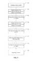
- a method of making a backside-illuminated photosensitive imager devicecan include traditional fabrication steps along with additional steps of forming isolation features 702 , doping a portion of the semiconductor material to form n+ implant 704 , doping a portion with an n+ implant to form a source-drain 706 , doping a portion of the semiconductor substrate with a p+ dopant to form p+ implant 708 , and growing and etching a gate oxide region 710 .
- the methodcan also include depositing and etching to form a polysilicon gate 712 , forming a textured surface near the p+ implant region 714 , and depositing the contacts 716 .
- this processcan be applied in modular form to the steps involved in the fabrication of a conventional BSI CMOS imager pixel arrays.
- this modular processing methodcan be an insert of a process module in the process flow of the fabrication of a conventional BSI imager.
- the conventional processcan be stopped just before the first via etch but after the deposition of the interlayer dielectric.
- the mask that was used to define the p-type implantation on top of the n-type diodecan be used to mask and open the area over the p-type layer.
- a sidewall spacer processcan be employed on the inside border of this opening to insure adequate spacing of the textured layers to be deposited away from the transfer device.
- a dielectric region, a textured region, and in some cases a metal or oxide reflectorcan be deposited in the area over the p-type region. As such, this module can be introduced into a conventional process flow with minimal changes.
- an interlayer dielectric similar to the first interlayer dielectriccan be deposited over the metal reflector, and the combined interlayer dielectrics can be chemically and mechanically polished to planarize the surface.
- the normal contact maskcan then be used to open vias resulting in minimal changes to the conventional process flow.
- a viacan be opened to the metal reflector layer to control the potential of this layer and if appropriate, the textured layer to avoid charging during processing or for the region, can act as an MOS gate.
- CMOS imagersare commonly used as visible light cell phone, still frame and video cameras, with BSI devices becoming a common structure. Cameras for use as infrared imagers for security and surveillance are, however, not commonly available.
- the present methodsallow the conversion of visible light imagers to include the capability for imaging in the near infrared.
- the texture processing methods describedcan be adapted to a traditional fabrication process for visible imagers to provide an additional capability for near infrared imaging.
- the CMOS imagerscan employ any pixel design including more than one transistor or transfer device.
- the transfer devicecan be a p-channel transfer gate or an n-channel transfer gate and associated implant polarities.
- CCD imagersemploy photodiode detectors similar to those used in CMOS imagers, and as such, the present methods can also be applied to the fabrication of CCD imagers to form devices capable of detecting infrared wavelengths in appreciable amounts and with appreciable enhancement.
- the photodetecting diode used in the imager pixelcan also include MOS diodes rather than doped junction diodes.
- MOS diodesuse a pulsed bias to form a depletion region and light collecting region near the surface rather than a junction diode.
- the method described hereincan equally be applied and inserted into imager pixels with MOS diodes or CCD imagers where the light generated carriers are collected in a surface depletion region. In these latter cases the metal reflecting gate can be driven with a voltage to act as a MOS or CCD gate.
- a BSI photosensitive imager device 800can include a textured region 802 , a reflecting layer 804 , and a dielectric layer 806 disposed between the semiconductor substrate 808 and the textured region 802 .
- the devicecan further include doped regions 810 , 812 , a drain region 814 , sidewall spacers 816 , and a transfer device having a gate insulator 818 and a polysilicon gate 820 , as has been described.
- the reflecting/diffusing region 822shown separately in FIG. 8 b , is thus effectively a process module that can be inserted into a standard CMOS imager manufacturing process as has been described.
- this process module of forming the reflective/diffusing regioncan be inserted after deposition of the first dielectric spacer layer and before a contact etch step in a CMOS image sensor manufacturing process.
- a maskcan be used to create the implantation of the P+ surface region on the photodiode, which can also be used to etch an aperture in the newly formed dielectric layer.
- the spacers 816can be formed on the inside of this hole using conventional techniques to space the textured region 802 away from the edge of the P+ region.
- the holecan then be filled with any one of a variety of “process modules” to form the textured region 802 .
- the conventional processcan be continued starting with the contact etch mask.
- the present scopealso includes aspects having a lens without an anti-reflecting coating, and aspects having an anti-reflecting coating associated with the semiconductor substrate without a lens.
- a color filter(not shown) can be optically coupled to the lens to allow specific wavelength filtering of the electromagnetic radiation. Incident electromagnetic radiation passing through the color filter prior to contacting the semiconductor substrate can be filtered according to the characteristics of the filter.
- the textured regioncan be formed by various techniques, including plasma etching, reactive ion etching, porous silicon etching, lasing, chemical etching (e.g. anisotropic etching, isotropic etching), nanoimprinting, material deposition, selective epitaxial growth, and the like.
- the texturing processcan be performed during the manufacture of the photosensitive device.
- the texturing processcan be performed on a photosensitive device that has previously been made.
- a CMOS, CCD, or other photosensitive elementcan be textured following manufacture. In this case, material layers may be removed from the photosensitive element to expose the semiconductor substrate or the dielectric region upon which a textured region can be formed.
- the textured regioncan be formed having surface features with a size and position distribution that allows tuning to a desired light wavelength or range of wavelengths.
- a given textured regioncan contain an arrangement of surface features that facilitate tuning of the textured region to a preselected wavelength of light. Any wavelength that can be selectively tuned via surface features in the textured region is considered to be within the present scope.
- the preselected wavelength or wavelengths of lightcan be in the near infrared or infrared range.
- the preselected wavelength of lightcan be greater than or equal to about 800 nm.
- tuningcan be accomplished by generating a texture with sufficient long-range lateral order such that interference directs the photons within a certain wavelength range in such a direction that they will experience total internal reflection (TIR) on the surface opposite the texture. This will enhance absorptance and QE.
- the texturewill be additionally tuned to minimize photons reflected into the range of angles where TIR will not occur. This further enhances absorptance and QE.
- the texturewill be additionally tuned to keep the angle at which the photons at the preselected wavelength impinge on the surface opposite the texture as close to normal as possible while still maintaining TIR. This maximized the propagation path, thereby further increasing absorptance and QE, and simultaneously minimizing the optical crosstalk at that preselected wavelength.
- the texturecan be tuned for wavelength selection.
- the average lateral modulation spatial frequencywill be large enough compared to the diffraction limited spot size at the preselected wavelength that effective index descriptions are inaccurate and scattering is substantial.
- the average modulation amplitudewill not be much smaller than the preselected wavelength, so that the surface will not substantially behave as though it were planar.
- the individual features that make up the texturecan be adjusted in shape so as to maximize the number of photons that are incident on the opposite surface at an angle beyond the critical angle, ⁇ c .
- these individual featuresare adjusted to minimize the number of photons that are incident on the opposite surface at an angle less than the critical angle, ⁇ c .
- the texturecan also be tuned to provide polarization selectivity.
- the rotational symmetry in the plane of the texturecan be maximized, thereby leading to uniform behavior over the maximum polarization states.
- the rotational symmetry in the plane of the texturecan be minimized, thereby leading to maximal difference in the behavior for differing polarization states.
- One effective method of producing a textured regionis through laser processing.
- laser processingallows discrete locations of the dielectric region or other substrate to be textured.
- a variety of techniques of laser processing to form a textured regionare contemplated, and any technique capable of forming such a region should be considered to be within the present scope.
- Laser treatment or processingcan allow, among other things, enhanced absorptance properties and thus increased electromagnetic radiation focusing and detection.
- the laser treated regioncan be associated with the surface nearest the impinging electromagnetic radiation or, in the case of BSI devices, the laser treated surface can be associated with a surface opposite in relation to impinging electromagnetic radiation, thereby allowing the radiation to pass through the semiconductor substrate before it hits the laser treated region.
- a target region of the semiconductor materialcan be irradiated with laser radiation to form a textured region.
- Examples of such processinghave been described in further detail in U.S. Pat. Nos. 7,057,256, 7,354,792 and 7,442,629, which are incorporated herein by reference in their entireties.
- a surface of a substrate materialis irradiated with laser radiation to form a textured or surface modified region.
- Such laser processingcan occur with or without a dopant material.
- the lasercan be directed through a dopant carrier and onto the substrate surface. In this way, dopant from the dopant carrier is introduced into the target region of the substrate material.
- the target regiontypically has a textured surface that increases the surface area of the laser treated region and increases the probability of radiation absorption via the mechanisms described herein.
- such a target regionis a substantially textured surface including micron-sized and/or nano-sized surface features that have been generated by the laser texturing.
- irradiating the surface of the substrate materialincludes exposing the laser radiation to a dopant such that irradiation incorporates the dopant into the substrate.
- dopant materialsare known in the art, and are discussed in more detail herein.
- the surface of the substrate or dielectric regionis chemically and/or structurally altered by the laser treatment, which may, in some aspects, result in the formation of surface features appearing as microstructures or patterned areas on the surface and, if a dopant is used, the incorporation of such dopants into the substrate material.
- the features or microstructurescan be on the order of 50 nm to 20 ⁇ m in size (i.e. size at the base, or in some cases center-to-center) and can assist in the absorption of electromagnetic radiation.
- the textured surfacecan increase the probability of incident radiation being absorbed.
- the type of laser radiation used to surface modify a materialcan vary depending on the material and the intended modification. Any laser radiation known in the art can be used with the devices and methods of the present disclosure. There are a number of laser characteristics, however, that can affect the surface modification process and/or the resulting product including, but not limited to the wavelength of the laser radiation, pulse duration, pulse fluence, pulsing frequency, polarization, laser propagation direction relative to the semiconductor material, etc.
- a lasercan be configured to provide pulsatile lasing of a material.
- a short-pulsed laseris one capable of producing femtosecond, picosecond and/or nanosecond pulse durations.
- Laser pulsescan have a central wavelength in a range of about from about 10 nm to about 8 ⁇ m, and more specifically from about 200 nm to about 1200 nm.
- the pulse duration of the laser radiationcan be in a range of from about tens of femtoseconds to about hundreds of nanoseconds.
- laser pulse durationscan be in the range of from about 50 femtoseconds to about 50 picoseconds.
- laser pulse durationscan be in the range of from about 50 picoseconds to 100 nanoseconds.
- laser pulse durationsare in the range of from about 50 to 500 femtoseconds.
- the number of laser pulses irradiating a target regioncan be in a range of from about 1 to about 2000. In one aspect, the number of laser pulses irradiating a target region can be from about 2 to about 1000. Further, the repetition rate or pulsing frequency can be selected to be in a range of from about 10 Hz to about 10 ⁇ Hz, or in a range of from about 1 kHz to about 1 MHz, or in a range from about 10 Hz to about 1 kHz. Moreover, the fluence of each laser pulse can be in a range of from about 1 kJ/m 2 to about 20 kJ/m 2 , or in a range of from about 3 kJ/m 2 to about 8 kJ/m 2 .
- the devices according to aspects of the present disclosurecan additionally include one or more reflecting regions.
- the reflecting regioncan be deposited over the entire textured region or only over a portion of the textured region. In some aspects, the reflecting region can be deposited over a larger area of the device than the textured region.
- the reflecting regioncan be positioned to reflect electromagnetic radiation passing through the texture region back through the textured region. In other words, as electromagnetic radiation passes into the semiconductor substrate, a portion that is not absorbed contacts the textured region. Of that portion that contacts the textured region, a smaller portion may pass though the textured region to strike the reflecting region and be reflected back through the textured region toward the semiconductor substrate.
- a variety of reflective materialscan be utilized in constructing the reflecting region, and any such material capable of incorporation into a photosensitive device is considered to be within the present scope.
- Non-limiting examples of such materialsinclude a Bragg reflector, a metal reflector, a metal reflector over a dielectric material, a transparent conductive oxide such as zinc oxide, indium oxide, or tin oxide, and the like, including combinations thereof.
- Non-limiting examples of metal reflector materialscan include silver, aluminum, gold, platinum, reflective metal nitrides, reflective metal oxides, and the like, including combinations thereof.
- a BSI photosensitive imager devicecan include a dielectric layer positioned between the reflecting region and the textured region.
- the dielectric layercan include an oxide layer and the reflecting region can include a metal layer.
- the surface of the metal layer on an oxideacts as a mirror-like reflector for the incident electromagnetic radiation from the backside. It should be noted that the reflective region is not biased with a voltage.
- the textured regioncan include a hemispherical grained polysilicon or coarse grained polysilicon material and the reflective region can include a metal layer.
- the hemispherical grained or coarse grained siliconcan act as a diffusive scattering site for the incident optical radiation and the dielectric layer and the reflective region together can act as a reflector.
- the photosensitive imagercan include selective epitaxial silicon growth for generating the textured region on top of the junction formed by the doped regions (e.g. a photodiode) without the dielectric region being present (not shown).
- An oxide and metal reflectorfor example, can be coupled to the textured region.
- the epitaxial growthplaces the textured region away from the top of the junction, and the rapid etch characteristics of grain boundaries can be used to create texturing.
- the textured surface of a metal on a roughened oxidecan act as a diffusive scattering site for the incident electromagnetic radiation and also as a mirror-like reflector.
- Other aspectscan utilize porous materials for the texturing.
- Porous polysiliconfor example, can be oxidized or oxide deposited and a reflective region such as a metal reflector can be associated therewith to provide a scattering and reflecting surface.
- aluminumcan be subjected to anodic oxidation to provide porous aluminum oxide, a high dielectric constant insulator. This insulator can be coated with aluminum or other metals to provide a scattering and reflecting surface.
- a reflective regioncan include a transparent conductive oxide, an oxide, and a metal layer.
- the transparent oxidecan be textured and a metal reflector deposited thereupon.
- the textured surface of the metal on a roughened transparent conductive oxidecan act as a diffusive scattering site for the incident electromagnetic radiation.
- a Bragg reflectorcan be utilized as a reflective region.
- a Bragg reflectoris a structure formed from multiple layers of alternating materials with varying refractive indexes, or by some other method of inducing a periodic variation in the propagation constant. Each layer boundary causes a partial reflection of an optical wave. For waves whose wavelength is close to four times the optical thickness of the layers, the many reflections combine with constructive interference, and the layers act as a high-quality reflector. Thus the coherent super-positioning of reflected and transmitted light from multiple interfaces in the structure interfere so as to provide the desired reflective, transmissive, and absorptive behavior.
- the Bragg reflector layerscan be alternating layers of silicon dioxide and silicon.
- this structurecan be fairly low loss even in regions where bulk silicon absorbs appreciably. Additionally, because of the large refractive index difference, the optical thickness of the entire layer set can be thinner, resulting in a broader-band behavior and fewer fabrications steps.
- texturingcan be applied to the light-incident surface of the semiconductor substrate in order to facilitate additional scattering as light enters the device.
- itcan be useful to also include trench isolation to preclude optical crosstalk between pixels due to this forward scattering. By also texturing the trench isolation, light can be reflected back into the semiconductor from the edges of the pixel. It is noted that, for a BSI architecture, the light-incident surface is on the back side of the semiconductor substrate opposite the photodiode.
- FIGS. 9 a,ba backside texture surface an imager pixel is shown in FIGS. 9 a,b .
- FIG. 9 ashows a top view
- FIG. 9 bshows a cross sectional view of a textured region 900 including pillars etched into a semiconductor material.
- the textured regioncan include a plurality of pillars having a uniform size.
- the textured regioncan include a plurality of pillars in a regular (ordered pattern) array.
- the textured regioncan include a plurality of pillars of variable sizes ( 902 , 904 in FIG. 9 ).
- the textured regioncan be arranged in a non-uniform array (see FIG. 9 ).
- holes of uniform or variable sizescan be etched into the silicon and covered by a thin layer of oxide and metal to achieve similar effects as the pillars.
- the pillar or hole featurescan be etched into a thin layer of oxide and metal, or they can be etched into a thicker oxide on the semiconductor substrate and covered by a reflective material, such as silver or aluminum.
- the minimum oxide thickness between the semiconductor substrate and metalcan be in the range of about 5 nm to 100 nm. In another aspect, the thickness can be about 40 nm.
- the height of the pillarscan vary depending on the design and desired use of the device.
- the average pillar heightcan be a multiple of a quarter wavelength of the desired light wavelength selectivity in the medium to which they are etched (e.g., the semiconductor material or the dielectric material.
- the average center-to-center distance between pillarscan be about one half the wavelength of light desired to be absorbed (1 ⁇ 2 ⁇ ), multiples of one half the wavelength, or larger than half the wavelength of desired light selectivity.
- the pillarscan also be designed to be anti-reflecting to the specular reflection of light or the zero th order diffraction from the texture.
- the higher order diffractions of light from the texturecan be designed to optimize the reflection of light at any particular oblique angle. In this manner most of the incident light can be reflected at angles to maximize light trapping in the imager pixel. Light scattered by the front side textured region and striking the semiconductor side of the back interface can be totally internally reflected if it is outside of the critical angle as defined by Snell's law.
- FIGS. 10 a - cOne exemplary method of creating a textured region such as a diffraction grating is shown in FIGS. 10 a - c .
- a semiconductor substrate 1002 having an oxide layer 1004is provided.
- a mask 1006 as a 2-dimensional gratingis formed on the oxide layer 1004 , as is shown in FIG. 10 a .
- the oxide layer 1004can then be etched with an isotropic etch 1008 to form a plurality of pillars 1010 , as shown in FIG. 10 b .
- undercutting of the pillars by the isotropic etch 1008can results in pillars 1010 that are narrow at the top of the pillar than the bottom.
- the mask 1006can be removed and a rinse etch used to round off sharp corners and tops of the pillars 1010 , as is shown in FIG. 10 c .
- a reflecting material 1012e.g. a metal
- the rounded surfacescan reduce the amplitude of the specular reflection or zero th order diffraction of light from the diffraction grating (i.e., the textured region). Thus, the light will be scattered more effectively at oblique angles.
- FIG. 10 calso shows the thickness (t ox ) 1014 of oxide layer 1004 , the grating thickness (t gr ) 1016 , and the distance from pillar peak-to-peak (T) 1018 .
- the average thickness of t oxcan have a range of from about 10 nm to about 100 nm. In another aspect, the t ox can have a thickness of less than about 50 nm.
- the average grating thickness t grmeasured from the base of the oxide layer 1004 to a pillar peak 1010 , can be about a quarter of the wavelength of the desired light wavelength selectivity in the oxide layer ( ⁇ 1 ⁇ 4 ⁇ ). For example, light having a wavelength of about 1000 nm can dictate t gr having a thickness of greater than about 175 nm.
- the average distance (T) from pillar peak-to-peakcan be greater than 300 nm for light having a wavelength of greater than 1000 nm.
- FIGS. 11 a - dare cross-sectional views of a photosensitive device at different stages of manufacturing.
- the semiconductor materialcan be amorphous silicon, which can have a texture surface with a high index of refraction because amorphous silicon can be deposited at low temperatures.
- FIGs. 11 a - dshow a one dimensional grating, such as a plurality of grooves, or in two dimensions an array of pyramidal structures being formed on or in the photosensitive device.
- a semiconductor material 1102can be coupled to a thin layer of oxide 1104 and a layer of nitride 1106 .
- the front side 1102 of the pixel in the P+ diode surface areahas been opened in the first interlayer dielectric.
- the semiconductor material 1102can be etched 1108 to form a mask 1110 using standard techniques on an opposite side where incident light enters the device.
- a semiconductor material 1112such as amorphous silicon can be deposited, and an anisotropic etch can be used in a “sidewall” like process.
- a reflecting regioncomprising a dielectric layer 1114 and metallic layer 1116 can be deposited on the etched surface. In one dimensional arrays this produces a series lines of material 1118 and grooves in the semiconductor material that functions as a diffraction grating 1120 ( FIG. 11 c ). The distance from one groove to the neighboring groove (2k, FIG. 11 b ) can be determined by the diffraction angle for different orders (m) of diffraction.
- the first order diffraction, 1122can be selected to be a large angle ⁇ eta (( ⁇ ) 1124 , thereby maximizing light trapping effects.
- the height of the original pillarsare measured from the valley to the peak of the pillar identified as h, which determines the “blaze” angle gamma ( ⁇ ) 1126 of the grating and the efficiency of the diffraction into different diffraction orders.
- the semiconductor structurecan have pillars rather than lines and the final structure is a two dimensional grating. Similar one dimensional grating design considerations can also be applied.
- fully sub-wavelength pillars and grating structurescan be used to form anti-reflecting structures for zero th order diffraction or to form plasmonic structures.
- the zero th order diffraction from such sub-wavelength structurescan result in evanescent waves in the imager pixel. These evanescent waves will result in efficient absorption of the light striking the back in the imager pixel. Higher order diffractions in these structures will result in guided waves along the back surface but theses will be reflected by the isolation areas. In this manner efficient light trapping and absorption of infrared light can be achieved.
- a method of making a BSI photosensitive imager devicecan include forming at least one junction at a surface of a semiconductor substrate 1202 , forming a dielectric region over the at least one junction 1204 , and forming a textured region over the dielectric region 1206 , where the textured region includes surface features sized and positioned to facilitate tuning to a preselected wavelength of light 1208 .
- the dielectric regionthus isolates the at least one junction from the textured region, and the semiconductor substrate and the textured region are positioned such that incoming electromagnetic radiation passes through the semiconductor substrate before contacting the textured region.
- the methodalso includes coupling an electrical transfer element to the semiconductor substrate 118 such that the electrical transfer element is operable to transfer an electrical signal from the at least one junction.
- multiple pixelscan be associated together to form an imager.
- a dielectric regioncan also be disposed on the backside of the photosensitive imager device to protect and/or reduce the dark current of the device.
- the methodcan also include coupling an electrical transfer element to the semiconductor substrate 1210 such that the electrical transfer element is operable to transfer an electrical signal from the at least one junction.
Landscapes
- Engineering & Computer Science (AREA)
- Signal Processing (AREA)
- Business, Economics & Management (AREA)
- Emergency Management (AREA)
- Computer Networks & Wireless Communication (AREA)
- Health & Medical Sciences (AREA)
- Environmental & Geological Engineering (AREA)
- Public Health (AREA)
- Solid State Image Pick-Up Elements (AREA)
- Chemical & Material Sciences (AREA)
- Materials Engineering (AREA)
- Nanotechnology (AREA)
Abstract
Description
This application claims the benefit of U.S. Provisional Application Ser. No. 61/495,243, filed on Jun. 9, 2011, which is incorporated herein by reference.
The interaction of light with semiconductor materials has been a significant innovation. Silicon imaging devices are used in various technologies, such as digital cameras, optical mice, video cameras, cell phones, and the like. Charge-coupled devices (CCDs) were widely used in digital imaging, and were later improved upon by complementary metal-oxide-semiconductor (CMOS) imagers having improved performance. Many traditional CMOS imagers utilize front side illumination (FSI). In such cases, electromagnetic radiation is incident upon the semiconductor surface containing the CMOS devices and circuits. Backside illumination CMOS imagers have also been used, and in many designs electromagnetic radiation is incident on the semiconductor surface opposite the CMOS devices and circuits. CMOS sensors are typically manufactured from silicon and can covert visible incident light into a photocurrent and ultimately into a digital image. Silicon-based technologies for detecting infrared incident electromagnetic radiation have been problematic, however, because silicon is an indirect bandgap semiconductor having a bandgap of about 1.1 eV. Thus the absorption of electromagnetic radiation having wavelengths of greater than about 1100 nm is, therefore, very low in silicon.
The present disclosure provides backside-illuminated photosensitive imager devices and associated methods. In one aspect, for example, a backside-illuminated photosensitive imager device can include a semiconductor substrate having multiple doped regions forming a least one junction, a textured region coupled to the semiconductor substrate and positioned to interact with electromagnetic radiation, wherein the textured region includes surface features sized and positioned to facilitate tuning to a preselected wavelength of light, and a dielectric region positioned between the textured region and the at least one junction. The dielectric region is positioned to isolate the at least one junction from the textured region, and the semiconductor substrate and the textured region are positioned such that incoming electromagnetic radiation passes through the semiconductor substrate before contacting the textured region. Additionally, the device includes an electrical transfer element coupled to the semiconductor substrate to transfer an electrical signal from the at least one junction. In some aspects, the dielectric region is positioned to physically isolate the textured region from the at least one junction. In other aspects, the dielectric region is positioned to electrically isolate the textured region from the at least one junction.
In one aspect, the surface features have an average center-to-center distance of one half wavelength of the preselected wavelength of light, multiples of one half wavelength of the preselected wavelength of light, or at least one half wavelength of the preselected wavelength of light, wherein the preselected wavelength in this context is scaled by the refractive index of the surrounding material. In another aspect, the center-to-center distance of the features is substantially uniform across the textured region. In a further aspect, the surface features have an average height of about a multiple of a quarter wavelength of the preselected wavelength of light, wherein the preselected wavelength is scaled by the refractive index of the surrounding material. In another aspect, the surface features can be sized and positioned to reduce specular reflection.
Additional regions and/or structures can be included in various devices according to aspects of the present disclosure. In some aspects, for example, the device can include a reflecting region coupled to the textured region opposite the dielectric region and positioned to reflect electromagnetic radiation passing through the textured region back through the textured region. Various reflective materials can be included in the reflecting region including, without limitation, a Bragg reflector, a metal reflector, a metal reflector over a dielectric material, and the like, including combinations thereof. In some aspects, one or more dielectric layers are positioned between the reflecting region and the textured region. In another aspect, a lens can be optically coupled to the semiconductor substrate and positioned to focus incident electromagnetic radiation into the semiconductor substrate.
The preselected wavelength of light can be any wavelength or wavelength distribution. In one aspect, for example, the preselected wavelength of light can be in the near infrared or infrared range. In another aspect, the preselected wavelength of light can be greater than or equal to about 800 nm.
In another aspect, one or more anti-reflective layers can be deposited on the semiconductor substrate at a surface opposite the at least one junction such that incident light passes through the anti-reflective layer prior to contacting the semiconductor substrate. Additionally, in a further aspect at least one isolation feature can be formed in the semiconductor substrate, where the at least one isolation feature is positioned to reflect light impinging thereon back into the semiconductor substrate.
The present disclosure additionally provides various methods of making a backside-illuminated photosensitive imager device. One such method can include forming at least one junction at a surface of a semiconductor substrate, forming a dielectric region over the at least one junction, and forming a textured region over the dielectric region. The textured region can include surface features sized and positioned to facilitate tuning to a preselected wavelength of light. The dielectric region isolates the at least one junction from the textured region, and the semiconductor substrate and the textured region are positioned such that incoming electromagnetic radiation passes through the semiconductor substrate before contacting the textured region. The method can also include coupling an electrical transfer element to the semiconductor substrate such that the electrical transfer element is operable to transfer an electrical signal from the at least one junction.
Various techniques are contemplated for forming the textured region, and any technique useful for such a process is considered to be within the present scope. Non-limiting examples of such techniques include plasma etching, reactive ion etching, porous silicon etching, lasing, chemical etching, nanoimprinting, material deposition, selective epitaxial growth, lithography, and the like, including combinations thereof In one specific aspect, the forming of the textured region can include depositing a mask on the dielectric region, etching the dielectric region through the mask to form surface features, and removing the mask from the dielectric region. The surface features can be further etched to round exposed edges. In yet another specific aspect, forming the textured region further includes depositing a first semiconductor material on the dielectric region, texturing the first semiconductor material to form a mask, depositing a second semiconductor material on the mask, and etching the second semiconductor material to form the textured region. In one specific aspect, texturing the second semiconductor material further includes etching the second semiconductor material to form a plurality of scallops pointing toward the semiconductor substrate. A variety of first and second semiconductor materials are contemplated, and any suitable material is considered to be within the present scope. In one aspect, however, the first and second semiconductor materials include silicon, polysilicon, amorphous silicon, or the like, including combinations thereof.
For a fuller understanding of the nature and advantage of the present invention, reference is being made to the following detailed description of preferred embodiments and in connection with the accompanying drawings, in which:
Before the present disclosure is described herein, it is to be understood that this disclosure is not limited to the particular structures, process steps, or materials disclosed herein, but is extended to equivalents thereof as would be recognized by those ordinarily skilled in the relevant arts. It should also be understood that terminology employed herein is used for the purpose of describing particular embodiments only and is not intended to be limiting.
Definitions
The following terminology will be used in accordance with the definitions set forth below.
It should be noted that, as used in this specification and the appended claims, the singular forms “a,” and, “the” include plural referents unless the context clearly dictates otherwise. Thus, for example, reference to “a dopant” includes one or more of such dopants and reference to “the layer” includes reference to one or more of such layers.
As used herein, “tuning” refers to selectively enhancing a device for a property of light at a desired wavelength or range of wavelengths. In one aspect, a property of light can be absorptance, quantum efficiency, polarization, and the like.
As used herein, the term “textured surface” refers to a surface having a topology with nano- to micron-sized surface variations formed by the irradiation of laser pulses or other texturing methods. One non-limiting example of other texturing methods can include chemical etching. While the characteristics of such a surface can be variable depending on the materials and techniques employed, in one aspect such a surface can be several hundred nanometers thick and made up of nanocrystallites (e.g. from about 10 to about 50 nanometers) and nanopores. In another aspect, such a surface can include micron-sized structures (e.g. about 500 nm to about 60 μm). In yet another aspect, the surface can include nano-sized and/or micron-sized structures from about 5 nm and about 500 μm.
As used herein, the terms “surface modifying” and “surface modification” refer to the altering of a surface of a semiconductor material using a variety of surface modification techniques. Non-limiting examples of such techniques include plasma etching, reactive ion etching, porous silicon etching, lasing, chemical etching (e.g. anisotropic etching, isotropic etching), nanoimprinting, material deposition, selective epitaxial growth, and the like, including combinations thereof. In one specific aspect, surface modification can include processes using primarily laser radiation or laser radiation in combination with a dopant, whereby the laser radiation facilitates the incorporation of the dopant into a surface of the semiconductor material. Accordingly, in one aspect surface modification includes doping of a substrate such as a semiconductor material.
As used herein, the term “target region” refers to an area of a substrate that is intended to be doped or surface modified. The target region of the substrate can vary as the surface modifying process progresses. For example, after a first target region is doped or surface modified, a second target region may be selected on the same substrate.
As used herein, the term “fluence” refers to the amount of energy from a single pulse of laser radiation that passes through a unit area. In other words, “fluence” can be described as the energy surface density of one laser pulse.
As used herein, the term “detection” refers to the sensing, absorption, and/or collection of electromagnetic radiation.
As used herein, the term “backside illumination” refers to a device architecture design whereby electromagnetic radiation is incident on a surface of a semiconductor material that is opposite a surface containing the device circuitry. In other words, electromagnetic radiation is incident upon and passes through a semiconductor material prior to contacting the device circuitry.
As used herein, the term “substantially” refers to the complete or nearly complete extent or degree of an action, characteristic, property, state, structure, item, or result. For example, an object that is “substantially” enclosed would mean that the object is either completely enclosed or nearly completely enclosed. The exact allowable degree of deviation from absolute completeness may in some cases depend on the specific context. However, generally speaking the nearness of completion will be so as to have the same overall result as if absolute and total completion were obtained. The use of “substantially” is equally applicable when used in a negative connotation to refer to the complete or near complete lack of an action, characteristic, property, state, structure, item, or result. For example, a composition that is “substantially free of” particles would either completely lack particles, or so nearly completely lack particles that the effect would be the same as if it completely lacked particles. In other words, a composition that is “substantially free of” an ingredient or element may still actually contain such item as long as there is no measurable effect thereof.
As used herein, the term “about” is used to provide flexibility to a numerical range endpoint by providing that a given value may be “a little above” or “a little below” the endpoint.
As used herein, a plurality of items, structural elements, compositional elements, and/or materials may be presented in a common list for convenience. However, these lists should be construed as though each member of the list is individually identified as a separate and unique member. Thus, no individual member of such list should be construed as a de facto equivalent of any other member of the same list solely based on their presentation in a common group without indications to the contrary.
Concentrations, amounts, and other numerical data may be expressed or presented herein in a range format. It is to be understood that such a range format is used merely for convenience and brevity and thus should be interpreted flexibly to include not only the numerical values explicitly recited as the limits of the range, but also to include all the individual numerical values or sub-ranges encompassed within that range as if each numerical value and sub-range is explicitly recited. As an illustration, a numerical range of “about 1 to about 5” should be interpreted to include not only the explicitly recited values of about 1 to about 5, but also include individual values and sub-ranges within the indicated range. Thus, included in this numerical range are individual values such as 2, 3, and 4 and sub-ranges such as from 1-3, from 2-4, and from 3-5, etc., as well as 1, 2, 3, 4, and 5, individually.
This same principle applies to ranges reciting only one numerical value as a minimum or a maximum. Furthermore, such an interpretation should apply regardless of the breadth of the range or the characteristics being described.
The Disclosure
Electromagnetic radiation can be present across a broad wavelength range, including visible range wavelengths (approximately 350 nm to 800 nm) and non-visible wavelengths (longer than about 800 nm or shorter than 350 nm). The infrared spectrum is often described as including a near infrared portion of the spectrum including wavelengths of approximately 800 nm to 1300 nm, a short wave infrared portion of the spectrum including wavelengths of approximately 1300 nm to 3 micrometers, and a mid to long wave infrared (or thermal infrared) portion of the spectrum including wavelengths greater than about 3 micrometers up to about 30 micrometers. These are generally and collectively referred to herein as “infrared” portions of the electromagnetic spectrum unless otherwise noted.
Traditional silicon photodetecting imagers have limited light absorption/detection properties. For example, such silicon based detectors are mostly transparent to infrared light. While other mostly opaque materials (e.g. InGaAs) can be used to detect infrared electromagnetic radiation having wavelengths greater than about 1000 nm, silicon is still commonly used because it is relatively cheap to manufacture and can be used to detect wavelengths in the visible spectrum (i.e. visible light, 350 nm-800 nm). Traditional silicon materials require substantial path lengths to detect photons having wavelengths longer than approximately 700 nm. While visible light can be absorbed at relatively shallow depths in silicon, absorptance of longer wavelengths (e.g. 900 nm) in silicon of a standard wafer depth (e.g. approximately 750 μm) is poor if at all.
The devices of the present disclosure increase the absorptance of semiconductor materials by increasing the propagation path length for longer wavelengths as compared to traditional materials. The absorption depth in conventional silicon detectors is the depth into silicon at which the radiation intensity is reduced to about 36% of the value at the surface of the semiconductor. The increased propagation path length results in an apparent reduction in the absorption depth, or a reduced apparent or effective absorption depth. For example, the effective absorption depth of silicon can be reduced such that these longer wavelengths can be absorbed in material thicknesses of less than or equal to about 850 μm. In other words, by increasing the propagation path length, these devices are able to absorb longer wavelengths (e.g. >1000 nm for silicon) within a thinner semiconductor material. In addition to decreasing the effective absorption depth, the response rate or response speed can also be increased by using thinner semiconductor materials.
Accordingly, backside-illuminated (BSI) photosensitive imager devices and associated methods are provided. Such devices provide, among other things, enhanced response in the infrared light portion of the electromagnetic spectrum and improved response and quantum efficiency in converting electromagnetic radiation to electrical signals. Quantum efficiency can be defined as the percentage of photons that are converted into electrons and collected by a sensing circuit. There are two types of QE, Internal QE (IQE) and External QE (EQE). The EQE is always lower than the IQE since there will inevitably be recombination effects and optical losses (e.g. transmission and reflection losses). One reason for improved performance with BSI is a higher fill factor or, in other words, the percentage if incident light that is incident on a photosensitive region of the device. The various metal layers on top of a front side-illuminated sensor (FSI) limit the amount of light that can be collected in a pixel. As pixel sizes get smaller, the fill factor gets worse. BSI provides a more direct path for light to travel into the pixel, thus avoiding light blockage by the metal interconnect and dielectric layers on the top-side of the semiconductor substrate.
The present disclosure additionally provides BSI broadband photosensitive diodes, pixels, and imagers capable of detecting visible as well as infrared electromagnetic radiation, including associated methods of making such devices. A photosensitive diode can include a semiconductor substrate having multiple doped regions forming at least one junction, a textured region coupled to the semiconductor substrate and positioned to interact with electromagnetic radiation where the textured region includes surface features sized and positioned to facilitate tuning to a preselected wavelength of light, and a dielectric region positioned between the textured region and the at least one junction. The dielectric region is positioned to isolate the at least one junction from the textured region, and the semiconductor substrate and the textured region are positioned such that incoming electromagnetic radiation passes through the semiconductor substrate before contacting the textured region. It should be noted that, in some aspects, the dielectric region can be a passivation region.
In one aspect the multiple doped regions can include at least one cathode region and at least one anode region. In some aspects, doped regions can include an n-type dopant and/or a p-type dopant as is discussed below, thereby creating a p-n junction. In other aspects, a photosensitive device can include an i-type region to form a p-i-n junction.
A photosensitive pixel can include a semiconductor substrate having multiple doped regions forming at least one junction, a textured region coupled to the semiconductor substrate and positioned to interact with electromagnetic radiation where the textured region includes surface features sized and positioned to facilitate tuning to a preselected wavelength of light, and a dielectric region positioned between the textured region and the at least one junction. The dielectric region is positioned to isolate the at least one junction from the textured region, and the semiconductor substrate and the textured region are positioned such that incoming electromagnetic radiation passes through the semiconductor substrate before contacting the textured region. Additionally, the photosensitive pixel also includes an electrical transfer element coupled to the semiconductor substrate and operable to transfer an electrical signal from the at least one junction. A photosensitive imager can include multiple photosensitive pixels. Additionally, an electrical transfer element can include a variety of devices, including without limitation, transistors, sensing nodes, transfer gates, transfer electrodes, and the like.
Photosensitive or photo detecting imagers include photodiodes or pixels that are capable of absorbing electromagnetic radiation within a given wavelength range. Such imagers can be passive pixel sensors (PPS), active pixel sensors (APS), digital pixel sensor imagers (DPS), or the like, with one difference being the image sensor read out architecture. For example, a semiconducting photosensitive imager can be a three or four transistor active pixel sensor (3T APS or 4T APS). Various additional components are also contemplated, and would necessarily vary depending on the particular configuration and intended results. As an example, a 4T configuration as is shown inFIG. 1 can additionally include, among other things, atransfer gate 102, areset transistor 104, asource follower 106, a rowselect transistor 108, and aphotodiode sensor 110. Additionally, devices having greater than 4 transistors are also within the present scope. In one aspect,photosensor diode 110 can be a conventional pinned photodiode as used in current state of the art complimentary metal-oxide-semiconductor (CMOS) imagers.
Photosensitive imagers can be front side illumination (FSI) or back side illumination (BSI) devices. In a typical FSI imager, incident light enters the semiconductor device by first passing by transistors and metal circuitry. The light, however, can scatter off of the transistors and circuitry prior to entering the light sensing portion of the imager, thus causing optical loss and noise. A lens can be disposed on the topside of a FSI pixel to direct and focus the incident light to the light sensing active region of the device, thus partially avoiding the circuitry. In one aspect the lens can be a micro-lens. In one aspect, for example, incident light enters the device via the light sensing portion and is mostly absorbed prior to reaching the circuitry. BSI designs allow for smaller pixel architecture and a higher fill factor for the imager. It should also be understood that devices according to aspects of the present disclosure can be incorporated into CMOS imager architectures, charge-coupled device (CCD) imager architectures, and the like.
In one aspect, as is shown inFIG. 2 , a BSIphotosensitive diode 200 can include asemiconductor substrate 202 having multiple dopedregions textured region 208 coupled to thesemiconductor substrate 202 and positioned to interact withelectromagnetic radiation 212. The multiple dopedregions FIG. 2 contains three doped regions, it should be noted that other aspects containing one or more doped regions are considered to be within the present scope. Additionally, thesemiconductor substrate 202 can be doped, and thus can be considered to be a doped region in some aspects. Adielectric region 210 is positioned between thetextured region 208 and the at least one junction. In one aspect, the dielectric region can have a thickness in the range of about 1 nm to about 2 μm. In another aspect, the dielectric region can have a thickness in the range of about 10 nm to about 100 nm. In yet another aspect the dielectric region can have a thickness of less than about 50 nm. Thedielectric region 210 can be positioned to isolate the at least one junction from thetextured region 208, and thesemiconductor substrate 202 and thetextured region 208 can be positioned such that incomingelectromagnetic radiation 212 passes through thesemiconductor substrate 202 before contacting thetextured region 208. The photosensitive diode is backside illuminated byelectromagnetic radiation 212 that is incident on the side of thesemiconductor substrate 202 opposite the multiple dopedregions
In another aspect, as is shown inFIG. 3 , a BSIphotosensitive imager device 300 is provided. The BSI photosensitive imager device can include asemiconductor substrate 302 having multiple dopedregions textured region 308 coupled to thesemiconductor substrate 302 and positioned to interact withelectromagnetic radiation 310. Adielectric region 312 can be positioned between thetextured region 308 and the at least one junction to isolate the at least one junction from the textured region. Thesemiconductor substrate 302 and thetextured region 308 are positioned such that incomingelectromagnetic radiation 310 passes through thesemiconductor substrate 302 before contacting thetextured region 308. Additionally, in some aspects an optional dielectric region or reflectingregion 314 can be coupled to thetextured region 308. Anelectrical transfer element 316 can be coupled to thesemiconductor substrate 302 to transfer an electrical signal from the at least one junction.Side wall insulators transfer element 316 and also around the dielectric andtextured regions transfer element 316. Additionally, adrain junction region 322 can be electrically coupled to thetransfer element 316 to receive charge transferred thereto by the transfer element.
The various devices according to aspects of the present disclosure can exhibit increased quantum efficiency over traditional photosensitive devices. Any increase in the quantum efficiency makes a large difference in the signal to noise ratio. More complex structures can provide not only increased quantum efficiency but also good uniformity from pixel to pixel. In addition, devices of the present disclosure exhibit increased responsivity as compared to traditional photosensitive devices. For example, in one aspect the responsivity can be greater than or equal to 0.8 A/W for wavelengths greater than 1000 nm for semiconductor substrate that is less than 100 μm thick. In other embodiment the responsivity can be greater than 0.5 A/W for wavelengths greater than 1100 nm for semiconductor substrate that is less than 50 μm thick.
A variety of semiconductor materials are contemplated for use with the devices and methods according to aspects of the present disclosure. Non-limiting examples of such semiconductor materials can include group IV materials, compounds and alloys comprised of materials from groups II and VI, compounds and alloys comprised of materials from groups III and V, and combinations thereof. More specifically, exemplary group IV materials can include silicon, carbon (e.g. diamond), germanium, and combinations thereof. Various exemplary combinations of group IV materials can include silicon carbide (SiC) and silicon germanium (SiGe). In one specific aspect, the semiconductor material can be or include silicon. Exemplary silicon materials can include amorphous silicon (a-Si), microcrystalline silicon, multicrystalline silicon, and monocrystalline silicon, as well as other crystal types. In another aspect, the semiconductor material can include at least one of silicon, carbon, germanium, aluminum nitride, gallium nitride, indium gallium arsenide, aluminum gallium arsenide, and combinations thereof.
Exemplary combinations of group II-VI materials can include cadmium selenide (CdSe), cadmium sulfide (CdS), cadmium telluride (CdTe), zinc oxide (ZnO), zinc selenide (ZnSe), zinc sulfide (ZnS), zinc telluride (ZnTe), cadmium zinc telluride (CdZnTe, CZT), mercury cadmium telluride (HgCdTe), mercury zinc telluride (HgZnTe), mercury zinc selenide (HgZnSe), and combinations thereof.
Exemplary combinations of group III-V materials can include aluminum antimonide (AlSb), aluminum arsenide (AlAs), aluminum nitride (AlN), aluminum phosphide (AlP), boron nitride (BN), boron phosphide (BP), boron arsenide (BAs), gallium antimonide (GaSb), gallium arsenide (GaAs), gallium nitride (GaN), gallium phosphide (GaP), indium antimonide (InSb), indium arsenide (InAs), indium nitride (InN), indium phosphide (InP), aluminum gallium arsenide (AlGaAs, AlxGa1−xAs), indium gallium arsenide (InGaAs, InxGa1−xAs), indium gallium phosphide (InGaP), aluminum indium arsenide (AlInAs), aluminum indium antimonide (AlInSb), gallium arsenide nitride (GaAsN), gallium arsenide phosphide (GaAsP), aluminum gallium nitride (AlGaN), aluminum gallium phosphide (AlGaP), indium gallium nitride (InGaN), indium arsenide antimonide (InAsSb), indium gallium antimonide (InGaSb), aluminum gallium indium phosphide (AlGaInP), aluminum gallium arsenide phosphide (AlGaAsP), indium gallium arsenide phosphide (InGaAsP), aluminum indium arsenide phosphide (AlInAsP), aluminum gallium arsenide nitride (AlGaAsN), indium gallium arsenide nitride (InGaAsN), indium aluminum arsenide nitride (InAlAsN), gallium arsenide antimonide nitride (GaAsSbN), gallium indium nitride arsenide antimonide (GaInNAsSb), gallium indium arsenide antimonide phosphide (GaInAsSbP), and combinations thereof.
The semiconductor substrate can be of any thickness that allows electromagnetic radiation detection and conversion functionality, and thus any such thickness of semiconductor material is considered to be within the present scope. In some aspects, the textured region increases the efficiency of the device such that the semiconductor substrate can be thinner than has previously been possible. Decreasing the thickness of the semiconductor substrate reduces the amount of semiconductor material required to make such a device. In one aspect, for example, the semiconductor substrate has a thickness of from about 500 nm to about 50 μm. In another aspect, the semiconductor substrate has a thickness of less than or equal to about 100 μm. In yet another aspect, the semiconductor substrate has a thickness of from about 1 μm to about 10 μm. In a further aspect, the semiconductor substrate can have a thickness of from about 5 μm to about 50 μm. In yet a further aspect, the semiconductor substrate can have a thickness of from about 5 μm to about 10 μm.
Additionally, various types of semiconductor materials are contemplated, and any such material that can be incorporated into an electromagnetic radiation detection device is considered to be within the present scope. In one aspect, for example, the semiconductor material is monocrystalline. In another aspect, the semiconductor material is multicrystalline. In yet another aspect, the semiconductor material is microcrystalline. It is also contemplated that the semiconductor material can be amorphous. Specific nonlimiting examples include amorphous silicon or amorphous selenium.
The semiconductor materials of the present disclosure can also be made using a variety of manufacturing processes. In some cases the manufacturing procedures can affect the efficiency of the device, and may be taken into account in achieving a desired result. Exemplary manufacturing processes can include Czochralski (Cz) processes, magnetic Czochralski (mCz) processes, Float Zone (FZ) processes, epitaxial growth or deposition processes, and the like. It is contemplated that the semiconductor materials used in the present invention can be a combination of monocrystalline material with epitaxially grown layers formed thereon.
A variety of dopant materials are contemplated for the formation of the multiple doped regions, and any such dopant that can be used in such processes to surface modify a material is considered to be within the present scope. It should be noted that the particular dopant utilized can vary depending on the material being doped, as well as the intended use of the resulting material. For example, the selection of potential dopants may differ depending on whether or not tuning of the photosensitive device is desired.
A dopant can be either charge donating or accepting dopant species. More specifically, an electron donating or a hole donating species can cause a region to become more positive or negative in polarity as compared to the semiconductor substrate. In one aspect, for example, the doped region can be p-doped. In another aspect the doped region can be n-doped. A highly doped region can also be formed on or near the doped region to create a pinned diode. In one non-limiting example, the semiconductor substrate can be negative in polarity, and a doped region and a highly doped region can be doped with p+ and n dopants respectively. In some aspects, variations of n(−−), n(−), n(+), n(++), p(−−), p(−), p(+), or p(++) type doping of the regions can be used.
In one aspect, non-limiting examples of dopant materials can include S, F, B, P, N, As, Se, Te, Ge, Ar, Ga, In, Sb, and combinations thereof. It should be noted that the scope of dopant materials should include, not only the dopant materials themselves, but also materials in forms that deliver such dopants (i.e. dopant carriers). For example, S dopant materials includes not only S, but also any material capable being used to dope S into the target region, such as, for example, H2S, SF6, SO2, and the like, including combinations thereof. In one specific aspect, the dopant can be S. Sulfur can be present at an ion dosage level of between about 5×10¹⁴ions/cm2and about 1×10¹⁶ions/cm2. Non-limiting examples of fluorine-containing compounds can include ClF3, PF5, F2SF6, BF3, GeF4, WF6, SiF4, HF, CF4, CHF3, CH2F2, CH3F, C2F6, C2HF5, C3F8, C4F8, NF3, and the like, including combinations thereof. Non-limiting examples of boron-containing compounds can include B(CH3)3, BF3, BCl3, BN, C2B10H12, borosilica, B2H6, and the like, including combinations thereof. Non-limiting examples of phosphorous-containing compounds can include PF5, PH3, and the like, including combinations thereof. Non-limiting examples of chlorine-containing compounds can include Cl2, SiH2Cl2, HCl, SiCl4, and the like, including combinations thereof Dopants can also include arsenic-containing compounds such as AsH3and the like, as well as antimony-containing compounds. Additionally, dopant materials can include mixtures or combinations across dopant groups, i.e. a sulfur-containing compound mixed with a chlorine-containing compound. In one aspect, the dopant material can have a density that is greater than air. In one specific aspect, the dopant material can include Se, H2S, SF6, or mixtures thereof. In yet another specific aspect, the dopant can be SF6and can have a predetermined concentration range of about 5.0×10⁻⁸mol/cm3to about 5.0×10⁻⁴mol/cm3. As one non-limiting example, SF6gas is a good carrier for the incorporation of sulfur into the semiconductor material via a laser process without significant adverse effects on the material. Additionally, it is noted that dopants can also be liquid solutions of n-type or p-type dopant materials dissolved in a solution such as water, alcohol, or an acid or basic solution. Dopants can also be solid materials applied as a powder or as a suspension dried onto the wafer.
As a further processing note, the semiconductor substrate can be annealed for a variety of reasons, including dopant activation, semiconductor damage repair, and the like. The semiconductor substrate can be annealed prior to texturing, following texturing, during texturing, or any combination thereof. Annealing can enhance the semiconductive properties of the device, including increasing the photoresponse properties of the semiconductor materials by reducing any imperfections in the material. Additionally, annealing can reduce damage that may occur during the texturing process. Although any known anneal can be beneficial and would be considered to be within the present scope, annealing at lower temperatures can be particularly useful. Such a “low temperature” anneal can greatly enhance the external quantum efficiency of devices utilizing such materials. In one aspect, for example, the semiconductor substrate can be annealed to a temperature of from about 300° C. to about 1100 C.°. In another aspect, the semiconductor substrate can be annealed to a temperature of from about 500° C. to about 900° C. In yet another aspect, the semiconductor substrate can be annealed to a temperature of from about 700° C. to about 800° C. In a further aspect, the semiconductor substrate can be annealed to a temperature that is less than or equal to about 850° C.
The duration of the annealing procedure can vary according to the specific type of anneal being performed, as well as according to the materials being used. For example, rapid annealing processes can be used, and as such, the duration of the anneal may be shorter as compared to other techniques. Various rapid thermal anneal techniques are known, all of which should be considered to be within the present scope. In one aspect, the semiconductor substrate can be annealed by a rapid annealing process for a duration of greater than or equal to about 1 μs. In another aspect, the duration of the rapid annealing process can be from about 1 μs to about 1 ms. As another example, a baking or furnace anneal process can be used having durations that may be longer compared to a rapid anneal. In one aspect, for example, the semiconductor substrate can be annealed by a baking anneal process for a duration of greater than or equal to about 1 ms to several hours.
Various types of dielectric region configurations are contemplated, and any configuration that can be incorporated into a photosensitive device is considered to be within the present scope. One benefit to such a dielectric region pertains to the isolation provided between the textured region and the doped regions that form the junction. In one aspect, for example, the dielectric region can be positioned to physically isolate the textured region from the junction. In this way, the creation of the textured region can be isolated from the doped regions, thus precluding undesirable effects of the texturing process from affecting the junction. In another aspect, the dielectric region can be a dielectric material, and thus the dielectric region could be used to electrically isolate the textured region from the junction. In some cases, the dielectric region is coupled directly to at least one of the doped regions forming the junction.
The dielectric region can be made from a variety of materials, and such materials can vary depending on the device design and desired characteristics. Non-limiting examples of such materials can include oxides, nitrides, oxynitrides, and the like, including combinations thereof. In one specific aspect, the dielectric region includes an oxide. Additionally, the dielectric region can be of various thicknesses. In one aspect, for example, the dielectric region has a thickness of from about 100 nm to about 1 micron. In another aspect, the dielectric region has a thickness of from about 5 nm to about 100 nm. In yet another aspect, the dielectric region has a thickness of from about 20 nm to about 50 nm. It should be noted that, in cases where the textured region is a portion of the dielectric region (e.g. a dielectric layer) that has been textured, the thickness of the dielectric material would be increased to account for the texturing. Thus the thickness ranges for the dielectric region provided here would be measured as the thickness of the dielectric region not including the textured portion.
The textured region can function to diffuse electromagnetic radiation, to redirect electromagnetic radiation, to absorb electromagnetic radiation, and the like, thus increasing the quantum efficiency of the device. In the present BSI devices, electromagnetic radiation passing through the semiconductor substrate can contact the textured region. The textured region can include surface features to thus increase the effective absorption length of the photosensitive pixel. Such surface features can be to micron-sized and/or nano-sized, and can be any shape or configurations. Non-limiting examples of such shapes and configurations include cones, pillars, pyramids, micolenses, quantum dots, inverted features, gratings, protrusions, scallops, and the like, including combinations thereof. Additionally, factors such as manipulating the feature sizes, dimensions, material type, dopant profiles, texture location, etc. can allow the diffusing region to be tunable for a specific wavelength. In one aspect, tuning the device can allow specific wavelengths or ranges of wavelengths to be absorbed. In another aspect, tuning the device can allow specific wavelengths or ranges of wavelengths to be reduced or eliminated via filtering.
Tuning can also be accomplished through the relative location of the texture region within the device, modifying the dopant profile(s) of regions within the device, dopant selection, and the like. Additionally, material composition near the textured region can create a wavelength specific photosensing pixel device. It should be noted that a wavelength specific photosensing pixel can differ from one pixel to the next, and can be incorporated into an imaging array. For example a 4×4 array can include a blue pixel, a green pixel, a red pixel, and infrared light absorbing pixel, or a blue pixel, two green pixels, and a red pixel.
The textured regions can also be made to be selective to polarized light and light of particular polarizations. In one specific example, if the textured region includes a one dimensional grating of grooves on a high index of refraction material then the scattering of the light will depend upon the polarization of the light and the pixels can select light of specific linear polarizations.
Textured regions according to aspects of the present disclosure can allow a photosensitive device to experience multiple passes of incident electromagnetic radiation within the device, particularly at longer wavelengths (i.e. infrared). Such internal reflection increases the effective absorption length to be greater than the thickness of the semiconductor substrate. This increase in absorption length increases the quantum efficiency of the device, leading to an improved signal to noise ratio.
The materials used for producing the textured region can vary depending on the design and the desired characteristics of the device. As such, any material that can be utilized in the construction of a textured region is considered to be within the present scope. Non-limiting examples of such materials include semiconductor materials, dielectric materials, conductive materials (e.g. metals), silicon, polysilicon, amorphous silicon, transparent conductive oxides, and the like, including composites and combinations thereof. In one specific aspect, the textured layer can be a textured polysilicon layer. Thus a polysilicon layer can be deposited onto the dielectric region and then textured to form the textured region. In another aspect, the textured layer can be a textured dielectric layer. In this case the textured region can be a portion of the dielectric layer making up the dielectric region. In yet another aspect the textured layer can be a transparent conductive oxide or another semiconductor material. In the case of dielectric layers, the textured region can be a textured portion of the dielectric region or the textured region can be formed from other dielectric material deposited over the dielectric region. In the case of semiconductor materials, forming the textured region can include depositing a semiconductor material on the dielectric region and texturing the semiconductor material to form the textured region. In another aspect, the semiconductor material can be bonded or adhered to the dielectric region. The texturing process can texture the entire semiconductor material or only a portion of the semiconductor material. In one specific aspect, a polysilicon layer can be deposited over the dielectric region and textured and patterned by an appropriate technique (e.g. a porous silicon etch) to form the textured region. In yet another aspect, a polysilicon layer can be deposited over the dielectric region and textured and patterned by using a mask, photolithography, and an etch to define a specific structure or pattern.
In addition to surface features, the textured region can have a surface morphology that is designed to focus or otherwise direct electromagnetic radiation, thus enhancing the quantum efficiency of the device. For example, in one aspect the textured region has a surface morphology operable to direct electromagnetic radiation into the semiconductor substrate. Non-limiting examples of various surface morphologies include sloping, pyramidal, inverted pyramidal, spherical, square, rectangular, parabolic, ellipsoidal, asymmetric, symmetric, scallops, gratings, pillars, cones, microlenses, quantum dots, and the like, including combinations thereof.
One example of such a surface morphology is shown inFIG. 4 . Without intending to be limited to any operational theory, the following description provides one possible explanation for the effects of surface morphology in tuning a textured region for specific wavelengths of electromagnetic radiation.FIG. 4 shows atextured device 400 having a surface morphology that affects the near infrared wavelength response. Asemiconductor substrate 402 is shown having an illuminatedsurface 404 to receive incidentelectromagnetic radiation 406. Thesemiconductor substrate 402 further has a textured region408 (e.g. dielectric) coupled thereto at a surface that is opposite to theilluminated surface 404. Thetextured region 408 has a surface morphology configured in anundulating pattern 410 with grooves, ridges, or similar patterns to produce an internal reflection that is not specular. In the near infrared, the index of refraction of silicon is about η=3.42 and the reflectance is about R=30% from a single planar surface, and transmittance through a single planar surface is T=70% for normally incident waves. The absorption coefficient of silicon is very low in the near infrared. Electromagnetic radiation under normal incidence, represented byarrow 412, is reflected from the illuminatedsurface 404, and this is shown asarrow 414. There are successive reflections from both the illuminated surface and the opposing side, represented byarrows surface 404, represented byarrow 420, resulting in a total internal reflection. If there is neither areflective metal layer 422 nor textured region, the total transmittance, Ttot, is as shown in Equation (I) as:
Ttot=(TT)(1+R2+R4+. . . )=(TT)/(1−R2) (I)
This result has been obtained using the sum of a geometric series. If both surfaces are just polished silicon—air, then the total transmittance is 54% and the reflectance is 46%.
Ttot=(TT)(1+R2+R4+. . . )=(TT)/(1−R2) (I)
This result has been obtained using the sum of a geometric series. If both surfaces are just polished silicon—air, then the total transmittance is 54% and the reflectance is 46%.
If the increase in the individual path lengths caused by the diffuse scattering is neglected and if the absorption coefficient is very low then the total effective path length is determined by just the number of reflections, and the total absorptance can be as shown in Equation (II):
A=αd(1R2)(1+R1R2+R12R22+. . . )=αd(1+R2)/(1−R1R2) (II)
Here, α is the absorption coefficient in reciprocal cm, d is the thickness of the sample in cm, and the effective increase in path length is Enh=(1+R2)/(1−R1R2). The internal quantum efficiency (IQE) in the infrared where the absorption in silicon is low is thus IQE=αd(Enh). The external quantum efficiency (EQE) is EQE=T1IQE and EQE=T1αd(Enh).
If both sides of an infrared photo detector are polished then T1=T2=0.70 and R1=R2=0.3, which gives Enh=1.4, IQE=1.4αd, and EQE=αd. If one side is polished and the other side has an oxide and a metal reflector, then R1=0.3 and R2=1.0, yielding an enhancement in infrared absorptance or Enh=3. T1is the transmittance of radiation incident on the first surface. T2is the transmittance of radiation striking the second surface from the semiconductor side. R1is the amount of radiation reflected back into the semiconductor for radiation striking the first surface from the semiconductor side. R2is the amount of radiation reflected back into the semiconductor for radiation striking the second surface from the semiconductor side.
In one aspect that can improve the infrared response, theilluminated side 404 is polished but the opposingside 410 is a textureddielectric material 408 with a reflecting region422 (seeFIG. 4 ). The texturing can be realized in a fashion to produce a true diffuse scattering (i.e. a Lambertian scattering) at the infrared wavelengths. This diffuse scattering layer/reflecting layer combination, in essence yields an R2=100%, which is a diffuse reflector. The reflectance of the polished front side to the scattered light radiation is determined by solid angle considerations. Any incident light with an angle of incidence greater than the critical angle θc,424, will be totally internally reflected420. If the backside scattering is totally diffused in a half sphere or Lambertian, the transmittance is then determined by the area of the surface (π2) within the critical angle θc,424, in this case 17° for silicon and air. The radius of the circle is r=d·sin(17°), where d is the thickness of the sample. This area is divided by the area of the half sphere (2πd2). If the backside scattering is totally diffuse, the transmittance of the front planar surface is then roughly T1=3% and the reflectance R1=97%. The path length enhancement factor can be very large, as is shown in Equation (III):
Enh=(1+R2)/(1−R1R2)=66 (III)
This would result in an IQE=66αd and an EQE=46. If the backside includes a textured region and a truly diffusive scattering surface, and a mirror-like surface is used behind the back side, a very large enhancement of absorptance in the near infrared can be achieved. If the absorption in the semiconductor substrate is not assumed to be small but rather is taken into account, it can be shown that the enhancement factor for the IQE due to multiple reflections is modified from Equation (I) and as is shown in Equation (IV):
Enh=(1−exp(-αd))(1+R2exp(-αd))/(1−R1R2exp(-2αd)) (IV)
This allows a calculation of the responsivity in terms of the electrical current in Amperes per incident light power in Watts of photo detectors of different thickness d for different wavelengths λ, since the absorption coefficient α(λ) is a function of wavelength (seeFIG. 5 ). If it is assumed that the textured side is an ideal reflector (i.e. R2=1.0) and the amount of diffusive scattering of the textured surface varies from that of a planar surface, then the fraction of light reflected back from the opposing illuminated surface may vary. If the textured surface is planar, then there is only specular reflection, and R1=0.3 and the enhancement in responsivity, as indicated bycurve 600, is not large. If the textured surface is an ideal Lambertian diffusive surface then the fraction of light reflected back from the front surface may be very large, R1=0.97. Several values of R1as illustrated by curves,601,602, and603 are discussed herein and illustrated inFIG. 5 , for a diffuse reflector, and these represent the fraction of light internally reflected back at the front surface. For purposes of the present disclosure, values of R1≧0.9 (curve601) are deemed useful. The enhancement in absorptance described by Equation (IV) then varies with the fraction of light radiation reflected back from the illuminated surface and thickness of the sample, as is illustrated inFIG. 5 . It should be noted that, while the techniques described herein have been used to enhance the absorptance at infrared and red light radiation, they are also applicable to visible light as the thickness of the silicon layer becomes thinner. Scattering and multiple internal reflections can also be used to increase the absorptance at yellow, green and even blue light that will not be totally absorbed in single passes within thin silicon layers. These techniques can be applied then to visible imagers with thin silicon absorption layers.
Enh=(1+R2)/(1−R1R2)=66 (III)
This would result in an IQE=66αd and an EQE=46. If the backside includes a textured region and a truly diffusive scattering surface, and a mirror-like surface is used behind the back side, a very large enhancement of absorptance in the near infrared can be achieved. If the absorption in the semiconductor substrate is not assumed to be small but rather is taken into account, it can be shown that the enhancement factor for the IQE due to multiple reflections is modified from Equation (I) and as is shown in Equation (IV):
Enh=(1−exp(-αd))(1+R2exp(-αd))/(1−R1R2exp(-2αd)) (IV)
This allows a calculation of the responsivity in terms of the electrical current in Amperes per incident light power in Watts of photo detectors of different thickness d for different wavelengths λ, since the absorption coefficient α(λ) is a function of wavelength (see
In another aspect,FIG. 6 shows a cross-section of a BSIphotosensitive pixel device 600. The photosensitive pixel device can include asemiconductor substrate 602 that can be referred to as bulk semiconductor material. Thesemiconductor substrate 602 includes at least onedoped region various metal regions 606, at least one via608, adielectric region 610, isolation element(s)612, such as trench isolation elements, and anelectrical transfer element 614.
Trench isolation elements can maintain pixel to pixel uniformity by reducing optical and electrical crosstalk. The isolation elements can be shallow or deep trench isolation. The trench isolation elements ofFIG. 6 are shown as deep trench isolation elements. The isolation elements can include various materials, including, without limitation, dielectric materials, reflective materials, conductive materials, light diffusing features, and the like. These isolation regions can be configured to reflect incident light until it is absorbed, thereby increase the effective absorption length of the device.
Alens 624 and ananti-reflective coating 616 can be disposed on the backside of the pixel following thinning and trench isolation. Acolor filter 618 can be optically coupled to the lens to allow specific wavelength filtering of the electromagnetic radiation. Atextured region 620 can be coupled to thesemiconductor substrate 602 opposite thelens 624 in order to provide diffusive scattering and reflection of the incident electromagnetic radiation that passes through to the front side of the pixel. Thus the electromagnetic radiation can be focused within thesemiconductor substrate 602 to the combined action of thetextured region 620 and the isolation features612. Additionally,side wall insulators 622 can be formed about thetransfer element 606 and also aroundtextured region 620 to facilitate proper spacing.
In general, isolation features can maintain pixel to pixel uniformity when multiple pixels are used in association by reducing optical and electrical crosstalk there between. The isolation feature can be shallow or deep, depending on the desired design. The isolation features can be generated using various materials including, without limitation, dielectric materials, reflective materials, conductive materials, light diffusing features, and the like. Additionally, in some aspects the isolation feature can be a void in the semiconductor substrate. In one aspect, isolation features can also be configured to reflect incident electromagnetic radiation until it is absorbed, thereby increasing the effective absorption length of the incident light and reducing optical crosstalk into neighboring devices. Furthermore, the devices according to aspects of the present disclosure can also independently include one or more vias, dielectric regions, and the like.
In other aspects of the present disclosure, various methods of making a photosensitive device as described herein are contemplated. In one aspect, as is shown inFIG. 7 , a method of making a backside-illuminated photosensitive imager device can include traditional fabrication steps along with additional steps of forming isolation features702, doping a portion of the semiconductor material to formn+ implant 704, doping a portion with an n+ implant to form a source-drain 706, doping a portion of the semiconductor substrate with a p+ dopant to formp+ implant 708, and growing and etching agate oxide region 710. The method can also include depositing and etching to form apolysilicon gate 712, forming a textured surface near thep+ implant region 714, and depositing thecontacts 716. It should be noted that the present scope is not limited to the above described doping scheme. Thus, this process can be applied in modular form to the steps involved in the fabrication of a conventional BSI CMOS imager pixel arrays. In other words, this modular processing method can be an insert of a process module in the process flow of the fabrication of a conventional BSI imager. In one aspect, the conventional process can be stopped just before the first via etch but after the deposition of the interlayer dielectric. At this point, rather than etch a via, the mask that was used to define the p-type implantation on top of the n-type diode can be used to mask and open the area over the p-type layer. A sidewall spacer process can be employed on the inside border of this opening to insure adequate spacing of the textured layers to be deposited away from the transfer device. A dielectric region, a textured region, and in some cases a metal or oxide reflector can be deposited in the area over the p-type region. As such, this module can be introduced into a conventional process flow with minimal changes. Subsequently, an interlayer dielectric similar to the first interlayer dielectric can be deposited over the metal reflector, and the combined interlayer dielectrics can be chemically and mechanically polished to planarize the surface. The normal contact mask can then be used to open vias resulting in minimal changes to the conventional process flow. A via can be opened to the metal reflector layer to control the potential of this layer and if appropriate, the textured layer to avoid charging during processing or for the region, can act as an MOS gate.
CMOS imagers are commonly used as visible light cell phone, still frame and video cameras, with BSI devices becoming a common structure. Cameras for use as infrared imagers for security and surveillance are, however, not commonly available. The present methods allow the conversion of visible light imagers to include the capability for imaging in the near infrared. Thus, the texture processing methods described can be adapted to a traditional fabrication process for visible imagers to provide an additional capability for near infrared imaging. The CMOS imagers can employ any pixel design including more than one transistor or transfer device. In some aspects, the transfer device can be a p-channel transfer gate or an n-channel transfer gate and associated implant polarities.
Conventional CCD imagers employ photodiode detectors similar to those used in CMOS imagers, and as such, the present methods can also be applied to the fabrication of CCD imagers to form devices capable of detecting infrared wavelengths in appreciable amounts and with appreciable enhancement.
The photodetecting diode used in the imager pixel can also include MOS diodes rather than doped junction diodes. MOS diodes use a pulsed bias to form a depletion region and light collecting region near the surface rather than a junction diode. The method described herein can equally be applied and inserted into imager pixels with MOS diodes or CCD imagers where the light generated carriers are collected in a surface depletion region. In these latter cases the metal reflecting gate can be driven with a voltage to act as a MOS or CCD gate.
In one aspect, as is shown inFIG. 8a , a BSIphotosensitive imager device 800, can include atextured region 802, a reflectinglayer 804, and adielectric layer 806 disposed between thesemiconductor substrate 808 and thetextured region 802. The device can further include dopedregions drain region 814,sidewall spacers 816, and a transfer device having agate insulator 818 and apolysilicon gate 820, as has been described. The reflecting/diffusingregion 822, shown separately inFIG. 8b , is thus effectively a process module that can be inserted into a standard CMOS imager manufacturing process as has been described. In one aspect, this process module of forming the reflective/diffusing region can be inserted after deposition of the first dielectric spacer layer and before a contact etch step in a CMOS image sensor manufacturing process. A mask can be used to create the implantation of the P+ surface region on the photodiode, which can also be used to etch an aperture in the newly formed dielectric layer. Thespacers 816 can be formed on the inside of this hole using conventional techniques to space thetextured region 802 away from the edge of the P+ region. The hole can then be filled with any one of a variety of “process modules” to form thetextured region 802. After completion of the textured region, the conventional process can be continued starting with the contact etch mask. It should be noted that the present scope also includes aspects having a lens without an anti-reflecting coating, and aspects having an anti-reflecting coating associated with the semiconductor substrate without a lens. Additionally, a color filter (not shown) can be optically coupled to the lens to allow specific wavelength filtering of the electromagnetic radiation. Incident electromagnetic radiation passing through the color filter prior to contacting the semiconductor substrate can be filtered according to the characteristics of the filter.
One simple aspect to enhance the infrared response of photo detecting pixels can include a module consisting essentially of a dielectric region, an oxide, and a metal reflector region without texture. Even this simple structure can provide, by virtue of Equation III with R2=1.0, R1=0.3, an enhancement in the infrared response over that of a single pass of radiation by a factor of about 2.
The textured region, including surface features as well as surface morphologies, can be formed by various techniques, including plasma etching, reactive ion etching, porous silicon etching, lasing, chemical etching (e.g. anisotropic etching, isotropic etching), nanoimprinting, material deposition, selective epitaxial growth, and the like. In one aspect, the texturing process can be performed during the manufacture of the photosensitive device. In another aspect, the texturing process can be performed on a photosensitive device that has previously been made. For example, a CMOS, CCD, or other photosensitive element can be textured following manufacture. In this case, material layers may be removed from the photosensitive element to expose the semiconductor substrate or the dielectric region upon which a textured region can be formed.
Additionally, it is contemplated that the textured region can be formed having surface features with a size and position distribution that allows tuning to a desired light wavelength or range of wavelengths. As such, a given textured region can contain an arrangement of surface features that facilitate tuning of the textured region to a preselected wavelength of light. Any wavelength that can be selectively tuned via surface features in the textured region is considered to be within the present scope. In one aspect, for example, the preselected wavelength or wavelengths of light can be in the near infrared or infrared range. In another aspect, the preselected wavelength of light can be greater than or equal to about 800 nm.
In one aspect, tuning can be accomplished by generating a texture with sufficient long-range lateral order such that interference directs the photons within a certain wavelength range in such a direction that they will experience total internal reflection (TIR) on the surface opposite the texture. This will enhance absorptance and QE. In another aspect, the texture will be additionally tuned to minimize photons reflected into the range of angles where TIR will not occur. This further enhances absorptance and QE. In another aspect, the texture will be additionally tuned to keep the angle at which the photons at the preselected wavelength impinge on the surface opposite the texture as close to normal as possible while still maintaining TIR. This maximized the propagation path, thereby further increasing absorptance and QE, and simultaneously minimizing the optical crosstalk at that preselected wavelength.
For texture with poor long-range lateral order, the texture can be tuned for wavelength selection. In one aspect, the average lateral modulation spatial frequency will be large enough compared to the diffraction limited spot size at the preselected wavelength that effective index descriptions are inaccurate and scattering is substantial. In another aspect, the average modulation amplitude will not be much smaller than the preselected wavelength, so that the surface will not substantially behave as though it were planar.
Regardless of the degree of long-range lateral order, the individual features that make up the texture can be adjusted in shape so as to maximize the number of photons that are incident on the opposite surface at an angle beyond the critical angle, θc. In another aspect, these individual features are adjusted to minimize the number of photons that are incident on the opposite surface at an angle less than the critical angle, θc.
The texture can also be tuned to provide polarization selectivity. In one aspect, the rotational symmetry in the plane of the texture can be maximized, thereby leading to uniform behavior over the maximum polarization states. In another aspect, the rotational symmetry in the plane of the texture can be minimized, thereby leading to maximal difference in the behavior for differing polarization states.
One effective method of producing a textured region is through laser processing. Such laser processing allows discrete locations of the dielectric region or other substrate to be textured. A variety of techniques of laser processing to form a textured region are contemplated, and any technique capable of forming such a region should be considered to be within the present scope. Laser treatment or processing can allow, among other things, enhanced absorptance properties and thus increased electromagnetic radiation focusing and detection. The laser treated region can be associated with the surface nearest the impinging electromagnetic radiation or, in the case of BSI devices, the laser treated surface can be associated with a surface opposite in relation to impinging electromagnetic radiation, thereby allowing the radiation to pass through the semiconductor substrate before it hits the laser treated region.
In one aspect, for example, a target region of the semiconductor material can be irradiated with laser radiation to form a textured region. Examples of such processing have been described in further detail in U.S. Pat. Nos. 7,057,256, 7,354,792 and 7,442,629, which are incorporated herein by reference in their entireties. Briefly, a surface of a substrate material is irradiated with laser radiation to form a textured or surface modified region. Such laser processing can occur with or without a dopant material. In those aspects whereby a dopant is used, the laser can be directed through a dopant carrier and onto the substrate surface. In this way, dopant from the dopant carrier is introduced into the target region of the substrate material. Such a region incorporated into a substrate material can have various benefits in accordance with aspects of the present disclosure. For example, the target region typically has a textured surface that increases the surface area of the laser treated region and increases the probability of radiation absorption via the mechanisms described herein. In one aspect, such a target region is a substantially textured surface including micron-sized and/or nano-sized surface features that have been generated by the laser texturing. In another aspect, irradiating the surface of the substrate material includes exposing the laser radiation to a dopant such that irradiation incorporates the dopant into the substrate. Various dopant materials are known in the art, and are discussed in more detail herein.
Thus the surface of the substrate or dielectric region is chemically and/or structurally altered by the laser treatment, which may, in some aspects, result in the formation of surface features appearing as microstructures or patterned areas on the surface and, if a dopant is used, the incorporation of such dopants into the substrate material. In some aspects, the features or microstructures can be on the order of 50 nm to 20 μm in size (i.e. size at the base, or in some cases center-to-center) and can assist in the absorption of electromagnetic radiation. In other words, the textured surface can increase the probability of incident radiation being absorbed.
The type of laser radiation used to surface modify a material can vary depending on the material and the intended modification. Any laser radiation known in the art can be used with the devices and methods of the present disclosure. There are a number of laser characteristics, however, that can affect the surface modification process and/or the resulting product including, but not limited to the wavelength of the laser radiation, pulse duration, pulse fluence, pulsing frequency, polarization, laser propagation direction relative to the semiconductor material, etc. In one aspect, a laser can be configured to provide pulsatile lasing of a material. A short-pulsed laser is one capable of producing femtosecond, picosecond and/or nanosecond pulse durations. Laser pulses can have a central wavelength in a range of about from about 10 nm to about 8 μm, and more specifically from about 200 nm to about 1200 nm. The pulse duration of the laser radiation can be in a range of from about tens of femtoseconds to about hundreds of nanoseconds. In one aspect, laser pulse durations can be in the range of from about 50 femtoseconds to about 50 picoseconds. In another aspect, laser pulse durations can be in the range of from about 50 picoseconds to 100 nanoseconds. In another aspect, laser pulse durations are in the range of from about 50 to 500 femtoseconds.
The number of laser pulses irradiating a target region can be in a range of from about 1 to about 2000. In one aspect, the number of laser pulses irradiating a target region can be from about 2 to about 1000. Further, the repetition rate or pulsing frequency can be selected to be in a range of from about 10 Hz to about 10 μHz, or in a range of from about 1 kHz to about 1 MHz, or in a range from about 10 Hz to about 1 kHz. Moreover, the fluence of each laser pulse can be in a range of from about 1 kJ/m2to about 20 kJ/m2, or in a range of from about 3 kJ/m2to about 8 kJ/m2.
As has been described, the devices according to aspects of the present disclosure can additionally include one or more reflecting regions. The reflecting region can be deposited over the entire textured region or only over a portion of the textured region. In some aspects, the reflecting region can be deposited over a larger area of the device than the textured region. The reflecting region can be positioned to reflect electromagnetic radiation passing through the texture region back through the textured region. In other words, as electromagnetic radiation passes into the semiconductor substrate, a portion that is not absorbed contacts the textured region. Of that portion that contacts the textured region, a smaller portion may pass though the textured region to strike the reflecting region and be reflected back through the textured region toward the semiconductor substrate.
A variety of reflective materials can be utilized in constructing the reflecting region, and any such material capable of incorporation into a photosensitive device is considered to be within the present scope. Non-limiting examples of such materials include a Bragg reflector, a metal reflector, a metal reflector over a dielectric material, a transparent conductive oxide such as zinc oxide, indium oxide, or tin oxide, and the like, including combinations thereof. Non-limiting examples of metal reflector materials can include silver, aluminum, gold, platinum, reflective metal nitrides, reflective metal oxides, and the like, including combinations thereof. In one aspect, a BSI photosensitive imager device can include a dielectric layer positioned between the reflecting region and the textured region. In one specific aspect, the dielectric layer can include an oxide layer and the reflecting region can include a metal layer. The surface of the metal layer on an oxide acts as a mirror-like reflector for the incident electromagnetic radiation from the backside. It should be noted that the reflective region is not biased with a voltage.
In another aspect, the textured region can include a hemispherical grained polysilicon or coarse grained polysilicon material and the reflective region can include a metal layer. The hemispherical grained or coarse grained silicon can act as a diffusive scattering site for the incident optical radiation and the dielectric layer and the reflective region together can act as a reflector.
In still another aspect, the photosensitive imager can include selective epitaxial silicon growth for generating the textured region on top of the junction formed by the doped regions (e.g. a photodiode) without the dielectric region being present (not shown). An oxide and metal reflector, for example, can be coupled to the textured region. The epitaxial growth places the textured region away from the top of the junction, and the rapid etch characteristics of grain boundaries can be used to create texturing.
Additionally, the textured surface of a metal on a roughened oxide can act as a diffusive scattering site for the incident electromagnetic radiation and also as a mirror-like reflector. Other aspects can utilize porous materials for the texturing. Porous polysilicon, for example, can be oxidized or oxide deposited and a reflective region such as a metal reflector can be associated therewith to provide a scattering and reflecting surface. In another aspect, aluminum can be subjected to anodic oxidation to provide porous aluminum oxide, a high dielectric constant insulator. This insulator can be coated with aluminum or other metals to provide a scattering and reflecting surface.
In one specific aspect, a reflective region can include a transparent conductive oxide, an oxide, and a metal layer. The transparent oxide can be textured and a metal reflector deposited thereupon. The textured surface of the metal on a roughened transparent conductive oxide can act as a diffusive scattering site for the incident electromagnetic radiation.
In another specific aspect, a Bragg reflector can be utilized as a reflective region. A Bragg reflector is a structure formed from multiple layers of alternating materials with varying refractive indexes, or by some other method of inducing a periodic variation in the propagation constant. Each layer boundary causes a partial reflection of an optical wave. For waves whose wavelength is close to four times the optical thickness of the layers, the many reflections combine with constructive interference, and the layers act as a high-quality reflector. Thus the coherent super-positioning of reflected and transmitted light from multiple interfaces in the structure interfere so as to provide the desired reflective, transmissive, and absorptive behavior. In one aspect, the Bragg reflector layers can be alternating layers of silicon dioxide and silicon. Because of the high refractive index difference between silicon and silicon dioxide, and the thickness of these layers, this structure can be fairly low loss even in regions where bulk silicon absorbs appreciably. Additionally, because of the large refractive index difference, the optical thickness of the entire layer set can be thinner, resulting in a broader-band behavior and fewer fabrications steps.
In another aspect, texturing can be applied to the light-incident surface of the semiconductor substrate in order to facilitate additional scattering as light enters the device. In some aspects it can be useful to also include trench isolation to preclude optical crosstalk between pixels due to this forward scattering. By also texturing the trench isolation, light can be reflected back into the semiconductor from the edges of the pixel. It is noted that, for a BSI architecture, the light-incident surface is on the back side of the semiconductor substrate opposite the photodiode.
In another embodiment of the present disclosure, a backside texture surface an imager pixel is shown inFIGS. 9a,b . Specifically,FIG. 9a shows a top view andFIG. 9b shows a cross sectional view of atextured region 900 including pillars etched into a semiconductor material. In one aspect, the textured region can include a plurality of pillars having a uniform size. In another aspect, the textured region can include a plurality of pillars in a regular (ordered pattern) array. In yet another aspect, the textured region can include a plurality of pillars of variable sizes (902,904 inFIG. 9 ). In a further aspect, the textured region can be arranged in a non-uniform array (seeFIG. 9 ). Similarly, holes of uniform or variable sizes can be etched into the silicon and covered by a thin layer of oxide and metal to achieve similar effects as the pillars. Moreover, the pillar or hole features can be etched into a thin layer of oxide and metal, or they can be etched into a thicker oxide on the semiconductor substrate and covered by a reflective material, such as silver or aluminum. In the former case the minimum oxide thickness between the semiconductor substrate and metal can be in the range of about 5 nm to 100 nm. In another aspect, the thickness can be about 40 nm.
The height of the pillars, shown in the cross sectional view ofFIG. 9b , can vary depending on the design and desired use of the device. In one aspect, however, the average pillar height can be a multiple of a quarter wavelength of the desired light wavelength selectivity in the medium to which they are etched (e.g., the semiconductor material or the dielectric material. In another aspect, the average center-to-center distance between pillars can be about one half the wavelength of light desired to be absorbed (½ λ), multiples of one half the wavelength, or larger than half the wavelength of desired light selectivity. The pillars can also be designed to be anti-reflecting to the specular reflection of light or the zerothorder diffraction from the texture. The higher order diffractions of light from the texture can be designed to optimize the reflection of light at any particular oblique angle. In this manner most of the incident light can be reflected at angles to maximize light trapping in the imager pixel. Light scattered by the front side textured region and striking the semiconductor side of the back interface can be totally internally reflected if it is outside of the critical angle as defined by Snell's law.
One exemplary method of creating a textured region such as a diffraction grating is shown inFIGS. 10a-c . In this case, asemiconductor substrate 1002 having anoxide layer 1004 is provided. Amask 1006 as a 2-dimensional grating is formed on theoxide layer 1004, as is shown inFIG. 10a . Theoxide layer 1004 can then be etched with anisotropic etch 1008 to form a plurality ofpillars 1010, as shown inFIG. 10b . In one aspect, undercutting of the pillars by theisotropic etch 1008 can results inpillars 1010 that are narrow at the top of the pillar than the bottom. Themask 1006 can be removed and a rinse etch used to round off sharp corners and tops of thepillars 1010, as is shown inFIG. 10c . A reflecting material1012 (e.g. a metal) can be deposited as a reflector. The rounded surfaces can reduce the amplitude of the specular reflection or zerothorder diffraction of light from the diffraction grating (i.e., the textured region). Thus, the light will be scattered more effectively at oblique angles.FIG. 10c also shows the thickness (tox)1014 ofoxide layer 1004, the grating thickness (tgr)1016, and the distance from pillar peak-to-peak (T)1018. While the dimensions of the grating can vary depending on the design of the device and the desired usage, in one aspect the average thickness of toxcan have a range of from about 10 nm to about 100 nm. In another aspect, the toxcan have a thickness of less than about 50 nm. The average grating thickness tgr, measured from the base of theoxide layer 1004 to apillar peak 1010, can be about a quarter of the wavelength of the desired light wavelength selectivity in the oxide layer (˜¼λ). For example, light having a wavelength of about 1000 nm can dictate tgrhaving a thickness of greater than about 175 nm. The average distance (T) from pillar peak-to-peak can be greater than 300 nm for light having a wavelength of greater than 1000 nm.
Another exemplary method of creating a textured region such as a diffraction grating is shown inFIGS. 11a-d , which are cross-sectional views of a photosensitive device at different stages of manufacturing. In one specific aspect, the semiconductor material can be amorphous silicon, which can have a texture surface with a high index of refraction because amorphous silicon can be deposited at low temperatures.
Specifically,FIGs. 11a-d show a one dimensional grating, such as a plurality of grooves, or in two dimensions an array of pyramidal structures being formed on or in the photosensitive device. InFIG. 11a , asemiconductor material 1102 can be coupled to a thin layer ofoxide 1104 and a layer ofnitride 1106. In this aspect, thefront side 1102 of the pixel in the P+ diode surface area has been opened in the first interlayer dielectric. Thesemiconductor material 1102 can be etched1108 to form amask 1110 using standard techniques on an opposite side where incident light enters the device. Furthermore, in some aspects another layer of asemiconductor material 1112 such as amorphous silicon can be deposited, and an anisotropic etch can be used in a “sidewall” like process. A reflecting region comprising adielectric layer 1114 andmetallic layer 1116 can be deposited on the etched surface. In one dimensional arrays this produces a series lines ofmaterial 1118 and grooves in the semiconductor material that functions as a diffraction grating1120 (FIG. 11c ). The distance from one groove to the neighboring groove (2k,FIG. 11b ) can be determined by the diffraction angle for different orders (m) of diffraction. The first order diffraction,1122, can be selected to be a large angle βeta ((β)1124, thereby maximizing light trapping effects. The height of the original pillars are measured from the valley to the peak of the pillar identified as h, which determines the “blaze” angle gamma (γ)1126 of the grating and the efficiency of the diffraction into different diffraction orders. In two dimensions, the semiconductor structure can have pillars rather than lines and the final structure is a two dimensional grating. Similar one dimensional grating design considerations can also be applied.
In yet another aspect, fully sub-wavelength pillars and grating structures can be used to form anti-reflecting structures for zerothorder diffraction or to form plasmonic structures. The zerothorder diffraction from such sub-wavelength structures can result in evanescent waves in the imager pixel. These evanescent waves will result in efficient absorption of the light striking the back in the imager pixel. Higher order diffractions in these structures will result in guided waves along the back surface but theses will be reflected by the isolation areas. In this manner efficient light trapping and absorption of infrared light can be achieved.
In other aspects of the present disclosure, various methods of making photosensitive diodes, pixels, and imagers, are contemplated. In one aspect, as is shown inFIG. 12 , a method of making a BSI photosensitive imager device can include forming at least one junction at a surface of asemiconductor substrate 1202, forming a dielectric region over the at least onejunction 1204, and forming a textured region over thedielectric region 1206, where the textured region includes surface features sized and positioned to facilitate tuning to a preselected wavelength of light1208. The dielectric region thus isolates the at least one junction from the textured region, and the semiconductor substrate and the textured region are positioned such that incoming electromagnetic radiation passes through the semiconductor substrate before contacting the textured region. The method also includes coupling an electrical transfer element to the semiconductor substrate118 such that the electrical transfer element is operable to transfer an electrical signal from the at least one junction. In one aspect, multiple pixels can be associated together to form an imager. A dielectric region can also be disposed on the backside of the photosensitive imager device to protect and/or reduce the dark current of the device. The method can also include coupling an electrical transfer element to thesemiconductor substrate 1210 such that the electrical transfer element is operable to transfer an electrical signal from the at least one junction.
Of course, it is to be understood that the above-described arrangements are only illustrative of the application of the principles of the present disclosure. Numerous modifications and alternative arrangements may be devised by those skilled in the art without departing from the spirit and scope of the present disclosure and the appended claims are intended to cover such modifications and arrangements. Thus, while the present disclosure has been described above with particularity and detail in connection with what is presently deemed to be the most practical embodiments of the disclosure, it will be apparent to those of ordinary skill in the art that numerous modifications, including, but not limited to, variations in size, materials, shape, form, function and manner of operation, assembly and use may be made without departing from the principles and concepts set forth herein.
Claims (15)
1. A backside-illuminated photosensitive image device, comprising:
a semiconductor substrate having multiple doped regions forming at least one junction;
a textured region coupled to the semiconductor substrate and positioned such that incoming electromagnetic radiation passes through the semiconductor substrate before contacting the textured region, wherein the textured region interacts with the electromagnetic radiation so as to redirect at least a portion of the electromagnetic radiation back into the semiconductor substrate,
a dielectric region positioned between the textured region and the at least one junction, the dielectric region being positioned to isolate the at least one junction from the textured region,
a reflecting region coupled to the textured region for reflecting electromagnetic radiation passing through the textured region back to the textured region, wherein the textured region is disposed between the dielectric region and the reflecting region, and
an electrical transfer element coupled to the semiconductor substrate and operable to transfer an electrical signal from the at least one junction.
2. The device ofclaim 1 , wherein the textured region includes surface features having an average center-to-center distance of one half wavelength of a preselected wavelength of light, multiples of one half wavelength of the preselected wavelength of light, or at least one half wavelength of the preselected wavelength of light.
3. The device ofclaim 2 , wherein the center-to-center distance distribution is a substantially uniform distance distribution.
4. The device ofclaim 2 , wherein the surface features have an average height of about a multiple of a quarter wavelength of the preselected wavelength of light.
5. The device ofclaim 2 , wherein the preselected wavelength of light is in the near infrared or infrared range.
6. The device ofclaim 2 , wherein the preselected wavelength of light is greater than or equal to about 800 nm.
7. The device ofclaim 1 , further comprising a dielectric layer positioned between the reflecting region and the textured region.
8. The device ofclaim 1 , wherein the reflecting region includes a member selected from the group consisting of a Bragg reflector, a metal reflector, a metal reflector over a dielectric material, and combinations thereof.
9. The device ofclaim 1 , wherein the textured region includes surface features selected from the group consisting of sloping, pyramidal, inverted pyramidal, spherical, square, rectangular, parabolic, ellipsoidal, asymmetric, symmetric, scallops, gratings, pillars, cones, microlenses, quantum dots, and combinations thereof.
10. The device ofclaim 1 , wherein the textured region includes surface features having a size selected from the group consisting of micron-sized, nano-sized, and combinations thereof.
11. The device ofclaim 1 , wherein the textured region has been formed by a process selected from the group consisting of plasma etching, reactive ion etching, porous silicon etching, lasing, chemical etching, nanoimprinting, material deposition, selective epitaxial growth, and combinations thereof.
12. The device ofclaim 1 , wherein the textured region includes surface features that are sized and positioned to reduce specular reflection in the zerothorder direction.
13. The device ofclaim 1 , further comprising an anti-reflective layer deposited on the semiconductor substrate at a surface opposite the at least one junction such that incident light passes through the anti-reflective layer prior to contacting the semiconductor substrate.
14. The device ofclaim 13 , further comprising at least one isolation feature in the semiconductor substrate, the at least one isolation feature being positioned to reflect light impinging thereon back into the semiconductor substrate.
15. A backside-illuminated photosensitive image device, comprising:
a semiconductor substrate having multiple doped regions forming at least one junction;
a textured region coupled to the semiconductor substrate and positioned to interact with electromagnetic radiation, wherein the textured region includes a plurality of grooves;
a dielectric region positioned between the textured region and the at least one junction, the dielectric region being positioned to isolate the at least one junction from the textured region, wherein the semiconductor substrate and the textured region are positioned such that incoming electromagnetic radiation passes through the semiconductor substrate and the dielectric region before contacting the textured region; and
an electrical transfer element coupled to the semiconductor substrate and operable to transfer an electrical signal from the at least one junction.
Priority Applications (5)
| Application Number | Priority Date | Filing Date | Title |
|---|---|---|---|
| US13/493,891US9496308B2 (en) | 2011-06-09 | 2012-06-11 | Process module for increasing the response of backside illuminated photosensitive imagers and associated methods |
| US15/287,430US9666636B2 (en) | 2011-06-09 | 2016-10-06 | Process module for increasing the response of backside illuminated photosensitive imagers and associated methods |
| US15/607,706US10269861B2 (en) | 2011-06-09 | 2017-05-30 | Process module for increasing the response of backside illuminated photosensitive imagers and associated methods |
| US16/391,540US10484855B2 (en) | 2011-06-09 | 2019-04-23 | Process module for increasing the response of backside illuminated photosensitive imagers and associated methods |
| US16/687,346US20200105822A1 (en) | 2011-06-09 | 2019-11-18 | Process module for increasing the response of backside illuminated photosensitive imagers and associated methods |
Applications Claiming Priority (2)
| Application Number | Priority Date | Filing Date | Title |
|---|---|---|---|
| US201161495243P | 2011-06-09 | 2011-06-09 | |
| US13/493,891US9496308B2 (en) | 2011-06-09 | 2012-06-11 | Process module for increasing the response of backside illuminated photosensitive imagers and associated methods |
Related Child Applications (1)
| Application Number | Title | Priority Date | Filing Date |
|---|---|---|---|
| US15/287,430ContinuationUS9666636B2 (en) | 2011-06-09 | 2016-10-06 | Process module for increasing the response of backside illuminated photosensitive imagers and associated methods |
Publications (2)
| Publication Number | Publication Date |
|---|---|
| US20120313204A1 US20120313204A1 (en) | 2012-12-13 |
| US9496308B2true US9496308B2 (en) | 2016-11-15 |
Family
ID=47292449
Family Applications (5)
| Application Number | Title | Priority Date | Filing Date |
|---|---|---|---|
| US13/493,891Active2034-02-10US9496308B2 (en) | 2011-06-09 | 2012-06-11 | Process module for increasing the response of backside illuminated photosensitive imagers and associated methods |
| US15/287,430ActiveUS9666636B2 (en) | 2011-06-09 | 2016-10-06 | Process module for increasing the response of backside illuminated photosensitive imagers and associated methods |
| US15/607,706ActiveUS10269861B2 (en) | 2011-06-09 | 2017-05-30 | Process module for increasing the response of backside illuminated photosensitive imagers and associated methods |
| US16/391,540ActiveUS10484855B2 (en) | 2011-06-09 | 2019-04-23 | Process module for increasing the response of backside illuminated photosensitive imagers and associated methods |
| US16/687,346AbandonedUS20200105822A1 (en) | 2011-06-09 | 2019-11-18 | Process module for increasing the response of backside illuminated photosensitive imagers and associated methods |
Family Applications After (4)
| Application Number | Title | Priority Date | Filing Date |
|---|---|---|---|
| US15/287,430ActiveUS9666636B2 (en) | 2011-06-09 | 2016-10-06 | Process module for increasing the response of backside illuminated photosensitive imagers and associated methods |
| US15/607,706ActiveUS10269861B2 (en) | 2011-06-09 | 2017-05-30 | Process module for increasing the response of backside illuminated photosensitive imagers and associated methods |
| US16/391,540ActiveUS10484855B2 (en) | 2011-06-09 | 2019-04-23 | Process module for increasing the response of backside illuminated photosensitive imagers and associated methods |
| US16/687,346AbandonedUS20200105822A1 (en) | 2011-06-09 | 2019-11-18 | Process module for increasing the response of backside illuminated photosensitive imagers and associated methods |
Country Status (1)
| Country | Link |
|---|---|
| US (5) | US9496308B2 (en) |
Cited By (5)
| Publication number | Priority date | Publication date | Assignee | Title |
|---|---|---|---|---|
| US20150281620A1 (en)* | 2012-12-18 | 2015-10-01 | Panasonic Intellectual Property Management Co., Ltd. | Semiconductor photodetector |
| US10388224B2 (en)* | 2016-10-11 | 2019-08-20 | Samsung Electronics Co., Ltd. | Quantum dot light emitting device and optical apparatus including the same |
| US10519642B2 (en) | 2017-04-26 | 2019-12-31 | Masco Canada Limited | Adjustable sensor device for a plumbing fixture |
| US10741399B2 (en) | 2004-09-24 | 2020-08-11 | President And Fellows Of Harvard College | Femtosecond laser-induced formation of submicrometer spikes on a semiconductor substrate |
| US20220359595A1 (en)* | 2020-02-27 | 2022-11-10 | Taiwan Semiconductor Manufacturing Company, Ltd. | Absorption enhancement structure to increase quantum efficiency of image sensor |
Families Citing this family (54)
| Publication number | Priority date | Publication date | Assignee | Title |
|---|---|---|---|---|
| US7057256B2 (en) | 2001-05-25 | 2006-06-06 | President & Fellows Of Harvard College | Silicon-based visible and near-infrared optoelectric devices |
| WO2010028177A1 (en)* | 2008-09-03 | 2010-03-11 | Sionyx, Inc. | High sensitivity photodetectors, imaging arrays, and high efficiency photovoltaic devices produced using ion implantation and femtosecond laser irradiation |
| US8207051B2 (en) | 2009-04-28 | 2012-06-26 | Sionyx, Inc. | Semiconductor surface modification |
| US9911781B2 (en) | 2009-09-17 | 2018-03-06 | Sionyx, Llc | Photosensitive imaging devices and associated methods |
| US9673243B2 (en) | 2009-09-17 | 2017-06-06 | Sionyx, Llc | Photosensitive imaging devices and associated methods |
| KR101893331B1 (en) | 2009-09-17 | 2018-08-30 | 사이오닉스, 엘엘씨 | Photosensitive imaging devices and associated methods |
| US8692198B2 (en) | 2010-04-21 | 2014-04-08 | Sionyx, Inc. | Photosensitive imaging devices and associated methods |
| WO2011160130A2 (en) | 2010-06-18 | 2011-12-22 | Sionyx, Inc | High speed photosensitive devices and associated methods |
| JP2012059881A (en)* | 2010-09-08 | 2012-03-22 | Toshiba Corp | Imaging device, imaging module and method for manufacturing imaging device |
| KR20140014121A (en) | 2010-12-21 | 2014-02-05 | 사이오닉스, 아이엔씨. | Semiconductor devices having reduced substrate damage and associated methods |
| JP2014514733A (en) | 2011-03-10 | 2014-06-19 | サイオニクス、インク. | Three-dimensional sensor, system, and related methods |
| US9496308B2 (en) | 2011-06-09 | 2016-11-15 | Sionyx, Llc | Process module for increasing the response of backside illuminated photosensitive imagers and associated methods |
| WO2013010127A2 (en) | 2011-07-13 | 2013-01-17 | Sionyx, Inc. | Biometric imaging devices and associated methods |
| US8865507B2 (en) | 2011-09-16 | 2014-10-21 | Sionyx, Inc. | Integrated visible and infrared imager devices and associated methods |
| FR2984607A1 (en)* | 2011-12-16 | 2013-06-21 | St Microelectronics Crolles 2 | CURED PHOTODIODE IMAGE SENSOR |
| US11038080B2 (en)* | 2012-01-19 | 2021-06-15 | Utica Leaseco, Llc | Thin-film semiconductor optoelectronic device with textured front and/or back surface prepared from etching |
| US9064764B2 (en) | 2012-03-22 | 2015-06-23 | Sionyx, Inc. | Pixel isolation elements, devices, and associated methods |
| US9762830B2 (en) | 2013-02-15 | 2017-09-12 | Sionyx, Llc | High dynamic range CMOS image sensor having anti-blooming properties and associated methods |
| WO2014151093A1 (en) | 2013-03-15 | 2014-09-25 | Sionyx, Inc. | Three dimensional imaging utilizing stacked imager devices and associated methods |
| US10884551B2 (en) | 2013-05-16 | 2021-01-05 | Analog Devices, Inc. | Integrated gesture sensor module |
| US11121271B2 (en) | 2013-05-22 | 2021-09-14 | W&WSens, Devices, Inc. | Microstructure enhanced absorption photosensitive devices |
| US12087871B2 (en) | 2013-05-22 | 2024-09-10 | W&W Sens Devices, Inc. | Microstructure enhanced absorption photosensitive devices |
| US9209345B2 (en) | 2013-06-29 | 2015-12-08 | Sionyx, Inc. | Shallow trench textured regions and associated methods |
| US9281251B2 (en)* | 2013-08-09 | 2016-03-08 | Tokyo Electron Limited | Substrate backside texturing |
| US9590129B2 (en)* | 2014-11-19 | 2017-03-07 | Analog Devices Global | Optical sensor module |
| US20160225812A1 (en)* | 2015-02-03 | 2016-08-04 | Microsoft Technology Licensing, Llc | Cmos depth image sensor with integrated shallow trench isolation structures |
| CN108140556B (en) | 2015-08-22 | 2022-07-26 | 东京毅力科创株式会社 | Substrate backside texturing |
| US9859325B2 (en)* | 2015-11-13 | 2018-01-02 | Taiwan Semiconductor Manufacturing Co., Ltd. | Complementary metal-oxide-semiconductor (CMOS) image sensor with silicon and silicon germanium |
| EP3410486B1 (en)* | 2017-06-02 | 2022-08-24 | ams AG | Resonant cavity enhanced image sensor |
| US10224364B2 (en)* | 2017-07-05 | 2019-03-05 | Omnivision Technologies, Inc. | CMOS image sensor having enhanced near infrared quantum efficiency and modulation transfer function |
| US9991309B1 (en)* | 2017-07-05 | 2018-06-05 | Omnivision Technologies, Inc. | CMOS image sensor having enhanced near infrared quantum efficiency |
| US10510794B2 (en)* | 2017-10-31 | 2019-12-17 | Taiwan Semiconductor Manufacturing Company Ltd. | Semiconductor image sensor |
| US10892295B2 (en) | 2018-01-10 | 2021-01-12 | Microsoft Technology Licensing, Llc | Germanium-modified, back-side illuminated optical sensor |
| US10712197B2 (en) | 2018-01-11 | 2020-07-14 | Analog Devices Global Unlimited Company | Optical sensor package |
| JP7034816B2 (en) | 2018-04-16 | 2022-03-14 | 浜松ホトニクス株式会社 | Backside incident type semiconductor photodetector |
| JP7089930B2 (en)* | 2018-04-16 | 2022-06-23 | 浜松ホトニクス株式会社 | Semiconductor photodetector |
| JP7089931B2 (en) | 2018-04-16 | 2022-06-23 | 浜松ホトニクス株式会社 | Manufacturing method of backside incident type semiconductor photodetection |
| JP7148261B2 (en)* | 2018-04-16 | 2022-10-05 | 浜松ホトニクス株式会社 | Back-thinned semiconductor photodetector |
| US10424568B1 (en)* | 2018-06-19 | 2019-09-24 | Globalfoundries Singapore Pte. Ltd. | Image sensor with stacked SPAD and method for producing the same |
| US10872921B2 (en)* | 2018-08-30 | 2020-12-22 | Taiwan Semiconductor Manufacturing Co., Ltd. | Image sensor and method for fabricating the image sensor |
| US10985201B2 (en) | 2018-09-28 | 2021-04-20 | Taiwan Semiconductor Manufacturing Co., Ltd. | Image sensor including silicon over germanium layer |
| CN109411500B (en)* | 2018-10-31 | 2021-01-22 | 京东方科技集团股份有限公司 | Detection panel and manufacturing method thereof |
| CN109742095B (en)* | 2018-12-20 | 2022-05-20 | 纳晶科技股份有限公司 | Photoelectric device and electronic device |
| US10797090B2 (en) | 2019-02-27 | 2020-10-06 | Semiconductor Components Industries, Llc | Image sensor with near-infrared and visible light phase detection pixels |
| US10854653B2 (en) | 2019-04-10 | 2020-12-01 | Semiconductor Components Industries, Llc | Imaging systems with improved near-infrared detection pixels |
| US20210038080A1 (en)* | 2019-08-09 | 2021-02-11 | Maxim Integrated Products, Inc. | Optical diagnostic sensor systems and methods |
| US12094903B2 (en) | 2019-09-24 | 2024-09-17 | W&W Sens Devices, Inc | Microstructure enhanced absorption photosensitive devices |
| CN113097236B (en)* | 2020-01-08 | 2024-03-12 | 联华电子股份有限公司 | photosensitive device |
| CN111650632B (en)* | 2020-06-03 | 2023-04-18 | 京东方科技集团股份有限公司 | Photoelectric detection circuit, driving method thereof, detection substrate and ray detector |
| US11502214B2 (en)* | 2021-03-09 | 2022-11-15 | Globalfoundries U.S. Inc. | Photodetectors used with broadband signal |
| US11682752B2 (en)* | 2021-03-31 | 2023-06-20 | Lumileds Llc | Light-emitting device with nano-structured light extraction layer |
| US11881498B2 (en)* | 2021-06-23 | 2024-01-23 | Aeluma, Inc. | Photodetector circuit comprising a compound semiconductor device on silicon |
| EP4254501A1 (en)* | 2022-03-31 | 2023-10-04 | Sony Semiconductor Solutions Corporation | A pixel unit with infrared absorber, a pixel array, and a camera implementing such a pixel array |
| US12433061B1 (en)* | 2022-12-06 | 2025-09-30 | Aeluma, Inc. | Method and device for photosensor using graded wavelength configuring materials |
Citations (495)
| Publication number | Priority date | Publication date | Assignee | Title |
|---|---|---|---|---|
| US3487223A (en) | 1968-07-10 | 1969-12-30 | Us Air Force | Multiple internal reflection structure in a silicon detector which is obtained by sandblasting |
| US3922571A (en) | 1974-06-12 | 1975-11-25 | Bell Telephone Labor Inc | Semiconductor voltage transformer |
| US3973994A (en) | 1974-03-11 | 1976-08-10 | Rca Corporation | Solar cell with grooved surface |
| US3994012A (en) | 1975-05-07 | 1976-11-23 | The Regents Of The University Of Minnesota | Photovoltaic semi-conductor devices |
| US4017887A (en) | 1972-07-25 | 1977-04-12 | The United States Of America As Represented By The Secretary Of The Air Force | Method and means for passivation and isolation in semiconductor devices |
| US4149174A (en) | 1976-03-24 | 1979-04-10 | U.S. Philips Corporation | Majority charge carrier bipolar diode with fully depleted barrier region at zero bias |
| US4176365A (en) | 1978-05-08 | 1979-11-27 | Sperry Rand Corporation | Josephson tunnel junction device with hydrogenated amorphous silicon, germanium or silicon-germanium alloy tunneling barrier |
| GB2030766A (en) | 1978-09-02 | 1980-04-10 | Plessey Co Ltd | Laser treatment of semiconductor material |
| US4201450A (en) | 1978-04-03 | 1980-05-06 | Polaroid Corporation | Rigid electro-optic device using a transparent ferroelectric ceramic element |
| US4242149A (en) | 1979-07-31 | 1980-12-30 | The United States Of America As Represented By The Secretary Of The Army | Method of making photodetectors using ion implantation and laser annealing |
| US4253882A (en) | 1980-02-15 | 1981-03-03 | University Of Delaware | Multiple gap photovoltaic device |
| US4277793A (en) | 1979-07-16 | 1981-07-07 | Rca Corporation | Photodiode having enhanced long wavelength response |
| US4322571A (en) | 1980-07-17 | 1982-03-30 | The Boeing Company | Solar cells and methods for manufacture thereof |
| JPS5771188U (en) | 1980-10-17 | 1982-04-30 | ||
| JPS57173966U (en) | 1981-04-27 | 1982-11-02 | ||
| US4419533A (en) | 1982-03-03 | 1983-12-06 | Energy Conversion Devices, Inc. | Photovoltaic device having incident radiation directing means for total internal reflection |
| US4452826A (en) | 1980-11-24 | 1984-06-05 | Hughes Aircraft Company | Use of polysilicon for smoothing of liquid crystal MOS displays |
| US4493942A (en) | 1983-01-18 | 1985-01-15 | Exxon Research And Engineering Co. | Solar cell with two-dimensional reflecting diffraction grating |
| US4514582A (en) | 1982-09-17 | 1985-04-30 | Exxon Research And Engineering Co. | Optical absorption enhancement in amorphous silicon deposited on rough substrate |
| AU3666484A (en) | 1983-12-23 | 1985-06-27 | Unisearch Limited | Laser grooved solar cell |
| US4536608A (en) | 1983-04-25 | 1985-08-20 | Exxon Research And Engineering Co. | Solar cell with two-dimensional hexagonal reflecting diffraction grating |
| US4568960A (en) | 1980-10-23 | 1986-02-04 | Rockwell International Corporation | Blocked impurity band detectors |
| US4593313A (en) | 1983-09-05 | 1986-06-03 | Olympus Optical Co., Ltd. | Endoscope |
| US4593303A (en) | 1981-07-10 | 1986-06-03 | Fairchild Camera & Instrument Corporation | Self-aligned antiblooming structure for charge-coupled devices |
| US4617593A (en) | 1984-08-07 | 1986-10-14 | Texas Instruments Incorporated | Visible and near infrared imaging system |
| US4630082A (en) | 1979-03-12 | 1986-12-16 | Clarion Co., Ltd. | Semiconductor device with multi-electrode construction equivalent to variable capacitance diode |
| US4648936A (en) | 1985-10-11 | 1987-03-10 | The United States Of America As Represented By The United States Department Of Energy | Dopant type and/or concentration selective dry photochemical etching of semiconductor materials |
| US4663188A (en) | 1982-09-27 | 1987-05-05 | Rca Corporation | Method for making a photodetector with enhanced light absorption |
| US4672206A (en) | 1984-09-25 | 1987-06-09 | Matsushita Electric Works, Ltd. | Passive infrared detector |
| US4673770A (en) | 1985-10-21 | 1987-06-16 | Joseph Mandelkorn | Glass sealed silicon membrane solar cell |
| US4679068A (en) | 1985-07-25 | 1987-07-07 | General Electric Company | Composite visible/thermal-infrared imaging system |
| US4751571A (en) | 1987-07-29 | 1988-06-14 | General Electric Company | Composite visible/thermal-infrared imaging apparatus |
| JPS63116421U (en) | 1987-01-23 | 1988-07-27 | ||
| US4775425A (en) | 1987-07-27 | 1988-10-04 | Energy Conversion Devices, Inc. | P and n-type microcrystalline semiconductor alloy material including band gap widening elements, devices utilizing same |
| US4777490A (en) | 1986-04-22 | 1988-10-11 | General Electric Company | Monolithic antenna with integral pin diode tuning |
| US4829013A (en) | 1983-01-12 | 1989-05-09 | Semiconductor Energy Laboratory Co., Ltd. | Semiconductor photoelectric conversion device, light-transparent substrate therefor and their manufacturing methods |
| US4883962A (en) | 1979-07-30 | 1989-11-28 | The Secretary Of State For Defence In Her Britannic Majesty's Government Of The United Kingdom Of Great Britain And Northern Ireland | Thermal imaging devices |
| US4887255A (en) | 1986-08-25 | 1989-12-12 | Canon Kabushiki Kaisha | Integrated optical head |
| US4894526A (en) | 1987-01-15 | 1990-01-16 | American Telephone And Telegraph Company, At&T Bell Laboratories | Infrared-radiation detector device |
| US4910588A (en) | 1983-10-13 | 1990-03-20 | Canon Kabushiki Kaisha | Image pick-up apparatus with high resolution and anti-bloom characteristics |
| US4910568A (en) | 1986-05-26 | 1990-03-20 | Fujitsu Limited | Image sensor |
| JPH02237026A (en) | 1989-03-09 | 1990-09-19 | Sony Corp | Manufacture of semiconductor device |
| US4964134A (en) | 1987-02-18 | 1990-10-16 | British Telecommunications Public Limited Company | Semiconductor laser structures |
| US4965784A (en) | 1988-05-31 | 1990-10-23 | Sandia Corporation | Method and apparatus for bistable optical information storage for erasable optical disks |
| US4968372A (en) | 1988-08-12 | 1990-11-06 | Licentia Patent-Verwaltungs-Gmbh | Method of producing a flexible carrier substrate |
| US4999308A (en) | 1987-11-09 | 1991-03-12 | Fuji Electric Co., Ltd. | Method of making thin film solar cell array |
| US5021854A (en) | 1987-12-03 | 1991-06-04 | Xsirius Photonics, Inc. | Silicon avalanche photodiode array |
| US5021100A (en) | 1989-03-10 | 1991-06-04 | Mitsubishi Denki Kabushiki Kaisha | Tandem solar cell |
| JPH03183037A (en) | 1989-12-11 | 1991-08-09 | Nec Corp | Optical memory medium |
| WO1991014284A1 (en) | 1990-03-06 | 1991-09-19 | Unisearch Limited | Schottky junction charge coupled device |
| US5081049A (en) | 1988-07-18 | 1992-01-14 | Unisearch Limited | Sculpted solar cell surfaces |
| US5080725A (en) | 1987-12-17 | 1992-01-14 | Unisearch Limited | Optical properties of solar cells using tilted geometrical features |
| US5100478A (en) | 1989-12-01 | 1992-03-31 | Mitsubishi Denki Kabushiki Kaisha | Solar cell |
| US5114876A (en) | 1990-12-07 | 1992-05-19 | The United States Of America As Represented By The United States Department Of Energy | Selective epitaxy using the gild process |
| US5127964A (en) | 1981-11-04 | 1992-07-07 | Kanegafuchi Kagaku Kogyo Kabushiki Kaisha | Flexible photovoltaic device |
| JPH04318970A (en) | 1991-04-17 | 1992-11-10 | Mitsubishi Electric Corp | Manufacture of photosensor |
| US5164324A (en) | 1990-03-29 | 1992-11-17 | The United States Of America As Represented By The Secretary Of The Navy | Laser texturing |
| US5208822A (en) | 1990-07-19 | 1993-05-04 | Kokusai Denshin Denwa Co., Ltd. | Semiconductor element having opposite signs of α parameter |
| US5223043A (en) | 1991-02-11 | 1993-06-29 | The United States Of America As Represented By The United States Department Of Energy | Current-matched high-efficiency, multijunction monolithic solar cells |
| US5234790A (en) | 1991-03-04 | 1993-08-10 | E. I. Du Pont De Nemours And Company | Peel-apart photosensitive element |
| US5244817A (en) | 1992-08-03 | 1993-09-14 | Eastman Kodak Company | Method of making backside illuminated image sensors |
| US5296045A (en) | 1992-09-04 | 1994-03-22 | United Solar Systems Corporation | Composite back reflector for photovoltaic device |
| US5309275A (en) | 1990-06-21 | 1994-05-03 | Canon Kabushiki Kaisha | Semiconductor optical amplifying apparatus |
| US5322988A (en) | 1990-03-29 | 1994-06-21 | The United States Of America As Represented By The Secretary Of The Navy | Laser texturing |
| US5346850A (en) | 1992-10-29 | 1994-09-13 | Regents Of The University Of California | Crystallization and doping of amorphous silicon on low temperature plastic |
| JPH06267868A (en) | 1993-03-16 | 1994-09-22 | Fuji Electric Co Ltd | Formation of silicon oxide semiconductor film |
| JPH06275641A (en) | 1993-03-22 | 1994-09-30 | Semiconductor Energy Lab Co Ltd | Method of forming thin film transistor |
| US5370747A (en) | 1991-11-25 | 1994-12-06 | Sanyo Electric Co., Ltd. | Photovoltaic device |
| US5373182A (en) | 1993-01-12 | 1994-12-13 | Santa Barbara Research Center | Integrated IR and visible detector |
| JPH06104414B2 (en) | 1989-07-22 | 1994-12-21 | 三井金属鉱業株式会社 | Vehicle door glass slider |
| US5381431A (en) | 1993-08-13 | 1995-01-10 | Massachusetts Institute Of Technology | Picosecond Q-switched microlasers |
| US5383217A (en) | 1989-05-09 | 1995-01-17 | Nikon Corporation | Exposure apparatus with laser source requiring new gas introduction |
| US5390201A (en) | 1992-12-04 | 1995-02-14 | Fuji Xerox Co., Ltd. | Self-frequency-doubler laser element |
| US5413100A (en) | 1991-07-17 | 1995-05-09 | Effets Biologiques Exercice | Non-invasive method for the in vivo determination of the oxygen saturation rate of arterial blood, and device for carrying out the method |
| JPH07173484A (en) | 1993-12-17 | 1995-07-11 | Toyota Motor Corp | Electrorheological fluid composition |
| US5449626A (en) | 1991-12-27 | 1995-09-12 | Hezel; Rudolf | Method for manufacture of a solar cell |
| US5454347A (en) | 1992-07-03 | 1995-10-03 | Agency Of Industrial Science & Technology | Laser-beam annealing apparatus |
| US5502329A (en) | 1992-01-31 | 1996-03-26 | Sgs-Thomson Microelectronics S.A. | Protection component for automobile circuit |
| EP0473439B1 (en) | 1990-08-31 | 1996-04-17 | Cooper Industries, Inc. | Electronic switch comprising a photosensitive semiconductor |
| US5523570A (en) | 1994-07-15 | 1996-06-04 | Loral Infrared & Imaging Systems, Inc. | Double direct injection dual band sensor readout input circuit |
| US5559361A (en) | 1993-04-13 | 1996-09-24 | Sgs-Thomson Microelectronics S.A. | Monolithic diode assay |
| US5569615A (en) | 1992-10-30 | 1996-10-29 | Semiconductor Energy Laboratory Co., Ltd. | Method for forming a flash memory by forming shallow and deep regions adjacent the gate |
| US5578858A (en) | 1992-10-13 | 1996-11-26 | Fraunhofer-Gesellschaft Zur Foerderung Der Angewandten Forschung E.V. | Infrared radiation absorption device |
| US5580615A (en) | 1983-12-27 | 1996-12-03 | Kabushiki Kaisha Toshiba | Method of forming a conductive film on an insulating region of a substrate |
| US5589704A (en) | 1995-01-27 | 1996-12-31 | Lucent Technologies Inc. | Article comprising a Si-based photodetector |
| US5589008A (en) | 1993-10-11 | 1996-12-31 | Universite De Neuchatel | Photovoltaic cell and method for fabrication of said cell |
| US5597621A (en) | 1995-12-01 | 1997-01-28 | University Of Florida | Method of manufacturing photoluminescing semiconductor material using lasers |
| US5627081A (en) | 1994-11-29 | 1997-05-06 | Midwest Research Institute | Method for processing silicon solar cells |
| US5640013A (en) | 1995-04-07 | 1997-06-17 | Mitsubishi Denki Kabushiki Kaisha | Infrared sensor having a heat sensitive semiconductor portion that detects and absorbs infrared rays |
| US5641362A (en) | 1995-11-22 | 1997-06-24 | Ebara Solar, Inc. | Structure and fabrication process for an aluminum alloy junction self-aligned back contact silicon solar cell |
| EP0566156B1 (en) | 1992-04-17 | 1997-08-27 | Terumo Kabushiki Kaisha | Infrared sensor and method for production thereof |
| US5705828A (en) | 1991-08-10 | 1998-01-06 | Sanyo Electric Co., Ltd. | Photovoltaic device |
| US5705413A (en) | 1995-10-12 | 1998-01-06 | U.S. Philips Corporation | Method of manufacturing an electronic device using thermally stable mask |
| US5708486A (en) | 1995-09-14 | 1998-01-13 | Canon Kabushiki Kaisha | LCD having a shading layer exhibiting a different reflection characteristic from reflection electrodes |
| US5710442A (en) | 1995-02-03 | 1998-01-20 | Hitachi, Ltd. | Semiconductor device and method of manufacturing same |
| US5714404A (en) | 1993-11-18 | 1998-02-03 | Regents Of The University Of California | Fabrication of polycrystalline thin films by pulsed laser processing |
| US5731213A (en) | 1992-07-28 | 1998-03-24 | Kabushiki Kaisha Toshiba | Semiconductor light receiving device and method of manufacturing the same |
| US5751005A (en) | 1996-12-20 | 1998-05-12 | Raytheon Company | Low-crosstalk column differencing circuit architecture for integrated two-color focal plane arrays |
| US5758644A (en) | 1995-06-07 | 1998-06-02 | Masimo Corporation | Manual and automatic probe calibration |
| US5766127A (en) | 1996-04-15 | 1998-06-16 | Ohmeda Inc. | Method and apparatus for improved photoplethysmographic perfusion-index monitoring |
| US5766964A (en) | 1994-09-09 | 1998-06-16 | Georgia Tech Research Corporation | Processes for producing low cost, high efficiency silicon solar cells |
| US5773820A (en) | 1995-06-12 | 1998-06-30 | Motorola, Inc. | Rotary position sensor with reference and grey scales |
| US5779631A (en) | 1988-11-02 | 1998-07-14 | Non-Invasive Technology, Inc. | Spectrophotometer for measuring the metabolic condition of a subject |
| US5781392A (en) | 1997-05-12 | 1998-07-14 | Tii Industries, Inc. | Balanced overvoltage protector for a dual-wire system |
| US5792280A (en) | 1994-05-09 | 1998-08-11 | Sandia Corporation | Method for fabricating silicon cells |
| US5808350A (en) | 1997-01-03 | 1998-09-15 | Raytheon Company | Integrated IR, visible and NIR sensor and methods of fabricating same |
| US5859446A (en) | 1996-02-28 | 1999-01-12 | Hitachi, Ltd. | Diode and power converting apparatus |
| US5861639A (en) | 1994-11-25 | 1999-01-19 | Sgs-Thomson Microelectronics S.A. | Breakover-triggered dipole component having a controlled sensitivity |
| JPH1177348A (en) | 1997-08-29 | 1999-03-23 | Canon Inc | Welding method and photovoltaic element |
| JPH1197724A (en) | 1997-09-25 | 1999-04-09 | Citizen Watch Co Ltd | Solar cell and its manufacture |
| US5923071A (en) | 1992-06-12 | 1999-07-13 | Seiko Instruments Inc. | Semiconductor device having a semiconductor film of low oxygen concentration |
| US5935320A (en) | 1996-09-12 | 1999-08-10 | Wacker Siltronic Gesellschaft Fur Halbleitermaterialien Ag | Process for producing silicon semiconductor wafers with low defect density |
| US5942789A (en) | 1996-07-30 | 1999-08-24 | Nec Corporation | Photodetector and method for fabricating same |
| US5943584A (en) | 1996-11-22 | 1999-08-24 | Samsung Electronics Co., Ltd. | Annealing methods of doping electrode surfaces using dopant gases |
| US5963790A (en) | 1992-07-22 | 1999-10-05 | Mitsubshiki Denki Kabushiki Kaisha | Method of producing thin film solar cell |
| US5977603A (en) | 1995-12-18 | 1999-11-02 | Mitsubishi Denki Kabushiki Kaisha | Infrared detector and fabrication method thereof |
| US6071796A (en) | 1998-10-30 | 2000-06-06 | Sharp Laboratories Of America, Inc. | Method of controlling oxygen incorporation during crystallization of silicon film by excimer laser anneal in air ambient |
| US6072117A (en) | 1996-02-27 | 2000-06-06 | Canon Kabushiki Kaisha | Photovoltaic device provided with an opaque substrate having a specific irregular surface structure |
| JP2000164914A (en) | 1998-09-10 | 2000-06-16 | Electrowatt Technol Innov Ag | Photosensitive semiconductor device, photosensitive semiconductor device, photosensitive circuit, and method for controlling flame using photosensitive semiconductor device or photosensitive semiconductor device |
| US6080988A (en) | 1996-12-20 | 2000-06-27 | Nikon Corporation | Optically readable radiation-displacement-conversion devices and methods, and image-rendering apparatus and methods employing same |
| US6097031A (en) | 1997-07-25 | 2000-08-01 | Honeywell Inc. | Dual bandwith bolometer |
| US6107618A (en) | 1997-07-14 | 2000-08-22 | California Institute Of Technology | Integrated infrared and visible image sensors |
| US6106689A (en) | 1997-01-20 | 2000-08-22 | Canon Kabushiki Kaisha | Process for forming zinc oxide film and processes for producing semiconductor device substrate and photo-electricity generating device using the film |
| US6111300A (en) | 1998-12-01 | 2000-08-29 | Agilent Technologies | Multiple color detection elevated pin photo diode active pixel sensor |
| US6147297A (en) | 1995-06-21 | 2000-11-14 | Fraunhofer Gesellschaft Zur Foerderung Der Angewandten Forschung E.V. | Solar cell having an emitter provided with a surface texture and a process for the fabrication thereof |
| US6160833A (en) | 1998-05-06 | 2000-12-12 | Xerox Corporation | Blue vertical cavity surface emitting laser |
| US6168965B1 (en) | 1999-08-12 | 2001-01-02 | Tower Semiconductor Ltd. | Method for making backside illuminated image sensor |
| JP2001007381A (en) | 1999-06-24 | 2001-01-12 | Nippon Hoso Kyokai <Nhk> | Photoelectric conversion film and manufacturing method thereof |
| US6194722B1 (en) | 1997-03-28 | 2001-02-27 | Interuniversitair Micro-Elektronica Centrum, Imec, Vzw | Method of fabrication of an infrared radiation detector and infrared detector device |
| US6229192B1 (en) | 1998-01-27 | 2001-05-08 | Ois Optical Imaging Systems, Inc. | Image sensor or LCD including switching pin diodes |
| US6252256B1 (en) | 1992-12-04 | 2001-06-26 | Stmicroelectronics, Inc. | Overvoltage protection circuit |
| KR20010061058A (en) | 1999-12-28 | 2001-07-07 | 박종섭 | Method for manufacturing image sensor |
| JP2001189478A (en) | 1999-12-28 | 2001-07-10 | Sanyo Electric Co Ltd | Semiconductor device and manufacturing method thereof |
| US20010017344A1 (en) | 1999-07-20 | 2001-08-30 | Aebi Verle W. | Electron bombarded passive pixel sensor imaging |
| US6290713B1 (en) | 1999-08-24 | 2001-09-18 | Thomas A. Russell | Flexible illuminators for phototherapy |
| US6291302B1 (en) | 2000-01-14 | 2001-09-18 | Advanced Micro Devices, Inc. | Selective laser anneal process using highly reflective aluminum mask |
| US20010022768A1 (en) | 2000-02-22 | 2001-09-20 | Shinichi Takahashi | Optical pickup apparatus and laser diode chip |
| US6313901B1 (en) | 1999-09-01 | 2001-11-06 | National Semiconductor Corporation | Liquid crystal display fabrication process using a final rapid thermal anneal |
| US6320296B1 (en) | 1997-10-06 | 2001-11-20 | Sumitomo Electric Industries, Ltd. | Diamond wafer, method of estimating a diamond wafer and diamond surface acoustic wave device |
| US20010044175A1 (en) | 1999-04-13 | 2001-11-22 | Howard Ted Barrett | Micro heating of selective regions |
| JP2001339057A (en) | 2000-05-30 | 2001-12-07 | Mitsumasa Koyanagi | Manufacturing method of three-dimensional image processing device |
| US6331445B1 (en) | 1999-05-07 | 2001-12-18 | National Research Council Of Canada | Phototonic device with strain-induced three dimensional growth morphology |
| JP2002043594A (en) | 2000-07-21 | 2002-02-08 | Sharp Corp | Light transmission type thin film solar cell module |
| US20020020893A1 (en) | 1995-06-22 | 2002-02-21 | Andre Lhorte | Monolithic assembly of semiconductor components including a fast diode |
| US20020024618A1 (en) | 2000-08-31 | 2002-02-28 | Nec Corporation | Field sequential display of color video picture with color breakup prevention |
| US6372611B1 (en) | 1997-01-24 | 2002-04-16 | Nec Corporation | Semiconductor manufacturing method including gettering of metal impurities |
| US6372591B1 (en) | 1997-12-03 | 2002-04-16 | Nec Corporation | Fabrication method of semiconductor device using ion implantation |
| US6379979B1 (en) | 1998-07-06 | 2002-04-30 | Intel Corporation | Method of making infrared and visible light detector |
| JP2002134640A (en) | 2000-10-11 | 2002-05-10 | United Test Center Inc | Thin photosensitive semiconductor device |
| US20020056845A1 (en) | 2000-11-14 | 2002-05-16 | Yasuhiro Iguchi | Semiconductor photodiode and an optical receiver |
| US20020060322A1 (en) | 2000-11-20 | 2002-05-23 | Hiroshi Tanabe | Thin film transistor having high mobility and high on-current and method for manufacturing the same |
| US20020079290A1 (en) | 1998-03-18 | 2002-06-27 | Konstantin Holdermann | Etching solution for wet chemical pyramidal texture etching of silicon surfaces |
| US6420706B1 (en) | 1999-01-08 | 2002-07-16 | Sarnoff Corporation | Optical detectors using nulling for high linearity and large dynamic range |
| US6429036B1 (en) | 1999-01-14 | 2002-08-06 | Micron Technology, Inc. | Backside illumination of CMOS image sensor |
| US6429037B1 (en) | 1998-06-29 | 2002-08-06 | Unisearch Limited | Self aligning method for forming a selective emitter and metallization in a solar cell |
| US20020117699A1 (en) | 2001-02-12 | 2002-08-29 | Roy Francois | High-capacitance photodiode |
| US6465860B2 (en) | 1998-09-01 | 2002-10-15 | Kabushiki Kaisha Toshiba | Multi-wavelength semiconductor image sensor and method of manufacturing the same |
| US20020148964A1 (en) | 2001-04-13 | 2002-10-17 | Mcnc | Electromagnetic radiation detectors having a micromachined electrostatic chopper device |
| US6475839B2 (en) | 1993-11-05 | 2002-11-05 | Semiconductor Energy Laboratory Co., Ltd. | Manufacturing of TFT device by backside laser irradiation |
| US6483116B1 (en) | 2000-04-25 | 2002-11-19 | Innovative Technology Licensing, Llc | High performance ultraviolet imager for operation at room temperature |
| US6483929B1 (en) | 2000-06-08 | 2002-11-19 | Tarian Llc | Method and apparatus for histological and physiological biometric operation and authentication |
| US6486522B1 (en) | 1999-09-28 | 2002-11-26 | Pictos Technologies, Inc. | Light sensing system with high pixel fill factor |
| US20020182769A1 (en) | 2001-01-29 | 2002-12-05 | Xoptix, Inc. | Transparent solar cell and method of fabrication |
| US6493567B1 (en) | 1997-10-14 | 2002-12-10 | Transonic Systems, Inc. | Single light sensor optical probe for monitoring blood parameters and cardiovascular measurements |
| US6498336B1 (en) | 2000-11-15 | 2002-12-24 | Pixim, Inc. | Integrated light sensors with back reflectors for increased quantum efficiency |
| US6500690B1 (en) | 1999-10-27 | 2002-12-31 | Kaneka Corporation | Method of producing a thin-film photovoltaic device |
| US6504178B2 (en) | 1999-07-02 | 2003-01-07 | Digirad Corporation | Indirect back surface contact to semiconductor devices |
| US20030029495A1 (en) | 2001-05-25 | 2003-02-13 | President And Fellows Of Harvard College | Systems and methods for light absorption and field emission using microstructured silicon |
| US20030030083A1 (en) | 1998-06-27 | 2003-02-13 | Hyundai Electronics Industries Co., Ltd. | Photodiode having a plurality of PN injections and image sensor having the same |
| US20030045092A1 (en) | 2001-09-05 | 2003-03-06 | Dong Suk Shin | Method of fabricating a semiconductor device having reduced contact resistance |
| US20030057357A1 (en) | 1999-12-29 | 2003-03-27 | Uppal Jack S. | Method of fabricating image sensors using a thin film photodiode above active CMOS circuitry |
| JP2003163360A (en) | 2000-12-07 | 2003-06-06 | Seiko Epson Corp | Photoelectric conversion element |
| US6580053B1 (en) | 2000-08-31 | 2003-06-17 | Sharp Laboratories Of America, Inc. | Apparatus to control the amount of oxygen incorporated into polycrystalline silicon film during excimer laser processing of silicon films |
| US20030111106A1 (en) | 2001-08-24 | 2003-06-19 | Yasue Nagano | Stacked photoelectric conversion device |
| US6583936B1 (en) | 2002-03-11 | 2003-06-24 | Eastman Kodak Company | Patterned roller for the micro-replication of complex lenses |
| US6597025B2 (en) | 2001-03-15 | 2003-07-22 | Koninklijke Philips Electronics N.V. | Light sensitive semiconductor component |
| WO2003059390A1 (en) | 2002-01-16 | 2003-07-24 | Dong Wha Pharm. Ind. Co., Ltd. | Oral mucoadhesive film |
| US6607927B2 (en) | 2001-09-28 | 2003-08-19 | Agere Systems, Inc. | Method and apparatus for monitoring in-line copper contamination |
| US6624049B1 (en) | 1996-07-08 | 2003-09-23 | Semiconductor Energy Laboratory Co., Ltd. | Semiconductor device and method of manufacturing the same |
| US6639253B2 (en) | 2001-04-07 | 2003-10-28 | Bourns Limited | Overvoltage protection device |
| US20030210332A1 (en) | 2002-05-08 | 2003-11-13 | Frame Wayne W. | One chip, low light level color camera |
| WO2002041363A9 (en) | 2000-11-16 | 2003-11-20 | Solarflex Technologies Inc | System and methods for laser assisted deposition |
| FR2827707B1 (en) | 2001-07-20 | 2003-11-21 | Fr De Detecteurs Infrarouges S | METHOD FOR PRODUCING A BOLOMETRIC DETECTOR AND DETECTOR CARRIED OUT ACCORDING TO THIS METHOD |
| US6667528B2 (en) | 2002-01-03 | 2003-12-23 | International Business Machines Corporation | Semiconductor-on-insulator lateral p-i-n photodetector with a reflecting mirror and backside contact and method for forming the same |
| US6677655B2 (en) | 2000-08-04 | 2004-01-13 | Amberwave Systems Corporation | Silicon wafer with embedded optoelectronic material for monolithic OEIC |
| US20040014307A1 (en) | 2002-07-19 | 2004-01-22 | Shin Dong Suk | Method for fabricating semiconductor device |
| US20040016886A1 (en) | 2002-07-25 | 2004-01-29 | General Electric Company | Flexible imager and digital imaging method |
| US6689209B2 (en) | 2000-11-03 | 2004-02-10 | Memc Electronic Materials, Inc. | Process for preparing low defect density silicon using high growth rates |
| US20040041168A1 (en) | 2002-08-29 | 2004-03-04 | Hembree David R | Test insert with electrostatic discharge structures and associated methods |
| US20040046224A1 (en) | 2000-04-10 | 2004-03-11 | Pierre Rossel | Schottky-diode semiconductor device |
| US20040077117A1 (en) | 2002-10-18 | 2004-04-22 | Xiaoyi Ding | Feedthrough design and method for a hermetically sealed microdevice |
| US20040080638A1 (en) | 2002-10-23 | 2004-04-29 | Won-Ho Lee | CMOS image sensor including photodiodes having different depth accordong to wavelength of light |
| US6753585B1 (en) | 2002-12-05 | 2004-06-22 | National Semiconductor Corporation | Vertical color photo-detector with increased sensitivity and compatible video interface |
| US6759262B2 (en) | 2001-12-18 | 2004-07-06 | Agilent Technologies, Inc. | Image sensor with pixel isolation system and manufacturing method therefor |
| US20040130020A1 (en) | 2002-12-27 | 2004-07-08 | Semiconductor Energy Laboratory Co., Ltd. | Semiconductor device and manufacturing method thereof |
| US20040161868A1 (en) | 2003-02-19 | 2004-08-19 | Hong Sungkwon (Chris) | CMOS image sensor and method of fabrication |
| JP2004273887A (en) | 2003-03-11 | 2004-09-30 | Hitachi Cable Ltd | Crystal thin film semiconductor device and solar cell element |
| JP2004273886A (en) | 2003-03-11 | 2004-09-30 | Hitachi Cable Ltd | Crystal thin film semiconductor device and photovoltaic device |
| US6800541B2 (en) | 1999-07-22 | 2004-10-05 | Nec Corporation | Pulse laser irradiation method for forming a semiconductor thin film |
| US6801799B2 (en) | 2000-10-05 | 2004-10-05 | Cybro Medical, Ltd. | Pulse oximeter and method of operation |
| US6803555B1 (en) | 2001-09-07 | 2004-10-12 | Indigo Systems Corporation | Two-stage auto-zero amplifier circuit for electro-optical arrays |
| US6815685B2 (en) | 1999-12-22 | 2004-11-09 | Photonfocus Ag | Photodetector and method for detecting radiation |
| US20040222187A1 (en) | 2003-05-02 | 2004-11-11 | Kun-Chih Lin | Method of fabricating polysilicon film by excimer laser crystallization process |
| US6818535B2 (en) | 1999-12-28 | 2004-11-16 | Xerox Corporation | Thin phosphorus nitride film as an n-type doping source used in a laser doping technology |
| US6822313B2 (en) | 2001-03-27 | 2004-11-23 | Kabushiki Kaisha Toshiba | Diode |
| US6825057B1 (en) | 1997-11-25 | 2004-11-30 | Robert Bosch Gmbh | Thermal membrane sensor and method for the production thereof |
| US20040252931A1 (en) | 2001-11-15 | 2004-12-16 | Marc Belleville | Multilayer monolithic electronic device and method for producing such a device |
| US6864156B1 (en) | 2003-04-04 | 2005-03-08 | Xilinx, Inc. | Semiconductor wafer with well contacts on back side |
| US6864190B2 (en) | 2002-10-17 | 2005-03-08 | National Research Council Of Canada | Laser chemical fabrication of nanostructures |
| US20050051822A1 (en) | 2003-09-04 | 2005-03-10 | Manning Homer M. | Support for vertically oriented capacitors during the formation of a semiconductor device |
| US6867806B1 (en) | 1999-11-04 | 2005-03-15 | Taiwan Advanced Sensors Corporation | Interlace overlap pixel design for high sensitivity CMOS image sensors |
| US20050062041A1 (en) | 2003-09-24 | 2005-03-24 | Sanyo Electric Co., Ltd. | Photovoltaic cell and method of fabricating the same |
| US20050101160A1 (en) | 2003-11-12 | 2005-05-12 | Diwakar Garg | Silicon thin film transistors and solar cells on plastic substrates |
| US20050101100A1 (en) | 2003-11-06 | 2005-05-12 | General Electric Company | Integrated devices with optical and electrical isolation and method for making |
| US6900839B1 (en) | 2000-09-29 | 2005-05-31 | Rockwell Science Center, Llc | High gain detector amplifier with enhanced dynamic range for single photon read-out of photodetectors |
| US20050127401A1 (en) | 2001-05-25 | 2005-06-16 | President & Fellows Of Harvard Coll | Silicon-based visible and near-infrared optoelectric devices |
| US20050134698A1 (en) | 2003-12-18 | 2005-06-23 | Schroeder Dale W. | Color image sensor with imaging elements imaging on respective regions of sensor elements |
| US6911375B2 (en) | 2003-06-02 | 2005-06-28 | International Business Machines Corporation | Method of fabricating silicon devices on sapphire with wafer bonding at low temperature |
| US20050150542A1 (en) | 2004-01-13 | 2005-07-14 | Arun Madan | Stable Three-Terminal and Four-Terminal Solar Cells and Solar Cell Panels Using Thin-Film Silicon Technology |
| US6919587B2 (en) | 2001-12-21 | 2005-07-19 | Stmicroelectronics S.A. | Low-capacitance bidirectional protection device |
| US20050158969A1 (en) | 2001-04-11 | 2005-07-21 | Memc Electronic Materials, Inc. | Control of thermal donor formation in high resistivity CZ silicon |
| US6923625B2 (en) | 2002-01-07 | 2005-08-02 | Integrated Sensing Systems, Inc. | Method of forming a reactive material and article formed thereby |
| US6927432B2 (en) | 2003-08-13 | 2005-08-09 | Motorola, Inc. | Vertically integrated photosensor for CMOS imagers |
| US20050211996A1 (en) | 2003-10-14 | 2005-09-29 | Sanjay Krishna | Intersubband detector with avalanche multiplier region |
| US20050227390A1 (en) | 2004-04-13 | 2005-10-13 | Max Shtein | Method of fabricating an optoelectronic device having a bulk heterojunction |
| US6984816B2 (en) | 2003-08-13 | 2006-01-10 | Motorola, Inc. | Vertically integrated photosensor for CMOS imagers |
| US20060006482A1 (en) | 2002-07-16 | 2006-01-12 | Stmicroelectronics N.V. | Tfa image sensor with stability-optimized photodiode |
| US20060011954A1 (en) | 2004-07-16 | 2006-01-19 | Tetsuzo Ueda | Semiconductor photodetecting device and method of manufacturing the same |
| US20060011955A1 (en) | 2004-07-19 | 2006-01-19 | Baggenstoss William J | Pixel cell having a grated interface |
| US7008854B2 (en) | 2003-05-21 | 2006-03-07 | Micron Technology, Inc. | Silicon oxycarbide substrates for bonded silicon on insulator |
| US20060060848A1 (en) | 2004-09-23 | 2006-03-23 | Chih-Hsiung Chang | Semiconductor device and method of fabricating a ltps film |
| US20060071254A1 (en) | 2004-09-28 | 2006-04-06 | Rhodes Howard E | High dynamic range image sensor |
| US20060079062A1 (en) | 2004-09-24 | 2006-04-13 | President & Fellows Of Harvard College | Femtosecond laser-induced formation of submicrometer spikes on a semiconductor substrate |
| US7041525B2 (en) | 2001-08-06 | 2006-05-09 | International Business Machines Corporation | Three-dimensional island pixel photo-sensor |
| US20060097172A1 (en) | 2004-11-09 | 2006-05-11 | Samsung Electronics Co., Ltd. | Imaging apparatus, medium, and method using infrared rays with image discrimination |
| KR20060052278A (en) | 2004-10-28 | 2006-05-19 | 소니 가부시끼 가이샤 | Solid-state image sensor, its manufacturing method, semiconductor device, and its manufacturing method |
| US20060118781A1 (en) | 2004-12-03 | 2006-06-08 | Omnivision Technologies, Inc. | Image sensor and pixel having a polysilicon layer over the photodiode |
| US20060121680A1 (en) | 2004-12-03 | 2006-06-08 | Semiconductor Energy Laboratory Co., Ltd. | Semiconductor device and manufacturing method thereof |
| US20060132633A1 (en) | 2004-12-16 | 2006-06-22 | Samsung Electronics Co., Ltd. | CMOS image sensors having pixel arrays with uniform light sensitivity |
| JP2006173381A (en) | 2004-12-16 | 2006-06-29 | Toyota Motor Corp | Photovoltaic element |
| US20060138396A1 (en) | 2004-12-29 | 2006-06-29 | Industrial Technology Research Institute | Quantum-dot infrared photodetector |
| US20060145176A1 (en) | 2004-12-30 | 2006-07-06 | Dongbuanam Semiconductor Inc. | CMOS image sensor and fabricating method thereof |
| US20060145148A1 (en) | 2005-01-05 | 2006-07-06 | Katsura Hirai | Method for forming organic semiconductor layer and organic thin film transistor |
| US7075079B2 (en) | 2001-06-27 | 2006-07-11 | Wood Roland A | Sensor for dual wavelength bands |
| US20060160343A1 (en) | 2005-01-20 | 2006-07-20 | Chong Yung F | Laser activation of implanted contact plug for memory bitline fabrication |
| US20060166475A1 (en) | 2003-03-10 | 2006-07-27 | Siegfried Mantl | Method for the production of stree-relaxed layer structure on a non-lattice adapted substrate and utilization of said layer system in electronic and/or optoelectronic components |
| US20060175529A1 (en) | 2003-11-06 | 2006-08-10 | Harmon Eric S | Large-area detector |
| US7091411B2 (en) | 2000-08-31 | 2006-08-15 | Institut Fur Physikalische Hochtechnologie E.V. | Multicrystalline laser-crystallized silicon thin layer solar cell deposited on a glass substrate and method of producing |
| US20060180885A1 (en) | 2005-02-14 | 2006-08-17 | Omnivision Technologies, Inc. | Image sensor using deep trench isolation |
| US20060181627A1 (en) | 2005-01-06 | 2006-08-17 | Recon/Optical, Inc. | Hybrid infrared detector array and CMOS readout integrated circuit with improved dynamic range |
| US7109517B2 (en) | 2001-11-16 | 2006-09-19 | Zaidi Saleem H | Method of making an enhanced optical absorption and radiation tolerance in thin-film solar cells and photodetectors |
| US20060210122A1 (en) | 2005-03-16 | 2006-09-21 | Dixon Cleveland | System and method for eyeball surface topography as a biometric discriminator |
| US20060214121A1 (en) | 2003-10-29 | 2006-09-28 | Olaf Schrey | Distance sensor and method for detecting a distance |
| WO2006086014A3 (en) | 2004-09-24 | 2006-09-28 | Harvard College | Method for manufacturing of silicon-based detektors having laser-microstructured sulfur-doped surface layers |
| US20060228897A1 (en) | 2005-04-08 | 2006-10-12 | Timans Paul J | Rapid thermal processing using energy transfer layers |
| US7126212B2 (en) | 1999-10-01 | 2006-10-24 | Ziptronix, Inc. | Three dimensional device integration method and integrated device |
| US20060238632A1 (en) | 2005-04-26 | 2006-10-26 | Micron Technology, Inc. | Rolling shutter for prevention of blooming |
| US20060244090A1 (en) | 2005-04-11 | 2006-11-02 | Stmicroelectronics S.A. | Method for fabricating an integrated circuit comprising a photodiode and corresponding integrated circuit |
| US7132724B1 (en) | 2000-09-25 | 2006-11-07 | Foveon, Inc. | Complete-charge-transfer vertical color filter detector |
| US20060255340A1 (en) | 2005-05-12 | 2006-11-16 | Venkatesan Manivannan | Surface passivated photovoltaic devices |
| US20060257140A1 (en) | 2003-02-07 | 2006-11-16 | Ulrich Seger | Device and method for generating images |
| US20070035879A1 (en) | 2003-12-29 | 2007-02-15 | Sherwood Information Partners, Inc. | Disk-drive system supporting massively parallel video streams and method |
| US20070035849A1 (en) | 2005-08-11 | 2007-02-15 | Jin Li | Method and apparatus providing graded-index microlenses |
| US20070052050A1 (en) | 2005-09-07 | 2007-03-08 | Bart Dierickx | Backside thinned image sensor with integrated lens stack |
| US20070051876A1 (en) | 2005-02-25 | 2007-03-08 | Hirofumi Sumi | Imager |
| US20070076481A1 (en) | 2005-10-03 | 2007-04-05 | Rockwell Scientific Licensing, Llc | Multimode focal plane array with electrically isolated commons for independent sub-array biasing |
| US7202102B2 (en) | 2001-11-27 | 2007-04-10 | Jds Uniphase Corporation | Doped absorption for enhanced responsivity for high speed photodiodes |
| US7211501B2 (en) | 2002-12-12 | 2007-05-01 | Intel Corporation | Method and apparatus for laser annealing |
| US20070115554A1 (en) | 2005-11-22 | 2007-05-24 | Breitung Eric M | Antireflective surfaces, methods of manufacture thereof and articles comprising the same |
| US20070123005A1 (en) | 2005-09-27 | 2007-05-31 | Semiconductor Energy Laboratory Co., Ltd. | Film formation apparatus, method for forming film, and method for manufacturing photoelectric conversion device |
| US20070138590A1 (en) | 2005-12-15 | 2007-06-21 | Micron Technology, Inc. | Light sensor having undulating features for CMOS imager |
| US7235812B2 (en) | 2004-09-13 | 2007-06-26 | International Business Machines Corporation | Method of creating defect free high Ge content (>25%) SiGe-on-insulator (SGOI) substrates using wafer bonding techniques |
| US20070145505A1 (en) | 2005-12-28 | 2007-06-28 | Dongbu Electronics Co., Ltd. | Image sensor and method for manufacturing the same |
| JP2007165909A (en) | 2005-12-16 | 2007-06-28 | Icemos Technology Corp | Manufacturing method of backlit photodiode and backlit photo diode auto |
| JP2007180642A (en) | 2005-12-27 | 2007-07-12 | Swcc Showa Device Technology Co Ltd | High definition image serial data transmission apparatus |
| JP2007180643A (en) | 2005-12-27 | 2007-07-12 | Sony Corp | Switching device, signal transmission circuit device, and switching method |
| US7247527B2 (en) | 2003-07-31 | 2007-07-24 | Semiconductor Energy Laboratory Co., Ltd. | Method for manufacturing semiconductor device, and laser irradiation apparatus |
| US7247812B2 (en) | 2002-11-22 | 2007-07-24 | Au Optronics Corporation | Laser annealing apparatus |
| US20070178672A1 (en) | 2004-10-20 | 2007-08-02 | Semiconductor Energy Laboratory Co., Ltd. | Laser irradiation method, laser irradiation apparatus and method for manufacturing semiconductor device |
| US7256102B2 (en) | 2003-10-30 | 2007-08-14 | Nec Corporation | Manufacturing method of thin film device substrate |
| US20070187670A1 (en) | 2006-02-16 | 2007-08-16 | International Business Machines Corporation | Opto-thermal annealing mask and method |
| US20070195056A1 (en) | 2006-02-17 | 2007-08-23 | Beverly Lloyd | Optical device for producing a virtual image |
| US20070194356A1 (en) | 2006-01-31 | 2007-08-23 | Chang-Rok Moon | Image sensor having improved sensitivity and decreased crosstalk and method of fabricating same |
| US20070194401A1 (en) | 2006-02-22 | 2007-08-23 | Youichi Nagai | Photodetector |
| US20070200940A1 (en) | 2006-02-28 | 2007-08-30 | Gruhlke Russell W | Vertical tri-color sensor |
| US20070201859A1 (en) | 2006-02-24 | 2007-08-30 | Logitech Europe S.A. | Method and system for use of 3D sensors in an image capture device |
| US7271835B2 (en) | 2002-09-18 | 2007-09-18 | Sony Corporation | Solid-state image pickup device and device driving control method for solid-state image pickup |
| US7271445B2 (en) | 2003-05-21 | 2007-09-18 | Micron Technology, Inc. | Ultra-thin semiconductors bonded on glass substrates |
| US20070235827A1 (en) | 2006-04-07 | 2007-10-11 | Micron Technology, Inc. | Method and apparatus providing isolation well for increasing shutter efficiency in global storage pixels |
| US7285482B2 (en) | 2004-01-09 | 2007-10-23 | Matsushita Electric Industrial Co., Ltd. | Method for producing solid-state imaging device |
| US20070247414A1 (en) | 2006-04-21 | 2007-10-25 | Cree, Inc. | Solid state luminaires for general illumination |
| US20070262366A1 (en) | 2004-09-11 | 2007-11-15 | Samsung Electronics Co,. Ltd. | Cmos image sensor and method of manufacturing same |
| JP2007305675A (en) | 2006-05-09 | 2007-11-22 | Sony Corp | Solid-state imaging device, imaging device |
| US20070290283A1 (en) | 2005-12-29 | 2007-12-20 | Sang-Wook Park | Solar cell and manufacturing method thereof |
| US20070296060A1 (en) | 2004-08-06 | 2007-12-27 | Keiichiro Tanabe | Method for Forming P-Type Semiconductor Region, and Semiconductor Element |
| US7314832B2 (en) | 2002-10-03 | 2008-01-01 | Pan Jit Americas, Inc. | Low temperature texturing layer to enhance adhesion of subsequent layers |
| EP1873840A1 (en) | 2006-06-30 | 2008-01-02 | General Electric Company | Photovoltaic device which includes all-back-contact configuration; and related fabrication processes |
| US20080002863A1 (en) | 2004-12-07 | 2008-01-03 | Aoptix Technologies, Inc. | Iris imaging using reflection from the eye |
| US20080020555A1 (en) | 2006-07-21 | 2008-01-24 | Semiconductor Energy Laboratory Co., Ltd. | Method for manufacturing semiconductor device |
| US20080026550A1 (en) | 2004-07-26 | 2008-01-31 | Werner Jurgen H | Laser doping of solid bodies using a linear-focussed laser beam and production of solar-cell emitters based on said method |
| US20080036022A1 (en) | 2006-08-11 | 2008-02-14 | Sung-Ho Hwang | Image sensor and method of manufacturing the same |
| US20080044943A1 (en) | 2001-05-25 | 2008-02-21 | President & Fellows Of Harvard | Manufacture of silicon-based devices having disordered sulfur-doped surface layers |
| US20080076240A1 (en) | 2006-09-22 | 2008-03-27 | Commissariat A L'energie Atomique | Method for producing doped regions in a substrate, and photovoltaic cell |
| US7358498B2 (en) | 2003-08-04 | 2008-04-15 | Technest Holdings, Inc. | System and a method for a smart surveillance system |
| KR100825808B1 (en) | 2007-02-26 | 2008-04-29 | 삼성전자주식회사 | Image sensor of back lighting structure and manufacturing method of image sensor |
| US20080099804A1 (en) | 2006-10-26 | 2008-05-01 | Omnivision Technologies, Inc. | Image sensor having curved micro-mirrors over the sensing photodiode and method for fabricating |
| US20080121805A1 (en) | 2006-11-04 | 2008-05-29 | Tweet Douglas J | Ge short wavelength infrared imager |
| US20080121280A1 (en) | 2005-05-17 | 2008-05-29 | Interuniversitair Microelektronica Centrum (Imec) Vzw | Method for the production of photovoltaic cells |
| US20080170173A1 (en) | 2007-01-11 | 2008-07-17 | Samsung Electronics Co., Ltd. | Compact backlight assembly capable of adjusting light color level |
| US20080174685A1 (en) | 2007-01-22 | 2008-07-24 | Omnivision Technologies, Inc. | Image sensors with blooming reduction mechanisms |
| WO2008091242A2 (en) | 2005-12-21 | 2008-07-31 | Uva Patent Foundation | Systems and methods of laser texturing and crystallization of material surfaces |
| US20080179762A1 (en) | 2007-01-25 | 2008-07-31 | Au Optronics Corporation | Layered structure with laser-induced aggregation silicon nano-dots in a silicon-rich dielectric layer, and applications of the same |
| US20080178932A1 (en) | 2006-11-02 | 2008-07-31 | Guardian Industries Corp. | Front electrode including transparent conductive coating on patterned glass substrate for use in photovoltaic device and method of making same |
| JP2008187003A (en) | 2007-01-30 | 2008-08-14 | Fujitsu Ltd | Infrared detector |
| US20080191310A1 (en) | 2007-02-12 | 2008-08-14 | Weng-Jin Wu | By-product removal for wafer bonding process |
| US20080192132A1 (en) | 2007-02-09 | 2008-08-14 | Gentex Corporation | Imaging device |
| WO2008099524A1 (en) | 2007-02-16 | 2008-08-21 | Mitsubishi Heavy Industries, Ltd. | Photoelectric converter and method for fabricating the same |
| US20080198251A1 (en) | 2007-02-15 | 2008-08-21 | Micron Technology, Inc. | Method, apparatus, and system providing multiple pixel integration periods |
| US20080202576A1 (en) | 2007-02-16 | 2008-08-28 | Henry Hieslmair | Solar cell structures, photovoltaic panels and corresponding processes |
| US20080213936A1 (en) | 2007-01-23 | 2008-09-04 | Sharp Kabushiki Kaisha | Alignment mark forming method, alignment method, semiconductor device manufacturing method, and solid-state image capturing apparatus manufacturing method |
| US20080242005A1 (en) | 2007-03-26 | 2008-10-02 | Semiconductor Energy Laboratory Co., Ltd. | Method for manufacturing semiconductor device |
| US7432148B2 (en) | 2005-08-31 | 2008-10-07 | Micron Technology, Inc. | Shallow trench isolation by atomic-level silicon reconstruction |
| US20080257409A1 (en) | 2007-04-09 | 2008-10-23 | Amberwave Systems Corporation | Photovoltaics on silicon |
| US20080266434A1 (en) | 2004-04-12 | 2008-10-30 | Shigetoshi Sugawa | Solid-State Imaging Device, Optical Sensor and Method of Operating Solid-State Imaging Device |
| US20080266435A1 (en) | 2005-02-11 | 2008-10-30 | Gennadiy Agranov | Method and apparatus for dark current and hot pixel reduction in active pixel image sensors |
| US7446807B2 (en) | 2004-12-03 | 2008-11-04 | Micron Technology, Inc. | Imager pixel with capacitance for boosting reset voltage |
| US7446359B2 (en) | 2004-06-28 | 2008-11-04 | Samsung Electronics Co., Ltd. | Image sensor integrated circuit devices including a photo absorption layer |
| US20080281174A1 (en) | 2006-06-16 | 2008-11-13 | Thomas Dietiker | System and method for a non-invasive medical sensor |
| JP2008283219A (en) | 2008-08-14 | 2008-11-20 | Toshiba Corp | Optical device |
| WO2008145097A2 (en) | 2007-05-25 | 2008-12-04 | Fraunhofer-Gesellschaft zur Förderung der angewandten Forschung e.V. | Photosensitive semiconductor component |
| US20080309913A1 (en) | 2007-06-14 | 2008-12-18 | James John Fallon | Systems and methods for laser radar imaging for the blind and visually impaired |
| US20090002528A1 (en) | 2007-06-29 | 2009-01-01 | Sohei Manabe | High dynamic range sensor with blooming drain |
| US20090014056A1 (en) | 2007-07-09 | 2009-01-15 | Energy Related Devices, Inc. | Micro concentrators elastically coupled with spherical photovoltaic cells |
| US7482532B2 (en) | 2005-01-19 | 2009-01-27 | Massachusetts Institute Of Technology | Light trapping in thin film solar cells using textured photonic crystal |
| JP2009021479A (en) | 2007-07-13 | 2009-01-29 | Omron Corp | CIS solar cell and manufacturing method thereof |
| US20090038669A1 (en) | 2006-09-20 | 2009-02-12 | Translucent Photonics, Inc. | Thin Film Solar Cell III |
| US20090039397A1 (en) | 2007-08-09 | 2009-02-12 | Micromedia Technology Corp. | Image sensor structure |
| US7498650B2 (en) | 2007-03-08 | 2009-03-03 | Teledyne Licensing, Llc | Backside illuminated CMOS image sensor with pinned photodiode |
| US20090057536A1 (en) | 2007-08-28 | 2009-03-05 | Matsushita Electric Industrial Co., Ltd. | Image sensor and electromagnetic radiation imaging device |
| US20090056797A1 (en) | 2007-08-28 | 2009-03-05 | Blue Square Energy Incorporated | Photovoltaic Thin-Film Solar Cell and Method Of Making The Same |
| US20090065051A1 (en) | 2007-09-11 | 2009-03-12 | Silicon China (Hk) Limited | Method and structure for hydrogenation of silicon substrates with shaped covers |
| US7504325B2 (en) | 2002-11-05 | 2009-03-17 | Semiconductor Energy Laboratory Co., Ltd. | Laser doping processing method and method for manufacturing semiconductor device |
| US7511750B2 (en) | 2003-08-20 | 2009-03-31 | Sony Corporation | Photo-electric converting device and its driving method, and its manufacturing method, solid-state image pickup device and its driving method and its manufacturing method |
| US20090095887A1 (en) | 2007-10-10 | 2009-04-16 | Valeri Saveliev | Avalanche pixel sensors and related methods |
| US20090097290A1 (en) | 2007-03-14 | 2009-04-16 | Sriram Chandrasekaran | Isolated Power Converter |
| US7521737B2 (en) | 2002-09-19 | 2009-04-21 | Quantum Semiconductor Llc | Light-sensing device |
| US20090109305A1 (en) | 2007-10-31 | 2009-04-30 | Tiejun Dai | One-step black level calibration for image sensors |
| US7542085B2 (en) | 2003-11-26 | 2009-06-02 | Aptina Imaging Corporation | Image sensor with a capacitive storage node linked to transfer gate |
| US20090142879A1 (en) | 2007-11-30 | 2009-06-04 | Semiconductor Energy Laboratory Co., Ltd. | Method of manufacturing photoelectric conversion device |
| US7547616B2 (en) | 2005-06-01 | 2009-06-16 | International Business Machines Corporation | Laser processing method for trench-edge-defect-free solid phase epitaxy in confined geometrics |
| US20090160983A1 (en) | 2007-12-19 | 2009-06-25 | Micron Technology, Inc. | Method and apparatus providing light traps for optical crosstalk reduction |
| US7560750B2 (en) | 2003-06-26 | 2009-07-14 | Kyocera Corporation | Solar cell device |
| US20090180010A1 (en) | 2008-01-14 | 2009-07-16 | Adkisson James W | Low lag transfer gate device |
| US20090194671A1 (en) | 2008-01-31 | 2009-08-06 | Omnivision Technologies, Inc. | Image sensor reflector |
| US20090200454A1 (en) | 2008-01-10 | 2009-08-13 | Stmicroelectronics S.A. | Pixel circuit for global electronic shutter |
| US20090200631A1 (en) | 2008-02-08 | 2009-08-13 | Omnivision Technologies, Inc. | Backside illuminated imaging sensor with light attenuating layer |
| US20090200626A1 (en) | 2008-02-08 | 2009-08-13 | Omnivision Technologies Inc. | Backside illuminated imaging sensor with vertical pixel sensor |
| US20090200586A1 (en) | 2008-02-08 | 2009-08-13 | Omnivision Technologies, Inc. | Backside illuminated imaging sensor with silicide light reflecting layer |
| WO2009100023A2 (en) | 2008-02-01 | 2009-08-13 | President & Fellows Of Harvard College | A multijunction photovoltaic device |
| US20090206237A1 (en) | 2004-01-24 | 2009-08-20 | Shannon John M | Phototransistor |
| US20090213883A1 (en) | 2008-02-27 | 2009-08-27 | President & Fellows Of Harvard College | Laser-induced structuring of substrate surfaces |
| US20090211627A1 (en) | 2008-02-25 | 2009-08-27 | Suniva, Inc. | Solar cell having crystalline silicon p-n homojunction and amorphous silicon heterojunctions for surface passivation |
| US7582515B2 (en) | 2007-01-18 | 2009-09-01 | Applied Materials, Inc. | Multi-junction solar cells and methods and apparatuses for forming the same |
| US20090218493A1 (en) | 2008-02-29 | 2009-09-03 | Mccaffrey Nathaniel J | Wide spectral range hybrid image detector |
| US20090227061A1 (en) | 2008-03-05 | 2009-09-10 | Nicholas Bateman | Establishing a high phosphorus concentration in solar cells |
| US20090223561A1 (en) | 2008-02-19 | 2009-09-10 | Lg Electronics Inc. | Method of etching asymmetric wafer, solar cell including the asymmetrically etched wafer, and method of manufacturing the same |
| US7592593B2 (en) | 2006-07-26 | 2009-09-22 | Northrop Grumman Corporation | Multi-band focal plane array |
| US7595213B2 (en) | 2005-12-15 | 2009-09-29 | Samsung Electronics Co., Ltd. | Semiconductor devices, CMOS image sensors, and methods of manufacturing same |
| US20090242933A1 (en) | 2008-03-28 | 2009-10-01 | Jds Uniphase Corporation | Semiconductor Photodiode And Method Of Manufacture Thereof |
| US20090242032A1 (en) | 2008-03-28 | 2009-10-01 | Semiconductor Energy Laboratory Co., Ltd. | Photoelectric conversion device and method for manufacturing the same |
| US20090256226A1 (en) | 2008-04-09 | 2009-10-15 | Sony Corporation | Solid-state imaging device, production method thereof, and electronic device |
| US20090256156A1 (en) | 2008-04-09 | 2009-10-15 | E-Phocus, Inc | Hybrid imaging sensor with approximately equal potential photodiodes |
| US7605397B2 (en) | 2005-08-17 | 2009-10-20 | Digirad Corporation | Capacitive bypass |
| US20090261255A1 (en) | 2004-12-21 | 2009-10-22 | Hitachi Metals, Ltd. | Fluorescent material, a method of manufacturing the fluorescent material, a radiation detector using the fluorescent material, and an X-ray CT scanner |
| US7615808B2 (en) | 2004-09-17 | 2009-11-10 | California Institute Of Technology | Structure for implementation of back-illuminated CMOS or CCD imagers |
| US7618839B2 (en) | 2003-07-02 | 2009-11-17 | Aptina Imaging Corporation | Pinned photodiode structure and method of formation |
| US7619269B2 (en) | 2003-03-19 | 2009-11-17 | Fujitsu Microelectronics Limited | Semiconductor device, manufacturing process thereof and imaging device |
| US20090283807A1 (en) | 2008-05-14 | 2009-11-19 | International Business Machines Corporation | Anti-Reflection Structures For CMOS Image Sensors |
| US20090294787A1 (en) | 2008-06-02 | 2009-12-03 | Mitsubishi Electric Corporation | Optical semiconductor device |
| US7629582B2 (en) | 2006-10-24 | 2009-12-08 | Raytheon Company | Dual band imager with visible or SWIR detectors combined with uncooled LWIR detectors |
| WO2009147085A1 (en) | 2008-06-06 | 2009-12-10 | Robert Bosch Gmbh | Multispectral sensor |
| US20090308450A1 (en) | 2008-06-11 | 2009-12-17 | Solar Implant Technologies Inc. | Solar cell fabrication with faceting and ion implantation |
| US20100000597A1 (en) | 2008-07-01 | 2010-01-07 | Peter John Cousins | Front Contact Solar Cell With Formed Electrically Conducting Layers On the Front Side And Backside |
| US7649156B2 (en) | 2003-11-27 | 2010-01-19 | Samsung Mobile Display Co., Ltd. | Laser annealing apparatus for processing semiconductor devices in inline manner |
| US7648851B2 (en) | 2006-03-06 | 2010-01-19 | Taiwan Semiconductor Manufacturing Company, Ltd. | Method of fabricating backside illuminated image sensor |
| US20100013036A1 (en) | 2008-07-16 | 2010-01-21 | Carey James E | Thin Sacrificial Masking Films for Protecting Semiconductors From Pulsed Laser Process |
| US20100013593A1 (en) | 2008-07-16 | 2010-01-21 | IP Filepoint, LLC A Delaware LLC | Biometric authentication and verification |
| US20100013039A1 (en) | 2008-07-21 | 2010-01-21 | Omnivision Technologies, Inc. | Backside-illuminated imaging sensor including backside passivation |
| US20100024871A1 (en) | 2008-07-31 | 2010-02-04 | Min-Seok Oh | Photovoltaic device and method of manufacturing the same |
| US20100032008A1 (en) | 2006-12-11 | 2010-02-11 | Lumenz Llc | Zinc oxide multi-junction photovoltaic cells and optoelectronic devices |
| US20100037952A1 (en) | 2008-08-18 | 2010-02-18 | Semiconductor Manufacturing International (Shanghai) Corporation | Selective Emitter Solar Cell and Fabrication Method Thereof |
| US20100038542A1 (en) | 2008-08-15 | 2010-02-18 | Sionyx, Inc. | Wideband Semiconducting Light Detector |
| US20100038523A1 (en)* | 2008-02-12 | 2010-02-18 | Omnivision Technologies, Inc. | Image sensor with buried self aligned focusing element |
| US20100040981A1 (en) | 2007-02-05 | 2010-02-18 | Palo Alto Research Center Incorporated | Tuning Optical Cavities |
| US20100044552A1 (en) | 2008-08-19 | 2010-02-25 | Lockheed Martin Corporation | Automatic simultaneous dual gain readout integrated circuit using threshold voltage shifts of mosfet bulk to source potential |
| US20100051809A1 (en) | 2008-09-02 | 2010-03-04 | Princeton Lightwave, Inc. | Monolithic Dual Band Imager |
| US20100053382A1 (en) | 2006-12-26 | 2010-03-04 | Nikon Corporation | Image processing device for correcting signal irregularity, calibration method,imaging device, image processing program, and image processing method |
| US20100052088A1 (en) | 2008-09-03 | 2010-03-04 | Sionyx, Inc. | High sensitivity photodetectors, imaging arrays, and high efficiency photovoltaic devices produced using ion implantation and femtosecond laser irradiation |
| US20100055887A1 (en) | 2008-09-03 | 2010-03-04 | IP Photonics Corporation | Laser Diffusion Fabrication of Solar Cells |
| EP1630871B1 (en) | 2003-11-10 | 2010-03-10 | Panasonic Corporation | Imaging device and imaging method |
| US20100059803A1 (en) | 2008-09-05 | 2010-03-11 | Commissariat A L'energie Atomique | Light reflecting cmos image sensor |
| US20100059385A1 (en) | 2008-09-06 | 2010-03-11 | Delin Li | Methods for fabricating thin film solar cells |
| WO2010033127A1 (en) | 2008-09-22 | 2010-03-25 | Sionyx, Inc. | Response-enhanced monolithic-hybrid pixel |
| US20100074396A1 (en) | 2008-07-07 | 2010-03-25 | Siemens Medical Solutions Usa, Inc. | Medical imaging with black silicon photodetector |
| US20100072349A1 (en)* | 2008-09-22 | 2010-03-25 | Kenton Veeder | Response-enhanced monolithic-hybrid pixel |
| US20100083997A1 (en) | 2008-10-02 | 2010-04-08 | International Business Machines Corporation | QUANTUM WELL GaP/Si TANDEM PHOTOVOLTAIC CELLS |
| US20100084009A1 (en) | 2007-03-16 | 2010-04-08 | Bp Corporation North America Inc. | Solar Cells |
| US20100097609A1 (en) | 2006-11-30 | 2010-04-22 | Arndt Jaeger | Radiation Detector |
| US20100096718A1 (en) | 2008-10-21 | 2010-04-22 | Jaroslav Hynecek | Backside illuminated image sensor |
| US7705879B2 (en) | 2006-02-13 | 2010-04-27 | Max-Viz, Inc. | System for and method of synchronous acquisition of pulsed source light in performance of monitoring aircraft flight operation |
| US20100102206A1 (en) | 2008-10-27 | 2010-04-29 | Stmicroelectronics S.A. | Near infrared/color image sensor |
| US20100109060A1 (en) | 2008-11-06 | 2010-05-06 | Omnivision Technologies Inc. | Image sensor with backside photodiode implant |
| US20100117181A1 (en)* | 2008-11-13 | 2010-05-13 | Samsung Electronics Co., Ltd. | Semiconductor package and method of manufacturing the same |
| US20100116312A1 (en) | 2004-06-24 | 2010-05-13 | The Trustees Of Princeton University | Solar cells |
| US20100118172A1 (en)* | 2008-11-13 | 2010-05-13 | Mccarten John P | Image sensors having gratings for color separation |
| US20100128937A1 (en) | 2008-11-24 | 2010-05-27 | Electronics And Telecommunications Research Institute | Multi-image acquisition apparatus |
| US20100133635A1 (en)* | 2008-11-28 | 2010-06-03 | Samsung Electronics Co., Ltd. | image sensor and image sensing system including the same |
| US7731665B2 (en) | 2005-09-07 | 2010-06-08 | Lg Electronics, Inc. | Apparatus and method for measuring biological information |
| US20100143744A1 (en) | 2007-03-09 | 2010-06-10 | University Of Virginia Patent Foundation | Systems and Methods of Laser Texturing of Material Surfaces and their Applications |
| US20100140733A1 (en) | 2008-12-05 | 2010-06-10 | Samsung Electronics Co., Ltd. | Back-side illuminated image sensor |
| US20100147383A1 (en) | 2008-12-17 | 2010-06-17 | Carey James E | Method and apparatus for laser-processing a semiconductor photovoltaic apparatus |
| US7741666B2 (en) | 2008-02-08 | 2010-06-22 | Omnivision Technologies, Inc. | Backside illuminated imaging sensor with backside P+ doped layer |
| US7745901B1 (en) | 2009-01-29 | 2010-06-29 | Sionyx, Inc. | Highly-depleted laser doped semiconductor volume |
| US7763913B2 (en) | 2006-12-12 | 2010-07-27 | Aptina Imaging Corporation | Imaging method, apparatus, and system providing improved imager quantum efficiency |
| US7772028B2 (en) | 2004-12-23 | 2010-08-10 | International Business Machines Corporation | CMOS imager with Cu wiring and method of eliminating high reflectivity interfaces therefrom |
| US20100224229A1 (en) | 2009-03-09 | 2010-09-09 | Pralle Martin U | Multi-junction semiconductor photovoltaic apparatus and methods |
| US7800192B2 (en) | 2008-02-08 | 2010-09-21 | Omnivision Technologies, Inc. | Backside illuminated image sensor having deep light reflective trenches |
| US20100240169A1 (en) | 2009-03-19 | 2010-09-23 | Tswin Creeks Technologies, Inc. | Method to make electrical contact to a bonded face of a photovoltaic cell |
| US20100245647A1 (en) | 2009-03-24 | 2010-09-30 | Sony Corporation | Solid-state imaging device, driving method of solid-state imaging device, and electronic apparatus |
| US20100258176A1 (en) | 2009-06-04 | 2010-10-14 | Juwan Kang | Solar cell and method of manufacturing the same |
| KR20100118864A (en) | 2009-04-29 | 2010-11-08 | 주식회사 효성 | A fabricating method of buried contact solar cell |
| US7828983B2 (en) | 2001-11-29 | 2010-11-09 | Transform Solar Pty Ltd | Semiconductor texturing process |
| US20100290668A1 (en) | 2006-09-15 | 2010-11-18 | Friedman Marc D | Long distance multimodal biometric system and method |
| US20100289885A1 (en) | 2007-10-04 | 2010-11-18 | Yuesheng Lu | Combined RGB and IR Imaging Sensor |
| US20100300507A1 (en) | 2009-06-02 | 2010-12-02 | Sierra Solar Power, Inc. | High efficiency low cost crystalline-si thin film solar module |
| US20100300505A1 (en) | 2009-05-26 | 2010-12-02 | Chen Yung T | Multiple junction photovolatic devices and process for making the same |
| US7847326B2 (en) | 2007-06-29 | 2010-12-07 | Park Sung-Hyung | Backside illuminated image sensor |
| JP2010278472A (en) | 2010-08-30 | 2010-12-09 | Sony Corp | Method of manufacturing solid-state imaging device |
| US20100313932A1 (en) | 2007-12-19 | 2010-12-16 | Oerlikon Solar Ip Ag, Trubbach | Method for obtaining high performance thin film devices deposited on highly textured substrates |
| US7855406B2 (en) | 2006-07-13 | 2010-12-21 | Kabushiki Kaisha Toshiba | Solid-state imaging device and method of manufacturing the same |
| WO2011003871A1 (en) | 2009-07-07 | 2011-01-13 | International Business Machines Corporation | A temperature control device for optoelectronic devices |
| US7875498B2 (en) | 2006-06-30 | 2011-01-25 | Fairchild Semiconductor Corporation | Chip module for complete power train |
| US20110056544A1 (en) | 2009-09-04 | 2011-03-10 | Lg Electronics Inc. | Solar cell |
| US7910964B2 (en) | 2005-08-30 | 2011-03-22 | National University Corporation Shizuoka University | Semiconductor range-finding element and solid-state imaging device |
| WO2011035188A2 (en) | 2009-09-17 | 2011-03-24 | Sionyx, Inc. | Photosensitive imaging devices and associated methods |
| US20110073976A1 (en) | 2009-09-30 | 2011-03-31 | Stmicroelectronics S.A. | Back-side image sensor |
| US7923801B2 (en) | 2007-04-18 | 2011-04-12 | Invisage Technologies, Inc. | Materials, systems and methods for optoelectronic devices |
| US20110095387A1 (en) | 2009-10-22 | 2011-04-28 | James Carey | Semiconductor devices having an enhanced absorption region and associated methods |
| US20110104850A1 (en) | 2007-11-19 | 2011-05-05 | Weidman Timothy W | Solar cell contact formation process using a patterned etchant material |
| JP2011091128A (en) | 2009-10-21 | 2011-05-06 | Canon Inc | Solid-state image pickup element |
| US20110127567A1 (en) | 2008-06-02 | 2011-06-02 | Korea University Industrial & Academic Collaboration Foundation | Supporting substrate for preparing semiconductor light-emitting device and semiconductor light-emitting device using supporting substrates |
| US8008205B2 (en) | 2006-03-08 | 2011-08-30 | Sharp Kabushiki Kaisha | Methods for producing a semiconductor device having planarization films |
| US8013411B2 (en) | 2005-03-07 | 2011-09-06 | Micron Technology, Inc. | Method and structure to reduce optical crosstalk in a solid state imager |
| US20110220971A1 (en) | 2009-09-17 | 2011-09-15 | Sionyx, Inc. | Photosensitive imaging devices and associated methods |
| WO2011119618A2 (en) | 2010-03-24 | 2011-09-29 | Sionyx, Inc. | Devices having enhanced electromagnetic radiation detection and associated methods |
| US8035343B2 (en) | 2007-10-15 | 2011-10-11 | Black & Decker Inc. | Method for balancing cells in a battery pack |
| US20110251478A1 (en) | 2007-08-10 | 2011-10-13 | Koninklijke Philips Electronics N.V. | Motion detection in medical systems |
| US20110260059A1 (en) | 2010-04-21 | 2011-10-27 | Sionyx, Inc. | Photosensitive imaging devices and associated methods |
| US20110266644A1 (en) | 2009-02-24 | 2011-11-03 | Hamamatsu Photonics K.K. | Semiconductor photodetection element |
| US20110303999A1 (en) | 2009-02-24 | 2011-12-15 | Hamamatsu Photonics K.K. | Semiconductor light-detecting element |
| US8088219B2 (en) | 2006-07-27 | 2012-01-03 | Siltronic Ag | Monocrystalline semiconductor wafer comprising defect-reduced regions and method for producing it |
| US8093559B1 (en) | 2008-12-02 | 2012-01-10 | Hrl Laboratories, Llc | Methods and apparatus for three-color infrared sensors |
| US20120024363A1 (en) | 2010-08-02 | 2012-02-02 | Von Ardenne Anlagentechnik Gmbh | Thin film solar cell and method for producing it |
| USRE43169E1 (en) | 1998-10-15 | 2012-02-07 | Masimo Corporation | Universal modular pulse oximeter probe for use with reusable and disposable patient attachment devices |
| US20120038811A1 (en) | 2008-04-23 | 2012-02-16 | International Business Machines Corporation | Methods for enhancing quality of pixel sensor image frames for global shutter imaging |
| US20120043637A1 (en) | 2002-12-18 | 2012-02-23 | Infrared Newco, Inc. | Image sensor comprising isolated germanium photodetectors integrated with a silicon substrate and silicon circuitry |
| US20120049242A1 (en) | 2009-04-21 | 2012-03-01 | The Silanna Group Pty Ltd | Optoelectronic device with lateral pin or pin junction |
| US20120111396A1 (en) | 2010-05-04 | 2012-05-10 | Sionyx, Inc. | Photovoltaic Devices and Associated Methods |
| US8207051B2 (en) | 2009-04-28 | 2012-06-26 | Sionyx, Inc. | Semiconductor surface modification |
| US20120171804A1 (en) | 2004-11-30 | 2012-07-05 | Solexel, Inc. | Patterning of silicon oxide layers using pulsed laser ablation |
| US20120187190A1 (en) | 2005-03-11 | 2012-07-26 | Hand Held Products, Inc. | Image reader having image sensor array |
| US8247259B2 (en) | 2007-12-20 | 2012-08-21 | Osram Opto Semiconductors Gmbh | Method for the production of an optoelectronic component using thin-film technology |
| US8259293B2 (en) | 2007-03-15 | 2012-09-04 | Johns Hopkins University | Deep submicron and nano CMOS single photon photodetector pixel with event based circuits for readout data-rate reduction communication system |
| US20120222396A1 (en) | 2011-03-04 | 2012-09-06 | Rolls-Royce Deutschland Ltd & Co Kg | Jet engine device with a bypass duct |
| US20120291859A1 (en) | 2011-05-17 | 2012-11-22 | Christopher Vineis | Multi-Junction Semiconductor Photovoltaic Apparatus and Methods |
| US20120300037A1 (en) | 2010-02-03 | 2012-11-29 | Battelle Memorial Institute | Three-dimensional imaging system using a single lens system |
| US20120305063A1 (en) | 2009-12-09 | 2012-12-06 | Solexel, Inc. | High-efficiency photovoltaic back-contact solar cell structures and manufacturing methods using thin planar semiconductor absorbers |
| US20120313204A1 (en) | 2011-06-09 | 2012-12-13 | Homayoon Haddad | Process Module for Increasing the Response of Backside Illuminated Photosensitive Imagers and Associated Methods |
| US20120313205A1 (en) | 2011-06-10 | 2012-12-13 | Homayoon Haddad | Photosensitive Imagers Having Defined Textures for Light Trapping and Associated Methods |
| US20120312304A1 (en) | 2005-01-12 | 2012-12-13 | Resmed Limited | Reinforcing member for a patient interface |
| US20120326008A1 (en) | 2010-12-21 | 2012-12-27 | Sionyx, Inc. | Photodetecting imager devices having correlated double sampling and associated methods |
| US20130001553A1 (en) | 2010-12-21 | 2013-01-03 | Sionyx, Inc. | Semiconductor devices having reduced substrate damage and associated methods |
| US20130082343A1 (en) | 2011-10-04 | 2013-04-04 | Canon Kabushiki Kaisha | Photoelectric conversion device, method of manufacturing the same and photoelectric conversion system |
| US20130168792A1 (en) | 2011-09-16 | 2013-07-04 | Sionyx, Inc. | Three Dimensional Architecture Semiconductor Devices and Associated Methods |
| US20130168803A1 (en) | 2011-09-16 | 2013-07-04 | Sionyx, Inc. | Semiconductor-On-Insulator Devices and Associated Methods |
| US20130200251A1 (en) | 2012-02-07 | 2013-08-08 | Aptina Imaging Corporation | Imaging sensors with optical cavity pixels |
| US20130207214A1 (en) | 2011-09-16 | 2013-08-15 | Sionyx, Inc. | Integrated Visible and Infrared Imager Devices and Associated Methods |
| US8564087B2 (en) | 2009-02-25 | 2013-10-22 | Hamamatsu Photonics K.K. | Photodiode manufacturing method and photodiodes |
| US20130285130A1 (en) | 2012-04-25 | 2013-10-31 | Taiwan Semiconductor Manufacturing Company, Ltd. | Backside illuminated image sensor with negatively charged layer |
| US8603902B2 (en) | 2008-01-31 | 2013-12-10 | President And Fellows Of Harvard College | Engineering flat surfaces on materials doped via pulsed laser irradiation |
| EP2073270B1 (en) | 2007-12-18 | 2014-03-19 | Sony Corporation | Solid-state imaging device and camera |
| US8742528B2 (en) | 2009-02-24 | 2014-06-03 | Hamamatsu Photonics K.K. | Photodiode and photodiode array |
| US20140247378A1 (en) | 2013-03-01 | 2014-09-04 | Apple Inc. | Exposure control for image sensors |
| US8884226B2 (en) | 2010-01-25 | 2014-11-11 | Hamamatsu Photonics K.K. | OCT device |
| US9190551B2 (en) | 2009-02-24 | 2015-11-17 | Hamamatsu Photonics K.K. | Photodiode and photodiode array |
Family Cites Families (245)
| Publication number | Priority date | Publication date | Assignee | Title |
|---|---|---|---|---|
| JPS52109884A (en) | 1976-03-11 | 1977-09-14 | Nec Corp | Stripe type hetero junction semoonductor laser |
| US4181538A (en) | 1978-09-26 | 1980-01-01 | The United States Of America As Represented By The United States Department Of Energy | Method for making defect-free zone by laser-annealing of doped silicon |
| US4343832A (en) | 1980-10-02 | 1982-08-10 | Motorola, Inc. | Semiconductor devices by laser enhanced diffusion |
| US4346164A (en) | 1980-10-06 | 1982-08-24 | Werner Tabarelli | Photolithographic method for the manufacture of integrated circuits |
| JPS5771188A (en) | 1980-10-21 | 1982-05-01 | Mitsubishi Electric Corp | Amorphous solar cell |
| JPS57173966A (en) | 1981-04-20 | 1982-10-26 | Fuji Photo Film Co Ltd | Solid state image pickup device |
| US4546945A (en) | 1981-04-30 | 1985-10-15 | Sea Co Services Limited | Freight-carrying platforms |
| US4703996A (en) | 1984-08-24 | 1987-11-03 | American Telephone And Telegraph Company, At&T Bell Laboratories | Integrated optical device having integral photodetector |
| US4723086A (en) | 1986-10-07 | 1988-02-02 | Micronix Corporation | Coarse and fine motion positioning mechanism |
| JPS63116421A (en) | 1986-11-05 | 1988-05-20 | Mitsubishi Electric Corp | Manufacturing method of semiconductor device |
| US4773944A (en) | 1987-09-08 | 1988-09-27 | Energy Conversion Devices, Inc. | Large area, low voltage, high current photovoltaic modules and method of fabricating same |
| US4886958A (en) | 1988-03-25 | 1989-12-12 | Texas Instruments Incorporated | Autofocus system for scanning laser inspector or writer |
| US5182231A (en) | 1988-04-07 | 1993-01-26 | Hitachi, Ltd. | Method for modifying wiring of semiconductor device |
| US4838952A (en) | 1988-04-29 | 1989-06-13 | Spectrolab, Inc. | Controlled reflectance solar cell |
| US6048588A (en) | 1988-07-08 | 2000-04-11 | Cauldron Limited Partnership | Method for enhancing chemisorption of material |
| JPH02152226A (en) | 1988-12-02 | 1990-06-12 | Fujitsu Ltd | Manufacturing method of semiconductor device |
| US5101260A (en) | 1989-05-01 | 1992-03-31 | Energy Conversion Devices, Inc. | Multilayer light scattering photovoltaic back reflector and method of making same |
| JPH0348594A (en) | 1989-07-17 | 1991-03-01 | Sanyo Electric Co Ltd | Burst gate pulse generation circuit |
| JPH03131083A (en) | 1989-10-17 | 1991-06-04 | Mitsubishi Electric Corp | Manufacture of semiconductor laser device |
| US5507881A (en) | 1991-09-30 | 1996-04-16 | Fuji Electric Co., Ltd. | Thin-film solar cell and method of manufacturing same |
| DE4134110A1 (en) | 1991-10-15 | 1993-04-22 | Wacker Chemitronic | METHOD FOR ROTARY SAWING OF SPROEDHARD MATERIALS, ESPECIALLY SUCH WITH DIAMETERS OVER 200 MM IN THIN DISC MEDIA BY MEANS OF INSIDE HOLE SAW, AND DEVICE FOR CARRYING OUT THE METHOD |
| GB2261079B (en) | 1991-10-31 | 1995-06-14 | Asahi Optical Co Ltd | Surface reflecting mirror |
| JPH05267695A (en) | 1991-11-06 | 1993-10-15 | Mitsubishi Electric Corp | Infrared image sensing device |
| US5236863A (en) | 1992-06-01 | 1993-08-17 | National Semiconductor Corporation | Isolation process for VLSI |
| JPH06104414A (en) | 1992-09-18 | 1994-04-15 | Toshiba Corp | Solid-state imaging device |
| JP3526308B2 (en) | 1993-02-18 | 2004-05-10 | 株式会社日立製作所 | Light receiving element |
| US20020037517A1 (en) | 1993-05-28 | 2002-03-28 | Hutchens T. William | Methods for sequencing biopolymers |
| JP2590690B2 (en) | 1993-06-15 | 1997-03-12 | 日本電気株式会社 | Semiconductor device |
| US5473138A (en) | 1993-07-13 | 1995-12-05 | Singh; Rajiv K. | Method for increasing the surface area of ceramics, metals and composites |
| FR2710455B1 (en) | 1993-09-24 | 1995-12-15 | Frederic Ghirardi | Method for producing a monolithic integrated structure incorporating opto-electronic components and structure thus produced. |
| JP3271222B2 (en) | 1994-02-22 | 2002-04-02 | ソニー株式会社 | Solid-state imaging device |
| US5600130A (en) | 1994-06-17 | 1997-02-04 | The Regents Of The University Of Colorado | Two-dimensional optoelectronic array module |
| JP3119090B2 (en) | 1994-10-05 | 2000-12-18 | 株式会社日立製作所 | Underwater laser processing device and underwater construction method using the device |
| FI97186C (en) | 1994-11-11 | 1996-10-25 | Nokia Telecommunications Oy | Overload lock in a node in a data communication network |
| CA2168484C (en) | 1995-03-13 | 2000-12-05 | Mehmet Reha Civanlar | Client-server architecture using internet and public switched networks |
| US5626687A (en) | 1995-03-29 | 1997-05-06 | The United States Of America As Represented By The United States Department Of Energy | Thermophotovoltaic in-situ mirror cell |
| US5569624A (en) | 1995-06-05 | 1996-10-29 | Regents Of The University Of California | Method for shallow junction formation |
| JP3416364B2 (en) | 1995-11-27 | 2003-06-16 | 三洋電機株式会社 | Photovoltaic element and method for manufacturing the same |
| US5641969A (en) | 1996-03-28 | 1997-06-24 | Applied Materials, Inc. | Ion implantation apparatus |
| JP3516552B2 (en) | 1996-04-30 | 2004-04-05 | シャープ株式会社 | Manufacturing method of light receiving element |
| US5871826A (en) | 1996-05-30 | 1999-02-16 | Xerox Corporation | Proximity laser doping technique for electronic materials |
| JP2000514005A (en) | 1996-06-14 | 2000-10-24 | 松下電器産業株式会社 | Screen printing method and screen printing apparatus |
| US5802091A (en) | 1996-11-27 | 1998-09-01 | Lucent Technologies Inc. | Tantalum-aluminum oxide coatings for semiconductor devices |
| JP3917698B2 (en) | 1996-12-12 | 2007-05-23 | 株式会社半導体エネルギー研究所 | Laser annealing method and laser annealing apparatus |
| JPH10209039A (en) | 1997-01-27 | 1998-08-07 | Nikon Corp | Projection exposure method and projection exposure apparatus |
| DE69830306T2 (en) | 1997-03-03 | 2006-02-02 | British Telecommunications P.L.C. | DEVICE FOR SAFETY TESTING |
| US6117499A (en) | 1997-04-09 | 2000-09-12 | Komag, Inc. | Micro-texture media made by polishing of a selectively irradiated surface |
| JP3924352B2 (en) | 1997-06-05 | 2007-06-06 | 浜松ホトニクス株式会社 | Backside illuminated light receiving device |
| US5918140A (en) | 1997-06-16 | 1999-06-29 | The Regents Of The University Of California | Deposition of dopant impurities and pulsed energy drive-in |
| DE19729396A1 (en) | 1997-07-09 | 1999-01-14 | Siemens Ag | Electrical contact for a II-VI semiconductor device and method for producing the electrical contact |
| US6107641A (en) | 1997-09-10 | 2000-08-22 | Xerox Corporation | Thin film transistor with reduced parasitic capacitance and reduced feed-through voltage |
| KR100521704B1 (en) | 1997-09-19 | 2005-10-14 | 가부시키가이샤 니콘 | Stage apparatus, a scanning aligner and a scanning exposure method, and a device manufacturing thereby |
| WO1999029095A1 (en) | 1997-12-03 | 1999-06-10 | Telcordia Technologies, Inc. | Intelligent data peripheral systems and methods |
| US6131512A (en) | 1998-02-03 | 2000-10-17 | Agfa-Gevaert, N.V. | Printing master comprising strain gauges |
| JP4208281B2 (en) | 1998-02-26 | 2009-01-14 | キヤノン株式会社 | Multilayer photovoltaic device |
| JP3592075B2 (en) | 1998-04-16 | 2004-11-24 | 松下電器産業株式会社 | Disc-shaped positioning device |
| US6756104B2 (en) | 1998-04-21 | 2004-06-29 | Lsp Technologies, Inc. | Surface finishes on laser rods and slabs for laser peening systems |
| WO1999055220A1 (en) | 1998-04-29 | 1999-11-04 | Carnegie Mellon University | Apparatus and method of monitoring a subject's eyes using two different wavelengths of light |
| DE19838439C1 (en) | 1998-08-24 | 2000-04-27 | Fraunhofer Ges Forschung | Vertically integrated thin film photodiode, for photodetector used e.g. in optical data storage and transmission, is produced by thinning and reflective coating of a photodiode substrate bonded to a temporary substrate |
| US6121130A (en) | 1998-11-16 | 2000-09-19 | Chartered Semiconductor Manufacturing Ltd. | Laser curing of spin-on dielectric thin films |
| US6377699B1 (en) | 1998-11-25 | 2002-04-23 | Iridian Technologies, Inc. | Iris imaging telephone security module and method |
| US6333485B1 (en) | 1998-12-11 | 2001-12-25 | International Business Machines Corporation | Method for minimizing sample damage during the ablation of material using a focused ultrashort pulsed beam |
| US6049058A (en) | 1998-12-15 | 2000-04-11 | Lsp Technologies, Inc. | Laser peening process and apparatus with uniform pressure pulse confinement |
| US6876003B1 (en) | 1999-04-15 | 2005-04-05 | Sumitomo Electric Industries, Ltd. | Semiconductor light-emitting device, method of manufacturing transparent conductor film and method of manufacturing compound semiconductor light-emitting device |
| JP2001024936A (en) | 1999-07-09 | 2001-01-26 | Matsushita Electric Ind Co Ltd | Image capture device |
| US7112545B1 (en) | 1999-09-10 | 2006-09-26 | The Board Of Trustees Of The University Of Arkansas | Passivation of material using ultra-fast pulsed laser |
| WO2001031842A2 (en) | 1999-10-26 | 2001-05-03 | Telefonaktiebolaget Lm Ericsson (Publ) | System and method for improved resource management in an integrated telecommunications network having a packet-switched network portion and a circuit-switched network portion |
| US6562705B1 (en) | 1999-10-26 | 2003-05-13 | Kabushiki Kaisha Toshiba | Method and apparatus for manufacturing semiconductor element |
| WO2001035601A1 (en) | 1999-11-10 | 2001-05-17 | Rainfinity, Inc. | Distributed traffic controlling system and method for network data |
| US6457478B1 (en) | 1999-11-12 | 2002-10-01 | Michael J. Danese | Method for treating an object using ultra-violet light |
| US6272768B1 (en) | 1999-11-12 | 2001-08-14 | Michael J. Danese | Apparatus for treating an object using ultra-violet light |
| JP4124396B2 (en) | 1999-12-17 | 2008-07-23 | 独立行政法人科学技術振興機構 | Hologram manufacturing method and apparatus |
| US6366804B1 (en) | 1999-12-29 | 2002-04-02 | Ge Medical Systems Information Technologies, Inc. | Method of and apparatus for Identifying a portion of a waveform representing a physiological event |
| JP3398638B2 (en) | 2000-01-28 | 2003-04-21 | 科学技術振興事業団 | LIGHT EMITTING DIODE, SEMICONDUCTOR LASER AND METHOD FOR MANUFACTURING THE SAME |
| KR20010085722A (en) | 2000-02-29 | 2001-09-07 | 추후제출 | Selective laser anneal on semiconductor material |
| JP2001257927A (en) | 2000-03-09 | 2001-09-21 | Technosonic:Kk | Object tracking device |
| US6830993B1 (en) | 2000-03-21 | 2004-12-14 | The Trustees Of Columbia University In The City Of New York | Surface planarization of thin silicon films during and after processing by the sequential lateral solidification method |
| JP2001326201A (en) | 2000-05-16 | 2001-11-22 | Ebara Corp | Polishing device |
| US6682383B2 (en) | 2000-05-17 | 2004-01-27 | Electronics And Telecommunications Research Institute | Cathode structure for field emission device and method of fabricating the same |
| US7211214B2 (en) | 2000-07-18 | 2007-05-01 | Princeton University | Laser assisted direct imprint lithography |
| US6388204B1 (en) | 2000-08-29 | 2002-05-14 | International Business Machines Corporation | Composite laminate circuit structure and methods of interconnecting the same |
| JP4919546B2 (en) | 2000-09-18 | 2012-04-18 | 東芝モバイルディスプレイ株式会社 | Method for forming polycrystalline silicon film |
| US7352454B2 (en) | 2000-11-09 | 2008-04-01 | Canesta, Inc. | Methods and devices for improved charge management for three-dimensional and color sensing |
| JP2002190386A (en) | 2000-12-20 | 2002-07-05 | Daicel Chem Ind Ltd | Material for organic electroluminescence element and method for producing the same |
| KR20020077484A (en) | 2000-12-20 | 2002-10-11 | 다이셀 가가꾸 고교 가부시끼가이샤 | Material for Organic Electroluminescence Device and Its Manufacturing Method |
| US6782154B2 (en) | 2001-02-12 | 2004-08-24 | Rensselaer Polytechnic Institute | Ultrafast all-optical switch using carbon nanotube polymer composites |
| JP2002343993A (en) | 2001-03-15 | 2002-11-29 | Canon Inc | Thin film polycrystalline solar cell and method for forming the same |
| US6734455B2 (en) | 2001-03-15 | 2004-05-11 | Micron Technology, Inc. | Agglomeration elimination for metal sputter deposition of chalcogenides |
| JP4433131B2 (en) | 2001-03-22 | 2010-03-17 | キヤノン株式会社 | Method for forming silicon-based thin film |
| US6796144B2 (en) | 2001-05-30 | 2004-09-28 | Battelle Memorial Institute | System and method for glass processing and temperature sensing |
| US6735225B2 (en) | 2001-06-07 | 2004-05-11 | Lambda Physik Ag | Chirp compensation method and apparatus |
| JP2003058269A (en) | 2001-08-09 | 2003-02-28 | Mitsubishi Heavy Ind Ltd | Individual authentication system |
| US6777317B2 (en) | 2001-08-29 | 2004-08-17 | Ultratech Stepper, Inc. | Method for semiconductor gate doping |
| JP2003104121A (en) | 2001-09-27 | 2003-04-09 | Matsushita Electric Ind Co Ltd | Rear view display device |
| CA2359269A1 (en) | 2001-10-17 | 2003-04-17 | Biodentity Systems Corporation | Face imaging system for recordal and automated identity confirmation |
| JP2003242125A (en) | 2002-02-18 | 2003-08-29 | Canon Inc | Mobile information terminal, authentication auxiliary terminal and personal authentication method |
| JP2003258285A (en) | 2002-02-27 | 2003-09-12 | Sharp Corp | Method for producing surface uneven structure and solar cell |
| US20050088634A1 (en) | 2002-03-15 | 2005-04-28 | Nikon Corporation | Exposure system and device production process |
| JP2003308130A (en) | 2002-04-15 | 2003-10-31 | Matsushita Electric Ind Co Ltd | Information device |
| JP4123415B2 (en) | 2002-05-20 | 2008-07-23 | ソニー株式会社 | Solid-state imaging device |
| JP2004047682A (en) | 2002-07-11 | 2004-02-12 | Toshiba Corp | Solid-state imaging device |
| GB2392307B8 (en) | 2002-07-26 | 2006-09-20 | Detection Technology Oy | Semiconductor structure for imaging detectors |
| DE10253679A1 (en) | 2002-11-18 | 2004-06-03 | Infineon Technologies Ag | Optical arrangement used in the production of semiconductor components comprises a lens system arranged behind a mask, and a medium having a specified refractive index lying between the mask and the lens system |
| CN100388511C (en) | 2002-12-10 | 2008-05-14 | 北京力诺桑普光伏高科技有限公司 | Surface structure and fabrication method of monocrystalline silicon solar cell |
| JP2004193350A (en) | 2002-12-11 | 2004-07-08 | Sharp Corp | Solar cell and method of manufacturing the same |
| US7176528B2 (en) | 2003-02-18 | 2007-02-13 | Corning Incorporated | Glass-based SOI structures |
| IL155536A0 (en) | 2003-04-21 | 2003-11-23 | Yissum Res Dev Co | Voltage tunable integrated infrared imager |
| US7161173B2 (en) | 2003-05-20 | 2007-01-09 | Burgener Ii Robert H | P-type group II-VI semiconductor compounds |
| US20040256561A1 (en) | 2003-06-17 | 2004-12-23 | Allyson Beuhler | Wide band light sensing pixel array |
| BRPI0413567A (en) | 2003-08-14 | 2006-10-17 | Univ Johannesburg | method for the preparation of ib-iiia-group quaternary or higher alloy semiconductor films |
| TWI246783B (en) | 2003-09-24 | 2006-01-01 | Matsushita Electric Works Ltd | Light-emitting device and its manufacturing method |
| KR100543532B1 (en) | 2003-10-24 | 2006-01-20 | 준 신 이 | Module integrated solar cell and its manufacturing method |
| US7084460B2 (en) | 2003-11-03 | 2006-08-01 | International Business Machines Corporation | Method for fabricating SiGe-on-insulator (SGOI) and Ge-on-insulator (GOI) substrates |
| US6897118B1 (en) | 2004-02-11 | 2005-05-24 | Chartered Semiconductor Manufacturing Ltd. | Method of multiple pulse laser annealing to activate ultra-shallow junctions |
| US7663057B2 (en) | 2004-02-19 | 2010-02-16 | Nanosolar, Inc. | Solution-based fabrication of photovoltaic cell |
| US7154136B2 (en) | 2004-02-20 | 2006-12-26 | Micron Technology, Inc. | Isolation structures for preventing photons and carriers from reaching active areas and methods of formation |
| US7492027B2 (en) | 2004-02-20 | 2009-02-17 | Micron Technology, Inc. | Reduced crosstalk sensor and method of formation |
| US7486705B2 (en) | 2004-03-31 | 2009-02-03 | Imra America, Inc. | Femtosecond laser processing system with process parameters, controls and feedback |
| JP5095073B2 (en) | 2004-04-28 | 2012-12-12 | 株式会社イー・エム・ディー | Method for surface modification of semiconductor material, method for manufacturing semiconductor device |
| JP5110239B2 (en) | 2004-05-11 | 2012-12-26 | Jsr株式会社 | Method for forming organic silica film, composition for film formation |
| JP2005339425A (en) | 2004-05-31 | 2005-12-08 | Sanyo Electric Co Ltd | Personal identification device |
| US7935941B2 (en) | 2004-06-18 | 2011-05-03 | Electro Scientific Industries, Inc. | Semiconductor structure processing using multiple laser beam spots spaced on-axis on non-adjacent structures |
| US7923306B2 (en) | 2004-06-18 | 2011-04-12 | Electro Scientific Industries, Inc. | Semiconductor structure processing using multiple laser beam spots |
| US7687740B2 (en) | 2004-06-18 | 2010-03-30 | Electro Scientific Industries, Inc. | Semiconductor structure processing using multiple laterally spaced laser beam spots delivering multiple blows |
| US7629234B2 (en) | 2004-06-18 | 2009-12-08 | Electro Scientific Industries, Inc. | Semiconductor structure processing using multiple laterally spaced laser beam spots with joint velocity profiling |
| JP2006033493A (en) | 2004-07-16 | 2006-02-02 | Matsushita Electric Ind Co Ltd | Imaging device |
| KR20060020400A (en) | 2004-08-31 | 2006-03-06 | 매그나칩 반도체 유한회사 | Manufacturing method of CMOS image sensor with reduced light loss |
| US7633097B2 (en) | 2004-09-23 | 2009-12-15 | Philips Lumileds Lighting Company, Llc | Growth of III-nitride light emitting devices on textured substrates |
| CN100344001C (en) | 2004-09-30 | 2007-10-17 | 无锡尚德太阳能电力有限公司 | Method for preparing polycrystalline silicon suede |
| JP4867152B2 (en) | 2004-10-20 | 2012-02-01 | ソニー株式会社 | Solid-state image sensor |
| EP2453481B1 (en) | 2004-11-10 | 2017-01-11 | Canon Kabushiki Kaisha | Field effect transistor with amorphous oxide |
| US7645337B2 (en) | 2004-11-18 | 2010-01-12 | The Trustees Of Columbia University In The City Of New York | Systems and methods for creating crystallographic-orientation controlled poly-silicon films |
| KR101217108B1 (en) | 2004-11-18 | 2012-12-31 | 가부시키가이샤 한도오따이 에네루기 켄큐쇼 | Method for manufacturing semiconductor device |
| EP1820210A4 (en) | 2004-11-24 | 2014-03-05 | Nanosys Inc | CONTACT DOPING AND NANOFIL THIN FILM RECOVERY SYSTEMS AND PROCESSES |
| JP2006147991A (en) | 2004-11-24 | 2006-06-08 | Canon Inc | Solid-state imaging device and optical apparatus having the same |
| JP2006210701A (en) | 2005-01-28 | 2006-08-10 | Sanyo Electric Co Ltd | Solid-state imaging device and manufacturing method thereof |
| JP4826111B2 (en) | 2005-03-17 | 2011-11-30 | ソニー株式会社 | Solid-state imaging device, manufacturing method of solid-state imaging device, and image photographing apparatus |
| DE112005003362T5 (en) | 2005-05-11 | 2008-02-14 | Mitsubishi Denki K.K. | Solar battery and manufacturing process for this |
| EP1896805A4 (en) | 2005-06-14 | 2010-03-31 | Steven M Ebstein | Applications of laser-processed substrate for molecular diagnostics |
| US7315014B2 (en) | 2005-08-30 | 2008-01-01 | Micron Technology, Inc. | Image sensors with optical trench |
| US20080173620A1 (en) | 2005-09-26 | 2008-07-24 | Ultratech, Inc. | Apparatuses and methods for irradiating a substrate to avoid substrate edge damage |
| JP2007122237A (en) | 2005-10-26 | 2007-05-17 | Mitsubishi Electric Corp | Imaging device for forgery determination and personal identification device |
| US7732769B2 (en) | 2005-11-08 | 2010-06-08 | General Atomics | Apparatus and methods for use in flash detection |
| JP4708965B2 (en) | 2005-11-10 | 2011-06-22 | キヤノン株式会社 | Imaging device |
| US11211510B2 (en) | 2005-12-13 | 2021-12-28 | The Boeing Company | Multijunction solar cell with bonded transparent conductive interlayer |
| EP1964165B1 (en) | 2005-12-21 | 2018-03-14 | Sunpower Corporation | Fabrication processes of back side contact solar cells |
| KR20070081773A (en) | 2006-02-13 | 2007-08-17 | 스마트 와이어레스 가부시키가이샤 | Infrared face authentication device, portable terminal and security device having same |
| JP4992446B2 (en) | 2006-02-24 | 2012-08-08 | ソニー株式会社 | Solid-state imaging device, manufacturing method thereof, and camera |
| JP4965151B2 (en) | 2006-04-11 | 2012-07-04 | ルネサスエレクトロニクス株式会社 | Solid-state imaging device |
| JP2007287860A (en) | 2006-04-14 | 2007-11-01 | Toshiba Corp | Manufacturing method of semiconductor device |
| JP4308220B2 (en) | 2006-04-24 | 2009-08-05 | 富士通株式会社 | Personal recognition device |
| US20100171948A1 (en) | 2006-06-14 | 2010-07-08 | President And Fellows Of Harvard College | Metalized semiconductor substrates for raman spectroscopy |
| US7714368B2 (en) | 2006-06-26 | 2010-05-11 | Aptina Imaging Corporation | Method and apparatus providing imager pixel array with grating structure and imager device containing the same |
| US8013919B2 (en) | 2006-06-27 | 2011-09-06 | Samsung Electronics Co., Ltd. | CMOS image sensor with increased dynamic range based on multiple exposure periods of varying lengths |
| US8355545B2 (en) | 2007-04-10 | 2013-01-15 | Lumidigm, Inc. | Biometric detection using spatial, temporal, and/or spectral techniques |
| KR20080014301A (en) | 2006-08-10 | 2008-02-14 | 삼성전자주식회사 | Back-illumination type CMOS image sensor including a deep trench device isolation film and a method of manufacturing the same |
| WO2008025057A1 (en) | 2006-08-31 | 2008-03-06 | Newsouth Innovations Pty Limited | Thin-film diode structure using a sacrificial doped dielectric layer |
| JP4973115B2 (en) | 2006-10-16 | 2012-07-11 | ソニー株式会社 | Solid-state imaging device, driving method of solid-state imaging device, and imaging device |
| JP5147226B2 (en) | 2006-12-15 | 2013-02-20 | 株式会社日立製作所 | Solid-state image sensor, photodetector, and authentication device using the same |
| JP4609428B2 (en) | 2006-12-27 | 2011-01-12 | ソニー株式会社 | Solid-state imaging device, driving method of solid-state imaging device, and imaging device |
| JP4243870B2 (en) | 2007-02-08 | 2009-03-25 | ソニー株式会社 | Solid-state imaging device and imaging device |
| US7803647B2 (en) | 2007-02-08 | 2010-09-28 | Taiwan Semiconductor Manufacturing Company, Ltd. | Optical transmission improvement on multi-dielectric structure in advance CMOS imager |
| US20080223436A1 (en) | 2007-03-15 | 2008-09-18 | Guardian Industries Corp. | Back reflector for use in photovoltaic device |
| US7728274B2 (en) | 2007-03-30 | 2010-06-01 | Subrahmanyam Pilla | Imaging system with negative electron affinity photocathode |
| US20080251812A1 (en) | 2007-04-16 | 2008-10-16 | Woo Sik Yoo | Heteroepitaxial Crystal Quality Improvement |
| KR20080097709A (en) | 2007-05-03 | 2008-11-06 | 동부일렉트로닉스 주식회사 | Image sensor and manufacturing method thereof |
| TWI413240B (en) | 2007-05-07 | 2013-10-21 | Sony Corp | A solid-state imaging device, a manufacturing method thereof, and an image pickup device |
| JP5163935B2 (en) | 2007-05-17 | 2013-03-13 | ソニー株式会社 | Image sensor |
| JP4325703B2 (en) | 2007-05-24 | 2009-09-02 | ソニー株式会社 | Solid-state imaging device, signal processing device and signal processing method for solid-state imaging device, and imaging device |
| TW200849462A (en) | 2007-06-11 | 2008-12-16 | Taiwan Semiconductor Mfg | Isolation structure for image sensor device |
| JP4910923B2 (en) | 2007-07-20 | 2012-04-04 | ソニー株式会社 | Imaging apparatus, imaging method, and imaging program |
| US8194232B2 (en) | 2007-07-24 | 2012-06-05 | Nikon Corporation | Movable body drive method and movable body drive system, pattern formation method and apparatus, exposure method and apparatus, position control method and position control system, and device manufacturing method |
| JP4379500B2 (en) | 2007-07-30 | 2009-12-09 | ソニー株式会社 | Biological imaging device |
| JPWO2009016846A1 (en) | 2007-08-02 | 2010-10-14 | パナソニック株式会社 | Iris authentication device and iris authentication system |
| US20090078316A1 (en) | 2007-09-24 | 2009-03-26 | Qualcomm Incorporated | Interferometric photovoltaic cell |
| JP5151375B2 (en) | 2007-10-03 | 2013-02-27 | ソニー株式会社 | Solid-state imaging device, manufacturing method thereof, and imaging device |
| US20090114630A1 (en) | 2007-11-05 | 2009-05-07 | Hawryluk Andrew M | Minimization of surface reflectivity variations |
| JP5286046B2 (en) | 2007-11-30 | 2013-09-11 | 株式会社半導体エネルギー研究所 | Method for manufacturing photoelectric conversion device |
| TWI390008B (en) | 2007-12-12 | 2013-03-21 | Solar cells and their light-emitting conversion layer | |
| CN101465361A (en) | 2007-12-18 | 2009-06-24 | 台湾积体电路制造股份有限公司 | Isolation structure of image sensor element |
| US20090242019A1 (en) | 2007-12-19 | 2009-10-01 | Silexos, Inc | Method to create high efficiency, low cost polysilicon or microcrystalline solar cell on flexible substrates using multilayer high speed inkjet printing and, rapid annealing and light trapping |
| US7897942B1 (en) | 2007-12-20 | 2011-03-01 | Kla-Tencor Corporation | Dynamic tracking of wafer motion and distortion during lithography |
| KR101387715B1 (en) | 2008-01-10 | 2014-04-22 | 엘지전자 주식회사 | Method for fabricating selar cell having semiconductor wafer substrate with nano texturing structure |
| JP2009206356A (en) | 2008-02-28 | 2009-09-10 | Toshiba Corp | Solid-state imaging device and manufacturing method thereof |
| JP4968151B2 (en) | 2008-04-07 | 2012-07-04 | コニカミノルタホールディングス株式会社 | Optical sensor |
| JP4697258B2 (en) | 2008-05-09 | 2011-06-08 | ソニー株式会社 | Solid-state imaging device and electronic equipment |
| US7851698B2 (en) | 2008-06-12 | 2010-12-14 | Sunpower Corporation | Trench process and structure for backside contact solar cells with polysilicon doped regions |
| KR101010286B1 (en) | 2008-08-29 | 2011-01-24 | 엘지전자 주식회사 | Manufacturing method of solar cell |
| US7915652B2 (en) | 2008-10-24 | 2011-03-29 | Sharp Laboratories Of America, Inc. | Integrated infrared and color CMOS imager sensor |
| CN101404307A (en) | 2008-10-29 | 2009-04-08 | 中山大学 | Production method for polycrystalline silicon solar cell texture surface |
| JP4862878B2 (en) | 2008-10-30 | 2012-01-25 | ソニー株式会社 | Solid-state imaging device, manufacturing method thereof, and imaging device |
| CN101423942B (en) | 2008-11-13 | 2012-09-05 | 蒋冬 | Alkali etch solution and method for preparing monocrystalline silicon pile fabrics |
| JP5353201B2 (en) | 2008-11-21 | 2013-11-27 | ソニー株式会社 | Method for manufacturing solid-state imaging device |
| US20100140768A1 (en) | 2008-12-10 | 2010-06-10 | Zafiropoulo Arthur W | Systems and processes for forming three-dimensional circuits |
| US8124993B2 (en) | 2008-12-17 | 2012-02-28 | Palo Alto Research Center Incorporated | Selective decomposition of nitride semiconductors to enhance LED light extraction |
| CN101478013A (en) | 2008-12-30 | 2009-07-08 | 无锡尚德太阳能电力有限公司 | Method for producing solar cell silicon wafer suede by reactive ion etching and solar cell produced thereby |
| JP4816768B2 (en) | 2009-06-22 | 2011-11-16 | ソニー株式会社 | Solid-state imaging device, manufacturing method thereof, and electronic apparatus |
| KR101776955B1 (en) | 2009-02-10 | 2017-09-08 | 소니 주식회사 | Solid-state imaging device, method of manufacturing the same, and electronic apparatus |
| US8118226B2 (en) | 2009-02-11 | 2012-02-21 | Datalogic Scanning, Inc. | High-resolution optical code imaging using a color imager |
| US8953149B2 (en) | 2009-02-17 | 2015-02-10 | Microsoft Corporation | CMOS three-dimensional image sensor detectors having reduced inter-gate capacitance, and enhanced modulation contrast |
| DE202010018601U1 (en) | 2009-02-18 | 2018-04-30 | Google LLC (n.d.Ges.d. Staates Delaware) | Automatically collecting information, such as gathering information using a document recognizing device |
| US8604405B2 (en) | 2009-03-31 | 2013-12-10 | Taiwan Semiconductor Manufacturing Company, Ltd. | Backside illuminated image sensor device with refractive index dependent layer thicknesses and method of forming the same |
| US8076746B2 (en) | 2009-06-26 | 2011-12-13 | Omnivision Technologies, Inc. | Back-illuminated image sensors having both frontside and backside photodetectors |
| CN101634027A (en) | 2009-08-26 | 2010-01-27 | 北京市太阳能研究所有限公司 | Method for preparing monocrystal silicon textured surface |
| CN101634026A (en) | 2009-08-26 | 2010-01-27 | 北京市太阳能研究所有限公司 | Corrosive liquid for preparing monocrystal silicon textured surface and method thereof |
| US8906670B2 (en) | 2009-09-11 | 2014-12-09 | Pacific Bioscience Of California, Inc. | Zero-mode waveguides with non-reflecting walls |
| JP5297997B2 (en) | 2009-12-21 | 2013-09-25 | 株式会社日立メディアエレクトロニクス | Personal authentication device and mobile communication terminal |
| JP5172819B2 (en) | 2009-12-28 | 2013-03-27 | 株式会社東芝 | Solid-state imaging device |
| KR20110079323A (en) | 2009-12-31 | 2011-07-07 | 주식회사 동부하이텍 | Image sensor and its manufacturing method |
| JP5663925B2 (en) | 2010-03-31 | 2015-02-04 | ソニー株式会社 | Solid-state imaging device, manufacturing method thereof, and electronic apparatus |
| US8389377B2 (en) | 2010-04-02 | 2013-03-05 | Taiwan Semiconductor Manufacturing Company, Ltd. | Sensor element isolation in a backside illuminated image sensor |
| CN101818348A (en) | 2010-04-02 | 2010-09-01 | 浙江大学 | Method for preparing texture of monocrystalline-silicon solar cell by one-step process |
| CN102270646A (en) | 2010-06-01 | 2011-12-07 | 格科微电子(上海)有限公司 | Backside illuminated CMOS imaging sensor |
| WO2011150551A1 (en) | 2010-06-01 | 2011-12-08 | 博立码杰通讯(深圳)有限公司 | Multispectral photosensitive device |
| CN201725796U (en) | 2010-06-01 | 2011-01-26 | 格科微电子(上海)有限公司 | CMOS image sensor with back illumination |
| US20120001841A1 (en) | 2010-06-30 | 2012-01-05 | Jeff Gokingco | Identifying ambient light type and illuminance compensation using a plurality of photodetectors |
| US8390089B2 (en) | 2010-07-27 | 2013-03-05 | Taiwan Semiconductor Manufacturing Company, Ltd. | Image sensor with deep trench isolation structure |
| JP5726005B2 (en) | 2010-08-02 | 2015-05-27 | アイメックImec | Method for manufacturing CMOS imaging device array |
| US8625013B2 (en) | 2010-08-23 | 2014-01-07 | Red.Com, Inc. | Multi-exposure imaging |
| JP2012054321A (en) | 2010-08-31 | 2012-03-15 | Sony Corp | Solid state image sensor and method of manufacturing the same, and solid state image pick-up device and image pick-up device |
| US8378398B2 (en) | 2010-09-30 | 2013-02-19 | Omnivision Technologies, Inc. | Photodetector isolation in image sensors |
| FR2969384A1 (en) | 2010-12-21 | 2012-06-22 | St Microelectronics Sa | IMAGE SENSOR WITH REDUCED INTERMODULATION |
| FR2969385A1 (en) | 2010-12-21 | 2012-06-22 | St Microelectronics Crolles 2 | IMAGE SENSOR WITH REDUCED INTERMODULATION RATE |
| JP2012156334A (en) | 2011-01-26 | 2012-08-16 | Sony Corp | Solid state image pickup device, manufacturing method of the solid state image pickup device, and electronic apparatus |
| KR20120092326A (en) | 2011-02-11 | 2012-08-21 | 서울옵토디바이스주식회사 | Non-polar light emitting diode having photonic crystal structure and method of fabricating the same |
| JP2012169530A (en) | 2011-02-16 | 2012-09-06 | Sony Corp | Solid state image sensor, manufacturing method therefor, and electronic apparatus |
| JP5708025B2 (en) | 2011-02-24 | 2015-04-30 | ソニー株式会社 | Solid-state imaging device, manufacturing method thereof, and electronic apparatus |
| JP5810551B2 (en) | 2011-02-25 | 2015-11-11 | ソニー株式会社 | Solid-state imaging device, manufacturing method thereof, and electronic apparatus |
| JP6299058B2 (en) | 2011-03-02 | 2018-03-28 | ソニー株式会社 | Solid-state imaging device, method for manufacturing solid-state imaging device, and electronic apparatus |
| JP2012191005A (en) | 2011-03-10 | 2012-10-04 | Sony Corp | Solid state image sensor, manufacturing method therefor, and imaging device |
| JP2012212349A (en) | 2011-03-31 | 2012-11-01 | Hitachi Solutions Ltd | Biometric authentication device |
| US9083905B2 (en) | 2011-04-26 | 2015-07-14 | Semiconductor Components Industries, Llc | Structured light imaging system |
| WO2012174752A1 (en) | 2011-06-24 | 2012-12-27 | 博立码杰通讯(深圳)有限公司 | Multi scene depth photo sensitive device, system thereof, scene depth expanding method, and optical imaging system |
| CN103022062B (en) | 2011-07-19 | 2016-12-21 | 索尼公司 | Solid-state imaging device, manufacturing method thereof, and electronic device |
| JP5794068B2 (en) | 2011-09-16 | 2015-10-14 | ソニー株式会社 | Solid-state imaging device, manufacturing method, and electronic apparatus |
| KR101853333B1 (en) | 2011-10-21 | 2018-05-02 | 삼성전자주식회사 | Image Sensor of Stabilizing Black Level |
| US9593053B1 (en) | 2011-11-14 | 2017-03-14 | Hypersolar, Inc. | Photoelectrosynthetically active heterostructures |
| JP5768684B2 (en) | 2011-11-29 | 2015-08-26 | 富士通株式会社 | Stereo image generation apparatus, stereo image generation method, and computer program for stereo image generation |
| US9653627B2 (en) | 2012-01-18 | 2017-05-16 | Wostec, Inc. | Arrangements with pyramidal features having at least one nanostructured surface and methods of making and using |
| US8772898B2 (en) | 2012-02-09 | 2014-07-08 | Omnivision Technologies, Inc. | Lateral light shield in backside illuminated imaging sensors |
| JPWO2013154150A1 (en) | 2012-04-13 | 2015-12-17 | 旭化成イーマテリアルズ株式会社 | Light extractor for semiconductor light emitting device and light emitting device |
| US9136300B2 (en) | 2013-01-11 | 2015-09-15 | Digimarc Corporation | Next generation imaging methods and systems |
| KR20140147508A (en) | 2013-06-20 | 2014-12-30 | 삼성전자주식회사 | Image sensor |
| US9209345B2 (en) | 2013-06-29 | 2015-12-08 | Sionyx, Inc. | Shallow trench textured regions and associated methods |
| US9559215B1 (en) | 2015-12-23 | 2017-01-31 | Intel Corporation | Method and apparatus for making p-channel thin film transistors for OLED and LED active matrix flat panel displays |
- 2012
- 2012-06-11USUS13/493,891patent/US9496308B2/enactiveActive
- 2016
- 2016-10-06USUS15/287,430patent/US9666636B2/enactiveActive
- 2017
- 2017-05-30USUS15/607,706patent/US10269861B2/enactiveActive
- 2019
- 2019-04-23USUS16/391,540patent/US10484855B2/enactiveActive
- 2019-11-18USUS16/687,346patent/US20200105822A1/ennot_activeAbandoned
Patent Citations (534)
| Publication number | Priority date | Publication date | Assignee | Title |
|---|---|---|---|---|
| US3487223A (en) | 1968-07-10 | 1969-12-30 | Us Air Force | Multiple internal reflection structure in a silicon detector which is obtained by sandblasting |
| US4017887A (en) | 1972-07-25 | 1977-04-12 | The United States Of America As Represented By The Secretary Of The Air Force | Method and means for passivation and isolation in semiconductor devices |
| US3973994A (en) | 1974-03-11 | 1976-08-10 | Rca Corporation | Solar cell with grooved surface |
| US3922571A (en) | 1974-06-12 | 1975-11-25 | Bell Telephone Labor Inc | Semiconductor voltage transformer |
| US3994012A (en) | 1975-05-07 | 1976-11-23 | The Regents Of The University Of Minnesota | Photovoltaic semi-conductor devices |
| US4149174A (en) | 1976-03-24 | 1979-04-10 | U.S. Philips Corporation | Majority charge carrier bipolar diode with fully depleted barrier region at zero bias |
| US4201450A (en) | 1978-04-03 | 1980-05-06 | Polaroid Corporation | Rigid electro-optic device using a transparent ferroelectric ceramic element |
| US4176365A (en) | 1978-05-08 | 1979-11-27 | Sperry Rand Corporation | Josephson tunnel junction device with hydrogenated amorphous silicon, germanium or silicon-germanium alloy tunneling barrier |
| GB2030766A (en) | 1978-09-02 | 1980-04-10 | Plessey Co Ltd | Laser treatment of semiconductor material |
| US4630082A (en) | 1979-03-12 | 1986-12-16 | Clarion Co., Ltd. | Semiconductor device with multi-electrode construction equivalent to variable capacitance diode |
| US4277793A (en) | 1979-07-16 | 1981-07-07 | Rca Corporation | Photodiode having enhanced long wavelength response |
| US4883962A (en) | 1979-07-30 | 1989-11-28 | The Secretary Of State For Defence In Her Britannic Majesty's Government Of The United Kingdom Of Great Britain And Northern Ireland | Thermal imaging devices |
| US4242149A (en) | 1979-07-31 | 1980-12-30 | The United States Of America As Represented By The Secretary Of The Army | Method of making photodetectors using ion implantation and laser annealing |
| US4253882A (en) | 1980-02-15 | 1981-03-03 | University Of Delaware | Multiple gap photovoltaic device |
| US4322571A (en) | 1980-07-17 | 1982-03-30 | The Boeing Company | Solar cells and methods for manufacture thereof |
| JPS5771188U (en) | 1980-10-17 | 1982-04-30 | ||
| US4568960A (en) | 1980-10-23 | 1986-02-04 | Rockwell International Corporation | Blocked impurity band detectors |
| US4452826A (en) | 1980-11-24 | 1984-06-05 | Hughes Aircraft Company | Use of polysilicon for smoothing of liquid crystal MOS displays |
| JPS57173966U (en) | 1981-04-27 | 1982-11-02 | ||
| US4593303A (en) | 1981-07-10 | 1986-06-03 | Fairchild Camera & Instrument Corporation | Self-aligned antiblooming structure for charge-coupled devices |
| US5127964A (en) | 1981-11-04 | 1992-07-07 | Kanegafuchi Kagaku Kogyo Kabushiki Kaisha | Flexible photovoltaic device |
| US4419533A (en) | 1982-03-03 | 1983-12-06 | Energy Conversion Devices, Inc. | Photovoltaic device having incident radiation directing means for total internal reflection |
| US4514582A (en) | 1982-09-17 | 1985-04-30 | Exxon Research And Engineering Co. | Optical absorption enhancement in amorphous silicon deposited on rough substrate |
| US4663188A (en) | 1982-09-27 | 1987-05-05 | Rca Corporation | Method for making a photodetector with enhanced light absorption |
| US4829013A (en) | 1983-01-12 | 1989-05-09 | Semiconductor Energy Laboratory Co., Ltd. | Semiconductor photoelectric conversion device, light-transparent substrate therefor and their manufacturing methods |
| US4493942A (en) | 1983-01-18 | 1985-01-15 | Exxon Research And Engineering Co. | Solar cell with two-dimensional reflecting diffraction grating |
| US4536608A (en) | 1983-04-25 | 1985-08-20 | Exxon Research And Engineering Co. | Solar cell with two-dimensional hexagonal reflecting diffraction grating |
| US4593313A (en) | 1983-09-05 | 1986-06-03 | Olympus Optical Co., Ltd. | Endoscope |
| US4910588A (en) | 1983-10-13 | 1990-03-20 | Canon Kabushiki Kaisha | Image pick-up apparatus with high resolution and anti-bloom characteristics |
| AU3666484A (en) | 1983-12-23 | 1985-06-27 | Unisearch Limited | Laser grooved solar cell |
| US5580615A (en) | 1983-12-27 | 1996-12-03 | Kabushiki Kaisha Toshiba | Method of forming a conductive film on an insulating region of a substrate |
| US4617593A (en) | 1984-08-07 | 1986-10-14 | Texas Instruments Incorporated | Visible and near infrared imaging system |
| US4672206A (en) | 1984-09-25 | 1987-06-09 | Matsushita Electric Works, Ltd. | Passive infrared detector |
| US4679068A (en) | 1985-07-25 | 1987-07-07 | General Electric Company | Composite visible/thermal-infrared imaging system |
| US4648936A (en) | 1985-10-11 | 1987-03-10 | The United States Of America As Represented By The United States Department Of Energy | Dopant type and/or concentration selective dry photochemical etching of semiconductor materials |
| US4673770A (en) | 1985-10-21 | 1987-06-16 | Joseph Mandelkorn | Glass sealed silicon membrane solar cell |
| US4777490A (en) | 1986-04-22 | 1988-10-11 | General Electric Company | Monolithic antenna with integral pin diode tuning |
| US4910568A (en) | 1986-05-26 | 1990-03-20 | Fujitsu Limited | Image sensor |
| US4887255A (en) | 1986-08-25 | 1989-12-12 | Canon Kabushiki Kaisha | Integrated optical head |
| US4894526A (en) | 1987-01-15 | 1990-01-16 | American Telephone And Telegraph Company, At&T Bell Laboratories | Infrared-radiation detector device |
| JPS63116421U (en) | 1987-01-23 | 1988-07-27 | ||
| US4964134A (en) | 1987-02-18 | 1990-10-16 | British Telecommunications Public Limited Company | Semiconductor laser structures |
| US4775425A (en) | 1987-07-27 | 1988-10-04 | Energy Conversion Devices, Inc. | P and n-type microcrystalline semiconductor alloy material including band gap widening elements, devices utilizing same |
| US4751571A (en) | 1987-07-29 | 1988-06-14 | General Electric Company | Composite visible/thermal-infrared imaging apparatus |
| US4999308A (en) | 1987-11-09 | 1991-03-12 | Fuji Electric Co., Ltd. | Method of making thin film solar cell array |
| US5021854A (en) | 1987-12-03 | 1991-06-04 | Xsirius Photonics, Inc. | Silicon avalanche photodiode array |
| US5080725A (en) | 1987-12-17 | 1992-01-14 | Unisearch Limited | Optical properties of solar cells using tilted geometrical features |
| US4965784A (en) | 1988-05-31 | 1990-10-23 | Sandia Corporation | Method and apparatus for bistable optical information storage for erasable optical disks |
| US5081049A (en) | 1988-07-18 | 1992-01-14 | Unisearch Limited | Sculpted solar cell surfaces |
| US4968372A (en) | 1988-08-12 | 1990-11-06 | Licentia Patent-Verwaltungs-Gmbh | Method of producing a flexible carrier substrate |
| US5779631A (en) | 1988-11-02 | 1998-07-14 | Non-Invasive Technology, Inc. | Spectrophotometer for measuring the metabolic condition of a subject |
| JPH02237026A (en) | 1989-03-09 | 1990-09-19 | Sony Corp | Manufacture of semiconductor device |
| US5021100A (en) | 1989-03-10 | 1991-06-04 | Mitsubishi Denki Kabushiki Kaisha | Tandem solar cell |
| US5383217A (en) | 1989-05-09 | 1995-01-17 | Nikon Corporation | Exposure apparatus with laser source requiring new gas introduction |
| JPH06104414B2 (en) | 1989-07-22 | 1994-12-21 | 三井金属鉱業株式会社 | Vehicle door glass slider |
| US5100478A (en) | 1989-12-01 | 1992-03-31 | Mitsubishi Denki Kabushiki Kaisha | Solar cell |
| JPH03183037A (en) | 1989-12-11 | 1991-08-09 | Nec Corp | Optical memory medium |
| WO1991014284A1 (en) | 1990-03-06 | 1991-09-19 | Unisearch Limited | Schottky junction charge coupled device |
| US5164324A (en) | 1990-03-29 | 1992-11-17 | The United States Of America As Represented By The Secretary Of The Navy | Laser texturing |
| US5322988A (en) | 1990-03-29 | 1994-06-21 | The United States Of America As Represented By The Secretary Of The Navy | Laser texturing |
| US5309275A (en) | 1990-06-21 | 1994-05-03 | Canon Kabushiki Kaisha | Semiconductor optical amplifying apparatus |
| US5208822A (en) | 1990-07-19 | 1993-05-04 | Kokusai Denshin Denwa Co., Ltd. | Semiconductor element having opposite signs of α parameter |
| EP0473439B1 (en) | 1990-08-31 | 1996-04-17 | Cooper Industries, Inc. | Electronic switch comprising a photosensitive semiconductor |
| US5114876A (en) | 1990-12-07 | 1992-05-19 | The United States Of America As Represented By The United States Department Of Energy | Selective epitaxy using the gild process |
| US5223043A (en) | 1991-02-11 | 1993-06-29 | The United States Of America As Represented By The United States Department Of Energy | Current-matched high-efficiency, multijunction monolithic solar cells |
| US5234790A (en) | 1991-03-04 | 1993-08-10 | E. I. Du Pont De Nemours And Company | Peel-apart photosensitive element |
| JPH04318970A (en) | 1991-04-17 | 1992-11-10 | Mitsubishi Electric Corp | Manufacture of photosensor |
| US5413100A (en) | 1991-07-17 | 1995-05-09 | Effets Biologiques Exercice | Non-invasive method for the in vivo determination of the oxygen saturation rate of arterial blood, and device for carrying out the method |
| US5705828A (en) | 1991-08-10 | 1998-01-06 | Sanyo Electric Co., Ltd. | Photovoltaic device |
| US5370747A (en) | 1991-11-25 | 1994-12-06 | Sanyo Electric Co., Ltd. | Photovoltaic device |
| US5449626A (en) | 1991-12-27 | 1995-09-12 | Hezel; Rudolf | Method for manufacture of a solar cell |
| US5502329A (en) | 1992-01-31 | 1996-03-26 | Sgs-Thomson Microelectronics S.A. | Protection component for automobile circuit |
| EP0566156B1 (en) | 1992-04-17 | 1997-08-27 | Terumo Kabushiki Kaisha | Infrared sensor and method for production thereof |
| US5923071A (en) | 1992-06-12 | 1999-07-13 | Seiko Instruments Inc. | Semiconductor device having a semiconductor film of low oxygen concentration |
| US5454347A (en) | 1992-07-03 | 1995-10-03 | Agency Of Industrial Science & Technology | Laser-beam annealing apparatus |
| US5963790A (en) | 1992-07-22 | 1999-10-05 | Mitsubshiki Denki Kabushiki Kaisha | Method of producing thin film solar cell |
| US5731213A (en) | 1992-07-28 | 1998-03-24 | Kabushiki Kaisha Toshiba | Semiconductor light receiving device and method of manufacturing the same |
| US5244817A (en) | 1992-08-03 | 1993-09-14 | Eastman Kodak Company | Method of making backside illuminated image sensors |
| US5296045A (en) | 1992-09-04 | 1994-03-22 | United Solar Systems Corporation | Composite back reflector for photovoltaic device |
| US5578858A (en) | 1992-10-13 | 1996-11-26 | Fraunhofer-Gesellschaft Zur Foerderung Der Angewandten Forschung E.V. | Infrared radiation absorption device |
| US5346850A (en) | 1992-10-29 | 1994-09-13 | Regents Of The University Of California | Crystallization and doping of amorphous silicon on low temperature plastic |
| US5569615A (en) | 1992-10-30 | 1996-10-29 | Semiconductor Energy Laboratory Co., Ltd. | Method for forming a flash memory by forming shallow and deep regions adjacent the gate |
| US5390201A (en) | 1992-12-04 | 1995-02-14 | Fuji Xerox Co., Ltd. | Self-frequency-doubler laser element |
| US6252256B1 (en) | 1992-12-04 | 2001-06-26 | Stmicroelectronics, Inc. | Overvoltage protection circuit |
| US5373182A (en) | 1993-01-12 | 1994-12-13 | Santa Barbara Research Center | Integrated IR and visible detector |
| JPH06267868A (en) | 1993-03-16 | 1994-09-22 | Fuji Electric Co Ltd | Formation of silicon oxide semiconductor film |
| JPH06275641A (en) | 1993-03-22 | 1994-09-30 | Semiconductor Energy Lab Co Ltd | Method of forming thin film transistor |
| US5559361A (en) | 1993-04-13 | 1996-09-24 | Sgs-Thomson Microelectronics S.A. | Monolithic diode assay |
| US5381431A (en) | 1993-08-13 | 1995-01-10 | Massachusetts Institute Of Technology | Picosecond Q-switched microlasers |
| US5589008A (en) | 1993-10-11 | 1996-12-31 | Universite De Neuchatel | Photovoltaic cell and method for fabrication of said cell |
| US6475839B2 (en) | 1993-11-05 | 2002-11-05 | Semiconductor Energy Laboratory Co., Ltd. | Manufacturing of TFT device by backside laser irradiation |
| US5714404A (en) | 1993-11-18 | 1998-02-03 | Regents Of The University Of California | Fabrication of polycrystalline thin films by pulsed laser processing |
| JPH07173484A (en) | 1993-12-17 | 1995-07-11 | Toyota Motor Corp | Electrorheological fluid composition |
| US5792280A (en) | 1994-05-09 | 1998-08-11 | Sandia Corporation | Method for fabricating silicon cells |
| US5523570A (en) | 1994-07-15 | 1996-06-04 | Loral Infrared & Imaging Systems, Inc. | Double direct injection dual band sensor readout input circuit |
| US5766964A (en) | 1994-09-09 | 1998-06-16 | Georgia Tech Research Corporation | Processes for producing low cost, high efficiency silicon solar cells |
| US5861639A (en) | 1994-11-25 | 1999-01-19 | Sgs-Thomson Microelectronics S.A. | Breakover-triggered dipole component having a controlled sensitivity |
| US5627081A (en) | 1994-11-29 | 1997-05-06 | Midwest Research Institute | Method for processing silicon solar cells |
| US5589704A (en) | 1995-01-27 | 1996-12-31 | Lucent Technologies Inc. | Article comprising a Si-based photodetector |
| US5710442A (en) | 1995-02-03 | 1998-01-20 | Hitachi, Ltd. | Semiconductor device and method of manufacturing same |
| US5640013A (en) | 1995-04-07 | 1997-06-17 | Mitsubishi Denki Kabushiki Kaisha | Infrared sensor having a heat sensitive semiconductor portion that detects and absorbs infrared rays |
| US5758644A (en) | 1995-06-07 | 1998-06-02 | Masimo Corporation | Manual and automatic probe calibration |
| US5773820A (en) | 1995-06-12 | 1998-06-30 | Motorola, Inc. | Rotary position sensor with reference and grey scales |
| US6147297A (en) | 1995-06-21 | 2000-11-14 | Fraunhofer Gesellschaft Zur Foerderung Der Angewandten Forschung E.V. | Solar cell having an emitter provided with a surface texture and a process for the fabrication thereof |
| US20020020893A1 (en) | 1995-06-22 | 2002-02-21 | Andre Lhorte | Monolithic assembly of semiconductor components including a fast diode |
| US5708486A (en) | 1995-09-14 | 1998-01-13 | Canon Kabushiki Kaisha | LCD having a shading layer exhibiting a different reflection characteristic from reflection electrodes |
| US5705413A (en) | 1995-10-12 | 1998-01-06 | U.S. Philips Corporation | Method of manufacturing an electronic device using thermally stable mask |
| US5641362A (en) | 1995-11-22 | 1997-06-24 | Ebara Solar, Inc. | Structure and fabrication process for an aluminum alloy junction self-aligned back contact silicon solar cell |
| US5597621A (en) | 1995-12-01 | 1997-01-28 | University Of Florida | Method of manufacturing photoluminescing semiconductor material using lasers |
| US5977603A (en) | 1995-12-18 | 1999-11-02 | Mitsubishi Denki Kabushiki Kaisha | Infrared detector and fabrication method thereof |
| US6072117A (en) | 1996-02-27 | 2000-06-06 | Canon Kabushiki Kaisha | Photovoltaic device provided with an opaque substrate having a specific irregular surface structure |
| US5859446A (en) | 1996-02-28 | 1999-01-12 | Hitachi, Ltd. | Diode and power converting apparatus |
| US5766127A (en) | 1996-04-15 | 1998-06-16 | Ohmeda Inc. | Method and apparatus for improved photoplethysmographic perfusion-index monitoring |
| US6624049B1 (en) | 1996-07-08 | 2003-09-23 | Semiconductor Energy Laboratory Co., Ltd. | Semiconductor device and method of manufacturing the same |
| US5942789A (en) | 1996-07-30 | 1999-08-24 | Nec Corporation | Photodetector and method for fabricating same |
| US5935320A (en) | 1996-09-12 | 1999-08-10 | Wacker Siltronic Gesellschaft Fur Halbleitermaterialien Ag | Process for producing silicon semiconductor wafers with low defect density |
| US5943584A (en) | 1996-11-22 | 1999-08-24 | Samsung Electronics Co., Ltd. | Annealing methods of doping electrode surfaces using dopant gases |
| US5751005A (en) | 1996-12-20 | 1998-05-12 | Raytheon Company | Low-crosstalk column differencing circuit architecture for integrated two-color focal plane arrays |
| US6080988A (en) | 1996-12-20 | 2000-06-27 | Nikon Corporation | Optically readable radiation-displacement-conversion devices and methods, and image-rendering apparatus and methods employing same |
| US5808350A (en) | 1997-01-03 | 1998-09-15 | Raytheon Company | Integrated IR, visible and NIR sensor and methods of fabricating same |
| US6106689A (en) | 1997-01-20 | 2000-08-22 | Canon Kabushiki Kaisha | Process for forming zinc oxide film and processes for producing semiconductor device substrate and photo-electricity generating device using the film |
| US6372611B1 (en) | 1997-01-24 | 2002-04-16 | Nec Corporation | Semiconductor manufacturing method including gettering of metal impurities |
| US6194722B1 (en) | 1997-03-28 | 2001-02-27 | Interuniversitair Micro-Elektronica Centrum, Imec, Vzw | Method of fabrication of an infrared radiation detector and infrared detector device |
| US5781392A (en) | 1997-05-12 | 1998-07-14 | Tii Industries, Inc. | Balanced overvoltage protector for a dual-wire system |
| US6107618A (en) | 1997-07-14 | 2000-08-22 | California Institute Of Technology | Integrated infrared and visible image sensors |
| US6097031A (en) | 1997-07-25 | 2000-08-01 | Honeywell Inc. | Dual bandwith bolometer |
| JPH1177348A (en) | 1997-08-29 | 1999-03-23 | Canon Inc | Welding method and photovoltaic element |
| JPH1197724A (en) | 1997-09-25 | 1999-04-09 | Citizen Watch Co Ltd | Solar cell and its manufacture |
| US6320296B1 (en) | 1997-10-06 | 2001-11-20 | Sumitomo Electric Industries, Ltd. | Diamond wafer, method of estimating a diamond wafer and diamond surface acoustic wave device |
| US6493567B1 (en) | 1997-10-14 | 2002-12-10 | Transonic Systems, Inc. | Single light sensor optical probe for monitoring blood parameters and cardiovascular measurements |
| US6825057B1 (en) | 1997-11-25 | 2004-11-30 | Robert Bosch Gmbh | Thermal membrane sensor and method for the production thereof |
| US6372591B1 (en) | 1997-12-03 | 2002-04-16 | Nec Corporation | Fabrication method of semiconductor device using ion implantation |
| US6229192B1 (en) | 1998-01-27 | 2001-05-08 | Ois Optical Imaging Systems, Inc. | Image sensor or LCD including switching pin diodes |
| US20020079290A1 (en) | 1998-03-18 | 2002-06-27 | Konstantin Holdermann | Etching solution for wet chemical pyramidal texture etching of silicon surfaces |
| US6160833A (en) | 1998-05-06 | 2000-12-12 | Xerox Corporation | Blue vertical cavity surface emitting laser |
| US20030030083A1 (en) | 1998-06-27 | 2003-02-13 | Hyundai Electronics Industries Co., Ltd. | Photodiode having a plurality of PN injections and image sensor having the same |
| US6429037B1 (en) | 1998-06-29 | 2002-08-06 | Unisearch Limited | Self aligning method for forming a selective emitter and metallization in a solar cell |
| US6379979B1 (en) | 1998-07-06 | 2002-04-30 | Intel Corporation | Method of making infrared and visible light detector |
| US6790701B2 (en) | 1998-09-01 | 2004-09-14 | Kabushiki Kaisha Toshiba | Method of manufacturing a multi-wavelength semiconductor image sensor |
| US6465860B2 (en) | 1998-09-01 | 2002-10-15 | Kabushiki Kaisha Toshiba | Multi-wavelength semiconductor image sensor and method of manufacturing the same |
| JP2000164914A (en) | 1998-09-10 | 2000-06-16 | Electrowatt Technol Innov Ag | Photosensitive semiconductor device, photosensitive semiconductor device, photosensitive circuit, and method for controlling flame using photosensitive semiconductor device or photosensitive semiconductor device |
| USRE43169E1 (en) | 1998-10-15 | 2012-02-07 | Masimo Corporation | Universal modular pulse oximeter probe for use with reusable and disposable patient attachment devices |
| US6071796A (en) | 1998-10-30 | 2000-06-06 | Sharp Laboratories Of America, Inc. | Method of controlling oxygen incorporation during crystallization of silicon film by excimer laser anneal in air ambient |
| US6111300A (en) | 1998-12-01 | 2000-08-29 | Agilent Technologies | Multiple color detection elevated pin photo diode active pixel sensor |
| US6420706B1 (en) | 1999-01-08 | 2002-07-16 | Sarnoff Corporation | Optical detectors using nulling for high linearity and large dynamic range |
| US6429036B1 (en) | 1999-01-14 | 2002-08-06 | Micron Technology, Inc. | Backside illumination of CMOS image sensor |
| US20010044175A1 (en) | 1999-04-13 | 2001-11-22 | Howard Ted Barrett | Micro heating of selective regions |
| US6331445B1 (en) | 1999-05-07 | 2001-12-18 | National Research Council Of Canada | Phototonic device with strain-induced three dimensional growth morphology |
| JP2001007381A (en) | 1999-06-24 | 2001-01-12 | Nippon Hoso Kyokai <Nhk> | Photoelectric conversion film and manufacturing method thereof |
| US6504178B2 (en) | 1999-07-02 | 2003-01-07 | Digirad Corporation | Indirect back surface contact to semiconductor devices |
| US20010017344A1 (en) | 1999-07-20 | 2001-08-30 | Aebi Verle W. | Electron bombarded passive pixel sensor imaging |
| US6800541B2 (en) | 1999-07-22 | 2004-10-05 | Nec Corporation | Pulse laser irradiation method for forming a semiconductor thin film |
| US6168965B1 (en) | 1999-08-12 | 2001-01-02 | Tower Semiconductor Ltd. | Method for making backside illuminated image sensor |
| US6290713B1 (en) | 1999-08-24 | 2001-09-18 | Thomas A. Russell | Flexible illuminators for phototherapy |
| US6313901B1 (en) | 1999-09-01 | 2001-11-06 | National Semiconductor Corporation | Liquid crystal display fabrication process using a final rapid thermal anneal |
| US6486522B1 (en) | 1999-09-28 | 2002-11-26 | Pictos Technologies, Inc. | Light sensing system with high pixel fill factor |
| US7126212B2 (en) | 1999-10-01 | 2006-10-24 | Ziptronix, Inc. | Three dimensional device integration method and integrated device |
| US6500690B1 (en) | 1999-10-27 | 2002-12-31 | Kaneka Corporation | Method of producing a thin-film photovoltaic device |
| US6867806B1 (en) | 1999-11-04 | 2005-03-15 | Taiwan Advanced Sensors Corporation | Interlace overlap pixel design for high sensitivity CMOS image sensors |
| US6815685B2 (en) | 1999-12-22 | 2004-11-09 | Photonfocus Ag | Photodetector and method for detecting radiation |
| KR20010061058A (en) | 1999-12-28 | 2001-07-07 | 박종섭 | Method for manufacturing image sensor |
| JP2001189478A (en) | 1999-12-28 | 2001-07-10 | Sanyo Electric Co Ltd | Semiconductor device and manufacturing method thereof |
| US6818535B2 (en) | 1999-12-28 | 2004-11-16 | Xerox Corporation | Thin phosphorus nitride film as an n-type doping source used in a laser doping technology |
| US20030057357A1 (en) | 1999-12-29 | 2003-03-27 | Uppal Jack S. | Method of fabricating image sensors using a thin film photodiode above active CMOS circuitry |
| US6291302B1 (en) | 2000-01-14 | 2001-09-18 | Advanced Micro Devices, Inc. | Selective laser anneal process using highly reflective aluminum mask |
| US20010022768A1 (en) | 2000-02-22 | 2001-09-20 | Shinichi Takahashi | Optical pickup apparatus and laser diode chip |
| US20040046224A1 (en) | 2000-04-10 | 2004-03-11 | Pierre Rossel | Schottky-diode semiconductor device |
| US6483116B1 (en) | 2000-04-25 | 2002-11-19 | Innovative Technology Licensing, Llc | High performance ultraviolet imager for operation at room temperature |
| JP2001339057A (en) | 2000-05-30 | 2001-12-07 | Mitsumasa Koyanagi | Manufacturing method of three-dimensional image processing device |
| US6483929B1 (en) | 2000-06-08 | 2002-11-19 | Tarian Llc | Method and apparatus for histological and physiological biometric operation and authentication |
| JP2002043594A (en) | 2000-07-21 | 2002-02-08 | Sharp Corp | Light transmission type thin film solar cell module |
| US6677655B2 (en) | 2000-08-04 | 2004-01-13 | Amberwave Systems Corporation | Silicon wafer with embedded optoelectronic material for monolithic OEIC |
| US6580053B1 (en) | 2000-08-31 | 2003-06-17 | Sharp Laboratories Of America, Inc. | Apparatus to control the amount of oxygen incorporated into polycrystalline silicon film during excimer laser processing of silicon films |
| US7091411B2 (en) | 2000-08-31 | 2006-08-15 | Institut Fur Physikalische Hochtechnologie E.V. | Multicrystalline laser-crystallized silicon thin layer solar cell deposited on a glass substrate and method of producing |
| US20020024618A1 (en) | 2000-08-31 | 2002-02-28 | Nec Corporation | Field sequential display of color video picture with color breakup prevention |
| US7132724B1 (en) | 2000-09-25 | 2006-11-07 | Foveon, Inc. | Complete-charge-transfer vertical color filter detector |
| US6900839B1 (en) | 2000-09-29 | 2005-05-31 | Rockwell Science Center, Llc | High gain detector amplifier with enhanced dynamic range for single photon read-out of photodetectors |
| US6801799B2 (en) | 2000-10-05 | 2004-10-05 | Cybro Medical, Ltd. | Pulse oximeter and method of operation |
| JP2002134640A (en) | 2000-10-11 | 2002-05-10 | United Test Center Inc | Thin photosensitive semiconductor device |
| US6689209B2 (en) | 2000-11-03 | 2004-02-10 | Memc Electronic Materials, Inc. | Process for preparing low defect density silicon using high growth rates |
| US20020056845A1 (en) | 2000-11-14 | 2002-05-16 | Yasuhiro Iguchi | Semiconductor photodiode and an optical receiver |
| US6683326B2 (en) | 2000-11-14 | 2004-01-27 | Sumitomo Electric Industries, Ltd. | Semiconductor photodiode and an optical receiver |
| US6498336B1 (en) | 2000-11-15 | 2002-12-24 | Pixim, Inc. | Integrated light sensors with back reflectors for increased quantum efficiency |
| WO2002041363A9 (en) | 2000-11-16 | 2003-11-20 | Solarflex Technologies Inc | System and methods for laser assisted deposition |
| US20020060322A1 (en) | 2000-11-20 | 2002-05-23 | Hiroshi Tanabe | Thin film transistor having high mobility and high on-current and method for manufacturing the same |
| JP2003163360A (en) | 2000-12-07 | 2003-06-06 | Seiko Epson Corp | Photoelectric conversion element |
| US20020182769A1 (en) | 2001-01-29 | 2002-12-05 | Xoptix, Inc. | Transparent solar cell and method of fabrication |
| US6677656B2 (en) | 2001-02-12 | 2004-01-13 | Stmicroelectronics S.A. | High-capacitance photodiode |
| US20020117699A1 (en) | 2001-02-12 | 2002-08-29 | Roy Francois | High-capacitance photodiode |
| US6597025B2 (en) | 2001-03-15 | 2003-07-22 | Koninklijke Philips Electronics N.V. | Light sensitive semiconductor component |
| US6822313B2 (en) | 2001-03-27 | 2004-11-23 | Kabushiki Kaisha Toshiba | Diode |
| US6639253B2 (en) | 2001-04-07 | 2003-10-28 | Bourns Limited | Overvoltage protection device |
| US20050158969A1 (en) | 2001-04-11 | 2005-07-21 | Memc Electronic Materials, Inc. | Control of thermal donor formation in high resistivity CZ silicon |
| US20020148964A1 (en) | 2001-04-13 | 2002-10-17 | Mcnc | Electromagnetic radiation detectors having a micromachined electrostatic chopper device |
| US7504702B2 (en) | 2001-05-25 | 2009-03-17 | President & Fellows Of Harvard College | Silicon-based visible and near-infrared optoelectric devices |
| US20060231914A1 (en) | 2001-05-25 | 2006-10-19 | President & Fellows Of Harvard College | Silicon-based visible and near-infrared optoelectric devices |
| US7884439B2 (en) | 2001-05-25 | 2011-02-08 | President And Fellows Of Harvard College | Silicon-based visible and near-infrared optoelectric devices |
| US20080044943A1 (en) | 2001-05-25 | 2008-02-21 | President & Fellows Of Harvard | Manufacture of silicon-based devices having disordered sulfur-doped surface layers |
| US7781856B2 (en) | 2001-05-25 | 2010-08-24 | President And Fellows Of Harvard College | Silicon-based visible and near-infrared optoelectric devices |
| US20080258604A1 (en) | 2001-05-25 | 2008-10-23 | President And Fellows Of Harvard College | Systems and methods for light absorption and field emission using microstructured silicon |
| US7354792B2 (en) | 2001-05-25 | 2008-04-08 | President And Fellows Of Harvard College | Manufacture of silicon-based devices having disordered sulfur-doped surface layers |
| US8080467B2 (en) | 2001-05-25 | 2011-12-20 | President And Fellows Of Harvard College | Silicon-based visible and near-infrared optoelectric devices |
| US20120024364A1 (en) | 2001-05-25 | 2012-02-02 | President And Fellows Of Harvard College | Silicon-based visible and near-infrared optoelectric devices |
| US20050127401A1 (en) | 2001-05-25 | 2005-06-16 | President & Fellows Of Harvard Coll | Silicon-based visible and near-infrared optoelectric devices |
| US7390689B2 (en) | 2001-05-25 | 2008-06-24 | President And Fellows Of Harvard College | Systems and methods for light absorption and field emission using microstructured silicon |
| US7057256B2 (en) | 2001-05-25 | 2006-06-06 | President & Fellows Of Harvard College | Silicon-based visible and near-infrared optoelectric devices |
| US20090146240A1 (en) | 2001-05-25 | 2009-06-11 | President And Fellows Of Harvard College | Silicon-based visible and near-infrared optoelectric devices |
| US20030029495A1 (en) | 2001-05-25 | 2003-02-13 | President And Fellows Of Harvard College | Systems and methods for light absorption and field emission using microstructured silicon |
| US7075079B2 (en) | 2001-06-27 | 2006-07-11 | Wood Roland A | Sensor for dual wavelength bands |
| FR2827707B1 (en) | 2001-07-20 | 2003-11-21 | Fr De Detecteurs Infrarouges S | METHOD FOR PRODUCING A BOLOMETRIC DETECTOR AND DETECTOR CARRIED OUT ACCORDING TO THIS METHOD |
| US7041525B2 (en) | 2001-08-06 | 2006-05-09 | International Business Machines Corporation | Three-dimensional island pixel photo-sensor |
| US20030111106A1 (en) | 2001-08-24 | 2003-06-19 | Yasue Nagano | Stacked photoelectric conversion device |
| US20030045092A1 (en) | 2001-09-05 | 2003-03-06 | Dong Suk Shin | Method of fabricating a semiconductor device having reduced contact resistance |
| US6803555B1 (en) | 2001-09-07 | 2004-10-12 | Indigo Systems Corporation | Two-stage auto-zero amplifier circuit for electro-optical arrays |
| US6607927B2 (en) | 2001-09-28 | 2003-08-19 | Agere Systems, Inc. | Method and apparatus for monitoring in-line copper contamination |
| US20040252931A1 (en) | 2001-11-15 | 2004-12-16 | Marc Belleville | Multilayer monolithic electronic device and method for producing such a device |
| US7109517B2 (en) | 2001-11-16 | 2006-09-19 | Zaidi Saleem H | Method of making an enhanced optical absorption and radiation tolerance in thin-film solar cells and photodetectors |
| US7202102B2 (en) | 2001-11-27 | 2007-04-10 | Jds Uniphase Corporation | Doped absorption for enhanced responsivity for high speed photodiodes |
| US7828983B2 (en) | 2001-11-29 | 2010-11-09 | Transform Solar Pty Ltd | Semiconductor texturing process |
| US6759262B2 (en) | 2001-12-18 | 2004-07-06 | Agilent Technologies, Inc. | Image sensor with pixel isolation system and manufacturing method therefor |
| US6919587B2 (en) | 2001-12-21 | 2005-07-19 | Stmicroelectronics S.A. | Low-capacitance bidirectional protection device |
| US6667528B2 (en) | 2002-01-03 | 2003-12-23 | International Business Machines Corporation | Semiconductor-on-insulator lateral p-i-n photodetector with a reflecting mirror and backside contact and method for forming the same |
| US6923625B2 (en) | 2002-01-07 | 2005-08-02 | Integrated Sensing Systems, Inc. | Method of forming a reactive material and article formed thereby |
| WO2003059390A1 (en) | 2002-01-16 | 2003-07-24 | Dong Wha Pharm. Ind. Co., Ltd. | Oral mucoadhesive film |
| US6583936B1 (en) | 2002-03-11 | 2003-06-24 | Eastman Kodak Company | Patterned roller for the micro-replication of complex lenses |
| US20030210332A1 (en) | 2002-05-08 | 2003-11-13 | Frame Wayne W. | One chip, low light level color camera |
| US20060006482A1 (en) | 2002-07-16 | 2006-01-12 | Stmicroelectronics N.V. | Tfa image sensor with stability-optimized photodiode |
| US20040014307A1 (en) | 2002-07-19 | 2004-01-22 | Shin Dong Suk | Method for fabricating semiconductor device |
| US20040016886A1 (en) | 2002-07-25 | 2004-01-29 | General Electric Company | Flexible imager and digital imaging method |
| US20040041168A1 (en) | 2002-08-29 | 2004-03-04 | Hembree David R | Test insert with electrostatic discharge structures and associated methods |
| US7271835B2 (en) | 2002-09-18 | 2007-09-18 | Sony Corporation | Solid-state image pickup device and device driving control method for solid-state image pickup |
| US7521737B2 (en) | 2002-09-19 | 2009-04-21 | Quantum Semiconductor Llc | Light-sensing device |
| US7314832B2 (en) | 2002-10-03 | 2008-01-01 | Pan Jit Americas, Inc. | Low temperature texturing layer to enhance adhesion of subsequent layers |
| US6864190B2 (en) | 2002-10-17 | 2005-03-08 | National Research Council Of Canada | Laser chemical fabrication of nanostructures |
| US20040077117A1 (en) | 2002-10-18 | 2004-04-22 | Xiaoyi Ding | Feedthrough design and method for a hermetically sealed microdevice |
| US20040080638A1 (en) | 2002-10-23 | 2004-04-29 | Won-Ho Lee | CMOS image sensor including photodiodes having different depth accordong to wavelength of light |
| US7504325B2 (en) | 2002-11-05 | 2009-03-17 | Semiconductor Energy Laboratory Co., Ltd. | Laser doping processing method and method for manufacturing semiconductor device |
| US7247812B2 (en) | 2002-11-22 | 2007-07-24 | Au Optronics Corporation | Laser annealing apparatus |
| US6753585B1 (en) | 2002-12-05 | 2004-06-22 | National Semiconductor Corporation | Vertical color photo-detector with increased sensitivity and compatible video interface |
| US7211501B2 (en) | 2002-12-12 | 2007-05-01 | Intel Corporation | Method and apparatus for laser annealing |
| US20120043637A1 (en) | 2002-12-18 | 2012-02-23 | Infrared Newco, Inc. | Image sensor comprising isolated germanium photodetectors integrated with a silicon substrate and silicon circuitry |
| US20040130020A1 (en) | 2002-12-27 | 2004-07-08 | Semiconductor Energy Laboratory Co., Ltd. | Semiconductor device and manufacturing method thereof |
| US20060257140A1 (en) | 2003-02-07 | 2006-11-16 | Ulrich Seger | Device and method for generating images |
| US20040161868A1 (en) | 2003-02-19 | 2004-08-19 | Hong Sungkwon (Chris) | CMOS image sensor and method of fabrication |
| US20090050944A1 (en) | 2003-02-19 | 2009-02-26 | Hong Sungkwon Chris | CMOS image sensor and method of fabrication |
| US20060166475A1 (en) | 2003-03-10 | 2006-07-27 | Siegfried Mantl | Method for the production of stree-relaxed layer structure on a non-lattice adapted substrate and utilization of said layer system in electronic and/or optoelectronic components |
| JP2004273886A (en) | 2003-03-11 | 2004-09-30 | Hitachi Cable Ltd | Crystal thin film semiconductor device and photovoltaic device |
| JP2004273887A (en) | 2003-03-11 | 2004-09-30 | Hitachi Cable Ltd | Crystal thin film semiconductor device and solar cell element |
| US7619269B2 (en) | 2003-03-19 | 2009-11-17 | Fujitsu Microelectronics Limited | Semiconductor device, manufacturing process thereof and imaging device |
| US6864156B1 (en) | 2003-04-04 | 2005-03-08 | Xilinx, Inc. | Semiconductor wafer with well contacts on back side |
| US20040222187A1 (en) | 2003-05-02 | 2004-11-11 | Kun-Chih Lin | Method of fabricating polysilicon film by excimer laser crystallization process |
| US7271445B2 (en) | 2003-05-21 | 2007-09-18 | Micron Technology, Inc. | Ultra-thin semiconductors bonded on glass substrates |
| US7528463B2 (en) | 2003-05-21 | 2009-05-05 | Micron Technolgy, Inc. | Semiconductor on insulator structure |
| US7008854B2 (en) | 2003-05-21 | 2006-03-07 | Micron Technology, Inc. | Silicon oxycarbide substrates for bonded silicon on insulator |
| US6911375B2 (en) | 2003-06-02 | 2005-06-28 | International Business Machines Corporation | Method of fabricating silicon devices on sapphire with wafer bonding at low temperature |
| US7560750B2 (en) | 2003-06-26 | 2009-07-14 | Kyocera Corporation | Solar cell device |
| US7618839B2 (en) | 2003-07-02 | 2009-11-17 | Aptina Imaging Corporation | Pinned photodiode structure and method of formation |
| US7247527B2 (en) | 2003-07-31 | 2007-07-24 | Semiconductor Energy Laboratory Co., Ltd. | Method for manufacturing semiconductor device, and laser irradiation apparatus |
| US7358498B2 (en) | 2003-08-04 | 2008-04-15 | Technest Holdings, Inc. | System and a method for a smart surveillance system |
| US6984816B2 (en) | 2003-08-13 | 2006-01-10 | Motorola, Inc. | Vertically integrated photosensor for CMOS imagers |
| US6927432B2 (en) | 2003-08-13 | 2005-08-09 | Motorola, Inc. | Vertically integrated photosensor for CMOS imagers |
| US7511750B2 (en) | 2003-08-20 | 2009-03-31 | Sony Corporation | Photo-electric converting device and its driving method, and its manufacturing method, solid-state image pickup device and its driving method and its manufacturing method |
| US20050051822A1 (en) | 2003-09-04 | 2005-03-10 | Manning Homer M. | Support for vertically oriented capacitors during the formation of a semiconductor device |
| US20050062041A1 (en) | 2003-09-24 | 2005-03-24 | Sanyo Electric Co., Ltd. | Photovoltaic cell and method of fabricating the same |
| US20050211996A1 (en) | 2003-10-14 | 2005-09-29 | Sanjay Krishna | Intersubband detector with avalanche multiplier region |
| US20060214121A1 (en) | 2003-10-29 | 2006-09-28 | Olaf Schrey | Distance sensor and method for detecting a distance |
| US7256102B2 (en) | 2003-10-30 | 2007-08-14 | Nec Corporation | Manufacturing method of thin film device substrate |
| US20050101100A1 (en) | 2003-11-06 | 2005-05-12 | General Electric Company | Integrated devices with optical and electrical isolation and method for making |
| US20060175529A1 (en) | 2003-11-06 | 2006-08-10 | Harmon Eric S | Large-area detector |
| EP1630871B1 (en) | 2003-11-10 | 2010-03-10 | Panasonic Corporation | Imaging device and imaging method |
| US20050101160A1 (en) | 2003-11-12 | 2005-05-12 | Diwakar Garg | Silicon thin film transistors and solar cells on plastic substrates |
| US7542085B2 (en) | 2003-11-26 | 2009-06-02 | Aptina Imaging Corporation | Image sensor with a capacitive storage node linked to transfer gate |
| US7649156B2 (en) | 2003-11-27 | 2010-01-19 | Samsung Mobile Display Co., Ltd. | Laser annealing apparatus for processing semiconductor devices in inline manner |
| US20050134698A1 (en) | 2003-12-18 | 2005-06-23 | Schroeder Dale W. | Color image sensor with imaging elements imaging on respective regions of sensor elements |
| US20070035879A1 (en) | 2003-12-29 | 2007-02-15 | Sherwood Information Partners, Inc. | Disk-drive system supporting massively parallel video streams and method |
| US7285482B2 (en) | 2004-01-09 | 2007-10-23 | Matsushita Electric Industrial Co., Ltd. | Method for producing solid-state imaging device |
| US20050150542A1 (en) | 2004-01-13 | 2005-07-14 | Arun Madan | Stable Three-Terminal and Four-Terminal Solar Cells and Solar Cell Panels Using Thin-Film Silicon Technology |
| US20090206237A1 (en) | 2004-01-24 | 2009-08-20 | Shannon John M | Phototransistor |
| US20080266434A1 (en) | 2004-04-12 | 2008-10-30 | Shigetoshi Sugawa | Solid-State Imaging Device, Optical Sensor and Method of Operating Solid-State Imaging Device |
| US20050227390A1 (en) | 2004-04-13 | 2005-10-13 | Max Shtein | Method of fabricating an optoelectronic device having a bulk heterojunction |
| US20100116312A1 (en) | 2004-06-24 | 2010-05-13 | The Trustees Of Princeton University | Solar cells |
| US7446359B2 (en) | 2004-06-28 | 2008-11-04 | Samsung Electronics Co., Ltd. | Image sensor integrated circuit devices including a photo absorption layer |
| US20060011954A1 (en) | 2004-07-16 | 2006-01-19 | Tetsuzo Ueda | Semiconductor photodetecting device and method of manufacturing the same |
| US20060011955A1 (en) | 2004-07-19 | 2006-01-19 | Baggenstoss William J | Pixel cell having a grated interface |
| US20080026550A1 (en) | 2004-07-26 | 2008-01-31 | Werner Jurgen H | Laser doping of solid bodies using a linear-focussed laser beam and production of solar-cell emitters based on said method |
| US20070296060A1 (en) | 2004-08-06 | 2007-12-27 | Keiichiro Tanabe | Method for Forming P-Type Semiconductor Region, and Semiconductor Element |
| US20070262366A1 (en) | 2004-09-11 | 2007-11-15 | Samsung Electronics Co,. Ltd. | Cmos image sensor and method of manufacturing same |
| US7235812B2 (en) | 2004-09-13 | 2007-06-26 | International Business Machines Corporation | Method of creating defect free high Ge content (>25%) SiGe-on-insulator (SGOI) substrates using wafer bonding techniques |
| US7615808B2 (en) | 2004-09-17 | 2009-11-10 | California Institute Of Technology | Structure for implementation of back-illuminated CMOS or CCD imagers |
| US20060060848A1 (en) | 2004-09-23 | 2006-03-23 | Chih-Hsiung Chang | Semiconductor device and method of fabricating a ltps film |
| US7442629B2 (en) | 2004-09-24 | 2008-10-28 | President & Fellows Of Harvard College | Femtosecond laser-induced formation of submicrometer spikes on a semiconductor substrate |
| US20060079062A1 (en) | 2004-09-24 | 2006-04-13 | President & Fellows Of Harvard College | Femtosecond laser-induced formation of submicrometer spikes on a semiconductor substrate |
| US7884446B2 (en) | 2004-09-24 | 2011-02-08 | President & Fellows Of Harvard College | Femtosecond laser-induced formation of submicrometer spikes on a semiconductor substrate |
| WO2006086014A3 (en) | 2004-09-24 | 2006-09-28 | Harvard College | Method for manufacturing of silicon-based detektors having laser-microstructured sulfur-doped surface layers |
| US20060071254A1 (en) | 2004-09-28 | 2006-04-06 | Rhodes Howard E | High dynamic range image sensor |
| US20070178672A1 (en) | 2004-10-20 | 2007-08-02 | Semiconductor Energy Laboratory Co., Ltd. | Laser irradiation method, laser irradiation apparatus and method for manufacturing semiconductor device |
| US8030726B2 (en) | 2004-10-28 | 2011-10-04 | Sony Corporation | Solid-state image sensor and method for manufacturing thereof as well as semiconductor device and method for manufacturing thereof |
| KR20060052278A (en) | 2004-10-28 | 2006-05-19 | 소니 가부시끼 가이샤 | Solid-state image sensor, its manufacturing method, semiconductor device, and its manufacturing method |
| US20060097172A1 (en) | 2004-11-09 | 2006-05-11 | Samsung Electronics Co., Ltd. | Imaging apparatus, medium, and method using infrared rays with image discrimination |
| US20120171804A1 (en) | 2004-11-30 | 2012-07-05 | Solexel, Inc. | Patterning of silicon oxide layers using pulsed laser ablation |
| US7446807B2 (en) | 2004-12-03 | 2008-11-04 | Micron Technology, Inc. | Imager pixel with capacitance for boosting reset voltage |
| US20060121680A1 (en) | 2004-12-03 | 2006-06-08 | Semiconductor Energy Laboratory Co., Ltd. | Semiconductor device and manufacturing method thereof |
| US20060118781A1 (en) | 2004-12-03 | 2006-06-08 | Omnivision Technologies, Inc. | Image sensor and pixel having a polysilicon layer over the photodiode |
| US20080002863A1 (en) | 2004-12-07 | 2008-01-03 | Aoptix Technologies, Inc. | Iris imaging using reflection from the eye |
| JP2006173381A (en) | 2004-12-16 | 2006-06-29 | Toyota Motor Corp | Photovoltaic element |
| US20060132633A1 (en) | 2004-12-16 | 2006-06-22 | Samsung Electronics Co., Ltd. | CMOS image sensors having pixel arrays with uniform light sensitivity |
| US20090261255A1 (en) | 2004-12-21 | 2009-10-22 | Hitachi Metals, Ltd. | Fluorescent material, a method of manufacturing the fluorescent material, a radiation detector using the fluorescent material, and an X-ray CT scanner |
| US7772028B2 (en) | 2004-12-23 | 2010-08-10 | International Business Machines Corporation | CMOS imager with Cu wiring and method of eliminating high reflectivity interfaces therefrom |
| US20060138396A1 (en) | 2004-12-29 | 2006-06-29 | Industrial Technology Research Institute | Quantum-dot infrared photodetector |
| US20060145176A1 (en) | 2004-12-30 | 2006-07-06 | Dongbuanam Semiconductor Inc. | CMOS image sensor and fabricating method thereof |
| US20060145148A1 (en) | 2005-01-05 | 2006-07-06 | Katsura Hirai | Method for forming organic semiconductor layer and organic thin film transistor |
| US7551059B2 (en) | 2005-01-06 | 2009-06-23 | Goodrich Corporation | Hybrid infrared detector array and CMOS readout integrated circuit with improved dynamic range |
| US20060181627A1 (en) | 2005-01-06 | 2006-08-17 | Recon/Optical, Inc. | Hybrid infrared detector array and CMOS readout integrated circuit with improved dynamic range |
| US20120312304A1 (en) | 2005-01-12 | 2012-12-13 | Resmed Limited | Reinforcing member for a patient interface |
| US7482532B2 (en) | 2005-01-19 | 2009-01-27 | Massachusetts Institute Of Technology | Light trapping in thin film solar cells using textured photonic crystal |
| US20060160343A1 (en) | 2005-01-20 | 2006-07-20 | Chong Yung F | Laser activation of implanted contact plug for memory bitline fabrication |
| US20080266435A1 (en) | 2005-02-11 | 2008-10-30 | Gennadiy Agranov | Method and apparatus for dark current and hot pixel reduction in active pixel image sensors |
| US20060180885A1 (en) | 2005-02-14 | 2006-08-17 | Omnivision Technologies, Inc. | Image sensor using deep trench isolation |
| US20070051876A1 (en) | 2005-02-25 | 2007-03-08 | Hirofumi Sumi | Imager |
| US8013411B2 (en) | 2005-03-07 | 2011-09-06 | Micron Technology, Inc. | Method and structure to reduce optical crosstalk in a solid state imager |
| US20120187190A1 (en) | 2005-03-11 | 2012-07-26 | Hand Held Products, Inc. | Image reader having image sensor array |
| US20060210122A1 (en) | 2005-03-16 | 2006-09-21 | Dixon Cleveland | System and method for eyeball surface topography as a biometric discriminator |
| US20060228897A1 (en) | 2005-04-08 | 2006-10-12 | Timans Paul J | Rapid thermal processing using energy transfer layers |
| US20060244090A1 (en) | 2005-04-11 | 2006-11-02 | Stmicroelectronics S.A. | Method for fabricating an integrated circuit comprising a photodiode and corresponding integrated circuit |
| US20060238632A1 (en) | 2005-04-26 | 2006-10-26 | Micron Technology, Inc. | Rolling shutter for prevention of blooming |
| US7375378B2 (en) | 2005-05-12 | 2008-05-20 | General Electric Company | Surface passivated photovoltaic devices |
| US20060255340A1 (en) | 2005-05-12 | 2006-11-16 | Venkatesan Manivannan | Surface passivated photovoltaic devices |
| US20080121280A1 (en) | 2005-05-17 | 2008-05-29 | Interuniversitair Microelektronica Centrum (Imec) Vzw | Method for the production of photovoltaic cells |
| US7547616B2 (en) | 2005-06-01 | 2009-06-16 | International Business Machines Corporation | Laser processing method for trench-edge-defect-free solid phase epitaxy in confined geometrics |
| US7564631B2 (en) | 2005-08-11 | 2009-07-21 | Aptina Imaging Corporation | Method and apparatus providing graded-index microlenses |
| US20070035849A1 (en) | 2005-08-11 | 2007-02-15 | Jin Li | Method and apparatus providing graded-index microlenses |
| US7605397B2 (en) | 2005-08-17 | 2009-10-20 | Digirad Corporation | Capacitive bypass |
| US7910964B2 (en) | 2005-08-30 | 2011-03-22 | National University Corporation Shizuoka University | Semiconductor range-finding element and solid-state imaging device |
| US7432148B2 (en) | 2005-08-31 | 2008-10-07 | Micron Technology, Inc. | Shallow trench isolation by atomic-level silicon reconstruction |
| US7731665B2 (en) | 2005-09-07 | 2010-06-08 | Lg Electronics, Inc. | Apparatus and method for measuring biological information |
| US20070052050A1 (en) | 2005-09-07 | 2007-03-08 | Bart Dierickx | Backside thinned image sensor with integrated lens stack |
| US20070123005A1 (en) | 2005-09-27 | 2007-05-31 | Semiconductor Energy Laboratory Co., Ltd. | Film formation apparatus, method for forming film, and method for manufacturing photoelectric conversion device |
| US20070076481A1 (en) | 2005-10-03 | 2007-04-05 | Rockwell Scientific Licensing, Llc | Multimode focal plane array with electrically isolated commons for independent sub-array biasing |
| US20070115554A1 (en) | 2005-11-22 | 2007-05-24 | Breitung Eric M | Antireflective surfaces, methods of manufacture thereof and articles comprising the same |
| US20070138590A1 (en) | 2005-12-15 | 2007-06-21 | Micron Technology, Inc. | Light sensor having undulating features for CMOS imager |
| US7595213B2 (en) | 2005-12-15 | 2009-09-29 | Samsung Electronics Co., Ltd. | Semiconductor devices, CMOS image sensors, and methods of manufacturing same |
| US7456452B2 (en) | 2005-12-15 | 2008-11-25 | Micron Technology, Inc. | Light sensor having undulating features for CMOS imager |
| JP2007165909A (en) | 2005-12-16 | 2007-06-28 | Icemos Technology Corp | Manufacturing method of backlit photodiode and backlit photo diode auto |
| US20100219506A1 (en) | 2005-12-21 | 2010-09-02 | University Of Virginia Patent Foundation | Systems and Methods of Laser Texturing and Crystallization of Material Surfaces |
| WO2008091242A2 (en) | 2005-12-21 | 2008-07-31 | Uva Patent Foundation | Systems and methods of laser texturing and crystallization of material surfaces |
| JP2007180642A (en) | 2005-12-27 | 2007-07-12 | Swcc Showa Device Technology Co Ltd | High definition image serial data transmission apparatus |
| JP2007180643A (en) | 2005-12-27 | 2007-07-12 | Sony Corp | Switching device, signal transmission circuit device, and switching method |
| US20070145505A1 (en) | 2005-12-28 | 2007-06-28 | Dongbu Electronics Co., Ltd. | Image sensor and method for manufacturing the same |
| US20070290283A1 (en) | 2005-12-29 | 2007-12-20 | Sang-Wook Park | Solar cell and manufacturing method thereof |
| US20070194356A1 (en) | 2006-01-31 | 2007-08-23 | Chang-Rok Moon | Image sensor having improved sensitivity and decreased crosstalk and method of fabricating same |
| US7705879B2 (en) | 2006-02-13 | 2010-04-27 | Max-Viz, Inc. | System for and method of synchronous acquisition of pulsed source light in performance of monitoring aircraft flight operation |
| US20070187670A1 (en) | 2006-02-16 | 2007-08-16 | International Business Machines Corporation | Opto-thermal annealing mask and method |
| US20070195056A1 (en) | 2006-02-17 | 2007-08-23 | Beverly Lloyd | Optical device for producing a virtual image |
| US20070194401A1 (en) | 2006-02-22 | 2007-08-23 | Youichi Nagai | Photodetector |
| US20070201859A1 (en) | 2006-02-24 | 2007-08-30 | Logitech Europe S.A. | Method and system for use of 3D sensors in an image capture device |
| US20070200940A1 (en) | 2006-02-28 | 2007-08-30 | Gruhlke Russell W | Vertical tri-color sensor |
| US7648851B2 (en) | 2006-03-06 | 2010-01-19 | Taiwan Semiconductor Manufacturing Company, Ltd. | Method of fabricating backside illuminated image sensor |
| US8008205B2 (en) | 2006-03-08 | 2011-08-30 | Sharp Kabushiki Kaisha | Methods for producing a semiconductor device having planarization films |
| US20070235827A1 (en) | 2006-04-07 | 2007-10-11 | Micron Technology, Inc. | Method and apparatus providing isolation well for increasing shutter efficiency in global storage pixels |
| US20070247414A1 (en) | 2006-04-21 | 2007-10-25 | Cree, Inc. | Solid state luminaires for general illumination |
| JP2007305675A (en) | 2006-05-09 | 2007-11-22 | Sony Corp | Solid-state imaging device, imaging device |
| US20080281174A1 (en) | 2006-06-16 | 2008-11-13 | Thomas Dietiker | System and method for a non-invasive medical sensor |
| US7875498B2 (en) | 2006-06-30 | 2011-01-25 | Fairchild Semiconductor Corporation | Chip module for complete power train |
| EP1873840A1 (en) | 2006-06-30 | 2008-01-02 | General Electric Company | Photovoltaic device which includes all-back-contact configuration; and related fabrication processes |
| US7855406B2 (en) | 2006-07-13 | 2010-12-21 | Kabushiki Kaisha Toshiba | Solid-state imaging device and method of manufacturing the same |
| US20080020555A1 (en) | 2006-07-21 | 2008-01-24 | Semiconductor Energy Laboratory Co., Ltd. | Method for manufacturing semiconductor device |
| US7592593B2 (en) | 2006-07-26 | 2009-09-22 | Northrop Grumman Corporation | Multi-band focal plane array |
| US8088219B2 (en) | 2006-07-27 | 2012-01-03 | Siltronic Ag | Monocrystalline semiconductor wafer comprising defect-reduced regions and method for producing it |
| US20080036022A1 (en) | 2006-08-11 | 2008-02-14 | Sung-Ho Hwang | Image sensor and method of manufacturing the same |
| US20100290668A1 (en) | 2006-09-15 | 2010-11-18 | Friedman Marc D | Long distance multimodal biometric system and method |
| US20090038669A1 (en) | 2006-09-20 | 2009-02-12 | Translucent Photonics, Inc. | Thin Film Solar Cell III |
| US20080076240A1 (en) | 2006-09-22 | 2008-03-27 | Commissariat A L'energie Atomique | Method for producing doped regions in a substrate, and photovoltaic cell |
| US7629582B2 (en) | 2006-10-24 | 2009-12-08 | Raytheon Company | Dual band imager with visible or SWIR detectors combined with uncooled LWIR detectors |
| US20110140221A1 (en) | 2006-10-26 | 2011-06-16 | Omnivision Technologies, Inc. | Image sensor having curved micro-mirrors over the sensing photodiode and method for fabricating |
| US20080099804A1 (en) | 2006-10-26 | 2008-05-01 | Omnivision Technologies, Inc. | Image sensor having curved micro-mirrors over the sensing photodiode and method for fabricating |
| US20080178932A1 (en) | 2006-11-02 | 2008-07-31 | Guardian Industries Corp. | Front electrode including transparent conductive coating on patterned glass substrate for use in photovoltaic device and method of making same |
| US20080121805A1 (en) | 2006-11-04 | 2008-05-29 | Tweet Douglas J | Ge short wavelength infrared imager |
| US20100097609A1 (en) | 2006-11-30 | 2010-04-22 | Arndt Jaeger | Radiation Detector |
| US20100032008A1 (en) | 2006-12-11 | 2010-02-11 | Lumenz Llc | Zinc oxide multi-junction photovoltaic cells and optoelectronic devices |
| US7763913B2 (en) | 2006-12-12 | 2010-07-27 | Aptina Imaging Corporation | Imaging method, apparatus, and system providing improved imager quantum efficiency |
| US20100053382A1 (en) | 2006-12-26 | 2010-03-04 | Nikon Corporation | Image processing device for correcting signal irregularity, calibration method,imaging device, image processing program, and image processing method |
| US20080170173A1 (en) | 2007-01-11 | 2008-07-17 | Samsung Electronics Co., Ltd. | Compact backlight assembly capable of adjusting light color level |
| US7582515B2 (en) | 2007-01-18 | 2009-09-01 | Applied Materials, Inc. | Multi-junction solar cells and methods and apparatuses for forming the same |
| US20080174685A1 (en) | 2007-01-22 | 2008-07-24 | Omnivision Technologies, Inc. | Image sensors with blooming reduction mechanisms |
| US20080213936A1 (en) | 2007-01-23 | 2008-09-04 | Sharp Kabushiki Kaisha | Alignment mark forming method, alignment method, semiconductor device manufacturing method, and solid-state image capturing apparatus manufacturing method |
| US20080179762A1 (en) | 2007-01-25 | 2008-07-31 | Au Optronics Corporation | Layered structure with laser-induced aggregation silicon nano-dots in a silicon-rich dielectric layer, and applications of the same |
| JP2008187003A (en) | 2007-01-30 | 2008-08-14 | Fujitsu Ltd | Infrared detector |
| US20100040981A1 (en) | 2007-02-05 | 2010-02-18 | Palo Alto Research Center Incorporated | Tuning Optical Cavities |
| US20080192132A1 (en) | 2007-02-09 | 2008-08-14 | Gentex Corporation | Imaging device |
| US20080191310A1 (en) | 2007-02-12 | 2008-08-14 | Weng-Jin Wu | By-product removal for wafer bonding process |
| US20080198251A1 (en) | 2007-02-15 | 2008-08-21 | Micron Technology, Inc. | Method, apparatus, and system providing multiple pixel integration periods |
| WO2008099524A1 (en) | 2007-02-16 | 2008-08-21 | Mitsubishi Heavy Industries, Ltd. | Photoelectric converter and method for fabricating the same |
| US20080202576A1 (en) | 2007-02-16 | 2008-08-28 | Henry Hieslmair | Solar cell structures, photovoltaic panels and corresponding processes |
| US20080196761A1 (en) | 2007-02-16 | 2008-08-21 | Mitsubishi Heavy Industries, Ltd | Photovoltaic device and process for producing same |
| US8164126B2 (en) | 2007-02-26 | 2012-04-24 | Samsung Electronics Co., Ltd. | CMOS image sensors including backside illumination structure |
| KR100825808B1 (en) | 2007-02-26 | 2008-04-29 | 삼성전자주식회사 | Image sensor of back lighting structure and manufacturing method of image sensor |
| US7498650B2 (en) | 2007-03-08 | 2009-03-03 | Teledyne Licensing, Llc | Backside illuminated CMOS image sensor with pinned photodiode |
| US20100143744A1 (en) | 2007-03-09 | 2010-06-10 | University Of Virginia Patent Foundation | Systems and Methods of Laser Texturing of Material Surfaces and their Applications |
| US20090097290A1 (en) | 2007-03-14 | 2009-04-16 | Sriram Chandrasekaran | Isolated Power Converter |
| US8259293B2 (en) | 2007-03-15 | 2012-09-04 | Johns Hopkins University | Deep submicron and nano CMOS single photon photodetector pixel with event based circuits for readout data-rate reduction communication system |
| US20100084009A1 (en) | 2007-03-16 | 2010-04-08 | Bp Corporation North America Inc. | Solar Cells |
| US20080242005A1 (en) | 2007-03-26 | 2008-10-02 | Semiconductor Energy Laboratory Co., Ltd. | Method for manufacturing semiconductor device |
| US20080257409A1 (en) | 2007-04-09 | 2008-10-23 | Amberwave Systems Corporation | Photovoltaics on silicon |
| US7923801B2 (en) | 2007-04-18 | 2011-04-12 | Invisage Technologies, Inc. | Materials, systems and methods for optoelectronic devices |
| WO2008145097A2 (en) | 2007-05-25 | 2008-12-04 | Fraunhofer-Gesellschaft zur Förderung der angewandten Forschung e.V. | Photosensitive semiconductor component |
| US20080309913A1 (en) | 2007-06-14 | 2008-12-18 | James John Fallon | Systems and methods for laser radar imaging for the blind and visually impaired |
| US7847326B2 (en) | 2007-06-29 | 2010-12-07 | Park Sung-Hyung | Backside illuminated image sensor |
| US20090002528A1 (en) | 2007-06-29 | 2009-01-01 | Sohei Manabe | High dynamic range sensor with blooming drain |
| US20090014056A1 (en) | 2007-07-09 | 2009-01-15 | Energy Related Devices, Inc. | Micro concentrators elastically coupled with spherical photovoltaic cells |
| JP2009021479A (en) | 2007-07-13 | 2009-01-29 | Omron Corp | CIS solar cell and manufacturing method thereof |
| US20090039397A1 (en) | 2007-08-09 | 2009-02-12 | Micromedia Technology Corp. | Image sensor structure |
| US20110251478A1 (en) | 2007-08-10 | 2011-10-13 | Koninklijke Philips Electronics N.V. | Motion detection in medical systems |
| US20090057536A1 (en) | 2007-08-28 | 2009-03-05 | Matsushita Electric Industrial Co., Ltd. | Image sensor and electromagnetic radiation imaging device |
| US20090056797A1 (en) | 2007-08-28 | 2009-03-05 | Blue Square Energy Incorporated | Photovoltaic Thin-Film Solar Cell and Method Of Making The Same |
| US20090065051A1 (en) | 2007-09-11 | 2009-03-12 | Silicon China (Hk) Limited | Method and structure for hydrogenation of silicon substrates with shaped covers |
| US20100289885A1 (en) | 2007-10-04 | 2010-11-18 | Yuesheng Lu | Combined RGB and IR Imaging Sensor |
| US20090095887A1 (en) | 2007-10-10 | 2009-04-16 | Valeri Saveliev | Avalanche pixel sensors and related methods |
| US8035343B2 (en) | 2007-10-15 | 2011-10-11 | Black & Decker Inc. | Method for balancing cells in a battery pack |
| US20090109305A1 (en) | 2007-10-31 | 2009-04-30 | Tiejun Dai | One-step black level calibration for image sensors |
| US20110104850A1 (en) | 2007-11-19 | 2011-05-05 | Weidman Timothy W | Solar cell contact formation process using a patterned etchant material |
| US20090142879A1 (en) | 2007-11-30 | 2009-06-04 | Semiconductor Energy Laboratory Co., Ltd. | Method of manufacturing photoelectric conversion device |
| EP2073270B1 (en) | 2007-12-18 | 2014-03-19 | Sony Corporation | Solid-state imaging device and camera |
| US20090160983A1 (en) | 2007-12-19 | 2009-06-25 | Micron Technology, Inc. | Method and apparatus providing light traps for optical crosstalk reduction |
| US7880168B2 (en) | 2007-12-19 | 2011-02-01 | Aptina Imaging Corporation | Method and apparatus providing light traps for optical crosstalk reduction |
| US20100313932A1 (en) | 2007-12-19 | 2010-12-16 | Oerlikon Solar Ip Ag, Trubbach | Method for obtaining high performance thin film devices deposited on highly textured substrates |
| US8247259B2 (en) | 2007-12-20 | 2012-08-21 | Osram Opto Semiconductors Gmbh | Method for the production of an optoelectronic component using thin-film technology |
| US20090200454A1 (en) | 2008-01-10 | 2009-08-13 | Stmicroelectronics S.A. | Pixel circuit for global electronic shutter |
| US20090180010A1 (en) | 2008-01-14 | 2009-07-16 | Adkisson James W | Low lag transfer gate device |
| US20090194671A1 (en) | 2008-01-31 | 2009-08-06 | Omnivision Technologies, Inc. | Image sensor reflector |
| US8603902B2 (en) | 2008-01-31 | 2013-12-10 | President And Fellows Of Harvard College | Engineering flat surfaces on materials doped via pulsed laser irradiation |
| WO2009100023A2 (en) | 2008-02-01 | 2009-08-13 | President & Fellows Of Harvard College | A multijunction photovoltaic device |
| US7800192B2 (en) | 2008-02-08 | 2010-09-21 | Omnivision Technologies, Inc. | Backside illuminated image sensor having deep light reflective trenches |
| US7741666B2 (en) | 2008-02-08 | 2010-06-22 | Omnivision Technologies, Inc. | Backside illuminated imaging sensor with backside P+ doped layer |
| US20090200631A1 (en) | 2008-02-08 | 2009-08-13 | Omnivision Technologies, Inc. | Backside illuminated imaging sensor with light attenuating layer |
| US20090200626A1 (en) | 2008-02-08 | 2009-08-13 | Omnivision Technologies Inc. | Backside illuminated imaging sensor with vertical pixel sensor |
| US20090200586A1 (en) | 2008-02-08 | 2009-08-13 | Omnivision Technologies, Inc. | Backside illuminated imaging sensor with silicide light reflecting layer |
| US20100038523A1 (en)* | 2008-02-12 | 2010-02-18 | Omnivision Technologies, Inc. | Image sensor with buried self aligned focusing element |
| US20090223561A1 (en) | 2008-02-19 | 2009-09-10 | Lg Electronics Inc. | Method of etching asymmetric wafer, solar cell including the asymmetrically etched wafer, and method of manufacturing the same |
| US20090211627A1 (en) | 2008-02-25 | 2009-08-27 | Suniva, Inc. | Solar cell having crystalline silicon p-n homojunction and amorphous silicon heterojunctions for surface passivation |
| US20090213883A1 (en) | 2008-02-27 | 2009-08-27 | President & Fellows Of Harvard College | Laser-induced structuring of substrate surfaces |
| US7816220B2 (en) | 2008-02-27 | 2010-10-19 | President & Fellows Of Harvard College | Laser-induced structuring of substrate surfaces |
| US20090218493A1 (en) | 2008-02-29 | 2009-09-03 | Mccaffrey Nathaniel J | Wide spectral range hybrid image detector |
| US8058615B2 (en) | 2008-02-29 | 2011-11-15 | Sionyx, Inc. | Wide spectral range hybrid image detector |
| US20090227061A1 (en) | 2008-03-05 | 2009-09-10 | Nicholas Bateman | Establishing a high phosphorus concentration in solar cells |
| US20090242933A1 (en) | 2008-03-28 | 2009-10-01 | Jds Uniphase Corporation | Semiconductor Photodiode And Method Of Manufacture Thereof |
| US20090242032A1 (en) | 2008-03-28 | 2009-10-01 | Semiconductor Energy Laboratory Co., Ltd. | Photoelectric conversion device and method for manufacturing the same |
| US20090256226A1 (en) | 2008-04-09 | 2009-10-15 | Sony Corporation | Solid-state imaging device, production method thereof, and electronic device |
| US20090256156A1 (en) | 2008-04-09 | 2009-10-15 | E-Phocus, Inc | Hybrid imaging sensor with approximately equal potential photodiodes |
| US20120038811A1 (en) | 2008-04-23 | 2012-02-16 | International Business Machines Corporation | Methods for enhancing quality of pixel sensor image frames for global shutter imaging |
| US20100264473A1 (en) | 2008-05-14 | 2010-10-21 | International Business Machines Corporation | Anti-reflection structures for cmos image sensors |
| US20090283807A1 (en) | 2008-05-14 | 2009-11-19 | International Business Machines Corporation | Anti-Reflection Structures For CMOS Image Sensors |
| US20110127567A1 (en) | 2008-06-02 | 2011-06-02 | Korea University Industrial & Academic Collaboration Foundation | Supporting substrate for preparing semiconductor light-emitting device and semiconductor light-emitting device using supporting substrates |
| US20090294787A1 (en) | 2008-06-02 | 2009-12-03 | Mitsubishi Electric Corporation | Optical semiconductor device |
| WO2009147085A1 (en) | 2008-06-06 | 2009-12-10 | Robert Bosch Gmbh | Multispectral sensor |
| US20090308450A1 (en) | 2008-06-11 | 2009-12-17 | Solar Implant Technologies Inc. | Solar cell fabrication with faceting and ion implantation |
| US20100000597A1 (en) | 2008-07-01 | 2010-01-07 | Peter John Cousins | Front Contact Solar Cell With Formed Electrically Conducting Layers On the Front Side And Backside |
| US20100074396A1 (en) | 2008-07-07 | 2010-03-25 | Siemens Medical Solutions Usa, Inc. | Medical imaging with black silicon photodetector |
| US20100013593A1 (en) | 2008-07-16 | 2010-01-21 | IP Filepoint, LLC A Delaware LLC | Biometric authentication and verification |
| US20100013036A1 (en) | 2008-07-16 | 2010-01-21 | Carey James E | Thin Sacrificial Masking Films for Protecting Semiconductors From Pulsed Laser Process |
| US20100013039A1 (en) | 2008-07-21 | 2010-01-21 | Omnivision Technologies, Inc. | Backside-illuminated imaging sensor including backside passivation |
| US20100024871A1 (en) | 2008-07-31 | 2010-02-04 | Min-Seok Oh | Photovoltaic device and method of manufacturing the same |
| JP2008283219A (en) | 2008-08-14 | 2008-11-20 | Toshiba Corp | Optical device |
| US7847253B2 (en) | 2008-08-15 | 2010-12-07 | Sionyx, Inc. | Wideband semiconducting light detector |
| US20100038542A1 (en) | 2008-08-15 | 2010-02-18 | Sionyx, Inc. | Wideband Semiconducting Light Detector |
| US20100037952A1 (en) | 2008-08-18 | 2010-02-18 | Semiconductor Manufacturing International (Shanghai) Corporation | Selective Emitter Solar Cell and Fabrication Method Thereof |
| US20100044552A1 (en) | 2008-08-19 | 2010-02-25 | Lockheed Martin Corporation | Automatic simultaneous dual gain readout integrated circuit using threshold voltage shifts of mosfet bulk to source potential |
| US20100051809A1 (en) | 2008-09-02 | 2010-03-04 | Princeton Lightwave, Inc. | Monolithic Dual Band Imager |
| US20100052088A1 (en) | 2008-09-03 | 2010-03-04 | Sionyx, Inc. | High sensitivity photodetectors, imaging arrays, and high efficiency photovoltaic devices produced using ion implantation and femtosecond laser irradiation |
| US20100055887A1 (en) | 2008-09-03 | 2010-03-04 | IP Photonics Corporation | Laser Diffusion Fabrication of Solar Cells |
| US20100059803A1 (en) | 2008-09-05 | 2010-03-11 | Commissariat A L'energie Atomique | Light reflecting cmos image sensor |
| US20100059385A1 (en) | 2008-09-06 | 2010-03-11 | Delin Li | Methods for fabricating thin film solar cells |
| US8288702B2 (en) | 2008-09-22 | 2012-10-16 | Sionyx, Inc. | Response-enhanced monolithic-hybrid pixel |
| WO2010033127A1 (en) | 2008-09-22 | 2010-03-25 | Sionyx, Inc. | Response-enhanced monolithic-hybrid pixel |
| US20100072349A1 (en)* | 2008-09-22 | 2010-03-25 | Kenton Veeder | Response-enhanced monolithic-hybrid pixel |
| US7968834B2 (en) | 2008-09-22 | 2011-06-28 | Sionyx, Inc. | Response-enhanced monolithic-hybrid pixel |
| US20100083997A1 (en) | 2008-10-02 | 2010-04-08 | International Business Machines Corporation | QUANTUM WELL GaP/Si TANDEM PHOTOVOLTAIC CELLS |
| US20100096718A1 (en) | 2008-10-21 | 2010-04-22 | Jaroslav Hynecek | Backside illuminated image sensor |
| US20100102206A1 (en) | 2008-10-27 | 2010-04-29 | Stmicroelectronics S.A. | Near infrared/color image sensor |
| US20100109060A1 (en) | 2008-11-06 | 2010-05-06 | Omnivision Technologies Inc. | Image sensor with backside photodiode implant |
| US20100118172A1 (en)* | 2008-11-13 | 2010-05-13 | Mccarten John P | Image sensors having gratings for color separation |
| US20100117181A1 (en)* | 2008-11-13 | 2010-05-13 | Samsung Electronics Co., Ltd. | Semiconductor package and method of manufacturing the same |
| US20100128937A1 (en) | 2008-11-24 | 2010-05-27 | Electronics And Telecommunications Research Institute | Multi-image acquisition apparatus |
| US20100133635A1 (en)* | 2008-11-28 | 2010-06-03 | Samsung Electronics Co., Ltd. | image sensor and image sensing system including the same |
| US8093559B1 (en) | 2008-12-02 | 2012-01-10 | Hrl Laboratories, Llc | Methods and apparatus for three-color infrared sensors |
| US20100140733A1 (en) | 2008-12-05 | 2010-06-10 | Samsung Electronics Co., Ltd. | Back-side illuminated image sensor |
| US20100147383A1 (en) | 2008-12-17 | 2010-06-17 | Carey James E | Method and apparatus for laser-processing a semiconductor photovoltaic apparatus |
| US7745901B1 (en) | 2009-01-29 | 2010-06-29 | Sionyx, Inc. | Highly-depleted laser doped semiconductor volume |
| US8629485B2 (en) | 2009-02-24 | 2014-01-14 | Hamamatsu Photonics K.K. | Semiconductor photodetection element |
| US9190551B2 (en) | 2009-02-24 | 2015-11-17 | Hamamatsu Photonics K.K. | Photodiode and photodiode array |
| US8994135B2 (en) | 2009-02-24 | 2015-03-31 | Hamamatsu Photonics K.K. | Photodiode and photodiode array |
| US20110266644A1 (en) | 2009-02-24 | 2011-11-03 | Hamamatsu Photonics K.K. | Semiconductor photodetection element |
| US20110303999A1 (en) | 2009-02-24 | 2011-12-15 | Hamamatsu Photonics K.K. | Semiconductor light-detecting element |
| US8742528B2 (en) | 2009-02-24 | 2014-06-03 | Hamamatsu Photonics K.K. | Photodiode and photodiode array |
| US8916945B2 (en) | 2009-02-24 | 2014-12-23 | Hamamatsu Photonics K.K. | Semiconductor light-detecting element |
| US8564087B2 (en) | 2009-02-25 | 2013-10-22 | Hamamatsu Photonics K.K. | Photodiode manufacturing method and photodiodes |
| US20100224229A1 (en) | 2009-03-09 | 2010-09-09 | Pralle Martin U | Multi-junction semiconductor photovoltaic apparatus and methods |
| US20100240169A1 (en) | 2009-03-19 | 2010-09-23 | Tswin Creeks Technologies, Inc. | Method to make electrical contact to a bonded face of a photovoltaic cell |
| US20100245647A1 (en) | 2009-03-24 | 2010-09-30 | Sony Corporation | Solid-state imaging device, driving method of solid-state imaging device, and electronic apparatus |
| US20120049242A1 (en) | 2009-04-21 | 2012-03-01 | The Silanna Group Pty Ltd | Optoelectronic device with lateral pin or pin junction |
| US8207051B2 (en) | 2009-04-28 | 2012-06-26 | Sionyx, Inc. | Semiconductor surface modification |
| KR20100118864A (en) | 2009-04-29 | 2010-11-08 | 주식회사 효성 | A fabricating method of buried contact solar cell |
| US20100300505A1 (en) | 2009-05-26 | 2010-12-02 | Chen Yung T | Multiple junction photovolatic devices and process for making the same |
| US20100300507A1 (en) | 2009-06-02 | 2010-12-02 | Sierra Solar Power, Inc. | High efficiency low cost crystalline-si thin film solar module |
| US20100258176A1 (en) | 2009-06-04 | 2010-10-14 | Juwan Kang | Solar cell and method of manufacturing the same |
| WO2011003871A1 (en) | 2009-07-07 | 2011-01-13 | International Business Machines Corporation | A temperature control device for optoelectronic devices |
| US20110056544A1 (en) | 2009-09-04 | 2011-03-10 | Lg Electronics Inc. | Solar cell |
| US20110220971A1 (en) | 2009-09-17 | 2011-09-15 | Sionyx, Inc. | Photosensitive imaging devices and associated methods |
| WO2011035188A2 (en) | 2009-09-17 | 2011-03-24 | Sionyx, Inc. | Photosensitive imaging devices and associated methods |
| US20110227138A1 (en) | 2009-09-17 | 2011-09-22 | Homayoon Haddad | Photosensitive Imaging Devices And Associated Methods |
| US8476681B2 (en) | 2009-09-17 | 2013-07-02 | Sionyx, Inc. | Photosensitive imaging devices and associated methods |
| US20110073976A1 (en) | 2009-09-30 | 2011-03-31 | Stmicroelectronics S.A. | Back-side image sensor |
| JP2011091128A (en) | 2009-10-21 | 2011-05-06 | Canon Inc | Solid-state image pickup element |
| US20110095387A1 (en) | 2009-10-22 | 2011-04-28 | James Carey | Semiconductor devices having an enhanced absorption region and associated methods |
| US20120305063A1 (en) | 2009-12-09 | 2012-12-06 | Solexel, Inc. | High-efficiency photovoltaic back-contact solar cell structures and manufacturing methods using thin planar semiconductor absorbers |
| US8884226B2 (en) | 2010-01-25 | 2014-11-11 | Hamamatsu Photonics K.K. | OCT device |
| US20120300037A1 (en) | 2010-02-03 | 2012-11-29 | Battelle Memorial Institute | Three-dimensional imaging system using a single lens system |
| WO2011119618A2 (en) | 2010-03-24 | 2011-09-29 | Sionyx, Inc. | Devices having enhanced electromagnetic radiation detection and associated methods |
| US20110260059A1 (en) | 2010-04-21 | 2011-10-27 | Sionyx, Inc. | Photosensitive imaging devices and associated methods |
| US20120111396A1 (en) | 2010-05-04 | 2012-05-10 | Sionyx, Inc. | Photovoltaic Devices and Associated Methods |
| US20120024363A1 (en) | 2010-08-02 | 2012-02-02 | Von Ardenne Anlagentechnik Gmbh | Thin film solar cell and method for producing it |
| JP2010278472A (en) | 2010-08-30 | 2010-12-09 | Sony Corp | Method of manufacturing solid-state imaging device |
| US20120326008A1 (en) | 2010-12-21 | 2012-12-27 | Sionyx, Inc. | Photodetecting imager devices having correlated double sampling and associated methods |
| US20130001553A1 (en) | 2010-12-21 | 2013-01-03 | Sionyx, Inc. | Semiconductor devices having reduced substrate damage and associated methods |
| US20120222396A1 (en) | 2011-03-04 | 2012-09-06 | Rolls-Royce Deutschland Ltd & Co Kg | Jet engine device with a bypass duct |
| US20120291859A1 (en) | 2011-05-17 | 2012-11-22 | Christopher Vineis | Multi-Junction Semiconductor Photovoltaic Apparatus and Methods |
| US20120313204A1 (en) | 2011-06-09 | 2012-12-13 | Homayoon Haddad | Process Module for Increasing the Response of Backside Illuminated Photosensitive Imagers and Associated Methods |
| US20120313205A1 (en) | 2011-06-10 | 2012-12-13 | Homayoon Haddad | Photosensitive Imagers Having Defined Textures for Light Trapping and Associated Methods |
| US20130168803A1 (en) | 2011-09-16 | 2013-07-04 | Sionyx, Inc. | Semiconductor-On-Insulator Devices and Associated Methods |
| US20130207214A1 (en) | 2011-09-16 | 2013-08-15 | Sionyx, Inc. | Integrated Visible and Infrared Imager Devices and Associated Methods |
| US20130168792A1 (en) | 2011-09-16 | 2013-07-04 | Sionyx, Inc. | Three Dimensional Architecture Semiconductor Devices and Associated Methods |
| US20130082343A1 (en) | 2011-10-04 | 2013-04-04 | Canon Kabushiki Kaisha | Photoelectric conversion device, method of manufacturing the same and photoelectric conversion system |
| US20130200251A1 (en) | 2012-02-07 | 2013-08-08 | Aptina Imaging Corporation | Imaging sensors with optical cavity pixels |
| US20130285130A1 (en) | 2012-04-25 | 2013-10-31 | Taiwan Semiconductor Manufacturing Company, Ltd. | Backside illuminated image sensor with negatively charged layer |
| US20140247378A1 (en) | 2013-03-01 | 2014-09-04 | Apple Inc. | Exposure control for image sensors |
Non-Patent Citations (138)
| Title |
|---|
| "Infrared Absorption by Sulfur-Doped Silicon formed by Femtosecond Laser Irradiation"; Springer Berline/Heidelberg, vol. 79, Nov. 2004. |
| "Masimo Rainbow SET Pulse CO-Oximetry," 2010, Masimo Corporation, Irvine, California, http://www.masimo.com/Rainbow/about.htm. |
| A. Arndt, J.F. Allison, J.G. Haynos, and A. Meulenberg, Jr., "Optical Properties of the COMSAT Non-reflective Cell," 11th IEEE Photovoltaic Spec. Conf., p. 40, 1975. |
| Asom et al., Interstitial Defect Reactions in Silicon; Appl. Phys. Lett.; Jul. 27, 1987; pp. 256-258; vol. 51(4); American Institute of Physics. |
| Berger, Michael; Moth Eyes Inspire Self-Cleaning Antireflection Nanotechnology Coatings; 2008; 3 pages; Nanowerk LLC. |
| Berger, O., Inns, D. and Aberle, A.E. "Commercial White Paint as Back Surface Reflector for Thin-Film Solar Cells", Solar Energy Materials & Solar Cells, vol. 91, pp. 1215-1221,2007. |
| Betta et al.; Si-PIN X-Ray Detector Technology; Nuclear Instruments and Methods in Physics Research; 1997; pp. 344-348; vol. A, No. 395; Elsevier Science B.V. |
| Boden, S.A. et al.; Nanoimprinting for Antireflective Moth-Eye Surfaces; 4 pages; 2008. |
| Bogue: "From bolometers to beetles: the development of the thermal imaging sensors;" sensor Review; 2007; pp. 278-281; Emerald Group Publishing Limited (ISSN 0260-2288). |
| Borghesi et al.; "Oxygen Precipitation in Silicon," J. Appl. Phys., v. 77(9), pp. 4169-4244 (May 1, 1995). |
| Born, M. and E.Wolf, "Princip les of Optics, 7th Ed.", Cambridge University Press, 1999, pp. 246-255. |
| Brieger,S., O.Dubbers, S.Fricker, A.Manzke, C.Pfahler, A.Plettl, and P.Zlemann, "An Approach for the Fabrication of Hexagonally Ordered Arrays of Cylindrical Nanoholes in Crystalline and Amorphous Silicon Based on the Self-Organization of Polymer Micelles", Nanotechnology, vol. 17, pp. 4991-4994, 2006, doi:10.1088/0957-4884/17/19/036. |
| Buttgen, B.; "Demodulation Pixel Based on Static Drift Fields"; IEEE Transactions on Electron Devices, vol. 53, No. 11, Nov. 2006. |
| Carey et al., "Femtosecond-Laser-Assisted Microstructuring of Silicon Surfaces", Optics and Photonics News, 2003. 14, 32-36. |
| Carey, et al. "Femtosecond Laser-Assisted Microstructuring of Silicon for Novel Detector, Sensing and Display Technologies", LEOS 2003, 481-482, Tuscon, AR. |
| Carey, et al. "Femtosecond Laser-Assisted Microstructuring of Silicon for Novel Detector, Sensing and Display Technologies", LEOS; 2002, 97-98, Glasgos, Scotland, 2002. |
| Carey, et al., "Fabrication of Micrometer-Sized Conical Field Emitters Using Femtosecond Laser-Assisted Etching of Silicon," Proc. IVMC 2001, 75-76, UC Davis, Davis, CA. |
| Carey, et al., "Field Emission from Silicon. Microstructures Formed by Femtosecond Laser Assisted Etching," Proc. CLEO 2001 (Baltimore, MD 2001) 555-557. |
| Carey, et al., "High Sensitivity Silicon-Based VIS/NIR Photodetectors", Optical Society of America (2003) 1-2. |
| Carey, III; "Femtosecond-laser Microstructuring of Silicon for Novel Optoelectronic Devices"; Harvard University, Jul. 2004; (Thesis). |
| Chang, S.W., V.P.Chuang, S.T.Boles, and C.V.Thompson, "Metal-Catalyzed Etching of Vertically Aligned Polysilicon and Amorphous Silicon Nanowire Arrays by Etching Direction Confinement", Advanced Functional Materials, vol. 20, No. 24, pp. 4364-4370, 2010. |
| Chen, Q. et al.; Broadband moth-eye antireflection coatings fabricated by low-cost nanoimprinting; Applied Physics Letters 94; pp. 263118-1-263118-3; 2009; American Institute of Physics. |
| Chiang, Wen Jen Et al., "Silicon Nanocrystal-Based Photosensor on Low-Temperature Polycrystalline-Silicone Panels", Applied Physics Letters, 2007, 51120-1-51120-3, Ltt. 91, American Inst. of Physics, Melville, NY. |
| Chichkiv, B.N. et al, "Femtosecond, picosecond and nanosecond laser ablation of solids" Appl. Phys. A 63, 109-115; 1996. |
| Chien et al, "Pulse Width Effect in Ultrafast Laser Processing of Materials," Applied Physics A, 2005, 1257-1263, 81, Springer Berlin, Heidelberg, Germany. |
| Cilingiroglu et al., "An evaluation of MOS Interface-Trap Charge Pump as and Ultralow Constant-Current Generator," IEEE Journal of Solid-State Circuit, 2003, vol. 38, No. 1, Jan. 2003, 71-83. |
| CMOSIS; "Global Shutter Image Sensors for Machine Vision Application"; Image Sensors Europe 2010, Mar. 23-25, 2010; .COPYRGT. copyright 2010. |
| Cotter, Jeffrey E.; Optical intensity of light in layers of silicon with rear diffuse reflectors; Journal of Applied Physics; Jul. 1, 1998; pp. 618-624; vol. 84, No. 1; American Institute of Physics. |
| Crouch et al., "Comparison of Structure and Properties of Femtosecond and Nanosecond Laser-Structured Silicon" Appl. Phys. Left., 2004, 84,1850-1852. |
| Crouch et al., "Infrared Absorption by Sulfur-Doped Silicon Formed by Femtosecond Laser Irradiation", Appl. Phys. A, 2004, 79, 1635-1641. |
| Despeisse, et al.; "Thin Film Silicon Solar Cell on Highly Textured Substrates for High Conversion Efficiency"; 2004. |
| Detection of X-ray and Gamma-ray Photons Using Silicon Diodes; Dec. 2000; Detection Technology, Inc.; Micropolis, Finland. |
| Dewan, Rahul et al.; Light Trapping in Thin-Film Silicon Solar Cells with Submicron Surface Texture; Optics Express; vol. 17, No. 25; Dec. 7, 2009; Optical Society of America. |
| Deych et al.; Advances in Computed Tomography and Digital Mammography; Power Point; Nov. 18, 2008; Analogic Corp.; Peabody, MA. |
| Dobie, et al.; "Minimization of reflected light in photovoltaic modules"; Mar. 1, 2009. |
| Dobrzanski, L.A. et al.; Laser Surface Treatment of Multicrystalline Silicon for Enhancing Optical Properties; Journal of Materials Processing Technology; p. 291-296; 2007; Elsevier B.V. |
| Dolgaev et al., "Formation of Conical Microstructures Upon Laser Evaporation of Solids", Appl. Phys. A, 2001, 73, 177-181. |
| Duerinckx, et al.; "Optical Path Length Enhancement for >13% Screenprinted Thin Film Silicon Solar Cells"; 2006. |
| Dulinski, Wojciech et al.; Tests of backside illumincated monolithic CMOS pixel sensor in an HPD set-up; Nuclear Instruments and methods in Physics Research; Apr. 19, 2005; pp. 274-280; Elsevier B.V. |
| EP Search Report dated May 19, 2014 in EP App. No. 10817938.3 (5 pages). |
| Forbes, L. and M.Y. Louie, "Backside Nanoscale Texturing to Improve IR Response of Silicon Photodetectors and Solar Cells," Nanotech, vol. 2, pp. 9-12, Jun. 2010. |
| Forbes; "Texturing, reflectivity, diffuse scattering and light trapping in silicon solar cells"; 2012. |
| Fowlkes et al., "Surface Microstructuring and Long-Range Ordering of Silicon Nanoparticles", Appl. Phys. Lett., 2002, 80 (20), 3799-3801. |
| Gjessing, J. et al.; 2D back-side diffraction grating for impored light trapping in thin silicon solar cells; Optics Express; vol. 18, No. 6; pp. 5481-5495; Mar. 15, 2010; Optical Society of America. |
| Gjessing, J. et al.; 2D blazed grating for light trapping in thin silicon solar cells; 3 pages; 2010; Optical Society of America. |
| Gloeckler et al. Band-Gap Grading in CU(In,GA)Se2 Solar Cells, Journal of Physics and Chemistry of Solids; 2005; pp. 189-194; vol. 66. |
| Goetzberger, et al.; "Solar Energy Materials & Solar Cells"; vol. 92 (2008) pp. 1570-1578. |
| Han et al., "Evaluation of a Small Negative Transfer Gate Bias on the Performance of 4T CMOS Image Sensor Pixels," 2007 International Image Sensor Workshop, 238-240, Ogunquit, Maine. |
| Haug, et al.; "Light Trapping effects in thin film silicon solar cells"; 2009. |
| Her et al., "Microstructuring of Silicon with Femtosecond Laser Pulses," Applied Physics Letters, 1998, 1673-1675, vol. 73, No. 12, American Institute of Physics. |
| Her et al., "Novel Conical Microstructures Created in Silicon With Femtosecond Laser Pulses", CLEO 1998, 511-512, San Francisco, CA. |
| Her, et al., "Femtosecond laser-induced formation of spikes on silicon," Applied Physics A, 2000, 70, 383-385. |
| Hermann, S. et al.; Impact of Surface Topography and Laser Pulse Duration for Laser Ablation of Solar Cell Front Side Passivating SiNx Layers; Journal of Applied Physics; vol. 108, No. 11; pp. 114514-1-114514-8; 2010; American Institute of Physics. |
| High-Performance Technologies for Advanced Biomedical Applications; .COPYRGT. 2004Brochure; pp. 1-46; PerkinElmerOptoelectronics. |
| Holland; Fabrication of Detectors and Transistors on High-Resistivity Silicon; Nuclear Instruments and Methods in Physics Research, vol. A275, pp. 537-541 (1989). |
| Hong et al., "Cryogenic processed metal-semiconductor-metal (MSM) photodetectors on MBE grown ZnSe,", 1999, IEEE Transactions on Electron Devices, vol. 46, No. 6, pp. 1127-1134. |
| Hsieh et al., "Focal-Plane-Arrays and CMOS Readout Techniques of Infrared Imaging Systems," IEE Transactions on Circuits and Systems for Video Technology, 1997, vol. 7, No. 4, Aug. 1997, 594-605. |
| Hu et al., "Solar Cells from Basic to Advanced Systems," McGraw Hill Book Co., 1983, 39, New York, New York. |
| Huang, et al.; "Microstructured silicon photodetector"; Applied Physics Letters 89, 033506; 2006 American Institute of Physics; 2000. |
| Hüpkes, J. et al.; Light Scattering and Trapping in Different Thin Film Photovoltaic Devices; 24th European Photovoltaic Solar Energy Conference, Hamburg, Germany (Sep. 21-25, 2009); pp. 2766-2769. |
| Igalson et al. Defect States in the CIGS Solar cells by Photocapacitance and Deep Level Optical Spectroscopy; Bulletin of the Polish Academy of Sciences Technical Sciences; 2005; pp. 157-161; vol. 53(2). |
| Job et al., "Doping of Oxidized Float Zone Silincon by Thermal Donors-A low Thermal Budget Doping Method for Device Applications?" Mat. Res. Soc. Symp. Pro.; v. 719, F9.5.1-F9.5.6 (2002). |
| Joy, T. et al.; Development of a Production-Ready, Back-Illuminated CMOS Image Sensor with Small Pixels; Electron Devices Meeting; pp. 1007-1010; 2007; IEEE. |
| Juntunen et al.; Advanced Photodiode Detector for Medical CT Imaging: Design and Performance; 2007; pp. 2730-2735; IEEE. |
| Kim et al.; "Strong Sub-Band-Gap Infrared Absorption in Silicon Supersaturated with Sulfur"; 2006 Appl. Phys. Lett. 88, 241902-1-241902-3. |
| Kolasinski et al., "Laser Assisted and Wet Chemical Etching of Silicon Nanostructures," J. Vac. Sci. Technol., A 24(4), Jul./Aug. 2006, 1474-1479. |
| Konstantatos et al., "Engineering the Temproal Response of Photoconductive Photodetectors via Selective Introduction of Surface Trap States," Nano Letters, v. 8(5), pp. 1446-1450 (Apr. 2, 2008). |
| Konstantatos et al., "PbS Colloidal Quantum Dot Photoconductive Photodetectors: Transport, Traps, and Gain," Appl. Phys. Lett., v. 91, pp. 173505-1-173505-3 (Oct. 23, 2007). |
| Kray, D. et al.; Laser-doped Silicon Soalr Cells by Laser Chemical Processing (LCP) exceeding 20% Efficiency; 33rd IEEE Photovoltaic Specialist Conference; 3 pages; May 2008; IEEE. |
| Kroning et al.; X-ray Imaging Systems for NDT and General Applications; 2002; Fraunhofer Institute for Nondestructive Testing; Saarbrucken and Dresden, Germany. |
| Kryski; A High Speed 4 Megapixel Digital CMOS Sensor; 2007 International Image Sensor Workshop; Jun. 6-10, 2007. |
| Li et al., "Gettering in High Resistive Float Zone Silicon Wafers," Transaction on Nuclear Science, vol. 36(1), pp. 290-294 (Feb. 1, 1989). |
| Li, "Design and Simulation of an Uncooled Double-Cantilever Microbolometer with the Potential for .about.mK NETD," 2004, Sensors and Actuators A, 351-359, vol. 112, Elsevier B.V. |
| Li, Hongsong et al.; An experimental study of the correlation between surface roughness and light scattering for rough metallic surfaces; Advanced Characterization Techniques for Optics, Semiconductors, and Nanotechnologies II; 2005; pp. 25780V-1-25780V-15; vol. 5878; SPIE Bellingham, WA. |
| Lin, A. et al.; Optimization of Random Diffraction Gratings in Thin-Film Solar Cells Using Genetic Algorithms; 2007; 1 page; SSEL Annual Report. |
| Low Dose Technologies; Power Point. |
| Madzhaov, et al.; "Light trapping in thin-firm silicon solar cells for superstrate and substrate configuration" Abstract #1614, 218th ECS Meeting © 2010 the Electrochemical Society. |
| Mateus; C.F.R. et al.; Ultrabroadband Mirror Using Low-Index Cladded Subwavelength Grating; Photonics Technology Letters; vol. 16, Issue No. 2; pp. 518-520; Feb. 2004; IEEE. |
| Matsuno, Shigeru et al.; Advanced Technologies for High Efficiency Photovoltaic Systems; Mitsubishi Electric Advance; vol. 122; pp. 17-19; Jun. 2008. |
| Meynants, et al.; "Backside illuminated global shutter COMOS image sensors"; 2011 International Image Sensor Workshop; Jun. 11, 2011. |
| Moloney, A.M. et al.; Novel Black Silicon PIN Photodiodes; 8 pages; Jan. 25, 2006; SPIE. |
| Moon et al. Selective emitter using porous silicon for crystalline silicon solar cells. Solar Energy Materials & Solar Cells, v. 93, pp. 846-850 (2009). |
| Moses; Nuclear Medical Imaging-Techniques and Challenges; Power Point; Feb. 9, 2005; Lawrence Berkeley National Laboratory Department of Functional Imaging. |
| Munday, J.N. et al.; Large Integrated Absorption Enhancement in Plasmonic Solar Cells by Combining Metallic Gratings and Antireflection Coatings; Nano Letters; vol. 11, No. 6; pp. 2195-2201; Oct. 14, 2010; American Chemical Society. |
| Murkin, JM and Arangol, M, "Near Infrared spectroscopy as an index of rain and tissue oxygenation," Bri. J. of Anathesia (BJA/PGA Supplement):13-il3 (2009). |
| Myers, Richard et al., "Enhancing Near-IR Avalanche Photodiodes Performance by Femtosecond Laser Microstructuring" Harvard Dept. of Physics. |
| Nauka et al., "New Intrinsic Gettering Process in Silicon Based on Interactions of Silicon Interstitials," J. App. Phys., vol. 60(2), pp. 615-621, Jul. 15, 1986. |
| Nauka et al., Intrinsic Gettering in Oxygen-Free Silicon; App. Phys. Lett., vol. 46(7), Apr. 4, 1985. |
| Nayak et al, "Semiconductor Laesr Crystallization of a-Si:H," SPIE Digital Library, 2003, 277-380, vol. 4977, Bellingham, Washington. 2003. |
| Nayak et al, "Semiconductor Laser Crystallization of a-Si:H on Conducting Tin-Oxide-Coated Glass for Solar Cell and Display Applications," Applied Physics A, 2005, 1077-1080, 80, Springer Berlin, Heidelberg, Germany. |
| Nayak et al, "Ultrafast-Laser-Assisted Chemical Restructuring of Silicon and Germanium Surfaces," Applied Surface Science, 2007, 6580-6583, vol. 253, Issue 15, Elsevier B.V. |
| Nayak, B.K. et al.; Ultrafast Laser Textured Silicon Solar Cells; Mater. Res. Soc. Symp. Proc.; vol. 1123; 6 pages; 2009; Materials Research Society. |
| Nayak, et al.; "Efficient light trapping in silicon solar cells by ultrafast-laser-induced self-assembled micro/nano structures"; Progress in Photovoltaics: Research and Applications; 2011. |
| Oden, et al.; "Optical and Infrared Detection Using Microcantilevers;" SPIE Digital Library on Oct. 13, 2010; vol. 2744; 10 pages. |
| Pain, Bedabrata; "A Back-Illuminated Megapixel CMOS Image Sensor"; http://hdl.handle.net/2014/39312; May 1, 2005. |
| Pain, Bedabrata; Backside Illumination Technology for SOI-CMOS Image Sensors; 2009 IISW Symposium on Backside Illujination of Solid-State Image Sensors, Bergen Norway; Jun. 25, 2009; pp. 1-23. |
| Palm et al. CIGSSe Thin Film PB Modules: From Fundamental Investigators to Advanced Performance and Stability; Thin Solid Films; 2004; pp. 544-551; vol. 451-2. |
| Payne, D.N.R. et al.; Characterization of Experimental Textured ZnO:Al Films for Thin Film Solar Cell Applications and Comparison with Commercial and Plasmonic Alternatives; Photovoltaic Specialists Conference (PVSC); pp. 1560-1564; 2010; IEEE. |
| Pedraza et al., "Silicon Microcolumn Arrays Grown by Nanosecond Pulsed-Excimer Laser Irradiation", Appl. Phys. Lett., 1999, 74 (16), 2322-2324, American Institute of Physics. |
| Pedraza et al., "Surface Nanostructuring of Silicon", Appl. Phys. A, 2003, 77, 277-284. |
| Rashkeev et al., "Hydrogen passivation and Activation of Oxygen Complexes in Silicon," American Institute of Physics, vol. 78(11), pp. 1571-1573 (Mar. 12, 2001). |
| Russell, et al.; "Nanosecond Eximer Laser Processing for Novel Microelectronic Fabrication"; Nanosecond Excimer Laser Processing; 6 pages; 1989. |
| Russell, Ramirez, Kelley, "Nanosecond Excimer Laser Processing for Novel Microelectronic Fabrication," SSC Pacific Technical Reports , pp. 228-233, 2003, vol. 4, US Navy. |
| Sai, H. et al.; Enhancement of Light Trapping in Thin-Film Hydrogenated Microcrystalline Si Solar Cells Using Back Reflectors with Self-Ordered Dimple Pattern; Applied Physics Letters; vol. 93; 2008; American Institute of Physics. |
| Sanchez et al., "Dynamics of the Hydrodynamical Growth of Columns on Silicon Exposed to ArF Excimer-Laser Irradiation", Appl. Phys. A, 66, 83-86 (1998). |
| Sanchez et al., "Whiskerlike Structure Growth on Silicon Exposed to ArF Excimer Laser Irradiation", Appl. Phys. Lett., 1996, 69 (5), 620-622. |
| Sarnet et al.; "Femtosecond laser for black silicon and photovoltaic cells"; Feb. 21, 2008, Proc. of SPIE; vol. 6881; pp. 1-15. |
| Senoussaoui, N. et al.; Thin-Film Solar Cells with Periodic Grating Coupler; Thin Solid Films; pp. 397-401; 2003; Elsevier B.V. |
| Serpenguzel et al., "Temperature Dependence of Photluminescence in Non-Crystalline Silicon", Photonics West (San Jose, CA, 2004) 454-462. |
| Shen et al., "Formation of Regular Arrays of Silicon Micorspikes by Femotsecond Laser Irradiation Through a Mask", Appl. Phys. Lett., 82, 1715-1717 (2003). |
| Solar Energy Research Institute, "Basic Photovoltaic Principles and Methods," Van Nostrand Reinhold Co., NY 1984, pp. 45-47 and 138-142. |
| Solhusvik, J. et al. "A 1280×960 3.75um pixel CMOS imager with Triple Exposure HDR," Proc. of 2009 International Image Sensor Workshop, Bergen, Norway, Jun. 22-28, 2009. |
| Stone et al.; The X-ray Sensitivity of Amorphous Selenium for Mammography;.Am. Assoc. Phys. Med.; Mar. 2002; pp. 319-324; vol. 29 No. 3; Am. Assoc. Phys. Med. |
| Szlufcik, J. et al.; Simple Integral Screenprinting process for selective emitter polycrystalline silicon solar cells; Applied Physics Letters; vol. 59, No. 13; Sep. 23, 1991; American Institute of Physics. |
| Tabbal et al., "Formation of Single Crystal Sulfur Supersaturated Silicon Based Junctions by Pulsed Laser Melting". 2007, J. Vac. Sci. Technol. B25(6), 1847-1852. |
| Takayanagi, et al.; "A 600.times.600 Pixel, 500, fps CMOS Image Sensor with a 4.4 jum Pinned Photodiode 5-Transistor Global Shutter Pixel"; 2007 International Image Sensor Workshop; Jun. 6-10, 2007. |
| Tower, John R. et al.; Large Format Backside Illuminated CCD Imager for Space Surveillance; IEEE Transactions on Electron Devices, vol. 50, No. 1; Jan. 2003; pp. 218-224. |
| Tull; "Femtosecond Laser Ablation of Silicon: Nanoparticles, Doping and Photovotaics"; Harvard University, Jun. 2007 (Thesis). |
| U.S. Appl. No. 12/885,158, filed Sep. 17, 2010; Homayoon Haddad; notice of allowance issued Nov. 8, 2013. |
| Uehara et al., "A High-Sensitive Digital Photosensor Using MOS Interface-Trap Charge Pumping," IEICE Electronics Express, 2004, vol. 1, No. 18, 556-561. |
| Wilson, "Depth Distributions of Sulfur Implanted Into Silicon as a Function of Ion energy, Ion Fluence, and Anneal Temperature," 1984, Appl. Phys. 55(10, 3490-3494. |
| Winderbaum, S. et al.; Reactive ion etching (RIE) as a method for texturing polycrystalline silicon solar cells; Solar Energy Materials and Solar Cells; 1997; pp. 239-248; Elsevier Science B.V. |
| Wu et al., "Black Silicon" Harvard UPS 1999. |
| Wu et al., "Black Silicon: A New Light Absorber," APS Centennial Meeting (Mar. 23, 1999). |
| Wu et al., "Femtosecond laser-gas-solid interactions," Thesis presented to the Department of Physics at Harvard University, pp. 1-113, 126-136, Aug. 2000. |
| Wu et al., "Visible Luminescence From Silicon Surfaces Microstructured in Air". Appl. Phys. Lett., vol. 81, No. 11, 1999-2001 (2002). |
| Wu, et al, "Near-Unity Below-Band-Gap Absorption by Microstructured Silicon," 2001, Applied Physics Letters, 1850-1852, vol. 78, No. 13, American Institute of Physics. |
| Xu, Y., et al, "Infrared Detection Using Thermally Isolated Diode," Sensors and Actuators A, Elsevier Sequoia S.A., 1993, vol. 36, 209-217, Lausanne, Switzerland. |
| Yablonovitch, et al.; "Intensity Enhancement in Textured Optical Sheets for Solar Cells"; .COPYRGT. 1982 IEEE. |
| Yamamoto, K. et al.; NIR Sensitivity Enhancement by Laser Treatment for Si Detectors; Nuclear Instruments and Methods in Physics Research A; pp. 520-523; Mar. 31, 2010; Elsevier. |
| Yan, B.; Light Trapping Effect from Randomized Textures of Ag/ZnO Back Reflector on Hyrdrogenated Amorphous and Nanocrystalline Silicon Based Solar Cells; Thin Film Solar Technology II; vol. 7771; 2010; SPIE. |
| Yasutomi, et al.; "Two-Stage Charge Transfer Pixel Using Pinned Diodes for Low-Noise Global Shutter Imaging"; 2009 International Image Sensor Workshop; Mar. 28, 2009. |
| Younkin et al., "Infrared Absorption by Conical Silicon Microstructures Made in a Variety of Background Gases Using Femtosecond-Laser Pulses", J. Appl. Phys., 93, 2626-2629 (2003). |
| Younkin, "Surface Studies and Microstructure Fabrication Using Femtosecond Laser Pulses," Thesis presented to the Division of Engineering & Applied sciences at Harvard University (Aug. 2001). |
| Yuan, et al.; "Efficient black silicon solar cell with a density-graded nanoporous surface: Optical properties, performance limitations, and design rules"; American Institute of Physics; Applied Physics Letters 95. 1230501 (2009) 3 pages. |
| Zaidi, S.H. et al.; Diffraction Grating Structures in Solar Cells; Photovoltaic Specialists Conference, 2000; 4 pages; Sep. 2000; IEEE. |
| Zhang et al, "Ultra-Shallow P+-Junction Formation in Silicon by Excimer Laser Doping: a Heat and Mass Transfer Perspective," Int. J. Heat Mass Transfer, 1996, 3835-3844, vol. 39, No. 18, Elsevier Science Ltd., Great Britain. |
| Zhu et al., "Evolution of Silicon Surface Microstructures by Picosecond and Femtosecond Laser Irradiations," Applied Surface Science, 2005, 102-108, Elsevie, Amsterdam, NL.Ultra-Shallow P+-Junction Formation in Silicon by Excimer Laser Doping: a Heat and Mass Transfer Perspective, Int. J. Heat Mass Transfer, 1996, 3835-3844, vol. 39, No. 18, Elsevier Science Ltd., Great Britain. |
Cited By (7)
| Publication number | Priority date | Publication date | Assignee | Title |
|---|---|---|---|---|
| US10741399B2 (en) | 2004-09-24 | 2020-08-11 | President And Fellows Of Harvard College | Femtosecond laser-induced formation of submicrometer spikes on a semiconductor substrate |
| US20150281620A1 (en)* | 2012-12-18 | 2015-10-01 | Panasonic Intellectual Property Management Co., Ltd. | Semiconductor photodetector |
| US9743026B2 (en)* | 2012-12-18 | 2017-08-22 | Panasonic Intellectual Property Management Co., Ltd. | Semiconductor photodetector |
| US10388224B2 (en)* | 2016-10-11 | 2019-08-20 | Samsung Electronics Co., Ltd. | Quantum dot light emitting device and optical apparatus including the same |
| US10519642B2 (en) | 2017-04-26 | 2019-12-31 | Masco Canada Limited | Adjustable sensor device for a plumbing fixture |
| US20220359595A1 (en)* | 2020-02-27 | 2022-11-10 | Taiwan Semiconductor Manufacturing Company, Ltd. | Absorption enhancement structure to increase quantum efficiency of image sensor |
| US12002828B2 (en)* | 2020-02-27 | 2024-06-04 | Taiwan Semiconductor Manufacturing Company, Ltd. | Absorption enhancement structure to increase quantum efficiency of image sensor |
Also Published As
| Publication number | Publication date |
|---|---|
| US10269861B2 (en) | 2019-04-23 |
| US20200105822A1 (en) | 2020-04-02 |
| US20190289451A1 (en) | 2019-09-19 |
| US9666636B2 (en) | 2017-05-30 |
| US20170025467A1 (en) | 2017-01-26 |
| US10484855B2 (en) | 2019-11-19 |
| US20170263671A1 (en) | 2017-09-14 |
| US20120313204A1 (en) | 2012-12-13 |
Similar Documents
| Publication | Publication Date | Title |
|---|---|---|
| US10484855B2 (en) | Process module for increasing the response of backside illuminated photosensitive imagers and associated methods | |
| US10361232B2 (en) | Photosensitive imaging devices and associated methods | |
| US8476681B2 (en) | Photosensitive imaging devices and associated methods | |
| US11721714B2 (en) | Pixel isolation elements, devices and associated methods | |
| JP7386830B2 (en) | Photosensitive imaging device and related methods | |
| US20120313205A1 (en) | Photosensitive Imagers Having Defined Textures for Light Trapping and Associated Methods | |
| US12057464B2 (en) | Photosensitive imaging devices and associated methods |
Legal Events
| Date | Code | Title | Description |
|---|---|---|---|
| AS | Assignment | Owner name:SIONYX, INC., MASSACHUSETTS Free format text:ASSIGNMENT OF ASSIGNORS INTEREST;ASSIGNORS:HADDAD, HOMAYOON;MCKEE, JEFFREY;JIANG, JUTAO;AND OTHERS;SIGNING DATES FROM 20120725 TO 20120806;REEL/FRAME:029276/0917 | |
| AS | Assignment | Owner name:SIONYX, LLC, MASSACHUSETTS Free format text:CHANGE OF NAME;ASSIGNOR:SIONYX, INC.;REEL/FRAME:037449/0544 Effective date:20150802 | |
| STCF | Information on status: patent grant | Free format text:PATENTED CASE | |
| MAFP | Maintenance fee payment | Free format text:PAYMENT OF MAINTENANCE FEE, 4TH YEAR, LARGE ENTITY (ORIGINAL EVENT CODE: M1551); ENTITY STATUS OF PATENT OWNER: LARGE ENTITY Year of fee payment:4 | |
| MAFP | Maintenance fee payment | Free format text:PAYMENT OF MAINTENANCE FEE, 8TH YEAR, LARGE ENTITY (ORIGINAL EVENT CODE: M1552); ENTITY STATUS OF PATENT OWNER: LARGE ENTITY Year of fee payment:8 |