US9496265B2 - Circuit and system of a high density anti-fuse - Google Patents
Circuit and system of a high density anti-fuseDownload PDFInfo
- Publication number
- US9496265B2 US9496265B2US13/314,444US201113314444AUS9496265B2US 9496265 B2US9496265 B2US 9496265B2US 201113314444 AUS201113314444 AUS 201113314444AUS 9496265 B2US9496265 B2US 9496265B2
- Authority
- US
- United States
- Prior art keywords
- lines
- silicon
- oxide
- layer
- fuse
- Prior art date
- Legal status (The legal status is an assumption and is not a legal conclusion. Google has not performed a legal analysis and makes no representation as to the accuracy of the status listed.)
- Expired - Fee Related
Links
- 229910021420polycrystalline siliconInorganic materials0.000claimsabstractdescription82
- 229920005591polysiliconPolymers0.000claimsabstractdescription82
- 229910052751metalInorganic materials0.000claimsabstractdescription72
- 239000002184metalSubstances0.000claimsabstractdescription72
- 229910052710siliconInorganic materials0.000claimsdescription103
- 239000010703siliconSubstances0.000claimsdescription103
- XUIMIQQOPSSXEZ-UHFFFAOYSA-NSiliconChemical compound[Si]XUIMIQQOPSSXEZ-UHFFFAOYSA-N0.000claimsdescription99
- VYPSYNLAJGMNEJ-UHFFFAOYSA-NSilicium dioxideChemical compoundO=[Si]=OVYPSYNLAJGMNEJ-UHFFFAOYSA-N0.000claimsdescription42
- 239000002019doping agentSubstances0.000claimsdescription30
- 239000000377silicon dioxideSubstances0.000claimsdescription21
- 239000007943implantSubstances0.000claimsdescription19
- 230000002093peripheral effectEffects0.000claimsdescription12
- 229910052581Si3N4Inorganic materials0.000claimsdescription10
- 238000002955isolationMethods0.000claimsdescription10
- HQVNEWCFYHHQES-UHFFFAOYSA-Nsilicon nitrideChemical compoundN12[Si]34N5[Si]62N3[Si]51N64HQVNEWCFYHHQES-UHFFFAOYSA-N0.000claimsdescription10
- 235000012239silicon dioxideNutrition0.000claimsdescription8
- 229910044991metal oxideInorganic materials0.000claimsdescription7
- 150000004706metal oxidesChemical class0.000claimsdescription7
- 230000015556catabolic processEffects0.000description51
- 239000010410layerSubstances0.000description43
- 239000010408filmSubstances0.000description42
- 239000004020conductorSubstances0.000description29
- 238000000034methodMethods0.000description27
- 238000000151depositionMethods0.000description17
- 239000012790adhesive layerSubstances0.000description15
- 230000008569processEffects0.000description12
- 239000011229interlayerSubstances0.000description10
- FVBUAEGBCNSCDD-UHFFFAOYSA-Nsilicide(4-)Chemical compound[Si-4]FVBUAEGBCNSCDD-UHFFFAOYSA-N0.000description8
- 238000005530etchingMethods0.000description7
- 239000011295pitchSubstances0.000description7
- QDOXWKRWXJOMAK-UHFFFAOYSA-Ndichromium trioxideChemical compoundO=[Cr]O[Cr]=OQDOXWKRWXJOMAK-UHFFFAOYSA-N0.000description6
- 238000004519manufacturing processMethods0.000description5
- 229910021332silicideInorganic materials0.000description5
- 239000000758substrateSubstances0.000description5
- MCMNRKCIXSYSNV-UHFFFAOYSA-NZirconium dioxideChemical compoundO=[Zr]=OMCMNRKCIXSYSNV-UHFFFAOYSA-N0.000description4
- 230000007246mechanismEffects0.000description4
- 238000012986modificationMethods0.000description4
- 230000004048modificationEffects0.000description4
- 230000003647oxidationEffects0.000description4
- 238000007254oxidation reactionMethods0.000description4
- TWNQGVIAIRXVLR-UHFFFAOYSA-Noxo(oxoalumanyloxy)alumaneChemical compoundO=[Al]O[Al]=OTWNQGVIAIRXVLR-UHFFFAOYSA-N0.000description4
- -1Al2O3Chemical class0.000description3
- 230000008901benefitEffects0.000description3
- 230000008859changeEffects0.000description3
- 238000005229chemical vapour depositionMethods0.000description3
- 238000011109contaminationMethods0.000description3
- 238000009792diffusion processMethods0.000description3
- CJNBYAVZURUTKZ-UHFFFAOYSA-Nhafnium(IV) oxideInorganic materialsO=[Hf]=OCJNBYAVZURUTKZ-UHFFFAOYSA-N0.000description3
- CPLXHLVBOLITMK-UHFFFAOYSA-Nmagnesium oxideInorganic materials[Mg]=OCPLXHLVBOLITMK-UHFFFAOYSA-N0.000description3
- 239000000463materialSubstances0.000description3
- 238000000059patterningMethods0.000description3
- 125000006850spacer groupChemical group0.000description3
- 229910004205SiNXInorganic materials0.000description1
- ATJFFYVFTNAWJD-UHFFFAOYSA-NTinChemical compound[Sn]ATJFFYVFTNAWJD-UHFFFAOYSA-N0.000description1
- 230000015572biosynthetic processEffects0.000description1
- 239000003990capacitorSubstances0.000description1
- 238000010276constructionMethods0.000description1
- 230000001351cycling effectEffects0.000description1
- 238000013500data storageMethods0.000description1
- 230000008021depositionEffects0.000description1
- 239000003989dielectric materialSubstances0.000description1
- 230000000694effectsEffects0.000description1
- 238000011065in-situ storageMethods0.000description1
- 239000000203mixtureSubstances0.000description1
- 150000004767nitridesChemical class0.000description1
- 238000005457optimizationMethods0.000description1
- 230000002028prematureEffects0.000description1
- 239000010409thin filmSubstances0.000description1
Images


Classifications
- H01L27/101—
- H—ELECTRICITY
- H10—SEMICONDUCTOR DEVICES; ELECTRIC SOLID-STATE DEVICES NOT OTHERWISE PROVIDED FOR
- H10B—ELECTRONIC MEMORY DEVICES
- H10B20/00—Read-only memory [ROM] devices
- H10B20/20—Programmable ROM [PROM] devices comprising field-effect components
- H10B20/25—One-time programmable ROM [OTPROM] devices, e.g. using electrically-fusible links
- G—PHYSICS
- G11—INFORMATION STORAGE
- G11C—STATIC STORES
- G11C17/00—Read-only memories programmable only once; Semi-permanent stores, e.g. manually-replaceable information cards
- G11C17/14—Read-only memories programmable only once; Semi-permanent stores, e.g. manually-replaceable information cards in which contents are determined by selectively establishing, breaking or modifying connecting links by permanently altering the state of coupling elements, e.g. PROM
- G11C17/16—Read-only memories programmable only once; Semi-permanent stores, e.g. manually-replaceable information cards in which contents are determined by selectively establishing, breaking or modifying connecting links by permanently altering the state of coupling elements, e.g. PROM using electrically-fusible links
- H—ELECTRICITY
- H01—ELECTRIC ELEMENTS
- H01L—SEMICONDUCTOR DEVICES NOT COVERED BY CLASS H10
- H01L23/00—Details of semiconductor or other solid state devices
- H01L23/52—Arrangements for conducting electric current within the device in operation from one component to another, i.e. interconnections, e.g. wires, lead frames
- H01L23/522—Arrangements for conducting electric current within the device in operation from one component to another, i.e. interconnections, e.g. wires, lead frames including external interconnections consisting of a multilayer structure of conductive and insulating layers inseparably formed on the semiconductor body
- H01L23/525—Arrangements for conducting electric current within the device in operation from one component to another, i.e. interconnections, e.g. wires, lead frames including external interconnections consisting of a multilayer structure of conductive and insulating layers inseparably formed on the semiconductor body with adaptable interconnections
- H01L23/5252—Arrangements for conducting electric current within the device in operation from one component to another, i.e. interconnections, e.g. wires, lead frames including external interconnections consisting of a multilayer structure of conductive and insulating layers inseparably formed on the semiconductor body with adaptable interconnections comprising anti-fuses, i.e. connections having their state changed from non-conductive to conductive
- H—ELECTRICITY
- H01—ELECTRIC ELEMENTS
- H01L—SEMICONDUCTOR DEVICES NOT COVERED BY CLASS H10
- H01L2924/00—Indexing scheme for arrangements or methods for connecting or disconnecting semiconductor or solid-state bodies as covered by H01L24/00
- H—ELECTRICITY
- H01—ELECTRIC ELEMENTS
- H01L—SEMICONDUCTOR DEVICES NOT COVERED BY CLASS H10
- H01L2924/00—Indexing scheme for arrangements or methods for connecting or disconnecting semiconductor or solid-state bodies as covered by H01L24/00
- H01L2924/0001—Technical content checked by a classifier
- H01L2924/0002—Not covered by any one of groups H01L24/00, H01L24/00 and H01L2224/00
Definitions
- Anti-fuseis one of the One-Time Programmable (OTP) devices that can only be programmed once. Particularly, an anti-fuse has a high impedance state after fabrication and a low impedance state after being programmed. On the contrary, a fuse has a low impedance state after fabrication and a high impedance state after being programmed.
- the most commonly used anti-fusesare based on MOS gate oxide breakdown, metal-dielectric-metal breakdown, metal-dielectric-silicon breakdown, or silicon-dielectric-silicon breakdown, etc. Silicon dioxide (SiO 2 ) is the most commonly used dielectric for breakdown in anti-fuses.
- Silicon-Oxide-NitrideSilicon Nitride (SiN x ), Oxide-Nitride-Oxide (ONO), or other type of metal oxides, such as Aluminum Oxide (Al 2 O 3 ), MgO, HfO 2 , or Cr 2 O 3 , can also be used.
- MOS gate oxide breakdownis based on applying a high voltage to break down the gate oxide to create a programmed state.
- soft-breakdownother than the desirable hard-breakdown, which makes the dielectric film appear to be broken down, but the film may heal by itself after cycling or burn-in. The reliability may be a concern for practical applications.
- Dielectric breakdown anti-fuseshave been proven in manufacture.
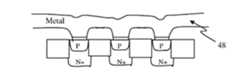
- One of conventional dielectric breakdown anti-fuseis shown in FIGS. 1( a ), 1( b ), and 1( c ) .
- This anti-fuseis based on metal-dielectric-silicon with a diode constructed by P+ active region over N+ bar as program selector.
- FIG. 1( a )shows a portion of process steps by using a first Local Oxidation (LOCOS) to define an N+ bar area.
- FIG. 1( b )shows a second LOCOS step to further define active regions within each N+ bar in a perpendicular direction.
- LOCOSLocal Oxidation
- the cellis patterned by two LOCOS steps so that the cell size is determined by the pitches of active regions in the X- and Y-directions.
- the cell sizeis generally referred to 4F 2 , where F stands for figure size.
- Fstands for figure size.
- a P type dopantis implanted, a thin silicon dioxide is grown, and then a metal is built on top of each cell as shown in FIG. 1( c ) .
- the equivalent circuit of the anti-fuse cellis a capacitor in series with a diode at an X and Y cross-point as shown in FIG. 1( d ) .
- Noriaki, et. al“A New Cell for High Capacity Mask ROM by the Double LOCOS Techniques,” International Electronics Device Meeting, December, 1983, pp. 581-584.
- the anti-fuse cell in FIGS. 1( a ), 1( b ), and 1( c )is very complicated to fabricate, as it requires three more masks and two LOCOS steps over standard CMOS processes. Fabricating LOCOS requires a mask for field implant, nitride deposition, and a long thermal cycle to grow field oxide. Accordingly, there is a need for an anti-fuse cell that is more compatible with standard CMOS process to save costs.
- the inventionpertains to an anti-fuse device and memory based on dielectric breakdown formed at the cross points of two perpendicular conductors that has minimum process steps or masks over standard CMOS logic processes.
- the general structures of the devices in this inventionhas a dielectric film for rupture and a diode as program selector in a cell defined at a cross-point of two conductor (conductive) lines in perpendicular directions.
- the dielectric filmcan be fabricated from silicon dioxide (SiO 2 ), silicon nitride (SiN x , or Si 3 N 4 particularly), silicon oxide-nitride (SON), or silicon oxide-nitride-oxide (ONO).
- the diodecan be a junction diode constructed from bulk silicon, a diode constructed from polysilicon, a diode constructed from bulk silicon and polysilicon, or a p-i-n diode with an intrinsic layer between P and N type silicon or polysilicon.
- An intrinsic layermeans it is not intentionally P or N doped but can be slightly N or P type due to out-diffusion or contamination.
- the dielectric filmmay be fabricated before, after, or between the N or P terminals of the diode.
- the conductors in perpendicular directionscan be both active regions, active and polysilicon, polysilicon and metal, or active and metal, in various embodiments.
- the cross pointmay be formed at the junction of two perpendicular conductors, or inside a contact hole at the junction of two perpendicular conductors.
- Another key concept of this inventionis to use core logic or I/O devices in the peripheral of the anti-fuse memory that are the same devices as those built in the rest of integrated circuits.
- the programming voltage of an anti-fuseis very high, about 12V or 18V, that needs special high voltage devices in the peripheral circuit to design an anti-fuse memory.
- One aspect of this inventioncan eliminate the need to use high voltage devices to lower the breakdown voltage of the dielectric film so that core or I/O devices in an integrated circuit can be used.
- Another embodimentis to use a combination of different voltages in two perpendicular conductors to achieve high voltage for a selected cell to program, while the unselected cells are operated within a low voltage range.
- the size of the anti-fusecan be 4F 2 , where F stands for figure size that is the width or space of the conductors to form an anti-fuse cell. It will be apparent to those skilled in the art that various modifications and variations can be made in the present invention without departing from the spirit or scope of the invention. Thus, it is intended that the present invention covers the modifications and variations of this invention provided they come within the scope of the appended claims and their equivalents.
- the inventioncan be implemented in numerous ways, including as a method, system, device, or apparatus (including graphical user interface and computer readable medium). Several embodiments of the invention are discussed below.
- one embodimentcan, for example, include a plurality of anti-fuse cells. At least one of the anti-fuse cells can include a dielectric film coupled to a first supply voltage line, and a diode including at least a first type of silicon and a second type of silicon.
- the first type of siliconcan have a first type of dopant and the second type of silicon can have a second type of dopant.
- An intrinsic layermay be inserted between the first and the second types of silicon.
- the first type of siliconcan provide a first terminal of the diode and the second type of silicon can provide a second terminal of the diode.
- the first type of siliconcan also be coupled to the dielectric film, and the second type of silicon can be coupled to a second supply voltage line.
- the first and second type of siliconcan be fabricated at the cross points of two perpendicular conductor lines.
- the conductor linescan be implemented by any combinations of metal, active region, buried layer, or polysilicon.
- the diodecan be constructed explicitly or by itself after oxide breakdown. If one of the conductor lines is metal while the other is an active region, buried layer, or polysilicon, a diode can built explicitly in the active region, buried layer or polysilicon with a first and a second type of silicon. If the two perpendicular conductor lines are buried layer and polysilicon with a first and second type of silicon, respectively, a diode can be constructed by itself once the oxide film is broken down.
- the dielectric filmcan be configured to be programmable by applying voltages to the first and second supply voltage lines to thereby change the resistance of the dielectric film into a different logic state.
- the dielectric filmcan be coupled to the second type of silicon, or in between the first and the second type of silicon in other embodiments.
- one embodimentcan, for example, include at least a processor, and an anti-fuse memory operatively connected to the processor.
- the anti-fuse memorycan include at least a plurality of anti-fuse cells for providing data storage.
- Each of the anti-fuse cellscan include at least a dielectric film coupled to a first supply voltage line, and a diode including at least a first type of silicon and a second type of silicon.
- the first type of siliconcan have a first type of dopant and the second type of silicon can have a second type of dopant.
- An intrinsic layermay be inserted between the first and the second types of silicon.
- the first type of siliconcan provide a first terminal of the diode and the second type of silicon can provide a second terminal of the diode.
- the first type of siliconcan be coupled to the dielectric film and the second type of silicon can be coupled to a second supply voltage line.
- the first and second type of siliconcan be fabricated at the cross points of two perpendicular conductor lines.
- the conductor linescan be implemented by any combinations of metal, active region, buried layer, or polysilicon.
- the diodecan be constructed explicitly or by itself after oxide breakdown. If one of the conductor lines is metal while the other is an active region, buried layer, or polysilicon, a diode can be built explicitly in the active region, buried layer or polysilicon with a first and a second type of silicon.
- a diodecan be constructed by itself once the oxide film is broken down.
- the dielectric filmcan be configured to be programmable by applying voltages to the first and the second supply voltage lines to thereby change the resistance of the dielectric film into a different logic state.
- the dielectric filmcan be coupled to the second type of silicon, or in between the first and the second type of silicon in other embodiments.
- one embodimentcan, for example, include at least providing a plurality of anti-fuse cells, and programming a logic state into at least one of the anti-fuse cells by applying voltages to the first and the second voltage lines.
- the at least one of the anti-fuse cellscan include at least (i) a dielectric film coupled to a first supply voltage line, and (ii) a diode including at least a first type of silicon and a second type of silicon.
- the first type of siliconcan have a first type of dopant and the second type of silicon can have a second type of dopant.
- An intrinsic layermay be inserted between the first and the second types of silicon.
- the first type of siliconcan provide a first terminal of the diode and the second type of silicon can provide a second terminal of the diode.
- the first type of siliconcan be coupled to the dielectric film and the second type of silicon can be coupled to a second supply voltage line.
- the first and second type of siliconcan be fabricated at the cross points of two perpendicular conductor lines.
- the conductor linescan be any combinations of metal, active region, buried layer, or polysilicon.
- the diodecan be constructed explicitly or by itself after oxide breakdown. If one of the conductor lines is metal while the other is an active region, buried layer, or polysilicon, a diode can be built explicitly in the active region, buried layer or polysilicon with a first and a second type of silicon.
- a diodecan be constructed by itself once the oxide film is broken down.
- the dielectric filmcan be configured to be programmable by applying voltages to the first and the second supply voltage lines to thereby change the resistance of the dielectric film into a different logic state.
- the dielectric filmcan be coupled to the second type of silicon, or in between the first and the second type of silicon in other embodiments.
- Each of at least the plurality of the anti-fuse cellscan be constructed at one of the cross points and each of at least the plurality of anti-fuse cells can include at least: (i) a plurality of conductive lines with a first type of dopant; (ii) a plurality of metal lines being substantially perpendicular to the polysilicon lines; (iii) a layer of isolation oxide fabricated between the metal and conductive lines; (iv) a plurality of contacts being open at the cross points of metal and conductive line; and (v) a silicon diode and a layer of thin oxide fabricated in each contact hole before placing metal lines.
- the anti-fuse memorycan be configured to be selectively programmable by applying a first supply voltage to the metal lines and a second supply voltage to the conductive lines to rupture the thin oxide.
- FIG. 1( a )shows a first LOCOS step in a conventional dielectric breakdown anti-fuse.
- FIG. 1( b )shows a second LOCOS step in a conventional dielectric breakdown anti-fuse.
- FIG. 1( c )shows a cross section of a conventional metal-oxide-silicon anti-fuse using a diode as program selector.
- FIG. 1( d )shows a conventional equivalent circuit of the anti-fuse cell.
- FIG. 2( a )shows a top view of a dielectric-breakdown anti-fuse defined by active regions in X- and Y-directions according to one embodiment.
- FIG. 2( b )shows a cross section of a dielectric-breakdown anti-fuse defined by active regions in the Y direction.
- FIG. 2( c )shows a cross section of a dielectric-breakdown anti-fuse defined by active regions in the X direction.
- FIG. 3( a )shows step (a) of fabricating a dielectric-breakdown anti-fuse defined by active regions (ref. FIG. 2( a )-2( c ) ) after buried N+ layer.
- FIG. 3( c )shows step (c) of fabricating a dielectric-breakdown anti-fuse defined by active regions (ref. FIG. 2( a )-2( c ) ) after building isolation for active regions.
- FIG. 3( d )shows step (d) of fabricating a dielectric-breakdown anti-fuse defined by active regions (ref. FIG. 2( a )-2( c ) ) after a P+ implant as the P terminal of a diode.
- FIG. 3( g )shows step (g) of fabricating a dielectric-breakdown anti-fuse defined by active regions (ref. FIG. 2( a )-2( c ) ) after depositing an adhesive layer.
- FIG. 3( h )shows step (h) of fabricating a dielectric-breakdown anti-fuse defined by active regions (ref. FIG. 2( a )-2( c ) ) after depositing, patterning, and etching a metal layer.
- FIG. 4shows a top view of another embodiment of dielectric breakdown anti-fuse defined by metal and polysilicon according to one embodiment.
- FIG. 5( a )shows step (a) of fabricating a dielectric breakdown anti-fuse defined by metal and polysilicon (ref. FIG. 4 ) after depositing and siliciding polysilicon.
- FIG. 5( b )shows step (b) of fabricating a dielectric-breakdown anti-fuse defined by metal and polysilicon (ref. FIG. 4 ) after growing an interlayer dielectric and etching contact holes.
- FIG. 5( c )shows step (c) of fabricating a dielectric-breakdown anti-fuse defined by metal and polysilicon (ref. FIG. 4 ) after depositing an adhesive layer.
- FIG. 5( d )shows step (d) of fabricating a dielectric-breakdown anti-fuse defined by metal and polysilicon (ref. FIG. 4 ) after growing a p-i-n silicon diode inside a contact hole.
- FIG. 5( e )shows step (e) of fabricating a dielectric-breakdown anti-fuse defined by metal and polysilicon (ref. FIG. 4 ) after growing an oxide film on top of a silicon diode.
- FIG. 5( f )shows step (f) of fabricating a dielectric-breakdown anti-fuse defined by metal and polysilicon (ref. FIG. 4 ) after depositing another adhesive layer.
- FIG. 5( g )shows step (g) of fabricating a dielectric-breakdown anti-fuse defined by metal and polysilicon (ref. FIG. 4 ) after depositing, patterning, and etching a metal layer.
- FIG. 6shows using dummy polysilicon to raise contact-hole height in an anti-fuse defined by metal and active lines.
- FIG. 7shows a top view of dielectric breakdown anti-fuse defined by active and polysilicon lines according to one embodiment.
- FIG. 8( b )shows step (a) of fabricating a dielectric breakdown anti-fuse defined by active and polysilicon (ref. to FIG. 7 ) after buried N+ implant.
- FIG. 8( d )shows step (a) of fabricating a dielectric breakdown anti-fuse defined by active and polysilicon (ref. to FIG. 7 ) after growing oxide.
- FIG. 8( e )shows step (a) of fabricating a dielectric breakdown anti-fuse defined by active and polysilicon (ref. to FIG. 7 ) after depositing and etching polysilicon.
- FIG. 10( a )shows step (a) of fabricating a dielectric breakdown anti-fuse defined by active and metal (ref. FIG. 9 ) after building buried N+ lines and depositing gate oxide.
- FIG. 10( b )shows step (b) of fabricating a dielectric-breakdown anti-fuse defined by active and metal (ref. FIG. 9 ) after stripping the gate oxide and depositing P type polysilicon.
- FIG. 10( c )shows step (c) of fabricating a dielectric-breakdown anti-fuse defined by active and metal (ref. FIG. 9 ) after depositing interlayer dielectric, opening contact holes, and deposit an adhesive layer.
- FIG. 10( d )shows step (d) of fabricating a dielectric-breakdown anti-fuse defined by active and metal (ref. FIG. 9 ) after growing or depositing an oxide film.
- FIG. 10( e )shows step (e) of fabricating a dielectric-breakdown anti-fuse defined by active and metal (ref. FIG. 9 ) after depositing another adhesive layer.
- FIG. 10( f )shows step (f) of fabricating a dielectric-breakdown anti-fuse defined by active and metal (ref. FIG. 9 ) after depositing, patterning, and etching a metal layer.
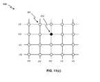
- FIG. 11( a )shows one high voltage and one core logic or I/O voltage voltages applied to the perpendicular conductors to the selected and unselected cells according to one embodiment.
- FIG. 11( b )shows positive and negative supply voltages applied to the perpendicular conductors to the selected and unselected cells according to one embodiment.
- FIG. 11( c )shows a high and a half-value program supply voltages applied to the perpendicular conductors to the selected and unselected cells according to one embodiment.
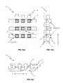
- FIG. 2( a )shows a top view of a dielectric breakdown anti-fuse 10 according to one embodiment.
- Each anti-fuse cell 15is defined by active regions in X- and Y-directions.
- An array of buried N+ lines 11serve as wordlines are built running in the X-direction before active regions 12 is defined.
- the active regionscan be isolated in X- and Y-directions by Local Oxidation (LOCOS) or Shallow Trench Isolation (STI).
- LOCidationLOCidation
- STIShallow Trench Isolation
- a contact hole 13 in each active regionis etched after depositing an interlayer dielectric. Then, N type and P type dopants are subsequently implanted into the contact hole in each active region to act as N and P terminals of a diode.
- a thin film of dielectricsuch as SiO 2 , Si 3 N 4 , SiN x , silicon-oxide-nitride (SON), or silicon oxide-nitride-oxide (ONO), is deposited or grown into each contact hole for rupture by programming.
- a metalis built on top of the contact hole to serve as a bitline.
- FIGS. 2( a ) and 2( b )shows a cross section 20 of the same dielectric breakdown anti-fuse in FIGS. 2( a ) and 2( b ) along the X-direction.
- Buried N+ lines 24 between LOCOS or STI 22connect active regions along the X-direction and also serve as the N terminal of each diode.
- the interlayer dielectric 21normally silicon diode
- Each cellis implanted with P+ 23 , the same implant for sources or drains of PMOS devices, to serve as the P terminal of a diode.
- the N+ linescan be fabricated in one or two steps.
- the first stepis to implant a heavy N+ line deep into the silicon to connect the cells in the X-direction, and then a second shallower N type dopant is implanted into each cell to reach the deep N+ line and to serve as the N terminal of a diode.
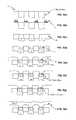
- FIGS. 3( a )-3( h )show cross sections 40 in a portion of process steps related to the dielectric breakdown anti-fuse shown in FIG. 2( a )-2( c ) .
- the cross sectionsare shown along the Y-direction.
- FIG. 3( a )shows a cross section after buried N+ lines 41 are implanted and annealed.
- the N+ lines 41act as the N terminals of a diode in each cell, interconnect the cells in the X-direction, and serve as wordlines.
- the N+ linesshall be deeper than the isolation for active regions and can be heavily doped near the bottom.
- the desirable embodiment for N+ linesis a shallow retrograde N well, similar to the N well in common CMOS processes.
- FIG. 3( b )shows a field implant 42 before growing thermal oxide in LOCOS or etching shallow trenches in STI process.
- FIG. 3( c )shows after active region isolations 43 , either LOCOS or STI, are built. Alternatively, the buried N+ 41 in FIG. 3( a ) can be implanted into silicon after LOCOS or STI 43 is formed in FIG. 3( c ) .
- FIG. 3( d )shows after a P+ implant 44 , the same as source or drain implant of a PMOS, to act as the P terminal of the diode in each cell.
- FIG. 3( e )shows after an interlayer dielectric 45 is deposited and contact holes 45 A are etched.
- FIG. 3( f )shows after a thin oxide film 46 is deposited for rupture upon programming.
- the thickness of the SiO 2is generally around 30-80 ⁇ to have breakdown voltage about 6-15V.
- FIG. 3( g )shows after an adhesive layer 47 is deposited to provide a better attachment for metal on top.
- the adhesive layercan be a 200 ⁇ TiN film or other material.
- FIG. 3( h )shows after a metal layer 48 is deposited, patterned, and then etched. Two additional masks may be needed: one for defining and building N+ lines and the other for growing a dielectric film for breakdown.
- FIG. 4shows a top view of dielectric breakdown anti-fuse cells 50 defined by metal lines 52 and polysilicon lines 51 according to embodiment. Inside each contact hole 53 at the junctions of the polysilicon lines 51 and metal lines 52 builds an anti-fuse cell 55 .
- the cell sizeis determined by metal pitch in the X-direction and polysilicon pitch in the Y-direction so that the cell size is 4F 2 .
- FIGS. 5( a )-5( g )show cross sections 60 in a portion of process steps related to the dielectric breakdown anti-fuse defined by metal and polysilicon in FIG. 4 .
- the cross sectionsare along the Y-direction.
- FIG. 5( a )shows a cross section after polysilicon lines 61 are built and silicide 62 is grown on top.
- the polysilicon linesinterconnect the cells in the X-direction, and serve as wordlines.
- the silicide on topreduces resistance of the polysilicon lines.
- FIG. 5( b )shows after an interlayer dielectric 64 is deposited and contact holes 64 A are etched therein.
- FIG. 5( c )shows after an adhesive layer 65 is deposited in the contact holes.
- the diodecan be fabricated by Chemical Vapor Deposition (CVD) with dopants changed in situ, (i.e. dopants changed from N type, intrinsic, and to P type along the course of CVD processing).
- the composition of the diode in one embodimentcan be an intrinsic layer between the P and N type silicon, the so-called p-i-n diode.
- the intrinsic layermeans there is no intention to add any dopants but it could be slightly N or P type due to out diffusion or contamination.
- the thickness of the intrinsic layerdetermines the breakdown voltage of the diode and shall be high enough to prevent premature programming.
- Another embodiment to control the breakdown voltage of the diodeis to use lesser doped N or P type, rather than intrinsic, in between the heavily doped P and N terminals of the diode.
- the thickness of the diodeis about 3,000-5,000 ⁇ to fit into the contact height.
- the p-i-n diodecan be fabricated from depositing silicon and then followed by implanting N or P type dopants in different steps.
- FIG. 5( e )shows after a thin layer of oxide 67 is deposited as an anti-fuse film after the formation of the P and N portions of the diode 66 .
- the dielectric filmcan be fabricated from silicon dioxide (SiO 2 ), silicon nitride (Si 3 N 4 ), silicon oxide-nitride (SON), or silicon oxide-nitride-oxide (ONO).
- silicon dioxideSiO 2
- Si 3 N 4silicon nitride
- SONsilicon oxide-nitride
- ONOsilicon oxide-nitride-oxide
- metal oxidessuch as Al 2 O 3 , HfO 2 , ZrO 2 , or Cr 2 O 3
- the thicknessis generally around 30-80 ⁇ to have breakdown voltage about 6-15V.
- the oxide for breakdown 67can also be fabricated before or inserted between the P, intrinsic, or N portions of the diode 66 .
- FIG. 5( f )shows after another adhesive layer 68 is deposited.
- FIG. 5( g )shows after a metal layer 69 is deposited, patterned, and etched.
- the metal layer 69serves as the bitline running in the Y-direction.
- one additional maskis needed to open contact holes, build p-i-n or P/N silicon diode, grow oxide inside the contact holes.
- the adhesive layersserve to provide better attachment between metal and different materials in the contact holes that can be one, two, or none.
- Embodiments as illustrated in FIGS. 4, 5 ( a )- 5 ( g )are about anti-fuses defined by metal and polysilicon lines. There are some embodiments about building an oxide film external to a p-i-n diode or between P and N terminals of a diode. The required processing steps are about the same. But the breakdown mechanism in p-i-n diode is an oxide breakdown between silicon and metal, while the breakdown mechanism in the p-oxide-n sandwich structure is an oxide breakdown between P and N type silicon. Breaking down between silicon and metal may be more reliable than the mechanism between P and N types of silicon. Therefore, a p-i-n diode is a more desirable embodiment over a P-oxide-N sandwich structure.
- Polysilicon linescan be readily replaced by active region lines while the other perpendicular conductor lines are metal in other embodiment, which can be anti-fuse cells having a p-i-n diode with external oxide film or having a p-oxide-n sandwich structure.
- FIG. 4 and FIG. 5( a )-5( g )can be readily applied with the polysilicon lines replaced by active region lines.
- Using polysilicon lines, rather than active region lines, as wordlinesallows them to be biased at a negative voltage, since the wordlines are isolated by oxidation rather than P/N junctions.
- anti-fuse cells defined by metal and active region linesallow variations in adjusting contact height by placing dummy polysilicon between active regions on the field.
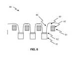
- FIG. 6shows a cross section 80 of anti-fuse cells defined by metal and active lines. Active region lines 81 are built and grown with silicide 82 on top. Dummy polysilicon lines 84 with silicide 83 on top are placed between active region lines, but on the field oxide. Because of the dummy polysilicon, the height of the interlayer dielectric 85 to the silicon surface is raised by the thickness of the polysilicon, or about 2,000-5,000 ⁇ , so is the height of contact holes. This allows more depth to build p-i-n diode or p-oxide-n sandwich structure inside a contact hole 86 , and hence provides one more parameter for optimization.
- FIG. 7shows a top view of dielectric breakdown anti-fuse cells 90 defined by active lines 92 and polysilicon lines 91 according to one embodiment.
- the polysilicon 91 linesare blocked spacers on each side so that the memory cell size can be smaller.
- the spaceris a technique to allow forming a lightly-doped source/drain (LDD) region near the gate to alleviate the short channel effects.
- LDDlightly-doped source/drain
- the cell sizeis determined by active region pitch in the X-direction and polysilicon pitch in the Y-direction so that the cell size is 4F 2 .
- the active lines 92can be doped with N type dopant and the polysilicon lines 91 can be doped with P type dopant so that a diode can be created after the oxide layer is broken down.
- the active lines 92can also be doped with P type dopant after being doped with the N type dopant to form an explicit diode before fabricating an oxide layer.
- the active lines 92can be doped with an intrinsic layer after doped with the N type dopant and before fabricating the oxide layer to create a p-i-n diode after the oxide is broken down.
- FIGS. 8( a )-8( e )show cross sections 100 in a portion of process steps related to dielectric breakdown anti-fuse cells defined by active region and polysilicon lines in FIG. 7 .
- the gate oxide between active and polysiliconacts as an anti-fuse for rupture.
- the cross sectionsare along the X-direction.
- FIG. 8( a )shows a cross section after active isolation, such as LOCOS or STI 104 , is built on a P type substrate 101 according to standard CMOS processes. Then, the surface is implanted by N+ 106 to create buried N+ lines to serve as bitlines in FIG. 8( b ) .
- FIG. 8( c )shows a cross section after a P type implant 107 is introduced.
- the P type dopant and the buried N+constitute a P/N junction diode.
- FIG. 8( d )shows a cross section after a thin layer of oxide 108 as dielectric is deposited or grown. Then, a polysilicon 109 is deposited, patterned, implanted by P+, and etched to serve as wordlines of the anti-fuse cells, running in the X-direction in FIG.
- the polysilicon 109may be silicided to reduce resistance but is blocked spacers on each side so that memory cell can be smaller.
- the rest of process stepsfollow the standard CMOS processes. With a proper voltage applied between buried N+ and polysilicon lines, the gate oxide can be rupture so that at the cross-point of the polysilicon and buried N+ lines acts as the P and N terminals of a diode.
- One additional maskmay be needed to build buried N+ lines with heavy N+ implant.
- One of the embodimentsis to eliminate the P type dopant. Without explicit P type implant to build a P/N junction diode in FIG. 8( c ) , an implicit diode, constructed from P type polysilicon and N type buried lines, may still be created after the oxide is ruptured. Another embodiment is to fabricate an intrinsic layer before the P type dopant on the silicon surface to create a p-i-n diode. Intrinsic means no intentionally N or P doped but can be slightly N or P type due to out-diffusion or contamination. Yet another embodiment is to fabricate an intrinsic layer without any P type dopant on the silicon surface before an oxide is fabricated and a polysilicon is deposited. The step to grow or deposit oxide 108 in FIG. 8( d ) may be omitted by sharing the gate oxide growing process in standard CMOS processes. These are many variations to build an implicit or explicit P/N junction diodes at the cross points in other embodiments.
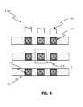
- FIG. 9shows a top view of dielectric breakdown anti-fuse cells 110 defined by active lines 111 and metal lines 114 with a piece of polysilicon 112 at the cross-point in according to 5one embodiment.
- metal 114 and active region 111builds an anti-fuse cell 115 , where the polysilicon and active region serves as the P and N terminals of a diode.
- the cell sizeis determined by active region pitch in the X-direction and metal or polysilicon pitch in the Y-direction so that the cell size is 4F 2 .
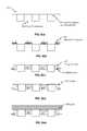
- FIGS. 10( a )-10( f )show cross sections 120 in a portion of process steps related to the dielectric breakdown anti-fuse cells defined by active and metal with a piece of polysilicon in each contact hole as shown in FIG. 9 .
- a diode constructed from a polysilicon patch and an active lineis formed after the gate oxide is stripped. An oxide film is then grown or deposited inside the contact holes.
- the cross sectionsare along the Y-direction.
- FIG. 10( a )shows a cross section after N type active lines 121 are built and gate oxide 122 is grown on top of a silicon substrate. The active lines interconnect the cells in the X-direction, and serve as bitlines.
- FIG. 10( a )-10( f )show cross sections 120 in a portion of process steps related to the dielectric breakdown anti-fuse cells defined by active and metal with a piece of polysilicon in each contact hole as shown in FIG. 9 .
- FIG. 10( b )shows after the gate oxide is striped and pieces of polysilicon 123 are built over the active regions.
- the polysiliconis P type and the active is N type so that a diode is built as program selector in an anti-fuse cell.
- FIG. 10( c )shows after an interlayer dielectric 124 is deposited, contact holes 124 A are etched, and a thin adhesive layer 125 is deposited.
- FIG. 10( d )shows after an oxide film 126 is fabricated.
- the oxide filmsuch as SiO 2 , Si 3 N 4 , SiN X , silicon oxide-nitride (SON), silicon oxide-nitride-oxide (ONO), or other types of metal oxide, can be deposited or grown by oxidation or deposit.
- the thickness of the oxide layerdetermines the breakdown voltage of the anti-fuse for programming. If SiO 2 is employed, the thickness is generally around 30-80 ⁇ to have breakdown voltage about 6-15V.
- FIG. 10( e )shows after another adhesive layer 128 is deposited.
- FIG. 10( f )shows after a metal layer 129 is deposited, patterned, and etched. The metal serves as a bitline running in the Y-direction.
- two additional masksare needed to strip the gate oxide and open contact holes for building diodes and an oxide film.
- the gate oxide strip maskcan be shared in a CMOS process that offers more than one kind of gate-oxide devices.
- the adhesive layersserve to have better attachment between different materials to metal in the contact holes such that the adhesive layer number can be one, two, or none.
- the anti-fusecan be fabricated in a few more masks over the standard CMOS process, more masks may be needed to fabricate high voltage devices in the peripheral circuit considering the programming voltage tend to be very high, about 10-15V.
- the rupture voltage for a SiO 2 filmis 2V for every 10 ⁇ .
- the breakdown voltage for a 30 ⁇ SiO 2 filmis about 6V. Reducing the thickness of the dielectric film can lower the program voltage so that high voltage devices are not needed in the peripheral circuits. Novel half-select schemes also help to alleviate the requirements of using high voltage devices so that the core logic or I/O devices in the other parts of the integrated circuit can be used for embedded applications.
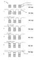
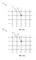
- FIG. 11( a )shows one embodiment of a 4 ⁇ 5 anti-fuse array 200 to alleviate the requirements for high voltage supplies in the peripheral.
- the supply voltage of the peripheral and the rest of integrated circuitis 5V
- the program voltage for anti-fuseis 8V
- the voltage swings for two perpendicular conductorsare 0-5V, and 5-8V, respectively.
- the selected cell 202has 0V in the horizontal line and 8V in the vertical line so that the resultant voltage at the cross point is 8V to program the selected cell.
- the voltage across the cellis either 5V, or 3V so that no programming could happen.
- the 8V program voltageis low enough for the peripheral devices to sustain over the maximum programming time. By doing this way, not only high voltage devices are not necessary but also the internal voltage generators.
- This cell select schemedoes not require any negative voltages that may need additional masks to isolate NMOS from a P substrate.
- FIG. 11( b )shows another embodiment of a 4 ⁇ 5 anti-fuse array 300 to alleviate the requirements for high voltage supplies in the peripheral.
- the supply voltage of the peripheral and the rest of integrated circuitis 4V
- the program voltage for anti-fuseis 8V
- the voltage swings for two perpendicular conductorsare 0-4V, and ⁇ 4-0V, respectively.
- the selected cell 302has ⁇ 4V in the horizontal line and 4V in the vertical line so that the resultant voltage at the cross point is 8V to program the cell.
- the voltage across the cellis either ⁇ 4V, or 4V so that no programming could happen.
- this combination of positive and negative supplyis a desirable embodiment. By doing this way, not only high voltage devices are not necessary but also the internal voltage generators.
- This cell select schemerequires a negative voltage supply that may need additional masks to isolate NMOS from a P substrate.
- FIG. 11( c )shows another half-select scheme 400 by swinging the row and column voltages between 0 to 4V.
- the voltage applied to the columnis 8V while the voltage to the row is 0V, so that the resulting voltage drop on the cell 402 is 8V for programming.
- the unselected cell 401has either both 4V's on the rows and columns, or one 4V and the other 0V on row or column, so that the resulting voltage drop is either 4V or 0V to prevent from programming.
- a voltage generator to generate half of the program voltagemay be needed.
- the substratecan be N type rather than P type through the above discussions.
- the N type or P type dopantcan be reversed so that a p-i-n diode and n-i-p diode can be considered equivalent. So are the p-oxide-n and the n-oxide-p sandwich structures. Some process steps may be omitted, such as adhesive layers. And the order of fabricating oxide film and p-i-n or P/N diode may be reversed.
- the dielectric film for rupturecan be fabricated before, after, or in between P type and N type of the diode.
- the polysilicon and activemay not be silicided in an older process. For those skilled in the art understand that various embodiments are possible and they are still within the scope of this invention.
Landscapes
- Semiconductor Memories (AREA)
- Design And Manufacture Of Integrated Circuits (AREA)
Abstract
Description
This application claimed priority benefit of U.S. Provisional Patent Application No. 61/421,184 filed on Dec. 8, 2010, titled “Method and Apparatus of A High Density Anti-fuse,” which is hereby incorporated herein by reference.
Anti-fuse is one of the One-Time Programmable (OTP) devices that can only be programmed once. Particularly, an anti-fuse has a high impedance state after fabrication and a low impedance state after being programmed. On the contrary, a fuse has a low impedance state after fabrication and a high impedance state after being programmed. The most commonly used anti-fuses are based on MOS gate oxide breakdown, metal-dielectric-metal breakdown, metal-dielectric-silicon breakdown, or silicon-dielectric-silicon breakdown, etc. Silicon dioxide (SiO2) is the most commonly used dielectric for breakdown in anti-fuses. However, Silicon-Oxide-Nitride (SON), Silicon Nitride (SiNx), Oxide-Nitride-Oxide (ONO), or other type of metal oxides, such as Aluminum Oxide (Al2O3), MgO, HfO2, or Cr2O3, can also be used.
MOS gate oxide breakdown is based on applying a high voltage to break down the gate oxide to create a programmed state. However, there is a mechanism called soft-breakdown, other than the desirable hard-breakdown, which makes the dielectric film appear to be broken down, but the film may heal by itself after cycling or burn-in. The reliability may be a concern for practical applications.
Dielectric breakdown anti-fuses have been proven in manufacture. One of conventional dielectric breakdown anti-fuse is shown inFIGS. 1(a), 1(b), and 1(c) . This anti-fuse is based on metal-dielectric-silicon with a diode constructed by P+ active region over N+ bar as program selector.FIG. 1(a) shows a portion of process steps by using a first Local Oxidation (LOCOS) to define an N+ bar area.FIG. 1(b) shows a second LOCOS step to further define active regions within each N+ bar in a perpendicular direction. The cell is patterned by two LOCOS steps so that the cell size is determined by the pitches of active regions in the X- and Y-directions. The cell size is generally referred to 4F2, where F stands for figure size. After the active region of the cells is determined, a P type dopant is implanted, a thin silicon dioxide is grown, and then a metal is built on top of each cell as shown inFIG. 1(c) . The equivalent circuit of the anti-fuse cell is a capacitor in series with a diode at an X and Y cross-point as shown inFIG. 1(d) . For additional information see, e.g., Noriaki, et. al, “A New Cell for High Capacity Mask ROM by the Double LOCOS Techniques,” International Electronics Device Meeting, December, 1983, pp. 581-584.
The anti-fuse cell inFIGS. 1(a), 1(b), and 1(c) is very complicated to fabricate, as it requires three more masks and two LOCOS steps over standard CMOS processes. Fabricating LOCOS requires a mask for field implant, nitride deposition, and a long thermal cycle to grow field oxide. Accordingly, there is a need for an anti-fuse cell that is more compatible with standard CMOS process to save costs.
The invention pertains to an anti-fuse device and memory based on dielectric breakdown formed at the cross points of two perpendicular conductors that has minimum process steps or masks over standard CMOS logic processes.
The general structures of the devices in this invention has a dielectric film for rupture and a diode as program selector in a cell defined at a cross-point of two conductor (conductive) lines in perpendicular directions. There are various embodiments that are within the scope and spirit of this invention. The dielectric film can be fabricated from silicon dioxide (SiO2), silicon nitride (SiNx, or Si3N4particularly), silicon oxide-nitride (SON), or silicon oxide-nitride-oxide (ONO). Alternatively other types of metal oxides, such as Al2O3, HfO2, MgO, ZrO2, or Cr2O3, can be used, but they may be more expensive, difficult to manufacture, and have a higher breakdown voltage. The diode can be a junction diode constructed from bulk silicon, a diode constructed from polysilicon, a diode constructed from bulk silicon and polysilicon, or a p-i-n diode with an intrinsic layer between P and N type silicon or polysilicon. An intrinsic layer means it is not intentionally P or N doped but can be slightly N or P type due to out-diffusion or contamination. The dielectric film may be fabricated before, after, or between the N or P terminals of the diode. The conductors in perpendicular directions can be both active regions, active and polysilicon, polysilicon and metal, or active and metal, in various embodiments. The cross point may be formed at the junction of two perpendicular conductors, or inside a contact hole at the junction of two perpendicular conductors.
Another key concept of this invention is to use core logic or I/O devices in the peripheral of the anti-fuse memory that are the same devices as those built in the rest of integrated circuits. In the past, the programming voltage of an anti-fuse is very high, about 12V or 18V, that needs special high voltage devices in the peripheral circuit to design an anti-fuse memory. As a result, more mask layers and more process steps are needed, and hence the fabrication costs are very high. One aspect of this invention can eliminate the need to use high voltage devices to lower the breakdown voltage of the dielectric film so that core or I/O devices in an integrated circuit can be used. Another embodiment is to use a combination of different voltages in two perpendicular conductors to achieve high voltage for a selected cell to program, while the unselected cells are operated within a low voltage range.
Though there are many different and useful embodiments of the invention, the size of the anti-fuse can be 4F2, where F stands for figure size that is the width or space of the conductors to form an anti-fuse cell. It will be apparent to those skilled in the art that various modifications and variations can be made in the present invention without departing from the spirit or scope of the invention. Thus, it is intended that the present invention covers the modifications and variations of this invention provided they come within the scope of the appended claims and their equivalents.
The invention can be implemented in numerous ways, including as a method, system, device, or apparatus (including graphical user interface and computer readable medium). Several embodiments of the invention are discussed below.
As an anti-fuse memory, one embodiment can, for example, include a plurality of anti-fuse cells. At least one of the anti-fuse cells can include a dielectric film coupled to a first supply voltage line, and a diode including at least a first type of silicon and a second type of silicon. The first type of silicon can have a first type of dopant and the second type of silicon can have a second type of dopant. An intrinsic layer may be inserted between the first and the second types of silicon. The first type of silicon can provide a first terminal of the diode and the second type of silicon can provide a second terminal of the diode. The first type of silicon can also be coupled to the dielectric film, and the second type of silicon can be coupled to a second supply voltage line. The first and second type of silicon can be fabricated at the cross points of two perpendicular conductor lines. The conductor lines can be implemented by any combinations of metal, active region, buried layer, or polysilicon. The diode can be constructed explicitly or by itself after oxide breakdown. If one of the conductor lines is metal while the other is an active region, buried layer, or polysilicon, a diode can built explicitly in the active region, buried layer or polysilicon with a first and a second type of silicon. If the two perpendicular conductor lines are buried layer and polysilicon with a first and second type of silicon, respectively, a diode can be constructed by itself once the oxide film is broken down. The dielectric film can be configured to be programmable by applying voltages to the first and second supply voltage lines to thereby change the resistance of the dielectric film into a different logic state. Alternatively, the dielectric film can be coupled to the second type of silicon, or in between the first and the second type of silicon in other embodiments.
As an electronic system, one embodiment can, for example, include at least a processor, and an anti-fuse memory operatively connected to the processor. The anti-fuse memory can include at least a plurality of anti-fuse cells for providing data storage. Each of the anti-fuse cells can include at least a dielectric film coupled to a first supply voltage line, and a diode including at least a first type of silicon and a second type of silicon. The first type of silicon can have a first type of dopant and the second type of silicon can have a second type of dopant. An intrinsic layer may be inserted between the first and the second types of silicon. The first type of silicon can provide a first terminal of the diode and the second type of silicon can provide a second terminal of the diode. The first type of silicon can be coupled to the dielectric film and the second type of silicon can be coupled to a second supply voltage line. The first and second type of silicon can be fabricated at the cross points of two perpendicular conductor lines. The conductor lines can be implemented by any combinations of metal, active region, buried layer, or polysilicon. The diode can be constructed explicitly or by itself after oxide breakdown. If one of the conductor lines is metal while the other is an active region, buried layer, or polysilicon, a diode can be built explicitly in the active region, buried layer or polysilicon with a first and a second type of silicon. If the two perpendicular conductor lines are buried layer and polysilicon with a first and second type of silicon, respectively, a diode can be constructed by itself once the oxide film is broken down. The dielectric film can be configured to be programmable by applying voltages to the first and the second supply voltage lines to thereby change the resistance of the dielectric film into a different logic state. Alternatively, the dielectric film can be coupled to the second type of silicon, or in between the first and the second type of silicon in other embodiments.
As a method for providing an anti-fuse memory, one embodiment can, for example, include at least providing a plurality of anti-fuse cells, and programming a logic state into at least one of the anti-fuse cells by applying voltages to the first and the second voltage lines. The at least one of the anti-fuse cells can include at least (i) a dielectric film coupled to a first supply voltage line, and (ii) a diode including at least a first type of silicon and a second type of silicon. The first type of silicon can have a first type of dopant and the second type of silicon can have a second type of dopant. An intrinsic layer may be inserted between the first and the second types of silicon. The first type of silicon can provide a first terminal of the diode and the second type of silicon can provide a second terminal of the diode. The first type of silicon can be coupled to the dielectric film and the second type of silicon can be coupled to a second supply voltage line. The first and second type of silicon can be fabricated at the cross points of two perpendicular conductor lines. The conductor lines can be any combinations of metal, active region, buried layer, or polysilicon. The diode can be constructed explicitly or by itself after oxide breakdown. If one of the conductor lines is metal while the other is an active region, buried layer, or polysilicon, a diode can be built explicitly in the active region, buried layer or polysilicon with a first and a second type of silicon. If the two perpendicular conductor lines are buried layer and polysilicon with a first and second type of silicon, respectively, a diode can be constructed by itself once the oxide film is broken down. The dielectric film can be configured to be programmable by applying voltages to the first and the second supply voltage lines to thereby change the resistance of the dielectric film into a different logic state. Alternatively, the dielectric film can be coupled to the second type of silicon, or in between the first and the second type of silicon in other embodiments.
As an electronic system, one embodiment can, for example, include at least a battery and an integrated circuit operatively connected to the battery. The at least one battery can provide a voltage between 1.0 and 2.0V in the nominal conditions. The integrated circuit can include at least an anti-fuse memory including at least a plurality of anti-fuse cells. Each of at least the plurality of the anti-fuse cells can be constructed at one of the cross points and each of at least the plurality of anti-fuse cells can include at least: (i) a plurality of conductive lines with a first type of dopant; (ii) a plurality of metal lines being substantially perpendicular to the polysilicon lines; (iii) a layer of isolation oxide fabricated between the metal and conductive lines; (iv) a plurality of contacts being open at the cross points of metal and conductive line; and (v) a silicon diode and a layer of thin oxide fabricated in each contact hole before placing metal lines. The anti-fuse memory can be configured to be selectively programmable by applying a first supply voltage to the metal lines and a second supply voltage to the conductive lines to rupture the thin oxide.
The present invention will be readily understood by the following detailed descriptions in conjunction with the accompanying drawings, wherein like reference numerals designate like structural elements, and in which:
This invention concerns a dielectric breakdown anti-fuse cell using diode as program selector defined at a cross-point of two conductor lines in perpendicular directions. Various embodiments about dielectric materials, diode structures, conductor types, process steps, devices employed, and cell select schemes will be disclosed and that are within the scope of this invention.
Embodiments as illustrated inFIGS. 4, 5 (a)-5(g) are about anti-fuses defined by metal and polysilicon lines. There are some embodiments about building an oxide film external to a p-i-n diode or between P and N terminals of a diode. The required processing steps are about the same. But the breakdown mechanism in p-i-n diode is an oxide breakdown between silicon and metal, while the breakdown mechanism in the p-oxide-n sandwich structure is an oxide breakdown between P and N type silicon. Breaking down between silicon and metal may be more reliable than the mechanism between P and N types of silicon. Therefore, a p-i-n diode is a more desirable embodiment over a P-oxide-N sandwich structure.
Polysilicon lines can be readily replaced by active region lines while the other perpendicular conductor lines are metal in other embodiment, which can be anti-fuse cells having a p-i-n diode with external oxide film or having a p-oxide-n sandwich structure.FIG. 4 andFIG. 5(a)-5(g) can be readily applied with the polysilicon lines replaced by active region lines. Using polysilicon lines, rather than active region lines, as wordlines allows them to be biased at a negative voltage, since the wordlines are isolated by oxidation rather than P/N junctions.
However, anti-fuse cells defined by metal and active region lines in other embodiments allow variations in adjusting contact height by placing dummy polysilicon between active regions on the field.FIG. 6 shows across section 80 of anti-fuse cells defined by metal and active lines.Active region lines 81 are built and grown withsilicide 82 on top.Dummy polysilicon lines 84 withsilicide 83 on top are placed between active region lines, but on the field oxide. Because of the dummy polysilicon, the height of theinterlayer dielectric 85 to the silicon surface is raised by the thickness of the polysilicon, or about 2,000-5,000 Å, so is the height of contact holes. This allows more depth to build p-i-n diode or p-oxide-n sandwich structure inside acontact hole 86, and hence provides one more parameter for optimization.
One of the embodiments is to eliminate the P type dopant. Without explicit P type implant to build a P/N junction diode inFIG. 8(c) , an implicit diode, constructed from P type polysilicon and N type buried lines, may still be created after the oxide is ruptured. Another embodiment is to fabricate an intrinsic layer before the P type dopant on the silicon surface to create a p-i-n diode. Intrinsic means no intentionally N or P doped but can be slightly N or P type due to out-diffusion or contamination. Yet another embodiment is to fabricate an intrinsic layer without any P type dopant on the silicon surface before an oxide is fabricated and a polysilicon is deposited. The step to grow ordeposit oxide 108 inFIG. 8(d) may be omitted by sharing the gate oxide growing process in standard CMOS processes. These are many variations to build an implicit or explicit P/N junction diodes at the cross points in other embodiments.
Though the anti-fuse can be fabricated in a few more masks over the standard CMOS process, more masks may be needed to fabricate high voltage devices in the peripheral circuit considering the programming voltage tend to be very high, about 10-15V. As a rule of thumb, the rupture voltage for a SiO2film is 2V for every 10 Å. For example, the breakdown voltage for a 30 Å SiO2film is about 6V. Reducing the thickness of the dielectric film can lower the program voltage so that high voltage devices are not needed in the peripheral circuits. Novel half-select schemes also help to alleviate the requirements of using high voltage devices so that the core logic or I/O devices in the other parts of the integrated circuit can be used for embedded applications.
There are many variations in the embodiments of this invention. For example, the substrate can be N type rather than P type through the above discussions. The N type or P type dopant can be reversed so that a p-i-n diode and n-i-p diode can be considered equivalent. So are the p-oxide-n and the n-oxide-p sandwich structures. Some process steps may be omitted, such as adhesive layers. And the order of fabricating oxide film and p-i-n or P/N diode may be reversed. The dielectric film for rupture can be fabricated before, after, or in between P type and N type of the diode. The polysilicon and active may not be silicided in an older process. For those skilled in the art understand that various embodiments are possible and they are still within the scope of this invention.
The many features and advantages of the present invention are apparent from the written description and, thus, it is intended by the appended claims to cover all such features and advantages of the invention. Further, since numerous modifications and changes will readily occur to those skilled in the art, it is not desired to limit the invention to the exact construction and operation as illustrated and described. Hence, all suitable modifications and equivalents may be resorted to as falling within the scope of the invention.
Claims (21)
1. An anti-fuse memory in an integrated circuit, comprises:
a plurality of anti-fuse cells, at least one of the cells being constructed at the cross points of:
a plurality of conductive lines, the conductive lines being polysilicon lines;
a plurality of metal lines being substantially perpendicular to the conductive lines;
a layer of isolation oxide fabricated between the metal lines and the conductive lines;
a plurality of contacts holes at the cross points of the metal lines and the conductive lines; and
a silicon diode and a layer of thin oxide fabricated in at least one of the contact holes before placing the metal lines, the layer of thin oxide being provided over the silicon diode between the silicon diode and at least one of the metal lines;
wherein the anti-fuse memory is configured to be selectively programmable by applying a first supply voltage to the metal lines and a second supply voltage to the conductive lines to rupture the thin oxide.
2. An anti-fuse memory as recited inclaim 1 , wherein the conductive lines are active region lines with an implant before CMOS source/drain implants.
3. An anti-fuse memory as recited inclaim 1 , wherein the layer of thin oxide is fabricated after the silicon diode is fabricated in the at least one of the contact hole.
4. An anti-fuse memory as recited inclaim 1 , wherein the layer of thin oxide is fabricated between the first and second portions of the silicon diode in at least one of the contact holes, where the first and second portions of the silicon diode have different types of dopants that serve as the P and N terminals of the silicon diode.
5. An anti-fuse memory as recited inclaim 1 , wherein the layer of thin oxide comprises a silicon dioxide (SiO2), silicon nitride (SiNx), silicon oxide-nitride (SON), silicon oxide-nitride (SON), silicon oxide-nitride-oxide (ONO), or any metal oxide.
6. An anti-fuse memory as recited inclaim 1 , wherein the thickness of the layer of thin oxide in the at least one of the contact holes is less than 50 Å.
7. An anti-fuse memory as recited inclaim 1 ,
wherein the layer of thin oxide is fabricated between first and second portions of the silicon diode in at least one of the contact holes, where the first and second portions of the silicon diode have different types of dopants that serve as the P and N terminals of the silicon diode, and
wherein the thickness of the layer of thin oxide in each of the contact holes is less than 50 Å.
8. An anti-fuse memory as recited inclaim 1 , wherein the conductive lines are active region lines with an implant before CMOS source/drain implants.
9. An anti-fuse memory as recited inclaim 1 , wherein the layer of thin oxide is fabricated after the silicon diode is fabricated in the at least one of the contact holes.
10. An anti-fuse memory as recited inclaim 9 , wherein the layer of thin oxide is fabricated between first and second portions of the silicon diode in at least one of the contact holes, where the first and second portions of the silicon diode have different types of dopants that serve as the P and N terminals of the silicon diode.
11. An anti-fuse memory as recited inclaim 10 , wherein the layer of thin oxide comprises a silicon dioxide (SiO2), silicon nitride (SiNx), silicon oxide-nitride (SON), silicon oxide-nitride-oxide (ONO), or any metal oxide.
12. An anti-fuse memory as recited inclaim 9 , wherein the thickness of the layer of thin oxide in the at least one of the contact holes is less than 50 Å.
13. An anti-fuse memory as recited inclaim 1 , wherein devices in a peripheral portion of the anti-fuse memory are built from the same as core logic or 1/O devices in another part of the integrated circuit.
14. An electronic system, comprises:
at least one battery; and
an integrated circuit operatively connected to the at least one battery, the integrated circuit including at least an anti-fuse memory comprising a plurality of anti-fuse cells, each of at least the plurality of the anti-fuse cells being constructed at one of the cross points and each of at least the plurality of anti-fuse cells includes at least:
a plurality of conductive polysilicon lines with a first type of dopant;
a plurality of metal lines being substantially perpendicular to the conductive polysilicon lines;
a layer of isolation oxide fabricated between the metal and conductive polysilicon lines;
a plurality of contact holes at the cross points of the metal and conductive polysilicon lines; and
a silicon diode and a layer of thin oxide fabricated in at least one of the contact holes before placing the metal lines, the layer of thin oxide being provided over the silicon diode between the silicon diode and at least one of the metal lines,
wherein the anti-fuse memory is configured to be selectively programmable by applying a first supply voltage to the metal lines and a second supply voltage to the polysilicon conductive lines to rupture a portion of the layer of thin oxide.
15. An electronic system as recited inclaim 14 , wherein devices formed in a peripheral portion of the anti-fuse memory are built from the same as core logic or I/O devices in another part of the integrated circuit.
16. An electronic system as recited inclaim 14 , wherein the polysilicon conductive lines are active region lines with an implant before CMOS source/drain implants.
17. An electronic system as recited inclaim 14 , wherein the layer of thin oxide is fabricated after the silicon diode is fabricated in each of the contact holes.
18. An electronic system as recited inclaim 14 , wherein the layer of thin oxide is fabricated between first and second portions of the silicon diode in at least one of the contact holes, where the first and second portions of the silicon diode have different types of dopants that serve as the P and N terminals of the silicon diode.
19. An electronic system as recited inclaim 14 , wherein the layer of thin oxide comprises a silicon dioxide (SiO2), silicon nitride (SiNx), silicon oxide-nitride (SON), silicon oxide-nitride-oxide (ONO), or any metal oxide.
20. An electronic system as recited inclaim 14 , wherein the thickness of the layer of thin oxide in each of the contact holes is less than 50 Å.
21. An electronic system as recited inclaim 14 , wherein the at least one battery provides a voltage between 1.0 and 2.0V in the nominal conditions.
Priority Applications (1)
| Application Number | Priority Date | Filing Date | Title |
|---|---|---|---|
| US13/314,444US9496265B2 (en) | 2010-12-08 | 2011-12-08 | Circuit and system of a high density anti-fuse |
Applications Claiming Priority (2)
| Application Number | Priority Date | Filing Date | Title |
|---|---|---|---|
| US42118410P | 2010-12-08 | 2010-12-08 | |
| US13/314,444US9496265B2 (en) | 2010-12-08 | 2011-12-08 | Circuit and system of a high density anti-fuse |
Publications (2)
| Publication Number | Publication Date |
|---|---|
| US20120147653A1 US20120147653A1 (en) | 2012-06-14 |
| US9496265B2true US9496265B2 (en) | 2016-11-15 |
Family
ID=46199249
Family Applications (1)
| Application Number | Title | Priority Date | Filing Date |
|---|---|---|---|
| US13/314,444Expired - Fee RelatedUS9496265B2 (en) | 2010-12-08 | 2011-12-08 | Circuit and system of a high density anti-fuse |
Country Status (3)
| Country | Link |
|---|---|
| US (1) | US9496265B2 (en) |
| CN (1) | CN102544011A (en) |
| TW (1) | TWI478168B (en) |
Cited By (3)
| Publication number | Priority date | Publication date | Assignee | Title |
|---|---|---|---|---|
| US20160104541A1 (en)* | 2014-10-14 | 2016-04-14 | Globalfoundries Inc. | Novel otprom for post-process programming using selective breakdown |
| US11563054B2 (en) | 2019-03-21 | 2023-01-24 | International Business Machines Corporation | MJT based anti-fuses with low programming voltage |
| TWI833224B (en)* | 2022-03-18 | 2024-02-21 | 南亞科技股份有限公司 | Semiconductor device with programmable element and method for fabricating the same |
Families Citing this family (58)
| Publication number | Priority date | Publication date | Assignee | Title |
|---|---|---|---|---|
| JP3935139B2 (en) | 2002-11-29 | 2007-06-20 | 株式会社東芝 | Semiconductor memory device |
| US9230813B2 (en)* | 2010-06-21 | 2016-01-05 | Kilopass Technology, Inc. | One-time programmable memory and method for making the same |
| US9224496B2 (en) | 2010-08-11 | 2015-12-29 | Shine C. Chung | Circuit and system of aggregated area anti-fuse in CMOS processes |
| US9251893B2 (en) | 2010-08-20 | 2016-02-02 | Shine C. Chung | Multiple-bit programmable resistive memory using diode as program selector |
| US9431127B2 (en) | 2010-08-20 | 2016-08-30 | Shine C. Chung | Circuit and system of using junction diode as program selector for metal fuses for one-time programmable devices |
| US9711237B2 (en) | 2010-08-20 | 2017-07-18 | Attopsemi Technology Co., Ltd. | Method and structure for reliable electrical fuse programming |
| US9496033B2 (en) | 2010-08-20 | 2016-11-15 | Attopsemi Technology Co., Ltd | Method and system of programmable resistive devices with read capability using a low supply voltage |
| US9042153B2 (en) | 2010-08-20 | 2015-05-26 | Shine C. Chung | Programmable resistive memory unit with multiple cells to improve yield and reliability |
| US10229746B2 (en) | 2010-08-20 | 2019-03-12 | Attopsemi Technology Co., Ltd | OTP memory with high data security |
| US9460807B2 (en) | 2010-08-20 | 2016-10-04 | Shine C. Chung | One-time programmable memory devices using FinFET technology |
| US9025357B2 (en) | 2010-08-20 | 2015-05-05 | Shine C. Chung | Programmable resistive memory unit with data and reference cells |
| US9236141B2 (en) | 2010-08-20 | 2016-01-12 | Shine C. Chung | Circuit and system of using junction diode of MOS as program selector for programmable resistive devices |
| US10916317B2 (en) | 2010-08-20 | 2021-02-09 | Attopsemi Technology Co., Ltd | Programmable resistance memory on thin film transistor technology |
| US10249379B2 (en) | 2010-08-20 | 2019-04-02 | Attopsemi Technology Co., Ltd | One-time programmable devices having program selector for electrical fuses with extended area |
| US8488359B2 (en) | 2010-08-20 | 2013-07-16 | Shine C. Chung | Circuit and system of using junction diode as program selector for one-time programmable devices |
| US9070437B2 (en) | 2010-08-20 | 2015-06-30 | Shine C. Chung | Circuit and system of using junction diode as program selector for one-time programmable devices with heat sink |
| US9019742B2 (en) | 2010-08-20 | 2015-04-28 | Shine C. Chung | Multiple-state one-time programmable (OTP) memory to function as multi-time programmable (MTP) memory |
| US8830720B2 (en) | 2010-08-20 | 2014-09-09 | Shine C. Chung | Circuit and system of using junction diode as program selector and MOS as read selector for one-time programmable devices |
| US9824768B2 (en) | 2015-03-22 | 2017-11-21 | Attopsemi Technology Co., Ltd | Integrated OTP memory for providing MTP memory |
| US9818478B2 (en) | 2012-12-07 | 2017-11-14 | Attopsemi Technology Co., Ltd | Programmable resistive device and memory using diode as selector |
| US10923204B2 (en) | 2010-08-20 | 2021-02-16 | Attopsemi Technology Co., Ltd | Fully testible OTP memory |
| US8488364B2 (en) | 2010-08-20 | 2013-07-16 | Shine C. Chung | Circuit and system of using a polysilicon diode as program selector for resistive devices in CMOS logic processes |
| US8804398B2 (en) | 2010-08-20 | 2014-08-12 | Shine C. Chung | Reversible resistive memory using diodes formed in CMOS processes as program selectors |
| US9019791B2 (en) | 2010-11-03 | 2015-04-28 | Shine C. Chung | Low-pin-count non-volatile memory interface for 3D IC |
| US8988965B2 (en) | 2010-11-03 | 2015-03-24 | Shine C. Chung | Low-pin-count non-volatile memory interface |
| US9076513B2 (en) | 2010-11-03 | 2015-07-07 | Shine C. Chung | Low-pin-count non-volatile memory interface with soft programming capability |
| US8913449B2 (en) | 2012-03-11 | 2014-12-16 | Shine C. Chung | System and method of in-system repairs or configurations for memories |
| US9496265B2 (en) | 2010-12-08 | 2016-11-15 | Attopsemi Technology Co., Ltd | Circuit and system of a high density anti-fuse |
| US8557654B2 (en)* | 2010-12-13 | 2013-10-15 | Sandisk 3D Llc | Punch-through diode |
| US8848423B2 (en) | 2011-02-14 | 2014-09-30 | Shine C. Chung | Circuit and system of using FinFET for building programmable resistive devices |
| US10586832B2 (en) | 2011-02-14 | 2020-03-10 | Attopsemi Technology Co., Ltd | One-time programmable devices using gate-all-around structures |
| US10192615B2 (en) | 2011-02-14 | 2019-01-29 | Attopsemi Technology Co., Ltd | One-time programmable devices having a semiconductor fin structure with a divided active region |
| US8607019B2 (en) | 2011-02-15 | 2013-12-10 | Shine C. Chung | Circuit and method of a memory compiler based on subtractive approach |
| US8741697B2 (en)* | 2011-09-14 | 2014-06-03 | Semiconductor Components Industries, Llc | Electronic device including a nonvolatile memory structure having an antifuse component and a process of forming the same |
| US8912576B2 (en) | 2011-11-15 | 2014-12-16 | Shine C. Chung | Structures and techniques for using semiconductor body to construct bipolar junction transistors |
| US9136261B2 (en) | 2011-11-15 | 2015-09-15 | Shine C. Chung | Structures and techniques for using mesh-structure diodes for electro-static discharge (ESD) protection |
| US9324849B2 (en) | 2011-11-15 | 2016-04-26 | Shine C. Chung | Structures and techniques for using semiconductor body to construct SCR, DIAC, or TRIAC |
| US8861249B2 (en) | 2012-02-06 | 2014-10-14 | Shine C. Chung | Circuit and system of a low density one-time programmable memory |
| US9007804B2 (en) | 2012-02-06 | 2015-04-14 | Shine C. Chung | Circuit and system of protective mechanisms for programmable resistive memories |
| US8917533B2 (en) | 2012-02-06 | 2014-12-23 | Shine C. Chung | Circuit and system for testing a one-time programmable (OTP) memory |
| US9076526B2 (en) | 2012-09-10 | 2015-07-07 | Shine C. Chung | OTP memories functioning as an MTP memory |
| US9183897B2 (en) | 2012-09-30 | 2015-11-10 | Shine C. Chung | Circuits and methods of a self-timed high speed SRAM |
| US9324447B2 (en) | 2012-11-20 | 2016-04-26 | Shine C. Chung | Circuit and system for concurrently programming multiple bits of OTP memory devices |
| US20140138777A1 (en)* | 2012-11-21 | 2014-05-22 | Qualcomm Incorporated | Integrated circuit device and method for making same |
| KR101966278B1 (en)* | 2012-12-28 | 2019-04-08 | 에스케이하이닉스 주식회사 | Anti fuse arrary of semiconductor device and method for fabricating the same |
| US9412473B2 (en) | 2014-06-16 | 2016-08-09 | Shine C. Chung | System and method of a novel redundancy scheme for OTP |
| JP5756971B1 (en)* | 2014-10-31 | 2015-07-29 | 株式会社フローディア | Antifuse memory and semiconductor memory device |
| DE102016106691B4 (en)* | 2016-04-12 | 2021-09-02 | Infineon Technologies Ag | Method for producing a self-aligning masking layer |
| US9919915B2 (en)* | 2016-06-14 | 2018-03-20 | Invensense, Inc. | Method and system for MEMS devices with dual damascene formed electrodes |
| CN107785348B (en)* | 2016-08-24 | 2019-12-10 | 中芯国际集成电路制造(上海)有限公司 | Antifuse structure, semiconductor device, and electronic apparatus |
| US10529436B1 (en) | 2017-01-17 | 2020-01-07 | Synopsys, Inc. | One-time programmable bitcell with diode under anti-fuse |
| US11062786B2 (en) | 2017-04-14 | 2021-07-13 | Attopsemi Technology Co., Ltd | One-time programmable memories with low power read operation and novel sensing scheme |
| US10535413B2 (en) | 2017-04-14 | 2020-01-14 | Attopsemi Technology Co., Ltd | Low power read operation for programmable resistive memories |
| US10726914B2 (en) | 2017-04-14 | 2020-07-28 | Attopsemi Technology Co. Ltd | Programmable resistive memories with low power read operation and novel sensing scheme |
| US11615859B2 (en) | 2017-04-14 | 2023-03-28 | Attopsemi Technology Co., Ltd | One-time programmable memories with ultra-low power read operation and novel sensing scheme |
| US10770160B2 (en) | 2017-11-30 | 2020-09-08 | Attopsemi Technology Co., Ltd | Programmable resistive memory formed by bit slices from a standard cell library |
| CN108470676A (en)* | 2018-04-04 | 2018-08-31 | 睿力集成电路有限公司 | Breakdown formula electric fuse structure and forming method thereof, semiconductor devices |
| US11456303B2 (en)* | 2018-12-27 | 2022-09-27 | Nanya Technology Corporation | Fuse array structure |
Citations (200)
| Publication number | Priority date | Publication date | Assignee | Title |
|---|---|---|---|---|
| US3198670A (en) | 1961-03-09 | 1965-08-03 | Bunker Ramo | Multi-tunnel diode |
| US3715242A (en) | 1969-12-17 | 1973-02-06 | Philips Corp | Methods of manufacturing semiconductor devices |
| US4148046A (en) | 1978-01-16 | 1979-04-03 | Honeywell Inc. | Semiconductor apparatus |
| US4192059A (en)* | 1978-06-06 | 1980-03-11 | Rockwell International Corporation | Process for and structure of high density VLSI circuits, having inherently self-aligned gates and contacts for FET devices and conducting lines |
| US4642674A (en) | 1983-06-13 | 1987-02-10 | U.S. Philips Corporation | Field effect semiconductor device having improved voltage breakdown characteristics |
| JPH03264814A (en) | 1990-03-15 | 1991-11-26 | Pioneer Electron Corp | Nagivation apparatus for vehicle |
| US5192989A (en) | 1989-11-28 | 1993-03-09 | Nissan Motor Co., Ltd. | Lateral dmos fet device with reduced on resistance |
| US5389552A (en) | 1993-01-29 | 1995-02-14 | National Semiconductor Corporation | Transistors having bases with different shape top surfaces |
| US5447876A (en) | 1993-11-19 | 1995-09-05 | Micrel, Inc. | Method of making a diamond shaped gate mesh for cellular MOS transistor array |
| US5635742A (en) | 1994-02-02 | 1997-06-03 | Nissan Motor Co., Ltd. | Lateral double-diffused mosfet |
| US5637901A (en) | 1993-12-14 | 1997-06-10 | Analog Devices, Inc. | Integrated circuit with diode-connected transistor for reducing ESD damage |
| US5723890A (en) | 1994-01-07 | 1998-03-03 | Fuji Electric Co., Ltd. | MOS type semiconductor device |
| US5757046A (en) | 1994-01-07 | 1998-05-26 | Fuji Electric Company Ltd. | MOS type semiconductor device |
| US5761148A (en) | 1996-12-16 | 1998-06-02 | Cypress Semiconductor Corp. | Sub-word line driver circuit for memory blocks of a semiconductor memory device |
| US5962903A (en)* | 1995-06-08 | 1999-10-05 | Taiwan Semiconductor Manufacturing Company, Ltd. | Planarized plug-diode mask ROM structure |
| US6002156A (en) | 1997-09-16 | 1999-12-14 | Winbond Electronics Corp. | Distributed MOSFET structure with enclosed gate for improved transistor size/layout area ratio and uniform ESD triggering |
| US6008092A (en) | 1996-02-12 | 1999-12-28 | International Rectifier Corporation | Short channel IGBT with improved forward voltage drop and improved switching power loss |
| US6034882A (en) | 1998-11-16 | 2000-03-07 | Matrix Semiconductor, Inc. | Vertically stacked field programmable nonvolatile memory and method of fabrication |
| US6054344A (en) | 1998-10-30 | 2000-04-25 | Taiwan Semiconductor Manufacturing Company | OTP (open trigger path) latchup scheme using buried-diode for sub-quarter micron transistors |
| US6140687A (en) | 1996-11-28 | 2000-10-31 | Matsushita Electric Industrial Co., Ltd. | High frequency ring gate MOSFET |
| US6243864B1 (en) | 1997-07-17 | 2001-06-05 | Matsushita Electric Industrial Co., Ltd. | Compiler for optimizing memory instruction sequences by marking instructions not having multiple memory address paths |
| US6249472B1 (en) | 1997-12-25 | 2001-06-19 | Texas Instruments Incorporated | Semiconductor memory device with antifuse |
| US6346727B1 (en) | 1998-01-07 | 2002-02-12 | Nec Corporation | Semiconductor device having optimized two-dimensional array of double diffused MOS field effect transistors |
| US6400540B1 (en) | 1999-03-12 | 2002-06-04 | Sil.Able Inc. | Clamp circuit to prevent ESD damage to an integrated circuit |
| US6405160B1 (en) | 1998-08-03 | 2002-06-11 | Motorola, Inc. | Memory compiler interface and methodology |
| US20020075744A1 (en) | 2000-12-20 | 2002-06-20 | Mccollum John | Antifuse memory cell and antifuse memory cell array |
| US6461934B2 (en) | 1998-11-13 | 2002-10-08 | Mitsubishi Denki Kabushiki Kaisha | Method of manufacturing semiconductor device having trench type element isolation regions |
| US20020168821A1 (en) | 1999-04-22 | 2002-11-14 | Advanced Analogic Technologies, Inc. | Fabrication process for a super-self-aligned trench-gated DMOS with reduced on-resistance |
| US6483734B1 (en) | 2001-11-26 | 2002-11-19 | Hewlett Packard Company | Memory device having memory cells capable of four states |
| US20020196659A1 (en) | 2001-06-05 | 2002-12-26 | Hurst Terril N. | Non-Volatile memory |
| US20030135709A1 (en) | 2001-02-23 | 2003-07-17 | Niles Ronald Steven | Dynamic allocation of computer memory |
| US6597629B1 (en) | 2001-11-30 | 2003-07-22 | Virage Locic Corp. | Built-in precision shutdown apparatus for effectuating self-referenced access timing scheme |
| US6611043B2 (en) | 2000-03-15 | 2003-08-26 | Nec Corporation | Bipolar transistor and semiconductor device having the same |
| US20030169625A1 (en) | 2002-03-05 | 2003-09-11 | Glen Hush | Programmable conductor random access memory and method for sensing same |
| EP1367596A1 (en) | 2002-05-31 | 2003-12-03 | Hewlett-Packard Company | Cross-point diode ROM |
| CN1469473A (en) | 2002-07-15 | 2004-01-21 | �����ɷ� | Integrated circuit device and method of manufacturing integrated circuit device |
| US20040057271A1 (en) | 2002-09-25 | 2004-03-25 | Ward Parkinson | Method of operating programmable resistant element |
| US6731535B1 (en)* | 2002-12-10 | 2004-05-04 | Renesas Technology Corp. | Nonvolatile semiconductor memory device |
| US20040113183A1 (en) | 2002-12-13 | 2004-06-17 | Ilya Karpov | Isolating phase change memory devices |
| US20040130924A1 (en) | 2000-05-31 | 2004-07-08 | Ma Stanley Jeh-Chun | Multiple match detection circuit and method |
| US6770953B2 (en) | 2000-01-31 | 2004-08-03 | Infineon Technologies Ag | Bipolar transistor |
| US6798684B2 (en) | 2002-04-04 | 2004-09-28 | Broadcom Corporation | Methods and systems for programmable memory using silicided poly-silicon fuses |
| US6803804B2 (en) | 2002-05-24 | 2004-10-12 | Raminda U. Madurawe | Programmable latch array using antifuses |
| US6813705B2 (en) | 2000-02-09 | 2004-11-02 | Hewlett-Packard Development Company, L.P. | Memory disambiguation scheme for partially redundant load removal |
| US20050060500A1 (en) | 2003-09-11 | 2005-03-17 | Taiwan Semiconductor Manufacturing Company, Ltd. | General purpose memory compiler system and associated methods |
| US20050062110A1 (en) | 2003-09-18 | 2005-03-24 | Franz Dietz | Semiconductor over-voltage protection structure for integrated circuit and for diode |
| US6897543B1 (en) | 2003-08-22 | 2005-05-24 | Altera Corporation | Electrically-programmable integrated circuit antifuses |
| US20050110081A1 (en) | 2003-11-25 | 2005-05-26 | Texas Instruments Incorporated | Drain extended MOS transistor with improved breakdown robustness |
| US20050124116A1 (en) | 2003-12-08 | 2005-06-09 | Tzu-Hsuan Hsu | 3D polysilicon ROM and method of fabrication thereof |
| US20050146962A1 (en) | 2002-02-15 | 2005-07-07 | John Schreck | Physically alternating sense amplifier activation |
| US6944083B2 (en) | 2003-11-17 | 2005-09-13 | Sony Corporation | Method for detecting and preventing tampering with one-time programmable digital devices |
| CN1691204A (en) | 2004-01-05 | 2005-11-02 | 国际商业机器公司 | Memory cell using gated diode and method of use thereof |
| US20050242386A1 (en)* | 2004-04-29 | 2005-11-03 | Kern-Huat Ang | Memory cell and method of fabricating the same |
| US6967879B2 (en) | 2002-11-20 | 2005-11-22 | Matsushita Electric Industrial Co., Ltd. | Memory trouble relief circuit |
| US7009182B2 (en) | 2001-05-14 | 2006-03-07 | Department Of Atomic Energy, Government Of India | Low cost digital pocket dosemeter |
| US20060072357A1 (en) | 2004-10-01 | 2006-04-06 | Wicker Guy C | Method of operating a programmable resistance memory array |
| US20060092689A1 (en) | 2004-11-04 | 2006-05-04 | Daniel Braun | Reference current source for current sense amplifier and programmable resistor configured with magnetic tunnel junction cells |
| US20060104111A1 (en) | 2004-11-17 | 2006-05-18 | Spansion Llc | Diode array architecture for addressing nanoscale resistive memory arrays |
| US20060120148A1 (en) | 2004-10-26 | 2006-06-08 | Samsung Electronics Co., Ltd. | Semiconductor memory device with stacked memory cell and method of manufacturing the stacked memory cell |
| US20060129782A1 (en) | 2004-12-15 | 2006-06-15 | Sorav Bansal | Apparatus, system, and method for dynamically allocating main memory among a plurality of applications |
| US7102951B2 (en) | 2004-11-01 | 2006-09-05 | Intel Corporation | OTP antifuse cell and cell array |
| US20060215440A1 (en) | 2005-03-24 | 2006-09-28 | Beak-Hyung Cho | Nonvolatile memory devices having enhanced bit line and/or word line driving capability |
| US20060244099A1 (en) | 2004-05-06 | 2006-11-02 | Wlodek Kurjanowicz | Split-channel antifuse array architecture |
| US20070004160A1 (en) | 2004-01-07 | 2007-01-04 | Voldman Steven H | Tunable semiconductor diodes |
| US7167397B2 (en) | 2005-06-21 | 2007-01-23 | Intel Corporation | Apparatus and method for programming a memory array |
| US20070057323A1 (en) | 2005-09-12 | 2007-03-15 | International Business Machines Corporation | Silicon-on-insulator (soi) read only memory (rom) array and method of making a soi rom |
| US20070081377A1 (en) | 2005-09-26 | 2007-04-12 | Macronix International Co., Ltd. | Method and circuit for reading fuse cells in a nonvolatile memory during power-up |
| US7211843B2 (en) | 2002-04-04 | 2007-05-01 | Broadcom Corporation | System and method for programming a memory cell |
| US7212432B2 (en) | 2004-09-30 | 2007-05-01 | Infineon Technologies Ag | Resistive memory cell random access memory device and method of fabrication |
| US7224598B2 (en) | 2004-09-02 | 2007-05-29 | Hewlett-Packard Development Company, L.P. | Programming of programmable resistive memory devices |
| US20070133341A1 (en) | 2002-07-05 | 2007-06-14 | Aplus Flash Technology, Inc. | Combination nonvolatile memory using unified technology with byte, page and block write and simultaneous read and write operations |
| US20070138549A1 (en) | 2005-12-19 | 2007-06-21 | Schyi-Yi Wu | Gate layouts for transistors |
| US7263027B2 (en) | 2004-10-14 | 2007-08-28 | Broadcom Corporation | Integrated circuit chip having non-volatile on-chip memories for providing programmable functions and features |
| US20070223266A1 (en) | 2006-03-24 | 2007-09-27 | Macronix International Co., Ltd. | One-time-programmable (OTP) memory device and method for testing the same |
| US7294542B2 (en) | 2000-05-15 | 2007-11-13 | Nec Electronics Corporation | Method of fabricating a semiconductor device having CMOS transistors and a bipolar transistor |
| CN101083227A (en) | 2006-05-30 | 2007-12-05 | 旺宏电子股份有限公司 | Magnetic random access memory using single crystal self-aligned diode |
| US20080028134A1 (en) | 1992-03-17 | 2008-01-31 | Kiyoshi Matsubara | Data line disturbance free memory block divided flash memory and microcomputer having flash memory therein |
| US20080025068A1 (en)* | 2006-07-31 | 2008-01-31 | Scheuerlein Roy E | Reverse bias trim operations in non-volatile memory |
| US20080044959A1 (en) | 2005-08-31 | 2008-02-21 | International Business Machines Corporation | Body-contacted semiconductor structures and methods of fabricating such body-contacted semiconductor structures |
| US20080067601A1 (en) | 2006-09-20 | 2008-03-20 | Himax Technologies Limited | Esd protection apparatus and circuit thereof |
| US7369452B2 (en) | 2006-04-07 | 2008-05-06 | Freescale Semiconductor, Inc. | Programmable cell |
| US20080105878A1 (en)* | 2006-11-07 | 2008-05-08 | Elpida Memory, Inc. | Semiconductor storage device and method of manufacturing the same |
| CN101188140A (en) | 2006-11-21 | 2008-05-28 | 奇梦达北美公司 | Resistive memory including bipolar transistor access device |
| US7391064B1 (en) | 2004-12-01 | 2008-06-24 | Spansion Llc | Memory device with a selection element and a control line in a substantially similar layer |
| US20080151612A1 (en)* | 2005-06-03 | 2008-06-26 | Stmicroelectronics S.R.L. | Method for multilevel programming of phase change memory cells using a percolation algorithm |
| US20080170429A1 (en) | 2005-05-09 | 2008-07-17 | Nantero, Inc. | Nonvolatile nanotube diodes and nonvolatile nanotube blocks and systems using same and methods of making same |
| US20080175060A1 (en) | 2007-01-24 | 2008-07-24 | Kilopass Technology, Inc. | Non-volatile semiconductor memory based on enhanced gate oxide breakdown |
| US7411844B2 (en) | 2005-11-30 | 2008-08-12 | Infineon Technologies Flash Gmbh & Co. Kg | Semiconductor memory device having a redundancy information memory directly connected to a redundancy control circuit |
| US20080220560A1 (en) | 1997-10-01 | 2008-09-11 | Patrick Klersy | Programmable resistance memory element and method for making same |
| US20080225567A1 (en) | 2007-03-15 | 2008-09-18 | International Business Machines Corporation | Method and structure for increasing effective transistor width in memory arrays with dual bitlines |
| CN101271881A (en) | 2007-03-20 | 2008-09-24 | 联华电子股份有限公司 | Anti-fuse and memory cell without causing non-linear current after fusing |
| US7439608B2 (en) | 2006-09-22 | 2008-10-21 | Intel Corporation | Symmetric bipolar junction transistor design for deep sub-micron fabrication processes |
| US20080316852A1 (en) | 2007-06-21 | 2008-12-25 | Kabushiki Kaisha Toshiba | Nonvolatile semiconductor memory device |
| TWI309081B (en) | 2005-09-28 | 2009-04-21 | Sandisk 3D Llc | Method for using a memory cell comprising switchable semiconductor memory element with trimmable resistance |
| US20090115021A1 (en) | 2007-11-02 | 2009-05-07 | Elpida Memory, Inc. | Antifuse element in which more than two values of information can be written |
| US20090168493A1 (en) | 2004-10-26 | 2009-07-02 | Samsung Electronics Co., Ltd | Semiconductor memory device with stacked memory cell and method of manufacturing the stacked memory cell |
| US20090172315A1 (en) | 2007-12-27 | 2009-07-02 | Ravishankar Iyer | Priority aware selective cache allocation |
| CN101483062A (en) | 2008-01-11 | 2009-07-15 | 株式会社东芝 | Resistance change type memory |
| US20090194839A1 (en) | 2005-11-15 | 2009-08-06 | Bertin Claude L | Nonvolatile nanotube diodes and nonvolatile nanotube blocks and systems using same and methods of making same |
| US7573762B2 (en) | 2007-06-06 | 2009-08-11 | Freescale Semiconductor, Inc. | One time programmable element system in an integrated circuit |
| US20090213660A1 (en) | 2008-02-25 | 2009-08-27 | Tower Semiconductor Ltd. | Three-Terminal Single Poly NMOS Non-Volatile Memory Cell |
| US20090219756A1 (en) | 2008-02-28 | 2009-09-03 | Peter Schroegmeier | Apparatus and Method for Determining a Memory State of a Resistive N-Level Memory Cell and Memory Device |
| US7589367B2 (en) | 2005-04-08 | 2009-09-15 | Samsung Electronics Co., Ltd. | Layout structure in semiconductor memory device comprising global work lines, local work lines, global bit lines and local bit lines |
| US7609578B2 (en) | 2007-10-31 | 2009-10-27 | Broadcom Corporation | Quad SRAM based one time programmable memory |
| US20090309089A1 (en)* | 2008-06-13 | 2009-12-17 | Kang-Jay Hsia | Non-Volatile Memory Arrays Comprising Rail Stacks with a Shared Diode Component Portion for Diodes of Electrically Isolated Pillars |
| US20100027326A1 (en) | 2008-07-30 | 2010-02-04 | Ho Jung Kim | Memory device, memory system having the same, and programming method of a memory cell |
| US7660181B2 (en) | 2002-12-19 | 2010-02-09 | Sandisk 3D Llc | Method of making non-volatile memory cell with embedded antifuse |
| US20100061136A1 (en) | 2008-09-05 | 2010-03-11 | Semiconductor Energy Laboratory Co., Ltd. | Semiconductor Memory Device and Semiconductor Device |
| US20100085798A1 (en) | 2008-10-08 | 2010-04-08 | The Regents Of The University Of Michigan | Silicon-based nanoscale resistive device with adjustable resistance |
| US20100091546A1 (en) | 2008-10-15 | 2010-04-15 | Seagate Technology Llc | High density reconfigurable spin torque non-volatile memory |
| US7701038B2 (en) | 2005-10-31 | 2010-04-20 | Taiwan Semiconductor Manufacturing Company, Ltd. | High-gain vertex lateral bipolar junction transistor |
| CN101728412A (en) | 2008-11-03 | 2010-06-09 | 财团法人工业技术研究院 | Resistive memory cell and resistive memory array |
| US20100142254A1 (en) | 2008-12-05 | 2010-06-10 | Byung-Gil Choi | Nonvolatile Memory Device Using Variable Resistive Element |
| US20100157651A1 (en) | 2008-12-18 | 2010-06-24 | Sandisk 3D Llc | Method of programming a nonvolatile memory device containing a carbon storage material |
| US20100171086A1 (en) | 2009-01-07 | 2010-07-08 | Macronix International Co., Ltd. | Integrated circuit memory with single crystal silicon on silicide driver and manufacturing method |
| US7764532B2 (en) | 2004-05-06 | 2010-07-27 | Sidense Corp. | High speed OTP sensing scheme |
| US7772591B1 (en) | 2004-02-17 | 2010-08-10 | Altera Corporation | Electrically-programmable transistor antifuses |
| US20100232203A1 (en) | 2009-03-16 | 2010-09-16 | Taiwan Semiconductor Manufacturing Company, Ltd. | Electrical anti-fuse and related applications |
| US20100238701A1 (en) | 2009-03-23 | 2010-09-23 | Kabushiki Kaisha Toshiba | Semiconductor memory device |
| US20100246237A1 (en) | 2007-10-03 | 2010-09-30 | Bertrand Borot | Anti-fuse element |
| US7808815B2 (en) | 2006-10-02 | 2010-10-05 | Samsung Electronics Co., Ltd. | Variable resistance memory device and method of manufacturing the same |
| US20100277967A1 (en) | 2009-04-29 | 2010-11-04 | Macronix International Co., Ltd. | Graded metal oxide resistance based semiconductor memory device |
| US7830697B2 (en) | 2007-06-25 | 2010-11-09 | Sandisk 3D Llc | High forward current diodes for reverse write 3D cell |
| US20100301304A1 (en) | 2009-05-26 | 2010-12-02 | Macronix International Co., Ltd. | Buried silicide structure and method for making |
| US7852656B2 (en) | 2007-02-16 | 2010-12-14 | Magnachip Semiconductor Ltd. | One-time programmable cell and memory device having the same |
| US7859920B2 (en) | 2008-03-14 | 2010-12-28 | Qualcomm Incorporated | Advanced bit line tracking in high performance memory compilers |
| US20110022648A1 (en) | 2008-05-23 | 2011-01-27 | Harris Edward B | Secure Random Number Generator |
| US7889204B2 (en) | 1998-08-24 | 2011-02-15 | Microunity Systems Engineering, Inc. | Processor architecture for executing wide transform slice instructions |
| US20110062557A1 (en) | 2009-09-17 | 2011-03-17 | Abhijit Bandyopadhyay | 3d polysilicon diode with low contact resistance and method for forming same |
| US7910999B2 (en) | 2002-07-29 | 2011-03-22 | Taiwan Semiconductor Manufacturing Company | Method for four direction low capacitance ESD protection |
| US20110128772A1 (en) | 2009-12-02 | 2011-06-02 | Samsung Electronics Co., Ltd. | Nonvolatile memory cells and nonvolatile memory devices including the same |
| US20110145777A1 (en) | 2009-12-15 | 2011-06-16 | Sundar Iyer | Intelligent memory system compiler |
| US20110175199A1 (en) | 2010-01-18 | 2011-07-21 | Freescale Semiconductor, Inc. | Zener diode with reduced substrate current |
| US8008723B2 (en) | 2008-03-27 | 2011-08-30 | Renesas Electronics Corporation | Semiconductor device including a plurality of diffusion layers and diffusion resistance layer |
| US20110222330A1 (en) | 2010-03-11 | 2011-09-15 | Samsung Electronics Co., Ltd. | Nonvolatile memory device comprising one-time-programmable lock bit register |
| US20110260289A1 (en) | 2008-03-17 | 2011-10-27 | Seisei Oyamada | Semiconductor device and bypass capacitor module |
| US8050129B2 (en) | 2009-06-25 | 2011-11-01 | Mediatek Inc. | E-fuse apparatus for controlling reference voltage required for programming/reading e-fuse macro in an integrated circuit via switch device in the same integrated circuit |
| US20110297912A1 (en) | 2010-06-08 | 2011-12-08 | George Samachisa | Non-Volatile Memory Having 3d Array of Read/Write Elements with Vertical Bit Lines and Laterally Aligned Active Elements and Methods Thereof |
| US20110312166A1 (en) | 2003-05-20 | 2011-12-22 | Yedinak Joseph A | Methods of Manufacturing Power Semiconductor Devices with Shield and Gate Contacts |
| US20110310655A1 (en) | 2010-06-18 | 2011-12-22 | Franz Kreupl | Composition Of Memory Cell With Resistance-Switching Layers |
| US20120032303A1 (en) | 2010-08-05 | 2012-02-09 | Elkareh Badih | Bipolar Junction Transistor Based on CMOS Technology |
| US8115280B2 (en) | 2005-10-31 | 2012-02-14 | Taiwan Semiconductor Manufacturing Company, Ltd. | Four-terminal gate-controlled LVBJTs |
| US20120039107A1 (en) | 2010-08-11 | 2012-02-16 | Chung Shine C | Circuit and System of Aggregated Area Anti-Fuse in CMOS Processes |
| US8119048B2 (en) | 2006-09-22 | 2012-02-21 | Nissha Printing Co., Ltd. | Housing case, method for manufacturing housing case, and glass insert molding die used in same |
| US20120044746A1 (en) | 2010-08-20 | 2012-02-23 | Chung Shine C | Circuit and system of using a junction diode as program selector for resistive devices |
| US20120044747A1 (en) | 2010-08-20 | 2012-02-23 | Chung Shine C | Reversible resistive memory using diodes formed in cmos processes as program selectors |
| US20120047322A1 (en) | 2010-08-20 | 2012-02-23 | Chung Shine C | Method and System of Using One-Time Programmable Memory as Multi-Time Programmable in Code Memory of Processors |
| US20120074460A1 (en) | 2010-09-21 | 2012-03-29 | Kabushiki Kaisha Toshiba | Semiconductor device and method for manufacturing the same |
| US20120106231A1 (en) | 2010-11-03 | 2012-05-03 | Chung Shine C | Low-pin-count non-volatile memory interface |
| US8174922B2 (en) | 2009-04-28 | 2012-05-08 | Renesas Electronics Corporation | Anti-fuse memory cell and semiconductor memory device |
| US8174063B2 (en) | 2009-07-30 | 2012-05-08 | Ememory Technology Inc. | Non-volatile semiconductor memory device with intrinsic charge trapping layer |
| US20120147657A1 (en) | 2009-06-19 | 2012-06-14 | Sekar Deepak C | Programming reversible resistance switching elements |
| US20120147653A1 (en) | 2010-12-08 | 2012-06-14 | Chung Shine C | Circuit and system of a high density anti-fuse |
| US8233316B2 (en) | 2006-05-18 | 2012-07-31 | Micron Technology, Inc. | Memory architecture and cell design employing two access transistors |
| US20120209888A1 (en) | 2011-02-15 | 2012-08-16 | Chung Shine C | Circuit and Method of a Memory Compiler Based on Subtraction Approach |
| US20120224406A1 (en) | 2010-08-20 | 2012-09-06 | Chung Shine C | Circuit and System of Using Junction Diode as Program Selector for One-Time Programmable Devices |
| US20120256292A1 (en) | 2011-04-08 | 2012-10-11 | Taiwan Semiconductor Manufacturing Company, Ltd. | Diodes with Embedded Dummy Gate Electrodes |
| US20120287730A1 (en) | 2011-05-11 | 2012-11-15 | Hynix Semiconductor Inc. | Non-volatile memory device and sensing method thereof |
| US20120314473A1 (en) | 2010-08-20 | 2012-12-13 | Chung Shine C | Multiple-State One-Time Programmable (OTP) Memory to Function as Multi-Time Programmable (MTP) Memory |
| US20120314472A1 (en) | 2010-08-20 | 2012-12-13 | Chung Shine C | Multiple-Bit Programmable Resistive Memory Using Diode as Program Selector |
| US20120320657A1 (en) | 2010-08-20 | 2012-12-20 | Chung Shine C | Programmable Resistive Memory Unit with Multiple Cells to Improve Yield and Reliability |
| US20120320656A1 (en) | 2010-08-20 | 2012-12-20 | Chung Shine C | Programmable Resistive Memory Unit with Data and Reference Cells |
| US8339079B2 (en) | 2007-09-12 | 2012-12-25 | Aisin Seiki Kabushiki Kaisha | Power semiconductor chip, power semiconductor module, inverter apparatus, and inverter-integrated motor |
| US8369166B2 (en) | 2009-07-27 | 2013-02-05 | Sidense Corp. | Redundancy system for non-volatile memory |
| US8373254B2 (en) | 2008-07-29 | 2013-02-12 | Taiwan Semiconductor Manufacturing Company, Ltd. | Structure for reducing integrated circuit corner peeling |
| US8380768B2 (en) | 2009-01-30 | 2013-02-19 | Freescale Semiconductor, Inc. | Random number generator |
| US8415764B2 (en) | 2009-06-02 | 2013-04-09 | Taiwan Semiconductor Manufacturing Company, Ltd. | High-voltage BJT formed using CMOS HV processes |
| US20130148409A1 (en) | 2011-02-14 | 2013-06-13 | Shine C. Chung | Circuit and system of using finfet for building programmable resistive devices |
| US20130161780A1 (en) | 2011-12-22 | 2013-06-27 | Epowersoft, Inc. | Method of fabricating a gan p-i-n diode using implantation |
| US20130189829A1 (en) | 2009-11-17 | 2013-07-25 | Cree, Inc. | Devices with crack stops |
| US20130201748A1 (en) | 2012-02-06 | 2013-08-08 | Shine C. Chung | Circuit and System of Protective Mechanisms for Programmable Resistive Memories |
| US20130200488A1 (en) | 2011-11-15 | 2013-08-08 | Shine C. Chung | Structures and techniques for using mesh-structure diodes for electro-static discharge (esd) protection |
| US20130201746A1 (en) | 2012-02-06 | 2013-08-08 | Shine C. Chung | Circuit and system for testing a one-time programmable (otp) memory |
| US20130201745A1 (en) | 2012-02-06 | 2013-08-08 | Shine C. Chung | Circuit and System of a Low Density One-Time Programmable Memory |
| US20130208526A1 (en) | 2010-08-20 | 2013-08-15 | Shine C. Chung | Circuit and system of using junction diode as program selector and mos as read selector for one-time programmable devices |
| US20130215663A1 (en) | 2010-08-20 | 2013-08-22 | Shine C. Chung | Circuit and System of Using Junction Diode as Porgram Selector for One-Time Programmable Devices with Heat Sink |
| US8526254B2 (en) | 2008-04-03 | 2013-09-03 | Sidense Corp. | Test cells for an unprogrammed OTP memory array |
| US20130235644A1 (en) | 2012-03-11 | 2013-09-12 | Shine C. Chung | System and method of in-system repairs or configurations for memories |
| US20130268526A1 (en) | 2012-04-06 | 2013-10-10 | Mark E. Johns | Discovery engine |
| US20140010032A1 (en) | 2012-07-09 | 2014-01-09 | Texas Instruments Incorporated | Read-Current and Word Line Delay Path Tracking for Sense Amplifier Enable Timing |
| US20140016394A1 (en) | 2010-08-20 | 2014-01-16 | Shine C. Chung | Ccircuit and system of using junction diode as program selector for metal fuses for one-time programmable devices |
| US8643085B2 (en) | 2004-09-24 | 2014-02-04 | Infineon Technologies Ag | High-voltage-resistant semiconductor component having vertically conductive semiconductor body areas and a trench structure |
| US8648349B2 (en) | 2009-08-18 | 2014-02-11 | Sumitomo Electric Industries, Ltd. | Semiconductor device |
| US20140071726A1 (en) | 2012-09-10 | 2014-03-13 | Shine C. Chung | OTP Memories Functioning as an MTP Memory |
| US8680620B2 (en) | 2011-08-04 | 2014-03-25 | Analog Devices, Inc. | Bi-directional blocking voltage protection devices and methods of forming the same |
| US20140092674A1 (en) | 2012-09-30 | 2014-04-03 | Shine C. Chung | Circuits and Methods of a Self-Timed High Speed SRAM |
| US8699259B2 (en) | 2011-03-02 | 2014-04-15 | Sandisk 3D Llc | Non-volatile storage system using opposite polarity programming signals for MIM memory cell |
| US20140124895A1 (en) | 2012-11-06 | 2014-05-08 | Texas Instruments Incorporated | Radiation induced diode structure |
| US20140124871A1 (en) | 2009-02-20 | 2014-05-08 | Mediatek Inc. | Lateral bipolar junction transistor |
| US20140133056A1 (en) | 2012-11-15 | 2014-05-15 | Shine C. Chung | Structures and techniques for using mesh-structure diodes for electro-static discharge (esd) protection |
| US20140131710A1 (en) | 2012-11-15 | 2014-05-15 | Shine C. Chung | Structures and techniques for electro-static discharge (esd) protection using ring structured diodes |
| US20140131764A1 (en) | 2011-11-15 | 2014-05-15 | Shine C. Chung | Structures and techniques for using semiconductor body to construct scr, diac, or triac |
| US20140131711A1 (en) | 2011-11-15 | 2014-05-15 | Shine C. Chung | Structures and techniques for using semiconductor body to construct bipolar junction transistors |
| US20140160830A1 (en) | 2012-12-07 | 2014-06-12 | Shine C. Chung | Programmable Resistive Device and Memory Using Diode as Selector |
| US20140211567A1 (en) | 2010-11-03 | 2014-07-31 | Shine C. Chung | Low-Pin-Count Non-Volatile Memory Embedded in a Integrated Circuit without any Additional Pins for Access |
| US20140269135A1 (en) | 2012-11-20 | 2014-09-18 | Shine C. Chung | Circuit and system for concurrently programming multiple bits of otp memory devices |
| US20150003142A1 (en) | 2010-08-20 | 2015-01-01 | Shine C. Chung | Method and structure for reliable electrical fuse programming |
| US20150003143A1 (en) | 2010-08-20 | 2015-01-01 | Shine C. Chung | One-time programmable devices using junction diode as program selector for electrical fuses with extended area |
| US20150009743A1 (en) | 2010-11-03 | 2015-01-08 | Shine C. Chung | Low-Pin-Count Non-Volatile Memory Interface for 3D IC |
| US20150029777A1 (en) | 2010-08-20 | 2015-01-29 | Shine C. Chung | Circuit and System of Using Junction Diode of MOS as Program Selector for Programmable Resistive Devices |
Family Cites Families (2)
| Publication number | Priority date | Publication date | Assignee | Title |
|---|---|---|---|---|
| US5350710A (en)* | 1993-06-24 | 1994-09-27 | United Microelectronics Corporation | Device for preventing antenna effect on circuit |
| US8193074B2 (en)* | 2008-11-21 | 2012-06-05 | Sandisk 3D Llc | Integration of damascene type diodes and conductive wires for memory device |
- 2011
- 2011-12-08USUS13/314,444patent/US9496265B2/ennot_activeExpired - Fee Related
- 2011-12-08CNCN2011104050985Apatent/CN102544011A/enactivePending
- 2011-12-08TWTW100145395Apatent/TWI478168B/ennot_activeIP Right Cessation
Patent Citations (261)
| Publication number | Priority date | Publication date | Assignee | Title |
|---|---|---|---|---|
| US3198670A (en) | 1961-03-09 | 1965-08-03 | Bunker Ramo | Multi-tunnel diode |
| US3715242A (en) | 1969-12-17 | 1973-02-06 | Philips Corp | Methods of manufacturing semiconductor devices |
| US4148046A (en) | 1978-01-16 | 1979-04-03 | Honeywell Inc. | Semiconductor apparatus |
| US4192059A (en)* | 1978-06-06 | 1980-03-11 | Rockwell International Corporation | Process for and structure of high density VLSI circuits, having inherently self-aligned gates and contacts for FET devices and conducting lines |
| US4642674A (en) | 1983-06-13 | 1987-02-10 | U.S. Philips Corporation | Field effect semiconductor device having improved voltage breakdown characteristics |
| US5192989A (en) | 1989-11-28 | 1993-03-09 | Nissan Motor Co., Ltd. | Lateral dmos fet device with reduced on resistance |
| JPH03264814A (en) | 1990-03-15 | 1991-11-26 | Pioneer Electron Corp | Nagivation apparatus for vehicle |
| US20080028134A1 (en) | 1992-03-17 | 2008-01-31 | Kiyoshi Matsubara | Data line disturbance free memory block divided flash memory and microcomputer having flash memory therein |
| US5389552A (en) | 1993-01-29 | 1995-02-14 | National Semiconductor Corporation | Transistors having bases with different shape top surfaces |
| US5447876A (en) | 1993-11-19 | 1995-09-05 | Micrel, Inc. | Method of making a diamond shaped gate mesh for cellular MOS transistor array |
| US5637901A (en) | 1993-12-14 | 1997-06-10 | Analog Devices, Inc. | Integrated circuit with diode-connected transistor for reducing ESD damage |
| US5757046A (en) | 1994-01-07 | 1998-05-26 | Fuji Electric Company Ltd. | MOS type semiconductor device |
| US5723890A (en) | 1994-01-07 | 1998-03-03 | Fuji Electric Co., Ltd. | MOS type semiconductor device |
| US5635742A (en) | 1994-02-02 | 1997-06-03 | Nissan Motor Co., Ltd. | Lateral double-diffused mosfet |
| US5962903A (en)* | 1995-06-08 | 1999-10-05 | Taiwan Semiconductor Manufacturing Company, Ltd. | Planarized plug-diode mask ROM structure |
| US6008092A (en) | 1996-02-12 | 1999-12-28 | International Rectifier Corporation | Short channel IGBT with improved forward voltage drop and improved switching power loss |
| US6140687A (en) | 1996-11-28 | 2000-10-31 | Matsushita Electric Industrial Co., Ltd. | High frequency ring gate MOSFET |
| US5761148A (en) | 1996-12-16 | 1998-06-02 | Cypress Semiconductor Corp. | Sub-word line driver circuit for memory blocks of a semiconductor memory device |
| US6243864B1 (en) | 1997-07-17 | 2001-06-05 | Matsushita Electric Industrial Co., Ltd. | Compiler for optimizing memory instruction sequences by marking instructions not having multiple memory address paths |
| US6002156A (en) | 1997-09-16 | 1999-12-14 | Winbond Electronics Corp. | Distributed MOSFET structure with enclosed gate for improved transistor size/layout area ratio and uniform ESD triggering |
| US6388292B1 (en) | 1997-09-16 | 2002-05-14 | Winbond Electronics Corporation | Distributed MOSFET structure with enclosed gate for improved transistor size/layout area ratio and uniform ESD triggering |
| US20080220560A1 (en) | 1997-10-01 | 2008-09-11 | Patrick Klersy | Programmable resistance memory element and method for making same |
| US7833823B2 (en) | 1997-10-01 | 2010-11-16 | Ovonyx, Inc. | Programmable resistance memory element and method for making same |
| US6249472B1 (en) | 1997-12-25 | 2001-06-19 | Texas Instruments Incorporated | Semiconductor memory device with antifuse |
| US6346727B1 (en) | 1998-01-07 | 2002-02-12 | Nec Corporation | Semiconductor device having optimized two-dimensional array of double diffused MOS field effect transistors |
| US6405160B1 (en) | 1998-08-03 | 2002-06-11 | Motorola, Inc. | Memory compiler interface and methodology |
| US7889204B2 (en) | 1998-08-24 | 2011-02-15 | Microunity Systems Engineering, Inc. | Processor architecture for executing wide transform slice instructions |
| US6054344A (en) | 1998-10-30 | 2000-04-25 | Taiwan Semiconductor Manufacturing Company | OTP (open trigger path) latchup scheme using buried-diode for sub-quarter micron transistors |
| US6461934B2 (en) | 1998-11-13 | 2002-10-08 | Mitsubishi Denki Kabushiki Kaisha | Method of manufacturing semiconductor device having trench type element isolation regions |
| US6034882A (en) | 1998-11-16 | 2000-03-07 | Matrix Semiconductor, Inc. | Vertically stacked field programmable nonvolatile memory and method of fabrication |
| US6400540B1 (en) | 1999-03-12 | 2002-06-04 | Sil.Able Inc. | Clamp circuit to prevent ESD damage to an integrated circuit |
| US20020168821A1 (en) | 1999-04-22 | 2002-11-14 | Advanced Analogic Technologies, Inc. | Fabrication process for a super-self-aligned trench-gated DMOS with reduced on-resistance |
| US6770953B2 (en) | 2000-01-31 | 2004-08-03 | Infineon Technologies Ag | Bipolar transistor |
| US6813705B2 (en) | 2000-02-09 | 2004-11-02 | Hewlett-Packard Development Company, L.P. | Memory disambiguation scheme for partially redundant load removal |
| US6611043B2 (en) | 2000-03-15 | 2003-08-26 | Nec Corporation | Bipolar transistor and semiconductor device having the same |
| US7294542B2 (en) | 2000-05-15 | 2007-11-13 | Nec Electronics Corporation | Method of fabricating a semiconductor device having CMOS transistors and a bipolar transistor |
| US20040130924A1 (en) | 2000-05-31 | 2004-07-08 | Ma Stanley Jeh-Chun | Multiple match detection circuit and method |
| US20020075744A1 (en) | 2000-12-20 | 2002-06-20 | Mccollum John | Antifuse memory cell and antifuse memory cell array |
| US20030135709A1 (en) | 2001-02-23 | 2003-07-17 | Niles Ronald Steven | Dynamic allocation of computer memory |
| US7009182B2 (en) | 2001-05-14 | 2006-03-07 | Department Of Atomic Energy, Government Of India | Low cost digital pocket dosemeter |
| US20020196659A1 (en) | 2001-06-05 | 2002-12-26 | Hurst Terril N. | Non-Volatile memory |
| US6483734B1 (en) | 2001-11-26 | 2002-11-19 | Hewlett Packard Company | Memory device having memory cells capable of four states |
| US6597629B1 (en) | 2001-11-30 | 2003-07-22 | Virage Locic Corp. | Built-in precision shutdown apparatus for effectuating self-referenced access timing scheme |
| US20050146962A1 (en) | 2002-02-15 | 2005-07-07 | John Schreck | Physically alternating sense amplifier activation |
| US20030169625A1 (en) | 2002-03-05 | 2003-09-11 | Glen Hush | Programmable conductor random access memory and method for sensing same |
| US6798684B2 (en) | 2002-04-04 | 2004-09-28 | Broadcom Corporation | Methods and systems for programmable memory using silicided poly-silicon fuses |
| US6934176B2 (en) | 2002-04-04 | 2005-08-23 | Broadcom Corporation | Systems for programmable memory using silicided poly-silicon fuses |
| US7211843B2 (en) | 2002-04-04 | 2007-05-01 | Broadcom Corporation | System and method for programming a memory cell |
| US6803804B2 (en) | 2002-05-24 | 2004-10-12 | Raminda U. Madurawe | Programmable latch array using antifuses |
| EP1367596A1 (en) | 2002-05-31 | 2003-12-03 | Hewlett-Packard Company | Cross-point diode ROM |
| US20070133341A1 (en) | 2002-07-05 | 2007-06-14 | Aplus Flash Technology, Inc. | Combination nonvolatile memory using unified technology with byte, page and block write and simultaneous read and write operations |
| CN1469473A (en) | 2002-07-15 | 2004-01-21 | �����ɷ� | Integrated circuit device and method of manufacturing integrated circuit device |
| US7910999B2 (en) | 2002-07-29 | 2011-03-22 | Taiwan Semiconductor Manufacturing Company | Method for four direction low capacitance ESD protection |
| US20040057271A1 (en) | 2002-09-25 | 2004-03-25 | Ward Parkinson | Method of operating programmable resistant element |
| US6967879B2 (en) | 2002-11-20 | 2005-11-22 | Matsushita Electric Industrial Co., Ltd. | Memory trouble relief circuit |
| US6731535B1 (en)* | 2002-12-10 | 2004-05-04 | Renesas Technology Corp. | Nonvolatile semiconductor memory device |
| US20040113183A1 (en) | 2002-12-13 | 2004-06-17 | Ilya Karpov | Isolating phase change memory devices |
| US7660181B2 (en) | 2002-12-19 | 2010-02-09 | Sandisk 3D Llc | Method of making non-volatile memory cell with embedded antifuse |
| US20110312166A1 (en) | 2003-05-20 | 2011-12-22 | Yedinak Joseph A | Methods of Manufacturing Power Semiconductor Devices with Shield and Gate Contacts |
| US6897543B1 (en) | 2003-08-22 | 2005-05-24 | Altera Corporation | Electrically-programmable integrated circuit antifuses |
| US20050060500A1 (en) | 2003-09-11 | 2005-03-17 | Taiwan Semiconductor Manufacturing Company, Ltd. | General purpose memory compiler system and associated methods |
| US7461371B2 (en) | 2003-09-11 | 2008-12-02 | Taiwan Semiconductor Manufacturing Company, Ltd. | General purpose memory compiler system and associated methods |
| US20050062110A1 (en) | 2003-09-18 | 2005-03-24 | Franz Dietz | Semiconductor over-voltage protection structure for integrated circuit and for diode |
| US6944083B2 (en) | 2003-11-17 | 2005-09-13 | Sony Corporation | Method for detecting and preventing tampering with one-time programmable digital devices |
| US20050110081A1 (en) | 2003-11-25 | 2005-05-26 | Texas Instruments Incorporated | Drain extended MOS transistor with improved breakdown robustness |
| US20050124116A1 (en) | 2003-12-08 | 2005-06-09 | Tzu-Hsuan Hsu | 3D polysilicon ROM and method of fabrication thereof |
| CN1691204A (en) | 2004-01-05 | 2005-11-02 | 国际商业机器公司 | Memory cell using gated diode and method of use thereof |
| US20070004160A1 (en) | 2004-01-07 | 2007-01-04 | Voldman Steven H | Tunable semiconductor diodes |
| US7772591B1 (en) | 2004-02-17 | 2010-08-10 | Altera Corporation | Electrically-programmable transistor antifuses |
| US20050242386A1 (en)* | 2004-04-29 | 2005-11-03 | Kern-Huat Ang | Memory cell and method of fabricating the same |
| US20060244099A1 (en) | 2004-05-06 | 2006-11-02 | Wlodek Kurjanowicz | Split-channel antifuse array architecture |
| US7764532B2 (en) | 2004-05-06 | 2010-07-27 | Sidense Corp. | High speed OTP sensing scheme |
| US7224598B2 (en) | 2004-09-02 | 2007-05-29 | Hewlett-Packard Development Company, L.P. | Programming of programmable resistive memory devices |
| US8643085B2 (en) | 2004-09-24 | 2014-02-04 | Infineon Technologies Ag | High-voltage-resistant semiconductor component having vertically conductive semiconductor body areas and a trench structure |
| US7212432B2 (en) | 2004-09-30 | 2007-05-01 | Infineon Technologies Ag | Resistive memory cell random access memory device and method of fabrication |
| US20060072357A1 (en) | 2004-10-01 | 2006-04-06 | Wicker Guy C | Method of operating a programmable resistance memory array |
| US7263027B2 (en) | 2004-10-14 | 2007-08-28 | Broadcom Corporation | Integrated circuit chip having non-volatile on-chip memories for providing programmable functions and features |
| US20090168493A1 (en) | 2004-10-26 | 2009-07-02 | Samsung Electronics Co., Ltd | Semiconductor memory device with stacked memory cell and method of manufacturing the stacked memory cell |
| US20060120148A1 (en) | 2004-10-26 | 2006-06-08 | Samsung Electronics Co., Ltd. | Semiconductor memory device with stacked memory cell and method of manufacturing the stacked memory cell |
| US8179711B2 (en) | 2004-10-26 | 2012-05-15 | Samsung Electronics Co., Ltd. | Semiconductor memory device with stacked memory cell and method of manufacturing the stacked memory cell |
| US7102951B2 (en) | 2004-11-01 | 2006-09-05 | Intel Corporation | OTP antifuse cell and cell array |
| US20060092689A1 (en) | 2004-11-04 | 2006-05-04 | Daniel Braun | Reference current source for current sense amplifier and programmable resistor configured with magnetic tunnel junction cells |
| CN101057330A (en) | 2004-11-17 | 2007-10-17 | 斯班逊有限公司 | Diode array architecture for addressing nanoscale resistive memory arrays |
| US20060104111A1 (en) | 2004-11-17 | 2006-05-18 | Spansion Llc | Diode array architecture for addressing nanoscale resistive memory arrays |
| US7696017B1 (en) | 2004-12-01 | 2010-04-13 | Spansion Llc | Memory device with a selection element and a control line in a substantially similar layer |
| US7391064B1 (en) | 2004-12-01 | 2008-06-24 | Spansion Llc | Memory device with a selection element and a control line in a substantially similar layer |
| US20060129782A1 (en) | 2004-12-15 | 2006-06-15 | Sorav Bansal | Apparatus, system, and method for dynamically allocating main memory among a plurality of applications |
| US20090055617A1 (en) | 2004-12-15 | 2009-02-26 | International Business Machines Corporation | Apparatus, System, and Method for Dynamically Allocating Main Memory Among A Plurality of Applications |
| US20060215440A1 (en) | 2005-03-24 | 2006-09-28 | Beak-Hyung Cho | Nonvolatile memory devices having enhanced bit line and/or word line driving capability |
| US7589367B2 (en) | 2005-04-08 | 2009-09-15 | Samsung Electronics Co., Ltd. | Layout structure in semiconductor memory device comprising global work lines, local work lines, global bit lines and local bit lines |
| US20080170429A1 (en) | 2005-05-09 | 2008-07-17 | Nantero, Inc. | Nonvolatile nanotube diodes and nonvolatile nanotube blocks and systems using same and methods of making same |
| US8217490B2 (en) | 2005-05-09 | 2012-07-10 | Nantero Inc. | Nonvolatile nanotube diodes and nonvolatile nanotube blocks and systems using same and methods of making same |
| US20080151612A1 (en)* | 2005-06-03 | 2008-06-26 | Stmicroelectronics S.R.L. | Method for multilevel programming of phase change memory cells using a percolation algorithm |
| US7167397B2 (en) | 2005-06-21 | 2007-01-23 | Intel Corporation | Apparatus and method for programming a memory array |
| US20080044959A1 (en) | 2005-08-31 | 2008-02-21 | International Business Machines Corporation | Body-contacted semiconductor structures and methods of fabricating such body-contacted semiconductor structures |
| US20070057323A1 (en) | 2005-09-12 | 2007-03-15 | International Business Machines Corporation | Silicon-on-insulator (soi) read only memory (rom) array and method of making a soi rom |
| US20070081377A1 (en) | 2005-09-26 | 2007-04-12 | Macronix International Co., Ltd. | Method and circuit for reading fuse cells in a nonvolatile memory during power-up |
| TWI309081B (en) | 2005-09-28 | 2009-04-21 | Sandisk 3D Llc | Method for using a memory cell comprising switchable semiconductor memory element with trimmable resistance |
| US7701038B2 (en) | 2005-10-31 | 2010-04-20 | Taiwan Semiconductor Manufacturing Company, Ltd. | High-gain vertex lateral bipolar junction transistor |
| US8115280B2 (en) | 2005-10-31 | 2012-02-14 | Taiwan Semiconductor Manufacturing Company, Ltd. | Four-terminal gate-controlled LVBJTs |
| US8183665B2 (en) | 2005-11-15 | 2012-05-22 | Nantero Inc. | Nonvolatile nanotube diodes and nonvolatile nanotube blocks and systems using same and methods of making same |
| US20090194839A1 (en) | 2005-11-15 | 2009-08-06 | Bertin Claude L | Nonvolatile nanotube diodes and nonvolatile nanotube blocks and systems using same and methods of making same |
| US7411844B2 (en) | 2005-11-30 | 2008-08-12 | Infineon Technologies Flash Gmbh & Co. Kg | Semiconductor memory device having a redundancy information memory directly connected to a redundancy control circuit |
| US20070138549A1 (en) | 2005-12-19 | 2007-06-21 | Schyi-Yi Wu | Gate layouts for transistors |
| US20070223266A1 (en) | 2006-03-24 | 2007-09-27 | Macronix International Co., Ltd. | One-time-programmable (OTP) memory device and method for testing the same |
| US7369452B2 (en) | 2006-04-07 | 2008-05-06 | Freescale Semiconductor, Inc. | Programmable cell |
| US8233316B2 (en) | 2006-05-18 | 2012-07-31 | Micron Technology, Inc. | Memory architecture and cell design employing two access transistors |
| CN101083227A (en) | 2006-05-30 | 2007-12-05 | 旺宏电子股份有限公司 | Magnetic random access memory using single crystal self-aligned diode |
| US20070279978A1 (en) | 2006-05-30 | 2007-12-06 | Macronix International Co., Ltd. | Magnetic random access memory using single crystal self-aligned diode |
| US20080025068A1 (en)* | 2006-07-31 | 2008-01-31 | Scheuerlein Roy E | Reverse bias trim operations in non-volatile memory |
| US20080067601A1 (en) | 2006-09-20 | 2008-03-20 | Himax Technologies Limited | Esd protection apparatus and circuit thereof |
| US8119048B2 (en) | 2006-09-22 | 2012-02-21 | Nissha Printing Co., Ltd. | Housing case, method for manufacturing housing case, and glass insert molding die used in same |
| US7439608B2 (en) | 2006-09-22 | 2008-10-21 | Intel Corporation | Symmetric bipolar junction transistor design for deep sub-micron fabrication processes |
| US7808815B2 (en) | 2006-10-02 | 2010-10-05 | Samsung Electronics Co., Ltd. | Variable resistance memory device and method of manufacturing the same |
| US20080105878A1 (en)* | 2006-11-07 | 2008-05-08 | Elpida Memory, Inc. | Semiconductor storage device and method of manufacturing the same |
| CN101188140A (en) | 2006-11-21 | 2008-05-28 | 奇梦达北美公司 | Resistive memory including bipolar transistor access device |
| US20080175060A1 (en) | 2007-01-24 | 2008-07-24 | Kilopass Technology, Inc. | Non-volatile semiconductor memory based on enhanced gate oxide breakdown |
| US7852656B2 (en) | 2007-02-16 | 2010-12-14 | Magnachip Semiconductor Ltd. | One-time programmable cell and memory device having the same |
| US20080280401A1 (en) | 2007-03-15 | 2008-11-13 | International Business Machines Corporation | Increasing effective transistor witdth in memory arrays with dual bitlines |
| US20080225567A1 (en) | 2007-03-15 | 2008-09-18 | International Business Machines Corporation | Method and structure for increasing effective transistor width in memory arrays with dual bitlines |
| CN101271881A (en) | 2007-03-20 | 2008-09-24 | 联华电子股份有限公司 | Anti-fuse and memory cell without causing non-linear current after fusing |
| US7573762B2 (en) | 2007-06-06 | 2009-08-11 | Freescale Semiconductor, Inc. | One time programmable element system in an integrated circuit |
| US20080316852A1 (en) | 2007-06-21 | 2008-12-25 | Kabushiki Kaisha Toshiba | Nonvolatile semiconductor memory device |
| US7830697B2 (en) | 2007-06-25 | 2010-11-09 | Sandisk 3D Llc | High forward current diodes for reverse write 3D cell |
| US8339079B2 (en) | 2007-09-12 | 2012-12-25 | Aisin Seiki Kabushiki Kaisha | Power semiconductor chip, power semiconductor module, inverter apparatus, and inverter-integrated motor |
| US20100246237A1 (en) | 2007-10-03 | 2010-09-30 | Bertrand Borot | Anti-fuse element |
| US7609578B2 (en) | 2007-10-31 | 2009-10-27 | Broadcom Corporation | Quad SRAM based one time programmable memory |
| US20090115021A1 (en) | 2007-11-02 | 2009-05-07 | Elpida Memory, Inc. | Antifuse element in which more than two values of information can be written |
| US20090172315A1 (en) | 2007-12-27 | 2009-07-02 | Ravishankar Iyer | Priority aware selective cache allocation |
| US7802057B2 (en) | 2007-12-27 | 2010-09-21 | Intel Corporation | Priority aware selective cache allocation |
| CN101483062A (en) | 2008-01-11 | 2009-07-15 | 株式会社东芝 | Resistance change type memory |
| US20090180310A1 (en) | 2008-01-11 | 2009-07-16 | Naoharu Shimomura | Resistance change type memory |
| US20090213660A1 (en) | 2008-02-25 | 2009-08-27 | Tower Semiconductor Ltd. | Three-Terminal Single Poly NMOS Non-Volatile Memory Cell |
| US20090219756A1 (en) | 2008-02-28 | 2009-09-03 | Peter Schroegmeier | Apparatus and Method for Determining a Memory State of a Resistive N-Level Memory Cell and Memory Device |
| US7859920B2 (en) | 2008-03-14 | 2010-12-28 | Qualcomm Incorporated | Advanced bit line tracking in high performance memory compilers |
| US20110260289A1 (en) | 2008-03-17 | 2011-10-27 | Seisei Oyamada | Semiconductor device and bypass capacitor module |
| US8008723B2 (en) | 2008-03-27 | 2011-08-30 | Renesas Electronics Corporation | Semiconductor device including a plurality of diffusion layers and diffusion resistance layer |
| US8526254B2 (en) | 2008-04-03 | 2013-09-03 | Sidense Corp. | Test cells for an unprogrammed OTP memory array |
| US20110022648A1 (en) | 2008-05-23 | 2011-01-27 | Harris Edward B | Secure Random Number Generator |
| US20090309089A1 (en)* | 2008-06-13 | 2009-12-17 | Kang-Jay Hsia | Non-Volatile Memory Arrays Comprising Rail Stacks with a Shared Diode Component Portion for Diodes of Electrically Isolated Pillars |
| US8373254B2 (en) | 2008-07-29 | 2013-02-12 | Taiwan Semiconductor Manufacturing Company, Ltd. | Structure for reducing integrated circuit corner peeling |
| US20100027326A1 (en) | 2008-07-30 | 2010-02-04 | Ho Jung Kim | Memory device, memory system having the same, and programming method of a memory cell |
| US20100061136A1 (en) | 2008-09-05 | 2010-03-11 | Semiconductor Energy Laboratory Co., Ltd. | Semiconductor Memory Device and Semiconductor Device |
| US20100085798A1 (en) | 2008-10-08 | 2010-04-08 | The Regents Of The University Of Michigan | Silicon-based nanoscale resistive device with adjustable resistance |
| US20100091546A1 (en) | 2008-10-15 | 2010-04-15 | Seagate Technology Llc | High density reconfigurable spin torque non-volatile memory |
| CN101728412A (en) | 2008-11-03 | 2010-06-09 | 财团法人工业技术研究院 | Resistive memory cell and resistive memory array |
| US20100142254A1 (en) | 2008-12-05 | 2010-06-10 | Byung-Gil Choi | Nonvolatile Memory Device Using Variable Resistive Element |
| US20100157651A1 (en) | 2008-12-18 | 2010-06-24 | Sandisk 3D Llc | Method of programming a nonvolatile memory device containing a carbon storage material |
| US8089137B2 (en) | 2009-01-07 | 2012-01-03 | Macronix International Co., Ltd. | Integrated circuit memory with single crystal silicon on silicide driver and manufacturing method |
| US20100171086A1 (en) | 2009-01-07 | 2010-07-08 | Macronix International Co., Ltd. | Integrated circuit memory with single crystal silicon on silicide driver and manufacturing method |
| US8380768B2 (en) | 2009-01-30 | 2013-02-19 | Freescale Semiconductor, Inc. | Random number generator |
| US20140124871A1 (en) | 2009-02-20 | 2014-05-08 | Mediatek Inc. | Lateral bipolar junction transistor |
| US20100232203A1 (en) | 2009-03-16 | 2010-09-16 | Taiwan Semiconductor Manufacturing Company, Ltd. | Electrical anti-fuse and related applications |
| US20100238701A1 (en) | 2009-03-23 | 2010-09-23 | Kabushiki Kaisha Toshiba | Semiconductor memory device |
| US8174922B2 (en) | 2009-04-28 | 2012-05-08 | Renesas Electronics Corporation | Anti-fuse memory cell and semiconductor memory device |
| US20100277967A1 (en) | 2009-04-29 | 2010-11-04 | Macronix International Co., Ltd. | Graded metal oxide resistance based semiconductor memory device |
| US8168538B2 (en) | 2009-05-26 | 2012-05-01 | Macronix International Co., Ltd. | Buried silicide structure and method for making |
| US20100301304A1 (en) | 2009-05-26 | 2010-12-02 | Macronix International Co., Ltd. | Buried silicide structure and method for making |
| US8415764B2 (en) | 2009-06-02 | 2013-04-09 | Taiwan Semiconductor Manufacturing Company, Ltd. | High-voltage BJT formed using CMOS HV processes |
| US20120147657A1 (en) | 2009-06-19 | 2012-06-14 | Sekar Deepak C | Programming reversible resistance switching elements |
| US8050129B2 (en) | 2009-06-25 | 2011-11-01 | Mediatek Inc. | E-fuse apparatus for controlling reference voltage required for programming/reading e-fuse macro in an integrated circuit via switch device in the same integrated circuit |
| US8369166B2 (en) | 2009-07-27 | 2013-02-05 | Sidense Corp. | Redundancy system for non-volatile memory |
| US8174063B2 (en) | 2009-07-30 | 2012-05-08 | Ememory Technology Inc. | Non-volatile semiconductor memory device with intrinsic charge trapping layer |
| US8648349B2 (en) | 2009-08-18 | 2014-02-11 | Sumitomo Electric Industries, Ltd. | Semiconductor device |
| US20110062557A1 (en) | 2009-09-17 | 2011-03-17 | Abhijit Bandyopadhyay | 3d polysilicon diode with low contact resistance and method for forming same |
| US20130189829A1 (en) | 2009-11-17 | 2013-07-25 | Cree, Inc. | Devices with crack stops |
| US20110128772A1 (en) | 2009-12-02 | 2011-06-02 | Samsung Electronics Co., Ltd. | Nonvolatile memory cells and nonvolatile memory devices including the same |
| US20110145777A1 (en) | 2009-12-15 | 2011-06-16 | Sundar Iyer | Intelligent memory system compiler |
| US20110175199A1 (en) | 2010-01-18 | 2011-07-21 | Freescale Semiconductor, Inc. | Zener diode with reduced substrate current |
| US20110222330A1 (en) | 2010-03-11 | 2011-09-15 | Samsung Electronics Co., Ltd. | Nonvolatile memory device comprising one-time-programmable lock bit register |
| US20110297912A1 (en) | 2010-06-08 | 2011-12-08 | George Samachisa | Non-Volatile Memory Having 3d Array of Read/Write Elements with Vertical Bit Lines and Laterally Aligned Active Elements and Methods Thereof |
| US20110310655A1 (en) | 2010-06-18 | 2011-12-22 | Franz Kreupl | Composition Of Memory Cell With Resistance-Switching Layers |
| US20120032303A1 (en) | 2010-08-05 | 2012-02-09 | Elkareh Badih | Bipolar Junction Transistor Based on CMOS Technology |
| US20120039107A1 (en) | 2010-08-11 | 2012-02-16 | Chung Shine C | Circuit and System of Aggregated Area Anti-Fuse in CMOS Processes |
| US20120044756A1 (en) | 2010-08-20 | 2012-02-23 | Chung Shine C | Memory devices using a plurality of diodes as program selectors with at least one being a polysilicon diode |
| US8817563B2 (en) | 2010-08-20 | 2014-08-26 | Shine C. Chung | Sensing circuit for programmable resistive device using diode as program selector |
| US9070437B2 (en) | 2010-08-20 | 2015-06-30 | Shine C. Chung | Circuit and system of using junction diode as program selector for one-time programmable devices with heat sink |
| US20120044739A1 (en) | 2010-08-20 | 2012-02-23 | Chung Shine C | Circuit and system of using junction diode as program selector for one-time programmable devices |
| US20120044748A1 (en) | 2010-08-20 | 2012-02-23 | Chung Shine C | Sensing Circuit For Programmable Resistive Device Using Diode as Program Selector |
| US20120047322A1 (en) | 2010-08-20 | 2012-02-23 | Chung Shine C | Method and System of Using One-Time Programmable Memory as Multi-Time Programmable in Code Memory of Processors |
| US9025357B2 (en) | 2010-08-20 | 2015-05-05 | Shine C. Chung | Programmable resistive memory unit with data and reference cells |
| US20120044736A1 (en) | 2010-08-20 | 2012-02-23 | Chung Shine C | Memory devices using a plurality of diodes as program selectors for memory cells |
| US20120044758A1 (en) | 2010-08-20 | 2012-02-23 | Chung Shine C | Circuit and system of using at least one junction diode as program selector for memories |
| US9019742B2 (en) | 2010-08-20 | 2015-04-28 | Shine C. Chung | Multiple-state one-time programmable (OTP) memory to function as multi-time programmable (MTP) memory |
| US20120224406A1 (en) | 2010-08-20 | 2012-09-06 | Chung Shine C | Circuit and System of Using Junction Diode as Program Selector for One-Time Programmable Devices |
| US20150029777A1 (en) | 2010-08-20 | 2015-01-29 | Shine C. Chung | Circuit and System of Using Junction Diode of MOS as Program Selector for Programmable Resistive Devices |
| US20150021543A1 (en) | 2010-08-20 | 2015-01-22 | Shine C. Chung | Programmably Reversible Resistive Device Cells Using CMOS Logic Processes |
| US20120314473A1 (en) | 2010-08-20 | 2012-12-13 | Chung Shine C | Multiple-State One-Time Programmable (OTP) Memory to Function as Multi-Time Programmable (MTP) Memory |
| US20120314472A1 (en) | 2010-08-20 | 2012-12-13 | Chung Shine C | Multiple-Bit Programmable Resistive Memory Using Diode as Program Selector |
| US20120320657A1 (en) | 2010-08-20 | 2012-12-20 | Chung Shine C | Programmable Resistive Memory Unit with Multiple Cells to Improve Yield and Reliability |
| US20120320656A1 (en) | 2010-08-20 | 2012-12-20 | Chung Shine C | Programmable Resistive Memory Unit with Data and Reference Cells |
| US20120044740A1 (en) | 2010-08-20 | 2012-02-23 | Chung Shine C | One-time programmable memories using junction diodes as program selectors |
| US20120044737A1 (en) | 2010-08-20 | 2012-02-23 | Chung Shine C | Circuit and system of using polysilicon diode as program selector for one-time programmable devices |
| US20120044747A1 (en) | 2010-08-20 | 2012-02-23 | Chung Shine C | Reversible resistive memory using diodes formed in cmos processes as program selectors |
| US20120044757A1 (en) | 2010-08-20 | 2012-02-23 | Chung Shine C | Memory using a plurality of diodes as program selectors with at least one being a polysilicon diode |
| US20120044753A1 (en) | 2010-08-20 | 2012-02-23 | Chung Shine C | Programmably reversible resistive device cells using cmos logic processes |
| US8929122B2 (en) | 2010-08-20 | 2015-01-06 | Shine C. Chung | Circuit and system of using a junction diode as program selector for resistive devices |
| US20150003143A1 (en) | 2010-08-20 | 2015-01-01 | Shine C. Chung | One-time programmable devices using junction diode as program selector for electrical fuses with extended area |
| US8482972B2 (en) | 2010-08-20 | 2013-07-09 | Shine C. Chung | Memory devices using a plurality of diodes as program selectors with at least one being a polysilicon diode |
| US8488359B2 (en) | 2010-08-20 | 2013-07-16 | Shine C. Chung | Circuit and system of using junction diode as program selector for one-time programmable devices |
| US8488364B2 (en) | 2010-08-20 | 2013-07-16 | Shine C. Chung | Circuit and system of using a polysilicon diode as program selector for resistive devices in CMOS logic processes |
| US20120044743A1 (en) | 2010-08-20 | 2012-02-23 | Chung Shine C | Circuit and system of using a polysilicon diode as program selector for resistive devices in cmos logic processes |
| US20150003142A1 (en) | 2010-08-20 | 2015-01-01 | Shine C. Chung | Method and structure for reliable electrical fuse programming |
| US20130201749A1 (en) | 2010-08-20 | 2013-08-08 | Shine C. Chung | Circuit and System for Using Junction Diode as Program Selector for One-Time Programmable Devices |
| US8913415B2 (en) | 2010-08-20 | 2014-12-16 | Shine C. Chung | Circuit and system for using junction diode as program selector for one-time programmable devices |
| US8854859B2 (en) | 2010-08-20 | 2014-10-07 | Shine C. Chung | Programmably reversible resistive device cells using CMOS logic processes |
| US8830720B2 (en) | 2010-08-20 | 2014-09-09 | Shine C. Chung | Circuit and system of using junction diode as program selector and MOS as read selector for one-time programmable devices |
| US20130208526A1 (en) | 2010-08-20 | 2013-08-15 | Shine C. Chung | Circuit and system of using junction diode as program selector and mos as read selector for one-time programmable devices |
| US8514606B2 (en) | 2010-08-20 | 2013-08-20 | Shine C. Chung | Circuit and system of using junction diode as program selector for one-time programmable devices |
| US20130215663A1 (en) | 2010-08-20 | 2013-08-22 | Shine C. Chung | Circuit and System of Using Junction Diode as Porgram Selector for One-Time Programmable Devices with Heat Sink |
| US20120044745A1 (en) | 2010-08-20 | 2012-02-23 | Chung Shine C | Reversible resistive memory using polysilicon diodes as program selectors |
| US8804398B2 (en) | 2010-08-20 | 2014-08-12 | Shine C. Chung | Reversible resistive memory using diodes formed in CMOS processes as program selectors |
| US8760904B2 (en) | 2010-08-20 | 2014-06-24 | Shine C. Chung | One-Time Programmable memories using junction diodes as program selectors |
| US8559208B2 (en) | 2010-08-20 | 2013-10-15 | Shine C. Chung | Programmably reversible resistive device cells using polysilicon diodes |
| US8570800B2 (en) | 2010-08-20 | 2013-10-29 | Shine C. Chung | Memory using a plurality of diodes as program selectors with at least one being a polysilicon diode |
| US8576602B2 (en) | 2010-08-20 | 2013-11-05 | Shine C. Chung | One-time programmable memories using polysilicon diodes as program selectors |
| US20130308366A1 (en) | 2010-08-20 | 2013-11-21 | Shine C. Chung | Circuit and System of Using Junction Diode as Program Selector for One-Time Programmable Devices |
| US20140126266A1 (en) | 2010-08-20 | 2014-05-08 | Shine C. Chung | One-time programmable memories using polysilicon diodes as program selectors |
| US20140016394A1 (en) | 2010-08-20 | 2014-01-16 | Shine C. Chung | Ccircuit and system of using junction diode as program selector for metal fuses for one-time programmable devices |
| US8644049B2 (en) | 2010-08-20 | 2014-02-04 | Shine C. Chung | Circuit and system of using polysilicon diode as program selector for one-time programmable devices |
| US20120044744A1 (en) | 2010-08-20 | 2012-02-23 | Chung Shine C | Programmably reversible resistive device cells using polysilicon diodes |
| US8649203B2 (en) | 2010-08-20 | 2014-02-11 | Shine C. Chung | Reversible resistive memory using polysilicon diodes as program selectors |
| US20120044738A1 (en) | 2010-08-20 | 2012-02-23 | Chung Shine C | One-time programmable memories using polysilicon diodes as program selectors |
| US20120044746A1 (en) | 2010-08-20 | 2012-02-23 | Chung Shine C | Circuit and system of using a junction diode as program selector for resistive devices |
| US20120074460A1 (en) | 2010-09-21 | 2012-03-29 | Kabushiki Kaisha Toshiba | Semiconductor device and method for manufacturing the same |
| US20140211567A1 (en) | 2010-11-03 | 2014-07-31 | Shine C. Chung | Low-Pin-Count Non-Volatile Memory Embedded in a Integrated Circuit without any Additional Pins for Access |
| US20120106231A1 (en) | 2010-11-03 | 2012-05-03 | Chung Shine C | Low-pin-count non-volatile memory interface |
| US8923085B2 (en) | 2010-11-03 | 2014-12-30 | Shine C. Chung | Low-pin-count non-volatile memory embedded in a integrated circuit without any additional pins for access |
| US9019791B2 (en) | 2010-11-03 | 2015-04-28 | Shine C. Chung | Low-pin-count non-volatile memory interface for 3D IC |
| US20150009743A1 (en) | 2010-11-03 | 2015-01-08 | Shine C. Chung | Low-Pin-Count Non-Volatile Memory Interface for 3D IC |
| US8988965B2 (en) | 2010-11-03 | 2015-03-24 | Shine C. Chung | Low-pin-count non-volatile memory interface |
| US20150078060A1 (en) | 2010-11-03 | 2015-03-19 | Shine C. Chung | Low-Pin-Count Non-Volatile Memory Interface |
| US20140340954A1 (en) | 2010-11-03 | 2014-11-20 | Shine C. Chung | Low-Pin-Count Non-Volatile Memory Interface with Soft Programming Capability |
| US20120147653A1 (en) | 2010-12-08 | 2012-06-14 | Chung Shine C | Circuit and system of a high density anti-fuse |
| US20150014785A1 (en) | 2011-02-14 | 2015-01-15 | Shine C. Chung | Circuit and System of Using Finfet for building Programmable Resistive Devices |
| US20130148409A1 (en) | 2011-02-14 | 2013-06-13 | Shine C. Chung | Circuit and system of using finfet for building programmable resistive devices |
| US8848423B2 (en) | 2011-02-14 | 2014-09-30 | Shine C. Chung | Circuit and system of using FinFET for building programmable resistive devices |
| US20120209888A1 (en) | 2011-02-15 | 2012-08-16 | Chung Shine C | Circuit and Method of a Memory Compiler Based on Subtraction Approach |
| US8699259B2 (en) | 2011-03-02 | 2014-04-15 | Sandisk 3D Llc | Non-volatile storage system using opposite polarity programming signals for MIM memory cell |
| US20120256292A1 (en) | 2011-04-08 | 2012-10-11 | Taiwan Semiconductor Manufacturing Company, Ltd. | Diodes with Embedded Dummy Gate Electrodes |
| US20120287730A1 (en) | 2011-05-11 | 2012-11-15 | Hynix Semiconductor Inc. | Non-volatile memory device and sensing method thereof |
| US8680620B2 (en) | 2011-08-04 | 2014-03-25 | Analog Devices, Inc. | Bi-directional blocking voltage protection devices and methods of forming the same |
| US20140131711A1 (en) | 2011-11-15 | 2014-05-15 | Shine C. Chung | Structures and techniques for using semiconductor body to construct bipolar junction transistors |
| US20130200488A1 (en) | 2011-11-15 | 2013-08-08 | Shine C. Chung | Structures and techniques for using mesh-structure diodes for electro-static discharge (esd) protection |
| US20140131764A1 (en) | 2011-11-15 | 2014-05-15 | Shine C. Chung | Structures and techniques for using semiconductor body to construct scr, diac, or triac |
| US20130161780A1 (en) | 2011-12-22 | 2013-06-27 | Epowersoft, Inc. | Method of fabricating a gan p-i-n diode using implantation |
| US20130201745A1 (en) | 2012-02-06 | 2013-08-08 | Shine C. Chung | Circuit and System of a Low Density One-Time Programmable Memory |
| US20130201746A1 (en) | 2012-02-06 | 2013-08-08 | Shine C. Chung | Circuit and system for testing a one-time programmable (otp) memory |
| US8861249B2 (en) | 2012-02-06 | 2014-10-14 | Shine C. Chung | Circuit and system of a low density one-time programmable memory |
| US20130201748A1 (en) | 2012-02-06 | 2013-08-08 | Shine C. Chung | Circuit and System of Protective Mechanisms for Programmable Resistive Memories |
| US8913449B2 (en) | 2012-03-11 | 2014-12-16 | Shine C. Chung | System and method of in-system repairs or configurations for memories |
| US20130235644A1 (en) | 2012-03-11 | 2013-09-12 | Shine C. Chung | System and method of in-system repairs or configurations for memories |
| US20130268526A1 (en) | 2012-04-06 | 2013-10-10 | Mark E. Johns | Discovery engine |
| US20140010032A1 (en) | 2012-07-09 | 2014-01-09 | Texas Instruments Incorporated | Read-Current and Word Line Delay Path Tracking for Sense Amplifier Enable Timing |
| US20140071726A1 (en) | 2012-09-10 | 2014-03-13 | Shine C. Chung | OTP Memories Functioning as an MTP Memory |
| US20140092674A1 (en) | 2012-09-30 | 2014-04-03 | Shine C. Chung | Circuits and Methods of a Self-Timed High Speed SRAM |
| US20140124895A1 (en) | 2012-11-06 | 2014-05-08 | Texas Instruments Incorporated | Radiation induced diode structure |
| US20140131710A1 (en) | 2012-11-15 | 2014-05-15 | Shine C. Chung | Structures and techniques for electro-static discharge (esd) protection using ring structured diodes |
| US20140133056A1 (en) | 2012-11-15 | 2014-05-15 | Shine C. Chung | Structures and techniques for using mesh-structure diodes for electro-static discharge (esd) protection |
| US20140269135A1 (en) | 2012-11-20 | 2014-09-18 | Shine C. Chung | Circuit and system for concurrently programming multiple bits of otp memory devices |
| US20140160830A1 (en) | 2012-12-07 | 2014-06-12 | Shine C. Chung | Programmable Resistive Device and Memory Using Diode as Selector |
Non-Patent Citations (322)
| Title |
|---|
| "Embedded Systems/Mixed C and Assembly Programming", Wikibooks, Aug. 6, 2009, pp. 1-7. |
| Ahn, S.J. et al, "Highly Reliable 50nm Contact Cell Technology for 256Mb PRAM," IEEE VLSI Tech Symp., Jun. 2005, pp. 98-99. |
| Alavi, Mohsen, et al., "A PROM Element Based on Salicide Allgomeration of Poly Fuses in a CMOS Logic Process," IEEE IEDM, 97, pp. 855-858. |
| Andre, T. W. et al., "A 4-Mb 0.18um 1T1MTJ Toggle MRAM With Balanced Three Input Sensing Scheme and Locally Mirrored Unidirectional Write Drivers," IEEE J. of Solid-State Circuits, vol. 40, No. 1, Jan. 2005, pp. 301-309. |
| Ang, Boon et al., "NiSi Polysilicon Fuse Reliability in 65nm Logic CMOS Technology," IEEE Trans. on Dev. Mat. Rel. vol. 7, No. 2, Jun. 2007, pp. 298-303. |
| Aziz, A. et al., "Lateral Polysilicon n+p Diodes: Effect of the Grain boundaries and of the p-Implemented Doping Level on the I-V and C-V Characteristics,"Springer Proceedings in Physics, vol. 54, 1991, pp. 318-322. |
| Aziz, A. et al., "Lateral Polysilicon PN Diodes: Current-Voltage Characteristics Simulation Between 200K and 400K a Numerical Approach," IEEE Trans. on Elec. Dev., vol. 41, No. 2, Feb. 1994, pp. 204-211. |
| Banerjee, Kaustav et al., "High Current Effects in Silicide Films for Sub-0.25um VLSI Technologies," IEEE 36th IRPS, 1998, pp. 284-292. |
| Bedeschi, F. et al., "4-Mb MOSFET-Selected uTrench Phase-Change Memory Experimental Chip," IEEE J. of Solid-State Circuits, vol. 40, No. 7, Jul. 2005, pp. 1557-1565. |
| Bedeschi, F. et al., "A Bipolar-Selected Phase Change Memory Featuring Multi-Level Cell Storage," IEEE J. Sol. Stat. Cir., vol. 44, No. 1, Jan. 2009, pp. 217-227. |
| Bedeschi, F. et al., "A Fully Symmetrical Sense Amplifier for Non-volatile Memories," IEEE. Int. Symp. on Circuits and Systems, (ISCAS), vol. 2, 2004, pp. 625-628. |
| Bedeschi, F. et al., "An 8Mb Demonstrator for High-Density 1.8V Phase-Change Memories," VLIS Cir. Symp, Jun. 2004, pp. 442-445. |
| Bedeschi, F. et al., "Set and Reset Pulse Characterization in BJT-Selected Phase-Change Memory," IEEE Int. Symp. on Circuits and Systems (ISCAS), 2005, pp. 1270-1273. |
| Braganca, P. M. et al., "A Three-Terminal Approach to Developing Spin-Torque Written Magnetic Random Access Memory Cells," IEEE Trans. on Nano. vol. 8, No. 2, Mar. 2009, pp. 190-195. |
| Cagli, C. et al., "Evidence for threshold switching in the set process of NiO-based RRAM and physical modeling for set, reset, retention and disturb prediction," IEEE IEDM, 2008, pp. 1-4. |
| Chan, W. T. et al., "CMOS Compatible Zero-Mask One-Time Programmable (OTP) Memory Design," Proc. Int. Conf. Solid State Integr. Cir. Tech., Beijing, China, Oct. 20-23, 2008. pp. 861-864. |
| Chan, Wan Tim, et al., "CMOS Compatible Zero-Mask One Time Programmable Memory Design", Master Thesis, Hong-Kong University of Science and Technologies, 2008. |
| Chang, Meng-Fan et al., "Circuit Design Challenges in Embedded Memory and Resistive RAM (RRAM) for Mobile SoC and 3D-IC", Design Automation Conference (ASP-DAC), 16th Asia and South Pacific, 2011, pp. 197-203. |
| Cheng, Yu-Hsing et al., "Failure Analysis and Optimization of Metal Fuses for Post Package Trimming," IEEE 45th IRPS, 2007, pp. 616-617. |
| Chiu, Pi-Feng et al., "A Low Store Energy, Low VDDmin, Nonvolatile 8T2R SRAM with 3D Stacked RRAM Devices for Low Power Mobile Applications," IEEE VLSI Cir./Tech Symp., Jun. 2010, pp. 229-230. |
| Cho, Woo Yeong et al., "A 0.18um 3.0V 64Mb Non-Volatile Phase-Transition Random-Access Memory (PRAM)," ISSCC, Feb. 2004, Sec. 2-1. |
| Choi, Sang-Jun et al., "Improvement of CBRAM Resistance Window by Scaling Down Electrode Size in Pure-GeTe Film," IEEE Elec. Dev., vol. 30, No. 2, Feb. 2009, pp. 120-122. |
| Choi, Youngdon et al., "A 20nm 1.8V 8Gb PRAM with 40MB/s Program Bandwidth," IEEE ISSCC, 2012, pp. 46-47. |
| Chua, "Many Times Programmable z8 Microcontroller", e-Gizmo.cim, Nov. 21, 2006, pp. 1-5. |
| Chung, S. et al., "A 1.25um2 Cell 32Kb Electrical Fuse Memory in 32nm CMOS with 700mV Vddmin and Parallel/Serial Interface," VLSI Cir. Symp., Jun. 2009, pp. 30-31. |
| Chung, S. et al., "A 512x8 Electrical Fuse Memory with 15um2 Cells Using 8-sq Asymmetrical Fuse and Core Devices in 90nm CMOS," VLSI Cir. Symp., Jun. 2007, pp. 74-75. |
| CMOS Z8 OTP Microcontrollers Product Specification, Zilog Inc., May 2008, Revision 1, pp. 1-84. |
| Corrected Notice of Allowability for U.S. Appl. No. 13/288,843, mailed Aug. 19, 2014. |
| Crowley, Matthew et al., "512Mb PROM with 8 Layers of Antifuse/Diode Cells," IEEE ISSCC 2003, Sec. 16.4. |
| De Sandre, Guido et al., "A 4Mb LV MOS-Selected Embedded Phase Change Memory in 90nm Standard CMOS Technology," IEEE J. Sol. Stat. Cir, vol. 46. No. 1, Jan. 2011, pp. 52-63. |
| De Sandre, Guido et al., "A 90nm 4Mb Embedded Phase-Change Memory with 1.2V 12ns Read Access Time and 1MB/s Write Throughput," ISSCC 2010, Sec. 14.7. |
| Desikan, Rajagopalan et al., "On-Chip MRAM as a High-Bandwidth Low-Latency Replacement for DRAM Physical Memories," Tech Report TR-02-47, Dept. of Computer Science, University of Texas, Austin, Sep. 27, 2002, 18 pages. |
| Dietrich, Stefan et al., "A Nonvolatile 2-Mbit CBRAM Memory Core Featuring Advanced Read and Program Control," IEEE J. of Solid-Stat Cir., vol. 42, No. 4, Apr. 2007, pp. 839-845. |
| Dion, Michael J., "Reservoir Modeling for Electromigration Improvement of Metal Systems with Refractory Barriers," IEEE 39th IRPS, 2001, pp. 327-333. |
| Doorn, T. S. et al., "Ultra-fast Programming of Silicided Polysilicon Fuses Based on New Insights in the Programming Physics," IEEE IEDM, 2005, pp. 667-670. |
| Doorn, T. S., "Detailed Qualitative Model for the Programming Physics of Silicided Polysilicon Fuses," IEEE Trans. on Elec. Dev. vol. 54, No. 12, Dec. 2007, pp. 3285-3291. |
| Durlam, M. et al., "A 1-Mbit MRAM Based on 1T1MTJ Bit Cell Integrated With Copper Interconnects," IEEE J. of Solid-State Circuits, vol. 38, No. 5, May 2003, pp. 769-773. |
| Engel, B. et al., "The Science and Technology of Magnetoresistive Tunnel Memory," IEEE Tran. on Nanotechnology, vol. 1, No. 1, Mar. 2002, pp. 32-38. |
| Engel, B.N. et al., "A 4Mb Toggle MRAM Based on a Novel bit and Switching Method," IEEE Trans. on Mag. vol. 41, No. 1, Jan. 2005, pp. 132-136. |
| Ex Parte Quayle for U.S. Appl. No. 13/590,047, mailed Aug. 29, 2014. |
| Ex Parte Quayle for U.S. Appl. No. 13/590,050, mailed Sep. 3, 2014. |
| Ex parte Quayle for U.S. Appl. No. 13/761,057, mailed Aug. 8, 2014. |
| Fellner, Johannes, et al., "Lifetime Study for a Poly Fuse in a 0.35um Polycide CMOS Process," IEEE 43rd IRPS, 2005, pp. 446-449. |
| Final Office Action for U.S. Appl. No. 13/026,783, mailed Jul. 30, 2015. |
| Final Office Action for U.S. Appl. No. 13/214,183, mailed Apr. 17, 2014. |
| Final Office Action for U.S. Appl. No. 13/678,539, mailed Apr. 1, 2015. |
| Final Office Action for U.S. Appl. No. 13/678,544, mailed Feb. 15, 2015. |
| Final Office Action for U.S. Appl. No. 14/101,125, mailed Nov. 17, 2015. |
| Forum, Intel Multi-byte Nops, asmcommunity.net, Nov. 21, 2006, pp. 1-5. |
| Gao, B. et al., "Oxide-Based RRAM Switching Mechanism: A New Ion-Transport-Recombination Model," IEDM, Dec. 2008, pp. 563-566. |
| Gao, B. et al., "Oxide-Based RRAM: Uniformity Improvement Using a New Material-Oriented Methodology," IEEE VLSI Tech. Symp., Jun. 2009, pp. 30-31. |
| Gill, M. et al., "Ovonic Unified Memory-A High Performance Nonvolatile Memory Technology for Stand-Alone Memory and Embedded Applications," IEEE, ISSCC Dig. of Tech. Paper, Feb. 2002, pp. 202-203. |
| Gogl, D. et al., "A 16-Mb MRAM Featuring Bootstrapped Write Drivers," IEEE J. of Solid-State Circuits, vol. 40, No. 4, Apr. 2005, pp. 902-908. |
| Gopalan, C. et al., Demonstration of Conductive Bridging Random Access Memory (CBRAM) in Logic CMOS Process, IEEE Int. Memory Workshop, 2010, pp. 1-4. |
| Ha, Daewon and Kim, Kinam, "Recent Advances in High Density Phase Change Memory (PRAM)," IEEE VLSI Tech. Symp. Jun. 2007. |
| Hassan, "Argument for anti-fuse non-volatile memory in 28nm high-k metal gate", Feb. 15, 2011, wwwl.eeetimes.com publication. |
| Herner et al., "Vertical p-i-n. Polysilicon Diode with Antifuse for stackable Field-Programmable ROM", IEEE Electron Device Letters, vol. 25, No. 5, pp. 271-273, May 2004. |
| Hosoi, Y. et al., "High Speed Unipolar Switching Resistance RAM (RRAM) Technology," IEEE IEDM, Dec. 2006, pp. 1-4. |
| Hosomi, M. et al., "A Novel Nonvolatile Memory with Spin Torque Transfer Magnetization Switching: Spin-RAM," IEEE IEDM Dig. of Tech. Paper, Dec. 2005, pp. 459-463. |
| Huang, Chia-En et al., "A New CMOS Logic Anti-Fuse Cell with Programmable Contact," IEEE IEDM Tech. Dig. 2007, pp. 48-51. |
| Im, Jay et al., "Characterization of Silicided Polysilicon Fuse Implemented in 65nm CMOS Technology,"7th Annual Non-Volatile Memory Technology Symp, (NVMTS) 2006, pp. 55-57. |
| International Search Report and Written Opinion for International Patent Application No. PCT/US/2014/056676, mailed Dec. 19, 2014. |
| Jagasivamani et al., "Development of a Low-Power SRAM Compiler", IEEE Press, 2001, pp. 498-501. |
| Jin, Li-Yan et al., "Low-Area 1-Kb Multi-Bit OTP IP Design," IEEE 8th Int. Conf. on ASIC (ASICON), 2009. pp. 629-632. |
| Johnson, Mark et al., "512Mb PROM with a Three-Dimensional Array of Diode/Antifuse Memory Cells," IEEE J. of Sol. Stat. Cir., vol. 38, No. 11, Nov. 2003, pp. 1920-1928. |
| Kalnitsy, Alexander et al., "CoSi2 Integrated Fuses on Poly Silicon for Low Voltage 0.18um CMOS Applications," IEEE IEDM 1999, pp. 765-768. |
| Kang, Han-Byul et al., "Electromigration of NiSi Poly Gated Electrical Fuse and Its Resistance Behaviors Induced by High Temperature," IEEE IRPS, 2010, pp. 265-270. |
| Kang, Sangbeom et al., "A 0.1um 1.8V 256Mb Phase-Change Random Access Memory (PRAM) with 66Mhz Synchronous Burst-Read," IEEE J. of Sol. Stat. Cir. vol. 42. No. 1, Jan. 2007, pp. 210-218. |
| Kawhara, T. et al., "2Mb Spin-Transfer Torque RAM (SPRAM) with Bit-by-Bit Bidirectional Current Write and Parallelizing-Direction Current Read," IEEE ISSCC Dig. of Tech. Paper, Feb. 2007, pp. 480-481. |
| Ker et al., "MOS-bounded diodes for on-chip ESD protection in a 0.15-μ m shallow-trench-isolation salicided CMOS Process" International Symposium on VLSI Technology, Systems and Applications, 2003, 5 pgs. |
| Ker, Ming-Dou et al., "High-Current Characterization of Polysilicon Diode for Electrostatic Discharge Protection in Sub-Quarter-Micron Complementary Metal Oxide Semiconductor Technology," Jpn. J. Appl. Phys. vol. 42 (2003) pp. 3377-3378. |
| Ker, Ming-Dou et al., "Ultra-High-Voltage Charge Pump Circuit in Low-Voltage Bulk CMOS Processes With Polysilicon Diodes," IEEE Trans. on Cir. and Sys.-II: Exp. Brief., vol. 54, No. 1, Jan. 2007, pp. 47-51. |
| Kim, Deok-Kee et al., "An Investigation of Electrical Current Induced Phase Transitions in the NiPtSi/Polysilicon System," J. App. Phy. 103, 073708 (2008). |
| Kim, I. S. et al., "High Performance PRAM Cell Scalable to sub-20nm Technology with below 4F2 Cell Size, Extendable to DRAM Applications," IEEE VLSI Tech Symp., Jun. 2010, pp. 203-204. |
| Kim, Jinbong et al., "3-Transistor Antifuse OTP ROM Array Using Standard CMOS Process," IEEE VLSI Cir. Symposium, Jun. 2003, pp. 239-242. |
| Kim, O. et al., "CMOS trimming circuit based on polysilicon fusing," Elec. Lett. vol. 34, No. 4, pp. 355-356, Feb. 1998. |
| Klee, V. et al., "A 0.13um Logic-Based Embedded DRAM Technology with Electrical Fuses, Cu Interconnect in SiLK, sub-7ns Random Access Time and its Extension to the 0.10um Generation," IEEE IEDM, 2001, pp. 407-410. |
| Kothandaramam, C. et al., "Electrically programmable fuse (eFUSE) using electromigration in silicides," IEEE Elec. Dev. Lett., vol. 23, No. 9, pp. 523-525, Sep. 2002. |
| Kulkarni, S. et al., "A 4Kb Metal-Fuse OTP-ROM Macro Featuring a 2V Programmable 1.37um2 1T1R Bit Cell in 32nm High-K Metal-Gate CMOS," IEEE J. of Sol. Stat. Cir, vol. 45, No. 4, Apr. 2010, pp. 863-868. |
| Kulkarni, S. et al., "High-Density 3-D Metal-Fuse PROM Featuring 1.37um2 1T1R Bit Cell in 32nm High-K Metal-Gate CMOS Technology," VLSI Cir. Symp., Jun. 2009 pp. 28-29. |
| Kund, Michael et al., "Conductive Bridging RAM (CBRAM): An Emerging Non-Volatile Memory Technology Scalable to Sub 20nm," IEEE IEDM 2005, pp. 754-757. |
| Lai, Han-Chao et al., "A 0.26um2 U-Shaped Nitride-Based Programming Cell on Pure 90nm CMOS Technology," IEEE Elec. Dev. Lett. vol. 28, No. 9, Sep. 2007, pp. 837-839. |
| Lai, S., "Current Status of the Phase Change Memory and Its Future," IEEE IEDM Dig. of Tech. Paper, Dec. 2003, pp. 255-258. |
| Lee, H. Y. et al., "Low Power and High Speed Bipolar Switching with a Thin Reactive Ti Buffer Layer in Robust HfO2 Based RRAM," IEEE IEDM, 2008, pp. 1-4. |
| Lee, K.J., et al., "A 90nm 1.8V 512Mb Diode-Switch PRAM with 266MB/s Read Throughout," IEEE ISSCC, Dig. of Tech. Paper, Feb. 2007, 3 pgs. |
| Lee, Kwang-Jin et al., "A 90nm 1.8V 512Mb Diode-Switch PRAM with 266MB/s Read Throughput," IEEE J. of Sol. Stat. Cir., vol. 43, No. 1, Jan. 2008, pp. 150-162. |
| Lee, M.-J. et al., "Stack Friendly all-Oxide 3D RRAM Using GaInZnO Peripheral Glass Substrates," IEDM, Dec. 2008. pp. 1-4. |
| Lee, Man Chiu et al., "OTP Memory for Low Cost Passive RFID Tags," IEEE Conf. on Electron Devices and Solid-State Circuits (EDSSC), 2007, pp. 633-636. |
| Liaw, Corvin et al., "The Conductive Bridging Random Access Memory (CBRAM): A Non-volatile Multi-Level Memory Technology," 37th European Solid-State Device Research Conference (ESSDERC), 2007, pp. 226-229. |
| Lim, Kyunam et al., "Bit Line Coupling Scheme and Electrical Fuse Circuit for Reliable Operation of High Density DRAM," IEEE VLSI Cir. Symp. Jun. 2001, pp. 33-34. |
| Liu et al., "A Flexible Embedded SRAM Compiler", IEEE Press, 2002, 3 pgs. |
| Maffitt, T. et al., "Design Considerations for MRAM," IBM J. Res. & Dev., vol. 50, No. 1, Jan. 2006, pp. 25-39. |
| Meng, X.Z. et al., "Reliability Concept for Electrical Fuses," IEE Proc.-Sci Meas. Technol., vol. 144, No. 2, Mar. 1997, pp. 87-92. |
| Min, Byung-Jun et al., "An Embedded Non-volatile FRAM with Electrical Fuse Repair Scheme and One Time Programming Scheme for High Performance Smart Cards," IEEE CICC, Nov. 2005, pp. 255-258. |
| Mojumder, N. N. et al., "Three-Terminal Dual-Pillar STT-MRAM for High Performance Robust Memory Applications," IEEE Trans. Elec. Dev. vol. 58. No. 5, May 2011, pp. 1508-1516. |
| Morimoto, T. et al., "A NiSi Salicide Technology for Advanced Logic Devices," IEEE IEDM, Dec. 1991, pp. 653-656. |
| Neale, Ron, "PCM Progress Report No. 6 Afterthoughts," http://www.eetimes.com/General/PrintView/4236240, Feb. 13, 2012, 5 pages. |
| Nebashi, R. et al., "A 90nm 12ns 32Mb 2T1MTJ MRAM," IEEE ISSCC Dig. of Tech. Paper, Sess. 27.4, Feb. 2009, 3 pages. |
| Ng, K.P. et al., "Diode-Base Gate Oxide Anti-Fuse One-Time Programmable Memory Array in Standard CMOS Process," IEEE Int. Conf. of Elect. Dev. & Solid-Stat Cir. (EDSSC), Dec. 2009, pp. 457-460. |
| Notice of Allowance for U.S. Appl. No. 13/026,650, mailed May 30, 2013. |
| Notice of Allowance for U.S. Appl. No. 13/026,656, mailed Apr. 22, 2013. |
| Notice of Allowance for U.S. Appl. No. 13/026,656, mailed Oct. 4, 2013. |
| Notice of Allowance for U.S. Appl. No. 13/026,664 mailed Sep. 18, 2012. |
| Notice of Allowance for U.S. Appl. No. 13/026,664, mailed Apr. 22, 2013. |
| Notice of Allowance for U.S. Appl. No. 13/026,664, mailed Jul. 22, 2013. |
| Notice of Allowance for U.S. Appl. No. 13/026,678 mailed Sep. 19, 2012. |
| Notice of Allowance for U.S. Appl. No. 13/026,678, mailed May 28, 2013. |
| Notice of Allowance for U.S. Appl. No. 13/026,692, mailed Jul. 23, 2013. |
| Notice of Allowance for U.S. Appl. No. 13/026,692, mailed Mar. 15, 2013. |
| Notice of Allowance for U.S. Appl. No. 13/026,704, mailed Apr. 30, 2013. |
| Notice of Allowance for U.S. Appl. No. 13/026,704, mailed Aug. 2, 2013. |
| Notice of Allowance for U.S. Appl. No. 13/026,717, mailed Feb. 12, 2013. |
| Notice of Allowance for U.S. Appl. No. 13/026,717, mailed May 15, 2013. |
| Notice of Allowance for U.S. Appl. No. 13/026,717, mailed Oct. 1, 2013. |
| Notice of Allowance for U.S. Appl. No. 13/026,725, mailed Dec. 10, 2013. |
| Notice of Allowance for U.S. Appl. No. 13/026,725, mailed Mar. 31, 2014. |
| Notice of Allowance for U.S. Appl. No. 13/026,752, mailed Jul. 1, 2013. |
| Notice of Allowance for U.S. Appl. No. 13/026,771, mailed Jan. 15, 2014. |
| Notice of Allowance for U.S. Appl. No. 13/026,771, mailed Mar. 18, 2014. |
| Notice of Allowance for U.S. Appl. No. 13/026,783, mailed Aug. 5, 2013. |
| Notice of Allowance for U.S. Appl. No. 13/026,783, mailed Mar. 4, 2013. |
| Notice of Allowance for U.S. Appl. No. 13/026,835, mailed Mar. 14, 2014. |
| Notice of Allowance for U.S. Appl. No. 13/026,835, mailed Mar. 20, 2013. |
| Notice of Allowance for U.S. Appl. No. 13/026,835, mailed Nov. 22, 2013. |
| Notice of Allowance for U.S. Appl. No. 13/026,840, mailed Jun. 13, 2013. |
| Notice of Allowance for U.S. Appl. No. 13/026,840, mailed Jun. 24, 2014. |
| Notice of Allowance for U.S. Appl. No. 13/026,840, mailed Mar. 10, 2014. |
| Notice of Allowance for U.S. Appl. No. 13/026,840, mailed Mar. 6, 2014. |
| Notice of Allowance for U.S. Appl. No. 13/026,852, mailed Mar. 20, 2014. |
| Notice of Allowance for U.S. Appl. No. 13/026,852, mailed May 10, 2013. |
| Notice of Allowance for U.S. Appl. No. 13/026,852, mailed Nov. 15, 2013. |
| Notice of Allowance for U.S. Appl. No. 13/026,852, mailed Sep. 18, 2013. |
| Notice of Allowance for U.S. Appl. No. 13/072,783, mailed May 13, 2015. |
| Notice of Allowance for U.S. Appl. No. 13/072,783, mailed Oct. 27, 2015. |
| Notice of Allowance for U.S. Appl. No. 13/214,198, mailed Jun. 23, 2014. |
| Notice of Allowance for U.S. Appl. No. 13/288,843, mailed Jul. 8, 2014. |
| Notice of Allowance for U.S. Appl. No. 13/288,843, mailed Sep. 18, 2014. |
| Notice of Allowance for U.S. Appl. No. 13/397,673, mailed Jul. 30, 2013. |
| Notice of Allowance for U.S. Appl. No. 13/471,704 mailed Oct. 18, 2012. |
| Notice of Allowance for U.S. Appl. No. 13/471,704, mailed May 22, 2013. |
| Notice of Allowance for U.S. Appl. No. 13/571,797, mailed Oct. 14, 2014. |
| Notice of Allowance for U.S. Appl. No. 13/590,044, mailed Apr. 29, 2014. |
| Notice of Allowance for U.S. Appl. No. 13/590,044, mailed Jul. 23, 2014. |
| Notice of Allowance for U.S. Appl. No. 13/590,044, mailed Jun. 23, 2014. |
| Notice of Allowance for U.S. Appl. No. 13/590,047, mailed Nov. 24, 2014. |
| Notice of Allowance for U.S. Appl. No. 13/590,049, mailed Nov. 25, 2014. |
| Notice of Allowance for U.S. Appl. No. 13/590,050, mailed Dec. 18, 2014. |
| Notice of Allowance for U.S. Appl. No. 13/590,444, mailed May 12, 2015. |
| Notice of Allowance for U.S. Appl. No. 13/761,045, mailed Feb. 18, 2015. |
| Notice of Allowance for U.S. Appl. No. 13/761,048, mailed Jun. 10, 2014. |
| Notice of Allowance for U.S. Appl. No. 13/761,057, mailed Sep. 26, 2014. |
| Notice of Allowance for U.S. Appl. No. 13/761,097, mailed Jul. 15, 2014. |
| Notice of Allowance for U.S. Appl. No. 13/761,097, mailed Jul. 25, 2014. |
| Notice of Allowance for U.S. Appl. No. 13/833,044, mailed Sep. 24, 2014. |
| Notice of Allowance for U.S. Appl. No. 13/833,067, mailed Jun. 5, 2015. |
| Notice of Allowance for U.S. Appl. No. 13/835,308, mailed Mar. 14, 2014. |
| Notice of Allowance for U.S. Appl. No. 13/835,308, mailed Oct. 10, 2014. |
| Notice of Allowance for U.S. Appl. No. 13/840,965, mailed Jun. 25, 2014. |
| Notice of Allowance for U.S. Appl. No. 13/842,824, mailed Apr. 14, 2015. |
| Notice of Allowance for U.S. Appl. No. 13/954,831, mailed Aug. 4, 2014. |
| Notice of Allowance for U.S. Appl. No. 13/954,831, mailed May 27, 2014. |
| Notice of Allowance for U.S. Appl. No. 13/970,562, mailed Jan. 23, 2015. |
| Notice of Allowance for U.S. Appl. No. 14/021,990, mailed Apr. 14, 2015. |
| Notice of Allowance for U.S. Appl. No. 14/021,990, mailed Dec. 9, 2014. |
| Notice of Allowance for U.S. Appl. No. 14/042,392, mailed Aug. 21, 2015. |
| Notice of Allowance for U.S. Appl. No. 14/071,957, mailed Apr. 14, 2014. |
| Notice of Allowance for U.S. Appl. No. 14/085,228, mailed Feb. 18, 2015. |
| Notice of Allowance for U.S. Appl. No. 14/085,228, mailed Oct. 23, 2014. |
| Notice of Allowance for U.S. Appl. No. 14/231,404, mailed Apr. 17, 2015. |
| Notice of Allowance for U.S. Appl. No. 14/231,404, mailed Jan. 22, 2015. |
| Notice of Allowance for U.S. Appl. No. 14/231,413, mailed Jul. 18, 2014. |
| Notice of Allowance for U.S. Appl. No. 14/493,069, mailed Feb. 17, 2015. |
| Notice of Allowance for U.S. Appl. No. 14/493,083, mailed Aug. 27, 2015. |
| Notice of Allowance for U.S. Appl. No. 14/500,743, mailed Dec. 2, 2015. |
| Notice of Allowance for U.S. Appl. No. 14/553,874, Aug. 10, 2015. |
| Notice of Allowance of U.S. Appl. No. 13/678,543, mailed Dec. 13, 2013. |
| Notice of Allowance of U.S. Appl. No. 13/833,044, mailed May 29, 2014. |
| Office Action (Ex Parte) for U.S. Appl. No. 13/678,543, mailed Sep. 20, 2013. |
| Office Action for Chinese Patent Application No. 201110235464.7, mailed Oct. 8, 2013. |
| Office Action for Chinese Patent Application No. 201110244342.4, mailed Oct. 31, 2013. |
| Office Action for Chinese Patent Application No. 201110244362.1, mailed Sep. 29, 2013. |
| Office Action for Chinese Patent Application No. 2011102443903, mailed Dec. 16, 2014 (with translation). |
| Office Action for Chinese Patent Application No. 201110244400.3, mailed Nov. 5, 2013. |
| Office action for Chinese Patent Application No. 201110279954.7, mailed Jul. 1, 2013. |
| Office Action for Taiwanese Patent Application No. 100129642, mailed May 19, 2014 (with translation). |
| Office Action for U.S. Appl. No. 13/026,650 mailed Nov. 9, 2012. |
| Office Action for U.S. Appl. No. 13/026,656 mailed Nov. 13, 2012. |
| Office Action for U.S. Appl. No. 13/026,678, mailed Feb. 20, 2013. |
| Office Action for U.S. Appl. No. 13/026,692 mailed Nov. 9, 2012. |
| Office Action for U.S. Appl. No. 13/026,704 mailed Nov. 23, 2012. |
| Office Action for U.S. Appl. No. 13/026,704, mailed Nov. 23, 2012. |
| Office Action for U.S. Appl. No. 13/026,717 mailed Oct. 25, 2012. |
| Office Action for U.S. Appl. No. 13/026,752 mailed Nov. 9, 2012. |
| Office Action for U.S. Appl. No. 13/026,771, mailed Sep. 9, 2013. |
| Office Action for U.S. Appl. No. 13/026,783 mailed Sep. 27, 2012. |
| Office Action for U.S. Appl. No. 13/026,783, mailed Dec. 23, 2013. |
| Office Action for U.S. Appl. No. 13/026,783, mailed on Mar. 5, 2015. |
| Office Action for U.S. Appl. No. 13/026,783, mailed Sep. 27, 2012. |
| Office Action for U.S. Appl. No. 13/026,783, mailed Sep. 9, 2013. |
| Office Action for U.S. Appl. No. 13/026,840, mailed Dec. 31, 2012. |
| Office Action for U.S. Appl. No. 13/026,852, mailed Jan. 14, 2013. |
| Office Action for U.S. Appl. No. 13/072,783, mailed Nov. 7, 2013. |
| Office Action for U.S. Appl. No. 13/214,183, mailed Oct. 25, 2013. |
| Office Action for U.S. Appl. No. 13/214,198, mailed Aug. 6, 2013. |
| Office Action for U.S. Appl. No. 13/314,444, mailed Dec. 10, 2014. |
| Office Action for U.S. Appl. No. 13/314,444, mailed Sep. 9, 2013. |
| Office Action for U.S. Appl. No. 13/397,673, mailed Dec. 18, 2012. |
| Office Action for U.S. Appl. No. 13/471,704 mailed Jul. 31, 2012. |
| Office Action for U.S. Appl. No. 13/471,704, mailed Jan. 25, 2013. |
| Office Action for U.S. Appl. No. 13/571,797, mailed Apr. 24, 2014. |
| Office Action for U.S. Appl. No. 13/590,044, mailed Dec. 9, 2014. |
| Office Action for U.S. Appl. No. 13/590,049, mailed Aug. 29, 2014. |
| Office Action for U.S. Appl. No. 13/678,539, mailed Sep. 10, 2014. |
| Office Action for U.S. Appl. No. 13/678,539, mailed Sep. 16, 2015. |
| Office Action for U.S. Appl. No. 13/678,544, mailed Sep. 12, 2014. |
| Office Action for U.S. Appl. No. 13/761,045, mailed Sep. 30, 2014. |
| Office Action for U.S. Appl. No. 13/833,067, mailed Oct. 20, 2014. |
| Office Action for U.S. Appl. No. 13/835,308, mailed Jun. 27, 2014. |
| Office Action for U.S. Appl. No. 13/835,308, mailed Sep. 27, 2013. |
| Office Action for U.S. Appl. No. 13/842,824, mailed Oct. 29, 2014. |
| Office Action for U.S. Appl. No. 13/954,831, mailed Oct. 1, 2013. |
| Office Action for U.S. Appl. No. 13/970,562, mailed Jun. 27, 2014. |
| Office Action for U.S. Appl. No. 14/042,392, mailed Dec. 31, 2014. |
| Office Action for U.S. Appl. No. 14/071,957, mailed Dec. 29, 2014. |
| Office Action for U.S. Appl. No. 14/101,125, mailed Mar. 6, 2015. |
| Office Action for U.S. Appl. No. 14/485,696, mailed Aug. 20, 2015. |
| Office Action for U.S. Appl. No. 14/493,083, mailed Jan. 8, 2015. |
| Office Action for U.S. Appl. No. 14/500,743, mailed Aug. 17, 2015. |
| Office Action for U.S. Appl. No. 14/507,691, mailed Oct. 30, 2015. |
| Office Action for U.S. Appl. No. 14/636,155, mailed on Apr. 10, 2015. |
| Office Action for U.S. Appl. No. 14/792,479, mailed Aug. 28, 2015. |
| Oh, G. H. et al., "Parallel Multi-Confined (PMC) Cell Technology for High Density MLC PRAM," IEEE VLSI Tech. Symp., Jun. 2009, pp. 220-221. |
| Oh, J. H. et al., "Full Integration of Highly Manufacturable 512Mb PRAM Based on 90nm Technology," IEEE IEDM Dig. of Tech. Paper, Dec. 2006, pp. 1-4. |
| Ohbayashi, Shigeki et al., "A 65nm Embedded SRAM With Wafer Level Burn-In Mode, Leak-Bit Redundancy and Cu E-Trim Fuse for Known Good Die," IEEE J. of Solid. Stat. Cir., vol. 43, No. 1, Jan. 2008, pp. 96-108. |
| Osada, K. et al., "Phase Change RAM Operated with 1.5V CMOS as Low Cost Embedded Memory," IEEE CICC, Nov. 2005, pp. 431-434. |
| OTP Programming Adapter Product User Guide, Zilog Inc., 2006, pp. 1-3. |
| Park, Don et al., "Study on Reliability of Metal Fuse for Sub-100nm Technology," IEEE Int. Symp. On Semiconductor Manufacturing (ISSM), 2005, pp. 420-421. |
| Park, Jongwoo et al., "Phase Transformation of Programmed NiSi Electrical Fuse: Diffusion, Agglomeration, and Thermal Stability," 18th IEEE Int. Symp. on Physical and Failure Analysis of Integrated Circuits, (IPFA), 2011, pp. 1-7. |
| Park, Young-Bae et al., "Design of an eFuse OTP Memory of 8 Bits Based on a 0.35um BCD Process," Mobile IT Convergence (ICMIC), 2011 Int. Conf. on, pp. 137-139. |
| Pellizzer, F. et al., "Novel uTrench Phase-Change Memory Cell for Embedded and Stand-alone Non-Volatile Memory Applications," IEEE VLSI Tech Symp. Jun. 2004, pp. 18-19. |
| Peng, J. et al., "A Novel Embedded OTP NVM Using Standard Foundry CMOS Logic Technology," IEEE 21st Non-Volatile Semiconductor Memory Workshop (NVSMW) 2006, pp. 24-26. |
| Restriction Requirement for U.S. Appl. No. 13/026,771, mailed Jun. 13, 2013. |
| Restriction Requirement for U.S. Appl. No. 13/026,835, mailed Dec. 12, 2012. |
| Restriction Requirement for U.S. Appl. No. 13/214,198, mailed Jun. 13, 2013. |
| Restriction Requirement for U.S. Appl. No. 13/678,539, mailed Jul. 1, 2014. |
| Restriction Requirement for U.S. Appl. No. 13/678,541, mailed Feb. 28, 2014. |
| Restriction Requirement for U.S. Appl. No. 13/678,543, mailed Jul. 8, 2013. |
| Restriction Requirement for U.S. Appl. No. 13/678,544, mailed Aug. 1, 2014. |
| Restriction Requirement for U.S. Appl. No. 13/833,067, mailed Jul. 11, 2014. |
| Rizzolo, R. F. et al., "IBM System z9 eFUSE applications and methodology," IBM J. Res. & Dev. vol. 51 No. ½ Jan./Mar. 2007, pp. 65-75. |
| Robson, Norm et al., "Electrically Programmable Fuse (eFuse) from Memory Redundancy to Autonomic Chips," IEEE CICC, 2007, pp. 799-804. |
| Russo, U. et al., "Conductive-Filament Switching Analysis and Self-Accelerated Thermal Dissolution Model for Reset in NiO-based RRAM," IEDM, Dec. 2007, pp. 775-778. |
| Safran, J. et al., "A Compact eFUSE Programmable Array Memory for SOI CMOS," VLSI Cir. Symp. Jun. 2007, pp. 72-73. |
| Sasaki, Takahiko et al., "Metal-Segregate-Quench Programming of Electrical Fuse," IEEE 43rd IRPS, 2005, pp. 347-351. |
| Schrogmeier, P. et al., "Time Discrete Voltage Sensing and Iterative Programming Control for a 4F2 Multilevel CBRAM," VLSI Cir. Symp., Jun. 2007, pp. 186-187. |
| Shen et al., "High-K Metal Gate Contact RRAM (CRRAM) in Pure 28 nm CMOS Logic Process", Electron Devices Meeting (IEDM), 2012 IEEE International, Dec. 2012, 4 pgs. |
| Sheu, Shyh-Shyuan et al., "A 5ns Fast Write Multi-Level Non-Volatile 1K-bits RRAM Memory with Advance Write Scheme," VLSI Cir. Symp., Jun. 2009, pp. 82-83. |
| Sheu, Shyh-Shyuan et al., "Fast-Write Resistive RAM (RRAM) for Embedded Applications," IEEE Design & Test of Computers, Jan./Feb. 2011, pp. 64-71. |
| Shi, Min et al., "Zero-Mask Contact Fuse for One-Time-Programmable Memory in Standard CMOS Processes," IEEE Dev. Lett. vol. 32, No. 7, Jul. 2011, pp. 955-957. |
| Song, Y. J. et al., "Highly Reliable 256Mb PRAM with Advanced Ring Contact Technology and Novel Encapsulating Technology," IEEE VLSI Tech Symp., Jun. 2006, pp. 153-154. |
| Sundrararajan, "OSUSPRAM: Design of a Single Port SRAM Compiler in NCSU FREEPDK45 Process", Mater of Science in Electrical Engineering, Oklahoma State University, Jul. 2010, 117 pgs. |
| Suto, Hiroyuki et al., "Programming Conditions for Silicided Poly-Si or Copper Electrically Programmable Fuses," IEEE IIRW Final Report, 2007, pp. 84-89. |
| Suto, Hiroyuki et al., "Study of Electrically Programmable Fuses Through Series of I-V Measurements," IEEE IIRW Final Report, 2006, pp. 83-86. |
| Suto, Hiroyuki et al., "Systematic Study of the Dopant-Dependent Properties of Electrically Programmable Fuses With Silicide Poly-Si Links Through a Series of I-V Measurements," IEEE Trans. on Dev. Mat. Rel. vol. 7, No. 2, Jun. 2007, pp. 285-297. |
| Takaoka, H. et al., A Novel Via-fuse Technology Featuring Highly Stable Blow Operation with Large on-off Ratio for 32nm Node and Beyond, IEDM, 2007, pp. 43-46. |
| Tehrani, S. et al., "Magnetoresistive Random Access Memory Using Magnetic Tunnel Junction," Proc. of IEEE, vol. 91, No. 5, May 2003, pp. 703-714. |
| Tehrani, S., "Status and Outlook of MRAM Memory Technology," IEEE IEDM Dig. of Tech Paper., Dec. 2006, pp. 1-4. |
| Teichmann, J. et al., "One Time Programming (OTP) with Zener Diodes in CMOS Processes," 33rd Conf. on European Solid-State Device Research (ESSDERC), 2003, pp. 433-436. |
| Tian, C. et al., "Reliability Investigation of NiPtSi Electrical Fuse with Different Programming Mechanisms," IEEE IIRW Final Report, 2007, pp. 90-93. |
| Tian, C. et al., "Reliability Qualification of CoSi2 Electrical Fuse for 90nm Technology," IEEE 44th IRPS, 2006, pp. 392-397. |
| Tian, Chunyan et al., "Reliability Investigation of NiPtSi Electrical Fuse with Different Programming Mechanisms," IEEE Trans. on Dev. Mat. Rel. vol. 8, No. 3, Sep. 2008, pp. 536-542. |
| Tonti, W. R. et al., "Product Specific Sub-Micron E-Fuse Reliability and Design Qualification," IEEE IIRW Final Report, 2003, pp. 36-40. |
| Tonti, W. R., "Reliability and Design Qualification of a Sub-Micro Tungsten Silicide E-Fuse," IEEE IRPS Proceedings, 2004, pp. 152-156. |
| Tonti, W. R., "Reliability, Design Qualification, and Prognostic Opportunity of in Die E-Fuse," IEEE Conference on Prognostics and Health Management (PHM), 2011, pp. 1-7. |
| Tseng et al., "A New High-Density and Ultrasmall-Cell Size Contact RRAM (CR-RAM) with Fully CMOS-Logic-Compatible Technology and Circuits", IEEE Transactions on Electron Devices, vol. 58, Issue 1, Jan. 2011, 6 pgs. |
| U.S. Appl. No. 13/026,650, filed Jan. 14, 2011. |
| U.S. Appl. No. 13/026,656, filed Feb. 14, 2011. |
| U.S. Appl. No. 13/026,664, filed Feb. 14, 2011. |
| U.S. Appl. No. 13/026,678, filed Feb. 14, 2011. |
| U.S. Appl. No. 13/026,692, filed Feb. 14, 2011. |
| U.S. Appl. No. 13/026,704, filed Feb. 14, 2011. |
| U.S. Appl. No. 13/026,717, filed Feb. 14, 2011. |
| U.S. Appl. No. 13/026,725, filed Feb. 14, 2011. |
| U.S. Appl. No. 13/026,752, filed Feb. 14, 2011. |
| U.S. Appl. No. 13/026,771, filed Feb. 14, 2011. |
| U.S. Appl. No. 13/026,783, filed Feb. 14, 2011. |
| U.S. Appl. No. 13/026,835, filed Feb. 14, 2011. |
| U.S. Appl. No. 13/026,840, filed Feb. 14, 2011. |
| U.S. Appl. No. 13/026,852, filed Feb. 14, 2011. |
| U.S. Appl. No. 13/214,183, filed Aug. 20, 2011. |
| U.S. Appl. No. 13/214,198, filed Aug. 21, 2011. |
| U.S. Appl. No. 13/288,843, filed Nov. 3, 2011. |
| U.S. Appl. No. 13/397,673, filed Feb. 15, 2012. |
| U.S. Appl. No. 13/471,704, filed Feb. 1, 2011. |
| U.S. Appl. No. 13/471,704, filed May 15, 2012. |
| U.S. Appl. No. 13/571,797, filed Aug. 10, 2012. |
| U.S. Appl. No. 13/590,044, filed Aug. 20, 2012. |
| U.S. Appl. No. 13/590,044, filed Aug. 20. 2012. |
| U.S. Appl. No. 13/590,047, filed Aug. 20, 2012. |
| U.S. Appl. No. 13/590,049, filed Aug. 20, 2012. |
| U.S. Appl. No. 13/590,050, filed Aug. 20, 2012. |
| U.S. Appl. No. 13/678,539, filed Nov. 15, 2012. |
| U.S. Appl. No. 13/678,541, filed Nov. 15, 2012. |
| U.S. Appl. No. 13/678,543, filed Nov. 15, 2012. |
| U.S. Appl. No. 13/678,544, filed Nov. 15, 2012. |
| U.S. Appl. No. 13/761,045, filed Feb. 6, 2013. |
| U.S. Appl. No. 13/761,048, filed Feb. 6, 2013. |
| U.S. Appl. No. 13/761,057, filed Feb. 6, 2013. |
| U.S. Appl. No. 13/761,097, filed Feb. 6, 2013. |
| Ueda, T. et al., "A Novel Cu Electrical Fuse Structure and Blowing Scheme utilizing Crack-assisted Mode for 90-45nm-node and beyond," IEEE VLSI Tech. Sym., Jun. 2006, 2 pages. |
| Ulman, G. et al., "A Commercial Field-Programmable Dense eFUSE Array Memory with 00.999% Sense Yield for 45nm SOI CMOS", ISSCC 2008/ Session 22 / Variation Compensation and Measurement/ 22.4, 2008 IEEE International Solid-State Circuits Conference, pp. 406-407. |
| Vimercati, Daniele et al., "A 45nm 1Gbit 1.8V PCM for Wireless and Embedded Applications," IEEE ISSCC Feb. 2010, 26 pages. |
| Vinson, J. E., "NiCr Fuse Reliability-A New Approach," Southcon/94, Conference Record, 1994, pp. 250-255. |
| Walko, J., "Ovshinsky's Memories," IEE Review, Issue 11, Nov. 2005, pp. 42-45. |
| Wang, J. P. et al., "The Understanding of Resistive Switching Mechansim in HfO2-Based Resistive Random Access Memory," IEDM, 2011, pp. 12.1.1-12.1.4. |
| Wikipedia, "Programmable read-only memory", http://en.wikipedia.org/wiki/Programmable-read-only-memory, downloaded Jan. 31, 2010, 4 pages. |
| Worledge, D.C., "Single-Domain Model for Toggle MRAM," IBM J. Res. & Dev. vol. 50, No. 1, Jan. 2006, pp. 69-79. |
| Wu, Kuei-Sheng et al., "Investigation of Electrical Programmable Metal Fuse in 28nm and beyond CMOS Technology," IEEE International Interconnect Technology Conference and 2011 Materials for Advanced Metallization (IITC/MAM), 2011, pp. 1-3. |
| Wu, Kuei-Sheng et al., "The Improvement of Electrical Programmable Fuse with Salicide-Block Dielectrical Film in 40nm CMOS Technology," Interconnect Technology Conference (IITC), 2010 Int. pp. 1-3. |
| Yin, M. et al., "Enhancement of Endurance for CuxO based RRAM Cell," 9th Int. Conf. on Solid-State and Integrated-Circuit Technology (ICSICT) 2008, pp. 917-920. |
| Zhu, Jian-Gang, "Magnetoresistive Random Access Memory: The Path to Competitiveness and Scalability," Proc. of IEEE, vol. 96, No. 11, Nov. 2008, pp. 1786-1798. |
| Zhuang, W. W. et al., "Novell Colossal Magnetonresistive Thin Film Nonvolatile Resistance Random Access Memory (RRAM)," IEEE IEDM 2002, pp. 193-196. |
Cited By (6)
| Publication number | Priority date | Publication date | Assignee | Title |
|---|---|---|---|---|
| US20160104541A1 (en)* | 2014-10-14 | 2016-04-14 | Globalfoundries Inc. | Novel otprom for post-process programming using selective breakdown |
| US9916903B2 (en)* | 2014-10-14 | 2018-03-13 | Globalfoundries Inc. | OTPROM for post-process programming using selective breakdown |
| US20180151238A1 (en)* | 2014-10-14 | 2018-05-31 | Globalfoundries Inc. | Novel otprom for post-process programming using selective breakdown |
| US10147496B2 (en)* | 2014-10-14 | 2018-12-04 | Globalfoundries Inc. | OTPROM for post-process programming using selective breakdown |
| US11563054B2 (en) | 2019-03-21 | 2023-01-24 | International Business Machines Corporation | MJT based anti-fuses with low programming voltage |
| TWI833224B (en)* | 2022-03-18 | 2024-02-21 | 南亞科技股份有限公司 | Semiconductor device with programmable element and method for fabricating the same |
Also Published As
| Publication number | Publication date |
|---|---|
| CN102544011A (en) | 2012-07-04 |
| US20120147653A1 (en) | 2012-06-14 |
| TW201225094A (en) | 2012-06-16 |
| TWI478168B (en) | 2015-03-21 |
Similar Documents
| Publication | Publication Date | Title |
|---|---|---|
| US9496265B2 (en) | Circuit and system of a high density anti-fuse | |
| US6765259B2 (en) | Non-volatile memory transistor array implementing “H” shaped source/drain regions and method for fabricating same | |
| US5242851A (en) | Programmable interconnect device and method of manufacturing same | |
| CN100474564C (en) | Method for fabricating integrated circuit | |
| KR101038314B1 (en) | Phase change memory device and manufacturing method thereof | |
| WO2003017285A1 (en) | Nonvolatile memory on soi and compound semiconductor substrates and methods of fabrication | |
| CN113424320A (en) | Memory array and method for forming the same | |
| US7995369B2 (en) | Semiconductor memory device | |
| US11948639B2 (en) | Methods including a method of forming a stack and isotropically etching material of the stack | |
| US20100120213A1 (en) | Embedded DRAM with multiple gate oxide thicknesses | |
| US20090140313A1 (en) | Nonvolatile memory devices and methods of forming the same | |
| US6794253B2 (en) | Mask ROM structure and method of fabricating the same | |
| US6700154B1 (en) | EEPROM cell with trench coupling capacitor | |
| US20100129972A1 (en) | Bit line structure and method for the production thereof | |
| US20200357809A1 (en) | Memory Arrays And Methods Used In Forming A Memory Array | |
| US20230099418A1 (en) | Integrated Circuitry Comprising A Memory Array Comprising Strings Of Memory Cells And Methods Used In Forming A Memory Array Comprising Strings Of Memory Cells | |
| US12424282B2 (en) | Memory arrays comprising strings of memory cells and methods used in forming a memory array comprising strings of memory cells | |
| US20230389314A1 (en) | Integrated Circuitry, Memory Arrays Comprising Strings Of Memory Cells, Methods Used In Forming Integrated Circuitry, And Methods Used In Forming A Memory Array Comprising Strings Of Memory Cells | |
| US20230207011A1 (en) | Memory Arrays Comprising Strings Of Memory Cells And Methods Used In Forming A Memory Array Comprising Strings Of Memory Cells | |
| US20230020696A1 (en) | Memory device and formation method thereof | |
| US11683932B2 (en) | Memory array comprising strings of memory cells and method used in forming a memory array comprising strings of memory cells | |
| US7294548B2 (en) | Semiconductor device and fabricating method thereof | |
| US12340846B2 (en) | Memory arrays comprising strings of memory cells and methods used in forming a memory array comprising strings of memory cells | |
| US20240355391A1 (en) | Memory Circuitry Comprising Strings Of Memory Cells And Method Used In Forming Memory Circuitry Comprising Strings Of Memory Cells | |
| US12040253B2 (en) | Memory arrays comprising strings of memory cells and methods used in forming a memory array comprising strings of memory cells |
Legal Events
| Date | Code | Title | Description |
|---|---|---|---|
| AS | Assignment | Owner name:ATTOPSEMI TECHNOLOGY CO., LTD, TAIWAN Free format text:ASSIGNMENT OF ASSIGNORS INTEREST;ASSIGNOR:CHUNG, SHINE C.;REEL/FRAME:039919/0229 Effective date:20160824 | |
| STCF | Information on status: patent grant | Free format text:PATENTED CASE | |
| MAFP | Maintenance fee payment | Free format text:PAYMENT OF MAINTENANCE FEE, 4TH YEAR, LARGE ENTITY (ORIGINAL EVENT CODE: M1551); ENTITY STATUS OF PATENT OWNER: LARGE ENTITY Year of fee payment:4 | |
| LAPS | Lapse for failure to pay maintenance fees | Free format text:PATENT EXPIRED FOR FAILURE TO PAY MAINTENANCE FEES (ORIGINAL EVENT CODE: EXP.); ENTITY STATUS OF PATENT OWNER: LARGE ENTITY | |
| STCH | Information on status: patent discontinuation | Free format text:PATENT EXPIRED DUE TO NONPAYMENT OF MAINTENANCE FEES UNDER 37 CFR 1.362 | |
| FP | Lapsed due to failure to pay maintenance fee | Effective date:20241115 |