US9496195B2 - Semiconductor device and method of depositing encapsulant along sides and surface edge of semiconductor die in embedded WLCSP - Google Patents
Semiconductor device and method of depositing encapsulant along sides and surface edge of semiconductor die in embedded WLCSPDownload PDFInfo
- Publication number
- US9496195B2 US9496195B2US13/832,809US201313832809AUS9496195B2US 9496195 B2US9496195 B2US 9496195B2US 201313832809 AUS201313832809 AUS 201313832809AUS 9496195 B2US9496195 B2US 9496195B2
- Authority
- US
- United States
- Prior art keywords
- semiconductor die
- semiconductor
- carrier
- over
- encapsulant
- Prior art date
- Legal status (The legal status is an assumption and is not a legal conclusion. Google has not performed a legal analysis and makes no representation as to the accuracy of the status listed.)
- Active
Links
Images


Classifications
- H—ELECTRICITY
- H01—ELECTRIC ELEMENTS
- H01L—SEMICONDUCTOR DEVICES NOT COVERED BY CLASS H10
- H01L21/00—Processes or apparatus adapted for the manufacture or treatment of semiconductor or solid state devices or of parts thereof
- H01L21/02—Manufacture or treatment of semiconductor devices or of parts thereof
- H01L21/04—Manufacture or treatment of semiconductor devices or of parts thereof the devices having potential barriers, e.g. a PN junction, depletion layer or carrier concentration layer
- H01L21/50—Assembly of semiconductor devices using processes or apparatus not provided for in a single one of the groups H01L21/18 - H01L21/326 or H10D48/04 - H10D48/07 e.g. sealing of a cap to a base of a container
- H01L21/56—Encapsulations, e.g. encapsulation layers, coatings
- H01L21/565—Moulds
- H—ELECTRICITY
- H01—ELECTRIC ELEMENTS
- H01L—SEMICONDUCTOR DEVICES NOT COVERED BY CLASS H10
- H01L24/00—Arrangements for connecting or disconnecting semiconductor or solid-state bodies; Methods or apparatus related thereto
- H01L24/01—Means for bonding being attached to, or being formed on, the surface to be connected, e.g. chip-to-package, die-attach, "first-level" interconnects; Manufacturing methods related thereto
- H01L24/10—Bump connectors ; Manufacturing methods related thereto
- H01L24/11—Manufacturing methods
- H—ELECTRICITY
- H01—ELECTRIC ELEMENTS
- H01L—SEMICONDUCTOR DEVICES NOT COVERED BY CLASS H10
- H01L21/00—Processes or apparatus adapted for the manufacture or treatment of semiconductor or solid state devices or of parts thereof
- H01L21/02—Manufacture or treatment of semiconductor devices or of parts thereof
- H01L21/04—Manufacture or treatment of semiconductor devices or of parts thereof the devices having potential barriers, e.g. a PN junction, depletion layer or carrier concentration layer
- H01L21/18—Manufacture or treatment of semiconductor devices or of parts thereof the devices having potential barriers, e.g. a PN junction, depletion layer or carrier concentration layer the devices having semiconductor bodies comprising elements of Group IV of the Periodic Table or AIIIBV compounds with or without impurities, e.g. doping materials
- H01L21/30—Treatment of semiconductor bodies using processes or apparatus not provided for in groups H01L21/20 - H01L21/26
- H01L21/31—Treatment of semiconductor bodies using processes or apparatus not provided for in groups H01L21/20 - H01L21/26 to form insulating layers thereon, e.g. for masking or by using photolithographic techniques; After treatment of these layers; Selection of materials for these layers
- H01L21/3105—After-treatment
- H01L21/31058—After-treatment of organic layers
- H—ELECTRICITY
- H01—ELECTRIC ELEMENTS
- H01L—SEMICONDUCTOR DEVICES NOT COVERED BY CLASS H10
- H01L21/00—Processes or apparatus adapted for the manufacture or treatment of semiconductor or solid state devices or of parts thereof
- H01L21/02—Manufacture or treatment of semiconductor devices or of parts thereof
- H01L21/04—Manufacture or treatment of semiconductor devices or of parts thereof the devices having potential barriers, e.g. a PN junction, depletion layer or carrier concentration layer
- H01L21/50—Assembly of semiconductor devices using processes or apparatus not provided for in a single one of the groups H01L21/18 - H01L21/326 or H10D48/04 - H10D48/07 e.g. sealing of a cap to a base of a container
- H01L21/56—Encapsulations, e.g. encapsulation layers, coatings
- H01L21/561—Batch processing
- H—ELECTRICITY
- H01—ELECTRIC ELEMENTS
- H01L—SEMICONDUCTOR DEVICES NOT COVERED BY CLASS H10
- H01L21/00—Processes or apparatus adapted for the manufacture or treatment of semiconductor or solid state devices or of parts thereof
- H01L21/02—Manufacture or treatment of semiconductor devices or of parts thereof
- H01L21/04—Manufacture or treatment of semiconductor devices or of parts thereof the devices having potential barriers, e.g. a PN junction, depletion layer or carrier concentration layer
- H01L21/50—Assembly of semiconductor devices using processes or apparatus not provided for in a single one of the groups H01L21/18 - H01L21/326 or H10D48/04 - H10D48/07 e.g. sealing of a cap to a base of a container
- H01L21/56—Encapsulations, e.g. encapsulation layers, coatings
- H01L21/563—Encapsulation of active face of flip-chip device, e.g. underfilling or underencapsulation of flip-chip, encapsulation preform on chip or mounting substrate
- H—ELECTRICITY
- H01—ELECTRIC ELEMENTS
- H01L—SEMICONDUCTOR DEVICES NOT COVERED BY CLASS H10
- H01L21/00—Processes or apparatus adapted for the manufacture or treatment of semiconductor or solid state devices or of parts thereof
- H01L21/70—Manufacture or treatment of devices consisting of a plurality of solid state components formed in or on a common substrate or of parts thereof; Manufacture of integrated circuit devices or of parts thereof
- H01L21/77—Manufacture or treatment of devices consisting of a plurality of solid state components or integrated circuits formed in, or on, a common substrate
- H01L21/78—Manufacture or treatment of devices consisting of a plurality of solid state components or integrated circuits formed in, or on, a common substrate with subsequent division of the substrate into plural individual devices
- H—ELECTRICITY
- H01—ELECTRIC ELEMENTS
- H01L—SEMICONDUCTOR DEVICES NOT COVERED BY CLASS H10
- H01L23/00—Details of semiconductor or other solid state devices
- H01L23/28—Encapsulations, e.g. encapsulating layers, coatings, e.g. for protection
- H—ELECTRICITY
- H01—ELECTRIC ELEMENTS
- H01L—SEMICONDUCTOR DEVICES NOT COVERED BY CLASS H10
- H01L23/00—Details of semiconductor or other solid state devices
- H01L23/28—Encapsulations, e.g. encapsulating layers, coatings, e.g. for protection
- H01L23/31—Encapsulations, e.g. encapsulating layers, coatings, e.g. for protection characterised by the arrangement or shape
- H01L23/3107—Encapsulations, e.g. encapsulating layers, coatings, e.g. for protection characterised by the arrangement or shape the device being completely enclosed
- H01L23/3114—Encapsulations, e.g. encapsulating layers, coatings, e.g. for protection characterised by the arrangement or shape the device being completely enclosed the device being a chip scale package, e.g. CSP
- H—ELECTRICITY
- H01—ELECTRIC ELEMENTS
- H01L—SEMICONDUCTOR DEVICES NOT COVERED BY CLASS H10
- H01L23/00—Details of semiconductor or other solid state devices
- H01L23/28—Encapsulations, e.g. encapsulating layers, coatings, e.g. for protection
- H01L23/31—Encapsulations, e.g. encapsulating layers, coatings, e.g. for protection characterised by the arrangement or shape
- H01L23/3107—Encapsulations, e.g. encapsulating layers, coatings, e.g. for protection characterised by the arrangement or shape the device being completely enclosed
- H01L23/3121—Encapsulations, e.g. encapsulating layers, coatings, e.g. for protection characterised by the arrangement or shape the device being completely enclosed a substrate forming part of the encapsulation
- H01L23/3128—Encapsulations, e.g. encapsulating layers, coatings, e.g. for protection characterised by the arrangement or shape the device being completely enclosed a substrate forming part of the encapsulation the substrate having spherical bumps for external connection
- H—ELECTRICITY
- H01—ELECTRIC ELEMENTS
- H01L—SEMICONDUCTOR DEVICES NOT COVERED BY CLASS H10
- H01L23/00—Details of semiconductor or other solid state devices
- H01L23/28—Encapsulations, e.g. encapsulating layers, coatings, e.g. for protection
- H01L23/31—Encapsulations, e.g. encapsulating layers, coatings, e.g. for protection characterised by the arrangement or shape
- H01L23/3107—Encapsulations, e.g. encapsulating layers, coatings, e.g. for protection characterised by the arrangement or shape the device being completely enclosed
- H01L23/3135—Double encapsulation or coating and encapsulation
- H—ELECTRICITY
- H01—ELECTRIC ELEMENTS
- H01L—SEMICONDUCTOR DEVICES NOT COVERED BY CLASS H10
- H01L23/00—Details of semiconductor or other solid state devices
- H01L23/28—Encapsulations, e.g. encapsulating layers, coatings, e.g. for protection
- H01L23/31—Encapsulations, e.g. encapsulating layers, coatings, e.g. for protection characterised by the arrangement or shape
- H01L23/3107—Encapsulations, e.g. encapsulating layers, coatings, e.g. for protection characterised by the arrangement or shape the device being completely enclosed
- H01L23/3142—Sealing arrangements between parts, e.g. adhesion promotors
- H—ELECTRICITY
- H01—ELECTRIC ELEMENTS
- H01L—SEMICONDUCTOR DEVICES NOT COVERED BY CLASS H10
- H01L24/00—Arrangements for connecting or disconnecting semiconductor or solid-state bodies; Methods or apparatus related thereto
- H01L24/80—Methods for connecting semiconductor or other solid state bodies using means for bonding being attached to, or being formed on, the surface to be connected
- H01L24/81—Methods for connecting semiconductor or other solid state bodies using means for bonding being attached to, or being formed on, the surface to be connected using a bump connector
- H—ELECTRICITY
- H01—ELECTRIC ELEMENTS
- H01L—SEMICONDUCTOR DEVICES NOT COVERED BY CLASS H10
- H01L24/00—Arrangements for connecting or disconnecting semiconductor or solid-state bodies; Methods or apparatus related thereto
- H01L24/93—Batch processes
- H01L24/95—Batch processes at chip-level, i.e. with connecting carried out on a plurality of singulated devices, i.e. on diced chips
- H01L24/96—Batch processes at chip-level, i.e. with connecting carried out on a plurality of singulated devices, i.e. on diced chips the devices being encapsulated in a common layer, e.g. neo-wafer or pseudo-wafer, said common layer being separable into individual assemblies after connecting
- H—ELECTRICITY
- H01—ELECTRIC ELEMENTS
- H01L—SEMICONDUCTOR DEVICES NOT COVERED BY CLASS H10
- H01L24/00—Arrangements for connecting or disconnecting semiconductor or solid-state bodies; Methods or apparatus related thereto
- H01L24/93—Batch processes
- H01L24/95—Batch processes at chip-level, i.e. with connecting carried out on a plurality of singulated devices, i.e. on diced chips
- H01L24/97—Batch processes at chip-level, i.e. with connecting carried out on a plurality of singulated devices, i.e. on diced chips the devices being connected to a common substrate, e.g. interposer, said common substrate being separable into individual assemblies after connecting
- H—ELECTRICITY
- H01—ELECTRIC ELEMENTS
- H01L—SEMICONDUCTOR DEVICES NOT COVERED BY CLASS H10
- H01L25/00—Assemblies consisting of a plurality of semiconductor or other solid state devices
- H01L25/03—Assemblies consisting of a plurality of semiconductor or other solid state devices all the devices being of a type provided for in a single subclass of subclasses H10B, H10D, H10F, H10H, H10K or H10N, e.g. assemblies of rectifier diodes
- H01L25/04—Assemblies consisting of a plurality of semiconductor or other solid state devices all the devices being of a type provided for in a single subclass of subclasses H10B, H10D, H10F, H10H, H10K or H10N, e.g. assemblies of rectifier diodes the devices not having separate containers
- H01L25/065—Assemblies consisting of a plurality of semiconductor or other solid state devices all the devices being of a type provided for in a single subclass of subclasses H10B, H10D, H10F, H10H, H10K or H10N, e.g. assemblies of rectifier diodes the devices not having separate containers the devices being of a type provided for in group H10D89/00
- H01L25/0655—Assemblies consisting of a plurality of semiconductor or other solid state devices all the devices being of a type provided for in a single subclass of subclasses H10B, H10D, H10F, H10H, H10K or H10N, e.g. assemblies of rectifier diodes the devices not having separate containers the devices being of a type provided for in group H10D89/00 the devices being arranged next to each other
- H—ELECTRICITY
- H01—ELECTRIC ELEMENTS
- H01L—SEMICONDUCTOR DEVICES NOT COVERED BY CLASS H10
- H01L21/00—Processes or apparatus adapted for the manufacture or treatment of semiconductor or solid state devices or of parts thereof
- H01L21/02—Manufacture or treatment of semiconductor devices or of parts thereof
- H01L21/04—Manufacture or treatment of semiconductor devices or of parts thereof the devices having potential barriers, e.g. a PN junction, depletion layer or carrier concentration layer
- H01L21/50—Assembly of semiconductor devices using processes or apparatus not provided for in a single one of the groups H01L21/18 - H01L21/326 or H10D48/04 - H10D48/07 e.g. sealing of a cap to a base of a container
- H01L21/56—Encapsulations, e.g. encapsulation layers, coatings
- H01L21/568—Temporary substrate used as encapsulation process aid
- H—ELECTRICITY
- H01—ELECTRIC ELEMENTS
- H01L—SEMICONDUCTOR DEVICES NOT COVERED BY CLASS H10
- H01L2224/00—Indexing scheme for arrangements for connecting or disconnecting semiconductor or solid-state bodies and methods related thereto as covered by H01L24/00
- H01L2224/01—Means for bonding being attached to, or being formed on, the surface to be connected, e.g. chip-to-package, die-attach, "first-level" interconnects; Manufacturing methods related thereto
- H01L2224/02—Bonding areas; Manufacturing methods related thereto
- H01L2224/04—Structure, shape, material or disposition of the bonding areas prior to the connecting process
- H01L2224/04105—Bonding areas formed on an encapsulation of the semiconductor or solid-state body, e.g. bonding areas on chip-scale packages
- H—ELECTRICITY
- H01—ELECTRIC ELEMENTS
- H01L—SEMICONDUCTOR DEVICES NOT COVERED BY CLASS H10
- H01L2224/00—Indexing scheme for arrangements for connecting or disconnecting semiconductor or solid-state bodies and methods related thereto as covered by H01L24/00
- H01L2224/01—Means for bonding being attached to, or being formed on, the surface to be connected, e.g. chip-to-package, die-attach, "first-level" interconnects; Manufacturing methods related thereto
- H01L2224/02—Bonding areas; Manufacturing methods related thereto
- H01L2224/04—Structure, shape, material or disposition of the bonding areas prior to the connecting process
- H01L2224/05—Structure, shape, material or disposition of the bonding areas prior to the connecting process of an individual bonding area
- H01L2224/05001—Internal layers
- H01L2224/05075—Plural internal layers
- H01L2224/0508—Plural internal layers being stacked
- H—ELECTRICITY
- H01—ELECTRIC ELEMENTS
- H01L—SEMICONDUCTOR DEVICES NOT COVERED BY CLASS H10
- H01L2224/00—Indexing scheme for arrangements for connecting or disconnecting semiconductor or solid-state bodies and methods related thereto as covered by H01L24/00
- H01L2224/01—Means for bonding being attached to, or being formed on, the surface to be connected, e.g. chip-to-package, die-attach, "first-level" interconnects; Manufacturing methods related thereto
- H01L2224/02—Bonding areas; Manufacturing methods related thereto
- H01L2224/04—Structure, shape, material or disposition of the bonding areas prior to the connecting process
- H01L2224/05—Structure, shape, material or disposition of the bonding areas prior to the connecting process of an individual bonding area
- H01L2224/05001—Internal layers
- H01L2224/05099—Material
- H01L2224/051—Material with a principal constituent of the material being a metal or a metalloid, e.g. boron [B], silicon [Si], germanium [Ge], arsenic [As], antimony [Sb], tellurium [Te] and polonium [Po], and alloys thereof
- H01L2224/05101—Material with a principal constituent of the material being a metal or a metalloid, e.g. boron [B], silicon [Si], germanium [Ge], arsenic [As], antimony [Sb], tellurium [Te] and polonium [Po], and alloys thereof the principal constituent melting at a temperature of less than 400°C
- H01L2224/05111—Tin [Sn] as principal constituent
- H—ELECTRICITY
- H01—ELECTRIC ELEMENTS
- H01L—SEMICONDUCTOR DEVICES NOT COVERED BY CLASS H10
- H01L2224/00—Indexing scheme for arrangements for connecting or disconnecting semiconductor or solid-state bodies and methods related thereto as covered by H01L24/00
- H01L2224/01—Means for bonding being attached to, or being formed on, the surface to be connected, e.g. chip-to-package, die-attach, "first-level" interconnects; Manufacturing methods related thereto
- H01L2224/02—Bonding areas; Manufacturing methods related thereto
- H01L2224/04—Structure, shape, material or disposition of the bonding areas prior to the connecting process
- H01L2224/05—Structure, shape, material or disposition of the bonding areas prior to the connecting process of an individual bonding area
- H01L2224/05001—Internal layers
- H01L2224/05099—Material
- H01L2224/051—Material with a principal constituent of the material being a metal or a metalloid, e.g. boron [B], silicon [Si], germanium [Ge], arsenic [As], antimony [Sb], tellurium [Te] and polonium [Po], and alloys thereof
- H01L2224/05117—Material with a principal constituent of the material being a metal or a metalloid, e.g. boron [B], silicon [Si], germanium [Ge], arsenic [As], antimony [Sb], tellurium [Te] and polonium [Po], and alloys thereof the principal constituent melting at a temperature of greater than or equal to 400°C and less than 950°C
- H01L2224/05124—Aluminium [Al] as principal constituent
- H—ELECTRICITY
- H01—ELECTRIC ELEMENTS
- H01L—SEMICONDUCTOR DEVICES NOT COVERED BY CLASS H10
- H01L2224/00—Indexing scheme for arrangements for connecting or disconnecting semiconductor or solid-state bodies and methods related thereto as covered by H01L24/00
- H01L2224/01—Means for bonding being attached to, or being formed on, the surface to be connected, e.g. chip-to-package, die-attach, "first-level" interconnects; Manufacturing methods related thereto
- H01L2224/02—Bonding areas; Manufacturing methods related thereto
- H01L2224/04—Structure, shape, material or disposition of the bonding areas prior to the connecting process
- H01L2224/05—Structure, shape, material or disposition of the bonding areas prior to the connecting process of an individual bonding area
- H01L2224/05001—Internal layers
- H01L2224/05099—Material
- H01L2224/051—Material with a principal constituent of the material being a metal or a metalloid, e.g. boron [B], silicon [Si], germanium [Ge], arsenic [As], antimony [Sb], tellurium [Te] and polonium [Po], and alloys thereof
- H01L2224/05138—Material with a principal constituent of the material being a metal or a metalloid, e.g. boron [B], silicon [Si], germanium [Ge], arsenic [As], antimony [Sb], tellurium [Te] and polonium [Po], and alloys thereof the principal constituent melting at a temperature of greater than or equal to 950°C and less than 1550°C
- H01L2224/05139—Silver [Ag] as principal constituent
- H—ELECTRICITY
- H01—ELECTRIC ELEMENTS
- H01L—SEMICONDUCTOR DEVICES NOT COVERED BY CLASS H10
- H01L2224/00—Indexing scheme for arrangements for connecting or disconnecting semiconductor or solid-state bodies and methods related thereto as covered by H01L24/00
- H01L2224/01—Means for bonding being attached to, or being formed on, the surface to be connected, e.g. chip-to-package, die-attach, "first-level" interconnects; Manufacturing methods related thereto
- H01L2224/02—Bonding areas; Manufacturing methods related thereto
- H01L2224/04—Structure, shape, material or disposition of the bonding areas prior to the connecting process
- H01L2224/05—Structure, shape, material or disposition of the bonding areas prior to the connecting process of an individual bonding area
- H01L2224/05001—Internal layers
- H01L2224/05099—Material
- H01L2224/051—Material with a principal constituent of the material being a metal or a metalloid, e.g. boron [B], silicon [Si], germanium [Ge], arsenic [As], antimony [Sb], tellurium [Te] and polonium [Po], and alloys thereof
- H01L2224/05138—Material with a principal constituent of the material being a metal or a metalloid, e.g. boron [B], silicon [Si], germanium [Ge], arsenic [As], antimony [Sb], tellurium [Te] and polonium [Po], and alloys thereof the principal constituent melting at a temperature of greater than or equal to 950°C and less than 1550°C
- H01L2224/05144—Gold [Au] as principal constituent
- H—ELECTRICITY
- H01—ELECTRIC ELEMENTS
- H01L—SEMICONDUCTOR DEVICES NOT COVERED BY CLASS H10
- H01L2224/00—Indexing scheme for arrangements for connecting or disconnecting semiconductor or solid-state bodies and methods related thereto as covered by H01L24/00
- H01L2224/01—Means for bonding being attached to, or being formed on, the surface to be connected, e.g. chip-to-package, die-attach, "first-level" interconnects; Manufacturing methods related thereto
- H01L2224/02—Bonding areas; Manufacturing methods related thereto
- H01L2224/04—Structure, shape, material or disposition of the bonding areas prior to the connecting process
- H01L2224/05—Structure, shape, material or disposition of the bonding areas prior to the connecting process of an individual bonding area
- H01L2224/05001—Internal layers
- H01L2224/05099—Material
- H01L2224/051—Material with a principal constituent of the material being a metal or a metalloid, e.g. boron [B], silicon [Si], germanium [Ge], arsenic [As], antimony [Sb], tellurium [Te] and polonium [Po], and alloys thereof
- H01L2224/05138—Material with a principal constituent of the material being a metal or a metalloid, e.g. boron [B], silicon [Si], germanium [Ge], arsenic [As], antimony [Sb], tellurium [Te] and polonium [Po], and alloys thereof the principal constituent melting at a temperature of greater than or equal to 950°C and less than 1550°C
- H01L2224/05147—Copper [Cu] as principal constituent
- H—ELECTRICITY
- H01—ELECTRIC ELEMENTS
- H01L—SEMICONDUCTOR DEVICES NOT COVERED BY CLASS H10
- H01L2224/00—Indexing scheme for arrangements for connecting or disconnecting semiconductor or solid-state bodies and methods related thereto as covered by H01L24/00
- H01L2224/01—Means for bonding being attached to, or being formed on, the surface to be connected, e.g. chip-to-package, die-attach, "first-level" interconnects; Manufacturing methods related thereto
- H01L2224/02—Bonding areas; Manufacturing methods related thereto
- H01L2224/04—Structure, shape, material or disposition of the bonding areas prior to the connecting process
- H01L2224/05—Structure, shape, material or disposition of the bonding areas prior to the connecting process of an individual bonding area
- H01L2224/05001—Internal layers
- H01L2224/05099—Material
- H01L2224/051—Material with a principal constituent of the material being a metal or a metalloid, e.g. boron [B], silicon [Si], germanium [Ge], arsenic [As], antimony [Sb], tellurium [Te] and polonium [Po], and alloys thereof
- H01L2224/05138—Material with a principal constituent of the material being a metal or a metalloid, e.g. boron [B], silicon [Si], germanium [Ge], arsenic [As], antimony [Sb], tellurium [Te] and polonium [Po], and alloys thereof the principal constituent melting at a temperature of greater than or equal to 950°C and less than 1550°C
- H01L2224/05155—Nickel [Ni] as principal constituent
- H—ELECTRICITY
- H01—ELECTRIC ELEMENTS
- H01L—SEMICONDUCTOR DEVICES NOT COVERED BY CLASS H10
- H01L2224/00—Indexing scheme for arrangements for connecting or disconnecting semiconductor or solid-state bodies and methods related thereto as covered by H01L24/00
- H01L2224/01—Means for bonding being attached to, or being formed on, the surface to be connected, e.g. chip-to-package, die-attach, "first-level" interconnects; Manufacturing methods related thereto
- H01L2224/02—Bonding areas; Manufacturing methods related thereto
- H01L2224/04—Structure, shape, material or disposition of the bonding areas prior to the connecting process
- H01L2224/05—Structure, shape, material or disposition of the bonding areas prior to the connecting process of an individual bonding area
- H01L2224/05001—Internal layers
- H01L2224/05099—Material
- H01L2224/051—Material with a principal constituent of the material being a metal or a metalloid, e.g. boron [B], silicon [Si], germanium [Ge], arsenic [As], antimony [Sb], tellurium [Te] and polonium [Po], and alloys thereof
- H01L2224/05163—Material with a principal constituent of the material being a metal or a metalloid, e.g. boron [B], silicon [Si], germanium [Ge], arsenic [As], antimony [Sb], tellurium [Te] and polonium [Po], and alloys thereof the principal constituent melting at a temperature of greater than 1550°C
- H01L2224/05164—Palladium [Pd] as principal constituent
- H—ELECTRICITY
- H01—ELECTRIC ELEMENTS
- H01L—SEMICONDUCTOR DEVICES NOT COVERED BY CLASS H10
- H01L2224/00—Indexing scheme for arrangements for connecting or disconnecting semiconductor or solid-state bodies and methods related thereto as covered by H01L24/00
- H01L2224/01—Means for bonding being attached to, or being formed on, the surface to be connected, e.g. chip-to-package, die-attach, "first-level" interconnects; Manufacturing methods related thereto
- H01L2224/02—Bonding areas; Manufacturing methods related thereto
- H01L2224/04—Structure, shape, material or disposition of the bonding areas prior to the connecting process
- H01L2224/05—Structure, shape, material or disposition of the bonding areas prior to the connecting process of an individual bonding area
- H01L2224/05001—Internal layers
- H01L2224/05099—Material
- H01L2224/051—Material with a principal constituent of the material being a metal or a metalloid, e.g. boron [B], silicon [Si], germanium [Ge], arsenic [As], antimony [Sb], tellurium [Te] and polonium [Po], and alloys thereof
- H01L2224/05163—Material with a principal constituent of the material being a metal or a metalloid, e.g. boron [B], silicon [Si], germanium [Ge], arsenic [As], antimony [Sb], tellurium [Te] and polonium [Po], and alloys thereof the principal constituent melting at a temperature of greater than 1550°C
- H01L2224/05166—Titanium [Ti] as principal constituent
- H—ELECTRICITY
- H01—ELECTRIC ELEMENTS
- H01L—SEMICONDUCTOR DEVICES NOT COVERED BY CLASS H10
- H01L2224/00—Indexing scheme for arrangements for connecting or disconnecting semiconductor or solid-state bodies and methods related thereto as covered by H01L24/00
- H01L2224/01—Means for bonding being attached to, or being formed on, the surface to be connected, e.g. chip-to-package, die-attach, "first-level" interconnects; Manufacturing methods related thereto
- H01L2224/02—Bonding areas; Manufacturing methods related thereto
- H01L2224/04—Structure, shape, material or disposition of the bonding areas prior to the connecting process
- H01L2224/05—Structure, shape, material or disposition of the bonding areas prior to the connecting process of an individual bonding area
- H01L2224/05001—Internal layers
- H01L2224/05099—Material
- H01L2224/051—Material with a principal constituent of the material being a metal or a metalloid, e.g. boron [B], silicon [Si], germanium [Ge], arsenic [As], antimony [Sb], tellurium [Te] and polonium [Po], and alloys thereof
- H01L2224/05163—Material with a principal constituent of the material being a metal or a metalloid, e.g. boron [B], silicon [Si], germanium [Ge], arsenic [As], antimony [Sb], tellurium [Te] and polonium [Po], and alloys thereof the principal constituent melting at a temperature of greater than 1550°C
- H01L2224/05169—Platinum [Pt] as principal constituent
- H—ELECTRICITY
- H01—ELECTRIC ELEMENTS
- H01L—SEMICONDUCTOR DEVICES NOT COVERED BY CLASS H10
- H01L2224/00—Indexing scheme for arrangements for connecting or disconnecting semiconductor or solid-state bodies and methods related thereto as covered by H01L24/00
- H01L2224/01—Means for bonding being attached to, or being formed on, the surface to be connected, e.g. chip-to-package, die-attach, "first-level" interconnects; Manufacturing methods related thereto
- H01L2224/02—Bonding areas; Manufacturing methods related thereto
- H01L2224/04—Structure, shape, material or disposition of the bonding areas prior to the connecting process
- H01L2224/05—Structure, shape, material or disposition of the bonding areas prior to the connecting process of an individual bonding area
- H01L2224/05001—Internal layers
- H01L2224/05099—Material
- H01L2224/051—Material with a principal constituent of the material being a metal or a metalloid, e.g. boron [B], silicon [Si], germanium [Ge], arsenic [As], antimony [Sb], tellurium [Te] and polonium [Po], and alloys thereof
- H01L2224/05163—Material with a principal constituent of the material being a metal or a metalloid, e.g. boron [B], silicon [Si], germanium [Ge], arsenic [As], antimony [Sb], tellurium [Te] and polonium [Po], and alloys thereof the principal constituent melting at a temperature of greater than 1550°C
- H01L2224/05171—Chromium [Cr] as principal constituent
- H—ELECTRICITY
- H01—ELECTRIC ELEMENTS
- H01L—SEMICONDUCTOR DEVICES NOT COVERED BY CLASS H10
- H01L2224/00—Indexing scheme for arrangements for connecting or disconnecting semiconductor or solid-state bodies and methods related thereto as covered by H01L24/00
- H01L2224/01—Means for bonding being attached to, or being formed on, the surface to be connected, e.g. chip-to-package, die-attach, "first-level" interconnects; Manufacturing methods related thereto
- H01L2224/02—Bonding areas; Manufacturing methods related thereto
- H01L2224/04—Structure, shape, material or disposition of the bonding areas prior to the connecting process
- H01L2224/05—Structure, shape, material or disposition of the bonding areas prior to the connecting process of an individual bonding area
- H01L2224/05001—Internal layers
- H01L2224/05099—Material
- H01L2224/051—Material with a principal constituent of the material being a metal or a metalloid, e.g. boron [B], silicon [Si], germanium [Ge], arsenic [As], antimony [Sb], tellurium [Te] and polonium [Po], and alloys thereof
- H01L2224/05163—Material with a principal constituent of the material being a metal or a metalloid, e.g. boron [B], silicon [Si], germanium [Ge], arsenic [As], antimony [Sb], tellurium [Te] and polonium [Po], and alloys thereof the principal constituent melting at a temperature of greater than 1550°C
- H01L2224/05172—Vanadium [V] as principal constituent
- H—ELECTRICITY
- H01—ELECTRIC ELEMENTS
- H01L—SEMICONDUCTOR DEVICES NOT COVERED BY CLASS H10
- H01L2224/00—Indexing scheme for arrangements for connecting or disconnecting semiconductor or solid-state bodies and methods related thereto as covered by H01L24/00
- H01L2224/01—Means for bonding being attached to, or being formed on, the surface to be connected, e.g. chip-to-package, die-attach, "first-level" interconnects; Manufacturing methods related thereto
- H01L2224/02—Bonding areas; Manufacturing methods related thereto
- H01L2224/04—Structure, shape, material or disposition of the bonding areas prior to the connecting process
- H01L2224/05—Structure, shape, material or disposition of the bonding areas prior to the connecting process of an individual bonding area
- H01L2224/05001—Internal layers
- H01L2224/05099—Material
- H01L2224/051—Material with a principal constituent of the material being a metal or a metalloid, e.g. boron [B], silicon [Si], germanium [Ge], arsenic [As], antimony [Sb], tellurium [Te] and polonium [Po], and alloys thereof
- H01L2224/05163—Material with a principal constituent of the material being a metal or a metalloid, e.g. boron [B], silicon [Si], germanium [Ge], arsenic [As], antimony [Sb], tellurium [Te] and polonium [Po], and alloys thereof the principal constituent melting at a temperature of greater than 1550°C
- H01L2224/05184—Tungsten [W] as principal constituent
- H—ELECTRICITY
- H01—ELECTRIC ELEMENTS
- H01L—SEMICONDUCTOR DEVICES NOT COVERED BY CLASS H10
- H01L2224/00—Indexing scheme for arrangements for connecting or disconnecting semiconductor or solid-state bodies and methods related thereto as covered by H01L24/00
- H01L2224/01—Means for bonding being attached to, or being formed on, the surface to be connected, e.g. chip-to-package, die-attach, "first-level" interconnects; Manufacturing methods related thereto
- H01L2224/10—Bump connectors; Manufacturing methods related thereto
- H01L2224/11—Manufacturing methods
- H01L2224/113—Manufacturing methods by local deposition of the material of the bump connector
- H01L2224/1133—Manufacturing methods by local deposition of the material of the bump connector in solid form
- H01L2224/1134—Stud bumping, i.e. using a wire-bonding apparatus
- H—ELECTRICITY
- H01—ELECTRIC ELEMENTS
- H01L—SEMICONDUCTOR DEVICES NOT COVERED BY CLASS H10
- H01L2224/00—Indexing scheme for arrangements for connecting or disconnecting semiconductor or solid-state bodies and methods related thereto as covered by H01L24/00
- H01L2224/01—Means for bonding being attached to, or being formed on, the surface to be connected, e.g. chip-to-package, die-attach, "first-level" interconnects; Manufacturing methods related thereto
- H01L2224/10—Bump connectors; Manufacturing methods related thereto
- H01L2224/12—Structure, shape, material or disposition of the bump connectors prior to the connecting process
- H01L2224/12105—Bump connectors formed on an encapsulation of the semiconductor or solid-state body, e.g. bumps on chip-scale packages
- H—ELECTRICITY
- H01—ELECTRIC ELEMENTS
- H01L—SEMICONDUCTOR DEVICES NOT COVERED BY CLASS H10
- H01L2224/00—Indexing scheme for arrangements for connecting or disconnecting semiconductor or solid-state bodies and methods related thereto as covered by H01L24/00
- H01L2224/01—Means for bonding being attached to, or being formed on, the surface to be connected, e.g. chip-to-package, die-attach, "first-level" interconnects; Manufacturing methods related thereto
- H01L2224/10—Bump connectors; Manufacturing methods related thereto
- H01L2224/12—Structure, shape, material or disposition of the bump connectors prior to the connecting process
- H01L2224/13—Structure, shape, material or disposition of the bump connectors prior to the connecting process of an individual bump connector
- H01L2224/13001—Core members of the bump connector
- H01L2224/13099—Material
- H01L2224/131—Material with a principal constituent of the material being a metal or a metalloid, e.g. boron [B], silicon [Si], germanium [Ge], arsenic [As], antimony [Sb], tellurium [Te] and polonium [Po], and alloys thereof
- H01L2224/13101—Material with a principal constituent of the material being a metal or a metalloid, e.g. boron [B], silicon [Si], germanium [Ge], arsenic [As], antimony [Sb], tellurium [Te] and polonium [Po], and alloys thereof the principal constituent melting at a temperature of less than 400°C
- H01L2224/13111—Tin [Sn] as principal constituent
- H—ELECTRICITY
- H01—ELECTRIC ELEMENTS
- H01L—SEMICONDUCTOR DEVICES NOT COVERED BY CLASS H10
- H01L2224/00—Indexing scheme for arrangements for connecting or disconnecting semiconductor or solid-state bodies and methods related thereto as covered by H01L24/00
- H01L2224/01—Means for bonding being attached to, or being formed on, the surface to be connected, e.g. chip-to-package, die-attach, "first-level" interconnects; Manufacturing methods related thereto
- H01L2224/10—Bump connectors; Manufacturing methods related thereto
- H01L2224/12—Structure, shape, material or disposition of the bump connectors prior to the connecting process
- H01L2224/13—Structure, shape, material or disposition of the bump connectors prior to the connecting process of an individual bump connector
- H01L2224/13001—Core members of the bump connector
- H01L2224/13099—Material
- H01L2224/131—Material with a principal constituent of the material being a metal or a metalloid, e.g. boron [B], silicon [Si], germanium [Ge], arsenic [As], antimony [Sb], tellurium [Te] and polonium [Po], and alloys thereof
- H01L2224/13101—Material with a principal constituent of the material being a metal or a metalloid, e.g. boron [B], silicon [Si], germanium [Ge], arsenic [As], antimony [Sb], tellurium [Te] and polonium [Po], and alloys thereof the principal constituent melting at a temperature of less than 400°C
- H01L2224/13113—Bismuth [Bi] as principal constituent
- H—ELECTRICITY
- H01—ELECTRIC ELEMENTS
- H01L—SEMICONDUCTOR DEVICES NOT COVERED BY CLASS H10
- H01L2224/00—Indexing scheme for arrangements for connecting or disconnecting semiconductor or solid-state bodies and methods related thereto as covered by H01L24/00
- H01L2224/01—Means for bonding being attached to, or being formed on, the surface to be connected, e.g. chip-to-package, die-attach, "first-level" interconnects; Manufacturing methods related thereto
- H01L2224/10—Bump connectors; Manufacturing methods related thereto
- H01L2224/12—Structure, shape, material or disposition of the bump connectors prior to the connecting process
- H01L2224/13—Structure, shape, material or disposition of the bump connectors prior to the connecting process of an individual bump connector
- H01L2224/13001—Core members of the bump connector
- H01L2224/13099—Material
- H01L2224/131—Material with a principal constituent of the material being a metal or a metalloid, e.g. boron [B], silicon [Si], germanium [Ge], arsenic [As], antimony [Sb], tellurium [Te] and polonium [Po], and alloys thereof
- H01L2224/13101—Material with a principal constituent of the material being a metal or a metalloid, e.g. boron [B], silicon [Si], germanium [Ge], arsenic [As], antimony [Sb], tellurium [Te] and polonium [Po], and alloys thereof the principal constituent melting at a temperature of less than 400°C
- H01L2224/13116—Lead [Pb] as principal constituent
- H—ELECTRICITY
- H01—ELECTRIC ELEMENTS
- H01L—SEMICONDUCTOR DEVICES NOT COVERED BY CLASS H10
- H01L2224/00—Indexing scheme for arrangements for connecting or disconnecting semiconductor or solid-state bodies and methods related thereto as covered by H01L24/00
- H01L2224/01—Means for bonding being attached to, or being formed on, the surface to be connected, e.g. chip-to-package, die-attach, "first-level" interconnects; Manufacturing methods related thereto
- H01L2224/10—Bump connectors; Manufacturing methods related thereto
- H01L2224/12—Structure, shape, material or disposition of the bump connectors prior to the connecting process
- H01L2224/13—Structure, shape, material or disposition of the bump connectors prior to the connecting process of an individual bump connector
- H01L2224/13001—Core members of the bump connector
- H01L2224/13099—Material
- H01L2224/131—Material with a principal constituent of the material being a metal or a metalloid, e.g. boron [B], silicon [Si], germanium [Ge], arsenic [As], antimony [Sb], tellurium [Te] and polonium [Po], and alloys thereof
- H01L2224/13117—Material with a principal constituent of the material being a metal or a metalloid, e.g. boron [B], silicon [Si], germanium [Ge], arsenic [As], antimony [Sb], tellurium [Te] and polonium [Po], and alloys thereof the principal constituent melting at a temperature of greater than or equal to 400°C and less than 950°C
- H01L2224/13124—Aluminium [Al] as principal constituent
- H—ELECTRICITY
- H01—ELECTRIC ELEMENTS
- H01L—SEMICONDUCTOR DEVICES NOT COVERED BY CLASS H10
- H01L2224/00—Indexing scheme for arrangements for connecting or disconnecting semiconductor or solid-state bodies and methods related thereto as covered by H01L24/00
- H01L2224/01—Means for bonding being attached to, or being formed on, the surface to be connected, e.g. chip-to-package, die-attach, "first-level" interconnects; Manufacturing methods related thereto
- H01L2224/10—Bump connectors; Manufacturing methods related thereto
- H01L2224/12—Structure, shape, material or disposition of the bump connectors prior to the connecting process
- H01L2224/13—Structure, shape, material or disposition of the bump connectors prior to the connecting process of an individual bump connector
- H01L2224/13001—Core members of the bump connector
- H01L2224/13099—Material
- H01L2224/131—Material with a principal constituent of the material being a metal or a metalloid, e.g. boron [B], silicon [Si], germanium [Ge], arsenic [As], antimony [Sb], tellurium [Te] and polonium [Po], and alloys thereof
- H01L2224/13138—Material with a principal constituent of the material being a metal or a metalloid, e.g. boron [B], silicon [Si], germanium [Ge], arsenic [As], antimony [Sb], tellurium [Te] and polonium [Po], and alloys thereof the principal constituent melting at a temperature of greater than or equal to 950°C and less than 1550°C
- H01L2224/13139—Silver [Ag] as principal constituent
- H—ELECTRICITY
- H01—ELECTRIC ELEMENTS
- H01L—SEMICONDUCTOR DEVICES NOT COVERED BY CLASS H10
- H01L2224/00—Indexing scheme for arrangements for connecting or disconnecting semiconductor or solid-state bodies and methods related thereto as covered by H01L24/00
- H01L2224/01—Means for bonding being attached to, or being formed on, the surface to be connected, e.g. chip-to-package, die-attach, "first-level" interconnects; Manufacturing methods related thereto
- H01L2224/10—Bump connectors; Manufacturing methods related thereto
- H01L2224/12—Structure, shape, material or disposition of the bump connectors prior to the connecting process
- H01L2224/13—Structure, shape, material or disposition of the bump connectors prior to the connecting process of an individual bump connector
- H01L2224/13001—Core members of the bump connector
- H01L2224/13099—Material
- H01L2224/131—Material with a principal constituent of the material being a metal or a metalloid, e.g. boron [B], silicon [Si], germanium [Ge], arsenic [As], antimony [Sb], tellurium [Te] and polonium [Po], and alloys thereof
- H01L2224/13138—Material with a principal constituent of the material being a metal or a metalloid, e.g. boron [B], silicon [Si], germanium [Ge], arsenic [As], antimony [Sb], tellurium [Te] and polonium [Po], and alloys thereof the principal constituent melting at a temperature of greater than or equal to 950°C and less than 1550°C
- H01L2224/13144—Gold [Au] as principal constituent
- H—ELECTRICITY
- H01—ELECTRIC ELEMENTS
- H01L—SEMICONDUCTOR DEVICES NOT COVERED BY CLASS H10
- H01L2224/00—Indexing scheme for arrangements for connecting or disconnecting semiconductor or solid-state bodies and methods related thereto as covered by H01L24/00
- H01L2224/01—Means for bonding being attached to, or being formed on, the surface to be connected, e.g. chip-to-package, die-attach, "first-level" interconnects; Manufacturing methods related thereto
- H01L2224/10—Bump connectors; Manufacturing methods related thereto
- H01L2224/12—Structure, shape, material or disposition of the bump connectors prior to the connecting process
- H01L2224/13—Structure, shape, material or disposition of the bump connectors prior to the connecting process of an individual bump connector
- H01L2224/13001—Core members of the bump connector
- H01L2224/13099—Material
- H01L2224/131—Material with a principal constituent of the material being a metal or a metalloid, e.g. boron [B], silicon [Si], germanium [Ge], arsenic [As], antimony [Sb], tellurium [Te] and polonium [Po], and alloys thereof
- H01L2224/13138—Material with a principal constituent of the material being a metal or a metalloid, e.g. boron [B], silicon [Si], germanium [Ge], arsenic [As], antimony [Sb], tellurium [Te] and polonium [Po], and alloys thereof the principal constituent melting at a temperature of greater than or equal to 950°C and less than 1550°C
- H01L2224/13147—Copper [Cu] as principal constituent
- H—ELECTRICITY
- H01—ELECTRIC ELEMENTS
- H01L—SEMICONDUCTOR DEVICES NOT COVERED BY CLASS H10
- H01L2224/00—Indexing scheme for arrangements for connecting or disconnecting semiconductor or solid-state bodies and methods related thereto as covered by H01L24/00
- H01L2224/01—Means for bonding being attached to, or being formed on, the surface to be connected, e.g. chip-to-package, die-attach, "first-level" interconnects; Manufacturing methods related thereto
- H01L2224/10—Bump connectors; Manufacturing methods related thereto
- H01L2224/12—Structure, shape, material or disposition of the bump connectors prior to the connecting process
- H01L2224/13—Structure, shape, material or disposition of the bump connectors prior to the connecting process of an individual bump connector
- H01L2224/13001—Core members of the bump connector
- H01L2224/13099—Material
- H01L2224/131—Material with a principal constituent of the material being a metal or a metalloid, e.g. boron [B], silicon [Si], germanium [Ge], arsenic [As], antimony [Sb], tellurium [Te] and polonium [Po], and alloys thereof
- H01L2224/13138—Material with a principal constituent of the material being a metal or a metalloid, e.g. boron [B], silicon [Si], germanium [Ge], arsenic [As], antimony [Sb], tellurium [Te] and polonium [Po], and alloys thereof the principal constituent melting at a temperature of greater than or equal to 950°C and less than 1550°C
- H01L2224/13155—Nickel [Ni] as principal constituent
- H—ELECTRICITY
- H01—ELECTRIC ELEMENTS
- H01L—SEMICONDUCTOR DEVICES NOT COVERED BY CLASS H10
- H01L2224/00—Indexing scheme for arrangements for connecting or disconnecting semiconductor or solid-state bodies and methods related thereto as covered by H01L24/00
- H01L2224/01—Means for bonding being attached to, or being formed on, the surface to be connected, e.g. chip-to-package, die-attach, "first-level" interconnects; Manufacturing methods related thereto
- H01L2224/10—Bump connectors; Manufacturing methods related thereto
- H01L2224/15—Structure, shape, material or disposition of the bump connectors after the connecting process
- H01L2224/16—Structure, shape, material or disposition of the bump connectors after the connecting process of an individual bump connector
- H01L2224/161—Disposition
- H01L2224/16151—Disposition the bump connector connecting between a semiconductor or solid-state body and an item not being a semiconductor or solid-state body, e.g. chip-to-substrate, chip-to-passive
- H01L2224/16221—Disposition the bump connector connecting between a semiconductor or solid-state body and an item not being a semiconductor or solid-state body, e.g. chip-to-substrate, chip-to-passive the body and the item being stacked
- H01L2224/16225—Disposition the bump connector connecting between a semiconductor or solid-state body and an item not being a semiconductor or solid-state body, e.g. chip-to-substrate, chip-to-passive the body and the item being stacked the item being non-metallic, e.g. insulating substrate with or without metallisation
- H—ELECTRICITY
- H01—ELECTRIC ELEMENTS
- H01L—SEMICONDUCTOR DEVICES NOT COVERED BY CLASS H10
- H01L2224/00—Indexing scheme for arrangements for connecting or disconnecting semiconductor or solid-state bodies and methods related thereto as covered by H01L24/00
- H01L2224/01—Means for bonding being attached to, or being formed on, the surface to be connected, e.g. chip-to-package, die-attach, "first-level" interconnects; Manufacturing methods related thereto
- H01L2224/26—Layer connectors, e.g. plate connectors, solder or adhesive layers; Manufacturing methods related thereto
- H01L2224/31—Structure, shape, material or disposition of the layer connectors after the connecting process
- H01L2224/32—Structure, shape, material or disposition of the layer connectors after the connecting process of an individual layer connector
- H01L2224/321—Disposition
- H01L2224/32151—Disposition the layer connector connecting between a semiconductor or solid-state body and an item not being a semiconductor or solid-state body, e.g. chip-to-substrate, chip-to-passive
- H01L2224/32221—Disposition the layer connector connecting between a semiconductor or solid-state body and an item not being a semiconductor or solid-state body, e.g. chip-to-substrate, chip-to-passive the body and the item being stacked
- H01L2224/32225—Disposition the layer connector connecting between a semiconductor or solid-state body and an item not being a semiconductor or solid-state body, e.g. chip-to-substrate, chip-to-passive the body and the item being stacked the item being non-metallic, e.g. insulating substrate with or without metallisation
- H—ELECTRICITY
- H01—ELECTRIC ELEMENTS
- H01L—SEMICONDUCTOR DEVICES NOT COVERED BY CLASS H10
- H01L2224/00—Indexing scheme for arrangements for connecting or disconnecting semiconductor or solid-state bodies and methods related thereto as covered by H01L24/00
- H01L2224/01—Means for bonding being attached to, or being formed on, the surface to be connected, e.g. chip-to-package, die-attach, "first-level" interconnects; Manufacturing methods related thereto
- H01L2224/42—Wire connectors; Manufacturing methods related thereto
- H01L2224/47—Structure, shape, material or disposition of the wire connectors after the connecting process
- H01L2224/48—Structure, shape, material or disposition of the wire connectors after the connecting process of an individual wire connector
- H01L2224/4805—Shape
- H01L2224/4809—Loop shape
- H01L2224/48091—Arched
- H—ELECTRICITY
- H01—ELECTRIC ELEMENTS
- H01L—SEMICONDUCTOR DEVICES NOT COVERED BY CLASS H10
- H01L2224/00—Indexing scheme for arrangements for connecting or disconnecting semiconductor or solid-state bodies and methods related thereto as covered by H01L24/00
- H01L2224/01—Means for bonding being attached to, or being formed on, the surface to be connected, e.g. chip-to-package, die-attach, "first-level" interconnects; Manufacturing methods related thereto
- H01L2224/42—Wire connectors; Manufacturing methods related thereto
- H01L2224/47—Structure, shape, material or disposition of the wire connectors after the connecting process
- H01L2224/48—Structure, shape, material or disposition of the wire connectors after the connecting process of an individual wire connector
- H01L2224/481—Disposition
- H01L2224/48151—Connecting between a semiconductor or solid-state body and an item not being a semiconductor or solid-state body, e.g. chip-to-substrate, chip-to-passive
- H01L2224/48221—Connecting between a semiconductor or solid-state body and an item not being a semiconductor or solid-state body, e.g. chip-to-substrate, chip-to-passive the body and the item being stacked
- H01L2224/48225—Connecting between a semiconductor or solid-state body and an item not being a semiconductor or solid-state body, e.g. chip-to-substrate, chip-to-passive the body and the item being stacked the item being non-metallic, e.g. insulating substrate with or without metallisation
- H01L2224/48227—Connecting between a semiconductor or solid-state body and an item not being a semiconductor or solid-state body, e.g. chip-to-substrate, chip-to-passive the body and the item being stacked the item being non-metallic, e.g. insulating substrate with or without metallisation connecting the wire to a bond pad of the item
- H—ELECTRICITY
- H01—ELECTRIC ELEMENTS
- H01L—SEMICONDUCTOR DEVICES NOT COVERED BY CLASS H10
- H01L2224/00—Indexing scheme for arrangements for connecting or disconnecting semiconductor or solid-state bodies and methods related thereto as covered by H01L24/00
- H01L2224/73—Means for bonding being of different types provided for in two or more of groups H01L2224/10, H01L2224/18, H01L2224/26, H01L2224/34, H01L2224/42, H01L2224/50, H01L2224/63, H01L2224/71
- H01L2224/732—Location after the connecting process
- H01L2224/73251—Location after the connecting process on different surfaces
- H01L2224/73265—Layer and wire connectors
- H—ELECTRICITY
- H01—ELECTRIC ELEMENTS
- H01L—SEMICONDUCTOR DEVICES NOT COVERED BY CLASS H10
- H01L2224/00—Indexing scheme for arrangements for connecting or disconnecting semiconductor or solid-state bodies and methods related thereto as covered by H01L24/00
- H01L2224/80—Methods for connecting semiconductor or other solid state bodies using means for bonding being attached to, or being formed on, the surface to be connected
- H01L2224/81—Methods for connecting semiconductor or other solid state bodies using means for bonding being attached to, or being formed on, the surface to be connected using a bump connector
- H01L2224/818—Bonding techniques
- H01L2224/81801—Soldering or alloying
- H01L2224/81805—Soldering or alloying involving forming a eutectic alloy at the bonding interface
- H—ELECTRICITY
- H01—ELECTRIC ELEMENTS
- H01L—SEMICONDUCTOR DEVICES NOT COVERED BY CLASS H10
- H01L2224/00—Indexing scheme for arrangements for connecting or disconnecting semiconductor or solid-state bodies and methods related thereto as covered by H01L24/00
- H01L2224/93—Batch processes
- H01L2224/95—Batch processes at chip-level, i.e. with connecting carried out on a plurality of singulated devices, i.e. on diced chips
- H01L2224/96—Batch processes at chip-level, i.e. with connecting carried out on a plurality of singulated devices, i.e. on diced chips the devices being encapsulated in a common layer, e.g. neo-wafer or pseudo-wafer, said common layer being separable into individual assemblies after connecting
- H—ELECTRICITY
- H01—ELECTRIC ELEMENTS
- H01L—SEMICONDUCTOR DEVICES NOT COVERED BY CLASS H10
- H01L2224/00—Indexing scheme for arrangements for connecting or disconnecting semiconductor or solid-state bodies and methods related thereto as covered by H01L24/00
- H01L2224/93—Batch processes
- H01L2224/95—Batch processes at chip-level, i.e. with connecting carried out on a plurality of singulated devices, i.e. on diced chips
- H01L2224/97—Batch processes at chip-level, i.e. with connecting carried out on a plurality of singulated devices, i.e. on diced chips the devices being connected to a common substrate, e.g. interposer, said common substrate being separable into individual assemblies after connecting
- H—ELECTRICITY
- H01—ELECTRIC ELEMENTS
- H01L—SEMICONDUCTOR DEVICES NOT COVERED BY CLASS H10
- H01L2924/00—Indexing scheme for arrangements or methods for connecting or disconnecting semiconductor or solid-state bodies as covered by H01L24/00
- H—ELECTRICITY
- H01—ELECTRIC ELEMENTS
- H01L—SEMICONDUCTOR DEVICES NOT COVERED BY CLASS H10
- H01L2924/00—Indexing scheme for arrangements or methods for connecting or disconnecting semiconductor or solid-state bodies as covered by H01L24/00
- H01L2924/0001—Technical content checked by a classifier
- H01L2924/00011—Not relevant to the scope of the group, the symbol of which is combined with the symbol of this group
- H—ELECTRICITY
- H01—ELECTRIC ELEMENTS
- H01L—SEMICONDUCTOR DEVICES NOT COVERED BY CLASS H10
- H01L2924/00—Indexing scheme for arrangements or methods for connecting or disconnecting semiconductor or solid-state bodies as covered by H01L24/00
- H01L2924/0001—Technical content checked by a classifier
- H01L2924/00014—Technical content checked by a classifier the subject-matter covered by the group, the symbol of which is combined with the symbol of this group, being disclosed without further technical details
- H—ELECTRICITY
- H01—ELECTRIC ELEMENTS
- H01L—SEMICONDUCTOR DEVICES NOT COVERED BY CLASS H10
- H01L2924/00—Indexing scheme for arrangements or methods for connecting or disconnecting semiconductor or solid-state bodies as covered by H01L24/00
- H01L2924/013—Alloys
- H01L2924/0132—Binary Alloys
- H01L2924/01322—Eutectic Alloys, i.e. obtained by a liquid transforming into two solid phases
- H—ELECTRICITY
- H01—ELECTRIC ELEMENTS
- H01L—SEMICONDUCTOR DEVICES NOT COVERED BY CLASS H10
- H01L2924/00—Indexing scheme for arrangements or methods for connecting or disconnecting semiconductor or solid-state bodies as covered by H01L24/00
- H01L2924/10—Details of semiconductor or other solid state devices to be connected
- H01L2924/102—Material of the semiconductor or solid state bodies
- H01L2924/1025—Semiconducting materials
- H01L2924/10251—Elemental semiconductors, i.e. Group IV
- H01L2924/10252—Germanium [Ge]
- H—ELECTRICITY
- H01—ELECTRIC ELEMENTS
- H01L—SEMICONDUCTOR DEVICES NOT COVERED BY CLASS H10
- H01L2924/00—Indexing scheme for arrangements or methods for connecting or disconnecting semiconductor or solid-state bodies as covered by H01L24/00
- H01L2924/10—Details of semiconductor or other solid state devices to be connected
- H01L2924/102—Material of the semiconductor or solid state bodies
- H01L2924/1025—Semiconducting materials
- H01L2924/10251—Elemental semiconductors, i.e. Group IV
- H01L2924/10253—Silicon [Si]
- H—ELECTRICITY
- H01—ELECTRIC ELEMENTS
- H01L—SEMICONDUCTOR DEVICES NOT COVERED BY CLASS H10
- H01L2924/00—Indexing scheme for arrangements or methods for connecting or disconnecting semiconductor or solid-state bodies as covered by H01L24/00
- H01L2924/10—Details of semiconductor or other solid state devices to be connected
- H01L2924/102—Material of the semiconductor or solid state bodies
- H01L2924/1025—Semiconducting materials
- H01L2924/1026—Compound semiconductors
- H01L2924/1027—IV
- H01L2924/10272—Silicon Carbide [SiC]
- H—ELECTRICITY
- H01—ELECTRIC ELEMENTS
- H01L—SEMICONDUCTOR DEVICES NOT COVERED BY CLASS H10
- H01L2924/00—Indexing scheme for arrangements or methods for connecting or disconnecting semiconductor or solid-state bodies as covered by H01L24/00
- H01L2924/10—Details of semiconductor or other solid state devices to be connected
- H01L2924/102—Material of the semiconductor or solid state bodies
- H01L2924/1025—Semiconducting materials
- H01L2924/1026—Compound semiconductors
- H01L2924/1032—III-V
- H01L2924/10329—Gallium arsenide [GaAs]
- H—ELECTRICITY
- H01—ELECTRIC ELEMENTS
- H01L—SEMICONDUCTOR DEVICES NOT COVERED BY CLASS H10
- H01L2924/00—Indexing scheme for arrangements or methods for connecting or disconnecting semiconductor or solid-state bodies as covered by H01L24/00
- H01L2924/10—Details of semiconductor or other solid state devices to be connected
- H01L2924/102—Material of the semiconductor or solid state bodies
- H01L2924/1025—Semiconducting materials
- H01L2924/1026—Compound semiconductors
- H01L2924/1032—III-V
- H01L2924/10335—Indium phosphide [InP]
- H—ELECTRICITY
- H01—ELECTRIC ELEMENTS
- H01L—SEMICONDUCTOR DEVICES NOT COVERED BY CLASS H10
- H01L2924/00—Indexing scheme for arrangements or methods for connecting or disconnecting semiconductor or solid-state bodies as covered by H01L24/00
- H01L2924/10—Details of semiconductor or other solid state devices to be connected
- H01L2924/11—Device type
- H01L2924/12—Passive devices, e.g. 2 terminal devices
- H01L2924/1204—Optical Diode
- H01L2924/12041—LED
- H—ELECTRICITY
- H01—ELECTRIC ELEMENTS
- H01L—SEMICONDUCTOR DEVICES NOT COVERED BY CLASS H10
- H01L2924/00—Indexing scheme for arrangements or methods for connecting or disconnecting semiconductor or solid-state bodies as covered by H01L24/00
- H01L2924/10—Details of semiconductor or other solid state devices to be connected
- H01L2924/11—Device type
- H01L2924/12—Passive devices, e.g. 2 terminal devices
- H01L2924/1204—Optical Diode
- H01L2924/12042—LASER
- H—ELECTRICITY
- H01—ELECTRIC ELEMENTS
- H01L—SEMICONDUCTOR DEVICES NOT COVERED BY CLASS H10
- H01L2924/00—Indexing scheme for arrangements or methods for connecting or disconnecting semiconductor or solid-state bodies as covered by H01L24/00
- H01L2924/10—Details of semiconductor or other solid state devices to be connected
- H01L2924/11—Device type
- H01L2924/13—Discrete devices, e.g. 3 terminal devices
- H01L2924/1304—Transistor
- H01L2924/1306—Field-effect transistor [FET]
- H01L2924/13091—Metal-Oxide-Semiconductor Field-Effect Transistor [MOSFET]
- H—ELECTRICITY
- H01—ELECTRIC ELEMENTS
- H01L—SEMICONDUCTOR DEVICES NOT COVERED BY CLASS H10
- H01L2924/00—Indexing scheme for arrangements or methods for connecting or disconnecting semiconductor or solid-state bodies as covered by H01L24/00
- H01L2924/15—Details of package parts other than the semiconductor or other solid state devices to be connected
- H01L2924/181—Encapsulation
Definitions
- the present inventionrelates in general to semiconductor devices and, more particularly, to a semiconductor device and method of depositing an encapsulant over the sides and an exposed portion of an active surface of a semiconductor die in a fan-out wafer level chip scale packages (Fo-WLCSP).
- Fo-WLCSPfan-out wafer level chip scale packages
- Semiconductor devicesare commonly found in modern electronic products. Semiconductor devices vary in the number and density of electrical components. Discrete semiconductor devices generally contain one type of electrical component, e.g., light emitting diode (LED), small signal transistor, resistor, capacitor, inductor, and power metal oxide semiconductor field effect transistor (MOSFET). Integrated semiconductor devices typically contain hundreds to millions of electrical components. Examples of integrated semiconductor devices include microcontrollers, microprocessors, charged-coupled devices (CCDs), solar cells, and digital micro-mirror devices (DMDs).
- LEDlight emitting diode
- MOSFETpower metal oxide semiconductor field effect transistor
- Semiconductor devicesperform a wide range of functions such as signal processing, high-speed calculations, transmitting and receiving electromagnetic signals, controlling electronic devices, transforming sunlight to electricity, and creating visual projections for television displays.
- Semiconductor devicesare found in the fields of entertainment, communications, power conversion, networks, computers, and consumer products. Semiconductor devices are also found in military applications, aviation, automotive, industrial controllers, and office equipment.
- Semiconductor devicesexploit the electrical properties of semiconductor materials.
- the structure of semiconductor materialallows its electrical conductivity to be manipulated by the application of an electric field or base current or through the process of doping. Doping introduces impurities into the semiconductor material to manipulate and control the conductivity of the semiconductor device.
- a semiconductor devicecontains active and passive electrical structures.
- Active structuresincluding bipolar and field effect transistors, control the flow of electrical current. By varying levels of doping and application of an electric field or base current, the transistor either promotes or restricts the flow of electrical current.
- Passive structuresincluding resistors, capacitors, and inductors, create a relationship between voltage and current necessary to perform a variety of electrical functions.
- the passive and active structuresare electrically connected to form circuits, which enable the semiconductor device to perform high-speed operations and other useful functions.
- Front-end manufacturinginvolves the formation of a plurality of die on the surface of a semiconductor wafer.
- Each semiconductor dieis typically identical and contains circuits formed by electrically connecting active and passive components.
- Back-end manufacturinginvolves singulating individual semiconductor die from the finished wafer and packaging the die to provide structural support and environmental isolation.
- semiconductor dierefers to both the singular and plural form of the words, and accordingly, can refer to both a single semiconductor device and multiple semiconductor devices.
- One goal of semiconductor manufacturingis to produce smaller semiconductor devices. Smaller devices typically consume less power, have higher performance, and can be produced more efficiently. In addition, smaller semiconductor devices have a smaller footprint, which is desirable for smaller end products.
- a smaller semiconductor die sizecan be achieved by improvements in the front-end process resulting in semiconductor die with smaller, higher density active and passive components. Back-end processes may result in semiconductor device packages with a smaller footprint by improvements in electrical interconnection and packaging materials.
- Semiconductor dieare typically enclosed within a semiconductor package for electrical interconnect, structural support, and environmental protection of the die.
- the semiconductorcan be subject to damage or degradation if a portion of the semiconductor die is exposed to external elements, particularly when surface mounting the die.
- the semiconductor diecan be damaged or degraded during handling and exposure to light.
- the present inventionis a method of making a semiconductor device comprising the steps of providing a semiconductor wafer including a plurality of semiconductor die, forming an insulating layer over the semiconductor wafer, removing a portion of the insulating layer to expose a portion of an active surface of the semiconductor die, singulating the semiconductor wafer to separate the semiconductor die, and depositing an encapsulant over the semiconductor die to cover a side of the semiconductor die and the exposed portion of the active surface of the semiconductor die.
- the present inventionis a method of making a semiconductor device comprising the steps of providing a semiconductor die, forming an insulating layer over the semiconductor die, removing a portion of the insulating layer to expose a portion of a surface of the semiconductor die, and depositing an encapsulant over the semiconductor die to cover a side of the semiconductor die and the exposed portion of the active surface of the semiconductor die.
- the present inventionis a semiconductor device comprising a semiconductor die and insulating layer formed over the semiconductor die with a portion of a surface of the semiconductor die devoid of the insulating layer.
- An encapsulantis deposited over the semiconductor die to cover a side of the semiconductor die and the portion of the surface of the semiconductor die devoid of the insulating layer.
- the present inventionis a semiconductor device comprising a semiconductor die and insulating layer formed over the semiconductor die with a portion of a surface of the semiconductor die devoid of the insulating layer.
- An encapsulantis deposited over the semiconductor die to cover the portion of the surface of the semiconductor die devoid of the insulating layer.
- the present inventionis a method of making a semiconductor device comprising the steps of providing a substrate, mounting a semiconductor die to the substrate, depositing a mold underfill material over a side surface of the semiconductor die and an exposed surface of the semiconductor die, and depositing an encapsulant over the mold underfill material.
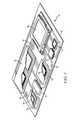
- FIG. 1illustrates a printed circuit board (PCB) with different types of packages mounted to its surface
- FIGS. 2 a -2 cillustrate further detail of the representative semiconductor packages mounted to the PCB
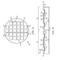
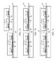
- FIGS. 3 a -3 dillustrate a semiconductor wafer with a plurality of semiconductor die separated by a saw street
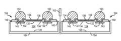
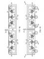
- FIGS. 4 a -4 eillustrate a process of depositing an encapsulant over the sides and an exposed portion of an active surface of a semiconductor die in a WLCSP;
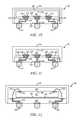
- FIG. 5illustrates the WLCSP with the sides and the exposed portion of the active surface of the semiconductor die covered with the encapsulant
- FIGS. 6 a -6 cillustrate a semiconductor wafer with a plurality of semiconductor die separated by a saw street
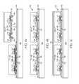
- FIGS. 7 a -7 eillustrate another process of depositing an encapsulant over the sides and an exposed portion of an active surface of a semiconductor die in a WLCSP;
- FIG. 8illustrates the WLCSP with the sides and the exposed portion of the active surface of the semiconductor die covered with the encapsulant
- FIGS. 9 a -9 hillustrate a process of depositing a MUF material with the sides and a portion of an active surface of a semiconductor die in a WLCSP;
- FIG. 10illustrates the WLCSP with the sides and the portion of the active surface of the semiconductor die covered with the MUF material
- FIG. 11illustrates the MUF material disposed between the semiconductor die and substrate
- FIG. 12illustrates another WLCSP with the sides and the portion of the active surface of the semiconductor die covered with the MUF material.
- Front-end manufacturinginvolves the formation of a plurality of die on the surface of a semiconductor wafer.
- Each die on the wafercontains active and passive electrical components, which are electrically connected to form functional electrical circuits.
- Active electrical componentssuch as transistors and diodes, have the ability to control the flow of electrical current.
- Passive electrical componentssuch as capacitors, inductors, and resistors, create a relationship between voltage and current necessary to perform electrical circuit functions.
- Passive and active componentsare formed over the surface of the semiconductor wafer by a series of process steps including doping, deposition, photolithography, etching, and planarization.
- Dopingintroduces impurities into the semiconductor material by techniques such as ion implantation or thermal diffusion.
- the doping processmodifies the electrical conductivity of semiconductor material in active devices by dynamically changing the semiconductor material conductivity in response to an electric field or base current.
- Transistorscontain regions of varying types and degrees of doping arranged as necessary to enable the transistor to promote or restrict the flow of electrical current upon the application of the electric field or base current.
- Active and passive componentsare formed by layers of materials with different electrical properties.
- the layerscan be formed by a variety of deposition techniques determined in part by the type of material being deposited. For example, thin film deposition can involve chemical vapor deposition (CVD), physical vapor deposition (PVD), electrolytic plating, and electroless plating processes.
- CVDchemical vapor deposition
- PVDphysical vapor deposition
- electrolytic platingelectroless plating processes.
- Each layeris generally patterned to form portions of active components, passive components, or electrical connections between components.
- Back-end manufacturingrefers to cutting or singulating the finished wafer into the individual semiconductor die and then packaging the semiconductor die for structural support and environmental isolation.
- the waferis scored and broken along non-functional regions of the wafer called saw streets or scribes.
- the waferis singulated using a laser cutting tool or saw blade.
- the individual semiconductor dieare mounted to a package substrate that includes pins or contact pads for interconnection with other system components. Contact pads formed over the semiconductor die are then connected to contact pads within the package.
- the electrical connectionscan be made with solder bumps, stud bumps, conductive paste, or wirebonds.
- An encapsulant or other molding materialis deposited over the package to provide physical support and electrical isolation. The finished package is then inserted into an electrical system and the functionality of the semiconductor device is made available to the other system components.
- FIG. 1illustrates electronic device 50 having a chip carrier substrate or printed circuit board (PCB) 52 with a plurality of semiconductor packages mounted on its surface.
- Electronic device 50can have one type of semiconductor package, or multiple types of semiconductor packages, depending on the application. The different types of semiconductor packages are shown in FIG. 1 for purposes of illustration.
- Electronic device 50can be a stand-alone system that uses the semiconductor packages to perform one or more electrical functions.
- electronic device 50can be a subcomponent of a larger system.
- electronic device 50can be part of a cellular phone, personal digital assistant (PDA), digital video camera (DVC), or other electronic communication device.
- PDApersonal digital assistant
- DVCdigital video camera
- electronic device 50can be a graphics card, network interface card, or other signal processing card that can be inserted into a computer.
- the semiconductor packagecan include microprocessors, memories, application specific integrated circuits (ASIC), logic circuits, analog circuits, RF circuits, discrete devices, or other semiconductor die or electrical components. Miniaturization and weight reduction are essential for the products to be accepted by the market. The distance between semiconductor devices must be decreased to achieve higher density.
- PCB 52provides a general substrate for structural support and electrical interconnect of the semiconductor packages mounted on the PCB.
- Conductive signal traces 54are formed over a surface or within layers of PCB 52 using evaporation, electrolytic plating, electroless plating, screen printing, or other suitable metal deposition process. Signal traces 54 provide for electrical communication between each of the semiconductor packages, mounted components, and other external system components. Traces 54 also provide power and ground connections to each of the semiconductor packages.
- a semiconductor devicehas two packaging levels.
- First level packagingis a technique for mechanically and electrically attaching the semiconductor die to an intermediate carrier.
- Second level packaginginvolves mechanically and electrically attaching the intermediate carrier to the PCB.
- a semiconductor devicemay only have the first level packaging where the die is mechanically and electrically mounted directly to the PCB.
- first level packagingincluding bond wire package 56 and flipchip 58
- second level packagingincluding ball grid array (BGA) 60 , bump chip carrier (BCC) 62 , dual in-line package (DIP) 64 , land grid array (LGA) 66 , multi-chip module (MCM) 68 , quad flat non-leaded package (QFN) 70 , and quad flat package 72 .
- BGAball grid array
- BCCbump chip carrier
- DIPdual in-line package
- LGAland grid array
- MCMmulti-chip module
- QFNquad flat non-leaded package
- quad flat package 72quad flat package
- electronic device 50includes a single attached semiconductor package, while other embodiments call for multiple interconnected packages.
- manufacturerscan incorporate pre-made components into electronic devices and systems. Because the semiconductor packages include sophisticated functionality, electronic devices can be manufactured using less expensive components and a streamlined manufacturing process. The resulting devices are less likely to fail and less expensive to manufacture resulting in a lower cost for consumers.
- FIGS. 2 a -2 cshow exemplary semiconductor packages.
- FIG. 2 aillustrates further detail of DIP 64 mounted on PCB 52 .
- Semiconductor die 74includes an active region containing analog or digital circuits implemented as active devices, passive devices, conductive layers, and dielectric layers formed within the die and are electrically interconnected according to the electrical design of the die.
- the circuitcan include one or more transistors, diodes, inductors, capacitors, resistors, and other circuit elements formed within the active region of semiconductor die 74 .
- Contact pads 76are one or more layers of conductive material, such as aluminum (Al), copper (Cu), tin (Sn), nickel (Ni), gold (Au), or silver (Ag), and are electrically connected to the circuit elements formed within semiconductor die 74 .
- semiconductor die 74is mounted to an intermediate carrier 78 using a gold-silicon eutectic layer or adhesive material such as thermal epoxy or epoxy resin.
- the package bodyincludes an insulative packaging material such as polymer or ceramic.
- Conductor leads 80 and bond wires 82provide electrical interconnect between semiconductor die 74 and PCB 52 .
- Encapsulant 84is deposited over the package for environmental protection by preventing moisture and particles from entering the package and contaminating semiconductor die 74 or bond wires 82 .
- FIG. 2 billustrates further detail of BCC 62 mounted on PCB 52 .
- Semiconductor die 88is mounted over carrier 90 using an underfill or epoxy-resin adhesive material 92 .
- Bond wires 94provide first level packaging interconnect between contact pads 96 and 98 .
- Molding compound or encapsulant 100is deposited over semiconductor die 88 and bond wires 94 to provide physical support and electrical isolation for the device.
- Contact pads 102are formed over a surface of PCB 52 using a suitable metal deposition process such as electrolytic plating or electroless plating to prevent oxidation.
- Contact pads 102are electrically connected to one or more conductive signal traces 54 in PCB 52 .
- Bumps 104are formed between contact pads 98 of BCC 62 and contact pads 102 of PCB 52 .
- semiconductor die 58is mounted face down to intermediate carrier 106 with a flipchip style first level packaging.
- Active region 108 of semiconductor die 58contains analog or digital circuits implemented as active devices, passive devices, conductive layers, and dielectric layers formed according to the electrical design of the die.
- the circuitcan include one or more transistors, diodes, inductors, capacitors, resistors, and other circuit elements within active region 108 .
- Semiconductor die 58is electrically and mechanically connected to carrier 106 through bumps 110 .
- BGA 60is electrically and mechanically connected to PCB 52 with a BGA style second level packaging using bumps 112 .
- Semiconductor die 58is electrically connected to conductive signal traces 54 in PCB 52 through bumps 110 , signal lines 114 , and bumps 112 .
- a molding compound or encapsulant 116is deposited over semiconductor die 58 and carrier 106 to provide physical support and electrical isolation for the device.
- the flipchip semiconductor deviceprovides a short electrical conduction path from the active devices on semiconductor die 58 to conduction tracks on PCB 52 in order to reduce signal propagation distance, lower capacitance, and improve overall circuit performance.
- the semiconductor die 58can be mechanically and electrically connected directly to PCB 52 using flipchip style first level packaging without intermediate carrier 106 .
- FIG. 3 ashows a semiconductor wafer 120 with a base substrate material 122 , such as silicon, germanium, gallium arsenide, indium phosphide, or silicon carbide, for structural support.
- a plurality of semiconductor die or components 124is formed on wafer 120 separated by a non-active, inter-die wafer area or saw street 126 as described above.
- Saw street 126provides cutting areas to singulate semiconductor wafer 120 into individual semiconductor die 124 .
- semiconductor wafer 120is 200-300 millimeters (mm) in diameter.
- FIG. 3 bshows a cross-sectional view of a portion of semiconductor wafer 120 .
- Each semiconductor die 124has a back surface 128 and active surface 130 containing analog or digital circuits implemented as active devices, passive devices, conductive layers, and dielectric layers formed within the die and electrically interconnected according to the electrical design and function of the die.
- the circuitmay include one or more transistors, diodes, and other circuit elements formed within active surface 130 to implement analog circuits or digital circuits, such as digital signal processor (DSP), ASIC, memory, or other signal processing circuit.
- DSPdigital signal processor
- Semiconductor die 124may also contain integrated passive devices (IPDs), such as inductors, capacitors, and resistors, for RF signal processing.
- IPDsintegrated passive devices
- An electrically conductive layer 132is formed over active surface 130 using PVD, CVD, electrolytic plating, electroless plating process, or other suitable metal deposition process.
- Conductive layer 132can be one or more layers of Al, Cu, Sn, Ni, Au, Ag, or other suitable electrically conductive material.
- Conductive layer 132operates as contact pads electrically connected to the circuits on active surface 130 .
- Conductive layer 132can be formed as contact pads disposed side-by-side a first distance from the edge of semiconductor die 124 , as shown in FIG. 3 b .
- conductive layer 132can be formed as contact pads that are offset in multiple rows such that a first row of contact pads is disposed a first distance from the edge of the die, and a second row of contact pads alternating with the first row is disposed a second distance from the edge of the die.
- a first insulating or passivation layer 134is formed over semiconductor die 124 and conductive layer 132 using PVD, CVD, printing, spin coating, spray coating, sintering or thermal oxidation.
- the insulating layer 134contains one or more layers of silicon dioxide (SiO2), silicon nitride (Si3N4), silicon oxynitride (SiON), tantalum pentoxide (Ta2O5), aluminum oxide (Al2O3), hafnium oxide (HfO2), benzocyclobutene (BCB), polyimide (PI), polybenzoxazoles (PBO), polymer, or other dielectric material having similar structural and insulating properties.
- An electrically conductive layer or redistribution layer (RDL) 136is formed over the first insulating layer 134 using a patterning and metal deposition process such as sputtering, electrolytic plating, and electroless plating.
- Conductive layer 136can be one or more layers of Al, Cu, Sn, Ni, Au, Ag, or other suitable electrically conductive material.
- One portion of conductive layer 136is electrically connected to conductive layer 132 of semiconductor die 124 .
- Other portions of conductive layer 136can be electrically common or electrically isolated depending on the design and function of semiconductor die 124 .
- a second insulating or passivation layer 134is formed over conductive layer 136 and the first insulating layer 134 .
- Multiple insulating layers 134 and conductive layers 136can be formed over active surface 130 of semiconductor die 124 .
- a surface inspectioncan be performed to detect passivation or RDL defects.
- a portion of insulating layer 134is removed by laser direct ablation (LDA) using laser 138 to expose conductive layer 132 and portion 140 of active surface 130 along a surface edge of semiconductor die 124 . That is, portion 140 of active surface 130 along a surface edge of semiconductor die 124 is devoid of insulating layer 134 .
- a portion of insulating layer 134is removed by an etching process through a patterned photoresist layer to expose conductive layer 132 and portion 140 of active surface 130 along the surface edge of semiconductor die 124 .
- an electrically conductive layer 142is formed over the exposed portion of conductive layer 132 and insulating layer 134 after final repassivation using PVD, CVD, evaporation, electrolytic plating, electroless plating, or other suitable metal deposition process.
- Conductive layer 142can be Al, Cu, Sn, Ni, Au, Ag, tungsten (W), or other suitable electrically conductive material.
- Conductive layer 142is a UBM electrically connected to conductive layer 132 .
- UBMs 142can be a multi-metal stack with adhesion layer, barrier layer, and seed or wetting layer.
- the adhesion layeris formed over conductive layer 132 and can be titanium (Ti), titanium nitride (TiN), titanium tungsten (TiW), Al, or chromium (Cr).
- the barrier layeris formed over the adhesion layer and can be Ni, NiV, platinum (Pt), palladium (Pd), TiW, or chromium copper (CrCu).
- the barrier layerinhibits the diffusion of Cu into the active area of the die.
- the seed layeris formed over the barrier layer and can be Cu, Ni, NiV, Au, or Al.
- UBMs 142provide a low resistive interconnect to conductive layer 132 , as well as a barrier to solder diffusion and seed layer for solder wettability.
- semiconductor wafer 120is singulated through saw street 126 using a saw blade or laser cutting tool 144 into individual semiconductor die 124 .
- FIGS. 4 a -4 eillustrate, in relation to FIGS. 1 and 2 a - 2 c , a process of depositing an encapsulant over the sides and an exposed portion of an active surface of a semiconductor die in a WLCSP.
- FIG. 4 ashows a cross-sectional view of a portion of a carrier or temporary substrate 150 containing sacrificial base material such as silicon, polymer, beryllium oxide, glass, or other suitable low-cost, rigid material for structural support.
- An interface layer or double-sided tape 152is formed over carrier 150 as a temporary adhesive bonding film, etch-stop layer, or thermal release layer.
- Carrier 150can be a large round or rectangular panel (greater than 300 mm) with capacity for multiple semiconductor die 124 .
- Semiconductor die 124 from FIG. 3 dare mounted to carrier 150 and interface layer 152 using, for example, a pick and place operation with insulating layer 134 oriented toward the carrier.
- FIG. 4 bshows semiconductor die 124 mounted to interface layer 152 of carrier 150 as reconstituted wafer 153 .
- Active surface 130 of semiconductor die 124is held off or offset from interface layer 152 by nature of insulating layer 134 and/or conductive layer 142 contacting the interface layer, i.e., there is a gap between portion 140 of active surface 130 and interface layer 152 .
- an encapsulant or molding compound 154is deposited over semiconductor die 124 and carrier 150 using a paste printing, compressive molding, transfer molding, liquid encapsulant molding, vacuum lamination, spin coating, or other suitable applicator.
- Encapsulant 154can be polymer composite material, such as epoxy resin with filler, epoxy acrylate with filler, or polymer with proper filler.
- Encapsulant 154is non-conductive and environmentally protects the semiconductor device from external elements and contaminants.
- encapsulant 154is disposed along the sides of semiconductor die 124 and in the gap between active surface 130 and interface layer 152 and thus covers the sides of semiconductor die 124 and exposed portion 140 of active surface 130 along the surface edge of the semiconductor die up to insulating layer 134 . Accordingly, encapsulant 154 covers or contacts at least five surfaces of semiconductor die 124 , i.e., four side surfaces and portion 140 of active surface 130 of the semiconductor die.
- carrier 150 and interface layer 152are removed by chemical etching, mechanical peeling, chemical mechanical planarization (CMP), mechanical grinding, thermal bake, UV light, laser scanning, or wet stripping to expose insulating layer 134 and conductive layer 142 .
- a portion of encapsulant 154is removed by LDA using laser 156 .
- a portion of encapsulant 154is removed by an etching process through a patterned photoresist layer.
- Portion 140 of active surface 130 along the surface edge of semiconductor die 124 , as well as the sides of the semiconductor die,remain covered by encapsulant 154 as a protective panel to increase yield, particularly when surface mounting the semiconductor die.
- Encapsulant 154also protects semiconductor die 124 from degradation due to exposure to light.
- Semiconductor die 124is prepared for electrical testing by cleaning insulating layer 134 and conductive layer 142 with one or more steps of plasma, wet solvent, copper oxide, or dry cleaning.
- an electrically conductive bump materialis deposited over conductive layer 142 using an evaporation, electrolytic plating, electroless plating, ball drop, or screen printing process.
- the bump materialis deposited with a ball drop stencil, i.e., no mask required.
- the bump materialcan be Al, Sn, Ni, Au, Ag, lead (Pb), Bi, Cu, solder, and combinations thereof, with an optional flux solution.
- the bump materialcan be eutectic Sn/Pb, high-lead solder, or lead-free solder.
- the bump materialis bonded to conductive layer 142 using a suitable attachment or bonding process.
- the bump materialis reflowed by heating the material above its melting point to form balls or bumps 160 .
- bumps 160are reflowed a second time to improve electrical contact to conductive layer 142 .
- Bumps 160can also be compression bonded or thermocompression bonded to conductive layer 142 .
- Bumps 160represent one type of interconnect structure that can be formed over conductive layer 142 .
- the interconnect structurecan also use bond wires, conductive paste, stud bump, micro bump, or other electrical interconnect. Laser marking can be performed before or after bump formation, or after removal of carrier 150 .
- Semiconductor die 124are singulated through encapsulant 154 with saw blade or laser cutting tool 162 into individual embedded wafer level ball grid array (eWLB) or wafer-level chip scale package (WLCSP) 164 .
- FIG. 5shows WLCSP 164 after singulation.
- WLCSP 164has dimensions of 3.0 ⁇ 2.6 ⁇ 0.7 millimeters mm with 0.4 mm pitch.
- Semiconductor die 124is electrically connected to bumps 160 for external interconnect.
- Encapsulant 154covers the sides of semiconductor die 124 and portion 140 of active surface 130 to protect the sides and surface edge of the semiconductor die and increase manufacturing yield, particularly when surface mounting the semiconductor die.
- Encapsulant 154also protects semiconductor die 124 from degradation due to exposure to light.
- WLCSP 164undergoes electrical testing before or after singulation.
- FIGS. 6 a -6 cillustrate another embodiment of semiconductor wafer 170 with a base substrate material 172 , such as silicon, germanium, gallium arsenide, indium phosphide, or silicon carbide, for structural support, similar to FIG. 3 a .
- a plurality of semiconductor die or components 174is formed on wafer 170 separated by a non-active, inter-die wafer area or saw street 176 as described above.
- Saw street 176provides cutting areas to singulate semiconductor wafer 170 into individual semiconductor die 174 .
- semiconductor wafer 170is 200-300 millimeters (mm) in diameter.
- FIG. 6 ashows a cross-sectional view of a portion of semiconductor wafer 170 .
- Each semiconductor die 174has a back surface 178 and active surface 180 containing analog or digital circuits implemented as active devices, passive devices, conductive layers, and dielectric layers formed within the die and electrically interconnected according to the electrical design and function of the die.
- the circuitmay include one or more transistors, diodes, and other circuit elements formed within active surface 180 to implement analog circuits or digital circuits, such as DSP, ASIC, memory, or other signal processing circuit.
- semiconductor die 174may also contain IPDs, such as inductors, capacitors, and resistors, for RF signal processing.
- An electrically conductive layer 182is formed over active surface 180 using PVD, CVD, electrolytic plating, electroless plating process, or other suitable metal deposition process.
- Conductive layer 182can be one or more layers of Al, Cu, Sn, Ni, Au, Ag, or other suitable electrically conductive material.
- Conductive layer 182operates as contact pads electrically connected to the circuits on active surface 180 .
- Conductive layer 182can be formed as contact pads disposed side-by-side a first distance from the edge of semiconductor die 174 , as shown in FIG. 6 a .
- conductive layer 182can be formed as contact pads that are offset in multiple rows such that a first row of contact pads is disposed a first distance from the edge of the die, and a second row of contact pads alternating with the first row is disposed a second distance from the edge of the die.
- An electrically conductive layer 184is formed over conductive layer 182 using PVD, CVD, evaporation, electrolytic plating, electroless plating, or other suitable metal deposition process.
- Conductive layer 184can be Al, Cu, Sn, Ni, Au, Ag, W, or other suitable electrically conductive material.
- Conductive layer 184is a UBM electrically connected to conductive layer 182 .
- UBMs 184can be a multi-metal stack with adhesion layer, barrier layer, and seed or wetting layer.
- the adhesion layeris formed over conductive layer 182 and can be Ti, TiN, TiW, Al, or Cr.
- the barrier layeris formed over the adhesion layer and can be Ni, NiV, Pt, Pd, TiW, or CrCu.
- the barrier layerinhibits the diffusion of Cu into the active area of the die.
- the seed layeris formed over the barrier layer and can be Cu, Ni, NiV, Au, or Al.
- UBMs 184provide a low resistive interconnect to conductive layer 182 , as well as a barrier to solder diffusion and seed layer for solder wettability.
- a first insulating or passivation layer 186is formed over semiconductor die 174 and conductive layer 184 using PVD, CVD, printing, spin coating, spray coating, sintering or thermal oxidation, i.e., passivation occurs after formation of UBM 184 .
- the insulating layer 186contains one or more layers of SiO2, Si3N4, SiON, Ta2O5, Al2O3, HfO2, BCB, PI, PBO, polymer, or other dielectric material having similar structural and insulating properties.
- An electrically conductive layer or RDL 188is formed over the first insulating layer 186 using a patterning and metal deposition process such as sputtering, electrolytic plating, and electroless plating.
- Conductive layer 188can be one or more layers of Al, Cu, Sn, Ni, Au, Ag, or other suitable electrically conductive material.
- One portion of conductive layer 188is electrically connected to conductive layer 182 of semiconductor die 174 .
- Other portions of conductive layer 188can be electrically common or electrically isolated depending on the design and function of semiconductor die 174 .
- a second insulating or passivation layer 186is formed over conductive layer 188 and the first insulating layer 186 .
- Multiple insulating layers 186 and conductive layers 188can be formed over active surface 180 of semiconductor die 174 .
- a surface inspectioncan be performed to detect passivation or RDL defects.
- a portion of insulating layer 186is removed by LDA using laser 190 to expose conductive layer 184 and portion 192 of active surface 180 along a surface edge of semiconductor die 174 . That is, portion 192 of active surface 180 along a surface edge of semiconductor die 174 is devoid of insulating layer 186 .
- a portion of insulating layer 186is removed by an etching process through a patterned photoresist layer to expose conductive layer 182 and portion 192 of active surface 180 along the surface edge of semiconductor die 174 .
- semiconductor wafer 170is singulated through saw street 176 using a saw blade or laser cutting tool 194 into individual semiconductor die 174 .
- FIGS. 7 a -7 eillustrate, in relation to FIGS. 1 and 2 a - 2 c , another process of depositing an encapsulant over the sides and an exposed portion of an active surface of a semiconductor die in a WLCSP.
- FIG. 7 ashows a cross-sectional view of a portion of a carrier or temporary substrate 200 containing sacrificial base material such as silicon, polymer, beryllium oxide, glass, or other suitable low-cost, rigid material for structural support.
- An interface layer or double-sided tape 202is formed over carrier 200 as a temporary adhesive bonding film, etch-stop layer, or thermal release layer.
- Carrier 200can be a large round or rectangular panel (greater than 300 mm) with capacity for multiple semiconductor die 174 .
- FIG. 7 bshows semiconductor die 174 mounted to interface layer 202 of carrier 200 as reconstituted wafer 203 .
- Active surface 180 of semiconductor die 174is held off or offset from interface layer 202 by nature of insulating layer 186 contacting the interface layer, i.e., there is a gap between portion 192 of active surface 180 and interface layer 202 .
- an encapsulant or molding compound 204is deposited over semiconductor die 174 and carrier 200 using a paste printing, compressive molding, transfer molding, liquid encapsulant molding, vacuum lamination, spin coating, or other suitable applicator.
- Encapsulant 204can be polymer composite material, such as epoxy resin with filler, epoxy acrylate with filler, or polymer with proper filler.
- Encapsulant 204is non-conductive and environmentally protects the semiconductor device from external elements and contaminants.
- encapsulant 204is disposed along the sides of semiconductor die 174 and in the gap between active surface 180 and interface layer 202 and thus covers the sides of semiconductor die 174 and exposed portion 192 of active surface 180 along the surface edge of the semiconductor die up to insulating layer 186 . Accordingly, encapsulant 204 covers or contacts at least five surfaces of semiconductor die 174 , i.e., four side surfaces and portion 192 of active surface 180 of the semiconductor die.
- carrier 200 and interface layer 202are removed by chemical etching, mechanical peeling, CMP, mechanical grinding, thermal bake, UV light, laser scanning, or wet stripping to expose insulating layer 186 and conductive layer 184 .
- a portion of encapsulant 204is removed by LDA using laser 206 .
- a portion of encapsulant 204is removed by an etching process through a patterned photoresist layer.
- Portion 192 of active surface 180 along the surface edge of semiconductor die 124 , as well as the sides of the semiconductor die,remain covered by encapsulant 204 as a protective panel to increase yield, particularly when surface mounting the semiconductor die.
- Encapsulant 204also protects semiconductor die 174 from degradation due to exposure to light.
- Semiconductor die 174is prepared for electrical testing by cleaning insulating layer 186 and conductive layer 184 with one or more steps of plasma, wet solvent, copper oxide, or dry cleaning.
- an electrically conductive bump materialis deposited over conductive layer 184 using an evaporation, electrolytic plating, electroless plating, ball drop, or screen printing process.
- the bump materialis deposited with a ball drop stencil, i.e., no mask required.
- the bump materialcan be Al, Sn, Ni, Au, Ag, Pb, Bi, Cu, solder, and combinations thereof, with an optional flux solution.
- the bump materialcan be eutectic Sn/Pb, high-lead solder, or lead-free solder.
- the bump materialis bonded to conductive layer 184 using a suitable attachment or bonding process.
- the bump materialis reflowed by heating the material above its melting point to form balls or bumps 210 .
- bumps 210are reflowed a second time to improve electrical contact to conductive layer 184 .
- Bumps 210can also be compression bonded or thermocompression bonded to conductive layer 184 .
- Bumps 210represent one type of interconnect structure that can be formed over conductive layer 184 .
- the interconnect structurecan also use bond wires, conductive paste, stud bump, micro bump, or other electrical interconnect. Laser marking can be performed before or after bump formation, or after removal of carrier 200 .
- Semiconductor die 174are singulated through encapsulant 204 with saw blade or laser cutting tool 212 into individual eWLB or WLCSP 214 .
- FIG. 8shows WLCSP 214 after singulation.
- WLCSP 214has dimensions of 3.0 ⁇ 2.6 ⁇ 0.7 millimeters mm with 0.4 mm pitch.
- Semiconductor die 174is electrically connected to bumps 210 for external interconnect.
- Encapsulant 204covers the sides of semiconductor die 174 and portion 192 of active surface 180 to protect the sides and surface edge of semiconductor die 174 and increase manufacturing yield, particularly when surface mounting the semiconductor die.
- Encapsulant 204also protects semiconductor die 174 from degradation due to exposure to light. WLCSP 214 undergoes electrical testing before or after singulation.
- FIGS. 9 a -9 hillustrate, in relation to FIGS. 1 and 2 a - 2 c , a process of depositing MUF material over the sides and an exposed portion of an active surface of a semiconductor die in a WLCSP.
- FIG. 9 ashows a semiconductor die 220 , from a semiconductor wafer similar to FIG. 3 a , having a back surface 222 and active surface 224 containing analog or digital circuits implemented as active devices, passive devices, conductive layers, and dielectric layers formed within the die and electrically interconnected according to the electrical design and function of the die.
- the circuitmay include one or more transistors, diodes, and other circuit elements formed within active surface 224 to implement analog circuits or digital circuits, such as DSP, ASIC, memory, or other signal processing circuit.
- Semiconductor die 220may also contain IPDs, such as inductors, capacitors, and resistors, for RF signal processing. In one embodiment, semiconductor die 220 is a flipchip type semiconductor die.
- An electrically conductive layer 226is formed over active surface 224 using PVD, CVD, electrolytic plating, electroless plating process, or other suitable metal deposition process.
- Conductive layer 226can be one or more layers of Al, Cu, Sn, Ni, Au, Ag, or other suitable electrically conductive material.
- Conductive layer 226operates as contact pads electrically connected to the circuits on active surface 224 .
- An electrically conductive layer 228is formed over conductive layer 226 using a patterning and metal deposition process such as sputtering, electrolytic plating, and electroless plating.
- Conductive layer 228can be Al, Cu, Sn, Ni, Au, Ag, W, or other suitable electrically conductive material.
- Conductive layer 228is a UBM electrically connected to conductive layer 226 .
- UBMs 228can be a multi-metal stack with adhesion layer, barrier layer, and seed or wetting layer.
- the adhesion layeris formed over conductive layer 226 and can be Ti, TiN, TiW, Al, or Cr.
- the barrier layeris formed over the adhesion layer and can be Ni, NiV, Pt, Pd, TiW, or CrCu.
- the barrier layerinhibits the diffusion of Cu into the active area of the die.
- the seed layeris formed over the barrier layer and can be Cu, Ni, NiV, Au, or Al.
- UBMs 228provide a low resistive interconnect to conductive layer 226 , as well as a barrier to solder diffusion and seed layer for solder wettability.
- An electrically conductive bump materialis deposited over conductive layer 228 using an evaporation, electrolytic plating, electroless plating, ball drop, or screen printing process.
- the bump materialcan be Al, Sn, Ni, Au, Ag, Pb, Bi, Cu, solder, and combinations thereof, with an optional flux solution.
- the bump materialcan be eutectic Sn/Pb, high-lead solder, or lead-free solder.
- the bump materialis bonded to conductive layer 228 using a suitable attachment or bonding process.
- the bump materialis reflowed by heating the material above its melting point to form balls or bumps 230 .
- bumps 230are reflowed a second time to improve electrical contact to conductive layer 228 .
- Bumps 230can also be compression bonded or thermocompression bonded to conductive layer 228 .
- Bumps 230represent one type of interconnect structure that can be formed over conductive layer 228 .
- the interconnect structurecan also use stud bump, micro bump, or other electrical interconnect.
- Semiconductor die 220are mounted to substrate 232 using, for example, a pick and place operation with bumps 230 oriented toward the substrate.
- Substrate 232includes conductive traces 234 for vertical and lateral interconnect through the substrate.
- FIG. 9 bshows semiconductor die 220 mounted to substrate 232 , as reconstituted wafer 236 , with bumps 230 metallurgically and electrically bonded to conductive traces 234 .
- Active surface 224 of semiconductor die 220is held off or offset from substrate 232 by nature of bumps 230 , i.e., there is a gap between portion 238 of active surface 224 and substrate 232 .
- Substrate 232can be a large round or rectangular panel (greater than 300 mm) with capacity for multiple semiconductor die 220 .
- a mold underfill (MUF) material 240is deposited over semiconductor die 220 and substrate 232 using a paste printing, compressive molding, transfer molding, liquid encapsulant molding, vacuum lamination, spin coating, mold underfill, or other suitable application process.
- MUF material 240can be polymer composite material, such as epoxy resin with filler, epoxy acrylate with filler, or polymer with proper filler.
- MUF material 240is non-conductive and environmentally protects the semiconductor device from external elements and contaminants.
- MUF material 240is disposed along the sides of semiconductor die 220 and in the gap between active surface 224 and substrate 232 and thus covers the sides of semiconductor die 220 and exposed portion 238 of active surface 224 along the surface edge of the semiconductor die.
- semiconductor die 220are singulated through MUF material 240 and substrate 232 with saw blade or laser cutting tool 239 to separate the semiconductor die and substrate units.
- FIG. 9 eshows a cross-sectional view of a portion of a carrier or temporary substrate 242 containing sacrificial base material such as silicon, polymer, beryllium oxide, glass, or other suitable low-cost, rigid material for structural support.
- An interface layer or double-sided tape 243is formed over carrier 150 as a temporary adhesive bonding film, etch-stop layer, or thermal release layer.
- Carrier 242can be a large round or rectangular panel (greater than 300 mm) with capacity for multiple semiconductor die 220 and substrate 232 units.
- FIG. 9 fshows semiconductor die 220 and substrate 232 units mounted to interface layer 243 of carrier 242 .
- An encapsulant or molding compound 244is deposited over MUF material 240 , substrate 232 , and carrier 242 using a paste printing, compressive molding, transfer molding, liquid encapsulant molding, vacuum lamination, spin coating, or other suitable applicator.
- Encapsulant 244can be polymer composite material, such as epoxy resin with filler, epoxy acrylate with filler, or polymer with proper filler.
- Encapsulant 244is non-conductive and environmentally protects the semiconductor device from external elements and contaminants.
- carrier 242 and interface layer 243are removed by chemical etching, mechanical peeling, CMP, mechanical grinding, thermal bake, UV light, laser scanning, or wet stripping to expose substrate 232 and encapsulant 244 .
- a portion of encapsulant 244is removed by LDA using laser 245 .
- a portion of encapsulant 244is removed by an etching process through a patterned photoresist layer.
- an electrically conductive bump materialis deposited over conductive layer 234 of substrate 232 opposite semiconductor die 220 using an evaporation, electrolytic plating, electroless plating, ball drop, or screen printing process.
- the bump materialcan be Al, Sn, Ni, Au, Ag, Pb, Bi, Cu, solder, and combinations thereof, with an optional flux solution.
- the bump materialcan be eutectic Sn/Pb, high-lead solder, or lead-free solder.
- the bump materialis bonded to conductive layer 234 using a suitable attachment or bonding process. In one embodiment, the bump material is reflowed by heating the material above its melting point to form balls or bumps 246 .
- bumps 246are reflowed a second time to improve electrical contact to conductive layer 234 .
- Bumps 246can also be compression bonded or thermocompression bonded to conductive layer 234 .
- Bumps 246represent one type of interconnect structure that can be formed over conductive layer 234 .
- the interconnect structurecan also use bond wires, conductive paste, stud bump, micro bump, or other electrical interconnect.
- Laser markingcan be performed before or after bump formation, or after removal of carrier 242 .
- the assemblyundergoes plasma cleaning and flux printing.
- Semiconductor die 220are singulated through encapsulant 244 with saw blade or laser cutting tool 248 into individual eWLB or WLCSP 250 .
- FIG. 10shows WLCSP 250 after singulation.
- WLCSP 250has dimensions of 3.0 ⁇ 2.6 ⁇ 0.7 millimeters mm with 0.4 mm pitch.
- Semiconductor die 220is electrically connected to substrate 232 and bumps 246 for external interconnect.
- MUF material 240covers the sides of semiconductor die 220 and portion 238 of active surface 224 to protect the sides and surface edge of the semiconductor die and increase manufacturing yield, particularly when surface mounting the semiconductor die. MUF material 240 also protects semiconductor die 220 from degradation due to exposure to light. WLCSP 250 undergoes electrical testing before or after singulation.
- FIG. 11illustrates an embodiment of WLCSP 254 , similar to FIG. 10 , with MUF material 240 disposed under semiconductor die 220 and encapsulant 244 covering the side surfaces of the semiconductor die.
- FIG. 12illustrates another embodiment including semiconductor die 260 , from a semiconductor wafer similar to FIG. 3 a , having a back surface 262 and active surface 264 containing analog or digital circuits implemented as active devices, passive devices, conductive layers, and dielectric layers formed within the die and electrically interconnected according to the electrical design and function of the die.
- the circuitmay include one or more transistors, diodes, and other circuit elements formed within active surface 264 to implement analog circuits or digital circuits, such as DSP, ASIC, memory, or other signal processing circuit.
- semiconductor die 260may also contain IPDs, such as inductors, capacitors, and resistors, for RF signal processing.
- semiconductor die 260is a wire bond type semiconductor die.
- An electrically conductive layer 266is formed over active surface 264 using PVD, CVD, electrolytic plating, electroless plating process, or other suitable metal deposition process.
- Conductive layer 266can be one or more layers of Al, Cu, Sn, Ni, Au, Ag, or other suitable electrically conductive material.
- Conductive layer 266operates as contact pads electrically connected to the circuits on active surface 264 .
- Semiconductor die 260is mounted to substrate 268 with die attach adhesive 270 , such as epoxy resin, similar to FIGS. 9 a -9 b .
- Substrate 268includes conductive traces 272 for vertical and lateral interconnect through the substrate. Bond wires 274 are formed between conductive layer 266 of semiconductor die 260 and conductive traces 272 on substrate 268 .
- Substrate 268can be a large round or rectangular panel (greater than 300 mm) with capacity for multiple semiconductor die 260 .
- Encapsulant or molding compound 276is deposited over semiconductor die 260 and substrate 268 using a paste printing, compressive molding, transfer molding, liquid encapsulant molding, vacuum lamination, spin coating, or other suitable applicator, similar to FIG. 9 c .
- Encapsulant 276can be polymer composite material, such as epoxy resin with filler, epoxy acrylate with filler, or polymer with proper filler.
- Encapsulant 276is non-conductive and environmentally protects the semiconductor device from external elements and contaminants.
- Semiconductor die 260are singulated through encapsulant 276 and substrate 268 , similar to FIG. 9 d .
- the singulated semiconductor die 260 and substrate 268are mounted to a carrier, similar to FIG. 9 e .
- An encapsulant or molding compound 278is deposited over encapsulant 276 and substrate 268 using a paste printing, compressive molding, transfer molding, liquid encapsulant molding, vacuum lamination, spin coating, or other suitable applicator, similar to FIG. 9 f .
- Encapsulant 278can be polymer composite material, such as epoxy resin with filler, epoxy acrylate with filler, or polymer with proper filler.
- Encapsulant 278is non-conductive and environmentally protects the semiconductor device from external elements and contaminants. The carrier is removed.
- An electrically conductive bump materialis deposited over conductive layer 272 of substrate 268 opposite semiconductor die 260 using an evaporation, electrolytic plating, electroless plating, ball drop, or screen printing process.
- the bump materialcan be Al, Sn, Ni, Au, Ag, Pb, Bi, Cu, solder, and combinations thereof, with an optional flux solution.
- the bump materialcan be eutectic Sn/Pb, high-lead solder, or lead-free solder.
- the bump materialis bonded to conductive layer 272 using a suitable attachment or bonding process. In one embodiment, the bump material is reflowed by heating the material above its melting point to form balls or bumps 280 .
- bumps 280are reflowed a second time to improve electrical contact to conductive layer 272 .
- Bumps 280can also be compression bonded or thermocompression bonded to conductive layer 272 .
- Bumps 280represent one type of interconnect structure that can be formed over conductive layer 272 .
- the interconnect structurecan also use bond wires, conductive paste, stud bump, micro bump, or other electrical interconnect.
- Laser markingcan be performed before or after bump formation, or after removal of the carrier.
- the assemblyundergoes plasma cleaning and flux printing.
- Semiconductor die 260are singulated through encapsulant 244 into individual eWLB or WLCSP 282 having dimensions of 3.0 ⁇ 2.6 ⁇ 0.7 millimeters mm with 0.4 mm pitch.
- Semiconductor die 260is electrically connected to substrate 268 and bumps 280 for external interconnect.
- Encapsulant 276covers the side surfaces of semiconductor die 260 to protect the surface edge of the semiconductor die and increase manufacturing yield, particularly when surface mounting the semiconductor die.
Landscapes
- Engineering & Computer Science (AREA)
- Microelectronics & Electronic Packaging (AREA)
- Power Engineering (AREA)
- Computer Hardware Design (AREA)
- Physics & Mathematics (AREA)
- Condensed Matter Physics & Semiconductors (AREA)
- General Physics & Mathematics (AREA)
- Manufacturing & Machinery (AREA)
- Internal Circuitry In Semiconductor Integrated Circuit Devices (AREA)
- Structures Or Materials For Encapsulating Or Coating Semiconductor Devices Or Solid State Devices (AREA)
- Encapsulation Of And Coatings For Semiconductor Or Solid State Devices (AREA)
- Semiconductor Integrated Circuits (AREA)
Abstract
Description
Claims (23)
Priority Applications (18)
| Application Number | Priority Date | Filing Date | Title |
|---|---|---|---|
| US13/832,809US9496195B2 (en) | 2012-10-02 | 2013-03-15 | Semiconductor device and method of depositing encapsulant along sides and surface edge of semiconductor die in embedded WLCSP |
| CN201310164479.8ACN103715108A (en) | 2012-10-02 | 2013-05-07 | Semiconductor device and method of depositing encapsulant in embedded WLCSP |
| CN201911325388.1ACN110993514B (en) | 2012-10-02 | 2013-05-07 | Semiconductor device and method of depositing encapsulant in embedded WLCSP |
| CN2013202416296UCN203288575U (en) | 2012-10-02 | 2013-05-07 | Semiconductor device |
| TW107122625ATWI689075B (en) | 2012-10-02 | 2013-07-16 | Semiconductor device and method of depositing encapsulant along sides and surface edge of semiconductor die in embedded wlcsp |
| TW102125368ATWI632648B (en) | 2012-10-02 | 2013-07-16 | Semiconductor device and method of depositing encapsulant along sides and surface edge of semiconductor die in embedded wlcsp |
| SG10201602415VASG10201602415VA (en) | 2012-10-02 | 2013-07-18 | Semiconductor device and method of depositing encapsulant along sides and surface edge of semiconductor die in embedded wlcsp |
| SG10201709560YASG10201709560YA (en) | 2012-10-02 | 2013-07-18 | Semiconductor device and method of depositing encapsulant along sides and surface edge of semiconductor die in embedded wlcsp |
| SG2013054978ASG2013054978A (en) | 2012-10-02 | 2013-07-18 | Semiconductor device and method of depositing encapsulant along sides and surface edge of semiconductor die in embedded wlcsp |
| KR1020130090751AKR101886888B1 (en) | 2012-10-02 | 2013-07-31 | A semiconductor device and a method of making a semiconductor device |
| US14/097,534US9620413B2 (en) | 2012-10-02 | 2013-12-05 | Semiconductor device and method of using a standardized carrier in semiconductor packaging |
| US15/274,590US10515828B2 (en) | 2012-10-02 | 2016-09-23 | Method of depositing encapsulant along sides and surface edge of semiconductor die in embedded WLCSP |
| US15/414,469US10181423B2 (en) | 2012-10-02 | 2017-01-24 | Semiconductor device and method of using a standardized carrier in semiconductor packaging |
| KR1020180089648AKR102024472B1 (en) | 2012-10-02 | 2018-08-01 | A semiconductor device and a method of making a semiconductor device |
| US16/204,737US11011423B2 (en) | 2012-10-02 | 2018-11-29 | Semiconductor device and method of using a standardized carrier in semiconductor packaging |
| US16/687,865US11222793B2 (en) | 2012-10-02 | 2019-11-19 | Semiconductor device with encapsulant deposited along sides and surface edge of semiconductor die in embedded WLCSP |
| US17/231,591US11961764B2 (en) | 2012-10-02 | 2021-04-15 | Semiconductor device and method of making a wafer-level chip-scale package |
| US17/457,719US12094729B2 (en) | 2012-10-02 | 2021-12-06 | Semiconductor device with encapsulant deposited along sides and surface edge of semiconductor die in embedded WLCSP |
Applications Claiming Priority (2)
| Application Number | Priority Date | Filing Date | Title |
|---|---|---|---|
| US201261744699P | 2012-10-02 | 2012-10-02 | |
| US13/832,809US9496195B2 (en) | 2012-10-02 | 2013-03-15 | Semiconductor device and method of depositing encapsulant along sides and surface edge of semiconductor die in embedded WLCSP |
Related Child Applications (2)
| Application Number | Title | Priority Date | Filing Date |
|---|---|---|---|
| US14/097,534Continuation-In-PartUS9620413B2 (en) | 2012-10-02 | 2013-12-05 | Semiconductor device and method of using a standardized carrier in semiconductor packaging |
| US15/274,590ContinuationUS10515828B2 (en) | 2012-10-02 | 2016-09-23 | Method of depositing encapsulant along sides and surface edge of semiconductor die in embedded WLCSP |
Publications (2)
| Publication Number | Publication Date |
|---|---|
| US20140091482A1 US20140091482A1 (en) | 2014-04-03 |
| US9496195B2true US9496195B2 (en) | 2016-11-15 |
Family
ID=50384422
Family Applications (4)
| Application Number | Title | Priority Date | Filing Date |
|---|---|---|---|
| US13/832,809ActiveUS9496195B2 (en) | 2012-10-02 | 2013-03-15 | Semiconductor device and method of depositing encapsulant along sides and surface edge of semiconductor die in embedded WLCSP |
| US15/274,590ActiveUS10515828B2 (en) | 2012-10-02 | 2016-09-23 | Method of depositing encapsulant along sides and surface edge of semiconductor die in embedded WLCSP |
| US16/687,865ActiveUS11222793B2 (en) | 2012-10-02 | 2019-11-19 | Semiconductor device with encapsulant deposited along sides and surface edge of semiconductor die in embedded WLCSP |
| US17/457,719Active2033-11-03US12094729B2 (en) | 2012-10-02 | 2021-12-06 | Semiconductor device with encapsulant deposited along sides and surface edge of semiconductor die in embedded WLCSP |
Family Applications After (3)
| Application Number | Title | Priority Date | Filing Date |
|---|---|---|---|
| US15/274,590ActiveUS10515828B2 (en) | 2012-10-02 | 2016-09-23 | Method of depositing encapsulant along sides and surface edge of semiconductor die in embedded WLCSP |
| US16/687,865ActiveUS11222793B2 (en) | 2012-10-02 | 2019-11-19 | Semiconductor device with encapsulant deposited along sides and surface edge of semiconductor die in embedded WLCSP |
| US17/457,719Active2033-11-03US12094729B2 (en) | 2012-10-02 | 2021-12-06 | Semiconductor device with encapsulant deposited along sides and surface edge of semiconductor die in embedded WLCSP |
Country Status (5)
| Country | Link |
|---|---|
| US (4) | US9496195B2 (en) |
| KR (2) | KR101886888B1 (en) |
| CN (2) | CN103715108A (en) |
| SG (3) | SG2013054978A (en) |
| TW (2) | TWI689075B (en) |
Cited By (4)
| Publication number | Priority date | Publication date | Assignee | Title |
|---|---|---|---|---|
| US10431575B2 (en) | 2017-12-19 | 2019-10-01 | Nxp B.V. | Multi-die array device |
| US11075180B2 (en) | 2017-05-30 | 2021-07-27 | Aoi Electronics Co., Ltd. | Semiconductor device and method of manufacturing the semiconductor device |
| US11257729B2 (en)* | 2014-02-27 | 2022-02-22 | Jcet Semiconductor (Shaoxing) Co., Ltd. | Semiconductor device and method of forming encapsulated wafer level chip scale package (eWLCSP) |
| US11562937B2 (en)* | 2018-02-28 | 2023-01-24 | Stmicroelectronics Pte Ltd | Semiconductor package with protected sidewall and method of forming the same |
Families Citing this family (27)
| Publication number | Priority date | Publication date | Assignee | Title |
|---|---|---|---|---|
| US9620413B2 (en) | 2012-10-02 | 2017-04-11 | STATS ChipPAC Pte. Ltd. | Semiconductor device and method of using a standardized carrier in semiconductor packaging |
| US9496195B2 (en) | 2012-10-02 | 2016-11-15 | STATS ChipPAC Pte. Ltd. | Semiconductor device and method of depositing encapsulant along sides and surface edge of semiconductor die in embedded WLCSP |
| US9704824B2 (en) | 2013-01-03 | 2017-07-11 | STATS ChipPAC Pte. Ltd. | Semiconductor device and method of forming embedded wafer level chip scale packages |
| US9721862B2 (en) | 2013-01-03 | 2017-08-01 | STATS ChipPAC Pte. Ltd. | Semiconductor device and method of using a standardized carrier to form embedded wafer level chip scale packages |
| US9379041B2 (en)* | 2013-12-11 | 2016-06-28 | Taiwan Semiconductor Manufacturing Company, Ltd. | Fan out package structure |
| US9508623B2 (en) | 2014-06-08 | 2016-11-29 | UTAC Headquarters Pte. Ltd. | Semiconductor packages and methods of packaging semiconductor devices |
| US9449908B2 (en) | 2014-07-30 | 2016-09-20 | Taiwan Semiconductor Manufacturing Company, Ltd. | Semiconductor package system and method |
| US20160064299A1 (en)* | 2014-08-29 | 2016-03-03 | Nishant Lakhera | Structure and method to minimize warpage of packaged semiconductor devices |
| US9484227B1 (en)* | 2015-06-22 | 2016-11-01 | Taiwan Semiconductor Manufacturing Company, Ltd. | Dicing in wafer level package |
| DE102015122294B4 (en)* | 2015-07-06 | 2021-04-22 | Infineon Technologies Ag | Isolated Die |
| JP2017054888A (en)* | 2015-09-08 | 2017-03-16 | 株式会社ディスコ | Processing method for wafer |
| US10276421B2 (en)* | 2016-03-15 | 2019-04-30 | Taiwan Semiconductor Manufacturing Co., Ltd. | Integrated fan-out package, integrated fan-out package array, and method of manufacturing integrated fan-out packages |
| CN109075151B (en) | 2016-04-26 | 2023-06-27 | 亚德诺半导体国际无限责任公司 | Lead frame for mechanical mating, and electrical and thermal conduction of component package circuits |
| CN106098625B (en)* | 2016-08-08 | 2023-05-02 | 华天科技(昆山)电子有限公司 | Plasma dicing chip encapsulation structure and manufacturing method |
| KR102034307B1 (en)* | 2017-05-04 | 2019-10-18 | 삼성전자주식회사 | Method of manufacturing semiconductor package and appraratus for the same |
| US10497635B2 (en) | 2018-03-27 | 2019-12-03 | Linear Technology Holding Llc | Stacked circuit package with molded base having laser drilled openings for upper package |
| US11450606B2 (en)* | 2018-09-14 | 2022-09-20 | Mediatek Inc. | Chip scale package structure and method of forming the same |
| US20200312732A1 (en) | 2018-09-14 | 2020-10-01 | Mediatek Inc. | Chip scale package structure and method of forming the same |
| US11410977B2 (en) | 2018-11-13 | 2022-08-09 | Analog Devices International Unlimited Company | Electronic module for high power applications |
| US11004700B2 (en)* | 2019-08-21 | 2021-05-11 | Infineon Technologies Ag | Temporary post-assisted embedding of semiconductor dies |
| CN114258580A (en) | 2020-01-28 | 2022-03-29 | Tdk电子股份有限公司 | Method of manufacturing and passivating a die |
| US11626337B2 (en)* | 2020-05-19 | 2023-04-11 | Amkor Technology Singapore Holding Pte. Ltd. | Semiconductor devices and methods of manufacturing semiconductor devices |
| US11844178B2 (en) | 2020-06-02 | 2023-12-12 | Analog Devices International Unlimited Company | Electronic component |
| KR102818700B1 (en) | 2020-07-09 | 2025-06-09 | 삼성전자주식회사 | Interposer and semiconductor package including the same |
| KR20220029232A (en) | 2020-09-01 | 2022-03-08 | 삼성전자주식회사 | Semiconductor package and semiconductor apparatus comprising the same |
| US11935878B2 (en)* | 2021-09-10 | 2024-03-19 | Vanguard International Semiconductor Corporation | Package structure and method for manufacturing the same |
| JP2024135584A (en)* | 2023-03-23 | 2024-10-04 | 株式会社東芝 | Storage |
Citations (16)
| Publication number | Priority date | Publication date | Assignee | Title |
|---|---|---|---|---|
| US20030170450A1 (en)* | 2002-03-05 | 2003-09-11 | Stewart Steven L. | Attachment of surface mount devices to printed circuit boards using a thermoplastic adhesive |
| US7190080B1 (en)* | 2000-10-13 | 2007-03-13 | Bridge Semiconductor Corporation | Semiconductor chip assembly with embedded metal pillar |
| US7642128B1 (en)* | 2008-12-12 | 2010-01-05 | Stats Chippac, Ltd. | Semiconductor device and method of forming a vertical interconnect structure for 3-D FO-WLCSP |
| US20100095739A1 (en)* | 2008-10-21 | 2010-04-22 | Teledyne Scientific & Imaging, Llc | Method for adjusting resonance frequencies of a vibrating microelectromechanical device |
| US20100127360A1 (en) | 2008-11-23 | 2010-05-27 | Stats Chippac, Ltd. | Semiconductor Device and Method of Forming WLCSP Using Wafer Sections Containing Multiple Die |
| US20110001238A1 (en)* | 2009-07-03 | 2011-01-06 | Casio Computer Co., Ltd. | Semiconductor construct and manufacturing method thereof as well as semiconductor device and manufacturing method thereof |
| US20110127668A1 (en)* | 2006-02-07 | 2011-06-02 | Stats Chippac, Ltd. | Semiconductor Device and Method of Forming Bump Structure with Multi-Layer UBM Around Bump Formation Area |
| US20110233766A1 (en)* | 2010-03-25 | 2011-09-29 | Stats Chippac, Ltd. | Semiconductor Device and Method of Forming a Dual UBM Structure for Lead Free Bump Connections |
| US20120038047A1 (en)* | 2010-08-10 | 2012-02-16 | Stats Chippac, Ltd. | Semiconductor Device and Method of Forming B-Stage Conductive Polymer Over Contact Pads of Semiconductor Die in FO-WLCSP |
| US20120112340A1 (en) | 2007-12-14 | 2012-05-10 | Stats Chippac, Ltd. | Semiconductor Device and Method of Forming Insulating Layer Disposed Over The Semiconductor Die For Stress Relief |
| US20120168089A1 (en) | 2009-09-09 | 2012-07-05 | Kulicke & Soffa Die Bonding Gmbh | Tool for picking a planar object from a supply station |
| US20120186793A1 (en)* | 2011-01-20 | 2012-07-26 | International Business Machines Corporation | Integrated device with defined heat flow |
| US20120187584A1 (en)* | 2011-01-21 | 2012-07-26 | Stats Chippac, Ltd. | Semiconductor Device and Method for Forming Semiconductor Package Having Build-Up Interconnect Structure Over Semiconductor Die with Different CTE Insulating Layers |
| US8367475B2 (en) | 2011-03-25 | 2013-02-05 | Broadcom Corporation | Chip scale package assembly in reconstitution panel process format |
| US20130168874A1 (en) | 2011-12-30 | 2013-07-04 | Deca Technologies Inc. | Die up fully molded fan-out wafer level packaging |
| US20140131896A1 (en)* | 2011-12-20 | 2014-05-15 | Taiwan Semiconductor Manufacturing Company, Ltd. | Exposing Connectors in Packages Through Selective Treatment |
Family Cites Families (86)
| Publication number | Priority date | Publication date | Assignee | Title |
|---|---|---|---|---|
| JP2936669B2 (en) | 1990-08-07 | 1999-08-23 | 株式会社デンソー | Resin-sealed semiconductor device |
| US5148266A (en) | 1990-09-24 | 1992-09-15 | Ist Associates, Inc. | Semiconductor chip assemblies having interposer and flexible lead |
| JPH0574932A (en) | 1991-09-17 | 1993-03-26 | Fujitsu Ltd | Semiconductor wafer dicing method |
| JPH08306828A (en)* | 1995-05-11 | 1996-11-22 | Nitto Denko Corp | Semiconductor device |
| US6136137A (en) | 1998-07-06 | 2000-10-24 | Micron Technology, Inc. | System and method for dicing semiconductor components |
| JP3455948B2 (en)* | 2000-05-19 | 2003-10-14 | カシオ計算機株式会社 | Semiconductor device and manufacturing method thereof |
| US6525407B1 (en) | 2001-06-29 | 2003-02-25 | Novellus Systems, Inc. | Integrated circuit package |
| US7135356B2 (en) | 2002-02-07 | 2006-11-14 | Semiconductor Components Industries, L.L.C. | Semiconductor device and method of producing a high contrast identification mark |
| US6908784B1 (en) | 2002-03-06 | 2005-06-21 | Micron Technology, Inc. | Method for fabricating encapsulated semiconductor components |
| US7388294B2 (en) | 2003-01-27 | 2008-06-17 | Micron Technology, Inc. | Semiconductor components having stacked dice |
| TWI250622B (en) | 2003-09-10 | 2006-03-01 | Siliconware Precision Industries Co Ltd | Semiconductor package having high quantity of I/O connections and method for making the same |
| WO2005078789A1 (en) | 2004-01-13 | 2005-08-25 | Infineon Technologies Ag | Chip-sized filp-chip semiconductor package and method for making the same |
| US7109587B1 (en) | 2004-05-25 | 2006-09-19 | National Semiconductor Corporation | Apparatus and method for enhanced thermal conductivity packages for high powered semiconductor devices |
| KR100640580B1 (en)* | 2004-06-08 | 2006-10-31 | 삼성전자주식회사 | Semiconductor package whose side is encapsulated with encapsulant and manufacturing method |
| DE102005046737B4 (en) | 2005-09-29 | 2009-07-02 | Infineon Technologies Ag | Benefits for the production of an electronic component, component with chip-through contacts and methods |
| JP4779581B2 (en)* | 2005-11-08 | 2011-09-28 | パナソニック株式会社 | Electronic component package |
| JP4811233B2 (en)* | 2006-02-27 | 2011-11-09 | パナソニック株式会社 | Electronic component package |
| JP4812525B2 (en)* | 2006-06-12 | 2011-11-09 | パナソニック株式会社 | Semiconductor device, semiconductor device mounting body, and semiconductor device manufacturing method |
| US7838424B2 (en) | 2007-07-03 | 2010-11-23 | Taiwan Semiconductor Manufacturing Company, Ltd. | Enhanced reliability of wafer-level chip-scale packaging (WLCSP) die separation using dry etching |
| US7745910B1 (en)* | 2007-07-10 | 2010-06-29 | Amkor Technology, Inc. | Semiconductor device having RF shielding and method therefor |
| US9941245B2 (en) | 2007-09-25 | 2018-04-10 | Intel Corporation | Integrated circuit packages including high density bump-less build up layers and a lesser density core or coreless substrate |
| KR100887479B1 (en)* | 2007-10-09 | 2009-03-10 | 주식회사 네패스 | Crack resistant semiconductor package and manufacturing method thereof |
| US8343809B2 (en) | 2010-03-15 | 2013-01-01 | Stats Chippac, Ltd. | Semiconductor device and method of forming repassivation layer with reduced opening to contact pad of semiconductor die |
| US8035210B2 (en) | 2007-12-28 | 2011-10-11 | Stats Chippac Ltd. | Integrated circuit package system with interposer |
| US8309864B2 (en) | 2008-01-31 | 2012-11-13 | Sanyo Electric Co., Ltd. | Device mounting board and manufacturing method therefor, and semiconductor module |
| CN101521165B (en) | 2008-02-26 | 2012-01-11 | 上海凯虹电子有限公司 | Chip-scale packaging method |
| JP5588601B2 (en)* | 2008-05-14 | 2014-09-10 | ローム株式会社 | Manufacturing method of semiconductor device |
| US7964450B2 (en) | 2008-05-23 | 2011-06-21 | Stats Chippac, Ltd. | Wirebondless wafer level package with plated bumps and interconnects |
| US20100252828A1 (en) | 2009-04-03 | 2010-10-07 | Michael Grillberger | Semiconductor device comprising a chip internal electrical test structure allowing electrical measurements during the fabrication process |
| TW201003880A (en) | 2008-05-30 | 2010-01-16 | Advanced Micro Devices Inc | Semiconductor device comprising a chip internal electrical test structure allowing electrical measurements during the fabrication process |
| US8367415B2 (en) | 2008-09-05 | 2013-02-05 | University Of South Carolina | Specific gene polymorphisms in breast cancer diagnosis, prevention and treatment |
| KR101227078B1 (en) | 2008-11-25 | 2013-01-29 | 삼성전자주식회사 | Semiconductor package and method of forming the same |
| US9064936B2 (en) | 2008-12-12 | 2015-06-23 | Stats Chippac, Ltd. | Semiconductor device and method of forming a vertical interconnect structure for 3-D FO-WLCSP |
| US9082806B2 (en) | 2008-12-12 | 2015-07-14 | Stats Chippac, Ltd. | Semiconductor device and method of forming a vertical interconnect structure for 3-D FO-WLCSP |
| US8569877B2 (en) | 2009-03-12 | 2013-10-29 | Utac Thai Limited | Metallic solderability preservation coating on metal part of semiconductor package to prevent oxide |
| WO2010104610A2 (en) | 2009-03-13 | 2010-09-16 | Tessera Technologies Hungary Kft. | Stacked microelectronic assemblies having vias extending through bond pads |
| JP5543125B2 (en) | 2009-04-08 | 2014-07-09 | ピーエスフォー ルクスコ エスエイアールエル | Semiconductor device and manufacturing method of semiconductor device |
| US20110014746A1 (en) | 2009-07-17 | 2011-01-20 | Stats Chippac, Ltd. | Semiconductor Device and Method of Forming Conductive TSV in Peripheral Region of Die Prior to Wafer Singulaton |
| US8263434B2 (en)* | 2009-07-31 | 2012-09-11 | Stats Chippac, Ltd. | Semiconductor device and method of mounting die with TSV in cavity of substrate for electrical interconnect of Fi-PoP |
| US8039304B2 (en)* | 2009-08-12 | 2011-10-18 | Stats Chippac, Ltd. | Semiconductor device and method of dual-molding die formed on opposite sides of build-up interconnect structures |
| TWI528514B (en) | 2009-08-20 | 2016-04-01 | 精材科技股份有限公司 | Chip package and fabrication method thereof |
| US9397050B2 (en)* | 2009-08-31 | 2016-07-19 | STATS ChipPAC Pte. Ltd. | Semiconductor device and method of forming pre-molded semiconductor die having bumps embedded in encapsulant |
| US8772087B2 (en) | 2009-10-22 | 2014-07-08 | Infineon Technologies Ag | Method and apparatus for semiconductor device fabrication using a reconstituted wafer |
| US8008121B2 (en) | 2009-11-04 | 2011-08-30 | Stats Chippac, Ltd. | Semiconductor package and method of mounting semiconductor die to opposite sides of TSV substrate |
| US8460972B2 (en)* | 2009-11-05 | 2013-06-11 | Freescale Semiconductor, Inc. | Method of forming semiconductor package |
| US8604600B2 (en)* | 2011-12-30 | 2013-12-10 | Deca Technologies Inc. | Fully molded fan-out |
| US9177926B2 (en) | 2011-12-30 | 2015-11-03 | Deca Technologies Inc | Semiconductor device and method comprising thickened redistribution layers |
| US8822281B2 (en) | 2010-02-23 | 2014-09-02 | Stats Chippac, Ltd. | Semiconductor device and method of forming TMV and TSV in WLCSP using same carrier |
| JP5460388B2 (en) | 2010-03-10 | 2014-04-02 | 新光電気工業株式会社 | Semiconductor device and manufacturing method thereof |
| US8258633B2 (en) | 2010-03-31 | 2012-09-04 | Infineon Technologies Ag | Semiconductor package and multichip arrangement having a polymer layer and an encapsulant |
| US9431316B2 (en) | 2010-05-04 | 2016-08-30 | STATS ChipPAC Pte. Ltd. | Semiconductor device and method of forming channels in back surface of FO-WLCSP for heat dissipation |
| US8241964B2 (en) | 2010-05-13 | 2012-08-14 | Stats Chippac, Ltd. | Semiconductor device and method of embedding bumps formed on semiconductor die into penetrable adhesive layer to reduce die shifting during encapsulation |
| US8258012B2 (en) | 2010-05-14 | 2012-09-04 | Stats Chippac, Ltd. | Semiconductor device and method of forming discontinuous ESD protection layers between semiconductor die |
| KR101678054B1 (en) | 2010-06-28 | 2016-11-22 | 삼성전자 주식회사 | Semiconductor package and method for fabricating the package |
| US20120001339A1 (en) | 2010-06-30 | 2012-01-05 | Pramod Malatkar | Bumpless build-up layer package design with an interposer |
| CN102339763B (en)* | 2010-07-21 | 2016-01-27 | 飞思卡尔半导体公司 | The method of assembling integrated circuit (IC)-components |
| US9202713B2 (en) | 2010-07-26 | 2015-12-01 | Stats Chippac, Ltd. | Semiconductor device and method of forming RDL over contact pad with high alignment tolerance or reduced interconnect pitch |
| US8501618B2 (en) | 2010-07-26 | 2013-08-06 | Stats Chippac, Ltd. | Semiconductor device and method of forming RDL wider than contact pad along first axis and narrower than contact pad along second axis |
| US8501544B2 (en) | 2010-08-31 | 2013-08-06 | Stats Chippac, Ltd. | Semiconductor device and method of forming adhesive material over semiconductor die and carrier to reduce die shifting during encapsulation |
| US8993377B2 (en) | 2010-09-29 | 2015-03-31 | Stats Chippac, Ltd. | Semiconductor device and method of bonding different size semiconductor die at the wafer level |
| EP2453474A1 (en) | 2010-11-10 | 2012-05-16 | Nxp B.V. | Semiconductor device packaging method and semiconductor device package |
| US8659166B2 (en) | 2010-11-18 | 2014-02-25 | Headway Technologies, Inc. | Memory device, laminated semiconductor substrate and method of manufacturing the same |
| US9171769B2 (en) | 2010-12-06 | 2015-10-27 | Stats Chippac, Ltd. | Semiconductor device and method of forming openings through encapsulant to reduce warpage and stress on semiconductor package |
| US8445990B2 (en) | 2010-12-10 | 2013-05-21 | Stats Chippac, Ltd. | Semiconductor device and method of forming an inductor within interconnect layer vertically separated from semiconductor die |
| TWI528466B (en) | 2011-01-21 | 2016-04-01 | 史達晶片有限公司 | Semiconductor device and method of forming insulating layer disposed over the semiconductor die for stress relief |
| US8648470B2 (en) | 2011-01-21 | 2014-02-11 | Stats Chippac, Ltd. | Semiconductor device and method of forming FO-WLCSP with multiple encapsulants |
| US8409917B2 (en) | 2011-03-22 | 2013-04-02 | Stats Chippac Ltd. | Integrated circuit packaging system with an interposer substrate and method of manufacture thereof |
| US9087701B2 (en) | 2011-04-30 | 2015-07-21 | Stats Chippac, Ltd. | Semiconductor device and method of embedding TSV semiconductor die within substrate for vertical interconnect in POP |
| US8883561B2 (en) | 2011-04-30 | 2014-11-11 | Stats Chippac, Ltd. | Semiconductor device and method of embedding TSV semiconductor die within encapsulant with TMV for vertical interconnect in POP |
| US9559004B2 (en) | 2011-05-12 | 2017-01-31 | STATS ChipPAC Pte. Ltd. | Semiconductor device and method of singulating thin semiconductor wafer on carrier along modified region within non-active region formed by irradiating energy |
| CN102903642B (en) | 2011-07-29 | 2015-04-15 | 万国半导体(开曼)股份有限公司 | Chip scale packaging method capable of encapsulating bottom and periphery of chip |
| US8642385B2 (en) | 2011-08-09 | 2014-02-04 | Alpha & Omega Semiconductor, Inc. | Wafer level package structure and the fabrication method thereof |
| CN103035578B (en) | 2011-10-06 | 2017-08-18 | 新科金朋有限公司 | Form the semiconductor devices and method of the reconstructed wafer with compared with larger vector |
| US8524577B2 (en) | 2011-10-06 | 2013-09-03 | Stats Chippac, Ltd. | Semiconductor device and method of forming reconstituted wafer with larger carrier to achieve more eWLB packages per wafer with encapsulant deposited under temperature and pressure |
| US8513098B2 (en) | 2011-10-06 | 2013-08-20 | Stats Chippac, Ltd. | Semiconductor device and method of forming reconstituted wafer with larger carrier to achieve more eWLB packages per wafer with encapsulant deposited under temperature and pressure |
| US8486803B2 (en) | 2011-10-13 | 2013-07-16 | Alpha & Omega Semiconductor, Inc. | Wafer level packaging method of encapsulating the bottom and side of a semiconductor chip |
| CN103117232B (en) | 2011-11-16 | 2015-07-01 | 美新半导体(无锡)有限公司 | Wafer-level packaging method and packaging structure thereof |
| US9842798B2 (en) | 2012-03-23 | 2017-12-12 | STATS ChipPAC Pte. Ltd. | Semiconductor device and method of forming a PoP device with embedded vertical interconnect units |
| TWI463619B (en) | 2012-06-22 | 2014-12-01 | 矽品精密工業股份有限公司 | Semiconductor package and method of forming the same |
| US9349663B2 (en)* | 2012-06-29 | 2016-05-24 | Taiwan Semiconductor Manufacturing Co., Ltd. | Package-on-package structure having polymer-based material for warpage control |
| US8890319B2 (en)* | 2012-09-12 | 2014-11-18 | Infineon Technologies Ag | Chip to package interface |
| US9496195B2 (en) | 2012-10-02 | 2016-11-15 | STATS ChipPAC Pte. Ltd. | Semiconductor device and method of depositing encapsulant along sides and surface edge of semiconductor die in embedded WLCSP |
| CN203288575U (en) | 2012-10-02 | 2013-11-13 | 新科金朋有限公司 | Semiconductor device |
| US8975726B2 (en) | 2012-10-11 | 2015-03-10 | Taiwan Semiconductor Manufacturing Company, Ltd. | POP structures and methods of forming the same |
| US9245804B2 (en) | 2012-10-23 | 2016-01-26 | Nxp B.V. | Using a double-cut for mechanical protection of a wafer-level chip scale package (WLCSP) |
| US9721862B2 (en) | 2013-01-03 | 2017-08-01 | STATS ChipPAC Pte. Ltd. | Semiconductor device and method of using a standardized carrier to form embedded wafer level chip scale packages |
- 2013
- 2013-03-15USUS13/832,809patent/US9496195B2/enactiveActive
- 2013-05-07CNCN201310164479.8Apatent/CN103715108A/enactivePending
- 2013-05-07CNCN201911325388.1Apatent/CN110993514B/enactiveActive
- 2013-07-16TWTW107122625Apatent/TWI689075B/enactive
- 2013-07-16TWTW102125368Apatent/TWI632648B/enactive
- 2013-07-18SGSG2013054978Apatent/SG2013054978A/enunknown
- 2013-07-18SGSG10201709560YApatent/SG10201709560YA/enunknown
- 2013-07-18SGSG10201602415VApatent/SG10201602415VA/enunknown
- 2013-07-31KRKR1020130090751Apatent/KR101886888B1/enactiveActive
- 2016
- 2016-09-23USUS15/274,590patent/US10515828B2/enactiveActive
- 2018
- 2018-08-01KRKR1020180089648Apatent/KR102024472B1/enactiveActive
- 2019
- 2019-11-19USUS16/687,865patent/US11222793B2/enactiveActive
- 2021
- 2021-12-06USUS17/457,719patent/US12094729B2/enactiveActive
Patent Citations (16)
| Publication number | Priority date | Publication date | Assignee | Title |
|---|---|---|---|---|
| US7190080B1 (en)* | 2000-10-13 | 2007-03-13 | Bridge Semiconductor Corporation | Semiconductor chip assembly with embedded metal pillar |
| US20030170450A1 (en)* | 2002-03-05 | 2003-09-11 | Stewart Steven L. | Attachment of surface mount devices to printed circuit boards using a thermoplastic adhesive |
| US20110127668A1 (en)* | 2006-02-07 | 2011-06-02 | Stats Chippac, Ltd. | Semiconductor Device and Method of Forming Bump Structure with Multi-Layer UBM Around Bump Formation Area |
| US20120112340A1 (en) | 2007-12-14 | 2012-05-10 | Stats Chippac, Ltd. | Semiconductor Device and Method of Forming Insulating Layer Disposed Over The Semiconductor Die For Stress Relief |
| US20100095739A1 (en)* | 2008-10-21 | 2010-04-22 | Teledyne Scientific & Imaging, Llc | Method for adjusting resonance frequencies of a vibrating microelectromechanical device |
| US20100127360A1 (en) | 2008-11-23 | 2010-05-27 | Stats Chippac, Ltd. | Semiconductor Device and Method of Forming WLCSP Using Wafer Sections Containing Multiple Die |
| US7642128B1 (en)* | 2008-12-12 | 2010-01-05 | Stats Chippac, Ltd. | Semiconductor device and method of forming a vertical interconnect structure for 3-D FO-WLCSP |
| US20110001238A1 (en)* | 2009-07-03 | 2011-01-06 | Casio Computer Co., Ltd. | Semiconductor construct and manufacturing method thereof as well as semiconductor device and manufacturing method thereof |
| US20120168089A1 (en) | 2009-09-09 | 2012-07-05 | Kulicke & Soffa Die Bonding Gmbh | Tool for picking a planar object from a supply station |
| US20110233766A1 (en)* | 2010-03-25 | 2011-09-29 | Stats Chippac, Ltd. | Semiconductor Device and Method of Forming a Dual UBM Structure for Lead Free Bump Connections |
| US20120038047A1 (en)* | 2010-08-10 | 2012-02-16 | Stats Chippac, Ltd. | Semiconductor Device and Method of Forming B-Stage Conductive Polymer Over Contact Pads of Semiconductor Die in FO-WLCSP |
| US20120186793A1 (en)* | 2011-01-20 | 2012-07-26 | International Business Machines Corporation | Integrated device with defined heat flow |
| US20120187584A1 (en)* | 2011-01-21 | 2012-07-26 | Stats Chippac, Ltd. | Semiconductor Device and Method for Forming Semiconductor Package Having Build-Up Interconnect Structure Over Semiconductor Die with Different CTE Insulating Layers |
| US8367475B2 (en) | 2011-03-25 | 2013-02-05 | Broadcom Corporation | Chip scale package assembly in reconstitution panel process format |
| US20140131896A1 (en)* | 2011-12-20 | 2014-05-15 | Taiwan Semiconductor Manufacturing Company, Ltd. | Exposing Connectors in Packages Through Selective Treatment |
| US20130168874A1 (en) | 2011-12-30 | 2013-07-04 | Deca Technologies Inc. | Die up fully molded fan-out wafer level packaging |
Cited By (4)
| Publication number | Priority date | Publication date | Assignee | Title |
|---|---|---|---|---|
| US11257729B2 (en)* | 2014-02-27 | 2022-02-22 | Jcet Semiconductor (Shaoxing) Co., Ltd. | Semiconductor device and method of forming encapsulated wafer level chip scale package (eWLCSP) |
| US11075180B2 (en) | 2017-05-30 | 2021-07-27 | Aoi Electronics Co., Ltd. | Semiconductor device and method of manufacturing the semiconductor device |
| US10431575B2 (en) | 2017-12-19 | 2019-10-01 | Nxp B.V. | Multi-die array device |
| US11562937B2 (en)* | 2018-02-28 | 2023-01-24 | Stmicroelectronics Pte Ltd | Semiconductor package with protected sidewall and method of forming the same |
Also Published As
| Publication number | Publication date |
|---|---|
| US20140091482A1 (en) | 2014-04-03 |
| US11222793B2 (en) | 2022-01-11 |
| KR20180090768A (en) | 2018-08-13 |
| SG2013054978A (en) | 2014-05-29 |
| US12094729B2 (en) | 2024-09-17 |
| KR102024472B1 (en) | 2019-09-23 |
| CN103715108A (en) | 2014-04-09 |
| US20220093417A1 (en) | 2022-03-24 |
| SG10201709560YA (en) | 2018-01-30 |
| TWI632648B (en) | 2018-08-11 |
| US20200090954A1 (en) | 2020-03-19 |
| TW201838131A (en) | 2018-10-16 |
| US20170011936A1 (en) | 2017-01-12 |
| TW201415585A (en) | 2014-04-16 |
| SG10201602415VA (en) | 2016-05-30 |
| US10515828B2 (en) | 2019-12-24 |
| CN110993514A (en) | 2020-04-10 |
| CN110993514B (en) | 2024-10-01 |
| KR101886888B1 (en) | 2018-08-08 |
| TWI689075B (en) | 2020-03-21 |
| KR20140043859A (en) | 2014-04-11 |
Similar Documents
| Publication | Publication Date | Title |
|---|---|---|
| US12094729B2 (en) | Semiconductor device with encapsulant deposited along sides and surface edge of semiconductor die in embedded WLCSP | |
| US9842775B2 (en) | Semiconductor device and method of forming a thin wafer without a carrier | |
| US8389333B2 (en) | Semiconductor device and method of forming EWLB package containing stacked semiconductor die electrically connected through conductive vias formed in encapsulant around die | |
| US9559039B2 (en) | Semiconductor device and method of using substrate having base and conductive posts to form vertical interconnect structure in embedded die package | |
| US9385009B2 (en) | Semiconductor device and method of forming stacked vias within interconnect structure for Fo-WLCSP | |
| US9275877B2 (en) | Semiconductor device and method of forming semiconductor package using panel form carrier | |
| US10388584B2 (en) | Semiconductor device and method of forming Fo-WLCSP with recessed interconnect area in peripheral region of semiconductor die | |
| US8642469B2 (en) | Semiconductor device and method of forming multi-layered UBM with intermediate insulating buffer layer to reduce stress for semiconductor wafer | |
| US9780063B2 (en) | Semiconductor device and method of forming bump structure with insulating buffer layer to reduce stress on semiconductor wafer | |
| US20110221041A1 (en) | Semiconductor Device and Method of Forming Insulating Layer Around Semiconductor Die | |
| US20170133330A1 (en) | Semiconductor Device and Method of Controlling Warpage in Reconstituted Wafer | |
| US9601434B2 (en) | Semiconductor device and method of forming openings through insulating layer over encapsulant for enhanced adhesion of interconnect structure | |
| US9524958B2 (en) | Semiconductor device and method of individual die bonding followed by simultaneous multiple die thermal compression bonding |
Legal Events
| Date | Code | Title | Description |
|---|---|---|---|
| AS | Assignment | Owner name:STATS CHIPPAC, LTD., SINGAPORE Free format text:ASSIGNMENT OF ASSIGNORS INTEREST;ASSIGNORS:LIN, YAOJIAN;WIRTZ, HEINZ-PETER;YOON, SEUNG WOOK;AND OTHERS;SIGNING DATES FROM 20130429 TO 20130528;REEL/FRAME:030502/0713 | |
| AS | Assignment | Owner name:CITICORP INTERNATIONAL LIMITED, AS COMMON SECURITY AGENT, HONG KONG Free format text:SECURITY INTEREST;ASSIGNORS:STATS CHIPPAC, INC.;STATS CHIPPAC LTD.;REEL/FRAME:036288/0748 Effective date:20150806 Owner name:CITICORP INTERNATIONAL LIMITED, AS COMMON SECURITY Free format text:SECURITY INTEREST;ASSIGNORS:STATS CHIPPAC, INC.;STATS CHIPPAC LTD.;REEL/FRAME:036288/0748 Effective date:20150806 | |
| AS | Assignment | Owner name:STATS CHIPPAC PTE. LTE., SINGAPORE Free format text:CHANGE OF NAME;ASSIGNOR:STATS CHIPPAC LTD.;REEL/FRAME:038378/0391 Effective date:20160329 | |
| STCF | Information on status: patent grant | Free format text:PATENTED CASE | |
| MAFP | Maintenance fee payment | Free format text:PAYMENT OF MAINTENANCE FEE, 4TH YEAR, LARGE ENTITY (ORIGINAL EVENT CODE: M1551); ENTITY STATUS OF PATENT OWNER: LARGE ENTITY Year of fee payment:4 | |
| AS | Assignment | Owner name:STATS CHIPPAC, INC., CALIFORNIA Free format text:RELEASE BY SECURED PARTY;ASSIGNOR:CITICORP INTERNATIONAL LIMITED, AS COMMON SECURITY AGENT;REEL/FRAME:052963/0546 Effective date:20190503 Owner name:STATS CHIPPAC PTE. LTD. FORMERLY KNOWN AS STATS CHIPPAC LTD., SINGAPORE Free format text:RELEASE BY SECURED PARTY;ASSIGNOR:CITICORP INTERNATIONAL LIMITED, AS COMMON SECURITY AGENT;REEL/FRAME:052963/0546 Effective date:20190503 | |
| AS | Assignment | Owner name:STATS CHIPPAC PTE. LTD., SINGAPORE Free format text:CORRECTIVE ASSIGNMENT TO CORRECT THE CORRECT THE SPELLING OF ASSIGNEE'S NAME FROM "STATS CHIPPAC PTE. LTE. " TO STATS CHIPPAC PTE. LTD." PREVIOUSLY RECORDED AT REEL: 038378 FRAME: 0391. ASSIGNOR(S) HEREBY CONFIRMS THE ASSIGNMENT;ASSIGNOR:STATS CHIPPAC LTD.;REEL/FRAME:064809/0877 Effective date:20160329 | |
| MAFP | Maintenance fee payment | Free format text:PAYMENT OF MAINTENANCE FEE, 8TH YEAR, LARGE ENTITY (ORIGINAL EVENT CODE: M1552); ENTITY STATUS OF PATENT OWNER: LARGE ENTITY Year of fee payment:8 |