US9485851B2 - Thermal tube assembly structures - Google Patents
Thermal tube assembly structuresDownload PDFInfo
- Publication number
- US9485851B2 US9485851B2US14/244,745US201414244745AUS9485851B2US 9485851 B2US9485851 B2US 9485851B2US 201414244745 AUS201414244745 AUS 201414244745AUS 9485851 B2US9485851 B2US 9485851B2
- Authority
- US
- United States
- Prior art keywords
- circuit board
- assembly
- assembly rail
- card guide
- guide structure
- Prior art date
- Legal status (The legal status is an assumption and is not a legal conclusion. Google has not performed a legal analysis and makes no representation as to the accuracy of the status listed.)
- Active
Links
Images


Classifications
- G—PHYSICS
- G06—COMPUTING OR CALCULATING; COUNTING
- G06F—ELECTRIC DIGITAL DATA PROCESSING
- G06F1/00—Details not covered by groups G06F3/00 - G06F13/00 and G06F21/00
- G06F1/16—Constructional details or arrangements
- G06F1/18—Packaging or power distribution
- G06F1/183—Internal mounting support structures, e.g. for printed circuit boards, internal connecting means
- G06F1/187—Mounting of fixed and removable disk drives
- G—PHYSICS
- G06—COMPUTING OR CALCULATING; COUNTING
- G06F—ELECTRIC DIGITAL DATA PROCESSING
- G06F1/00—Details not covered by groups G06F3/00 - G06F13/00 and G06F21/00
- G06F1/16—Constructional details or arrangements
- G06F1/20—Cooling means
- G06F1/203—Cooling means for portable computers, e.g. for laptops
- G—PHYSICS
- G11—INFORMATION STORAGE
- G11B—INFORMATION STORAGE BASED ON RELATIVE MOVEMENT BETWEEN RECORD CARRIER AND TRANSDUCER
- G11B33/00—Constructional parts, details or accessories not provided for in the other groups of this subclass
- G11B33/14—Reducing influence of physical parameters, e.g. temperature change, moisture, dust
- G11B33/1406—Reducing the influence of the temperature
- G11B33/1413—Reducing the influence of the temperature by fluid cooling
- G11B33/142—Reducing the influence of the temperature by fluid cooling by air cooling
- H—ELECTRICITY
- H05—ELECTRIC TECHNIQUES NOT OTHERWISE PROVIDED FOR
- H05K—PRINTED CIRCUITS; CASINGS OR CONSTRUCTIONAL DETAILS OF ELECTRIC APPARATUS; MANUFACTURE OF ASSEMBLAGES OF ELECTRICAL COMPONENTS
- H05K1/00—Printed circuits
- H05K1/02—Details
- H05K1/0201—Thermal arrangements, e.g. for cooling, heating or preventing overheating
- H05K1/0203—Cooling of mounted components
- H—ELECTRICITY
- H05—ELECTRIC TECHNIQUES NOT OTHERWISE PROVIDED FOR
- H05K—PRINTED CIRCUITS; CASINGS OR CONSTRUCTIONAL DETAILS OF ELECTRIC APPARATUS; MANUFACTURE OF ASSEMBLAGES OF ELECTRICAL COMPONENTS
- H05K1/00—Printed circuits
- H05K1/02—Details
- H05K1/14—Structural association of two or more printed circuits
- H05K1/144—Stacked arrangements of planar printed circuit boards
- H—ELECTRICITY
- H05—ELECTRIC TECHNIQUES NOT OTHERWISE PROVIDED FOR
- H05K—PRINTED CIRCUITS; CASINGS OR CONSTRUCTIONAL DETAILS OF ELECTRIC APPARATUS; MANUFACTURE OF ASSEMBLAGES OF ELECTRICAL COMPONENTS
- H05K7/00—Constructional details common to different types of electric apparatus
- H05K7/14—Mounting supporting structure in casing or on frame or rack
- H05K7/1417—Mounting supporting structure in casing or on frame or rack having securing means for mounting boards, plates or wiring boards
- H05K7/1418—Card guides, e.g. grooves
- H—ELECTRICITY
- H05—ELECTRIC TECHNIQUES NOT OTHERWISE PROVIDED FOR
- H05K—PRINTED CIRCUITS; CASINGS OR CONSTRUCTIONAL DETAILS OF ELECTRIC APPARATUS; MANUFACTURE OF ASSEMBLAGES OF ELECTRICAL COMPONENTS
- H05K7/00—Constructional details common to different types of electric apparatus
- H05K7/20—Modifications to facilitate cooling, ventilating, or heating
- H05K7/20009—Modifications to facilitate cooling, ventilating, or heating using a gaseous coolant in electronic enclosures
- H05K7/20136—Forced ventilation, e.g. by fans
- H05K7/20145—Means for directing air flow, e.g. ducts, deflectors, plenum or guides
- Y—GENERAL TAGGING OF NEW TECHNOLOGICAL DEVELOPMENTS; GENERAL TAGGING OF CROSS-SECTIONAL TECHNOLOGIES SPANNING OVER SEVERAL SECTIONS OF THE IPC; TECHNICAL SUBJECTS COVERED BY FORMER USPC CROSS-REFERENCE ART COLLECTIONS [XRACs] AND DIGESTS
- Y02—TECHNOLOGIES OR APPLICATIONS FOR MITIGATION OR ADAPTATION AGAINST CLIMATE CHANGE
- Y02D—CLIMATE CHANGE MITIGATION TECHNOLOGIES IN INFORMATION AND COMMUNICATION TECHNOLOGIES [ICT], I.E. INFORMATION AND COMMUNICATION TECHNOLOGIES AIMING AT THE REDUCTION OF THEIR OWN ENERGY USE
- Y02D10/00—Energy efficient computing, e.g. low power processors, power management or thermal management
Definitions
- the disclosed embodimentsrelate generally to heat management, and in particular, to dissipating heat generated by electronic components in electronic assemblies.
- SSDssolid state drives
- DIMMsdual in-line memory modules
- small outline-DIMMsall of which utilize memory cells to store data as an electrical charge or voltage.
- Existing cooling systems for such systemstypically include multiple heat sinks and high-speed fans. These cooling systems are noisy; add significant expense to the system; increase the overall energy consumption of these systems; and decrease system efficiency. Moreover, existing cooling systems do not always alleviate localized hot-spots that form within the systems, which in turn shorten the life of the individual components within the system.
- an electronic assemblythat includes a first assembly rail, a top circuit board and a bottom circuit board.
- the first assembly railfurther includes a first card guide structure and a second card guide structure, and the first and second card guide structures are arranged on a first side near two opposite edges of the first assembly rail.
- the top circuit boardis mechanically coupled to the first card guide structure of the first assembly rail, and the bottom circuit board is mechanically coupled to the second card guide structure of the first assembly rail.
- the top circuit boardis substantially parallel to the bottom circuit board, and separated from the bottom circuit board by a predefined distance.
- the first assembly rail, the top circuit board and the bottom circuit boardtogether form a channel there between for receiving a heat dissipating airflow.
- FIG. 1is a block diagram of an exemplary system module in a typical computational device in accordance with some embodiments.
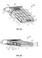
- FIG. 2Ais an isometric view of an exemplary electronic assembly that includes an extended thermal channel formed by circuit boards and assembly rails and in accordance with some embodiments.
- FIG. 2Bis another isometric view of the exemplary electronic assembly shown in FIG. 2A in accordance with some embodiments.
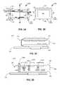
- FIG. 3Ais a side view of an exemplary electronic assembly that includes two circuit boards coupled between two assembly rails in accordance with some embodiments.
- FIG. 3Bis a front view of the exemplary electronic assembly configured to direct airflow through a vent opening of an assembly rail in accordance with some embodiments.
- FIG. 3Cis a cross sectional view of an exemplary electronic assembly that uses a flexible cable to electrically couple two circuit boards in accordance with some embodiments.
- FIG. 3Dis a cross sectional view of an exemplary electronic system that includes a rigid tab and/or a rigid interconnect in accordance with some embodiments.
- FIG. 4Ais a side view of another exemplary electronic assembly that includes an extended thermal channel formed by a plurality of assembly rails and a plurality of circuit boards in accordance with some embodiments.
- FIG. 4Bis a front or cross sectional view of an exemplary electronic assembly that includes a plurality of assembly rails coupled together at their edges in accordance with some embodiments.
- FIGS. 5A and 5Billustrate a side view and an isometric view of two exemplary assembly rails and each including a respective ducted vent opening and a respective duct portion extended and widened along an airflow direction in accordance with some embodiments.
- FIG. 6is a comparison of the airflow dynamics around a regular vent opening and a ducted vent opening of two exemplary assembly rails in accordance with some embodiments, respectively.
- FIG. 7illustrates an exemplary flow chart of a method for assembling and using an electronic system including a thermal channel in accordance with some embodiments.
- the various embodiments described hereininclude systems, methods and/or devices used or integrated in electronic assemblies.
- the electronic assemblies and the heat dissipation method described hereinmanage airflow that is used to facilitate dissipation of heat generated by electronic components in the electronic systems.
- the present inventionsare not limited to such. In fact, the present invention applies equally to any electronic systems that require heat dissipation—particularly those systems that include two or more adjacent electronic circuit boards each having components that generate heat.
- an electronic assemblythat includes a first assembly rail, a top circuit board and a bottom circuit board.
- the first assembly railfurther includes a first card guide structure and a second card guide structure, and the first and second card guide structures are arranged on a first side near two opposite edges of the first assembly rail.
- the top circuit boardis mechanically coupled to the first card guide structure of the first assembly rail, and the bottom circuit board is mechanically coupled to the second card guide structure of the first assembly rail.
- the top circuit boardis substantially parallel to the bottom circuit board, and separated from the bottom circuit board by a predefined distance.
- the first assembly rail, the top circuit board and the bottom circuit boardtogether form a channel there between for receiving a heat dissipating airflow.
- each of the first and second card guide structuresincludes a respective card guide slot, and a respective edge of each of the top and bottom circuit boards is configured to be inserted and locked into a corresponding card guide slot.
- the channelfurther includes an additional assembly rail facing, and substantially parallel to, the assembly rail, where the top circuit board and the bottom circuit board are mechanically coupled to the additional assembly rail between the first and second assembly rails.
- the electronic assemblyis mechanically coupled to an external electronic system to an end of the channel via the second assembly rail.
- the electronic assemblyis mechanically coupled to an external electronic system using one or more mounting fasteners located at an edge of the assembly rail.
- the channelfurther includes an airflow tab that is coupled to a side of the channel and includes at least one of a rigid material or a flexible cable.
- the top circuit board and the bottom circuit boardare electronically coupled to each other via a flexible cable that itself contributes to the channel to further direct the airflow.
- the top circuit board and the bottom circuit boardare electronically coupled to each other via one or more rigid electronic interconnects, where the one or more rigid electronic interconnects act as an airflow tab to direct the airflow.
- the top circuit board and the bottom circuit boardare electronically coupled to each other via one or more rigid electronic interconnects, where the one or more rigid electronic interconnects are located within the channel and are configured to disturb the airflow.
- the electronic assemblyfurther includes a first set of heat-sensitive electronic components mechanically coupled to one of the top or bottom circuit boards, and a second set of heat-generating electronic components mechanically coupled to the other one of the top or bottom circuit boards. In some embodiments, the electronic assembly further includes a plurality of temperature-sensitive electronic components coupled to a region of the top circuit board that is thermally isolated from other regions of the top circuit board.
- the assembly railfurther includes a vent opening at one side of the channel.
- the electronic assemblyfurther includes an additional assembly rail that is mechanically coupled to a second top circuit board and a second bottom circuit board near two opposite ends of the additional assembly rail.
- the second top and bottom circuit boardsbeing substantially parallel to one another and forming at least a part of a second channel together with the second assembly rail.
- the additional assembly rail, the second top circuit board, and the second bottom circuit boardtogether form an additional channel there between for receiving a heat dissipating airflow.
- the channelincludes a first channel, and the additional channel is coupled to the first channel on its side.
- the top circuit boardincludes a first top circuit board
- the bottom circuit boardincludes a first bottom circuit board.
- the electronic assemblyfurther includes an additional assembly rail that is mechanically coupled to a second top circuit board and a second bottom circuit board near two opposite ends of a front side of the additional assembly rail.
- the second top and bottom circuit boardsare substantially parallel to one another and form at least a part of a second channel together with the additional assembly rail.
- the first top and bottom circuit boardsare mechanically coupled on a back side of the additional assembly rail to form an extended channel including both the first and second channels, and in accordance with the extended channel, the airflow is directed through a vent opening of the first assembly rail, the space between the first top and bottom circuit boards, a vent opening of the second assembly rail, and space between the second top and bottom circuit boards.
- the assembly railwidens along a direction of the airflow to form a ducted vent opening.
- a heat dissipation methodthat includes providing a first assembly rail.
- the first assembly railincludes a first card guide structure, a second card guide structure and a vent opening.
- the first and second card guide structuresare arranged on a first side of the assembly rail near two opposite edges of the first assembly rail.
- the heat dissipation methodfurther includes mechanically coupling a top circuit board to the first card guide structure of the first assembly rail, and mechanically coupling a bottom circuit board to the second card guide structure of the first assembly rail.
- the top circuit boardis substantially parallel to the bottom circuit board, and separated from the bottom circuit board by a predefined distance. Then, the first assembly rail, the top circuit board and the bottom circuit board form at least a part of a thermal channel that is configured to receive a heat dissipating airflow.
- an electronic assemblythat includes a plurality of assembly rails and a plurality of circuit board sets each further including a top circuit board and a bottom circuit board.
- the plurality of assembly railsthat are arranged substantially in parallel.
- Each assembly railincludes a respective vent opening, a respective front side and a respective back side.
- Each side of the respective assembly railfurther includes a respective first card guide structure and a respective second card guide structure that are arranged near two opposite edges of the corresponding assembly rail.
- the top circuit board and the bottom circuit boardare mechanically coupled between the first card guide structures and between the second card guide structures on two respective sides of two adjacent assembly rails, respectively. The two respective sides face each other.
- the top circuit boardis substantially parallel to the bottom circuit board, and separated from the bottom circuit board by a predefined distance. Further, the plurality of assembly rails alternate with the plurality of circuit board sets and together forms a channel having an extended length and configured to receive a heat dissipating airflow.
- At least one of the plurality of assembly railsis extended and widened along a direction of the airflow on at least one side of the at least one assembly rail to form a ducted vent opening.
- an assembly railthat is configured to form a part of a channel for receiving a heat dissipating airflow.
- the assembly railincludes a first card guide structure, a second card guide structure and a vent opening.
- the first card guide structure and the second card guide structureare arranged on a first side of the assembly rail near two opposite ends of the assembly rail and configured to receive a top circuit board and a bottom circuit board, respectively.
- the vent openingis located between the first card structure and the second card structure, and configured to receive the heat dissipating airflow.
- FIG. 1is a block diagram of an exemplary system module 100 in a typical computational device in accordance with some embodiments.
- the system module 100 in this computational deviceincludes at least a central processing unit (CPU) 2 , memory modules 4 for storing programs, instructions and data, an input/output (I/O) controller 6 , one or more communication interfaces such as network interfaces 8 , and one or more communication buses 50 for interconnecting these components.
- the I/O controller 6allows the CPU 2 to communicate with an I/O device (e.g., a keyboard, a mouse or a track-pad) via a universal serial bus interface.
- an I/O devicee.g., a keyboard, a mouse or a track-pad
- the network interfaces 8includes one or more interfaces for Wi-Fi, Ethernet and Bluetooth networks, each allowing the computational device to exchange data with an external source, e.g., a server or another computational device.
- the communication buses 50include circuitry (sometimes called a chipset) that interconnect and control communications among various system components included in the system module.
- the system module 100includes a motherboard that holds various system components (such as components 2 - 22 ).
- the memory modules 4include high-speed random access memory, such as DRAM, SRAM, DDR RAM or other random access solid state memory devices.
- the memory modules 4include non-volatile memory, such as one or more magnetic disk storage devices, optical disk storage devices, flash memory devices, or other non-volatile solid state storage devices.
- the memory modules 4or alternatively the non-volatile memory device(s) within memory modules 4 , include a non-transitory computer readable storage medium.
- memory slotsare reserved on the system module 100 for receiving the memory modules 4 . Once inserted into the memory slots, the memory modules 4 are integrated into the system module 100 .
- system module 100further includes one or more components selected from:
- non-transitory computer readable storage mediacan be used, as new data storage technologies are developed for storing information in the non-transitory computer readable storage media in the memory modules 4 and in the SSDs 12 .
- These new non-transitory computer readable storage mediainclude, but are not limited to, those manufactured from biological materials, nanowires, carbon nanotubes and individual molecules, even though the respective data storage technologies are currently under development and yet to be commercialized.
- the SSDs 12 used in a blade servermay have heat sinks mounted on the top of each individual dual in-line memory module (DIMM) or on an electronic assembly containing the DIMMs. Heat generated from electronic components in the DIMMs are primarily conducted to the heat sinks, and further dissipated by airflow generated by fans. However, as the data workload in these blade servers increases and the form factor of the DIMMs decreases (e.g., closely placed memory slots in the memory modules 4 ), it becomes more difficult for conventional heat sinks and cooling fans to conduct and dissipate the generated heat efficiently.
- DIMMdual in-line memory module
- various embodiments described hereinrelate to an electronic assembly in which circuit boards are mechanically assembled on assembly rails to form a channel through which airflow generated by an external fan is directed.
- the airflowpasses along a pathway through the channel, it flows over surfaces of electronic components mounted on the circuit boards and at least partially carries-away heat generated by these components.
- the channelfurther includes one or two airflow tabs on its sides for controlling the airflow, and each airflow tab is optionally made from a rigid material, a flexible cable or a combination of both.
- geometries (e.g., shape and dimensions) of vent openings of the assembly railsare configured to modify the dynamics of the airflow at the entrance and/or the exit of the channel.
- locations of the electronic components on the circuit boardsare arranged to physically separate heat-sensitive components from other components (such as some heat-generating components). By these means, the channel formed by the assembly rails and the circuit boards may further improve the heat dissipation efficiency of the electronic assembly, in addition to the aforementioned conventional solutions using heat sinks and high-speed fans.
- FIG. 2Ais an isometric view of an exemplary electronic assembly 200 that includes a channel 101 formed by the combination of circuit boards and one or more assembly rails.
- the channel 101is formed by mechanically coupling one or more duct units 102 to one another.
- Each duct unit 102includes at least a top circuit board 104 , a bottom circuit board 106 and an assembly rail 108 .
- Each duct unit 102optionally includes an airflow tab 110 to substantially close each side of the duct unit 102 , i.e., enclose the duct on all four sides. When coupled to one another, the duct unit 102 provides an extended length channel 101 .
- the channel 101includes an interior airflow pathway bounded by the top circuit board 104 , the bottom circuit board 106 , and the optional airflow tabs 110 of each duct unit 102 .
- airflowpasses through the interior airflow pathway of the channel 101 , it at least partially carries away the heat generated in the electronic assembly 200 .
- At least one of the top circuit board 104 and bottom circuit board 106include one or more solid state drives (SSDs). In some embodiments, at least one of the top circuit board 104 and the bottom circuit board 106 include one or more three-dimensional (3D) memory devices.
- SSDssolid state drives
- 3Dthree-dimensional
- the assembly rail 108 or 108 Aacts as a structural frame of each duct unit 102 .
- the top circuit board 104 and the bottom circuit board 106are mechanically coupled on a first side (e.g., a back side) near two opposite ends of the assembly rail 112 .
- the airflow tab 110is optionally coupled to the assembly rail 108 , the top circuit board 104 , and/or the bottom circuit board 106 .
- the duct unit 102optionally includes an additional assembly rail 108 B (e.g., a second assembly rail) that is positioned substantially parallel with the first assembly rail 108 .
- the top and bottom circuit boards 104 and 106are similarly coupled to the first and second assembly rails 108 A and 108 B but at two opposite edges of the respective circuit board.
- the airflowenters the channel 101 from one assembly rail 108 , passes through the space between the top and bottom circuit boards 104 and 106 , and exits from the other assembly rail 108 .
- the electronic assembly 100includes more than one duct unit 102 (e.g., three duct units—as shown in FIG. 1 ) that are coupled to each other.
- the channel 101 formed by these duct units 102are aligned with each other to form a channel 101 having an extended length.
- the assembly rail 108is optionally coupled at an entrance of the channel 101 , at the interface of two duct units 102 , or at the exit of the channel 101 .
- the assembly rail 108e.g., rail 108 B
- the assembly rail 108is coupled at the interface of two duct units 102
- itis mechanically coupled not only to the circuit boards of the duct unit 102 which it belongs to, but also to the circuit boards of an adjacent duct unit 102 .
- the top circuit board 104 and the bottom circuit board of each duct unit 102are mechanically coupled between two assembly rails 108 of the electronic assembly 200 .
- assembly rail 108forms a vent opening 116 through which the airflow passes into the channel 101 .
- the shape of the vent opening 116is selected from a rectangle, a square, a circle, an oval, a triangle, a diamond and the like.
- corners of the vent opening 116are rounded.
- the vent openingincludes one or more openings configured according to a pattern (e.g., a grill pattern).
- each of the top circuit board 104 and the bottom circuit board 106is a printed circuit board.
- a circuit boardinclude, but are not limited to, a flash memory board of a solid-state drive (SSD) 112 , a memory board of memory modules 104 , a graphics board of the graphics card 120 , a controller board, a co-processor board, a communication interface, a blank board, or a combination thereof.
- SSDsolid-state drive
- Each circuit board 104 or 106further includes a plurality of electronic components 130 that are mechanically and electrically coupled to a substrate of the respective circuit board 104 or 106 .
- the electronic components 130are memory components that are mounted on a memory module.
- the electronic components 130are optionally coupled on either side or both sides of the substrate of the respective board 104 or 106 .
- some electronic components 130generate substantially more heat or are more sensitive to temperature increases than other components 130 , and such electronic components 130 are preferably mounted on the interior airflow pathway of the channel, e.g., a back side of the top circuit board 104 or a top side of the bottom circuit board 106 .
- An airflow tab 110 of the channel 101is optionally made from a rigid tab, a flexible cable or a combination of both.
- the rigid tabis mechanically coupled to a third edge of the assembly rail 108 , and the third edge is distinct from the two opposite edges of the assembly rail 108 to which the circuit boards 104 and 106 are coupled.
- An airflow tab 110 made of the rigid tabavoids the airflow from leaking through the corresponding side of the channel 101 .
- the top circuit board 104 and the bottom circuit board 106are electronically coupled to each other via a rigid tab including one or more rigid electronic interconnects (sometimes called electronic connectors).
- the top circuit board 104 and the bottom circuit board 106are electronically coupled to each other via a flexible cable, and the flexible cable forms another part of the channel to further direct the airflow within the interior airflow pathway.
- rigid interconnects and a flexible cabletogether couple the top and bottom circuit boards 104 and 106 .
- two rigid interconnectsare coupled to the top circuit board 104 and the bottom circuit board 106 , respectively, and these boards are further coupled together by a flexible cable.
- the combination of the rigid interconnects and the flexible cablealso performs the function of the airflow tab 110 to direct the airflow through the interior airflow pathway of the channel 101 .
- the channel 101is further coupled to an external electronic system (e.g., a backplate 118 ) at one of its two channel ends.
- the backplate 118is configured to include a vent opening at a corresponding position according to the position of the vent opening 116 of the assembly rail 108 .
- the shape and configuration of the vent opening of the backplate 118are optionally configured according to those of the vent opening 116 .
- the airflow that passes through the channel 101enters from the vent opening of the backplate 118 and flows through the channel 101 , while in some embodiments, the airflow flows through the channel 101 , and exits from the vent opening of the backplate 118 .
- the electronic assembly 100is mechanically coupled on top of an external component or system 120 , such as a PCI interface card, an ExpressCard housing, a PC card housing, a motherboard of a server, a bus slot of an embedded controller system, or a combination thereof.
- an external component or system 120such as a PCI interface card, an ExpressCard housing, a PC card housing, a motherboard of a server, a bus slot of an embedded controller system, or a combination thereof.
- the electronic assembly 100constitutes a daughterboard structure, and is assembled directly to a motherboard.
- the electronic assembly 200is coupled to one or more heat sinks.
- the heat sinksare optionally coupled to the electronic components 130 or to the circuit boards 104 and 106 to absorb and dissipate heat generated by the electronic components 130 .
- a heat sinkis coupled between a corresponding assembly rail and an edge of a circuit board (e.g., a top circuit board 104 or a bottom circuit board 106 ) as described in U.S. Provisional Application Ser. No. 61/945,674, filed on Feb. 27, 2014, titled “Heat Dissipation for Substrate Assemblies,” which is hereby incorporated by reference in its entirety.
- the heat sinkincludes a card guide tab and an attachment structure to mechanically couple to the assembly rail and the circuit board edge, respectively.
- the heat sinkoptionally includes heat dissipaters to at least partially dissipate the heat that is generated by the electronic components 130 and absorbed by the heat sink.
- FIG. 2Bis another isometric view of the exemplary electronic assembly 200 shown in FIG. 2A in accordance with some embodiments.
- the electronic assembly 200includes a plurality of duct units 102 configured to form the channel 101 .
- the duct units 102are coupled together to form an extended length channel.
- the airflow tab 110 of each duct unit 102is removed to better illustrate the electronic assembly 200 .
- the electronic assembly 200includes a plurality of assembly rails and a plurality of circuit board sets each including a top circuit board 104 and a bottom circuit board 106 .
- the plurality of assembly rails 108alternate with the plurality of circuit board sets and together form the channel 101 that has the extended length.
- This channel 101is configured to direct airflow through a respective vent opening 116 of each assembly rail 108 and into the channel between the top and bottom circuit boards 104 and 106 of each circuit board set successively.
- Each assembly rail 108includes a respective vent opening 116 , a respective first side (e.g., a front side) and a respective second side (e.g., a backside).
- Each side of the respective assembly rail 108further includes a first card guide structure and a second card guide structure that are arranged near two opposite edges of the respective side of the corresponding assembly rail 108 , respectively.
- Each circuit board setis coupled between two adjacent assembly rails 108 .
- the top circuit board and the bottom circuit boardre mechanically coupled between the first card guide structures and between the second card guide structures on two respective sides of two adjacent assembly rails, respectively.
- the two respective sides of the two adjacent assembly railsface each other.
- the top circuit board 104is substantially parallel to the bottom circuit board 106 , and separated from the bottom circuit board 106 by a predefined distance.
- the predefined distanceis determined in accordance with a rail height h of the plurality of assembly rails (including the assembly rails 108 A and 108 B).
- the channel 101includes three sets of circuit boards.
- the channel 101may optionally have only one circuit board set that further includes a top circuit board 104 and a bottom circuit board 106 and that the circuit board set is coupled between two adjacent assembly rails 108 .
- FIG. 3Ais a side view of an exemplary electronic assembly 300 that includes two circuit boards coupled between two assembly rails 108 in accordance with some embodiments
- FIG. 3Bis a front view of the exemplary electronic assembly 300 configured to direct airflow through a vent opening 116 of an assembly rail 108 in accordance with some embodiments.
- a top circuit board 104 and a bottom circuit board 106are mechanically coupled between the two assembly rails 108 (e.g., a first assembly rail 108 A and a second assembly rail 108 B).
- the first assembly rail 108 A and the circuit boards 104 and 106form part of a duct unit 102
- the duct unit 102 and the second assembly rail 108are assembled together to form the electronic assembly 300 .
- Each assembly rail 108includes a front side 302 and a back side 304 , and each side of the assembly rail 108 further includes a first card guide structure 310 and a second card guide structure 320 .
- the first and second card guide structures 310 and 320are arranged near two opposite edges (or ends) 330 and 340 of each assembly rail 108 .
- the top circuit board 104is mechanically coupled and locked to the two first card guide structures 310 on the back side 304 of the first assembly rail 108 A and the front side of the second assembly rail 108 B, respectively.
- the bottom circuit board 106is mechanically coupled and locked to the two second card guide structures 320 on the back side 304 of the first assembly rail 108 A and the front side of the second assembly rail 108 B, respectively.
- the first card guide structure 310 and the first card guide structure 320 on each side of the assembly rail 108are configured to be substantially parallel to each other, such that the top and bottom circuit boards 104 and 106 are also substantially parallel to each other when they are mechanically coupled to the first and second card guide structures 310 and 320 , respectively.
- each card guide structure 310 or 320includes a respective board guide slot, and a top or bottom circuit board 104 , 106 is inserted and optionally locked into the corresponding board guide slot.
- the assembly rail 108further includes one or more mounting fasteners 306 on any one of its edges (such as the edges 330 , 340 , 350 and 360 ), such that the assembly rail 108 may be mechanically coupled to another component or another assembly rail 108 via the mounting fasteners 306 .
- the mounting fasteners 306e.g., the fasteners 306 A
- the fasteners 306 Aare located on a bottom edge 340 of the assembly rail 108 (i.e., externally on the bottom of the channel 101 ), and used to mount the electronic assembly 300 on top of an external component or system 120 (e.g., a motherboard).
- the mounting fasteners 306are located on the side edge 350 or 360 of the assembly rail 108 (i.e., externally on a side of the channel 101 ).
- the mounting fasteners 306 B on the side edges 350 and 360are configured to couple an airflow tab 110 to the assembly rail(s) 108 .
- the mounting fasteners 306 B on the side edges 350 and 360are configured to couple two electronic assemblies 300 side-by-side or couple the electronic assembly 300 to an external component or system (e.g., a motherboard).
- Naturally occurring airflow or airflow created by a fanenters the channel 101 via the vent opening 116 of the assembly rail 108 A, passes through the space between the top circuit board 104 and the bottom circuit board 106 , and exits the channel 101 from the vent opening 116 of the assembly rail 108 B.
- the assembly rail 108 Bis further coupled to a backplate 118 , the airflow further passes through the corresponding vent opening on the backplate 118 after exiting the channel 101 .
- the electronic components 130 of the top circuit board 104 or the bottom circuit board 106are optionally coupled to one side or on both sides of a respective circuit board.
- the electronic components 130are preferably placed in the channel or interior airflow pathway (including the corresponding side of the circuit board that is passed by the airflow) to benefit from the heat dissipation effect provided by the airflow.
- the electronic components 130are placed on a back side of the top circuit board 104 or a top side of the bottom circuit board 106 .
- the electronic component 130is placed on the interior airflow pathway.
- placing the heat-generating or heat-sensitive electronic components 130 on the interior airflow pathway of the channel 101allows the generated or absorbed heat to be dissipated more efficiently by the airflow and reduces local temperature increases that could degrade the performances of the corresponding electronic components 130 .
- the heat-sensitive electronic components 130are physically separated from other electronic components, and in particular, separated from the heat-generating electronic components to avoid temperature increases.
- the heat-sensitive and heat-generating electronic componentsare located on the top circuit board 104 and the bottom circuit board 106 , respectively.
- the heat-sensitive electronic componentsare disposed at a region of the top circuit board that is thermally isolated from other regions of the top circuit board, and thereby substantially insulated from heat generated by other electronic components on the top and bottom circuit boards.
- the heat-sensitive and heat-generating electronic componentsare located at two distinct regions of one circuit board (the top circuit board 104 or the bottom circuit board 106 ).
- the region that includes the heat-sensitive electronic componentsis positioned upstream in the airflow from the region that includes the other electronic components (including the heat-generating electronic components).
- memory cellsare sensitive to temperature increases but they do not generate a large amount of heat.
- the memory controllersmay not be sensitive to temperature increases but themselves generate a relatively larger amount of heat.
- the heat-sensitive memory cells and the heat-generating memory controllersare positioned on the interior airflow pathway of the channel 101 , and they are separately mounted on two circuit boards or at two distinct regions of one circuit board as discussed above.
- FIG. 3Cis a cross sectional view of an exemplary electronic assembly 300 that uses a flexible cable 112 to electrically couple two circuit boards 104 and 106 in accordance with some embodiments.
- the cross sectional viewis optionally associated with a part of the cross section A-A′ of the electronic assembly 300 shown in FIG. 3A .
- the electronic assembly 300is further coupled to an external component or system 120 via mounting fasteners 340 on the assembly rails 108 .
- the flexible cable 112includes a flexible substrate and interconnect that are embedded in the flexible substrate.
- the interconnectelectrically couples the top circuit board 104 and a bottom circuit board 106 , and carries electrical signals between these two circuit boards.
- the flexible substrate of the flexible cable 112is made of flexible materials, such as polymeric materials. Examples of the flexible cable 112 include, but are not limited to, a flexible board, flexible wire array, flexible PCB, flexible flat cable, ribbon cable, and a combination thereof.
- the flexible cable 112becomes a part of an airflow tab on one side of the channel 101 to at least partially direct the airflow that passes the channel 101 .
- the flexible cable 112faces another airflow tab 110 that lies close to another opposite edge area of the channel 101 .
- the flexible cable 112is provided in addition to an existing airflow tab 101 , and faces the other airflow tab 110 that lies close to the other opposite edge area of the channel 101 .
- FIG. 3Dis a cross sectional view of an exemplary electronic system 300 that includes a rigid tab 122 in accordance with some embodiments.
- the cross sectional viewis optionally associated with a part of the cross section A-A′ of the electronic assembly 300 shown in FIG. 3A .
- the rigid tab 122mechanically couples two circuit boards 104 and 106 together, and broadly includes a rigid tab 122 A and rigid interconnects 122 C- 122 E.
- a rigid interconnectis also called as a rigid connector.
- the rigid tab 122is positioned substantially close to the corresponding edges of the two circuit boards 104 and 106 , and acts as an airflow tab 110 of the channel 101 .
- the rigid tab 122is optionally coupled on an edge of the assembly rail 101 using the fasteners 306 B, or is coupled to the edges of the two circuit boards 104 and 106 .
- the rigid tab 122(e.g., the rigid tab 122 A) does not include interconnects, and only mechanically couples the top circuit board 104 and the bottom circuit board 106 .
- the rigid tab 122(e.g., the rigid tab 122 A and the rigid interconnects 122 C- 122 E) further includes interconnects that electrically and mechanically couples the top circuit board 104 and the bottom circuit board 106 .
- one or more of the rigid interconnects 122 C- 122 Eare positioned internally within the channel 101 .
- an internally positioned interconnect 122is configured to disturb but not block airflow in the thermal channel.
- the internally positioned interconnectcontains a row of conductive pins, it is preferably oriented to substantially align with the airflow tabs and along the airflow direction.
- a respective rigid interconnectsuch as the rigid interconnect 122 A, includes a single interconnect part that includes two electrical terminals, one electrically coupled to the top circuit board 104 and the other electrically couples to the bottom circuit board 106 .
- a respective rigid interconnectsuch as the rigid interconnect 122 C, includes two complimentary interconnect parts 122 T and 122 B, where the interconnect part 122 T is configured to connect to the top circuit board 104 , and the interconnect part 122 B is configured to connect to the bottom circuit board 106 .
- the interconnect parts 122 T and 122 Bare further pluggable one into the other to form an electrical connection between the top and bottom circuit boards.
- a respective rigid interconnectsuch as the rigid interconnect 122 D, includes a set of interconnect parts that has more than two interconnect parts. Two of these interconnect parts are configured to be coupled to the top circuit board 104 and the bottom circuit board 106 , respectively, and furthermore the set of interconnect parts are configured to be assembled into a rigid interconnect that couples the top circuit board 104 to the bottom circuit board 106 .
- the interconnectwhether implemented as the flexible interconnect 112 (shown in FIG. 3C ) or the rigid interconnect 122 (shown in FIG. 3D ), includes a plurality of parallel wires, conductive channels, or signal paths, between the top circuit board 104 and the bottom circuit board 106 .
- both ends of the interconnect 112comprise terminals.
- each terminal of rigid interconnect 122includes a plurality of conductive pins that are assembled on an insulating housing of the rigid interconnect 122 .
- Each respective terminal of rigid interconnect 122is optionally configured to be connected to a corresponding circuit board via surface mounting technology or through-hole technology.
- conductive pins of the respective terminalsare configured to be soldered to conductive pads or via holes that are coated with conductive materials on the corresponding circuit board, thereby forming mechanical and electrical connections with the circuit board.
- the height of the rigid interconnect 122is commensurate with a separation distance 402 , which is the distance between the top circuit board 104 and the bottom circuit board 106 .
- the rail height h of the assembly rail 108is also commensurate with the separation distance 402 and/or the height of the rigid interconnect 122 .
- rigid interconnect 122(e.g., the interconnect 122 A) is attached to respective sides of the top circuit board 104 and the bottom circuit board 106 , and optionally faces another airflow tab attached to opposite sides of the boards.
- the rigid interconnect 122e.g., the interconnect 122 C, 122 D or 122 E
- the rigid interconnect 122is attached to respective inner regions of the top circuit board 104 and the bottom circuit board 106 .
- two terminals of the rigid interconnect 122(e.g., the interconnect 122 D) are directly mounted on the top circuit board 104 and the bottom circuit board 106 .
- one terminal of the rigid interconnect 122(e.g., the interconnect 122 B) is attached indirectly to a circuit board via an electronic part that is already mounted on the circuit board.
- both terminals of the rigid interconnect 122(e.g., the interconnect 122 E) are attached indirectly to the top circuit board 104 and the bottom circuit board 106 via a respective electronic part that is already mounted on the corresponding circuit board.
- the rigid interconnect 122is instead a semi-rigid interconnect.
- an interconnect that electrically couples the top circuit board 104 and the bottom circuit board 106may also include both a flexible interconnect part and a rigid interconnect part.
- a rigid interconnect partis coupled to the top circuit board 104 at one end and to a flexible interconnect part at the other end, and the flexible interconnect part further connects to the bottom circuit board 106 or to another rigid interconnect that connects to the bottom circuit board 106 .
- a respective rigid interconnect 122(e.g., the interconnect 122 E) is attached to respective inner regions of the top circuit board 104 and the bottom circuit board 106 and carries electrical signals between the top circuit board 104 and the bottom circuit board 106 .
- the electronic assembly(or a duct unit of the electronic assembly) also includes one or two airflow tabs 110 , positioned on one or both respective sides of the channel 101 , to constraint airflow between the top and bottom circuit boards 104 and 106 .
- a respective rigid interconnect 122(e.g., the interconnect 122 A) is positioned at or substantially close to respective edges of the top circuit board 104 and the bottom circuit board 106 .
- the rigid interconnectextends substantially the entire length of the duct unit 102 , or substantially the length of the entire the top circuit board 104 and/or the bottom circuit board 106 .
- a respective rigid interconnect 122is used in place of a corresponding airflow tab 110 to control or direct airflow between the top circuit board 104 and the bottom circuit board 106 .
- a respective rigid interconnect 122has a length substantially shorter than the length of the duct unit 102 , or substantially shorter than the length of the top circuit board 104 and/or the bottom circuit board 106 .
- FIG. 4Ais a side view of another exemplary electronic assembly 200 that includes an extended channel 101 formed by a plurality of assembly rails 108 and a plurality of circuit boards 104 and 106 in accordance with some embodiments.
- the electronic assembly 200is formed by coupling a sequence of duct units 102 to each other and optionally attaching an assembly rail 108 ′ to an end duct unit 108 in the sequence.
- Each assembly rail 108alternates with a circuit board set including a top circuit board 104 and a bottom circuit board 106 .
- the assembly rails 108are positioned substantially in parallel and coaligned with each other. After being assembled on the assembly rails 108 , the top circuit boards 104 and the bottom circuit boards 106 in the circuit board sets are also parallel to each other. As such, each circuit board set is mechanically coupled between two substantially parallel assembly rails 108 .
- each assembly rail 108includes a respective first side (e.g., a front side) and a respective second side (e.g., a back side).
- Each side of the respective assembly rail 108further includes a first card guide structure 310 and a second guide structure 320 that are arranged on the respective side near two opposite edges of the corresponding assembly rail 108 , respectively.
- the top circuit board 104 and the bottom circuit board 106 of each circuit board setare coupled on the card guide structures 310 and 320 of two adjacent assembly rails 108 (e.g., a first assembly rail and a second assembly rail), respectively.
- the top circuit board 104is mechanically coupled between a first card guide structure 310 A on a back side of a first assembly rail 108 and another first card guide structure 310 B on a front side of a second assembly rail 108
- the bottom circuit board 106is mechanically coupled between a second card guide structure 320 A on the back side of the first assembly rail 108 A and another second card guide structure 320 B on the front side of the second assembly rail 108 B.
- top and bottom circuit boards 104 and 106are substantially parallel to and separated from each other.
- the top and bottom circuit boards 104 and 106have a separation that is defined in accordance with a rail height h of the plurality of assembly rails.
- Each assembly rail 108further includes a vent opening 116 between the first and second card guide structures.
- the vent openings 116 of the plurality of assembly rails 108are aligned to each other, and further aligned to the respective space between the top and bottom circuit boards of each circuit board set, thereby forming an interior airflow pathway for the channel 101 .
- airflowis directed through the vent opening of each assembly rail and space between the top and bottom circuit boards of each circuit board set successively.
- FIG. 4Bis a front view of an exemplary electronic assembly 200 that includes a plurality of assembly rails 108 coupled together at their edges (e.g., one of the edges 330 - 360 ) in accordance with some embodiments.
- each assembly rail 108optionally includes mounting fasteners 306 on its edges 330 - 360 .
- the mounting fasteners 306 on two opposite edgesmatch with each other, such that every two assembly rails 108 may be coupled to each other via the mounting fasteners 306 . For example, as shown in FIG.
- the mounting fasteners 306 Bhave allowed every two assembly rails 108 A and 108 B, 108 B and 108 C, 108 D and 108 E, and 108 E and 108 F to mechanically couple to each other on their corresponding opposite edges 350 and 360 .
- the mounting fasteners 306have also allowed every two assembly rails 108 A and 108 D, 108 B and 108 E, and 108 C and 108 F to mechanically couple to each other on their corresponding opposite edges 330 and 340 .
- Each assembly rail 108is associated with a respective channel 101 that includes one or more circuit board sets, and is optionally located at an end or an intermediate location of the respective channel 101 .
- corresponding duct units 102 of two neighboring thermal channels 101do not include airflow tabs at their adjacent sides, and the airflow in one of these two neighboring thermal channels 101 freely enters the corresponding airflow pathway of the other channel 101 .
- corresponding duct units 102 of two neighboring thermal channels 101do not include a bottom circuit board 106 and a top circuit board 104 , respectively, and the airflow in one of these two neighboring thermal channels 101 may also freely enter the corresponding airflow pathway of the other channel 101 .
- the airflowdoes not pass over surfaces of electronic components 118 that are coupled externally to each channel 101 , e.g., on a top side of the top circuit board 104 or a back side of the bottom circuit board 106 . Therefore, these externally coupled electronic components 118 does not dissipate heat as efficiently as the electronic components 118 located on the respective interior airflow pathway (i.e., internally in the channel 101 ). Therefore, in some embodiments, the electronic components 118 that generate less heat and/or are less sensitive to temperature increases are coupled externally to the respective channel 101 .
- FIGS. 5A and 5Billustrate a side view and an isometric view of two exemplary assembly rails 500 and 550 each including a respective ducted vent opening 502 extended and widened along an airflow direction in accordance with some embodiments.
- the respective ducted vent opening 502further includes a duct portion 504 .
- the duct portions 504 shown in FIGS. 5A and 5Bare included and configured to extend and widen on one side of the respective assembly rail, they are optionally included, and configured to extend and widen at both sides of the assembly rail.
- the duct portion 504optionally guides the airflow to enter or exit the ducted vent opening 502 , when the ducted vent opening 502 is located on an airflow incoming or outgoing side of the assembly rail 500 or 550 , respectively.
- the duct portion 504widens from the ducted vent opening 502 to the edges of the assembly rail 500 .
- the assembly rail 500replaces one or both end assembly rails 108 that are coupled at the ends of the channel 101 , while being preferably used on an airflow incoming end of the channel 101 .
- the assembly rail 500is used at an intermediate assembly rail 108 of the channel 101 to control the airflow that passes through the interior airflow pathway of the channel 101 .
- the assembly rail 500includes card guide structures 310 and 320 on a respective duct portion 504 of the duct vent opening 502 . The card guide structures 310 and 320 are still located near the two opposite edges 330 and 340 of the assembly rail 400 , such that a top circuit board 104 and a bottom circuit board 106 may be assembled to the assembly rail 500 if needed.
- the duct portion 504 of the ducted vent opening 502widens beyond the assembly rail edges 330 - 360 around the vent opening 502 .
- Geometric configurations and dimensions of the duct portion 504are configured according to specific airflow dynamics requirements.
- the duct portion 504 of the ducted vent opening 502 in the assembly rail 550is substantially wider than the duct portion 504 of the ducted vent opening 502 in the assembly rail 500 .
- the assembly rail 550is preferably used on an airflow incoming end of the channel 101 , although it may also be used on an airflow outgoing end of the channel 101 , or at an intermediate assembly rail 108 of the channel 101 .
- the assembly rail 550includes card guide structures 310 and 320 on a respective duct portion 504 , such that a top circuit board 104 and a bottom circuit board 106 may be assembled to the assembly rail 500 .
- assembly rails 500 and 550 having the ducted venting openings 502may also act as structural frames to assemble the electronic assembly 200 shown in FIGS. 2A-2B, 3A-3D and 4A-4B .
- the analogous detailsare not repeated here.
- FIG. 6is a comparison 600 of the airflow dynamics around a regular vent opening 116 and a ducted vent opening 502 of two exemplary assembly rails 108 and 500 in accordance with some embodiments, respectively.
- the assembly rails 108 and 500are used at an airflow inlet end of the channel 101 .
- a part (e.g., part A) of incoming airfloweasily enters the regular vent opening of the assembly rail 108 , and however, another part (e.g., part B) of the inlet airflow hits an edge area between an edge 330 or 340 of the assembly rail 108 and an edge 610 of the regular vent opening 116 .
- the part B of the incoming airflowcauses turbulence around the edge area, and is ultimately blocked from entering or redirected into the vent opening 116 .
- Such a blocked or redirected part B of the incoming airflowreduces the amount of the air that enters the channel 101 , and thereby compromises the flow rate of the airflow in the channel 101 .
- the part B of the incoming airfloware guided by the duct portion 504 and enters the ducted vent opening 116 when the assembly rail 500 is applied at the airflow incoming end of the channel 101 .
- Such a directed airflowimproves the amount of the air that enters the channel 101 and the flow rate of the airflow in the channel 101 , and the overall heat dissipation efficiency of the electronic assembly 200 are thereby enhanced.
- FIG. 7illustrates an exemplary flow chart of a method for assembling and using an electronic system 200 including a channel in accordance with some embodiments.
- a first assembly railis provided ( 702 ).
- the first assembly railincludes a first card guide structure, a second card guide structure and a vent opening.
- the first and second card guide structuresare arranged on a first side of the first assembly rail near two opposite edges of the first assembly rail.
- the first assembly railacts as a structural frame to assemble components (e.g., circuit boards and airflow tabs) of the channel thereon.
- a top circuit boardis mechanically coupled ( 704 ) to the first card guide structure of the first assembly rail, and a bottom circuit board is mechanically coupled ( 706 ) to the second card guide structure of the first assembly rail.
- the top circuit boardis substantially parallel to the top circuit board and separated from the bottom circuit board by a predefined distance.
- each of the first and second card guide structuresincludes a card guide slot where a circuit board is inserted and locked.
- the first assembly rail, the top circuit board and the bottom circuit boardare configured ( 708 ) to form at least a part of the thermal channel, and the channel is configured to receive a heat dissipating airflow.
- the channelhas an extended length, when the electronic system 200 includes a plurality of assembly rails and a plurality of circuit board sets each further including a top circuit board and a bottom circuit board.
- Each circuit board setis assembled with an assembly rail to form a duct unit according to operations 702 - 708 .
- Each circuit board of a duct unitis further coupled to an assembly rail of a neighboring duct unit or another standalone assembly rail at an end of the thermal channel.
- the extended channelis formed by successively coupling two or more duct units together.
- airflowis passed or directed ( 710 ) through the channel to dissipate heat, as described above.
- FIGS. 2A-2B, 3A-3D, 4A-4B and 5A-5BMore details and examples of the components of the channel (e.g., the circuit boards and the assembly rails) are discussed above with reference to FIGS. 2A-2B, 3A-3D, 4A-4B and 5A-5B .
- assembly railsfunction as structural frames to conveniently assemble a plurality of circuit boards together, and form an electronic assembly including a thermal channel.
- Such an electronic assemblyoffers an easy, flexible and inexpensive solution to manufacture and assemble daughter card assemblies that are configured to integrate with a motherboard for many electronic devices. More importantly, airflow is directed through the channel in a controlled manner.
- the airflowefficiently carries away the heat generated by these electronic components, maintains a low temperature increase for these electronic components and reduces the thermal expansion of the corresponding circuit boards.
- heat-sensitive electronic componentsare isolated from other electronic components, and placed at an upstream location in the interior airflow pathway. Under some circumstances, the heat-sensitive electronic components and other electronic components may have a temperature difference of 20° C. as a result of using the thermal channel.
- the electronic assembly 200 or 300 described hereinincludes one or more memory modules, and in some embodiments, the electronic components of the electronic assembly 200 or 300 include semiconductor memory devices or elements.
- the semiconductor memory devicesinclude volatile memory devices, such as dynamic random access memory (“DRAM”) or static random access memory (“SRAM”) devices, non-volatile memory devices, such as resistive random access memory (“ReRAM”), electrically erasable programmable read only memory (“EEPROM”), flash memory (which can also be considered a subset of EEPROM), ferroelectric random access memory (“FRAM”), and magnetoresistive random access memory (“MRAM”), and other semiconductor elements capable of storing information.
- each type of memory devicemay have different configurations.
- flash memory devicesmay be configured in a NAND or a NOR configuration.
- the memory devicescan be formed from passive elements, active elements, or both.
- passive semiconductor memory elementsinclude ReRAM device elements, which in some embodiments include a resistivity switching storage element, such as an anti-fuse, phase change material, etc., and optionally a steering element, such as a diode, etc.
- active semiconductor memory elementsinclude EEPROM and flash memory device elements, which in some embodiments include elements containing a charge storage region, such as a floating gate, conductive nanoparticles or a charge storage dielectric material.
- NAND devicescontain memory elements (e.g., devices containing a charge storage region) connected in series.
- a NAND memory arraymay be configured so that the array is composed of multiple strings of memory in which each string is composed of multiple memory elements sharing a single bit line and accessed as a group.
- memory elementsmay be configured so that each element is individually accessible, e.g., a NOR memory array.
- NOR memory arrayOne of skill in the art will recognize that the NAND and NOR memory configurations are exemplary, and memory elements may be otherwise configured.
- the semiconductor memory elements included in a single devicemay be distributed in a two- or three-dimensional manner (such as a two dimensional (2D) memory array structure or a three dimensional (3D) memory array structure).
- the semiconductor memory elementsare arranged in a single plane or single memory device level.
- memory elementsare located in a plane (e.g., in an x-z direction plane) which extends substantially parallel to a major surface of a substrate that supports the memory elements.
- the substratemay be a wafer on which the material layers of the memory elements are deposited and/or in which memory elements are formed or it may be a carrier substrate which is attached to the memory elements after they are formed.
- the memory elementsmay be arranged in the single memory device level in an ordered array, such as in a plurality of rows and/or columns. However, the memory elements may be arranged in non-regular or non-orthogonal configurations as understood by one of skill in the art.
- the memory elementsmay each have two or more electrodes or contact lines, including a bit line and a word line.
- a three dimensional memory arrayis organized so that memory elements occupy multiple planes or multiple device levels, forming a structure in three dimensions (i.e., in the x, y and z directions, where the y direction is substantially perpendicular and the x and z directions are substantially parallel to the major surface of the substrate).
- each plane in a three dimensional memory array structuremay be physically located in two dimensions (one memory level) with multiple two dimensional memory levels to form a three dimensional memory array structure.
- a three dimensional memory arraymay be physically structured as multiple vertical columns (e.g., columns extending substantially perpendicular to the major surface of the substrate in the y direction) having multiple elements in each column and therefore having elements spanning several vertically stacked planes of memory devices.
- the columnsmay be arranged in a two dimensional configuration, e.g., in an x-z plane, thereby resulting in a three dimensional arrangement of memory elements.
- One of skill in the artwill understand that other configurations of memory elements in three dimensions will also constitute a three dimensional memory array.
- the memory elementsmay be connected together to form a NAND string within a single plane, sometimes called a horizontal (e.g., x-z) plane for ease of discussion.
- the memory elementsmay be connected together to extend through multiple parallel planes.
- Other three dimensional configurationscan be envisioned wherein some NAND strings contain memory elements in a single plane of memory elements (sometimes called a memory level) while other strings contain memory elements which extend through multiple parallel planes (sometimes called parallel memory levels).
- Three dimensional memory arraysmay also be designed in a NOR configuration and in a ReRAM configuration.
- a monolithic three dimensional memory arrayis one in which multiple planes of memory elements (also called multiple memory levels) are formed above and/or within a single substrate, such as a semiconductor wafer, according to a sequence of manufacturing operations.
- the material layers forming a respective memory levelsuch as the topmost memory level, are located on top of the material layers forming an underlying memory level, but on the same single substrate.
- adjacent memory levels of a monolithic 3D memory arrayoptionally share at least one material layer, while in other implementations adjacent memory levels have intervening material layers separating them.
- two dimensional memory arraysmay be formed separately and then integrated together to form a non-monolithic 3D memory device in a hybrid manner.
- stacked memorieshave been constructed by forming 2D memory levels on separate substrates and integrating the formed 2D memory levels atop each other. The substrate of each 2D memory level may be thinned or removed prior to integrating it into a 3D memory device. As the individual memory levels are formed on separate substrates, the resulting 3D memory arrays are not monolithic three dimensional memory arrays.
- more than one memory array selected from 2D memory arrays and 3D memory arraysmay be formed separately and then packaged together to form a stacked-chip memory device.
- a stacked-chip memory deviceincludes multiple planes or layers of memory devices, sometimes called memory levels.
- three-dimensional memory device(or 3D memory device) is herein defined to mean a memory device having multiple layers or multiple levels (e.g., sometimes called multiple memory levels) of memory elements, including any of the following: a memory device having a monolithic or non-monolithic 3D memory array, some non-limiting examples of which are described above; or two or more 2D and/or 3D memory devices, packaged together to form a stacked-chip memory device, some non-limiting examples of which are described above.
- firstfirst
- secondsecond
- first contactfirst contact
- first contactsecond contact
- first contactsecond contact
- the term “if”may be construed to mean “when” or “upon” or “in response to determining” or “in accordance with a determination” or “in response to detecting,” that a stated condition precedent is true, depending on the context.
- the phrase “if it is determined [that a stated condition precedent is true]” or “if [a stated condition precedent is true]” or “when [a stated condition precedent is true]”may be construed to mean “upon determining” or “in response to determining” or “in accordance with a determination” or “upon detecting” or “in response to detecting” that the stated condition precedent is true, depending on the context.
Landscapes
- Engineering & Computer Science (AREA)
- Microelectronics & Electronic Packaging (AREA)
- Theoretical Computer Science (AREA)
- Physics & Mathematics (AREA)
- Computer Hardware Design (AREA)
- Human Computer Interaction (AREA)
- General Engineering & Computer Science (AREA)
- General Physics & Mathematics (AREA)
- Thermal Sciences (AREA)
- Power Engineering (AREA)
- Cooling Or The Like Of Electrical Apparatus (AREA)
Abstract
Description
- a
memory controller 10 that controls communication between theCPU 2 and memory components, including thememory modules 4, in the computational device; - solid state drives (SSDs)12 that apply integrated circuit assemblies to store data in the computational device, and in many embodiments, are based on NAND or NOR memory configurations;
- a
hard drive 14 that is a conventional data storage device used for storing and retrieving digital information based on electromechanical magnetic disks; - a
power supply connector 16 that is electrically coupled to receive an external power supply; - a power management integrated circuit (PMIC)18 that modulates the received external power supply to other desired DC voltage levels, e.g., 5V, 3.3V or 1.8V, as required by various components or circuits within the computational device;
- a
graphics card 20 that generates a feed of output images to one or more display devices according to their desirable image/video formats; and - a
sound card 22 that facilitates the input and output of audio signals to and from the computational device under control of computer programs.
- a
Claims (20)
Priority Applications (5)
| Application Number | Priority Date | Filing Date | Title |
|---|---|---|---|
| US14/244,745US9485851B2 (en) | 2014-03-14 | 2014-04-03 | Thermal tube assembly structures |
| CN201580003579.XACN105874403B (en) | 2014-03-14 | 2015-02-26 | Heat Pipe Assembly Structure |
| KR1020167017195AKR101939452B1 (en) | 2014-03-14 | 2015-02-26 | Thermal tube assembly structures |
| EP15710040.5AEP3074839B1 (en) | 2014-03-14 | 2015-02-26 | Thermal tube assembly structures |
| PCT/US2015/017729WO2015138134A1 (en) | 2014-03-14 | 2015-02-26 | Thermal tube assembly structures |
Applications Claiming Priority (2)
| Application Number | Priority Date | Filing Date | Title |
|---|---|---|---|
| US201461953696P | 2014-03-14 | 2014-03-14 | |
| US14/244,745US9485851B2 (en) | 2014-03-14 | 2014-04-03 | Thermal tube assembly structures |
Publications (2)
| Publication Number | Publication Date |
|---|---|
| US20150264834A1 US20150264834A1 (en) | 2015-09-17 |
| US9485851B2true US9485851B2 (en) | 2016-11-01 |
Family
ID=54070612
Family Applications (1)
| Application Number | Title | Priority Date | Filing Date |
|---|---|---|---|
| US14/244,745ActiveUS9485851B2 (en) | 2014-03-14 | 2014-04-03 | Thermal tube assembly structures |
Country Status (5)
| Country | Link |
|---|---|
| US (1) | US9485851B2 (en) |
| EP (1) | EP3074839B1 (en) |
| KR (1) | KR101939452B1 (en) |
| CN (1) | CN105874403B (en) |
| WO (1) | WO2015138134A1 (en) |
Cited By (3)
| Publication number | Priority date | Publication date | Assignee | Title |
|---|---|---|---|---|
| US10582644B1 (en) | 2018-11-05 | 2020-03-03 | Samsung Electronics Co., Ltd. | Solid state drive device and computer server system including the same |
| US20210410278A1 (en)* | 2020-06-24 | 2021-12-30 | Micron Technology, Inc. | Thermal management of circuit boards |
| US11317540B2 (en)* | 2019-09-20 | 2022-04-26 | Samsung Electronics Co., Ltd. | Solid state drive apparatus and data storage apparatus including the same |
Families Citing this family (13)
| Publication number | Priority date | Publication date | Assignee | Title |
|---|---|---|---|---|
| US9532485B2 (en)* | 2014-02-21 | 2016-12-27 | Lenovo (Beijing) Co., Ltd. | Heat dissipating device and electronic apparatus |
| US9578786B1 (en)* | 2014-06-10 | 2017-02-21 | Amazon Technologies, Inc. | Computer system with bypass air plenum |
| EP3266288A4 (en)* | 2015-04-20 | 2018-11-14 | Hewlett Packard Enterprise Development LP | Supplemental air cooling |
| CN106016878A (en)* | 2016-05-11 | 2016-10-12 | 济南欧菲特制冷设备有限公司 | Controller for single screw machine unit and parallel screw machine unit |
| JP2019045777A (en)* | 2017-09-06 | 2019-03-22 | セイコーエプソン株式会社 | Electro-optical device, electronic device and projector |
| WO2019061361A1 (en) | 2017-09-29 | 2019-04-04 | Intel Corporation | Automatic vent for ssd cooling enhancement |
| JP6622785B2 (en)* | 2017-12-19 | 2019-12-18 | ファナック株式会社 | Electronic component unit |
| CN110602863A (en)* | 2018-06-13 | 2019-12-20 | Oppo广东移动通信有限公司 | Circuit board assembly and electronic equipment with same |
| CN110602864A (en)* | 2018-06-13 | 2019-12-20 | Oppo广东移动通信有限公司 | Circuit board assembly and electronic equipment with same |
| US10653033B1 (en)* | 2018-10-30 | 2020-05-12 | Micron Technology, Inc. | Kits for enhanced cooling of components of computing devices and related computing devices, systems and methods |
| USD916706S1 (en)* | 2019-01-28 | 2021-04-20 | Cambricon Technologies Corporation Limited | Graphics card |
| CN112074113A (en)* | 2020-08-17 | 2020-12-11 | 珠海格力电器股份有限公司 | Driver installing support, driver and electronic equipment thereof |
| CN215818843U (en)* | 2021-05-18 | 2022-02-11 | 上海宝存信息科技有限公司 | Electronic device with storage function |
Citations (325)
| Publication number | Priority date | Publication date | Assignee | Title |
|---|---|---|---|---|
| WO1988007193A1 (en) | 1987-03-12 | 1988-09-22 | Japan, As Represented By President Of National Reh | Immobilization of biofunctional material, element prepared therefrom and measurement using the same |
| FR2560731B1 (en) | 1984-03-05 | 1989-05-12 | Telecommunications Sa | MULTI-LAYER PRINTED CARD |
| US4839587A (en) | 1988-03-29 | 1989-06-13 | Digital Equipment Corporation | Test fixture for tab circuits and devices |
| US4916652A (en) | 1987-09-30 | 1990-04-10 | International Business Machines Corporation | Dynamic multiple instruction stream multiple data multiple pipeline apparatus for floating-point single instruction stream single data architectures |
| US5210680A (en)* | 1990-08-07 | 1993-05-11 | Sulzer Brothers Limited | Card cage having an air cooling system |
| JPH066064Y2 (en) | 1986-11-29 | 1994-02-16 | 本州製紙株式会社 | Collective package of molded containers |
| EP0600590A1 (en) | 1992-12-03 | 1994-06-08 | International Computers Limited | Cooling electronic circuit assemblies |
| US5489805A (en) | 1993-12-29 | 1996-02-06 | Intel Corporation | Slotted thermal dissipater for a semiconductor package |
| US5519847A (en) | 1993-06-30 | 1996-05-21 | Intel Corporation | Method of pipelining sequential writes in a flash memory |
| US5530705A (en) | 1995-02-08 | 1996-06-25 | International Business Machines Corporation | Soft error recovery system and method |
| US5537555A (en) | 1993-03-22 | 1996-07-16 | Compaq Computer Corporation | Fully pipelined and highly concurrent memory controller |
| US5551003A (en) | 1992-12-11 | 1996-08-27 | International Business Machines Corporation | System for managing log structured array (LSA) of DASDS by managing segment space availability and reclaiming regions of segments using garbage collection procedure |
| US5628031A (en) | 1993-07-19 | 1997-05-06 | Elonex Ip Holdings Ltd. | Personal digital assistant module implemented as a low-profile printed circuit assembly having a rigid substrate wherein IC devices are mounted within openings wholly between opposite plane surfaces of the rigid substrate |
| US5657332A (en) | 1992-05-20 | 1997-08-12 | Sandisk Corporation | Soft errors handling in EEPROM devices |
| US5666114A (en) | 1994-11-22 | 1997-09-09 | International Business Machines Corporation | Method and means for managing linear mapped address spaces storing compressed data at the storage subsystem control unit or device level |
| US5705850A (en) | 1993-09-20 | 1998-01-06 | Hitachi, Ltd. | Semiconductor module |
| US5708849A (en) | 1994-01-26 | 1998-01-13 | Intel Corporation | Implementing scatter/gather operations in a direct memory access device on a personal computer |
| US5763950A (en) | 1993-07-30 | 1998-06-09 | Fujitsu Limited | Semiconductor element cooling apparatus |
| US5828549A (en) | 1996-10-08 | 1998-10-27 | Dell U.S.A., L.P. | Combination heat sink and air duct for cooling processors with a series air flow |
| US5923532A (en)* | 1998-04-21 | 1999-07-13 | Rockwell Science Center, Inc. | Lanced card guide |
| US5943692A (en) | 1997-04-30 | 1999-08-24 | International Business Machines Corporation | Mobile client computer system with flash memory management utilizing a virtual address map and variable length data |
| US5946190A (en) | 1997-08-29 | 1999-08-31 | Hewlett-Packard Company | Ducted high aspect ratio heatsink assembly |
| US5973920A (en) | 1996-05-31 | 1999-10-26 | Texas Instruments Incorporated | Heat frame for portable computer |
| US5982664A (en) | 1997-10-22 | 1999-11-09 | Oki Electric Industry Co., Ltd. | Semiconductor memory capable of writing and reading data |
| US6000006A (en) | 1997-08-25 | 1999-12-07 | Bit Microsystems, Inc. | Unified re-map and cache-index table with dual write-counters for wear-leveling of non-volatile flash RAM mass storage |
| US6008987A (en) | 1998-04-21 | 1999-12-28 | Nortel Networks Corporation | Electronic circuitry |
| US6009938A (en) | 1997-12-11 | 2000-01-04 | Eastman Kodak Company | Extruded, tiered high fin density heat sinks and method of manufacture |
| US6016560A (en) | 1995-06-14 | 2000-01-18 | Hitachi, Ltd. | Semiconductor memory, memory device, and memory card |
| US6018304A (en) | 1997-12-18 | 2000-01-25 | Texas Instruments Incorporated | Method and apparatus for high-rate n/n+1 low-complexity modulation codes with adjustable codeword length and error control capability |
| US6031730A (en) | 1998-11-17 | 2000-02-29 | Siemens Automotive Corporation | Connector for electrically connecting circuit boards |
| EP0989794A2 (en) | 1998-09-22 | 2000-03-29 | Lucent Technologies Inc. | Surface mount thermal connections |
| US6058012A (en) | 1996-08-26 | 2000-05-02 | Compaq Computer Corporation | Apparatus, method and system for thermal management of an electronic system having semiconductor devices |
| US6061245A (en) | 1998-01-22 | 2000-05-09 | International Business Machines Corporation | Free standing, three dimensional, multi-chip, carrier package with air flow baffle |
| US6070074A (en) | 1998-04-24 | 2000-05-30 | Trw Inc. | Method for enhancing the performance of a regenerative satellite communications system |
| US6084773A (en) | 1998-02-17 | 2000-07-04 | Intel Corporation | Intergrated processor substrate protective enclosure for use in desktop PC systems |
| DE19910500A1 (en) | 1999-03-10 | 2000-10-05 | Bosch Gmbh Robert | Electrical device such as control device with printed circuit board having heat generating components, has heat sink elements located for easy soldering to printed circuit board |
| US6138261A (en) | 1998-04-29 | 2000-10-24 | Trw Inc. | Concatenated coding system for satellite communications |
| US6182264B1 (en) | 1998-05-22 | 2001-01-30 | Vlsi Technology, Inc. | Smart dynamic selection of error correction methods for DECT based data services |
| US6192092B1 (en) | 1998-06-15 | 2001-02-20 | Intel Corp. | Method and apparatus for clock skew compensation |
| US6295592B1 (en) | 1998-07-31 | 2001-09-25 | Micron Technology, Inc. | Method of processing memory requests in a pipelined memory controller |
| US6311263B1 (en) | 1994-09-23 | 2001-10-30 | Cambridge Silicon Radio Limited | Data processing circuits and interfaces |
| US6335862B1 (en) | 1999-11-17 | 2002-01-01 | Nec Corporation | Multilayer printed wiring board provided with injection hole for thermally conductive filler |
| US20020008963A1 (en) | 1999-07-15 | 2002-01-24 | Dibene, Ii Joseph T. | Inter-circuit encapsulated packaging |
| US20020024846A1 (en) | 1996-09-30 | 2002-02-28 | Takayuki Kawahara | Semiconductor integrated circuit and data processing system |
| US20020076951A1 (en) | 2000-12-15 | 2002-06-20 | Di/Dt, Inc. | I-channel surface-mount connector |
| US6411511B1 (en)* | 2001-09-14 | 2002-06-25 | Portwell Inc. | Motherboard heat sink passage and support board |
| US20020083299A1 (en) | 2000-12-22 | 2002-06-27 | International Business Machines Corporation | High speed remote storage controller |
| US6442076B1 (en) | 2000-06-30 | 2002-08-27 | Micron Technology, Inc. | Flash memory with multiple status reading capability |
| US20020123259A1 (en) | 2001-03-02 | 2002-09-05 | Yatskov Alexander I. | Electrical circuit connector with resilient pressure pads |
| US6449625B1 (en) | 1999-04-20 | 2002-09-10 | Lucent Technologies Inc. | Use of a two-way stack approach to optimize flash memory management for embedded database systems |
| JP2002532806A (en) | 1998-12-18 | 2002-10-02 | ユニシス コーポレーション | Computer system and method for operating multiple operating systems in different partitions of a computer system so that different partitions can communicate with each other via shared memory |
| US20020152305A1 (en) | 2000-03-03 | 2002-10-17 | Jackson Gregory J. | Systems and methods for resource utilization analysis in information management environments |
| US20020162075A1 (en) | 2001-04-30 | 2002-10-31 | Talagala Nisha D. | Storage array employing scrubbing operations at the disk-controller level |
| US20020165896A1 (en) | 2001-05-02 | 2002-11-07 | Kim Jason Seung-Min | Multiprocessor communication system and method |
| US6484224B1 (en) | 1999-11-29 | 2002-11-19 | Cisco Technology Inc. | Multi-interface symmetric multiprocessor |
| US6507101B1 (en) | 1999-03-26 | 2003-01-14 | Hewlett-Packard Company | Lossy RF shield for integrated circuits |
| US6516437B1 (en) | 2000-03-07 | 2003-02-04 | General Electric Company | Turbo decoder control for use with a programmable interleaver, variable block length, and multiple code rates |
| US20030041299A1 (en) | 2001-08-23 | 2003-02-27 | Fujitsu Limited | Memory controller for multilevel cell memory |
| US6528878B1 (en) | 1999-08-05 | 2003-03-04 | Hitachi, Ltd. | Device for sealing and cooling multi-chip modules |
| US20030043829A1 (en) | 2001-07-06 | 2003-03-06 | Abbas Rashid | Cross-bar switch employing a multiple entry point FIFO |
| US6541310B1 (en) | 2000-07-24 | 2003-04-01 | Siliconware Precision Industries Co., Ltd. | Method of fabricating a thin and fine ball-grid array package with embedded heat spreader |
| US20030088805A1 (en) | 2001-09-28 | 2003-05-08 | Tim Majni | Error indication in a raid memory system |
| US20030093628A1 (en) | 2001-11-14 | 2003-05-15 | Matter Eugene P. | Memory adaptedt to provide dedicated and or shared memory to multiple processors and method therefor |
| US6570762B2 (en)* | 2000-08-24 | 2003-05-27 | Nortel Networks Limited | Telecommunications system |
| JP2003188565A (en) | 2001-12-18 | 2003-07-04 | Nec Corp | Heat dissipation structure of surface mount electronic component |
| US6618249B2 (en) | 2002-02-05 | 2003-09-09 | Quantum Corporation | Thermal cooling system for densely packed storage devices |
| US6621705B1 (en) | 2002-04-12 | 2003-09-16 | Cisco Technology, Inc. | Miniature surface mount heatsink element and method of use |
| US20030184970A1 (en)* | 2002-03-30 | 2003-10-02 | Volker Bosch | Cooling arrangement and electrical apparatus with cooling arrangement |
| US20030188045A1 (en) | 2000-04-13 | 2003-10-02 | Jacobson Michael B. | System and method for distributing storage controller tasks |
| US20030189856A1 (en) | 2002-04-04 | 2003-10-09 | Samsung Electronics Co., Ltd. | Multi-level flash memory with temperature compensation |
| US20030198100A1 (en) | 2001-12-04 | 2003-10-23 | Hitachi, Ltd. | Method of controlling the operation of non-volatile semiconductor memory chips |
| WO2003094586A1 (en) | 2002-04-29 | 2003-11-13 | Siemens Aktiengesellschaft | Circuit board with smd component and cooling body |
| US20030212719A1 (en) | 2002-05-08 | 2003-11-13 | Hitachi, Ltd. | Method for heap memory management and computer system using the same method |
| US6678788B1 (en) | 2000-05-26 | 2004-01-13 | Emc Corporation | Data type and topological data categorization and ordering for a mass storage system |
| US20040024957A1 (en) | 2001-08-07 | 2004-02-05 | Chun-Hung Lin | Window-based flash memory storage system and management and access methods thereof |
| US20040024963A1 (en) | 2002-08-05 | 2004-02-05 | Nisha Talagala | Method and system for striping data to accommodate integrity metadata |
| US20040073829A1 (en) | 1998-07-16 | 2004-04-15 | Olarig Sompong P. | Fail-over of multiple memory blocks in multiple memory modules in computer system |
| US6757768B1 (en) | 2001-05-17 | 2004-06-29 | Cisco Technology, Inc. | Apparatus and technique for maintaining order among requests issued over an external bus of an intermediate network node |
| US6762942B1 (en)* | 2002-09-05 | 2004-07-13 | Gary W. Smith | Break away, high speed, folded, jumperless electronic assembly |
| US20040153902A1 (en) | 2003-01-21 | 2004-08-05 | Nexflash Technologies, Inc. | Serial flash integrated circuit having error detection and correction |
| US6775792B2 (en) | 2001-01-29 | 2004-08-10 | Snap Appliance, Inc. | Discrete mapping of parity blocks |
| US20040181734A1 (en) | 2003-03-14 | 2004-09-16 | Saliba George A. | Extended error correction codes |
| EP1465203A1 (en) | 2003-04-03 | 2004-10-06 | Samsung Electronics Co., Ltd. | Nonvolatile memory with page copy capability and method thereof |
| WO2004086827A2 (en) | 2003-03-19 | 2004-10-07 | Delta Design, Inc | Thermal apparatus for engaging electronic device |
| US20040199714A1 (en) | 1995-07-31 | 2004-10-07 | Petro Estakhri | Increasing the memory performance of flash memory devices by writing sectors simultaneously to multiple flash memory devices |
| US6810440B2 (en) | 1999-06-09 | 2004-10-26 | Qlogic Corporation | Method and apparatus for automatically transferring I/O blocks between a host system and a host adapter |
| US20040218367A1 (en) | 2003-04-29 | 2004-11-04 | Wen-Yen Lin | Function module with built-in heat dissipation fin |
| US20040237018A1 (en) | 2003-05-23 | 2004-11-25 | Riley Dwight D. | Dual decode scheme |
| US20040246662A1 (en) | 2003-06-06 | 2004-12-09 | Electronic Theatre Controls, Inc. | Power module package for high frequency switching system |
| US6836815B1 (en) | 2001-07-11 | 2004-12-28 | Pasternak Solutions Llc | Layered crossbar for interconnection of multiple processors and shared memories |
| US6836808B2 (en) | 2002-02-25 | 2004-12-28 | International Business Machines Corporation | Pipelined packet processing |
| US6842436B2 (en) | 1999-12-17 | 2005-01-11 | Siemens Aktiengesellschaft | Multiport-RAM memory device |
| US20050009382A1 (en) | 2003-07-12 | 2005-01-13 | Harting Electro-Optics Gmbh & Co. Kg | Connector for connecting printed circuit boards |
| US20050013120A1 (en)* | 2003-07-18 | 2005-01-20 | Kechuan Liu | Configurable heat sink with matrix clipping system |
| US20050060456A1 (en) | 2003-09-16 | 2005-03-17 | Denali Software, Inc. | Method and apparatus for multi-port memory controller |
| US20050060501A1 (en) | 2003-09-16 | 2005-03-17 | Denali Software, Inc. | Port independent data transaction interface for multi-port devices |
| US6871257B2 (en) | 2002-02-22 | 2005-03-22 | Sandisk Corporation | Pipelined parallel programming operation in a non-volatile memory system |
| US20050082663A1 (en) | 2003-10-20 | 2005-04-21 | Renesas Technology Corp. | Semiconductor device and semiconductor module |
| US6895464B2 (en) | 2002-06-03 | 2005-05-17 | Honeywell International Inc. | Flash memory management system and method utilizing multiple block list windows |
| US6892801B1 (en) | 2004-01-15 | 2005-05-17 | Sun Microsystems, Inc. | Thermal control apparatus for electronic systems |
| US20050114587A1 (en) | 2003-11-22 | 2005-05-26 | Super Talent Electronics Inc. | ExpressCard with On-Card Flash Memory with Shared Flash-Control Bus but Separate Ready Lines |
| US20050152112A1 (en) | 2004-01-08 | 2005-07-14 | Apple Computer Inc. | Apparatus for air cooling of an electronic device |
| US20050172065A1 (en) | 2004-01-30 | 2005-08-04 | Micron Technology, Inc. | Data move method and apparatus |
| US20050172207A1 (en) | 2004-01-30 | 2005-08-04 | Radke William H. | Error detection and correction scheme for a memory device |
| US6934152B1 (en)* | 2003-06-27 | 2005-08-23 | Emc Corporation | Systems and methods for connecting an electronic apparatus to a backplane |
| US20050193161A1 (en) | 2004-02-26 | 2005-09-01 | Lee Charles C. | System and method for controlling flash memory |
| US20050201148A1 (en) | 2004-03-12 | 2005-09-15 | Super Talent Electronics, Inc. | Flash memory device and architecture with multi level cells |
| US20050231765A1 (en) | 2003-12-16 | 2005-10-20 | Matsushita Electric Industrial Co., Ltd. | Information recording medium, data processing apparatus and data processing method |
| US20050257120A1 (en) | 2004-05-13 | 2005-11-17 | Gorobets Sergey A | Pipelined data relocation and improved chip architectures |
| US20050273560A1 (en) | 2004-06-03 | 2005-12-08 | Hulbert Jared E | Method and apparatus to avoid incoherency between a cache memory and flash memory |
| US6978343B1 (en) | 2002-08-05 | 2005-12-20 | Netlogic Microsystems, Inc. | Error-correcting content addressable memory |
| US6981205B2 (en) | 2001-10-23 | 2005-12-27 | Lenovo (Singapore) Pte Ltd | Data storage apparatus, read data processor, and read data processing method |
| US6980985B1 (en) | 2000-08-30 | 2005-12-27 | At&T Corp. | Distributed evalulation of directory queries using a topology cache |
| US20050289314A1 (en) | 2004-06-23 | 2005-12-29 | Adusumilli Vijaya P | Simultaneous external read operation during internal programming in a flash memory device |
| US6988171B2 (en) | 1999-03-03 | 2006-01-17 | International Business Machines Corporation | Method and system for recovery of meta data in a storage controller |
| US6997720B2 (en) | 2000-12-28 | 2006-02-14 | Thales | Interconnecting module for the base of electronic equipment casing |
| US20060039196A1 (en) | 2003-10-03 | 2006-02-23 | Gorobets Sergey A | Corrected data storage and handling methods |
| US20060042291A1 (en) | 2004-09-01 | 2006-03-02 | Gelcore Llc | Method and apparatus for increasing natural convection efficiency in long heat sinks |
| US20060053246A1 (en) | 2004-08-30 | 2006-03-09 | Lee Schweiray J | Systems and methods for providing nonvolatile memory management in wireless phones |
| US7020017B2 (en) | 2004-04-06 | 2006-03-28 | Sandisk Corporation | Variable programming of non-volatile memory |
| US20060067066A1 (en)* | 2004-09-27 | 2006-03-30 | Meier Pascal C | Flexible cable for high-speed interconnect |
| US7032123B2 (en) | 2001-10-19 | 2006-04-18 | Sun Microsystems, Inc. | Error recovery |
| US7030482B2 (en) | 2001-12-21 | 2006-04-18 | Intel Corporation | Method and apparatus for protecting a die ESD events |
| US7043505B1 (en) | 2003-01-28 | 2006-05-09 | Unisys Corporation | Method variation for collecting stability data from proprietary systems |
| US20060136570A1 (en) | 2003-06-10 | 2006-06-22 | Pandya Ashish A | Runtime adaptable search processor |
| US20060133041A1 (en) | 2004-12-21 | 2006-06-22 | Belady Christian L | Processor module for system board |
| US7075788B2 (en)* | 2003-06-11 | 2006-07-11 | Hewlett-Packard Development Company, L.P. | Computer cooling system and method |
| US20060156177A1 (en) | 2004-12-29 | 2006-07-13 | Sailesh Kottapalli | Method and apparatus for recovering from soft errors in register files |
| US7079972B1 (en) | 2002-10-15 | 2006-07-18 | Garrettcom, Inc | Apparatus and method for temperature control of integrated circuits |
| US20060195650A1 (en) | 2005-02-25 | 2006-08-31 | Su Zhiqiang J | Method to detect NAND-flash parameters by hardware automatically |
| US7111293B1 (en) | 1998-06-03 | 2006-09-19 | Ants Software, Inc. | Method for increased concurrency in a computer system |
| US20060259528A1 (en) | 2005-05-13 | 2006-11-16 | Microsoft Corporation | Implementation for collecting unmanaged memory |
| US20070001282A1 (en) | 2005-07-01 | 2007-01-04 | Sun-Won Kang | Three-dimensional semiconductor module having multi-sided ground block |
| US20070011413A1 (en) | 2004-01-29 | 2007-01-11 | Yusuke Nonaka | Storage system having a plurality of interfaces |
| US20070057686A1 (en) | 2005-09-15 | 2007-03-15 | Advantest Corporation | Burn-in system |
| US20070061597A1 (en) | 2005-09-14 | 2007-03-15 | Micky Holtzman | Secure yet flexible system architecture for secure devices with flash mass storage memory |
| US20070058446A1 (en) | 2005-09-15 | 2007-03-15 | Hynix Semiconductor Inc. | Erase and Program Method of Flash Memory Device for Increasing Program Speed of Flash Memory Device |
| US20070074850A1 (en) | 2005-10-04 | 2007-04-05 | Peschl Hans P | Heat sink |
| WO2007036834A2 (en) | 2005-09-27 | 2007-04-05 | Nxp B.V. | Error detection / correction circuit and corresponding method |
| US20070076479A1 (en) | 2005-09-30 | 2007-04-05 | Mosaid Technologies Incorporated | Multiple independent serial link memory |
| US20070081408A1 (en) | 2005-10-06 | 2007-04-12 | Oh Suk Kwon | Multi-chip semiconductor memory device having internal power supply voltage generation circuit for decreasing current consumption |
| US20070083697A1 (en) | 2005-10-07 | 2007-04-12 | Microsoft Corporation | Flash memory management |
| US20070097653A1 (en) | 2005-11-03 | 2007-05-03 | International Business Machines Corporation | Method and apparatus for grounding a heat sink in thermal contact with an electronic component using a grounding spring having multiple-jointed spring fingers |
| US20070113019A1 (en) | 2005-11-17 | 2007-05-17 | International Business Machines Corporation | Fast path memory read request processing in a multi-level memory architecture |
| US20070121297A1 (en) | 2005-11-30 | 2007-05-31 | Orion Electric Co., Ltd. | Display device provided with radiating structure and plasma display device provided with radiating structure |
| US20070133312A1 (en) | 2000-05-10 | 2007-06-14 | Micron Technology, Inc. | Flash with consistent latency for read operations |
| US7233501B1 (en)* | 2004-09-09 | 2007-06-19 | Sun Microsystems, Inc. | Interleaved memory heat sink |
| US20070147113A1 (en) | 2005-12-28 | 2007-06-28 | Nima Mokhlesi | Alternate sensing techniques for non-volatile memories |
| US20070145996A1 (en) | 2005-12-22 | 2007-06-28 | Honeywell International, Inc. | Circuit board damping assembly |
| US20070150790A1 (en) | 2005-12-27 | 2007-06-28 | Gross Stephen J | Method of storing downloadable firmware on bulk media |
| US20070157064A1 (en) | 2005-12-27 | 2007-07-05 | D.S.P. Group Ltd. | Systems and methods for error corrections |
| WO2007080586A2 (en) | 2006-01-10 | 2007-07-19 | Saifun Semiconductors Ltd. | Rd algorithm improvement for nrom technology |
| US20070174579A1 (en) | 2006-01-20 | 2007-07-26 | Samsung Electronics Co., Ltd. | Apparatus for collecting garbage block of nonvolatile memory according to power state and method of collecting the same |
| US20070180188A1 (en) | 2006-02-02 | 2007-08-02 | Akira Fujibayashi | Virtual path storage system and control method for the same |
| US20070211426A1 (en) | 2006-03-08 | 2007-09-13 | Clayton James E | Thin multichip flex-module |
| US20070211436A1 (en) | 2006-03-09 | 2007-09-13 | Robinson Kenneth M | Combined board level shielding and thermal management |
| US20070216009A1 (en) | 2004-02-03 | 2007-09-20 | Ng Thian Moy S | Semiconductor Package With Heat Spreader |
| US20070216005A1 (en) | 2006-03-17 | 2007-09-20 | Stats Chippac Ltd. | Integrated circuit package-in-package system |
| US20070234143A1 (en) | 2006-01-25 | 2007-10-04 | Samsung Electronics Co., Ltd. | Semiconductor memory devices and methods of testing for failed bits of semiconductor memory devices |
| US20070230111A1 (en)* | 2006-03-31 | 2007-10-04 | Spectra Logic Corporation | High density array system with active movable media drawers |
| US7280364B2 (en) | 2004-11-24 | 2007-10-09 | Hewlett-Packard Development Company, L.P. | Apparatus and method for multiprocessor circuit board |
| US20070245061A1 (en) | 2006-04-13 | 2007-10-18 | Intel Corporation | Multiplexing a parallel bus interface and a flash memory interface |
| US20070247805A1 (en)* | 2006-04-21 | 2007-10-25 | International Business Machines Corporation | Multiple hard disk drive cooling |
| US20070246189A1 (en) | 2006-04-19 | 2007-10-25 | Hon Hai Precision Industry Co., Ltd. | Heat sink |
| US20070277036A1 (en) | 2003-05-23 | 2007-11-29 | Washington University, A Corporation Of The State Of Missouri | Intelligent data storage and processing using fpga devices |
| US20070294496A1 (en) | 2006-06-19 | 2007-12-20 | Texas Instruments Incorporated | Methods, apparatus, and systems for secure demand paging and other paging operations for processor devices |
| US20070291556A1 (en) | 2006-06-19 | 2007-12-20 | Teruhiko Kamei | Programming Differently Sized Margins and Sensing with Compensations at Select States for Improved Read Operations in Non-Volatile Memory |
| US20070300130A1 (en) | 2006-05-17 | 2007-12-27 | Sandisk Corporation | Method of Error Correction Coding for Multiple-Sector Pages in Flash Memory Devices |
| US20080022163A1 (en) | 2006-06-28 | 2008-01-24 | Hitachi, Ltd. | Storage system and data protection method therefor |
| US20080019182A1 (en) | 2006-07-20 | 2008-01-24 | Kosuke Yanagidaira | Semiconductor memory device and control method of the same |
| US20080019095A1 (en) | 2006-07-24 | 2008-01-24 | Kechuan Liu | Configurable heat sink with matrix clipping system |
| WO2008013850A2 (en) | 2006-07-28 | 2008-01-31 | Apple Inc. | Staggered memory layout for improved cooling in reduced height enclosure |
| US20080026637A1 (en) | 2006-07-31 | 2008-01-31 | Minich Steven E | Backplane connector |
| US7328377B1 (en) | 2004-01-27 | 2008-02-05 | Altera Corporation | Error correction for programmable logic integrated circuits |
| US20080043435A1 (en) | 2006-08-16 | 2008-02-21 | Rambus, Inc. | System for controlling the temperature of electronic devices |
| US20080052435A1 (en)* | 2006-06-29 | 2008-02-28 | Norwood Victor N | Devices, systems, and/or methods regarding a programmable logic controller |
| US20080052446A1 (en) | 2006-08-28 | 2008-02-28 | Sandisk Il Ltd. | Logical super block mapping for NAND flash memory |
| US20080068796A1 (en) | 2006-09-20 | 2008-03-20 | Pav Darren B | System and Method for Managing Cooling Airflow for a Multiprocessor Information Handling System |
| US20080077841A1 (en) | 2006-09-27 | 2008-03-27 | Gonzalez Carlos J | Methods of Cell Population Distribution Assisted Read Margining |
| US20080077937A1 (en) | 2006-07-28 | 2008-03-27 | Samsung Electronics Co., Ltd. | Multipath accessible semiconductor memory device with host interface between processors |
| US20080086677A1 (en) | 2006-10-10 | 2008-04-10 | Xueshi Yang | Adaptive systems and methods for storing and retrieving data to and from memory cells |
| US20080116571A1 (en) | 2006-11-22 | 2008-05-22 | International Business Machines Corporation, Inc. | Structures to enhance cooling of computer memory modules |
| US20080147964A1 (en) | 2004-02-26 | 2008-06-19 | Chow David Q | Using various flash memory cells to build usb data flash cards with multiple partitions and autorun function |
| US20080147998A1 (en) | 2006-12-18 | 2008-06-19 | Samsung Electronics Co., Ltd. | Method and apparatus for detecting static data area, wear-leveling, and merging data units in nonvolatile data storage device |
| US20080148124A1 (en) | 2004-06-04 | 2008-06-19 | Yan Zhang | Method and system for detecting and correcting errors while accessing memory devices in microprocessor systems |
| US20080144371A1 (en) | 2005-10-12 | 2008-06-19 | Macronix International Co., Ltd. | Systems and methods for programming a memory device |
| US20080158818A1 (en) | 2006-12-29 | 2008-07-03 | Google Inc. | Motherboards with Integrated Cooling |
| US20080168191A1 (en) | 2007-01-10 | 2008-07-10 | Giora Biran | Barrier and Interrupt Mechanism for High Latency and Out of Order DMA Device |
| US20080168319A1 (en) | 2007-01-08 | 2008-07-10 | Samsung Electronics Co., Ltd. | Flash memory Device Error Correction Code Controllers and Related Methods and Memory Systems |
| US20080170460A1 (en) | 2007-01-17 | 2008-07-17 | Samsung Electronics Co., Ltd | Multi-path accessible semiconductor memory device having mailbox areas and mailbox access control method thereof |
| US20080229176A1 (en) | 2003-12-22 | 2008-09-18 | International Business Machines Corporation | Method for fast ecc memory testing by software including ecc check byte |
| US20080229003A1 (en) | 2007-03-15 | 2008-09-18 | Nagamasa Mizushima | Storage system and method of preventing deterioration of write performance in storage system |
| US20080229000A1 (en) | 2007-03-12 | 2008-09-18 | Samsung Electronics Co., Ltd. | Flash memory device and memory system |
| US20080236791A1 (en)* | 2007-03-27 | 2008-10-02 | Adc Telecommunications, Inc. | Heat sink with angled fins |
| WO2008121553A1 (en) | 2007-03-29 | 2008-10-09 | Sandisk Corporation | Non-volatile storage with decoding of data using reliability metrics based on multiple reads |
| WO2008121577A1 (en) | 2007-03-31 | 2008-10-09 | Sandisk Corporation | Soft bit data transmission for error correction control in non-volatile memory |
| US20080252324A1 (en) | 2007-03-30 | 2008-10-16 | Nasser Barabi | Active thermal control unit for maintaining the set point temperature of a DUT |
| US20080254573A1 (en) | 2005-03-25 | 2008-10-16 | Jiun Hann Sir | Integrated circuit thermal management method and apparatus |
| US20080266807A1 (en) | 2007-04-27 | 2008-10-30 | Cray Inc. | Electronic assembly with emi shielding heat sink |
| US20080270680A1 (en) | 2005-11-17 | 2008-10-30 | Chee Keng Chang | Controller for Non-Volatile Memories and Methods of Operating the Memory Controller |
| EP1990921A2 (en) | 2007-05-07 | 2008-11-12 | Broadcom Corporation | Operational parameter adaptable LDPC (low density parity check) decoder |
| US20080282128A1 (en) | 1999-08-04 | 2008-11-13 | Super Talent Electronics, Inc. | Method of Error Correction Code on Solid State Disk to Gain Data Security and Higher Performance |
| US20080285351A1 (en) | 2007-05-14 | 2008-11-20 | Mark Shlick | Measuring threshold voltage distribution in memory using an aggregate characteristic |
| US20080291636A1 (en) | 2007-05-25 | 2008-11-27 | Shogo Mori | Semiconductor device |
| US20090003058A1 (en) | 2007-06-28 | 2009-01-01 | Samsung Electronics Co., Ltd. | Flash memory device and method for adjusting read voltage of flash memory device |
| US7474528B1 (en) | 2006-04-10 | 2009-01-06 | Sun Microsystems, Inc. | Configurable flow control air baffle |
| US7480147B2 (en)* | 2006-10-13 | 2009-01-20 | Dell Products L.P. | Heat dissipation apparatus utilizing empty component slot |
| US20090037652A1 (en) | 2003-12-02 | 2009-02-05 | Super Talent Electronics Inc. | Command Queuing Smart Storage Transfer Manager for Striping Data to Raw-NAND Flash Modules |
| WO2009028281A1 (en) | 2007-08-31 | 2009-03-05 | Kabushiki Kaisha Toshiba | Semiconductor memory device and method of controlling the same |
| WO2009032945A1 (en) | 2007-09-06 | 2009-03-12 | Siliconsystems, Inc. | Storage subsystem capable of adjusting ecc settings based on monitored conditions |
| US7516292B2 (en) | 2003-05-09 | 2009-04-07 | Fujitsu Limited | Method for predicting and avoiding danger in execution environment |
| US7523157B2 (en) | 2003-09-25 | 2009-04-21 | International Business Machines Corporation | Managing a plurality of processors as devices |
| US7529466B2 (en) | 2001-08-06 | 2009-05-05 | Sony Corporation | Signal processing method and signal processing apparatus |
| US7527466B2 (en) | 2003-04-03 | 2009-05-05 | Simmons Robert J | Building-erection structural member transporter |
| WO2009058140A1 (en) | 2007-10-31 | 2009-05-07 | Agere Systems Inc. | Systematic error correction for multi-level flash memory |
| EP2066158A2 (en) | 2007-11-30 | 2009-06-03 | Itt Manufacturing Enterprises, Inc. | Multilayer, thermally-stabilized substrate structures |
| US20090144598A1 (en) | 2007-11-30 | 2009-06-04 | Tony Yoon | Error correcting code predication system and method |
| US20090172499A1 (en) | 2007-12-27 | 2009-07-02 | Pliant Technology, Inc. | Patrol function used in flash storage controller to detect data errors |
| US20090172335A1 (en) | 2007-12-31 | 2009-07-02 | Anand Krishnamurthi Kulkarni | Flash devices with raid |
| WO2009084724A1 (en) | 2007-12-28 | 2009-07-09 | Kabushiki Kaisha Toshiba | Semiconductor storage device |
| US20090190308A1 (en) | 2008-01-29 | 2009-07-30 | Nokia Corporation | Method and apparaus for inverted vortex generator for enhanced cooling |
| US20090193058A1 (en) | 2008-01-29 | 2009-07-30 | Denali Software, Inc. | System and method for providing copyback data integrity in a non-volatile memory system |
| US7571277B2 (en) | 2006-11-06 | 2009-08-04 | Hitachi, Ltd. | Semiconductor memory system for flash memory |
| US20090222708A1 (en) | 2008-03-01 | 2009-09-03 | Kabushiki Kaisha Toshiba | Error correcting device and error correcting method |
| US20090228761A1 (en) | 2008-03-07 | 2009-09-10 | Anobit Technologies Ltd | Efficient readout from analog memory cells using data compression |
| US7595994B1 (en)* | 2008-04-03 | 2009-09-29 | Hon Hai Precision Industry Co., Ltd. | Heat dissipation device for expansion card and bracket thereof |
| US7596643B2 (en) | 2007-02-07 | 2009-09-29 | Siliconsystems, Inc. | Storage subsystem with configurable buffer |
| US7599182B2 (en) | 2006-11-23 | 2009-10-06 | Hon Hai Precision Industry Co., Ltd. | Heat dissipation device |
| US20090273898A1 (en)* | 2006-04-21 | 2009-11-05 | Max Vision Corporation | Removable Hard Drive Module for a Computer with Improved Thermal Performance |
| WO2009134576A1 (en) | 2008-04-30 | 2009-11-05 | Apple Inc. | Copyback optimization for memory system |
| US7623343B2 (en)* | 2007-04-16 | 2009-11-24 | Inventec Corporation | Physical configuration of computer system |
| US20090296466A1 (en) | 2008-05-28 | 2009-12-03 | Samsung Electronics Co., Ltd. | Memory device and memory programming method |
| US20090296486A1 (en) | 2008-05-28 | 2009-12-03 | Samsung Electronics Co., Ltd. | Memory device and memory programming method |
| US20090302458A1 (en) | 2005-06-27 | 2009-12-10 | Hidehito Kubo | Heat Sink For Power Module |
| US20090309214A1 (en)* | 2006-01-13 | 2009-12-17 | Entorian Technologies, Lp | Circuit Module Turbulence Enhancement |
| US20090319864A1 (en) | 2008-06-20 | 2009-12-24 | Denali Software, Inc. | Method and apparatus for dynamically configurable multi level error correction |
| US20100008034A1 (en)* | 2008-07-14 | 2010-01-14 | International Business Machines Corporation | Tubular memory module |
| US20100061151A1 (en) | 2008-09-11 | 2010-03-11 | Toru Miwa | Multi-pass programming for memory with reduced data storage requirement |
| US7681106B2 (en) | 2006-03-29 | 2010-03-16 | Freescale Semiconductor, Inc. | Error correction device and methods thereof |
| US7685494B1 (en) | 2006-05-08 | 2010-03-23 | Marvell International, Ltd. | Error correction coding for varying signal-to-noise ratio channels |
| US20100073860A1 (en) | 2008-09-24 | 2010-03-25 | Takakatsu Moriai | Ssd apparatus |
| US20100073880A1 (en) | 2008-09-19 | 2010-03-25 | Fu Zhun Precision Industry (Shen Zhen) Co., Ltd. | Heat dissipation device |
| US20100091463A1 (en) | 2007-04-27 | 2010-04-15 | Isabell Buresch | Cooling body |
| US7707481B2 (en) | 2006-05-16 | 2010-04-27 | Pitney Bowes Inc. | System and method for efficient uncorrectable error detection in flash memory |
| US20100103737A1 (en) | 2008-10-28 | 2010-04-29 | Ki Tae Park | Read Compensation Circuits and Apparatus Using Same |
| US20100118496A1 (en) | 2008-11-11 | 2010-05-13 | Chi Wai Lo | Heat sink for modular led flood light |
| US20100161936A1 (en) | 2008-12-22 | 2010-06-24 | Robert Royer | Method and system for queuing transfers of multiple non-contiguous address ranges with a single command |
| US20100164525A1 (en) | 2008-06-24 | 2010-07-01 | Samsung Electronics Co., Ltd | Test socket, test apparatus with test socket |
| US20100199125A1 (en) | 2009-02-04 | 2010-08-05 | Micron Technology, Inc. | Systems and Methods for Storing and Recovering Controller Data in Non-Volatile Memory Devices |
| US20100202196A1 (en) | 2009-02-06 | 2010-08-12 | Sang Kyu Lee | Method of reading nonvolatile memory device and nonvolatile memory device for implementing the method |
| US20100208521A1 (en) | 2009-02-17 | 2010-08-19 | Samsung Electronics Co., Ltd. | Nonvolatile memory device, method of operating nonvolatile memory device and memory system including nonvolatile memory device |
| US20100224985A1 (en) | 2009-03-05 | 2010-09-09 | Mihalis Michael | Chip-Scale Packaging with Protective Heat Spreader |
| US20100262889A1 (en) | 2006-06-30 | 2010-10-14 | Bains Kuljit S | Reliability, availability, and serviceability in a memory device |
| US20100281342A1 (en) | 2009-04-30 | 2010-11-04 | Samsung Electronics Co., Ltd. | Memory controller and memory system |
| US20100281207A1 (en) | 2009-04-30 | 2010-11-04 | Miller Steven C | Flash-based data archive storage system |
| CN201655782U (en) | 2010-02-08 | 2010-11-24 | 艾默生网络能源有限公司 | Surface-mounted radiator |
| US20100296255A1 (en) | 2009-05-21 | 2010-11-25 | Pem Management, Inc. | Two-piece heat sink stud |
| US20100319986A1 (en)* | 2009-06-17 | 2010-12-23 | Bleau Charles A | Modular vented circuit board enclosure |
| US20100328887A1 (en) | 2009-06-24 | 2010-12-30 | Gamal Refai-Ahmed | Heat Sink for a Circuit Device |
| US7870326B2 (en) | 2006-07-28 | 2011-01-11 | Samsung Electronics Co., Ltd. | Multiprocessor system and method thereof |
| US7890818B2 (en) | 2007-03-28 | 2011-02-15 | Samsung Electronics Co., Ltd. | Read level control apparatuses and methods |
| US7913022B1 (en) | 2007-02-14 | 2011-03-22 | Xilinx, Inc. | Port interface modules (PIMs) in a multi-port memory controller (MPMC) |
| US20110083060A1 (en) | 2009-10-05 | 2011-04-07 | Kabushiki Kaisha Toshiba | Memory system and control method for the same |
| US7925960B2 (en) | 2006-11-07 | 2011-04-12 | Macronix International Co., Ltd. | Memory and method for checking reading errors thereof |
| US20110113281A1 (en) | 2009-11-12 | 2011-05-12 | Via Technologies, Inc. | Data storage system and method |
| US7954041B2 (en) | 2005-10-31 | 2011-05-31 | Samsung Electronics Co., Ltd | Apparatus and method for transmitting/receiving a signal in a communication system using a low density parity check code |
| US20110131444A1 (en) | 2009-12-02 | 2011-06-02 | Seagate Technology Llc | Systems and methods for low wear operation of solid state memory |
| US20110132000A1 (en)* | 2009-12-09 | 2011-06-09 | Deane Philip A | Thermoelectric Heating/Cooling Structures Including a Plurality of Spaced Apart Thermoelectric Components |
| US7961462B2 (en) | 2009-05-28 | 2011-06-14 | Alcatel Lucent | Use of vortex generators to improve efficacy of heat sinks used to cool electrical and electro-optical components |
| US7959445B1 (en) | 2009-08-28 | 2011-06-14 | Tyco Electronics Corporation | Board-to-board connector system |
| US7971112B2 (en) | 2008-02-05 | 2011-06-28 | Fujitsu Limited | Memory diagnosis method |
| US7974368B2 (en) | 2006-09-25 | 2011-07-05 | Sunplus Technology Co., Ltd. | Decoding method and system for real-time wireless channel estimation |
| US20110173378A1 (en) | 2009-08-24 | 2011-07-14 | Ocz Technology Group, Inc. | Computer system with backup function and method therefor |
| US7980863B1 (en) | 2008-02-14 | 2011-07-19 | Metrospec Technology, Llc | Printed circuit board flexible interconnect design |
| US20110182035A1 (en) | 2010-01-28 | 2011-07-28 | Takashi Yajima | Electronic device |
| US7989709B2 (en) | 2008-10-10 | 2011-08-02 | Chi Mei Communication Systems, Inc. | Flexible sheet with electrical connecting locations engaging through holes in a rigid substrate |
| US20110188205A1 (en) | 2010-02-04 | 2011-08-04 | Powerwave Technologies, Inc. | Active antenna array heatsink |
| US7996642B1 (en) | 2007-04-25 | 2011-08-09 | Marvell International Ltd. | Digital locked loop on channel tagged memory requests for memory optimization |
| US8000096B2 (en) | 2008-04-01 | 2011-08-16 | Thales | Computer with simplified layout, designed for aviation |
| US8006161B2 (en) | 2005-10-26 | 2011-08-23 | Samsung Electronics Co., Ltd | Apparatus and method for receiving signal in a communication system using a low density parity check code |
| US20110205823A1 (en) | 2010-02-19 | 2011-08-25 | Gerrit Jan Hemink | Non-Volatile Storage With Temperature Compensation Based On Neighbor State Information |
| US20110213920A1 (en) | 2009-08-11 | 2011-09-01 | Texas Memory Systems, Inc. | FLASH-based Memory System with Static or Variable Length Page Stripes Including Data Protection Information and Auxiliary Protection Stripes |
| US20110231600A1 (en) | 2006-03-29 | 2011-09-22 | Hitachi, Ltd. | Storage System Comprising Flash Memory Modules Subject to Two Wear - Leveling Process |
| US20110228601A1 (en) | 2010-03-17 | 2011-09-22 | Olbrich Aaron K | Mlc self-raid flash data protection scheme |
| US8032724B1 (en) | 2007-04-04 | 2011-10-04 | Marvell International Ltd. | Demand-driven opportunistic garbage collection in memory components |
| US8069390B2 (en) | 2006-07-25 | 2011-11-29 | Commuications Coding Corporation | Universal error control coding scheme for digital communication and data storage systems |
| US20110299244A1 (en) | 2010-06-08 | 2011-12-08 | Toyota Motor Engineering & Manufacturing | Cooling member for heat containing device |
| EP2395827A2 (en) | 2010-06-14 | 2011-12-14 | Kabushiki Kaisha Toshiba | Substrate unit and electronic device |
| US20110317359A1 (en)* | 2010-06-23 | 2011-12-29 | Hon Hai Precision Industry Co., Ltd. | Fan duct for electronic components of electronic device |
| US20120014067A1 (en) | 2010-07-16 | 2012-01-19 | Rockwell Automation Technologies, Inc. | Heat sink for power circuits |
| US20120064781A1 (en) | 2010-09-15 | 2012-03-15 | Shutesh Krishnan | Connector assembly and method of manufacture |
| US20120096217A1 (en) | 2010-10-15 | 2012-04-19 | Kyquang Son | File system-aware solid-state storage management system |
| US20120110250A1 (en) | 2010-11-03 | 2012-05-03 | Densbits Technologies Ltd. | Meethod, system and computer readable medium for copy back |
| CN102446873A (en) | 2010-10-07 | 2012-05-09 | 卓英社有限公司 | Heat radiator |
| US8190967B2 (en) | 2006-12-08 | 2012-05-29 | Samsung Electronics Co., Ltd. | Parity check matrix storing method, block LDPC coding method, and apparatus using parity check matrix storing method |
| US8198539B2 (en) | 2005-07-07 | 2012-06-12 | Kabushiki Kaisha Toyota Jidoshokki | Heat radiator and power module |
| US20120151253A1 (en) | 2010-12-14 | 2012-06-14 | Western Digital Technologies, Inc. | System and method for maintaining a data redundancy scheme in a solid state memory in the event of a power loss |
| US8208252B2 (en)* | 2009-11-05 | 2012-06-26 | Alcatel-Lucent Usa Inc. | Infrared energy powered cooling apparatus and computer chassis comprising same |
| US20120170224A1 (en)* | 2010-12-29 | 2012-07-05 | Src, Inc. | Circuit board frame with integral heat sink for enhanced thermal transfer |
| US20120195126A1 (en) | 2008-01-22 | 2012-08-02 | Micron Technology, Inc. | Cell operation monitoring |
| US20120201007A1 (en) | 2011-02-09 | 2012-08-09 | Taiwan Semiconductor Manufacturing Company, Ltd. | Systems and methods providing thermal spreading for an led module |
| US8254181B2 (en) | 2008-11-24 | 2012-08-28 | Samsung Electronics Co., Ltd. | Nonvolatile memory device and programming method |
| US20120239976A1 (en) | 2010-07-09 | 2012-09-20 | Stec, Inc. | Apparatus and method for determining a read level of a flash memory after an inactive period of time |
| US8305103B2 (en) | 2009-03-12 | 2012-11-06 | Samsung Electronics Co., Ltd. | Solid state drive testing apparatus to sort the solid state drives according to a determined operability of each drive |
| US20120284587A1 (en) | 2008-06-18 | 2012-11-08 | Super Talent Electronics, Inc. | Super-Endurance Solid-State Drive with Endurance Translation Layer (ETL) and Diversion of Temp Files for Reduced Flash Wear |
| US8312349B2 (en) | 2009-10-27 | 2012-11-13 | Micron Technology, Inc. | Error detection/correction based memory management |
| US20120293962A1 (en) | 2011-02-23 | 2012-11-22 | University Of Maryland,College Park | Trench-assisted thermoelectric isothermalization of power switching chips |
| US20120327598A1 (en)* | 2011-06-24 | 2012-12-27 | Fujitsu Limited | Electronic device housing device |
| US8373986B2 (en) | 2010-10-19 | 2013-02-12 | Hon Hai Precision Industry Co., Ltd. | Enclosure of electronic device |
| US8405985B1 (en)* | 2010-09-08 | 2013-03-26 | Juniper Networks, Inc. | Chassis system with front cooling intake |
| US8412985B1 (en) | 2009-06-30 | 2013-04-02 | Micron Technology, Inc. | Hardwired remapped memory |
| EP2600700A1 (en) | 2011-12-02 | 2013-06-05 | ADVA Optical Networking SE | A method of cooling electronic circuit boards using surface mounted devices |
| WO2013080341A1 (en) | 2011-11-30 | 2013-06-06 | 富士通株式会社 | Electronic board unit and electronic device |
| US20130155800A1 (en) | 2011-12-20 | 2013-06-20 | Samsung Electronics Co., Ltd. | Secondary Memory Units and Systems Including the Same |
| US8472183B1 (en)* | 2010-09-20 | 2013-06-25 | Amazon Technologies, Inc. | Rack-mounted computer system with front-facing power supply unit |
| US8477495B2 (en) | 2011-03-01 | 2013-07-02 | Hong Fu Jin Precision Industry (Shenzhen) Co., Ltd. | Airflow guide member and electronic device having the same |
| US20130181733A1 (en) | 2012-01-13 | 2013-07-18 | Advantest Corporation | Handler apparatus and test method |
| US8570740B2 (en) | 2011-09-23 | 2013-10-29 | Hong Fu Jin Precision Industry (Shenzhen) Co., Ltd. | Electronic device with expansion cards |
| US20130285686A1 (en)* | 2012-04-18 | 2013-10-31 | Silicon Turnkey Solutions, Inc. | Systems and Methods for Thermal Control |
| US20130294028A1 (en)* | 2012-03-22 | 2013-11-07 | Airbus Operations (Sas) | Ventilation-cooled avionics module |
| US20130307060A1 (en) | 2012-05-17 | 2013-11-21 | Freescale Semiconductor, Inc. | Trench semiconductor devices with edge termination structures, and methods of manufacture thereof |
| US20140055944A1 (en)* | 2012-08-27 | 2014-02-27 | Sanmina Corporation | Enclosure architecture of high density, easy access, racked data storage |
| US20140071614A1 (en) | 2012-09-12 | 2014-03-13 | Violin Memory Inc. | Heat dissipation device |
| US20140153181A1 (en)* | 2012-12-04 | 2014-06-05 | Hon Hai Precision Industry Co., Ltd. | Rack-mount server assembly |
| US20140182814A1 (en)* | 2012-12-27 | 2014-07-03 | Hon Hai Precision Industry Co., Ltd. | Air duct |
Family Cites Families (2)
| Publication number | Priority date | Publication date | Assignee | Title |
|---|---|---|---|---|
| CA2330640C (en)* | 1998-05-15 | 2007-06-12 | Hybricon Corporation | Card guide including air deflector means and air deflector means for a cooling card guide |
| US8462502B2 (en)* | 2010-11-09 | 2013-06-11 | Hitachi, Ltd. | Structural fabric of a storage apparatus for mounting storage devices |
- 2014
- 2014-04-03USUS14/244,745patent/US9485851B2/enactiveActive
- 2015
- 2015-02-26CNCN201580003579.XApatent/CN105874403B/ennot_activeExpired - Fee Related
- 2015-02-26EPEP15710040.5Apatent/EP3074839B1/enactiveActive
- 2015-02-26KRKR1020167017195Apatent/KR101939452B1/ennot_activeExpired - Fee Related
- 2015-02-26WOPCT/US2015/017729patent/WO2015138134A1/enactiveApplication Filing
Patent Citations (347)
| Publication number | Priority date | Publication date | Assignee | Title |
|---|---|---|---|---|
| FR2560731B1 (en) | 1984-03-05 | 1989-05-12 | Telecommunications Sa | MULTI-LAYER PRINTED CARD |
| JPH066064Y2 (en) | 1986-11-29 | 1994-02-16 | 本州製紙株式会社 | Collective package of molded containers |
| WO1988007193A1 (en) | 1987-03-12 | 1988-09-22 | Japan, As Represented By President Of National Reh | Immobilization of biofunctional material, element prepared therefrom and measurement using the same |
| US4916652A (en) | 1987-09-30 | 1990-04-10 | International Business Machines Corporation | Dynamic multiple instruction stream multiple data multiple pipeline apparatus for floating-point single instruction stream single data architectures |
| US4839587A (en) | 1988-03-29 | 1989-06-13 | Digital Equipment Corporation | Test fixture for tab circuits and devices |
| US5210680A (en)* | 1990-08-07 | 1993-05-11 | Sulzer Brothers Limited | Card cage having an air cooling system |
| US5657332A (en) | 1992-05-20 | 1997-08-12 | Sandisk Corporation | Soft errors handling in EEPROM devices |
| EP0600590A1 (en) | 1992-12-03 | 1994-06-08 | International Computers Limited | Cooling electronic circuit assemblies |
| US5551003A (en) | 1992-12-11 | 1996-08-27 | International Business Machines Corporation | System for managing log structured array (LSA) of DASDS by managing segment space availability and reclaiming regions of segments using garbage collection procedure |
| US5537555A (en) | 1993-03-22 | 1996-07-16 | Compaq Computer Corporation | Fully pipelined and highly concurrent memory controller |
| US5519847A (en) | 1993-06-30 | 1996-05-21 | Intel Corporation | Method of pipelining sequential writes in a flash memory |
| US5628031A (en) | 1993-07-19 | 1997-05-06 | Elonex Ip Holdings Ltd. | Personal digital assistant module implemented as a low-profile printed circuit assembly having a rigid substrate wherein IC devices are mounted within openings wholly between opposite plane surfaces of the rigid substrate |
| US5763950A (en) | 1993-07-30 | 1998-06-09 | Fujitsu Limited | Semiconductor element cooling apparatus |
| US5705850A (en) | 1993-09-20 | 1998-01-06 | Hitachi, Ltd. | Semiconductor module |
| US5489805A (en) | 1993-12-29 | 1996-02-06 | Intel Corporation | Slotted thermal dissipater for a semiconductor package |
| US5708849A (en) | 1994-01-26 | 1998-01-13 | Intel Corporation | Implementing scatter/gather operations in a direct memory access device on a personal computer |
| US6311263B1 (en) | 1994-09-23 | 2001-10-30 | Cambridge Silicon Radio Limited | Data processing circuits and interfaces |
| US5666114A (en) | 1994-11-22 | 1997-09-09 | International Business Machines Corporation | Method and means for managing linear mapped address spaces storing compressed data at the storage subsystem control unit or device level |
| US5530705A (en) | 1995-02-08 | 1996-06-25 | International Business Machines Corporation | Soft error recovery system and method |
| US6016560A (en) | 1995-06-14 | 2000-01-18 | Hitachi, Ltd. | Semiconductor memory, memory device, and memory card |
| US20040199714A1 (en) | 1995-07-31 | 2004-10-07 | Petro Estakhri | Increasing the memory performance of flash memory devices by writing sectors simultaneously to multiple flash memory devices |
| US5973920A (en) | 1996-05-31 | 1999-10-26 | Texas Instruments Incorporated | Heat frame for portable computer |
| US6058012A (en) | 1996-08-26 | 2000-05-02 | Compaq Computer Corporation | Apparatus, method and system for thermal management of an electronic system having semiconductor devices |
| US20020024846A1 (en) | 1996-09-30 | 2002-02-28 | Takayuki Kawahara | Semiconductor integrated circuit and data processing system |
| US5828549A (en) | 1996-10-08 | 1998-10-27 | Dell U.S.A., L.P. | Combination heat sink and air duct for cooling processors with a series air flow |
| US5943692A (en) | 1997-04-30 | 1999-08-24 | International Business Machines Corporation | Mobile client computer system with flash memory management utilizing a virtual address map and variable length data |
| US6000006A (en) | 1997-08-25 | 1999-12-07 | Bit Microsystems, Inc. | Unified re-map and cache-index table with dual write-counters for wear-leveling of non-volatile flash RAM mass storage |
| US5946190A (en) | 1997-08-29 | 1999-08-31 | Hewlett-Packard Company | Ducted high aspect ratio heatsink assembly |
| US5982664A (en) | 1997-10-22 | 1999-11-09 | Oki Electric Industry Co., Ltd. | Semiconductor memory capable of writing and reading data |
| US6009938A (en) | 1997-12-11 | 2000-01-04 | Eastman Kodak Company | Extruded, tiered high fin density heat sinks and method of manufacture |
| US6018304A (en) | 1997-12-18 | 2000-01-25 | Texas Instruments Incorporated | Method and apparatus for high-rate n/n+1 low-complexity modulation codes with adjustable codeword length and error control capability |
| US6061245A (en) | 1998-01-22 | 2000-05-09 | International Business Machines Corporation | Free standing, three dimensional, multi-chip, carrier package with air flow baffle |
| US6084773A (en) | 1998-02-17 | 2000-07-04 | Intel Corporation | Intergrated processor substrate protective enclosure for use in desktop PC systems |
| US5923532A (en)* | 1998-04-21 | 1999-07-13 | Rockwell Science Center, Inc. | Lanced card guide |
| US6008987A (en) | 1998-04-21 | 1999-12-28 | Nortel Networks Corporation | Electronic circuitry |
| US6070074A (en) | 1998-04-24 | 2000-05-30 | Trw Inc. | Method for enhancing the performance of a regenerative satellite communications system |
| US6138261A (en) | 1998-04-29 | 2000-10-24 | Trw Inc. | Concatenated coding system for satellite communications |
| US6182264B1 (en) | 1998-05-22 | 2001-01-30 | Vlsi Technology, Inc. | Smart dynamic selection of error correction methods for DECT based data services |
| US7111293B1 (en) | 1998-06-03 | 2006-09-19 | Ants Software, Inc. | Method for increased concurrency in a computer system |
| US6192092B1 (en) | 1998-06-15 | 2001-02-20 | Intel Corp. | Method and apparatus for clock skew compensation |
| US20040073829A1 (en) | 1998-07-16 | 2004-04-15 | Olarig Sompong P. | Fail-over of multiple memory blocks in multiple memory modules in computer system |
| US6295592B1 (en) | 1998-07-31 | 2001-09-25 | Micron Technology, Inc. | Method of processing memory requests in a pipelined memory controller |
| EP0989794A2 (en) | 1998-09-22 | 2000-03-29 | Lucent Technologies Inc. | Surface mount thermal connections |
| US6031730A (en) | 1998-11-17 | 2000-02-29 | Siemens Automotive Corporation | Connector for electrically connecting circuit boards |
| JP2002532806A (en) | 1998-12-18 | 2002-10-02 | ユニシス コーポレーション | Computer system and method for operating multiple operating systems in different partitions of a computer system so that different partitions can communicate with each other via shared memory |
| US6988171B2 (en) | 1999-03-03 | 2006-01-17 | International Business Machines Corporation | Method and system for recovery of meta data in a storage controller |
| DE19910500A1 (en) | 1999-03-10 | 2000-10-05 | Bosch Gmbh Robert | Electrical device such as control device with printed circuit board having heat generating components, has heat sink elements located for easy soldering to printed circuit board |
| US6507101B1 (en) | 1999-03-26 | 2003-01-14 | Hewlett-Packard Company | Lossy RF shield for integrated circuits |
| US6449625B1 (en) | 1999-04-20 | 2002-09-10 | Lucent Technologies Inc. | Use of a two-way stack approach to optimize flash memory management for embedded database systems |
| US6810440B2 (en) | 1999-06-09 | 2004-10-26 | Qlogic Corporation | Method and apparatus for automatically transferring I/O blocks between a host system and a host adapter |
| US20020008963A1 (en) | 1999-07-15 | 2002-01-24 | Dibene, Ii Joseph T. | Inter-circuit encapsulated packaging |
| US20080282128A1 (en) | 1999-08-04 | 2008-11-13 | Super Talent Electronics, Inc. | Method of Error Correction Code on Solid State Disk to Gain Data Security and Higher Performance |
| US6528878B1 (en) | 1999-08-05 | 2003-03-04 | Hitachi, Ltd. | Device for sealing and cooling multi-chip modules |
| US6335862B1 (en) | 1999-11-17 | 2002-01-01 | Nec Corporation | Multilayer printed wiring board provided with injection hole for thermally conductive filler |
| US6484224B1 (en) | 1999-11-29 | 2002-11-19 | Cisco Technology Inc. | Multi-interface symmetric multiprocessor |
| US6842436B2 (en) | 1999-12-17 | 2005-01-11 | Siemens Aktiengesellschaft | Multiport-RAM memory device |
| US20020152305A1 (en) | 2000-03-03 | 2002-10-17 | Jackson Gregory J. | Systems and methods for resource utilization analysis in information management environments |
| US6516437B1 (en) | 2000-03-07 | 2003-02-04 | General Electric Company | Turbo decoder control for use with a programmable interleaver, variable block length, and multiple code rates |
| US20030188045A1 (en) | 2000-04-13 | 2003-10-02 | Jacobson Michael B. | System and method for distributing storage controller tasks |
| US20070133312A1 (en) | 2000-05-10 | 2007-06-14 | Micron Technology, Inc. | Flash with consistent latency for read operations |
| US6678788B1 (en) | 2000-05-26 | 2004-01-13 | Emc Corporation | Data type and topological data categorization and ordering for a mass storage system |
| US6442076B1 (en) | 2000-06-30 | 2002-08-27 | Micron Technology, Inc. | Flash memory with multiple status reading capability |
| US6541310B1 (en) | 2000-07-24 | 2003-04-01 | Siliconware Precision Industries Co., Ltd. | Method of fabricating a thin and fine ball-grid array package with embedded heat spreader |
| US6570762B2 (en)* | 2000-08-24 | 2003-05-27 | Nortel Networks Limited | Telecommunications system |
| US6980985B1 (en) | 2000-08-30 | 2005-12-27 | At&T Corp. | Distributed evalulation of directory queries using a topology cache |
| US20020076951A1 (en) | 2000-12-15 | 2002-06-20 | Di/Dt, Inc. | I-channel surface-mount connector |
| US20020083299A1 (en) | 2000-12-22 | 2002-06-27 | International Business Machines Corporation | High speed remote storage controller |
| US6997720B2 (en) | 2000-12-28 | 2006-02-14 | Thales | Interconnecting module for the base of electronic equipment casing |
| US6775792B2 (en) | 2001-01-29 | 2004-08-10 | Snap Appliance, Inc. | Discrete mapping of parity blocks |
| US20020123259A1 (en) | 2001-03-02 | 2002-09-05 | Yatskov Alexander I. | Electrical circuit connector with resilient pressure pads |
| US20020162075A1 (en) | 2001-04-30 | 2002-10-31 | Talagala Nisha D. | Storage array employing scrubbing operations at the disk-controller level |
| US20020165896A1 (en) | 2001-05-02 | 2002-11-07 | Kim Jason Seung-Min | Multiprocessor communication system and method |
| US6757768B1 (en) | 2001-05-17 | 2004-06-29 | Cisco Technology, Inc. | Apparatus and technique for maintaining order among requests issued over an external bus of an intermediate network node |
| US20030043829A1 (en) | 2001-07-06 | 2003-03-06 | Abbas Rashid | Cross-bar switch employing a multiple entry point FIFO |
| US7184446B2 (en) | 2001-07-06 | 2007-02-27 | Juniper Networks, Inc. | Cross-bar switch employing a multiple entry point FIFO |
| US20070208901A1 (en) | 2001-07-11 | 2007-09-06 | Purcell Stephen C | Layered crossbar for interconnection of multiple processors and shared memories |
| US6836815B1 (en) | 2001-07-11 | 2004-12-28 | Pasternak Solutions Llc | Layered crossbar for interconnection of multiple processors and shared memories |
| US7529466B2 (en) | 2001-08-06 | 2009-05-05 | Sony Corporation | Signal processing method and signal processing apparatus |
| US20040024957A1 (en) | 2001-08-07 | 2004-02-05 | Chun-Hung Lin | Window-based flash memory storage system and management and access methods thereof |
| US20030041299A1 (en) | 2001-08-23 | 2003-02-27 | Fujitsu Limited | Memory controller for multilevel cell memory |
| US6411511B1 (en)* | 2001-09-14 | 2002-06-25 | Portwell Inc. | Motherboard heat sink passage and support board |
| US20030088805A1 (en) | 2001-09-28 | 2003-05-08 | Tim Majni | Error indication in a raid memory system |
| US20060085671A1 (en) | 2001-09-28 | 2006-04-20 | Tim Majni | Error indication in a raid memory system |
| US7032123B2 (en) | 2001-10-19 | 2006-04-18 | Sun Microsystems, Inc. | Error recovery |
| US6981205B2 (en) | 2001-10-23 | 2005-12-27 | Lenovo (Singapore) Pte Ltd | Data storage apparatus, read data processor, and read data processing method |
| US20030093628A1 (en) | 2001-11-14 | 2003-05-15 | Matter Eugene P. | Memory adaptedt to provide dedicated and or shared memory to multiple processors and method therefor |
| US20030198100A1 (en) | 2001-12-04 | 2003-10-23 | Hitachi, Ltd. | Method of controlling the operation of non-volatile semiconductor memory chips |
| JP2003188565A (en) | 2001-12-18 | 2003-07-04 | Nec Corp | Heat dissipation structure of surface mount electronic component |
| US7030482B2 (en) | 2001-12-21 | 2006-04-18 | Intel Corporation | Method and apparatus for protecting a die ESD events |
| US6618249B2 (en) | 2002-02-05 | 2003-09-09 | Quantum Corporation | Thermal cooling system for densely packed storage devices |
| US6871257B2 (en) | 2002-02-22 | 2005-03-22 | Sandisk Corporation | Pipelined parallel programming operation in a non-volatile memory system |
| US6836808B2 (en) | 2002-02-25 | 2004-12-28 | International Business Machines Corporation | Pipelined packet processing |
| US20030184970A1 (en)* | 2002-03-30 | 2003-10-02 | Volker Bosch | Cooling arrangement and electrical apparatus with cooling arrangement |
| US20030189856A1 (en) | 2002-04-04 | 2003-10-09 | Samsung Electronics Co., Ltd. | Multi-level flash memory with temperature compensation |
| US6621705B1 (en) | 2002-04-12 | 2003-09-16 | Cisco Technology, Inc. | Miniature surface mount heatsink element and method of use |
| WO2003094586A1 (en) | 2002-04-29 | 2003-11-13 | Siemens Aktiengesellschaft | Circuit board with smd component and cooling body |
| US20030212719A1 (en) | 2002-05-08 | 2003-11-13 | Hitachi, Ltd. | Method for heap memory management and computer system using the same method |
| US6895464B2 (en) | 2002-06-03 | 2005-05-17 | Honeywell International Inc. | Flash memory management system and method utilizing multiple block list windows |
| US20040024963A1 (en) | 2002-08-05 | 2004-02-05 | Nisha Talagala | Method and system for striping data to accommodate integrity metadata |
| US6978343B1 (en) | 2002-08-05 | 2005-12-20 | Netlogic Microsystems, Inc. | Error-correcting content addressable memory |
| US6762942B1 (en)* | 2002-09-05 | 2004-07-13 | Gary W. Smith | Break away, high speed, folded, jumperless electronic assembly |
| US7079972B1 (en) | 2002-10-15 | 2006-07-18 | Garrettcom, Inc | Apparatus and method for temperature control of integrated circuits |
| US20040153902A1 (en) | 2003-01-21 | 2004-08-05 | Nexflash Technologies, Inc. | Serial flash integrated circuit having error detection and correction |
| US7043505B1 (en) | 2003-01-28 | 2006-05-09 | Unisys Corporation | Method variation for collecting stability data from proprietary systems |
| US7162678B2 (en) | 2003-03-14 | 2007-01-09 | Quantum Corporation | Extended error correction codes |
| US20040181734A1 (en) | 2003-03-14 | 2004-09-16 | Saliba George A. | Extended error correction codes |
| WO2004086827A2 (en) | 2003-03-19 | 2004-10-07 | Delta Design, Inc | Thermal apparatus for engaging electronic device |
| EP1465203A1 (en) | 2003-04-03 | 2004-10-06 | Samsung Electronics Co., Ltd. | Nonvolatile memory with page copy capability and method thereof |
| US7527466B2 (en) | 2003-04-03 | 2009-05-05 | Simmons Robert J | Building-erection structural member transporter |
| US20080163030A1 (en) | 2003-04-03 | 2008-07-03 | Samsung Electronics Co., Ltd. | Nonvolatile memory with error correction for page copy operation and method thereof |
| US20040218367A1 (en) | 2003-04-29 | 2004-11-04 | Wen-Yen Lin | Function module with built-in heat dissipation fin |
| US7516292B2 (en) | 2003-05-09 | 2009-04-07 | Fujitsu Limited | Method for predicting and avoiding danger in execution environment |
| US20070277036A1 (en) | 2003-05-23 | 2007-11-29 | Washington University, A Corporation Of The State Of Missouri | Intelligent data storage and processing using fpga devices |
| US20040237018A1 (en) | 2003-05-23 | 2004-11-25 | Riley Dwight D. | Dual decode scheme |
| US20040246662A1 (en) | 2003-06-06 | 2004-12-09 | Electronic Theatre Controls, Inc. | Power module package for high frequency switching system |
| US20060136570A1 (en) | 2003-06-10 | 2006-06-22 | Pandya Ashish A | Runtime adaptable search processor |
| US7075788B2 (en)* | 2003-06-11 | 2006-07-11 | Hewlett-Packard Development Company, L.P. | Computer cooling system and method |
| US6934152B1 (en)* | 2003-06-27 | 2005-08-23 | Emc Corporation | Systems and methods for connecting an electronic apparatus to a backplane |
| US20050009382A1 (en) | 2003-07-12 | 2005-01-13 | Harting Electro-Optics Gmbh & Co. Kg | Connector for connecting printed circuit boards |
| US20050013120A1 (en)* | 2003-07-18 | 2005-01-20 | Kechuan Liu | Configurable heat sink with matrix clipping system |
| US7100002B2 (en) | 2003-09-16 | 2006-08-29 | Denali Software, Inc. | Port independent data transaction interface for multi-port devices |
| US20050060501A1 (en) | 2003-09-16 | 2005-03-17 | Denali Software, Inc. | Port independent data transaction interface for multi-port devices |
| US20050060456A1 (en) | 2003-09-16 | 2005-03-17 | Denali Software, Inc. | Method and apparatus for multi-port memory controller |
| US7523157B2 (en) | 2003-09-25 | 2009-04-21 | International Business Machines Corporation | Managing a plurality of processors as devices |
| US20060039196A1 (en) | 2003-10-03 | 2006-02-23 | Gorobets Sergey A | Corrected data storage and handling methods |
| US7173852B2 (en) | 2003-10-03 | 2007-02-06 | Sandisk Corporation | Corrected data storage and handling methods |
| US20050082663A1 (en) | 2003-10-20 | 2005-04-21 | Renesas Technology Corp. | Semiconductor device and semiconductor module |
| US20050114587A1 (en) | 2003-11-22 | 2005-05-26 | Super Talent Electronics Inc. | ExpressCard with On-Card Flash Memory with Shared Flash-Control Bus but Separate Ready Lines |
| US20090037652A1 (en) | 2003-12-02 | 2009-02-05 | Super Talent Electronics Inc. | Command Queuing Smart Storage Transfer Manager for Striping Data to Raw-NAND Flash Modules |
| US20050231765A1 (en) | 2003-12-16 | 2005-10-20 | Matsushita Electric Industrial Co., Ltd. | Information recording medium, data processing apparatus and data processing method |
| US20080229176A1 (en) | 2003-12-22 | 2008-09-18 | International Business Machines Corporation | Method for fast ecc memory testing by software including ecc check byte |
| US20050152112A1 (en) | 2004-01-08 | 2005-07-14 | Apple Computer Inc. | Apparatus for air cooling of an electronic device |
| US6892801B1 (en) | 2004-01-15 | 2005-05-17 | Sun Microsystems, Inc. | Thermal control apparatus for electronic systems |
| US7328377B1 (en) | 2004-01-27 | 2008-02-05 | Altera Corporation | Error correction for programmable logic integrated circuits |
| US20070011413A1 (en) | 2004-01-29 | 2007-01-11 | Yusuke Nonaka | Storage system having a plurality of interfaces |
| US20050172207A1 (en) | 2004-01-30 | 2005-08-04 | Radke William H. | Error detection and correction scheme for a memory device |
| US20050172065A1 (en) | 2004-01-30 | 2005-08-04 | Micron Technology, Inc. | Data move method and apparatus |
| US20070216009A1 (en) | 2004-02-03 | 2007-09-20 | Ng Thian Moy S | Semiconductor Package With Heat Spreader |
| US20050193161A1 (en) | 2004-02-26 | 2005-09-01 | Lee Charles C. | System and method for controlling flash memory |
| US20080147964A1 (en) | 2004-02-26 | 2008-06-19 | Chow David Q | Using various flash memory cells to build usb data flash cards with multiple partitions and autorun function |
| US20050201148A1 (en) | 2004-03-12 | 2005-09-15 | Super Talent Electronics, Inc. | Flash memory device and architecture with multi level cells |
| US7020017B2 (en) | 2004-04-06 | 2006-03-28 | Sandisk Corporation | Variable programming of non-volatile memory |
| US20050257120A1 (en) | 2004-05-13 | 2005-11-17 | Gorobets Sergey A | Pipelined data relocation and improved chip architectures |
| US20050273560A1 (en) | 2004-06-03 | 2005-12-08 | Hulbert Jared E | Method and apparatus to avoid incoherency between a cache memory and flash memory |
| US20080148124A1 (en) | 2004-06-04 | 2008-06-19 | Yan Zhang | Method and system for detecting and correcting errors while accessing memory devices in microprocessor systems |
| US20050289314A1 (en) | 2004-06-23 | 2005-12-29 | Adusumilli Vijaya P | Simultaneous external read operation during internal programming in a flash memory device |
| US20060053246A1 (en) | 2004-08-30 | 2006-03-09 | Lee Schweiray J | Systems and methods for providing nonvolatile memory management in wireless phones |
| US20060042291A1 (en) | 2004-09-01 | 2006-03-02 | Gelcore Llc | Method and apparatus for increasing natural convection efficiency in long heat sinks |
| US7233501B1 (en)* | 2004-09-09 | 2007-06-19 | Sun Microsystems, Inc. | Interleaved memory heat sink |
| US20060067066A1 (en)* | 2004-09-27 | 2006-03-30 | Meier Pascal C | Flexible cable for high-speed interconnect |
| US7280364B2 (en) | 2004-11-24 | 2007-10-09 | Hewlett-Packard Development Company, L.P. | Apparatus and method for multiprocessor circuit board |
| US20060133041A1 (en) | 2004-12-21 | 2006-06-22 | Belady Christian L | Processor module for system board |
| US20060156177A1 (en) | 2004-12-29 | 2006-07-13 | Sailesh Kottapalli | Method and apparatus for recovering from soft errors in register files |
| US20060195650A1 (en) | 2005-02-25 | 2006-08-31 | Su Zhiqiang J | Method to detect NAND-flash parameters by hardware automatically |
| US20080254573A1 (en) | 2005-03-25 | 2008-10-16 | Jiun Hann Sir | Integrated circuit thermal management method and apparatus |
| US20060259528A1 (en) | 2005-05-13 | 2006-11-16 | Microsoft Corporation | Implementation for collecting unmanaged memory |
| US20090302458A1 (en) | 2005-06-27 | 2009-12-10 | Hidehito Kubo | Heat Sink For Power Module |
| US20070001282A1 (en) | 2005-07-01 | 2007-01-04 | Sun-Won Kang | Three-dimensional semiconductor module having multi-sided ground block |
| US8198539B2 (en) | 2005-07-07 | 2012-06-12 | Kabushiki Kaisha Toyota Jidoshokki | Heat radiator and power module |
| US20070061597A1 (en) | 2005-09-14 | 2007-03-15 | Micky Holtzman | Secure yet flexible system architecture for secure devices with flash mass storage memory |
| US20070058446A1 (en) | 2005-09-15 | 2007-03-15 | Hynix Semiconductor Inc. | Erase and Program Method of Flash Memory Device for Increasing Program Speed of Flash Memory Device |
| US20090207660A1 (en) | 2005-09-15 | 2009-08-20 | Hynix Semiconductor Inc. | Program method of flash memory device |
| US20070057686A1 (en) | 2005-09-15 | 2007-03-15 | Advantest Corporation | Burn-in system |
| WO2007036834A2 (en) | 2005-09-27 | 2007-04-05 | Nxp B.V. | Error detection / correction circuit and corresponding method |
| US20070076479A1 (en) | 2005-09-30 | 2007-04-05 | Mosaid Technologies Incorporated | Multiple independent serial link memory |
| US20070074850A1 (en) | 2005-10-04 | 2007-04-05 | Peschl Hans P | Heat sink |
| US20070081408A1 (en) | 2005-10-06 | 2007-04-12 | Oh Suk Kwon | Multi-chip semiconductor memory device having internal power supply voltage generation circuit for decreasing current consumption |
| US20070083697A1 (en) | 2005-10-07 | 2007-04-12 | Microsoft Corporation | Flash memory management |
| US20080144371A1 (en) | 2005-10-12 | 2008-06-19 | Macronix International Co., Ltd. | Systems and methods for programming a memory device |
| US8006161B2 (en) | 2005-10-26 | 2011-08-23 | Samsung Electronics Co., Ltd | Apparatus and method for receiving signal in a communication system using a low density parity check code |
| US7954041B2 (en) | 2005-10-31 | 2011-05-31 | Samsung Electronics Co., Ltd | Apparatus and method for transmitting/receiving a signal in a communication system using a low density parity check code |
| US20070097653A1 (en) | 2005-11-03 | 2007-05-03 | International Business Machines Corporation | Method and apparatus for grounding a heat sink in thermal contact with an electronic component using a grounding spring having multiple-jointed spring fingers |
| US20080270680A1 (en) | 2005-11-17 | 2008-10-30 | Chee Keng Chang | Controller for Non-Volatile Memories and Methods of Operating the Memory Controller |
| US20070113019A1 (en) | 2005-11-17 | 2007-05-17 | International Business Machines Corporation | Fast path memory read request processing in a multi-level memory architecture |
| US20070121297A1 (en) | 2005-11-30 | 2007-05-31 | Orion Electric Co., Ltd. | Display device provided with radiating structure and plasma display device provided with radiating structure |
| US20070145996A1 (en) | 2005-12-22 | 2007-06-28 | Honeywell International, Inc. | Circuit board damping assembly |
| US20070150790A1 (en) | 2005-12-27 | 2007-06-28 | Gross Stephen J | Method of storing downloadable firmware on bulk media |
| US20070157064A1 (en) | 2005-12-27 | 2007-07-05 | D.S.P. Group Ltd. | Systems and methods for error corrections |
| US20070147113A1 (en) | 2005-12-28 | 2007-06-28 | Nima Mokhlesi | Alternate sensing techniques for non-volatile memories |
| WO2007080586A2 (en) | 2006-01-10 | 2007-07-19 | Saifun Semiconductors Ltd. | Rd algorithm improvement for nrom technology |
| US20090309214A1 (en)* | 2006-01-13 | 2009-12-17 | Entorian Technologies, Lp | Circuit Module Turbulence Enhancement |
| US7774390B2 (en) | 2006-01-20 | 2010-08-10 | Samsung Electronics Co., Ltd. | Apparatus for collecting garbage block of nonvolatile memory according to power state and method of collecting the same |
| US20070174579A1 (en) | 2006-01-20 | 2007-07-26 | Samsung Electronics Co., Ltd. | Apparatus for collecting garbage block of nonvolatile memory according to power state and method of collecting the same |
| US20070234143A1 (en) | 2006-01-25 | 2007-10-04 | Samsung Electronics Co., Ltd. | Semiconductor memory devices and methods of testing for failed bits of semiconductor memory devices |
| US20070180188A1 (en) | 2006-02-02 | 2007-08-02 | Akira Fujibayashi | Virtual path storage system and control method for the same |
| US20070211426A1 (en) | 2006-03-08 | 2007-09-13 | Clayton James E | Thin multichip flex-module |
| US20070211436A1 (en) | 2006-03-09 | 2007-09-13 | Robinson Kenneth M | Combined board level shielding and thermal management |
| US20070216005A1 (en) | 2006-03-17 | 2007-09-20 | Stats Chippac Ltd. | Integrated circuit package-in-package system |
| US7681106B2 (en) | 2006-03-29 | 2010-03-16 | Freescale Semiconductor, Inc. | Error correction device and methods thereof |
| US20110231600A1 (en) | 2006-03-29 | 2011-09-22 | Hitachi, Ltd. | Storage System Comprising Flash Memory Modules Subject to Two Wear - Leveling Process |
| US20070230111A1 (en)* | 2006-03-31 | 2007-10-04 | Spectra Logic Corporation | High density array system with active movable media drawers |
| US7474528B1 (en) | 2006-04-10 | 2009-01-06 | Sun Microsystems, Inc. | Configurable flow control air baffle |
| US20070245061A1 (en) | 2006-04-13 | 2007-10-18 | Intel Corporation | Multiplexing a parallel bus interface and a flash memory interface |
| US20070246189A1 (en) | 2006-04-19 | 2007-10-25 | Hon Hai Precision Industry Co., Ltd. | Heat sink |
| US20070247805A1 (en)* | 2006-04-21 | 2007-10-25 | International Business Machines Corporation | Multiple hard disk drive cooling |
| US20090273898A1 (en)* | 2006-04-21 | 2009-11-05 | Max Vision Corporation | Removable Hard Drive Module for a Computer with Improved Thermal Performance |
| US7685494B1 (en) | 2006-05-08 | 2010-03-23 | Marvell International, Ltd. | Error correction coding for varying signal-to-noise ratio channels |
| US7707481B2 (en) | 2006-05-16 | 2010-04-27 | Pitney Bowes Inc. | System and method for efficient uncorrectable error detection in flash memory |
| US20070300130A1 (en) | 2006-05-17 | 2007-12-27 | Sandisk Corporation | Method of Error Correction Coding for Multiple-Sector Pages in Flash Memory Devices |
| US20070294496A1 (en) | 2006-06-19 | 2007-12-20 | Texas Instruments Incorporated | Methods, apparatus, and systems for secure demand paging and other paging operations for processor devices |
| US20070291556A1 (en) | 2006-06-19 | 2007-12-20 | Teruhiko Kamei | Programming Differently Sized Margins and Sensing with Compensations at Select States for Improved Read Operations in Non-Volatile Memory |
| US20080022163A1 (en) | 2006-06-28 | 2008-01-24 | Hitachi, Ltd. | Storage system and data protection method therefor |
| US7574554B2 (en) | 2006-06-28 | 2009-08-11 | Hitachi, Ltd. | Storage system and data protection method therefor |
| US20080052435A1 (en)* | 2006-06-29 | 2008-02-28 | Norwood Victor N | Devices, systems, and/or methods regarding a programmable logic controller |
| US20100262889A1 (en) | 2006-06-30 | 2010-10-14 | Bains Kuljit S | Reliability, availability, and serviceability in a memory device |
| US20080019182A1 (en) | 2006-07-20 | 2008-01-24 | Kosuke Yanagidaira | Semiconductor memory device and control method of the same |
| US20080019095A1 (en) | 2006-07-24 | 2008-01-24 | Kechuan Liu | Configurable heat sink with matrix clipping system |
| US8069390B2 (en) | 2006-07-25 | 2011-11-29 | Commuications Coding Corporation | Universal error control coding scheme for digital communication and data storage systems |
| WO2008013850A2 (en) | 2006-07-28 | 2008-01-31 | Apple Inc. | Staggered memory layout for improved cooling in reduced height enclosure |
| US20080077937A1 (en) | 2006-07-28 | 2008-03-27 | Samsung Electronics Co., Ltd. | Multipath accessible semiconductor memory device with host interface between processors |
| US7870326B2 (en) | 2006-07-28 | 2011-01-11 | Samsung Electronics Co., Ltd. | Multiprocessor system and method thereof |
| US20080026637A1 (en) | 2006-07-31 | 2008-01-31 | Minich Steven E | Backplane connector |
| US20080043435A1 (en) | 2006-08-16 | 2008-02-21 | Rambus, Inc. | System for controlling the temperature of electronic devices |
| US20080052446A1 (en) | 2006-08-28 | 2008-02-28 | Sandisk Il Ltd. | Logical super block mapping for NAND flash memory |
| US20080068796A1 (en) | 2006-09-20 | 2008-03-20 | Pav Darren B | System and Method for Managing Cooling Airflow for a Multiprocessor Information Handling System |
| US7974368B2 (en) | 2006-09-25 | 2011-07-05 | Sunplus Technology Co., Ltd. | Decoding method and system for real-time wireless channel estimation |
| US20080077841A1 (en) | 2006-09-27 | 2008-03-27 | Gonzalez Carlos J | Methods of Cell Population Distribution Assisted Read Margining |
| US20080086677A1 (en) | 2006-10-10 | 2008-04-10 | Xueshi Yang | Adaptive systems and methods for storing and retrieving data to and from memory cells |
| US7480147B2 (en)* | 2006-10-13 | 2009-01-20 | Dell Products L.P. | Heat dissipation apparatus utilizing empty component slot |
| US7571277B2 (en) | 2006-11-06 | 2009-08-04 | Hitachi, Ltd. | Semiconductor memory system for flash memory |
| US7925960B2 (en) | 2006-11-07 | 2011-04-12 | Macronix International Co., Ltd. | Memory and method for checking reading errors thereof |
| US20080116571A1 (en) | 2006-11-22 | 2008-05-22 | International Business Machines Corporation, Inc. | Structures to enhance cooling of computer memory modules |
| US7599182B2 (en) | 2006-11-23 | 2009-10-06 | Hon Hai Precision Industry Co., Ltd. | Heat dissipation device |
| US8190967B2 (en) | 2006-12-08 | 2012-05-29 | Samsung Electronics Co., Ltd. | Parity check matrix storing method, block LDPC coding method, and apparatus using parity check matrix storing method |
| US20080147998A1 (en) | 2006-12-18 | 2008-06-19 | Samsung Electronics Co., Ltd. | Method and apparatus for detecting static data area, wear-leveling, and merging data units in nonvolatile data storage device |
| US20080158818A1 (en) | 2006-12-29 | 2008-07-03 | Google Inc. | Motherboards with Integrated Cooling |
| US20080168319A1 (en) | 2007-01-08 | 2008-07-10 | Samsung Electronics Co., Ltd. | Flash memory Device Error Correction Code Controllers and Related Methods and Memory Systems |
| US20080168191A1 (en) | 2007-01-10 | 2008-07-10 | Giora Biran | Barrier and Interrupt Mechanism for High Latency and Out of Order DMA Device |
| US20080170460A1 (en) | 2007-01-17 | 2008-07-17 | Samsung Electronics Co., Ltd | Multi-path accessible semiconductor memory device having mailbox areas and mailbox access control method thereof |
| US7840762B2 (en) | 2007-01-17 | 2010-11-23 | Samsung Electronics Co., Ltd | Multi-path accessible semiconductor memory device having mailbox areas and mailbox access control method thereof |
| US7596643B2 (en) | 2007-02-07 | 2009-09-29 | Siliconsystems, Inc. | Storage subsystem with configurable buffer |
| US7913022B1 (en) | 2007-02-14 | 2011-03-22 | Xilinx, Inc. | Port interface modules (PIMs) in a multi-port memory controller (MPMC) |
| US20080229000A1 (en) | 2007-03-12 | 2008-09-18 | Samsung Electronics Co., Ltd. | Flash memory device and memory system |
| US20080229003A1 (en) | 2007-03-15 | 2008-09-18 | Nagamasa Mizushima | Storage system and method of preventing deterioration of write performance in storage system |
| US7761655B2 (en) | 2007-03-15 | 2010-07-20 | Hitachi, Ltd. | Storage system and method of preventing deterioration of write performance in storage system |
| US20080236791A1 (en)* | 2007-03-27 | 2008-10-02 | Adc Telecommunications, Inc. | Heat sink with angled fins |
| US7890818B2 (en) | 2007-03-28 | 2011-02-15 | Samsung Electronics Co., Ltd. | Read level control apparatuses and methods |
| WO2008121553A1 (en) | 2007-03-29 | 2008-10-09 | Sandisk Corporation | Non-volatile storage with decoding of data using reliability metrics based on multiple reads |
| US20080252324A1 (en) | 2007-03-30 | 2008-10-16 | Nasser Barabi | Active thermal control unit for maintaining the set point temperature of a DUT |
| WO2008121577A1 (en) | 2007-03-31 | 2008-10-09 | Sandisk Corporation | Soft bit data transmission for error correction control in non-volatile memory |
| US8032724B1 (en) | 2007-04-04 | 2011-10-04 | Marvell International Ltd. | Demand-driven opportunistic garbage collection in memory components |
| US7623343B2 (en)* | 2007-04-16 | 2009-11-24 | Inventec Corporation | Physical configuration of computer system |
| US7996642B1 (en) | 2007-04-25 | 2011-08-09 | Marvell International Ltd. | Digital locked loop on channel tagged memory requests for memory optimization |
| US20100091463A1 (en) | 2007-04-27 | 2010-04-15 | Isabell Buresch | Cooling body |
| US20080266807A1 (en) | 2007-04-27 | 2008-10-30 | Cray Inc. | Electronic assembly with emi shielding heat sink |
| EP1990921A2 (en) | 2007-05-07 | 2008-11-12 | Broadcom Corporation | Operational parameter adaptable LDPC (low density parity check) decoder |
| US20080285351A1 (en) | 2007-05-14 | 2008-11-20 | Mark Shlick | Measuring threshold voltage distribution in memory using an aggregate characteristic |
| US20080291636A1 (en) | 2007-05-25 | 2008-11-27 | Shogo Mori | Semiconductor device |
| US20090003058A1 (en) | 2007-06-28 | 2009-01-01 | Samsung Electronics Co., Ltd. | Flash memory device and method for adjusting read voltage of flash memory device |
| WO2009028281A1 (en) | 2007-08-31 | 2009-03-05 | Kabushiki Kaisha Toshiba | Semiconductor memory device and method of controlling the same |
| WO2009032945A1 (en) | 2007-09-06 | 2009-03-12 | Siliconsystems, Inc. | Storage subsystem capable of adjusting ecc settings based on monitored conditions |
| WO2009058140A1 (en) | 2007-10-31 | 2009-05-07 | Agere Systems Inc. | Systematic error correction for multi-level flash memory |
| US20090144598A1 (en) | 2007-11-30 | 2009-06-04 | Tony Yoon | Error correcting code predication system and method |
| EP2066158A2 (en) | 2007-11-30 | 2009-06-03 | Itt Manufacturing Enterprises, Inc. | Multilayer, thermally-stabilized substrate structures |
| US20090172259A1 (en) | 2007-12-27 | 2009-07-02 | Pliant Technology, Inc. | Mass storage controller volatile memory containing metadata related to flash memory storage |
| US7978516B2 (en) | 2007-12-27 | 2011-07-12 | Pliant Technology, Inc. | Flash memory controller having reduced pinout |
| US20090172262A1 (en) | 2007-12-27 | 2009-07-02 | Pliant Technology, Inc. | Metadata rebuild in a flash memory controller following a loss of power |
| US20090172308A1 (en) | 2007-12-27 | 2009-07-02 | Pliant Technology, Inc. | Storage controller for flash memory including a crossbar switch connecting a plurality of processors with a plurality of internal memories |
| US20090172260A1 (en) | 2007-12-27 | 2009-07-02 | Pliant Technology, Inc. | Flash memory controller and system including data pipelines incorporating multiple buffers |
| US20090172258A1 (en) | 2007-12-27 | 2009-07-02 | Pliant Technology, Inc | Flash memory controller garbage collection operations performed independently in multiple flash memory groups |
| US20090172499A1 (en) | 2007-12-27 | 2009-07-02 | Pliant Technology, Inc. | Patrol function used in flash storage controller to detect data errors |
| US7934052B2 (en) | 2007-12-27 | 2011-04-26 | Pliant Technology, Inc. | System and method for performing host initiated mass storage commands using a hierarchy of data structures |
| US20090172261A1 (en) | 2007-12-27 | 2009-07-02 | Pliant Technology, Inc. | Multiprocessor storage controller |
| US20090168525A1 (en) | 2007-12-27 | 2009-07-02 | Pliant Technology, Inc. | Flash memory controller having reduced pinout |
| WO2009084724A1 (en) | 2007-12-28 | 2009-07-09 | Kabushiki Kaisha Toshiba | Semiconductor storage device |
| US20090172335A1 (en) | 2007-12-31 | 2009-07-02 | Anand Krishnamurthi Kulkarni | Flash devices with raid |
| US20120195126A1 (en) | 2008-01-22 | 2012-08-02 | Micron Technology, Inc. | Cell operation monitoring |
| US20090190308A1 (en) | 2008-01-29 | 2009-07-30 | Nokia Corporation | Method and apparaus for inverted vortex generator for enhanced cooling |
| US20090193058A1 (en) | 2008-01-29 | 2009-07-30 | Denali Software, Inc. | System and method for providing copyback data integrity in a non-volatile memory system |
| US7971112B2 (en) | 2008-02-05 | 2011-06-28 | Fujitsu Limited | Memory diagnosis method |
| US7980863B1 (en) | 2008-02-14 | 2011-07-19 | Metrospec Technology, Llc | Printed circuit board flexible interconnect design |
| US20090222708A1 (en) | 2008-03-01 | 2009-09-03 | Kabushiki Kaisha Toshiba | Error correcting device and error correcting method |
| US20090228761A1 (en) | 2008-03-07 | 2009-09-10 | Anobit Technologies Ltd | Efficient readout from analog memory cells using data compression |
| US8000096B2 (en) | 2008-04-01 | 2011-08-16 | Thales | Computer with simplified layout, designed for aviation |
| US7595994B1 (en)* | 2008-04-03 | 2009-09-29 | Hon Hai Precision Industry Co., Ltd. | Heat dissipation device for expansion card and bracket thereof |
| WO2009134576A1 (en) | 2008-04-30 | 2009-11-05 | Apple Inc. | Copyback optimization for memory system |
| US20090296466A1 (en) | 2008-05-28 | 2009-12-03 | Samsung Electronics Co., Ltd. | Memory device and memory programming method |
| US20090296486A1 (en) | 2008-05-28 | 2009-12-03 | Samsung Electronics Co., Ltd. | Memory device and memory programming method |
| US20120284587A1 (en) | 2008-06-18 | 2012-11-08 | Super Talent Electronics, Inc. | Super-Endurance Solid-State Drive with Endurance Translation Layer (ETL) and Diversion of Temp Files for Reduced Flash Wear |
| US20090319864A1 (en) | 2008-06-20 | 2009-12-24 | Denali Software, Inc. | Method and apparatus for dynamically configurable multi level error correction |
| US20100164525A1 (en) | 2008-06-24 | 2010-07-01 | Samsung Electronics Co., Ltd | Test socket, test apparatus with test socket |
| US20100008034A1 (en)* | 2008-07-14 | 2010-01-14 | International Business Machines Corporation | Tubular memory module |
| US20100061151A1 (en) | 2008-09-11 | 2010-03-11 | Toru Miwa | Multi-pass programming for memory with reduced data storage requirement |
| US20100073880A1 (en) | 2008-09-19 | 2010-03-25 | Fu Zhun Precision Industry (Shen Zhen) Co., Ltd. | Heat dissipation device |
| US20100073860A1 (en) | 2008-09-24 | 2010-03-25 | Takakatsu Moriai | Ssd apparatus |
| US7989709B2 (en) | 2008-10-10 | 2011-08-02 | Chi Mei Communication Systems, Inc. | Flexible sheet with electrical connecting locations engaging through holes in a rigid substrate |
| US20100103737A1 (en) | 2008-10-28 | 2010-04-29 | Ki Tae Park | Read Compensation Circuits and Apparatus Using Same |
| US20100118496A1 (en) | 2008-11-11 | 2010-05-13 | Chi Wai Lo | Heat sink for modular led flood light |
| US8254181B2 (en) | 2008-11-24 | 2012-08-28 | Samsung Electronics Co., Ltd. | Nonvolatile memory device and programming method |
| US20100161936A1 (en) | 2008-12-22 | 2010-06-24 | Robert Royer | Method and system for queuing transfers of multiple non-contiguous address ranges with a single command |
| US20100199125A1 (en) | 2009-02-04 | 2010-08-05 | Micron Technology, Inc. | Systems and Methods for Storing and Recovering Controller Data in Non-Volatile Memory Devices |
| US20100202196A1 (en) | 2009-02-06 | 2010-08-12 | Sang Kyu Lee | Method of reading nonvolatile memory device and nonvolatile memory device for implementing the method |
| US20100208521A1 (en) | 2009-02-17 | 2010-08-19 | Samsung Electronics Co., Ltd. | Nonvolatile memory device, method of operating nonvolatile memory device and memory system including nonvolatile memory device |
| US20100224985A1 (en) | 2009-03-05 | 2010-09-09 | Mihalis Michael | Chip-Scale Packaging with Protective Heat Spreader |
| US8305103B2 (en) | 2009-03-12 | 2012-11-06 | Samsung Electronics Co., Ltd. | Solid state drive testing apparatus to sort the solid state drives according to a determined operability of each drive |
| US20100281342A1 (en) | 2009-04-30 | 2010-11-04 | Samsung Electronics Co., Ltd. | Memory controller and memory system |
| US20100281207A1 (en) | 2009-04-30 | 2010-11-04 | Miller Steven C | Flash-based data archive storage system |
| US20100296255A1 (en) | 2009-05-21 | 2010-11-25 | Pem Management, Inc. | Two-piece heat sink stud |
| US7961462B2 (en) | 2009-05-28 | 2011-06-14 | Alcatel Lucent | Use of vortex generators to improve efficacy of heat sinks used to cool electrical and electro-optical components |
| US20100319986A1 (en)* | 2009-06-17 | 2010-12-23 | Bleau Charles A | Modular vented circuit board enclosure |
| US20100328887A1 (en) | 2009-06-24 | 2010-12-30 | Gamal Refai-Ahmed | Heat Sink for a Circuit Device |
| US8412985B1 (en) | 2009-06-30 | 2013-04-02 | Micron Technology, Inc. | Hardwired remapped memory |
| US20110213920A1 (en) | 2009-08-11 | 2011-09-01 | Texas Memory Systems, Inc. | FLASH-based Memory System with Static or Variable Length Page Stripes Including Data Protection Information and Auxiliary Protection Stripes |
| US20110173378A1 (en) | 2009-08-24 | 2011-07-14 | Ocz Technology Group, Inc. | Computer system with backup function and method therefor |
| US7959445B1 (en) | 2009-08-28 | 2011-06-14 | Tyco Electronics Corporation | Board-to-board connector system |
| US20110083060A1 (en) | 2009-10-05 | 2011-04-07 | Kabushiki Kaisha Toshiba | Memory system and control method for the same |
| US8312349B2 (en) | 2009-10-27 | 2012-11-13 | Micron Technology, Inc. | Error detection/correction based memory management |
| US8208252B2 (en)* | 2009-11-05 | 2012-06-26 | Alcatel-Lucent Usa Inc. | Infrared energy powered cooling apparatus and computer chassis comprising same |
| US20110113281A1 (en) | 2009-11-12 | 2011-05-12 | Via Technologies, Inc. | Data storage system and method |
| US20110131444A1 (en) | 2009-12-02 | 2011-06-02 | Seagate Technology Llc | Systems and methods for low wear operation of solid state memory |
| US20110132000A1 (en)* | 2009-12-09 | 2011-06-09 | Deane Philip A | Thermoelectric Heating/Cooling Structures Including a Plurality of Spaced Apart Thermoelectric Components |
| US20110182035A1 (en) | 2010-01-28 | 2011-07-28 | Takashi Yajima | Electronic device |
| US20110188205A1 (en) | 2010-02-04 | 2011-08-04 | Powerwave Technologies, Inc. | Active antenna array heatsink |
| CN201655782U (en) | 2010-02-08 | 2010-11-24 | 艾默生网络能源有限公司 | Surface-mounted radiator |
| US20110205823A1 (en) | 2010-02-19 | 2011-08-25 | Gerrit Jan Hemink | Non-Volatile Storage With Temperature Compensation Based On Neighbor State Information |
| US20110228601A1 (en) | 2010-03-17 | 2011-09-22 | Olbrich Aaron K | Mlc self-raid flash data protection scheme |
| US20110299244A1 (en) | 2010-06-08 | 2011-12-08 | Toyota Motor Engineering & Manufacturing | Cooling member for heat containing device |
| EP2395827A2 (en) | 2010-06-14 | 2011-12-14 | Kabushiki Kaisha Toshiba | Substrate unit and electronic device |
| US20110317359A1 (en)* | 2010-06-23 | 2011-12-29 | Hon Hai Precision Industry Co., Ltd. | Fan duct for electronic components of electronic device |
| US20120239976A1 (en) | 2010-07-09 | 2012-09-20 | Stec, Inc. | Apparatus and method for determining a read level of a flash memory after an inactive period of time |
| US20120014067A1 (en) | 2010-07-16 | 2012-01-19 | Rockwell Automation Technologies, Inc. | Heat sink for power circuits |
| US9089073B2 (en)* | 2010-09-08 | 2015-07-21 | Juniper Networks, Inc. | Chassis system with front cooling intake |
| US8405985B1 (en)* | 2010-09-08 | 2013-03-26 | Juniper Networks, Inc. | Chassis system with front cooling intake |
| US20120064781A1 (en) | 2010-09-15 | 2012-03-15 | Shutesh Krishnan | Connector assembly and method of manufacture |
| US8472183B1 (en)* | 2010-09-20 | 2013-06-25 | Amazon Technologies, Inc. | Rack-mounted computer system with front-facing power supply unit |
| CN102446873A (en) | 2010-10-07 | 2012-05-09 | 卓英社有限公司 | Heat radiator |
| US20120096217A1 (en) | 2010-10-15 | 2012-04-19 | Kyquang Son | File system-aware solid-state storage management system |
| US8373986B2 (en) | 2010-10-19 | 2013-02-12 | Hon Hai Precision Industry Co., Ltd. | Enclosure of electronic device |
| US20120110250A1 (en) | 2010-11-03 | 2012-05-03 | Densbits Technologies Ltd. | Meethod, system and computer readable medium for copy back |
| US20120151253A1 (en) | 2010-12-14 | 2012-06-14 | Western Digital Technologies, Inc. | System and method for maintaining a data redundancy scheme in a solid state memory in the event of a power loss |
| US20120170224A1 (en)* | 2010-12-29 | 2012-07-05 | Src, Inc. | Circuit board frame with integral heat sink for enhanced thermal transfer |
| US20120201007A1 (en) | 2011-02-09 | 2012-08-09 | Taiwan Semiconductor Manufacturing Company, Ltd. | Systems and methods providing thermal spreading for an led module |
| US20120293962A1 (en) | 2011-02-23 | 2012-11-22 | University Of Maryland,College Park | Trench-assisted thermoelectric isothermalization of power switching chips |
| US8477495B2 (en) | 2011-03-01 | 2013-07-02 | Hong Fu Jin Precision Industry (Shenzhen) Co., Ltd. | Airflow guide member and electronic device having the same |
| US20120327598A1 (en)* | 2011-06-24 | 2012-12-27 | Fujitsu Limited | Electronic device housing device |
| US8570740B2 (en) | 2011-09-23 | 2013-10-29 | Hong Fu Jin Precision Industry (Shenzhen) Co., Ltd. | Electronic device with expansion cards |
| WO2013080341A1 (en) | 2011-11-30 | 2013-06-06 | 富士通株式会社 | Electronic board unit and electronic device |
| EP2600700A1 (en) | 2011-12-02 | 2013-06-05 | ADVA Optical Networking SE | A method of cooling electronic circuit boards using surface mounted devices |
| US20130155800A1 (en) | 2011-12-20 | 2013-06-20 | Samsung Electronics Co., Ltd. | Secondary Memory Units and Systems Including the Same |
| US20130181733A1 (en) | 2012-01-13 | 2013-07-18 | Advantest Corporation | Handler apparatus and test method |
| US20130294028A1 (en)* | 2012-03-22 | 2013-11-07 | Airbus Operations (Sas) | Ventilation-cooled avionics module |
| US20130285686A1 (en)* | 2012-04-18 | 2013-10-31 | Silicon Turnkey Solutions, Inc. | Systems and Methods for Thermal Control |
| US20130307060A1 (en) | 2012-05-17 | 2013-11-21 | Freescale Semiconductor, Inc. | Trench semiconductor devices with edge termination structures, and methods of manufacture thereof |
| US20140055944A1 (en)* | 2012-08-27 | 2014-02-27 | Sanmina Corporation | Enclosure architecture of high density, easy access, racked data storage |
| US20140071614A1 (en) | 2012-09-12 | 2014-03-13 | Violin Memory Inc. | Heat dissipation device |
| US20140153181A1 (en)* | 2012-12-04 | 2014-06-05 | Hon Hai Precision Industry Co., Ltd. | Rack-mount server assembly |
| US20140182814A1 (en)* | 2012-12-27 | 2014-07-03 | Hon Hai Precision Industry Co., Ltd. | Air duct |
Non-Patent Citations (48)
| Title |
|---|
| Barr, "Introduction to Watchdog Timers," Oct. 2001, 3 pgs. |
| Canim, "Buffered Bloom Filters on Solid State Storage," ADMS*10, Singapore, Sep. 13-17, 2010, 8 pgs. |
| European Search Report dated Feb. 23, 2012, received in European Patent Application No. 08866997.3, which corresponds to U.S. Appl. No. 12/082,207, 6 pgs (Prins). |
| International Search Report and Written Opinion dated Apr. 28, 2015 received in International Patent Application No. PCT/US2015/014563, which corresponds to U.S. Appl. No. 14/179,247, 9 pages (Ellis). |
| International Search Report and Written Opinion dated Apr. 5, 2013, received in International Patent Application No. PCT/US2012/065916, which corresponds to U.S. Appl. No. 13/679,969, 7 pgs (Frayer). |
| International Search Report and Written Opinion dated Aug. 31, 2012, received in International Patent Application PCT/US2012/042764, which corresponds to U.S. Appl. No. 13/285,873,12 pgs (Frayer). |
| International Search Report and Written Opinion dated Dec. 16, 2014, received in International Patent Application No. PCT/US2014/059114, which corresponds to U.S. Appl. No. 14/135,223, 9 pages (Dean). |
| International Search Report and Written Opinion dated Dec. 23, 2014, received in International Patent Application No. PCT/US2014/042772, which corresponds to U.S. Appl. No. 13/922,105, 10 pages (Dean). |
| International Search Report and Written Opinion dated Feb. 13, 2009, received in International Patent Application No. PCT/US08/88164, which corresponds to U.S. Appl. No. 12/082,220, 6 pgs (Olbrich). |
| International Search Report and Written Opinion dated Feb. 13, 2009, received in International Patent Application No. PCT/US08/88229, which corresponds to U.S. Appl. No. 12/082,223, 7 pgs (Olbrich). |
| International Search Report and Written Opinion dated Feb. 14, 2013, received in International Patent Application No. PCT/US2012/059459, which corresponds to U.S. Appl. No. 13/602,047, 9 pgs (Tai). |
| International Search Report and Written Opinion dated Feb. 18, 2009, received in International Patent Application No. PCT/US08/88206, which corresponds to U.S. Appl. No. 12/082,206, 8 pgs (Prins). |
| International Search Report and Written Opinion dated Feb. 19, 2009, received in International Patent Application No. PCT/US08/88217, which corresponds to U.S. Appl. No. 12/082,204, 7 pgs (Olbrich). |
| International Search Report and Written Opinion dated Feb. 19, 2009, received in International Patent Application No. PCT/US08/88232, which corresponds to U.S. Appl. No. 12/082,222, 8 pgs (Olbrich). |
| International Search Report and Written Opinion dated Feb. 19, 2009, received in International Patent Application No. PCT/US08/88236, which corresponds to U.S. Appl. No. 12/082,203, 7 pgs (Olbrich). |
| International Search Report and Written Opinion dated Feb. 26, 2009, received in International Patent Application No. PCT/US08/88146, which corresponds to U.S. Appl. No. 12/082,221, 10 pgs (Prins). |
| International Search Report and Written Opinion dated Feb. 27, 2009, received in International Patent Application No. PCT/US2008/088154, which corresponds to U.S. Appl. No. 12/082,207, 8 pgs (Prins). |
| International Search Report and Written Opinion dated Jun. 17, 2013, received in International Patent Application No. PCT/US2012/065919, which corresponds to U.S. Appl. No. 13/679,970, 8 pgs (Frayer). |
| International Search Report and Written Opinion dated Jun. 6, 2013, received in International Patent Application No. PCT/US2012/059447, which corresponds to U.S. Appl. No. 13/602,031, 12 pgs (Tai). |
| International Search Report and Written Opinion dated Jun. 6, 2013, received in International Patent Application No. PCT/US2012/059453, which corresponds to U.S. Appl. No. 13/602,039,12 pgs (Frayer). |
| International Search Report and Written Opinion dated Mar. 24, 2014, received in International Patent Application No. PCT/US2013/074777, which corresponds to U.S. Appl. No. 13/831,308, 10 pages (George). |
| International Search Report and Written Opinion dated Mar. 4, 2013, received in PCT/US2012/042771, which corresponds to U.S. Appl. No. 13/286,012, 14 pgs (Stonelake). |
| International Search Report and Written Opinion dated Mar. 7, 2014, received in International Patent Application No. PCT/US2013/074772, which corresponds to U.S. Appl. No. 13/831,218, 10 pages (George). |
| International Search Report and Written Opinion dated Mar. 7, 2014, received in International Patent Application No. PCT/US2013/074779, which corresponds to U.S. Appl. No. 13/831,374, 8 pages (George). |
| International Search Report and Written Opinion dated May 13, 2015, received in International Patent Application No. PCT/US2015/017724, which corresponds to U.S. Appl. No. 14/244,734, 12 pages, (Dean). |
| International Search Report and Written Opinion dated May 18, 2015, received in International Patent Application No. PCT/US2015/016656, which corresponds to U.S. Appl. No. 14/275,690, 14 pages (Wright). |
| International Search Report and Written Opinion dated May 23, 2013, received in International Patent Application No. PCT/US2012/065914, which corresponds to U.S. Appl. No. 13/679,963, 7 pgs (Frayer). |
| International Search Report and Written Opinion dated May 28, 2015, received in International Patent Application No. PCT/US2015/017729, which corresponds to U.S. Appl. No. 14/244,745, 14 pages (Ellis). |
| International Search Report and Written Opinion dated May 8, 2015, received in International Patent Application No. PCT/US2015/017722, which corresponds to U.S. Appl. No. 14/277,716, 9 pages (Dean). |
| International Search Report and Written Opinion dated Nov. 20, 2014, received in International Patent Application No. PCT/US2014/020290, which corresponds to U.S. Appl. No. 13/791,797, 21 pages (Dean). |
| International Search Report and Written Opinion dated Oct. 27, 2011, received in International Patent Application No. PCT/US2011/028637, which corresponds to U.S. Appl. No. 12/726,200,11 pgs (Olbrich). |
| International Search Report and Written Opinion dated Sep. 12, 2014, received in International Patent Application No. PCT/US2014/043146. |
| International Search Report and Written Opinion dated Sep. 26, 2012, received in International Patent Application No. PCT/US2012/042775, which corresponds to U.S. Appl. No. 13/285,892, 8 pgs (Weston-Lewis et al.). |
| International Search Report and Written Opinion, dated Mar. 19, 2009 received in International Patent Application No. PCT/US08/88133, which corresponds to U.S. Appl. No. 12/082,202, 7 pgs (Prins). |
| International Search Report and Written Opinion, dated Mar. 19, 2009, received in International Patent Application No. PCT/US08/88136, which corresponds to U.S. Appl. No. 12/082,205, 7 pgs (Olbrich). |
| Invitation to Pay Additional Fees dated Jul. 25, 2014, received in International Patent Application No. PCT/US2014/021290, which corresponds to U.S. Appl. No. 13/791,797, 8 pages (Dean). |
| Kang, "A Multi-Channel Architecture for High-Performance NAND Flash-Based Storage System," J. Syst. Archit., vol. 53, Issue 9, Sep. 2007, 15 pgs. |
| Kim, "A Space-Efficient Flash Translation Layer for CompactFlash Systems," May 2002, IEEE vol. 48, No. 2, 10 pgs. |
| Lu, "A Forest-structured Bloom Filter with Flash Memory," MSST 2011, Denver, CO, May 23-27, 2011, article, 6 pgs. |
| Lu, "A Forest-structured Bloom Filter with Flash Memory," MSST 2011, Denver, CO, May 23-27, 2011, presentation slides, 25 pgs. |
| McLean, "Information Technology-AT Attachment with Packet Interface Extension," Aug. 19, 1998, 339 pgs. |
| Microchip Technology, "Section 10. Watchdog Timer and Power-Saving Modes," 2005, 14 pages. |
| Notification of the Decision to Grant a Patent Right for Patent for Invention dated Jul. 4, 2013, received in Chinese Patent Application No. 200880127623.8, which corresponds to U.S. Appl. No. 12/082,207,1 pg (Prins). |
| Office Action dated Apr. 18, 2012, received in Chinese Patent Application No. 200880127623.8, which corresponds to U.S. Appl. No. 12/082,207,12 pgs (Prins). |
| Office Action dated Dec. 31, 2012, received in Chinese Patent Application No. 200880127623.8, which corresponds to U.S. Appl. No. 12/082,207, 9 pgs (Prins). |
| Office Action dated Jul. 24, 2012, received in Japanese Patent Application No. JP 2010-540863, 3 pgs (Prins). |
| Park et al., "A High Performance Controller for NAND Flash-Based Solid State Disk (NSSD)," Proceedings of Non-Volatile Semiconductor Memory Workshop, Feb. 2006, 4 pgs. |
| Zeidman, "Verilog Designer's Library," 1999, 9 pgs. |
Cited By (8)
| Publication number | Priority date | Publication date | Assignee | Title |
|---|---|---|---|---|
| US10582644B1 (en) | 2018-11-05 | 2020-03-03 | Samsung Electronics Co., Ltd. | Solid state drive device and computer server system including the same |
| US11272640B2 (en) | 2018-11-05 | 2022-03-08 | Samsung Electronics Co., Ltd. | Solid state drive device and computer server system including the same |
| US11558980B2 (en) | 2018-11-05 | 2023-01-17 | Samsung Electronics Co., Ltd. | Solid state drive device and computer server system including the same |
| US11317540B2 (en)* | 2019-09-20 | 2022-04-26 | Samsung Electronics Co., Ltd. | Solid state drive apparatus and data storage apparatus including the same |
| US11800686B2 (en) | 2019-09-20 | 2023-10-24 | Samsung Electronics Co., Ltd. | Solid state drive apparatus and data storage apparatus including the same |
| US20210410278A1 (en)* | 2020-06-24 | 2021-12-30 | Micron Technology, Inc. | Thermal management of circuit boards |
| US11419239B2 (en)* | 2020-06-24 | 2022-08-16 | Micron Technology, Inc. | Thermal management of circuit boards |
| US12028962B2 (en)* | 2020-06-24 | 2024-07-02 | Micron Technology, Inc. | Thermal management of circuit boards |
Also Published As
| Publication number | Publication date |
|---|---|
| CN105874403B (en) | 2019-03-12 |
| WO2015138134A1 (en) | 2015-09-17 |
| KR101939452B1 (en) | 2019-01-16 |
| EP3074839A1 (en) | 2016-10-05 |
| EP3074839B1 (en) | 2019-12-18 |
| CN105874403A (en) | 2016-08-17 |
| US20150264834A1 (en) | 2015-09-17 |
| KR20160135161A (en) | 2016-11-25 |
Similar Documents
| Publication | Publication Date | Title |
|---|---|---|
| US9485851B2 (en) | Thermal tube assembly structures | |
| US9348377B2 (en) | Thermal isolation techniques | |
| US9519319B2 (en) | Self-supporting thermal tube structure for electronic assemblies | |
| US9848512B2 (en) | Heat dissipation for substrate assemblies | |
| US8929066B2 (en) | Chassis with separate thermal chamber for solid state memory | |
| US9158349B2 (en) | System and method for heat dissipation | |
| US9301402B2 (en) | High density server storage unit | |
| US20140160664A1 (en) | Serial advanced technology attachment dual in-line memory module device and motherboard for supporting the same | |
| US20060050497A1 (en) | Buffered thin module system and method | |
| US10013033B2 (en) | Electronic assembly with thermal channel and method of manufacture thereof | |
| US11321009B2 (en) | System and method for compression dual in-line memory module scalability | |
| US9377828B2 (en) | Adjustable heat sink supporting multiple platforms and system configurations | |
| US20250212371A1 (en) | Server with increased space capacity | |
| US20240203851A1 (en) | Semiconductor Device Package with Coupled Substrates |
Legal Events
| Date | Code | Title | Description |
|---|---|---|---|
| AS | Assignment | Owner name:SANDISK ENTERPRISE IP LLC, CALIFORNIA Free format text:ASSIGNMENT OF ASSIGNORS INTEREST;ASSIGNORS:ELLIS, ROBERT W.;DEAN, DAVID;REEL/FRAME:032621/0258 Effective date:20140403 | |
| AS | Assignment | Owner name:SANDISK TECHNOLOGIES INC., TEXAS Free format text:ASSIGNMENT OF ASSIGNORS INTEREST;ASSIGNOR:SANDISK ENTERPRISE IP LLC;REEL/FRAME:038295/0225 Effective date:20160324 | |
| AS | Assignment | Owner name:SANDISK TECHNOLOGIES LLC, TEXAS Free format text:CHANGE OF NAME;ASSIGNOR:SANDISK TECHNOLOGIES INC;REEL/FRAME:038807/0807 Effective date:20160516 | |
| STCF | Information on status: patent grant | Free format text:PATENTED CASE | |
| AS | Assignment | Owner name:SANDISK TECHNOLOGIES LLC, TEXAS Free format text:ASSIGNMENT OF ASSIGNORS INTEREST;ASSIGNOR:BENNETT, DENNIS;REEL/FRAME:044502/0907 Effective date:20171119 | |
| CC | Certificate of correction | ||
| MAFP | Maintenance fee payment | Free format text:PAYMENT OF MAINTENANCE FEE, 4TH YEAR, LARGE ENTITY (ORIGINAL EVENT CODE: M1551); ENTITY STATUS OF PATENT OWNER: LARGE ENTITY Year of fee payment:4 | |
| FEPP | Fee payment procedure | Free format text:MAINTENANCE FEE REMINDER MAILED (ORIGINAL EVENT CODE: REM.); ENTITY STATUS OF PATENT OWNER: LARGE ENTITY | |
| FEPP | Fee payment procedure | Free format text:7.5 YR SURCHARGE - LATE PMT W/IN 6 MO, LARGE ENTITY (ORIGINAL EVENT CODE: M1555); ENTITY STATUS OF PATENT OWNER: LARGE ENTITY | |
| MAFP | Maintenance fee payment | Free format text:PAYMENT OF MAINTENANCE FEE, 8TH YEAR, LARGE ENTITY (ORIGINAL EVENT CODE: M1552); ENTITY STATUS OF PATENT OWNER: LARGE ENTITY Year of fee payment:8 | |
| AS | Assignment | Owner name:SANDISK TECHNOLOGIES, INC., CALIFORNIA Free format text:ASSIGNMENT OF ASSIGNORS INTEREST;ASSIGNOR:SANDISK TECHNOLOGIES LLC;REEL/FRAME:069796/0423 Effective date:20241227 | |
| AS | Assignment | Owner name:SANDISK TECHNOLOGIES, INC., CALIFORNIA Free format text:PARTIAL RELEASE OF SECURITY INTERESTS;ASSIGNOR:JPMORGAN CHASE BANK, N.A., AS AGENT;REEL/FRAME:071382/0001 Effective date:20250424 Owner name:JPMORGAN CHASE BANK, N.A., AS COLLATERAL AGENT, ILLINOIS Free format text:SECURITY AGREEMENT;ASSIGNOR:SANDISK TECHNOLOGIES, INC.;REEL/FRAME:071050/0001 Effective date:20250424 |