US9478840B2 - Transmission line and methods for fabricating thereof - Google Patents
Transmission line and methods for fabricating thereofDownload PDFInfo
- Publication number
- US9478840B2 US9478840B2US13/973,385US201313973385AUS9478840B2US 9478840 B2US9478840 B2US 9478840B2US 201313973385 AUS201313973385 AUS 201313973385AUS 9478840 B2US9478840 B2US 9478840B2
- Authority
- US
- United States
- Prior art keywords
- dielectric
- layer
- wave
- dielectric constant
- accordance
- Prior art date
- Legal status (The legal status is an assumption and is not a legal conclusion. Google has not performed a legal analysis and makes no representation as to the accuracy of the status listed.)
- Expired - Fee Related
Links
Images


Classifications
- H—ELECTRICITY
- H01—ELECTRIC ELEMENTS
- H01P—WAVEGUIDES; RESONATORS, LINES, OR OTHER DEVICES OF THE WAVEGUIDE TYPE
- H01P3/00—Waveguides; Transmission lines of the waveguide type
- H01P3/02—Waveguides; Transmission lines of the waveguide type with two longitudinal conductors
- H01P3/08—Microstrips; Strip lines
- H01P3/081—Microstriplines
- H01P3/082—Multilayer dielectric
- H—ELECTRICITY
- H01—ELECTRIC ELEMENTS
- H01P—WAVEGUIDES; RESONATORS, LINES, OR OTHER DEVICES OF THE WAVEGUIDE TYPE
- H01P11/00—Apparatus or processes specially adapted for manufacturing waveguides or resonators, lines, or other devices of the waveguide type
- H01P11/001—Manufacturing waveguides or transmission lines of the waveguide type
- H01P11/006—Manufacturing dielectric waveguides
- H—ELECTRICITY
- H01—ELECTRIC ELEMENTS
- H01P—WAVEGUIDES; RESONATORS, LINES, OR OTHER DEVICES OF THE WAVEGUIDE TYPE
- H01P3/00—Waveguides; Transmission lines of the waveguide type
- H01P3/16—Dielectric waveguides, i.e. without a longitudinal conductor
- Y—GENERAL TAGGING OF NEW TECHNOLOGICAL DEVELOPMENTS; GENERAL TAGGING OF CROSS-SECTIONAL TECHNOLOGIES SPANNING OVER SEVERAL SECTIONS OF THE IPC; TECHNICAL SUBJECTS COVERED BY FORMER USPC CROSS-REFERENCE ART COLLECTIONS [XRACs] AND DIGESTS
- Y10—TECHNICAL SUBJECTS COVERED BY FORMER USPC
- Y10T—TECHNICAL SUBJECTS COVERED BY FORMER US CLASSIFICATION
- Y10T29/00—Metal working
- Y10T29/49—Method of mechanical manufacture
- Y10T29/49002—Electrical device making
- Y10T29/49016—Antenna or wave energy "plumbing" making
Definitions
- This inventionrelations to a transmission line, and particularly, although not exclusively, to a planar transmission line for millimeter-wave applications.
- Microwave applicationshave been found in fields ranging from wireless communications, radar technology navigation, radio-astronomy, imaging, etc. Often, these applications operate with a high data rate or in high resolution. In view of these large uses of microwave applications, there is a trend in the industry to use the working frequencies of the microwave ranges to millimeter-wave ranges in various systems.
- the transmission line of millimeter-wave bandsis an important part of the design and application of millimeter-wave technology. This is because a transmission line is the basic element for building passive/active components.
- conventional transmission lines using printed circuit technologysuch as microstrip lines and coplanar waveguides which have been used in microwave hybrid and monolithic integrated circuits operate poorly in practice. This is due to the fact that these lines and waveguides fail to meet low-loss requirement at the millimeter-wave ranges, partially, due to the serious losses of the millimeter-wave signal through the transmission lines.
- a transmission linecomprising: a transmission medium arranged to transmit a signal defined by a plurality of dielectric layers, wherein the dielectric layers include a first layer having a first dielectric constant, a second layer having a second dielectric constant and a third layer between the first and second layer having a third dielectric constant being less than the first and second dielectric constant.
- the signalis an electromagnetic signal.
- each of the dielectric layersis non-metallic.
- a transmission linecomprising: a transmission medium arranged to transmit an electromagnetic signal, wherein the transmission medium is defined by a plurality of non-metallic dielectric layers.
- a transmission linecomprising: a transmission medium defined by a plurality of dielectric layers, wherein the dielectric layers include:
- the third layeris disposed between the first and second layer.
- each of the dielectric layersis non-metallic.
- the transmission mediumis arranged to transmit a wave signal.
- the wave signalis an electromagnetic signal with a frequency range in a microwave range, a millimeter-wave range or a submillimeter-wave range.
- the first dielectric constantis equal to the second dielectric constant.
- the first layeris a strip.
- the third layeris a layer of air defined by a gap between the first and second layer.
- the transmission linehas a rigorous field solution when transmitting the wave signal is:
- wis a width of the first layer
- Ais a magnitude of a field
- ⁇is the propagation constant
- ⁇ rhis the dielectric constant of the first and second layer
- ⁇ rlis the dielectric constant of the third layer.
- a wave guidecomprising:
- a wave transmission mediumdefined by a plurality of dielectric layers, wherein the dielectric layers include:
- the third layeris disposed between the first and second layer.
- each of the dielectric layersis non-metallic.
- the wave guideis arranged to transmit a wave signal.
- the wave signalis an electromagnetic signal with a frequency range in a microwave range, a millimeter-wave range or a submillimeter-wave range.
- the first dielectric constantis equal to the second dielectric constant.
- the first layeris a strip.
- the third layeris a layer of air defined by a gap between the first and second layer.
- a rigorous field solution for the wave guide in transmitting a wave signalis:
- wis a width of the first layer
- Ais a magnitude of a field
- ⁇is the propagation constant
- ⁇ rhis the dielectric constant of the first and second layer
- ⁇ rlis the dielectric constant of the third layer.
- the first layeris the top layer of the DML.
- a method for fabricating a wave guidecomprising the steps of:
- the transmission layer and the first and second external layeris non-metallic.
- the first external layeris a strip.
- a printed circuit boardcomprising a transmission line in accordance with claim 1 .
- a transmission linecomprising: a transmission medium arranged to transmit an electromagnetic signal, wherein the transmission medium is defined by a plurality of non-metallic dielectric layers.
- FIG. 1Ais a three dimensional view of a dielectric microstrip line (DML) in accordance with one embodiment of the present invention
- FIG. 1Bis a side view of a dielectric microstrip line (DML) of FIG. 1A ;
- DMLdielectric microstrip line
- FIG. 2Ais a 3D (x-y-z) diagram of an example simulated magnetic vector field distribution of the DML of FIGS. 1A and 1B in a lower dielectric constant layer;
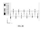
- FIG. 2Bis a 2D (x-y) diagram of an example simulated magnetic vector field distribution of the DML of FIGS. 1A and 1B in a lower dielectric constant layer;
- FIG. 3Ais a 3D (x-y-z) view of an example simulated electric vector field distributions of the DML of FIGS. 1A and 1B in a lower dielectric constant layer;
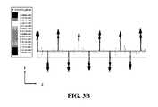
- FIG. 3Bis a 2D (x-y) view of an example simulated electric vector field distributions of the DML of FIGS. 1A and 1B in a lower dielectric constant layer;
- FIG. 4is a diagram illustrated the results of a simulated power distribution along lines a-a′ as shown in the FIG. 1B ;
- FIG. 5Ais an illustration of an EM model of the DML of FIGS. 1A and 1B with 2 transitions in simulation;
- FIG. 5Bis a photograph of the DML of FIGS. 1A and 1B ;
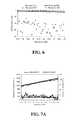
- FIG. 7Ais a diagram illustrating the frequency response of the simulated and the measured S-parameters of the DML of FIG. 6 ;
- FIG. 7Bis a diagram illustrating the frequency response of the propagation constants of the DML of FIG. 6 ;
- FIG. 8Ais another diagram illustrating an electric field distribution of the DML of FIGS. 1A and 1B in x-z and x-y planes;
- FIG. 8Bis another diagram illustrating a magnetic field distribution in x-z and x-y planes of the DML of FIGS. 1A and 1B ;
- FIG. 8Cis a diagram illustrating the simulated power distribution in x-y plan along x direction
- FIG. 9is an illustration of a 3D structure of the DML of FIGS. 1A and 1B and waveguide transition and electric field distributions of the transition cross-sections at different positions;
- FIG. 10Ais an illustration of a frequency response of a simulated and a measured S-parameters of the DML of FIGS. 1A and 1B ;
- FIG. 10Bis an illustration of a frequency response of the propagation constants of the DML of FIGS. 1A and 1B .
- transmission microstrip linesmay fail to meet low-loss requirement at the millimeter-wave ranges due to metal loss which causes a loss of these signals transmitted on these lines.
- metal losscauses a loss of these signals transmitted on these lines.
- One cause for this loss due to the factis that the current conducting volume in the metallic components of microstrip lines is significantly reduced and in turn, introduces a higher loss at these frequency ranges due to skin effect.
- the metal lossdominates the total loss in these transmission lines and causes a detrimental effect to the use of microstrip lines in the transmission of wave signals.
- millimeter-wave componentsare very small.
- the electrical performance of millimeter-wave applicationsis very sensitive to every small fabrication error, including transmission lines. This lack of tolerance would make many circuits not realizable.
- roughness of the metal surface found in metallic transmission linesmay also become significant at millimeter-wave and higher frequency bands as these roughnesses can cause the meandering of a current flowing path along the surface and thus cause the length of the effective current path to become much longer than the actual distance.
- dielectric waveguidessuch as image guide, non-radiative dielectric waveguide, and optical fibre are good candidates to transmit millimeter-wave and Terahertz signals (submillimeter-waves).
- EM wavesare guided by total internal reflection in the high dielectric constant material which may be surrounded by air, metal, or cladding.
- a transmission linecomprising:
- a transmission mediumarranged to transmit a signal defined by a plurality of dielectric layers, wherein the dielectric layers include a first layer having a first dielectric constant, a second layer having a second dielectric constant and a third layer between the first and second layer having a third dielectric constant being less than the first and second dielectric constant.
- the guided wave structure 100comprises a 3-layer structure which can be referred to as a dielectric microstrip line (DML) 100 .
- the 3 layer structuremay be similar in appearance to a microstrip line but do not have any metal or metallic conductors.
- this lack of metallic conductorsmay result in a structure which is non-metallic and thus will not have any metal loss when signals are transmitted through the DML 100 .
- the EM fieldsconcentrate in the lower dielectric constant layer.
- airas a low loss dielectric material, may also be used to guide EM wave in theory.
- the DML 100is able to transmit millimeter waves without significant loss
- the DMLmay be used in many applications in the regime of millimeter waves such as a microstrip line in the microwave band.
- the DML 100is formed or fabricated by three layers of dielectric substrates with different dielectric constants and thickness placed (clung) on top of each other or otherwise engaged together.
- each of the layersis bonded together so as to avoid the presence of any unnecessary air gaps between each of the layers, although as will be explained below as air also has a dielectric constant, it may be used as a layer itself.
- the 3D and cross-section views of the DML 100have different dielectric constants of ⁇ rh and ⁇ rl, and substrate thicknesses t(h) and t(l), respectively.
- ⁇ rhis greater than ⁇ rl.
- a DML 100 using Duroid® substrates(ceramic-PTFE composites, Rogers Corporation) was fabricated and tested with results described below.
- aircould also be used as the middle layer 106 in theory.
- the DML 100supports LSM10(y) propagation mode waves.
- the rigorous field solutions of the DMLare presented in below in (1):
- FIG. 4there is illustrated a normalized power density along cross section a-a′ as shown in FIG. 1B , the line of symmetry on the x-y plane. A distinct sharp change of the power density in the different layers is observed. This indicates that the DML is able to confine most of the EM wave power. This result has also been confirmed by simulation, with more than 96% wave power being guided by the entire DML 100 .
- the transition between the standard rectangular waveguide and the DMLhas to be designed for measurement purpose.
- the transitionis basically a linearly tapered DML inserted into the rectangular waveguide such that the EM field distribution interchanges gradually.
- the WR28 standard rectangular waveguidethat works within the frequency range of 26.5 GHz-40 GHz was used in this study.
- FIG. 5Aan embodiment of the DML is shown.
- the entire structure of DML having two transitions for the simulationis shown.
- Photograph of the prototype for measurementis also shown in FIG. 5B , which is suitable for the vector network analyser with waveguide interfaces.
- the measured frequency responses of the S-parameters S 11 and S 21 of the DMLbeing 25 mm long.
- the average measured insertion loss of the section of DMLis 2.3 dB and maximum value is 4.3 dB, while the measured return loss is greater than 12 dB.
- Two straight DML sections with 25 mm and 30 mm longwere fabricated. Two sets of the measured S-parameters are required to determine the propagation constant, attenuation constant, and Q-factor of the DML as shown in FIGS. 7A and 7B . Acceptable agreements of loss are obtained.
- the Q-factor of the DMLis about 55 at 30 GHz and it tends to increase with the frequency.
- all of the dielectric substratesare just placed (clung) together.
- unpredicted air gap between dielectric substratesmay result in small disagreement between simulation and measurement.
- Small ripple of all parametersare observed because losses due to radiations and connectors are taken into account. A certain deviation can be attributed to the fabrication and measurement tolerances.
- Embodiments of the DML 100are advantageous in that the DML forms a low-loss transmission line for at least the millimeter-wave frequency range. During simulation, measurements and results of these simulations indicated that S-parameters and propagation constants were presented.
- the DMLis suitable for low-cost and low loss millimeter circuits which may not require the use of metal or metallic components rather may be constructed with purely dielectric materials. These embodiments of the DML may also be used into the Terahertz (submillimeter-wave) applications.
- the DML 100can also be implemented or fabricated onto a printed circuit board (PCB) where the layers of the dielectric material may be included in part to materials used to fabricate the PCB.
- PCBprinted circuit board
- guided wave characteristics of a section of the DML 100were further simulated by Ansoft HFSS. According to this simulation, the guided EM wave propagates alone the z-direction with a single port excitation. Both electric and magnetic field distributions in both x-z and x-y planes are shown in FIGS. 8A and 8B , respectively. It can be observed from the theses figures that the DML supports quasi-transverse magnetic (quasi-TM) waves. Most of the magnetic field components exist in y-direction and are almost zero in z-direction, while most of the electric field components exist in both x- and z-directions.
- quasi-TMquasi-transverse magnetic
- FIG. 8Cthere is illustrated the normalized power density along a-a′, the line of symmetry on the x-y plane. As is shown in FIG. 8C , a distinct sharp change of the power density in the different layers is observed. Confining most of the EM wave power with more than 96% wave power is guided by the entire DML.
- the WR28 standard rectangular waveguide porthas been chosen for measurement to test the performance of the DML.
- a transition between the rectangular waveguide and the DMLhas to be designed for measurement purpose.
- the transition 502is basically a linearly tapered DML inserted into the rectangular waveguide such that the EM field distribution interchanges gradually.
- a stepped discontinuity at the interface between the waveguide and the DMLis used to reduce the width of the DML inside the waveguide to a narrower one outside the waveguide for impedance matching.
- the EM model of the transitionhas been realized by means of the Ansoft HFSS too as shown in FIG. 9 . Simulated cross-section electric field distributions at different positions of the transition (A, B, C, D, and E) are shown in FIG. 9 Electric field changes gradually between waveguide (TE10) and DML (quasi-TM).
- the measured frequency responses of the S-parameters S 11 and S 21 of the section of the DMLare shown.
- the average measured insertion loss of the section of DMLis 2.3 dB and maximum value is 4.3 dB, while the measured return loss is greater than 12 dB.
- All dielectric substratesare just placed together. As a result, unpredicted air gap between dielectric substrates may result in small disagreement between simulation and measurement. Small ripple of S-parameters are observed because losses due to radiations and connectors are taken into account in one example.
- two straight DML sections with 5 mm long differencewere fabricated. Two sets of the measured S-parameters were used to determine the loss and propagation constants of the DML. During the measurement, no obvious difference on the insertion loss can be observed between the two DMLs with different lengths, confirming that the DML is a very low loss transmission line. Of course, the phase angles of these two DMLs may be distinctly different and thus the propagation constant is then calculated by the phase difference of the two DMLs divided by the length difference. Simulated and measured propagation constants of this embodiment of the DML are shown in FIG. 10B with a certain deviation being attributed to the fabrication and measurement tolerances.
Landscapes
- Engineering & Computer Science (AREA)
- Manufacturing & Machinery (AREA)
- Waveguides (AREA)
Abstract
Description
- a first layer having a first dielectric constant;
- a second layer having a second dielectric constant and
- a third layer having a third dielectric constant being less than the first and second dielectric constant.
- the first and second dielectric constant is 10.2;
- the third dielectric constant is 2.94;
- the first and second layer have a thickness of 1.27 mm;
- the third layer has a thickness of 0.381 mm;
- the strip has a width of 5 mm; and
- the second and third layer have a width of 50 mm.
- disposing a transmission layer between a first and second external layers, wherein the transmission layer has a dielectric constant less than the first and second external layers.
where w is the width of the top layer of the DML, A is magnitude of the fields, and β is the propagation constant. Guided wave characteristics of a section of the DML were re-confirmed and simulated by Ansoft HFSS. The guided EM wave propagates alone the z-direction with a single port excitation. Both electric and magnetic vector field distributions in the lower dielectric constant layer in both 3-D view and x-z or x-y planes are shown in
Claims (15)
Priority Applications (1)
| Application Number | Priority Date | Filing Date | Title |
|---|---|---|---|
| US13/973,385US9478840B2 (en) | 2012-08-24 | 2013-08-22 | Transmission line and methods for fabricating thereof |
Applications Claiming Priority (2)
| Application Number | Priority Date | Filing Date | Title |
|---|---|---|---|
| US201261692890P | 2012-08-24 | 2012-08-24 | |
| US13/973,385US9478840B2 (en) | 2012-08-24 | 2013-08-22 | Transmission line and methods for fabricating thereof |
Publications (2)
| Publication Number | Publication Date |
|---|---|
| US20140055216A1 US20140055216A1 (en) | 2014-02-27 |
| US9478840B2true US9478840B2 (en) | 2016-10-25 |
Family
ID=50147473
Family Applications (1)
| Application Number | Title | Priority Date | Filing Date |
|---|---|---|---|
| US13/973,385Expired - Fee RelatedUS9478840B2 (en) | 2012-08-24 | 2013-08-22 | Transmission line and methods for fabricating thereof |
Country Status (2)
| Country | Link |
|---|---|
| US (1) | US9478840B2 (en) |
| CN (1) | CN103633403B (en) |
Families Citing this family (3)
| Publication number | Priority date | Publication date | Assignee | Title |
|---|---|---|---|---|
| US9405064B2 (en)* | 2012-04-04 | 2016-08-02 | Texas Instruments Incorporated | Microstrip line of different widths, ground planes of different distances |
| US9634618B2 (en)* | 2015-07-20 | 2017-04-25 | City University Of Hong Kong | Impedance matching arrangement for an amplifier |
| CN117458111B (en)* | 2023-11-24 | 2024-07-09 | 江苏工程职业技术学院 | Gradual change type medium substrate integrated low-loss transmission line |
Citations (28)
| Publication number | Priority date | Publication date | Assignee | Title |
|---|---|---|---|---|
| US4028643A (en)* | 1976-05-12 | 1977-06-07 | University Of Illinois Foundation | Waveguide having strip dielectric structure |
| US4441091A (en)* | 1979-07-18 | 1984-04-03 | Hitachi Cable Ltd. | Low loss leakage transmission line |
| US4463329A (en)* | 1978-08-15 | 1984-07-31 | Hirosuke Suzuki | Dielectric waveguide |
| US4825221A (en)* | 1985-01-16 | 1989-04-25 | Junkosha Co., Ltd. | Directly emitting dielectric transmission line |
| US5459807A (en)* | 1993-02-08 | 1995-10-17 | Sony Corporation | Optical waveguide device and second harmonic generator using the same |
| US5682401A (en)* | 1994-10-05 | 1997-10-28 | Massachusetts Institute Of Technology | Resonant microcavities employing one-dimensionally periodic dielectric waveguides |
| US5861782A (en)* | 1995-08-18 | 1999-01-19 | Murata Manufacturing Co., Ltd. | Nonradiative dielectric waveguide and method of producing the same |
| US5889449A (en)* | 1995-12-07 | 1999-03-30 | Space Systems/Loral, Inc. | Electromagnetic transmission line elements having a boundary between materials of high and low dielectric constants |
| US5977915A (en)* | 1997-06-27 | 1999-11-02 | Telefonaktiebolaget Lm Ericsson | Microstrip structure |
| US5986527A (en)* | 1995-03-28 | 1999-11-16 | Murata Manufacturing Co., Ltd. | Planar dielectric line and integrated circuit using the same line |
| US6104264A (en)* | 1997-02-06 | 2000-08-15 | Murata Manufacturing Co., Ltd. | Dielectric waveguide of a laminated structure |
| US6340951B1 (en)* | 2000-06-02 | 2002-01-22 | Industrial Technology Research Institute | Wideband microstrip leaky-wave antenna |
| US20020031321A1 (en)* | 2000-07-10 | 2002-03-14 | Lee Kevin K. | Low-loss waveguide and method of making same |
| US20030042997A1 (en)* | 2001-08-22 | 2003-03-06 | Postech Foundation | Tunable microwave systems with air-dielectric sandwich structures |
| US6724281B2 (en)* | 1999-10-29 | 2004-04-20 | Fci Americas Technology, Inc. | Waveguides and backplane systems |
| US6834152B2 (en)* | 2001-09-10 | 2004-12-21 | California Institute Of Technology | Strip loaded waveguide with low-index transition layer |
| US6909345B1 (en)* | 1999-07-09 | 2005-06-21 | Nokia Corporation | Method for creating waveguides in multilayer ceramic structures and a waveguide having a core bounded by air channels |
| US20050213873A1 (en)* | 2004-03-24 | 2005-09-29 | Sioptical, Inc. | Optical Crossover in thin silicon |
| US20070274654A1 (en)* | 2004-08-23 | 2007-11-29 | Molex Incorporated | System and Tapered Waveguide for Improving Light Coupling Efficiency Between Optical Fibers and Integrated Planar Waveguides and Method of Manufacturing Same |
| US7414491B2 (en)* | 2004-09-28 | 2008-08-19 | Teledyne Licensing, Llc | Method and apparatus for changing the polarization of a signal |
| US20090051467A1 (en)* | 2007-08-14 | 2009-02-26 | Mckinzie Iii William E | Apparatus and method for mode suppression in microwave and millimeterwave packages |
| US20090087137A1 (en)* | 2007-10-02 | 2009-04-02 | My The Doan | Planar lightwave circuits with air filled trenches |
| US20090273532A1 (en)* | 2008-05-02 | 2009-11-05 | William Marsh Rice University | Ultra Low Loss Waveguide for Broadband Terahertz Radiation |
| US8018375B1 (en)* | 2010-04-11 | 2011-09-13 | Broadcom Corporation | Radar system using a projected artificial magnetic mirror |
| US8189980B2 (en)* | 2005-03-01 | 2012-05-29 | National Institute For Materials Science | Electromagnetic wave resonator, method of manufacturing the same, and method of resonating electromagnetic wave |
| US20140104130A1 (en)* | 2012-10-12 | 2014-04-17 | Honeywell International Inc. | Systems and methods for injection molded phase shifter |
| US20140240187A1 (en)* | 2013-02-27 | 2014-08-28 | Texas Instruments Incorporated | Dielectric Waveguide with Non-planar Interface Surface |
| US8995838B1 (en)* | 2008-06-18 | 2015-03-31 | Hrl Laboratories, Llc | Waveguide assembly for a microwave receiver with electro-optic modulator |
Family Cites Families (4)
| Publication number | Priority date | Publication date | Assignee | Title |
|---|---|---|---|---|
| JP2991076B2 (en)* | 1995-03-28 | 1999-12-20 | 株式会社村田製作所 | Planar dielectric line and integrated circuit |
| CN100495812C (en)* | 2002-12-26 | 2009-06-03 | 松下电器产业株式会社 | Dielectric filter |
| JP4874113B2 (en)* | 2003-10-22 | 2012-02-15 | エヌエックスピー ビー ヴィ | Method and apparatus for sending and receiving data units via a transmission medium |
| JP2005175941A (en)* | 2003-12-11 | 2005-06-30 | Nippon Telegr & Teleph Corp <Ntt> | High frequency electromagnetic transmission line |
- 2013
- 2013-08-22USUS13/973,385patent/US9478840B2/ennot_activeExpired - Fee Related
- 2013-08-23CNCN201310373044.4Apatent/CN103633403B/enactiveActive
Patent Citations (28)
| Publication number | Priority date | Publication date | Assignee | Title |
|---|---|---|---|---|
| US4028643A (en)* | 1976-05-12 | 1977-06-07 | University Of Illinois Foundation | Waveguide having strip dielectric structure |
| US4463329A (en)* | 1978-08-15 | 1984-07-31 | Hirosuke Suzuki | Dielectric waveguide |
| US4441091A (en)* | 1979-07-18 | 1984-04-03 | Hitachi Cable Ltd. | Low loss leakage transmission line |
| US4825221A (en)* | 1985-01-16 | 1989-04-25 | Junkosha Co., Ltd. | Directly emitting dielectric transmission line |
| US5459807A (en)* | 1993-02-08 | 1995-10-17 | Sony Corporation | Optical waveguide device and second harmonic generator using the same |
| US5682401A (en)* | 1994-10-05 | 1997-10-28 | Massachusetts Institute Of Technology | Resonant microcavities employing one-dimensionally periodic dielectric waveguides |
| US5986527A (en)* | 1995-03-28 | 1999-11-16 | Murata Manufacturing Co., Ltd. | Planar dielectric line and integrated circuit using the same line |
| US5861782A (en)* | 1995-08-18 | 1999-01-19 | Murata Manufacturing Co., Ltd. | Nonradiative dielectric waveguide and method of producing the same |
| US5889449A (en)* | 1995-12-07 | 1999-03-30 | Space Systems/Loral, Inc. | Electromagnetic transmission line elements having a boundary between materials of high and low dielectric constants |
| US6104264A (en)* | 1997-02-06 | 2000-08-15 | Murata Manufacturing Co., Ltd. | Dielectric waveguide of a laminated structure |
| US5977915A (en)* | 1997-06-27 | 1999-11-02 | Telefonaktiebolaget Lm Ericsson | Microstrip structure |
| US6909345B1 (en)* | 1999-07-09 | 2005-06-21 | Nokia Corporation | Method for creating waveguides in multilayer ceramic structures and a waveguide having a core bounded by air channels |
| US6724281B2 (en)* | 1999-10-29 | 2004-04-20 | Fci Americas Technology, Inc. | Waveguides and backplane systems |
| US6340951B1 (en)* | 2000-06-02 | 2002-01-22 | Industrial Technology Research Institute | Wideband microstrip leaky-wave antenna |
| US20020031321A1 (en)* | 2000-07-10 | 2002-03-14 | Lee Kevin K. | Low-loss waveguide and method of making same |
| US20030042997A1 (en)* | 2001-08-22 | 2003-03-06 | Postech Foundation | Tunable microwave systems with air-dielectric sandwich structures |
| US6834152B2 (en)* | 2001-09-10 | 2004-12-21 | California Institute Of Technology | Strip loaded waveguide with low-index transition layer |
| US20050213873A1 (en)* | 2004-03-24 | 2005-09-29 | Sioptical, Inc. | Optical Crossover in thin silicon |
| US20070274654A1 (en)* | 2004-08-23 | 2007-11-29 | Molex Incorporated | System and Tapered Waveguide for Improving Light Coupling Efficiency Between Optical Fibers and Integrated Planar Waveguides and Method of Manufacturing Same |
| US7414491B2 (en)* | 2004-09-28 | 2008-08-19 | Teledyne Licensing, Llc | Method and apparatus for changing the polarization of a signal |
| US8189980B2 (en)* | 2005-03-01 | 2012-05-29 | National Institute For Materials Science | Electromagnetic wave resonator, method of manufacturing the same, and method of resonating electromagnetic wave |
| US20090051467A1 (en)* | 2007-08-14 | 2009-02-26 | Mckinzie Iii William E | Apparatus and method for mode suppression in microwave and millimeterwave packages |
| US20090087137A1 (en)* | 2007-10-02 | 2009-04-02 | My The Doan | Planar lightwave circuits with air filled trenches |
| US20090273532A1 (en)* | 2008-05-02 | 2009-11-05 | William Marsh Rice University | Ultra Low Loss Waveguide for Broadband Terahertz Radiation |
| US8995838B1 (en)* | 2008-06-18 | 2015-03-31 | Hrl Laboratories, Llc | Waveguide assembly for a microwave receiver with electro-optic modulator |
| US8018375B1 (en)* | 2010-04-11 | 2011-09-13 | Broadcom Corporation | Radar system using a projected artificial magnetic mirror |
| US20140104130A1 (en)* | 2012-10-12 | 2014-04-17 | Honeywell International Inc. | Systems and methods for injection molded phase shifter |
| US20140240187A1 (en)* | 2013-02-27 | 2014-08-28 | Texas Instruments Incorporated | Dielectric Waveguide with Non-planar Interface Surface |
Also Published As
| Publication number | Publication date |
|---|---|
| CN103633403B (en) | 2018-08-31 |
| US20140055216A1 (en) | 2014-02-27 |
| CN103633403A (en) | 2014-03-12 |
Similar Documents
| Publication | Publication Date | Title |
|---|---|---|
| US20150333726A1 (en) | Apparatus and a method for electromagnetic signal transition | |
| US9912032B2 (en) | Waveguide assembly having a conductive waveguide with ends thereof mated with at least first and second dielectric waveguides | |
| US10147991B1 (en) | Non-reciprocal mode converting substrate integrated waveguide | |
| He et al. | Characteristic impedance extraction of spoof surface plasmon polariton waveguides | |
| Huang et al. | Substrate integrated waveguide filters with broadside‐coupled complementary split ring resonators | |
| CN104103882A (en) | Terahertz medium filled metal groove waveguide | |
| US9478840B2 (en) | Transmission line and methods for fabricating thereof | |
| Liu et al. | Novel methods for modeling of multiple vias in multilayered parallel-plate structures | |
| Mittal et al. | Spoof surface plasmon polaritons based microwave bandpass filter | |
| Aziz et al. | A novel plasmonic waveguide for the dual-band transmission of spoof surface plasmon polaritons | |
| Zou et al. | Design of an X-band symmetrical window bandpass filter based on substrate integrated waveguide | |
| Mazhar et al. | Design and analysis of wideband eight‐way SIW power splitter for mm‐wave applications | |
| Yang et al. | Half-height-pin gap waveguide technology and its applications in high gain planar array antennas at millimeter wave frequency | |
| Xue et al. | A transition of microstrip line to dielectric microstrip line for millimeter wave circuits | |
| Hamada et al. | A 60-GHz Out-of-Phase Power Divider with WR-15 Standard Interface Based on Trapped Printed Gap Waveguide Technology | |
| JP2012151786A (en) | Antenna device | |
| Wu | A combined efficient approach for analysis of nonradiative dielectric (NRD) waveguide components | |
| Tang et al. | Co-layered integration and interconnect of planar circuits and nonradiative dielectric (NRD) waveguide | |
| Miri et al. | A wideband, sharp roll‐off U‐band diplexer in suspended stripline technology | |
| Yin et al. | A substrate integrated waveguide bandpass filter based on the modified CSRRs and the Z shaped slot | |
| US20150102870A1 (en) | Directional coupler arrangement and method | |
| Miri et al. | A Wideband, Sharp Roll‐Off U‐Band Diplexer in Suspended Stripline Technology | |
| Sahoo et al. | Analysis and Design of Low Index Core Dielectric Waveguide Using Planar Excitation for Ku-Band Applications | |
| Jankovic et al. | Planar transitions from substrate integrated coaxial line to single-layer transmission lines and waveguides | |
| Amari et al. | On the acceleration of the coupled-integral-equations technique and its application to multistub E-plane discontinuities |
Legal Events
| Date | Code | Title | Description |
|---|---|---|---|
| AS | Assignment | Owner name:CITY UNIVERSITY OF HONG KONG, HONG KONG Free format text:ASSIGNMENT OF ASSIGNORS INTEREST;ASSIGNORS:XUE, QUAN;CHIU, LEUNG;REEL/FRAME:032387/0176 Effective date:20140121 | |
| ZAAA | Notice of allowance and fees due | Free format text:ORIGINAL CODE: NOA | |
| ZAAB | Notice of allowance mailed | Free format text:ORIGINAL CODE: MN/=. | |
| STCF | Information on status: patent grant | Free format text:PATENTED CASE | |
| MAFP | Maintenance fee payment | Free format text:PAYMENT OF MAINTENANCE FEE, 4TH YR, SMALL ENTITY (ORIGINAL EVENT CODE: M2551); ENTITY STATUS OF PATENT OWNER: SMALL ENTITY Year of fee payment:4 | |
| FEPP | Fee payment procedure | Free format text:MAINTENANCE FEE REMINDER MAILED (ORIGINAL EVENT CODE: REM.); ENTITY STATUS OF PATENT OWNER: SMALL ENTITY | |
| LAPS | Lapse for failure to pay maintenance fees | Free format text:PATENT EXPIRED FOR FAILURE TO PAY MAINTENANCE FEES (ORIGINAL EVENT CODE: EXP.); ENTITY STATUS OF PATENT OWNER: SMALL ENTITY | |
| STCH | Information on status: patent discontinuation | Free format text:PATENT EXPIRED DUE TO NONPAYMENT OF MAINTENANCE FEES UNDER 37 CFR 1.362 | |
| FP | Lapsed due to failure to pay maintenance fee | Effective date:20241025 |