US9478502B2 - Device identification assignment and total device number detection - Google Patents
Device identification assignment and total device number detectionDownload PDFInfo
- Publication number
- US9478502B2 US9478502B2US13/559,235US201213559235AUS9478502B2US 9478502 B2US9478502 B2US 9478502B2US 201213559235 AUS201213559235 AUS 201213559235AUS 9478502 B2US9478502 B2US 9478502B2
- Authority
- US
- United States
- Prior art keywords
- dice
- devices
- assignment
- stack
- input
- Prior art date
- Legal status (The legal status is an assumption and is not a legal conclusion. Google has not performed a legal analysis and makes no representation as to the accuracy of the status listed.)
- Active, expires
Links
Images


Classifications
- H—ELECTRICITY
- H01—ELECTRIC ELEMENTS
- H01L—SEMICONDUCTOR DEVICES NOT COVERED BY CLASS H10
- H01L23/00—Details of semiconductor or other solid state devices
- H01L23/544—Marks applied to semiconductor devices or parts, e.g. registration marks, alignment structures, wafer maps
- G—PHYSICS
- G11—INFORMATION STORAGE
- G11C—STATIC STORES
- G11C5/00—Details of stores covered by group G11C11/00
- G11C5/02—Disposition of storage elements, e.g. in the form of a matrix array
- G11C5/025—Geometric lay-out considerations of storage- and peripheral-blocks in a semiconductor storage device
- G—PHYSICS
- G11—INFORMATION STORAGE
- G11C—STATIC STORES
- G11C5/00—Details of stores covered by group G11C11/00
- G11C5/02—Disposition of storage elements, e.g. in the form of a matrix array
- G11C5/04—Supports for storage elements, e.g. memory modules; Mounting or fixing of storage elements on such supports
- G—PHYSICS
- G11—INFORMATION STORAGE
- G11C—STATIC STORES
- G11C8/00—Arrangements for selecting an address in a digital store
- G11C8/12—Group selection circuits, e.g. for memory block selection, chip selection, array selection
- G—PHYSICS
- G11—INFORMATION STORAGE
- G11C—STATIC STORES
- G11C16/00—Erasable programmable read-only memories
- G11C16/02—Erasable programmable read-only memories electrically programmable
- G11C16/06—Auxiliary circuits, e.g. for writing into memory
- G11C16/10—Programming or data input circuits
- G11C16/20—Initialising; Data preset; Chip identification
- G—PHYSICS
- G11—INFORMATION STORAGE
- G11C—STATIC STORES
- G11C29/00—Checking stores for correct operation ; Subsequent repair; Testing stores during standby or offline operation
- G11C29/04—Detection or location of defective memory elements, e.g. cell constructio details, timing of test signals
- G11C29/08—Functional testing, e.g. testing during refresh, power-on self testing [POST] or distributed testing
- G11C29/12—Built-in arrangements for testing, e.g. built-in self testing [BIST] or interconnection details
- G11C2029/4402—Internal storage of test result, quality data, chip identification, repair information
- H—ELECTRICITY
- H01—ELECTRIC ELEMENTS
- H01L—SEMICONDUCTOR DEVICES NOT COVERED BY CLASS H10
- H01L2223/00—Details relating to semiconductor or other solid state devices covered by the group H01L23/00
- H01L2223/544—Marks applied to semiconductor devices or parts
- H01L2223/54433—Marks applied to semiconductor devices or parts containing identification or tracking information
- H01L2223/5444—Marks applied to semiconductor devices or parts containing identification or tracking information for electrical read out
- H—ELECTRICITY
- H01—ELECTRIC ELEMENTS
- H01L—SEMICONDUCTOR DEVICES NOT COVERED BY CLASS H10
- H01L2223/00—Details relating to semiconductor or other solid state devices covered by the group H01L23/00
- H01L2223/544—Marks applied to semiconductor devices or parts
- H01L2223/54473—Marks applied to semiconductor devices or parts for use after dicing
- H—ELECTRICITY
- H01—ELECTRIC ELEMENTS
- H01L—SEMICONDUCTOR DEVICES NOT COVERED BY CLASS H10
- H01L2224/00—Indexing scheme for arrangements for connecting or disconnecting semiconductor or solid-state bodies and methods related thereto as covered by H01L24/00
- H01L2224/01—Means for bonding being attached to, or being formed on, the surface to be connected, e.g. chip-to-package, die-attach, "first-level" interconnects; Manufacturing methods related thereto
- H01L2224/10—Bump connectors; Manufacturing methods related thereto
- H01L2224/15—Structure, shape, material or disposition of the bump connectors after the connecting process
- H01L2224/16—Structure, shape, material or disposition of the bump connectors after the connecting process of an individual bump connector
- H01L2224/161—Disposition
- H01L2224/16135—Disposition the bump connector connecting between different semiconductor or solid-state bodies, i.e. chip-to-chip
- H01L2224/16145—Disposition the bump connector connecting between different semiconductor or solid-state bodies, i.e. chip-to-chip the bodies being stacked
- H—ELECTRICITY
- H01—ELECTRIC ELEMENTS
- H01L—SEMICONDUCTOR DEVICES NOT COVERED BY CLASS H10
- H01L2225/00—Details relating to assemblies covered by the group H01L25/00 but not provided for in its subgroups
- H01L2225/03—All the devices being of a type provided for in the same main group of the same subclass of class H10, e.g. assemblies of rectifier diodes
- H01L2225/04—All the devices being of a type provided for in the same main group of the same subclass of class H10, e.g. assemblies of rectifier diodes the devices not having separate containers
- H01L2225/065—All the devices being of a type provided for in the same main group of the same subclass of class H10
- H01L2225/06503—Stacked arrangements of devices
- H01L2225/06513—Bump or bump-like direct electrical connections between devices, e.g. flip-chip connection, solder bumps
- H—ELECTRICITY
- H01—ELECTRIC ELEMENTS
- H01L—SEMICONDUCTOR DEVICES NOT COVERED BY CLASS H10
- H01L2225/00—Details relating to assemblies covered by the group H01L25/00 but not provided for in its subgroups
- H01L2225/03—All the devices being of a type provided for in the same main group of the same subclass of class H10, e.g. assemblies of rectifier diodes
- H01L2225/04—All the devices being of a type provided for in the same main group of the same subclass of class H10, e.g. assemblies of rectifier diodes the devices not having separate containers
- H01L2225/065—All the devices being of a type provided for in the same main group of the same subclass of class H10
- H01L2225/06503—Stacked arrangements of devices
- H01L2225/06541—Conductive via connections through the device, e.g. vertical interconnects, through silicon via [TSV]
- H—ELECTRICITY
- H01—ELECTRIC ELEMENTS
- H01L—SEMICONDUCTOR DEVICES NOT COVERED BY CLASS H10
- H01L25/00—Assemblies consisting of a plurality of semiconductor or other solid state devices
- H01L25/03—Assemblies consisting of a plurality of semiconductor or other solid state devices all the devices being of a type provided for in a single subclass of subclasses H10B, H10D, H10F, H10H, H10K or H10N, e.g. assemblies of rectifier diodes
- H01L25/04—Assemblies consisting of a plurality of semiconductor or other solid state devices all the devices being of a type provided for in a single subclass of subclasses H10B, H10D, H10F, H10H, H10K or H10N, e.g. assemblies of rectifier diodes the devices not having separate containers
- H01L25/065—Assemblies consisting of a plurality of semiconductor or other solid state devices all the devices being of a type provided for in a single subclass of subclasses H10B, H10D, H10F, H10H, H10K or H10N, e.g. assemblies of rectifier diodes the devices not having separate containers the devices being of a type provided for in group H10D89/00
- H01L25/0657—Stacked arrangements of devices
Definitions
- Computers and other electronic systemsfor example, digital televisions, digital cameras, and cellular phones, often have one or more memory and other devices to store information.
- memory and other devicesare being reduced in size to achieve a higher density of storage capacity and/or a higher density of functionality.
- FIG. 1shows a cross-sectional view of a microelectronics package having a number of stacked and interconnected integrated circuit dice, according to various embodiments of the invention
- FIG. 2Ashows a cross-sectional view of a microelectronics package having four integrated circuit dice that are stacked and interconnected and incorporate embodiments of the described subject matter;
- FIG. 2Bshows a portion of the fourth integrated circuit die of FIG. 2A ;
- FIG. 3shows a cross-sectional view of a stacked package having two device cards that are stacked and interconnected and incorporate embodiments of the described subject matter
- FIG. 4is a block diagram of a system embodiment, including a memory device and an addressable device having stacked dice.
- integrated circuit dice and other device typesmay be stacked on top of one another.
- One such exampleincludes stacked memory dice, where a number of dice are stacked to increase an overall amount of memory within the given area.
- Each die in the stackmay have a number of integrated circuit devices fabricated on a substrate comprising the die.
- Some dice within the stackmay operate to communicate with other dice in the stack (e.g., slave dice may communicate with a master die to perform their functions).
- Such stacksmay be interconnected from one side of the substrate to the other.
- the interconnectionsinclude through-substrate vias (TSVs). When the substrate comprises silicon, the interconnections may also be referred to as through-silicon vias.
- Addressable devicestypically make use of a mechanism by which each device can be addressed independently from other devices residing on the same bus. Addressable devices used in stacked configurations may provide this capability by assigning each device a unique device identifier (ID) value.
- IDdevice identifier
- the device ID valuemay be configured in the assembly process by selectively bonding several device ID bonding pads to power (e.g., V DD ) or ground (e.g., V ss ), thereby encoding a unique device ID value.
- V DDpower
- V ssground
- Some of the embodiments described hereinoperate to automatically assign a device ID value to each device in a stack of devices. The device ID value may be assigned either during manufacture or at some later time (e.g., if other devices are later added or removed).
- Various embodiments of the disclosed subject matterinclude an apparatus for generating a unique device ID value for each addressable device in a multi-device stacked package, such as a stacked-CSP (chip scale package).
- Generation of the unique device ID value for each stacked devicecan be accomplished by including circuitry for each addressable device that generates a device ID value based on an input device ID value signal. The addressable device may then operate to provide an output value corresponding to the generated device ID value to another device in the stack, such as for assignment thereto.
- FIG. 1a cross-sectional view of a microelectronics package 100 having a number of stacked and interconnected integrated circuit dice, according to various embodiments of the invention, is shown.
- the stacked and interconnected dicemay form at least a portion of a microelectronics package.
- the microelectronics package 100is shown to include four integrated circuit dice.
- the four integrated circuit diceinclude a master die 101 , and three slave dice 103 A, 103 B, 103 C.
- the three slave dice 103 A, 103 B, 103 Cmay be identified individually as the first, the second, and the third slave die, respectively.
- any one or more of the master die 101 or the three slave dice 103 A, 103 B, 103 Cmay operate to provide a generated device ID value to other devices, as described herein.
- the microelectronics package 100may contain any other desired number of integrated circuit dice.
- Each of the integrated circuit dicehas a first surface 105 A and a second surface 105 B.
- An arrow 110indicates a normal orientation of the dice in which the first surface 105 A is located at an upper surface of the substrate where the upper surface is generally used during fabrication of integrated circuit devices on the substrate. That is, the upper surface of the substrate is the surface that may be used to form integrated circuit devices on a die.
- TSVsthrough-substrate vias
- the TSVs 107may also be referred to as through-silicon vias, depending upon the substrate type (e.g., silicon or other elemental semiconductors, compound semiconductors, or other substrate types known in the art, including those used in the formation of device cards) from which the dice are formed.
- the TSVs 107may be formed from the first surface 105 A through the integrated circuit die to the second surface 105 B (or alternatively, from the second surface 105 B to the first surface 105 A).
- the TSVs 107can be selectively connected to certain metallization layers within the die and therefore allow an interconnection from, for example, integrated circuit devices formed on the first surface 105 A and through to the second surface 105 B of the master die 101 , to connect to one or more of the slave dice 103 A, 103 B, 103 C, in the stack.
- Other types of viasmay pass only partially through the integrated circuit die.
- the TSVs 107may function, for example, electrically, optically, or otherwise.
- the TSVs 107allow signals to travel electrically, optically, or otherwise between the master die 101 and various ones of the slave dice 103 A, 103 B, 103 C.
- Each of the TSVs 107has a conductive bonding pad 109 formed on either end or both ends of the TSVs 107 .
- Adjacent ones of the diceare electrically coupled by a conductive electrical connector 113 that is formed (e.g., placed) between the conductive bonding pads.
- the conductive electrical connector 113may be, for example, a wirebond, a solder ball, conductive tape, a Controlled Collapse Chip Connection (C 4 ) interconnect, or other suitable electrical connector.
- the conductive electrical connectors 113therefore form electrical interconnects 111 between each of the adjacent dice.
- the conductive bonding pads 109 on the first surface 105 A of the master die 101may be accessible to form an external interface 115 .
- the external interface 115allows interconnection with other devices such as, for example, a microprocessor.
- the external interfacemay be connected to pins (not shown) of the microelectronic package by bonding wires allowing accessibility from outside the package.
- the conductive bonding pads 109 on the second surface 105 B of the third slave die 103 Cform an external slave interface 121 that may be used, for example, to interface with other devices or, alternatively, allow interconnection with other slave dice in a larger stack.
- FIG. 2Ashows a cross-sectional view of a microelectronics package 200 having four integrated circuit dice 215 A, 215 B, 215 C, 215 D that are stacked and interconnected.
- the integrated circuit diceincorporate embodiments of the described subject matter.
- the four integrated circuit dice 215 A, 215 B, 215 C, 215 Dmay be identified individually as the first, the second, the third, and the fourth slave die, respectively.
- the identification as first, second, third, and fourthdoes not necessarily indicate any type of order or importance and is simply provided for ease in identification throughout the various embodiments.
- any of the integrated circuit dice 215 A, 215 B, 215 C, 215 Dmay be a master die, possibly similar to or identical to the master die 101 of FIG.
- none of the integrated circuit dice 215 A, 215 B, 215 C, 215 Dis a master die.
- each of the integrated circuit dice 215 A, 215 B, 215 C, 215 Dmay be independent of one another and/or controlled by an external controller or other device (not shown in FIG. 2A ).
- the integrated circuit dice 215 A, 215 B, 215 C, 215 Dare addressable devices.
- the integrated circuit diceare memory devices.
- the integrated circuit dicemay comprise flash memory, conductive-bridging random access memory (CBRAM), static RAM (SRAM), dynamic RAM (DRAM), or various other types of memory devices.
- the integrated circuit dicecomprise memory plus logic devices.
- each of the integrated circuit dice 215 A, 215 B, 215 C, 215 Dmay comprise devices different from remaining ones of the integrated circuit devices, such as a processor.
- Each die in FIG. 2Aincludes a die assignment portion 210 and a detection of number of dice portion 230 .
- the die assignment portion 210includes a respective assignment device 201 A, 201 B, 201 C, 201 D.
- each diecontains a first-level first bonding-pad 207 A and a first-level second bonding-pad 207 B on a first surface 213 A of the die.
- Each diealso has a number of second-level bonding-pads 205 on a second surface 213 B.
- the second-level bonding-pads 205may not be on the second surface 213 B of the die and may, alternatively, be within the die (e.g., between the first surface 213 A and the second surface 213 B). In these cases, the second-level bonding-pads 205 may be an internal conductive layer, such as a metal layer.
- Each of the first-level first bonding-pads 207 A, the first-level second bonding-pads 207 B, and the second-level bonding-pads 205are shown to be electrically coupled to respective ones of the TSVs 107 .
- the through-substrate vias 107 of FIG. 2Amay also be considered to be contacts or vias.
- each of the four integrated circuit dice 215 A, 215 B, 215 C, 215 D of FIG. 2Amay include additional TSVs.
- FIG. 2Aonly a limited number of TSVs are shown in FIG. 2A . That is, only the TSVs 107 that are used to either assign unique device ID values to each of the devices or to detect the number of dice are shown so as not to obscure details of the disclosed subject matter.
- the assignment devices 201 A, 201 B, 201 C, 201 Deach comprise a +1 adder circuit.
- the assignment devicesmay comprise combinatorial logic to produce a desired selectable output from a given input.
- the assignment devicesmay comprise a +N adder circuit, a ⁇ N adder circuit, an active logical shifter, a passive logical shifter, or various combinations thereof.
- An output of the assignment devicecan be based on a signal input to the assignment device.
- the output of the assignment devicecan be predetermined based on a design of the circuit.
- assignment devices 201 A, 201 B, 201 C, 201 D of FIG. 2Aare shown and described as having a two-bit input and a two-bit output, the assignment devices may include a number of one or more bits for the input and/or output.
- a single bitmay be used to indicate a respective device ID value for two assignable devices, “0” and “11,” representing ID (0) and ID (1).
- three or more bitsmay be used to indicate a device ID value.
- three bitsmay be used to indicate a respective unique device ID value for up to eight assignable devices, “000,” “001,” “010,” “011,” “100,” “101,” “110,” and “111.” That is, base 10 numbers 0 through 7, representing ID (0) through ID (7).
- the maximum number of addressable devices in the systemshould be less than or equal to 2 M , where M is the number of bits. For example, a three-bit device ID value can accommodate eight dice (e.g., 2 3 ) in a stack.
- each of the TSVs 107is floating, in a default configuration, as indicated on the first surface 213 A of the first integrated circuit die 215 A.
- the first-level first bonding-pad 207 A and the first-level second bonding-pad 207 Bmay be coupled to ground through a weak pull-down device 209 .
- a weak pull-down device 209when the weak pull-down device(s) 209 is activated, a floating input(s) of the assignment device 201 is pulled to ground.
- the weak pull-down devices 209 on each of the first-level first bonding-pad 207 A and the first-level second bonding-pad 207 B of each of the integrated circuit dice 215 A, 215 B, 215 C, 215 Dmay be activated.
- an input(s) of the assignment device(s) 201is tied to ground through the TSV 107 near the first surface 213 A.
- only the assignment device 201 Amay have its input pulled to ground to provide an initialization of the assignment device 201 A.
- assignment devices 201 B, 201 C, 201 Dmay also have their respective inputs initially tied to ground to reduce the possibility that one or more of the devices is not set to an initial input value other than “00” (through, for example, an externally generated voltage spike).
- the weak pull-down devices 209may be deactivated.
- each of the assignment devicesare +1 adders
- each of the assignment devices 201 A, 201 B, 201 Cautomatically generates a respective unique device ID value which is assigned to a respective subsequent one of the integrated circuit dice 215 B, 215 C, 215 D.
- the initialization valuewhich in this example is “00,” initially provided by the weak pull-down device 209 becomes the unique device ID value for the first integrated circuit die 215 A.
- the “00” signalbecomes the input to a first of the assignment devices 201 A.
- the “00” signalis operated on and produces an output on the second-level bonding-pads 205 of the first integrated circuit die 215 A of “01” as indicated by an arrow 211 A.
- the “01” signalis input as a “0” and a “1” to a second of the assignment devices 201 B through the first-level first bonding-pad 207 A and the first-level second bonding-pad 207 B, respectively.
- the “01” input to the second of the assignment devices 201 Bproduces an output on the second-level bonding-pads 205 of the second integrated circuit die 215 B of “10” as indicated by an arrow 211 B.
- the “10” signalis input as a “1” and a “0” to a third of the assignment devices 201 C through the first-level first bonding-pad 207 A and the first-level second bonding-pad 207 B, respectively.
- the “10” input to the third of the assignment devices 201 Cproduces an output on the second-level bonding-pads 205 of the third integrated circuit die 215 C of “11” as indicated by an arrow 211 C.
- the “11” signalis input as a “1” and a “1” to a fourth of the assignment devices 201 D through the first-level first bonding-pad 207 A and the first-level second bonding-pad 207 B, respectively.
- the “11” input to the fourth of the assignment devices 201 Dproduces an output on the second-level bonding-pads 205 of the fourth integrated circuit die 215 D.
- the fourth of the assignment devices 201 Dmay not be included since only the input value will be used, as discussed below. However, including the assignment device on all integrated circuit dice enables an unmodified fabrication process since all dice may be identical.
- Each of the unique device ID valuesmay be stored in, for example, a non-volatile memory 219 contained within the respective assignment device 201 A, 201 B, 201 C, 201 D, or elsewhere on the respective integrated circuit dice 215 A, 215 B, 215 C, 215 D.
- a pull-up device or other switching devicemay be substituted for the weak pull-down device 209 to pull the TSVs 107 to a power rail.
- an input(s) of the assignment device(s) 201is tied to, for example, V DD , through the TSV 107 near the first surface 213 A.
- the initial input of each of the assignment devicesbecomes “11.”
- the examples that followare then modified to accommodate the “11” initialization value.
- a +N addermay be substituted by a ⁇ N adder.
- an output signal from each of the assignment devices 201 A, 201 B, 201 C, 201 Dhas a progressively smaller, rather than larger, number.
- each of the integrated circuit dice 215 A, 215 B, 215 C, 215 Dthe detection of number of dice portion 230 includes evaluation devices 203 A, 203 B, 203 C, 203 D. Further, each die contains a first-level third bonding-pad 207 C and a first-level fourth bonding-pad 207 D on the first surface 213 A of the die. Similar to the die assignment portion 210 described above, each die also has a number of second-level bonding-pads 205 on the second surface 213 B.
- the second-level bonding-pads 205may not be on the second surface 213 B of the die and may, alternatively, be within the die (e.g., between the first surface 213 A and the second surface 213 B). In these cases, the second-level bonding-pads 205 may be an internal conductive layer, such as a metal layer.
- Each of the first-level third bonding-pads 207 C, the first-level fourth bonding-pads 207 D, and the second-level bonding-pads 205are shown to be electrically coupled to respective ones of the TSVs 107 .
- the evaluation devices 203 A, 203 B, 203 C, 203 Dcomprise arbiter circuits.
- the evaluation devicesmay comprise combinatorial logic to produce a desired selectable output based on an evaluation of a given input.
- the evaluation devicesmay comprise digital or analog evaluation devices.
- the evaluation devicesmay comprise combinations of the devices listed. An output value of the evaluation device is based on the evaluation of a signal input to the evaluation device. The output value can be predetermined, based on a design of the circuit.
- the weak pull-down devices 209 in the detection of the number of dice portion 230 on each of the second-level bonding-pads 205 of each of the integrated circuit dice 215 A, 215 B, 215 C, 215 Dmay be activated.
- a first input of an evaluation device(s) 203is tied to ground through the TSV 107 near the second surface 213 B.
- only the evaluation device 203 Dmay have its first input pulled to ground to provide an initialization of the evaluation device 203 D.
- remaining ones of the evaluation devices 203 A, 203 B, 203 Cmay also have their respective first inputs initially tied to ground to reduce the possibility that one or more of the devices is not set to an initial input value other than “00” (through, for example, an externally generated voltage spike).
- the weak pull-down devices 209 in the detection of the number of dice portion 230may be deactivated.
- a fourth one of the evaluation devices 203 Dreceives as a second input the device ID value assigned to the integrated circuit die 215 D (e.g., as read from the non-volatile memory 219 of the assignment device 201 D and/or from the input to the assignment device 201 D).
- the input to the fourth assignment device 201 Dis “11.” If the value of the first input of the evaluation device 203 D is “00,” the evaluation device 203 D takes the value of the second input to the evaluation device 203 D (in this example, “11”) and provides that as an output value.
- the evaluation criteriaare discussed in more detail, below, with reference to FIG. 2B .
- the output of the fourth evaluation device 203 Dis provided (e.g., fed, transmitted, sent, etc.) through the TSVs 107 to the first input of the third evaluation device 203 C.
- the third evaluation device 203 C(forming a part of the third one of the integrated circuit die 215 C), receives as a second input the device ID value assigned to the integrated circuit die 215 C (e.g., as read from the non-volatile memory 219 of the assignment device 201 C and/or from the input to the assignment device 201 C). As noted above, the third evaluation device 203 C receives, as a first input, the “11” value output from the fourth evaluation device 203 D.
- the outputis evaluated to be the same as the received first input value (in this example, “11”), which was received from the fourth evaluation device 203 D (e.g., as opposed to the second input value, which in this example is the value “10”).
- the output, “11,” of the third evaluation device 203 C, as indicated by an arrow 217 C,is provided through the TSVs 107 to the first input of the second evaluation device 203 B.
- the second evaluation device 203 B(forming a part of the second integrated circuit die 215 B), receives as a second input the device ID value assigned to the integrated circuit die 215 B (e.g., as read from the non-volatile memory 219 of the assignment device 201 B and/or from the input to the assignment device 201 B).
- the second evaluation device 203 Breceives, as a first input, the “11” output from the third evaluation device 203 C. Since the first input value of the second evaluation device 203 B is not “00,” the output is evaluated to be the same as the first input value (in this example, “11”), which was received from the third evaluation device 203 C (e.g., as opposed to the value of the respective second input, which in this example is “01”).
- the output, “11,” of the second evaluation device 203 Bis provided through the TSVs 107 to the input of the first evaluation device 203 A.
- the first evaluation device 203 A(forming a part of the first integrated circuit die 215 A), receives as a second input the device ID value assigned to the integrated circuit die 215 A (e.g., as read from the non-volatile memory 219 of the assignment device 201 A and/or from the input to the assignment device 201 A). As noted above, the first evaluation device 203 A receives, as a first input, the “11” output from the second evaluation device 203 B. Since the first input value of the first evaluation device 203 A is not “00,” the output is evaluated to be the same as the first input value (in this example, “11”), which was received from the second evaluation device 203 B.
- the output, “11,” of the first evaluation device 203 Ais provided through the TSVs 107 and is available at the first-level third bonding-pad 207 C and the first-level fourth bonding-pad 207 D at the first surface of the first integrated circuit die 215 A. Accordingly, in this example, each of the evaluation devices 203 detected that there were a total of four (“11” equals 3 or a total of 4 (0, 1, 2, 3)) integrated circuit dice in the stack.
- each of the integrated circuit dice 215 A, 215 B, 215 C, 215 Dhas been assigned a die number, “00,” “01,” “10,” and “11,” respectively, by the die assignment portion 210 .
- each of the integrated circuit dice 215 A, 215 B, 215 C, 215 Dhas detected a total number of dice in the stack, as determined by the detection of the total number of dice portion 230 . Consequently, the address of each die in the stack and the total number of dice in the stack can be assigned automatically.
- a pull-up devicemay be substituted for the weak pull-down device 209 in the detection of the number of dice portion 230 .
- a first input(s) of each of the evaluation devices 203 A. 203 B, 203 C, 203 Dis tied to, for example, V DD , through the respective TSV(s) 107 near the respective second surface(s) 213 B.
- the first input value of the evaluation device 203 Dbecomes “11.”
- the examples provided aboveare then modified to accommodate the “11” input signal to the fourth evaluation device 203 D.
- a person of ordinary skill in the artwill envision many other ways, for example, two's complement arithmetic in the evaluation devices, to perform similar calculations to determine the total number of dice in the stack based on reading and understanding the disclosure provided herein.
- the fourth evaluation device 203 Dreceives, as a second input, the device ID value assigned to the die 215 D.
- the fourth evaluation device 203 Dincorporates a conditional evaluation routine.
- the evaluation routinemay be software, firmware, or hardware-based, or a combination thereof.
- a software evaluation routinemay be embedded within the device.
- an application specific integrated circuit (ASIC), a floating point gate array (FPGA), combinational logic, or some other hardware devicemay implement the evaluation routine.
- the evaluation routinemay first evaluate a first input. For example, after an initialization procedure described above, a variable STACK3_U ⁇ 1:0> takes the value of the first input, which in the case of the fourth evaluation device 203 D as illustrated in FIG. 2A is provided from the second-level bonding-pads being pulled low to obtain a value of “00.” The evaluation routine assigns the input value received from the second input “11” to the variable (e.g., memory location) STACK. An evaluation is performed for each stack level L of each of the integrated circuit dice 215 A, 215 B, 215 C, 215 D.
- a variable STACK3_U ⁇ 1:0>takes the value of the first input, which in the case of the fourth evaluation device 203 D as illustrated in FIG. 2A is provided from the second-level bonding-pads being pulled low to obtain a value of “00.”
- the evaluation routineassigns the input value received from the second input “11” to the variable (e.g., memory location) STACK.
- An evaluationis performed
- each of the evaluation devices 203 A, 203 B, 203 Chas been assigned the value of the total number of dice, “11,” in the stack.
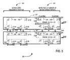
- FIG. 3a cross-sectional view of a stacked package 300 having a first device-card 303 A and a second device-card 303 B is shown with the device-cards being stacked and interconnected.
- the first device-card 303 Aincludes a card assignment portion 310 and a detection of the number of cards portion 330 .
- the card assignment portion 310includes the assignment device 201 A and the detection of the number of cards portion 330 includes the evaluation device 203 A.
- Other elements shownmay be similar or the same as those discussed above with reference to FIG. 2A .
- the second device-card 303 Bincludes the card assignment portion 310 having the assignment device 201 B and the detection of the number of cards portion 330 having the evaluation device 203 B.
- Each of the device cards 303 A, 303 Bmay include a number of other devices (not shown so as to prevent details of the disclosed subject matter from being obscured).
- the first device-card 303 A and the second device-card 303 Bmay include various additional components formed (e.g., fabricated, placed, etc.) on or within the device cards.
- the various additional componentsmay comprise, for example, individual integrated circuit devices and/or a number of different discrete devices (e.g., resistors, capacitors, inductors, transistors, other transconductance devices, antennas, switches, TSVs, or combinations thereof).
- the first device-card 303 A and the second device-card 303 Bmay each include different additional components.
- the two device cardsmay each have additional different functions or capabilities from one another.
- the first device-card 303 Amay include controller or microprocessor circuitry and the second device-card 303 B may include wireless transceiver circuitry.
- the first device-card 303 A and the second device-card 303 Bmay be interconnected by a variety of pin or jack connectors 305 known independently in the art.
- the first device-card 303 A and the second device-card 303 Bmay be replaced by an end-user. Additionally, the end-user may add additional device cards (not shown). Should replacement or addition of any device cards be desired, the end-user may do so by plugging in new or replacement cards to the stack.
- the total number of cards that can be stackeddepends, at least partially, on the number of inputs and outputs on the assignment and evaluation devices contained on the device cards.
- the assignment and evaluation devicesmay include any number of one or more bits.
- the stacked package 300 of FIG. 3four device cards may be stacked. Thus, two additional device cards (not shown) may be added to the stacked package 300 .
- the first time the stacked package 300 is operatedan initialization procedure similar to the procedure discussed with reference to FIG. 2A can be performed.
- the initialization proceduremay be performed automatically upon startup, or may be initiated by the end-user utilizing, for example, a software switch or a hardware reset switch 307 .
- the initialization procedurecan be again run, either automatically or manually, to assign a unique device ID value to each device card and to determine a total number of device cards in the stacked package.
- the procedures to assign a unique device ID valuecan operate similarly, whether the device comprises a die formed of an elemental or compound semiconductor substrate, with integrated devices formed on one or both sides of the substrate, or whether the device is a plug-in type of device card, with integrated circuit devices and discrete components mounted either thereon or therein. Further, the orientation of surfaces of the device is unimportant. That is, as long as appropriate electrical routing is provided to the assignment devices and the evaluation devices, the devices may be stacked in first side-to-second side, second side-to-second side, or first side-to-first side configurations.
- the memory devicemay be comprised of stacked integrated circuit dice, as discussed above.
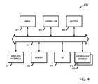
- the system 400may be used in devices such as, for example, a personal digital assistant (PDA), a laptop or portable computer with or without wireless capability, a web tablet, a wireless telephone, a pager, an instant messaging device, a digital music player, a digital camera, or other devices that may be adapted to transmit or receive information either wirelessly or over a wired connection.
- PDApersonal digital assistant
- the system 400may be used in any of the following systems: a wireless local area network (WLAN) system, a wireless personal area network (WPAN) system, or a cellular network.
- WLANwireless local area network
- WPANwireless personal area network
- cellular networkcellular network
- the system 400 of FIG. 4is shown to include a controller 403 , an input/output (I/O) device 411 (e.g., a keypad, a touchscreen, or a display), a memory device 409 , a wireless interface 407 , a static random access memory (SRAM) device 401 , a first addressable device 413 , and a second addressable device 415 , coupled to each other via a bus 417 .
- a battery 405may supply power to the system 400 in one embodiment.
- the memory device 409may include a NAND memory, a flash memory, a NOR memory, a combination of these, or the like.
- the memory device 409may include one or more of the novel memory devices described herein.
- the controller 403may include, for example, one or more microprocessors, digital signal processors, micro-controllers, or the like.
- the memory device 409may be used to store information transmitted to or by the system 400 .
- the memory device 409may optionally also be used to store information in the form of instructions that are executed by the controller 403 during operation of the system 400 and may be used to store information in the form of user data either generated, collected, or received by the system 400 (such as image data).
- the instructionsmay be stored as digital information and the user data, as disclosed herein, may be stored in one section of the memory as digital information and in another section as analog information. As another example, a given section at one time may be labeled to store digital information and then later may be reallocated and reconfigured to store analog information.
- the controller 403may include one or more of the novel memory devices described herein.
- the I/O device 411may be used to generate information.
- the system 400may use the wireless interface 407 to transmit and receive information to and from a wireless communication network with a radio frequency (RF) signal.
- Examples of the wireless interface 407may include an antenna, or a wireless transceiver, such as a dipole antenna.
- the I/O device 411may deliver a signal reflecting what is stored as either a digital output (if digital information was stored), or as an analog output (if analog information was stored). While an example in a wireless application is provided above, embodiments of the inventive subject matter disclosed herein may also be used in non-wireless applications as well.
- the I/O device 411may include one or more of the novel stacked devices described herein.
- each of the first addressable device 413 and the second addressable device 415can be an addressable die or other device having a unique device ID, such as the first device-card 303 A and the second device-card 303 B of FIG. 3 .
- an apparatushas multiple dice in a stacked device. At least one of the multiple dice includes an assignment device to operate on an input and generate, as an output, a device identification (ID) value. The at least one of the multiple dice also includes an evaluation device to detect a total number of the dice in the stack.
- IDdevice identification
- an apparatushas multiple devices in a stacked device. At least one of the multiple devices includes an assignment device to operate on an input and generate, as an output, a device identification (ID) value. The at least one of the multiple devices also includes an evaluation device to detect a total number of the devices in the stack.
- IDdevice identification
- an apparatushaving a number of dice in a stacked device. At least one of the number of dice includes an assignment device to operate on an input and generate, as an output, a device ID value for a subsequent die in the stacked device.
- a pull-down deviceis coupled to an input of the assignment device to provide an initialization value as an input to the assignment device.
- the apparatusis to perform an evaluation routine to determine the total number of the dice in the stacked device.
- an apparatuscomprising multiple devices in a stack of devices.
- a first one of the devicesincludes an assignment device to operate on an input and to generate, as an output, a device identification (ID) value.
- An evaluation deviceis to detect a total number of devices in the stack, and a switching device is coupled to an input of the assignment device to provide an initialization value as an input to the assignment device.
- an apparatuscomprising a stack of dice.
- a first die in the stackincludes an assignment device to operate on an input and to generate, as an output, a device identification (ID) value for a subsequent die in the stack.
- An evaluation deviceis to detect a total number of the dice in the stack, and a switching device is to provide an initialization value as a device ID value to be assigned to the first die, the initialization value to serve as an input value to the assignment device.
- the evaluation deviceis to evaluate a conditional routine based on an input to the evaluation device, and, based on the input, generate an output upon evaluation of one or more criterion in the conditional routine.
Landscapes
- Engineering & Computer Science (AREA)
- Microelectronics & Electronic Packaging (AREA)
- Physics & Mathematics (AREA)
- Condensed Matter Physics & Semiconductors (AREA)
- General Physics & Mathematics (AREA)
- Computer Hardware Design (AREA)
- Power Engineering (AREA)
- Semiconductor Integrated Circuits (AREA)
Abstract
Description
Claims (31)
Priority Applications (3)
| Application Number | Priority Date | Filing Date | Title |
|---|---|---|---|
| US13/559,235US9478502B2 (en) | 2012-07-26 | 2012-07-26 | Device identification assignment and total device number detection |
| TW102126523ATWI560849B (en) | 2012-07-26 | 2013-07-24 | Device identification assignment and total device number detection |
| PCT/US2013/052091WO2014018772A1 (en) | 2012-07-26 | 2013-07-25 | Device identification assignment and total device number detection |
Applications Claiming Priority (1)
| Application Number | Priority Date | Filing Date | Title |
|---|---|---|---|
| US13/559,235US9478502B2 (en) | 2012-07-26 | 2012-07-26 | Device identification assignment and total device number detection |
Publications (2)
| Publication Number | Publication Date |
|---|---|
| US20140027771A1 US20140027771A1 (en) | 2014-01-30 |
| US9478502B2true US9478502B2 (en) | 2016-10-25 |
Family
ID=49994026
Family Applications (1)
| Application Number | Title | Priority Date | Filing Date |
|---|---|---|---|
| US13/559,235Active2033-07-30US9478502B2 (en) | 2012-07-26 | 2012-07-26 | Device identification assignment and total device number detection |
Country Status (3)
| Country | Link |
|---|---|
| US (1) | US9478502B2 (en) |
| TW (1) | TWI560849B (en) |
| WO (1) | WO2014018772A1 (en) |
Cited By (3)
| Publication number | Priority date | Publication date | Assignee | Title |
|---|---|---|---|---|
| US10382042B2 (en)* | 2017-11-29 | 2019-08-13 | Imec Vzw | Assembly of integrated circuit modules and method for identifying the modules |
| US10908211B2 (en) | 2019-03-07 | 2021-02-02 | Winbond Electronics Corp. | Integrated circuit and detection method for multi-chip status thereof |
| US20220101888A1 (en)* | 2020-09-25 | 2022-03-31 | SK Hynix Inc. | Semiconductor memory device, processing system including the same and power control circuit for the same |
Families Citing this family (11)
| Publication number | Priority date | Publication date | Assignee | Title |
|---|---|---|---|---|
| US9478502B2 (en) | 2012-07-26 | 2016-10-25 | Micron Technology, Inc. | Device identification assignment and total device number detection |
| KR20150043045A (en)* | 2013-10-14 | 2015-04-22 | 에스케이하이닉스 주식회사 | Semiconductor device |
| US9693166B2 (en)* | 2014-06-24 | 2017-06-27 | The Boeing Company | Automated production of acoustic structures |
| CN106325563B (en)* | 2015-06-15 | 2021-06-04 | 联想企业解决方案(新加坡)有限公司 | Data storage device for identifying electronic devices and corresponding method |
| JP2017044829A (en)* | 2015-08-26 | 2017-03-02 | 三菱電機株式会社 | Liquid crystal display device |
| US11222884B2 (en)* | 2018-11-28 | 2022-01-11 | Taiwan Semiconductor Manufacturing Co., Ltd. | Layout design methodology for stacked devices |
| CN111458621B (en)* | 2019-01-21 | 2022-03-01 | 华邦电子股份有限公司 | Integrated circuit and detection method of multi-chip state |
| US11024385B2 (en)* | 2019-05-17 | 2021-06-01 | Sandisk Technologies Llc | Parallel memory operations in multi-bonded memory device |
| DE112019007422T5 (en)* | 2019-05-31 | 2022-02-24 | Micron Technology, Inc. | MEMORY COMPONENT FOR A SYSTEM-ON-CHIP DEVICE |
| CN114446335A (en)* | 2020-11-04 | 2022-05-06 | 中国科学院微电子研究所 | Stacked memory and method of resetting memory die of the stacked memory |
| US20250210538A1 (en)* | 2023-12-22 | 2025-06-26 | Advanced Micro Devices, Inc. | Apparatus, system, and method for uniquely identifying individual dies across die stacks |
Citations (81)
| Publication number | Priority date | Publication date | Assignee | Title |
|---|---|---|---|---|
| US5838891A (en)* | 1995-03-22 | 1998-11-17 | Mitsubishi Denki Kabushiki Kaisha | Data storage system and storage managing method |
| US6269411B1 (en)* | 1999-08-12 | 2001-07-31 | Hewlett-Packard Company | System for enabling stacking of autochanger modules |
| US6460093B1 (en)* | 1997-09-12 | 2002-10-01 | Hewlett-Packard Company | Automatic configuration of primary and secondary peripheral devices for a computer |
| US6535981B1 (en)* | 1997-08-04 | 2003-03-18 | Sega Enterprises. Ltd. | Information processing system |
| US20030135699A1 (en)* | 2000-12-20 | 2003-07-17 | Yasurou Matsuzaki | Multi-port memory based on DRAM core |
| US6643787B1 (en)* | 1999-10-19 | 2003-11-04 | Rambus Inc. | Bus system optimization |
| US6740981B2 (en)* | 2000-03-27 | 2004-05-25 | Kabushiki Kaisha, Toshiba | Semiconductor device including memory unit and semiconductor module including memory units |
| US20040232559A1 (en)* | 2003-05-19 | 2004-11-25 | Adelmann Todd C. | Interconnect method for directly connected stacked integrated circuits |
| US20050010725A1 (en)* | 2003-07-07 | 2005-01-13 | Eilert Sean E. | Method and apparatus for generating a device ID for stacked devices |
| US20050082664A1 (en)* | 2003-10-16 | 2005-04-21 | Elpida Memory, Inc. | Stacked semiconductor device and semiconductor chip control method |
| US20050102477A1 (en)* | 2003-11-10 | 2005-05-12 | Hitachi, Ltd. | Multiprocessor system |
| US20060206745A1 (en)* | 2005-03-11 | 2006-09-14 | Advanced Micro Devices, Inc. | Automatic resource assignment in devices having stacked modules |
| US7123497B2 (en)* | 2003-04-21 | 2006-10-17 | Elpida Memory, Inc. | Memory module and memory system |
| US20070014140A1 (en)* | 2005-07-15 | 2007-01-18 | Nicola Telecco | Nonvolatile semiconductor memory apparatus |
| US7221057B2 (en)* | 2002-05-31 | 2007-05-22 | Nokia Corporation | Stacked IC device having functions for selecting and counting IC chips |
| US20070126105A1 (en)* | 2005-12-06 | 2007-06-07 | Elpida Memory Inc. | Stacked type semiconductor memory device and chip selection circuit |
| US20070194447A1 (en)* | 2006-01-24 | 2007-08-23 | Hermann Ruckerbauer | Semiconductor component comprising an integrated semiconductor chip and a chip housing, and electronic device |
| US20080054488A1 (en)* | 2006-08-31 | 2008-03-06 | Michael Leddige | Systems and arrangements for interconnecting integrated circuit dies |
| US20080220565A1 (en)* | 2007-03-09 | 2008-09-11 | Chao-Shun Hsu | Design techniques for stacking identical memory dies |
| US20090039915A1 (en)* | 2007-08-06 | 2009-02-12 | Hermann Ruckerbauer | Integrated Circuit, Chip Stack and Data Processing System |
| US20090085608A1 (en)* | 2007-10-02 | 2009-04-02 | Micron Technology, Inc. | Systems, methods and devices for arbitrating die stack position in a multi-bit stack device |
| US20090096478A1 (en)* | 2007-10-16 | 2009-04-16 | Micron Technology, Inc. | Reconfigurable connections for stacked semiconductor devices |
| US20090154285A1 (en)* | 2007-12-14 | 2009-06-18 | Mosaid Technologies Incorporated | Memory controller with flexible data alignment to clock |
| US20090249014A1 (en)* | 2008-03-25 | 2009-10-01 | Spansion Llc | Secure management of memory regions in a memory |
| US20090289701A1 (en) | 2005-08-30 | 2009-11-26 | Micron Technology, Inc. | Self-Identifying Stacked Die Semiconductor Components |
| US20100059898A1 (en)* | 2008-09-11 | 2010-03-11 | Micron Technology, Inc. | Signal delivery in stacked device |
| US20100064114A1 (en)* | 2008-09-11 | 2010-03-11 | Micron Technology, Inc. | Stacked device identification assignment |
| US20100074038A1 (en)* | 2008-09-19 | 2010-03-25 | Hermann Ruckerbauer | Memory Dies for Flexible Use and Method for Configuring Memory Dies |
| US20100078829A1 (en)* | 2008-09-30 | 2010-04-01 | Micron Technology, Inc. | Stacked device conductive path connectivity |
| US20100131684A1 (en)* | 2008-11-26 | 2010-05-27 | Micron Technology, Inc. | Sharing resources in multi-dice stacks |
| US20110050303A1 (en)* | 2009-08-27 | 2011-03-03 | Micron Technology, Inc. | Die location compensation |
| US20110060942A1 (en)* | 2001-03-05 | 2011-03-10 | Martin Vorbach | Methods and devices for treating and/or processing data |
| US7917818B2 (en)* | 2007-04-23 | 2011-03-29 | Renesas Electronics Corporation | Semiconductor device controlling debug operation of processing unit in response to permission or prohibition from other processing unit |
| US20110079923A1 (en)* | 2009-10-07 | 2011-04-07 | Qualcomm Incorporated | Vertically Stackable Dies Having Chip Identifier Structures |
| US20110079924A1 (en)* | 2009-10-07 | 2011-04-07 | Qualcomm Incorporated | Vertically Stackable Dies Having Chip Identifier Structures |
| US7925949B2 (en)* | 2008-10-15 | 2011-04-12 | Micron Technology, Inc. | Embedded processor |
| US20110090004A1 (en)* | 2009-10-19 | 2011-04-21 | Mosaid Technologies Incorporated | Reconfiguring through silicon vias in stacked multi-die packages |
| US20110102065A1 (en)* | 2009-10-29 | 2011-05-05 | Hynix Semiconductor Inc. | Semiconductor apparatus and chip selection method thereof |
| US20110134705A1 (en)* | 2009-12-07 | 2011-06-09 | Stmicroelectronics (R&D) Ltd | Integrated circuit package with multiple dies and a multiplexed communications interface |
| US20110141828A1 (en)* | 2009-12-11 | 2011-06-16 | Elpida Memory, Inc. | Semiconductor system |
| US7964946B2 (en)* | 2007-05-17 | 2011-06-21 | Micron Technology, Inc. | Semiconductor package having discrete components and system containing the package |
| US20110148469A1 (en)* | 2009-12-18 | 2011-06-23 | Yutaka Ito | Stacked device detection and identification |
| US20110157951A1 (en)* | 2009-12-30 | 2011-06-30 | Marconix International Co., Ltd. | 3d chip selection for shared input packages |
| US20110194326A1 (en)* | 2010-02-11 | 2011-08-11 | Takuya Nakanishi | Memory dies, stacked memories, memory devices and methods |
| US20110195529A1 (en) | 2010-02-08 | 2011-08-11 | Charles Hung-Hsiang Wu | Rule-Based Semiconductor Die Stacking And Bonding Within A Multi-Die Package |
| US20110228783A1 (en)* | 2010-03-19 | 2011-09-22 | International Business Machines Corporation | Implementing ordered and reliable transfer of packets while spraying packets over multiple links |
| US8032804B2 (en)* | 2009-01-12 | 2011-10-04 | Micron Technology, Inc. | Systems and methods for monitoring a memory system |
| US20110246746A1 (en)* | 2010-03-30 | 2011-10-06 | Brent Keeth | Apparatuses enabling concurrent communication between an interface die and a plurality of dice stacks, interleaved conductive paths in stacked devices, and methods for forming and operating the same |
| US20110260331A1 (en)* | 2010-04-26 | 2011-10-27 | Samsung Electronics Co., Ltd. | Stacked semiconductor device |
| US20110272788A1 (en)* | 2010-05-10 | 2011-11-10 | International Business Machines Corporation | Computer system wafer integrating different dies in stacked master-slave structures |
| US20110302058A1 (en)* | 2010-06-07 | 2011-12-08 | Masaki Hashiura | Content playback apparatus, content playback method, program, and recording medium |
| US20120025391A1 (en)* | 2010-07-29 | 2012-02-02 | Sony Corporation | Semiconductor device and multilayer semiconductor device |
| US20120069685A1 (en)* | 2010-09-17 | 2012-03-22 | Hitachi Ulsi Systems Co., Ltd. | Semiconductor device having optical fuse and electrical fuse |
| US20120092943A1 (en)* | 2010-10-13 | 2012-04-19 | Elpida Memory, Inc. | Semiconductor device and test method thereof |
| US20120119357A1 (en)* | 2010-11-17 | 2012-05-17 | Hynix Semiconductor Inc. | Semiconductor apparatus |
| US20120126848A1 (en)* | 2010-11-19 | 2012-05-24 | Industrial Technology Research Institute | Multi-chip stacked system and chip select apparatus thereof |
| US20120146707A1 (en)* | 2010-12-08 | 2012-06-14 | Elpida Memory, Inc. | Semiconductor device and method of manufacturing the same |
| US20120182042A1 (en)* | 2011-01-14 | 2012-07-19 | Hynix Semiconductor Inc. | Semiconductor apparatus, method for assigning chip ids therein, and method for setting chip ids thereof |
| US20120196402A1 (en)* | 2010-08-23 | 2012-08-02 | International Business Machines Corporation | Implementing multiple different types of dies for memory stacking |
| US20120195148A1 (en)* | 2011-01-28 | 2012-08-02 | Elpida Memory, Inc. | Semiconductor device and information processing system including the same |
| US20120254472A1 (en)* | 2010-03-15 | 2012-10-04 | Ware Frederick A | Chip selection in a symmetric interconnection topology |
| US20130009694A1 (en)* | 2011-07-05 | 2013-01-10 | Xilinx, Inc. | Method and apparatus for self-annealing multi-die interconnect redundancy control |
| US20130021866A1 (en)* | 2011-07-20 | 2013-01-24 | Samsung Electronics Co., Ltd. | Semiconductor Devices Compatible with Mono-Rank and Multi-Ranks |
| US20130094301A1 (en)* | 2011-10-18 | 2013-04-18 | Oh Seung Min | Interfaces and die packages, and appartuses including the same |
| US20130094271A1 (en)* | 2011-08-22 | 2013-04-18 | Mosaid Technologies Incorporated | Connection of multiple semiconductor memory devices with chip enable function |
| US20130119542A1 (en)* | 2011-11-14 | 2013-05-16 | Mosaid Technologies Incorporated | Package having stacked memory dies with serially connected buffer dies |
| US20130155794A1 (en)* | 2011-12-20 | 2013-06-20 | Industrial Technology Research Institute | Repairable multi-layer memory chip stack and method thereof |
| US20130230932A1 (en)* | 2012-03-02 | 2013-09-05 | Venkatraghavan Bringivijayaraghavan | Through-substrate via (tsv) testing |
| US8559258B1 (en)* | 2011-12-13 | 2013-10-15 | Michael C. Stephens, Jr. | Self-refresh adjustment in memory devices configured for stacked arrangements |
| US20130279253A1 (en)* | 2012-04-18 | 2013-10-24 | Akira Ogawa | Semiconductor memory device and writing method of id codes and upper addresses |
| US20130326294A1 (en)* | 2012-05-30 | 2013-12-05 | Industrial Technology Research Institute | 3-D Memory and Built-In Self-Test Circuit Thereof |
| US20130340068A1 (en)* | 2012-06-13 | 2013-12-19 | Samsung Electronics Co., Ltd. | Memory device comprising a plurality of memory chips, authentication system and authentication method thereof |
| US20130336039A1 (en)* | 2012-06-05 | 2013-12-19 | Rambus Inc. | Memory bandwidth aggregation using simultaneous access of stacked semiconductor memory die |
| US8618541B2 (en)* | 2011-10-18 | 2013-12-31 | SK Hynix Inc. | Semiconductor apparatus |
| WO2014018772A1 (en) | 2012-07-26 | 2014-01-30 | Micron Technology, Inc. | Device identification assignment and total device number detection |
| US20140160867A1 (en)* | 2012-12-10 | 2014-06-12 | Micron Technology, Inc. | Apparatuses and methods for unit identification in a master/slave memory stack |
| US20140192583A1 (en)* | 2005-06-24 | 2014-07-10 | Suresh Natarajan Rajan | Configurable memory circuit system and method |
| US8778734B2 (en)* | 2012-03-28 | 2014-07-15 | Advanced Micro Devices, Inc. | Tree based adaptive die enumeration |
| US20140205056A1 (en)* | 2013-01-23 | 2014-07-24 | Micron Technology, Inc. | Identifying stacked dice |
| US20150009743A1 (en)* | 2010-11-03 | 2015-01-08 | Shine C. Chung | Low-Pin-Count Non-Volatile Memory Interface for 3D IC |
| US20150234707A1 (en)* | 2012-06-21 | 2015-08-20 | Rambus Inc. | Error Correction In A Memory Device |
- 2012
- 2012-07-26USUS13/559,235patent/US9478502B2/enactiveActive
- 2013
- 2013-07-24TWTW102126523Apatent/TWI560849B/enactive
- 2013-07-25WOPCT/US2013/052091patent/WO2014018772A1/enactiveApplication Filing
Patent Citations (92)
| Publication number | Priority date | Publication date | Assignee | Title |
|---|---|---|---|---|
| US5838891A (en)* | 1995-03-22 | 1998-11-17 | Mitsubishi Denki Kabushiki Kaisha | Data storage system and storage managing method |
| US6535981B1 (en)* | 1997-08-04 | 2003-03-18 | Sega Enterprises. Ltd. | Information processing system |
| US6460093B1 (en)* | 1997-09-12 | 2002-10-01 | Hewlett-Packard Company | Automatic configuration of primary and secondary peripheral devices for a computer |
| US6269411B1 (en)* | 1999-08-12 | 2001-07-31 | Hewlett-Packard Company | System for enabling stacking of autochanger modules |
| US6643787B1 (en)* | 1999-10-19 | 2003-11-04 | Rambus Inc. | Bus system optimization |
| US6740981B2 (en)* | 2000-03-27 | 2004-05-25 | Kabushiki Kaisha, Toshiba | Semiconductor device including memory unit and semiconductor module including memory units |
| US20030135699A1 (en)* | 2000-12-20 | 2003-07-17 | Yasurou Matsuzaki | Multi-port memory based on DRAM core |
| US20110060942A1 (en)* | 2001-03-05 | 2011-03-10 | Martin Vorbach | Methods and devices for treating and/or processing data |
| US7221057B2 (en)* | 2002-05-31 | 2007-05-22 | Nokia Corporation | Stacked IC device having functions for selecting and counting IC chips |
| US7123497B2 (en)* | 2003-04-21 | 2006-10-17 | Elpida Memory, Inc. | Memory module and memory system |
| US20040232559A1 (en)* | 2003-05-19 | 2004-11-25 | Adelmann Todd C. | Interconnect method for directly connected stacked integrated circuits |
| US20050010725A1 (en)* | 2003-07-07 | 2005-01-13 | Eilert Sean E. | Method and apparatus for generating a device ID for stacked devices |
| US20050082664A1 (en)* | 2003-10-16 | 2005-04-21 | Elpida Memory, Inc. | Stacked semiconductor device and semiconductor chip control method |
| US20050102477A1 (en)* | 2003-11-10 | 2005-05-12 | Hitachi, Ltd. | Multiprocessor system |
| US20060206745A1 (en)* | 2005-03-11 | 2006-09-14 | Advanced Micro Devices, Inc. | Automatic resource assignment in devices having stacked modules |
| US20140192583A1 (en)* | 2005-06-24 | 2014-07-10 | Suresh Natarajan Rajan | Configurable memory circuit system and method |
| US20070014140A1 (en)* | 2005-07-15 | 2007-01-18 | Nicola Telecco | Nonvolatile semiconductor memory apparatus |
| US20090289701A1 (en) | 2005-08-30 | 2009-11-26 | Micron Technology, Inc. | Self-Identifying Stacked Die Semiconductor Components |
| US20070126105A1 (en)* | 2005-12-06 | 2007-06-07 | Elpida Memory Inc. | Stacked type semiconductor memory device and chip selection circuit |
| US20070194447A1 (en)* | 2006-01-24 | 2007-08-23 | Hermann Ruckerbauer | Semiconductor component comprising an integrated semiconductor chip and a chip housing, and electronic device |
| US20080054488A1 (en)* | 2006-08-31 | 2008-03-06 | Michael Leddige | Systems and arrangements for interconnecting integrated circuit dies |
| US7494846B2 (en)* | 2007-03-09 | 2009-02-24 | Taiwan Semiconductor Manufacturing Company, Ltd. | Design techniques for stacking identical memory dies |
| US20080220565A1 (en)* | 2007-03-09 | 2008-09-11 | Chao-Shun Hsu | Design techniques for stacking identical memory dies |
| US7917818B2 (en)* | 2007-04-23 | 2011-03-29 | Renesas Electronics Corporation | Semiconductor device controlling debug operation of processing unit in response to permission or prohibition from other processing unit |
| US7964946B2 (en)* | 2007-05-17 | 2011-06-21 | Micron Technology, Inc. | Semiconductor package having discrete components and system containing the package |
| US20090039915A1 (en)* | 2007-08-06 | 2009-02-12 | Hermann Ruckerbauer | Integrated Circuit, Chip Stack and Data Processing System |
| US20090085608A1 (en)* | 2007-10-02 | 2009-04-02 | Micron Technology, Inc. | Systems, methods and devices for arbitrating die stack position in a multi-bit stack device |
| US7760533B2 (en) | 2007-10-02 | 2010-07-20 | Micron Technology, Inc. | Systems, methods and devices for arbitrating die stack position in a multi-bit stack device |
| US20090096478A1 (en)* | 2007-10-16 | 2009-04-16 | Micron Technology, Inc. | Reconfigurable connections for stacked semiconductor devices |
| US7816934B2 (en)* | 2007-10-16 | 2010-10-19 | Micron Technology, Inc. | Reconfigurable connections for stacked semiconductor devices |
| US20090154285A1 (en)* | 2007-12-14 | 2009-06-18 | Mosaid Technologies Incorporated | Memory controller with flexible data alignment to clock |
| US20090249014A1 (en)* | 2008-03-25 | 2009-10-01 | Spansion Llc | Secure management of memory regions in a memory |
| US20100059898A1 (en)* | 2008-09-11 | 2010-03-11 | Micron Technology, Inc. | Signal delivery in stacked device |
| US8861242B2 (en)* | 2008-09-11 | 2014-10-14 | Micron Technology, Inc. | Stacked device identification assignment |
| US20120161814A1 (en)* | 2008-09-11 | 2012-06-28 | Brent Keeth | Stacked device identification assignment |
| US8130527B2 (en)* | 2008-09-11 | 2012-03-06 | Micron Technology, Inc. | Stacked device identification assignment |
| US20100064114A1 (en)* | 2008-09-11 | 2010-03-11 | Micron Technology, Inc. | Stacked device identification assignment |
| US20100074038A1 (en)* | 2008-09-19 | 2010-03-25 | Hermann Ruckerbauer | Memory Dies for Flexible Use and Method for Configuring Memory Dies |
| US8578591B2 (en)* | 2008-09-30 | 2013-11-12 | Micron Technology, Inc. | Method for manufacturing a stacked device conductive path connectivity |
| US20100078829A1 (en)* | 2008-09-30 | 2010-04-01 | Micron Technology, Inc. | Stacked device conductive path connectivity |
| US7925949B2 (en)* | 2008-10-15 | 2011-04-12 | Micron Technology, Inc. | Embedded processor |
| US20100131684A1 (en)* | 2008-11-26 | 2010-05-27 | Micron Technology, Inc. | Sharing resources in multi-dice stacks |
| US8032804B2 (en)* | 2009-01-12 | 2011-10-04 | Micron Technology, Inc. | Systems and methods for monitoring a memory system |
| US20110050303A1 (en)* | 2009-08-27 | 2011-03-03 | Micron Technology, Inc. | Die location compensation |
| US20110079924A1 (en)* | 2009-10-07 | 2011-04-07 | Qualcomm Incorporated | Vertically Stackable Dies Having Chip Identifier Structures |
| US20110079923A1 (en)* | 2009-10-07 | 2011-04-07 | Qualcomm Incorporated | Vertically Stackable Dies Having Chip Identifier Structures |
| US20110090004A1 (en)* | 2009-10-19 | 2011-04-21 | Mosaid Technologies Incorporated | Reconfiguring through silicon vias in stacked multi-die packages |
| US20140097891A1 (en)* | 2009-10-19 | 2014-04-10 | Mosaid Technologies Incorporated | Reconfiguring through silicon vias in stacked multi-die packages |
| US20110102065A1 (en)* | 2009-10-29 | 2011-05-05 | Hynix Semiconductor Inc. | Semiconductor apparatus and chip selection method thereof |
| US20110134705A1 (en)* | 2009-12-07 | 2011-06-09 | Stmicroelectronics (R&D) Ltd | Integrated circuit package with multiple dies and a multiplexed communications interface |
| US20110141828A1 (en)* | 2009-12-11 | 2011-06-16 | Elpida Memory, Inc. | Semiconductor system |
| US20110148469A1 (en)* | 2009-12-18 | 2011-06-23 | Yutaka Ito | Stacked device detection and identification |
| US20110157951A1 (en)* | 2009-12-30 | 2011-06-30 | Marconix International Co., Ltd. | 3d chip selection for shared input packages |
| US20110195529A1 (en) | 2010-02-08 | 2011-08-11 | Charles Hung-Hsiang Wu | Rule-Based Semiconductor Die Stacking And Bonding Within A Multi-Die Package |
| US8399298B2 (en)* | 2010-02-08 | 2013-03-19 | Sandisk Technologies Inc. | Rule-based semiconductor die stacking and bonding within a multi-die package |
| US20110194326A1 (en)* | 2010-02-11 | 2011-08-11 | Takuya Nakanishi | Memory dies, stacked memories, memory devices and methods |
| US20120254472A1 (en)* | 2010-03-15 | 2012-10-04 | Ware Frederick A | Chip selection in a symmetric interconnection topology |
| US20110228783A1 (en)* | 2010-03-19 | 2011-09-22 | International Business Machines Corporation | Implementing ordered and reliable transfer of packets while spraying packets over multiple links |
| US20110246746A1 (en)* | 2010-03-30 | 2011-10-06 | Brent Keeth | Apparatuses enabling concurrent communication between an interface die and a plurality of dice stacks, interleaved conductive paths in stacked devices, and methods for forming and operating the same |
| US20110260331A1 (en)* | 2010-04-26 | 2011-10-27 | Samsung Electronics Co., Ltd. | Stacked semiconductor device |
| US20110272788A1 (en)* | 2010-05-10 | 2011-11-10 | International Business Machines Corporation | Computer system wafer integrating different dies in stacked master-slave structures |
| US20110302058A1 (en)* | 2010-06-07 | 2011-12-08 | Masaki Hashiura | Content playback apparatus, content playback method, program, and recording medium |
| US20120025391A1 (en)* | 2010-07-29 | 2012-02-02 | Sony Corporation | Semiconductor device and multilayer semiconductor device |
| US20120196402A1 (en)* | 2010-08-23 | 2012-08-02 | International Business Machines Corporation | Implementing multiple different types of dies for memory stacking |
| US20120069685A1 (en)* | 2010-09-17 | 2012-03-22 | Hitachi Ulsi Systems Co., Ltd. | Semiconductor device having optical fuse and electrical fuse |
| US20120092943A1 (en)* | 2010-10-13 | 2012-04-19 | Elpida Memory, Inc. | Semiconductor device and test method thereof |
| US20150009743A1 (en)* | 2010-11-03 | 2015-01-08 | Shine C. Chung | Low-Pin-Count Non-Volatile Memory Interface for 3D IC |
| US20120119357A1 (en)* | 2010-11-17 | 2012-05-17 | Hynix Semiconductor Inc. | Semiconductor apparatus |
| US20120126848A1 (en)* | 2010-11-19 | 2012-05-24 | Industrial Technology Research Institute | Multi-chip stacked system and chip select apparatus thereof |
| US20120146707A1 (en)* | 2010-12-08 | 2012-06-14 | Elpida Memory, Inc. | Semiconductor device and method of manufacturing the same |
| US20120182042A1 (en)* | 2011-01-14 | 2012-07-19 | Hynix Semiconductor Inc. | Semiconductor apparatus, method for assigning chip ids therein, and method for setting chip ids thereof |
| US20120195148A1 (en)* | 2011-01-28 | 2012-08-02 | Elpida Memory, Inc. | Semiconductor device and information processing system including the same |
| US20130009694A1 (en)* | 2011-07-05 | 2013-01-10 | Xilinx, Inc. | Method and apparatus for self-annealing multi-die interconnect redundancy control |
| US8539420B2 (en)* | 2011-07-05 | 2013-09-17 | Xilinx, Inc. | Method and apparatus for self-annealing multi-die interconnect redundancy control |
| US20130021866A1 (en)* | 2011-07-20 | 2013-01-24 | Samsung Electronics Co., Ltd. | Semiconductor Devices Compatible with Mono-Rank and Multi-Ranks |
| US20130094271A1 (en)* | 2011-08-22 | 2013-04-18 | Mosaid Technologies Incorporated | Connection of multiple semiconductor memory devices with chip enable function |
| US8618541B2 (en)* | 2011-10-18 | 2013-12-31 | SK Hynix Inc. | Semiconductor apparatus |
| US20130094301A1 (en)* | 2011-10-18 | 2013-04-18 | Oh Seung Min | Interfaces and die packages, and appartuses including the same |
| US20130119542A1 (en)* | 2011-11-14 | 2013-05-16 | Mosaid Technologies Incorporated | Package having stacked memory dies with serially connected buffer dies |
| US8559258B1 (en)* | 2011-12-13 | 2013-10-15 | Michael C. Stephens, Jr. | Self-refresh adjustment in memory devices configured for stacked arrangements |
| US20130155794A1 (en)* | 2011-12-20 | 2013-06-20 | Industrial Technology Research Institute | Repairable multi-layer memory chip stack and method thereof |
| US20130230932A1 (en)* | 2012-03-02 | 2013-09-05 | Venkatraghavan Bringivijayaraghavan | Through-substrate via (tsv) testing |
| US8778734B2 (en)* | 2012-03-28 | 2014-07-15 | Advanced Micro Devices, Inc. | Tree based adaptive die enumeration |
| US20130279253A1 (en)* | 2012-04-18 | 2013-10-24 | Akira Ogawa | Semiconductor memory device and writing method of id codes and upper addresses |
| US20130326294A1 (en)* | 2012-05-30 | 2013-12-05 | Industrial Technology Research Institute | 3-D Memory and Built-In Self-Test Circuit Thereof |
| US20130336039A1 (en)* | 2012-06-05 | 2013-12-19 | Rambus Inc. | Memory bandwidth aggregation using simultaneous access of stacked semiconductor memory die |
| US20130340068A1 (en)* | 2012-06-13 | 2013-12-19 | Samsung Electronics Co., Ltd. | Memory device comprising a plurality of memory chips, authentication system and authentication method thereof |
| US20150234707A1 (en)* | 2012-06-21 | 2015-08-20 | Rambus Inc. | Error Correction In A Memory Device |
| TW201411812A (en) | 2012-07-26 | 2014-03-16 | Micron Technology Inc | Device identification assignment and total device number detection |
| WO2014018772A1 (en) | 2012-07-26 | 2014-01-30 | Micron Technology, Inc. | Device identification assignment and total device number detection |
| US20140160867A1 (en)* | 2012-12-10 | 2014-06-12 | Micron Technology, Inc. | Apparatuses and methods for unit identification in a master/slave memory stack |
| US20140205056A1 (en)* | 2013-01-23 | 2014-07-24 | Micron Technology, Inc. | Identifying stacked dice |
Non-Patent Citations (3)
Cited By (5)
| Publication number | Priority date | Publication date | Assignee | Title |
|---|---|---|---|---|
| US10382042B2 (en)* | 2017-11-29 | 2019-08-13 | Imec Vzw | Assembly of integrated circuit modules and method for identifying the modules |
| US10908211B2 (en) | 2019-03-07 | 2021-02-02 | Winbond Electronics Corp. | Integrated circuit and detection method for multi-chip status thereof |
| US20220101888A1 (en)* | 2020-09-25 | 2022-03-31 | SK Hynix Inc. | Semiconductor memory device, processing system including the same and power control circuit for the same |
| US11600308B2 (en)* | 2020-09-25 | 2023-03-07 | SK Hynix Inc. | Semiconductor memory device, processing system including the same and power control circuit for the same |
| US12288596B2 (en) | 2020-09-25 | 2025-04-29 | SK Hynix Inc. | Semiconductor memory device, processing system including the same and power control circuit for the same |
Also Published As
| Publication number | Publication date |
|---|---|
| US20140027771A1 (en) | 2014-01-30 |
| WO2014018772A1 (en) | 2014-01-30 |
| TW201411812A (en) | 2014-03-16 |
| TWI560849B (en) | 2016-12-01 |
Similar Documents
| Publication | Publication Date | Title |
|---|---|---|
| US9478502B2 (en) | Device identification assignment and total device number detection | |
| US11693801B2 (en) | Stacked semiconductor device assembly in computer system | |
| US9558844B2 (en) | Identifying stacked dice | |
| TWI728002B (en) | Improving size and efficiency of dies | |
| US7834450B2 (en) | Semiconductor package having memory devices stacked on logic device | |
| US9793217B2 (en) | Package-on-package type semiconductor device which is realized through applying not a TSV technology but a fan-out wafer level package technology | |
| US20110309468A1 (en) | Semiconductor chip package and method of manufacturing the same | |
| US20140145757A1 (en) | Three dimensional integrated circuit connection structure and method | |
| US9391048B2 (en) | Semiconductor package | |
| US9275688B2 (en) | Semiconductor device and semiconductor package | |
| US10553567B2 (en) | Chip stack packages | |
| CN110416202A (en) | Package-on-package including through-mold via structure | |
| CN110416174A (en) | Stacked package including through-mold vias | |
| TW202044520A (en) | Stack packages including an interconnection structure | |
| KR102498883B1 (en) | Semiconductor device including through electrodes distributing current | |
| US20120049361A1 (en) | Semiconductor integrated circuit | |
| US20110309843A1 (en) | Discontinuous Type Layer-ID Detector For 3D-IC And Method of The Same | |
| US10002851B2 (en) | Semiconductor packages including chip enablement pads | |
| US10002850B2 (en) | Semiconductor chip flexibly applied to various routing structures and semiconductor chip module using the same |
Legal Events
| Date | Code | Title | Description |
|---|---|---|---|
| AS | Assignment | Owner name:MICRON TECHNOLOGY, INC., IDAHO Free format text:ASSIGNMENT OF ASSIGNORS INTEREST;ASSIGNOR:SATOH, YASUO;REEL/FRAME:030807/0687 Effective date:20120726 | |
| FEPP | Fee payment procedure | Free format text:PAYOR NUMBER ASSIGNED (ORIGINAL EVENT CODE: ASPN); ENTITY STATUS OF PATENT OWNER: LARGE ENTITY | |
| AS | Assignment | Owner name:U.S. BANK NATIONAL ASSOCIATION, AS COLLATERAL AGENT, CALIFORNIA Free format text:SECURITY INTEREST;ASSIGNOR:MICRON TECHNOLOGY, INC.;REEL/FRAME:038669/0001 Effective date:20160426 Owner name:U.S. BANK NATIONAL ASSOCIATION, AS COLLATERAL AGEN Free format text:SECURITY INTEREST;ASSIGNOR:MICRON TECHNOLOGY, INC.;REEL/FRAME:038669/0001 Effective date:20160426 | |
| AS | Assignment | Owner name:MORGAN STANLEY SENIOR FUNDING, INC., AS COLLATERAL AGENT, MARYLAND Free format text:PATENT SECURITY AGREEMENT;ASSIGNOR:MICRON TECHNOLOGY, INC.;REEL/FRAME:038954/0001 Effective date:20160426 Owner name:MORGAN STANLEY SENIOR FUNDING, INC., AS COLLATERAL Free format text:PATENT SECURITY AGREEMENT;ASSIGNOR:MICRON TECHNOLOGY, INC.;REEL/FRAME:038954/0001 Effective date:20160426 | |
| STCF | Information on status: patent grant | Free format text:PATENTED CASE | |
| AS | Assignment | Owner name:U.S. BANK NATIONAL ASSOCIATION, AS COLLATERAL AGENT, CALIFORNIA Free format text:CORRECTIVE ASSIGNMENT TO CORRECT THE REPLACE ERRONEOUSLY FILED PATENT #7358718 WITH THE CORRECT PATENT #7358178 PREVIOUSLY RECORDED ON REEL 038669 FRAME 0001. ASSIGNOR(S) HEREBY CONFIRMS THE SECURITY INTEREST;ASSIGNOR:MICRON TECHNOLOGY, INC.;REEL/FRAME:043079/0001 Effective date:20160426 Owner name:U.S. BANK NATIONAL ASSOCIATION, AS COLLATERAL AGEN Free format text:CORRECTIVE ASSIGNMENT TO CORRECT THE REPLACE ERRONEOUSLY FILED PATENT #7358718 WITH THE CORRECT PATENT #7358178 PREVIOUSLY RECORDED ON REEL 038669 FRAME 0001. ASSIGNOR(S) HEREBY CONFIRMS THE SECURITY INTEREST;ASSIGNOR:MICRON TECHNOLOGY, INC.;REEL/FRAME:043079/0001 Effective date:20160426 | |
| AS | Assignment | Owner name:JPMORGAN CHASE BANK, N.A., AS COLLATERAL AGENT, ILLINOIS Free format text:SECURITY INTEREST;ASSIGNORS:MICRON TECHNOLOGY, INC.;MICRON SEMICONDUCTOR PRODUCTS, INC.;REEL/FRAME:047540/0001 Effective date:20180703 Owner name:JPMORGAN CHASE BANK, N.A., AS COLLATERAL AGENT, IL Free format text:SECURITY INTEREST;ASSIGNORS:MICRON TECHNOLOGY, INC.;MICRON SEMICONDUCTOR PRODUCTS, INC.;REEL/FRAME:047540/0001 Effective date:20180703 | |
| AS | Assignment | Owner name:MICRON TECHNOLOGY, INC., IDAHO Free format text:RELEASE BY SECURED PARTY;ASSIGNOR:U.S. BANK NATIONAL ASSOCIATION, AS COLLATERAL AGENT;REEL/FRAME:047243/0001 Effective date:20180629 | |
| AS | Assignment | Owner name:MICRON TECHNOLOGY, INC., IDAHO Free format text:RELEASE BY SECURED PARTY;ASSIGNOR:MORGAN STANLEY SENIOR FUNDING, INC., AS COLLATERAL AGENT;REEL/FRAME:050937/0001 Effective date:20190731 | |
| AS | Assignment | Owner name:MICRON SEMICONDUCTOR PRODUCTS, INC., IDAHO Free format text:RELEASE BY SECURED PARTY;ASSIGNOR:JPMORGAN CHASE BANK, N.A., AS COLLATERAL AGENT;REEL/FRAME:051028/0001 Effective date:20190731 Owner name:MICRON TECHNOLOGY, INC., IDAHO Free format text:RELEASE BY SECURED PARTY;ASSIGNOR:JPMORGAN CHASE BANK, N.A., AS COLLATERAL AGENT;REEL/FRAME:051028/0001 Effective date:20190731 | |
| MAFP | Maintenance fee payment | Free format text:PAYMENT OF MAINTENANCE FEE, 4TH YEAR, LARGE ENTITY (ORIGINAL EVENT CODE: M1551); ENTITY STATUS OF PATENT OWNER: LARGE ENTITY Year of fee payment:4 | |
| MAFP | Maintenance fee payment | Free format text:PAYMENT OF MAINTENANCE FEE, 8TH YEAR, LARGE ENTITY (ORIGINAL EVENT CODE: M1552); ENTITY STATUS OF PATENT OWNER: LARGE ENTITY Year of fee payment:8 |