US9478495B1 - Three dimensional memory device containing aluminum source contact via structure and method of making thereof - Google Patents
Three dimensional memory device containing aluminum source contact via structure and method of making thereofDownload PDFInfo
- Publication number
- US9478495B1 US9478495B1US14/922,516US201514922516AUS9478495B1US 9478495 B1US9478495 B1US 9478495B1US 201514922516 AUS201514922516 AUS 201514922516AUS 9478495 B1US9478495 B1US 9478495B1
- Authority
- US
- United States
- Prior art keywords
- layer
- aluminum
- semiconductor
- dielectric
- electrically conductive
- Prior art date
- Legal status (The legal status is an assumption and is not a legal conclusion. Google has not performed a legal analysis and makes no representation as to the accuracy of the status listed.)
- Expired - Fee Related
Links
- XAGFODPZIPBFFR-UHFFFAOYSA-NaluminiumChemical compound[Al]XAGFODPZIPBFFR-UHFFFAOYSA-N0.000titleclaimsabstractdescription150
- 229910052782aluminiumInorganic materials0.000titleclaimsabstractdescription149
- 238000004519manufacturing processMethods0.000titleclaimsdescription5
- 239000000463materialSubstances0.000claimsabstractdescription310
- 239000004065semiconductorSubstances0.000claimsabstractdescription229
- 238000000034methodMethods0.000claimsabstractdescription87
- 239000000758substrateSubstances0.000claimsabstractdescription85
- 239000003989dielectric materialSubstances0.000claimsabstractdescription75
- 238000009792diffusion processMethods0.000claimsabstractdescription74
- 230000004888barrier functionEffects0.000claimsabstractdescription72
- 239000007769metal materialSubstances0.000claimsabstractdescription66
- 229910052751metalInorganic materials0.000claimsabstractdescription52
- 239000002184metalSubstances0.000claimsabstractdescription40
- 125000006850spacer groupChemical group0.000claimsabstractdescription35
- 238000002425crystallisationMethods0.000claimsabstractdescription15
- 230000008025crystallizationEffects0.000claimsabstractdescription15
- 230000015654memoryEffects0.000claimsdescription119
- XUIMIQQOPSSXEZ-UHFFFAOYSA-NSiliconChemical compound[Si]XUIMIQQOPSSXEZ-UHFFFAOYSA-N0.000claimsdescription42
- 229910052710siliconInorganic materials0.000claimsdescription41
- 239000010703siliconSubstances0.000claimsdescription38
- 230000005641tunnelingEffects0.000claimsdescription32
- VYPSYNLAJGMNEJ-UHFFFAOYSA-NSilicium dioxideChemical compoundO=[Si]=OVYPSYNLAJGMNEJ-UHFFFAOYSA-N0.000claimsdescription30
- 229910052814silicon oxideInorganic materials0.000claimsdescription28
- 229910021420polycrystalline siliconInorganic materials0.000claimsdescription25
- 229920005591polysiliconPolymers0.000claimsdescription25
- 238000000151depositionMethods0.000claimsdescription22
- 229910052581Si3N4Inorganic materials0.000claimsdescription20
- HQVNEWCFYHHQES-UHFFFAOYSA-Nsilicon nitrideChemical compoundN12[Si]34N5[Si]62N3[Si]51N64HQVNEWCFYHHQES-UHFFFAOYSA-N0.000claimsdescription20
- 229910044991metal oxideInorganic materials0.000claimsdescription18
- 150000004706metal oxidesChemical class0.000claimsdescription18
- 238000003860storageMethods0.000claimsdescription17
- 229910021417amorphous siliconInorganic materials0.000claimsdescription15
- 229910021421monocrystalline siliconInorganic materials0.000claimsdescription10
- 238000000137annealingMethods0.000claimsdescription8
- 238000011049fillingMethods0.000claimsdescription7
- 229910000765intermetallicInorganic materials0.000claimsdescription3
- 230000008569processEffects0.000abstractdescription59
- 230000015572biosynthetic processEffects0.000abstractdescription27
- 239000010410layerSubstances0.000description602
- 230000000903blocking effectEffects0.000description52
- 238000005229chemical vapour depositionMethods0.000description22
- 230000002093peripheral effectEffects0.000description22
- 238000000231atomic layer depositionMethods0.000description18
- 239000002019doping agentSubstances0.000description18
- 239000004020conductorSubstances0.000description13
- 150000001875compoundsChemical class0.000description12
- 239000011810insulating materialSubstances0.000description12
- 238000012545processingMethods0.000description12
- 230000006870functionEffects0.000description10
- 229920002120photoresistant polymerPolymers0.000description10
- 229910052721tungstenInorganic materials0.000description10
- 230000005669field effectEffects0.000description9
- IJGRMHOSHXDMSA-UHFFFAOYSA-NAtomic nitrogenChemical compoundN#NIJGRMHOSHXDMSA-UHFFFAOYSA-N0.000description8
- 239000007789gasSubstances0.000description8
- 239000011521glassSubstances0.000description8
- 229910045601alloyInorganic materials0.000description7
- 239000000956alloySubstances0.000description7
- 229910021419crystalline siliconInorganic materials0.000description7
- 238000004518low pressure chemical vapour depositionMethods0.000description7
- 229910021332silicideInorganic materials0.000description7
- FVBUAEGBCNSCDD-UHFFFAOYSA-Nsilicide(4-)Chemical compound[Si-4]FVBUAEGBCNSCDD-UHFFFAOYSA-N0.000description7
- 239000000126substanceSubstances0.000description7
- 238000005137deposition processMethods0.000description6
- MRELNEQAGSRDBK-UHFFFAOYSA-Nlanthanum(3+);oxygen(2-)Chemical compound[O-2].[O-2].[O-2].[La+3].[La+3]MRELNEQAGSRDBK-UHFFFAOYSA-N0.000description6
- TWNQGVIAIRXVLR-UHFFFAOYSA-Noxo(oxoalumanyloxy)alumaneChemical compoundO=[Al]O[Al]=OTWNQGVIAIRXVLR-UHFFFAOYSA-N0.000description6
- WFKWXMTUELFFGS-UHFFFAOYSA-NtungstenChemical compound[W]WFKWXMTUELFFGS-UHFFFAOYSA-N0.000description6
- 239000010937tungstenSubstances0.000description6
- QVGXLLKOCUKJST-UHFFFAOYSA-Natomic oxygenChemical compound[O]QVGXLLKOCUKJST-UHFFFAOYSA-N0.000description5
- 239000012792core layerSubstances0.000description5
- 150000004767nitridesChemical class0.000description5
- 229910052760oxygenInorganic materials0.000description5
- 239000001301oxygenSubstances0.000description5
- 239000010936titaniumSubstances0.000description5
- ATJFFYVFTNAWJD-UHFFFAOYSA-NTinChemical compound[Sn]ATJFFYVFTNAWJD-UHFFFAOYSA-N0.000description4
- 238000006243chemical reactionMethods0.000description4
- 230000008021depositionEffects0.000description4
- 150000002500ionsChemical class0.000description4
- 230000014759maintenance of locationEffects0.000description4
- 229910052757nitrogenInorganic materials0.000description4
- 238000005240physical vapour depositionMethods0.000description4
- 239000002243precursorSubstances0.000description4
- 229910052719titaniumInorganic materials0.000description4
- PXHVJJICTQNCMI-UHFFFAOYSA-NNickelChemical compound[Ni]PXHVJJICTQNCMI-UHFFFAOYSA-N0.000description3
- KJTLSVCANCCWHF-UHFFFAOYSA-NRutheniumChemical compound[Ru]KJTLSVCANCCWHF-UHFFFAOYSA-N0.000description3
- BOTDANWDWHJENH-UHFFFAOYSA-NTetraethyl orthosilicateChemical compoundCCO[Si](OCC)(OCC)OCCBOTDANWDWHJENH-UHFFFAOYSA-N0.000description3
- AZDRQVAHHNSJOQ-UHFFFAOYSA-NalumaneChemical group[AlH3]AZDRQVAHHNSJOQ-UHFFFAOYSA-N0.000description3
- 229910017052cobaltInorganic materials0.000description3
- 239000010941cobaltSubstances0.000description3
- GUTLYIVDDKVIGB-UHFFFAOYSA-Ncobalt atomChemical compound[Co]GUTLYIVDDKVIGB-UHFFFAOYSA-N0.000description3
- 229910052802copperInorganic materials0.000description3
- 239000010949copperSubstances0.000description3
- 229910052731fluorineInorganic materials0.000description3
- 229910000449hafnium oxideInorganic materials0.000description3
- 239000000203mixtureSubstances0.000description3
- 230000006911nucleationEffects0.000description3
- 238000010899nucleationMethods0.000description3
- 239000000376reactantSubstances0.000description3
- 229910052707rutheniumInorganic materials0.000description3
- 150000004760silicatesChemical class0.000description3
- 229910052715tantalumInorganic materials0.000description3
- GUVRBAGPIYLISA-UHFFFAOYSA-Ntantalum atomChemical compound[Ta]GUVRBAGPIYLISA-UHFFFAOYSA-N0.000description3
- 238000012546transferMethods0.000description3
- JLTRXTDYQLMHGR-UHFFFAOYSA-NtrimethylaluminiumChemical compoundC[Al](C)CJLTRXTDYQLMHGR-UHFFFAOYSA-N0.000description3
- 229910000838Al alloyInorganic materials0.000description2
- OKTJSMMVPCPJKN-UHFFFAOYSA-NCarbonChemical compound[C]OKTJSMMVPCPJKN-UHFFFAOYSA-N0.000description2
- YCKRFDGAMUMZLT-UHFFFAOYSA-NFluorine atomChemical compound[F]YCKRFDGAMUMZLT-UHFFFAOYSA-N0.000description2
- -1HfO2Chemical class0.000description2
- NBIIXXVUZAFLBC-UHFFFAOYSA-NPhosphoric acidChemical compoundOP(O)(O)=ONBIIXXVUZAFLBC-UHFFFAOYSA-N0.000description2
- RTAQQCXQSZGOHL-UHFFFAOYSA-NTitaniumChemical compound[Ti]RTAQQCXQSZGOHL-UHFFFAOYSA-N0.000description2
- NRTOMJZYCJJWKI-UHFFFAOYSA-NTitanium nitrideChemical compound[Ti]#NNRTOMJZYCJJWKI-UHFFFAOYSA-N0.000description2
- MCMNRKCIXSYSNV-UHFFFAOYSA-NZirconium dioxideChemical compoundO=[Zr]=OMCMNRKCIXSYSNV-UHFFFAOYSA-N0.000description2
- 238000003491arrayMethods0.000description2
- 238000004380ashingMethods0.000description2
- 239000005380borophosphosilicate glassSubstances0.000description2
- 239000005388borosilicate glassSubstances0.000description2
- 229910052799carbonInorganic materials0.000description2
- 238000009429electrical wiringMethods0.000description2
- 238000000407epitaxyMethods0.000description2
- 239000011737fluorineSubstances0.000description2
- WIHZLLGSGQNAGK-UHFFFAOYSA-Nhafnium(4+);oxygen(2-)Chemical compound[O-2].[O-2].[Hf+4]WIHZLLGSGQNAGK-UHFFFAOYSA-N0.000description2
- 239000011229interlayerSubstances0.000description2
- 229910001092metal group alloyInorganic materials0.000description2
- 238000013508migrationMethods0.000description2
- 230000005012migrationEffects0.000description2
- 238000012986modificationMethods0.000description2
- 230000004048modificationEffects0.000description2
- 229910052759nickelInorganic materials0.000description2
- SIWVEOZUMHYXCS-UHFFFAOYSA-Noxo(oxoyttriooxy)yttriumChemical compoundO=[Y]O[Y]=OSIWVEOZUMHYXCS-UHFFFAOYSA-N0.000description2
- 239000012071phaseSubstances0.000description2
- 239000005360phosphosilicate glassSubstances0.000description2
- BASFCYQUMIYNBI-UHFFFAOYSA-NplatinumChemical compound[Pt]BASFCYQUMIYNBI-UHFFFAOYSA-N0.000description2
- 238000004549pulsed laser depositionMethods0.000description2
- 239000005368silicate glassSubstances0.000description2
- 238000004528spin coatingMethods0.000description2
- MCULRUJILOGHCJ-UHFFFAOYSA-NtriisobutylaluminiumChemical compoundCC(C)C[Al](CC(C)C)CC(C)CMCULRUJILOGHCJ-UHFFFAOYSA-N0.000description2
- 239000011800void materialSubstances0.000description2
- 229910018999CoSi2Inorganic materials0.000description1
- RYGMFSIKBFXOCR-UHFFFAOYSA-NCopperChemical compound[Cu]RYGMFSIKBFXOCR-UHFFFAOYSA-N0.000description1
- 230000005689Fowler Nordheim tunnelingEffects0.000description1
- UFHFLCQGNIYNRP-UHFFFAOYSA-NHydrogenChemical compound[H][H]UFHFLCQGNIYNRP-UHFFFAOYSA-N0.000description1
- ZOKXTWBITQBERF-UHFFFAOYSA-NMolybdenumChemical compound[Mo]ZOKXTWBITQBERF-UHFFFAOYSA-N0.000description1
- 229910005487Ni2SiInorganic materials0.000description1
- 229910005883NiSiInorganic materials0.000description1
- 229910012990NiSi2Inorganic materials0.000description1
- 229910000577Silicon-germaniumInorganic materials0.000description1
- LEVVHYCKPQWKOP-UHFFFAOYSA-N[Si].[Ge]Chemical compound[Si].[Ge]LEVVHYCKPQWKOP-UHFFFAOYSA-N0.000description1
- 229910000147aluminium phosphateInorganic materials0.000description1
- 125000004429atomChemical group0.000description1
- YXTPWUNVHCYOSP-UHFFFAOYSA-Nbis($l^{2}-silanylidene)molybdenumChemical compound[Si]=[Mo]=[Si]YXTPWUNVHCYOSP-UHFFFAOYSA-N0.000description1
- 239000003990capacitorSubstances0.000description1
- 238000005234chemical depositionMethods0.000description1
- 239000011370conductive nanoparticleSubstances0.000description1
- 238000010276constructionMethods0.000description1
- 239000000109continuous materialSubstances0.000description1
- TUTOKIOKAWTABR-UHFFFAOYSA-NdimethylalumaneChemical compoundC[AlH]CTUTOKIOKAWTABR-UHFFFAOYSA-N0.000description1
- 230000005684electric fieldEffects0.000description1
- 238000007772electroless platingMethods0.000description1
- 238000009713electroplatingMethods0.000description1
- 239000008393encapsulating agentSubstances0.000description1
- 238000005538encapsulationMethods0.000description1
- 238000005530etchingMethods0.000description1
- 125000001153fluoro groupChemical groupF*0.000description1
- 229940104869fluorosilicateDrugs0.000description1
- 229910052732germaniumInorganic materials0.000description1
- GNPVGFCGXDBREM-UHFFFAOYSA-Ngermanium atomChemical compound[Ge]GNPVGFCGXDBREM-UHFFFAOYSA-N0.000description1
- CJNBYAVZURUTKZ-UHFFFAOYSA-Nhafnium(iv) oxideChemical compoundO=[Hf]=OCJNBYAVZURUTKZ-UHFFFAOYSA-N0.000description1
- 239000001257hydrogenSubstances0.000description1
- 229910052739hydrogenInorganic materials0.000description1
- 238000002513implantationMethods0.000description1
- 239000012535impuritySubstances0.000description1
- 238000011065in-situ storageMethods0.000description1
- 238000002347injectionMethods0.000description1
- 239000007924injectionSubstances0.000description1
- 239000001995intermetallic alloySubstances0.000description1
- 239000007788liquidSubstances0.000description1
- 238000005259measurementMethods0.000description1
- 150000001247metal acetylidesChemical class0.000description1
- 239000002082metal nanoparticleSubstances0.000description1
- 229910052914metal silicateInorganic materials0.000description1
- 150000002739metalsChemical class0.000description1
- 229910052750molybdenumInorganic materials0.000description1
- 239000011733molybdenumSubstances0.000description1
- 229910021344molybdenum silicideInorganic materials0.000description1
- 239000002105nanoparticleSubstances0.000description1
- RUFLMLWJRZAWLJ-UHFFFAOYSA-Nnickel silicideChemical compound[Ni]=[Si]=[Ni]RUFLMLWJRZAWLJ-UHFFFAOYSA-N0.000description1
- 229910021334nickel silicideInorganic materials0.000description1
- BPUBBGLMJRNUCC-UHFFFAOYSA-Noxygen(2-);tantalum(5+)Chemical compound[O-2].[O-2].[O-2].[O-2].[O-2].[Ta+5].[Ta+5]BPUBBGLMJRNUCC-UHFFFAOYSA-N0.000description1
- 238000000059patterningMethods0.000description1
- 229910052698phosphorusInorganic materials0.000description1
- 229910052697platinumInorganic materials0.000description1
- 239000003870refractory metalSubstances0.000description1
- 238000000926separation methodMethods0.000description1
- 239000000377silicon dioxideSubstances0.000description1
- 235000012239silicon dioxideNutrition0.000description1
- 239000002210silicon-based materialSubstances0.000description1
- 239000007787solidSubstances0.000description1
- 239000000243solutionSubstances0.000description1
- 238000006467substitution reactionMethods0.000description1
- 230000003746surface roughnessEffects0.000description1
- MZLGASXMSKOWSE-UHFFFAOYSA-Ntantalum nitrideChemical compound[Ta]#NMZLGASXMSKOWSE-UHFFFAOYSA-N0.000description1
- 229910021341titanium silicideInorganic materials0.000description1
- 230000001052transient effectEffects0.000description1
- WQJQOUPTWCFRMM-UHFFFAOYSA-Ntungsten disilicideChemical compound[Si]#[W]#[Si]WQJQOUPTWCFRMM-UHFFFAOYSA-N0.000description1
- 229910021342tungsten silicideInorganic materials0.000description1
- 239000012808vapor phaseSubstances0.000description1
Images


Classifications
- H—ELECTRICITY
- H01—ELECTRIC ELEMENTS
- H01L—SEMICONDUCTOR DEVICES NOT COVERED BY CLASS H10
- H01L21/00—Processes or apparatus adapted for the manufacture or treatment of semiconductor or solid state devices or of parts thereof
- H01L21/70—Manufacture or treatment of devices consisting of a plurality of solid state components formed in or on a common substrate or of parts thereof; Manufacture of integrated circuit devices or of parts thereof
- H01L21/71—Manufacture of specific parts of devices defined in group H01L21/70
- H01L21/768—Applying interconnections to be used for carrying current between separate components within a device comprising conductors and dielectrics
- H01L21/76838—Applying interconnections to be used for carrying current between separate components within a device comprising conductors and dielectrics characterised by the formation and the after-treatment of the conductors
- H01L21/76877—Filling of holes, grooves or trenches, e.g. vias, with conductive material
- H01L21/76883—Post-treatment or after-treatment of the conductive material
- H—ELECTRICITY
- H01—ELECTRIC ELEMENTS
- H01L—SEMICONDUCTOR DEVICES NOT COVERED BY CLASS H10
- H01L21/00—Processes or apparatus adapted for the manufacture or treatment of semiconductor or solid state devices or of parts thereof
- H01L21/02—Manufacture or treatment of semiconductor devices or of parts thereof
- H01L21/04—Manufacture or treatment of semiconductor devices or of parts thereof the devices having potential barriers, e.g. a PN junction, depletion layer or carrier concentration layer
- H01L21/18—Manufacture or treatment of semiconductor devices or of parts thereof the devices having potential barriers, e.g. a PN junction, depletion layer or carrier concentration layer the devices having semiconductor bodies comprising elements of Group IV of the Periodic Table or AIIIBV compounds with or without impurities, e.g. doping materials
- H01L21/30—Treatment of semiconductor bodies using processes or apparatus not provided for in groups H01L21/20 - H01L21/26
- H01L21/324—Thermal treatment for modifying the properties of semiconductor bodies, e.g. annealing, sintering
- H—ELECTRICITY
- H01—ELECTRIC ELEMENTS
- H01L—SEMICONDUCTOR DEVICES NOT COVERED BY CLASS H10
- H01L21/00—Processes or apparatus adapted for the manufacture or treatment of semiconductor or solid state devices or of parts thereof
- H01L21/70—Manufacture or treatment of devices consisting of a plurality of solid state components formed in or on a common substrate or of parts thereof; Manufacture of integrated circuit devices or of parts thereof
- H01L21/71—Manufacture of specific parts of devices defined in group H01L21/70
- H01L21/768—Applying interconnections to be used for carrying current between separate components within a device comprising conductors and dielectrics
- H01L21/76801—Applying interconnections to be used for carrying current between separate components within a device comprising conductors and dielectrics characterised by the formation and the after-treatment of the dielectrics, e.g. smoothing
- H01L21/76802—Applying interconnections to be used for carrying current between separate components within a device comprising conductors and dielectrics characterised by the formation and the after-treatment of the dielectrics, e.g. smoothing by forming openings in dielectrics
- H—ELECTRICITY
- H01—ELECTRIC ELEMENTS
- H01L—SEMICONDUCTOR DEVICES NOT COVERED BY CLASS H10
- H01L21/00—Processes or apparatus adapted for the manufacture or treatment of semiconductor or solid state devices or of parts thereof
- H01L21/70—Manufacture or treatment of devices consisting of a plurality of solid state components formed in or on a common substrate or of parts thereof; Manufacture of integrated circuit devices or of parts thereof
- H01L21/71—Manufacture of specific parts of devices defined in group H01L21/70
- H01L21/768—Applying interconnections to be used for carrying current between separate components within a device comprising conductors and dielectrics
- H01L21/76801—Applying interconnections to be used for carrying current between separate components within a device comprising conductors and dielectrics characterised by the formation and the after-treatment of the dielectrics, e.g. smoothing
- H01L21/76829—Applying interconnections to be used for carrying current between separate components within a device comprising conductors and dielectrics characterised by the formation and the after-treatment of the dielectrics, e.g. smoothing characterised by the formation of thin functional dielectric layers, e.g. dielectric etch-stop, barrier, capping or liner layers
- H01L21/76831—Applying interconnections to be used for carrying current between separate components within a device comprising conductors and dielectrics characterised by the formation and the after-treatment of the dielectrics, e.g. smoothing characterised by the formation of thin functional dielectric layers, e.g. dielectric etch-stop, barrier, capping or liner layers in via holes or trenches, e.g. non-conductive sidewall liners
- H—ELECTRICITY
- H01—ELECTRIC ELEMENTS
- H01L—SEMICONDUCTOR DEVICES NOT COVERED BY CLASS H10
- H01L21/00—Processes or apparatus adapted for the manufacture or treatment of semiconductor or solid state devices or of parts thereof
- H01L21/70—Manufacture or treatment of devices consisting of a plurality of solid state components formed in or on a common substrate or of parts thereof; Manufacture of integrated circuit devices or of parts thereof
- H01L21/71—Manufacture of specific parts of devices defined in group H01L21/70
- H01L21/768—Applying interconnections to be used for carrying current between separate components within a device comprising conductors and dielectrics
- H01L21/76838—Applying interconnections to be used for carrying current between separate components within a device comprising conductors and dielectrics characterised by the formation and the after-treatment of the conductors
- H01L21/76841—Barrier, adhesion or liner layers
- H01L21/76843—Barrier, adhesion or liner layers formed in openings in a dielectric
- H01L21/76844—Bottomless liners
- H—ELECTRICITY
- H01—ELECTRIC ELEMENTS
- H01L—SEMICONDUCTOR DEVICES NOT COVERED BY CLASS H10
- H01L21/00—Processes or apparatus adapted for the manufacture or treatment of semiconductor or solid state devices or of parts thereof
- H01L21/70—Manufacture or treatment of devices consisting of a plurality of solid state components formed in or on a common substrate or of parts thereof; Manufacture of integrated circuit devices or of parts thereof
- H01L21/71—Manufacture of specific parts of devices defined in group H01L21/70
- H01L21/768—Applying interconnections to be used for carrying current between separate components within a device comprising conductors and dielectrics
- H01L21/76838—Applying interconnections to be used for carrying current between separate components within a device comprising conductors and dielectrics characterised by the formation and the after-treatment of the conductors
- H01L21/76841—Barrier, adhesion or liner layers
- H01L21/76867—Barrier, adhesion or liner layers characterized by methods of formation other than PVD, CVD or deposition from a liquids
- H—ELECTRICITY
- H01—ELECTRIC ELEMENTS
- H01L—SEMICONDUCTOR DEVICES NOT COVERED BY CLASS H10
- H01L21/00—Processes or apparatus adapted for the manufacture or treatment of semiconductor or solid state devices or of parts thereof
- H01L21/70—Manufacture or treatment of devices consisting of a plurality of solid state components formed in or on a common substrate or of parts thereof; Manufacture of integrated circuit devices or of parts thereof
- H01L21/71—Manufacture of specific parts of devices defined in group H01L21/70
- H01L21/768—Applying interconnections to be used for carrying current between separate components within a device comprising conductors and dielectrics
- H01L21/76838—Applying interconnections to be used for carrying current between separate components within a device comprising conductors and dielectrics characterised by the formation and the after-treatment of the conductors
- H01L21/76877—Filling of holes, grooves or trenches, e.g. vias, with conductive material
- H01L21/76879—Filling of holes, grooves or trenches, e.g. vias, with conductive material by selective deposition of conductive material in the vias, e.g. selective C.V.D. on semiconductor material, plating
- H—ELECTRICITY
- H01—ELECTRIC ELEMENTS
- H01L—SEMICONDUCTOR DEVICES NOT COVERED BY CLASS H10
- H01L23/00—Details of semiconductor or other solid state devices
- H01L23/48—Arrangements for conducting electric current to or from the solid state body in operation, e.g. leads, terminal arrangements ; Selection of materials therefor
- H01L23/482—Arrangements for conducting electric current to or from the solid state body in operation, e.g. leads, terminal arrangements ; Selection of materials therefor consisting of lead-in layers inseparably applied to the semiconductor body (electrodes)
- H01L23/485—Arrangements for conducting electric current to or from the solid state body in operation, e.g. leads, terminal arrangements ; Selection of materials therefor consisting of lead-in layers inseparably applied to the semiconductor body (electrodes) consisting of layered constructions comprising conductive layers and insulating layers, e.g. planar contacts
- H—ELECTRICITY
- H01—ELECTRIC ELEMENTS
- H01L—SEMICONDUCTOR DEVICES NOT COVERED BY CLASS H10
- H01L23/00—Details of semiconductor or other solid state devices
- H01L23/52—Arrangements for conducting electric current within the device in operation from one component to another, i.e. interconnections, e.g. wires, lead frames
- H01L23/522—Arrangements for conducting electric current within the device in operation from one component to another, i.e. interconnections, e.g. wires, lead frames including external interconnections consisting of a multilayer structure of conductive and insulating layers inseparably formed on the semiconductor body
- H01L23/5226—Via connections in a multilevel interconnection structure
- H—ELECTRICITY
- H01—ELECTRIC ELEMENTS
- H01L—SEMICONDUCTOR DEVICES NOT COVERED BY CLASS H10
- H01L23/00—Details of semiconductor or other solid state devices
- H01L23/52—Arrangements for conducting electric current within the device in operation from one component to another, i.e. interconnections, e.g. wires, lead frames
- H01L23/522—Arrangements for conducting electric current within the device in operation from one component to another, i.e. interconnections, e.g. wires, lead frames including external interconnections consisting of a multilayer structure of conductive and insulating layers inseparably formed on the semiconductor body
- H01L23/528—Layout of the interconnection structure
- H—ELECTRICITY
- H01—ELECTRIC ELEMENTS
- H01L—SEMICONDUCTOR DEVICES NOT COVERED BY CLASS H10
- H01L23/00—Details of semiconductor or other solid state devices
- H01L23/52—Arrangements for conducting electric current within the device in operation from one component to another, i.e. interconnections, e.g. wires, lead frames
- H01L23/522—Arrangements for conducting electric current within the device in operation from one component to another, i.e. interconnections, e.g. wires, lead frames including external interconnections consisting of a multilayer structure of conductive and insulating layers inseparably formed on the semiconductor body
- H01L23/532—Arrangements for conducting electric current within the device in operation from one component to another, i.e. interconnections, e.g. wires, lead frames including external interconnections consisting of a multilayer structure of conductive and insulating layers inseparably formed on the semiconductor body characterised by the materials
- H01L23/53204—Conductive materials
- H01L23/53209—Conductive materials based on metals, e.g. alloys, metal silicides
- H01L23/53214—Conductive materials based on metals, e.g. alloys, metal silicides the principal metal being aluminium
- H01L23/53223—Additional layers associated with aluminium layers, e.g. adhesion, barrier, cladding layers
- H—ELECTRICITY
- H01—ELECTRIC ELEMENTS
- H01L—SEMICONDUCTOR DEVICES NOT COVERED BY CLASS H10
- H01L23/00—Details of semiconductor or other solid state devices
- H01L23/52—Arrangements for conducting electric current within the device in operation from one component to another, i.e. interconnections, e.g. wires, lead frames
- H01L23/522—Arrangements for conducting electric current within the device in operation from one component to another, i.e. interconnections, e.g. wires, lead frames including external interconnections consisting of a multilayer structure of conductive and insulating layers inseparably formed on the semiconductor body
- H01L23/532—Arrangements for conducting electric current within the device in operation from one component to another, i.e. interconnections, e.g. wires, lead frames including external interconnections consisting of a multilayer structure of conductive and insulating layers inseparably formed on the semiconductor body characterised by the materials
- H01L23/5329—Insulating materials
- H01L27/11519—
- H01L27/11521—
- H01L27/11556—
- H01L27/11565—
- H01L27/11568—
- H01L27/11582—
- H01L29/04—
- H01L29/16—
- H01L29/42324—
- H01L29/4234—
- H01L29/66825—
- H01L29/66833—
- H01L29/7889—
- H01L29/7926—
- H—ELECTRICITY
- H10—SEMICONDUCTOR DEVICES; ELECTRIC SOLID-STATE DEVICES NOT OTHERWISE PROVIDED FOR
- H10B—ELECTRONIC MEMORY DEVICES
- H10B41/00—Electrically erasable-and-programmable ROM [EEPROM] devices comprising floating gates
- H10B41/10—Electrically erasable-and-programmable ROM [EEPROM] devices comprising floating gates characterised by the top-view layout
- H—ELECTRICITY
- H10—SEMICONDUCTOR DEVICES; ELECTRIC SOLID-STATE DEVICES NOT OTHERWISE PROVIDED FOR
- H10B—ELECTRONIC MEMORY DEVICES
- H10B41/00—Electrically erasable-and-programmable ROM [EEPROM] devices comprising floating gates
- H10B41/20—Electrically erasable-and-programmable ROM [EEPROM] devices comprising floating gates characterised by three-dimensional arrangements, e.g. with cells on different height levels
- H10B41/23—Electrically erasable-and-programmable ROM [EEPROM] devices comprising floating gates characterised by three-dimensional arrangements, e.g. with cells on different height levels with source and drain on different levels, e.g. with sloping channels
- H10B41/27—Electrically erasable-and-programmable ROM [EEPROM] devices comprising floating gates characterised by three-dimensional arrangements, e.g. with cells on different height levels with source and drain on different levels, e.g. with sloping channels the channels comprising vertical portions, e.g. U-shaped channels
- H—ELECTRICITY
- H10—SEMICONDUCTOR DEVICES; ELECTRIC SOLID-STATE DEVICES NOT OTHERWISE PROVIDED FOR
- H10B—ELECTRONIC MEMORY DEVICES
- H10B41/00—Electrically erasable-and-programmable ROM [EEPROM] devices comprising floating gates
- H10B41/30—Electrically erasable-and-programmable ROM [EEPROM] devices comprising floating gates characterised by the memory core region
- H—ELECTRICITY
- H10—SEMICONDUCTOR DEVICES; ELECTRIC SOLID-STATE DEVICES NOT OTHERWISE PROVIDED FOR
- H10B—ELECTRONIC MEMORY DEVICES
- H10B43/00—EEPROM devices comprising charge-trapping gate insulators
- H10B43/10—EEPROM devices comprising charge-trapping gate insulators characterised by the top-view layout
- H—ELECTRICITY
- H10—SEMICONDUCTOR DEVICES; ELECTRIC SOLID-STATE DEVICES NOT OTHERWISE PROVIDED FOR
- H10B—ELECTRONIC MEMORY DEVICES
- H10B43/00—EEPROM devices comprising charge-trapping gate insulators
- H10B43/20—EEPROM devices comprising charge-trapping gate insulators characterised by three-dimensional arrangements, e.g. with cells on different height levels
- H10B43/23—EEPROM devices comprising charge-trapping gate insulators characterised by three-dimensional arrangements, e.g. with cells on different height levels with source and drain on different levels, e.g. with sloping channels
- H10B43/27—EEPROM devices comprising charge-trapping gate insulators characterised by three-dimensional arrangements, e.g. with cells on different height levels with source and drain on different levels, e.g. with sloping channels the channels comprising vertical portions, e.g. U-shaped channels
- H—ELECTRICITY
- H10—SEMICONDUCTOR DEVICES; ELECTRIC SOLID-STATE DEVICES NOT OTHERWISE PROVIDED FOR
- H10B—ELECTRONIC MEMORY DEVICES
- H10B43/00—EEPROM devices comprising charge-trapping gate insulators
- H10B43/30—EEPROM devices comprising charge-trapping gate insulators characterised by the memory core region
- H10B43/35—EEPROM devices comprising charge-trapping gate insulators characterised by the memory core region with cell select transistors, e.g. NAND
- H—ELECTRICITY
- H10—SEMICONDUCTOR DEVICES; ELECTRIC SOLID-STATE DEVICES NOT OTHERWISE PROVIDED FOR
- H10B—ELECTRONIC MEMORY DEVICES
- H10B43/00—EEPROM devices comprising charge-trapping gate insulators
- H10B43/40—EEPROM devices comprising charge-trapping gate insulators characterised by the peripheral circuit region
- H—ELECTRICITY
- H10—SEMICONDUCTOR DEVICES; ELECTRIC SOLID-STATE DEVICES NOT OTHERWISE PROVIDED FOR
- H10B—ELECTRONIC MEMORY DEVICES
- H10B43/00—EEPROM devices comprising charge-trapping gate insulators
- H10B43/50—EEPROM devices comprising charge-trapping gate insulators characterised by the boundary region between the core and peripheral circuit regions
- H—ELECTRICITY
- H10—SEMICONDUCTOR DEVICES; ELECTRIC SOLID-STATE DEVICES NOT OTHERWISE PROVIDED FOR
- H10D—INORGANIC ELECTRIC SEMICONDUCTOR DEVICES
- H10D30/00—Field-effect transistors [FET]
- H10D30/01—Manufacture or treatment
- H10D30/021—Manufacture or treatment of FETs having insulated gates [IGFET]
- H10D30/0411—Manufacture or treatment of FETs having insulated gates [IGFET] of FETs having floating gates
- H—ELECTRICITY
- H10—SEMICONDUCTOR DEVICES; ELECTRIC SOLID-STATE DEVICES NOT OTHERWISE PROVIDED FOR
- H10D—INORGANIC ELECTRIC SEMICONDUCTOR DEVICES
- H10D30/00—Field-effect transistors [FET]
- H10D30/01—Manufacture or treatment
- H10D30/021—Manufacture or treatment of FETs having insulated gates [IGFET]
- H10D30/0413—Manufacture or treatment of FETs having insulated gates [IGFET] of FETs having charge-trapping gate insulators, e.g. MNOS transistors
- H—ELECTRICITY
- H10—SEMICONDUCTOR DEVICES; ELECTRIC SOLID-STATE DEVICES NOT OTHERWISE PROVIDED FOR
- H10D—INORGANIC ELECTRIC SEMICONDUCTOR DEVICES
- H10D30/00—Field-effect transistors [FET]
- H10D30/60—Insulated-gate field-effect transistors [IGFET]
- H10D30/68—Floating-gate IGFETs
- H10D30/689—Vertical floating-gate IGFETs
- H—ELECTRICITY
- H10—SEMICONDUCTOR DEVICES; ELECTRIC SOLID-STATE DEVICES NOT OTHERWISE PROVIDED FOR
- H10D—INORGANIC ELECTRIC SEMICONDUCTOR DEVICES
- H10D30/00—Field-effect transistors [FET]
- H10D30/60—Insulated-gate field-effect transistors [IGFET]
- H10D30/68—Floating-gate IGFETs
- H10D30/6891—Floating-gate IGFETs characterised by the shapes, relative sizes or dispositions of the floating gate electrode
- H—ELECTRICITY
- H10—SEMICONDUCTOR DEVICES; ELECTRIC SOLID-STATE DEVICES NOT OTHERWISE PROVIDED FOR
- H10D—INORGANIC ELECTRIC SEMICONDUCTOR DEVICES
- H10D30/00—Field-effect transistors [FET]
- H10D30/60—Insulated-gate field-effect transistors [IGFET]
- H10D30/69—IGFETs having charge trapping gate insulators, e.g. MNOS transistors
- H10D30/693—Vertical IGFETs having charge trapping gate insulators
- H—ELECTRICITY
- H10—SEMICONDUCTOR DEVICES; ELECTRIC SOLID-STATE DEVICES NOT OTHERWISE PROVIDED FOR
- H10D—INORGANIC ELECTRIC SEMICONDUCTOR DEVICES
- H10D30/00—Field-effect transistors [FET]
- H10D30/60—Insulated-gate field-effect transistors [IGFET]
- H10D30/69—IGFETs having charge trapping gate insulators, e.g. MNOS transistors
- H10D30/694—IGFETs having charge trapping gate insulators, e.g. MNOS transistors characterised by the shapes, relative sizes or dispositions of the gate electrodes
- H—ELECTRICITY
- H10—SEMICONDUCTOR DEVICES; ELECTRIC SOLID-STATE DEVICES NOT OTHERWISE PROVIDED FOR
- H10D—INORGANIC ELECTRIC SEMICONDUCTOR DEVICES
- H10D62/00—Semiconductor bodies, or regions thereof, of devices having potential barriers
- H10D62/40—Crystalline structures
- H—ELECTRICITY
- H10—SEMICONDUCTOR DEVICES; ELECTRIC SOLID-STATE DEVICES NOT OTHERWISE PROVIDED FOR
- H10D—INORGANIC ELECTRIC SEMICONDUCTOR DEVICES
- H10D62/00—Semiconductor bodies, or regions thereof, of devices having potential barriers
- H10D62/80—Semiconductor bodies, or regions thereof, of devices having potential barriers characterised by the materials
- H10D62/83—Semiconductor bodies, or regions thereof, of devices having potential barriers characterised by the materials being Group IV materials, e.g. B-doped Si or undoped Ge
Definitions
- the present disclosurerelates generally to the field of semiconductor devices and specifically to three-dimensional memory structures, such as vertical NAND strings and other three-dimensional devices, and methods of making thereof.
- Three-dimensional vertical NAND strings having one bit per cellare disclosed in an article by T. Endoh, et. al., titled “Novel Ultra High Density Memory With A Stacked-Surrounding Gate Transistor (S-SGT) Structured Cell”, IEDM Proc. (2001) 33-36.
- S-SGTStacked-Surrounding Gate Transistor
- a structurewhich comprises an alternating stack of insulating layers and electrically conductive layers located over a substrate, and a contact via structure extending through the alternating stack.
- a bottom of the contact via structurecontacts a top surface of a doped semiconductor portion.
- the contact via structurecomprises an electrically conductive diffusion barrier layer, and a combination of an aluminum portion and a non-metallic material portion. The combination of the aluminum portion and the non-metallic material portion is laterally surrounded by the diffusion barrier layer.
- a method of manufacturing a structurecomprises forming an alternating stack comprising insulating layers and electrically conductive layers over a substrate, forming a trench extending to the substrate through the alternating stack, forming an insulating spacer on a sidewall of the trench, wherein a cavity is provided within the insulating spacer, forming an electrically conductive diffusion barrier layer in the cavity, and filling a remaining portion of the cavity with a combination of an aluminum portion and a non-metallic material portion.
- the combination of the aluminum portion and a non-metallic material portion and a portion of the diffusion barrier layerconstitute a contact via structure extending through the alternating stack and contacting a top surface of a doped semiconductor portion.
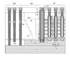
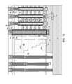
- FIG. 1is a vertical cross-sectional view of a first exemplary structure after formation of an alternating stack of insulating layers and sacrificial material layers and memory openings extending through the alternating stack according to a first embodiment of the present disclosure.
- FIGS. 2A-2Hare sequential vertical cross-sectional views of a memory opening within the first exemplary structure during various processing steps employed to form a memory stack structure according to the first embodiment of the present disclosure.
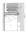
- FIG. 3is a vertical cross-sectional view of the first exemplary structure after formation of memory stack structures according to the first embodiment of the present disclosure.
- FIG. 4is a vertical cross-sectional view of the first exemplary structure after formation of a set of stepped surfaces and a retro-stepped dielectric material portion according to the first embodiment of the present disclosure.
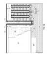
- FIG. 5Ais a vertical cross-sectional view of the first exemplary structure after formation of dielectric pillar structures and formation of backside trenches according to the first embodiment of the present disclosure.
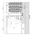
- FIG. 5Bis a see-through top-down view of the first exemplary structure of FIG. 5A .
- the vertical plane A-A′is the plane of the vertical cross-sectional view of FIG. 5A .
- FIG. 6is a vertical cross-sectional view of the first exemplary structure after formation of backside recesses according to the first embodiment of the present disclosure.
- FIG. 7is a vertical cross-sectional view of the first exemplary structure after formation of electrically conductive layers according to the first embodiment of the present disclosure.
- FIG. 8is a vertical cross-sectional view of the first exemplary structure after removal of a deposited conductive material from within the backside contact trench according to the first embodiment of the present disclosure.
- FIG. 9is a vertical cross-sectional view of the first exemplary structure after formation of an insulating spacer according to the first embodiment of the present disclosure.
- FIG. 10is a vertical cross-sectional view of the first exemplary structure after deposition of a diffusion barrier layer and an aluminum layer according to the first embodiment of the present disclosure.
- FIG. 11is a vertical cross-sectional view of the first exemplary structure after deposition of a semiconductor material layer according to the first embodiment of the present disclosure.
- FIG. 12is a vertical cross-sectional view of the first exemplary structure after an anneal process that induces layer crystallization and migration of aluminum according to the first embodiment of the present disclosure.
- FIG. 13is a vertical cross-sectional view of the first exemplary structure after a planarization process that forms a contact via structure according to the first embodiment of the present disclosure.
- FIG. 14is a vertical cross-sectional view of the first exemplary structure after formation of additional contact via structures and metal lines according to the first embodiment of the present disclosure.
- FIG. 15is a vertical cross-sectional view of an alternate embodiment of the first exemplary structure according to the first embodiment of the present disclosure.
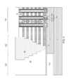
- FIG. 16is a vertical cross-sectional view of a second exemplary structure after formation of a dielectric fill material layer according to a second embodiment of the present disclosure.
- FIG. 17is a vertical cross-sectional view of the second exemplary structure after a planarization process that forms a contact via structure according to the second embodiment of the present disclosure.
- FIG. 18is a vertical cross-sectional view of the second exemplary structure after formation of additional contact via structures and metal lines according to the second embodiment of the present disclosure.
- FIG. 19is a vertical cross-sectional view of an alternate embodiment of the second exemplary structure after an anisotropic etch that forms a sidewall spacer portion according to the second embodiment of the present disclosure.
- FIG. 20is a vertical cross-sectional view of the alternate embodiment of the second exemplary structure after formation of additional contact via structures and metal lines according to the second embodiment of the present disclosure.
- the present disclosureis directed to three-dimensional memory structures, such as vertical NAND strings and other three-dimensional devices, and methods of making thereof, the various aspects of which are described below.
- the embodiments of the disclosurecan be employed to form various structures including a multilevel memory structure, non-limiting examples of which include semiconductor devices such as three-dimensional monolithic memory array devices comprising a plurality of NAND memory strings.
- the drawingsare not drawn to scale. Multiple instances of an element may be duplicated where a single instance of the element is illustrated, unless absence of duplication of elements is expressly described or clearly indicated otherwise. Ordinals such as “first,” “second,” and “third” are employed merely to identify similar elements, and different ordinals may be employed across the specification and the claims of the instant disclosure.
- a first element located “on” a second elementcan be located on the exterior side of a surface of the second element or on the interior side of the second element.
- a first elementis located “directly on” a second element if there exist a physical contact between a surface of the first element and a surface of the second element.
- a “layer”refers to a material portion including a region having a substantially uniform thickness.
- a layermay extend over the entirety of an underlying or overlying structure, or may have an extent less than the extent of an underlying or overlying structure. Further, a layer may be a region of a homogeneous or inhomogeneous continuous structure that has a thickness less than the thickness of the continuous structure. For example, a layer may be located between any pair of horizontal planes between, or at, a top surface and a bottom surface of the continuous structure. A layer may extend horizontally, vertically, and/or along a tapered surface.
- a substratemay be a layer, may include one or more layers therein, and/or may have one or more layer thereupon, thereabove, and/or therebelow.
- a “field effect transistor”refers to any semiconductor device having a semiconductor channel through which electrical current flows with a current density modulated by an external electrical field.
- an “active region”refers to a source region of a field effect transistor or a drain region of a field effect transistor.
- a “top active region”refers to an active region of a field effect transistor that is located above another active region of the field effect transistor.
- a “bottom active region”refers to an active region of a field effect transistor that is located below another active region of the field effect transistor.
- a monolithic three-dimensional memory arrayis a memory array in which multiple memory levels are formed above a single substrate, such as a semiconductor wafer, with no intervening substrates.
- non-monolithicmeans that layers of each level of the array are directly deposited on the layers of each underlying level of the array.
- two dimensional arraysmay be formed separately and then packaged together to form a non-monolithic memory device.
- non-monolithic stacked memorieshave been constructed by forming memory levels on separate substrates and vertically stacking the memory levels, as described in U.S. Pat. No. 5,915,167 titled “Three-dimensional Structure Memory.” The substrates may be thinned or removed from the memory levels before bonding, but as the memory levels are initially formed over separate substrates, such memories are not true monolithic three-dimensional memory arrays.
- the various three-dimensional memory devices of the present disclosureinclude a monolithic three-dimensional NAND string memory device, and can be fabricated employing the various embodiments described herein.
- the first exemplary structureincludes a substrate 9 , which can be a semiconductor substrate (e.g., a single crystalline silicon wafer).
- the substratecan include a semiconductor substrate layer 10 located over or in the top surface 7 of the substrate 9 .
- the semiconductor substrate layer 10is a semiconductor material layer, and can include at least one elemental semiconductor material (e.g., silicon, such as single crystalline silicon), at least one III-V compound semiconductor material, at least one II-VI compound semiconductor material, at least one organic semiconductor material, or other semiconductor materials known in the art.
- a “semiconductor material”refers to a material having electrical conductivity in the range from 1.0 ⁇ 10 ⁇ 6 S/cm to 1.0 ⁇ 10 5 S/cm, and is capable of producing a doped material having electrical conductivity in a range from 1.0 S/cm to 1.0 ⁇ 10 5 S/cm upon suitable doping with an electrical dopant.
- an “electrical dopant”refers to a p-type dopant that adds a hole to a valence band within a band structure, or an n-type dopant that adds an electron to a conduction band within a band structure.
- a “conductive material”refers to a material having electrical conductivity greater than 1.0 ⁇ 10 5 S/cm.
- an “insulating material” or a “dielectric material”refers to a material having electrical conductivity less than 1.0 ⁇ 10 ⁇ 6 S/cm. All measurements for electrical conductivities are made at the standard condition.
- the semiconductor substrate layer 10can include at least one doped well or layer 10 may comprise a doped well in the substrate 9 having a substantially uniform dopant concentration therein.
- the first exemplary structurecan have multiple regions for building different types of devices. Such areas can include, for example, a device region 100 , a contact region 300 , and a peripheral device region 200 .
- the semiconductor substrate layer 10can include at least one a doped well in the device region 100 .
- a “doped well”refers to a portion of a semiconductor material having a doping of a same conductivity type (which can be p-type or n-type) and a substantially same level of dopant concentration throughout.
- the doped wellcan be the same as the semiconductor substrate layer 10 or can be a portion of the semiconductor substrate layer 10 .
- the conductivity type of the doped wellis herein referred to as a first conductivity type, which can be p-type or n-type.
- the dopant concentration level of the doped wellis herein referred to as a first dopant concentration level.
- the first dopant concentration levelcan be in a range from 1.0 ⁇ 10 15 /cm 3 to 1.0 ⁇ 10 18 /cm 3 , although lesser and greater dopant concentration levels can also be employed.
- a dopant concentration levelrefers to average dopant concentration for a given region.
- Peripheral devices 210can be formed in, or on, a portion of the semiconductor substrate layer 10 located within the peripheral device region 200 .
- the peripheral devicescan include various devices employed to operate the memory devices to be formed in the device region 100 , and can include, for example, driver circuits for the various components of the memory devices.
- the peripheral devices 210can include, for example, field effect transistors and/or passive components such as resistors, capacitors, inductors, diodes, etc.
- a gate dielectric layer 12can be formed above the semiconductor substrate layer 10 .
- the gate dielectric layer 12can be employed as the gate dielectric for a first source select gate electrode.
- the gate dielectric layer 12can include, for example, silicon oxide and/or a dielectric metal oxide (such as HfO 2 , ZrO 2 , LaO 2 , etc.).
- the thickness of the gate dielectric layer 12can be in a range from 3 nm to 30 nm, although lesser and greater thicknesses can also be employed.
- first material layerswhich can be insulating layers 32
- second material layerswhich are referred to spacer material layers
- top surface of the substratewhich can be, for example, on the top surface of the gate dielectric layer 12 .
- a “material layer”refers to a layer including a material throughout the entirety thereof.
- a “spacer material layer”refers to a material layer that is located between two other material layers, i.e., between an overlying material layer and an underlying material layer. The spacer material layers can be formed as electrically conductive layers, or can be replaced with electrically conductive layers in a subsequent processing step.
- an alternating stack of first elements and second elementsrefers to a structure in which instances of the first elements and instances of the second elements alternate. Each instance of the first elements that is not an end element of the alternating plurality is adjoined by two instances of the second elements on both sides, and each instance of the second elements that is not an end element of the alternating plurality is adjoined by two instances of the first elements on both ends.
- the first elementsmay have the same thickness thereamongst, or may have different thicknesses.
- the second elementsmay have the same thickness thereamongst, or may have different thicknesses.
- the alternating plurality of first material layers and second material layersmay begin with an instance of the first material layers or with an instance of the second material layers, and may end with an instance of the first material layers or with an instance of the second material layers.
- an instance of the first elements and an instance of the second elementsmay form a unit that is repeated with periodicity within the alternating plurality.
- Each first material layerincludes a first material
- each second material layerincludes a second material that is different from the first material.
- each first material layercan be an insulating layer 32
- each second material layercan be a sacrificial material layer 42 .
- the stackcan include an alternating plurality of insulating layers 32 and sacrificial material layers 42 , and constitutes a prototype stack of alternating layers comprising insulating layers 32 and sacrificial material layers 42 .
- a “prototype” structure or an “in-process” structurerefers to a transient structure that is subsequently modified in the shape or composition of at least one component therein.
- the stack of the alternating pluralityis herein referred to as an alternating stack ( 32 , 42 ).
- the alternating stack ( 32 , 42 )can include insulating layers 32 composed of the first material, and sacrificial material layers 42 composed of a second material different from that of insulating layers 32 .
- the first material of the insulating layers 32can be at least one insulating material.
- each insulating layer 32can be an insulating material layer.
- Insulating materials that can be employed for the insulating layers 32include, but are not limited to, silicon oxide (including doped or undoped silicate glass), silicon nitride, silicon oxynitride, organosilicate glass (OSG), spin-on dielectric materials, dielectric metal oxides that are commonly known as high dielectric constant (high-k) dielectric oxides (e.g., aluminum oxide, hafnium oxide, etc.) and silicates thereof, dielectric metal oxynitrides and silicates thereof, and organic insulating materials.
- the first material of the insulating layers 32can be silicon oxide.
- the second material of the sacrificial material layers 42is a sacrificial material that can be removed selective to the first material of the insulating layers 32 .
- a removal of a first materialis “selective to” a second material if the removal process removes the first material at a rate that is at least twice the rate of removal of the second material.
- the ratio of the rate of removal of the first material to the rate of removal of the second materialis herein referred to as a “selectivity” of the removal process for the first material with respect to the second material.
- the sacrificial material layers 42may comprise an insulating material, a semiconductor material, or a conductive material.
- the second material of the sacrificial material layers 42can be subsequently replaced with electrically conductive electrodes which can function, for example, as control gate electrodes of a vertical NAND device.
- Non-limiting examples of the second materialinclude silicon nitride, an amorphous semiconductor material (such as amorphous silicon), and a polycrystalline semiconductor material (such as polysilicon).
- the sacrificial material layers 42can be spacer material layers that comprise silicon nitride or a semiconductor material including at least one of silicon and germanium.
- the insulating layers 32can include silicon oxide, and sacrificial material layers can include silicon nitride sacrificial material layers.
- the first material of the insulating layers 32can be deposited, for example, by chemical vapor deposition (CVD).
- CVDchemical vapor deposition
- TEOStetraethyl orthosilicate
- the second material of the sacrificial material layers 42can be formed, for example, CVD or atomic layer deposition (ALD).
- the sacrificial material layers 42can be suitably patterned so that conductive material portions to be subsequently formed by replacement of the sacrificial material layers 42 can function as electrically conductive electrodes, such as the control gate electrodes of the monolithic three-dimensional NAND string memory devices to be subsequently formed.
- the sacrificial material layers 42may comprise a portion having a strip shape extending substantially parallel to the top surface of the substrate.
- the thicknesses of the insulating layers 32 and the sacrificial material layers 42can be in a range from 20 nm to 50 nm, although lesser and greater thicknesses can be employed for each insulating layer 32 and for each sacrificial material layer 42 .
- the number of repetitions of the pairs of an insulating layer 32 and a sacrificial material layer (e.g., a control gate electrode or a sacrificial material layer) 42can be in a range from 2 to 1,024, and typically from 8 to 256, although a greater number of repetitions can also be employed.
- the top and bottom gate electrodes in the stackmay function as the select gate electrodes.
- each sacrificial material layer 42 in the alternating stack ( 32 , 42 )can have a uniform thickness that is substantially invariant within each respective sacrificial material layer 42 .
- an insulating cap layer 70can be formed over the alternating stack ( 32 , 42 ).
- the insulating cap layer 70includes a dielectric material that is different from the material of the sacrificial material layers 42 .
- the insulating cap layer 70can include a dielectric material that can be employed for the insulating layers 32 as described above.
- the insulating cap layer 70can have a greater thickness than each of the insulating layers 32 .
- the insulating cap layer 70can be deposited, for example, by chemical vapor deposition.
- the insulating cap layer 70can be a silicon oxide layer.
- a lithographic material stackincluding at least a photoresist layer can be formed over the insulating cap layer 70 and the alternating stack ( 32 , 42 ), and can be lithographically patterned to form openings therein.
- the pattern in the lithographic material stackcan be transferred through the insulating cap layer 70 and through entirety of the alternating stack ( 32 , 42 ) by at least one anisotropic etch that employs the patterned lithographic material stack as an etch mask. Portions of the alternating stack ( 32 , 42 ) underlying the openings in the patterned lithographic material stack are etched to form first memory openings 49 .
- the transfer of the pattern in the patterned lithographic material stack through the alternating stack ( 32 , 42 )forms the first memory openings that extend through the alternating stack ( 32 , 42 ).
- the chemistry of the anisotropic etch process employed to etch through the materials of the alternating stack ( 32 , 42 )can alternate to optimize etching of the first and second materials in the alternating stack ( 32 , 42 ).
- the anisotropic etchcan be, for example, a series of reactive ion etches.
- the gate dielectric layer 12may be used as an etch stop layer between the alternating stack ( 32 , 42 ) and the substrate.
- the sidewalls of the first memory openingscan be substantially vertical, or can be tapered.
- the patterned lithographic material stackcan be subsequently removed, for example, by ashing.
- FIGS. 2A-2Hillustrate sequential vertical cross-sectional views of a memory opening during formation of an exemplary memory stack structure. Formation of the exemplary memory stack structure can be performed within each of the memory openings 49 in the first exemplary structure illustrated in FIG. 1 .
- a memory opening 49is illustrated.
- the memory opening 49extends through the insulating cap layer 70 , the alternating stack ( 32 , 42 ), and the gate dielectric layer 12 , and optionally into an upper portion of the semiconductor substrate layer 10 .
- the recess depth of the bottom surface of each memory opening 49 with respect to the top surface of the semiconductor substrate layer 10can be in a range from 0 nm to 30 nm, although greater recess depths can also be employed.
- the sacrificial material layers 42can be laterally recessed partially to form lateral recesses (not shown), for example, by an isotropic etch.
- an epitaxial channel portion 11can be optionally formed at the bottom of each memory opening 49 by selective epitaxy of a semiconductor material.
- a reactant gas and an etchant gascan be simultaneously or alternatively flowed into a process chamber.
- Semiconductor surfaces and dielectric surfaces of the first exemplary structureprovide different nucleation rates for the semiconductor material.
- each portion of the deposited semiconductor materialconstitutes an epitaxial channel portion 11 , which comprises a single crystalline semiconductor material (e.g., single crystalline silicon) in epitaxial alignment with the single crystalline semiconductor material (e.g., single crystalline silicon) of the semiconductor substrate layer 10 .
- Each epitaxial channel portion 11functions as a portion of a channel of a vertical field effect transistor.
- the top surface of the epitaxial channel portion 11can be between a pair of sacrificial material layers 42 .
- a periphery of each epitaxial channel portion 11can be in physical contact with a sidewall of an insulating layer 32 .
- a cavity 49 ′is present over an epitaxial channel portion 11 in each memory opening 49 .
- a series of layers including at least one blocking dielectric layer ( 501 L, 503 L), a continuous memory material layer 504 L, a tunneling dielectric layer 506 L, and an optional first semiconductor channel layer 601 Lcan be sequentially deposited in the memory openings 49 .
- the at least one blocking dielectric layer ( 501 L, 503 L)can include, for example, a first blocking dielectric layer 501 L and a second blocking dielectric layer 503 L.
- the first blocking dielectric layer 501 Lcan be deposited on the sidewalls of each memory opening 49 by a conformal deposition method.
- the first blocking dielectric layer 501 Lincludes a dielectric material, which can be a dielectric metal oxide.
- a dielectric metal oxiderefers to a dielectric material that includes at least one metallic element and at least oxygen.
- the dielectric metal oxidemay consist essentially of the at least one metallic element and oxygen, or may consist essentially of the at least one metallic element, oxygen, and at least one non-metallic element such as nitrogen.
- the first blocking dielectric layer 501 Lcan include a dielectric metal oxide having a dielectric constant greater than 7.9, i.e., having a dielectric constant greater than the dielectric constant of silicon nitride.
- Non-limiting examples of dielectric metal oxidesinclude aluminum oxide (Al 2 O 3 ), hafnium oxide (HfO 2 ), lanthanum oxide (LaO 2 ), yttrium oxide (Y 2 O 3 ), tantalum oxide (Ta 2 O 5 ), silicates thereof, nitrogen-doped compounds thereof, alloys thereof, and stacks thereof.
- the first blocking dielectric layer 501 Lcan be deposited, for example, by chemical vapor deposition (CVD), atomic layer deposition (ALD), pulsed laser deposition (PLD), liquid source misted chemical deposition, or a combination thereof.
- the thickness of the first blocking dielectric layer 501 Lcan be in a range from 1 nm to 20 nm, although lesser and greater thicknesses can also be employed.
- the first blocking dielectric layer 501 Lcan subsequently function as a dielectric material portion that blocks leakage of stored electrical charges to control gate electrodes.
- the first blocking dielectric layer 501 Lincludes aluminum oxide.
- the second blocking dielectric layer 503 Lcan be formed on the first blocking dielectric layer 501 L.
- the second blocking dielectric layer 503 Lcan include a dielectric material that is different from the dielectric material of the first blocking dielectric layer 501 L.
- the second blocking dielectric layer 503 Lcan include silicon oxide, a dielectric metal oxide having a different composition than the first blocking dielectric layer 501 L, silicon oxynitride, silicon nitride, or a combination thereof.
- the second blocking dielectric layer 503 Lcan include silicon oxide.
- the second blocking dielectric layer 503 Lcan be formed by a conformal deposition method such as low pressure chemical vapor deposition, atomic layer deposition, or a combination thereof.
- the thickness of the second blocking dielectric layer 503 Lcan be in a range from 1 nm to 20 nm, although lesser and greater thicknesses can also be employed.
- the first blocking dielectric layer 501 L and/or the second blocking dielectric layer 503 Lcan be omitted, and a blocking dielectric layer can be formed after formation of backside recesses on surfaces of memory films to be subsequently formed.
- the continuous memory material layer 504 L, the tunneling dielectric layer 506 L, and the optional first semiconductor channel layer 601 Lcan be sequentially formed.
- the continuous memory material layer 504 Lcan be a charge trapping material including a dielectric charge trapping material, which can be, for example, silicon nitride.
- the continuous memory material layer 504 Lcan include a conductive material such as doped polysilicon or a metallic material that is patterned into multiple electrically isolated portions (e.g., floating gates), for example, by being formed within lateral recesses into sacrificial material layers 42 .
- the continuous memory material layer 504 Lincludes a silicon nitride layer.
- the continuous memory material layer 504 Lcan be formed as a single memory material layer of homogeneous composition, or can include a stack of multiple memory material layers.
- the multiple memory material layersif employed, can comprise a plurality of spaced-apart floating gate material layers that contain conductive materials (e.g., metal such as tungsten, molybdenum, tantalum, titanium, platinum, ruthenium, and alloys thereof, or a metal silicide such as tungsten silicide, molybdenum silicide, tantalum silicide, titanium silicide, nickel silicide, cobalt silicide, or a combination thereof) and/or semiconductor materials (e.g., polycrystalline or amorphous semiconductor material including at least one elemental semiconductor element or at least one compound semiconductor material).
- conductive materialse.g., metal such as tungsten, molybdenum, tantalum, titanium, platinum, ruthenium, and alloys thereof, or a metal silicide such as tungsten silicide
- the continuous memory material layer 504 Lmay comprise an insulating charge trapping material, such as one or more silicon nitride segments.
- the continuous memory material layer 504 Lmay comprise conductive nanoparticles such as metal nanoparticles, which can be, for example, ruthenium nanoparticles.
- the continuous memory material layer 504 Lcan be formed, for example, by chemical vapor deposition (CVD), atomic layer deposition (ALD), physical vapor deposition (PVD), or any suitable deposition technique for storing electrical charges therein.
- the thickness of the continuous memory material layer 504 Lcan be in a range from 2 nm to 20 nm, although lesser and greater thicknesses can also be employed.
- the tunneling dielectric layer 506 Lincludes a dielectric material through which charge tunneling can be performed under suitable electrical bias conditions.
- the charge tunnelingmay be performed through hot-carrier injection or by Fowler-Nordheim tunneling induced charge transfer depending on the mode of operation of the monolithic three-dimensional NAND string memory device to be formed.
- the tunneling dielectric layer 506 Lcan include silicon oxide, silicon nitride, silicon oxynitride, dielectric metal oxides (such as aluminum oxide and hafnium oxide), dielectric metal oxynitride, dielectric metal silicates, alloys thereof, and/or combinations thereof.
- the tunneling dielectric layer 506 Lcan include a stack of a first silicon oxide layer, a silicon oxynitride layer, and a second silicon oxide layer, which is commonly known as an ONO stack.
- the tunneling dielectric layer 506 Lcan include a silicon oxide layer that is substantially free of carbon or a silicon oxynitride layer that is substantially free of carbon.
- the thickness of the tunneling dielectric layer 506 Lcan be in a range from 2 nm to 20 nm, although lesser and greater thicknesses can also be employed.
- the optional first semiconductor channel layer 601 Lincludes a semiconductor material such as at least one elemental semiconductor material, at least one III-V compound semiconductor material, at least one II-VI compound semiconductor material, at least one organic semiconductor material, or other semiconductor materials known in the art.
- the first semiconductor channel layer 601 Lincludes amorphous silicon or polysilicon.
- the first semiconductor channel layer 601 Lcan be formed by a conformal deposition method such as low pressure chemical vapor deposition (LPCVD).
- the thickness of the first semiconductor channel layer 601 Lcan be in a range from 2 nm to 10 nm, although lesser and greater thicknesses can also be employed.
- a cavity 49 ′is formed in the volume of each memory opening 49 that is not filled with the deposited material layers ( 501 L, 503 L, 504 L, 506 L, 601 L).
- the optional first semiconductor channel layer 601 L, the tunneling dielectric layer 506 L, the continuous memory material layer 504 L, the at least one blocking dielectric layer ( 501 L, 503 L)are sequentially anisotropically etched employing at least one anisotropic etch process.
- the portions of the first semiconductor channel layer 601 L, the tunneling dielectric layer 506 L, the continuous memory material layer 504 L, and the at least one blocking dielectric layer ( 501 L, 503 L) located above the top surface of the insulating cap layer 70can be removed by the at least one anisotropic etch process.
- first semiconductor channel layer 601 L, the tunneling dielectric layer 506 L, the continuous memory material layer 504 L, and the at least one blocking dielectric layer ( 501 L, 503 L) at a bottom of each cavity 49 ′can be removed to form openings in remaining portions thereof.
- Each of the first semiconductor channel layer 601 L, the tunneling dielectric layer 506 L, the continuous memory material layer 504 L, and the at least one blocking dielectric layer ( 501 L, 503 L)can be etched by anisotropic etch process.
- Each remaining portion of the first semiconductor channel layer 601 Lconstitutes a first semiconductor channel portion 601 .
- Each remaining portion of the tunneling dielectric layer 506 Lconstitutes a tunneling dielectric 506 .
- Each remaining portion of the continuous memory material layer 504 Lis herein referred to as a memory material layer 504 .
- the memory material layer 504can comprise a charge trapping material or a floating gate material.
- each memory material layer 504can include a vertical stack of charge storage regions that store electrical charges upon programming.
- the memory material layer 504can be a charge storage layer in which each portion adjacent to the sacrificial material layers 42 constitutes a charge storage region.
- Each remaining portion of the second blocking dielectric layer 503 Lis herein referred to as a second blocking dielectric 503 .
- Each remaining portion of the first blocking dielectric layer 501 Lis herein referred to as a first blocking dielectric 501 .
- a surface of the epitaxial channel portion 11(or a surface of the semiconductor substrate layer 10 in case the epitaxial channel portions 11 are not employed) can be physically exposed underneath the opening through the first semiconductor channel portion 601 , the tunneling dielectric 506 , the memory material layer 504 , and the at least one blocking dielectric ( 501 , 503 ).
- the physically exposed semiconductor surface at the bottom of each cavity 49 ′can be vertically recessed so that the recessed semiconductor surface underneath the cavity 49 ′ is vertically offset from the topmost surface of the epitaxial channel portion 11 (or of the semiconductor substrate layer 10 in case epitaxial channel portions 11 are not employed) by a recess distance.
- a tunneling dielectric 506is located over the memory material layer 504 .
- a set of at least one blocking dielectric ( 501 , 503 ), a memory material layer 504 , and a tunneling dielectric 506 in a memory opening 49constitutes a memory film 50 , which includes a plurality of charge storage regions (as embodied as the memory material layer 504 ) that are insulated from surrounding materials by the at least one blocking dielectric ( 501 , 503 ) and the tunneling dielectric 506 .
- the first semiconductor channel portion 601 , the tunneling dielectric 506 , the memory material layer 504 , the second blocking dielectric 503 , and the first blocking dielectric 501can have vertically coincident sidewalls.
- a first surfaceis “vertically coincident” with a second surface if there exists a vertical plane including both the first surface and the second surface.
- Such a vertical planemay, or may not, have a horizontal curvature, but does not include any curvature along the vertical direction, i.e., extends straight up and down.
- a second semiconductor channel layer 602 Lcan be deposited directly on the semiconductor surface of the epitaxial channel portion 11 or the semiconductor substrate layer 10 if portion 11 is omitted, and directly on the first semiconductor channel portion 601 .
- the second semiconductor channel layer 602 Lincludes a semiconductor material such as at least one elemental semiconductor material, at least one III-V compound semiconductor material, at least one II-VI compound semiconductor material, at least one organic semiconductor material, or other semiconductor materials known in the art.
- the second semiconductor channel layer 602 Lincludes amorphous silicon or polysilicon.
- the second semiconductor channel layer 602 Lcan be formed by a conformal deposition method such as low pressure chemical vapor deposition (LPCVD).
- the thickness of the second semiconductor channel layer 602 Lcan be in a range from 2 nm to 10 nm, although lesser and greater thicknesses can also be employed.
- the second semiconductor channel layer 602 Lmay partially fill the cavity 49 ′ in each memory opening, or may fully fill the cavity in each memory opening.
- the materials of the first semiconductor channel portion 601 and the second semiconductor channel layer 602 Lare collectively referred to as a semiconductor channel material.
- the semiconductor channel materialis a set of all semiconductor material in the first semiconductor channel portion 601 and the second semiconductor channel layer 602 L.
- a dielectric core layer 62 Lcan be deposited in the cavity 49 ′ to fill any remaining portion of the cavity 49 ′ within each memory opening.
- the dielectric core layer 62 Lincludes a dielectric material such as silicon oxide or organosilicate glass.
- the dielectric core layer 62 Lcan be deposited by a conformal deposition method such as low pressure chemical vapor deposition (LPCVD), or by a self-planarizing deposition process such as spin coating.
- the horizontal portion of the dielectric core layer 62 Lcan be removed, for example, by a recess etch from above the top surface of the insulating cap layer 70 .
- Each remaining portion of the dielectric core layer 62 Lconstitutes a dielectric core 62 .
- the horizontal portion of the second semiconductor channel layer 602 L located above the top surface of the insulating cap layer 70can be removed by a planarization process, which can employ a recess etch or chemical mechanical planarization (CMP).
- CMPchemical mechanical planarization
- Each adjoining pair of a first semiconductor channel portion 601 and a second semiconductor channel portion 602can collectively form a semiconductor channel 60 through which electrical current can flow when a vertical NAND device including the semiconductor channel 60 is turned on.
- a tunneling dielectric 506is surrounded by a memory material layer 504 , and laterally surrounds a portion of the semiconductor channel 60 .
- Each adjoining set of a first blocking dielectric 501 , a second blocking dielectric 503 , a memory material layer 504 , and a tunneling dielectric 506collectively constitute a memory film 50 , which can store electrical charges with a macroscopic retention time.
- a first blocking dielectric 501 and/or a second blocking dielectric 503may not be present in the memory film 50 at this step, and a blocking dielectric may be subsequently formed after formation of backside recesses.
- a macroscopic retention timerefers to a retention time suitable for operation of a memory device as a permanent memory device such as a retention time in excess of 24 hours.
- each dielectric core 62can be further recessed within each memory opening, for example, by a recess etch to a depth that is located between the top surface of the insulating cap layer 70 and the bottom surface of the insulating cap layer 70 .
- Drain regions 63can be formed by depositing a doped semiconductor material within each recessed region above the dielectric cores 62 .
- the doped semiconductor materialcan be, for example, doped polysilicon. Excess portions of the deposited semiconductor material can be removed from above the top surface of the insulating cap layer 70 , for example, by chemical mechanical planarization (CMP) or a recess etch to form the drain regions 63 .
- CMPchemical mechanical planarization
- the exemplary memory stack structure 55can be embedded into the first exemplary structure illustrated in FIG. 1 .
- FIG. 3illustrates the first exemplary structure that incorporates multiple instances of the exemplary memory stack structure of FIG. 2H .
- Each exemplary memory stack structure 55includes a semiconductor channel 60 (comprising layers 601 , 602 ); a tunneling dielectric layer 506 laterally surrounding the semiconductor channel 60 ; and a vertical stack of charge storage regions laterally surrounding the tunneling dielectric layer 506 (as embodied as a memory material layer 504 ).
- the first exemplary structureincludes a semiconductor device, which comprises a stack ( 32 , 42 ) including an alternating plurality of material layers (e.g., the sacrificial material layers 42 ) and insulating layers 32 located over a semiconductor substrate (e.g., over the semiconductor substrate layer 10 ), and a memory opening extending through the stack ( 32 , 42 ).
- the semiconductor devicefurther comprises a first blocking dielectric 501 vertically extending from a bottommost layer (e.g., the bottommost sacrificial material layer 42 ) of the stack to a topmost layer (e.g., the topmost sacrificial material layer 42 ) of the stack, and contacting a sidewall of the memory opening and a horizontal surface of the semiconductor substrate. While the present disclosure is described employing the illustrated configuration for the memory stack structure, the methods of the present disclosure can be applied to alternative memory stack structures.
- an optional first contact level dielectric layer 71can be formed over the semiconductor substrate layer 10 .
- the first contact level dielectric layer 71may, or may not, be formed.
- the first contact level dielectric layer 71includes a dielectric material such as silicon oxide, silicon nitride, silicon oxynitride, porous or non-porous organosilicate glass (OSG), or a combination thereof. If an organosilicate glass is employed, the organosilicate glass may, or may not, be doped with nitrogen.
- the first contact level dielectric layer 71can be formed over a horizontal plane including the top surface of the insulating cap layer 70 and the top surfaces of the drain regions 63 .
- the first contact level dielectric layer 71can be deposited by chemical vapor deposition, atomic layer deposition (ALD), spin-coating, or a combination thereof.
- the thickness of the first contact level dielectric layer 71can be in a range from 10 nm to 300 nm, although lesser and greater thicknesses can also be employed.
- the first contact level dielectric layer 71can be formed as a dielectric material layer having a uniform thickness throughout.
- the first contact level dielectric layer 71may be formed as a single dielectric material layer, or can be formed as a stack of a plurality of dielectric material layers. Alternatively, formation of the first contact level dielectric layer 71 may be merged with formation of at least one line level dielectric layer (not shown).
- first contact level dielectric layer 71is a structure separate from an optional second contact level dielectric layer or at least one line level dielectric layer to be subsequently deposited
- first contact level dielectric layer 71 and at least one line level dielectric layerare formed at a same processing step, and/or as a same material layer, are expressly contemplated herein.
- the first contact level dielectric layer 71 , the insulating cap layer 70 , and the alternating stack ( 32 , 42 )can be removed from the peripheral device region 200 , for example, by a masked etch process.
- a stepped cavitycan be formed within the contact region 300 by patterning a portion of the alternating stack ( 32 , 42 ).
- a “stepped cavity”refers to a cavity having stepped surfaces.
- stepped surfacesrefer to a set of surfaces that include at least two horizontal surfaces and at least two vertical surfaces such that each horizontal surface is adjoined to a first vertical surface that extends upward from a first edge of the horizontal surface, and is adjoined to a second vertical surface that extends downward from a second edge of the horizontal surface.
- a “step”refers to a vertical shift in the height of a set of adjoined surfaces.
- the stepped cavitycan have various stepped surfaces such that the horizontal cross-sectional shape of the stepped cavity changes in steps as a function of the vertical distance from the top surface of the semiconductor substrate layer 10 .
- the stepped cavitycan be formed by repetitively performing a set of processing steps.
- the set of processing stepscan include, for example, an etch process of a first type that vertically increases the depth of a cavity by one or more levels, and an etch process of a second type that laterally expands the area to be vertically etched in a subsequent etch process of the first type.
- a “level” of a structure including alternating stackis defined as the relative position of a pair of a first material layer and a second material layer within the structure.
- a dielectric material such as silicon oxideis deposited in the stepped cavity and over the peripheral devices 210 in the peripheral device region 200 . Excess portions of the deposited dielectric material can be removed from above the top surface of the first contact level dielectric layer 71 , for example, by chemical mechanical planarization (CMP). The remaining portion of the deposited dielectric material filling the stepped cavity in the contact region 300 and overlying the semiconductor substrate layer 10 in the peripheral device region 200 constitutes a retro-stepped dielectric material portion 65 .
- a “retro-stepped” elementrefers to an element that has stepped surfaces and a horizontal cross-sectional area that increases monotonically as a function of a vertical distance from a top surface of a substrate on which the element is present.
- the silicon oxide of the retro-stepped dielectric material portion 65may, or may not, be doped with dopants such as B, P, and/or F.
- the top surface of the retro-stepped dielectric material portion 65can be coplanar with the top surface of the first contact level dielectric layer 71 .
- the region over the peripheral devices 210 and the region over the stepped cavitiescan be filled simultaneously with the same dielectric material, or can be filled in different processing steps with the same dielectric material or with different dielectric materials.
- the cavity over the peripheral devices 210can be filled with a dielectric material prior to, simultaneously with, or after, filling of the cavity over the stepped surface of the contact region 300 with a dielectric material. While the present disclosure is described employing an embodiment in which the cavity in the peripheral device region 200 and the stepped cavity in the contact region 300 are filled simultaneously, embodiments are expressly contemplated herein in which the cavity in the peripheral device region 200 and the stepped cavity in the contact region 300 are filled in different processing steps.
- dielectric support pillars 7 Pmay be optionally formed through the retro-stepped dielectric material portion 65 and/or through the first contact level dielectric layer 71 and/or through the alternating stack ( 32 , 42 ). In one embodiment, the dielectric support pillars 7 P can be formed in the contact region 300 , which is located adjacent to the device region 100 .
- the dielectric support pillars 7 Pcan be formed, for example, by forming an opening extending through the retro-stepped dielectric material portion 65 and/or through the alternating stack ( 32 , 42 ) and at least to the top surface of the semiconductor substrate layer 10 , and by filling the opening with a dielectric material that is resistant to the etch chemistry to be employed to remove the sacrificial material layers 42 .
- the dielectric support pillars 7 Pcan include silicon oxide and/or a dielectric metal oxide such as aluminum oxide.
- the portion of the dielectric material that is deposited over the first contact level dielectric layer 71 concurrently with deposition of the dielectric support pillars 7 Pcan be present over the first contact level dielectric layer 71 as a second contact level dielectric layer 73 .
- Each of the dielectric support pillars 7 P and the second contact level dielectric layer 73is an optional structure. As such, the second contact level dielectric layer 73 may, or may not, be present over the insulating cap layer 70 and the retro-stepped dielectric material portion 65 .
- the first contact level dielectric layer 71 and the second contact level dielectric layer 73are herein collectively referred to as at least one contact level dielectric layer ( 71 , 73 ).
- the at least one contact level dielectric layer ( 71 , 73 )can include both the first and second contact level dielectric layers ( 71 , 73 ), and optionally include any additional via level dielectric layer that can be subsequently formed.
- the at least one contact level dielectric layer ( 71 , 73 )can include only the first contact level dielectric layer 71 or the second contact level dielectric layer 73 , and optionally include any additional via level dielectric layer that can be subsequently formed.
- formation of the first and second contact level dielectric layers ( 71 , 73 )may be omitted, and at least one via level dielectric layer may be subsequently formed, i.e., after formation of a first source contact via structure.
- the second contact level dielectric layer 73 and the dielectric support pillars 7 Pcan be formed as a single continuous structure of integral construction, i.e., without any material interface therebetween.
- the portion of the dielectric material that is deposited over the first contact level dielectric layer 71 concurrently with deposition of the dielectric support pillars 7 Pcan be removed, for example, by chemical mechanical planarization or a recess etch.
- the second contact level dielectric layer 73is not present, and the top surface of the first contact level dielectric layer 71 can be physically exposed.
- trenches(which are herein referred to as backside trenches 79 ) can be formed between each neighboring pair of clusters of the memory stack structures 55 by transferring the pattern of the openings in the photoresist layer through the at least one contact level dielectric layer ( 71 , 73 ), the retro-stepped dielectric material portion 65 , and the alternating stack ( 32 , 42 ).
- Each backside trench 79extends through the in-process alternating stack ( 32 , 42 ) and to the top surface of the substrate ( 9 , 10 ).
- a top surface of the semiconductor substrate layer 10can be physically exposed at the bottom of each backside trench 79 .
- each backside trench 79can extend along a first horizontal direction so that clusters of the memory stack structures 55 are laterally spaced along a second horizontal direction that is different from the first horizontal direction.
- Each cluster of memory stack structures 55 in conjunction with the portions of the alternating stack ( 32 , 42 ) that surround the clusterconstitutes a memory block.
- Each memory blockis laterally spaced from one another by the backside trenches 79 .
- source regions 61can be formed in, or on, portions of the semiconductor substrate layer 10 underlying the backside trenches 79 by implantation of dopants of a second conductivity type (which is the opposite of the first conductivity type) after formation of the backside trenches 79 .
- a second conductivity typewhich is the opposite of the first conductivity type
- the first conductivity typeis p-type
- the second conductivity typeis n-type, and vice versa.
- the alternating stack of insulating layers 32 and the sacrificial material layers 42is an in-process structure, i.e., an in-process alternating stack.
- the in-process alternating stackis subsequently modified by replacement of the sacrificial material layers 42 with electrically conductive layers.
- an etchant that selectively etches the second material of the sacrificial material layers 42 with respect to the first material of the insulating layers 32can be introduced through the backside trenches 79 , for example, employing an etch process.
- Recesses(which are herein referred to as backside recesses 43 ) are formed in volumes from which the sacrificial material layers 42 are removed.
- the backside trenches 79 and the backside recesses 43are formed from locations away from the memory stack structures 55 , which are formed within memory openings 49 that are also referred to as front side openings.
- the removal of the second material of the sacrificial material layers 42can be selective to the first material of the insulating layers 32 , the material of the dielectric support pillars 7 P, the material of the retro-stepped dielectric material portion 65 , the semiconductor material of the semiconductor substrate layer 10 , and the material of the outermost layer of the first memory films 50 .
- the sacrificial material layers 42can include silicon nitride, and the materials of the insulating layers 32 , the dielectric support pillars 7 P, and the retro-stepped dielectric material portion 65 can be selected from silicon oxide and dielectric metal oxides.
- the sacrificial material layers 42can include a semiconductor material such as polysilicon, and the materials of the insulating layers 32 , the dielectric support pillars 7 P, and the retro-stepped dielectric material portion 65 can be selected from silicon oxide, silicon nitride, and dielectric metal oxides.
- the depth of the backside trenches 79can be modified so that the bottommost surface of the backside trenches 79 is located within the gate dielectric layer 12 , i.e., to avoid physical exposure of the top surface of the semiconductor substrate layer 10 .
- the etch process that removes the second material selective to the first material and the outermost layer of the first memory films 50can be a wet etch process employing a wet etch solution, or can be a gas phase (dry) etch process in which the etchant is introduced in a vapor phase into the backside trenches 79 .
- the etch processcan be a wet etch process in which the first exemplary structure is immersed within a wet etch tank including phosphoric acid at room temperature or higher temperature, which etches silicon nitride selective to silicon oxide, silicon, and various other materials employed in the art.
- the dielectric support pillars 7 P, the retro-stepped dielectric material portion 65 , and the memory stack structures 55provide structural support while the backside recesses 43 are present within volumes previously occupied by the sacrificial material layers 42 .
- Each backside recess 43can be a laterally extending cavity having a lateral dimension that is greater than the vertical extent of the cavity. In other words, the lateral dimension of each backside recess 43 can be greater than the height of the backside recess 43 .
- a plurality of backside recesses 43can be formed in the volumes from which the second material of the sacrificial material layers 42 is removed.
- the first memory openings in which the memory stack structures 55 are formedare herein referred to as front side openings or holes in contrast with the backside recesses 43 .
- the device region 100comprises an array of monolithic three-dimensional NAND strings having a plurality of device levels disposed above the substrate (e.g., above the semiconductor substrate layer 10 ).
- each backside recess 43can define a space for receiving a respective word line of the array of monolithic three-dimensional NAND strings.
- Each of the plurality of backside recesses 43can extend substantially parallel to the top surface of the semiconductor substrate layer 10 .
- a backside recess 43can be vertically bounded by a top surface of an underlying insulating layer 32 and a bottom surface of an overlying insulating layer 32 .
- each backside recess 43can have a uniform height throughout.
- a backside blocking dielectric layercan be formed in the backside recesses.
- each dielectric spacer 116can be topologically homeomorphic to a torus, i.e., generally ring-shaped.
- an elementis topologically homeomorphic to a torus if the shape of the element can be continuously stretched without destroying a hole or forming a new hole into the shape of a torus.
- the dielectric spacers 116include a dielectric material that includes the same semiconductor element as the epitaxial channel portions 11 and additionally includes at least one non-metallic element such as oxygen and/or nitrogen such that the material of the dielectric spacers 116 is a dielectric material.
- the dielectric spacers 116can include a dielectric oxide, a dielectric nitride, or a dielectric oxynitride of the semiconductor material of the epitaxial channel portions 11 .
- each sacrificial dielectric portion 616includes a dielectric material that includes the same semiconductor element as the source regions 61 and additionally includes at least one non-metallic element such as oxygen and/or nitrogen such that the material of the sacrificial dielectric portions 616 is a dielectric material.
- the sacrificial dielectric portions 616can include a dielectric oxide, a dielectric nitride, or a dielectric oxynitride of the semiconductor material of the source region 61 .
- a backside blocking dielectric layer(not shown) can be optionally formed.
- the backside blocking dielectric layerif present, comprises a dielectric material that functions as a control gate dielectric for the control gates to be subsequently formed in the backside recesses 43 .
- the backside blocking dielectric layeris optional.
- the backside blocking dielectric layeris present.
- At least one metallic materialcan be deposited in the plurality of backside recesses 43 , on the sidewalls of the at least one the backside contact trench 79 , and over the top surface of the second contact level dielectric layer 73 .
- a metallic materialrefers to an electrically conductive material that includes at least one metallic element
- the metallic materialcan be deposited by a conformal deposition method, which can be, for example, chemical vapor deposition (CVD), atomic layer deposition (ALD), electroless plating, electroplating, or a combination thereof.
- the metallic materialcan be an elemental metal, an intermetallic alloy of at least two elemental metals, a conductive nitride of at least one elemental metal, a conductive metal oxide, a conductive doped semiconductor material, a conductive metal-semiconductor alloy such as a metal silicide, alloys thereof, and combinations or stacks thereof.
- Non-limiting exemplary metallic materials that can be deposited in the plurality of backside recesses 43include tungsten, tungsten nitride, titanium, titanium nitride, tantalum, tantalum nitride, cobalt, and ruthenium.
- the metallic materialcan comprise a metal such as tungsten and/or metal nitride.
- the metallic material for filling the plurality of backside recesses 43can be a combination of titanium nitride layer and a tungsten fill material.
- the metallic materialcan be deposited by chemical vapor deposition or atomic layer deposition.
- the metallic materialcan be employing at least one fluorine-containing precursor gas as a precursor gas during the deposition process.
- the molecule of the at least one fluorine-containing precursor gascan comprise a compound of at least one tungsten atom and at least one fluorine atom. For example, if the metallic material includes tungsten, WF 6 and H 2 can be employed during the deposition process.
- a plurality of electrically conductive layers 46can be formed in the plurality of backside recesses 43 , and a continuous metallic material layer 46 L can be formed on the sidewalls of each backside contact trench 79 and over the at least one contact level dielectric layer ( 71 , 73 ).
- each sacrificial material layer 42can be replaced with an electrically conductive layer 46 .
- a backside cavity 79 ′is present in the portion of each backside contact trench 79 that is not filled with the backside blocking dielectric layer and the continuous metallic material layer 46 L.
- the deposited metallic material of the continuous metallic material layer 46 Lis etched back from the sidewalls of each backside contact trench 79 and from above the second contact level dielectric layer 73 , for example, by an isotropic etch.
- Each remaining portion of the deposited metallic material in the backside recesses 43constitutes an electrically conductive layer 46 .
- Each electrically conductive layer 46can be a conductive line structure.
- the sacrificial material layers 42are replaced with the electrically conductive layers 46 .
- Each electrically conductive layer 46can function as a combination of a plurality of control gate electrodes located at a same level and a word line electrically interconnecting, i.e., electrically shorting, the plurality of control gate electrodes located at the same level.
- the plurality of control gate electrodes within each electrically conductive layer 46are the control gate electrodes for the vertical memory devices including the memory stack structures 55 .
- each electrically conductive layer 46can be a word line that functions as a common control gate electrode for the plurality of vertical memory devices.
- the sacrificial dielectric portions 616can be removed from above the source regions 61 during the last processing step of the anisotropic etch.
- Each backside trench 79extends through the alternating stack ( 32 , 46 ) of the insulating layers 32 and the electrically conductive layers 46 and to the top surface of the substrate ( 9 , 10 ).
- an insulating material layercan be formed in each backside contact trench 79 and over the second contact level dielectric layer 73 by a conformal deposition process.
- exemplary conformal deposition processesinclude, but are not limited to, chemical vapor deposition and atomic layer deposition.
- the insulating material layerincludes an insulating material such as silicon oxide, silicon nitride, a dielectric metal oxide, an organosilicate glass, or a combination thereof.
- the thickness of the insulating material layercan be in a range from 1.5 nm to 60 nm, although lesser and greater thicknesses can also be employed.
- an anisotropic etchis performed to remove horizontal portions of the insulating material layer and to optionally remove the horizontal portion of the backside blocking dielectric layer from above the second contact level dielectric layer 73 .
- Each remaining portion of the insulating material layer inside a backside contact trench 79constitutes a vertically elongated annular structure with a vertical cavity therethrough, which is herein referred to as an insulating spacer 74 .
- an annular bottom surface of the insulating spacer 74contacts a top surface of the source region 61 .
- Each insulating spacer 74can be formed over the sidewalls of the backside contact trench 79 , and directly on the sidewalls of the electrically conductive layers 46 , i.e., directly on the sidewalls of the metallic material portions 46 .
- the thickness of each insulating spacer 74as measured at a bottom portion thereof, can be in a range from 1.5 nm to 60 nm, although lesser and greater thicknesses can also be employed. In one embodiment, the thickness of the insulating spacer 74 can be in a range from 3 nm to 10 nm.
- Each insulating spacer 74laterally surrounds a cavity, which is herein referred to as a backside cavity 79 ′.
- a top surface of a source region 61(which is a doped semiconductor material portion) can be physically exposed at the bottom of each backside cavity 79 ′ that is provided within an insulating spacer 74 .
- an electrically conductive diffusion barrier layer 75can be formed on the inner sidewalls of each insulating spacer 74 , on the physically exposed surfaces of the source regions 61 , and over the contact level dielectric layers ( 71 , 73 ).
- the diffusion barrier layer 75may be a metallic diffusion barrier layer.
- a “metallic diffusion barrier material”refers to a conductive metal layer or an electrically conductive compound of at least one elemental metal and at least one non-metallic element that is effective in blocking diffusion of metal therethrough.
- Exemplary metallic diffusion barrier materialsinclude refractory metals (such as Ti and W), metallic nitrides (such as TiN, TaN, and WN) and metallic carbides (such as TiC, TaC, and WC).
- the diffusion barrier layer 75does not diffuse into underlying semiconductor materials, and prevents diffusion of metallic materials to be subsequently deposited in the backside trenches 79 into the substrate ( 9 , 10 ).
- the diffusion barrier layer 75may be deposited by a conformal deposition method such as chemical vapor deposition (CVD), or may be deposited by a non-conformal deposition method such as physical vapor deposition (PVD).
- CVDchemical vapor deposition
- PVDphysical vapor deposition
- the thickness of the diffusion barrier layer 75can be in a range from 2 nm to 30 nm, although lesser and greater thicknesses can also be employed.
- the diffusion barrier 75may include a 20 nm thick Ti layer and a 5 nm thick TiN layer.
- the diffusion barrier layer 75 materialmay be selected to have an opposite stress type to the aluminum layer 76 L described below to avoid or reduce warping the substrate. For example, if the aluminum layer 76 L is in tensile stress, then the barrier layer 75 may be in compressive stress.
- the aluminum layer 76 Lcan be deposited on the diffusion barrier layer 75 .
- the aluminum layer 76 Lincludes an aluminum-containing material, which can be aluminum or an aluminum-containing metallic alloy in which aluminum is the predominant element, i.e., an aluminum-containing metallic alloy in which aluminum atoms accounts for more than 50 wt. % (such as more than 90 wt. %, such as 97-99 wt. %) of all atoms in the alloy.
- the aluminum layer 76can include substantially pure aluminum and unavoidable impurities, i.e., a material consisting essentially of aluminum.
- non-aluminum metal elements in the aluminum alloycan include, for example, copper, nickel and/or cobalt (e.g., 2 wt. % Cu or Co and remainder Al).
- the aluminum layer 76 Lcan be deposited as an amorphous or small grain polycrystalline material layer.
- the aluminum layer 76 Lcan be deposited as an amorphous aluminum layer consisting essentially of amorphous aluminum.
- the aluminum layer 76 Lcan be deposited as a conformal aluminum layer by a metal organic chemical vapor deposition employing an organoaluminum compound such as triisobutylaluminum (TIBAL), dimethyl aluminum hydride or trimethylaluminum (TMA).
- a conformal deposition processsuch as atomic layer deposition (ALD) or chemical vapor deposition (CVD) can be employed to deposit the aluminum layer 76 L.
- ALDatomic layer deposition
- CVDchemical vapor deposition
- the aluminum layer 76 Lcan be deposited employing an ALD process in which trimethylaluminum (which is the reactant gas) and hydrogen plasma (which reduces the reactant molecules adsorbed on surfaces) are alternately provided in a process chamber including the first exemplary structure.
- the aluminum layer 76 L deposited by such a conformal deposition methodcan provide smooth surface morphology (with root mean square surface roughness less than 0.2 nm) and good step coverage even in high aspect ratio cavities.
- the thickness of the aluminum layer 76 L, as measured on a sidewall of the diffusion barrier layer 75can be less than one half of the minimum lateral dimension between opposing inner sidewalls of the diffusion barrier layer 75 within a backside trench 79 . In this case, a vertically-extending cavity that is not filled within the aluminum layer 75 can be present within each backside trench 79 .
- a non-metallic materialis deposited in each cavity surrounded by vertical portions of the aluminum layer 75 L and over the contact level dielectric layers ( 71 , 73 ).
- the non-metallic materialfills each cavity in the backside trenches 79 .
- the non-metallic materialincludes a semiconductor material.
- a semiconductor material layer 77 Lthat continuously extends over the entire surface of the contact level dielectric layers ( 71 , 73 ) and over the backside trenches 79 is thus formed.
- the semiconductor material layer 77 Lcan include a Group IV semiconductor material or a III-V compound semiconductor material.
- the semiconductor material layer 77 Lcan include silicon or a silicon-germanium alloy.
- the semiconductor material layer 77 Lmay, or may not, be doped with electrical dopants, which can be p-type dopants or n-type dopants. In one embodiment, the semiconductor material layer 77 L can be in-situ doped to provide low resistivity to the deposited semiconductor material.
- the semiconductor material layer 77 Lcan include a conductive material if the dopant concentration therein is sufficiently high. In an illustrative example, the semiconductor material layer 77 L can include doped amorphous silicon or doped small grain polysilicon.
- the semiconductor material layer 77 Lcan be deposited by a conformal deposition method such as chemical vapor deposition (CVD) or atomic layer deposition (ALD).
- a planarization processis performed to remove portions of the aluminum layer 76 L, the semiconductor material layer 77 L, and the diffusion barrier layer 75 from above a horizontal plane including the top surface of the contact level dielectric layer ( 71 , 73 ).
- the planarizationis carried out after the anneal and crystallization, as will be described below with respect to FIG. 13 .
- an anneal process(which is herein referred to as a crystallization anneal) is performed to induce crystallization of the deposited semiconductor material.
- the anneal processcan be performed at an elevated temperature in a range from 400 degrees Celsius to 725 degrees Celsius (such as from 625 degrees Celsius to 700 degrees Celsius).
- the semiconductor material layer 77 Lis deposited as an amorphous or small grain polycrystalline semiconductor material layer
- the semiconductor material of the semiconductor material layer 77 Lcan be crystallized to form a large grain polycrystalline or single crystalline semiconductor material.
- the crystallization annealcan convert the amorphous silicon layer into a large grain polysilicon or single crystal silicon layer.
- layer 77 Lcomprises amorphous silicon or polysilicon
- the crystallization processcomprises a metal induced crystallization (“MIC”) process.
- MICmetal induced crystallization
- aluminum from layer 76 Laids crystallization of the silicon layer 77 L during the annealing.
- silicon atomsmove relatively freely into and through the aluminum layer. Dissolved silicon starts crystallizing since free energy of amorphous silicon is high as compared to crystalline silicon, as the system tends to go into a state with lower free energy.
- the aluminum atomsare rejected from the crystalline phase due to very low solid solubility of aluminum in silicon.
- the aluminum atomsdiffuse out of leaving behind crystalline silicon.
- the separation of crystalline silicon and aluminum layersoccurs, and the two layers exchange places.
- the aluminumleaves behind a single crystal silicon or large grain polysilicon material in the region through which the aluminum is diffused.
- the aluminum layer 76 Lis relatively thin, then substantially all of the aluminum from layer 76 L may exchange places with the silicon layer 77 L to be located in the middle of the trench 79 during the MIC process. In this case, the silicon layer 77 L and the aluminum layer 76 L switch positions in the trench 79 during the MIC process. After aluminum layer and semiconductor layer exchange process, aluminum layer 76 L is located in the middle of the trench 79 .
- the recrystallized single crystal silicon or polysilicon layer 77 Lis located between the diffusion barrier layer 75 and the aluminum layer 76 L in the trench 79 .
- the silicon layer 77 Lis located on both lateral (i.e., vertical) sidewalls of the aluminum layer 76 L.
- the recrystallized silicon layer 77 L and the diffusion barrier layer 75encapsulate the aluminum layer 76 L on both sides. The encapsulation reduces or prevents aluminum migration voids from occurring in the aluminum layer 76 L during subsequent high temperature process steps during device manufacture. If the subsequent process steps are conducted at the same or lower temperature as the MIC anneal, then the subsequent process steps should not cause the aluminum layer 76 L to flow and thus should not cause voids in the aluminum layer 76 L.
- the recrystallized silicon layer 77 L formed during the MIC processmay have a higher conductivity than the initial amorphous silicon or small grain polysilicon. Some of the aluminum that diffuses through the silicon may remain in the silicon layer 77 L such that the silicon layer 77 L becomes an aluminum doped silicon layer, which further increases its conductivity.
- a horizontal portion of the deposited semiconductor material(as embodied as the semiconductor material layer 77 L) overlies a horizontal portion of the deposited aluminum located above the alternating stack (i.e., the horizontal portion of the aluminum layer 76 L overlying the alternating stack) prior to the anneal process.
- the horizontal portion of the deposited aluminumcan exchange places with the horizontal portion of the deposited semiconductor material during the anneal process.
- the anneal processcan induce crystallization of the semiconductor material.
- a planarization processis performed to remove portions of the aluminum layer 76 L, the semiconductor material layer 75 L, and the diffusion barrier layer 75 from above a horizontal plane including the top surface of the contact level dielectric layer ( 71 , 73 ).
- a horizontal portion of aluminum (as embodied in the horizontal portion of the aluminum layer 76 L), a horizontal portion of the semiconductor material (as embodied in the horizontal portion of the polycrystalline semiconductor material layer 77 L), and a horizontal portion of the diffusion barrier layer 75can be sequentially removed from above the alternating stack ( 32 , 46 ) in that order.
- Removal of the various material portions of the aluminum layer 76 L, the semiconductor material layer 77 L, and the diffusion barrier layer 75can be performed employing at least one recess etch (which may be an anisotropic etch or an isotropic etch) and/or chemical mechanical planarization (CMP).
- CMPchemical mechanical planarization
- a series of reactive ion etch processescan be performed to remove the entire horizontal portions of the layer stack including the aluminum layer 76 L, the semiconductor material layer 77 L, and the diffusion barrier layer 75 , or a subset thereof. If horizontal portions of the layer stack are not completely removed from above the top surface of the contact level dielectric layer ( 71 , 73 ), a CMP process can be employed to complete the planarization process.
- Each backside trench 79includes a dielectric spacer 74 , a remaining portion of the diffusion barrier layer 75 , a remaining portion of the semiconductor material layer 77 L which is herein referred to as a semiconductor material portion 77 (e.g., a silicon portion), and a remaining portion of the aluminum layer 76 L which is herein referred to as an aluminum portion 76 .
- the semiconductor material portion 77is a non-metallic material portion, i.e., a portion that includes a material other than a metallic material.
- the diffusion barrier layer 75is laterally surrounded by, and contacted by, the insulating spacer 74 .
- the aluminum portion 76is located in the middle of the trench 79 , the silicon portion 77 surrounds and encapsulates the aluminum portion 76 on both vertical sides of portion 76 .
- the diffusion barrier layer 75surrounds the silicon portion 77 .
- the cavity 79 ′ that is present immediately after formation of the diffusion barrier layer 75 in one of the processing steps of FIG. 10can be filled with a combination of an aluminum portion 76 and a non-metallic material portion as embodied in a semiconductor material portion 77 .
- the combination of the aluminum portion 76 and the semiconductor material portion 77 and a portion of the diffusion barrier layer 75constitute a contact via structure 78 (which is a source contact via structure).
- the contact via structure 78extends through the alternating stack ( 32 , 46 ) and contacts a top surface of a doped semiconductor portion (i.e., a source region 61 ) embedded in the substrate ( 9 , 10 ).
- a photoresist layer(not shown) can be applied over the topmost layer of the first exemplary structure (which can be, for example, the second contact level dielectric layer 73 ), and can be lithographically patterned to form various openings in the device region 100 , the peripheral device region 200 , and the contact region 300 .
- the locations and the shapes of the various openingsare selected to correspond to electrical nodes of the various devices to be electrically contacted by contact via structures.
- a single photoresist layermay be employed to pattern all openings that correspond to the contact via cavities to be formed, and all contact via cavities can be simultaneously formed by at least one anisotropic etch process that employs the patterned photoresist layer as an etch mask.
- a plurality of photoresist layersmay be employed in combination with a plurality of anisotropic etch processes to form different sets of contact via cavities with different patterns of openings in the photoresist layers.
- the photoresist layer(s)can be removed after a respective anisotropic etch process that transfers the pattern of the openings in the respective photoresist layer through the underlying dielectric material layers and to a top surface of a respective electrically conductive structure.
- drain contact via cavitiescan be formed over each memory stack structure 55 in the device region 100 such that a top surface of a drain region 63 is physically exposed at the bottom of each drain contact via cavity.
- Word line contact via cavitiescan be formed to the stepped surfaces of the alternating stack ( 32 , 46 ) such that a top surface of an electrically conductive layer 46 is physically exposed at the bottom of each word line contact via cavity in the contact region 300 .
- a device contact via cavitycan be formed to each electrical node of the peripheral devices 210 to be contacted by a contact via structure in the peripheral device region.
- the various via cavitiescan be filled with at least one conductive material, which can be a combination of an electrically conductive metallic liner material (such as TiN, TaN, or WN) and a metallic fill material (such as W, Cu, or Al). Excess portions of the at least one conductive material can be removed from above the at least one contact level dielectric layer ( 71 , 73 ) by a planarization process, which can include, for example, chemical mechanical planarization (CMP) and/or a recess etch.
- Drain contact via structures 88can be formed on the respective drain regions 63 .
- Word line contact via structures(not shown) can be formed on the respective electrically conductive layers 46 .
- Peripheral device contact via structures 68can be formed on the respective nodes of the peripheral devices.
- a line level dielectric layer 90can be formed over the at least one contact level dielectric layer ( 71 , 73 ), and can be patterned to form line level cavities.
- the line level cavitiescan be filled with at least one conductive material to provide various metal lines, which can include, for example, a source line 79 that contacts the contact via structure 78 , bit lines 89 that contact the drain contact via structures 88 , and peripheral device lines 69 that contact peripheral device contact structures 68 .
- Additional metal interconnect structures (not shown) and interlayer dielectric material layers (not) showncan be formed over the first exemplary structure to provide additional electrical wiring.
- the first exemplary structureincludes an alternating stack of insulating layers 32 and electrically conductive layers 46 located over a substrate ( 9 , 10 ), and a contact via structure 78 extending through the alternating stack ( 32 , 46 ), contacting a top surface of a doped semiconductor portion (i.e., a source region 61 ) embedded in the substrate ( 9 , 10 ).
- the via structure 78includes a diffusion barrier layer 75 comprising a conductive metallic compound of at least one elemental metal and at least one non-metallic element, and a combination of an aluminum portion 76 and a non-metallic material portion 77 .
- the combination ( 76 , 77 )is laterally surrounded by the diffusion bather layer 75 .
- the non-metallic material portioncomprises a semiconductor material portion 77 .
- the semiconductor material portion 77can laterally surround the aluminum portion 76 .
- An outer sidewall of the semiconductor material portion 77can contact an inner sidewall of the diffusion barrier layer 75
- an inner sidewall of the semiconductor material portion 77can contact an outer sidewall of the aluminum portion 76 .
- a bottom surface of the aluminum portion 76can be located above, and can be vertically spaced from, a top surface of a horizontal portion of the diffusion barrier layer 75 that contacts the source region 61 underneath.
- each of the aluminum portion 76 and the non-metallic material portioncan extend from a first horizontal plane HP 1 including a top surface of a bottommost layer within the alternating stack ( 32 , 46 ) to a second horizontal plane HP 2 including a top surface of the topmost layer within the alternating stack ( 32 , 46 ).
- a horizontal portion of the diffusion barrier layer 75can contact the top surface of the doped semiconductor portion (i.e., the source region 61 ) embedded in the substrate ( 9 , 10 ) and a bottom surface of the aluminum portion 76 .
- the non-metallic portioni.e., the semiconductor material portion 77
- a metal line 79(e.g., source line) can contact a top surface of the aluminum portion 76 and a top surface of the non-metallic material portion (as embodied as the semiconductor material portion 77 ).
- an insulating spacer 74laterally surrounds the contact via structure 78 and electrically isolates the contact via structure 78 from the electrically conductive layers 46 (e.g., word lines).
- At least one memory stack structure 55extending through the alternating stack ( 32 , 46 ) is provided.
- Each of the at least one memory stack structure 55includes, from inside to outside, a semiconductor channel 60 , a tunneling dielectric layer 506 laterally surrounding the semiconductor channel 60 .
- a vertical stack of charge storage regions(as embodied as portions of the memory material layer 504 at each level of the conductive material layers 46 and vertically spaced by portions of the memory material layer 504 at each level of the insulating layers 32 ) laterally surrounds the tunneling dielectric layer 506 .
- the structurecomprises a three-dimensional memory device that comprises a vertical NAND device formed in a device region 100 .
- the electrically conductive layers 46can comprise, or can be electrically connected to, a respective word line of the NAND device as embodied as portions of the electrically conductive layers 46 .
- the device region 100can include a plurality of semiconductor channels 60 , wherein at least one end portion of each of the plurality of semiconductor channels 60 extends substantially perpendicular to a top surface of the substrate ( 9 , 10 ), a plurality of charge storage regions as embodied as discrete portions of the memory material layer 504 that are located adjacent to the electrically conductive layers, and a plurality of control gate electrodes having a strip shape extending substantially parallel to the top surface of the substrate ( 9 , 10 ). Each charge storage region is located adjacent to a respective one of the plurality of semiconductor channels 60 .
- Each of the control gate electrodescomprises a portion of a respective electrically conductive layer 46 that is proximal to the memory material layer 504 .
- the plurality of control gate electrodescomprise at least a first control gate electrode located in a first device level and a second control gate electrode located in a second device level.
- the electrically conductive layers in the stackcan be in electrical contact with the plurality of control gate electrodes and extend from the device region to a contact region including the plurality of electrically conductive via connections.
- the substrate ( 9 , 10 )can comprise a silicon substrate containing a driver circuit for the NAND device.
- the alternate embodiment of the first exemplary structuremay be obtained by forming the aluminum portion 76 with a sufficiently thin bottom horizontal portion. In this case, all aluminum from the aluminum portion 76 diffuses upwards into the semiconductor (e.g., silicon) material portion 77 .
- the semiconductore.g., silicon
- a bottom surface of the semiconductor (e.g., silicon) material portion 77can contact a top surface of the horizontal portion of the diffusion barrier layer 75 .
- a horizontal portion of the diffusion barrier layer 75can contact the top surface of the doped semiconductor portion (e.g., the source region 61 ) embedded in the substrate ( 9 , 10 ), and can contact the entire bottom surface of the semiconductor (e.g., silicon) material portion 77 .
- the aluminum portion 76can be vertically spaced from the horizontal portion of the diffusion bather layer 75 by the semiconductor (e.g., silicon) material portion 77 .
- a second exemplary structure according to a second embodiment of the present disclosurecan be derived from the first exemplary structure of FIG. 10 by depositing a non-metallic material on the deposited aluminum.
- the non-metallic materialcan be a dielectric material such as silicon oxide, silicon nitride, and/or a dielectric metal oxide.
- the deposited dielectric materialfills each vertically extending cavity within the sidewalls of the aluminum layer 76 L and overlies the entire horizontal portions of the aluminum layer 76 L above the contact level dielectric layers ( 71 , 73 ) to form a dielectric fill material layer 84 L.
- the dielectric fill material layer 84 Lcan be a continuous material layer having a horizontal portion overlying the contact level dielectric layers ( 71 , 73 ) and vertically extending portions that fill the cavities within the vertical portions of the aluminum layer 76 L.
- the non-metallic material (i.e., the dielectric material) of the dielectric fill material layer 84 Lincludes silicon oxide, which can be undoped silicate glass (USG) (e.g., silicon dioxide layer deposited by CVD using a TEOS source), fluorosilicate glass (FSG), phosphosilicate glass (PSG), borophosphosilicate glass (BPSG), borosilicate glass (BSG), organosilicate glass (OSG), porous derivatives thereof, or a combination thereof.
- USGundoped silicate glass
- FSGfluorosilicate glass
- PSGphosphosilicate glass
- BPSGborophosphosilicate glass
- BSGborosilicate glass
- OSGorganosilicate glass
- the dielectric fill material layer 84 L and the diffusion barrier layer 75encapsulate the aluminum layer 76 L (and thus the to be formed aluminum portion 76 ) to prevent or reduce void formation in the to be formed aluminum portion 76 during subsequent high temperature process steps.
- a planarization processis performed to remove portions of the dielectric fill material layer 84 L, the aluminum layer 76 L, and the diffusion barrier layer 75 from above a horizontal plane including the top surface of the contact level dielectric layer ( 71 , 73 )).
- a horizontal portion of the dielectric material(as embodied in the horizontal portion of the dielectric fill material layer 84 L that overlies the contact level dielectric layer ( 71 , 73 ), a horizontal portion of aluminum (as embodied in the horizontal portion of the aluminum layer 76 L), and a horizontal portion of the diffusion barrier layer 75 can be sequentially removed from above the alternating stack ( 32 , 46 ) in that order.
- Removal of the various material portions of the dielectric fill material layer 84 L, the aluminum layer 76 L, and the diffusion barrier layer 75can be performed employing at least one recess etch (which may be an anisotropic etch or an isotropic etch) and/or chemical mechanical planarization (CMP).
- a series of reactive ion etch processescan be performed to remove the entire horizontal portions of the layer stack including the dielectric fill material layer 84 L, the aluminum layer 76 L, and the diffusion barrier layer 75 , or a subset thereof.
- an isotropic etch process(such as a wet etch) may be employed to remove the horizontal portion of the dielectric fill material layer 84 L from above the horizontal plane including the top surface of the contact level dielectric layers ( 71 , 73 ). If horizontal portions of the layer stack are not completely removed from above the top surface of the contact level dielectric layer ( 71 , 73 ), a CMP process and/or at least one additional wet and/or dry etch process can be employed to complete the planarization process.
- a CMP process and/or at least one additional wet and/or dry etch processcan be employed to complete the planarization process.
- Each backside trench 79includes a dielectric spacer 74 , a remaining portion of the diffusion bather layer 75 , a remaining portion of the aluminum layer 76 L which is herein referred to as an aluminum portion 76 , and a remaining portion of the dielectric fill material layer 84 L, which is herein referred to as dielectric material portion 84 (which is a non-metallic material portion).
- the diffusion barrier layer 75is laterally surrounded by, and contacted by, the insulating spacer 74 .
- the cavity 79 ′that is present immediately after formation of the diffusion barrier layer 75 in one of the processing steps of FIG.
- the 10can be filled with a combination of an aluminum portion 76 and a non-metallic material portion as embodied in a dielectric material portion 84 .
- the combination of the aluminum portion 76 and the dielectric material portion 84 and a portion of the diffusion barrier layer 75constitute a contact via structure 178 (which is a source contact via structure).
- the contact via structure 178extends through the alternating stack ( 32 , 46 ) and contacts a top surface of a doped semiconductor portion (i.e., a source region 61 ) embedded in the substrate ( 9 , 10 ).
- the processing steps of FIG. 14can be performed to form additional contact via structures ( 88 , 68 ), a line level dielectric layer 90 , and various metal lines ( 79 , 89 , 69 ).
- the metal lines ( 79 , 89 , 69 )which can include, for example, a source line 79 that contacts the contact via structure 178 , bit lines 89 that contact the drain contact via structures 88 , and peripheral device lines 69 that contact peripheral device contact structures 68 .
- Additional metal interconnect structures (not shown) and interlayer dielectric material layers (not) showncan be formed over the first exemplary structure to provide additional electrical wiring.
- the second exemplary structureincludes an alternating stack of insulating layers 32 and electrically conductive layers 46 located over a substrate ( 9 , 10 ), and a contact via structure 178 extending through the alternating stack ( 32 , 46 ), contacting a top surface of a doped semiconductor portion (i.e., a source region 61 ) embedded in the substrate ( 9 , 10 ).
- the contact via structure 178comprises a diffusion barrier layer 75 comprising a conductive metallic compound of at least one elemental metal and at least one non-metallic element, and a combination of an aluminum portion 76 and a non-metallic material portion 84 .
- the combination ( 76 , 84 )is laterally surrounded by the diffusion bather layer 75 .
- the non-metallic material portioncomprises a dielectric material portion 84 including a dielectric material selected from silicon oxide, silicon nitride, and a dielectric metal oxide.
- the aluminum portion 76can laterally surround the dielectric material portion 84 .
- An outer sidewall of the aluminum portion 76can contact an inner sidewall of the diffusion barrier layer 75 , and an inner sidewall of the aluminum portion 76 can contact a sidewall of the dielectric material portion 84 .
- each of the aluminum portion 76 and the non-metallic material portioncan extend from a first horizontal plane HP 1 including a top surface of a bottommost layer within the alternating stack ( 32 , 46 ) to a second horizontal plane HP 2 including a top surface of the topmost layer within the alternating stack ( 32 , 46 ).
- a horizontal portion of the diffusion barrier layer 75can contact the top surface of the doped semiconductor portion (e.g., a source region 61 ) embedded in the substrate ( 9 , 10 ) and a bottom surface of the aluminum portion 76 , and the non-metallic portion (i.e., the dielectric material portion 84 ) can be vertically spaced from the horizontal portion of the diffusion barrier layer 75 by the aluminum portion 76 .
- the doped semiconductor portione.g., a source region 61
- the non-metallic portioni.e., the dielectric material portion 84
- a metal line 79can contact a top surface of the aluminum portion 76 and a top surface of the non-metallic material portion (as embodied as the dielectric material portion 84 ).
- an insulating spacer 74laterally surrounds the contact via structure 178 and electrically isolates the contact via structure 178 from the electrically conductive layers 46 .
- At least one memory stack structure 55extending through the alternating stack ( 32 , 46 ) is provided.
- Each of the at least one memory stack structure 55includes, from inside to outside, a semiconductor channel 60 , a tunneling dielectric layer 506 laterally surrounding the semiconductor channel 60 , and a vertical stack of charge storage regions (as embodied as portions of the memory material layer 504 at each level of the conductive material layers 46 and vertically spaced by portions of the memory material layer 504 at each level of the insulating layers 32 ) which laterally surrounds the tunneling dielectric layer 506 .
- the structurecomprises a three-dimensional memory device that comprises a vertical NAND device formed in a device region 110 .
- the electrically conductive layers 46can comprise, or can be electrically connected to, a respective word line of the NAND device as embodied as portions of the electrically conductive layers 46 .
- the device region 100can include a plurality of semiconductor channels 60 , wherein at least one end portion of each of the plurality of semiconductor channels 60 extends substantially perpendicular to a top surface of the substrate ( 9 , 10 ), a plurality of charge storage regions as embodied as discrete portions of the memory material layer 504 that are located adjacent to the electrically conductive layers, and a plurality of control gate electrodes having a strip shape extending substantially parallel to the top surface of the substrate ( 9 , 10 ). Each charge storage region is located adjacent to a respective one of the plurality of semiconductor channels 60 .
- Each of the control gate electrodescomprises a portion of a respective electrically conductive layer 46 that is proximal to the memory material layer 504 .
- the plurality of control gate electrodescomprise at least a first control gate electrode located in a first device level and a second control gate electrode located in a second device level.
- the electrically conductive layers in the stackcan be in electrical contact with the plurality of control gate electrodes and extend from the device region to a contact region including the plurality of electrically conductive via connections.
- the substrate ( 9 , 10 )can comprise a silicon substrate containing a driver circuit for the NAND device.
- an alternate embodiment of the second exemplary structure according to the second embodiment of the present disclosurecan be derived from the second exemplary structure of FIG. 10 by performing an anisotropic etch that removes horizontal portions of the aluminum layer 76 L.
- the anisotropic etchcan be a dry etch such as a reactive ion etch.
- the anisotropic etchcan be selective to the material of the diffusion barrier layer 75 .
- Each remaining vertical portion of the aluminum layer 76 L within the backside trenches 79constitutes an aluminum portion 76 , which can be a sidewall spacer aluminum portion.
- a sidewall spacer elementrefers to a vertically extending element along a sidewall of an opening, such as a sidewall of trench, and which includes a vertically extending through-cavity therein.
- each dielectric material portion 84can contact the top surface of the underlying horizontal portion of the diffusion barrier layer 75 .
- a horizontal portion of the diffusion barrier layer 75contacts the top surface of the doped semiconductor portion (e.g., a source region 61 ) embedded in the substrate ( 9 , 10 ), a bottom surface of the aluminum portion 76 , and a bottom surface of the non-metallic portion (which is the dielectric material portion 84 ).
- contact via structuresinclude a barrier layer, an aluminum portion and a non-metallic portion (e.g., silicon or dielectric material portion are described above), in alternative embodiments, one or more additional portions may be included in the contact via structure in addition to or instead of one or more of the above described portions.
- a metal silicide portionsuch as a self aligned silicide (“salicide”) portion may be included in the contact via structure.
- a buried salicide portionmay be formed at the top of the contact via structure by recessing the dielectric material portion 84 at the top of the contact via structure to form a recess, forming a metal and silicon (e.g., amorphous silicon) layers in the recess and annealing the layers to form a metal silicide (e.g., salicide) at the top of the contact via structure.
- the salicide regionmay then be buried under silicon oxide cover layer.
- the salicide portionmay be formed throughout the height of the contact via structure by depositing a metal layer and a silicon layer into the trench 79 followed by annealing the layers to form the salicide portion.
- any suitable metal materialsmay be used for the salicide portion, such as Ni, Co, W, Ti, etc.
- a monosalicidee.g. having one metal to one silicon atom ratio
- NiSi or a disalicidee.g., having one metal to two silicon
- NiSi 2 or CoSi 2e.g., having two metal to one silicon atom ratio
- a dimetal salicidee.g., having two metal to one silicon atom ratio
- Ni 2 Simay be formed.
- the various contact via structures of the present disclosurecan provide less stress to surrounding regions compared to contact via structures consisting of metallic materials such as a combination of a TiN liner and a W fill portion.
- the combination of aluminum and the non-metallic materialwhich can be a semiconductor material or a dielectric material, provides a structure with a lower Young's modulus, thereby reducing or preventing warping of the substrate and deformation of the structure embedding the contact via structures of the present disclosure.
- the structure of the present disclosurecan be incorporated into semiconductor devices to enhance yield and to improve reliability.
- the portions 77 or 84can act as an encapsulant for the aluminum portion 76 to prevent or reduce void formation in the aluminum portion. Furthermore, the MIC process improves the conductivity of the silicon portion 77 which improves the conductivity of the contact via structure 78 .
Landscapes
- Engineering & Computer Science (AREA)
- Physics & Mathematics (AREA)
- Power Engineering (AREA)
- General Physics & Mathematics (AREA)
- Computer Hardware Design (AREA)
- Microelectronics & Electronic Packaging (AREA)
- Condensed Matter Physics & Semiconductors (AREA)
- Manufacturing & Machinery (AREA)
- Geometry (AREA)
- Chemical & Material Sciences (AREA)
- Crystallography & Structural Chemistry (AREA)
- Semiconductor Memories (AREA)
- Non-Volatile Memory (AREA)
Abstract
Description
Claims (27)
Priority Applications (1)
| Application Number | Priority Date | Filing Date | Title |
|---|---|---|---|
| US14/922,516US9478495B1 (en) | 2015-10-26 | 2015-10-26 | Three dimensional memory device containing aluminum source contact via structure and method of making thereof |
Applications Claiming Priority (1)
| Application Number | Priority Date | Filing Date | Title |
|---|---|---|---|
| US14/922,516US9478495B1 (en) | 2015-10-26 | 2015-10-26 | Three dimensional memory device containing aluminum source contact via structure and method of making thereof |
Publications (1)
| Publication Number | Publication Date |
|---|---|
| US9478495B1true US9478495B1 (en) | 2016-10-25 |
Family
ID=57137438
Family Applications (1)
| Application Number | Title | Priority Date | Filing Date |
|---|---|---|---|
| US14/922,516Expired - Fee RelatedUS9478495B1 (en) | 2015-10-26 | 2015-10-26 | Three dimensional memory device containing aluminum source contact via structure and method of making thereof |
Country Status (1)
| Country | Link |
|---|---|
| US (1) | US9478495B1 (en) |
Cited By (45)
| Publication number | Priority date | Publication date | Assignee | Title |
|---|---|---|---|---|
| US20170207226A1 (en)* | 2016-01-18 | 2017-07-20 | SK Hynix Inc. | Semiconductor device |
| US9842856B2 (en)* | 2016-03-09 | 2017-12-12 | Toshiba Memory Corporation | Semiconductor memory device and method of manufacturing the same |
| US9847345B2 (en)* | 2016-03-18 | 2017-12-19 | Toshiba Memory Corporation | Semiconductor memory device and method of manufacturing the same |
| CN107579072A (en)* | 2017-08-31 | 2018-01-12 | 长江存储科技有限责任公司 | A method for forming a channel layer in a 3D NAND device and a wafer box structure |
| US9929178B1 (en)* | 2016-09-09 | 2018-03-27 | Toshiba Memory Corporation | Semiconductor device and method for manufacturing the same |
| US9929174B1 (en)* | 2016-10-28 | 2018-03-27 | Sandisk Technologies Llc | Three-dimensional memory device having non-uniform spacing among memory stack structures and method of making thereof |
| CN108364953A (en)* | 2018-03-13 | 2018-08-03 | 长江存储科技有限责任公司 | The device guard method of three-dimensional storage part and its manufacturing process |
| US20180254247A1 (en)* | 2017-03-03 | 2018-09-06 | Samsung Electronics Co., Ltd. | Three-dimensional semiconductor device |
| KR20180101685A (en)* | 2017-03-03 | 2018-09-13 | 삼성전자주식회사 | Semiconductor device |
| WO2018186863A1 (en)* | 2017-04-06 | 2018-10-11 | Intel Corporation | Thin-film transistor based magnetic random-access memory |
| CN108807410A (en)* | 2018-07-16 | 2018-11-13 | 长江存储科技有限责任公司 | 3D memory devices and its manufacturing method |
| CN109585454A (en)* | 2018-11-20 | 2019-04-05 | 长江存储科技有限责任公司 | 3D memory device and its manufacturing method |
| CN110520985A (en)* | 2019-07-16 | 2019-11-29 | 长江存储科技有限责任公司 | The interconnection structure of three-dimensional storage part |
| TWI690055B (en)* | 2019-07-01 | 2020-04-01 | 華邦電子股份有限公司 | Memory device and method for fabricating the same |
| US20200119029A1 (en)* | 2018-10-11 | 2020-04-16 | International Business Machines Corporation | Staircase patterning for 3d nand devices |
| WO2020131170A1 (en)* | 2018-12-17 | 2020-06-25 | Sandisk Technologies Llc | Three-dimensional memory device having stressed vertical semiconductor channels and method of making the same |
| US10756186B2 (en) | 2018-04-12 | 2020-08-25 | Sandisk Technologies Llc | Three-dimensional memory device including germanium-containing vertical channels and method of making the same |
| US10763271B2 (en) | 2018-06-27 | 2020-09-01 | Sandisk Technologies Llc | Three-dimensional memory device containing aluminum-silicon word lines and methods of manufacturing the same |
| US10797061B2 (en) | 2018-12-17 | 2020-10-06 | Sandisk Technologies Llc | Three-dimensional memory device having stressed vertical semiconductor channels and method of making the same |
| US10797060B2 (en) | 2018-12-17 | 2020-10-06 | Sandisk Technologies Llc | Three-dimensional memory device having stressed vertical semiconductor channels and method of making the same |
| CN111968991A (en)* | 2019-01-18 | 2020-11-20 | 长江存储科技有限责任公司 | Source contact structure of three-dimensional memory device and manufacturing method of memory device |
| US10868025B2 (en) | 2018-11-26 | 2020-12-15 | Sandisk Technologies Llc | Three-dimensional memory device including replacement crystalline channels and methods of making the same |
| TWI714872B (en)* | 2018-03-16 | 2021-01-01 | 日商東芝記憶體股份有限公司 | Memory device |
| CN112310103A (en)* | 2019-07-26 | 2021-02-02 | 爱思开海力士有限公司 | Vertical semiconductor device and method for manufacturing a vertical semiconductor device |
| CN112563196A (en)* | 2020-11-24 | 2021-03-26 | 惠科股份有限公司 | Manufacturing method of active switch and display panel |
| CN112687699A (en)* | 2020-12-24 | 2021-04-20 | 长江存储科技有限责任公司 | Three-dimensional memory and preparation method thereof |
| WO2021097796A1 (en)* | 2019-11-22 | 2021-05-27 | Yangtze Memory Technologies Co., Ltd. | Contact structures having conductive portions in substrate in three-dimensional memory devices and methods for forming the same |
| US11088146B2 (en) | 2017-04-04 | 2021-08-10 | Intel Corporation | Thin-film transistor embedded dynamic random-access memory |
| CN113270418A (en)* | 2019-08-13 | 2021-08-17 | 长江存储科技有限责任公司 | Three-dimensional memory device having source structure and method for forming the same |
| US20210320120A1 (en)* | 2020-04-14 | 2021-10-14 | Yangize Memory Technologies Co., Ltd. | Three-dimensional memory devices |
| US11164883B2 (en) | 2018-06-27 | 2021-11-02 | Sandisk Technologies Llc | Three-dimensional memory device containing aluminum-silicon word lines and methods of manufacturing the same |
| US20210351197A1 (en)* | 2016-10-17 | 2021-11-11 | Micron Technology, Inc. | Methods Of Forming An Array Of Elevationally-Extending Strings Of Memory Cells, Methods Of Forming Polysilicon, Elevationally-Extending Strings Of Memory Cells Individually Comprising A Programmable Charge Storage Transistor, And Electronic Components Comprising Polysilicon |
| US20210358950A1 (en)* | 2019-12-06 | 2021-11-18 | Micron Technology, Inc. | Integrated Assemblies, and Methods of Forming Integrated Assemblies |
| US20220271755A1 (en)* | 2020-10-05 | 2022-08-25 | Imec Vzw | 3d integrated count |
| US11450669B2 (en) | 2018-07-24 | 2022-09-20 | Intel Corporation | Stacked thin-film transistor based embedded dynamic random-access memory |
| US11482539B2 (en) | 2020-10-28 | 2022-10-25 | Sandisk Technologies Llc | Three-dimensional memory device including metal silicide source regions and methods for forming the same |
| TWI784615B (en)* | 2020-07-17 | 2022-11-21 | 台灣積體電路製造股份有限公司 | Magnetic tunnel junction device and method of forming the same |
| US11521984B2 (en) | 2020-06-24 | 2022-12-06 | Sandisk Technologies Llc | Three-dimensional memory device containing low resistance source-level contact and method of making thereof |
| US20230066753A1 (en)* | 2021-09-01 | 2023-03-02 | Micron Technology, Inc. | Electronic devices including vertical strings of memory cells, and related memory devices, systems and methods |
| US11626415B2 (en) | 2021-02-16 | 2023-04-11 | Sandisk Technologies Llc | Lateral transistors for selecting blocks in a three-dimensional memory array and methods for forming the same |
| US11653495B2 (en) | 2019-08-13 | 2023-05-16 | Yangtze Memory Technologies Co., Ltd. | Three-dimensional memory device with source structure and methods for forming the same |
| US11721727B2 (en) | 2018-12-17 | 2023-08-08 | Sandisk Technologies Llc | Three-dimensional memory device including a silicon-germanium source contact layer and method of making the same |
| US20230328982A1 (en)* | 2022-04-11 | 2023-10-12 | Macronix International Co., Ltd. | Semiconductor structure and method for manufacturing the same |
| US11882702B2 (en) | 2021-02-16 | 2024-01-23 | Sandisk Technologies Llc | Lateral transistors for selecting blocks in a three-dimensional memory array and methods for forming the same |
| CN118284049A (en)* | 2024-04-19 | 2024-07-02 | 联和存储科技(江苏)有限公司 | NAND FLASH memory device and method of fabricating the same |
Citations (231)
| Publication number | Priority date | Publication date | Assignee | Title |
|---|---|---|---|---|
| US3414892A (en) | 1967-12-26 | 1968-12-03 | Lab For Electronics Inc | Means interconnecting printed circuit memory planes |
| US3432827A (en) | 1964-09-04 | 1969-03-11 | An Controls Inc Di | Stacked magnetic memory system |
| US3571809A (en) | 1968-11-04 | 1971-03-23 | Energy Conversion Devices Inc | Memory matrix having serially connected threshold and memory switch devices at each cross-over point |
| US3573757A (en) | 1968-11-04 | 1971-04-06 | Energy Conversion Devices Inc | Memory matrix having serially connected threshold and memory switch devices at each cross-over point |
| US3576549A (en) | 1969-04-14 | 1971-04-27 | Cogar Corp | Semiconductor device, method, and memory array |
| US3582908A (en) | 1969-03-10 | 1971-06-01 | Bell Telephone Labor Inc | Writing a read-only memory while protecting nonselected elements |
| US3629863A (en) | 1968-11-04 | 1971-12-21 | Energy Conversion Devices Inc | Film deposited circuits and devices therefor |
| US3634929A (en) | 1968-11-02 | 1972-01-18 | Tokyo Shibaura Electric Co | Method of manufacturing semiconductor integrated circuits |
| US3671948A (en) | 1970-09-25 | 1972-06-20 | North American Rockwell | Read-only memory |
| US3699543A (en) | 1968-11-04 | 1972-10-17 | Energy Conversion Devices Inc | Combination film deposited switch unit and integrated circuits |
| US3717852A (en) | 1971-09-17 | 1973-02-20 | Ibm | Electronically rewritable read-only memory using via connections |
| US3728695A (en) | 1971-10-06 | 1973-04-17 | Intel Corp | Random-access floating gate mos memory array |
| US3787822A (en) | 1971-04-23 | 1974-01-22 | Philips Corp | Method of providing internal connections in a semiconductor device |
| US3846767A (en) | 1973-10-24 | 1974-11-05 | Energy Conversion Devices Inc | Method and means for resetting filament-forming memory semiconductor device |
| US3863231A (en) | 1973-07-23 | 1975-01-28 | Nat Res Dev | Read only memory with annular fuse links |
| US3877049A (en) | 1973-11-28 | 1975-04-08 | William D Buckley | Electrodes for amorphous semiconductor switch devices and method of making the same |
| US3886577A (en) | 1973-09-12 | 1975-05-27 | Energy Conversion Devices Inc | Filament-type memory semiconductor device and method of making the same |
| US3922648A (en) | 1974-08-19 | 1975-11-25 | Energy Conversion Devices Inc | Method and means for preventing degradation of threshold voltage of filament-forming memory semiconductor device |
| US3980505A (en) | 1973-09-12 | 1976-09-14 | Buckley William D | Process of making a filament-type memory semiconductor device |
| US3990098A (en) | 1972-12-22 | 1976-11-02 | E. I. Du Pont De Nemours And Co. | Structure capable of forming a diode and associated conductive path |
| US4037243A (en) | 1974-07-01 | 1977-07-19 | Motorola, Inc. | Semi conductor memory cell utilizing sensing of variations in PN junction current conrolled by stored data |
| US4146902A (en) | 1975-12-03 | 1979-03-27 | Nippon Telegraph And Telephone Public Corp. | Irreversible semiconductor switching element and semiconductor memory device utilizing the same |
| US4177475A (en) | 1977-10-31 | 1979-12-04 | Burroughs Corporation | High temperature amorphous memory device for an electrically alterable read-only memory |
| US4203158A (en) | 1978-02-24 | 1980-05-13 | Intel Corporation | Electrically programmable and erasable MOS floating gate memory device employing tunneling and method of fabricating same |
| US4203123A (en) | 1977-12-12 | 1980-05-13 | Burroughs Corporation | Thin film memory device employing amorphous semiconductor materials |
| US4272880A (en) | 1979-04-20 | 1981-06-16 | Intel Corporation | MOS/SOS Process |
| US4281397A (en) | 1979-10-29 | 1981-07-28 | Texas Instruments Incorporated | Virtual ground MOS EPROM or ROM matrix |
| US4355375A (en) | 1980-07-28 | 1982-10-19 | Fujitsu Limited | Semiconductor memory device |
| EP0073486A2 (en) | 1981-08-31 | 1983-03-09 | Kabushiki Kaisha Toshiba | Stacked semiconductor memory |
| US4419741A (en) | 1980-01-28 | 1983-12-06 | Rca Corporation | Read only memory (ROM) having high density memory array with on pitch decoder circuitry |
| US4420766A (en) | 1981-02-09 | 1983-12-13 | Harris Corporation | Reversibly programmable polycrystalline silicon memory element |
| US4442507A (en) | 1981-02-23 | 1984-04-10 | Burroughs Corporation | Electrically programmable read-only memory stacked above a semiconductor substrate |
| US4489478A (en) | 1981-09-29 | 1984-12-25 | Fujitsu Limited | Process for producing a three-dimensional semiconductor device |
| US4494135A (en) | 1976-04-06 | 1985-01-15 | U.S. Philips Corporation | Programmable read only memory cell having an electrically destructible programmation element integrally formed with a junction diode |
| US4499557A (en) | 1980-10-28 | 1985-02-12 | Energy Conversion Devices, Inc. | Programmable cell for use in programmable electronic arrays |
| US4498226A (en) | 1981-08-31 | 1985-02-12 | Tokyo Shibaura Denki Kabushiki Kaisha | Method for manufacturing three-dimensional semiconductor device by sequential beam epitaxy |
| JPS6022352U (en) | 1983-07-22 | 1985-02-15 | 富士通株式会社 | thermal printer |
| US4500905A (en) | 1981-09-30 | 1985-02-19 | Tokyo Shibaura Denki Kabushiki Kaisha | Stacked semiconductor device with sloping sides |
| US4507757A (en) | 1982-03-23 | 1985-03-26 | Texas Instruments Incorporated | Avalanche fuse element in programmable memory |
| US4535424A (en) | 1982-06-03 | 1985-08-13 | Texas Instruments Incorporated | Solid state three dimensional semiconductor memory array |
| US4543594A (en) | 1982-09-07 | 1985-09-24 | Intel Corporation | Fusible link employing capacitor structure |
| US4569121A (en) | 1983-03-07 | 1986-02-11 | Signetics Corporation | Method of fabricating a programmable read-only memory cell incorporating an antifuse utilizing deposition of amorphous semiconductor layer |
| JPS61222216A (en) | 1985-03-28 | 1986-10-02 | Canon Inc | Manufacture of superlattice semiconductor device |
| US4630096A (en) | 1984-05-30 | 1986-12-16 | Motorola, Inc. | High density IC module assembly |
| US4639893A (en) | 1984-05-15 | 1987-01-27 | Wafer Scale Integration, Inc. | Self-aligned split gate EPROM |
| US4646266A (en) | 1984-09-28 | 1987-02-24 | Energy Conversion Devices, Inc. | Programmable semiconductor structures and methods for using the same |
| US4672577A (en) | 1984-06-18 | 1987-06-09 | Hiroshima University | Three-dimensional integrated circuit with optically coupled shared memories |
| US4677742A (en) | 1983-01-18 | 1987-07-07 | Energy Conversion Devices, Inc. | Electronic matrix arrays and method for making the same |
| US4692994A (en) | 1986-04-29 | 1987-09-15 | Hitachi, Ltd. | Process for manufacturing semiconductor devices containing microbridges |
| US4710798A (en) | 1985-09-10 | 1987-12-01 | Northern Telecom Limited | Integrated circuit chip package |
| US4729005A (en) | 1985-04-29 | 1988-03-01 | General Electric Company | Method and apparatus for improved metal-insulator-semiconductor device operation |
| US4728626A (en) | 1985-11-18 | 1988-03-01 | International Business Machines Corporation | Method for making planar 3D heterepitaxial semiconductor structures with buried epitaxial silicides |
| JPS6352463U (en) | 1986-09-24 | 1988-04-08 | ||
| US4774556A (en) | 1985-07-25 | 1988-09-27 | Nippondenso Co., Ltd. | Non-volatile semiconductor memory device |
| US4811082A (en) | 1986-11-12 | 1989-03-07 | International Business Machines Corporation | High performance integrated circuit packaging structure |
| US4811114A (en) | 1986-02-24 | 1989-03-07 | Konishiroku Photo Industry Co., Ltd. | Image reading apparatus |
| US4820657A (en) | 1987-02-06 | 1989-04-11 | Georgia Tech Research Corporation | Method for altering characteristics of junction semiconductor devices |
| US4823181A (en) | 1986-05-09 | 1989-04-18 | Actel Corporation | Programmable low impedance anti-fuse element |
| US4876220A (en) | 1986-05-16 | 1989-10-24 | Actel Corporation | Method of making programmable low impedance interconnect diode element |
| US4881114A (en) | 1986-05-16 | 1989-11-14 | Actel Corporation | Selectively formable vertical diode circuit element |
| US4899205A (en) | 1986-05-09 | 1990-02-06 | Actel Corporation | Electrically-programmable low-impedance anti-fuse element |
| US4922319A (en) | 1985-09-09 | 1990-05-01 | Fujitsu Limited | Semiconductor programmable memory device |
| US4943538A (en) | 1986-05-09 | 1990-07-24 | Actel Corporation | Programmable low impedance anti-fuse element |
| EP0387834A2 (en) | 1989-03-14 | 1990-09-19 | Kabushiki Kaisha Toshiba | Semiconductor structure for processing and storing of information |
| US4967247A (en) | 1987-12-10 | 1990-10-30 | Hitachi, Ltd | Vertical dynamic random access memory |
| EP0395886A2 (en) | 1989-04-03 | 1990-11-07 | Olympus Optical Co., Ltd. | Memory cell and multidimensinal memory device constituted by arranging the memory cells |
| US5001539A (en) | 1988-07-08 | 1991-03-19 | Mitsubishi Denki Kabushiki Kaisha | Multiple layer static random access memory device |
| US5006909A (en) | 1989-10-30 | 1991-04-09 | Motorola, Inc. | Dram with a vertical capacitor and transistor |
| US5070383A (en) | 1989-01-10 | 1991-12-03 | Zoran Corporation | Programmable memory matrix employing voltage-variable resistors |
| US5070384A (en) | 1990-04-12 | 1991-12-03 | Actel Corporation | Electrically programmable antifuse element incorporating a dielectric and amorphous silicon interlayer |
| US5089862A (en) | 1986-05-12 | 1992-02-18 | Warner Jr Raymond M | Monocrystalline three-dimensional integrated circuit |
| US5091762A (en) | 1988-07-05 | 1992-02-25 | Kabushiki Kaisha Toshiba | Semiconductor memory device with a 3-dimensional structure |
| US5160987A (en) | 1989-10-26 | 1992-11-03 | International Business Machines Corporation | Three-dimensional semiconductor structures formed from planar layers |
| EP0516866A1 (en) | 1991-05-03 | 1992-12-09 | International Business Machines Corporation | Modular multilayer interwiring structure |
| US5191551A (en) | 1990-11-30 | 1993-03-02 | Nec Corporation | Non-volatile semiconductor memory device with transistor paralleling floating gate transistor |
| US5191405A (en) | 1988-12-23 | 1993-03-02 | Matsushita Electric Industrial Co., Ltd. | Three-dimensional stacked lsi |
| US5202754A (en) | 1991-09-13 | 1993-04-13 | International Business Machines Corporation | Three-dimensional multichip packages and methods of fabrication |
| JPH0582787U (en) | 1992-04-10 | 1993-11-09 | 裕一 大西 | Foldable small boat |
| US5266912A (en) | 1992-08-19 | 1993-11-30 | Micron Technology, Inc. | Inherently impedance matched multiple integrated circuit module |
| US5268319A (en) | 1988-06-08 | 1993-12-07 | Eliyahou Harari | Highly compact EPROM and flash EEPROM devices |
| US5270562A (en) | 1989-09-07 | 1993-12-14 | Sgs-Thomson Microelectronics S.A. | Locking device with a never-programmable floating gate cell |
| US5283468A (en) | 1988-05-30 | 1994-02-01 | Canon Kabushiki Kaisha | Electric circuit apparatus |
| US5283458A (en) | 1992-03-30 | 1994-02-01 | Trw Inc. | Temperature stable semiconductor bulk acoustic resonator |
| US5306935A (en) | 1988-12-21 | 1994-04-26 | Texas Instruments Incorporated | Method of forming a nonvolatile stacked memory |
| US5311039A (en) | 1990-04-24 | 1994-05-10 | Seiko Epson Corporation | PROM and ROM memory cells |
| US5321286A (en) | 1991-11-26 | 1994-06-14 | Nec Corporation | Non-volatile semiconductor memory device having thin film memory transistors stacked over associated selecting transistors |
| EP0606653A1 (en) | 1993-01-04 | 1994-07-20 | Texas Instruments Incorporated | Field programmable distributed processing memory |
| US5334880A (en) | 1991-04-30 | 1994-08-02 | International Business Machines Corporation | Low voltage programmable storage element |
| WO1994026083A1 (en) | 1993-04-23 | 1994-11-10 | Irvine Sensors Corporation | Electronic module comprising a stack of ic chips |
| US5379255A (en) | 1992-12-14 | 1995-01-03 | Texas Instruments Incorporated | Three dimensional famos memory devices and methods of fabricating |
| US5391518A (en) | 1993-09-24 | 1995-02-21 | Vlsi Technology, Inc. | Method of making a field programmable read only memory (ROM) cell using an amorphous silicon fuse with buried contact polysilicon and metal electrodes |
| US5391907A (en) | 1991-04-15 | 1995-02-21 | Gold Star Electron Co., Ltd. | Semiconductor device with buried inverse T-type field region |
| US5397908A (en) | 1993-06-09 | 1995-03-14 | Micron Technology, Inc. | Arrays of memory integrated circuitry |
| US5398200A (en) | 1992-03-02 | 1995-03-14 | Motorola, Inc. | Vertically formed semiconductor random access memory device |
| EP0644548A2 (en) | 1993-09-13 | 1995-03-22 | International Business Machines Corporation | Integrated memory cube, structure and fabrication |
| US5422435A (en) | 1992-05-22 | 1995-06-06 | National Semiconductor Corporation | Stacked multi-chip modules and method of manufacturing |
| US5426566A (en) | 1991-09-30 | 1995-06-20 | International Business Machines Corporation | Multichip integrated circuit packages and systems |
| US5427979A (en) | 1993-10-18 | 1995-06-27 | Vlsi Technology, Inc. | Method for making multi-level antifuse structure |
| US5434745A (en) | 1994-07-26 | 1995-07-18 | White Microelectronics Div. Of Bowmar Instrument Corp. | Stacked silicon die carrier assembly |
| US5441907A (en) | 1994-06-27 | 1995-08-15 | Taiwan Semiconductor Manufacturing Company | Process for manufacturing a plug-diode mask ROM |
| US5453952A (en) | 1991-04-23 | 1995-09-26 | Mitsubishi Denki Kabushiki Kaisha | Semiconductor device having peripheral circuit formed of TFT (thin film transistor) |
| US5455445A (en) | 1994-01-21 | 1995-10-03 | Kulite Semiconductor Products, Inc. | Multi-level semiconductor structures having environmentally isolated elements |
| US5463244A (en) | 1994-05-26 | 1995-10-31 | Symetrix Corporation | Antifuse programmable element using ferroelectric material |
| US5468663A (en) | 1992-03-12 | 1995-11-21 | International Business Machines Corporation | Method of fabricating three-dimensional direct-write EEPROM arrays |
| US5468997A (en) | 1991-06-10 | 1995-11-21 | Ngk Spark Plug Co., Ltd. | Integrated circuit package having a multilayered wiring portion formed on an insulating substrate |
| US5471090A (en) | 1993-03-08 | 1995-11-28 | International Business Machines Corporation | Electronic structures having a joining geometry providing reduced capacitive loading |
| US5481133A (en) | 1994-03-21 | 1996-01-02 | United Microelectronics Corporation | Three-dimensional multichip package |
| US5483094A (en) | 1993-09-20 | 1996-01-09 | Motorola, Inc. | Electrically programmable read-only memory cell |
| US5517044A (en) | 1992-02-07 | 1996-05-14 | Nec Corporation | Non-volatile semiconductor memory device having thin film transistors equipped with floating gates |
| US5523622A (en) | 1992-11-24 | 1996-06-04 | Hitachi, Ltd. | Semiconductor integrated device having parallel signal lines |
| US5535156A (en) | 1994-05-05 | 1996-07-09 | California Institute Of Technology | Transistorless, multistable current-mode memory cells and memory arrays and methods of reading and writing to the same |
| US5536968A (en) | 1992-12-18 | 1996-07-16 | At&T Global Information Solutions Company | Polysilicon fuse array structure for integrated circuits |
| US5552963A (en) | 1994-03-07 | 1996-09-03 | Staktek Corporation | Bus communication system for stacked high density integrated circuit packages |
| US5557122A (en) | 1995-05-12 | 1996-09-17 | Alliance Semiconductors Corporation | Semiconductor electrode having improved grain structure and oxide growth properties |
| US5559048A (en) | 1993-11-17 | 1996-09-24 | Nec Corporation | Method of making a double layered floating gate EPROM with trench isolation |
| US5581498A (en) | 1993-08-13 | 1996-12-03 | Irvine Sensors Corporation | Stack of IC chips in lieu of single IC chip |
| US5585675A (en) | 1994-05-11 | 1996-12-17 | Harris Corporation | Semiconductor die packaging tub having angularly offset pad-to-pad via structure configured to allow three-dimensional stacking and electrical interconnections among multiple identical tubs |
| US5612570A (en) | 1995-04-13 | 1997-03-18 | Dense-Pac Microsystems, Inc. | Chip stack and method of making same |
| US5654220A (en) | 1992-04-08 | 1997-08-05 | Elm Technology Corporation | Method of making a stacked 3D integrated circuit structure |
| US5675547A (en) | 1995-06-01 | 1997-10-07 | Sony Corporation | One time programmable read only memory programmed by destruction of insulating layer |
| EP0800137A1 (en) | 1996-04-04 | 1997-10-08 | International Business Machines Corporation | Memory controller |
| US5693552A (en) | 1996-04-29 | 1997-12-02 | United Microelectronics Corporation | Method for fabricating read-only memory device with a three-dimensional memory cell structure |
| US5696031A (en) | 1996-11-20 | 1997-12-09 | Micron Technology, Inc. | Device and method for stacking wire-bonded integrated circuit dice on flip-chip bonded integrated circuit dice |
| US5703747A (en) | 1995-02-22 | 1997-12-30 | Voldman; Steven Howard | Multichip semiconductor structures with interchip electrostatic discharge protection, and fabrication methods therefore |
| US5737259A (en) | 1996-11-22 | 1998-04-07 | United Microelectronics Corporation | Method of decoding a diode type read only memory |
| US5739567A (en) | 1992-11-02 | 1998-04-14 | Wong; Chun Chiu D. | Highly compact memory device with nonvolatile vertical transistor memory cell |
| US5751012A (en) | 1995-06-07 | 1998-05-12 | Micron Technology, Inc. | Polysilicon pillar diode for use in a non-volatile memory cell |
| US5751037A (en) | 1995-07-27 | 1998-05-12 | Sony Corporation | Non-volatile memory cell having dual gate electrodes |
| US5768192A (en) | 1996-07-23 | 1998-06-16 | Saifun Semiconductors, Ltd. | Non-volatile semiconductor memory cell utilizing asymmetrical charge trapping |
| US5776810A (en) | 1992-01-14 | 1998-07-07 | Sandisk Corporation | Method for forming EEPROM with split gate source side injection |
| US5780925A (en) | 1992-10-28 | 1998-07-14 | International Business Machines Corporation | Lead frame package for electronic devices |
| US5781031A (en) | 1995-11-21 | 1998-07-14 | International Business Machines Corporation | Programmable logic array |
| US5801437A (en) | 1993-03-29 | 1998-09-01 | Staktek Corporation | Three-dimensional warp-resistant integrated circuit module method and apparatus |
| US5825046A (en) | 1996-10-28 | 1998-10-20 | Energy Conversion Devices, Inc. | Composite memory material comprising a mixture of phase-change memory material and dielectric material |
| US5835396A (en) | 1996-10-17 | 1998-11-10 | Zhang; Guobiao | Three-dimensional read-only memory |
| US5840589A (en) | 1985-11-19 | 1998-11-24 | Warner, Jr.; Raymond M. | Method for fabricating monolithic and monocrystalline all-semiconductor three-dimensional integrated circuits |
| US5852317A (en) | 1995-03-31 | 1998-12-22 | National Semiconductor Corporation | Method to reduce gate oxide damage due to non-uniform plasmas in read only memory arrays |
| US5883409A (en) | 1992-01-14 | 1999-03-16 | Sandisk Corporation | EEPROM with split gate source side injection |
| US5889302A (en) | 1997-04-21 | 1999-03-30 | Advanced Micro Devices, Inc. | Multilayer floating gate field effect transistor structure for use in integrated circuit devices |
| US5903492A (en) | 1996-06-10 | 1999-05-11 | Kabushiki Kaisha Toshiba | Semiconductor memory device and various systems mounting them |
| US5915167A (en) | 1997-04-04 | 1999-06-22 | Elm Technology Corporation | Three dimensional structure memory |
| US5930608A (en) | 1992-02-21 | 1999-07-27 | Semiconductor Energy Laboratory Co., Ltd. | Method of fabricating a thin film transistor in which the channel region of the transistor consists of two portions of differing crystallinity |
| EP0933817A2 (en) | 1998-01-28 | 1999-08-04 | Hitachi, Ltd. | Semiconductor memory with stacked structure |
| US5936280A (en) | 1997-04-21 | 1999-08-10 | Advanced Micro Devices, Inc. | Multilayer quadruple gate field effect transistor structure for use in integrated circuit devices |
| US5939749A (en) | 1996-03-29 | 1999-08-17 | Sanyo Electric Company, Ltd. | Split gate transistor array |
| US5966603A (en) | 1997-06-11 | 1999-10-12 | Saifun Semiconductors Ltd. | NROM fabrication method with a periphery portion |
| US5969380A (en) | 1996-06-07 | 1999-10-19 | Micron Technology, Inc. | Three dimensional ferroelectric memory |
| US5973356A (en) | 1997-07-08 | 1999-10-26 | Micron Technology, Inc. | Ultra high density flash memory |
| US5976953A (en) | 1993-09-30 | 1999-11-02 | Kopin Corporation | Three dimensional processor using transferred thin film circuits |
| US5978258A (en) | 1996-10-21 | 1999-11-02 | Micron Technology, Inc. | MOS diode for use in a non-volatile memory cell background |
| US5981974A (en) | 1996-09-30 | 1999-11-09 | Sharp Kabushiki Kaisha | Semiconductor device and method for fabricating the same |
| US5982003A (en) | 1994-04-07 | 1999-11-09 | The Regents Of The University Of California | Silicon-on-insulator transistors having improved current characteristics and reduced electrostatic discharge susceptibility |
| US5985693A (en) | 1994-09-30 | 1999-11-16 | Elm Technology Corporation | High density three-dimensional IC interconnection |
| US5999453A (en) | 1997-06-27 | 1999-12-07 | Nec Corporation | Nonvolatile semiconductor memory |
| US5998808A (en) | 1997-06-27 | 1999-12-07 | Sony Corporation | Three-dimensional integrated circuit device and its manufacturing method |
| US6005270A (en) | 1997-11-10 | 1999-12-21 | Sony Corporation | Semiconductor nonvolatile memory device and method of production of same |
| US6011725A (en) | 1997-08-01 | 2000-01-04 | Saifun Semiconductors, Ltd. | Two bit non-volatile electrically erasable and programmable semiconductor memory cell utilizing asymmetrical charge trapping |
| US6028326A (en) | 1993-03-22 | 2000-02-22 | Semiconductor Energy Laboratory Co., Ltd. | Thin film transistor including a catalytic element for promoting crystallization of a semiconductor film |
| US6034882A (en) | 1998-11-16 | 2000-03-07 | Matrix Semiconductor, Inc. | Vertically stacked field programmable nonvolatile memory and method of fabrication |
| US6057598A (en) | 1997-01-31 | 2000-05-02 | Vlsi Technology, Inc. | Face on face flip chip integration |
| US6066547A (en) | 1997-06-20 | 2000-05-23 | Sharp Laboratories Of America, Inc. | Thin-film transistor polycrystalline film formation by nickel induced, rapid thermal annealing method |
| US6072193A (en) | 1997-05-30 | 2000-06-06 | Semiconductor Energy Laboratory Co., Ltd. | Thin-film transistor and semiconductor device using thin-film transistors |
| US6072234A (en) | 1996-12-21 | 2000-06-06 | Irvine Sensors Corporation | Stack of equal layer neo-chips containing encapsulated IC chips of different sizes |
| US6075719A (en) | 1999-06-22 | 2000-06-13 | Energy Conversion Devices, Inc. | Method of programming phase-change memory element |
| EP1017100A1 (en) | 1998-03-02 | 2000-07-05 | Seiko Epson Corporation | Three-dimensional device |
| US6087674A (en) | 1996-10-28 | 2000-07-11 | Energy Conversion Devices, Inc. | Memory element with memory material comprising phase-change material and dielectric material |
| US6087722A (en) | 1998-05-28 | 2000-07-11 | Samsung Electronics Co., Ltd. | Multi-chip package |
| US6100200A (en) | 1998-12-21 | 2000-08-08 | Advanced Technology Materials, Inc. | Sputtering process for the conformal deposition of a metallization or insulating layer |
| EP0971416A4 (en) | 1998-01-26 | 2000-08-09 | Sony Corp | MEMORY DEVICE AND CORRESPONDING MANUFACTURING METHOD, AND INTEGRATED CIRCUIT AND CORRESPONDING MANUFACTURING METHOD |
| US6107666A (en) | 1996-11-22 | 2000-08-22 | United Microelectronics Corp. | High density ROM and a method of making the same |
| US6110278A (en) | 1998-08-10 | 2000-08-29 | Saxena; Arjun N. | Methods for and products of growth of single-crystal on arrayed nucleation sites (SCANS) defined in nucleation unfriendly substrates |
| US6114767A (en) | 1997-07-31 | 2000-09-05 | Nec Corporation | EEPROM semiconductor device and method of fabricating the same |
| US6137718A (en) | 1996-08-01 | 2000-10-24 | Siemens Aktiengesellschaft | Method for operating a non-volatile memory cell arrangement |
| US6141241A (en) | 1998-06-23 | 2000-10-31 | Energy Conversion Devices, Inc. | Universal memory element with systems employing same and apparatus and method for reading, writing and programming same |
| US6153495A (en) | 1998-03-09 | 2000-11-28 | Intersil Corporation | Advanced methods for making semiconductor devices by low temperature direct bonding |
| US6157061A (en) | 1997-08-29 | 2000-12-05 | Nec Corporation | Nonvolatile semiconductor memory device and method of manufacturing the same |
| US6184088B1 (en) | 1996-03-29 | 2001-02-06 | Sanyo Electric Co., Ltd. | Method for manufacturing a split game type transistor |
| US6188605B1 (en) | 1998-02-27 | 2001-02-13 | Sanyo Electric Co., Ltd. | Non-volatile semiconductor memory using split bit lines |
| US6191459B1 (en) | 1996-01-08 | 2001-02-20 | Infineon Technologies Ag | Electrically programmable memory cell array, using charge carrier traps and insulation trenches |
| US6197641B1 (en) | 1998-08-28 | 2001-03-06 | Lucent Technologies Inc. | Process for fabricating vertical transistors |
| US6211015B1 (en) | 1997-08-20 | 2001-04-03 | Micron Technology, Inc. | Ultra high density flash memory having vertically stacked devices |
| US6255705B1 (en) | 1997-09-23 | 2001-07-03 | Semiconductor Energy Laboratory Co., Ltd. | Producing devices having both active matrix display circuits and peripheral circuits on a same substrate |
| USRE37259E1 (en) | 1996-04-19 | 2001-07-03 | Energy Conversion Devices, Inc. | Multibit single cell memory element having tapered contact |
| US6281042B1 (en) | 1998-08-31 | 2001-08-28 | Micron Technology, Inc. | Structure and method for a high performance electronic packaging assembly |
| US6291858B1 (en) | 2000-01-03 | 2001-09-18 | International Business Machines Corporation | Multistack 3-dimensional high density semiconductor device and method for fabrication |
| US6299338B1 (en) | 1998-11-30 | 2001-10-09 | General Electric Company | Decorative lighting apparatus with light source and luminescent material |
| US6307257B1 (en) | 1999-05-14 | 2001-10-23 | Siliconware Precision Industries, Co., Ltd. | Dual-chip integrated circuit package with a chip-die pad formed from leadframe leads |
| US6314013B1 (en) | 1998-11-23 | 2001-11-06 | Micron Technology, Inc. | Stacked integrated circuits |
| US6322903B1 (en) | 1999-12-06 | 2001-11-27 | Tru-Si Technologies, Inc. | Package of integrated circuits and vertical integration |
| US6323515B1 (en) | 1997-08-29 | 2001-11-27 | Semiconductor Energy Laboratory Co., Ltd. | Non-volatile memory and semiconductor device |
| US20010055838A1 (en) | 2000-04-28 | 2001-12-27 | Matrix Semiconductor Inc. | Nonvolatile memory on SOI and compound semiconductor substrates and method of fabrication |
| US20010054759A1 (en) | 2000-06-02 | 2001-12-27 | Kabushiki Kaisha Shinkawa | Semiconductor device |
| US6335554B1 (en) | 1999-03-08 | 2002-01-01 | Kabushiki Kaisha Toshiba | Semiconductor Memory |
| US6337521B1 (en) | 1999-09-22 | 2002-01-08 | Hitachi, Ltd. | Semiconductor device and a method of manufacturing the same |
| US6351028B1 (en) | 1999-02-08 | 2002-02-26 | Micron Technology, Inc. | Multiple die stack apparatus employing T-shaped interposer elements |
| US6353265B1 (en) | 2001-02-06 | 2002-03-05 | Mitsubishi Denki Kabushiki Kaisha | Semiconductor device |
| US20020028541A1 (en) | 2000-08-14 | 2002-03-07 | Lee Thomas H. | Dense arrays and charge storage devices, and methods for making same |
| US6355501B1 (en) | 2000-09-21 | 2002-03-12 | International Business Machines Corporation | Three-dimensional chip stacking assembly |
| US20020093052A1 (en) | 2000-10-23 | 2002-07-18 | Citizen Watch Co., Ltd. | Semiconductor device |
| US6433382B1 (en) | 1995-04-06 | 2002-08-13 | Motorola, Inc. | Split-gate vertically oriented EEPROM device and process |
| US20020142546A1 (en) | 2001-03-28 | 2002-10-03 | Matrix Semiconductor, Inc. | Two mask floating gate EEPROM and method of making |
| US6472684B1 (en) | 1997-09-20 | 2002-10-29 | Semiconductor Energy Laboratories Co., Ltd. | Nonvolatile memory and manufacturing method thereof |
| US6486027B1 (en) | 1998-02-27 | 2002-11-26 | Micron Technology, Inc. | Field programmable logic arrays with vertical transistors |
| US6498369B1 (en) | 1999-04-15 | 2002-12-24 | Semiconductor Energy Laboratory Co., Ltd. | Electro-optical device and electronic equipment |
| US6509638B2 (en) | 2000-09-07 | 2003-01-21 | Matsushita Electric Industrial Co., Ltd. | Semiconductor device having a plurality of stacked semiconductor chips on a wiring board |
| US6525962B1 (en) | 2000-04-05 | 2003-02-25 | Cypress Semiconductor Corporation | High current and/or high speed electrically erasable memory cell for programmable logic devices |
| US6551857B2 (en) | 1997-04-04 | 2003-04-22 | Elm Technology Corporation | Three dimensional structure integrated circuits |
| US6577531B2 (en) | 2000-04-27 | 2003-06-10 | Semiconductor Energy Laboratory Co., Ltd. | Nonvolatile memory and semiconductor device |
| US6587365B1 (en) | 2000-08-31 | 2003-07-01 | Micron Technology, Inc. | Array architecture for depletion mode ferroelectric memory devices |
| US6593624B2 (en) | 2001-09-25 | 2003-07-15 | Matrix Semiconductor, Inc. | Thin film transistors with vertically offset drain regions |
| US6627518B1 (en) | 1998-02-27 | 2003-09-30 | Seiko Epson Corporation | Method for making three-dimensional device |
| US6653733B1 (en) | 1996-02-23 | 2003-11-25 | Micron Technology, Inc. | Conductors in semiconductor devices |
| US6713810B1 (en) | 2003-02-10 | 2004-03-30 | Micron Technology, Inc. | Non-volatile devices, and electronic systems comprising non-volatile devices |
| US6812575B2 (en) | 2000-08-29 | 2004-11-02 | Nec Corporation | Semiconductor device |
| US6841813B2 (en) | 2001-08-13 | 2005-01-11 | Matrix Semiconductor, Inc. | TFT mask ROM and method for making same |
| US6853049B2 (en) | 2002-03-13 | 2005-02-08 | Matrix Semiconductor, Inc. | Silicide-silicon oxide-semiconductor antifuse device and method of making |
| US20050052915A1 (en) | 2002-12-19 | 2005-03-10 | Matrix Semiconductor, Inc. | Nonvolatile memory cell without a dielectric antifuse having high- and low-impedance states |
| US20050226067A1 (en) | 2002-12-19 | 2005-10-13 | Matrix Semiconductor, Inc. | Nonvolatile memory cell operating by increasing order in polycrystalline semiconductor material |
| US7125763B1 (en) | 2000-09-29 | 2006-10-24 | Spansion Llc | Silicided buried bitline process for a non-volatile memory cell |
| US20070010100A1 (en) | 2005-07-11 | 2007-01-11 | Matrix Semiconductor, Inc. | Method of plasma etching transition metals and their compounds |
| US20070114509A1 (en) | 2005-11-23 | 2007-05-24 | Sandisk 3D Llc | Memory cell comprising nickel-cobalt oxide switching element |
| US7486537B2 (en) | 2006-07-31 | 2009-02-03 | Sandisk 3D Llc | Method for using a mixed-use memory array with different data states |
| US20090168507A1 (en) | 2007-12-28 | 2009-07-02 | Sandisk 3D Llc | Method of programming cross-point diode memory array |
| US7800161B2 (en) | 2006-12-21 | 2010-09-21 | Sandisk Corporation | Flash NAND memory cell array with charge storage elements positioned in trenches |
| US7851851B2 (en) | 2007-03-27 | 2010-12-14 | Sandisk 3D Llc | Three dimensional NAND memory |
| US20100323489A1 (en) | 2007-02-21 | 2010-12-23 | Park Sang-Jin | Method of forming a vertical diode and method of manufacturing a semiconductor device using the same |
| US20110151667A1 (en) | 2009-12-18 | 2011-06-23 | Sung-Min Hwang | Methods of Manufacturing Three-Dimensional Semiconductor Devices and Related Devices |
| US20130126957A1 (en) | 2011-11-21 | 2013-05-23 | Masaaki Higashitani | 3D Non-Volatile Memory With Metal Silicide Interconnect |
| US8492238B2 (en) | 2008-08-14 | 2013-07-23 | Board Of Regents, The University Of Texas System | Method and apparatus for fabricating piezoresistive polysilicon by low-temperature metal induced crystallization |
| US20150179660A1 (en) | 2013-12-19 | 2015-06-25 | SanDisk Technologies, Inc. | Three Dimensional NAND Device with Channel Located on Three Sides of Lower Select Gate and Method of Making Thereof |
| US20160079265A1 (en)* | 2014-09-12 | 2016-03-17 | Kabushiki Kaisha Toshiba | Nonvolatile semiconductor memory device and method of manufacturing the same |
- 2015
- 2015-10-26USUS14/922,516patent/US9478495B1/ennot_activeExpired - Fee Related
Patent Citations (252)
| Publication number | Priority date | Publication date | Assignee | Title |
|---|---|---|---|---|
| US3432827A (en) | 1964-09-04 | 1969-03-11 | An Controls Inc Di | Stacked magnetic memory system |
| US3414892A (en) | 1967-12-26 | 1968-12-03 | Lab For Electronics Inc | Means interconnecting printed circuit memory planes |
| US3634929A (en) | 1968-11-02 | 1972-01-18 | Tokyo Shibaura Electric Co | Method of manufacturing semiconductor integrated circuits |
| US3699543A (en) | 1968-11-04 | 1972-10-17 | Energy Conversion Devices Inc | Combination film deposited switch unit and integrated circuits |
| US3571809A (en) | 1968-11-04 | 1971-03-23 | Energy Conversion Devices Inc | Memory matrix having serially connected threshold and memory switch devices at each cross-over point |
| US3573757A (en) | 1968-11-04 | 1971-04-06 | Energy Conversion Devices Inc | Memory matrix having serially connected threshold and memory switch devices at each cross-over point |
| US3629863A (en) | 1968-11-04 | 1971-12-21 | Energy Conversion Devices Inc | Film deposited circuits and devices therefor |
| US3582908A (en) | 1969-03-10 | 1971-06-01 | Bell Telephone Labor Inc | Writing a read-only memory while protecting nonselected elements |
| US3576549A (en) | 1969-04-14 | 1971-04-27 | Cogar Corp | Semiconductor device, method, and memory array |
| US3671948A (en) | 1970-09-25 | 1972-06-20 | North American Rockwell | Read-only memory |
| US3787822A (en) | 1971-04-23 | 1974-01-22 | Philips Corp | Method of providing internal connections in a semiconductor device |
| US3717852A (en) | 1971-09-17 | 1973-02-20 | Ibm | Electronically rewritable read-only memory using via connections |
| US3728695A (en) | 1971-10-06 | 1973-04-17 | Intel Corp | Random-access floating gate mos memory array |
| US3990098A (en) | 1972-12-22 | 1976-11-02 | E. I. Du Pont De Nemours And Co. | Structure capable of forming a diode and associated conductive path |
| US3863231A (en) | 1973-07-23 | 1975-01-28 | Nat Res Dev | Read only memory with annular fuse links |
| US3886577A (en) | 1973-09-12 | 1975-05-27 | Energy Conversion Devices Inc | Filament-type memory semiconductor device and method of making the same |
| US3980505A (en) | 1973-09-12 | 1976-09-14 | Buckley William D | Process of making a filament-type memory semiconductor device |
| US3846767A (en) | 1973-10-24 | 1974-11-05 | Energy Conversion Devices Inc | Method and means for resetting filament-forming memory semiconductor device |
| US3877049A (en) | 1973-11-28 | 1975-04-08 | William D Buckley | Electrodes for amorphous semiconductor switch devices and method of making the same |
| US4037243A (en) | 1974-07-01 | 1977-07-19 | Motorola, Inc. | Semi conductor memory cell utilizing sensing of variations in PN junction current conrolled by stored data |
| US3922648A (en) | 1974-08-19 | 1975-11-25 | Energy Conversion Devices Inc | Method and means for preventing degradation of threshold voltage of filament-forming memory semiconductor device |
| US4146902A (en) | 1975-12-03 | 1979-03-27 | Nippon Telegraph And Telephone Public Corp. | Irreversible semiconductor switching element and semiconductor memory device utilizing the same |
| US4494135A (en) | 1976-04-06 | 1985-01-15 | U.S. Philips Corporation | Programmable read only memory cell having an electrically destructible programmation element integrally formed with a junction diode |
| US4177475A (en) | 1977-10-31 | 1979-12-04 | Burroughs Corporation | High temperature amorphous memory device for an electrically alterable read-only memory |
| US4203123A (en) | 1977-12-12 | 1980-05-13 | Burroughs Corporation | Thin film memory device employing amorphous semiconductor materials |
| US4203158A (en) | 1978-02-24 | 1980-05-13 | Intel Corporation | Electrically programmable and erasable MOS floating gate memory device employing tunneling and method of fabricating same |
| US4203158B1 (en) | 1978-02-24 | 1992-09-22 | Intel Corp | |
| US4272880A (en) | 1979-04-20 | 1981-06-16 | Intel Corporation | MOS/SOS Process |
| US4281397A (en) | 1979-10-29 | 1981-07-28 | Texas Instruments Incorporated | Virtual ground MOS EPROM or ROM matrix |
| US4419741A (en) | 1980-01-28 | 1983-12-06 | Rca Corporation | Read only memory (ROM) having high density memory array with on pitch decoder circuitry |
| US4355375A (en) | 1980-07-28 | 1982-10-19 | Fujitsu Limited | Semiconductor memory device |
| US4499557A (en) | 1980-10-28 | 1985-02-12 | Energy Conversion Devices, Inc. | Programmable cell for use in programmable electronic arrays |
| US4420766A (en) | 1981-02-09 | 1983-12-13 | Harris Corporation | Reversibly programmable polycrystalline silicon memory element |
| US4442507A (en) | 1981-02-23 | 1984-04-10 | Burroughs Corporation | Electrically programmable read-only memory stacked above a semiconductor substrate |
| US4498226A (en) | 1981-08-31 | 1985-02-12 | Tokyo Shibaura Denki Kabushiki Kaisha | Method for manufacturing three-dimensional semiconductor device by sequential beam epitaxy |
| EP0073486A2 (en) | 1981-08-31 | 1983-03-09 | Kabushiki Kaisha Toshiba | Stacked semiconductor memory |
| US4489478A (en) | 1981-09-29 | 1984-12-25 | Fujitsu Limited | Process for producing a three-dimensional semiconductor device |
| US4500905A (en) | 1981-09-30 | 1985-02-19 | Tokyo Shibaura Denki Kabushiki Kaisha | Stacked semiconductor device with sloping sides |
| US4507757A (en) | 1982-03-23 | 1985-03-26 | Texas Instruments Incorporated | Avalanche fuse element in programmable memory |
| US4535424A (en) | 1982-06-03 | 1985-08-13 | Texas Instruments Incorporated | Solid state three dimensional semiconductor memory array |
| US4543594A (en) | 1982-09-07 | 1985-09-24 | Intel Corporation | Fusible link employing capacitor structure |
| US4677742A (en) | 1983-01-18 | 1987-07-07 | Energy Conversion Devices, Inc. | Electronic matrix arrays and method for making the same |
| US4569121A (en) | 1983-03-07 | 1986-02-11 | Signetics Corporation | Method of fabricating a programmable read-only memory cell incorporating an antifuse utilizing deposition of amorphous semiconductor layer |
| JPS6022352U (en) | 1983-07-22 | 1985-02-15 | 富士通株式会社 | thermal printer |
| US4639893A (en) | 1984-05-15 | 1987-01-27 | Wafer Scale Integration, Inc. | Self-aligned split gate EPROM |
| US4630096A (en) | 1984-05-30 | 1986-12-16 | Motorola, Inc. | High density IC module assembly |
| US4672577A (en) | 1984-06-18 | 1987-06-09 | Hiroshima University | Three-dimensional integrated circuit with optically coupled shared memories |
| US4646266A (en) | 1984-09-28 | 1987-02-24 | Energy Conversion Devices, Inc. | Programmable semiconductor structures and methods for using the same |
| JPS61222216A (en) | 1985-03-28 | 1986-10-02 | Canon Inc | Manufacture of superlattice semiconductor device |
| US4729005A (en) | 1985-04-29 | 1988-03-01 | General Electric Company | Method and apparatus for improved metal-insulator-semiconductor device operation |
| US4774556A (en) | 1985-07-25 | 1988-09-27 | Nippondenso Co., Ltd. | Non-volatile semiconductor memory device |
| US4922319A (en) | 1985-09-09 | 1990-05-01 | Fujitsu Limited | Semiconductor programmable memory device |
| US4710798A (en) | 1985-09-10 | 1987-12-01 | Northern Telecom Limited | Integrated circuit chip package |
| US4728626A (en) | 1985-11-18 | 1988-03-01 | International Business Machines Corporation | Method for making planar 3D heterepitaxial semiconductor structures with buried epitaxial silicides |
| US5840589A (en) | 1985-11-19 | 1998-11-24 | Warner, Jr.; Raymond M. | Method for fabricating monolithic and monocrystalline all-semiconductor three-dimensional integrated circuits |
| US4811114A (en) | 1986-02-24 | 1989-03-07 | Konishiroku Photo Industry Co., Ltd. | Image reading apparatus |
| US4692994A (en) | 1986-04-29 | 1987-09-15 | Hitachi, Ltd. | Process for manufacturing semiconductor devices containing microbridges |
| US4823181A (en) | 1986-05-09 | 1989-04-18 | Actel Corporation | Programmable low impedance anti-fuse element |
| US4899205A (en) | 1986-05-09 | 1990-02-06 | Actel Corporation | Electrically-programmable low-impedance anti-fuse element |
| US4943538A (en) | 1986-05-09 | 1990-07-24 | Actel Corporation | Programmable low impedance anti-fuse element |
| US5089862A (en) | 1986-05-12 | 1992-02-18 | Warner Jr Raymond M | Monocrystalline three-dimensional integrated circuit |
| US4876220A (en) | 1986-05-16 | 1989-10-24 | Actel Corporation | Method of making programmable low impedance interconnect diode element |
| US4881114A (en) | 1986-05-16 | 1989-11-14 | Actel Corporation | Selectively formable vertical diode circuit element |
| JPS6352463U (en) | 1986-09-24 | 1988-04-08 | ||
| US4811082A (en) | 1986-11-12 | 1989-03-07 | International Business Machines Corporation | High performance integrated circuit packaging structure |
| US4820657A (en) | 1987-02-06 | 1989-04-11 | Georgia Tech Research Corporation | Method for altering characteristics of junction semiconductor devices |
| US4967247A (en) | 1987-12-10 | 1990-10-30 | Hitachi, Ltd | Vertical dynamic random access memory |
| US5283468A (en) | 1988-05-30 | 1994-02-01 | Canon Kabushiki Kaisha | Electric circuit apparatus |
| US20030218920A1 (en) | 1988-06-08 | 2003-11-27 | Sandisk Corporation | Highly compact Eprom and flash EEprom devices |
| US5268319A (en) | 1988-06-08 | 1993-12-07 | Eliyahou Harari | Highly compact EPROM and flash EEPROM devices |
| US5091762A (en) | 1988-07-05 | 1992-02-25 | Kabushiki Kaisha Toshiba | Semiconductor memory device with a 3-dimensional structure |
| US5001539A (en) | 1988-07-08 | 1991-03-19 | Mitsubishi Denki Kabushiki Kaisha | Multiple layer static random access memory device |
| US5306935A (en) | 1988-12-21 | 1994-04-26 | Texas Instruments Incorporated | Method of forming a nonvolatile stacked memory |
| US5191405A (en) | 1988-12-23 | 1993-03-02 | Matsushita Electric Industrial Co., Ltd. | Three-dimensional stacked lsi |
| US5070383A (en) | 1989-01-10 | 1991-12-03 | Zoran Corporation | Programmable memory matrix employing voltage-variable resistors |
| EP0387834A2 (en) | 1989-03-14 | 1990-09-19 | Kabushiki Kaisha Toshiba | Semiconductor structure for processing and storing of information |
| EP0395886A2 (en) | 1989-04-03 | 1990-11-07 | Olympus Optical Co., Ltd. | Memory cell and multidimensinal memory device constituted by arranging the memory cells |
| US5270562A (en) | 1989-09-07 | 1993-12-14 | Sgs-Thomson Microelectronics S.A. | Locking device with a never-programmable floating gate cell |
| US5160987A (en) | 1989-10-26 | 1992-11-03 | International Business Machines Corporation | Three-dimensional semiconductor structures formed from planar layers |
| US5006909A (en) | 1989-10-30 | 1991-04-09 | Motorola, Inc. | Dram with a vertical capacitor and transistor |
| US5070384A (en) | 1990-04-12 | 1991-12-03 | Actel Corporation | Electrically programmable antifuse element incorporating a dielectric and amorphous silicon interlayer |
| US5311039A (en) | 1990-04-24 | 1994-05-10 | Seiko Epson Corporation | PROM and ROM memory cells |
| US5191551A (en) | 1990-11-30 | 1993-03-02 | Nec Corporation | Non-volatile semiconductor memory device with transistor paralleling floating gate transistor |
| US5391907A (en) | 1991-04-15 | 1995-02-21 | Gold Star Electron Co., Ltd. | Semiconductor device with buried inverse T-type field region |
| US5453952A (en) | 1991-04-23 | 1995-09-26 | Mitsubishi Denki Kabushiki Kaisha | Semiconductor device having peripheral circuit formed of TFT (thin film transistor) |
| US5334880A (en) | 1991-04-30 | 1994-08-02 | International Business Machines Corporation | Low voltage programmable storage element |
| EP0516866A1 (en) | 1991-05-03 | 1992-12-09 | International Business Machines Corporation | Modular multilayer interwiring structure |
| US5468997A (en) | 1991-06-10 | 1995-11-21 | Ngk Spark Plug Co., Ltd. | Integrated circuit package having a multilayered wiring portion formed on an insulating substrate |
| US5202754A (en) | 1991-09-13 | 1993-04-13 | International Business Machines Corporation | Three-dimensional multichip packages and methods of fabrication |
| US5426566A (en) | 1991-09-30 | 1995-06-20 | International Business Machines Corporation | Multichip integrated circuit packages and systems |
| US5321286A (en) | 1991-11-26 | 1994-06-14 | Nec Corporation | Non-volatile semiconductor memory device having thin film memory transistors stacked over associated selecting transistors |
| US5776810A (en) | 1992-01-14 | 1998-07-07 | Sandisk Corporation | Method for forming EEPROM with split gate source side injection |
| US5883409A (en) | 1992-01-14 | 1999-03-16 | Sandisk Corporation | EEPROM with split gate source side injection |
| US5517044A (en) | 1992-02-07 | 1996-05-14 | Nec Corporation | Non-volatile semiconductor memory device having thin film transistors equipped with floating gates |
| US5930608A (en) | 1992-02-21 | 1999-07-27 | Semiconductor Energy Laboratory Co., Ltd. | Method of fabricating a thin film transistor in which the channel region of the transistor consists of two portions of differing crystallinity |
| US5398200A (en) | 1992-03-02 | 1995-03-14 | Motorola, Inc. | Vertically formed semiconductor random access memory device |
| US5468663A (en) | 1992-03-12 | 1995-11-21 | International Business Machines Corporation | Method of fabricating three-dimensional direct-write EEPROM arrays |
| US5283458A (en) | 1992-03-30 | 1994-02-01 | Trw Inc. | Temperature stable semiconductor bulk acoustic resonator |
| US5654220A (en) | 1992-04-08 | 1997-08-05 | Elm Technology Corporation | Method of making a stacked 3D integrated circuit structure |
| JPH0582787U (en) | 1992-04-10 | 1993-11-09 | 裕一 大西 | Foldable small boat |
| US5495398A (en) | 1992-05-22 | 1996-02-27 | National Semiconductor Corporation | Stacked multi-chip modules and method of manufacturing |
| US5422435A (en) | 1992-05-22 | 1995-06-06 | National Semiconductor Corporation | Stacked multi-chip modules and method of manufacturing |
| US5502289A (en) | 1992-05-22 | 1996-03-26 | National Semiconductor Corporation | Stacked multi-chip modules and method of manufacturing |
| US5266912A (en) | 1992-08-19 | 1993-11-30 | Micron Technology, Inc. | Inherently impedance matched multiple integrated circuit module |
| US5780925A (en) | 1992-10-28 | 1998-07-14 | International Business Machines Corporation | Lead frame package for electronic devices |
| US5739567A (en) | 1992-11-02 | 1998-04-14 | Wong; Chun Chiu D. | Highly compact memory device with nonvolatile vertical transistor memory cell |
| US5523622A (en) | 1992-11-24 | 1996-06-04 | Hitachi, Ltd. | Semiconductor integrated device having parallel signal lines |
| US5379255A (en) | 1992-12-14 | 1995-01-03 | Texas Instruments Incorporated | Three dimensional famos memory devices and methods of fabricating |
| US5536968A (en) | 1992-12-18 | 1996-07-16 | At&T Global Information Solutions Company | Polysilicon fuse array structure for integrated circuits |
| EP0606653A1 (en) | 1993-01-04 | 1994-07-20 | Texas Instruments Incorporated | Field programmable distributed processing memory |
| US5471090A (en) | 1993-03-08 | 1995-11-28 | International Business Machines Corporation | Electronic structures having a joining geometry providing reduced capacitive loading |
| US6028326A (en) | 1993-03-22 | 2000-02-22 | Semiconductor Energy Laboratory Co., Ltd. | Thin film transistor including a catalytic element for promoting crystallization of a semiconductor film |
| US5801437A (en) | 1993-03-29 | 1998-09-01 | Staktek Corporation | Three-dimensional warp-resistant integrated circuit module method and apparatus |
| WO1994026083A1 (en) | 1993-04-23 | 1994-11-10 | Irvine Sensors Corporation | Electronic module comprising a stack of ic chips |
| US5397908A (en) | 1993-06-09 | 1995-03-14 | Micron Technology, Inc. | Arrays of memory integrated circuitry |
| US5581498A (en) | 1993-08-13 | 1996-12-03 | Irvine Sensors Corporation | Stack of IC chips in lieu of single IC chip |
| EP0644548A2 (en) | 1993-09-13 | 1995-03-22 | International Business Machines Corporation | Integrated memory cube, structure and fabrication |
| US5561622A (en) | 1993-09-13 | 1996-10-01 | International Business Machines Corporation | Integrated memory cube structure |
| US5483094A (en) | 1993-09-20 | 1996-01-09 | Motorola, Inc. | Electrically programmable read-only memory cell |
| US5391518A (en) | 1993-09-24 | 1995-02-21 | Vlsi Technology, Inc. | Method of making a field programmable read only memory (ROM) cell using an amorphous silicon fuse with buried contact polysilicon and metal electrodes |
| US5976953A (en) | 1993-09-30 | 1999-11-02 | Kopin Corporation | Three dimensional processor using transferred thin film circuits |
| US5427979A (en) | 1993-10-18 | 1995-06-27 | Vlsi Technology, Inc. | Method for making multi-level antifuse structure |
| US5559048A (en) | 1993-11-17 | 1996-09-24 | Nec Corporation | Method of making a double layered floating gate EPROM with trench isolation |
| US5455445A (en) | 1994-01-21 | 1995-10-03 | Kulite Semiconductor Products, Inc. | Multi-level semiconductor structures having environmentally isolated elements |
| US5552963A (en) | 1994-03-07 | 1996-09-03 | Staktek Corporation | Bus communication system for stacked high density integrated circuit packages |
| US5481133A (en) | 1994-03-21 | 1996-01-02 | United Microelectronics Corporation | Three-dimensional multichip package |
| US5982003A (en) | 1994-04-07 | 1999-11-09 | The Regents Of The University Of California | Silicon-on-insulator transistors having improved current characteristics and reduced electrostatic discharge susceptibility |
| US5535156A (en) | 1994-05-05 | 1996-07-09 | California Institute Of Technology | Transistorless, multistable current-mode memory cells and memory arrays and methods of reading and writing to the same |
| US5745407A (en) | 1994-05-05 | 1998-04-28 | California Institute Of Technology | Transistorless, multistable current-mode memory cells and memory arrays and methods of reading and writing to the same |
| US5585675A (en) | 1994-05-11 | 1996-12-17 | Harris Corporation | Semiconductor die packaging tub having angularly offset pad-to-pad via structure configured to allow three-dimensional stacking and electrical interconnections among multiple identical tubs |
| US5463244A (en) | 1994-05-26 | 1995-10-31 | Symetrix Corporation | Antifuse programmable element using ferroelectric material |
| US5441907A (en) | 1994-06-27 | 1995-08-15 | Taiwan Semiconductor Manufacturing Company | Process for manufacturing a plug-diode mask ROM |
| US5434745A (en) | 1994-07-26 | 1995-07-18 | White Microelectronics Div. Of Bowmar Instrument Corp. | Stacked silicon die carrier assembly |
| US5985693A (en) | 1994-09-30 | 1999-11-16 | Elm Technology Corporation | High density three-dimensional IC interconnection |
| US5703747A (en) | 1995-02-22 | 1997-12-30 | Voldman; Steven Howard | Multichip semiconductor structures with interchip electrostatic discharge protection, and fabrication methods therefore |
| US5852317A (en) | 1995-03-31 | 1998-12-22 | National Semiconductor Corporation | Method to reduce gate oxide damage due to non-uniform plasmas in read only memory arrays |
| US6433382B1 (en) | 1995-04-06 | 2002-08-13 | Motorola, Inc. | Split-gate vertically oriented EEPROM device and process |
| US5612570A (en) | 1995-04-13 | 1997-03-18 | Dense-Pac Microsystems, Inc. | Chip stack and method of making same |
| US5557122A (en) | 1995-05-12 | 1996-09-17 | Alliance Semiconductors Corporation | Semiconductor electrode having improved grain structure and oxide growth properties |
| US5675547A (en) | 1995-06-01 | 1997-10-07 | Sony Corporation | One time programmable read only memory programmed by destruction of insulating layer |
| US5751012A (en) | 1995-06-07 | 1998-05-12 | Micron Technology, Inc. | Polysilicon pillar diode for use in a non-volatile memory cell |
| US5751037A (en) | 1995-07-27 | 1998-05-12 | Sony Corporation | Non-volatile memory cell having dual gate electrodes |
| US5781031A (en) | 1995-11-21 | 1998-07-14 | International Business Machines Corporation | Programmable logic array |
| US6191459B1 (en) | 1996-01-08 | 2001-02-20 | Infineon Technologies Ag | Electrically programmable memory cell array, using charge carrier traps and insulation trenches |
| US6653733B1 (en) | 1996-02-23 | 2003-11-25 | Micron Technology, Inc. | Conductors in semiconductor devices |
| US6184088B1 (en) | 1996-03-29 | 2001-02-06 | Sanyo Electric Co., Ltd. | Method for manufacturing a split game type transistor |
| US5939749A (en) | 1996-03-29 | 1999-08-17 | Sanyo Electric Company, Ltd. | Split gate transistor array |
| EP0800137A1 (en) | 1996-04-04 | 1997-10-08 | International Business Machines Corporation | Memory controller |
| USRE37259E1 (en) | 1996-04-19 | 2001-07-03 | Energy Conversion Devices, Inc. | Multibit single cell memory element having tapered contact |
| US5693552A (en) | 1996-04-29 | 1997-12-02 | United Microelectronics Corporation | Method for fabricating read-only memory device with a three-dimensional memory cell structure |
| US5969380A (en) | 1996-06-07 | 1999-10-19 | Micron Technology, Inc. | Three dimensional ferroelectric memory |
| US5903492A (en) | 1996-06-10 | 1999-05-11 | Kabushiki Kaisha Toshiba | Semiconductor memory device and various systems mounting them |
| US5768192A (en) | 1996-07-23 | 1998-06-16 | Saifun Semiconductors, Ltd. | Non-volatile semiconductor memory cell utilizing asymmetrical charge trapping |
| US6137718A (en) | 1996-08-01 | 2000-10-24 | Siemens Aktiengesellschaft | Method for operating a non-volatile memory cell arrangement |
| US5981974A (en) | 1996-09-30 | 1999-11-09 | Sharp Kabushiki Kaisha | Semiconductor device and method for fabricating the same |
| US5835396A (en) | 1996-10-17 | 1998-11-10 | Zhang; Guobiao | Three-dimensional read-only memory |
| US5978258A (en) | 1996-10-21 | 1999-11-02 | Micron Technology, Inc. | MOS diode for use in a non-volatile memory cell background |
| US6087674A (en) | 1996-10-28 | 2000-07-11 | Energy Conversion Devices, Inc. | Memory element with memory material comprising phase-change material and dielectric material |
| US5825046A (en) | 1996-10-28 | 1998-10-20 | Energy Conversion Devices, Inc. | Composite memory material comprising a mixture of phase-change memory material and dielectric material |
| US5696031A (en) | 1996-11-20 | 1997-12-09 | Micron Technology, Inc. | Device and method for stacking wire-bonded integrated circuit dice on flip-chip bonded integrated circuit dice |
| US6107666A (en) | 1996-11-22 | 2000-08-22 | United Microelectronics Corp. | High density ROM and a method of making the same |
| US5737259A (en) | 1996-11-22 | 1998-04-07 | United Microelectronics Corporation | Method of decoding a diode type read only memory |
| US6072234A (en) | 1996-12-21 | 2000-06-06 | Irvine Sensors Corporation | Stack of equal layer neo-chips containing encapsulated IC chips of different sizes |
| US6057598A (en) | 1997-01-31 | 2000-05-02 | Vlsi Technology, Inc. | Face on face flip chip integration |
| US5915167A (en) | 1997-04-04 | 1999-06-22 | Elm Technology Corporation | Three dimensional structure memory |
| US6133640A (en) | 1997-04-04 | 2000-10-17 | Elm Technology Corporation | Three-dimensional structure memory |
| US6208545B1 (en) | 1997-04-04 | 2001-03-27 | Glenn J. Leedy | Three dimensional structure memory |
| US6551857B2 (en) | 1997-04-04 | 2003-04-22 | Elm Technology Corporation | Three dimensional structure integrated circuits |
| US5889302A (en) | 1997-04-21 | 1999-03-30 | Advanced Micro Devices, Inc. | Multilayer floating gate field effect transistor structure for use in integrated circuit devices |
| US5936280A (en) | 1997-04-21 | 1999-08-10 | Advanced Micro Devices, Inc. | Multilayer quadruple gate field effect transistor structure for use in integrated circuit devices |
| US6072193A (en) | 1997-05-30 | 2000-06-06 | Semiconductor Energy Laboratory Co., Ltd. | Thin-film transistor and semiconductor device using thin-film transistors |
| US5966603A (en) | 1997-06-11 | 1999-10-12 | Saifun Semiconductors Ltd. | NROM fabrication method with a periphery portion |
| US6066547A (en) | 1997-06-20 | 2000-05-23 | Sharp Laboratories Of America, Inc. | Thin-film transistor polycrystalline film formation by nickel induced, rapid thermal annealing method |
| US5999453A (en) | 1997-06-27 | 1999-12-07 | Nec Corporation | Nonvolatile semiconductor memory |
| US5998808A (en) | 1997-06-27 | 1999-12-07 | Sony Corporation | Three-dimensional integrated circuit device and its manufacturing method |
| US5973356A (en) | 1997-07-08 | 1999-10-26 | Micron Technology, Inc. | Ultra high density flash memory |
| US6114767A (en) | 1997-07-31 | 2000-09-05 | Nec Corporation | EEPROM semiconductor device and method of fabricating the same |
| US6011725A (en) | 1997-08-01 | 2000-01-04 | Saifun Semiconductors, Ltd. | Two bit non-volatile electrically erasable and programmable semiconductor memory cell utilizing asymmetrical charge trapping |
| US6211015B1 (en) | 1997-08-20 | 2001-04-03 | Micron Technology, Inc. | Ultra high density flash memory having vertically stacked devices |
| US6157061A (en) | 1997-08-29 | 2000-12-05 | Nec Corporation | Nonvolatile semiconductor memory device and method of manufacturing the same |
| US6323515B1 (en) | 1997-08-29 | 2001-11-27 | Semiconductor Energy Laboratory Co., Ltd. | Non-volatile memory and semiconductor device |
| US6472684B1 (en) | 1997-09-20 | 2002-10-29 | Semiconductor Energy Laboratories Co., Ltd. | Nonvolatile memory and manufacturing method thereof |
| US6509602B2 (en) | 1997-09-20 | 2003-01-21 | Semiconductor Energy Laboratory Co., Ltd. | Nonvolatile memory and manufacturing method thereof |
| US6255705B1 (en) | 1997-09-23 | 2001-07-03 | Semiconductor Energy Laboratory Co., Ltd. | Producing devices having both active matrix display circuits and peripheral circuits on a same substrate |
| US6005270A (en) | 1997-11-10 | 1999-12-21 | Sony Corporation | Semiconductor nonvolatile memory device and method of production of same |
| EP0971416A4 (en) | 1998-01-26 | 2000-08-09 | Sony Corp | MEMORY DEVICE AND CORRESPONDING MANUFACTURING METHOD, AND INTEGRATED CIRCUIT AND CORRESPONDING MANUFACTURING METHOD |
| US6285055B1 (en) | 1998-01-26 | 2001-09-04 | Sony Corporation | Memory device and method of manufacturing the same, and integrated circuit and method of manufacturing semiconductor device |
| EP0933817A2 (en) | 1998-01-28 | 1999-08-04 | Hitachi, Ltd. | Semiconductor memory with stacked structure |
| US6188605B1 (en) | 1998-02-27 | 2001-02-13 | Sanyo Electric Co., Ltd. | Non-volatile semiconductor memory using split bit lines |
| US6486027B1 (en) | 1998-02-27 | 2002-11-26 | Micron Technology, Inc. | Field programmable logic arrays with vertical transistors |
| US6627518B1 (en) | 1998-02-27 | 2003-09-30 | Seiko Epson Corporation | Method for making three-dimensional device |
| EP1017100A1 (en) | 1998-03-02 | 2000-07-05 | Seiko Epson Corporation | Three-dimensional device |
| US6153495A (en) | 1998-03-09 | 2000-11-28 | Intersil Corporation | Advanced methods for making semiconductor devices by low temperature direct bonding |
| US6087722A (en) | 1998-05-28 | 2000-07-11 | Samsung Electronics Co., Ltd. | Multi-chip package |
| US6141241A (en) | 1998-06-23 | 2000-10-31 | Energy Conversion Devices, Inc. | Universal memory element with systems employing same and apparatus and method for reading, writing and programming same |
| US6110278A (en) | 1998-08-10 | 2000-08-29 | Saxena; Arjun N. | Methods for and products of growth of single-crystal on arrayed nucleation sites (SCANS) defined in nucleation unfriendly substrates |
| US6197641B1 (en) | 1998-08-28 | 2001-03-06 | Lucent Technologies Inc. | Process for fabricating vertical transistors |
| US6281042B1 (en) | 1998-08-31 | 2001-08-28 | Micron Technology, Inc. | Structure and method for a high performance electronic packaging assembly |
| US6185122B1 (en) | 1998-11-16 | 2001-02-06 | Matrix Semiconductor, Inc. | Vertically stacked field programmable nonvolatile memory and method of fabrication |
| US6034882A (en) | 1998-11-16 | 2000-03-07 | Matrix Semiconductor, Inc. | Vertically stacked field programmable nonvolatile memory and method of fabrication |
| WO2000030118A1 (en) | 1998-11-16 | 2000-05-25 | Matrix Semiconductor, Inc. | Vertically stacked field programmable nonvolatile memory and method of fabrication |
| US6314013B1 (en) | 1998-11-23 | 2001-11-06 | Micron Technology, Inc. | Stacked integrated circuits |
| US6299338B1 (en) | 1998-11-30 | 2001-10-09 | General Electric Company | Decorative lighting apparatus with light source and luminescent material |
| US6100200A (en) | 1998-12-21 | 2000-08-08 | Advanced Technology Materials, Inc. | Sputtering process for the conformal deposition of a metallization or insulating layer |
| US6730543B2 (en) | 1999-02-08 | 2004-05-04 | Micron Technology, Inc. | Methods for multiple die stack apparatus employing |
| US20020030262A1 (en) | 1999-02-08 | 2002-03-14 | Salman Akram | Multiple die stack apparatus employing T-shaped interposer elements |
| US6351028B1 (en) | 1999-02-08 | 2002-02-26 | Micron Technology, Inc. | Multiple die stack apparatus employing T-shaped interposer elements |
| US6335554B1 (en) | 1999-03-08 | 2002-01-01 | Kabushiki Kaisha Toshiba | Semiconductor Memory |
| US6498369B1 (en) | 1999-04-15 | 2002-12-24 | Semiconductor Energy Laboratory Co., Ltd. | Electro-optical device and electronic equipment |
| US6307257B1 (en) | 1999-05-14 | 2001-10-23 | Siliconware Precision Industries, Co., Ltd. | Dual-chip integrated circuit package with a chip-die pad formed from leadframe leads |
| US6075719A (en) | 1999-06-22 | 2000-06-13 | Energy Conversion Devices, Inc. | Method of programming phase-change memory element |
| US6337521B1 (en) | 1999-09-22 | 2002-01-08 | Hitachi, Ltd. | Semiconductor device and a method of manufacturing the same |
| US6322903B1 (en) | 1999-12-06 | 2001-11-27 | Tru-Si Technologies, Inc. | Package of integrated circuits and vertical integration |
| US6291858B1 (en) | 2000-01-03 | 2001-09-18 | International Business Machines Corporation | Multistack 3-dimensional high density semiconductor device and method for fabrication |
| US6525962B1 (en) | 2000-04-05 | 2003-02-25 | Cypress Semiconductor Corporation | High current and/or high speed electrically erasable memory cell for programmable logic devices |
| US6577531B2 (en) | 2000-04-27 | 2003-06-10 | Semiconductor Energy Laboratory Co., Ltd. | Nonvolatile memory and semiconductor device |
| US6888750B2 (en) | 2000-04-28 | 2005-05-03 | Matrix Semiconductor, Inc. | Nonvolatile memory on SOI and compound semiconductor substrates and method of fabrication |
| US20010055838A1 (en) | 2000-04-28 | 2001-12-27 | Matrix Semiconductor Inc. | Nonvolatile memory on SOI and compound semiconductor substrates and method of fabrication |
| US20010054759A1 (en) | 2000-06-02 | 2001-12-27 | Kabushiki Kaisha Shinkawa | Semiconductor device |
| US20110156044A1 (en) | 2000-08-14 | 2011-06-30 | Sandisk 3D Llc | Dense arrays and charge storage devices |
| US20070029607A1 (en) | 2000-08-14 | 2007-02-08 | Sandisk 3D Llc | Dense arrays and charge storage devices |
| US20120223380A1 (en) | 2000-08-14 | 2012-09-06 | Sandisk 3D Llc | Dense arrays and charge storage devices |
| US20140225180A1 (en) | 2000-08-14 | 2014-08-14 | Sandisk 3D Llc | Dense arrays and charge storage devices |
| US8823076B2 (en) | 2000-08-14 | 2014-09-02 | Sandisk 3D Llc | Dense arrays and charge storage devices |
| US20020028541A1 (en) | 2000-08-14 | 2002-03-07 | Lee Thomas H. | Dense arrays and charge storage devices, and methods for making same |
| US6812575B2 (en) | 2000-08-29 | 2004-11-02 | Nec Corporation | Semiconductor device |
| US6587365B1 (en) | 2000-08-31 | 2003-07-01 | Micron Technology, Inc. | Array architecture for depletion mode ferroelectric memory devices |
| US6509638B2 (en) | 2000-09-07 | 2003-01-21 | Matsushita Electric Industrial Co., Ltd. | Semiconductor device having a plurality of stacked semiconductor chips on a wiring board |
| US6355501B1 (en) | 2000-09-21 | 2002-03-12 | International Business Machines Corporation | Three-dimensional chip stacking assembly |
| US7125763B1 (en) | 2000-09-29 | 2006-10-24 | Spansion Llc | Silicided buried bitline process for a non-volatile memory cell |
| US20020093052A1 (en) | 2000-10-23 | 2002-07-18 | Citizen Watch Co., Ltd. | Semiconductor device |
| US6353265B1 (en) | 2001-02-06 | 2002-03-05 | Mitsubishi Denki Kabushiki Kaisha | Semiconductor device |
| US20020142546A1 (en) | 2001-03-28 | 2002-10-03 | Matrix Semiconductor, Inc. | Two mask floating gate EEPROM and method of making |
| US6841813B2 (en) | 2001-08-13 | 2005-01-11 | Matrix Semiconductor, Inc. | TFT mask ROM and method for making same |
| US6593624B2 (en) | 2001-09-25 | 2003-07-15 | Matrix Semiconductor, Inc. | Thin film transistors with vertically offset drain regions |
| US6853049B2 (en) | 2002-03-13 | 2005-02-08 | Matrix Semiconductor, Inc. | Silicide-silicon oxide-semiconductor antifuse device and method of making |
| US20050226067A1 (en) | 2002-12-19 | 2005-10-13 | Matrix Semiconductor, Inc. | Nonvolatile memory cell operating by increasing order in polycrystalline semiconductor material |
| US20050052915A1 (en) | 2002-12-19 | 2005-03-10 | Matrix Semiconductor, Inc. | Nonvolatile memory cell without a dielectric antifuse having high- and low-impedance states |
| US6713810B1 (en) | 2003-02-10 | 2004-03-30 | Micron Technology, Inc. | Non-volatile devices, and electronic systems comprising non-volatile devices |
| US20070010100A1 (en) | 2005-07-11 | 2007-01-11 | Matrix Semiconductor, Inc. | Method of plasma etching transition metals and their compounds |
| US20070114509A1 (en) | 2005-11-23 | 2007-05-24 | Sandisk 3D Llc | Memory cell comprising nickel-cobalt oxide switching element |
| US7486537B2 (en) | 2006-07-31 | 2009-02-03 | Sandisk 3D Llc | Method for using a mixed-use memory array with different data states |
| US7800161B2 (en) | 2006-12-21 | 2010-09-21 | Sandisk Corporation | Flash NAND memory cell array with charge storage elements positioned in trenches |
| US20100323489A1 (en) | 2007-02-21 | 2010-12-23 | Park Sang-Jin | Method of forming a vertical diode and method of manufacturing a semiconductor device using the same |
| US8241979B2 (en) | 2007-02-21 | 2012-08-14 | Samsung Electronics Co., Ltd. | Method of forming a vertical diode and method of manufacturing a semiconductor device using the same |
| US7851851B2 (en) | 2007-03-27 | 2010-12-14 | Sandisk 3D Llc | Three dimensional NAND memory |
| US20090168507A1 (en) | 2007-12-28 | 2009-07-02 | Sandisk 3D Llc | Method of programming cross-point diode memory array |
| US8492238B2 (en) | 2008-08-14 | 2013-07-23 | Board Of Regents, The University Of Texas System | Method and apparatus for fabricating piezoresistive polysilicon by low-temperature metal induced crystallization |
| US20110151667A1 (en) | 2009-12-18 | 2011-06-23 | Sung-Min Hwang | Methods of Manufacturing Three-Dimensional Semiconductor Devices and Related Devices |
| US20130126957A1 (en) | 2011-11-21 | 2013-05-23 | Masaaki Higashitani | 3D Non-Volatile Memory With Metal Silicide Interconnect |
| US20150179660A1 (en) | 2013-12-19 | 2015-06-25 | SanDisk Technologies, Inc. | Three Dimensional NAND Device with Channel Located on Three Sides of Lower Select Gate and Method of Making Thereof |
| US20160079265A1 (en)* | 2014-09-12 | 2016-03-17 | Kabushiki Kaisha Toshiba | Nonvolatile semiconductor memory device and method of manufacturing the same |
Non-Patent Citations (119)
| Title |
|---|
| "3D Chip-on-Chip Stacking," Semiconductor International, Dec. 1991. |
| Abou-Samra, "3D CMOS SOI for High Performance Computing," Low Power Electronics and Design Proceedings, 1998. |
| Akasaka, Y., "Three Dimensional IC Trends," Proceedings of the IEEE, vol. 74, No. 12, 1986, pp. 1703-1714. |
| Akasaka, Y., "Three Dimensional Integrated Circuit: Technology and Application Prospect," Microelectronics Journal, vol. 20, Nos. 1-2, 1989, pp. 105-112. |
| Arienzo et al., "Diffusion of Arsenic in Bilayer Polycrystalline Silicon Films," J. Appl. Phys. Jan. 1984, pp. 365-369, vol. 55, No. 2, American Institute of Physics. |
| Aritome, "Advanced Rash Memory Technology and Trends for File Storage Application," IEEE, 2000. |
| Bellezza et al., "A New Self-Aligned Field Oxide Cell for Multimegabit Eproms," IEDM, pp. 579-582, IEEE. |
| Bertin, "Evaluation of a Three-Dimensional Memory Cube System," IEEE Transactions on Components, Hybrids, and Manufacturing Technology, vol. 16, No. 8, Dec. 1993, pp. 1006-1011. |
| Brotherton et al., "Excimer-Laser-Annealed Poly-Si Thin-Film Transistors," IEEE Transactions on Electron Devices, Feb. 1993, pp. 407-413, vol. 40, No. 2, IEEE. |
| Burnett et al, "An Advanced Flash Memory Technology on SOI," 1998, pp. 983-986, IEEE. |
| Camperi-Ginestet, "Vertical Electrical Interconnection of Compound Semiconductor Thin-Film Devices to Underlying Silicon Circuitry," IEEE Photonics Technology Letters, vol. 4, No. 9, Sep. 1992, pp. 1003-1006. |
| Candelier et al., "Simplified 0.35-mum Flash EEPROM Process Using High-Temperature Oxide (HTO) Deposited by LPCVD as Interpoly Dielectrics and Peripheral Transistors Gate Oxide," IEEE Electron Device Letters, Jul. 1997, pp. 306-308, vol. 18, No. 7. |
| Candelier et al., "Simplified 0.35-μm Flash EEPROM Process Using High-Temperature Oxide (HTO) Deposited by LPCVD as Interpoly Dielectrics and Peripheral Transistors Gate Oxide," IEEE Electron Device Letters, Jul. 1997, pp. 306-308, vol. 18, No. 7. |
| Cao et al, "A High-Performance Polysilicon Thin-Film Transistor Using XeCl Excimer Laser Crystallization of Pre-Patterned Amorphous Si Films," IEEE Transactions on Electron Devices, Apr. 1996, pp. 561-567, vol. 43, No. 4. |
| Cao et al., "A Simple EEPROM Cell Using Twin Polysilicon Thin-Film Transistors," IEEE Electron Device Letters, Aug. 1994, pp. 304-306, vol. 15, No. 8. |
| Carter, W., "National Science Foundation Forum on Optical Science and Engineering," Proceedings SPIE-The International Optical Society for Engineering, vol. 2524, Jul. 11-12, 1995, (Article by N. Joverst, "Manfacturable Multi-Material Integration Compound Semi-conductor Devices Bonded to Silicon Circuitry." |
| Chan et al., "Three Dimensional CMOS Integrated Circuits on Large Grain Polysilicon Films," IEEE Hong Kong University of Science and Technology, 2000. |
| Chatterjee et al, CMOS Metal Replacement Gate Transistors Using Tantalum Pentoxide Gate Insulator, 1998, pp. 777-780, IEEE. |
| Chatterjee et al., "Sub-100nm Gate Length Metal Gate NMOS Transistors Fabricated by a Replacement Gate Process," 1997, pp. 821-824, IEEE. |
| Chen et al., "Yield Improvement for a 3.5ns BICMOS Technology in a 200-mm Manufacturing Line," IBM Technology Products, 1993, pp. 301-305, VLSITSA. |
| Chi et al., "Programming a Erase with Floating-Body for High Density Low Voltage Flash EEPROM Fabricated on SOI Wafters," Proceedings 1995 IEEE International SOI Conference, Oct. 1995, pp. 129-130. |
| Choi et al., "A 0.15mum NAND Flash Technology with 0.11mum2 Cell Size for 1 Gbit Flash Memory," IEEE 2000. |
| Choi et al., "A 0.15μm NAND Flash Technology with 0.11μm2 Cell Size for 1 Gbit Flash Memory," IEEE 2000. |
| De Graaf et al., "A Novel High-Density, Low-Cost Diode Programmable Read Only Memory," IEDM, starts p. 189. |
| Dipert, "Exotic Memories, Diverse Approaches," EDN Asia, Sep. 2001. |
| Douglas, "The Route to 3D Chips," High Technology, Sep. 1983, pp. 55-59, vol. 3, No. 9. |
| Eitan et al., "Alternate Metal Virtual Ground (AMG)-A New Scaling Concept for Very High-Density EPROM's," lEEE Electron Device Letters, pp. 450-452, vol. 12, No. 8, Aug. 1991. |
| Eitan et al., "NROM: A Novel Localized Trapping, 2-Bit Nonvolatile Memory Cell," IEEE Electron Device Letters, vol. 21, No. 11, Nov. 2000, pp. 543-545. |
| Endert, "Excimer Lasers as Tools for Material Processing in Manufacturing," Technical Digest: International Electron Devices Meeting, 1985, pp. 28-29, Washington, DC, Dec. 1-4, 1985. |
| Esquivel et al., "High Density Contactless, Self Aligned EPROM Cell Array Technology," Texas Instruments, IEDM 1986, pp. 592-595. |
| Frohman-Bentchkowsky, "A Fully Decoded 2048-Bit Electrically Programmable FAMOS Read-Only Memory," IEEE Journal of Solid-State Circuits, pp. 301-306, vol. sc-6, No. 5, Oct. 1971. |
| Fujiwara et al., "0.13mum Metal-Oxide-Nitride-Oxide Semiconductor Single Transistor Memory Cell with Separated Source Line," Feb. 2000, Jpn J. Appl. Phys., vol. 39, Part 1, No. 2A. |
| Fujiwara et al., "0.13μm Metal-Oxide-Nitride-Oxide Semiconductor Single Transistor Memory Cell with Separated Source Line," Feb. 2000, Jpn J. Appl. Phys., vol. 39, Part 1, No. 2A. |
| Giust et al., "High-Performance Laser-Processed Polysilicon Thin-Film Transistors," IEEE Electron Device Letters, pp. 77-79, vol. 20, No. 2, Feb. 1999. |
| Giust et al., "High-Performance Thin-Film Transistors Fabricated Using Excimer Laser Processing and Grain Engineering," IEEE Transactions on Electron Devices, pp. 925-932, vol. 45, No. 4, Apr. 1998. |
| Giust et al., "Laser-Processed Thin-Film Transistors Fabricated from Sputtered Amorphous-Silicon Films," IEEE Transactions on Electron Devices, pp. 207-213, vol. 47, No. 1, Jan. 2000. |
| Gogl et al., "A 1-Kbit EEPROM in SIMOX Technology for High-Temperature Applications up to 250° C.," IEEE Journal of Solid-State Circuits, Oct. 2000, vol. 35, No. 10. |
| Hardee et al, "A Fault-Tolerant 30ns/375mW 16k×1 NMOS Static RAM," IEEE Journal of Solid State Circuits, Oct. 1981, vol. SC-16, No. 5, pp. 435-443. |
| Hayashi et al., "A Self-Aligned Split-Gate Flash EEPROM Cell with 3D Pillar Structure," 1999 Symposium on VLSI Technology Digest of Technical Papers, pp. 87-88, Stanford University. |
| Hayashi, Y. et al., "A New Three Dimensional IC Fabrication Technology, Stacking Thin Film Dual-CMOS Layers," Microelectronics Research Laboratories, 4 pages (1991). |
| Hayzelden et al., "Silicide Formation and Silicide-Mediated Crystallization of Nickel-Implanted Amorphous Silicon Thin Films," J. Appl. Phys., Jun. 16, 1993, pp. 8279-8289, 73 (12), 1993. |
| Ho et al., "Thermal Stability of Nickel Suicides in Different Silicon Substrates," Department of Electrical and Electronic Engineering, pp. 105-108, 1998, IEEE. |
| Hur et al., "A Poly-Si Thin-Film Transistor EEPROM Cell with a Folded Floating Gate," IEEE Transactions on Electron Devices, Feb. 1999, pp. 436-438, vol. 46, No. 2, Feb. 1999. |
| Inoue, "A Three-Dimensional Static RAM," IEEE Electron Device Letters, vol. 7, No. 5, May 1986, pp. 327-329. |
| Ishii, T. et al., "A 3-D Single-Electron-Memory Cell Structure with 2f^2 per Bit," International Electron Devices Meeting, Washington, DC, Dec. 7-10, 1997. |
| Jagar et al., "Characterization of MOSFET's Fabricated on Large-Grain Polysilicon on Insulator," Solid-State Electronics 45, 2001, pp. 743-749. |
| Jin et al., "The Effects of Extended Heat Treatment on Ni Induced Lateral Crystallization of Amorphous Silicon Thin Films," IEEE Transactions on Electron Devices, vol. 46, No. 1, Jan. 1999, pp. 78-82. |
| Kazerounian et al., Alternate Metal Virtual Ground EPROM Array Implemented in a 0.6mum Process for Very High Density Applications, IEDM 91, pp. 311-314, 1991, IEEE. |
| Kazerounian et al., Alternate Metal Virtual Ground EPROM Array Implemented in a 0.6μm Process for Very High Density Applications, IEDM 91, pp. 311-314, 1991, IEEE. |
| Kim et al., "A Novel Dual String NOR (DuSNOR) Memory Cell Technology Scalable to the 256Mbit and 1Gbit Flash Memories," IEDM, 1995, pp. 263-266, IEEE. |
| Kim, C.D. et al., "Short-Channel Amorphous-Silicon Thin-Film Transistors," IEEE Transactions on Electron Devices, vol. 43, No. 12, pp. 2172-2176, (1996). |
| Kitamura et al., "A Low Voltage Operating Flash Memory Cell with High Coupling Ratio Using Homed Floating Gate with Fine HSG," IEEE, 1998, pp. 104-105. |
| Klootwijk et al., "Deposited Inter-Polysilicon Dielectrics for Nonvolatile Memories," IEEE Transactions on Electron Devices, pp. 1435-1445, vol. 46, No. 7, Jul. 1999. |
| Koyama, "A Novel Cell Structure for Giga-bit EPROMs and Flash Memories Using Polysilicon Thin Film Transistors," Symposium on VLSI Technology Digest of Technical Papers, 1992, pp. 44-45. |
| Ku et al., High Performance pMOSFETs with Ni(Si/sub x/Ge/sub 1−x Si/Sub 0.8/Ge/sub 0.2/gate, IEEE Xplore Citation, VLSI Technology 2000, digest of Technical Papers, pp. 114-115, Jun. 13-15, 2000. |
| Ku et al., High Performance pMOSFETs with Ni(Si/sub x/Ge/sub 1-x Si/Sub 0.8/Ge/sub 0.2/gate, IEEE Xplore Citation, VLSI Technology 2000, digest of Technical Papers, pp. 114-115, Jun. 13-15, 2000. |
| Kurokawa, T. et al., "3D VLSI Technology in Japan and an Example: A Syndrome Decoder for Double Error Correction," FGCS, vol. 4, No. 2, 1988, pp. 145-155. |
| Lee et al., "High-Performance EEPROMs Using N-and P-Channel Polysilicon Thin-Film Transistors with Electron Cycletron Resonance N2O-Plasma Oxide," pp. 15-17, IEEE Electron Device Letters, vol. 20, No. 1, Jan. 1999. |
| Lee et al., "Improved Stability of Polysilicon Thin-Film Transistors under Self-Heating and High Endurance EEPROM Cells for Systems-On-Panel," IEEE Electron Device Letters, 1998, pp. 265-268. |
| Lee et al., "Pd Induced lateral crystallization of Amorphous Si thin films," Appl. Phys. Lett. 66 (13) pp. 1671-1673, Mar. 1995. |
| Lee et al., "Three Dimensional Shared Memory Fabricated Using Wafer Stacking Technology," 2000, IEEE. |
| Lindsey et al., "Polysilicon Thin Film Transistor for Three Dimensional Memory," Electrochemical Society Meeting 198th, Oct. 2000, Phoenix, AZ. |
| Liu et al., "Scaled Dielectric Antifuse Structure for Field-Programmable Gate Array Applications," IEEE Electron Device Letters, Apr. 1991, pp. 151-153, vol. 12, No. 4. |
| Maliniak, D., "Vertical Integration of Silicon Allows Packaging of Extremely Dense System Memory in Tiny Volumes: Memory-chip Stacks Send Density Skyward," Electronic Design, No. 17, Aug. 22, 1994, pp. 69-75. |
| Miyashita et al., "Optimized Halo Structure for 80nm Physical Gate CMOS Technology with Indium and Antimony Highly Angled Ion Implementation," IEDM 1999, pp. 27.2.1-27.2.4. |
| Naji et al., "A 256kb 3.0V 1T1MTJ Nonvolatile Magnetoresistive RAM," 2001 IEEE International Solid State Circuits Conference, Digest of Technical Papers, ISSCC 2001/Session 7/Technology Directions: Advanced Technologies/7.6, Feb. 6, 2001, pp. 122-123 (including enlargement of figures, totaling 9 pages), and associated Visual Supplement, pp. 94-95, 404-405. |
| Office Communication Concerning Corresponding U.S. Appl. No. 14/501,539, filed Sep. 30, 2014, (19 pages). |
| Oh et al., "A High-Endurance Low Temperature Polysilicon Thin Film Transistor EEPROM Cell," pp. 304-306, IEEE Electron Device Letters, vol. 21, No. 6, Jun. 2000. |
| Pein, "Performance of the 3D Pencil Flash EPROM Cell and Memory Array," IEEE Transactions on Electron Devices, vol. 42, No. 11, Nov. 1995, pp. 1982-1991. |
| Poon, M.C. et al., "Thermal Stability of Cobalt and Nickel Silicides in Amorpho Crystalline Silicon," IEEE Xplore Citation, 1 page, (1997). |
| Reber, :"Benefits of Vertically Stacked Integrated Circuits for Sequential Logic," IEEE 1996, pp. 121-124. |
| Sakamoto, "Architecture of Three Dimensional Devices," Bulletin of the Electrotechnical Laboratory, ISSN 0366-9092, vol. 51, No. 1, 1987, pp. 16-29. |
| Sato et al. "A New Programmable Cell Utilizing Insulator Breakdown," IEDM 1985, pp. 639-642, IEEE. |
| Sato et al., "A 0.5-mum EEPROM Cell Using Poly-Si TFT Technology," IEEE Transactions on Electron Devices, vol. 40, No. 11, Nov. 1993, p. 2126. |
| Sato et al., "A 0.5-μm EEPROM Cell Using Poly-Si TFT Technology," IEEE Transactions on Electron Devices, vol. 40, No. 11, Nov. 1993, p. 2126. |
| Schlaeppi, "nd Core Memories using Multiple Coincidence," IRE Transactions on Electronic Computers, Jun. 1960, pp. 192-196. |
| Schlaeppi, "Session V: Information Storage Techniques," International Solid State Circuits Conference, Feb. 11, 1960, pp. 54-55. |
| Shiba et al., "In Situ Phosphorus-Doped Polysilicon Emitter Technology for Very High Speed, Small Emitter Bipolar Transistors," IEEE Transactions on Electron Devices, pp. 889-897, vol. 43, No. 6, Jun. 1996. |
| Shirai et al., "A 0.54mum2 Self-Aligned, HSG Floating Gate Cell (SAHF Cell) for 356Mbit Flash Memories," IEEE, 1995, pp. 653-656. |
| Shirai et al., "A 0.54μm2 Self-Aligned, HSG Floating Gate Cell (SAHF Cell) for 356Mbit Flash Memories," IEEE, 1995, pp. 653-656. |
| Song et al., "High Performance Transistors with State of the art CMOS Technologies," IEDM 1999, pp. 427-430, IEEE. |
| Stern, Design and Evaluation of an Epoxy Three Dimensional Multichip Module, IEEE Transactions on Components, Packaging, and Manufacturing Technology-Part B, vol. 19, No. 1, Feb. 1996., pp. 188-194. |
| Subramanian et al., "High Performance Germanium Seeded Laterally Crystallized TFTs for Vertical Device Integration," IEEE Transactions on Electron Devices, vol. 45, No. 9, Sep. 1999, pp. 1934-1939. |
| Subramanian et al., "Low Leakage Germanium Seeded Laterally Crystallized Single Grain 100-nm TFTs for Vertical Integration Applications," IEEE Electron Device Letters, vol. 20, No. 7, Jul. 1999, pp. 341-343. |
| Subramanian, "Control of Nucleation and Grain Growth in Solid Phase Crystallized Silicon for High Performance Thin Film Transistors," Dissertation to the Department of Electrical Engineering and the Committee of Graduate Studies, Stanford University, Jun. 1998. |
| Takao et al.; "Low Power and High Stability SRAM Technology Using a Laser-Recrystallized p-channel SOI MOSFET," IEEE Transactions on Electron Devices, pp. 2147-2152, vol. 39, No. 9, Sep. 1992. |
| Takeuchi et al., "A Dual Page Programming Scheme for High Speed Multigigabit-Scale NAND Flash Memories," IEEE Journal of Solid State Circuits, May 2001, pp. 744-751, vol. 36, No. 5. |
| Taniguchi et al., "Process Modeling and Simulation: Boundary Conditions for Point Defect-Based Impurity Diffusion Model," IEEE Transactions on Computer-Aided Design, pp. 1177-1183, vol. 9, No. 11, Nov. 1990. |
| Terril, "3D Packaging Technology Overview and Mass Memory Applications," IEDM 1996, pp. 347-355. |
| Thakur, S. et al., "An Optimal Layer Assignment Algorithm for Minimizing Crosstalk for Three VHV Channel Routing," IEDM, 1995, pp. 207-210. |
| U.S. Appl. No. 14/225,116, filed Mar. 25, 2014, SanDisk Technologies Inc. |
| U.S. Appl. No. 14/225,176, filed Mar. 25, 2014, SanDisk Technologies Inc. |
| U.S. Appl. No. 14/317,274, filed Jun. 27, 2014, San Disk Technologies, Inc. |
| U.S. Appl. No. 14/462,209, filed Aug. 14, 2014, SanDisk Technologies Inc. |
| U.S. Appl. No. 14/468,743, filed Aug. 26, 2014, SanDisk Technologies Inc. |
| U.S. Appl. No. 14/491,026, filed Sep. 19, 2014, SanDisk Technologies Inc. |
| U.S. Appl. No. 14/491,315, filed Sep. 19, 2014, SanDisk Technologies Inc. |
| U.S. Appl. No. 14/501,539, filed Sep. 30, 2014, SanDisk Technologies Inc. |
| U.S. Appl. No. 14/520,084, filed Oct. 21, 2014, SanDisk Technologies, Inc. |
| U.S. Appl. No. 14/540,479, filed Nov. 13, 2014, SanDisk Technologies Inc. |
| U.S. Appl. No. 14/602,491, filed Jan. 22, 2015, SanDisk Technologies Inc. |
| U.S. Appl. No. 14/619,691, filed Feb. 11, 2015, SanDisk Technologies, Inc. |
| Wada et al., "A 15-ns 1024-Bit Fully Static MOS RAM," IEEE Journal of Solid State Circuits, Oct. 1978, vol. SC-13, No. 5, pp. 635-639. |
| Wang et al., "Submicron Super TFTs for 3D VLSI Applications," IEEE Electron Device Letters, Sep. 2000, pp. 391-393, vol. 21, No. 9. |
| Wang et al., "Submicron Super TFTs for 3D VLSI Applications," IEEE Electron Device Letters, Sep. 2000, pp. 439-441, vol. 21, No. 9. |
| Wang et al., "Super Thin Film Transistor with SOI CMOS Performance Formed by a Novel Grain Enhancement Method," IEEE Transactions on Electron Devices, pp. 1580-1586, vol. 47, No. 8, Aug. 2000. |
| Watanabe, H. et al., "Stacked Capacitor Cells for High-Density Dynamic RAMs," IEDM, 1988, pp. 600-603. |
| White et al., "A Low Voltage SONOS Nonvolatile Semiconductor Memory Technology," IEEE Transactions on Components, Packaging, and Manufacturing Technology, Part A, vol. 20, No. 2, Jun. 1997, pp. 190-195. |
| White et al., "On the Go with SONOS," Circuit and Devices, pp. 22-31, Jul. 2000. |
| Woo et al., "A Novel Memory Cell Using Flash Array Contactless EPROM (Face) Technology," IEDM 1990, pp. 90-93, IEEE. |
| Xiang et al., "Deep Sub-100nm CMOS with Ultra Low Gate Sheet Resistance by NiSi," IEEE pp. 76-77, 2000, Symposium on VLSI Technology, Digest of Technical Papers. |
| Xu et al., "New Ti-SALICIDE Process Using Sb and Ge Preamorphization for Sub-0.2mum CMOS Technology," IEEE Transactions on Electron Devices, pp. 2002-2009, vol. 45, No. 9, Sep. 1998. |
| Xu et al., "New Ti-SALICIDE Process Using Sb and Ge Preamorphization for Sub-0.2μm CMOS Technology," IEEE Transactions on Electron Devices, pp. 2002-2009, vol. 45, No. 9, Sep. 1998. |
| Yamanaka et al., "Advanced TFT SRAM Cell Technology Using a Phase-Shift Lithography," IEEE Transactions on Electron Devices, Jul. 1995, pp. 1305-1313, vol. 42, No. 7. |
| Yamazaki, "Fabrication Technologies for Dual 4-Kbit Stacked SRAM," IEDM 18.8., 1986, pp. 435-438. |
| Yamazaki, K. et al., "4-Layer 3-D IC Technologies for Parallel Signal Processing," Semiconductor Research Center, 5 pages, (2002). |
| Yoshikawa et al., "An Asymmetrical Lightly Doped Source Cell for Virtual Ground High Density EPROMs," IEEE Transactions on Electron Devices, pp. 1046-1051, vol. 37, No. 4, Apr. 1990. |
| Young et al., "The Fabrication and Characterization of EEPROM Arrays on Glass Using a Low Temperature Poly-Si TFT Process," IEEE Transactions on Electron Devices, pp. 1930-1936, vol. 43, No. 11, Nov. 1996. |
| Zhang, "3D-ROM-A First Practical Step Towards 3D-IC," Semiconductor International, Jul. 2000. |
Cited By (78)
| Publication number | Priority date | Publication date | Assignee | Title |
|---|---|---|---|---|
| US11342342B2 (en)* | 2016-01-18 | 2022-05-24 | SK Hynix Inc. | Semiconductor device |
| US10468422B2 (en)* | 2016-01-18 | 2019-11-05 | SK Hynix Inc. | Semiconductor device |
| US20170207226A1 (en)* | 2016-01-18 | 2017-07-20 | SK Hynix Inc. | Semiconductor device |
| US12048168B2 (en) | 2016-01-18 | 2024-07-23 | SK Hynix Inc. | Three-dimensional semiconductor device |
| US9842856B2 (en)* | 2016-03-09 | 2017-12-12 | Toshiba Memory Corporation | Semiconductor memory device and method of manufacturing the same |
| US10186522B2 (en) | 2016-03-18 | 2019-01-22 | Toshiba Memory Corporation | Three-dimensional semiconductor memory device |
| US10854633B2 (en) | 2016-03-18 | 2020-12-01 | Toshiba Memory Corporation | Semiconductor memory device and method of manufacturing the same |
| US10622376B2 (en) | 2016-03-18 | 2020-04-14 | Toshiba Memory Corporation | Semiconductor memory device having spacer insulating layers disposed between a plurality of control gate electrodes and a contact thereto |
| US9847345B2 (en)* | 2016-03-18 | 2017-12-19 | Toshiba Memory Corporation | Semiconductor memory device and method of manufacturing the same |
| US11792984B2 (en) | 2016-03-18 | 2023-10-17 | Kioxia Corporation | Semiconductor memory device having a protective layer provided between a source contact and a spacer insulating layer |
| US12144180B2 (en) | 2016-03-18 | 2024-11-12 | Kioxia Corporation | Semiconductor memory device |
| US9929178B1 (en)* | 2016-09-09 | 2018-03-27 | Toshiba Memory Corporation | Semiconductor device and method for manufacturing the same |
| US10312257B2 (en) | 2016-09-09 | 2019-06-04 | Toshiba Memory Corporation | Semiconductor device and method for manufacturing the same |
| US20210351197A1 (en)* | 2016-10-17 | 2021-11-11 | Micron Technology, Inc. | Methods Of Forming An Array Of Elevationally-Extending Strings Of Memory Cells, Methods Of Forming Polysilicon, Elevationally-Extending Strings Of Memory Cells Individually Comprising A Programmable Charge Storage Transistor, And Electronic Components Comprising Polysilicon |
| US11621270B2 (en)* | 2016-10-17 | 2023-04-04 | Micron Technology, Inc. | Methods of forming an array of elevationally-extending strings of memory cells, methods of forming polysilicon, elevationally-extending strings of memory cells individually comprising a programmable charge storage transistor, and electronic components comprising polysilicon |
| US9929174B1 (en)* | 2016-10-28 | 2018-03-27 | Sandisk Technologies Llc | Three-dimensional memory device having non-uniform spacing among memory stack structures and method of making thereof |
| US10504844B2 (en)* | 2017-03-03 | 2019-12-10 | Samsung Electronics Co., Ltd. | Three-dimensional semiconductor device |
| US20180254247A1 (en)* | 2017-03-03 | 2018-09-06 | Samsung Electronics Co., Ltd. | Three-dimensional semiconductor device |
| US10892272B2 (en)* | 2017-03-03 | 2021-01-12 | Samsung Electronics Co., Ltd. | Semiconductor memory devices including a stress relief region |
| US10566342B2 (en)* | 2017-03-03 | 2020-02-18 | Samsung Electronics Co., Ltd. | Semiconductor memory devices including a stress relief region |
| CN108538844B (en)* | 2017-03-03 | 2023-11-28 | 三星电子株式会社 | 3D semiconductor device |
| CN108538844A (en)* | 2017-03-03 | 2018-09-14 | 三星电子株式会社 | Three-dimensional semiconductor memory devices |
| KR20180101685A (en)* | 2017-03-03 | 2018-09-13 | 삼성전자주식회사 | Semiconductor device |
| US10840187B2 (en) | 2017-03-03 | 2020-11-17 | Samsung Electronics Co., Ltd. | Three-dimensional semiconductor device |
| KR102333173B1 (en) | 2017-03-03 | 2021-12-01 | 삼성전자주식회사 | Semiconductor device |
| US11088146B2 (en) | 2017-04-04 | 2021-08-10 | Intel Corporation | Thin-film transistor embedded dynamic random-access memory |
| WO2018186863A1 (en)* | 2017-04-06 | 2018-10-11 | Intel Corporation | Thin-film transistor based magnetic random-access memory |
| CN107579072A (en)* | 2017-08-31 | 2018-01-12 | 长江存储科技有限责任公司 | A method for forming a channel layer in a 3D NAND device and a wafer box structure |
| CN107579072B (en)* | 2017-08-31 | 2019-12-13 | 长江存储科技有限责任公司 | Method for forming channel layer in 3D NAND device and wafer box structure |
| CN108364953A (en)* | 2018-03-13 | 2018-08-03 | 长江存储科技有限责任公司 | The device guard method of three-dimensional storage part and its manufacturing process |
| CN108364953B (en)* | 2018-03-13 | 2019-08-27 | 长江存储科技有限责任公司 | Three-dimensional memory device and device protection method in its manufacturing process |
| TWI714872B (en)* | 2018-03-16 | 2021-01-01 | 日商東芝記憶體股份有限公司 | Memory device |
| US10756186B2 (en) | 2018-04-12 | 2020-08-25 | Sandisk Technologies Llc | Three-dimensional memory device including germanium-containing vertical channels and method of making the same |
| US10763271B2 (en) | 2018-06-27 | 2020-09-01 | Sandisk Technologies Llc | Three-dimensional memory device containing aluminum-silicon word lines and methods of manufacturing the same |
| US11164883B2 (en) | 2018-06-27 | 2021-11-02 | Sandisk Technologies Llc | Three-dimensional memory device containing aluminum-silicon word lines and methods of manufacturing the same |
| CN108807410A (en)* | 2018-07-16 | 2018-11-13 | 长江存储科技有限责任公司 | 3D memory devices and its manufacturing method |
| US11450669B2 (en) | 2018-07-24 | 2022-09-20 | Intel Corporation | Stacked thin-film transistor based embedded dynamic random-access memory |
| US11211390B2 (en)* | 2018-10-11 | 2021-12-28 | International Business Machines Corporation | Staircase patterning for 3D NAND devices |
| US20200119029A1 (en)* | 2018-10-11 | 2020-04-16 | International Business Machines Corporation | Staircase patterning for 3d nand devices |
| CN109585454B (en)* | 2018-11-20 | 2023-08-22 | 长江存储科技有限责任公司 | 3D memory device and manufacturing method thereof |
| CN109585454A (en)* | 2018-11-20 | 2019-04-05 | 长江存储科技有限责任公司 | 3D memory device and its manufacturing method |
| US10868025B2 (en) | 2018-11-26 | 2020-12-15 | Sandisk Technologies Llc | Three-dimensional memory device including replacement crystalline channels and methods of making the same |
| US11322509B2 (en) | 2018-12-17 | 2022-05-03 | Sandisk Technologies Llc | Three-dimensional memory device including a silicon-germanium source contact layer and method of making the same |
| US10797061B2 (en) | 2018-12-17 | 2020-10-06 | Sandisk Technologies Llc | Three-dimensional memory device having stressed vertical semiconductor channels and method of making the same |
| US11721727B2 (en) | 2018-12-17 | 2023-08-08 | Sandisk Technologies Llc | Three-dimensional memory device including a silicon-germanium source contact layer and method of making the same |
| US10797060B2 (en) | 2018-12-17 | 2020-10-06 | Sandisk Technologies Llc | Three-dimensional memory device having stressed vertical semiconductor channels and method of making the same |
| WO2020131170A1 (en)* | 2018-12-17 | 2020-06-25 | Sandisk Technologies Llc | Three-dimensional memory device having stressed vertical semiconductor channels and method of making the same |
| CN111968991A (en)* | 2019-01-18 | 2020-11-20 | 长江存储科技有限责任公司 | Source contact structure of three-dimensional memory device and manufacturing method of memory device |
| TWI690055B (en)* | 2019-07-01 | 2020-04-01 | 華邦電子股份有限公司 | Memory device and method for fabricating the same |
| CN110520985B (en)* | 2019-07-16 | 2020-08-25 | 长江存储科技有限责任公司 | Interconnect structure of three-dimensional memory device |
| US11205659B2 (en)* | 2019-07-16 | 2021-12-21 | Yangtze Memory Technologies Co., Ltd. | Interconnect structures of three-dimensional memory devices |
| US11521986B2 (en) | 2019-07-16 | 2022-12-06 | Yangtze Memory Technologies Co., Ltd. | Interconnect structures of three-dimensional memory devices |
| WO2021007767A1 (en)* | 2019-07-16 | 2021-01-21 | Yangtze Memory Technologies Co., Ltd. | Interconnect structures of three-dimensional memory devices |
| CN110520985A (en)* | 2019-07-16 | 2019-11-29 | 长江存储科技有限责任公司 | The interconnection structure of three-dimensional storage part |
| CN112310103A (en)* | 2019-07-26 | 2021-02-02 | 爱思开海力士有限公司 | Vertical semiconductor device and method for manufacturing a vertical semiconductor device |
| US11903209B2 (en) | 2019-07-26 | 2024-02-13 | SK Hynix Inc. | Vertical semiconductor device and method for fabricating the same |
| US12363902B2 (en) | 2019-07-26 | 2025-07-15 | SK Hynix Inc. | Vertical semiconductor device and method for fabricating the same |
| US11653495B2 (en) | 2019-08-13 | 2023-05-16 | Yangtze Memory Technologies Co., Ltd. | Three-dimensional memory device with source structure and methods for forming the same |
| US11785772B2 (en) | 2019-08-13 | 2023-10-10 | Yangtze Memory Technologies Co., Ltd. | Three-dimensional memory device with source structure and methods for forming the same |
| CN113270418A (en)* | 2019-08-13 | 2021-08-17 | 长江存储科技有限责任公司 | Three-dimensional memory device having source structure and method for forming the same |
| WO2021097796A1 (en)* | 2019-11-22 | 2021-05-27 | Yangtze Memory Technologies Co., Ltd. | Contact structures having conductive portions in substrate in three-dimensional memory devices and methods for forming the same |
| US20210358950A1 (en)* | 2019-12-06 | 2021-11-18 | Micron Technology, Inc. | Integrated Assemblies, and Methods of Forming Integrated Assemblies |
| US11903201B2 (en)* | 2019-12-06 | 2024-02-13 | Micron Technology, Inc. | Integrated assemblies, and methods of forming integrated assemblies |
| US20210320120A1 (en)* | 2020-04-14 | 2021-10-14 | Yangize Memory Technologies Co., Ltd. | Three-dimensional memory devices |
| US12114498B2 (en)* | 2020-04-14 | 2024-10-08 | Yangtze Memory Technologies Co., Ltd. | Three-dimensional memory devices |
| US11521984B2 (en) | 2020-06-24 | 2022-12-06 | Sandisk Technologies Llc | Three-dimensional memory device containing low resistance source-level contact and method of making thereof |
| TWI784615B (en)* | 2020-07-17 | 2022-11-21 | 台灣積體電路製造股份有限公司 | Magnetic tunnel junction device and method of forming the same |
| US11677401B2 (en)* | 2020-10-05 | 2023-06-13 | Imec Vzw | 3D integrated count |
| US20220271755A1 (en)* | 2020-10-05 | 2022-08-25 | Imec Vzw | 3d integrated count |
| US11482539B2 (en) | 2020-10-28 | 2022-10-25 | Sandisk Technologies Llc | Three-dimensional memory device including metal silicide source regions and methods for forming the same |
| CN112563196A (en)* | 2020-11-24 | 2021-03-26 | 惠科股份有限公司 | Manufacturing method of active switch and display panel |
| CN112687699B (en)* | 2020-12-24 | 2023-12-26 | 长江存储科技有限责任公司 | Three-dimensional memory and preparation method thereof |
| CN112687699A (en)* | 2020-12-24 | 2021-04-20 | 长江存储科技有限责任公司 | Three-dimensional memory and preparation method thereof |
| US11626415B2 (en) | 2021-02-16 | 2023-04-11 | Sandisk Technologies Llc | Lateral transistors for selecting blocks in a three-dimensional memory array and methods for forming the same |
| US11882702B2 (en) | 2021-02-16 | 2024-01-23 | Sandisk Technologies Llc | Lateral transistors for selecting blocks in a three-dimensional memory array and methods for forming the same |
| US20230066753A1 (en)* | 2021-09-01 | 2023-03-02 | Micron Technology, Inc. | Electronic devices including vertical strings of memory cells, and related memory devices, systems and methods |
| US20230328982A1 (en)* | 2022-04-11 | 2023-10-12 | Macronix International Co., Ltd. | Semiconductor structure and method for manufacturing the same |
| CN118284049A (en)* | 2024-04-19 | 2024-07-02 | 联和存储科技(江苏)有限公司 | NAND FLASH memory device and method of fabricating the same |
Similar Documents
| Publication | Publication Date | Title |
|---|---|---|
| US9478495B1 (en) | Three dimensional memory device containing aluminum source contact via structure and method of making thereof | |
| US9659955B1 (en) | Crystalinity-dependent aluminum oxide etching for self-aligned blocking dielectric in a memory structure | |
| US9842907B2 (en) | Memory device containing cobalt silicide control gate electrodes and method of making thereof | |
| US10741572B2 (en) | Three-dimensional memory device having multilayer word lines containing selectively grown cobalt or ruthenium and method of making the same | |
| US9601508B2 (en) | Blocking oxide in memory opening integration scheme for three-dimensional memory structure | |
| US9698152B2 (en) | Three-dimensional memory structure with multi-component contact via structure and method of making thereof | |
| US9646975B2 (en) | Lateral stack of cobalt and a cobalt-semiconductor alloy for control gate electrodes in a memory structure | |
| US10083982B2 (en) | Three-dimensional memory device having select gate electrode that is thicker than word lines and method of making thereof | |
| US9659956B1 (en) | Three-dimensional memory device containing source select gate electrodes with enhanced electrical isolation | |
| US9748174B1 (en) | Three-dimensional memory device having multi-layer diffusion barrier stack and method of making thereof | |
| US9972641B1 (en) | Three-dimensional memory device having a multilevel drain select gate electrode and method of making thereof | |
| US10014316B2 (en) | Three-dimensional memory device with leakage reducing support pillar structures and method of making thereof | |
| US9831266B2 (en) | Three-dimensional NAND device containing support pedestal structures for a buried source line and method of making the same | |
| US9799670B2 (en) | Three dimensional NAND device containing dielectric pillars for a buried source line and method of making thereof | |
| US9960180B1 (en) | Three-dimensional memory device with partially discrete charge storage regions and method of making thereof | |
| US10224240B1 (en) | Distortion reduction of memory openings in a multi-tier memory device through thermal cycle control | |
| US10115732B2 (en) | Three dimensional memory device containing discrete silicon nitride charge storage regions | |
| US9984963B2 (en) | Cobalt-containing conductive layers for control gate electrodes in a memory structure | |
| US9524981B2 (en) | Three dimensional memory device with hybrid source electrode for wafer warpage reduction | |
| US10381372B2 (en) | Selective tungsten growth for word lines of a three-dimensional memory device | |
| US9911748B2 (en) | Epitaxial source region for uniform threshold voltage of vertical transistors in 3D memory devices | |
| US9754956B2 (en) | Uniform thickness blocking dielectric portions in a three-dimensional memory structure | |
| US9711530B1 (en) | Locally-trap-characteristic-enhanced charge trap layer for three-dimensional memory structures | |
| WO2015126664A1 (en) | A multilevel memory stack structure and methods of manufacturing the same | |
| US12087628B2 (en) | High aspect ratio via fill process employing selective metal deposition and structures formed by the same |
Legal Events
| Date | Code | Title | Description |
|---|---|---|---|
| AS | Assignment | Owner name:SANDISK TECHNOLOGIES, INC., TEXAS Free format text:ASSIGNMENT OF ASSIGNORS INTEREST;ASSIGNORS:PACHAMUTHU, JAYAVEL;RABKIN, PETER;XIA, JILIN;AND OTHERS;SIGNING DATES FROM 20151021 TO 20151026;REEL/FRAME:036943/0530 | |
| AS | Assignment | Owner name:SANDISK TECHNOLOGIES LLC, TEXAS Free format text:CHANGE OF NAME;ASSIGNOR:SANDISK TECHNOLOGIES INC;REEL/FRAME:038812/0954 Effective date:20160516 | |
| ZAAA | Notice of allowance and fees due | Free format text:ORIGINAL CODE: NOA | |
| ZAAB | Notice of allowance mailed | Free format text:ORIGINAL CODE: MN/=. | |
| STCF | Information on status: patent grant | Free format text:PATENTED CASE | |
| MAFP | Maintenance fee payment | Free format text:PAYMENT OF MAINTENANCE FEE, 4TH YEAR, LARGE ENTITY (ORIGINAL EVENT CODE: M1551); ENTITY STATUS OF PATENT OWNER: LARGE ENTITY Year of fee payment:4 | |
| FEPP | Fee payment procedure | Free format text:MAINTENANCE FEE REMINDER MAILED (ORIGINAL EVENT CODE: REM.); ENTITY STATUS OF PATENT OWNER: LARGE ENTITY | |
| LAPS | Lapse for failure to pay maintenance fees | Free format text:PATENT EXPIRED FOR FAILURE TO PAY MAINTENANCE FEES (ORIGINAL EVENT CODE: EXP.); ENTITY STATUS OF PATENT OWNER: LARGE ENTITY | |
| STCH | Information on status: patent discontinuation | Free format text:PATENT EXPIRED DUE TO NONPAYMENT OF MAINTENANCE FEES UNDER 37 CFR 1.362 | |
| FP | Lapsed due to failure to pay maintenance fee | Effective date:20241025 |