US9475694B2 - Two-axis vertical mount package assembly - Google Patents
Two-axis vertical mount package assemblyDownload PDFInfo
- Publication number
- US9475694B2 US9475694B2US13/741,198US201313741198AUS9475694B2US 9475694 B2US9475694 B2US 9475694B2US 201313741198 AUS201313741198 AUS 201313741198AUS 9475694 B2US9475694 B2US 9475694B2
- Authority
- US
- United States
- Prior art keywords
- package
- base substrate
- vertical mount
- package assembly
- mount package
- Prior art date
- Legal status (The legal status is an assumption and is not a legal conclusion. Google has not performed a legal analysis and makes no representation as to the accuracy of the status listed.)
- Active, expires
Links
Images


Classifications
- B—PERFORMING OPERATIONS; TRANSPORTING
- B81—MICROSTRUCTURAL TECHNOLOGY
- B81C—PROCESSES OR APPARATUS SPECIALLY ADAPTED FOR THE MANUFACTURE OR TREATMENT OF MICROSTRUCTURAL DEVICES OR SYSTEMS
- B81C3/00—Assembling of devices or systems from individually processed components
- B81C3/008—Aspects related to assembling from individually processed components, not covered by groups B81C3/001 - B81C3/002
- B—PERFORMING OPERATIONS; TRANSPORTING
- B81—MICROSTRUCTURAL TECHNOLOGY
- B81B—MICROSTRUCTURAL DEVICES OR SYSTEMS, e.g. MICROMECHANICAL DEVICES
- B81B7/00—Microstructural systems; Auxiliary parts of microstructural devices or systems
- B81B7/0032—Packages or encapsulation
- B81B7/0074—3D packaging, i.e. encapsulation containing one or several MEMS devices arranged in planes non-parallel to the mounting board
- H—ELECTRICITY
- H01—ELECTRIC ELEMENTS
- H01L—SEMICONDUCTOR DEVICES NOT COVERED BY CLASS H10
- H01L23/00—Details of semiconductor or other solid state devices
- H01L23/48—Arrangements for conducting electric current to or from the solid state body in operation, e.g. leads, terminal arrangements ; Selection of materials therefor
- H01L23/488—Arrangements for conducting electric current to or from the solid state body in operation, e.g. leads, terminal arrangements ; Selection of materials therefor consisting of soldered or bonded constructions
- H01L23/495—Lead-frames or other flat leads
- H01L23/49541—Geometry of the lead-frame
- H01L23/49548—Cross section geometry
- H01L23/49551—Cross section geometry characterised by bent parts
- H01L23/49555—Cross section geometry characterised by bent parts the bent parts being the outer leads
- H—ELECTRICITY
- H01—ELECTRIC ELEMENTS
- H01L—SEMICONDUCTOR DEVICES NOT COVERED BY CLASS H10
- H01L2224/00—Indexing scheme for arrangements for connecting or disconnecting semiconductor or solid-state bodies and methods related thereto as covered by H01L24/00
- H01L2224/01—Means for bonding being attached to, or being formed on, the surface to be connected, e.g. chip-to-package, die-attach, "first-level" interconnects; Manufacturing methods related thereto
- H01L2224/42—Wire connectors; Manufacturing methods related thereto
- H01L2224/47—Structure, shape, material or disposition of the wire connectors after the connecting process
- H01L2224/48—Structure, shape, material or disposition of the wire connectors after the connecting process of an individual wire connector
- H01L2224/4805—Shape
- H01L2224/4809—Loop shape
- H01L2224/48091—Arched
- H—ELECTRICITY
- H01—ELECTRIC ELEMENTS
- H01L—SEMICONDUCTOR DEVICES NOT COVERED BY CLASS H10
- H01L2224/00—Indexing scheme for arrangements for connecting or disconnecting semiconductor or solid-state bodies and methods related thereto as covered by H01L24/00
- H01L2224/01—Means for bonding being attached to, or being formed on, the surface to be connected, e.g. chip-to-package, die-attach, "first-level" interconnects; Manufacturing methods related thereto
- H01L2224/42—Wire connectors; Manufacturing methods related thereto
- H01L2224/47—Structure, shape, material or disposition of the wire connectors after the connecting process
- H01L2224/48—Structure, shape, material or disposition of the wire connectors after the connecting process of an individual wire connector
- H01L2224/481—Disposition
- H01L2224/48151—Connecting between a semiconductor or solid-state body and an item not being a semiconductor or solid-state body, e.g. chip-to-substrate, chip-to-passive
- H01L2224/48221—Connecting between a semiconductor or solid-state body and an item not being a semiconductor or solid-state body, e.g. chip-to-substrate, chip-to-passive the body and the item being stacked
- H01L2224/48245—Connecting between a semiconductor or solid-state body and an item not being a semiconductor or solid-state body, e.g. chip-to-substrate, chip-to-passive the body and the item being stacked the item being metallic
- H01L2224/48247—Connecting between a semiconductor or solid-state body and an item not being a semiconductor or solid-state body, e.g. chip-to-substrate, chip-to-passive the body and the item being stacked the item being metallic connecting the wire to a bond pad of the item
- H—ELECTRICITY
- H01—ELECTRIC ELEMENTS
- H01L—SEMICONDUCTOR DEVICES NOT COVERED BY CLASS H10
- H01L2924/00—Indexing scheme for arrangements or methods for connecting or disconnecting semiconductor or solid-state bodies as covered by H01L24/00
- H01L2924/0001—Technical content checked by a classifier
- H01L2924/00012—Relevant to the scope of the group, the symbol of which is combined with the symbol of this group
- H—ELECTRICITY
- H01—ELECTRIC ELEMENTS
- H01L—SEMICONDUCTOR DEVICES NOT COVERED BY CLASS H10
- H01L2924/00—Indexing scheme for arrangements or methods for connecting or disconnecting semiconductor or solid-state bodies as covered by H01L24/00
- H01L2924/0001—Technical content checked by a classifier
- H01L2924/00014—Technical content checked by a classifier the subject-matter covered by the group, the symbol of which is combined with the symbol of this group, being disclosed without further technical details
- H—ELECTRICITY
- H01—ELECTRIC ELEMENTS
- H01L—SEMICONDUCTOR DEVICES NOT COVERED BY CLASS H10
- H01L2924/00—Indexing scheme for arrangements or methods for connecting or disconnecting semiconductor or solid-state bodies as covered by H01L24/00
- H01L2924/10—Details of semiconductor or other solid state devices to be connected
- H01L2924/146—Mixed devices
- H01L2924/1461—MEMS
- H—ELECTRICITY
- H01—ELECTRIC ELEMENTS
- H01L—SEMICONDUCTOR DEVICES NOT COVERED BY CLASS H10
- H01L2924/00—Indexing scheme for arrangements or methods for connecting or disconnecting semiconductor or solid-state bodies as covered by H01L24/00
- H01L2924/15—Details of package parts other than the semiconductor or other solid state devices to be connected
- H01L2924/181—Encapsulation
- H01L2924/1815—Shape
- Y—GENERAL TAGGING OF NEW TECHNOLOGICAL DEVELOPMENTS; GENERAL TAGGING OF CROSS-SECTIONAL TECHNOLOGIES SPANNING OVER SEVERAL SECTIONS OF THE IPC; TECHNICAL SUBJECTS COVERED BY FORMER USPC CROSS-REFERENCE ART COLLECTIONS [XRACs] AND DIGESTS
- Y10—TECHNICAL SUBJECTS COVERED BY FORMER USPC
- Y10T—TECHNICAL SUBJECTS COVERED BY FORMER US CLASSIFICATION
- Y10T156/00—Adhesive bonding and miscellaneous chemical manufacture
- Y10T156/10—Methods of surface bonding and/or assembly therefor
- Y—GENERAL TAGGING OF NEW TECHNOLOGICAL DEVELOPMENTS; GENERAL TAGGING OF CROSS-SECTIONAL TECHNOLOGIES SPANNING OVER SEVERAL SECTIONS OF THE IPC; TECHNICAL SUBJECTS COVERED BY FORMER USPC CROSS-REFERENCE ART COLLECTIONS [XRACs] AND DIGESTS
- Y10—TECHNICAL SUBJECTS COVERED BY FORMER USPC
- Y10T—TECHNICAL SUBJECTS COVERED BY FORMER US CLASSIFICATION
- Y10T29/00—Metal working
- Y10T29/49—Method of mechanical manufacture
- Y10T29/49002—Electrical device making
- Y10T29/49117—Conductor or circuit manufacturing
Definitions
- Embodiments of the inventionrelate to vertical mount packages for integrated circuits or microelectromechanical systems (MEMS) devices.
- MEMSmicroelectromechanical systems
- Microelectromechanical systems (MEMS) devicescan include one or more of mechanical elements, sensors, and actuators formed on a substrate, such as a silicon substrate, through micro fabrication technology. Such MEMS devices in a state before packaging can also be referred to as a “MEMS die” in the context of this document.
- MEMS dieis used as a plural form of “die,” but “dice” can also be used as a plural form.
- MEMS diesare typically placed in a package (hereinafter, referred to as “MEMS package”) to protect the MEMS dies and facilitate electrical connection to larger electronic devices.
- MEMS packagesare often designed to be mounted on a printed circuit board (PCB) or similar interface for larger devices.
- a MEMS packagecan be encapsulated or overmolded, but often will instead include a casing defining a cavity to contain a MEMS die, bond pads for electrical connection to the MEMS die, leads for electrical connection to a larger device, and interconnects for electrical connection between the bond pads and the leads.
- a MEMS dieis attached to a mounting surface of the MEMS package, and can be electrically connected to the bond pads, e.g., via bond wires.
- the cavitycan be defined in various ways, such as a substrate (e.g., PCB) and metal “can” or three-dimensional lid, a molded package with integrated substrate and walls with a planar lid, etc.
- a vertical mount package assemblycomprises a base substrate having electrical connections for affixing to external circuitry, a package having a device region configured to receive at least one device, and a plurality of flexible electrical leads between the base substrate and the package.
- the flexible leadscan include aligned grooves.
- the packagecan be fixed in a position substantially perpendicular to the base substrate.
- the base substrate and the packageeach include beveled edges configured to mate.
- the packageis fixed with an adhesive between the base substrate and the package.
- the vertical mount package assemblycan further include a MEMS die on the device region of the package.
- the plurality of flexible electrical leadscan provide electrical communication between the MEMS die and the electrical connections of the base substrate.
- the base substratecan further include an integrated circuit communicating with the flexible electrical leads and the electrical connections.
- the MEMS diecan include at least one of an accelerometer and a gyroscope.
- a vertical mount package assemblyin another embodiment, includes a base substrate having electrical connections for affixing to external circuitry, a package having a device region configured to receive at least one device, and a plurality of flexible electrical leads between the base substrate and the package.
- Each of the base substrate and the packagecan include beveled edges configured to mate when the base substrate and package are substantially orthogonal to one another.
- the vertical mount package assemblycan further include a MEMS die on the device region of the package.
- the MEMS diecomprises at least one of: an accelerometer and a gyroscope.
- FIGS. 2A-4Bare schematic cross-sections of various embodiments of a vertical mount package assembly before and after rotation of the package.
- FIG. 5Ais a perspective top view of a vertical mount package assembly prior to rotation of the package, according to one embodiment.
- FIG. 5Bis an enlarged detail view showing the flexible electrical leads of FIG. 5A .
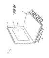
- FIG. 6Ais a perspective front view of a vertical mount package assembly after rotation of the package.
- FIG. 6Bis a perspective rear view of a vertical mount package assembly after rotation of the package.
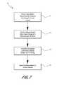
- FIG. 7is a flow diagram illustrating a method of making a vertical mount package assembly according to one embodiment.
- rotation or angular sensors(alternatively, referred to as “gyroscopes”) and/or MEMS static motion sensors (alternatively, referred to as “accelerometers”) are oriented vertically on a horizontally mounted part inside a vehicle.
- the term “vertical”can refer to the orientation approximately perpendicular to the package mounting plane (e.g., on a motherboard), which can be, but is not necessarily, parallel to ground.
- Rotation sensors and motion sensorscan be collectively referred to as “inertial sensors.”
- Such inertial sensorscan be oriented vertically using a vertical mount package, which is configured to mount a sensor die vertically and make electrical connections to a horizontal mounting surface.
- a vertical mount packagewhich is configured to mount a sensor die vertically and make electrical connections to a horizontal mounting surface.
- known schemes for vertical mount packagescan be expensive and have several limitations. Many vertical mount packages rely on pre-molded packages or ceramic, both of which are expensive. Additionally, vertical mount packages can be more susceptible to vibration and package tilt than horizontal mount packages. Accordingly, there is a need for providing a vertical mount package that can incorporate mature packaging technologies to reduce overall cost. Among other attributes, vertical mount packages should have low height and low manufacturing costs while maintaining or improving overall performance.
- a vertical mount package assemblycan include a package and a base substrate.
- the base substratecan include electrical connections for affixing to external circuitry.
- the packagecan include one or more of device regions.
- the packagefurther includes a plurality of flexible electrical leads extending between the base and the package.
- the packagecan take the form of a cavity package in which the device regions are positioned within the cavity and are configured to receive MEMS or IC dies.
- the MEMS or IC diescan be separately formed, diced, and mounted onto the device regions.
- the packagecan take the form of an overmolded leadframe package.
- the packagecan take the form of a laminate substrate having a die mounted thereon, encapsulated with glob top or other material. Electrical connections between the device regions and the flexible leads can be provided, such that the dies of the package can be in electrical communication with the base substrate.
- the base substratecan serve to make electrical connections between the device(s) of the package and the external circuitry.
- the base substratecan additionally serve as a second package in the package assembly, e.g., for an ASIC that processes signals from an inertial motion sensor in the vertical package.
- FIGS. 1A and 1Bare schematic side views of a vertical mount package assembly 1 , before and after rotation.
- the vertical mount package assembly 1includes a base substrate 3 and a package 7 .
- the base substrate 3includes a plurality of leads 5 for providing electrical connection to an external device.
- the leads 5can include a plurality of bond pads on the bottom surface of the base substrate 3 .
- solder bumpscan be attached to the bond pads.
- the leads 5can be exposed portions of a leadframe extending laterally from the sides of the base substrate 3 .
- the leads 5can electrically communicate with contacts or wire-bond pads arranged on an upper surface of the base substrate for connecting to die(s) mounted thereupon.
- the base substrate 3can take any number of forms.
- the base substrate 3can be made of ceramic, plastic, molding compound, or PCB.
- the flexible electrical leads 9connect the base substrate 3 to the package 7 .
- the flexible electrical leads 9include a crease or groove 11 formed therein.
- the groove 11is substantially rectangular in cross-section.
- the groovecan take any number of shapes, for example triangular, curved, or trapezoidal.
- the groove 11may be omitted.
- the groove 11can be formed by a variety of methods. For example, the groove 11 can be stamped into a pre-formed leadframe. In other embodiments, the groove 11 can be formed by standard photolithography followed by a half-etch of the flexible electrical leads 9 . Alternatively, a laser drill can be used to form the groove 11 .
- multiple leads between the base substrate 3 and the package 7have aligned grooves 11 to facilitate controlled bending during assembly.
- the package 7can be rotated with respect to the base substrate 3 .
- the flexible leads 9remain intact following rotation of the package 7 .
- the groove 11can be configured to facilitate aligned bending of the flexible electrical leads 9 during rotation of the package 7 .
- the package 7can include therein a device region configured to receive a device thereon.
- a device regionconfigured to receive a device thereon.
- one or more MEMS or IC diesmay be enclosed within the package 7 .
- the package 7is illustrated schematically, but may take any number of forms.
- the package 7can be a cavity package housing the device within the cavity and an optical lid for environmental protection.
- the package 7can be an overmolded leadframe package.
- the package 7can comprise a laminate substrate, with glob top or other adhesive encapsulating an IC or MEMS device.
- Various other types of packagescan be employed, so long as flexible electrical leads 9 can be provided that extend between the package 7 and the base substrate 3 , and wherein the flexible electrical leads 9 are in electrical communication (whether direct or indirect) with the die enclosed within the package 7 .
- the rotated package 7is positioned substantially vertically, while the base substrate 3 remains substantially horizontal.
- the leads 5 on the base substrate 3can provide for electrical connection to external devices.
- the base substrate 3can be mounted onto the mounting board of an external device or system, and electrically connected thereto through leads 5 .
- the package 7is aligned vertically, while the base substrate 3 provides both mechanical and electrical connection to the external system, for example a PCB.
- Internal electrical connectionsare provided between the leads 5 of the base substrate and the flexible electrical leads 9 .
- the flexible electrical leads 9can be internally connected to a device within the interior of the package 7 .
- the base substrate 3may itself comprise a package housing a device therein.
- the base substrate 3may be a simple substrate, such as PCB or a molded leadframe, having electrical connections therein but containing no devices therein.
- the base substrate 3itself comprises an overmolded leadframe package.
- the base substrate 3can be a thin quad-flat package (TQFP) with an exposed die pad 19 on the bottom surface.
- An IC die 17 or other devicecan be mounted onto the die pad 19 .
- the IC diecan be replaced with a MEMS device.
- Wire bonds 13provide electrical connection between the IC die 17 and both the leads 5 and the flexible electrical leads 9 .
- a molding compound 23covers the IC die 17 , wire bonds 13 , die pad 19 , and portions of the leads 5 and flexible electrical leads 9 .
- the bottom portion of the die pad 19is exposed, allowing thermal conduction away from the encapsulated IC die 17 .
- the package 7can also comprise an overmolded leadframe package.
- the die attach pad 21includes a device 14 mounted therein.
- the die attach pad 21is one example of a “device region” in which a device is configured to be mounted.
- the device 14can be a MEMS or IC die.
- a MEMS diecan be separately fabricated, singulated, and attached to the die attach pad 21 of the package 7 .
- Wire bonds 15provide electrical connection between the device 14 and the flexible electrical leads 9 .
- a molding compound 23covers the die attach pad 21 , device 14 , wire bonds 15 , and a portion of the flexible electrical leads 9 .
- the leadframecan comprise the die attach pad 21 and the flexible electrical leads 9 . After mounting the device 14 , the molding compound 23 can be molded thereover.
- Both the base substrate 3 and the package 7can include beveled edges 25 .
- the angle of the beveled edges 25can define the relative orientation of the base substrate 3 and the package 7 following rotation of the package 7 .
- the beveled edges 25are angled at approximately 45 degrees.
- the package 7is rotated vertically, the two beveled edges 25 meet, restraining the package 7 in a position substantially orthogonal to the base substrate 3 .
- the base substrate 3mounted horizontally, therefore, the package 7 is aligned vertically.
- Having one bevel of 30 degrees and the other bevel of 60 degreescan also provide an orthogonal orientation. As noted above, angles other than 90 degrees are possible.
- FIGS. 3A and 3Banother embodiment of the vertical mount package assembly 1 is shown in cross-section, both before and after rotation of the package. Similar to the embodiments described above, a base substrate 3 is connected via flexible electrical leads 9 to a package 7 .
- the base substrate 3includes leads 5 for external electrical connection.
- the leads 5comprise exposed portions of a leadframe extending laterally from the side of the base substrate 3 .
- the flexible electrical leads 9include a crease or groove 11 formed therein.
- the groove 11can be formed by stamping the leadframe, by chemical etching, laser drilling, or mechanical drilling. The groove can be aligned across a plurality of flexible electrical leads so as to ensure the proper alignment between the base substrate 3 and the package 7 during and after relative rotation during assembly.
- the base substrate 3itself comprises an overmolded leadframe, but no IC or other device is enclosed therein. Accordingly, the external leads 5 can be directly connected to the flexible electrical leads 9 . As will be understood, in this simplified cross-section only one external lead 5 and one flexible electrical lead 9 are shown. In practice, arbitrary numbers of leads can be used. For example, in some embodiments there may be 10 or more separate flexible electrical leads 9 can extend between the base substrate 3 and the package 7 . A molding compound 23 covers portions of the leads 5 and flexible electrical leads 9 . As noted previously, the external leads 5 can provide for electrical connection to external surfaces, such as PCB.
- Both the base substrate 3 and the package 7can include beveled edges 25 to define the relative orientation of the base substrate 3 and the package 7 following rotation of the package 7 .
- the package 7is rotated vertically, the two beveled edges 25 meet, restraining the package 7 in a position substantially orthogonal to the base substrate 3 .
- the base substrate 3mounted horizontally, therefore, the package 7 is aligned vertically.
- bevelscan be angled at other than 45 degrees, and the base substrate 3 and package 7 can be oriented at other than 90 degrees.
- FIGS. 4A and 4Banother embodiment of the vertical mount package assembly 1 is shown in cross-section, both before and after rotation of the package. Similar to the embodiments described above, a base substrate 3 is connected via flexible electrical leads 9 to a package 7 .
- the base substrate 3includes leads 5 for external electrical connection.
- the leads 5comprise exposed portions of a leadframe extending laterally from the side of the base substrate 3 .
- the flexible electrical leads 9include a crease or groove 11 formed therein.
- the groove 11can be formed by stamping the leadframe, by chemical etching, laser drilling, or mechanical drilling. The groove can be aligned across a plurality of flexible electrical leads so as to ensure the proper alignment between the base substrate 3 and the package 7 during and after relative rotation during assembly.
- the base substrate 3itself comprises an overmolded leadframe package.
- the base substrate 3can include an exposed pad 19 on the bottom surface, an IC die 17 mounted onto the exposed pad 19 , and wire bonds 13 providing electrical connection between the IC die 17 and both the leads 5 and the flexible electrical leads 9 .
- a molding compound 23covers the IC die 17 , wire bonds 13 , die pad 19 , and portions of the leads 5 and flexible electrical leads 9 .
- the bottom portion of the die pad 19is exposed, allowing for thermal communication from the encapsulated IC die 17 .
- wire bondsmay be used to provide connections between the device and the flexible electrical leads, as well as between the flexible electrical leads and an ASIC within the base substrate.
- electrical connectionmay be provided using flip-chip methods, as is known in the art.
- the flexible electrical leadsmay extend into the device region of the package. The device can then be affixed directly onto the flexible electrical leads with a conductive adhesive, such as solder.
- anisotropic conducting film or nonconducting pastemay be used to provide electrical and mechanical connection between the device and the flexible electrical leads.
- FIG. 5Ais a schematic perspective top view of a vertical mount package assembly prior to rotation of the package, according to one embodiment.
- the package 7comprises a cavity package, having a cavity 27 exposed to a top surface.
- the device and the cavity lidhave been omitted in FIG. 5A .
- flexible electrical leads 9extend between the base substrate 3 and the package 7 , and extend partially into the cavity 27 .
- a plurality of external leads 5are arranged around each of the sides of the base substrate 3 , except for the side directly adjacent the package 7 .
- a creaseis defined by grooves 11 is formed along the center of the flexible electrical leads 9 , in the exposed portion between the base substrate 3 and the package 7 .
- Beveled edges 25 on each of the base substrate 3 and package 7can provide for a fixed relative orientation, as described in more detail herein.
- FIG. 5Bis an enlarged detail view of the flexible electrical leads shown in FIG. 5A .
- the grooves 11can be substantially aligned to facilitate proper rotation of the package 7 with respect to the base substrate 3 .
- the groovescan be formed by stamping a leadframe, by chemical etching, laser drilling, or mechanical drilling.
- the flexible electrical leads 9can be spaced with an approximately 1 mm pitch, and each flexible electrical lead 9 can have a width of approximately 0.5 mm.
- the package 7Upon attaching the base substrate 3 to a horizontal surface, the package 7 is then vertically aligned. As noted previously, adhesive, such as epoxy (not shown) may be applied to the adjacent beveled edges to fix the relative positions of the package 7 and the base substrate 3 after rotation.
- adhesivesuch as epoxy (not shown) may be applied to the adjacent beveled edges to fix the relative positions of the package 7 and the base substrate 3 after rotation.
- the exposed die pad 19is shown on the bottom surface of the base substrate 3 in FIG. 6B .
- the base substrate 3can be mounted to an external surface, such as PCB, by solder or other connection between the plurality of external leads 5 and optionally the exposed die pad 19 .
- the device (not shown) mounted within the package 7is in electrical communication with the external leads 5 through the plurality of flexible electrical leads 9 .
- a base substrateis provided in block 71 that includes a electrical connections for affixing to external circuitry.
- the base substratecan take the form of an overmolded leadframe package, in one embodiment.
- the base substratecan comprise a package configured to receive a device within the cavity.
- the base substratecan comprise an overmolded leadframe with no device enclosed therein.
- a packageis provided in block 72 that includes a device region configured to receive at least one device.
- the devicescan include MEMS or ICs, and can be separately manufactured and then mounted onto the device regions.
- the devices, particularly IC's,can be sealed onto the device regions by covering them with epoxy or standard deposited passivation layers used in semiconductor fabrication, such as SiON layers.
- MEMS devices, particularly motion sensors,are preferably not encapsulated to avoid stress. Rather, a cavity package can be provided in block 72 and a separate lid can be mounted over the device region, thereby sealing the devices on the device regions within sealed cavities and allowing free MEMS beam or membrane movement, either by individual planar or shaped three-dimensional lids.
- flexible electrical leads between the base substrate and the packageare formed in block 73 .
- the flexible electrical leadscan be integral to the leadframes of both the base substrate and the package.
- the flexible electrical leadscan be integral only to the leadframe of one or the other of the base substrate and the package.
- electrical connections internally within the package and/or base substratecan be provided between the flexible electrical leads and packaged devices by wire-bonds.
- other electrical connectionscan be provided, for example direct or indirect physical contact in flip-chip arrangements.
- the packageis rotated in block 74 relative to the base substrate.
- the packagecan be rotated such that it is oriented substantially perpendicular to the base substrate. In other embodiments, the package can be rotated to a different orientation with respect to the base substrate.
- beveled edges on each of the base substrate and the packagecan join cooperatively to form an orthogonal configuration. In some embodiments, each substrate can have a beveled edge angled at approximately 45 degrees.
- all processing stepse.g., mounting devices, wire-bonding connections, placing a lid over the cavity, and affixing the base substrate to external circuitry, can take place prior to block 74 , while the package is substantially coplanar with the base substrate.
- the packagecan be rotated after each of these processing steps has been performed. Epoxy or other adhesive may then be applied to fix the vertical orientation of the package.
- the packagemay be rotated prior to one or more of the processing steps mentioned above. For example, in some embodiments the package may be rotated and fixed with adhesive prior to mounting the base substrate onto external circuitry.
- MEMS devicesincluding, but not limited to: optical sensors, RF MEMS, inertial sensors (for example, gyroscopes and accelerometers), MEMS thermal sensors, microphone, and pressure sensors.
- the packageshave particular utility for packaging vertically mounted sensors, such as gyroscopic angular motion sensors, to achieve the detection at a certain orientation.
- the devicescan be hermetically sealed within package cavities, and the simple construction is particularly robust for environments (e.g., automobiles) subject to high vibrations.
- “vertical” packages employing the above described configurationscan be used for various electronic devices.
- the electronic devicescan include, but are not limited to, consumer electronic products, parts of the consumer electronic products, electronic test equipments, etc.
- the consumer electronic productscan include, but are not limited to, vehicles (for example, stability control devices), a mobile phone, cellular base stations, a telephone, a television, a computer monitor, a computer, a hand-held computer, a netbook, a tablet computer, a digital book, a personal digital assistant (PDA), a game controller, a GPS, a stereo system, a cassette recorder or player, a DVD player, a CD player, a VCR, a DVR, an MP3 player, a radio, a camcorder, a camera, a digital camera, a portable memory chip, a copier, a facsimile machine, a scanner, a multi functional peripheral device, a wrist watch, a clock, etc.
- the electronic devicecan include unfinished products.
Landscapes
- Engineering & Computer Science (AREA)
- Microelectronics & Electronic Packaging (AREA)
- Physics & Mathematics (AREA)
- Computer Hardware Design (AREA)
- Geometry (AREA)
- Condensed Matter Physics & Semiconductors (AREA)
- General Physics & Mathematics (AREA)
- Power Engineering (AREA)
- Gyroscopes (AREA)
- Micromachines (AREA)
Abstract
Description
Claims (21)
Priority Applications (1)
| Application Number | Priority Date | Filing Date | Title |
|---|---|---|---|
| US13/741,198US9475694B2 (en) | 2013-01-14 | 2013-01-14 | Two-axis vertical mount package assembly |
Applications Claiming Priority (1)
| Application Number | Priority Date | Filing Date | Title |
|---|---|---|---|
| US13/741,198US9475694B2 (en) | 2013-01-14 | 2013-01-14 | Two-axis vertical mount package assembly |
Publications (2)
| Publication Number | Publication Date |
|---|---|
| US20140196540A1 US20140196540A1 (en) | 2014-07-17 |
| US9475694B2true US9475694B2 (en) | 2016-10-25 |
Family
ID=51164150
Family Applications (1)
| Application Number | Title | Priority Date | Filing Date |
|---|---|---|---|
| US13/741,198Active2035-04-27US9475694B2 (en) | 2013-01-14 | 2013-01-14 | Two-axis vertical mount package assembly |
Country Status (1)
| Country | Link |
|---|---|
| US (1) | US9475694B2 (en) |
Cited By (10)
| Publication number | Priority date | Publication date | Assignee | Title |
|---|---|---|---|---|
| US20160343651A1 (en)* | 2015-05-22 | 2016-11-24 | Qualcomm Incorporated | System, apparatus, and method for embedding a 3d component with an interconnect structure |
| US20170112001A1 (en)* | 2015-10-16 | 2017-04-20 | Delta Electronics,Inc. | Stack structure and the manufacturing method of the same |
| US10349539B2 (en)* | 2017-10-03 | 2019-07-09 | Aptiv Technologies Limited | Vehicle electrical center and method of manufacturing same |
| US10629574B2 (en) | 2016-10-27 | 2020-04-21 | Analog Devices, Inc. | Compact integrated device packages |
| US10697800B2 (en) | 2016-11-04 | 2020-06-30 | Analog Devices Global | Multi-dimensional measurement using magnetic sensors and related systems, methods, and integrated circuits |
| US10916871B2 (en)* | 2018-10-09 | 2021-02-09 | TE Connectivity Italia Distribution S.r.l. | Connection device |
| US11628275B2 (en) | 2018-01-31 | 2023-04-18 | Analog Devices, Inc. | Electronic devices |
| US11647678B2 (en) | 2016-08-23 | 2023-05-09 | Analog Devices International Unlimited Company | Compact integrated device packages |
| TWI812232B (en)* | 2021-10-27 | 2023-08-11 | 大陸商珠海越亞半導體股份有限公司 | Embedded packaging structure and manufacturing method thereof |
| US20240401756A1 (en)* | 2023-05-17 | 2024-12-05 | Creeled, Inc. | Three dimensional led device and method of manufacture |
Families Citing this family (4)
| Publication number | Priority date | Publication date | Assignee | Title |
|---|---|---|---|---|
| US11432407B2 (en) | 2016-10-28 | 2022-08-30 | Xfmrs, Inc. | Electrical component package with reinforced molded pins |
| US10531573B2 (en)* | 2016-10-28 | 2020-01-07 | Xfmrs, Inc. | Electrical component package with reinforced molded pins |
| DE102017212748B4 (en)* | 2017-07-25 | 2021-02-11 | Infineon Technologies Ag | Sensor devices and methods of making them |
| NL2026503B1 (en)* | 2020-09-18 | 2022-05-23 | Ampleon Netherlands Bv | Molded RF power package |
Citations (74)
| Publication number | Priority date | Publication date | Assignee | Title |
|---|---|---|---|---|
| US3949274A (en) | 1974-05-30 | 1976-04-06 | International Business Machines Corporation | Packaging and interconnection for superconductive circuitry |
| US4642670A (en)* | 1983-12-02 | 1987-02-10 | At&T Bell Laboratories | Chip carrier package |
| US4742183A (en) | 1986-10-24 | 1988-05-03 | Napco Security Systems, Inc. | Methods and techniques for fabricating foldable printed circuit boards |
| US5126286A (en) | 1990-10-05 | 1992-06-30 | Micron Technology, Inc. | Method of manufacturing edge connected semiconductor die |
| US5452182A (en) | 1990-04-05 | 1995-09-19 | Martin Marietta Corporation | Flexible high density interconnect structure and flexibly interconnected system |
| US5554806A (en) | 1994-06-15 | 1996-09-10 | Nippondenso Co., Ltd. | Physical-quantity detecting device |
| US5555159A (en) | 1993-12-17 | 1996-09-10 | Schneider Electric Sa | Add-on module for variable speed drives |
| US5616863A (en)* | 1994-02-01 | 1997-04-01 | Ic Sensors, Inc. | Side surface mounted accelerometer assembly |
| JPH09121015A (en) | 1995-10-25 | 1997-05-06 | Hitachi Ltd | Semiconductor device |
| US5731222A (en) | 1995-08-01 | 1998-03-24 | Hughes Aircraft Company | Externally connected thin electronic circuit having recessed bonding pads |
| US5889658A (en)* | 1997-11-25 | 1999-03-30 | Motorola, Inc. | Package assembly for an electronic component |
| US5903440A (en) | 1998-01-30 | 1999-05-11 | Delco Electronics Corporaiton | Method of forming assemblies of circuit boards in different planes |
| US5936850A (en)* | 1995-03-03 | 1999-08-10 | Canon Kabushiki Kaisha | Circuit board connection structure and method, and liquid crystal device including the connection structure |
| US5949657A (en)* | 1997-12-01 | 1999-09-07 | Karabatsos; Chris | Bottom or top jumpered foldable electronic assembly |
| US6035712A (en)* | 1997-03-14 | 2000-03-14 | Denso Corporation | Sensor device and method of producing the same using lead frame |
| US6040624A (en) | 1997-10-02 | 2000-03-21 | Motorola, Inc. | Semiconductor device package and method |
| US6060780A (en)* | 1996-02-23 | 2000-05-09 | Denson Corporation | Surface mount type unit and transducer assembly using same |
| US6075708A (en) | 1997-09-04 | 2000-06-13 | Rohm Co., Ltd. | Partly bent electric circuit substrate and method for manufacturing the same |
| US6078102A (en) | 1998-03-03 | 2000-06-20 | Silicon Bandwidth, Inc. | Semiconductor die package for mounting in horizontal and upright configurations |
| US6291894B1 (en) | 1998-08-31 | 2001-09-18 | Micron Technology, Inc. | Method and apparatus for a semiconductor package for vertical surface mounting |
| US6339191B1 (en) | 1994-03-11 | 2002-01-15 | Silicon Bandwidth Inc. | Prefabricated semiconductor chip carrier |
| US6348427B1 (en) | 1999-02-01 | 2002-02-19 | Kyocera Corporation | High-thermal-expansion glass ceramic sintered product |
| US6520789B2 (en)* | 2001-05-22 | 2003-02-18 | Delphi Technologies, Inc. | Connecting system for printed circuit boards |
| US6532157B1 (en)* | 2000-11-16 | 2003-03-11 | Amkor Technology, Inc. | Angulated semiconductor packages |
| US6570246B1 (en) | 2002-06-12 | 2003-05-27 | United Microelectronics Corp. | Multi-die package |
| US6591492B2 (en) | 2001-08-30 | 2003-07-15 | Micron Technology, Inc. | Angled edge connections for multichip structures |
| US6618938B1 (en)* | 2000-02-08 | 2003-09-16 | Lsi Logic Corporation | Interposer for semiconductor package assembly |
| US20030209789A1 (en) | 2002-05-09 | 2003-11-13 | Hanson David S. | Coplanar mounting member for a mem sensor |
| US20040041254A1 (en)* | 2002-09-04 | 2004-03-04 | Lewis Long | Packaged microchip |
| US6721189B1 (en)* | 2002-03-13 | 2004-04-13 | Rambus, Inc. | Memory module |
| US20040157410A1 (en) | 2003-01-16 | 2004-08-12 | Seiko Epson Corporation | Semiconductor device, semiconductor module, electronic equipment, method for manufacturing semiconductor device, and method for manufacturing semiconductor module |
| US6777261B2 (en) | 2000-12-26 | 2004-08-17 | Micron Technology, Inc. | Method and apparatus for a semiconductor package for vertical surface mounting |
| US20040169244A1 (en) | 2003-02-28 | 2004-09-02 | Honeywell International, Inc. | Miniature 3-dimensional package for MEMS sensors |
| US6852607B2 (en) | 2001-05-31 | 2005-02-08 | Samsung Electronics., Ltd | Wafer level package having a side package |
| US20050136740A1 (en)* | 2003-12-20 | 2005-06-23 | Ronny Ludwig | Premolded housing |
| US20050230795A1 (en) | 2004-03-30 | 2005-10-20 | Kabushiki Kaisha Toshiba | LSI package provided with interface module, and transmission line header employed in the package |
| US6966784B2 (en)* | 2003-12-19 | 2005-11-22 | Palo Alto Research Center Incorporated | Flexible cable interconnect assembly |
| US7035116B2 (en)* | 2002-11-21 | 2006-04-25 | Infineon Technologies Ag | Memory system and memory subsystem |
| US20060151864A1 (en) | 2005-01-11 | 2006-07-13 | Rosemount Inc. | MEMS packaging with improved reaction to temperature changes |
| US7115984B2 (en) | 2002-06-18 | 2006-10-03 | Micron Technology, Inc. | Semiconductor devices including peripherally located bond pads, intermediates thereof, assemblies, and packages including the semiconductor devices, and support elements for the semiconductor devices |
| US7122889B2 (en)* | 2000-05-03 | 2006-10-17 | Rambus, Inc. | Semiconductor module |
| US20060261453A1 (en) | 2005-03-16 | 2006-11-23 | Yonggill Lee | Semiconductor package and stack arrangement thereof |
| US7148428B2 (en)* | 2004-09-27 | 2006-12-12 | Intel Corporation | Flexible cable for high-speed interconnect |
| US20070053504A1 (en) | 2003-10-31 | 2007-03-08 | Matsushita Electric Industrial Co., Ltd. | Connection device, electronic apparatus with the same, and folding portable terminal device |
| US7202552B2 (en) | 2005-07-15 | 2007-04-10 | Silicon Matrix Pte. Ltd. | MEMS package using flexible substrates, and method thereof |
| US7211886B2 (en)* | 2004-04-01 | 2007-05-01 | Industrial Technology Research Institute | Three-dimensional multichip stack electronic package structure |
| US7265719B1 (en) | 2006-05-11 | 2007-09-04 | Ball Aerospace & Technologies Corp. | Packaging technique for antenna systems |
| US20080001241A1 (en)* | 2006-03-01 | 2008-01-03 | Tessera, Inc. | Structure and method of making lidded chips |
| US7351072B2 (en)* | 2005-07-08 | 2008-04-01 | Qimonda Ag | Memory module, memory extension memory module, memory module system, and method for manufacturing a memory module |
| US7375009B2 (en) | 2002-06-14 | 2008-05-20 | Micron Technology, Inc. | Method of forming a conductive via through a wafer |
| US20080175425A1 (en) | 2006-11-30 | 2008-07-24 | Analog Devices, Inc. | Microphone System with Silicon Microphone Secured to Package Lid |
| US20080205025A1 (en)* | 2006-07-21 | 2008-08-28 | Analog Devices, Inc. | Package Having a Plurality of Mounting Orientations |
| US7420262B2 (en) | 2003-02-27 | 2008-09-02 | Infineon Technologies Ag | Electronic component and semiconductor wafer, and method for producing the same |
| US7429788B2 (en) | 2006-03-08 | 2008-09-30 | Microelectronics Assembly Technologies, Inc. | Thin multichip flex-module |
| US20080285111A1 (en) | 2006-08-30 | 2008-11-20 | Fusao Ishii | Mirror device |
| US7467552B2 (en) | 2005-11-10 | 2008-12-23 | Honeywell International Inc. | Miniature package for translation of sensor sense axis |
| US20090121342A1 (en) | 2007-11-14 | 2009-05-14 | Minakawa Atsushi | Semiconductor device including main substrate and sub substrates and fabrication method of the same |
| US20100078739A1 (en)* | 2008-09-30 | 2010-04-01 | Analog Devices, Inc. | Vertical Mount Package for MEMS Sensors |
| US7692102B2 (en)* | 2004-08-11 | 2010-04-06 | Sony Corporation | Electronic circuit device |
| US20100090295A1 (en) | 2008-10-09 | 2010-04-15 | Silicon Matrix Pte. Ltd. | Folded lead-frame packages for MEMS devices |
| US20100155863A1 (en) | 2005-08-11 | 2010-06-24 | Koninklijke Philips Electronics, N.V. | Method for manufacturing a microelectronic package comprising a silicon mems microphone |
| US7768280B1 (en)* | 2007-11-15 | 2010-08-03 | Altera Corporation | Apparatus for a low-cost semiconductor test interface system |
| US20100197148A1 (en) | 2009-02-02 | 2010-08-05 | Apex Technologies, Inc. | Flexible magnetic interconnects |
| US7839657B2 (en) | 2006-04-28 | 2010-11-23 | Continental Automotive Systems Us, Inc. | Position adjustable printed circuit board |
| US7851829B2 (en)* | 2007-02-05 | 2010-12-14 | Infineon Technologies Ag | Semiconductor chip module |
| USRE42318E1 (en)* | 2000-05-03 | 2011-05-03 | Rambus Inc. | Semiconductor module with serial bus connection to multiple dies |
| US20110141712A1 (en)* | 2009-12-11 | 2011-06-16 | You Se-Ho | Package substrate and semiconductor package having the same |
| US20110149522A1 (en) | 2009-12-22 | 2011-06-23 | Christian Johann | Electronic control unit and method for producing component of same |
| US8217507B1 (en)* | 2010-01-22 | 2012-07-10 | Amkor Technology, Inc. | Edge mount semiconductor package |
| US8520401B2 (en)* | 2011-08-18 | 2013-08-27 | Hong Fu Jin Precision Industry (Shenzhen) Co., Ltd. | Motherboard assembly having serial advanced technology attachment dual in-line memory module |
| US8529276B2 (en)* | 2011-02-18 | 2013-09-10 | Hi Rel Connectors, Inc. | Connector to flex assembly |
| US8692366B2 (en)* | 2010-09-30 | 2014-04-08 | Analog Device, Inc. | Apparatus and method for microelectromechanical systems device packaging |
| US8821167B2 (en)* | 2012-05-31 | 2014-09-02 | Hi Rel Connectors, Inc. | Apparatus for electrically connecting a flexible circuit to a receiver |
| US8836132B2 (en)* | 2012-04-03 | 2014-09-16 | Analog Devices, Inc. | Vertical mount package and wafer level packaging therefor |
- 2013
- 2013-01-14USUS13/741,198patent/US9475694B2/enactiveActive
Patent Citations (81)
| Publication number | Priority date | Publication date | Assignee | Title |
|---|---|---|---|---|
| US3949274A (en) | 1974-05-30 | 1976-04-06 | International Business Machines Corporation | Packaging and interconnection for superconductive circuitry |
| US4642670A (en)* | 1983-12-02 | 1987-02-10 | At&T Bell Laboratories | Chip carrier package |
| US4742183A (en) | 1986-10-24 | 1988-05-03 | Napco Security Systems, Inc. | Methods and techniques for fabricating foldable printed circuit boards |
| US5452182A (en) | 1990-04-05 | 1995-09-19 | Martin Marietta Corporation | Flexible high density interconnect structure and flexibly interconnected system |
| US5126286A (en) | 1990-10-05 | 1992-06-30 | Micron Technology, Inc. | Method of manufacturing edge connected semiconductor die |
| US5555159A (en) | 1993-12-17 | 1996-09-10 | Schneider Electric Sa | Add-on module for variable speed drives |
| US5616863A (en)* | 1994-02-01 | 1997-04-01 | Ic Sensors, Inc. | Side surface mounted accelerometer assembly |
| US6339191B1 (en) | 1994-03-11 | 2002-01-15 | Silicon Bandwidth Inc. | Prefabricated semiconductor chip carrier |
| US5554806A (en) | 1994-06-15 | 1996-09-10 | Nippondenso Co., Ltd. | Physical-quantity detecting device |
| US5936850A (en)* | 1995-03-03 | 1999-08-10 | Canon Kabushiki Kaisha | Circuit board connection structure and method, and liquid crystal device including the connection structure |
| US5731222A (en) | 1995-08-01 | 1998-03-24 | Hughes Aircraft Company | Externally connected thin electronic circuit having recessed bonding pads |
| JPH09121015A (en) | 1995-10-25 | 1997-05-06 | Hitachi Ltd | Semiconductor device |
| US6060780A (en)* | 1996-02-23 | 2000-05-09 | Denson Corporation | Surface mount type unit and transducer assembly using same |
| US6035712A (en)* | 1997-03-14 | 2000-03-14 | Denso Corporation | Sensor device and method of producing the same using lead frame |
| US6075708A (en) | 1997-09-04 | 2000-06-13 | Rohm Co., Ltd. | Partly bent electric circuit substrate and method for manufacturing the same |
| US6040624A (en) | 1997-10-02 | 2000-03-21 | Motorola, Inc. | Semiconductor device package and method |
| US5889658A (en)* | 1997-11-25 | 1999-03-30 | Motorola, Inc. | Package assembly for an electronic component |
| US5949657A (en)* | 1997-12-01 | 1999-09-07 | Karabatsos; Chris | Bottom or top jumpered foldable electronic assembly |
| US6705005B1 (en) | 1998-01-30 | 2004-03-16 | Delphi Technologies, Inc. | Method of forming assemblies of circuit boards in different planes |
| US5903440A (en) | 1998-01-30 | 1999-05-11 | Delco Electronics Corporaiton | Method of forming assemblies of circuit boards in different planes |
| US6078102A (en) | 1998-03-03 | 2000-06-20 | Silicon Bandwidth, Inc. | Semiconductor die package for mounting in horizontal and upright configurations |
| US6903465B2 (en) | 1998-08-31 | 2005-06-07 | Micron Technology, Inc. | Method and apparatus for a semiconductor package for vertical surface mounting |
| US6511863B2 (en) | 1998-08-31 | 2003-01-28 | Micron Technology, Inc. | Method and apparatus for a semiconductor package for vertical surface mounting |
| US6291894B1 (en) | 1998-08-31 | 2001-09-18 | Micron Technology, Inc. | Method and apparatus for a semiconductor package for vertical surface mounting |
| US6348427B1 (en) | 1999-02-01 | 2002-02-19 | Kyocera Corporation | High-thermal-expansion glass ceramic sintered product |
| US6618938B1 (en)* | 2000-02-08 | 2003-09-16 | Lsi Logic Corporation | Interposer for semiconductor package assembly |
| US7122889B2 (en)* | 2000-05-03 | 2006-10-17 | Rambus, Inc. | Semiconductor module |
| USRE42318E1 (en)* | 2000-05-03 | 2011-05-03 | Rambus Inc. | Semiconductor module with serial bus connection to multiple dies |
| US6532157B1 (en)* | 2000-11-16 | 2003-03-11 | Amkor Technology, Inc. | Angulated semiconductor packages |
| US6777261B2 (en) | 2000-12-26 | 2004-08-17 | Micron Technology, Inc. | Method and apparatus for a semiconductor package for vertical surface mounting |
| US6520789B2 (en)* | 2001-05-22 | 2003-02-18 | Delphi Technologies, Inc. | Connecting system for printed circuit boards |
| US6852607B2 (en) | 2001-05-31 | 2005-02-08 | Samsung Electronics., Ltd | Wafer level package having a side package |
| US6591492B2 (en) | 2001-08-30 | 2003-07-15 | Micron Technology, Inc. | Angled edge connections for multichip structures |
| US6721189B1 (en)* | 2002-03-13 | 2004-04-13 | Rambus, Inc. | Memory module |
| US7012812B2 (en)* | 2002-03-13 | 2006-03-14 | Rambus, Inc. | Memory module |
| US20030209789A1 (en) | 2002-05-09 | 2003-11-13 | Hanson David S. | Coplanar mounting member for a mem sensor |
| US6570246B1 (en) | 2002-06-12 | 2003-05-27 | United Microelectronics Corp. | Multi-die package |
| US20110018143A1 (en) | 2002-06-14 | 2011-01-27 | Swee Kwang Chua | Wafer level packaging |
| US7375009B2 (en) | 2002-06-14 | 2008-05-20 | Micron Technology, Inc. | Method of forming a conductive via through a wafer |
| US7115984B2 (en) | 2002-06-18 | 2006-10-03 | Micron Technology, Inc. | Semiconductor devices including peripherally located bond pads, intermediates thereof, assemblies, and packages including the semiconductor devices, and support elements for the semiconductor devices |
| US20040041254A1 (en)* | 2002-09-04 | 2004-03-04 | Lewis Long | Packaged microchip |
| US7035116B2 (en)* | 2002-11-21 | 2006-04-25 | Infineon Technologies Ag | Memory system and memory subsystem |
| US20040157410A1 (en) | 2003-01-16 | 2004-08-12 | Seiko Epson Corporation | Semiconductor device, semiconductor module, electronic equipment, method for manufacturing semiconductor device, and method for manufacturing semiconductor module |
| US7420262B2 (en) | 2003-02-27 | 2008-09-02 | Infineon Technologies Ag | Electronic component and semiconductor wafer, and method for producing the same |
| US20040169244A1 (en) | 2003-02-28 | 2004-09-02 | Honeywell International, Inc. | Miniature 3-dimensional package for MEMS sensors |
| US20070053504A1 (en) | 2003-10-31 | 2007-03-08 | Matsushita Electric Industrial Co., Ltd. | Connection device, electronic apparatus with the same, and folding portable terminal device |
| US6966784B2 (en)* | 2003-12-19 | 2005-11-22 | Palo Alto Research Center Incorporated | Flexible cable interconnect assembly |
| US20050136740A1 (en)* | 2003-12-20 | 2005-06-23 | Ronny Ludwig | Premolded housing |
| US20050230795A1 (en) | 2004-03-30 | 2005-10-20 | Kabushiki Kaisha Toshiba | LSI package provided with interface module, and transmission line header employed in the package |
| US7211886B2 (en)* | 2004-04-01 | 2007-05-01 | Industrial Technology Research Institute | Three-dimensional multichip stack electronic package structure |
| US7692102B2 (en)* | 2004-08-11 | 2010-04-06 | Sony Corporation | Electronic circuit device |
| US7148428B2 (en)* | 2004-09-27 | 2006-12-12 | Intel Corporation | Flexible cable for high-speed interconnect |
| US20060151864A1 (en) | 2005-01-11 | 2006-07-13 | Rosemount Inc. | MEMS packaging with improved reaction to temperature changes |
| US20060261453A1 (en) | 2005-03-16 | 2006-11-23 | Yonggill Lee | Semiconductor package and stack arrangement thereof |
| US7351072B2 (en)* | 2005-07-08 | 2008-04-01 | Qimonda Ag | Memory module, memory extension memory module, memory module system, and method for manufacturing a memory module |
| US7202552B2 (en) | 2005-07-15 | 2007-04-10 | Silicon Matrix Pte. Ltd. | MEMS package using flexible substrates, and method thereof |
| US20100155863A1 (en) | 2005-08-11 | 2010-06-24 | Koninklijke Philips Electronics, N.V. | Method for manufacturing a microelectronic package comprising a silicon mems microphone |
| US7467552B2 (en) | 2005-11-10 | 2008-12-23 | Honeywell International Inc. | Miniature package for translation of sensor sense axis |
| US20080001241A1 (en)* | 2006-03-01 | 2008-01-03 | Tessera, Inc. | Structure and method of making lidded chips |
| US7429788B2 (en) | 2006-03-08 | 2008-09-30 | Microelectronics Assembly Technologies, Inc. | Thin multichip flex-module |
| US7839657B2 (en) | 2006-04-28 | 2010-11-23 | Continental Automotive Systems Us, Inc. | Position adjustable printed circuit board |
| US7265719B1 (en) | 2006-05-11 | 2007-09-04 | Ball Aerospace & Technologies Corp. | Packaging technique for antenna systems |
| US20080205025A1 (en)* | 2006-07-21 | 2008-08-28 | Analog Devices, Inc. | Package Having a Plurality of Mounting Orientations |
| US20080285111A1 (en) | 2006-08-30 | 2008-11-20 | Fusao Ishii | Mirror device |
| US20080175425A1 (en) | 2006-11-30 | 2008-07-24 | Analog Devices, Inc. | Microphone System with Silicon Microphone Secured to Package Lid |
| US7851829B2 (en)* | 2007-02-05 | 2010-12-14 | Infineon Technologies Ag | Semiconductor chip module |
| US20090121342A1 (en) | 2007-11-14 | 2009-05-14 | Minakawa Atsushi | Semiconductor device including main substrate and sub substrates and fabrication method of the same |
| US7768280B1 (en)* | 2007-11-15 | 2010-08-03 | Altera Corporation | Apparatus for a low-cost semiconductor test interface system |
| US8174111B2 (en)* | 2008-09-30 | 2012-05-08 | Analog Devices, Inc. | Vertical mount package for MEMS sensors |
| US20100078739A1 (en)* | 2008-09-30 | 2010-04-01 | Analog Devices, Inc. | Vertical Mount Package for MEMS Sensors |
| US8624380B2 (en)* | 2008-09-30 | 2014-01-07 | Analog Devices, Inc. | Vertical mount package for MEMS sensors |
| US20100090295A1 (en) | 2008-10-09 | 2010-04-15 | Silicon Matrix Pte. Ltd. | Folded lead-frame packages for MEMS devices |
| US20100197148A1 (en) | 2009-02-02 | 2010-08-05 | Apex Technologies, Inc. | Flexible magnetic interconnects |
| US20110141712A1 (en)* | 2009-12-11 | 2011-06-16 | You Se-Ho | Package substrate and semiconductor package having the same |
| US20110149522A1 (en) | 2009-12-22 | 2011-06-23 | Christian Johann | Electronic control unit and method for producing component of same |
| US8217507B1 (en)* | 2010-01-22 | 2012-07-10 | Amkor Technology, Inc. | Edge mount semiconductor package |
| US8692366B2 (en)* | 2010-09-30 | 2014-04-08 | Analog Device, Inc. | Apparatus and method for microelectromechanical systems device packaging |
| US8529276B2 (en)* | 2011-02-18 | 2013-09-10 | Hi Rel Connectors, Inc. | Connector to flex assembly |
| US8520401B2 (en)* | 2011-08-18 | 2013-08-27 | Hong Fu Jin Precision Industry (Shenzhen) Co., Ltd. | Motherboard assembly having serial advanced technology attachment dual in-line memory module |
| US8836132B2 (en)* | 2012-04-03 | 2014-09-16 | Analog Devices, Inc. | Vertical mount package and wafer level packaging therefor |
| US8821167B2 (en)* | 2012-05-31 | 2014-09-02 | Hi Rel Connectors, Inc. | Apparatus for electrically connecting a flexible circuit to a receiver |
Non-Patent Citations (3)
| Title |
|---|
| Images obtained on Jun. 13, 2011 from a web search related to three-dimensional packaging. |
| Sensors-HARTING Mitronics, HARTING Pushing Performance, in 2 pages (downloaded from World Wide Web page: harting-mitronics.ch/en/produkte/anwendungen/sensorik/index.php on Jul. 11, 2011). |
| USPTO; Office Action dated Apr. 11, 2013, from related U.S. Appl. No. 13/085,294, filed Apr. 12, 2011. |
Cited By (13)
| Publication number | Priority date | Publication date | Assignee | Title |
|---|---|---|---|---|
| US20160343651A1 (en)* | 2015-05-22 | 2016-11-24 | Qualcomm Incorporated | System, apparatus, and method for embedding a 3d component with an interconnect structure |
| US10163687B2 (en)* | 2015-05-22 | 2018-12-25 | Qualcomm Incorporated | System, apparatus, and method for embedding a 3D component with an interconnect structure |
| US20170112001A1 (en)* | 2015-10-16 | 2017-04-20 | Delta Electronics,Inc. | Stack structure and the manufacturing method of the same |
| US10342153B2 (en)* | 2015-10-16 | 2019-07-02 | Delta Electronics, Inc. | Stack structure and the manufacturing method of the same |
| US11647678B2 (en) | 2016-08-23 | 2023-05-09 | Analog Devices International Unlimited Company | Compact integrated device packages |
| US10629574B2 (en) | 2016-10-27 | 2020-04-21 | Analog Devices, Inc. | Compact integrated device packages |
| US10697800B2 (en) | 2016-11-04 | 2020-06-30 | Analog Devices Global | Multi-dimensional measurement using magnetic sensors and related systems, methods, and integrated circuits |
| US10349539B2 (en)* | 2017-10-03 | 2019-07-09 | Aptiv Technologies Limited | Vehicle electrical center and method of manufacturing same |
| US11628275B2 (en) | 2018-01-31 | 2023-04-18 | Analog Devices, Inc. | Electronic devices |
| US10916871B2 (en)* | 2018-10-09 | 2021-02-09 | TE Connectivity Italia Distribution S.r.l. | Connection device |
| TWI812232B (en)* | 2021-10-27 | 2023-08-11 | 大陸商珠海越亞半導體股份有限公司 | Embedded packaging structure and manufacturing method thereof |
| US20240401756A1 (en)* | 2023-05-17 | 2024-12-05 | Creeled, Inc. | Three dimensional led device and method of manufacture |
| US12385605B2 (en)* | 2023-05-17 | 2025-08-12 | Creeled, Inc. | Three dimensional LED device and method of manufacture |
Also Published As
| Publication number | Publication date |
|---|---|
| US20140196540A1 (en) | 2014-07-17 |
Similar Documents
| Publication | Publication Date | Title |
|---|---|---|
| US9475694B2 (en) | Two-axis vertical mount package assembly | |
| US9278851B2 (en) | Vertical mount package and wafer level packaging therefor | |
| US8692366B2 (en) | Apparatus and method for microelectromechanical systems device packaging | |
| US7671432B2 (en) | Dynamic quantity sensor | |
| KR101771064B1 (en) | Microelectromechanical system (mems) on application specific integrated circuit (asic) | |
| US20140217566A1 (en) | Double-sided package | |
| US8421210B2 (en) | Integrated circuit packaging system with dual side connection and method of manufacture thereof | |
| US8624380B2 (en) | Vertical mount package for MEMS sensors | |
| US9731959B2 (en) | Integrated device packages having a MEMS die sealed in a cavity by a processor die and method of manufacturing the same | |
| US8541886B2 (en) | Integrated circuit packaging system with via and method of manufacture thereof | |
| CN103569956B (en) | Sensor package and method of forming same | |
| CN110677793B (en) | Microphone packaging structure | |
| EP2520541B1 (en) | Systems and methods for three-axis sensor chip packages | |
| JP2009021564A (en) | Image sensor module, manufacturing method thereof, and camera module | |
| JP2007227596A (en) | Semiconductor module and its manufacturing method | |
| US20070277607A1 (en) | Semiconductor acceleration sensor | |
| US8981577B2 (en) | Integrated circuit packaging system with interconnect and method of manufacture thereof | |
| US9362257B2 (en) | Mirco-electro-mechanical system module and manufacturing method thereof | |
| JP2008026183A (en) | Ic-integrated acceleration sensor | |
| US8937393B2 (en) | Integrated circuit package system with device cavity | |
| US20080105988A1 (en) | Electrical component having external contacting | |
| US20070090544A1 (en) | Integrated circuit package encapsulating a hermetically sealed device | |
| JP2007007774A (en) | Package for micro electro mechanical device and manufacturing method thereof | |
| JP2009229349A (en) | Acceleration sensor package | |
| KR20120125176A (en) | Systems and methods for three-axis sensor chip packages |
Legal Events
| Date | Code | Title | Description |
|---|---|---|---|
| AS | Assignment | Owner name:ANALOG DEVICES TECHNOLOGY, BERMUDA Free format text:ASSIGNMENT OF ASSIGNORS INTEREST;ASSIGNORS:MARTIZON, ARTURO, JR.;GOIDA, THOMAS M.;SIGNING DATES FROM 20130215 TO 20130218;REEL/FRAME:029842/0947 | |
| AS | Assignment | Owner name:ANALOG DEVICES GLOBAL, BERMUDA Free format text:ASSIGNMENT OF ASSIGNORS INTEREST;ASSIGNOR:ANALOG DEVICES TECHNOLOGY;REEL/FRAME:034787/0910 Effective date:20141031 | |
| STCF | Information on status: patent grant | Free format text:PATENTED CASE | |
| MAFP | Maintenance fee payment | Free format text:PAYMENT OF MAINTENANCE FEE, 4TH YEAR, LARGE ENTITY (ORIGINAL EVENT CODE: M1551); ENTITY STATUS OF PATENT OWNER: LARGE ENTITY Year of fee payment:4 | |
| AS | Assignment | Owner name:ANALOG DEVICES INTERNATIONAL UNLIMITED COMPANY, IRELAND Free format text:ASSIGNMENT OF ASSIGNORS INTEREST;ASSIGNOR:ANALOG DEVICES GLOBAL UNLIMITED COMPANY;REEL/FRAME:059096/0794 Effective date:20181105 Owner name:ANALOG DEVICES GLOBAL UNLIMITED COMPANY, BERMUDA Free format text:CHANGE OF NAME;ASSIGNOR:ANALOG DEVICES GLOBAL;REEL/FRAME:059089/0791 Effective date:20161130 | |
| MAFP | Maintenance fee payment | Free format text:PAYMENT OF MAINTENANCE FEE, 8TH YEAR, LARGE ENTITY (ORIGINAL EVENT CODE: M1552); ENTITY STATUS OF PATENT OWNER: LARGE ENTITY Year of fee payment:8 |