US9473243B2 - Optical transceiver device - Google Patents
Optical transceiver deviceDownload PDFInfo
- Publication number
- US9473243B2 US9473243B2US14/187,739US201414187739AUS9473243B2US 9473243 B2US9473243 B2US 9473243B2US 201414187739 AUS201414187739 AUS 201414187739AUS 9473243 B2US9473243 B2US 9473243B2
- Authority
- US
- United States
- Prior art keywords
- optical
- signal
- module
- transceiver
- switching
- Prior art date
- Legal status (The legal status is an assumption and is not a legal conclusion. Google has not performed a legal analysis and makes no representation as to the accuracy of the status listed.)
- Active, expires
Links
- 230000003287optical effectEffects0.000titleclaimsabstractdescription500
- 239000013307optical fiberSubstances0.000claimsabstractdescription15
- 238000004891communicationMethods0.000claimsabstractdescription8
- 238000012544monitoring processMethods0.000claimsdescription16
- 238000000034methodMethods0.000claimsdescription13
- 230000008569processEffects0.000claimsdescription13
- 238000010168coupling processMethods0.000claimsdescription8
- 230000008878couplingEffects0.000claimsdescription7
- 238000005859coupling reactionMethods0.000claimsdescription7
- 230000002159abnormal effectEffects0.000claimsdescription3
- 238000010586diagramMethods0.000description9
- 230000005540biological transmissionEffects0.000description4
- 238000006243chemical reactionMethods0.000description3
- 238000005516engineering processMethods0.000description3
- 238000005452bendingMethods0.000description2
- 238000011161developmentMethods0.000description2
- 239000000835fiberSubstances0.000description2
- 241000700605VirusesSpecies0.000description1
- 230000002776aggregationEffects0.000description1
- 238000004220aggregationMethods0.000description1
- 238000013459approachMethods0.000description1
- 230000015556catabolic processEffects0.000description1
- 230000003247decreasing effectEffects0.000description1
- 238000006731degradation reactionMethods0.000description1
- 238000013461designMethods0.000description1
- 238000001514detection methodMethods0.000description1
- 230000000694effectsEffects0.000description1
- 238000007689inspectionMethods0.000description1
- 239000000463materialSubstances0.000description1
- 230000007246mechanismEffects0.000description1
- 238000012986modificationMethods0.000description1
- 230000004048modificationEffects0.000description1
- 230000004044responseEffects0.000description1
- 230000008054signal transmissionEffects0.000description1
Images


Classifications
- H—ELECTRICITY
- H04—ELECTRIC COMMUNICATION TECHNIQUE
- H04B—TRANSMISSION
- H04B10/00—Transmission systems employing electromagnetic waves other than radio-waves, e.g. infrared, visible or ultraviolet light, or employing corpuscular radiation, e.g. quantum communication
- H04B10/40—Transceivers
Definitions
- the inventionrelates to an optical transceiver device, particularly to an optical transceiver device with smaller volume and simpler structure.
- optical communication technologyhas become a major communication technology developed currently because of several advantages, including rapid transmission speed, long transmission distance, capability of anti-electromagnetic interference, and high security etc.
- optical transceiver devicesare mainly formed by O/E transceivers, optical switching switches and optical transceiving components.
- O/E transceiversare mainly in charge of mutual conversion processes between optical signal and electrical signal.
- Conventional O/E transceiversare provided in optical transceiver devices as parts individually. Because of limited number of optical signal transmitting channels provided by a single O/E transceiver, as optical transceiver devices are connected to multiple optical network equipments, multiple O/E transceivers have to be provided therein, such that O/E transceiving modules are maximized, which results in relatively large volume for conventional optical transceiver devices.
- optical signal transmits between optical switching switches and optical transceiving components in an optical transceiver devicesis achieved by optical cables.
- a certain degree of bending radiusin terms of EAI/TIA 568 regulation, the bending radius of multi-mode optical cable shall not be smaller than 25 mm
- the optical cable used in transmitting optical signalsuch that optical signal keep on transmitting in optical cables without degradation. Therefore, a space has to be reserved inside the optical transceiver device to contain optical cables, such that the volume cannot be reduced and the development trend to minimize optical transceiver device is impossible.
- one object of the inventionis to provide an optical transceiver device with smaller volume.
- an optical transceiver device of the inventionis provided to connect a first, second optical network equipments and an in-line equipment, respectively, in order to form an optical fiber network to provide network communication services for the first, second optical network equipments.
- the optical transceiver device of the inventionhas an O/E transceiver module, a control module for transceiver, an optical wave guide, an optical switching module and a switching control module.
- the O/E transceiver moduleis formed by an integrated chip integrating a plurality of O/E transceiver units.
- multiple full duplex transmitting parallel channelsare integrated for receiving optical signal in parallel and converting the received optical signal into electrical signal, and transmitting the converted electrical signal to the in-line equipment; or for receiving electrical signal of the in-line equipment, and converting the received electrical signal into optical signal.
- the control module for transceiverwhich electrically connects said in-line equipment, for receiving an O/E transceiving control signal output from the in-line equipment, thereby each of the O/E transceiver units on the integrated chip in the O/E transceiver module being controlled to perform a corresponding O/E transceiving operation.
- the optical wave guideis for changing the traveling direction of optical signal.
- the optical switching modulehas optical switches for performing a switching operation of optical channels, being optical coupled with the first, second optical network equipments for receiving the optical signal of the first, second optical network equipments, and optically coupling said O/E transceiver module through said optical wave guide in order for optical signal transmitting with said O/E transceiver module.
- the switching control moduleelectrically connects the in-line equipment and the optical switching module, for receiving the optical switching control signal output from the in-line equipment, thereby the optical switching module being controlled to perform a corresponding optical channel switching operation.
- the optical transceiver device of the inventionfurther include an optical coupler, which optically couples the first, second optical network equipments, an external monitoring equipment and the optical switching module, in order for said external monitoring equipment to monitor the optical signal transmitting between the first, second optical network equipments and in-line equipment.
- the in-line equipmentfurther includes control signal output unit, which connects the control module for transceiver and the switching control module through an I2C bus, respectively, for controlling both the control module for transceiver and the switching control module.
- the in-line equipmentmay connect said switching control module through a GPIO port for controlling the switching control module.
- the optical switching moduleswitches optical channels to switch its operation modes, the operation modes including normal mode, bypass mode and bypass disabled mode.
- the bypass disabled modecan be said failure open mode, link drop mode or block mode.
- the switching control modulemay monitor the operation status of the in-line equipment by the optical switching control signal.
- the switching control modulemay send a first control instruction to the optical switching module for the first, second optical network equipment to perform optical signal transmitting to the O/E transceiver module.
- the switching control modulemay send a second control instruction to the optical switching module for the optical signal to be transmitted between the first, second optical network equipment mutually without the O/E transceiver module.
- the switching control modulemay have a monitoring unit and a process unit.
- the monitoring unitmay receive a return-to-zero signal and perform timing operation. As the return-to-zero signal is received at the timing of a default time, a first state signal is generated. As the return-to-zero signal is not received at the timing of the default time, a second state signal is generated and an operating system on the in-line equipment is rebooted.
- the process unitreceives a state signal generated by the monitoring unit. As the received signal changes from the second state signal to the first state signal, the first control instruction is sent to the optical switching module. As the received signal changes from the first state signal to the second state signal, the second control instruction is sent to the optical switching module.
- the monitoring unit and said process unitmay be integrated as a chipset.
- the optical switches of the optical switching modulefurther includes an optical input port, an optical output port, an space for optical for providing optical channels for optical signal, an optical element for switching the optical channel, and a driving unit for receiving the optical switching control signal output from said switching control module, thereby the move of said optical element to or from the space for optical path is controlled.
- the optical input port and optical output portare located on the same side of the optical switching module, and as the driving unit controls the optical element to move to the space for optical path, the optical signal input by the optical input port will be reflected due to the impact of the optical element, the channel for the optical signal to travel will be switched from the optical channel of the optical input port to the optical channel of the optical output port.
- the optical elementmay be a total reflection mirror with a V-shaped or W-shaped reflection mirror plane.
- the optical channel of the optical input port and the optical channel of the optical output portare parallel to each other.
- the present inventionfurther provide an optical transceiver device having an O/E transceiver module, which is at least formed by an integrated chip integrating a plurality of O/E transceiver units and a wavelength division multiplexer.
- the present inventionfurther provide an optical transceiver device having a wavelength division multiplexer, which is not belonging one part of O/E transceiver module.
- the volume of the O/E transceiver moduleis reduced by integrating the plurality of O/E transceiver units into one integrated chip to form an integrated O/E transceiver module.
- the optical switching module provided by the inventionmay switch optical channels with a mirror total reflection principle for an optical access port to be provided close to one side of the optical transceiver module, so that an optical fiber of the optical access port may be connected to the optical transceiving port without routing.
- no spaceis necessary to be reserved for the optical transceiver device with respect to optical fiber routing, such that the entire volume of the optical transceiver device is further reduced.
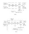
- FIG. 1is a structure diagram showing an optical transceiver device of a first example according the invention.
- FIG. 2is a structure diagram showing an optical transceiver device of a second example according the invention.
- FIG. 3is a structure diagram showing an optical transceiver device of a third example according the invention.
- FIG. 4is a structure diagram showing an optical transceiver device of a fourth example according the invention.
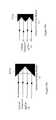
- FIGS. 5A to 5Care schematic views showing different switching states of an optical switching module according to the invention.
- FIGS. 6A and 6Bare perspective views of different examples for an optical element according to the invention.
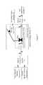
- FIG. 7is a state view showing an optical switching module forming a full path reflection optical switch according to the invention.
- FIG. 8is a block diagram showing the connection of a optical transceiver device and four 10G optical network equipments according to the invention.
- FIG. 9is a block diagram showing the connection of an optical transceiver device and two 40G optical network equipments according to the invention.
- FIG. 10is a block diagram showing the connection of an optical transceiver device and multiple 10G optical network equipment according to the invention.
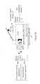
- FIG. 11is an implementation perspective view showing the connection of an optical transceiver device and multiple optical network equipments through a fan-out equipment according to the invention.
- FIG. 12is another implementation perspective view showing the connection of an optical transceiver device and multiple optical network equipments through a fan-out equipment according to the invention.
- FIG. 13is an implementation perspective view showing the arrangement of O/E transceiver modules and optical switching modules in an optical transceiver device on a single chip according to the invention.
- FIGS. 1 to 4are system structure diagram showing various examples of optical transceiver devices according to the invention, wherein, identical or like elements are indicated by identical or like numerals in various examples without detailed description in order for more clear understanding of the technical description of the application.
- an optical transceiver device 1 of the inventionis connected to a first optical network equipment 2 , a second optical network equipment 3 and an in-line equipment 4 for forming an optical fiber network to provide service functions, such as network communication, for first optical network equipment 2 and the second optical network equipment 3 .
- the optical transceiver device 1includes at least an O/E transceiver module 11 , an optical wave guide 12 , an optical switching module 13 , a switching control module 14 , an optical transceiving port 15 and a control module for transceiver 16 .
- the O/E transceiver module 11 and the control module for transceiver 16may be integrated as a single entity or arranged separately.
- the optical switching module 13 and the switching control module 14may be integrated as a single entity or arranged separately. Also, refer to FIG. 13 . As shown in FIG.
- the optical transceiver device 1is provided with an chip for optical switching and transceiver 19 , which has an O/E transceiver module 191 and an optical switching module 192 to replace the O/E transceiver module 11 and the optical switching module 13 mentioned above.
- the volume of the optical transceiver device 1may be reduced further, and the optical fiber routing between the O/E transceiver module 11 and the optical switching module 13 may be simplified.
- the chip for optical switching and transceiver 19may be, for example, formed by a planar lightwave circuit (PLC) and micro electro mechanical system (MEMS), but not limited thereto.
- the optical transceiving port 15may be connected with the first optical network equipment 2 , the second optical network equipment 3 and the optical switching module 13 separately in order for transceiving process of optical signal.
- the optical transceiver device 1may further include an optical coupler 17 , which is optically coupled to the optical transceiving port 15 and the optical switching module 13 in order for coupling process with respect to optical signal transmitting between the optical transceiving port 15 and the optical switching module 13 , such that the transmitted optical signal is split in a proportional or non-proportional manner, and is provided for an external monitoring equipment 5 to determine the condition of the optical signal accessed by the optical transceiving port 15 , that is, the function of split mode or aggregation mode for optical signal is performed.
- optical signal splitting from the optical coupler 17 to external monitoring equipment 5may be accessed by optical transceiving port 15 and perform the function for said external monitoring equipment to monitor the optical signal transmitting between said first, second optical network equipments and in-line equipment. It is noted that the optical coupling between the optical coupler 17 and the two modules, the optical transceiving port 15 and the optical switching module 13 may be achieved by mutual connection of optical fibers in a fiber splicing or ferrule sleeve manner.
- the O/E transceiver module 11provided by the invention is formed of at least one integrated chip 111 integrated with multiple O/E transceiver units therein.
- the O/E transceiver module 11may receive, in parallel, optical signal received from the first optical network equipment 2 , the second optical network equipment 3 , and convert the received optical signal into electrical signal, followed by optical signal transmitting the converted electrical signal to the in-line equipment 4 for the in-line equipment 4 to receive and process.
- the in-line equipment 4may also provide electrical signal for the O/E transceiver module 11 to receive.
- the O/E transceiver module 11may convert the received electrical signal into optical signal for respective transmitting to the first optical network equipment 2 , the second optical network equipment 3 .
- the integrated chip 111 in the O/E transceiver module 11may be a quad SPF+ (QSFP+) interface chip with 4 full duplex transmitting parallel channels and 4 sets of O/E transceiver units integrated therein. It is to be noted that the number of the parallel channels and O/E transceiver units of the integrated chip in the O/E transceiver module of the invention is not limited to what mentioned above, but may be increased or decreased in order for improved design according to actual requirement.
- the control module for transceiver 16may be electrically connected to the in-line equipment 4 through an I2C bus to receive O/E transceiving control signal output from the in-line equipment 4 , thereby each of the O/E transceiver units in the integrated chip 111 is controlled to perform an O/E transceiving process.
- the O/E transceiving processconverts the received optical signal into electrical signal, or converts the received electrical signal into optical signal.
- the above optical switching module 13includes at least an optical switch with bypass function or full function used to perform a switching operation for optical channels, wherein, the optical switching module 13 may be optical coupled with the O/E transceiver module 11 by the optical wave guide 12 to achieve the transmitting of optical signal.
- the optical wave guide 12is a device capable of changing the traveling direction of the optical signal.
- the optical switching module 13may be optically coupled with the optical wave guide 12 by a MPO connector.
- the optical switching module 13switches optical channels to switch its operation modes, including at least normal mode and bypass mode (mentioned later in detail).
- the switching control module 14connects electrically the in-line equipment 4 and the optical switching module 13 to receive optical switching control signal output from a control signal output unit 41 of the in-line equipment 4 through a general purpose I/O (GPIO) pin 411 , thereby the optical switching module 13 is controlled to perform corresponding optical switching operations.
- the switching control module 14may be a pin exposed to the optical transceiver device 1 , a control logic circuit or a microprocessor.
- the output for the optical switching control signal of the in-line equipment 4may be achieved through the I2C bus of the control signal output unit 41 .
- the control signal output unit 41 of the in-line equipment 4may be connected to the switching control module 14 through the I2C bus, such that the optical switching control signal is transmitted to the switching control module 14 by the control signal output unit 41 .
- the control signal output unit 41may also transmit the O/E transceiving control signal to the control module for transceiver 16 by the I2C bus.
- the switching control module 14may monitor the operation status of the in-line equipment by the optical switching control signal.
- the switching control module 14may send a first control instruction to the optical switching module for the first, second optical network equipment 2 , 3 to perform optical signal transmitting to the O/E transceiver module 11 .
- the switching control module 14may send a second control instruction to the optical switching module for the optical signal to be transmitted between the first, second optical network equipment 2 , 3 mutually without the O/E transceiver module 11 .
- the switching control module 14may have a monitoring unit and a process unit.
- the monitoring unitmay receive a return-to-zero signal, which represents normal operation, output from the in-line equipment, and perform timing operation.
- a return-to-zero signalis received at the timing of a default time.
- a first state signalis generated.
- a second state signalis generated, and an operating system on the in-line equipment is rebooted.
- the process unitreceives a state signal generated by the monitoring unit.
- the first control instructionis sent to the optical switching module.
- the second control instructionis sent to the optical switching module.
- the monitoring unitmay be a watch dog timer (WDT) chip, while the process unit may be a complex programmable logic device (CPLD) or CPU.
- WDTwatch dog timer
- CPLDcomplex programmable logic device
- a wavelength division multiplexer (WDM) 18may further be provided between the O/E transceiver module 11 and the optical switching module 13 in the optical transceiver device 1 of the invention to multiplex the optical signal of various different wavelengths for transmission within the same optical fiber.
- the number of optical fibers optically coupling the O/E transceiver module 11 and the optical switching module 13may be reduced in order to economize optical switches arranged in the optical switching module 13 , and further reduce the volume occupied by the optical transceiver device 1 of the invention.
- the wavelength division multiplexer 18may be arranged optionally in the O/E transceiver module 11 to achieve reduced volume as well.
- an optical switch 131 in the optical switching module 13 of the inventionfurther includes an optical input port 1311 , an optical output port 1312 , a space for optical path 1313 , an optical element 1314 and a driving unit 1315 .
- the optical input port 1311is used to input optical signal transmitted from optical transceiving port 15 .
- the optical output port 1312is used to output optical signal for the optical transceiving port 15 to receive.
- the optical input port 1311 and the optical output port 1312are located at the same side of the optical switching module 13 close to the optical transceiving port 15 to reduce routing opportunity of optical fibers for the optical switching module 13 and the optical transceiving port 15 , such that the space reserved for optical fiber routing necessary by the optical transceiver device 1 is reduced.
- the space for optical path 1313is a space without obstacle to optical signal traveling used to provide an optical channel for optical signal to travel.
- the optical element 1314is used for optical signal reflection to switch the optical channel for the optical signal to travel in the space for optical path 1313 .
- the driving unit 1315is connected with the optical element 1314 and electrically connected to the switching control module 14 for receiving the optical switching control signal output from the switching control module 14 , thereby the optical element 1314 into or removed from the space for optical path 1313 is controlled.
- the optical switch 131 of the optical switching module 13runs in a normal mode, in which the input optical signal of the optical input port 1311 may pass through the space for optical path 133 , the optical wave guide 12 sequentially to be transmitted to the O/E transceiver module 11 ; the optical signal provided by the O/E transceiver module 11 may pass through the optical wave guide 12 , space for optical path 133 to be transmitted to the optical output port 1312 .
- the optical switching module 13runs in the bypass mode, in which, after the optical signal input by the optical input port 1311 is reflected totally by the optical element 1314 , the optical signal traveling channel will switch from the optical channel of the optical input port 1311 to the optical channel of the optical output port 1312 , such that the optical signal may be outputted from the optical output port 1312 without the in-line equipment 4 . That is, in the situation without the in-line equipment 4 , the first optical network equipment 2 and the second optical network equipment 3 may transmit optical signal mutually through the optical switching module 13 , so that uninterrupted optical signal transmitting between the first optical network equipment 2 and the second optical network equipment 3 is implemented.
- an optical switching switchmay be provided in each optical channel of the optical switching module 13 .
- the optical switching module 13runs in a bypass-disabled mode.
- a managermay input the optical switching control signal through a control signal output unit 411 (refer to FIG. 1 ), and control the optical switching module 13 through the switching control module 14 to perform the corresponding optical switching operation, thereby the optical switching switch in each of the optical channels switches off the optical signal transmitting between the first optical network equipment 2 and the second optical network equipment 3 .
- the above optical switching switchmay control the on/off state of each optical channel in the optical switching module 13 to provide an effective response mechanism, for example, disabling the running of the optical switching module 13 in the bypass mode, for emergent events on network (such as network system intruded by virus or hacker etc.), thereby the security of network transmission is improved.
- the optical element 1314 of the inventionis, for example, a total reflection mirror with a V-shaped or W-shaped reflection mirror plane on at least one side.
- the optical channel of the optical input port 1311 and the optical channel of the optical output port 1312are parallel to each other.
- the optical element 1314may also have both V-shaped and W-shaped reflection mirror planes such that the V-shaped and W-shaped reflection mirror plane may be selected to accept the optical signal input from the optical input port 1311 depending on actual requirement for the optical switching states for the optical switching module 13 of the invention to be more versatile.
- the optical element 1314may still be formed of a prism or a mirror, but not limited thereto.
- two sides of the optical element 1314 facing the optical transceiving port 15 and the optical wave guide 12may have a V-shaped or a W-shaped reflection mirror plane, respectively, for the optical switching module 13 to form a full OSW, such that the in-line equipment 4 may reflect optical signal through the reflection mirror plane of the optical element 1314 facing one side of the optical wave guide 12 to perform loop back detection for self-inspection of conditions as the optical switching module 13 runs in the bypass mode.
- the optical transceiving port 15provides a MPO connector 151
- the optical switching module 13provides optical switches 131 , 132 .
- the MPO connector 151provides ports for 10G first optical network equipments 2 ′′, 2 ′′′ and 10G second optical network equipment 3 ′′, 3 ′′′ to plug, such that the above respective optical couplings of the 10G first, second optical network equipments 2 ′′, 3 ′′, 2 ′′′, 3 ′′′ and the optical switches 131 , 132 are accomplished.
- the above optical switches 131 , 132may run on the bypass mode for the optical signal of the 10G first optical network equipments 2 ′′, 2 ′′′ to be transmitted directly to the second optical network equipments 3 ′′, 3 ′′′ without the in-line equipment 4 . Moreover, the optical switches 131 , 132 may also run in the normal mode to transmit the optical signal of the 10G first optical network equipments 2 ′′, 2 ′′′ to the integrated chip 111 of the OLE transceiver module 11 for OLE conversion, and transmit the converted electrical signal to the in-line equipment 4 .
- the OLE transceiver module 11may also convert the electrical signal of the in-line equipment 4 into optical signal to be transmitted to above 10G first, second optical network equipments 2 ′′, 3 ′′, 2 ′′′, 3 ′′′, respectively.
- the optical transceiver device 1is provided for the 40G first optical network equipment 2 ′ and the 40G second optical network equipment 3 ′ to plug for optical signal transmission of the two 40G optical network equipments 2 ′, 3 ′.
- the optical transceiving port 15provides two MPO connectors 151 , 152 ; while the optical switching module 13 provides optical switches 131 , 132 , 133 , 134 .
- the two MPO connectors 151 , 152provide plug ports for the 40G first optical network equipment 2 ′ and the 40G second optical network equipment 3 ′ to plug, so that the respective optical couplings of the above 40G first, second optical network equipment 2 ′, 3 ′ and the optical switches 131 , 132 , 133 , 134 are accomplished.
- the above optical switches 131 , 132 , 133 , 134may run in the bypass mode simultaneously for the optical signal of the 40G first optical network equipment 2 ′ to be transmitted to the second optical network equipment 3 ′ directly without the in-line equipment 4 .
- the optical switches 131 , 132 , 133 , 134may also run in the normal mode to transmit the optical signal of the 40G first optical network equipment 2 ′ to the integrated chips 111 , 112 in the OLE transceiver module 11 for OLE conversion, and transmit the converted electrical signal to the in-line equipment 4 .
- the OLE transceiver module 11may also convert the electrical signal of the in-line equipment 4 into optical signal by the integrated chips 111 , 112 for respective transmitting to the 40G first optical network equipment 2 ′ and the 40G second optical network equipment 3 ′.
- the optical transceiver device 1 provided by the inventionmay be also plugged by multiple 10G optical network equipments 21 ′′, 31 ′′, 22 ′′, 32 ′′, 23 ′′, 33 ′′, 24 ′′, 34 ′′ to form an optical fiber network and provide network communication services for these 10G optical network equipment 21 ′′, 31 ′′, 22 ′′, 32 ′′, 23 ′′, 33 ′′, 24 ′′, 34 ′′.
- optical switching modules 13 shown in FIG. 9 , FIG. 10are the same. Thereby, it is understood that optical switching modules with the same hardware specifications may be selected for various implementation perspectives of the optical transceiver device in the invention. As such, material cost of the optical switching module may be economized.
- connection of the optical transceiver device and the optical network equipment of the inventionis also achievable in a non-MPO connector approach.
- the optical transceiver device 1may be connected to the fan-out equipment 5 externally through a ribbon fiber 6 extended from the optical switching module 13 (as shown in FIG. 11 ), or allow the optical switching module 13 to be connected to the fan-out equipment 5 externally (as shown in FIG. 12 ), such that the connection with multiple optical network equipment 2 ′′, 3 ′′, 2 ′′′, 3 ′′′ is accomplished.
- the arrangement of the optical transceiving port for the optical transceiver devicemay be omitted to reduce the volume occupied by the optical transceiver device considerably.
- the O/E transceiver module 11 in FIGS. 11 and 12may be a QSFP+ chip from selection, for the optical transceiver device to be plugged onto the in-line equipment in order to increase the convenience of usage.
- optical transceiver device of the inventionhas at least the following advantages and features:
- the optical switching modulemay switch the optical channels with the mirror total reflection principle so that the optical switching module may have the optical access ports provided on one side of the optical transceiver module, such that the optical fibers of the optical access ports may be connected to the optical transceiving port under reduced routing, and thereby the objective of reduced entire volume of the optical transceiver device is achieved.
- the optical elements provided by the optical switching modulemay be switched to be reflection mirrors with V-shaped or W-shaped reflection mirror planes for changing optical switching channels, thereby the optical switching operation is more flexible.
- connection with the optical network equipmentmay be accomplished through an external connected fan-out equipment without the arrangement of the optical transceiving port such that the entire volume of the optical transceiver device is reduced.
- Itmay be manufactured as an active optical bypass cable (or referred to as Active Optical Cable with Bypass Function).
Landscapes
- Engineering & Computer Science (AREA)
- Computer Networks & Wireless Communication (AREA)
- Physics & Mathematics (AREA)
- Electromagnetism (AREA)
- Signal Processing (AREA)
- Optical Communication System (AREA)
Abstract
Description
Claims (6)
Priority Applications (1)
| Application Number | Priority Date | Filing Date | Title |
|---|---|---|---|
| US15/268,901US9838132B2 (en) | 2013-02-25 | 2016-09-19 | Optical transceiver device |
Applications Claiming Priority (6)
| Application Number | Priority Date | Filing Date | Title |
|---|---|---|---|
| TW102106614ATWI535227B (en) | 2013-02-25 | 2013-02-25 | An optical access device |
| TW102106614 | 2013-02-25 | ||
| TW102106614A | 2013-02-25 | ||
| TW102133827ATWI512350B (en) | 2013-09-18 | 2013-09-18 | Optical transceiver device |
| TW102133827 | 2013-09-18 | ||
| TW102133827A | 2013-09-18 |
Related Child Applications (1)
| Application Number | Title | Priority Date | Filing Date |
|---|---|---|---|
| US15/268,901Continuation-In-PartUS9838132B2 (en) | 2013-02-25 | 2016-09-19 | Optical transceiver device |
Publications (2)
| Publication Number | Publication Date |
|---|---|
| US20140241718A1 US20140241718A1 (en) | 2014-08-28 |
| US9473243B2true US9473243B2 (en) | 2016-10-18 |
Family
ID=51388270
Family Applications (1)
| Application Number | Title | Priority Date | Filing Date |
|---|---|---|---|
| US14/187,739Active2034-07-11US9473243B2 (en) | 2013-02-25 | 2014-02-24 | Optical transceiver device |
Country Status (1)
| Country | Link |
|---|---|
| US (1) | US9473243B2 (en) |
Families Citing this family (172)
| Publication number | Priority date | Publication date | Assignee | Title |
|---|---|---|---|---|
| KR101946004B1 (en)* | 2012-01-11 | 2019-02-11 | 삼성전자주식회사 | Microprocessor chip, data center, and computing system |
| US10009065B2 (en) | 2012-12-05 | 2018-06-26 | At&T Intellectual Property I, L.P. | Backhaul link for distributed antenna system |
| US9113347B2 (en) | 2012-12-05 | 2015-08-18 | At&T Intellectual Property I, Lp | Backhaul link for distributed antenna system |
| US9103948B2 (en)* | 2012-12-13 | 2015-08-11 | Sean Jiang | Fiber bypass module and its adapted in-line equipment |
| TWI520510B (en)* | 2013-03-25 | 2016-02-01 | 傳承光電股份有限公司 | Optical transceiver |
| US9999038B2 (en) | 2013-05-31 | 2018-06-12 | At&T Intellectual Property I, L.P. | Remote distributed antenna system |
| US9525524B2 (en) | 2013-05-31 | 2016-12-20 | At&T Intellectual Property I, L.P. | Remote distributed antenna system |
| TWI527513B (en)* | 2013-09-11 | 2016-03-21 | 廣達電腦股份有限公司 | Rack server |
| US8897697B1 (en) | 2013-11-06 | 2014-11-25 | At&T Intellectual Property I, Lp | Millimeter-wave surface-wave communications |
| US9209902B2 (en) | 2013-12-10 | 2015-12-08 | At&T Intellectual Property I, L.P. | Quasi-optical coupler |
| US9692101B2 (en) | 2014-08-26 | 2017-06-27 | At&T Intellectual Property I, L.P. | Guided wave couplers for coupling electromagnetic waves between a waveguide surface and a surface of a wire |
| US9768833B2 (en) | 2014-09-15 | 2017-09-19 | At&T Intellectual Property I, L.P. | Method and apparatus for sensing a condition in a transmission medium of electromagnetic waves |
| US10063280B2 (en) | 2014-09-17 | 2018-08-28 | At&T Intellectual Property I, L.P. | Monitoring and mitigating conditions in a communication network |
| US9628854B2 (en) | 2014-09-29 | 2017-04-18 | At&T Intellectual Property I, L.P. | Method and apparatus for distributing content in a communication network |
| US9615269B2 (en) | 2014-10-02 | 2017-04-04 | At&T Intellectual Property I, L.P. | Method and apparatus that provides fault tolerance in a communication network |
| US9685992B2 (en) | 2014-10-03 | 2017-06-20 | At&T Intellectual Property I, L.P. | Circuit panel network and methods thereof |
| US9503189B2 (en) | 2014-10-10 | 2016-11-22 | At&T Intellectual Property I, L.P. | Method and apparatus for arranging communication sessions in a communication system |
| US9973299B2 (en) | 2014-10-14 | 2018-05-15 | At&T Intellectual Property I, L.P. | Method and apparatus for adjusting a mode of communication in a communication network |
| US9762289B2 (en) | 2014-10-14 | 2017-09-12 | At&T Intellectual Property I, L.P. | Method and apparatus for transmitting or receiving signals in a transportation system |
| US9564947B2 (en) | 2014-10-21 | 2017-02-07 | At&T Intellectual Property I, L.P. | Guided-wave transmission device with diversity and methods for use therewith |
| US9312919B1 (en) | 2014-10-21 | 2016-04-12 | At&T Intellectual Property I, Lp | Transmission device with impairment compensation and methods for use therewith |
| US9653770B2 (en) | 2014-10-21 | 2017-05-16 | At&T Intellectual Property I, L.P. | Guided wave coupler, coupling module and methods for use therewith |
| US9627768B2 (en) | 2014-10-21 | 2017-04-18 | At&T Intellectual Property I, L.P. | Guided-wave transmission device with non-fundamental mode propagation and methods for use therewith |
| US9769020B2 (en) | 2014-10-21 | 2017-09-19 | At&T Intellectual Property I, L.P. | Method and apparatus for responding to events affecting communications in a communication network |
| US9780834B2 (en) | 2014-10-21 | 2017-10-03 | At&T Intellectual Property I, L.P. | Method and apparatus for transmitting electromagnetic waves |
| US9577306B2 (en) | 2014-10-21 | 2017-02-21 | At&T Intellectual Property I, L.P. | Guided-wave transmission device and methods for use therewith |
| US9520945B2 (en) | 2014-10-21 | 2016-12-13 | At&T Intellectual Property I, L.P. | Apparatus for providing communication services and methods thereof |
| US9742462B2 (en) | 2014-12-04 | 2017-08-22 | At&T Intellectual Property I, L.P. | Transmission medium and communication interfaces and methods for use therewith |
| US9680670B2 (en) | 2014-11-20 | 2017-06-13 | At&T Intellectual Property I, L.P. | Transmission device with channel equalization and control and methods for use therewith |
| US9954287B2 (en) | 2014-11-20 | 2018-04-24 | At&T Intellectual Property I, L.P. | Apparatus for converting wireless signals and electromagnetic waves and methods thereof |
| US9800327B2 (en) | 2014-11-20 | 2017-10-24 | At&T Intellectual Property I, L.P. | Apparatus for controlling operations of a communication device and methods thereof |
| US9654173B2 (en) | 2014-11-20 | 2017-05-16 | At&T Intellectual Property I, L.P. | Apparatus for powering a communication device and methods thereof |
| US9997819B2 (en) | 2015-06-09 | 2018-06-12 | At&T Intellectual Property I, L.P. | Transmission medium and method for facilitating propagation of electromagnetic waves via a core |
| US10340573B2 (en) | 2016-10-26 | 2019-07-02 | At&T Intellectual Property I, L.P. | Launcher with cylindrical coupling device and methods for use therewith |
| US10009067B2 (en) | 2014-12-04 | 2018-06-26 | At&T Intellectual Property I, L.P. | Method and apparatus for configuring a communication interface |
| US9461706B1 (en) | 2015-07-31 | 2016-10-04 | At&T Intellectual Property I, Lp | Method and apparatus for exchanging communication signals |
| US10243784B2 (en) | 2014-11-20 | 2019-03-26 | At&T Intellectual Property I, L.P. | System for generating topology information and methods thereof |
| US9544006B2 (en) | 2014-11-20 | 2017-01-10 | At&T Intellectual Property I, L.P. | Transmission device with mode division multiplexing and methods for use therewith |
| US10144036B2 (en) | 2015-01-30 | 2018-12-04 | At&T Intellectual Property I, L.P. | Method and apparatus for mitigating interference affecting a propagation of electromagnetic waves guided by a transmission medium |
| US9876570B2 (en) | 2015-02-20 | 2018-01-23 | At&T Intellectual Property I, Lp | Guided-wave transmission device with non-fundamental mode propagation and methods for use therewith |
| US9749013B2 (en) | 2015-03-17 | 2017-08-29 | At&T Intellectual Property I, L.P. | Method and apparatus for reducing attenuation of electromagnetic waves guided by a transmission medium |
| US9680771B2 (en) | 2015-04-22 | 2017-06-13 | Gigamon Inc. | Redundant inline-bypass switch |
| US9705561B2 (en) | 2015-04-24 | 2017-07-11 | At&T Intellectual Property I, L.P. | Directional coupling device and methods for use therewith |
| US10224981B2 (en) | 2015-04-24 | 2019-03-05 | At&T Intellectual Property I, Lp | Passive electrical coupling device and methods for use therewith |
| US9793954B2 (en) | 2015-04-28 | 2017-10-17 | At&T Intellectual Property I, L.P. | Magnetic coupling device and methods for use therewith |
| US9948354B2 (en) | 2015-04-28 | 2018-04-17 | At&T Intellectual Property I, L.P. | Magnetic coupling device with reflective plate and methods for use therewith |
| US9641245B2 (en) | 2015-05-12 | 2017-05-02 | Saudi Arabian Oil Company | System, method, and apparatus for daisy chain network protection from node malfunction or power outage |
| US9490869B1 (en) | 2015-05-14 | 2016-11-08 | At&T Intellectual Property I, L.P. | Transmission medium having multiple cores and methods for use therewith |
| US9748626B2 (en) | 2015-05-14 | 2017-08-29 | At&T Intellectual Property I, L.P. | Plurality of cables having different cross-sectional shapes which are bundled together to form a transmission medium |
| US9871282B2 (en) | 2015-05-14 | 2018-01-16 | At&T Intellectual Property I, L.P. | At least one transmission medium having a dielectric surface that is covered at least in part by a second dielectric |
| US10679767B2 (en) | 2015-05-15 | 2020-06-09 | At&T Intellectual Property I, L.P. | Transmission medium having a conductive material and methods for use therewith |
| US10650940B2 (en) | 2015-05-15 | 2020-05-12 | At&T Intellectual Property I, L.P. | Transmission medium having a conductive material and methods for use therewith |
| US9917341B2 (en) | 2015-05-27 | 2018-03-13 | At&T Intellectual Property I, L.P. | Apparatus and method for launching electromagnetic waves and for modifying radial dimensions of the propagating electromagnetic waves |
| US20160359567A1 (en)* | 2015-06-02 | 2016-12-08 | Alcatel-Lucent Usa Inc. | Multi-endpoint optical receiver |
| US10103801B2 (en) | 2015-06-03 | 2018-10-16 | At&T Intellectual Property I, L.P. | Host node device and methods for use therewith |
| US10812174B2 (en) | 2015-06-03 | 2020-10-20 | At&T Intellectual Property I, L.P. | Client node device and methods for use therewith |
| US9866309B2 (en) | 2015-06-03 | 2018-01-09 | At&T Intellectual Property I, Lp | Host node device and methods for use therewith |
| US9912381B2 (en) | 2015-06-03 | 2018-03-06 | At&T Intellectual Property I, Lp | Network termination and methods for use therewith |
| US10154493B2 (en) | 2015-06-03 | 2018-12-11 | At&T Intellectual Property I, L.P. | Network termination and methods for use therewith |
| US10348391B2 (en) | 2015-06-03 | 2019-07-09 | At&T Intellectual Property I, L.P. | Client node device with frequency conversion and methods for use therewith |
| US9913139B2 (en) | 2015-06-09 | 2018-03-06 | At&T Intellectual Property I, L.P. | Signal fingerprinting for authentication of communicating devices |
| US9608692B2 (en) | 2015-06-11 | 2017-03-28 | At&T Intellectual Property I, L.P. | Repeater and methods for use therewith |
| US10142086B2 (en) | 2015-06-11 | 2018-11-27 | At&T Intellectual Property I, L.P. | Repeater and methods for use therewith |
| US9820146B2 (en) | 2015-06-12 | 2017-11-14 | At&T Intellectual Property I, L.P. | Method and apparatus for authentication and identity management of communicating devices |
| US9667317B2 (en) | 2015-06-15 | 2017-05-30 | At&T Intellectual Property I, L.P. | Method and apparatus for providing security using network traffic adjustments |
| US9640850B2 (en) | 2015-06-25 | 2017-05-02 | At&T Intellectual Property I, L.P. | Methods and apparatus for inducing a non-fundamental wave mode on a transmission medium |
| US9865911B2 (en) | 2015-06-25 | 2018-01-09 | At&T Intellectual Property I, L.P. | Waveguide system for slot radiating first electromagnetic waves that are combined into a non-fundamental wave mode second electromagnetic wave on a transmission medium |
| US9509415B1 (en) | 2015-06-25 | 2016-11-29 | At&T Intellectual Property I, L.P. | Methods and apparatus for inducing a fundamental wave mode on a transmission medium |
| US9853342B2 (en) | 2015-07-14 | 2017-12-26 | At&T Intellectual Property I, L.P. | Dielectric transmission medium connector and methods for use therewith |
| US10044409B2 (en) | 2015-07-14 | 2018-08-07 | At&T Intellectual Property I, L.P. | Transmission medium and methods for use therewith |
| US9628116B2 (en) | 2015-07-14 | 2017-04-18 | At&T Intellectual Property I, L.P. | Apparatus and methods for transmitting wireless signals |
| US9882257B2 (en) | 2015-07-14 | 2018-01-30 | At&T Intellectual Property I, L.P. | Method and apparatus for launching a wave mode that mitigates interference |
| US10170840B2 (en) | 2015-07-14 | 2019-01-01 | At&T Intellectual Property I, L.P. | Apparatus and methods for sending or receiving electromagnetic signals |
| US9836957B2 (en) | 2015-07-14 | 2017-12-05 | At&T Intellectual Property I, L.P. | Method and apparatus for communicating with premises equipment |
| US10148016B2 (en) | 2015-07-14 | 2018-12-04 | At&T Intellectual Property I, L.P. | Apparatus and methods for communicating utilizing an antenna array |
| US10341142B2 (en) | 2015-07-14 | 2019-07-02 | At&T Intellectual Property I, L.P. | Apparatus and methods for generating non-interfering electromagnetic waves on an uninsulated conductor |
| US9722318B2 (en) | 2015-07-14 | 2017-08-01 | At&T Intellectual Property I, L.P. | Method and apparatus for coupling an antenna to a device |
| US10033108B2 (en) | 2015-07-14 | 2018-07-24 | At&T Intellectual Property I, L.P. | Apparatus and methods for generating an electromagnetic wave having a wave mode that mitigates interference |
| US10033107B2 (en) | 2015-07-14 | 2018-07-24 | At&T Intellectual Property I, L.P. | Method and apparatus for coupling an antenna to a device |
| US10320586B2 (en) | 2015-07-14 | 2019-06-11 | At&T Intellectual Property I, L.P. | Apparatus and methods for generating non-interfering electromagnetic waves on an insulated transmission medium |
| US9847566B2 (en) | 2015-07-14 | 2017-12-19 | At&T Intellectual Property I, L.P. | Method and apparatus for adjusting a field of a signal to mitigate interference |
| US10205655B2 (en) | 2015-07-14 | 2019-02-12 | At&T Intellectual Property I, L.P. | Apparatus and methods for communicating utilizing an antenna array and multiple communication paths |
| US9793951B2 (en) | 2015-07-15 | 2017-10-17 | At&T Intellectual Property I, L.P. | Method and apparatus for launching a wave mode that mitigates interference |
| US9608740B2 (en) | 2015-07-15 | 2017-03-28 | At&T Intellectual Property I, L.P. | Method and apparatus for launching a wave mode that mitigates interference |
| US10090606B2 (en) | 2015-07-15 | 2018-10-02 | At&T Intellectual Property I, L.P. | Antenna system with dielectric array and methods for use therewith |
| US9948333B2 (en) | 2015-07-23 | 2018-04-17 | At&T Intellectual Property I, L.P. | Method and apparatus for wireless communications to mitigate interference |
| US10784670B2 (en) | 2015-07-23 | 2020-09-22 | At&T Intellectual Property I, L.P. | Antenna support for aligning an antenna |
| US9749053B2 (en) | 2015-07-23 | 2017-08-29 | At&T Intellectual Property I, L.P. | Node device, repeater and methods for use therewith |
| US9871283B2 (en) | 2015-07-23 | 2018-01-16 | At&T Intellectual Property I, Lp | Transmission medium having a dielectric core comprised of plural members connected by a ball and socket configuration |
| US9912027B2 (en) | 2015-07-23 | 2018-03-06 | At&T Intellectual Property I, L.P. | Method and apparatus for exchanging communication signals |
| US9735833B2 (en) | 2015-07-31 | 2017-08-15 | At&T Intellectual Property I, L.P. | Method and apparatus for communications management in a neighborhood network |
| US9967173B2 (en) | 2015-07-31 | 2018-05-08 | At&T Intellectual Property I, L.P. | Method and apparatus for authentication and identity management of communicating devices |
| US10020587B2 (en) | 2015-07-31 | 2018-07-10 | At&T Intellectual Property I, L.P. | Radial antenna and methods for use therewith |
| US9904535B2 (en) | 2015-09-14 | 2018-02-27 | At&T Intellectual Property I, L.P. | Method and apparatus for distributing software |
| US10051629B2 (en) | 2015-09-16 | 2018-08-14 | At&T Intellectual Property I, L.P. | Method and apparatus for use with a radio distributed antenna system having an in-band reference signal |
| US9705571B2 (en) | 2015-09-16 | 2017-07-11 | At&T Intellectual Property I, L.P. | Method and apparatus for use with a radio distributed antenna system |
| US10136434B2 (en) | 2015-09-16 | 2018-11-20 | At&T Intellectual Property I, L.P. | Method and apparatus for use with a radio distributed antenna system having an ultra-wideband control channel |
| US10009901B2 (en) | 2015-09-16 | 2018-06-26 | At&T Intellectual Property I, L.P. | Method, apparatus, and computer-readable storage medium for managing utilization of wireless resources between base stations |
| US10009063B2 (en) | 2015-09-16 | 2018-06-26 | At&T Intellectual Property I, L.P. | Method and apparatus for use with a radio distributed antenna system having an out-of-band reference signal |
| US10079661B2 (en) | 2015-09-16 | 2018-09-18 | At&T Intellectual Property I, L.P. | Method and apparatus for use with a radio distributed antenna system having a clock reference |
| US9769128B2 (en) | 2015-09-28 | 2017-09-19 | At&T Intellectual Property I, L.P. | Method and apparatus for encryption of communications over a network |
| US9729197B2 (en) | 2015-10-01 | 2017-08-08 | At&T Intellectual Property I, L.P. | Method and apparatus for communicating network management traffic over a network |
| US9882277B2 (en) | 2015-10-02 | 2018-01-30 | At&T Intellectual Property I, Lp | Communication device and antenna assembly with actuated gimbal mount |
| US9876264B2 (en) | 2015-10-02 | 2018-01-23 | At&T Intellectual Property I, Lp | Communication system, guided wave switch and methods for use therewith |
| US10074890B2 (en) | 2015-10-02 | 2018-09-11 | At&T Intellectual Property I, L.P. | Communication device and antenna with integrated light assembly |
| US10051483B2 (en) | 2015-10-16 | 2018-08-14 | At&T Intellectual Property I, L.P. | Method and apparatus for directing wireless signals |
| US10665942B2 (en) | 2015-10-16 | 2020-05-26 | At&T Intellectual Property I, L.P. | Method and apparatus for adjusting wireless communications |
| US10355367B2 (en) | 2015-10-16 | 2019-07-16 | At&T Intellectual Property I, L.P. | Antenna structure for exchanging wireless signals |
| CN105429696A (en)* | 2015-12-30 | 2016-03-23 | 桂林创研科技有限公司 | Intelligent optical line automatic switching system |
| US9912419B1 (en) | 2016-08-24 | 2018-03-06 | At&T Intellectual Property I, L.P. | Method and apparatus for managing a fault in a distributed antenna system |
| US9860075B1 (en) | 2016-08-26 | 2018-01-02 | At&T Intellectual Property I, L.P. | Method and communication node for broadband distribution |
| US10291311B2 (en) | 2016-09-09 | 2019-05-14 | At&T Intellectual Property I, L.P. | Method and apparatus for mitigating a fault in a distributed antenna system |
| US11032819B2 (en) | 2016-09-15 | 2021-06-08 | At&T Intellectual Property I, L.P. | Method and apparatus for use with a radio distributed antenna system having a control channel reference signal |
| US10135146B2 (en) | 2016-10-18 | 2018-11-20 | At&T Intellectual Property I, L.P. | Apparatus and methods for launching guided waves via circuits |
| US10340600B2 (en) | 2016-10-18 | 2019-07-02 | At&T Intellectual Property I, L.P. | Apparatus and methods for launching guided waves via plural waveguide systems |
| US10135147B2 (en) | 2016-10-18 | 2018-11-20 | At&T Intellectual Property I, L.P. | Apparatus and methods for launching guided waves via an antenna |
| US9991580B2 (en) | 2016-10-21 | 2018-06-05 | At&T Intellectual Property I, L.P. | Launcher and coupling system for guided wave mode cancellation |
| US10374316B2 (en) | 2016-10-21 | 2019-08-06 | At&T Intellectual Property I, L.P. | System and dielectric antenna with non-uniform dielectric |
| US9876605B1 (en) | 2016-10-21 | 2018-01-23 | At&T Intellectual Property I, L.P. | Launcher and coupling system to support desired guided wave mode |
| US10811767B2 (en) | 2016-10-21 | 2020-10-20 | At&T Intellectual Property I, L.P. | System and dielectric antenna with convex dielectric radome |
| US10312567B2 (en) | 2016-10-26 | 2019-06-04 | At&T Intellectual Property I, L.P. | Launcher with planar strip antenna and methods for use therewith |
| US10225025B2 (en) | 2016-11-03 | 2019-03-05 | At&T Intellectual Property I, L.P. | Method and apparatus for detecting a fault in a communication system |
| US10291334B2 (en) | 2016-11-03 | 2019-05-14 | At&T Intellectual Property I, L.P. | System for detecting a fault in a communication system |
| US10498044B2 (en) | 2016-11-03 | 2019-12-03 | At&T Intellectual Property I, L.P. | Apparatus for configuring a surface of an antenna |
| US10224634B2 (en) | 2016-11-03 | 2019-03-05 | At&T Intellectual Property I, L.P. | Methods and apparatus for adjusting an operational characteristic of an antenna |
| US10340603B2 (en) | 2016-11-23 | 2019-07-02 | At&T Intellectual Property I, L.P. | Antenna system having shielded structural configurations for assembly |
| US10178445B2 (en) | 2016-11-23 | 2019-01-08 | At&T Intellectual Property I, L.P. | Methods, devices, and systems for load balancing between a plurality of waveguides |
| US10340601B2 (en) | 2016-11-23 | 2019-07-02 | At&T Intellectual Property I, L.P. | Multi-antenna system and methods for use therewith |
| US10535928B2 (en) | 2016-11-23 | 2020-01-14 | At&T Intellectual Property I, L.P. | Antenna system and methods for use therewith |
| US10090594B2 (en) | 2016-11-23 | 2018-10-02 | At&T Intellectual Property I, L.P. | Antenna system having structural configurations for assembly |
| US10305190B2 (en) | 2016-12-01 | 2019-05-28 | At&T Intellectual Property I, L.P. | Reflecting dielectric antenna system and methods for use therewith |
| US10361489B2 (en) | 2016-12-01 | 2019-07-23 | At&T Intellectual Property I, L.P. | Dielectric dish antenna system and methods for use therewith |
| US10819035B2 (en) | 2016-12-06 | 2020-10-27 | At&T Intellectual Property I, L.P. | Launcher with helical antenna and methods for use therewith |
| US10382976B2 (en) | 2016-12-06 | 2019-08-13 | At&T Intellectual Property I, L.P. | Method and apparatus for managing wireless communications based on communication paths and network device positions |
| US10755542B2 (en) | 2016-12-06 | 2020-08-25 | At&T Intellectual Property I, L.P. | Method and apparatus for surveillance via guided wave communication |
| US10637149B2 (en) | 2016-12-06 | 2020-04-28 | At&T Intellectual Property I, L.P. | Injection molded dielectric antenna and methods for use therewith |
| US10727599B2 (en) | 2016-12-06 | 2020-07-28 | At&T Intellectual Property I, L.P. | Launcher with slot antenna and methods for use therewith |
| US10326494B2 (en) | 2016-12-06 | 2019-06-18 | At&T Intellectual Property I, L.P. | Apparatus for measurement de-embedding and methods for use therewith |
| US10439675B2 (en) | 2016-12-06 | 2019-10-08 | At&T Intellectual Property I, L.P. | Method and apparatus for repeating guided wave communication signals |
| US10020844B2 (en) | 2016-12-06 | 2018-07-10 | T&T Intellectual Property I, L.P. | Method and apparatus for broadcast communication via guided waves |
| US10135145B2 (en) | 2016-12-06 | 2018-11-20 | At&T Intellectual Property I, L.P. | Apparatus and methods for generating an electromagnetic wave along a transmission medium |
| US9927517B1 (en) | 2016-12-06 | 2018-03-27 | At&T Intellectual Property I, L.P. | Apparatus and methods for sensing rainfall |
| US10694379B2 (en) | 2016-12-06 | 2020-06-23 | At&T Intellectual Property I, L.P. | Waveguide system with device-based authentication and methods for use therewith |
| US10389029B2 (en) | 2016-12-07 | 2019-08-20 | At&T Intellectual Property I, L.P. | Multi-feed dielectric antenna system with core selection and methods for use therewith |
| US9893795B1 (en) | 2016-12-07 | 2018-02-13 | At&T Intellectual Property I, Lp | Method and repeater for broadband distribution |
| US10168695B2 (en) | 2016-12-07 | 2019-01-01 | At&T Intellectual Property I, L.P. | Method and apparatus for controlling an unmanned aircraft |
| US10547348B2 (en) | 2016-12-07 | 2020-01-28 | At&T Intellectual Property I, L.P. | Method and apparatus for switching transmission mediums in a communication system |
| US10359749B2 (en) | 2016-12-07 | 2019-07-23 | At&T Intellectual Property I, L.P. | Method and apparatus for utilities management via guided wave communication |
| US10243270B2 (en) | 2016-12-07 | 2019-03-26 | At&T Intellectual Property I, L.P. | Beam adaptive multi-feed dielectric antenna system and methods for use therewith |
| US10446936B2 (en) | 2016-12-07 | 2019-10-15 | At&T Intellectual Property I, L.P. | Multi-feed dielectric antenna system and methods for use therewith |
| US10139820B2 (en) | 2016-12-07 | 2018-11-27 | At&T Intellectual Property I, L.P. | Method and apparatus for deploying equipment of a communication system |
| US10027397B2 (en) | 2016-12-07 | 2018-07-17 | At&T Intellectual Property I, L.P. | Distributed antenna system and methods for use therewith |
| US10601494B2 (en) | 2016-12-08 | 2020-03-24 | At&T Intellectual Property I, L.P. | Dual-band communication device and method for use therewith |
| US9911020B1 (en) | 2016-12-08 | 2018-03-06 | At&T Intellectual Property I, L.P. | Method and apparatus for tracking via a radio frequency identification device |
| US10326689B2 (en) | 2016-12-08 | 2019-06-18 | At&T Intellectual Property I, L.P. | Method and system for providing alternative communication paths |
| US10389037B2 (en) | 2016-12-08 | 2019-08-20 | At&T Intellectual Property I, L.P. | Apparatus and methods for selecting sections of an antenna array and use therewith |
| US9998870B1 (en) | 2016-12-08 | 2018-06-12 | At&T Intellectual Property I, L.P. | Method and apparatus for proximity sensing |
| US10777873B2 (en) | 2016-12-08 | 2020-09-15 | At&T Intellectual Property I, L.P. | Method and apparatus for mounting network devices |
| US10530505B2 (en) | 2016-12-08 | 2020-01-07 | At&T Intellectual Property I, L.P. | Apparatus and methods for launching electromagnetic waves along a transmission medium |
| US10069535B2 (en) | 2016-12-08 | 2018-09-04 | At&T Intellectual Property I, L.P. | Apparatus and methods for launching electromagnetic waves having a certain electric field structure |
| US10103422B2 (en) | 2016-12-08 | 2018-10-16 | At&T Intellectual Property I, L.P. | Method and apparatus for mounting network devices |
| US10938108B2 (en) | 2016-12-08 | 2021-03-02 | At&T Intellectual Property I, L.P. | Frequency selective multi-feed dielectric antenna system and methods for use therewith |
| US10411356B2 (en) | 2016-12-08 | 2019-09-10 | At&T Intellectual Property I, L.P. | Apparatus and methods for selectively targeting communication devices with an antenna array |
| US10916969B2 (en) | 2016-12-08 | 2021-02-09 | At&T Intellectual Property I, L.P. | Method and apparatus for providing power using an inductive coupling |
| US9838896B1 (en) | 2016-12-09 | 2017-12-05 | At&T Intellectual Property I, L.P. | Method and apparatus for assessing network coverage |
| US10340983B2 (en) | 2016-12-09 | 2019-07-02 | At&T Intellectual Property I, L.P. | Method and apparatus for surveying remote sites via guided wave communications |
| US10264586B2 (en) | 2016-12-09 | 2019-04-16 | At&T Mobility Ii Llc | Cloud-based packet controller and methods for use therewith |
| US9973940B1 (en) | 2017-02-27 | 2018-05-15 | At&T Intellectual Property I, L.P. | Apparatus and methods for dynamic impedance matching of a guided wave launcher |
| US10298293B2 (en) | 2017-03-13 | 2019-05-21 | At&T Intellectual Property I, L.P. | Apparatus of communication utilizing wireless network devices |
| US10819438B1 (en)* | 2018-12-20 | 2020-10-27 | Acacia Communications, Inc. | Optical grooming interconnection network |
| CN110086539B (en)* | 2019-05-31 | 2024-01-30 | 武汉火石光电有限公司 | BIDI module |
| US20240413901A1 (en)* | 2023-06-06 | 2024-12-12 | Cisco Technology, Inc. | Reversed fiber detection and correction in optical transceivers |
Citations (3)
| Publication number | Priority date | Publication date | Assignee | Title |
|---|---|---|---|---|
| US20030190113A1 (en)* | 2001-10-24 | 2003-10-09 | Cheng-Chung Huang | Optical system for calibration and control of an optical fiber switch |
| US6647212B1 (en)* | 1999-04-26 | 2003-11-11 | Sony Corporation | Optical transmitter receiver and method of optical transmission and reception |
| US7212738B1 (en)* | 2002-08-01 | 2007-05-01 | Finisar Corporation | Preventing signal loss in an optical communications network |
- 2014
- 2014-02-24USUS14/187,739patent/US9473243B2/enactiveActive
Patent Citations (3)
| Publication number | Priority date | Publication date | Assignee | Title |
|---|---|---|---|---|
| US6647212B1 (en)* | 1999-04-26 | 2003-11-11 | Sony Corporation | Optical transmitter receiver and method of optical transmission and reception |
| US20030190113A1 (en)* | 2001-10-24 | 2003-10-09 | Cheng-Chung Huang | Optical system for calibration and control of an optical fiber switch |
| US7212738B1 (en)* | 2002-08-01 | 2007-05-01 | Finisar Corporation | Preventing signal loss in an optical communications network |
Also Published As
| Publication number | Publication date |
|---|---|
| US20140241718A1 (en) | 2014-08-28 |
Similar Documents
| Publication | Publication Date | Title |
|---|---|---|
| US9473243B2 (en) | Optical transceiver device | |
| US9209901B2 (en) | Configurable single-fiber or dual-fiber optical transceiver | |
| US11451301B2 (en) | Light source backup method, apparatus, and system | |
| US9103948B2 (en) | Fiber bypass module and its adapted in-line equipment | |
| CN106461954B (en) | Optical splitter | |
| US12156310B2 (en) | Optical source switching method and apparatus | |
| US20180375579A1 (en) | Communication system and connector | |
| CN104518830B (en) | optical transceiver | |
| EP4351035A1 (en) | Optical cross-connect device and wavelength selective switch | |
| US11675133B2 (en) | Optical add/drop device and assembly, and communications network node | |
| US9838132B2 (en) | Optical transceiver device | |
| CN110768743B (en) | Optical module | |
| CN104009799A (en) | Optical bypass switch module and online equipment matched with same | |
| TWI512350B (en) | Optical transceiver device | |
| CN203617998U (en) | Optical transceiver | |
| US20180054273A1 (en) | Optical Transceiver and Network Device | |
| KR100336727B1 (en) | method for open fiber control propagation in multi-link fiberoptic connection | |
| TW201434280A (en) | An optical access device | |
| TWM474147U (en) | Optical transceiver device | |
| US20200257066A1 (en) | Optical interconnect topology | |
| US10707956B1 (en) | Active fiber tap | |
| CN113711703B (en) | Cable arrangement in a data center | |
| US20230361876A1 (en) | Installation method of optical communication device and optical communication system | |
| WO2024001750A1 (en) | Co-packaged optics (cpo) module | |
| JPH0482335A (en) | Fail-safe optical transmission/reception system and its optical circuit |
Legal Events
| Date | Code | Title | Description |
|---|---|---|---|
| AS | Assignment | Owner name:CHIANG, JO-CHIEH, TAIWAN Free format text:ASSIGNMENT OF ASSIGNORS INTEREST;ASSIGNOR:JIANG, SEAN;REEL/FRAME:032281/0290 Effective date:20140221 | |
| STCF | Information on status: patent grant | Free format text:PATENTED CASE | |
| FEPP | Fee payment procedure | Free format text:SURCHARGE FOR LATE PAYMENT, SMALL ENTITY (ORIGINAL EVENT CODE: M2554); ENTITY STATUS OF PATENT OWNER: SMALL ENTITY | |
| MAFP | Maintenance fee payment | Free format text:PAYMENT OF MAINTENANCE FEE, 4TH YR, SMALL ENTITY (ORIGINAL EVENT CODE: M2551); ENTITY STATUS OF PATENT OWNER: SMALL ENTITY Year of fee payment:4 | |
| AS | Assignment | Owner name:AGILEIOTS INVESTMENT CO., LTD., TAIWAN Free format text:ASSIGNMENT OF ASSIGNORS INTEREST;ASSIGNOR:CHIANG, JO-CHIEH;REEL/FRAME:055692/0824 Effective date:20200107 | |
| FEPP | Fee payment procedure | Free format text:MAINTENANCE FEE REMINDER MAILED (ORIGINAL EVENT CODE: REM.); ENTITY STATUS OF PATENT OWNER: SMALL ENTITY | |
| FEPP | Fee payment procedure | Free format text:7.5 YR SURCHARGE - LATE PMT W/IN 6 MO, SMALL ENTITY (ORIGINAL EVENT CODE: M2555); ENTITY STATUS OF PATENT OWNER: SMALL ENTITY | |
| MAFP | Maintenance fee payment | Free format text:PAYMENT OF MAINTENANCE FEE, 8TH YR, SMALL ENTITY (ORIGINAL EVENT CODE: M2552); ENTITY STATUS OF PATENT OWNER: SMALL ENTITY Year of fee payment:8 |