US9472432B1 - Dedicated hot and cold end effectors for improved throughput - Google Patents
Dedicated hot and cold end effectors for improved throughputDownload PDFInfo
- Publication number
- US9472432B1 US9472432B1US13/856,376US201313856376AUS9472432B1US 9472432 B1US9472432 B1US 9472432B1US 201313856376 AUS201313856376 AUS 201313856376AUS 9472432 B1US9472432 B1US 9472432B1
- Authority
- US
- United States
- Prior art keywords
- wafers
- robot
- arm
- wafer
- loadlock
- Prior art date
- Legal status (The legal status is an assumption and is not a legal conclusion. Google has not performed a legal analysis and makes no representation as to the accuracy of the status listed.)
- Active, expires
Links
Images


Classifications
- H—ELECTRICITY
- H01—ELECTRIC ELEMENTS
- H01L—SEMICONDUCTOR DEVICES NOT COVERED BY CLASS H10
- H01L21/00—Processes or apparatus adapted for the manufacture or treatment of semiconductor or solid state devices or of parts thereof
- H01L21/67—Apparatus specially adapted for handling semiconductor or electric solid state devices during manufacture or treatment thereof; Apparatus specially adapted for handling wafers during manufacture or treatment of semiconductor or electric solid state devices or components ; Apparatus not specifically provided for elsewhere
- H01L21/677—Apparatus specially adapted for handling semiconductor or electric solid state devices during manufacture or treatment thereof; Apparatus specially adapted for handling wafers during manufacture or treatment of semiconductor or electric solid state devices or components ; Apparatus not specifically provided for elsewhere for conveying, e.g. between different workstations
- H01L21/67739—Apparatus specially adapted for handling semiconductor or electric solid state devices during manufacture or treatment thereof; Apparatus specially adapted for handling wafers during manufacture or treatment of semiconductor or electric solid state devices or components ; Apparatus not specifically provided for elsewhere for conveying, e.g. between different workstations into and out of processing chamber
- H01L21/67742—Mechanical parts of transfer devices
- H—ELECTRICITY
- H01—ELECTRIC ELEMENTS
- H01L—SEMICONDUCTOR DEVICES NOT COVERED BY CLASS H10
- H01L21/00—Processes or apparatus adapted for the manufacture or treatment of semiconductor or solid state devices or of parts thereof
- H01L21/67—Apparatus specially adapted for handling semiconductor or electric solid state devices during manufacture or treatment thereof; Apparatus specially adapted for handling wafers during manufacture or treatment of semiconductor or electric solid state devices or components ; Apparatus not specifically provided for elsewhere
- H01L21/677—Apparatus specially adapted for handling semiconductor or electric solid state devices during manufacture or treatment thereof; Apparatus specially adapted for handling wafers during manufacture or treatment of semiconductor or electric solid state devices or components ; Apparatus not specifically provided for elsewhere for conveying, e.g. between different workstations
- Y—GENERAL TAGGING OF NEW TECHNOLOGICAL DEVELOPMENTS; GENERAL TAGGING OF CROSS-SECTIONAL TECHNOLOGIES SPANNING OVER SEVERAL SECTIONS OF THE IPC; TECHNICAL SUBJECTS COVERED BY FORMER USPC CROSS-REFERENCE ART COLLECTIONS [XRACs] AND DIGESTS
- Y10—TECHNICAL SUBJECTS COVERED BY FORMER USPC
- Y10S—TECHNICAL SUBJECTS COVERED BY FORMER USPC CROSS-REFERENCE ART COLLECTIONS [XRACs] AND DIGESTS
- Y10S901/00—Robots
- Y10S901/02—Arm motion controller
- Y—GENERAL TAGGING OF NEW TECHNOLOGICAL DEVELOPMENTS; GENERAL TAGGING OF CROSS-SECTIONAL TECHNOLOGIES SPANNING OVER SEVERAL SECTIONS OF THE IPC; TECHNICAL SUBJECTS COVERED BY FORMER USPC CROSS-REFERENCE ART COLLECTIONS [XRACs] AND DIGESTS
- Y10—TECHNICAL SUBJECTS COVERED BY FORMER USPC
- Y10S—TECHNICAL SUBJECTS COVERED BY FORMER USPC CROSS-REFERENCE ART COLLECTIONS [XRACs] AND DIGESTS
- Y10S901/00—Robots
- Y10S901/30—End effector
Definitions
- Wafersare introduced to the process chambers with wafer handling systems that are mechanically coupled to the process chambers.
- the wafer handling systemstransfer wafers from the factory floor to the process chamber. These systems include loadlocks to bring the wafers from atmospheric conditions to very low pressure conditions and back, and robots to transfer the wafers to various positions.
- Throughputthe number of wafers that is processed in a period of time—is affected by the process time, the number of wafers that are processed at a time, as well as timing of the steps to introduce the wafers into the vacuum process chambers. What are needed are improved methods and apparatuses of increasing throughput.
- Methods, systems and apparatuses for high throughput substrate transferare provided.
- the methods and systems describeduse robots having dedicated end effectors for hot and cold wafers or other substrates. Throughput is increased by optimizing the transfer of both the hot and the cold wafers.
- wafer transfer apparatuseshaving end effectors configured for supporting either hot or cold wafers.
- dual arm robotshaving dedicated hot and cold wafer arms are provided.
- methods of transferring substratesthat to improve overall throughput. The methods involve transferring hot and cold substrates at different accelerations.
- FIG. 1 ashows a schematic representation of a top view of a dual arm robot having dedicated hot and cold wafer end effectors in a vacuum transfer module.
- FIG. 1 bshows a schematic representation of a dual arm robot having transfer module robot having dedicated hot and cold wafer end effectors, with one arm in an extended position and the other arm in a retracted position.
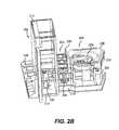
- FIG. 2 ais a schematic of an exterior of a dual wafer handling apparatus and components thereof according to various embodiments.
- FIGS. 2 b and 2 care schematics of a dual wafer handling apparatus showing internal views of the atmospheric environment and the transfer module according to various embodiments.
- FIGS. 3 a - eare graphical representations showing top views of a dual wafer transport apparatus performing certain operations in dual wafer transport of a pair of wafers from a storage cassette to a wafer transfer module and back according to various embodiments.
- FIG. 3 fshows an example of a sequence of movements a pair of wafers may undergo in a process module according to certain embodiments.
- Wafersare often introduced to processing stations or modules via wafer transfer apparatuses during integrated circuit fabrication.
- wafersare processed at high temperatures—entering a wafer transfer apparatus “cold,” typically between about room temperature and leaving the process module “hot,” typically between about 300-500 C.
- a plasma enhanced chemical vapor deposition (PECVD) of a dielectric layer processmay operate at a wafer temperature of about 400 C.
- PECVDplasma enhanced chemical vapor deposition
- Examples of other fabrication processes that operate at elevated wafer temperatureinclude deposition of dielectric and conductive layers, etch processes, etc.
- a robotis used to transfer cold wafers from a first location, e.g., a loadlock or storage location, to a process module for processing, and transfer processed hot wafers from the process module back to the first location or to another location.
- the processesare operated in vacuum environments with a vacuum transfer module used to transfer wafers to and from the process modules.
- a vacuum transfer module robotmay transfer cold wafers from a loadlock or other location to a process module for processing, and transfer processed hot wafers from the process module back to the loadlock or to another location such as a second process module
- Methods, systems and apparatuses for high throughput substrate transferare provided herein.
- the methods and systemsuse robots having dedicated end effectors for hot and cold wafers. Throughput is increased by optimizing the transfer of both the hot and the cold wafers (or other substrates).
- wafer transfer apparatuseshaving end effectors configured for supporting either hot or cold wafers.
- dual arm robotshaving dedicated hot and cold wafer arms are provided.
- methods of transferring substratesthat improve overall throughput. The methods involve transferring hot and cold substrates at different accelerations.
- An end effectoris a device or tool connected to the end of a robot arm, for example, a blade, paddle or gripper.
- the end effectoris any such support or device that physically contacts the wafer or other substrate to transport it.
- End effectorsinclude generally flat supports, such as blades, paddles or forks, on which the wafer sits, as well as devices that hold the wafer in place, such as a gripper.
- the wafer transfer apparatuses described hereinhave dedicated end effectors to support hot and cold substrates during substrate transfer—the dedicated hot substrate end effector(s) are exclusively used for transferring hot substrates and the dedicated cold substrate end effector(s) exclusively used for transferring cold substrates.
- robots having dual armsare provided—one arm having one or more dedicated cold wafer end effectors and the other arm having one or more dedicated hot wafer end effectors.
- the robots described hereinuse end effectors on which the wafer sits, however the methods are not limited to such end effectors.
- the dedicated end effectors for hot wafers described hereinare made of a material that is able to withstand the heat from the wafer. Materials with low thermal conductivity and low coefficients of thermal expansion are used. In many embodiments, ceramics are used, with a specific example being alumina and silicon carbide materials.
- the dedicated end effectors for cold wafers described hereinare made of materials that have high coefficients of friction. The coefficient of friction determines the maximum acceleration and deceleration that the end effector and wafer may obtain without wafer slippage. Using materials with high coefficients of friction allow greater acceleration—reducing the time it takes to transport the wafers. As an example, perfluoroelastomers (PFEs) have coefficients of friction around 1.
- FIG. 1 ashows a schematic representation of a top view of a dual arm robot 106 in a vacuum transfer module 100 .
- the dual arm robot 106transfers wafers between a loadlock 102 and a process module 104 .
- Robot arm 108is a dedicated arm for transferring cold wafers, e.g., from the loadlock 102 to the process module 104 .
- Robot arm 110is a dedicated arm for transferring hot wafers, usually from the process module 104 to the loadlock 102 .
- the robot armshave dual end effectors and are each capable of transferring two wafers simultaneously.
- FIG. 1 bis a graphical representation showing a top view of the relative positions of the arms of a dual arm robot according to certain embodiments.
- a robot 150has dual arms 152 and 154 .
- Arm 152is dedicated to transferring cold wafers and arm 154 to hot wafers.
- Each armhas two end effectors: arm 152 has end effectors 156 a and 156 b attached to it and arm 154 has end effectors 158 a and 158 b .
- the end effectorsare paddle-type end effectors that support wafers during transfer.
- the dedicated cold armtakes unprocessed wafers from a loadlock (not shown) transfers them to the process module and places them in the process module, while the dedicated hot arm takes processed wafers from the process module and transfers them to the loadlock.
- arm 152is in a forward position, extending into a process module 160 .
- a robot armextends into a process module or other location during a pick or place move. The movement of a robot to take a wafer from a location such as a processing station is referred to herein as a “pick” move, while the placement of a wafer to a location by the robot is referred to herein as a “place” move.
- arm 152is a dedicated arm for cold wafers; thus it places cold unprocessed wafers into the process module 160 .
- Arm 154picks hot processed wafers from the process module 160 , to transfer and place them in a loadlock or other location.
- arm 154is extended into the process module to remove the wafers and arm 152 is retracted.
- Place and pick moves to and from a loadlock or other locationare similarly performed—with the arm pick or placing extended to the location and the other arm retracted.
- the dual arm robot shown in FIG. 1 bis an example of possible dual arm robots having dedicated hot and cold end effectors.
- arm and end effector(s) carrying the wafersmay be moved at or below the maximum acceleration at which the wafers will not move or slip. In many cases, the arms are moved at some factor below the maximum. Because the hot and cold wafer end effectors are made of materials having different coefficients of friction, the cold wafer end effectors can be moved at higher accelerations (and decelerations). Using a dual arm robot, there are several possible accelerations:
- Wafer on Leading Arm(may be wafer on retracted arm): Low (0.15 g)
- Hot wafer on leading armLow (e.g., about 0.15 g)
- Table 1 belowshows a simplified comparison of robot acceleration and wafer throughput using dedicated hot and cold paddles with that using standard paddles.
- Moves of a dual arm robot transferring wafers between a loadlock and a process moduleare shown, along with achievable acceleration.
- Place movesinvolve extending the arm to the place location, placing the wafer, and retracting the arm from the place location.
- Placing the wafermay involve lowering the wafer onto a wafer support or a lift mechanism lifting the wafer from the end effector.
- Pick movesinvolve extending the arm into the pick location, picking the wafer, and retracting the arm from the pick location.
- Picking the wafermay involve lifting the wafer from a wafer support or lift mechanism.
- Place and pick movesmay involve extension or retraction along a standard or nominal path. In certain embodiments, adjustments are made as necessary for wafer position correction. Wafer position correction is also discussed in application Ser. Nos. 11/998,857 and 11/998,858, both filed Nov. 20, 2007, and incorporated by reference for all purposes.
- Goto movesinvolve rotating the arm, e.g., from the process module to the loadlock or vice versa, and/or well as necessary vertical translations. For example, in certain embodiments, vertical translations are used to move between vertically stacked loadlock chambers. In certain embodiments, goto moves also involve moving along a standard nominal path.
- moves to a process module from a loadlockmay involve moving along substantially the same nominal path as moves to the loadlock from the process module and vice versa.
- the dedicated to cold armmay trace in reverse the path taken by the dedicated hot arm in moving to the loadlock from the process module.
- the standard paddlesare limited by the lower coefficient of friction materials that are used to carry hot wafers.
- Dedicated hot and cold paddlesallow four of the seven moves to be performed more quickly resulting in improved throughput. Exact throughput depends on various factors including robot used, robot move distance, etc., but in one example, throughput can be improved by about 10%, as shown in the Table 1.
- the moves and accelerations shown in Table 1are example of possible process sequence and moves. Although the exact analysis will change based on the robot used and process sequence, in general throughput will be improved for other possible process sequences. This is because the dedicated hot and cold paddles allow greater accelerations/decelerations during some moves than standard paddles. Also as indicated above, dedicated hot and cold end effectors may be on the same arm, with acceleration increased for moves involving only cold wafers.
- the surface of the dedicated hot substrate end effectoris made of a material that is chemically inert and can withstand the heat from the processed wafers.
- Processed waferstypically have temperatures ranging from about 300-500 C. Materials that are able to withstand such temperatures include ceramics, such as alumina.
- Appropriate materials for the hot substrate end effectorhave low thermal conductivities and/or low coefficients of thermal expansion. According to various embodiments, the hot substrate end effectors have thermal conductivities ranging from about 15 to 45 W/mK at 100 C. According to various embodiments, the hot substrate end effectors coefficients of thermal expansion ranging from about 8 to 10 ((° C.) ⁇ 1 ⁇ 10 ⁇ 6 ).
- Coefficients of friction for the hot substrate end effectormay be as high as allowable without sacrificing the above-described thermal properties.
- the coefficient of static frictiontypically range from about 0.2 to 0.5.
- the surface of the cold substrate end effectoris made of a material that is chemically inert and has a high coefficient of static friction. According to various embodiments, the coefficient of static friction of the dedicated cold substrate end effector ranges from about 0.75 to 1.5. Examples of materials include perfluoroelastomers (PFEs). Viton® is an example of a fluoroelastomer that may be used.
- PFEsperfluoroelastomers
- Viton®is an example of a fluoroelastomer that may be used.
- the hot and cold end effectorsmay be constructed of the material or the material may be applied as a coating or covering on another surface. The above ranges for thermal and mechanical properties of the end effector material depends on the application; for applications in which the substrate is not a semiconductor wafer for example, these ranges may differ.
- the robots and methods described hereinare used to transfer wafers to and from process modules. In certain embodiments, the robots and methods are used in dual wafer transport systems. A description of such a system according to various embodiments is given below with respect to FIGS. 2 a - c.
- FIG. 2 ashows an exterior of dual wafer handling apparatus and components thereof.
- the apparatus shown in FIG. 2 amay be used to transfer wafers from atmospheric conditions (e.g, to and from a storage unit) to one or more processing chambers (e.g., PECVD chambers) and back again.
- the apparatus shown in FIG. 2 ahas three main components: an atmospheric environment 202 , loadlocks 204 and a transfer module 206 .
- Storage unitse.g., Front Opening Unified Pods or FOUPs
- Processing chambersare not shown in the figure.
- Atmospheric environment 202is typically at atmospheric pressure and interact with FOUPs and/or parts of the external facility.
- Transfer module 206is typically at sub-atmospheric pressure and can be in communication with the loadlocks and various processing chambers which are often run at vacuum or low pressure. Wafers are placed in loadlocks 204 for pump-down or vent operations when transitioning between atmospheric and sub-atmospheric environments.
- the atmospheric environment 202(also referred to as a ‘mini-environment’) contains an atmospheric robot (not shown) that transfers wafers to and from FOUPs and loadlocks 204 .
- Pod loaders 208receive and support FOUPs so that they may be accessed by the atmospheric robot.
- the atmospheric environment 202typically contains an overhead fan filter unit, e.g., a HEPA filter unit, to prevent contaminants from entering the atmospheric environment.
- the air inlet 210 for the fan filter unitis shown in FIG. 2 .
- the lower boundary of the atmospheric or mini-environmentmay be a false floor, such as that depicted in FIG. 2 a at 212 .
- Loadlocks 204receive inbound (unprocessed) wafers from the atmospheric environment 202 to be transferred to the process chambers, and outbound (processed) wafers from the transfer module 206 to be transferred back to the FOUPs.
- a loadlockmay be bidirectional (holding inbound and outbound wafers) or unidirectional (holding only inbound or outbound wafers). In certain embodiments, the loadlocks are unidirectional. Inbound wafers are also referred to herein as incoming or unprocessed wafers; outbound wafers are also referred to herein as outgoing or processed wafers.
- FIG. 2there are two independent loadlocks: an upper loadlock stacked on top of a lower loadlock, each having two connected chambers.
- the upper loadlockis an inbound loadlock and the lower loadlock is an outbound loadlock.
- Plates 214are lids of the inbound loadlock, each plate covering one of the two connected chambers.
- Loadlock vacuum pumps 216are used to pump down the loadlocks as necessary during operation.
- Atmospheric valve doors 218provide access to the loadlocks from the atmospheric environment 202 .
- a four door slit valve externally mounted to the mini-environmentis used, though any type of doors or valves including gate valves, sliding doors, rotational doors, etc., may be used.
- the transfer moduleis configured to be attached to one or more process modules (e.g., single or multi-station PECVD chambers, UV cure chambers, etc.).
- a process modulemay be attached to the transfer module 206 at multiple interface locations/sides of the transfer module.
- Slit valves 222provide access from the transfer module to the process modules. Any appropriate valve or door system may be used.
- FIG. 2there are two valves per side—allowing two wafers to be transferred between a loadlock and a process module (e.g., between two chambers of a loadlock and two adjacent stations of a process module) or between two process modules.
- Transfer module lift assembly 220is used to raise and lower the cover 228 of the transfer module. In FIG. 2 , cover 228 is down (i.e., the interior of the transfer module is not shown in the figure).
- a vacuum transfer robotis located in the interior of the transfer module to transfer wafers between the loadlocks and the process modules or from process module to process module.
- the transfer module 206is maintained at sub-atmospheric pressure, and is sometimes referred to herein as a vacuum transfer module. Transfer module pressure is typically between 760 torr-1 miliTorr, though in certain embodiments the tool may be used for even lower pressure regimes.
- the loadlock vacuum pumps 216are used to pump down the loadlock to a sub-atmospheric pressure so that the wafer may be subsequently transferred to the vacuum transfer module.
- Loadlock slit valves 230provide access to the loadlocks from the transfer module 206 .
- Transfer module vacuum pump 224along with a gas mass flow controller (MFC), a throttle valve and a manometer, is used to obtain and maintain the desired pressure of the transfer module.
- MFCgas mass flow controller
- on-tool or off-tool vacuum pumpsmay be used for the transfer module.
- various methods of controlling pressure in the transfer moduleexist.
- a MFCprovides a constant flow of N 2 gas into the transfer chamber.
- the manometerprovides feedback as to the pressure of the transfer module chamber.
- the vacuum pumpremoves a constant volume of gas per unit time as measured in cubic feet per minute.
- the throttle valveactively maintains a pressure set point through the use of a closed loop control system.
- the throttle valvereads the manometer's pressure feedback, and based on the commands from the valve's control system, adjusts the opening of the effective orifice to the vacuum pump.
- An access panel 226provides access to an electronics bay that contains a control system to control the wafer handling operations, including robot movements, pressure, timing, etc.
- the control systemmay also control some or all operations of processes performed in the process module.
- the controllers, switches, and other related electrical hardwarecan be located elsewhere according to various embodiments.
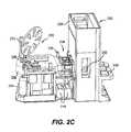
- FIGS. 2 b and 2 care additional schematics of a dual wafer handling apparatus that show internal views of an atmospheric environment 202 and transfer module 206 .
- the apparatus shown in FIGS. 2 b and 2 cis substantially the same as that shown in FIG. 2A , with the shape of the transfer module of the apparatus in FIGS. 2 b and 2 c a trapezoid to allow a larger access 238 area to service the transfer module.
- the transfer module lift assembly and lid, and a portion of the atmospheric environment casingare not shown in FIG. 2 a.
- the atmospheric environment 202contains an atmospheric robot 232 .
- the transfer module 206contains a vacuum robot 236 .
- the atmospheric robot 232has one arm, with two articulated wrists, each of which has a paddle or other end effector capable of carrying a wafer.
- Vacuum transfer robot 236has two arms, each with two paddles capable of carrying a wafer.
- the atmospheric robotis capable of handling two wafers simultaneously and the vacuum robot can simultaneously carry up to four wafers.
- the vacuum robothas dedicated cold and hot arms.
- FIG. 2 balso provides a partial view of a pipe 244 , also referred to the loadlock pump foreline, that leads from a manifold to the vacuum pumps 244 .
- Dual vacuum pumps 244work in tandem and are used to pumpdown both loadlocks According to various embodiments, the dual pumps may function as a single pump resource or could be dedicated to a specific loadlock for parallel pump downs.
- FIG. 2 cshows a schematic of the apparatus shown in FIG. 2 b from the opposite side. The transfer module lift assembly 220 and the transfer module lid 228 are shown in an upright position.
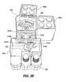
- FIGS. 3 a - fare graphical representations showing certain operations in dual wafer transport of a pair of wafers from FOUPs to the wafer transfer module and back.
- FIG. 3 ashows an apparatus with transfer module 306 , upper (inbound) loadlock 304 a , lower (outbound) loadlock 304 b and atmospheric environment 302 . Also shown are process modules 303 a and 303 b .
- FOUPs 334which interface with the atmospheric environment 302 .
- the atmospheric environment 302contains an atmospheric robot 332 ; the transfer module 306 contains a vacuum robot 336 .
- the apparatusis capable of parallel transport and processing of two wafers.
- Both the atmospheric and vacuum robotsare capable of simultaneous handling at least two wafers.
- Atmospheric robot 332has one arm, with two articulated wrists, each of which has gripper capable of carrying a wafer.
- Vacuum transfer robot 336has two arms, each with two blades or grippers capable of carrying a wafer. Also, as described above, in embodiments of the invention at least the vacuum robot has a dedicated hot arm and a dedicated cold arm.
- the atmospheric robottakes two wafers from FOUPs.
- These movesare also referred to herein as “get” and “put” moves, respectively.
- the two wafersmay be taken simultaneously or one after another. In the embodiment depicted in FIG.
- the atmospheric robothas one arm with two articulated wrists and is capable of simultaneous transfer of two stacked wafers, e.g., simultaneous picks of two stacked wafers from a FOUP.
- FIG. 3 bshows the atmospheric robot 332 with two wafers 335 ′ and 335 ′′ during transfer from the FOUP to the upper loadlock 304 a .
- the atmospheric robotthen places the wafers into the upper loadlock 304 a for depressurization. This is shown in FIG. 3 c .
- One waferis in each chamber. Once the wafers are placed in the upper loadlock, the atmospheric doors 318 a of the upper loadlock close and the loadlock is pumped down.
- FIG. 3 dshows transfer module robot 336 with wafers 335 ′ and 335 ′′.
- the transfer module robot depicted in FIGS. 3 a - ehas two arms, each with two end effectors and is capable of holding four wafers simultaneously. Wafers 335 ′ and 335 ′′ are unprocessed and so are on dedicated cold end effectors.
- the upper loadlockdoes not have an active wafer centering, nor are there independent z-drives for each of the pans of each arm.
- the vacuum robotpicks the wafer simultaneously and cannot selectively pick one wafer if two wafers are present in the incoming loadlock.
- the transfer module robotmay pick each wafer simultaneously or consecutively. Also depending on the robot and the system, the robot may use one arm with two end effectors to pick both wafers, or each wafer may be picked by a different arm.
- the transfer module robottransfers the wafers to processing module, i.e., either process module 303 a or process module 303 b , by rotating and placing the wafers in the process module.
- FIG. 3 fshows an example of a sequence of movements the wafers may undergo in a process module 303 a .
- wafer 335 ′is placed in station 338 of processing module 303 a and wafer 335 ′′ is placed in station 340 of processing module 303 a .
- the wafersthen undergo processing at these stations.
- Wafer 335 ′′moves from station 340 to station 344 and wafer 335 ′ from station 338 to station 342 ′ for further processing.
- the wafersare then returned to their original stations to be picked using the dedicated hot wafer end effectors of the transfer module robot for transfer to the outbound loadlock or to processing module 303 b for further processing.
- the stationsare depicted as ‘empty’ in the figure when not occupied by wafers 335 ′ and 335 ′′, in operation all stations are typically filled by wafers.
- the sequence illustrated in FIG. 3 fis just an example of a possible sequence that may be employed with the apparatuses described herein.
- the transfer module robotpicks both wafers up for simultaneous transfer to the loadlock. The pick moves may occur simultaneously or consecutively. The robot then rotates to place the processed wafers in the loadlock. Again, these moves may occur simultaneously or consecutively according to various embodiments.
- 3 eshows the now processed wafers 335 ′ and 335 ′′ placed in the outbound (lower) loadlock 304 b via lower loadlock doors 320 b .
- all loadlock valves or doorsare shut and the outbound loadlock is vented (pressurized) to atmospheric pressure.
- the wafersmay also be cooled here.
- the atmospheric doors 318 b of the outbound loadlockare then opened, and the atmospheric robot picks up the processed wafers and transfers them to the appropriate place in the FOUP.
- a unidirectional flow schemeis used.
- An example of inbound and outbound loadlocks, atmospheric robot and transfer module robot moves in a unidirectional flow scheme using dedicated arms for hot and cold wafersis given below in Table 2:
- Table 2presents an example of a sequence of unidirectional operational mode in which the transfer module robot hand-off sequence is process module (wafer exchange) ⁇ outgoing loadlock (place processed wafers) ⁇ incoming loadlock (pick unprocessed wafers). This is an example of one possible sequence—others may be used with the dual wafer handling apparatuses described herein, including outgoing loadlock accessed before the incoming loadlock.
- Rowscan be read as roughly simultaneously occurring or overlapping operations. Columns show the sequence of operations the robot or loadlock performs. Of course, in any system, these operations may not overlap exactly and one or more of the modules may be idle or begin or end later. Further, it should be noted that certain operations are not shown.
- the rotational and translational moves the robots must perform to reach the pods, loadlocks and process modulesare not shown.
- the descriptions ‘TM Robot’ and ‘ATM Robot’can refer to the moves the loadlocks undergo—opening and closing the appropriate doors—as well as admitting the robot end effectors to pick or place the wafers.
- the loadlockcan then be pumped down—it does not have to wait for the atmospheric robot to complete its moves before pumping down.
- Thisis distinguished from bidirectional operation in which a loadlock is idle while the atmospheric robot places the processed wafers in a FOUP or other cassette and gets two unprocessed wafers from a cassette for placement into the loadlock.
- VentVent the upper loadlock from 550 mTorr to atmospheric. No wafer is present. Like the pump down operation, the vent operation is fairly rapid.
- Open/Close slit valve(valve to transfer module): 0.5
- Vent/CoolVent the lower loadlock from 550 mtorr to atmospheric pressure. Venting is done by flowing gases such as helium and/or nitrogen into the chamber.
- Open/Close slit valve(valve to transfer module): 0.5
- the atmospheric robotpicks two stacked unprocessed wafers from a FOUP or other cassette.
- the end effectorsare stacked on top of the other and pick the stacked wafers simultaneously. After picking the wafers, the end effectors are rotated with respect to each other, and the arm is rotated to place the wafers in the upper loadlock (see FIG. 3 b , which shows a single arm dual end effector robot holding two wafers ready to place them into the upper loadlock).
- Upper LL PlaceThe atmospheric robot places the wafers into the upper loadlock chambers. In certain embodiments, first one end effector is extended into a chamber of the upper loadlock and lowers the wafer onto the shelf. The end effector is then retracted from the loadlock and the second end effector is extended into the other chamber of the upper loadlock and lowers the wafer onto the shelf.
- Lower LL PickThe atmospheric robot picks the wafers from the lower loadlock chambers.
- first one end effectoris extended into a chamber of the upper loadlock and picks the wafer from the pedestal.
- the end effectoris then retracted from the loadlock and the second end effector is extended into the other chamber of the lower loadlock and picks the wafer from the pedestal.
- the robotuses information about the placement of each wafer in the lower loadlock to correct wafer position during the pick move.
- the atmospheric robot armis then rotated to place the wafers in the FOUP.
- FOUP PlaceThe atmospheric robot places the wafers into stacked positions in a FOUP. In one embodiment, both wafers are placed simultaneously.
- the transfer module robotextends a dedicated cold wafer dual end effector arm of the transfer module into the upper loadlock and lifts the wafers from the shelves onto the end effectors.
- the other armmoves into a retracted position.
- FIG. 1 bshows a dual arm dual end effector robot with one arm extended (e.g., into a loadlock or process module for a pick or place move) and one arm retracted.
- the dedicated cold armis dedicated to taking unprocessed wafers from the upper loadlock and placing them in the process module (cold arm), and the other arm is dedicated to taking processed wafers from the process module and placing them in the lower loadlock (hot arm).
- the transfer module robotextends the dedicated hot wafer arm—having a process wafer on each end effector—into the lower loadlock and places them there. In certain embodiments, this is done simultaneously. Position information of each wafer loadlock may be measured and stored for use by the atmospheric robot in picking the wafers. The robot is then positioned for the process module pick move.
- Process Module PickThe transfer module robot extends the dedicated hot arm into the process module and picks the two processed wafers. In certain embodiments, this is done simultaneously. In the scheme shown in Table 2, after the process module pick, the transfer module robot places the unprocessed wafers into the process module.
- the transfer module robotextends the dedicated cold arm—having two unprocessed wafers—into the process module and places them at the stations either by lower the wafers onto the stations, or by wafer supports in the stations lifting the wafers off the end effectors.
- the place movesare done sequentially to allow position corrections to be made in each place move.
- Wafer Exchange(processed for unprocessed at process module or chamber): 8.5
- a controlleris employed to control aspects of the wafer transfer processes described above.
- the controllerwill typically include one or more memory devices and one or more processors.
- the processormay include a CPU or computer, analog and/or digital input/output connections, stepper motor controller boards, etc.
- the controllerexecutes system control software including sets of instructions for controlling the timing, Other computer programs stored on memory devices associated with the controller may be employed in some embodiments.
- the user interfacemay include a display screen, graphical software displays of the apparatus and/or process conditions, and user input devices such as pointing devices, keyboards, touch screens, microphones, etc.
- the computer program code for controlling the transfer and position error correction and other processes in a process sequencecan be written in any conventional computer readable programming language: for example, assembly language, C, C++, Pascal, Fortran or others.
- Compiled object code or scriptis executed by the processor to perform the tasks identified in the program.
- Parametersmay be provided to the user in the form of a recipe, and may be entered utilizing the user interface.
- Signals for monitoring the processmay be provided by analog and/or digital input connections of the system controller.
- the signals for controlling the processare output on the analog and digital output connections of the apparatus.
- the system softwaremay be designed or configured in many different ways. For example, various transfer apparatus component subroutines or control objects may be written to control operation of the apparatus components necessary to carry out the inventive transfer processes.
- Examples of programs or sections of programs for this purposeinclude code for controlling which arm and/or end effector is used to pick up processed or hot wafers and code controlling which arm and/or end effector is used to pick up unprocessed or cold wafers.
- the robottypically has its own controller, with speeds preset.
- a system controllermay also include code to run pumpdown/vent or process module operations.
Landscapes
- Engineering & Computer Science (AREA)
- Physics & Mathematics (AREA)
- Condensed Matter Physics & Semiconductors (AREA)
- General Physics & Mathematics (AREA)
- Manufacturing & Machinery (AREA)
- Computer Hardware Design (AREA)
- Microelectronics & Electronic Packaging (AREA)
- Power Engineering (AREA)
- Robotics (AREA)
- Container, Conveyance, Adherence, Positioning, Of Wafer (AREA)
Abstract
Description
This application is a continuation of U.S. application Ser. No. 12/079,242, having the title “DEDICATED HOT AND COLD END EFFECTORS FOR IMPROVED THROUGHPUT,” filed Mar. 24, 2008, all of which is incorporated herein by this reference for all purposes.
Different types of tools are used to perform hundreds of processing operations during semiconductor device fabrication. Most of these operations are performed in vacuum chambers at very low pressure. Wafers are introduced to the process chambers with wafer handling systems that are mechanically coupled to the process chambers. The wafer handling systems transfer wafers from the factory floor to the process chamber. These systems include loadlocks to bring the wafers from atmospheric conditions to very low pressure conditions and back, and robots to transfer the wafers to various positions. Throughput—the number of wafers that is processed in a period of time—is affected by the process time, the number of wafers that are processed at a time, as well as timing of the steps to introduce the wafers into the vacuum process chambers. What are needed are improved methods and apparatuses of increasing throughput.
Methods, systems and apparatuses for high throughput substrate transfer are provided. According to various embodiments, the methods and systems described use robots having dedicated end effectors for hot and cold wafers or other substrates. Throughput is increased by optimizing the transfer of both the hot and the cold wafers. Also described are wafer transfer apparatuses having end effectors configured for supporting either hot or cold wafers. In certain embodiments, dual arm robots having dedicated hot and cold wafer arms are provided. Also provided are methods of transferring substrates that to improve overall throughput. The methods involve transferring hot and cold substrates at different accelerations.
Methods, systems and apparatuses used for substrate transport are provided herein. While the methods, systems and apparatuses described can be used for semiconductor manufacturing, it should be understood they could be used in any processes or industries where it is necessary or advantageous to transfer substrates of multiple different temperatures. For the purposes of discussion, the below description refers chiefly to wafers, however one of skill in the art will understand how to implement the methods, systems and apparatuses for other types of substrates and workpieces.
Wafers are often introduced to processing stations or modules via wafer transfer apparatuses during integrated circuit fabrication. In many integrated circuit manufacture processes, wafers are processed at high temperatures—entering a wafer transfer apparatus “cold,” typically between about room temperature and leaving the process module “hot,” typically between about 300-500 C. For example, a plasma enhanced chemical vapor deposition (PECVD) of a dielectric layer process may operate at a wafer temperature of about 400 C. Examples of other fabrication processes that operate at elevated wafer temperature include deposition of dielectric and conductive layers, etch processes, etc. A robot is used to transfer cold wafers from a first location, e.g., a loadlock or storage location, to a process module for processing, and transfer processed hot wafers from the process module back to the first location or to another location. In many applications, the processes are operated in vacuum environments with a vacuum transfer module used to transfer wafers to and from the process modules. A vacuum transfer module robot may transfer cold wafers from a loadlock or other location to a process module for processing, and transfer processed hot wafers from the process module back to the loadlock or to another location such as a second process module
Methods, systems and apparatuses for high throughput substrate transfer are provided herein. The methods and systems use robots having dedicated end effectors for hot and cold wafers. Throughput is increased by optimizing the transfer of both the hot and the cold wafers (or other substrates). Also provided are wafer transfer apparatuses having end effectors configured for supporting either hot or cold wafers. In certain embodiments, dual arm robots having dedicated hot and cold wafer arms are provided. Also provided are methods of transferring substrates that improve overall throughput. The methods involve transferring hot and cold substrates at different accelerations.
An end effector is a device or tool connected to the end of a robot arm, for example, a blade, paddle or gripper. As used herein, the end effector is any such support or device that physically contacts the wafer or other substrate to transport it. End effectors include generally flat supports, such as blades, paddles or forks, on which the wafer sits, as well as devices that hold the wafer in place, such as a gripper. The wafer transfer apparatuses described herein have dedicated end effectors to support hot and cold substrates during substrate transfer—the dedicated hot substrate end effector(s) are exclusively used for transferring hot substrates and the dedicated cold substrate end effector(s) exclusively used for transferring cold substrates. In certain embodiments, robots having dual arms are provided—one arm having one or more dedicated cold wafer end effectors and the other arm having one or more dedicated hot wafer end effectors. In many embodiments, the robots described herein use end effectors on which the wafer sits, however the methods are not limited to such end effectors.
The dedicated end effectors for hot wafers described herein are made of a material that is able to withstand the heat from the wafer. Materials with low thermal conductivity and low coefficients of thermal expansion are used. In many embodiments, ceramics are used, with a specific example being alumina and silicon carbide materials. The dedicated end effectors for cold wafers described herein are made of materials that have high coefficients of friction. The coefficient of friction determines the maximum acceleration and deceleration that the end effector and wafer may obtain without wafer slippage. Using materials with high coefficients of friction allow greater acceleration—reducing the time it takes to transport the wafers. As an example, perfluoroelastomers (PFEs) have coefficients of friction around 1. This is compared to a coefficient of about 0.3 for ceramics to silicon. As a result, the acceleration rate obtainable for a wafer on a PFE end effector is more than double than that obtainable for a wafer on a ceramic end effector. Further discussion of the properties and examples of materials suitable for the dedicated hot and cold end effectors is below.
In transferring the wafers between the loadlock and process modules (or between any two locations appropriate for the application), arm and end effector(s) carrying the wafers may be moved at or below the maximum acceleration at which the wafers will not move or slip. In many cases, the arms are moved at some factor below the maximum. Because the hot and cold wafer end effectors are made of materials having different coefficients of friction, the cold wafer end effectors can be moved at higher accelerations (and decelerations). Using a dual arm robot, there are several possible accelerations:
Standard Paddles
Wafer on Leading Arm (may be wafer on retracted arm): Low (0.15 g)
No wafer on leading arm but wafer on retracted arm: Medium (0.5 g)
No wafer on either arm: High (1.0 g)
Hot and Cold Paddles
Hot wafer on leading arm: Low (e.g., about 0.15 g)
Cold wafer on leading arm/hot wafer on retracted arm: Low 2 (e.g., about 0.3 g)
Cold wafer on leading arm/no wafer on retracted arm: Low 3 (e.g, about 0.5 g)
- Low 3>Low 2>Low 3
No wafer on leading arm/hot wafer on retracted arm: Medium (e.g., about 0.5 g)
No wafer on leading arm/cold wafer on retracted arm: Medium 2 (e.g., about 0.75 g)
Medium 2>Medium
No wafer on either arm: High (e.g., about 1.0 g)
Table 1 below shows a simplified comparison of robot acceleration and wafer throughput using dedicated hot and cold paddles with that using standard paddles. Moves of a dual arm robot transferring wafers between a loadlock and a process module (as inFIGS. 1aand 1b ) are shown, along with achievable acceleration. Place moves involve extending the arm to the place location, placing the wafer, and retracting the arm from the place location. Placing the wafer may involve lowering the wafer onto a wafer support or a lift mechanism lifting the wafer from the end effector. Pick moves involve extending the arm into the pick location, picking the wafer, and retracting the arm from the pick location. Picking the wafer may involve lifting the wafer from a wafer support or lift mechanism. Place and pick moves may involve extension or retraction along a standard or nominal path. In certain embodiments, adjustments are made as necessary for wafer position correction. Wafer position correction is also discussed in application Ser. Nos. 11/998,857 and 11/998,858, both filed Nov. 20, 2007, and incorporated by reference for all purposes. Goto moves involve rotating the arm, e.g., from the process module to the loadlock or vice versa, and/or well as necessary vertical translations. For example, in certain embodiments, vertical translations are used to move between vertically stacked loadlock chambers. In certain embodiments, goto moves also involve moving along a standard nominal path. Also, moves to a process module from a loadlock may involve moving along substantially the same nominal path as moves to the loadlock from the process module and vice versa. For example, in moving to the process module, the dedicated to cold arm may trace in reverse the path taken by the dedicated hot arm in moving to the loadlock from the process module.
| TABLE 1 |
| Robot acceleration and throughout improvement |
| Robot | |||
| Acceleration | |||
| Hot and | Change and | ||
| Standard | Cold | Throughput | |
| TM Robot | Paddles | Paddles | Improvement |
| Goto LL from PM (hot | Low | Low | No |
| wafer on leading arm) | |||
| Place LL (hot wafer on | Low | Low | No |
| leading arm/no | (extension) | ||
| wafer on trailing) | High | High | |
| (retraction) | |||
| Goto LL (go between | High | High | No |
| stacked LL chambers) | |||
| (no wafers) | |||
| Pick LL (cold wafer on | Low | Low 3 | Yes |
| leading/none on trailing) | |||
| Goto PM from LL (cold | Low | Low 3 | Yes |
| wafer on leading/ | (retraction) | ||
| none on trailing) | |||
| Pick PM (hot wafer on | Medium | Medium | Yes |
| leading/cold on trailing) | (extension) | 2 | |
| Low | Low | ||
| (retraction) | |||
| Place PM (cold wafer on | Low | Low 2 | Yes |
| leading/hot on trailing) | (extension) | ||
| Medium | Medium | ||
| (retraction) | |||
| Throughput (WPH) | ~150 | ~165 | Yes |
The standard paddles are limited by the lower coefficient of friction materials that are used to carry hot wafers. Dedicated hot and cold paddles allow four of the seven moves to be performed more quickly resulting in improved throughput. Exact throughput depends on various factors including robot used, robot move distance, etc., but in one example, throughput can be improved by about 10%, as shown in the Table 1. The moves and accelerations shown in Table 1 are example of possible process sequence and moves. Although the exact analysis will change based on the robot used and process sequence, in general throughput will be improved for other possible process sequences. This is because the dedicated hot and cold paddles allow greater accelerations/decelerations during some moves than standard paddles. Also as indicated above, dedicated hot and cold end effectors may be on the same arm, with acceleration increased for moves involving only cold wafers.
The surface of the dedicated hot substrate end effector is made of a material that is chemically inert and can withstand the heat from the processed wafers. Processed wafers typically have temperatures ranging from about 300-500 C. Materials that are able to withstand such temperatures include ceramics, such as alumina. Appropriate materials for the hot substrate end effector have low thermal conductivities and/or low coefficients of thermal expansion. According to various embodiments, the hot substrate end effectors have thermal conductivities ranging from about 15 to 45 W/mK at 100 C. According to various embodiments, the hot substrate end effectors coefficients of thermal expansion ranging from about 8 to 10 ((° C.)−1×10⁻⁶).
Coefficients of friction for the hot substrate end effector may be as high as allowable without sacrificing the above-described thermal properties. For ceramic end effectors, the coefficient of static friction typically range from about 0.2 to 0.5.
The surface of the cold substrate end effector is made of a material that is chemically inert and has a high coefficient of static friction. According to various embodiments, the coefficient of static friction of the dedicated cold substrate end effector ranges from about 0.75 to 1.5. Examples of materials include perfluoroelastomers (PFEs). Viton® is an example of a fluoroelastomer that may be used. The hot and cold end effectors may be constructed of the material or the material may be applied as a coating or covering on another surface. The above ranges for thermal and mechanical properties of the end effector material depends on the application; for applications in which the substrate is not a semiconductor wafer for example, these ranges may differ.
In certain embodiments, the robots and methods described herein are used to transfer wafers to and from process modules. In certain embodiments, the robots and methods are used in dual wafer transport systems. A description of such a system according to various embodiments is given below with respect toFIGS. 2a -c.
The atmospheric environment202 (also referred to as a ‘mini-environment’) contains an atmospheric robot (not shown) that transfers wafers to and from FOUPs andloadlocks 204.Pod loaders 208 receive and support FOUPs so that they may be accessed by the atmospheric robot. Theatmospheric environment 202 typically contains an overhead fan filter unit, e.g., a HEPA filter unit, to prevent contaminants from entering the atmospheric environment. Theair inlet 210 for the fan filter unit is shown inFIG. 2 . The lower boundary of the atmospheric or mini-environment may be a false floor, such as that depicted inFIG. 2a at212.
InFIG. 2 , there are two independent loadlocks: an upper loadlock stacked on top of a lower loadlock, each having two connected chambers. In certain embodiments, the upper loadlock is an inbound loadlock and the lower loadlock is an outbound loadlock.Plates 214 are lids of the inbound loadlock, each plate covering one of the two connected chambers.Loadlock vacuum pumps 216 are used to pump down the loadlocks as necessary during operation.
The transfer module is configured to be attached to one or more process modules (e.g., single or multi-station PECVD chambers, UV cure chambers, etc.). A process module may be attached to thetransfer module 206 at multiple interface locations/sides of the transfer module.Slit valves 222 provide access from the transfer module to the process modules. Any appropriate valve or door system may be used. InFIG. 2 , there are two valves per side—allowing two wafers to be transferred between a loadlock and a process module (e.g., between two chambers of a loadlock and two adjacent stations of a process module) or between two process modules. Transfermodule lift assembly 220 is used to raise and lower thecover 228 of the transfer module. InFIG. 2 , cover228 is down (i.e., the interior of the transfer module is not shown in the figure). A vacuum transfer robot is located in the interior of the transfer module to transfer wafers between the loadlocks and the process modules or from process module to process module.
Thetransfer module 206 is maintained at sub-atmospheric pressure, and is sometimes referred to herein as a vacuum transfer module. Transfer module pressure is typically between 760 torr-1 miliTorr, though in certain embodiments the tool may be used for even lower pressure regimes. Once an inbound wafer is in place in the loadlock, theloadlock vacuum pumps 216 are used to pump down the loadlock to a sub-atmospheric pressure so that the wafer may be subsequently transferred to the vacuum transfer module. Loadlock slitvalves 230 provide access to the loadlocks from thetransfer module 206. Transfermodule vacuum pump 224, along with a gas mass flow controller (MFC), a throttle valve and a manometer, is used to obtain and maintain the desired pressure of the transfer module. In general, on-tool or off-tool vacuum pumps may be used for the transfer module. As is known in the art, various methods of controlling pressure in the transfer module exist. In one example, a MFC provides a constant flow of N2gas into the transfer chamber. The manometer provides feedback as to the pressure of the transfer module chamber. The vacuum pump removes a constant volume of gas per unit time as measured in cubic feet per minute. The throttle valve actively maintains a pressure set point through the use of a closed loop control system. The throttle valve reads the manometer's pressure feedback, and based on the commands from the valve's control system, adjusts the opening of the effective orifice to the vacuum pump.
Anaccess panel 226 provides access to an electronics bay that contains a control system to control the wafer handling operations, including robot movements, pressure, timing, etc. The control system may also control some or all operations of processes performed in the process module. The controllers, switches, and other related electrical hardware can be located elsewhere according to various embodiments.
Theatmospheric environment 202 contains anatmospheric robot 232. Thetransfer module 206 contains avacuum robot 236. In the embodiment depicted inFIG. 2a , theatmospheric robot 232 has one arm, with two articulated wrists, each of which has a paddle or other end effector capable of carrying a wafer.Vacuum transfer robot 236 has two arms, each with two paddles capable of carrying a wafer. The atmospheric robot is capable of handling two wafers simultaneously and the vacuum robot can simultaneously carry up to four wafers. (The apparatus and methods described herein are not limited to these particular robot designs, though in dual wafer transport embodiments each of the robots is capable of handling, transferring, or exchanging at least two wafers.) As described above, according to embodiments of the invention, the vacuum robot has dedicated cold and hot arms.
As indicated above, the apparatus is capable of parallel transport and processing of two wafers. Both the atmospheric and vacuum robots are capable of simultaneous handling at least two wafers.
In operation, to process wafers, the atmospheric robot takes two wafers from FOUPs. (As indicated above, the movement of a robot to take a wafer from a location such as a FOUP, loadlock or processing station is sometimes referred to herein as a “pick” move, while the placement of a wafer to a location by the robot is sometimes referred to herein as a “place” move. These moves are also referred to herein as “get” and “put” moves, respectively.) Depending on the robot and the arrangement of the FOUPs or other wafer storage, the two wafers may be taken simultaneously or one after another. In the embodiment depicted inFIG. 3a , for example, the atmospheric robot has one arm with two articulated wrists and is capable of simultaneous transfer of two stacked wafers, e.g., simultaneous picks of two stacked wafers from a FOUP.FIG. 3b shows theatmospheric robot 332 with twowafers 335′ and335″ during transfer from the FOUP to theupper loadlock 304a. The atmospheric robot then places the wafers into theupper loadlock 304afor depressurization. This is shown inFIG. 3c . One wafer is in each chamber. Once the wafers are placed in the upper loadlock, theatmospheric doors 318aof the upper loadlock close and the loadlock is pumped down. When the desired pressure is reached, theupper loadlock doors 320aon the transfer module side are open andtransfer module robot 336 picks the wafers from the upper loadlock.FIG. 3d showstransfer module robot 336 withwafers 335′ and335″. The transfer module robot depicted inFIGS. 3a-e has two arms, each with two end effectors and is capable of holding four wafers simultaneously.Wafers 335′ and335″ are unprocessed and so are on dedicated cold end effectors. In the embodiment shown, the upper loadlock does not have an active wafer centering, nor are there independent z-drives for each of the pans of each arm. In certain embodiments, the vacuum robot picks the wafer simultaneously and cannot selectively pick one wafer if two wafers are present in the incoming loadlock. However, depending on the robot and the system, the transfer module robot may pick each wafer simultaneously or consecutively. Also depending on the robot and the system, the robot may use one arm with two end effectors to pick both wafers, or each wafer may be picked by a different arm. After picking the unprocessed wafers from the inbound loadlock, the transfer module robot transfers the wafers to processing module, i.e., eitherprocess module 303aorprocess module 303b, by rotating and placing the wafers in the process module. Although not depicted inFIGS. 3a-e , there may also be a third processing module connected to the transfer module. The wafers then undergo processing in the processing module.FIG. 3f shows an example of a sequence of movements the wafers may undergo in aprocess module 303a. First,wafer 335′ is placed instation 338 ofprocessing module 303aandwafer 335″ is placed instation 340 ofprocessing module 303a. The wafers then undergo processing at these stations.Wafer 335″ moves fromstation 340 tostation 344 andwafer 335′ fromstation 338 to station342′ for further processing. The wafers are then returned to their original stations to be picked using the dedicated hot wafer end effectors of the transfer module robot for transfer to the outbound loadlock or toprocessing module 303bfor further processing. For clarity, the stations are depicted as ‘empty’ in the figure when not occupied bywafers 335′ and335″, in operation all stations are typically filled by wafers. The sequence illustrated inFIG. 3f is just an example of a possible sequence that may be employed with the apparatuses described herein. The transfer module robot picks both wafers up for simultaneous transfer to the loadlock. The pick moves may occur simultaneously or consecutively. The robot then rotates to place the processed wafers in the loadlock. Again, these moves may occur simultaneously or consecutively according to various embodiments.FIG. 3e shows the now processedwafers 335′ and335″ placed in the outbound (lower) loadlock304bvialower loadlock doors 320b. After being placed there, all loadlock valves or doors are shut and the outbound loadlock is vented (pressurized) to atmospheric pressure. The wafers may also be cooled here. Theatmospheric doors 318bof the outbound loadlock are then opened, and the atmospheric robot picks up the processed wafers and transfers them to the appropriate place in the FOUP.
Unidirectional Flow
In certain embodiments, a unidirectional flow scheme is used. An example of inbound and outbound loadlocks, atmospheric robot and transfer module robot moves in a unidirectional flow scheme using dedicated arms for hot and cold wafers is given below in Table 2:
| TABLE 2 |
| Robot and Loadlocks Moves in Unidirectional Flow Operation |
| Incoming LL | Outgoing LL | ||
| ATM Robot | (Upper) | (Lower) | TM Robot |
| FOUP Pick | Vent (Empty) | TM Robot | Lower LL Place |
| (1) | (hot arm) | ||
| Upper LL | ATM Robot (2) | Vent/Cool (Wafers) | PM Pick |
| Place (2) | (hot arm) | ||
| Lower LL | Pumpdown | ATM Robot | PM Place (cold |
| Pick | (Wafers) (3) | arm) | |
| FOUP Place | TM Robot (4) | Pumpdown (Empty) | Upper LL Pick |
| (cold arm) (4) | |||
| FOUP Pick | Vent (Empty) | TM Robot | Lower LL Place |
| (hot arm) | |||
| Upper LL | ATM Robot | Vent/Cool (Wafers) | PM Pick |
| Place | (hot arm) (1′) | ||
| Lower LL | Pumpdown | ATM Robot | PM Place (cold |
| Pick | (Wafers) | arm) (5) | |
| FOUP Place | TM Robot | Pumpdown (Empty) | Upper LL Pick |
| (cold arm) | |||
| FOUP Pick | Vent (Empty) | TM Robot | Lower LL Place |
| (hot arm) (2′) | |||
| Upper LL | ATM Robot | Vent/Cool (Wafers) | PM Pick |
| Place | (3′) | (hot arm) | |
| Lower LL | Pumpdown | ATM Robot (4′) | PM Place (cold |
| Pick (4′) | (Wafers) | arm) | |
| FOUP Place | TM Robot | Pumpdown (Empty) | Upper LL Pick |
| (5′) | (hot arm) | ||
Table 2 presents an example of a sequence of unidirectional operational mode in which the transfer module robot hand-off sequence is process module (wafer exchange)→outgoing loadlock (place processed wafers)→incoming loadlock (pick unprocessed wafers). This is an example of one possible sequence—others may be used with the dual wafer handling apparatuses described herein, including outgoing loadlock accessed before the incoming loadlock.
Rows can be read as roughly simultaneously occurring or overlapping operations. Columns show the sequence of operations the robot or loadlock performs. Of course, in any system, these operations may not overlap exactly and one or more of the modules may be idle or begin or end later. Further, it should be noted that certain operations are not shown. The rotational and translational moves the robots must perform to reach the pods, loadlocks and process modules are not shown. The descriptions ‘TM Robot’ and ‘ATM Robot’ can refer to the moves the loadlocks undergo—opening and closing the appropriate doors—as well as admitting the robot end effectors to pick or place the wafers.
The path of a pair of unprocessed wafers going from a FOUP to a process module is traced in the Table in steps 1-5:
1—ATM Robot FOUP Pick
2—ATM Robot Upper Loadlock Place
3—Upper LL Pumpdown (seeFIG. 3c )
4—TM Robot Pick
5—TM Robot Process Module Place
The path of a pair of processed wafers going from a process module to a FOUP is traced in the Table in steps 1′-5′:
1′—TM Robot Process Module Pick
2′—TM Robot Lower LL Place
3′—Lower LL Vent/Cool (seeFIG. 3e )
4′—ATM Robot Lower LL Pick
5′—ATM Robot FOUP Place
As can be seen from the Table 2, once outgoing wafers are handed off to an atmospheric robot, for example, the loadlock can then be pumped down—it does not have to wait for the atmospheric robot to complete its moves before pumping down. This is distinguished from bidirectional operation in which a loadlock is idle while the atmospheric robot places the processed wafers in a FOUP or other cassette and gets two unprocessed wafers from a cassette for placement into the loadlock. Various robot and loadlock moves according to certain embodiments are described below.
Incoming LL
Pumpdown: Pressure in the upper loadlock is lowered from atmospheric to about 650 mTorr. This pumpdown operation is fairly rapid.
Vent: Vent the upper loadlock from 550 mTorr to atmospheric. No wafer is present. Like the pump down operation, the vent operation is fairly rapid.
Examples of timing of Incoming LL Moves (secs):
Open/Close VAT Valve (Valve to Atmospheric environment): 0.5
Open/Close slit valve (valve to transfer module): 0.5
Verify slit valve closed, vent, verify at atmosphere: several seconds
Verify VAT door closed, pumpdown and transfer module pressure match: several seconds
Outgoing LL
Vent/Cool: Vent the lower loadlock from 550 mtorr to atmospheric pressure. Venting is done by flowing gases such as helium and/or nitrogen into the chamber.
Pumpdown: Pump the lower loadlock from atmospheric to 650 mTorr. The chambers are empty.
Examples of timing of Outgoing LL Moves (secs):
Open/Close VAT Valve (valve to atmospheric environment): 0.5
Open/Close slit valve (valve to transfer module): 0.5
Verify slit valve closed, He vent, verify at atmosphere: several seconds
Verify VAT door closed, pumpdown and transfer module pressure match: several seconds
ATM Robot
FOUP Pick: The atmospheric robot picks two stacked unprocessed wafers from a FOUP or other cassette. In one embodiment, the end effectors are stacked on top of the other and pick the stacked wafers simultaneously. After picking the wafers, the end effectors are rotated with respect to each other, and the arm is rotated to place the wafers in the upper loadlock (seeFIG. 3b , which shows a single arm dual end effector robot holding two wafers ready to place them into the upper loadlock).
Upper LL Place: The atmospheric robot places the wafers into the upper loadlock chambers. In certain embodiments, first one end effector is extended into a chamber of the upper loadlock and lowers the wafer onto the shelf. The end effector is then retracted from the loadlock and the second end effector is extended into the other chamber of the upper loadlock and lowers the wafer onto the shelf.
Lower LL Pick: The atmospheric robot picks the wafers from the lower loadlock chambers. In certain embodiments, first one end effector is extended into a chamber of the upper loadlock and picks the wafer from the pedestal. The end effector is then retracted from the loadlock and the second end effector is extended into the other chamber of the lower loadlock and picks the wafer from the pedestal. In certain embodiments, the robot uses information about the placement of each wafer in the lower loadlock to correct wafer position during the pick move. The atmospheric robot arm is then rotated to place the wafers in the FOUP.
FOUP Place: The atmospheric robot places the wafers into stacked positions in a FOUP. In one embodiment, both wafers are placed simultaneously.
Examples of timing of ATM Robot Moves (secs):
Goto outgoing LL from incoming LL: 0.5
Get wafers from outgoing LL: 5.9
Goto cassette from outgoing LL: 1
Put wafers into cassette: 3
Retract and move in Z-direction in prep for “get” from cassette: 0.3
Get wafers from cassette: 2.5
Goto incoming LL from cassette: 1.3
Put wafers into incoming LL: 6.5
Transfer Module Robot
Upper LL Pick: The transfer module robot extends a dedicated cold wafer dual end effector arm of the transfer module into the upper loadlock and lifts the wafers from the shelves onto the end effectors. In certain embodiments, as one arm is extended into the loadlock, the other arm moves into a retracted position.FIG. 1b shows a dual arm dual end effector robot with one arm extended (e.g., into a loadlock or process module for a pick or place move) and one arm retracted. In the scheme shown in Table 2, the dedicated cold arm is dedicated to taking unprocessed wafers from the upper loadlock and placing them in the process module (cold arm), and the other arm is dedicated to taking processed wafers from the process module and placing them in the lower loadlock (hot arm). In the scheme shown in Table 2, after the upper loadlock pick move, the cold arm retracts and the hot arm is extended into the lower loadlock to place processed wafers there. (Note that in the example discussed with reference to Table 1, the upper loadlock pick move occurs after the lower loadlock place move.)
Lower LL Place: The transfer module robot extends the dedicated hot wafer arm—having a process wafer on each end effector—into the lower loadlock and places them there. In certain embodiments, this is done simultaneously. Position information of each wafer loadlock may be measured and stored for use by the atmospheric robot in picking the wafers. The robot is then positioned for the process module pick move.
Process Module Pick: The transfer module robot extends the dedicated hot arm into the process module and picks the two processed wafers. In certain embodiments, this is done simultaneously. In the scheme shown in Table 2, after the process module pick, the transfer module robot places the unprocessed wafers into the process module.
Process Module Place: The transfer module robot extends the dedicated cold arm—having two unprocessed wafers—into the process module and places them at the stations either by lower the wafers onto the stations, or by wafer supports in the stations lifting the wafers off the end effectors. In certain embodiments, the place moves are done sequentially to allow position corrections to be made in each place move.
Examples of timing of various transfer module robot moves (secs):
Goto incoming LL from outgoing LL: 1.2
Goto chamber1 (process module) from LL and goto LL (90°): 1.8
Goto chamber2 from LL and goto LL (180°): 2.8
Incoming LL “get” (pick): 4.3
Outgoing LL “put” (place): 4.3
Wafer Exchange (processed for unprocessed at process module or chamber): 8.5
In certain embodiments, a controller is employed to control aspects of the wafer transfer processes described above. The controller will typically include one or more memory devices and one or more processors. The processor may include a CPU or computer, analog and/or digital input/output connections, stepper motor controller boards, etc. The controller executes system control software including sets of instructions for controlling the timing, Other computer programs stored on memory devices associated with the controller may be employed in some embodiments. In certain embodiments, there will be a user interface associated with controller. The user interface may include a display screen, graphical software displays of the apparatus and/or process conditions, and user input devices such as pointing devices, keyboards, touch screens, microphones, etc.
The computer program code for controlling the transfer and position error correction and other processes in a process sequence can be written in any conventional computer readable programming language: for example, assembly language, C, C++, Pascal, Fortran or others. Compiled object code or script is executed by the processor to perform the tasks identified in the program. Parameters may be provided to the user in the form of a recipe, and may be entered utilizing the user interface. Signals for monitoring the process may be provided by analog and/or digital input connections of the system controller. The signals for controlling the process are output on the analog and digital output connections of the apparatus. The system software may be designed or configured in many different ways. For example, various transfer apparatus component subroutines or control objects may be written to control operation of the apparatus components necessary to carry out the inventive transfer processes. Examples of programs or sections of programs for this purpose include code for controlling which arm and/or end effector is used to pick up processed or hot wafers and code controlling which arm and/or end effector is used to pick up unprocessed or cold wafers. The robot typically has its own controller, with speeds preset. A system controller may also include code to run pumpdown/vent or process module operations.
Claims (19)
1. A semiconductor substrate process system robot comprising:
at least two arms;
a first end effector for supporting a semiconductor substrate, said first end effector having a first top surface configured to contact a semiconductor substrate during substrate transfer, wherein said first top surface comprises a first material having a first coefficient of friction,
a second end effector for supporting a semiconductor substrate, said second end effector having a second top surface configured to contact a semiconductor substrate during substrate transfer, wherein said second top surface comprises a second material having a second coefficient of friction, wherein the first coefficient of friction and the second coefficient of friction are different and wherein the first end effector is on a first arm of the at least two arms and the second end effector is on a second arm of the at least two arms; and
a controller programmed to move the first arm at an acceleration of at least a first acceleration level during transfer of a semiconductor substrate supported by the first end effector and programmed to limit an acceleration of the second arm to no more than a second acceleration level during transfer of a semiconductor substrate supported by the second end effector, wherein the first acceleration level is greater than the second acceleration level.
2. The semiconductor substrate process system robot ofclaim 1 , wherein the first material is a ceramic material.
3. The semiconductor substrate process system robot ofclaim 2 , wherein the second material is an elastomeric material.
4. The semiconductor substrate process system robot ofclaim 1 , wherein the first coefficient of friction is about 0.2-0.5.
5. The semiconductor substrate process system robot ofclaim 1 , wherein the first coefficient of friction is about 0.9-1.1.
6. The semiconductor substrate process system robot ofclaim 5 , wherein the second coefficient of friction is about 0.2-0.5.
7. The semiconductor substrate process system robot ofclaim 1 , wherein the controller is programmed to move the first arm at an acceleration of at least about 0.7 g during transfer of a semiconductor substrate supported by the first end effector and programmed to limit the acceleration of the second arm to no more than 0.5 g during transfer of a semiconductor substrate supported by the second end effector.
8. The semiconductor substrate process system robot ofclaim 1 , wherein the first acceleration level is 0.7 g.
9. The semiconductor substrate process system robot ofclaim 1 , wherein the second acceleration level is 0.5 g.
10. The semiconductor substrate process system robot ofclaim 1 , wherein the first coefficient of friction is at least about 0.7 and the second coefficient of friction is no more than about 0.5.
11. The semiconductor substrate process system robot ofclaim 1 , wherein the first coefficient of friction is at least 0.75 and the second material has a thermal conductivity of no more than about 45 W/K at 100° C.
12. The semiconductor substrate process system robot ofclaim 1 , wherein the second material is a fluoroelastomer.
13. A semiconductor processing system comprising:
a) a robot including
first and second arms;
a first end effector for supporting a semiconductor substrate, said first end effector being on the first arm and having a first top surface configured to contact a semiconductor substrate during substrate transfer, wherein said first top surface comprises a first material having a first coefficient of friction; and
a second end effector for supporting a semiconductor substrate, said second end effector being on the second arm and having a second top surface configured to contact a semiconductor substrate during substrate transfer, wherein said second top surface comprises a second material having a second coefficient of friction,
wherein the first coefficient is greater than the second coefficient; and
b) a controller programmed to move the first arm at an acceleration of at least a first acceleration level during transfer of a semiconductor substrate supported by the first end effector and programmed to limit the acceleration of the second arm to no more than a second acceleration level during transfer of a semiconductor substrate supported by the second end effector, wherein the first acceleration level is greater than the second acceleration level.
14. The semiconductor processing system ofclaim 13 , wherein the first acceleration level is at least about 0.7 g and the second acceleration level is no more than about 0.5 g.
15. The semiconductor processing system ofclaim 13 , wherein the first material is an elastomeric material.
16. The semiconductor processing system ofclaim 15 , wherein the second material is a ceramic material.
17. The semiconductor processing system ofclaim 13 , wherein the first coefficient of friction is at least 0.7.
18. The semiconductor processing system ofclaim 13 , wherein the first coefficient of friction is about 0.9-1.1.
19. The semiconductor processing system ofclaim 13 , wherein the second coefficient of friction is about 0.2-0.5.
Priority Applications (1)
| Application Number | Priority Date | Filing Date | Title |
|---|---|---|---|
| US13/856,376US9472432B1 (en) | 2008-03-24 | 2013-04-03 | Dedicated hot and cold end effectors for improved throughput |
Applications Claiming Priority (2)
| Application Number | Priority Date | Filing Date | Title |
|---|---|---|---|
| US12/079,242US8430620B1 (en) | 2008-03-24 | 2008-03-24 | Dedicated hot and cold end effectors for improved throughput |
| US13/856,376US9472432B1 (en) | 2008-03-24 | 2013-04-03 | Dedicated hot and cold end effectors for improved throughput |
Related Parent Applications (1)
| Application Number | Title | Priority Date | Filing Date |
|---|---|---|---|
| US12/079,242ContinuationUS8430620B1 (en) | 2008-03-24 | 2008-03-24 | Dedicated hot and cold end effectors for improved throughput |
Publications (1)
| Publication Number | Publication Date |
|---|---|
| US9472432B1true US9472432B1 (en) | 2016-10-18 |
Family
ID=48146023
Family Applications (2)
| Application Number | Title | Priority Date | Filing Date |
|---|---|---|---|
| US12/079,242Active2029-01-04US8430620B1 (en) | 2008-03-24 | 2008-03-24 | Dedicated hot and cold end effectors for improved throughput |
| US13/856,376Active2029-12-24US9472432B1 (en) | 2008-03-24 | 2013-04-03 | Dedicated hot and cold end effectors for improved throughput |
Family Applications Before (1)
| Application Number | Title | Priority Date | Filing Date |
|---|---|---|---|
| US12/079,242Active2029-01-04US8430620B1 (en) | 2008-03-24 | 2008-03-24 | Dedicated hot and cold end effectors for improved throughput |
Country Status (1)
| Country | Link |
|---|---|
| US (2) | US8430620B1 (en) |
Cited By (273)
| Publication number | Priority date | Publication date | Assignee | Title |
|---|---|---|---|---|
| US11004977B2 (en) | 2017-07-19 | 2021-05-11 | Asm Ip Holding B.V. | Method for depositing a group IV semiconductor and related semiconductor device structures |
| US11001925B2 (en) | 2016-12-19 | 2021-05-11 | Asm Ip Holding B.V. | Substrate processing apparatus |
| US11018002B2 (en) | 2017-07-19 | 2021-05-25 | Asm Ip Holding B.V. | Method for selectively depositing a Group IV semiconductor and related semiconductor device structures |
| US11015245B2 (en) | 2014-03-19 | 2021-05-25 | Asm Ip Holding B.V. | Gas-phase reactor and system having exhaust plenum and components thereof |
| US11022879B2 (en) | 2017-11-24 | 2021-06-01 | Asm Ip Holding B.V. | Method of forming an enhanced unexposed photoresist layer |
| US11031242B2 (en) | 2018-11-07 | 2021-06-08 | Asm Ip Holding B.V. | Methods for depositing a boron doped silicon germanium film |
| USD922229S1 (en) | 2019-06-05 | 2021-06-15 | Asm Ip Holding B.V. | Device for controlling a temperature of a gas supply unit |
| US11049751B2 (en) | 2018-09-14 | 2021-06-29 | Asm Ip Holding B.V. | Cassette supply system to store and handle cassettes and processing apparatus equipped therewith |
| US11056344B2 (en) | 2017-08-30 | 2021-07-06 | Asm Ip Holding B.V. | Layer forming method |
| US11053591B2 (en) | 2018-08-06 | 2021-07-06 | Asm Ip Holding B.V. | Multi-port gas injection system and reactor system including same |
| US11069510B2 (en) | 2017-08-30 | 2021-07-20 | Asm Ip Holding B.V. | Substrate processing apparatus |
| US11081345B2 (en) | 2018-02-06 | 2021-08-03 | Asm Ip Holding B.V. | Method of post-deposition treatment for silicon oxide film |
| US11087997B2 (en) | 2018-10-31 | 2021-08-10 | Asm Ip Holding B.V. | Substrate processing apparatus for processing substrates |
| US11088002B2 (en) | 2018-03-29 | 2021-08-10 | Asm Ip Holding B.V. | Substrate rack and a substrate processing system and method |
| US11094582B2 (en) | 2016-07-08 | 2021-08-17 | Asm Ip Holding B.V. | Selective deposition method to form air gaps |
| US11094546B2 (en) | 2017-10-05 | 2021-08-17 | Asm Ip Holding B.V. | Method for selectively depositing a metallic film on a substrate |
| US11101370B2 (en) | 2016-05-02 | 2021-08-24 | Asm Ip Holding B.V. | Method of forming a germanium oxynitride film |
| US11107676B2 (en) | 2016-07-28 | 2021-08-31 | Asm Ip Holding B.V. | Method and apparatus for filling a gap |
| US11114283B2 (en) | 2018-03-16 | 2021-09-07 | Asm Ip Holding B.V. | Reactor, system including the reactor, and methods of manufacturing and using same |
| US11114294B2 (en) | 2019-03-08 | 2021-09-07 | Asm Ip Holding B.V. | Structure including SiOC layer and method of forming same |
| USD930782S1 (en) | 2019-08-22 | 2021-09-14 | Asm Ip Holding B.V. | Gas distributor |
| US11127617B2 (en) | 2017-11-27 | 2021-09-21 | Asm Ip Holding B.V. | Storage device for storing wafer cassettes for use with a batch furnace |
| US11127589B2 (en) | 2019-02-01 | 2021-09-21 | Asm Ip Holding B.V. | Method of topology-selective film formation of silicon oxide |
| USD931978S1 (en) | 2019-06-27 | 2021-09-28 | Asm Ip Holding B.V. | Showerhead vacuum transport |
| US11139191B2 (en) | 2017-08-09 | 2021-10-05 | Asm Ip Holding B.V. | Storage apparatus for storing cassettes for substrates and processing apparatus equipped therewith |
| US11139308B2 (en) | 2015-12-29 | 2021-10-05 | Asm Ip Holding B.V. | Atomic layer deposition of III-V compounds to form V-NAND devices |
| US11158513B2 (en) | 2018-12-13 | 2021-10-26 | Asm Ip Holding B.V. | Methods for forming a rhenium-containing film on a substrate by a cyclical deposition process and related semiconductor device structures |
| US11164955B2 (en) | 2017-07-18 | 2021-11-02 | Asm Ip Holding B.V. | Methods for forming a semiconductor device structure and related semiconductor device structures |
| US11171025B2 (en) | 2019-01-22 | 2021-11-09 | Asm Ip Holding B.V. | Substrate processing device |
| US11168395B2 (en) | 2018-06-29 | 2021-11-09 | Asm Ip Holding B.V. | Temperature-controlled flange and reactor system including same |
| USD935572S1 (en) | 2019-05-24 | 2021-11-09 | Asm Ip Holding B.V. | Gas channel plate |
| US11205585B2 (en) | 2016-07-28 | 2021-12-21 | Asm Ip Holding B.V. | Substrate processing apparatus and method of operating the same |
| US11217444B2 (en) | 2018-11-30 | 2022-01-04 | Asm Ip Holding B.V. | Method for forming an ultraviolet radiation responsive metal oxide-containing film |
| USD940837S1 (en) | 2019-08-22 | 2022-01-11 | Asm Ip Holding B.V. | Electrode |
| US11222772B2 (en) | 2016-12-14 | 2022-01-11 | Asm Ip Holding B.V. | Substrate processing apparatus |
| US11227789B2 (en) | 2019-02-20 | 2022-01-18 | Asm Ip Holding B.V. | Method and apparatus for filling a recess formed within a substrate surface |
| US11227782B2 (en) | 2019-07-31 | 2022-01-18 | Asm Ip Holding B.V. | Vertical batch furnace assembly |
| US11233133B2 (en) | 2015-10-21 | 2022-01-25 | Asm Ip Holding B.V. | NbMC layers |
| US11230766B2 (en) | 2018-03-29 | 2022-01-25 | Asm Ip Holding B.V. | Substrate processing apparatus and method |
| US11232963B2 (en) | 2018-10-03 | 2022-01-25 | Asm Ip Holding B.V. | Substrate processing apparatus and method |
| US11244825B2 (en) | 2018-11-16 | 2022-02-08 | Asm Ip Holding B.V. | Methods for depositing a transition metal chalcogenide film on a substrate by a cyclical deposition process |
| US11242598B2 (en) | 2015-06-26 | 2022-02-08 | Asm Ip Holding B.V. | Structures including metal carbide material, devices including the structures, and methods of forming same |
| US11251068B2 (en) | 2018-10-19 | 2022-02-15 | Asm Ip Holding B.V. | Substrate processing apparatus and substrate processing method |
| US11251035B2 (en) | 2016-12-22 | 2022-02-15 | Asm Ip Holding B.V. | Method of forming a structure on a substrate |
| US11251040B2 (en) | 2019-02-20 | 2022-02-15 | Asm Ip Holding B.V. | Cyclical deposition method including treatment step and apparatus for same |
| USD944946S1 (en) | 2019-06-14 | 2022-03-01 | Asm Ip Holding B.V. | Shower plate |
| US11270899B2 (en) | 2018-06-04 | 2022-03-08 | Asm Ip Holding B.V. | Wafer handling chamber with moisture reduction |
| US11274369B2 (en) | 2018-09-11 | 2022-03-15 | Asm Ip Holding B.V. | Thin film deposition method |
| US11282698B2 (en) | 2019-07-19 | 2022-03-22 | Asm Ip Holding B.V. | Method of forming topology-controlled amorphous carbon polymer film |
| US11286558B2 (en) | 2019-08-23 | 2022-03-29 | Asm Ip Holding B.V. | Methods for depositing a molybdenum nitride film on a surface of a substrate by a cyclical deposition process and related semiconductor device structures including a molybdenum nitride film |
| US11286562B2 (en) | 2018-06-08 | 2022-03-29 | Asm Ip Holding B.V. | Gas-phase chemical reactor and method of using same |
| US11289326B2 (en) | 2019-05-07 | 2022-03-29 | Asm Ip Holding B.V. | Method for reforming amorphous carbon polymer film |
| US11296189B2 (en) | 2018-06-21 | 2022-04-05 | Asm Ip Holding B.V. | Method for depositing a phosphorus doped silicon arsenide film and related semiconductor device structures |
| US11295980B2 (en) | 2017-08-30 | 2022-04-05 | Asm Ip Holding B.V. | Methods for depositing a molybdenum metal film over a dielectric surface of a substrate by a cyclical deposition process and related semiconductor device structures |
| USD947913S1 (en) | 2019-05-17 | 2022-04-05 | Asm Ip Holding B.V. | Susceptor shaft |
| USD948463S1 (en) | 2018-10-24 | 2022-04-12 | Asm Ip Holding B.V. | Susceptor for semiconductor substrate supporting apparatus |
| USD949319S1 (en) | 2019-08-22 | 2022-04-19 | Asm Ip Holding B.V. | Exhaust duct |
| US11306395B2 (en) | 2017-06-28 | 2022-04-19 | Asm Ip Holding B.V. | Methods for depositing a transition metal nitride film on a substrate by atomic layer deposition and related deposition apparatus |
| US11315794B2 (en) | 2019-10-21 | 2022-04-26 | Asm Ip Holding B.V. | Apparatus and methods for selectively etching films |
| US11339476B2 (en) | 2019-10-08 | 2022-05-24 | Asm Ip Holding B.V. | Substrate processing device having connection plates, substrate processing method |
| US11342216B2 (en) | 2019-02-20 | 2022-05-24 | Asm Ip Holding B.V. | Cyclical deposition method and apparatus for filling a recess formed within a substrate surface |
| US11345999B2 (en) | 2019-06-06 | 2022-05-31 | Asm Ip Holding B.V. | Method of using a gas-phase reactor system including analyzing exhausted gas |
| US11355338B2 (en) | 2019-05-10 | 2022-06-07 | Asm Ip Holding B.V. | Method of depositing material onto a surface and structure formed according to the method |
| US11361990B2 (en) | 2018-05-28 | 2022-06-14 | Asm Ip Holding B.V. | Substrate processing method and device manufactured by using the same |
| US11374112B2 (en) | 2017-07-19 | 2022-06-28 | Asm Ip Holding B.V. | Method for depositing a group IV semiconductor and related semiconductor device structures |
| US11378337B2 (en) | 2019-03-28 | 2022-07-05 | Asm Ip Holding B.V. | Door opener and substrate processing apparatus provided therewith |
| US11387106B2 (en) | 2018-02-14 | 2022-07-12 | Asm Ip Holding B.V. | Method for depositing a ruthenium-containing film on a substrate by a cyclical deposition process |
| US11387120B2 (en) | 2017-09-28 | 2022-07-12 | Asm Ip Holding B.V. | Chemical dispensing apparatus and methods for dispensing a chemical to a reaction chamber |
| US11390946B2 (en) | 2019-01-17 | 2022-07-19 | Asm Ip Holding B.V. | Methods of forming a transition metal containing film on a substrate by a cyclical deposition process |
| US11390950B2 (en) | 2017-01-10 | 2022-07-19 | Asm Ip Holding B.V. | Reactor system and method to reduce residue buildup during a film deposition process |
| US11390945B2 (en) | 2019-07-03 | 2022-07-19 | Asm Ip Holding B.V. | Temperature control assembly for substrate processing apparatus and method of using same |
| US11393690B2 (en) | 2018-01-19 | 2022-07-19 | Asm Ip Holding B.V. | Deposition method |
| US11398382B2 (en) | 2018-03-27 | 2022-07-26 | Asm Ip Holding B.V. | Method of forming an electrode on a substrate and a semiconductor device structure including an electrode |
| US11396702B2 (en) | 2016-11-15 | 2022-07-26 | Asm Ip Holding B.V. | Gas supply unit and substrate processing apparatus including the gas supply unit |
| US11401605B2 (en) | 2019-11-26 | 2022-08-02 | Asm Ip Holding B.V. | Substrate processing apparatus |
| US11411088B2 (en) | 2018-11-16 | 2022-08-09 | Asm Ip Holding B.V. | Methods for forming a metal silicate film on a substrate in a reaction chamber and related semiconductor device structures |
| US11410851B2 (en) | 2017-02-15 | 2022-08-09 | Asm Ip Holding B.V. | Methods for forming a metallic film on a substrate by cyclical deposition and related semiconductor device structures |
| US11417545B2 (en) | 2017-08-08 | 2022-08-16 | Asm Ip Holding B.V. | Radiation shield |
| US11414760B2 (en) | 2018-10-08 | 2022-08-16 | Asm Ip Holding B.V. | Substrate support unit, thin film deposition apparatus including the same, and substrate processing apparatus including the same |
| US11424119B2 (en) | 2019-03-08 | 2022-08-23 | Asm Ip Holding B.V. | Method for selective deposition of silicon nitride layer and structure including selectively-deposited silicon nitride layer |
| US11430674B2 (en) | 2018-08-22 | 2022-08-30 | Asm Ip Holding B.V. | Sensor array, apparatus for dispensing a vapor phase reactant to a reaction chamber and related methods |
| US11430640B2 (en) | 2019-07-30 | 2022-08-30 | Asm Ip Holding B.V. | Substrate processing apparatus |
| US11437241B2 (en) | 2020-04-08 | 2022-09-06 | Asm Ip Holding B.V. | Apparatus and methods for selectively etching silicon oxide films |
| US11443926B2 (en) | 2019-07-30 | 2022-09-13 | Asm Ip Holding B.V. | Substrate processing apparatus |
| US11447864B2 (en) | 2019-04-19 | 2022-09-20 | Asm Ip Holding B.V. | Layer forming method and apparatus |
| US11447861B2 (en) | 2016-12-15 | 2022-09-20 | Asm Ip Holding B.V. | Sequential infiltration synthesis apparatus and a method of forming a patterned structure |
| USD965044S1 (en) | 2019-08-19 | 2022-09-27 | Asm Ip Holding B.V. | Susceptor shaft |
| US11453943B2 (en) | 2016-05-25 | 2022-09-27 | Asm Ip Holding B.V. | Method for forming carbon-containing silicon/metal oxide or nitride film by ALD using silicon precursor and hydrocarbon precursor |
| USD965524S1 (en) | 2019-08-19 | 2022-10-04 | Asm Ip Holding B.V. | Susceptor support |
| US11469098B2 (en) | 2018-05-08 | 2022-10-11 | Asm Ip Holding B.V. | Methods for depositing an oxide film on a substrate by a cyclical deposition process and related device structures |
| US11476109B2 (en) | 2019-06-11 | 2022-10-18 | Asm Ip Holding B.V. | Method of forming an electronic structure using reforming gas, system for performing the method, and structure formed using the method |
| US11473195B2 (en) | 2018-03-01 | 2022-10-18 | Asm Ip Holding B.V. | Semiconductor processing apparatus and a method for processing a substrate |
| US11482533B2 (en) | 2019-02-20 | 2022-10-25 | Asm Ip Holding B.V. | Apparatus and methods for plug fill deposition in 3-D NAND applications |
| US11482412B2 (en) | 2018-01-19 | 2022-10-25 | Asm Ip Holding B.V. | Method for depositing a gap-fill layer by plasma-assisted deposition |
| US11482418B2 (en) | 2018-02-20 | 2022-10-25 | Asm Ip Holding B.V. | Substrate processing method and apparatus |
| US11488854B2 (en) | 2020-03-11 | 2022-11-01 | Asm Ip Holding B.V. | Substrate handling device with adjustable joints |
| US11488819B2 (en) | 2018-12-04 | 2022-11-01 | Asm Ip Holding B.V. | Method of cleaning substrate processing apparatus |
| US11495459B2 (en) | 2019-09-04 | 2022-11-08 | Asm Ip Holding B.V. | Methods for selective deposition using a sacrificial capping layer |
| US11492703B2 (en) | 2018-06-27 | 2022-11-08 | Asm Ip Holding B.V. | Cyclic deposition methods for forming metal-containing material and films and structures including the metal-containing material |
| US11501956B2 (en) | 2012-10-12 | 2022-11-15 | Asm Ip Holding B.V. | Semiconductor reaction chamber showerhead |
| US11501973B2 (en) | 2018-01-16 | 2022-11-15 | Asm Ip Holding B.V. | Method for depositing a material film on a substrate within a reaction chamber by a cyclical deposition process and related device structures |
| US11501968B2 (en) | 2019-11-15 | 2022-11-15 | Asm Ip Holding B.V. | Method for providing a semiconductor device with silicon filled gaps |
| US11499222B2 (en) | 2018-06-27 | 2022-11-15 | Asm Ip Holding B.V. | Cyclic deposition methods for forming metal-containing material and films and structures including the metal-containing material |
| US11499226B2 (en) | 2018-11-02 | 2022-11-15 | Asm Ip Holding B.V. | Substrate supporting unit and a substrate processing device including the same |
| US11515188B2 (en) | 2019-05-16 | 2022-11-29 | Asm Ip Holding B.V. | Wafer boat handling device, vertical batch furnace and method |
| US11515187B2 (en) | 2020-05-01 | 2022-11-29 | Asm Ip Holding B.V. | Fast FOUP swapping with a FOUP handler |
| US11521851B2 (en) | 2020-02-03 | 2022-12-06 | Asm Ip Holding B.V. | Method of forming structures including a vanadium or indium layer |
| US11527400B2 (en) | 2019-08-23 | 2022-12-13 | Asm Ip Holding B.V. | Method for depositing silicon oxide film having improved quality by peald using bis(diethylamino)silane |
| US11527403B2 (en) | 2019-12-19 | 2022-12-13 | Asm Ip Holding B.V. | Methods for filling a gap feature on a substrate surface and related semiconductor structures |
| US11532757B2 (en) | 2016-10-27 | 2022-12-20 | Asm Ip Holding B.V. | Deposition of charge trapping layers |
| US11530876B2 (en) | 2020-04-24 | 2022-12-20 | Asm Ip Holding B.V. | Vertical batch furnace assembly comprising a cooling gas supply |
| US11530483B2 (en) | 2018-06-21 | 2022-12-20 | Asm Ip Holding B.V. | Substrate processing system |
| US11551912B2 (en) | 2020-01-20 | 2023-01-10 | Asm Ip Holding B.V. | Method of forming thin film and method of modifying surface of thin film |
| US11551925B2 (en) | 2019-04-01 | 2023-01-10 | Asm Ip Holding B.V. | Method for manufacturing a semiconductor device |
| USD975665S1 (en) | 2019-05-17 | 2023-01-17 | Asm Ip Holding B.V. | Susceptor shaft |
| US11557474B2 (en) | 2019-07-29 | 2023-01-17 | Asm Ip Holding B.V. | Methods for selective deposition utilizing n-type dopants and/or alternative dopants to achieve high dopant incorporation |
| US11562901B2 (en) | 2019-09-25 | 2023-01-24 | Asm Ip Holding B.V. | Substrate processing method |
| US11572620B2 (en) | 2018-11-06 | 2023-02-07 | Asm Ip Holding B.V. | Methods for selectively depositing an amorphous silicon film on a substrate |
| US11581186B2 (en) | 2016-12-15 | 2023-02-14 | Asm Ip Holding B.V. | Sequential infiltration synthesis apparatus |
| US11587821B2 (en) | 2017-08-08 | 2023-02-21 | Asm Ip Holding B.V. | Substrate lift mechanism and reactor including same |
| US11587815B2 (en) | 2019-07-31 | 2023-02-21 | Asm Ip Holding B.V. | Vertical batch furnace assembly |
| US11587814B2 (en) | 2019-07-31 | 2023-02-21 | Asm Ip Holding B.V. | Vertical batch furnace assembly |
| USD979506S1 (en) | 2019-08-22 | 2023-02-28 | Asm Ip Holding B.V. | Insulator |
| US11594600B2 (en) | 2019-11-05 | 2023-02-28 | Asm Ip Holding B.V. | Structures with doped semiconductor layers and methods and systems for forming same |
| US11594450B2 (en) | 2019-08-22 | 2023-02-28 | Asm Ip Holding B.V. | Method for forming a structure with a hole |
| USD980814S1 (en) | 2021-05-11 | 2023-03-14 | Asm Ip Holding B.V. | Gas distributor for substrate processing apparatus |
| USD980813S1 (en) | 2021-05-11 | 2023-03-14 | Asm Ip Holding B.V. | Gas flow control plate for substrate processing apparatus |
| US11605528B2 (en) | 2019-07-09 | 2023-03-14 | Asm Ip Holding B.V. | Plasma device using coaxial waveguide, and substrate treatment method |
| US11610775B2 (en) | 2016-07-28 | 2023-03-21 | Asm Ip Holding B.V. | Method and apparatus for filling a gap |
| US11610774B2 (en) | 2019-10-02 | 2023-03-21 | Asm Ip Holding B.V. | Methods for forming a topographically selective silicon oxide film by a cyclical plasma-enhanced deposition process |
| USD981973S1 (en) | 2021-05-11 | 2023-03-28 | Asm Ip Holding B.V. | Reactor wall for substrate processing apparatus |
| US11615970B2 (en) | 2019-07-17 | 2023-03-28 | Asm Ip Holding B.V. | Radical assist ignition plasma system and method |
| US11626316B2 (en) | 2019-11-20 | 2023-04-11 | Asm Ip Holding B.V. | Method of depositing carbon-containing material on a surface of a substrate, structure formed using the method, and system for forming the structure |
| US11626308B2 (en) | 2020-05-13 | 2023-04-11 | Asm Ip Holding B.V. | Laser alignment fixture for a reactor system |
| US11629407B2 (en) | 2019-02-22 | 2023-04-18 | Asm Ip Holding B.V. | Substrate processing apparatus and method for processing substrates |
| US11629406B2 (en)* | 2018-03-09 | 2023-04-18 | Asm Ip Holding B.V. | Semiconductor processing apparatus comprising one or more pyrometers for measuring a temperature of a substrate during transfer of the substrate |
| US11637011B2 (en) | 2019-10-16 | 2023-04-25 | Asm Ip Holding B.V. | Method of topology-selective film formation of silicon oxide |
| US11637014B2 (en) | 2019-10-17 | 2023-04-25 | Asm Ip Holding B.V. | Methods for selective deposition of doped semiconductor material |
| US11639548B2 (en) | 2019-08-21 | 2023-05-02 | Asm Ip Holding B.V. | Film-forming material mixed-gas forming device and film forming device |
| US11639811B2 (en) | 2017-11-27 | 2023-05-02 | Asm Ip Holding B.V. | Apparatus including a clean mini environment |
| US11646197B2 (en) | 2018-07-03 | 2023-05-09 | Asm Ip Holding B.V. | Method for depositing silicon-free carbon-containing film as gap-fill layer by pulse plasma-assisted deposition |
| US11643724B2 (en) | 2019-07-18 | 2023-05-09 | Asm Ip Holding B.V. | Method of forming structures using a neutral beam |
| US11646205B2 (en) | 2019-10-29 | 2023-05-09 | Asm Ip Holding B.V. | Methods of selectively forming n-type doped material on a surface, systems for selectively forming n-type doped material, and structures formed using same |
| US11644758B2 (en) | 2020-07-17 | 2023-05-09 | Asm Ip Holding B.V. | Structures and methods for use in photolithography |
| US11646204B2 (en) | 2020-06-24 | 2023-05-09 | Asm Ip Holding B.V. | Method for forming a layer provided with silicon |
| US11646184B2 (en) | 2019-11-29 | 2023-05-09 | Asm Ip Holding B.V. | Substrate processing apparatus |
| US11649546B2 (en) | 2016-07-08 | 2023-05-16 | Asm Ip Holding B.V. | Organic reactants for atomic layer deposition |
| US11658035B2 (en) | 2020-06-30 | 2023-05-23 | Asm Ip Holding B.V. | Substrate processing method |
| US11658030B2 (en) | 2017-03-29 | 2023-05-23 | Asm Ip Holding B.V. | Method for forming doped metal oxide films on a substrate by cyclical deposition and related semiconductor device structures |
| US11658029B2 (en) | 2018-12-14 | 2023-05-23 | Asm Ip Holding B.V. | Method of forming a device structure using selective deposition of gallium nitride and system for same |
| US11664199B2 (en) | 2018-10-19 | 2023-05-30 | Asm Ip Holding B.V. | Substrate processing apparatus and substrate processing method |
| US11664267B2 (en) | 2019-07-10 | 2023-05-30 | Asm Ip Holding B.V. | Substrate support assembly and substrate processing device including the same |
| US11664245B2 (en) | 2019-07-16 | 2023-05-30 | Asm Ip Holding B.V. | Substrate processing device |
| US11676812B2 (en) | 2016-02-19 | 2023-06-13 | Asm Ip Holding B.V. | Method for forming silicon nitride film selectively on top/bottom portions |
| US11674220B2 (en) | 2020-07-20 | 2023-06-13 | Asm Ip Holding B.V. | Method for depositing molybdenum layers using an underlayer |
| US11680839B2 (en) | 2019-08-05 | 2023-06-20 | Asm Ip Holding B.V. | Liquid level sensor for a chemical source vessel |
| USD990441S1 (en) | 2021-09-07 | 2023-06-27 | Asm Ip Holding B.V. | Gas flow control plate |
| US11688603B2 (en) | 2019-07-17 | 2023-06-27 | Asm Ip Holding B.V. | Methods of forming silicon germanium structures |
| US11685991B2 (en) | 2018-02-14 | 2023-06-27 | Asm Ip Holding B.V. | Method for depositing a ruthenium-containing film on a substrate by a cyclical deposition process |
| USD990534S1 (en) | 2020-09-11 | 2023-06-27 | Asm Ip Holding B.V. | Weighted lift pin |
| US11705333B2 (en) | 2020-05-21 | 2023-07-18 | Asm Ip Holding B.V. | Structures including multiple carbon layers and methods of forming and using same |
| US11718913B2 (en) | 2018-06-04 | 2023-08-08 | Asm Ip Holding B.V. | Gas distribution system and reactor system including same |
| US11725277B2 (en) | 2011-07-20 | 2023-08-15 | Asm Ip Holding B.V. | Pressure transmitter for a semiconductor processing environment |
| US11725280B2 (en) | 2020-08-26 | 2023-08-15 | Asm Ip Holding B.V. | Method for forming metal silicon oxide and metal silicon oxynitride layers |
| US11735422B2 (en) | 2019-10-10 | 2023-08-22 | Asm Ip Holding B.V. | Method of forming a photoresist underlayer and structure including same |
| US11742189B2 (en) | 2015-03-12 | 2023-08-29 | Asm Ip Holding B.V. | Multi-zone reactor, system including the reactor, and method of using the same |
| US11742198B2 (en) | 2019-03-08 | 2023-08-29 | Asm Ip Holding B.V. | Structure including SiOCN layer and method of forming same |
| US11769682B2 (en) | 2017-08-09 | 2023-09-26 | Asm Ip Holding B.V. | Storage apparatus for storing cassettes for substrates and processing apparatus equipped therewith |
| US11767589B2 (en) | 2020-05-29 | 2023-09-26 | Asm Ip Holding B.V. | Substrate processing device |
| US11776846B2 (en) | 2020-02-07 | 2023-10-03 | Asm Ip Holding B.V. | Methods for depositing gap filling fluids and related systems and devices |
| US11781243B2 (en) | 2020-02-17 | 2023-10-10 | Asm Ip Holding B.V. | Method for depositing low temperature phosphorous-doped silicon |
| US11781221B2 (en) | 2019-05-07 | 2023-10-10 | Asm Ip Holding B.V. | Chemical source vessel with dip tube |
| US11795545B2 (en) | 2014-10-07 | 2023-10-24 | Asm Ip Holding B.V. | Multiple temperature range susceptor, assembly, reactor and system including the susceptor, and methods of using the same |
| US11804388B2 (en) | 2018-09-11 | 2023-10-31 | Asm Ip Holding B.V. | Substrate processing apparatus and method |
| US11802338B2 (en) | 2017-07-26 | 2023-10-31 | Asm Ip Holding B.V. | Chemical treatment, deposition and/or infiltration apparatus and method for using the same |
| US11804364B2 (en) | 2020-05-19 | 2023-10-31 | Asm Ip Holding B.V. | Substrate processing apparatus |
| US11810788B2 (en) | 2016-11-01 | 2023-11-07 | Asm Ip Holding B.V. | Methods for forming a transition metal niobium nitride film on a substrate by atomic layer deposition and related semiconductor device structures |
| US11814747B2 (en) | 2019-04-24 | 2023-11-14 | Asm Ip Holding B.V. | Gas-phase reactor system-with a reaction chamber, a solid precursor source vessel, a gas distribution system, and a flange assembly |
| US11823876B2 (en) | 2019-09-05 | 2023-11-21 | Asm Ip Holding B.V. | Substrate processing apparatus |
| US11821078B2 (en) | 2020-04-15 | 2023-11-21 | Asm Ip Holding B.V. | Method for forming precoat film and method for forming silicon-containing film |
| US11823866B2 (en) | 2020-04-02 | 2023-11-21 | Asm Ip Holding B.V. | Thin film forming method |
| US11827981B2 (en) | 2020-10-14 | 2023-11-28 | Asm Ip Holding B.V. | Method of depositing material on stepped structure |
| US11830730B2 (en) | 2017-08-29 | 2023-11-28 | Asm Ip Holding B.V. | Layer forming method and apparatus |
| US11830738B2 (en) | 2020-04-03 | 2023-11-28 | Asm Ip Holding B.V. | Method for forming barrier layer and method for manufacturing semiconductor device |
| US11828707B2 (en) | 2020-02-04 | 2023-11-28 | Asm Ip Holding B.V. | Method and apparatus for transmittance measurements of large articles |
| US11840761B2 (en) | 2019-12-04 | 2023-12-12 | Asm Ip Holding B.V. | Substrate processing apparatus |
| US11848200B2 (en) | 2017-05-08 | 2023-12-19 | Asm Ip Holding B.V. | Methods for selectively forming a silicon nitride film on a substrate and related semiconductor device structures |
| US11873557B2 (en) | 2020-10-22 | 2024-01-16 | Asm Ip Holding B.V. | Method of depositing vanadium metal |
| US11876356B2 (en) | 2020-03-11 | 2024-01-16 | Asm Ip Holding B.V. | Lockout tagout assembly and system and method of using same |
| USD1012873S1 (en) | 2020-09-24 | 2024-01-30 | Asm Ip Holding B.V. | Electrode for semiconductor processing apparatus |
| US11885023B2 (en) | 2018-10-01 | 2024-01-30 | Asm Ip Holding B.V. | Substrate retaining apparatus, system including the apparatus, and method of using same |
| US11887857B2 (en) | 2020-04-24 | 2024-01-30 | Asm Ip Holding B.V. | Methods and systems for depositing a layer comprising vanadium, nitrogen, and a further element |
| US11885013B2 (en) | 2019-12-17 | 2024-01-30 | Asm Ip Holding B.V. | Method of forming vanadium nitride layer and structure including the vanadium nitride layer |
| US11885020B2 (en) | 2020-12-22 | 2024-01-30 | Asm Ip Holding B.V. | Transition metal deposition method |
| US11891696B2 (en) | 2020-11-30 | 2024-02-06 | Asm Ip Holding B.V. | Injector configured for arrangement within a reaction chamber of a substrate processing apparatus |
| US11898243B2 (en) | 2020-04-24 | 2024-02-13 | Asm Ip Holding B.V. | Method of forming vanadium nitride-containing layer |
| US11901179B2 (en) | 2020-10-28 | 2024-02-13 | Asm Ip Holding B.V. | Method and device for depositing silicon onto substrates |
| US11915929B2 (en) | 2019-11-26 | 2024-02-27 | Asm Ip Holding B.V. | Methods for selectively forming a target film on a substrate comprising a first dielectric surface and a second metallic surface |
| US11923181B2 (en) | 2019-11-29 | 2024-03-05 | Asm Ip Holding B.V. | Substrate processing apparatus for minimizing the effect of a filling gas during substrate processing |
| US11923190B2 (en) | 2018-07-03 | 2024-03-05 | Asm Ip Holding B.V. | Method for depositing silicon-free carbon-containing film as gap-fill layer by pulse plasma-assisted deposition |
| US11929251B2 (en) | 2019-12-02 | 2024-03-12 | Asm Ip Holding B.V. | Substrate processing apparatus having electrostatic chuck and substrate processing method |
| US11939673B2 (en) | 2018-02-23 | 2024-03-26 | Asm Ip Holding B.V. | Apparatus for detecting or monitoring for a chemical precursor in a high temperature environment |
| US11946137B2 (en) | 2020-12-16 | 2024-04-02 | Asm Ip Holding B.V. | Runout and wobble measurement fixtures |
| US11959168B2 (en) | 2020-04-29 | 2024-04-16 | Asm Ip Holding B.V. | Solid source precursor vessel |
| US11961741B2 (en) | 2020-03-12 | 2024-04-16 | Asm Ip Holding B.V. | Method for fabricating layer structure having target topological profile |
| US11967488B2 (en) | 2013-02-01 | 2024-04-23 | Asm Ip Holding B.V. | Method for treatment of deposition reactor |
| USD1023959S1 (en) | 2021-05-11 | 2024-04-23 | Asm Ip Holding B.V. | Electrode for substrate processing apparatus |
| US11976359B2 (en) | 2020-01-06 | 2024-05-07 | Asm Ip Holding B.V. | Gas supply assembly, components thereof, and reactor system including same |
| US11987881B2 (en) | 2020-05-22 | 2024-05-21 | Asm Ip Holding B.V. | Apparatus for depositing thin films using hydrogen peroxide |
| US11986868B2 (en) | 2020-02-28 | 2024-05-21 | Asm Ip Holding B.V. | System dedicated for parts cleaning |
| US11996292B2 (en) | 2019-10-25 | 2024-05-28 | Asm Ip Holding B.V. | Methods for filling a gap feature on a substrate surface and related semiconductor structures |
| US11996309B2 (en) | 2019-05-16 | 2024-05-28 | Asm Ip Holding B.V. | Wafer boat handling device, vertical batch furnace and method |
| US11993847B2 (en) | 2020-01-08 | 2024-05-28 | Asm Ip Holding B.V. | Injector |
| US11996289B2 (en) | 2020-04-16 | 2024-05-28 | Asm Ip Holding B.V. | Methods of forming structures including silicon germanium and silicon layers, devices formed using the methods, and systems for performing the methods |
| US12009224B2 (en) | 2020-09-29 | 2024-06-11 | Asm Ip Holding B.V. | Apparatus and method for etching metal nitrides |
| US12006572B2 (en) | 2019-10-08 | 2024-06-11 | Asm Ip Holding B.V. | Reactor system including a gas distribution assembly for use with activated species and method of using same |
| US12009241B2 (en) | 2019-10-14 | 2024-06-11 | Asm Ip Holding B.V. | Vertical batch furnace assembly with detector to detect cassette |
| US12020934B2 (en) | 2020-07-08 | 2024-06-25 | Asm Ip Holding B.V. | Substrate processing method |
| US12027365B2 (en) | 2020-11-24 | 2024-07-02 | Asm Ip Holding B.V. | Methods for filling a gap and related systems and devices |
| US12025484B2 (en) | 2018-05-08 | 2024-07-02 | Asm Ip Holding B.V. | Thin film forming method |
| US12033885B2 (en) | 2020-01-06 | 2024-07-09 | Asm Ip Holding B.V. | Channeled lift pin |
| US12040200B2 (en) | 2017-06-20 | 2024-07-16 | Asm Ip Holding B.V. | Semiconductor processing apparatus and methods for calibrating a semiconductor processing apparatus |
| US12040184B2 (en) | 2017-10-30 | 2024-07-16 | Asm Ip Holding B.V. | Methods for forming a semiconductor structure and related semiconductor structures |
| US12040199B2 (en) | 2018-11-28 | 2024-07-16 | Asm Ip Holding B.V. | Substrate processing apparatus for processing substrates |
| US12040177B2 (en) | 2020-08-18 | 2024-07-16 | Asm Ip Holding B.V. | Methods for forming a laminate film by cyclical plasma-enhanced deposition processes |
| US12051602B2 (en) | 2020-05-04 | 2024-07-30 | Asm Ip Holding B.V. | Substrate processing system for processing substrates with an electronics module located behind a door in a front wall of the substrate processing system |
| US12051567B2 (en) | 2020-10-07 | 2024-07-30 | Asm Ip Holding B.V. | Gas supply unit and substrate processing apparatus including gas supply unit |
| US12057314B2 (en) | 2020-05-15 | 2024-08-06 | Asm Ip Holding B.V. | Methods for silicon germanium uniformity control using multiple precursors |
| US12074022B2 (en) | 2020-08-27 | 2024-08-27 | Asm Ip Holding B.V. | Method and system for forming patterned structures using multiple patterning process |
| US12087586B2 (en) | 2020-04-15 | 2024-09-10 | Asm Ip Holding B.V. | Method of forming chromium nitride layer and structure including the chromium nitride layer |
| US12106944B2 (en) | 2020-06-02 | 2024-10-01 | Asm Ip Holding B.V. | Rotating substrate support |
| US12107005B2 (en) | 2020-10-06 | 2024-10-01 | Asm Ip Holding B.V. | Deposition method and an apparatus for depositing a silicon-containing material |
| US12112940B2 (en) | 2019-07-19 | 2024-10-08 | Asm Ip Holding B.V. | Method of forming topology-controlled amorphous carbon polymer film |
| US12125700B2 (en) | 2020-01-16 | 2024-10-22 | Asm Ip Holding B.V. | Method of forming high aspect ratio features |
| US12129545B2 (en) | 2020-12-22 | 2024-10-29 | Asm Ip Holding B.V. | Precursor capsule, a vessel and a method |
| US12131885B2 (en) | 2020-12-22 | 2024-10-29 | Asm Ip Holding B.V. | Plasma treatment device having matching box |
| US12148609B2 (en) | 2020-09-16 | 2024-11-19 | Asm Ip Holding B.V. | Silicon oxide deposition method |
| US12154824B2 (en) | 2020-08-14 | 2024-11-26 | Asm Ip Holding B.V. | Substrate processing method |
| US12159788B2 (en) | 2020-12-14 | 2024-12-03 | Asm Ip Holding B.V. | Method of forming structures for threshold voltage control |
| US12169361B2 (en) | 2019-07-30 | 2024-12-17 | Asm Ip Holding B.V. | Substrate processing apparatus and method |
| US12173402B2 (en) | 2018-02-15 | 2024-12-24 | Asm Ip Holding B.V. | Method of forming a transition metal containing film on a substrate by a cyclical deposition process, a method for supplying a transition metal halide compound to a reaction chamber, and related vapor deposition apparatus |
| US12173404B2 (en) | 2020-03-17 | 2024-12-24 | Asm Ip Holding B.V. | Method of depositing epitaxial material, structure formed using the method, and system for performing the method |
| US12195852B2 (en) | 2020-11-23 | 2025-01-14 | Asm Ip Holding B.V. | Substrate processing apparatus with an injector |
| US12211742B2 (en) | 2020-09-10 | 2025-01-28 | Asm Ip Holding B.V. | Methods for depositing gap filling fluid |
| US12209308B2 (en) | 2020-11-12 | 2025-01-28 | Asm Ip Holding B.V. | Reactor and related methods |
| US12217946B2 (en) | 2020-10-15 | 2025-02-04 | Asm Ip Holding B.V. | Method of manufacturing semiconductor device, and substrate treatment apparatus using ether-CAT |
| US12217954B2 (en) | 2020-08-25 | 2025-02-04 | Asm Ip Holding B.V. | Method of cleaning a surface |
| US12218269B2 (en) | 2020-02-13 | 2025-02-04 | Asm Ip Holding B.V. | Substrate processing apparatus including light receiving device and calibration method of light receiving device |
| US12218000B2 (en) | 2020-09-25 | 2025-02-04 | Asm Ip Holding B.V. | Semiconductor processing method |
| USD1060598S1 (en) | 2021-12-03 | 2025-02-04 | Asm Ip Holding B.V. | Split showerhead cover |
| US12221357B2 (en) | 2020-04-24 | 2025-02-11 | Asm Ip Holding B.V. | Methods and apparatus for stabilizing vanadium compounds |
| US12230531B2 (en) | 2018-04-09 | 2025-02-18 | Asm Ip Holding B.V. | Substrate supporting apparatus, substrate processing apparatus including the same, and substrate processing method |
| US12243757B2 (en) | 2020-05-21 | 2025-03-04 | Asm Ip Holding B.V. | Flange and apparatus for processing substrates |
| US12240760B2 (en) | 2016-03-18 | 2025-03-04 | Asm Ip Holding B.V. | Aligned carbon nanotubes |
| US12243747B2 (en) | 2020-04-24 | 2025-03-04 | Asm Ip Holding B.V. | Methods of forming structures including vanadium boride and vanadium phosphide layers |
| US12241158B2 (en) | 2020-07-20 | 2025-03-04 | Asm Ip Holding B.V. | Method for forming structures including transition metal layers |
| US12243742B2 (en) | 2020-04-21 | 2025-03-04 | Asm Ip Holding B.V. | Method for processing a substrate |
| US12247286B2 (en) | 2019-08-09 | 2025-03-11 | Asm Ip Holding B.V. | Heater assembly including cooling apparatus and method of using same |
| US12252785B2 (en) | 2019-06-10 | 2025-03-18 | Asm Ip Holding B.V. | Method for cleaning quartz epitaxial chambers |
| US12255053B2 (en) | 2020-12-10 | 2025-03-18 | Asm Ip Holding B.V. | Methods and systems for depositing a layer |
| US12266524B2 (en) | 2020-06-16 | 2025-04-01 | Asm Ip Holding B.V. | Method for depositing boron containing silicon germanium layers |
| US12272527B2 (en) | 2018-05-09 | 2025-04-08 | Asm Ip Holding B.V. | Apparatus for use with hydrogen radicals and method of using same |
| US12278129B2 (en) | 2020-03-04 | 2025-04-15 | Asm Ip Holding B.V. | Alignment fixture for a reactor system |
| US12276023B2 (en) | 2017-08-04 | 2025-04-15 | Asm Ip Holding B.V. | Showerhead assembly for distributing a gas within a reaction chamber |
| US12288710B2 (en) | 2020-12-18 | 2025-04-29 | Asm Ip Holding B.V. | Wafer processing apparatus with a rotatable table |
| US12322591B2 (en) | 2020-07-27 | 2025-06-03 | Asm Ip Holding B.V. | Thin film deposition process |
| US12378665B2 (en) | 2018-10-26 | 2025-08-05 | Asm Ip Holding B.V. | High temperature coatings for a preclean and etch apparatus and related methods |
| US12406846B2 (en) | 2020-05-26 | 2025-09-02 | Asm Ip Holding B.V. | Method for depositing boron and gallium containing silicon germanium layers |
| US12410515B2 (en) | 2020-01-29 | 2025-09-09 | Asm Ip Holding B.V. | Contaminant trap system for a reactor system |
| US12428726B2 (en) | 2019-10-08 | 2025-09-30 | Asm Ip Holding B.V. | Gas injection system and reactor system including same |
| US12431354B2 (en) | 2020-07-01 | 2025-09-30 | Asm Ip Holding B.V. | Silicon nitride and silicon oxide deposition methods using fluorine inhibitor |
| US12431334B2 (en) | 2020-02-13 | 2025-09-30 | Asm Ip Holding B.V. | Gas distribution assembly |
| US12442082B2 (en) | 2021-05-04 | 2025-10-14 | Asm Ip Holding B.V. | Reactor system comprising a tuning circuit |
Families Citing this family (16)
| Publication number | Priority date | Publication date | Assignee | Title |
|---|---|---|---|---|
| US8430620B1 (en)* | 2008-03-24 | 2013-04-30 | Novellus Systems, Inc. | Dedicated hot and cold end effectors for improved throughput |
| US9669552B2 (en) | 2013-05-20 | 2017-06-06 | Varian Semiconductor Equipment Associates, Inc. | System and method for quick-swap of multiple substrates |
| US9818633B2 (en) | 2014-10-17 | 2017-11-14 | Lam Research Corporation | Equipment front end module for transferring wafers and method of transferring wafers |
| US9673071B2 (en) | 2014-10-23 | 2017-06-06 | Lam Research Corporation | Buffer station for thermal control of semiconductor substrates transferred therethrough and method of transferring semiconductor substrates |
| US10580672B2 (en) | 2016-10-18 | 2020-03-03 | Mattson Technology, Inc. | Systems and methods for workpiece processing |
| US11482434B2 (en) | 2016-10-18 | 2022-10-25 | Belting E-Town Semiconductor Technology Co., Ltd | Systems and methods for workpiece processing |
| US10763139B2 (en)* | 2017-05-23 | 2020-09-01 | Tokyo Electron Limited | Vacuum transfer module and substrate processing apparatus |
| JP6972852B2 (en)* | 2017-05-23 | 2021-11-24 | 東京エレクトロン株式会社 | Vacuum transfer module and substrate processing equipment |
| JP7124103B2 (en)* | 2018-09-27 | 2022-08-23 | 株式会社Kokusai Electric | SUBSTRATE PROCESSING APPARATUS, SEMICONDUCTOR DEVICE MANUFACTURING METHOD AND PROGRAM |
| CN114743854B (en) | 2019-05-14 | 2025-02-25 | 玛特森技术公司 | End effector and system for handling workpiece |
| JP2021046273A (en)* | 2019-09-17 | 2021-03-25 | 株式会社ダイフク | Article conveying device |
| US11049740B1 (en)* | 2019-12-05 | 2021-06-29 | Applied Materials, Inc. | Reconfigurable mainframe with replaceable interface plate |
| KR20240042070A (en)* | 2021-08-10 | 2024-04-01 | 카티바, 인크. | Board preparation chamber with board positioning function |
| KR20240137011A (en)* | 2022-01-19 | 2024-09-19 | 도쿄엘렉트론가부시키가이샤 | Substrate Return System |
| CN118824933A (en)* | 2023-04-17 | 2024-10-22 | 盛美半导体设备(上海)股份有限公司 | Substrate processing equipment |
| WO2025054527A1 (en)* | 2023-09-08 | 2025-03-13 | Brooks Automation Us, Llc | Active thermal management of substrate, heated end effector, and transport of apparatus including the heated end effector |
Citations (33)
| Publication number | Priority date | Publication date | Assignee | Title |
|---|---|---|---|---|
| US4818169A (en) | 1985-05-17 | 1989-04-04 | Schram Richard R | Automated wafer inspection system |
| US5442416A (en) | 1988-02-12 | 1995-08-15 | Tokyo Electron Limited | Resist processing method |
| US5460478A (en) | 1992-02-05 | 1995-10-24 | Tokyo Electron Limited | Method for processing wafer-shaped substrates |
| US5518542A (en) | 1993-11-05 | 1996-05-21 | Tokyo Electron Limited | Double-sided substrate cleaning apparatus |
| US5826129A (en) | 1994-06-30 | 1998-10-20 | Tokyo Electron Limited | Substrate processing system |
| US5984391A (en) | 1997-02-03 | 1999-11-16 | Novellus Systems, Inc. | Microfeature wafer handling apparatus and methods |
| US6322119B1 (en) | 1999-07-09 | 2001-11-27 | Semitool, Inc. | Robots for microelectronic workpiece handling |
| US20020006323A1 (en) | 2000-07-12 | 2002-01-17 | Tetsuo Yoshida | Semiconductor processing system and transfer apparatus for the same |
| US6375746B1 (en) | 1998-07-10 | 2002-04-23 | Novellus Systems, Inc. | Wafer processing architecture including load locks |
| US6405101B1 (en) | 1998-11-17 | 2002-06-11 | Novellus Systems, Inc. | Wafer centering system and method |
| US6431807B1 (en) | 1998-07-10 | 2002-08-13 | Novellus Systems, Inc. | Wafer processing architecture including single-wafer load lock with cooling unit |
| US6550484B1 (en) | 2001-12-07 | 2003-04-22 | Novellus Systems, Inc. | Apparatus for maintaining wafer back side and edge exclusion during supercritical fluid processing |
| US20030223853A1 (en) | 2002-05-29 | 2003-12-04 | Caveney Robert T. | Dual arm substrate transport apparatus |
| US6669434B2 (en) | 2000-11-17 | 2003-12-30 | Tazmo Co., Ltd. | Double arm substrate transport unit |
| US20040151574A1 (en) | 2001-05-29 | 2004-08-05 | Zhimin Lu | Method and apparatus to correct wafer drift |
| US6877946B2 (en) | 2001-07-13 | 2005-04-12 | Axcelis Technologies, Inc. | Wafer transport apparatus |
| US20050110292A1 (en) | 2002-11-26 | 2005-05-26 | Axcelis Technologies, Inc. | Ceramic end effector for micro circuit manufacturing |
| US6934606B1 (en) | 2003-06-20 | 2005-08-23 | Novellus Systems, Inc. | Automatic calibration of a wafer-handling robot |
| US20050220576A1 (en) | 2004-01-07 | 2005-10-06 | Samsung Electronics Co., Ltd. | Substrate manufacturing apparatus and substrate transfer module used therein |
| US6953382B1 (en) | 2004-06-24 | 2005-10-11 | Novellus Systems, Inc. | Methods and apparatuses for conditioning polishing surfaces utilized during CMP processing |
| US7048316B1 (en) | 2002-07-12 | 2006-05-23 | Novellus Systems, Inc. | Compound angled pad end-effector |
| US7084466B1 (en) | 2002-12-09 | 2006-08-01 | Novellus Systems, Inc. | Liquid detection end effector sensor and method of using the same |
| US20060222480A1 (en) | 2005-03-30 | 2006-10-05 | Duhamel Michael A | Substrate transport apparatus with active edge gripper |
| US20060287438A1 (en)* | 2004-03-31 | 2006-12-21 | Greene, Tweed Of Delaware, Inc. | Fast curing fluoroelastomeric compositions, adhesive fluoroelastomeric compositions and methods for bonding fluoroelastomeric compositions |
| US7229339B2 (en) | 2004-07-02 | 2007-06-12 | Novellus Systems, Inc. | CMP apparatus and method |
| US7245987B2 (en) | 2001-04-06 | 2007-07-17 | Tokyo Electron Limited | Cluster tool and transfer control method |
| US20070290150A1 (en) | 2006-06-15 | 2007-12-20 | Krupyshev Alexander G | Substrate alignment apparatus |
| US20080138176A1 (en) | 2006-12-12 | 2008-06-12 | Semes Co., Ltd. | Apparatus for manufacturing semiconductor device |
| US20080159832A1 (en) | 2006-12-27 | 2008-07-03 | Ichiro Mitsuyoshi | Substrate transporting apparatus, substrate platform shelf and substrate processing apparatus |
| US8033769B2 (en) | 2007-11-30 | 2011-10-11 | Novellus Systems, Inc. | Loadlock designs and methods for using same |
| US8092137B2 (en) | 2007-09-25 | 2012-01-10 | Tokyo Electron Ltd. | Substrate transfer apparatus and method for controlling down flow |
| US8137048B2 (en) | 2006-09-27 | 2012-03-20 | Vserv Technologies | Wafer processing system with dual wafer robots capable of asynchronous motion |
| US8430620B1 (en)* | 2008-03-24 | 2013-04-30 | Novellus Systems, Inc. | Dedicated hot and cold end effectors for improved throughput |
- 2008
- 2008-03-24USUS12/079,242patent/US8430620B1/enactiveActive
- 2013
- 2013-04-03USUS13/856,376patent/US9472432B1/enactiveActive
Patent Citations (34)
| Publication number | Priority date | Publication date | Assignee | Title |
|---|---|---|---|---|
| US4818169A (en) | 1985-05-17 | 1989-04-04 | Schram Richard R | Automated wafer inspection system |
| US5442416A (en) | 1988-02-12 | 1995-08-15 | Tokyo Electron Limited | Resist processing method |
| US5460478A (en) | 1992-02-05 | 1995-10-24 | Tokyo Electron Limited | Method for processing wafer-shaped substrates |
| US5518542A (en) | 1993-11-05 | 1996-05-21 | Tokyo Electron Limited | Double-sided substrate cleaning apparatus |
| US5826129A (en) | 1994-06-30 | 1998-10-20 | Tokyo Electron Limited | Substrate processing system |
| US5984391A (en) | 1997-02-03 | 1999-11-16 | Novellus Systems, Inc. | Microfeature wafer handling apparatus and methods |
| US6431807B1 (en) | 1998-07-10 | 2002-08-13 | Novellus Systems, Inc. | Wafer processing architecture including single-wafer load lock with cooling unit |
| US6722835B1 (en) | 1998-07-10 | 2004-04-20 | Novellus Systems, Inc. | System and method for processing semiconductor wafers including single-wafer load lock |
| US6375746B1 (en) | 1998-07-10 | 2002-04-23 | Novellus Systems, Inc. | Wafer processing architecture including load locks |
| US6405101B1 (en) | 1998-11-17 | 2002-06-11 | Novellus Systems, Inc. | Wafer centering system and method |
| US6322119B1 (en) | 1999-07-09 | 2001-11-27 | Semitool, Inc. | Robots for microelectronic workpiece handling |
| US20020006323A1 (en) | 2000-07-12 | 2002-01-17 | Tetsuo Yoshida | Semiconductor processing system and transfer apparatus for the same |
| US6669434B2 (en) | 2000-11-17 | 2003-12-30 | Tazmo Co., Ltd. | Double arm substrate transport unit |
| US7245987B2 (en) | 2001-04-06 | 2007-07-17 | Tokyo Electron Limited | Cluster tool and transfer control method |
| US20040151574A1 (en) | 2001-05-29 | 2004-08-05 | Zhimin Lu | Method and apparatus to correct wafer drift |
| US6877946B2 (en) | 2001-07-13 | 2005-04-12 | Axcelis Technologies, Inc. | Wafer transport apparatus |
| US6550484B1 (en) | 2001-12-07 | 2003-04-22 | Novellus Systems, Inc. | Apparatus for maintaining wafer back side and edge exclusion during supercritical fluid processing |
| US20030223853A1 (en) | 2002-05-29 | 2003-12-04 | Caveney Robert T. | Dual arm substrate transport apparatus |
| US7048316B1 (en) | 2002-07-12 | 2006-05-23 | Novellus Systems, Inc. | Compound angled pad end-effector |
| US20050110292A1 (en) | 2002-11-26 | 2005-05-26 | Axcelis Technologies, Inc. | Ceramic end effector for micro circuit manufacturing |
| US7084466B1 (en) | 2002-12-09 | 2006-08-01 | Novellus Systems, Inc. | Liquid detection end effector sensor and method of using the same |
| US6934606B1 (en) | 2003-06-20 | 2005-08-23 | Novellus Systems, Inc. | Automatic calibration of a wafer-handling robot |
| US20050220576A1 (en) | 2004-01-07 | 2005-10-06 | Samsung Electronics Co., Ltd. | Substrate manufacturing apparatus and substrate transfer module used therein |
| US20060287438A1 (en)* | 2004-03-31 | 2006-12-21 | Greene, Tweed Of Delaware, Inc. | Fast curing fluoroelastomeric compositions, adhesive fluoroelastomeric compositions and methods for bonding fluoroelastomeric compositions |
| US6953382B1 (en) | 2004-06-24 | 2005-10-11 | Novellus Systems, Inc. | Methods and apparatuses for conditioning polishing surfaces utilized during CMP processing |
| US7229339B2 (en) | 2004-07-02 | 2007-06-12 | Novellus Systems, Inc. | CMP apparatus and method |
| US20060222480A1 (en) | 2005-03-30 | 2006-10-05 | Duhamel Michael A | Substrate transport apparatus with active edge gripper |
| US20070290150A1 (en) | 2006-06-15 | 2007-12-20 | Krupyshev Alexander G | Substrate alignment apparatus |
| US8137048B2 (en) | 2006-09-27 | 2012-03-20 | Vserv Technologies | Wafer processing system with dual wafer robots capable of asynchronous motion |
| US20080138176A1 (en) | 2006-12-12 | 2008-06-12 | Semes Co., Ltd. | Apparatus for manufacturing semiconductor device |
| US20080159832A1 (en) | 2006-12-27 | 2008-07-03 | Ichiro Mitsuyoshi | Substrate transporting apparatus, substrate platform shelf and substrate processing apparatus |
| US8092137B2 (en) | 2007-09-25 | 2012-01-10 | Tokyo Electron Ltd. | Substrate transfer apparatus and method for controlling down flow |
| US8033769B2 (en) | 2007-11-30 | 2011-10-11 | Novellus Systems, Inc. | Loadlock designs and methods for using same |
| US8430620B1 (en)* | 2008-03-24 | 2013-04-30 | Novellus Systems, Inc. | Dedicated hot and cold end effectors for improved throughput |
Non-Patent Citations (11)
| Title |
|---|
| U.S. Appl. No. 12/079,242, filed Mar. 24, 2008, entitled "Dedicated Hot and Cold End Effectors for Improved Throughput". |
| U.S. Appl. No. 12/627,886, filed Nov. 30, 2009, entitled "High Throughput Robot Architecture for Semiconductor Processing". |
| U.S. Final Office Action, dated Mar. 12, 2013, issued in U.S. Appl. 12/627,886. |
| U.S. Final Office Action, dated Nov. 17, 2009, issued in U.S. Appl. No. 12/079,242. |
| U.S. Notice of Allowance dated Jan. 4, 2013, issued in U.S. Appl. No. 12/079,242. |
| U.S. Office Action, dated Apr. 25, 2011, issued in U.S. Appl. No. 12/079,242. |
| U.S. Office Action, dated Apr. 6, 2012, issued in U.S. Appl. No. 12/079,242. |
| U.S. Office Action, dated Jul. 22, 2009, issued in U.S. Appl. No. 12/079,242. |
| U.S. Office Action, dated Sep. 18, 2012, issued in Application No. 12/079,242. |
| U.S. Office Action, dated Sep. 25, 2012, issued in U.S. Appl. No. 12/627,886. |
| US Final Office Action, dated Aug. 30, 2011, issued in U.S. Appl. No. 12/079,242. |
Cited By (325)
| Publication number | Priority date | Publication date | Assignee | Title |
|---|---|---|---|---|
| US11725277B2 (en) | 2011-07-20 | 2023-08-15 | Asm Ip Holding B.V. | Pressure transmitter for a semiconductor processing environment |
| US11501956B2 (en) | 2012-10-12 | 2022-11-15 | Asm Ip Holding B.V. | Semiconductor reaction chamber showerhead |
| US11967488B2 (en) | 2013-02-01 | 2024-04-23 | Asm Ip Holding B.V. | Method for treatment of deposition reactor |
| US11015245B2 (en) | 2014-03-19 | 2021-05-25 | Asm Ip Holding B.V. | Gas-phase reactor and system having exhaust plenum and components thereof |
| US11795545B2 (en) | 2014-10-07 | 2023-10-24 | Asm Ip Holding B.V. | Multiple temperature range susceptor, assembly, reactor and system including the susceptor, and methods of using the same |
| US11742189B2 (en) | 2015-03-12 | 2023-08-29 | Asm Ip Holding B.V. | Multi-zone reactor, system including the reactor, and method of using the same |
| US11242598B2 (en) | 2015-06-26 | 2022-02-08 | Asm Ip Holding B.V. | Structures including metal carbide material, devices including the structures, and methods of forming same |
| US11233133B2 (en) | 2015-10-21 | 2022-01-25 | Asm Ip Holding B.V. | NbMC layers |
| US11956977B2 (en) | 2015-12-29 | 2024-04-09 | Asm Ip Holding B.V. | Atomic layer deposition of III-V compounds to form V-NAND devices |
| US11139308B2 (en) | 2015-12-29 | 2021-10-05 | Asm Ip Holding B.V. | Atomic layer deposition of III-V compounds to form V-NAND devices |
| US11676812B2 (en) | 2016-02-19 | 2023-06-13 | Asm Ip Holding B.V. | Method for forming silicon nitride film selectively on top/bottom portions |
| US12240760B2 (en) | 2016-03-18 | 2025-03-04 | Asm Ip Holding B.V. | Aligned carbon nanotubes |
| US11101370B2 (en) | 2016-05-02 | 2021-08-24 | Asm Ip Holding B.V. | Method of forming a germanium oxynitride film |
| US11453943B2 (en) | 2016-05-25 | 2022-09-27 | Asm Ip Holding B.V. | Method for forming carbon-containing silicon/metal oxide or nitride film by ALD using silicon precursor and hydrocarbon precursor |
| US11749562B2 (en) | 2016-07-08 | 2023-09-05 | Asm Ip Holding B.V. | Selective deposition method to form air gaps |
| US11094582B2 (en) | 2016-07-08 | 2021-08-17 | Asm Ip Holding B.V. | Selective deposition method to form air gaps |
| US11649546B2 (en) | 2016-07-08 | 2023-05-16 | Asm Ip Holding B.V. | Organic reactants for atomic layer deposition |
| US11610775B2 (en) | 2016-07-28 | 2023-03-21 | Asm Ip Holding B.V. | Method and apparatus for filling a gap |
| US11107676B2 (en) | 2016-07-28 | 2021-08-31 | Asm Ip Holding B.V. | Method and apparatus for filling a gap |
| US11205585B2 (en) | 2016-07-28 | 2021-12-21 | Asm Ip Holding B.V. | Substrate processing apparatus and method of operating the same |
| US11694892B2 (en) | 2016-07-28 | 2023-07-04 | Asm Ip Holding B.V. | Method and apparatus for filling a gap |
| US11532757B2 (en) | 2016-10-27 | 2022-12-20 | Asm Ip Holding B.V. | Deposition of charge trapping layers |
| US11810788B2 (en) | 2016-11-01 | 2023-11-07 | Asm Ip Holding B.V. | Methods for forming a transition metal niobium nitride film on a substrate by atomic layer deposition and related semiconductor device structures |
| US11396702B2 (en) | 2016-11-15 | 2022-07-26 | Asm Ip Holding B.V. | Gas supply unit and substrate processing apparatus including the gas supply unit |
| US11222772B2 (en) | 2016-12-14 | 2022-01-11 | Asm Ip Holding B.V. | Substrate processing apparatus |
| US11970766B2 (en) | 2016-12-15 | 2024-04-30 | Asm Ip Holding B.V. | Sequential infiltration synthesis apparatus |
| US11851755B2 (en) | 2016-12-15 | 2023-12-26 | Asm Ip Holding B.V. | Sequential infiltration synthesis apparatus and a method of forming a patterned structure |
| US11581186B2 (en) | 2016-12-15 | 2023-02-14 | Asm Ip Holding B.V. | Sequential infiltration synthesis apparatus |
| US12000042B2 (en) | 2016-12-15 | 2024-06-04 | Asm Ip Holding B.V. | Sequential infiltration synthesis apparatus and a method of forming a patterned structure |
| US11447861B2 (en) | 2016-12-15 | 2022-09-20 | Asm Ip Holding B.V. | Sequential infiltration synthesis apparatus and a method of forming a patterned structure |
| US11001925B2 (en) | 2016-12-19 | 2021-05-11 | Asm Ip Holding B.V. | Substrate processing apparatus |
| US11251035B2 (en) | 2016-12-22 | 2022-02-15 | Asm Ip Holding B.V. | Method of forming a structure on a substrate |
| US11390950B2 (en) | 2017-01-10 | 2022-07-19 | Asm Ip Holding B.V. | Reactor system and method to reduce residue buildup during a film deposition process |
| US12043899B2 (en) | 2017-01-10 | 2024-07-23 | Asm Ip Holding B.V. | Reactor system and method to reduce residue buildup during a film deposition process |
| US12106965B2 (en) | 2017-02-15 | 2024-10-01 | Asm Ip Holding B.V. | Methods for forming a metallic film on a substrate by cyclical deposition and related semiconductor device structures |
| US11410851B2 (en) | 2017-02-15 | 2022-08-09 | Asm Ip Holding B.V. | Methods for forming a metallic film on a substrate by cyclical deposition and related semiconductor device structures |
| US11658030B2 (en) | 2017-03-29 | 2023-05-23 | Asm Ip Holding B.V. | Method for forming doped metal oxide films on a substrate by cyclical deposition and related semiconductor device structures |
| US11848200B2 (en) | 2017-05-08 | 2023-12-19 | Asm Ip Holding B.V. | Methods for selectively forming a silicon nitride film on a substrate and related semiconductor device structures |
| US12040200B2 (en) | 2017-06-20 | 2024-07-16 | Asm Ip Holding B.V. | Semiconductor processing apparatus and methods for calibrating a semiconductor processing apparatus |
| US11306395B2 (en) | 2017-06-28 | 2022-04-19 | Asm Ip Holding B.V. | Methods for depositing a transition metal nitride film on a substrate by atomic layer deposition and related deposition apparatus |
| US11976361B2 (en) | 2017-06-28 | 2024-05-07 | Asm Ip Holding B.V. | Methods for depositing a transition metal nitride film on a substrate by atomic layer deposition and related deposition apparatus |
| US11164955B2 (en) | 2017-07-18 | 2021-11-02 | Asm Ip Holding B.V. | Methods for forming a semiconductor device structure and related semiconductor device structures |
| US11695054B2 (en) | 2017-07-18 | 2023-07-04 | Asm Ip Holding B.V. | Methods for forming a semiconductor device structure and related semiconductor device structures |
| US11004977B2 (en) | 2017-07-19 | 2021-05-11 | Asm Ip Holding B.V. | Method for depositing a group IV semiconductor and related semiconductor device structures |
| US12363960B2 (en) | 2017-07-19 | 2025-07-15 | Asm Ip Holding B.V. | Method for depositing a Group IV semiconductor and related semiconductor device structures |
| US11018002B2 (en) | 2017-07-19 | 2021-05-25 | Asm Ip Holding B.V. | Method for selectively depositing a Group IV semiconductor and related semiconductor device structures |
| US11374112B2 (en) | 2017-07-19 | 2022-06-28 | Asm Ip Holding B.V. | Method for depositing a group IV semiconductor and related semiconductor device structures |
| US11802338B2 (en) | 2017-07-26 | 2023-10-31 | Asm Ip Holding B.V. | Chemical treatment, deposition and/or infiltration apparatus and method for using the same |
| US12276023B2 (en) | 2017-08-04 | 2025-04-15 | Asm Ip Holding B.V. | Showerhead assembly for distributing a gas within a reaction chamber |
| US11587821B2 (en) | 2017-08-08 | 2023-02-21 | Asm Ip Holding B.V. | Substrate lift mechanism and reactor including same |
| US11417545B2 (en) | 2017-08-08 | 2022-08-16 | Asm Ip Holding B.V. | Radiation shield |
| US11139191B2 (en) | 2017-08-09 | 2021-10-05 | Asm Ip Holding B.V. | Storage apparatus for storing cassettes for substrates and processing apparatus equipped therewith |
| US11769682B2 (en) | 2017-08-09 | 2023-09-26 | Asm Ip Holding B.V. | Storage apparatus for storing cassettes for substrates and processing apparatus equipped therewith |
| US11830730B2 (en) | 2017-08-29 | 2023-11-28 | Asm Ip Holding B.V. | Layer forming method and apparatus |
| US11581220B2 (en) | 2017-08-30 | 2023-02-14 | Asm Ip Holding B.V. | Methods for depositing a molybdenum metal film over a dielectric surface of a substrate by a cyclical deposition process and related semiconductor device structures |
| US11069510B2 (en) | 2017-08-30 | 2021-07-20 | Asm Ip Holding B.V. | Substrate processing apparatus |
| US11295980B2 (en) | 2017-08-30 | 2022-04-05 | Asm Ip Holding B.V. | Methods for depositing a molybdenum metal film over a dielectric surface of a substrate by a cyclical deposition process and related semiconductor device structures |
| US11056344B2 (en) | 2017-08-30 | 2021-07-06 | Asm Ip Holding B.V. | Layer forming method |
| US11387120B2 (en) | 2017-09-28 | 2022-07-12 | Asm Ip Holding B.V. | Chemical dispensing apparatus and methods for dispensing a chemical to a reaction chamber |
| US12033861B2 (en) | 2017-10-05 | 2024-07-09 | Asm Ip Holding B.V. | Method for selectively depositing a metallic film on a substrate |
| US11094546B2 (en) | 2017-10-05 | 2021-08-17 | Asm Ip Holding B.V. | Method for selectively depositing a metallic film on a substrate |
| US12040184B2 (en) | 2017-10-30 | 2024-07-16 | Asm Ip Holding B.V. | Methods for forming a semiconductor structure and related semiconductor structures |
| US11022879B2 (en) | 2017-11-24 | 2021-06-01 | Asm Ip Holding B.V. | Method of forming an enhanced unexposed photoresist layer |
| US11682572B2 (en) | 2017-11-27 | 2023-06-20 | Asm Ip Holdings B.V. | Storage device for storing wafer cassettes for use with a batch furnace |
| US11639811B2 (en) | 2017-11-27 | 2023-05-02 | Asm Ip Holding B.V. | Apparatus including a clean mini environment |
| US11127617B2 (en) | 2017-11-27 | 2021-09-21 | Asm Ip Holding B.V. | Storage device for storing wafer cassettes for use with a batch furnace |
| US11501973B2 (en) | 2018-01-16 | 2022-11-15 | Asm Ip Holding B.V. | Method for depositing a material film on a substrate within a reaction chamber by a cyclical deposition process and related device structures |
| US12119228B2 (en) | 2018-01-19 | 2024-10-15 | Asm Ip Holding B.V. | Deposition method |
| US11482412B2 (en) | 2018-01-19 | 2022-10-25 | Asm Ip Holding B.V. | Method for depositing a gap-fill layer by plasma-assisted deposition |
| US11393690B2 (en) | 2018-01-19 | 2022-07-19 | Asm Ip Holding B.V. | Deposition method |
| US11972944B2 (en) | 2018-01-19 | 2024-04-30 | Asm Ip Holding B.V. | Method for depositing a gap-fill layer by plasma-assisted deposition |
| US11081345B2 (en) | 2018-02-06 | 2021-08-03 | Asm Ip Holding B.V. | Method of post-deposition treatment for silicon oxide film |
| US11735414B2 (en) | 2018-02-06 | 2023-08-22 | Asm Ip Holding B.V. | Method of post-deposition treatment for silicon oxide film |
| US11685991B2 (en) | 2018-02-14 | 2023-06-27 | Asm Ip Holding B.V. | Method for depositing a ruthenium-containing film on a substrate by a cyclical deposition process |
| US11387106B2 (en) | 2018-02-14 | 2022-07-12 | Asm Ip Holding B.V. | Method for depositing a ruthenium-containing film on a substrate by a cyclical deposition process |
| US12173402B2 (en) | 2018-02-15 | 2024-12-24 | Asm Ip Holding B.V. | Method of forming a transition metal containing film on a substrate by a cyclical deposition process, a method for supplying a transition metal halide compound to a reaction chamber, and related vapor deposition apparatus |
| US11482418B2 (en) | 2018-02-20 | 2022-10-25 | Asm Ip Holding B.V. | Substrate processing method and apparatus |
| US11939673B2 (en) | 2018-02-23 | 2024-03-26 | Asm Ip Holding B.V. | Apparatus for detecting or monitoring for a chemical precursor in a high temperature environment |
| US11473195B2 (en) | 2018-03-01 | 2022-10-18 | Asm Ip Holding B.V. | Semiconductor processing apparatus and a method for processing a substrate |
| US11629406B2 (en)* | 2018-03-09 | 2023-04-18 | Asm Ip Holding B.V. | Semiconductor processing apparatus comprising one or more pyrometers for measuring a temperature of a substrate during transfer of the substrate |
| US11114283B2 (en) | 2018-03-16 | 2021-09-07 | Asm Ip Holding B.V. | Reactor, system including the reactor, and methods of manufacturing and using same |
| US11398382B2 (en) | 2018-03-27 | 2022-07-26 | Asm Ip Holding B.V. | Method of forming an electrode on a substrate and a semiconductor device structure including an electrode |
| US12020938B2 (en) | 2018-03-27 | 2024-06-25 | Asm Ip Holding B.V. | Method of forming an electrode on a substrate and a semiconductor device structure including an electrode |
| US11088002B2 (en) | 2018-03-29 | 2021-08-10 | Asm Ip Holding B.V. | Substrate rack and a substrate processing system and method |
| US11230766B2 (en) | 2018-03-29 | 2022-01-25 | Asm Ip Holding B.V. | Substrate processing apparatus and method |
| US12230531B2 (en) | 2018-04-09 | 2025-02-18 | Asm Ip Holding B.V. | Substrate supporting apparatus, substrate processing apparatus including the same, and substrate processing method |
| US11469098B2 (en) | 2018-05-08 | 2022-10-11 | Asm Ip Holding B.V. | Methods for depositing an oxide film on a substrate by a cyclical deposition process and related device structures |
| US12025484B2 (en) | 2018-05-08 | 2024-07-02 | Asm Ip Holding B.V. | Thin film forming method |
| US12272527B2 (en) | 2018-05-09 | 2025-04-08 | Asm Ip Holding B.V. | Apparatus for use with hydrogen radicals and method of using same |
| US11908733B2 (en) | 2018-05-28 | 2024-02-20 | Asm Ip Holding B.V. | Substrate processing method and device manufactured by using the same |
| US11361990B2 (en) | 2018-05-28 | 2022-06-14 | Asm Ip Holding B.V. | Substrate processing method and device manufactured by using the same |
| US11270899B2 (en) | 2018-06-04 | 2022-03-08 | Asm Ip Holding B.V. | Wafer handling chamber with moisture reduction |
| US11718913B2 (en) | 2018-06-04 | 2023-08-08 | Asm Ip Holding B.V. | Gas distribution system and reactor system including same |
| US11837483B2 (en) | 2018-06-04 | 2023-12-05 | Asm Ip Holding B.V. | Wafer handling chamber with moisture reduction |
| US11286562B2 (en) | 2018-06-08 | 2022-03-29 | Asm Ip Holding B.V. | Gas-phase chemical reactor and method of using same |
| US11296189B2 (en) | 2018-06-21 | 2022-04-05 | Asm Ip Holding B.V. | Method for depositing a phosphorus doped silicon arsenide film and related semiconductor device structures |
| US11530483B2 (en) | 2018-06-21 | 2022-12-20 | Asm Ip Holding B.V. | Substrate processing system |
| US11814715B2 (en) | 2018-06-27 | 2023-11-14 | Asm Ip Holding B.V. | Cyclic deposition methods for forming metal-containing material and films and structures including the metal-containing material |
| US11499222B2 (en) | 2018-06-27 | 2022-11-15 | Asm Ip Holding B.V. | Cyclic deposition methods for forming metal-containing material and films and structures including the metal-containing material |
| US11492703B2 (en) | 2018-06-27 | 2022-11-08 | Asm Ip Holding B.V. | Cyclic deposition methods for forming metal-containing material and films and structures including the metal-containing material |
| US11952658B2 (en) | 2018-06-27 | 2024-04-09 | Asm Ip Holding B.V. | Cyclic deposition methods for forming metal-containing material and films and structures including the metal-containing material |
| US11168395B2 (en) | 2018-06-29 | 2021-11-09 | Asm Ip Holding B.V. | Temperature-controlled flange and reactor system including same |
| US11923190B2 (en) | 2018-07-03 | 2024-03-05 | Asm Ip Holding B.V. | Method for depositing silicon-free carbon-containing film as gap-fill layer by pulse plasma-assisted deposition |
| US11646197B2 (en) | 2018-07-03 | 2023-05-09 | Asm Ip Holding B.V. | Method for depositing silicon-free carbon-containing film as gap-fill layer by pulse plasma-assisted deposition |
| US11053591B2 (en) | 2018-08-06 | 2021-07-06 | Asm Ip Holding B.V. | Multi-port gas injection system and reactor system including same |
| US11430674B2 (en) | 2018-08-22 | 2022-08-30 | Asm Ip Holding B.V. | Sensor array, apparatus for dispensing a vapor phase reactant to a reaction chamber and related methods |
| US11274369B2 (en) | 2018-09-11 | 2022-03-15 | Asm Ip Holding B.V. | Thin film deposition method |
| US11804388B2 (en) | 2018-09-11 | 2023-10-31 | Asm Ip Holding B.V. | Substrate processing apparatus and method |
| US11049751B2 (en) | 2018-09-14 | 2021-06-29 | Asm Ip Holding B.V. | Cassette supply system to store and handle cassettes and processing apparatus equipped therewith |
| US11885023B2 (en) | 2018-10-01 | 2024-01-30 | Asm Ip Holding B.V. | Substrate retaining apparatus, system including the apparatus, and method of using same |
| US11232963B2 (en) | 2018-10-03 | 2022-01-25 | Asm Ip Holding B.V. | Substrate processing apparatus and method |
| US11414760B2 (en) | 2018-10-08 | 2022-08-16 | Asm Ip Holding B.V. | Substrate support unit, thin film deposition apparatus including the same, and substrate processing apparatus including the same |
| US11664199B2 (en) | 2018-10-19 | 2023-05-30 | Asm Ip Holding B.V. | Substrate processing apparatus and substrate processing method |
| US11251068B2 (en) | 2018-10-19 | 2022-02-15 | Asm Ip Holding B.V. | Substrate processing apparatus and substrate processing method |
| USD948463S1 (en) | 2018-10-24 | 2022-04-12 | Asm Ip Holding B.V. | Susceptor for semiconductor substrate supporting apparatus |
| US12378665B2 (en) | 2018-10-26 | 2025-08-05 | Asm Ip Holding B.V. | High temperature coatings for a preclean and etch apparatus and related methods |
| US11087997B2 (en) | 2018-10-31 | 2021-08-10 | Asm Ip Holding B.V. | Substrate processing apparatus for processing substrates |
| US11735445B2 (en) | 2018-10-31 | 2023-08-22 | Asm Ip Holding B.V. | Substrate processing apparatus for processing substrates |
| US11866823B2 (en) | 2018-11-02 | 2024-01-09 | Asm Ip Holding B.V. | Substrate supporting unit and a substrate processing device including the same |
| US11499226B2 (en) | 2018-11-02 | 2022-11-15 | Asm Ip Holding B.V. | Substrate supporting unit and a substrate processing device including the same |
| US11572620B2 (en) | 2018-11-06 | 2023-02-07 | Asm Ip Holding B.V. | Methods for selectively depositing an amorphous silicon film on a substrate |
| US11031242B2 (en) | 2018-11-07 | 2021-06-08 | Asm Ip Holding B.V. | Methods for depositing a boron doped silicon germanium film |
| US11411088B2 (en) | 2018-11-16 | 2022-08-09 | Asm Ip Holding B.V. | Methods for forming a metal silicate film on a substrate in a reaction chamber and related semiconductor device structures |
| US11798999B2 (en) | 2018-11-16 | 2023-10-24 | Asm Ip Holding B.V. | Methods for forming a metal silicate film on a substrate in a reaction chamber and related semiconductor device structures |
| US11244825B2 (en) | 2018-11-16 | 2022-02-08 | Asm Ip Holding B.V. | Methods for depositing a transition metal chalcogenide film on a substrate by a cyclical deposition process |
| US12040199B2 (en) | 2018-11-28 | 2024-07-16 | Asm Ip Holding B.V. | Substrate processing apparatus for processing substrates |
| US11217444B2 (en) | 2018-11-30 | 2022-01-04 | Asm Ip Holding B.V. | Method for forming an ultraviolet radiation responsive metal oxide-containing film |
| US11488819B2 (en) | 2018-12-04 | 2022-11-01 | Asm Ip Holding B.V. | Method of cleaning substrate processing apparatus |
| US11769670B2 (en) | 2018-12-13 | 2023-09-26 | Asm Ip Holding B.V. | Methods for forming a rhenium-containing film on a substrate by a cyclical deposition process and related semiconductor device structures |
| US11158513B2 (en) | 2018-12-13 | 2021-10-26 | Asm Ip Holding B.V. | Methods for forming a rhenium-containing film on a substrate by a cyclical deposition process and related semiconductor device structures |
| US11658029B2 (en) | 2018-12-14 | 2023-05-23 | Asm Ip Holding B.V. | Method of forming a device structure using selective deposition of gallium nitride and system for same |
| US11390946B2 (en) | 2019-01-17 | 2022-07-19 | Asm Ip Holding B.V. | Methods of forming a transition metal containing film on a substrate by a cyclical deposition process |
| US11959171B2 (en) | 2019-01-17 | 2024-04-16 | Asm Ip Holding B.V. | Methods of forming a transition metal containing film on a substrate by a cyclical deposition process |
| US11171025B2 (en) | 2019-01-22 | 2021-11-09 | Asm Ip Holding B.V. | Substrate processing device |
| US11127589B2 (en) | 2019-02-01 | 2021-09-21 | Asm Ip Holding B.V. | Method of topology-selective film formation of silicon oxide |
| US11798834B2 (en) | 2019-02-20 | 2023-10-24 | Asm Ip Holding B.V. | Cyclical deposition method and apparatus for filling a recess formed within a substrate surface |
| US11251040B2 (en) | 2019-02-20 | 2022-02-15 | Asm Ip Holding B.V. | Cyclical deposition method including treatment step and apparatus for same |
| US12176243B2 (en) | 2019-02-20 | 2024-12-24 | Asm Ip Holding B.V. | Method and apparatus for filling a recess formed within a substrate surface |
| US11615980B2 (en) | 2019-02-20 | 2023-03-28 | Asm Ip Holding B.V. | Method and apparatus for filling a recess formed within a substrate surface |
| US11342216B2 (en) | 2019-02-20 | 2022-05-24 | Asm Ip Holding B.V. | Cyclical deposition method and apparatus for filling a recess formed within a substrate surface |
| US11227789B2 (en) | 2019-02-20 | 2022-01-18 | Asm Ip Holding B.V. | Method and apparatus for filling a recess formed within a substrate surface |
| US11482533B2 (en) | 2019-02-20 | 2022-10-25 | Asm Ip Holding B.V. | Apparatus and methods for plug fill deposition in 3-D NAND applications |
| US12410522B2 (en) | 2019-02-22 | 2025-09-09 | Asm Ip Holding B.V. | Substrate processing apparatus and method for processing substrates |
| US11629407B2 (en) | 2019-02-22 | 2023-04-18 | Asm Ip Holding B.V. | Substrate processing apparatus and method for processing substrates |
| US11114294B2 (en) | 2019-03-08 | 2021-09-07 | Asm Ip Holding B.V. | Structure including SiOC layer and method of forming same |
| US11742198B2 (en) | 2019-03-08 | 2023-08-29 | Asm Ip Holding B.V. | Structure including SiOCN layer and method of forming same |
| US11424119B2 (en) | 2019-03-08 | 2022-08-23 | Asm Ip Holding B.V. | Method for selective deposition of silicon nitride layer and structure including selectively-deposited silicon nitride layer |
| US11901175B2 (en) | 2019-03-08 | 2024-02-13 | Asm Ip Holding B.V. | Method for selective deposition of silicon nitride layer and structure including selectively-deposited silicon nitride layer |
| US11378337B2 (en) | 2019-03-28 | 2022-07-05 | Asm Ip Holding B.V. | Door opener and substrate processing apparatus provided therewith |
| US11551925B2 (en) | 2019-04-01 | 2023-01-10 | Asm Ip Holding B.V. | Method for manufacturing a semiconductor device |
| US11447864B2 (en) | 2019-04-19 | 2022-09-20 | Asm Ip Holding B.V. | Layer forming method and apparatus |
| US11814747B2 (en) | 2019-04-24 | 2023-11-14 | Asm Ip Holding B.V. | Gas-phase reactor system-with a reaction chamber, a solid precursor source vessel, a gas distribution system, and a flange assembly |
| US11781221B2 (en) | 2019-05-07 | 2023-10-10 | Asm Ip Holding B.V. | Chemical source vessel with dip tube |
| US11289326B2 (en) | 2019-05-07 | 2022-03-29 | Asm Ip Holding B.V. | Method for reforming amorphous carbon polymer film |
| US11355338B2 (en) | 2019-05-10 | 2022-06-07 | Asm Ip Holding B.V. | Method of depositing material onto a surface and structure formed according to the method |
| US11996309B2 (en) | 2019-05-16 | 2024-05-28 | Asm Ip Holding B.V. | Wafer boat handling device, vertical batch furnace and method |
| US11515188B2 (en) | 2019-05-16 | 2022-11-29 | Asm Ip Holding B.V. | Wafer boat handling device, vertical batch furnace and method |
| USD947913S1 (en) | 2019-05-17 | 2022-04-05 | Asm Ip Holding B.V. | Susceptor shaft |
| USD975665S1 (en) | 2019-05-17 | 2023-01-17 | Asm Ip Holding B.V. | Susceptor shaft |
| USD935572S1 (en) | 2019-05-24 | 2021-11-09 | Asm Ip Holding B.V. | Gas channel plate |
| USD922229S1 (en) | 2019-06-05 | 2021-06-15 | Asm Ip Holding B.V. | Device for controlling a temperature of a gas supply unit |
| US11453946B2 (en) | 2019-06-06 | 2022-09-27 | Asm Ip Holding B.V. | Gas-phase reactor system including a gas detector |
| US12195855B2 (en) | 2019-06-06 | 2025-01-14 | Asm Ip Holding B.V. | Gas-phase reactor system including a gas detector |
| US11345999B2 (en) | 2019-06-06 | 2022-05-31 | Asm Ip Holding B.V. | Method of using a gas-phase reactor system including analyzing exhausted gas |
| US12252785B2 (en) | 2019-06-10 | 2025-03-18 | Asm Ip Holding B.V. | Method for cleaning quartz epitaxial chambers |
| US11476109B2 (en) | 2019-06-11 | 2022-10-18 | Asm Ip Holding B.V. | Method of forming an electronic structure using reforming gas, system for performing the method, and structure formed using the method |
| US11908684B2 (en) | 2019-06-11 | 2024-02-20 | Asm Ip Holding B.V. | Method of forming an electronic structure using reforming gas, system for performing the method, and structure formed using the method |
| USD944946S1 (en) | 2019-06-14 | 2022-03-01 | Asm Ip Holding B.V. | Shower plate |
| USD931978S1 (en) | 2019-06-27 | 2021-09-28 | Asm Ip Holding B.V. | Showerhead vacuum transport |
| US11390945B2 (en) | 2019-07-03 | 2022-07-19 | Asm Ip Holding B.V. | Temperature control assembly for substrate processing apparatus and method of using same |
| US11746414B2 (en) | 2019-07-03 | 2023-09-05 | Asm Ip Holding B.V. | Temperature control assembly for substrate processing apparatus and method of using same |
| US11605528B2 (en) | 2019-07-09 | 2023-03-14 | Asm Ip Holding B.V. | Plasma device using coaxial waveguide, and substrate treatment method |
| US12107000B2 (en) | 2019-07-10 | 2024-10-01 | Asm Ip Holding B.V. | Substrate support assembly and substrate processing device including the same |
| US11664267B2 (en) | 2019-07-10 | 2023-05-30 | Asm Ip Holding B.V. | Substrate support assembly and substrate processing device including the same |
| US11996304B2 (en) | 2019-07-16 | 2024-05-28 | Asm Ip Holding B.V. | Substrate processing device |
| US11664245B2 (en) | 2019-07-16 | 2023-05-30 | Asm Ip Holding B.V. | Substrate processing device |
| US11688603B2 (en) | 2019-07-17 | 2023-06-27 | Asm Ip Holding B.V. | Methods of forming silicon germanium structures |
| US11615970B2 (en) | 2019-07-17 | 2023-03-28 | Asm Ip Holding B.V. | Radical assist ignition plasma system and method |
| US11643724B2 (en) | 2019-07-18 | 2023-05-09 | Asm Ip Holding B.V. | Method of forming structures using a neutral beam |
| US12129548B2 (en) | 2019-07-18 | 2024-10-29 | Asm Ip Holding B.V. | Method of forming structures using a neutral beam |
| US11282698B2 (en) | 2019-07-19 | 2022-03-22 | Asm Ip Holding B.V. | Method of forming topology-controlled amorphous carbon polymer film |
| US12112940B2 (en) | 2019-07-19 | 2024-10-08 | Asm Ip Holding B.V. | Method of forming topology-controlled amorphous carbon polymer film |
| US11557474B2 (en) | 2019-07-29 | 2023-01-17 | Asm Ip Holding B.V. | Methods for selective deposition utilizing n-type dopants and/or alternative dopants to achieve high dopant incorporation |
| US11443926B2 (en) | 2019-07-30 | 2022-09-13 | Asm Ip Holding B.V. | Substrate processing apparatus |
| US12169361B2 (en) | 2019-07-30 | 2024-12-17 | Asm Ip Holding B.V. | Substrate processing apparatus and method |
| US11430640B2 (en) | 2019-07-30 | 2022-08-30 | Asm Ip Holding B.V. | Substrate processing apparatus |
| US11587814B2 (en) | 2019-07-31 | 2023-02-21 | Asm Ip Holding B.V. | Vertical batch furnace assembly |
| US11587815B2 (en) | 2019-07-31 | 2023-02-21 | Asm Ip Holding B.V. | Vertical batch furnace assembly |
| US11227782B2 (en) | 2019-07-31 | 2022-01-18 | Asm Ip Holding B.V. | Vertical batch furnace assembly |
| US11876008B2 (en) | 2019-07-31 | 2024-01-16 | Asm Ip Holding B.V. | Vertical batch furnace assembly |
| US11680839B2 (en) | 2019-08-05 | 2023-06-20 | Asm Ip Holding B.V. | Liquid level sensor for a chemical source vessel |
| US12247286B2 (en) | 2019-08-09 | 2025-03-11 | Asm Ip Holding B.V. | Heater assembly including cooling apparatus and method of using same |
| USD965524S1 (en) | 2019-08-19 | 2022-10-04 | Asm Ip Holding B.V. | Susceptor support |
| USD965044S1 (en) | 2019-08-19 | 2022-09-27 | Asm Ip Holding B.V. | Susceptor shaft |
| US11639548B2 (en) | 2019-08-21 | 2023-05-02 | Asm Ip Holding B.V. | Film-forming material mixed-gas forming device and film forming device |
| USD940837S1 (en) | 2019-08-22 | 2022-01-11 | Asm Ip Holding B.V. | Electrode |
| US11594450B2 (en) | 2019-08-22 | 2023-02-28 | Asm Ip Holding B.V. | Method for forming a structure with a hole |
| USD949319S1 (en) | 2019-08-22 | 2022-04-19 | Asm Ip Holding B.V. | Exhaust duct |
| USD979506S1 (en) | 2019-08-22 | 2023-02-28 | Asm Ip Holding B.V. | Insulator |
| USD930782S1 (en) | 2019-08-22 | 2021-09-14 | Asm Ip Holding B.V. | Gas distributor |
| US12040229B2 (en) | 2019-08-22 | 2024-07-16 | Asm Ip Holding B.V. | Method for forming a structure with a hole |
| US11527400B2 (en) | 2019-08-23 | 2022-12-13 | Asm Ip Holding B.V. | Method for depositing silicon oxide film having improved quality by peald using bis(diethylamino)silane |
| US11827978B2 (en) | 2019-08-23 | 2023-11-28 | Asm Ip Holding B.V. | Methods for depositing a molybdenum nitride film on a surface of a substrate by a cyclical deposition process and related semiconductor device structures including a molybdenum nitride film |
| US11286558B2 (en) | 2019-08-23 | 2022-03-29 | Asm Ip Holding B.V. | Methods for depositing a molybdenum nitride film on a surface of a substrate by a cyclical deposition process and related semiconductor device structures including a molybdenum nitride film |
| US12033849B2 (en) | 2019-08-23 | 2024-07-09 | Asm Ip Holding B.V. | Method for depositing silicon oxide film having improved quality by PEALD using bis(diethylamino)silane |
| US11898242B2 (en) | 2019-08-23 | 2024-02-13 | Asm Ip Holding B.V. | Methods for forming a polycrystalline molybdenum film over a surface of a substrate and related structures including a polycrystalline molybdenum film |
| US11495459B2 (en) | 2019-09-04 | 2022-11-08 | Asm Ip Holding B.V. | Methods for selective deposition using a sacrificial capping layer |
| US11823876B2 (en) | 2019-09-05 | 2023-11-21 | Asm Ip Holding B.V. | Substrate processing apparatus |
| US11562901B2 (en) | 2019-09-25 | 2023-01-24 | Asm Ip Holding B.V. | Substrate processing method |
| US11610774B2 (en) | 2019-10-02 | 2023-03-21 | Asm Ip Holding B.V. | Methods for forming a topographically selective silicon oxide film by a cyclical plasma-enhanced deposition process |
| US12230497B2 (en) | 2019-10-02 | 2025-02-18 | Asm Ip Holding B.V. | Methods for forming a topographically selective silicon oxide film by a cyclical plasma-enhanced deposition process |
| US12428726B2 (en) | 2019-10-08 | 2025-09-30 | Asm Ip Holding B.V. | Gas injection system and reactor system including same |
| US11339476B2 (en) | 2019-10-08 | 2022-05-24 | Asm Ip Holding B.V. | Substrate processing device having connection plates, substrate processing method |
| US12006572B2 (en) | 2019-10-08 | 2024-06-11 | Asm Ip Holding B.V. | Reactor system including a gas distribution assembly for use with activated species and method of using same |
| US11735422B2 (en) | 2019-10-10 | 2023-08-22 | Asm Ip Holding B.V. | Method of forming a photoresist underlayer and structure including same |
| US12009241B2 (en) | 2019-10-14 | 2024-06-11 | Asm Ip Holding B.V. | Vertical batch furnace assembly with detector to detect cassette |
| US11637011B2 (en) | 2019-10-16 | 2023-04-25 | Asm Ip Holding B.V. | Method of topology-selective film formation of silicon oxide |
| US11637014B2 (en) | 2019-10-17 | 2023-04-25 | Asm Ip Holding B.V. | Methods for selective deposition of doped semiconductor material |
| US11315794B2 (en) | 2019-10-21 | 2022-04-26 | Asm Ip Holding B.V. | Apparatus and methods for selectively etching films |
| US11996292B2 (en) | 2019-10-25 | 2024-05-28 | Asm Ip Holding B.V. | Methods for filling a gap feature on a substrate surface and related semiconductor structures |
| US11646205B2 (en) | 2019-10-29 | 2023-05-09 | Asm Ip Holding B.V. | Methods of selectively forming n-type doped material on a surface, systems for selectively forming n-type doped material, and structures formed using same |
| US11594600B2 (en) | 2019-11-05 | 2023-02-28 | Asm Ip Holding B.V. | Structures with doped semiconductor layers and methods and systems for forming same |
| US12266695B2 (en) | 2019-11-05 | 2025-04-01 | Asm Ip Holding B.V. | Structures with doped semiconductor layers and methods and systems for forming same |
| US11501968B2 (en) | 2019-11-15 | 2022-11-15 | Asm Ip Holding B.V. | Method for providing a semiconductor device with silicon filled gaps |
| US11626316B2 (en) | 2019-11-20 | 2023-04-11 | Asm Ip Holding B.V. | Method of depositing carbon-containing material on a surface of a substrate, structure formed using the method, and system for forming the structure |
| US11915929B2 (en) | 2019-11-26 | 2024-02-27 | Asm Ip Holding B.V. | Methods for selectively forming a target film on a substrate comprising a first dielectric surface and a second metallic surface |
| US11401605B2 (en) | 2019-11-26 | 2022-08-02 | Asm Ip Holding B.V. | Substrate processing apparatus |
| US11923181B2 (en) | 2019-11-29 | 2024-03-05 | Asm Ip Holding B.V. | Substrate processing apparatus for minimizing the effect of a filling gas during substrate processing |
| US11646184B2 (en) | 2019-11-29 | 2023-05-09 | Asm Ip Holding B.V. | Substrate processing apparatus |
| US11929251B2 (en) | 2019-12-02 | 2024-03-12 | Asm Ip Holding B.V. | Substrate processing apparatus having electrostatic chuck and substrate processing method |
| US11840761B2 (en) | 2019-12-04 | 2023-12-12 | Asm Ip Holding B.V. | Substrate processing apparatus |
| US11885013B2 (en) | 2019-12-17 | 2024-01-30 | Asm Ip Holding B.V. | Method of forming vanadium nitride layer and structure including the vanadium nitride layer |
| US11527403B2 (en) | 2019-12-19 | 2022-12-13 | Asm Ip Holding B.V. | Methods for filling a gap feature on a substrate surface and related semiconductor structures |
| US12119220B2 (en) | 2019-12-19 | 2024-10-15 | Asm Ip Holding B.V. | Methods for filling a gap feature on a substrate surface and related semiconductor structures |
| US12033885B2 (en) | 2020-01-06 | 2024-07-09 | Asm Ip Holding B.V. | Channeled lift pin |
| US11976359B2 (en) | 2020-01-06 | 2024-05-07 | Asm Ip Holding B.V. | Gas supply assembly, components thereof, and reactor system including same |
| US11993847B2 (en) | 2020-01-08 | 2024-05-28 | Asm Ip Holding B.V. | Injector |
| US12125700B2 (en) | 2020-01-16 | 2024-10-22 | Asm Ip Holding B.V. | Method of forming high aspect ratio features |
| US11551912B2 (en) | 2020-01-20 | 2023-01-10 | Asm Ip Holding B.V. | Method of forming thin film and method of modifying surface of thin film |
| US12410515B2 (en) | 2020-01-29 | 2025-09-09 | Asm Ip Holding B.V. | Contaminant trap system for a reactor system |
| US11521851B2 (en) | 2020-02-03 | 2022-12-06 | Asm Ip Holding B.V. | Method of forming structures including a vanadium or indium layer |
| US11828707B2 (en) | 2020-02-04 | 2023-11-28 | Asm Ip Holding B.V. | Method and apparatus for transmittance measurements of large articles |
| US11776846B2 (en) | 2020-02-07 | 2023-10-03 | Asm Ip Holding B.V. | Methods for depositing gap filling fluids and related systems and devices |
| US12431334B2 (en) | 2020-02-13 | 2025-09-30 | Asm Ip Holding B.V. | Gas distribution assembly |
| US12218269B2 (en) | 2020-02-13 | 2025-02-04 | Asm Ip Holding B.V. | Substrate processing apparatus including light receiving device and calibration method of light receiving device |
| US11781243B2 (en) | 2020-02-17 | 2023-10-10 | Asm Ip Holding B.V. | Method for depositing low temperature phosphorous-doped silicon |
| US11986868B2 (en) | 2020-02-28 | 2024-05-21 | Asm Ip Holding B.V. | System dedicated for parts cleaning |
| US12278129B2 (en) | 2020-03-04 | 2025-04-15 | Asm Ip Holding B.V. | Alignment fixture for a reactor system |
| US11488854B2 (en) | 2020-03-11 | 2022-11-01 | Asm Ip Holding B.V. | Substrate handling device with adjustable joints |
| US11837494B2 (en) | 2020-03-11 | 2023-12-05 | Asm Ip Holding B.V. | Substrate handling device with adjustable joints |
| US11876356B2 (en) | 2020-03-11 | 2024-01-16 | Asm Ip Holding B.V. | Lockout tagout assembly and system and method of using same |
| US11961741B2 (en) | 2020-03-12 | 2024-04-16 | Asm Ip Holding B.V. | Method for fabricating layer structure having target topological profile |
| US12173404B2 (en) | 2020-03-17 | 2024-12-24 | Asm Ip Holding B.V. | Method of depositing epitaxial material, structure formed using the method, and system for performing the method |
| US11823866B2 (en) | 2020-04-02 | 2023-11-21 | Asm Ip Holding B.V. | Thin film forming method |
| US11830738B2 (en) | 2020-04-03 | 2023-11-28 | Asm Ip Holding B.V. | Method for forming barrier layer and method for manufacturing semiconductor device |
| US11437241B2 (en) | 2020-04-08 | 2022-09-06 | Asm Ip Holding B.V. | Apparatus and methods for selectively etching silicon oxide films |
| US11821078B2 (en) | 2020-04-15 | 2023-11-21 | Asm Ip Holding B.V. | Method for forming precoat film and method for forming silicon-containing film |
| US12087586B2 (en) | 2020-04-15 | 2024-09-10 | Asm Ip Holding B.V. | Method of forming chromium nitride layer and structure including the chromium nitride layer |
| US11996289B2 (en) | 2020-04-16 | 2024-05-28 | Asm Ip Holding B.V. | Methods of forming structures including silicon germanium and silicon layers, devices formed using the methods, and systems for performing the methods |
| US12243742B2 (en) | 2020-04-21 | 2025-03-04 | Asm Ip Holding B.V. | Method for processing a substrate |
| US11898243B2 (en) | 2020-04-24 | 2024-02-13 | Asm Ip Holding B.V. | Method of forming vanadium nitride-containing layer |
| US12130084B2 (en) | 2020-04-24 | 2024-10-29 | Asm Ip Holding B.V. | Vertical batch furnace assembly comprising a cooling gas supply |
| US12243747B2 (en) | 2020-04-24 | 2025-03-04 | Asm Ip Holding B.V. | Methods of forming structures including vanadium boride and vanadium phosphide layers |
| US11887857B2 (en) | 2020-04-24 | 2024-01-30 | Asm Ip Holding B.V. | Methods and systems for depositing a layer comprising vanadium, nitrogen, and a further element |
| US12221357B2 (en) | 2020-04-24 | 2025-02-11 | Asm Ip Holding B.V. | Methods and apparatus for stabilizing vanadium compounds |
| US11530876B2 (en) | 2020-04-24 | 2022-12-20 | Asm Ip Holding B.V. | Vertical batch furnace assembly comprising a cooling gas supply |
| US11959168B2 (en) | 2020-04-29 | 2024-04-16 | Asm Ip Holding B.V. | Solid source precursor vessel |
| US11515187B2 (en) | 2020-05-01 | 2022-11-29 | Asm Ip Holding B.V. | Fast FOUP swapping with a FOUP handler |
| US11798830B2 (en) | 2020-05-01 | 2023-10-24 | Asm Ip Holding B.V. | Fast FOUP swapping with a FOUP handler |
| US12051602B2 (en) | 2020-05-04 | 2024-07-30 | Asm Ip Holding B.V. | Substrate processing system for processing substrates with an electronics module located behind a door in a front wall of the substrate processing system |
| US11626308B2 (en) | 2020-05-13 | 2023-04-11 | Asm Ip Holding B.V. | Laser alignment fixture for a reactor system |
| US12057314B2 (en) | 2020-05-15 | 2024-08-06 | Asm Ip Holding B.V. | Methods for silicon germanium uniformity control using multiple precursors |
| US11804364B2 (en) | 2020-05-19 | 2023-10-31 | Asm Ip Holding B.V. | Substrate processing apparatus |
| US11705333B2 (en) | 2020-05-21 | 2023-07-18 | Asm Ip Holding B.V. | Structures including multiple carbon layers and methods of forming and using same |
| US12243757B2 (en) | 2020-05-21 | 2025-03-04 | Asm Ip Holding B.V. | Flange and apparatus for processing substrates |
| US11987881B2 (en) | 2020-05-22 | 2024-05-21 | Asm Ip Holding B.V. | Apparatus for depositing thin films using hydrogen peroxide |
| US12406846B2 (en) | 2020-05-26 | 2025-09-02 | Asm Ip Holding B.V. | Method for depositing boron and gallium containing silicon germanium layers |
| US11767589B2 (en) | 2020-05-29 | 2023-09-26 | Asm Ip Holding B.V. | Substrate processing device |
| US12106944B2 (en) | 2020-06-02 | 2024-10-01 | Asm Ip Holding B.V. | Rotating substrate support |
| US12266524B2 (en) | 2020-06-16 | 2025-04-01 | Asm Ip Holding B.V. | Method for depositing boron containing silicon germanium layers |
| US11646204B2 (en) | 2020-06-24 | 2023-05-09 | Asm Ip Holding B.V. | Method for forming a layer provided with silicon |
| US11658035B2 (en) | 2020-06-30 | 2023-05-23 | Asm Ip Holding B.V. | Substrate processing method |
| US12431354B2 (en) | 2020-07-01 | 2025-09-30 | Asm Ip Holding B.V. | Silicon nitride and silicon oxide deposition methods using fluorine inhibitor |
| US12020934B2 (en) | 2020-07-08 | 2024-06-25 | Asm Ip Holding B.V. | Substrate processing method |
| US12055863B2 (en) | 2020-07-17 | 2024-08-06 | Asm Ip Holding B.V. | Structures and methods for use in photolithography |
| US11644758B2 (en) | 2020-07-17 | 2023-05-09 | Asm Ip Holding B.V. | Structures and methods for use in photolithography |
| US12241158B2 (en) | 2020-07-20 | 2025-03-04 | Asm Ip Holding B.V. | Method for forming structures including transition metal layers |
| US11674220B2 (en) | 2020-07-20 | 2023-06-13 | Asm Ip Holding B.V. | Method for depositing molybdenum layers using an underlayer |
| US12322591B2 (en) | 2020-07-27 | 2025-06-03 | Asm Ip Holding B.V. | Thin film deposition process |
| US12154824B2 (en) | 2020-08-14 | 2024-11-26 | Asm Ip Holding B.V. | Substrate processing method |
| US12040177B2 (en) | 2020-08-18 | 2024-07-16 | Asm Ip Holding B.V. | Methods for forming a laminate film by cyclical plasma-enhanced deposition processes |
| US12217954B2 (en) | 2020-08-25 | 2025-02-04 | Asm Ip Holding B.V. | Method of cleaning a surface |
| US11725280B2 (en) | 2020-08-26 | 2023-08-15 | Asm Ip Holding B.V. | Method for forming metal silicon oxide and metal silicon oxynitride layers |
| US12074022B2 (en) | 2020-08-27 | 2024-08-27 | Asm Ip Holding B.V. | Method and system for forming patterned structures using multiple patterning process |
| US12211742B2 (en) | 2020-09-10 | 2025-01-28 | Asm Ip Holding B.V. | Methods for depositing gap filling fluid |
| USD990534S1 (en) | 2020-09-11 | 2023-06-27 | Asm Ip Holding B.V. | Weighted lift pin |
| US12148609B2 (en) | 2020-09-16 | 2024-11-19 | Asm Ip Holding B.V. | Silicon oxide deposition method |
| USD1012873S1 (en) | 2020-09-24 | 2024-01-30 | Asm Ip Holding B.V. | Electrode for semiconductor processing apparatus |
| US12218000B2 (en) | 2020-09-25 | 2025-02-04 | Asm Ip Holding B.V. | Semiconductor processing method |
| US12009224B2 (en) | 2020-09-29 | 2024-06-11 | Asm Ip Holding B.V. | Apparatus and method for etching metal nitrides |
| US12107005B2 (en) | 2020-10-06 | 2024-10-01 | Asm Ip Holding B.V. | Deposition method and an apparatus for depositing a silicon-containing material |
| US12051567B2 (en) | 2020-10-07 | 2024-07-30 | Asm Ip Holding B.V. | Gas supply unit and substrate processing apparatus including gas supply unit |
| US11827981B2 (en) | 2020-10-14 | 2023-11-28 | Asm Ip Holding B.V. | Method of depositing material on stepped structure |
| US12217946B2 (en) | 2020-10-15 | 2025-02-04 | Asm Ip Holding B.V. | Method of manufacturing semiconductor device, and substrate treatment apparatus using ether-CAT |
| US11873557B2 (en) | 2020-10-22 | 2024-01-16 | Asm Ip Holding B.V. | Method of depositing vanadium metal |
| US11901179B2 (en) | 2020-10-28 | 2024-02-13 | Asm Ip Holding B.V. | Method and device for depositing silicon onto substrates |
| US12209308B2 (en) | 2020-11-12 | 2025-01-28 | Asm Ip Holding B.V. | Reactor and related methods |
| US12195852B2 (en) | 2020-11-23 | 2025-01-14 | Asm Ip Holding B.V. | Substrate processing apparatus with an injector |
| US12027365B2 (en) | 2020-11-24 | 2024-07-02 | Asm Ip Holding B.V. | Methods for filling a gap and related systems and devices |
| US11891696B2 (en) | 2020-11-30 | 2024-02-06 | Asm Ip Holding B.V. | Injector configured for arrangement within a reaction chamber of a substrate processing apparatus |
| US12255053B2 (en) | 2020-12-10 | 2025-03-18 | Asm Ip Holding B.V. | Methods and systems for depositing a layer |
| US12159788B2 (en) | 2020-12-14 | 2024-12-03 | Asm Ip Holding B.V. | Method of forming structures for threshold voltage control |
| US11946137B2 (en) | 2020-12-16 | 2024-04-02 | Asm Ip Holding B.V. | Runout and wobble measurement fixtures |
| US12288710B2 (en) | 2020-12-18 | 2025-04-29 | Asm Ip Holding B.V. | Wafer processing apparatus with a rotatable table |
| US12129545B2 (en) | 2020-12-22 | 2024-10-29 | Asm Ip Holding B.V. | Precursor capsule, a vessel and a method |
| US11885020B2 (en) | 2020-12-22 | 2024-01-30 | Asm Ip Holding B.V. | Transition metal deposition method |
| US12131885B2 (en) | 2020-12-22 | 2024-10-29 | Asm Ip Holding B.V. | Plasma treatment device having matching box |
| US12442082B2 (en) | 2021-05-04 | 2025-10-14 | Asm Ip Holding B.V. | Reactor system comprising a tuning circuit |
| USD980814S1 (en) | 2021-05-11 | 2023-03-14 | Asm Ip Holding B.V. | Gas distributor for substrate processing apparatus |
| USD1023959S1 (en) | 2021-05-11 | 2024-04-23 | Asm Ip Holding B.V. | Electrode for substrate processing apparatus |
| USD981973S1 (en) | 2021-05-11 | 2023-03-28 | Asm Ip Holding B.V. | Reactor wall for substrate processing apparatus |
| USD980813S1 (en) | 2021-05-11 | 2023-03-14 | Asm Ip Holding B.V. | Gas flow control plate for substrate processing apparatus |
| USD990441S1 (en) | 2021-09-07 | 2023-06-27 | Asm Ip Holding B.V. | Gas flow control plate |
| USD1060598S1 (en) | 2021-12-03 | 2025-02-04 | Asm Ip Holding B.V. | Split showerhead cover |
| US12444599B2 (en) | 2021-12-08 | 2025-10-14 | Asm Ip Holding B.V. | Method for forming an ultraviolet radiation responsive metal oxide-containing film |
Also Published As
| Publication number | Publication date |
|---|---|
| US8430620B1 (en) | 2013-04-30 |
Similar Documents
| Publication | Publication Date | Title |
|---|---|---|
| US9472432B1 (en) | Dedicated hot and cold end effectors for improved throughput | |
| US9496159B2 (en) | Wafer position correction with a dual, side-by-side wafer transfer robot | |
| US8489237B2 (en) | High throughput method of in transit wafer position correction in a system using multiple robots | |
| US8491248B2 (en) | Loadlock designs and methods for using same | |
| US8382088B2 (en) | Substrate processing apparatus | |
| US11171028B2 (en) | Indexable side storage pod apparatus, heated side storage pod apparatus, systems, and methods | |
| JP5503006B2 (en) | Substrate processing system, transfer module, substrate processing method, and semiconductor device manufacturing method | |
| US6375746B1 (en) | Wafer processing architecture including load locks | |
| US20170040204A1 (en) | Substrate processing apparatus | |
| US20110188974A1 (en) | Work-piece transfer systems and methods | |
| JP2002501303A (en) | Two wafer load lock wafer processing apparatus and method for loading and discharging the same | |
| JP4916140B2 (en) | Vacuum processing system | |
| JP2019520701A (en) | 12-sided transfer chamber, and processing system having such a transfer chamber | |
| TW201714806A (en) | Vacuum lock system and its method for processing substrate to reduce the transporting pressure of the mechanical arm, enhance the working efficiency, and increase the output | |
| KR20150073915A (en) | Wafer position correction | |
| CN111742400A (en) | Mobile substrate transfer chamber | |
| JPH10107124A (en) | Substrate processing equipment | |
| US6860711B2 (en) | Semiconductor-manufacturing device having buffer mechanism and method for buffering semiconductor wafers | |
| KR20240051070A (en) | Factory interface with redundancy | |
| KR20240074703A (en) | Factory interface robots available with integrated loadlocks | |
| US20030194299A1 (en) | Processing system for semiconductor wafers | |
| JP2012099711A (en) | Substrate processing equipment and method for manufacturing semiconductor device | |
| JP2014130895A (en) | Substrate processing apparatus, substrate transfer method and semiconductor device manufacturing method |
Legal Events
| Date | Code | Title | Description |
|---|---|---|---|
| STCF | Information on status: patent grant | Free format text:PATENTED CASE | |
| MAFP | Maintenance fee payment | Free format text:PAYMENT OF MAINTENANCE FEE, 4TH YEAR, LARGE ENTITY (ORIGINAL EVENT CODE: M1551); ENTITY STATUS OF PATENT OWNER: LARGE ENTITY Year of fee payment:4 | |
| MAFP | Maintenance fee payment | Free format text:PAYMENT OF MAINTENANCE FEE, 8TH YEAR, LARGE ENTITY (ORIGINAL EVENT CODE: M1552); ENTITY STATUS OF PATENT OWNER: LARGE ENTITY Year of fee payment:8 |