US9467141B2 - Measuring capacitance of a capacitive sensor with a microcontroller having an analog output for driving a guard ring - Google Patents
Measuring capacitance of a capacitive sensor with a microcontroller having an analog output for driving a guard ringDownload PDFInfo
- Publication number
- US9467141B2 US9467141B2US13/633,429US201213633429AUS9467141B2US 9467141 B2US9467141 B2US 9467141B2US 201213633429 AUS201213633429 AUS 201213633429AUS 9467141 B2US9467141 B2US 9467141B2
- Authority
- US
- United States
- Prior art keywords
- node
- capacitive sensor
- voltage
- analog
- coupled
- Prior art date
- Legal status (The legal status is an assumption and is not a legal conclusion. Google has not performed a legal analysis and makes no representation as to the accuracy of the status listed.)
- Active, expires
Links
- 239000003990capacitorSubstances0.000claimsdescription159
- 230000008878couplingEffects0.000claimsdescription58
- 238000010168coupling processMethods0.000claimsdescription58
- 238000005859coupling reactionMethods0.000claimsdescription58
- 238000000034methodMethods0.000claimsdescription30
- 230000006870functionEffects0.000claimsdescription28
- 238000005259measurementMethods0.000claimsdescription26
- 238000007600chargingMethods0.000claimsdescription16
- 238000012545processingMethods0.000claimsdescription13
- 230000005669field effectEffects0.000claimsdescription3
- 238000005070samplingMethods0.000claimsdescription2
- 230000003071parasitic effectEffects0.000abstractdescription20
- 239000004020conductorSubstances0.000abstractdescription16
- 238000010586diagramMethods0.000description27
- 238000006243chemical reactionMethods0.000description18
- 230000008859changeEffects0.000description10
- 238000001514detection methodMethods0.000description8
- 230000005686electrostatic fieldEffects0.000description6
- 230000008569processEffects0.000description6
- 239000011159matrix materialSubstances0.000description5
- 230000000994depressogenic effectEffects0.000description4
- 238000007599dischargingMethods0.000description3
- 230000004048modificationEffects0.000description3
- 238000012986modificationMethods0.000description3
- 230000009471actionEffects0.000description2
- 230000008901benefitEffects0.000description2
- 238000013461designMethods0.000description2
- 238000011156evaluationMethods0.000description2
- 239000002184metalSubstances0.000description2
- 230000002093peripheral effectEffects0.000description2
- 230000035945sensitivityEffects0.000description2
- 239000000758substrateSubstances0.000description2
- 238000012935AveragingMethods0.000description1
- 230000004075alterationEffects0.000description1
- 238000010277constant-current chargingMethods0.000description1
- 230000003247decreasing effectEffects0.000description1
- 230000000694effectsEffects0.000description1
- 238000005516engineering processMethods0.000description1
- 125000006850spacer groupChemical group0.000description1
- 238000012546transferMethods0.000description1
Images


Classifications
- H—ELECTRICITY
- H03—ELECTRONIC CIRCUITRY
- H03K—PULSE TECHNIQUE
- H03K17/00—Electronic switching or gating, i.e. not by contact-making and –breaking
- H03K17/94—Electronic switching or gating, i.e. not by contact-making and –breaking characterised by the way in which the control signals are generated
- H03K17/96—Touch switches
- H03K17/962—Capacitive touch switches
- H03K17/9622—Capacitive touch switches using a plurality of detectors, e.g. keyboard
- H—ELECTRICITY
- H03—ELECTRONIC CIRCUITRY
- H03K—PULSE TECHNIQUE
- H03K2217/00—Indexing scheme related to electronic switching or gating, i.e. not by contact-making or -breaking covered by H03K17/00
- H03K2217/94—Indexing scheme related to electronic switching or gating, i.e. not by contact-making or -breaking covered by H03K17/00 characterised by the way in which the control signal is generated
- H03K2217/96—Touch switches
- H03K2217/9607—Capacitive touch switches
- H03K2217/960705—Safety of capacitive touch and proximity switches, e.g. increasing reliability, fail-safe
- H—ELECTRICITY
- H03—ELECTRONIC CIRCUITRY
- H03K—PULSE TECHNIQUE
- H03K2217/00—Indexing scheme related to electronic switching or gating, i.e. not by contact-making or -breaking covered by H03K17/00
- H03K2217/94—Indexing scheme related to electronic switching or gating, i.e. not by contact-making or -breaking covered by H03K17/00 characterised by the way in which the control signal is generated
- H03K2217/96—Touch switches
- H03K2217/9607—Capacitive touch switches
- H03K2217/960755—Constructional details of capacitive touch and proximity switches
- H03K2217/960765—Details of shielding arrangements
Definitions
- the present disclosurerelates to analog-to-digital and frequency converters in particular for use in a microcontroller and, more particularly, for use by a microcontroller with capacitive touch detection capabilities.
- Touching of a capacitive sensor or approaching a capacitive proximity sensor by an objectchanges certain parameters thereof, in particular the capacitance value of a capacitor that is built into the touch sensor used, for example, in human to machine interface devices, e.g., keypad or keyboard.
- Microcontrollersnow include peripherals that enhance the detection and evaluation of such capacitive sensors.
- One such applicationutilizes capacitive voltage division (CVD) to evaluate whether a capacitive touch element has been touched or not.
- CVDcapacitive voltage division
- CSMcapacitive sensing module
- parasitic capacitancemay pose a problem in many capacitive sensor applications.
- Parasitic capacitanceis generated whenever a conductor adjacent to the sensor (or its connection to the microcontroller) is at a different voltage potential then the sensor. Therefore it is preferable to reduce the parasitic capacitance associated with capacitive sensors, assuming that parasitic capacitance may decrease the sensitivity of a capacitive sensor and thereby decrease the resolution of the resulting capacitive conversion process, e.g., CVD, CTMU or CSM.
- a microcontrollermay comprise: a digital processor with memory; a plurality of external input/output nodes that can be programmed to function as analog nodes, a multiplexer controlled by the digital processor for selecting one of said analog nodes and coupling the analog node to an analog bus; an analog-to-digital converter (ADC) coupled with the analog bus for converting an analog voltage on the analog bus to a digital representation thereof and having a digital output coupled to the digital processor for conveying the digital representation, and a further external node which can be connected by means of a programmable switch controlled by the digital processor to the analog bus independent from said multiplexer.
- ADCanalog-to-digital converter
- the microcontrollermay comprise: at least one analog output driver; a sample and hold capacitor associated with the ADC; a first analog node coupled to a first analog bus in the microcontroller; a second analog node coupled to a second analog bus in the microcontroller, the second analog bus may also be coupled to an input of the at least one analog output driver; the first analog bus may be switchably coupled to a power supply common, a power supply voltage, the sample and hold capacitor, or the second analog bus; the second analog bus may be switchably coupled to the power supply common, the power supply voltage, or the first analog bus; the sample and hold capacitor may be switchably coupled to either the first analog bus or an input of the ADC; and at least one third analog output node of the microcontroller may be coupled to a respective one of the at least one analog output driver.
- the second analog nodemay be adapted for coupling to a capacitive sensor.
- the at least one third analog output nodemay be adapted for coupling to a guard ring associated with the capacitive sensor, wherein a voltage on the guard ring may be substantially the same voltage as on the capacitive sensor.
- the first analog nodemay be adapted for coupling to an external capacitor.
- at least one internal capacitorswitchably may be coupled to the first analog bus.
- the microcontrollermay comprise a plurality of switches, wherein: a first one of the plurality of switches couples the first and second analog buses together when closed, a second one of the plurality of switches couples the first analog bus to a power supply common when closed, a third one of the plurality of switches couples the second analog bus to a power supply voltage when closed, a fourth one of the plurality of switches couples the first analog bus to the power supply voltage when closed, and a fifth one of the plurality of switches couples the second analog bus to the power supply common when closed.
- the digital processorcontrols the plurality of switches.
- the plurality of switchesmay be a plurality of field effect transistor (FET) switches.
- the microcontrollermay comprise: a precision timer coupled to the digital processor; a plurality of switches; a first node coupled to the plurality of switches, the first node may also be adapted for coupling to an external capacitive sensor; a sample and hold circuit having a control input coupled to the precision timer, an analog input coupled to the first node and an analog output coupled to an input of the ADC; a constant current source coupled to the plurality of switches; wherein the plurality of switches may be controlled by the precision timer for coupling the first node to either a power supply common or the constant current source; a second node; and an analog driver having an analog input coupled to the first node and an analog output coupled to the second node, whereby a voltage on the second node may be substantially the same as a voltage on the first node; wherein the second node may be adapted for coupling to an external guard ring associated with the external capacitive sensor; wherein the first node may be coupled to the power supply common through the plurality
- the microcontrollermay comprise: a constant current sink coupled to the plurality of switches; wherein the first node may be coupled to a power supply voltage through the plurality of switches until a start of another precision time period determined by the precision timer then the first node may be coupled to the constant current sink, whereby the external capacitive sensor may be discharged by the constant current sink until another stop of the precision time period determined by the precision timer; after the another stop of the precision timer occurs a sample of another voltage charge on the external capacitive sensor may be taken by and stored in the sample and hold circuit; the sampled and stored another voltage charge may be converted by the ADC to another digital representation thereof; and the digital processor reads the another digital representation from the ADC and determines a capacitance value of the external capacitive sensor from the another precision time period and the another digital representation of the another voltage charge.
- the microcontrollermay comprise: a variable frequency oscillator; a frequency measurement circuit having an output coupled to the digital processor and an input coupled to the variable frequency oscillator; a first node coupled to the variable frequency oscillator, the first node may be also adapted for coupling to an external capacitive sensor; a second node adapted for coupling to an external guard ring associated with the external capacitive sensor; and an analog driver having an analog input coupled to the first node and an analog output coupled to the second node, whereby a voltage on the second node may be substantially the same as a voltage on the first node; wherein the external capacitive sensor may be part of a frequency determining circuit of the variable frequency oscillator, whereby a frequency of the variable frequency oscillator changes when a capacitance value of the external capacitive sensor changes; wherein the frequency measurement circuit measures and converts the frequency of the variable frequency oscillator into a digital representation thereof; and wherein the digital processor reads the digital representation of the frequency and determines
- a capacitive sensor systemmay comprise: a capacitive sensor; a guard ring associated with the capacitive sensor; a microcontroller, comprising: a digital processor with memory; a plurality of external input/output nodes that can be programmed to function as analog nodes, a multiplexer controlled by the digital processor for selecting one of said analog nodes and coupling the analog node to an analog bus; an analog-to-digital converter (ADC) coupled with the analog bus for converting an analog voltage on the analog bus to a digital representation thereof and having a digital output coupled to the digital processor for conveying the digital representation; a further external node which can be connected by means of a programmable switch controlled by the digital processor to the analog bus independent from said multiplexer; a sample and hold capacitor coupled to a plurality of switches; a first node coupled to the plurality of switches; wherein a first one of the plurality of switches couples the sample and hold capacitor to either an input of the ADC or the first node; a second no
- the capacitive sensor systemmay comprise a padding capacitor coupled to the first node, wherein a combined capacitive value of the padding capacitor and the sample and hold capacitor may be approximately equal to the capacitive value of the capacitive sensor.
- the digital processorcontrols the plurality of switches.
- a capacitive sensor systemmay comprise: a capacitive sensor; a guard ring associated with the capacitive sensor; a microcontroller may comprise: a digital processor with memory; a variable frequency oscillator; a frequency measurement circuit having an output coupled to the digital processor and an input coupled to the variable frequency oscillator; a first node coupled to the variable frequency oscillator and the external capacitive sensor; a second node coupling to the guard ring; and an analog driver having an analog input coupled to the first node and an analog output coupled to the second node, whereby a voltage on the second node may be substantially the same as a voltage on the first node; wherein the external capacitive sensor may be part of a frequency determining circuit of the variable frequency oscillator, whereby a frequency of the variable frequency oscillator changes when a capacitance value of the external capacitive sensor changes; wherein the frequency measurement circuit measures and converts the frequency of the variable frequency oscillator into a digital representation thereof; and wherein the digital processor
- a method for measuring capacitance of a capacitive sensor and controlling a voltage on a guard ring associated with the capacitive sensormay comprise the steps of: providing a capacitive sensor; providing a guard ring associated with the capacitive sensor; providing to the guard ring a voltage that may be substantially the same as a voltage on the capacitive sensor; providing a microcontroller may comprise: a digital processor with memory; an analog-to-digital converter (ADC) having an output coupled to the digital processor; a sample and hold capacitor coupled to a plurality of switches; a first node coupled to the plurality of switches; wherein a first one of the plurality of switches couples the sample and hold capacitor to either an input of the ADC or the first node; a second node coupled to the plurality of switches and the capacitive sensor; a third node coupled to the guard ring associated with the capacitive sensor; and an analog driver having an analog input coupled to the second node and an analog output coupled to the third node, whereby
- the step of processing the first and the second digital representations with the digital processormay substantially reduce common mode noise.
- the methodmay comprise the steps of: storing the first and the second digital representations in a memory associated with the digital processor; comparing the stored first and second digital representations with subsequent first and second digital representations, wherein if the stored first and second digital representations may be substantially the same as the subsequent first and second digital representations then the capacitive sensor may be not actuated, and if the stored first and second digital representations may not substantially be the same as the subsequent first and second digital representations then the capacitive sensor may be actuated.
- a method for measuring capacitance of a capacitive sensor and controlling a voltage on a guard ring associated with the capacitive sensormay comprise the steps of: providing to a guard ring associated with a capacitive sensor a voltage that may be substantially the same as a voltage on the capacitive sensor, further comprising the steps of: a) charging a capacitive sensor to a second voltage; b) charging a sample and hold capacitor to a first voltage; c) coupling together the sample and hold capacitor and the capacitive sensor long enough for a first charge to settle therebetween; d) decoupling the sample and hold capacitor from the capacitive sensor; e) converting the settled first charge on the sample and hold capacitor to a first digital representation thereof with an analog-to-digital converter (ADC); f) charging the capacitive sensor to the second voltage; g) charging the capacitive sensor to the first voltage; h) reading the first digital representation of the first charge from the ADC with a digital processor; i) coup
- ADCanalog
- the first voltagemay be approximately a power supply voltage and the second voltage may be approximately a power supply common.
- the first voltagemay be approximately a power supply common and the second voltage may be approximately a power supply voltage.
- a voltage on the guard ringmay be substantially the same as a voltage on the capacitive sensor.
- a method for measuring capacitance of a capacitive sensor and controlling a voltage on a guard ring associated with the capacitive sensormay comprise the steps of: providing a capacitive sensor; providing a guard ring associated with the capacitive sensor; providing to the guard ring a voltage that may be substantially the same as a voltage on the capacitive sensor; providing a mixed signal integrated circuit, comprising: a digital processor with memory; a precision timer coupled to the digital processor; an analog-to-digital converter (ADC) having an output coupled to the digital processor; a first node coupled to a plurality of switches and the capacitive sensor; a sample and hold circuit having a control input coupled to the precision timer, an analog input coupled to the first node and an analog output coupled to an input of the ADC; a constant current source coupled to the plurality of switches; wherein the plurality of switches may be controlled by the precision timer for coupling the first node to either a power supply common or the constant current source; a second node
- a method for measuring capacitance of a capacitive sensor and controlling a voltage on a guard ring associated with the capacitive sensormay comprise the steps of: providing a capacitive sensor; providing a guard ring associated with the capacitive sensor; and providing to the guard ring a voltage that may be substantially the same as a voltage on the capacitive sensor; providing a microcontroller, comprising: a digital processor with memory; a variable frequency oscillator; a frequency measurement circuit having an output coupled to the digital processor and an input coupled to the variable frequency oscillator; a first node coupled to the variable frequency oscillator and the external capacitive sensor; a second node coupling to the guard ring; and an analog driver having an analog input coupled to the first node and an analog output coupled to the second node, whereby a voltage on the second node may be substantially the same as a voltage on the first node; measuring a frequency of the variable frequency oscillator with the frequency determining circuit; providing a digital representation of the measured frequency
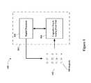
- FIG. 1illustrates a schematic block diagram of an electronic system having a capacitive touch keypad, a capacitive touch analog front end and a digital processor, according to the teachings of this disclosure
- FIG. 2illustrates a schematic elevational view of capacitive sensor keys shown in FIG. 1 ;
- FIG. 3illustrates a schematic elevational view of capacitive sensor keys shown in FIG. 1 and having capacitive guard rings around each of the capacitive sensors, according to a specific example embodiment of this disclosure
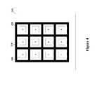
- FIG. 4illustrates a schematic plan view of capacitive sensor keys shown in FIG. 1 and having guard rings around each of the capacitive sensors, according to another specific example embodiment of this disclosure
- FIG. 5illustrates a schematic elevational view of electrostatic field lines surrounding a capacitive sensor and grounded shield
- FIG. 6illustrates a schematic elevational view of electrostatic field lines surrounding a capacitive sensor, guard ring and grounded shield, according to the teachings of this disclosure
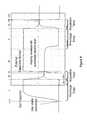
- FIG. 7illustrates a schematic diagram of a mixed signal integrated circuit device having CVD processing capabilities for a capacitive sensor and associated guard ring, according to a specific example embodiment of this disclosure
- FIG. 7Aillustrates a schematic diagram of a mixed signal integrated circuit device having CVD processing capabilities for plurality of capacitive sensors and a guard ring, according to another specific example embodiment of this disclosure
- FIG. 8illustrates a schematic voltage-time diagram of capacitance conversions, according to the teachings of this disclosure
- FIG. 9illustrates a schematic voltage-time diagram of capacitance conversions and guard ring voltage control during these conversions, according to a specific example embodiment of this disclosure.
- FIG. 10illustrates a schematic timing diagram of the capacitive conversion system shown in FIGS. 7 and 7A ;
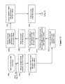
- FIGS. 11 and 12illustrate schematic process flow diagrams of capacitive conversions, according to a specific example embodiment of this disclosure
- FIG. 13illustrates a time-voltage graph of a capacitor being charged from a constant current source
- FIG. 14illustrates a schematic diagram of a mixed signal integrated circuit device having CTMU processing capabilities for a plurality of capacitive sensors and a guard ring, according to still another specific example embodiment of this disclosure
- FIG. 15illustrates a schematic diagram of a mixed signal integrated circuit device having two stage CTMU processing capabilities for a capacitive sensor and associated guard ring, according to yet another specific example embodiment of this disclosure
- FIG. 16illustrates a schematic diagram of a mixed signal integrated circuit device having CSM processing capabilities for a plurality of capacitive sensors and a guard ring, according to another specific example embodiment of this disclosure
- FIG. 17illustrates a schematic block diagram of multi-function port logic that supports a digital I/O and an analog function via an analog pass gate switch, according to the teachings of this disclosure
- FIG. 18illustrates a schematic block diagram of multi-function port logic that supports a digital I/O and an analog function via an analog pass gate switch wherein the analog function can be overridden to precharge and discharge a capacitive touch sensor connected to the port with ADC controller logic, according to the teachings of this disclosure;
- FIG. 19illustrates a schematic block diagram of analog and digital connection configurations, according to specific example embodiments of this disclosure.
- Microcontrollersnow include peripherals that enhance the detection and evaluation of capacitive sensors.
- capacitive voltage divisionmay be used to evaluate whether a capacitive touch element has been touched or not.
- CMUcharge time measurement unit
- CSMcapacitive sensing module
- parasitic capacitancemay pose a problem in many capacitive sensor application.
- Parasitic capacitanceis generated whenever a conductor adjacent to the sensor (or its connection to the microcontroller) is at a different voltage potential then the sensor.
- a voltagecan be created approximating the sensor capacitance and driving conductive traces placed between the sensor (and its connection) and other conductors and/or ground plane in close proximity thereto.
- a microcontroller integrated circuit device 101may comprise a digital processor 106 , memory, one or more of input-output (I/O) ports (nodes), an analog-to-digital converter (ADC), precision timers, multifunction input and output nodes, charge time measurement unit (CTMU), multiplexers, digital-to-analog converter (DAC), or combinations thereof.
- a capacitive touch analog front end (AFE) 104may be implemented with some of the aforementioned functions of the microprocessor 101 .
- the capacitive touch AFE 104may be coupled to a matrix of capacitive sensor keys 102 , e.g., pushbuttons, levers, toggles, targets, handles, knobs, etc., through an analog multiplexer (not shown).
- the capacitive touch AFE 104facilitates, with a single low-cost integrated circuit microcontroller, all active functions used in determining when there is actuation of capacitive sensors by, for example but is not limited to, pressing and deflecting a target key that changes the capacitance value of an associated capacitive sensor.
- the capacitive touch AFE 104measures the capacitance value of each sensor of the matrix of capacitive sensor keys 102 and converts the capacitance values into respective analog direct current (DC) voltages or frequencies that are read and converted into digital values with an analog-to-digital converter (ADC) (not shown) or frequency measurement device (not shown), and sent to the digital processor 106 .
- DCdirect current
- ADCanalog-to-digital converter
- the digital processor 106supplies clock and control functions to the capacitive touch AFE 104 , reads the analog voltage detector output of the capacitive touch AFE 104 , and selects each key of the matrix of capacitive sensor keys 102 . When actuation of a key of the matrix of capacitive sensor keys 102 is determined, the digital processor 106 will take an appropriate action. More detailed descriptions of various capacitive touch systems are more fully disclosed in Microchip Technology Incorporated application notes AN1298, AN1325 and AN1334, available at www.microchip.com, and are hereby incorporated by reference herein for all purposes.
- a substrate 204e.g., printed circuit board (PCB) may have a ground plane 206 (optional) that may be used for electromagnetic interference (EMI) shielding.
- Capacitive sensor plates 208may be transposed on a face of the substrate 204 and in proximity to the ground plane 206 (optional).
- Other circuit conductors 210e.g., PCB traces
- Touch targets 212may lay over respective ones of the capacitive sensor plates 208 and may have an air gap 214 therebetween.
- a touch target 212may be replaced by any object that changes the capacitance of the capacitive sensor plate 208 , e.g., a piece of metal, a finger, a hand, a foot, a leg, etc.
- Coverings 216may be placed over the capacitive sensor plates 208 and/or be part of the touch targets 212 (optional) and have alpha-numerical information engraved thereon.
- Each of the capacitive touch keys 108comprises a sensor plate 208 and covering 216 .
- Dielectric spacers 218are located between each of the capacitive touch keys 108 .
- a touch target 212may be added over each respective sensor plate 208 .
- the ground plane 206 (optional) and/or circuit conductors 210may be at different voltage potentials then the capacitive sensor plates 208 .
- See FIG. 5for a schematic representation of electrostatic fields between the capacitive sensor plate 208 and surrounding conductors at different voltage potential. Note the strong electrostatic field lines between the capacitive sensor plate 208 and the surrounding conductors.
- This parasitic capacitancelimits detection resolution of a change in the capacitance value of the capacitive sensor plate 208 occurring during a touch thereto. Parasitic capacitance similarly affects the connections between the capacitive sensor plates 208 and the AFE 104 . It also limits the amount of noise shielding that may be employed in capacitive touch systems.
- FIG. 3depicted is a schematic elevational view of capacitive sensor keys shown in FIG. 1 and having capacitive guard rings around each of the capacitive sensors, according to a specific example embodiment of this disclosure.
- a guard ring 320 around each of the capacitive sensor plates 208is added to the capacitive sensor keys 102 a . Otherwise all other elements are substantially the same as the capacitive sensor keys 102 shown in FIG. 2 .
- parasitic capacitancesare significantly reduced. Thereby increasing detection resolution of a change in the capacitance value of the capacitor sensor plate 208 occurring during a touch thereto.
- FIG. 6for a schematic representation of electrostatic fields between the capacitive sensor plate 208 , guard ring 320 , surrounding ground plane 206 (optional) and conductors 210 (not shown), wherein the capacitive sensor plate 208 and the guard ring 320 are at substantially the same voltage potential.
- FIG. 4depicted is a schematic plan view of capacitive sensor keys shown in FIG. 1 and having guard rings around each of the capacitive sensors, according to another specific example embodiment of this disclosure.
- Each of the capacitive sensor plates 208 of the touch keys 108are surrounded by guard rings 420 that are electrically coupled together and have the same voltage potential thereon.
- guard rings 420In this configuration only one capacitive sensor plate 208 capacitance value is determined at a time so the entire matrix of guard rings 420 assumes the voltage potential of the capacitive sensor plate 208 having its capacitance value determined by the AFE 104 and digital processor 106 , as more fully described hereinafter.
- Each of the guard rings 320 shown in FIG. 3may be independent of one another and have different voltages thereon, but would require more connections to the digital processor 106 . So unless simultaneous capacitance readings of more than one capacitive sensor plate 208 needs to be determined at the same time, the single voltage potential guard rings 420 ( FIG. 4 ) would suffice and require fewer circuit connections to the digital processor 106 .
- FIG. 7depicted is a schematic diagram of a mixed signal integrated circuit device having CVD processing capabilities for a capacitive sensor and associated guard ring, according to a specific example embodiment of this disclosure.
- the mixed signal integrated circuit device 101 a shown in FIG. 7e.g., a microcontroller, is applicable when using the capacitive voltage divider (CVD) method of determining the capacitance value of the capacitive sensor plate 208 .
- CVDcapacitive voltage divider
- the switches shown in FIG. 7may be, for example but are not limited to, field effect transistor (FET) switches.
- the nodes 728 and 730are analog nodes coupled to respective internal single line (conductor) analog buses 732 and 734 , respectively.
- the capacitance of the capacitive sensor plate 208is represented by variable capacitor 704 (first CVD capacitor), and the second CVD capacitor may be the sample and hold capacitor 716 if these two capacitors have fairly close capacitive values e.g., 1:1 to about 3:1.
- the reason for this in CVDis that part of the charge from one capacitor is transferred to the other capacitor having no charge or an opposite charge. For example, when the two CVD capacitors are equal in value, half of the charge on one will be transferred to the other capacitor. A two to one capacitance ratio will result in 1 ⁇ 3 of the charge being transferred to or taken from the smaller (1 ⁇ 2C) capacitor depending upon which of one the capacitors was initially charged.
- Capacitor 716is also the sample and hold capacitor used to sample and hold the analog voltage resulting after charge is transferred between the two CVD capacitors. Once the charge transfer is complete, an analog-to-digital converter (ADC) 718 converts the resulting charge voltage to a digital value that is read by the digital processor 106 for further processing and determination of the capacitance value of the touch sensor capacitor 704 .
- ADCanalog-to-digital converter
- the capacitance values for the capacitor 704are selected in combination with the sample and hold capacitor 716 to result in a combined voltage of 1 ⁇ 3 or 2 ⁇ 3 of the Vdd voltage depending on whether the first CVD capacitor 704 is discharged to Vss or charged to Vdd, and the combination of capacitors 706 and 716 are charged to Vdd or discharged to Vss, respectively.
- the capacitor 704is about twice the capacitance as the capacitance of the parallel connected combination of capacitors 706 and 716 .
- the resulting quiescent voltage after coupling the two opposite polarity charged CVD capacitors togetherwill be about 1 ⁇ 3*Vdd when the capacitor 704 was initially discharged to Vss, and about 2 ⁇ 3*Vdd when the capacitor 704 was initially charged to Vdd.
- an analog buffer driver 714 having a high input impedancemay be coupled to node 730 which is also coupled to the capacitor 704 .
- the analog buffer driver 714has a low impedance output that may be switchably coupled through switch J to the node 726 that is also coupled to the guard ring capacitance 702 .
- the output voltage of the analog buffer driver 714faithfully follows the voltage at the input thereto. Therefore, the voltage on the guard ring 320 or 420 substantially follows the voltage on the respective sensor plate 208 being evaluated for a capacitance value by the digital processor 106 .
- FIG. 7Adepicted is a schematic diagram of a mixed signal integrated circuit device having CVD processing capabilities for a plurality of capacitive sensors and a guard ring, according to another specific example embodiment of this disclosure.
- the mixed signal integrated circuit device 101 b shown in FIG. 7Ae.g., a microcontroller, performs substantially the same as the device 101 a shown in FIG.
- a plurality of switches Iare used to multiplex each of the capacitive sensors 704 used in the capacitive touch keys 108 shown in FIG. 1 .
- the analog multiplexer switches Iselect respective ones of the plurality of sensor capacitors 704 as the capacitive touch analog front end 104 scans the capacitive touch keys 108 .
- the plurality of nodes 730are typically multi-purpose programmable analog or digital inputs and/or outputs. For explanatory clarity in this disclosure only analog input/output (two way) configured nodes are shown.
- an analog buffer driver 714 having a high input impedancemay be coupled between the node 726 and the single wire analog bus 732 a through switch J when the selected one of the plurality of capacitors 704 is being charged/discharged.
- the analog buffer driver 714has a low impedance output coupled to the node 726 which is coupled to the guard ring capacitance 702 .
- the output voltage of the analog buffer driver 714faithfully follows the voltage on the selected one of the plurality of capacitors 704 .
- a microcontrollermay include external node 728 to allow for connection of an external capacitor 706 a as explained hereinabove.
- An additional adjustable capacitor(s) 706 b (and 706 c )may be present internally and may be switchably coupled to the analog bus 732 a .
- other embodimentsmay not provide for such an external node 728 .
- either capacitance 716may have the appropriate value or an additional internal capacitance 706 b , for example a variable capacitance, is or can be connected to bus 732 .
- each external node 726 , 728 , and 730may be programmable to support multiple functions
- additional switchesmay be used to allow to use nodes 726 , 728 , and 730 for other functions as will be explained in more detail hereinafter with respect to FIGS. 17 and 18 .
- FIGS. 8 and 9depicted are schematic voltage-time diagrams of capacitance conversions ( FIG. 8 ), and guard ring voltage control ( FIG. 9 ) during these conversions, according to a specific example embodiment of this disclosure.
- the capacitors 706 and 716(sample and hold capacitor) are charged to Vdd
- the capacitive sensor capacitor 704 and the guard ring capacitance 702are discharged to Vss.
- the capacitors 706 , 716 and 704are coupled together and a quiescent voltage of about 1 ⁇ 3*Vdd will result when the capacitive touch key 108 is not depressed, and a little less than 1 ⁇ 3*Vdd when depressed.
- the guard ring capacitance 702follows the voltage on the capacitor 704 (capacitive sensor) so as to minimize any parasitic capacitances therebetween.
- the sample and hold capacitor 716decouples from the capacitors 706 and 704 and retains the quiescent voltage obtained during segment II.
- any voltage charge on the capacitor 704 (capacitive sensor)is discharged to substantially Vss, then at the beginning of segment IV the capacitor 704 (capacitive sensor) and the guard ring capacitance 702 are charged to substantially Vdd.
- the quiescent voltage stored on the sample and hold capacitor 716is converted by the ADC 718 to a digital value representing the quiescent voltage and read by the digital processor 106 .
- the digital value from the ADC 718is used in determining whether the capacitive sensor was being actuated (touched), e.g., quiescent voltage lower then what is expected from a non-actuated touch sensor or not.
- the capacitive value of the touch sensor capacitor 704is actuated (touched) its capacitance increases and the subsequent quiescent voltage will thereby be less then when not actuated. This is true when the capacitor 704 is initialized to Vss.
- the subsequent quiescent voltageis about 2 ⁇ 3*Vdd when the capacitive sensor is not actuated.
- the capacitors 706 and 716are discharged to Vss, the capacitive sensor capacitor 704 and guard ring capacitance 702 have already been charged to Vdd.
- the capacitors 706 , 716 and 704are coupled together and a quiescent voltage of about 2 ⁇ 3*Vdd will result when the capacitive touch key 108 is not depressed, and a little more than 2 ⁇ 3*Vdd when depressed.
- the guard ring capacitance 702follows the voltage on the capacitor 704 (capacitive sensor) so as to minimize any parasitic capacitances therebetween.
- the sample and hold capacitor 716decouples from the capacitors 706 and 704 and retains the quiescent voltage obtained during segment VI.
- the capacitor 704(capacitive sensor) is charged to substantially Vdd, then at the beginning of segment VIII the capacitor 704 (capacitive sensor) and the guard ring capacitance 702 are discharged to substantially Vss.
- the quiescent voltage stored on the sample and hold capacitor 716is converted by the ADC 718 to a digital value representing the quiescent voltage and read by the digital processor 106 .
- the digital value from the ADC 718is used in determining whether the capacitive sensor was being actuated (touched), e.g., quiescent voltage lower then what is expected from a non-actuated touch sensor or not.
- the capacitive value of the touch sensor capacitor 704When the capacitive value of the touch sensor capacitor 704 is actuated (touched) its capacitance increases and the subsequent quiescent voltage will thereby be greater than when not actuated. This is true when the capacitor 704 is initialized to Vdd.
- the subsequent quiescent voltageis about 1 ⁇ 3*Vdd when the capacitive sensor is not actuated, as described hereinabove.
- FIG. 10depicted is a schematic timing diagram of the capacitive conversion system shown in FIG. 7 .
- This schematic timing diagramclearly represents a specific example operational embodiment of the circuit shown in FIG. 7 .
- Voltages on nodes 724 , 726 , 728 and 730are shown in relation to the operational open and close combinations of switches A-F.
- FIG. 10basically represents the same voltage and timing waveforms as shown in FIG. 9 . It is contemplated and within the scope of this disclosure that other and further circuit designs and timing diagrams could be used with equal effect, and one having ordinary skill in electronic circuit design and having the benefit of this disclosure could replicate the results described herein.
- step 1102a capacitance value conversion is started.
- step 1104the sample and hold capacitor combination of the capacitors 706 and 716 are charged to a first voltage.
- step 1106the capacitive sensor and capacitive sensor guard ring are charged to a second voltage.
- the first voltagemay be Vdd and the second voltage may be Vss or visa versa.
- the capacitive sensor guard ringis charged to the second voltage so as to minimize parasitic capacitance that would otherwise develop at the capacitive sensor due to electrostatic charge caused by a difference of voltage potential between the capacitive sensor and adjacent conductors.
- step 1112the sample and hold capacitor combination, previously charged to the first voltage, is coupled to the capacitive sensor, previously charged to the second voltage.
- step 1114the sample and hold capacitor and the capacitive sensor are coupled together long enough in time for a complete settling to a common quiescent first charge.
- step 1116the sample and hold capacitor is decoupled from the capacitive sensor and the sample and hold capacitor thereafter retains the settled first charge.
- step 1118conversion to a digital representation of the first charge stored in the sample and hold capacitor begins.
- step 1120the capacitive sensor and guard ring are briefly discharged to the second voltage.
- step 1122the capacitive sensor and guard ring are charged to the first voltage.
- the capacitive sensor guard ringis charged to the first voltage so as to minimize parasitic capacitance that would otherwise develop at the capacitive sensor due to electrostatic charge caused by a difference of voltage potential between the capacitive sensor and adjacent conductors.
- step 1126the conversion of the first charge to a digital representation thereof terminates and is then read by the digital processor 106 for determining the capacitance value of the capacitive sensor 108 .
- step 1128the sample and hold capacitor combination of the capacitors 706 and 716 are charged to the second voltage.
- step 1130the capacitive sensor and capacitive sensor guard ring are charged to the first voltage.
- the capacitive sensor guard ringis charged to the first voltage so as to minimize parasitic capacitance that would otherwise develop at the capacitive sensor due to electrostatic charge caused by a difference of voltage potential between the capacitive sensor and adjacent conductors.
- step 1136the sample and hold capacitor combination, previously charged to the second voltage level, is coupled to the capacitive sensor, previously charged to the first voltage.
- step 1138the sample and hold capacitor combination and the capacitive sensor are coupled together long enough in time for a complete settling to a quiescent second charge.
- step 1140the sample and hold capacitor is decoupled from the capacitive sensor and the sample and hold capacitor thereafter retains the settled second charge).
- step 1142a conversion to a digital representation of the second charge stored in the sample and hold capacitor begins.
- step 1144the capacitive sensor and guard ring are briefly discharged to the first voltage.
- step 1146the capacitive sensor and guard ring are charged to the second voltage.
- the capacitive sensor guard ringis charged to the second voltage so as to minimize parasitic capacitance that would otherwise develop at the capacitive sensor due to electrostatic charge caused by a difference of voltage potential between the capacitive sensor and adjacent conductors.
- step 1150the conversion of the second charge to a digital representation thereof terminates and is then read by the digital processor 106 for determining the capacitance value of the capacitive sensor 108 .
- the digital representations of the first and second chargesmay thereafter be processed to reduce common mode noise and interference, e.g., 60 Hz power line interference.
- the mixed signal integrated circuit device 101 c shown in FIG. 14may comprise a charge time measurement unit (CTMU) comprising a precision timer 1420 , a sample and hold circuit 1416 , a constant current source 1422 , and current steering switches 1424 ; an analog-to-digital converter (ADC) 1418 , and a digital processor with memory 1406 .
- CTMUcharge time measurement unit
- ADCanalog-to-digital converter
- the voltage at node 726will follow the voltage on the signal wire analog bus 1432 , as more fully described hereinabove.
- an analog buffer driver 714 having a high input impedancemay be coupled between the node 726 and the single wire analog bus 1432 .
- the analog buffer driver 714has a low impedance output coupled to the node 726 which is coupled to the guard ring capacitance 702 .
- the output voltage of the analog buffer driver 714faithfully follows the voltage on the selected one of the plurality of capacitors 704 .
- a plurality of switches Iare used to multiplex each of the capacitive sensors 704 used in the capacitive touch keys 108 shown in FIG. 1 .
- the analog multiplexer switches Iselect respective ones of the plurality of sensor capacitors 704 as the capacitive touch analog front end 104 scans the capacitive touch keys 108 .
- the plurality of nodes 730are typically multi-purpose programmable analog or digital inputs and/or outputs. Node 726 and the plurality of nodes 730 may be programmed to support a plurality of functions as will be explained in more detail hereinafter for the circuits shown in FIGS. 17 and 18 . For explanatory clarity in this disclosure only analog input/output (two way) configured nodes are shown.
- the function of the CTMUmay better be understood by referring to FIG. 13 , wherein a time-voltage graph of a capacitor being charged from a constant current source is depicted.
- Cthe capacitance value of the capacitor 704
- Ithe current from the constant current source 1422
- Vthe voltage on the capacitor 704 at time T.
- the other unknown valuemay be calculated from the two known values. For example, if the charging current from the constant current source 1422 , and the time interval between T 1 at voltage V 1 and T 2 at voltage V 2 are known, then the capacitance of the capacitor 704 may be determined using equation (1) above.
- the digital processor 1406enables the precision timer 1420 of the CTMU to begin precise timing of the constant current source 1422 charging of the capacitor 730 .
- the precision timer 1420closes switch 1424 a and opens switches 1424 b and 1424 c , thereby starting the constant current charging of the capacitor 704 .
- the constant current source 1422charges the capacitor 704 with a resulting linearly increasing voltage thereon (see voltage-time graph of FIG. 13 until a second time).
- the sample and hold circuit 1416takes a voltage sample of the voltage charge on the capacitor 730 .
- the precision timer 1420opens switch 1424 a and closes switches 1424 b and 1424 c .
- the voltage charge on the capacitor 704starts at zero voltage and returns back to zero voltage due to switch 1424 c being closed.
- the elapse time from the precision timer 1420is sent to the digital processor 1406 .
- the ADC 1418converts the sampled voltage from the sample and hold circuit 1416 into a digital representation thereof and sends that digital representation to the digital processor 1406 .
- the digital processor 1406uses the elapse time from the precision timer 1420 and the digital representation of the sampled voltage from the ADC 1418 to determine a capacitance value for the capacitor 704 , according to equation (1) above. This process continues repetitiously for each one of the capacitive touch keys 108 .
- the CTMUis more fully described in Microchip application notes AN1250 and AN1375, available at www.microchip.com, and commonly owned U.S. Pat. No. 7,460,441 B2, entitled “Measuring a long time period;” and U.S. Pat. No. 7,764,213 B2, entitled “Current-time digital-to-analog converter,” both by James E. Bartling; wherein all are hereby incorporated by reference herein for all purposes.
- the mixed signal integrated circuit device 101 cmay further comprise a plurality of input/output nodes 742 , programmable receivers/drivers 740 coupled to the plurality of input/output nodes 742 , and an analog multiplexer 738 coupled to the programmable receivers/drivers 740 .
- the digital processor 106controls the programmable receivers/drivers 740 and may thereby configure any one or more of the plurality of input/output nodes 742 as analog inputs, digital inputs, analog outputs (DAC not shown) and/or digital outputs.
- the multiplexer 738is controlled by the digital processor 106 and may be used to couple the input of the ADC 718 , to any one of the plurality of input/output nodes 742 configured as an analog input.
- the multiplexer 738may also be used to couple an analog module (not shown), e.g., ADC, digital-to-analog converter (DAC), comparator, operational amplifier, etc., to any one of or more of the plurality of input/output nodes 742 configured appropriately as an analog input or output.
- FIG. 15depicted is a schematic diagram of a mixed signal integrated circuit device having two stage CTMU processing capabilities for a capacitive sensor and associated guard ring, according to yet another specific example embodiment of this disclosure.
- the mixed signal integrated circuit device 101 d shown in FIG. 15may comprise a charge time measurement unit (CTMU) comprising a precision timer 1420 , a sample and hold circuit 1416 , a first constant current source 1422 , first current steering switches 1424 , a second constant current source 1536 , second current steering switches 1534 ; inversion switch 1532 , an analog-to-digital converter (ADC) 1418 , and a digital processor with memory 1406 .
- CTMUcharge time measurement unit
- ADCanalog-to-digital converter
- the circuit features shown in FIG. 14may also be incorporated into the circuit of FIG. 15 .
- the digital processor 1406does a first capacitive measurement sequence as described for the circuit shown in FIG. 14 . Then the digital processor 1406 changes the capacitive measurement inversion switch 1532 from position a (operation the same as the circuit shown in FIG. 14 ) to position b. Now switches 1534 b and 1534 c are closed, charging the capacitor 704 to Vdd. The digital processor 1406 then enables the precision timer 1420 of the CTMU to begin precise timing of the constant current source 1536 discharging of the capacitor 730 .
- the precision timer 1420closes switch 1534 a and opens switches 1534 b and 1534 c , thereby starting the constant current discharging of the capacitor 704 .
- the constant current source 1536discharges the capacitor 704 with a resulting linearly decreasing voltage thereon.
- the sample and hold circuit 1416takes a voltage sample of the voltage charge on the capacitor 730 .
- the precision timer 1420opens switch 1534 a and closes switches 1534 b and 1534 c .
- the voltage charge on the capacitor 704starts at Vdd volts and returns back to Vdd volts due to switch 1534 b being closed.
- the elapse time from the precision timer 1420is sent to the digital processor 1406 .
- the ADC 1418converts the sampled voltage from the sample and hold circuit 1416 into a digital representation thereof and sends that (second conversion) digital representation to the digital processor 1406 .
- the digital processor 1406uses the elapse time from the precision timer 1420 and the digital representation of the sampled voltage from the ADC 1418 to determine a second capacitance value for the capacitor 704 , according to equation (1) above.
- the digital representations from the first and second conversionsmay thereafter be processed to reduce common mode noise and interference, e.g., 60 Hz power line interference. This process continues repetitiously for each one of the capacitive touch keys 108 .
- FIG. 16depicted is a schematic diagram of a mixed signal integrated circuit device having CSM processing capabilities for a plurality of capacitive sensors and a guard ring, according to another specific example embodiment of this disclosure.
- the mixed signal integrated circuit device 101 e shown in FIG. 16may comprise a variable frequency oscillator 1618 , a frequency measurement circuit 1620 and a digital processor 1620 .
- the optional analog buffer driver 714functions as more fully described hereinabove.
- a selected one of the plurality of capacitors 704is part of the frequency determining circuit of the variable frequency oscillator 1618 , and as the capacitance value thereof changes so does the resulting frequency.
- the frequency measurement circuit 1620measures the frequencies from the variable frequency oscillator 1618 and provides the measured frequencies in a digital format be read by the digital processor 1620 , which then determines the amount of frequency change. A large enough change in frequency will indicate that the capacitance value of the selected capacitor 704 has changed which indicates that the associated capacitive touch key 108 is actuated.
- a capacitive measurement system using frequencyis more fully described in commonly owned U.S. Patent Application Publication No. US 2011/0267309, entitled “Mutual Capacitance Measurement in a Multi-Touch Input Device;” by Jerry Hanauer and Todd O'Connor; is hereby incorporated by reference herein for all purposes.
- a plurality of switches Iare used to multiplex each of capacitive sensors 704 used in the capacitive touch keys 108 shown in FIG. 1 .
- the analog multiplexer switches Iselect respective ones of the plurality of sensor capacitors 704 as the capacitive touch analog front end 104 scans the capacitive touch keys 108 .
- the plurality of nodes 730are typically multi-purpose programmable analog or digital inputs and/or outputs. For explanatory clarity in this disclosure only analog input/output (two way) configured nodes are shown.
- a digital driver 1754 having a tri-state outputis coupled to the external node 728 and is controlled by a tri-state control signal from, for example but is not limited to, the digital processor 106 .
- a digital output signal from, for example but is not limited to, the digital processor 106is coupled to an input of the digital driver 1754 .
- An analog pass gate switch 1750which for example may implement switch G in FIG. 7A , is controlled by analog switch logic 1752 that may be controlled by an analog bus control signal, independent form the ADC channel selection, from, for example but is not limited to, the digital processor 106 .
- analog switch logic 1752may be controlled by an analog bus control signal, independent form the ADC channel selection, from, for example but is not limited to, the digital processor 106 .
- an analog multiplexer for the internal ADCis configured to allow only one of the multiple switches to close so that only one of the external pins at a time is connected to the internal ADC.
- an analog multiplexer for the ADCmay be configured to allow that more than one switch can be controlled to connect an external pin to the analog bus.
- the control logic 1752 and analog pass gate switches 1750may either be controlled independently from the analog multiplexer or may be part of the analog multiplexer.
- the analog pass gate switch 1750when closed enables direct coupling of the node 728 to an analog bus 1732 , as more fully described hereinabove.
- the analog pass gate switch 1750When the analog pass gate switch 1750 is closed, the output of the digital driver 1754 is put into a high impedance state by the tri-state control, thereby minimally affecting the node 728 when being used as an analog port. It is contemplated and within the scope of this disclosure that other functions may be included according to other embodiments described herein.
- FIG. 18depicted is a schematic block diagram of multi-function port logic that supports a digital I/O and an analog function via an analog pass gate switch wherein in addition the analog function can be overridden to precharge and discharge a capacitive touch sensor connected to the port with ADC controller logic, according to the teachings of this disclosure.
- a port logicmay be used for any of the external pins 730 and when the analog multiplexer is configured to allow more than one switch to be closed then also for pin 728 .
- Switching between digital and analog functions at the node 730can be processor intensive and may require a complex program to properly handle all related digital and analog functions required of the node 730 , as more fully described hereinabove.
- an ADC override featuremay be incorporated into the capacitive touch determination circuits described herein.
- Use of a dedicated ADC controller incorporating the circuit functions shown in FIG. 18will save digital processor program steps and allow for the processor to perform other functions during determination of the capacitive sensor capacitance.
- the override functioncan also be omitted.
- the port logic as shown in FIGS. 17 and 18may be combined to create a universal port logic for each external pin, as for example, shown in FIG. 7A .
- a universal port logic for all external pinsmay have two pass gates which can be controlled independently to connect to the analog bus or may have a single pass gate which is part of the analog multiplexer that allows to be controlled by an independent enable signal.
- a digital driver 1854 having a tri-state outputis coupled to the external node 730 and is controlled by a tri-state control signal from a multiplexer 1858 .
- a digital output signal from a multiplexer 1860is coupled to an input of the digital driver 1854 .
- An analog pass gate switch 1850which may implement the switch I in FIG. 7A , is controlled by analog switch logic 1852 .
- the multiplexer 1858couples the tri-state control signal to control the tri-state output of the digital driver 1854
- the multiplexer 1860couples the digital output signal to the input of the digital driver 1854 .
- the ADC channel selectcontrols the analog pass gate switch 1850 to directly couple the node 730 to the analog bus 732 , as more fully described hereinabove.
- the circuit shown in FIG. 18functions in substantially the same fashion as the circuit shown in FIG. 17 .
- the multiplexer 1858couples the ADC override data enable signal to control the tri-state output of the digital driver 1854
- the multiplexer 1860couples the ADC override data signal to the input of the digital driver 1854 .
- the analog pass gate switch 1850is forced to decouple the analog bus 732 from the node 730 .
- the ADC override data enable and ADC override data signalsmay be provided by an ADC logic controller (not shown), and may be used to charge or discharge a capacitive touch sensor coupled to the node 730 without requiring program intensive actions from the digital processor 106 .
- Port logic for nodes 726 and 728may be implemented as shown in FIG. 17 or FIG. 18 as explained above.
- the plurality of Nodes 730can be implemented as shown in FIG. 18 .
- a universal portmay be used for all external pins. Additional functions, such as the additional drivers 714 or other logic or circuitry can be implemented to support other functionalities according to a respective external pin.
- a plurality of analog pass gate switches 1938may implement an analog multiplexer and couple and decouple a plurality of nodes 730 x to and from an analog bus 732 , e.g., selection of each of a plurality of capacitive touch sensors. Either a direct connection couples together the node 728 and the analog bus 732 (e.g., see FIG. 7 ), or an optional analog pass gate switch 1936 may couple and decouple the node 728 to and from the analog bus 732 (e.g., see FIG. 7A ).
- the additional pass gate switch 1936can be part of the analog multiplexer if the multiplexer is designed to allow more than one switch to be closed.
- a plurality of switches 1934may couple and decouple additional sample and hold capacitors 1944 to and from the analog bus 732 .
- Switch 1940may be used to charge the analog bus 732 to Vdd, and switch 1942 may be used to discharge the analog bus 732 to Vss.
Landscapes
- Analogue/Digital Conversion (AREA)
- Electronic Switches (AREA)
- Measurement Of Current Or Voltage (AREA)
Abstract
Description
I=C*dV/dT Eq. (1)
where C is the capacitance value of the
Claims (26)
Priority Applications (14)
| Application Number | Priority Date | Filing Date | Title |
|---|---|---|---|
| US13/633,429US9467141B2 (en) | 2011-10-07 | 2012-10-02 | Measuring capacitance of a capacitive sensor with a microcontroller having an analog output for driving a guard ring |
| EP12780347.6AEP2764353B1 (en) | 2011-10-06 | 2012-10-04 | Differential current measurements to determine ion current in the presence of leakage current |
| KR1020147012337AKR101948664B1 (en) | 2011-10-07 | 2012-10-04 | Measuring capacitance of a capacitive sensor with a microcontroller having an analog output for driving a guard ring |
| PCT/US2012/058688WO2013052622A2 (en) | 2011-10-06 | 2012-10-04 | Differential current measurements to determine ion current in the presence of leakage current |
| CN201280054576.5ACN103918183B (en) | 2011-10-07 | 2012-10-04 | Measure the capacitance of a capacitive sensor with a microcontroller with an analog output for driving a guard ring |
| KR1020147012336AKR20140088553A (en) | 2011-10-06 | 2012-10-04 | Differential current measurements to determine ion current in the presence of leakage current |
| CN201280056484.0ACN103946703B (en) | 2011-10-06 | 2012-10-04 | Differential current measurements to determine ion current in the presence of leakage current |
| JP2014534704AJP6134723B2 (en) | 2011-10-07 | 2012-10-04 | Capacitance measurement of a capacitive sensor using a microcontroller with an analog output to drive a guard ring |
| PCT/US2012/058691WO2013052623A1 (en) | 2011-10-07 | 2012-10-04 | Measuring capacitance of a capacitive sensor with a microcontroller having an analog output for driving a guard ring |
| JP2014534703AJP6228543B2 (en) | 2011-10-06 | 2012-10-04 | Differential current measurement to determine ionic current in the presence of leakage current |
| ES12780347.6TES2555875T3 (en) | 2011-10-06 | 2012-10-04 | Differential current measurements to determine an ion current in the presence of a leakage current |
| EP12783424.0AEP2764620B1 (en) | 2011-10-07 | 2012-10-04 | Measuring capacitance of a capacitive sensor with a microcontroller having an analog output for driving a guard ring |
| TW101136986ATWI580959B (en) | 2011-10-06 | 2012-10-05 | Method for determining ion current in an ion chamber and apparatus for detecting |
| TW101137033ATWI579532B (en) | 2011-10-07 | 2012-10-05 | Measuring capacitance of a capacitive sensor with a microcontroller having an analog output for driving a guard ring |
Applications Claiming Priority (2)
| Application Number | Priority Date | Filing Date | Title |
|---|---|---|---|
| US201161544363P | 2011-10-07 | 2011-10-07 | |
| US13/633,429US9467141B2 (en) | 2011-10-07 | 2012-10-02 | Measuring capacitance of a capacitive sensor with a microcontroller having an analog output for driving a guard ring |
Publications (2)
| Publication Number | Publication Date |
|---|---|
| US20130090873A1 US20130090873A1 (en) | 2013-04-11 |
| US9467141B2true US9467141B2 (en) | 2016-10-11 |
Family
ID=48042613
Family Applications (1)
| Application Number | Title | Priority Date | Filing Date |
|---|---|---|---|
| US13/633,429Active2034-12-04US9467141B2 (en) | 2011-10-06 | 2012-10-02 | Measuring capacitance of a capacitive sensor with a microcontroller having an analog output for driving a guard ring |
Country Status (7)
| Country | Link |
|---|---|
| US (1) | US9467141B2 (en) |
| EP (1) | EP2764620B1 (en) |
| JP (1) | JP6134723B2 (en) |
| KR (1) | KR101948664B1 (en) |
| CN (1) | CN103918183B (en) |
| TW (1) | TWI579532B (en) |
| WO (1) | WO2013052623A1 (en) |
Cited By (1)
| Publication number | Priority date | Publication date | Assignee | Title |
|---|---|---|---|---|
| US20160049933A1 (en)* | 2013-04-01 | 2016-02-18 | Denso Corporation | Capacitance-type switch |
Families Citing this family (30)
| Publication number | Priority date | Publication date | Assignee | Title |
|---|---|---|---|---|
| US9437093B2 (en) | 2011-10-06 | 2016-09-06 | Microchip Technology Incorporated | Differential current measurements to determine ION current in the presence of leakage current |
| US9252769B2 (en) | 2011-10-07 | 2016-02-02 | Microchip Technology Incorporated | Microcontroller with optimized ADC controller |
| US9257980B2 (en)* | 2011-10-06 | 2016-02-09 | Microchip Technology Incorporated | Measuring capacitance of a capacitive sensor with a microcontroller having digital outputs for driving a guard ring |
| US9467141B2 (en) | 2011-10-07 | 2016-10-11 | Microchip Technology Incorporated | Measuring capacitance of a capacitive sensor with a microcontroller having an analog output for driving a guard ring |
| US9207209B2 (en) | 2011-12-14 | 2015-12-08 | Microchip Technology Incorporated | Method and apparatus for detecting smoke in an ion chamber |
| US9189940B2 (en) | 2011-12-14 | 2015-11-17 | Microchip Technology Incorporated | Method and apparatus for detecting smoke in an ion chamber |
| US9176088B2 (en) | 2011-12-14 | 2015-11-03 | Microchip Technology Incorporated | Method and apparatus for detecting smoke in an ion chamber |
| US9823280B2 (en) | 2011-12-21 | 2017-11-21 | Microchip Technology Incorporated | Current sensing with internal ADC capacitor |
| US9607786B2 (en)* | 2012-11-20 | 2017-03-28 | Pass & Seymour, Inc. | Electronic switching device and system |
| US10402000B2 (en)* | 2013-03-04 | 2019-09-03 | Apple Inc. | Display with integrated pressure sensing utilizing capacitive coupling to circuit elements |
| FR3008809B1 (en)* | 2013-07-18 | 2017-07-07 | Fogale Nanotech | CUSTOM ACCESSORY DEVICE FOR AN ELECTRONIC AND / OR COMPUTER APPARATUS, AND APPARATUS EQUIPPED WITH SUCH AN ACCESSORY DEVICE |
| FR3013472B1 (en) | 2013-11-19 | 2016-07-08 | Fogale Nanotech | COVERING ACCESSORY DEVICE FOR AN ELECTRONIC AND / OR COMPUTER PORTABLE APPARATUS, AND APPARATUS EQUIPPED WITH SUCH AN ACCESSORY DEVICE |
| US9739816B2 (en)* | 2013-11-27 | 2017-08-22 | Analog Devices, Inc. | Capacitive sensor with differential shield |
| EP2887185B1 (en)* | 2013-12-20 | 2016-11-09 | LG Display Co., Ltd. | Display device integrated with touch screen panel and method of driving the same |
| US10260983B2 (en)* | 2014-01-20 | 2019-04-16 | Lear Corporation | Apparatus and method for diagnostics of a capacitive sensor with plausibility check |
| JP6400944B2 (en)* | 2014-05-26 | 2018-10-03 | シナプティクス・ジャパン合同会社 | Capacitance detection circuit, touch detection circuit, and semiconductor integrated circuit including the same |
| US9590649B2 (en)* | 2014-10-17 | 2017-03-07 | Microchip Technology Incorporated | Analog-to-digital conversion with micro-coded sequencer |
| US9542051B2 (en)* | 2014-10-24 | 2017-01-10 | Microchip Technology Incorporated | Analog elimination of ungrounded conductive objects in capacitive sensing |
| DE102014016422A1 (en)* | 2014-11-07 | 2016-05-12 | Trw Automotive Safety Systems Gmbh | Device and method for detecting a steering wheel touch |
| US9542050B2 (en)* | 2014-12-04 | 2017-01-10 | Semtech Corporation | Multi-shield capacitive sensing circuit |
| US20160371216A1 (en)* | 2015-06-17 | 2016-12-22 | Intel Corporation | Capacitor interconnections and volume re-capture for voltage noise reduction |
| US10290573B2 (en)* | 2015-07-02 | 2019-05-14 | Semiconductor Energy Laboratory Co., Ltd. | Semiconductor device and electronic device |
| EP3851162A1 (en) | 2015-07-28 | 2021-07-21 | KNOW Bio, LLC | Phototherapy devices for treatment of dermatological disorders of the scalp |
| RU2690112C1 (en)* | 2018-05-17 | 2019-05-30 | Евгений Владимирович Круглов | Usb-device for recording electrocardiograms |
| KR102709011B1 (en)* | 2018-11-21 | 2024-09-24 | 엘지전자 주식회사 | Panel assembly and Refrigerator having the same |
| CN111694440B (en)* | 2019-03-13 | 2025-05-16 | 密克罗奇普技术公司 | Keyboard for secure data entry |
| US11975215B2 (en) | 2020-05-26 | 2024-05-07 | Know Bio, Llc | Devices and related methods for phototherapeutic treatment of skin |
| CN112697174B (en)* | 2020-12-14 | 2022-11-29 | 潍柴动力股份有限公司 | A kind of measuring method and measuring circuit |
| TWI756143B (en)* | 2021-06-16 | 2022-02-21 | 英業達股份有限公司 | Load capacitance calculation system and load capacitance calculation method for crystal oscillator |
| US12062909B2 (en)* | 2022-05-24 | 2024-08-13 | Changxin Memory Technologies, Inc. | Method and apparatus for capacitor demand evaluation in power distribution network |
Citations (97)
| Publication number | Priority date | Publication date | Assignee | Title |
|---|---|---|---|---|
| US3295121A (en) | 1961-12-30 | 1966-12-27 | Danske Securitas As | Electric alarm system, preferably for fire alarms |
| US3832678A (en) | 1970-11-12 | 1974-08-27 | B Gysell | Fire alarm system |
| US4213047A (en) | 1978-10-25 | 1980-07-15 | General Signal Corporation | Smoke detector having unipolar ionization chamber |
| US4222045A (en) | 1979-05-04 | 1980-09-09 | Firetek Corporation | Capacitive shift fire detection device |
| US4260984A (en) | 1979-03-17 | 1981-04-07 | Hochiki Corporation | Count discriminating fire detector |
| US4266220A (en) | 1979-07-27 | 1981-05-05 | Malinowski William J | Self-calibrating smoke detector and method |
| FR2473201A1 (en) | 1980-01-02 | 1981-07-10 | Gamma Electronic | CAPACITIVE SMOKE DETECTOR WITH LOW IONIZATION SOURCE |
| GB1598821A (en) | 1978-04-13 | 1981-09-23 | Plessey Co Ltd | Ionization detectors |
| US4401978A (en) | 1979-02-21 | 1983-08-30 | The Gamewell Corporation | Combination detector |
| GB2117560A (en) | 1982-03-09 | 1983-10-12 | Emile Hugon | Capacitive smoke detector |
| US4538137A (en) | 1983-01-20 | 1985-08-27 | Nittan Company, Limited | Fire detector |
| GB2156126A (en) | 1984-03-05 | 1985-10-02 | Hochiki Co | Fire detector |
| US4652866A (en) | 1982-12-03 | 1987-03-24 | Slm Investissements Sa | Fire detector and electrode arrangement thereof |
| US4672324A (en) | 1984-04-12 | 1987-06-09 | U.S. Philips Corporation | Flame protection circuit |
| US5173683A (en) | 1991-04-22 | 1992-12-22 | Simplex Time Recorder Co. | Apparatus and method for multiplexing multiple data and analog values in a peripheral device |
| US5243330A (en) | 1990-12-04 | 1993-09-07 | Cerberus Ag | Fire detector system and method |
| CN1087739A (en) | 1993-11-26 | 1994-06-08 | 陆基 | Ion smoke-sensitive detector capable of reliably finding failure |
| JPH06345666A (en) | 1993-06-10 | 1994-12-20 | Agency Of Ind Science & Technol | Hepatic function improving agent |
| US5422807A (en) | 1992-08-31 | 1995-06-06 | Microchip Technology Incorporated | Microcontroller with improved A/D conversion |
| US5633591A (en)* | 1994-04-19 | 1997-05-27 | Gas Research Institute | Apparatus and method for measuring the breakdown voltage between two electrodes separated by a dielectric |
| US5705988A (en)* | 1996-07-08 | 1998-01-06 | Detection Systems, Inc. | Photoelectric smoke detector with count based A/D and D/A converter |
| US5966078A (en) | 1997-02-19 | 1999-10-12 | Ranco Inc. | Battery saving circuit for a dangerous condition warning device |
| JP2000049608A (en) | 1998-07-28 | 2000-02-18 | Matsushita Electric Ind Co Ltd | AD converter and AD converter |
| JP2000278131A (en) | 1999-03-26 | 2000-10-06 | Keihin Corp | Analog / digital converter |
| US6257049B1 (en) | 1999-08-31 | 2001-07-10 | Lucent Technologies, Inc. | Ambient humidity measurement using microwaves |
| JP2001223586A (en) | 2000-02-08 | 2001-08-17 | Denso Corp | Multi-channel analog/digital conversion method and device |
| US20020078744A1 (en) | 2000-12-21 | 2002-06-27 | Gehman Richard William | system for sensing the motion or pressure of a fluid |
| US20020101345A1 (en) | 2001-01-26 | 2002-08-01 | Pattok Greg R. | Smoke detector maintenance and verification tool |
| US6433712B1 (en) | 2001-07-25 | 2002-08-13 | Texas Instruments Incorporated | Offset error compensation of input signals in analog-to-digital converter |
| US20020153923A1 (en) | 2001-04-18 | 2002-10-24 | Cygnal Integrated Products, Inc. | Ic with digital and analog circuits and mixed signal i/o pins |
| US20030058114A1 (en) | 2001-09-21 | 2003-03-27 | Miller Mark S. | Fire detection system |
| US6661346B1 (en) | 1996-02-28 | 2003-12-09 | Gasguard Safety Systems, Inc. | Gas, fire and earthquake detector |
| US20040257235A1 (en) | 2003-06-18 | 2004-12-23 | Robert Right | Ambient condition detector with multi-function test |
| US20050030172A1 (en) | 2003-08-06 | 2005-02-10 | Edwards Systems Technology, Inc. | Detector with dust filter and airflow monitor |
| DE10357371A1 (en) | 2003-12-09 | 2005-07-07 | E.T.R. Elektronik Technologie Rump Gmbh | Equipment and method detecting smoke and gases from fires in air supplied to measurement chamber, measures ion current between electrodes in chamber |
| JP2005301974A (en) | 2004-03-15 | 2005-10-27 | Sharp Corp | Coordinate position detector |
| US6981090B1 (en) | 2000-10-26 | 2005-12-27 | Cypress Semiconductor Corporation | Multiple use of microcontroller pad |
| EP1719947A1 (en) | 2005-05-06 | 2006-11-08 | Siemens Building Technologies HVAC Products GmbH | Method and device for flame monitoring |
| US20060284639A1 (en) | 2005-06-03 | 2006-12-21 | Reynolds Joseph K | Methods and systems for guarding a charge transfer capacitance sensor for proximity detection |
| WO2006138205A1 (en) | 2005-06-16 | 2006-12-28 | Qualcomm Incorporated | Gain error correction in an analog-to-digital converter |
| US20070075710A1 (en) | 2005-06-03 | 2007-04-05 | Kirk Hargreaves | Methods and systems for detecting a capacitance using sigma-delta measurement techniques |
| US7307485B1 (en) | 2005-11-14 | 2007-12-11 | Cypress Semiconductor Corporation | Capacitance sensor using relaxation oscillators |
| US20080012715A1 (en) | 2005-05-16 | 2008-01-17 | Montgomery Tony C | Microprocessor operated, portable early fire detection and prevention device |
| US20080079148A1 (en) | 2006-09-30 | 2008-04-03 | Silicon Laboratories Inc. | Package for mixed signal mcu with minimal pin count |
| US20080111714A1 (en)* | 2006-11-14 | 2008-05-15 | Viktor Kremin | Capacitance to code converter with sigma-delta modulator |
| CN101213461A (en) | 2005-06-03 | 2008-07-02 | 辛纳普蒂克斯公司 | Method and system for detecting capacitance using SIGMA-DELTA measurement technique |
| US20080169826A1 (en) | 2007-01-12 | 2008-07-17 | Microchip Technology Incorporated | Measuring a long time period or generating a time delayed event |
| CN101261225A (en) | 2007-03-08 | 2008-09-10 | 能美防灾株式会社 | smoke detector |
| US20080272826A1 (en) | 2007-05-03 | 2008-11-06 | Microchip Technology Incorporated | Interrupt/Wake-Up of an Electronic Device in a Low Power Sleep Mode When Detecting a Sensor or Frequency Source Activated Frequency Change |
| US20080312857A1 (en) | 2006-03-27 | 2008-12-18 | Seguine Dennis R | Input/output multiplexer bus |
| US20090230305A1 (en) | 2008-02-04 | 2009-09-17 | Burke Joseph P | Radon monitor |
| US20090256817A1 (en)* | 2008-02-28 | 2009-10-15 | New York University | Method and apparatus for providing input to a processor, and a sensor pad |
| TW201005615A (en) | 2008-05-27 | 2010-02-01 | Microchip Tech Inc | Capacitive voltage divider touch sensor |
| US20100052700A1 (en) | 2008-09-03 | 2010-03-04 | Rohm Co., Ltd. | Capacitive sensor |
| US20100059295A1 (en)* | 2008-09-10 | 2010-03-11 | Apple Inc. | Single-chip multi-stimulus sensor controller |
| US20100060593A1 (en)* | 2008-09-10 | 2010-03-11 | Apple Inc. | Phase compensation for multi-stimulus controller |
| US20100097015A1 (en) | 2008-10-16 | 2010-04-22 | Digital Imaging Systems Gmbh | Distance measurement with capacitive sensor |
| US20100102832A1 (en) | 2008-10-27 | 2010-04-29 | Microchip Technology Incorporated | Automated Capacitive Touch Scan |
| TWM384374U (en) | 2010-03-05 | 2010-07-11 | Wei-Cheng Lin | Warning and illuminating device |
| US20100181180A1 (en) | 2009-01-16 | 2010-07-22 | Microchip Technology Incorporated | Capacitive touch sensing using an internal capacitor of an analog-to-digital converter (adc) and a voltage reference |
| US7764213B2 (en) | 2008-07-01 | 2010-07-27 | Microchip Technology Incorporated | Current-time digital-to-analog converter |
| JP2010191834A (en) | 2009-02-20 | 2010-09-02 | Renesas Electronics Corp | Data processing system and microcomputer |
| CN101833044A (en) | 2009-02-12 | 2010-09-15 | 硅谷实验室公司 | Be used for determining the system and method for capacitance |
| US20100231241A1 (en) | 2009-03-16 | 2010-09-16 | Texas Instruments Incorporated | Capacitance measurement system and method |
| TW201037287A (en) | 2009-04-06 | 2010-10-16 | Himax Display Inc | Light sensing circuit and method thereof |
| US20100267309A1 (en) | 2005-06-24 | 2010-10-21 | Hyland Alastair Mcdonald | Apparatus for playing a balloon bursting game |
| JP2010250522A (en) | 2009-04-15 | 2010-11-04 | Hitachi Displays Ltd | Coordinate input device and display device including the same |
| US20100283760A1 (en) | 2009-05-06 | 2010-11-11 | Silicon Laboratories Inc. | Method and apparatus for scanning a touchscreen with multi-touch detection using master/slave devices |
| US20100287571A1 (en)* | 2009-05-07 | 2010-11-11 | Cypress Semiconductor Corporation | Development, programming, and debugging environment |
| TW201041305A (en) | 2009-01-12 | 2010-11-16 | Microchip Tech Inc | Capacitive touch sensing and light emitting diode drive matrix |
| US20100295555A1 (en) | 2007-12-10 | 2010-11-25 | Mtronix Precision Measuring Instruments Gmbh | Apparatus and method for generating a defined charge pulse for carrying out a partial discharge measurement |
| JP2010272991A (en) | 2009-05-19 | 2010-12-02 | Toyota Boshoku Corp | Electrode structure of capacitance sensor and vehicle proximity sensor using the structure |
| DE102009030495A1 (en) | 2009-06-24 | 2011-01-05 | Ident Technology Ag | Electrode arrangement for capacitive sensor device or for capacitive sensor for detecting position or approach of object, has sensor electrode and shielding electrode, where sensor electrode is arranged on side of carrier material |
| US20110007028A1 (en) | 2009-07-13 | 2011-01-13 | Microchip Technology Incorporated | Capacitive touch system with noise immunity |
| CN102063774A (en) | 2009-11-17 | 2011-05-18 | 无锡华润矽科微电子有限公司 | Smoke alarm circuit |
| CN102096978A (en) | 2009-12-10 | 2011-06-15 | 能美防灾株式会社 | Photoelectric smoke sensor |
| JP2011175451A (en) | 2010-02-24 | 2011-09-08 | Renesas Sp Drivers Inc | Capacity detecting device |
| US20110234417A1 (en) | 2010-03-26 | 2011-09-29 | Microchip Technology Incorporated | Failsafe oscillator monitor and alarm |
| US8031094B2 (en)* | 2009-09-11 | 2011-10-04 | Apple Inc. | Touch controller with improved analog front end |
| TW201136302A (en) | 2009-12-31 | 2011-10-16 | Eastman Kodak Co | Pausing column readout in image sensors |
| US20110267287A1 (en) | 2010-04-30 | 2011-11-03 | Microchip Technology Incorporated | Touch sense using time domain reflectometry |
| US20110267309A1 (en) | 2010-04-30 | 2011-11-03 | Microchip Technology Incorporated | Mutual capacitance measurement in a multi-touch input device |
| CN102257543A (en) | 2008-12-19 | 2011-11-23 | 鞍点有限责任两合公司 | Method and device for the early detection of fires |
| US20120005693A1 (en)* | 2010-01-08 | 2012-01-05 | Cypress Semiconductor Corporation | Development, Programming, and Debugging Environment |
| US8155903B2 (en) | 2006-04-21 | 2012-04-10 | Huf Hulsbeck & Furst Gmbh & Co. Kg | Method and circuit arrangement for measuring a capacitance |
| US20120098686A1 (en) | 2010-10-26 | 2012-04-26 | Ping-Ying Wang | Voltage converter |
| US20120112728A1 (en)* | 2009-05-08 | 2012-05-10 | Bodo Martin J | Reduced parts count isolated ac current switching and sensing |
| US20130090873A1 (en) | 2011-10-07 | 2013-04-11 | Microchip Technology Incorporated | Measuring Capacitance of a Capacitive Sensor with a Microcontroller Having an Analog Output for Driving a Guard Ring |
| US20130088246A1 (en) | 2011-10-07 | 2013-04-11 | Microchip Technology Incorporated | Microcontroller with Optimized ADC Controller |
| US20130126715A1 (en) | 2011-11-21 | 2013-05-23 | Richard Charles Flaherty | Photosensor circuits including a regulated power supply |
| US8487655B1 (en) | 2009-05-05 | 2013-07-16 | Cypress Semiconductor Corporation | Combined analog architecture and functionality in a mixed-signal array |
| US8547135B1 (en) | 2009-08-28 | 2013-10-01 | Cypress Semiconductor Corporation | Self-modulated voltage reference |
| US20130298100A1 (en)* | 2012-05-07 | 2013-11-07 | Cypress Semiconductor Corporation | Graphical User Interface for Display of System Resistance |
| US20130322439A1 (en) | 2012-06-04 | 2013-12-05 | Dialog Semiconductor B.V. | Circuit and Methods to Use an Audio Interface to Program a Device within an Audio Stream |
| US8847802B2 (en) | 2011-10-06 | 2014-09-30 | Microchip Technology Incorporated | Microcontroller ADC with a variable sample and hold capacitor |
| US8884771B2 (en) | 2012-08-01 | 2014-11-11 | Microchip Technology Incorporated | Smoke detection using change in permittivity of capacitor air dielectric |
| US8981754B1 (en)* | 2009-05-10 | 2015-03-17 | Cypress Semiconductor Corporation | Programmable reference signal selection |
Family Cites Families (1)
| Publication number | Priority date | Publication date | Assignee | Title |
|---|---|---|---|---|
| KR100713841B1 (en)* | 2005-09-30 | 2007-05-04 | 싱클레어 월드와이드 인코포레이티드 | Document Separator with Collection Bag |
- 2012
- 2012-10-02USUS13/633,429patent/US9467141B2/enactiveActive
- 2012-10-04JPJP2014534704Apatent/JP6134723B2/enactiveActive
- 2012-10-04CNCN201280054576.5Apatent/CN103918183B/enactiveActive
- 2012-10-04KRKR1020147012337Apatent/KR101948664B1/enactiveActive
- 2012-10-04WOPCT/US2012/058691patent/WO2013052623A1/enactiveApplication Filing
- 2012-10-04EPEP12783424.0Apatent/EP2764620B1/enactiveActive
- 2012-10-05TWTW101137033Apatent/TWI579532B/enactive
Patent Citations (111)
| Publication number | Priority date | Publication date | Assignee | Title |
|---|---|---|---|---|
| US3295121A (en) | 1961-12-30 | 1966-12-27 | Danske Securitas As | Electric alarm system, preferably for fire alarms |
| US3832678A (en) | 1970-11-12 | 1974-08-27 | B Gysell | Fire alarm system |
| GB1598821A (en) | 1978-04-13 | 1981-09-23 | Plessey Co Ltd | Ionization detectors |
| US4213047A (en) | 1978-10-25 | 1980-07-15 | General Signal Corporation | Smoke detector having unipolar ionization chamber |
| US4401978A (en) | 1979-02-21 | 1983-08-30 | The Gamewell Corporation | Combination detector |
| US4260984A (en) | 1979-03-17 | 1981-04-07 | Hochiki Corporation | Count discriminating fire detector |
| US4222045A (en) | 1979-05-04 | 1980-09-09 | Firetek Corporation | Capacitive shift fire detection device |
| US4266220A (en) | 1979-07-27 | 1981-05-05 | Malinowski William J | Self-calibrating smoke detector and method |
| FR2473201A1 (en) | 1980-01-02 | 1981-07-10 | Gamma Electronic | CAPACITIVE SMOKE DETECTOR WITH LOW IONIZATION SOURCE |
| GB2117560A (en) | 1982-03-09 | 1983-10-12 | Emile Hugon | Capacitive smoke detector |
| US4652866A (en) | 1982-12-03 | 1987-03-24 | Slm Investissements Sa | Fire detector and electrode arrangement thereof |
| US4538137A (en) | 1983-01-20 | 1985-08-27 | Nittan Company, Limited | Fire detector |
| GB2156126A (en) | 1984-03-05 | 1985-10-02 | Hochiki Co | Fire detector |
| US4672324A (en) | 1984-04-12 | 1987-06-09 | U.S. Philips Corporation | Flame protection circuit |
| US5243330A (en) | 1990-12-04 | 1993-09-07 | Cerberus Ag | Fire detector system and method |
| US5173683A (en) | 1991-04-22 | 1992-12-22 | Simplex Time Recorder Co. | Apparatus and method for multiplexing multiple data and analog values in a peripheral device |
| US5422807A (en) | 1992-08-31 | 1995-06-06 | Microchip Technology Incorporated | Microcontroller with improved A/D conversion |
| JPH06345666A (en) | 1993-06-10 | 1994-12-20 | Agency Of Ind Science & Technol | Hepatic function improving agent |
| CN1087739A (en) | 1993-11-26 | 1994-06-08 | 陆基 | Ion smoke-sensitive detector capable of reliably finding failure |
| US5633591A (en)* | 1994-04-19 | 1997-05-27 | Gas Research Institute | Apparatus and method for measuring the breakdown voltage between two electrodes separated by a dielectric |
| US6661346B1 (en) | 1996-02-28 | 2003-12-09 | Gasguard Safety Systems, Inc. | Gas, fire and earthquake detector |
| US5705988A (en)* | 1996-07-08 | 1998-01-06 | Detection Systems, Inc. | Photoelectric smoke detector with count based A/D and D/A converter |
| US5966078A (en) | 1997-02-19 | 1999-10-12 | Ranco Inc. | Battery saving circuit for a dangerous condition warning device |
| JP2000049608A (en) | 1998-07-28 | 2000-02-18 | Matsushita Electric Ind Co Ltd | AD converter and AD converter |
| JP2000278131A (en) | 1999-03-26 | 2000-10-06 | Keihin Corp | Analog / digital converter |
| US6257049B1 (en) | 1999-08-31 | 2001-07-10 | Lucent Technologies, Inc. | Ambient humidity measurement using microwaves |
| JP2001223586A (en) | 2000-02-08 | 2001-08-17 | Denso Corp | Multi-channel analog/digital conversion method and device |
| US6981090B1 (en) | 2000-10-26 | 2005-12-27 | Cypress Semiconductor Corporation | Multiple use of microcontroller pad |
| US20020078744A1 (en) | 2000-12-21 | 2002-06-27 | Gehman Richard William | system for sensing the motion or pressure of a fluid |
| US20020101345A1 (en) | 2001-01-26 | 2002-08-01 | Pattok Greg R. | Smoke detector maintenance and verification tool |
| US20020153923A1 (en) | 2001-04-18 | 2002-10-24 | Cygnal Integrated Products, Inc. | Ic with digital and analog circuits and mixed signal i/o pins |
| US6433712B1 (en) | 2001-07-25 | 2002-08-13 | Texas Instruments Incorporated | Offset error compensation of input signals in analog-to-digital converter |
| US20030058114A1 (en) | 2001-09-21 | 2003-03-27 | Miller Mark S. | Fire detection system |
| US20040257235A1 (en) | 2003-06-18 | 2004-12-23 | Robert Right | Ambient condition detector with multi-function test |
| US20050030172A1 (en) | 2003-08-06 | 2005-02-10 | Edwards Systems Technology, Inc. | Detector with dust filter and airflow monitor |
| DE10357371A1 (en) | 2003-12-09 | 2005-07-07 | E.T.R. Elektronik Technologie Rump Gmbh | Equipment and method detecting smoke and gases from fires in air supplied to measurement chamber, measures ion current between electrodes in chamber |
| JP2005301974A (en) | 2004-03-15 | 2005-10-27 | Sharp Corp | Coordinate position detector |
| US7382140B2 (en) | 2005-05-06 | 2008-06-03 | Siemens Building Technologies Hvac Products Gmbh | Method and device for flame monitoring |
| EP1719947A1 (en) | 2005-05-06 | 2006-11-08 | Siemens Building Technologies HVAC Products GmbH | Method and device for flame monitoring |
| US20080012715A1 (en) | 2005-05-16 | 2008-01-17 | Montgomery Tony C | Microprocessor operated, portable early fire detection and prevention device |
| US20070075710A1 (en) | 2005-06-03 | 2007-04-05 | Kirk Hargreaves | Methods and systems for detecting a capacitance using sigma-delta measurement techniques |
| US7288946B2 (en) | 2005-06-03 | 2007-10-30 | Synaptics Incorporated | Methods and systems for detecting a capacitance using sigma-delta measurement techniques |
| US20060284639A1 (en) | 2005-06-03 | 2006-12-21 | Reynolds Joseph K | Methods and systems for guarding a charge transfer capacitance sensor for proximity detection |
| US7521942B2 (en) | 2005-06-03 | 2009-04-21 | Synaptics, Inc. | Methods and systems for guarding a charge transfer capacitance sensor for proximity detection |
| CN101213461A (en) | 2005-06-03 | 2008-07-02 | 辛纳普蒂克斯公司 | Method and system for detecting capacitance using SIGMA-DELTA measurement technique |
| JP2008542760A (en) | 2005-06-03 | 2008-11-27 | シナプティクス インコーポレイテッド | Method and system for detecting capacitance using sigma delta measurement |
| WO2006138205A1 (en) | 2005-06-16 | 2006-12-28 | Qualcomm Incorporated | Gain error correction in an analog-to-digital converter |
| US20100267309A1 (en) | 2005-06-24 | 2010-10-21 | Hyland Alastair Mcdonald | Apparatus for playing a balloon bursting game |
| US7307485B1 (en) | 2005-11-14 | 2007-12-11 | Cypress Semiconductor Corporation | Capacitance sensor using relaxation oscillators |
| US20080312857A1 (en) | 2006-03-27 | 2008-12-18 | Seguine Dennis R | Input/output multiplexer bus |
| US8155903B2 (en) | 2006-04-21 | 2012-04-10 | Huf Hulsbeck & Furst Gmbh & Co. Kg | Method and circuit arrangement for measuring a capacitance |
| US20080079148A1 (en) | 2006-09-30 | 2008-04-03 | Silicon Laboratories Inc. | Package for mixed signal mcu with minimal pin count |
| US20080111714A1 (en)* | 2006-11-14 | 2008-05-15 | Viktor Kremin | Capacitance to code converter with sigma-delta modulator |
| US7460441B2 (en) | 2007-01-12 | 2008-12-02 | Microchip Technology Incorporated | Measuring a long time period |
| US20080169826A1 (en) | 2007-01-12 | 2008-07-17 | Microchip Technology Incorporated | Measuring a long time period or generating a time delayed event |
| CN101261225A (en) | 2007-03-08 | 2008-09-10 | 能美防灾株式会社 | smoke detector |
| US7834773B2 (en) | 2007-03-08 | 2010-11-16 | Nohmi Bosai Ltd. | Smoke detector |
| US20080272826A1 (en) | 2007-05-03 | 2008-11-06 | Microchip Technology Incorporated | Interrupt/Wake-Up of an Electronic Device in a Low Power Sleep Mode When Detecting a Sensor or Frequency Source Activated Frequency Change |
| US20100295555A1 (en) | 2007-12-10 | 2010-11-25 | Mtronix Precision Measuring Instruments Gmbh | Apparatus and method for generating a defined charge pulse for carrying out a partial discharge measurement |
| US20090230305A1 (en) | 2008-02-04 | 2009-09-17 | Burke Joseph P | Radon monitor |
| US20090256817A1 (en)* | 2008-02-28 | 2009-10-15 | New York University | Method and apparatus for providing input to a processor, and a sensor pad |
| TW201005615A (en) | 2008-05-27 | 2010-02-01 | Microchip Tech Inc | Capacitive voltage divider touch sensor |
| US9367179B2 (en) | 2008-05-27 | 2016-06-14 | Microchip Technology Incorporated | Capacitive voltage divider touch sensor |
| US7764213B2 (en) | 2008-07-01 | 2010-07-27 | Microchip Technology Incorporated | Current-time digital-to-analog converter |
| US20100052700A1 (en) | 2008-09-03 | 2010-03-04 | Rohm Co., Ltd. | Capacitive sensor |
| JP2010061405A (en) | 2008-09-03 | 2010-03-18 | Rohm Co Ltd | Capacitance sensor, detection circuit thereof, input device, and control method of capacity sensor |
| US20100059295A1 (en)* | 2008-09-10 | 2010-03-11 | Apple Inc. | Single-chip multi-stimulus sensor controller |
| US20100060593A1 (en)* | 2008-09-10 | 2010-03-11 | Apple Inc. | Phase compensation for multi-stimulus controller |
| US20100097015A1 (en) | 2008-10-16 | 2010-04-22 | Digital Imaging Systems Gmbh | Distance measurement with capacitive sensor |
| US20100102832A1 (en) | 2008-10-27 | 2010-04-29 | Microchip Technology Incorporated | Automated Capacitive Touch Scan |
| CN102257543A (en) | 2008-12-19 | 2011-11-23 | 鞍点有限责任两合公司 | Method and device for the early detection of fires |
| US9035243B2 (en) | 2008-12-19 | 2015-05-19 | Minimax Gmbh & Co. Kg | Method and a device for early detection of fires |
| TW201041305A (en) | 2009-01-12 | 2010-11-16 | Microchip Tech Inc | Capacitive touch sensing and light emitting diode drive matrix |
| US8780068B2 (en) | 2009-01-12 | 2014-07-15 | Microchip Technology Incorporated | Capacitive touch sensing and light emitting diode drive matrix |
| US20100181180A1 (en) | 2009-01-16 | 2010-07-22 | Microchip Technology Incorporated | Capacitive touch sensing using an internal capacitor of an analog-to-digital converter (adc) and a voltage reference |
| US8193822B2 (en) | 2009-02-12 | 2012-06-05 | Silicon Laboratories Inc. | System and method for determining capacitance value |
| CN101833044A (en) | 2009-02-12 | 2010-09-15 | 硅谷实验室公司 | Be used for determining the system and method for capacitance |
| JP2010191834A (en) | 2009-02-20 | 2010-09-02 | Renesas Electronics Corp | Data processing system and microcomputer |
| US20100231241A1 (en) | 2009-03-16 | 2010-09-16 | Texas Instruments Incorporated | Capacitance measurement system and method |
| TW201037287A (en) | 2009-04-06 | 2010-10-16 | Himax Display Inc | Light sensing circuit and method thereof |
| US8658958B2 (en) | 2009-04-06 | 2014-02-25 | Himax Display, Inc. | Light sensing circuit having programmable current source and method thereof |
| JP2010250522A (en) | 2009-04-15 | 2010-11-04 | Hitachi Displays Ltd | Coordinate input device and display device including the same |
| US8487655B1 (en) | 2009-05-05 | 2013-07-16 | Cypress Semiconductor Corporation | Combined analog architecture and functionality in a mixed-signal array |
| US20100283760A1 (en) | 2009-05-06 | 2010-11-11 | Silicon Laboratories Inc. | Method and apparatus for scanning a touchscreen with multi-touch detection using master/slave devices |
| US20100287571A1 (en)* | 2009-05-07 | 2010-11-11 | Cypress Semiconductor Corporation | Development, programming, and debugging environment |
| US20120112728A1 (en)* | 2009-05-08 | 2012-05-10 | Bodo Martin J | Reduced parts count isolated ac current switching and sensing |
| US8981754B1 (en)* | 2009-05-10 | 2015-03-17 | Cypress Semiconductor Corporation | Programmable reference signal selection |
| JP2010272991A (en) | 2009-05-19 | 2010-12-02 | Toyota Boshoku Corp | Electrode structure of capacitance sensor and vehicle proximity sensor using the structure |
| DE102009030495A1 (en) | 2009-06-24 | 2011-01-05 | Ident Technology Ag | Electrode arrangement for capacitive sensor device or for capacitive sensor for detecting position or approach of object, has sensor electrode and shielding electrode, where sensor electrode is arranged on side of carrier material |
| US20110007028A1 (en) | 2009-07-13 | 2011-01-13 | Microchip Technology Incorporated | Capacitive touch system with noise immunity |
| US8547135B1 (en) | 2009-08-28 | 2013-10-01 | Cypress Semiconductor Corporation | Self-modulated voltage reference |
| US8031094B2 (en)* | 2009-09-11 | 2011-10-04 | Apple Inc. | Touch controller with improved analog front end |
| CN102063774A (en) | 2009-11-17 | 2011-05-18 | 无锡华润矽科微电子有限公司 | Smoke alarm circuit |
| CN102096978A (en) | 2009-12-10 | 2011-06-15 | 能美防灾株式会社 | Photoelectric smoke sensor |
| US8510068B2 (en) | 2009-12-10 | 2013-08-13 | Nohmi Bosai Ltd. | Photoelectric smoke sensor |
| TW201136302A (en) | 2009-12-31 | 2011-10-16 | Eastman Kodak Co | Pausing column readout in image sensors |
| US8659694B2 (en) | 2009-12-31 | 2014-02-25 | Omnivision Technologies, Inc. | Pausing column readout in image sensors |
| US20120005693A1 (en)* | 2010-01-08 | 2012-01-05 | Cypress Semiconductor Corporation | Development, Programming, and Debugging Environment |
| JP2011175451A (en) | 2010-02-24 | 2011-09-08 | Renesas Sp Drivers Inc | Capacity detecting device |
| TWM384374U (en) | 2010-03-05 | 2010-07-11 | Wei-Cheng Lin | Warning and illuminating device |
| US20110234417A1 (en) | 2010-03-26 | 2011-09-29 | Microchip Technology Incorporated | Failsafe oscillator monitor and alarm |
| US20110267287A1 (en) | 2010-04-30 | 2011-11-03 | Microchip Technology Incorporated | Touch sense using time domain reflectometry |
| US20110267309A1 (en) | 2010-04-30 | 2011-11-03 | Microchip Technology Incorporated | Mutual capacitance measurement in a multi-touch input device |
| US20120098686A1 (en) | 2010-10-26 | 2012-04-26 | Ping-Ying Wang | Voltage converter |
| US8847802B2 (en) | 2011-10-06 | 2014-09-30 | Microchip Technology Incorporated | Microcontroller ADC with a variable sample and hold capacitor |
| US20130088246A1 (en) | 2011-10-07 | 2013-04-11 | Microchip Technology Incorporated | Microcontroller with Optimized ADC Controller |
| US20130090873A1 (en) | 2011-10-07 | 2013-04-11 | Microchip Technology Incorporated | Measuring Capacitance of a Capacitive Sensor with a Microcontroller Having an Analog Output for Driving a Guard Ring |
| US20130126715A1 (en) | 2011-11-21 | 2013-05-23 | Richard Charles Flaherty | Photosensor circuits including a regulated power supply |
| US20130298100A1 (en)* | 2012-05-07 | 2013-11-07 | Cypress Semiconductor Corporation | Graphical User Interface for Display of System Resistance |
| US20130322439A1 (en) | 2012-06-04 | 2013-12-05 | Dialog Semiconductor B.V. | Circuit and Methods to Use an Audio Interface to Program a Device within an Audio Stream |
| US8884771B2 (en) | 2012-08-01 | 2014-11-11 | Microchip Technology Incorporated | Smoke detection using change in permittivity of capacitor air dielectric |
Non-Patent Citations (37)
| Title |
|---|
| Anonymous, "Delta-Sigma Modulation," Wikipedia, URL: http://en.wikipedia.org/w/index.php?title=Special:Book&bookcmd=download&collection-id=fal36df1282a073a&writer=rl&return-to=Delta-sigma modulation, 14 pages, 2012. |
| Bohn, Bruce, "AN1250: Microchip CTMU for Capacitive Touch Applications," Microchip Technology, Inc., XP055007432, URL: http://www.microchip.com/stellent/Idcplg?IdcService=SS-GET-PAGE&nodeID=1824&appnote=en539441, 22 pages, Feb. 3, 2009. |
| Chinese Office Action, Application No. 201280054576.5, 5 pages, Mar. 31, 2016. |
| Chinese Office Action, Application No. 201280056484.0, 4 pages, Jun. 15, 2016. |
| Chinese Office Action, Application No. 201280058691.X, 7 pages, Apr. 1, 2016. |
| Chinese Office Action, Application No. 201280059635.8, 8 pages, Jun. 3, 2016. |
| Chinese Office Action, Application No. 201280067196.5, 13 pages, Oct. 28, 2015. |
| Chinese Office Action, Application No. 201280068100.7, 4 pages, Jun. 13, 2016. |
| Chinese Office Action, Application No. 201280068100.7, 5 pages, Oct. 9, 2015. |
| Cuilan, Tan, Research & Design of Wireless Smoke Detection System, Engineering Science and technology II, China Master's Theses (Chinese language), 1 page (English abstract), Sep. 15, 2009. |
| Davison, Burke, "AN1334: Techniques for Robust Touch Sensing Design," Microchip Technology, Inc., XP055047201, URL: http://www.microchip.com/downloads/en/AppNotes/01334A.pdf, 28 pages, Aug. 6, 2010. |
| International Search Report and Written Opinion, Application No. PCT/US2012/058682, 12 pages, Dec. 17, 2012. |
| International Search Report and Written Opinion, Application No. PCT/US2012/058688, 11 pages, Apr. 5, 2013. |
| International Search Report and Written Opinion, Application No. PCT/US2012/058691, 13 pages, Dec. 19, 2012. |
| International Search Report and Written Opinion, Application No. PCT/US2012/058716, 10 pages, Mar. 15, 2013. |
| International Search Report and Written Opinion, Application No. PCT/US2012/058832, 11 pages, Jan. 22, 2013. |
| International Search Report and Written Opinion, Application No. PCT/US2012/058837, 14 pages, Feb. 18, 2013. |
| International Search Report and Written Opinion, Application No. PCT/US2012/069076, 11 pages, Apr. 10, 2013. |
| International Search Report and Written Opinion, Application No. PCT/US2012/069086, 10 pages, Apr. 5, 2013. |
| International Search Report and Written Opinion, Application No. PCT/US2012/069094, 12 pages, Apr. 5, 2013. |
| International Search Report and Written Opinion, Application No. PCT/US2012/070466, 13 pages, Apr. 24, 2013. |
| Japanese Office Action, Application No. 2014534700, 8 pages, Apr. 20, 2016. |
| Japanese Office Action, Application No. 2014534704, 9 pages, Jul. 29, 2016. |
| Japanese Office Action, Application No. 2014534713, 7 pages, Jun. 10, 2016. |
| Margarita, Andrey, "Application Note AN2245: Smart Smoke Detector," Cypress Semiconductor Corporation, XP055054690, URL: http://www.psocdeveloper.com/uploads/tx-piapappnote/an2245-01.pdf, 12 pages, Feb. 22, 2005. |
| Perme, Thomas et al., AN1298: Capacitive Touch Using Only an ADC ("CVD"), Microchip Technology, Inc., XP055007357, URL: http://www.microchip.com/stellent/idcplg?IdcService=SS-GET-PAGE&nodeId=1824&appnote=en545264, 4 pages, Oct. 7, 2009. |
| Perme, Thomas, "AN1101: Introduction to Capacitive Sensing," Microchip Technology, Inc., XP002693941, URL: http://ww1.microchip.com/downloads/en/AppNotes/01101A.pdf, 10 pages, Jun. 25, 2007. |
| RE46C162/163: "CMOS Ionization Smoke Detector ASIC with Interconnect, Timer Mode and Alarm Memory," Microchip Technology Incorporated, 22 pages, © 2010. |
| Taiwan Office Action, Application No. 101136986, 3 pages, Jul. 13, 2016. |
| Taiwan Office Action, Application No. 101136994, 3 pages, Jul. 13, 2016. |
| Taiwan Office Action, Application No. 101137033, 3 pages, Jul. 13, 2016. |
| Taiwan Office Action, Application No. 101149173, 8 pages, Jun. 21, 2016. |
| U.S. Advisory Action, U.S. Appl. No. 13/709,399, 3 pages, Sep. 8, 2015. |
| U.S. Final Office Action, U.S. Appl. No. 13/709,399, 39 pages, Jun. 22, 2016. |
| U.S. Non-Final Office Action, U.S. Appl. No. 13/709,399, 39 pages, Dec. 2, 2015. |
| Yair, R., "Charge Sampling Mcthod for Low Current Measurement," Review of Scientific Instruments, vol. 45, No. 3, 6 pages, Mar. 1974. |
| Yedamale, Padmaraja et al., "AN1375: See What You Can Do with the CTMU," Microchip Technology, Inc., XP055047211, URL: http://www.microchip.com/downloads/en/AppNotes/CTMU%2001375a.pdf, 12 pages, May, 11, 2011. |
Cited By (2)
| Publication number | Priority date | Publication date | Assignee | Title |
|---|---|---|---|---|
| US20160049933A1 (en)* | 2013-04-01 | 2016-02-18 | Denso Corporation | Capacitance-type switch |
| US9608629B2 (en)* | 2013-04-01 | 2017-03-28 | Denso Corporation | Use of relative permittivity in different materials to enhance capacitive switch sensitivity |
Also Published As
| Publication number | Publication date |
|---|---|
| CN103918183A (en) | 2014-07-09 |
| KR20140079816A (en) | 2014-06-27 |
| CN103918183B (en) | 2017-09-29 |
| JP2014534504A (en) | 2014-12-18 |
| EP2764620B1 (en) | 2019-11-27 |
| KR101948664B1 (en) | 2019-02-18 |
| EP2764620A1 (en) | 2014-08-13 |
| TW201326759A (en) | 2013-07-01 |
| US20130090873A1 (en) | 2013-04-11 |
| WO2013052623A1 (en) | 2013-04-11 |
| JP6134723B2 (en) | 2017-05-24 |
| TWI579532B (en) | 2017-04-21 |
Similar Documents
| Publication | Publication Date | Title |
|---|---|---|
| US9467141B2 (en) | Measuring capacitance of a capacitive sensor with a microcontroller having an analog output for driving a guard ring | |
| US9257980B2 (en) | Measuring capacitance of a capacitive sensor with a microcontroller having digital outputs for driving a guard ring | |
| US9252769B2 (en) | Microcontroller with optimized ADC controller | |
| US9071264B2 (en) | Microcontroller with sequencer driven analog-to-digital converter | |
| US8847802B2 (en) | Microcontroller ADC with a variable sample and hold capacitor |
Legal Events
| Date | Code | Title | Description |
|---|---|---|---|
| AS | Assignment | Owner name:MICROCHIP TECHNOLOGY INCORPORATED, ARIZONA Free format text:ASSIGNMENT OF ASSIGNORS INTEREST;ASSIGNORS:LUNDSTRUM, ZEKE;CURTIS, KEITH;DAVISON, BURKE;AND OTHERS;SIGNING DATES FROM 20160330 TO 20160331;REEL/FRAME:038231/0599 | |
| STCF | Information on status: patent grant | Free format text:PATENTED CASE | |
| AS | Assignment | Owner name:JPMORGAN CHASE BANK, N.A., AS ADMINISTRATIVE AGENT, ILLINOIS Free format text:SECURITY INTEREST;ASSIGNOR:MICROCHIP TECHNOLOGY INCORPORATED;REEL/FRAME:041675/0617 Effective date:20170208 Owner name:JPMORGAN CHASE BANK, N.A., AS ADMINISTRATIVE AGENT Free format text:SECURITY INTEREST;ASSIGNOR:MICROCHIP TECHNOLOGY INCORPORATED;REEL/FRAME:041675/0617 Effective date:20170208 | |
| AS | Assignment | Owner name:JPMORGAN CHASE BANK, N.A., AS ADMINISTRATIVE AGENT, ILLINOIS Free format text:SECURITY INTEREST;ASSIGNORS:MICROCHIP TECHNOLOGY INCORPORATED;SILICON STORAGE TECHNOLOGY, INC.;ATMEL CORPORATION;AND OTHERS;REEL/FRAME:046426/0001 Effective date:20180529 Owner name:JPMORGAN CHASE BANK, N.A., AS ADMINISTRATIVE AGENT Free format text:SECURITY INTEREST;ASSIGNORS:MICROCHIP TECHNOLOGY INCORPORATED;SILICON STORAGE TECHNOLOGY, INC.;ATMEL CORPORATION;AND OTHERS;REEL/FRAME:046426/0001 Effective date:20180529 | |
| AS | Assignment | Owner name:WELLS FARGO BANK, NATIONAL ASSOCIATION, AS NOTES COLLATERAL AGENT, CALIFORNIA Free format text:SECURITY INTEREST;ASSIGNORS:MICROCHIP TECHNOLOGY INCORPORATED;SILICON STORAGE TECHNOLOGY, INC.;ATMEL CORPORATION;AND OTHERS;REEL/FRAME:047103/0206 Effective date:20180914 Owner name:WELLS FARGO BANK, NATIONAL ASSOCIATION, AS NOTES C Free format text:SECURITY INTEREST;ASSIGNORS:MICROCHIP TECHNOLOGY INCORPORATED;SILICON STORAGE TECHNOLOGY, INC.;ATMEL CORPORATION;AND OTHERS;REEL/FRAME:047103/0206 Effective date:20180914 | |
| MAFP | Maintenance fee payment | Free format text:PAYMENT OF MAINTENANCE FEE, 4TH YEAR, LARGE ENTITY (ORIGINAL EVENT CODE: M1551); ENTITY STATUS OF PATENT OWNER: LARGE ENTITY Year of fee payment:4 | |
| AS | Assignment | Owner name:JPMORGAN CHASE BANK, N.A., AS ADMINISTRATIVE AGENT, DELAWARE Free format text:SECURITY INTEREST;ASSIGNORS:MICROCHIP TECHNOLOGY INC.;SILICON STORAGE TECHNOLOGY, INC.;ATMEL CORPORATION;AND OTHERS;REEL/FRAME:053311/0305 Effective date:20200327 | |
| AS | Assignment | Owner name:MICROSEMI STORAGE SOLUTIONS, INC., ARIZONA Free format text:RELEASE BY SECURED PARTY;ASSIGNOR:JPMORGAN CHASE BANK, N.A, AS ADMINISTRATIVE AGENT;REEL/FRAME:053466/0011 Effective date:20200529 Owner name:MICROSEMI CORPORATION, CALIFORNIA Free format text:RELEASE BY SECURED PARTY;ASSIGNOR:JPMORGAN CHASE BANK, N.A, AS ADMINISTRATIVE AGENT;REEL/FRAME:053466/0011 Effective date:20200529 Owner name:SILICON STORAGE TECHNOLOGY, INC., ARIZONA Free format text:RELEASE BY SECURED PARTY;ASSIGNOR:JPMORGAN CHASE BANK, N.A, AS ADMINISTRATIVE AGENT;REEL/FRAME:053466/0011 Effective date:20200529 Owner name:ATMEL CORPORATION, ARIZONA Free format text:RELEASE BY SECURED PARTY;ASSIGNOR:JPMORGAN CHASE BANK, N.A, AS ADMINISTRATIVE AGENT;REEL/FRAME:053466/0011 Effective date:20200529 Owner name:MICROCHIP TECHNOLOGY INC., ARIZONA Free format text:RELEASE BY SECURED PARTY;ASSIGNOR:JPMORGAN CHASE BANK, N.A, AS ADMINISTRATIVE AGENT;REEL/FRAME:053466/0011 Effective date:20200529 | |
| AS | Assignment | Owner name:WELLS FARGO BANK, NATIONAL ASSOCIATION, MINNESOTA Free format text:SECURITY INTEREST;ASSIGNORS:MICROCHIP TECHNOLOGY INC.;SILICON STORAGE TECHNOLOGY, INC.;ATMEL CORPORATION;AND OTHERS;REEL/FRAME:053468/0705 Effective date:20200529 | |
| AS | Assignment | Owner name:WELLS FARGO BANK, NATIONAL ASSOCIATION, AS COLLATERAL AGENT, MINNESOTA Free format text:SECURITY INTEREST;ASSIGNORS:MICROCHIP TECHNOLOGY INCORPORATED;SILICON STORAGE TECHNOLOGY, INC.;ATMEL CORPORATION;AND OTHERS;REEL/FRAME:055671/0612 Effective date:20201217 | |
| AS | Assignment | Owner name:WELLS FARGO BANK, NATIONAL ASSOCIATION, AS NOTES COLLATERAL AGENT, MINNESOTA Free format text:SECURITY INTEREST;ASSIGNORS:MICROCHIP TECHNOLOGY INCORPORATED;SILICON STORAGE TECHNOLOGY, INC.;ATMEL CORPORATION;AND OTHERS;REEL/FRAME:057935/0474 Effective date:20210528 | |
| AS | Assignment | Owner name:MICROSEMI STORAGE SOLUTIONS, INC., ARIZONA Free format text:RELEASE BY SECURED PARTY;ASSIGNOR:JPMORGAN CHASE BANK, N.A., AS ADMINISTRATIVE AGENT;REEL/FRAME:059333/0222 Effective date:20220218 Owner name:MICROSEMI CORPORATION, ARIZONA Free format text:RELEASE BY SECURED PARTY;ASSIGNOR:JPMORGAN CHASE BANK, N.A., AS ADMINISTRATIVE AGENT;REEL/FRAME:059333/0222 Effective date:20220218 Owner name:ATMEL CORPORATION, ARIZONA Free format text:RELEASE BY SECURED PARTY;ASSIGNOR:JPMORGAN CHASE BANK, N.A., AS ADMINISTRATIVE AGENT;REEL/FRAME:059333/0222 Effective date:20220218 Owner name:SILICON STORAGE TECHNOLOGY, INC., ARIZONA Free format text:RELEASE BY SECURED PARTY;ASSIGNOR:JPMORGAN CHASE BANK, N.A., AS ADMINISTRATIVE AGENT;REEL/FRAME:059333/0222 Effective date:20220218 Owner name:MICROCHIP TECHNOLOGY INCORPORATED, ARIZONA Free format text:RELEASE BY SECURED PARTY;ASSIGNOR:JPMORGAN CHASE BANK, N.A., AS ADMINISTRATIVE AGENT;REEL/FRAME:059333/0222 Effective date:20220218 | |
| AS | Assignment | Owner name:MICROCHIP TECHNOLOGY INCORPORATED, ARIZONA Free format text:RELEASE BY SECURED PARTY;ASSIGNOR:JPMORGAN CHASE BANK, N.A., AS ADMINISTRATIVE AGENT;REEL/FRAME:059666/0545 Effective date:20220218 | |
| AS | Assignment | Owner name:MICROSEMI STORAGE SOLUTIONS, INC., ARIZONA Free format text:RELEASE BY SECURED PARTY;ASSIGNOR:WELLS FARGO BANK, NATIONAL ASSOCIATION, AS NOTES COLLATERAL AGENT;REEL/FRAME:059358/0001 Effective date:20220228 Owner name:MICROSEMI CORPORATION, ARIZONA Free format text:RELEASE BY SECURED PARTY;ASSIGNOR:WELLS FARGO BANK, NATIONAL ASSOCIATION, AS NOTES COLLATERAL AGENT;REEL/FRAME:059358/0001 Effective date:20220228 Owner name:ATMEL CORPORATION, ARIZONA Free format text:RELEASE BY SECURED PARTY;ASSIGNOR:WELLS FARGO BANK, NATIONAL ASSOCIATION, AS NOTES COLLATERAL AGENT;REEL/FRAME:059358/0001 Effective date:20220228 Owner name:SILICON STORAGE TECHNOLOGY, INC., ARIZONA Free format text:RELEASE BY SECURED PARTY;ASSIGNOR:WELLS FARGO BANK, NATIONAL ASSOCIATION, AS NOTES COLLATERAL AGENT;REEL/FRAME:059358/0001 Effective date:20220228 Owner name:MICROCHIP TECHNOLOGY INCORPORATED, ARIZONA Free format text:RELEASE BY SECURED PARTY;ASSIGNOR:WELLS FARGO BANK, NATIONAL ASSOCIATION, AS NOTES COLLATERAL AGENT;REEL/FRAME:059358/0001 Effective date:20220228 | |
| AS | Assignment | Owner name:MICROSEMI STORAGE SOLUTIONS, INC., ARIZONA Free format text:RELEASE BY SECURED PARTY;ASSIGNOR:WELLS FARGO BANK, NATIONAL ASSOCIATION, AS NOTES COLLATERAL AGENT;REEL/FRAME:059863/0400 Effective date:20220228 Owner name:MICROSEMI CORPORATION, ARIZONA Free format text:RELEASE BY SECURED PARTY;ASSIGNOR:WELLS FARGO BANK, NATIONAL ASSOCIATION, AS NOTES COLLATERAL AGENT;REEL/FRAME:059863/0400 Effective date:20220228 Owner name:ATMEL CORPORATION, ARIZONA Free format text:RELEASE BY SECURED PARTY;ASSIGNOR:WELLS FARGO BANK, NATIONAL ASSOCIATION, AS NOTES COLLATERAL AGENT;REEL/FRAME:059863/0400 Effective date:20220228 Owner name:SILICON STORAGE TECHNOLOGY, INC., ARIZONA Free format text:RELEASE BY SECURED PARTY;ASSIGNOR:WELLS FARGO BANK, NATIONAL ASSOCIATION, AS NOTES COLLATERAL AGENT;REEL/FRAME:059863/0400 Effective date:20220228 Owner name:MICROCHIP TECHNOLOGY INCORPORATED, ARIZONA Free format text:RELEASE BY SECURED PARTY;ASSIGNOR:WELLS FARGO BANK, NATIONAL ASSOCIATION, AS NOTES COLLATERAL AGENT;REEL/FRAME:059863/0400 Effective date:20220228 | |
| AS | Assignment | Owner name:MICROSEMI STORAGE SOLUTIONS, INC., ARIZONA Free format text:RELEASE BY SECURED PARTY;ASSIGNOR:WELLS FARGO BANK, NATIONAL ASSOCIATION, AS NOTES COLLATERAL AGENT;REEL/FRAME:059363/0001 Effective date:20220228 Owner name:MICROSEMI CORPORATION, ARIZONA Free format text:RELEASE BY SECURED PARTY;ASSIGNOR:WELLS FARGO BANK, NATIONAL ASSOCIATION, AS NOTES COLLATERAL AGENT;REEL/FRAME:059363/0001 Effective date:20220228 Owner name:ATMEL CORPORATION, ARIZONA Free format text:RELEASE BY SECURED PARTY;ASSIGNOR:WELLS FARGO BANK, NATIONAL ASSOCIATION, AS NOTES COLLATERAL AGENT;REEL/FRAME:059363/0001 Effective date:20220228 Owner name:SILICON STORAGE TECHNOLOGY, INC., ARIZONA Free format text:RELEASE BY SECURED PARTY;ASSIGNOR:WELLS FARGO BANK, NATIONAL ASSOCIATION, AS NOTES COLLATERAL AGENT;REEL/FRAME:059363/0001 Effective date:20220228 Owner name:MICROCHIP TECHNOLOGY INCORPORATED, ARIZONA Free format text:RELEASE BY SECURED PARTY;ASSIGNOR:WELLS FARGO BANK, NATIONAL ASSOCIATION, AS NOTES COLLATERAL AGENT;REEL/FRAME:059363/0001 Effective date:20220228 | |
| AS | Assignment | Owner name:MICROSEMI STORAGE SOLUTIONS, INC., ARIZONA Free format text:RELEASE BY SECURED PARTY;ASSIGNOR:WELLS FARGO BANK, NATIONAL ASSOCIATION, AS NOTES COLLATERAL AGENT;REEL/FRAME:060894/0437 Effective date:20220228 Owner name:MICROSEMI CORPORATION, ARIZONA Free format text:RELEASE BY SECURED PARTY;ASSIGNOR:WELLS FARGO BANK, NATIONAL ASSOCIATION, AS NOTES COLLATERAL AGENT;REEL/FRAME:060894/0437 Effective date:20220228 Owner name:ATMEL CORPORATION, ARIZONA Free format text:RELEASE BY SECURED PARTY;ASSIGNOR:WELLS FARGO BANK, NATIONAL ASSOCIATION, AS NOTES COLLATERAL AGENT;REEL/FRAME:060894/0437 Effective date:20220228 Owner name:SILICON STORAGE TECHNOLOGY, INC., ARIZONA Free format text:RELEASE BY SECURED PARTY;ASSIGNOR:WELLS FARGO BANK, NATIONAL ASSOCIATION, AS NOTES COLLATERAL AGENT;REEL/FRAME:060894/0437 Effective date:20220228 Owner name:MICROCHIP TECHNOLOGY INCORPORATED, ARIZONA Free format text:RELEASE BY SECURED PARTY;ASSIGNOR:WELLS FARGO BANK, NATIONAL ASSOCIATION, AS NOTES COLLATERAL AGENT;REEL/FRAME:060894/0437 Effective date:20220228 | |
| MAFP | Maintenance fee payment | Free format text:PAYMENT OF MAINTENANCE FEE, 8TH YEAR, LARGE ENTITY (ORIGINAL EVENT CODE: M1552); ENTITY STATUS OF PATENT OWNER: LARGE ENTITY Year of fee payment:8 |