US9466787B2 - Memory cells, methods of fabrication, semiconductor device structures, memory systems, and electronic systems - Google Patents
Memory cells, methods of fabrication, semiconductor device structures, memory systems, and electronic systemsDownload PDFInfo
- Publication number
- US9466787B2 US9466787B2US13/948,839US201313948839AUS9466787B2US 9466787 B2US9466787 B2US 9466787B2US 201313948839 AUS201313948839 AUS 201313948839AUS 9466787 B2US9466787 B2US 9466787B2
- Authority
- US
- United States
- Prior art keywords
- region
- magnetic
- nonmagnetic
- seed
- over
- Prior art date
- Legal status (The legal status is an assumption and is not a legal conclusion. Google has not performed a legal analysis and makes no representation as to the accuracy of the status listed.)
- Active
Links
- 238000000034methodMethods0.000titleclaimsabstractdescription49
- 239000004065semiconductorSubstances0.000titleclaimsdescription22
- 238000004519manufacturing processMethods0.000titleabstractdescription14
- 230000005291magnetic effectEffects0.000claimsabstractdescription264
- 239000013078crystalSubstances0.000claimsabstractdescription30
- 239000000463materialSubstances0.000claimsdescription289
- 239000000696magnetic materialSubstances0.000claimsdescription142
- XEEYBQQBJWHFJM-UHFFFAOYSA-NIronChemical compound[Fe]XEEYBQQBJWHFJM-UHFFFAOYSA-N0.000claimsdescription54
- 239000000758substrateSubstances0.000claimsdescription31
- 229910052796boronInorganic materials0.000claimsdescription28
- 229910019236CoFeBInorganic materials0.000claimsdescription26
- 238000000137annealingMethods0.000claimsdescription25
- 239000004020conductorSubstances0.000claimsdescription24
- 229910052742ironInorganic materials0.000claimsdescription23
- ZOXJGFHDIHLPTG-UHFFFAOYSA-NBoronChemical compound[B]ZOXJGFHDIHLPTG-UHFFFAOYSA-N0.000claimsdescription22
- 229910017052cobaltInorganic materials0.000claimsdescription18
- 239000010941cobaltSubstances0.000claimsdescription18
- GUTLYIVDDKVIGB-UHFFFAOYSA-Ncobalt atomChemical compound[Co]GUTLYIVDDKVIGB-UHFFFAOYSA-N0.000claimsdescription18
- 238000004891communicationMethods0.000claimsdescription13
- CPLXHLVBOLITMK-UHFFFAOYSA-Nmagnesium oxideInorganic materials[Mg]=OCPLXHLVBOLITMK-UHFFFAOYSA-N0.000claimsdescription12
- 239000000395magnesium oxideSubstances0.000claimsdescription12
- AXZKOIWUVFPNLO-UHFFFAOYSA-Nmagnesium;oxygen(2-)Chemical compound[O-2].[Mg+2]AXZKOIWUVFPNLO-UHFFFAOYSA-N0.000claimsdescription12
- 230000005389magnetismEffects0.000claimsdescription12
- 239000002243precursorSubstances0.000claimsdescription8
- 238000012546transferMethods0.000claimsdescription7
- KJTLSVCANCCWHF-UHFFFAOYSA-NRutheniumChemical compound[Ru]KJTLSVCANCCWHF-UHFFFAOYSA-N0.000claimsdescription6
- 229910052707rutheniumInorganic materials0.000claimsdescription6
- TWNQGVIAIRXVLR-UHFFFAOYSA-Noxo(oxoalumanyloxy)alumaneChemical compoundO=[Al]O[Al]=OTWNQGVIAIRXVLR-UHFFFAOYSA-N0.000claimsdescription5
- 238000000059patterningMethods0.000claimsdescription5
- 230000002093peripheral effectEffects0.000claimsdescription5
- GWEVSGVZZGPLCZ-UHFFFAOYSA-NTitan oxideChemical compoundO=[Ti]=OGWEVSGVZZGPLCZ-UHFFFAOYSA-N0.000claimsdescription3
- 230000001902propagating effectEffects0.000claimsdescription2
- 238000010438heat treatmentMethods0.000claims1
- OGIDPMRJRNCKJF-UHFFFAOYSA-Ntitanium oxideInorganic materials[Ti]=OOGIDPMRJRNCKJF-UHFFFAOYSA-N0.000claims1
- 230000015572biosynthetic processEffects0.000abstractdescription27
- 230000004888barrier functionEffects0.000abstractdescription13
- 238000003491arrayMethods0.000abstractdescription2
- 230000008569processEffects0.000description16
- 230000001939inductive effectEffects0.000description15
- 230000001747exhibiting effectEffects0.000description9
- 230000006870functionEffects0.000description9
- 230000007847structural defectEffects0.000description9
- 238000012545processingMethods0.000description7
- 230000005415magnetizationEffects0.000description5
- 239000000203mixtureSubstances0.000description5
- 229910052715tantalumInorganic materials0.000description5
- GUVRBAGPIYLISA-UHFFFAOYSA-Ntantalum atomChemical compound[Ta]GUVRBAGPIYLISA-UHFFFAOYSA-N0.000description5
- 230000007547defectEffects0.000description4
- 238000010586diagramMethods0.000description4
- 230000000694effectsEffects0.000description4
- 239000003302ferromagnetic materialSubstances0.000description4
- 239000010936titaniumSubstances0.000description4
- -1CoxFeyChemical compound0.000description3
- KDLHZDBZIXYQEI-UHFFFAOYSA-NPalladiumChemical compound[Pd]KDLHZDBZIXYQEI-UHFFFAOYSA-N0.000description3
- XUIMIQQOPSSXEZ-UHFFFAOYSA-NSiliconChemical compound[Si]XUIMIQQOPSSXEZ-UHFFFAOYSA-N0.000description3
- RTAQQCXQSZGOHL-UHFFFAOYSA-NTitaniumChemical compound[Ti]RTAQQCXQSZGOHL-UHFFFAOYSA-N0.000description3
- 230000004075alterationEffects0.000description3
- 238000000231atomic layer depositionMethods0.000description3
- 230000015556catabolic processEffects0.000description3
- 238000006731degradation reactionMethods0.000description3
- 230000000593degrading effectEffects0.000description3
- 238000013461designMethods0.000description3
- 238000009792diffusion processMethods0.000description3
- 230000014759maintenance of locationEffects0.000description3
- BASFCYQUMIYNBI-UHFFFAOYSA-NplatinumChemical compound[Pt]BASFCYQUMIYNBI-UHFFFAOYSA-N0.000description3
- 229910052710siliconInorganic materials0.000description3
- 239000010703siliconSubstances0.000description3
- 238000003860storageMethods0.000description3
- 229910052719titaniumInorganic materials0.000description3
- WFKWXMTUELFFGS-UHFFFAOYSA-NtungstenChemical compound[W]WFKWXMTUELFFGS-UHFFFAOYSA-N0.000description3
- 229910052721tungstenInorganic materials0.000description3
- 239000010937tungstenSubstances0.000description3
- RYGMFSIKBFXOCR-UHFFFAOYSA-NCopperChemical compound[Cu]RYGMFSIKBFXOCR-UHFFFAOYSA-N0.000description2
- PXHVJJICTQNCMI-UHFFFAOYSA-NNickelChemical compound[Ni]PXHVJJICTQNCMI-UHFFFAOYSA-N0.000description2
- NRTOMJZYCJJWKI-UHFFFAOYSA-NTitanium nitrideChemical compound[Ti]#NNRTOMJZYCJJWKI-UHFFFAOYSA-N0.000description2
- 230000008859changeEffects0.000description2
- 239000010949copperSubstances0.000description2
- 229910052802copperInorganic materials0.000description2
- 238000002425crystallisationMethods0.000description2
- 230000008025crystallizationEffects0.000description2
- 238000005516engineering processMethods0.000description2
- 239000011777magnesiumSubstances0.000description2
- 229910052751metalInorganic materials0.000description2
- 239000002184metalSubstances0.000description2
- 238000012986modificationMethods0.000description2
- 230000004048modificationEffects0.000description2
- 238000005240physical vapour depositionMethods0.000description2
- 230000002028prematureEffects0.000description2
- MZLGASXMSKOWSE-UHFFFAOYSA-Ntantalum nitrideChemical compound[Ta]#NMZLGASXMSKOWSE-UHFFFAOYSA-N0.000description2
- JBRZTFJDHDCESZ-UHFFFAOYSA-NAsGaChemical compound[As]#[Ga]JBRZTFJDHDCESZ-UHFFFAOYSA-N0.000description1
- JMASRVWKEDWRBT-UHFFFAOYSA-NGallium nitrideChemical compound[Ga]#NJMASRVWKEDWRBT-UHFFFAOYSA-N0.000description1
- GPXJNWSHGFTCBW-UHFFFAOYSA-NIndium phosphideChemical compound[In]#PGPXJNWSHGFTCBW-UHFFFAOYSA-N0.000description1
- FYYHWMGAXLPEAU-UHFFFAOYSA-NMagnesiumChemical compound[Mg]FYYHWMGAXLPEAU-UHFFFAOYSA-N0.000description1
- 229910006990Si1-xGexInorganic materials0.000description1
- 229910007020Si1−xGexInorganic materials0.000description1
- 229910000577Silicon-germaniumInorganic materials0.000description1
- FOPBMNGISYSNED-UHFFFAOYSA-N[Fe].[Co].[Tb]Chemical compound[Fe].[Co].[Tb]FOPBMNGISYSNED-UHFFFAOYSA-N0.000description1
- LEVVHYCKPQWKOP-UHFFFAOYSA-N[Si].[Ge]Chemical compound[Si].[Ge]LEVVHYCKPQWKOP-UHFFFAOYSA-N0.000description1
- 229910045601alloyInorganic materials0.000description1
- 239000000956alloySubstances0.000description1
- 230000005290antiferromagnetic effectEffects0.000description1
- 239000002885antiferromagnetic materialSubstances0.000description1
- QVGXLLKOCUKJST-UHFFFAOYSA-Natomic oxygenChemical compound[O]QVGXLLKOCUKJST-UHFFFAOYSA-N0.000description1
- 230000001413cellular effectEffects0.000description1
- 238000005229chemical vapour depositionMethods0.000description1
- 235000019504cigarettesNutrition0.000description1
- 239000011248coating agentSubstances0.000description1
- 238000000576coating methodMethods0.000description1
- 238000010276constructionMethods0.000description1
- 238000000151depositionMethods0.000description1
- 230000009977dual effectEffects0.000description1
- 238000005530etchingMethods0.000description1
- 238000011066ex-situ storageMethods0.000description1
- 239000002902ferrimagnetic materialSubstances0.000description1
- 238000001914filtrationMethods0.000description1
- 239000000446fuelSubstances0.000description1
- 229910052732germaniumInorganic materials0.000description1
- GNPVGFCGXDBREM-UHFFFAOYSA-Ngermanium atomChemical compound[Ge]GNPVGFCGXDBREM-UHFFFAOYSA-N0.000description1
- 239000011521glassSubstances0.000description1
- 230000003116impacting effectEffects0.000description1
- 238000011065in-situ storageMethods0.000description1
- 239000012212insulatorSubstances0.000description1
- 230000003993interactionEffects0.000description1
- 239000010410layerSubstances0.000description1
- 229910052749magnesiumInorganic materials0.000description1
- 229910001092metal group alloyInorganic materials0.000description1
- 239000007769metal materialSubstances0.000description1
- 229910052759nickelInorganic materials0.000description1
- 230000005693optoelectronicsEffects0.000description1
- 229910052760oxygenInorganic materials0.000description1
- 239000001301oxygenSubstances0.000description1
- 229910052763palladiumInorganic materials0.000description1
- 239000002907paramagnetic materialSubstances0.000description1
- 230000000704physical effectEffects0.000description1
- 229910052697platinumInorganic materials0.000description1
- 229910052594sapphireInorganic materials0.000description1
- 239000010980sapphireSubstances0.000description1
- 230000002000scavenging effectEffects0.000description1
- 239000002356single layerSubstances0.000description1
- 238000004528spin coatingMethods0.000description1
- 238000000992sputter etchingMethods0.000description1
- 230000003068static effectEffects0.000description1
- 239000000126substanceSubstances0.000description1
- 235000012431wafersNutrition0.000description1
Images


Classifications
- H—ELECTRICITY
- H10—SEMICONDUCTOR DEVICES; ELECTRIC SOLID-STATE DEVICES NOT OTHERWISE PROVIDED FOR
- H10B—ELECTRONIC MEMORY DEVICES
- H10B61/00—Magnetic memory devices, e.g. magnetoresistive RAM [MRAM] devices
- H01L43/12—
- G—PHYSICS
- G11—INFORMATION STORAGE
- G11C—STATIC STORES
- G11C11/00—Digital stores characterised by the use of particular electric or magnetic storage elements; Storage elements therefor
- G11C11/02—Digital stores characterised by the use of particular electric or magnetic storage elements; Storage elements therefor using magnetic elements
- G11C11/16—Digital stores characterised by the use of particular electric or magnetic storage elements; Storage elements therefor using magnetic elements using elements in which the storage effect is based on magnetic spin effect
- G11C11/161—Digital stores characterised by the use of particular electric or magnetic storage elements; Storage elements therefor using magnetic elements using elements in which the storage effect is based on magnetic spin effect details concerning the memory cell structure, e.g. the layers of the ferromagnetic memory cell
- H01L43/08—
- H—ELECTRICITY
- H10—SEMICONDUCTOR DEVICES; ELECTRIC SOLID-STATE DEVICES NOT OTHERWISE PROVIDED FOR
- H10N—ELECTRIC SOLID-STATE DEVICES NOT OTHERWISE PROVIDED FOR
- H10N50/00—Galvanomagnetic devices
- H10N50/01—Manufacture or treatment
- H—ELECTRICITY
- H10—SEMICONDUCTOR DEVICES; ELECTRIC SOLID-STATE DEVICES NOT OTHERWISE PROVIDED FOR
- H10N—ELECTRIC SOLID-STATE DEVICES NOT OTHERWISE PROVIDED FOR
- H10N50/00—Galvanomagnetic devices
- H10N50/10—Magnetoresistive devices
- H—ELECTRICITY
- H10—SEMICONDUCTOR DEVICES; ELECTRIC SOLID-STATE DEVICES NOT OTHERWISE PROVIDED FOR
- H10N—ELECTRIC SOLID-STATE DEVICES NOT OTHERWISE PROVIDED FOR
- H10N50/00—Galvanomagnetic devices
- H10N50/80—Constructional details
- H—ELECTRICITY
- H10—SEMICONDUCTOR DEVICES; ELECTRIC SOLID-STATE DEVICES NOT OTHERWISE PROVIDED FOR
- H10N—ELECTRIC SOLID-STATE DEVICES NOT OTHERWISE PROVIDED FOR
- H10N50/00—Galvanomagnetic devices
- H10N50/80—Constructional details
- H10N50/85—Materials of the active region
- H01L27/228—
- H—ELECTRICITY
- H10—SEMICONDUCTOR DEVICES; ELECTRIC SOLID-STATE DEVICES NOT OTHERWISE PROVIDED FOR
- H10B—ELECTRONIC MEMORY DEVICES
- H10B61/00—Magnetic memory devices, e.g. magnetoresistive RAM [MRAM] devices
- H10B61/20—Magnetic memory devices, e.g. magnetoresistive RAM [MRAM] devices comprising components having three or more electrodes, e.g. transistors
- H10B61/22—Magnetic memory devices, e.g. magnetoresistive RAM [MRAM] devices comprising components having three or more electrodes, e.g. transistors of the field-effect transistor [FET] type
Definitions
- the present disclosurein various embodiments, relates generally to the field of memory device design and fabrication. More particularly, this disclosure relates to design and fabrication of memory cells characterized as spin torque transfer magnetic random access memory (STT-MRAM) cells.
- STT-MRAMspin torque transfer magnetic random access memory
- MRAMMagnetic Random Access Memory
- STT-MRAMspin torque transfer MRAM
- the magnetic cell coreincludes at least two magnetic regions, for example, a “fixed region” and a “free region,” with a non-magnetic region between.
- the free region and the fixed regionmay exhibit magnetic orientations that are either horizontally oriented (“in-plane”) or perpendicularly oriented (“out-of-plane”) with the width of the regions.
- the fixed regionincludes a magnetic material that has a substantially fixed (e.g., a non-switchable) magnetic orientation.
- the free regionincludes a magnetic material that has a magnetic orientation that may be switched, during operation of the cell, between a “parallel” configuration and an “anti-parallel” configuration.
- the magnetic orientations of the fixed region and the free regionare directed in the same direction (e.g., north and north, east and east, south and south, or west and west, respectively).
- the magnetic orientations of the fixed region and the free regionare directed in opposite directions (e.g., north and south, east and west, south and north, or west and east, respectively).
- the STT-MRAM cellexhibits a lower electrical resistance across the magnetoresistive elements (e.g., the fixed region and free region).
- This state of low electrical resistancemay be defined as a “0” logic state of the MRAM cell.
- the STT-MRAM cellexhibits a higher electrical resistance across the magnetoresistive elements.
- This state of high electrical resistancemay be defined as a “1” logic state of the STT-MRAM cell.
- Switching of the magnetic orientation of the free regionmay be accomplished by passing a programming current through the magnetic cell core and the fixed and free regions therein.
- the fixed regionpolarizes the electron spin of the programming current, and torque is created as the spin-polarized current passes through the core.
- the spin-polarized electron currentexerts the torque on the free region.
- J ccritical switching current density
- the magnetic orientation of the free regionis usually desired to be maintained, during a “storage” stage, until the MRAM cell is to be rewritten to a different configuration (i.e., to a different logic state).
- a magnetic region's magnetic anisotropy (“MA”)is an indication of the directional dependence of the material's magnetic properties. Therefore, the MA is also an indication of the strength of the material's magnetic orientation and of its resistance to alteration of the magnetic orientation.
- a magnetic material exhibiting a magnetic orientation with a high MA strengthmay be less prone to alteration of its magnetic orientation than a magnetic material exhibiting a magnetic orientation with a lower MA strength.
- the amount of programming current required to switch the free region from the parallel configuration to the anti-parallel configurationis affected by MA strength in that a free region with a stronger (i.e., a higher) MA strength may require a greater amount of programming current to switch the magnetic orientation thereof than a free region with a weaker (i.e., a lower) MA strength.
- a free region with a weak MA strengthis also often less stable during storage such that it may be prone to premature alteration out of its programmed configuration (i.e., the programmed parallel or anti-parallel configuration).
- a magnetic material's MA strengthmay be impacted by interaction (e.g., contact) between the magnetic material and a neighboring nonmagnetic material (e.g., an oxide material). Contact may induce MA (e.g., increase MA strength) along the interface between the magnetic material and the nonmagnetic material, adding to the overall MA strength of the magnetic material and the MRAM cell. Generally, the greater the ratio of the magnetic material in contact with the surface/interface MA-inducing material to the non-contacted portion of the magnetic material, the higher the MA strength of the magnetic region.
- a thin (i.e., short height) free regionadjacent to an MA-inducing material, may have a high ratio of contact-to-non-contacted portions and therefore, high MA strength.
- a thin free regionmay have a low “energy barrier ratio” (Eb/kT, wherein, Eb represents the cell's energy barrier, k is the Boltzmann constant, and T is the temperature of the cell), compared to a thick free region.
- Eb and energy barrier ratioare indications of the cell's thermal stability and, therefore, its data retention.
- TMRtunnel magnetoresistance
- MA-inducing materialmay be prone to structural defects in its microstructure when formed over conventional base materials of MRAM cell structures base materials such as tantalum (Ta) or ruthenium (Ru)).
- the structural defects in the MA-inducing materialmay lead to the overlying magnetic material of the free region being formed with structural defects or to the structural defects propagating from the MA-inducing material to the magnetic material after the magnetic material is formed.
- the structural defectsmay be more pronounced, having more volume in which to form and propagate. The defects in the free region may degrade the magnetic properties of the region and also, the MRAM cell as a whole. Therefore, fabricating MRAM cells with dual surface/interface MA-inducing regions to achieve high MA strength without degrading other properties often presents challenges.
- FIG. 1Ais a cross-sectional, elevational, schematic illustration of a magnetic cell structure according to an embodiment of the present disclosure, wherein a seed region is directly on a lower electrode.
- FIG. 1Bis a cross-sectional, elevational, schematic illustration of a magnetic cell structure according to an embodiment of the present disclosure, wherein a lower intermediary region is disposed between a seed region and a lower electrode.
- FIGS. 2A through 2Care cross-sectional, elevational, schematic illustrations of a magnetic cell structure during various stages of processing, according to an embodiment of the present disclosure, wherein a portion of material to be included in a fixed region of a magnetic cell is formed over underlying materials and then exposed to an annealing process before the remainder of the materials of the magnetic cell are formed and patterned.
- FIGS. 3A and 3Bare cross-sectional, elevational, schematic illustrations of a magnetic cell structure during various stages of processing, according to an embodiment of the present disclosure, wherein material to be included in a fixed region of the magnetic cell is formed after underlying materials are annealed.
- FIG. 4is a cross-sectional, elevational, schematic illustration of a magnetic cell structure according to an embodiment of the present disclosure, wherein a seed region may be configured to exhibit magnetism.
- FIG. 5Ais a partial, cross-sectional, elevational, schematic illustration of a magnetic cell structure according to an embodiment of the present disclosure, wherein a seed region is formed of a magnetic material exhibiting an in-plane magnetic orientation.
- FIG. 5Bis a partial, cross-sectional, elevational, schematic illustration of a magnetic cell structure according to an embodiment of the present disclosure, wherein a seed region is formed of a magnetic material exhibiting an out-of-plane magnetic orientation.
- FIG. 6is a partial, cross-sectional, elevational, schematic illustration of a magnetic cell structure according to an embodiment of the present disclosure, wherein a free region comprises multiple sub-regions.
- FIGS. 7A through 7Care cross-sectional, elevational, schematic illustrations of a magnetic cell structure during various stages of processing, according to an embodiment of the present disclosure, wherein a conductive material is formed on or in a nonmagnetic material, to be included in a lower nonmagnetic region, prior to formation of overlying materials.
- FIG. 8is a schematic diagram of an STT-MRAM system including a memory cell having a magnetic cell structure according to an embodiment of the present disclosure.
- FIG. 9is a simplified block diagram of a semiconductor device structure including memory cells having a magnetic cell structure according to an embodiment of the present disclosure.
- FIG. 10is a simplified block diagram of a system implemented according to one or more embodiments of the present disclosure.
- the memory cellsinclude a seed region overlying a substrate and include a plurality of magnetic and nonmagnetic regions formed over the seed region.
- the seed regionwhich may include at least one of cobalt (Co), iron (Fe), and boron (B) (e.g., a CoFeB material), provides a foundation that enables forming an overlying, magnetic anisotropy (“MA”)-inducing, nonmagnetic region with a desired crystalline microstructure (e.g., a bcc (001) crystalline structure).
- Cocobalt
- Feiron
- Bboron
- the microstructure of the nonmagnetic regionenables formation of an overlying magnetic region (e.g., the free region of the memory cell) with a desired microstructure (e.g., the bcc (001) crystalline structure).
- the crystalline structure of either or both of the nonmagnetic region and the overlying magnetic regionmay be effected either at initial formation or during a subsequent anneal. At least in part because of the desired crystalline structure of the free region, the free region may be formed to be thick without being prone to structural defects that degrade the characteristics of the region.
- a magnetic memory cellmay have a magnetic region (e.g., the free region) between two MA-inducing nonmagnetic regions, which enables a high MA strength, while also being formed to a thickness that enables a high data retention ratio (i.e., high Eb/kT), use of a low programming current, and a high tunnel magnetoresistance (“TMR”).
- the crystalline structure of the free regionmay also enable formation of memory cells with precision and consistency such that the cells exhibit low cell-to-cell electrical resistance variation (R_sigma) and low variation of other magnetic properties from cell-to-cell in a memory array.
- the term “substrate”means and includes a base material or other construction upon which components, such as those within memory cells, are formed.
- the substratemay be a semiconductor substrate, a base semiconductor material on a supporting structure, a metal electrode, or a semiconductor substrate having one or more materials, structures, or regions formed thereon.
- the substratemay be a conventional silicon substrate or other bulk substrate including a semiconductive material.
- the term “bulk substrate”means and includes not only silicon wafers, but also silicon-on-insulator (“SOI”) substrates, such as silicon-on-sapphire (“SOS”) substrates or silicon-on-glass (“SOG”) substrates, epitaxial layers of silicon on a base semiconductor foundation, or other semiconductor or optoelectronic materials, such as silicon-germanium (Si 1-x Ge x , where x is, for example, a mole fraction between 0.2 and 0.8), germanium (Ge), gallium arsenide (GaAs), gallium nitride (GaN), or indium phosphide (InP), among others.
- SOIsilicon-on-insulator
- SOSsilicon-on-sapphire
- SOOGsilicon-on-glass
- epitaxial layers of silicon on a base semiconductor foundationor other semiconductor or optoelectronic materials, such as silicon-germanium (Si 1-x Ge x , where x is, for example, a mole
- STT-MRAM cellmeans and includes a magnetic cell structure that includes a magnetic cell core including a nonmagnetic region disposed between a free region and a fixed region.
- the nonmagnetic regionmay be an electrically insulative (e.g., dielectric) region, in a magnetic tunnel junction (“MTJ”) configuration.
- MTJmagnetic tunnel junction
- the non-magnetic regionmay be an electrically conductive region, in a spin-valve configuration.
- magnetic cell coremeans and includes a memory cell structure comprising the free region and the fixed region and through which, during use and operation of the memory cell, current may be passed (i.e., flowed) to effect a parallel or anti-parallel configuration of the magnetic orientations of the free region and the fixed region.
- magnetic regionmeans a region that exhibits magnetism.
- a magnetic regionincludes a magnetic material and may also include one or more non-magnetic materials.
- magnetic materialmeans and includes ferromagnetic materials, ferrimagnetic materials, antiferromagnetic, and paramagnetic materials.
- the term “fixed region”means and includes a magnetic region within the STT-MRAM cell that includes a magnetic material and that has a fixed magnetic orientation during use and operation of the STT-MRAM cell in that a current or applied field effecting a change in the magnetization direction of one magnetic region, e.g., the free region, of the cell core may not effect a change in the magnetization direction of the fixed region.
- the fixed regionmay include one or more magnetic materials and, optionally, one or more non-magnetic materials.
- the fixed regionmay be configured as a synthetic antiferromagnet (SAF) including a sub-region of ruthenium (Ru) adjoined by magnetic sub-regions.
- SAFsynthetic antiferromagnet
- Ruruthenium
- Each of the magnetic sub-regionsmay include one or more materials and one or more regions therein.
- the fixed regionmay be configured as a single, homogeneous magnetic material. Accordingly, the fixed region may have uniform magnetization, or sub-regions of differing magnetization that, overall, effect the fixed region having a fixed magnetic orientation during use and operation of the STT-MRAM cell.
- free regionmeans and includes a magnetic region within the STT-MRAM cell that includes a magnetic material and that has a switchable magnetic orientation during use and operation of the STT-MRAM cell.
- the magnetic orientationmay be switched between a parallel configuration and an anti-parallel configuration by the application of a current or applied field.
- switchingmeans and includes a stage of use and operation of the memory cell during which programming current is passed through the magnetic cell core of the STT-MRAM cell to effect a parallel or anti-parallel configuration of the magnetic orientations of the free region and the fixed region.
- “storage”means and includes a stage of use and operation of the memory cell during which programming current is not passed through the magnetic cell core of the STT-MRAM cell and in which the parallel or anti-parallel configuration of the magnetic orientations of the free region and the fixed region is not purposefully altered.
- verticalmeans and includes a direction that is perpendicular to the width and length of the respective region. “Vertical” may also mean and include a direction that is perpendicular to a primary surface of the substrate on which the STT-MRAM cell is located.
- horizontalmeans and includes a direction that is parallel to at least one of the width and length of the respective region. “Horizontal” may also mean and include a direction that is parallel to a primary surface of the substrate on which the STT-MRAM cell is located.
- one magnetic regionmeans and includes a region included in another region.
- one magnetic regionmay include one or more magnetic sub-regions, i.e., sub-regions of magnetic material, as well as non-magnetic sub-regions, i.e., sub-regions of non-magnetic material.
- the term “base,” when referring to a region or material,means and includes the lowest-most region or material of a plurality of such regions or materials.
- the “base magnetic region”refers to the lowest magnetic region compared to other magnetic regions.
- the term “between”is a spatially relative term used to describe the relative disposition of one material, region, or sub-region relative to at least two other materials, regions, or sub-regions.
- the term “between”can encompass both a disposition of one material, region, or sub-region directly adjacent to the other materials, regions, or sub-regions and a disposition of one material, region, or sub-region indirectly adjacent to the other materials, regions, or sub-regions.
- reference to an element as being “on” or “over” another elementmeans and includes the element being directly on top of, adjacent to, underneath, or in direct contact with the other element. It also includes the element being indirectly on top of, adjacent to, underneath, or near the other element, with other elements present therebetween. In contrast, when an element is referred to as being “directly on” or “directly adjacent to” another element, there are no intervening elements present.
- spatially relative termssuch as “beneath,” “below,” “lower,” “bottom,” “above,” “upper,” “top,” “front,” “rear,” “left,” “right,” and the like, may be used for ease of description to describe one element's or feature's relationship to another element(s) or feature(s) as illustrated in the figures.
- the spatially relative termsare intended to encompass different orientations of the materials in addition to the orientation as depicted in the figures. For example, if materials in the figures are inverted, elements described as “below” or “beneath” or “under” or “on bottom of” other elements or features would then be oriented “above” or “on top of” the other elements or features.
- the term “below”can encompass both an orientation of above and below, depending on the context in which the term is used, which will be evident to one of ordinary skill in the art.
- the materialsmay be otherwise oriented (rotated 90 degrees, inverted, etc.) and the spatially relative descriptors used herein interpreted accordingly.
- the terms “comprises,” “comprising,” “includes,” and/or “including”specify the presence of stated features, regions, integers, stages, operations, elements, materials, components, and/or groups, but do not preclude the presence or addition of one or more other features, regions, integers, stages, operations, elements, materials, components, and/or groups thereof.
- Embodimentsare described herein with reference to cross-sectional illustrations that are schematic illustrations. Accordingly, variations from the shapes of the illustrations as a result, for example, of manufacturing techniques and/or tolerances, are to be expected. Thus, embodiments described herein are not to be construed as limited to the particular shapes or regions as illustrated but may include deviations in shapes that result, for example, from manufacturing techniques. For example, a region illustrated or described as box-shaped may have rough and/or nonlinear features. Moreover, sharp angles that are illustrated may be rounded. Thus, the materials, features, and regions illustrated in the figures are schematic in nature and their shapes are not intended to illustrate the precise shape of a material, feature, or region and do not limit the scope of the present claims.
- the materials described hereinmay be formed by any suitable technique including, but not limited to, spin coating, blanket coating, chemical vapor deposition (“CVD”), atomic layer deposition (“ALD”), plasma enhanced ALD, physical vapor deposition (“PVD”), or epitaxial growth.
- CVDchemical vapor deposition
- ALDatomic layer deposition
- PVDphysical vapor deposition
- epitaxial growthDepending on the specific material to be formed, the technique for depositing or growing the material may be selected by a person of ordinary skill in the art.
- removal of materials described hereinmay be accomplished by any suitable technique including, but not limited to, etching, ion milling, abrasive planarization, or other known methods.
- a memory cellincludes a magnetic cell core that includes a seed region.
- the seed regionprovides a structural foundation for forming a lower nonmagnetic region (e.g., an MA-inducing region) thereover.
- the seed regionmay be configured to enable formation of the lower nonmagnetic region at a desired crystal structure (e.g., a bcc (001) structure).
- the crystal structure of the lower nonmagnetic regionenables formation of a free region thereover at a desired crystal structure, either at initial formation of the magnetic material of the free region or during an anneal thereof.
- An intermediate nonmagnetic regione.g., a tunnel region
- a fixed regionare formed, from bottom to top, over the free region.
- the lower materialsi.e., the materials of the seed region, the lower nonmagnetic region, the free region, and the intermediate nonmagnetic region
- the resulting cell core, with crystallized materialmay enable formation of memory cells with high MA strength, high TMR, low programming current, high energy barrier ratios (i.e., high Eb/kT ratios), low cell-to-cell electrical resistance variation, and low cell-to-cell variation of magnetic properties.
- FIG. 1Aillustrates an embodiment of a magnetic cell structure 100 A according to the present disclosure.
- the magnetic cell structure 100 Aincludes a magnetic cell core 101 A over a substrate 102 .
- the magnetic cell core 101 Amay be disposed between an upper electrode 104 above and a lower electrode 105 below.
- the magnetic cell core 101 Aincludes at least two magnetic regions, for example, a “fixed region” 110 and a “free region” 120 with an intermediate nonmagnetic region 130 between.
- Either or both of the fixed region 110 and the free region 120may be formed homogeneously or, optionally, may be formed to include more than one sub-region (see. FIGS. 2C and 6 , discussed further below).
- the intermediate nonmagnetic region 130may be configured as a tunnel region and may contact the free region 120 along an interface 132 and may contact the fixed region 110 along an interface 131 .
- One or more upper intermediary regions 150may, optionally, be disposed over the magnetic regions (e.g., the fixed region 110 and the free region 120 ) of the magnetic cell 100 A structure.
- the magnetic cell core 101 Aincludes a seed region 160 over the substrate 102 .
- the seed region 160may provide a smooth template upon which overlying materials are formed, as discussed in more detail below.
- the seed region 160may be formed directly on the bottom electrode 105 .
- the seed region 160may be formed on one or more lower intermediary regions 140 . Such lower intermediary regions 140 may be configured to inhibit diffusion between the lower electrode 105 and the seed region 160 during operation of the memory cell.
- a lower nonmagnetic region 170is formed over (e.g., directly on) the seed region 160 , such that an upper surface of the seed region 160 and a lower surface of the lower nonmagnetic region 170 may contact one another at an interface 176 .
- the seed region 160thus provides the foundation for formation of the lower nonmagnetic region 170 .
- the seed region 160is formulated and configured to enable formation of the lower nonmagnetic region 170 to have a crystal structure that enables formation of the free region 120 , over the lower nonmagnetic region 170 , with a desired crystal structure (e.g., a bcc (001) crystalline structure).
- the free region 120may be formed over (e.g., directly on) the lower nonmagnetic region 170 .
- an upper surface of the lower nonmagnetic region 170 and a lower surface of the free region 120may contact one another at an interface 172 .
- the memory cells of embodiments of the present disclosuremay be configured as either in-plane STT-MRAM cells or out-of-plane STT-MRAM cells.
- “In-plane” STT-MRAM cellsinclude magnetic regions exhibiting a magnetic origination that is predominantly oriented in a horizontal direction
- “out-of-plane” STT-MRAM cellsinclude magnetic regions exhibiting a magnetic orientation that is predominantly oriented in a vertical direction.
- the STT-MRAM cellmay be configured to exhibit a vertical magnetic orientation in at least one of the magnetic regions (e.g., the fixed region 110 and the free region 120 ).
- the vertical magnetic orientation exhibitedmay be characterized by perpendicular magnetic anisotropy (“PMA”) strength.
- PMAperpendicular magnetic anisotropy
- each of the fixed region 110 and the free region 120may exhibit a vertical magnetic orientation.
- the magnetic orientation of the fixed region 110may remain directed in essentially the same direction throughout operation of the STT-MRAM cell, for example, in the direction indicated by arrows 112 of FIGS. 1A and 1B .
- the magnetic orientation of the free region 120may be switched, during operation of the cell, between a parallel configuration and an anti-parallel configuration, as indicated by double-pointed arrows 122 of FIGS. 1A and 1B .
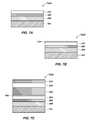
- FIGS. 2A through 2Cillustrated are stages in a method of fabricating magnetic cell structures, such as the magnetic cell structure 100 A of FIG. 1A (in which the seed region 160 is directly on the lower electrode 105 ) and a magnetic cell structure 100 B of FIG. 1B (in which the seed region 160 is indirectly on the lower electrode 105 , a lower intermediary region 140 being disposed between).
- FIG. 1Athe magnetic cell structure 100 A of FIG. 1A (in which the seed region 160 is directly on the lower electrode 105 ) and a magnetic cell structure 100 B of FIG. 1B (in which the seed region 160 is indirectly on the lower electrode 105 , a lower intermediary region 140 being disposed between).
- a structure 200 Amay be formed, from bottom to top, with a conductive material 205 formed over the substrate 102 , a seed material 260 over the conductive material 205 , a nonmagnetic material 270 over the seed material 260 , a magnetic material 220 over the nonmagnetic material 270 , another nonmagnetic material 230 over the magnetic material 220 , and another magnetic material 214 over the another nonmagnetic material 230 .
- the conductive material 205from which the lower electrode 105 ( FIGS. 1A and 1B ) is formed, may comprise, consist essentially of, or consist of, for example and without limitation, a metal (e.g., copper, tungsten, titanium, tantalum), a metal alloy, or a combination thereof.
- a metale.g., copper, tungsten, titanium, tantalum
- a metal alloye.g., copper, tungsten, titanium, tantalum
- the seed material 260may comprise, consist essentially of, or consist of magnetic material (e.g., CoFeB material or a magnetic material other than a CoFeB material).
- the seed material 260from which the seed region 160 ( FIGS. 1A and 1B ) is formed, may be formulated and configured to exhibit magnetism.
- the seed material 260may be a magnetic material formed to a thickness at which magnetism is exhibited.
- the seed material 260may comprise a magnetic material, but may be configured to not exhibit magnetism.
- the seed material 260may comprise, consist essentially of, or consist of at least one of Co, Fe, and B (e.g., a CoFeB material), but may be thin (e.g., about 6 ⁇ (about 0.6 nm)) and so not exhibit magnetism impacting other regions of the cell structure, as discussed further below.
- the seed material 260may comprise, consist essentially of, or consist of material comprising the same elements as the material of one or more of the overlying magnetic regions (e.g., the fixed region 110 and the free region 120 ( FIGS. 1A and 1B )).
- each of the seed material 260 , the fixed region 110 , and the free region 120may be formed from materials comprising Co, Fe, and B.
- the atomic ratios of Co:Fe:B in each of the seed material 260 , the fixed region 110 , and the free region 120may differ.
- the seed material 260may comprise, consist essentially of, or consist of another magnetic material (regardless of whether or not the seed material 260 is configured to exhibit magnetism), a nonmagnetic material (e.g., a nonmagnetic conductive material (e.g., a nickel-based material)), or a combination thereof.
- a nonmagnetic materiale.g., a nonmagnetic conductive material (e.g., a nickel-based material)
- a combination thereofe.g., a nonmagnetic conductive material (e.g., a nickel-based material)
- the seed region 160may be formed by, for example and without limitation, growing the seed material 260 directly on the conductive material 205 , or, in embodiments in which a lower intermediary region 140 ( FIG. 1B ) is to be disposed between the seed region 160 ( FIG. 1B ) and the lower electrode 105 ( FIG. 1B ), directly on the material of the lower intermediary region 140 .
- the seed material 260may be amorphous upon formation over the conductive material 205 .
- the lower intermediary region 140may be formed from, for example and without limitation, tantalum (Ta), titanium (Ti), tantalum nitride (TaN), titanium nitride (TiN), ruthenium (Ru), tungsten (W), or a combination thereof.
- the lower intermediary region 140( FIG. 1B ), if included, may be incorporated with the conductive material 205 from which the lower electrode 105 (FIGS. 1 A and 1 B) is to be formed.
- the material of the lower intermediary region 140may be an upper-most material of the conductive material 205 .
- the nonmagnetic material 270from which the lower nonmagnetic region 170 ( FIGS. 1A and 1B ) is formed, may comprise, consist essentially of, or consist of, for example and without limitation, a nonmagnetic oxide material (e.g., magnesium oxide (MgO), aluminum oxide (Al 2 O 3 ), titanium dioxide (TiO 2 ), or other oxide materials of conventional MTJ regions).
- a nonmagnetic oxide materiale.g., magnesium oxide (MgO), aluminum oxide (Al 2 O 3 ), titanium dioxide (TiO 2 ), or other oxide materials of conventional MTJ regions.
- the nonmagnetic material 270may be formed (e.g., grown, deposited) directly on the seed material 260 .
- the nonmagnetic material 270may have a crystal structure when initially formed.
- the seed material 260may comprise a CoFeB material initially formed to be amorphous
- the nonmagnetic material 270may comprise MgO initially formed to have a bcc (001) crystalline structure.
- the crystal structure of the nonmagnetic material 270may be enabled by the amorphous structure of the seed material 260 .
- the magnetic material 220may comprise at least one of Co, Fe, and B (e.g., a CoFeB material).
- the magnetic material 220may be formed of the same material as the seed material 260 or from a material comprising the same elements as the seed material 260 , though the relative atomic ratios of the elements within the materials may differ.
- the magnetic material 220may be formed as a homogeneous region.
- the magnetic material 220may be formed of one or more sub-regions of CoFeB material, with the sub-regions having different relative ratios of Co, Fe, and B.
- the another nonmagnetic material 230from which the intermediate nonmagnetic region 130 ( FIGS. 1A and 1B ) is formed, may comprise, consist essentially of, or consist of, for example and without limitation, a nonmagnetic oxide material (e.g., magnesium oxide (MgO), aluminum oxide (Al 2 O 3 ), titanium dioxide (TiO 2 ), or other oxide materials of conventional MTJ regions).
- a nonmagnetic oxide materiale.g., magnesium oxide (MgO), aluminum oxide (Al 2 O 3 ), titanium dioxide (TiO 2 ), or other oxide materials of conventional MTJ regions.
- the another nonmagnetic material 230may be formed of the same material as nonmagnetic material 270 or from a material having the same elements as the nonmagnetic material 270 , though ratios of elements within the materials may differ.
- both of the another nonmagnetic material 230 and the nonmagnetic material 270may be formed from material including magnesium (Mg) and oxygen (O), e.g., MgO.
- the another nonmagnetic material 230may be formed (e.g., grown, deposited) directly on the magnetic material 220 .
- the another nonmagnetic material 230may be amorphous when initially formed.
- the another magnetic material 214from which a lower portion of the fixed region 110 ( FIGS. 1A and 1B ) (i.e., a lower fixed region 114 (see FIG. 2C )) is formed, may be formed (e.g., grown, deposited) directly on the another nonmagnetic material 230 .
- the another magnetic material 214may comprise a CoFeB material.
- the another magnetic material 214may be the same material as either or both of magnetic material 220 and seed material 260 .
- the structure 200 A of FIG. 2Amay then be annealed to crystallize at least the magnetic material 220 of the free region 120 ( FIG. 2C ) into a desired crystal structure.
- the crystal structure of the nonmagnetic material 270may propagate to the magnetic material 220 of the free region 120 ( FIG. 2C ) to alter the microstructure of the magnetic material 220 from its original structure, which may have been amorphous, to a desired crystalline structure (e.g., a bce (001) crystalline structure).
- each of the materials of the structure 200 A over the conductive material 205may have a crystalline structure following the anneal, which crystalline structure may be the same structure in each of the materials.
- each of the seed material 260 , the magnetic material 220 , and the another magnetic material 214may be converted from an initial, amorphous structure into a crystalline structure due to propagation of the structure from the nearby, initially-crystalline nonmagnetic material 270 and another nonmagnetic material 230 .
- the nonmagnetic material 270may, upon formation, have a structure other than a desired crystal structure, but annealing the structure 200 A may alter the microstructure of the nonmagnetic material 270 into the desired crystal structure. In such embodiments, the nonmagnetic material 270 may be annealed before the magnetic material 220 is formed thereover and before another anneal to propagate the desired crystal structure from the nonmagnetic material 270 to the magnetic material 220 .
- the structure 200 Amay be formed to include a crystallized magnetic material 220 from which the free region 120 ( FIG. 2C ) is to be formed and wherein the crystalline structure of the magnetic material 220 is enabled by influence of the nonmagnetic material 270 on the overlying magnetic material 220 .
- the annealing processmay be carried out in situ, in some embodiments, or ex situ, in other embodiments.
- the annealing processmay use an annealing temperature of from about 300° C. to about 600° C. (e.g., about 400° C.) and may be held at the annealing temperature for from about one minute to about one hour.
- the annealing temperature and timemay be tailored based on the materials of the structure 200 A and the desired crystal structure.
- the remaining materials of the magnetic cell structuremay be fabricated, as illustrated in FIG. 2B .
- These upper-most materialsmay not be subjected to an annealing process.
- the upper-most materialsmay be subjected to an anneal, but this subsequent anneal may not be at a temperature as high as that used in the initial anneal. Therefore, the upper-most materials (e.g., materials of the fixed region 110 , upper intermediary region 150 , and upper electrode 104 ) may be selected from a variety of materials that include those that would have been degraded by the high temperature of the initial anneal.
- the magnetic material 216may include cobalt/palladium (Co/Pd) multi-sub-regions; cobalt/platinum (Co/Pt) multi-sub-regions; cobalt iron terbium (Co/Fe/Tb) based materials, L 1 0 materials, or other magnetic materials of conventional fixe regions.
- the magnetic material 216may be formed over the another magnetic material 214 .
- the another magnetic material 214 and the magnetic material 216may, together, form the fixed region 110 ( FIGS. 1A and 1B ). Therefore, a portion of the fixed region 110 may be crystallized, e.g., in the bcc (001) structure, due to the annealing process, while an upper portion of the fixed region 110 may have a different crystal structure (e.g., an amorphous structure or a crystalline structure other than the bcc (001) structure). In some embodiments, during subsequent processing, the crystal structure of the upper portion of the fixed region 110 may convert to the same crystal structure as the lower portion of the fixed region 110 .
- one or more intermediary materials 250may be formed over the magnetic material 216 .
- the intermediary materials 250which, if included, form the optional upper intermediary regions 150 ( FIGS. 1A and 1B ), may comprise, consist essentially of, or consist of materials configured to ensure a desired crystal structure in neighboring materials.
- the intermediary materials 250may alternatively or additionally include metal materials configured to aid in patterning processes during fabrication of the magnetic cell, barrier materials, or other materials of conventional STT-MRAM cell core structures.
- the intermediary materials 250may include a conductive material (e.g., one or more materials such as copper, tantalum, titanium, tungsten, ruthenium, tantalum nitride, or titanium nitride) to be formed into a conductive capping region.
- a conductive materiale.g., one or more materials such as copper, tantalum, titanium, tungsten, ruthenium, tantalum nitride, or titanium nitride
- a conductive material 204from which the upper electrode 104 ( FIGS. 1A and 1B ) may be formed, may be formed over the magnetic material 216 .
- the conductive material 204may be formed directly on the magnetic material 216 .
- the intermediary materials 250are present, the conductive material 204 may be formed directly on the intermediary materials 250 .
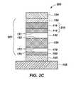
- a resulting precursor structure 200 Bmay then be patterned, in one or more stages, to for in a magnetic cell structure 200 , as illustrated in FIG. 2C .
- Techniques for patterning structures such as the precursor structure 200 B to form structures such as the magnetic cell structure 200are known in the art and so are not described herein in detail.
- the magnetic cell structure 200includes a magnetic cell core 201 having a fixed region 210 comprising the lower fixed region 114 , formed from the annealed another magnetic material 214 , and an upper fixed region 116 , formed from the magnetic material 216 .
- the lower fixed region 114may have a different crystal structure than the upper fixed region 116 .
- the free region 120 of the magnetic cell structure 200may therefore be formed with minimal structural defects. That is, the smoothness provided by the seed material 260 may function as a template to enable formation of overlying materials, including the magnetic material 220 of the free region 120 , with minimal propagation of defects as materials are subsequently formed over one another. Likewise, the annealing of the magnetic material 220 of the free region 120 further promotes a substantially defect-free microstructure with a desired crystallinity.
- the magnetic cell structure 200 including the free region 120 , formed proximate to the seed region 160 and with desired crystal structureenables the magnetic cell structure 200 to have a high TMR, a high energy barrier ratio (Eb/kT), a low switching current, a low cell-to-cell electrical resistance variation (R_sigma), and low cell-to-cell variation of magnetic properties.
- the exposure of the free region 120 to two nonmagnetic regionsi.e., the lower nonmagnetic region 170 and the intermediate nonmagnetic region 130 ), which may be formulated to be MA-inducing regions (e.g., oxide regions), at two interfaces (i.e., interface 132 and interface 172 ) may induce magnetic anisotropy (“MA”) at both interfaces (the interface 132 and the interface 172 ) such that the free region 120 has a higher MA strength than a magnetic region exposed to a nonmagnetic region along only one side.
- MAmagnetic anisotropy
- the higher MAmay be enabled even with formation of the free region 120 at a greater thickness (e.g., at about 15 ⁇ and above, e.g., at about 50 ⁇ and above); whereas, in conventional structures, thick magnetic regions adjacent to one MA-inducing region generally exhibited lower MA strengths.
- the thickness at which the free region 120 is formedmay be tailored to achieve desired properties of the free region 120 (e.g., TMR and energy barrier (Eb)).
- the seed region 160may be configured and formulated not to magnetically contribute to the magnetic cell structure 200 . That is, the seed region 160 may not produce a magnetic field that substantially impacts operation of the magnetic cell structure 200 , including the switching of the magnetic orientation of the free region 120 .
- the seed region 160may be thin, compared to, e.g., the free region 120 .
- the seed region 160may be formed to have a thickness (i.e., a height) of about 6 ⁇ (about 0.6 nm), while the free region 120 may be formed to have a thickness of about 14 ⁇ (1.4 nm).
- the lower nonmagnetic region 170may be structured to be thinner than the intermediate nonmagnetic region 130 such that, of the two nonmagnetic regions (i.e., the intermediate nonmagnetic region 130 and the lower nonmagnetic region 170 ), only the intermediate nonmagnetic region 130 may be configured as a tunnel region (e.g., a spin filter) of the magnetic cell core 201 .
- a tunnel regione.g., a spin filter
- the lower nonmagnetic region 170may be faulted to have a thickness of about 2 ⁇ (about 0.2 nm) to about 8 ⁇ (about 0.8 nm) while the intermediate nonmagnetic region 130 may be formed to have a thickness of about 6 ⁇ (about 0.6 nm) to about 15 ⁇ (about 1.5 nm).
- the lower nonmagnetic region 170while not configured to function as a spin filter, may contribute to surface/interface anisotropy along interface 172 .
- the lower nonmagnetic region 170may be configured to enable out-diffusion of boron, from neighboring magnetic material (e.g., a CoFeB material) during annealing. As discussed further below, this may enable formation of the neighboring magnetic regions to have portions proximate to an interface (e.g., the interface 172 ) having a greater ratio of iron to boron than more distal portions of the neighboring magnetic regions, which may promote inducement of surface/interface MA.
- neighboring magnetic materiale.g., a CoFeB material
- the magnetic cell structure 200includes the seed region 160 formed from a CoFeB material, the lower nonmagnetic region 170 formed from MgO, the free region 120 formed from a CoFeB material, the intermediate nonmagnetic region 130 formed from MgO, and at least the lower fixed region 114 formed from a CoFeB material.
- all of the CoFeB material regionsmay be amorphous and all of the MgO regions may be crystalline (e.g., with a bcc (001) crystalline structure).
- the crystalline structure of the MgO regionsmay propagate to the CoFeB material regions, crystallizing the CoFeB material into the same crystalline structure (e.g., the bcc (001) crystalline structure) as the MgO material.
- the annealingmay be performed at a temperature of about 300° C. to about 400° C., to crystallize the regions in the bcc (001) crystalline structure.
- the seed region 160may be formed directly on the lower electrode 105 , which may include at least a top portion comprising, consisting essentially of, or consisting of tantalum (Ta).
- the CoFeB material of each of the seed region 160 , the free region 120 , and the lower fixed region 114may have the same or different elemental ratios of Co, Fe, and B.
- the upper fixed region 116may be formed of the same or a different magnetic material than that of the lower fixed region 114 . However, the crystal structure of the upper fixed region 116 differs from the bcc (001) crystalline structure of the lower fixed region 114 .
- a memory cellcomprising a magnetic cell core.
- the magnetic cell corecomprises a seed region comprising at least one of cobalt, iron, and boron.
- a lower nonmagnetic regionis disposed over the seed region.
- a magnetic regionis disposed over the lower nonmagnetic region and exhibits a switchable magnetic orientation.
- An intermediate nonmagnetic regionis disposed over the magnetic region.
- Another magnetic regionis disposed over the intermediate nonmagnetic region. The another magnetic region exhibits a fixed magnetic orientation.
- the resulting final magnetic cell structure 200may have the magnetic cell core 201 with at least its lower regions (e.g., the lower nonmagnetic region 170 , the free region 120 , and the intermediate nonmagnetic region 130 ) formed with minimal defects in the structure.
- forming materiale.g., the nonmagnetic material 270 ( FIG. 2A ) of the lower nonmagnetic region 170 ) on a rough surface or a damaged surface may lead to the overlying materials having a corresponding rough or damaged structure.
- the resulting crystalline structure of the free region 120 and the minimized defects thereinmay enable formation of the free region 120 at a thickness that provides a high TMR, high energy barrier ratio (i.e., Eb/kT), use of low programming current.
- the double-exposure of the free region 120 to MA-inducing nonmagnetic material (in the lower nonmagnetic region 170 and the intermediate nonmagnetic region 130 )enables formation of the free region 120 at a high MA strength.
- the crystalline structure and minimized structural defectsalso enable formation of a number of magnetic cell structures 200 with precision and low cell-to-cell variation and, thus, low cell-to-cell electrical resistance variation (R_sigma) and low cell-to-cell variation of other magnetic properties of the magnetic cell structures 200 .
- the enhanced magnetic, electrical, and physical properties of the resulting structuresmay also enable scaling of the cell structures.
- a structure 300 Amay be formed to include, over the substrate 102 and from base to top, the conductive material 205 , the seed material 260 , the nonmagnetic material 270 , the magnetic material 220 , and the another nonmagnetic material 230 .
- the structure 300 Amay be annealed, as discussed above.
- the structure 300 Amay be annealed, e.g., to propagate a crystalline structure from the nonmagnetic material 270 to the magnetic material 220 , before material of the fixed region 110 ( FIGS. 1A and 1B ) is formed.
- Each of the materials in the structure 300 Amay be crystallized, or at least the magnetic material 220 may be crystallized in a desired crystal structure (e.g., in the bcc (001) structure), by the anneal process.
- the crystal structure of the magnetic material 220may be enabled by the neighboring nonmagnetic material 270 .
- the remaining materials of a precursor structure 300 Bmay be formed over the annealed materials.
- a magnetic material 310from which the fixed region 110 ( FIGS. 1A and 1B ) is to be formed, may be formed (e.g., grown, deposited) on the another nonmagnetic material 230 .
- the magnetic material 310may have a different crystal structure than the annealed material on which it is formed.
- the magnetic material 310may be amorphous or may have a crystal structure other than the bcc (001) structure if the underlying materials have the bcc (001) structure following the anneal.
- the magnetic material 310may be the same as the magnetic material 220 and, optionally, also the same as the seed material 260 .
- one or more of the intermediary materials 250may be formed over the magnetic material 310 .
- the conductive material 204is formed over the magnetic material 310 , which may complete formation of the precursor structure 300 B.
- the precursor structure 300 Bmay then be patterned to form the magnetic cell structure 100 A of FIG. 1A .
- the seed region 460may be configured to exhibit a magnetism that affects operation of the magnetic cell core 401 .
- the seed region 460may be configured to exhibit a fixed magnetic orientation.
- the magnetic orientation of the seed region 460may be oppositely directed to the magnetic orientation of the fixed region 110 , and magnetic dipole fields emitted by the seed region 460 and the fixed region 110 may be substantially symmetrically disposed around the free region 120 . Accordingly, a magnetic dipole field emitted by one of the seed region 460 and the fixed region 110 may be substantially cancelled by a magnetic dipole field emitted by the other of the seed region 460 and the fixed region 110 .
- the magnetic dipole fields emitted by the seed region 460 and the fixed region 110may not substantially interfere with switching of the magnetic orientation of the free region 120 , which may promote symmetrical switching of the free region 120 .
- Symmetrical switchingmay enhance the reliability of the magnetic cell core 401 during operation.
- the lower nonmagnetic region 470may be formed from the nonmagnetic material 270 ( FIG. 2A ), as described above, and both the intermediate nonmagnetic region 130 and the lower nonmagnetic region 470 may be formulated, located, and otherwise configured to function as tunnel regions (e.g., spin filters) during operation of the magnetic cell core 401 .
- tunnel regionse.g., spin filters
- a base magnetic region(e.g., the seed region 160 of FIGS. 1A, 1B, and 2C ; the seed region 460 of FIG. 4 ) may be configured to exhibit a magnetic orientation that is substantially perpendicular to the magnetic orientation of an overlying magnetic region (e.g., the free region 120 ).
- the seed region 460may be formulated, formed, and otherwise configured as a seed region 560 A, illustrated in FIG. 5A , exhibiting an in-plane (e.g., horizontal) magnetic orientation, as indicated by arrow 562 A.
- the seed region 560 Amay be configured to not magnetically affect operation of the cell core.
- the seed region 560 Amay be formed to be substantially thinner than the magnetic regions of the cell core (e.g., the free region 120 and the fixed region 110 ( FIGS. 1A and 1B )). However, in other embodiments, the seed region 560 A may be formed to have substantially the same thickness as other magnetic regions, as illustrated in FIG. 5A .
- the seed region 560 Amay be formed to have substantially the same thickness as other magnetic regions, as illustrated in FIG. 5A .
- the base magnetic region(e.g., the seed region 160 of FIGS. 1A, 1B, and 2C ; the seed region 460 of FIG. 4 ) may, alternatively, be configured to exhibit a magnetic orientation that is substantially aligned (e.g., parallel or anti-parallel) to the magnetic orientation of an overlying magnetic region (e.g., the free region 120 ).
- the seed regione.g., the seed region 160 of FIGS. 1A, 1B, and 2C ; the seed region 460 of FIG. 4
- the seed region 560 Bmay or may not be configured to magnetically affect operation of the cell core.
- the magnetic orientation of the seed region 560 B(as indicated by arrow 562 B may be oppositely directed (i.e., antiparallel) to the magnetic orientation of the fixed region 110 (as indicated by arrow 112 in FIG. 1A ), and the seed region 560 B and the fixed region 110 may be symmetrically disposed about the free region 120 to enable substantial cancellation of magnetic dipole fields emitted by the seed region 560 B and the fixed region 110 ( FIG. 1A ).
- the material of e.g., the seed material 260 , the magnetic material 220 , and the magnetic material 310may be each formed as single, homogeneous regions of the material, in other embodiments, e.g., one or more of the seed material 260 , the magnetic material 220 , and the magnetic material 310 ( FIG. 3B ) may be formed from multiple sub-regions of material.
- each of the sub-regions of materialmay be formed of the same composition of magnetic material, while, in other embodiments, at least one of such sub-regions comprises a different composition (e.g., elemental ratio) of material than another sub-region.
- Each sub-regionmay be sequentially formed, one on another, to form the structure of the region.
- the fixed region 210may be formed from the another magnetic material 214 ( FIG. 2B ) and the magnetic material 216 ( FIG. 2B ).
- the magnetic material 216may comprise a different magnetic material than the another magnetic material 214 .
- the another magnetic material 214may be formed of magnetic material formulated to crystallize and withstand the conditions of the annealing process.
- the magnetic material 216on the other hand, which is not subjected to annealing, may comprise magnetic material that would otherwise be damaged by exposure to the conditions of the annealing process.
- the another magnetic material 214 and the magnetic material 216may be formed of the same material.
- the another magnetic material 214may be crystallized by the anneal while the magnetic material 216 , not subjected to a crystallizing anneal, may be amorphous or have a crystal structure differing from that of the annealed another magnetic material 214 .
- a free region 620may be formed of multiple magnetic sub-regions, e.g., a lower free region 124 , an intermediate free region 125 , and an upper free region 126 . In other embodiments, fewer than three or more than three sub-regions may be utilized. In some embodiments, all of the sub-regions may be formed of the same magnetic material composition, e.g., a CoFeB material with the same ratio of Co:Fe:B in each of the sub-regions. Nonetheless, the sub-regions may be independently formed, one over the other, rather than formed in one large region (e.g., as with the magnetic material 310 of FIG. 3B ).
- At least one of the plurality of the lower free region 124 , the intermediate free region 125 , and the upper free region 126comprises a magnetic material composition that differs from the magnetic material composition of another of the lower free region 124 , the intermediate free region 125 , and the upper free region 126 .
- all of the lower free region 124 , the intermediate free region 125 , and the upper free region 126may be formed of CoFeB materials, but the CoFeB material of the lower free region 124 and the upper free region 126 may have a higher ratio of Fe to B compared to the CoFeB material of the intermediate free region 125 .
- the free region 620may be “iron rich” and “boron poor” along the interface 132 with the intermediate nonmagnetic region 130 and the interface 172 with the lower nonmagnetic region 170 .
- the iron rich upper free region 126 and lower free region 124may enable inducement of strong surface/interfacial MA along the interfaces 132 , 172 .
- only the portion of the free region 620 that is proximate to the interface 132may be formulated to be “iron rich.”
- the free region 620or other magnetic or nonmagnetic regions of the magnetic cell structure, may be engineered to include spatially distributed elements (i.e., sub-regions with different elemental ratios).
- a material 770may be formed over the nonmagnetic material 270 , with such material 770 configured to reduce the electrical resistance of the nonmagnetic material 270 and, therefore, of the lower nonmagnetic region 170 ( FIG. 1A ) formed therefrom.
- a structure 700 Amay be formed over the substrate 102 with just the conductive material 205 , the seed material 260 , and the nonmagnetic material 270 .
- the material 770may be formed (e.g., deposited) over the nonmagnetic material 270 , forming structure 700 B.
- the material 770may comprise, consist essentially of, or consist of ruthenium (Ru) or an alloy thereof.
- the material 770may be formed in an atomic monolayer or other thin region over the nonmagnetic material 270 .
- the material 770may be embedded into the nonmagnetic material 270 .
- the presence of the material 770 proximate to or in the nonmagnetic material 270may increase the electrical conductivity (and decrease the electrical resistance) of the nonmagnetic material 270 without substantially degrading the magnetic-related properties (e.g., the spin filtering function, the surface/interfacial MA-inducing properties) of the nonmagnetic material 270 .
- the nonmagnetic material 270may, therefore, not exhibit a substantial resistance during switching of the magnetic orientation of the free region 120 .
- additional materialsmay be formed over structure 700 B ( FIG. 7B ), and, thus, over the nonmagnetic material 270 .
- the additional materialsmay include the magnetic material 220 , the another nonmagnetic material 230 , and, optionally, the another magnetic material 214 .
- a structure 700 C, resulting from formation of the additional materials,may be annealed, as discussed above, to crystallize, e.g., the magnetic material 220 into the desired crystal structure, which may be enabled by the proximity of the magnetic material 220 to the nonmagnetic material 270 .
- annealingmay also promote diffusion of the material 770 into the nonmagnetic material 270 .
- the remaining materialsmay be formed over the uppermost material of the structure 700 C to form, e.g., the precursor structure 200 B of FIG. 2B , except having a less electrically resistant nonmagnetic material 270 .
- additional annealsmay be conducted before the anneal to crystallize the materials (e.g., the magnetic material 220 ) or after the crystallizing anneal.
- the anneal described above as effecting the crystallization of materialmay be the highest temperature anneal carried out before patterning. It is also contemplated that anneals carried out after formation of materials above the crystallized structure may not be conducted at temperatures high enough to crystallize the latter-formed materials. Therefore, again, in some embodiments, the lower-most materials of the structure may be crystallized, while the upper-most materials may be amorphous or of a different crystal structure.
- the methodcomprises forming a structure.
- Forming a structurecomprises forming a seed material over a substrate and forming a nonmagnetic material over the seed material.
- a magnetic materialis formed over the nonmagnetic material.
- Another nonmagnetic materialis formed over the magnetic material.
- the structureis annealed and another magnetic material is formed over the another nonmagnetic material.
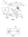
- an STT-MRAM system 800that includes peripheral devices 812 in operable communication with an STT-MRAM cell 814 , a grouping of which may be fabricated to form an array of memory cells in a grid pattern including a number of rows and columns, or in various other arrangements, depending on the system requirements and fabrication technology.
- the STT-MRAM cell 814includes a magnetic cell core 802 , an access transistor 803 , a conductive material that may function as a data/sense line 804 (e.g., a bit line), a conductive material that may function as an access line 805 (e.g., a word line), and a conductive material that may function as a source line 806 .
- the peripheral devices 812 of the STT-MRAM system 800may include read/write circuitry 807 , a bit line reference 808 , and a sense amplifier 809 .
- the cell core 802may be any one of the magnetic cell cores (e.g., the magnetic cell core 101 A ( FIG. 1A ), the magnetic cell core 101 B ( FIG. 1B ), the magnetic cell core 201 ( FIG. 2C ), the magnetic cell core 401 ( FIG. 4 )) described above.
- the STT-MRAM cell 814may have a high TMR, a high energy barrier ratio (Eb/kT), a low programming current, a high MA strength, low cell-to-cell electrical resistance variation, and low cell-to-cell variation of magnetic properties.
- an STT-MRAM cell 814In use and operation, when an STT-MRAM cell 814 is selected to be programmed, a programming current is applied to the STT-MRAM cell 814 , and the current is spin-polarized by the fixed region of the cell core 802 and exerts a torque on the free region of the cell core 802 , which switches the magnetization of the free region to “write to” or “program” the STT-MRAM cell 814 . In a read operation of the STT-MRAM cell 814 , a current is used to detect the resistance state of the cell core 802 .
- the read/write circuitry 807may generate a write current (i.e., a programming current) to the data/sense line 804 and the source line 806 .
- a write currenti.e., a programming current
- the polarity of the voltage between the data/sense line 804 and the source line 806determines the switch in magnetic orientation of the free region in the cell core 802 .
- the free regionis magnetized according to the spin polarity of the programming current, the programmed logic state is written to the STT-MRAM cell 814 .
- the read/write circuitry 807To read the STT-MRAM cell 814 , the read/write circuitry 807 generates a read voltage to the data/sense line 804 and the source line 806 through the cell core 802 and the access transistor 803 .
- the programmed state of the STT-MRAM cell 814relates to the electrical resistance across the cell core 802 , which may be determined by the voltage difference between the data/sense line 804 and the source line 806 . In some embodiments, the voltage difference may be compared to the bit line reference 808 and amplified by the sense amplifier 809 .
- FIG. 8illustrates one example of an operable STT-MRAM system 800 .
- the magnetic cell corese.g., the magnetic cell core 101 A ( FIG. 1A ), the magnetic cell core 101 B ( FIG. 1B ), the magnetic cell core 201 ( FIG. 2C ), and the magnetic cell core 401 ( FIG. 4 )
- the magnetic cell coresmay be incorporated and utilized within any STT-MRAM system configured to incorporate a magnetic cell core having magnetic regions.
- a spin torque transfer magnetic random access memory (STT-MRAM) systemcomprising STT-MRAM cells.
- At least one STT-MRAM cell of the STT-MRAM cellscomprises a magnetic cell core.
- the magnetic cell corecomprises a seed region over a substrate and a nonmagnetic region on the seed region.
- the seed regioncomprises at least one of cobalt, iron, and boron.
- a magnetic regionis disposed on the nonmagnetic region and has a switchable magnetic orientation.
- Another nonmagnetic regionis disposed on the magnetic region.
- Another magnetic regionis disposed on the another nonmagnetic region.
- the at least one STT-MRAM cellalso comprises conductive materials in operable communication with the magnetic cell core.
- the STT-MRAM systemalso comprises at least one peripheral device in operable communication with the at least one STT-MRAM cell. At least one of an access transistor, a bit line, a word line, and a source line is in operable communication with the magnetic cell core.
- the semiconductor device 900includes a memory array 902 and a control logic component 904 .
- the memory array 902may include a plurality of the STT-MRAM cells 814 ( FIG. 8 ) including any of the magnetic cell cores (e.g., the magnetic cell core 101 A ( FIG. 1A ), the magnetic cell core 101 B ( FIG. 1B ), the magnetic cell core 201 ( FIG. 2C ), and the magnetic cell core 401 ( FIG. 4 )) discussed above, which magnetic cell cores (e.g., the magnetic cell core 101 A ( FIG. 1A ), the magnetic cell core 101 B ( FIG.
- the control logic component 904may be configured to operatively interact with the memory array 902 to read from or write to any or all memory cells (e.g., STT-MRAM cell 814 ( FIG. 8 )) within the memory array 902 .
- a semiconductor devicecomprising a spin torque transfer magnetic random access memory (STT-MRAM) array comprising STT-MRAM cells.
- At least one STT-MRAM cell of the STT-MRAM cellscomprises a magnetic cell core.
- the magnetic cell corecomprises a seed region over a substrate and a nonmagnetic region over the seed region.
- the nonmagnetic regionhas a bcc (001) crystalline structure.
- a free regionis disposed over the nonmagnetic region.
- Another nonmagnetic regionis disposed over the free region.
- a fixed regionis disposed over the another nonmagnetic region.
- the processor-based system 1000may include various electronic devices manufactured in accordance with embodiments of the present disclosure.
- the processor-based system 1000may be any of a variety of types, such as a computer, pager, cellular phone, personal organizer, control circuit, or other electronic device.
- the processor-based system 1000may include one or more processors 1002 , such as a microprocessor, to control the processing of system functions and requests in the processor-based system 1000 .
- the processor 1002 and other subcomponents of the processor-based system 1000may include magnetic memory devices manufactured in accordance with embodiments of the present disclosure.
- the processor-based system 1000may include a power supply 1004 in operable communication with the processor 1002 .
- the power supply 1004may include one or more of a fuel cell, a power scavenging device, permanent batteries, replaceable batteries, and rechargeable batteries.
- the power supply 1004may also include an AC adapter; therefore, the processor-based system 1000 may be plugged into a wall outlet, for example.
- the power supply 1004may also include a DC adapter such that the processor-based system 1000 may be plugged into a vehicle cigarette lighter or a vehicle power port, for example.
- a user interface 1006may be coupled to the processor 1002 .
- the user interface 1006may include input devices such as buttons, switches, a keyboard, a light pen, a mouse, a digitizer and stylus, a touch screen, a voice recognition system, a microphone, or a combination thereof.
- a display 1008may also be coupled to the processor 1002 .
- the display 1008may include an LCD display, an SED display, a CRT display, a DLP display, a plasma display, an OLED display, an LED display, a three-dimensional projection, an audio display, or a combination thereof.
- an RF sub-system/baseband processor 1010may also be coupled to the processor 1002 .
- the RF sub-system/baseband processor 1010may include an antenna that is coupled to an RF receiver and to an RF transmitter (not shown).
- a communication port 1012or more than one communication port 1012 , may also be coupled to the processor 1002 .
- the communication port 1012may be adapted to be coupled to one or more peripheral devices 1014 , such as a modem, a printer, a computer, a scanner, or a camera, or to a network, such as a local area network, remote area network, intranet, or the Internet, for example.
- the processor 1002may control the processor-based system 1000 by implementing software programs stored in the memory.
- the software programsmay include an operating system, database software, drafting software, word processing software, media editing software, or media playing software, for example.
- the memoryis operably coupled to the processor 1002 to store and facilitate execution of various programs.
- the processor 1002may be coupled to system memory 1016 , which may include one or more of spin torque transfer magnetic random access memory (STT-MRAM), magnetic random access memory (MRAM), dynamic random access memory (DRAM), static random access memory (SRAM), racetrack memory, and other known memory types.
- STT-MRAMspin torque transfer magnetic random access memory
- MRAMmagnetic random access memory
- DRAMdynamic random access memory
- SRAMstatic random access memory
- racetrack memoryand other known memory types.
- the system memory 1016may include volatile memory, non-volatile memory, or a combination thereof.
- the system memory 1016is typically large so that it can store dynamically loaded applications and data.
- the system memory 1016may include semiconductor devices, such as the semiconductor device 900 of FIG. 9 , memory cells including any of the magnetic cell cores (e.g., the magnetic cell core 101 A ( FIG. 1A ), the magnetic cell core 101 B ( FIG. 1B ), the magnetic cell core 201 ( FIG. 2C ), and the magnetic cell core 401 ( FIG. 4 )), or a combination thereof.
- semiconductor devicessuch as the semiconductor device 900 of FIG. 9
- memory cellsincluding any of the magnetic cell cores (e.g., the magnetic cell core 101 A ( FIG. 1A ), the magnetic cell core 101 B ( FIG. 1B ), the magnetic cell core 201 ( FIG. 2C ), and the magnetic cell core 401 ( FIG. 4 )), or a combination thereof.
- the processor 1002may also be coupled to non-volatile memory 1018 , which is not to suggest that system memory 1016 is necessarily volatile.
- the non-volatile memory 1018may include one or more of STT-MRAM, MRAM, read-only memory (ROM) such as an EPROM, resistive read-only memory (RROM), and Flash memory to be used in conjunction with the system memory 1016 .
- ROMread-only memory
- RROMresistive read-only memory
- Flash memoryto be used in conjunction with the system memory 1016 .
- the size of the non-volatile memory 1018is typically selected to be just large enough to store any necessary operating system, application programs, and fixed data.
- the non-volatile memory 1018may include high capacity memory, such as disk drive memory, such as a hybrid-drive including resistive memory, or other types of non-volatile solid-state memory, for example.
- the non-volatile memory 1018may include semiconductor devices, such as the semiconductor device 900 of FIG. 9 , memory cells including any of the magnetic cell cores (e.g., the magnetic cell core 101 A ( FIG. 1A ), the magnetic cell core 101 B ( FIG. 1B ), the magnetic cell core 201 ( FIG. 2C ), and the magnetic cell core 401 ( FIG. 4 )), or a combination thereof.
- semiconductor devicessuch as the semiconductor device 900 of FIG. 9
- memory cellsincluding any of the magnetic cell cores (e.g., the magnetic cell core 101 A ( FIG. 1A ), the magnetic cell core 101 B ( FIG. 1B ), the magnetic cell core 201 ( FIG. 2C ), and the magnetic cell core 401 ( FIG. 4 )), or a combination thereof.
- an electronic systemcomprising at least one processor.
- the at least one processorcomprises at least one magnetic memory cell.
- the at least one magnetic memory cellcomprises at least two magnetic regions over a seed region comprising at least one of cobalt, iron, and boron. One of the at least two magnetic regions exhibits a switchable magnetic orientation. A nonmagnetic region is between the at least two magnetic regions. Another nonmagnetic region is over the at least two magnetic regions.
- the electronic systemalso comprises a power supply in operable communication with the at least one processor.
Landscapes
- Engineering & Computer Science (AREA)
- Computer Hardware Design (AREA)
- Manufacturing & Machinery (AREA)
- Hall/Mr Elements (AREA)
- Mram Or Spin Memory Techniques (AREA)
Abstract
Description
Claims (25)
Priority Applications (5)
| Application Number | Priority Date | Filing Date | Title |
|---|---|---|---|
| US13/948,839US9466787B2 (en) | 2013-07-23 | 2013-07-23 | Memory cells, methods of fabrication, semiconductor device structures, memory systems, and electronic systems |
| US15/289,610US9876053B2 (en) | 2013-07-23 | 2016-10-10 | Semiconductor devices comprising magnetic memory cells and methods of fabrication |
| US15/877,064US10515996B2 (en) | 2013-07-23 | 2018-01-22 | Semiconductor devices with seed and magnetic regions and methods of fabrication |
| US16/710,983US11393872B2 (en) | 2013-07-23 | 2019-12-11 | Electronic devices with seed and magnetic regions and methods of fabrication |
| US17/806,674US12048167B2 (en) | 2013-07-23 | 2022-06-13 | Electronic devices including a seed region and magnetic regions |
Applications Claiming Priority (1)
| Application Number | Priority Date | Filing Date | Title |
|---|---|---|---|
| US13/948,839US9466787B2 (en) | 2013-07-23 | 2013-07-23 | Memory cells, methods of fabrication, semiconductor device structures, memory systems, and electronic systems |
Related Child Applications (1)
| Application Number | Title | Priority Date | Filing Date |
|---|---|---|---|
| US15/289,610ContinuationUS9876053B2 (en) | 2013-07-23 | 2016-10-10 | Semiconductor devices comprising magnetic memory cells and methods of fabrication |
Publications (2)
| Publication Number | Publication Date |
|---|---|
| US20150028439A1 US20150028439A1 (en) | 2015-01-29 |
| US9466787B2true US9466787B2 (en) | 2016-10-11 |
Family
ID=52389789
Family Applications (5)
| Application Number | Title | Priority Date | Filing Date |
|---|---|---|---|
| US13/948,839ActiveUS9466787B2 (en) | 2013-07-23 | 2013-07-23 | Memory cells, methods of fabrication, semiconductor device structures, memory systems, and electronic systems |
| US15/289,610ActiveUS9876053B2 (en) | 2013-07-23 | 2016-10-10 | Semiconductor devices comprising magnetic memory cells and methods of fabrication |
| US15/877,064ActiveUS10515996B2 (en) | 2013-07-23 | 2018-01-22 | Semiconductor devices with seed and magnetic regions and methods of fabrication |
| US16/710,983Active2033-12-11US11393872B2 (en) | 2013-07-23 | 2019-12-11 | Electronic devices with seed and magnetic regions and methods of fabrication |
| US17/806,674Active2033-10-02US12048167B2 (en) | 2013-07-23 | 2022-06-13 | Electronic devices including a seed region and magnetic regions |
Family Applications After (4)
| Application Number | Title | Priority Date | Filing Date |
|---|---|---|---|
| US15/289,610ActiveUS9876053B2 (en) | 2013-07-23 | 2016-10-10 | Semiconductor devices comprising magnetic memory cells and methods of fabrication |
| US15/877,064ActiveUS10515996B2 (en) | 2013-07-23 | 2018-01-22 | Semiconductor devices with seed and magnetic regions and methods of fabrication |
| US16/710,983Active2033-12-11US11393872B2 (en) | 2013-07-23 | 2019-12-11 | Electronic devices with seed and magnetic regions and methods of fabrication |
| US17/806,674Active2033-10-02US12048167B2 (en) | 2013-07-23 | 2022-06-13 | Electronic devices including a seed region and magnetic regions |
Country Status (1)
| Country | Link |
|---|---|
| US (5) | US9466787B2 (en) |
Cited By (3)
| Publication number | Priority date | Publication date | Assignee | Title |
|---|---|---|---|---|
| US9768376B2 (en) | 2013-07-01 | 2017-09-19 | Micron Technology, Inc. | Magnetic memory cells, semiconductor devices, and methods of operation |
| US10793812B2 (en) | 2017-05-31 | 2020-10-06 | SK Hynix Inc. | Cleaning composition and method for fabricating electronic device using the same |
| US11205679B2 (en) | 2019-07-22 | 2021-12-21 | Samsung Electronics Co., Ltd. | Magnetic memory device including a free layer and a pinned layer |
Families Citing this family (25)
| Publication number | Priority date | Publication date | Assignee | Title |
|---|---|---|---|---|
| US9007818B2 (en) | 2012-03-22 | 2015-04-14 | Micron Technology, Inc. | Memory cells, semiconductor device structures, systems including such cells, and methods of fabrication |
| US9054030B2 (en) | 2012-06-19 | 2015-06-09 | Micron Technology, Inc. | Memory cells, semiconductor device structures, memory systems, and methods of fabrication |
| US9379315B2 (en) | 2013-03-12 | 2016-06-28 | Micron Technology, Inc. | Memory cells, methods of fabrication, semiconductor device structures, and memory systems |
| US9466787B2 (en) | 2013-07-23 | 2016-10-11 | Micron Technology, Inc. | Memory cells, methods of fabrication, semiconductor device structures, memory systems, and electronic systems |
| US9178134B2 (en)* | 2013-08-30 | 2015-11-03 | Masahiko Nakayama | Magnetoresistive element and method of manufacturing the same |
| US9461242B2 (en) | 2013-09-13 | 2016-10-04 | Micron Technology, Inc. | Magnetic memory cells, methods of fabrication, semiconductor devices, memory systems, and electronic systems |
| US9608197B2 (en) | 2013-09-18 | 2017-03-28 | Micron Technology, Inc. | Memory cells, methods of fabrication, and semiconductor devices |
| US20150129996A1 (en)* | 2013-11-12 | 2015-05-14 | Samsung Electronics Co., Ltd. | Method and system for providing a top pinned layer perpendicular magnetic anisotropy magnetic junction usable in spin transfer torque magnetic random access memory applications |
| US9373781B2 (en) | 2013-11-12 | 2016-06-21 | Samsung Electronics Co., Ltd. | Dual perpendicular magnetic anisotropy magnetic junction usable in spin transfer torque magnetic random access memory applications |
| US10454024B2 (en) | 2014-02-28 | 2019-10-22 | Micron Technology, Inc. | Memory cells, methods of fabrication, and memory devices |
| US9281466B2 (en) | 2014-04-09 | 2016-03-08 | Micron Technology, Inc. | Memory cells, semiconductor structures, semiconductor devices, and methods of fabrication |
| US9269888B2 (en) | 2014-04-18 | 2016-02-23 | Micron Technology, Inc. | Memory cells, methods of fabrication, and semiconductor devices |
| US10026888B2 (en)* | 2014-08-06 | 2018-07-17 | Toshiba Memory Corporation | Magnetoresistive effect element and magnetic memory |
| US9349945B2 (en) | 2014-10-16 | 2016-05-24 | Micron Technology, Inc. | Memory cells, semiconductor devices, and methods of fabrication |
| US9768377B2 (en) | 2014-12-02 | 2017-09-19 | Micron Technology, Inc. | Magnetic cell structures, and methods of fabrication |
| US10439131B2 (en) | 2015-01-15 | 2019-10-08 | Micron Technology, Inc. | Methods of forming semiconductor devices including tunnel barrier materials |
| KR102397904B1 (en)* | 2015-09-17 | 2022-05-13 | 삼성전자주식회사 | Free Layer Having a Low Boron Concentration Region and a High Boron Concentration Region, Magneto-resistive Cell, and Magneto-resistive Random Access Memory Device Having the Same, and Methods of Fabricating the Same |
| KR102511828B1 (en)* | 2016-06-29 | 2023-03-21 | 삼성전자주식회사 | Method for manufacturing magnetic memory device |
| US10727271B2 (en) | 2017-01-05 | 2020-07-28 | Micron Trechnology, Inc. | Memory device having source contacts located at intersections of linear portions of a common source, electronic systems, and associated methods |
| US10453895B2 (en) | 2017-01-05 | 2019-10-22 | Micron Technology, Inc. | Magnetic memory device with a common source having an array of openings, system, and method of fabrication |
| US10014345B1 (en) | 2017-01-05 | 2018-07-03 | Micron Technology, Inc. | Magnetic memory device with grid-shaped common source plate, system, and method of fabrication |
| US10014465B1 (en) | 2017-04-03 | 2018-07-03 | Headway Technologies, Inc. | Maintaining coercive field after high temperature anneal for magnetic device applications with perpendicular magnetic anisotropy |
| US10502900B2 (en)* | 2018-04-06 | 2019-12-10 | Hewlett Packard Enterprise Development Lp | CWDM transmit module for wavelength tuning and tracking |
| WO2019230352A1 (en)* | 2018-05-31 | 2019-12-05 | Tdk株式会社 | Spin-orbit torque magnetoresistance effect element, and magnetic memory |
| TWI765221B (en)* | 2020-02-06 | 2022-05-21 | 國立成功大學 | Optoelectronic device and memory device |
Citations (190)
| Publication number | Priority date | Publication date | Assignee | Title |
|---|---|---|---|---|
| US4882936A (en) | 1986-12-05 | 1989-11-28 | Mag Dev Inc. | Magnetoelastic torque tool |
| US5768069A (en) | 1996-11-27 | 1998-06-16 | International Business Machines Corporation | Self-biased dual spin valve sensor |
| GB2343308A (en) | 1998-10-30 | 2000-05-03 | Nikolai Franz Gregor Schwabe | Magnetic storage device |
| US6166948A (en) | 1999-09-03 | 2000-12-26 | International Business Machines Corporation | Magnetic memory array with magnetic tunnel junction memory cells having flux-closed free layers |
| US6258470B1 (en) | 1998-01-16 | 2001-07-10 | Matsushita Electric Industrial Co., Ltd. | Exchange coupling film, magnetoresistance effect device, magnetoresistance effective head and method for producing exchange coupling film |
| US6275363B1 (en) | 1999-07-23 | 2001-08-14 | International Business Machines Corporation | Read head with dual tunnel junction sensor |
| US6363000B2 (en) | 2000-05-03 | 2002-03-26 | Hewlett-Packard Company | Write circuit for large MRAM arrays |
| US6387476B1 (en) | 1999-07-14 | 2002-05-14 | Sony Corporation | Magnetic functional element and magnetic recording medium |
| US20020089874A1 (en) | 2001-01-11 | 2002-07-11 | Nickel Janice H. | Thermally-assisted switching of magnetic memory elements |
| US20020105827A1 (en) | 2000-12-07 | 2002-08-08 | Commissariat A L'energie Atomique | Three-layered stacked magnetic spin polarisation device with memory, using such a device |
| JP2002314049A (en) | 2001-04-18 | 2002-10-25 | Nec Corp | Magnetic memory and manufacturing method therefor |
| US6483741B1 (en) | 1999-09-17 | 2002-11-19 | Sony Corporation | Magnetization drive method, magnetic functional device, and magnetic apparatus |
| US20030011939A1 (en) | 2001-07-16 | 2003-01-16 | International Business Machines Corporation | Dual/differential GMR head with a singlel AFM layer |
| US20030064569A1 (en) | 2001-08-10 | 2003-04-03 | Semiconductor Energy Laboratory Co., Ltd. | Method of peeling off and method of manufacturing semiconductor device |
| US6560135B2 (en) | 2001-01-12 | 2003-05-06 | Hitachi, Ltd. | Magnetic semiconductor memory apparatus and method of manufacturing the same |
| US20030103371A1 (en) | 2001-12-05 | 2003-06-05 | Sang-Koog Kim | Method of controlling magnetization easy axis in ferromagnetic films using voltage, ultrahigh-density, low power, nonvolatile magnetic memory using the control method, and method of writing information on the magnetic memory |
| US6611405B1 (en) | 1999-09-16 | 2003-08-26 | Kabushiki Kaisha Toshiba | Magnetoresistive element and magnetic memory device |
| EP1353443A2 (en) | 2002-04-12 | 2003-10-15 | Xerox Corporation | Spring contact |
| US20030199104A1 (en) | 2002-04-18 | 2003-10-23 | Infineon Technologies North America Corp. | Material combinations for tunnel junction cap layer, tunnel junction hard mask and tunnel junction stack seed layer in MRAM processing |
| JP2004104076A (en) | 2002-07-16 | 2004-04-02 | Hitachi Ltd | Semiconductor laser device and method of manufacturing the same |
| US20040075959A1 (en) | 2002-10-21 | 2004-04-22 | International Business Machines Corporation | Insulative in-stack hard bias for GMR sensor stabilization |
| US20040091744A1 (en) | 2002-11-07 | 2004-05-13 | Carey Matthew J. | Low-resistance high-magnetoresistance magnetic tunnel junction device with improved tunnel barrier |
| US6771534B2 (en) | 2002-11-15 | 2004-08-03 | International Business Machines Corporation | Thermally-assisted magnetic writing using an oxide layer and current-induced heating |
| US20040174740A1 (en) | 2003-03-03 | 2004-09-09 | Kyu-Mann Lee | Magnetic tunnel junction structures and methods of fabrication |
| US6806096B1 (en) | 2003-06-18 | 2004-10-19 | Infineon Technologies Ag | Integration scheme for avoiding plasma damage in MRAM technology |
| KR20040092342A (en) | 2003-04-25 | 2004-11-03 | 재단법인서울대학교산학협력재단 | non-volatile MRAM cell and operating methode thereof, and ultra-high large scale integrated multi-radix MRAM using non-volatile MRAM cell |
| US20040224243A1 (en) | 2003-05-08 | 2004-11-11 | Sony Corporation | Mask, mask blank, and methods of producing these |
| US20040233760A1 (en) | 2000-10-06 | 2004-11-25 | Headway Technologies, Inc. | Magnetic random access memory array with coupled soft adjacent magnetic layer |
| US6845038B1 (en) | 2003-02-01 | 2005-01-18 | Alla Mikhailovna Shukh | Magnetic tunnel junction memory device |
| US20050036361A1 (en) | 2003-08-14 | 2005-02-17 | Yoshiaki Fukuzumi | Semiconductor memory device with magnetoresistance elements and method of writing data into the same |
| US20050068683A1 (en) | 2003-09-26 | 2005-03-31 | Hitachi Global Technologies Netherlands B.V. | Method for providing a self-pinned differential GMR sensor and self-pinned differential GMR sensor |
| US20050087511A1 (en) | 2003-10-22 | 2005-04-28 | Manish Sharma | Process for making magnetic memory structures having different-sized memory cell layers |
| US20050106810A1 (en) | 2003-11-14 | 2005-05-19 | Mahendra Pakala | Stress assisted current driven switching for magnetic memory applications |
| US20050164414A1 (en) | 2004-01-26 | 2005-07-28 | Deak James G. | Magnetic annealing sequences for patterned MRAM synthetic antiferromagnetic pinned layers |
| US20050173698A1 (en) | 2002-06-10 | 2005-08-11 | Drewes Joel A. | Multilayer dielectric tunnel barrier used in magnetic tunnel junction devices, and its method of fabrication |
| US20050189574A1 (en) | 2004-02-26 | 2005-09-01 | Nguyen Paul P. | Spin transfer magnetic element with free layers having high perpendicular anisotropy and in-plane equilibrium magnetization |
| US20050211973A1 (en) | 2004-03-23 | 2005-09-29 | Kiyotaka Mori | Stressed organic semiconductor |
| US6970376B1 (en) | 2004-05-17 | 2005-11-29 | Kabushiki Kaisha Toshiba | Magnetic random access memory and method of writing data in magnetic random access memory |
| US6980468B1 (en) | 2002-10-28 | 2005-12-27 | Silicon Magnetic Systems | High density MRAM using thermal writing |
| US6998150B2 (en) | 2003-03-12 | 2006-02-14 | Headway Technologies, Inc. | Method of adjusting CoFe free layer magnetostriction |
| US20060038213A1 (en) | 2004-08-19 | 2006-02-23 | Nec Corporation | Magnetic memory adopting synthetic antiferromagnet as free magnetic layer |
| US20060042930A1 (en) | 2004-08-26 | 2006-03-02 | Daniele Mauri | Method for reactive sputter deposition of a magnesium oxide (MgO) tunnel barrier in a magnetic tunnel junction |
| US7026671B2 (en) | 2002-06-20 | 2006-04-11 | Sony Corporation | Magnetoresistive effect element, magnetic memory device and manufacturing method of magnetoresistive effect element and magnetic memory device |
| US20060114714A1 (en) | 2004-11-29 | 2006-06-01 | Yoshiharu Kanegae | Magnetroresistive random access memory and method of manufacturing the same |
| US20060118842A1 (en) | 2004-12-08 | 2006-06-08 | Yoshihisa Iwata | Magnetic random access memory |
| US7095933B2 (en) | 2002-04-09 | 2006-08-22 | Barth Phillip W | Systems and methods for designing and fabricating multi-layer structures having thermal expansion properties |
| US7130167B2 (en) | 2004-03-03 | 2006-10-31 | Hitachi Global Storage Technologies Netherlands B.V. | Magnetoresistive sensor having improved synthetic free layer |
| US20060261425A1 (en) | 2002-10-02 | 2006-11-23 | Nec Corporation | Magnetic memory and method of manufacturing the memory |
| US20070008661A1 (en) | 2004-01-20 | 2007-01-11 | Tai Min | Magnetic tunneling junction film structure with process determined in-plane magnetic anisotropy |
| US20070035890A1 (en) | 2004-04-02 | 2007-02-15 | Tdk Corporation | Composed free layer for stabilizing magnetoresistive head having low magnetostriction |
| US20070053112A1 (en) | 2005-09-07 | 2007-03-08 | Papworth Parkin Stuart S | Tunnel barriers based on alkaline earth oxides |
| US7189583B2 (en) | 2003-07-02 | 2007-03-13 | Micron Technology, Inc. | Method for production of MRAM elements |
| US20070086121A1 (en) | 2005-10-19 | 2007-04-19 | Toshihiko Nagase | Magnetoresistive element |
| US7230265B2 (en) | 2005-05-16 | 2007-06-12 | International Business Machines Corporation | Spin-polarization devices using rare earth-transition metal alloys |
| US7239489B2 (en) | 2002-11-25 | 2007-07-03 | International Business Machines Corporation | Tunneling magnetoresistive (TMR) sensor having a magnesium oxide barrier layer formed by a multi-layer process |
| KR20070094431A (en) | 2006-03-16 | 2007-09-20 | 후지쯔 가부시끼가이샤 | Magnetic recording medium, method of manufacturing magnetic recording medium and magnetic recording apparatus |
| US7274080B1 (en) | 2003-08-22 | 2007-09-25 | International Business Machines Corporation | MgO-based tunnel spin injectors |
| US20070297220A1 (en) | 2006-06-22 | 2007-12-27 | Masatoshi Yoshikawa | Magnetoresistive element and magnetic memory |
| KR20080029852A (en) | 2006-09-28 | 2008-04-03 | 가부시끼가이샤 도시바 | Magnetoresistive element and magnetoresistive random access memory |
| US7372674B2 (en) | 2005-07-22 | 2008-05-13 | Hitachi Global Storage Technologies Netherlands B.V. | Magnetic tunnel transistor with high magnetocurrent and stronger pinning |
| US7378698B2 (en) | 2003-08-12 | 2008-05-27 | Samsung Electronics Co., Ltd. | Magnetic tunnel junction and memory device including the same |
| US7379280B2 (en) | 2002-12-16 | 2008-05-27 | Nec Corporation | Magnetic tunnel magneto-resistance device and magnetic memory using the same |
| US20080164548A1 (en) | 2006-02-25 | 2008-07-10 | Yadav Technology | Low resistance high-tmr magnetic tunnel junction and process for fabrication thereof |
| US20080164502A1 (en) | 2004-11-16 | 2008-07-10 | Nec Corporation | Magnetic Memory and Manufacturing Method For the Same |
| US20080179699A1 (en) | 2007-01-30 | 2008-07-31 | Magic Technologies, Inc. | Novel magnetic tunnel junction (MTJ) to reduce spin transfer magnetization switching current |
| US20080205130A1 (en) | 2007-02-28 | 2008-08-28 | Freescale Semiconductor, Inc. | Mram free layer synthetic antiferromagnet structure and methods |
| US20080225581A1 (en) | 2007-03-15 | 2008-09-18 | Sony Corporation | Memory device and memory |
| US20080278867A1 (en) | 2002-11-01 | 2008-11-13 | Nec Corporation | Magnetoresistance device with a diffusion barrier between a conductor and a magnetoresistance element and method of fabricating the same |
| US7486552B2 (en) | 2007-05-21 | 2009-02-03 | Grandis, Inc. | Method and system for providing a spin transfer device with improved switching characteristics |
| US7488609B1 (en) | 2007-11-16 | 2009-02-10 | Hitachi Global Storage Technologies Netherlands B.V. | Method for forming an MgO barrier layer in a tunneling magnetoresistive (TMR) device |
| US20090039450A1 (en) | 2007-08-09 | 2009-02-12 | Industrial Technology Research Institute | Structure of magnetic memory cell and magnetic memory device |
| US20090079018A1 (en) | 2007-09-26 | 2009-03-26 | Toshihiko Nagase | Magnetoresistive element and magnetic memory |
| US7514160B2 (en) | 2001-05-31 | 2009-04-07 | National Institute Of Advanced Industrial Science And Technology | Tunnel magnetoresistance element having a double underlayer of amorphous MgO and crystalline MgO(001) |
| US20090096043A1 (en) | 2007-10-10 | 2009-04-16 | Magic Technologies, Inc. | MRAM with means of controlling magnetic anisotropy |
| US20090108383A1 (en) | 2007-10-31 | 2009-04-30 | Magic Technologies, Inc. | High performance MTJ element for conventional MRAM and for STT-RAM and a method for making the same |
| US7564152B1 (en) | 2004-02-12 | 2009-07-21 | The United States Of America As Represented By The Secretary Of The Navy | High magnetostriction of positive magnetostrictive materials under tensile load |
| US20090190262A1 (en) | 2008-01-30 | 2009-07-30 | Kabushiki Kaisha Toshiba | Magnetoresistive element and method of manufacturing the same |
| JP2009194366A (en) | 2008-02-14 | 2009-08-27 | Toshiba Corp | Manufacturing method of semiconductor device |
| US20090229111A1 (en) | 2008-03-12 | 2009-09-17 | Headway Technologies, Inc. | Two step annealing process for TMR device with amorphous free layer |
| US7602033B2 (en) | 2007-05-29 | 2009-10-13 | Headway Technologies, Inc. | Low resistance tunneling magnetoresistive sensor with composite inner pinned layer |
| US20090257151A1 (en) | 2008-03-27 | 2009-10-15 | Tdk Corporation & Kabushiki Kaisha Toshiba | Thin seeded Co/Ni multilayer film with perpendicular anisotropy for spintronic device applications |
| US20100034014A1 (en) | 2008-08-05 | 2010-02-11 | Hideo Ohno | Magnetoresistive Element, Magnetic Memory Cell and Magnetic Random Access Memory Using the Same |
| WO2010026831A1 (en) | 2008-09-03 | 2010-03-11 | 富士電機ホールディングス株式会社 | Magnetic memory element and storage device using same |
| US7682841B2 (en) | 2007-05-02 | 2010-03-23 | Qimonda Ag | Method of forming integrated circuit having a magnetic tunnel junction device |
| US20100080036A1 (en) | 2008-09-30 | 2010-04-01 | Micron Technology, Inc. | Unidirectional spin torque transfer magnetic memory cell structure |
| US20100080048A1 (en) | 2008-09-30 | 2010-04-01 | Micron Technology, Inc. | Stt-mram cell structure incorporating piezoelectric stress material |
| US20100102406A1 (en) | 2008-10-27 | 2010-04-29 | Seagate Technology Llc | Magnetic stack design |
| US20100109110A1 (en) | 2008-10-30 | 2010-05-06 | Seagate Technology Llc | ST-RAM Cells with Perpendicular Anisotropy |
| US20100110783A1 (en) | 2008-11-05 | 2010-05-06 | Micron Technology, Inc. | Spin torque transfer cell structure utilizing field-induced antiferromagnetic or ferromagnetic coupling |
| US7732881B2 (en) | 2006-11-01 | 2010-06-08 | Avalanche Technology, Inc. | Current-confined effect of magnetic nano-current-channel (NCC) for magnetic random access memory (MRAM) |
| US20100148167A1 (en) | 2008-12-12 | 2010-06-17 | Everspin Technologies, Inc. | Magnetic tunnel junction stack |
| US7750421B2 (en) | 2007-07-23 | 2010-07-06 | Magic Technologies, Inc. | High performance MTJ element for STT-RAM and method for making the same |
| US20100171086A1 (en) | 2009-01-07 | 2010-07-08 | Macronix International Co., Ltd. | Integrated circuit memory with single crystal silicon on silicide driver and manufacturing method |
| US20100177557A1 (en) | 2009-01-09 | 2010-07-15 | Micron Technology, Inc. | Stt-mram cell structures |
| US20100177561A1 (en) | 2009-01-12 | 2010-07-15 | Micron Technology, Inc. | Memory cell having nonmagnetic filament contact and methods of operating and fabricating the same |
| US20100176472A1 (en) | 2009-01-14 | 2010-07-15 | Sony Corporation | Nonvolatile magnetic memory device |
| US20100200899A1 (en) | 2009-02-10 | 2010-08-12 | Takao Marukame | Spin transistor and method of manufacturing the same |
| US7791844B2 (en) | 2005-12-14 | 2010-09-07 | Hitachi Global Storage Technologies Netherlands B.V. | Magnetoresistive sensor having a magnetically stable free layer with a positive magnetostriction |
| US20100230769A1 (en) | 2009-03-03 | 2010-09-16 | Nec Electronics Corporation | Magnetoresistive element, magnetic random access memory and method of manufacturing the same |
| US20100240151A1 (en) | 2009-03-23 | 2010-09-23 | Magic Technologies, Inc. | Method of double patterning and etching magnetic tunnel junction structures for spin-transfer torque MRAM devices |
| US7835173B2 (en) | 2008-10-31 | 2010-11-16 | Micron Technology, Inc. | Resistive memory |
| WO2010134378A1 (en) | 2009-05-19 | 2010-11-25 | 富士電機ホールディングス株式会社 | Magnetic memory element and storage device using same |
| US20100327248A1 (en) | 2009-06-29 | 2010-12-30 | Seagate Technology Llc | Cell patterning with multiple hard masks |
| WO2011001746A1 (en) | 2009-07-03 | 2011-01-06 | 富士電機ホールディングス株式会社 | Magnetic memory element and driving method therefor |
| US20110007429A1 (en) | 2009-07-13 | 2011-01-13 | Seagate Technology Llc | Magnetic sensor with perpendicular anisotrophy free layer and side shields |
| US20110007543A1 (en) | 2009-07-07 | 2011-01-13 | Seagate Technology Llc | Bipolar select device for resistive sense memory |
| US20110014500A1 (en) | 2009-07-17 | 2011-01-20 | Maglc Technologies, Inc. | Structure and method to fabricate high performance MTJ devices for spin-transfer torque (STT)-RAM application |
| US7885105B2 (en) | 2008-03-25 | 2011-02-08 | Qualcomm Incorporated | Magnetic tunnel junction cell including multiple vertical magnetic domains |
| US20110031569A1 (en) | 2009-08-10 | 2011-02-10 | Grandis, Inc. | Method and system for providing magnetic tunneling junction elements having improved performance through capping layer induced perpendicular anisotropy and memories using such magnetic elements |
| US20110049657A1 (en) | 2009-08-28 | 2011-03-03 | Renesas Electronics Corporation | Semiconductor device and method of manufacturing the same |
| US20110049658A1 (en) | 2008-09-29 | 2011-03-03 | Seagate Technology Llc | Magnetic tunnel junction with electronically reflective insulative spacer |
| US20110051503A1 (en) | 2009-09-03 | 2011-03-03 | International Business Machines Corporation | Magnetic Devices and Structures |
| US20110062537A1 (en) | 2009-09-11 | 2011-03-17 | Sechung Oh | Magnetic Memory Devices |
| US20110064969A1 (en) | 2009-09-15 | 2011-03-17 | Grandis Inc. | Magnetic Element Having Perpendicular Anisotropy With Enhanced Efficiency |
| US7919794B2 (en) | 2008-01-08 | 2011-04-05 | Qualcomm, Incorporated | Memory cell and method of forming a magnetic tunnel junction (MTJ) of a memory cell |
| US7929370B2 (en) | 2008-11-24 | 2011-04-19 | Magic Technologies, Inc. | Spin momentum transfer MRAM design |
| US7932572B2 (en) | 2008-02-15 | 2011-04-26 | Renesas Electronics Corporation | Semiconductor device having memory element with stress insulating film |
| US20110096443A1 (en) | 2009-10-26 | 2011-04-28 | Headway Technologies, Inc. | MTJ incorporating CoFe/Ni multilayer film with perpendicular magnetic anisotropy for MRAM application |
| US7948044B2 (en) | 2008-04-09 | 2011-05-24 | Magic Technologies, Inc. | Low switching current MTJ element for ultra-high STT-RAM and a method for making the same |
| US20110121366A1 (en) | 2009-04-14 | 2011-05-26 | NuPGA Corporation | System comprising a semiconductor device and structure |
| US20110145514A1 (en) | 2009-12-16 | 2011-06-16 | Samsung Electronics Co. Ltd. | Method and apparatus for inter-processor communication in mobile terminal |
| US20110149646A1 (en) | 2009-12-18 | 2011-06-23 | Micron Technology, Inc. | Transient heat assisted sttram cell for lower programming current |
| US20110149670A1 (en) | 2009-12-21 | 2011-06-23 | Samsung Electronics Co., Ltd. | Spin valve device including graphene, method of manufacturing the same, and magnetic device including the spin valve device |
| US20110149647A1 (en) | 2009-12-21 | 2011-06-23 | Samsung Electronics Co., Ltd. | Perpendicular magnetic tunnel junctions, magnetic devices including the same and method of manufacturing a perpendicular magnetic tunnel junction |
| US20110170341A1 (en) | 2010-01-11 | 2011-07-14 | Butler William H | Method and system for providing magnetic tunneling junctions usable in spin transfer torque magnetic memories |
| US20110170339A1 (en) | 2010-01-14 | 2011-07-14 | Joerg Wunderlich | Magnetoresistive device |
| US8009465B2 (en) | 2004-10-08 | 2011-08-30 | Kabushiki Kaisha Toshiba | Magnetoresistive element |
| US20110241138A1 (en) | 2010-03-31 | 2011-10-06 | Chun-I Hsieh | Magnetoresistive random access memory element and fabrication method thereof |
| US8043732B2 (en) | 2008-11-11 | 2011-10-25 | Seagate Technology Llc | Memory cell with radial barrier |
| US20110260274A1 (en) | 2009-07-13 | 2011-10-27 | Seagate Technology Llc | Magnetic stack having reference layers with orthogonal magnetization orientation directions |
| US8048492B2 (en) | 2005-12-21 | 2011-11-01 | Kabushiki Kaisha Toshiba | Magnetoresistive effect element and manufacturing method thereof |
| US20110266642A1 (en) | 2008-12-11 | 2011-11-03 | Centre National De La Recherche Scientifique | Method for producing a magnetic tunnel junction and magnetic tunnel junction thus obtained |
| US20110269251A1 (en) | 2008-09-09 | 2011-11-03 | Hynix Semiconductor Inc. | Spin Transfer Torque Memory Device Having Common Source Line and Method for Manufacturing the Same |
| US8068317B2 (en) | 2005-07-22 | 2011-11-29 | Hitachi Global Storage Technologies Netherlands B.V. | Magnetic tunnel transistor with high magnetocurrent |
| WO2011149274A2 (en) | 2010-05-26 | 2011-12-01 | 고려대학교 산학협력단 | Magnetic tunnel junction device having amorphous buffer layers that are magnetically connected together and that have perpendicular magnetic anisotropy |
| US20110293967A1 (en) | 2010-05-28 | 2011-12-01 | Headway Technologies, Inc. | Multilayer structure with high perpendicular anisotropy for device applications |
| US20110303997A1 (en) | 2010-06-14 | 2011-12-15 | Regents Of The University Of Minnesota | Magnetic tunnel junction device |
| US20110303995A1 (en) | 2010-06-15 | 2011-12-15 | International Business Machines Corporation | Seed layer and free magnetic layer for perpendicular anisotropy in a spin-torque magnetic random access memory |
| US20110309418A1 (en) | 2008-03-25 | 2011-12-22 | Kabushiki Kaisha Toshiba | Magnetoresistance effect element and magnetic random access memory |
| US20120015099A1 (en) | 2010-07-15 | 2012-01-19 | Everspin Technologies, Inc. | Structure and method for fabricating a magnetic thin film memory having a high field anisotropy |
| US20120012953A1 (en) | 2010-07-16 | 2012-01-19 | Grandis, Inc. | Method and system for providing magnetic tunneling junction elements having laminated free layers and memories using such magnetic elements |
| US20120012952A1 (en) | 2010-07-16 | 2012-01-19 | Qualcomm Incorporated | Magnetic Storage Element Utilizing Improved Pinned Layer Stack |
| US20120018823A1 (en) | 2010-07-26 | 2012-01-26 | Avalanche Technology, Inc. | Spin transfer torque magnetic random access memory (sttmram) having graded synthetic free layer |
| KR20120008295A (en) | 2010-07-16 | 2012-01-30 | 삼성전자주식회사 | A pattern structure, method for forming the same and method for manufacturing a semiconductor device using the same |
| US8138561B2 (en) | 2008-09-18 | 2012-03-20 | Magic Technologies, Inc. | Structure and method to fabricate high performance MTJ devices for spin-transfer torque (STT)-RAM |
| US20120069647A1 (en) | 2010-09-17 | 2012-03-22 | Micron Technology, Inc. | Spin torque transfer memory cell structures and methods |
| US20120074511A1 (en) | 2010-09-17 | 2012-03-29 | Kabushiki Kaisha Toshiba | Magnetic memory and method of manufacturing the same |
| US20120106233A1 (en) | 2010-10-29 | 2012-05-03 | Honeywell International Inc. | Reduced switching-energy magnetic elements |
| US20120135273A1 (en) | 2010-11-30 | 2012-05-31 | Magic Technologies, Inc. | Structure and method for enhancing interfacial perpendicular anisotropy in CoFe(B)/MgO/CoFe(B) Magnetic Tunnel Junctions |
| US20120146167A1 (en) | 2010-12-10 | 2012-06-14 | Avalanche Technology | Memory system having thermally stable perpendicular magneto tunnel junction (mtj) and a method of manufacturing same |
| US20120155156A1 (en) | 2009-08-10 | 2012-06-21 | Grandis, Inc. | Method and system for providing magnetic tunneling junction elements having improved performance through capping layer induced perpendicular anisotropy and memories using such magnetic elements |
| US8223539B2 (en) | 2010-01-26 | 2012-07-17 | Micron Technology, Inc. | GCIB-treated resistive device |
| US20120205758A1 (en) | 2011-02-11 | 2012-08-16 | Magic Technologies, Inc. | Magnetic element with improved out-of-plane anisotropy for spintronic applications |
| US20120218813A1 (en) | 2011-02-25 | 2012-08-30 | Samsung Electronics Co., Ltd. | Magnetic Memory Devices |
| US20120217594A1 (en) | 2011-02-28 | 2012-08-30 | Kabushiki Kaisha Toshiba | Magnetic random access memory |
| US20120225499A1 (en) | 2009-07-09 | 2012-09-06 | Crocus Technologies | Method for Use in Making Electronic Devices Having Thin-Film Magnetic Components |
| US20120236631A1 (en) | 2011-03-18 | 2012-09-20 | Samsung Electronics Co., Ltd. | Magnetic tunneling junction devices, memories, electronic systems, and memory systems, and methods of fabricating the same |
| US20120241878A1 (en) | 2011-03-24 | 2012-09-27 | International Business Machines Corporation | Magnetic tunnel junction with iron dusting layer between free layer and tunnel barrier |
| US20120267733A1 (en) | 2011-04-25 | 2012-10-25 | International Business Machines Corporation | Magnetic stacks with perpendicular magnetic anisotropy for spin momentum transfer magnetoresistive random access memory |
| US20120280336A1 (en) | 2011-05-04 | 2012-11-08 | Magic Technologies, Inc. | Multilayers having reduced perpendicular demagnetizing field using moment dilution for spintronic applications |
| US20120286382A1 (en) | 2011-05-10 | 2012-11-15 | Magic Technologies, Inc. | Co/Ni multilayers with improved out-of-plane anisotropy for magnetic device applications |
| WO2012160937A1 (en) | 2011-05-20 | 2012-11-29 | 日本電気株式会社 | Magnetic memory element and magnetic memory |
| US20120299134A1 (en) | 2011-05-10 | 2012-11-29 | Magic Technologies, Inc. | Co/Ni Multilayers with Improved Out-of-Plane Anisotropy for Magnetic Device Applications |
| US8334148B2 (en) | 2009-11-11 | 2012-12-18 | Samsung Electronics Co., Ltd. | Methods of forming pattern structures |
| US8338004B2 (en) | 2008-10-30 | 2012-12-25 | Korea Institute Of Science And Technology | Magnetic tunnel junction structure having free layer with oblique magnetization |
| EP2541554A1 (en) | 2011-06-30 | 2013-01-02 | Hitachi, Ltd. | Magnetic functional device |
| US20130028013A1 (en) | 2010-01-26 | 2013-01-31 | Shoji Ikeda | Magnetoresistive effect element, magnetic memory cell using same, and random access memory |
| US20130032911A1 (en)* | 2011-08-05 | 2013-02-07 | Jung Dong Ha | Magnetic memory device and fabrication method thereof |
| US20130042081A1 (en) | 2011-08-10 | 2013-02-14 | Samsung Electronics Co., Ltd. | Magnetic tunneling junction devices, memories, memory systems, and electronic devices |
| US8385107B2 (en) | 2009-05-08 | 2013-02-26 | Crocus Technology Sa | Magnetic memory with a thermally assisted spin transfer torque writing procedure using a low writing current |
| US20130059168A1 (en) | 2011-08-31 | 2013-03-07 | Agency Fo Science, Technology And Research | Magnetoresistance Device |
| US20130069185A1 (en) | 2011-09-21 | 2013-03-21 | Kabushiki Kaisha Toshiba | Magnetic memory element and nonvolatile memory device |
| US8411498B2 (en) | 2009-12-15 | 2013-04-02 | Samsung Electronics Co., Ltd. | Magnetic tunnel junction devices, electronic devices including a magnetic tunneling junction device and methods of fabricating the same |
| EP2015307B1 (en) | 2007-07-13 | 2013-04-10 | Hitachi Ltd. | Magnetoresistive device |
| US8422286B2 (en) | 2009-10-20 | 2013-04-16 | Avalanche Technology, Inc. | Low-crystallization temperature MTJ for spin-transfer torque magnetic random access memory (STTMRAM) |
| US20130140658A1 (en) | 2011-12-01 | 2013-06-06 | Sony Corporation | Memory element and memory apparatus |
| US20130146996A1 (en) | 2011-12-08 | 2013-06-13 | Taiwan Semiconductor Manufacturing Company, Ltd. | Magnetic device fabrication |
| US8481181B2 (en) | 2011-03-31 | 2013-07-09 | Seagate Technology Llc | Exchange coupled magnetic elements |
| US8492169B2 (en) | 2011-08-15 | 2013-07-23 | Magic Technologies, Inc. | Magnetic tunnel junction for MRAM applications |
| US20130228884A1 (en) | 2009-04-28 | 2013-09-05 | Seagate Technology Llc | Magnetic stack having assist layers |
| US20130250661A1 (en) | 2012-03-22 | 2013-09-26 | Micron Technology, Inc. | Memory cells, semiconductor device structures, systems including such cells, and methods of fabrication |
| US8570798B2 (en) | 2009-03-10 | 2013-10-29 | Micron Technology, Inc. | Electronic devices formed of two or more substrates connected together, electronic systems comprising electronic devices, and methods of forming electronic devices |
| US8587043B2 (en) | 2010-07-09 | 2013-11-19 | Kabushiki Kaisha Toshiba | Magnetoresistive random access memory and method of manufacturing the same |
| US20130334630A1 (en) | 2012-06-19 | 2013-12-19 | Micron Technology, Inc. | Memory cells, semiconductor device structures, memory systems, and methods of fabrication |
| US20130334631A1 (en) | 2012-06-19 | 2013-12-19 | Micron Technology, Inc. | Memory cells, semiconductor device structures, memory systems, and methods of fabrication |
| US20140008742A1 (en)* | 2009-08-10 | 2014-01-09 | Eugene Youjun Chen | Magnetic tunneling junction seed, capping, and spacer layer materials |
| US20140027869A1 (en)* | 2012-07-27 | 2014-01-30 | Qualcomm Incorporated | AMORPHOUS ALLOY SPACER FOR PERPENDICULAR MTJs |
| US8760818B1 (en)* | 2013-01-09 | 2014-06-24 | Western Digital (Fremont), Llc | Systems and methods for providing magnetic storage elements with high magneto-resistance using heusler alloys |
| US8803265B2 (en) | 2010-07-22 | 2014-08-12 | Samsung Electronics Co., Ltd. | Magnetic memory layer and magnetic memory device including the same |
| US8823118B2 (en) | 2012-01-05 | 2014-09-02 | Headway Technologies, Inc. | Spin torque transfer magnetic tunnel junction fabricated with a composite tunneling barrier layer |
Family Cites Families (4)
| Publication number | Priority date | Publication date | Assignee | Title |
|---|---|---|---|---|
| KR101457511B1 (en)* | 2011-08-18 | 2014-11-04 | 코넬 유니버시티 | Spin hall effect magnetic apparatus, method and applications |
| US8796796B2 (en)* | 2012-12-20 | 2014-08-05 | Samsung Electronics Co., Ltd. | Method and system for providing magnetic junctions having improved polarization enhancement and reference layers |
| US20140218821A1 (en)* | 2013-02-07 | 2014-08-07 | Seagate Technology Llc | Data reader with magnetic seed lamination |
| US9466787B2 (en) | 2013-07-23 | 2016-10-11 | Micron Technology, Inc. | Memory cells, methods of fabrication, semiconductor device structures, memory systems, and electronic systems |
- 2013
- 2013-07-23USUS13/948,839patent/US9466787B2/enactiveActive
- 2016
- 2016-10-10USUS15/289,610patent/US9876053B2/enactiveActive
- 2018
- 2018-01-22USUS15/877,064patent/US10515996B2/enactiveActive
- 2019
- 2019-12-11USUS16/710,983patent/US11393872B2/enactiveActive
- 2022
- 2022-06-13USUS17/806,674patent/US12048167B2/enactiveActive
Patent Citations (220)
| Publication number | Priority date | Publication date | Assignee | Title |
|---|---|---|---|---|
| US4882936A (en) | 1986-12-05 | 1989-11-28 | Mag Dev Inc. | Magnetoelastic torque tool |
| US5768069A (en) | 1996-11-27 | 1998-06-16 | International Business Machines Corporation | Self-biased dual spin valve sensor |
| US6258470B1 (en) | 1998-01-16 | 2001-07-10 | Matsushita Electric Industrial Co., Ltd. | Exchange coupling film, magnetoresistance effect device, magnetoresistance effective head and method for producing exchange coupling film |
| GB2343308A (en) | 1998-10-30 | 2000-05-03 | Nikolai Franz Gregor Schwabe | Magnetic storage device |
| US6387476B1 (en) | 1999-07-14 | 2002-05-14 | Sony Corporation | Magnetic functional element and magnetic recording medium |
| US6275363B1 (en) | 1999-07-23 | 2001-08-14 | International Business Machines Corporation | Read head with dual tunnel junction sensor |
| US6166948A (en) | 1999-09-03 | 2000-12-26 | International Business Machines Corporation | Magnetic memory array with magnetic tunnel junction memory cells having flux-closed free layers |
| US6611405B1 (en) | 1999-09-16 | 2003-08-26 | Kabushiki Kaisha Toshiba | Magnetoresistive element and magnetic memory device |
| US6483741B1 (en) | 1999-09-17 | 2002-11-19 | Sony Corporation | Magnetization drive method, magnetic functional device, and magnetic apparatus |
| US6363000B2 (en) | 2000-05-03 | 2002-03-26 | Hewlett-Packard Company | Write circuit for large MRAM arrays |
| US20040233760A1 (en) | 2000-10-06 | 2004-11-25 | Headway Technologies, Inc. | Magnetic random access memory array with coupled soft adjacent magnetic layer |
| US20020105827A1 (en) | 2000-12-07 | 2002-08-08 | Commissariat A L'energie Atomique | Three-layered stacked magnetic spin polarisation device with memory, using such a device |
| US20020089874A1 (en) | 2001-01-11 | 2002-07-11 | Nickel Janice H. | Thermally-assisted switching of magnetic memory elements |
| US6560135B2 (en) | 2001-01-12 | 2003-05-06 | Hitachi, Ltd. | Magnetic semiconductor memory apparatus and method of manufacturing the same |
| JP2002314049A (en) | 2001-04-18 | 2002-10-25 | Nec Corp | Magnetic memory and manufacturing method therefor |
| US6703249B2 (en) | 2001-04-18 | 2004-03-09 | Nec Electronics Corporation | Method of fabricating magnetic random access memory operating based on tunnel magnetroresistance effect |
| US7514160B2 (en) | 2001-05-31 | 2009-04-07 | National Institute Of Advanced Industrial Science And Technology | Tunnel magnetoresistance element having a double underlayer of amorphous MgO and crystalline MgO(001) |
| US20030011939A1 (en) | 2001-07-16 | 2003-01-16 | International Business Machines Corporation | Dual/differential GMR head with a singlel AFM layer |
| US20030064569A1 (en) | 2001-08-10 | 2003-04-03 | Semiconductor Energy Laboratory Co., Ltd. | Method of peeling off and method of manufacturing semiconductor device |
| US20030103371A1 (en) | 2001-12-05 | 2003-06-05 | Sang-Koog Kim | Method of controlling magnetization easy axis in ferromagnetic films using voltage, ultrahigh-density, low power, nonvolatile magnetic memory using the control method, and method of writing information on the magnetic memory |
| US7095933B2 (en) | 2002-04-09 | 2006-08-22 | Barth Phillip W | Systems and methods for designing and fabricating multi-layer structures having thermal expansion properties |
| US7563486B2 (en) | 2002-04-09 | 2009-07-21 | Avago Technologies General Ip (Singapore) Pte. Ltd. | Systems and methods for designing and fabricating multi-layer structures having thermal expansion properties |
| EP1353443A2 (en) | 2002-04-12 | 2003-10-15 | Xerox Corporation | Spring contact |
| US20030199104A1 (en) | 2002-04-18 | 2003-10-23 | Infineon Technologies North America Corp. | Material combinations for tunnel junction cap layer, tunnel junction hard mask and tunnel junction stack seed layer in MRAM processing |
| US20050173698A1 (en) | 2002-06-10 | 2005-08-11 | Drewes Joel A. | Multilayer dielectric tunnel barrier used in magnetic tunnel junction devices, and its method of fabrication |
| US7026671B2 (en) | 2002-06-20 | 2006-04-11 | Sony Corporation | Magnetoresistive effect element, magnetic memory device and manufacturing method of magnetoresistive effect element and magnetic memory device |
| JP2004104076A (en) | 2002-07-16 | 2004-04-02 | Hitachi Ltd | Semiconductor laser device and method of manufacturing the same |
| US20060261425A1 (en) | 2002-10-02 | 2006-11-23 | Nec Corporation | Magnetic memory and method of manufacturing the memory |
| US20040075959A1 (en) | 2002-10-21 | 2004-04-22 | International Business Machines Corporation | Insulative in-stack hard bias for GMR sensor stabilization |
| US6980468B1 (en) | 2002-10-28 | 2005-12-27 | Silicon Magnetic Systems | High density MRAM using thermal writing |
| US20080278867A1 (en) | 2002-11-01 | 2008-11-13 | Nec Corporation | Magnetoresistance device with a diffusion barrier between a conductor and a magnetoresistance element and method of fabricating the same |
| US20040091744A1 (en) | 2002-11-07 | 2004-05-13 | Carey Matthew J. | Low-resistance high-magnetoresistance magnetic tunnel junction device with improved tunnel barrier |
| US6771534B2 (en) | 2002-11-15 | 2004-08-03 | International Business Machines Corporation | Thermally-assisted magnetic writing using an oxide layer and current-induced heating |
| US7239489B2 (en) | 2002-11-25 | 2007-07-03 | International Business Machines Corporation | Tunneling magnetoresistive (TMR) sensor having a magnesium oxide barrier layer formed by a multi-layer process |
| US7379280B2 (en) | 2002-12-16 | 2008-05-27 | Nec Corporation | Magnetic tunnel magneto-resistance device and magnetic memory using the same |
| US6845038B1 (en) | 2003-02-01 | 2005-01-18 | Alla Mikhailovna Shukh | Magnetic tunnel junction memory device |
| US20040174740A1 (en) | 2003-03-03 | 2004-09-09 | Kyu-Mann Lee | Magnetic tunnel junction structures and methods of fabrication |
| US6998150B2 (en) | 2003-03-12 | 2006-02-14 | Headway Technologies, Inc. | Method of adjusting CoFe free layer magnetostriction |
| KR20040092342A (en) | 2003-04-25 | 2004-11-03 | 재단법인서울대학교산학협력재단 | non-volatile MRAM cell and operating methode thereof, and ultra-high large scale integrated multi-radix MRAM using non-volatile MRAM cell |
| US20040224243A1 (en) | 2003-05-08 | 2004-11-11 | Sony Corporation | Mask, mask blank, and methods of producing these |
| US6806096B1 (en) | 2003-06-18 | 2004-10-19 | Infineon Technologies Ag | Integration scheme for avoiding plasma damage in MRAM technology |
| US7189583B2 (en) | 2003-07-02 | 2007-03-13 | Micron Technology, Inc. | Method for production of MRAM elements |
| US7378698B2 (en) | 2003-08-12 | 2008-05-27 | Samsung Electronics Co., Ltd. | Magnetic tunnel junction and memory device including the same |
| US20050036361A1 (en) | 2003-08-14 | 2005-02-17 | Yoshiaki Fukuzumi | Semiconductor memory device with magnetoresistance elements and method of writing data into the same |
| US7274080B1 (en) | 2003-08-22 | 2007-09-25 | International Business Machines Corporation | MgO-based tunnel spin injectors |
| US20050068683A1 (en) | 2003-09-26 | 2005-03-31 | Hitachi Global Technologies Netherlands B.V. | Method for providing a self-pinned differential GMR sensor and self-pinned differential GMR sensor |
| US20050087511A1 (en) | 2003-10-22 | 2005-04-28 | Manish Sharma | Process for making magnetic memory structures having different-sized memory cell layers |
| US20050106810A1 (en) | 2003-11-14 | 2005-05-19 | Mahendra Pakala | Stress assisted current driven switching for magnetic memory applications |
| US20070008661A1 (en) | 2004-01-20 | 2007-01-11 | Tai Min | Magnetic tunneling junction film structure with process determined in-plane magnetic anisotropy |
| US7083988B2 (en) | 2004-01-26 | 2006-08-01 | Micron Technology, Inc. | Magnetic annealing sequences for patterned MRAM synthetic antiferromagnetic pinned layers |
| US20050164414A1 (en) | 2004-01-26 | 2005-07-28 | Deak James G. | Magnetic annealing sequences for patterned MRAM synthetic antiferromagnetic pinned layers |
| US7564152B1 (en) | 2004-02-12 | 2009-07-21 | The United States Of America As Represented By The Secretary Of The Navy | High magnetostriction of positive magnetostrictive materials under tensile load |
| US20050189574A1 (en) | 2004-02-26 | 2005-09-01 | Nguyen Paul P. | Spin transfer magnetic element with free layers having high perpendicular anisotropy and in-plane equilibrium magnetization |
| US6992359B2 (en) | 2004-02-26 | 2006-01-31 | Grandis, Inc. | Spin transfer magnetic element with free layers having high perpendicular anisotropy and in-plane equilibrium magnetization |
| US7130167B2 (en) | 2004-03-03 | 2006-10-31 | Hitachi Global Storage Technologies Netherlands B.V. | Magnetoresistive sensor having improved synthetic free layer |
| US20050211973A1 (en) | 2004-03-23 | 2005-09-29 | Kiyotaka Mori | Stressed organic semiconductor |
| US20070035890A1 (en) | 2004-04-02 | 2007-02-15 | Tdk Corporation | Composed free layer for stabilizing magnetoresistive head having low magnetostriction |
| US6970376B1 (en) | 2004-05-17 | 2005-11-29 | Kabushiki Kaisha Toshiba | Magnetic random access memory and method of writing data in magnetic random access memory |
| US20060038213A1 (en) | 2004-08-19 | 2006-02-23 | Nec Corporation | Magnetic memory adopting synthetic antiferromagnet as free magnetic layer |
| US20060042930A1 (en) | 2004-08-26 | 2006-03-02 | Daniele Mauri | Method for reactive sputter deposition of a magnesium oxide (MgO) tunnel barrier in a magnetic tunnel junction |
| US8009465B2 (en) | 2004-10-08 | 2011-08-30 | Kabushiki Kaisha Toshiba | Magnetoresistive element |
| US20080164502A1 (en) | 2004-11-16 | 2008-07-10 | Nec Corporation | Magnetic Memory and Manufacturing Method For the Same |
| US20060114714A1 (en) | 2004-11-29 | 2006-06-01 | Yoshiharu Kanegae | Magnetroresistive random access memory and method of manufacturing the same |
| US20060118842A1 (en) | 2004-12-08 | 2006-06-08 | Yoshihisa Iwata | Magnetic random access memory |
| US7230265B2 (en) | 2005-05-16 | 2007-06-12 | International Business Machines Corporation | Spin-polarization devices using rare earth-transition metal alloys |
| US7372674B2 (en) | 2005-07-22 | 2008-05-13 | Hitachi Global Storage Technologies Netherlands B.V. | Magnetic tunnel transistor with high magnetocurrent and stronger pinning |
| US8068317B2 (en) | 2005-07-22 | 2011-11-29 | Hitachi Global Storage Technologies Netherlands B.V. | Magnetic tunnel transistor with high magnetocurrent |
| US20070053112A1 (en) | 2005-09-07 | 2007-03-08 | Papworth Parkin Stuart S | Tunnel barriers based on alkaline earth oxides |
| US20070086121A1 (en) | 2005-10-19 | 2007-04-19 | Toshihiko Nagase | Magnetoresistive element |
| US7791844B2 (en) | 2005-12-14 | 2010-09-07 | Hitachi Global Storage Technologies Netherlands B.V. | Magnetoresistive sensor having a magnetically stable free layer with a positive magnetostriction |
| US8048492B2 (en) | 2005-12-21 | 2011-11-01 | Kabushiki Kaisha Toshiba | Magnetoresistive effect element and manufacturing method thereof |
| US20080164548A1 (en) | 2006-02-25 | 2008-07-10 | Yadav Technology | Low resistance high-tmr magnetic tunnel junction and process for fabrication thereof |
| US20070217071A1 (en) | 2006-03-16 | 2007-09-20 | Fujitsu Limited | Magnetic recording medium, method of manufacturing the same, and magnetic recording apparatus |
| KR20070094431A (en) | 2006-03-16 | 2007-09-20 | 후지쯔 가부시끼가이샤 | Magnetic recording medium, method of manufacturing magnetic recording medium and magnetic recording apparatus |
| US20070297220A1 (en) | 2006-06-22 | 2007-12-27 | Masatoshi Yoshikawa | Magnetoresistive element and magnetic memory |
| KR20080029852A (en) | 2006-09-28 | 2008-04-03 | 가부시끼가이샤 도시바 | Magnetoresistive element and magnetoresistive random access memory |
| US7732881B2 (en) | 2006-11-01 | 2010-06-08 | Avalanche Technology, Inc. | Current-confined effect of magnetic nano-current-channel (NCC) for magnetic random access memory (MRAM) |
| US20080179699A1 (en) | 2007-01-30 | 2008-07-31 | Magic Technologies, Inc. | Novel magnetic tunnel junction (MTJ) to reduce spin transfer magnetization switching current |
| US20080205130A1 (en) | 2007-02-28 | 2008-08-28 | Freescale Semiconductor, Inc. | Mram free layer synthetic antiferromagnet structure and methods |
| US7660153B2 (en) | 2007-03-15 | 2010-02-09 | Sony Corporation | Memory device and memory |
| US20080225581A1 (en) | 2007-03-15 | 2008-09-18 | Sony Corporation | Memory device and memory |
| US7682841B2 (en) | 2007-05-02 | 2010-03-23 | Qimonda Ag | Method of forming integrated circuit having a magnetic tunnel junction device |
| US7486552B2 (en) | 2007-05-21 | 2009-02-03 | Grandis, Inc. | Method and system for providing a spin transfer device with improved switching characteristics |
| US7602033B2 (en) | 2007-05-29 | 2009-10-13 | Headway Technologies, Inc. | Low resistance tunneling magnetoresistive sensor with composite inner pinned layer |
| EP2015307B1 (en) | 2007-07-13 | 2013-04-10 | Hitachi Ltd. | Magnetoresistive device |
| US8080432B2 (en) | 2007-07-23 | 2011-12-20 | Magic Technologies, Inc. | High performance MTJ element for STT-RAM and method for making the same |
| US7750421B2 (en) | 2007-07-23 | 2010-07-06 | Magic Technologies, Inc. | High performance MTJ element for STT-RAM and method for making the same |
| US20090039450A1 (en) | 2007-08-09 | 2009-02-12 | Industrial Technology Research Institute | Structure of magnetic memory cell and magnetic memory device |
| US20090079018A1 (en) | 2007-09-26 | 2009-03-26 | Toshihiko Nagase | Magnetoresistive element and magnetic memory |
| US20090096043A1 (en) | 2007-10-10 | 2009-04-16 | Magic Technologies, Inc. | MRAM with means of controlling magnetic anisotropy |
| US20090108383A1 (en) | 2007-10-31 | 2009-04-30 | Magic Technologies, Inc. | High performance MTJ element for conventional MRAM and for STT-RAM and a method for making the same |
| US8749003B2 (en) | 2007-10-31 | 2014-06-10 | Headway Technologies, Inc. | High performance MTJ element for conventional MRAM and for STT-RAM and a method for making the same |
| US7488609B1 (en) | 2007-11-16 | 2009-02-10 | Hitachi Global Storage Technologies Netherlands B.V. | Method for forming an MgO barrier layer in a tunneling magnetoresistive (TMR) device |
| US7919794B2 (en) | 2008-01-08 | 2011-04-05 | Qualcomm, Incorporated | Memory cell and method of forming a magnetic tunnel junction (MTJ) of a memory cell |
| US20090190262A1 (en) | 2008-01-30 | 2009-07-30 | Kabushiki Kaisha Toshiba | Magnetoresistive element and method of manufacturing the same |
| JP2009194366A (en) | 2008-02-14 | 2009-08-27 | Toshiba Corp | Manufacturing method of semiconductor device |
| US7932572B2 (en) | 2008-02-15 | 2011-04-26 | Renesas Electronics Corporation | Semiconductor device having memory element with stress insulating film |
| US20090229111A1 (en) | 2008-03-12 | 2009-09-17 | Headway Technologies, Inc. | Two step annealing process for TMR device with amorphous free layer |
| US7885105B2 (en) | 2008-03-25 | 2011-02-08 | Qualcomm Incorporated | Magnetic tunnel junction cell including multiple vertical magnetic domains |
| US20110309418A1 (en) | 2008-03-25 | 2011-12-22 | Kabushiki Kaisha Toshiba | Magnetoresistance effect element and magnetic random access memory |
| US20120040207A1 (en) | 2008-03-27 | 2012-02-16 | Horng Cheng T | Low switching current dual spin filter (DSF) element for STT-RAM and a method for making the same |
| US20090257151A1 (en) | 2008-03-27 | 2009-10-15 | Tdk Corporation & Kabushiki Kaisha Toshiba | Thin seeded Co/Ni multilayer film with perpendicular anisotropy for spintronic device applications |
| US7948044B2 (en) | 2008-04-09 | 2011-05-24 | Magic Technologies, Inc. | Low switching current MTJ element for ultra-high STT-RAM and a method for making the same |
| US20100034014A1 (en) | 2008-08-05 | 2010-02-11 | Hideo Ohno | Magnetoresistive Element, Magnetic Memory Cell and Magnetic Random Access Memory Using the Same |
| WO2010026831A1 (en) | 2008-09-03 | 2010-03-11 | 富士電機ホールディングス株式会社 | Magnetic memory element and storage device using same |
| US20120012954A1 (en) | 2008-09-03 | 2012-01-19 | Fuji Electric Holdings Co., Ltd. | Magnetic memory element and storage device using the same |
| US20110269251A1 (en) | 2008-09-09 | 2011-11-03 | Hynix Semiconductor Inc. | Spin Transfer Torque Memory Device Having Common Source Line and Method for Manufacturing the Same |
| US8138561B2 (en) | 2008-09-18 | 2012-03-20 | Magic Technologies, Inc. | Structure and method to fabricate high performance MTJ devices for spin-transfer torque (STT)-RAM |
| US20110049658A1 (en) | 2008-09-29 | 2011-03-03 | Seagate Technology Llc | Magnetic tunnel junction with electronically reflective insulative spacer |
| US20100080048A1 (en) | 2008-09-30 | 2010-04-01 | Micron Technology, Inc. | Stt-mram cell structure incorporating piezoelectric stress material |
| US8102700B2 (en) | 2008-09-30 | 2012-01-24 | Micron Technology, Inc. | Unidirectional spin torque transfer magnetic memory cell structure |
| US20100080036A1 (en) | 2008-09-30 | 2010-04-01 | Micron Technology, Inc. | Unidirectional spin torque transfer magnetic memory cell structure |
| US20130064011A1 (en) | 2008-09-30 | 2013-03-14 | Micron Technology, Inc. | Stt-mram cell structure incorporating piezoelectric stress material |
| US20100102406A1 (en) | 2008-10-27 | 2010-04-29 | Seagate Technology Llc | Magnetic stack design |
| US20100109110A1 (en) | 2008-10-30 | 2010-05-06 | Seagate Technology Llc | ST-RAM Cells with Perpendicular Anisotropy |
| US8338004B2 (en) | 2008-10-30 | 2012-12-25 | Korea Institute Of Science And Technology | Magnetic tunnel junction structure having free layer with oblique magnetization |
| US7835173B2 (en) | 2008-10-31 | 2010-11-16 | Micron Technology, Inc. | Resistive memory |
| US20100110783A1 (en) | 2008-11-05 | 2010-05-06 | Micron Technology, Inc. | Spin torque transfer cell structure utilizing field-induced antiferromagnetic or ferromagnetic coupling |
| US8043732B2 (en) | 2008-11-11 | 2011-10-25 | Seagate Technology Llc | Memory cell with radial barrier |
| US7929370B2 (en) | 2008-11-24 | 2011-04-19 | Magic Technologies, Inc. | Spin momentum transfer MRAM design |
| US20110266642A1 (en) | 2008-12-11 | 2011-11-03 | Centre National De La Recherche Scientifique | Method for producing a magnetic tunnel junction and magnetic tunnel junction thus obtained |
| US20100148167A1 (en) | 2008-12-12 | 2010-06-17 | Everspin Technologies, Inc. | Magnetic tunnel junction stack |
| US20100171086A1 (en) | 2009-01-07 | 2010-07-08 | Macronix International Co., Ltd. | Integrated circuit memory with single crystal silicon on silicide driver and manufacturing method |
| US8089137B2 (en) | 2009-01-07 | 2012-01-03 | Macronix International Co., Ltd. | Integrated circuit memory with single crystal silicon on silicide driver and manufacturing method |
| US20100177557A1 (en) | 2009-01-09 | 2010-07-15 | Micron Technology, Inc. | Stt-mram cell structures |
| US20100177561A1 (en) | 2009-01-12 | 2010-07-15 | Micron Technology, Inc. | Memory cell having nonmagnetic filament contact and methods of operating and fabricating the same |
| US20100176472A1 (en) | 2009-01-14 | 2010-07-15 | Sony Corporation | Nonvolatile magnetic memory device |
| US8357962B2 (en) | 2009-02-10 | 2013-01-22 | Kabushiki Kaisha Toshiba | Spin transistor and method of manufacturing the same |
| US20100200899A1 (en) | 2009-02-10 | 2010-08-12 | Takao Marukame | Spin transistor and method of manufacturing the same |
| US20100230769A1 (en) | 2009-03-03 | 2010-09-16 | Nec Electronics Corporation | Magnetoresistive element, magnetic random access memory and method of manufacturing the same |
| US8570798B2 (en) | 2009-03-10 | 2013-10-29 | Micron Technology, Inc. | Electronic devices formed of two or more substrates connected together, electronic systems comprising electronic devices, and methods of forming electronic devices |
| US20100240151A1 (en) | 2009-03-23 | 2010-09-23 | Magic Technologies, Inc. | Method of double patterning and etching magnetic tunnel junction structures for spin-transfer torque MRAM devices |
| US7863060B2 (en) | 2009-03-23 | 2011-01-04 | Magic Technologies, Inc. | Method of double patterning and etching magnetic tunnel junction structures for spin-transfer torque MRAM devices |
| US20110121366A1 (en) | 2009-04-14 | 2011-05-26 | NuPGA Corporation | System comprising a semiconductor device and structure |
| US20130228884A1 (en) | 2009-04-28 | 2013-09-05 | Seagate Technology Llc | Magnetic stack having assist layers |
| US8385107B2 (en) | 2009-05-08 | 2013-02-26 | Crocus Technology Sa | Magnetic memory with a thermally assisted spin transfer torque writing procedure using a low writing current |
| US20120075922A1 (en) | 2009-05-19 | 2012-03-29 | Fuji Electric Co., Ltd. | Magnetic memory element and storage device using the same |
| WO2010134378A1 (en) | 2009-05-19 | 2010-11-25 | 富士電機ホールディングス株式会社 | Magnetic memory element and storage device using same |
| US20100327248A1 (en) | 2009-06-29 | 2010-12-30 | Seagate Technology Llc | Cell patterning with multiple hard masks |
| WO2011001746A1 (en) | 2009-07-03 | 2011-01-06 | 富士電機ホールディングス株式会社 | Magnetic memory element and driving method therefor |
| US20120134201A1 (en) | 2009-07-03 | 2012-05-31 | Fuji Electronic Co., Ltd | Magnetic memory element and driving method for same |
| EP2385548A1 (en) | 2009-07-03 | 2011-11-09 | Fuji Electric Co., Ltd. | Magnetic memory element and driving method therefor |
| US20110007543A1 (en) | 2009-07-07 | 2011-01-13 | Seagate Technology Llc | Bipolar select device for resistive sense memory |
| US20120225499A1 (en) | 2009-07-09 | 2012-09-06 | Crocus Technologies | Method for Use in Making Electronic Devices Having Thin-Film Magnetic Components |
| US20110260274A1 (en) | 2009-07-13 | 2011-10-27 | Seagate Technology Llc | Magnetic stack having reference layers with orthogonal magnetization orientation directions |
| US20110007429A1 (en) | 2009-07-13 | 2011-01-13 | Seagate Technology Llc | Magnetic sensor with perpendicular anisotrophy free layer and side shields |
| US20110014500A1 (en) | 2009-07-17 | 2011-01-20 | Maglc Technologies, Inc. | Structure and method to fabricate high performance MTJ devices for spin-transfer torque (STT)-RAM application |
| US20140099735A1 (en) | 2009-07-17 | 2014-04-10 | Magic Technologies, Inc. | Structure and Method to Fabricate High Performance MTJ Devices for Spin-Transfer Torque (STT)-RAM Application |
| US20140008742A1 (en)* | 2009-08-10 | 2014-01-09 | Eugene Youjun Chen | Magnetic tunneling junction seed, capping, and spacer layer materials |
| US20120155156A1 (en) | 2009-08-10 | 2012-06-21 | Grandis, Inc. | Method and system for providing magnetic tunneling junction elements having improved performance through capping layer induced perpendicular anisotropy and memories using such magnetic elements |
| US20110031569A1 (en) | 2009-08-10 | 2011-02-10 | Grandis, Inc. | Method and system for providing magnetic tunneling junction elements having improved performance through capping layer induced perpendicular anisotropy and memories using such magnetic elements |
| US8779538B2 (en) | 2009-08-10 | 2014-07-15 | Samsung Electronics Co., Ltd. | Magnetic tunneling junction seed, capping, and spacer layer materials |
| US20110049657A1 (en) | 2009-08-28 | 2011-03-03 | Renesas Electronics Corporation | Semiconductor device and method of manufacturing the same |
| US20110051503A1 (en) | 2009-09-03 | 2011-03-03 | International Business Machines Corporation | Magnetic Devices and Structures |
| US20110062537A1 (en) | 2009-09-11 | 2011-03-17 | Sechung Oh | Magnetic Memory Devices |
| US20110064969A1 (en) | 2009-09-15 | 2011-03-17 | Grandis Inc. | Magnetic Element Having Perpendicular Anisotropy With Enhanced Efficiency |
| US20120075927A1 (en) | 2009-09-15 | 2012-03-29 | Grandis Inc. | Magnetic Element Having Perpendicular Anisotropy With Enhanced Efficiency |
| US8422286B2 (en) | 2009-10-20 | 2013-04-16 | Avalanche Technology, Inc. | Low-crystallization temperature MTJ for spin-transfer torque magnetic random access memory (STTMRAM) |
| US20130229866A1 (en) | 2009-10-20 | 2013-09-05 | Avalanche Technology, Inc. | Spin-transfer torque magnetic random access memory (sttmram) using a synthetic free layer |
| US20110096443A1 (en) | 2009-10-26 | 2011-04-28 | Headway Technologies, Inc. | MTJ incorporating CoFe/Ni multilayer film with perpendicular magnetic anisotropy for MRAM application |
| US8334148B2 (en) | 2009-11-11 | 2012-12-18 | Samsung Electronics Co., Ltd. | Methods of forming pattern structures |
| US8411498B2 (en) | 2009-12-15 | 2013-04-02 | Samsung Electronics Co., Ltd. | Magnetic tunnel junction devices, electronic devices including a magnetic tunneling junction device and methods of fabricating the same |
| US20110145514A1 (en) | 2009-12-16 | 2011-06-16 | Samsung Electronics Co. Ltd. | Method and apparatus for inter-processor communication in mobile terminal |
| US20110149646A1 (en) | 2009-12-18 | 2011-06-23 | Micron Technology, Inc. | Transient heat assisted sttram cell for lower programming current |
| US20110149670A1 (en) | 2009-12-21 | 2011-06-23 | Samsung Electronics Co., Ltd. | Spin valve device including graphene, method of manufacturing the same, and magnetic device including the spin valve device |
| US20110149647A1 (en) | 2009-12-21 | 2011-06-23 | Samsung Electronics Co., Ltd. | Perpendicular magnetic tunnel junctions, magnetic devices including the same and method of manufacturing a perpendicular magnetic tunnel junction |
| US20110170341A1 (en) | 2010-01-11 | 2011-07-14 | Butler William H | Method and system for providing magnetic tunneling junctions usable in spin transfer torque magnetic memories |
| US20110170339A1 (en) | 2010-01-14 | 2011-07-14 | Joerg Wunderlich | Magnetoresistive device |
| US20130028013A1 (en) | 2010-01-26 | 2013-01-31 | Shoji Ikeda | Magnetoresistive effect element, magnetic memory cell using same, and random access memory |
| US8223539B2 (en) | 2010-01-26 | 2012-07-17 | Micron Technology, Inc. | GCIB-treated resistive device |
| US20110241138A1 (en) | 2010-03-31 | 2011-10-06 | Chun-I Hsieh | Magnetoresistive random access memory element and fabrication method thereof |
| US20130313665A1 (en) | 2010-05-26 | 2013-11-28 | Samsung Electronics Co., Ltd. | Magnetic Tunnel Junction Device Having Amorphous Buffer Layers That Are Magnetically Connected Together And That Have Perpendicular Magnetic Anisotropy |
| WO2011149274A2 (en) | 2010-05-26 | 2011-12-01 | 고려대학교 산학협력단 | Magnetic tunnel junction device having amorphous buffer layers that are magnetically connected together and that have perpendicular magnetic anisotropy |
| US20110293967A1 (en) | 2010-05-28 | 2011-12-01 | Headway Technologies, Inc. | Multilayer structure with high perpendicular anisotropy for device applications |
| US20110303997A1 (en) | 2010-06-14 | 2011-12-15 | Regents Of The University Of Minnesota | Magnetic tunnel junction device |
| WO2011159422A1 (en) | 2010-06-15 | 2011-12-22 | International Business Machines Corp. | Seed layer and free magnetic layer for perpendicular anisotropy in a spin-torque magnetic random access memory |
| US20110303995A1 (en) | 2010-06-15 | 2011-12-15 | International Business Machines Corporation | Seed layer and free magnetic layer for perpendicular anisotropy in a spin-torque magnetic random access memory |
| US8324697B2 (en) | 2010-06-15 | 2012-12-04 | International Business Machines Corporation | Seed layer and free magnetic layer for perpendicular anisotropy in a spin-torque magnetic random access memory |
| US20120299137A1 (en) | 2010-06-15 | 2012-11-29 | International Business Machines Corporation | Seed layer and free magnetic layer for perpindicular anisotropy in a spin-torque magnetic random access memory |
| US8587043B2 (en) | 2010-07-09 | 2013-11-19 | Kabushiki Kaisha Toshiba | Magnetoresistive random access memory and method of manufacturing the same |
| US20120015099A1 (en) | 2010-07-15 | 2012-01-19 | Everspin Technologies, Inc. | Structure and method for fabricating a magnetic thin film memory having a high field anisotropy |
| US20120012953A1 (en) | 2010-07-16 | 2012-01-19 | Grandis, Inc. | Method and system for providing magnetic tunneling junction elements having laminated free layers and memories using such magnetic elements |
| KR20120008295A (en) | 2010-07-16 | 2012-01-30 | 삼성전자주식회사 | A pattern structure, method for forming the same and method for manufacturing a semiconductor device using the same |
| US20120012952A1 (en) | 2010-07-16 | 2012-01-19 | Qualcomm Incorporated | Magnetic Storage Element Utilizing Improved Pinned Layer Stack |
| US8803265B2 (en) | 2010-07-22 | 2014-08-12 | Samsung Electronics Co., Ltd. | Magnetic memory layer and magnetic memory device including the same |
| US20120018823A1 (en) | 2010-07-26 | 2012-01-26 | Avalanche Technology, Inc. | Spin transfer torque magnetic random access memory (sttmram) having graded synthetic free layer |
| US20120074511A1 (en) | 2010-09-17 | 2012-03-29 | Kabushiki Kaisha Toshiba | Magnetic memory and method of manufacturing the same |
| US20120069647A1 (en) | 2010-09-17 | 2012-03-22 | Micron Technology, Inc. | Spin torque transfer memory cell structures and methods |
| US20120106233A1 (en) | 2010-10-29 | 2012-05-03 | Honeywell International Inc. | Reduced switching-energy magnetic elements |
| US20120135273A1 (en) | 2010-11-30 | 2012-05-31 | Magic Technologies, Inc. | Structure and method for enhancing interfacial perpendicular anisotropy in CoFe(B)/MgO/CoFe(B) Magnetic Tunnel Junctions |
| US8470462B2 (en) | 2010-11-30 | 2013-06-25 | Magic Technologies, Inc. | Structure and method for enhancing interfacial perpendicular anisotropy in CoFe(B)/MgO/CoFe(B) magnetic tunnel junctions |
| US8623452B2 (en) | 2010-12-10 | 2014-01-07 | Avalanche Technology, Inc. | Magnetic random access memory (MRAM) with enhanced magnetic stiffness and method of making same |
| US20120146167A1 (en) | 2010-12-10 | 2012-06-14 | Avalanche Technology | Memory system having thermally stable perpendicular magneto tunnel junction (mtj) and a method of manufacturing same |
| US20120205758A1 (en) | 2011-02-11 | 2012-08-16 | Magic Technologies, Inc. | Magnetic element with improved out-of-plane anisotropy for spintronic applications |
| US20120218813A1 (en) | 2011-02-25 | 2012-08-30 | Samsung Electronics Co., Ltd. | Magnetic Memory Devices |
| US20120217594A1 (en) | 2011-02-28 | 2012-08-30 | Kabushiki Kaisha Toshiba | Magnetic random access memory |
| US20120236631A1 (en) | 2011-03-18 | 2012-09-20 | Samsung Electronics Co., Ltd. | Magnetic tunneling junction devices, memories, electronic systems, and memory systems, and methods of fabricating the same |
| US20130005052A1 (en) | 2011-03-24 | 2013-01-03 | International Business Machines Corporation | Magnetic tunnel junction with iron dusting layer between free layer and tunnel barrier |
| WO2012128891A1 (en) | 2011-03-24 | 2012-09-27 | International Business Machines Corp. | Magnetic tunnel junction with iron dusting layer between free layer and tunnel barrier |
| US20120241878A1 (en) | 2011-03-24 | 2012-09-27 | International Business Machines Corporation | Magnetic tunnel junction with iron dusting layer between free layer and tunnel barrier |
| US8481181B2 (en) | 2011-03-31 | 2013-07-09 | Seagate Technology Llc | Exchange coupled magnetic elements |
| US20120267733A1 (en) | 2011-04-25 | 2012-10-25 | International Business Machines Corporation | Magnetic stacks with perpendicular magnetic anisotropy for spin momentum transfer magnetoresistive random access memory |
| US20120280336A1 (en) | 2011-05-04 | 2012-11-08 | Magic Technologies, Inc. | Multilayers having reduced perpendicular demagnetizing field using moment dilution for spintronic applications |
| US20120286382A1 (en) | 2011-05-10 | 2012-11-15 | Magic Technologies, Inc. | Co/Ni multilayers with improved out-of-plane anisotropy for magnetic device applications |
| US20120299134A1 (en) | 2011-05-10 | 2012-11-29 | Magic Technologies, Inc. | Co/Ni Multilayers with Improved Out-of-Plane Anisotropy for Magnetic Device Applications |
| WO2012160937A1 (en) | 2011-05-20 | 2012-11-29 | 日本電気株式会社 | Magnetic memory element and magnetic memory |
| EP2541554A1 (en) | 2011-06-30 | 2013-01-02 | Hitachi, Ltd. | Magnetic functional device |
| US20130032911A1 (en)* | 2011-08-05 | 2013-02-07 | Jung Dong Ha | Magnetic memory device and fabrication method thereof |
| US20130042081A1 (en) | 2011-08-10 | 2013-02-14 | Samsung Electronics Co., Ltd. | Magnetic tunneling junction devices, memories, memory systems, and electronic devices |
| US8492169B2 (en) | 2011-08-15 | 2013-07-23 | Magic Technologies, Inc. | Magnetic tunnel junction for MRAM applications |
| US20130059168A1 (en) | 2011-08-31 | 2013-03-07 | Agency Fo Science, Technology And Research | Magnetoresistance Device |
| US20130069185A1 (en) | 2011-09-21 | 2013-03-21 | Kabushiki Kaisha Toshiba | Magnetic memory element and nonvolatile memory device |
| US20130140658A1 (en) | 2011-12-01 | 2013-06-06 | Sony Corporation | Memory element and memory apparatus |
| US20130146996A1 (en) | 2011-12-08 | 2013-06-13 | Taiwan Semiconductor Manufacturing Company, Ltd. | Magnetic device fabrication |
| US8823118B2 (en) | 2012-01-05 | 2014-09-02 | Headway Technologies, Inc. | Spin torque transfer magnetic tunnel junction fabricated with a composite tunneling barrier layer |
| US20130250661A1 (en) | 2012-03-22 | 2013-09-26 | Micron Technology, Inc. | Memory cells, semiconductor device structures, systems including such cells, and methods of fabrication |
| US20130334630A1 (en) | 2012-06-19 | 2013-12-19 | Micron Technology, Inc. | Memory cells, semiconductor device structures, memory systems, and methods of fabrication |
| US20130334631A1 (en) | 2012-06-19 | 2013-12-19 | Micron Technology, Inc. | Memory cells, semiconductor device structures, memory systems, and methods of fabrication |
| US20140027869A1 (en)* | 2012-07-27 | 2014-01-30 | Qualcomm Incorporated | AMORPHOUS ALLOY SPACER FOR PERPENDICULAR MTJs |
| US8760818B1 (en)* | 2013-01-09 | 2014-06-24 | Western Digital (Fremont), Llc | Systems and methods for providing magnetic storage elements with high magneto-resistance using heusler alloys |
Non-Patent Citations (55)
| Title |
|---|
| Apalkov et al., Comparison of Scaling of In-Plane and Perpendicular Spin Transfer Switching Technologies by Micromagnetic Simulation, IEEE Transactions on Magnetics, vol. 46, Issue 6, (Jun. 2010), pp. 2240-2243 (abstract only). |
| Auwarter et al., Co on h-BN/Ni(1 1 1): From Island to Island-Chain Formation and Co Intercalation, Surface Science, vol. 511, (2002), pp. 379-386. |
| Bai et al., Boron Diffusion Induced Symmetry Reduction and Scattering in CoFeB/MgO/CoFeB Magnetic Tunnel Junctions, Phys. Rev. B, vol. 87, (Jan. 23, 2013), p. 014114 (abstract only). |
| Braun et al., Strain-Induced Perpendicular Magnetic Anisotropy in Ultrathin Ni Films on Cu3Au(0 0 1), Journal of Magnetism and Magnetic Materials, vol. 171 (1997), pp. 16-28. |
| Carrey et al., Influence of Interface Alloying on the Magnetic Properties of Co/Pd Multilayers, Applied Physics Letters, vol. 83, No. 25, (Dec. 22, 2003), pp. 5259-5261. |
| Cha et al., Atomic-Scale Spectroscopic Imaging of CoFeB/Mg-B-O/CoFeB Magnetic Tunnel Junctions, Applied Physics Letters, vol. 95, (2009), pp. 032506-1-032506-3. |
| Chen et al., Advances and Future Prospects of Spin-Transfer Torque Random Access Memory, IEEE Transactions on Magnetics, vol. 46, No. 6, (Jun. 2010), pp. 1873-1878. |
| Diao et al., Spin Transfer Switching in Dual MgO Magnetic Tunnel Junctions, Applied Physics Letters, vol. 90, (2007), pp. 132508-1-132508-3. |
| Djayaprawira et al., 230% Room-Temperature Magnetoresistance in CoFeB/MgO/CoFeB Magnetic Tunnel Junctions, Applied Physics Letters, vol. 86, Issue 9, (2005), abstract only, 2 pages. |
| Farle et al., The Temperature Dependence of Magnetic Anisotropy in Ultra-Thin Films, Journal of Magnetism and Magnetic Materials, vol. 165, (1997), pp. 74-77. |
| Gan et al., Origin of the Collapse of Tunnel Magnetoresistance at High Annealing Temperature in CoFeB/MgO Perpendicular Magnetic Tunnel Junctions, Applied Physics Letters, vol. 99, (2011), pp. 252507-1-252507-3. |
| Gao et al., Combinatorial Exploration of Rare-Earth-Free Permanent Magnets: Magnetic and Microstructural Properties of Fe-Co-W Thin Films, Applied Physics Letters, vol. 102, (2013), pp. 022419-1-022419-4. |
| Hayakawa et al., Dependence of Giant Tunnel Magnetoresistance of Sputtered CoFeB/MgO/CoFeB Magnetic Tunnel Junctions on MgO Barrier Thickness and Annealing Temperature, Japanese Journal of Applied Physics, vol. 44, No. 19, (2005), pp. L587-L589. |
| Heczko et al., Strain and Concurrent Magnetization Changes in Magnetic Shape Memory Ni-Mn-Ga Single Crystals-Experiment and Model, Materials Science and Engineering A, vol. 481-482, (2008), pp. 283-287. |
| Hendrych et al., Magnetic Behavior and Domain Structure in As-Quenched, Annealed, and Stress-Annealed CoFeCrSiB Ribbons, Journal of Magnetism and Magnetic Materials, vol. 321, (2009), pp. 3771-3777. |
| Ikeda et al., Tunnel Magetoresistance of 604% at 300K by Suppression of Ta Diffusion in CoFeB/MgO/CoFeB Pseudo-Spin-Valves Annealed at High Temperature, Applied Physics letters, vol. 93, (2008), pp. 082508-1-082508-3. |
| Ke et al., Oxygen-Vacancy-Induced Diffusive Scatting in Fe/MgO/Fe Magnetic Tunnel Junctions, Physical Review Letters, vol. 105, (Nov. 30, 2010), pp. 236801-1-236801-4. |
| Kim et al., Effect of Annealing on Magnetic Exchange Coupling in CoPt/Co Bilayer Thin Films, Journal of Applied Physics, vol. 87, No. 9, (May 1, 2000), pp. 6140-6142. |
| Kim et al., Enhancement of Data Retention and Write Current Scaling for Sub-20nm STT-MRAM by Utilizing Dual Interfaces for Perpendicular Magnetic Anisotropy, VLSI Technology (VLSIT), 2012 Symposium, Jun. 12-14, 2012, abstract, 1 page. |
| Ko et al., Effects of MgO and MgO/Pd Seed-Layers on Perpendicular Magnetic Anisotropy of CoPd Thin Films, Thin Solid Films, vol. 519, (2011), pp. 8252-8255. |
| Kohda et al., Width and Temperature Dependence of Lithography-Induced Magnetic Anisotropy in (Ga,Mn)As Wires, Physica E, vol. 42, (2010), pp. 2685-2689. |
| Lavrijsen et al., Tuning the Interlayer Exchange Coupling Between Single Perpendicularly Magnetized CoFeB Layers, Appl. Phys. Lett., vol. 100, (2012), pp. 052411-1-052411-5. |
| Löhndorf et al., Characterization of Magnetostrictive TMR Pressure Sensors by MOKE, Journal of Magnetism and Magnetic Materials, vol. 316, (2007), pp. e223-e225. |
| Ma et al., NiO-Thickness Dependent Magnetic Anisotropies in Fe/NiO/Au(001) and Fe/NiO/MgO(001) Systems, Journal of Magnetism and Magnetic Materials, vol. 324, (2012), pp. 528-533. |
| Maehara et al., Tunnel Magnetoresistance Above 170% and Resistance-Area Product of 1 Omega (mum)2 Attained by In Situ Annealing of Ultra-Thin MgO Tunnel Barrier, Applied Physics Express, vol. 4, (2011), abstract only, 2 pages. |
| Maehara et al., Tunnel Magnetoresistance Above 170% and Resistance-Area Product of 1 Ω (μm)2 Attained by In Situ Annealing of Ultra-Thin MgO Tunnel Barrier, Applied Physics Express, vol. 4, (2011), abstract only, 2 pages. |
| Matsumoto et al., Dependence on Annealing Temperatures of Tunneling Spectra in High-resistance CoFeB/MgO/CoFeB Magnetic Tunnel Junctions, Solid State Communications, vol. 143, (2007), pp. 574-578. |
| Matsumoto et al., Tunneling Spectra of Sputter-Deposited CoFeB/MgO/CoFeB Magnetic Tunnel Junctions Showing Giant Tunneling Magnetoresistance Effect, Solid State Communications, vol. 136, (2005), pp. 611-615. |
| Miao et al., Disturbance of Tunneling Coherence by Oxygen Vacancy in Epitaxial Fe/MgO/Fe Magnetic Tunnel Junctions, Physical Review Letters, vol. 100, (Jun. 19, 2008), pp. 246803-1-246803-4. |
| Miracle et al., An Assessment of Binary Metallic Glasses: Correlations Between Structure, Glass Forming Ability and Stability (Preprint), Air Force Research Laboratory, (2011), 97 pages. |
| Miura et al., CoFeB/MgO Based Perpendicular Magnetic Tunnel Junctions with Stepped Structure for Symmetrizing Different Retention Times of "0" and "1" Information, 2011 Symposium on VLSI Technology (VLSIT), (Jun. 14-16, 2011), 19 pages. |
| Moroz et al., Modeling the Impact of Stress on Silicon Processes and Devices, Materials Science in Semiconductor Processing, vol. 6, (2003), pp. 27-36. |
| Moutis et al., Voltage-Induced Modification in Magnetic Coercivity of Patterned Co50Fe50 Thin Film on Piezoelectric Substrate, Journal of Magnetism and Magnetic Materials, vol. 320, (2008), pp. 1050-1055. |
| Nishitani et al., Magnetic Anisotropy in a Ferromagnetic (Ga,Mn)Sb Thin Film, Physica E, vol. 42, (2010), pp. 2681-2684. |
| Piramanayagam, S. N., Perpendicular Recording Media for Hard Disk Drives, Journal of Applied Physics, vol. 102, (2007), pp. 011301-1-011301-22. |
| Resnik et al., Mechanical Stress in Thin Film Microstructures on Silicon Substrate, Vacuum, vol. 80, (2005), pp. 236-240. |
| Rodmacq et al., Influence of Thermal Annealing on the Perpendicuular Magnetic Anisotropy of Pt/Co/AlOx Trilayers, Physical Review B, vol. 79, (2009), pp. 024423-1-024423-8. |
| Sandhu et al., Memory Cells, Methods of Fabrication, Semiconductor Devices, Memory Systems, and Electronic Systems, U.S. Appl. No. 14/026,627, filed Sep. 13, 2013. |
| Sandhu et al., Memory Cells, Semiconductor Structures, Semiconductor Devices, and Methods of Fabrication, U.S. Appl. No. 14/249,183, filed Apr. 9, 2014. |
| Sato et al., Perpendicular-Anisotropy CoFeB-MgO Magnetic Tunnel Junctions with a MgO/CoFeB/Ta/CoFeB/MgO Recording Structure, Applied Physics Letters, vol. 101, (2012), pp. 022414-1-022414-4. |
| Siddik et al., Memory Cells, Methods of Fabrication, and Semiconductor Devices, U.S. Appl. No. 14/030,763, filed Sep. 18, 2013. |
| Siddik et al., Memory Cells, Methods of Fabrication, and Semiconductor Devices, U.S. Appl. No. 14/193,979, filed Feb. 28, 2014. |
| Stone et al, Tuning of Ferromagnetism Through Anion Substitution in Ga-Mn-Pnictide Ferromagnetic Semiconductors, Physica B, vol. 401-402, (2007), pp. 454-457. |
| Tao et al., Uniform Wafer-Scale Chemical Vapor Deposition of Graphene on Evaporated Cu (1 1 1) Film with Quality Comparable to Exfoliated Monolayer, J. Physical Chemistry, vol. 116, (2012), pp. 24068-24074. |
| Vitos et al., The Surface Energy of Metals, Surface Science, vol. 411, (1998), pp. 186-202. |
| Wang et al., C-Spin Kickoff Meeting Presentation, Semiconductor Research Corp., (Mar. 26, 2013), Minneapolis, Minnesota, (available at https://www.src.org/library/publication/p0662031/), 195 pages. |
| Wang et al., Exchange Coupling Between Ferromagnetic and Antiferromagnetic Layers Via Ru and Application for a Linear Magnetic Field Sensor, Journal of Applied Physics, vol. 99, (2006), pp. 08H703-1-08H703-3. |
| Wilson et al., New Materials for Micro-Scale Sensors and Actuators: An Engineering Review, Materials Science and Engineering R, vol. 56, (2007), pp. 1-129. |
| Worledge et al., Magnetoresistance Measurement of Unpatterned Magnetic Tunnel Junction Wafers by Currentin-Plane in-Plane Tunneling, Applied Physics Letters, vol. 83, No. 1, (Jul. 7, 2013), pp. 84-86. |
| Worledge et al., Spin Torque Switching of Perpendicular Ta|CoFeB|MgO-Based Magnetic Tunnel Junctions, Applied Physics Letters, vol. 98, (2011), pp. 022501-1-022501-3. |
| Wu et al., Tuning Magnetic Anisotropies of Fe Films on Si(111) Substrate Via Direction Variation of Heating Current, Scientific Reports, vol. 3, (Mar. 26, 2013), pp. 1-5. |
| You et al., Spin Transfer Torque and Tunneling Magnetoresistance Dependences on Finite Bias Voltages and Insulator Barrier Energy, Thin Solid Films, vol. 519, (2011), pp. 8247-8251. |
| Yu et al., 1/f Noise in MgO Double-Barrier Magnetic Tunnel Junctions, Applied Physics Letters, vol. 98, (2011), pp. 112504-1-112504-3. |
| Zhang, Anisotropic Magnetomechanical Effect in Tb0.3Dy0.7Fe2 Alloy, Journal of Magnetism and Magnetic Materials, vol. 324, (2012), pp. 190-195. |
| Zhu et al., Magnetic Tunnel Junctions, Materials Today, vol. 9, No. 11, (Nov. 2006), pp. 36-45. |
Cited By (5)
| Publication number | Priority date | Publication date | Assignee | Title |
|---|---|---|---|---|
| US9768376B2 (en) | 2013-07-01 | 2017-09-19 | Micron Technology, Inc. | Magnetic memory cells, semiconductor devices, and methods of operation |
| US10090457B2 (en) | 2013-07-01 | 2018-10-02 | Micron Technology, Inc. | Semiconductor devices with magnetic regions and stressor structures, and methods of operation |
| US10510947B2 (en) | 2013-07-01 | 2019-12-17 | Micron Technology, Inc | Semiconductor devices with magnetic regions and stressor structures |
| US10793812B2 (en) | 2017-05-31 | 2020-10-06 | SK Hynix Inc. | Cleaning composition and method for fabricating electronic device using the same |
| US11205679B2 (en) | 2019-07-22 | 2021-12-21 | Samsung Electronics Co., Ltd. | Magnetic memory device including a free layer and a pinned layer |
Also Published As
| Publication number | Publication date |
|---|---|
| US20170033155A1 (en) | 2017-02-02 |
| US12048167B2 (en) | 2024-07-23 |
| US20180145112A1 (en) | 2018-05-24 |
| US10515996B2 (en) | 2019-12-24 |
| US11393872B2 (en) | 2022-07-19 |
| US20200119090A1 (en) | 2020-04-16 |
| US9876053B2 (en) | 2018-01-23 |
| US20220320179A1 (en) | 2022-10-06 |
| US20150028439A1 (en) | 2015-01-29 |
Similar Documents
| Publication | Publication Date | Title |
|---|---|---|
| US12048167B2 (en) | Electronic devices including a seed region and magnetic regions | |
| US11211554B2 (en) | Electronic systems including magnetic regions | |
| US11251363B2 (en) | Methods of forming electronic devices | |
| US10396278B2 (en) | Electronic devices with magnetic and attractor materials and methods of fabrication | |
| US10680036B2 (en) | Magnetic devices with magnetic and getter regions | |
| US10651367B2 (en) | Electronic devices and related electronic systems |
Legal Events
| Date | Code | Title | Description |
|---|---|---|---|
| AS | Assignment | Owner name:MICRON TECHNOLOGY, INC., IDAHO Free format text:ASSIGNMENT OF ASSIGNORS INTEREST;ASSIGNORS:KULA, WITOLD;KINNEY, WAYNE I.;SANDHU, GURTEJ S.;SIGNING DATES FROM 20130712 TO 20130723;REEL/FRAME:030860/0223 | |
| FEPP | Fee payment procedure | Free format text:PAYOR NUMBER ASSIGNED (ORIGINAL EVENT CODE: ASPN); ENTITY STATUS OF PATENT OWNER: LARGE ENTITY | |
| AS | Assignment | Owner name:U.S. BANK NATIONAL ASSOCIATION, AS COLLATERAL AGENT, CALIFORNIA Free format text:SECURITY INTEREST;ASSIGNOR:MICRON TECHNOLOGY, INC.;REEL/FRAME:038669/0001 Effective date:20160426 Owner name:U.S. BANK NATIONAL ASSOCIATION, AS COLLATERAL AGEN Free format text:SECURITY INTEREST;ASSIGNOR:MICRON TECHNOLOGY, INC.;REEL/FRAME:038669/0001 Effective date:20160426 | |
| AS | Assignment | Owner name:MORGAN STANLEY SENIOR FUNDING, INC., AS COLLATERAL AGENT, MARYLAND Free format text:PATENT SECURITY AGREEMENT;ASSIGNOR:MICRON TECHNOLOGY, INC.;REEL/FRAME:038954/0001 Effective date:20160426 Owner name:MORGAN STANLEY SENIOR FUNDING, INC., AS COLLATERAL Free format text:PATENT SECURITY AGREEMENT;ASSIGNOR:MICRON TECHNOLOGY, INC.;REEL/FRAME:038954/0001 Effective date:20160426 | |
| STCF | Information on status: patent grant | Free format text:PATENTED CASE | |
| CC | Certificate of correction | ||
| AS | Assignment | Owner name:U.S. BANK NATIONAL ASSOCIATION, AS COLLATERAL AGENT, CALIFORNIA Free format text:CORRECTIVE ASSIGNMENT TO CORRECT THE REPLACE ERRONEOUSLY FILED PATENT #7358718 WITH THE CORRECT PATENT #7358178 PREVIOUSLY RECORDED ON REEL 038669 FRAME 0001. ASSIGNOR(S) HEREBY CONFIRMS THE SECURITY INTEREST;ASSIGNOR:MICRON TECHNOLOGY, INC.;REEL/FRAME:043079/0001 Effective date:20160426 Owner name:U.S. BANK NATIONAL ASSOCIATION, AS COLLATERAL AGEN Free format text:CORRECTIVE ASSIGNMENT TO CORRECT THE REPLACE ERRONEOUSLY FILED PATENT #7358718 WITH THE CORRECT PATENT #7358178 PREVIOUSLY RECORDED ON REEL 038669 FRAME 0001. ASSIGNOR(S) HEREBY CONFIRMS THE SECURITY INTEREST;ASSIGNOR:MICRON TECHNOLOGY, INC.;REEL/FRAME:043079/0001 Effective date:20160426 | |
| AS | Assignment | Owner name:JPMORGAN CHASE BANK, N.A., AS COLLATERAL AGENT, ILLINOIS Free format text:SECURITY INTEREST;ASSIGNORS:MICRON TECHNOLOGY, INC.;MICRON SEMICONDUCTOR PRODUCTS, INC.;REEL/FRAME:047540/0001 Effective date:20180703 Owner name:JPMORGAN CHASE BANK, N.A., AS COLLATERAL AGENT, IL Free format text:SECURITY INTEREST;ASSIGNORS:MICRON TECHNOLOGY, INC.;MICRON SEMICONDUCTOR PRODUCTS, INC.;REEL/FRAME:047540/0001 Effective date:20180703 | |
| AS | Assignment | Owner name:MICRON TECHNOLOGY, INC., IDAHO Free format text:RELEASE BY SECURED PARTY;ASSIGNOR:U.S. BANK NATIONAL ASSOCIATION, AS COLLATERAL AGENT;REEL/FRAME:047243/0001 Effective date:20180629 | |
| AS | Assignment | Owner name:MICRON TECHNOLOGY, INC., IDAHO Free format text:RELEASE BY SECURED PARTY;ASSIGNOR:MORGAN STANLEY SENIOR FUNDING, INC., AS COLLATERAL AGENT;REEL/FRAME:050937/0001 Effective date:20190731 | |
| AS | Assignment | Owner name:MICRON SEMICONDUCTOR PRODUCTS, INC., IDAHO Free format text:RELEASE BY SECURED PARTY;ASSIGNOR:JPMORGAN CHASE BANK, N.A., AS COLLATERAL AGENT;REEL/FRAME:051028/0001 Effective date:20190731 Owner name:MICRON TECHNOLOGY, INC., IDAHO Free format text:RELEASE BY SECURED PARTY;ASSIGNOR:JPMORGAN CHASE BANK, N.A., AS COLLATERAL AGENT;REEL/FRAME:051028/0001 Effective date:20190731 | |
| MAFP | Maintenance fee payment | Free format text:PAYMENT OF MAINTENANCE FEE, 4TH YEAR, LARGE ENTITY (ORIGINAL EVENT CODE: M1551); ENTITY STATUS OF PATENT OWNER: LARGE ENTITY Year of fee payment:4 | |
| MAFP | Maintenance fee payment | Free format text:PAYMENT OF MAINTENANCE FEE, 8TH YEAR, LARGE ENTITY (ORIGINAL EVENT CODE: M1552); ENTITY STATUS OF PATENT OWNER: LARGE ENTITY Year of fee payment:8 |