US9466723B1 - Liner and cap layer for placeholder source/drain contact structure planarization and replacement - Google Patents
Liner and cap layer for placeholder source/drain contact structure planarization and replacementDownload PDFInfo
- Publication number
- US9466723B1 US9466723B1US14/751,718US201514751718AUS9466723B1US 9466723 B1US9466723 B1US 9466723B1US 201514751718 AUS201514751718 AUS 201514751718AUS 9466723 B1US9466723 B1US 9466723B1
- Authority
- US
- United States
- Prior art keywords
- layer
- placeholder
- contact structure
- liner
- cap layer
- Prior art date
- Legal status (The legal status is an assumption and is not a legal conclusion. Google has not performed a legal analysis and makes no representation as to the accuracy of the status listed.)
- Expired - Fee Related
Links
Images


Classifications
- H01L29/7851—
- H—ELECTRICITY
- H01—ELECTRIC ELEMENTS
- H01L—SEMICONDUCTOR DEVICES NOT COVERED BY CLASS H10
- H01L21/00—Processes or apparatus adapted for the manufacture or treatment of semiconductor or solid state devices or of parts thereof
- H01L21/70—Manufacture or treatment of devices consisting of a plurality of solid state components formed in or on a common substrate or of parts thereof; Manufacture of integrated circuit devices or of parts thereof
- H01L21/71—Manufacture of specific parts of devices defined in group H01L21/70
- H01L21/768—Applying interconnections to be used for carrying current between separate components within a device comprising conductors and dielectrics
- H01L21/76897—Formation of self-aligned vias or contact plugs, i.e. involving a lithographically uncritical step
- H—ELECTRICITY
- H01—ELECTRIC ELEMENTS
- H01L—SEMICONDUCTOR DEVICES NOT COVERED BY CLASS H10
- H01L21/00—Processes or apparatus adapted for the manufacture or treatment of semiconductor or solid state devices or of parts thereof
- H01L21/02—Manufacture or treatment of semiconductor devices or of parts thereof
- H01L21/02104—Forming layers
- H01L21/02107—Forming insulating materials on a substrate
- H01L21/02109—Forming insulating materials on a substrate characterised by the type of layer, e.g. type of material, porous/non-porous, pre-cursors, mixtures or laminates
- H01L21/02112—Forming insulating materials on a substrate characterised by the type of layer, e.g. type of material, porous/non-porous, pre-cursors, mixtures or laminates characterised by the material of the layer
- H01L21/02123—Forming insulating materials on a substrate characterised by the type of layer, e.g. type of material, porous/non-porous, pre-cursors, mixtures or laminates characterised by the material of the layer the material containing silicon
- H01L21/02126—Forming insulating materials on a substrate characterised by the type of layer, e.g. type of material, porous/non-porous, pre-cursors, mixtures or laminates characterised by the material of the layer the material containing silicon the material containing Si, O, and at least one of H, N, C, F, or other non-metal elements, e.g. SiOC, SiOC:H or SiONC
- H—ELECTRICITY
- H01—ELECTRIC ELEMENTS
- H01L—SEMICONDUCTOR DEVICES NOT COVERED BY CLASS H10
- H01L21/00—Processes or apparatus adapted for the manufacture or treatment of semiconductor or solid state devices or of parts thereof
- H01L21/02—Manufacture or treatment of semiconductor devices or of parts thereof
- H01L21/02104—Forming layers
- H01L21/02107—Forming insulating materials on a substrate
- H01L21/02109—Forming insulating materials on a substrate characterised by the type of layer, e.g. type of material, porous/non-porous, pre-cursors, mixtures or laminates
- H01L21/02112—Forming insulating materials on a substrate characterised by the type of layer, e.g. type of material, porous/non-porous, pre-cursors, mixtures or laminates characterised by the material of the layer
- H01L21/02123—Forming insulating materials on a substrate characterised by the type of layer, e.g. type of material, porous/non-porous, pre-cursors, mixtures or laminates characterised by the material of the layer the material containing silicon
- H01L21/0217—Forming insulating materials on a substrate characterised by the type of layer, e.g. type of material, porous/non-porous, pre-cursors, mixtures or laminates characterised by the material of the layer the material containing silicon the material being a silicon nitride not containing oxygen, e.g. SixNy or SixByNz
- H—ELECTRICITY
- H01—ELECTRIC ELEMENTS
- H01L—SEMICONDUCTOR DEVICES NOT COVERED BY CLASS H10
- H01L21/00—Processes or apparatus adapted for the manufacture or treatment of semiconductor or solid state devices or of parts thereof
- H01L21/02—Manufacture or treatment of semiconductor devices or of parts thereof
- H01L21/04—Manufacture or treatment of semiconductor devices or of parts thereof the devices having potential barriers, e.g. a PN junction, depletion layer or carrier concentration layer
- H01L21/18—Manufacture or treatment of semiconductor devices or of parts thereof the devices having potential barriers, e.g. a PN junction, depletion layer or carrier concentration layer the devices having semiconductor bodies comprising elements of Group IV of the Periodic Table or AIIIBV compounds with or without impurities, e.g. doping materials
- H01L21/30—Treatment of semiconductor bodies using processes or apparatus not provided for in groups H01L21/20 - H01L21/26
- H01L21/31—Treatment of semiconductor bodies using processes or apparatus not provided for in groups H01L21/20 - H01L21/26 to form insulating layers thereon, e.g. for masking or by using photolithographic techniques; After treatment of these layers; Selection of materials for these layers
- H01L21/3105—After-treatment
- H01L21/31051—Planarisation of the insulating layers
- H01L21/31053—Planarisation of the insulating layers involving a dielectric removal step
- H—ELECTRICITY
- H01—ELECTRIC ELEMENTS
- H01L—SEMICONDUCTOR DEVICES NOT COVERED BY CLASS H10
- H01L21/00—Processes or apparatus adapted for the manufacture or treatment of semiconductor or solid state devices or of parts thereof
- H01L21/70—Manufacture or treatment of devices consisting of a plurality of solid state components formed in or on a common substrate or of parts thereof; Manufacture of integrated circuit devices or of parts thereof
- H01L21/71—Manufacture of specific parts of devices defined in group H01L21/70
- H01L21/768—Applying interconnections to be used for carrying current between separate components within a device comprising conductors and dielectrics
- H01L21/76801—Applying interconnections to be used for carrying current between separate components within a device comprising conductors and dielectrics characterised by the formation and the after-treatment of the dielectrics, e.g. smoothing
- H01L21/76819—Smoothing of the dielectric
- H—ELECTRICITY
- H01—ELECTRIC ELEMENTS
- H01L—SEMICONDUCTOR DEVICES NOT COVERED BY CLASS H10
- H01L21/00—Processes or apparatus adapted for the manufacture or treatment of semiconductor or solid state devices or of parts thereof
- H01L21/70—Manufacture or treatment of devices consisting of a plurality of solid state components formed in or on a common substrate or of parts thereof; Manufacture of integrated circuit devices or of parts thereof
- H01L21/71—Manufacture of specific parts of devices defined in group H01L21/70
- H01L21/768—Applying interconnections to be used for carrying current between separate components within a device comprising conductors and dielectrics
- H01L21/76801—Applying interconnections to be used for carrying current between separate components within a device comprising conductors and dielectrics characterised by the formation and the after-treatment of the dielectrics, e.g. smoothing
- H01L21/76829—Applying interconnections to be used for carrying current between separate components within a device comprising conductors and dielectrics characterised by the formation and the after-treatment of the dielectrics, e.g. smoothing characterised by the formation of thin functional dielectric layers, e.g. dielectric etch-stop, barrier, capping or liner layers
- H01L21/76831—Applying interconnections to be used for carrying current between separate components within a device comprising conductors and dielectrics characterised by the formation and the after-treatment of the dielectrics, e.g. smoothing characterised by the formation of thin functional dielectric layers, e.g. dielectric etch-stop, barrier, capping or liner layers in via holes or trenches, e.g. non-conductive sidewall liners
- H—ELECTRICITY
- H01—ELECTRIC ELEMENTS
- H01L—SEMICONDUCTOR DEVICES NOT COVERED BY CLASS H10
- H01L21/00—Processes or apparatus adapted for the manufacture or treatment of semiconductor or solid state devices or of parts thereof
- H01L21/70—Manufacture or treatment of devices consisting of a plurality of solid state components formed in or on a common substrate or of parts thereof; Manufacture of integrated circuit devices or of parts thereof
- H01L21/71—Manufacture of specific parts of devices defined in group H01L21/70
- H01L21/768—Applying interconnections to be used for carrying current between separate components within a device comprising conductors and dielectrics
- H01L21/76838—Applying interconnections to be used for carrying current between separate components within a device comprising conductors and dielectrics characterised by the formation and the after-treatment of the conductors
- H01L21/76877—Filling of holes, grooves or trenches, e.g. vias, with conductive material
- H—ELECTRICITY
- H01—ELECTRIC ELEMENTS
- H01L—SEMICONDUCTOR DEVICES NOT COVERED BY CLASS H10
- H01L23/00—Details of semiconductor or other solid state devices
- H01L23/52—Arrangements for conducting electric current within the device in operation from one component to another, i.e. interconnections, e.g. wires, lead frames
- H01L23/535—Arrangements for conducting electric current within the device in operation from one component to another, i.e. interconnections, e.g. wires, lead frames including internal interconnections, e.g. cross-under constructions
- H01L29/66545—
- H01L29/66795—
- H—ELECTRICITY
- H10—SEMICONDUCTOR DEVICES; ELECTRIC SOLID-STATE DEVICES NOT OTHERWISE PROVIDED FOR
- H10D—INORGANIC ELECTRIC SEMICONDUCTOR DEVICES
- H10D30/00—Field-effect transistors [FET]
- H10D30/01—Manufacture or treatment
- H10D30/021—Manufacture or treatment of FETs having insulated gates [IGFET]
- H10D30/024—Manufacture or treatment of FETs having insulated gates [IGFET] of fin field-effect transistors [FinFET]
- H—ELECTRICITY
- H10—SEMICONDUCTOR DEVICES; ELECTRIC SOLID-STATE DEVICES NOT OTHERWISE PROVIDED FOR
- H10D—INORGANIC ELECTRIC SEMICONDUCTOR DEVICES
- H10D30/00—Field-effect transistors [FET]
- H10D30/60—Insulated-gate field-effect transistors [IGFET]
- H10D30/62—Fin field-effect transistors [FinFET]
- H10D30/6211—Fin field-effect transistors [FinFET] having fin-shaped semiconductor bodies integral with the bulk semiconductor substrates
- H—ELECTRICITY
- H10—SEMICONDUCTOR DEVICES; ELECTRIC SOLID-STATE DEVICES NOT OTHERWISE PROVIDED FOR
- H10D—INORGANIC ELECTRIC SEMICONDUCTOR DEVICES
- H10D30/00—Field-effect transistors [FET]
- H10D30/60—Insulated-gate field-effect transistors [IGFET]
- H10D30/62—Fin field-effect transistors [FinFET]
- H10D30/6219—Fin field-effect transistors [FinFET] characterised by the source or drain electrodes
- H—ELECTRICITY
- H10—SEMICONDUCTOR DEVICES; ELECTRIC SOLID-STATE DEVICES NOT OTHERWISE PROVIDED FOR
- H10D—INORGANIC ELECTRIC SEMICONDUCTOR DEVICES
- H10D64/00—Electrodes of devices having potential barriers
- H10D64/01—Manufacture or treatment
- H10D64/017—Manufacture or treatment using dummy gates in processes wherein at least parts of the final gates are self-aligned to the dummy gates, i.e. replacement gate processes
Definitions
- the present disclosuregenerally relates to the fabrication of semiconductor devices, and, more particularly, to a method for forming a liner and cap layer for placeholder source/drain contact structure planarization and replacement.
- Transistorscome in a variety of shapes and forms, e.g., planar transistors, FinFET transistors, nanowire devices, etc.
- the transistorsare typically either NMOS (NFET) or PMOS (PFET) type devices wherein the “N” and “P” designation is based upon the type of dopants used to create the source/drain regions of the devices.
- CMOSComplementary Metal Oxide Semiconductor
- CMOSComplementary Metal Oxide Semiconductor
- each devicecomprises drain and source regions and a gate electrode structure positioned above and between the source/drain regions.
- a gate electrode structurepositioned above and between the source/drain regions.
- a conductive channel regionforms between the drain region and the source region.
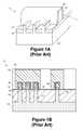
- FIG. 1Ais a perspective view of an illustrative prior art FinFET semiconductor device 100 that is formed above a semiconductor substrate 105 at an intermediate point during fabrication.
- the FinFET device 100includes three illustrative fins 110 , an isolation material 130 , a gate structure 115 , sidewall spacers 120 and a gate cap layer 125 .
- the fins 110have a three-dimensional configuration: a height, a width, and an axial length.
- the portions of the fins 110 covered by the gate structure 115are the channel regions of the FinFET device 100 , while the portions of the fins 110 positioned laterally outside of the spacers 120 are part of the source/drain regions of the device 100 .
- the portions of the fins 110 in the source/drain regionsmay have additional epi semiconductor material formed thereon in either a merged or unmerged condition.
- the gate structure 115is typically comprised of a layer of insulating material (not separately shown), e.g., a layer of high-k insulating material or silicon dioxide, and one or more conductive material layers (e.g., metal and/or polysilicon) that serve as the gate electrode for the device 100 .
- the fins 110have a three-dimensional configuration.
- the portions of the fins 110 covered by the gate structure 115is the channel region of the FinFET device 100 .
- additional epitaxial grown semiconductor materialmay be formed on the portions of the fins 110 that are positioned outside of the spacers 120 , i.e., the fins in the source/drain regions of the device 100 may have a merged, unmerged and or embedded condition. Forming the additional epi material on the fins 110 in the source/drain regions of the device reduces the resistance of source/drain regions and/or makes it easier to establish electrical contact to the source/drain regions.
- FIG. 1Billustrates a cross-sectional view of the device 100 taken across the fins in the source/drain regions of the devices in a direction corresponding to the gate width direction of the devices.
- the fins 110 shown in FIG. 1Aare so-called densely-spaced fins.
- An additional so-called isolated fin 135is illustrated representing a different region of the substrate 105 where the spacing between adjacent fins is larger.
- the densely-spaced fins 110may be part of a logic device or SRAM NFET, while the isolated fin 135 may be part of an SRAM PFET.
- Epitaxial material 140 , 145is formed on the fins 110 , 135 , respectively.
- a contact etch stop layer 148is formed above the dielectric layer 130 and the epitaxial material 140 , 145 .
- Placeholder contact structures 150 with cap layers 155were formed above the fins 110 , 135 by performing deposition and etching processes. Subsequently, a dielectric layer 160 was formed to fill the spaces between the placeholder contact structures 150 and planarized to expose the cap layers 155 .
- One material used for the dielectric layer 160is SiOC due to its favorable gap filling characteristics and its resistance to CD loss during the removal of the placeholder material 150 and/or the contact etch stop layer 148 for the contact replacement process.
- the removal rate for SiOC planarizationis limited by the chemical properties of the material and the slurry used. A lower removal rate reduces polishing uniformity across the wafer, especially in regions with different contact densities.
- the present disclosureis directed to various methods and resulting devices that may avoid, or at least reduce, the effects of one or more of the problems identified above.
- a methodincludes, among other things, forming a placeholder source/drain contact structure above a semiconductor material.
- a conformal deposition processis performed to form a liner layer above the placeholder contact structure.
- a dielectric layeris formed above the liner layer.
- a first planarization processis performed to remove material of the dielectric layer and expose a first top surface of the liner layer above the placeholder contact structure.
- a first cap layeris formed above the dielectric layer and the first top surface.
- a second planarization processis performed to remove material of the first cap layer and the liner layer to expose a second top surface of the placeholder contact structure.
- the placeholder contact structureis removed to define a contact recess in the dielectric layer.
- the sidewalls of the dielectric layer in the contact recessare covered by the liner layer.
- a conductive materialis formed in the contact recess.
- Another methodincludes, among other things, forming a fin in a semiconductor substrate.
- a placeholder contact structureis formed above the fin, the placeholder contact structure comprising a placeholder material and a first cap layer formed above the placeholder material.
- a conformal deposition processis performed to form a liner layer above the placeholder contact structure.
- a dielectric layeris formed above the liner layer.
- a first planarization processis performed to remove material of the dielectric layer and expose a first top surface of the liner layer above the placeholder contact structure.
- the dielectric layeris recessed to a level below a bottom surface of the first cap layer.
- a second cap layeris formed above the dielectric layer and the first top surface.
- a second planarization processis performed to remove material of the second cap layer and the liner layer to expose the first cap layer.
- the first cap layer and the placeholder materialare removed to define a recess in the dielectric layer.
- the sidewalls of the dielectric layer in the recessare covered by the liner layer.
- a conductive material
- One illustrative deviceincludes, among other things, a fin defined in a semiconductor substrate.
- a conductive materialis embedded in a recess defined in a dielectric material and contacts a portion of the fin.
- a liner layercomprising at least silicon, oxygen and carbon covers sidewalls of the recess without covering a bottom surface of the recess.
- the dielectric materialcomprises a material different than the liner layer.
- FIGS. 1A-1Bschematically depict an illustrative prior art finFET device
- FIGS. 2A-2Jdepict various methods disclosed herein of forming source/drain contacts for a semiconductor device using a liner and cap layer for placeholder source/drain contact structure planarization and replacement.
- the present disclosuregenerally relates to various methods of forming source/drain contacts for a semiconductor device such as a FinFET device or a nanowire device using a liner and cap layer for placeholder source/drain contact structure planarization and replacement and the resulting semiconductor devices.
- a semiconductor devicesuch as a FinFET device or a nanowire device
- the present methodis applicable to a variety of devices, including, but not limited to, logic devices, memory devices, etc.
- various illustrative embodiments of the methods and devices disclosed hereinwill now be described in more detail.
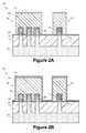
- FIGS. 2A-2Jillustrate various novel methods disclosed herein for forming an integrated circuit product 200 .
- the product 200includes a substrate 205 and fins 210 associated with a first transistor device defined in the substrate 205 .
- a fin 215 associated with a second transistor deviceis also defined in the substrate 205 .
- the views in FIGS. 2A-2Jare cross-sectional views taken across the fins 210 , 215 in the source/drain regions of the devices in a direction corresponding to the gate width direction of the devices.
- the number of fins 210 , 215 , and the spacing between finsmay vary depending on the particular characteristics of the device(s) being formed.
- a dielectric layer 220(e.g., silicon dioxide) defines an isolation structure between the fins 210 , 215 .
- Epitaxial regions 225 , 230are formed on the fins 210 , 215 , respectively.
- a contact etch stop layer 232is formed above the epitaxial regions 225 , 230 and the dielectric layer 220 .
- the particular structure and configuration of the fins and the manner in which they are formedmay vary depending upon the particular application. Thus, the presently disclosed inventions should not be considered to be limited to any such details.
- the substrate 205may have a variety of configurations, such as the depicted bulk silicon configuration.
- the substrate 205may also have a silicon-on-insulator (SOI) configuration that includes a bulk silicon layer, a buried insulation layer and an active layer, wherein semiconductor devices are formed in and above the active layer.
- SOIsilicon-on-insulator
- the substrate 205may be formed of silicon or silicon germanium or it may be made of materials other than silicon, such as germanium.
- the terms “substrate” or “semiconductor substrate”should be understood to cover all semiconducting materials and all forms of such materials.
- the substrate 205may have different layers.
- the fins 210 , 215may be formed in a process layer formed above the base layer of the substrate 205 .
- a replacement techniqueis used to form source/drain contacts for the fins 210 , 215 .
- Placeholder (or sacrificial) contact structures 235each including a placeholder material 240 (e.g., polysilicon) and a cap layer 245 (e.g., silicon nitride) were formed above the fins 210 , 215 in the source/drain regions.
- a layer of placeholder material 240 and a layer of cap layer 245 materialwere deposited and patterned to define the placeholder contact structures 235 in the source/drain regions of the fins 210 , 215 .
- the size of the placeholder contact structures 235may vary depending upon the particular application.
- FIG. 2Billustrates the product 200 after a conformal deposition process was performed to form a liner 250 (e.g., SiOC, SiCON) above the placeholder contact structures 235 .
- the liner 250may have a thickness that falls within the range of about 2-10 nm.
- FIG. 2Cillustrates the product 200 after a deposition process was performed to form a dielectric layer 255 (e.g., a polymer dielectric material such as Tonen SilaZene (TOSZ)) over the liner 240 .
- the material of the dielectric layer 255may vary and it may be selected for its gap-filling characteristics and its polishing rate characteristics. Generally, a material that allows a relatively high polishing rate reduces topography variations across the substrate 205 after a planarization process is performed.
- FIG. 2Dillustrates the product 200 after a planarization process was performed to planarize the dielectric layer 255 and expose the liner 250 .
- FIG. 2Eillustrates the product 200 after a timed recess etching process was performed to recess the dielectric layer 255 to a level below a bottom surface of the cap layer 245 .
- the amount of recessingmay vary depending upon the particular application.
- FIG. 2Fillustrates the product 200 after a deposition process was performed to form an additional cap layer 260 (e.g., SiOC, SiCON) above the liner 250 and the dielectric layer 255 .
- the cap layer 260may have a thickness that falls within the range of about 10-30 nm.
- the cap layer 260 and the liner 250may be made of the same material, but that is not required in all applications.
- the cap layer 260should be a material that exhibits good etch selectivity relative to the materials of the cap layer 245 and the dielectric layer 255 .
- FIG. 2Gillustrates the product 200 after a planarization process was performed on the cap layer 260 and the liner 250 to expose the cap layer 245 .
- FIG. 2Hillustrates the product 200 after multiple etch processes were performed to remove the cap layer 245 and the placeholder material 240 , thereby creating source/drain contact recesses 265 exposing the contact etch stop layer 232 above the fins 210 , 215 in the source/drain regions of the devices.
- the liner 250 and the cap layer 260protect the dielectric layer 255 during the etch processes to avoid affecting the CD of the recesses thereby created.
- FIG. 2Iillustrates the product after an etch process was performed to remove exposed portions of the contact etch stop layer 232 , thereby exposing the epitaxial material 225 , 230 .
- the liner 250 and the cap layer 260also protect the dielectric layer 255 during this etch process.
- Recessing the dielectric layer 255 prior to forming the cap layer 260enhances the protection in corner regions 270 of the dielectric layer 255 during the etch processes of FIGS. 2H and 2I .
- FIG. 2Jillustrates the integrated circuit product 200 after multiple processes were performed to form conductive contacts 275 in the source/drain contact recesses 265 .
- the conductive contacts 275may include multiple layers, such as one or more barrier layers (e.g., Ta, TaN, TiN, etc.) to prevent migration of any metal in the conductive contacts 275 into the liner 250 or the dielectric layer 255 , a metal seed layer (e.g., copper), a metal fill material (e.g., copper), a metal silicide material, etc.
- the processes for forming the conductive contacts 275may include a planarization process to remove excess conductive material disposed outside the recesses 265 . This planarization process may terminate on the cap layer 260 as illustrated in FIG. 2J , or alternatively, the planarization process may terminate on the top surface of the dielectric layer 255 , thereby removing the cap layer 260 (not shown).
Landscapes
- Engineering & Computer Science (AREA)
- Physics & Mathematics (AREA)
- Condensed Matter Physics & Semiconductors (AREA)
- General Physics & Mathematics (AREA)
- Computer Hardware Design (AREA)
- Microelectronics & Electronic Packaging (AREA)
- Power Engineering (AREA)
- Manufacturing & Machinery (AREA)
- Thin Film Transistor (AREA)
- Insulated Gate Type Field-Effect Transistor (AREA)
Abstract
Description
Claims (15)
Priority Applications (1)
| Application Number | Priority Date | Filing Date | Title |
|---|---|---|---|
| US14/751,718US9466723B1 (en) | 2015-06-26 | 2015-06-26 | Liner and cap layer for placeholder source/drain contact structure planarization and replacement |
Applications Claiming Priority (1)
| Application Number | Priority Date | Filing Date | Title |
|---|---|---|---|
| US14/751,718US9466723B1 (en) | 2015-06-26 | 2015-06-26 | Liner and cap layer for placeholder source/drain contact structure planarization and replacement |
Publications (1)
| Publication Number | Publication Date |
|---|---|
| US9466723B1true US9466723B1 (en) | 2016-10-11 |
Family
ID=57046673
Family Applications (1)
| Application Number | Title | Priority Date | Filing Date |
|---|---|---|---|
| US14/751,718Expired - Fee RelatedUS9466723B1 (en) | 2015-06-26 | 2015-06-26 | Liner and cap layer for placeholder source/drain contact structure planarization and replacement |
Country Status (1)
| Country | Link |
|---|---|
| US (1) | US9466723B1 (en) |
Cited By (15)
| Publication number | Priority date | Publication date | Assignee | Title |
|---|---|---|---|---|
| US9761491B1 (en) | 2016-12-06 | 2017-09-12 | Globalfoundries Inc. | Self-aligned deep contact for vertical FET |
| US9818875B1 (en)* | 2016-10-17 | 2017-11-14 | International Business Machines Corporation | Approach to minimization of strain loss in strained fin field effect transistors |
| US20170365674A1 (en)* | 2016-06-17 | 2017-12-21 | Taiwan Semiconductor Manufacturing Company, Ltd. | Self-aligned contact and manufacturing method thereof |
| US10043893B1 (en)* | 2017-08-03 | 2018-08-07 | Globalfoundries Inc. | Post gate silicon germanium channel condensation and method for producing the same |
| US10256089B2 (en) | 2017-06-19 | 2019-04-09 | Globalfoundries Inc. | Replacement contact cuts with an encapsulated low-K dielectric |
| DE102018106581A1 (en)* | 2017-11-30 | 2019-06-06 | Taiwan Semiconductor Manufacturing Co. Ltd. | Semiconductor device and method for its production |
| CN109860275A (en)* | 2017-11-30 | 2019-06-07 | 台湾积体电路制造股份有限公司 | Semiconductor device and method of manufacturing the same |
| US10559470B2 (en) | 2018-01-22 | 2020-02-11 | Globalfoundries Inc. | Capping structure |
| US10651089B2 (en) | 2018-02-12 | 2020-05-12 | International Business Machines Corporation | Low thermal budget top source and drain region formation for vertical transistors |
| TWI739065B (en)* | 2018-03-12 | 2021-09-11 | 美商格芯(美國)集成電路科技有限公司 | Methods, apparatus, and system for reducing gate cut gouging and/or gate height loss in semiconductor devices |
| US11164781B2 (en)* | 2018-07-11 | 2021-11-02 | Tokyo Electron Limited | ALD (atomic layer deposition) liner for via profile control and related applications |
| EP3940789A1 (en)* | 2020-07-10 | 2022-01-19 | Taiwan Semiconductor Manufacturing Co., Ltd. | Anchor-shaped backside via and method thereof |
| EP4109505A1 (en)* | 2021-06-25 | 2022-12-28 | INTEL Corporation | Back-side device contacts around epitaxial source/drain |
| DE102017116787B4 (en) | 2016-12-29 | 2023-08-17 | Taiwan Semiconductor Manufacturing Co. Ltd. | Semiconductor device and method for its manufacture |
| US12419079B2 (en) | 2022-10-04 | 2025-09-16 | International Business Machines Corporation | Field effect transistor with backside source/drain |
Citations (21)
| Publication number | Priority date | Publication date | Assignee | Title |
|---|---|---|---|---|
| US5955759A (en)* | 1997-12-11 | 1999-09-21 | International Business Machines Corporation | Reduced parasitic resistance and capacitance field effect transistor |
| US6083827A (en)* | 1998-12-15 | 2000-07-04 | United Microelectronics Corp. | Method for fabricating local interconnect |
| US20010017417A1 (en)* | 1995-12-08 | 2001-08-30 | Hideaki Kuroda | Semiconductor device with a condductive metal layer engaging not less than fifty percent of a source\drain region |
| US6288431B1 (en)* | 1997-04-04 | 2001-09-11 | Nippon Steel Corporation | Semiconductor device and a method of manufacturing the same |
| US20010022399A1 (en)* | 1997-03-31 | 2001-09-20 | Yasushi Koubuchi | Semiconductor integrated circuit device |
| US6359301B1 (en)* | 1997-06-25 | 2002-03-19 | Sony Corporation | Semiconductor device and method of manufacturing the same |
| US20020094610A1 (en)* | 2001-01-12 | 2002-07-18 | Hitachi, Ltd. | Method of producing a semiconductor integrated circuit device and the semiconductor integrated circuit device |
| US20030111686A1 (en)* | 2001-12-13 | 2003-06-19 | Nowak Edward J. | Method for forming asymmetric dual gate transistor |
| US20050026377A1 (en)* | 2003-07-31 | 2005-02-03 | Hirohisa Kawasaki | Semiconductor device with silicon-film fins and method of manufacturing the same |
| US20050124099A1 (en)* | 2003-12-09 | 2005-06-09 | International Business Machines Corporation | Selfaligned source/drain finfet process flow |
| US20050124120A1 (en)* | 2003-12-05 | 2005-06-09 | Yang Du | Method and circuit for multiplying signals with a transistor having more than one independent gate structure |
| US20050239242A1 (en)* | 2004-04-23 | 2005-10-27 | International Business Machines Corporation | structure and method of manufacturing a finFet device having stacked fins |
| US20050242406A1 (en)* | 2003-06-27 | 2005-11-03 | Hareland Scott A | Nonplanar device with stress incorporation layer and method of fabrication |
| US20070057325A1 (en)* | 2005-09-13 | 2007-03-15 | International Business Machines Corporation | Semiconductor FinFET structures with encapsulated gate electrodes and methods for forming such semiconductor FinFET structures |
| US20070108514A1 (en)* | 2003-04-28 | 2007-05-17 | Akira Inoue | Semiconductor device and method of fabricating the same |
| US20090001464A1 (en)* | 2007-06-27 | 2009-01-01 | International Business Machines Corporation | Finfet with top body contact |
| US7579272B2 (en)* | 2004-10-04 | 2009-08-25 | International Business Machines Corporation | Methods of forming low-k dielectric layers containing carbon nanostructures |
| US20120025289A1 (en)* | 2010-07-28 | 2012-02-02 | Jarrett Jun Liang | Metal control gate formation in non-volatile storage |
| US20120104514A1 (en)* | 2010-11-03 | 2012-05-03 | Samsung Electronics Co., Ltd. | Semiconductor Devices and Methods of Manufacturing the Same |
| US20130020658A1 (en)* | 2011-07-20 | 2013-01-24 | International Business Machines Corporation | Replacement gate electrode with planar work function material layers |
| US20130075821A1 (en)* | 2011-09-23 | 2013-03-28 | Globalfoundries Inc. | Semiconductor Device Comprising Replacement Gate Electrode Structures and Self-Aligned Contact Elements Formed by a Late Contact Fill |
- 2015
- 2015-06-26USUS14/751,718patent/US9466723B1/ennot_activeExpired - Fee Related
Patent Citations (21)
| Publication number | Priority date | Publication date | Assignee | Title |
|---|---|---|---|---|
| US20010017417A1 (en)* | 1995-12-08 | 2001-08-30 | Hideaki Kuroda | Semiconductor device with a condductive metal layer engaging not less than fifty percent of a source\drain region |
| US20010022399A1 (en)* | 1997-03-31 | 2001-09-20 | Yasushi Koubuchi | Semiconductor integrated circuit device |
| US6288431B1 (en)* | 1997-04-04 | 2001-09-11 | Nippon Steel Corporation | Semiconductor device and a method of manufacturing the same |
| US6359301B1 (en)* | 1997-06-25 | 2002-03-19 | Sony Corporation | Semiconductor device and method of manufacturing the same |
| US5955759A (en)* | 1997-12-11 | 1999-09-21 | International Business Machines Corporation | Reduced parasitic resistance and capacitance field effect transistor |
| US6083827A (en)* | 1998-12-15 | 2000-07-04 | United Microelectronics Corp. | Method for fabricating local interconnect |
| US20020094610A1 (en)* | 2001-01-12 | 2002-07-18 | Hitachi, Ltd. | Method of producing a semiconductor integrated circuit device and the semiconductor integrated circuit device |
| US20030111686A1 (en)* | 2001-12-13 | 2003-06-19 | Nowak Edward J. | Method for forming asymmetric dual gate transistor |
| US20070108514A1 (en)* | 2003-04-28 | 2007-05-17 | Akira Inoue | Semiconductor device and method of fabricating the same |
| US20050242406A1 (en)* | 2003-06-27 | 2005-11-03 | Hareland Scott A | Nonplanar device with stress incorporation layer and method of fabrication |
| US20050026377A1 (en)* | 2003-07-31 | 2005-02-03 | Hirohisa Kawasaki | Semiconductor device with silicon-film fins and method of manufacturing the same |
| US20050124120A1 (en)* | 2003-12-05 | 2005-06-09 | Yang Du | Method and circuit for multiplying signals with a transistor having more than one independent gate structure |
| US20050124099A1 (en)* | 2003-12-09 | 2005-06-09 | International Business Machines Corporation | Selfaligned source/drain finfet process flow |
| US20050239242A1 (en)* | 2004-04-23 | 2005-10-27 | International Business Machines Corporation | structure and method of manufacturing a finFet device having stacked fins |
| US7579272B2 (en)* | 2004-10-04 | 2009-08-25 | International Business Machines Corporation | Methods of forming low-k dielectric layers containing carbon nanostructures |
| US20070057325A1 (en)* | 2005-09-13 | 2007-03-15 | International Business Machines Corporation | Semiconductor FinFET structures with encapsulated gate electrodes and methods for forming such semiconductor FinFET structures |
| US20090001464A1 (en)* | 2007-06-27 | 2009-01-01 | International Business Machines Corporation | Finfet with top body contact |
| US20120025289A1 (en)* | 2010-07-28 | 2012-02-02 | Jarrett Jun Liang | Metal control gate formation in non-volatile storage |
| US20120104514A1 (en)* | 2010-11-03 | 2012-05-03 | Samsung Electronics Co., Ltd. | Semiconductor Devices and Methods of Manufacturing the Same |
| US20130020658A1 (en)* | 2011-07-20 | 2013-01-24 | International Business Machines Corporation | Replacement gate electrode with planar work function material layers |
| US20130075821A1 (en)* | 2011-09-23 | 2013-03-28 | Globalfoundries Inc. | Semiconductor Device Comprising Replacement Gate Electrode Structures and Self-Aligned Contact Elements Formed by a Late Contact Fill |
Cited By (26)
| Publication number | Priority date | Publication date | Assignee | Title |
|---|---|---|---|---|
| US20170365674A1 (en)* | 2016-06-17 | 2017-12-21 | Taiwan Semiconductor Manufacturing Company, Ltd. | Self-aligned contact and manufacturing method thereof |
| US10825907B2 (en) | 2016-06-17 | 2020-11-03 | Taiwan Semiconductor Manufacturing Company, Ltd. | Self-aligned contact and manufacturing method thereof |
| US10164032B2 (en)* | 2016-06-17 | 2018-12-25 | Taiwan Semiconductor Manufacturing Company, Ltd. | Self-aligned contact and manufacturing method thereof |
| US10446647B2 (en)* | 2016-10-17 | 2019-10-15 | International Business Machines Corporation | Approach to minimization of strain loss in strained fin field effect transistors |
| US9818875B1 (en)* | 2016-10-17 | 2017-11-14 | International Business Machines Corporation | Approach to minimization of strain loss in strained fin field effect transistors |
| US20180108771A1 (en)* | 2016-10-17 | 2018-04-19 | International Business Machines Corporation | Approach to minimization of strain loss in strained fin field effect transistors |
| US9761491B1 (en) | 2016-12-06 | 2017-09-12 | Globalfoundries Inc. | Self-aligned deep contact for vertical FET |
| DE102017116787B4 (en) | 2016-12-29 | 2023-08-17 | Taiwan Semiconductor Manufacturing Co. Ltd. | Semiconductor device and method for its manufacture |
| US10256089B2 (en) | 2017-06-19 | 2019-04-09 | Globalfoundries Inc. | Replacement contact cuts with an encapsulated low-K dielectric |
| US10043893B1 (en)* | 2017-08-03 | 2018-08-07 | Globalfoundries Inc. | Post gate silicon germanium channel condensation and method for producing the same |
| US10326007B2 (en)* | 2017-08-03 | 2019-06-18 | Globalfoundries Inc. | Post gate silicon germanium channel condensation and method for producing the same |
| CN109860275A (en)* | 2017-11-30 | 2019-06-07 | 台湾积体电路制造股份有限公司 | Semiconductor device and method of manufacturing the same |
| DE102018106581B4 (en)* | 2017-11-30 | 2020-07-09 | Taiwan Semiconductor Manufacturing Co. Ltd. | Semiconductor component and method for its production |
| DE102018106581A1 (en)* | 2017-11-30 | 2019-06-06 | Taiwan Semiconductor Manufacturing Co. Ltd. | Semiconductor device and method for its production |
| US11211492B2 (en)* | 2017-11-30 | 2021-12-28 | Taiwan Semiconductor Manufacturing Co., Ltd. | Method of manufacturing semiconductor devices having a SiGe epitaxtial layer containing Ga |
| US10923595B2 (en) | 2017-11-30 | 2021-02-16 | Taiwan Semiconductor Manufacturing Co., Ltd. | Semiconductor device having a SiGe epitaxial layer containing Ga |
| CN109860275B (en)* | 2017-11-30 | 2022-06-28 | 台湾积体电路制造股份有限公司 | Semiconductor device and method for manufacturing the same |
| US10559470B2 (en) | 2018-01-22 | 2020-02-11 | Globalfoundries Inc. | Capping structure |
| US10651089B2 (en) | 2018-02-12 | 2020-05-12 | International Business Machines Corporation | Low thermal budget top source and drain region formation for vertical transistors |
| US10777464B2 (en) | 2018-02-12 | 2020-09-15 | International Business Machines Corporation | Low thermal budget top source and drain region formation for vertical transistors |
| TWI739065B (en)* | 2018-03-12 | 2021-09-11 | 美商格芯(美國)集成電路科技有限公司 | Methods, apparatus, and system for reducing gate cut gouging and/or gate height loss in semiconductor devices |
| US11164781B2 (en)* | 2018-07-11 | 2021-11-02 | Tokyo Electron Limited | ALD (atomic layer deposition) liner for via profile control and related applications |
| US11742241B2 (en) | 2018-07-11 | 2023-08-29 | Tokyo Electron Limited | ALD (atomic layer deposition) liner for via profile control and related applications |
| EP3940789A1 (en)* | 2020-07-10 | 2022-01-19 | Taiwan Semiconductor Manufacturing Co., Ltd. | Anchor-shaped backside via and method thereof |
| EP4109505A1 (en)* | 2021-06-25 | 2022-12-28 | INTEL Corporation | Back-side device contacts around epitaxial source/drain |
| US12419079B2 (en) | 2022-10-04 | 2025-09-16 | International Business Machines Corporation | Field effect transistor with backside source/drain |
Similar Documents
| Publication | Publication Date | Title |
|---|---|---|
| US9466723B1 (en) | Liner and cap layer for placeholder source/drain contact structure planarization and replacement | |
| US9899268B2 (en) | Cap layer for spacer-constrained epitaxially grown material on fins of a FinFET device | |
| US9443956B2 (en) | Method for forming air gap structure using carbon-containing spacer | |
| US8841711B1 (en) | Methods of increasing space for contact elements by using a sacrificial liner and the resulting device | |
| US9478662B2 (en) | Gate and source/drain contact structures for a semiconductor device | |
| US8928048B2 (en) | Methods of forming semiconductor device with self-aligned contact elements and the resulting device | |
| US9882025B1 (en) | Methods of simultaneously forming bottom and top spacers on a vertical transistor device | |
| US9502286B2 (en) | Methods of forming self-aligned contact structures on semiconductor devices and the resulting devices | |
| US10276674B2 (en) | Method of forming a gate contact structure and source/drain contact structure for a semiconductor device | |
| US9825031B1 (en) | Methods of forming a high-k contact liner to improve effective via separation distance and the resulting devices | |
| US9824920B2 (en) | Methods of forming self-aligned contact structures by work function material layer recessing and the resulting devices | |
| US8809184B2 (en) | Methods of forming contacts for semiconductor devices using a local interconnect processing scheme | |
| US9530869B2 (en) | Methods of forming embedded source/drain regions on finFET devices | |
| US10777637B2 (en) | Integrated circuit product with a multi-layer single diffusion break and methods of making such products | |
| US10825741B2 (en) | Methods of forming single diffusion breaks on integrated circuit products comprised of FinFET devices and the resulting products | |
| US20180366553A1 (en) | Methods of forming an air gap adjacent a gate structure of a finfet device and the resulting devices | |
| US10872979B2 (en) | Spacer structures for a transistor device | |
| US11011604B2 (en) | Semiconductor device with recessed source/drain contacts and a gate contact positioned above the active region | |
| US10242982B2 (en) | Method for forming a protection device having an inner contact spacer and the resulting devices | |
| US20150340497A1 (en) | Methods of increasing silicide to epi contact areas and the resulting devices | |
| US20170345912A1 (en) | Methods of recessing a gate structure using oxidizing treatments during a recessing etch process | |
| US11610843B2 (en) | Well tap for an integrated circuit product and methods of forming such a well tap | |
| US10249616B2 (en) | Methods of forming a resistor structure between adjacent transistor gates on an integrated circuit product and the resulting devices | |
| US9589829B1 (en) | FinFET device including silicon oxycarbon isolation structure | |
| US10600876B2 (en) | Methods for chamfering work function material layers in gate cavities having varying widths |
Legal Events
| Date | Code | Title | Description |
|---|---|---|---|
| AS | Assignment | Owner name:GLOBALFOUNDRIES INC., CAYMAN ISLANDS Free format text:ASSIGNMENT OF ASSIGNORS INTEREST;ASSIGNORS:HUANG, HAIGOU;FANG, QIANG;LIU, JIN PING;AND OTHERS;SIGNING DATES FROM 20150622 TO 20150623;REEL/FRAME:035914/0679 | |
| STCF | Information on status: patent grant | Free format text:PATENTED CASE | |
| AS | Assignment | Owner name:WILMINGTON TRUST, NATIONAL ASSOCIATION, DELAWARE Free format text:SECURITY AGREEMENT;ASSIGNOR:GLOBALFOUNDRIES INC.;REEL/FRAME:049490/0001 Effective date:20181127 | |
| FEPP | Fee payment procedure | Free format text:MAINTENANCE FEE REMINDER MAILED (ORIGINAL EVENT CODE: REM.); ENTITY STATUS OF PATENT OWNER: LARGE ENTITY | |
| LAPS | Lapse for failure to pay maintenance fees | Free format text:PATENT EXPIRED FOR FAILURE TO PAY MAINTENANCE FEES (ORIGINAL EVENT CODE: EXP.); ENTITY STATUS OF PATENT OWNER: LARGE ENTITY | |
| STCH | Information on status: patent discontinuation | Free format text:PATENT EXPIRED DUE TO NONPAYMENT OF MAINTENANCE FEES UNDER 37 CFR 1.362 | |
| AS | Assignment | Owner name:GLOBALFOUNDRIES INC., CAYMAN ISLANDS Free format text:RELEASE BY SECURED PARTY;ASSIGNOR:WILMINGTON TRUST, NATIONAL ASSOCIATION;REEL/FRAME:054636/0001 Effective date:20201117 | |
| FP | Lapsed due to failure to pay maintenance fee | Effective date:20201011 | |
| AS | Assignment | Owner name:GLOBALFOUNDRIES U.S. INC., NEW YORK Free format text:RELEASE BY SECURED PARTY;ASSIGNOR:WILMINGTON TRUST, NATIONAL ASSOCIATION;REEL/FRAME:056987/0001 Effective date:20201117 |