US9462921B2 - Broken wafer recovery system - Google Patents
Broken wafer recovery systemDownload PDFInfo
- Publication number
- US9462921B2 US9462921B2US13/912,126US201313912126AUS9462921B2US 9462921 B2US9462921 B2US 9462921B2US 201313912126 AUS201313912126 AUS 201313912126AUS 9462921 B2US9462921 B2US 9462921B2
- Authority
- US
- United States
- Prior art keywords
- broken
- suction head
- chamber
- wafer
- inlet
- Prior art date
- Legal status (The legal status is an assumption and is not a legal conclusion. Google has not performed a legal analysis and makes no representation as to the accuracy of the status listed.)
- Active, expires
Links
Images


Classifications
- A—HUMAN NECESSITIES
- A47—FURNITURE; DOMESTIC ARTICLES OR APPLIANCES; COFFEE MILLS; SPICE MILLS; SUCTION CLEANERS IN GENERAL
- A47L—DOMESTIC WASHING OR CLEANING; SUCTION CLEANERS IN GENERAL
- A47L9/00—Details or accessories of suction cleaners, e.g. mechanical means for controlling the suction or for effecting pulsating action; Storing devices specially adapted to suction cleaners or parts thereof; Carrying-vehicles specially adapted for suction cleaners
- A47L9/28—Installation of the electric equipment, e.g. adaptation or attachment to the suction cleaner; Controlling suction cleaners by electric means
- H—ELECTRICITY
- H01—ELECTRIC ELEMENTS
- H01L—SEMICONDUCTOR DEVICES NOT COVERED BY CLASS H10
- H01L21/00—Processes or apparatus adapted for the manufacture or treatment of semiconductor or solid state devices or of parts thereof
- H01L21/67—Apparatus specially adapted for handling semiconductor or electric solid state devices during manufacture or treatment thereof; Apparatus specially adapted for handling wafers during manufacture or treatment of semiconductor or electric solid state devices or components ; Apparatus not specifically provided for elsewhere
- H01L21/67005—Apparatus not specifically provided for elsewhere
- H01L21/67242—Apparatus for monitoring, sorting or marking
- H01L21/67271—Sorting devices
- B—PERFORMING OPERATIONS; TRANSPORTING
- B08—CLEANING
- B08B—CLEANING IN GENERAL; PREVENTION OF FOULING IN GENERAL
- B08B5/00—Cleaning by methods involving the use of air flow or gas flow
- B08B5/04—Cleaning by suction, with or without auxiliary action
- H—ELECTRICITY
- H01—ELECTRIC ELEMENTS
- H01L—SEMICONDUCTOR DEVICES NOT COVERED BY CLASS H10
- H01L21/00—Processes or apparatus adapted for the manufacture or treatment of semiconductor or solid state devices or of parts thereof
- H01L21/67—Apparatus specially adapted for handling semiconductor or electric solid state devices during manufacture or treatment thereof; Apparatus specially adapted for handling wafers during manufacture or treatment of semiconductor or electric solid state devices or components ; Apparatus not specifically provided for elsewhere
- H01L21/67005—Apparatus not specifically provided for elsewhere
- H01L21/67242—Apparatus for monitoring, sorting or marking
- H01L21/67288—Monitoring of warpage, curvature, damage, defects or the like
- H—ELECTRICITY
- H01—ELECTRIC ELEMENTS
- H01L—SEMICONDUCTOR DEVICES NOT COVERED BY CLASS H10
- H01L21/00—Processes or apparatus adapted for the manufacture or treatment of semiconductor or solid state devices or of parts thereof
- H01L21/67—Apparatus specially adapted for handling semiconductor or electric solid state devices during manufacture or treatment thereof; Apparatus specially adapted for handling wafers during manufacture or treatment of semiconductor or electric solid state devices or components ; Apparatus not specifically provided for elsewhere
- H01L21/683—Apparatus specially adapted for handling semiconductor or electric solid state devices during manufacture or treatment thereof; Apparatus specially adapted for handling wafers during manufacture or treatment of semiconductor or electric solid state devices or components ; Apparatus not specifically provided for elsewhere for supporting or gripping
- H01L21/6838—Apparatus specially adapted for handling semiconductor or electric solid state devices during manufacture or treatment thereof; Apparatus specially adapted for handling wafers during manufacture or treatment of semiconductor or electric solid state devices or components ; Apparatus not specifically provided for elsewhere for supporting or gripping with gripping and holding devices using a vacuum; Bernoulli devices
Definitions
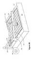
- the broken wafer recovery systemis provided on the flipping station 221 .
- the broken wafer recovery systemcan be in the form of those described with respect to FIGS. 2A and 2B above.
- various sensorshere sensors 244 , 246 and 248 , communicate with controller 205 to identify breakage of wafers. For example, if any of sensors 244 , 246 or 248 detects a broken wafer, the tray 204 is moved to the flipping mechanism and the suction head 254 is used to remove the broken wafer from the tray. Sensor 248 can be used to verify complete removal of the broken wafer from the tray, before the wafers are flipped and the tray proceeds into chamber 201 .
Landscapes
- Engineering & Computer Science (AREA)
- Physics & Mathematics (AREA)
- Condensed Matter Physics & Semiconductors (AREA)
- General Physics & Mathematics (AREA)
- Manufacturing & Machinery (AREA)
- Computer Hardware Design (AREA)
- Microelectronics & Electronic Packaging (AREA)
- Power Engineering (AREA)
- Mechanical Engineering (AREA)
- Container, Conveyance, Adherence, Positioning, Of Wafer (AREA)
- Cleaning Or Drying Semiconductors (AREA)
Abstract
Description
Claims (19)
Priority Applications (1)
| Application Number | Priority Date | Filing Date | Title |
|---|---|---|---|
| US13/912,126US9462921B2 (en) | 2011-05-24 | 2013-06-06 | Broken wafer recovery system |
Applications Claiming Priority (2)
| Application Number | Priority Date | Filing Date | Title |
|---|---|---|---|
| US13/115,064US8459276B2 (en) | 2011-05-24 | 2011-05-24 | Broken wafer recovery system |
| US13/912,126US9462921B2 (en) | 2011-05-24 | 2013-06-06 | Broken wafer recovery system |
Related Parent Applications (1)
| Application Number | Title | Priority Date | Filing Date |
|---|---|---|---|
| US13/115,064DivisionUS8459276B2 (en) | 2011-05-24 | 2011-05-24 | Broken wafer recovery system |
Publications (2)
| Publication Number | Publication Date |
|---|---|
| US20130269149A1 US20130269149A1 (en) | 2013-10-17 |
| US9462921B2true US9462921B2 (en) | 2016-10-11 |
Family
ID=46085474
Family Applications (2)
| Application Number | Title | Priority Date | Filing Date |
|---|---|---|---|
| US13/115,064ActiveUS8459276B2 (en) | 2011-05-24 | 2011-05-24 | Broken wafer recovery system |
| US13/912,126Active2032-10-26US9462921B2 (en) | 2011-05-24 | 2013-06-06 | Broken wafer recovery system |
Family Applications Before (1)
| Application Number | Title | Priority Date | Filing Date |
|---|---|---|---|
| US13/115,064ActiveUS8459276B2 (en) | 2011-05-24 | 2011-05-24 | Broken wafer recovery system |
Country Status (5)
| Country | Link |
|---|---|
| US (2) | US8459276B2 (en) |
| EP (1) | EP2528088B1 (en) |
| JP (1) | JP6080118B2 (en) |
| CN (1) | CN102810497B (en) |
| TW (1) | TWI470729B (en) |
Cited By (1)
| Publication number | Priority date | Publication date | Assignee | Title |
|---|---|---|---|---|
| CN110854051A (en)* | 2019-09-11 | 2020-02-28 | 芜湖德锐电子技术有限公司 | Chip picking device |
Families Citing this family (13)
| Publication number | Priority date | Publication date | Assignee | Title |
|---|---|---|---|---|
| JP5835722B2 (en) | 2009-12-10 | 2015-12-24 | オルボテック エルティ ソラー,エルエルシー | Automatic ranking multi-directional serial processor |
| US8459276B2 (en) | 2011-05-24 | 2013-06-11 | Orbotech LT Solar, LLC. | Broken wafer recovery system |
| TW201332871A (en)* | 2011-12-07 | 2013-08-16 | Intevac Inc | High load solar wafer loading device |
| US8863349B2 (en)* | 2012-04-18 | 2014-10-21 | King Fahd University Of Petroleum And Minerals | Steering and cleaning mechanism for reflector arrays |
| CN104103564B (en)* | 2013-04-15 | 2017-06-06 | 北京北方微电子基地设备工艺研究中心有限责任公司 | A kind of substrate transfer method and system |
| JP6186940B2 (en)* | 2013-06-26 | 2017-08-30 | 三星ダイヤモンド工業株式会社 | Method for transporting brittle material substrate |
| US10161033B2 (en)* | 2015-08-21 | 2018-12-25 | Taiwan Semiconductor Manufacturing Co., Ltd. | Method for cleaning load port of wafer processing apparatus |
| CN108111117A (en)* | 2017-12-21 | 2018-06-01 | 河南理工大学 | Solar power supply unit and system |
| CN107946220A (en)* | 2017-12-22 | 2018-04-20 | 君泰创新(北京)科技有限公司 | Cell piece slice turning device |
| FR3079761B1 (en)* | 2018-04-10 | 2022-02-04 | Commissariat Energie Atomique | SEMICONDUCTOR PAD AND/OR GLASS DEBRIS CLEANING AND COLLECTION ATTACHMENT |
| CN111710635B (en)* | 2020-08-19 | 2020-11-20 | 深圳新益昌科技股份有限公司 | Automatic Decrystallizing Machine and Decrystallizing Method |
| TWI795105B (en)* | 2021-11-30 | 2023-03-01 | 弘塑科技股份有限公司 | Crusher, wafer shaking device, and wafer cleaning system |
| CN114715657B (en)* | 2022-04-07 | 2023-09-12 | 九江聚鸿新材料有限公司 | Automatic slitting machine of blowing ejection of compact |
Citations (205)
| Publication number | Priority date | Publication date | Assignee | Title |
|---|---|---|---|---|
| US3158086A (en) | 1960-03-21 | 1964-11-24 | Ralph E Weimer | Apparatus for charging hamburger patties onto a griddle |
| JPS57211746A (en) | 1981-06-23 | 1982-12-25 | Fujitsu Ltd | Wafer conveying apparatus |
| US4490042A (en) | 1981-06-04 | 1984-12-25 | Wyatt Philip J | Method for determining the properties of wine |
| JPS60178639A (en) | 1984-02-27 | 1985-09-12 | Toshiba Seiki Kk | Selector for pellet |
| US4544642A (en) | 1981-04-30 | 1985-10-01 | Hitachi, Ltd. | Silicon carbide electrical insulator material of low dielectric constant |
| US4590042A (en) | 1984-12-24 | 1986-05-20 | Tegal Corporation | Plasma reactor having slotted manifold |
| DE3508516A1 (en) | 1985-03-09 | 1986-09-11 | Wolfgang 6108 Weiterstadt Köhler | Appliance for transferring a disc in the clean room |
| US4612077A (en) | 1985-07-29 | 1986-09-16 | The Perkin-Elmer Corporation | Electrode for plasma etching system |
| US4643629A (en) | 1984-10-30 | 1987-02-17 | Anelva Corporation | Automatic loader |
| US4694779A (en) | 1984-10-19 | 1987-09-22 | Tetron, Inc. | Reactor apparatus for semiconductor wafer processing |
| USH422H (en) | 1986-04-25 | 1988-02-02 | American Telephone And Telegraph Company, At&T Bell Laboratories | Apparatus for inverting articles and method for using same |
| US4752180A (en) | 1985-02-14 | 1988-06-21 | Kabushiki Kaisha Toshiba | Method and apparatus for handling semiconductor wafers |
| JPS63276239A (en) | 1987-05-08 | 1988-11-14 | Hitachi Ltd | wafer carrier jig |
| JPH01139771A (en) | 1987-08-14 | 1989-06-01 | Applied Materials Inc | Plasma enhanced chemical vapor deposition method |
| JPH01294868A (en) | 1988-01-30 | 1989-11-28 | Nec Corp | Vapor growth apparatus |
| US5084125A (en) | 1989-09-12 | 1992-01-28 | Matsushita Electric Industrial Co., Ltd. | Apparatus and method for producing semiconductor substrate |
| JPH0478125A (en) | 1990-07-20 | 1992-03-12 | Tokyo Electron Ltd | Vacuum treatment equipment |
| US5136975A (en) | 1990-06-21 | 1992-08-11 | Watkins-Johnson Company | Injector and method for delivering gaseous chemicals to a surface |
| US5167922A (en) | 1990-04-27 | 1992-12-01 | Pb Diagnostic Systems Inc. | Assay cartridge |
| JPH05109683A (en) | 1991-03-27 | 1993-04-30 | Mitsubishi Materials Corp | Removal of metallic impurity in semiconductor silicon wafer cleaning fluid |
| JPH0569162U (en) | 1992-02-28 | 1993-09-17 | セイコー電子工業株式会社 | Cluster type thin film processing equipment with buffer |
| US5288379A (en) | 1991-12-04 | 1994-02-22 | Anelva Corporation | Multi-chamber integrated process system |
| US5353495A (en) | 1992-11-16 | 1994-10-11 | Pfu Limited | Parts supply system applied to a versatile production line |
| US5404894A (en) | 1992-05-20 | 1995-04-11 | Tokyo Electron Kabushiki Kaisha | Conveyor apparatus |
| US5439524A (en) | 1993-04-05 | 1995-08-08 | Vlsi Technology, Inc. | Plasma processing apparatus |
| JPH088586A (en) | 1994-06-16 | 1996-01-12 | Rohm Co Ltd | Thin substrate transferring device |
| US5486080A (en) | 1994-06-30 | 1996-01-23 | Diamond Semiconductor Group, Inc. | High speed movement of workpieces in vacuum processing |
| US5551327A (en) | 1994-08-22 | 1996-09-03 | Hamby; William D. | Adjusting means for multi-blade cutting apparatus |
| US5558717A (en) | 1994-11-30 | 1996-09-24 | Applied Materials | CVD Processing chamber |
| JPH08316286A (en) | 1995-05-18 | 1996-11-29 | Plasma Syst:Kk | Plasma processing apparatus and operating method thereof |
| US5589002A (en) | 1994-03-24 | 1996-12-31 | Applied Materials, Inc. | Gas distribution plate for semiconductor wafer processing apparatus with means for inhibiting arcing |
| US5591269A (en) | 1993-06-24 | 1997-01-07 | Tokyo Electron Limited | Vacuum processing apparatus |
| US5595606A (en) | 1995-04-20 | 1997-01-21 | Tokyo Electron Limited | Shower head and film forming apparatus using the same |
| EP0768702A1 (en) | 1995-10-16 | 1997-04-16 | Applied Materials, Inc. | Gas injection slit nozzle for a plasma process reactor |
| US5624498A (en) | 1993-12-22 | 1997-04-29 | Samsung Electronics Co., Ltd. | Showerhead for a gas supplying apparatus |
| US5631573A (en) | 1994-09-20 | 1997-05-20 | Mitsubishi Denki Kabushiki Kaisha | Probe-type test handler |
| JPH09176856A (en) | 1995-12-22 | 1997-07-08 | Ulvac Japan Ltd | Sheet type vacuum treating apparatus |
| US5679055A (en) | 1996-05-31 | 1997-10-21 | Memc Electronic Materials, Inc. | Automated wafer lapping system |
| JPH09283983A (en) | 1996-04-10 | 1997-10-31 | Matsushita Electric Ind Co Ltd | Semiconductor chip pickup method and pickup device |
| US5690742A (en) | 1994-09-06 | 1997-11-25 | Komatsu Electronic Metals Co., Ltd. | Susceptor for an epitaxial growth apparatus |
| US5695564A (en) | 1994-08-19 | 1997-12-09 | Tokyo Electron Limited | Semiconductor processing system |
| US5756155A (en) | 1996-01-22 | 1998-05-26 | Taiwan Semiconductor Manufacturing Company, Ltd. | Combination nozzle and vacuum hood that is self cleaning |
| US5795399A (en) | 1994-06-30 | 1998-08-18 | Kabushiki Kaisha Toshiba | Semiconductor device manufacturing apparatus, method for removing reaction product, and method of suppressing deposition of reaction product |
| US5846332A (en) | 1996-07-12 | 1998-12-08 | Applied Materials, Inc. | Thermally floating pedestal collar in a chemical vapor deposition chamber |
| US5855468A (en) | 1995-12-22 | 1999-01-05 | Navistar International Transportation Corp. | Method and apparatus for setting foundry core assemblies |
| US5885356A (en) | 1994-11-30 | 1999-03-23 | Applied Materials, Inc. | Method of reducing residue accumulation in CVD chamber using ceramic lining |
| JPH11204813A (en) | 1998-01-12 | 1999-07-30 | Semiconductor Energy Lab Co Ltd | Manufacture of photoelectric converter |
| US5944940A (en) | 1996-07-09 | 1999-08-31 | Gamma Precision Technology, Inc. | Wafer transfer system and method of using the same |
| US5968275A (en) | 1997-06-25 | 1999-10-19 | Lam Research Corporation | Methods and apparatus for passivating a substrate in a plasma reactor |
| US5989346A (en) | 1995-12-12 | 1999-11-23 | Tokyo Electron Limited | Semiconductor processing apparatus |
| US5996528A (en) | 1996-07-02 | 1999-12-07 | Novellus Systems, Inc. | Method and apparatus for flowing gases into a manifold at high potential |
| CN1250490A (en) | 1997-03-24 | 2000-04-12 | 克里研究公司 | Susceptor Design for SiC Thin Films |
| US6050506A (en) | 1998-02-13 | 2000-04-18 | Applied Materials, Inc. | Pattern of apertures in a showerhead for chemical vapor deposition |
| WO2000022655A1 (en) | 1998-10-15 | 2000-04-20 | Applied Materials, Inc. | Detection of wafer fragments in a wafer processing apparatus |
| US6064629A (en) | 1989-09-01 | 2000-05-16 | Quantronix, Inc. | Object detection apparatus and method |
| JP2000208587A (en) | 1999-01-18 | 2000-07-28 | Tokyo Ohka Kogyo Co Ltd | Apparatus and method for transferring boards |
| JP2000223546A (en) | 1999-02-02 | 2000-08-11 | Dainippon Screen Mfg Co Ltd | Substrate processor |
| US6110287A (en) | 1993-03-31 | 2000-08-29 | Tokyo Electron Limited | Plasma processing method and plasma processing apparatus |
| US6113984A (en) | 1996-08-07 | 2000-09-05 | Concept Systems Design, Inc. | Gas injection system for CVD reactors |
| US6135102A (en) | 1997-05-20 | 2000-10-24 | Tokyo Seimitsu Co., Ltd. | Wafer collecting apparatus |
| US6148761A (en) | 1998-06-16 | 2000-11-21 | Applied Materials, Inc. | Dual channel gas distribution plate |
| US6159301A (en) | 1997-12-17 | 2000-12-12 | Asm Japan K.K. | Substrate holding apparatus for processing semiconductor |
| US6176668B1 (en) | 1998-05-20 | 2001-01-23 | Applied Komatsu Technology, Inc. | In-situ substrate transfer shuttle |
| US6202589B1 (en) | 1998-05-29 | 2001-03-20 | Advanced Micro Devices, Inc. | Grounding mechanism which maintains a low resistance electrical ground path between a plate electrode and an etch chamber |
| US6206972B1 (en) | 1999-07-08 | 2001-03-27 | Genus, Inc. | Method and apparatus for providing uniform gas delivery to substrates in CVD and PECVD processes |
| US20010000747A1 (en) | 1998-05-20 | 2001-05-03 | Applied Komatsu Technology, Inc. | Multi-function chamber for a substrate processing system |
| US6245192B1 (en) | 1999-06-30 | 2001-06-12 | Lam Research Corporation | Gas distribution apparatus for semiconductor processing |
| US6267839B1 (en) | 1999-01-12 | 2001-07-31 | Applied Materials, Inc. | Electrostatic chuck with improved RF power distribution |
| JP2001210695A (en) | 2000-01-28 | 2001-08-03 | Anelva Corp | Substrate transfer equipment for substrate processing equipment |
| US6286230B1 (en) | 1998-07-13 | 2001-09-11 | Applied Komatsu Technology, Inc. | Method of controlling gas flow in a substrate processing system |
| JP2001284258A (en) | 2000-03-30 | 2001-10-12 | Hitachi Kokusai Electric Inc | Semiconductor manufacturing equipment |
| US6302965B1 (en) | 2000-08-15 | 2001-10-16 | Applied Materials, Inc. | Dispersion plate for flowing vaporizes compounds used in chemical vapor deposition of films onto semiconductor surfaces |
| US6323616B1 (en) | 1999-03-15 | 2001-11-27 | Berkeley Process Control, Inc. | Self teaching robotic wafer handling system |
| US20020000196A1 (en) | 2000-06-24 | 2002-01-03 | Park Young-Hoon | Reactor for depositing thin film on wafer |
| CN1330507A (en) | 2000-04-26 | 2002-01-09 | 尤纳克西斯巴尔策斯公司 | Radio frequency plasma generator |
| JP2002043404A (en) | 2000-07-27 | 2002-02-08 | Anelva Corp | Vacuum processing equipment tray and vacuum processing equipment |
| US6361648B1 (en) | 1999-06-18 | 2002-03-26 | Applied Materials, Inc. | Wafer transfer station for a chemical mechanical polisher |
| US20020080291A1 (en) | 2000-12-27 | 2002-06-27 | Nobuyuki Takahashi | Interback-type substrate processing device |
| US6436193B1 (en) | 1999-04-07 | 2002-08-20 | Tokyo Electron Limited | Gas processing apparatus baffle member, and gas processing method |
| US6435798B1 (en) | 1999-04-09 | 2002-08-20 | Asm Japan K.K. | Semiconductor processing apparatus with substrate-supporting mechanism |
| JP2002256439A (en) | 2001-03-06 | 2002-09-11 | Hitachi Kokusai Electric Inc | Substrate processing equipment |
| JP2002270880A (en) | 2001-03-14 | 2002-09-20 | Shin Etsu Handotai Co Ltd | Solar cell module and method of manufacturing the same |
| JP2002288888A (en) | 2001-03-26 | 2002-10-04 | Anelva Corp | Substrate transfer apparatus and substrate processing apparatus using the same |
| US6471779B1 (en) | 1999-04-30 | 2002-10-29 | Ngk Insulators, Ltd. | Gas feed ceramic structure for semiconductor-producing apparatus |
| US6486444B1 (en) | 1999-06-03 | 2002-11-26 | Applied Materials, Inc. | Load-lock with external staging area |
| US20030003767A1 (en) | 2001-06-29 | 2003-01-02 | Plasmion Corporation | High throughput hybrid deposition system and method using the same |
| JP2003007682A (en) | 2001-06-25 | 2003-01-10 | Matsushita Electric Ind Co Ltd | Electrode member for plasma processing equipment |
| EP1278230A2 (en) | 2001-07-16 | 2003-01-22 | Applied Materials, Inc. | Dual wafer load lock |
| JP2003028142A (en) | 2001-07-19 | 2003-01-29 | Konica Corp | Positioning mechanism and image forming device |
| US6517691B1 (en) | 1998-08-20 | 2003-02-11 | Intevac, Inc. | Substrate processing system |
| JP2003059999A (en) | 2001-08-14 | 2003-02-28 | Tokyo Electron Ltd | Treating system |
| US20030068215A1 (en) | 2001-10-05 | 2003-04-10 | Sumitomo Heavy Industries, Ltd. | Substrate transfer device |
| US6556715B1 (en) | 1999-10-29 | 2003-04-29 | Unisys Corporation | Method for CCITT compression of image data |
| US20030106574A1 (en) | 2001-07-13 | 2003-06-12 | Michael Krolak | Clean method and apparatus for vacuum holding of substrates |
| US20030111961A1 (en) | 2001-12-19 | 2003-06-19 | Applied Materials, Inc. | Gas distribution plate electrode for a plasma reactor |
| US20030113187A1 (en) | 2001-12-14 | 2003-06-19 | Applied Materials, Inc. | Dual robot processing system |
| US20030140851A1 (en) | 2002-01-25 | 2003-07-31 | Applied Materials, Inc. | Gas distribution showerhead |
| JP2003258058A (en) | 2002-02-27 | 2003-09-12 | Anelva Corp | Operation method of substrate processing equipment |
| JP2003282462A (en) | 2002-03-27 | 2003-10-03 | Kyocera Corp | Shower plate, method of manufacturing the same, and shower head using the same |
| CN1446742A (en) | 2002-03-26 | 2003-10-08 | 株式会社日立高新技术 | Substrate conveying method and device thereof |
| US20040060514A1 (en) | 2002-01-25 | 2004-04-01 | Applied Materials, Inc. A Delaware Corporation | Gas distribution showerhead |
| US6719517B2 (en) | 2001-12-04 | 2004-04-13 | Brooks Automation | Substrate processing apparatus with independently configurable integral load locks |
| US6722834B1 (en) | 1997-10-08 | 2004-04-20 | Applied Materials, Inc. | Robot blade with dual offset wafer supports |
| US6746198B2 (en) | 1998-05-20 | 2004-06-08 | Applied Materials, Inc. | Substrate transfer shuttle |
| JP2004200421A (en) | 2002-12-18 | 2004-07-15 | Sharp Corp | Plasma CVD apparatus, film forming method using the same, and method for manufacturing semiconductor device |
| US20040163761A1 (en) | 2002-06-20 | 2004-08-26 | Strang Eric J | Directed gas injection apparatus for semiconductor processing |
| US20040197184A1 (en) | 2003-03-19 | 2004-10-07 | Akira Sugiyama | Workpiece transport apparatus |
| JP2004327761A (en) | 2003-04-25 | 2004-11-18 | Sumitomo Mitsubishi Silicon Corp | Susceptor for epitaxial growth |
| US6821563B2 (en) | 2002-10-02 | 2004-11-23 | Applied Materials, Inc. | Gas distribution system for cyclical layer deposition |
| WO2005001925A1 (en) | 2003-06-26 | 2005-01-06 | Tokyo Electron Limited | Vacuum processing device operating method |
| US20050011447A1 (en) | 2003-07-14 | 2005-01-20 | Tokyo Electron Limited | Method and apparatus for delivering process gas to a process chamber |
| US6849555B2 (en) | 2001-03-13 | 2005-02-01 | Samsung Electronics Co., Ltd. | Wafer processing apparatus and wafer processing method using the same |
| CN1582488A (en) | 2001-01-22 | 2005-02-16 | 东京毅力科创株式会社 | Treatment device and treatment method |
| US6872259B2 (en) | 2000-03-30 | 2005-03-29 | Tokyo Electron Limited | Method of and apparatus for tunable gas injection in a plasma processing system |
| US6902647B2 (en) | 2002-08-29 | 2005-06-07 | Asm International N.V. | Method of processing substrates with integrated weighing steps |
| US20050150601A1 (en) | 2004-01-12 | 2005-07-14 | Srivastava Aseem K. | Gas distribution plate assembly for plasma reactors |
| US20050160991A1 (en) | 2003-12-22 | 2005-07-28 | Toshiba Ceramics Co., Ltd. | Barrel type susceptor |
| CN1650416A (en) | 2002-05-23 | 2005-08-03 | 安内华株式会社 | Substrate processing device and processing method |
| JP2005211865A (en) | 2004-02-02 | 2005-08-11 | Masato Toshima | Plasma processing apparatus |
| US20050183666A1 (en) | 2004-02-20 | 2005-08-25 | Asm Japan K.K. | Shower plate having projections and plasma CVD apparatus using same |
| CN1674220A (en) | 2004-03-24 | 2005-09-28 | 周星工程股份有限公司 | Apparatus for manufacturing substrate |
| US20050263066A1 (en) | 2004-01-26 | 2005-12-01 | Dmitry Lubomirsky | Apparatus for electroless deposition of metals onto semiconductor substrates |
| CN1734711A (en) | 2004-08-11 | 2006-02-15 | 株式会社岛津制作所 | Vacuum treatment device |
| JP2006058769A (en) | 2004-08-23 | 2006-03-02 | Sony Corp | Collapsible mount type lens barrel and imaging apparatus |
| US7010388B2 (en) | 2003-05-22 | 2006-03-07 | Axcelis Technologies, Inc. | Work-piece treatment system having load lock and buffer |
| US7042553B2 (en) | 2003-10-01 | 2006-05-09 | Samsung Electronics Co., Ltd. | Apparatus for conveying substrates |
| US20060102081A1 (en) | 2004-11-16 | 2006-05-18 | Sumitomo Electric Industries, Ltd. | Wafer Guide, MOCVD Equipment, and Nitride Semiconductor Growth Method |
| US20060137609A1 (en) | 2004-09-13 | 2006-06-29 | Puchacz Jerzy P | Multi-single wafer processing apparatus |
| US20060177288A1 (en) | 2005-02-09 | 2006-08-10 | Parker N W | Multiple loadlocks and processing chamber |
| US20060197235A1 (en) | 2000-06-08 | 2006-09-07 | Farnworth Warren M | Electronic device components including protective layers on surfaces thereof |
| US20060236929A1 (en) | 2002-11-15 | 2006-10-26 | Seiji Katsuoka | Substrate processing apparatus and substrate processing method |
| JP2006332536A (en) | 2005-05-30 | 2006-12-07 | Shin Etsu Handotai Co Ltd | Device and method of inspecting cracking in wafer and manufacturing method of wafer |
| US20060286193A1 (en) | 2005-05-24 | 2006-12-21 | Takashi Ando | Imprint device and microstructure transfer method |
| US20070017445A1 (en) | 2005-07-19 | 2007-01-25 | Takako Takehara | Hybrid PVD-CVD system |
| TW200710928A (en) | 2005-05-13 | 2007-03-16 | Tes Co Ltd | Gas exhaust system and semiconductor manufacturing apparatus and method for manufacturing thin film using the same |
| US7214027B2 (en) | 2003-10-16 | 2007-05-08 | Varian Semiconductor Equipment Associates, Inc. | Wafer handler method and system |
| JP2007112626A (en) | 2005-09-20 | 2007-05-10 | Olympus Corp | Substrate carrying device, substrate inspection device and substrate carrying method |
| JP2007123684A (en) | 2005-10-31 | 2007-05-17 | Masato Toshima | Substrate treatment device |
| US20070119393A1 (en) | 2005-11-28 | 2007-05-31 | Ashizawa Kengo | Vacuum processing system |
| US20070151516A1 (en) | 2006-01-03 | 2007-07-05 | Law Kam S | Chemical vapor deposition apparatus and electrode plate thereof |
| WO2007077765A1 (en) | 2005-12-28 | 2007-07-12 | Sharp Kabushiki Kaisha | Stage apparatus and plasma processing apparatus |
| WO2007084124A1 (en) | 2006-01-18 | 2007-07-26 | Applied Materials, Inc. | Sensors for dynamically detecting substrate breakage and misalignment of a moving substrate |
| US20070181531A1 (en) | 2006-02-06 | 2007-08-09 | Tokyo Electron Limited | Plasma processing apparatus and plasma processing method |
| US20070207014A1 (en) | 2006-03-04 | 2007-09-06 | Masato Toshima | Substrate processing apparatus |
| US7270713B2 (en) | 2003-01-07 | 2007-09-18 | Applied Materials, Inc. | Tunable gas distribution plate assembly |
| US20070215048A1 (en) | 2006-03-16 | 2007-09-20 | Kenji Suzuki | Method and apparatus for reducing particle contamination in a deposition system |
| US7283660B2 (en) | 2000-11-08 | 2007-10-16 | Orbotech, Ltd. | Multi-layer printed circuit board fabrication system and method |
| US7290978B2 (en) | 2004-06-09 | 2007-11-06 | N&K Technology Inc. | Photomask flipper and single direction inspection device for dual side photomask inspection |
| WO2007126289A1 (en) | 2006-05-03 | 2007-11-08 | New Power Plasma Co., Ltd. | Substrate transfer equipment and high speed substrate processing system using the same |
| US20070261956A1 (en) | 2006-05-12 | 2007-11-15 | Applied Materials Gmbh & Co. Kg | Coating installation with carrier for substrate coating |
| US20080014055A1 (en) | 2003-11-10 | 2008-01-17 | Van Der Meulen Peter | Bypass thermal adjuster for vacuum semiconductor processing |
| US20080066683A1 (en) | 2006-09-19 | 2008-03-20 | General Electric Company | Assembly with Enhanced Thermal Uniformity and Method For Making Thereof |
| US20080090417A1 (en) | 2006-10-16 | 2008-04-17 | Lam Research Corporation | Upper electrode backing member with particle reducing features |
| US20080099448A1 (en) | 2006-10-16 | 2008-05-01 | Lam Research Corporation | Quartz guard ring |
| US20080138175A1 (en) | 2006-12-06 | 2008-06-12 | Axcelis Technologies, Inc. | High throughput wafer notch aligner |
| US20080196666A1 (en) | 2007-02-20 | 2008-08-21 | Masato Toshima | Shower head and cvd apparatus using the same |
| TW200835638A (en) | 2006-12-06 | 2008-09-01 | Axcelis Tech Inc | High throughput serial wafer handling end station |
| US20080213477A1 (en) | 2007-03-02 | 2008-09-04 | Arno Zindel | Inline vacuum processing apparatus and method for processing substrates therein |
| US20080233283A1 (en) | 2007-03-22 | 2008-09-25 | Yong-Sup Choi | Apparatus for depositing protective layer and depositing method using the apparatus |
| US20090045182A1 (en) | 2007-08-15 | 2009-02-19 | Lerner Alexander N | Pulsed laser anneal system architecture |
| CN101413112A (en) | 2007-10-16 | 2009-04-22 | 应用材料股份有限公司 | Multi-gas straight channel showerhead |
| WO2009052002A1 (en) | 2007-10-16 | 2009-04-23 | Applied Materials, Inc. | Multi-gas concentric injection showerhead |
| US20090104374A1 (en) | 2004-08-04 | 2009-04-23 | Canon Anelva Corporation | Substrate Processing Method Using A Substrate Processing Apparatus |
| US20090106968A1 (en) | 2007-10-24 | 2009-04-30 | Oc Oerlikon Balzers Ag | Method for manufacturing workpieces and apparatus |
| CN101423936A (en) | 2007-10-16 | 2009-05-06 | 应用材料股份有限公司 | Spray head with multiple gas spiral passages |
| US20090179085A1 (en) | 2008-01-10 | 2009-07-16 | Applied Materials, Inc. | Heated showerhead assembly |
| US20090181593A1 (en) | 2004-06-29 | 2009-07-16 | Kim Deuk Soo | Robot for transfer of glass |
| WO2009119096A1 (en) | 2008-03-27 | 2009-10-01 | 株式会社ニコン | Joining device and joining method |
| WO2009119580A1 (en) | 2008-03-25 | 2009-10-01 | Toshima Masato | Processing apparatus and processing method |
| WO2009130790A1 (en) | 2008-04-25 | 2009-10-29 | キヤノンアネルバ株式会社 | Tray transfer type inline film forming apparatus |
| JP2009267012A (en) | 2008-04-24 | 2009-11-12 | Canon Anelva Corp | Vacuum processing apparatus, and vacuum processing method |
| JP2009540561A (en) | 2006-06-20 | 2009-11-19 | ソスル カンパニー, リミテッド | Plasma etching chamber |
| US20090309905A1 (en) | 2006-05-12 | 2009-12-17 | Chiyoshi Yoshioka | Droplet Discharging and Drawing Apparatus |
| US20100068011A1 (en) | 2006-12-05 | 2010-03-18 | Shimadzu Corporation | Pallet conveyance device and substrate inspection device |
| US20100076601A1 (en) | 2006-11-09 | 2010-03-25 | Kengo Matsuo | Frog-leg-arm robot and control method thereof |
| US20100087028A1 (en) | 2008-10-07 | 2010-04-08 | Applied Materials, Inc. | Advanced platform for processing crystalline silicon solar cells |
| US20100089319A1 (en) | 2008-10-09 | 2010-04-15 | Applied Materials, Inc. | Rf return path for large plasma processing chamber |
| US20100136261A1 (en) | 2008-12-03 | 2010-06-03 | Applied Materials, Inc. | Modulation of rf returning straps for uniformity control |
| TW201026583A (en) | 2009-01-09 | 2010-07-16 | Chi Mei Optoelectronics Corp | Transmission apparatus |
| WO2010091205A2 (en) | 2009-02-04 | 2010-08-12 | Applied Materials, Inc. | Ground return for plasma processes |
| US20100203242A1 (en) | 2009-02-06 | 2010-08-12 | Applied Materials, Inc. | self-cleaning susceptor for solar cell processing |
| US20100202860A1 (en) | 2009-02-09 | 2010-08-12 | Asm America, Inc. | Method and apparatus for minimizing contamination in semiconductor processing chamber |
| US20100220304A1 (en) | 2007-11-15 | 2010-09-02 | Mikihito Mukai | Mask case, transport apparatus, exposure apparatus, mask transport method, and device production method |
| US7806641B2 (en) | 2007-08-30 | 2010-10-05 | Ascentool, Inc. | Substrate processing system having improved substrate transport system |
| WO2010127038A2 (en) | 2009-04-29 | 2010-11-04 | Applied Materials, Inc. | End effector for handling substrates |
| US7841820B2 (en) | 2001-08-31 | 2010-11-30 | Crossing Automation, Inc. | Universal modular wafer transport system |
| US20100301088A1 (en) | 2007-09-08 | 2010-12-02 | Stephen Maher | Glass Breaking Device |
| US7845529B2 (en) | 2003-12-04 | 2010-12-07 | Mitsuboshi Diamond Industrial Co., Ltd. | Method for processing substrate, apparatus for processing substrate, method for conveying substrate and mechanism for conveying substrate |
| KR20100130838A (en) | 2009-06-04 | 2010-12-14 | 주식회사 에스에프에이 | In-line solar cell manufacturing plasma processing device |
| US20110011338A1 (en) | 2009-07-15 | 2011-01-20 | Applied Materials, Inc. | Flow control features of cvd chambers |
| EP2312613A2 (en) | 2009-10-15 | 2011-04-20 | Orbotech LT Solar, LLC | Showerhead assembly for plasma processing chamber |
| EP2333814A2 (en) | 2009-12-10 | 2011-06-15 | Orbotech LT Solar, LLC | Auto-sequencing multi-directional inline processing apparatus |
| US20110188974A1 (en) | 2008-07-15 | 2011-08-04 | Ulvac Technologies, Inc. | Work-piece transfer systems and methods |
| US20110313565A1 (en) | 2010-06-17 | 2011-12-22 | Semes Co., Ltd. | Substrate Processing Apparatus And Method For Loading And Unloading Substrates |
| EP2400537A2 (en) | 2010-06-25 | 2011-12-28 | Orbotech LT Solar, LLC | Susceptor for plasma processing chamber |
| US8152923B2 (en) | 2007-01-12 | 2012-04-10 | Veeco Instruments Inc. | Gas treatment systems |
| US8246284B2 (en) | 2009-03-05 | 2012-08-21 | Applied Materials, Inc. | Stacked load-lock apparatus and method for high throughput solar cell manufacturing |
| US20120267049A1 (en) | 2011-04-25 | 2012-10-25 | Craig Lyle Stevens | Grounding assembly for vacuum processing apparatus |
| US8307972B2 (en) | 2008-02-14 | 2012-11-13 | Mag Ias Gmbh | Feed and removal system for machine tools |
| EP2528088A2 (en) | 2011-05-24 | 2012-11-28 | Orbotech LT Solar, LLC | Broken wafer recovery system |
| KR20120131105A (en) | 2011-05-24 | 2012-12-04 | 오보텍 엘티 솔라 엘엘씨 | Broken wafer recovery system |
| US8408858B2 (en) | 2007-08-30 | 2013-04-02 | Ascentool International Limited | Substrate processing system having improved substrate transport system |
| US8454850B2 (en) | 2009-09-02 | 2013-06-04 | Air Products And Chemicals, Inc. | Method for the removal of surface oxides by electron attachment |
| US20140064886A1 (en) | 2012-08-30 | 2014-03-06 | Orbotech LT Solar, LLC. | System, architecture and method for simultaneous transfer and process of substrates |
| JP5613302B2 (en) | 2007-10-23 | 2014-10-22 | オルボテック エルティ ソラー,エルエルシー | Work processing device |
Family Cites Families (1)
| Publication number | Priority date | Publication date | Assignee | Title |
|---|---|---|---|---|
| TWM366667U (en)* | 2009-05-25 | 2009-10-11 | Aidc Aerospace Ind Dev Corp | Auto movement and inspection device for solar energy panel |
- 2011
- 2011-05-24USUS13/115,064patent/US8459276B2/enactiveActive
- 2012
- 2012-05-07TWTW101116209Apatent/TWI470729B/ennot_activeIP Right Cessation
- 2012-05-15EPEP12168068.0Apatent/EP2528088B1/ennot_activeNot-in-force
- 2012-05-23JPJP2012117853Apatent/JP6080118B2/ennot_activeExpired - Fee Related
- 2012-05-24CNCN201210163936.7Apatent/CN102810497B/ennot_activeExpired - Fee Related
- 2013
- 2013-06-06USUS13/912,126patent/US9462921B2/enactiveActive
Patent Citations (278)
| Publication number | Priority date | Publication date | Assignee | Title |
|---|---|---|---|---|
| US3158086A (en) | 1960-03-21 | 1964-11-24 | Ralph E Weimer | Apparatus for charging hamburger patties onto a griddle |
| US4544642A (en) | 1981-04-30 | 1985-10-01 | Hitachi, Ltd. | Silicon carbide electrical insulator material of low dielectric constant |
| US4490042A (en) | 1981-06-04 | 1984-12-25 | Wyatt Philip J | Method for determining the properties of wine |
| JPS57211746A (en) | 1981-06-23 | 1982-12-25 | Fujitsu Ltd | Wafer conveying apparatus |
| JPS60178639A (en) | 1984-02-27 | 1985-09-12 | Toshiba Seiki Kk | Selector for pellet |
| US4694779A (en) | 1984-10-19 | 1987-09-22 | Tetron, Inc. | Reactor apparatus for semiconductor wafer processing |
| US4643629A (en) | 1984-10-30 | 1987-02-17 | Anelva Corporation | Automatic loader |
| US4590042A (en) | 1984-12-24 | 1986-05-20 | Tegal Corporation | Plasma reactor having slotted manifold |
| US4752180A (en) | 1985-02-14 | 1988-06-21 | Kabushiki Kaisha Toshiba | Method and apparatus for handling semiconductor wafers |
| DE3508516A1 (en) | 1985-03-09 | 1986-09-11 | Wolfgang 6108 Weiterstadt Köhler | Appliance for transferring a disc in the clean room |
| US4612077A (en) | 1985-07-29 | 1986-09-16 | The Perkin-Elmer Corporation | Electrode for plasma etching system |
| USH422H (en) | 1986-04-25 | 1988-02-02 | American Telephone And Telegraph Company, At&T Bell Laboratories | Apparatus for inverting articles and method for using same |
| JPS63276239A (en) | 1987-05-08 | 1988-11-14 | Hitachi Ltd | wafer carrier jig |
| JPH01139771A (en) | 1987-08-14 | 1989-06-01 | Applied Materials Inc | Plasma enhanced chemical vapor deposition method |
| US4854263A (en) | 1987-08-14 | 1989-08-08 | Applied Materials, Inc. | Inlet manifold and methods for increasing gas dissociation and for PECVD of dielectric films |
| US4854263B1 (en) | 1987-08-14 | 1997-06-17 | Applied Materials Inc | Inlet manifold and methods for increasing gas dissociation and for PECVD of dielectric films |
| JPH01294868A (en) | 1988-01-30 | 1989-11-28 | Nec Corp | Vapor growth apparatus |
| US6064629A (en) | 1989-09-01 | 2000-05-16 | Quantronix, Inc. | Object detection apparatus and method |
| US5084125A (en) | 1989-09-12 | 1992-01-28 | Matsushita Electric Industrial Co., Ltd. | Apparatus and method for producing semiconductor substrate |
| US5167922A (en) | 1990-04-27 | 1992-12-01 | Pb Diagnostic Systems Inc. | Assay cartridge |
| US5136975A (en) | 1990-06-21 | 1992-08-11 | Watkins-Johnson Company | Injector and method for delivering gaseous chemicals to a surface |
| US5178638A (en) | 1990-07-20 | 1993-01-12 | Tokyo Electron Limited | Pressure-reduced chamber system having a filter means |
| JPH0478125A (en) | 1990-07-20 | 1992-03-12 | Tokyo Electron Ltd | Vacuum treatment equipment |
| JPH05109683A (en) | 1991-03-27 | 1993-04-30 | Mitsubishi Materials Corp | Removal of metallic impurity in semiconductor silicon wafer cleaning fluid |
| US5288379A (en) | 1991-12-04 | 1994-02-22 | Anelva Corporation | Multi-chamber integrated process system |
| JPH0569162U (en) | 1992-02-28 | 1993-09-17 | セイコー電子工業株式会社 | Cluster type thin film processing equipment with buffer |
| US5404894A (en) | 1992-05-20 | 1995-04-11 | Tokyo Electron Kabushiki Kaisha | Conveyor apparatus |
| US5353495A (en) | 1992-11-16 | 1994-10-11 | Pfu Limited | Parts supply system applied to a versatile production line |
| US6110287A (en) | 1993-03-31 | 2000-08-29 | Tokyo Electron Limited | Plasma processing method and plasma processing apparatus |
| US5439524A (en) | 1993-04-05 | 1995-08-08 | Vlsi Technology, Inc. | Plasma processing apparatus |
| US5591269A (en) | 1993-06-24 | 1997-01-07 | Tokyo Electron Limited | Vacuum processing apparatus |
| US5624498A (en) | 1993-12-22 | 1997-04-29 | Samsung Electronics Co., Ltd. | Showerhead for a gas supplying apparatus |
| US5589002A (en) | 1994-03-24 | 1996-12-31 | Applied Materials, Inc. | Gas distribution plate for semiconductor wafer processing apparatus with means for inhibiting arcing |
| JPH088586A (en) | 1994-06-16 | 1996-01-12 | Rohm Co Ltd | Thin substrate transferring device |
| US5486080A (en) | 1994-06-30 | 1996-01-23 | Diamond Semiconductor Group, Inc. | High speed movement of workpieces in vacuum processing |
| US5795399A (en) | 1994-06-30 | 1998-08-18 | Kabushiki Kaisha Toshiba | Semiconductor device manufacturing apparatus, method for removing reaction product, and method of suppressing deposition of reaction product |
| US5695564A (en) | 1994-08-19 | 1997-12-09 | Tokyo Electron Limited | Semiconductor processing system |
| US5551327A (en) | 1994-08-22 | 1996-09-03 | Hamby; William D. | Adjusting means for multi-blade cutting apparatus |
| US5690742A (en) | 1994-09-06 | 1997-11-25 | Komatsu Electronic Metals Co., Ltd. | Susceptor for an epitaxial growth apparatus |
| US5746875A (en) | 1994-09-16 | 1998-05-05 | Applied Materials, Inc. | Gas injection slit nozzle for a plasma process reactor |
| US5631573A (en) | 1994-09-20 | 1997-05-20 | Mitsubishi Denki Kabushiki Kaisha | Probe-type test handler |
| US5853607A (en) | 1994-11-30 | 1998-12-29 | Applied Materials, Inc. | CVD processing chamber |
| US5558717A (en) | 1994-11-30 | 1996-09-24 | Applied Materials | CVD Processing chamber |
| US5885356A (en) | 1994-11-30 | 1999-03-23 | Applied Materials, Inc. | Method of reducing residue accumulation in CVD chamber using ceramic lining |
| US5595606A (en) | 1995-04-20 | 1997-01-21 | Tokyo Electron Limited | Shower head and film forming apparatus using the same |
| JPH08316286A (en) | 1995-05-18 | 1996-11-29 | Plasma Syst:Kk | Plasma processing apparatus and operating method thereof |
| US5759334A (en) | 1995-05-18 | 1998-06-02 | Plasma System Corp. | Plasma processing apparatus |
| EP0768702A1 (en) | 1995-10-16 | 1997-04-16 | Applied Materials, Inc. | Gas injection slit nozzle for a plasma process reactor |
| US5989346A (en) | 1995-12-12 | 1999-11-23 | Tokyo Electron Limited | Semiconductor processing apparatus |
| US5855468A (en) | 1995-12-22 | 1999-01-05 | Navistar International Transportation Corp. | Method and apparatus for setting foundry core assemblies |
| JPH09176856A (en) | 1995-12-22 | 1997-07-08 | Ulvac Japan Ltd | Sheet type vacuum treating apparatus |
| US5756155A (en) | 1996-01-22 | 1998-05-26 | Taiwan Semiconductor Manufacturing Company, Ltd. | Combination nozzle and vacuum hood that is self cleaning |
| JPH09283983A (en) | 1996-04-10 | 1997-10-31 | Matsushita Electric Ind Co Ltd | Semiconductor chip pickup method and pickup device |
| JPH1098089A (en) | 1996-05-31 | 1998-04-14 | Memc Electron Materials Inc | Automatic wafer-lapping device |
| US5679055A (en) | 1996-05-31 | 1997-10-21 | Memc Electronic Materials, Inc. | Automated wafer lapping system |
| US5996528A (en) | 1996-07-02 | 1999-12-07 | Novellus Systems, Inc. | Method and apparatus for flowing gases into a manifold at high potential |
| US5944940A (en) | 1996-07-09 | 1999-08-31 | Gamma Precision Technology, Inc. | Wafer transfer system and method of using the same |
| US6007675A (en) | 1996-07-09 | 1999-12-28 | Gamma Precision Technology, Inc. | Wafer transfer system and method of using the same |
| US5846332A (en) | 1996-07-12 | 1998-12-08 | Applied Materials, Inc. | Thermally floating pedestal collar in a chemical vapor deposition chamber |
| US6113984A (en) | 1996-08-07 | 2000-09-05 | Concept Systems Design, Inc. | Gas injection system for CVD reactors |
| CN1250490A (en) | 1997-03-24 | 2000-04-12 | 克里研究公司 | Susceptor Design for SiC Thin Films |
| US20010009141A1 (en) | 1997-03-24 | 2001-07-26 | Hua-Shuang Kong | Susceptor designs for silicon carbide thin films |
| US6135102A (en) | 1997-05-20 | 2000-10-24 | Tokyo Seimitsu Co., Ltd. | Wafer collecting apparatus |
| US5968275A (en) | 1997-06-25 | 1999-10-19 | Lam Research Corporation | Methods and apparatus for passivating a substrate in a plasma reactor |
| US6722834B1 (en) | 1997-10-08 | 2004-04-20 | Applied Materials, Inc. | Robot blade with dual offset wafer supports |
| US6159301A (en) | 1997-12-17 | 2000-12-12 | Asm Japan K.K. | Substrate holding apparatus for processing semiconductor |
| JPH11204813A (en) | 1998-01-12 | 1999-07-30 | Semiconductor Energy Lab Co Ltd | Manufacture of photoelectric converter |
| US6050506A (en) | 1998-02-13 | 2000-04-18 | Applied Materials, Inc. | Pattern of apertures in a showerhead for chemical vapor deposition |
| US6176668B1 (en) | 1998-05-20 | 2001-01-23 | Applied Komatsu Technology, Inc. | In-situ substrate transfer shuttle |
| US6746198B2 (en) | 1998-05-20 | 2004-06-08 | Applied Materials, Inc. | Substrate transfer shuttle |
| US20010000747A1 (en) | 1998-05-20 | 2001-05-03 | Applied Komatsu Technology, Inc. | Multi-function chamber for a substrate processing system |
| JP2002516239A (en) | 1998-05-20 | 2002-06-04 | エーケーティー株式会社 | In-situ substrate transfer shuttle |
| US6202589B1 (en) | 1998-05-29 | 2001-03-20 | Advanced Micro Devices, Inc. | Grounding mechanism which maintains a low resistance electrical ground path between a plate electrode and an etch chamber |
| US6148761A (en) | 1998-06-16 | 2000-11-21 | Applied Materials, Inc. | Dual channel gas distribution plate |
| US6286230B1 (en) | 1998-07-13 | 2001-09-11 | Applied Komatsu Technology, Inc. | Method of controlling gas flow in a substrate processing system |
| US6517691B1 (en) | 1998-08-20 | 2003-02-11 | Intevac, Inc. | Substrate processing system |
| WO2000022655A1 (en) | 1998-10-15 | 2000-04-20 | Applied Materials, Inc. | Detection of wafer fragments in a wafer processing apparatus |
| US6267839B1 (en) | 1999-01-12 | 2001-07-31 | Applied Materials, Inc. | Electrostatic chuck with improved RF power distribution |
| JP2000208587A (en) | 1999-01-18 | 2000-07-28 | Tokyo Ohka Kogyo Co Ltd | Apparatus and method for transferring boards |
| JP2000223546A (en) | 1999-02-02 | 2000-08-11 | Dainippon Screen Mfg Co Ltd | Substrate processor |
| US6323616B1 (en) | 1999-03-15 | 2001-11-27 | Berkeley Process Control, Inc. | Self teaching robotic wafer handling system |
| US6436193B1 (en) | 1999-04-07 | 2002-08-20 | Tokyo Electron Limited | Gas processing apparatus baffle member, and gas processing method |
| US6435798B1 (en) | 1999-04-09 | 2002-08-20 | Asm Japan K.K. | Semiconductor processing apparatus with substrate-supporting mechanism |
| US6471779B1 (en) | 1999-04-30 | 2002-10-29 | Ngk Insulators, Ltd. | Gas feed ceramic structure for semiconductor-producing apparatus |
| US6486444B1 (en) | 1999-06-03 | 2002-11-26 | Applied Materials, Inc. | Load-lock with external staging area |
| US6361648B1 (en) | 1999-06-18 | 2002-03-26 | Applied Materials, Inc. | Wafer transfer station for a chemical mechanical polisher |
| US6245192B1 (en) | 1999-06-30 | 2001-06-12 | Lam Research Corporation | Gas distribution apparatus for semiconductor processing |
| US6206972B1 (en) | 1999-07-08 | 2001-03-27 | Genus, Inc. | Method and apparatus for providing uniform gas delivery to substrates in CVD and PECVD processes |
| US6556715B1 (en) | 1999-10-29 | 2003-04-29 | Unisys Corporation | Method for CCITT compression of image data |
| JP2001210695A (en) | 2000-01-28 | 2001-08-03 | Anelva Corp | Substrate transfer equipment for substrate processing equipment |
| JP2001284258A (en) | 2000-03-30 | 2001-10-12 | Hitachi Kokusai Electric Inc | Semiconductor manufacturing equipment |
| US6872259B2 (en) | 2000-03-30 | 2005-03-29 | Tokyo Electron Limited | Method of and apparatus for tunable gas injection in a plasma processing system |
| CN1330507A (en) | 2000-04-26 | 2002-01-09 | 尤纳克西斯巴尔策斯公司 | Radio frequency plasma generator |
| US20080093341A1 (en) | 2000-04-26 | 2008-04-24 | Unaxis Balzers Aktiengesellschaft | RF Plasma Reactor Having a Distribution Chamber with at Least One Grid |
| US20060197235A1 (en) | 2000-06-08 | 2006-09-07 | Farnworth Warren M | Electronic device components including protective layers on surfaces thereof |
| US20020000196A1 (en) | 2000-06-24 | 2002-01-03 | Park Young-Hoon | Reactor for depositing thin film on wafer |
| JP2002043404A (en) | 2000-07-27 | 2002-02-08 | Anelva Corp | Vacuum processing equipment tray and vacuum processing equipment |
| US6302965B1 (en) | 2000-08-15 | 2001-10-16 | Applied Materials, Inc. | Dispersion plate for flowing vaporizes compounds used in chemical vapor deposition of films onto semiconductor surfaces |
| US7283660B2 (en) | 2000-11-08 | 2007-10-16 | Orbotech, Ltd. | Multi-layer printed circuit board fabrication system and method |
| JP2002203885A (en) | 2000-12-27 | 2002-07-19 | Anelva Corp | Inter-back type substrate processing equipment |
| US20020080291A1 (en) | 2000-12-27 | 2002-06-27 | Nobuyuki Takahashi | Interback-type substrate processing device |
| CN1582488A (en) | 2001-01-22 | 2005-02-16 | 东京毅力科创株式会社 | Treatment device and treatment method |
| JP2002256439A (en) | 2001-03-06 | 2002-09-11 | Hitachi Kokusai Electric Inc | Substrate processing equipment |
| US6849555B2 (en) | 2001-03-13 | 2005-02-01 | Samsung Electronics Co., Ltd. | Wafer processing apparatus and wafer processing method using the same |
| JP2002270880A (en) | 2001-03-14 | 2002-09-20 | Shin Etsu Handotai Co Ltd | Solar cell module and method of manufacturing the same |
| JP2002288888A (en) | 2001-03-26 | 2002-10-04 | Anelva Corp | Substrate transfer apparatus and substrate processing apparatus using the same |
| JP2003007682A (en) | 2001-06-25 | 2003-01-10 | Matsushita Electric Ind Co Ltd | Electrode member for plasma processing equipment |
| US20030003767A1 (en) | 2001-06-29 | 2003-01-02 | Plasmion Corporation | High throughput hybrid deposition system and method using the same |
| US20030106574A1 (en) | 2001-07-13 | 2003-06-12 | Michael Krolak | Clean method and apparatus for vacuum holding of substrates |
| JP2003068819A (en) | 2001-07-16 | 2003-03-07 | Applied Materials Inc | Dual wafer load lock |
| EP1278230A2 (en) | 2001-07-16 | 2003-01-22 | Applied Materials, Inc. | Dual wafer load lock |
| JP2003028142A (en) | 2001-07-19 | 2003-01-29 | Konica Corp | Positioning mechanism and image forming device |
| JP2003059999A (en) | 2001-08-14 | 2003-02-28 | Tokyo Electron Ltd | Treating system |
| US7841820B2 (en) | 2001-08-31 | 2010-11-30 | Crossing Automation, Inc. | Universal modular wafer transport system |
| US20030068215A1 (en) | 2001-10-05 | 2003-04-10 | Sumitomo Heavy Industries, Ltd. | Substrate transfer device |
| US6719517B2 (en) | 2001-12-04 | 2004-04-13 | Brooks Automation | Substrate processing apparatus with independently configurable integral load locks |
| US20030113187A1 (en) | 2001-12-14 | 2003-06-19 | Applied Materials, Inc. | Dual robot processing system |
| US6677712B2 (en) | 2001-12-19 | 2004-01-13 | Applied Materials Inc. | Gas distribution plate electrode for a plasma receptor |
| US20030201723A1 (en) | 2001-12-19 | 2003-10-30 | Applied Materials, Inc. | Gas distribution plate electrode for a plasma reactor |
| US6586886B1 (en) | 2001-12-19 | 2003-07-01 | Applied Materials, Inc. | Gas distribution plate electrode for a plasma reactor |
| US20030111961A1 (en) | 2001-12-19 | 2003-06-19 | Applied Materials, Inc. | Gas distribution plate electrode for a plasma reactor |
| US6793733B2 (en) | 2002-01-25 | 2004-09-21 | Applied Materials Inc. | Gas distribution showerhead |
| WO2003064725A1 (en) | 2002-01-25 | 2003-08-07 | Applied Materials, Inc. | Gas distribution showerhead |
| US20030140851A1 (en) | 2002-01-25 | 2003-07-31 | Applied Materials, Inc. | Gas distribution showerhead |
| US20040060514A1 (en) | 2002-01-25 | 2004-04-01 | Applied Materials, Inc. A Delaware Corporation | Gas distribution showerhead |
| JP2005516407A (en) | 2002-01-25 | 2005-06-02 | アプライド マテリアルズ インコーポレイテッド | Gas distribution shower head |
| JP2003258058A (en) | 2002-02-27 | 2003-09-12 | Anelva Corp | Operation method of substrate processing equipment |
| US6979168B2 (en) | 2002-03-26 | 2005-12-27 | Hitachi High-Technologies Corporation | Method and apparatus for transferring substrate |
| CN1446742A (en) | 2002-03-26 | 2003-10-08 | 株式会社日立高新技术 | Substrate conveying method and device thereof |
| JP2003282462A (en) | 2002-03-27 | 2003-10-03 | Kyocera Corp | Shower plate, method of manufacturing the same, and shower head using the same |
| CN1650416A (en) | 2002-05-23 | 2005-08-03 | 安内华株式会社 | Substrate processing device and processing method |
| US20040163761A1 (en) | 2002-06-20 | 2004-08-26 | Strang Eric J | Directed gas injection apparatus for semiconductor processing |
| US6902647B2 (en) | 2002-08-29 | 2005-06-07 | Asm International N.V. | Method of processing substrates with integrated weighing steps |
| US6821563B2 (en) | 2002-10-02 | 2004-11-23 | Applied Materials, Inc. | Gas distribution system for cyclical layer deposition |
| US20060236929A1 (en) | 2002-11-15 | 2006-10-26 | Seiji Katsuoka | Substrate processing apparatus and substrate processing method |
| US7195673B2 (en) | 2002-12-18 | 2007-03-27 | Sharp Kabushiki Kaisha | Plasma CVD apparatus, and method for forming film and method for forming semiconductor device using the same |
| JP2004200421A (en) | 2002-12-18 | 2004-07-15 | Sharp Corp | Plasma CVD apparatus, film forming method using the same, and method for manufacturing semiconductor device |
| US7270713B2 (en) | 2003-01-07 | 2007-09-18 | Applied Materials, Inc. | Tunable gas distribution plate assembly |
| US7128516B2 (en) | 2003-03-19 | 2006-10-31 | Sharp Kabushiki Kaisha | Workpiece transport apparatus |
| US20040197184A1 (en) | 2003-03-19 | 2004-10-07 | Akira Sugiyama | Workpiece transport apparatus |
| JP2004327761A (en) | 2003-04-25 | 2004-11-18 | Sumitomo Mitsubishi Silicon Corp | Susceptor for epitaxial growth |
| US7010388B2 (en) | 2003-05-22 | 2006-03-07 | Axcelis Technologies, Inc. | Work-piece treatment system having load lock and buffer |
| WO2005001925A1 (en) | 2003-06-26 | 2005-01-06 | Tokyo Electron Limited | Vacuum processing device operating method |
| JP2005019739A (en) | 2003-06-26 | 2005-01-20 | Tokyo Electron Ltd | Conveying method of workpiece |
| US20050011447A1 (en) | 2003-07-14 | 2005-01-20 | Tokyo Electron Limited | Method and apparatus for delivering process gas to a process chamber |
| US7042553B2 (en) | 2003-10-01 | 2006-05-09 | Samsung Electronics Co., Ltd. | Apparatus for conveying substrates |
| US7214027B2 (en) | 2003-10-16 | 2007-05-08 | Varian Semiconductor Equipment Associates, Inc. | Wafer handler method and system |
| US20080014055A1 (en) | 2003-11-10 | 2008-01-17 | Van Der Meulen Peter | Bypass thermal adjuster for vacuum semiconductor processing |
| US7845529B2 (en) | 2003-12-04 | 2010-12-07 | Mitsuboshi Diamond Industrial Co., Ltd. | Method for processing substrate, apparatus for processing substrate, method for conveying substrate and mechanism for conveying substrate |
| US20050160991A1 (en) | 2003-12-22 | 2005-07-28 | Toshiba Ceramics Co., Ltd. | Barrel type susceptor |
| US20050150601A1 (en) | 2004-01-12 | 2005-07-14 | Srivastava Aseem K. | Gas distribution plate assembly for plasma reactors |
| US20050263066A1 (en) | 2004-01-26 | 2005-12-01 | Dmitry Lubomirsky | Apparatus for electroless deposition of metals onto semiconductor substrates |
| JP2005211865A (en) | 2004-02-02 | 2005-08-11 | Masato Toshima | Plasma processing apparatus |
| US20050183666A1 (en) | 2004-02-20 | 2005-08-25 | Asm Japan K.K. | Shower plate having projections and plasma CVD apparatus using same |
| CN1674220A (en) | 2004-03-24 | 2005-09-28 | 周星工程股份有限公司 | Apparatus for manufacturing substrate |
| US7290978B2 (en) | 2004-06-09 | 2007-11-06 | N&K Technology Inc. | Photomask flipper and single direction inspection device for dual side photomask inspection |
| US20090181593A1 (en) | 2004-06-29 | 2009-07-16 | Kim Deuk Soo | Robot for transfer of glass |
| US20090104374A1 (en) | 2004-08-04 | 2009-04-23 | Canon Anelva Corporation | Substrate Processing Method Using A Substrate Processing Apparatus |
| CN1734711A (en) | 2004-08-11 | 2006-02-15 | 株式会社岛津制作所 | Vacuum treatment device |
| JP2006058769A (en) | 2004-08-23 | 2006-03-02 | Sony Corp | Collapsible mount type lens barrel and imaging apparatus |
| US20060137609A1 (en) | 2004-09-13 | 2006-06-29 | Puchacz Jerzy P | Multi-single wafer processing apparatus |
| US20060102081A1 (en) | 2004-11-16 | 2006-05-18 | Sumitomo Electric Industries, Ltd. | Wafer Guide, MOCVD Equipment, and Nitride Semiconductor Growth Method |
| US20060177288A1 (en) | 2005-02-09 | 2006-08-10 | Parker N W | Multiple loadlocks and processing chamber |
| TW200710928A (en) | 2005-05-13 | 2007-03-16 | Tes Co Ltd | Gas exhaust system and semiconductor manufacturing apparatus and method for manufacturing thin film using the same |
| US20060286193A1 (en) | 2005-05-24 | 2006-12-21 | Takashi Ando | Imprint device and microstructure transfer method |
| JP2006332536A (en) | 2005-05-30 | 2006-12-07 | Shin Etsu Handotai Co Ltd | Device and method of inspecting cracking in wafer and manufacturing method of wafer |
| US20070017445A1 (en) | 2005-07-19 | 2007-01-25 | Takako Takehara | Hybrid PVD-CVD system |
| JP2007112626A (en) | 2005-09-20 | 2007-05-10 | Olympus Corp | Substrate carrying device, substrate inspection device and substrate carrying method |
| JP2007123684A (en) | 2005-10-31 | 2007-05-17 | Masato Toshima | Substrate treatment device |
| US20070119393A1 (en) | 2005-11-28 | 2007-05-31 | Ashizawa Kengo | Vacuum processing system |
| WO2007077765A1 (en) | 2005-12-28 | 2007-07-12 | Sharp Kabushiki Kaisha | Stage apparatus and plasma processing apparatus |
| US20070151516A1 (en) | 2006-01-03 | 2007-07-05 | Law Kam S | Chemical vapor deposition apparatus and electrode plate thereof |
| CN101360988A (en) | 2006-01-18 | 2009-02-04 | 应用材料股份有限公司 | Sensor for dynamically detecting damage and deviation of moving substrate |
| WO2007084124A1 (en) | 2006-01-18 | 2007-07-26 | Applied Materials, Inc. | Sensors for dynamically detecting substrate breakage and misalignment of a moving substrate |
| US20070181531A1 (en) | 2006-02-06 | 2007-08-09 | Tokyo Electron Limited | Plasma processing apparatus and plasma processing method |
| JP2007242648A (en) | 2006-03-04 | 2007-09-20 | Masato Toshima | Substrate processing apparatus |
| US7695233B2 (en) | 2006-03-04 | 2010-04-13 | Orbotech LT Solar, LLC. | Substrate processing apparatus |
| US20070207014A1 (en) | 2006-03-04 | 2007-09-06 | Masato Toshima | Substrate processing apparatus |
| US20070215048A1 (en) | 2006-03-16 | 2007-09-20 | Kenji Suzuki | Method and apparatus for reducing particle contamination in a deposition system |
| WO2007126289A1 (en) | 2006-05-03 | 2007-11-08 | New Power Plasma Co., Ltd. | Substrate transfer equipment and high speed substrate processing system using the same |
| US20090309905A1 (en) | 2006-05-12 | 2009-12-17 | Chiyoshi Yoshioka | Droplet Discharging and Drawing Apparatus |
| US20070261956A1 (en) | 2006-05-12 | 2007-11-15 | Applied Materials Gmbh & Co. Kg | Coating installation with carrier for substrate coating |
| JP2009540561A (en) | 2006-06-20 | 2009-11-19 | ソスル カンパニー, リミテッド | Plasma etching chamber |
| US20080066683A1 (en) | 2006-09-19 | 2008-03-20 | General Electric Company | Assembly with Enhanced Thermal Uniformity and Method For Making Thereof |
| WO2008048543A1 (en) | 2006-10-16 | 2008-04-24 | Lam Research Corporation | Upper electrode backing member with particle reducing features |
| US7854820B2 (en) | 2006-10-16 | 2010-12-21 | Lam Research Corporation | Upper electrode backing member with particle reducing features |
| US20080090417A1 (en) | 2006-10-16 | 2008-04-17 | Lam Research Corporation | Upper electrode backing member with particle reducing features |
| US20080099448A1 (en) | 2006-10-16 | 2008-05-01 | Lam Research Corporation | Quartz guard ring |
| US20100076601A1 (en) | 2006-11-09 | 2010-03-25 | Kengo Matsuo | Frog-leg-arm robot and control method thereof |
| US20100068011A1 (en) | 2006-12-05 | 2010-03-18 | Shimadzu Corporation | Pallet conveyance device and substrate inspection device |
| TW200835638A (en) | 2006-12-06 | 2008-09-01 | Axcelis Tech Inc | High throughput serial wafer handling end station |
| US20080138175A1 (en) | 2006-12-06 | 2008-06-12 | Axcelis Technologies, Inc. | High throughput wafer notch aligner |
| US8152923B2 (en) | 2007-01-12 | 2012-04-10 | Veeco Instruments Inc. | Gas treatment systems |
| US8287646B2 (en) | 2007-01-12 | 2012-10-16 | Veeco Instruments Inc. | Gas treatment systems |
| US20080196666A1 (en) | 2007-02-20 | 2008-08-21 | Masato Toshima | Shower head and cvd apparatus using the same |
| JP2008205219A (en) | 2007-02-20 | 2008-09-04 | Masato Toshima | Showerhead, and cvd apparatus using the same showerhead |
| US20080213477A1 (en) | 2007-03-02 | 2008-09-04 | Arno Zindel | Inline vacuum processing apparatus and method for processing substrates therein |
| US20080233283A1 (en) | 2007-03-22 | 2008-09-25 | Yong-Sup Choi | Apparatus for depositing protective layer and depositing method using the apparatus |
| US20090045182A1 (en) | 2007-08-15 | 2009-02-19 | Lerner Alexander N | Pulsed laser anneal system architecture |
| US7806641B2 (en) | 2007-08-30 | 2010-10-05 | Ascentool, Inc. | Substrate processing system having improved substrate transport system |
| US8408858B2 (en) | 2007-08-30 | 2013-04-02 | Ascentool International Limited | Substrate processing system having improved substrate transport system |
| US20100301088A1 (en) | 2007-09-08 | 2010-12-02 | Stephen Maher | Glass Breaking Device |
| WO2009052002A1 (en) | 2007-10-16 | 2009-04-23 | Applied Materials, Inc. | Multi-gas concentric injection showerhead |
| CN101413112A (en) | 2007-10-16 | 2009-04-22 | 应用材料股份有限公司 | Multi-gas straight channel showerhead |
| CN101423937A (en) | 2007-10-16 | 2009-05-06 | 应用材料股份有限公司 | Multi-gas concentric injection showerhead |
| CN101423936A (en) | 2007-10-16 | 2009-05-06 | 应用材料股份有限公司 | Spray head with multiple gas spiral passages |
| JP5613302B2 (en) | 2007-10-23 | 2014-10-22 | オルボテック エルティ ソラー,エルエルシー | Work processing device |
| US8998552B2 (en) | 2007-10-23 | 2015-04-07 | Orbotech LT Solar, LLC. | Processing apparatus and processing method |
| US20090106968A1 (en) | 2007-10-24 | 2009-04-30 | Oc Oerlikon Balzers Ag | Method for manufacturing workpieces and apparatus |
| US20100220304A1 (en) | 2007-11-15 | 2010-09-02 | Mikihito Mukai | Mask case, transport apparatus, exposure apparatus, mask transport method, and device production method |
| US20090179085A1 (en) | 2008-01-10 | 2009-07-16 | Applied Materials, Inc. | Heated showerhead assembly |
| US8307972B2 (en) | 2008-02-14 | 2012-11-13 | Mag Ias Gmbh | Feed and removal system for machine tools |
| KR20100134062A (en) | 2008-03-25 | 2010-12-22 | 오보텍 엘티 솔라 엘엘씨 | Processing device and processing method |
| WO2009119580A1 (en) | 2008-03-25 | 2009-10-01 | Toshima Masato | Processing apparatus and processing method |
| CN102751158A (en) | 2008-03-25 | 2012-10-24 | 奥宝科技Lt太阳能有限公司 | Processing apparatus |
| EP2261391A1 (en) | 2008-03-25 | 2010-12-15 | Orbotech LT Solar, LLC | Processing apparatus and processing method |
| WO2009119096A1 (en) | 2008-03-27 | 2009-10-01 | 株式会社ニコン | Joining device and joining method |
| JP2009267012A (en) | 2008-04-24 | 2009-11-12 | Canon Anelva Corp | Vacuum processing apparatus, and vacuum processing method |
| WO2009130790A1 (en) | 2008-04-25 | 2009-10-29 | キヤノンアネルバ株式会社 | Tray transfer type inline film forming apparatus |
| US20110188974A1 (en) | 2008-07-15 | 2011-08-04 | Ulvac Technologies, Inc. | Work-piece transfer systems and methods |
| US20100087028A1 (en) | 2008-10-07 | 2010-04-08 | Applied Materials, Inc. | Advanced platform for processing crystalline silicon solar cells |
| US20100089319A1 (en) | 2008-10-09 | 2010-04-15 | Applied Materials, Inc. | Rf return path for large plasma processing chamber |
| US20100136261A1 (en) | 2008-12-03 | 2010-06-03 | Applied Materials, Inc. | Modulation of rf returning straps for uniformity control |
| TW201026583A (en) | 2009-01-09 | 2010-07-16 | Chi Mei Optoelectronics Corp | Transmission apparatus |
| WO2010091205A2 (en) | 2009-02-04 | 2010-08-12 | Applied Materials, Inc. | Ground return for plasma processes |
| US20100203242A1 (en) | 2009-02-06 | 2010-08-12 | Applied Materials, Inc. | self-cleaning susceptor for solar cell processing |
| US20100202860A1 (en) | 2009-02-09 | 2010-08-12 | Asm America, Inc. | Method and apparatus for minimizing contamination in semiconductor processing chamber |
| US8246284B2 (en) | 2009-03-05 | 2012-08-21 | Applied Materials, Inc. | Stacked load-lock apparatus and method for high throughput solar cell manufacturing |
| WO2010127038A2 (en) | 2009-04-29 | 2010-11-04 | Applied Materials, Inc. | End effector for handling substrates |
| KR20100130838A (en) | 2009-06-04 | 2010-12-14 | 주식회사 에스에프에이 | In-line solar cell manufacturing plasma processing device |
| US20110011338A1 (en) | 2009-07-15 | 2011-01-20 | Applied Materials, Inc. | Flow control features of cvd chambers |
| US8454850B2 (en) | 2009-09-02 | 2013-06-04 | Air Products And Chemicals, Inc. | Method for the removal of surface oxides by electron attachment |
| TWI430714B (en) | 2009-10-15 | 2014-03-11 | Orbotech Lt Solar Llc | Showerhead assembly for plasma processing chamber and method for fabricating gas ionization plate thereof |
| EP2312613A2 (en) | 2009-10-15 | 2011-04-20 | Orbotech LT Solar, LLC | Showerhead assembly for plasma processing chamber |
| KR20110041427A (en) | 2009-10-15 | 2011-04-21 | 오보텍 엘티 솔라 엘엘씨 | Showerhead Assembly for Plasma Processing Chamber |
| US8617349B2 (en) | 2009-10-15 | 2013-12-31 | Orbotech LT Solar, LLC. | Showerhead assembly for plasma processing chamber |
| CN102051600B (en) | 2009-10-15 | 2015-07-29 | 奥博泰克Lt太阳能公司 | For the nozzle component of plasma processing chamber |
| CN102051600A (en) | 2009-10-15 | 2011-05-11 | 奥博泰克Lt太阳能公司 | Showerhead assembly for plasma processing chamber |
| EP2312613B1 (en) | 2009-10-15 | 2016-04-13 | Orbotech LT Solar, LLC | Showerhead assembly for plasma processing chamber |
| US20130294678A1 (en) | 2009-12-10 | 2013-11-07 | Orbotech LT Solar, LLC. | Auto-sequencing multi-directional inline processing method |
| US8672603B2 (en) | 2009-12-10 | 2014-03-18 | Orbotech LT Solar, LLC. | Auto-sequencing inline processing apparatus |
| TWI417984B (en) | 2009-12-10 | 2013-12-01 | Orbotech Lt Solar Llc | Multi-directional linear processing device for automatic sorting |
| CN102122609A (en) | 2009-12-10 | 2011-07-13 | 奥博泰克Lt太阳能公司 | Auto-sequencing inline processing apparatus |
| JP2011124579A (en) | 2009-12-10 | 2011-06-23 | Orbotech Lt Solar Llc | Auto-sequencing multi-directional inline processing apparatus |
| TW201140733A (en) | 2009-12-10 | 2011-11-16 | Orbotech Lt Solar Llc | Auto-sequencing inline processing |
| EP2333814A2 (en) | 2009-12-10 | 2011-06-15 | Orbotech LT Solar, LLC | Auto-sequencing multi-directional inline processing apparatus |
| US9287152B2 (en) | 2009-12-10 | 2016-03-15 | Orbotech LT Solar, LLC. | Auto-sequencing multi-directional inline processing method |
| JP5835722B2 (en) | 2009-12-10 | 2015-12-24 | オルボテック エルティ ソラー,エルエルシー | Automatic ranking multi-directional serial processor |
| CN102122609B (en) | 2009-12-10 | 2015-08-19 | 奥博泰克Lt太阳能公司 | The multidirectional inline processing apparatus of auto-sequencing |
| US8444364B2 (en) | 2009-12-10 | 2013-05-21 | Orbotech LT Solar, LLC. | Auto-sequencing multi-directional inline processing apparatus |
| CN102122610A (en) | 2009-12-10 | 2011-07-13 | 奥博泰克Lt太阳能公司 | Auto-sequencing inline processing apparatus |
| EP2333813A2 (en) | 2009-12-10 | 2011-06-15 | Orbotech LT Solar, LLC | Auto-sequencing inline processing apparatus |
| TWI485799B (en) | 2009-12-10 | 2015-05-21 | Orbotech Lt Solar Llc | Auto-sequencing inline processing |
| KR20110066113A (en) | 2009-12-10 | 2011-06-16 | 오보텍 엘티 솔라 엘엘씨 | Autosequencing Inline Processing Unit |
| KR20110066111A (en) | 2009-12-10 | 2011-06-16 | 오보텍 엘티 솔라 엘엘씨 | Autosequencing Multi-Directional Inline Processing Unit |
| US20110313565A1 (en) | 2010-06-17 | 2011-12-22 | Semes Co., Ltd. | Substrate Processing Apparatus And Method For Loading And Unloading Substrates |
| EP2400537A2 (en) | 2010-06-25 | 2011-12-28 | Orbotech LT Solar, LLC | Susceptor for plasma processing chamber |
| JP2012009854A (en) | 2010-06-25 | 2012-01-12 | Orbotech Lt Solar Llc | Susceptor for plasma processing chamber |
| CN102296277A (en) | 2010-06-25 | 2011-12-28 | 奥博泰克Lt太阳能公司 | Susceptor for plasma processing chamber |
| US20110315081A1 (en) | 2010-06-25 | 2011-12-29 | Law Kam S | Susceptor for plasma processing chamber |
| TW201201319A (en) | 2010-06-25 | 2012-01-01 | Orbotech Lt Solar Llc | Susceptor for plasma processing chamber |
| KR20120000501A (en) | 2010-06-25 | 2012-01-02 | 오보텍 엘티 솔라 엘엘씨 | Susceptor for plasma processing chamber |
| KR20120120909A (en) | 2011-04-25 | 2012-11-02 | 오보텍 엘티 솔라 엘엘씨 | A grounding assembly for vacuum processing apparatus |
| JP2012230900A (en) | 2011-04-25 | 2012-11-22 | Orbotech Lt Solar Llc | Grounding assembly for vacuum processing apparatus |
| US20120267049A1 (en) | 2011-04-25 | 2012-10-25 | Craig Lyle Stevens | Grounding assembly for vacuum processing apparatus |
| EP2518763A1 (en) | 2011-04-25 | 2012-10-31 | Orbotech LT Solar, LLC | A grounding assembly for vacuum processing apparatus |
| CN102760631A (en) | 2011-04-25 | 2012-10-31 | 奥博泰克Lt太阳能公司 | A grounding assembly for vacuum processing apparatus |
| EP2518763B1 (en) | 2011-04-25 | 2015-09-09 | Orbotech LT Solar, LLC | A grounding assembly for vacuum processing apparatus |
| TW201243982A (en) | 2011-04-25 | 2012-11-01 | Orbotech Lt Solar Llc | A grounding assembly for vacuum processing apparatus |
| JP2012248837A (en) | 2011-05-24 | 2012-12-13 | Orbotech Lt Solar Llc | Broken wafer recovery system |
| KR20120131105A (en) | 2011-05-24 | 2012-12-04 | 오보텍 엘티 솔라 엘엘씨 | Broken wafer recovery system |
| EP2528088A2 (en) | 2011-05-24 | 2012-11-28 | Orbotech LT Solar, LLC | Broken wafer recovery system |
| TWI470729B (en) | 2011-05-24 | 2015-01-21 | Orbotech Lt Solar Llc | Broken substrate or wafer recovery system and method for removing broken wafer using the sysyem |
| CN102810497A (en) | 2011-05-24 | 2012-12-05 | 奥博泰克Lt太阳能公司 | Broken wafer recovery system |
| US8459276B2 (en) | 2011-05-24 | 2013-06-11 | Orbotech LT Solar, LLC. | Broken wafer recovery system |
| TW201425189A (en) | 2012-08-30 | 2014-07-01 | Orbotech Lt Solar Llc | System, architecture and method for simultaneous transfer and process of substrates |
| US20140064886A1 (en) | 2012-08-30 | 2014-03-06 | Orbotech LT Solar, LLC. | System, architecture and method for simultaneous transfer and process of substrates |
| WO2014035768A1 (en) | 2012-08-30 | 2014-03-06 | Orbotech Lt Solar, Inc. | System, architecture and method for simultaneous transfer and process of substrates |
Non-Patent Citations (85)
| Title |
|---|
| Advisory Action in U.S. Appl. No. 13/093,698 dated Sep. 4, 2013. |
| Decision of Grant for Japanese Patent Application No. 2010-275100 dated Oct. 6, 2015, Not in English. Considered to the extent is could be understood. |
| European Extended Search Report for Application No. 10194525.1 dated Apr. 22, 2015. |
| European Extended Search Report for Application No. 10194527.7 dated Apr. 28, 2015. |
| Examination Report for European Patent Application No. 09725876.8 dated Jun. 19, 2015. |
| Examination Report for European Patent Application No. 12168068.0 dated Apr. 15, 2016. |
| Examination Report in Taiwanese Patent Application No. 100119927 dated Sep. 25, 2013. |
| Extended Search Report and Opinion for European Application No. 12165448.7 dated Jul. 5. 2012. |
| Extended Search Report and Opinion for European Application No. 12168068.0 dated May 21, 2014. |
| Extended Search Report for European Application No. 09725876 dated Dec. 20, 2012. |
| Extended Search Report for European Application No. 10013687.8 dated Feb. 5, 2014. |
| Final Refusal for Japanese Patent Application No. 2010-275100 dated Apr. 14, 2015. |
| Final Rejection for Korean Patent Application No. 10-2010-7023727 dated Mar. 25, 2016. |
| First Office Action & Examination Report in Chinese Patent Application No. 201010552244.2, dated Dec. 27, 2013. |
| First Office Action & Examination Report in Chinese Patent Application No. 201010625047.9 dated Jun. 30, 2014. |
| First Office Action & Examination Report in Chinese Patent Application No. 201010625048.3 dated Jun. 11, 2014. |
| First Office Action and Examination Opinion in Taiwanese Patent Application No. 99135138 dated Aug. 13, 2013. |
| First Office Action for Chinese Patent Application No. 201210124533.1 dated Jul. 28, 2015. |
| First Office Action in Chinese Patent Application No. 200980119052.8 dated Oct. 27, 2011. |
| Fist Office Action & Examination Report in Chinese Patent Application No. 201210207818.1 dated Jun. 17, 2014. |
| Fourth Office Action for Chinese Patent Application No. 201010625048.3 dated Jan. 18, 2016. |
| Fukada, T. et al., "Uniform RF Discharge Plasmas Produced by a Square Hollow Cathode with Tapered Shape", Jpn. J. Appl. Phys., Part 2: No. 1A/B, vol. 37, Jan. 15, 1998, pp. L81-L84. |
| International Preliminary Report on Patentability for PCT/JP2009/055818 dated Oct. 7, 2010. |
| International Preliminary Report on Patentability for PCT/US2013/056030 dated Mar. 12, 2015. |
| International Search Report for PCT/JP2009/055818 dated Jun. 16, 2009. |
| International Search Report for PCT/US2013/056030 dated Feb. 3, 2014. |
| Notice of Allowance for Japanese Patent Application No. 2008-078764 dated May 28, 2013. |
| Notice of Allowance for Japanese Patent Application No. 2013-154164 dated Aug. 12, 2014. |
| Notice of Allowance in Chinese Patent Application No. 200980119052.8 dated Apr. 1, 2012. |
| Notice of Allowance in U.S. Appl. No. 11/477,931 dated Dec. 29, 2009. |
| Notice of Allowance in U.S. Appl. No. 12/906,053 dated Aug. 14, 2013. |
| Notice of Allowance in U.S. Appl. No. 12/934,629 dated Nov. 28, 2014. |
| Notice of Allowance in U.S. Appl. No. 12/965,791 dated Oct. 24, 2013. |
| Notice of Allowance in U.S. Appl. No. 12/965,798 dated Jan. 17, 2013. |
| Notice of Allowance in U.S. Appl. No. 13/115,064 dated Feb. 8, 2013. |
| Notice of Allowance in U.S. Appl. No. 13/898,353 dated Oct. 26, 2015. |
| Notice of Grant for Chinese Patent Application No. 201210124533.1 dated Mar. 2, 2016. |
| Notice of Intention to Grant in European Application No. 12165448.7 dated Jan. 6, 2015. |
| Notice of Rejection for Japanese Patent Application No. 2006-058769 dated Aug. 9, 2011. |
| Notice of Rejection for Japanese Patent Application No. P2005-316213 dated Mar. 6, 2012. |
| Notification for Reasons for Refusal for Japanese Patent Application No. 2010-275100 dated Oct. 7, 2014. |
| Office Action and Examination Report for Taiwanese Patent Application No. 101112986 dated Sep. 30, 2014. |
| Office Action and Examination Report for Taiwanese Patent Application No. 101116209 dated May 13, 2014. |
| Office Action and Examination Report for Taiwanese Patent Application No. 99143048 dated Jul. 8, 2014. |
| Office Action for Chinese Patent Application No. 2012101639363.7 dated Dec. 4, 2015. |
| Office Action for Japanese Patent Application No. 2012-117853 dated Jun. 7, 2016. |
| Office Action for Japanese Patent Application No. 2012-98537 dated Mar. 22, 2016. |
| Office Action for Korean Patent Application No. 2010-7023727 dated Aug. 18, 2015. |
| Office Action for U.S. Appl. No. 13/972,282 dated Sep. 18, 2015. |
| Office Action in Korean Patent Application No. 10-2010-0100808 dated Jun. 30, 2016. |
| Office Action in U.S. Appl. No. 11/322,334 dated Aug. 12, 2009. |
| Office Action in U.S. Appl. No. 11/322,334 dated May 22, 2008. |
| Office Action in U.S. Appl. No. 11/322,334 dated Nov. 27, 2007. |
| Office Action in U.S. Appl. No. 11/322,334 dated Nov. 4, 2008. |
| Office Action in U.S. Appl. No. 11/477,931 dated Jul. 14, 2009. |
| Office Action in U.S. Appl. No. 11/477,931 dated Oct. 15, 2008. |
| Office Action in U.S. Appl. No. 11/826,336 dated Jan. 5, 2010. |
| Office Action in U.S. Appl. No. 11/826,336 dated May 1, 2009. |
| Office Action in U.S. Appl. No. 11/826,336 dated May 25, 2010. |
| Office Action in U.S. Appl. No. 12/934,629 dated May 16, 2014. |
| Office Action in U.S. Appl. No. 12/934,629 dated Oct. 3, 2013. |
| Office Action in U.S. Appl. No. 12/965,791 dated Aug. 14, 2013. |
| Office Action in U.S. Appl. No. 12/965,791 dated Dec. 28, 2012. |
| Office Action in U.S. Appl. No. 12/965,791 dated Feb. 27, 2013. |
| Office Action in U.S. Appl. No. 12/965,791 dated Sep. 25, 2012. |
| Office Action in U.S. Appl. No. 13/093,698 dated May 28, 2013. |
| Office Action in U.S. Appl. No. 13/093,698 dated Nov. 7, 2012. |
| Office Action in U.S. Appl. No. 13/115,064 dated Aug. 2, 2012. |
| Office Action in U.S. Appl. No. 13/115,064 dated Dec. 4, 2012. |
| Office Action in U.S. Appl. No. 13/149,828 dated Jul. 2, 2013. |
| Office Action in U.S. Appl. No. 13/898,353 dated May 28, 2015. |
| Restriction Requirement for U.S. Appl. No. 13/912,126 dated Sep. 28, 2015. |
| Restriction Requirement in U.S. Appl. No. 11/322,334 dated Sep. 13, 2007. |
| Restriction Requirement in U.S. Appl. No. 11/826,336 dated Dec. 24, 2008. |
| Restriction Requirement in U.S. Appl. No. 12/906,053 dated Mar. 26, 2013. |
| Restriction Requirement in U.S. Appl. No. 13/093,698 dated Aug. 20, 2012. |
| Restriction Requirement in U.S. Appl. No. 13/115,064 dated Jul. 6, 2012. |
| Second Office Action & Examination Report in Chinese Patent Application No. 201010552244.2 dated Jan. 7, 2014. |
| Second Office Action & Examination Report in Chinese Patent Application No. 201010625047.9 dated Dec. 15, 2014. |
| Second Office Action & Examination Report in Chinese Patent Application No. 201010625048.3 dated Jan. 22, 2015. |
| Second Office Action and Examination Report for Taiwanese Patent Application No. 101116209 dated Aug. 15, 2014. |
| Supplemental Notice of Allowance in U.S. Appl. No. 13/115,064 dated Mar. 14, 2013. |
| Third Office Action for Chinese Patent Application No. 201010625048.3 dated Jul. 15, 2015. |
| Third Office Action in Chinese Patent Application No. 201010552244.2 dated Oct. 23, 2014. |
| Zhang, D. et al., University of Illinois: Optical and Discharge Physics, "Optimization of Plasma Uniformity Using Hollow-Cathode Structure in RF Discharges", 51st Gaseous Electronics Conference & 4th International Conference on Reactive Plasmas, Oct. 1923, 1998, Maui, Hawaii, pp. GEC98-01 thru GEC98-15. |
Cited By (2)
| Publication number | Priority date | Publication date | Assignee | Title |
|---|---|---|---|---|
| CN110854051A (en)* | 2019-09-11 | 2020-02-28 | 芜湖德锐电子技术有限公司 | Chip picking device |
| CN110854051B (en)* | 2019-09-11 | 2022-03-01 | 深圳市奥维特机电有限公司 | Chip picking device |
Also Published As
| Publication number | Publication date |
|---|---|
| JP6080118B2 (en) | 2017-02-15 |
| TW201302584A (en) | 2013-01-16 |
| JP2012248837A (en) | 2012-12-13 |
| CN102810497B (en) | 2017-05-31 |
| EP2528088B1 (en) | 2018-11-07 |
| CN102810497A (en) | 2012-12-05 |
| TWI470729B (en) | 2015-01-21 |
| EP2528088A2 (en) | 2012-11-28 |
| EP2528088A3 (en) | 2014-06-18 |
| US20130269149A1 (en) | 2013-10-17 |
| US8459276B2 (en) | 2013-06-11 |
| US20120298141A1 (en) | 2012-11-29 |
Similar Documents
| Publication | Publication Date | Title |
|---|---|---|
| US9462921B2 (en) | Broken wafer recovery system | |
| US9287152B2 (en) | Auto-sequencing multi-directional inline processing method | |
| TWI645494B (en) | Substrate transfer method and transfer device | |
| WO2007129558A1 (en) | Substrate conveyance device and vertical heat treatment equipment | |
| JP5751690B2 (en) | Semiconductor manufacturing equipment | |
| JP2011134898A (en) | Substrate processing apparatus, substrate processing method, and storage medium | |
| TWI512878B (en) | Substrate processing device | |
| US20100280653A1 (en) | Substrate processing apparatus and semiconductor device manufacturing method | |
| US12249527B2 (en) | Substrate transport apparatus and substrate transport method | |
| KR20120131105A (en) | Broken wafer recovery system | |
| KR101184596B1 (en) | Apparatus for transfering wafer and method for operating the same | |
| JP4369159B2 (en) | Vacuum processing equipment | |
| TWI854030B (en) | Handling system | |
| JP2002270671A (en) | Substrate processing equipment | |
| JP2007042929A (en) | Load lock device and method, and semiconductor manufacturing apparatus | |
| KR20230021892A (en) | Substrate inspection appratus and substrate inspection method | |
| KR20160149706A (en) | Multi substrate transfer robot | |
| JP2003086650A (en) | Vacuum processing apparatus, semiconductor manufacturing line using the same, and vacuum processing method for sample | |
| JP2002270675A (en) | Substrate processing equipment |
Legal Events
| Date | Code | Title | Description |
|---|---|---|---|
| AS | Assignment | Owner name:ORBOTECH LT SOLAR, LLC., CALIFORNIA Free format text:ASSIGNMENT OF ASSIGNORS INTEREST;ASSIGNORS:STEVENS, CRAIG LYLE;BERKSTRESSER, DAVID ERIC;BLONIGAN, WENDELL THOMAS;REEL/FRAME:032204/0670 Effective date:20110517 | |
| STCF | Information on status: patent grant | Free format text:PATENTED CASE | |
| FEPP | Fee payment procedure | Free format text:ENTITY STATUS SET TO UNDISCOUNTED (ORIGINAL EVENT CODE: BIG.); ENTITY STATUS OF PATENT OWNER: LARGE ENTITY | |
| MAFP | Maintenance fee payment | Free format text:PAYMENT OF MAINTENANCE FEE, 4TH YEAR, LARGE ENTITY (ORIGINAL EVENT CODE: M1551); ENTITY STATUS OF PATENT OWNER: LARGE ENTITY Year of fee payment:4 | |
| AS | Assignment | Owner name:ORBOTECH LIMITED, ISRAEL Free format text:ASSIGNMENT OF ASSIGNORS INTEREST;ASSIGNOR:ORBOTECH LT SOLAR, LLC.;REEL/FRAME:060233/0555 Effective date:20220613 | |
| AS | Assignment | Owner name:ORBOTECH LT SOLAR, LLC., CALIFORNIA Free format text:ASSIGNMENT OF ASSIGNORS INTEREST;ASSIGNOR:ORBOTECH LIMITED;REEL/FRAME:061176/0621 Effective date:20220919 | |
| AS | Assignment | Owner name:KLA CORPORATION, CALIFORNIA Free format text:ASSIGNMENT OF ASSIGNORS INTEREST;ASSIGNOR:ORBOTECH LT SOLAR, LLC.;REEL/FRAME:061280/0626 Effective date:20220929 | |
| MAFP | Maintenance fee payment | Free format text:PAYMENT OF MAINTENANCE FEE, 8TH YEAR, LARGE ENTITY (ORIGINAL EVENT CODE: M1552); ENTITY STATUS OF PATENT OWNER: LARGE ENTITY Year of fee payment:8 |