US9462704B1 - Extended landing pad substrate package structure and method - Google Patents
Extended landing pad substrate package structure and methodDownload PDFInfo
- Publication number
- US9462704B1 US9462704B1US14/517,403US201414517403AUS9462704B1US 9462704 B1US9462704 B1US 9462704B1US 201414517403 AUS201414517403 AUS 201414517403AUS 9462704 B1US9462704 B1US 9462704B1
- Authority
- US
- United States
- Prior art keywords
- landing pad
- extended landing
- circuit pattern
- thickness
- primary
- Prior art date
- Legal status (The legal status is an assumption and is not a legal conclusion. Google has not performed a legal analysis and makes no representation as to the accuracy of the status listed.)
- Active
Links
Images


Classifications
- H—ELECTRICITY
- H05—ELECTRIC TECHNIQUES NOT OTHERWISE PROVIDED FOR
- H05K—PRINTED CIRCUITS; CASINGS OR CONSTRUCTIONAL DETAILS OF ELECTRIC APPARATUS; MANUFACTURE OF ASSEMBLAGES OF ELECTRICAL COMPONENTS
- H05K3/00—Apparatus or processes for manufacturing printed circuits
- H05K3/46—Manufacturing multilayer circuits
- H05K3/4611—Manufacturing multilayer circuits by laminating two or more circuit boards
- H05K3/4614—Manufacturing multilayer circuits by laminating two or more circuit boards the electrical connections between the circuit boards being made during lamination
- H05K3/4617—Manufacturing multilayer circuits by laminating two or more circuit boards the electrical connections between the circuit boards being made during lamination characterized by laminating only or mainly similar single-sided circuit boards
- H—ELECTRICITY
- H01—ELECTRIC ELEMENTS
- H01L—SEMICONDUCTOR DEVICES NOT COVERED BY CLASS H10
- H01L23/00—Details of semiconductor or other solid state devices
- H01L23/48—Arrangements for conducting electric current to or from the solid state body in operation, e.g. leads, terminal arrangements ; Selection of materials therefor
- H01L23/488—Arrangements for conducting electric current to or from the solid state body in operation, e.g. leads, terminal arrangements ; Selection of materials therefor consisting of soldered or bonded constructions
- H01L23/498—Leads, i.e. metallisations or lead-frames on insulating substrates, e.g. chip carriers
- H01L23/49827—Via connections through the substrates, e.g. pins going through the substrate, coaxial cables
- H—ELECTRICITY
- H01—ELECTRIC ELEMENTS
- H01L—SEMICONDUCTOR DEVICES NOT COVERED BY CLASS H10
- H01L21/00—Processes or apparatus adapted for the manufacture or treatment of semiconductor or solid state devices or of parts thereof
- H01L21/02—Manufacture or treatment of semiconductor devices or of parts thereof
- H01L21/04—Manufacture or treatment of semiconductor devices or of parts thereof the devices having potential barriers, e.g. a PN junction, depletion layer or carrier concentration layer
- H01L21/48—Manufacture or treatment of parts, e.g. containers, prior to assembly of the devices, using processes not provided for in a single one of the groups H01L21/18 - H01L21/326 or H10D48/04 - H10D48/07
- H01L21/4814—Conductive parts
- H01L21/4846—Leads on or in insulating or insulated substrates, e.g. metallisation
- H01L21/486—Via connections through the substrate with or without pins
- H—ELECTRICITY
- H05—ELECTRIC TECHNIQUES NOT OTHERWISE PROVIDED FOR
- H05K—PRINTED CIRCUITS; CASINGS OR CONSTRUCTIONAL DETAILS OF ELECTRIC APPARATUS; MANUFACTURE OF ASSEMBLAGES OF ELECTRICAL COMPONENTS
- H05K3/00—Apparatus or processes for manufacturing printed circuits
- H05K3/0058—Laminating printed circuit boards onto other substrates, e.g. metallic substrates
- H05K3/0064—Laminating printed circuit boards onto other substrates, e.g. metallic substrates onto a polymeric substrate
- H—ELECTRICITY
- H01—ELECTRIC ELEMENTS
- H01L—SEMICONDUCTOR DEVICES NOT COVERED BY CLASS H10
- H01L21/00—Processes or apparatus adapted for the manufacture or treatment of semiconductor or solid state devices or of parts thereof
- H01L21/67—Apparatus specially adapted for handling semiconductor or electric solid state devices during manufacture or treatment thereof; Apparatus specially adapted for handling wafers during manufacture or treatment of semiconductor or electric solid state devices or components ; Apparatus not specifically provided for elsewhere
- H01L21/683—Apparatus specially adapted for handling semiconductor or electric solid state devices during manufacture or treatment thereof; Apparatus specially adapted for handling wafers during manufacture or treatment of semiconductor or electric solid state devices or components ; Apparatus not specifically provided for elsewhere for supporting or gripping
- H01L21/6835—Apparatus specially adapted for handling semiconductor or electric solid state devices during manufacture or treatment thereof; Apparatus specially adapted for handling wafers during manufacture or treatment of semiconductor or electric solid state devices or components ; Apparatus not specifically provided for elsewhere for supporting or gripping using temporarily an auxiliary support
- H—ELECTRICITY
- H01—ELECTRIC ELEMENTS
- H01L—SEMICONDUCTOR DEVICES NOT COVERED BY CLASS H10
- H01L2221/00—Processes or apparatus adapted for the manufacture or treatment of semiconductor or solid state devices or of parts thereof covered by H01L21/00
- H01L2221/67—Apparatus for handling semiconductor or electric solid state devices during manufacture or treatment thereof; Apparatus for handling wafers during manufacture or treatment of semiconductor or electric solid state devices or components; Apparatus not specifically provided for elsewhere
- H01L2221/683—Apparatus for handling semiconductor or electric solid state devices during manufacture or treatment thereof; Apparatus for handling wafers during manufacture or treatment of semiconductor or electric solid state devices or components; Apparatus not specifically provided for elsewhere for supporting or gripping
- H01L2221/68304—Apparatus for handling semiconductor or electric solid state devices during manufacture or treatment thereof; Apparatus for handling wafers during manufacture or treatment of semiconductor or electric solid state devices or components; Apparatus not specifically provided for elsewhere for supporting or gripping using temporarily an auxiliary support
- H01L2221/68345—Apparatus for handling semiconductor or electric solid state devices during manufacture or treatment thereof; Apparatus for handling wafers during manufacture or treatment of semiconductor or electric solid state devices or components; Apparatus not specifically provided for elsewhere for supporting or gripping using temporarily an auxiliary support used as a support during the manufacture of self supporting substrates
- H—ELECTRICITY
- H01—ELECTRIC ELEMENTS
- H01L—SEMICONDUCTOR DEVICES NOT COVERED BY CLASS H10
- H01L2224/00—Indexing scheme for arrangements for connecting or disconnecting semiconductor or solid-state bodies and methods related thereto as covered by H01L24/00
- H01L2224/01—Means for bonding being attached to, or being formed on, the surface to be connected, e.g. chip-to-package, die-attach, "first-level" interconnects; Manufacturing methods related thereto
- H01L2224/10—Bump connectors; Manufacturing methods related thereto
- H01L2224/12—Structure, shape, material or disposition of the bump connectors prior to the connecting process
- H01L2224/13—Structure, shape, material or disposition of the bump connectors prior to the connecting process of an individual bump connector
- H01L2224/13001—Core members of the bump connector
- H01L2224/13099—Material
- H01L2224/131—Material with a principal constituent of the material being a metal or a metalloid, e.g. boron [B], silicon [Si], germanium [Ge], arsenic [As], antimony [Sb], tellurium [Te] and polonium [Po], and alloys thereof
- H—ELECTRICITY
- H01—ELECTRIC ELEMENTS
- H01L—SEMICONDUCTOR DEVICES NOT COVERED BY CLASS H10
- H01L2224/00—Indexing scheme for arrangements for connecting or disconnecting semiconductor or solid-state bodies and methods related thereto as covered by H01L24/00
- H01L2224/01—Means for bonding being attached to, or being formed on, the surface to be connected, e.g. chip-to-package, die-attach, "first-level" interconnects; Manufacturing methods related thereto
- H01L2224/10—Bump connectors; Manufacturing methods related thereto
- H01L2224/15—Structure, shape, material or disposition of the bump connectors after the connecting process
- H01L2224/16—Structure, shape, material or disposition of the bump connectors after the connecting process of an individual bump connector
- H01L2224/161—Disposition
- H01L2224/16151—Disposition the bump connector connecting between a semiconductor or solid-state body and an item not being a semiconductor or solid-state body, e.g. chip-to-substrate, chip-to-passive
- H01L2224/16221—Disposition the bump connector connecting between a semiconductor or solid-state body and an item not being a semiconductor or solid-state body, e.g. chip-to-substrate, chip-to-passive the body and the item being stacked
- H01L2224/16225—Disposition the bump connector connecting between a semiconductor or solid-state body and an item not being a semiconductor or solid-state body, e.g. chip-to-substrate, chip-to-passive the body and the item being stacked the item being non-metallic, e.g. insulating substrate with or without metallisation
- H01L2224/16227—Disposition the bump connector connecting between a semiconductor or solid-state body and an item not being a semiconductor or solid-state body, e.g. chip-to-substrate, chip-to-passive the body and the item being stacked the item being non-metallic, e.g. insulating substrate with or without metallisation the bump connector connecting to a bond pad of the item
- H—ELECTRICITY
- H01—ELECTRIC ELEMENTS
- H01L—SEMICONDUCTOR DEVICES NOT COVERED BY CLASS H10
- H01L2224/00—Indexing scheme for arrangements for connecting or disconnecting semiconductor or solid-state bodies and methods related thereto as covered by H01L24/00
- H01L2224/01—Means for bonding being attached to, or being formed on, the surface to be connected, e.g. chip-to-package, die-attach, "first-level" interconnects; Manufacturing methods related thereto
- H01L2224/26—Layer connectors, e.g. plate connectors, solder or adhesive layers; Manufacturing methods related thereto
- H01L2224/28—Structure, shape, material or disposition of the layer connectors prior to the connecting process
- H01L2224/29—Structure, shape, material or disposition of the layer connectors prior to the connecting process of an individual layer connector
- H01L2224/29001—Core members of the layer connector
- H01L2224/29099—Material
- H01L2224/2919—Material with a principal constituent of the material being a polymer, e.g. polyester, phenolic based polymer, epoxy
- H—ELECTRICITY
- H01—ELECTRIC ELEMENTS
- H01L—SEMICONDUCTOR DEVICES NOT COVERED BY CLASS H10
- H01L2224/00—Indexing scheme for arrangements for connecting or disconnecting semiconductor or solid-state bodies and methods related thereto as covered by H01L24/00
- H01L2224/01—Means for bonding being attached to, or being formed on, the surface to be connected, e.g. chip-to-package, die-attach, "first-level" interconnects; Manufacturing methods related thereto
- H01L2224/26—Layer connectors, e.g. plate connectors, solder or adhesive layers; Manufacturing methods related thereto
- H01L2224/31—Structure, shape, material or disposition of the layer connectors after the connecting process
- H01L2224/32—Structure, shape, material or disposition of the layer connectors after the connecting process of an individual layer connector
- H01L2224/321—Disposition
- H01L2224/32151—Disposition the layer connector connecting between a semiconductor or solid-state body and an item not being a semiconductor or solid-state body, e.g. chip-to-substrate, chip-to-passive
- H01L2224/32221—Disposition the layer connector connecting between a semiconductor or solid-state body and an item not being a semiconductor or solid-state body, e.g. chip-to-substrate, chip-to-passive the body and the item being stacked
- H01L2224/32225—Disposition the layer connector connecting between a semiconductor or solid-state body and an item not being a semiconductor or solid-state body, e.g. chip-to-substrate, chip-to-passive the body and the item being stacked the item being non-metallic, e.g. insulating substrate with or without metallisation
- H—ELECTRICITY
- H01—ELECTRIC ELEMENTS
- H01L—SEMICONDUCTOR DEVICES NOT COVERED BY CLASS H10
- H01L2224/00—Indexing scheme for arrangements for connecting or disconnecting semiconductor or solid-state bodies and methods related thereto as covered by H01L24/00
- H01L2224/01—Means for bonding being attached to, or being formed on, the surface to be connected, e.g. chip-to-package, die-attach, "first-level" interconnects; Manufacturing methods related thereto
- H01L2224/42—Wire connectors; Manufacturing methods related thereto
- H01L2224/47—Structure, shape, material or disposition of the wire connectors after the connecting process
- H01L2224/48—Structure, shape, material or disposition of the wire connectors after the connecting process of an individual wire connector
- H01L2224/481—Disposition
- H01L2224/48151—Connecting between a semiconductor or solid-state body and an item not being a semiconductor or solid-state body, e.g. chip-to-substrate, chip-to-passive
- H01L2224/48221—Connecting between a semiconductor or solid-state body and an item not being a semiconductor or solid-state body, e.g. chip-to-substrate, chip-to-passive the body and the item being stacked
- H01L2224/48225—Connecting between a semiconductor or solid-state body and an item not being a semiconductor or solid-state body, e.g. chip-to-substrate, chip-to-passive the body and the item being stacked the item being non-metallic, e.g. insulating substrate with or without metallisation
- H01L2224/48227—Connecting between a semiconductor or solid-state body and an item not being a semiconductor or solid-state body, e.g. chip-to-substrate, chip-to-passive the body and the item being stacked the item being non-metallic, e.g. insulating substrate with or without metallisation connecting the wire to a bond pad of the item
- H—ELECTRICITY
- H01—ELECTRIC ELEMENTS
- H01L—SEMICONDUCTOR DEVICES NOT COVERED BY CLASS H10
- H01L2224/00—Indexing scheme for arrangements for connecting or disconnecting semiconductor or solid-state bodies and methods related thereto as covered by H01L24/00
- H01L2224/73—Means for bonding being of different types provided for in two or more of groups H01L2224/10, H01L2224/18, H01L2224/26, H01L2224/34, H01L2224/42, H01L2224/50, H01L2224/63, H01L2224/71
- H01L2224/732—Location after the connecting process
- H01L2224/73201—Location after the connecting process on the same surface
- H01L2224/73203—Bump and layer connectors
- H01L2224/73204—Bump and layer connectors the bump connector being embedded into the layer connector
- H—ELECTRICITY
- H01—ELECTRIC ELEMENTS
- H01L—SEMICONDUCTOR DEVICES NOT COVERED BY CLASS H10
- H01L2224/00—Indexing scheme for arrangements for connecting or disconnecting semiconductor or solid-state bodies and methods related thereto as covered by H01L24/00
- H01L2224/73—Means for bonding being of different types provided for in two or more of groups H01L2224/10, H01L2224/18, H01L2224/26, H01L2224/34, H01L2224/42, H01L2224/50, H01L2224/63, H01L2224/71
- H01L2224/732—Location after the connecting process
- H01L2224/73251—Location after the connecting process on different surfaces
- H01L2224/73265—Layer and wire connectors
- H—ELECTRICITY
- H01—ELECTRIC ELEMENTS
- H01L—SEMICONDUCTOR DEVICES NOT COVERED BY CLASS H10
- H01L23/00—Details of semiconductor or other solid state devices
- H01L23/16—Fillings or auxiliary members in containers or encapsulations, e.g. centering rings
- H—ELECTRICITY
- H01—ELECTRIC ELEMENTS
- H01L—SEMICONDUCTOR DEVICES NOT COVERED BY CLASS H10
- H01L23/00—Details of semiconductor or other solid state devices
- H01L23/48—Arrangements for conducting electric current to or from the solid state body in operation, e.g. leads, terminal arrangements ; Selection of materials therefor
- H—ELECTRICITY
- H01—ELECTRIC ELEMENTS
- H01L—SEMICONDUCTOR DEVICES NOT COVERED BY CLASS H10
- H01L2924/00—Indexing scheme for arrangements or methods for connecting or disconnecting semiconductor or solid-state bodies as covered by H01L24/00
- H01L2924/0001—Technical content checked by a classifier
- H01L2924/00014—Technical content checked by a classifier the subject-matter covered by the group, the symbol of which is combined with the symbol of this group, being disclosed without further technical details
- H—ELECTRICITY
- H05—ELECTRIC TECHNIQUES NOT OTHERWISE PROVIDED FOR
- H05K—PRINTED CIRCUITS; CASINGS OR CONSTRUCTIONAL DETAILS OF ELECTRIC APPARATUS; MANUFACTURE OF ASSEMBLAGES OF ELECTRICAL COMPONENTS
- H05K2203/00—Indexing scheme relating to apparatus or processes for manufacturing printed circuits covered by H05K3/00
- H05K2203/04—Soldering or other types of metallurgic bonding
- H05K2203/041—Solder preforms in the shape of solder balls
- H—ELECTRICITY
- H05—ELECTRIC TECHNIQUES NOT OTHERWISE PROVIDED FOR
- H05K—PRINTED CIRCUITS; CASINGS OR CONSTRUCTIONAL DETAILS OF ELECTRIC APPARATUS; MANUFACTURE OF ASSEMBLAGES OF ELECTRICAL COMPONENTS
- H05K2203/00—Indexing scheme relating to apparatus or processes for manufacturing printed circuits covered by H05K3/00
- H05K2203/06—Lamination
- H05K2203/061—Lamination of previously made multilayered subassemblies
- H—ELECTRICITY
- H05—ELECTRIC TECHNIQUES NOT OTHERWISE PROVIDED FOR
- H05K—PRINTED CIRCUITS; CASINGS OR CONSTRUCTIONAL DETAILS OF ELECTRIC APPARATUS; MANUFACTURE OF ASSEMBLAGES OF ELECTRICAL COMPONENTS
- H05K2203/00—Indexing scheme relating to apparatus or processes for manufacturing printed circuits covered by H05K3/00
- H05K2203/07—Treatments involving liquids, e.g. plating, rinsing
- H05K2203/0703—Plating
Definitions
- the present applicationrelates to the field of electronics, and more particularly, to methods of forming electronic component packages and related structures.
- an upper circuit patternis formed on or embedded within an upper surface of a dielectric layer.
- a lower circuit patternis formed on or embedded within a lower surface of the dielectric layer.
- blind via aperturesare formed through the upper circuit pattern and the dielectric layer to expose portions of the lower circuit pattern.
- the blind via aperturesare filled with electrically conductive material to form blind vias electrically interconnecting the upper circuit pattern with the lower circuit pattern.
- the blind via aperturesare formed using laser-ablation, i.e., by using a laser to ablate through the upper circuit pattern and the dielectric layer to form the blind via apertures. Accordingly, the blind via apertures taper, i.e., are not perfectly cylindrical.
- the blind via apertureshave a greater width at the upper circuit pattern than at the lower circuit pattern.
- the relatively large width of the blind via apertures at the upper circuit patternplaces fundamental restrictions on the ability to minimize the feature size of the substrate.
- an extended landing pad substrate packageincludes a dielectric layer having an upper surface and an opposite lower surface.
- a lower circuit patternis embedded in the lower surface of the dielectric layer.
- the lower circuit patternincludes traces having a first thickness and extended landing pads having a second thickness greater than the first thickness.
- Blind via aperturesare formed through an upper circuit pattern embedded into the upper surface of the dielectric layer, through the dielectric layer and to the extended landing pads.
- the length of the blind via aperturesis minimized due to the increased second thickness of the extended landing pads as compared to the first thickness of traces. Accordingly, the width of the blind via apertures at the upper surface of the dielectric layer is minimized. Accordingly, extremely small blind via apertures are formed even when the dielectric layer is relatively thick. This enables the upper circuit pattern to be formed with minimum feature size.
- FIG. 1is an extended landing pad substrate package formation method in accordance with one embodiment
- FIG. 2is a cross-sectional view of an extended landing pad substrate package during fabrication in accordance with one embodiment
- FIGS. 3, 4, 5, 6, 7, 8are cross-sectional views of the extended landing pad substrate package of FIG. 2 at later stages during fabrication in accordance with various embodiments;
- FIG. 9is a cross-sectional view of an upper circuit pattern carrier structure of the extended landing pad substrate package in accordance with one embodiment
- FIGS. 10, 11, 12are cross-sectional view of the upper circuit pattern carrier structure of the extended landing pad substrate package of FIG. 9 at later stages during fabrication in accordance with various embodiments;
- FIG. 13is a cross-sectional view of the extended landing pad substrate package of FIGS. 8, 12 at a later stage during fabrication in accordance with one embodiment
- FIG. 14, 15, 16, 17are cross-sectional views of the extended landing pad substrate package of FIG. 13 at later stages during fabrication in accordance with various embodiments.
- FIG. 18is a cross-sectional view of the extended landing pad substrate package of FIG. 16 at a later stage during fabrication in accordance with another embodiment.
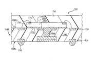
- an extended landing pad substrate package 200includes a dielectric layer 1340 having an upper surface 1340 U and an opposite lower surface 1340 L.
- a lower circuit pattern 834is embedded in lower surface 1340 L of dielectric layer 1340 .
- Lower circuit pattern 834includes traces 418 having a first thickness T 1 and extended landing pads 732 having a second thickness T 2 greater than first thickness T 1 .
- Blind via apertures 1544are formed through an upper circuit pattern 1234 embedded into upper surface 1340 U of dielectric layer 1340 , through dielectric layer 1340 and to extended landing pads 732 .
- the length L 1 of blind via apertures 1544is minimized due to the increased thickness T 2 of extended landing pads 732 as compared to thickness T 1 of traces 418 . Accordingly, the width W 3 of blind via apertures 1544 at upper surface 1340 U of dielectric layer 1340 is minimized. Accordingly, extremely small blind via apertures 1544 are formed even when dielectric layer 1340 is relatively thick. This enables upper circuit pattern 1234 to be formed with minimum feature size.
- blind via apertures 1544by minimizing length L 1 of blind via apertures 1544 , tolerance in the alignment between blind via apertures 1544 and extended landing pads 732 is minimized. This enables the width of extended landing pads 732 in a direction parallel to lower surface 1340 L of dielectric layer 1340 to be minimized. This, in turn, enables lower circuit pattern 834 to be formed with minimum feature size.
- the time required to form blind via apertures 1544is minimized thus minimizing the cost of the blind via laser-ablation process and thus of extended landing pad substrate package 200 .
- FIG. 1is an extended landing pad substrate package formation method 100 in accordance with one embodiment.
- FIG. 2is a cross-sectional view of an extended landing pad substrate package 200 during fabrication in accordance with one embodiment. Referring now to FIGS. 1 and 2 together, in a form seed layer on carrier operation 102 , a seed layer 202 is formed on a carrier 204 .
- Carrier 204is an electrically conductive material, e.g., copper, although is formed of other conductive materials in other embodiments. In yet another embodiment, carrier 204 is a dielectric material.
- Carrier 204includes a first surface 204 U and an opposite second surface 204 L.
- Seed layer 202is formed, e.g., by plating a conductive material or applying a conductive foil, on first surface 204 U of carrier 202 . As illustrated in FIG. 2 , seed layer 202 entirely covers upper surface 204 U of carrier 204 .
- Seed layer 202is an electrically conductive material, e.g., copper.
- a primary resist 206is applied to seed layer 202 .
- primary resist 206entirely covers seed layer 202 .
- Primary resist 206e.g., photoresist, is a dielectric material.
- FIG. 3is a cross-sectional view of extended landing pad substrate package 200 of FIG. 2 at a later stage during fabrication in accordance with one embodiment.
- flowmoves to a pattern primary resist operation 106 .
- pattern primary resist operation 106primary resist 206 is patterned to form a circuit pattern artifact 308 within primary resist 206 .
- Circuit pattern artifact 308i.e., a patterned opening within primary resist 206 , is a positive image of the circuit pattern to be formed. More particularly, primary resist 206 is patterned to expose exposed portions 314 of seed layer 202 through circuit pattern artifact 308 . Primary resist 206 is patterned using any one of a number of resist patterning techniques such as laser-ablation or photo-imaging, and the particular technique used is not essential to this embodiment.
- Circuit pattern artifact 308includes a trace pattern artifact 310 and an extended landing pad pattern artifact 312 .
- Trace pattern artifact 310i.e., a first portion of the patterned opening within primary resist 206
- Extended landing pad pattern artifact 312i.e., a second portion of the patterned opening within primary resist 206 , is a positive image of the extended landing pads of the circuit pattern to be formed.
- FIG. 4is a cross-sectional view of extended landing pad substrate package 200 of FIG. 3 at a later stage during fabrication in accordance with one embodiment.
- flowmoves to a plate primary conductor layer operation 108 .
- a primary conductor layer 416is plated within circuit pattern artifact 308 of primary resist 206 .
- Primary conductor layer 416is formed of an electrically conductive material such as copper, sometimes called a circuit pattern metal.
- Primary conductor layer 416is plated on seed layer 202 using primary resist 206 as a mask. More particularly, primary conductor layer 416 is plated on exposed portions 314 of seed layer 202 , e.g., using seed layer 202 as the electroplating electrode.
- primary conductor layer 416includes electrically conductive traces 418 and extended landing pad foundation portions 420 . More particularly, traces 418 are formed within trace pattern artifact 310 of circuit pattern artifact 308 . Extended landing pad foundation portions 420 are formed within extending landing pad pattern artifact 312 of circuit pattern artifact 308 .
- primary conductor layer 416only partially fills circuit pattern artifact 308 . More particularly, the thickness T 1 of primary conductor layer 416 is less than the thickness T 2 of primary resist 206 . Accordingly, an unfilled portion 421 of circuit pattern artifact 308 remains empty.
- FIG. 5is a cross-sectional view of extended landing pad substrate package 200 of FIG. 4 at a later stage during fabrication in accordance with one embodiment.
- an apply secondary resist operation 110a secondary resist 522 , e.g., photoresist, is applied to entirely cover primary resist 206 and primary conductor layer 416 as illustrated in FIG. 5 .
- Secondary resist 522fills unfilled portion 421 of circuit pattern artifact 308 .
- secondary resist 522is a dielectric material.
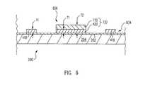
- FIG. 6is a cross-sectional view of extended landing pad substrate package 200 of FIG. 5 at a later stage during fabrication in accordance with one embodiment.
- flowmoves to a pattern secondary resist operation 112 .
- pattern secondary resist operation 112secondary resist 522 is patterned to form an extended landing pad overlay pattern artifact 624 within secondary resist 522 .
- Extended landing pad overlay pattern artifact 624i.e., a patterned opening within secondary resist 522 , is a positive image of the extended landing pads to be formed. More particularly, secondary resist 522 is patterned to expose extended landing pad foundation portions 420 of primary conductor layer 416 through extended landing pad overlay pattern artifact 624 . Secondary resist 522 is patterned using any one of a number of resist patterning techniques such as laser-ablation or photo-imaging, and the particular technique used is not essential to this embodiment.
- extended landing pad overlay pattern artifact 624is formed with a greater width W 1 then the width W 2 of extended landing pad pattern artifact 312 (and thus extending landing pad foundation portions 420 ). Accordingly, portions 626 of primary resist 206 adjacent extended landing pad pattern artifact 312 (and extending landing pad foundation portions 420 ) are exposed.
- Secondary resist 522remains over traces 418 of primary conductor layer 416 thus protecting traces 418 from additive plating as discussed below.
- FIG. 7is a cross-sectional view of extended landing pad substrate package 200 of FIG. 6 at a later stage during fabrication in accordance with one embodiment.
- flowmoves to a plate secondary conductor layer operation 114 .
- a secondary conductor layer 728is plated on primary conductor layer 416 using primary resist 206 and secondary resist 522 as a mask.
- secondary conductor layer 728is plated on extended landing pad foundation portions 420 of primary conductor layer 416 , e.g., using primary conductor layer 416 as the electroplating electrode.
- Secondary conductor layer 728is plated within extending landing pad pattern artifact 312 of primary resist 206 through extended landing pad overlay pattern artifact 624 of secondary resist 522 .
- Secondary conductor layer 728is formed of an electrically conductive material such as copper, sometimes called an extended landing pad extension metal.
- secondary conductor layer 728completely fills unfilled portion 421 of extending landing pad pattern artifact 312 .
- secondary conductor layer 728is over plated to cover portions 626 of primary resist 206 and then etched to expose portions 626 of primary resist 206 to ensure that unfilled portion 421 of extending landing pad pattern artifact 312 is completely filled.
- Secondary resist 522covers and protects traces 418 and thus secondary conductor layer 728 is not formed on traces 418 .
- Secondary conductor layer 728forms extended landing pad extension portions 730 .
- extended landing pad extension portions 730are selectively plated on extended landing pad foundation portions 420 .
- extended landing pad foundation portions 420 and extended landing pad extension portions 730form extended landing pads 732 .
- Extended landing pads 732have thickness T 2 of primary resist 206 . Accordingly, by selecting the desired thickness T 2 of primary resist 206 , the thickness T 2 of extended landing pads 732 is precisely controlled. Recall that traces 418 have thickness T 1 less than thickness T 2 of extended landing pads 732 .
- FIG. 8is a cross-sectional view of extended landing pad substrate package 200 of FIG. 7 at a later stage during fabrication in accordance with one embodiment.
- flowmoves to a strip primary resist and secondary resist operation 116 .
- strip primary resist and secondary resist operation 116primary resist 206 and secondary resist 522 are stripped, i.e., removed.
- Primary resist 206 and secondary resist 522are stripped using any one of a number of techniques and the particular technique used is not essential to this embodiment.
- Lower circuit pattern 834includes traces 418 and extended landing pads 732 .
- Traces 418are electrical conductors extending in the horizontal, e.g., first, direction substantially parallel to first surface 204 U of carrier 204 .
- Extended landing pads 732are electrically interconnected to traces 418 .
- traces 418have thickness T 1 less than thickness T 2 of extended landing pads 732 . More particularly, thickness T 1 and thickness T 2 are measured in the vertical, e.g., second, direction substantially perpendicular to first surface 204 U of carrier 204 .
- Extended landing pad substrate package 200 at the stage illustrated in FIG. 8is sometimes referred to as a lower, e.g., first, circuit pattern carrier structure 836 .
- lower circuit pattern carrier structure 836sometimes called a second layer transfer template, includes carrier 204 , seed layer 202 , and lower circuit pattern 834 .
- an upper circuit pattern carrier structureis also formed separately from lower circuit pattern carrier structure 836 .
- FIG. 9is a cross-sectional view of an upper, e.g., second, circuit pattern carrier structure 900 of extended landing pad substrate package 200 in accordance with one embodiment.
- a seed layer 202is formed on a carrier 204 .
- Seed layer 202 and carrier 204are similar to seed layer 202 and carrier 204 as discussed above in reference to FIG. 2 and so the description thereof is not repeated here.
- a resist 906is applied to seed layer 202 .
- resist 906As illustrated in FIG. 9 , resist 906 entirely covers seed layer 202 .
- Resist 906e.g., photoresist, is a dielectric material.
- thickness T 2 of primary resist 206(see FIG. 4 ) is greater than a thickness T 3 of resist 906 , e.g., primary resist 206 is two to three times thicker than resist 906 .
- FIG. 10is a cross-sectional view of upper circuit pattern carrier structure 900 of extended landing pad substrate package 200 of FIG. 9 at a later stage during fabrication in accordance with one embodiment.
- a pattern resist operation 122resist 906 is patterned to form a circuit pattern artifact 1008 within resist 906 .
- Circuit pattern artifact 1008i.e., a patterned opening within resist 906 , is a positive image of the circuit pattern to be formed. More particularly, resist 906 is patterned to expose exposed portions 1014 of seed layer 202 through circuit pattern artifact 1008 . Resist 906 is patterned using any one of a number of resist patterning techniques such as laser-ablation or photo-imaging, and the particular technique used is not essential to this embodiment.
- FIG. 11is a cross-sectional view of upper circuit pattern carrier structure 900 of extended landing pad substrate package 200 of FIG. 10 at a later stage during fabrication in accordance with one embodiment.
- flowmoves to a plate conductor layer operation 124 .
- a conductor layer 1116is plated within circuit pattern artifact 1008 of resist 906 .
- Conductor layer 1116is formed of an electrically conductive material such as copper, sometimes called a circuit pattern metal.
- Conductor layer 1116is plated on seed layer 202 using resist 906 as a mask. More particularly, conductor layer 1116 is plated on exposed portions 1014 of seed layer 202 , e.g., using seed layer 202 as the electroplating electrode. In accordance with this embodiment, conductor layer 1116 completely fills circuit pattern artifact 1008 . More particularly, conductor layer 1116 and resist 906 have an approximately equal thickness T 3 .
- FIG. 12is a cross-sectional view of upper circuit pattern carrier structure 900 of extended landing pad substrate package 200 of FIG. 11 at a later stage during fabrication in accordance with one embodiment.
- a strip resist operation 126resist 906 is stripped, i.e., removed. Resist 906 is stripped using any one of a number of techniques and the particular technique used is not essential to this embodiment.
- fabrication of upper circuit pattern carrier structure 900sometimes called a first layer transfer template, is complete.
- Upper circuit pattern carrier structure 900includes carrier 204 , seed layer 202 , and an upper, e.g., second, circuit pattern 1234 formed by conductor layer 1116 . Upper circuit pattern 1234 remains upon seed layer 202 and generally on carrier 204 . Upper circuit pattern 1234 includes traces, landing pads and/or other electrically conductive features.
- Upper circuit pattern 1234has thickness T 3 . More particularly, thickness T 3 is measured in the vertical direction substantially perpendicular to first surface 204 U of carrier 204 .
- FIG. 13is a cross-sectional view of extended landing pad substrate package 200 of FIGS. 8, 12 at a later stage during fabrication in accordance with one embodiment.
- FIG. 14is a cross-sectional view of extended landing pad substrate package 200 of FIG. 13 at a later stage during fabrication in accordance with one embodiment.
- Dielectric layer 1340includes an upper, e.g., first, surface 1340 U and an opposite lower, e.g., second, surface 1340 L.
- Upper circuit pattern 1234 of upper circuit pattern carrier structure 900(which has been inverted from the view of FIG. 12 ) is laminated into upper surface 1340 U of dielectric layer 1340 .
- lower circuit pattern 834 of lower circuit pattern carrier structure 836is laminated into lower surface 1340 L of dielectric layer 1340 .
- upper circuit pattern carrier structure 900 and lower circuit pattern carrier structure 836are simultaneously pressed into dielectric layer 1340 as indicated by the arrows 1342 in FIG. 13 while the assembly is heated. This causes dielectric layer 1340 to flow around upper circuit pattern 1234 and lower circuit pattern 834 and to seed layers 202 . Accordingly, upper circuit pattern 1234 is embedded within upper surface 1340 U of dielectric layer 1340 and lower circuit pattern 834 is embedded within lower surface 1340 L of dielectric layer 1340 as illustrated in FIG. 14 .
- thickness T 3 of upper circuit pattern 1234is approximately equal to thickness T 1 of traces 418 . However, in other embodiments, thickness T 3 of upper circuit pattern 1234 is greater than or less than thickness T 1 of traces 418 .
- FIG. 15is a cross-sectional view of extended landing pad substrate package 200 of FIG. 14 at a later stage during fabrication in accordance with one embodiment.
- a remove carriers operation 130from laminate upper and lower circuit patterns to dielectric layer operation 128 , flow moves to a remove carriers operation 130 .
- remove carriers operation 130carriers 204 of circuit pattern carrier structures 900 , 836 are removed.
- carriers 204are removed by etching, mechanical grinding, and/or peeling.
- remove seed layers operation 132seed layers 202 of circuit pattern carrier structures 900 , 836 are removed.
- seed layers 202are removed by etching and/or mechanical grinding.
- upper surface 1340 U, upper circuit pattern 1234 , lower surface 1340 L, and lower circuit pattern 834are exposed.
- blind via apertures 1544are formed, e.g., using laser-ablation. Blind via apertures 1544 extend through upper circuit pattern 1234 and dielectric layer 1340 and to extended landing pads 732 of lower circuit pattern 834 . Blind via apertures 1544 expose extended landing pads 732 but do not extend through extended landing pads 732 .
- Length L 1is the distance between extended landing pads 732 and upper surface 1340 U of dielectric layer 1340 .
- Length L 2is the distance between traces 418 and upper surface 1340 U of dielectric layer 1340 .
- length L 2is the distance between traces 418 and upper surface 1340 U of dielectric layer 1340 .
- blind via apertures 1544have a first width W 3 at upper surface 1340 U of dielectric layer 1340 and a second width W 4 at extended landing pads 732 . As illustrated, blind via apertures 1544 taper from width W 3 at upper surface 1340 U of dielectric layer 1340 to width W 4 at extended landing pads 732 , width W 3 being greater than width W 4 .
- blind via apertureshave an aspect ratio, i.e., a length to width ratio, due to the laser-ablation process used to form the blind via aperture.
- the aspect ratio of blind via apertures 1544is length L 1 divided by width W 3 (L 1 /W 3 ).
- the resulting width of the blind via aperturesalso decreases.
- the length L 1 of blind via apertures 1544is minimized due to the increased thickness T 2 of extended landing pads 732 as compared to thickness T 1 of traces 418 .
- the width W 3 of blind via apertures 1544 at upper surface 1340 U of dielectric layer 1340is minimized. Accordingly, extremely small blind via apertures 1544 are formed even when dielectric layer 1340 is relatively thick. This enables upper circuit pattern 1234 to be formed with minimum feature size.
- blind via apertures 1544by minimizing length L 1 of blind via apertures 1544 , tolerance in the alignment between blind via apertures 1544 and extended landing pads 732 is minimized. This enables the width of extended landing pads 732 in a direction parallel to lower surface 1340 L of dielectric layer 1340 to be minimized. This, in turn, enables lower circuit pattern 834 to be formed with minimum feature size.
- the time required to form blind via apertures 1544is minimized thus minimizing the cost of the blind via laser-ablation process and thus of extended landing pad substrate package 200 .
- FIG. 16is a cross-sectional view of extended landing pad substrate package 200 of FIG. 15 at a later stage during fabrication in accordance with one embodiment.
- a form blind vias operation 136blind vias 1646 are formed within blind via apertures 1544 .
- blind via apertures 1544are filled with electrically conductive material, e.g., by plating a blind via metal or applying an electrically conductive epoxy, to form blind vias 1646 .
- Blind vias 1646extend through upper circuit pattern 1234 and dielectric layer 1340 and to extended landing pads 732 of lower circuit pattern 834 . Accordingly, upper circuit pattern 1234 is electrically connected to lower circuit pattern 834 through dielectric layer 1340 by blind vias 1646 . Blind vias 1646 are formed within blind via apertures 1544 and thus the above discussion of blind via apertures 1544 and the relative dimensions thereof are equally applicable to blind vias 1646 .
- Extended landing pad substrate package 200 at the stage illustrated in FIG. 16is sometimes referred to as an extended landing pad substrate 1648 .
- Extended landing pad substrate 1648includes dielectric layer 1340 , upper circuit pattern 1234 embedded within upper surface 1340 U of dielectric layer 1340 , lower circuit pattern 834 embedded within lower surface 1340 L of dielectric layer 1340 , and blind vias 1646 electrically connecting upper and lower circuit patterns 1234 , 834 through dielectric layer 1340 .
- Extending landing pad substrate 1648includes an upper, e.g., first surface 1648 U and an opposite lower, e.g., second, surface 1648 L.
- FIG. 17is a cross-sectional view of extended landing pad substrate package 200 of FIG. 16 at a later stage during fabrication in accordance with one embodiment. Referring now to FIGS. 1 and 17 together, from form blind vias operation 136 , flow moves to a mount electronic component(s) operation 138 . In mount electronic component(s) operation 138 , at least one electronic component 1750 is mounted to extended landing pad substrate 1648 .
- Electronic component 1750is an integrated circuit chip, i.e., an active component, in accordance with this embodiment. However, in other embodiments, electronic component 1750 is a passive component, e.g., a capacitor, resistor or inductor.
- electronic component 1750is mounted in a wire bond configuration. More particularly, electronic component 1750 includes an inactive surface 17501 mounted to upper surface 1648 U of extended landing pad substrate 1648 with an adhesive 1752 , sometimes called a die attach adhesive. Bond pads 1754 on an active surface 1750 A of electronic component 1750 are electrically connected to upper circuit pattern 1234 by bond wires 1756 .
- a package body 1758e.g., an encapsulant, molding compound, or other dielectric material, is formed to encapsulate and protect electronic component 1750 and bond wires 1756 .
- interconnection balls 1760e.g., solder balls
- interconnection balls 1760are formed on lower circuit pattern 834 .
- Interconnection balls 1760e.g., a ball grid array, are used to electrically interconnect and mount extended landing pad substrate package 200 to a larger substrate such as a printed circuit motherboard.
- interconnection balls 1760are not formed and thus form interconnection balls operation 140 is an optional operation.
- FIG. 18is a cross-sectional view of extended landing pad substrate package 200 of FIG. 16 at a later stage during fabrication in accordance with another embodiment. Referring now to FIGS. 1 and 18 together, from form blind vias operation 136 , flow moves to mount electronic component(s) operation 138 . In mount electronic component(s) operation 138 , at least one electronic component 1850 is mounted to extended landing pad substrate 1648 .
- Electronic component 1850is an integrated circuit chip, i.e., an active component, in accordance with this embodiment. However, in other embodiments, electronic component 1850 is a passive component, e.g., a capacitor, resistor or inductor.
- electronic component 1850is mounted in a flip chip configuration. More particularly, electronic component 1850 includes an inactive surface 18501 and an opposite active surface 1850 A. Bond pads 1854 on active surface 1850 A of electronic component 1850 are physically and electrically connected to upper circuit pattern 1234 by flip chip bumps 1856 , e.g., solder bumps.
- flip chip bumps 1856e.g., solder bumps.
- an underfill material 1858is formed between upper surface 1648 U of extended landing pad substrate 1648 and active surface 1850 A of electronic component 1850 to encapsulate and protect flip chip bumps 1856 .
- interconnection balls operation 140From mount electronic component(s) operation 138 , flow moves, optionally, to form interconnection balls operation 140 .
- interconnection balls 1860e.g., solder balls
- interconnection balls 1860are formed on lower circuit pattern 834 .
- Interconnection balls 1860e.g., a ball grid array, are used to electrically interconnect and mount extended landing pad substrate package 200 to a larger substrate such as a printed circuit motherboard.
- interconnection balls 1860are not formed and thus form interconnection balls operation 140 is an optional operation.
- an individual extended landing pad substrate package 200is described above, in other embodiments, a plurality of extended landing pad substrate package 200 are formed simultaneously in an array or strip using extended landing pad substrate package formation method 100 as described above.
- the array or stripis singulated to singulate extended landing pad substrate packages 200 from one another.
Landscapes
- Engineering & Computer Science (AREA)
- Microelectronics & Electronic Packaging (AREA)
- Manufacturing & Machinery (AREA)
- Physics & Mathematics (AREA)
- Condensed Matter Physics & Semiconductors (AREA)
- General Physics & Mathematics (AREA)
- Computer Hardware Design (AREA)
- Power Engineering (AREA)
- Ceramic Engineering (AREA)
- Production Of Multi-Layered Print Wiring Board (AREA)
Abstract
Description
Claims (20)
Priority Applications (1)
| Application Number | Priority Date | Filing Date | Title |
|---|---|---|---|
| US14/517,403US9462704B1 (en) | 2009-01-09 | 2014-10-17 | Extended landing pad substrate package structure and method |
Applications Claiming Priority (2)
| Application Number | Priority Date | Filing Date | Title |
|---|---|---|---|
| US12/351,596US8872329B1 (en) | 2009-01-09 | 2009-01-09 | Extended landing pad substrate package structure and method |
| US14/517,403US9462704B1 (en) | 2009-01-09 | 2014-10-17 | Extended landing pad substrate package structure and method |
Related Parent Applications (1)
| Application Number | Title | Priority Date | Filing Date |
|---|---|---|---|
| US12/351,596DivisionUS8872329B1 (en) | 2009-01-09 | 2009-01-09 | Extended landing pad substrate package structure and method |
Publications (1)
| Publication Number | Publication Date |
|---|---|
| US9462704B1true US9462704B1 (en) | 2016-10-04 |
Family
ID=51752724
Family Applications (2)
| Application Number | Title | Priority Date | Filing Date |
|---|---|---|---|
| US12/351,596Active2030-10-18US8872329B1 (en) | 2009-01-09 | 2009-01-09 | Extended landing pad substrate package structure and method |
| US14/517,403ActiveUS9462704B1 (en) | 2009-01-09 | 2014-10-17 | Extended landing pad substrate package structure and method |
Family Applications Before (1)
| Application Number | Title | Priority Date | Filing Date |
|---|---|---|---|
| US12/351,596Active2030-10-18US8872329B1 (en) | 2009-01-09 | 2009-01-09 | Extended landing pad substrate package structure and method |
Country Status (1)
| Country | Link |
|---|---|
| US (2) | US8872329B1 (en) |
Cited By (2)
| Publication number | Priority date | Publication date | Assignee | Title |
|---|---|---|---|---|
| US9847244B2 (en) | 2015-07-15 | 2017-12-19 | Chip Solutions, LLC | Semiconductor device and method |
| US9922949B2 (en)* | 2015-07-15 | 2018-03-20 | Chip Solutions, LLC | Semiconductor device and method |
Families Citing this family (5)
| Publication number | Priority date | Publication date | Assignee | Title |
|---|---|---|---|---|
| US9691635B1 (en) | 2002-05-01 | 2017-06-27 | Amkor Technology, Inc. | Buildup dielectric layer having metallization pattern semiconductor package fabrication method |
| US7548430B1 (en) | 2002-05-01 | 2009-06-16 | Amkor Technology, Inc. | Buildup dielectric and metallization process and semiconductor package |
| US10811277B2 (en) | 2004-03-23 | 2020-10-20 | Amkor Technology, Inc. | Encapsulated semiconductor package |
| US11081370B2 (en) | 2004-03-23 | 2021-08-03 | Amkor Technology Singapore Holding Pte. Ltd. | Methods of manufacturing an encapsulated semiconductor device |
| TWI587463B (en)* | 2014-11-12 | 2017-06-11 | 矽品精密工業股份有限公司 | Semiconductor package structure and fabrication method thereof |
Citations (199)
| Publication number | Priority date | Publication date | Assignee | Title |
|---|---|---|---|---|
| US3324014A (en) | 1962-12-03 | 1967-06-06 | United Carr Inc | Method for making flush metallic patterns |
| US3778900A (en) | 1970-09-04 | 1973-12-18 | Ibm | Method for forming interconnections between circuit layers of a multi-layer package |
| US3868724A (en) | 1973-11-21 | 1975-02-25 | Fairchild Camera Instr Co | Multi-layer connecting structures for packaging semiconductor devices mounted on a flexible carrier |
| US3916434A (en) | 1972-11-30 | 1975-10-28 | Power Hybrids Inc | Hermetically sealed encapsulation of semiconductor devices |
| US4322778A (en) | 1980-01-25 | 1982-03-30 | International Business Machines Corp. | High performance semiconductor package assembly |
| US4508754A (en) | 1982-08-19 | 1985-04-02 | Gte Automatic Electric Inc. | Method of adding fine line conductive/resistive patterns to a thick film microcircuit |
| US4532152A (en) | 1982-03-05 | 1985-07-30 | Elarde Vito D | Fabrication of a printed circuit board with metal-filled channels |
| US4532419A (en) | 1982-09-09 | 1985-07-30 | Sony Corporation | Memory card having static electricity protection |
| US4604799A (en) | 1982-09-03 | 1986-08-12 | John Fluke Mfg. Co., Inc. | Method of making molded circuit board |
| US4642160A (en) | 1985-08-12 | 1987-02-10 | Interconnect Technology Inc. | Multilayer circuit board manufacturing |
| US4685033A (en) | 1984-08-28 | 1987-08-04 | Nec Corporation | Multilayer wiring substrate |
| US4706167A (en) | 1983-11-10 | 1987-11-10 | Telemark Co., Inc. | Circuit wiring disposed on solder mask coating |
| US4716049A (en) | 1985-12-20 | 1987-12-29 | Hughes Aircraft Company | Compressive pedestal for microminiature connections |
| US4786952A (en) | 1986-07-24 | 1988-11-22 | General Motors Corporation | High voltage depletion mode MOS power field effect transistor |
| US4806188A (en) | 1988-03-04 | 1989-02-21 | E. I. Du Pont De Nemours And Company | Method for fabricating multilayer circuits |
| US4811082A (en) | 1986-11-12 | 1989-03-07 | International Business Machines Corporation | High performance integrated circuit packaging structure |
| US4897338A (en) | 1987-08-03 | 1990-01-30 | Allied-Signal Inc. | Method for the manufacture of multilayer printed circuit boards |
| US4905124A (en) | 1987-03-31 | 1990-02-27 | Mitsubishi Denki Kabushiki Kaisha | IC card |
| US4915983A (en) | 1985-06-10 | 1990-04-10 | The Foxboro Company | Multilayer circuit board fabrication process |
| US4964212A (en) | 1988-09-29 | 1990-10-23 | Commissariat A L'energie Atomique | Process for producing electrical connections through a substrate |
| US4974120A (en) | 1989-01-12 | 1990-11-27 | Mitsubishi Denki Kabushiki Kaisha | IC card |
| US4996391A (en) | 1988-09-30 | 1991-02-26 | Siemens Aktiengesellschaft | Printed circuit board having an injection molded substrate |
| US5021047A (en) | 1989-08-29 | 1991-06-04 | Movern John B | Restricted use hypodermic syringe |
| US5053357A (en) | 1989-12-27 | 1991-10-01 | Motorola, Inc. | Method of aligning and mounting an electronic device on a printed circuit board using a flexible substrate having fixed lead arrays thereon |
| US5072075A (en) | 1989-06-28 | 1991-12-10 | Digital Equipment Corporation | Double-sided hybrid high density circuit board and method of making same |
| US5081520A (en) | 1989-05-16 | 1992-01-14 | Minolta Camera Kabushiki Kaisha | Chip mounting substrate having an integral molded projection and conductive pattern |
| US5108553A (en) | 1989-04-04 | 1992-04-28 | Olin Corporation | G-tab manufacturing process and the product produced thereby |
| US5110664A (en) | 1989-07-10 | 1992-05-05 | Hitachi, Ltd. | Thick film and thin film composite substrate and electronic circuit apparatus using it |
| US5191174A (en) | 1990-08-01 | 1993-03-02 | International Business Machines Corporation | High density circuit board and method of making same |
| JPH05109975A (en) | 1991-10-14 | 1993-04-30 | Hitachi Ltd | Resin-sealed type semiconductor device |
| JPH05136323A (en) | 1991-11-13 | 1993-06-01 | Nec Corp | Integrated circuit device |
| US5229550A (en) | 1990-10-30 | 1993-07-20 | International Business Machines Corporation | Encapsulated circuitized power core alignment and lamination |
| US5239448A (en) | 1991-10-28 | 1993-08-24 | International Business Machines Corporation | Formulation of multichip modules |
| US5247429A (en) | 1990-11-21 | 1993-09-21 | Nippondenso Co., Ltd. | Display board |
| US5263243A (en)* | 1992-01-28 | 1993-11-23 | Nec Corporation | Method for producing multilayer printed wiring boards |
| US5283459A (en) | 1989-11-15 | 1994-02-01 | Kabushiki Kaisha Toshiba | Semiconductor sensor including an aperture having a funnel shaped section intersecting a second section |
| US5293243A (en) | 1992-04-21 | 1994-03-08 | Degnan Donald E | Image splitter for security cameras |
| US5371654A (en) | 1992-10-19 | 1994-12-06 | International Business Machines Corporation | Three dimensional high performance interconnection package |
| US5379191A (en) | 1991-02-26 | 1995-01-03 | Microelectronics And Computer Technology Corporation | Compact adapter package providing peripheral to area translation for an integrated circuit chip |
| JPH0717175B2 (en) | 1985-08-20 | 1995-03-01 | 金井重要工業株式会社 | Automotive interior ceiling material for molding |
| US5404044A (en) | 1992-09-29 | 1995-04-04 | International Business Machines Corporation | Parallel process interposer (PPI) |
| US5440805A (en) | 1992-03-09 | 1995-08-15 | Rogers Corporation | Method of manufacturing a multilayer circuit |
| US5463253A (en) | 1990-03-15 | 1995-10-31 | Fujitsu Limited | Semiconductor device having a plurality of chips |
| US5474958A (en) | 1993-05-04 | 1995-12-12 | Motorola, Inc. | Method for making semiconductor device having no die supporting surface |
| US5474957A (en) | 1994-05-09 | 1995-12-12 | Nec Corporation | Process of mounting tape automated bonded semiconductor chip on printed circuit board through bumps |
| US5508938A (en) | 1992-08-13 | 1996-04-16 | Fujitsu Limited | Special interconnect layer employing offset trace layout for advanced multi-chip module packages |
| US5530288A (en) | 1994-10-12 | 1996-06-25 | International Business Machines Corporation | Passive interposer including at least one passive electronic component |
| US5531020A (en) | 1989-11-14 | 1996-07-02 | Poly Flex Circuits, Inc. | Method of making subsurface electronic circuits |
| JPH08190615A (en) | 1995-01-09 | 1996-07-23 | Seiko Epson Corp | memory card |
| US5574309A (en) | 1991-11-25 | 1996-11-12 | Gemplus Card International | Integrated circuit card comprising means for the protection of the integrated circuit |
| US5581498A (en) | 1993-08-13 | 1996-12-03 | Irvine Sensors Corporation | Stack of IC chips in lieu of single IC chip |
| US5582858A (en) | 1991-10-07 | 1996-12-10 | International Business Machines Corporation | Adhesive layer in multi-level packaging and organic material as a metal diffusion barrier |
| US5616422A (en) | 1994-02-28 | 1997-04-01 | International Business Machines Corporation | Metallized substrate |
| US5637832A (en) | 1993-10-26 | 1997-06-10 | Pacific Microelectronics Corporation | Solder ball array and method of preparation |
| US5674785A (en) | 1995-11-27 | 1997-10-07 | Micron Technology, Inc. | Method of producing a single piece package for semiconductor die |
| US5719749A (en) | 1994-09-26 | 1998-02-17 | Sheldahl, Inc. | Printed circuit assembly with fine pitch flexible printed circuit overlay mounted to printed circuit board |
| US5739588A (en) | 1994-08-15 | 1998-04-14 | Citizen Watch Co., Ltd. | Semiconductor device |
| US5739579A (en) | 1992-06-29 | 1998-04-14 | Intel Corporation | Method for forming interconnections for semiconductor fabrication and semiconductor device having such interconnections |
| US5739581A (en) | 1995-11-17 | 1998-04-14 | National Semiconductor Corporation | High density integrated circuit package assembly with a heatsink between stacked dies |
| US5742479A (en) | 1994-03-09 | 1998-04-21 | Seiko Epson Corporation | Card-type electronic device with plastic frame sandwiched between printed circuit board and metal panel |
| US5774340A (en) | 1996-08-28 | 1998-06-30 | International Business Machines Corporation | Planar redistribution structure and printed wiring device |
| US5798014A (en) | 1995-02-02 | 1998-08-25 | Hestia Technologies, Inc. | Methods of making multi-tier laminate substrates for electronic device packaging |
| US5822190A (en) | 1996-06-11 | 1998-10-13 | Kabushiki Kaisha Toshiba | Card type memory device and a method for manufacturing the same |
| US5826330A (en) | 1995-12-28 | 1998-10-27 | Hitachi Aic Inc. | Method of manufacturing multilayer printed wiring board |
| US5835355A (en) | 1997-09-22 | 1998-11-10 | Lsi Logic Corporation | Tape ball grid array package with perforated metal stiffener |
| US5847453A (en) | 1996-03-27 | 1998-12-08 | Honda Giken Kogyo Kabushiki Kaisha | Microwave circuit package |
| JPH10334205A (en) | 1997-05-30 | 1998-12-18 | Toshiba Corp | IC card and memory package |
| US5894108A (en) | 1997-02-11 | 1999-04-13 | National Semiconductor Corporation | Plastic package with exposed die |
| US5903052A (en) | 1998-05-12 | 1999-05-11 | Industrial Technology Research Institute | Structure for semiconductor package for improving the efficiency of spreading heat |
| US5936843A (en) | 1997-10-14 | 1999-08-10 | Fujitsu Limited | Printed wiring board with mounted circuit element using a terminal density conversion board |
| US5952611A (en) | 1997-12-19 | 1999-09-14 | Texas Instruments Incorporated | Flexible pin location integrated circuit package |
| US5990546A (en) | 1994-12-29 | 1999-11-23 | Nitto Denko Corporation | Chip scale package type of semiconductor device |
| US6004619A (en) | 1996-11-07 | 1999-12-21 | Hewlett-Packard Company | Process for manufacturing printed circuit boards |
| US6013948A (en) | 1995-11-27 | 2000-01-11 | Micron Technology, Inc. | Stackable chip scale semiconductor package with mating contacts on opposed surfaces |
| US6021564A (en) | 1996-11-08 | 2000-02-08 | W. L. Gore & Associates, Inc. | Method for reducing via inductance in an electronic assembly and article |
| US6028364A (en) | 1994-09-20 | 2000-02-22 | Hitachi, Ltd. | Semiconductor device having a stress relieving mechanism |
| US6034427A (en) | 1998-01-28 | 2000-03-07 | Prolinx Labs Corporation | Ball grid array structure and method for packaging an integrated circuit chip |
| US6035527A (en)* | 1996-05-18 | 2000-03-14 | Ingenieurbuero Tamm Factory Innovations | Method for the production of printed circuit boards |
| US6040622A (en) | 1998-06-11 | 2000-03-21 | Sandisk Corporation | Semiconductor package using terminals formed on a conductive layer of a circuit board |
| US6039889A (en) | 1999-01-12 | 2000-03-21 | Fujitsu Limited | Process flows for formation of fine structure layer pairs on flexible films |
| US6060778A (en) | 1997-05-17 | 2000-05-09 | Hyundai Electronics Industries Co. Ltd. | Ball grid array package |
| US6069407A (en) | 1998-11-18 | 2000-05-30 | Vlsi Technology, Inc. | BGA package using PCB and tape in a die-up configuration |
| US6072243A (en) | 1996-11-26 | 2000-06-06 | Sharp Kabushiki Kaisha | Semiconductor integrated circuit device capable of surely electrically insulating two semiconductor chips from each other and fabricating method thereof |
| US6081036A (en) | 1996-04-19 | 2000-06-27 | Matsushita Electronics Corp. | Semiconductor device |
| US6115910A (en) | 1997-05-08 | 2000-09-12 | Lsi Logic Corporation | Misregistration fidutial |
| US6119338A (en) | 1998-03-19 | 2000-09-19 | Industrial Technology Research Institute | Method for manufacturing high-density multilayer printed circuit boards |
| US6122171A (en) | 1999-07-30 | 2000-09-19 | Micron Technology, Inc. | Heat sink chip package and method of making |
| US6127833A (en) | 1999-01-04 | 2000-10-03 | Taiwan Semiconductor Manufacturing Co. | Test carrier for attaching a semiconductor device |
| US6127250A (en) | 1996-11-08 | 2000-10-03 | W. L. Gore & Associates, Inc. | Method of increasing package reliability by designing in plane CTE gradients |
| US6160705A (en) | 1997-05-09 | 2000-12-12 | Texas Instruments Incorporated | Ball grid array package and method using enhanced power and ground distribution circuitry |
| US6162365A (en) | 1998-03-04 | 2000-12-19 | International Business Machines Corporation | Pd etch mask for copper circuitization |
| US6172419B1 (en) | 1998-02-24 | 2001-01-09 | Micron Technology, Inc. | Low profile ball grid array package |
| US6175087B1 (en) | 1998-12-02 | 2001-01-16 | International Business Machines Corporation | Composite laminate circuit structure and method of forming the same |
| US6184463B1 (en) | 1998-04-13 | 2001-02-06 | Harris Corporation | Integrated circuit package for flip chip |
| US6194250B1 (en) | 1998-09-14 | 2001-02-27 | Motorola, Inc. | Low-profile microelectronic package |
| US6204453B1 (en) | 1998-12-02 | 2001-03-20 | International Business Machines Corporation | Two signal one power plane circuit board |
| US6214641B1 (en) | 1996-06-25 | 2001-04-10 | Micron Technology, Inc. | Method of fabricating a multi-chip module |
| US6239485B1 (en) | 1998-11-13 | 2001-05-29 | Fujitsu Limited | Reduced cross-talk noise high density signal interposer with power and ground wrap |
| USD445096S1 (en) | 1998-04-01 | 2001-07-17 | Sandisk Corporation | Removable memory card for use with portable electronic devices |
| US6274821B1 (en) | 1998-09-16 | 2001-08-14 | Denso Corporation | Shock-resistive printed circuit board and electronic device including the same |
| USD446525S1 (en) | 1999-08-24 | 2001-08-14 | Kabushiki Kaisha Toshiba | IC memory card |
| US6280641B1 (en) | 1998-06-02 | 2001-08-28 | Mitsubishi Gas Chemical Company, Inc. | Printed wiring board having highly reliably via hole and process for forming via hole |
| US6316285B1 (en) | 1998-09-02 | 2001-11-13 | Micron Technology, Inc. | Passivation layer for packaged integrated circuits |
| US20010041436A1 (en) | 1998-10-01 | 2001-11-15 | Applied Materials, Inc. | Techniques for triple and quadruple damascene fabrication |
| US20020017712A1 (en) | 1998-06-04 | 2002-02-14 | Yoshihiro Bessho | Method for fabricating a semiconductor package with a semiconductor device attached to a multilayered substrate |
| US6351031B1 (en) | 1999-10-12 | 2002-02-26 | Fujitsu Limited | Semiconductor device and method for manufacturing substrate of the same |
| US6352914B2 (en) | 1998-06-11 | 2002-03-05 | Intel Corporation | Interleaved signal trace routing |
| US6353999B1 (en) | 1999-03-09 | 2002-03-12 | Unimicron Taiwan Corp. | Method of making mechanical-laser structure |
| US6365975B1 (en) | 1997-04-02 | 2002-04-02 | Tessera, Inc. | Chip with internal signal routing in external element |
| US6368967B1 (en) | 2000-05-04 | 2002-04-09 | Advanced Micro Devices, Inc. | Method to control mechanical stress of copper interconnect line using post-plating copper anneal |
| US6376906B1 (en) | 1997-02-12 | 2002-04-23 | Denso Corporation | Mounting structure of semiconductor element |
| US6378201B1 (en) | 1990-09-27 | 2002-04-30 | International Business Machines Corporation | Method for making a printed circuit board |
| US6392160B1 (en) | 1998-11-25 | 2002-05-21 | Lucent Technologies Inc. | Backplane for radio frequency signals |
| US6395578B1 (en) | 1999-05-20 | 2002-05-28 | Amkor Technology, Inc. | Semiconductor package and method for fabricating the same |
| US6407341B1 (en) | 2000-04-25 | 2002-06-18 | International Business Machines Corporation | Conductive substructures of a multilayered laminate |
| US6407930B1 (en) | 1999-06-23 | 2002-06-18 | Asustek Computer Inc. | Structure of printed circuit board with stacked daughter board |
| US6406942B2 (en) | 2000-03-09 | 2002-06-18 | Nec Corporation | Flip chip type semiconductor device and method for manufacturing the same |
| US6405431B1 (en) | 1996-06-27 | 2002-06-18 | Samsung Electro-Mechanics Co., Ltd. | Method for manufacturing build-up multi-layer printed circuit board by using yag laser |
| US6418615B1 (en) | 1999-03-11 | 2002-07-16 | Shinko Electronics Industries, Co., Ltd. | Method of making multilayered substrate for semiconductor device |
| US20020140105A1 (en) | 2001-02-16 | 2002-10-03 | Higgins Leo M. | High strength vias |
| US6472306B1 (en) | 2000-09-05 | 2002-10-29 | Industrial Technology Research Institute | Method of forming a dual damascene opening using CVD Low-K material and spin-on-polymer |
| US6479762B2 (en) | 2000-11-20 | 2002-11-12 | Alps Electric Co., Ltd. | Printed circuit board having a pattern of traces formed by screen-printing |
| US6497943B1 (en) | 2000-02-14 | 2002-12-24 | International Business Machines Corporation | Surface metal balancing to reduce chip carrier flexing |
| US20030000738A1 (en) | 2001-06-25 | 2003-01-02 | Rumsey Brad D. | Solder resist opening to define a combination pin one indicator and fiducial |
| US6502774B1 (en) | 2000-03-08 | 2003-01-07 | J + L Fiber Services, Inc. | Refiner disk sensor and sensor refiner disk |
| US6517995B1 (en) | 1999-09-14 | 2003-02-11 | Massachusetts Institute Of Technology | Fabrication of finely featured devices by liquid embossing |
| US6528874B1 (en) | 1999-10-12 | 2003-03-04 | North Corporation | Wiring circuit substrate and manufacturing method thereof |
| US6534723B1 (en) | 1999-11-26 | 2003-03-18 | Ibiden Co., Ltd. | Multilayer printed-circuit board and semiconductor device |
| US6534391B1 (en) | 2001-08-17 | 2003-03-18 | Amkor Technology, Inc. | Semiconductor package having substrate with laser-formed aperture through solder mask layer |
| US6544638B2 (en) | 1996-11-08 | 2003-04-08 | Gore Enterprise Holdings, Inc. | Electronic chip package |
| US6570258B2 (en) | 1996-04-29 | 2003-05-27 | Micron Technology, Inc. | Method for reducing capacitive coupling between conductive lines |
| US6574106B2 (en) | 1998-06-10 | 2003-06-03 | Nec Corporation | Mounting structure of semiconductor device |
| US6586682B2 (en) | 2000-02-23 | 2003-07-01 | Kulicke & Soffa Holdings, Inc. | Printed wiring board with controlled line impedance |
| US20030128096A1 (en) | 2002-01-10 | 2003-07-10 | Joseph Mazzochette | Temperature compensating device with integral sheet thermistors |
| US6591495B2 (en)* | 1998-09-03 | 2003-07-15 | Ibiden Co., Ltd. | Manufacturing method of a multilayered printed circuit board having an opening made by a laser, and using electroless and electrolytic plating |
| US20030153172A1 (en)* | 2002-02-08 | 2003-08-14 | Hitachi, Ltd. | Method of manufacturing a semiconductor integrated circuit device |
| US6608757B1 (en) | 2002-03-18 | 2003-08-19 | International Business Machines Corporation | Method for making a printed wiring board |
| US6637105B1 (en) | 1999-08-16 | 2003-10-28 | Sony Corporation | Method of manufacturing a multilayer printed wiring board |
| US6660559B1 (en) | 2001-06-25 | 2003-12-09 | Amkor Technology, Inc. | Method of making a chip carrier package using laser ablation |
| US6715204B1 (en) | 1998-07-08 | 2004-04-06 | Ibiden Co., Ltd. | Printed wiring board and method for producing the same |
| US6727645B2 (en) | 2002-05-24 | 2004-04-27 | International Business Machines Corporation | Organic LED device |
| US6730857B2 (en) | 2001-03-13 | 2004-05-04 | International Business Machines Corporation | Structure having laser ablated features and method of fabricating |
| US6740964B2 (en) | 2000-11-17 | 2004-05-25 | Oki Electric Industry Co., Ltd. | Semiconductor package for three-dimensional mounting, fabrication method thereof, and semiconductor device |
| US6753612B2 (en) | 2001-04-05 | 2004-06-22 | International Business Machines Corporation | Economical high density chip carrier |
| US6784376B1 (en)* | 2001-08-16 | 2004-08-31 | Amkor Technology, Inc. | Solderable injection-molded integrated circuit substrate and method therefor |
| US6787443B1 (en) | 2003-05-20 | 2004-09-07 | Intel Corporation | PCB design and method for providing vented blind vias |
| US6803528B1 (en) | 1999-11-05 | 2004-10-12 | 3M Innovative Properties Company | Multi-layer double-sided wiring board and method of fabricating the same |
| US6804881B1 (en) | 2000-05-12 | 2004-10-19 | Shipley Company, L.L.C. | Multilayer circuit board manufacturing process |
| US6815739B2 (en) | 2001-05-18 | 2004-11-09 | Corporation For National Research Initiatives | Radio frequency microelectromechanical systems (MEMS) devices on low-temperature co-fired ceramic (LTCC) substrates |
| US6815709B2 (en) | 2001-05-23 | 2004-11-09 | International Business Machines Corporation | Structure having flush circuitry features and method of making |
| US6822334B2 (en) | 2000-05-30 | 2004-11-23 | Renesas Technology Corp. | Semiconductor device having a layered wiring structure with hard mask covering |
| US20050039950A1 (en)* | 2003-01-30 | 2005-02-24 | Endicott Interconnect Technologies, Inc. | High speed circuitized substrate with reduced thru-hole stub, method for fabrication and information handling system utilizing same |
| US6891261B2 (en) | 2000-12-06 | 2005-05-10 | Sharp Kabushiki Kaisha | Semiconductor device and method of manufacturing the same |
| US6908863B2 (en) | 2003-09-29 | 2005-06-21 | Intel Corporation | Sacrificial dielectric planarization layer |
| US6913952B2 (en) | 2003-07-03 | 2005-07-05 | Micron Technology, Inc. | Methods of forming circuit traces and contact pads for interposers utilized in semiconductor packages |
| US6930256B1 (en) | 2002-05-01 | 2005-08-16 | Amkor Technology, Inc. | Integrated circuit substrate having laser-embedded conductive patterns and method therefor |
| US6930257B1 (en) | 2002-05-01 | 2005-08-16 | Amkor Technology, Inc. | Integrated circuit substrate having laminated laser-embedded circuit layers |
| US20050194353A1 (en) | 2001-02-12 | 2005-09-08 | Johnson Morgan T. | Laser micromachining and electrical structures formed thereby |
| US20050205295A1 (en) | 2004-03-19 | 2005-09-22 | Tsuk Michael J | Apparatuses, systems and/or methods to affect impedance |
| US6969674B2 (en)* | 2002-07-17 | 2005-11-29 | Kinsus Interconnect Technology | Structure and method for fine pitch flip chip substrate |
| US6989593B2 (en) | 2000-12-22 | 2006-01-24 | Broadcom Corporation | Die-up ball grid array package with patterned stiffener opening |
| US6998335B2 (en) | 2003-12-13 | 2006-02-14 | Chartered Semiconductor Manufacturing, Ltd | Structure and method for fabricating a bond pad structure |
| US7028400B1 (en) | 2002-05-01 | 2006-04-18 | Amkor Technology, Inc. | Integrated circuit substrate having laser-exposed terminals |
| US7033928B2 (en) | 2002-03-20 | 2006-04-25 | Nec Electronics Corporation | Method of fabricating semiconductor device |
| US7061095B2 (en) | 2001-09-26 | 2006-06-13 | Intel Corporation | Printed circuit board conductor channeling |
| US20060157854A1 (en) | 2005-01-14 | 2006-07-20 | Nec Electronics Corporation | Semiconductor device featuring copper wiring layers of different widths having metal capping layers of different thickness formed thereon, and method for manufacturing the same |
| US20060197228A1 (en) | 2005-03-04 | 2006-09-07 | International Business Machines Corporation | Single mask process for variable thickness dual damascene structures, other grey-masking processes, and structures made using grey-masking |
| US7145238B1 (en) | 2004-05-05 | 2006-12-05 | Amkor Technology, Inc. | Semiconductor package and substrate having multi-level vias |
| US20060289202A1 (en)* | 2005-06-24 | 2006-12-28 | Intel Corporation | Stacked microvias and method of manufacturing same |
| US7214609B2 (en) | 2002-12-05 | 2007-05-08 | Texas Instruments Incorporated | Methods for forming single damascene via or trench cavities and for forming dual damascene via cavities |
| US20070114203A1 (en) | 2005-11-18 | 2007-05-24 | Samsung Electro-Mechanics Co., Ltd. | High density printed circuit board and method of manufacturing the same |
| US7242081B1 (en) | 2006-04-24 | 2007-07-10 | Advanced Semiconductor Engineering Inc. | Stacked package structure |
| US7292056B2 (en) | 2004-10-08 | 2007-11-06 | Matsushita Electric Industrial Co., Ltd. | Membrane with bumps, method of manufacturing the same, and method of testing electrical circuit |
| US20070273049A1 (en) | 2006-05-12 | 2007-11-29 | Broadcom Corporation | Interconnect structure and formation for package stacking of molded plastic area array package |
| US20070290376A1 (en) | 2006-06-20 | 2007-12-20 | Broadcom Corporation | Integrated circuit (IC) package stacking and IC packages formed by same |
| US20080043447A1 (en) | 2002-05-01 | 2008-02-21 | Amkor Technology, Inc. | Semiconductor package having laser-embedded terminals |
| US7345361B2 (en) | 2003-12-04 | 2008-03-18 | Intel Corporation | Stackable integrated circuit packaging |
| US7372151B1 (en) | 2003-09-12 | 2008-05-13 | Asat Ltd. | Ball grid array package and process for manufacturing same |
| US20080122079A1 (en)* | 2006-08-16 | 2008-05-29 | Phoenix Precision Technology Corporation | Package substrate and manufacturing method thereof |
| US7399661B2 (en) | 2002-05-01 | 2008-07-15 | Amkor Technology, Inc. | Method for making an integrated circuit substrate having embedded back-side access conductors and vias |
| US20080230887A1 (en) | 2007-03-23 | 2008-09-25 | Advanced Semiconductor Engineering, Inc. | Semiconductor package and the method of making the same |
| US20080244902A1 (en)* | 2007-04-09 | 2008-10-09 | Endicott Interconnect Technologies, Inc. | Circuitized substrate with internal stacked semiconductor chips, method of making same, electrical assembly utilizing same and information handling system utilizing same |
| US7435352B2 (en) | 2003-06-03 | 2008-10-14 | Samsung Electro-Mechanics Co., Ltd. | Method of forming solder resist pattern |
| US20080264684A1 (en)* | 2007-04-30 | 2008-10-30 | Samsung Electro-Mechanics Co., Ltd. | Carrier member for transmitting circuits, coreless printed circuit board using the carrier member, and method of manufacturing the same |
| US20080264676A1 (en)* | 2006-10-25 | 2008-10-30 | Samsung Electro-Mechanics Co., Ltd. | Circuit board and method for manufaturing thereof |
| US7589398B1 (en) | 2006-10-04 | 2009-09-15 | Amkor Technology, Inc. | Embedded metal features structure |
| US20090294401A1 (en)* | 2008-05-30 | 2009-12-03 | Chang-Fu Chen | Method for fabricating a packaging substrate |
| US7670962B2 (en) | 2002-05-01 | 2010-03-02 | Amkor Technology, Inc. | Substrate having stiffener fabrication method |
| US7752752B1 (en) | 2007-01-09 | 2010-07-13 | Amkor Technology, Inc. | Method of fabricating an embedded circuit pattern |
| US7777351B1 (en) | 2007-10-01 | 2010-08-17 | Amkor Technology, Inc. | Thin stacked interposer package |
| US7832097B1 (en)* | 2008-01-23 | 2010-11-16 | Amkor Technology, Inc. | Shielded trace structure and fabrication method |
| US7842541B1 (en)* | 2008-09-24 | 2010-11-30 | Amkor Technology, Inc. | Ultra thin package and fabrication method |
| US7902660B1 (en)* | 2006-05-24 | 2011-03-08 | Amkor Technology, Inc. | Substrate for semiconductor device and manufacturing method thereof |
| US7923645B1 (en)* | 2007-06-20 | 2011-04-12 | Amkor Technology, Inc. | Metal etch stop fabrication method and structure |
| US7932170B1 (en)* | 2008-06-23 | 2011-04-26 | Amkor Technology, Inc. | Flip chip bump structure and fabrication method |
| US20110139494A1 (en)* | 2009-12-10 | 2011-06-16 | Unimicron Technology Corp. | Embedded wiring board and method for manufacturing the same |
| US8017436B1 (en)* | 2007-12-10 | 2011-09-13 | Amkor Technology, Inc. | Thin substrate fabrication method and structure |
| US8169071B2 (en)* | 2008-09-10 | 2012-05-01 | Stats Chippac, Ltd. | Semiconductor device having vertically offset bond on trace interconnects on recessed and raised bond fingers |
| US8826531B1 (en) | 2005-04-05 | 2014-09-09 | Amkor Technology, Inc. | Method for making an integrated circuit substrate having laminated laser-embedded circuit layers |
- 2009
- 2009-01-09USUS12/351,596patent/US8872329B1/enactiveActive
- 2014
- 2014-10-17USUS14/517,403patent/US9462704B1/enactiveActive
Patent Citations (211)
| Publication number | Priority date | Publication date | Assignee | Title |
|---|---|---|---|---|
| US3324014A (en) | 1962-12-03 | 1967-06-06 | United Carr Inc | Method for making flush metallic patterns |
| US3778900A (en) | 1970-09-04 | 1973-12-18 | Ibm | Method for forming interconnections between circuit layers of a multi-layer package |
| US3916434A (en) | 1972-11-30 | 1975-10-28 | Power Hybrids Inc | Hermetically sealed encapsulation of semiconductor devices |
| US3868724A (en) | 1973-11-21 | 1975-02-25 | Fairchild Camera Instr Co | Multi-layer connecting structures for packaging semiconductor devices mounted on a flexible carrier |
| US4322778A (en) | 1980-01-25 | 1982-03-30 | International Business Machines Corp. | High performance semiconductor package assembly |
| US4532152A (en) | 1982-03-05 | 1985-07-30 | Elarde Vito D | Fabrication of a printed circuit board with metal-filled channels |
| US4508754A (en) | 1982-08-19 | 1985-04-02 | Gte Automatic Electric Inc. | Method of adding fine line conductive/resistive patterns to a thick film microcircuit |
| US4604799A (en) | 1982-09-03 | 1986-08-12 | John Fluke Mfg. Co., Inc. | Method of making molded circuit board |
| US4532419A (en) | 1982-09-09 | 1985-07-30 | Sony Corporation | Memory card having static electricity protection |
| US4706167A (en) | 1983-11-10 | 1987-11-10 | Telemark Co., Inc. | Circuit wiring disposed on solder mask coating |
| US4685033A (en) | 1984-08-28 | 1987-08-04 | Nec Corporation | Multilayer wiring substrate |
| US4915983A (en) | 1985-06-10 | 1990-04-10 | The Foxboro Company | Multilayer circuit board fabrication process |
| US4642160A (en) | 1985-08-12 | 1987-02-10 | Interconnect Technology Inc. | Multilayer circuit board manufacturing |
| JPH0717175B2 (en) | 1985-08-20 | 1995-03-01 | 金井重要工業株式会社 | Automotive interior ceiling material for molding |
| US4716049A (en) | 1985-12-20 | 1987-12-29 | Hughes Aircraft Company | Compressive pedestal for microminiature connections |
| US4786952A (en) | 1986-07-24 | 1988-11-22 | General Motors Corporation | High voltage depletion mode MOS power field effect transistor |
| US4811082A (en) | 1986-11-12 | 1989-03-07 | International Business Machines Corporation | High performance integrated circuit packaging structure |
| US4905124A (en) | 1987-03-31 | 1990-02-27 | Mitsubishi Denki Kabushiki Kaisha | IC card |
| US4897338A (en) | 1987-08-03 | 1990-01-30 | Allied-Signal Inc. | Method for the manufacture of multilayer printed circuit boards |
| US4806188A (en) | 1988-03-04 | 1989-02-21 | E. I. Du Pont De Nemours And Company | Method for fabricating multilayer circuits |
| US4964212A (en) | 1988-09-29 | 1990-10-23 | Commissariat A L'energie Atomique | Process for producing electrical connections through a substrate |
| US4996391A (en) | 1988-09-30 | 1991-02-26 | Siemens Aktiengesellschaft | Printed circuit board having an injection molded substrate |
| US4974120A (en) | 1989-01-12 | 1990-11-27 | Mitsubishi Denki Kabushiki Kaisha | IC card |
| US5108553A (en) | 1989-04-04 | 1992-04-28 | Olin Corporation | G-tab manufacturing process and the product produced thereby |
| US5081520A (en) | 1989-05-16 | 1992-01-14 | Minolta Camera Kabushiki Kaisha | Chip mounting substrate having an integral molded projection and conductive pattern |
| US5072075A (en) | 1989-06-28 | 1991-12-10 | Digital Equipment Corporation | Double-sided hybrid high density circuit board and method of making same |
| US5110664A (en) | 1989-07-10 | 1992-05-05 | Hitachi, Ltd. | Thick film and thin film composite substrate and electronic circuit apparatus using it |
| US5021047A (en) | 1989-08-29 | 1991-06-04 | Movern John B | Restricted use hypodermic syringe |
| US5531020A (en) | 1989-11-14 | 1996-07-02 | Poly Flex Circuits, Inc. | Method of making subsurface electronic circuits |
| US5283459A (en) | 1989-11-15 | 1994-02-01 | Kabushiki Kaisha Toshiba | Semiconductor sensor including an aperture having a funnel shaped section intersecting a second section |
| US5053357A (en) | 1989-12-27 | 1991-10-01 | Motorola, Inc. | Method of aligning and mounting an electronic device on a printed circuit board using a flexible substrate having fixed lead arrays thereon |
| US5463253A (en) | 1990-03-15 | 1995-10-31 | Fujitsu Limited | Semiconductor device having a plurality of chips |
| US5191174A (en) | 1990-08-01 | 1993-03-02 | International Business Machines Corporation | High density circuit board and method of making same |
| US6378201B1 (en) | 1990-09-27 | 2002-04-30 | International Business Machines Corporation | Method for making a printed circuit board |
| US5229550A (en) | 1990-10-30 | 1993-07-20 | International Business Machines Corporation | Encapsulated circuitized power core alignment and lamination |
| US5247429A (en) | 1990-11-21 | 1993-09-21 | Nippondenso Co., Ltd. | Display board |
| US5379191A (en) | 1991-02-26 | 1995-01-03 | Microelectronics And Computer Technology Corporation | Compact adapter package providing peripheral to area translation for an integrated circuit chip |
| US5582858A (en) | 1991-10-07 | 1996-12-10 | International Business Machines Corporation | Adhesive layer in multi-level packaging and organic material as a metal diffusion barrier |
| JPH05109975A (en) | 1991-10-14 | 1993-04-30 | Hitachi Ltd | Resin-sealed type semiconductor device |
| US5239448A (en) | 1991-10-28 | 1993-08-24 | International Business Machines Corporation | Formulation of multichip modules |
| JPH05136323A (en) | 1991-11-13 | 1993-06-01 | Nec Corp | Integrated circuit device |
| US5574309A (en) | 1991-11-25 | 1996-11-12 | Gemplus Card International | Integrated circuit card comprising means for the protection of the integrated circuit |
| US5263243A (en)* | 1992-01-28 | 1993-11-23 | Nec Corporation | Method for producing multilayer printed wiring boards |
| US5440805A (en) | 1992-03-09 | 1995-08-15 | Rogers Corporation | Method of manufacturing a multilayer circuit |
| US5293243A (en) | 1992-04-21 | 1994-03-08 | Degnan Donald E | Image splitter for security cameras |
| US5739579A (en) | 1992-06-29 | 1998-04-14 | Intel Corporation | Method for forming interconnections for semiconductor fabrication and semiconductor device having such interconnections |
| US5508938A (en) | 1992-08-13 | 1996-04-16 | Fujitsu Limited | Special interconnect layer employing offset trace layout for advanced multi-chip module packages |
| US5404044A (en) | 1992-09-29 | 1995-04-04 | International Business Machines Corporation | Parallel process interposer (PPI) |
| US5371654A (en) | 1992-10-19 | 1994-12-06 | International Business Machines Corporation | Three dimensional high performance interconnection package |
| US5474958A (en) | 1993-05-04 | 1995-12-12 | Motorola, Inc. | Method for making semiconductor device having no die supporting surface |
| US5581498A (en) | 1993-08-13 | 1996-12-03 | Irvine Sensors Corporation | Stack of IC chips in lieu of single IC chip |
| US5637832A (en) | 1993-10-26 | 1997-06-10 | Pacific Microelectronics Corporation | Solder ball array and method of preparation |
| US5616422A (en) | 1994-02-28 | 1997-04-01 | International Business Machines Corporation | Metallized substrate |
| US5742479A (en) | 1994-03-09 | 1998-04-21 | Seiko Epson Corporation | Card-type electronic device with plastic frame sandwiched between printed circuit board and metal panel |
| US5784259A (en) | 1994-03-09 | 1998-07-21 | Seiko Epson Corporation | Card-type electronic device with plastic frame sandwiched between printed circuit boarding metal panel |
| US5474957A (en) | 1994-05-09 | 1995-12-12 | Nec Corporation | Process of mounting tape automated bonded semiconductor chip on printed circuit board through bumps |
| US5739588A (en) | 1994-08-15 | 1998-04-14 | Citizen Watch Co., Ltd. | Semiconductor device |
| US6028364A (en) | 1994-09-20 | 2000-02-22 | Hitachi, Ltd. | Semiconductor device having a stress relieving mechanism |
| US5719749A (en) | 1994-09-26 | 1998-02-17 | Sheldahl, Inc. | Printed circuit assembly with fine pitch flexible printed circuit overlay mounted to printed circuit board |
| US5530288A (en) | 1994-10-12 | 1996-06-25 | International Business Machines Corporation | Passive interposer including at least one passive electronic component |
| US5990546A (en) | 1994-12-29 | 1999-11-23 | Nitto Denko Corporation | Chip scale package type of semiconductor device |
| JPH08190615A (en) | 1995-01-09 | 1996-07-23 | Seiko Epson Corp | memory card |
| US5798014A (en) | 1995-02-02 | 1998-08-25 | Hestia Technologies, Inc. | Methods of making multi-tier laminate substrates for electronic device packaging |
| US5739581A (en) | 1995-11-17 | 1998-04-14 | National Semiconductor Corporation | High density integrated circuit package assembly with a heatsink between stacked dies |
| US5739585A (en) | 1995-11-27 | 1998-04-14 | Micron Technology, Inc. | Single piece package for semiconductor die |
| US6235554B1 (en) | 1995-11-27 | 2001-05-22 | Micron Technology, Inc. | Method for fabricating stackable chip scale semiconductor package |
| US5674785A (en) | 1995-11-27 | 1997-10-07 | Micron Technology, Inc. | Method of producing a single piece package for semiconductor die |
| US6013948A (en) | 1995-11-27 | 2000-01-11 | Micron Technology, Inc. | Stackable chip scale semiconductor package with mating contacts on opposed surfaces |
| US5826330A (en) | 1995-12-28 | 1998-10-27 | Hitachi Aic Inc. | Method of manufacturing multilayer printed wiring board |
| US5847453A (en) | 1996-03-27 | 1998-12-08 | Honda Giken Kogyo Kabushiki Kaisha | Microwave circuit package |
| US6081036A (en) | 1996-04-19 | 2000-06-27 | Matsushita Electronics Corp. | Semiconductor device |
| US6570258B2 (en) | 1996-04-29 | 2003-05-27 | Micron Technology, Inc. | Method for reducing capacitive coupling between conductive lines |
| US6035527A (en)* | 1996-05-18 | 2000-03-14 | Ingenieurbuero Tamm Factory Innovations | Method for the production of printed circuit boards |
| US5822190A (en) | 1996-06-11 | 1998-10-13 | Kabushiki Kaisha Toshiba | Card type memory device and a method for manufacturing the same |
| US6214641B1 (en) | 1996-06-25 | 2001-04-10 | Micron Technology, Inc. | Method of fabricating a multi-chip module |
| US6405431B1 (en) | 1996-06-27 | 2002-06-18 | Samsung Electro-Mechanics Co., Ltd. | Method for manufacturing build-up multi-layer printed circuit board by using yag laser |
| US5774340A (en) | 1996-08-28 | 1998-06-30 | International Business Machines Corporation | Planar redistribution structure and printed wiring device |
| US6004619A (en) | 1996-11-07 | 1999-12-21 | Hewlett-Packard Company | Process for manufacturing printed circuit boards |
| US6127250A (en) | 1996-11-08 | 2000-10-03 | W. L. Gore & Associates, Inc. | Method of increasing package reliability by designing in plane CTE gradients |
| US6021564A (en) | 1996-11-08 | 2000-02-08 | W. L. Gore & Associates, Inc. | Method for reducing via inductance in an electronic assembly and article |
| US6544638B2 (en) | 1996-11-08 | 2003-04-08 | Gore Enterprise Holdings, Inc. | Electronic chip package |
| US6072243A (en) | 1996-11-26 | 2000-06-06 | Sharp Kabushiki Kaisha | Semiconductor integrated circuit device capable of surely electrically insulating two semiconductor chips from each other and fabricating method thereof |
| US5894108A (en) | 1997-02-11 | 1999-04-13 | National Semiconductor Corporation | Plastic package with exposed die |
| US6376906B1 (en) | 1997-02-12 | 2002-04-23 | Denso Corporation | Mounting structure of semiconductor element |
| US6365975B1 (en) | 1997-04-02 | 2002-04-02 | Tessera, Inc. | Chip with internal signal routing in external element |
| US6115910A (en) | 1997-05-08 | 2000-09-12 | Lsi Logic Corporation | Misregistration fidutial |
| US6160705A (en) | 1997-05-09 | 2000-12-12 | Texas Instruments Incorporated | Ball grid array package and method using enhanced power and ground distribution circuitry |
| US6060778A (en) | 1997-05-17 | 2000-05-09 | Hyundai Electronics Industries Co. Ltd. | Ball grid array package |
| JPH10334205A (en) | 1997-05-30 | 1998-12-18 | Toshiba Corp | IC card and memory package |
| US5835355A (en) | 1997-09-22 | 1998-11-10 | Lsi Logic Corporation | Tape ball grid array package with perforated metal stiffener |
| US5936843A (en) | 1997-10-14 | 1999-08-10 | Fujitsu Limited | Printed wiring board with mounted circuit element using a terminal density conversion board |
| US5952611A (en) | 1997-12-19 | 1999-09-14 | Texas Instruments Incorporated | Flexible pin location integrated circuit package |
| US6034427A (en) | 1998-01-28 | 2000-03-07 | Prolinx Labs Corporation | Ball grid array structure and method for packaging an integrated circuit chip |
| US6172419B1 (en) | 1998-02-24 | 2001-01-09 | Micron Technology, Inc. | Low profile ball grid array package |
| US6162365A (en) | 1998-03-04 | 2000-12-19 | International Business Machines Corporation | Pd etch mask for copper circuitization |
| US6119338A (en) | 1998-03-19 | 2000-09-19 | Industrial Technology Research Institute | Method for manufacturing high-density multilayer printed circuit boards |
| USD445096S1 (en) | 1998-04-01 | 2001-07-17 | Sandisk Corporation | Removable memory card for use with portable electronic devices |
| US6184463B1 (en) | 1998-04-13 | 2001-02-06 | Harris Corporation | Integrated circuit package for flip chip |
| US5903052A (en) | 1998-05-12 | 1999-05-11 | Industrial Technology Research Institute | Structure for semiconductor package for improving the efficiency of spreading heat |
| US6280641B1 (en) | 1998-06-02 | 2001-08-28 | Mitsubishi Gas Chemical Company, Inc. | Printed wiring board having highly reliably via hole and process for forming via hole |
| US20020017712A1 (en) | 1998-06-04 | 2002-02-14 | Yoshihiro Bessho | Method for fabricating a semiconductor package with a semiconductor device attached to a multilayered substrate |
| US6574106B2 (en) | 1998-06-10 | 2003-06-03 | Nec Corporation | Mounting structure of semiconductor device |
| US6426550B2 (en) | 1998-06-11 | 2002-07-30 | Intel Corporation | Interleaved signal trace routing |
| US6040622A (en) | 1998-06-11 | 2000-03-21 | Sandisk Corporation | Semiconductor package using terminals formed on a conductive layer of a circuit board |
| US6352914B2 (en) | 1998-06-11 | 2002-03-05 | Intel Corporation | Interleaved signal trace routing |
| US6715204B1 (en) | 1998-07-08 | 2004-04-06 | Ibiden Co., Ltd. | Printed wiring board and method for producing the same |
| US6316285B1 (en) | 1998-09-02 | 2001-11-13 | Micron Technology, Inc. | Passivation layer for packaged integrated circuits |
| US6591495B2 (en)* | 1998-09-03 | 2003-07-15 | Ibiden Co., Ltd. | Manufacturing method of a multilayered printed circuit board having an opening made by a laser, and using electroless and electrolytic plating |
| US6194250B1 (en) | 1998-09-14 | 2001-02-27 | Motorola, Inc. | Low-profile microelectronic package |
| US6274821B1 (en) | 1998-09-16 | 2001-08-14 | Denso Corporation | Shock-resistive printed circuit board and electronic device including the same |
| US20010041436A1 (en) | 1998-10-01 | 2001-11-15 | Applied Materials, Inc. | Techniques for triple and quadruple damascene fabrication |
| US6940170B2 (en) | 1998-10-01 | 2005-09-06 | Applied Materials, Inc. | Techniques for triple and quadruple damascene fabrication |
| US6239485B1 (en) | 1998-11-13 | 2001-05-29 | Fujitsu Limited | Reduced cross-talk noise high density signal interposer with power and ground wrap |
| US6069407A (en) | 1998-11-18 | 2000-05-30 | Vlsi Technology, Inc. | BGA package using PCB and tape in a die-up configuration |
| US6392160B1 (en) | 1998-11-25 | 2002-05-21 | Lucent Technologies Inc. | Backplane for radio frequency signals |
| US6451509B2 (en) | 1998-12-02 | 2002-09-17 | International Business Machines Corporation | Composite laminate circuit structure and method of forming the same |
| US6204453B1 (en) | 1998-12-02 | 2001-03-20 | International Business Machines Corporation | Two signal one power plane circuit board |
| US6175087B1 (en) | 1998-12-02 | 2001-01-16 | International Business Machines Corporation | Composite laminate circuit structure and method of forming the same |
| US6127833A (en) | 1999-01-04 | 2000-10-03 | Taiwan Semiconductor Manufacturing Co. | Test carrier for attaching a semiconductor device |
| US6039889A (en) | 1999-01-12 | 2000-03-21 | Fujitsu Limited | Process flows for formation of fine structure layer pairs on flexible films |
| US6353999B1 (en) | 1999-03-09 | 2002-03-12 | Unimicron Taiwan Corp. | Method of making mechanical-laser structure |
| US6418615B1 (en) | 1999-03-11 | 2002-07-16 | Shinko Electronics Industries, Co., Ltd. | Method of making multilayered substrate for semiconductor device |
| US6395578B1 (en) | 1999-05-20 | 2002-05-28 | Amkor Technology, Inc. | Semiconductor package and method for fabricating the same |
| US6407930B1 (en) | 1999-06-23 | 2002-06-18 | Asustek Computer Inc. | Structure of printed circuit board with stacked daughter board |
| US6122171A (en) | 1999-07-30 | 2000-09-19 | Micron Technology, Inc. | Heat sink chip package and method of making |
| US6637105B1 (en) | 1999-08-16 | 2003-10-28 | Sony Corporation | Method of manufacturing a multilayer printed wiring board |
| USD446525S1 (en) | 1999-08-24 | 2001-08-14 | Kabushiki Kaisha Toshiba | IC memory card |
| US6517995B1 (en) | 1999-09-14 | 2003-02-11 | Massachusetts Institute Of Technology | Fabrication of finely featured devices by liquid embossing |
| US6528874B1 (en) | 1999-10-12 | 2003-03-04 | North Corporation | Wiring circuit substrate and manufacturing method thereof |
| US6351031B1 (en) | 1999-10-12 | 2002-02-26 | Fujitsu Limited | Semiconductor device and method for manufacturing substrate of the same |
| US6803528B1 (en) | 1999-11-05 | 2004-10-12 | 3M Innovative Properties Company | Multi-layer double-sided wiring board and method of fabricating the same |
| US6534723B1 (en) | 1999-11-26 | 2003-03-18 | Ibiden Co., Ltd. | Multilayer printed-circuit board and semiconductor device |
| US6497943B1 (en) | 2000-02-14 | 2002-12-24 | International Business Machines Corporation | Surface metal balancing to reduce chip carrier flexing |
| US6586682B2 (en) | 2000-02-23 | 2003-07-01 | Kulicke & Soffa Holdings, Inc. | Printed wiring board with controlled line impedance |
| US6502774B1 (en) | 2000-03-08 | 2003-01-07 | J + L Fiber Services, Inc. | Refiner disk sensor and sensor refiner disk |
| US6406942B2 (en) | 2000-03-09 | 2002-06-18 | Nec Corporation | Flip chip type semiconductor device and method for manufacturing the same |
| US6407341B1 (en) | 2000-04-25 | 2002-06-18 | International Business Machines Corporation | Conductive substructures of a multilayered laminate |
| US6368967B1 (en) | 2000-05-04 | 2002-04-09 | Advanced Micro Devices, Inc. | Method to control mechanical stress of copper interconnect line using post-plating copper anneal |
| US6804881B1 (en) | 2000-05-12 | 2004-10-19 | Shipley Company, L.L.C. | Multilayer circuit board manufacturing process |
| US6822334B2 (en) | 2000-05-30 | 2004-11-23 | Renesas Technology Corp. | Semiconductor device having a layered wiring structure with hard mask covering |
| US6472306B1 (en) | 2000-09-05 | 2002-10-29 | Industrial Technology Research Institute | Method of forming a dual damascene opening using CVD Low-K material and spin-on-polymer |
| US6740964B2 (en) | 2000-11-17 | 2004-05-25 | Oki Electric Industry Co., Ltd. | Semiconductor package for three-dimensional mounting, fabrication method thereof, and semiconductor device |
| US6479762B2 (en) | 2000-11-20 | 2002-11-12 | Alps Electric Co., Ltd. | Printed circuit board having a pattern of traces formed by screen-printing |
| US6891261B2 (en) | 2000-12-06 | 2005-05-10 | Sharp Kabushiki Kaisha | Semiconductor device and method of manufacturing the same |
| US6989593B2 (en) | 2000-12-22 | 2006-01-24 | Broadcom Corporation | Die-up ball grid array package with patterned stiffener opening |
| US20050194353A1 (en) | 2001-02-12 | 2005-09-08 | Johnson Morgan T. | Laser micromachining and electrical structures formed thereby |
| US20020140105A1 (en) | 2001-02-16 | 2002-10-03 | Higgins Leo M. | High strength vias |
| US6730857B2 (en) | 2001-03-13 | 2004-05-04 | International Business Machines Corporation | Structure having laser ablated features and method of fabricating |
| US6919514B2 (en) | 2001-03-13 | 2005-07-19 | International Business Machines Corporation | Structure having laser ablated features and method of fabricating |
| US6753612B2 (en) | 2001-04-05 | 2004-06-22 | International Business Machines Corporation | Economical high density chip carrier |
| US6815739B2 (en) | 2001-05-18 | 2004-11-09 | Corporation For National Research Initiatives | Radio frequency microelectromechanical systems (MEMS) devices on low-temperature co-fired ceramic (LTCC) substrates |
| US6815709B2 (en) | 2001-05-23 | 2004-11-09 | International Business Machines Corporation | Structure having flush circuitry features and method of making |
| US20030000738A1 (en) | 2001-06-25 | 2003-01-02 | Rumsey Brad D. | Solder resist opening to define a combination pin one indicator and fiducial |
| US6660559B1 (en) | 2001-06-25 | 2003-12-09 | Amkor Technology, Inc. | Method of making a chip carrier package using laser ablation |
| US6784376B1 (en)* | 2001-08-16 | 2004-08-31 | Amkor Technology, Inc. | Solderable injection-molded integrated circuit substrate and method therefor |
| US6534391B1 (en) | 2001-08-17 | 2003-03-18 | Amkor Technology, Inc. | Semiconductor package having substrate with laser-formed aperture through solder mask layer |
| US7061095B2 (en) | 2001-09-26 | 2006-06-13 | Intel Corporation | Printed circuit board conductor channeling |
| US20030128096A1 (en) | 2002-01-10 | 2003-07-10 | Joseph Mazzochette | Temperature compensating device with integral sheet thermistors |
| US20030153172A1 (en)* | 2002-02-08 | 2003-08-14 | Hitachi, Ltd. | Method of manufacturing a semiconductor integrated circuit device |
| US6608757B1 (en) | 2002-03-18 | 2003-08-19 | International Business Machines Corporation | Method for making a printed wiring board |
| US7033928B2 (en) | 2002-03-20 | 2006-04-25 | Nec Electronics Corporation | Method of fabricating semiconductor device |
| US6930257B1 (en) | 2002-05-01 | 2005-08-16 | Amkor Technology, Inc. | Integrated circuit substrate having laminated laser-embedded circuit layers |
| US7670962B2 (en) | 2002-05-01 | 2010-03-02 | Amkor Technology, Inc. | Substrate having stiffener fabrication method |
| US6930256B1 (en) | 2002-05-01 | 2005-08-16 | Amkor Technology, Inc. | Integrated circuit substrate having laser-embedded conductive patterns and method therefor |
| US7297562B1 (en) | 2002-05-01 | 2007-11-20 | Amkor Technology, Inc. | Circuit-on-foil process for manufacturing a laminated semiconductor package substrate having embedded conductive patterns |
| US8316536B1 (en) | 2002-05-01 | 2012-11-27 | Amkor Technology, Inc. | Multi-level circuit substrate fabrication method |
| US20080043447A1 (en) | 2002-05-01 | 2008-02-21 | Amkor Technology, Inc. | Semiconductor package having laser-embedded terminals |
| US7399661B2 (en) | 2002-05-01 | 2008-07-15 | Amkor Technology, Inc. | Method for making an integrated circuit substrate having embedded back-side access conductors and vias |
| US8322030B1 (en) | 2002-05-01 | 2012-12-04 | Amkor Technology, Inc. | Circuit-on-foil process for manufacturing a laminated semiconductor package substrate having embedded conductive patterns |
| US7028400B1 (en) | 2002-05-01 | 2006-04-18 | Amkor Technology, Inc. | Integrated circuit substrate having laser-exposed terminals |
| US6727645B2 (en) | 2002-05-24 | 2004-04-27 | International Business Machines Corporation | Organic LED device |
| US6969674B2 (en)* | 2002-07-17 | 2005-11-29 | Kinsus Interconnect Technology | Structure and method for fine pitch flip chip substrate |
| US7214609B2 (en) | 2002-12-05 | 2007-05-08 | Texas Instruments Incorporated | Methods for forming single damascene via or trench cavities and for forming dual damascene via cavities |
| US20050039950A1 (en)* | 2003-01-30 | 2005-02-24 | Endicott Interconnect Technologies, Inc. | High speed circuitized substrate with reduced thru-hole stub, method for fabrication and information handling system utilizing same |
| US6787443B1 (en) | 2003-05-20 | 2004-09-07 | Intel Corporation | PCB design and method for providing vented blind vias |
| US7435352B2 (en) | 2003-06-03 | 2008-10-14 | Samsung Electro-Mechanics Co., Ltd. | Method of forming solder resist pattern |
| US6913952B2 (en) | 2003-07-03 | 2005-07-05 | Micron Technology, Inc. | Methods of forming circuit traces and contact pads for interposers utilized in semiconductor packages |
| US7372151B1 (en) | 2003-09-12 | 2008-05-13 | Asat Ltd. | Ball grid array package and process for manufacturing same |
| US6908863B2 (en) | 2003-09-29 | 2005-06-21 | Intel Corporation | Sacrificial dielectric planarization layer |
| US7345361B2 (en) | 2003-12-04 | 2008-03-18 | Intel Corporation | Stackable integrated circuit packaging |
| US6998335B2 (en) | 2003-12-13 | 2006-02-14 | Chartered Semiconductor Manufacturing, Ltd | Structure and method for fabricating a bond pad structure |
| US20050205295A1 (en) | 2004-03-19 | 2005-09-22 | Tsuk Michael J | Apparatuses, systems and/or methods to affect impedance |
| US7145238B1 (en) | 2004-05-05 | 2006-12-05 | Amkor Technology, Inc. | Semiconductor package and substrate having multi-level vias |
| US7365006B1 (en) | 2004-05-05 | 2008-04-29 | Amkor Technology, Inc. | Semiconductor package and substrate having multi-level vias fabrication method |
| US7292056B2 (en) | 2004-10-08 | 2007-11-06 | Matsushita Electric Industrial Co., Ltd. | Membrane with bumps, method of manufacturing the same, and method of testing electrical circuit |
| US20060157854A1 (en) | 2005-01-14 | 2006-07-20 | Nec Electronics Corporation | Semiconductor device featuring copper wiring layers of different widths having metal capping layers of different thickness formed thereon, and method for manufacturing the same |
| US20060197228A1 (en) | 2005-03-04 | 2006-09-07 | International Business Machines Corporation | Single mask process for variable thickness dual damascene structures, other grey-masking processes, and structures made using grey-masking |
| US8826531B1 (en) | 2005-04-05 | 2014-09-09 | Amkor Technology, Inc. | Method for making an integrated circuit substrate having laminated laser-embedded circuit layers |
| US20060289202A1 (en)* | 2005-06-24 | 2006-12-28 | Intel Corporation | Stacked microvias and method of manufacturing same |
| US20070114203A1 (en) | 2005-11-18 | 2007-05-24 | Samsung Electro-Mechanics Co., Ltd. | High density printed circuit board and method of manufacturing the same |
| US7242081B1 (en) | 2006-04-24 | 2007-07-10 | Advanced Semiconductor Engineering Inc. | Stacked package structure |
| US20070273049A1 (en) | 2006-05-12 | 2007-11-29 | Broadcom Corporation | Interconnect structure and formation for package stacking of molded plastic area array package |
| US7902660B1 (en)* | 2006-05-24 | 2011-03-08 | Amkor Technology, Inc. | Substrate for semiconductor device and manufacturing method thereof |
| US20070290376A1 (en) | 2006-06-20 | 2007-12-20 | Broadcom Corporation | Integrated circuit (IC) package stacking and IC packages formed by same |
| US20080122079A1 (en)* | 2006-08-16 | 2008-05-29 | Phoenix Precision Technology Corporation | Package substrate and manufacturing method thereof |
| US7589398B1 (en) | 2006-10-04 | 2009-09-15 | Amkor Technology, Inc. | Embedded metal features structure |
| US7911037B1 (en) | 2006-10-04 | 2011-03-22 | Amkor Technology, Inc. | Method and structure for creating embedded metal features |
| US20080264676A1 (en)* | 2006-10-25 | 2008-10-30 | Samsung Electro-Mechanics Co., Ltd. | Circuit board and method for manufaturing thereof |
| US7752752B1 (en) | 2007-01-09 | 2010-07-13 | Amkor Technology, Inc. | Method of fabricating an embedded circuit pattern |
| US20080230887A1 (en) | 2007-03-23 | 2008-09-25 | Advanced Semiconductor Engineering, Inc. | Semiconductor package and the method of making the same |
| US20080244902A1 (en)* | 2007-04-09 | 2008-10-09 | Endicott Interconnect Technologies, Inc. | Circuitized substrate with internal stacked semiconductor chips, method of making same, electrical assembly utilizing same and information handling system utilizing same |
| US20080264684A1 (en)* | 2007-04-30 | 2008-10-30 | Samsung Electro-Mechanics Co., Ltd. | Carrier member for transmitting circuits, coreless printed circuit board using the carrier member, and method of manufacturing the same |
| US7923645B1 (en)* | 2007-06-20 | 2011-04-12 | Amkor Technology, Inc. | Metal etch stop fabrication method and structure |
| US7777351B1 (en) | 2007-10-01 | 2010-08-17 | Amkor Technology, Inc. | Thin stacked interposer package |
| US8017436B1 (en)* | 2007-12-10 | 2011-09-13 | Amkor Technology, Inc. | Thin substrate fabrication method and structure |
| US7832097B1 (en)* | 2008-01-23 | 2010-11-16 | Amkor Technology, Inc. | Shielded trace structure and fabrication method |
| US20090294401A1 (en)* | 2008-05-30 | 2009-12-03 | Chang-Fu Chen | Method for fabricating a packaging substrate |
| US7932170B1 (en)* | 2008-06-23 | 2011-04-26 | Amkor Technology, Inc. | Flip chip bump structure and fabrication method |
| US8169071B2 (en)* | 2008-09-10 | 2012-05-01 | Stats Chippac, Ltd. | Semiconductor device having vertically offset bond on trace interconnects on recessed and raised bond fingers |
| US7842541B1 (en)* | 2008-09-24 | 2010-11-30 | Amkor Technology, Inc. | Ultra thin package and fabrication method |
| US20110139494A1 (en)* | 2009-12-10 | 2011-06-16 | Unimicron Technology Corp. | Embedded wiring board and method for manufacturing the same |
Non-Patent Citations (6)
| Title |
|---|
| Huemoeller et al., Integral Plated Semiconductor Package Substrate Stiffener, U.S. Appl. No. 11/189,593, filed Jul. 26, 2005. |
| Huemoeller et al., Semiconductor Package Substrate Having a Printed Circuit Pattern Atop and Within a Dielectric and a Method for Making a Substrate, U.S. Appl. No. 11/045,402, filed Jan. 28, 2005. |
| Kim et al., Application of Through Mold Via (TMV) as PoP base package, 58th ECTC Proceedings, May 2008, Lake Buena Vista, FL, 6 pages, IEEE. |
| Microstructure Solder Mask by Means of a Laser, IBM Technical Disclosure Bulletin, Nov. 1, 1993, p. 589, vol. 36-Issue 11, (NN9311589). |
| Scanlan, Package-on-package (PoP) with Through-mold Vias, Advanced Packaging, Jan. 2008, 3 pages, vol. 17, Issue 1, PennWell Corporation. |
| Wolf et al., Silicon Processing for the VLSI Era: vol. 1-Process Technology, 1986, pp. 407-408. |
Cited By (5)
| Publication number | Priority date | Publication date | Assignee | Title |
|---|---|---|---|---|
| US9847244B2 (en) | 2015-07-15 | 2017-12-19 | Chip Solutions, LLC | Semiconductor device and method |
| US9922949B2 (en)* | 2015-07-15 | 2018-03-20 | Chip Solutions, LLC | Semiconductor device and method |
| US9941146B2 (en) | 2015-07-15 | 2018-04-10 | Chip Solutions, LLC | Semiconductor device and method |
| US10332775B2 (en) | 2015-07-15 | 2019-06-25 | Chip Solutions, LLC | Releasable carrier and method |
| US10354907B2 (en) | 2015-07-15 | 2019-07-16 | Chip Solutions, LLC | Releasable carrier method |
Also Published As
| Publication number | Publication date |
|---|---|
| US8872329B1 (en) | 2014-10-28 |
Similar Documents
| Publication | Publication Date | Title |
|---|---|---|
| US9165878B2 (en) | Semiconductor packages and methods of packaging semiconductor devices | |
| US9462704B1 (en) | Extended landing pad substrate package structure and method | |
| US10354984B2 (en) | Semiconductor assembly with electromagnetic shielding and thermally enhanced characteristics and method of making the same | |
| EP2798675B1 (en) | Method for a substrate core layer | |
| US7170162B2 (en) | Chip embedded package structure | |
| US9093459B2 (en) | Package structure having a semiconductor component embedded therein and method of fabricating the same | |
| US9345143B2 (en) | Method of fabricating a wiring board | |
| US20110221069A1 (en) | Semiconductor device and method of manufacturing the same | |
| KR20130014379A (en) | Semiconductor device, semiconductor module structure configured by vertically stacking semiconductor devices, and manufacturing method thereof | |
| EP1317773A2 (en) | Direct build-up layer on an encapsulated die package having a moisture barrier structure | |
| KR20070120449A (en) | Wiring board, its manufacturing method, and semiconductor device | |
| KR20160066311A (en) | semi-conductor package and manufacturing method thereof | |
| US8176628B1 (en) | Protruding post substrate package structure and method | |
| KR20170009128A (en) | Circuit board and manufacturing method of the same | |
| US10483194B2 (en) | Interposer substrate and method of fabricating the same | |
| US8061024B2 (en) | Method of fabricating a circuit board and semiconductor package. | |
| US7745260B2 (en) | Method of forming semiconductor package | |
| KR20240017393A (en) | Semiconductor device and manufacturing method thereof | |
| KR101134519B1 (en) | Embedded printed circuit board and its manufacturing method | |
| CN104167369B (en) | Manufacturing method of chip packaging structure | |
| KR101158213B1 (en) | Printed Circuit Board with Electronic Components Embedded therein and Method for Fabricating the same | |
| KR20110124482A (en) | Lead frame and its manufacturing method | |
| KR101617023B1 (en) | Method of manufacturing PCB substrate having metal post | |
| KR101115476B1 (en) | Embedded PCB and Manufacturing method of the same | |
| US20240371825A1 (en) | Semiconductor package and method for making the same |
Legal Events
| Date | Code | Title | Description |
|---|---|---|---|
| AS | Assignment | Owner name:AMKOR TECHNOLOGY, INC., ARIZONA Free format text:ASSIGNMENT OF ASSIGNORS INTEREST;ASSIGNORS:HINER, DAVID JON;HUEMOELLER, RONALD PATRICK;REEL/FRAME:034014/0500 Effective date:20090107 | |
| AS | Assignment | Owner name:BANK OF AMERICA, N.A., TEXAS Free format text:PATENT SECURITY AGREEMENT;ASSIGNOR:AMKOR TECHNOLOGY, INC.;REEL/FRAME:035613/0592 Effective date:20150409 | |
| STCF | Information on status: patent grant | Free format text:PATENTED CASE | |
| AS | Assignment | Owner name:BANK OF AMERICA, N.A., AS AGENT, CALIFORNIA Free format text:SECURITY INTEREST;ASSIGNOR:AMKOR TECHNOLOGY, INC.;REEL/FRAME:046683/0139 Effective date:20180713 | |
| MAFP | Maintenance fee payment | Free format text:PAYMENT OF MAINTENANCE FEE, 4TH YEAR, LARGE ENTITY (ORIGINAL EVENT CODE: M1551); ENTITY STATUS OF PATENT OWNER: LARGE ENTITY Year of fee payment:4 | |
| AS | Assignment | Owner name:AMKOR TECHNOLOGY SINGAPORE HOLDING PTE.LTD., SINGAPORE Free format text:ASSIGNMENT OF ASSIGNORS INTEREST;ASSIGNOR:AMKOR TECHNOLOGY, INC.;REEL/FRAME:054046/0673 Effective date:20191119 | |
| MAFP | Maintenance fee payment | Free format text:PAYMENT OF MAINTENANCE FEE, 8TH YEAR, LARGE ENTITY (ORIGINAL EVENT CODE: M1552); ENTITY STATUS OF PATENT OWNER: LARGE ENTITY Year of fee payment:8 |